US9459661B2 - Camouflaged openings in electronic device housings - Google Patents
Camouflaged openings in electronic device housingsDownload PDFInfo
- Publication number
- US9459661B2 US9459661B2US13/921,983US201313921983AUS9459661B2US 9459661 B2US9459661 B2US 9459661B2US 201313921983 AUS201313921983 AUS 201313921983AUS 9459661 B2US9459661 B2US 9459661B2
- Authority
- US
- United States
- Prior art keywords
- electronic device
- hole
- recited
- light
- housing
- Prior art date
- Legal status (The legal status is an assumption and is not a legal conclusion. Google has not performed a legal analysis and makes no representation as to the accuracy of the status listed.)
- Active, expires
Links
Images


Classifications
- G—PHYSICS
- G06—COMPUTING OR CALCULATING; COUNTING
- G06F—ELECTRIC DIGITAL DATA PROCESSING
- G06F1/00—Details not covered by groups G06F3/00 - G06F13/00 and G06F21/00
- G06F1/16—Constructional details or arrangements
- G06F1/1613—Constructional details or arrangements for portable computers
- G06F1/1633—Constructional details or arrangements of portable computers not specific to the type of enclosures covered by groups G06F1/1615 - G06F1/1626
- G06F1/1656—Details related to functional adaptations of the enclosure, e.g. to provide protection against EMI, shock, water, or to host detachable peripherals like a mouse or removable expansions units like PCMCIA cards, or to provide access to internal components for maintenance or to removable storage supports like CDs or DVDs, or to mechanically mount accessories
- H—ELECTRICITY
- H04—ELECTRIC COMMUNICATION TECHNIQUE
- H04M—TELEPHONIC COMMUNICATION
- H04M1/00—Substation equipment, e.g. for use by subscribers
- H04M1/02—Constructional features of telephone sets
- H04M1/0202—Portable telephone sets, e.g. cordless phones, mobile phones or bar type handsets
- H04M1/026—Details of the structure or mounting of specific components
- G—PHYSICS
- G06—COMPUTING OR CALCULATING; COUNTING
- G06F—ELECTRIC DIGITAL DATA PROCESSING
- G06F1/00—Details not covered by groups G06F3/00 - G06F13/00 and G06F21/00
- G06F1/16—Constructional details or arrangements
- G06F1/1613—Constructional details or arrangements for portable computers
- G06F1/1626—Constructional details or arrangements for portable computers with a single-body enclosure integrating a flat display, e.g. Personal Digital Assistants [PDAs]
Definitions
- a portable electronic devicehas a housing that encases various electrical components of the portable electronic device.
- the portable electronic devicehas one or more indicator lights.
- the housingcan include a small hole through which light can be expelled when an indicator light is to be provided.
- the indicator lightscan be used for various purposes, such as for a status indication or an alert to be provided to a user of the portable electronic device. Examples of common indicator lights include a battery charging indicator light, a power-on indicator light, etc.
- the holes in the housing for the indicator lightsare visible and cosmetically unappealing when the indicator lights are not use.
- the one or more holes in the housingcan be used to facilitate visual indicators.
- a light sourcecan be controlled to provide light into a hole and thus emit light from the hole.
- the holecan be visually disguised (e.g., camouflaged) so it blends with the surrounding portions of the housing.
- the electronic devicecan, for example, be a small electronic device, such as a portable or handheld electronic device.
- Embodiments of the inventioncan be implemented in numerous ways, including as a method, system, device, or apparatus. Several embodiments of the invention are discussed below.
- one embodimentcan, for example, include at least: a housing having an outer exposed surface with at least one hole extending therethrough, the housing at least partially covering an inner region; a light source provided within the inner region and proximate to the at least one hole; a light transmissive filler provided in the hole; and light reflective material selectively provided in or on the light transmissive filler.
- one embodimentcan, for example, include at least: filling at least a portion of the indicator hole with a transparent material to seal the indicator hole; and selectively providing light reflective material in or on the transparent material provided in the indicator hole.
- one embodimentcan, for example, include at least: a housing having an outer exposed surface with at least one hole extending therethrough, the housing at least partially covering an inner region; a light source provided within the inner region and proximate to the at least one hole; a controller provided within the inner region and operatively coupled to the light source to control when the light source emits light; a polymer filler provided in the hole; and ink selectively provided in or on the polymer filler.
- FIG. 1is a perspective diagram of a handheld electronic device according to one embodiment.
- FIG. 2Ais a cross-sectional diagram of a portion of an electronic device according to one embodiment.
- FIG. 2Bis a cross-sectional diagram of a portion of an electronic device according to one embodiment.
- FIG. 2Cis a cross-sectional diagram of a portion of an electronic device according to one embodiment.
- FIG. 3is a housing indication process according to one embodiment.
- FIG. 4is a flow diagram of a discreet hole formation process according to one embodiment.
- FIGS. 5A-5Dillustrate cross-sectional diagrams of a portion of a housing being modified to form an indicator hole according to one embodiment.
- FIGS. 6A-6Dillustrate cross-sectional diagrams of a portion of a housing having light reflective characteristics being implemented at an indicator hole for an indicator according to several different embodiments.
- FIG. 7illustrates a top view of a portion of a housing according to one embodiment.
- the one or more holes in the housingcan be used to facilitate visual indicators.
- a light sourcecan be controlled to provide light into a hole and thus emit light from the hole.
- the holecan be visually disguised (e.g., camouflaged) so it blends with the surrounding portions of the housing.
- the electronic devicecan, for example, be a small electronic device, such as a portable or handheld electronic device.
- the techniques and methodscan be used for electronic devices which have a housing that contains one or more electrical components. These electronic devices can also be referred to as consumer electronic devices since they are for user by a consumer. In any event, the electronic devices are relatively small electronic devices, such as electronic devices which have a relatively small form factor (e.g., portable digital media players, mobile telephones (smart phones), remote controllers, connectors, adapters (power adapters)), or electronic devices which have a relatively larger form factor (e.g., portable computers, tablet computers, displays, monitors, televisions, etc.).
- a relatively small form factore.g., portable digital media players, mobile telephones (smart phones), remote controllers, connectors, adapters (power adapters)
- electronic devices which have a relatively larger form factore.g., portable computers, tablet computers, displays, monitors, televisions, etc.
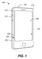
- FIG. 1is a perspective diagram of a handheld electronic device 100 according to one embodiment.
- the handheld electronic device 100may include a housing 102 that is arranged to at least partially surround the periphery of the handheld electronic device 100 to form some or all of the outer-most side, top and bottom surfaces of the handheld electronic device 100 .
- the handheld electronic device 100also includes a cover piece 104 that is arranged to be substantially coupled to housing 102 to effectively enclose an inner volume of the handheld electronic device 100 .
- the cover piece 104may include a glass member 106 , e.g., cover glass, provided over a display of the handheld electronic device 100 .
- the cover piece 104can include a protective frame 108 in which glass member 106 is held.
- the glass member 106can serve as the top surface of the housing 102 .
- a display region 107 of the glass member 106is that portion of the glass member 106 that corresponds to the display (e.g., active display region).
- the housing 102may have any suitable shape, including, for example, one or more elements that may be combined to form a rectangular structure.
- the housing 102may at least partially enclose an inner volume in which electronic device components, including a light source, may be assembled and retained.
- the shape of housing 102may substantially define boundaries of the inner volume, and may be determined based upon the size and type of components placed within the inner volume.
- the housing 102may have any suitable size, and the size may be determined based on any suitable criteria. Suitable criteria may include, but are not limited to including, aesthetics or industrial design, structural considerations, components required for a desired functionality, and/or product design.
- the housing 102may have any suitable cross-section, including for example a variable cross-section or a constant cross-section. In some embodiments, the cross-section may be selected based on desired structural properties for housing 102 .
- the cross-section of housing 102may be substantially rectangular, such that the height of housing 102 is substantially larger than the width of housing 102 .
- Such a cross-sectional shapemay provide structural stiffness in compression and tension, as well as in bending.
- the dimensions of housing 102 cross-sectionmay be determined relative to the dimensions of the components contained by housing 102 .
- housing 102may include features 110 , 112 .
- the features 110 , 112may generally include one or more openings, knobs, extensions, flanges, chamfers, or other features for receiving components or elements of the device.
- the features 110 , 112 of the housing 102extend from any surface of housing 102 , including for example from internal surfaces (e.g., to retain internal components or component layers) or from external surfaces.
- the housing 102may include a slot or opening (not shown) for receiving a card or tray within the handheld electronic device 100 .
- the housing 102may also include a connector opening (not shown), e.g., for a 30-pin connector, through which a connector may engage one or more conductive pins of the handheld electronic device 100 .
- Other features 110 , 112 included on the housing 102may include, but are not limited to, an opening for providing audio to a user, an opening for receiving audio from a user, an opening for a connector (e.g., audio connector or power supply connector), and/or features for retaining and enabling a button such as a volume control or silencing switch.
- a connectore.g., audio connector or power supply connector
- the housing 102also include an indicator hole 714 .
- the indicator hole 714is provided at a side of the housing 102 .
- the indicator holecould be placed at any portion of the housing 102 .
- the indicator hole 714is used to provide a visual indicator to a user of the handheld electronic device 100 (or other person).
- the visual indicatorcan indicate a status or alert.
- the visual indicatorcan indicate battery charging, powered-on, accessing memory, transmitting data, electrical connection, etc.
- the visual indicatorcan provide a cosmetic effect for the housing 102 .
- FIG. 2Ais a cross-sectional diagram of a portion of an electronic device 200 according to one embodiment.
- the electronic device 200includes a housing member 202 that represents a portion of a housing for the electronic device 200 and provides an outer exposed surface 204 .
- the outer exposed surface 204 of the housing for the electronic device 200is visible to a user of the electronic device.
- the housing member 202includes a hole 206 that extends through the width of the housing member 202 .
- the housing for the electronic device 200includes an inner region 208 where one or more electrical components can be provided to support the functionality of the electronic device.
- a light source 210can be provided within the inner region 208 .
- the light source 210can be mounted on a substrate 212 .
- the light source 210can, for example, be implemented as a light emitting diode (LED).
- the substrate 212can be implemented as a printed circuit board.
- a controller 214can also be mounted on the substrate 212 and electrically coupled to the light source 210 .
- the controller 214can control when the light source 210 is to produce light that will pass through the hole 206 in the housing member 202 so that a visible light indication is provided at the outer exposed surface 204 of the housing member 202 .
- the hole 206 in the housing member 202can be partially or completely filled with a light transmissive filler 216 .
- the light transmissive filler 216is substantially transparent to light so that the light produced by the light source 210 can pass through the light transmissive filler 216 .
- the light transmissive filler 216serves to seal the hole 206 so that unwanted dirt, dust, or other debris can not enter or clog the hole 206 .
- a light reflective material 218is provided on or in the light transmissive filler 216 .
- the light reflective material 218is provided in a manner such that it does not dramatically impede the light produced by the light source 210 , yet is able to provide reflection of external light that impinges on the light reflective material 218 .
- the light reflective material 218allows the hole 206 in the housing member 202 to be disguised or camouflaged while the light indication is not being provided.
- FIG. 2Bis a cross-sectional diagram of a portion of an electronic device 200 ′ according to one embodiment.
- the electronic device 200 ′ illustrated in FIG. 2Bis the same structure as the electronic device 200 illustrated in FIG. 2A .
- the electronic device 200 ′ depicted in FIG. 2Billustrates an illuminated state in which light 220 produced by the light source 210 is projected through the hole 206 .
- the light 220transmits through the light transmissive filler 216 without being blocked by the light reflective material 218 . While some of the light generated by the light source 210 could be blocked by the light reflective material 218 , a substantial portion of the generated light does project out from the hole 206 in the housing for the electronic device 200 ′.
- FIG. 2Cis a cross-sectional diagram of a portion of an electronic device 200 ′′ according to one embodiment.
- the electronic device 200 ′′ illustrated in FIG. 2Cis the same structure as the electronic device 200 illustrated in FIG. 2A .
- the electronic device 200 ′′ depicted in FIG. 2Cillustrates an non-illuminated state in which a portion of incoming external ambient light 240 is reflected by the light reflective material 218 to produce reflected ambient light 242 .
- the reflected ambient light 242can serve that provide a visual impression that the hole 206 is not present.
- the light source 210is inactive, the hole 206 is disguised whereby the user does not visually perceive the existence of the hole 206 .
- FIG. 3is a housing indication process 300 according to one embodiment.
- the housing indication process 300can be performed by an electronic device, such as the portable electronic device 100 illustrated in FIG. 1 or the electronic device 200 illustrated in FIG. 2A .
- the housing indication process 300can begin with a decision 302 that determines whether an indicator is to be turned on.
- the indicatorcan be associated with the electronic device and represent a status, alert, or other feedback to a user of the electronic device.
- the indicatoris provided by a combination of a light source (e.g., LED) and an opening in a housing for the electronic device.
- the openingcan be referred to a hole or, more specifically, an indicator hole.
- the light sourcecan be activated 304 .
- the light sourceis contained within the housing. Once the light source is activated 304 , the indicator hole in the housing can be illuminated 306 .
- the light produced by the light source(when activated) can exit the housing through the indicator hole and thereby provide a visual alert the user of the electronic device of a particular condition.
- a decision 308can determine whether the indicator is to be turned off.
- the light sourcecan be deactivated 310 . Consequently, with the light source deactivated 310 , the indicator hole in the housing becomes camouflaged 312 .
- the indicator holeis physically present in the housing of the electronic device, the indicator hole is not visible or at least not clearly visible to a person while the light source is deactivated 310 .
- the housing indication process 300can return to repeat the decision 302 and subsequent blocks so that the indicator can be continuously operated to illuminate if active or to camouflage if inactive.
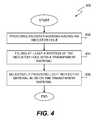
- FIG. 4is a flow diagram of a discreet hole formation process 400 according to one embodiment.
- the discreet hole formation process 400can be used to form one or more indicator holes in a housing for a consumer electronic device in a manner that makes the indicator hole discreet, that is, substantially imperceptible to a user's eye while inactivated.
- the discreet hole formation process 400can provide 402 an outer housing having an indicator hole.
- the outer housingcan refer to the exposed outer portion of the housing for the consumer electronic device, such as a portable electronic device.
- the outer housingcan include at least one indicator hole that is utilized to alert a user of one or more conditions associated with the consumer electronic device.
- the indicator holecan be filled 404 with a transparent material.
- the transparent materialdoes not have to be completely transparent but is generally clear or substantially transparent.
- a polymercan be used as the transparent material.
- the polymercan pertain to a curable adhesive that is substantially transparent at least when cured.
- light reflective materialcan be selectively provided 406 in or on the transparent material that is provided within the indicator hole.
- the light reflective materialcan pertain to ink (including paint) that can be substantially more reflective to light than the transparent material.
- FIGS. 5A-5Dillustrate cross-sectional diagrams of a portion of a housing being modified to form an indicator hole according to one embodiment.
- FIG. 5Aillustrates a housing member 500 being provided.
- the housing member 500represents a portion of the housing for an electronic device.
- the housing memberis relatively thin, such as less than 5 mm thick or, more particularly, between 0.5-2 mm thick.
- the housing member 500can be formed of an material suitable for a housing. Examples of suitable materials include metal (e.g., aluminum) or polymers (e.g., polycarbonate).
- FIG. 5Billustrates the housing member 500 being processed to form a hole 502 through the housing member 500 .
- the hole 502is also relatively small, such as less than 3 mm diameter or, more particularly, about 1 mm diameter.
- the hole 502can be formed by a laser or by drilling.
- FIG. 5Cillustrates the housing member 500 being processed to fill the hole 502 with a transparent material 504 .
- the transparent material 504can be a polymer that is in a liquid or gel form that can be inserted into the hole 502 and then solidified or cured.
- the transparent material 504can be a curable adhesive (e.g., UV curable adhesive) that can be inserted into the hole 502 and then cured, whereby when cured the adhesive is substantially transparent.
- a curable adhesivee.g., UV curable adhesive
- FIG. 5Dillustrates the housing member 500 being further processed to apply light reflective material 506 to select portions on the outer surface of the transparent material 504 .
- the light reflective material 506can be an ink that is printed, sprayed or otherwise provided on the transparent material 504 .
- the light reflective material 506can be a metal that can be deposited (e.g., physical vapor deposition) on the transparent material 504 .
- FIGS. 6A-6Dillustrate cross-sectional diagrams of a portion of a housing having light reflective characteristics being implemented at an indicator hole for an indicator according to several different embodiments.
- FIG. 6Aillustrates a housing member 600 having a hole 602 extending through the depth of the housing member 600 .
- a transparent material 604that serves to fill or seal the hole 602 .
- light reflective material 606can be provided at selective portions within the transparent material 604 .
- FIG. 6Billustrates the housing member 600 having the hole 602 extending through the depth of the housing member 600 .
- a transparent material 604that serves to fill or seal the hole 602 .
- light reflective material 608can be provided at selective portions within recesses 609 provided on the surface of the transparent material 604 .
- the recesses 609can be etched, laser formed, cut, or molded.
- the recesses 609provide a tiny reservoirs into which the light reflection material 808 (e.g., ink) can be placed.
- FIG. 6Cillustrates the housing member 600 having the hole 602 extending through the depth of the housing member 600 .
- a transparent material 604that serves to fill or seal the hole 602 .
- light reflective material 610can be provided as a layer of material provided over the transparent material 604 .
- the layer of material 610is partially light reflective and partially light transmissive so that some incident external light can be reflected so as to disguise the hole 602 when the indicator is not in use, while not overly impeding light from emitting from the hole 602 when the indicator is in use.
- FIG. 6Dillustrates the housing member 600 having the hole 602 extending through the depth of the housing member 600 .
- a semi-transparent material 604 ′that serves to fill or seal the hole 602 .
- the semi-transparent material 604 ′includes light reflection material 612 dispersed therein. The light reflection material 612 serves to provided the light reflection needed to disguise (or camouflage) the hole 602 when not in use.
- FIG. 7illustrates a top view of a portion of a housing 700 according to one embodiment.
- the housing 700includes a housing surface 702 that includes a hole 704 .
- the hole 704is filled with a filler 706 .
- the filler 706is substantially transparent so that light can pass therethrough without substantial loss.
- reflective elements 708are provided on or in the filler 706 .
- the reflective elements 708serve to reflect external incident light so that the hole 704 appears to a person to no be present. In other words, the reflective elements 708 disguise (or camouflage) the hole 704 .
- the number, size, shape and spacing of the reflective elements 708can vary widely with implementation.
- the visual appearance of the hole 704can take on any desired color.
- the techniques and apparatus describe hereinmay be applied to housings used by any of a variety of electronic devices including but not limited handheld electronic devices, portable electronic devices and substantially stationary electronic devices. Examples of these include any known consumer electronic device that includes a display.
- the electronic devicemay correspond to media players, mobile phones (e.g., cellular phones, smart phones), PDAs, remote controls, netbooks, notebooks, tablet PCs, gaming controllers, monitors, all in one computers and the like.
Landscapes
- Engineering & Computer Science (AREA)
- Computer Hardware Design (AREA)
- General Engineering & Computer Science (AREA)
- Theoretical Computer Science (AREA)
- Human Computer Interaction (AREA)
- Physics & Mathematics (AREA)
- General Physics & Mathematics (AREA)
- Signal Processing (AREA)
- Casings For Electric Apparatus (AREA)
- Telephone Set Structure (AREA)
Abstract
Description
Conventionally, a portable electronic device has a housing that encases various electrical components of the portable electronic device. Often, the portable electronic device has one or more indicator lights. For example, the housing can include a small hole through which light can be expelled when an indicator light is to be provided. The indicator lights can be used for various purposes, such as for a status indication or an alert to be provided to a user of the portable electronic device. Examples of common indicator lights include a battery charging indicator light, a power-on indicator light, etc. Unfortunately, however, the holes in the housing for the indicator lights are visible and cosmetically unappealing when the indicator lights are not use.
Techniques and apparatus for providing one or more holes in a housing for an electronic device. The one or more holes in the housing can be used to facilitate visual indicators. A light source can be controlled to provide light into a hole and thus emit light from the hole. When the light source is not providing light to the hole, the hole can be visually disguised (e.g., camouflaged) so it blends with the surrounding portions of the housing. The electronic device can, for example, be a small electronic device, such as a portable or handheld electronic device.
Embodiments of the invention can be implemented in numerous ways, including as a method, system, device, or apparatus. Several embodiments of the invention are discussed below.
As an electronic device, one embodiment can, for example, include at least: a housing having an outer exposed surface with at least one hole extending therethrough, the housing at least partially covering an inner region; a light source provided within the inner region and proximate to the at least one hole; a light transmissive filler provided in the hole; and light reflective material selectively provided in or on the light transmissive filler.
As a method for camouflaging an indicator hole in an outer housing for an electronic device, one embodiment can, for example, include at least: filling at least a portion of the indicator hole with a transparent material to seal the indicator hole; and selectively providing light reflective material in or on the transparent material provided in the indicator hole.
As a consumer electronic device, one embodiment can, for example, include at least: a housing having an outer exposed surface with at least one hole extending therethrough, the housing at least partially covering an inner region; a light source provided within the inner region and proximate to the at least one hole; a controller provided within the inner region and operatively coupled to the light source to control when the light source emits light; a polymer filler provided in the hole; and ink selectively provided in or on the polymer filler.
Other aspects and advantages of embodiment of the invention will become apparent from the following detailed description taken in conjunction with the accompanying drawings which illustrate, by way of example, the principles of the invention.
The invention will be readily understood by the following detailed description in conjunction with the accompanying drawings, wherein like reference numerals designate like structural elements, and in which:
Techniques and apparatus for providing one or more holes in a housing for an electronic device. The one or more holes in the housing can be used to facilitate visual indicators. A light source can be controlled to provide light into a hole and thus emit light from the hole. When the light source is not providing light to the hole, the hole can be visually disguised (e.g., camouflaged) so it blends with the surrounding portions of the housing. The electronic device can, for example, be a small electronic device, such as a portable or handheld electronic device.
The techniques and methods can be used for electronic devices which have a housing that contains one or more electrical components. These electronic devices can also be referred to as consumer electronic devices since they are for user by a consumer. In any event, the electronic devices are relatively small electronic devices, such as electronic devices which have a relatively small form factor (e.g., portable digital media players, mobile telephones (smart phones), remote controllers, connectors, adapters (power adapters)), or electronic devices which have a relatively larger form factor (e.g., portable computers, tablet computers, displays, monitors, televisions, etc.).
Embodiments are discussed below with reference toFIGS. 1-7 . However, those skilled in the art will readily appreciate that the detailed description given herein with respect to these figures is for explanatory purposes as the invention extends beyond these limited embodiments.
The following detailed description is illustrative only, and is not intended to be in any way limiting. Other embodiments will readily suggest themselves to skilled persons having the benefit of this disclosure. Reference will now be made in detail to implementations as illustrated in the accompanying drawings. The same reference indicators will generally be used throughout the drawings and the following detailed description to refer to the same or like parts. It should be appreciated that the drawings are generally not drawn to scale, and at least some features of the drawings have been exaggerated for ease of illustration.
Thehousing 102 may have any suitable shape, including, for example, one or more elements that may be combined to form a rectangular structure. Thehousing 102 may at least partially enclose an inner volume in which electronic device components, including a light source, may be assembled and retained. The shape ofhousing 102 may substantially define boundaries of the inner volume, and may be determined based upon the size and type of components placed within the inner volume.
Thehousing 102 may have any suitable size, and the size may be determined based on any suitable criteria. Suitable criteria may include, but are not limited to including, aesthetics or industrial design, structural considerations, components required for a desired functionality, and/or product design. Thehousing 102 may have any suitable cross-section, including for example a variable cross-section or a constant cross-section. In some embodiments, the cross-section may be selected based on desired structural properties forhousing 102. For example, the cross-section ofhousing 102 may be substantially rectangular, such that the height ofhousing 102 is substantially larger than the width ofhousing 102. Such a cross-sectional shape may provide structural stiffness in compression and tension, as well as in bending. In some embodiments, the dimensions ofhousing 102 cross-section may be determined relative to the dimensions of the components contained byhousing 102.
In some embodiments,housing 102 may includefeatures features features housing 102 extend from any surface ofhousing 102, including for example from internal surfaces (e.g., to retain internal components or component layers) or from external surfaces. In particular, thehousing 102 may include a slot or opening (not shown) for receiving a card or tray within the handheldelectronic device 100. Thehousing 102 may also include a connector opening (not shown), e.g., for a 30-pin connector, through which a connector may engage one or more conductive pins of the handheldelectronic device 100.Other features housing 102 may include, but are not limited to, an opening for providing audio to a user, an opening for receiving audio from a user, an opening for a connector (e.g., audio connector or power supply connector), and/or features for retaining and enabling a button such as a volume control or silencing switch.
Thehousing 102 also include an indicator hole714. In this embodiment, the indicator hole714 is provided at a side of thehousing 102. However, in other embodiment, the indicator hole could be placed at any portion of thehousing 102. The indicator hole714 is used to provide a visual indicator to a user of the handheld electronic device100 (or other person). The visual indicator can indicate a status or alert. For example, the visual indicator can indicate battery charging, powered-on, accessing memory, transmitting data, electrical connection, etc. Alternatively, the visual indicator can provide a cosmetic effect for thehousing 102.
In addition, the housing for theelectronic device 200 includes aninner region 208 where one or more electrical components can be provided to support the functionality of the electronic device. In this embodiment, alight source 210 can be provided within theinner region 208. Thelight source 210 can be mounted on asubstrate 212. Thelight source 210 can, for example, be implemented as a light emitting diode (LED). Thesubstrate 212 can be implemented as a printed circuit board. Further still, to control thelight source 210, acontroller 214 can also be mounted on thesubstrate 212 and electrically coupled to thelight source 210.
During operation of the electronic device, thecontroller 214 can control when thelight source 210 is to produce light that will pass through thehole 206 in thehousing member 202 so that a visible light indication is provided at the outer exposedsurface 204 of thehousing member 202. Additionally, thehole 206 in thehousing member 202 can be partially or completely filled with alight transmissive filler 216. Thelight transmissive filler 216 is substantially transparent to light so that the light produced by thelight source 210 can pass through thelight transmissive filler 216. Thelight transmissive filler 216 serves to seal thehole 206 so that unwanted dirt, dust, or other debris can not enter or clog thehole 206.
Further still, a lightreflective material 218 is provided on or in thelight transmissive filler 216. The lightreflective material 218 is provided in a manner such that it does not dramatically impede the light produced by thelight source 210, yet is able to provide reflection of external light that impinges on the lightreflective material 218. As a result, the lightreflective material 218 allows thehole 206 in thehousing member 202 to be disguised or camouflaged while the light indication is not being provided.
Thehousing indication process 300 can begin with adecision 302 that determines whether an indicator is to be turned on. Here, the indicator can be associated with the electronic device and represent a status, alert, or other feedback to a user of the electronic device. In one embodiment, the indicator is provided by a combination of a light source (e.g., LED) and an opening in a housing for the electronic device. The opening can be referred to a hole or, more specifically, an indicator hole. When thedecision 302 determines that the indicator is to be turned on, the light source can be activated304. Typically, the light source is contained within the housing. Once the light source is activated304, the indicator hole in the housing can be illuminated306. In particular, the light produced by the light source (when activated) can exit the housing through the indicator hole and thereby provide a visual alert the user of the electronic device of a particular condition.
On the other hand, when thedecision 302 determines that the indicator is not to be turned on, adecision 308 can determine whether the indicator is to be turned off. When thedecision 308 determines that the indicator should be turned off, the light source can be deactivated310. Consequently, with the light source deactivated310, the indicator hole in the housing becomes camouflaged312. As a result, although the indicator hole is physically present in the housing of the electronic device, the indicator hole is not visible or at least not clearly visible to a person while the light source is deactivated310.
Following theblock 306, the decision308 (when the indicator is not be turned off), or theblock 312, thehousing indication process 300 can return to repeat thedecision 302 and subsequent blocks so that the indicator can be continuously operated to illuminate if active or to camouflage if inactive.
The discreethole formation process 400 can provide402 an outer housing having an indicator hole. Here, the outer housing can refer to the exposed outer portion of the housing for the consumer electronic device, such as a portable electronic device. The outer housing can include at least one indicator hole that is utilized to alert a user of one or more conditions associated with the consumer electronic device.
Next, at least a portion of the indicator hole can be filled404 with a transparent material. The transparent material does not have to be completely transparent but is generally clear or substantially transparent. For example, a polymer can be used as the transparent material. In one specific example, the polymer can pertain to a curable adhesive that is substantially transparent at least when cured.
After the at least a portion of the indicator hole has been filled404 with the transparent material, light reflective material can be selectively provided406 in or on the transparent material that is provided within the indicator hole. The light reflective material can pertain to ink (including paint) that can be substantially more reflective to light than the transparent material. By selectively providing the light reflective material, only a portion of the outer exposed surface area of the transparent material provided in the indicator hole is covered or includes the light reflective material. After the light reflective serial has been selectively provided406, the discreethole formation process 400 can end.
The techniques and apparatus describe herein may be applied to housings used by any of a variety of electronic devices including but not limited handheld electronic devices, portable electronic devices and substantially stationary electronic devices. Examples of these include any known consumer electronic device that includes a display. By way of example, and not by way of limitation, the electronic device may correspond to media players, mobile phones (e.g., cellular phones, smart phones), PDAs, remote controls, netbooks, notebooks, tablet PCs, gaming controllers, monitors, all in one computers and the like.
The various aspects, features, embodiments or implementations of the invention described above can be used alone or in various combinations.
Although only a few embodiments of the invention have been described, it should be understood that the invention may be embodied in many other specific forms without departing from the spirit or the scope of the present invention. By way of example, the steps associated with the methods of the invention may vary widely. Steps may be added, removed, altered, combined, and reordered without departing from the spirit of the scope of the invention. Similarly, while operations are depicted in the drawings in a particular order, this should not be understood as requiring that such operations be performed in the particular order shown or in sequential order, or that all illustrated operations be performed, to achieve desirable results.
While this specification contains many specifics, these should not be construed as limitations on the scope of the disclosure or of what may be claimed, but rather as descriptions of features specific to particular embodiment of the disclosure. Certain features that are described in the context of separate embodiments can also be implemented in combination. Conversely, various features that are described in the context of a single embodiment can also be implemented in multiple embodiments separately or in any suitable subcombination. Moreover, although features may be described above as acting in certain combinations, one or more features from a claimed combination can in some cases be excised from the combination, and the claimed combination may be directed to a subcombination or variation of a subcombination.
While this invention has been described in terms of several embodiments, there are alterations, permutations, and equivalents, which fall within the scope of this invention. It should also be noted that there are many alternative ways of implementing the methods and apparatuses of the present invention. It is therefore intended that the following appended claims be interpreted as including all such alterations, permutations, and equivalents as fall within the true spirit and scope of the present invention.
Claims (24)
1. An electronic device, comprising:
a housing having an outer exposed surface with at least one hole extending therethrough, the housing at least partially covering an inner region;
a light source provided within the inner region and proximate to the at least one hole;
a light transmissive filler provided in the hole; and
light reflective material selectively and partially provided in or on the light transmissive filler.
2. An electronic device as recited inclaim 1 , wherein the light transmissive is a polymer filler, and wherein the polymer filler is substantially transparent.
3. An electronic device as recited inclaim 2 , wherein the polymer filler comprises a curable adhesive.
4. An electronic device as recited inclaim 1 , wherein the light reflective material comprises ink.
5. An electronic device as recited inclaim 1 , wherein the light reflective material comprises a plurality of layers of ink.
6. An electronic device as recited inclaim 1 , wherein the light reflective material comprises a plurality of micro dots of ink.
7. An electronic device as recited inclaim 1 , wherein the at least one hole has a diameter less than 3 millimeters.
8. An electronic device as recited inclaim 1 , wherein the electronic device is a handheld electronic device.
9. An electronic device as recited inclaim 1 , wherein the electronic device comprises:
a controller operatively coupled to the light source to control when the light source emits light.
10. An electronic device as recited inclaim 1 , wherein the light reflective material serves to reflect external light such that to an observer viewing the hole, the hole is substantially camouflaged relative to nearby portions of the outer exposed surface.
11. An electronic device as recited inclaim 10 , wherein the light transmissive filler comprises a transparent material, and wherein the transparent material comprises a polymer.
12. An electronic device as recited inclaim 11 , wherein the polymer comprises a curable adhesive that is substantially transparent at least when cured.
13. An electronic device as recited inclaim 11 , wherein the polymer is substantially transparent.
14. An electronic device as recited inclaim 10 , wherein the light reflective material comprises ink.
15. An electronic device as recited inclaim 10 , wherein the light reflective material is selectively provided by printing micro dots of ink in or on the light transmissive filler provided in the hole.
16. An electronic device as recited inclaim 10 , wherein the light reflective material is selectively provided by printing micro dots of ink on the light transmissive filler provided in the hole.
17. An electronic device as recited inclaim 10 , wherein the light reflective material is selectively provided by depositing at least one layer of ink at select portions in or on the light transmissive filler provided in the hole.
18. An electronic device as recited inclaim 10 , wherein the selectively providing comprises:
depositing at least one layer of ink at select portions on the light transmissive filler provided in the hole.
19. A consumer electronic device, comprising:
a housing having an outer exposed surface with at least one hole extending therethrough, the housing at least partially covering an inner region;
a light source provided within the inner region and proximate to the at least one hole;
a controller provided within the inner region and operatively coupled to the light source to control when the light source emits light;
a polymer filler provided in the hole; and
ink selectively provided in or on the polymer filler, wherein the ink is only partially in or on the polymer filler.
20. A consumer electronic device as recited inclaim 19 , wherein the polymer filler is substantially transparent, and wherein the ink is substantially opaque.
21. A consumer electronic device as recited inclaim 19 , wherein the ink serves to reflect external light such that to an observer viewing the at least one hole, the at least one hole is substantially camouflaged relative to nearby portions of the outer exposed surface.
22. A consumer electronic device as recited inclaim 19 , wherein the at least one hole has a diameter less than 3 millimeters.
23. An electronic device as recited inclaim 1 , wherein the outer exposed surface of the housing adjacent the hole is substantially flush with a top surface of the polymer filler with the ink material.
24. An electronic device as recited inclaim 1 , wherein the outer exposed surface of the housing adjacent the hole is substantially flush with a top surface of the light transmissive filler with the light reflective material.
Priority Applications (1)
| Application Number | Priority Date | Filing Date | Title |
|---|---|---|---|
| US13/921,983US9459661B2 (en) | 2013-06-19 | 2013-06-19 | Camouflaged openings in electronic device housings |
Applications Claiming Priority (1)
| Application Number | Priority Date | Filing Date | Title |
|---|---|---|---|
| US13/921,983US9459661B2 (en) | 2013-06-19 | 2013-06-19 | Camouflaged openings in electronic device housings |
Publications (2)
| Publication Number | Publication Date |
|---|---|
| US20140376234A1 US20140376234A1 (en) | 2014-12-25 |
| US9459661B2true US9459661B2 (en) | 2016-10-04 |
Family
ID=52110790
Family Applications (1)
| Application Number | Title | Priority Date | Filing Date |
|---|---|---|---|
| US13/921,983Active2034-05-18US9459661B2 (en) | 2013-06-19 | 2013-06-19 | Camouflaged openings in electronic device housings |
Country Status (1)
| Country | Link |
|---|---|
| US (1) | US9459661B2 (en) |
Families Citing this family (1)
| Publication number | Priority date | Publication date | Assignee | Title |
|---|---|---|---|---|
| US9652082B1 (en)* | 2014-08-20 | 2017-05-16 | Amazon Technologies, Inc. | Space efficient electronic device component configurations |
Citations (298)
| Publication number | Priority date | Publication date | Assignee | Title |
|---|---|---|---|---|
| US2643020A (en) | 1946-03-04 | 1953-06-23 | Corning Glass Works | Soft glass and composite article |
| US3415637A (en) | 1967-06-14 | 1968-12-10 | Saint Gobain Corp | Strengthening glass sheets by ion exchange |
| US3441398A (en) | 1964-08-10 | 1969-04-29 | Ppg Industries Inc | Method of removing ion from salt bath by ion exchange regeneration |
| DE1496586A1 (en) | 1962-12-19 | 1969-06-04 | Philips Nv | Process for the production of glass objects with high mechanical strength |
| US3467508A (en) | 1965-07-09 | 1969-09-16 | Pilkington Brothers Ltd | Float glass surface modification process |
| US3498773A (en) | 1966-02-23 | 1970-03-03 | Owens Illinois Inc | Method of strengthening glass by ion exchange |
| AT283630B (en) | 1967-04-28 | 1970-08-10 | Glaverbel | Method and device for the production of bent and toughened glass sheets |
| US3558415A (en) | 1969-01-13 | 1971-01-26 | Ppg Industries Inc | Glass window having a compressively stressed outer glass sheet |
| US3607172A (en) | 1968-11-01 | 1971-09-21 | Brockway Glass Co Inc | Tripotassium phosphate treatment for strengthening glass |
| US3619240A (en) | 1967-04-25 | 1971-11-09 | Glaverbel | Mechanically strengthening articles made of vitreous or ceramic materials |
| US3626723A (en) | 1967-04-28 | 1971-12-14 | Glaverbel | Production of chemically strengthened curved glass bodies |
| DE1771268A1 (en) | 1967-04-28 | 1971-12-23 | Glaverbel | Method and device for bending glass |
| US3652244A (en) | 1967-04-27 | 1972-03-28 | Glaverbel | Chemical treatments for modifying physical properties of various materials |
| US3753840A (en) | 1970-01-19 | 1973-08-21 | Glaverbel | Fabrication of curved glass sheets |
| GB1346747A (en) | 1971-07-28 | 1974-02-13 | Saint Gobain | Method for strengthening glass by ion exchange |
| US3798013A (en) | 1971-04-26 | 1974-03-19 | Nippon Sheet Glass Co Ltd | Double ion exchange method for strengthening glass articles |
| US3843472A (en) | 1971-05-21 | 1974-10-22 | Glaverbel | Method of strengthening an edge of a glass article and article with strengthened edge |
| US3857689A (en) | 1971-12-28 | 1974-12-31 | Nippon Selfoc Co Ltd | Ion exchange process for manufacturing integrated optical circuits |
| US3926605A (en) | 1974-06-27 | 1975-12-16 | Ppg Industries Inc | Method and apparatus for forming a ribbon of glass on a molten metal bath |
| US3951707A (en) | 1973-04-02 | 1976-04-20 | Kulite Semiconductor Products, Inc. | Method for fabricating glass-backed transducers and glass-backed structures |
| US4015045A (en) | 1974-01-09 | 1977-03-29 | Ppg Industries, Inc. | Chemical strengthening of glass |
| JPS5231757B2 (en) | 1972-12-30 | 1977-08-17 | ||
| US4052184A (en) | 1976-03-23 | 1977-10-04 | Corning Glass Works | Contouring glass seal edge |
| US4119760A (en) | 1975-08-15 | 1978-10-10 | Ppg Industries, Inc. | Chemical strengthening of glass |
| US4156755A (en) | 1978-04-19 | 1979-05-29 | Ppg Industries, Inc. | Lithium containing ion exchange strengthened glass |
| US4165228A (en) | 1977-05-26 | 1979-08-21 | Agency Of Industrial Science And Technology | Process and apparatus for heat treating edge of plate glass |
| US4178082A (en) | 1976-12-18 | 1979-12-11 | Carl Zeiss-Stiftung | Hardened circular spectacle-lens element and method of making the same |
| JPS5567529U (en) | 1978-11-02 | 1980-05-09 | ||
| JPS5595645U (en) | 1978-12-22 | 1980-07-02 | ||
| US4212919A (en) | 1979-06-28 | 1980-07-15 | Corning Glass Works | Strengthened polychromatic glasses |
| JPS5531944Y2 (en) | 1975-07-23 | 1980-07-30 | ||
| US4218230A (en) | 1978-08-04 | 1980-08-19 | Brockway Glass Company, Inc. | Method of glass strengthening by ion exchange |
| JPS55144450U (en) | 1979-04-03 | 1980-10-16 | ||
| US4346601A (en) | 1980-08-18 | 1982-08-31 | The Post Office | Testing glass fibres |
| US4353649A (en) | 1979-07-06 | 1982-10-12 | Tokyo Shibaura Denki Kabushiki Kaisha | Apparatus for surface stress measurement of glass coating and transparent plastic product |
| DE3212612A1 (en) | 1982-04-05 | 1983-10-13 | Schott Glaswerke, 6500 Mainz | Chemically curable watch glass of high Knoop hardness |
| US4425810A (en) | 1981-11-05 | 1984-01-17 | Chevron Research Company | Apparatus for physical properties measurements at high temperatures and pressures |
| JPS5937451Y2 (en) | 1978-10-13 | 1984-10-17 | 株式会社クボタ | label pasting equipment |
| US4537820A (en) | 1983-11-01 | 1985-08-27 | Union Carbide Corporation | Insulation board and process of making |
| US4646722A (en) | 1984-12-10 | 1987-03-03 | Opielab, Inc. | Protective endoscope sheath and method of installing same |
| US4733973A (en) | 1986-05-12 | 1988-03-29 | American Glass Research, Inc. | Method and apparatus for testing glassware |
| JPS63222234A (en) | 1987-03-11 | 1988-09-16 | Mitsubishi Heavy Ind Ltd | Strain/stress measuring film |
| JPS6360129B2 (en) | 1979-10-01 | 1988-11-22 | ||
| US4842629A (en) | 1986-12-01 | 1989-06-27 | Siemens Aktiengesellschaft | Method for producing buried regions of raised refractive index in a glass member by ion exchange |
| US4844724A (en) | 1984-11-29 | 1989-07-04 | Hoya Corporation | Method of adjusting refractive index distribution lenses |
| US4846868A (en) | 1986-09-05 | 1989-07-11 | Central Glass Company, Limited | Chemically strengthened glass article and method of producing same |
| US4849002A (en) | 1987-10-27 | 1989-07-18 | Kigre, Inc. | Ion-exchangeable germanate method for strengthened germanate glass articles |
| US4872896A (en) | 1988-05-27 | 1989-10-10 | Alfred University | Process for strengthening glass |
| US4911743A (en) | 1986-05-29 | 1990-03-27 | Hughes Aircraft Company | Glass structure strengthening by etching |
| US4937129A (en) | 1988-01-06 | 1990-06-26 | Semiconductor Energy Laboratory Co., Ltd. | Thin film pattern structure formed on a glass substrate |
| US4957364A (en) | 1989-04-18 | 1990-09-18 | Hughes Aircraft Company | Helical bend proof testing of optical fibers |
| US4959548A (en) | 1989-05-02 | 1990-09-25 | The United States Of America As Represented By The United States Department Of Energy | Neutron apparatus for measuring strain in composites |
| US4983197A (en) | 1988-08-09 | 1991-01-08 | Froning Edilbert A K | Method for producing waveguides in a glass substrate by ion exchange |
| US4986130A (en) | 1989-10-19 | 1991-01-22 | Engelhaupt Darell E | Apparatus and method for monitoring stress as a coating is applied |
| US5041173A (en) | 1985-03-25 | 1991-08-20 | Kabushiki Kaisha Toshiba | Lapping tools |
| US5104435A (en) | 1985-03-05 | 1992-04-14 | Nippon Sheet Glass Co., Ltd. | Method of making a plate microlens |
| US5129934A (en) | 1990-12-24 | 1992-07-14 | Ford Motor Company | Method and apparatus for bending glass sheets |
| US5157746A (en) | 1990-06-08 | 1992-10-20 | Brother Kogyo Kabushiki Kaisha | Optical waveguide array including two-dimensional lens and its manufacturing method |
| US5160523A (en) | 1990-07-10 | 1992-11-03 | Oy Nokia Ab | Method of producing optical waveguides by an ion exchange technique on a glass substrate |
| JPH0532431Y2 (en) | 1987-08-25 | 1993-08-19 | ||
| JPH05249422A (en) | 1992-03-06 | 1993-09-28 | Casio Comput Co Ltd | Liquid crystal display device manufacturing method |
| US5254149A (en) | 1992-04-06 | 1993-10-19 | Ford Motor Company | Process for determining the quality of temper of a glass sheet using a laser beam |
| US5269888A (en) | 1990-04-19 | 1993-12-14 | Cselt - Centro Studi E Laboratori Telecomunicazioni S.P.A. | Method of fabricating integrated optical devices by means of field-assisted ion exchange |
| US5281303A (en) | 1991-09-27 | 1994-01-25 | Corning Incorporated | Process for manufacturing integrated optical components using silicon mask |
| US5369267A (en) | 1993-05-18 | 1994-11-29 | Intevac, Inc. | Microchannel image intensifier tube with novel sealing feature |
| US5411563A (en) | 1993-06-25 | 1995-05-02 | Industrial Technology Research Institute | Strengthening of multilayer ceramic/glass articles |
| US5437193A (en) | 1994-03-22 | 1995-08-01 | The United States Of America As Represented By The United States Department Of Energy | Method and apparatus for testing microfilaments |
| US5445871A (en) | 1990-10-30 | 1995-08-29 | Kansai Paint Co., Ltd. | Surface-modified plastic plate |
| US5483261A (en) | 1992-02-14 | 1996-01-09 | Itu Research, Inc. | Graphical input controller and method with rear screen image detection |
| US5488204A (en) | 1992-06-08 | 1996-01-30 | Synaptics, Incorporated | Paintbrush stylus for capacitive touch sensor pad |
| US5525138A (en) | 1994-05-26 | 1996-06-11 | Ford Motor Company | Determination of tensile membrane stress and compressive layer thickness in tempered glass using a CO2 laser beam |
| US5625154A (en) | 1993-12-24 | 1997-04-29 | Ngk Ceramics Europe S.A. | Method and apparatus for testing ceramic specimens by simultaneous application of mechanical and thermal stresses |
| US5654057A (en) | 1994-12-28 | 1997-08-05 | Hoya Corporation | Sheet glass flattening method, method of manufacturing glass substrate for an information recording disk using flattened glass, method of manufacturing a magnetic recording disk using glass substrate, and magnetic recording medium |
| JPH09312245A (en) | 1996-05-21 | 1997-12-02 | Hoya Corp | Thin-film-deposited substrate and manufacture thereof |
| US5733622A (en) | 1995-06-07 | 1998-03-31 | International Business Machines Corporation | Edge strengthened substrate of a data storage disk and method for fabricating same |
| US5766493A (en) | 1995-07-06 | 1998-06-16 | Lg Electronics Inc. | Method of fabricating a liquid crystal display substrate |
| US5780371A (en) | 1994-10-13 | 1998-07-14 | Saint-Gobain Vitrage S.A. | Reinforced glass substrate |
| US5816225A (en) | 1996-05-14 | 1998-10-06 | I.A.T. Technologies Limited | Device for the treatment of engine and heating fuels obtained from mineral oil or from plants |
| US5825352A (en) | 1996-01-04 | 1998-10-20 | Logitech, Inc. | Multiple fingers contact sensing method for emulating mouse buttons and mouse operations on a touch sensor pad |
| US5826601A (en) | 1995-03-30 | 1998-10-27 | Dainippon Screen Mfg., Co. | Treating liquid replacing method, substrate treating method and substrate treating apparatus |
| US5835079A (en) | 1996-06-13 | 1998-11-10 | International Business Machines Corporation | Virtual pointing device for touchscreens |
| US5880411A (en) | 1992-06-08 | 1999-03-09 | Synaptics, Incorporated | Object position detector with edge motion feature and gesture recognition |
| US5930047A (en) | 1995-04-21 | 1999-07-27 | Xelux Holding Ag | Anti-glare device |
| US5953094A (en) | 1997-04-04 | 1999-09-14 | Sanyo Electric Co., Ltd. | Liquid crystal display device |
| US5985014A (en) | 1996-10-01 | 1999-11-16 | Minolta Co., Ltd. | Ink for ink-jet recording containing specified glycol derivatives |
| US6050870A (en) | 1994-12-09 | 2000-04-18 | Seiko Instruments, Inc. | Display device and method of manufacturing the same |
| US6114039A (en) | 1996-02-07 | 2000-09-05 | Saint Gobain Vitrage | Process for treating glass substrates |
| US6120908A (en) | 1997-09-08 | 2000-09-19 | Elf Atochem North America, Inc. | Strengthening flat glass by edge coating |
| EP1038663A2 (en) | 1999-03-26 | 2000-09-27 | Agfa-Gevaert N.V. | Method of making an electronic module comprising a glass laminate |
| CN1277090A (en) | 1999-06-14 | 2000-12-20 | 康宁股份有限公司 | Method for finishing glass plate edge |
| US6166915A (en) | 1996-01-11 | 2000-12-26 | Micron Technology, Inc. | Electronic circuits and circuit boards |
| US6188391B1 (en) | 1998-07-09 | 2001-02-13 | Synaptics, Inc. | Two-layer capacitive touchpad and method of making same |
| FR2797627A1 (en) | 1999-08-19 | 2001-02-23 | Stein Heurtey | Improved annealing unit for flat glass has single cooling air manifold at junction of pre-annealing and annealing zones and at junction of annealing and post annealing zones |
| JP2001083887A (en) | 1999-09-10 | 2001-03-30 | Nec Eng Ltd | Mounting structure of liquid crystal display device |
| FR2801302A1 (en) | 1999-11-22 | 2001-05-25 | Saint Gobain Vitrage | Treatment of glass substrates used for production of display screens involves ion-exchange and thermal processing |
| US6245313B1 (en) | 1998-05-19 | 2001-06-12 | Toshiba Machine Co., Ltd. | Process for manufacturing a product of glassy carbon |
| US6287674B1 (en) | 1997-10-24 | 2001-09-11 | Agfa-Gevaert | Laminate comprising a thin borosilicate glass substrate as a constituting layer |
| US6307590B1 (en) | 1997-01-30 | 2001-10-23 | Fuji Photo Film Co., Ltd. | Cooled CCD camera |
| US6310610B1 (en) | 1997-12-04 | 2001-10-30 | Nortel Networks Limited | Intelligent touch display |
| US6323846B1 (en) | 1998-01-26 | 2001-11-27 | University Of Delaware | Method and apparatus for integrating manual input |
| US6327011B2 (en) | 1997-10-20 | 2001-12-04 | Lg Electronics, Inc. | Liquid crystal display device having thin glass substrate on which protective layer formed and method of making the same |
| JP2002003895A (en) | 2000-06-26 | 2002-01-09 | Lion Hygiene Kk | Solid detergent and its manufacturing method |
| US6350664B1 (en) | 1999-09-02 | 2002-02-26 | Matsushita Electric Industrial Co., Ltd. | Semiconductor device and method of manufacturing the same |
| US6393180B1 (en) | 1997-10-07 | 2002-05-21 | Jds Fitel Inc. | Providing a refractive index change in an ion diffused material |
| WO2002042838A1 (en) | 2000-11-27 | 2002-05-30 | Seamless Display Limited | Visual display screen arrangement |
| US6429840B1 (en) | 1999-09-27 | 2002-08-06 | Citizen Watch Co., Ltd. | Method of driving color liquid crystal display panel and method of controlling display of timepiece |
| US20020105793A1 (en)* | 2000-12-12 | 2002-08-08 | Masaharu Oda | Surface lighting device |
| US6437867B2 (en) | 1996-12-04 | 2002-08-20 | The Research Foundation Of The City University Of New York | Performing selected optical measurements with optical coherence domain reflectometry |
| CN1369449A (en) | 2002-03-26 | 2002-09-18 | 中国建筑材料科学研究院 | Process for over-all strengthening of glass |
| US20020155302A1 (en) | 2001-04-19 | 2002-10-24 | Smith Novis W. | Method for preparing laminated safety glass |
| US20020157199A1 (en) | 2000-05-19 | 2002-10-31 | International Business Machines Corporation | Lanthanide oxide dissolution from glass surface |
| JP2002342033A (en) | 2001-05-21 | 2002-11-29 | Sony Corp | Non-contact type user input device |
| US20030024274A1 (en) | 2001-08-06 | 2003-02-06 | Cho Doo Hee | Method of manufacturing a planar waveguide using ion exchange method |
| US6516634B1 (en) | 1999-02-12 | 2003-02-11 | The Penn State Research Foundation | Strengthening, crack arrest and multiple cracking in brittle materials using residual stresses |
| US6521862B1 (en) | 2001-10-09 | 2003-02-18 | International Business Machines Corporation | Apparatus and method for improving chamfer quality of disk edge surfaces with laser treatment |
| US20030057183A1 (en) | 2001-09-21 | 2003-03-27 | Cho Gyu Sn | Method of fabricating thin liquid crystal display device |
| US20030077453A1 (en) | 2001-10-18 | 2003-04-24 | Hitoshi Oaku | Display device substrate and display device formed therewith |
| US6621542B1 (en) | 1999-10-29 | 2003-09-16 | Seiko Epson Corporation | Electro-optic panel, device, and apparatus having a mark on a planarized layer on an irregular surface |
| US20030234771A1 (en) | 2002-06-21 | 2003-12-25 | Mulligan Roger C. | Capacitive touch sensor architecture with unique sensor bar addressing |
| US6690387B2 (en) | 2001-12-28 | 2004-02-10 | Koninklijke Philips Electronics N.V. | Touch-screen image scrolling system and method |
| WO2004014109A1 (en) | 2002-07-31 | 2004-02-12 | Nippon Sheet Glass Co., Ltd. | Sealing plate for electroluminecense element and mother glass substrate for taking a large number of sealing plates |
| JP2004094256A (en) | 2002-09-03 | 2004-03-25 | Samsung Electronics Co Ltd | Flat panel display |
| US6718612B2 (en) | 1999-08-04 | 2004-04-13 | Asahi Glass Company, Ltd. | Method for manufacturing a magnetic disk comprising a glass substrate using a protective layer over a glass workpiece |
| US20040119701A1 (en) | 2002-12-19 | 2004-06-24 | Mulligan Roger C. | Lattice touch-sensing system |
| US20040137828A1 (en) | 2002-07-17 | 2004-07-15 | Hoya Corporation | Glass substrate for a mask blank, method of producing a glass substrate for a mask blank, mask blank, method of producing the mask blank, transfer mask, and method of producing a transfer mask |
| US20040142118A1 (en) | 2003-01-10 | 2004-07-22 | Nec Corporation | Flexible electronic device and production method of the same |
| WO2004061806A1 (en) | 2002-12-27 | 2004-07-22 | Semiconductor Energy Laboratory Co., Ltd. | Display and electronic device |
| US20040163414A1 (en) | 2003-02-20 | 2004-08-26 | Hoya Corporation | Method of processing a glass substrate for a magnetic disk and method of manufacturing the glass substrate |
| DE10322350A1 (en) | 2003-05-17 | 2004-12-09 | Schott Ag | Production of optical device comprises coating first region of substrate with coating having first layer with exchange atoms, removing substrate material from second region, and exchanging substrate ions with exchange ions |
| US20050105071A1 (en) | 2003-06-03 | 2005-05-19 | Fusao Ishii | Methods for patterning substrates having arbitrary and unexpected dimensional changes |
| JP2005162549A (en) | 2003-12-03 | 2005-06-23 | Toshiba Ceramics Co Ltd | Silica glass crucible |
| US20050135724A1 (en) | 2003-12-19 | 2005-06-23 | Henry Helvajian | Integrated glass ceramic systems |
| US6936741B2 (en) | 2003-06-30 | 2005-08-30 | Bayer Materialscience Ag | Process for working up the waste water obtained in the preparation of dinitrotoluene |
| US20050193772A1 (en) | 2004-03-05 | 2005-09-08 | Davidson Ronald A. | Closed cassette and method for heat treating glass sheets |
| US6955971B2 (en) | 2002-11-12 | 2005-10-18 | S.O.I.Tec Silicon On Insulator Technologies S.A. | Semiconductor structure and methods for fabricating same |
| EP1592073A1 (en) | 2004-04-30 | 2005-11-02 | Kabushiki Kaisha Toyota Jidoshokki | Method for thinning substrates of EL devices |
| EP1593658A1 (en) | 2004-05-07 | 2005-11-09 | Schott AG | Chemically and thermally pre-stressable lithium aluminosilicate float glass of high temperature resistance |
| US20050259438A1 (en)* | 2003-02-21 | 2005-11-24 | Minebea Co., Ltd. | Spread illuminating apparatus with light conductive plate having polygonal configuration |
| US20050285991A1 (en) | 2004-06-28 | 2005-12-29 | Kabushiki Kaisha Toshiba | Liquid crystal display device protection structure for electronic equipment |
| US20060026521A1 (en) | 2004-07-30 | 2006-02-02 | Apple Computer, Inc. | Gestures for touch sensitive input devices |
| US6996324B2 (en) | 2001-09-19 | 2006-02-07 | Matsushita Electric Industrial Co., Ltd. | Optical waveguide and method for fabricating the same |
| US7012700B2 (en) | 2002-06-17 | 2006-03-14 | Zygo Corporation | Interferometric optical systems having simultaneously scanned optical path length and focus |
| US20060055936A1 (en) | 2004-09-10 | 2006-03-16 | The General Hospital Corporation | System and method for optical coherence imaging |
| US20060054335A1 (en)* | 2004-09-13 | 2006-03-16 | Rapp Geoffrey D | Housing for scale or load cell controller |
| US7013709B2 (en) | 2002-01-31 | 2006-03-21 | Symyx Technologies, Inc. | High throughput preparation and analysis of plastically shaped material samples |
| US7015894B2 (en) | 2001-09-28 | 2006-03-21 | Ricoh Company, Ltd. | Information input and output system, method, storage medium, and carrier wave |
| JP2000163031A5 (en) | 1998-11-25 | 2006-03-23 | ||
| US20060063351A1 (en) | 2004-09-10 | 2006-03-23 | Versatilis Llc | Method of making a microelectronic and/or optoelectronic circuitry sheet |
| US20060070694A1 (en) | 2000-05-03 | 2006-04-06 | Saint-Gobain Glass France | Laminated glazing material |
| US20060097991A1 (en) | 2004-05-06 | 2006-05-11 | Apple Computer, Inc. | Multipoint touchscreen |
| US7070837B2 (en) | 2001-08-08 | 2006-07-04 | Mark Ross | Screen protector |
| US20060197753A1 (en) | 2005-03-04 | 2006-09-07 | Hotelling Steven P | Multi-functional hand-held device |
| US20060227331A1 (en) | 2005-04-06 | 2006-10-12 | Frank Vollmer | Method and apparatus for measuring and monitoring optical properties based on a ring-resonator |
| US20060238695A1 (en) | 2005-04-26 | 2006-10-26 | Sharp Kabushiki Kaisha | Display device and method for manufacturing the same |
| US20060250559A1 (en) | 2003-07-03 | 2006-11-09 | Bocko Peter L | Glass product for use in ultra-thin glass display applications |
| US20060268528A1 (en) | 2004-07-02 | 2006-11-30 | Apple Computer, Inc. | Handheld computing device |
| US20060292822A1 (en) | 2005-06-27 | 2006-12-28 | Ya-Hong Xie | Method for producing dislocation-free strained crystalline films |
| US20070003796A1 (en) | 2005-06-03 | 2007-01-04 | Hoya Corporation | Method for manufacturing magnetic disk glass substrate and method for manufacturing magnetic disk |
| US20070013822A1 (en) | 2005-07-15 | 2007-01-18 | Toshiba Matsushita Display Technology Co., Ltd | Display device and method of manufacturing the same |
| US7166531B1 (en) | 2005-01-31 | 2007-01-23 | Novellus Systems, Inc. | VLSI fabrication processes for introducing pores into dielectric materials |
| US20070029519A1 (en) | 2001-08-24 | 2007-02-08 | Hirohisa Kikuyama | Surface treating solution for fine processing of glass base plate having a plurality of components |
| US20070030436A1 (en) | 2005-08-05 | 2007-02-08 | Seiko Epson Corporation | Liquid crystal device, electro-optical device, projector, and micro-device |
| US20070039353A1 (en) | 2003-09-29 | 2007-02-22 | Naohiro Kamiya | Chemical strengthening treatment method of magnetic disk glass substrate |
| US20070046200A1 (en) | 2005-08-31 | 2007-03-01 | Chung-Lin Fu | Plasma display panel and manufacturing method of barrier ribs thereof |
| US20070063876A1 (en) | 2005-08-24 | 2007-03-22 | Wong Alex K | Multiple sensing element touch sensor |
| JP2007099557A (en) | 2005-10-04 | 2007-04-19 | Nippon Electric Glass Co Ltd | Tempered glass article and method for producing the same |
| US20070089827A1 (en) | 2004-06-01 | 2007-04-26 | Asahi Glass Co., Ltd. | Method for producing an optical element |
| US20070122542A1 (en) | 2003-07-03 | 2007-05-31 | Donnelly Corporation | Method of manufacturing a touch screen |
| US20070132737A1 (en) | 2005-12-09 | 2007-06-14 | Mulligan Roger C | Systems and methods for determining touch location |
| CN1322339C (en) | 2005-06-08 | 2007-06-20 | 中国科学院上海光学精密机械研究所 | High diffraction efficiency quartz transmission grating with 532 nm wavelength |
| WO2007089054A1 (en) | 2006-01-31 | 2007-08-09 | Optron-Tec Co., Ltd. | Protective glass complex and method of manufacturing the same |
| US20070196578A1 (en) | 2006-10-10 | 2007-08-23 | Michael Karp | Method and system for coating |
| US20070236618A1 (en) | 2006-03-31 | 2007-10-11 | 3M Innovative Properties Company | Touch Screen Having Reduced Visibility Transparent Conductor Pattern |
| JP2008001590A (en) | 2006-05-25 | 2008-01-10 | Nippon Electric Glass Co Ltd | Tempered glass and method for producing the same |
| JP2008007360A (en) | 2006-06-28 | 2008-01-17 | Optrex Corp | Mother glass substrate, glass substrate and method for manufacturing the glass substrate |
| US20080020919A1 (en) | 2006-05-25 | 2008-01-24 | Nippon Electric Glass Co., Ltd. | Tempered glass and process for producing the same |
| US20080026260A1 (en) | 2006-07-03 | 2008-01-31 | Hideki Kawai | Method for fabricating a glass substrate, magnetic disk, and method for fabricating the same |
| JP2008066126A (en) | 2006-09-07 | 2008-03-21 | Pentax Corp | Sealing member and organic electroluminescence element |
| JP2008063166A (en) | 2006-09-05 | 2008-03-21 | Casio Comput Co Ltd | Method for reducing deformation of workpiece, method for machining workpiece, and method for manufacturing reactor |
| US20080074028A1 (en) | 2002-09-03 | 2008-03-27 | Helmars Ozolins | Bezel-less electronic display |
| US20080094716A1 (en) | 2004-09-10 | 2008-04-24 | Toshihiko Ushiro | Transmission-Type Display Panel and Method of Manufacturing the Same |
| US20080135175A1 (en) | 2005-08-09 | 2008-06-12 | Asahi Glass Company, Limited | Thin plate glass laminate and process for producing display device using thin plate glass laminate |
| CN101206314A (en) | 2006-12-19 | 2008-06-25 | 蔡孟廷 | Touch panel display device, touch panel unit manufacturing method, and glass grinder for manufacturing touch panel unit |
| US20080158181A1 (en) | 2007-01-03 | 2008-07-03 | Apple Computer, Inc. | Double-sided touch sensitive panel and flex circuit bonding |
| JP2008192194A (en) | 2007-01-31 | 2008-08-21 | Hoya Corp | Manufacturing method of glass substrate for magnetic disk, manufacturing method of magnetic disk, magnetic disk and manufacturing system of glass substrate for magnetic disk |
| US20080202167A1 (en) | 2007-02-23 | 2008-08-28 | Nicholas Dominic Cavallaro | Thermal edge finishing |
| CN101267509A (en) | 2008-04-28 | 2008-09-17 | 刘圣平 | A bluetooth TV receiving device and its method |
| US20080230177A1 (en) | 2007-03-19 | 2008-09-25 | White Electronic Designs Corp. | Enhanced liquid crystal display system and methods |
| US20080243321A1 (en) | 2005-02-11 | 2008-10-02 | Econtrols, Inc. | Event sensor |
| US20080261057A1 (en) | 2007-04-20 | 2008-10-23 | White Electronic Designs Corp. | Bezelless display system |
| US20080264176A1 (en) | 2007-04-30 | 2008-10-30 | Snecma | Method of making an alumina deposit on a substrate covered in sic |
| US20080286548A1 (en) | 2007-05-18 | 2008-11-20 | Adam James Ellison | Down-drawable, chemically strengthened glass for cover plate |
| US7461564B2 (en) | 2006-10-04 | 2008-12-09 | Corning Incorporated | Method and apparatus for proof testing a sheet of brittle material |
| WO2009003029A2 (en) | 2007-06-25 | 2008-12-31 | Brewer Science Inc. | High-temperature spin-on temporary bonding compositions |
| EP2025556A2 (en) | 2007-08-07 | 2009-02-18 | Murakami Corporation | Image pickup device-equipped rear view mirror |
| US20090046240A1 (en) | 2007-08-16 | 2009-02-19 | Brian Bolton | Methods and Systems for Strengthening LCD Modules |
| US20090067141A1 (en) | 2007-09-04 | 2009-03-12 | Apple Inc. | Assembly of a handheld electronic device |
| EP2036867A1 (en) | 2006-06-08 | 2009-03-18 | Hoya Corporation | Glass for use as substrate for information recording medium, substrate for information recording medium, information recording medium, and their production methods |
| US20090091551A1 (en) | 2007-10-04 | 2009-04-09 | Apple Inc. | Single-layer touch-sensitive display |
| US20090096937A1 (en) | 2007-08-16 | 2009-04-16 | Bauer Frederick T | Vehicle Rearview Assembly Including a Display for Displaying Video Captured by a Camera and User Instructions |
| US20090153729A1 (en) | 2007-12-17 | 2009-06-18 | Jari Hiltunen | Reflowable Camera Module With Integrated Flash |
| WO2009078406A1 (en) | 2007-12-18 | 2009-06-25 | Hoya Corporation | Cover glass for portable terminal, method for manufacturing cover glass for portable terminal, and portable terminal apparatus |
| US20090162703A1 (en) | 2006-10-16 | 2009-06-25 | Konica Minolta | Glass Substrate for Information Recording Medium, and Method of Manufacturing Glass Substrate for Magnetic Recording Medium and Information Recording Medium |
| EP2075237A1 (en) | 2006-10-10 | 2009-07-01 | Nippon Electric Glass Co., Ltd. | Reinforced glass substrate |
| US7558054B1 (en) | 2008-01-03 | 2009-07-07 | Apple Inc. | Display window securing system |
| US20090197048A1 (en) | 2008-02-05 | 2009-08-06 | Jaymin Amin | Damage resistant glass article for use as a cover plate in electronic devices |
| US20090202808A1 (en) | 2008-02-08 | 2009-08-13 | Gregory Scott Glaesemann | Damage resistant chemically-toughened protective cover glass |
| WO2009102326A1 (en) | 2008-02-13 | 2009-08-20 | Hewlett-Packard Development Company, L.P. | Reinforced display devices |
| US20090220761A1 (en) | 2008-02-29 | 2009-09-03 | Matthew John Dejneka | Ion exchanged, fast cooled glasses |
| US20090257189A1 (en) | 2008-04-11 | 2009-10-15 | Wang Erik L | Portable electronic device housing structures |
| WO2009125133A2 (en) | 2008-03-27 | 2009-10-15 | Saint-Gobain Glass France | Method of manufacturing flat optical elements, and elements obtained |
| US7626807B2 (en) | 2007-01-17 | 2009-12-01 | Askey Computer Corp. | Display device capable of protecting a display panel |
| US20090294420A1 (en) | 2008-05-30 | 2009-12-03 | Anatoli Anatolyevich Abramov | Laser Cutting of Glass Along A Predetermined Line |
| US20090324899A1 (en) | 2008-06-30 | 2009-12-31 | Feinstein Casey J | Full perimeter chemical strengthening of substrates |
| US20090324939A1 (en) | 2008-06-27 | 2009-12-31 | Feinstein Casey J | Method for Fabricating Thin Sheets of Glass |
| WO2010005578A1 (en) | 2008-07-11 | 2010-01-14 | Corning Incorporated | Glass with compressive surface for consumer applications |
| WO2010014163A1 (en) | 2008-07-29 | 2010-02-04 | Corning Incorporated | Dual stage ion exchange for chemical strengthening of glass |
| US20100035038A1 (en) | 2008-08-08 | 2010-02-11 | Barefoot Kristen L | Strengthened glass articles and methods of making |
| TW201007521A (en) | 2008-08-12 | 2010-02-16 | Cando Corp | Cover lens with touch-sensing function and method for fabricating the same |
| WO2010019829A1 (en) | 2008-08-13 | 2010-02-18 | Robert Stancel | Impact resistant thin-glass solar modules |
| US20100053632A1 (en) | 2004-11-12 | 2010-03-04 | Medeikon Corporation | Single Trace Multi-Channel Low Coherence Interferometric Sensor |
| US20100062284A1 (en) | 2006-12-04 | 2010-03-11 | Toru Watanabe | Method of manufacturing glass substrate for recording medium, glass substrate for recording medium, recording medium and holding jig |
| JP2010060908A (en) | 2008-09-04 | 2010-03-18 | Panasonic Corp | Video display device |
| JP2010064943A (en) | 2008-09-12 | 2010-03-25 | Olympus Corp | Method for producing glass substrate and apparatus for reinforcing glass substrate |
| US20100119846A1 (en) | 2007-03-02 | 2010-05-13 | Masahiro Sawada | Reinforced plate glass and method for manufacturing the same |
| US7719835B1 (en)* | 2009-01-05 | 2010-05-18 | Middle Atlantic Products, Inc. | Wiring distribution device for an electronics rack |
| US20100137031A1 (en) | 2008-12-01 | 2010-06-03 | Research In Motion Limited | Portable electronic device and method of controlling same |
| EP2196870A1 (en) | 2007-09-26 | 2010-06-16 | Citizen Holdings Co., Ltd. | Cover glass for watch |
| US20100154992A1 (en) | 2008-12-22 | 2010-06-24 | Feinstein Casey J | Layer-Specific Energy Distribution Delamination |
| US20100167059A1 (en) | 2008-12-26 | 2010-07-01 | Kazuaki Hashimoto | Glass substrate and method for manufacturing the same |
| US20100171920A1 (en) | 2007-06-22 | 2010-07-08 | Tomohiro Nishiyama | Display device and method for producing the same |
| US20100179044A1 (en) | 2007-09-03 | 2010-07-15 | Saint- Gobain Glass France | Glass substrate with refractive index gradient and manufacturing process of same |
| WO2010080988A2 (en) | 2009-01-09 | 2010-07-15 | Apple Inc. | A method for fabricating thin touch sensor panels |
| US20100206008A1 (en) | 2009-02-19 | 2010-08-19 | Harvey Daniel R | Method of separating strengthened glass |
| US20100216514A1 (en) | 2009-02-25 | 2010-08-26 | Embarq Holdings Company, Llc | Multi-directional display communication devices, systems, and methods |
| US20100215862A1 (en) | 2009-02-26 | 2010-08-26 | Sinue Gomez | Method for forming an opal glass |
| JP2010195600A (en) | 2009-02-23 | 2010-09-09 | Nishiyama Stainless Chemical Kk | Methods for manufacturing glass substrate for electronic device and electronic device |
| US20100224767A1 (en) | 2009-03-04 | 2010-09-09 | Tdk Corporation | Photodetector, method for manufacturing the same, and photodetection system |
| WO2010101961A2 (en) | 2009-03-02 | 2010-09-10 | Apple Inc. | Techniques for strengthening glass covers for portable electronic devices |
| JP2010237493A (en) | 2009-03-31 | 2010-10-21 | Toshiba Mobile Display Co Ltd | Liquid crystal display |
| US20100265188A1 (en) | 2009-04-20 | 2010-10-21 | Shih Chang Chang | Touch actuated sensor configuration integrated with an oled structure |
| US20100279067A1 (en) | 2009-04-30 | 2010-11-04 | Robert Sabia | Glass sheet having enhanced edge strength |
| US20100285275A1 (en) | 2009-05-06 | 2010-11-11 | Adra Smith Baca | Fingerprint-resistant glass substrates |
| US20100296027A1 (en) | 2006-10-17 | 2010-11-25 | Tsutomu Matsuhira | Display device |
| US20100315570A1 (en) | 2009-06-11 | 2010-12-16 | Mathew Dinesh C | Portable computer display structures |
| US20100321305A1 (en) | 2009-06-18 | 2010-12-23 | Shih Chang Chang | Driving an oled display structure integrated with a touch sensor configuration |
| US7872644B2 (en) | 2005-12-01 | 2011-01-18 | Lg Display Co., Ltd. | Aging pad and flat panel display device having the same |
| WO2011008433A1 (en) | 2009-07-15 | 2011-01-20 | Apple Inc. | Display modules |
| US20110019354A1 (en) | 2009-03-02 | 2011-01-27 | Christopher Prest | Techniques for Strengthening Glass Covers for Portable Electronic Devices |
| JP2011032124A (en) | 2009-07-31 | 2011-02-17 | Bridgestone Plant Engineering Co Ltd | Processing apparatus for thin sheet glass |
| US20110063550A1 (en) | 2009-09-11 | 2011-03-17 | Gettemy Shawn R | Electronic device display structures with alignment features |
| KR20110030919A (en) | 2009-09-18 | 2011-03-24 | 엘지전자 주식회사 | Handheld terminal |
| US20110067447A1 (en) | 2010-08-18 | 2011-03-24 | Stephen Paul Zadesky | Enhanced Strengthening of Glass |
| US20110072856A1 (en) | 2009-09-30 | 2011-03-31 | Andrew Davidson | Pre-Processing Techniques to Produce Complex Edges Using a Glass Slumping Process |
| WO2011041484A1 (en) | 2009-09-30 | 2011-04-07 | Apple Inc. | Techniques for strengthening glass covers for portable electronic devices |
| US20110102346A1 (en) | 2009-10-30 | 2011-05-05 | Orsley Timothy J | Methods and apparatus for providing touch sensitive displays |
| CN101465892B (en) | 2007-12-19 | 2011-06-08 | 深圳富泰宏精密工业有限公司 | Pick-up head protective cover structure |
| US20110159321A1 (en) | 2009-12-29 | 2011-06-30 | Hoya Corporation | Glass substrate for magnetic disk and manufacturing method thereof |
| US20110164372A1 (en) | 2010-01-06 | 2011-07-07 | Apple Inc. | Display module |
| US20110182084A1 (en)* | 2008-09-29 | 2011-07-28 | Andrew Michael Tomlinson | Light guide device |
| US20110186345A1 (en) | 2010-02-02 | 2011-08-04 | David Pakula | Offset Control for Assemblying an Electronic Device Housing |
| US20110188846A1 (en)* | 2008-04-25 | 2011-08-04 | Osram Opto Semiconductors Gmbh | Illumination Unit |
| JP2011158799A (en) | 2010-02-03 | 2011-08-18 | Sony Corp | Electro-optical device and electronic device |
| US8013834B2 (en) | 2005-08-04 | 2011-09-06 | Lg Electronics Inc. | Display apparatus and mobile communication terminal having the same |
| US20110248152A1 (en) | 2010-04-13 | 2011-10-13 | Silicon Laboratories, Inc. | Apparatus and Circuit with a Multi-Directional Arrangement of Optical Elements |
| US20110255000A1 (en) | 2010-04-19 | 2011-10-20 | Trent Weber | Camera alignment and mounting structures |
| US20110255250A1 (en) | 2010-04-19 | 2011-10-20 | Richard Hung Minh Dinh | Printed circuit board components for electronic devices |
| US20110267833A1 (en) | 2008-10-27 | 2011-11-03 | Saint-Gobain Glass France | Light-emitting diode module for a vehicle, and productions |
| US20110279383A1 (en) | 2010-05-14 | 2011-11-17 | Wilson Stephen S | Touch Screen Shield |
| US20110300908A1 (en) | 2010-06-04 | 2011-12-08 | Silvio Grespan | Thin Glass for Touch Panel Sensors and Methods Therefor |
| US20120018323A1 (en) | 2010-07-20 | 2012-01-26 | Otter Products, Llc | Flash Isolation for Device Covers |
| US20120027399A1 (en) | 2010-07-30 | 2012-02-02 | Yeates Kyle H | Electronic Device Having Selectively Strengthening Glass Cover Glass |
| US8110268B2 (en) | 2006-11-03 | 2012-02-07 | Skinit, Inc. | Adhesive cover for consumer devices |
| US8111248B2 (en) | 2008-09-12 | 2012-02-07 | Lg Display Co., Ltd. | Liquid crystal display device and method of manufacturing thereof |
| US20120099113A1 (en) | 2008-11-05 | 2012-04-26 | The General Hospital Corporation | System and method for providing full jones matrix-based analysis to determine non-depolarizing polarization parameters using optical frequency domain imaging |
| US20120105400A1 (en) | 2010-10-29 | 2012-05-03 | Mathew Dinesh C | Camera lens structures and display structures for electronic devices |
| US20120118628A1 (en) | 2010-11-11 | 2012-05-17 | David Pakula | Insert Molding Around Glass Members for Portable Electronic Devices |
| US20120136259A1 (en) | 2006-06-05 | 2012-05-31 | Volcano Corporation | Polarization-sensitive spectral interferometry |
| US20120135195A1 (en) | 2010-11-30 | 2012-05-31 | Gregory Scott Glaesemann | Methods for separating glass articles from strengthened glass substrate sheets |
| US20120151760A1 (en) | 2010-12-15 | 2012-06-21 | Sony Ericsson Mobile Communications Ab | Non-planar display glass for mobile device |
| US20120188743A1 (en) | 2010-05-14 | 2012-07-26 | Wilson Stephen S | Touch screen shield |
| US20120196071A1 (en) | 2011-02-01 | 2012-08-02 | Cornejo Ivan A | Strengthened glass substrate sheets and methods for fabricating glass panels from glass substrate sheets |
| US20120236477A1 (en) | 2011-03-16 | 2012-09-20 | Weber Douglas J | Electronic device having selectively strengthened glass |
| US20120236526A1 (en) | 2011-03-16 | 2012-09-20 | Weber Douglas J | Strengthening variable thickness glass |
| US20120281381A1 (en) | 2011-05-04 | 2012-11-08 | Sanford Emery A | Housing for Portable Electronic Device with Reduced Border Region |
| US8312743B2 (en) | 2005-05-18 | 2012-11-20 | City University Of Hong Kong | Method for fabricating buried ion-exchanged waveguides using field-assisted annealing |
| US20120328843A1 (en) | 2011-06-24 | 2012-12-27 | Cleary Thomas M | Light-weight hybrid glass laminates |
| US8393175B2 (en) | 2010-08-26 | 2013-03-12 | Corning Incorporated | Methods for extracting strengthened glass substrates from glass sheets |
| US20130071601A1 (en) | 2011-09-16 | 2013-03-21 | Amazon Technologies, Inc. | Cover glass for electronic devices |
| US20130083506A1 (en) | 2011-09-29 | 2013-04-04 | Derek W. Wright | Multi-layer transparent structures for electronic device housings |
| US20130182259A1 (en) | 2009-12-01 | 2013-07-18 | Mark Brezinski | System and method for calibrated spectral domain optical coherence tomography and low coherence interferometry |
| WO2013106242A2 (en) | 2012-01-10 | 2013-07-18 | Apple Inc. | Integrated camera window |
| US20130213565A1 (en) | 2009-04-28 | 2013-08-22 | Cheil Industries Inc. | Flexible substrate for display panel and manufacturing method thereof |
| EP2635540A1 (en) | 2010-11-04 | 2013-09-11 | Apple Inc. | Enhanced strengthening of glass |
| US8616661B2 (en)* | 2011-12-09 | 2013-12-31 | Trystar, Inc. | Portable power distribution box |
| US8779287B2 (en)* | 2009-06-23 | 2014-07-15 | Inscape Data Corporation | Apparatus for an electrical equipment enclosure with electrical connection weatherproofing by a multi-hole gland and/or a tube |
| US8824140B2 (en) | 2010-09-17 | 2014-09-02 | Apple Inc. | Glass enclosure |
| CN102131357B (en) | 2010-02-02 | 2015-03-18 | 苹果公司 | Handheld Device Housing |
Family Cites Families (1)
| Publication number | Priority date | Publication date | Assignee | Title |
|---|---|---|---|---|
| JP4542637B2 (en) | 1998-11-25 | 2010-09-15 | セイコーエプソン株式会社 | Portable information device and information storage medium |
- 2013
- 2013-06-19USUS13/921,983patent/US9459661B2/enactiveActive
Patent Citations (335)
| Publication number | Priority date | Publication date | Assignee | Title |
|---|---|---|---|---|
| US2643020A (en) | 1946-03-04 | 1953-06-23 | Corning Glass Works | Soft glass and composite article |
| DE1496586A1 (en) | 1962-12-19 | 1969-06-04 | Philips Nv | Process for the production of glass objects with high mechanical strength |
| US3441398A (en) | 1964-08-10 | 1969-04-29 | Ppg Industries Inc | Method of removing ion from salt bath by ion exchange regeneration |
| US3467508A (en) | 1965-07-09 | 1969-09-16 | Pilkington Brothers Ltd | Float glass surface modification process |
| US3498773A (en) | 1966-02-23 | 1970-03-03 | Owens Illinois Inc | Method of strengthening glass by ion exchange |
| US3619240A (en) | 1967-04-25 | 1971-11-09 | Glaverbel | Mechanically strengthening articles made of vitreous or ceramic materials |
| US3652244A (en) | 1967-04-27 | 1972-03-28 | Glaverbel | Chemical treatments for modifying physical properties of various materials |
| US3626723A (en) | 1967-04-28 | 1971-12-14 | Glaverbel | Production of chemically strengthened curved glass bodies |
| DE1771268A1 (en) | 1967-04-28 | 1971-12-23 | Glaverbel | Method and device for bending glass |
| AT283630B (en) | 1967-04-28 | 1970-08-10 | Glaverbel | Method and device for the production of bent and toughened glass sheets |
| US3415637A (en) | 1967-06-14 | 1968-12-10 | Saint Gobain Corp | Strengthening glass sheets by ion exchange |
| US3607172A (en) | 1968-11-01 | 1971-09-21 | Brockway Glass Co Inc | Tripotassium phosphate treatment for strengthening glass |
| US3558415A (en) | 1969-01-13 | 1971-01-26 | Ppg Industries Inc | Glass window having a compressively stressed outer glass sheet |
| US3753840A (en) | 1970-01-19 | 1973-08-21 | Glaverbel | Fabrication of curved glass sheets |
| US3798013A (en) | 1971-04-26 | 1974-03-19 | Nippon Sheet Glass Co Ltd | Double ion exchange method for strengthening glass articles |
| US3843472A (en) | 1971-05-21 | 1974-10-22 | Glaverbel | Method of strengthening an edge of a glass article and article with strengthened edge |
| GB1346747A (en) | 1971-07-28 | 1974-02-13 | Saint Gobain | Method for strengthening glass by ion exchange |
| US3857689A (en) | 1971-12-28 | 1974-12-31 | Nippon Selfoc Co Ltd | Ion exchange process for manufacturing integrated optical circuits |
| JPS5231757B2 (en) | 1972-12-30 | 1977-08-17 | ||
| US3951707A (en) | 1973-04-02 | 1976-04-20 | Kulite Semiconductor Products, Inc. | Method for fabricating glass-backed transducers and glass-backed structures |
| US4015045A (en) | 1974-01-09 | 1977-03-29 | Ppg Industries, Inc. | Chemical strengthening of glass |
| US3926605A (en) | 1974-06-27 | 1975-12-16 | Ppg Industries Inc | Method and apparatus for forming a ribbon of glass on a molten metal bath |
| JPS5531944Y2 (en) | 1975-07-23 | 1980-07-30 | ||
| US4119760A (en) | 1975-08-15 | 1978-10-10 | Ppg Industries, Inc. | Chemical strengthening of glass |
| US4052184A (en) | 1976-03-23 | 1977-10-04 | Corning Glass Works | Contouring glass seal edge |
| US4178082A (en) | 1976-12-18 | 1979-12-11 | Carl Zeiss-Stiftung | Hardened circular spectacle-lens element and method of making the same |
| US4165228A (en) | 1977-05-26 | 1979-08-21 | Agency Of Industrial Science And Technology | Process and apparatus for heat treating edge of plate glass |
| US4156755A (en) | 1978-04-19 | 1979-05-29 | Ppg Industries, Inc. | Lithium containing ion exchange strengthened glass |
| US4218230A (en) | 1978-08-04 | 1980-08-19 | Brockway Glass Company, Inc. | Method of glass strengthening by ion exchange |
| JPS5937451Y2 (en) | 1978-10-13 | 1984-10-17 | 株式会社クボタ | label pasting equipment |
| JPS5567529U (en) | 1978-11-02 | 1980-05-09 | ||
| JPS5595645U (en) | 1978-12-22 | 1980-07-02 | ||
| JPS55144450U (en) | 1979-04-03 | 1980-10-16 | ||
| US4212919A (en) | 1979-06-28 | 1980-07-15 | Corning Glass Works | Strengthened polychromatic glasses |
| US4353649A (en) | 1979-07-06 | 1982-10-12 | Tokyo Shibaura Denki Kabushiki Kaisha | Apparatus for surface stress measurement of glass coating and transparent plastic product |
| JPS6360129B2 (en) | 1979-10-01 | 1988-11-22 | ||
| US4346601A (en) | 1980-08-18 | 1982-08-31 | The Post Office | Testing glass fibres |
| US4425810A (en) | 1981-11-05 | 1984-01-17 | Chevron Research Company | Apparatus for physical properties measurements at high temperatures and pressures |
| DE3212612A1 (en) | 1982-04-05 | 1983-10-13 | Schott Glaswerke, 6500 Mainz | Chemically curable watch glass of high Knoop hardness |
| US4537820A (en) | 1983-11-01 | 1985-08-27 | Union Carbide Corporation | Insulation board and process of making |
| US4844724A (en) | 1984-11-29 | 1989-07-04 | Hoya Corporation | Method of adjusting refractive index distribution lenses |
| US4646722A (en) | 1984-12-10 | 1987-03-03 | Opielab, Inc. | Protective endoscope sheath and method of installing same |
| US5104435A (en) | 1985-03-05 | 1992-04-14 | Nippon Sheet Glass Co., Ltd. | Method of making a plate microlens |
| US5041173A (en) | 1985-03-25 | 1991-08-20 | Kabushiki Kaisha Toshiba | Lapping tools |
| US4733973A (en) | 1986-05-12 | 1988-03-29 | American Glass Research, Inc. | Method and apparatus for testing glassware |
| US4911743A (en) | 1986-05-29 | 1990-03-27 | Hughes Aircraft Company | Glass structure strengthening by etching |
| US4846868A (en) | 1986-09-05 | 1989-07-11 | Central Glass Company, Limited | Chemically strengthened glass article and method of producing same |
| US4842629A (en) | 1986-12-01 | 1989-06-27 | Siemens Aktiengesellschaft | Method for producing buried regions of raised refractive index in a glass member by ion exchange |
| JPS63222234A (en) | 1987-03-11 | 1988-09-16 | Mitsubishi Heavy Ind Ltd | Strain/stress measuring film |
| JPH0532431Y2 (en) | 1987-08-25 | 1993-08-19 | ||
| US4849002A (en) | 1987-10-27 | 1989-07-18 | Kigre, Inc. | Ion-exchangeable germanate method for strengthened germanate glass articles |
| US4937129A (en) | 1988-01-06 | 1990-06-26 | Semiconductor Energy Laboratory Co., Ltd. | Thin film pattern structure formed on a glass substrate |
| US4872896A (en) | 1988-05-27 | 1989-10-10 | Alfred University | Process for strengthening glass |
| US4983197A (en) | 1988-08-09 | 1991-01-08 | Froning Edilbert A K | Method for producing waveguides in a glass substrate by ion exchange |
| US4957364A (en) | 1989-04-18 | 1990-09-18 | Hughes Aircraft Company | Helical bend proof testing of optical fibers |
| US4959548A (en) | 1989-05-02 | 1990-09-25 | The United States Of America As Represented By The United States Department Of Energy | Neutron apparatus for measuring strain in composites |
| US4986130A (en) | 1989-10-19 | 1991-01-22 | Engelhaupt Darell E | Apparatus and method for monitoring stress as a coating is applied |
| US5269888A (en) | 1990-04-19 | 1993-12-14 | Cselt - Centro Studi E Laboratori Telecomunicazioni S.P.A. | Method of fabricating integrated optical devices by means of field-assisted ion exchange |
| US5157746A (en) | 1990-06-08 | 1992-10-20 | Brother Kogyo Kabushiki Kaisha | Optical waveguide array including two-dimensional lens and its manufacturing method |
| US5160523A (en) | 1990-07-10 | 1992-11-03 | Oy Nokia Ab | Method of producing optical waveguides by an ion exchange technique on a glass substrate |
| US5445871A (en) | 1990-10-30 | 1995-08-29 | Kansai Paint Co., Ltd. | Surface-modified plastic plate |
| US5129934A (en) | 1990-12-24 | 1992-07-14 | Ford Motor Company | Method and apparatus for bending glass sheets |
| US5281303A (en) | 1991-09-27 | 1994-01-25 | Corning Incorporated | Process for manufacturing integrated optical components using silicon mask |
| US5483261A (en) | 1992-02-14 | 1996-01-09 | Itu Research, Inc. | Graphical input controller and method with rear screen image detection |
| JPH05249422A (en) | 1992-03-06 | 1993-09-28 | Casio Comput Co Ltd | Liquid crystal display device manufacturing method |
| US5254149A (en) | 1992-04-06 | 1993-10-19 | Ford Motor Company | Process for determining the quality of temper of a glass sheet using a laser beam |
| US5880411A (en) | 1992-06-08 | 1999-03-09 | Synaptics, Incorporated | Object position detector with edge motion feature and gesture recognition |
| US5488204A (en) | 1992-06-08 | 1996-01-30 | Synaptics, Incorporated | Paintbrush stylus for capacitive touch sensor pad |
| US5369267A (en) | 1993-05-18 | 1994-11-29 | Intevac, Inc. | Microchannel image intensifier tube with novel sealing feature |
| US5411563A (en) | 1993-06-25 | 1995-05-02 | Industrial Technology Research Institute | Strengthening of multilayer ceramic/glass articles |
| US5625154A (en) | 1993-12-24 | 1997-04-29 | Ngk Ceramics Europe S.A. | Method and apparatus for testing ceramic specimens by simultaneous application of mechanical and thermal stresses |
| US5437193A (en) | 1994-03-22 | 1995-08-01 | The United States Of America As Represented By The United States Department Of Energy | Method and apparatus for testing microfilaments |
| US5525138A (en) | 1994-05-26 | 1996-06-11 | Ford Motor Company | Determination of tensile membrane stress and compressive layer thickness in tempered glass using a CO2 laser beam |
| US5780371A (en) | 1994-10-13 | 1998-07-14 | Saint-Gobain Vitrage S.A. | Reinforced glass substrate |
| US6050870A (en) | 1994-12-09 | 2000-04-18 | Seiko Instruments, Inc. | Display device and method of manufacturing the same |
| US5654057A (en) | 1994-12-28 | 1997-08-05 | Hoya Corporation | Sheet glass flattening method, method of manufacturing glass substrate for an information recording disk using flattened glass, method of manufacturing a magnetic recording disk using glass substrate, and magnetic recording medium |
| US5725625A (en) | 1994-12-28 | 1998-03-10 | Hoya Corporation | Method of manufacturing a magnetic recording disk using glass substrate |
| US5826601A (en) | 1995-03-30 | 1998-10-27 | Dainippon Screen Mfg., Co. | Treating liquid replacing method, substrate treating method and substrate treating apparatus |
| US5930047A (en) | 1995-04-21 | 1999-07-27 | Xelux Holding Ag | Anti-glare device |
| US5733622A (en) | 1995-06-07 | 1998-03-31 | International Business Machines Corporation | Edge strengthened substrate of a data storage disk and method for fabricating same |
| US5766493A (en) | 1995-07-06 | 1998-06-16 | Lg Electronics Inc. | Method of fabricating a liquid crystal display substrate |
| US5825352A (en) | 1996-01-04 | 1998-10-20 | Logitech, Inc. | Multiple fingers contact sensing method for emulating mouse buttons and mouse operations on a touch sensor pad |
| US6166915A (en) | 1996-01-11 | 2000-12-26 | Micron Technology, Inc. | Electronic circuits and circuit boards |
| US6114039A (en) | 1996-02-07 | 2000-09-05 | Saint Gobain Vitrage | Process for treating glass substrates |
| US5816225A (en) | 1996-05-14 | 1998-10-06 | I.A.T. Technologies Limited | Device for the treatment of engine and heating fuels obtained from mineral oil or from plants |
| JPH09312245A (en) | 1996-05-21 | 1997-12-02 | Hoya Corp | Thin-film-deposited substrate and manufacture thereof |
| US5835079A (en) | 1996-06-13 | 1998-11-10 | International Business Machines Corporation | Virtual pointing device for touchscreens |
| US5985014A (en) | 1996-10-01 | 1999-11-16 | Minolta Co., Ltd. | Ink for ink-jet recording containing specified glycol derivatives |
| US6437867B2 (en) | 1996-12-04 | 2002-08-20 | The Research Foundation Of The City University Of New York | Performing selected optical measurements with optical coherence domain reflectometry |
| US6307590B1 (en) | 1997-01-30 | 2001-10-23 | Fuji Photo Film Co., Ltd. | Cooled CCD camera |
| US5953094A (en) | 1997-04-04 | 1999-09-14 | Sanyo Electric Co., Ltd. | Liquid crystal display device |
| US6120908A (en) | 1997-09-08 | 2000-09-19 | Elf Atochem North America, Inc. | Strengthening flat glass by edge coating |
| US6393180B1 (en) | 1997-10-07 | 2002-05-21 | Jds Fitel Inc. | Providing a refractive index change in an ion diffused material |
| US6327011B2 (en) | 1997-10-20 | 2001-12-04 | Lg Electronics, Inc. | Liquid crystal display device having thin glass substrate on which protective layer formed and method of making the same |
| US6287674B1 (en) | 1997-10-24 | 2001-09-11 | Agfa-Gevaert | Laminate comprising a thin borosilicate glass substrate as a constituting layer |
| US6310610B1 (en) | 1997-12-04 | 2001-10-30 | Nortel Networks Limited | Intelligent touch display |
| US6323846B1 (en) | 1998-01-26 | 2001-11-27 | University Of Delaware | Method and apparatus for integrating manual input |
| US6245313B1 (en) | 1998-05-19 | 2001-06-12 | Toshiba Machine Co., Ltd. | Process for manufacturing a product of glassy carbon |
| US6188391B1 (en) | 1998-07-09 | 2001-02-13 | Synaptics, Inc. | Two-layer capacitive touchpad and method of making same |
| JP2000163031A5 (en) | 1998-11-25 | 2006-03-23 | ||
| US6516634B1 (en) | 1999-02-12 | 2003-02-11 | The Penn State Research Foundation | Strengthening, crack arrest and multiple cracking in brittle materials using residual stresses |
| EP1038663A2 (en) | 1999-03-26 | 2000-09-27 | Agfa-Gevaert N.V. | Method of making an electronic module comprising a glass laminate |
| US6325704B1 (en) | 1999-06-14 | 2001-12-04 | Corning Incorporated | Method for finishing edges of glass sheets |
| US20020035853A1 (en) | 1999-06-14 | 2002-03-28 | Corning Incorporated | Method for finishing edges of glass sheets |
| CN1277090A (en) | 1999-06-14 | 2000-12-20 | 康宁股份有限公司 | Method for finishing glass plate edge |
| US6718612B2 (en) | 1999-08-04 | 2004-04-13 | Asahi Glass Company, Ltd. | Method for manufacturing a magnetic disk comprising a glass substrate using a protective layer over a glass workpiece |
| EP1206422B1 (en) | 1999-08-19 | 2002-11-06 | Stein Heurtey | Improved flat glass annealing lehrs |
| FR2797627A1 (en) | 1999-08-19 | 2001-02-23 | Stein Heurtey | Improved annealing unit for flat glass has single cooling air manifold at junction of pre-annealing and annealing zones and at junction of annealing and post annealing zones |
| US6772610B1 (en) | 1999-08-19 | 2004-08-10 | Stein Heurtey | Flat glass annealing lehrs |
| US6350664B1 (en) | 1999-09-02 | 2002-02-26 | Matsushita Electric Industrial Co., Ltd. | Semiconductor device and method of manufacturing the same |
| JP2001083887A (en) | 1999-09-10 | 2001-03-30 | Nec Eng Ltd | Mounting structure of liquid crystal display device |
| US6429840B1 (en) | 1999-09-27 | 2002-08-06 | Citizen Watch Co., Ltd. | Method of driving color liquid crystal display panel and method of controlling display of timepiece |
| US6621542B1 (en) | 1999-10-29 | 2003-09-16 | Seiko Epson Corporation | Electro-optic panel, device, and apparatus having a mark on a planarized layer on an irregular surface |
| US6810688B1 (en) | 1999-11-22 | 2004-11-02 | Saint-Gobain Glass France | Method for treating glass substrates and glass substrates for the producing of display screens |
| FR2801302A1 (en) | 1999-11-22 | 2001-05-25 | Saint Gobain Vitrage | Treatment of glass substrates used for production of display screens involves ion-exchange and thermal processing |
| US20060070694A1 (en) | 2000-05-03 | 2006-04-06 | Saint-Gobain Glass France | Laminated glazing material |
| US20020157199A1 (en) | 2000-05-19 | 2002-10-31 | International Business Machines Corporation | Lanthanide oxide dissolution from glass surface |
| JP2002003895A (en) | 2000-06-26 | 2002-01-09 | Lion Hygiene Kk | Solid detergent and its manufacturing method |
| WO2002042838A1 (en) | 2000-11-27 | 2002-05-30 | Seamless Display Limited | Visual display screen arrangement |
| US20040051944A1 (en) | 2000-11-27 | 2004-03-18 | Stark Bernard Harry | Visual display screen arrangement |
| US20020105793A1 (en)* | 2000-12-12 | 2002-08-08 | Masaharu Oda | Surface lighting device |
| US20020155302A1 (en) | 2001-04-19 | 2002-10-24 | Smith Novis W. | Method for preparing laminated safety glass |
| JP2002342033A (en) | 2001-05-21 | 2002-11-29 | Sony Corp | Non-contact type user input device |
| US20030024274A1 (en) | 2001-08-06 | 2003-02-06 | Cho Doo Hee | Method of manufacturing a planar waveguide using ion exchange method |
| US6769274B2 (en) | 2001-08-06 | 2004-08-03 | Electronics And Telecommunications Research Institute | Method of manufacturing a planar waveguide using ion exchange method |
| US7070837B2 (en) | 2001-08-08 | 2006-07-04 | Mark Ross | Screen protector |
| US20070029519A1 (en) | 2001-08-24 | 2007-02-08 | Hirohisa Kikuyama | Surface treating solution for fine processing of glass base plate having a plurality of components |
| US6996324B2 (en) | 2001-09-19 | 2006-02-07 | Matsushita Electric Industrial Co., Ltd. | Optical waveguide and method for fabricating the same |
| US20030057183A1 (en) | 2001-09-21 | 2003-03-27 | Cho Gyu Sn | Method of fabricating thin liquid crystal display device |
| US7015894B2 (en) | 2001-09-28 | 2006-03-21 | Ricoh Company, Ltd. | Information input and output system, method, storage medium, and carrier wave |
| US6521862B1 (en) | 2001-10-09 | 2003-02-18 | International Business Machines Corporation | Apparatus and method for improving chamfer quality of disk edge surfaces with laser treatment |
| US20030077453A1 (en) | 2001-10-18 | 2003-04-24 | Hitoshi Oaku | Display device substrate and display device formed therewith |
| US7184064B2 (en) | 2001-12-28 | 2007-02-27 | Koninklijke Philips Electronics N.V. | Touch-screen image scrolling system and method |
| US6690387B2 (en) | 2001-12-28 | 2004-02-10 | Koninklijke Philips Electronics N.V. | Touch-screen image scrolling system and method |
| US7013709B2 (en) | 2002-01-31 | 2006-03-21 | Symyx Technologies, Inc. | High throughput preparation and analysis of plastically shaped material samples |
| CN1369449A (en) | 2002-03-26 | 2002-09-18 | 中国建筑材料科学研究院 | Process for over-all strengthening of glass |
| US7012700B2 (en) | 2002-06-17 | 2006-03-14 | Zygo Corporation | Interferometric optical systems having simultaneously scanned optical path length and focus |
| US20030234771A1 (en) | 2002-06-21 | 2003-12-25 | Mulligan Roger C. | Capacitive touch sensor architecture with unique sensor bar addressing |
| US20040137828A1 (en) | 2002-07-17 | 2004-07-15 | Hoya Corporation | Glass substrate for a mask blank, method of producing a glass substrate for a mask blank, mask blank, method of producing the mask blank, transfer mask, and method of producing a transfer mask |
| WO2004014109A1 (en) | 2002-07-31 | 2004-02-12 | Nippon Sheet Glass Co., Ltd. | Sealing plate for electroluminecense element and mother glass substrate for taking a large number of sealing plates |
| US20080074028A1 (en) | 2002-09-03 | 2008-03-27 | Helmars Ozolins | Bezel-less electronic display |
| JP2004094256A (en) | 2002-09-03 | 2004-03-25 | Samsung Electronics Co Ltd | Flat panel display |
| US6955971B2 (en) | 2002-11-12 | 2005-10-18 | S.O.I.Tec Silicon On Insulator Technologies S.A. | Semiconductor structure and methods for fabricating same |
| US20040119701A1 (en) | 2002-12-19 | 2004-06-24 | Mulligan Roger C. | Lattice touch-sensing system |
| WO2004061806A1 (en) | 2002-12-27 | 2004-07-22 | Semiconductor Energy Laboratory Co., Ltd. | Display and electronic device |
| US20040142118A1 (en) | 2003-01-10 | 2004-07-22 | Nec Corporation | Flexible electronic device and production method of the same |
| CN101025502A (en) | 2003-01-10 | 2007-08-29 | 日本电气株式会社 | Production method of flexible electronic device |
| US20040163414A1 (en) | 2003-02-20 | 2004-08-26 | Hoya Corporation | Method of processing a glass substrate for a magnetic disk and method of manufacturing the glass substrate |
| US20050259438A1 (en)* | 2003-02-21 | 2005-11-24 | Minebea Co., Ltd. | Spread illuminating apparatus with light conductive plate having polygonal configuration |
| DE10322350A1 (en) | 2003-05-17 | 2004-12-09 | Schott Ag | Production of optical device comprises coating first region of substrate with coating having first layer with exchange atoms, removing substrate material from second region, and exchanging substrate ions with exchange ions |
| US20050058423A1 (en) | 2003-05-17 | 2005-03-17 | Schott Glas | Optical device, and process for producing it |
| US20050105071A1 (en) | 2003-06-03 | 2005-05-19 | Fusao Ishii | Methods for patterning substrates having arbitrary and unexpected dimensional changes |
| US6936741B2 (en) | 2003-06-30 | 2005-08-30 | Bayer Materialscience Ag | Process for working up the waste water obtained in the preparation of dinitrotoluene |
| US20060250559A1 (en) | 2003-07-03 | 2006-11-09 | Bocko Peter L | Glass product for use in ultra-thin glass display applications |
| US20070122542A1 (en) | 2003-07-03 | 2007-05-31 | Donnelly Corporation | Method of manufacturing a touch screen |
| US20070039353A1 (en) | 2003-09-29 | 2007-02-22 | Naohiro Kamiya | Chemical strengthening treatment method of magnetic disk glass substrate |
| JP2005162549A (en) | 2003-12-03 | 2005-06-23 | Toshiba Ceramics Co Ltd | Silica glass crucible |
| US20050135724A1 (en) | 2003-12-19 | 2005-06-23 | Henry Helvajian | Integrated glass ceramic systems |
| US20050193772A1 (en) | 2004-03-05 | 2005-09-08 | Davidson Ronald A. | Closed cassette and method for heat treating glass sheets |
| CN1694589A (en) | 2004-04-30 | 2005-11-09 | 株式会社丰田自动织机 | Method for thinning substrate of EL device |
| EP1592073A1 (en) | 2004-04-30 | 2005-11-02 | Kabushiki Kaisha Toyota Jidoshokki | Method for thinning substrates of EL devices |
| US20050245165A1 (en) | 2004-04-30 | 2005-11-03 | Masayuki Harada | Method for thinning substrate of EL device |
| US20060097991A1 (en) | 2004-05-06 | 2006-05-11 | Apple Computer, Inc. | Multipoint touchscreen |
| US7663607B2 (en) | 2004-05-06 | 2010-02-16 | Apple Inc. | Multipoint touchscreen |
| EP1593658A1 (en) | 2004-05-07 | 2005-11-09 | Schott AG | Chemically and thermally pre-stressable lithium aluminosilicate float glass of high temperature resistance |
| US20070089827A1 (en) | 2004-06-01 | 2007-04-26 | Asahi Glass Co., Ltd. | Method for producing an optical element |
| US20050285991A1 (en) | 2004-06-28 | 2005-12-29 | Kabushiki Kaisha Toshiba | Liquid crystal display device protection structure for electronic equipment |
| US20060268528A1 (en) | 2004-07-02 | 2006-11-30 | Apple Computer, Inc. | Handheld computing device |
| US20060026521A1 (en) | 2004-07-30 | 2006-02-02 | Apple Computer, Inc. | Gestures for touch sensitive input devices |
| US20060063351A1 (en) | 2004-09-10 | 2006-03-23 | Versatilis Llc | Method of making a microelectronic and/or optoelectronic circuitry sheet |
| US20060055936A1 (en) | 2004-09-10 | 2006-03-16 | The General Hospital Corporation | System and method for optical coherence imaging |
| US20080094716A1 (en) | 2004-09-10 | 2008-04-24 | Toshihiko Ushiro | Transmission-Type Display Panel and Method of Manufacturing the Same |
| US20060054335A1 (en)* | 2004-09-13 | 2006-03-16 | Rapp Geoffrey D | Housing for scale or load cell controller |
| US20100053632A1 (en) | 2004-11-12 | 2010-03-04 | Medeikon Corporation | Single Trace Multi-Channel Low Coherence Interferometric Sensor |
| US7166531B1 (en) | 2005-01-31 | 2007-01-23 | Novellus Systems, Inc. | VLSI fabrication processes for introducing pores into dielectric materials |
| US20080243321A1 (en) | 2005-02-11 | 2008-10-02 | Econtrols, Inc. | Event sensor |
| US20060197753A1 (en) | 2005-03-04 | 2006-09-07 | Hotelling Steven P | Multi-functional hand-held device |
| US20060227331A1 (en) | 2005-04-06 | 2006-10-12 | Frank Vollmer | Method and apparatus for measuring and monitoring optical properties based on a ring-resonator |
| US20060238695A1 (en) | 2005-04-26 | 2006-10-26 | Sharp Kabushiki Kaisha | Display device and method for manufacturing the same |
| US8312743B2 (en) | 2005-05-18 | 2012-11-20 | City University Of Hong Kong | Method for fabricating buried ion-exchanged waveguides using field-assisted annealing |
| US20070003796A1 (en) | 2005-06-03 | 2007-01-04 | Hoya Corporation | Method for manufacturing magnetic disk glass substrate and method for manufacturing magnetic disk |
| CN1322339C (en) | 2005-06-08 | 2007-06-20 | 中国科学院上海光学精密机械研究所 | High diffraction efficiency quartz transmission grating with 532 nm wavelength |
| US20060292822A1 (en) | 2005-06-27 | 2006-12-28 | Ya-Hong Xie | Method for producing dislocation-free strained crystalline films |
| US20070013822A1 (en) | 2005-07-15 | 2007-01-18 | Toshiba Matsushita Display Technology Co., Ltd | Display device and method of manufacturing the same |
| US8013834B2 (en) | 2005-08-04 | 2011-09-06 | Lg Electronics Inc. | Display apparatus and mobile communication terminal having the same |
| US20070030436A1 (en) | 2005-08-05 | 2007-02-08 | Seiko Epson Corporation | Liquid crystal device, electro-optical device, projector, and micro-device |
| US20080135175A1 (en) | 2005-08-09 | 2008-06-12 | Asahi Glass Company, Limited | Thin plate glass laminate and process for producing display device using thin plate glass laminate |
| US20070063876A1 (en) | 2005-08-24 | 2007-03-22 | Wong Alex K | Multiple sensing element touch sensor |
| US20070046200A1 (en) | 2005-08-31 | 2007-03-01 | Chung-Lin Fu | Plasma display panel and manufacturing method of barrier ribs thereof |
| JP2007099557A (en) | 2005-10-04 | 2007-04-19 | Nippon Electric Glass Co Ltd | Tempered glass article and method for producing the same |
| US7872644B2 (en) | 2005-12-01 | 2011-01-18 | Lg Display Co., Ltd. | Aging pad and flat panel display device having the same |
| US20070132737A1 (en) | 2005-12-09 | 2007-06-14 | Mulligan Roger C | Systems and methods for determining touch location |
| WO2007089054A1 (en) | 2006-01-31 | 2007-08-09 | Optron-Tec Co., Ltd. | Protective glass complex and method of manufacturing the same |
| US20070236618A1 (en) | 2006-03-31 | 2007-10-11 | 3M Innovative Properties Company | Touch Screen Having Reduced Visibility Transparent Conductor Pattern |
| US20080020919A1 (en) | 2006-05-25 | 2008-01-24 | Nippon Electric Glass Co., Ltd. | Tempered glass and process for producing the same |
| JP2008001590A (en) | 2006-05-25 | 2008-01-10 | Nippon Electric Glass Co Ltd | Tempered glass and method for producing the same |
| US20120136259A1 (en) | 2006-06-05 | 2012-05-31 | Volcano Corporation | Polarization-sensitive spectral interferometry |
| EP2036867A1 (en) | 2006-06-08 | 2009-03-18 | Hoya Corporation | Glass for use as substrate for information recording medium, substrate for information recording medium, information recording medium, and their production methods |
| JP2008007360A (en) | 2006-06-28 | 2008-01-17 | Optrex Corp | Mother glass substrate, glass substrate and method for manufacturing the glass substrate |
| US20080026260A1 (en) | 2006-07-03 | 2008-01-31 | Hideki Kawai | Method for fabricating a glass substrate, magnetic disk, and method for fabricating the same |
| JP2008063166A (en) | 2006-09-05 | 2008-03-21 | Casio Comput Co Ltd | Method for reducing deformation of workpiece, method for machining workpiece, and method for manufacturing reactor |
| JP2008066126A (en) | 2006-09-07 | 2008-03-21 | Pentax Corp | Sealing member and organic electroluminescence element |
| US7461564B2 (en) | 2006-10-04 | 2008-12-09 | Corning Incorporated | Method and apparatus for proof testing a sheet of brittle material |
| US20070196578A1 (en) | 2006-10-10 | 2007-08-23 | Michael Karp | Method and system for coating |
| EP2075237A1 (en) | 2006-10-10 | 2009-07-01 | Nippon Electric Glass Co., Ltd. | Reinforced glass substrate |
| US20090162703A1 (en) | 2006-10-16 | 2009-06-25 | Konica Minolta | Glass Substrate for Information Recording Medium, and Method of Manufacturing Glass Substrate for Magnetic Recording Medium and Information Recording Medium |
| US20100296027A1 (en) | 2006-10-17 | 2010-11-25 | Tsutomu Matsuhira | Display device |
| CN101523275B (en) | 2006-10-17 | 2011-03-09 | 精工电子有限公司 | Display device |
| US8110268B2 (en) | 2006-11-03 | 2012-02-07 | Skinit, Inc. | Adhesive cover for consumer devices |
| US20100062284A1 (en) | 2006-12-04 | 2010-03-11 | Toru Watanabe | Method of manufacturing glass substrate for recording medium, glass substrate for recording medium, recording medium and holding jig |
| CN101206314A (en) | 2006-12-19 | 2008-06-25 | 蔡孟廷 | Touch panel display device, touch panel unit manufacturing method, and glass grinder for manufacturing touch panel unit |
| US20080158181A1 (en) | 2007-01-03 | 2008-07-03 | Apple Computer, Inc. | Double-sided touch sensitive panel and flex circuit bonding |
| US7626807B2 (en) | 2007-01-17 | 2009-12-01 | Askey Computer Corp. | Display device capable of protecting a display panel |
| JP2008192194A (en) | 2007-01-31 | 2008-08-21 | Hoya Corp | Manufacturing method of glass substrate for magnetic disk, manufacturing method of magnetic disk, magnetic disk and manufacturing system of glass substrate for magnetic disk |
| US20080202167A1 (en) | 2007-02-23 | 2008-08-28 | Nicholas Dominic Cavallaro | Thermal edge finishing |
| US20100119846A1 (en) | 2007-03-02 | 2010-05-13 | Masahiro Sawada | Reinforced plate glass and method for manufacturing the same |
| US20080230177A1 (en) | 2007-03-19 | 2008-09-25 | White Electronic Designs Corp. | Enhanced liquid crystal display system and methods |
| US20080261057A1 (en) | 2007-04-20 | 2008-10-23 | White Electronic Designs Corp. | Bezelless display system |
| US20080264176A1 (en) | 2007-04-30 | 2008-10-30 | Snecma | Method of making an alumina deposit on a substrate covered in sic |
| US20080286548A1 (en) | 2007-05-18 | 2008-11-20 | Adam James Ellison | Down-drawable, chemically strengthened glass for cover plate |
| WO2008143999A1 (en) | 2007-05-18 | 2008-11-27 | Corning Incorporated | Down-drawable, chemically strengthened glass for cover plate |
| KR20100019526A (en) | 2007-05-18 | 2010-02-18 | 코닝 인코포레이티드 | Down-drawable, chemically strengthened glass for cover plate |
| US20100171920A1 (en) | 2007-06-22 | 2010-07-08 | Tomohiro Nishiyama | Display device and method for producing the same |
| WO2009003029A2 (en) | 2007-06-25 | 2008-12-31 | Brewer Science Inc. | High-temperature spin-on temporary bonding compositions |
| EP2025556A2 (en) | 2007-08-07 | 2009-02-18 | Murakami Corporation | Image pickup device-equipped rear view mirror |
| US20090046240A1 (en) | 2007-08-16 | 2009-02-19 | Brian Bolton | Methods and Systems for Strengthening LCD Modules |
| US20090096937A1 (en) | 2007-08-16 | 2009-04-16 | Bauer Frederick T | Vehicle Rearview Assembly Including a Display for Displaying Video Captured by a Camera and User Instructions |
| US20100179044A1 (en) | 2007-09-03 | 2010-07-15 | Saint- Gobain Glass France | Glass substrate with refractive index gradient and manufacturing process of same |
| US20090067141A1 (en) | 2007-09-04 | 2009-03-12 | Apple Inc. | Assembly of a handheld electronic device |
| EP2196870A1 (en) | 2007-09-26 | 2010-06-16 | Citizen Holdings Co., Ltd. | Cover glass for watch |
| US20090091551A1 (en) | 2007-10-04 | 2009-04-09 | Apple Inc. | Single-layer touch-sensitive display |
| US20090153729A1 (en) | 2007-12-17 | 2009-06-18 | Jari Hiltunen | Reflowable Camera Module With Integrated Flash |
| EP2233447A4 (en) | 2007-12-18 | 2014-03-26 | Hoya Corp | RECOVERY GLASS FOR PORTABLE TERMINAL, METHOD FOR MANUFACTURING COVER GLASS FOR PORTABLE TERMINAL, AND PORTABLE TERMINAL APPARATUS |
| WO2009078406A1 (en) | 2007-12-18 | 2009-06-25 | Hoya Corporation | Cover glass for portable terminal, method for manufacturing cover glass for portable terminal, and portable terminal apparatus |
| US20110003619A1 (en) | 2007-12-18 | 2011-01-06 | Hoya Corporation | Cover glass for mobile terminals, manufacturing method of the same and mobile terminal device |
| CN101465892B (en) | 2007-12-19 | 2011-06-08 | 深圳富泰宏精密工业有限公司 | Pick-up head protective cover structure |
| US7558054B1 (en) | 2008-01-03 | 2009-07-07 | Apple Inc. | Display window securing system |
| US20090197048A1 (en) | 2008-02-05 | 2009-08-06 | Jaymin Amin | Damage resistant glass article for use as a cover plate in electronic devices |
| WO2009099615A1 (en) | 2008-02-05 | 2009-08-13 | Corning Incorporated | Damage resistant glass article for use as a cover plate in electronic devices |
| US20090202808A1 (en) | 2008-02-08 | 2009-08-13 | Gregory Scott Glaesemann | Damage resistant chemically-toughened protective cover glass |
| WO2009102326A1 (en) | 2008-02-13 | 2009-08-20 | Hewlett-Packard Development Company, L.P. | Reinforced display devices |
| US20090220761A1 (en) | 2008-02-29 | 2009-09-03 | Matthew John Dejneka | Ion exchanged, fast cooled glasses |
| US20110199687A1 (en) | 2008-03-27 | 2011-08-18 | Saint-Gobain Glass France | Process for the manufacture of flat optical elements and elements thus obtained |
| WO2009125133A2 (en) | 2008-03-27 | 2009-10-15 | Saint-Gobain Glass France | Method of manufacturing flat optical elements, and elements obtained |
| US20090257189A1 (en) | 2008-04-11 | 2009-10-15 | Wang Erik L | Portable electronic device housing structures |
| US20110188846A1 (en)* | 2008-04-25 | 2011-08-04 | Osram Opto Semiconductors Gmbh | Illumination Unit |
| CN101267509A (en) | 2008-04-28 | 2008-09-17 | 刘圣平 | A bluetooth TV receiving device and its method |
| US20090294420A1 (en) | 2008-05-30 | 2009-12-03 | Anatoli Anatolyevich Abramov | Laser Cutting of Glass Along A Predetermined Line |
| US8673163B2 (en) | 2008-06-27 | 2014-03-18 | Apple Inc. | Method for fabricating thin sheets of glass |
| US20090324939A1 (en) | 2008-06-27 | 2009-12-31 | Feinstein Casey J | Method for Fabricating Thin Sheets of Glass |
| US20090324899A1 (en) | 2008-06-30 | 2009-12-31 | Feinstein Casey J | Full perimeter chemical strengthening of substrates |
| US7810355B2 (en) | 2008-06-30 | 2010-10-12 | Apple Inc. | Full perimeter chemical strengthening of substrates |
| US20100009154A1 (en) | 2008-07-11 | 2010-01-14 | Douglas Clippinger Allan | Glass with compressive surface for consumer applications |
| JP2011527661A (en) | 2008-07-11 | 2011-11-04 | コーニング インコーポレイテッド | Glass with compression surface for consumer use |
| WO2010005578A1 (en) | 2008-07-11 | 2010-01-14 | Corning Incorporated | Glass with compressive surface for consumer applications |
| US20100028607A1 (en) | 2008-07-29 | 2010-02-04 | Christopher Morton Lee | Dual stage ion exchange for chemical strengthening of glass |
| WO2010014163A1 (en) | 2008-07-29 | 2010-02-04 | Corning Incorporated | Dual stage ion exchange for chemical strengthening of glass |
| US20120202040A1 (en) | 2008-08-08 | 2012-08-09 | Barefoot Kristen L | Strengthened glass articles and methods of making |
| US20100035038A1 (en) | 2008-08-08 | 2010-02-11 | Barefoot Kristen L | Strengthened glass articles and methods of making |
| TW201007521A (en) | 2008-08-12 | 2010-02-16 | Cando Corp | Cover lens with touch-sensing function and method for fabricating the same |
| WO2010019829A1 (en) | 2008-08-13 | 2010-02-18 | Robert Stancel | Impact resistant thin-glass solar modules |
| JP2010060908A (en) | 2008-09-04 | 2010-03-18 | Panasonic Corp | Video display device |
| JP2010064943A (en) | 2008-09-12 | 2010-03-25 | Olympus Corp | Method for producing glass substrate and apparatus for reinforcing glass substrate |
| US8111248B2 (en) | 2008-09-12 | 2012-02-07 | Lg Display Co., Ltd. | Liquid crystal display device and method of manufacturing thereof |
| US20110182084A1 (en)* | 2008-09-29 | 2011-07-28 | Andrew Michael Tomlinson | Light guide device |
| US20110267833A1 (en) | 2008-10-27 | 2011-11-03 | Saint-Gobain Glass France | Light-emitting diode module for a vehicle, and productions |
| US20120099113A1 (en) | 2008-11-05 | 2012-04-26 | The General Hospital Corporation | System and method for providing full jones matrix-based analysis to determine non-depolarizing polarization parameters using optical frequency domain imaging |
| US20100137031A1 (en) | 2008-12-01 | 2010-06-03 | Research In Motion Limited | Portable electronic device and method of controlling same |
| US20100154992A1 (en) | 2008-12-22 | 2010-06-24 | Feinstein Casey J | Layer-Specific Energy Distribution Delamination |
| US20100167059A1 (en) | 2008-12-26 | 2010-07-01 | Kazuaki Hashimoto | Glass substrate and method for manufacturing the same |
| US7719835B1 (en)* | 2009-01-05 | 2010-05-18 | Middle Atlantic Products, Inc. | Wiring distribution device for an electronics rack |
| US20110030209A1 (en) | 2009-01-09 | 2011-02-10 | Shih Chang Chang | Method for fabricating thin touch sensor panels |
| WO2010080988A2 (en) | 2009-01-09 | 2010-07-15 | Apple Inc. | A method for fabricating thin touch sensor panels |
| US7918019B2 (en) | 2009-01-09 | 2011-04-05 | Apple Inc. | Method for fabricating thin touch sensor panels |
| US20100206008A1 (en) | 2009-02-19 | 2010-08-19 | Harvey Daniel R | Method of separating strengthened glass |
| JP2010195600A (en) | 2009-02-23 | 2010-09-09 | Nishiyama Stainless Chemical Kk | Methods for manufacturing glass substrate for electronic device and electronic device |
| US20100216514A1 (en) | 2009-02-25 | 2010-08-26 | Embarq Holdings Company, Llc | Multi-directional display communication devices, systems, and methods |
| US20100215862A1 (en) | 2009-02-26 | 2010-08-26 | Sinue Gomez | Method for forming an opal glass |
| US20110019123A1 (en) | 2009-03-02 | 2011-01-27 | Christopher Prest | Techniques for Strengthening Glass Covers for Portable Electronic Devices |
| US20110019354A1 (en) | 2009-03-02 | 2011-01-27 | Christopher Prest | Techniques for Strengthening Glass Covers for Portable Electronic Devices |
| WO2010101961A2 (en) | 2009-03-02 | 2010-09-10 | Apple Inc. | Techniques for strengthening glass covers for portable electronic devices |
| US20100224767A1 (en) | 2009-03-04 | 2010-09-09 | Tdk Corporation | Photodetector, method for manufacturing the same, and photodetection system |
| JP2010237493A (en) | 2009-03-31 | 2010-10-21 | Toshiba Mobile Display Co Ltd | Liquid crystal display |
| US20100265188A1 (en) | 2009-04-20 | 2010-10-21 | Shih Chang Chang | Touch actuated sensor configuration integrated with an oled structure |
| US20130213565A1 (en) | 2009-04-28 | 2013-08-22 | Cheil Industries Inc. | Flexible substrate for display panel and manufacturing method thereof |
| US20100279067A1 (en) | 2009-04-30 | 2010-11-04 | Robert Sabia | Glass sheet having enhanced edge strength |
| US20100285275A1 (en) | 2009-05-06 | 2010-11-11 | Adra Smith Baca | Fingerprint-resistant glass substrates |
| US20100315570A1 (en) | 2009-06-11 | 2010-12-16 | Mathew Dinesh C | Portable computer display structures |
| US20100321305A1 (en) | 2009-06-18 | 2010-12-23 | Shih Chang Chang | Driving an oled display structure integrated with a touch sensor configuration |
| US8779287B2 (en)* | 2009-06-23 | 2014-07-15 | Inscape Data Corporation | Apparatus for an electrical equipment enclosure with electrical connection weatherproofing by a multi-hole gland and/or a tube |
| US20110012873A1 (en) | 2009-07-15 | 2011-01-20 | Prest Christopher D | Display modules |
| WO2011008433A1 (en) | 2009-07-15 | 2011-01-20 | Apple Inc. | Display modules |
| JP2011032124A (en) | 2009-07-31 | 2011-02-17 | Bridgestone Plant Engineering Co Ltd | Processing apparatus for thin sheet glass |
| US20110063550A1 (en) | 2009-09-11 | 2011-03-17 | Gettemy Shawn R | Electronic device display structures with alignment features |
| KR20110030919A (en) | 2009-09-18 | 2011-03-24 | 엘지전자 주식회사 | Handheld terminal |
| WO2011041484A1 (en) | 2009-09-30 | 2011-04-07 | Apple Inc. | Techniques for strengthening glass covers for portable electronic devices |
| US20110072856A1 (en) | 2009-09-30 | 2011-03-31 | Andrew Davidson | Pre-Processing Techniques to Produce Complex Edges Using a Glass Slumping Process |
| EP2483216A1 (en) | 2009-09-30 | 2012-08-08 | Apple Inc. | Techniques for strengthening glass covers for portable electronic devices |
| US20110102346A1 (en) | 2009-10-30 | 2011-05-05 | Orsley Timothy J | Methods and apparatus for providing touch sensitive displays |
| US20130182259A1 (en) | 2009-12-01 | 2013-07-18 | Mark Brezinski | System and method for calibrated spectral domain optical coherence tomography and low coherence interferometry |
| US20110159321A1 (en) | 2009-12-29 | 2011-06-30 | Hoya Corporation | Glass substrate for magnetic disk and manufacturing method thereof |
| US20110164372A1 (en) | 2010-01-06 | 2011-07-07 | Apple Inc. | Display module |
| US8551283B2 (en) | 2010-02-02 | 2013-10-08 | Apple Inc. | Offset control for assembling an electronic device housing |
| CN102131357B (en) | 2010-02-02 | 2015-03-18 | 苹果公司 | Handheld Device Housing |
| US20110186345A1 (en) | 2010-02-02 | 2011-08-04 | David Pakula | Offset Control for Assemblying an Electronic Device Housing |
| JP2011158799A (en) | 2010-02-03 | 2011-08-18 | Sony Corp | Electro-optical device and electronic device |
| US20110248152A1 (en) | 2010-04-13 | 2011-10-13 | Silicon Laboratories, Inc. | Apparatus and Circuit with a Multi-Directional Arrangement of Optical Elements |
| US20110255250A1 (en) | 2010-04-19 | 2011-10-20 | Richard Hung Minh Dinh | Printed circuit board components for electronic devices |
| US20110255000A1 (en) | 2010-04-19 | 2011-10-20 | Trent Weber | Camera alignment and mounting structures |
| US20120188743A1 (en) | 2010-05-14 | 2012-07-26 | Wilson Stephen S | Touch screen shield |
| US20110279383A1 (en) | 2010-05-14 | 2011-11-17 | Wilson Stephen S | Touch Screen Shield |
| US20110300908A1 (en) | 2010-06-04 | 2011-12-08 | Silvio Grespan | Thin Glass for Touch Panel Sensors and Methods Therefor |
| US20120018323A1 (en) | 2010-07-20 | 2012-01-26 | Otter Products, Llc | Flash Isolation for Device Covers |
| US20120027399A1 (en) | 2010-07-30 | 2012-02-02 | Yeates Kyle H | Electronic Device Having Selectively Strengthening Glass Cover Glass |
| WO2012015960A2 (en) | 2010-07-30 | 2012-02-02 | Apple Inc. | Electronic device having selectively strengthened cover glass |
| US20110067447A1 (en) | 2010-08-18 | 2011-03-24 | Stephen Paul Zadesky | Enhanced Strengthening of Glass |
| US8393175B2 (en) | 2010-08-26 | 2013-03-12 | Corning Incorporated | Methods for extracting strengthened glass substrates from glass sheets |
| US8824140B2 (en) | 2010-09-17 | 2014-09-02 | Apple Inc. | Glass enclosure |
| US20120105400A1 (en) | 2010-10-29 | 2012-05-03 | Mathew Dinesh C | Camera lens structures and display structures for electronic devices |
| EP2635540A1 (en) | 2010-11-04 | 2013-09-11 | Apple Inc. | Enhanced strengthening of glass |
| US20120118628A1 (en) | 2010-11-11 | 2012-05-17 | David Pakula | Insert Molding Around Glass Members for Portable Electronic Devices |
| US20120135195A1 (en) | 2010-11-30 | 2012-05-31 | Gregory Scott Glaesemann | Methods for separating glass articles from strengthened glass substrate sheets |
| US20120151760A1 (en) | 2010-12-15 | 2012-06-21 | Sony Ericsson Mobile Communications Ab | Non-planar display glass for mobile device |
| WO2012106280A1 (en) | 2011-02-01 | 2012-08-09 | Corning Incorporated | Strengthened glass substrate sheets and methods for fabricating glass panels from glass substrate sheets |
| US20120196071A1 (en) | 2011-02-01 | 2012-08-02 | Cornejo Ivan A | Strengthened glass substrate sheets and methods for fabricating glass panels from glass substrate sheets |
| US20120236477A1 (en) | 2011-03-16 | 2012-09-20 | Weber Douglas J | Electronic device having selectively strengthened glass |
| US20120236526A1 (en) | 2011-03-16 | 2012-09-20 | Weber Douglas J | Strengthening variable thickness glass |
| US20120281381A1 (en) | 2011-05-04 | 2012-11-08 | Sanford Emery A | Housing for Portable Electronic Device with Reduced Border Region |
| US20120328843A1 (en) | 2011-06-24 | 2012-12-27 | Cleary Thomas M | Light-weight hybrid glass laminates |
| US20130071601A1 (en) | 2011-09-16 | 2013-03-21 | Amazon Technologies, Inc. | Cover glass for electronic devices |
| US20130083506A1 (en) | 2011-09-29 | 2013-04-04 | Derek W. Wright | Multi-layer transparent structures for electronic device housings |
| US8616661B2 (en)* | 2011-12-09 | 2013-12-31 | Trystar, Inc. | Portable power distribution box |
| WO2013106242A2 (en) | 2012-01-10 | 2013-07-18 | Apple Inc. | Integrated camera window |
| US8684613B2 (en) | 2012-01-10 | 2014-04-01 | Apple Inc. | Integrated camera window |
| US20140176779A1 (en) | 2012-01-10 | 2014-06-26 | Apple Inc. | Integrated camera window |
Non-Patent Citations (13)
| Title |
|---|
| "Toward Making Smart Phone Touch-Screens More Glare and Smudge Resistant", e! Science News, http://eciencenews.com/articles/2009/08/19toward.making.smart.phone.touch.screens.more.glare.and.smudge.resistant, Aug. 19, 2009, 1 pg. |
| Aben "Laboratory of Photoelasticity", Institute of Cybernetics at TTU, www.ioc.ee/res/photo.html, Oct. 5, 2000. |
| Arun K. Varshneya, Chemical Strengthening of Glass: Lessons Learned and Yet to be Learned International Journal of Applied Glass Science, 2010, 1, 2, pp. 131-142. |
| Chemically Strengthened Glass, Wikipedia, Apr. 19, 2009, http://en/wikipedia.org/w/index.php?title=Chemically-strengthened-glass&oldid=28 4794988. |
| Forooghian et al., Investigative Ophthalmology & Visual Science; Oct. 2008, vol. 49, No. 10. |
| Karlsson et al., "The Technology of Chemical Glass Strengthening-a review", Apr. 2010, Glass Technology, European Journal of Glass Science and Technology A., vol. 51, No. 2, pp., 41-54. |
| Kingery et al., "Introduction to Ceramics" 2nd Ed. John Wiley & Sons, 1976, pp. 792 and 833-844. |
| Lee et al., "A Multi-Touch Three Dimensional Touch-Sensitive Tablet", Proceedings of CHI: ACM Conference on Human Factors in Computing Systems, Apr. 1985, pp. 21-25. |
| Ohkuma, "Development of a Manufacturing Process of a Thin, Lightweight LCD Cell", Department of Cell Process Development, IBM, Japan, Section 13.4. |
| Rubine, "Combining Gestures and Direct Manipulation", CHI'92, May 1992, pp. 659-660. |
| Rubine, "The Automatic Recognition of Gestures", CMU-CS-91-202, Submitted in Partial Fulfillment of the Requirements of the Degree of Doctor of Philosophy in Computer Science at Carnegie Mellon University, Dec. 1991, 285 pages. |
| Westerman, "Hand Tracking, Finger Identification and Chrodic Manipulation of a Multi-Touch Surface", A Dissertation Submitted to the Faculty of the University of Delaware in Partial Fulfillment of the Requirements for the degree of Doctor of Philosophy in Electrical Engineering, Spring 1999, 364 pages. |
| Wikipedia: "Iphone 4", www.wikipedia.org, retrieved Oct. 31, 2011, 15 pgs. |
Also Published As
| Publication number | Publication date |
|---|---|
| US20140376234A1 (en) | 2014-12-25 |
Similar Documents
| Publication | Publication Date | Title |
|---|---|---|
| US11287564B2 (en) | Illuminated multilayer structure with embedded light sources | |
| USD914734S1 (en) | Display screen or portion thereof with graphical user interface | |
| US10401547B2 (en) | Illuminated multilayer structure with embedded area light source | |
| JP2017516304A (en) | Method for manufacturing electronic products, related apparatus and products | |
| EP3401754A1 (en) | Splicing screen, display device and mobile terminal | |
| US20140078412A1 (en) | Exposed Glass Article with Inner Recessed Area for Portable Electronic Device Housing | |
| CN109167859B (en) | Screen cover plate, method for manufacturing screen cover plate and electronic equipment | |
| TW201640966A (en) | Multilayer structure for accommodating electronics and related method of manufacture | |
| US9599765B2 (en) | System and method for displaying visual notifications on an electronic device | |
| US20110141390A1 (en) | Case for portable electronic device | |
| US20190130153A1 (en) | Handheld electronic device | |
| US20130107576A1 (en) | Light-guide member, method of making light-guide member, and portable electronic device | |
| KR101494760B1 (en) | Covering Apparatus for Mobile Phone Having Display Panel | |
| US9459661B2 (en) | Camouflaged openings in electronic device housings | |
| CN104427031B (en) | electronic device | |
| CN103118152B (en) | Personalized signature device and mobile phone with the same | |
| CN203012301U (en) | Electronic equipment | |
| CN208672966U (en) | electronic device | |
| EP3432196A1 (en) | Sensing device and terminal device | |
| KR20220166722A (en) | One-way visibility keycaps | |
| KR101823091B1 (en) | Case device for mobile device and informaion display system using case of mobile device | |
| JP2013157975A (en) | Case for portable terminal | |
| US20160085004A1 (en) | Disappearing image screen protector | |
| CN206003009U (en) | Case device with screen protector | |
| CN203039759U (en) | Customized signature apparatus and handset possessing customized signature apparatus |
Legal Events
| Date | Code | Title | Description |
|---|---|---|---|
| AS | Assignment | Owner name:APPLE INC., CALIFORNIA Free format text:ASSIGNMENT OF ASSIGNORS INTEREST;ASSIGNORS:KROGDAHL, JAMES R.;NG, NATHAN N.;BHATIA, RIMPLE;REEL/FRAME:030850/0634 Effective date:20130716 | |
| FEPP | Fee payment procedure | Free format text:PAYOR NUMBER ASSIGNED (ORIGINAL EVENT CODE: ASPN); ENTITY STATUS OF PATENT OWNER: LARGE ENTITY | |
| STCF | Information on status: patent grant | Free format text:PATENTED CASE | |
| MAFP | Maintenance fee payment | Free format text:PAYMENT OF MAINTENANCE FEE, 4TH YEAR, LARGE ENTITY (ORIGINAL EVENT CODE: M1551); ENTITY STATUS OF PATENT OWNER: LARGE ENTITY Year of fee payment:4 | |
| MAFP | Maintenance fee payment | Free format text:PAYMENT OF MAINTENANCE FEE, 8TH YEAR, LARGE ENTITY (ORIGINAL EVENT CODE: M1552); ENTITY STATUS OF PATENT OWNER: LARGE ENTITY Year of fee payment:8 |