US9453971B2 - Managed fiber connectivity systems - Google Patents
Managed fiber connectivity systemsDownload PDFInfo
- Publication number
- US9453971B2 US9453971B2US13/939,826US201313939826AUS9453971B2US 9453971 B2US9453971 B2US 9453971B2US 201313939826 AUS201313939826 AUS 201313939826AUS 9453971 B2US9453971 B2US 9453971B2
- Authority
- US
- United States
- Prior art keywords
- connector
- fiber optic
- optic connector
- implementations
- adapter
- Prior art date
- Legal status (The legal status is an assumption and is not a legal conclusion. Google has not performed a legal analysis and makes no representation as to the accuracy of the status listed.)
- Active, expires
Links
Images


Classifications
- G—PHYSICS
- G02—OPTICS
- G02B—OPTICAL ELEMENTS, SYSTEMS OR APPARATUS
- G02B6/00—Light guides; Structural details of arrangements comprising light guides and other optical elements, e.g. couplings
- G02B6/24—Coupling light guides
- G02B6/36—Mechanical coupling means
- G02B6/38—Mechanical coupling means having fibre to fibre mating means
- G02B6/3807—Dismountable connectors, i.e. comprising plugs
- G02B6/381—Dismountable connectors, i.e. comprising plugs of the ferrule type, e.g. fibre ends embedded in ferrules, connecting a pair of fibres
- G02B6/3825—Dismountable connectors, i.e. comprising plugs of the ferrule type, e.g. fibre ends embedded in ferrules, connecting a pair of fibres with an intermediate part, e.g. adapter, receptacle, linking two plugs
- G—PHYSICS
- G02—OPTICS
- G02B—OPTICAL ELEMENTS, SYSTEMS OR APPARATUS
- G02B6/00—Light guides; Structural details of arrangements comprising light guides and other optical elements, e.g. couplings
- G02B6/24—Coupling light guides
- G02B6/36—Mechanical coupling means
- G02B6/38—Mechanical coupling means having fibre to fibre mating means
- G02B6/3807—Dismountable connectors, i.e. comprising plugs
- G02B6/381—Dismountable connectors, i.e. comprising plugs of the ferrule type, e.g. fibre ends embedded in ferrules, connecting a pair of fibres
- G02B6/3826—Dismountable connectors, i.e. comprising plugs of the ferrule type, e.g. fibre ends embedded in ferrules, connecting a pair of fibres characterised by form or shape
- G02B6/3831—Dismountable connectors, i.e. comprising plugs of the ferrule type, e.g. fibre ends embedded in ferrules, connecting a pair of fibres characterised by form or shape comprising a keying element on the plug or adapter, e.g. to forbid wrong connection
- G—PHYSICS
- G02—OPTICS
- G02B—OPTICAL ELEMENTS, SYSTEMS OR APPARATUS
- G02B6/00—Light guides; Structural details of arrangements comprising light guides and other optical elements, e.g. couplings
- G02B6/24—Coupling light guides
- G02B6/36—Mechanical coupling means
- G02B6/38—Mechanical coupling means having fibre to fibre mating means
- G02B6/3807—Dismountable connectors, i.e. comprising plugs
- G02B6/3873—Connectors using guide surfaces for aligning ferrule ends, e.g. tubes, sleeves, V-grooves, rods, pins, balls
- G02B6/3874—Connectors using guide surfaces for aligning ferrule ends, e.g. tubes, sleeves, V-grooves, rods, pins, balls using tubes, sleeves to align ferrules
- G—PHYSICS
- G02—OPTICS
- G02B—OPTICAL ELEMENTS, SYSTEMS OR APPARATUS
- G02B6/00—Light guides; Structural details of arrangements comprising light guides and other optical elements, e.g. couplings
- G02B6/24—Coupling light guides
- G02B6/36—Mechanical coupling means
- G02B6/38—Mechanical coupling means having fibre to fibre mating means
- G02B6/3807—Dismountable connectors, i.e. comprising plugs
- G02B6/3895—Dismountable connectors, i.e. comprising plugs identification of connection, e.g. right plug to the right socket or full engagement of the mating parts
- G—PHYSICS
- G06—COMPUTING OR CALCULATING; COUNTING
- G06K—GRAPHICAL DATA READING; PRESENTATION OF DATA; RECORD CARRIERS; HANDLING RECORD CARRIERS
- G06K7/00—Methods or arrangements for sensing record carriers, e.g. for reading patterns
- G06K7/10—Methods or arrangements for sensing record carriers, e.g. for reading patterns by electromagnetic radiation, e.g. optical sensing; by corpuscular radiation
- G06K7/10009—Methods or arrangements for sensing record carriers, e.g. for reading patterns by electromagnetic radiation, e.g. optical sensing; by corpuscular radiation sensing by radiation using wavelengths larger than 0.1 mm, e.g. radio-waves or microwaves
- G06K7/10366—Methods or arrangements for sensing record carriers, e.g. for reading patterns by electromagnetic radiation, e.g. optical sensing; by corpuscular radiation sensing by radiation using wavelengths larger than 0.1 mm, e.g. radio-waves or microwaves the interrogation device being adapted for miscellaneous applications
- G—PHYSICS
- G06—COMPUTING OR CALCULATING; COUNTING
- G06K—GRAPHICAL DATA READING; PRESENTATION OF DATA; RECORD CARRIERS; HANDLING RECORD CARRIERS
- G06K7/00—Methods or arrangements for sensing record carriers, e.g. for reading patterns
- G06K7/10—Methods or arrangements for sensing record carriers, e.g. for reading patterns by electromagnetic radiation, e.g. optical sensing; by corpuscular radiation
- G06K2007/10485—Arrangement of optical elements
Definitions
- communications devicescan be used for switching, cross-connecting, and interconnecting communications signal transmission paths in a communications network. Some such communications devices are installed in one or more equipment racks to permit organized, high-density installations to be achieved in a limited space.
- Communications devicescan be organized into communications networks, which typically include numerous logical communication links between various items of equipment. Often a single logical communication link is implemented using several pieces of physical communication media.
- a logical communication link between a computer and an inter-networking devicesuch as a hub or router can be implemented as follows. A first cable connects the computer to a jack mounted in a wall. A second cable connects the wall-mounted jack to a port of a patch panel, and a third cable connects the inter-networking device to another port of a patch panel. A “patch cord” cross connects the two together.
- a single logical communication linkis often implemented using several segments of physical communication media.
- NMSNetwork management systems
- NMS systemsare typically aware of logical communication links that exist in a communications network, but typically do not have information about the specific physical layer media (e.g., the communications devices, cables, couplers, etc.) that are used to implement the logical communication links. Indeed, NMS systems typically do not have the ability to display or otherwise provide information about how logical communication links are implemented at the physical layer level.
- the present disclosurerelates to optical adapters and optical connectors that provide physical layer management capabilities.
- the disclosurerelates to SC-type optical adapters and SC-type optical connectors.
- a fiber optic connectorincludes an inner body, an outer body, and a storage device.
- the inner bodyis configured to retain a ferrule that extends longitudinally through the inner body.
- the inner bodydefines a recess that extends longitudinally along an exterior surface of the inner body.
- the outer bodyslideably received about the inner body.
- the outer bodydefines a cut-out extending rearwardly from a front of the outer body. The cut-out is aligned with the recess defined in the inner body.
- the storage deviceis disposed in the recess of the inner body. At least a portion of the storage device extends from the recess at least partially through the cut-out of the outer body.
- the storage deviceincludes memory configured to store physical layer information.
- the storage devicealso includes at least one contact member that is electrically connected to the memory.
- a front edge of the storage deviceis disposed flush with a front edge of the inner body. In other implementations, a front edge of the storage device is disposed rearwardly offset with a front edge of the inner body.
- a fiber optic adapter moduleincludes a housing, a cover, and a media reading interface.
- the housingdefines at least one passageway extending between the front and the rear to define first and second ports.
- the housingis configured to retain a fiber optic connector at each port.
- the housingalso defines at least a first opening leading through a first end wall to the passageway.
- the coveris configured to couple to the housing at the first end to cover the first opening.
- the cover and the housingcooperate to define an end wall at the first end of the housing.
- the coverdefines a majority of the end wall.
- the coverdefines at least one slot that extends along a central axis of the cover. The slot also extends through the cover to provide access between the passageway and an exterior of the housing when the cover is mounted to the housing.
- the first media reading interfaceis positioned in the cover and has at least a first contact location and a second contact location.
- the first media reading interfaceis configured so that the second contact location is accessible from within the passageway and the first contact locations is accessible through the slot from the exterior of the housing when the cover is coupled to the housing.
- a cover arrangement for mounting to an optical adapterincludes a cover body and at least a first contact member of a first media reading interface.
- the cover bodydefines at least a first slot that extends in a forward-rearward direction along a central longitudinal axis of the cover body.
- the first slotextends through two planar surfaces of the cover.
- the first contact member of the first media reading interfaceis disposed in the first slot.
- the first contact memberhas a first moveable section and a second moveable section.
- the first moveable sectionis configured to extend through the first slot past a first of the planar surfaces.
- the second moveable sectionis configured to extend through the first slot past a second of the planar surfaces.
- inventive aspectscan relate to individual features and to combinations of features. It is to be understood that both the forgoing general description and the following detailed description are exemplary and explanatory only and are not restrictive of the broad inventive concepts upon which the embodiments disclosed herein are based.
- FIG. 1is a block diagram of one embodiment of a communications management system that includes PLI functionality as well as PLM functionality in accordance with aspects of the present disclosure
- FIG. 2is a block diagram of one high-level example of a coupler assembly and media reading interface that are suitable for use in the management system of FIG. 1 in accordance with aspects of the present disclosure
- FIG. 3illustrates a first example implementation of a connector system including a first example optical adapter and fiber optic connectors having PLI functionality as well as PLM functionality;
- FIG. 4is a front perspective view of an SC-type optical connector on which a storage device is flush-mounted to provide PLI and PLM functionality;
- FIG. 5is an axial cross-sectional view of the optical connector of FIG. 4 ;
- FIG. 6is an axial cross-sectional view of the connector system of FIG. 3 ;
- FIG. 7is a top plan view of an example storage device suitable for mounting to any of the optical connectors disclosed herein;
- FIG. 8is a side elevational view of the storage device of FIG. 7 ;
- FIG. 9illustrates one example contact member of a media reading interface suitable for use with any optical adapter disclosed herein;
- FIG. 10illustrates a second example implementation of an SC-type optical connector suitable for use in a system having PLI functionality as well as PLM functionality;
- FIG. 11is an axial cross-sectional view of another example implementation of an SC-type adapter receiving two of the SC connectors of FIG. 10 ;
- FIG. 12is an enlarged view of the front of the SC optical connector shown in FIG. 10 with another example storage device mounted thereto;
- FIG. 13is a front perspective view of an example SC optical connector including an embedded storage device
- FIG. 14shows the storage device and a cover exploded from the SC optical connector of FIG. 13 ;
- FIG. 15is a front end view of the SC-type optical connector of FIG. 13 ;
- FIG. 16is a rear perspective view of an example LC connector having a rear slot for receiving a memory storage device.
- FIG. 17is a front perspective view of another example LC connector having a rear slot for receiving a memory storage device.
- an example communications and data management systemincludes at least part of a communications network along which communications signals pass.
- Media segmentsconnect equipment of the communications network.
- media segmentsinclude optical cables, electrical cables, and hybrid cables. This disclosure will focus on optical media segments.
- the media segmentsmay be terminated with optical plug connectors, media converters, or other optical termination components.
- the communications and data management systemprovides physical layer information (PLI) functionality as well as physical layer management (PLM) functionality.
- PLI functionalityrefers to the ability of a physical component or system to identify or otherwise associate physical layer information with some or all of the physical components used to implement the physical layer of the system.
- PLM functionalityrefers to the ability of a component or system to manipulate or to enable others to manipulate the physical components used to implement the physical layer of the system (e.g., to track what is connected to each component, to trace connections that are made using the components, or to provide visual indications to a user at a selected component).
- physical layer informationrefers to information about the identity, attributes, and/or status of the physical components used to implement the physical layer of the communications system.
- Physical layer information of the communications systemcan include media information, device information, and location information.
- Media informationrefers to physical layer information pertaining to cables, plugs, connectors, and other such physical media.
- Non-limiting examples of media informationinclude a part number, a serial number, a plug type, a conductor type, a cable length, cable polarity, a cable pass-through capacity, a date of manufacture, a manufacturing lot number, the color or shape of the plug connector, an insertion count, and testing or performance information.
- Device informationrefers to physical layer information pertaining to the communications panels, inter-networking devices, media converters, computers, servers, wall outlets, and other physical communications devices to which the media segments attach.
- Location informationrefers to physical layer information pertaining to a physical layout of a building or buildings in which the network is deployed.
- one or more of the components (e.g., media segments, equipment, etc.) of the communications networkare configured to store physical layer information pertaining to the component as will be disclosed in more detail herein.
- Some componentsinclude media reading interfaces that are configured to read stored physical layer information from the components. The physical layer information obtained by the media reading interface may be communicated over the network for processing and/or storage.
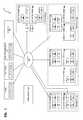
- FIG. 1is a block diagram of one example implementation of a communications management system 200 that includes PLI functionality as well as PLM functionality.
- the management system 200comprises a plurality of connector assemblies 202 (e.g., patch panels, blades, optical adapters, electrical jacks, media converters, transceivers, etc.), connected to an IP network 218 .
- Each connector assembly 202includes one or more ports 204 , each of which is configured to receive a media segment for connection to other media segments or equipment of the management system 200 .
- optical connector assemblies 202 and optical media segmentswill be described. In other implementations, however, electrical connector assemblies and media segments may be used.
- At least some of the connector assemblies 202are designed for use with optical cables that have physical layer information stored in or on them.
- the physical layer informationis configured to be read by a programmable processor 206 associated with one or more connector assemblies 202 .
- the programmable processor 206communicates with memory of an optical cable using a media reading interface 208 .
- each of the ports 204 of the connector assemblies 202includes a respective media reading interface 208 .
- a single media reading interface 208may correspond to two or more ports 204 .
- each connector assembly 202includes its own respective programmable processor 206 and its own respective network interface 216 that is used to communicatively couple that connector assembly 202 to an Internet Protocol (IP) network 218 .
- IPInternet Protocol
- connector assemblies 202are grouped together in proximity to each other (e.g., in a rack, rack system, patch panel, chassis, or equipment closet).
- Each connector assembly 202 of the groupincludes its own respective programmable processor 206 .
- not all of the connector assemblies 202include their own respective network interfaces 216 .
- some of the connector assemblies 202in the group include their own programmable processors 206 and network interfaces 216 , while others of the connector assemblies 202 (e.g., slaves”) do not include their own programmable processors 206 or network interfaces 216 .
- Each programmable processor 206is able to carry out the PLM functions for both the connector assembly 202 of which it is a part and any of the slave connector assemblies 202 to which the master connector assembly 202 is connected via the local connections.
- each of the connector assemblies 202 in a groupincludes its own “slave” programmable processors 206 .
- Each slave programmable processor 206is configured to manage the media reading interfaces 208 to determine if physical communication media segments are attached to the port 204 and to read the physical layer information stored in or on the attached physical communication media segments (if the attached segments have such information stored therein or thereon).
- Each of the slave programmable processors 206 in the groupalso is communicatively coupled to a common “master” programmable processor 217 .
- the master processor 217communicates the physical layer information read from by the slave processors 206 to devices that are coupled to the IP network 218 .
- the master programmable processor 217may be coupled to a network interface 216 that couples the master processor 217 to the IP network 218 .
- the communications management system 200includes functionality that enables the physical layer information captured by the connector assemblies 202 to be used by application-layer functionality outside of the traditional physical-layer management application domain.
- the management system 200may include an aggregation point 220 that is communicatively coupled to the connector assemblies 202 via the IP network 218 .
- the aggregation point 220can be implemented on a standalone network node or can be integrated along with other network functionality.
- the aggregation point 220includes functionality that obtains physical layer information from the connector assemblies 202 (and other devices) and stores the physical layer information in a data store.
- the aggregation point 220also can be used to obtain other types of physical layer information.
- this informationcan be provided to the aggregation point 220 , for example, by manually entering such information into a file (e.g., a spreadsheet) and then uploading the file to the aggregation point 220 (e.g., using a web browser) in connection with the initial installation of each of the various items.
- a filee.g., a spreadsheet
- Such informationcan also, for example, be directly entered using a user interface provided by the aggregation point 220 (e.g., using a web browser).
- the management system 200also may include a network management system (NMS) 230 includes PLI functionality 232 that is configured to retrieve physical layer information from the aggregation point 220 and provide it to the other parts of the NMS 230 for use thereby.
- the NMS 230uses the retrieved physical layer information to perform one or more network management functions.
- the NMS 230communicates with the aggregation point 220 over the IP network 218 .
- the NMS 230may be directly connected to the aggregation point 220 .
- An application 234 executing on a computer 236also can use the API implemented by the aggregation point 220 to access the PLI information maintained by the aggregation point 220 (e.g., to retrieve such information from the aggregation point 220 and/or to supply such information to the aggregation point 220 ).
- the computer 236is coupled to the IP network 218 and accesses the aggregation point 220 over the IP network 218 .
- One or more inter-networking devices 238 used to implement the IP network 218include physical layer information (PLI) functionality 240 .
- the PLI functionality 240 of the inter-networking device 238is configured to retrieve physical layer information from the aggregation point 220 and use the retrieved physical layer information to perform one or more inter-networking functions.
- Examples of inter-networking functionsinclude Layer 1, Layer 2, and Layer 3 (of the OSI model) inter-networking functions such as the routing, switching, repeating, bridging, and grooming of communication traffic that is received at the inter-networking device.
- example communications management system 200can be found in U.S. application Ser. No. 13/025,841, filed Feb. 11, 2011, and titled “Managed Fiber Connectivity Systems,” the disclosure of which is hereby incorporated herein by reference.
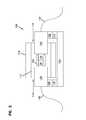
- FIG. 2is a schematic diagram of one example connector assembly 110 configured to collect physical layer information from a connector arrangement 120 terminating a media segment 122 .
- the example connector assembly 120 of FIG. 2is configured to connect segments of optical physical communications media in a physical layer management system.
- the connector assembly 110includes a fiber optic adapter defining at least one connection opening 111 having a first port end 112 and a second port end 114 .
- a sleeve (e.g., a split sleeve) 103is arranged within the connection opening 111 of the adapter 110 between the first and second port ends 112 , 114 .
- Each port end 112 , 114is configured to receive a connector arrangement as will be described in more detail herein.
- a first example segment of optical physical communication mediaincludes a first optical fiber 122 terminated by a first connector arrangement 120 .
- a second example segment of optical physical communication mediaincludes a second optical fiber 132 terminated by a second connector arrangement 130 .
- the first connector arrangement 120is plugged into the first port end 112 and the second connector arrangement 130 is plugged into the second port end 114 .
- Each fiber connector arrangement 120 , 130includes a ferrule 124 , 134 through which optical signals from the optical fiber 122 , 132 , respectively, pass.
- the ferrules 124 , 134 of the connector arrangements 120 , 130are aligned by the sleeve 103 when the connector arrangements 120 , 130 are inserted into the connection opening 111 of the adapter 110 . Aligning the ferrules 124 , 134 provides optical coupling between the optical fibers 122 , 132 .
- each segment of optical physical communication mediae.g., each optical fiber 122 , 132
- the aligned ferrules 124 , 134 of the connector arrangements 120 , 130create an optical path along which the communication signals may be carried.
- the first connector arrangement 120may include a storage device 125 that is configured to store physical layer information (e.g., an identifier and/or attribute information) pertaining to the segment of physical communications media (e.g., the first connector arrangement 120 and/or the fiber optic cable 122 terminated thereby).
- the connector arrangement 130also includes a storage device 135 that is configured to store information (e.g., an identifier and/or attribute information) pertaining to the second connector arrangement 130 and/or the second optic cable 132 terminated thereby.
- each of the storage devices 125 , 135is implemented using an EEPROM (e.g., a PCB surface-mount EEPROM). In other implementations, the storage devices 125 , 135 are implemented using other non-volatile memory device. Each storage device 125 , 135 is arranged and configured so that it does not interfere or interact with the communications signals communicated over the media segments 122 , 132 .
- the adapter 110is coupled to at least a first media reading interface 116 . In certain implementations, the adapter 110 also is coupled to at least a second media interface 118 . In some implementations, the adapter 110 is coupled to multiple media reading interfaces. In certain implementations, the adapter 110 includes a media reading interface for each port end defined by the adapter 110 . In other implementations, the adapter 110 includes a media reading interface for each connection opening 111 defined by the adapter 110 . In still other implementations, the adapter 110 includes a media reading interface for each connector arrangement that the adapter 110 is configured to receive. In still other implementations, the adapter 110 includes a media reading interface for only a portion of the connector arrangement that the adapter 110 is configured to receive.
- the first media reading interface 116is mounted to a printed circuit board 115 .
- the first media reading interface 116 of the printed circuit board 115is associated with the first port end 112 of the adapter 110 .
- the printed circuit board 115also can include the second media reading interface 118 .
- the second media reading interface 1818is associated with the second port end 114 of the adapter 110 .
- the printed circuit board 115 of the connector assembly 110can be communicatively connected to one or more programmable processors (e.g., processors 216 of FIG. 1 ) and/or to one or more network interfaces (e.g., network interfaces 216 of FIG. 1 ).
- the network interfacemay be configured to send the physical layer information to a physical layer management network (e.g., see IP network 218 of FIG. 1 ).
- one or more such processors and interfacescan be arranged as components on the printed circuit board 115 .
- one or more such processor and interfacescan be arranged on separate circuit boards that are coupled together.
- the printed circuit board 115can couple to other circuit boards via a card edge type connection, a connector-to-connector type connection, a cable connection, etc.
- the first media reading interface 1816is configured to enable reading (e.g., by the processor) of the information stored in the storage device 125 .
- the information read from the first connector arrangement 120can be transferred through the printed circuit board 115 to a physical layer management network, e.g., network 218 of FIG. 1 , etc.
- the second media reading interface 118is configured to enable reading (e.g., by the processor) of the information stored in the storage device 135 .
- the information read from the second connector arrangement 130can be transferred through the printed circuit board 115 or another circuit board to the physical layer management network.
- the storage devices 125 , 135 and the media reading interfaces 116 , 118each comprise three (3) leads—a power lead, a ground lead, and a data lead.
- the three leads of the storage devices 125 , 135come into electrical contact with three (3) corresponding leads of the media reading interfaces 116 , 118 when the corresponding media segment is inserted in the corresponding port.
- a two-line interfaceis used with a simple charge pump.
- additional leadscan be provided (e.g., for potential future applications).
- the storage devices 125 , 135 and the media reading interfaces 116 , 118may each include four (4) leads, five (5) leads, six (6) leads, etc.
- FIGS. 4-5illustrate an example implementation of a connector system 300 that can be utilized on a connector assembly (e.g., a communications panel) having PLI functionality as well as PLM functionality.
- a connector assemblye.g., a communications panel
- One example connector assembly on which the connector system 300 can be implementedis a bladed chassis. Examples of bladed chassis can be found in U.S. application Ser. No. 13/025,750, filed Feb. 11, 2011, and titled “Communications Bladed Panel System,” the disclosure of which is hereby incorporated herein by reference in its entirety.
- the connector system 300includes at least one example communications coupler assembly 310 and at least two connector arrangements 320 .
- the communications coupler assembly 310is configured to be mounted to a connector assembly, such as a communications blade or a communications panel.
- a connector assemblysuch as a communications blade or a communications panel.
- One or more connector arrangements 320which each terminate at least one segment of communications media 325 ( FIG. 4 ), are configured to communicatively couple to other segments of physical communications media at the coupler assembly 310 (e.g., see FIG. 3 ). Accordingly, communications data signals carried by a media segment 325 terminated by a first connector arrangement 320 can be propagated to another media segment (e.g., terminated by a second connector arrangement 320 ) through the communications coupler assembly 310 .
- each communications coupler assembly 310is configured to form a single link between segments of physical communications media.
- each communications coupler assembly 310can define a single passage at which a first connector arrangement 320 A is coupled to a second connector arrangement 320 B (see FIG. 3 ).
- each communications coupler assembly 310is configured to form two or more links between segments 325 of physical communications media.
- each connector arrangement 320is configured to terminate a single segment of physical communications media.
- each connector arrangement 320can include a single optical connector that terminate a single optical fiber 325 or a single electrical conductor.
- each connector arrangement 320includes a single SC-type fiber optic connector 320 that terminates a single optical fiber 325 (see FIG. 4 ).
- the connector 320can be an LC-type, an ST-type, an FC-type, an LX.5-type, etc.
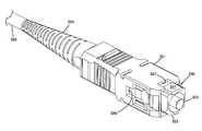
- FIG. 4is a front perspective view an example fiber optic connector arrangement 320 including an SC-type connector.
- the connector 320includes an outer body 321 surrounding an inner body 322 .
- the inner body 322holds a ferrule 323 , which retains an optical fiber 325 .
- the outer body 321is configured to move relative to the inner body 322 along a longitudinal axis L of the ferrule 323 .
- the ferrule 323also is configured to move within the inner body 322 against a spring bias.
- a boot 324extends rearwardly from the outer connector body 321 to provide bend protection to the optical fiber 325 .
- the boot 324may be secured between the outer body 321 and the inner body 322 .
- the outer housing 321defines two slots 329 on opposite sides thereof through which raised portions of the inner housing 322 are visible.
- the outer housing 321also defines a key 328 located on a side perpendicular to the sides containing the slots 329 .
- the key 328is configured to engage a keyway of coupler assembly 310 to properly position the connector 320 at a port of the coupler assembly 310 .
- the outer body 321also includes a knurled handle or other grip section at a rear of the outer body 321 .
- the grip sectiondefines a textured surface (e.g., ridges).
- Each connector arrangement 320is configured to store physical layer information.
- a storage device 330( FIGS. 7 and 8 ) may be installed on or in the fiber optic connector 320 .
- One example storage device 330includes a printed circuit board 331 on which memory circuitry can be arranged. Electrical contacts 332 also may be arranged on the printed circuit board 331 for interaction with a media reading interface of the communications coupler assembly 310 (described in more detail herein).
- the storage device 330includes an EEPROM circuit 333 arranged on the printed circuit board 331 . In other implementations, however, the storage device 330 can include any suitable type of non-volatile memory.
- the storage device 330 shown in FIGS. 7 and 8includes generally planar contacts 332 positioned on a generally planar circuit board 331 .
- the contactsextend over an elongated dimension of the board 331 .
- the board 331may have a square geometry or the contacts may be otherwise arranged on the board.
- Memory 333 ( FIG. 8 ) of the storage device 330which is located on the non-visible side of the board in FIGS. 4 and 7 , is accessed by engaging the tops of the contacts 332 with one or more electrically conductive contact members of a media reading interface (e.g., media reading interface 116 of FIG. 2 ).
- the contact memberslides or wipes across the memory contacts 332 .
- the contacts 332have the same length. In other implementations, one or more of the contacts 332 may have different lengths. In some implementations, the contacts 332 have the same shape. For example, in some implementation, the contacts 332 may be generally rounded at one or both ends of the contact members. In other implementations, one or more of the contacts 332 may have different shapes. For example, in certain implementations, some of the contacts 332 are straight and some of the contacts 332 are generally L-shaped. In one example implementation, the L-shaped contacts may be longer than the rounded end contacts. In some implementations, the contacts 332 may be positioned in a staggered configuration. In other implementations, the contacts 332 may be laterally aligned.
- the inner body 322 of the connector 320may define a recessed section 326 in which the storage device 330 may be disposed.
- the cavity 326faces away from the key 328 of the outer body 321 .
- the cavity 326may be provided on the same side as the key 328 .
- the cavity 326is formed at a front, center location of the connector 320 .
- the cavity 326may open to a front side of the connector 320 .
- a front edge of the circuit board 331may be disposed flush with a front edge of the inner body 322 when the storage device 330 is mounted at the cavity 326 .
- the cavity 326may be formed at a front location laterally offset from the center.
- the cavity 326is formed by a depression in a side of the inner body 322 (e.g., the side opposite the key 328 ).
- the depressionis generally sized and configured to receive the printed circuit board 331 of the storage device 330 .
- the cavity 326has a stepped configuration to facilitate positioning of the storage device 330 .
- a wellmay be formed at one location in the depression. The well is sufficiently deep to accommodate an EEPROM circuit 333 coupled to one side of the circuit board 331 .
- the depressionmay be sufficiently deep to enable electrical contacts 332 provided on the circuit board 331 to be generally flush with the outer surface of the inner body 322 .
- the depressionis shallow so that a top of the printed circuit board 331 extends outwardly from the inner body 322 .
- the outer body 321may define a cut-out 327 that is sized to accommodate the storage device 330 (e.g., see FIGS. 4 and 5 ).
- the cut-out 327aligns with the depression 326 in the inner body so that the cut-out 327 accommodates the storage device 330 .
- the cut-out 327may be formed by removing a front, center portion of the outer body 321 to enable the storage device 330 to extend through the outer body 321 .
- the cut-out 327extends sufficiently rearward to accommodate rearward movement of the storage device 330 relative to the outer body 321 (e.g., when the inner body 322 moves relative to the outer body 321 ).
- FIGS. 3 and 6show one example implementation of a communications coupler assembly 310 implemented as a fiber optic adapter.
- the example communications coupler assembly 310includes an adapter housing 311 defining one or more passages configured to align and interface two or more fiber optic connectors 320 .
- one or more passagescan be configured to communicatively couple together a fiber optic connector 320 with a media converter (not shown) to convert the optical data signals into electrical data signals, wireless data signals, or other such data signals.
- the communications coupler assembly 310can include an electrical termination block that is configured to receive punch-down wires, electrical plugs (e.g., for electrical jacks), or other types of electrical connectors.
- the example adapter housing 311includes opposing side walls interconnected by at least one end wall.
- the side walls and end wallseach extend between a front end and a rear end.
- the adapter housing 311defines one or more axial passages extending between the front and rear ends.
- Each passagedefines a first port 313 and a second port 314 at the front and rear ends, respectively.
- Each port 313 , 314is configured to receive a connector 320 .
- the adapter housing 311defines a single axial passage. In other implementations, however, the adapter housing 311 may define one, two, three, six, eight, ten, twelve, sixteen, or even more axial passages.
- Sleeves (e.g., split sleeves) 319may be positioned within the axial passages to receive and align the ferrules 323 of fiber optic connectors 320 (see FIG. 6 ).
- the sleeve 319is monolithically formed with the adapter housing 311 .
- one of the end walls of the adapter housing 311defines an opening 312 leading to the axial passage (see FIG. 3 ).
- the opening 312 in the end wallmay enable an injection molding machine access to the axial passage to form the sleeve 319 .
- a cover 315may be coupled (e.g., latched, welded, fastened, adhered, etc.) to the adapter housing 311 to close the opening 312 and protect the interior of the adapter housing 311 .
- the sleeve 319is formed separately from the adapter housing 311 and subsequently inserted into the axial passage through the opening 312 .
- neither of the end wallsdefines an opening 312 . Rather, the sleeve 319 may be inserted into the axial passage through one of the ports 313 , 314 .
- One or more guidesmay be defined at an interior of adapter housing 311 .
- the guideswhich extend longitudinally along the interior corners of the axial passage, guide the fiber optic connector 320 through the port 313 , 314 .
- the guidesmay define ramped entry surfaces to facilitate insertion of the connector 320 within the adapter passage.
- One of the end walls of the adapter housing 311defines at least one keyway 317 sized and shaped to receive a corresponding key 328 of the SC-type fiber optic connector 320 (see FIG. 6 ).
- a keyway 317is defined in the end wall at both ports 313 , 314 (e.g., see FIG. 6 ).
- flangesmay extend outwardly from the side walls of the adapter housing 311 (see FIG. 3 ). The flanges aid in supporting the adapter housing 311 on or against a planar surface, such as that of a bulkhead.
- one or both side walls of the adapter housing 1210also include a flexible cantilever arm defining outwardly protruding tabs that are configured to cooperate with the flanges to capture the adapter housing 311 against a bulkhead.
- the side walls of the adapter housing 311define solid surfaces.
- recessesmay be provided in the side walls to permit the use of alternative fasteners, such as a flexible clip.
- the coupler assembly 310includes one or more media reading interfaces 318 (see FIG. 6 ). Each media reading interface 318 is configured to acquire the physical layer information from the storage device 330 of a fiber optic connector 320 plugged into the fiber optic adapter 310 .
- the adapter housing 310can hold or retain a media reading interface 318 for each passage.
- the adapter housing 310can hold or retain a media reading interface 318 for each port 313 , 314 of each passage.
- the adapter 310 shown in FIG. 6includes a first media reading interface 318 associated with the front port 313 of the passage and a second media reading interface 318 associated with the rear port of the passage.
- the adapter housing 310can include a media reading interface 318 associated with each set of passages that accommodate a duplex connector arrangement 310 .
- the adapter housing 310can include any desired combination of front and rear media reading interfaces 318 .
- the orientation of the first media reading interface 318is flipped 180° from the orientation of the second media reading interface 318 .
- the first media reading interface 318is laterally offset from the second media reading interface 318 .
- the first and second media reading interfaces 318may be positioned side-by-side.
- the first and second media reading interfaces 318may be axially aligned.
- the first and second media reading interfaces 318may be laterally aligned.
- the first media reading interfaces 318may be offset towards the front of the adapter housing 310 and the second media reading interface 318 may be offset towards the rear of the adapter housing 310 .
- each media reading interface 318is formed from one or more contact members 340 ( FIG. 9 ).
- the media reading interface 318includes at least a first contact member 340 that transfers power, at least a second contact member 340 that transfers data, and at least a third contact member 340 that provides grounding.
- the media reading interface 318includes a fourth contact member 340 .
- the media reading interface 318include greater or fewer contact members 340 .
- the cover 315defines slots 316 configured to receive one or more contact members 340 . At least a portion of each slot 316 extends through the cover 315 to the axial passage of the adapter housing 311 . In some implementations, the entirety of each slot 316 extends through the cover 315 from top to bottom. In other implementations, only portions of the slot 316 extend from the top to the bottom of the cover 315 . For example, each slot 316 may define a recess in the top surface of the cover 315 in which the contact members can be positioned. Openings defined in a bottom of the cover 315 enable portions of the contact members 340 to extend into a respective adapter passageway.
- the media reading interfaces 318are positioned in the slots 316 of the cover 315 to connect a storage device 330 of a connector 3210 received at the adapter housing 310 with a circuit board coupled to the adapter housing 310 .
- a circuit boardmay be secured (e.g., via fasteners) to the adapter housing 310 so as to extend over the slots 316 of the cover 315 .
- Each media reading interface 318 held by the cover 315extends between the circuit board and a respective axial passage of the adapter housing 310 .
- Portions of each contact member 340engage tracings and contacts on the circuit board. Other portions of the contact members 340 engage the electrical contacts 332 of the storage members 330 attached to any connector 320 plugged into the adapter housing 310 .
- the circuit boardelectrically connects to a data processor and/or to a network interface (e.g., the processor 217 and network interface 216 of FIG. 1 ). It is further to be understood that multiple adapter housings 310 can be connected to the printed circuit board within a connector assembly (e.g., a bladed panel). A processor coupled to the circuit board can access the memory 333 of each connector arrangement 320 coupled to the adapter housing 310 through corresponding ones of the contact members 340 , 332 .
- the slots 316 of the cover 315are sized to hold individual contacts 340 .
- the adapter housing 311has internal structure that holds the contacts 340 in the slots 316 .
- the slots 316position the contact members 340 in alignment with the contact pads 332 of a connector storage device 330 mounted to a connector 320 received at the adapter housing 310 .
- the slots 316may be separated by intermediate walls to inhibit touching between adjacent contact members 340 .
- all of the contact members 340 in a single media reading interface 318may be retained in a single slot 316 .
- the slots 316are sized to accommodate multiple contact members 340 mounted to a support body.
- the contact members 340 of a single media reading interface 318are positioned in a staggered configuration. For example, alternating ones of the contact members 340 are moved axially forward or axially rearward.
- the slots 316 accommodating the staggered contact members 340also are staggered (e.g., in a front to rear direction). In other implementations, however, the slots 316 may have a common length.
- the front and rear ends of the contact members 340 of a single media reading interface 318are transversely aligned within similarly transversely aligned slots 316 .
- the cover 315is sufficiently thick to enable the media reading interface contacts 340 to be substantially positioned in the cover 315 .
- the material height of the cover 315is at least 0.76 mm (0.03 inches). Indeed, in some implementations, the material height of the cover 315 is at least 1.02 mm (0.04 inches). In certain implementations, the material height of the cover 315 is at least 1.27 mm (0.05 inches).
- a height H 1 ( FIG. 27 ) of the adapter housing 310is at least 9.4 mm. In certain implementations, the height H 1 is at least 10 mm. Indeed, in certain implementations, the height H 1 is at least 10 mm. In one example implementation, the height H 1 is about 10.4 mm.
- the slots 316 for accommodating the media reading interface 318may be defined in the adapter housing 311 instead of in the cover 315 .
- the slots 316may be defined in a side wall of the adapter housing 311 located opposite the cover 315 .
- certain types of adapters 310do not include a cover 315 .
- Some such example implementationsinclude a monolithic adapter housing.
- Other such example implementationsinclude two-piece (e.g., front and rear) housings.
- the slots 316may be defined in two or more side walls of the adapter housing 311 .
- Each contact member 340includes at least two moveable (e.g., flexible) contact sections defining contact surfaces.
- one or more contact members 340include three moveable (e.g., flexible) contact sections. The flexibility of the contact sections provides tolerance for differences in spacing between the contact member 340 and the adapter printed circuit board.
- Certain types of contact members 340also include at least one stationary contact having a contact surface. For example, each contact member 340 may have two stationary contact sections. The ability of the first contact section to flex relative to the stationary contact provides tolerance for placement of the contact member 340 relative to the circuit board.
- the first moveable contact section and the stationary contact sectionsextend through the adapter slot 316 to engage the adapter circuit board.
- the second moveable contact sectionis configured to extend into the axial passage of the adapter housing 310 and engage a connector 320 plugged into one of the ports 313 , 314 . If a storage device 330 is installed on the connector 320 , then the second contact surface is configured to engage the contact pads 332 of the storage device 330 .
- the third moveable contact sectionselectively extends through the slot 316 and engages the adapter circuit board.
- the third contact sectionmay be configured to engage the circuit board only when a connector 320 is plugged into the port 313 , 314 corresponding with the contact member 340 .
- the third contact sectionmay be resiliently biased to extend within the adapter housing 310 .
- certain types of contact members 340may include a resilient section that transfers force applied to second moveable contact section to the third moveable contact section. Accordingly, the resilient section may transfers a force pushing the second section towards the slot 316 to the third section, thereby pushing the third contact section through the slot 316 (e.g., toward the circuit board).
- a circumferential edge of each contact member 340defines the contact surface of each contact section.
- the edgehas a substantially continuous thickness.
- the thicknessranges from about 0.05 inches to about 0.005 inches. In some implementation, the thickness is less than about 0.012 inches. In one example implementation, the thickness is about 0.008 inches. In other implementations, the thickness may vary across the body of the contact member 340 .
- the contact member 340is formed monolithically (e.g., from a continuous sheet of metal or other material).
- the contact member 340may be manufactured by cutting a planar sheet of metal or other material.
- the contact member 340may be manufactured by etching a planar sheet of metal or other material.
- the contact member 340may be manufactured by laser trimming a planar sheet of metal or other material.
- the contact member 340may be manufactured by stamping a planar sheet of metal or other material.
- the contact member 340may be formed from wire stock.
- the contact member 340 shown and described hereinis formed from a single piece. In other implementations, however, two or more separate pieces may operate together to perform the functions of the contact member 340 .
- a first piecemay form the first moveable contact section and a second piece may form the third moveable contact section. Either of the pieces may form the second moveable contact section. Insertion of a connector 320 into a respective port of the adapter housing 310 may push one of the pieces into electrical contact with the other of the pieces to electrically connect the first and second contact sections.
- the connector ferrule 323is received within one end of the ferrule sleeve 319 inside the adapter housing 310 .
- the connector 320may be releasably locked to the housing 310 .
- flexible latching hooks disposed within the interior of the housing 310may engage the slots 329 defined in the outer body 321 of the connector 320 to releasably hold the connector 320 at the adapter port 313 , 314 .
- the connector 320includes a storage device 330
- the contacts 332 of the storage device 330are configured to align with the slots 316 defined in the adapter housing 310 . Accordingly, the media reading interface contact members 340 held within the slots 316 align with the contacts 332 of the connector storage device 330 to establish an electrical connection between the storage device 330 and the adapter circuit board.
- each media reading interface 318 of the adapter 310is configured to detect the presence of a connector arrangement 320 plugged into a port 313 , 314 of the adapter housing 310 .
- the contact members 340 of a media reading interface 318can function as presence detection sensors or trigger switches.
- the contact members 340 of a media reading interface 318are configured to form a complete circuit with the adapter circuit board only when a connector 320 is plugged into a respective port 313 , 314 .
- each contact member 340may contact the circuit board only after being pushed toward the circuit board by a connector 320 received at the adapter 310 .
- the connector 320may push the contact members 340 away from the circuit board or from a shorting rod. In accordance with other aspects, however, certain types of contact members 340 may form a complete circuit with the circuit board regardless of whether a connector 320 is received at the adapter 310 .
- a processore.g., processor 217 of FIG. 2
- the processorcan communicate with the memory circuitry 333 on the connector storage device 330 via the contact members 340 and the printed circuit board.
- the processoris configured to obtain physical layer information from the connector storage device 330 .
- the processoris configured to write physical layer information to the connector storage device 330 .
- the processoris configured to delete physical layer information from the connector storage device 330 .
- the processordetects the presence or absence of a connector 320 at each port 313 , 314 .
- the slidable outer body 321 of the connector 320is slid axially relative to the inner body 322 away from the adapter housing 310 until the flexible latching hooks of the adapter housing 310 are released from the slots 329 defined on the outer body 321 of the connector 320 .
- the connector 320may be slide rearwardly through the port 313 , 314 to remove the connector 320 from the adapter housing 310 .
- Removing the connector 320 from the port 313 , 314releases the second moveable contact portion of the contact member 340 , thereby allowing the third moveable contact portion to move back to the initial position.
- Dropping the third moveable contact portiondisengages the third contact surface from the circuit board, thereby interrupting the circuit created by the contact member 340 .
- Interrupting the circuitenables a processor connected to the circuit board to determine that the connector 320 has been removed from the port 313 , 314 .
- the storage device 330is not moved out of alignment with the media reading interface 318 until the connector 320 is released. In other implementations, however, moving the outer body 321 rearwardly applies sufficient force to the inner body 322 to move the storage device 330 out of alignment with the media reading interface 318 .
- FIGS. 10 and 11illustrate another example implementation of a connector system 400 ( FIG. 11 ) that can be utilized on a connector assembly (e.g., a communications panel) having PLI functionality as well as PLM functionality.
- the connector system 400includes at least one example optical adapter 410 and at least two optical connector arrangements 420 .
- the optical connector 420 shownis an SC-type optical connector having an outer body 421 that is axially moveable relative to an inner body 422 .
- the inner body 422holds a ferrule 423 through which at least one optical fiber extends.
- the optical connector 420 shown in FIGS. 10-12is substantially the same as the optical connector 320 disclosed above, except for certain features discussed below.
- a storage device 430is coupled to the connector 420 at a recessed portion 426 of the inner body 422 .
- the location on the inner body 422 at which the storage device 430 is disposedis rearwardly offset compared to the location of the storage device 330 on the inner body 322 of the optical connector 320 disclosed above.
- a front edge of the storage device 430is rearwardly offset from the front edge of the inner body 422 .
- the recessdoes not extend sufficiently forward to open through the front edge of the inner body 422 .
- the optical adapter 410 shown in FIG. 11is substantially the same as the optical adapter 310 disclosed above, except for certain features discussed below.
- the axial positioning of the storage device 330 , 430 on the inner body 322 , 422 of the connector 320 , 420determines or is influenced by the axial positioning of the media reading interfaces 318 in the adapter 310 , 410 . Accordingly, the slots 416 defined in the adapter 410 shown in FIG. 11 are spaced farther apart in the axial direction as compared to the slots 316 of the adapter 320 shown in FIG. 3 .
- FIG. 12illustrates another example storage device 450 disposed on the optical connector 420 of FIG. 10 .
- the storage device 450is offset rearwardly from a front of the inner body 422 of the connector 420 .
- the storage device 450includes contacts 452 disposed on one side of a printed circuit board 451 .
- the memorye.g., EEPROM
- the memorycan be disposed on the same side of the circuit board 451 as the contacts 452 .
- the contacts 452are uniformly disposed on the board 451 . In the example shown in FIG. 12 , however, two of the contacts are shorter than another two of the contacts. Also in the example shown, two of the contacts are L-shaped and two of the contacts extend in a straight line. In other implementations, however, other types of contacts 452 may be disposed on the circuit board 451 . For example, square contacts may be arranged in a grid pattern.
- the embodiments described abovemake use of a contact-based interface for reading from and/or writing information to a storage device 330 attached to the connector 320 , 420 .
- contact-less or wireless interfacesalso can be used with the optical systems described above.
- RFID technologyis used.
- the storage device 330 , 430 attached to the connector 320 , 420is implemented as an RFID tag.
- the storage device 330does not include an EEPROM 333 and contacts 332 . Rather, the RFID tag includes memory and an antenna.
- the adapter contacts 340 of the media reading interfaces 318 , 418are replaced with an RFID coil or antenna.
- the RFID coils in the adapter portsare connected to one or more RFID readers (using a suitable multiplexing mechanism if needed).
- the RFID readerIn order to read information from an RFID tag, the RFID reader outputs an RF interrogation signal via the RFID coil associated with the appropriate adapter port.
- the RFID readermay output such an RF interrogation signal in response to an optical connector 320 , 420 being inserted into the adapter port 313 , 314 , 413 , 414 .
- the RFID tag on the optical connectorreceives the RFID interrogation signal, which causes the RFID tag to power on, to retrieve information (e.g., physical layer information) stored in the RFID tag, and to transmit the read information.
- the transmission from the RFID tagis received by the RFID reader using the RFID coil in the adapter port.
- the information included in such transmissionscan be provided to a controller included in the patch panel or other optical system associated with the adapter 310 , 410 .
- the informationalso can be communicated to the aggregation point 220 in an IP network 218 as described above.
- Other contact-less or wireless embodimentscan be implemented in other ways.
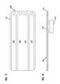
- FIGS. 13-15illustrate another example optical connector 500 having a storage device 525 .
- the optical connector 500has a front 501 , a rear 502 , a first side 503 , a second side 504 , a top 505 , and a bottom 506 .
- the connector 500includes an outer body 510 defining grip surfaces 514 and a connection mechanism 516 .
- a grip surface 514 and a connection componentcan be formed on each side 503 , 504 of the outer body 510 .
- An inner bodyis configured to move (e.g., slide) relative to the outer body 510 .
- An optical fiber tipis held at the inner body and accessible from the front 501 of the connector 500 (e.g., via a ferrule).
- a dust cap 515covers the optical fiber tip.
- a strain-relief boot 518can extend rearwardly from the outer body 510 .
- the storage device 525is disposed internally within the connector body 510 .
- the connector body 510can define a storage compartment 520 to hold the storage device 525 .
- the storage compartment 520includes a cavity 521 extending into the connector body 510 from the front 501 .
- the cavity 521is defined in the connector body 510 between the top 505 of the body 510 and the internal passage in which the optical fiber is disposed.
- the connector body 510forms shelves 522 that partially define the cavity 521 .
- a notch 523can be provided in the connector body 510 at the front 501 to be continuous with the cavity 521 .
- the shelves 522are separated by a gap 524 (see FIG. 15 ).
- the inner bodyalso defines a gap 519 .
- the gaps 519 , 524provide sufficient room to inhibit interference between the shelves 522 and other components.
- the gaps 519 , 524enable components within an optical adapter to fit with the connector 500 .
- the gaps 519 , 524provide sufficient room for a split sleeve or other structure disposed within an optical adapter to surround the optical tip of the connector 500 when the connector 500 is received at a port of the optical adapter.
- the gaps 519 , 524provide sufficient room for a dust cap to be mounted over the optical tip.
- the storage device 525is configured to be advanced into the cavity 521 from the front 501 of the connector 500 (see FIG. 14 ).
- the storage device 525can be slid edge-wise into the cavity 521 along the shelves 522 .
- a plug piece 526can be coupled to the connector body 510 to close the storage device 525 within the cavity 521 .
- the plug piece 526can be welded, glued, overmolded, or otherwise secured to the body 510 .
- the plug piece 526includes a front member 527 that extends across the opening to the cavity 521 , two arms 528 extending rearwardly from the front member 527 , and a lug 529 that extends outwardly from the front member 527 .
- the arms 528are sized and configured to slide into the cavity 521 on opposite sides of the storage device 525 .
- the lug 529is sized and configured to fit within the notch 523 .
- the storage device 525can be glued into position within the cavity 525 .
- the storage device 525can be held into position using a vacuum until the plug piece 526 is added.
- the storage device 525includes an RFID tag. In such implementations, the storage device 525 can be fully sealed within the connector body 510 . In other implementations, the storage device 525 includes a circuit board including memory and contact pads. In such implementations, openings are defined in the top 505 of the connector body 500 to provide access to the contact pads.
- a cavitycan be defined in the top surface 505 of the connector body 510 .
- the storage device 525can be disposed within the cavity.
- a covercan be added to close the cavity.
- the storage device 525can be glued into position within the cavity.
- the storage device 525can be held into position using a vacuum until a cover is added.
- the cavity section of the connector body 510 and storage device 525can be overmolded (e.g., using injection molded plastic) to close the cavity.
- the storage device 525includes an RFID tag that can be sealed within the cavity by the cover.
- the storage device 525can include a circuit board including memory and contact pads. In such implementations, the contact pads are left accessible through the cover. For example, the contact pads can be pressed against the mold during an overmolding process to prevent the contact pads from being overmolded.
- FIGS. 16 and 17illustrate various example LC connectors 600 , 650 having rear slots sized and configured to hold a storage device (e.g., an RFID tag, a circuit board and EEPROM, etc.).
- the LC connector 600includes a single-piece body 610 including a latch 615 for securing the connector 600 to an adapter.
- the body 610also includes a trigger 616 to facilitate depression of the latch 615 .
- a distal tip of an optical fiberprotrudes from a front of the body 610 and an optical cable extends from a rear of the body 610 .
- a strain-relief bootcan be mounted to the rear of the body 610 .
- the body 610defines a slot 620 leading to a cavity defined in the body 610 of the connector 600 .
- the cavityopens into a longitudinal bore extending through the connector body 610 .
- the cavityis separate from the bore.
- a storage devicecan be inserted edge-wise within the cavity and the slot 620 can be closed.
- the slot 620can be overmolded shut.
- a plugcan be inserted into the slot 620 .
- the bootcan cover the slot 620 .
- FIG. 17shows an LC connector 650 having a two-piece housing including a front housing piece 652 and a rear housing piece 654 .
- the front housing piece 652includes a latch 665 and the rear housing piece 654 includes a trigger 666 .
- a slot(e.g., slot 620 ) can be defined in the rear housing piece 654 .
- the slotleads to a cavity in the rear housing piece 654 .
- the storage devicecan be inserted edge-wise within the cavity and the slot can be sealed to close the storage device within the cavity.
- the slotcan be overmolded shut.
- a plugcan be inserted into the slot.
- the bootcan cover the slot.
Landscapes
- Physics & Mathematics (AREA)
- General Physics & Mathematics (AREA)
- Optics & Photonics (AREA)
- Health & Medical Sciences (AREA)
- Toxicology (AREA)
- Engineering & Computer Science (AREA)
- Electromagnetism (AREA)
- General Health & Medical Sciences (AREA)
- Artificial Intelligence (AREA)
- Computer Vision & Pattern Recognition (AREA)
- Theoretical Computer Science (AREA)
- Mechanical Coupling Of Light Guides (AREA)
Abstract
Description
Claims (17)
Priority Applications (2)
| Application Number | Priority Date | Filing Date | Title |
|---|---|---|---|
| US13/939,826US9453971B2 (en) | 2012-07-11 | 2013-07-11 | Managed fiber connectivity systems |
| US15/275,798US20170108653A1 (en) | 2012-07-11 | 2016-09-26 | Managed fiber connectivity systems |
Applications Claiming Priority (2)
| Application Number | Priority Date | Filing Date | Title |
|---|---|---|---|
| US201261670366P | 2012-07-11 | 2012-07-11 | |
| US13/939,826US9453971B2 (en) | 2012-07-11 | 2013-07-11 | Managed fiber connectivity systems |
Related Child Applications (1)
| Application Number | Title | Priority Date | Filing Date |
|---|---|---|---|
| US15/275,798ContinuationUS20170108653A1 (en) | 2012-07-11 | 2016-09-26 | Managed fiber connectivity systems |
Publications (2)
| Publication Number | Publication Date |
|---|---|
| US20140023326A1 US20140023326A1 (en) | 2014-01-23 |
| US9453971B2true US9453971B2 (en) | 2016-09-27 |
Family
ID=49916552
Family Applications (2)
| Application Number | Title | Priority Date | Filing Date |
|---|---|---|---|
| US13/939,826Active2033-08-10US9453971B2 (en) | 2012-07-11 | 2013-07-11 | Managed fiber connectivity systems |
| US15/275,798AbandonedUS20170108653A1 (en) | 2012-07-11 | 2016-09-26 | Managed fiber connectivity systems |
Family Applications After (1)
| Application Number | Title | Priority Date | Filing Date |
|---|---|---|---|
| US15/275,798AbandonedUS20170108653A1 (en) | 2012-07-11 | 2016-09-26 | Managed fiber connectivity systems |
Country Status (2)
| Country | Link |
|---|---|
| US (2) | US9453971B2 (en) |
| WO (1) | WO2014011898A1 (en) |
Cited By (8)
| Publication number | Priority date | Publication date | Assignee | Title |
|---|---|---|---|---|
| US20160352429A1 (en)* | 2015-05-28 | 2016-12-01 | Commscope Technologies Llc | Physical layer management configured active optical module with native and non-native network element support |
| US20190310428A1 (en)* | 2015-07-01 | 2019-10-10 | Go!Foton Holdings, Inc. | Connector engagement sensing mechanism |
| US10495836B2 (en) | 2007-08-06 | 2019-12-03 | Commscope Technologies Llc | Fiber optic payout assembly including cable spool |
| US10627592B2 (en) | 2007-05-07 | 2020-04-21 | Commscope Technologies Llc | Fiber optic assembly with cable spool |
| US20220074810A1 (en)* | 2020-09-10 | 2022-03-10 | Exfo Inc. | Optical fiber endface inspection microscope having adapter tip detection and autoconfiguration |
| US20220216655A1 (en)* | 2019-05-14 | 2022-07-07 | Autonetworks Technologies, Ltd. | Connector |
| US11644628B1 (en)* | 2022-01-28 | 2023-05-09 | Ciena Corporation | Micro-optical connector holder with integrated mating system |
| US20240210640A1 (en)* | 2022-12-27 | 2024-06-27 | Fujin Precision Industrial (Jincheng)Co.,Ltd. | Adapter, connector, and opto-electric transmission assembly |
Families Citing this family (24)
| Publication number | Priority date | Publication date | Assignee | Title |
|---|---|---|---|---|
| JP2015531103A (en)* | 2012-06-25 | 2015-10-29 | エーデーシー・テレコミュニケーションズ・インコーポレーテッド | Physical layer management for active optical modules |
| US9405080B2 (en) | 2012-07-11 | 2016-08-02 | Commscope Connectivity Uk Limited | Indicating communications components via illumination |
| US9435969B2 (en) | 2012-07-11 | 2016-09-06 | Commscope Connectivity Uk Limited | Indicating communications components via illumination |
| US9130318B2 (en)* | 2012-11-16 | 2015-09-08 | Tyco Electronics Uk Ltd. | Localized reading of RFID tags located on multiple sides of a port from a single side using RFID coupling circuit and portable RFID reader |
| CN104823090B (en) | 2012-11-30 | 2017-04-05 | 泰科电子公司 | Fiber optic connectors with field-installable outer connector housings |
| US8887991B2 (en)* | 2012-12-27 | 2014-11-18 | Ciena Corporation | Method and apparatus for configuring and validating telecom and datacom systems |
| MX355851B (en) | 2013-09-24 | 2018-05-02 | Commscope Technologies Llc | Pluggable active optical module with managed connectivity support and simulated memory table. |
| US9798096B2 (en) | 2014-02-07 | 2017-10-24 | Commscope Technologies Llc | Managed fiber connectivity systems |
| CN104849816B (en) | 2014-02-14 | 2017-01-11 | 泰科电子(上海)有限公司 | Optical fiber connector and assembly method therefor |
| CN104849815B (en) | 2014-02-14 | 2017-01-18 | 泰科电子(上海)有限公司 | Optical fiber connector and assembly method therefor |
| JP6318008B2 (en)* | 2014-05-30 | 2018-04-25 | 株式会社フジクラ | Optical connector |
| CN105445862B (en) | 2014-07-09 | 2018-01-19 | 泰科电子(上海)有限公司 | The joints of optical fibre and its on-site assembly method |
| CA2971584C (en)* | 2014-12-19 | 2023-08-01 | 3M Innovative Properties Company | Ruggedized optical fiber connection structures and assemblies |
| US9684139B2 (en) | 2015-05-29 | 2017-06-20 | Senko Advanced Components, Inc. | Optical fiber connector with changeable gender |
| CN105242355B (en)* | 2015-06-15 | 2017-08-01 | 烽火通信科技股份有限公司 | A kind of optical fiber connector plug with dual orientation function and preparation method thereof |
| CN104914515A (en)* | 2015-06-15 | 2015-09-16 | 南京邮电大学 | Intelligent optical patchcord |
| US10620385B2 (en) | 2015-11-30 | 2020-04-14 | Commscope Technologies Llc | Fiber optic connector and assembly thereof |
| US10641970B2 (en) | 2015-12-16 | 2020-05-05 | Commscope Technologies Llc | Field installed fiber optic connector |
| US10712507B2 (en)* | 2015-12-19 | 2020-07-14 | US Conec, Ltd | Field changeable fiber optic connector polarity keying |
| JP2020527752A (en)* | 2017-07-19 | 2020-09-10 | ファイバー・マウンテン・インコーポレイテッド | Fiber connector assembly |
| US11422312B2 (en)* | 2019-05-09 | 2022-08-23 | Commscope Technologies Llc | Fiber optic converter |
| WO2021055532A1 (en)* | 2019-09-17 | 2021-03-25 | US Conec, Ltd | Ferrule push |
| US12210196B2 (en) | 2019-12-13 | 2025-01-28 | Us Conec Ltd. | Cover for a fiber optic ferrule and ferrule push |
| US12405640B2 (en)* | 2023-02-03 | 2025-09-02 | Hewlett Packard Enterprise Development Lp | Adaptable housing for light pipes with different light pipe arrangements |
Citations (98)
| Publication number | Priority date | Publication date | Assignee | Title |
|---|---|---|---|---|
| USRE26692E (en) | 1967-09-07 | 1969-10-14 | Contact for direct reception of printed circuit board | |
| US3954320A (en) | 1973-07-06 | 1976-05-04 | Western Electric Company, Inc. | Electrical connecting devices for terminating cords |
| US4737120A (en) | 1986-11-12 | 1988-04-12 | Amp Incorporated | Electrical connector with low insertion force and overstress protection |
| US4953194A (en) | 1989-09-22 | 1990-08-28 | Network Devices, Incorporated | Automated documentation system for a communications network |
| US4968929A (en) | 1987-04-18 | 1990-11-06 | Heidelberger Druckmaschinen Ag | Plug connector coding system for electric cables |
| US5041005A (en) | 1991-02-10 | 1991-08-20 | Amp Incorporated | Low profile cam-in SIMM socket |
| US5052940A (en) | 1990-05-11 | 1991-10-01 | Rit-Rad Interconnection Technologies Ltd. | Hermaphroditic self-shorting electrical connector |
| US5064381A (en) | 1991-03-04 | 1991-11-12 | Lin Yu Chuan | Electric connecting device |
| EP0473063A2 (en)* | 1990-08-29 | 1992-03-04 | Labinal Components And Systems, Inc. | Overmolded shielded connector |
| US5161988A (en) | 1991-02-13 | 1992-11-10 | Rit Technologies Ltd. | Patching panel |
| US5199895A (en) | 1992-02-04 | 1993-04-06 | Chang Lien Ker | Low insertion force, self-locking connecting apparatus for electrically connecting memory modules to a printed circuit board |
| US5222164A (en) | 1992-08-27 | 1993-06-22 | International Business Machines Corporation | Electrically isolated optical connector identification system |
| US5305405A (en) | 1993-02-25 | 1994-04-19 | Adc Telecommunications, Inc. | Patch cord |
| US5317663A (en) | 1993-05-20 | 1994-05-31 | Adc Telecommunications, Inc. | One-piece SC adapter |
| US5394503A (en) | 1993-10-08 | 1995-02-28 | Data Switch Corporation | Optical fiber connection monitoring apparatus, patch panel control system and method of using same |
| US5393249A (en) | 1993-06-30 | 1995-02-28 | Adc Telecommunications, Inc. | Rear cross connect DSX system |
| US5413494A (en) | 1992-10-05 | 1995-05-09 | Adc Telecommunications, Inc. | Jack module assembly |
| US5419717A (en) | 1994-08-15 | 1995-05-30 | The Whitaker Corporation | Hybrid connector between optics and edge card |
| US5467062A (en) | 1992-04-02 | 1995-11-14 | Adc Telecommunications, Inc. | Miniature coax jack module |
| US5483467A (en) | 1992-06-10 | 1996-01-09 | Rit Technologies, Ltd. | Patching panel scanner |
| US5579425A (en) | 1995-08-30 | 1996-11-26 | Lucent Technologies Inc. | Anti-snag duplex connector |
| US5685741A (en) | 1996-06-27 | 1997-11-11 | Adc Telecommunications, Inc. | On demand plug-in jack card and monitor frame |
| US5821510A (en) | 1994-12-22 | 1998-10-13 | Lucent Technologies Inc. | Labeling and tracing system for jumper used in an exchange |
| WO1998053421A1 (en)* | 1997-05-20 | 1998-11-26 | Scm Schneider Microsysteme-Microsystemes Schneider Entwicklungs Und Vertriebs Gmbh S.A.R.L. Developpement Et Vente | Connector with direct or indirect insertion of smart card therein |
| US5910776A (en)* | 1994-10-24 | 1999-06-08 | Id Technologies, Inc. | Method and apparatus for identifying locating or monitoring equipment or other objects |
| US6002331A (en) | 1998-07-20 | 1999-12-14 | Laor; Herzel | Method and apparatus for identifying and tracking connections of communication lines |
| US6116961A (en) | 1998-11-12 | 2000-09-12 | Adc Telecommunications, Inc. | Jack assembly |
| US6222908B1 (en) | 1999-09-23 | 2001-04-24 | Avaya Technology Corp. | Method and device for identifying a specific patch cord connector as it is introduced into, or removed from, a telecommunications patch system |
| US6234830B1 (en) | 1999-02-10 | 2001-05-22 | Avaya Technology Corp. | Tracing interface module for patch cords in a telecommunications system |
| US6285293B1 (en) | 1999-02-10 | 2001-09-04 | Avaya Technology Corp. | System and method for addressing and tracing patch cords in a dedicated telecommunications system |
| US6300877B1 (en) | 2000-03-10 | 2001-10-09 | Adc Telecommunications, Inc. | DSX baytracer illuminator |
| US6330307B1 (en) | 1999-02-10 | 2001-12-11 | Avaya Technology Corp. | Display panel overlay structure and method for tracing interface modules in a telecommunications patch system |
| US6350148B1 (en) | 1999-02-10 | 2002-02-26 | Avaya Technology Corp. | Method and device for detecting the presence of a patch cord connector in a telecommunications patch system |
| EP1199586A2 (en) | 2000-10-18 | 2002-04-24 | Lucent Technologies Inc. | Optical fiber cable tracing system |
| US6409392B1 (en) | 1999-10-19 | 2002-06-25 | Fitel Usa Corp. | Duplex clip for clipping two optical fiber simplex connectors together to form a duplex connector |
| US20020081076A1 (en) | 2000-12-27 | 2002-06-27 | Lampert Norman R. | Optical connector receptacle having switching capability |
| US6424710B1 (en) | 1999-02-10 | 2002-07-23 | Avaya Technology Corp. | Method and device for detecting the presence of a patch cord connector in a telecommunications patch system using passive detection sensors |
| US6437894B1 (en) | 1998-12-11 | 2002-08-20 | Fitel Usa Corp. | Fiber distribution shelf assembly for a fiber administration system having integral line tracing capabilities |
| EP1237024A1 (en) | 2001-02-15 | 2002-09-04 | FITEL USA CORPORATION (a Delaware Corporation) | Optical connector receptacle having electrical switching capability |
| US6499861B1 (en) | 1999-09-23 | 2002-12-31 | Avaya Technology Corp. | Illuminated patch cord connector ports for use in a telecommunications patch closet having patch cord tracing capabilities |
| US6522737B1 (en) | 1999-02-10 | 2003-02-18 | Avaya Technology Corp. | System and method of operation for a telecommunications patch system |
| US6574586B1 (en) | 1999-04-06 | 2003-06-03 | Itracs Corporation | System for monitoring connection pattern of data ports |
| DE10244304B3 (en) | 2002-09-23 | 2004-03-18 | Data-Complex E.K. | Arrangement for monitoring patch panels at distributor points in data networks has patch cables that can be plugged into connections in patch fields with plugs, each fitted with a transponder |
| US20040052471A1 (en) | 2002-09-13 | 2004-03-18 | Fitel Usa Corp. | Connector systems for dynamically updating information related to a network and methods for developing the connector systems |
| US6743044B2 (en) | 2002-08-14 | 2004-06-01 | Adc Telecommunications, Inc. | Cross-connect jumper assembly having tracer lamp |
| US20040117515A1 (en)* | 2002-11-15 | 2004-06-17 | Masuyuki Sago | Distributing system |
| US20040120657A1 (en)* | 2002-01-15 | 2004-06-24 | Masuyuki Sago | Optical connector with memory function |
| US6802735B2 (en) | 2002-06-18 | 2004-10-12 | Tyco Electronics Corporation | Receptacle and plug interconnect module with integral sensor contacts |
| US6808116B1 (en)* | 2002-05-29 | 2004-10-26 | At&T Corp. | Fiber jumpers with data storage method and apparatus |
| US20040240807A1 (en) | 2001-05-30 | 2004-12-02 | Franz-Friedrich Frohlich | Optical distribution device and light waveguide connector cable |
| US6898368B2 (en) | 2002-09-13 | 2005-05-24 | Fitel Usa Corp. | Adapter systems for dynamically updating information related to a network and methods for developing the adapter systems |
| US6932517B2 (en) | 2000-10-27 | 2005-08-23 | Ethicon Endo-Surgery, Inc. | Connector incorporating a contact pad surface on a plane parallel to a longitudinal axis |
| US20050215119A1 (en)* | 2004-02-20 | 2005-09-29 | Hitachi Maxell, Ltd. | Adapter panel, electronic equipment, and cable connector identification system |
| JP2005303809A (en) | 2004-04-14 | 2005-10-27 | Nippon Telegr & Teleph Corp <Ntt> | Optical fiber cable core management wiring board and centralized control device |
| US20050249477A1 (en) | 2004-05-04 | 2005-11-10 | Mark Parrish | Optical fiber connectors with identification circuits and distribution terminals that communicate therewith |
| US6971895B2 (en)* | 2002-11-15 | 2005-12-06 | Tokyo Communication Equipment Mfg Co., Ltd. | Connector adapter with memory function unit |
| DE102004033940A1 (en) | 2004-07-14 | 2006-02-16 | Tkm Telekommunikation Und Elektronik Gmbh | Connector identification system for identifying multi-pole plug-in connectors for data-transmission cables in panels with manifold sockets has detectors/LEDs assigned to individual sockets |
| US20060098921A1 (en)* | 2004-06-16 | 2006-05-11 | Benaron David A | Optical and electrical hybrid connector |
| EP1662287A1 (en) | 2004-10-27 | 2006-05-31 | Panduit Corporation | Fiber optic industrial connector |
| US20060160395A1 (en) | 2004-12-21 | 2006-07-20 | Commscope Solutions Properties, Llc | Methods, systems and computer program products for connecting and monitoring network equipment in a telecommunications system |
| US7081808B2 (en) | 2002-09-13 | 2006-07-25 | Fitel Usa Corp. | Self-registration systems and methods for dynamically updating information related to a network |
| US7088880B1 (en) | 2003-12-24 | 2006-08-08 | Lockheed Martin Corporation | Optical fiber coupling and inline fault monitor device and method |
| US20060193591A1 (en) | 2003-12-23 | 2006-08-31 | Adc Telecommunications, Inc. | High density optical fiber distribution frame with modules |
| US20060228086A1 (en) | 2005-03-31 | 2006-10-12 | Matthew Holmberg | Adapter block including connector storage |
| US7153142B2 (en) | 2002-11-11 | 2006-12-26 | Rit Technologies Ltd. | Retrofit kit for interconnect cabling system |
| US7165728B2 (en)* | 2004-04-02 | 2007-01-23 | Stratos International, Inc. | Radio frequency identification for transfer of component information in fiber optic testing |
| US7193422B2 (en) | 2004-01-20 | 2007-03-20 | The Siemon Company | Patch panel system |
| US20070116411A1 (en) | 2005-11-18 | 2007-05-24 | Mark Benton | Transceiver/fiber optic connector adaptor with patch cord id reading capability |
| US7234944B2 (en) | 2005-08-26 | 2007-06-26 | Panduit Corp. | Patch field documentation and revision systems |
| US20070237470A1 (en) | 2006-04-10 | 2007-10-11 | Aronson Lewis B | Active optical cable with electrical connector |
| US7297018B2 (en) | 2004-11-03 | 2007-11-20 | Panduit Corp. | Method and apparatus for patch panel patch cord documentation and revision |
| US7315224B2 (en) | 2001-08-23 | 2008-01-01 | Rit Technologies Ltd. | High data rate interconnecting device |
| US7352289B1 (en) | 2003-09-11 | 2008-04-01 | Sun Microsystems, Inc. | System and method for detecting the connection state of a network cable connector |
| US7356208B2 (en) | 2006-05-03 | 2008-04-08 | Biolase Technology, Inc. | Fiber detector apparatus and related methods |
| US20080090450A1 (en) | 2004-12-22 | 2008-04-17 | Matsushita Electric Works, Ltd. | Optical And Eletrical Compound Connector |
| US20080100467A1 (en)* | 2006-10-31 | 2008-05-01 | Downie John D | Radio frequency identification of component connections |
| US20080100456A1 (en)* | 2006-10-31 | 2008-05-01 | Downie John D | System for mapping connections using RFID function |
| US20080172722A1 (en)* | 2007-01-11 | 2008-07-17 | Hitachi Plant Technologies, Ltd. | Cable installation support and management system |
| US20080175550A1 (en) | 2007-01-19 | 2008-07-24 | Hutch Coburn | Fiber optic adapter cassette and panel |
| US20080175532A1 (en)* | 2007-01-16 | 2008-07-24 | Reichle & De-Massari Ag | Plug connector system and protective device for optical plug connectors |
| US20080220721A1 (en)* | 2007-03-09 | 2008-09-11 | Downie John D | Passive RFID elements having visual indicators |
| US7458517B2 (en) | 2004-04-02 | 2008-12-02 | Stratos International, Inc. | Radio frequency identification of a connector by a patch panel or other similar structure |
| US20080310795A1 (en) | 2007-06-13 | 2008-12-18 | Parkman Iii Louis Edward | Dust cap for fiber optic adapter |
| US20090034911A1 (en) | 2007-08-01 | 2009-02-05 | Ortronics, Inc. | Positional differentiating connector assembly |
| US20090060422A1 (en) | 2007-08-28 | 2009-03-05 | Protai Photonic Co. Ltd. | One-piece lc type optical fiber adapter |
| US7519000B2 (en) | 2002-01-30 | 2009-04-14 | Panduit Corp. | Systems and methods for managing a network |
| US7552872B2 (en) | 2006-06-21 | 2009-06-30 | Opnext Japan, Inc. | Reader/writer, optical transceiver module, and cable system |
| US20090220248A1 (en) | 2006-08-04 | 2009-09-03 | Emcore Corporation | Embedded Parametric Monitoring of Optoelectronic Modules |
| WO2010001400A1 (en) | 2008-07-02 | 2010-01-07 | Rit Technologies Ltd. | System and method for monitoring physical layer connectivity |
| US20100211664A1 (en) | 2009-02-13 | 2010-08-19 | Adc Telecommunications, Inc. | Aggregation of physical layer information related to a network |
| WO2010121639A1 (en) | 2009-04-22 | 2010-10-28 | Adc Gmbh | Method and arrangement for identifying at least one object |
| US20100303421A1 (en) | 2009-06-02 | 2010-12-02 | Hon Hai Precision Industry Co., Ltd. | Connector with improved fastening structures for fastening two tongues thereof together |
| US7869426B2 (en) | 2006-03-22 | 2011-01-11 | Adc Gmbh | Intelligent patching system and method |
| US7872738B2 (en) | 2005-08-22 | 2011-01-18 | Tyco Electronics Subsea Communications Llc | System and method for monitoring an optical communication system |
| US20110222819A1 (en) | 2010-02-12 | 2011-09-15 | John Anderson | Managed fiber connectivity systems |
| US20120141074A1 (en) | 2010-12-06 | 2012-06-07 | Hon Hai Precision Industry Co., Ltd. | Waveguide connector with improved structure for positioning waveguide into ferrule |
| US20120208401A1 (en)* | 2010-10-22 | 2012-08-16 | Adc Telecommunications, Inc. | Plug contact arrangement and the manufacture thereof |
| US20120294572A1 (en) | 2011-04-15 | 2012-11-22 | Adc Telecommunications, Inc. | Managed fiber connectivity systems |
Family Cites Families (44)
| Publication number | Priority date | Publication date | Assignee | Title |
|---|---|---|---|---|
| US5226120A (en)* | 1990-05-21 | 1993-07-06 | Synoptics Communications, Inc. | Apparatus and method of monitoring the status of a local area network |
| CH684956A5 (en)* | 1991-04-23 | 1995-02-15 | Interlemo Holding Sa | connection device. |
| US5668675A (en)* | 1995-01-18 | 1997-09-16 | Fredricks; Ronald J. | Opto-electronic aid for alignment of exterior vehicle mirrors to minimize blind spot effects |
| TW340129B (en)* | 1995-04-24 | 1998-09-11 | Polyplastic Kk | Polyacetal resin composition |
| US5737463A (en)* | 1995-12-22 | 1998-04-07 | Weiss; Roger E. | Massive parallel optical interconnect system |
| US6192034B1 (en)* | 1997-06-30 | 2001-02-20 | Sterling Commerce, Inc. | System and method for network integrity management |
| AU2582699A (en)* | 1998-02-05 | 1999-08-23 | Alcoa Fujikura Limited | Fiber optic adapter shutter door assembly |
| WO1999053627A1 (en)* | 1998-04-10 | 1999-10-21 | Chrimar Systems, Inc. Doing Business As Cms Technologies | System for communicating with electronic equipment on a network |
| GB9816173D0 (en)* | 1998-07-25 | 1998-09-23 | Huntleigh Technology Plc | Pneumatic systems |
| US6451202B1 (en)* | 1999-06-21 | 2002-09-17 | Access Business Group International Llc | Point-of-use water treatment system |
| US6281790B1 (en)* | 1999-09-01 | 2001-08-28 | Net Talon Security Systems, Inc. | Method and apparatus for remotely monitoring a site |
| US6556562B1 (en)* | 1999-09-29 | 2003-04-29 | At&T Corp. | System to provide lifeline IP telephony service on cable access networks |
| US7020701B1 (en)* | 1999-10-06 | 2006-03-28 | Sensoria Corporation | Method for collecting and processing data using internetworked wireless integrated network sensors (WINS) |
| CA2423175A1 (en)* | 2000-09-22 | 2002-03-28 | Patchlink.Com Corporation | Non-invasive automatic offsite patch fingerprinting and updating system and method |
| US7398226B2 (en)* | 2000-11-06 | 2008-07-08 | American Express Travel Related Services Company, Inc. | System and method for networked loyalty program |
| US6554824B2 (en)* | 2000-12-15 | 2003-04-29 | Laserscope | Methods for laser treatment of soft tissue |
| US6986764B2 (en)* | 2000-12-15 | 2006-01-17 | Laserscope | Method and system for photoselective vaporization of the prostate, and other tissue |
| IL148224A0 (en)* | 2002-02-18 | 2002-09-12 | Ofer Givaty | A network-information device |
| JP2004317560A (en)* | 2003-04-11 | 2004-11-11 | Fujikura Ltd | MT connector, guide member used in MT connector, and optical fiber management method using MT connector |
| JP2004317737A (en)* | 2003-04-15 | 2004-11-11 | Fujikura Ltd | MT connector, clamp member used in MT connector, and optical fiber management method using MT connector |
| JP2005204412A (en)* | 2004-01-15 | 2005-07-28 | Sankosha Corp | Wiring management system |
| US7167078B2 (en)* | 2004-02-19 | 2007-01-23 | Pourchot Shawn C | Electric, telephone or network access control system and method |
| US7481917B2 (en)* | 2004-03-05 | 2009-01-27 | Hydranautics | Filtration devices with embedded radio frequency identification (RFID) tags |
| US8407097B2 (en)* | 2004-04-15 | 2013-03-26 | Hand Held Products, Inc. | Proximity transaction apparatus and methods of use thereof |
| US7197214B2 (en)* | 2004-05-24 | 2007-03-27 | Corning Cable Systems Llc | Methods and apparatus for facilitating cable locating |
| JP4466233B2 (en)* | 2004-06-29 | 2010-05-26 | Kddi株式会社 | IP telephone call origin notification method, optical transmission system, and optical subscriber terminal device |
| US7329186B2 (en)* | 2004-08-20 | 2008-02-12 | Igt | Gaming system with rewritable display card and LCD input display for reading same |
| KR101091895B1 (en)* | 2004-08-21 | 2011-12-08 | 삼성테크윈 주식회사 | RFID tag for mounting vehicle tire |
| US20060085293A1 (en)* | 2004-09-01 | 2006-04-20 | Melucci Robert J | System and method for processor-based inventory data collection and validation |
| CN101142826A (en)* | 2004-12-06 | 2008-03-12 | 北卡罗来纳科姆斯科普公司 | Telecommunications patching system that utilizes rfid tags to detect and identify patch cord interconnections |
| US20070013487A1 (en)* | 2005-07-18 | 2007-01-18 | Jan Scholtz | Digital certificate on connectors and other products using RFID tags and/or labels as well as RFID reader/interrogator |
| US8826972B2 (en)* | 2005-07-28 | 2014-09-09 | Intelliserv, Llc | Platform for electrically coupling a component to a downhole transmission line |
| US20070176745A1 (en)* | 2006-01-30 | 2007-08-02 | Telect, Inc. | Telecom Equipment With RFIDs |
| JP4931435B2 (en)* | 2006-02-15 | 2012-05-16 | 大崎電気工業株式会社 | Wiring information management system |
| US20070221730A1 (en)* | 2006-03-27 | 2007-09-27 | Mcreynolds Alan | RFID enabled cable tracking |
| JPWO2007138694A1 (en)* | 2006-05-31 | 2009-10-01 | 株式会社日立製作所 | Verification method |
| US8421626B2 (en)* | 2006-10-31 | 2013-04-16 | Corning Cable Systems, Llc | Radio frequency identification transponder for communicating condition of a component |
| US8260132B2 (en)* | 2007-03-26 | 2012-09-04 | Hewlett-Packard Development Company, L.P. | System and method for cable monitoring |
| US7920764B2 (en)* | 2007-05-04 | 2011-04-05 | Anthony Stephen Kewitsch | Electrically traceable and identifiable fiber optic cables and connectors |
| US20090157064A1 (en)* | 2007-05-11 | 2009-06-18 | Hodel Michael R | RFID System and Method Therefor |
| US7757936B2 (en)* | 2007-07-31 | 2010-07-20 | Hewlett-Packard Development Company, L.P. | System and method for cable monitoring |
| US8083415B2 (en)* | 2007-12-06 | 2011-12-27 | Finisar Corporation | Line-side out-of-band electrical interface for optoelectronic modules |
| US8554033B2 (en)* | 2008-05-02 | 2013-10-08 | Telescent Inc. | Radio frequency identification overlay network for fiber optic communication systems |
| JP5000778B2 (en)* | 2010-09-06 | 2012-08-15 | 株式会社精工技研 | Optical connector plug |
- 2013
- 2013-07-11WOPCT/US2013/050103patent/WO2014011898A1/enactiveApplication Filing
- 2013-07-11USUS13/939,826patent/US9453971B2/enactiveActive
- 2016
- 2016-09-26USUS15/275,798patent/US20170108653A1/ennot_activeAbandoned
Patent Citations (116)
| Publication number | Priority date | Publication date | Assignee | Title |
|---|---|---|---|---|
| USRE26692E (en) | 1967-09-07 | 1969-10-14 | Contact for direct reception of printed circuit board | |
| US3954320A (en) | 1973-07-06 | 1976-05-04 | Western Electric Company, Inc. | Electrical connecting devices for terminating cords |
| US4737120A (en) | 1986-11-12 | 1988-04-12 | Amp Incorporated | Electrical connector with low insertion force and overstress protection |
| US4968929A (en) | 1987-04-18 | 1990-11-06 | Heidelberger Druckmaschinen Ag | Plug connector coding system for electric cables |
| US4953194A (en) | 1989-09-22 | 1990-08-28 | Network Devices, Incorporated | Automated documentation system for a communications network |
| US5052940A (en) | 1990-05-11 | 1991-10-01 | Rit-Rad Interconnection Technologies Ltd. | Hermaphroditic self-shorting electrical connector |
| EP0473063A2 (en)* | 1990-08-29 | 1992-03-04 | Labinal Components And Systems, Inc. | Overmolded shielded connector |
| US5041005A (en) | 1991-02-10 | 1991-08-20 | Amp Incorporated | Low profile cam-in SIMM socket |
| US5161988A (en) | 1991-02-13 | 1992-11-10 | Rit Technologies Ltd. | Patching panel |
| US5064381A (en) | 1991-03-04 | 1991-11-12 | Lin Yu Chuan | Electric connecting device |
| US5199895A (en) | 1992-02-04 | 1993-04-06 | Chang Lien Ker | Low insertion force, self-locking connecting apparatus for electrically connecting memory modules to a printed circuit board |
| US5467062A (en) | 1992-04-02 | 1995-11-14 | Adc Telecommunications, Inc. | Miniature coax jack module |
| US5483467A (en) | 1992-06-10 | 1996-01-09 | Rit Technologies, Ltd. | Patching panel scanner |
| US5222164A (en) | 1992-08-27 | 1993-06-22 | International Business Machines Corporation | Electrically isolated optical connector identification system |
| US5413494A (en) | 1992-10-05 | 1995-05-09 | Adc Telecommunications, Inc. | Jack module assembly |
| US5305405A (en) | 1993-02-25 | 1994-04-19 | Adc Telecommunications, Inc. | Patch cord |
| US5317663A (en) | 1993-05-20 | 1994-05-31 | Adc Telecommunications, Inc. | One-piece SC adapter |
| US5393249A (en) | 1993-06-30 | 1995-02-28 | Adc Telecommunications, Inc. | Rear cross connect DSX system |
| US5394503A (en) | 1993-10-08 | 1995-02-28 | Data Switch Corporation | Optical fiber connection monitoring apparatus, patch panel control system and method of using same |
| US5419717A (en) | 1994-08-15 | 1995-05-30 | The Whitaker Corporation | Hybrid connector between optics and edge card |
| US5910776A (en)* | 1994-10-24 | 1999-06-08 | Id Technologies, Inc. | Method and apparatus for identifying locating or monitoring equipment or other objects |
| US5821510A (en) | 1994-12-22 | 1998-10-13 | Lucent Technologies Inc. | Labeling and tracing system for jumper used in an exchange |
| US5579425A (en) | 1995-08-30 | 1996-11-26 | Lucent Technologies Inc. | Anti-snag duplex connector |
| US5685741A (en) | 1996-06-27 | 1997-11-11 | Adc Telecommunications, Inc. | On demand plug-in jack card and monitor frame |
| WO1998053421A1 (en)* | 1997-05-20 | 1998-11-26 | Scm Schneider Microsysteme-Microsystemes Schneider Entwicklungs Und Vertriebs Gmbh S.A.R.L. Developpement Et Vente | Connector with direct or indirect insertion of smart card therein |
| US6002331A (en) | 1998-07-20 | 1999-12-14 | Laor; Herzel | Method and apparatus for identifying and tracking connections of communication lines |
| US6116961A (en) | 1998-11-12 | 2000-09-12 | Adc Telecommunications, Inc. | Jack assembly |
| US6437894B1 (en) | 1998-12-11 | 2002-08-20 | Fitel Usa Corp. | Fiber distribution shelf assembly for a fiber administration system having integral line tracing capabilities |
| US6234830B1 (en) | 1999-02-10 | 2001-05-22 | Avaya Technology Corp. | Tracing interface module for patch cords in a telecommunications system |
| US6285293B1 (en) | 1999-02-10 | 2001-09-04 | Avaya Technology Corp. | System and method for addressing and tracing patch cords in a dedicated telecommunications system |
| US6424710B1 (en) | 1999-02-10 | 2002-07-23 | Avaya Technology Corp. | Method and device for detecting the presence of a patch cord connector in a telecommunications patch system using passive detection sensors |
| US6330307B1 (en) | 1999-02-10 | 2001-12-11 | Avaya Technology Corp. | Display panel overlay structure and method for tracing interface modules in a telecommunications patch system |
| US6350148B1 (en) | 1999-02-10 | 2002-02-26 | Avaya Technology Corp. | Method and device for detecting the presence of a patch cord connector in a telecommunications patch system |
| US6522737B1 (en) | 1999-02-10 | 2003-02-18 | Avaya Technology Corp. | System and method of operation for a telecommunications patch system |
| US6725177B2 (en) | 1999-04-06 | 2004-04-20 | Itracs Corporation | System for monitoring connection pattern of data ports |
| US6574586B1 (en) | 1999-04-06 | 2003-06-03 | Itracs Corporation | System for monitoring connection pattern of data ports |
| US6222908B1 (en) | 1999-09-23 | 2001-04-24 | Avaya Technology Corp. | Method and device for identifying a specific patch cord connector as it is introduced into, or removed from, a telecommunications patch system |
| US6499861B1 (en) | 1999-09-23 | 2002-12-31 | Avaya Technology Corp. | Illuminated patch cord connector ports for use in a telecommunications patch closet having patch cord tracing capabilities |
| US6409392B1 (en) | 1999-10-19 | 2002-06-25 | Fitel Usa Corp. | Duplex clip for clipping two optical fiber simplex connectors together to form a duplex connector |
| US6300877B1 (en) | 2000-03-10 | 2001-10-09 | Adc Telecommunications, Inc. | DSX baytracer illuminator |
| US6636152B2 (en) | 2000-03-10 | 2003-10-21 | Adc Telecommunications, Inc. | DSX illuminator |
| EP1199586A2 (en) | 2000-10-18 | 2002-04-24 | Lucent Technologies Inc. | Optical fiber cable tracing system |
| US6456768B1 (en) | 2000-10-18 | 2002-09-24 | Fitel Usa Corp. | Optical fiber cable tracing system |
| US6932517B2 (en) | 2000-10-27 | 2005-08-23 | Ethicon Endo-Surgery, Inc. | Connector incorporating a contact pad surface on a plane parallel to a longitudinal axis |
| US20020081076A1 (en) | 2000-12-27 | 2002-06-27 | Lampert Norman R. | Optical connector receptacle having switching capability |
| US6511231B2 (en) | 2000-12-27 | 2003-01-28 | Fitel Usa Corp. | Optical connector receptacle having switching capability |
| EP1237024A1 (en) | 2001-02-15 | 2002-09-04 | FITEL USA CORPORATION (a Delaware Corporation) | Optical connector receptacle having electrical switching capability |
| US20040240807A1 (en) | 2001-05-30 | 2004-12-02 | Franz-Friedrich Frohlich | Optical distribution device and light waveguide connector cable |
| US7315224B2 (en) | 2001-08-23 | 2008-01-01 | Rit Technologies Ltd. | High data rate interconnecting device |
| US7210858B2 (en)* | 2002-01-15 | 2007-05-01 | Tokyo Communications Equipment Co., Ltd. | Optical connector with memory function |
| US20040120657A1 (en)* | 2002-01-15 | 2004-06-24 | Masuyuki Sago | Optical connector with memory function |
| EP1467232A1 (en) | 2002-01-15 | 2004-10-13 | Tokyo Communication Equipment Mfg. Co., Ltd. | Optical connector having memory function |
| US7519000B2 (en) | 2002-01-30 | 2009-04-14 | Panduit Corp. | Systems and methods for managing a network |
| US6808116B1 (en)* | 2002-05-29 | 2004-10-26 | At&T Corp. | Fiber jumpers with data storage method and apparatus |
| US6802735B2 (en) | 2002-06-18 | 2004-10-12 | Tyco Electronics Corporation | Receptacle and plug interconnect module with integral sensor contacts |
| US6743044B2 (en) | 2002-08-14 | 2004-06-01 | Adc Telecommunications, Inc. | Cross-connect jumper assembly having tracer lamp |
| US6905363B2 (en) | 2002-08-14 | 2005-06-14 | Adc Telecommunications, Inc. | Cross-connect jumper assembly having tracer lamp |
| US6898368B2 (en) | 2002-09-13 | 2005-05-24 | Fitel Usa Corp. | Adapter systems for dynamically updating information related to a network and methods for developing the adapter systems |
| US20040052471A1 (en) | 2002-09-13 | 2004-03-18 | Fitel Usa Corp. | Connector systems for dynamically updating information related to a network and methods for developing the connector systems |
| US7081808B2 (en) | 2002-09-13 | 2006-07-25 | Fitel Usa Corp. | Self-registration systems and methods for dynamically updating information related to a network |
| DE10244304B3 (en) | 2002-09-23 | 2004-03-18 | Data-Complex E.K. | Arrangement for monitoring patch panels at distributor points in data networks has patch cables that can be plugged into connections in patch fields with plugs, each fitted with a transponder |
| US7153142B2 (en) | 2002-11-11 | 2006-12-26 | Rit Technologies Ltd. | Retrofit kit for interconnect cabling system |
| US20040117515A1 (en)* | 2002-11-15 | 2004-06-17 | Masuyuki Sago | Distributing system |
| US6971895B2 (en)* | 2002-11-15 | 2005-12-06 | Tokyo Communication Equipment Mfg Co., Ltd. | Connector adapter with memory function unit |
| US7352289B1 (en) | 2003-09-11 | 2008-04-01 | Sun Microsystems, Inc. | System and method for detecting the connection state of a network cable connector |
| US20060193591A1 (en) | 2003-12-23 | 2006-08-31 | Adc Telecommunications, Inc. | High density optical fiber distribution frame with modules |
| US7088880B1 (en) | 2003-12-24 | 2006-08-08 | Lockheed Martin Corporation | Optical fiber coupling and inline fault monitor device and method |
| US7193422B2 (en) | 2004-01-20 | 2007-03-20 | The Siemon Company | Patch panel system |
| US20050215119A1 (en)* | 2004-02-20 | 2005-09-29 | Hitachi Maxell, Ltd. | Adapter panel, electronic equipment, and cable connector identification system |
| US7374101B2 (en)* | 2004-02-20 | 2008-05-20 | Hitachi Maxell, Ltd. | Adapter panel, electronic equipment, and cable connector identification system |
| US7165728B2 (en)* | 2004-04-02 | 2007-01-23 | Stratos International, Inc. | Radio frequency identification for transfer of component information in fiber optic testing |
| US7458517B2 (en) | 2004-04-02 | 2008-12-02 | Stratos International, Inc. | Radio frequency identification of a connector by a patch panel or other similar structure |
| JP2005303809A (en) | 2004-04-14 | 2005-10-27 | Nippon Telegr & Teleph Corp <Ntt> | Optical fiber cable core management wiring board and centralized control device |
| US7123810B2 (en) | 2004-05-04 | 2006-10-17 | Bellsouth Intellectual Property Corporation | Optical fiber connectors with identification circuits and distribution terminals that communicate therewith |
| US20050249477A1 (en) | 2004-05-04 | 2005-11-10 | Mark Parrish | Optical fiber connectors with identification circuits and distribution terminals that communicate therewith |
| US20060098921A1 (en)* | 2004-06-16 | 2006-05-11 | Benaron David A | Optical and electrical hybrid connector |
| US7427165B2 (en)* | 2004-06-16 | 2008-09-23 | Spectros Corporation | Optical and electrical hybrid connector |
| DE102004033940A1 (en) | 2004-07-14 | 2006-02-16 | Tkm Telekommunikation Und Elektronik Gmbh | Connector identification system for identifying multi-pole plug-in connectors for data-transmission cables in panels with manifold sockets has detectors/LEDs assigned to individual sockets |
| EP1662287A1 (en) | 2004-10-27 | 2006-05-31 | Panduit Corporation | Fiber optic industrial connector |
| US7297018B2 (en) | 2004-11-03 | 2007-11-20 | Panduit Corp. | Method and apparatus for patch panel patch cord documentation and revision |
| US20060160395A1 (en) | 2004-12-21 | 2006-07-20 | Commscope Solutions Properties, Llc | Methods, systems and computer program products for connecting and monitoring network equipment in a telecommunications system |
| US20080090450A1 (en) | 2004-12-22 | 2008-04-17 | Matsushita Electric Works, Ltd. | Optical And Eletrical Compound Connector |
| US20060228086A1 (en) | 2005-03-31 | 2006-10-12 | Matthew Holmberg | Adapter block including connector storage |
| US7872738B2 (en) | 2005-08-22 | 2011-01-18 | Tyco Electronics Subsea Communications Llc | System and method for monitoring an optical communication system |
| US7234944B2 (en) | 2005-08-26 | 2007-06-26 | Panduit Corp. | Patch field documentation and revision systems |
| US7226217B1 (en) | 2005-11-18 | 2007-06-05 | Stratos International, Inc. | Transceiver/fiber optic connector adaptor with patch cord ID reading capability |
| WO2007061490A2 (en) | 2005-11-18 | 2007-05-31 | Stratos International, Inc. | Transceiver/fiber optic connector adaptor with patch cord id reading capability |
| US20070116411A1 (en) | 2005-11-18 | 2007-05-24 | Mark Benton | Transceiver/fiber optic connector adaptor with patch cord id reading capability |
| US7869426B2 (en) | 2006-03-22 | 2011-01-11 | Adc Gmbh | Intelligent patching system and method |
| US20070237470A1 (en) | 2006-04-10 | 2007-10-11 | Aronson Lewis B | Active optical cable with electrical connector |
| US7356208B2 (en) | 2006-05-03 | 2008-04-08 | Biolase Technology, Inc. | Fiber detector apparatus and related methods |
| US7552872B2 (en) | 2006-06-21 | 2009-06-30 | Opnext Japan, Inc. | Reader/writer, optical transceiver module, and cable system |
| US20090220248A1 (en) | 2006-08-04 | 2009-09-03 | Emcore Corporation | Embedded Parametric Monitoring of Optoelectronic Modules |
| US20080100456A1 (en)* | 2006-10-31 | 2008-05-01 | Downie John D | System for mapping connections using RFID function |
| US20080100467A1 (en)* | 2006-10-31 | 2008-05-01 | Downie John D | Radio frequency identification of component connections |
| US20080172722A1 (en)* | 2007-01-11 | 2008-07-17 | Hitachi Plant Technologies, Ltd. | Cable installation support and management system |
| US20080175532A1 (en)* | 2007-01-16 | 2008-07-24 | Reichle & De-Massari Ag | Plug connector system and protective device for optical plug connectors |
| US20080175550A1 (en) | 2007-01-19 | 2008-07-24 | Hutch Coburn | Fiber optic adapter cassette and panel |
| US20080220721A1 (en)* | 2007-03-09 | 2008-09-11 | Downie John D | Passive RFID elements having visual indicators |
| US20080310795A1 (en) | 2007-06-13 | 2008-12-18 | Parkman Iii Louis Edward | Dust cap for fiber optic adapter |
| US20090034911A1 (en) | 2007-08-01 | 2009-02-05 | Ortronics, Inc. | Positional differentiating connector assembly |
| US20090060422A1 (en) | 2007-08-28 | 2009-03-05 | Protai Photonic Co. Ltd. | One-piece lc type optical fiber adapter |
| WO2010001400A1 (en) | 2008-07-02 | 2010-01-07 | Rit Technologies Ltd. | System and method for monitoring physical layer connectivity |
| US20100211697A1 (en) | 2009-02-13 | 2010-08-19 | Adc Telecommunications, Inc. | Managed connectivity devices, systems, and methods |
| US20100215049A1 (en) | 2009-02-13 | 2010-08-26 | Adc Telecommunications, Inc. | Inter-networking devices for use with physical layer information |
| US20100211665A1 (en) | 2009-02-13 | 2010-08-19 | Adc Telecommunications, Inc. | Network management systems for use with physical layer information |
| US20100211664A1 (en) | 2009-02-13 | 2010-08-19 | Adc Telecommunications, Inc. | Aggregation of physical layer information related to a network |
| WO2010121639A1 (en) | 2009-04-22 | 2010-10-28 | Adc Gmbh | Method and arrangement for identifying at least one object |
| US20100303421A1 (en) | 2009-06-02 | 2010-12-02 | Hon Hai Precision Industry Co., Ltd. | Connector with improved fastening structures for fastening two tongues thereof together |
| US20110222819A1 (en) | 2010-02-12 | 2011-09-15 | John Anderson | Managed fiber connectivity systems |
| US20110235979A1 (en) | 2010-02-12 | 2011-09-29 | John Anderson | Managed fiber connectivity systems |
| US20110255829A1 (en) | 2010-02-12 | 2011-10-20 | John Anderson | Managed fiber connectivity systems |
| US20110262077A1 (en) | 2010-02-12 | 2011-10-27 | John Anderson | Managed fiber connectivity systems |
| US20120208401A1 (en)* | 2010-10-22 | 2012-08-16 | Adc Telecommunications, Inc. | Plug contact arrangement and the manufacture thereof |
| US20120141074A1 (en) | 2010-12-06 | 2012-06-07 | Hon Hai Precision Industry Co., Ltd. | Waveguide connector with improved structure for positioning waveguide into ferrule |
| US20120294572A1 (en) | 2011-04-15 | 2012-11-22 | Adc Telecommunications, Inc. | Managed fiber connectivity systems |
Non-Patent Citations (17)
| Title |
|---|
| Avaya's Enhanced SYSTIMAX® iPatch System Enables IT Managers to Optimise Network Efficiency and Cut Downtime, Press Release, May 20, 2003, obtained from http://www.avaya.com/usa/about-avaya/newsroom/news-releases/2003/pr-030520 on Jan. 7, 2009. |
| Avaya's Enhanced SYSTIMAX® iPatch System Enables IT Managers to Optimise Network Efficiency and Cut Downtime, Press Release, May 9, 2003, obtained from http://www.avaya.com/usa/about-avaya/newsroom/news-releases/2003/pr-030509 on Jan. 7, 2009. |
| Intelligent patching systems carving out a 'large' niche, Cabling Installation & Maintenance, vol. 12, Issue 7, Jul. 2004 (5 pages). |
| intelliMAC: The intelligent way to make Moves, Adds or Changes! NORDX/CDT ©2003 (6 pages). |
| International Search Report and Written Opinion for PCT/US2012/033578 mailed Nov. 28, 2012. |
| International Search Report and Written Opinion for PCT/US2013/050103 mailed Oct. 24, 2013. |
| International Search Report and Written Opinion mailed May 23, 2011 in related Application No. PCT/US2011/024650 (17 pages). |
| International Search Report and Written Opinion mailed Sep. 12, 2011 in related Application No. PCT/US2011/024652 (28 pages). |
| International Search Report and Written Opinion mailed Sep. 19, 2011 in related Application No. PCT/US2011/024649 (27 pages). |
| International Search Report and Written Opinion mailed Sep. 22, 2011 in related Application No. PCT/US2011/024653 (25 pages). |
| Machine Translation (6 pages) of WO 9853421, which published Nov. 26, 1998. |
| Meredith, L., "Managers missing point of intelligent patching," Daa Center News, Jun. 21, 2005, obtained Dec. 2, 2008 from http://searchdatacenter.techtarget.com/news/article/0,289142,sid80-gcil099991,00.html. |
| Ohtsuki, F. et al., "Design of Optical Connectors with ID Modules," Electronics and Communications in Japan, Part 1, vol. 77, No. 2, pp. 94-105 (Feb. 1994). |
| Partial International Search and Invitation to Pay Additional Fees mailed Jun. 16, 2011 in related Application No. PCT/US2011/024652 (9 pages). |
| Partial International Search and Invitation to Pay Additional Fees mailed Jun. 8, 2011 in related Application No. PCT/US2011/024649 (8 pages). |
| Partial International Search and Invitation to Pay Additional Fees mailed May 19, 2011 in related Application No. PCT/US2011/024653 (6 pages). |
| SYSTIMAX® iPatch System Wins Platinum Network of the Year Award, Press Release, Jan. 30, 2003, obtained from http://www.avaya.com/usa/about-avaya/newsroom/news-releases/2003/pr-030130a on Jan. 7, 2009. |
Cited By (26)
| Publication number | Priority date | Publication date | Assignee | Title |
|---|---|---|---|---|
| US10627592B2 (en) | 2007-05-07 | 2020-04-21 | Commscope Technologies Llc | Fiber optic assembly with cable spool |
| US12235506B2 (en) | 2007-05-07 | 2025-02-25 | Commscope Technologies Llc | Fiber optic enclosure with external cable spool |
| US11009671B2 (en) | 2007-05-07 | 2021-05-18 | Commscope Technologies Llc | Fiber optic assembly with cable storage arrangement |
| US10788642B2 (en) | 2007-05-07 | 2020-09-29 | Commscope Technologies Llc | Fiber optic assembly with cable storage arrangement |
| US10895705B2 (en) | 2007-08-06 | 2021-01-19 | Commscope Technologies Llc | Fiber optic enclosure with internal cable spool |
| US10996418B2 (en) | 2007-08-06 | 2021-05-04 | Commscope Technologies Llc | Connecting subscribers to a fiber optic network using a cable spool |
| US10606015B2 (en) | 2007-08-06 | 2020-03-31 | Commscope Technologies Llc | Fiber optic payout assembly including cable spool |
| US10606017B2 (en)* | 2007-08-06 | 2020-03-31 | Commscope Technologies Llc | Fiber optic payout assembly including cable spool |
| US12253734B2 (en) | 2007-08-06 | 2025-03-18 | Commscope Technologies Llc | Fiber optic enclosure with internal cable spool |
| US10712518B2 (en) | 2007-08-06 | 2020-07-14 | Commscope Technologies Llc | Fiber optic enclosure with lockable internal cable spool |
| US12019301B2 (en) | 2007-08-06 | 2024-06-25 | Commscope Technologies Llc | Fiber optic enclosure with internal cable spool |
| US11573390B2 (en) | 2007-08-06 | 2023-02-07 | Commscope Technologies Llc | Fiber optic enclosure with internal cable spool |
| US10495836B2 (en) | 2007-08-06 | 2019-12-03 | Commscope Technologies Llc | Fiber optic payout assembly including cable spool |
| US10996417B2 (en) | 2007-08-06 | 2021-05-04 | Commscope Technologies Llc | Fiber optic enclosure with internal cable spool and movable cover |
| US20170346569A1 (en)* | 2015-05-28 | 2017-11-30 | Commscope Technologies Llc | Physical layer management configured active optical module with native and non-native network element support |
| US20160352429A1 (en)* | 2015-05-28 | 2016-12-01 | Commscope Technologies Llc | Physical layer management configured active optical module with native and non-native network element support |
| US10075244B2 (en)* | 2015-05-28 | 2018-09-11 | Commscope Technologies Llc | Physical layer management configured active optical module with native and non-native network element support |
| US9742496B2 (en)* | 2015-05-28 | 2017-08-22 | Commscope Technologies Llc | Physical layer management configured active optical module with native and non-native network element support |
| US11391893B2 (en) | 2015-07-01 | 2022-07-19 | Go!Foton Holdings, Inc. | Connector engagement sensing mechanism |
| US10845548B2 (en)* | 2015-07-01 | 2020-11-24 | Go!Foton Holdings, Inc. | Connector engagement sensing mechanism |
| US20190310428A1 (en)* | 2015-07-01 | 2019-10-10 | Go!Foton Holdings, Inc. | Connector engagement sensing mechanism |
| US20220216655A1 (en)* | 2019-05-14 | 2022-07-07 | Autonetworks Technologies, Ltd. | Connector |
| US20220074810A1 (en)* | 2020-09-10 | 2022-03-10 | Exfo Inc. | Optical fiber endface inspection microscope having adapter tip detection and autoconfiguration |
| US11624680B2 (en)* | 2020-09-10 | 2023-04-11 | Exfo Inc. | Optical fiber endface inspection microscope having adapter tip detection and autoconfiguration |
| US11644628B1 (en)* | 2022-01-28 | 2023-05-09 | Ciena Corporation | Micro-optical connector holder with integrated mating system |
| US20240210640A1 (en)* | 2022-12-27 | 2024-06-27 | Fujin Precision Industrial (Jincheng)Co.,Ltd. | Adapter, connector, and opto-electric transmission assembly |
Also Published As
| Publication number | Publication date |
|---|---|
| US20140023326A1 (en) | 2014-01-23 |
| US20170108653A1 (en) | 2017-04-20 |
| WO2014011898A1 (en) | 2014-01-16 |
Similar Documents
| Publication | Publication Date | Title |
|---|---|---|
| US9453971B2 (en) | Managed fiber connectivity systems | |
| US11899246B2 (en) | Managed fiber connectivity systems | |
| US20240118502A1 (en) | Optical assemblies with managed connectivity | |
| US9759874B2 (en) | Managed fiber connectivity systems | |
| US9798096B2 (en) | Managed fiber connectivity systems | |
| AU2015203136B2 (en) | Managed fiber connectivity systems |
Legal Events
| Date | Code | Title | Description |
|---|---|---|---|
| AS | Assignment | Owner name:ADC TELECOMMUNICATIONS, INC., PENNSYLVANIA Free format text:ASSIGNMENT OF ASSIGNORS INTEREST;ASSIGNOR:ANDERSON, DAVID J.;REEL/FRAME:031966/0056 Effective date:20130722 Owner name:TYCO ELECTRONICS UK LTD., UNITED KINGDOM Free format text:ASSIGNMENT OF ASSIGNORS INTEREST;ASSIGNOR:LAMBOURN, STEPHEN;REEL/FRAME:031966/0037 Effective date:20130920 | |
| AS | Assignment | Owner name:TYCO ELECTRONICS UK INFRASTRUCTURE LIMITED, UNITED Free format text:ASSIGNMENT OF ASSIGNORS INTEREST;ASSIGNOR:TYCO ELECTRONICS UK LTD.;REEL/FRAME:036074/0636 Effective date:20150530 | |
| AS | Assignment | Owner name:TYCO ELECTRONICS SERVICES GMBH, SWITZERLAND Free format text:ASSIGNMENT OF ASSIGNORS INTEREST;ASSIGNORS:ADC TELECOMMUNICATIONS, INC.;TE CONNECTIVITY SOLUTIONS GMBH;REEL/FRAME:036908/0443 Effective date:20150825 | |
| AS | Assignment | Owner name:COMMSCOPE EMEA LIMITED, IRELAND Free format text:ASSIGNMENT OF ASSIGNORS INTEREST;ASSIGNOR:TYCO ELECTRONICS SERVICES GMBH;REEL/FRAME:036956/0001 Effective date:20150828 | |
| AS | Assignment | Owner name:COMMSCOPE TECHNOLOGIES LLC, NORTH CAROLINA Free format text:ASSIGNMENT OF ASSIGNORS INTEREST;ASSIGNOR:COMMSCOPE EMEA LIMITED;REEL/FRAME:037012/0001 Effective date:20150828 | |
| AS | Assignment | Owner name:JPMORGAN CHASE BANK, N.A., AS COLLATERAL AGENT, ILLINOIS Free format text:PATENT SECURITY AGREEMENT (TERM);ASSIGNOR:COMMSCOPE TECHNOLOGIES LLC;REEL/FRAME:037513/0709 Effective date:20151220 Owner name:JPMORGAN CHASE BANK, N.A., AS COLLATERAL AGENT, ILLINOIS Free format text:PATENT SECURITY AGREEMENT (ABL);ASSIGNOR:COMMSCOPE TECHNOLOGIES LLC;REEL/FRAME:037514/0196 Effective date:20151220 Owner name:JPMORGAN CHASE BANK, N.A., AS COLLATERAL AGENT, IL Free format text:PATENT SECURITY AGREEMENT (TERM);ASSIGNOR:COMMSCOPE TECHNOLOGIES LLC;REEL/FRAME:037513/0709 Effective date:20151220 Owner name:JPMORGAN CHASE BANK, N.A., AS COLLATERAL AGENT, IL Free format text:PATENT SECURITY AGREEMENT (ABL);ASSIGNOR:COMMSCOPE TECHNOLOGIES LLC;REEL/FRAME:037514/0196 Effective date:20151220 | |
| AS | Assignment | Owner name:COMMSCOPE CONNECTIVITY UK LIMITED, UNITED KINGDOM Free format text:CHANGE OF NAME;ASSIGNOR:TYCO ELECTRONICS UK INFRASTRUCTURE LIMITED;REEL/FRAME:039551/0291 Effective date:20160104 | |
| STCF | Information on status: patent grant | Free format text:PATENTED CASE | |
| AS | Assignment | Owner name:COMMSCOPE, INC. OF NORTH CAROLINA, NORTH CAROLINA Free format text:RELEASE BY SECURED PARTY;ASSIGNOR:JPMORGAN CHASE BANK, N.A.;REEL/FRAME:048840/0001 Effective date:20190404 Owner name:COMMSCOPE TECHNOLOGIES LLC, NORTH CAROLINA Free format text:RELEASE BY SECURED PARTY;ASSIGNOR:JPMORGAN CHASE BANK, N.A.;REEL/FRAME:048840/0001 Effective date:20190404 Owner name:ALLEN TELECOM LLC, ILLINOIS Free format text:RELEASE BY SECURED PARTY;ASSIGNOR:JPMORGAN CHASE BANK, N.A.;REEL/FRAME:048840/0001 Effective date:20190404 Owner name:REDWOOD SYSTEMS, INC., NORTH CAROLINA Free format text:RELEASE BY SECURED PARTY;ASSIGNOR:JPMORGAN CHASE BANK, N.A.;REEL/FRAME:048840/0001 Effective date:20190404 Owner name:ANDREW LLC, NORTH CAROLINA Free format text:RELEASE BY SECURED PARTY;ASSIGNOR:JPMORGAN CHASE BANK, N.A.;REEL/FRAME:048840/0001 Effective date:20190404 Owner name:ANDREW LLC, NORTH CAROLINA Free format text:RELEASE BY SECURED PARTY;ASSIGNOR:JPMORGAN CHASE BANK, N.A.;REEL/FRAME:049260/0001 Effective date:20190404 Owner name:COMMSCOPE TECHNOLOGIES LLC, NORTH CAROLINA Free format text:RELEASE BY SECURED PARTY;ASSIGNOR:JPMORGAN CHASE BANK, N.A.;REEL/FRAME:049260/0001 Effective date:20190404 Owner name:COMMSCOPE, INC. OF NORTH CAROLINA, NORTH CAROLINA Free format text:RELEASE BY SECURED PARTY;ASSIGNOR:JPMORGAN CHASE BANK, N.A.;REEL/FRAME:049260/0001 Effective date:20190404 Owner name:REDWOOD SYSTEMS, INC., NORTH CAROLINA Free format text:RELEASE BY SECURED PARTY;ASSIGNOR:JPMORGAN CHASE BANK, N.A.;REEL/FRAME:049260/0001 Effective date:20190404 Owner name:ALLEN TELECOM LLC, ILLINOIS Free format text:RELEASE BY SECURED PARTY;ASSIGNOR:JPMORGAN CHASE BANK, N.A.;REEL/FRAME:049260/0001 Effective date:20190404 | |
| AS | Assignment | Owner name:WILMINGTON TRUST, NATIONAL ASSOCIATION, AS COLLATE Free format text:PATENT SECURITY AGREEMENT;ASSIGNOR:COMMSCOPE TECHNOLOGIES LLC;REEL/FRAME:049892/0051 Effective date:20190404 Owner name:JPMORGAN CHASE BANK, N.A., NEW YORK Free format text:TERM LOAN SECURITY AGREEMENT;ASSIGNORS:COMMSCOPE, INC. OF NORTH CAROLINA;COMMSCOPE TECHNOLOGIES LLC;ARRIS ENTERPRISES LLC;AND OTHERS;REEL/FRAME:049905/0504 Effective date:20190404 Owner name:JPMORGAN CHASE BANK, N.A., NEW YORK Free format text:ABL SECURITY AGREEMENT;ASSIGNORS:COMMSCOPE, INC. OF NORTH CAROLINA;COMMSCOPE TECHNOLOGIES LLC;ARRIS ENTERPRISES LLC;AND OTHERS;REEL/FRAME:049892/0396 Effective date:20190404 Owner name:WILMINGTON TRUST, NATIONAL ASSOCIATION, AS COLLATERAL AGENT, CONNECTICUT Free format text:PATENT SECURITY AGREEMENT;ASSIGNOR:COMMSCOPE TECHNOLOGIES LLC;REEL/FRAME:049892/0051 Effective date:20190404 | |
| MAFP | Maintenance fee payment | Free format text:PAYMENT OF MAINTENANCE FEE, 4TH YEAR, LARGE ENTITY (ORIGINAL EVENT CODE: M1551); ENTITY STATUS OF PATENT OWNER: LARGE ENTITY Year of fee payment:4 | |
| AS | Assignment | Owner name:WILMINGTON TRUST, DELAWARE Free format text:SECURITY INTEREST;ASSIGNORS:ARRIS SOLUTIONS, INC.;ARRIS ENTERPRISES LLC;COMMSCOPE TECHNOLOGIES LLC;AND OTHERS;REEL/FRAME:060752/0001 Effective date:20211115 | |
| MAFP | Maintenance fee payment | Free format text:PAYMENT OF MAINTENANCE FEE, 8TH YEAR, LARGE ENTITY (ORIGINAL EVENT CODE: M1552); ENTITY STATUS OF PATENT OWNER: LARGE ENTITY Year of fee payment:8 | |
| AS | Assignment | Owner name:APOLLO ADMINISTRATIVE AGENCY LLC, NEW YORK Free format text:SECURITY INTEREST;ASSIGNORS:ARRIS ENTERPRISES LLC;COMMSCOPE TECHNOLOGIES LLC;COMMSCOPE INC., OF NORTH CAROLINA;AND OTHERS;REEL/FRAME:069889/0114 Effective date:20241217 | |
| AS | Assignment | Owner name:RUCKUS WIRELESS, LLC (F/K/A RUCKUS WIRELESS, INC.), NORTH CAROLINA Free format text:RELEASE OF SECURITY INTEREST AT REEL/FRAME 049905/0504;ASSIGNOR:JPMORGAN CHASE BANK, N.A., AS COLLATERAL AGENT;REEL/FRAME:071477/0255 Effective date:20241217 Owner name:COMMSCOPE TECHNOLOGIES LLC, NORTH CAROLINA Free format text:RELEASE OF SECURITY INTEREST AT REEL/FRAME 049905/0504;ASSIGNOR:JPMORGAN CHASE BANK, N.A., AS COLLATERAL AGENT;REEL/FRAME:071477/0255 Effective date:20241217 Owner name:COMMSCOPE, INC. OF NORTH CAROLINA, NORTH CAROLINA Free format text:RELEASE OF SECURITY INTEREST AT REEL/FRAME 049905/0504;ASSIGNOR:JPMORGAN CHASE BANK, N.A., AS COLLATERAL AGENT;REEL/FRAME:071477/0255 Effective date:20241217 Owner name:ARRIS SOLUTIONS, INC., NORTH CAROLINA Free format text:RELEASE OF SECURITY INTEREST AT REEL/FRAME 049905/0504;ASSIGNOR:JPMORGAN CHASE BANK, N.A., AS COLLATERAL AGENT;REEL/FRAME:071477/0255 Effective date:20241217 Owner name:ARRIS TECHNOLOGY, INC., NORTH CAROLINA Free format text:RELEASE OF SECURITY INTEREST AT REEL/FRAME 049905/0504;ASSIGNOR:JPMORGAN CHASE BANK, N.A., AS COLLATERAL AGENT;REEL/FRAME:071477/0255 Effective date:20241217 Owner name:ARRIS ENTERPRISES LLC (F/K/A ARRIS ENTERPRISES, INC.), NORTH CAROLINA Free format text:RELEASE OF SECURITY INTEREST AT REEL/FRAME 049905/0504;ASSIGNOR:JPMORGAN CHASE BANK, N.A., AS COLLATERAL AGENT;REEL/FRAME:071477/0255 Effective date:20241217 |