US9450610B1 - High quality log likelihood ratios determined using two-index look-up table - Google Patents
High quality log likelihood ratios determined using two-index look-up tableDownload PDFInfo
- Publication number
- US9450610B1 US9450610B1US14/557,214US201414557214AUS9450610B1US 9450610 B1US9450610 B1US 9450610B1US 201414557214 AUS201414557214 AUS 201414557214AUS 9450610 B1US9450610 B1US 9450610B1
- Authority
- US
- United States
- Prior art keywords
- llr
- cell
- target cell
- read
- look
- Prior art date
- Legal status (The legal status is an assumption and is not a legal conclusion. Google has not performed a legal analysis and makes no representation as to the accuracy of the status listed.)
- Active, expires
Links
Images


Classifications
- H—ELECTRICITY
- H03—ELECTRONIC CIRCUITRY
- H03M—CODING; DECODING; CODE CONVERSION IN GENERAL
- H03M13/00—Coding, decoding or code conversion, for error detection or error correction; Coding theory basic assumptions; Coding bounds; Error probability evaluation methods; Channel models; Simulation or testing of codes
- H03M13/03—Error detection or forward error correction by redundancy in data representation, i.e. code words containing more digits than the source words
- H03M13/05—Error detection or forward error correction by redundancy in data representation, i.e. code words containing more digits than the source words using block codes, i.e. a predetermined number of check bits joined to a predetermined number of information bits
- H03M13/11—Error detection or forward error correction by redundancy in data representation, i.e. code words containing more digits than the source words using block codes, i.e. a predetermined number of check bits joined to a predetermined number of information bits using multiple parity bits
- H03M13/1102—Codes on graphs and decoding on graphs, e.g. low-density parity check [LDPC] codes
- H03M13/1105—Decoding
- H03M13/1111—Soft-decision decoding, e.g. by means of message passing or belief propagation algorithms
- H03M13/1125—Soft-decision decoding, e.g. by means of message passing or belief propagation algorithms using different domains for check node and bit node processing, wherein the different domains include probabilities, likelihood ratios, likelihood differences, log-likelihood ratios or log-likelihood difference pairs
- G—PHYSICS
- G06—COMPUTING OR CALCULATING; COUNTING
- G06F—ELECTRIC DIGITAL DATA PROCESSING
- G06F11/00—Error detection; Error correction; Monitoring
- G06F11/07—Responding to the occurrence of a fault, e.g. fault tolerance
- G06F11/08—Error detection or correction by redundancy in data representation, e.g. by using checking codes
- G06F11/10—Adding special bits or symbols to the coded information, e.g. parity check, casting out 9's or 11's
- G06F11/1008—Adding special bits or symbols to the coded information, e.g. parity check, casting out 9's or 11's in individual solid state devices
- G06F11/1012—Adding special bits or symbols to the coded information, e.g. parity check, casting out 9's or 11's in individual solid state devices using codes or arrangements adapted for a specific type of error
- G—PHYSICS
- G06—COMPUTING OR CALCULATING; COUNTING
- G06F—ELECTRIC DIGITAL DATA PROCESSING
- G06F11/00—Error detection; Error correction; Monitoring
- G06F11/07—Responding to the occurrence of a fault, e.g. fault tolerance
- G06F11/08—Error detection or correction by redundancy in data representation, e.g. by using checking codes
- G06F11/10—Adding special bits or symbols to the coded information, e.g. parity check, casting out 9's or 11's
- G06F11/1008—Adding special bits or symbols to the coded information, e.g. parity check, casting out 9's or 11's in individual solid state devices
- G06F11/1048—Adding special bits or symbols to the coded information, e.g. parity check, casting out 9's or 11's in individual solid state devices using arrangements adapted for a specific error detection or correction feature
- G—PHYSICS
- G06—COMPUTING OR CALCULATING; COUNTING
- G06F—ELECTRIC DIGITAL DATA PROCESSING
- G06F11/00—Error detection; Error correction; Monitoring
- G06F11/07—Responding to the occurrence of a fault, e.g. fault tolerance
- G06F11/08—Error detection or correction by redundancy in data representation, e.g. by using checking codes
- G06F11/10—Adding special bits or symbols to the coded information, e.g. parity check, casting out 9's or 11's
- G06F11/1008—Adding special bits or symbols to the coded information, e.g. parity check, casting out 9's or 11's in individual solid state devices
- G06F11/1072—Adding special bits or symbols to the coded information, e.g. parity check, casting out 9's or 11's in individual solid state devices in multilevel memories
- H—ELECTRICITY
- H03—ELECTRONIC CIRCUITRY
- H03M—CODING; DECODING; CODE CONVERSION IN GENERAL
- H03M13/00—Coding, decoding or code conversion, for error detection or error correction; Coding theory basic assumptions; Coding bounds; Error probability evaluation methods; Channel models; Simulation or testing of codes
- H03M13/03—Error detection or forward error correction by redundancy in data representation, i.e. code words containing more digits than the source words
- H03M13/05—Error detection or forward error correction by redundancy in data representation, i.e. code words containing more digits than the source words using block codes, i.e. a predetermined number of check bits joined to a predetermined number of information bits
- H03M13/11—Error detection or forward error correction by redundancy in data representation, i.e. code words containing more digits than the source words using block codes, i.e. a predetermined number of check bits joined to a predetermined number of information bits using multiple parity bits
- H03M13/1102—Codes on graphs and decoding on graphs, e.g. low-density parity check [LDPC] codes
- H03M13/1105—Decoding
- H03M13/1108—Hard decision decoding, e.g. bit flipping, modified or weighted bit flipping
- H—ELECTRICITY
- H03—ELECTRONIC CIRCUITRY
- H03M—CODING; DECODING; CODE CONVERSION IN GENERAL
- H03M13/00—Coding, decoding or code conversion, for error detection or error correction; Coding theory basic assumptions; Coding bounds; Error probability evaluation methods; Channel models; Simulation or testing of codes
- H03M13/03—Error detection or forward error correction by redundancy in data representation, i.e. code words containing more digits than the source words
- H03M13/05—Error detection or forward error correction by redundancy in data representation, i.e. code words containing more digits than the source words using block codes, i.e. a predetermined number of check bits joined to a predetermined number of information bits
- H03M13/11—Error detection or forward error correction by redundancy in data representation, i.e. code words containing more digits than the source words using block codes, i.e. a predetermined number of check bits joined to a predetermined number of information bits using multiple parity bits
- H03M13/1102—Codes on graphs and decoding on graphs, e.g. low-density parity check [LDPC] codes
- H03M13/1105—Decoding
- H03M13/1111—Soft-decision decoding, e.g. by means of message passing or belief propagation algorithms
- H03M13/1117—Soft-decision decoding, e.g. by means of message passing or belief propagation algorithms using approximations for check node processing, e.g. an outgoing message is depending on the signs and the minimum over the magnitudes of all incoming messages according to the min-sum rule
- H—ELECTRICITY
- H03—ELECTRONIC CIRCUITRY
- H03M—CODING; DECODING; CODE CONVERSION IN GENERAL
- H03M13/00—Coding, decoding or code conversion, for error detection or error correction; Coding theory basic assumptions; Coding bounds; Error probability evaluation methods; Channel models; Simulation or testing of codes
- H03M13/03—Error detection or forward error correction by redundancy in data representation, i.e. code words containing more digits than the source words
- H03M13/05—Error detection or forward error correction by redundancy in data representation, i.e. code words containing more digits than the source words using block codes, i.e. a predetermined number of check bits joined to a predetermined number of information bits
- H03M13/11—Error detection or forward error correction by redundancy in data representation, i.e. code words containing more digits than the source words using block codes, i.e. a predetermined number of check bits joined to a predetermined number of information bits using multiple parity bits
- H03M13/1102—Codes on graphs and decoding on graphs, e.g. low-density parity check [LDPC] codes
- H03M13/1105—Decoding
- H03M13/1131—Scheduling of bit node or check node processing
- H03M13/1137—Partly parallel processing, i.e. sub-blocks or sub-groups of nodes being processed in parallel
- H—ELECTRICITY
- H03—ELECTRONIC CIRCUITRY
- H03M—CODING; DECODING; CODE CONVERSION IN GENERAL
- H03M13/00—Coding, decoding or code conversion, for error detection or error correction; Coding theory basic assumptions; Coding bounds; Error probability evaluation methods; Channel models; Simulation or testing of codes
- H03M13/37—Decoding methods or techniques, not specific to the particular type of coding provided for in groups H03M13/03 - H03M13/35
- H03M13/3723—Decoding methods or techniques, not specific to the particular type of coding provided for in groups H03M13/03 - H03M13/35 using means or methods for the initialisation of the decoder
- H—ELECTRICITY
- H03—ELECTRONIC CIRCUITRY
- H03M—CODING; DECODING; CODE CONVERSION IN GENERAL
- H03M13/00—Coding, decoding or code conversion, for error detection or error correction; Coding theory basic assumptions; Coding bounds; Error probability evaluation methods; Channel models; Simulation or testing of codes
- H03M13/63—Joint error correction and other techniques
- H03M13/6325—Error control coding in combination with demodulation
Definitions
- SSDsolid state drive
- NAND-based flash memoriesare widely used as the solid-state memory storage in SSDs due to their compactness, low power consumption, low cost, high data throughput and reliability.
- SSDscommonly employ several NAND-based flash memory chips and a flash controller to manage the flash memory and to transfer data between the flash memory and a host computer.
- NAND-based flash memoriesare reliable, they are not inherently error-free and often rely on error correction coding (ECC) to correct raw bit errors in the stored data.
- ECCerror correction coding
- One commonly employed error correction code employed in nonvolatile memory storage modules, such as SSDsare low-density parity-check (LDPC) codes.
- An LDPC codeis a linear error correcting code having a parity check matrix with a small number of nonzero elements in each row and column.
- MSAlayered min-sum algorithm
- the layered min-sum algorithmintroduces a further hardware simplification.
- the layered min-sum algorithmis iterative by layer and is based on belief propagation.
- the layered min-sum algorithm(MSA) is less complex than other decoding methods known in the art.
- the min-sum algorithmexhibits a noticeable degradation in the decoding performance compared to the more complex decoding methods, such as belief propagation.
- normalized layered min-sum algorithmshave been developed incorporating a normalization factor, or attenuation factor, to account for the degradation in decoding performance.
- the power of LDPC codesresides in the ability of the decoding strategy to exploit the soft information on the stored data.
- the two voltage distributionsrepresent the two possible states: “0” and “1”, of the cells within the NAND chips.
- Soft information for the stored datais expressed by a log likelihood ratio (LLR).
- LLRlog likelihood ratio
- the read errorsare not binary in nature, but instead vary from an ideal voltage according to an analog function.
- LDPC decodershave the ability to address this non-binary behavior using LLRs.
- the LLR attributed to a bitis representative of the probability that the voltage value read corresponds to a 0 or a 1.
- the sign of the LLRtypically provides the bit estimation (i.e. positive LLR corresponds to 0 and negative LLR corresponds to 1).
- the magnitude of the LLRprovides the reliability of the estimation (i.e.
- 0 means that the estimation is completely unreliable and
- ⁇ means that the estimation is completely reliable and the bit value is known).
- Reading soft information from the NAND chipsrequires multiple reads at varying reference voltages. Performing multiple reads is time consuming and has a severe negative impact on the performance of the flash memory controller. As such, it is desirable to reduce the number of reads required to obtain quality LLR data that will be useful in the decoding process.
- a method of providing one or more log likelihood ratio (LLRs) of a target cell to a low-density parity check (LDPC) decoderincludes storing one or more two-index LLR look-up table in a memory controller.
- the two-index LLR look-up tablemay include a LLR, the hard-and-soft-decision bits associate with the LLR and the neighboring cell read pattern associated with the LLR.
- a plurality of reads of a cell of a nonvolatile memory storage moduleare performed at different read voltage levels to generate a plurality of target cell hard-and-soft-decision bits associated with a bit stored in the cell.
- Reads of neighboring cellsare performed to generate neighboring cell reads, where each of the neighboring cell reads are associated with a bit stored in one of the neighboring cells.
- the neighboring cell readsare combined to generate a neighboring cell read pattern that corresponds to the pattern of the neighboring cell reads.
- the one or more look-up tableis then accessed using the plurality of target cell hard-and-soft-decision bits and the neighboring cell read pattern to identify the corresponding LLR.
- the identified LLRis then sent to a Low-Density Party Check (LDPC) decoder for decoding of a codeword stored in the nonvolatile memory storage module.
- LDPCLow-Density Party Check
- a nonvolatile memory controllerincludes memory storage configured to store one or more two-index LLR look-up table that includes a LLR, hard-and-soft-decision bits associated with the LLR and a neighboring cell read pattern associated with the LLR.
- the nonvolatile memory controlleralso includes read circuitry configured to perform a plurality of reads of a cell of a nonvolatile memory storage module at different read voltage levels to generate a plurality of target cell hard-and-soft-decision bits associated with a bit stored in the cell and configured for performing reads of neighboring cells to generate a plurality of neighboring cell reads, each of the plurality of neighboring cell reads associated with a bit stored in one of the neighboring cells.
- the nonvolatile memory controllerincludes neighboring cell processing circuitry configured to combine the neighboring cell reads to generate a neighboring cell read pattern that corresponds to the pattern of the neighboring cell reads.
- Look-up circuitrythat is coupled to the neighboring cell circuitry and the read circuitry is configured to access the two-index LLR look-up table using the plurality of target cell hard-and-soft-decision bits associated with a bit stored in the cell and the neighboring cell read pattern that corresponds to the pattern of the neighboring cell reads to identify the corresponding LLR for use in LDPC decoding of a codeword stored in the nonvolatile memory storage module.
- the LLRsare higher quality than those generated using conventional methods.
- the high quality LLRs of the present inventionprovide improved decoding performance, resulting in a faster convergence or enabling a previously unavailable solution.
- the higher quality LLR values of the present inventionincrease the likelihood of determining a correct codeword during the decode process.
- FIG. 1is circuit diagram illustrating a NAND string and a NAND array architecture.
- FIG. 2is an illustration of a 16 GBit memory logic organization.
- FIG. 3is a graphical illustration of a single level cell distribution in a NAND cell.
- FIG. 4is an illustration of a target cell and its surrounding cells.
- FIG. 5is a graphical illustration of a target cell distribution after surrounding cell programming has occurred.
- FIG. 6is an illustration of the coupling coefficients of neighboring cells to a target cell in accordance with an embodiment of the present invention.
- FIG. 7is a graphical illustration of the distribution overlap in the two voltage distributions used for decoding.
- FIG. 8is a graphical illustration of is a graphical illustration of a possible threshold voltage distribution for a multi-level cell and the corresponding read reference voltages.
- FIG. 9is an illustration of a pattern table, BER table and LLR table in accordance with an embodiment of the present invention.
- FIG. 10is an illustration of a pattern table, BER table and LLR table in accordance with an embodiment of the present invention.
- FIG. 11is a graphical illustration of the average fail distribution inside pages of a NAND device.
- FIG. 12is a block diagram illustrating a nonvolatile memory system in accordance with an embodiment of the present invention.
- FIG. 13is a block diagram illustrating LDPC encoding and LDPC decoding in accordance with an embodiment of the present invention.
- FIG. 14is an illustration of the page organization for an interleaving architecture in a NAND device.
- FIG. 15is an illustration of the page organization for an all bit-line architecture in a NAND device.
- FIG. 16is a flow diagram illustrating a method of providing LLRs to an LDPC decoder in accordance with an embodiment of the present invention.
- FIG. 17is a flow diagram illustrating a method of providing LLRs to an LDPC decoder using a two-index LLR look-up table in accordance with an embodiment of the present invention.
- FIG. 18is an illustration of a two-index LLR look-up table in accordance with an embodiment of the present invention.
- FIG. 19is a block diagram illustrating a nonvolatile memory system in accordance with an embodiment of the present invention.
- FIG. 20is a graphical illustration of an exemplary threshold voltage distribution for a single-level cell that illustrates three soft-decision bit values that correspond to the different regions of the threshold voltage distribution.
- FIG. 21is a detailed illustration of a two-index LLR look-up table in accordance with an embodiment of the present invention.
- FIG. 22is a detailed illustration of an exemplary two-index LLR look-up table in accordance with an embodiment of the present invention.
- FIG. 23is a block diagram illustrating accessing a two-index LLR look-up table to obtain a LLR value for use in LDPC decoding in accordance with an embodiment of the present invention.
- FIG. 24is a block diagram illustrating the use of more than one two-index LLR look-up table to obtain a LLR value for use in LDPC decoding in accordance with an embodiment of the present invention.
- FIG. 25is a block diagram illustrating the use of a neighboring cell pattern look-up table and a two-index LLR look-up table to obtain a LLR value for use in LDPC decoding in accordance with an embodiment of the present invention.
- FIG. 26is a block diagram illustrating exemplary patterns that can be combined in the neighboring cell pattern look-up table in accordance with an embodiment of the present invention.
- FIG. 27is a block diagram illustrating exemplary neighboring cell patterns, target cell values and corresponding LLR values in accordance with an embodiment of the present invention.
- the SSD write controllermay comprise an LDPC encoder which multiplies an information bit vector with a generator matrix G of the LDPC code. The output of the encoder is then stored in a nonvolatile memory system.
- the nonvolatile memory systemprovides the stored codewords to an LDPC decoder which performs the LDPC decoding process.
- the nonvolatile memory systemmay be a NAND-based flash memory system.
- NAND flash memoriesare nonvolatile, and as such, are able to store and keep data even in the absence of a power source.
- the basic elements of a flash memoryare the nonvolatile memory cells, which are usually connected in series to form a string.
- a stringis composed of 32 or 64 cells in series.
- FIG. 1( a )illustrates the case wherein 32 cells (M C0 to MC 31 ) are connected in series. Two selection transistors are placed at the edge of the string of cells. Selection transistor M SSL ensures the connection to the source line, while selection transistor M BSL connects the string to the bitline (BL).
- BLbitline
- FIG. 1( b )illustrates how the matrix array of cells is built, beginning with a string. In the WL direction, adjacent NAND strings share the same WL, DSL, BSL and SL. In the BL direction, two consecutive strings share the BL contact.
- FIG. 1( b )illustrates three blocks: BLOCK 0 is made up of WL 0 ⁇ 31:0>, BLOCK 1 is made up of WL 1 ⁇ 31:0> and BLOCK 2 is made up of WL 2 ⁇ 31:0>.
- NAND based memoriesa logical page is composed of cells belonging to the same WL.
- the number of pages per WLis related to the storage capability of the memory cell.
- flash memoriesare referred to in different ways: SLC (single level cell) memories store 1 bit per cell, MLC (multi-level cell) memories store 2 bits per cell, 8LC (eight level cell or triple level cell) memories store 3 bits per cell and 16LC (sixteen level cell) memories store 4 bits per cell.
- a logical pageis the smallest addressable unit for reading from and writing to the NAND memory.
- the number of logical pages within a logical blockis typically a multiple of 16 (e.g. 64, 128).
- a logical blockis the smallest erasable unit.
- each page of the NAND memoryis composed of a main data area and a spare area.
- the main areamay have the size of 4 kB, 8 kB or 16 kB.
- the spare areacan be used to store error correction codes (ECC) and is made up of hundreds of bytes for every 4 kB of main data area.
- ECCerror correction codes
- FIG. 2illustrates the logical organization of an SLC device with a string of 64 cells, interleaving architecture and 4 kB page (plus 128B of spare area per page). Each logical block contains 128 pages with a total of 512 kB per block. It follows that for a 4 GB (16 Gbit) memory, 4096 block are needed for storage.
- NAND-based flash memoriesare reliable, they are not inherently error-free and often rely on error correction coding (ECC) to correct raw bit errors in the stored data.
- ECCerror correction coding
- Error correction codesare commonly employed in flash memories to recover stored data that is affected by such error mechanisms.
- ECCsupplements the user data with parity bits which store enough extra information for the data to be reconstructed if one or more of the data bits are corrupted.
- the number of data bit errors detectable and correctable in the dataincreases with an increasing number of parity bits in the ECC.
- datais stored in a memory location of the memory device along with the ECC for the data.
- the data and the ECCmay be written to the memory location in a single write memory operation and read from the memory location in a single read memory operation.
- ECCis typically implemented in the flash memory controller.
- NAND flash memoriesare based on floating gate storage.
- floating gate storage technologiestwo logic states are achieved by altering the number of electrons within the floating gate.
- the difference between the two logic states (1 and 0)is on the order of few electrons and is decreasing as the floating gate storage technology advances.
- the decreasing number of electrons responsible for the difference between the two logic statesresults in an increased probability of errors in the flash memory cell requiring more error correction.
- the fraction of data bits that are known to be corrupted, and therefore contain incorrect data, before applying the ECCis referred to as the raw bit error rate (RBER).
- RBERraw bit error rate
- the RBER for a flash page of memory cellsis increasing and at technologies with feature sizes in the 1 ⁇ range (below 20 nm) is nearing the Shannon Limit of the communication channel.
- the increased probability of errors in the stored dataresults in an increase in the error code correction necessary to correct the bit errors in the flash memory.
- the error rate observed after application of the ECCis referred to as the uncorrectable bit error rate (UBER).
- UBERuncorrectable bit error rate
- the acceptable UBERis often dependent upon the application in which the SSD is employed.
- the SSDmay tolerate a higher UBER as compared to a high-end application experiencing a relatively high number of memory accesses, such as an Enterprise application.
- LDPClow-density parity-check
- An LDPC codeis a linear error correcting code having a parity check matrix with a small number of nonzero elements in each row and column.
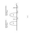
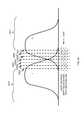
- FIG. 3illustrates an ideal distribution level for an SLC device, wherein V READ is the voltage level used during the read operation of the device. As shown, if the cell has a threshold voltage of less than V READ it is a “1” and if the cell has a threshold voltage higher than V READ it is a “0”.
- V READis the voltage level used during the read operation of the device.
- the ideal distribution of a SLC deviceis influenced by the data programmed into the adjoining cells in the device.
- One of the largest contributing factors affecting the distribution widthis the cell-to-cell floating gate coupling.
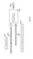
- FIG. 4illustrates a target cell 400 surrounded by its 8-most neighboring cells 401 , 402 , 403 , 404 , 405 , 406 , 407 , 408 . Due to the nature of the NAND architecture, coupling capacitance exists between the target cell 400 and the neighboring cells 401 , 402 , 403 , 404 , 405 , 406 , 407 , 408 . Depending upon the data to be programmed into the cell, the target cell 400 is programmed to a distribution “0” or remains in the erased state “1”. Sequentially, surrounding cells (or a subset of surrounding cells) are programmed to their target distributions.
- Surrounding cellsmove from the erased distribution to the written distribution. As a result of this, there is a change in the electric field of the target cell 400 . This electric field is reflected as a voltage threshold shift for the target cell 400 that appears “more programmed”. As a result, the target cell's 400 distribution experiences an enlargement on the right side of the distribution curve, as illustrated by the dotted lines in FIG. 5 . As such, if a target cell, belonging to the “1” distribution, crosses the V READ level after the programming of the surrounding cells, it will be read in error as a “0”.
- Each of the cells 401 , 402 , 403 , 404 , 405 , 406 , 407 , 408 surrounding the target cell 400contributes to the distribution of the target cell 400 , depending upon the capacitive coupling ratio between the target cell 400 and the neighboring cells 401 , 402 , 403 , 404 , 405 , 406 , 407 , 408 .
- FIG. 6illustrates the coupling coefficient of the eight neighboring cells 401 , 402 , 403 , 404 , 405 , 406 , 407 , 408 affecting the target cell 400 .
- cells in a pageare sequentially programmed from the bottom to the top (WL n ⁇ 2 to WL n+2 ). In this way, background pattern dependency is minimized. Additionally, cell-to-cell coupling effects are mitigated for the target cell 400 , because lower cells (pages) are programmed before the target cells 400 . However, this order of programming is true only if the target cell 400 is reprogrammed (or programmed) to “0”. Alternatively, if the target cell 400 stays in the erased state, it will be affected by the lowest cells as well as the highest cells, because it is not possible to lower the threshold voltage during program operation. Only the erase operation of the cells can lower the threshold voltage. As such, for an erased cell, the effect of all the surrounding cells must be considered.
- the coupling coefficients of the cellsdo not all have the same values/weights.
- Experimental resultsshow that Y coefficients 402 , 407 are dominant, followed by X 404 , 405 then XY 401 , 403 , 406 , 408 .
- Bit errors introduced by the coupling coefficients (and other phenomena)can be corrected using an ECC such as LDPC coding.
- LDPC codesare capacity-approaching codes that allow the noise threshold to be set very close to the Shannon limit for a symmetric, memory-less channel.
- the noise thresholddefines an upper bound for the channel noise, up to which the probability of lost information can be made as small as desired.
- Well-designed LDPC codeshave an UBER very near the Shannon limit.
- the power of LDPC codesresides in the ability of the decoding strategy to exploit the soft information on the stored data.
- the two voltage distributionsrepresent the two possible states: “0” and “1”, of the cells within the NAND chips.
- a hard decision decoderwill read all the positive values as 0 and all the negative values as 1. So, in the situation depicted in the graph 700 , the overlap region 710 will be composed of read errors.
- the error pointsmay vary in magnitude. For example, point A is slightly positive, while point B is farther away from the threshold voltage 705 .
- point Ais more likely to be in error than point B.
- differentiationcan be used between the two points and better information can then be provided to the decoder, resulting in improved decoding performance of the decoder in decoding the LDPC encoded codewords.
- Estimations of the exact value of point A and point Bare referred to as soft information, which may be expressed by a log likelihood ratio (LLR).
- LLRlog likelihood ratio
- the read errorsare not binary in nature, but instead vary from an ideal voltage according to an analog function.
- LDPC decodershave the ability to address this non-binary behavior using LLRs.
- the LLR attributed to a bitis representative of the probability that the voltage value read corresponds to a 0 or a 1.
- the sign of the LLRtypically provides the bit estimation (i.e. positive LLR corresponds to 0 and negative LLR corresponds to 1).
- the magnitude of the LLRprovides the reliability of the estimation (i.e.
- 0 means that the estimation is completely unreliable and
- ⁇ means that the estimation is completely reliable and the bit value is known).
- RBERraw bit error rate
- LDPC decodingis performed based upon a parity check matrix which consists of “0”'s and “1”'s that define the parity check equations.
- An M ⁇ N parity check matrix (H)comprises M rows and N columns. The number of columns N corresponds to the number N of codeword bits within one encoded codeword and the codeword comprises a plurality of information bits (K) and M parity check bits. The number of rows within the parity check matrix corresponds to the number M of parity check bits in the codeword.
- a plurality of read operationsare performed at various read reference voltage levels, by applying the read reference voltage to the corresponding control gate of the cell to see if the sensed cell conducts at that particular read reference voltage.
- the responses of the cell for each of the read reference voltagesare then used to determine the value of the bit stored by the cell.
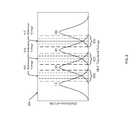
- the conventional design practiceis to employ uniform distribution for sensing the cells, wherein the soft-decision reference voltages are uniformly distributed between two consecutive hard-decision reference voltages.
- the present inventionemploys non-uniform partitioning of the threshold voltage distribution to improve the quality of the soft information.
- the soft-decision reference voltagesaround the hard-decision reference voltages and within the overlap regions, the same number of sensing voltages can be used in a non-uniform way to provide better information for determining the bit value.
- non-uniform threshold voltage sensingis performed for an MLC cell, wherein the overlap regions 820 , 825 and 830 are defined around each of the hard-decision reference voltages 805 , 810 and 815 and uniform memory sensing is performed within each of the overlap regions using the plurality of soft-decision reference voltages.
- the overlap regions of the threshold voltage distributions for the flash memory cellsare divided into a number of partitions, on either side of the hard-decision reference voltage, by moving the read reference voltages. In order to locate each bit without error, more read operations at these soft-decision reference voltages are required.
- each overlap region 820 , 825 and 830is divided into four partitions, so that each bit (LSB and MSB) is read utilizing 3 bits, where 3 represents the number of soft-decision bits.
- the log likelihood ratio (LLR) of the received data bits in the codewordis used to decode the codeword.
- LLRlog likelihood ratio
- the proper LLR associated with the soft-decision bitsis extracted from a look-up table stored in the flash controller and the LLR is then fed to the LDPC decoder for subsequent decoding of the codeword.
- 3 soft-decision bitsare used to identify eight regions, therefore eight LLRs will be extracted from the look-up table to perform the LDPC decoding process.
- every overlap regionrequires an LLR look-up table, so that in the MLC case illustrated in FIG. 8 , three LLR look-up tables are needed to provide the necessary decoding information.
- a single soft-decision reference voltagemay be used instead of a plurality of soft-decision references voltages, resulting in only one soft-decision bit with two states.
- the soft-decision decodingmay be considered hard-decision decoding resulting in a two-state result and therefore, two corresponding LLRs. As with the soft-decision LLRs, these hard-decision LLRs will also change over the lifetime of the device.
- the bit error rate (BER) of the memory deviceincreases during its lifetime. It follows that the log likelihood ratios (LLRs) of the flash memory device also change over the lifetime of the device, as the LLR values are measures of the reliability of the data read from the memory storage.
- LLRslog likelihood ratios
- LDPC decoders currently known in the artdo not consider the changes in the LLRs associated with the flash memory during the lifetime of the device and the effects of the neighboring cells on a target cell of the device. Instead, prior art LDPC decoders are designed for a maximum bit error rate that does not change during the memory device lifetime and does not consider the effects of neighboring cells.
- LLRsare a function of the shape and location of the threshold voltage distribution for the flash cells and can be computed or measured in a characterization laboratory.
- the LLR look-up tables used for decodingmust represent the channel and the BER at that specific point in the lifetime of the flash memory.
- the threshold voltage distribution for the flash cellschanges over the lifetime of the device due to wear-out and as such, the LLRs also change.
- a plurality of LLR tablesare needed that accurately reflect the threshold voltage distributions at various points over the lifetime of the device.
- a first LLR look-up tablewould be used for a fresh device, having a BER of around 10 ⁇ 6 and a second LLR look-up table would be used for the device towards the end of the device lifetime, when the BER is around 10 ⁇ 2 .
- the LLR look-up tablewill most accurately represent the noise and the LDPC will perform in a quasi-optimal way.
- Each flash technologyexhibits a unique threshold voltage distribution over its lifetime.
- a generic lawdoes not exist for determining standard LLR look-up table values for the variety of flash devices available in the market. Instead, in order to characterize the flash device and thereby determine the appropriate lifetime LLR look-up table values, it is necessary to measure billions and billions of flash cell distributions over the lifetime of each flash device to understand how the flash cells will perform.
- the lifetime threshold voltage distributionwill differ among technologies and among vendors. For example, it may be determined that a different LLR look-up table for every decade of BER accurately reflects the behavior of the flash cells over the lifetime of the device.
- LLR look-up tablewhen the BER of the flash device changes from 10 ⁇ 4 to 10 ⁇ 5 , a different LLR look-up table will be accessed in the flash controller to reflect this characterized change in BER. Additionally, at any single point in time, there may be multiple flash chips of the flash device operating at different points in their lifetime, or perhaps a single flash chip comprising regions that are operating at different points in their lifetime. By performing characterization of the flash device, either by computational techniques and laboratory measurements, a plurality of lifetime LLR look-up tables can be generated for the flash device that accurately reflect the change in the threshold voltage distribution of the flash device over its lifetime. The LLR look-up tables may also reflect changes to specific flash chips of the flash device or specific regions of a flash chip over the lifetime of the device. The plurality of LLR look-up tables are stored in the flash memory controller and in operation, the flash memory controller selects the appropriate LLR look-up table to use for decoding the codeword based upon the present point in the lifetime of the device.
- the effect of the programmed states of the neighboring cells on the threshold voltage of the target cellneed to be considered.
- a neighboring cell contribution LLR look-up tableis populated that is representative of the BER of a target cell (bit error probability) for each combination of possible patterns of the surrounding cells.
- FIG. 9illustrates a pattern table 900 for the neighboring cells 401 , 402 , 403 , 404 , 405 , 406 , 407 and 408 surrounding the target cell 400 , a BER table 905 for the target cell 400 and a resulting neighboring cell contribution LLR look-up table 910 populated by the BER table and the pattern table.
- pattern table 1003for the case in which the target cell 400 is programmed to “1” and another pattern table 1002 for the case in which the target cell 400 is programmed to “0”, as shown with reference to FIG. 10 .
- the values of all neighboring cells 401 , 402 , 403 , 404 , 405 , 406 , 407 and 408may not need to be fully determined for the application of the invention.
- the two states of the MSB valuemay have a larger voltage difference than the two LSB states. So, the MSB bit of the neighboring cells may influence the target cell 400 the most and the LSB bit of the neighboring cells may be ignored.
- FIG. 11illustrates a typical fail distribution as a function of page number (x-axis). As shown, fails are not uniformly distributed among pages, but instead, the number of fails has a tendency to increase with page number. It follows that different BER tables 905 can be populated, page by page. Experimental results show that two BER tables 905 are sufficient for an interleaving architecture of the NAND device, wherein, one BER table 905 is representative of the even pages and another BER table 905 is representative of the odd pages.
- each intermediate combinationcan be included, wherein one BER table 905 is representative of the lower pages and another BER table 905 is representative of the higher, etc.
- Various other configurations of the BER table 905 appropriate for the particular NAND deviceare within the scope of the invention.
- the entries for the BER table 905can be measured by the NAND controller is many ways. For example, BER can be measured on one, or more, dummy blocks during the device life. Since BER is dependent upon the number of P/E cycles, it must be measured for every fixed or variable step of P/E cycles. BER can also be measured on the data block, similar to the dummy block. The BER can be measured every fixed or variable step of P/E cycles after the erase cycle.
- the nonvolatile memory controller of the present inventioncan be used to provide one or more log likelihood ratios (LLRs) of a target cell for LDPC decoding.
- LLRslog likelihood ratios
- a nonvolatile memory system 1200such as a solid state drive, includes a nonvolatile memory controller 1205 coupled to a nonvolatile memory storage module 1215 comprising a plurality of NAND chips 1230 .
- the NAND chips 1230store the encoded codewords and the memory controller 1205 is designed to execute reading and writing controls for the NAND chips 1230 according to reading and writing instructions received from an access device.
- the nonvolatile memory controller 1205further includes read circuitry 1240 configured for reading a threshold voltage of a target cell stored in the nonvolatile memory storage module 1215 and for reading a threshold voltage of one or more neighboring cells of the target cell stored in the nonvolatile memory storage module 1215 .
- the nonvolatile memory controllerfurther includes one or more neighboring cell contribution LLR look-up tables 1235 associated with the nonvolatile memory storage module 1215 .
- Look-up circuitry 1250 of the nonvolatile memory controller 1205is configured for extracting an LLR associated with the threshold voltage of the target cell and the threshold voltage of the one or more neighboring cells from the one or more neighboring cell contribution LLR look-up tables 1235 and for providing the extracted LLR to an LDPC decoder.
- the read circuitry 1240is further configured for reading a logical page of the nonvolatile memory storage module 1215 , where the logical page includes the target cell.
- the read circuitry 1240is further configured for reading one or more neighboring logical pages of the nonvolatile memory storage 1215 , each of the one or more neighboring logical pages including one of the neighboring cells of the target cell.
- the read circuitry 1240may utilize a plurality of soft-decision reference voltages to read a plurality of threshold voltages of the target cell.
- the read circuitry 1240may utilize a plurality of soft-decision reference voltages to read a plurality of threshold voltages of each of the one or more neighboring cells.
- the one or more neighboring cell contribution LLR look-up tables 1235may include a neighboring cell contribution LLR look-up table 1235 that is associated with a current point in the lifetime of the nonvolatile memory storage module 1215 .
- the BER appropriate for the age of the nonvolatile memory storage module 1215may be taken into consideration when generating the neighboring cell contribution LLR look-up tables 1235 .
- the one or more neighboring cell contribution LLR look-up tables 1235may include a neighboring cell contribution LLR look-up table 1235 that is associated with a logical page of the nonvolatile memory storage module 1215 that includes the target cell. As such, the BER that is appropriate for the logical page of the nonvolatile memory storage module 1215 may be taken into consideration when generating the neighboring cell contribution LLR look-up tables 1235 .
- one or more neighboring cell contribution LLR look-up tables 1235may include a first neighboring cell contribution look-up table associated with a programmed state of the target cell and a second neighboring cell contribution look-up table associated with an unprogrammed state of the target cell, wherein the first neighboring cell contribution look-up table 1235 is different than the second neighboring cell contribution look-up table 1235 .
- the nonvolatile memory storage module 1215 of FIG. 12may be incorporated into a LDPC system as shown with reference to FIG. 13 .
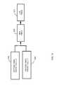
- the LDPC systemmay comprise an encoder 1335 that is responsible for adding the parity bits to the unencoded user data 1360 in accordance with a low-density parity check (LDPC) code.
- the LDPC encoded data 1365which includes the unencoded user data 1360 and an error correction code, may then be stored as encoded codewords in the nonvolatile memory storage module 1215 .
- the nonvolatile memory storage module 1215may include a plurality of NAND chips 1230 .
- the nonvolatile memory storage module 1215 and a nonvolatile memory controller 1205 having a plurality of neighboring cell contribution look-up tables 1235may be integrated into a nonvolatile memory system 1200 as previously described with reference to FIG. 12 .
- LLR look-up tables 1235may also include the current point in the lifetime of the device, which may be identified by the BER of the device or by other means, such as by counting the P/E cycles of the device.
- the LLRs 1370are used as input to the LDPC decoder 1340 to decode the user message data 1360 encoded by the encoder 1335 , utilizing LDPC coding parity check matrix (H).
- the received LLR values for each variable nodeare taken as the initial variable node messages.
- the check node processor 1345updates the check nodes of a first layer with the variable node messages to which they are connected.
- the resulting messages of the check node processor 1345are then passed to the variable node processor 1350 and the variable node processor 1350 then updates each variable node with the check node messages to which they are connected.
- the iterative decoding processcontinues, as is known in the art, and the resulting codeword estimate is then checked by a codeword estimate check processor 1355 , to verify whether or not the codeword estimate is a valid codeword.
- the codeword estimatemay be multiplied by the parity check matrix to determine the syndrome and if the syndrome is zero, it may be determined that the codeword estimate is a valid codeword. If the codeword estimate is determined to be a valid codeword, the decoding is complete and the estimated codeword is provided as output 1375 from the decoder 1340 . If it is determined by the codeword estimate check processor 1355 that the codeword estimate is not a valid codeword, a second iteration of the decoding begins. The iteration counter 1380 may be used to track the number of iterations of the decoding process and may cause the decoding to terminate if a maximum number of iterations is reached.
- the nonvolatile memory storage module 1215comprises a plurality of pages which may be organized in an interleaved architecture or, alternatively, in an all-bit-line (ABL) architecture.
- ABLall-bit-line
- two pagesbelong to the same word-line (WL).
- WLword-line
- to measure the pattern of the surrounding cells of a target cell on page nrequires the reading of pages: n+3, n+2, n+1, n, n ⁇ 1, n ⁇ 2.
- these six pagesneed to be read in order to be able to correct page “n”.
- An additional advantagecan be realized when utilizing a sequential read access for the interleaved NAND memory architecture. While there is still a latency associated with the six pages read in a sequential read, five of the six pages needed to correct page “n” can also be used to correct page “n+1”. As such, in a sequential read access, a latency of six reads exists, but there is no associated overhead, i.e. 2 pages read in order to correct 2 pages, or 1 read/page.
- the plurality of LLR look-up tables reflecting the effects of the neighboring cellsare stored in the flash memory controller and in operation, the flash memory controller selects the appropriate LLR look-up table to use for decoding the codeword.
- an LLR look-up tableneed not be a physical entity, but may be considered in a broader sense to be a logical entity. Additionally, the various LLR look-up tables reflecting the current BER of the device may be independent look-up tables or may alternatively be subsets of a larger look-up table.
- the present inventionutilizes a pattern recognition circuit to identify a pattern of the state of some or all of the neighboring cells in addition to the value of a target cell.
- the interpretation of the pattern by the pattern recognition circuittakes into account the proximity of the neighboring cells to the target cell, electrical coupling strengths, etc.
- the pattern recognition circuittranslates the pattern into an LLR value for storage into an LLR table. Many different patterns may translate to the same LLR value. A particular pattern for one vendor's flash technology may translate into a different LLR on another vendor's flash technology because the same pattern may be representing a different physical layout of the cells. Furthermore, the LLR a certain pattern translates to may change over time as a result of the program/erase cycles.
- pattern Amay translate to LLR “x” at the beginning of the life of the flash device, but after 8,000 erase cycles, pattern A may now translate to LLR “y”.
- the LLRs stored in the look-up tablesmay reflect both the contribution of the neighboring cells to a cell being read and the change of the contribution over the device lifetime.
- the diagonal neighborsmay have a weaker electrical coupling with the center cell and may be omitted. While the final LLR value for the center cell may not be quite as accurate as it could be when considering all the neighboring cells, omitting the diagonal neighbors may save additional flash read and processing time. The tradeoff in increased performance by omitting some of the neighboring cells may be preferred in a particular application.
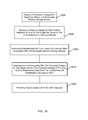
- a method of providing one or more log likelihood ratio (LLRs) of a target cell to a low-density parity check (LDPC) decoderbegins by reading a threshold voltage of a target cell stored in a nonvolatile memory storage module 1600 .
- the threshold voltage of the target cellmay be read from a nonvolatile memory storage module 1215 using the read circuitry 1240 of the nonvolatile memory controller 1205 .
- the nonvolatile memory storage module 1215may include a plurality of pages organized in an interleaved architecture or in an all-bit-line (ABL) architecture.
- the methodmay further include, reading the threshold voltages of a logical page of cells of the nonvolatile memory storage module, wherein the logical page of cells includes the target cell. Reading a threshold voltage of a target cell stored in a nonvolatile memory storage module 1600 may further include, using a plurality of soft-decision reference voltages to read a plurality of threshold voltages of the target cell.
- the methodfurther includes, reading a threshold voltage of one or more neighboring cells of the target cell stored in the nonvolatile memory storage module 1605 .
- the threshold voltage of the one or more neighboring cellsmay be read from a nonvolatile memory storage module 1215 using the read circuitry 1240 of the nonvolatile memory controller 1205 .
- Reading a threshold voltage of one or more neighboring cells of the target cell stored in the nonvolatile memory storage module 1605may further include, reading the threshold voltages of one or more logical pages of cells of the nonvolatile memory storage module, each of the one or more logical pages including one of the neighboring cells.
- the methodfurther includes, accessing a neighboring cell contribution LLR look-up table associated with the nonvolatile memory storage module 1610 .
- the neighboring cell contribution LLR look-up table 1235may be stored in a nonvolatile memory controller 1205 .
- Accessing a neighboring cell contribution LLR look-up table associated with the nonvolatile memory storage module 1610may further include, accessing a neighboring cell contribution LLR look-up table associated with a current point in the lifetime of the nonvolatile memory storage module.
- accessing a neighboring cell contribution LLR look-up table associated with the nonvolatile memory storage module 1610may further include, accessing a neighboring cell contribution LLR look-up table associated with a logical page of the nonvolatile memory storage module that includes the target cell.
- accessing a neighboring cell contribution LLR look-up table associated with the nonvolatile memory storage module 1610may further include, accessing a first neighboring cell contribution look-up table when the threshold voltage of the target cell indicates a programmed state of the target cell and accessing a second neighboring cell contribution look-up table when the threshold voltage of the target cell indicates an unprogrammed state of the target cell, wherein the first neighboring cell contribution look-up table is different than the second neighboring cell contribution look-up table.
- the methodfurther includes extracting an LLR associated with the threshold voltage of the target cell and the threshold voltage of the one or more neighboring cells from the neighboring cell contribution LLR look-up table 1615 .
- the extracted LLRis provided to an LDPC decoder 1620 .
- the present inventionutilizes the knowledge of now the NAND cells are physically laid out and their program/erase and read cycles to predict the most likely correct state of a cell whose correct state has been corrupted with noise.
- the information regarding the programmed states of the neighboring cells, the physical proximity of the neighboring cells and the number of read and program/erase cycles that have been performed on a cell being readit can be determined how the current state of a neighboring cell influences the state of the cell. If these factors have a very small effect, the LLR value assigned to the cell being read would be a large magnitude. If these factors have a larger effect, the assigned LLR value would have a smaller magnitude, thereby indicating a decreased likelihood that the correct state of the cell is the value that was written.
- a high quality LLRis assigned to the cell being read, thereby improving the decode performance resulting in a faster convergence or enabling a previously unavailable solution.
- the higher quality LLR values of the present inventionincrease the likelihood of determining a correct codeword during the decode process.
- FIG. 17illustrates a method 1700 for determining LLR values for use in LDPC decoding in accordance with an embodiment of the present invention.
- LLR valuesare determined.
- LLR valuesare determined for each possible pattern of reads of a test memory cell and memory cells that adjoin the test memory cell, where the test memory cell is read at plurality of different voltage levels.
- Step 1701can be performed in a test lab by coupling a test NAND memory device to a testing device and performing numerous reads of one or more test memory cells at varying test parameters.
- the test voltagesdivide the voltage threshold into a plurality of regions, and each region will have a plurality of corresponding LLRs associated with that region, each LLR associated with a pattern of reads of the target cell and neighboring cells.
- the reads of step 1701produce three information bits 2020 that can be referred to jointly as “hard-and-soft-decision bits,” that identify a particular region of the voltage distribution associated with a bit stored in the test memory cell.
- the first bitcommonly referred to as a hard decision bit identifies regions on opposite sides of the hard-decision reference voltage 2001
- the second bitthat can be referred to as a soft decision most significant bit identifies regions on opposite sides of soft-decision reference voltages 2002 and 2006
- the third bitthat can be referred to as a soft decision least significant bit identifies regions on opposite sides of soft-decision reference voltages 2003 and 2005 , and on opposite sides of soft-decision reference voltages 2004 and 2007 .
- Hard-decision reference voltage level 2001 and soft-decision reference voltages 2002 - 2007divide the voltage distribution into eight regions, the hard-and-soft-decision bits 2020 uniquely identifying each of the eight regions.
- the regionsinclude a region associated with an unprogrammed bit 2010 that can be, for example, a “1” and that can be identified by hard-and-soft-decision bits “111,” a region that extends between threshold voltages 2004 and 2002 that can be identified by hard-and-soft-decision bits “110,” a region that extends between threshold voltage 2002 and 2003 that can be identified by hard-and-soft-decision bits “100,” a region that extends between threshold voltages 2003 and 2001 that can be identified by hard-and-soft-decision bits “101,” a region that extends between threshold voltages 2001 and 2005 that can be identified by hard-and-soft-decision bits “001,” a region that extends between threshold voltages 2005 and 2006 that can be identified by hard-and-soft-decision bits “000,” a region that extends between threshold voltages
- each determined LLR value, the target cell hard-and-soft-decision bits associated with the determined LLR value and the neighboring cell read pattern associated with the determined LLR valueare stored in one or more look-up table.
- the one or more look-up tablecan be stored in the memory of the testing device.
- the look-up tableis a two-index LLR look-up table that includes a first index that identifies the region of the voltage distribution and a second index that identifies a neighboring cell pattern. Both the first index and the second index are required to identify the corresponding LLR value.
- the methodincludes storing one or more look-up table in a memory controller, the one or more look-up table including a LLR, the hard-and-soft-decision bits associated with the LLR and the neighboring cell read pattern associated with the LLR.
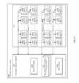
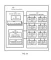
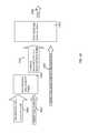
- a nonvolatile memory controller 1905is shown that includes memory storage configured to store one or more two-index LLR look-up tables 1935 that can have the format of two-index LLR look-up table 1800 of FIG. 18 .
- Nonvolatile memory controller 1905also includes read circuitry 1940 that is coupled to Look-up circuitry 1950 .
- Look-up circuitry 1950is also coupled to target cell read processing circuitry 1910 and to neighboring cell read processing circuitry 1920 .
- nonvolatile memory controller 1905includes LDPC encoder 1335 that is configured to generate a codeword by encoding unencoded user data using an LDPC code.
- the codeword (data+ECC) 1365is stored in one or more NAND devices 1930 that can be NAND semiconductor die coupled together to form nonvolatile memory storage module 1915 .
- the LDPC encoder 1335 and LDPC decoder 1340 shown in FIG. 13operate in the same manner as previously described in FIGS. 1-16 , except that, in the present embodiment, the LLRs provided to decoder 1340 are LLRs from two-index LLR look-up table stored in step 1703 .
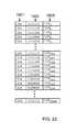
- an exemplary two-index LLR look-up table 1800is shown that includes the LLR values 1803 determined in step 1701 and stored in a memory controller in step 1703 .
- Each LLR value 1803 , the target cell hard-and-soft-decision bits 1801 associated with the LLR value 1803 and the neighboring cell read pattern 1802 associated with the LLR value 1803are stored in a row of two-index LLR look-up table 1800 .
- two-index LLR look-up table 1800includes a LLR, the hard-and-soft-decision bits associate with the LLR and the neighboring cell read pattern associated with the LLR for all possible combinations of target cell hard-and-soft-decision bits and neighboring cell read patterns, with each possible combination stored in a row of two-index LLR look-up table 1800 .
- the first rowincludes a first LLR, shown as LLR, that can be determined by testing a memory cell having a first voltage threshold that can be indicated by TARGET CELL HARD-AND-SOFT-DECISION BITS 1 and having a first neighboring cell read pattern that can be indicated by NEIGHBORING CELL READ PATTERN 1 .
- the second rowincludes a second LLR, shown as LLR 2 that can be determined by testing a cell having a second voltage threshold indicated by TARGET CELL HARD-AND-SOFT-DECISION BITS 2 and having a second neighboring cell read pattern (NEIGHBORING CELL READ PATTERN 2 ), where one of TARGET CELL HARD-AND-SOFT-DECISION BITS 2 and NEIGHBORING CELL READ PATTERN 2 is different from TARGET CELL HARD-AND-SOFT-DECISION BITS 1 and NEIGHBORING CELL READ PATTERN 1 .
- there are three soft-read bitsthere will be 2 11 possible combinations, giving a total of 2048 rows.
- FIG. 21illustrates an embodiment in which target cell hard-and-soft-decision bits 1801 of two-index LLR look-up table 1800 include target cell hard decision bit (X) that is read at a hard-decision voltage level, soft-read most significant bit (XMSB) and soft read least significant bit (XLSB) having the format shown in FIG. 20 .
- neighboring cell read pattern 1802includes bits XY1, YU, XY2, XR, XY4, YD, XY3 and XL, having the respective neighboring bit locations illustrated in FIG. 6 .
- each LLR 1803includes five bits, a first bit that is a sign bit and four additional bits that identify the numerical value of the LLR.
- steps 1701 and 1702are preformed in a test lab to generate one or more two-index LLR look-up table for a particular manufacturer and design of a NAND chip 1230 .
- Different manufacturers and different designs from a particular manufacturerwill have different two-index LLR look-up tables that reflect the bit error rate of each different NAND chip design.
- Step 1703can include selecting the correct two-index look-up table and installing the two-index LLR look-up table in a nonvolatile memory controller 1905 .
- nonvolatile memory controller 1905This can be done by the manufacturer of nonvolatile memory controller 1905 prior to shipping nonvolatile memory controller 1905 to a customer, or can be done by the customer, either before or after electrically coupling NAND chips 1230 to nonvolatile memory controller so as to form nonvolatile memory system 1200 .
- step 1704the method includes performing a plurality of reads of a cell of a nonvolatile memory storage module at different read voltage levels to generate a plurality of target cell hard-and-soft-decision bits associated with a bit stored in the cell.
- step 1704includes performing a plurality of reads of a cell of a nonvolatile memory storage module to generate a plurality of reads associated with a bit stored in the cell; analyzing the results from the plurality of reads associated with a bit stored in the cell to identify a threshold voltage region corresponding to the threshold voltage of the bit stored in the cell; and generating a plurality of target cell hard-and-soft-decision bits corresponding to the identified threshold voltage region.
- step 1704includes performing a first read of the cell of nonvolatile memory storage module 1915 at a hard read voltage and performing a plurality of additional reads of the cell at different soft read voltage levels proximate the hard read voltage, the nonvolatile memory controller 1905 operable for analyzing the plurality of reads to generate the target cell hard-and-soft-decision bits associated with a bit stored in the cell.
- read circuitry 1940is configured to perform the reads of a cell of a nonvolatile memory storage module 1915 at different read voltage levels to generate target cell hard-and-soft-decision bits associated with a bit stored in the cell.
- the reads of step 1704generate an index that identifies the threshold voltage region corresponding to the threshold voltage of the bit stored in the cell.
- the indexwill have one of the three bit soft-decision bit patterns shown in FIG. 20 .
- Read circuitry 1940includes target cell read processing circuitry 1910 that is configured to analyze the results from the plurality of reads associated with a bit stored in the cell to identify a threshold voltage region corresponding to the threshold voltage of the bit stored in the cell and is configured to generate a plurality of target cell hard-and-soft-decision bits 1801 corresponding to the identified threshold voltage region.
- target cell hard-and-soft-decision bits 2020are shown to be three bits in FIG. 20 , it is appreciated that target cell hard-and-soft-decision bits 2020 could include more or fewer bits. Moreover, in other embodiments of the present invention, other coding methods could be used to identify a region of the voltage distribution.
- read circuitry 1940is operable to send read requests to NAND chips 1930 and to analyze the results of the read requests to generate target cell hard-and-soft-decision bits 2020 .
- read circuitry 1940is operable to send requests to NAND chips 1930 and NAND chips 1930 are operable to generate target cell hard-and-soft-decision bits 2020 .
- the methodincludes performing reads of neighboring cells.
- the reads of neighboring cellsgenerate a plurality of neighboring cell reads, each of the plurality of neighboring cell reads associated with a bit stored in one of the neighboring cells.
- read circuitry 1940is configured for performing reads of neighboring cells to the cell of the nonvolatile memory storage module to generate a plurality of neighboring cell reads.
- the methodincludes combining the neighboring cell reads to generate a neighboring cell read pattern.
- neighboring cell read processing circuitry 1920is configured to combine the neighboring cell reads to generate a neighboring cell read pattern that corresponds to the pattern of the neighboring cell reads.
- each of the reads of neighboring cellsis representative of a logical “1” or a logical “0” and combining the neighboring cell reads to generate a neighboring cell read pattern that corresponds to the pattern of the neighboring cell reads further includes concatenating the neighboring cell reads representative of a logical “1” and representative of a logical “0” to generate the neighboring cell read pattern.
- neighboring cell processing circuitry 1920is configured to combine the neighboring cell reads by concatenating the neighboring cell reads representative of a logical “1” and representative of a logical “0” to generate the neighboring cell read pattern 1802 . For each combination of target cell hard-and-soft-decision bits 1802 there will be 256 possible combinations of neighboring cell read patterns 1802 , giving a total of 2048 different LLR values 1803 .
- the methodincludes accessing the one or more look-up table using the plurality of target cell hard-and-soft-decision bits associated with a bit stored in the cell and the neighboring cell read pattern that corresponds to the pattern of the neighboring cell soft reads to identify the corresponding LLR value.
- the methodincludes accessing the one or more look-up table using the plurality of target cell hard-and-soft-decision bits associated with a bit stored in the cell and the neighboring cell read pattern that corresponds to the pattern of the neighboring cell soft reads to identify the corresponding LLR value.
- step 1704generates hard-and-soft-decision bits 2301 that can include bits X 0 , XMSB 0 and XLSB 0 2311 and step 1706 generates neighboring cell read pattern 2302 that can include bits XY1 0 , YU 0 , XY2 0 , XR 0 , XY4 0 , YD 0 , XY3 0 and XL 0 2312 that are used to access two-index LLR look-up table 1800 .
- look-up circuitry 1950is configured to access the two-index LLR look-up table(s) 1935 using the target cell hard-and-soft-decision bits 2301 associated with a bit stored in the cell and neighboring cell read pattern 2302 that corresponds to the pattern of the neighboring cell soft reads to identify the corresponding LLR 2303 .
- Hard-and-soft-decision bits 2301 and neighboring cell read pattern 2302are described as being used separately to index two-index LLR look-up table in FIGS. 17-23 .
- the two indexescan be combined prior to step 1707 by concatenating target cell hard-and-soft decision bits and neighboring cell read pattern 2302 and the combination of the two indexes (e.g., bits X, XMSB, XLSB, XY1, YU, XY2, XR, XY4, YD, XY3 and XL) can be used to access two-index LLR look-up table 1800 .
- Two-index LLR look up table 2401includes target cell hard-and-soft-decision bits 1801 in which the target cell has a value of “0” and two-index LLR look up table 2402 includes target cell hard-and-soft-decision bits 1801 in which the target cell has a value of “1”.
- Two-index LLR look-up tables 2401 and 2402can be formed by dividing the rows of two-index look-up able 1800 according to the value of target cell hard-decision bit X N , with two-index LLR look up table 2401 including those rows of LLR look-up table 1800 in which X N has a value of “0” and two-index LLR look up table 2402 including those rows of LLR look-up table 1800 in which the X N has a value of 1.
- step 1707includes determining the value of the hard-decision bit X 0 stored in the target cell and using two-index LLR look up table 2301 when X 0 has a value of “0” and using two-index LLR look up table 2302 when X 0 has a value of “1.”
- the methodincludes sending the identified LLR to a Low-Density Party Check (LDPC) decoder for decoding of a codeword.
- LDPCLow-Density Party Check
- look-up circuitry 1950is operable to send the identified LLR to LDPC decoder 1340 .
- LDPC decoder 1340is configured to use the identified LLR 2303 to decode the codeword to obtain the estimated codeword 1375 .
- a neighboring cell pattern table 2530is used to combine some neighboring cell patterns to reduce the size of the two-index LLR look up table 2550 used to identify the correct LLR.
- Neighboring cell pattern table 2530includes all of the possible combinations of neighboring cell read patterns and provides corresponding indexes to a two-index LLR look-up table 2550 that are illustrated by common neighboring cell read pattern index 2540 shown in FIG. 25 . Accordingly, some of the common neighboring cell read pattern indexes 2540 of nonvolatile memory storage module 1915 are associated with more than one neighboring cell read pattern.
- the neighboring cell read patterns that are combinedcan be patterns of neighboring cells that are horizontally symmetrical, vertically symmetrical or diagonally symmetrical patterns.
- patterns 2501 and 2502may be combined such that they reference a single common neighboring cell read pattern index 2540 as they are vertically symmetrical (symmetrical with respect to the vertical axis), patterns 2503 and 2504 can be combined as they are horizontally symmetrical and patterns 2515 and 2516 can be combined as they are diagonally symmetrical (symmetrical about one or more diagonal axis).
- patterns 2505 and 2506can be combined, patterns 2507 and 2508 can be combined, patterns 2509 and 2510 , etc.
- more than two patterns 2501 - 2520can be combined such that they reference a single common neighboring cell read pattern index 2540 .
- patterns 2501 - 2504could be combined to reference a single common neighboring cell read pattern index 2540 .
- nonvolatile memory controller 1905is configured such that look-up tables 1935 include a neighboring cell look-up table 2530 that includes the neighboring cell read patterns and corresponding indexes to a two-index LLR look-up table 2550 .
- the common neighboring cell read pattern index 2540is then used as a first index to access the two-index LLR table 2550 , along with target cell hard-and-soft-decision bits 2301 identify the corresponding LLR 2303 .
- neighboring cell look-up table 2530includes both neighboring cell read patterns 2302 and target cell hard-decision bit values 2560 and is accessed using both a neighboring cell read patterns 2302 and a target cell hard-decision bit value (X 0 ) 2560 .
- the use of the target cell hard-decision bit value in conjunction with neighboring cell read pattern 2302allows for more precise combination of patterns than can be achieved using neighboring cell read pattern 2302 exclusively.
- neighboring cell look-up table 2530only includes neighboring cell read patterns 2302 and does not include target cell hard-decision bit values 2560 , and neighboring cell read patterns 2302 are exclusively used to determine the corresponding common neighboring cell pattern index 2540 .
- FIGS. 17-27are illustrated with respect to a single level cell. However, the method and apparatus of FIGS. 17-27 can also be used with NAND devices 1930 that are multi-level cell NAND devices, such as, for example, the two-bit MLC devices shown in FIG. 8 .
- the present inventionprovides an efficient method of acquiring, accumulating and processing soft information for use in LDPC decoding.
- the accumulationmay include incrementation, concatenation, collation, shifting and various other operations, performed independently or in combination, for the generation of a look-up table index to provide an appropriate LLR to be used in the LDPC decoding.
- system of the present inventionmay be implemented in a Field Programmable Gate Array (FPGA) or Application Specific Integrated Circuit (ASIC) suitable for the design of encoders/decoders for LDPC codes.
- FPGAField Programmable Gate Array
- ASICApplication Specific Integrated Circuit
Landscapes
- Engineering & Computer Science (AREA)
- Theoretical Computer Science (AREA)
- Physics & Mathematics (AREA)
- Probability & Statistics with Applications (AREA)
- Quality & Reliability (AREA)
- General Engineering & Computer Science (AREA)
- General Physics & Mathematics (AREA)
- Read Only Memory (AREA)
- Techniques For Improving Reliability Of Storages (AREA)
Abstract
Description
BER=f(yu,yd,xl,xr,xyl,xy2,xy3,xy4)
Claims (20)
Priority Applications (1)
| Application Number | Priority Date | Filing Date | Title |
|---|---|---|---|
| US14/557,214US9450610B1 (en) | 2013-03-15 | 2014-12-01 | High quality log likelihood ratios determined using two-index look-up table |
Applications Claiming Priority (3)
| Application Number | Priority Date | Filing Date | Title |
|---|---|---|---|
| US201361793198P | 2013-03-15 | 2013-03-15 | |
| US14/210,067US9590656B2 (en) | 2013-03-15 | 2014-03-13 | System and method for higher quality log likelihood ratios in LDPC decoding |
| US14/557,214US9450610B1 (en) | 2013-03-15 | 2014-12-01 | High quality log likelihood ratios determined using two-index look-up table |
Related Parent Applications (1)
| Application Number | Title | Priority Date | Filing Date |
|---|---|---|---|
| US14/210,067Continuation-In-PartUS9590656B2 (en) | 2013-03-15 | 2014-03-13 | System and method for higher quality log likelihood ratios in LDPC decoding |
Publications (1)
| Publication Number | Publication Date |
|---|---|
| US9450610B1true US9450610B1 (en) | 2016-09-20 |
Family
ID=56895816
Family Applications (1)
| Application Number | Title | Priority Date | Filing Date |
|---|---|---|---|
| US14/557,214Active2034-04-28US9450610B1 (en) | 2013-03-15 | 2014-12-01 | High quality log likelihood ratios determined using two-index look-up table |
Country Status (1)
| Country | Link |
|---|---|
| US (1) | US9450610B1 (en) |
Cited By (37)
| Publication number | Priority date | Publication date | Assignee | Title |
|---|---|---|---|---|
| US20170148510A1 (en)* | 2013-05-31 | 2017-05-25 | Sandisk Technologies Llc | Updating read voltages |
| US9740559B2 (en)* | 2015-10-28 | 2017-08-22 | Avago Technologies General Ip (Singapore) Pte. Ltd. | Systems and methods for compaction based flash memory data recovery |
| US20180048329A1 (en)* | 2016-08-12 | 2018-02-15 | SK Hynix Inc. | Memory controller, semiconductor memory system and operating method thereof |
| CN108268338A (en)* | 2016-12-30 | 2018-07-10 | 西部数据技术公司 | Gradually reduce the variable node memory of size |
| US10025661B1 (en)* | 2016-12-27 | 2018-07-17 | Sandisk Technologies Llc | Adaptive hard and soft bit decoding |
| US10083754B1 (en) | 2017-06-05 | 2018-09-25 | Western Digital Technologies, Inc. | Dynamic selection of soft decoding information |
| US10108489B2 (en) | 2015-10-28 | 2018-10-23 | Avago Technologies General Ip (Singapore) Pte. Ltd. | Systems and methods for efficient soft data based flash memory data recovery |
| US10204006B2 (en) | 2015-10-28 | 2019-02-12 | Avago Technologies International Sales Pte. Limited | Systems and methods for side data based soft data flash memory access |
| US10340951B2 (en) | 2017-09-13 | 2019-07-02 | Toshiba Memory Corporation | Soft decision LDPC decoder with improved LLR from neighboring bits |
| US10468112B1 (en)* | 2018-08-10 | 2019-11-05 | Micron Technology, Inc. | Disturb-optimized codeword layout |
| US20190340062A1 (en)* | 2018-05-03 | 2019-11-07 | SK Hynix Memory Solutions America Inc. | Neighbor assisted correction error recovery for memory system and method thereof |
| US20190340069A1 (en)* | 2018-05-03 | 2019-11-07 | SK Hynix Memory Solutions America Inc. | Memory system with deep learning based interference correction capability and method of operating such memory system |
| US10475523B2 (en) | 2013-05-31 | 2019-11-12 | Western Digital Technologies, Inc. | Updating read voltages triggered by the rate of temperature change |
| CN110797075A (en)* | 2018-08-02 | 2020-02-14 | 爱思开海力士有限公司 | NAND flash memory with reconfigurable neighbor assisted LLR correction |
| CN110955385A (en)* | 2018-09-26 | 2020-04-03 | 西部数据技术公司 | Data storage system and method for improved data relocation based on read level voltage associated with error recovery |
| US10811091B2 (en) | 2018-10-12 | 2020-10-20 | Western Digital Technologies, Inc. | Adaptive processing for read threshold voltage calibration |
| US10868566B2 (en) | 2017-12-14 | 2020-12-15 | Samsung Electronics Co., Ltd. | Error correction device, operating method of error correction device, and controller including error correction device |
| US10872013B2 (en) | 2019-03-15 | 2020-12-22 | Toshiba Memory Corporation | Non volatile memory controller device and method for adjustment |
| US11086716B2 (en) | 2019-07-24 | 2021-08-10 | Microchip Technology Inc. | Memory controller and method for decoding memory devices with early hard-decode exit |
| US11159176B1 (en)* | 2020-06-26 | 2021-10-26 | Western Digital Technologies, Inc. | Data-assisted LDPC decoding |
| US11309915B1 (en) | 2019-07-11 | 2022-04-19 | Arrowhead Center, Inc. | Efficient implementation of a threshold modified min-sum algorithm for low-density parity-check decoders |
| CN114567333A (en)* | 2022-02-24 | 2022-05-31 | 清华大学 | LDPC decoding method and device |
| US20220231700A1 (en)* | 2021-01-15 | 2022-07-21 | SK Hynix Inc. | Machine-learning based llr generation without assist-read for early-stage soft decoding |
| US11398291B2 (en) | 2020-11-20 | 2022-07-26 | Microchip Technology Inc. | Method and apparatus for determining when actual wear of a flash memory device differs from reliability states for the flash memory device |
| US20220278697A1 (en)* | 2020-12-28 | 2022-09-01 | Western Digital Technologies, Inc. | Error correction based on physical characteristics for memory |
| US20220365706A1 (en)* | 2021-05-12 | 2022-11-17 | Phison Electronics Corp. | Data accessing method, memory controlling circuit unit, and memory storage device |
| US11514992B2 (en) | 2021-02-25 | 2022-11-29 | Microchip Technology Inc. | Method and apparatus for reading a flash memory device |
| US11514994B1 (en) | 2021-05-28 | 2022-11-29 | Microchip Technology Inc. | Method and apparatus for outlier management |
| US11663076B2 (en) | 2021-06-01 | 2023-05-30 | Microchip Technology Inc. | Memory address protection |
| US11699493B2 (en) | 2021-05-24 | 2023-07-11 | Microchip Technology Inc. | Method and apparatus for performing a read of a flash memory using predicted retention-and-read-disturb-compensated threshold voltage shift offset values |
| US11782871B2 (en) | 2021-04-27 | 2023-10-10 | Microchip Technology Inc. | Method and apparatus for desynchronizing execution in a vector processor |
| US11809355B2 (en) | 2021-02-05 | 2023-11-07 | SK Hynix Inc. | UART aggregation and JTAG selection circuitry for a multi-solid state drive environment |
| US11843393B2 (en) | 2021-09-28 | 2023-12-12 | Microchip Technology Inc. | Method and apparatus for decoding with trapped-block management |
| US11934696B2 (en) | 2021-05-18 | 2024-03-19 | Microchip Technology Inc. | Machine learning assisted quality of service (QoS) for solid state drives |
| US12175363B2 (en) | 2020-07-27 | 2024-12-24 | Microchip Technology Inc. | Regression neural network for identifying threshold voltages to be used in reads of flash memory devices |
| US12175116B2 (en) | 2021-04-27 | 2024-12-24 | Microchip Technology Inc. | Method and apparatus for gather/scatter operations in a vector processor |
| US12393846B2 (en) | 2020-08-20 | 2025-08-19 | Microchip Technology Inc. | Partitionable neural network for solid state drives |
Citations (160)
| Publication number | Priority date | Publication date | Assignee | Title |
|---|---|---|---|---|
| US815137A (en) | 1904-10-24 | 1906-03-13 | Adolphus H Beecher | Safety starting mechanism for motors. |
| US5615235A (en) | 1988-06-08 | 1997-03-25 | Fujitsu Limited | Signal processing system for use in a digital signal clock changing apparatus |
| US5732092A (en) | 1996-01-25 | 1998-03-24 | Mitsubishi Denki Kabushiki Kaisha | Method of refreshing flash memory data in flash disk card |
| US5875343A (en) | 1995-10-20 | 1999-02-23 | Lsi Logic Corporation | Employing request queues and completion queues between main processors and I/O processors wherein a main processor is interrupted when a certain number of completion messages are present in its completion queue |
| US6115788A (en) | 1998-02-20 | 2000-09-05 | Seagate Technology, Inc. | Multi-drive array with improved data transfer rate performance |
| US20020051501A1 (en) | 2000-04-28 | 2002-05-02 | Victor Demjanenko | Use of turbo-like codes for QAM modulation using independent I and Q decoding techniques and applications to xDSL systems |
| US20020181438A1 (en) | 2001-05-16 | 2002-12-05 | Mcgibney Grant H. | Centralized synchronization for wireless networks |
| US20030033567A1 (en) | 2001-08-09 | 2003-02-13 | Hitachi, Ltd. | Memory card and memory controller |
| US6539515B1 (en) | 1999-11-24 | 2003-03-25 | Koninklijke Philips Electronics N.V. | Accelerated Reed-Solomon error correction |
| US20030104788A1 (en) | 2001-09-01 | 2003-06-05 | Sungwook Kim | Decoding architecture for low density parity check codes |
| US6633856B2 (en) | 2001-06-15 | 2003-10-14 | Flarion Technologies, Inc. | Methods and apparatus for decoding LDPC codes |
| US20030225970A1 (en) | 2002-05-28 | 2003-12-04 | Ebrahim Hashemi | Method and system for striping spares in a data storage system including an array of disk drives |
| US6725409B1 (en) | 2000-06-30 | 2004-04-20 | Texas Instruments Incorporated | DSP instruction for turbo decoding |
| US20040088636A1 (en) | 2002-06-28 | 2004-05-06 | Cypher Robert E. | Error detection/correction code which detects and corrects a first failing component and optionally a second failing component |
| US20040123230A1 (en) | 2002-12-24 | 2004-06-24 | Lee Sang-Hyun | Simplified message-passing decoder for low-density parity-check codes |
| US6789227B2 (en) | 2001-07-05 | 2004-09-07 | International Business Machines Corporation | System and method for generating low density parity check codes using bit-filling |
| US20040181735A1 (en) | 2003-03-04 | 2004-09-16 | Weizhuang (Wayne) Xin | Decoding a received BCH encoded signal |
| US20040234150A1 (en) | 2003-05-21 | 2004-11-25 | Yung-Ching Chang | Quantization matrix adjusting method for avoiding underflow of data |
| US20040252791A1 (en) | 2003-06-13 | 2004-12-16 | Ba-Zhong Shen | LDPC (Low Density Parity Check) coded modulation hybrid decoding using non-Gray code maps for improved performance |
| US20040268015A1 (en) | 2003-01-21 | 2004-12-30 | Nextio Inc. | Switching apparatus and method for providing shared I/O within a load-store fabric |
| US20050010846A1 (en) | 2002-08-27 | 2005-01-13 | Atsushi Kikuchi | Decoding device and decoding method |
| US6895547B2 (en) | 2001-07-11 | 2005-05-17 | International Business Machines Corporation | Method and apparatus for low density parity check encoding of data |
| US20050226355A1 (en) | 2004-04-09 | 2005-10-13 | Fujitsu Limited | Receiver circuit comprising equalizer |
| US20050252791A1 (en) | 2004-05-11 | 2005-11-17 | Rainer Pechtold | Removal of hydrogen from coolant fluid |
| US6976197B2 (en) | 2001-10-25 | 2005-12-13 | International Business Machines Corporation | Apparatus and method for error logging on a memory module |
| US6976194B2 (en) | 2002-06-28 | 2005-12-13 | Sun Microsystems, Inc. | Memory/Transmission medium failure handling controller and method |
| US20050286511A1 (en) | 2004-06-08 | 2005-12-29 | Johnsen Bjorn D | Method and apparatus for source authentication in a communications network |
| US20060039370A1 (en) | 2004-08-23 | 2006-02-23 | Warren Rosen | Low latency switch architecture for high-performance packet-switched networks |
| US20060050694A1 (en) | 2004-09-03 | 2006-03-09 | James Bury | Processing replies to request packets in an advanced switching context |
| US20060126728A1 (en) | 2004-12-10 | 2006-06-15 | Guoyao Yu | Parallel rate control for digital video encoder with multi-processor architecture and picture-based look-ahead window |
| US20060206655A1 (en) | 2004-12-10 | 2006-09-14 | Chappell Christopher L | Packet processing in switched fabric networks |
| US7116732B2 (en) | 2001-06-21 | 2006-10-03 | Alcatel | Method and apparatus for decoding a bit sequence |
| US20060282603A1 (en) | 2005-05-25 | 2006-12-14 | Integrated Device Technology, Inc. | Expansion of cross-domain addressing for PCI-express packets passing through non-transparent bridge |
| US20070050688A1 (en) | 2005-08-30 | 2007-03-01 | Larry Jay Thayer | Memory correction system and method |
| US20070089031A1 (en) | 2005-09-30 | 2007-04-19 | Intel Corporation | Methods and arrangements to remap degraded storage blocks |
| US7209527B2 (en) | 2002-07-08 | 2007-04-24 | Agere Systems Inc. | Turbo decoder employing max and max* map decoding |
| US20070118743A1 (en) | 2005-11-23 | 2007-05-24 | Microsoft Corporation | Communication of information via an in-band channel using a trusted configuration space |
| US20070136628A1 (en) | 2005-12-09 | 2007-06-14 | Advantest Corporation | Testing apparatus and testing method |
| US7237183B2 (en) | 2003-03-04 | 2007-06-26 | Broadcom Corporation | Parallel decoding of a BCH encoded signal |
| US20070147489A1 (en) | 2003-12-26 | 2007-06-28 | Zie Corporation | Uplink burst equalizing method in broad wide access system |
| US20070233939A1 (en) | 2006-03-31 | 2007-10-04 | Mosaid Technologies Incorporated | Flash memory system control scheme |
| US20080005382A1 (en) | 2006-06-14 | 2008-01-03 | Hitachi, Ltd. | System and method for resource allocation in fault tolerant storage system |
| US20080016425A1 (en) | 2006-04-04 | 2008-01-17 | Qualcomm Incorporated | Turbo decoder with symmetric and non-symmetric decoding rates |
| US20080229079A1 (en) | 2006-12-06 | 2008-09-18 | David Flynn | Apparatus, system, and method for managing commands of solid-state storage using bank interleave |
| US20080256280A1 (en) | 2007-04-12 | 2008-10-16 | Xiuling Ma | Splitting One Hardware Interrupt To Multiple Handlers |
| US20080267081A1 (en) | 2007-04-27 | 2008-10-30 | Guenter Roeck | Link layer loop detection method and apparatus |
| US20080276156A1 (en) | 2007-05-01 | 2008-11-06 | Texas A&M University System | Low density parity check decoder for regular ldpc codes |
| US7450668B2 (en) | 2005-02-02 | 2008-11-11 | At&T Intellectual Property I, L.P. | Soft bit viterbi equalizer using partially collapsed metrics |
| US7457906B2 (en) | 2003-01-21 | 2008-11-25 | Nextio, Inc. | Method and apparatus for shared I/O in a load/store fabric |
| US20080320214A1 (en) | 2003-12-02 | 2008-12-25 | Super Talent Electronics Inc. | Multi-Level Controller with Smart Storage Transfer Manager for Interleaving Multiple Single-Chip Flash Memory Devices |
| US7472331B2 (en) | 2004-07-16 | 2008-12-30 | Samsung Electronics Co., Ltd. | Memory systems including defective block management and related methods |
| US7484158B2 (en) | 2003-12-03 | 2009-01-27 | Infineon Technologies Ag | Method for decoding a low-density parity check (LDPC) codeword |
| US20090067320A1 (en) | 2007-09-11 | 2009-03-12 | Polycom, Inc. | Method and system for assigning a plurality of macs to a plurality of processors |
| US20090077302A1 (en) | 2007-09-18 | 2009-03-19 | Hitachi, Ltd. | Storage apparatus and control method thereof |
| US7529215B2 (en) | 2003-11-17 | 2009-05-05 | Telefonaktiebolaget Lm Ericsson (Publ) | Encapsulation of independent transmissions over internal interface of distributed radio base station |
| US20090164694A1 (en) | 2007-12-21 | 2009-06-25 | Aprius Inc. | Universal routing in pci-express fabrics |
| US7567472B2 (en) | 2006-04-12 | 2009-07-28 | Micron Technology, Inc. | Memory block testing |
| US7620784B2 (en) | 2006-06-09 | 2009-11-17 | Microsoft Corporation | High speed nonvolatile memory device using parallel writing among a plurality of interfaces |
| US20090296798A1 (en) | 2006-04-05 | 2009-12-03 | Agere Systems Inc,. | Hsdpa co-processor for mobile terminals |
| US20090303788A1 (en) | 2008-06-10 | 2009-12-10 | Roohparvar Frankie F | Methods and apparatus utilizing predicted coupling effect in the programming of non-volatile memory |
| US20090327802A1 (en) | 2008-06-30 | 2009-12-31 | Kabushiki Kaisha Toshiba | Storage control device, data recovery device, and storage system |
| US7694047B1 (en) | 2005-02-17 | 2010-04-06 | Qlogic, Corporation | Method and system for sharing input/output devices |
| US20100085076A1 (en) | 2007-01-05 | 2010-04-08 | Nxp, B.V. | Circuit comprising a matrix of programmable logic cells |
| US7708195B2 (en) | 2005-08-24 | 2010-05-04 | Renesas Technology Corp. | Memory card |
| US7739472B2 (en) | 2005-11-22 | 2010-06-15 | Sandisk Corporation | Memory system for legacy hosts |
| US20100162075A1 (en) | 2008-12-15 | 2010-06-24 | Quantenna Communications, Inc. | Low complexity LDCP decoding |
| US20100185808A1 (en) | 2004-03-17 | 2010-07-22 | Super Talent Electronics, Inc. | Methods and systems for storing and accessing data in uas based flash-memory device |
| US20100199149A1 (en) | 2007-12-05 | 2010-08-05 | Hanan Weingarten | Flash memory apparatus and methods using a plurality of decoding stages including optional use of concatenated bch codes and/or designation of "first below" cells |
| US20100211737A1 (en) | 2006-12-06 | 2010-08-19 | David Flynn | Apparatus, system, and method for data block usage information synchronization for a non-volatile storage volume |
| US20100211852A1 (en) | 2009-02-17 | 2010-08-19 | Samsung Electronics Co., Ltd. | Method of reading data in non-volatile memory device |
| US20100226422A1 (en) | 2005-06-29 | 2010-09-09 | Felix Alexandrovich Taubin | Precoder Construction And Equalization |
| US7801233B1 (en) | 2005-01-06 | 2010-09-21 | Marvell World Trade Ltd. | Method and system for channel equalization and crosstalk estimation in a multicarrier data transmission system |
| US20100246664A1 (en) | 2007-05-16 | 2010-09-30 | Citta Richard W | Apparatus and method for encoding and decoding signals |
| US20100262979A1 (en) | 2009-04-08 | 2010-10-14 | Google Inc. | Circular command queues for communication between a host and a data storage device |
| US20100293440A1 (en) | 2009-05-18 | 2010-11-18 | Jonathan Thatcher | Apparatus, system, and method to increase data integrity in a redundant storage system |
| US7860930B2 (en) | 2006-12-19 | 2010-12-28 | International Business Machines Corporation | Communication between host systems using a transaction protocol and shared memories |
| US20110055659A1 (en) | 2009-08-26 | 2011-03-03 | Skymedi Corporation | Method and System of Dynamic Data Storage for Error Correction in a Memory Device |
| US7904793B2 (en) | 2007-03-29 | 2011-03-08 | Sandisk Corporation | Method for decoding data in non-volatile storage using reliability metrics based on multiple reads |
| US20110066902A1 (en) | 2009-01-30 | 2011-03-17 | Sandisk Il Ltd. | System and method of reading data using a reliability measure |
| US20110072331A1 (en) | 2009-09-18 | 2011-03-24 | Kabushiki Kaisha Toshiba | Memory system and control method for the same |
| US7937641B2 (en) | 2006-12-21 | 2011-05-03 | Smart Modular Technologies, Inc. | Memory modules with error detection and correction |
| US7945721B1 (en) | 2006-08-11 | 2011-05-17 | Oracle America, Inc. | Flexible control and/or status register configuration |
| US20110119553A1 (en) | 2009-11-19 | 2011-05-19 | Lsi Corporation | Subwords coding using different encoding/decoding matrices |
| US7958430B1 (en) | 2005-06-20 | 2011-06-07 | Cypress Semiconductor Corporation | Flash memory device and method |
| US20110161678A1 (en) | 2009-12-24 | 2011-06-30 | Yasuyuki Niwa | Controller for controlling nand flash memory and data storage system |
| US7975193B2 (en) | 2009-06-01 | 2011-07-05 | Lsi Corporation | Solid state storage end of life prediction with correction history |
| US20110209031A1 (en) | 2010-02-25 | 2011-08-25 | Yong June Kim | Methods of Performing Error Detection/Correction in Nonvolatile Memory Devices |
| US20110225341A1 (en) | 2010-03-11 | 2011-09-15 | Tetsuya Satoh | Communication apparatus, communication system and adapter |
| US20110246136A1 (en) | 2010-03-31 | 2011-10-06 | Haratsch Erich F | Methods and apparatus for computing a probability value of a received value in communication or storage systems |
| US20110246842A1 (en) | 2010-03-31 | 2011-10-06 | Haratsch Erich F | Methods and apparatus for approximating a probability density function or distribution for a received value in communication or storage systems |
| US20110246853A1 (en) | 2010-04-02 | 2011-10-06 | Yong-June Kim | Semiconductor device and decoding method thereof |
| US20110296084A1 (en) | 2010-05-31 | 2011-12-01 | Kabushiki Kaisha Toshiba | Data storage apparatus and method of writing data |
| US20120054413A1 (en) | 2010-08-31 | 2012-03-01 | Micron Technology, Inc. | Stripe-based non-volatile multilevel memory operation |
| US20120051144A1 (en) | 2010-08-24 | 2012-03-01 | Hanan Weingarten | System and method for accelerated sampling |
| US8140930B1 (en) | 2005-05-13 | 2012-03-20 | Nec Corporation | Encoder and decoder by LDPC coding |
| US20120096192A1 (en) | 2010-10-19 | 2012-04-19 | Hitachi, Ltd. | Storage apparatus and virtual port migration method for storage apparatus |
| US8176367B2 (en) | 2009-05-28 | 2012-05-08 | Agere Systems Inc. | Systems and methods for managing end of life in a solid state drive |
| US20120141139A1 (en) | 2010-08-17 | 2012-06-07 | Umesh Bakhru | System and Method for Optical-Electrical-Optical Reach Extension in a Passive Optical Network |
| US20120166690A1 (en) | 2010-12-28 | 2012-06-28 | Plx Technology, Inc. | Multi-root sharing of single-root input/output virtualization |
| US8219894B2 (en) | 2004-10-27 | 2012-07-10 | Marvell International Ltd. | Architecture and control of reed-solomon error-correction decoding |
| US8223745B2 (en) | 2005-04-22 | 2012-07-17 | Oracle America, Inc. | Adding packet routing information without ECRC recalculation |
| US8228728B1 (en) | 2009-09-14 | 2012-07-24 | Marvell International Ltd. | Programming method for multi-level cell flash for minimizing inter-cell interference |
| US8245112B2 (en) | 2009-06-04 | 2012-08-14 | Lsi Corporation | Flash memory organization |
| US8244946B2 (en) | 2009-10-16 | 2012-08-14 | Brocade Communications Systems, Inc. | Interrupt moderation |
| US8245117B1 (en) | 2008-12-23 | 2012-08-14 | Link—A—Media Devices Corporation | Low complexity chien search in chase-type decoding of reed-solomon codes |
| US8250286B2 (en) | 2008-07-10 | 2012-08-21 | Phison Electronics Corp. | Block management method, and storage system and controller using the same |
| US8254112B2 (en) | 2010-04-26 | 2012-08-28 | Fu Zhun Precision Industry (Shen Zhen) Co., Ltd. | Compact heat dissipation device |
| US8255770B2 (en) | 2006-12-06 | 2012-08-28 | Samsung Electronics Co., Ltd. | Multi-level cell memory device and method thereof |
| US8261136B2 (en) | 2009-06-29 | 2012-09-04 | Sandisk Technologies Inc. | Method and device for selectively refreshing a region of a memory of a data storage device |
| US8259498B2 (en) | 2008-12-08 | 2012-09-04 | Infinite Memory Ltd. | Continuous address space in non-volatile-memories (NVM) using efficient management methods for array deficiencies |
| US8281217B2 (en) | 2008-03-18 | 2012-10-02 | Samsung Electronics Co., Ltd. | Memory devices and encoding and/or decoding methods |
| US8286004B2 (en) | 2009-10-09 | 2012-10-09 | Lsi Corporation | Saving encryption keys in one-time programmable memory |
| US8307258B2 (en) | 2009-05-18 | 2012-11-06 | Fusion-10, Inc | Apparatus, system, and method for reconfiguring an array to operate with less storage elements |
| US8327220B2 (en) | 2009-04-08 | 2012-12-04 | Google Inc. | Data storage device with verify on write command |
| US20120311402A1 (en) | 2011-06-02 | 2012-12-06 | Phison Electronics Corp. | Data reading method, memory controller, and memory storage device |
| US8341502B2 (en) | 2010-02-28 | 2012-12-25 | Densbits Technologies Ltd. | System and method for multi-dimensional decoding |
| US20130013983A1 (en) | 2004-10-12 | 2013-01-10 | Michael Livshitz | Structured low-density parity-check (ldpc) code |
| US8392789B2 (en) | 2009-07-28 | 2013-03-05 | Texas Instruments Incorporated | Method and system for decoding low density parity check codes |
| US20130086451A1 (en) | 2011-10-04 | 2013-04-04 | Cleversafe, Inc. | Reproducing data utilizing a zero information gain function |
| US8429325B1 (en) | 2010-08-06 | 2013-04-23 | Integrated Device Technology Inc. | PCI express switch and method for multi-port non-transparent switching |
| US20130117616A1 (en)* | 2011-11-07 | 2013-05-09 | Ying Yu Tai | Adaptive Read Comparison Signal Generation for Memory Systems |
| US20130145235A1 (en) | 2011-01-04 | 2013-06-06 | Lsi Corporation | Detection and decoding in flash memories with selective binary and non-binary decoding |
| US8473812B2 (en) | 2006-01-20 | 2013-06-25 | Marvell World Trade Ltd. | Method and system for error correction in flash memory |
| US20130163327A1 (en)* | 2011-12-23 | 2013-06-27 | Stec, Inc. | Word-line inter-cell interference detector in flash system |
| US20130163328A1 (en) | 2011-12-23 | 2013-06-27 | Stec, Inc. | Inter-cell interference algorithms for soft decoding of ldpc codes |
| US20130176779A1 (en) | 2011-01-04 | 2013-07-11 | Lsi Corporation | Inter-cell interference cancellation in flash memories |
| US20130185598A1 (en) | 2011-01-04 | 2013-07-18 | Lsi Corporation | Multi-tier detection and decoding in flash memories |
| US8504887B1 (en) | 2009-12-24 | 2013-08-06 | Marvell International Ltd. | Low power LDPC decoding under defects/erasures/puncturing |
| US20130318422A1 (en) | 2012-05-22 | 2013-11-28 | Stec, Inc. | Read level adjustment using soft information |
| US20130315252A1 (en) | 2012-05-22 | 2013-11-28 | Cisco Technology, Inc. | IMPLEMENTING PVLANs IN A LARGE-SCALE DISTRIBUTED VIRTUAL SWITCH |
| US8621318B1 (en) | 2012-01-11 | 2013-12-31 | Pmc-Sierra Us, Inc. | Nonvolatile memory controller with error detection for concatenated error correction codes |
| US8640005B2 (en) | 2010-05-21 | 2014-01-28 | Intel Corporation | Method and apparatus for using cache memory in a system that supports a low power state |
| US8645613B2 (en) | 2009-07-03 | 2014-02-04 | Phison Electronics Corp. | Data writing method for flash memory and control circuit and storage system using the same |
| US20140040704A1 (en) | 2012-08-04 | 2014-02-06 | Lsi Corporation | Soft-decision compensation for flash channel variation |
| US20140053037A1 (en) | 2012-08-17 | 2014-02-20 | Lsi Corporation | Multi-Level LDPC Layered Decoder With Out-Of-Order Processing |
| US20140068368A1 (en) | 2012-09-04 | 2014-03-06 | Lsi Corporation | LDPC Decoder With Fractional Unsatisfied Check Quality Metric |
| US20140072056A1 (en) | 2012-09-07 | 2014-03-13 | Sony Corporation | Combination a/53 and a/153 receiver using a hiho viterbi decoder |
| US20140085982A1 (en) | 2012-09-21 | 2014-03-27 | Kabushiki Kaisha Toshiba | Semiconductor memory device |
| US8694849B1 (en) | 2011-12-19 | 2014-04-08 | Pmc-Sierra Us, Inc. | Shuffler error correction code system and method |
| US8694855B1 (en) | 2011-11-02 | 2014-04-08 | Pmc-Sierra Us, Inc. | Error correction code technique for improving read stress endurance |
| US20140101510A1 (en) | 2012-10-05 | 2014-04-10 | Lsi Corporation | Low Density Parity Check Layer Decoder For Codes With Overlapped Circulants |
| US8707122B1 (en) | 2011-02-08 | 2014-04-22 | Pmc-Sierra Us, Inc. | Nonvolatile memory controller with two-stage error correction technique for enhanced reliability |
| US8739008B2 (en) | 2012-02-22 | 2014-05-27 | Silicon Motion, Inc. | Method for determining parity check matrix utilized in flash memory system and related flash memory system thereof |
| US20140181617A1 (en) | 2012-12-20 | 2014-06-26 | Lsi Corporation | Management of non-valid decision patterns of a soft read retry operation |
| US8769374B2 (en) | 2010-10-13 | 2014-07-01 | International Business Machines Corporation | Multi-write endurance and error control coding of non-volatile memories |
| US20140185611A1 (en) | 2012-12-31 | 2014-07-03 | Advanced Micro Devices, Inc. | Distributed packet switching in a source routed cluster server |
| US8775913B2 (en) | 2010-03-31 | 2014-07-08 | Lsi Corporation | Methods and apparatus for computing soft data or log likelihood ratios for received values in communication or storage systems |
| US20140198581A1 (en) | 2013-01-14 | 2014-07-17 | Eun-Kyoung Kim | Method of storing data in nonvolatile memory device and method of testing nonvolatile memory device |
| US8787428B2 (en) | 2010-12-01 | 2014-07-22 | Dynamic Invention Llc | Soft forwarding for cooperative wireless communication |
| US20140281823A1 (en) | 2013-03-15 | 2014-09-18 | Pmc-Sierra Us, Inc. | System and method with reference voltage partitioning for low density parity check decoding |
| US20140281767A1 (en) | 2013-03-14 | 2014-09-18 | Lsi Corporation | Recovery strategy that reduces errors misidentified as reliable |
| US20140281822A1 (en) | 2013-03-14 | 2014-09-18 | Lsi Corporation | Method and apparatus for generation of soft decision error correction code information |
| US8898372B2 (en) | 2011-03-29 | 2014-11-25 | Phison Electronics Corp. | Memory storage device, memory controller, and data writing method |
| US8917734B1 (en) | 2012-11-19 | 2014-12-23 | Pmc-Sierra Us, Inc. | Method and apparatus for an aggregated non-transparent requester ID translation for a PCIe switch |
| US8924824B1 (en)* | 2013-03-12 | 2014-12-30 | Western Digital Technologies, Inc. | Soft-decision input generation for data storage systems |
| US8995302B1 (en) | 2013-01-16 | 2015-03-31 | Pmc-Sierra Us, Inc. | Method and apparatus for translated routing in an interconnect switch |
| US9025495B1 (en) | 2013-01-16 | 2015-05-05 | Pmc-Sierra Us, Inc. | Flexible routing engine for a PCI express switch and method of use |
| US20150149871A1 (en) | 2013-11-28 | 2015-05-28 | Lsi Corporation | Flash Channel With Selective Decoder Likelihood Dampening |
| US20150186055A1 (en) | 2013-12-30 | 2015-07-02 | Sandisk Technologies Inc. | Method and system for predicting block failure in a non-volatile memory |
| US9294132B1 (en) | 2011-11-21 | 2016-03-22 | Proton Digital Systems, Inc. | Dual-stage data decoding for non-volatile memories |
- 2014
- 2014-12-01USUS14/557,214patent/US9450610B1/enactiveActive
Patent Citations (183)
| Publication number | Priority date | Publication date | Assignee | Title |
|---|---|---|---|---|
| US815137A (en) | 1904-10-24 | 1906-03-13 | Adolphus H Beecher | Safety starting mechanism for motors. |
| US5615235A (en) | 1988-06-08 | 1997-03-25 | Fujitsu Limited | Signal processing system for use in a digital signal clock changing apparatus |
| US5875343A (en) | 1995-10-20 | 1999-02-23 | Lsi Logic Corporation | Employing request queues and completion queues between main processors and I/O processors wherein a main processor is interrupted when a certain number of completion messages are present in its completion queue |
| US5732092A (en) | 1996-01-25 | 1998-03-24 | Mitsubishi Denki Kabushiki Kaisha | Method of refreshing flash memory data in flash disk card |
| US6115788A (en) | 1998-02-20 | 2000-09-05 | Seagate Technology, Inc. | Multi-drive array with improved data transfer rate performance |
| US6539515B1 (en) | 1999-11-24 | 2003-03-25 | Koninklijke Philips Electronics N.V. | Accelerated Reed-Solomon error correction |
| US20020051501A1 (en) | 2000-04-28 | 2002-05-02 | Victor Demjanenko | Use of turbo-like codes for QAM modulation using independent I and Q decoding techniques and applications to xDSL systems |
| US6725409B1 (en) | 2000-06-30 | 2004-04-20 | Texas Instruments Incorporated | DSP instruction for turbo decoding |
| US20020181438A1 (en) | 2001-05-16 | 2002-12-05 | Mcgibney Grant H. | Centralized synchronization for wireless networks |
| US7324559B2 (en) | 2001-05-16 | 2008-01-29 | Mcgibney Grant H | Centralized synchronization for wireless networks |
| US6633856B2 (en) | 2001-06-15 | 2003-10-14 | Flarion Technologies, Inc. | Methods and apparatus for decoding LDPC codes |
| US7116732B2 (en) | 2001-06-21 | 2006-10-03 | Alcatel | Method and apparatus for decoding a bit sequence |
| US6789227B2 (en) | 2001-07-05 | 2004-09-07 | International Business Machines Corporation | System and method for generating low density parity check codes using bit-filling |
| US6895547B2 (en) | 2001-07-11 | 2005-05-17 | International Business Machines Corporation | Method and apparatus for low density parity check encoding of data |
| US20050248999A1 (en) | 2001-08-09 | 2005-11-10 | Renesas Technology Corp. | Memory card and memory controller |
| US20030033567A1 (en) | 2001-08-09 | 2003-02-13 | Hitachi, Ltd. | Memory card and memory controller |
| US20080229164A1 (en) | 2001-08-09 | 2008-09-18 | Renesas Technology Corp. | Memory card and memory controller |
| US20030104788A1 (en) | 2001-09-01 | 2003-06-05 | Sungwook Kim | Decoding architecture for low density parity check codes |
| US6976197B2 (en) | 2001-10-25 | 2005-12-13 | International Business Machines Corporation | Apparatus and method for error logging on a memory module |
| US6934804B2 (en) | 2002-05-28 | 2005-08-23 | Sun Microsystems, Inc. | Method and system for striping spares in a data storage system including an array of disk drives |
| US20030225970A1 (en) | 2002-05-28 | 2003-12-04 | Ebrahim Hashemi | Method and system for striping spares in a data storage system including an array of disk drives |
| US6976194B2 (en) | 2002-06-28 | 2005-12-13 | Sun Microsystems, Inc. | Memory/Transmission medium failure handling controller and method |
| US20040088636A1 (en) | 2002-06-28 | 2004-05-06 | Cypher Robert E. | Error detection/correction code which detects and corrects a first failing component and optionally a second failing component |
| US7209527B2 (en) | 2002-07-08 | 2007-04-24 | Agere Systems Inc. | Turbo decoder employing max and max* map decoding |
| US20050010846A1 (en) | 2002-08-27 | 2005-01-13 | Atsushi Kikuchi | Decoding device and decoding method |
| US20040123230A1 (en) | 2002-12-24 | 2004-06-24 | Lee Sang-Hyun | Simplified message-passing decoder for low-density parity-check codes |
| US20040268015A1 (en) | 2003-01-21 | 2004-12-30 | Nextio Inc. | Switching apparatus and method for providing shared I/O within a load-store fabric |
| US7457906B2 (en) | 2003-01-21 | 2008-11-25 | Nextio, Inc. | Method and apparatus for shared I/O in a load/store fabric |
| US7206992B2 (en) | 2003-03-04 | 2007-04-17 | Broadcom Corporation | Decoding a received BCH encoded signal |
| US7237183B2 (en) | 2003-03-04 | 2007-06-26 | Broadcom Corporation | Parallel decoding of a BCH encoded signal |
| US20040181735A1 (en) | 2003-03-04 | 2004-09-16 | Weizhuang (Wayne) Xin | Decoding a received BCH encoded signal |
| US20040234150A1 (en) | 2003-05-21 | 2004-11-25 | Yung-Ching Chang | Quantization matrix adjusting method for avoiding underflow of data |
| US20040252791A1 (en) | 2003-06-13 | 2004-12-16 | Ba-Zhong Shen | LDPC (Low Density Parity Check) coded modulation hybrid decoding using non-Gray code maps for improved performance |
| US7529215B2 (en) | 2003-11-17 | 2009-05-05 | Telefonaktiebolaget Lm Ericsson (Publ) | Encapsulation of independent transmissions over internal interface of distributed radio base station |
| US20080320214A1 (en) | 2003-12-02 | 2008-12-25 | Super Talent Electronics Inc. | Multi-Level Controller with Smart Storage Transfer Manager for Interleaving Multiple Single-Chip Flash Memory Devices |
| US7484158B2 (en) | 2003-12-03 | 2009-01-27 | Infineon Technologies Ag | Method for decoding a low-density parity check (LDPC) codeword |
| US20070147489A1 (en) | 2003-12-26 | 2007-06-28 | Zie Corporation | Uplink burst equalizing method in broad wide access system |
| US20100185808A1 (en) | 2004-03-17 | 2010-07-22 | Super Talent Electronics, Inc. | Methods and systems for storing and accessing data in uas based flash-memory device |
| US20050226355A1 (en) | 2004-04-09 | 2005-10-13 | Fujitsu Limited | Receiver circuit comprising equalizer |
| US20050252791A1 (en) | 2004-05-11 | 2005-11-17 | Rainer Pechtold | Removal of hydrogen from coolant fluid |
| US20050286511A1 (en) | 2004-06-08 | 2005-12-29 | Johnsen Bjorn D | Method and apparatus for source authentication in a communications network |
| US7472331B2 (en) | 2004-07-16 | 2008-12-30 | Samsung Electronics Co., Ltd. | Memory systems including defective block management and related methods |
| US20060039370A1 (en) | 2004-08-23 | 2006-02-23 | Warren Rosen | Low latency switch architecture for high-performance packet-switched networks |
| US20060050694A1 (en) | 2004-09-03 | 2006-03-09 | James Bury | Processing replies to request packets in an advanced switching context |
| US20130013983A1 (en) | 2004-10-12 | 2013-01-10 | Michael Livshitz | Structured low-density parity-check (ldpc) code |
| US8219894B2 (en) | 2004-10-27 | 2012-07-10 | Marvell International Ltd. | Architecture and control of reed-solomon error-correction decoding |
| US20060206655A1 (en) | 2004-12-10 | 2006-09-14 | Chappell Christopher L | Packet processing in switched fabric networks |
| US20060126728A1 (en) | 2004-12-10 | 2006-06-15 | Guoyao Yu | Parallel rate control for digital video encoder with multi-processor architecture and picture-based look-ahead window |
| US7801233B1 (en) | 2005-01-06 | 2010-09-21 | Marvell World Trade Ltd. | Method and system for channel equalization and crosstalk estimation in a multicarrier data transmission system |
| US7450668B2 (en) | 2005-02-02 | 2008-11-11 | At&T Intellectual Property I, L.P. | Soft bit viterbi equalizer using partially collapsed metrics |
| US7694047B1 (en) | 2005-02-17 | 2010-04-06 | Qlogic, Corporation | Method and system for sharing input/output devices |
| US8223745B2 (en) | 2005-04-22 | 2012-07-17 | Oracle America, Inc. | Adding packet routing information without ECRC recalculation |
| US8140930B1 (en) | 2005-05-13 | 2012-03-20 | Nec Corporation | Encoder and decoder by LDPC coding |
| US20060282603A1 (en) | 2005-05-25 | 2006-12-14 | Integrated Device Technology, Inc. | Expansion of cross-domain addressing for PCI-express packets passing through non-transparent bridge |
| US7958430B1 (en) | 2005-06-20 | 2011-06-07 | Cypress Semiconductor Corporation | Flash memory device and method |
| US20100226422A1 (en) | 2005-06-29 | 2010-09-09 | Felix Alexandrovich Taubin | Precoder Construction And Equalization |
| US7708195B2 (en) | 2005-08-24 | 2010-05-04 | Renesas Technology Corp. | Memory card |
| US20070050688A1 (en) | 2005-08-30 | 2007-03-01 | Larry Jay Thayer | Memory correction system and method |
| US20070089031A1 (en) | 2005-09-30 | 2007-04-19 | Intel Corporation | Methods and arrangements to remap degraded storage blocks |
| US7739472B2 (en) | 2005-11-22 | 2010-06-15 | Sandisk Corporation | Memory system for legacy hosts |
| US20070118743A1 (en) | 2005-11-23 | 2007-05-24 | Microsoft Corporation | Communication of information via an in-band channel using a trusted configuration space |
| US20070136628A1 (en) | 2005-12-09 | 2007-06-14 | Advantest Corporation | Testing apparatus and testing method |
| US8473812B2 (en) | 2006-01-20 | 2013-06-25 | Marvell World Trade Ltd. | Method and system for error correction in flash memory |
| US8856622B2 (en) | 2006-01-20 | 2014-10-07 | Marvell World Trade Ltd. | Apparatus and method for encoding data for storage in multi-level nonvolatile memory |
| US20070233939A1 (en) | 2006-03-31 | 2007-10-04 | Mosaid Technologies Incorporated | Flash memory system control scheme |
| US20080016425A1 (en) | 2006-04-04 | 2008-01-17 | Qualcomm Incorporated | Turbo decoder with symmetric and non-symmetric decoding rates |
| US20090296798A1 (en) | 2006-04-05 | 2009-12-03 | Agere Systems Inc,. | Hsdpa co-processor for mobile terminals |
| US7567472B2 (en) | 2006-04-12 | 2009-07-28 | Micron Technology, Inc. | Memory block testing |
| US20090290441A1 (en) | 2006-04-12 | 2009-11-26 | Micron Technology, Inc. | Memory block testing |
| US8094508B2 (en) | 2006-04-12 | 2012-01-10 | Micron Technology, Inc. | Memory block testing |
| US7620784B2 (en) | 2006-06-09 | 2009-11-17 | Microsoft Corporation | High speed nonvolatile memory device using parallel writing among a plurality of interfaces |
| US20080005382A1 (en) | 2006-06-14 | 2008-01-03 | Hitachi, Ltd. | System and method for resource allocation in fault tolerant storage system |
| US7945721B1 (en) | 2006-08-11 | 2011-05-17 | Oracle America, Inc. | Flexible control and/or status register configuration |
| US20080229079A1 (en) | 2006-12-06 | 2008-09-18 | David Flynn | Apparatus, system, and method for managing commands of solid-state storage using bank interleave |
| US20080256292A1 (en) | 2006-12-06 | 2008-10-16 | David Flynn | Apparatus, system, and method for a shared, front-end, distributed raid |
| US8255770B2 (en) | 2006-12-06 | 2012-08-28 | Samsung Electronics Co., Ltd. | Multi-level cell memory device and method thereof |
| US20100211737A1 (en) | 2006-12-06 | 2010-08-19 | David Flynn | Apparatus, system, and method for data block usage information synchronization for a non-volatile storage volume |
| US8402201B2 (en) | 2006-12-06 | 2013-03-19 | Fusion-Io, Inc. | Apparatus, system, and method for storage space recovery in solid-state storage |
| US7860930B2 (en) | 2006-12-19 | 2010-12-28 | International Business Machines Corporation | Communication between host systems using a transaction protocol and shared memories |
| US7937641B2 (en) | 2006-12-21 | 2011-05-03 | Smart Modular Technologies, Inc. | Memory modules with error detection and correction |
| US20100085076A1 (en) | 2007-01-05 | 2010-04-08 | Nxp, B.V. | Circuit comprising a matrix of programmable logic cells |
| US7904793B2 (en) | 2007-03-29 | 2011-03-08 | Sandisk Corporation | Method for decoding data in non-volatile storage using reliability metrics based on multiple reads |
| US20080256280A1 (en) | 2007-04-12 | 2008-10-16 | Xiuling Ma | Splitting One Hardware Interrupt To Multiple Handlers |
| US20080267081A1 (en) | 2007-04-27 | 2008-10-30 | Guenter Roeck | Link layer loop detection method and apparatus |
| US20080276156A1 (en) | 2007-05-01 | 2008-11-06 | Texas A&M University System | Low density parity check decoder for regular ldpc codes |
| US8418023B2 (en) | 2007-05-01 | 2013-04-09 | The Texas A&M University System | Low density parity check decoder for irregular LDPC codes |
| US8555140B2 (en) | 2007-05-01 | 2013-10-08 | The Texas A&M University System | Low density parity check decoder for irregular LDPC codes |
| US8359522B2 (en) | 2007-05-01 | 2013-01-22 | Texas A&M University System | Low density parity check decoder for regular LDPC codes |
| US20100246664A1 (en) | 2007-05-16 | 2010-09-30 | Citta Richard W | Apparatus and method for encoding and decoding signals |
| US20090067320A1 (en) | 2007-09-11 | 2009-03-12 | Polycom, Inc. | Method and system for assigning a plurality of macs to a plurality of processors |
| US20090077302A1 (en) | 2007-09-18 | 2009-03-19 | Hitachi, Ltd. | Storage apparatus and control method thereof |
| US20100199149A1 (en) | 2007-12-05 | 2010-08-05 | Hanan Weingarten | Flash memory apparatus and methods using a plurality of decoding stages including optional use of concatenated bch codes and/or designation of "first below" cells |
| US8335977B2 (en) | 2007-12-05 | 2012-12-18 | Densbits Technologies Ltd. | Flash memory apparatus and methods using a plurality of decoding stages including optional use of concatenated BCH codes and/or designation of “first below” cells |
| US20090164694A1 (en) | 2007-12-21 | 2009-06-25 | Aprius Inc. | Universal routing in pci-express fabrics |
| US7752346B2 (en) | 2007-12-21 | 2010-07-06 | Aprius, Inc. | Universal routing in PCI-Express fabrics |
| US8281217B2 (en) | 2008-03-18 | 2012-10-02 | Samsung Electronics Co., Ltd. | Memory devices and encoding and/or decoding methods |
| US20090303788A1 (en) | 2008-06-10 | 2009-12-10 | Roohparvar Frankie F | Methods and apparatus utilizing predicted coupling effect in the programming of non-volatile memory |
| US20090327802A1 (en) | 2008-06-30 | 2009-12-31 | Kabushiki Kaisha Toshiba | Storage control device, data recovery device, and storage system |
| US8250286B2 (en) | 2008-07-10 | 2012-08-21 | Phison Electronics Corp. | Block management method, and storage system and controller using the same |
| US8259498B2 (en) | 2008-12-08 | 2012-09-04 | Infinite Memory Ltd. | Continuous address space in non-volatile-memories (NVM) using efficient management methods for array deficiencies |
| US20100162075A1 (en) | 2008-12-15 | 2010-06-24 | Quantenna Communications, Inc. | Low complexity LDCP decoding |
| US8245117B1 (en) | 2008-12-23 | 2012-08-14 | Link—A—Media Devices Corporation | Low complexity chien search in chase-type decoding of reed-solomon codes |
| US20110066902A1 (en) | 2009-01-30 | 2011-03-17 | Sandisk Il Ltd. | System and method of reading data using a reliability measure |
| US20100211852A1 (en) | 2009-02-17 | 2010-08-19 | Samsung Electronics Co., Ltd. | Method of reading data in non-volatile memory device |
| US8327220B2 (en) | 2009-04-08 | 2012-12-04 | Google Inc. | Data storage device with verify on write command |
| US20100262979A1 (en) | 2009-04-08 | 2010-10-14 | Google Inc. | Circular command queues for communication between a host and a data storage device |
| US8281227B2 (en) | 2009-05-18 | 2012-10-02 | Fusion-10, Inc. | Apparatus, system, and method to increase data integrity in a redundant storage system |
| US20100293440A1 (en) | 2009-05-18 | 2010-11-18 | Jonathan Thatcher | Apparatus, system, and method to increase data integrity in a redundant storage system |
| US8307258B2 (en) | 2009-05-18 | 2012-11-06 | Fusion-10, Inc | Apparatus, system, and method for reconfiguring an array to operate with less storage elements |
| US8176367B2 (en) | 2009-05-28 | 2012-05-08 | Agere Systems Inc. | Systems and methods for managing end of life in a solid state drive |
| US7975193B2 (en) | 2009-06-01 | 2011-07-05 | Lsi Corporation | Solid state storage end of life prediction with correction history |
| US8245112B2 (en) | 2009-06-04 | 2012-08-14 | Lsi Corporation | Flash memory organization |
| US8261136B2 (en) | 2009-06-29 | 2012-09-04 | Sandisk Technologies Inc. | Method and device for selectively refreshing a region of a memory of a data storage device |
| US8645613B2 (en) | 2009-07-03 | 2014-02-04 | Phison Electronics Corp. | Data writing method for flash memory and control circuit and storage system using the same |
| US8392789B2 (en) | 2009-07-28 | 2013-03-05 | Texas Instruments Incorporated | Method and system for decoding low density parity check codes |
| US8429497B2 (en) | 2009-08-26 | 2013-04-23 | Skymedi Corporation | Method and system of dynamic data storage for error correction in a memory device |
| US20110055659A1 (en) | 2009-08-26 | 2011-03-03 | Skymedi Corporation | Method and System of Dynamic Data Storage for Error Correction in a Memory Device |
| US8228728B1 (en) | 2009-09-14 | 2012-07-24 | Marvell International Ltd. | Programming method for multi-level cell flash for minimizing inter-cell interference |
| US20110072331A1 (en) | 2009-09-18 | 2011-03-24 | Kabushiki Kaisha Toshiba | Memory system and control method for the same |
| US8286004B2 (en) | 2009-10-09 | 2012-10-09 | Lsi Corporation | Saving encryption keys in one-time programmable memory |
| US8244946B2 (en) | 2009-10-16 | 2012-08-14 | Brocade Communications Systems, Inc. | Interrupt moderation |
| US20110119553A1 (en) | 2009-11-19 | 2011-05-19 | Lsi Corporation | Subwords coding using different encoding/decoding matrices |
| US8504887B1 (en) | 2009-12-24 | 2013-08-06 | Marvell International Ltd. | Low power LDPC decoding under defects/erasures/puncturing |
| US20110161678A1 (en) | 2009-12-24 | 2011-06-30 | Yasuyuki Niwa | Controller for controlling nand flash memory and data storage system |
| US20110209031A1 (en) | 2010-02-25 | 2011-08-25 | Yong June Kim | Methods of Performing Error Detection/Correction in Nonvolatile Memory Devices |
| US8341502B2 (en) | 2010-02-28 | 2012-12-25 | Densbits Technologies Ltd. | System and method for multi-dimensional decoding |
| US20110225341A1 (en) | 2010-03-11 | 2011-09-15 | Tetsuya Satoh | Communication apparatus, communication system and adapter |
| US8775913B2 (en) | 2010-03-31 | 2014-07-08 | Lsi Corporation | Methods and apparatus for computing soft data or log likelihood ratios for received values in communication or storage systems |
| US8504885B2 (en) | 2010-03-31 | 2013-08-06 | Lsi Corporation | Methods and apparatus for approximating a probability density function or distribution for a received value in communication or storage systems |
| US20110246842A1 (en) | 2010-03-31 | 2011-10-06 | Haratsch Erich F | Methods and apparatus for approximating a probability density function or distribution for a received value in communication or storage systems |
| US20110246136A1 (en) | 2010-03-31 | 2011-10-06 | Haratsch Erich F | Methods and apparatus for computing a probability value of a received value in communication or storage systems |
| US20110246853A1 (en) | 2010-04-02 | 2011-10-06 | Yong-June Kim | Semiconductor device and decoding method thereof |
| US8254112B2 (en) | 2010-04-26 | 2012-08-28 | Fu Zhun Precision Industry (Shen Zhen) Co., Ltd. | Compact heat dissipation device |
| US8640005B2 (en) | 2010-05-21 | 2014-01-28 | Intel Corporation | Method and apparatus for using cache memory in a system that supports a low power state |
| US20110296084A1 (en) | 2010-05-31 | 2011-12-01 | Kabushiki Kaisha Toshiba | Data storage apparatus and method of writing data |
| US8429325B1 (en) | 2010-08-06 | 2013-04-23 | Integrated Device Technology Inc. | PCI express switch and method for multi-port non-transparent switching |
| US20120141139A1 (en) | 2010-08-17 | 2012-06-07 | Umesh Bakhru | System and Method for Optical-Electrical-Optical Reach Extension in a Passive Optical Network |
| US20120051144A1 (en) | 2010-08-24 | 2012-03-01 | Hanan Weingarten | System and method for accelerated sampling |
| US20120054413A1 (en) | 2010-08-31 | 2012-03-01 | Micron Technology, Inc. | Stripe-based non-volatile multilevel memory operation |
| US8769374B2 (en) | 2010-10-13 | 2014-07-01 | International Business Machines Corporation | Multi-write endurance and error control coding of non-volatile memories |
| US20120096192A1 (en) | 2010-10-19 | 2012-04-19 | Hitachi, Ltd. | Storage apparatus and virtual port migration method for storage apparatus |
| US8787428B2 (en) | 2010-12-01 | 2014-07-22 | Dynamic Invention Llc | Soft forwarding for cooperative wireless communication |
| US20120166690A1 (en) | 2010-12-28 | 2012-06-28 | Plx Technology, Inc. | Multi-root sharing of single-root input/output virtualization |
| US20130176779A1 (en) | 2011-01-04 | 2013-07-11 | Lsi Corporation | Inter-cell interference cancellation in flash memories |
| US20130185598A1 (en) | 2011-01-04 | 2013-07-18 | Lsi Corporation | Multi-tier detection and decoding in flash memories |
| US20130145235A1 (en) | 2011-01-04 | 2013-06-06 | Lsi Corporation | Detection and decoding in flash memories with selective binary and non-binary decoding |
| US8707122B1 (en) | 2011-02-08 | 2014-04-22 | Pmc-Sierra Us, Inc. | Nonvolatile memory controller with two-stage error correction technique for enhanced reliability |
| US8898372B2 (en) | 2011-03-29 | 2014-11-25 | Phison Electronics Corp. | Memory storage device, memory controller, and data writing method |
| US20120311402A1 (en) | 2011-06-02 | 2012-12-06 | Phison Electronics Corp. | Data reading method, memory controller, and memory storage device |
| US20130086451A1 (en) | 2011-10-04 | 2013-04-04 | Cleversafe, Inc. | Reproducing data utilizing a zero information gain function |
| US8694855B1 (en) | 2011-11-02 | 2014-04-08 | Pmc-Sierra Us, Inc. | Error correction code technique for improving read stress endurance |
| US20130117616A1 (en)* | 2011-11-07 | 2013-05-09 | Ying Yu Tai | Adaptive Read Comparison Signal Generation for Memory Systems |
| US9058289B2 (en)* | 2011-11-07 | 2015-06-16 | Sandisk Enterprise Ip Llc | Soft information generation for memory systems |
| US20130117640A1 (en)* | 2011-11-07 | 2013-05-09 | Ying Yu Tai | Soft Information Generation for Memory Systems |
| US9294132B1 (en) | 2011-11-21 | 2016-03-22 | Proton Digital Systems, Inc. | Dual-stage data decoding for non-volatile memories |
| US8694849B1 (en) | 2011-12-19 | 2014-04-08 | Pmc-Sierra Us, Inc. | Shuffler error correction code system and method |
| US8493791B2 (en)* | 2011-12-23 | 2013-07-23 | Stec, Inc. | Word-line inter-cell interference detector in flash system |
| US20130163328A1 (en) | 2011-12-23 | 2013-06-27 | Stec, Inc. | Inter-cell interference algorithms for soft decoding of ldpc codes |
| US20130163327A1 (en)* | 2011-12-23 | 2013-06-27 | Stec, Inc. | Word-line inter-cell interference detector in flash system |
| US8656257B1 (en) | 2012-01-11 | 2014-02-18 | Pmc-Sierra Us, Inc. | Nonvolatile memory controller with concatenated error correction codes |
| US8621318B1 (en) | 2012-01-11 | 2013-12-31 | Pmc-Sierra Us, Inc. | Nonvolatile memory controller with error detection for concatenated error correction codes |
| US8739008B2 (en) | 2012-02-22 | 2014-05-27 | Silicon Motion, Inc. | Method for determining parity check matrix utilized in flash memory system and related flash memory system thereof |
| US20130318422A1 (en) | 2012-05-22 | 2013-11-28 | Stec, Inc. | Read level adjustment using soft information |
| US20130315252A1 (en) | 2012-05-22 | 2013-11-28 | Cisco Technology, Inc. | IMPLEMENTING PVLANs IN A LARGE-SCALE DISTRIBUTED VIRTUAL SWITCH |
| US20140040704A1 (en) | 2012-08-04 | 2014-02-06 | Lsi Corporation | Soft-decision compensation for flash channel variation |
| US20140053037A1 (en) | 2012-08-17 | 2014-02-20 | Lsi Corporation | Multi-Level LDPC Layered Decoder With Out-Of-Order Processing |
| US20140068368A1 (en) | 2012-09-04 | 2014-03-06 | Lsi Corporation | LDPC Decoder With Fractional Unsatisfied Check Quality Metric |
| US20140072056A1 (en) | 2012-09-07 | 2014-03-13 | Sony Corporation | Combination a/53 and a/153 receiver using a hiho viterbi decoder |
| US8958247B2 (en) | 2012-09-21 | 2015-02-17 | Kabushiki Kaisha Toshiba | Semiconductor memory device |
| US20140085982A1 (en) | 2012-09-21 | 2014-03-27 | Kabushiki Kaisha Toshiba | Semiconductor memory device |
| US20140101510A1 (en) | 2012-10-05 | 2014-04-10 | Lsi Corporation | Low Density Parity Check Layer Decoder For Codes With Overlapped Circulants |
| US8917734B1 (en) | 2012-11-19 | 2014-12-23 | Pmc-Sierra Us, Inc. | Method and apparatus for an aggregated non-transparent requester ID translation for a PCIe switch |
| US20140181617A1 (en) | 2012-12-20 | 2014-06-26 | Lsi Corporation | Management of non-valid decision patterns of a soft read retry operation |
| US20140185611A1 (en) | 2012-12-31 | 2014-07-03 | Advanced Micro Devices, Inc. | Distributed packet switching in a source routed cluster server |
| US20140198581A1 (en) | 2013-01-14 | 2014-07-17 | Eun-Kyoung Kim | Method of storing data in nonvolatile memory device and method of testing nonvolatile memory device |
| US8995302B1 (en) | 2013-01-16 | 2015-03-31 | Pmc-Sierra Us, Inc. | Method and apparatus for translated routing in an interconnect switch |
| US9025495B1 (en) | 2013-01-16 | 2015-05-05 | Pmc-Sierra Us, Inc. | Flexible routing engine for a PCI express switch and method of use |
| US8924824B1 (en)* | 2013-03-12 | 2014-12-30 | Western Digital Technologies, Inc. | Soft-decision input generation for data storage systems |
| US20140281822A1 (en) | 2013-03-14 | 2014-09-18 | Lsi Corporation | Method and apparatus for generation of soft decision error correction code information |
| US20140281767A1 (en) | 2013-03-14 | 2014-09-18 | Lsi Corporation | Recovery strategy that reduces errors misidentified as reliable |
| US20140281823A1 (en) | 2013-03-15 | 2014-09-18 | Pmc-Sierra Us, Inc. | System and method with reference voltage partitioning for low density parity check decoding |
| US20150149871A1 (en) | 2013-11-28 | 2015-05-28 | Lsi Corporation | Flash Channel With Selective Decoder Likelihood Dampening |
| US20150186055A1 (en) | 2013-12-30 | 2015-07-02 | Sandisk Technologies Inc. | Method and system for predicting block failure in a non-volatile memory |
Non-Patent Citations (2)
| Title |
|---|
| NVM Express, Revision 1.0; Intel Corporation; Mar. 1, 2011. |
| NVM Express, revision 1.0; Intel Corporation; pp. 103-106 and 110-114; Jul. 12, 2011. |
Cited By (54)
| Publication number | Priority date | Publication date | Assignee | Title |
|---|---|---|---|---|
| US10475523B2 (en) | 2013-05-31 | 2019-11-12 | Western Digital Technologies, Inc. | Updating read voltages triggered by the rate of temperature change |
| US20170148510A1 (en)* | 2013-05-31 | 2017-05-25 | Sandisk Technologies Llc | Updating read voltages |
| US10204006B2 (en) | 2015-10-28 | 2019-02-12 | Avago Technologies International Sales Pte. Limited | Systems and methods for side data based soft data flash memory access |
| US9740559B2 (en)* | 2015-10-28 | 2017-08-22 | Avago Technologies General Ip (Singapore) Pte. Ltd. | Systems and methods for compaction based flash memory data recovery |
| US10108489B2 (en) | 2015-10-28 | 2018-10-23 | Avago Technologies General Ip (Singapore) Pte. Ltd. | Systems and methods for efficient soft data based flash memory data recovery |
| US20180048329A1 (en)* | 2016-08-12 | 2018-02-15 | SK Hynix Inc. | Memory controller, semiconductor memory system and operating method thereof |
| US10200063B2 (en)* | 2016-08-12 | 2019-02-05 | SK Hynix Inc. | Memory controller, semiconductor memory system and operating method thereof |
| US10025661B1 (en)* | 2016-12-27 | 2018-07-17 | Sandisk Technologies Llc | Adaptive hard and soft bit decoding |
| CN108268338A (en)* | 2016-12-30 | 2018-07-10 | 西部数据技术公司 | Gradually reduce the variable node memory of size |
| CN108268338B (en)* | 2016-12-30 | 2021-03-23 | 西部数据技术公司 | Variable node memory of progressively reduced size |
| US10083754B1 (en) | 2017-06-05 | 2018-09-25 | Western Digital Technologies, Inc. | Dynamic selection of soft decoding information |
| US10340951B2 (en) | 2017-09-13 | 2019-07-02 | Toshiba Memory Corporation | Soft decision LDPC decoder with improved LLR from neighboring bits |
| US10868566B2 (en) | 2017-12-14 | 2020-12-15 | Samsung Electronics Co., Ltd. | Error correction device, operating method of error correction device, and controller including error correction device |
| CN110444242B (en)* | 2018-05-03 | 2023-09-08 | 爱思开海力士有限公司 | Memory system and operation method with interference correction capability based on deep learning |
| CN110444242A (en)* | 2018-05-03 | 2019-11-12 | 爱思开海力士有限公司 | There are the storage system and operating method of the interference correction ability based on deep learning |
| CN110444246A (en)* | 2018-05-03 | 2019-11-12 | 爱思开海力士有限公司 | Adjacent auxiliary corrective Fault recovery and its method for storage system |
| US20190340069A1 (en)* | 2018-05-03 | 2019-11-07 | SK Hynix Memory Solutions America Inc. | Memory system with deep learning based interference correction capability and method of operating such memory system |
| CN110444246B (en)* | 2018-05-03 | 2023-06-13 | 爱思开海力士有限公司 | Adjacent auxiliary correction error recovery for memory system and method thereof |
| US10997017B2 (en)* | 2018-05-03 | 2021-05-04 | SK Hynix Inc. | Neighbor assisted correction error recovery for memory system and method thereof |
| US20190340062A1 (en)* | 2018-05-03 | 2019-11-07 | SK Hynix Memory Solutions America Inc. | Neighbor assisted correction error recovery for memory system and method thereof |
| US10956263B2 (en)* | 2018-05-03 | 2021-03-23 | SK Hynix Inc. | Memory system with deep learning based interference correction capability and method of operating such memory system |
| CN110797075B (en)* | 2018-08-02 | 2023-08-25 | 爱思开海力士有限公司 | NAND Flash Memory with Reconfigurable Neighbor Assisted LLR Correction |
| CN110797075A (en)* | 2018-08-02 | 2020-02-14 | 爱思开海力士有限公司 | NAND flash memory with reconfigurable neighbor assisted LLR correction |
| US10468112B1 (en)* | 2018-08-10 | 2019-11-05 | Micron Technology, Inc. | Disturb-optimized codeword layout |
| CN110955385A (en)* | 2018-09-26 | 2020-04-03 | 西部数据技术公司 | Data storage system and method for improved data relocation based on read level voltage associated with error recovery |
| US11775178B2 (en) | 2018-09-26 | 2023-10-03 | Western Digital Technologies, Inc. | Data storage systems and methods for improved data relocation based on read-level voltages associated with error recovery |
| CN110955385B (en)* | 2018-09-26 | 2023-09-19 | 西部数据技术公司 | Data storage system and method for improved data relocation |
| US10811091B2 (en) | 2018-10-12 | 2020-10-20 | Western Digital Technologies, Inc. | Adaptive processing for read threshold voltage calibration |
| US10872013B2 (en) | 2019-03-15 | 2020-12-22 | Toshiba Memory Corporation | Non volatile memory controller device and method for adjustment |
| US12334954B1 (en) | 2019-07-11 | 2025-06-17 | Arrowhead Center, Inc. | Threshold-based min-sum algorithm to lower the error floors of quantized low-density parity-check decoders |
| US11962324B1 (en) | 2019-07-11 | 2024-04-16 | Arrowhead Center, Inc. | Threshold-based min-sum algorithm to lower the error floors of quantized low-density parity-check decoders |
| US11309915B1 (en) | 2019-07-11 | 2022-04-19 | Arrowhead Center, Inc. | Efficient implementation of a threshold modified min-sum algorithm for low-density parity-check decoders |
| US11086716B2 (en) | 2019-07-24 | 2021-08-10 | Microchip Technology Inc. | Memory controller and method for decoding memory devices with early hard-decode exit |
| US11159176B1 (en)* | 2020-06-26 | 2021-10-26 | Western Digital Technologies, Inc. | Data-assisted LDPC decoding |
| US12175363B2 (en) | 2020-07-27 | 2024-12-24 | Microchip Technology Inc. | Regression neural network for identifying threshold voltages to be used in reads of flash memory devices |
| US12393846B2 (en) | 2020-08-20 | 2025-08-19 | Microchip Technology Inc. | Partitionable neural network for solid state drives |
| US11398291B2 (en) | 2020-11-20 | 2022-07-26 | Microchip Technology Inc. | Method and apparatus for determining when actual wear of a flash memory device differs from reliability states for the flash memory device |
| US20220278697A1 (en)* | 2020-12-28 | 2022-09-01 | Western Digital Technologies, Inc. | Error correction based on physical characteristics for memory |
| US11601141B2 (en)* | 2020-12-28 | 2023-03-07 | Western Digital Technologies, Inc. | Error correction based on physical characteristics for memory |
| US20220231700A1 (en)* | 2021-01-15 | 2022-07-21 | SK Hynix Inc. | Machine-learning based llr generation without assist-read for early-stage soft decoding |
| US11411582B1 (en)* | 2021-01-15 | 2022-08-09 | SK Hynix Inc. | Machine-learning based LLR generation without assist-read for early-stage soft decoding |
| US11809355B2 (en) | 2021-02-05 | 2023-11-07 | SK Hynix Inc. | UART aggregation and JTAG selection circuitry for a multi-solid state drive environment |
| US11514992B2 (en) | 2021-02-25 | 2022-11-29 | Microchip Technology Inc. | Method and apparatus for reading a flash memory device |
| US12175116B2 (en) | 2021-04-27 | 2024-12-24 | Microchip Technology Inc. | Method and apparatus for gather/scatter operations in a vector processor |
| US11782871B2 (en) | 2021-04-27 | 2023-10-10 | Microchip Technology Inc. | Method and apparatus for desynchronizing execution in a vector processor |
| US12314599B2 (en)* | 2021-05-12 | 2025-05-27 | Phison Electronics Corp. | Method for adjusting a read voltage level or log likelihood ratio of a memory based on a calculated bit change ratio, memory controlling circuit unit, and memory storage device |
| TWI867220B (en)* | 2021-05-12 | 2024-12-21 | 群聯電子股份有限公司 | Data accessing method, memory controlling circuit unit and memory storage device |
| US20220365706A1 (en)* | 2021-05-12 | 2022-11-17 | Phison Electronics Corp. | Data accessing method, memory controlling circuit unit, and memory storage device |
| US11934696B2 (en) | 2021-05-18 | 2024-03-19 | Microchip Technology Inc. | Machine learning assisted quality of service (QoS) for solid state drives |
| US11699493B2 (en) | 2021-05-24 | 2023-07-11 | Microchip Technology Inc. | Method and apparatus for performing a read of a flash memory using predicted retention-and-read-disturb-compensated threshold voltage shift offset values |
| US11514994B1 (en) | 2021-05-28 | 2022-11-29 | Microchip Technology Inc. | Method and apparatus for outlier management |
| US11663076B2 (en) | 2021-06-01 | 2023-05-30 | Microchip Technology Inc. | Memory address protection |
| US11843393B2 (en) | 2021-09-28 | 2023-12-12 | Microchip Technology Inc. | Method and apparatus for decoding with trapped-block management |
| CN114567333A (en)* | 2022-02-24 | 2022-05-31 | 清华大学 | LDPC decoding method and device |
Similar Documents
| Publication | Publication Date | Title |
|---|---|---|
| US9450610B1 (en) | High quality log likelihood ratios determined using two-index look-up table | |
| US9590656B2 (en) | System and method for higher quality log likelihood ratios in LDPC decoding | |
| US9454414B2 (en) | System and method for accumulating soft information in LDPC decoding | |
| US10896123B2 (en) | Enhancing the effectiveness of read scan performance and reliability for non-volatile memory | |
| US9397701B1 (en) | System and method for lifetime specific LDPC decoding | |
| US11488673B2 (en) | Calibrating optimal read levels | |
| US10725860B2 (en) | Storage system and method for handling a burst of errors | |
| US9235467B2 (en) | System and method with reference voltage partitioning for low density parity check decoding | |
| CN108694098B (en) | Bit order modification for different memory regions of a storage device | |
| TWI391940B (en) | Non-volatile memory system with soft bit data transmission for error correction control and method of reading the same | |
| EP2737486B1 (en) | Non-volatile memory and method with accelerated post-write read using combined verification of multiple pages | |
| US10567001B2 (en) | Method and data storage device to estimate a number of errors using convolutional low-density parity-check coding | |
| US9905302B2 (en) | Read level grouping algorithms for increased flash performance | |
| US9235488B2 (en) | System and method for random noise generation | |
| US9502117B2 (en) | Cell-level statistics collection for detection and decoding in flash memories | |
| US20170255512A1 (en) | Multi-type parity bit generation for encoding and decoding | |
| CN108694097B (en) | Method and apparatus for using multiple codebooks of programming data in different memory regions of a storage device | |
| US10389389B2 (en) | Method and data storage device using convolutional low-density parity-check coding with a long page write and a short page read granularity | |
| US10977125B2 (en) | Adaptive usage of irregular code schemas based on specific system level triggers and policies | |
| US10367528B2 (en) | Convolutional low-density parity-check coding | |
| GB2537484A (en) | Read level grouping for increased flash performance | |
| TW201319801A (en) | Post-write read in non-volatile memories using comparison of data as written in binary and multi-state formats | |
| US11630722B2 (en) | Method and system for decoding data based on association of first memory location and second memory location | |
| US20150317203A1 (en) | Code-Based Read Control for Data Storage Devices | |
| CN111538621B (en) | Soft chip hunting recovery for bit line faults |
Legal Events
| Date | Code | Title | Description |
|---|---|---|---|
| AS | Assignment | Owner name:PMC-SIERRA US, INC., CALIFORNIA Free format text:ASSIGNMENT OF ASSIGNORS INTEREST;ASSIGNORS:MICHELONI, RINO;MARELLI, ALESSIA;NORRIE, CHRISTOPHER I. W.;SIGNING DATES FROM 20141124 TO 20141125;REEL/FRAME:034291/0732 | |
| FEPP | Fee payment procedure | Free format text:PAYOR NUMBER ASSIGNED (ORIGINAL EVENT CODE: ASPN); ENTITY STATUS OF PATENT OWNER: LARGE ENTITY Free format text:PAYER NUMBER DE-ASSIGNED (ORIGINAL EVENT CODE: RMPN); ENTITY STATUS OF PATENT OWNER: LARGE ENTITY | |
| AS | Assignment | Owner name:MORGAN STANLEY SENIOR FUNDING, INC., NEW YORK Free format text:PATENT SECURITY AGREEMENT;ASSIGNORS:MICROSEMI STORAGE SOLUTIONS, INC. (F/K/A PMC-SIERRA, INC.);MICROSEMI STORAGE SOLUTIONS (U.S.), INC. (F/K/A PMC-SIERRA US, INC.);REEL/FRAME:037689/0719 Effective date:20160115 | |
| AS | Assignment | Owner name:MICROSEMI STORAGE SOLUTIONS (U.S.), INC., DELAWARE Free format text:CHANGE OF NAME;ASSIGNOR:PMC-SIERRA US, INC.;REEL/FRAME:037961/0519 Effective date:20160115 | |
| AS | Assignment | Owner name:MICROSEMI STORAGE SOLUTIONS (US), INC., CALIFORNIA Free format text:CORRECTIVE ASSIGNMENT TO CORRECT THE ASSIGNEE NAME AND ADDRESS PREVIOUSLY RECORDED AT REEL: 037961 FRAME: 0519. ASSIGNOR(S) HEREBY CONFIRMS THE CHANGE OF NAME;ASSIGNOR:PMC-SIERRA US, INC.;REEL/FRAME:038102/0874 Effective date:20160115 | |
| STCF | Information on status: patent grant | Free format text:PATENTED CASE | |
| AS | Assignment | Owner name:IP GEM GROUP, LLC, CALIFORNIA Free format text:ASSIGNMENT OF ASSIGNORS INTEREST;ASSIGNOR:MICROSEMI SOLUTIONS (U.S.), INC.;REEL/FRAME:043212/0001 Effective date:20170721 Owner name:MICROSEMI SOLUTIONS (U.S.), INC., CALIFORNIA Free format text:CHANGE OF NAME;ASSIGNOR:MICROSEMI STORAGE SOLUTIONS (U.S.), INC.;REEL/FRAME:043458/0351 Effective date:20170119 | |
| AS | Assignment | Owner name:MICROSEMI STORAGE SOLUTIONS, INC., CALIFORNIA Free format text:RELEASE BY SECURED PARTY;ASSIGNOR:MORGAN STANLEY SENIOR FUNDING, INC.;REEL/FRAME:046251/0271 Effective date:20180529 Owner name:MICROSEMI STORAGE SOLUTIONS (U.S.), INC., CALIFORN Free format text:RELEASE BY SECURED PARTY;ASSIGNOR:MORGAN STANLEY SENIOR FUNDING, INC.;REEL/FRAME:046251/0271 Effective date:20180529 | |
| MAFP | Maintenance fee payment | Free format text:PAYMENT OF MAINTENANCE FEE, 4TH YEAR, LARGE ENTITY (ORIGINAL EVENT CODE: M1551); ENTITY STATUS OF PATENT OWNER: LARGE ENTITY Year of fee payment:4 | |
| MAFP | Maintenance fee payment | Free format text:PAYMENT OF MAINTENANCE FEE, 8TH YEAR, LARGE ENTITY (ORIGINAL EVENT CODE: M1552); ENTITY STATUS OF PATENT OWNER: LARGE ENTITY Year of fee payment:8 |