US9449987B1 - Three dimensional memory device with epitaxial semiconductor pedestal for peripheral transistors - Google Patents
Three dimensional memory device with epitaxial semiconductor pedestal for peripheral transistorsDownload PDFInfo
- Publication number
- US9449987B1 US9449987B1US14/995,017US201614995017AUS9449987B1US 9449987 B1US9449987 B1US 9449987B1US 201614995017 AUS201614995017 AUS 201614995017AUS 9449987 B1US9449987 B1US 9449987B1
- Authority
- US
- United States
- Prior art keywords
- memory
- semiconductor
- stack
- alternating stack
- forming
- Prior art date
- Legal status (The legal status is an assumption and is not a legal conclusion. Google has not performed a legal analysis and makes no representation as to the accuracy of the status listed.)
- Active
Links
Images


Classifications
- H—ELECTRICITY
- H10—SEMICONDUCTOR DEVICES; ELECTRIC SOLID-STATE DEVICES NOT OTHERWISE PROVIDED FOR
- H10B—ELECTRONIC MEMORY DEVICES
- H10B43/00—EEPROM devices comprising charge-trapping gate insulators
- H10B43/20—EEPROM devices comprising charge-trapping gate insulators characterised by three-dimensional arrangements, e.g. with cells on different height levels
- H10B43/23—EEPROM devices comprising charge-trapping gate insulators characterised by three-dimensional arrangements, e.g. with cells on different height levels with source and drain on different levels, e.g. with sloping channels
- H10B43/27—EEPROM devices comprising charge-trapping gate insulators characterised by three-dimensional arrangements, e.g. with cells on different height levels with source and drain on different levels, e.g. with sloping channels the channels comprising vertical portions, e.g. U-shaped channels
- H01L27/11582—
- H01L27/11556—
- H—ELECTRICITY
- H10—SEMICONDUCTOR DEVICES; ELECTRIC SOLID-STATE DEVICES NOT OTHERWISE PROVIDED FOR
- H10B—ELECTRONIC MEMORY DEVICES
- H10B41/00—Electrically erasable-and-programmable ROM [EEPROM] devices comprising floating gates
- H10B41/20—Electrically erasable-and-programmable ROM [EEPROM] devices comprising floating gates characterised by three-dimensional arrangements, e.g. with cells on different height levels
- H10B41/23—Electrically erasable-and-programmable ROM [EEPROM] devices comprising floating gates characterised by three-dimensional arrangements, e.g. with cells on different height levels with source and drain on different levels, e.g. with sloping channels
- H10B41/27—Electrically erasable-and-programmable ROM [EEPROM] devices comprising floating gates characterised by three-dimensional arrangements, e.g. with cells on different height levels with source and drain on different levels, e.g. with sloping channels the channels comprising vertical portions, e.g. U-shaped channels
- H—ELECTRICITY
- H10—SEMICONDUCTOR DEVICES; ELECTRIC SOLID-STATE DEVICES NOT OTHERWISE PROVIDED FOR
- H10B—ELECTRONIC MEMORY DEVICES
- H10B43/00—EEPROM devices comprising charge-trapping gate insulators
- H10B43/10—EEPROM devices comprising charge-trapping gate insulators characterised by the top-view layout
- H—ELECTRICITY
- H10—SEMICONDUCTOR DEVICES; ELECTRIC SOLID-STATE DEVICES NOT OTHERWISE PROVIDED FOR
- H10B—ELECTRONIC MEMORY DEVICES
- H10B43/00—EEPROM devices comprising charge-trapping gate insulators
- H10B43/30—EEPROM devices comprising charge-trapping gate insulators characterised by the memory core region
- H10B43/35—EEPROM devices comprising charge-trapping gate insulators characterised by the memory core region with cell select transistors, e.g. NAND
- H—ELECTRICITY
- H10—SEMICONDUCTOR DEVICES; ELECTRIC SOLID-STATE DEVICES NOT OTHERWISE PROVIDED FOR
- H10B—ELECTRONIC MEMORY DEVICES
- H10B43/00—EEPROM devices comprising charge-trapping gate insulators
- H10B43/40—EEPROM devices comprising charge-trapping gate insulators characterised by the peripheral circuit region
- H—ELECTRICITY
- H10—SEMICONDUCTOR DEVICES; ELECTRIC SOLID-STATE DEVICES NOT OTHERWISE PROVIDED FOR
- H10B—ELECTRONIC MEMORY DEVICES
- H10B43/00—EEPROM devices comprising charge-trapping gate insulators
- H10B43/50—EEPROM devices comprising charge-trapping gate insulators characterised by the boundary region between the core and peripheral circuit regions
- H—ELECTRICITY
- H01—ELECTRIC ELEMENTS
- H01L—SEMICONDUCTOR DEVICES NOT COVERED BY CLASS H10
- H01L21/00—Processes or apparatus adapted for the manufacture or treatment of semiconductor or solid state devices or of parts thereof
- H01L21/02—Manufacture or treatment of semiconductor devices or of parts thereof
- H01L21/02104—Forming layers
- H01L21/02365—Forming inorganic semiconducting materials on a substrate
- H01L21/02518—Deposited layers
- H01L21/02521—Materials
- H01L21/02524—Group 14 semiconducting materials
- H01L21/02532—Silicon, silicon germanium, germanium
- H—ELECTRICITY
- H01—ELECTRIC ELEMENTS
- H01L—SEMICONDUCTOR DEVICES NOT COVERED BY CLASS H10
- H01L21/00—Processes or apparatus adapted for the manufacture or treatment of semiconductor or solid state devices or of parts thereof
- H01L21/02—Manufacture or treatment of semiconductor devices or of parts thereof
- H01L21/02104—Forming layers
- H01L21/02365—Forming inorganic semiconducting materials on a substrate
- H01L21/02612—Formation types
- H01L21/02617—Deposition types
- H01L21/0262—Reduction or decomposition of gaseous compounds, e.g. CVD
- H—ELECTRICITY
- H01—ELECTRIC ELEMENTS
- H01L—SEMICONDUCTOR DEVICES NOT COVERED BY CLASS H10
- H01L21/00—Processes or apparatus adapted for the manufacture or treatment of semiconductor or solid state devices or of parts thereof
- H01L21/02—Manufacture or treatment of semiconductor devices or of parts thereof
- H01L21/02104—Forming layers
- H01L21/02365—Forming inorganic semiconducting materials on a substrate
- H01L21/02612—Formation types
- H01L21/02617—Deposition types
- H01L21/02636—Selective deposition, e.g. simultaneous growth of mono- and non-monocrystalline semiconductor materials
Definitions
- the present disclosurerelates generally to the field of three-dimensional semiconductor devices, and specifically to three-dimensional memory devices including peripheral devices and methods of manufacturing the same.
- Peripheral devicesare needed to control operation of various memory elements in three-dimensional memory devices. As the number of stacks in three-dimensional memory devices increases, the height of contact via structures for providing electrical contact to peripheral devices increases. Such an increase in the height of contact via structures makes it difficult to form reliable contact via structures for the peripheral devices.
- a method of fabricating a memory devicecomprises forming an alternating stack of insulator layers and spacer material layers over a single crystalline semiconductor surface of a substrate and forming stepped surfaces by patterning the alternating stack.
- the single crystalline semiconductor surfaceis exposed in a region from which all layers of the alternating stack are removed.
- the methodfurther comprises after forming the stepped surfaces, forming an epitaxial semiconductor pedestal and a dielectric material portion over a semiconductor surface of the semiconductor substrate and over the stepped surfaces, respectively.
- the epitaxial semiconductor pedestalis in epitaxial alignment with the single crystalline semiconductor surface of the semiconductor substrate.
- the methodfurther comprises forming an array of memory stack structures through a remaining portion of the alternating stack, and forming at least one semiconductor device on the epitaxial semiconductor pedestal.
- a memory devicecomprises an alternating stack of electrically conductive layers and insulator layers located over a semiconductor substrate, an array of memory stack structures located within memory openings which extend through the alternating stack, a dielectric material portion overlying stepped surfaces of the alternating stack, an epitaxial semiconductor pedestal having substantially vertical sidewalls in epitaxial alignment with a single crystalline substrate semiconductor material in the semiconductor substrate, and at least one semiconductor device located on the top surface of the epitaxial semiconductor pedestal.
- a method of fabricating a memory devicecomprises forming a first alternating stack of insulator layers and spacer material layers over a semiconductor substrate, etching the first alternating stack to expose a single crystalline semiconductor material, forming a first epitaxial semiconductor pedestal on the single crystalline semiconductor material, wherein the first epitaxial semiconductor pedestal is in epitaxial alignment with the single crystalline semiconductor material, forming an array of memory stack structures through the first alternating stack, forming a second epitaxial semiconductor pedestal on the first epitaxial semiconductor pedestal, wherein the first and the second epitaxial semiconductor pedestals are epitaxial alignment with each other, and forming at least one semiconductor device over the first epitaxial semiconductor pedestal.
- a memory devicewhich comprises at least one alternating stack located over a semiconductor substrate, wherein each of the at least one alternating stack comprises electrically conductive layers and insulator layers that alternate along a direction perpendicular to a top surface of the semiconductor substrate and including stepped surfaces in a contact region, an array of memory stack structures located within memory openings which extend through an entirety of the at least one alternating stack, at least one additional alternating stack of additional insulating layers and spacer material layers, wherein the spacer material layers have a different composition than the electrically conductive layers, at least one epitaxial semiconductor pedestal located in the at least one additional alternating stack, wherein each of the at least one epitaxial semiconductor pedestal is in epitaxial alignment with a single crystalline substrate semiconductor material of the semiconductor substrate, and at least one semiconductor device located on the at least one epitaxial semiconductor pedestal.
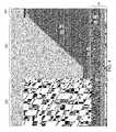
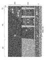
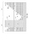
- FIG. 1is a vertical cross-sectional view of a first exemplary structure of after formation of a stack of alternating layers, an insulating cap layer, and a planarization stopping layer over a substrate according to a first embodiment of the present disclosure.
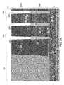
- FIG. 2is a vertical cross-sectional view of the first exemplary structure after formation of stepped terraces according to a first embodiment of the present disclosure.
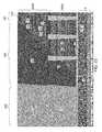
- FIG. 3is a vertical cross-sectional view of the first exemplary structure after formation of an epitaxial semiconductor pedestal in a peripheral device region according to the first embodiment of the present disclosure.
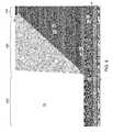
- FIG. 4is a vertical cross-sectional view of the first exemplary structure after deposition of a dielectric fill material layer according to the first embodiment of the present disclosure.
- FIG. 5is a vertical cross-sectional view of the first exemplary structure after formation of a dielectric material portion according to the first embodiment of the present disclosure.
- FIG. 6is a vertical cross-sectional view of a second exemplary structure after formation of a dielectric fill material layer according to a second embodiment of the present disclosure.
- FIG. 7is a vertical cross-sectional view of the second exemplary structure after formation of a dielectric material portion according to the second embodiment of the present disclosure.
- FIG. 8is a vertical cross-sectional view of the second exemplary structure after removal of a region of the dielectric material portion according to the second embodiment of the present disclosure.
- FIG. 9is a vertical cross-sectional view of the second exemplary structure after formation of an epitaxial semiconductor portion according to the second embodiment of the present disclosure.
- FIG. 10Ais a top-down view of the first or second exemplary structure after formation of memory openings and epitaxial channel portions according to the second embodiment of the present disclosure.
- FIG. 10Bis a vertical cross-sectional view of the exemplary structure of FIG. 10A along the vertical plane B-B′.
- FIG. 10Cis a vertical cross-sectional view of the exemplary structure of FIG. 10A along the vertical plane C-C′.
- FIG. 10Dis a vertical cross-sectional view of the exemplary structure of FIG. 10A along the vertical plane B-B′.
- FIG. 11Ais a top-down view of the first or second exemplary structure after formation of memory stack structures and backside contact structures according to the embodiments of the present disclosure.
- FIG. 11Bis a vertical cross-sectional view of the exemplary structure of FIG. 11A along the vertical plane B-B′.
- FIG. 11Cis a vertical cross-sectional view of the exemplary structure of FIG. 11A along the vertical plane C-C′.
- FIG. 11Dis a vertical cross-sectional view of the exemplary structure of FIG. 11A along the vertical plane B-B′.
- FIG. 12Ais a top-down view of the first or second exemplary structure after formation of peripheral devices according to the embodiments of the present disclosure.
- FIG. 12Bis a vertical cross-sectional view of the exemplary structure of FIG. 12A along the vertical plane B-B′.
- FIG. 12Cis a vertical cross-sectional view of the exemplary structure of FIG. 12A along the vertical plane C-C′.
- FIG. 12Dis a vertical cross-sectional view of the exemplary structure of FIG. 12A along the vertical plane D-D′.
- FIG. 12Eis a vertical cross-sectional view of the exemplary structure of FIG. 12A along the vertical plane E-E′.
- FIG. 13is a vertical cross-sectional view of a third exemplary structure after formation of a first alternating stack according to a third embodiment of the present disclosure.
- FIG. 14is a vertical cross-sectional view of the third exemplary structure after formation of first stepped terraces according to a third embodiment of the present disclosure.
- FIG. 15is a vertical cross-sectional view of the third exemplary structure after deposition of a first dielectric fill material layer according to the third embodiment of the present disclosure.
- FIG. 16is a vertical cross-sectional view of the third exemplary structure after formation of the first dielectric fill material portion according to the third embodiment of the present disclosure.
- FIG. 17is a vertical cross-sectional view of the third exemplary structure after patterning the first dielectric fill material portion to physically expose a top surface of single crystalline semiconductor layer according to the third embodiment of the present disclosure.
- FIG. 18is a vertical cross-sectional view of the third exemplary structure after formation of a first epitaxial semiconductor pedestal according to the third embodiment of the present disclosure.
- FIG. 19is a vertical cross-sectional view of the third exemplary structure after formation of first memory openings according to the third embodiment of the present disclosure.
- FIG. 20is a vertical cross-sectional view of the third exemplary structure after formation of sacrificial fill structures according to the third embodiment of the present disclosure.
- FIG. 21is a vertical cross-sectional view of the third exemplary structure after formation of a second alternating stack according to the third embodiment of the present disclosure.
- FIG. 22is a vertical cross-sectional view of the third exemplary structure after formation of second stepped terraces and a second dielectric fill material portion according to the third embodiment of the present disclosure.
- FIG. 23is a vertical cross-sectional view of the third exemplary structure after formation of a second epitaxial semiconductor pedestal according to the third embodiment of the present disclosure.
- FIG. 24is a vertical cross-sectional view of the third exemplary structure after formation of second memory openings according to the third embodiment of the present disclosure.
- FIG. 25is a vertical cross-sectional view of the third exemplary structure after formation of inter-stack memory openings according to the third embodiment of the present disclosure.
- FIG. 26Ais a top-down view of the third exemplary structure after formation of memory stack structures according to the third embodiment of the present disclosure.
- FIG. 26Bis a vertical cross-sectional view of the third exemplary structure of FIG. 26A along line B-B′ in FIG. 26A .
- FIG. 27is a vertical cross-sectional view of an alternate embodiment of the third exemplary structure after formation of a first epitaxial semiconductor pedestal prior to formation of a first dielectric material fill portion according to the third embodiment of the present disclosure.
- FIGS. 28A-28Dare sequential vertical cross-sectional views of an alternative configuration for the first, second, or third exemplary structure according to an embodiment of the present disclosure.
- FIG. 29Ais a schematic top-down view of the alternative configuration of FIG. 28D in which selected elements are illustrated.
- FIG. 29Bis a vertical cross-sectional view of the structure of FIG. 29A along the vertical plane B-B′.
- FIG. 29Cis a vertical cross-sectional view of the structure of FIG. 29A along the vertical plane C-C′.
- the present disclosureis directed to three-dimensional memory devices incorporating peripheral transistors, and methods of manufacturing the same, the various aspects of which are described below.
- the embodiments of the disclosurecan be employed to form various structures including a multilevel memory structure, non-limiting examples of which include semiconductor devices such as three-dimensional monolithic memory array devices comprising a plurality of NAND memory strings.
- the drawingsare not drawn to scale. Elements with the same reference numerals refer to the same or similar elements. Multiple instances of an element may be duplicated where a single instance of the element is illustrated, unless absence of duplication of elements is expressly described or clearly indicated otherwise.
- a first element located “on” a second elementcan be located on the exterior side of a surface of the second element or on the interior side of the second element.
- a first elementis located “directly on” a second element if there exist a physical contact between a surface of the first element and a surface of the second element.
- a monolithic three dimensional memory arrayis one in which multiple memory levels are formed above a single substrate, such as a semiconductor wafer, with no intervening substrates.
- the term “monolithic”means that layers of each level of the array are directly deposited on the layers of each underlying level of the array.
- two dimensional arraysmay be formed separately and then packaged together to form a non-monolithic memory device.
- non-monolithic stacked memorieshave been constructed by forming memory levels on separate substrates and vertically stacking the memory levels, as described in U.S. Pat. No.
- the substratesmay be thinned or removed from the memory levels before bonding, but as the memory levels are initially formed over separate substrates, such memories are not true monolithic three dimensional memory arrays.
- the various three dimensional memory devices of the present disclosureinclude a monolithic three-dimensional NAND string memory device, and can be fabricated employing the various embodiments described herein.
- the exemplary structureincludes a substrate 8 , which can be a semiconductor substrate, such as a single crystal silicon wafer.
- the semiconductor substrate 8can include one or more material layers ( 9 , 10 ).
- the substrate 8can include at least one underlying material layer 9 and a single crystalline semiconductor layer 10 as a topmost layer.
- the at least one underlying material layer 9can include a semiconductor material layer having a doping of a different conductivity type than the single crystalline semiconductor layer 10 located thereabove.
- the at least one underlying material layer 9can include a buried insulator layer.
- the at least one underlying material layer 9can include a first semiconductor material layer 9 B having a doping of a first conductivity type, and a second semiconductor material layer 9 A having a doping of a second conductivity type that is the opposite of the first conductivity type.
- the single crystalline semiconductor material layer 10can have a doping of the first conductivity type.
- the single crystalline semiconductor layer 10is a semiconductor material layer, and can include at least one elemental semiconductor material (e.g., silicon), at least one III-V compound semiconductor material, at least one II-VI compound semiconductor material, at least one organic semiconductor material, or other semiconductor materials known in the art.
- elemental semiconductor materiale.g., silicon
- III-V compound semiconductor materiale.g., silicon
- II-VI compound semiconductor materiale.g., II-VI compound semiconductor material
- organic semiconductor materiale.g., organic semiconductor material
- a “semiconductor material”refers to a material having electrical conductivity in the range from 1.0 ⁇ 10 ⁇ 6 S/cm to 1.0 ⁇ 10 5 S/cm, and is capable of producing a doped material having electrical conductivity in a range from 1.0 S/cm to 1.0 ⁇ 10 5 S/cm upon suitable doping with an electrical dopant.
- an “electrical dopant”refers to a p-type dopant that adds a hole to a balance band within a band structure, or an n-type dopant that adds an electron to a conduction band within a band structure.
- a “conductive material”refers to a material having electrical conductivity greater than 1.0 ⁇ 10 5 S/cm.
- an “insulator material” or a “dielectric material”refers to a material having electrical conductivity less than 1.0 ⁇ 10 ⁇ 6 S/cm. All measurements for electrical conductivities are made at the standard condition.
- at least one doped wellcan be formed within the single crystalline semiconductor layer 10 .
- a dielectric pad layer 12can be formed on a top surface of the single crystalline semiconductor layer 10 .
- the dielectric pad layer 12can be, for example, silicon oxide layer.
- the thickness of the dielectric pad layer 12can be in a range from 3 nm to 30 nm, although lesser and greater thicknesses can also be employed.
- a bottom insulator layer 31can be formed over the dielectric pad layer 12 . If present, the bottom insulator layer 31 includes a dielectric material, and can be formed directly on top surfaces of the dielectric pad layer 12 . Exemplary materials that can be employed for the bottom insulator layer 31 include, but are not limited to, silicon oxide, a dielectric metal oxide, and silicon nitride (in case the material of second material layers to be subsequently formed is not silicon nitride).
- an alternating stack of first material layers (which can be insulating layers 32 ) and second material layers (which can be spacer material layer 42 )is formed over the top surface of the substrate 8 , which can be, for example, on the top surface of the bottom insulator layer 31 .
- an alternating plurality of first elements and second elementsrefers to a structure in which instances of the first elements and instances of the second elements alternate. Each instance of the first elements that is not an end element of the alternating plurality is adjoined by two instances of the second elements on both sides, and each instance of the second elements that is not an end element of the alternating plurality is adjoined by two instances of the first elements on both ends.
- the first elementsmay have the same thickness thereamongst, or may have different thicknesses.
- the second elementsmay have the same thickness thereamongst, or may have different thicknesses.
- the alternating plurality of first material layers and second material layersmay begin with an instance of the first material layers or with an instance of the second material layers, and may end with an instance of the first material layers or with an instance of the second material layers.
- an instance of the first elements and an instance of the second elementsmay form a unit that is repeated with periodicity within the alternating plurality.
- Each first material layerincludes a first material
- each second material layerincludes a second material that is different from the first material.
- each first material layercan be an insulator layer 32
- each second material layercan be a spacer material layer 42 that provides vertical separation between the insulator layers.
- the stackcan include an alternating plurality of insulator layers 32 and spacer material layers 42 .
- the stack of the alternating pluralityis herein referred to as an alternating stack ( 32 , 42 ).
- the alternating stack ( 32 , 42 )can include insulator layers 32 composed of the first material, and spacer material layers 42 composed of a second material different from that of insulator layers 32 .
- the first material of the insulator layers 32can be at least one electrically insulating material.
- each insulator layer 32can be an electrically insulating material layer.
- Electrically insulating materials that can be employed for the insulator layers 32include, but are not limited to silicon oxide (including doped or undoped silicate glass), silicon nitride, silicon oxynitride, organosilicate glass (OSG), spin-on dielectric materials, dielectric metal oxides that are commonly known as high dielectric constant (high-k) dielectric oxides (e.g., aluminum oxide, hafnium oxide, etc.) and silicates thereof, dielectric metal oxynitrides and silicates thereof, and organic insulating materials.
- the first material of the insulator layers 32can be silicon oxide.
- the second material of the spacer material layers 42is a sacrificial material that can be removed selective to the first material of the insulator layers 32 .
- the spacer material layers 42are referred to sacrificial material layers.
- a removal of a first materialis “selective to” a second material if the removal process removes the first material at a rate that is at least twice the rate of removal of the second material.
- the ratio of the rate of removal of the first material to the rate of removal of the second materialis herein referred to as a “selectivity” of the removal process for the first material with respect to the second material.
- the spacer material layers 42may comprise an electrically insulating material, a semiconductor material, or a conductive material.
- the spacer material layers 42are sacrificial material layers, the sacrificial material of the spacer material layers 42 can be subsequently replaced with electrically conductive electrodes, which can function, for example, as control gate electrodes of a vertical NAND device.
- the sacrificial material that can be employed for the spacer material layers 42include silicon nitride, an amorphous semiconductor material (such as amorphous silicon), and a polycrystalline semiconductor material (such as polysilicon).
- the spacer material layers 42can be sacrificial material layers that comprise silicon nitride or a semiconductor material including at least one of silicon and germanium.
- the spacer material layers 42can be conductive material layers that are not subsequently replaced, i.e., permanent conductive material layers.
- the insulator layers 32can include silicon oxide, and spacer material layers can include silicon nitride spacer material layers.
- the first material of the insulator layers 32can be deposited, for example, by chemical vapor deposition (CVD).
- CVDchemical vapor deposition
- TEOStetraethyl orthosilicate
- the second material of the spacer material layers 42can be formed, for example, CVD or atomic layer deposition (ALD).
- the thicknesses of the insulator layers 32 and the spacer material layers 42can be in a range from 20 nm to 50 nm, although lesser and greater thicknesses can be employed for each insulator layer 32 and for each spacer material layer 42 .
- the number of repetitions of the pairs of an insulator layer 32 and a spacer material layer (e.g., a control gate electrode or a spacer material layer) 42can be in a range from 2 to 1,024, and typically from 8 to 256, although a greater number of repetitions can also be employed.
- the top and bottom gate electrodes in the stackmay function as the select gate electrodes.
- each spacer material layer 42 in the alternating stack ( 32 , 42 )can have a uniform thickness that is substantially invariant within each respective spacer material layer 42 .
- An insulating cap layer 70can be deposited over the alternating stack ( 32 , 42 ).
- the insulating cap layer 70includes an insulator material, which may be the same material as the first material of the insulator layers 32 .
- the insulating cap layer 70includes a material that is different from the second material of the spacer material layers 42 .
- the thickness of the insulating cap layer 70can be in a range from 20 nm to 100 nm, although lesser and greater thicknesses can also be employed.
- a planarization stopping layer 80can be formed over the insulating cap layer 70 .
- the planarization stopping layer 80includes a dielectric material that can be employed as a stopping layer in a subsequent planarization step, which may employ chemical mechanical planarization.
- the planarization stopping layer 80can employ a dielectric metal oxide (such as aluminum oxide), silicon nitride, or silicon oxide.
- the planarization stopping layer 80includes a dielectric material that is different from the second material of the spacer material layers 42 .
- the thickness of the planarization stopping layer 80can be in a range from 5 nm to 40 nm, although lesser and greater thicknesses can also be employed.
- the first exemplary structurecan have a region in which memory devices are to be subsequently formed, which is herein referred to as a device region 100 .
- the first exemplary structurecan have another region in which contact via structures that contact control gate electrodes are subsequently formed, which is herein referred to as contact region 300 .
- the first exemplary structurecan have still another region in which peripheral devices that control the operation of the memory devices are to be subsequently formed, which is herein referred to as a peripheral device region 200 .
- a stepped cavity 69 extending over the contact region 300 and the peripheral device region 200can be formed according to a first embodiment.
- the stepped cavity 69can have various stepped surfaces such that the horizontal cross-sectional shape of the stepped cavity changes in steps as a function of the vertical distance from the top surface of the substrate 8 .
- the stepped cavity 69can be formed by initially masking the device region 100 and optionally the contact region 200 with a masking layer (which may be a patterned photoresist layer), patterning the planarization stopping layer 80 and the insulating cap layer 70 by etching unmasked portions of the same, and by repetitively performing a set of processing steps to form the stepped surfaces.
- regions 200 and 300may etched at the same time during the same etch step, or region 200 may be etched prior to region 300 in separate etch steps.
- the set of processing stepscan include, for example, an etch process of a first type that vertically increases the depth of a cavity by one or more levels, and an etch process of a second type that laterally expands the area to be vertically etched in a subsequent etch process of the first type by trimming the masking layer (for example, by partially ashing an outer portion of the masking layer).
- a “level” of a structure including alternating pluralityis defined as the relative position of a pair of a first material layer and a second material layer within the structure.
- a photoresist layer(not shown) can be applied and patterned to initially cover the device region 100 and the contact region 300 , and an anisotropic etch process and an ashing process can be alternately performed.
- Each anisotropic etch processcan vertically extend a pre-existing cavity by two vertical levels (corresponding to a pair of an insulator layer 32 and a spacer material layer 42 ) and etch through the planarization stopping layer 80 and the insulating cap layer 70 within a newly physically exposed area, which is the area in which the top surface of the planarization stopping layer 80 is physically exposed during an immediately preceding ashing process that trims an outer portions of the photoresist layer.
- Each ashing processtrims the photoresist layer by removing only the outermost portions of the photoresist layer.
- the duration of the ashing processdetermines the amount of the ashed photoresist material, and the length of the corresponding ledge, i.e., a horizontal surface, of the stepped surfaces.
- the portions of layers 32 and 42 of the alternating stack ( 32 , 42 ) as well as layers 12 and 31 located in region 200may be removed during the formation of the stepped surfaces to expose the semiconductor substrate 8 (e.g., single crystal silicon substrate semiconductor layer 10 ) in region 200 . Alternatively, the portions of these layers located in region 200 may be removed during a separate etching step from the steps using to form the stepped surfaces.
- a peripheral portion of the alternating stack ( 32 , 42 )can have stepped surfaces after formation of the stepped cavity.
- stepped surfacesrefer to a set of surfaces that include at least two horizontal surfaces and at least two vertical surfaces such that each horizontal surface is adjoined to a first vertical surface that extends upward from a first edge of the horizontal surface, and is adjoined to a second vertical surface that extends downward from a second edge of the horizontal surface.
- a “stepped cavity”refers to a cavity having stepped surfaces. Remaining portions of the mask layer can be removed, for example, by ashing.
- an epitaxial semiconductor pedestal 110can be formed in the peripheral device region 200 , which is the region in which a top surface of the single crystalline substrate semiconductor material of the semiconductor material layer 10 is physically exposed.
- the epitaxial semiconductor pedestal 110can be formed by a selective epitaxy process.
- the epitaxial semiconductor pedestal 110comprises a single crystalline semiconductor material (e.g., single crystal silicon) in epitaxial alignment with the single crystalline substrate semiconductor material (e.g., single crystal silicon) of the semiconductor material layer 10 .
- the epitaxial semiconductor pedestal 110can be doped with electrical dopants of a suitable conductivity type.
- the top surface of the epitaxial semiconductor pedestal 110can be coplanar with, or can be located above, the horizontal plane including the top surface of the planarization stopping layer 80 .
- the sidewall surfaces of the epitaxial semiconductor pedestal 110may be substantially vertical and have no stepped surfaces which are a mirror image of the stepped surfaces in the stack in region 300 .
- the angle of the substantially vertical sidewalls of the epitaxial semiconductor pedestal 110 with respect to a horizontal planecan be in a range from 80 degrees to 100 degrees, such as 90 degrees.
- the selective epitaxy process that forms the epitaxial semiconductor pedestal 110can be performed, for example, by sequentially or simultaneously flowing a reactant gas (such as SiH 4 , SiH 2 Cl 2 , SiHCl 3 , SiCl 4 , Si 2 H 6 , GeH 4 , Ge 2 H 6 , other semiconductor precursor gases, or combinations there) with an etchant gas (such as HCl).
- a reactant gassuch as SiH 4 , SiH 2 Cl 2 , SiHCl 3 , SiCl 4 , Si 2 H 6 , GeH 4 , Ge 2 H 6 , other semiconductor precursor gases, or combinations there
- an etchant gassuch as HCl
- the semiconductor materialis deposited only on the semiconductor surface, which is the physically exposed portion of the top surface of the semiconductor material layer 10 .
- the process conditions(such as the deposition temperature, the partial pressure of the various gases in a process chamber, etc.) can be selected such that the deposited semiconductor material is epitaxial, i.e., single crystalline with atomic alignment with the single crystalline structure of the semiconductor material layer 10 .
- a dielectric fill material layer 65 Lis deposited in the remaining portion of the stepped cavity 69 , which is present in the contact region 300 , and over the alternating stack ( 32 , 42 ) in the device region 100 , and over the epitaxial semiconductor pedestal 110 in the peripheral device region 200 .
- the dielectric fill material layer 65 Lincludes a dielectric material that can be subsequently planarized employing a planarization process such as chemical mechanical planarization (CMP).
- CMPchemical mechanical planarization
- the dielectric fill material layer 65 Lcan include a dielectric material such as undoped silicon oxide or doped silicon oxide (such as phosphosilicate glass, borosilicate glass, or borophosphosilicate glass).
- the dielectric fill material layer 65 Lcan completely fill the remaining portion of the stepped cavity 69 in the contact region 300 .
- a planarization processcan be performed to remove portions of the dielectric fill material layer 65 L from above a horizontal plane including the top surface of the planarization stopping layer 80 .
- portions of the dielectric fill material layer 65 Lcan be removed from above the top surface of the planarization stopping layer 80 by chemical mechanical planarization (CMP).
- CMPchemical mechanical planarization
- the remaining portion of the dielectric fill material layer 65 L filling the stepped cavity in the contact region 300constitutes a dielectric material portion (i.e., an insulating fill material portion).
- the dielectric material portioncan include retro-stepped bottom surfaces. In this case, the dielectric material portion is herein referred to as a retro-stepped dielectric material portion 65 .
- a “retro-stepped” elementrefers to an element that has stepped surfaces and a horizontal cross-sectional area that increases monotonically as a function of a vertical distance from a top surface of a substrate on which the element is present.
- silicon oxideis employed for the retro-stepped dielectric material portion 65
- the silicon oxide of the retro-stepped dielectric material portion 65may, or may not, be doped with dopants such as B, P, and/or F.
- an epitaxial semiconductor pedestal 110 and a retro-stepped dielectric material portion 65are formed over a semiconductor surface of the semiconductor substrate 8 and over the stepped surfaces, respectively.
- the retro-stepped dielectric material portion 65may also be formed over a part of the exposed substrate 8 .
- the epitaxial semiconductor pedestal 110is in epitaxial alignment with a single crystalline substrate semiconductor material in the semiconductor substrate 8 .
- the dielectric material of the dielectric fill material layer 65 Lcan be planarized to form the retro-stepped dielectric material portion 65 employing at least the epitaxial semiconductor pedestal 110 as a stopping structure for the planarization process. In one embodiment, the dielectric material of the dielectric fill material layer 65 L can be planarized to form the retro-stepped dielectric material portion 65 employing the epitaxial semiconductor pedestal 110 and the planarization stopping layer 80 as stopping structures for the planarization process.
- the use of pedestal 100 as a planarization (e.g., polish) stop during planarization (e.g., CMP) of the retro-stepped dielectric material portion 65is one non-limiting advantage of forming the pedestal 110 after forming the stepped surfaces in region 300 .
- Another non-limiting advantage of forming the pedestal 110 after forming the stepped surfaces in region 300is that no stepped surfaces are formed in the sidewall(s) of the pedestal 110 . This leaves more room at the flat top surface of the pedestal 110 to form peripheral (e.g., driver circuit) devices and/or a reduction of space used for the pedestal which permits more memory devices to be formed in region 100 for the same size substrate.
- peripherale.g., driver circuit
- a second exemplary structure according to a second embodiment of the present disclosurecan be derived from the first exemplary structure of FIG. 2 by forming a dielectric fill material layer 65 L prior to forming the epitaxial semiconductor pedestal.
- the planarization stopping layer 80is patterned prior to forming the stepped surfaces illustrated in FIG. 2 .
- the dielectric fill material layer 65 L of FIG. 6can have the same composition as the dielectric fill material layer 65 L of FIG. 4 .
- the dielectric fill material layer 65 L of FIG. 6can be formed employing the same deposition methods as the deposition methods for forming the dielectric fill material layer 65 L of FIG. 4 .
- a planarization processcan be performed to remove portions of the dielectric fill material layer 65 L from above a horizontal plane including the top surface of the planarization stopping layer 80 .
- portions of the dielectric fill material layer 65 Lcan be removed from above the top surface of the planarization stopping layer 80 by chemical mechanical planarization (CMP).
- CMPchemical mechanical planarization
- the dielectric fill material layer 65 Lcan be planarized employing the planarization stopping layer 80 as a stopping layer.
- the remaining portion of the dielectric fill material layer 65 L filling the stepped cavity in the contact region 300 and the peripheral device region 200constitutes a retro-stepped dielectric material portion 65 (i.e., an insulating fill material portion).
- the silicon oxide of the retro-stepped dielectric material portion 65may, or may not, be doped with dopants such as B, P, and/or F.
- a photoresist layer(not shown) can be applied over the planarization stopping layer 80 and the retro-stepped dielectric material portion 65 , and can be patterned to cover the device region 100 and the contact region 300 , while not covering the peripheral device region 200 .
- An anisotropic etch or an isotropic etchcan be performed to remove a portion of the retro-stepped dielectric material portion 65 from the peripheral device region 200 .
- an anisotropic etchcan be employed to remove the physically exposed region of the retro-stepped dielectric material portion 65 from above the top surface of the semiconductor substrate 8 in the peripheral device region 200 .
- the retro-stepped dielectric material portion 65is reduced in size due to the anisotropic etch. Specifically, a remaining portion of the deposited dielectric material over the stepped surfaces in the contact region 300 constitutes the retro-stepped dielectric material portion 65 .
- the retro-stepped dielectric material portion 65(as provided after the processing steps of FIG. 8 ) is formed by deposition and patterning of a dielectric material over the substrate 8 .
- a peripheral region cavity 79is formed within the volume from which a portion of the retro-stepped dielectric material portion 65 is removed.
- a lower epitaxial semiconductor pedestal 110 Acan be formed in the peripheral device region 200 , which is the region in which a top surface of the single crystalline substrate semiconductor material of the semiconductor material layer 10 is physically exposed.
- the lower epitaxial semiconductor pedestal 110 Acan be formed by a selective epitaxy process, which is herein referred to as a first selective epitaxy process.
- the lower epitaxial semiconductor pedestal 110 Acomprises a single crystalline semiconductor material in epitaxial alignment with the single crystalline substrate semiconductor material of the semiconductor material layer 10 .
- the lower epitaxial semiconductor pedestal 110 Acan be doped with electrical dopants of a suitable conductivity type.
- the top surface of the lower epitaxial semiconductor pedestal 110 Acan be located below the horizontal plane including the top surface of the planarization stopping layer 80 and below the top surface of the retro-stepped dielectric material portion 65 .
- the sidewall surfaces of the lower epitaxial semiconductor pedestal 110 Acan contact a sidewall of the retro-stepped dielectric material portion 65 , which can be a substantially vertical sidewall.
- the angle of the sidewalls of the lower epitaxial semiconductor pedestal 110 A with respect to a horizontal planecan be in a range from 80 degrees to 100 degrees, such as 90 degrees, although lesser and greater angles can also be employed.
- the selective epitaxy process that forms the lower epitaxial semiconductor pedestal 110 Acan be the same as the selective epitaxy process that can be employed to form the epitaxial semiconductor pedestal 110 of FIG. 3 .
- the duration of the selective epitaxy processcan be selected such that the thickness of the lower epitaxial semiconductor pedestal 110 A can be between 30% and 99% of the vertical distance between the top surface of the planarization stopping layer 80 and the top surface of the semiconductor substrate 8 .
- a photoresist layer(not shown) is applied over the second exemplary structure of FIG. 9 or over the first exemplary structure of FIG. 5 .
- the photoresist layercan be applied over planarization stopping layer 80 , the retro-stepped dielectric material portion 65 , and either (i) the pedestal 110 of the first exemplary structure of the first embodiment shown in FIG. 5 or (ii) the lower epitaxial semiconductor pedestal 110 A in the second structure according to the second embodiment shown in FIG. 9 .
- the photoresist layeris lithographically patterned to form openings therein.
- the pattern of the openingsis selected such that a first subset of the openings is formed within the device region 100 at which formation of memory stack structures is desired, and a second subset of the openings is formed within the contact region 300 at which formation of dummy support structures is desired.
- a “dummy” structurerefers to a structure that is not electrically active.
- Memory openings 49 and dummy memory openings 49 ′can be formed by transferring the pattern of the openings through the planarization stopping layer 80 , the insulating cap layer 70 , the alternating stack ( 32 , 42 ), the bottom insulator layer 31 , the dielectric pad layer 12 , and the retro-stepped dielectric material portion 65 .
- each memory opening 49may have a smaller diameter or width than each dummy memory opening 49 ′.
- the openings 49may have the same diameter or width.
- the transfer of the pattern of the openingscan be performed employing an anisotropic etch such as a reactive ion etch.
- At least one semiconductor surface(e.g., layer 10 ) is physically exposed at a bottom portion of each memory opening 49 and each dummy memory opening 49 ′ by the anisotropic etch.
- the photoresist layercan be subsequently removed, for example, by ashing.
- an upper epitaxial semiconductor pedestal 110 B and epitaxial channel portions 11can be simultaneously formed on the second exemplary structure of FIG. 9 by another selective epitaxy process, which is herein referred to as a second selective epitaxy process.
- the upper epitaxial semiconductor pedestal 110 Bis formed directly on the lower epitaxial semiconductor pedestal 110 A.
- Each epitaxial channel portion 11is formed directly on the physically exposed semiconductor surfaces of the semiconductor material layer 10 in the substrate 8 .
- the second selective epitaxy processcan be performed in a process region in which the supply of the reactant gas (i.e., the semiconductor precursor gas) limits the deposition rate of the semiconductor material.
- the upper epitaxial semiconductor pedestal 110 Bcan have a greater thickness than the epitaxial channel portions 11 .
- the combination of the lower epitaxial semiconductor pedestal 110 A and the upper epitaxial semiconductor pedestal 110 Bconstitutes an epitaxial semiconductor pedestal 110 .
- the thickness of the lower epitaxial semiconductor pedestal apportion 110 A and the thickness of the upper epitaxial semiconductor pedestal 110 Bcan be selected such that the top surface of the upper epitaxial semiconductor pedestal 110 B is substantially coplanar with the top surface of the retro-stepped dielectric material portion 65 and/or the top surface of the planarization stopping layer 80 .
- the thickness of the lower epitaxial semiconductor pedestal apportion 110 A and the thickness of the upper epitaxial semiconductor pedestal 110 Bcan be selected such that the top surface of the upper epitaxial semiconductor pedestal 110 B is formed above a horizontal plane including the top surface of the retro-stepped dielectric material portion 65 and the top surface of the planarization stopping layer 80 .
- a touch-up chemical mechanical planarization processmay be optionally performed after formation of memory stack structures and drain regions.
- the plurality of memory openings 49is formed through the remaining portion of the alternating stack ( 32 , 42 ) after the first epitaxial semiconductor deposition process and prior to the second epitaxial semiconductor deposition process.
- the upper epitaxial semiconductor pedestal 110 Bcomprises a single crystalline semiconductor material in epitaxial alignment with the single crystalline substrate semiconductor material of the semiconductor material layer 10 .
- the semiconductor material of the upper epitaxial semiconductor pedestal 110 B and the epitaxial channel portions 11can be the same as, or can be different from, the semiconductor material of the lower epitaxial semiconductor pedestal 110 A (e.g., both may comprise single crystal silicon).
- an epitaxial semiconductor pedestal 110 and a retro-stepped dielectric material portion 65are formed over a semiconductor surface of the semiconductor substrate 8 and over the stepped surfaces, respectively. If desired, the portion 65 may also be formed over part of the substrate 8 .
- the epitaxial semiconductor pedestal 110is in epitaxial alignment with a single crystalline substrate semiconductor material in the semiconductor substrate 8 .
- the epitaxial semiconductor pedestal 110is masked during formation of the epitaxial channel portions 11 in the first exemplary structure of FIG. 5 .
- the epitaxial channel portions 11may be omitted entirely, and the channel 60 may directly contact the substrate 8 (e.g., directly contact layer 10 ).
- the planarization stopping layer 80can be removed selective to the insulating cap layer 70 .
- the next step in the methods of the first and the second embodimentsinclude forming a memory film layer within each of the memory openings 49 and the dummy memory openings 49 ′ by a sequential deposition of material layer.
- material layerFor example, at least one blocking dielectric layer, a memory material layer, and a tunneling dielectric layer can be sequentially deposited to form a contiguous layer stack.
- the at least one blocking dielectric layerincludes at least one dielectric material such as a dielectric metal oxide material and/or silicon oxide.
- the memory material layercan include a charge trapping dielectric material such as silicon nitride or a plurality of conductive floating gates.
- the tunneling dielectric layerincludes a single dielectric layer, such as silicon oxide, or a dielectric layer stack such as an ONO stack (i.e., a silicon oxide, silicon nitride, silicon oxide stack).
- a first contiguous semiconductor material layercan be deposited over the memory film 50 .
- the first contiguous semiconductor material layercan be a polycrystalline or an amorphous semiconductor material layer.
- An anisotropic etchcan be performed to remove horizontal portions of the first contiguous semiconductor material layer and the memory film layer.
- Each remaining portion of the memory film layer within a memory opening 49 or within a dummy memory opening 49 ′constitutes a memory film 50 .
- Each remaining portion of the first contiguous semiconductor material layer within a memory opening 49 or within a dummy memory opening 49 ′constitutes a first semiconductor material layer 601 .
- An openingis formed though a stack of a first semiconductor material layer 601 and a memory film 50 at a bottom portion of each memory opening 49 and each dummy memory opening 49 ′.
- a top surface of an epitaxial channel portion 11is physically exposed through an opening in each memory film 50 . If portion 11 is omitted, then layer 10 may be exposed instead.
- a second contiguous semiconductor material layeris deposited directly on the physically exposed top surfaces of the epitaxial channel portions 11 .
- a dielectric fill materialis deposited in the cavities that are unfilled portions of the memory openings 49 or the dummy memory openings 49 ′.
- the horizontal portions of the dielectric fill material and the second contiguous semiconductor material layerare removed from above the top surfaces of the retro-stepped dielectric material portion 65 and the epitaxial semiconductor pedestal 110 by a planarization process, which can include a recess etch and/or chemical mechanical planarization.
- Each remaining portion of the second contiguous semiconductor material layerconstitutes a second semiconductor material layer 602 .
- Each adjoining pair of a first semiconductor material layer 601 and a second semiconductor material layer 602constitutes a vertical semiconductor channel 60 .
- Each adjoining pair of a memory film 50 and a vertical semiconductor channel 60 in the device region 100constitutes a memory stack structure 55 which is electrically contacted by a respective bit line, as will be described in more detail below.
- Each adjoining pair of a memory film 50 and a vertical semiconductor channel 60 in the contact region 300constitutes a dummy memory stack structure 55 ′ which is not electrically contacted by a respective bit line.
- the dielectric fill materialis subsequently recessed below the top surface of the insulating cap layer 70 .
- Each remaining portion of the dielectric fill material in a memory opening 49 or in a dummy memory opening 49 ′constitutes a dielectric core 62 .
- a doped semiconductor materialis deposited in the recess regions to form drain regions 63 .
- Each drain region 63contacts a vertical semiconductor channel 60 and overlies a dielectric core 62 .
- a contact level dielectric layer 72is formed over the insulating cap layer 70 , the retro-stepped dielectric material portion 65 , and the epitaxial semiconductor pedestal 110 .
- Backside contact trenchescan be formed through the contact level dielectric layer 72 , the insulating cap layer 70 , the alternating stack ( 32 , 42 ), the bottom insulator layer 31 , the dielectric pad layer 12 , and the retro-stepped dielectric material portion 65 .
- the memory stack structures 55can be formed as groups that are laterally spaced from one another along a first horizontal direction hd 1 .
- the backside contact trenchescan extend along a second horizontal direction hd 2 , which can be perpendicular to the first horizontal direction hd 1 .
- the backside contact trenchescan extend into an upper portion of the semiconductor material layer 10 .
- Source regions 61Electrical dopants can be implanted into surface portions of the semiconductor material layer 10 to form source regions 61 .
- the semiconductor material layer 10 and the epitaxial channel portions 11can have a doping of a first conductivity type (such as p-type), and the source regions 61 and the drain regions 63 can have a doping of s second conductivity type (such as n-type).
- the vertical semiconductor channels 60can have a doping of the first conductivity type, or can be substantially intrinsic.
- a semiconductor materialis substantially intrinsic if the dopant concentration does not exceed 1.0 ⁇ 10 16 /cm 3 .
- the spacer material layers 42can comprise sacrificial material layers.
- the sacrificial material layers 42can be replaced with conductive material layers, for example, by removing the sacrificial material layers 42 selective to the insulator layer 32 employing a selective etch process to form lateral recesses, and by depositing at least one conductive material (such as a combination of a metallic nitride liner (e.g., TiN) and a metal fill material (e.g., W) to fill the lateral recesses.
- a metallic nitride linere.g., TiN
- a metal fill materiale.g., W
- Each lateral recessis filled with an electrically conductive layer 46 , which can function as control gate electrodes of the memory stack structures 55 .
- the dummy memory stack structures 55 ′are used to support the spaced apart layers 32 in the stack after layers 42 are removed from the stack.
- the spacer material layers 42can be provided as electrically conductive layers. In this case, replacement of the spacer material layers with at least one conductive material is not necessary.
- An insulating spacer 74can be formed on sidewalls of each backside contact trench, for example, by deposition of a conformal dielectric material layer and an anisotropic etch that removes horizontal portions of the conformal dielectric material layer. Each remaining vertical portion of the conformal dielectric material layer constitutes an insulating spacer 74 .
- At least one conductive materialcan be deposited within the unfilled portions of the backside contact trenches to form a backside contact via structure 76 within each backside contact trench.
- multiple conductive materialscan be employed to form the backside contact via structures 76 .
- each backside contact via structure 76can include a lower backside contact via portion 76 A containing a first conductive material and an upper backside contact via portion 76 B containing a second conductive material.
- contact via structures 66can be formed through the retro-stepped dielectric material portion 65 to a respective electrically conductive layer 46 in the methods of the first and the second embodiments.
- the contact via structures 66provide electrical contact to the electrically conductive layers 46 , which may be formed by replacement of sacrificial material layers (as embodied as the spacer material layers 42 ), or provided as the spacer material layers 42 .
- Memory contact via structures 88i.e., drain electrodes/local interconnects
- a plurality of bit lines 92are then formed in electrical contact with the structures 88 .
- the structures 88 and bit lines 92do not electrically contact the dummy memory stack structures 55 ′ in region 300 .
- the portion of the contact level dielectric layer 72 in the peripheral device region 200can be removed, for example, by application and patterning of a photoresist layer to cover the device region 100 and the contact region 300 , and by removing physically exposed portions of the contact level dielectric layer 72 .
- At least one semiconductor device 240can be formed on the epitaxial semiconductor pedestal 110 .
- the at least one semiconductor device 240can include at least one field effect transistor that includes a transistor source region 201 , a transistor drain region 202 , a transistor body region 203 , a gate electrode 205 (that includes a gate dielectric and a gate conductor), and a gate spacer 206 .
- the at least one semiconductor device 240can be any semiconductor device known in the art.
- the exemplary structure of FIGS. 12A-12Eincludes a multilevel structure, comprising an alternating stack ⁇ ( 32 , 46 ) or ( 32 , 42 ) ⁇ of electrically conductive layers ( 46 or 42 ) and insulator layers 32 located over a semiconductor substrate 8 ; an array of memory stack structures 55 located within memory openings through the alternating stack ⁇ ( 32 , 46 ) or ( 32 , 42 ) ⁇ ; a retro-stepped dielectric material portion 65 overlying stepped surfaces of the alternating stack ⁇ ( 32 , 46 ) or ( 32 , 42 ) ⁇ ; and an epitaxial semiconductor pedestal 110 in epitaxial alignment with a single crystalline substrate semiconductor material in the semiconductor substrate 8 .
- the pedestal 110may have a top surface within a same horizontal plane as a top surface of the retro-stepped dielectric material portion 65 .
- the pedestal 110has substantially vertical sidewalls and no stepped surfaces in the sidewalls.
- At least one semiconductor device 240can be located on the top surface of the epitaxial semiconductor pedestal 110 .
- the at least one semiconductor device 240can comprise a field effect transistor including a gate electrode 205 that protrudes above a top surface of a contact level dielectric layer 72 that overlies the memory stack structures 55 .
- An array of drain regions 63can contact a respective semiconductor channel 60 within the array of memory stack structures 55 .
- a bottom surface of each drain region 63can be located below a bottom surface of the insulating cap layer 70 .
- An array of epitaxial channel portions 11can underlie the array of memory stack structures 55 .
- the array of epitaxial channel portions 11can have the same material composition as an upper portion of the epitaxial semiconductor pedestal 110 .
- the epitaxial semiconductor pedestal 110can comprise an upper epitaxial semiconductor pedestal 110 B and a lower epitaxial semiconductor pedestal 110 A that comprises a different semiconductor material than the upper semiconductor pedestal 110 B.
- contact via structures 66can extend through the retro-stepped dielectric material portions 65 and contact a respective electrically conductive layer ( 46 or 42 ).
- the entire contact area between the retro-stepped dielectric material portion 65 and the epitaxial semiconductor pedestal 110can be within a two-dimensional plane, which can be the plane of a facet of the epitaxial semiconductor pedestal 110 and/or a substantially vertical sidewall of the retro-stepped dielectric material portion 65 .
- the multistack structurecan comprise a monolithic three-dimensional NAND memory device.
- the semiconductor substratecan comprise a silicon substrate.
- the monolithic three-dimensional NAND memory devicecan comprise an array of monolithic three-dimensional NAND strings over the silicon substrate. At least one memory cell in the first device level of the three-dimensional array of NAND strings can be located over another memory cell in the second device level of the three-dimensional array of NAND strings.
- the silicon substratecan contain an integrated circuit comprising a driver circuit for the memory device located thereon.
- Each NAND stringcan comprise a semiconductor channels. At least one end portion the semiconductor channel can extend substantially perpendicular to a top surface of the silicon substrate.
- Each NAND stringcan comprise a plurality of charge storage elements.
- Each charge storage elementcan be located adjacent to a respective semiconductor channel.
- each charge storage elementcan be a portion of the charge storage material that is located adjacent to a control gate electrode as embodied as a conductive material layer ( 46 or 42 ).
- Each NAND stringcan comprise a plurality of control gate electrodes having a strip shape extending substantially parallel to the top surface of the silicon substrate.
- the plurality of control gate electrodescan comprise at least a first control gate electrode located in the first device level and a second control gate electrode located in the second device level.
- thermal budgetis a big concern for complementary metal oxide semiconductor (CMOS) devices for three-dimensional (3D) NAND device manufacturing.
- memory stack structuresemploy high quality material layers, which can be implemented by high temperature process steps.
- CMOS modulee.g., containing peripheral/driver circuit transistors
- the CMOS devicesare impacted by all memory array thermal processes during formation of the memory array in region 100 .
- an epitaxial semiconductor pedestalis grown after staircase formation and prior to formation of memory stack structures.
- the CMOS devicesare fabricated after formation of the memory stack structures, which reduces thermal budget that the CMOS devices of the peripheral device region 200 are subjected to.
- the planarity of the top surface of the retro-stepped dielectric material portion 65can be improved, and the contact via structures (not shown) that are formed above the peripheral devices can be short, thereby reducing the parasitic resistance and the parasitic capacitance of the metal interconnect structures connected to the peripheral devices of the present disclosure.
- the pedestal 100can be used as a planarization (e.g., polish) stop during planarization (e.g., CMP) of the retro-stepped dielectric material portion 65 when the pedestal 110 is formed after the stepped surfaces in region 300 .
- planarizatione.g., polish
- CMPplanarization
- Another non-limiting advantage of forming the pedestal 110 after forming the stepped surfaces in region 300is that no stepped surfaces are formed in the sidewall(s) of the pedestal 110 . This leaves more room at the flat top surface of the pedestal 110 to form peripheral (e.g., driver circuit) devices and/or a reduction of space used for the pedestal which permits more memory devices to be formed in region 100 for the same size substrate.
- the alternating stackis herein referred to as a first alternating stack 1000 , and includes insulator layers and spacer material layers.
- the spacer material layersmay be electrically conductive layers, or can be sacrificial material layers that are subsequently removed.
- the spacer material layerscan be sacrificial material layers, which are herein referred to as first sacrificial material layers 42 .
- the insulator layersare herein referred to as first insulator layers 32 .
- the first insulator layers 32can be the same as the insulator layers 32 of the first embodiment, and the first sacrificial material layers 42 can be the same as the sacrificial material layers 42 of the first embodiment.
- the number of repetitions in the first alternating stack 1000may be the same as, or may be different from, the number of repetitions of the alternating stack in the first embodiment.
- a first insulating cap layer 70 and a first planarization stopping layer 80can be formed over the first alternating stack ( 32 , 42 ).
- the first insulating cap layer 70can include the same material as, and can have the same thickness as, the insulating cap layer 70 of the first embodiment.
- the first planarization stopping layer 80can include the same material as, and can have the same thickness as, the planarization stopping layer 80 of the first embodiment.
- first stepped surfacescan be formed on the first alternating stack employing the same methods as in the first embodiment.
- a first stepped cavity 69 extending over the contact region 300 and the peripheral device region 200can be formed.
- the first stepped cavity 69can have various stepped surfaces such that the horizontal cross-sectional shape of the stepped cavity changes in steps as a function of the vertical distance from the top surface of the substrate 8 .
- the same processing stepsmay be employed as in the first embodiment.
- a first dielectric fill material layer 65 Lis deposited in the stepped cavity 69 , which is present in the contact region 300 , and over the first alternating stack 1000 in the device region 100 .
- the first dielectric fill material layer 65 Lincludes a dielectric material that can be subsequently planarized employing a planarization process such as chemical mechanical planarization (CMP).
- CMPchemical mechanical planarization
- the first dielectric fill material layer 65 Lcan include the same material as the dielectric fill material layer 65 L of the first embodiment.
- the first dielectric fill material layer 65 Lcan completely fill the first stepped cavity 69 in the contact region 300 .
- a first planarization processcan be performed to remove portions of the first dielectric fill material layer 65 L from above a horizontal plane including the top surface of the first planarization stopping layer 80 .
- portions of the first dielectric fill material layer 65 Lcan be removed from above the top surface of the first planarization stopping layer 80 by chemical mechanical planarization (CMP).
- CMPchemical mechanical planarization
- the first dielectric fill material layer 65 Lcan be planarized employing the first planarization stopping layer 80 as a stopping layer.
- the first planarization stopping layer 80can be subsequently removed.
- first retro-stepped dielectric material portion 65(i.e., an insulating fill material portion). If silicon oxide is employed for the first retro-stepped dielectric material portion 65 , the silicon oxide of the retro-stepped dielectric material portion 65 may, or may not, be doped with dopants such as B, P, and/or F.
- a photoresist layer(not shown) can be applied over the first insulating cap layer 70 and the first retro-stepped dielectric material portion 65 , and can be patterned to cover the device region 100 and the contact region 300 , while not covering the peripheral device region 200 .
- An anisotropic etch or an isotropic etchcan be performed to remove a portion of the first retro-stepped dielectric material portion 65 from the peripheral device region 200 .
- an anisotropic etchcan be employed to remove the physically exposed region of the first retro-stepped dielectric material portion 65 from above the top surface of the semiconductor substrate 8 in the peripheral device region 200 .
- the first retro-stepped dielectric material portion 65is reduced in size due to the anisotropic etch. Specifically, a remaining portion of the deposited dielectric material over the first stepped surfaces in the contact region 300 constitutes the first retro-stepped dielectric material portion 65 .
- the first retro-stepped dielectric material portion 65(as provided after the processing steps of FIG. 17 ) is formed by deposition and patterning of a dielectric material over the substrate 8 .
- a first peripheral region cavity 79is formed within the volume from which a portion of the first retro-stepped dielectric material portion 65 is removed.
- a first epitaxial semiconductor pedestal 110can be formed in the peripheral device region 200 , which is the region in which a top surface of the single crystalline substrate semiconductor material of the semiconductor material layer 10 is physically exposed.
- the first epitaxial semiconductor pedestal 110can be formed by a selective epitaxy process.
- the first epitaxial semiconductor pedestal 110comprises a single crystalline semiconductor material (e.g., single crystal silicon) in epitaxial alignment with the single crystalline substrate semiconductor material (e.g., single crystal silicon) of the semiconductor material layer 10 .
- the first epitaxial semiconductor pedestal 110can be doped with electrical dopants of a suitable conductivity type.
- the top surface of the first epitaxial semiconductor pedestal 110can be coplanar with, or can be located above, the horizontal plane including the top surface of the first insulating cap layer 70 .
- the sidewall surface of the first epitaxial semiconductor pedestal 110 that contacts the first retro-stepped dielectric material portion 65may be substantially vertical.
- the angle of the substantially vertical sidewalls of the first epitaxial semiconductor pedestal 110 with respect to a horizontal planecan be in a range from 80 degrees to 100 degrees, such as 90 degrees.
- the sidewall surface of the first epitaxial semiconductor pedestal 110 that contacts the first retro-stepped dielectric material portion 65may be tapered at a taper angle of 10 degrees or greater (e.g., at a taper angle from 10 degrees to 45 degrees). The taper angle is measured from the vertical direction that is perpendicular to the top surface of the substrate 8 .
- the sidewall surface of the first epitaxial semiconductor pedestal 110 that contacts the first retro-stepped dielectric material portion 65does not have any stepped surfaces.
- the selective epitaxy process employed to form the epitaxial semiconductor pedestal 110 of the first embodimentmay be employed to form the first epitaxial semiconductor pedestal 110 of the third embodiment.
- the process conditions(such as the deposition temperature, the partial pressure of the various gases in a process chamber, etc.) can be selected such that the deposited semiconductor material is epitaxial, i.e., single crystalline with atomic alignment with the single crystalline structure of the semiconductor material layer 10 .
- any excess portion of the deposited epitaxial semiconductor material formed above the horizontal plane including the top surface of the first insulating cap layer 70can be removed by a planarization process. Chemical mechanical planarization (CMP) and/or a recess etch may be employed.
- CMPchemical mechanical planarization
- a recess etchmay be employed.
- the first epitaxial semiconductor pedestal 110can have a top surface within the same horizontal plane as the top surfaces of the first insulating cap layer 70 and the first retro-stepped dielectric material portion 65 .
- the top surface of the first epitaxial semiconductor pedestal 110may be raised above, or recessed below, the horizontal plane including the top surfaces of the first insulating cap layer 70 and the first retro-stepped dielectric material portion 65 .
- a photoresist layer(not shown) is applied over the third exemplary structure.
- the photoresist layermay be applied over first planarization insulating cap layer 70 , the first retro-stepped dielectric material portion 65 , and the first epitaxial semiconductor pedestal 110 .
- the photoresist layercan be lithographically patterned to form openings therein.
- the pattern of the openingsis selected such that a first subset of the openings is formed within the device region 100 at which formation of memory stack structures is desired, and a second subset of the openings is formed within the contact region 300 at which formation of dummy support structures is desired.
- the pattern of the memory openings 49 and the dummy memory openings 49 ′ illustrated in FIG. 10Amay be employed to form openings in the photoresist layer.
- First memory openings 49 and first dummy memory openings 49 ′can be formed by transferring the pattern of the openings in the photoresist layer through the first insulating cap layer 70 , the first alternating stack 1000 , the optional bottom insulator layer 31 , the optional dielectric pad layer 12 , and the first retro-stepped dielectric material portion 65 .
- each first memory opening 49may have a smaller diameter or width than each first dummy memory opening 49 ′.
- the memory openings 49 and the first dummy memory openings 49 ′may have the same diameter or width.
- the transfer of the pattern of the openings in the photoresist layer into the third exemplary structurecan be performed employing an anisotropic etch such as a reactive ion etch.
- At least one semiconductor surface(e.g., the single crystalline semiconductor layer 10 ) is physically exposed at a bottom portion of each first memory opening 49 and each first dummy memory opening 49 ′ by the anisotropic etch.
- the photoresist layercan be subsequently removed, for example, by ashing.
- sacrificial fill structures 59can be formed in each of the first memory openings 49 and the first dummy memory openings 49 ′.
- the sacrificial fill structures 59include a sacrificial material that can be subsequently removed selective to the materials of the single crystalline semiconductor layer 10 , the first alternating stack 1000 , and the first retro-stepped dielectric material portion 65 .
- a dielectric liner(not shown) may be formed on the surfaces of the first memory openings 49 and the first dummy memory openings 49 ′ prior to formation of the sacrificial fill structures 59 .
- the dielectric linerif employed, may include a dielectric material layer such as a silicon oxide layer, a silicon nitride layer, a dielectric metal oxide layer, or a stack thereof.
- the sacrificial fill structures 59may include a semiconductor material such as germanium or a silicon-germanium alloy, a dielectric material such as amorphous carbon, diamond-like carbon, an organic polymer, an inorganic polymer (such as a silicon-based polymer), or organosilicate glass.
- the sacrificial material of the sacrificial fill structures 59may be formed by a self-planarizing method (such as spin-coating), a conformal deposition method (such as low pressure chemical vapor deposition, or a non-conformal deposition method (such as plasma-enhanced chemical vapor deposition).
- At least one cavitymay, or may not, be formed within each sacrificial fill structure 59 depending on the method of deposition. Excess portions of the sacrificial material deposited above the horizontal plane including the top surfaces of the first insulating cap layer 70 and the first retro-stepped dielectric material portion 65 can be removed by a planarization process.
- the planarization processmay employ, for example, chemical mechanical planarization (CMP) and/or a recess etch.
- CMPchemical mechanical planarization
- Each sacrificial fill structures 59may have a top surface that is substantially coplanar with the top surfaces of the first insulating cap layer 70 and the first retro-stepped dielectric material portion 65 .
- a second alternating stack 2000 of spacer material layers and insulator layerscan be formed over the first alternating stack 1000 .
- the spacer material layersmay be electrically conductive layers, or can be sacrificial material layers that are subsequently removed.
- the spacer material layerscan be sacrificial material layers, which are herein referred to as second sacrificial material layers 242 .
- the insulator layersare herein referred to as second insulator layers 232 .
- the second insulator layers 232can include any material that can be employed for the first insulator layers 32 of the first embodiment, and the second sacrificial material layers 242 can include any material that can be employed for the sacrificial material layers 42 of the first embodiment.
- the range for the thickness of the second insulator layers 232may be the same as the range for the thickness of the insulator layers 32 of the first embodiment.
- the range for the thickness of the second sacrificial material layers 242may be the same as the range for the thickness of the sacrificial material layers 42 of the first embodiment or of the first stack 1000 .
- the number of repetitions in the second alternating stack 2000may be the same as, or may be different from, the number of repetitions of the alternating stack in the first embodiment.
- the second insulator layers 232may include the same material as the first insulator layers 32 of the first alternating stack 1000
- the second sacrificial material layers 242may include the same material as the first sacrificial material layers 42 of the first alternating stack 1000 .
- a second insulating cap layer 270 and a second planarization stopping layer 280can be formed over the second alternating stack 2000 .
- the second insulating cap layer 270can include the same material as, and can have the same thickness as, the first insulating cap layer 70 .
- the second planarization stopping layer 280can include the same material as, and can have the same thickness as, the first planarization stopping layer 80 .
- second stepped surfacescan be formed on the second alternating stack 2000 employing the same methods as during formation of the first stepped surfaces on the first alternating stack 1000 .
- the second stepped surfacescan be staggered with respect to the first stepped surfaces such that the area of the second stepped surfaces adjoins the area of the first stepped surfaces, and is more proximal to the device region 100 than the area of the first stepped surfaces that are present on the first alternating stack 1000 .
- a second stepped cavity extending over the contact region 300 and the peripheral device region 200can be formed.
- the second stepped cavitycan overlie the entirety of the first stepped surfaces.
- the second stepped cavitycan have various stepped surfaces such that the horizontal cross-sectional shape of the stepped cavity changes in steps as a function of the vertical distance from the top surface of the substrate 8 .
- a second dielectric fill material layercan be deposited in the second stepped cavity, which is present in the contact region 300 , over the second alternating stack 2000 in the device region 100 , over the first retro-stepped dielectric material portion 65 in the contact region 300 , and over the epitaxial semiconductor pedestal 110 in the peripheral device region 200 .
- the second dielectric fill material layerincludes a dielectric material that can be subsequently planarized employing a planarization process such as chemical mechanical planarization (CMP).
- CMPchemical mechanical planarization
- the second dielectric fill material layercan include any material that can be employed for the dielectric fill material layer 65 L of the first embodiment.
- the second dielectric fill material layercan include the same material as the dielectric material of the first retro-stepped dielectric material portion 65 .
- the second dielectric fill material layercan completely fill the second stepped cavity in the contact region 300 .
- a second planarization processcan be performed to remove portions of the second dielectric fill material layer from above a horizontal plane including the top surface of the second planarization stopping layer 280 .
- portions of the second dielectric fill material layercan be removed from above the top surface of the second planarization stopping layer 280 by chemical mechanical planarization (CMP).
- CMPchemical mechanical planarization
- the second dielectric fill material layercan be planarized employing the second planarization stopping layer 280 as a stopping layer.
- the remaining portion of the second dielectric fill material layer filling the second stepped cavity in the contact region 300 and the peripheral device region 200constitutes a second retro-stepped dielectric material portion 265 (i.e., an insulating fill material portion).
- the silicon oxide of the retro-stepped dielectric material portion 265may, or may not, be doped with dopants such as B, P, and/or F.
- the second planarization stopping layer 280can be subsequently removed.
- a photoresist layer(not shown) can be applied over the second insulating cap layer 270 and the second retro-stepped dielectric material portion 265 , and can be patterned to cover the device region 100 and the contact region 300 , while not covering the peripheral device region 200 .
- An anisotropic etch or an isotropic etchcan be performed to remove a portion of the second retro-stepped dielectric material portion 265 from the peripheral device region 200 .
- an anisotropic etchcan be employed to remove the physically exposed region of the second retro-stepped dielectric material portion 265 from above the top surface of the first epitaxial semiconductor pedestal 110 in the peripheral device region 200 .
- the first epitaxial semiconductor pedestal 110may be employed as a stopping layer for the anisotropic etch process.
- an overetchmay be performed into the top surface of the first epitaxial semiconductor pedestal 110 .
- the second retro-stepped dielectric material portion 265is reduced in size due to the anisotropic etch. Specifically, a remaining portion of the deposited dielectric material over the second stepped surfaces in the contact region 300 constitutes the second retro-stepped dielectric material portion 265 .
- the second retro-stepped dielectric material portion 265(as provided after the processing steps of FIG. 23 ) is formed by deposition and patterning of a dielectric material over the first retro-stepped dielectric material portion 65 .
- a second peripheral region cavityis formed within the volume from which a portion of the second retro-stepped dielectric material portion 265 is removed.
- a second epitaxial semiconductor pedestal 210can be formed in the peripheral device region 200 , which is the region in which a top surface of the first epitaxial semiconductor pedestal 110 is physically exposed.
- the second epitaxial semiconductor pedestal 210can be formed by a selective epitaxy process.
- the second epitaxial semiconductor pedestal 210comprises a single crystalline semiconductor material (e.g., single crystal silicon) that is in epitaxial alignment with the single crystalline semiconductor material of the first epitaxial semiconductor pedestal 110 , and thus, is in epitaxial alignment with the single crystalline substrate semiconductor material (e.g., single crystal silicon) of the semiconductor material layer 10 .
- the second epitaxial semiconductor pedestal 210can be doped with electrical dopants of a suitable conductivity type.
- the top surface of the second epitaxial semiconductor pedestal 210can be coplanar with, or can be located above, the horizontal plane including the top surface of the second insulating cap layer 270 .
- a planarization process(such as chemical mechanical planarization and/or a recess etch) can be performed to remove a protruding portion of the second epitaxial semiconductor pedestal 280 .
- the top surface of the second epitaxial semiconductor pedestal 210 after the planarization processcan be coplanar with the top surfaces of the second insulating cap layer 270 and the second retro-stepped dielectric material portion 265 .
- the sidewall surface of the second epitaxial semiconductor pedestal 210 that contacts the second retro-stepped dielectric material portion 265may be substantially vertical.
- the angle of the substantially vertical sidewalls of the second epitaxial semiconductor pedestal 210 with respect to a horizontal planecan be in a range from 80 degrees to 100 degrees, such as 90 degrees.
- the sidewall surface of the second epitaxial semiconductor pedestal 210 that contacts the second retro-stepped dielectric material portion 265may be tapered at a taper angle of 10 degrees or greater (e.g., at a taper angle from 10 degrees to 45 degrees).
- the sidewall surface of the second epitaxial semiconductor pedestal 210 that contacts the second retro-stepped dielectric material portion 265does not have any stepped surfaces.
- the selective epitaxy process employed to form the epitaxial semiconductor pedestal 110 of the first embodimentmay be employed to form the second epitaxial semiconductor pedestal 210 of the third embodiment.
- the process conditions(such as the deposition temperature, the partial pressure of the various gases in a process chamber, etc.) can be selected such that the deposited semiconductor material is epitaxial, i.e., single crystalline with atomic alignment with the single crystalline structure of the first epitaxial semiconductor pedestal 110 , and thus, with atomic alignment with the single crystalline structure of the semiconductor material layer 10 .
- any excess portion of the deposited epitaxial semiconductor material formed above the horizontal plane including the top surface of the second insulating cap layer 270can be removed by a planarization process.
- the second epitaxial semiconductor pedestal 210can have a top surface within the same horizontal plane as the top surfaces of the second insulating cap layer 270 and the second retro-stepped dielectric material portion 265 .
- Second memory openings 249 and second dummy memory openings 249 ′are formed through the second alternating stack 2000 to the top surfaces of the sacrificial fill structures 59 .
- the second memory openings 249are formed in the device region 100
- second dummy memory openings 249 ′are formed in the contact region 300 .
- Each second memory opening 249can be formed in an area that substantially coincides with the area of a respective first memory opening 49 .
- Each second dummy memory opening 249 ′can be formed in an area that substantially coincides with the area of a respective first dummy memory opening 49 ′.
- a lithographic material stackincluding at least a photoresist layer can be formed over the second alternating stack 2000 , and can be lithographically patterned to form openings within the lithographic material stack.
- the pattern in the lithographic material stackcan be transferred through the second alternating stack 2000 and the second retro-stepped dielectric material portion 265 by at least one anisotropic etch that employs the patterned lithographic material stack as an etch mask. Portions of the second alternating stack 2000 and the second retro-stepped dielectric material portion 265 that underlie the openings in the patterned lithographic material stack are etched to form the second memory openings 249 and the second dummy memory openings 249 ′.
- the transfer of the pattern in the patterned lithographic material stack through the second alternating stack 2000forms the second memory openings 249 and the second dummy memory openings 249 ′.
- the chemistry of the anisotropic etch process employed to etch through the materials of the second alternating stack 2000can alternate to optimize etching of the second insulating layers 232 and the second sacrificial material layers 242 in the second alternating stack 2000 while providing a comparable average etch rate for the second dielectric material portion 265 .
- the anisotropic etchcan be, for example, a series of reactive ion etches.
- the sidewalls of the second memory openings 249 and the second dummy memory openings 249 ′can be substantially vertical, or can be tapered.
- the second memory openings 249are formed through the second alternating stack 2000 in areas overlying the sacrificial fill structures 59 located in the device region 100 .
- the second dummy memory opening 249 ′can be formed through the second retro-stepped dielectric material portion and the second alternating stack 2000 in areas overlying the sacrificial fill structures 59 located in the contact region 200 concurrently with formation of the second memory openings 249 .
- the sacrificial fill structures 59can be employed as an endpoint detection material to control the termination time of the anisotropic etch process.
- the second memory openings 249 and the second dummy memory openings 249 ′may extend below the top surface of the sacrificial fill structures 59 by an overetch.
- the lateral dimensions (e.g., a diameter) of the second memory openings 249 and the second dummy memory openings 249 ′can be comparable to the lateral dimensions of the respective underlying sacrificial fill structures 59 .
- the lateral dimensions of each of the second memory openings 249 and the second dummy memory openings 249 ′can be from about 20 nm to 200 nm at an upper portion thereof, and can be about 10 nm to 150 nm at a lower portion thereof.
- the second memory openings 249 and the first memory openings 49can be formed as an array of openings, which can be a periodic two-dimensional array of openings.
- the second dummy memory openings 249 ′ and the first dummy memory openings 49 ′can be formed as discrete openings that are mutually separated from one another, and may, or may, not form a periodic two-dimensional array pattern.
- the lateral separation distance among the second dummy memory openings 249 ′may be greater than twice (e.g., three time or more) than the nearest neighbor distance among the second memory openings 249 .
- each bottom surface of the second memory openings 249can be entirely within the area of a top surface of an underlying sacrificial fill structure 59 .
- Each bottom surface of the second dummy memory openings 249 ′can be entirely within the area of a top surface of an underlying sacrificial fill structure 59 .
- the patterned lithographic material stackcan be subsequently removed, for example, by ashing.
- the sacrificial fill structures 59can be removed selective to the materials of the first alternating stack 1000 , the second alternating stack 2000 , the first and second retro-stepped dielectric material portions ( 65 , 265 ), and the substrate 8 .
- a wet etch employing hydrogen peroxidecan be used.
- amorphous carbon or an organic polymeris employed for the sacrificial fill structures 59 , an ashing process can be employed.
- the sacrificial linercan be removed by an etch process that is selective to the materials of the first alternating stack 1000 , the second alternating stack 2000 , the first and second retro-stepped dielectric material portions ( 65 , 265 ), and the substrate 8 .
- Each second memory opening 249is extended downward to include the volume of an underlying first memory opening 49 , thereby forming vertically extending openings, which are herein referred to as inter-stack memory openings 349 .
- Each inter-stack memory opening 349extends through the first alternating stack 1000 and the second alternating stack 2000 .
- an “inter-stack” elementrefers to an element that extends through at least two alternating stacks.
- Each second dummy memory openings 249 ′is extended downward to include the volume of an underlying first memory opening 49 ′, thereby forming additional vertically extending openings, which are herein referred to as inter-stack dummy memory openings 349 ′.
- Each inter-stack dummy memory opening 349 ′extends through the first alternating stack 1000 , the second retro-stepped dielectric material portion 265 , and optionally the second alternating stack 2000 , and optionally the first retro-stepped dielectric material portion 65 .
- Each inter-stack memory opening 349includes a volume of a vertically adjoining pair of a first memory opening 49 and a second memory opening 249 , and extends at least between a first horizontal plane including a bottom surface of the first alternating stack 1000 to a second horizontal plane including a top surface of the second alternating stack 2000 .
- Each inter-stack dummy memory opening 349 ′includes a volume of a vertically adjoining pair of a first dummy memory opening 49 ′ and a second dummy memory opening 249 ′, and extends at least between the first horizontal plane including the bottom surface of the first alternating stack 1000 to the second horizontal plane including the top surface of the second alternating stack 2000 .
- the inter-stack memory openings 349 and the inter-stack dummy memory openings 349 ′are multi-level opening structures containing a first-level opening within the first alternating stack ( 1000 ) and a second-level opening in the second alternating stack 2000 or the second retro-stepped dielectric material portion 265 .
- epitaxial channel portions 11may be optionally formed by a selective epitaxy process at the bottom of each inter-stack memory opening 349 and each inter-stack dummy memory opening 349 ′.
- the epitaxial channel portions 11 formed in the inter-stack memory openings 349function as a portion of a channel of a respective vertical field effect transistor.
- the epitaxial channel portions 11 formed in the inter-stack dummy memory openings 349 ′are dummy structures that provide a filling material in the inter-stack dummy memory openings 349 ′ to enhance structural integrity.
- Memory stack structures 55 and dummy memory stack structures 55 ′can be simultaneously formed in the inter-stack memory openings 349 in the device region 100 and in the inter-stack dummy memory openings 349 ′ in the contact region 300 , respectively.
- each memory stack structure 55 and each dummy memory structure 55 ′ which function as a support pillar structurecan have an identical set of elements.
- the set of all materials present within each memory stack structure 55can be the same as the set of all materials present within each dummy memory stack structure 55 ′.
- Each memory stack structure 55is formed by filling an inter-stack memory opening 349 with a set of materials, and each dummy memory stack structure 55 ′ is formed by filling an inter-stack dummy memory opening 349 ′ with the same set of materials deposited in the same processing steps.
- a memory film 50can be formed on each sidewall of the inter-stack memory openings 349 and the inter-stack dummy memory openings 349 ′.
- the memory film 50can include a layer stack including, from outside to inside, a blocking dielectric layer, a memory material layer, and a tunneling dielectric layer.
- the memory film 50can be the same as in the first or second embodiment, i.e., can have the same thickness and material composition for each of the components therein.
- the memory film 50can be deposited as a layer stack of contiguous layers.
- An anisotropic etchcan be performed to etch horizontal portions of the memory film 50 from above the second alternating stack 2000 and at the bottom of each inter-stack opening ( 349 , 349 ′).
- the remaining portions of the memory film 50are vertical portions that are located within a respective inter-stack memory opening 349 or inter-stack dummy memory opening 349 ′.
- An openingcan be formed through each horizontal portion of the memory film 50 at the bottom of each inter-stack opening ( 349 , 349 ′) by the anisotropic etch.
- a semiconductor channel 60is formed within each inter-stack opening ( 349 , 349 ′) and directly on an inner sidewall of each memory film 50 .
- the semiconductor channel 60can be formed by depositing at least one semiconductor material on the inner sidewalls of the memory films 50 and on semiconductor surfaces of the semiconductor substrate 8 .
- the semiconductor channel 60may include a combination of a first semiconductor channel layer 601 and a second semiconductor channel layer 602 as illustrated in FIGS. 11C and 11D .
- the semiconductor material of the semiconductor channel 60can include a doped polycrystalline semiconductor material (such as doped polysilicon), or can include a doped amorphous semiconductor material (such as amorphous silicon) that can be subsequently converted into a doped polycrystalline semiconductor material after a suitable anneal at an elevated temperature.
- each semiconductor channel 60can be a single semiconductor channel extending through the second alternating stack 2000 the first alternating stack 1000 .
- a dielectric core 62can be formed within a cavity inside each semiconductor channel 60 , for example, by deposition of a dielectric material such as silicon oxide, and subsequent planarization of the dielectric material. Planarization of the dielectric material can be performed to remove the portion of the deposited dielectric material from above the top surface of the horizontal plane including the top surface of the topmost layer of the upper stack structure. The planarization of the dielectric material can be performed, for example, by chemical mechanical planarization. The remaining dielectric material portions can be recessed below the top surface of the upper stack structure, for example, by a recess etch. Each remaining portion of the dielectric material inside a memory opening constitutes a dielectric core 62 .
- the dielectric core 62is an optional component, and a combination of a memory film 50 and a semiconductor channel 60 may completely fill a memory opening.
- a drain region 63can be formed on the top portion of each semiconductor channel 60 , for example, by deposition of a doped semiconductor material. If the semiconductor channels 60 comprise a doped semiconductor material, the conductivity type of the drain regions 63 can be the opposite of the conductivity type of the semiconductor channels 60 . In one embodiment, the semiconductor channels 60 and the doped semiconductor material layer 10 collectively constitute the channels of vertical stacks of field effect transistors embodied within a vertical memory stack structure such as a vertical NAND structure.
- Each set of a memory film 50 , a semiconductor channel 60 , a dielectric core 62 , and a drain region 63 within an inter-stack memory opening 349constitutes a memory stack structure 55 .
- Each set of a memory film 50 , a semiconductor channel 60 , a dielectric core 62 , and a drain region 63 within an inter-stack dummy memory opening 349 ′constitutes a dummy memory stack structure 55 ′.
- the dummy memory stack structures 55 ′do not provide any electrical functionality, but are employed to provide mechanical support during manufacture of the device in the exemplary structure, for example, by preventing collapse of material layers during subsequent formation of backside recesses. Further, the dummy memory stack structures 55 ′ can be employed to provide mechanical support after manufacture, and during operation, of the device in the exemplary structure.
- Each dummy memory stack structure 55 ′can comprises a dummy semiconductor channel 60 having the same composition as, and the same thickness as, a semiconductor channel 60 in a memory stack structure 55 .
- the dummy semiconductor channel 60is not electrically connected to a driver circuit of the monolithic three-dimensional memory device.
- a first elementis electrically connected to a second element if the first element contacts the second element or a conductive path (a path consisting of at least one conductive material) is present between the first element and the second element.
- each dummy memory stack structure 55 ′can comprise a dummy memory film 50 including a dummy memory material layer having the same composition as, and the same thickness as, the memory film in a memory stack structure 55 .
- Each dummy memory stack structure 55 ′can comprise a dummy tunneling dielectric layer having the same composition as, and the same thickness as, the tunneling dielectric layer.
- the dummy memory stack structures 55 ′do not perform any electrical function. Thus, no charge is stored in the dummy memory film during operation of the monolithic three-dimensional memory device. No charge carriers tunnel through the dummy tunneling dielectric layer during operation of the monolithic three-dimensional memory device. No current flows through the dummy semiconductor channel during operation of the monolithic three-dimensional memory device.
- Each dummy memory stack structure 55 ′is an electrically inactive component, i.e., a component that does not function electrically, by virtue of not being electrically shorted to a conductive component except for the semiconductor material of the semiconductor substrate 8 .
- Each semiconductor pillar structure 55 ′includes a memory film 50 which is a dummy memory film (i.e., an electrically inactive memory film), a semiconductor channel 60 which is a dummy semiconductor channel (i.e., an electrically inactive semiconductor channel), a dielectric core 62 , and a drain region 63 which is a dummy drain region (i.e., an electrically inactive drain region).
- Each dummy memory film 50 in the at least one dummy memory stack structure 55 ′is formed during the same step as the memory film 50 in each memory stack structure 55 .
- Each dummy tunneling dielectric layer in the at least one dummy memory stack structure 55 ′is formed during the same step as the tunneling dielectric layer in each memory stack structure 55 .
- Each dummy semiconductor channel 60 in the at least one dummy memory stack structure 55 ′is formed during the same step as the semiconductor channel 60 in each memory stack structure 55 .
- Each dummy drain region 63 in the at least one dummy memory stack structure 55 ′is formed during the same step as the drain region 63 in each memory stack structure 55 .
- At least one semiconductor device 240can be formed in, or on, the multiple epitaxial semiconductor pedestals, which can be, for example, the first and second epitaxial semiconductor pedestals ( 110 , 210 ).
- at least one semiconductor device formed on the at least one epitaxial semiconductor pedestal ( 110 , 210 )can comprise at least one transistor of a driver circuit of the memory device.
- the at least one semiconductor device 240can include at least one field effect transistor and/or one or more other semiconductor devices known in the art.
- a contact level dielectric layer 290can be formed over the second alternating stack 2000 , the second retro-stepped dielectric material portion 265 , and the second epitaxial semiconductor pedestal 210 .
- the contact level dielectric layer 290includes a dielectric material such as silicon oxide, silicon nitride, organosilicate glass, or a combination thereof.
- the thickness of the contact level dielectric layer 290can be in a range from 100 nm to 1,000 nm, although lesser and greater thicknesses can also be employed.
- Backside contact trenchescan be formed through the contact level dielectric layer 290 , the second alternating stack 2000 , the first alternating stack, the first and second insulating cap layers ( 70 , 270 ), the first alternating stack 1000 , the bottom insulator layer 31 , the dielectric pad layer 12 , and the first and second retro-stepped dielectric material portion ( 65 , 265 ).
- the memory stack structures 55can be formed as groups that are laterally spaced from one another by the backside contact trenches. Electrical dopants can be implanted into surface portions of the semiconductor material layer 10 to form source regions 61 in the same manner as in the first and second embodiments.
- FIGS. 20-24may be repeated to form a multistack structure including three or more alternating stacks.
- a set of stepped surfaces, a retro-stepped dielectric material portion, an epitaxial semiconductor pedestal, and a set of sacrificial fill structurescan be formed for each alternating stack.
- combinations of three or more alternating stacks, three or more sets of stepped surfaces, three or more retro-stepped dielectric material portions, three or more vertically stacked and mutually epitaxially aligned epitaxial semiconductor pedestals, and inter-stack openingscan be formed employing the methods of the present disclosure.
- an alternate embodiment of the third exemplary structurecan be provided by reversing order of the processing steps of FIG. 18 and the processing steps of FIGS. 14, 15 and 16 .
- the portion of the first alternating stack 1000 in the peripheral device region 200is removed by an anisotropic etch while the portion of the first alternating stack 1000 in the device region 100 and the contact region 300 is protected, for example, by a patterned photoresist layer that is subsequently removed.
- the alternate embodiment illustrated in FIG. 27corresponds to a processing step after formation of the first epitaxial semiconductor pedestal 110 and prior to formation of stepped surfaces, during which a portion of the first epitaxial semiconductor pedestal 110 may be removed.
- a first epitaxial semiconductor pedestal 110can be formed prior to formation of a first dielectric material fill portion 65 .
- the steps of FIGS. 14-17 and 19-24are then performed.
- a method of fabricating a memory deviceincludes performing a series of processing steps at least once.
- the series of processing stepsincludes a step of forming an alternating stack ( 1000 or 2000 ) of insulator layers ( 32 or 232 ) and spacer material layers ( 42 or 242 ) over a single crystalline semiconductor surface of a semiconductor substrate 8 , a step of forming stepped surfaces by patterning the alternating stack ( 1000 or 2000 ), wherein a single crystalline semiconductor material is exposed in a region (such as the peripheral device region 200 ) from which all layers of the alternating stack are removed, and a step of forming an epitaxial semiconductor pedestal ( 110 or 220 ) and a dielectric material portion ( 65 o 265 ) on the single crystalline semiconductor material and over the stepped surfaces, respectively, wherein the epitaxial semiconductor pedestal ( 110 , 210 ) is in epitaxial alignment with the single crystalline semiconductor material.
- An array of memory stack structures 55can be formed through the at least one alternating stack ( 1000 or 2000 ) of
- Each epitaxial semiconductor pedestal ( 110 , 210 )may be formed by a selective epitaxy process prior to, or after, formation of a respective dielectric material portion ( 65 , 265 ) within a same series of processing steps.
- each series of processing stepscan further include forming the dielectric material portion ( 65 or 265 ) by depositing a dielectric material over the single crystalline semiconductor material and removing a portion of the deposited dielectric material from above the single crystalline semiconductor material, and then forming the epitaxial semiconductor pedestal ( 110 or 210 ) by planarizing a deposited epitaxial semiconductor material to provide a top surface that is within a same horizontal plane as a top surface of the dielectric material portion ( 65 or 265 ).
- each dielectric material portion ( 65 or 265 )may be formed by deposition and patterning of a respective dielectric material after formation of the respective epitaxial semiconductor pedestal ( 110 or 210 ).
- each epitaxial semiconductor pedestal ( 110 , 210 )may be formed by performing an epitaxial semiconductor deposition process that deposits an epitaxial semiconductor material on an underlying physically exposed semiconductor surface; and planarizing the deposited epitaxial semiconductor material, such that a remaining portion of the deposited epitaxial semiconductor material constitutes the epitaxial semiconductor pedestal ( 110 , 210 ).
- each series of processing stepscan further comprise forming a plurality of memory openings ( 49 or 249 ) through a respective alternating stack ( 1000 or 2000 ).
- the array of memory stack structuresmay be formed by forming charge storage elements (as embodied by vertically spaced portions of a memory material layer that are adjacent to electrically conductive layers) and a tunneling dielectric through a vertically extending opening 349 that comprises a memory opening ( 49 , 249 ) from each alternating stack ( 1000 , 2000 ).
- each series of processing stepscan further comprise forming a planarization stopping layer ( 80 or 280 ) over a respective alternating stack ( 1000 or 2000 ), and planarizing a topmost surface of a respective epitaxial semiconductor pedestal ( 110 or 210 ) employing the planarization stopping layer ( 80 or 280 ) as a stopping layer.
- sidewalls of the at least one epitaxial semiconductor portion ( 110 , 210 )are free of stepped structures.
- each of the memory stack structures 55can comprise a memory film 50 including tunneling dielectric, charge storage regions, and a blocking dielectric, and a vertical semiconductor channel 60 contacting an inner surface of the memory film and overlying the single crystalline semiconductor surface of the substrate 8 .
- each series of processing stepscan further comprise forming a plurality of dummy openings (also referred to as dummy memory openings 49 ′ or 249 ′) through the stepped surfaces on a respective alternating stack ( 1000 or 2000 ).
- At least one dummy memory stack structure 55 ′can be formed through at least one vertically extending opening 349 ′ that comprises a dummy memory opening ( 49 ′ or 249 ′) from each alternating stack ( 1000 or 2000 ).
- a plurality of bit lines 92 in electrical contact with the array of memory stack structures 55can be formed such that the at least one dummy memory stack structures 55 ′ is not in electrical contact with the plurality of bit lines.
- the spacer material layers (such as the first and second sacrificial material layers ( 42 , 242 )) of each alternating stack ( 1000 or 2000 )can be removed to form a plurality of recesses using the at least one dummy memory stack structure 55 ′ as support pillars.
- Conductive material layers ( 46 , 246 )can be formed in the plurality of recesses, wherein the conductive material layers comprise control gate electrodes of the memory device.
- the spacer material layers of the at least one alternating stack ( 1000 , 2000 )may be provided as, or are replaced with, electrically conductive layers ( 46 , 246 ).
- Contact via structures 66can be formed to respective electrically conductive layers ( 46 , 246 ).
- the series of processing stepsis performed multiple times so that a plurality of alternating stacks ( 1000 , 2000 ) may be formed.
- sacrificial fill structures 59may be formed through a first alternating stack 1000 among the plurality of alternating stacks ( 1000 , 2000 ).
- Memory openings(such as the second memory openings 249 ) may be formed over the sacrificial fill structures 59 through a second alternating stack 200 that overlies the first alternating stack 1000 .
- Vertically extending openings 349 that extend through the first and second alternating stacks ( 1000 , 2000 )can be formed.
- Each vertically extending opening 349can include volumes of a second memory opening 249 in the second alternating stack 2000 and a first memory opening in the first alternating stack 1000 .
- the first spacer material layers in the first alternating stack and the second spacer material layers in the second alternating stackcan comprise first sacrificial material layers 42 and second sacrificial material layers 242 , respectively.
- the first and second sacrificial material layers ( 42 , 242 )can be replaced with conductive material layers, for example, by removing the first and second sacrificial material layers ( 42 , 242 ) selective to the first and second insulator layer ( 32 , 232 ) employing a selective etch process to form lateral recesses, and by depositing at least one conductive material (such as a combination of a metallic nitride liner (e.g., TiN) and a metal fill material (e.g., W)) to fill the lateral recesses.
- a metallic nitride linere.g., TiN
- a metal fill materiale.g., W
- each lateral recessis filled with an electrically conductive layer.
- each lateral recess bounded by one or more first insulator layers 32is filled with a first electrically conductive layer 46
- ad each lateral recess bounded by one or more second insulator layers 232is filled with a second electrically conductive layer 246 .
- the first and second electrically conductive layers ( 46 , 246 )can function as control gate electrodes of the memory stack structures 55 .
- the dummy memory stack structures 55 ′are used to support the first and second insulator layers ( 32 , 232 ) while the lateral recesses are present in the third exemplary structure.
- first and/or second spacer material layerscan be provided as electrically conductive layers. In this case, replacement of such spacer material layers with at least one conductive material is not necessary.
- An insulating spacer 74can be formed on sidewalls of each backside contact trench in the same manner as in the first and second embodiments.
- a backside contact via structure 76can be formed within each backside contact trench in the same manner as in the first and second embodiments.
- Contact via structures 66can be formed through the second and/or first retro-stepped dielectric material portion ( 265 , 65 ) to a respective electrically conductive layer 46 , 246 . The same processing steps may be employed to form the contact via structures 66 as in the first and second embodiments.
- the contact via structures 66can provide electrical contact to the electrically conductive layers 46 , 246 .
- Memory contact via structures 88can be formed in openings in the contact level dielectric layer 290 such that each respective memory contact via structure 88 contacts the drain region 63 in a respective memory stack structure 55 .
- a plurality of bit linesmay be formed to provide electrical connection to the memory contact via structures 88 in the same manner as in the first and second embodiments, for example, as illustrated in FIGS. 12D and 12E .
- the memory contact via structures 88 and bit linesdo not physically contact, and do not electrically contact, the dummy memory stack structures 55 ′ in the peripheral device region.
- the various embodiments of the present disclosurecan provide a memory device that comprises at least one alternating stack (which may comprise a plurality of alternating stacks ( 1000 , 2000 )) located over a semiconductor substrate 8 .
- Each of the at least one alternating stack ( 1000 , 2000 ))comprises electrically conductive layers ( 46 , 246 ) and insulator layers ( 32 , 232 ) that alternate along a direction perpendicular to a top surface of the semiconductor substrate 8 and providing stepped surfaces in a contact region 300 .
- the memory devicecan comprise an array of memory stack structures 55 located within memory openings which extend through an entirety of the at least one alternating stack ( 1000 , 2000 ), and at least one dielectric material portion ( 65 , 265 ) located at a level of a respective alternating stack ( 1000 , 2000 ). Each of the at least one dielectric material portion ( 65 , 265 ) overlies the stepped surfaces of a respective alternating stack ( 1000 , 2000 ).
- the memory devicecan comprise at least one epitaxial semiconductor pedestal ( 110 , 210 ) located on a respective alternating stack ( 1000 , 2000 ). Each of the at least one epitaxial semiconductor pedestal ( 1000 , 2000 ) is in epitaxial alignment with a single crystalline substrate semiconductor material in the semiconductor substrate 8 .
- the memory devicecan include at least one semiconductor device 240 located on the at least one epitaxial semiconductor pedestal ( 110 , 210 ).
- each of the at least one epitaxial semiconductor pedestal ( 110 , 210 )can have a top surface within the same horizontal plane as the top surface of a respective dielectric material portion, which can be, for example, a first retro-stepped dielectric material portion 65 or a second retro-stepped dielectric material portion 265 .
- the entire contact area between each dielectric material portion ( 65 , 265 ) and a respective epitaxial semiconductor pedestal ( 110 , 210 )can be within the same vertical or tapered plane.
- the at least one epitaxial semiconductor pedestal ( 110 , 210 )does not include stepped surfaces.
- the at least one semiconductor device 240comprises field effect transistor of a driver circuit of the memory device located in a peripheral region 200 of the memory device.
- an array of drain regions 63can contact a respective semiconductor channel 60 within the array of memory stack structures 55 .
- a dielectric material layer(such as the first insulating cap layer 70 or the second insulating cap layer 270 ) can be located over the at least one alternating stack ( 1000 , 2000 ).
- the top surface of the dielectric material layer(such as the first insulating cap layer 70 or the second insulating cap layer 270 ) can be coplanar with the top surface of the respective dielectric material portion ( 65 , 265 ).
- an array of epitaxial channel portions 11can underlie the array of memory stack structures and epitaxially aligned to a single crystalline structure of a semiconductor material in the semiconductor substrate 8 .
- contact via structures 66can extend through the at least one dielectric material portion ( 65 , 265 ) and can contact a respective electrically conductive layer ( 46 , 246 ).
- a plurality of dummy openings ( 49 ′, 249 ′)can extend through a respective portion of the stepped surfaces.
- a plurality of dummy memory stack structures 55 ′can be located in the plurality of dummy openings.
- a plurality of bit lines 92can be in electrical contact with the array of memory stack structures 55 . The plurality of dummy memory stack structures 55 ′ are not in electrical contact with the plurality of bit lines 92 .
- the array of memory stack structures 55can extend through the plurality of alternating stacks ( 1000 , 2000 ). At least one memory stack structure 55 ′ (or all of the memory stack structures 55 ′) within the array of memory stack structures can comprise a first tapered sidewall located within the first alternating stack 1000 , a horizontal surface contacting a bottom surface of the second alternating stack 2000 that overlies the first alternating stack 1000 , and a second tapered sidewall located within the second alternating stack 2000 .
- the multistack structurecan comprise a monolithic three-dimensional NAND memory device.
- the semiconductor substratecan comprise a silicon substrate.
- the monolithic three-dimensional NAND memory devicecan comprise an array of monolithic three-dimensional NAND strings over the silicon substrate. At least one memory cell in the first device level of the three-dimensional array of NAND strings can be located over another memory cell in the second device level of the three-dimensional array of NAND strings.
- the silicon substratecan contain an integrated circuit comprising a driver circuit for the memory device located thereon.
- Each NAND stringcan comprise a semiconductor channels. At least one end portion the semiconductor channel can extend substantially perpendicular to a top surface of the silicon substrate.
- Each NAND stringcan comprise a plurality of charge storage elements.
- Each charge storage elementcan be located adjacent to a respective semiconductor channel.
- each charge storage elementcan be a portion of the charge storage material that is located adjacent to a control gate electrode as embodied as a conductive material layer.
- Each NAND stringcan comprise a plurality of control gate electrodes having a strip shape extending substantially parallel to the top surface of the silicon substrate.
- the plurality of control gate electrodescan comprise at least a first control gate electrode located in the first device level and a second control gate electrode located in the second device level.
- Use of the multiple alternating stacksenables scaling of the total height of three-dimensional device structures by allowing repetition of processing steps that manipulates one alternating stack of insulator layers and spacer material layers at a time. While an exemplary embodiment is illustrated in which two alternating stacks are employed herein, the methods of the present disclosure can be extended to integrate three or more alternating stacks.
- FIG. 28Aan alternative configuration is illustrated for the first, second, or third exemplary structure or any derived therefrom.
- the exemplary structure of FIG. 28Acorresponds to any of the processing steps of FIGS. 7 and 16 .
- a first staircase region 301 including a first set of stepped surfaces extending farther along one direction with increased proximity to the substrate 8is laterally adjoined by a second staircase region 302 including a second set of stepped surfaces extending farther along the opposite direction with increased proximity to the substrate 8 such that a first retro-stepped dielectric material portion 65 is disposed between, and over, the first and second sets of stepped surfaces.
- the first staircase region 301may be located adjacent to the device region 100
- the second staircase region 302may be located adjacent to the peripheral device region.
- regions 301 and 302are formed at the same time during the same step etching process.
- region 302is not removed, while in the prior embodiments shown in FIGS. 7 and 16 , this region is removed.
- the first epitaxial semiconductor pedestal 110can be formed through the second staircase region 302 such that a remaining portion of the first alternating stack ( 32 , 42 ) of the first insulating layers 32 and the first spacer material layers 42 contacts at least a distal sidewall 110 D of the first epitaxial semiconductor pedestal 110 that is distal from the first staircase region 301 .
- the proximal sidewall 110 P of the first epitaxial semiconductor pedestal 110may contact a sidewall of the first retro-stepped dielectric material portion 65 , and may, or may not, contact another remaining portion of the first alternating stack ( 32 , 42 ) of the first insulating layers 32 and the first spacer material layers 42 .
- the distal sidewall 110 D of the first epitaxial semiconductor pedestal 110may, or may not, contact a portion of the first retro-stepped dielectric material portion 65 .
- the processing steps of FIGS. 19-22can be performed to form a second alternating stack ( 232 , 242 ) of the second insulating layers 232 and the second spacer material layers 242 and a second retro-stepped dielectric material portion 265 .
- the staircase regions 301 and 302are extended into the second alternating stack to form continuous respective staircase regions 301 and 302 in both stacks.
- the processing steps of FIG. 23can be performed to form the second epitaxial semiconductor pedestal 210 directly on the first epitaxial semiconductor pedestal 110 .
- the second epitaxial semiconductor pedestal 210can be formed through the second staircase region 302 such that a remaining portion of the second alternating stack ( 232 , 242 ) of the second insulating layers 232 and the second spacer material layers 242 contacts a distal sidewall 210 D of the second epitaxial semiconductor pedestal 210 that is distal from the first staircase region 301 .
- the proximal sidewall 210 P of the second epitaxial semiconductor pedestal 210may contact a sidewall of the second retro-stepped dielectric material portion 265 , and may, or may not, contact another remaining portion of the second alternating stack ( 232 , 242 ) of the second insulating layers 232 and the second spacer material layers 242 .
- the distal sidewall 210 D of the second epitaxial semiconductor pedestal 210may, or may not, contact a portion of the second retro-stepped dielectric material portion 265 .
- FIGS. 24, 25, 26A, and 26Bcan be performed to provide a memory device.
- FIGS. 29A-29Cillustrate the overall configuration of the structure that can be derived through the processing steps of FIGS. 28A-28D . Selected elements are illustrated, and some elements are omitted for clarity in FIGS. 29A-29C .
- a first memory block 120 A and a second memory block 120 Bare laterally spaced by a contact trench 79 , in which a backside contact via structure 76 (as illustrated in FIGS. 26A and 26B ) can be formed.
- a first stepped surface region 330 Acan be formed adjacent to the first memory block 120 A
- a second stepped surface region 330 Bcan be formed adjacent to the second memory block 120 B.
- the first stepped surface region 330 Aincludes a first pair of step patterns, which would be symmetric patterns with mirror symmetry but for the presence of at least one instance of a stack of first and second epitaxial semiconductor pedestals ( 110 , 120 ).
- the second stepped surface region 330 Bincludes a second pair of step patterns, which would be symmetric patterns with mirror symmetry but for the presence of at least another instance of a stack of first and second epitaxial semiconductor pedestals ( 110 , 210 ).
- a proximal side of each stepped surface region ( 330 A, 330 B)includes an active stair pattern ( 301 A or 301 B) in which the word lines 246 are electrically connected to the respective peripheral device regions 240 A, 240 B (e.g., word line driver circuit devices) located in the pedestal 210 in the respective dummy stair pattern ( 302 A or 302 B).
- a “proximal side” of a stepped surface region ( 330 A, 330 B)refers to the side that is proximal to the memory blocks ( 120 A, 120 B) in the device region 100 .
- first spacer material layers 42 and the second spacer material layers 242are formed as sacrificial material layers
- the first spacer material layers 42 and the second spacer material layers 242 in the active stair patterns ( 301 A, 301 B) and in the device region 100are replaced with first electrically conductive layers 146 and the second electrically conductive layers 246 after the processing steps of FIG. 25 and during the processing steps of FIGS. 26A and 26B .
- Contact via structureswhich are herein referred to as word line contact via structures 66 , are located in the active stair patterns.
- the word line contact via structures 66contact the word lines, which can be end portions of the control gate electrodes (as embodied as the first electrically conductive layers 146 and the second electrically conductive layers 246 ) of the first alternating stack ( 32 , 146 ) and the second stack ( 232 , 246 ) after replacement of sacrificial material layers with electrically conductive layers.
- the word line contact via structures 66can be connected to peripheral devices, such as field effect transistors 240 T, located in peripheral device regions ( 240 A, 240 B) by conductive interconnect lines 305 .
- the lines 305may be electrically connected to either a source 240 S or a drain 204 D of the respective transistor 240 T which also contains a gate electrode 240 G.
- the semiconductor devices 240 Tcan be formed on or in each stack of first and second epitaxial semiconductor pedestals ( 110 , 210 ).
- the memory devicecan include at least one semiconductor device 240 T located on the at least one epitaxial semiconductor pedestal ( 110 , 210 ).
- the at least one semiconductor device 240can be any semiconductor device of the driver circuit.
- each stepped surface regions ( 300 A, 300 B)can include dummy stair patterns ( 302 A, 302 B), which are not electrically connected to the peripheral devices 240 T in the peripheral device regions ( 240 A, 240 B) or the memory blocks ( 120 A, 120 B).
- a “distal side” of a stepped surface region ( 330 A, 330 B)refers to the side that is distal from the memory blocks ( 120 A, 120 B) in the device region 100 .
- the portion of the alternating stacks ( 32 , 42 , 232 , 242 ) located in the dummy stair patterncan be laterally spaced from backside contact trenches 79 by the retro-stepped dielectric material portions ( 65 , 265 ).
- the etchant that removes the sacrificial material of the first and second spacer material layers ( 42 , 242 )does not reach the portion of the alternating stacks ( 32 , 42 , 232 , 242 ) located in the dummy stair patterns ( 302 A, 302 B).
- first spacer material layers 42 and the second spacer material layers 242 in the dummy stair patternsare not replaced with first electrically conductive layers 146 and the second electrically conductive layers 246 during the processing steps of FIGS. 26A and 26B .
- each dummy stair pattern ( 302 A, 302 B)can include a first alternating stack ( 32 , 42 ) of first insulating layers 32 and first spacer material layers 42 (which may be first sacrificial material layers such as first silicon nitride layers), and a second alternating stack ( 232 , 242 ) of second insulating layers 232 and second spacer material layers 242 (which may be second sacrificial material layers such as second silicon nitride layers) even after the processing steps that form the electrically conductive layers ( 46 , 246 ) in the device region 100 and the active stair patterns ( 301 A, 301 B).
- a pair of stepped surface regions ⁇ ( 301 A, 302 A) or ( 301 B, 302 B) ⁇ having a mirror symmetrycan be formed at the processing step of FIG. 28A .
- Each pair of stepped surface regions ⁇ ( 301 A, 302 A) or ( 301 B, 302 B) ⁇includes active stair patterns ( 301 A or 301 B) that are proximal to a region of the array of memory stack devices in the device region 100 , and dummy stair patterns ( 302 A, 302 B) that are distal from the region of the array of memory stack devices in the device region 100 .
- the pair of stepped surface regions ⁇ ( 301 A, 302 A) or ( 301 B, 302 B) ⁇can be laterally spaced by at least one retro-stepped dielectric material portion ( 65 , 265 ).
- the first epitaxial semiconductor pedestal 110 and the second epitaxial semiconductor pedestal 210can be formed in an area of the dummy stair patterns ( 302 A, 302 B), and not in any area of the active stair patterns ( 301 A, 301 B).
- the at least one epitaxial semiconductor pedestal ( 110 , 210 )can be adjoined to the dummy stair patterns ( 302 A, 302 B) and does not extend into any area of the active stair patterns ( 301 A, 301 B).
- the active stair patterns ( 301 A, 301 B)are located in the alternating stacks ( 32 , 46 , 232 , 246 ) of respective insulating layers ( 32 , 232 ) and respective electrically conductive layers ( 46 , 246 ).
- the dummy stair patterns ( 302 A, 302 B)are located in the at least one additional alternating stack ( 32 , 42 , 232 , 242 ) of additional insulating layers ( 32 , 232 ) and spacer material layers ( 42 , 242 ).
- the spacer material layers ( 42 , 242 )include a sacrificial material, which has a different composition than the electrically conductive layers ( 46 , 246 ).
- the at least one additional alternating stack ( 32 , 42 , 232 , 242 ) of additional insulating layers ( 32 , 232 ) and spacer material layers ( 42 , 242 )contact at least one sidewall of the at least one epitaxial semiconductor pedestal ( 110 , 210 ).
- the spacer material layers ( 42 , 242 )can comprise a dielectric (i.e., electrically insulating) material such as silicon nitride and not contain an electrically conductive material.
Landscapes
- Engineering & Computer Science (AREA)
- Physics & Mathematics (AREA)
- Condensed Matter Physics & Semiconductors (AREA)
- General Physics & Mathematics (AREA)
- Manufacturing & Machinery (AREA)
- Computer Hardware Design (AREA)
- Microelectronics & Electronic Packaging (AREA)
- Power Engineering (AREA)
- Semiconductor Memories (AREA)
- Non-Volatile Memory (AREA)
Abstract
Description
Claims (28)
Priority Applications (5)
| Application Number | Priority Date | Filing Date | Title |
|---|---|---|---|
| US14/995,017US9449987B1 (en) | 2015-08-21 | 2016-01-13 | Three dimensional memory device with epitaxial semiconductor pedestal for peripheral transistors |
| CN201680036404.3ACN107771356B (en) | 2015-08-21 | 2016-06-09 | Three-dimensional memory device having epitaxial semiconductor pedestals with peripheral transistors |
| KR1020177036418AKR101968856B1 (en) | 2015-08-21 | 2016-06-09 | A three-dimensional memory device having an epitaxial semiconductor pedestal for peripheral transistors |
| PCT/US2016/036656WO2017034646A1 (en) | 2015-08-21 | 2016-06-09 | A three dimensional memory device with epitaxial semiconductor pedestal for peripheral transistors |
| EP16732418.5AEP3286785B1 (en) | 2015-08-21 | 2016-06-09 | Method of fabricating a three dimensional memory device with epitaxial semiconductor pedestal for peripheral transistors |
Applications Claiming Priority (2)
| Application Number | Priority Date | Filing Date | Title |
|---|---|---|---|
| US14/832,579US9543318B1 (en) | 2015-08-21 | 2015-08-21 | Three dimensional memory device with epitaxial semiconductor pedestal for peripheral transistors |
| US14/995,017US9449987B1 (en) | 2015-08-21 | 2016-01-13 | Three dimensional memory device with epitaxial semiconductor pedestal for peripheral transistors |
Related Parent Applications (1)
| Application Number | Title | Priority Date | Filing Date |
|---|---|---|---|
| US14/832,579Continuation-In-PartUS9543318B1 (en) | 2015-08-21 | 2015-08-21 | Three dimensional memory device with epitaxial semiconductor pedestal for peripheral transistors |
Publications (1)
| Publication Number | Publication Date |
|---|---|
| US9449987B1true US9449987B1 (en) | 2016-09-20 |
Family
ID=56236103
Family Applications (1)
| Application Number | Title | Priority Date | Filing Date |
|---|---|---|---|
| US14/995,017ActiveUS9449987B1 (en) | 2015-08-21 | 2016-01-13 | Three dimensional memory device with epitaxial semiconductor pedestal for peripheral transistors |
Country Status (5)
| Country | Link |
|---|---|
| US (1) | US9449987B1 (en) |
| EP (1) | EP3286785B1 (en) |
| KR (1) | KR101968856B1 (en) |
| CN (1) | CN107771356B (en) |
| WO (1) | WO2017034646A1 (en) |
Cited By (326)
| Publication number | Priority date | Publication date | Assignee | Title |
|---|---|---|---|---|
| US20160233162A1 (en)* | 2014-12-05 | 2016-08-11 | Varian Semiconductor Equipment Associates, Inc. | Angled ion beam processing of heterogeneous structure |
| US9768192B1 (en) | 2016-03-16 | 2017-09-19 | Sandisk Technologies Llc | Three-dimensional memory device containing annular etch-stop spacer and method of making thereof |
| US9780034B1 (en)* | 2016-03-16 | 2017-10-03 | Sandisk Technologies Llc | Three-dimensional memory device containing annular etch-stop spacer and method of making thereof |
| US9806093B2 (en) | 2015-12-22 | 2017-10-31 | Sandisk Technologies Llc | Through-memory-level via structures for a three-dimensional memory device |
| CN107578996A (en)* | 2017-08-31 | 2018-01-12 | 长江存储科技有限责任公司 | A three-dimensional memory and its planarization method |
| CN107731821A (en)* | 2017-08-22 | 2018-02-23 | 长江存储科技有限责任公司 | A kind of manufacture method and its device architecture of three-dimensional storage part |
| US9972641B1 (en)* | 2016-11-17 | 2018-05-15 | Sandisk Technologies Llc | Three-dimensional memory device having a multilevel drain select gate electrode and method of making thereof |
| US9985098B2 (en)* | 2016-11-03 | 2018-05-29 | Sandisk Technologies Llc | Bulb-shaped memory stack structures for direct source contact in three-dimensional memory device |
| US10056399B2 (en) | 2016-12-22 | 2018-08-21 | Sandisk Technologies Llc | Three-dimensional memory devices containing inter-tier dummy memory cells and methods of making the same |
| WO2018160239A1 (en) | 2017-02-28 | 2018-09-07 | Sandisk Technologies Llc | High voltage field effect transistor with laterally extended gate dielectric and method of making thereof |
| US10083982B2 (en)* | 2016-11-17 | 2018-09-25 | Sandisk Technologies Llc | Three-dimensional memory device having select gate electrode that is thicker than word lines and method of making thereof |
| US20180366481A1 (en)* | 2017-06-15 | 2018-12-20 | Micron Technology, Inc. | Methods of improving adhesion of photoresist and spin-on dielectric materials in staircase structures and methods of forming staircase structures |
| US20190019723A1 (en)* | 2016-08-31 | 2019-01-17 | Toshiba Memory Corporation | Semiconductor device |
| WO2019037403A1 (en)* | 2017-08-21 | 2019-02-28 | Yangtze Memory Technologies Co., Ltd. | Three-dimensional memory devices and methods for forming the same |
| TWI656624B (en)* | 2017-09-22 | 2019-04-11 | 日商東芝記憶體股份有限公司 | Memory device |
| US20190122983A1 (en)* | 2017-10-24 | 2019-04-25 | Macronix International Co., Ltd. | Stair contact structure, manufacturing method of stair contact structure, and memory structure |
| US10283411B1 (en)* | 2018-01-02 | 2019-05-07 | International Business Machines Corporation | Stacked vertical transistor device for three-dimensional monolithic integration |
| US10283493B1 (en) | 2018-01-17 | 2019-05-07 | Sandisk Technologies Llc | Three-dimensional memory device containing bonded memory die and peripheral logic die and method of making thereof |
| US20190139974A1 (en)* | 2017-11-07 | 2019-05-09 | Sandisk Technologies Llc | Three-dimensional memory device having level-shifted staircases and method of making thereof |
| US10332900B2 (en) | 2017-02-27 | 2019-06-25 | Samsung Electronics Co., Ltd. | Vertical memory devices |
| US10354980B1 (en) | 2018-03-22 | 2019-07-16 | Sandisk Technologies Llc | Three-dimensional memory device containing bonded chip assembly with through-substrate via structures and method of making the same |
| US10354987B1 (en) | 2018-03-22 | 2019-07-16 | Sandisk Technologies Llc | Three-dimensional memory device containing bonded chip assembly with through-substrate via structures and method of making the same |
| US20190221574A1 (en)* | 2018-01-18 | 2019-07-18 | Sandisk Technologies Llc | Three-dimensional memory device containing offset column stairs and method of making the same |
| US10381362B1 (en) | 2018-05-15 | 2019-08-13 | Sandisk Technologies Llc | Three-dimensional memory device including inverted memory stack structures and methods of making the same |
| US10381322B1 (en) | 2018-04-23 | 2019-08-13 | Sandisk Technologies Llc | Three-dimensional memory device containing self-aligned interlocking bonded structure and method of making the same |
| US10453798B2 (en) | 2017-09-27 | 2019-10-22 | Sandisk Technologies Llc | Three-dimensional memory device with gated contact via structures and method of making thereof |
| US10483280B1 (en)* | 2018-06-28 | 2019-11-19 | Yangtze Memory Technologies Co., Ltd. | Method of forming staircase structures for three-dimensional memory device double-sided routing |
| US10490498B2 (en) | 2017-04-13 | 2019-11-26 | Macronix International Co., Ltd. | Three-dimensional semiconductor device with isolated dummy pattern |
| US10510738B2 (en) | 2018-01-17 | 2019-12-17 | Sandisk Technologies Llc | Three-dimensional memory device having support-die-assisted source power distribution and method of making thereof |
| CN110729296A (en)* | 2019-10-21 | 2020-01-24 | 长江存储科技有限责任公司 | Three-dimensional memory and method of forming the same |
| US10553606B2 (en) | 2017-07-27 | 2020-02-04 | Samsung Electronics Co., Ltd. | Vertical-type memory device |
| US10559592B1 (en) | 2018-08-08 | 2020-02-11 | Yangtze Memory Technologies Co., Ltd. | Memory device and forming method thereof |
| US10573650B2 (en)* | 2018-04-19 | 2020-02-25 | Tc Lab, Inc. | Multi-layer horizontal thyristor random access memory and peripheral circuitry |
| US10580791B1 (en) | 2018-08-21 | 2020-03-03 | Micron Technology, Inc. | Semiconductor device structures, semiconductor devices, and electronic systems |
| WO2020051144A1 (en)* | 2018-09-05 | 2020-03-12 | Tokyo Electron Limited | Architecture design and processes for manufacturing monolithically integrated 3d cmos logic and memory |
| US20200176466A1 (en)* | 2018-11-30 | 2020-06-04 | Yangtze Memory Technologies Co., Ltd. | Bonded memory device and fabrication methods thereof |
| JP2020136676A (en)* | 2019-02-20 | 2020-08-31 | エーエスエム・アイピー・ホールディング・ベー・フェー | Apparatus and methods for plug fill deposition in 3-d nand applications |
| US10804292B2 (en) | 2018-10-29 | 2020-10-13 | Samsung Electronics Co., Ltd. | Vertical memory devices and methods of manufacturing the same |
| CN111900173A (en)* | 2017-03-08 | 2020-11-06 | 长江存储科技有限责任公司 | Interconnect structure for three-dimensional memory devices |
| US20200357813A1 (en)* | 2016-04-11 | 2020-11-12 | Micron Technology, Inc. | Devices including staircase structures, and related memory devices and electronic systems |
| US10868031B2 (en) | 2018-07-27 | 2020-12-15 | Yangtze Memory Technologies Co., Ltd. | Multiple-stack three-dimensional memory device and fabrication method thereof |
| US10879260B2 (en) | 2019-02-28 | 2020-12-29 | Sandisk Technologies Llc | Bonded assembly of a support die and plural memory dies containing laterally shifted vertical interconnections and methods for making the same |
| US10937801B2 (en)* | 2019-03-22 | 2021-03-02 | Sandisk Technologies Llc | Three-dimensional memory device containing a polygonal lattice of support pillar structures and contact via structures and methods of manufacturing the same |
| WO2021051383A1 (en)* | 2019-09-20 | 2021-03-25 | Yangtze Memory Technologies Co., Ltd. | Three-dimensional memory device having multi-deck structure and methods for forming the same |
| CN112614842A (en)* | 2019-10-04 | 2021-04-06 | 爱思开海力士有限公司 | Memory device and method of manufacturing the same |
| US10978456B2 (en) | 2018-04-19 | 2021-04-13 | Tc Lab, Inc. | Multi-layer thyristor random access memory with silicon-germanium bases |
| WO2021071598A1 (en)* | 2019-10-11 | 2021-04-15 | Tokyo Electron Limited | Device and method of forming with three-dimensional memory and three-dimensional logic |
| US10991714B2 (en) | 2018-06-12 | 2021-04-27 | Samsung Electronics Co., Ltd. | Three-dimensional semiconductor memory device |
| US10998079B2 (en)* | 2017-03-08 | 2021-05-04 | Yangtze Memory Technologies Co., Ltd. | Structure and method for testing three-dimensional memory device |
| US11024363B2 (en) | 2019-08-06 | 2021-06-01 | Samsung Electronics Co., Ltd. | Memory device having different numbers of bits stored in memory cells |
| US11043274B2 (en) | 2019-08-26 | 2021-06-22 | Samsung Electronics Co., Ltd. | Nonvolatile memory device, storage device, and operating method of nonvolatile memory device |
| US11043505B2 (en) | 2019-09-20 | 2021-06-22 | Yangtze Memory Technologies Co., Ltd. | Three-dimensional memory device having multi-deck structure and methods for forming the same |
| WO2021173346A1 (en)* | 2020-02-24 | 2021-09-02 | Micron Technology, Inc. | Methods of forming microelectronic devices, and related microelectronic devices, and electronic systems |
| US11127691B2 (en)* | 2018-12-28 | 2021-09-21 | Micron Technology, Inc. | Methods of forming a semiconductor device |
| WO2021188248A1 (en)* | 2020-03-17 | 2021-09-23 | Micron Technology, Inc. | Microelectronic devices including stadium structures, and related memory devices and electronic systems |
| US11145669B2 (en)* | 2018-12-11 | 2021-10-12 | Samsung Electronics Co., Ltd. | Semiconductor devices including a contact structure that contacts a dummy channel structure |
| US11158379B2 (en) | 2019-08-26 | 2021-10-26 | Samsung Electronics Co., Ltd. | Nonvolatile memory device, storage device, and operating method of nonvolatile memory device |
| US11164955B2 (en) | 2017-07-18 | 2021-11-02 | Asm Ip Holding B.V. | Methods for forming a semiconductor device structure and related semiconductor device structures |
| US11168395B2 (en) | 2018-06-29 | 2021-11-09 | Asm Ip Holding B.V. | Temperature-controlled flange and reactor system including same |
| US11171025B2 (en) | 2019-01-22 | 2021-11-09 | Asm Ip Holding B.V. | Substrate processing device |
| US11217444B2 (en) | 2018-11-30 | 2022-01-04 | Asm Ip Holding B.V. | Method for forming an ultraviolet radiation responsive metal oxide-containing film |
| US11222772B2 (en) | 2016-12-14 | 2022-01-11 | Asm Ip Holding B.V. | Substrate processing apparatus |
| USD940837S1 (en) | 2019-08-22 | 2022-01-11 | Asm Ip Holding B.V. | Electrode |
| US11227789B2 (en) | 2019-02-20 | 2022-01-18 | Asm Ip Holding B.V. | Method and apparatus for filling a recess formed within a substrate surface |
| US11227782B2 (en) | 2019-07-31 | 2022-01-18 | Asm Ip Holding B.V. | Vertical batch furnace assembly |
| US20220020768A1 (en)* | 2019-11-06 | 2022-01-20 | Micron Technology, Inc. | Memory Arrays And Methods Used In Forming A Memory Array Comprising Strings Of Memory Cells |
| US11230766B2 (en) | 2018-03-29 | 2022-01-25 | Asm Ip Holding B.V. | Substrate processing apparatus and method |
| US11232963B2 (en) | 2018-10-03 | 2022-01-25 | Asm Ip Holding B.V. | Substrate processing apparatus and method |
| US11233133B2 (en) | 2015-10-21 | 2022-01-25 | Asm Ip Holding B.V. | NbMC layers |
| US11242598B2 (en) | 2015-06-26 | 2022-02-08 | Asm Ip Holding B.V. | Structures including metal carbide material, devices including the structures, and methods of forming same |
| US11251068B2 (en) | 2018-10-19 | 2022-02-15 | Asm Ip Holding B.V. | Substrate processing apparatus and substrate processing method |
| US11251040B2 (en) | 2019-02-20 | 2022-02-15 | Asm Ip Holding B.V. | Cyclical deposition method including treatment step and apparatus for same |
| US11251035B2 (en) | 2016-12-22 | 2022-02-15 | Asm Ip Holding B.V. | Method of forming a structure on a substrate |
| US11257843B2 (en) | 2019-11-01 | 2022-02-22 | SK Hynix Inc. | Semiconductor memory device and manufacturing method of the semiconductor memory device |
| USD944946S1 (en) | 2019-06-14 | 2022-03-01 | Asm Ip Holding B.V. | Shower plate |
| US11270899B2 (en) | 2018-06-04 | 2022-03-08 | Asm Ip Holding B.V. | Wafer handling chamber with moisture reduction |
| US11274369B2 (en) | 2018-09-11 | 2022-03-15 | Asm Ip Holding B.V. | Thin film deposition method |
| US11282698B2 (en) | 2019-07-19 | 2022-03-22 | Asm Ip Holding B.V. | Method of forming topology-controlled amorphous carbon polymer film |
| US11289326B2 (en) | 2019-05-07 | 2022-03-29 | Asm Ip Holding B.V. | Method for reforming amorphous carbon polymer film |
| US11286562B2 (en) | 2018-06-08 | 2022-03-29 | Asm Ip Holding B.V. | Gas-phase chemical reactor and method of using same |
| US11286558B2 (en) | 2019-08-23 | 2022-03-29 | Asm Ip Holding B.V. | Methods for depositing a molybdenum nitride film on a surface of a substrate by a cyclical deposition process and related semiconductor device structures including a molybdenum nitride film |
| US11296189B2 (en) | 2018-06-21 | 2022-04-05 | Asm Ip Holding B.V. | Method for depositing a phosphorus doped silicon arsenide film and related semiconductor device structures |
| USD947913S1 (en) | 2019-05-17 | 2022-04-05 | Asm Ip Holding B.V. | Susceptor shaft |
| US11295980B2 (en) | 2017-08-30 | 2022-04-05 | Asm Ip Holding B.V. | Methods for depositing a molybdenum metal film over a dielectric surface of a substrate by a cyclical deposition process and related semiconductor device structures |
| USD949319S1 (en) | 2019-08-22 | 2022-04-19 | Asm Ip Holding B.V. | Exhaust duct |
| US11306395B2 (en) | 2017-06-28 | 2022-04-19 | Asm Ip Holding B.V. | Methods for depositing a transition metal nitride film on a substrate by atomic layer deposition and related deposition apparatus |
| US11315794B2 (en) | 2019-10-21 | 2022-04-26 | Asm Ip Holding B.V. | Apparatus and methods for selectively etching films |
| US11322518B2 (en)* | 2019-10-04 | 2022-05-03 | SK Hynix Inc. | Memory device and method of manufacturing the same |
| WO2022095799A1 (en)* | 2020-11-03 | 2022-05-12 | 长江存储科技有限责任公司 | Semiconductor device and method for manufacturing same |
| US11342216B2 (en) | 2019-02-20 | 2022-05-24 | Asm Ip Holding B.V. | Cyclical deposition method and apparatus for filling a recess formed within a substrate surface |
| US11339476B2 (en) | 2019-10-08 | 2022-05-24 | Asm Ip Holding B.V. | Substrate processing device having connection plates, substrate processing method |
| US20220165744A1 (en)* | 2020-11-26 | 2022-05-26 | SK Hynix Inc. | Semiconductor memory device having cell units and via regions with a different width |
| US11345999B2 (en) | 2019-06-06 | 2022-05-31 | Asm Ip Holding B.V. | Method of using a gas-phase reactor system including analyzing exhausted gas |
| US11355338B2 (en) | 2019-05-10 | 2022-06-07 | Asm Ip Holding B.V. | Method of depositing material onto a surface and structure formed according to the method |
| US11361990B2 (en) | 2018-05-28 | 2022-06-14 | Asm Ip Holding B.V. | Substrate processing method and device manufactured by using the same |
| US11374112B2 (en) | 2017-07-19 | 2022-06-28 | Asm Ip Holding B.V. | Method for depositing a group IV semiconductor and related semiconductor device structures |
| US11378337B2 (en) | 2019-03-28 | 2022-07-05 | Asm Ip Holding B.V. | Door opener and substrate processing apparatus provided therewith |
| US11387120B2 (en) | 2017-09-28 | 2022-07-12 | Asm Ip Holding B.V. | Chemical dispensing apparatus and methods for dispensing a chemical to a reaction chamber |
| US11387106B2 (en) | 2018-02-14 | 2022-07-12 | Asm Ip Holding B.V. | Method for depositing a ruthenium-containing film on a substrate by a cyclical deposition process |
| US11390950B2 (en) | 2017-01-10 | 2022-07-19 | Asm Ip Holding B.V. | Reactor system and method to reduce residue buildup during a film deposition process |
| US11390945B2 (en) | 2019-07-03 | 2022-07-19 | Asm Ip Holding B.V. | Temperature control assembly for substrate processing apparatus and method of using same |
| US11390946B2 (en) | 2019-01-17 | 2022-07-19 | Asm Ip Holding B.V. | Methods of forming a transition metal containing film on a substrate by a cyclical deposition process |
| US11393690B2 (en) | 2018-01-19 | 2022-07-19 | Asm Ip Holding B.V. | Deposition method |
| US11396702B2 (en) | 2016-11-15 | 2022-07-26 | Asm Ip Holding B.V. | Gas supply unit and substrate processing apparatus including the gas supply unit |
| US11398382B2 (en) | 2018-03-27 | 2022-07-26 | Asm Ip Holding B.V. | Method of forming an electrode on a substrate and a semiconductor device structure including an electrode |
| US11401605B2 (en) | 2019-11-26 | 2022-08-02 | Asm Ip Holding B.V. | Substrate processing apparatus |
| US11410851B2 (en) | 2017-02-15 | 2022-08-09 | Asm Ip Holding B.V. | Methods for forming a metallic film on a substrate by cyclical deposition and related semiconductor device structures |
| US11411088B2 (en) | 2018-11-16 | 2022-08-09 | Asm Ip Holding B.V. | Methods for forming a metal silicate film on a substrate in a reaction chamber and related semiconductor device structures |
| US11414760B2 (en) | 2018-10-08 | 2022-08-16 | Asm Ip Holding B.V. | Substrate support unit, thin film deposition apparatus including the same, and substrate processing apparatus including the same |
| US11417545B2 (en) | 2017-08-08 | 2022-08-16 | Asm Ip Holding B.V. | Radiation shield |
| US11424119B2 (en) | 2019-03-08 | 2022-08-23 | Asm Ip Holding B.V. | Method for selective deposition of silicon nitride layer and structure including selectively-deposited silicon nitride layer |
| US11430640B2 (en) | 2019-07-30 | 2022-08-30 | Asm Ip Holding B.V. | Substrate processing apparatus |
| US11430674B2 (en) | 2018-08-22 | 2022-08-30 | Asm Ip Holding B.V. | Sensor array, apparatus for dispensing a vapor phase reactant to a reaction chamber and related methods |
| US11437241B2 (en) | 2020-04-08 | 2022-09-06 | Asm Ip Holding B.V. | Apparatus and methods for selectively etching silicon oxide films |
| US11443926B2 (en) | 2019-07-30 | 2022-09-13 | Asm Ip Holding B.V. | Substrate processing apparatus |
| US11447861B2 (en) | 2016-12-15 | 2022-09-20 | Asm Ip Holding B.V. | Sequential infiltration synthesis apparatus and a method of forming a patterned structure |
| US11450529B2 (en) | 2019-11-26 | 2022-09-20 | Asm Ip Holding B.V. | Methods for selectively forming a target film on a substrate comprising a first dielectric surface and a second metallic surface |
| US11447864B2 (en) | 2019-04-19 | 2022-09-20 | Asm Ip Holding B.V. | Layer forming method and apparatus |
| US11453943B2 (en) | 2016-05-25 | 2022-09-27 | Asm Ip Holding B.V. | Method for forming carbon-containing silicon/metal oxide or nitride film by ALD using silicon precursor and hydrocarbon precursor |
| USD965044S1 (en) | 2019-08-19 | 2022-09-27 | Asm Ip Holding B.V. | Susceptor shaft |
| USD965524S1 (en) | 2019-08-19 | 2022-10-04 | Asm Ip Holding B.V. | Susceptor support |
| US11469098B2 (en) | 2018-05-08 | 2022-10-11 | Asm Ip Holding B.V. | Methods for depositing an oxide film on a substrate by a cyclical deposition process and related device structures |
| US11473195B2 (en) | 2018-03-01 | 2022-10-18 | Asm Ip Holding B.V. | Semiconductor processing apparatus and a method for processing a substrate |
| US11476109B2 (en) | 2019-06-11 | 2022-10-18 | Asm Ip Holding B.V. | Method of forming an electronic structure using reforming gas, system for performing the method, and structure formed using the method |
| US20220336476A1 (en)* | 2021-04-16 | 2022-10-20 | Taiwan Semiconductor Manufacturing Company, Ltd. | Semiconductor devices and methods of manufacturing thereof |
| US11482418B2 (en) | 2018-02-20 | 2022-10-25 | Asm Ip Holding B.V. | Substrate processing method and apparatus |
| US11482412B2 (en) | 2018-01-19 | 2022-10-25 | Asm Ip Holding B.V. | Method for depositing a gap-fill layer by plasma-assisted deposition |
| US20220344209A1 (en)* | 2021-04-27 | 2022-10-27 | Tokyo Electron Limited | High density 3d routing with rotational symmetry for a plurality of 3d devices |
| US11488819B2 (en) | 2018-12-04 | 2022-11-01 | Asm Ip Holding B.V. | Method of cleaning substrate processing apparatus |
| US11488854B2 (en) | 2020-03-11 | 2022-11-01 | Asm Ip Holding B.V. | Substrate handling device with adjustable joints |
| US11492703B2 (en) | 2018-06-27 | 2022-11-08 | Asm Ip Holding B.V. | Cyclic deposition methods for forming metal-containing material and films and structures including the metal-containing material |
| US11495459B2 (en) | 2019-09-04 | 2022-11-08 | Asm Ip Holding B.V. | Methods for selective deposition using a sacrificial capping layer |
| US11501973B2 (en) | 2018-01-16 | 2022-11-15 | Asm Ip Holding B.V. | Method for depositing a material film on a substrate within a reaction chamber by a cyclical deposition process and related device structures |
| US11501956B2 (en) | 2012-10-12 | 2022-11-15 | Asm Ip Holding B.V. | Semiconductor reaction chamber showerhead |
| US11499226B2 (en) | 2018-11-02 | 2022-11-15 | Asm Ip Holding B.V. | Substrate supporting unit and a substrate processing device including the same |
| US11501968B2 (en) | 2019-11-15 | 2022-11-15 | Asm Ip Holding B.V. | Method for providing a semiconductor device with silicon filled gaps |
| US11499222B2 (en) | 2018-06-27 | 2022-11-15 | Asm Ip Holding B.V. | Cyclic deposition methods for forming metal-containing material and films and structures including the metal-containing material |
| US11515188B2 (en) | 2019-05-16 | 2022-11-29 | Asm Ip Holding B.V. | Wafer boat handling device, vertical batch furnace and method |
| US11515187B2 (en) | 2020-05-01 | 2022-11-29 | Asm Ip Holding B.V. | Fast FOUP swapping with a FOUP handler |
| US11521851B2 (en) | 2020-02-03 | 2022-12-06 | Asm Ip Holding B.V. | Method of forming structures including a vanadium or indium layer |
| US11527400B2 (en) | 2019-08-23 | 2022-12-13 | Asm Ip Holding B.V. | Method for depositing silicon oxide film having improved quality by peald using bis(diethylamino)silane |
| US11527549B2 (en) | 2019-10-04 | 2022-12-13 | SK Hynix Inc. | Memory device and method of manufacturing the same |
| US11527403B2 (en) | 2019-12-19 | 2022-12-13 | Asm Ip Holding B.V. | Methods for filling a gap feature on a substrate surface and related semiconductor structures |
| US11530876B2 (en) | 2020-04-24 | 2022-12-20 | Asm Ip Holding B.V. | Vertical batch furnace assembly comprising a cooling gas supply |
| US11530483B2 (en) | 2018-06-21 | 2022-12-20 | Asm Ip Holding B.V. | Substrate processing system |
| US11532757B2 (en) | 2016-10-27 | 2022-12-20 | Asm Ip Holding B.V. | Deposition of charge trapping layers |
| US11551925B2 (en) | 2019-04-01 | 2023-01-10 | Asm Ip Holding B.V. | Method for manufacturing a semiconductor device |
| US11551912B2 (en) | 2020-01-20 | 2023-01-10 | Asm Ip Holding B.V. | Method of forming thin film and method of modifying surface of thin film |
| US11557474B2 (en) | 2019-07-29 | 2023-01-17 | Asm Ip Holding B.V. | Methods for selective deposition utilizing n-type dopants and/or alternative dopants to achieve high dopant incorporation |
| USD975665S1 (en) | 2019-05-17 | 2023-01-17 | Asm Ip Holding B.V. | Susceptor shaft |
| US11562901B2 (en) | 2019-09-25 | 2023-01-24 | Asm Ip Holding B.V. | Substrate processing method |
| US11572620B2 (en) | 2018-11-06 | 2023-02-07 | Asm Ip Holding B.V. | Methods for selectively depositing an amorphous silicon film on a substrate |
| US11581186B2 (en) | 2016-12-15 | 2023-02-14 | Asm Ip Holding B.V. | Sequential infiltration synthesis apparatus |
| US11587821B2 (en) | 2017-08-08 | 2023-02-21 | Asm Ip Holding B.V. | Substrate lift mechanism and reactor including same |
| US11587815B2 (en) | 2019-07-31 | 2023-02-21 | Asm Ip Holding B.V. | Vertical batch furnace assembly |
| US11587814B2 (en) | 2019-07-31 | 2023-02-21 | Asm Ip Holding B.V. | Vertical batch furnace assembly |
| USD979506S1 (en) | 2019-08-22 | 2023-02-28 | Asm Ip Holding B.V. | Insulator |
| US11594450B2 (en) | 2019-08-22 | 2023-02-28 | Asm Ip Holding B.V. | Method for forming a structure with a hole |
| US11594600B2 (en) | 2019-11-05 | 2023-02-28 | Asm Ip Holding B.V. | Structures with doped semiconductor layers and methods and systems for forming same |
| USD980813S1 (en) | 2021-05-11 | 2023-03-14 | Asm Ip Holding B.V. | Gas flow control plate for substrate processing apparatus |
| US11605528B2 (en) | 2019-07-09 | 2023-03-14 | Asm Ip Holding B.V. | Plasma device using coaxial waveguide, and substrate treatment method |
| USD980814S1 (en) | 2021-05-11 | 2023-03-14 | Asm Ip Holding B.V. | Gas distributor for substrate processing apparatus |
| US11610774B2 (en) | 2019-10-02 | 2023-03-21 | Asm Ip Holding B.V. | Methods for forming a topographically selective silicon oxide film by a cyclical plasma-enhanced deposition process |
| US11610775B2 (en) | 2016-07-28 | 2023-03-21 | Asm Ip Holding B.V. | Method and apparatus for filling a gap |
| US11615970B2 (en) | 2019-07-17 | 2023-03-28 | Asm Ip Holding B.V. | Radical assist ignition plasma system and method |
| USD981973S1 (en) | 2021-05-11 | 2023-03-28 | Asm Ip Holding B.V. | Reactor wall for substrate processing apparatus |
| US11621277B2 (en) | 2017-05-12 | 2023-04-04 | Sandisk Technologies Llc | Multilevel memory stack structure with tapered inter-tier joint region and methods of making thereof |
| US11626316B2 (en) | 2019-11-20 | 2023-04-11 | Asm Ip Holding B.V. | Method of depositing carbon-containing material on a surface of a substrate, structure formed using the method, and system for forming the structure |
| US11626308B2 (en) | 2020-05-13 | 2023-04-11 | Asm Ip Holding B.V. | Laser alignment fixture for a reactor system |
| US11629407B2 (en) | 2019-02-22 | 2023-04-18 | Asm Ip Holding B.V. | Substrate processing apparatus and method for processing substrates |
| US11629406B2 (en) | 2018-03-09 | 2023-04-18 | Asm Ip Holding B.V. | Semiconductor processing apparatus comprising one or more pyrometers for measuring a temperature of a substrate during transfer of the substrate |
| US11637014B2 (en) | 2019-10-17 | 2023-04-25 | Asm Ip Holding B.V. | Methods for selective deposition of doped semiconductor material |
| US11637011B2 (en) | 2019-10-16 | 2023-04-25 | Asm Ip Holding B.V. | Method of topology-selective film formation of silicon oxide |
| US11641746B2 (en) | 2021-02-25 | 2023-05-02 | Sandisk Technologies Llc | Three-dimensional memory device with peripheral circuit located over support pillar array and method of making thereof |
| US11639811B2 (en) | 2017-11-27 | 2023-05-02 | Asm Ip Holding B.V. | Apparatus including a clean mini environment |
| US11639548B2 (en) | 2019-08-21 | 2023-05-02 | Asm Ip Holding B.V. | Film-forming material mixed-gas forming device and film forming device |
| US11644758B2 (en) | 2020-07-17 | 2023-05-09 | Asm Ip Holding B.V. | Structures and methods for use in photolithography |
| US11646184B2 (en) | 2019-11-29 | 2023-05-09 | Asm Ip Holding B.V. | Substrate processing apparatus |
| US11643724B2 (en) | 2019-07-18 | 2023-05-09 | Asm Ip Holding B.V. | Method of forming structures using a neutral beam |
| US11646197B2 (en) | 2018-07-03 | 2023-05-09 | Asm Ip Holding B.V. | Method for depositing silicon-free carbon-containing film as gap-fill layer by pulse plasma-assisted deposition |
| US11646205B2 (en) | 2019-10-29 | 2023-05-09 | Asm Ip Holding B.V. | Methods of selectively forming n-type doped material on a surface, systems for selectively forming n-type doped material, and structures formed using same |
| US11646204B2 (en) | 2020-06-24 | 2023-05-09 | Asm Ip Holding B.V. | Method for forming a layer provided with silicon |
| US11649546B2 (en) | 2016-07-08 | 2023-05-16 | Asm Ip Holding B.V. | Organic reactants for atomic layer deposition |
| US11658029B2 (en) | 2018-12-14 | 2023-05-23 | Asm Ip Holding B.V. | Method of forming a device structure using selective deposition of gallium nitride and system for same |
| US11658035B2 (en) | 2020-06-30 | 2023-05-23 | Asm Ip Holding B.V. | Substrate processing method |
| US11664199B2 (en) | 2018-10-19 | 2023-05-30 | Asm Ip Holding B.V. | Substrate processing apparatus and substrate processing method |
| US11664245B2 (en) | 2019-07-16 | 2023-05-30 | Asm Ip Holding B.V. | Substrate processing device |
| US11664267B2 (en) | 2019-07-10 | 2023-05-30 | Asm Ip Holding B.V. | Substrate support assembly and substrate processing device including the same |
| US11672114B2 (en) | 2019-11-13 | 2023-06-06 | Micron Technology, Inc. | Memory arrays and methods used in forming a memory array comprising strings of memory cells |
| US11674220B2 (en) | 2020-07-20 | 2023-06-13 | Asm Ip Holding B.V. | Method for depositing molybdenum layers using an underlayer |
| US11676812B2 (en) | 2016-02-19 | 2023-06-13 | Asm Ip Holding B.V. | Method for forming silicon nitride film selectively on top/bottom portions |
| US11682572B2 (en) | 2017-11-27 | 2023-06-20 | Asm Ip Holdings B.V. | Storage device for storing wafer cassettes for use with a batch furnace |
| US11680839B2 (en) | 2019-08-05 | 2023-06-20 | Asm Ip Holding B.V. | Liquid level sensor for a chemical source vessel |
| US11685991B2 (en) | 2018-02-14 | 2023-06-27 | Asm Ip Holding B.V. | Method for depositing a ruthenium-containing film on a substrate by a cyclical deposition process |
| USD990534S1 (en) | 2020-09-11 | 2023-06-27 | Asm Ip Holding B.V. | Weighted lift pin |
| US11688603B2 (en) | 2019-07-17 | 2023-06-27 | Asm Ip Holding B.V. | Methods of forming silicon germanium structures |
| USD990441S1 (en) | 2021-09-07 | 2023-06-27 | Asm Ip Holding B.V. | Gas flow control plate |
| US11694892B2 (en) | 2016-07-28 | 2023-07-04 | Asm Ip Holding B.V. | Method and apparatus for filling a gap |
| US11705333B2 (en) | 2020-05-21 | 2023-07-18 | Asm Ip Holding B.V. | Structures including multiple carbon layers and methods of forming and using same |
| US11718913B2 (en) | 2018-06-04 | 2023-08-08 | Asm Ip Holding B.V. | Gas distribution system and reactor system including same |
| US11725280B2 (en) | 2020-08-26 | 2023-08-15 | Asm Ip Holding B.V. | Method for forming metal silicon oxide and metal silicon oxynitride layers |
| US11725277B2 (en) | 2011-07-20 | 2023-08-15 | Asm Ip Holding B.V. | Pressure transmitter for a semiconductor processing environment |
| US11735422B2 (en) | 2019-10-10 | 2023-08-22 | Asm Ip Holding B.V. | Method of forming a photoresist underlayer and structure including same |
| US11735414B2 (en) | 2018-02-06 | 2023-08-22 | Asm Ip Holding B.V. | Method of post-deposition treatment for silicon oxide film |
| US11735445B2 (en) | 2018-10-31 | 2023-08-22 | Asm Ip Holding B.V. | Substrate processing apparatus for processing substrates |
| US11742189B2 (en) | 2015-03-12 | 2023-08-29 | Asm Ip Holding B.V. | Multi-zone reactor, system including the reactor, and method of using the same |
| US11742198B2 (en) | 2019-03-08 | 2023-08-29 | Asm Ip Holding B.V. | Structure including SiOCN layer and method of forming same |
| US11749562B2 (en) | 2016-07-08 | 2023-09-05 | Asm Ip Holding B.V. | Selective deposition method to form air gaps |
| US11751384B2 (en) | 2019-11-01 | 2023-09-05 | SK Hynix Inc. | Semiconductor memory device and manufacturing method of the semiconductor memory device |
| US11769682B2 (en) | 2017-08-09 | 2023-09-26 | Asm Ip Holding B.V. | Storage apparatus for storing cassettes for substrates and processing apparatus equipped therewith |
| US11769670B2 (en) | 2018-12-13 | 2023-09-26 | Asm Ip Holding B.V. | Methods for forming a rhenium-containing film on a substrate by a cyclical deposition process and related semiconductor device structures |
| US11767589B2 (en) | 2020-05-29 | 2023-09-26 | Asm Ip Holding B.V. | Substrate processing device |
| US11776846B2 (en) | 2020-02-07 | 2023-10-03 | Asm Ip Holding B.V. | Methods for depositing gap filling fluids and related systems and devices |
| US11781243B2 (en) | 2020-02-17 | 2023-10-10 | Asm Ip Holding B.V. | Method for depositing low temperature phosphorous-doped silicon |
| US11781221B2 (en) | 2019-05-07 | 2023-10-10 | Asm Ip Holding B.V. | Chemical source vessel with dip tube |
| US11791202B2 (en) | 2019-11-13 | 2023-10-17 | Lodestar Licensing Group Llc | Memory arrays and methods used in forming a memory array comprising strings of memory cells |
| US11795545B2 (en) | 2014-10-07 | 2023-10-24 | Asm Ip Holding B.V. | Multiple temperature range susceptor, assembly, reactor and system including the susceptor, and methods of using the same |
| US11804364B2 (en) | 2020-05-19 | 2023-10-31 | Asm Ip Holding B.V. | Substrate processing apparatus |
| US11804388B2 (en) | 2018-09-11 | 2023-10-31 | Asm Ip Holding B.V. | Substrate processing apparatus and method |
| US11802338B2 (en) | 2017-07-26 | 2023-10-31 | Asm Ip Holding B.V. | Chemical treatment, deposition and/or infiltration apparatus and method for using the same |
| US11810788B2 (en) | 2016-11-01 | 2023-11-07 | Asm Ip Holding B.V. | Methods for forming a transition metal niobium nitride film on a substrate by atomic layer deposition and related semiconductor device structures |
| US11814747B2 (en) | 2019-04-24 | 2023-11-14 | Asm Ip Holding B.V. | Gas-phase reactor system-with a reaction chamber, a solid precursor source vessel, a gas distribution system, and a flange assembly |
| US11823876B2 (en) | 2019-09-05 | 2023-11-21 | Asm Ip Holding B.V. | Substrate processing apparatus |
| US11821078B2 (en) | 2020-04-15 | 2023-11-21 | Asm Ip Holding B.V. | Method for forming precoat film and method for forming silicon-containing film |
| US11823866B2 (en) | 2020-04-02 | 2023-11-21 | Asm Ip Holding B.V. | Thin film forming method |
| US11827981B2 (en) | 2020-10-14 | 2023-11-28 | Asm Ip Holding B.V. | Method of depositing material on stepped structure |
| US11830738B2 (en) | 2020-04-03 | 2023-11-28 | Asm Ip Holding B.V. | Method for forming barrier layer and method for manufacturing semiconductor device |
| US11828707B2 (en) | 2020-02-04 | 2023-11-28 | Asm Ip Holding B.V. | Method and apparatus for transmittance measurements of large articles |
| US11830730B2 (en) | 2017-08-29 | 2023-11-28 | Asm Ip Holding B.V. | Layer forming method and apparatus |
| US11840761B2 (en) | 2019-12-04 | 2023-12-12 | Asm Ip Holding B.V. | Substrate processing apparatus |
| US11848200B2 (en) | 2017-05-08 | 2023-12-19 | Asm Ip Holding B.V. | Methods for selectively forming a silicon nitride film on a substrate and related semiconductor device structures |
| US11876356B2 (en) | 2020-03-11 | 2024-01-16 | Asm Ip Holding B.V. | Lockout tagout assembly and system and method of using same |
| US11873557B2 (en) | 2020-10-22 | 2024-01-16 | Asm Ip Holding B.V. | Method of depositing vanadium metal |
| US11887857B2 (en) | 2020-04-24 | 2024-01-30 | Asm Ip Holding B.V. | Methods and systems for depositing a layer comprising vanadium, nitrogen, and a further element |
| US11885023B2 (en) | 2018-10-01 | 2024-01-30 | Asm Ip Holding B.V. | Substrate retaining apparatus, system including the apparatus, and method of using same |
| US11885013B2 (en) | 2019-12-17 | 2024-01-30 | Asm Ip Holding B.V. | Method of forming vanadium nitride layer and structure including the vanadium nitride layer |
| USD1012873S1 (en) | 2020-09-24 | 2024-01-30 | Asm Ip Holding B.V. | Electrode for semiconductor processing apparatus |
| US11885020B2 (en) | 2020-12-22 | 2024-01-30 | Asm Ip Holding B.V. | Transition metal deposition method |
| WO2024025856A1 (en)* | 2022-07-28 | 2024-02-01 | Applied Materials, Inc. | Carbon mold for dram capacitor |
| US11891696B2 (en) | 2020-11-30 | 2024-02-06 | Asm Ip Holding B.V. | Injector configured for arrangement within a reaction chamber of a substrate processing apparatus |
| US11898243B2 (en) | 2020-04-24 | 2024-02-13 | Asm Ip Holding B.V. | Method of forming vanadium nitride-containing layer |
| US11901179B2 (en) | 2020-10-28 | 2024-02-13 | Asm Ip Holding B.V. | Method and device for depositing silicon onto substrates |
| US11923181B2 (en) | 2019-11-29 | 2024-03-05 | Asm Ip Holding B.V. | Substrate processing apparatus for minimizing the effect of a filling gas during substrate processing |
| US11923190B2 (en) | 2018-07-03 | 2024-03-05 | Asm Ip Holding B.V. | Method for depositing silicon-free carbon-containing film as gap-fill layer by pulse plasma-assisted deposition |
| US11929251B2 (en) | 2019-12-02 | 2024-03-12 | Asm Ip Holding B.V. | Substrate processing apparatus having electrostatic chuck and substrate processing method |
| US11939673B2 (en) | 2018-02-23 | 2024-03-26 | Asm Ip Holding B.V. | Apparatus for detecting or monitoring for a chemical precursor in a high temperature environment |
| US11946137B2 (en) | 2020-12-16 | 2024-04-02 | Asm Ip Holding B.V. | Runout and wobble measurement fixtures |
| US11956977B2 (en) | 2015-12-29 | 2024-04-09 | Asm Ip Holding B.V. | Atomic layer deposition of III-V compounds to form V-NAND devices |
| US11961741B2 (en) | 2020-03-12 | 2024-04-16 | Asm Ip Holding B.V. | Method for fabricating layer structure having target topological profile |
| US11959168B2 (en) | 2020-04-29 | 2024-04-16 | Asm Ip Holding B.V. | Solid source precursor vessel |
| US11967488B2 (en) | 2013-02-01 | 2024-04-23 | Asm Ip Holding B.V. | Method for treatment of deposition reactor |
| USD1023959S1 (en) | 2021-05-11 | 2024-04-23 | Asm Ip Holding B.V. | Electrode for substrate processing apparatus |
| US11976359B2 (en) | 2020-01-06 | 2024-05-07 | Asm Ip Holding B.V. | Gas supply assembly, components thereof, and reactor system including same |
| US11986868B2 (en) | 2020-02-28 | 2024-05-21 | Asm Ip Holding B.V. | System dedicated for parts cleaning |
| US11987881B2 (en) | 2020-05-22 | 2024-05-21 | Asm Ip Holding B.V. | Apparatus for depositing thin films using hydrogen peroxide |
| US11996292B2 (en) | 2019-10-25 | 2024-05-28 | Asm Ip Holding B.V. | Methods for filling a gap feature on a substrate surface and related semiconductor structures |
| US11996289B2 (en) | 2020-04-16 | 2024-05-28 | Asm Ip Holding B.V. | Methods of forming structures including silicon germanium and silicon layers, devices formed using the methods, and systems for performing the methods |
| US11996309B2 (en) | 2019-05-16 | 2024-05-28 | Asm Ip Holding B.V. | Wafer boat handling device, vertical batch furnace and method |
| US11993847B2 (en) | 2020-01-08 | 2024-05-28 | Asm Ip Holding B.V. | Injector |
| US12009224B2 (en) | 2020-09-29 | 2024-06-11 | Asm Ip Holding B.V. | Apparatus and method for etching metal nitrides |
| US12006572B2 (en) | 2019-10-08 | 2024-06-11 | Asm Ip Holding B.V. | Reactor system including a gas distribution assembly for use with activated species and method of using same |
| US12009241B2 (en) | 2019-10-14 | 2024-06-11 | Asm Ip Holding B.V. | Vertical batch furnace assembly with detector to detect cassette |
| US12020934B2 (en) | 2020-07-08 | 2024-06-25 | Asm Ip Holding B.V. | Substrate processing method |
| US12025484B2 (en) | 2018-05-08 | 2024-07-02 | Asm Ip Holding B.V. | Thin film forming method |
| US12027365B2 (en) | 2020-11-24 | 2024-07-02 | Asm Ip Holding B.V. | Methods for filling a gap and related systems and devices |
| US12033885B2 (en) | 2020-01-06 | 2024-07-09 | Asm Ip Holding B.V. | Channeled lift pin |
| US12033861B2 (en) | 2017-10-05 | 2024-07-09 | Asm Ip Holding B.V. | Method for selectively depositing a metallic film on a substrate |
| US12040200B2 (en) | 2017-06-20 | 2024-07-16 | Asm Ip Holding B.V. | Semiconductor processing apparatus and methods for calibrating a semiconductor processing apparatus |
| US12040199B2 (en) | 2018-11-28 | 2024-07-16 | Asm Ip Holding B.V. | Substrate processing apparatus for processing substrates |
| US12040177B2 (en) | 2020-08-18 | 2024-07-16 | Asm Ip Holding B.V. | Methods for forming a laminate film by cyclical plasma-enhanced deposition processes |
| US12040184B2 (en) | 2017-10-30 | 2024-07-16 | Asm Ip Holding B.V. | Methods for forming a semiconductor structure and related semiconductor structures |
| US12051602B2 (en) | 2020-05-04 | 2024-07-30 | Asm Ip Holding B.V. | Substrate processing system for processing substrates with an electronics module located behind a door in a front wall of the substrate processing system |
| US12051567B2 (en) | 2020-10-07 | 2024-07-30 | Asm Ip Holding B.V. | Gas supply unit and substrate processing apparatus including gas supply unit |
| US12057314B2 (en) | 2020-05-15 | 2024-08-06 | Asm Ip Holding B.V. | Methods for silicon germanium uniformity control using multiple precursors |
| US12068154B2 (en) | 2020-04-13 | 2024-08-20 | Asm Ip Holding B.V. | Method of forming a nitrogen-containing carbon film and system for performing the method |
| US12074022B2 (en) | 2020-08-27 | 2024-08-27 | Asm Ip Holding B.V. | Method and system for forming patterned structures using multiple patterning process |
| US12087586B2 (en) | 2020-04-15 | 2024-09-10 | Asm Ip Holding B.V. | Method of forming chromium nitride layer and structure including the chromium nitride layer |
| WO2024196430A1 (en)* | 2023-03-22 | 2024-09-26 | Intel NDTM US LLC | Vertical wordline driver structures and methods |
| US12106944B2 (en) | 2020-06-02 | 2024-10-01 | Asm Ip Holding B.V. | Rotating substrate support |
| US12107005B2 (en) | 2020-10-06 | 2024-10-01 | Asm Ip Holding B.V. | Deposition method and an apparatus for depositing a silicon-containing material |
| US12112940B2 (en) | 2019-07-19 | 2024-10-08 | Asm Ip Holding B.V. | Method of forming topology-controlled amorphous carbon polymer film |
| US12125700B2 (en) | 2020-01-16 | 2024-10-22 | Asm Ip Holding B.V. | Method of forming high aspect ratio features |
| US12131885B2 (en) | 2020-12-22 | 2024-10-29 | Asm Ip Holding B.V. | Plasma treatment device having matching box |
| US12129545B2 (en) | 2020-12-22 | 2024-10-29 | Asm Ip Holding B.V. | Precursor capsule, a vessel and a method |
| US12148609B2 (en) | 2020-09-16 | 2024-11-19 | Asm Ip Holding B.V. | Silicon oxide deposition method |
| US12154824B2 (en) | 2020-08-14 | 2024-11-26 | Asm Ip Holding B.V. | Substrate processing method |
| US12159788B2 (en) | 2020-12-14 | 2024-12-03 | Asm Ip Holding B.V. | Method of forming structures for threshold voltage control |
| US12169361B2 (en) | 2019-07-30 | 2024-12-17 | Asm Ip Holding B.V. | Substrate processing apparatus and method |
| US12173404B2 (en) | 2020-03-17 | 2024-12-24 | Asm Ip Holding B.V. | Method of depositing epitaxial material, structure formed using the method, and system for performing the method |
| US12173402B2 (en) | 2018-02-15 | 2024-12-24 | Asm Ip Holding B.V. | Method of forming a transition metal containing film on a substrate by a cyclical deposition process, a method for supplying a transition metal halide compound to a reaction chamber, and related vapor deposition apparatus |
| US12185548B2 (en) | 2020-09-25 | 2024-12-31 | Samsung Electronics Co., Ltd. | Semiconductor device having dummy structures in a peripheral region and data storage system including the same |
| US12185550B2 (en)* | 2017-03-08 | 2024-12-31 | Yangtze Memory Technologies Co., Ltd. | Through array contact structure of three-dimensional memory device |
| US12195852B2 (en) | 2020-11-23 | 2025-01-14 | Asm Ip Holding B.V. | Substrate processing apparatus with an injector |
| US12203166B2 (en) | 2020-05-07 | 2025-01-21 | Asm Ip Holding B.V. | Apparatus and methods for performing an in-situ etch of reaction chambers with fluorine-based radicals |
| US12209308B2 (en) | 2020-11-12 | 2025-01-28 | Asm Ip Holding B.V. | Reactor and related methods |
| US12211742B2 (en) | 2020-09-10 | 2025-01-28 | Asm Ip Holding B.V. | Methods for depositing gap filling fluid |
| US12218269B2 (en) | 2020-02-13 | 2025-02-04 | Asm Ip Holding B.V. | Substrate processing apparatus including light receiving device and calibration method of light receiving device |
| US12217954B2 (en) | 2020-08-25 | 2025-02-04 | Asm Ip Holding B.V. | Method of cleaning a surface |
| US12218000B2 (en) | 2020-09-25 | 2025-02-04 | Asm Ip Holding B.V. | Semiconductor processing method |
| US12217946B2 (en) | 2020-10-15 | 2025-02-04 | Asm Ip Holding B.V. | Method of manufacturing semiconductor device, and substrate treatment apparatus using ether-CAT |
| USD1060598S1 (en) | 2021-12-03 | 2025-02-04 | Asm Ip Holding B.V. | Split showerhead cover |
| US12221357B2 (en) | 2020-04-24 | 2025-02-11 | Asm Ip Holding B.V. | Methods and apparatus for stabilizing vanadium compounds |
| US12230531B2 (en) | 2018-04-09 | 2025-02-18 | Asm Ip Holding B.V. | Substrate supporting apparatus, substrate processing apparatus including the same, and substrate processing method |
| US12241158B2 (en) | 2020-07-20 | 2025-03-04 | Asm Ip Holding B.V. | Method for forming structures including transition metal layers |
| US12240760B2 (en) | 2016-03-18 | 2025-03-04 | Asm Ip Holding B.V. | Aligned carbon nanotubes |
| US12243747B2 (en) | 2020-04-24 | 2025-03-04 | Asm Ip Holding B.V. | Methods of forming structures including vanadium boride and vanadium phosphide layers |
| US12243757B2 (en) | 2020-05-21 | 2025-03-04 | Asm Ip Holding B.V. | Flange and apparatus for processing substrates |
| US12243742B2 (en) | 2020-04-21 | 2025-03-04 | Asm Ip Holding B.V. | Method for processing a substrate |
| US12247286B2 (en) | 2019-08-09 | 2025-03-11 | Asm Ip Holding B.V. | Heater assembly including cooling apparatus and method of using same |
| US12255053B2 (en) | 2020-12-10 | 2025-03-18 | Asm Ip Holding B.V. | Methods and systems for depositing a layer |
| US12252785B2 (en) | 2019-06-10 | 2025-03-18 | Asm Ip Holding B.V. | Method for cleaning quartz epitaxial chambers |
| US12266524B2 (en) | 2020-06-16 | 2025-04-01 | Asm Ip Holding B.V. | Method for depositing boron containing silicon germanium layers |
| US12272527B2 (en) | 2018-05-09 | 2025-04-08 | Asm Ip Holding B.V. | Apparatus for use with hydrogen radicals and method of using same |
| US12278201B2 (en) | 2021-10-18 | 2025-04-15 | Samsung Electronics Co., Ltd. | Non-volatile memory device with a conductive etch stop layer, method of manufacturing the same, and memory system including the same |
| US12278129B2 (en) | 2020-03-04 | 2025-04-15 | Asm Ip Holding B.V. | Alignment fixture for a reactor system |
| US12276023B2 (en) | 2017-08-04 | 2025-04-15 | Asm Ip Holding B.V. | Showerhead assembly for distributing a gas within a reaction chamber |
| US12288710B2 (en) | 2020-12-18 | 2025-04-29 | Asm Ip Holding B.V. | Wafer processing apparatus with a rotatable table |
| US12295142B2 (en) | 2021-06-30 | 2025-05-06 | Samsung Electronics Co., Ltd. | Integrated circuit devices and electronic systems including the same |
| US12322591B2 (en) | 2020-07-27 | 2025-06-03 | Asm Ip Holding B.V. | Thin film deposition process |
| US12378665B2 (en) | 2018-10-26 | 2025-08-05 | Asm Ip Holding B.V. | High temperature coatings for a preclean and etch apparatus and related methods |
| US12406846B2 (en) | 2020-05-26 | 2025-09-02 | Asm Ip Holding B.V. | Method for depositing boron and gallium containing silicon germanium layers |
| US12410515B2 (en) | 2020-01-29 | 2025-09-09 | Asm Ip Holding B.V. | Contaminant trap system for a reactor system |
| US12428726B2 (en) | 2019-10-08 | 2025-09-30 | Asm Ip Holding B.V. | Gas injection system and reactor system including same |
| US12431354B2 (en) | 2020-07-01 | 2025-09-30 | Asm Ip Holding B.V. | Silicon nitride and silicon oxide deposition methods using fluorine inhibitor |
| US12431334B2 (en) | 2020-02-13 | 2025-09-30 | Asm Ip Holding B.V. | Gas distribution assembly |
| US12446224B2 (en) | 2019-11-01 | 2025-10-14 | SK Hynix Inc. | Semiconductor memory device and manufacturing method of the semiconductor memory device |
Families Citing this family (27)
| Publication number | Priority date | Publication date | Assignee | Title |
|---|---|---|---|---|
| JP6762897B2 (en)* | 2017-03-22 | 2020-09-30 | キオクシア株式会社 | Semiconductor storage device and its manufacturing method |
| KR102522164B1 (en)* | 2017-11-20 | 2023-04-17 | 삼성전자주식회사 | Three-dimensional semiconductor devices and method for fabricating the same |
| CN107946193B (en)* | 2017-11-23 | 2021-02-26 | 长江存储科技有限责任公司 | Three-dimensional storage structure manufacturing method, storage structure, memory and electronic equipment |
| CN108461503B (en)* | 2018-04-25 | 2019-11-08 | 长江存储科技有限责任公司 | Method for manufacturing three-dimensional memory and method for forming crystalline silicon layer |
| CN109314114B (en) | 2018-06-28 | 2019-11-22 | 长江存储科技有限责任公司 | Ladder structure for double-sided wiring of three-dimensional memory devices |
| CN109314112B (en)* | 2018-06-28 | 2019-11-05 | 长江存储科技有限责任公司 | The method for forming the hierarchic structure for the wiring of three-dimensional storage part bilateral |
| KR102721968B1 (en)* | 2018-08-16 | 2024-10-29 | 삼성전자주식회사 | Semiconductor device including stack region |
| WO2020037489A1 (en) | 2018-08-21 | 2020-02-27 | Yangtze Memory Technologies Co., Ltd. | Three-dimensional memory devices having through array contacts and methods for forming the same |
| US10777567B2 (en) | 2018-08-22 | 2020-09-15 | International Business Machines Corporation | Epitaxy lateral overgrowth for 3D NAND |
| CN109244076B (en)* | 2018-09-04 | 2024-04-12 | 长江存储科技有限责任公司 | 3D memory device |
| KR102586983B1 (en)* | 2018-09-18 | 2023-10-11 | 에스케이하이닉스 주식회사 | Semiconductor device and manufacturing method of the same |
| KR102614427B1 (en)* | 2018-09-19 | 2023-12-18 | 삼성전자주식회사 | Semiconductor device and method for forming the same |
| KR102693519B1 (en)* | 2018-12-19 | 2024-08-08 | 삼성전자주식회사 | 3-dimensional semiconductor device |
| US11424231B2 (en) | 2019-03-01 | 2022-08-23 | Sandisk Technologies Llc | Three-dimensional memory device having an epitaxial vertical semiconductor channel and method for making the same |
| US11398451B2 (en) | 2019-03-01 | 2022-07-26 | Sandisk Technologies Llc | Methods for reusing substrates during manufacture of a bonded assembly including a logic die and a memory die |
| US10790300B2 (en)* | 2019-03-01 | 2020-09-29 | Sandisk Technologies Llc | Three-dimensional memory device having an epitaxial vertical semiconductor channel and method for making the same |
| US11239253B2 (en) | 2019-03-01 | 2022-02-01 | Sandisk Technologies Llc | Three-dimensional memory device having an epitaxial vertical semiconductor channel and method for making the same |
| KR102688510B1 (en)* | 2019-03-28 | 2024-07-26 | 에스케이하이닉스 주식회사 | Semiconductor memory device |
| US10727276B1 (en)* | 2019-05-24 | 2020-07-28 | Sandisk Technologies Llc | Three-dimensional NAND memory device containing two terminal selector and methods of using and making thereof |
| US11024648B2 (en)* | 2019-08-15 | 2021-06-01 | Sandisk Technologies Llc | Ferroelectric memory devices including a stack of ferroelectric and antiferroelectric layers and method of making the same |
| US11139213B2 (en)* | 2019-11-13 | 2021-10-05 | Tokyo Electron Limited | Method of making 3D source drains with hybrid stacking for optimum 3D logic layout |
| US11515319B2 (en) | 2020-05-05 | 2022-11-29 | Macronix International Co., Ltd. | Semiconductor memory structure and manufacturing method thereof |
| US11398599B2 (en)* | 2020-06-29 | 2022-07-26 | Micron Technology, Inc. | Methods for forming memory devices, and associated devices and systems |
| CN112185977B (en)* | 2020-09-27 | 2021-10-19 | 长江存储科技有限责任公司 | Three-dimensional memory and manufacturing method thereof |
| WO2022133789A1 (en)* | 2020-12-23 | 2022-06-30 | Yangtze Memory Technologies Co., Ltd. | Methods for polishing dielectric layer in forming semiconductor device |
| CN114038859B (en)* | 2021-11-16 | 2025-09-02 | 长江存储科技有限责任公司 | Three-dimensional memory and manufacturing method thereof |
| CN114556564B (en)* | 2021-12-22 | 2025-03-21 | 长江存储科技有限责任公司 | Barrier layer for word line contact in three-dimensional NAND memory and method of manufacturing the same |
Citations (43)
| Publication number | Priority date | Publication date | Assignee | Title |
|---|---|---|---|---|
| US5915167A (en) | 1997-04-04 | 1999-06-22 | Elm Technology Corporation | Three dimensional structure memory |
| WO2002015277A2 (en) | 2000-08-14 | 2002-02-21 | Matrix Semiconductor, Inc. | Dense arrays and charge storage devices, and methods for making same |
| US7005350B2 (en) | 2002-12-31 | 2006-02-28 | Matrix Semiconductor, Inc. | Method for fabricating programmable memory array structures incorporating series-connected transistor strings |
| US7023739B2 (en) | 2003-12-05 | 2006-04-04 | Matrix Semiconductor, Inc. | NAND memory array incorporating multiple write pulse programming of individual memory cells and method for operation of same |
| US7177191B2 (en) | 2004-12-30 | 2007-02-13 | Sandisk 3D Llc | Integrated circuit including memory array incorporating multiple types of NAND string structures |
| US7221588B2 (en) | 2003-12-05 | 2007-05-22 | Sandisk 3D Llc | Memory array incorporating memory cells arranged in NAND strings |
| US7233522B2 (en) | 2002-12-31 | 2007-06-19 | Sandisk 3D Llc | NAND memory array incorporating capacitance boosting of channel regions in unselected memory cells and method for operation of same |
| US20070210338A1 (en) | 2006-03-08 | 2007-09-13 | Orlowski Marius K | Charge storage structure formation in transistor with vertical channel region |
| US20070252201A1 (en) | 2006-03-27 | 2007-11-01 | Masaru Kito | Nonvolatile semiconductor memory device and manufacturing method thereof |
| US7514321B2 (en) | 2007-03-27 | 2009-04-07 | Sandisk 3D Llc | Method of making three dimensional NAND memory |
| US7575973B2 (en) | 2007-03-27 | 2009-08-18 | Sandisk 3D Llc | Method of making three dimensional NAND memory |
| US20090230449A1 (en) | 2008-03-17 | 2009-09-17 | Kabushiki Kaisha Toshiba | Semiconductor storage device |
| US20090242967A1 (en) | 2008-03-14 | 2009-10-01 | Kabushiki Kaisha Toshiba | Non-volatile semiconductor storage device and method of manufacturing the same |
| US20100044778A1 (en) | 2008-08-21 | 2010-02-25 | Kwang-Soo Seol | Non-volatile memory device and method of manufacturing same |
| US7696559B2 (en) | 2005-12-28 | 2010-04-13 | Kabushiki Kaisha Toshiba | Semiconductor memory device including pillar-shaped semiconductor layers and a method of fabricating the same |
| US20100112769A1 (en) | 2007-11-08 | 2010-05-06 | Samsung Electronics Co., Ltd. | Vertical-type non-volatile memory devices and methods of manufacturing the same |
| US20100120214A1 (en) | 2008-11-12 | 2010-05-13 | Samsung Electronics Co., Ltd. | Method of manufacturing nonvolatile memory device and nonvolatile memory device manufactured by the method |
| US20100155810A1 (en) | 2008-12-24 | 2010-06-24 | Samsung Electronics Co., Ltd. | Multi-layer nonvolatile memory devices having vertical charge storage regions |
| US20100155818A1 (en) | 2008-12-24 | 2010-06-24 | Heung-Jae Cho | Vertical channel type nonvolatile memory device and method for fabricating the same |
| US7745265B2 (en) | 2007-03-27 | 2010-06-29 | Sandisk 3D, Llc | Method of making three dimensional NAND memory |
| US20100181610A1 (en) | 2009-01-19 | 2010-07-22 | Samsung Electronics Co., Ltd. | Non-volatile memory device and method for fabricating non-volatile memory device |
| US20100207195A1 (en)* | 2007-12-11 | 2010-08-19 | Kabushiki Kaisha Toshiba | Non-volatile semiconductor storage device and method of manufacturing the same |
| US7808038B2 (en) | 2007-03-27 | 2010-10-05 | Sandisk 3D Llc | Method of making three dimensional NAND memory |
| US7848145B2 (en) | 2007-03-27 | 2010-12-07 | Sandisk 3D Llc | Three dimensional NAND memory |
| US7851851B2 (en) | 2007-03-27 | 2010-12-14 | Sandisk 3D Llc | Three dimensional NAND memory |
| US20100320528A1 (en) | 2009-06-22 | 2010-12-23 | Samsung Electronics Co., Ltd. | Three-dimensional semiconductor memory device |
| US20110076819A1 (en) | 2009-09-29 | 2011-03-31 | Jinho Kim | Three-dimensional semiconductor memory device and method of fabricating the same |
| US20110133606A1 (en) | 2008-08-01 | 2011-06-09 | Nikko Company | Apparatus for holding piezoelectric vibrator |
| US8008710B2 (en) | 2008-08-12 | 2011-08-30 | Kabushiki Kaisha Toshiba | Non-volatile semiconductor storage device |
| US8053829B2 (en) | 2008-12-10 | 2011-11-08 | Samsung Electronics Co., Ltd. | Methods of fabricating nonvolatile memory devices |
| US20120001249A1 (en) | 2010-06-30 | 2012-01-05 | Sandisk Corporation | Ultrahigh density vertical nand memory device & method of making thereof |
| US20120001250A1 (en) | 2010-06-30 | 2012-01-05 | Sandisk Corporation | Ultrahigh density vertical nand memory device and method of making thereof |
| US20120001247A1 (en) | 2010-06-30 | 2012-01-05 | Sandisk Corporation | Ultrahigh density vertical nand memory device and method of making thereof |
| US20120012920A1 (en) | 2010-07-15 | 2012-01-19 | Seung-Mok Shin | Vertical non-volatile memory device |
| US20120119287A1 (en) | 2010-11-17 | 2012-05-17 | Samsung Electronics Co., Ltd. | 3d semiconductor devices and methods of fabricating same |
| US8187936B2 (en) | 2010-06-30 | 2012-05-29 | SanDisk Technologies, Inc. | Ultrahigh density vertical NAND memory device and method of making thereof |
| US8394716B2 (en) | 2009-12-18 | 2013-03-12 | Samsung Electronics Co., Ltd. | Methods of manufacturing three-dimensional semiconductor devices and related devices |
| US20130264631A1 (en) | 2012-04-10 | 2013-10-10 | SanDisk Technologies, Inc. | Vertical nand device with low capacitance and silicided word lines |
| US20140061849A1 (en)* | 2012-08-30 | 2014-03-06 | Toru Tanzawa | Three-dimensional devices having reduced contact length |
| US20140199815A1 (en)* | 2013-01-17 | 2014-07-17 | Sung-Min Hwang | Methods of manufacturing a semiconductor device |
| US20150076584A1 (en) | 2013-09-17 | 2015-03-19 | Jayavel Pachamuthu | High aspect ratio memory hole channel contact formation |
| US20150179660A1 (en) | 2013-12-19 | 2015-06-25 | SanDisk Technologies, Inc. | Three Dimensional NAND Device with Channel Located on Three Sides of Lower Select Gate and Method of Making Thereof |
| US9305934B1 (en)* | 2014-10-17 | 2016-04-05 | Sandisk Technologies Inc. | Vertical NAND device containing peripheral devices on epitaxial semiconductor pedestal |
Family Cites Families (6)
| Publication number | Priority date | Publication date | Assignee | Title |
|---|---|---|---|---|
| US6569729B1 (en)* | 2002-07-19 | 2003-05-27 | Taiwan Semiconductor Manufacturing Company | Method of fabricating three dimensional CMOSFET devices for an embedded DRAM application |
| CN101232038B (en)* | 2008-02-26 | 2010-12-08 | 中国科学院上海微系统与信息技术研究所 | Structure and Fabrication Process of High Density Phase Change Memory |
| US8355281B2 (en)* | 2010-04-20 | 2013-01-15 | Micron Technology, Inc. | Flash memory having multi-level architecture |
| KR20120006843A (en)* | 2010-07-13 | 2012-01-19 | 삼성전자주식회사 | Semiconductor device and manufacturing method thereof |
| US9076879B2 (en)* | 2012-09-11 | 2015-07-07 | Samsung Electronics Co., Ltd. | Three-dimensional semiconductor memory device and method for fabricating the same |
| US9230987B2 (en)* | 2014-02-20 | 2016-01-05 | Sandisk Technologies Inc. | Multilevel memory stack structure and methods of manufacturing the same |
- 2016
- 2016-01-13USUS14/995,017patent/US9449987B1/enactiveActive
- 2016-06-09KRKR1020177036418Apatent/KR101968856B1/enactiveActive
- 2016-06-09EPEP16732418.5Apatent/EP3286785B1/enactiveActive
- 2016-06-09CNCN201680036404.3Apatent/CN107771356B/enactiveActive
- 2016-06-09WOPCT/US2016/036656patent/WO2017034646A1/ennot_activeCeased
Patent Citations (45)
| Publication number | Priority date | Publication date | Assignee | Title |
|---|---|---|---|---|
| US5915167A (en) | 1997-04-04 | 1999-06-22 | Elm Technology Corporation | Three dimensional structure memory |
| WO2002015277A2 (en) | 2000-08-14 | 2002-02-21 | Matrix Semiconductor, Inc. | Dense arrays and charge storage devices, and methods for making same |
| US7005350B2 (en) | 2002-12-31 | 2006-02-28 | Matrix Semiconductor, Inc. | Method for fabricating programmable memory array structures incorporating series-connected transistor strings |
| US7233522B2 (en) | 2002-12-31 | 2007-06-19 | Sandisk 3D Llc | NAND memory array incorporating capacitance boosting of channel regions in unselected memory cells and method for operation of same |
| US7023739B2 (en) | 2003-12-05 | 2006-04-04 | Matrix Semiconductor, Inc. | NAND memory array incorporating multiple write pulse programming of individual memory cells and method for operation of same |
| US7221588B2 (en) | 2003-12-05 | 2007-05-22 | Sandisk 3D Llc | Memory array incorporating memory cells arranged in NAND strings |
| US7177191B2 (en) | 2004-12-30 | 2007-02-13 | Sandisk 3D Llc | Integrated circuit including memory array incorporating multiple types of NAND string structures |
| US7696559B2 (en) | 2005-12-28 | 2010-04-13 | Kabushiki Kaisha Toshiba | Semiconductor memory device including pillar-shaped semiconductor layers and a method of fabricating the same |
| US20070210338A1 (en) | 2006-03-08 | 2007-09-13 | Orlowski Marius K | Charge storage structure formation in transistor with vertical channel region |
| US20070252201A1 (en) | 2006-03-27 | 2007-11-01 | Masaru Kito | Nonvolatile semiconductor memory device and manufacturing method thereof |
| US7575973B2 (en) | 2007-03-27 | 2009-08-18 | Sandisk 3D Llc | Method of making three dimensional NAND memory |
| US7514321B2 (en) | 2007-03-27 | 2009-04-07 | Sandisk 3D Llc | Method of making three dimensional NAND memory |
| US7851851B2 (en) | 2007-03-27 | 2010-12-14 | Sandisk 3D Llc | Three dimensional NAND memory |
| US7745265B2 (en) | 2007-03-27 | 2010-06-29 | Sandisk 3D, Llc | Method of making three dimensional NAND memory |
| US7848145B2 (en) | 2007-03-27 | 2010-12-07 | Sandisk 3D Llc | Three dimensional NAND memory |
| US7808038B2 (en) | 2007-03-27 | 2010-10-05 | Sandisk 3D Llc | Method of making three dimensional NAND memory |
| US20100112769A1 (en) | 2007-11-08 | 2010-05-06 | Samsung Electronics Co., Ltd. | Vertical-type non-volatile memory devices and methods of manufacturing the same |
| US20100207195A1 (en)* | 2007-12-11 | 2010-08-19 | Kabushiki Kaisha Toshiba | Non-volatile semiconductor storage device and method of manufacturing the same |
| US20090242967A1 (en) | 2008-03-14 | 2009-10-01 | Kabushiki Kaisha Toshiba | Non-volatile semiconductor storage device and method of manufacturing the same |
| US20090230449A1 (en) | 2008-03-17 | 2009-09-17 | Kabushiki Kaisha Toshiba | Semiconductor storage device |
| US20110133606A1 (en) | 2008-08-01 | 2011-06-09 | Nikko Company | Apparatus for holding piezoelectric vibrator |
| US8008710B2 (en) | 2008-08-12 | 2011-08-30 | Kabushiki Kaisha Toshiba | Non-volatile semiconductor storage device |
| US20100044778A1 (en) | 2008-08-21 | 2010-02-25 | Kwang-Soo Seol | Non-volatile memory device and method of manufacturing same |
| US20100120214A1 (en) | 2008-11-12 | 2010-05-13 | Samsung Electronics Co., Ltd. | Method of manufacturing nonvolatile memory device and nonvolatile memory device manufactured by the method |
| US20110266606A1 (en) | 2008-11-12 | 2011-11-03 | Samsung Electronics Co., Ltd. | Method of manufacturing nonvolatile memory device and nonvolatile memory device manufactured by the method |
| US8053829B2 (en) | 2008-12-10 | 2011-11-08 | Samsung Electronics Co., Ltd. | Methods of fabricating nonvolatile memory devices |
| US20100155818A1 (en) | 2008-12-24 | 2010-06-24 | Heung-Jae Cho | Vertical channel type nonvolatile memory device and method for fabricating the same |
| US20100155810A1 (en) | 2008-12-24 | 2010-06-24 | Samsung Electronics Co., Ltd. | Multi-layer nonvolatile memory devices having vertical charge storage regions |
| US20100181610A1 (en) | 2009-01-19 | 2010-07-22 | Samsung Electronics Co., Ltd. | Non-volatile memory device and method for fabricating non-volatile memory device |
| US20100320528A1 (en) | 2009-06-22 | 2010-12-23 | Samsung Electronics Co., Ltd. | Three-dimensional semiconductor memory device |
| US20110076819A1 (en) | 2009-09-29 | 2011-03-31 | Jinho Kim | Three-dimensional semiconductor memory device and method of fabricating the same |
| US8394716B2 (en) | 2009-12-18 | 2013-03-12 | Samsung Electronics Co., Ltd. | Methods of manufacturing three-dimensional semiconductor devices and related devices |
| US20120001250A1 (en) | 2010-06-30 | 2012-01-05 | Sandisk Corporation | Ultrahigh density vertical nand memory device and method of making thereof |
| US20120001247A1 (en) | 2010-06-30 | 2012-01-05 | Sandisk Corporation | Ultrahigh density vertical nand memory device and method of making thereof |
| US8187936B2 (en) | 2010-06-30 | 2012-05-29 | SanDisk Technologies, Inc. | Ultrahigh density vertical NAND memory device and method of making thereof |
| US20120001249A1 (en) | 2010-06-30 | 2012-01-05 | Sandisk Corporation | Ultrahigh density vertical nand memory device & method of making thereof |
| US20120012920A1 (en) | 2010-07-15 | 2012-01-19 | Seung-Mok Shin | Vertical non-volatile memory device |
| US20120119287A1 (en) | 2010-11-17 | 2012-05-17 | Samsung Electronics Co., Ltd. | 3d semiconductor devices and methods of fabricating same |
| US20130264631A1 (en) | 2012-04-10 | 2013-10-10 | SanDisk Technologies, Inc. | Vertical nand device with low capacitance and silicided word lines |
| US20140061849A1 (en)* | 2012-08-30 | 2014-03-06 | Toru Tanzawa | Three-dimensional devices having reduced contact length |
| US20140199815A1 (en)* | 2013-01-17 | 2014-07-17 | Sung-Min Hwang | Methods of manufacturing a semiconductor device |
| US20150076584A1 (en) | 2013-09-17 | 2015-03-19 | Jayavel Pachamuthu | High aspect ratio memory hole channel contact formation |
| US9023719B2 (en) | 2013-09-17 | 2015-05-05 | Sandisk Technologies Inc. | High aspect ratio memory hole channel contact formation |
| US20150179660A1 (en) | 2013-12-19 | 2015-06-25 | SanDisk Technologies, Inc. | Three Dimensional NAND Device with Channel Located on Three Sides of Lower Select Gate and Method of Making Thereof |
| US9305934B1 (en)* | 2014-10-17 | 2016-04-05 | Sandisk Technologies Inc. | Vertical NAND device containing peripheral devices on epitaxial semiconductor pedestal |
Non-Patent Citations (10)
| Title |
|---|
| Endoh et al., "Novel Ultra High Density Memory with a Stacked-Surrounding Gate Transistor (S-SGT) Structured Cell," IEDM Proc. (2001) 33-36. |
| International Search Report & Written Opinion, PCT/US2011/042566, Jan. 17, 2012. |
| International Search Report, PCT/US2013/035567, Sep. 30, 2013, 6pgs. |
| Invitation to Pay Additional Fees & Partial International Search Report, PCT/US2011/042566, Sep. 28, 2011. |
| Jang et al., "Vertical Cell Array Using TCAT (Terabit Cell Array Transistor) Technology for Ultra High Density NAND Flash Memory," 2009 Symposium on VLSI Technology Digest of Technical Papers, pp. 192-193. |
| Katsumata et al., "Pipe-Shaped BiCS Flash Memory with 16 Stacked Layers and Multi-Level-Cell Operation for Ultra High Density Storage Devices," 2009 Symposium on VLSI Technology Digest of Technical Papers, pp. 136-137. |
| Kimura, "3D Cells Make Terabit NAND Flash Possible," Nikkei Electronics Asia, Sep. 17, 2009, 6pgs. |
| Maeda et al., "Multi-Stacked 1G Cell/Layer Pipe-Shaped BiCS Flash Memory," 2009 Symposium on VLSI Technology Digest of Technical Papers, pp. 22-23. |
| Tanaka et al., "Bit-Cost Scalable Technology for Low-Cost and Ultrahigh-Density Flash Memory," Toshiba Review, vol. 63, No. 2, 2008, pp. 28-31. |
| U.S. Appl. No. 14/517,134, filed Oct. 17, 2014 SanDisk Technologies Inc. |
Cited By (438)
| Publication number | Priority date | Publication date | Assignee | Title |
|---|---|---|---|---|
| US11725277B2 (en) | 2011-07-20 | 2023-08-15 | Asm Ip Holding B.V. | Pressure transmitter for a semiconductor processing environment |
| US11501956B2 (en) | 2012-10-12 | 2022-11-15 | Asm Ip Holding B.V. | Semiconductor reaction chamber showerhead |
| US11967488B2 (en) | 2013-02-01 | 2024-04-23 | Asm Ip Holding B.V. | Method for treatment of deposition reactor |
| US11795545B2 (en) | 2014-10-07 | 2023-10-24 | Asm Ip Holding B.V. | Multiple temperature range susceptor, assembly, reactor and system including the susceptor, and methods of using the same |
| US9520360B2 (en)* | 2014-12-05 | 2016-12-13 | Varian Semiconductor Equipment Associates, Inc. | Angled ion beam processing of heterogeneous structure |
| US20160233162A1 (en)* | 2014-12-05 | 2016-08-11 | Varian Semiconductor Equipment Associates, Inc. | Angled ion beam processing of heterogeneous structure |
| US11742189B2 (en) | 2015-03-12 | 2023-08-29 | Asm Ip Holding B.V. | Multi-zone reactor, system including the reactor, and method of using the same |
| US11242598B2 (en) | 2015-06-26 | 2022-02-08 | Asm Ip Holding B.V. | Structures including metal carbide material, devices including the structures, and methods of forming same |
| US11233133B2 (en) | 2015-10-21 | 2022-01-25 | Asm Ip Holding B.V. | NbMC layers |
| US9818759B2 (en) | 2015-12-22 | 2017-11-14 | Sandisk Technologies Llc | Through-memory-level via structures for a three-dimensional memory device |
| US9806093B2 (en) | 2015-12-22 | 2017-10-31 | Sandisk Technologies Llc | Through-memory-level via structures for a three-dimensional memory device |
| US10381371B2 (en) | 2015-12-22 | 2019-08-13 | Sandisk Technologies Llc | Through-memory-level via structures for a three-dimensional memory device |
| US9818693B2 (en) | 2015-12-22 | 2017-11-14 | Sandisk Technologies Llc | Through-memory-level via structures for a three-dimensional memory device |
| US10038006B2 (en) | 2015-12-22 | 2018-07-31 | Sandisk Technologies Llc | Through-memory-level via structures for a three-dimensional memory device |
| US11956977B2 (en) | 2015-12-29 | 2024-04-09 | Asm Ip Holding B.V. | Atomic layer deposition of III-V compounds to form V-NAND devices |
| US11676812B2 (en) | 2016-02-19 | 2023-06-13 | Asm Ip Holding B.V. | Method for forming silicon nitride film selectively on top/bottom portions |
| US9780034B1 (en)* | 2016-03-16 | 2017-10-03 | Sandisk Technologies Llc | Three-dimensional memory device containing annular etch-stop spacer and method of making thereof |
| US9768192B1 (en) | 2016-03-16 | 2017-09-19 | Sandisk Technologies Llc | Three-dimensional memory device containing annular etch-stop spacer and method of making thereof |
| US12240760B2 (en) | 2016-03-18 | 2025-03-04 | Asm Ip Holding B.V. | Aligned carbon nanotubes |
| US20200357813A1 (en)* | 2016-04-11 | 2020-11-12 | Micron Technology, Inc. | Devices including staircase structures, and related memory devices and electronic systems |
| US11600631B2 (en)* | 2016-04-11 | 2023-03-07 | Micron Technology, Inc. | Devices including staircase structures, and related memory devices and electronic systems |
| US11453943B2 (en) | 2016-05-25 | 2022-09-27 | Asm Ip Holding B.V. | Method for forming carbon-containing silicon/metal oxide or nitride film by ALD using silicon precursor and hydrocarbon precursor |
| US11749562B2 (en) | 2016-07-08 | 2023-09-05 | Asm Ip Holding B.V. | Selective deposition method to form air gaps |
| US11649546B2 (en) | 2016-07-08 | 2023-05-16 | Asm Ip Holding B.V. | Organic reactants for atomic layer deposition |
| US11694892B2 (en) | 2016-07-28 | 2023-07-04 | Asm Ip Holding B.V. | Method and apparatus for filling a gap |
| US11610775B2 (en) | 2016-07-28 | 2023-03-21 | Asm Ip Holding B.V. | Method and apparatus for filling a gap |
| US20210233804A1 (en)* | 2016-08-31 | 2021-07-29 | Kioxia Corporation | Semiconductor device |
| US20240063056A1 (en)* | 2016-08-31 | 2024-02-22 | Kioxia Corporation | Semiconductor device |
| US12347723B2 (en)* | 2016-08-31 | 2025-07-01 | Kioxia Corporation | Semiconductor device |
| US11004731B2 (en)* | 2016-08-31 | 2021-05-11 | Kioxia Corporation | Semiconductor device |
| US20190019723A1 (en)* | 2016-08-31 | 2019-01-17 | Toshiba Memory Corporation | Semiconductor device |
| US11848228B2 (en)* | 2016-08-31 | 2023-12-19 | Kioxia Corporation | Semiconductor device |
| US11532757B2 (en) | 2016-10-27 | 2022-12-20 | Asm Ip Holding B.V. | Deposition of charge trapping layers |
| US11810788B2 (en) | 2016-11-01 | 2023-11-07 | Asm Ip Holding B.V. | Methods for forming a transition metal niobium nitride film on a substrate by atomic layer deposition and related semiconductor device structures |
| US10008570B2 (en) | 2016-11-03 | 2018-06-26 | Sandisk Technologies Llc | Bulb-shaped memory stack structures for direct source contact in three-dimensional memory device |
| US10381443B2 (en)* | 2016-11-03 | 2019-08-13 | Sandisk Technologies Llc | Bulb-shaped memory stack structures for direct source contact in three-dimensional memory device |
| US10020363B2 (en) | 2016-11-03 | 2018-07-10 | Sandisk Technologies Llc | Bulb-shaped memory stack structures for direct source contact in three-dimensional memory device |
| US9985098B2 (en)* | 2016-11-03 | 2018-05-29 | Sandisk Technologies Llc | Bulb-shaped memory stack structures for direct source contact in three-dimensional memory device |
| US11396702B2 (en) | 2016-11-15 | 2022-07-26 | Asm Ip Holding B.V. | Gas supply unit and substrate processing apparatus including the gas supply unit |
| US10083982B2 (en)* | 2016-11-17 | 2018-09-25 | Sandisk Technologies Llc | Three-dimensional memory device having select gate electrode that is thicker than word lines and method of making thereof |
| US9972641B1 (en)* | 2016-11-17 | 2018-05-15 | Sandisk Technologies Llc | Three-dimensional memory device having a multilevel drain select gate electrode and method of making thereof |
| US11222772B2 (en) | 2016-12-14 | 2022-01-11 | Asm Ip Holding B.V. | Substrate processing apparatus |
| US11970766B2 (en) | 2016-12-15 | 2024-04-30 | Asm Ip Holding B.V. | Sequential infiltration synthesis apparatus |
| US11851755B2 (en) | 2016-12-15 | 2023-12-26 | Asm Ip Holding B.V. | Sequential infiltration synthesis apparatus and a method of forming a patterned structure |
| US11447861B2 (en) | 2016-12-15 | 2022-09-20 | Asm Ip Holding B.V. | Sequential infiltration synthesis apparatus and a method of forming a patterned structure |
| US11581186B2 (en) | 2016-12-15 | 2023-02-14 | Asm Ip Holding B.V. | Sequential infiltration synthesis apparatus |
| US12000042B2 (en) | 2016-12-15 | 2024-06-04 | Asm Ip Holding B.V. | Sequential infiltration synthesis apparatus and a method of forming a patterned structure |
| US10056399B2 (en) | 2016-12-22 | 2018-08-21 | Sandisk Technologies Llc | Three-dimensional memory devices containing inter-tier dummy memory cells and methods of making the same |
| US11251035B2 (en) | 2016-12-22 | 2022-02-15 | Asm Ip Holding B.V. | Method of forming a structure on a substrate |
| US12043899B2 (en) | 2017-01-10 | 2024-07-23 | Asm Ip Holding B.V. | Reactor system and method to reduce residue buildup during a film deposition process |
| US11390950B2 (en) | 2017-01-10 | 2022-07-19 | Asm Ip Holding B.V. | Reactor system and method to reduce residue buildup during a film deposition process |
| US11410851B2 (en) | 2017-02-15 | 2022-08-09 | Asm Ip Holding B.V. | Methods for forming a metallic film on a substrate by cyclical deposition and related semiconductor device structures |
| US12106965B2 (en) | 2017-02-15 | 2024-10-01 | Asm Ip Holding B.V. | Methods for forming a metallic film on a substrate by cyclical deposition and related semiconductor device structures |
| US10332900B2 (en) | 2017-02-27 | 2019-06-25 | Samsung Electronics Co., Ltd. | Vertical memory devices |
| US10224407B2 (en) | 2017-02-28 | 2019-03-05 | Sandisk Technologies Llc | High voltage field effect transistor with laterally extended gate dielectric and method of making thereof |
| WO2018160239A1 (en) | 2017-02-28 | 2018-09-07 | Sandisk Technologies Llc | High voltage field effect transistor with laterally extended gate dielectric and method of making thereof |
| US12185550B2 (en)* | 2017-03-08 | 2024-12-31 | Yangtze Memory Technologies Co., Ltd. | Through array contact structure of three-dimensional memory device |
| CN111900173A (en)* | 2017-03-08 | 2020-11-06 | 长江存储科技有限责任公司 | Interconnect structure for three-dimensional memory devices |
| CN111900173B (en)* | 2017-03-08 | 2021-05-07 | 长江存储科技有限责任公司 | Interconnect structure of three-dimensional memory device |
| US10998079B2 (en)* | 2017-03-08 | 2021-05-04 | Yangtze Memory Technologies Co., Ltd. | Structure and method for testing three-dimensional memory device |
| US10490498B2 (en) | 2017-04-13 | 2019-11-26 | Macronix International Co., Ltd. | Three-dimensional semiconductor device with isolated dummy pattern |
| US11848200B2 (en) | 2017-05-08 | 2023-12-19 | Asm Ip Holding B.V. | Methods for selectively forming a silicon nitride film on a substrate and related semiconductor device structures |
| US11621277B2 (en) | 2017-05-12 | 2023-04-04 | Sandisk Technologies Llc | Multilevel memory stack structure with tapered inter-tier joint region and methods of making thereof |
| US10930659B2 (en) | 2017-06-15 | 2021-02-23 | Micron Technology, Inc. | Methods of improving adhesion of photoresist in a staircase structure and methods of forming a staircase structure |
| US20180366481A1 (en)* | 2017-06-15 | 2018-12-20 | Micron Technology, Inc. | Methods of improving adhesion of photoresist and spin-on dielectric materials in staircase structures and methods of forming staircase structures |
| US12232314B2 (en) | 2017-06-15 | 2025-02-18 | Lodestar Licensing Group Llc | Methods of forming a staircase structure |
| US10600796B2 (en)* | 2017-06-15 | 2020-03-24 | Micron Technology, Inc. | Methods of forming staircase structures |
| US11678481B2 (en) | 2017-06-15 | 2023-06-13 | Micron Technology, Inc. | Methods of forming a staircase structure |
| US12040200B2 (en) | 2017-06-20 | 2024-07-16 | Asm Ip Holding B.V. | Semiconductor processing apparatus and methods for calibrating a semiconductor processing apparatus |
| US11976361B2 (en) | 2017-06-28 | 2024-05-07 | Asm Ip Holding B.V. | Methods for depositing a transition metal nitride film on a substrate by atomic layer deposition and related deposition apparatus |
| US11306395B2 (en) | 2017-06-28 | 2022-04-19 | Asm Ip Holding B.V. | Methods for depositing a transition metal nitride film on a substrate by atomic layer deposition and related deposition apparatus |
| US11695054B2 (en) | 2017-07-18 | 2023-07-04 | Asm Ip Holding B.V. | Methods for forming a semiconductor device structure and related semiconductor device structures |
| US11164955B2 (en) | 2017-07-18 | 2021-11-02 | Asm Ip Holding B.V. | Methods for forming a semiconductor device structure and related semiconductor device structures |
| US12363960B2 (en) | 2017-07-19 | 2025-07-15 | Asm Ip Holding B.V. | Method for depositing a Group IV semiconductor and related semiconductor device structures |
| US11374112B2 (en) | 2017-07-19 | 2022-06-28 | Asm Ip Holding B.V. | Method for depositing a group IV semiconductor and related semiconductor device structures |
| US11802338B2 (en) | 2017-07-26 | 2023-10-31 | Asm Ip Holding B.V. | Chemical treatment, deposition and/or infiltration apparatus and method for using the same |
| US10553606B2 (en) | 2017-07-27 | 2020-02-04 | Samsung Electronics Co., Ltd. | Vertical-type memory device |
| US12276023B2 (en) | 2017-08-04 | 2025-04-15 | Asm Ip Holding B.V. | Showerhead assembly for distributing a gas within a reaction chamber |
| US11587821B2 (en) | 2017-08-08 | 2023-02-21 | Asm Ip Holding B.V. | Substrate lift mechanism and reactor including same |
| US11417545B2 (en) | 2017-08-08 | 2022-08-16 | Asm Ip Holding B.V. | Radiation shield |
| US11769682B2 (en) | 2017-08-09 | 2023-09-26 | Asm Ip Holding B.V. | Storage apparatus for storing cassettes for substrates and processing apparatus equipped therewith |
| US11211397B2 (en) | 2017-08-21 | 2021-12-28 | Yangtze Memory Technologies Co., Ltd. | Three-dimensional memory devices and methods for forming the same |
| US11805646B2 (en) | 2017-08-21 | 2023-10-31 | Yangtze Memory Technologies Co., Ltd. | Three-dimensional memory devices and methods for forming the same |
| WO2019037403A1 (en)* | 2017-08-21 | 2019-02-28 | Yangtze Memory Technologies Co., Ltd. | Three-dimensional memory devices and methods for forming the same |
| CN107731821A (en)* | 2017-08-22 | 2018-02-23 | 长江存储科技有限责任公司 | A kind of manufacture method and its device architecture of three-dimensional storage part |
| CN107731821B (en)* | 2017-08-22 | 2019-01-29 | 长江存储科技有限责任公司 | A kind of manufacturing method and its device architecture of three-dimensional storage part |
| US11830730B2 (en) | 2017-08-29 | 2023-11-28 | Asm Ip Holding B.V. | Layer forming method and apparatus |
| US11295980B2 (en) | 2017-08-30 | 2022-04-05 | Asm Ip Holding B.V. | Methods for depositing a molybdenum metal film over a dielectric surface of a substrate by a cyclical deposition process and related semiconductor device structures |
| US11581220B2 (en) | 2017-08-30 | 2023-02-14 | Asm Ip Holding B.V. | Methods for depositing a molybdenum metal film over a dielectric surface of a substrate by a cyclical deposition process and related semiconductor device structures |
| CN107578996A (en)* | 2017-08-31 | 2018-01-12 | 长江存储科技有限责任公司 | A three-dimensional memory and its planarization method |
| CN107578996B (en)* | 2017-08-31 | 2019-02-22 | 长江存储科技有限责任公司 | A three-dimensional memory and its planarization method |
| TWI656624B (en)* | 2017-09-22 | 2019-04-11 | 日商東芝記憶體股份有限公司 | Memory device |
| US10453798B2 (en) | 2017-09-27 | 2019-10-22 | Sandisk Technologies Llc | Three-dimensional memory device with gated contact via structures and method of making thereof |
| US11387120B2 (en) | 2017-09-28 | 2022-07-12 | Asm Ip Holding B.V. | Chemical dispensing apparatus and methods for dispensing a chemical to a reaction chamber |
| US12033861B2 (en) | 2017-10-05 | 2024-07-09 | Asm Ip Holding B.V. | Method for selectively depositing a metallic film on a substrate |
| US10340222B2 (en)* | 2017-10-24 | 2019-07-02 | Macronix International Co., Ltd. | Stair contact structure, manufacturing method of stair contact structure, and memory structure |
| US20190122983A1 (en)* | 2017-10-24 | 2019-04-25 | Macronix International Co., Ltd. | Stair contact structure, manufacturing method of stair contact structure, and memory structure |
| US12040184B2 (en) | 2017-10-30 | 2024-07-16 | Asm Ip Holding B.V. | Methods for forming a semiconductor structure and related semiconductor structures |
| US10629606B2 (en)* | 2017-11-07 | 2020-04-21 | Sandisk Technologies Llc | Three-dimensional memory device having level-shifted staircases and method of making thereof |
| US20190139974A1 (en)* | 2017-11-07 | 2019-05-09 | Sandisk Technologies Llc | Three-dimensional memory device having level-shifted staircases and method of making thereof |
| US11639811B2 (en) | 2017-11-27 | 2023-05-02 | Asm Ip Holding B.V. | Apparatus including a clean mini environment |
| US11682572B2 (en) | 2017-11-27 | 2023-06-20 | Asm Ip Holdings B.V. | Storage device for storing wafer cassettes for use with a batch furnace |
| US10283411B1 (en)* | 2018-01-02 | 2019-05-07 | International Business Machines Corporation | Stacked vertical transistor device for three-dimensional monolithic integration |
| US11501973B2 (en) | 2018-01-16 | 2022-11-15 | Asm Ip Holding B.V. | Method for depositing a material film on a substrate within a reaction chamber by a cyclical deposition process and related device structures |
| US11791327B2 (en) | 2018-01-17 | 2023-10-17 | Sandisk Technologies Llc | Three-dimensional memory device having support-die-assisted source power distribution and method of making thereof |
| US10510738B2 (en) | 2018-01-17 | 2019-12-17 | Sandisk Technologies Llc | Three-dimensional memory device having support-die-assisted source power distribution and method of making thereof |
| US10283493B1 (en) | 2018-01-17 | 2019-05-07 | Sandisk Technologies Llc | Three-dimensional memory device containing bonded memory die and peripheral logic die and method of making thereof |
| US11133297B2 (en) | 2018-01-17 | 2021-09-28 | Sandisk Technologies Llc | Three-dimensional memory device having support-die-assisted source power distribution and method of making thereof |
| US20190221574A1 (en)* | 2018-01-18 | 2019-07-18 | Sandisk Technologies Llc | Three-dimensional memory device containing offset column stairs and method of making the same |
| US11482412B2 (en) | 2018-01-19 | 2022-10-25 | Asm Ip Holding B.V. | Method for depositing a gap-fill layer by plasma-assisted deposition |
| US11972944B2 (en) | 2018-01-19 | 2024-04-30 | Asm Ip Holding B.V. | Method for depositing a gap-fill layer by plasma-assisted deposition |
| US12119228B2 (en) | 2018-01-19 | 2024-10-15 | Asm Ip Holding B.V. | Deposition method |
| US11393690B2 (en) | 2018-01-19 | 2022-07-19 | Asm Ip Holding B.V. | Deposition method |
| US11735414B2 (en) | 2018-02-06 | 2023-08-22 | Asm Ip Holding B.V. | Method of post-deposition treatment for silicon oxide film |
| US11685991B2 (en) | 2018-02-14 | 2023-06-27 | Asm Ip Holding B.V. | Method for depositing a ruthenium-containing film on a substrate by a cyclical deposition process |
| US11387106B2 (en) | 2018-02-14 | 2022-07-12 | Asm Ip Holding B.V. | Method for depositing a ruthenium-containing film on a substrate by a cyclical deposition process |
| US12173402B2 (en) | 2018-02-15 | 2024-12-24 | Asm Ip Holding B.V. | Method of forming a transition metal containing film on a substrate by a cyclical deposition process, a method for supplying a transition metal halide compound to a reaction chamber, and related vapor deposition apparatus |
| US11482418B2 (en) | 2018-02-20 | 2022-10-25 | Asm Ip Holding B.V. | Substrate processing method and apparatus |
| US11939673B2 (en) | 2018-02-23 | 2024-03-26 | Asm Ip Holding B.V. | Apparatus for detecting or monitoring for a chemical precursor in a high temperature environment |
| US11473195B2 (en) | 2018-03-01 | 2022-10-18 | Asm Ip Holding B.V. | Semiconductor processing apparatus and a method for processing a substrate |
| US11629406B2 (en) | 2018-03-09 | 2023-04-18 | Asm Ip Holding B.V. | Semiconductor processing apparatus comprising one or more pyrometers for measuring a temperature of a substrate during transfer of the substrate |
| US10354980B1 (en) | 2018-03-22 | 2019-07-16 | Sandisk Technologies Llc | Three-dimensional memory device containing bonded chip assembly with through-substrate via structures and method of making the same |
| US10354987B1 (en) | 2018-03-22 | 2019-07-16 | Sandisk Technologies Llc | Three-dimensional memory device containing bonded chip assembly with through-substrate via structures and method of making the same |
| US12020938B2 (en) | 2018-03-27 | 2024-06-25 | Asm Ip Holding B.V. | Method of forming an electrode on a substrate and a semiconductor device structure including an electrode |
| US11398382B2 (en) | 2018-03-27 | 2022-07-26 | Asm Ip Holding B.V. | Method of forming an electrode on a substrate and a semiconductor device structure including an electrode |
| US11230766B2 (en) | 2018-03-29 | 2022-01-25 | Asm Ip Holding B.V. | Substrate processing apparatus and method |
| US12230531B2 (en) | 2018-04-09 | 2025-02-18 | Asm Ip Holding B.V. | Substrate supporting apparatus, substrate processing apparatus including the same, and substrate processing method |
| US10573650B2 (en)* | 2018-04-19 | 2020-02-25 | Tc Lab, Inc. | Multi-layer horizontal thyristor random access memory and peripheral circuitry |
| US11444084B2 (en) | 2018-04-19 | 2022-09-13 | Tc Lab, Inc. | Multi-layer horizontal thyristor random access memory and peripheral circuitry |
| US10964699B2 (en) | 2018-04-19 | 2021-03-30 | TCLab, Inc. | Multi-layer horizontal thyristor random access memory and peripheral circuitry |
| US10978456B2 (en) | 2018-04-19 | 2021-04-13 | Tc Lab, Inc. | Multi-layer thyristor random access memory with silicon-germanium bases |
| US10381322B1 (en) | 2018-04-23 | 2019-08-13 | Sandisk Technologies Llc | Three-dimensional memory device containing self-aligned interlocking bonded structure and method of making the same |
| US11469098B2 (en) | 2018-05-08 | 2022-10-11 | Asm Ip Holding B.V. | Methods for depositing an oxide film on a substrate by a cyclical deposition process and related device structures |
| US12025484B2 (en) | 2018-05-08 | 2024-07-02 | Asm Ip Holding B.V. | Thin film forming method |
| US12272527B2 (en) | 2018-05-09 | 2025-04-08 | Asm Ip Holding B.V. | Apparatus for use with hydrogen radicals and method of using same |
| US10381362B1 (en) | 2018-05-15 | 2019-08-13 | Sandisk Technologies Llc | Three-dimensional memory device including inverted memory stack structures and methods of making the same |
| US11361990B2 (en) | 2018-05-28 | 2022-06-14 | Asm Ip Holding B.V. | Substrate processing method and device manufactured by using the same |
| US11908733B2 (en) | 2018-05-28 | 2024-02-20 | Asm Ip Holding B.V. | Substrate processing method and device manufactured by using the same |
| US11837483B2 (en) | 2018-06-04 | 2023-12-05 | Asm Ip Holding B.V. | Wafer handling chamber with moisture reduction |
| US11718913B2 (en) | 2018-06-04 | 2023-08-08 | Asm Ip Holding B.V. | Gas distribution system and reactor system including same |
| US11270899B2 (en) | 2018-06-04 | 2022-03-08 | Asm Ip Holding B.V. | Wafer handling chamber with moisture reduction |
| US11286562B2 (en) | 2018-06-08 | 2022-03-29 | Asm Ip Holding B.V. | Gas-phase chemical reactor and method of using same |
| US10991714B2 (en) | 2018-06-12 | 2021-04-27 | Samsung Electronics Co., Ltd. | Three-dimensional semiconductor memory device |
| US11444085B2 (en) | 2018-06-13 | 2022-09-13 | Tc Lab, Inc. | Multi-layer thyristor random access memory with silicon-germanium bases |
| US11296189B2 (en) | 2018-06-21 | 2022-04-05 | Asm Ip Holding B.V. | Method for depositing a phosphorus doped silicon arsenide film and related semiconductor device structures |
| US11530483B2 (en) | 2018-06-21 | 2022-12-20 | Asm Ip Holding B.V. | Substrate processing system |
| US11952658B2 (en) | 2018-06-27 | 2024-04-09 | Asm Ip Holding B.V. | Cyclic deposition methods for forming metal-containing material and films and structures including the metal-containing material |
| US11492703B2 (en) | 2018-06-27 | 2022-11-08 | Asm Ip Holding B.V. | Cyclic deposition methods for forming metal-containing material and films and structures including the metal-containing material |
| US11499222B2 (en) | 2018-06-27 | 2022-11-15 | Asm Ip Holding B.V. | Cyclic deposition methods for forming metal-containing material and films and structures including the metal-containing material |
| US11814715B2 (en) | 2018-06-27 | 2023-11-14 | Asm Ip Holding B.V. | Cyclic deposition methods for forming metal-containing material and films and structures including the metal-containing material |
| US10483280B1 (en)* | 2018-06-28 | 2019-11-19 | Yangtze Memory Technologies Co., Ltd. | Method of forming staircase structures for three-dimensional memory device double-sided routing |
| US11168395B2 (en) | 2018-06-29 | 2021-11-09 | Asm Ip Holding B.V. | Temperature-controlled flange and reactor system including same |
| US11646197B2 (en) | 2018-07-03 | 2023-05-09 | Asm Ip Holding B.V. | Method for depositing silicon-free carbon-containing film as gap-fill layer by pulse plasma-assisted deposition |
| US11923190B2 (en) | 2018-07-03 | 2024-03-05 | Asm Ip Holding B.V. | Method for depositing silicon-free carbon-containing film as gap-fill layer by pulse plasma-assisted deposition |
| US20240179911A1 (en)* | 2018-07-27 | 2024-05-30 | Yangtze Memory Technologies Co., Ltd. | Multiple-stack three-dimensional memory device and fabrication method thereof |
| US20210043651A1 (en)* | 2018-07-27 | 2021-02-11 | Yangtze Memory Technologies Co., Ltd. | Multiple-stack three-dimensional memory device and fabrication method thereof |
| US11968832B2 (en)* | 2018-07-27 | 2024-04-23 | Yangtze Memory Technologies Co., Ltd. | Multiple-stack three-dimensional memory device and fabrication method thereof |
| US10868031B2 (en) | 2018-07-27 | 2020-12-15 | Yangtze Memory Technologies Co., Ltd. | Multiple-stack three-dimensional memory device and fabrication method thereof |
| US10559592B1 (en) | 2018-08-08 | 2020-02-11 | Yangtze Memory Technologies Co., Ltd. | Memory device and forming method thereof |
| US10580791B1 (en) | 2018-08-21 | 2020-03-03 | Micron Technology, Inc. | Semiconductor device structures, semiconductor devices, and electronic systems |
| US11043507B2 (en) | 2018-08-21 | 2021-06-22 | Micron Technology, Inc. | Devices including dummy regions, and related memory devices and electronic systems |
| US11430674B2 (en) | 2018-08-22 | 2022-08-30 | Asm Ip Holding B.V. | Sensor array, apparatus for dispensing a vapor phase reactant to a reaction chamber and related methods |
| US11901360B2 (en) | 2018-09-05 | 2024-02-13 | Tokyo Electron Limited | Architecture design and process for manufacturing monolithically integrated 3D CMOS logic and memory |
| CN112602193A (en)* | 2018-09-05 | 2021-04-02 | 东京毅力科创株式会社 | Architecture design and process for fabricating monolithically integrated 3D CMOS logic and memory |
| WO2020051144A1 (en)* | 2018-09-05 | 2020-03-12 | Tokyo Electron Limited | Architecture design and processes for manufacturing monolithically integrated 3d cmos logic and memory |
| US11217583B2 (en) | 2018-09-05 | 2022-01-04 | Tokyo Electron Limited | Architecture design of monolithically integrated 3D CMOS logic and memory |
| US11804388B2 (en) | 2018-09-11 | 2023-10-31 | Asm Ip Holding B.V. | Substrate processing apparatus and method |
| US11274369B2 (en) | 2018-09-11 | 2022-03-15 | Asm Ip Holding B.V. | Thin film deposition method |
| US11885023B2 (en) | 2018-10-01 | 2024-01-30 | Asm Ip Holding B.V. | Substrate retaining apparatus, system including the apparatus, and method of using same |
| US11232963B2 (en) | 2018-10-03 | 2022-01-25 | Asm Ip Holding B.V. | Substrate processing apparatus and method |
| US11414760B2 (en) | 2018-10-08 | 2022-08-16 | Asm Ip Holding B.V. | Substrate support unit, thin film deposition apparatus including the same, and substrate processing apparatus including the same |
| US11251068B2 (en) | 2018-10-19 | 2022-02-15 | Asm Ip Holding B.V. | Substrate processing apparatus and substrate processing method |
| US11664199B2 (en) | 2018-10-19 | 2023-05-30 | Asm Ip Holding B.V. | Substrate processing apparatus and substrate processing method |
| US12378665B2 (en) | 2018-10-26 | 2025-08-05 | Asm Ip Holding B.V. | High temperature coatings for a preclean and etch apparatus and related methods |
| US10804292B2 (en) | 2018-10-29 | 2020-10-13 | Samsung Electronics Co., Ltd. | Vertical memory devices and methods of manufacturing the same |
| US11205663B2 (en) | 2018-10-29 | 2021-12-21 | Samsung Electronics Co., Ltd. | Vertical memory devices and methods of manufacturing the same |
| US11735445B2 (en) | 2018-10-31 | 2023-08-22 | Asm Ip Holding B.V. | Substrate processing apparatus for processing substrates |
| US11499226B2 (en) | 2018-11-02 | 2022-11-15 | Asm Ip Holding B.V. | Substrate supporting unit and a substrate processing device including the same |
| US11866823B2 (en) | 2018-11-02 | 2024-01-09 | Asm Ip Holding B.V. | Substrate supporting unit and a substrate processing device including the same |
| US11572620B2 (en) | 2018-11-06 | 2023-02-07 | Asm Ip Holding B.V. | Methods for selectively depositing an amorphous silicon film on a substrate |
| US11411088B2 (en) | 2018-11-16 | 2022-08-09 | Asm Ip Holding B.V. | Methods for forming a metal silicate film on a substrate in a reaction chamber and related semiconductor device structures |
| US11798999B2 (en) | 2018-11-16 | 2023-10-24 | Asm Ip Holding B.V. | Methods for forming a metal silicate film on a substrate in a reaction chamber and related semiconductor device structures |
| US12040199B2 (en) | 2018-11-28 | 2024-07-16 | Asm Ip Holding B.V. | Substrate processing apparatus for processing substrates |
| US20200176466A1 (en)* | 2018-11-30 | 2020-06-04 | Yangtze Memory Technologies Co., Ltd. | Bonded memory device and fabrication methods thereof |
| US11114453B2 (en)* | 2018-11-30 | 2021-09-07 | Yangtze Memory Technologies Co., Ltd. | Bonded memory device and fabrication methods thereof |
| US11217444B2 (en) | 2018-11-30 | 2022-01-04 | Asm Ip Holding B.V. | Method for forming an ultraviolet radiation responsive metal oxide-containing film |
| US12232316B2 (en) | 2018-11-30 | 2025-02-18 | Yangtze Memory Technologies Co., Ltd. | Bonded memory device and fabrication methods thereof |
| US11488819B2 (en) | 2018-12-04 | 2022-11-01 | Asm Ip Holding B.V. | Method of cleaning substrate processing apparatus |
| US11145669B2 (en)* | 2018-12-11 | 2021-10-12 | Samsung Electronics Co., Ltd. | Semiconductor devices including a contact structure that contacts a dummy channel structure |
| US11769670B2 (en) | 2018-12-13 | 2023-09-26 | Asm Ip Holding B.V. | Methods for forming a rhenium-containing film on a substrate by a cyclical deposition process and related semiconductor device structures |
| US11658029B2 (en) | 2018-12-14 | 2023-05-23 | Asm Ip Holding B.V. | Method of forming a device structure using selective deposition of gallium nitride and system for same |
| US11916024B2 (en)* | 2018-12-28 | 2024-02-27 | Micron Technology, Inc. | Semiconductor devices comprising steps |
| US20210407930A1 (en)* | 2018-12-28 | 2021-12-30 | Micron Technology, Inc. | Semiconductor devices comprising steps |
| US12341112B2 (en) | 2018-12-28 | 2025-06-24 | Micron Technology, Inc. | Semiconductor devices comprising steps |
| US11127691B2 (en)* | 2018-12-28 | 2021-09-21 | Micron Technology, Inc. | Methods of forming a semiconductor device |
| US11959171B2 (en) | 2019-01-17 | 2024-04-16 | Asm Ip Holding B.V. | Methods of forming a transition metal containing film on a substrate by a cyclical deposition process |
| US11390946B2 (en) | 2019-01-17 | 2022-07-19 | Asm Ip Holding B.V. | Methods of forming a transition metal containing film on a substrate by a cyclical deposition process |
| US11171025B2 (en) | 2019-01-22 | 2021-11-09 | Asm Ip Holding B.V. | Substrate processing device |
| JP2020136676A (en)* | 2019-02-20 | 2020-08-31 | エーエスエム・アイピー・ホールディング・ベー・フェー | Apparatus and methods for plug fill deposition in 3-d nand applications |
| US11482533B2 (en)* | 2019-02-20 | 2022-10-25 | Asm Ip Holding B.V. | Apparatus and methods for plug fill deposition in 3-D NAND applications |
| US11798834B2 (en) | 2019-02-20 | 2023-10-24 | Asm Ip Holding B.V. | Cyclical deposition method and apparatus for filling a recess formed within a substrate surface |
| US11342216B2 (en) | 2019-02-20 | 2022-05-24 | Asm Ip Holding B.V. | Cyclical deposition method and apparatus for filling a recess formed within a substrate surface |
| US11251040B2 (en) | 2019-02-20 | 2022-02-15 | Asm Ip Holding B.V. | Cyclical deposition method including treatment step and apparatus for same |
| TWI838458B (en)* | 2019-02-20 | 2024-04-11 | 荷蘭商Asm Ip私人控股有限公司 | Apparatus and methods for plug fill deposition in 3-d nand applications |
| US12176243B2 (en) | 2019-02-20 | 2024-12-24 | Asm Ip Holding B.V. | Method and apparatus for filling a recess formed within a substrate surface |
| US11615980B2 (en) | 2019-02-20 | 2023-03-28 | Asm Ip Holding B.V. | Method and apparatus for filling a recess formed within a substrate surface |
| US11227789B2 (en) | 2019-02-20 | 2022-01-18 | Asm Ip Holding B.V. | Method and apparatus for filling a recess formed within a substrate surface |
| US12410522B2 (en) | 2019-02-22 | 2025-09-09 | Asm Ip Holding B.V. | Substrate processing apparatus and method for processing substrates |
| US11629407B2 (en) | 2019-02-22 | 2023-04-18 | Asm Ip Holding B.V. | Substrate processing apparatus and method for processing substrates |
| US10879260B2 (en) | 2019-02-28 | 2020-12-29 | Sandisk Technologies Llc | Bonded assembly of a support die and plural memory dies containing laterally shifted vertical interconnections and methods for making the same |
| US11424119B2 (en) | 2019-03-08 | 2022-08-23 | Asm Ip Holding B.V. | Method for selective deposition of silicon nitride layer and structure including selectively-deposited silicon nitride layer |
| US11901175B2 (en) | 2019-03-08 | 2024-02-13 | Asm Ip Holding B.V. | Method for selective deposition of silicon nitride layer and structure including selectively-deposited silicon nitride layer |
| US11742198B2 (en) | 2019-03-08 | 2023-08-29 | Asm Ip Holding B.V. | Structure including SiOCN layer and method of forming same |
| US10937801B2 (en)* | 2019-03-22 | 2021-03-02 | Sandisk Technologies Llc | Three-dimensional memory device containing a polygonal lattice of support pillar structures and contact via structures and methods of manufacturing the same |
| US11378337B2 (en) | 2019-03-28 | 2022-07-05 | Asm Ip Holding B.V. | Door opener and substrate processing apparatus provided therewith |
| US11551925B2 (en) | 2019-04-01 | 2023-01-10 | Asm Ip Holding B.V. | Method for manufacturing a semiconductor device |
| US11447864B2 (en) | 2019-04-19 | 2022-09-20 | Asm Ip Holding B.V. | Layer forming method and apparatus |
| US11814747B2 (en) | 2019-04-24 | 2023-11-14 | Asm Ip Holding B.V. | Gas-phase reactor system-with a reaction chamber, a solid precursor source vessel, a gas distribution system, and a flange assembly |
| US11289326B2 (en) | 2019-05-07 | 2022-03-29 | Asm Ip Holding B.V. | Method for reforming amorphous carbon polymer film |
| US11781221B2 (en) | 2019-05-07 | 2023-10-10 | Asm Ip Holding B.V. | Chemical source vessel with dip tube |
| US11355338B2 (en) | 2019-05-10 | 2022-06-07 | Asm Ip Holding B.V. | Method of depositing material onto a surface and structure formed according to the method |
| US11515188B2 (en) | 2019-05-16 | 2022-11-29 | Asm Ip Holding B.V. | Wafer boat handling device, vertical batch furnace and method |
| US11996309B2 (en) | 2019-05-16 | 2024-05-28 | Asm Ip Holding B.V. | Wafer boat handling device, vertical batch furnace and method |
| USD975665S1 (en) | 2019-05-17 | 2023-01-17 | Asm Ip Holding B.V. | Susceptor shaft |
| USD947913S1 (en) | 2019-05-17 | 2022-04-05 | Asm Ip Holding B.V. | Susceptor shaft |
| US12195855B2 (en) | 2019-06-06 | 2025-01-14 | Asm Ip Holding B.V. | Gas-phase reactor system including a gas detector |
| US11453946B2 (en) | 2019-06-06 | 2022-09-27 | Asm Ip Holding B.V. | Gas-phase reactor system including a gas detector |
| US11345999B2 (en) | 2019-06-06 | 2022-05-31 | Asm Ip Holding B.V. | Method of using a gas-phase reactor system including analyzing exhausted gas |
| US12252785B2 (en) | 2019-06-10 | 2025-03-18 | Asm Ip Holding B.V. | Method for cleaning quartz epitaxial chambers |
| US11476109B2 (en) | 2019-06-11 | 2022-10-18 | Asm Ip Holding B.V. | Method of forming an electronic structure using reforming gas, system for performing the method, and structure formed using the method |
| US11908684B2 (en) | 2019-06-11 | 2024-02-20 | Asm Ip Holding B.V. | Method of forming an electronic structure using reforming gas, system for performing the method, and structure formed using the method |
| USD944946S1 (en) | 2019-06-14 | 2022-03-01 | Asm Ip Holding B.V. | Shower plate |
| US11746414B2 (en) | 2019-07-03 | 2023-09-05 | Asm Ip Holding B.V. | Temperature control assembly for substrate processing apparatus and method of using same |
| US11390945B2 (en) | 2019-07-03 | 2022-07-19 | Asm Ip Holding B.V. | Temperature control assembly for substrate processing apparatus and method of using same |
| US11605528B2 (en) | 2019-07-09 | 2023-03-14 | Asm Ip Holding B.V. | Plasma device using coaxial waveguide, and substrate treatment method |
| US12107000B2 (en) | 2019-07-10 | 2024-10-01 | Asm Ip Holding B.V. | Substrate support assembly and substrate processing device including the same |
| US11664267B2 (en) | 2019-07-10 | 2023-05-30 | Asm Ip Holding B.V. | Substrate support assembly and substrate processing device including the same |
| US11664245B2 (en) | 2019-07-16 | 2023-05-30 | Asm Ip Holding B.V. | Substrate processing device |
| US11996304B2 (en) | 2019-07-16 | 2024-05-28 | Asm Ip Holding B.V. | Substrate processing device |
| US11688603B2 (en) | 2019-07-17 | 2023-06-27 | Asm Ip Holding B.V. | Methods of forming silicon germanium structures |
| US11615970B2 (en) | 2019-07-17 | 2023-03-28 | Asm Ip Holding B.V. | Radical assist ignition plasma system and method |
| US12129548B2 (en) | 2019-07-18 | 2024-10-29 | Asm Ip Holding B.V. | Method of forming structures using a neutral beam |
| US11643724B2 (en) | 2019-07-18 | 2023-05-09 | Asm Ip Holding B.V. | Method of forming structures using a neutral beam |
| US12112940B2 (en) | 2019-07-19 | 2024-10-08 | Asm Ip Holding B.V. | Method of forming topology-controlled amorphous carbon polymer film |
| US11282698B2 (en) | 2019-07-19 | 2022-03-22 | Asm Ip Holding B.V. | Method of forming topology-controlled amorphous carbon polymer film |
| US11557474B2 (en) | 2019-07-29 | 2023-01-17 | Asm Ip Holding B.V. | Methods for selective deposition utilizing n-type dopants and/or alternative dopants to achieve high dopant incorporation |
| US12169361B2 (en) | 2019-07-30 | 2024-12-17 | Asm Ip Holding B.V. | Substrate processing apparatus and method |
| US11430640B2 (en) | 2019-07-30 | 2022-08-30 | Asm Ip Holding B.V. | Substrate processing apparatus |
| US11443926B2 (en) | 2019-07-30 | 2022-09-13 | Asm Ip Holding B.V. | Substrate processing apparatus |
| US11227782B2 (en) | 2019-07-31 | 2022-01-18 | Asm Ip Holding B.V. | Vertical batch furnace assembly |
| US11876008B2 (en) | 2019-07-31 | 2024-01-16 | Asm Ip Holding B.V. | Vertical batch furnace assembly |
| US11587814B2 (en) | 2019-07-31 | 2023-02-21 | Asm Ip Holding B.V. | Vertical batch furnace assembly |
| US11587815B2 (en) | 2019-07-31 | 2023-02-21 | Asm Ip Holding B.V. | Vertical batch furnace assembly |
| US11680839B2 (en) | 2019-08-05 | 2023-06-20 | Asm Ip Holding B.V. | Liquid level sensor for a chemical source vessel |
| US11024363B2 (en) | 2019-08-06 | 2021-06-01 | Samsung Electronics Co., Ltd. | Memory device having different numbers of bits stored in memory cells |
| US12247286B2 (en) | 2019-08-09 | 2025-03-11 | Asm Ip Holding B.V. | Heater assembly including cooling apparatus and method of using same |
| USD965524S1 (en) | 2019-08-19 | 2022-10-04 | Asm Ip Holding B.V. | Susceptor support |
| USD965044S1 (en) | 2019-08-19 | 2022-09-27 | Asm Ip Holding B.V. | Susceptor shaft |
| US11639548B2 (en) | 2019-08-21 | 2023-05-02 | Asm Ip Holding B.V. | Film-forming material mixed-gas forming device and film forming device |
| US11594450B2 (en) | 2019-08-22 | 2023-02-28 | Asm Ip Holding B.V. | Method for forming a structure with a hole |
| USD940837S1 (en) | 2019-08-22 | 2022-01-11 | Asm Ip Holding B.V. | Electrode |
| USD979506S1 (en) | 2019-08-22 | 2023-02-28 | Asm Ip Holding B.V. | Insulator |
| US12040229B2 (en) | 2019-08-22 | 2024-07-16 | Asm Ip Holding B.V. | Method for forming a structure with a hole |
| USD949319S1 (en) | 2019-08-22 | 2022-04-19 | Asm Ip Holding B.V. | Exhaust duct |
| US11827978B2 (en) | 2019-08-23 | 2023-11-28 | Asm Ip Holding B.V. | Methods for depositing a molybdenum nitride film on a surface of a substrate by a cyclical deposition process and related semiconductor device structures including a molybdenum nitride film |
| US11898242B2 (en) | 2019-08-23 | 2024-02-13 | Asm Ip Holding B.V. | Methods for forming a polycrystalline molybdenum film over a surface of a substrate and related structures including a polycrystalline molybdenum film |
| US12033849B2 (en) | 2019-08-23 | 2024-07-09 | Asm Ip Holding B.V. | Method for depositing silicon oxide film having improved quality by PEALD using bis(diethylamino)silane |
| US11527400B2 (en) | 2019-08-23 | 2022-12-13 | Asm Ip Holding B.V. | Method for depositing silicon oxide film having improved quality by peald using bis(diethylamino)silane |
| US11286558B2 (en) | 2019-08-23 | 2022-03-29 | Asm Ip Holding B.V. | Methods for depositing a molybdenum nitride film on a surface of a substrate by a cyclical deposition process and related semiconductor device structures including a molybdenum nitride film |
| US11043274B2 (en) | 2019-08-26 | 2021-06-22 | Samsung Electronics Co., Ltd. | Nonvolatile memory device, storage device, and operating method of nonvolatile memory device |
| US11158379B2 (en) | 2019-08-26 | 2021-10-26 | Samsung Electronics Co., Ltd. | Nonvolatile memory device, storage device, and operating method of nonvolatile memory device |
| US11798629B2 (en) | 2019-08-26 | 2023-10-24 | Samsung Electronics Co., Ltd. | Nonvolatile memory device, storage device, and operating method of nonvolatile memory device |
| US11495459B2 (en) | 2019-09-04 | 2022-11-08 | Asm Ip Holding B.V. | Methods for selective deposition using a sacrificial capping layer |
| US11823876B2 (en) | 2019-09-05 | 2023-11-21 | Asm Ip Holding B.V. | Substrate processing apparatus |
| US11792979B2 (en) | 2019-09-20 | 2023-10-17 | Yangtze Memory Technologies Co., Ltd. | Three-dimensional memory device having multi-deck structure and methods for forming the same |
| US11545501B2 (en) | 2019-09-20 | 2023-01-03 | Yangtze Memory Technologies Co., Ltd. | Three-dimensional memory device having multi-deck structure and methods for forming the same |
| US11043505B2 (en) | 2019-09-20 | 2021-06-22 | Yangtze Memory Technologies Co., Ltd. | Three-dimensional memory device having multi-deck structure and methods for forming the same |
| WO2021051383A1 (en)* | 2019-09-20 | 2021-03-25 | Yangtze Memory Technologies Co., Ltd. | Three-dimensional memory device having multi-deck structure and methods for forming the same |
| US11508743B2 (en) | 2019-09-20 | 2022-11-22 | Yangtze Memory Technologies Co., Ltd. | Three-dimensional memory device having multi-deck structure and methods for forming the same |
| US11562901B2 (en) | 2019-09-25 | 2023-01-24 | Asm Ip Holding B.V. | Substrate processing method |
| US11610774B2 (en) | 2019-10-02 | 2023-03-21 | Asm Ip Holding B.V. | Methods for forming a topographically selective silicon oxide film by a cyclical plasma-enhanced deposition process |
| US12230497B2 (en) | 2019-10-02 | 2025-02-18 | Asm Ip Holding B.V. | Methods for forming a topographically selective silicon oxide film by a cyclical plasma-enhanced deposition process |
| US12225726B2 (en) | 2019-10-04 | 2025-02-11 | SK Hynix Inc. | Memory device and method of manufacturing the same |
| US11527549B2 (en) | 2019-10-04 | 2022-12-13 | SK Hynix Inc. | Memory device and method of manufacturing the same |
| CN112614842A (en)* | 2019-10-04 | 2021-04-06 | 爱思开海力士有限公司 | Memory device and method of manufacturing the same |
| US11322518B2 (en)* | 2019-10-04 | 2022-05-03 | SK Hynix Inc. | Memory device and method of manufacturing the same |
| US11339476B2 (en) | 2019-10-08 | 2022-05-24 | Asm Ip Holding B.V. | Substrate processing device having connection plates, substrate processing method |
| US12006572B2 (en) | 2019-10-08 | 2024-06-11 | Asm Ip Holding B.V. | Reactor system including a gas distribution assembly for use with activated species and method of using same |
| US12428726B2 (en) | 2019-10-08 | 2025-09-30 | Asm Ip Holding B.V. | Gas injection system and reactor system including same |
| US11735422B2 (en) | 2019-10-10 | 2023-08-22 | Asm Ip Holding B.V. | Method of forming a photoresist underlayer and structure including same |
| WO2021071598A1 (en)* | 2019-10-11 | 2021-04-15 | Tokyo Electron Limited | Device and method of forming with three-dimensional memory and three-dimensional logic |
| US11276704B2 (en) | 2019-10-11 | 2022-03-15 | Tokyo Electron Limited | Device and method of forming with three-dimensional memory and three-dimensional logic |
| US12009241B2 (en) | 2019-10-14 | 2024-06-11 | Asm Ip Holding B.V. | Vertical batch furnace assembly with detector to detect cassette |
| US11637011B2 (en) | 2019-10-16 | 2023-04-25 | Asm Ip Holding B.V. | Method of topology-selective film formation of silicon oxide |
| US11637014B2 (en) | 2019-10-17 | 2023-04-25 | Asm Ip Holding B.V. | Methods for selective deposition of doped semiconductor material |
| US11315794B2 (en) | 2019-10-21 | 2022-04-26 | Asm Ip Holding B.V. | Apparatus and methods for selectively etching films |
| CN110729296A (en)* | 2019-10-21 | 2020-01-24 | 长江存储科技有限责任公司 | Three-dimensional memory and method of forming the same |
| CN110729296B (en)* | 2019-10-21 | 2022-03-22 | 长江存储科技有限责任公司 | Three-dimensional memory and forming method thereof |
| US11996292B2 (en) | 2019-10-25 | 2024-05-28 | Asm Ip Holding B.V. | Methods for filling a gap feature on a substrate surface and related semiconductor structures |
| US11646205B2 (en) | 2019-10-29 | 2023-05-09 | Asm Ip Holding B.V. | Methods of selectively forming n-type doped material on a surface, systems for selectively forming n-type doped material, and structures formed using same |
| US11257843B2 (en) | 2019-11-01 | 2022-02-22 | SK Hynix Inc. | Semiconductor memory device and manufacturing method of the semiconductor memory device |
| US12382631B2 (en) | 2019-11-01 | 2025-08-05 | SK Hynix Inc. | Semiconductor memory device and manufacturing method of the semiconductor memory device |
| US11751384B2 (en) | 2019-11-01 | 2023-09-05 | SK Hynix Inc. | Semiconductor memory device and manufacturing method of the semiconductor memory device |
| US12446224B2 (en) | 2019-11-01 | 2025-10-14 | SK Hynix Inc. | Semiconductor memory device and manufacturing method of the semiconductor memory device |
| US11856777B2 (en)* | 2019-11-01 | 2023-12-26 | SK Hynix Inc. | Semiconductor memory device and manufacturing method of the semiconductor memory device |
| US20220130860A1 (en)* | 2019-11-01 | 2022-04-28 | SK Hynix Inc. | Semiconductor memory device and manufacturing method of the semiconductor memory device |
| US11594600B2 (en) | 2019-11-05 | 2023-02-28 | Asm Ip Holding B.V. | Structures with doped semiconductor layers and methods and systems for forming same |
| US12266695B2 (en) | 2019-11-05 | 2025-04-01 | Asm Ip Holding B.V. | Structures with doped semiconductor layers and methods and systems for forming same |
| US20220020768A1 (en)* | 2019-11-06 | 2022-01-20 | Micron Technology, Inc. | Memory Arrays And Methods Used In Forming A Memory Array Comprising Strings Of Memory Cells |
| US11765902B2 (en)* | 2019-11-06 | 2023-09-19 | Micron Technology, Inc. | Memory arrays and methods used in forming a memory array comprising strings of memory cells |
| US11791202B2 (en) | 2019-11-13 | 2023-10-17 | Lodestar Licensing Group Llc | Memory arrays and methods used in forming a memory array comprising strings of memory cells |
| US11672114B2 (en) | 2019-11-13 | 2023-06-06 | Micron Technology, Inc. | Memory arrays and methods used in forming a memory array comprising strings of memory cells |
| US11501968B2 (en) | 2019-11-15 | 2022-11-15 | Asm Ip Holding B.V. | Method for providing a semiconductor device with silicon filled gaps |
| US11626316B2 (en) | 2019-11-20 | 2023-04-11 | Asm Ip Holding B.V. | Method of depositing carbon-containing material on a surface of a substrate, structure formed using the method, and system for forming the structure |
| US11915929B2 (en) | 2019-11-26 | 2024-02-27 | Asm Ip Holding B.V. | Methods for selectively forming a target film on a substrate comprising a first dielectric surface and a second metallic surface |
| US11450529B2 (en) | 2019-11-26 | 2022-09-20 | Asm Ip Holding B.V. | Methods for selectively forming a target film on a substrate comprising a first dielectric surface and a second metallic surface |
| US11401605B2 (en) | 2019-11-26 | 2022-08-02 | Asm Ip Holding B.V. | Substrate processing apparatus |
| US11923181B2 (en) | 2019-11-29 | 2024-03-05 | Asm Ip Holding B.V. | Substrate processing apparatus for minimizing the effect of a filling gas during substrate processing |
| US11646184B2 (en) | 2019-11-29 | 2023-05-09 | Asm Ip Holding B.V. | Substrate processing apparatus |
| US11929251B2 (en) | 2019-12-02 | 2024-03-12 | Asm Ip Holding B.V. | Substrate processing apparatus having electrostatic chuck and substrate processing method |
| US11840761B2 (en) | 2019-12-04 | 2023-12-12 | Asm Ip Holding B.V. | Substrate processing apparatus |
| US11885013B2 (en) | 2019-12-17 | 2024-01-30 | Asm Ip Holding B.V. | Method of forming vanadium nitride layer and structure including the vanadium nitride layer |
| US12119220B2 (en) | 2019-12-19 | 2024-10-15 | Asm Ip Holding B.V. | Methods for filling a gap feature on a substrate surface and related semiconductor structures |
| US11527403B2 (en) | 2019-12-19 | 2022-12-13 | Asm Ip Holding B.V. | Methods for filling a gap feature on a substrate surface and related semiconductor structures |
| US11976359B2 (en) | 2020-01-06 | 2024-05-07 | Asm Ip Holding B.V. | Gas supply assembly, components thereof, and reactor system including same |
| US12033885B2 (en) | 2020-01-06 | 2024-07-09 | Asm Ip Holding B.V. | Channeled lift pin |
| US11993847B2 (en) | 2020-01-08 | 2024-05-28 | Asm Ip Holding B.V. | Injector |
| US12125700B2 (en) | 2020-01-16 | 2024-10-22 | Asm Ip Holding B.V. | Method of forming high aspect ratio features |
| US11551912B2 (en) | 2020-01-20 | 2023-01-10 | Asm Ip Holding B.V. | Method of forming thin film and method of modifying surface of thin film |
| US12410515B2 (en) | 2020-01-29 | 2025-09-09 | Asm Ip Holding B.V. | Contaminant trap system for a reactor system |
| US11521851B2 (en) | 2020-02-03 | 2022-12-06 | Asm Ip Holding B.V. | Method of forming structures including a vanadium or indium layer |
| US11828707B2 (en) | 2020-02-04 | 2023-11-28 | Asm Ip Holding B.V. | Method and apparatus for transmittance measurements of large articles |
| US11776846B2 (en) | 2020-02-07 | 2023-10-03 | Asm Ip Holding B.V. | Methods for depositing gap filling fluids and related systems and devices |
| US12218269B2 (en) | 2020-02-13 | 2025-02-04 | Asm Ip Holding B.V. | Substrate processing apparatus including light receiving device and calibration method of light receiving device |
| US12431334B2 (en) | 2020-02-13 | 2025-09-30 | Asm Ip Holding B.V. | Gas distribution assembly |
| US11781243B2 (en) | 2020-02-17 | 2023-10-10 | Asm Ip Holding B.V. | Method for depositing low temperature phosphorous-doped silicon |
| WO2021173346A1 (en)* | 2020-02-24 | 2021-09-02 | Micron Technology, Inc. | Methods of forming microelectronic devices, and related microelectronic devices, and electronic systems |
| US11690234B2 (en) | 2020-02-24 | 2023-06-27 | Micron Technology, Inc. | Microelectronic devices and related methods of forming microelectronic devices |
| JP2023515117A (en)* | 2020-02-24 | 2023-04-12 | マイクロン テクノロジー,インク. | Methods of forming microelectronic devices and related microelectronic devices and electronic systems |
| US11282747B2 (en) | 2020-02-24 | 2022-03-22 | Micron Technology, Inc. | Methods of forming microelectronic devices, and related microelectronic devices, and electronic systems |
| US11986868B2 (en) | 2020-02-28 | 2024-05-21 | Asm Ip Holding B.V. | System dedicated for parts cleaning |
| US12278129B2 (en) | 2020-03-04 | 2025-04-15 | Asm Ip Holding B.V. | Alignment fixture for a reactor system |
| US11488854B2 (en) | 2020-03-11 | 2022-11-01 | Asm Ip Holding B.V. | Substrate handling device with adjustable joints |
| US11876356B2 (en) | 2020-03-11 | 2024-01-16 | Asm Ip Holding B.V. | Lockout tagout assembly and system and method of using same |
| US11837494B2 (en) | 2020-03-11 | 2023-12-05 | Asm Ip Holding B.V. | Substrate handling device with adjustable joints |
| US11961741B2 (en) | 2020-03-12 | 2024-04-16 | Asm Ip Holding B.V. | Method for fabricating layer structure having target topological profile |
| US11424262B2 (en) | 2020-03-17 | 2022-08-23 | Micron Technology, Inc. | Microelectronic devices including staircase structures, and related memory devices and electronic systems |
| US12317498B2 (en) | 2020-03-17 | 2025-05-27 | Micron Technology, Inc. | Microelectronic devices including staircase structures |
| US12173404B2 (en) | 2020-03-17 | 2024-12-24 | Asm Ip Holding B.V. | Method of depositing epitaxial material, structure formed using the method, and system for performing the method |
| WO2021188248A1 (en)* | 2020-03-17 | 2021-09-23 | Micron Technology, Inc. | Microelectronic devices including stadium structures, and related memory devices and electronic systems |
| US11823866B2 (en) | 2020-04-02 | 2023-11-21 | Asm Ip Holding B.V. | Thin film forming method |
| US11830738B2 (en) | 2020-04-03 | 2023-11-28 | Asm Ip Holding B.V. | Method for forming barrier layer and method for manufacturing semiconductor device |
| US11437241B2 (en) | 2020-04-08 | 2022-09-06 | Asm Ip Holding B.V. | Apparatus and methods for selectively etching silicon oxide films |
| US12068154B2 (en) | 2020-04-13 | 2024-08-20 | Asm Ip Holding B.V. | Method of forming a nitrogen-containing carbon film and system for performing the method |
| US12087586B2 (en) | 2020-04-15 | 2024-09-10 | Asm Ip Holding B.V. | Method of forming chromium nitride layer and structure including the chromium nitride layer |
| US11821078B2 (en) | 2020-04-15 | 2023-11-21 | Asm Ip Holding B.V. | Method for forming precoat film and method for forming silicon-containing film |
| US11996289B2 (en) | 2020-04-16 | 2024-05-28 | Asm Ip Holding B.V. | Methods of forming structures including silicon germanium and silicon layers, devices formed using the methods, and systems for performing the methods |
| US12243742B2 (en) | 2020-04-21 | 2025-03-04 | Asm Ip Holding B.V. | Method for processing a substrate |
| US11530876B2 (en) | 2020-04-24 | 2022-12-20 | Asm Ip Holding B.V. | Vertical batch furnace assembly comprising a cooling gas supply |
| US11898243B2 (en) | 2020-04-24 | 2024-02-13 | Asm Ip Holding B.V. | Method of forming vanadium nitride-containing layer |
| US11887857B2 (en) | 2020-04-24 | 2024-01-30 | Asm Ip Holding B.V. | Methods and systems for depositing a layer comprising vanadium, nitrogen, and a further element |
| US12221357B2 (en) | 2020-04-24 | 2025-02-11 | Asm Ip Holding B.V. | Methods and apparatus for stabilizing vanadium compounds |
| US12130084B2 (en) | 2020-04-24 | 2024-10-29 | Asm Ip Holding B.V. | Vertical batch furnace assembly comprising a cooling gas supply |
| US12243747B2 (en) | 2020-04-24 | 2025-03-04 | Asm Ip Holding B.V. | Methods of forming structures including vanadium boride and vanadium phosphide layers |
| US11959168B2 (en) | 2020-04-29 | 2024-04-16 | Asm Ip Holding B.V. | Solid source precursor vessel |
| US11798830B2 (en) | 2020-05-01 | 2023-10-24 | Asm Ip Holding B.V. | Fast FOUP swapping with a FOUP handler |
| US11515187B2 (en) | 2020-05-01 | 2022-11-29 | Asm Ip Holding B.V. | Fast FOUP swapping with a FOUP handler |
| US12051602B2 (en) | 2020-05-04 | 2024-07-30 | Asm Ip Holding B.V. | Substrate processing system for processing substrates with an electronics module located behind a door in a front wall of the substrate processing system |
| US12203166B2 (en) | 2020-05-07 | 2025-01-21 | Asm Ip Holding B.V. | Apparatus and methods for performing an in-situ etch of reaction chambers with fluorine-based radicals |
| US11626308B2 (en) | 2020-05-13 | 2023-04-11 | Asm Ip Holding B.V. | Laser alignment fixture for a reactor system |
| US12057314B2 (en) | 2020-05-15 | 2024-08-06 | Asm Ip Holding B.V. | Methods for silicon germanium uniformity control using multiple precursors |
| US11804364B2 (en) | 2020-05-19 | 2023-10-31 | Asm Ip Holding B.V. | Substrate processing apparatus |
| US12243757B2 (en) | 2020-05-21 | 2025-03-04 | Asm Ip Holding B.V. | Flange and apparatus for processing substrates |
| US11705333B2 (en) | 2020-05-21 | 2023-07-18 | Asm Ip Holding B.V. | Structures including multiple carbon layers and methods of forming and using same |
| US11987881B2 (en) | 2020-05-22 | 2024-05-21 | Asm Ip Holding B.V. | Apparatus for depositing thin films using hydrogen peroxide |
| US12406846B2 (en) | 2020-05-26 | 2025-09-02 | Asm Ip Holding B.V. | Method for depositing boron and gallium containing silicon germanium layers |
| US11767589B2 (en) | 2020-05-29 | 2023-09-26 | Asm Ip Holding B.V. | Substrate processing device |
| US12106944B2 (en) | 2020-06-02 | 2024-10-01 | Asm Ip Holding B.V. | Rotating substrate support |
| US12266524B2 (en) | 2020-06-16 | 2025-04-01 | Asm Ip Holding B.V. | Method for depositing boron containing silicon germanium layers |
| US11646204B2 (en) | 2020-06-24 | 2023-05-09 | Asm Ip Holding B.V. | Method for forming a layer provided with silicon |
| US11658035B2 (en) | 2020-06-30 | 2023-05-23 | Asm Ip Holding B.V. | Substrate processing method |
| US12431354B2 (en) | 2020-07-01 | 2025-09-30 | Asm Ip Holding B.V. | Silicon nitride and silicon oxide deposition methods using fluorine inhibitor |
| US12020934B2 (en) | 2020-07-08 | 2024-06-25 | Asm Ip Holding B.V. | Substrate processing method |
| US12055863B2 (en) | 2020-07-17 | 2024-08-06 | Asm Ip Holding B.V. | Structures and methods for use in photolithography |
| US11644758B2 (en) | 2020-07-17 | 2023-05-09 | Asm Ip Holding B.V. | Structures and methods for use in photolithography |
| US12241158B2 (en) | 2020-07-20 | 2025-03-04 | Asm Ip Holding B.V. | Method for forming structures including transition metal layers |
| US11674220B2 (en) | 2020-07-20 | 2023-06-13 | Asm Ip Holding B.V. | Method for depositing molybdenum layers using an underlayer |
| US12322591B2 (en) | 2020-07-27 | 2025-06-03 | Asm Ip Holding B.V. | Thin film deposition process |
| US12154824B2 (en) | 2020-08-14 | 2024-11-26 | Asm Ip Holding B.V. | Substrate processing method |
| US12040177B2 (en) | 2020-08-18 | 2024-07-16 | Asm Ip Holding B.V. | Methods for forming a laminate film by cyclical plasma-enhanced deposition processes |
| US12217954B2 (en) | 2020-08-25 | 2025-02-04 | Asm Ip Holding B.V. | Method of cleaning a surface |
| US11725280B2 (en) | 2020-08-26 | 2023-08-15 | Asm Ip Holding B.V. | Method for forming metal silicon oxide and metal silicon oxynitride layers |
| US12074022B2 (en) | 2020-08-27 | 2024-08-27 | Asm Ip Holding B.V. | Method and system for forming patterned structures using multiple patterning process |
| US12211742B2 (en) | 2020-09-10 | 2025-01-28 | Asm Ip Holding B.V. | Methods for depositing gap filling fluid |
| USD990534S1 (en) | 2020-09-11 | 2023-06-27 | Asm Ip Holding B.V. | Weighted lift pin |
| US12148609B2 (en) | 2020-09-16 | 2024-11-19 | Asm Ip Holding B.V. | Silicon oxide deposition method |
| USD1012873S1 (en) | 2020-09-24 | 2024-01-30 | Asm Ip Holding B.V. | Electrode for semiconductor processing apparatus |
| US12218000B2 (en) | 2020-09-25 | 2025-02-04 | Asm Ip Holding B.V. | Semiconductor processing method |
| US12185548B2 (en) | 2020-09-25 | 2024-12-31 | Samsung Electronics Co., Ltd. | Semiconductor device having dummy structures in a peripheral region and data storage system including the same |
| US12009224B2 (en) | 2020-09-29 | 2024-06-11 | Asm Ip Holding B.V. | Apparatus and method for etching metal nitrides |
| US12107005B2 (en) | 2020-10-06 | 2024-10-01 | Asm Ip Holding B.V. | Deposition method and an apparatus for depositing a silicon-containing material |
| US12051567B2 (en) | 2020-10-07 | 2024-07-30 | Asm Ip Holding B.V. | Gas supply unit and substrate processing apparatus including gas supply unit |
| US11827981B2 (en) | 2020-10-14 | 2023-11-28 | Asm Ip Holding B.V. | Method of depositing material on stepped structure |
| US12217946B2 (en) | 2020-10-15 | 2025-02-04 | Asm Ip Holding B.V. | Method of manufacturing semiconductor device, and substrate treatment apparatus using ether-CAT |
| US11873557B2 (en) | 2020-10-22 | 2024-01-16 | Asm Ip Holding B.V. | Method of depositing vanadium metal |
| US11901179B2 (en) | 2020-10-28 | 2024-02-13 | Asm Ip Holding B.V. | Method and device for depositing silicon onto substrates |
| WO2022095799A1 (en)* | 2020-11-03 | 2022-05-12 | 长江存储科技有限责任公司 | Semiconductor device and method for manufacturing same |
| US12209308B2 (en) | 2020-11-12 | 2025-01-28 | Asm Ip Holding B.V. | Reactor and related methods |
| US12195852B2 (en) | 2020-11-23 | 2025-01-14 | Asm Ip Holding B.V. | Substrate processing apparatus with an injector |
| US12027365B2 (en) | 2020-11-24 | 2024-07-02 | Asm Ip Holding B.V. | Methods for filling a gap and related systems and devices |
| US11785771B2 (en)* | 2020-11-26 | 2023-10-10 | SK Hynix Inc. | Semiconductor memory device having cell units and via regions with a different width |
| US20220165744A1 (en)* | 2020-11-26 | 2022-05-26 | SK Hynix Inc. | Semiconductor memory device having cell units and via regions with a different width |
| US11891696B2 (en) | 2020-11-30 | 2024-02-06 | Asm Ip Holding B.V. | Injector configured for arrangement within a reaction chamber of a substrate processing apparatus |
| US12255053B2 (en) | 2020-12-10 | 2025-03-18 | Asm Ip Holding B.V. | Methods and systems for depositing a layer |
| US12159788B2 (en) | 2020-12-14 | 2024-12-03 | Asm Ip Holding B.V. | Method of forming structures for threshold voltage control |
| US11946137B2 (en) | 2020-12-16 | 2024-04-02 | Asm Ip Holding B.V. | Runout and wobble measurement fixtures |
| US12288710B2 (en) | 2020-12-18 | 2025-04-29 | Asm Ip Holding B.V. | Wafer processing apparatus with a rotatable table |
| US11885020B2 (en) | 2020-12-22 | 2024-01-30 | Asm Ip Holding B.V. | Transition metal deposition method |
| US12129545B2 (en) | 2020-12-22 | 2024-10-29 | Asm Ip Holding B.V. | Precursor capsule, a vessel and a method |
| US12131885B2 (en) | 2020-12-22 | 2024-10-29 | Asm Ip Holding B.V. | Plasma treatment device having matching box |
| US11641746B2 (en) | 2021-02-25 | 2023-05-02 | Sandisk Technologies Llc | Three-dimensional memory device with peripheral circuit located over support pillar array and method of making thereof |
| TWI865787B (en)* | 2021-04-16 | 2024-12-11 | 台灣積體電路製造股份有限公司 | Semiconductor die and method of fabricating semiconductor die |
| US11696449B2 (en)* | 2021-04-16 | 2023-07-04 | Taiwan Semiconductor Manufacturing Company, Ltd. | Semiconductor devices and methods of manufacturing thereof |
| US12356629B2 (en) | 2021-04-16 | 2025-07-08 | Taiwan Semiconductor Manufacturing Company, Ltd. | Semiconductor memory devices and methods of manufacturing thereof |
| US20220336476A1 (en)* | 2021-04-16 | 2022-10-20 | Taiwan Semiconductor Manufacturing Company, Ltd. | Semiconductor devices and methods of manufacturing thereof |
| US20220344209A1 (en)* | 2021-04-27 | 2022-10-27 | Tokyo Electron Limited | High density 3d routing with rotational symmetry for a plurality of 3d devices |
| US12442082B2 (en) | 2021-05-04 | 2025-10-14 | Asm Ip Holding B.V. | Reactor system comprising a tuning circuit |
| USD980814S1 (en) | 2021-05-11 | 2023-03-14 | Asm Ip Holding B.V. | Gas distributor for substrate processing apparatus |
| USD980813S1 (en) | 2021-05-11 | 2023-03-14 | Asm Ip Holding B.V. | Gas flow control plate for substrate processing apparatus |
| USD981973S1 (en) | 2021-05-11 | 2023-03-28 | Asm Ip Holding B.V. | Reactor wall for substrate processing apparatus |
| USD1023959S1 (en) | 2021-05-11 | 2024-04-23 | Asm Ip Holding B.V. | Electrode for substrate processing apparatus |
| US12295142B2 (en) | 2021-06-30 | 2025-05-06 | Samsung Electronics Co., Ltd. | Integrated circuit devices and electronic systems including the same |
| USD990441S1 (en) | 2021-09-07 | 2023-06-27 | Asm Ip Holding B.V. | Gas flow control plate |
| US12278201B2 (en) | 2021-10-18 | 2025-04-15 | Samsung Electronics Co., Ltd. | Non-volatile memory device with a conductive etch stop layer, method of manufacturing the same, and memory system including the same |
| USD1060598S1 (en) | 2021-12-03 | 2025-02-04 | Asm Ip Holding B.V. | Split showerhead cover |
| US12444599B2 (en) | 2021-12-08 | 2025-10-14 | Asm Ip Holding B.V. | Method for forming an ultraviolet radiation responsive metal oxide-containing film |
| WO2024025856A1 (en)* | 2022-07-28 | 2024-02-01 | Applied Materials, Inc. | Carbon mold for dram capacitor |
| WO2024196430A1 (en)* | 2023-03-22 | 2024-09-26 | Intel NDTM US LLC | Vertical wordline driver structures and methods |
Also Published As
| Publication number | Publication date |
|---|---|
| EP3286785A1 (en) | 2018-02-28 |
| CN107771356A (en) | 2018-03-06 |
| CN107771356B (en) | 2021-09-28 |
| KR20180034326A (en) | 2018-04-04 |
| WO2017034646A1 (en) | 2017-03-02 |
| EP3286785B1 (en) | 2023-01-18 |
| KR101968856B1 (en) | 2019-04-12 |
Similar Documents
| Publication | Publication Date | Title |
|---|---|---|
| US9449987B1 (en) | Three dimensional memory device with epitaxial semiconductor pedestal for peripheral transistors | |
| US11621277B2 (en) | Multilevel memory stack structure with tapered inter-tier joint region and methods of making thereof | |
| US9543318B1 (en) | Three dimensional memory device with epitaxial semiconductor pedestal for peripheral transistors | |
| US10553599B1 (en) | Three-dimensional memory device containing drain select isolation structures and on-pitch channels and methods of making the same without an etch stop layer | |
| US10319680B1 (en) | Metal contact via structure surrounded by an air gap and method of making thereof | |
| US10559582B2 (en) | Three-dimensional memory device containing source contact to bottom of vertical channels and method of making the same | |
| US9768192B1 (en) | Three-dimensional memory device containing annular etch-stop spacer and method of making thereof | |
| US9905573B1 (en) | Three-dimensional memory device with angled word lines and method of making thereof | |
| US9502429B2 (en) | Set of stepped surfaces formation for a multilevel interconnect structure | |
| US9991277B1 (en) | Three-dimensional memory device with discrete self-aligned charge storage elements and method of making thereof | |
| US9786681B1 (en) | Multilevel memory stack structure employing stacks of a support pedestal structure and a support pillar structure | |
| EP3286784B1 (en) | Method of making a multilevel memory stack structure using a cavity containing a sacrificial fill material | |
| US9728499B2 (en) | Set of stepped surfaces formation for a multilevel interconnect structure | |
| US9780034B1 (en) | Three-dimensional memory device containing annular etch-stop spacer and method of making thereof | |
| US9524981B2 (en) | Three dimensional memory device with hybrid source electrode for wafer warpage reduction | |
| US9601508B2 (en) | Blocking oxide in memory opening integration scheme for three-dimensional memory structure | |
| US9305934B1 (en) | Vertical NAND device containing peripheral devices on epitaxial semiconductor pedestal | |
| US10854627B1 (en) | Three-dimensional memory device containing a capped insulating source line core and method of making the same | |
| US9443861B1 (en) | Fluorine-blocking insulating spacer for backside contact structure of three-dimensional memory structures | |
| US10658377B2 (en) | Three-dimensional memory device with reduced etch damage to memory films and methods of making the same | |
| WO2020040833A1 (en) | Three-dimensional memory device containing drain-selct-level air gap and methods of making the same | |
| US10756106B2 (en) | Three-dimensional memory device with locally modulated threshold voltages at drain select levels and methods of making the same | |
| EP3224865B1 (en) | Set of stepped surfaces formation for a multilevel interconnect structure | |
| US11024645B2 (en) | Three-dimensional memory device containing a silicon nitride ring in an opening in a memory film and method of making the same |
Legal Events
| Date | Code | Title | Description |
|---|---|---|---|
| AS | Assignment | Owner name:SANDISK TECHNOLOGIES INC., TEXAS Free format text:ASSIGNMENT OF ASSIGNORS INTEREST;ASSIGNORS:MIYATA, KOJI;LU, ZHENYU;LIN, ANDREW;AND OTHERS;SIGNING DATES FROM 20160108 TO 20160113;REEL/FRAME:037482/0092 | |
| AS | Assignment | Owner name:SANDISK TECHNOLOGIES LLC, TEXAS Free format text:CHANGE OF NAME;ASSIGNOR:SANDISK TECHNOLOGIES INC;REEL/FRAME:038812/0954 Effective date:20160516 | |
| STCF | Information on status: patent grant | Free format text:PATENTED CASE | |
| MAFP | Maintenance fee payment | Free format text:PAYMENT OF MAINTENANCE FEE, 4TH YEAR, LARGE ENTITY (ORIGINAL EVENT CODE: M1551); ENTITY STATUS OF PATENT OWNER: LARGE ENTITY Year of fee payment:4 | |
| FEPP | Fee payment procedure | Free format text:MAINTENANCE FEE REMINDER MAILED (ORIGINAL EVENT CODE: REM.); ENTITY STATUS OF PATENT OWNER: LARGE ENTITY | |
| AS | Assignment | Owner name:SANDISK TECHNOLOGIES, INC., CALIFORNIA Free format text:ASSIGNMENT OF ASSIGNORS INTEREST;ASSIGNOR:SANDISK TECHNOLOGIES LLC;REEL/FRAME:069796/0423 Effective date:20241227 | |
| AS | Assignment | Owner name:SANDISK TECHNOLOGIES, INC., CALIFORNIA Free format text:PARTIAL RELEASE OF SECURITY INTERESTS;ASSIGNOR:JPMORGAN CHASE BANK, N.A., AS AGENT;REEL/FRAME:071382/0001 Effective date:20250424 Owner name:JPMORGAN CHASE BANK, N.A., AS COLLATERAL AGENT, ILLINOIS Free format text:SECURITY AGREEMENT;ASSIGNOR:SANDISK TECHNOLOGIES, INC.;REEL/FRAME:071050/0001 Effective date:20250424 |