US9449900B2 - Leadframe feature to minimize flip-chip semiconductor die collapse during flip-chip reflow - Google Patents
Leadframe feature to minimize flip-chip semiconductor die collapse during flip-chip reflowDownload PDFInfo
- Publication number
- US9449900B2 US9449900B2US12/834,688US83468810AUS9449900B2US 9449900 B2US9449900 B2US 9449900B2US 83468810 AUS83468810 AUS 83468810AUS 9449900 B2US9449900 B2US 9449900B2
- Authority
- US
- United States
- Prior art keywords
- leadframe
- support
- top surface
- support features
- semiconductor die
- Prior art date
- Legal status (The legal status is an assumption and is not a legal conclusion. Google has not performed a legal analysis and makes no representation as to the accuracy of the status listed.)
- Active, expires
Links
- 239000004065semiconductorSubstances0.000titleclaimsabstractdescription57
- 239000000463materialSubstances0.000claimsabstractdescription139
- 238000000034methodMethods0.000claimsabstractdescription94
- 238000000576coating methodMethods0.000claimsabstractdescription65
- 239000011248coating agentSubstances0.000claimsabstractdescription64
- 238000007747platingMethods0.000claimsabstractdescription52
- PXHVJJICTQNCMI-UHFFFAOYSA-NNickelChemical compound[Ni]PXHVJJICTQNCMI-UHFFFAOYSA-N0.000claimsdescription27
- KDLHZDBZIXYQEI-UHFFFAOYSA-NPalladiumChemical compound[Pd]KDLHZDBZIXYQEI-UHFFFAOYSA-N0.000claimsdescription27
- 239000004593EpoxySubstances0.000claimsdescription17
- 239000010931goldSubstances0.000claimsdescription15
- 229910052759nickelInorganic materials0.000claimsdescription15
- 229910052763palladiumInorganic materials0.000claimsdescription15
- 229910052709silverInorganic materials0.000claimsdescription15
- 229910052737goldInorganic materials0.000claimsdescription13
- BQCADISMDOOEFD-UHFFFAOYSA-NSilverChemical compound[Ag]BQCADISMDOOEFD-UHFFFAOYSA-N0.000claimsdescription12
- PCHJSUWPFVWCPO-UHFFFAOYSA-NgoldChemical compound[Au]PCHJSUWPFVWCPO-UHFFFAOYSA-N0.000claimsdescription12
- 239000004332silverSubstances0.000claimsdescription12
- 239000000155meltSubstances0.000claimsdescription3
- 238000005530etchingMethods0.000abstractdescription6
- 230000000694effectsEffects0.000abstractdescription2
- 230000004907fluxEffects0.000description47
- 238000002844meltingMethods0.000description12
- 230000008018meltingEffects0.000description12
- 238000005476solderingMethods0.000description9
- 229910000679solderInorganic materials0.000description7
- XUIMIQQOPSSXEZ-UHFFFAOYSA-NSiliconChemical compound[Si]XUIMIQQOPSSXEZ-UHFFFAOYSA-N0.000description5
- 229910052710siliconInorganic materials0.000description5
- 239000010703siliconSubstances0.000description5
- 239000002245particleSubstances0.000description4
- 239000010408filmSubstances0.000description3
- 238000000465mouldingMethods0.000description3
- 239000010944silver (metal)Substances0.000description3
- 150000001875compoundsChemical class0.000description2
- 238000007598dipping methodMethods0.000description2
- 238000004519manufacturing processMethods0.000description2
- 238000012986modificationMethods0.000description2
- 230000004048modificationEffects0.000description2
- 230000003213activating effectEffects0.000description1
- 229910045601alloyInorganic materials0.000description1
- 239000000956alloySubstances0.000description1
- 230000015572biosynthetic processEffects0.000description1
- 238000010276constructionMethods0.000description1
- 238000013036cure processMethods0.000description1
- 238000007667floatingMethods0.000description1
- 238000005187foamingMethods0.000description1
- 150000002500ionsChemical class0.000description1
- 229910052751metalInorganic materials0.000description1
- 239000002184metalSubstances0.000description1
- 150000003839saltsChemical class0.000description1
- 239000010409thin filmSubstances0.000description1
Images


Classifications
- H—ELECTRICITY
- H01—ELECTRIC ELEMENTS
- H01L—SEMICONDUCTOR DEVICES NOT COVERED BY CLASS H10
- H01L23/00—Details of semiconductor or other solid state devices
- H01L23/48—Arrangements for conducting electric current to or from the solid state body in operation, e.g. leads, terminal arrangements ; Selection of materials therefor
- H01L23/488—Arrangements for conducting electric current to or from the solid state body in operation, e.g. leads, terminal arrangements ; Selection of materials therefor consisting of soldered or bonded constructions
- H01L23/495—Lead-frames or other flat leads
- H01L23/49503—Lead-frames or other flat leads characterised by the die pad
- H01L23/49513—Lead-frames or other flat leads characterised by the die pad having bonding material between chip and die pad
- H—ELECTRICITY
- H01—ELECTRIC ELEMENTS
- H01L—SEMICONDUCTOR DEVICES NOT COVERED BY CLASS H10
- H01L21/00—Processes or apparatus adapted for the manufacture or treatment of semiconductor or solid state devices or of parts thereof
- H01L21/02—Manufacture or treatment of semiconductor devices or of parts thereof
- H01L21/04—Manufacture or treatment of semiconductor devices or of parts thereof the devices having potential barriers, e.g. a PN junction, depletion layer or carrier concentration layer
- H01L21/48—Manufacture or treatment of parts, e.g. containers, prior to assembly of the devices, using processes not provided for in a single one of the groups H01L21/18 - H01L21/326 or H10D48/04 - H10D48/07
- H01L21/4814—Conductive parts
- H01L21/4821—Flat leads, e.g. lead frames with or without insulating supports
- H—ELECTRICITY
- H01—ELECTRIC ELEMENTS
- H01L—SEMICONDUCTOR DEVICES NOT COVERED BY CLASS H10
- H01L23/00—Details of semiconductor or other solid state devices
- H01L23/48—Arrangements for conducting electric current to or from the solid state body in operation, e.g. leads, terminal arrangements ; Selection of materials therefor
- H01L23/488—Arrangements for conducting electric current to or from the solid state body in operation, e.g. leads, terminal arrangements ; Selection of materials therefor consisting of soldered or bonded constructions
- H01L23/495—Lead-frames or other flat leads
- H—ELECTRICITY
- H01—ELECTRIC ELEMENTS
- H01L—SEMICONDUCTOR DEVICES NOT COVERED BY CLASS H10
- H01L24/00—Arrangements for connecting or disconnecting semiconductor or solid-state bodies; Methods or apparatus related thereto
- H01L24/01—Means for bonding being attached to, or being formed on, the surface to be connected, e.g. chip-to-package, die-attach, "first-level" interconnects; Manufacturing methods related thereto
- H01L24/10—Bump connectors ; Manufacturing methods related thereto
- H01L24/12—Structure, shape, material or disposition of the bump connectors prior to the connecting process
- H01L24/14—Structure, shape, material or disposition of the bump connectors prior to the connecting process of a plurality of bump connectors
- H—ELECTRICITY
- H01—ELECTRIC ELEMENTS
- H01L—SEMICONDUCTOR DEVICES NOT COVERED BY CLASS H10
- H01L24/00—Arrangements for connecting or disconnecting semiconductor or solid-state bodies; Methods or apparatus related thereto
- H01L24/80—Methods for connecting semiconductor or other solid state bodies using means for bonding being attached to, or being formed on, the surface to be connected
- H01L24/81—Methods for connecting semiconductor or other solid state bodies using means for bonding being attached to, or being formed on, the surface to be connected using a bump connector
- H—ELECTRICITY
- H01—ELECTRIC ELEMENTS
- H01L—SEMICONDUCTOR DEVICES NOT COVERED BY CLASS H10
- H01L2224/00—Indexing scheme for arrangements for connecting or disconnecting semiconductor or solid-state bodies and methods related thereto as covered by H01L24/00
- H01L2224/01—Means for bonding being attached to, or being formed on, the surface to be connected, e.g. chip-to-package, die-attach, "first-level" interconnects; Manufacturing methods related thereto
- H01L2224/10—Bump connectors; Manufacturing methods related thereto
- H01L2224/11—Manufacturing methods
- H01L2224/118—Post-treatment of the bump connector
- H01L2224/1182—Applying permanent coating, e.g. in-situ coating
- H01L2224/11822—Applying permanent coating, e.g. in-situ coating by dipping, e.g. in a solder bath
- H—ELECTRICITY
- H01—ELECTRIC ELEMENTS
- H01L—SEMICONDUCTOR DEVICES NOT COVERED BY CLASS H10
- H01L2224/00—Indexing scheme for arrangements for connecting or disconnecting semiconductor or solid-state bodies and methods related thereto as covered by H01L24/00
- H01L2224/01—Means for bonding being attached to, or being formed on, the surface to be connected, e.g. chip-to-package, die-attach, "first-level" interconnects; Manufacturing methods related thereto
- H01L2224/10—Bump connectors; Manufacturing methods related thereto
- H01L2224/12—Structure, shape, material or disposition of the bump connectors prior to the connecting process
- H01L2224/13—Structure, shape, material or disposition of the bump connectors prior to the connecting process of an individual bump connector
- H01L2224/13001—Core members of the bump connector
- H01L2224/13099—Material
- H01L2224/131—Material with a principal constituent of the material being a metal or a metalloid, e.g. boron [B], silicon [Si], germanium [Ge], arsenic [As], antimony [Sb], tellurium [Te] and polonium [Po], and alloys thereof
- H—ELECTRICITY
- H01—ELECTRIC ELEMENTS
- H01L—SEMICONDUCTOR DEVICES NOT COVERED BY CLASS H10
- H01L2224/00—Indexing scheme for arrangements for connecting or disconnecting semiconductor or solid-state bodies and methods related thereto as covered by H01L24/00
- H01L2224/01—Means for bonding being attached to, or being formed on, the surface to be connected, e.g. chip-to-package, die-attach, "first-level" interconnects; Manufacturing methods related thereto
- H01L2224/10—Bump connectors; Manufacturing methods related thereto
- H01L2224/15—Structure, shape, material or disposition of the bump connectors after the connecting process
- H01L2224/16—Structure, shape, material or disposition of the bump connectors after the connecting process of an individual bump connector
- H01L2224/161—Disposition
- H01L2224/16151—Disposition the bump connector connecting between a semiconductor or solid-state body and an item not being a semiconductor or solid-state body, e.g. chip-to-substrate, chip-to-passive
- H01L2224/16221—Disposition the bump connector connecting between a semiconductor or solid-state body and an item not being a semiconductor or solid-state body, e.g. chip-to-substrate, chip-to-passive the body and the item being stacked
- H01L2224/16245—Disposition the bump connector connecting between a semiconductor or solid-state body and an item not being a semiconductor or solid-state body, e.g. chip-to-substrate, chip-to-passive the body and the item being stacked the item being metallic
- H—ELECTRICITY
- H01—ELECTRIC ELEMENTS
- H01L—SEMICONDUCTOR DEVICES NOT COVERED BY CLASS H10
- H01L2224/00—Indexing scheme for arrangements for connecting or disconnecting semiconductor or solid-state bodies and methods related thereto as covered by H01L24/00
- H01L2224/80—Methods for connecting semiconductor or other solid state bodies using means for bonding being attached to, or being formed on, the surface to be connected
- H01L2224/81—Methods for connecting semiconductor or other solid state bodies using means for bonding being attached to, or being formed on, the surface to be connected using a bump connector
- H01L2224/81009—Pre-treatment of the bump connector or the bonding area
- H01L2224/8101—Cleaning the bump connector, e.g. oxide removal step, desmearing
- H01L2224/81011—Chemical cleaning, e.g. etching, flux
- H—ELECTRICITY
- H01—ELECTRIC ELEMENTS
- H01L—SEMICONDUCTOR DEVICES NOT COVERED BY CLASS H10
- H01L2224/00—Indexing scheme for arrangements for connecting or disconnecting semiconductor or solid-state bodies and methods related thereto as covered by H01L24/00
- H01L2224/80—Methods for connecting semiconductor or other solid state bodies using means for bonding being attached to, or being formed on, the surface to be connected
- H01L2224/81—Methods for connecting semiconductor or other solid state bodies using means for bonding being attached to, or being formed on, the surface to be connected using a bump connector
- H01L2224/8119—Arrangement of the bump connectors prior to mounting
- H01L2224/81193—Arrangement of the bump connectors prior to mounting wherein the bump connectors are disposed on both the semiconductor or solid-state body and another item or body to be connected to the semiconductor or solid-state body
- H—ELECTRICITY
- H01—ELECTRIC ELEMENTS
- H01L—SEMICONDUCTOR DEVICES NOT COVERED BY CLASS H10
- H01L2224/00—Indexing scheme for arrangements for connecting or disconnecting semiconductor or solid-state bodies and methods related thereto as covered by H01L24/00
- H01L2224/80—Methods for connecting semiconductor or other solid state bodies using means for bonding being attached to, or being formed on, the surface to be connected
- H01L2224/81—Methods for connecting semiconductor or other solid state bodies using means for bonding being attached to, or being formed on, the surface to be connected using a bump connector
- H01L2224/8119—Arrangement of the bump connectors prior to mounting
- H01L2224/81194—Lateral distribution of the bump connectors
- H—ELECTRICITY
- H01—ELECTRIC ELEMENTS
- H01L—SEMICONDUCTOR DEVICES NOT COVERED BY CLASS H10
- H01L2224/00—Indexing scheme for arrangements for connecting or disconnecting semiconductor or solid-state bodies and methods related thereto as covered by H01L24/00
- H01L2224/80—Methods for connecting semiconductor or other solid state bodies using means for bonding being attached to, or being formed on, the surface to be connected
- H01L2224/81—Methods for connecting semiconductor or other solid state bodies using means for bonding being attached to, or being formed on, the surface to be connected using a bump connector
- H01L2224/818—Bonding techniques
- H01L2224/81801—Soldering or alloying
- H—ELECTRICITY
- H01—ELECTRIC ELEMENTS
- H01L—SEMICONDUCTOR DEVICES NOT COVERED BY CLASS H10
- H01L23/00—Details of semiconductor or other solid state devices
- H01L23/48—Arrangements for conducting electric current to or from the solid state body in operation, e.g. leads, terminal arrangements ; Selection of materials therefor
- H01L23/488—Arrangements for conducting electric current to or from the solid state body in operation, e.g. leads, terminal arrangements ; Selection of materials therefor consisting of soldered or bonded constructions
- H01L23/495—Lead-frames or other flat leads
- H01L23/49579—Lead-frames or other flat leads characterised by the materials of the lead frames or layers thereon
- H01L23/49582—Metallic layers on lead frames
- H—ELECTRICITY
- H01—ELECTRIC ELEMENTS
- H01L—SEMICONDUCTOR DEVICES NOT COVERED BY CLASS H10
- H01L24/00—Arrangements for connecting or disconnecting semiconductor or solid-state bodies; Methods or apparatus related thereto
- H01L24/01—Means for bonding being attached to, or being formed on, the surface to be connected, e.g. chip-to-package, die-attach, "first-level" interconnects; Manufacturing methods related thereto
- H01L24/10—Bump connectors ; Manufacturing methods related thereto
- H01L24/12—Structure, shape, material or disposition of the bump connectors prior to the connecting process
- H01L24/13—Structure, shape, material or disposition of the bump connectors prior to the connecting process of an individual bump connector
- H—ELECTRICITY
- H01—ELECTRIC ELEMENTS
- H01L—SEMICONDUCTOR DEVICES NOT COVERED BY CLASS H10
- H01L24/00—Arrangements for connecting or disconnecting semiconductor or solid-state bodies; Methods or apparatus related thereto
- H01L24/01—Means for bonding being attached to, or being formed on, the surface to be connected, e.g. chip-to-package, die-attach, "first-level" interconnects; Manufacturing methods related thereto
- H01L24/10—Bump connectors ; Manufacturing methods related thereto
- H01L24/15—Structure, shape, material or disposition of the bump connectors after the connecting process
- H01L24/16—Structure, shape, material or disposition of the bump connectors after the connecting process of an individual bump connector
- H—ELECTRICITY
- H01—ELECTRIC ELEMENTS
- H01L—SEMICONDUCTOR DEVICES NOT COVERED BY CLASS H10
- H01L2924/00—Indexing scheme for arrangements or methods for connecting or disconnecting semiconductor or solid-state bodies as covered by H01L24/00
- H—ELECTRICITY
- H01—ELECTRIC ELEMENTS
- H01L—SEMICONDUCTOR DEVICES NOT COVERED BY CLASS H10
- H01L2924/00—Indexing scheme for arrangements or methods for connecting or disconnecting semiconductor or solid-state bodies as covered by H01L24/00
- H01L2924/01—Chemical elements
- H01L2924/01005—Boron [B]
- H—ELECTRICITY
- H01—ELECTRIC ELEMENTS
- H01L—SEMICONDUCTOR DEVICES NOT COVERED BY CLASS H10
- H01L2924/00—Indexing scheme for arrangements or methods for connecting or disconnecting semiconductor or solid-state bodies as covered by H01L24/00
- H01L2924/01—Chemical elements
- H01L2924/01006—Carbon [C]
- H—ELECTRICITY
- H01—ELECTRIC ELEMENTS
- H01L—SEMICONDUCTOR DEVICES NOT COVERED BY CLASS H10
- H01L2924/00—Indexing scheme for arrangements or methods for connecting or disconnecting semiconductor or solid-state bodies as covered by H01L24/00
- H01L2924/01—Chemical elements
- H01L2924/01033—Arsenic [As]
- H—ELECTRICITY
- H01—ELECTRIC ELEMENTS
- H01L—SEMICONDUCTOR DEVICES NOT COVERED BY CLASS H10
- H01L2924/00—Indexing scheme for arrangements or methods for connecting or disconnecting semiconductor or solid-state bodies as covered by H01L24/00
- H01L2924/01—Chemical elements
- H01L2924/01046—Palladium [Pd]
- H—ELECTRICITY
- H01—ELECTRIC ELEMENTS
- H01L—SEMICONDUCTOR DEVICES NOT COVERED BY CLASS H10
- H01L2924/00—Indexing scheme for arrangements or methods for connecting or disconnecting semiconductor or solid-state bodies as covered by H01L24/00
- H01L2924/01—Chemical elements
- H01L2924/01047—Silver [Ag]
- H—ELECTRICITY
- H01—ELECTRIC ELEMENTS
- H01L—SEMICONDUCTOR DEVICES NOT COVERED BY CLASS H10
- H01L2924/00—Indexing scheme for arrangements or methods for connecting or disconnecting semiconductor or solid-state bodies as covered by H01L24/00
- H01L2924/01—Chemical elements
- H01L2924/01078—Platinum [Pt]
- H—ELECTRICITY
- H01—ELECTRIC ELEMENTS
- H01L—SEMICONDUCTOR DEVICES NOT COVERED BY CLASS H10
- H01L2924/00—Indexing scheme for arrangements or methods for connecting or disconnecting semiconductor or solid-state bodies as covered by H01L24/00
- H01L2924/01—Chemical elements
- H01L2924/01079—Gold [Au]
- H—ELECTRICITY
- H01—ELECTRIC ELEMENTS
- H01L—SEMICONDUCTOR DEVICES NOT COVERED BY CLASS H10
- H01L2924/00—Indexing scheme for arrangements or methods for connecting or disconnecting semiconductor or solid-state bodies as covered by H01L24/00
- H01L2924/013—Alloys
- H01L2924/014—Solder alloys
- H—ELECTRICITY
- H01—ELECTRIC ELEMENTS
- H01L—SEMICONDUCTOR DEVICES NOT COVERED BY CLASS H10
- H01L2924/00—Indexing scheme for arrangements or methods for connecting or disconnecting semiconductor or solid-state bodies as covered by H01L24/00
- H01L2924/10—Details of semiconductor or other solid state devices to be connected
- H01L2924/102—Material of the semiconductor or solid state bodies
- H01L2924/1025—Semiconducting materials
- H01L2924/10251—Elemental semiconductors, i.e. Group IV
- H01L2924/10253—Silicon [Si]
- H—ELECTRICITY
- H01—ELECTRIC ELEMENTS
- H01L—SEMICONDUCTOR DEVICES NOT COVERED BY CLASS H10
- H01L2924/00—Indexing scheme for arrangements or methods for connecting or disconnecting semiconductor or solid-state bodies as covered by H01L24/00
- H01L2924/15—Details of package parts other than the semiconductor or other solid state devices to be connected
- H01L2924/181—Encapsulation
Definitions
- the present inventionrelates to the field of semiconductor leadframes. More specifically, the present invention relates to leadframe features that are used to minimize flip-chip semiconductor die collapse.
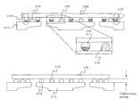
- FIG. 1is a perspective view of a prior art power semiconductor device 100 .
- the power semiconductor device 100comprises a power semiconductor device package 110 .
- the device package 110comprises a silicon die 120 partially or wholly encased within a molding compound 130 .
- power semiconductor devicesare operated in extreme conditions. When a high current is run through the device 100 , heat is generated in the silicon die 120 . The device 100 requires that the heat be removed efficiently. In most cases, a heat sink 140 is applied to the device package 110 as a heat extractor. In order to let the heat sink 140 contact the silicon die 120 directly, the silicon die 120 needs to be exposed from its package, as shown in FIG. 1 .
- FIG. 2is a transparent view of the prior art power semiconductor device package 110 , showing an X-rayed view of the device package 110 .
- the device package 110works with high electrical current.
- a flip chip diesuch as die 120 , is used for such a device.
- the flip chip dieuses connector balls 255 to connect the silicon die to a leadframe 215 .
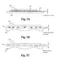
- FIGS. 3A-Cillustrate different stages of a prior art flip-chip process used to place a semiconductor die 320 on a leadframe 315 .
- tacky soldering flux 350is placed in a flux equalizer tray 360 .
- a flux equalizer squeegee 370then sweeps the flux 350 in order to level off its height along the tray 360 .
- a pick-and-place arm 380holds the die 320 , dipping its connector balls or bumps (disposed on the underside of the die) into the thin film of flux 350 , which is typically about 1 ⁇ 2 to 2 ⁇ 3 of the height of the bumps or a minimum of 25 microns, depending on the bump size.
- the pick-and-place arm 380places the die 320 on the leadframe strip 315 .
- the die 320is adhered onto the leadframe 315 by flux viscosity.
- FIG. 3Cshows the leadframe strip 315 after it has been reflowed. The solder flux activates and melts the solder bumps, thereby bonding the bumps and, as a result, the die 320 to the leadframe 315 .
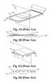
- FIG. 4Aillustrates a stand-off height between a flip-chip die 420 and a leadframe 415 .
- This stand-off heightshould be controlled when the die 420 is passed through the reflow process. As previously mentioned, during the reflow process, the solder bumps 455 are melted and bonded to the leadframe 415 . In order to achieve a properly exposed die, such as shown in FIG. 1 , the stand-off height needs to be precisely achieved at a certain value at all points of the package.
- FIGS. 4B-Cillustrate improper stand off height between the flip-chip die 420 and the leadframe 415 .
- something goes wrong in the fabrication process and the stand-off heightcannot be controlled.
- FIG. 4Bafter the unit has passed through the reflow process, one side of the die 420 has collapsed bumps 457 , while the other side has almost un-melted bumps 455 ′.
- FIG. 4Cif the unit with collapsed bumps passed through the molding process, the molding compound 430 would cover the collapsed part of the die 420 under the level of mold thickness. As a result, the device package 410 would not be able to be used because the contact area of the exposed die 420 would not fully contact the heat sink.
- FIG. 5Ais a perspective view of a flip-chip die 520 being dipped into soldering flux 550 in a tray 560 .
- Plane 5 Bis a virtual cutting plane used to illustrate the cross-sectional view of FIG. 5B .
- the connector balls 555 of the flip-chip die 520are partially dipped into the flux 550 .
- FIG. 6Ais a perspective view of the flip-chip die 520 being placed onto a leadframe 615 .
- Plane 6 Bis a virtual cutting plane used to illustrate the cross-sectional view of FIG. 6B .
- flip-chip die 520is placed onto the leadframe 615 with the flux-coated portion (shaded) of the connector balls 555 being placed in direct contact with the leadframe 615 .
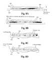
- FIGS. 7A-Cillustrate a good process for bonding a semiconductor die 720 to a leadframe 715 .
- the connector bumps 755 of the semiconductor die 720are dipped into soldering flux 750 in a tray 760 .
- the flux levelis uniform.
- the die 720is placed on the leadframe 715 before the reflowing process.
- the flux-coated portion (shaded) of the connector bumps 755are placed in direct contact with the leadframe 715 .
- the flux level on the bumps 755is uniform.
- FIG. 7Cafter the reflowing has been performed, the melted bumps 755 ′ connect the die 720 to the leadframe 715 .
- the melting of the bumps 755 ′is uniform.
- good uniform bump melting after reflowingis achieved.
- the exact desired stand-off heightis achieved at all points.
- FIGS. 8A-Dillustrate a bad process for bonding a semiconductor die 820 to a leadframe 815 .
- FIG. 8Ashows the connector bumps 855 of the die 820 being dipped into soldering flux 850 in a tray 860 where the flux level is not uniform throughout the tray 860 .
- FIG. 8Bshows the connector bumps 855 of the die 820 being dipped into soldering flux 850 in a tray 860 where the die 820 and the flux level are not coplanar (e.g., if the die 820 is dipped at an angle). As seen in FIG.
- FIG. 8Cshows the die 820 on the leadframe 815 after the reflowing process has been performed, with the melted bumps 855 ′ connecting the die 820 to the leadframe 815 .
- the present inventionprovides a way to minimize the collapsing effect of the connector bumps of the die after reflowing by creating a feature on the leadframe to support the die during placement of the die on the leadframe.
- a method of forming a leadframe devicecomprises: placing a flux material in a plurality of locations on a top surface of a leadframe; placing a metallic solder material on the flux material in the plurality of locations; and performing a reflow process on the leadframe, wherein the metallic solder material is melted to the top surface of the leadframe and formed into a plurality of support features that are configured to support a semiconductor die.
- the methodfurther comprises: placing a semiconductor die over the leadframe, wherein a plurality of connector bumps are disposed on a bottom surface of the semiconductor die between the semiconductor die and the leadframe, and a flux material is disposed on each connector bump at a location between the connector bump and the leadframe; and performing a reflow process on the leadframe, thereby melting the connector bumps to the leadframe.
- the liquidus temperature of the support featuresis higher than the liquidus temperature of the connector bumps.
- the height of the support featuresis approximately 50%-80% of the height of the connector bumps before the connector bumps are melted.
- the metallic solder materialis SAC105.
- the support featuresare substantially ball-shaped. In some embodiments, the support features are each formed in the shape of an elongated bar.
- the methodfurther comprises coating the support features with a coating material that is different from the material of the leadframe.
- coating the support featurescomprises performing a screen print process.
- coating the support featurescomprises performing a dispensing process.
- the coating materialis epoxy.
- the methodfurther comprises performing a curing process after the support features are coated with the coating material.
- the coating materialis a plating material.
- the coating materialis a plating material selected from the group consisting of: silver, nickel, palladium, and gold.
- a method of forming a leadframe devicecomprises: disposing a plating material and a leadframe in a plating solution, wherein the plating material is electrically coupled to an anode of an electrical power source, the leadframe is electrically coupled to the cathode of an electrical power source and has a top surface facing the plating material, and a plating mask having a plurality of openings is disposed between the top surface of the leadframe and the plating material; activating the electrical power source, thereby attracting particles from the plating material to the leadframe; and disposing the attracted particles onto the top surface of the leadframe at a plurality of locations aligned with the plurality of openings in the plating mask, thereby forming a plurality of support features on the top surface of the leadframe.
- the plating materialcomprises at least one material from the group of materials consisting of: silver, nickel, palladium, and gold.
- the methodfurther comprises the step of performing a reflow process on the leadframe after the attracted particles are disposed onto the top surface of the leadframe.
- the methodfurther comprises: placing a semiconductor die over the top surface of the leadframe, wherein a plurality of connector bumps are disposed on a bottom surface of the semiconductor die between the semiconductor die and the top surface of the leadframe, and a flux material is disposed on each connector bump at a location between the connector bump and the top surface of the leadframe; and performing a reflow process on the leadframe, thereby melting the connector bumps to the top surface of the leadframe.
- the liquidus temperature of the support featuresis higher than the liquidus temperature of the connector bumps. In some embodiments, the height of the support features is approximately 50%-80% of the height of the connector bumps before the connector bumps are melted.
- the support featuresare substantially ball-shaped. In some embodiments, the support features are each formed in the shape of an elongated bar.
- the methodfurther comprises coating the support features with a coating material that is different from the material of the leadframe.
- coating the support featurescomprises performing a screen print process.
- coating the support featurescomprises performing a dispensing process.
- the coating materialis epoxy.
- the methodfurther comprises performing a curing process after the support features are coated with the coating material.
- the coating materialis a plating material.
- the coating materialis a plating material selected from the group consisting of silver, nickel, palladium, and gold.
- a leadframe devicecomprises: a leadframe having a top surface; a plurality of support features disposed on the top surface of the leadframe, wherein the support features comprise a material different from the leadframe and are configured to support a semiconductor die; and a coating material covering each support feature.
- the support featurescomprise epoxy. In some embodiments, the support features comprise at least one material from the group of materials consisting of: silver, nickel, palladium, and gold.
- the devicefurther comprises a semiconductor die coupled to the top surface of the leadframe via a plurality of connector bumps disposed between the semiconductor die and the top surface of the leadframe.
- the support featuresare substantially ball-shaped. In some embodiments, the support features are each formed in the shape of an elongated bar.
- the coating materialis epoxy. In some embodiments, the coating material is a plating material. In some embodiments, the coating material is a plating material selected from the group consisting of: silver, nickel, palladium, and gold.
- a method of forming a leadframe devicecomprises: forming a plurality of support features on a top surface of a leadframe, wherein the support features comprise a material different from the leadframe; and covering each support feature with a coating material.
- covering each support feature with the coating materialcomprises performing a screen print process. In some embodiments, covering each support feature with the coating material comprises performing a dispensing process. In some embodiments, the coating material is epoxy. In some embodiments, the method further comprises performing a curing process after the support features are covered with the coating material. In some embodiments, the coating material is a plating material. In some embodiments, the coating material is a plating material selected from the group consisting of: silver, nickel, palladium, and gold.
- the methodfurther comprises: placing a semiconductor die over the top surface of the leadframe, wherein a plurality of connector bumps are disposed on a bottom surface of the semiconductor die between the semiconductor die and the top surface of the leadframe, and a flux material is disposed on each connector bump at a location between the connector bump and the top surface of the leadframe; and performing a reflow process on the leadframe, thereby melting the connector bumps to the top surface of the leadframe.
- the liquidus temperature of the support featuresis higher than the liquidus temperature of the connector bumps.
- the height of each support feature combined with the coating material covering the support featureis approximately 50%-110% of the height of the connector bumps before the connector bumps are melted.
- a leadframe devicecomprises: a leadframe consisting of leadframe material and having a top surface; and a plurality of support features extending from the top surface of the leadframe, wherein the support structures are formed from the leadframe material and are configured to support a semiconductor die.
- the devicefurther comprises a semiconductor die coupled to the top surface of the leadframe via a plurality of connector bumps disposed between the semiconductor die and the top surface of the leadframe.
- the support featuresare substantially ball-shaped. In some embodiments, the support features are each formed in the shape of an elongated bar.
- each support featureis covered by a coating material.
- the coating materialis epoxy.
- the coating materialis a plating material.
- the coating materialis a plating material selected from the group consisting of: silver, nickel, palladium, and gold.
- a method of forming a leadframe devicecomprises: providing a leadframe having a top surface, wherein the leadframe is formed from leadframe material; and removing a portion of the leadframe material to form a plurality of support features extending from the top surface of the leadframe, wherein the support features are formed from the leadframe material and are configured to support a semiconductor die.
- the step of removing a portion of the leadframe materialcomprises performing an etching process on the leadframe.
- the methodfurther comprises: placing a semiconductor die over the leadframe, wherein a plurality of connector bumps are disposed on a bottom surface of the semiconductor die between the semiconductor die and the leadframe, and a flux material is disposed on each connector bump at a location between the connector bump and the leadframe; and performing a reflow process on the leadframe, thereby melting the connector bumps to the leadframe.
- the height of the support featuresis approximately 50%-80% of the height of the connector bumps before the connector bumps are melted.
- the support featuresare substantially ball-shaped. In some embodiments, the support features are each formed in the shape of an elongated bar.
- the methodfurther comprises coating the support features with a coating material that is different from the material of the leadframe.
- coating the support featurescomprises performing a screen print process.
- coating the support featurescomprises performing a dispensing process.
- the coating materialis epoxy.
- the methodfurther comprises performing a curing process after the support features are coated with the coating material.
- the coating materialis a plating material.
- the coating materialis a plating material selected from the group consisting of: silver, nickel, palladium, and gold.
- the methodfurther comprises: placing a semiconductor die over the leadframe, wherein a plurality of connector bumps are disposed on a bottom surface of the semiconductor die between the semiconductor die and the leadframe, and a flux material is disposed on each connector bump at a location between the connector bump and the leadframe; and performing a reflow process on the leadframe, thereby melting the connector bumps to the leadframe.
- the height of each support feature combined with the coating material covering the support featureis approximately 50%-110% of the height of the connector bumps before the connector bumps are melted.
- FIG. 1is a perspective view of a prior art power semiconductor device.
- FIG. 2is a transparent view of a prior art power semiconductor device package.
- FIGS. 3A-Cillustrate different stages of a prior art flip-chip process.
- FIG. 4Aillustrates a stand-off height between a flip-chip die and a leadframe.
- FIGS. 4B-Cillustrate improper stand-off height between the flip-chip die and the leadframe.
- FIG. 5Ais a perspective view of a flip-chip die being dipped into soldering flux.
- FIG. 5Bis a cross-sectional view of a flip-chip die being dipped into soldering flux.
- FIG. 6Ais a perspective view of a flip-chip die being placed onto a leadframe.
- FIG. 6Bis a cross-sectional view of a flip-chip die being placed onto a leadframe.
- FIGS. 7A-Cillustrate a good process for bonding a semiconductor die to a leadframe.
- FIGS. 8A-Dillustrate a bad process for bonding a semiconductor die to a leadframe.
- FIG. 9illustrates one embodiment of a leadframe feature and a ball drop process used to form the leadframe feature in accordance with the principles of the present invention.
- FIGS. 10A-Cillustrate one embodiment of a plating process used to form the leadframe feature in accordance with the principles of the present invention.
- FIGS. 11A-Billustrate one embodiment of the leadframe feature being used to minimize collapse during flip-chip reflow in accordance with the principles of the present invention.
- FIGS. 12A-Billustrate one embodiment of forming a leadframe support post in accordance with the principles of the present invention.
- FIG. 13illustrates one embodiment of a leadframe support post having a coating in accordance with the principles of the present invention.
- FIG. 14illustrates one embodiment of the coating of the leadframe support post in accordance with the principles of the present invention.
- FIGS. 15A-Billustrate one embodiment of foaming a leadframe support post using a screen print process in accordance with the principles of the present invention.
- FIG. 16illustrates another embodiment of a leadframe support post having a coating in accordance with the principles of the present invention.
- FIG. 17illustrates one embodiment of a leadframe support bar in accordance with the principles of the present invention.
- the present inventionprovides a way to minimize the collapsing of the connector bumps of the die after reflowing by creating features on the leadframe to support the die during placement of the die on the leadframe.
- These support featurescan be configured in a variety of ways, being formed in a variety of shapes and from a variety of materials.
- FIG. 9illustrates one embodiment of a leadframe feature and a ball drop process used to form the leadframe feature in accordance with the principles of the present invention.
- a plurality of support features 975 ′are disposed on the top surface of a leadframe 915 .
- the support features 975 ′are configured to maintain the desired stand-off height at all points between the semiconductor die and the leadframe during and after the reflow process in the face of any of the situations that cause the collapse of the connector balls, such as those discussed above with respect to FIGS. 8A-D .
- the support featuresare formed from non-leadframe material (i.e., material different from the leadframe material), such as bump balls that are placed on the leadframe in order to behave as posts.
- this non-leadframe materialhas a liquidus temperature that is higher than the connector balls on the semiconductor die.
- the supportpreferably has a height that is approximately 50%-80% of the height of the connector balls on the semiconductor die.
- the support features 975 ′are formed using a ball drop process. As seen in window A of FIG. 9 , a flux material 950 is placed onto the leadframe 915 . Next, in window B, a bump ball 975 is placed on the flux material 950 . Finally, in window C, the leadframe 915 undergoes a reflow process, thereby melting the bump ball 975 ′ to the leadframe 915 .
- the bump ball 975 ′is configured to act as the support feature discussed above.
- the bump ballis formed from a solder material. In some embodiments, the bump ball is formed from an alloy. In some embodiments, the bump ball is formed from SAC105.
- the leadframe support featuresare formed using a plating process.
- FIGS. 10A-Cillustrate one embodiment of a plating system and process used to form the leadframe support feature in accordance with the principles of the present invention.
- a plating tank 1000is used to hold a plating solution 1040 .
- the plating solution 1040comprises one or more dissolved metal salts or other ionic materials.
- a plating material 1030is disposed in the plating solution 104 .
- the plating material 1030is held in a basket or some other container.
- the plating material 1030is the material that will be used to form the leadframe support features.
- Such plating material 1030can include, but is not limited to, Ag, Ni, Pd, and Au. It is contemplated that other plating materials can be additionally or alternatively be used.
- An electrical power source 1060such as a battery, is provided, with an anode 1070 and a cathode 1080 .
- the anode 1070is coupled to the basket holding the plating material 1030 .
- the cathode 1080is coupled to a plate holder 1020 , which is disposed in the plating solution 1040 .
- a leadframe 1015is disposed on the plate holder 1020 within the plating solution 1040 .
- a plating mask 1010is disposed over the leadframe 1015 and comprises openings aligned over the locations where the support features are to be formed on the leadframe 1015 .
- the electrical power source 1060When the electrical power source 1060 is switched on, it pulls electrons away from the plating material 1030 and pumps them over to the leadframe 1015 . As a result, the leadframe 1015 attracts the positively-charged ions (formed from the plating material 1030 ) that are floating around in the plating solution 1040 . As seen in FIG. 10B , which shows the leadframe 1015 without the plating mask 1010 disposed over it, the plating material particles form the support features 1075 , such as bumps, on the leadframe 1015 . A reflow process is performed, applying heat to the support features 1075 , thereby melting the support features 1075 down into reflown support features 1075 ′, as shown in FIG. 10C .
- FIGS. 11A-Billustrate one embodiment of the leadframe feature being used to minimize collapse during flip-chip reflow in accordance with the principles of the present invention.
- FIG. 11Ashows a cross-sectional view of die 1120 on leadframe 115 before a reflowing process has been performed.
- Leadframe support features 1175such as those discussed above, are disposed on the leadframe 1115 .
- Connector bumps 1155are coupled to or integrally formed with die 1120 .
- the connector bumps 1155 on the die 1120are dipped in soldering flux.
- the die 1120is then placed on the leadframe 1115 , with a portion of the flux-dipped side of the connector bumps 1155 contacting the leadframe 1115 .
- different connector bumps 1155may have different levels of soldering flux on them. Some connector bumps 1155 may have approximately half of their surface area covered with flux. Some connector bumps 1155 ′ may have a much smaller amount of flux disposed on them. However, these connector bumps 1155 ′ may still have a sufficient amount of flux to activate the appropriate melting. Some connector bumps 1155 ′′ may have a much greater amount of flux disposed on them. In a preferred embodiment, the height of the leadframe support features 1175 prior to reflowing is between approximately 50%-80% of the height of the connector bumps 1155 .
- FIG. 11Bshows a cross-sectional view of die 1120 on leadframe 1115 after a reflowing process has been performed.
- the reflown leadframe support features 1175 ′support the melting of the reflown connector bumps 1155 ′ on the die 1120 , thereby providing uniform bump height across the device package.
- FIGS. 12A-Billustrate one embodiment of forming a leadframe support post in accordance with the principles of the present invention.
- the leadframe support featuresare formed from the material of the leadframe 1215 .
- a mask 1275such as a photo mask, is placed on the leadframe to protect the areas on the leadframe that are not to be etched (i.e., where the support features are to be formed).
- An etching processis then performed, resulting in the formation of leadframe support features, such as support posts 1275 ′ shown in FIG. 12B .
- the leadframe materialis being utilized to behave as a post to eventually support the die.
- the height of the leadframe support features 1275 ′is between approximately 50%-80% of the height of the connector bumps on the die.
- FIG. 13illustrates one embodiment of a leadframe support post having a coating in accordance with the principles of the present invention.
- the combination of leadframe material and non-leadframe materialis used to form leadframe support features 1375 that are configured to support the die.
- Support postssuch as support posts 1275 ′ in FIG. 12B discussed above, are formed from the same material as the leadframe 1315 , such as by an etching process.
- the support postsare then coated with a material that is different from the leadframe material, thereby forming leadframe support features 1375 .
- the coated leadframe support features 1375have a total height between approximately 50%-110% of the height of the connector balls on the die.
- the pre-coated support postscan be formed using methods other than etching.
- the pre-coated support postsare formed using a stamping process. Other methods can be used as well.
- a screen print processis performed using a coating material such as epoxy.
- a dispense processis performed using a coating material such as epoxy.
- a plating processis performed using a coating material such as Ag, Ni, Pd, or Au.
- FIG. 14illustrates one embodiment of the coating of the leadframe support post in accordance with the principles of the present invention.
- Leadframe 1415comprises support posts 1475 , which have been etched similar to support posts 1275 ′ in FIG. 12B discussed above.
- the vertical shape of the support posts 1475is not perpendicularly etched.
- the sidewall 1480is over-etched, as well as being etched more at the top, resulting in a weak point.
- the shape of the leadframe support feature 1475 ′is more robust. Its height is also increased above that of the pre-coated support post 1475 . Additionally, the coating material behaves as a cushion at the point where it supports the die.
- FIGS. 15A-Billustrate one embodiment of forming a leadframe support post using a screen print process in accordance with the principles of the present invention.
- a screen print plate 1560is placed on a leadframe 1515 , thereby acting as a stencil.
- FIG. 15Bshows x-ray detail of the leadframe 1515 under the screen print plate.
- Epoxy 1550is placed on the screen print plate 1560 and leveled-off using a flux equalizer squeegee 1570 . Epoxy fills in the holes 1565 in the screen print plate 1560 , thereby reaching the leadframe 1515 in select locations where the support features are to be formed.
- an epoxy support structure 1575remains on the leadframe 1515 after the screen print plate 1560 has been removed.
- An epoxy cure processis then performed, thereby reshaping the epoxy and forming the leadframe support feature 1575 ′.
- FIG. 16illustrates another embodiment of a leadframe support post having a coating in accordance with the principles of the present invention.
- Coated leadframe support features 1675are disposed on the leadframe 1615 .
- non-leadframe materialis used to coat support posts that are formed from non-leadframe material.
- the coated support posts 1675have a height between approximately 50%-110% of the connector ball on the die.
- these leadframe support features 1675can be fabricated in a variety of ways.
- the pre-coated support postsare formed using either the ball drop process or the plating process discussed above with respect to FIGS. 9-10C .
- Other methods of forming the pre-coated support postsare also within the scope of the present invention. It is contemplated that a variety of different methods are suitable for coating the support posts in order to form the coated leadframe support features.
- a screen print processis performed using a coating material such as epoxy.
- a dispense processis performed using a coating material such as epoxy.
- a plating processis performed using a coating material such as Ag, Ni, Pd, or Au.
- FIG. 17illustrates one embodiment of the leadframe support features each comprising a bar-shape in accordance with the principles of the present invention.
- the bar-shaped support features 1775are disposed on the leadframe 1715 . Any of the methods and materials for fabrication discussed above can be used to form these bar-shaped support features.
Landscapes
- Engineering & Computer Science (AREA)
- Computer Hardware Design (AREA)
- Microelectronics & Electronic Packaging (AREA)
- Power Engineering (AREA)
- Physics & Mathematics (AREA)
- Condensed Matter Physics & Semiconductors (AREA)
- General Physics & Mathematics (AREA)
- Manufacturing & Machinery (AREA)
- Lead Frames For Integrated Circuits (AREA)
Abstract
Description
Claims (13)
Priority Applications (1)
| Application Number | Priority Date | Filing Date | Title |
|---|---|---|---|
| US12/834,688US9449900B2 (en) | 2009-07-23 | 2010-07-12 | Leadframe feature to minimize flip-chip semiconductor die collapse during flip-chip reflow |
Applications Claiming Priority (2)
| Application Number | Priority Date | Filing Date | Title |
|---|---|---|---|
| US22803509P | 2009-07-23 | 2009-07-23 | |
| US12/834,688US9449900B2 (en) | 2009-07-23 | 2010-07-12 | Leadframe feature to minimize flip-chip semiconductor die collapse during flip-chip reflow |
Publications (2)
| Publication Number | Publication Date |
|---|---|
| US20110018111A1 US20110018111A1 (en) | 2011-01-27 |
| US9449900B2true US9449900B2 (en) | 2016-09-20 |
Family
ID=43496541
Family Applications (1)
| Application Number | Title | Priority Date | Filing Date |
|---|---|---|---|
| US12/834,688Active2031-06-27US9449900B2 (en) | 2009-07-23 | 2010-07-12 | Leadframe feature to minimize flip-chip semiconductor die collapse during flip-chip reflow |
Country Status (1)
| Country | Link |
|---|---|
| US (1) | US9449900B2 (en) |
Cited By (2)
| Publication number | Priority date | Publication date | Assignee | Title |
|---|---|---|---|---|
| US10651143B2 (en)* | 2016-04-28 | 2020-05-12 | Sharp Kabushiki Kaisha | Conductive paste having dilatancy, electrode connection structure including the paste, and method for producing the structure |
| US20220223504A1 (en)* | 2021-01-08 | 2022-07-14 | Jmj Korea Co., Ltd. | Semiconductor package |
Citations (161)
| Publication number | Priority date | Publication date | Assignee | Title |
|---|---|---|---|---|
| US3611061A (en) | 1971-07-07 | 1971-10-05 | Motorola Inc | Multiple lead integrated circuit device and frame member for the fabrication thereof |
| US4411719A (en) | 1980-02-07 | 1983-10-25 | Westinghouse Electric Corp. | Apparatus and method for tape bonding and testing of integrated circuit chips |
| US4501960A (en) | 1981-06-22 | 1985-02-26 | Motorola, Inc. | Micropackage for identification card |
| US4801561A (en) | 1984-07-05 | 1989-01-31 | National Semiconductor Corporation | Method for making a pre-testable semiconductor die package |
| US4855672A (en) | 1987-05-18 | 1989-08-08 | Shreeve Robert W | Method and process for testing the reliability of integrated circuit (IC) chips and novel IC circuitry for accomplishing same |
| US5105259A (en) | 1990-09-28 | 1992-04-14 | Motorola, Inc. | Thermally enhanced semiconductor device utilizing a vacuum to ultimately enhance thermal dissipation |
| US5195023A (en) | 1991-12-23 | 1993-03-16 | At&T Bell Laboratories | Integrated circuit package with strain relief grooves |
| US5247248A (en) | 1991-02-18 | 1993-09-21 | Sharp Kabushiki Kaisha | Burn-in apparatus and method of use thereof |
| US5248075A (en) | 1992-04-13 | 1993-09-28 | Micron Technology, Inc. | IC pin forming machine with integrated IC testing capability |
| US5281851A (en) | 1992-10-02 | 1994-01-25 | Hewlett-Packard Company | Integrated circuit packaging with reinforced leads |
| US5396185A (en) | 1990-08-13 | 1995-03-07 | Kabushiki Kaisha Toshiba | System and carrier for testing semiconductor integrated circuit devices |
| US5397921A (en) | 1993-09-03 | 1995-03-14 | Advanced Semiconductor Assembly Technology | Tab grid array |
| US5479105A (en) | 1993-06-25 | 1995-12-26 | Samsung Electronics Co., Ltd. | Known-good die testing apparatus |
| US5535101A (en) | 1992-11-03 | 1996-07-09 | Motorola, Inc. | Leadless integrated circuit package |
| US5596231A (en) | 1991-08-05 | 1997-01-21 | Asat, Limited | High power dissipation plastic encapsulated package for integrated circuit die |
| US5843808A (en) | 1996-01-11 | 1998-12-01 | Asat, Limited | Structure and method for automated assembly of a tab grid array package |
| US5959363A (en) | 1995-01-12 | 1999-09-28 | Kabushiki Kaisha Toshiba | Semiconductor device with improved encapsulating resin |
| US5990692A (en) | 1996-05-10 | 1999-11-23 | Samsung Electronics Co., Ltd. | Testing apparatus for non-packaged semiconductor chip |
| US6072239A (en) | 1995-11-08 | 2000-06-06 | Fujitsu Limited | Device having resin package with projections |
| US6111324A (en) | 1998-02-05 | 2000-08-29 | Asat, Limited | Integrated carrier ring/stiffener and method for manufacturing a flexible integrated circuit package |
| US6159770A (en) | 1995-11-08 | 2000-12-12 | Fujitsu Limited | Method and apparatus for fabricating semiconductor device |
| US6177729B1 (en)* | 1999-04-03 | 2001-01-23 | International Business Machines Corporation | Rolling ball connector |
| US6197615B1 (en) | 1997-04-04 | 2001-03-06 | Samsung Electronics Co., Ltd. | Method of producing lead frame having uneven surfaces |
| US6208020B1 (en) | 1999-02-24 | 2001-03-27 | Matsushita Electronics Corporation | Leadframe for use in manufacturing a resin-molded semiconductor device |
| US6229200B1 (en) | 1998-06-10 | 2001-05-08 | Asat Limited | Saw-singulated leadless plastic chip carrier |
| US6250841B1 (en) | 1997-09-22 | 2001-06-26 | Valu Engineering, Inc. | Splice sleeve for guide rails |
| US20010005047A1 (en)* | 1999-05-10 | 2001-06-28 | Jimarez Miguel Angel | Flip chip C4 extension structure and process |
| US20010007285A1 (en) | 1997-08-04 | 2001-07-12 | Dai Nippon Insatsu Kabushiki Kaisha | Resin sealed semiconductor device, circuit member for use therein and method of manufacturing circuit member |
| US6285075B1 (en) | 1998-11-02 | 2001-09-04 | Asat, Limited | Integrated circuit package with bonding planes on a ceramic ring using an adhesive assembly |
| US6294100B1 (en) | 1998-06-10 | 2001-09-25 | Asat Ltd | Exposed die leadless plastic chip carrier |
| US6304000B1 (en) | 1997-04-30 | 2001-10-16 | Dow Corning Toray Silicone Company, Ltd. | Semiconductor device comprising silicone adhesive sheet |
| US6326678B1 (en) | 1993-09-03 | 2001-12-04 | Asat, Limited | Molded plastic package with heat sink and enhanced electrical performance |
| US6329711B1 (en) | 1995-11-08 | 2001-12-11 | Fujitsu Limited | Semiconductor device and mounting structure |
| US6353263B1 (en) | 1999-04-14 | 2002-03-05 | Sharp Kabushiki Kaisha | Semiconductor device and manufacturing method thereof |
| US6372625B1 (en) | 1997-08-26 | 2002-04-16 | Sanyo Electric Co., Ltd. | Semiconductor device having bonding wire spaced from semiconductor chip |
| US6376921B1 (en) | 1995-11-08 | 2002-04-23 | Fujitsu Limited | Semiconductor device, method for fabricating the semiconductor device, lead frame and method for producing the lead frame |
| US6384472B1 (en) | 2000-03-24 | 2002-05-07 | Siliconware Precision Industries Co., Ltd | Leadless image sensor package structure and method for making the same |
| US6392427B1 (en) | 1998-12-21 | 2002-05-21 | Kaitech Engineering, Inc. | Testing electronic devices |
| US6414385B1 (en) | 1999-11-08 | 2002-07-02 | Siliconware Precisionindustries Co., Ltd. | Quad flat non-lead package of semiconductor |
| US6429048B1 (en) | 2000-12-05 | 2002-08-06 | Asat Ltd. | Metal foil laminated IC package |
| US20020109214A1 (en) | 2001-02-14 | 2002-08-15 | Masanori Minamio | Leadframe, resin-molded semiconductor device including the leadframe, method of making the leadframe and method for manufacturing the device |
| US6451709B1 (en) | 1998-09-03 | 2002-09-17 | Micron Technology, Inc. | Methodology of removing misplaced encapsulant for attachment of heat sinks in a chip on board package |
| US6455348B1 (en) | 1998-03-12 | 2002-09-24 | Matsushita Electric Industrial Co., Ltd. | Lead frame, resin-molded semiconductor device, and method for manufacturing the same |
| US6476469B2 (en) | 2000-11-23 | 2002-11-05 | Siliconware Precision Industries Co., Ltd. | Quad flat non-leaded package structure for housing CMOS sensor |
| US6489218B1 (en) | 2001-06-21 | 2002-12-03 | Advanced Semiconductor Engineering, Inc. | Singulation method used in leadless packaging process |
| US6498099B1 (en) | 1998-06-10 | 2002-12-24 | Asat Ltd. | Leadless plastic chip carrier with etch back pad singulation |
| US20030006055A1 (en) | 2001-07-05 | 2003-01-09 | Walsin Advanced Electronics Ltd | Semiconductor package for fixed surface mounting |
| US6507116B1 (en) | 1997-04-24 | 2003-01-14 | International Business Machines Corporation | Electronic package and method of forming |
| US20030045032A1 (en) | 2001-08-31 | 2003-03-06 | Shinko Electric Industries Co., Ltd. | Leadframe, method of manufacturing the same, semiconductor device using the same, and method of manufacturing the device |
| US6545332B2 (en) | 2001-01-17 | 2003-04-08 | Siliconware Precision Industries Co., Ltd. | Image sensor of a quad flat package |
| US6545347B2 (en) | 2001-03-06 | 2003-04-08 | Asat, Limited | Enhanced leadless chip carrier |
| US20030071333A1 (en) | 2001-10-15 | 2003-04-17 | Shinko Electric Industries Co., Ltd. | Leadframe, method of manufacturing the same, and method of manufacturing a semiconductor device using the same |
| US6552423B2 (en) | 2000-02-18 | 2003-04-22 | Samsung Electronics Co., Ltd. | Higher-density memory card |
| US6552417B2 (en) | 1993-09-03 | 2003-04-22 | Asat, Limited | Molded plastic package with heat sink and enhanced electrical performance |
| US6566740B2 (en) | 2000-03-23 | 2003-05-20 | Mitsui High-Tec, Inc. | Lead frame for a semiconductor device and method of manufacturing a semiconductor device |
| US6586834B1 (en) | 2002-06-17 | 2003-07-01 | Asat Ltd. | Die-up tape ball grid array package |
| US6585905B1 (en) | 1998-06-10 | 2003-07-01 | Asat Ltd. | Leadless plastic chip carrier with partial etch die attach pad |
| US20030143776A1 (en) | 2002-01-31 | 2003-07-31 | Serafin Pedron | Method of manufacturing an encapsulated integrated circuit package |
| US20030178719A1 (en) | 2002-03-22 | 2003-09-25 | Combs Edward G. | Enhanced thermal dissipation integrated circuit package and method of manufacturing enhanced thermal dissipation integrated circuit package |
| US6635957B2 (en) | 1998-06-10 | 2003-10-21 | Asat Ltd. | Leadless plastic chip carrier with etch back pad singulation and die attach pad array |
| US20030201520A1 (en) | 2002-04-26 | 2003-10-30 | Knapp James H. | Structure and method of forming a multiple leadframe semiconductor device |
| US20030207498A1 (en) | 2002-04-29 | 2003-11-06 | Shafidul Islam | Partially patterned lead frames and methods of making and using the same in semiconductor packaging |
| US6667191B1 (en) | 2002-08-05 | 2003-12-23 | Asat Ltd. | Chip scale integrated circuit package |
| US20030234454A1 (en) | 2002-06-24 | 2003-12-25 | Serafin Pedron | Integrated circuit package and method of manufacturing the integrated circuit package |
| US20040014257A1 (en) | 2002-07-19 | 2004-01-22 | Kim Pyoung Wan | Method for joining lead frames in a package assembly, method for forming a chip stack package, and a chip stack package |
| US6683368B1 (en)* | 2000-06-09 | 2004-01-27 | National Semiconductor Corporation | Lead frame design for chip scale package |
| US6686667B2 (en) | 2002-04-22 | 2004-02-03 | Scientek Corp. | Image sensor semiconductor package with castellation |
| US20040026773A1 (en) | 2002-08-08 | 2004-02-12 | Koon Eng Meow | Packaged microelectronic components |
| US6703696B2 (en) | 2000-09-04 | 2004-03-09 | Dainippon Printing Co., Ltd. | Semiconductor package |
| US20040046237A1 (en) | 2002-09-05 | 2004-03-11 | Shinko Electric Industries Co., Ltd | Lead frame and method of manufacturing the same |
| US20040070055A1 (en) | 2002-02-26 | 2004-04-15 | St Assembly Test Services Pte Ltd | Ground plane for exposed package |
| US6723585B1 (en) | 2002-10-31 | 2004-04-20 | National Semiconductor Corporation | Leadless package |
| US20040080025A1 (en) | 2002-09-17 | 2004-04-29 | Shinko Electric Industries Co., Ltd. | Lead frame, method of manufacturing the same, and semiconductor device manufactured with the same |
| US6734552B2 (en) | 2001-07-11 | 2004-05-11 | Asat Limited | Enhanced thermal dissipation integrated circuit package |
| US6734044B1 (en) | 2002-06-10 | 2004-05-11 | Asat Ltd. | Multiple leadframe laminated IC package |
| US6737755B1 (en) | 2002-07-19 | 2004-05-18 | Asat, Ltd. | Ball grid array package with improved thermal characteristics |
| US20040110319A1 (en) | 1994-03-18 | 2004-06-10 | Hitachi Chemical Company, Ltd. | Fabrication process of semiconductor package and semiconductor package |
| US6750546B1 (en)* | 2001-11-05 | 2004-06-15 | Skyworks Solutions, Inc. | Flip-chip leadframe package |
| US6764880B2 (en) | 2001-11-15 | 2004-07-20 | Siliconware Precision Industries Co., Ltd. | Semiconductor package and fabricating method thereof |
| US6781242B1 (en) | 2002-12-02 | 2004-08-24 | Asat, Ltd. | Thin ball grid array package |
| US6812552B2 (en) | 2002-04-29 | 2004-11-02 | Advanced Interconnect Technologies Limited | Partially patterned lead frames and methods of making and using the same in semiconductor packaging |
| US6818980B1 (en) | 2003-05-07 | 2004-11-16 | Asat Ltd. | Stacked semiconductor package and method of manufacturing the same |
| US6818978B1 (en) | 2002-11-19 | 2004-11-16 | Asat Ltd. | Ball grid array package with shielding |
| US20050003586A1 (en) | 2001-05-11 | 2005-01-06 | Renesas Technology Corporation | Manufacturing method of a semiconductor device |
| US6841859B1 (en) | 2002-09-03 | 2005-01-11 | Asat Ltd. | Premolded cavity IC package |
| US6876066B2 (en) | 2001-08-29 | 2005-04-05 | Micron Technology, Inc. | Packaged microelectronic devices and methods of forming same |
| US20050077613A1 (en) | 2002-01-31 | 2005-04-14 | Mclellan Neil Robert | Integrated circuit package |
| US6894376B1 (en) | 2003-06-09 | 2005-05-17 | National Semiconductor Corporation | Leadless microelectronic package and a method to maximize the die size in the package |
| US6897428B2 (en) | 2003-07-01 | 2005-05-24 | Matsushita Electric Industrial Co., Ltd. | Solid-state imaging device and method for manufacturing the same |
| US6927483B1 (en) | 2003-03-07 | 2005-08-09 | Amkor Technology, Inc. | Semiconductor package exhibiting efficient lead placement |
| US6933176B1 (en) | 2002-07-19 | 2005-08-23 | Asat Ltd. | Ball grid array package and process for manufacturing same |
| US6933594B2 (en) | 1998-06-10 | 2005-08-23 | Asat Ltd. | Leadless plastic chip carrier with etch back pad singulation |
| US6946324B1 (en) | 1998-06-10 | 2005-09-20 | Asat Ltd. | Process for fabricating a leadless plastic chip carrier |
| US20050236701A1 (en) | 2002-10-24 | 2005-10-27 | Matsushita Electric Industrial Co., Ltd. | Leadframe, plastic-encapsulated semiconductor device, and method for fabricating the same |
| US6967126B2 (en) | 2001-07-31 | 2005-11-22 | Chippac, Inc. | Method for manufacturing plastic ball grid array with integral heatsink |
| US6979594B1 (en) | 2002-07-19 | 2005-12-27 | Asat Ltd. | Process for manufacturing ball grid array package |
| US6982491B1 (en) | 2004-01-20 | 2006-01-03 | Asat Ltd. | Sensor semiconductor package and method of manufacturing the same |
| US6984785B1 (en) | 2003-10-27 | 2006-01-10 | Asat Ltd. | Thermally enhanced cavity-down integrated circuit package |
| US20060019481A1 (en)* | 2003-03-21 | 2006-01-26 | Cheng-Yi Liu | Gold bump structure and fabricating method thereof |
| US7008825B1 (en) | 2003-05-27 | 2006-03-07 | Amkor Technology, Inc. | Leadframe strip having enhanced testability |
| US7009286B1 (en) | 2004-01-15 | 2006-03-07 | Asat Ltd. | Thin leadless plastic chip carrier |
| US20060071351A1 (en) | 2004-09-28 | 2006-04-06 | Texas Instruments Incorporated | Mold compound interlocking feature to improve semiconductor package strength |
| US7041533B1 (en)* | 2000-06-08 | 2006-05-09 | Micron Technology, Inc. | Stereolithographic method for fabricating stabilizers for semiconductor devices |
| US7045883B1 (en)* | 2001-04-04 | 2006-05-16 | Amkor Technology, Inc. | Thermally enhanced chip scale lead on chip semiconductor package and method of making same |
| US7049177B1 (en) | 2004-01-28 | 2006-05-23 | Asat Ltd. | Leadless plastic chip carrier with standoff contacts and die attach pad |
| US7052935B2 (en)* | 2003-02-26 | 2006-05-30 | Advanced Semiconductor Engineering, Inc. | Flip-chip package and fabricating process thereof |
| US7060535B1 (en) | 2003-10-29 | 2006-06-13 | Ns Electronics Bangkok (1993) Ltd. | Flat no-lead semiconductor die package including stud terminals |
| US7071545B1 (en) | 2002-12-20 | 2006-07-04 | Asat Ltd. | Shielded integrated circuit package |
| US20060170081A1 (en)* | 2005-02-03 | 2006-08-03 | Gerber Mark A | Method and apparatus for packaging an electronic chip |
| US7091581B1 (en) | 2004-06-14 | 2006-08-15 | Asat Limited | Integrated circuit package and process for fabricating the same |
| US20060192295A1 (en)* | 2004-11-17 | 2006-08-31 | Chippac, Inc. | Semiconductor package flip chip interconnect having spacer |
| US7102210B2 (en) | 2003-09-05 | 2006-09-05 | Oki Electric Industry Co., Ltd. | Lead frame, manufacturing method of the same, and semiconductor device using the same |
| US7101210B2 (en) | 2004-11-26 | 2006-09-05 | Hon Hai Precision Ind. Co., Ltd. | LGA socket |
| US20060223237A1 (en) | 2001-07-11 | 2006-10-05 | Combs Edward G | Method of manufacturing enhanced thermal dissipation integrated circuit package |
| US7126218B1 (en) | 2001-08-07 | 2006-10-24 | Amkor Technology, Inc. | Embedded heat spreader ball grid array |
| US7125747B2 (en) | 2004-06-23 | 2006-10-24 | Advanced Semiconductor Engineering, Inc. | Process for manufacturing leadless semiconductor packages including an electrical test in a matrix of a leadless leadframe |
| US20060237231A1 (en)* | 2005-04-25 | 2006-10-26 | Shohei Hata | Substrate for mounting electronic part and electronic part |
| US20060273433A1 (en) | 2002-04-01 | 2006-12-07 | Matsushita Electric Industrial Co., Ltd. | Semiconductor device |
| US20070001278A1 (en) | 2005-06-30 | 2007-01-04 | Oseob Jeon | Semiconductor die package and method for making the same |
| US20070013038A1 (en) | 2005-07-13 | 2007-01-18 | Advanced Semiconductor Engineering, Inc. | Semiconductor package having pre-plated leads and method of manufacturing the same |
| US20070029540A1 (en)* | 1999-01-28 | 2007-02-08 | Ryoichi Kajiwara | Semiconductor device |
| US7205178B2 (en) | 2004-03-24 | 2007-04-17 | Freescale Semiconductor, Inc. | Land grid array packaged device and method of forming same |
| US20070093000A1 (en) | 2005-10-21 | 2007-04-26 | Stats Chippac Ltd. | Pre-molded leadframe and method therefor |
| US7247526B1 (en) | 1998-06-10 | 2007-07-24 | Asat Ltd. | Process for fabricating an integrated circuit package |
| US7253503B1 (en)* | 1999-11-05 | 2007-08-07 | Amkor Technology, Inc. | Integrated circuit device packages and substrates for making the packages |
| US7259678B2 (en) | 2003-12-08 | 2007-08-21 | 3M Innovative Properties Company | Durable radio frequency identification label and methods of manufacturing the same |
| US20070200210A1 (en) | 2006-02-28 | 2007-08-30 | Broadcom Corporation | Methods and apparatus for improved thermal performance and electromagnetic interference (EMI) shielding in integrated circuit (IC) packages |
| US7268415B2 (en)* | 2004-11-09 | 2007-09-11 | Texas Instruments Incorporated | Semiconductor device having post-mold nickel/palladium/gold plated leads |
| US7274088B2 (en) | 2002-06-14 | 2007-09-25 | Siliconware Precision Industries Co., Ltd. | Flip-chip semiconductor package with lead frame as chip carrier and fabrication method thereof |
| US20070235217A1 (en) | 2006-03-29 | 2007-10-11 | Workman Derek B | Devices with microjetted polymer standoffs |
| US7315077B2 (en) | 2003-11-13 | 2008-01-01 | Fairchild Korea Semiconductor, Ltd. | Molded leadless package having a partially exposed lead frame pad |
| US7314820B2 (en) | 2004-12-02 | 2008-01-01 | Siliconware Precision Industries Co., Ltd. | Carrier-free semiconductor package and fabrication method thereof |
| US20080048308A1 (en) | 2006-08-28 | 2008-02-28 | Atmel Corporation | Stackable packages for three-dimensional packaging of semiconductor dice |
| US7344920B1 (en) | 2005-07-15 | 2008-03-18 | Asat Ltd. | Integrated circuit package and method for fabricating same |
| US7358119B2 (en) | 2005-01-12 | 2008-04-15 | Asat Ltd. | Thin array plastic package without die attach pad and process for fabricating the same |
| US7372151B1 (en) | 2003-09-12 | 2008-05-13 | Asat Ltd. | Ball grid array package and process for manufacturing same |
| US20080150094A1 (en) | 2006-12-21 | 2008-06-26 | M/A-Com, Inc. | Flip chip shielded RF I/O land grid array package |
| US7399658B2 (en) | 2005-10-21 | 2008-07-15 | Stats Chippac Ltd. | Pre-molded leadframe and method therefor |
| US7408251B2 (en) | 2003-07-31 | 2008-08-05 | Renesas Technology Corp. | Semiconductor packaging device comprising a semiconductor chip including a MOSFET |
| US7411289B1 (en) | 2004-06-14 | 2008-08-12 | Asat Ltd. | Integrated circuit package with partially exposed contact pads and process for fabricating the same |
| US20080293232A1 (en)* | 2007-05-21 | 2008-11-27 | Stats Chippac, Ltd. | Standoff Height Improvement for Bumping Technology Using Solder Resist |
| US7459345B2 (en)* | 2004-10-20 | 2008-12-02 | Mutual-Pak Technology Co., Ltd. | Packaging method for an electronic element |
| US20090014848A1 (en)* | 2004-08-19 | 2009-01-15 | Jenny Ong Wai Lian | Mixed Wire Semiconductor Lead Frame Package |
| US7495319B2 (en) | 2004-03-04 | 2009-02-24 | Panasonic Corporation | Resin-encapsulated semiconductor device and lead frame, and method for manufacturing the same |
| US20090152691A1 (en)* | 2007-12-18 | 2009-06-18 | National Semiconductor Corporation | Leadframe having die attach pad with delamination and crack-arresting features |
| US20090152694A1 (en) | 2007-12-12 | 2009-06-18 | Infineon Technologies Ag | Electronic device |
| US20090230525A1 (en) | 2008-03-14 | 2009-09-17 | Pao-Huei Chang Chien | Advanced quad flat no lead chip package having marking and corner lead features and manufacturing methods thereof |
| US20090236713A1 (en) | 2008-03-19 | 2009-09-24 | Freescale Semiconductor, Inc. | Semiconductor integrated circuit package and method of packaging semiconductor integrated circuit |
| US7595225B1 (en) | 2004-10-05 | 2009-09-29 | Chun Ho Fan | Leadless plastic chip carrier with contact standoff |
| US7608484B2 (en) | 2006-10-31 | 2009-10-27 | Texas Instruments Incorporated | Non-pull back pad package with an additional solder standoff |
| US20090321778A1 (en)* | 2008-06-30 | 2009-12-31 | Advanced Optoelectronic Technology, Inc. | Flip-chip light emitting diode and method for fabricating the same |
| US7709857B2 (en) | 2007-04-24 | 2010-05-04 | Samsung Electro-Mechanics Co., Ltd. | Light emitting diode package |
| US7714418B2 (en) | 2007-07-23 | 2010-05-11 | National Semiconductor Corporation | Leadframe panel |
| US20100133565A1 (en) | 2008-12-03 | 2010-06-03 | Seoul Semiconductor Co., Ltd. | Lead frame, light emitting diode having the lead frame, and backlight unit having the light emitting diode |
| US20100149773A1 (en) | 2008-12-17 | 2010-06-17 | Mohd Hanafi Mohd Said | Integrated circuit packages having shared die-to-die contacts and methods to manufacture the same |
| US20100178734A1 (en) | 2006-03-24 | 2010-07-15 | Hung-Tsun Lin | Leadless Semiconductor Package with Electroplated Layer Embedded in Encapsulant and the Method for Manufacturing the Same |
| US20100224971A1 (en) | 2009-03-06 | 2010-09-09 | Tung Lok Li | Leadless integrated circuit package having high density contacts |
| US20110115061A1 (en) | 2009-11-13 | 2011-05-19 | Shutesh Krishnan | Electronic device including a packaging substrate having a trench |
| US20110201159A1 (en) | 2008-11-05 | 2011-08-18 | Mitsui High-Tec, Inc. | Semiconductor package and manufacturing method thereof |
| US8035207B2 (en) | 2006-12-30 | 2011-10-11 | Stats Chippac Ltd. | Stackable integrated circuit package system with recess |
| US20130069221A1 (en) | 2011-09-16 | 2013-03-21 | Stats Chippac, Ltd. | Semiconductor Device and Method of Forming Conductive Protrusions Over Conductive Pillars or Bond Pads as Fixed Offset Vertical Interconnect Structures |
- 2010
- 2010-07-12USUS12/834,688patent/US9449900B2/enactiveActive
Patent Citations (182)
| Publication number | Priority date | Publication date | Assignee | Title |
|---|---|---|---|---|
| US3611061A (en) | 1971-07-07 | 1971-10-05 | Motorola Inc | Multiple lead integrated circuit device and frame member for the fabrication thereof |
| US4411719A (en) | 1980-02-07 | 1983-10-25 | Westinghouse Electric Corp. | Apparatus and method for tape bonding and testing of integrated circuit chips |
| US4501960A (en) | 1981-06-22 | 1985-02-26 | Motorola, Inc. | Micropackage for identification card |
| US4801561A (en) | 1984-07-05 | 1989-01-31 | National Semiconductor Corporation | Method for making a pre-testable semiconductor die package |
| US4855672A (en) | 1987-05-18 | 1989-08-08 | Shreeve Robert W | Method and process for testing the reliability of integrated circuit (IC) chips and novel IC circuitry for accomplishing same |
| US5396185A (en) | 1990-08-13 | 1995-03-07 | Kabushiki Kaisha Toshiba | System and carrier for testing semiconductor integrated circuit devices |
| US5105259A (en) | 1990-09-28 | 1992-04-14 | Motorola, Inc. | Thermally enhanced semiconductor device utilizing a vacuum to ultimately enhance thermal dissipation |
| US5247248A (en) | 1991-02-18 | 1993-09-21 | Sharp Kabushiki Kaisha | Burn-in apparatus and method of use thereof |
| US5596231A (en) | 1991-08-05 | 1997-01-21 | Asat, Limited | High power dissipation plastic encapsulated package for integrated circuit die |
| US5195023A (en) | 1991-12-23 | 1993-03-16 | At&T Bell Laboratories | Integrated circuit package with strain relief grooves |
| US5248075A (en) | 1992-04-13 | 1993-09-28 | Micron Technology, Inc. | IC pin forming machine with integrated IC testing capability |
| US5281851A (en) | 1992-10-02 | 1994-01-25 | Hewlett-Packard Company | Integrated circuit packaging with reinforced leads |
| US5535101A (en) | 1992-11-03 | 1996-07-09 | Motorola, Inc. | Leadless integrated circuit package |
| US5479105A (en) | 1993-06-25 | 1995-12-26 | Samsung Electronics Co., Ltd. | Known-good die testing apparatus |
| US6724071B2 (en) | 1993-09-03 | 2004-04-20 | Asat, Limited | Molded plastic package with heat sink and enhanced electrical performance |
| US5397921A (en) | 1993-09-03 | 1995-03-14 | Advanced Semiconductor Assembly Technology | Tab grid array |
| US6326678B1 (en) | 1993-09-03 | 2001-12-04 | Asat, Limited | Molded plastic package with heat sink and enhanced electrical performance |
| US6552417B2 (en) | 1993-09-03 | 2003-04-22 | Asat, Limited | Molded plastic package with heat sink and enhanced electrical performance |
| US20040110319A1 (en) | 1994-03-18 | 2004-06-10 | Hitachi Chemical Company, Ltd. | Fabrication process of semiconductor package and semiconductor package |
| US5959363A (en) | 1995-01-12 | 1999-09-28 | Kabushiki Kaisha Toshiba | Semiconductor device with improved encapsulating resin |
| US6573121B2 (en) | 1995-11-08 | 2003-06-03 | Fujitsu Limited | Semiconductor device, method for fabricating the semiconductor device, lead frame and method for producing the lead frame |
| US6329711B1 (en) | 1995-11-08 | 2001-12-11 | Fujitsu Limited | Semiconductor device and mounting structure |
| US6159770A (en) | 1995-11-08 | 2000-12-12 | Fujitsu Limited | Method and apparatus for fabricating semiconductor device |
| US6072239A (en) | 1995-11-08 | 2000-06-06 | Fujitsu Limited | Device having resin package with projections |
| US6376921B1 (en) | 1995-11-08 | 2002-04-23 | Fujitsu Limited | Semiconductor device, method for fabricating the semiconductor device, lead frame and method for producing the lead frame |
| US5843808A (en) | 1996-01-11 | 1998-12-01 | Asat, Limited | Structure and method for automated assembly of a tab grid array package |
| US5990692A (en) | 1996-05-10 | 1999-11-23 | Samsung Electronics Co., Ltd. | Testing apparatus for non-packaged semiconductor chip |
| US6197615B1 (en) | 1997-04-04 | 2001-03-06 | Samsung Electronics Co., Ltd. | Method of producing lead frame having uneven surfaces |
| US6507116B1 (en) | 1997-04-24 | 2003-01-14 | International Business Machines Corporation | Electronic package and method of forming |
| US6304000B1 (en) | 1997-04-30 | 2001-10-16 | Dow Corning Toray Silicone Company, Ltd. | Semiconductor device comprising silicone adhesive sheet |
| US20010007285A1 (en) | 1997-08-04 | 2001-07-12 | Dai Nippon Insatsu Kabushiki Kaisha | Resin sealed semiconductor device, circuit member for use therein and method of manufacturing circuit member |
| US6372625B1 (en) | 1997-08-26 | 2002-04-16 | Sanyo Electric Co., Ltd. | Semiconductor device having bonding wire spaced from semiconductor chip |
| US6250841B1 (en) | 1997-09-22 | 2001-06-26 | Valu Engineering, Inc. | Splice sleeve for guide rails |
| US6284569B1 (en) | 1998-02-05 | 2001-09-04 | Asat, Limited | Method of manufacturing a flexible integrated circuit package utilizing an integrated carrier ring/stiffener |
| US6111324A (en) | 1998-02-05 | 2000-08-29 | Asat, Limited | Integrated carrier ring/stiffener and method for manufacturing a flexible integrated circuit package |
| US6455348B1 (en) | 1998-03-12 | 2002-09-24 | Matsushita Electric Industrial Co., Ltd. | Lead frame, resin-molded semiconductor device, and method for manufacturing the same |
| US6964918B1 (en) | 1998-06-10 | 2005-11-15 | Asat Ltd. | Electronic components such as thin array plastic packages and process for fabricating same |
| US6585905B1 (en) | 1998-06-10 | 2003-07-01 | Asat Ltd. | Leadless plastic chip carrier with partial etch die attach pad |
| US7247526B1 (en) | 1998-06-10 | 2007-07-24 | Asat Ltd. | Process for fabricating an integrated circuit package |
| US6242281B1 (en) | 1998-06-10 | 2001-06-05 | Asat, Limited | Saw-singulated leadless plastic chip carrier |
| US6229200B1 (en) | 1998-06-10 | 2001-05-08 | Asat Limited | Saw-singulated leadless plastic chip carrier |
| US6989294B1 (en) | 1998-06-10 | 2006-01-24 | Asat, Ltd. | Leadless plastic chip carrier with etch back pad singulation |
| US7482690B1 (en) | 1998-06-10 | 2009-01-27 | Asat Ltd. | Electronic components such as thin array plastic packages and process for fabricating same |
| US6946324B1 (en) | 1998-06-10 | 2005-09-20 | Asat Ltd. | Process for fabricating a leadless plastic chip carrier |
| US6933594B2 (en) | 1998-06-10 | 2005-08-23 | Asat Ltd. | Leadless plastic chip carrier with etch back pad singulation |
| US6635957B2 (en) | 1998-06-10 | 2003-10-21 | Asat Ltd. | Leadless plastic chip carrier with etch back pad singulation and die attach pad array |
| US6294100B1 (en) | 1998-06-10 | 2001-09-25 | Asat Ltd | Exposed die leadless plastic chip carrier |
| US6498099B1 (en) | 1998-06-10 | 2002-12-24 | Asat Ltd. | Leadless plastic chip carrier with etch back pad singulation |
| US6995460B1 (en) | 1998-06-10 | 2006-02-07 | Asat Ltd. | Leadless plastic chip carrier with etch back pad singulation |
| US6451709B1 (en) | 1998-09-03 | 2002-09-17 | Micron Technology, Inc. | Methodology of removing misplaced encapsulant for attachment of heat sinks in a chip on board package |
| US6285075B1 (en) | 1998-11-02 | 2001-09-04 | Asat, Limited | Integrated circuit package with bonding planes on a ceramic ring using an adhesive assembly |
| US6392427B1 (en) | 1998-12-21 | 2002-05-21 | Kaitech Engineering, Inc. | Testing electronic devices |
| US20070029540A1 (en)* | 1999-01-28 | 2007-02-08 | Ryoichi Kajiwara | Semiconductor device |
| US6208020B1 (en) | 1999-02-24 | 2001-03-27 | Matsushita Electronics Corporation | Leadframe for use in manufacturing a resin-molded semiconductor device |
| US6177729B1 (en)* | 1999-04-03 | 2001-01-23 | International Business Machines Corporation | Rolling ball connector |
| US6353263B1 (en) | 1999-04-14 | 2002-03-05 | Sharp Kabushiki Kaisha | Semiconductor device and manufacturing method thereof |
| US20010005047A1 (en)* | 1999-05-10 | 2001-06-28 | Jimarez Miguel Angel | Flip chip C4 extension structure and process |
| US7253503B1 (en)* | 1999-11-05 | 2007-08-07 | Amkor Technology, Inc. | Integrated circuit device packages and substrates for making the packages |
| US6414385B1 (en) | 1999-11-08 | 2002-07-02 | Siliconware Precisionindustries Co., Ltd. | Quad flat non-lead package of semiconductor |
| US6552423B2 (en) | 2000-02-18 | 2003-04-22 | Samsung Electronics Co., Ltd. | Higher-density memory card |
| US6566740B2 (en) | 2000-03-23 | 2003-05-20 | Mitsui High-Tec, Inc. | Lead frame for a semiconductor device and method of manufacturing a semiconductor device |
| US6384472B1 (en) | 2000-03-24 | 2002-05-07 | Siliconware Precision Industries Co., Ltd | Leadless image sensor package structure and method for making the same |
| US7041533B1 (en)* | 2000-06-08 | 2006-05-09 | Micron Technology, Inc. | Stereolithographic method for fabricating stabilizers for semiconductor devices |
| US6683368B1 (en)* | 2000-06-09 | 2004-01-27 | National Semiconductor Corporation | Lead frame design for chip scale package |
| US6703696B2 (en) | 2000-09-04 | 2004-03-09 | Dainippon Printing Co., Ltd. | Semiconductor package |
| US6476469B2 (en) | 2000-11-23 | 2002-11-05 | Siliconware Precision Industries Co., Ltd. | Quad flat non-leaded package structure for housing CMOS sensor |
| US6429048B1 (en) | 2000-12-05 | 2002-08-06 | Asat Ltd. | Metal foil laminated IC package |
| US6545332B2 (en) | 2001-01-17 | 2003-04-08 | Siliconware Precision Industries Co., Ltd. | Image sensor of a quad flat package |
| US20020109214A1 (en) | 2001-02-14 | 2002-08-15 | Masanori Minamio | Leadframe, resin-molded semiconductor device including the leadframe, method of making the leadframe and method for manufacturing the device |
| US6545347B2 (en) | 2001-03-06 | 2003-04-08 | Asat, Limited | Enhanced leadless chip carrier |
| US7045883B1 (en)* | 2001-04-04 | 2006-05-16 | Amkor Technology, Inc. | Thermally enhanced chip scale lead on chip semiconductor package and method of making same |
| US20050003586A1 (en) | 2001-05-11 | 2005-01-06 | Renesas Technology Corporation | Manufacturing method of a semiconductor device |
| US6489218B1 (en) | 2001-06-21 | 2002-12-03 | Advanced Semiconductor Engineering, Inc. | Singulation method used in leadless packaging process |
| US20030006055A1 (en) | 2001-07-05 | 2003-01-09 | Walsin Advanced Electronics Ltd | Semiconductor package for fixed surface mounting |
| US20060223237A1 (en) | 2001-07-11 | 2006-10-05 | Combs Edward G | Method of manufacturing enhanced thermal dissipation integrated circuit package |
| US6734552B2 (en) | 2001-07-11 | 2004-05-11 | Asat Limited | Enhanced thermal dissipation integrated circuit package |
| US6967126B2 (en) | 2001-07-31 | 2005-11-22 | Chippac, Inc. | Method for manufacturing plastic ball grid array with integral heatsink |
| US7126218B1 (en) | 2001-08-07 | 2006-10-24 | Amkor Technology, Inc. | Embedded heat spreader ball grid array |
| US6876066B2 (en) | 2001-08-29 | 2005-04-05 | Micron Technology, Inc. | Packaged microelectronic devices and methods of forming same |
| US20030045032A1 (en) | 2001-08-31 | 2003-03-06 | Shinko Electric Industries Co., Ltd. | Leadframe, method of manufacturing the same, semiconductor device using the same, and method of manufacturing the device |
| US20030071333A1 (en) | 2001-10-15 | 2003-04-17 | Shinko Electric Industries Co., Ltd. | Leadframe, method of manufacturing the same, and method of manufacturing a semiconductor device using the same |
| US6750546B1 (en)* | 2001-11-05 | 2004-06-15 | Skyworks Solutions, Inc. | Flip-chip leadframe package |
| US6764880B2 (en) | 2001-11-15 | 2004-07-20 | Siliconware Precision Industries Co., Ltd. | Semiconductor package and fabricating method thereof |
| US20030143776A1 (en) | 2002-01-31 | 2003-07-31 | Serafin Pedron | Method of manufacturing an encapsulated integrated circuit package |
| US20050077613A1 (en) | 2002-01-31 | 2005-04-14 | Mclellan Neil Robert | Integrated circuit package |
| US20040070055A1 (en) | 2002-02-26 | 2004-04-15 | St Assembly Test Services Pte Ltd | Ground plane for exposed package |
| US20030178719A1 (en) | 2002-03-22 | 2003-09-25 | Combs Edward G. | Enhanced thermal dissipation integrated circuit package and method of manufacturing enhanced thermal dissipation integrated circuit package |
| US20040046241A1 (en) | 2002-03-22 | 2004-03-11 | Combs Edward G. | Method of manufacturing enhanced thermal dissipation integrated circuit package |
| US20060273433A1 (en) | 2002-04-01 | 2006-12-07 | Matsushita Electric Industrial Co., Ltd. | Semiconductor device |
| US6686667B2 (en) | 2002-04-22 | 2004-02-03 | Scientek Corp. | Image sensor semiconductor package with castellation |
| US20030201520A1 (en) | 2002-04-26 | 2003-10-30 | Knapp James H. | Structure and method of forming a multiple leadframe semiconductor device |
| US20030207498A1 (en) | 2002-04-29 | 2003-11-06 | Shafidul Islam | Partially patterned lead frames and methods of making and using the same in semiconductor packaging |
| US6812552B2 (en) | 2002-04-29 | 2004-11-02 | Advanced Interconnect Technologies Limited | Partially patterned lead frames and methods of making and using the same in semiconductor packaging |
| US20050263864A1 (en) | 2002-04-29 | 2005-12-01 | Shafidul Islam | Partially patterned lead frames and methods of making and using the same in semiconductor packaging |
| US7449771B1 (en) | 2002-06-10 | 2008-11-11 | Asat Ltd. | Multiple leadframe laminated IC package |
| US6734044B1 (en) | 2002-06-10 | 2004-05-11 | Asat Ltd. | Multiple leadframe laminated IC package |
| US7274088B2 (en) | 2002-06-14 | 2007-09-25 | Siliconware Precision Industries Co., Ltd. | Flip-chip semiconductor package with lead frame as chip carrier and fabrication method thereof |
| US6586834B1 (en) | 2002-06-17 | 2003-07-01 | Asat Ltd. | Die-up tape ball grid array package |
| US20030234454A1 (en) | 2002-06-24 | 2003-12-25 | Serafin Pedron | Integrated circuit package and method of manufacturing the integrated circuit package |
| US6940154B2 (en) | 2002-06-24 | 2005-09-06 | Asat Limited | Integrated circuit package and method of manufacturing the integrated circuit package |
| US20040014257A1 (en) | 2002-07-19 | 2004-01-22 | Kim Pyoung Wan | Method for joining lead frames in a package assembly, method for forming a chip stack package, and a chip stack package |
| US6933176B1 (en) | 2002-07-19 | 2005-08-23 | Asat Ltd. | Ball grid array package and process for manufacturing same |
| US6818472B1 (en) | 2002-07-19 | 2004-11-16 | Asat Ltd. | Ball grid array package |
| US6800948B1 (en) | 2002-07-19 | 2004-10-05 | Asat Ltd. | Ball grid array package |
| US6979594B1 (en) | 2002-07-19 | 2005-12-27 | Asat Ltd. | Process for manufacturing ball grid array package |
| US7315080B1 (en) | 2002-07-19 | 2008-01-01 | Asat Ltd. | Ball grid array package that includes a collapsible spacer for separating die adapter from a heat spreader |
| US20060223229A1 (en) | 2002-07-19 | 2006-10-05 | Asat Ltd. | Ball grid array package and process for manufacturing same |
| US6737755B1 (en) | 2002-07-19 | 2004-05-18 | Asat, Ltd. | Ball grid array package with improved thermal characteristics |
| US7371610B1 (en) | 2002-07-19 | 2008-05-13 | Asat Ltd. | Process for fabricating an integrated circuit package with reduced mold warping |
| US7224048B1 (en) | 2002-08-05 | 2007-05-29 | Asat Ltd. | Flip chip ball grid array package |
| US6667191B1 (en) | 2002-08-05 | 2003-12-23 | Asat Ltd. | Chip scale integrated circuit package |
| US20040026773A1 (en) | 2002-08-08 | 2004-02-12 | Koon Eng Meow | Packaged microelectronic components |
| US6841859B1 (en) | 2002-09-03 | 2005-01-11 | Asat Ltd. | Premolded cavity IC package |
| US20040046237A1 (en) | 2002-09-05 | 2004-03-11 | Shinko Electric Industries Co., Ltd | Lead frame and method of manufacturing the same |
| US20040080025A1 (en) | 2002-09-17 | 2004-04-29 | Shinko Electric Industries Co., Ltd. | Lead frame, method of manufacturing the same, and semiconductor device manufactured with the same |
| US20050236701A1 (en) | 2002-10-24 | 2005-10-27 | Matsushita Electric Industrial Co., Ltd. | Leadframe, plastic-encapsulated semiconductor device, and method for fabricating the same |
| US6723585B1 (en) | 2002-10-31 | 2004-04-20 | National Semiconductor Corporation | Leadless package |
| US6818978B1 (en) | 2002-11-19 | 2004-11-16 | Asat Ltd. | Ball grid array package with shielding |
| US6781242B1 (en) | 2002-12-02 | 2004-08-24 | Asat, Ltd. | Thin ball grid array package |
| US7381588B1 (en) | 2002-12-20 | 2008-06-03 | Asat Ltd. | Shielded integrated circuit package |
| US7071545B1 (en) | 2002-12-20 | 2006-07-04 | Asat Ltd. | Shielded integrated circuit package |
| US7052935B2 (en)* | 2003-02-26 | 2006-05-30 | Advanced Semiconductor Engineering, Inc. | Flip-chip package and fabricating process thereof |
| US6927483B1 (en) | 2003-03-07 | 2005-08-09 | Amkor Technology, Inc. | Semiconductor package exhibiting efficient lead placement |
| US20060019481A1 (en)* | 2003-03-21 | 2006-01-26 | Cheng-Yi Liu | Gold bump structure and fabricating method thereof |
| US6818980B1 (en) | 2003-05-07 | 2004-11-16 | Asat Ltd. | Stacked semiconductor package and method of manufacturing the same |
| US7008825B1 (en) | 2003-05-27 | 2006-03-07 | Amkor Technology, Inc. | Leadframe strip having enhanced testability |
| US6894376B1 (en) | 2003-06-09 | 2005-05-17 | National Semiconductor Corporation | Leadless microelectronic package and a method to maximize the die size in the package |
| US6897428B2 (en) | 2003-07-01 | 2005-05-24 | Matsushita Electric Industrial Co., Ltd. | Solid-state imaging device and method for manufacturing the same |
| US7408251B2 (en) | 2003-07-31 | 2008-08-05 | Renesas Technology Corp. | Semiconductor packaging device comprising a semiconductor chip including a MOSFET |
| US7102210B2 (en) | 2003-09-05 | 2006-09-05 | Oki Electric Industry Co., Ltd. | Lead frame, manufacturing method of the same, and semiconductor device using the same |
| US7372151B1 (en) | 2003-09-12 | 2008-05-13 | Asat Ltd. | Ball grid array package and process for manufacturing same |
| US6984785B1 (en) | 2003-10-27 | 2006-01-10 | Asat Ltd. | Thermally enhanced cavity-down integrated circuit package |
| US7342305B1 (en) | 2003-10-27 | 2008-03-11 | Asat Ltd. | Thermally enhanced cavity-down integrated circuit package |
| US7060535B1 (en) | 2003-10-29 | 2006-06-13 | Ns Electronics Bangkok (1993) Ltd. | Flat no-lead semiconductor die package including stud terminals |
| US7315077B2 (en) | 2003-11-13 | 2008-01-01 | Fairchild Korea Semiconductor, Ltd. | Molded leadless package having a partially exposed lead frame pad |
| US7259678B2 (en) | 2003-12-08 | 2007-08-21 | 3M Innovative Properties Company | Durable radio frequency identification label and methods of manufacturing the same |
| US7009286B1 (en) | 2004-01-15 | 2006-03-07 | Asat Ltd. | Thin leadless plastic chip carrier |
| US6982491B1 (en) | 2004-01-20 | 2006-01-03 | Asat Ltd. | Sensor semiconductor package and method of manufacturing the same |
| US7049177B1 (en) | 2004-01-28 | 2006-05-23 | Asat Ltd. | Leadless plastic chip carrier with standoff contacts and die attach pad |
| US7495319B2 (en) | 2004-03-04 | 2009-02-24 | Panasonic Corporation | Resin-encapsulated semiconductor device and lead frame, and method for manufacturing the same |
| US7205178B2 (en) | 2004-03-24 | 2007-04-17 | Freescale Semiconductor, Inc. | Land grid array packaged device and method of forming same |
| US7411289B1 (en) | 2004-06-14 | 2008-08-12 | Asat Ltd. | Integrated circuit package with partially exposed contact pads and process for fabricating the same |
| US7091581B1 (en) | 2004-06-14 | 2006-08-15 | Asat Limited | Integrated circuit package and process for fabricating the same |
| US7125747B2 (en) | 2004-06-23 | 2006-10-24 | Advanced Semiconductor Engineering, Inc. | Process for manufacturing leadless semiconductor packages including an electrical test in a matrix of a leadless leadframe |
| US20090014848A1 (en)* | 2004-08-19 | 2009-01-15 | Jenny Ong Wai Lian | Mixed Wire Semiconductor Lead Frame Package |
| US20060071351A1 (en) | 2004-09-28 | 2006-04-06 | Texas Instruments Incorporated | Mold compound interlocking feature to improve semiconductor package strength |
| US7595225B1 (en) | 2004-10-05 | 2009-09-29 | Chun Ho Fan | Leadless plastic chip carrier with contact standoff |
| US7459345B2 (en)* | 2004-10-20 | 2008-12-02 | Mutual-Pak Technology Co., Ltd. | Packaging method for an electronic element |
| US7268415B2 (en)* | 2004-11-09 | 2007-09-11 | Texas Instruments Incorporated | Semiconductor device having post-mold nickel/palladium/gold plated leads |
| US20060192295A1 (en)* | 2004-11-17 | 2006-08-31 | Chippac, Inc. | Semiconductor package flip chip interconnect having spacer |
| US7101210B2 (en) | 2004-11-26 | 2006-09-05 | Hon Hai Precision Ind. Co., Ltd. | LGA socket |
| US7314820B2 (en) | 2004-12-02 | 2008-01-01 | Siliconware Precision Industries Co., Ltd. | Carrier-free semiconductor package and fabrication method thereof |
| US7358119B2 (en) | 2005-01-12 | 2008-04-15 | Asat Ltd. | Thin array plastic package without die attach pad and process for fabricating the same |
| US20060170081A1 (en)* | 2005-02-03 | 2006-08-03 | Gerber Mark A | Method and apparatus for packaging an electronic chip |
| US20060237231A1 (en)* | 2005-04-25 | 2006-10-26 | Shohei Hata | Substrate for mounting electronic part and electronic part |
| US20070001278A1 (en) | 2005-06-30 | 2007-01-04 | Oseob Jeon | Semiconductor die package and method for making the same |
| US20070013038A1 (en) | 2005-07-13 | 2007-01-18 | Advanced Semiconductor Engineering, Inc. | Semiconductor package having pre-plated leads and method of manufacturing the same |
| US7348663B1 (en) | 2005-07-15 | 2008-03-25 | Asat Ltd. | Integrated circuit package and method for fabricating same |
| US7344920B1 (en) | 2005-07-15 | 2008-03-18 | Asat Ltd. | Integrated circuit package and method for fabricating same |
| US7399658B2 (en) | 2005-10-21 | 2008-07-15 | Stats Chippac Ltd. | Pre-molded leadframe and method therefor |
| US20070093000A1 (en) | 2005-10-21 | 2007-04-26 | Stats Chippac Ltd. | Pre-molded leadframe and method therefor |
| US20070200210A1 (en) | 2006-02-28 | 2007-08-30 | Broadcom Corporation | Methods and apparatus for improved thermal performance and electromagnetic interference (EMI) shielding in integrated circuit (IC) packages |
| US20100178734A1 (en) | 2006-03-24 | 2010-07-15 | Hung-Tsun Lin | Leadless Semiconductor Package with Electroplated Layer Embedded in Encapsulant and the Method for Manufacturing the Same |
| US20070235217A1 (en) | 2006-03-29 | 2007-10-11 | Workman Derek B | Devices with microjetted polymer standoffs |
| US20080048308A1 (en) | 2006-08-28 | 2008-02-28 | Atmel Corporation | Stackable packages for three-dimensional packaging of semiconductor dice |
| US7608484B2 (en) | 2006-10-31 | 2009-10-27 | Texas Instruments Incorporated | Non-pull back pad package with an additional solder standoff |
| US20080150094A1 (en) | 2006-12-21 | 2008-06-26 | M/A-Com, Inc. | Flip chip shielded RF I/O land grid array package |
| US8035207B2 (en) | 2006-12-30 | 2011-10-11 | Stats Chippac Ltd. | Stackable integrated circuit package system with recess |
| US7709857B2 (en) | 2007-04-24 | 2010-05-04 | Samsung Electro-Mechanics Co., Ltd. | Light emitting diode package |
| US20080293232A1 (en)* | 2007-05-21 | 2008-11-27 | Stats Chippac, Ltd. | Standoff Height Improvement for Bumping Technology Using Solder Resist |
| US7714418B2 (en) | 2007-07-23 | 2010-05-11 | National Semiconductor Corporation | Leadframe panel |
| US20090152694A1 (en) | 2007-12-12 | 2009-06-18 | Infineon Technologies Ag | Electronic device |
| US20090152691A1 (en)* | 2007-12-18 | 2009-06-18 | National Semiconductor Corporation | Leadframe having die attach pad with delamination and crack-arresting features |
| US20090230525A1 (en) | 2008-03-14 | 2009-09-17 | Pao-Huei Chang Chien | Advanced quad flat no lead chip package having marking and corner lead features and manufacturing methods thereof |
| US20090236713A1 (en) | 2008-03-19 | 2009-09-24 | Freescale Semiconductor, Inc. | Semiconductor integrated circuit package and method of packaging semiconductor integrated circuit |
| US20090321778A1 (en)* | 2008-06-30 | 2009-12-31 | Advanced Optoelectronic Technology, Inc. | Flip-chip light emitting diode and method for fabricating the same |
| US20110201159A1 (en) | 2008-11-05 | 2011-08-18 | Mitsui High-Tec, Inc. | Semiconductor package and manufacturing method thereof |
| US20100133565A1 (en) | 2008-12-03 | 2010-06-03 | Seoul Semiconductor Co., Ltd. | Lead frame, light emitting diode having the lead frame, and backlight unit having the light emitting diode |
| US20100149773A1 (en) | 2008-12-17 | 2010-06-17 | Mohd Hanafi Mohd Said | Integrated circuit packages having shared die-to-die contacts and methods to manufacture the same |
| US20100224971A1 (en) | 2009-03-06 | 2010-09-09 | Tung Lok Li | Leadless integrated circuit package having high density contacts |
| US20110115061A1 (en) | 2009-11-13 | 2011-05-19 | Shutesh Krishnan | Electronic device including a packaging substrate having a trench |
| US20130069221A1 (en) | 2011-09-16 | 2013-03-21 | Stats Chippac, Ltd. | Semiconductor Device and Method of Forming Conductive Protrusions Over Conductive Pillars or Bond Pads as Fixed Offset Vertical Interconnect Structures |
Non-Patent Citations (4)
| Title |
|---|
| Michael Quirk and Julian Serda, Semiconductor Manufacturing Technology, Pearson Education International, Pearson Prentice Hall , 2001, p. 587-588. |
| Non-Final Office Action mailed Dec. 20, 2012, U.S. Appl. No. 13/045,253, filed Mar. 10, 2011, Saravuth Sirinorakul. |
| Notice of Allowance, dated Nov. 28, 2012, U.S. Appl. No. 12/960,268, filed Dec. 3, 2012, Saravuth Sirinorakul et al. |
| Office Action dated Apr. 25, 2012, U.S. Appl. No. 12/960,268, filed Dec. 3, 2010, Somchai Nondhasitthichai et al. |
Cited By (3)
| Publication number | Priority date | Publication date | Assignee | Title |
|---|---|---|---|---|
| US10651143B2 (en)* | 2016-04-28 | 2020-05-12 | Sharp Kabushiki Kaisha | Conductive paste having dilatancy, electrode connection structure including the paste, and method for producing the structure |
| US20220223504A1 (en)* | 2021-01-08 | 2022-07-14 | Jmj Korea Co., Ltd. | Semiconductor package |
| US11521920B2 (en)* | 2021-01-08 | 2022-12-06 | Jmj Korea Co., Ltd. | Plurality of power semiconductor chips between a substrate and leadframe |
Also Published As
| Publication number | Publication date |
|---|---|
| US20110018111A1 (en) | 2011-01-27 |
Similar Documents
| Publication | Publication Date | Title |
|---|---|---|
| TWI595576B (en) | Copper pillar sidewall protection | |
| US5872051A (en) | Process for transferring material to semiconductor chip conductive pads using a transfer substrate | |
| US9984960B2 (en) | Integrated fan-out package and method of fabricating the same | |
| CN105938790B (en) | Method for manufacturing semiconductor device | |
| KR101420872B1 (en) | Gang flip for IC packaging | |
| US20080315412A1 (en) | Package Structure with Flat Bumps for Integrate Circuit or Discrete Device and Method of Manufacture the Same | |
| US10741513B2 (en) | Conductive external connector structure and method of forming | |
| CN102760664B (en) | Semiconductor device and the method manufacturing semiconductor device | |
| US20070273011A1 (en) | Method for fabricating a module having an electrical contact-connection | |
| US8794502B2 (en) | Method of forming solder on pad on fine pitch PCB and method of flip chip bonding semiconductor using the same | |
| CN117790461A (en) | Methods of manufacturing electronic devices | |
| US11594512B2 (en) | Method of manufacturing an electronic device and electronic device manufactured thereby | |
| US9449900B2 (en) | Leadframe feature to minimize flip-chip semiconductor die collapse during flip-chip reflow | |
| US9337131B2 (en) | Power semiconductor device and the preparation method | |
| KR20100080352A (en) | Semiconductor package substrate with metal bumps | |
| KR20170113180A (en) | Plating method | |
| US20070148951A1 (en) | System and method for flip chip substrate pad | |
| US8077466B2 (en) | Heat sink, semiconductor device, and method of manufacturing heat sink | |
| TWI743956B (en) | Chip package structure and method for forming the same | |
| CN116806368A (en) | Integrated circuit package and preparation method and terminal thereof | |
| JP2008517475A (en) | Substrate having electric contact and method of manufacturing the same | |
| KR101195265B1 (en) | Method for wire bonding | |
| CN210296365U (en) | Ceramic base and ceramic support for LED packaging | |
| EP4521859A2 (en) | Printed circuit board assembly and manufacturing method therefor | |
| US20080070329A1 (en) | Removing dry film resist residues using hydrolyzable membranes |
Legal Events
| Date | Code | Title | Description |
|---|---|---|---|
| AS | Assignment | Owner name:UTAC THAI LIMITED, THAILAND Free format text:ASSIGNMENT OF ASSIGNORS INTEREST;ASSIGNORS:SIRINORAKUL, SARAVUTH;YENRUDEE, SUEBPHONG;REEL/FRAME:024668/0133 Effective date:20100712 | |
| AS | Assignment | Owner name:UTAC HEADQUARTERS PTE. LTD., SINGAPORE Free format text:ASSIGNMENT OF ASSIGNORS INTEREST;ASSIGNOR:UTAC THAI LIMITED;REEL/FRAME:037959/0937 Effective date:20150508 | |
| AS | Assignment | Owner name:UTAC HEADQUARTERS PTE. LTD., SINGAPORE Free format text:CORRECTIVE ASSIGNMENT TO ADD THE ANNEX A AND THE ANNEX B WHICH WAS INADVERTENTLY LEFTOUT IN THE ORIGINAL ASSIGNMENT DOCUMENT PREVIOUSLY RECORDED ON REEL 037959 FRAME 0937. ASSIGNOR(S) HEREBY CONFIRMS THE ASSIGNMENT;ASSIGNOR:UTAC THAI LIMITED;REEL/FRAME:039902/0302 Effective date:20150508 | |
| STCF | Information on status: patent grant | Free format text:PATENTED CASE | |
| MAFP | Maintenance fee payment | Free format text:PAYMENT OF MAINTENANCE FEE, 4TH YEAR, LARGE ENTITY (ORIGINAL EVENT CODE: M1551); ENTITY STATUS OF PATENT OWNER: LARGE ENTITY Year of fee payment:4 | |
| MAFP | Maintenance fee payment | Free format text:PAYMENT OF MAINTENANCE FEE, 8TH YEAR, LARGE ENTITY (ORIGINAL EVENT CODE: M1552); ENTITY STATUS OF PATENT OWNER: LARGE ENTITY Year of fee payment:8 |