US9449795B2 - Ceramic showerhead with embedded RF electrode for capacitively coupled plasma reactor - Google Patents
Ceramic showerhead with embedded RF electrode for capacitively coupled plasma reactorDownload PDFInfo
- Publication number
- US9449795B2 US9449795B2US13/858,477US201313858477AUS9449795B2US 9449795 B2US9449795 B2US 9449795B2US 201313858477 AUS201313858477 AUS 201313858477AUS 9449795 B2US9449795 B2US 9449795B2
- Authority
- US
- United States
- Prior art keywords
- back plate
- showerhead assembly
- face plate
- plate
- plates
- Prior art date
- Legal status (The legal status is an assumption and is not a legal conclusion. Google has not performed a legal analysis and makes no representation as to the accuracy of the status listed.)
- Active, expires
Links
- 239000000919ceramicSubstances0.000title1
- 238000012545processingMethods0.000claimsabstractdescription28
- 239000000758substrateSubstances0.000claimsabstractdescription27
- 239000004020conductorSubstances0.000claimsabstractdescription20
- 238000009792diffusion processMethods0.000claimsabstractdescription12
- 239000007769metal materialSubstances0.000claimsabstractdescription9
- 238000004891communicationMethods0.000claimsabstractdescription3
- 239000012530fluidSubstances0.000claimsabstractdescription3
- 239000007789gasSubstances0.000claimsdescription68
- 238000006243chemical reactionMethods0.000claimsdescription13
- 238000000034methodMethods0.000claimsdescription13
- 230000008569processEffects0.000claimsdescription10
- 229910010293ceramic materialInorganic materials0.000claimsdescription7
- 239000003989dielectric materialSubstances0.000claimsdescription6
- NJPPVKZQTLUDBO-UHFFFAOYSA-NnovaluronChemical compoundC1=C(Cl)C(OC(F)(F)C(OC(F)(F)F)F)=CC=C1NC(=O)NC(=O)C1=C(F)C=CC=C1FNJPPVKZQTLUDBO-UHFFFAOYSA-N0.000claimsdescription6
- TWNQGVIAIRXVLR-UHFFFAOYSA-Noxo(oxoalumanyloxy)alumaneChemical compoundO=[Al]O[Al]=OTWNQGVIAIRXVLR-UHFFFAOYSA-N0.000claimsdescription6
- PMHQVHHXPFUNSP-UHFFFAOYSA-Mcopper(1+);methylsulfanylmethane;bromideChemical compoundBr[Cu].CSCPMHQVHHXPFUNSP-UHFFFAOYSA-M0.000claimsdescription4
- 230000003071parasitic effectEffects0.000description13
- 230000015654memoryEffects0.000description9
- 229910052782aluminiumInorganic materials0.000description6
- XAGFODPZIPBFFR-UHFFFAOYSA-NaluminiumChemical compound[Al]XAGFODPZIPBFFR-UHFFFAOYSA-N0.000description6
- 230000005684electric fieldEffects0.000description5
- 229910052751metalInorganic materials0.000description4
- 239000002184metalSubstances0.000description4
- 238000004140cleaningMethods0.000description3
- 238000004590computer programMethods0.000description3
- 230000008878couplingEffects0.000description3
- 238000010168coupling processMethods0.000description3
- 238000005859coupling reactionMethods0.000description3
- 230000007423decreaseEffects0.000description3
- 230000005284excitationEffects0.000description3
- IRPGOXJVTQTAAN-UHFFFAOYSA-N2,2,3,3,3-pentafluoropropanalChemical compoundFC(F)(F)C(F)(F)C=OIRPGOXJVTQTAAN-UHFFFAOYSA-N0.000description2
- KLZUFWVZNOTSEM-UHFFFAOYSA-KAluminum fluorideInorganic materialsF[Al](F)FKLZUFWVZNOTSEM-UHFFFAOYSA-K0.000description2
- ZAMOUSCENKQFHK-UHFFFAOYSA-NChlorine atomChemical compound[Cl]ZAMOUSCENKQFHK-UHFFFAOYSA-N0.000description2
- YCKRFDGAMUMZLT-UHFFFAOYSA-NFluorine atomChemical compound[F]YCKRFDGAMUMZLT-UHFFFAOYSA-N0.000description2
- 230000008859changeEffects0.000description2
- 229910052801chlorineInorganic materials0.000description2
- 239000000460chlorineSubstances0.000description2
- 238000011109contaminationMethods0.000description2
- 238000009826distributionMethods0.000description2
- 150000002500ionsChemical class0.000description2
- 239000000463materialSubstances0.000description2
- 230000006798recombinationEffects0.000description2
- 238000005215recombinationMethods0.000description2
- 238000003860storageMethods0.000description2
- 230000001629suppressionEffects0.000description2
- 230000002459sustained effectEffects0.000description2
- PIGFYZPCRLYGLF-UHFFFAOYSA-NAluminum nitrideChemical compound[Al]#NPIGFYZPCRLYGLF-UHFFFAOYSA-N0.000description1
- 230000004913activationEffects0.000description1
- 238000013459approachMethods0.000description1
- 230000006399behaviorEffects0.000description1
- 230000008901benefitEffects0.000description1
- 230000015572biosynthetic processEffects0.000description1
- 238000005219brazingMethods0.000description1
- 239000003990capacitorSubstances0.000description1
- 230000006835compressionEffects0.000description1
- 238000007906compressionMethods0.000description1
- 238000005137deposition processMethods0.000description1
- 238000013461designMethods0.000description1
- 230000001627detrimental effectEffects0.000description1
- 238000010586diagramMethods0.000description1
- 239000002019doping agentSubstances0.000description1
- 230000000694effectsEffects0.000description1
- 238000003682fluorination reactionMethods0.000description1
- 229910052731fluorineInorganic materials0.000description1
- 239000011737fluorineSubstances0.000description1
- 230000006870functionEffects0.000description1
- 238000004519manufacturing processMethods0.000description1
- 239000000203mixtureSubstances0.000description1
- 238000012986modificationMethods0.000description1
- 230000004048modificationEffects0.000description1
- 230000003287optical effectEffects0.000description1
- 239000002245particleSubstances0.000description1
- 230000002028prematureEffects0.000description1
- 230000001902propagating effectEffects0.000description1
- 238000007789sealingMethods0.000description1
- 239000004065semiconductorSubstances0.000description1
- 125000006850spacer groupChemical group0.000description1
- 239000000126substanceSubstances0.000description1
Images


Classifications
- H—ELECTRICITY
- H01—ELECTRIC ELEMENTS
- H01J—ELECTRIC DISCHARGE TUBES OR DISCHARGE LAMPS
- H01J37/00—Discharge tubes with provision for introducing objects or material to be exposed to the discharge, e.g. for the purpose of examination or processing thereof
- H01J37/32—Gas-filled discharge tubes
- H01J37/32431—Constructional details of the reactor
- H01J37/3244—Gas supply means
- C—CHEMISTRY; METALLURGY
- C23—COATING METALLIC MATERIAL; COATING MATERIAL WITH METALLIC MATERIAL; CHEMICAL SURFACE TREATMENT; DIFFUSION TREATMENT OF METALLIC MATERIAL; COATING BY VACUUM EVAPORATION, BY SPUTTERING, BY ION IMPLANTATION OR BY CHEMICAL VAPOUR DEPOSITION, IN GENERAL; INHIBITING CORROSION OF METALLIC MATERIAL OR INCRUSTATION IN GENERAL
- C23C—COATING METALLIC MATERIAL; COATING MATERIAL WITH METALLIC MATERIAL; SURFACE TREATMENT OF METALLIC MATERIAL BY DIFFUSION INTO THE SURFACE, BY CHEMICAL CONVERSION OR SUBSTITUTION; COATING BY VACUUM EVAPORATION, BY SPUTTERING, BY ION IMPLANTATION OR BY CHEMICAL VAPOUR DEPOSITION, IN GENERAL
- C23C16/00—Chemical coating by decomposition of gaseous compounds, without leaving reaction products of surface material in the coating, i.e. chemical vapour deposition [CVD] processes
- C23C16/44—Chemical coating by decomposition of gaseous compounds, without leaving reaction products of surface material in the coating, i.e. chemical vapour deposition [CVD] processes characterised by the method of coating
- C23C16/50—Chemical coating by decomposition of gaseous compounds, without leaving reaction products of surface material in the coating, i.e. chemical vapour deposition [CVD] processes characterised by the method of coating using electric discharges
- C23C16/505—Chemical coating by decomposition of gaseous compounds, without leaving reaction products of surface material in the coating, i.e. chemical vapour deposition [CVD] processes characterised by the method of coating using electric discharges using radio frequency discharges
- C23C16/509—Chemical coating by decomposition of gaseous compounds, without leaving reaction products of surface material in the coating, i.e. chemical vapour deposition [CVD] processes characterised by the method of coating using electric discharges using radio frequency discharges using internal electrodes
- H—ELECTRICITY
- H01—ELECTRIC ELEMENTS
- H01J—ELECTRIC DISCHARGE TUBES OR DISCHARGE LAMPS
- H01J37/00—Discharge tubes with provision for introducing objects or material to be exposed to the discharge, e.g. for the purpose of examination or processing thereof
- H01J37/32—Gas-filled discharge tubes
- H01J37/32009—Arrangements for generation of plasma specially adapted for examination or treatment of objects, e.g. plasma sources
- H01J37/32082—Radio frequency generated discharge
- H01J37/32091—Radio frequency generated discharge the radio frequency energy being capacitively coupled to the plasma
Definitions
- the present disclosurerelates to substrate processing systems, and more particularly to showerheads for substrate processing systems.
- Substrate processing systemstypically include a processing chamber with one or more reaction volumes.
- a pedestalis typically located in the reaction volume.
- a substratesuch as a semiconductor wafer is positioned on the pedestal.
- One or more process gasesare delivered to the reaction volume using a showerhead and plasma may be struck in the reaction volume.
- a filmsuch as a dielectric layer is formed on the substrate.
- the showerheadmay be used in a capacitively coupled plasma (CCP) reactor.
- CCPcapacitively coupled plasma
- the showerheaddistributes process gases over the substrate and serves as a radio-frequency (RF) electrode to drive the plasma.
- RFradio-frequency
- the showerheadis typically made of a metallic material.
- a metal electrodesubstantially reduces or eliminates an electric field inside a gas plenum of the showerhead to prevent plasma formation inside the showerhead and premature activation of gases.
- the showerhead for CCP reactorsis typically made of aluminum and includes a face plate that is welded to a body.
- the face plate of the showerheadtypically has a plurality of spaced gas holes to provide uniform gas distribution over an exposed surface of the substrate.
- RF voltagemay be applied to the showerhead, to another electrode (such as the pedestal), or to both.
- Aluminum showerheadswork well with many process chemistries (or gas compositions). However, aluminum is not compatible with process gases that leach elements from metallic surfaces. In particular, chlorine-based chemistry tends to leach aluminum at operating temperatures exceeding 300° C. As a result of the chemical attack of the chlorine-containing gas on the metal surface of the showerhead, the metallic material may end up in the film deposited on the substrate. This is often detrimental to device fabrication on the substrate. For example, in some instances the metallic materials are dopants that can compromise integrated device operation.
- Undesirable metal contaminationcan also occur during cleaning of the processing chamber. Since atomic fluorine is commonly used for cleaning, the face plate (the hottest area of the showerhead) reacts with the fluorine and forms aluminum fluoride. When a thickness of aluminum fluoride increases with time, showerhead surface properties (e.g., roughness, conductivity and emissivity) change. As a result, the deposition process can drift and is also at high risk for particle contamination.
- showerhead surface propertiese.g., roughness, conductivity and emissivity
- the design of the showerheadalso does not permit cleaning inside of the showerhead (because it is welded) while the showerhead is installed in the processing chamber.
- fluorination of the aluminum surface inside of the gas holes in the face platemay change the diameter of the holes and alter the uniformity of gas flow.
- Some metallic materialssuch as aluminum become softer at higher temperatures (over 400° C.) and the face plate of the showerhead may start to droop. This can cause changes in gas flow and plasma density distribution.
- a showerhead assembly for a substrate processing systemincludes a back plate connected to a gas channel.
- a face plateis connected adjacent to a first surface of the back plate and includes a gas diffusion surface.
- An electrodeis arranged in one of the back plate and the face plate and is connected to one or more conductors.
- a gas plenumis defined between the back plate and the face plate and is in fluid communication with the gas channel.
- the back plate and the face plateare made of a non-metallic material.
- a stemis connected to the back plate and defines the gas channel.
- the one or more conductorspass through the stem.
- the gas diffusion surface of the face plateincludes spaced holes, the gas diffusion surface of the face plate includes perforations or the gas diffusion surface of the face plate is porous.
- a plasma-suppressing structureis arranged adjacent to a second surface of the back plate.
- the first surface of the back plateis opposite to the second surface of the back plate.
- the plasma-suppressing structureincludes N plates located parallel to each other in a spaced relationship.
- Nis an integer greater than one, and the N plates are made of a dielectric material.
- the plasma-suppressing structureincludes a collar extending from one of the N plates towards an upper surface of a processing chamber of the substrate processing system.
- the collaris made of a dielectric material.
- Nis greater than two and the N plates are spaced in a uniform manner. N is greater than two and at least some of the N plates are spaced in a non-uniform manner. At least one of the N plates includes a plurality of perforations. At least one of the N plates includes a saw tooth surface.
- the stem, the back plate and the face plateare made of a ceramic material. The stem, the back plate and the face plate are made of at least one of aluminum nitride and aluminum oxide.
- the face plateis connected to the back plate to allow lateral movement of the face plate relative to the back plate while maintaining a seal therebetween.
- a baffleis arranged between the gas channel and the gas plenum.
- a collarconnects the stem to an upper surface of a substrate processing chamber.
- the back plateis connected to the face plate using fasteners.
- a height dimension of the gas plenumis less than twice an expected plasma sheath thickness.
- a first dimension between the electrode and the first surface of the back plateis less than a second dimension between the electrode and a second surface of the back plate.
- the first surface of the back plateis opposite to the second surface of the back plate.
- the electrodeis disc-shaped.
- a substrate processing systemincludes a processing chamber including a reaction volume.
- the showerhead assemblyis arranged in the reaction volume.
- a pedestalis arranged in the reaction volume adjacent to the face plate.
- a radio frequency (RF) circuitis configured to supply an RF signal to the one or more conductors having a frequency greater than 1 MHz.
- a controlleris configured to control process gases flowing to the gas channel and to control operation of the RF circuit.
- the one or more conductorsinclude a cylindrically-shaped conductor that surrounds the gas channel.
- FIGS. 1A and 1Bare functional block diagrams and simplified cross-sectional views of examples of substrate processing systems according to the present disclosure
- FIGS. 2A and 2Bare a partial cross-sectional views of a portion of example showerheads according to the present disclosure
- FIG. 3illustrates an example of non-uniform spacing between plates of a plasma-suppressing structure
- FIG. 4illustrates an example of scalloped surfaces on the plates of a plasma-suppressing structure
- FIG. 5illustrates an example of perforated plates of a plasma-suppressing structure.
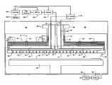
- FIGS. 1A, 1B, 2A and 2Bshow examples of showerheads 10 according to the present disclosure.
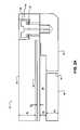
- the showerhead 10includes a back plate 20 , a stem 24 and a face plate 30 .
- the back plate 20 , the stem 24 and the face plate 30 of the showerhead 10are made of a non-metallic material such as a ceramic material. While the stem 24 is shown, the stem 24 can be omitted and the back plate can be arranged on, adjacent to and/or recessed into a surface of the process chamber ( FIG. 1B ).
- the ceramic materialincludes aluminum nitride (AlN), aluminum oxide (Al 2 O 3 ) or another suitable ceramic material.
- the back plate 20includes a generally planar disc.
- the stem 24is connected to the back plate 20 .
- the stem 24is cylindrical and an axis of the stem 24 is connected perpendicular to a plane including the back plate 20 .
- the stem 24 and the back plate 20may be fixedly connected together using diffusion bonding or brazing. Alternately, the stem 24 and the back plate 20 may be removably connected using fasteners, male and female connectors or other methods.
- the stem 24defines a gas channel 34 that extends axially through the stem 24 . Gas flows through the gas channel 34 onto an optional baffle 38 and into a gas plenum 32 , which is defined between the back plate 20 and the face plate 30 .
- a gas plenum 32which is defined between the back plate 20 and the face plate 30 .
- One or both of the back plate 20 and the face plate 30may include a recess 36 to define a height of the gas plenum 32 .
- the face plate 30defines a gas diffusion surface 41 that acts as a gas diffuser between the gas plenum 32 and the reaction volume 44 .
- the gas diffusion surface 41can be perforated, have holes, be porous, etc.
- the process gas in the gas plenum 32may flow through spaced holes 42 of the face plate 30 into a reaction volume 44 .
- the spaced holes 42distribute the process gases in a relatively uniform manner across an exposed surface of a substrate 46 arranged on a pedestal 48 .
- a radio frequency (RF) electrode 50is embedded inside either the back plate 20 ( FIGS. 1 and 2A ) or the face plate 30 ( FIG. 2B ).
- One or more conductors or rods 54pass through the stem 24 and part of the back plate 20 .
- the conductors 54are in electrical contact with the RF electrode 50 .
- four conductors 54are used although additional or fewer conductors 54 may be used.
- the electric field along the gas channel 34decreases as the number of rods increases.
- the conductor 54is cylindrical and surrounds the gas channel 34 .
- the one or more conductors 54may be connected to an RF voltage or to a reference potential such as ground if the showerhead 10 is configured as a grounded electrode.
- the showerhead 10includes a plasma-suppressing structure 60 that is arranged between a top surface of the back plate 20 and a top surface of the processing chamber to decrease or eliminate parasitic discharge driven through the back plate 20 .
- the plasma-suppressing structure 60may be made in accordance with commonly-assigned “MECHANICAL SUPPRESSION OF PARASITIC PLASMA IN SUBSTRATE PROCESSING CHAMBER”, U.S. patent application Ser. No. 13/303,386, filed on Nov. 23, 2011, which is hereby incorporated by reference in its entirety.
- the stem 24may be attached to a collar 80 .
- the collar 80may be attached to a top surface of the processing chamber.
- the collar 80may include a stem 85 and a flange 86 that extends radially outward from the stem 85 adjacent to a top portion of the collar 80 .
- the collar 80may be made of a dielectric (insulating) material and may have dimensions (i.e. may have a thickness or height) that minimize capacitive coupling to ground.
- a valve 90 and pump 92may be used to create a vacuum in the reaction volume 44 .
- the face plate 30is attached to the back plate 20 in a manner to provide a gas seal and to allow some relative lateral movement therebetween due to differences in thermal expansion.
- lateral movementrefers to movement parallel to a plane including the face plate.
- the face plate 30is mounted to the back plate 20 such that the face plate 30 can thermally expand without transmitting stress to the back plate 20 while simultaneously sealing gas/vapor inside the gas plenum 32 .
- edges of the back plate 20 and the face plate 30are connected using fasteners 64 .
- the fasteners 64include screws 66 that are preloaded with washers 67 . The screws 66 may be rotated until a predetermined torque is applied to maintain contact between the face plate 30 and the back plate 20 .
- the fastener 64may be a shoulder screw and the washer 67 may be a spring washer. The shoulder screw applies a predetermined compression to the spring washer to create a predefined load.
- the face plate 30 of the showerhead 10can be replaced by removing the fasteners 64 , installing a new face plate and reinstalling fasteners 64 .
- the spaced holes 42 in the face plate 30have a diameter in the range from 0.02′′ to 0.06′′ to prevent plasma ignition inside of the spaced holes 42 .
- the spaced holes 42 of the face plate 30can be arranged in different patterns to optimize on-wafer film properties.
- the number of the spaced holes 42can be in a range from 50 to 6000, although additional or fewer holes may be used.
- the diameter of the spaced holes 42can be the same for a given face plate or two or more different sizes can be used for a given face plate.
- the RF electrode 50 that is embedded in the back plate 20has a disc-shape and is made of metal that has a first coefficient of thermal expansion (CTE) that is comparable to a second CTE of the material used for the showerhead 10 .
- CTEcoefficient of thermal expansion
- the electrode 50can be arranged in the face plate 30 .
- the electrode 50will be patterned in a manner to accommodate the pattern of spaced holes 42 .
- the RF electrode 50 in the back plate 20 or faceplate 30enables high frequency RF to pass through the gas plenum 32 of the showerhead 10 without lightup.
- the RF electrode 50is located as close as possible to a lower surface of the back plate 20 that faces the substrate to improve power coupling (dimension d 2 in FIG. 2A ).
- dimension d 1is greater than dimension d 2 .
- the conductors 54are embedded in walls of the stem 24 to connect the RF electrode 50 to an RF circuit 70 .
- the conductors 54are arranged to minimize the electric field along the channel through which gas is introduced.
- the face plate 30may have any suitable thickness (dimension d 4 ).
- a height dimension of the gas plenum(dimension d 3 in FIG. 2A ) is less than twice the expected plasma sheath thickness. Using this approach ensures that parasitic plasma discharge cannot be sustained. In some examples, the dimension d 3 is 1 ⁇ 8′′ or less to prevent conditions that would sustain parasitic plasma inside the gas plenum 32 and to minimize voltage drop across the gas plenum 32 .
- the plasma-suppressing structure 60includes two or more spaced plates 100 - 1 , 100 - 2 , . . . , and 100 -N (collectively plates 100 ), where N is an integer greater than one. In some examples, N is equal to 5 although additional or fewer plates 100 may be used. In some examples, the plates 100 are made of a ceramic material or any other suitable dielectric material.
- Spacing between the plates 100is optimized to prevent self-sustained discharge between the plates 100 , and to drop significant voltage within the plasma-suppressing structure 60 so that parasitic discharge cannot be sustained behind the plasma-suppressing structure 60 .
- One or more spacers 102may be provided to define spacing between the plates 100 of the plasma-suppressing structure 60 .
- a collar 110may also be provided above a top one of the plates 100 ( 100 - 5 in the example in FIG. 1A ) and around the stem 85 of the collar 80 .
- the collar 110may be made of a dielectric material.
- a controller 120may be connected to one or more sensors 124 , which may be arranged both inside and outside of the processing chamber.
- the sensors 124sense system operating conditions and may include pressure sensors, temperature sensors and/or other sensors.
- the controller 120selectively supplies process gases to the gas channel 34 from gas sources 126 using one or more mass flow controllers (MFCs) 128 and valves 130 .
- MFCsmass flow controllers
- the RF electrode 50is connected to the RF circuit 70 , which provides high frequency excitation. In some examples, the high frequency excitation is greater than or equal to 1 MHz.
- the stacked layers of ceramic material and the gas plenum 32create a capacitive structure that adds to the discharge impedance. As the excitation frequency increases, the impedance decreases.
- most of the delivered powershould be dissipated in a discharge above the substrate. Plasma behind the showerhead 10 is considered parasitic. In order to maximize power dissipation over the substrate, the impedance through the face plate 30 is smaller than the impedance through the back plate 20 (otherwise back side plasma may consume a significant fraction of delivered power).
- the showerhead 10includes the RF electrode 50 that is embedded in the back plate 20 , more power tends to couple through the back plate 20 . This behavior may be reduced using the plasma-suppressing structure 60 .
- the impedance Z faceis estimated as:
- C iis the capacitance of layer i
- Ais the area
- fthe frequency
- d ia thickness of layer i
- ⁇ 0the permittivity
- ⁇ 31 which is the dielectric constant of vacuum.
- the platescontribute much less to the impedance than vacuum gaps of similar thickness.
- the impedance without the plasma-suppressing structure 60is evaluated as
- Z back1 2 ⁇ ⁇ ⁇ ⁇ fA ⁇ ⁇ ⁇ 0 ⁇ d 1 9 .
- the plasma-suppressing structure 60 with a large impedance Z suppis installed on the back plate 20 to insure Z face ⁇ Z back +Z supp .
- the impedance of the plasma-suppressing structure 60depends mostly on vacuum gaps between the plates 100 . If the gaps are too wide, however, capacitive parasitic discharge may occur between the plates 100 .
- the impedance model applied aboveassumes parallel plate capacitors and uniform electric fields. In reality, fringe fields will occur which will alter the above results but this effect is expected to be small. The fringe fields are the highest in the immediate vicinity of the RF electrode 50 . As a result, a first gap (between the back plate 20 and the first plate 100 - 1 of the plasma-suppressing structure 60 ) is the most prone to ignite parasitic discharge.
- the inter-plate gapsare uniform. In other examples, the inter-plate gaps are not uniform. For example only in FIG. 3 , some or all of inter-plate gaps 200 - 1 , 200 - 2 , 200 - 3 , 200 - 4 and 200 - 5 (collectively inter-plate gaps 200 ) may increase with a distance from the back plate 20 . For example only, the inter-plate gaps 200 may increase as follows 40-60-100-150-200 (in mils), although other values may be used. As can be appreciated, ends of the plates 100 may be enclosed for example using one or more plugs (not shown).
- plates 220 - 1 , 220 - 2 , 220 - 3 and 220 - 4that include one or more saw tooth or scalloped surfaces 230 . While only one scalloped surface 230 is shown for each of the plates 220 , both surfaces of each plate 220 may be scalloped. High surface area provides more recombination sites for ions and electrons which increases their loss rate and makes a self-sustained parasitic discharge less likely. As can be appreciated, ends of the plates 220 may be enclosed for example using one or more plugs (not shown).
- plates 250 - 1 , 250 - 2 and 250 - 3each including one or more perforations 260 .
- High surface areaprovides more recombination sites for ions and electrons which increases their loss rate and makes a self-sustained parasitic discharge less likely.
- ends of the plates 250may be enclosed for example using one or more plugs (not shown).
- the plasma-suppressing structure 60 for a given substrate processing chambermay include variations of the above described features such as uniform and non-uniform spacing, one or more scalloped surfaces, and/or perforations.
- controllermay be replaced with the term circuit.
- controllermay refer to, be part of, or include an Application Specific Integrated Circuit (ASIC); a digital, analog, or mixed analog/digital discrete circuit; a digital, analog, or mixed analog/digital integrated circuit; a combinational logic circuit; a field programmable gate array (FPGA); a processor (shared, dedicated, or group) that executes code; memory (shared, dedicated, or group) that stores code executed by a processor; other suitable hardware components that provide the described functionality; or a combination of some or all of the above, such as in a system-on-chip.
- ASICApplication Specific Integrated Circuit
- FPGAfield programmable gate array
- codemay include software, firmware, and/or microcode, and may refer to programs, routines, functions, classes, and/or objects.
- shared processorencompasses a single processor that executes some or all code from multiple controllers.
- group processorencompasses a processor that, in combination with additional processors, executes some or all code from one or more controllers.
- shared memoryencompasses a single memory that stores some or all code from multiple controllers.
- group memoryencompasses a memory that, in combination with additional memories, stores some or all code from one or more controllers.
- the term memorymay be a subset of the term computer-readable medium.
- Non-limiting examples of a non-transitory tangible computer readable mediuminclude nonvolatile memory, volatile memory, magnetic storage, and optical storage.
- the apparatuses and methods described in this applicationmay be partially or fully implemented by one or more computer programs executed by one or more processors.
- the computer programsinclude processor-executable instructions that are stored on at least one non-transitory tangible computer readable medium.
- the computer programsmay also include and/or rely on stored data.
Landscapes
- Chemical & Material Sciences (AREA)
- Engineering & Computer Science (AREA)
- Physics & Mathematics (AREA)
- Plasma & Fusion (AREA)
- Analytical Chemistry (AREA)
- Chemical Kinetics & Catalysis (AREA)
- General Chemical & Material Sciences (AREA)
- Materials Engineering (AREA)
- Mechanical Engineering (AREA)
- Metallurgy (AREA)
- Organic Chemistry (AREA)
- Drying Of Semiconductors (AREA)
- Plasma Technology (AREA)
- Chemical Vapour Deposition (AREA)
Abstract
Description
This application claims the benefit of U.S. Provisional Application No. 61/770,894, filed on Feb. 28, 2013. The entire disclosure of the application referenced above is incorporated herein by reference.
The present disclosure relates to substrate processing systems, and more particularly to showerheads for substrate processing systems.
The background description provided here is for the purpose of generally presenting the context of the disclosure. Work of the presently named inventors, to the extent it is described in this background section, as well as aspects of the description that may not otherwise qualify as prior art at the time of filing, are neither expressly nor impliedly admitted as prior art against the present disclosure.
Substrate processing systems typically include a processing chamber with one or more reaction volumes. A pedestal is typically located in the reaction volume. A substrate such as a semiconductor wafer is positioned on the pedestal. One or more process gases are delivered to the reaction volume using a showerhead and plasma may be struck in the reaction volume. A film such as a dielectric layer is formed on the substrate.
The showerhead may be used in a capacitively coupled plasma (CCP) reactor. The showerhead distributes process gases over the substrate and serves as a radio-frequency (RF) electrode to drive the plasma. The showerhead is typically made of a metallic material. A metal electrode substantially reduces or eliminates an electric field inside a gas plenum of the showerhead to prevent plasma formation inside the showerhead and premature activation of gases.
The showerhead for CCP reactors is typically made of aluminum and includes a face plate that is welded to a body. The face plate of the showerhead typically has a plurality of spaced gas holes to provide uniform gas distribution over an exposed surface of the substrate. RF voltage may be applied to the showerhead, to another electrode (such as the pedestal), or to both.
Aluminum showerheads work well with many process chemistries (or gas compositions). However, aluminum is not compatible with process gases that leach elements from metallic surfaces. In particular, chlorine-based chemistry tends to leach aluminum at operating temperatures exceeding 300° C. As a result of the chemical attack of the chlorine-containing gas on the metal surface of the showerhead, the metallic material may end up in the film deposited on the substrate. This is often detrimental to device fabrication on the substrate. For example, in some instances the metallic materials are dopants that can compromise integrated device operation.
Undesirable metal contamination can also occur during cleaning of the processing chamber. Since atomic fluorine is commonly used for cleaning, the face plate (the hottest area of the showerhead) reacts with the fluorine and forms aluminum fluoride. When a thickness of aluminum fluoride increases with time, showerhead surface properties (e.g., roughness, conductivity and emissivity) change. As a result, the deposition process can drift and is also at high risk for particle contamination.
The design of the showerhead also does not permit cleaning inside of the showerhead (because it is welded) while the showerhead is installed in the processing chamber. In extreme cases, fluorination of the aluminum surface inside of the gas holes in the face plate may change the diameter of the holes and alter the uniformity of gas flow.
Some metallic materials such as aluminum become softer at higher temperatures (over 400° C.) and the face plate of the showerhead may start to droop. This can cause changes in gas flow and plasma density distribution.
A showerhead assembly for a substrate processing system includes a back plate connected to a gas channel. A face plate is connected adjacent to a first surface of the back plate and includes a gas diffusion surface. An electrode is arranged in one of the back plate and the face plate and is connected to one or more conductors. A gas plenum is defined between the back plate and the face plate and is in fluid communication with the gas channel. The back plate and the face plate are made of a non-metallic material.
In other features, a stem is connected to the back plate and defines the gas channel. The one or more conductors pass through the stem.
In other features, the gas diffusion surface of the face plate includes spaced holes, the gas diffusion surface of the face plate includes perforations or the gas diffusion surface of the face plate is porous.
In other features, a plasma-suppressing structure is arranged adjacent to a second surface of the back plate. The first surface of the back plate is opposite to the second surface of the back plate.
In other features, the plasma-suppressing structure includes N plates located parallel to each other in a spaced relationship. N is an integer greater than one, and the N plates are made of a dielectric material.
In other features, the plasma-suppressing structure includes a collar extending from one of the N plates towards an upper surface of a processing chamber of the substrate processing system. The collar is made of a dielectric material.
In other features, N is greater than two and the N plates are spaced in a uniform manner. N is greater than two and at least some of the N plates are spaced in a non-uniform manner. At least one of the N plates includes a plurality of perforations. At least one of the N plates includes a saw tooth surface. The stem, the back plate and the face plate are made of a ceramic material. The stem, the back plate and the face plate are made of at least one of aluminum nitride and aluminum oxide.
In other features, the face plate is connected to the back plate to allow lateral movement of the face plate relative to the back plate while maintaining a seal therebetween.
In other features, a baffle is arranged between the gas channel and the gas plenum. A collar connects the stem to an upper surface of a substrate processing chamber. The back plate is connected to the face plate using fasteners. A height dimension of the gas plenum is less than twice an expected plasma sheath thickness. A first dimension between the electrode and the first surface of the back plate is less than a second dimension between the electrode and a second surface of the back plate. The first surface of the back plate is opposite to the second surface of the back plate. The electrode is disc-shaped.
In other features, a substrate processing system includes a processing chamber including a reaction volume. The showerhead assembly is arranged in the reaction volume. A pedestal is arranged in the reaction volume adjacent to the face plate.
In other features, a radio frequency (RF) circuit is configured to supply an RF signal to the one or more conductors having a frequency greater than 1 MHz. A controller is configured to control process gases flowing to the gas channel and to control operation of the RF circuit.
In other features, the one or more conductors include a cylindrically-shaped conductor that surrounds the gas channel.
Further areas of applicability of the present disclosure will become apparent from the detailed description, the claims and the drawings. The detailed description and specific examples are intended for purposes of illustration only and are not intended to limit the scope of the disclosure.
The present disclosure will become more fully understood from the detailed description and the accompanying drawings, wherein:
In the drawings, reference numbers may be reused to identify similar and/or identical elements.
In some examples, theback plate 20 includes a generally planar disc. Thestem 24 is connected to theback plate 20. In some examples, thestem 24 is cylindrical and an axis of thestem 24 is connected perpendicular to a plane including theback plate 20. For example only, thestem 24 and theback plate 20 may be fixedly connected together using diffusion bonding or brazing. Alternately, thestem 24 and theback plate 20 may be removably connected using fasteners, male and female connectors or other methods.
Thestem 24 defines agas channel 34 that extends axially through thestem 24. Gas flows through thegas channel 34 onto anoptional baffle 38 and into agas plenum 32, which is defined between theback plate 20 and theface plate 30. One or both of theback plate 20 and theface plate 30 may include arecess 36 to define a height of thegas plenum 32.
Theface plate 30 defines agas diffusion surface 41 that acts as a gas diffuser between thegas plenum 32 and thereaction volume 44. Thegas diffusion surface 41 can be perforated, have holes, be porous, etc. For example only inFIG. 1A , the process gas in thegas plenum 32 may flow through spacedholes 42 of theface plate 30 into areaction volume 44. The spaced holes42 distribute the process gases in a relatively uniform manner across an exposed surface of asubstrate 46 arranged on apedestal 48.
A radio frequency (RF)electrode 50 is embedded inside either the back plate20 (FIGS. 1 and 2A ) or the face plate30 (FIG. 2B ). One or more conductors orrods 54 pass through thestem 24 and part of theback plate 20. Theconductors 54 are in electrical contact with theRF electrode 50. In some examples, fourconductors 54 are used although additional orfewer conductors 54 may be used. The electric field along thegas channel 34 decreases as the number of rods increases. In some examples, theconductor 54 is cylindrical and surrounds thegas channel 34. The one ormore conductors 54 may be connected to an RF voltage or to a reference potential such as ground if theshowerhead 10 is configured as a grounded electrode.
Theshowerhead 10 includes a plasma-suppressingstructure 60 that is arranged between a top surface of theback plate 20 and a top surface of the processing chamber to decrease or eliminate parasitic discharge driven through theback plate 20. In some examples, the plasma-suppressingstructure 60 may be made in accordance with commonly-assigned “MECHANICAL SUPPRESSION OF PARASITIC PLASMA IN SUBSTRATE PROCESSING CHAMBER”, U.S. patent application Ser. No. 13/303,386, filed on Nov. 23, 2011, which is hereby incorporated by reference in its entirety.
Thestem 24 may be attached to acollar 80. Thecollar 80, in turn, may be attached to a top surface of the processing chamber. Thecollar 80 may include astem 85 and aflange 86 that extends radially outward from thestem 85 adjacent to a top portion of thecollar 80. Thecollar 80 may be made of a dielectric (insulating) material and may have dimensions (i.e. may have a thickness or height) that minimize capacitive coupling to ground. Avalve 90 and pump92 may be used to create a vacuum in thereaction volume 44.
Theface plate 30 is attached to theback plate 20 in a manner to provide a gas seal and to allow some relative lateral movement therebetween due to differences in thermal expansion. As used herein, lateral movement refers to movement parallel to a plane including the face plate. In other words, theface plate 30 is mounted to theback plate 20 such that theface plate 30 can thermally expand without transmitting stress to theback plate 20 while simultaneously sealing gas/vapor inside thegas plenum 32.
As can be best seen inFIG. 2A , in some examples, edges of theback plate 20 and theface plate 30 are connected usingfasteners 64. In some examples, thefasteners 64 includescrews 66 that are preloaded withwashers 67. Thescrews 66 may be rotated until a predetermined torque is applied to maintain contact between theface plate 30 and theback plate 20. In some examples, thefastener 64 may be a shoulder screw and thewasher 67 may be a spring washer. The shoulder screw applies a predetermined compression to the spring washer to create a predefined load. In some examples, theface plate 30 of theshowerhead 10 can be replaced by removing thefasteners 64, installing a new face plate and reinstallingfasteners 64.
In some examples, the spacedholes 42 in theface plate 30 have a diameter in the range from 0.02″ to 0.06″ to prevent plasma ignition inside of the spaced holes42. The spaced holes42 of theface plate 30 can be arranged in different patterns to optimize on-wafer film properties. The number of the spacedholes 42 can be in a range from 50 to 6000, although additional or fewer holes may be used. The diameter of the spacedholes 42 can be the same for a given face plate or two or more different sizes can be used for a given face plate.
In some examples, theRF electrode 50 that is embedded in theback plate 20 has a disc-shape and is made of metal that has a first coefficient of thermal expansion (CTE) that is comparable to a second CTE of the material used for theshowerhead 10. As can be seen inFIG. 2B , theelectrode 50 can be arranged in theface plate 30. As can be appreciated, theelectrode 50 will be patterned in a manner to accommodate the pattern of spaced holes42. TheRF electrode 50 in theback plate 20 orfaceplate 30 enables high frequency RF to pass through thegas plenum 32 of theshowerhead 10 without lightup.
As can be best seen inFIG. 2A , in some examples, theRF electrode 50 is located as close as possible to a lower surface of theback plate 20 that faces the substrate to improve power coupling (dimension d2inFIG. 2A ). In some examples, dimension d1is greater than dimension d2. Theconductors 54 are embedded in walls of thestem 24 to connect theRF electrode 50 to anRF circuit 70. In some examples, theconductors 54 are arranged to minimize the electric field along the channel through which gas is introduced. Theface plate 30 may have any suitable thickness (dimension d4).
When theRF electrode 50 is embedded in theback plate 20, the electric field that drives the discharge needs to pass through thegas plenum 32 and theface plate 30. In some examples, a height dimension of the gas plenum (dimension d3inFIG. 2A ) is less than twice the expected plasma sheath thickness. Using this approach ensures that parasitic plasma discharge cannot be sustained. In some examples, the dimension d3is ⅛″ or less to prevent conditions that would sustain parasitic plasma inside thegas plenum 32 and to minimize voltage drop across thegas plenum 32.
As can best be seen inFIG. 1A , when theRF electrode 50 is embedded inside theback plate 20, suppression of parasitic discharge on a back or top surface of theshowerhead 10 may be performed using the plasma-suppressingstructure 60. In some examples, the plasma-suppressingstructure 60 includes two or more spaced plates100-1,100-2, . . . , and100-N (collectively plates100), where N is an integer greater than one. In some examples, N is equal to 5 although additional or fewer plates100 may be used. In some examples, the plates100 are made of a ceramic material or any other suitable dielectric material. Spacing between the plates100 is optimized to prevent self-sustained discharge between the plates100, and to drop significant voltage within the plasma-suppressingstructure 60 so that parasitic discharge cannot be sustained behind the plasma-suppressingstructure 60. One ormore spacers 102 may be provided to define spacing between the plates100 of the plasma-suppressingstructure 60. Acollar 110 may also be provided above a top one of the plates100 (100-5 in the example inFIG. 1A ) and around thestem 85 of thecollar 80. Thecollar 110 may be made of a dielectric material.
Acontroller 120 may be connected to one ormore sensors 124, which may be arranged both inside and outside of the processing chamber. Thesensors 124 sense system operating conditions and may include pressure sensors, temperature sensors and/or other sensors. Thecontroller 120 selectively supplies process gases to thegas channel 34 fromgas sources 126 using one or more mass flow controllers (MFCs)128 andvalves 130.
In some examples, theRF electrode 50 is connected to theRF circuit 70, which provides high frequency excitation. In some examples, the high frequency excitation is greater than or equal to 1 MHz. The stacked layers of ceramic material and thegas plenum 32 create a capacitive structure that adds to the discharge impedance. As the excitation frequency increases, the impedance decreases. To provide efficient operation of theshowerhead 10, most of the delivered power should be dissipated in a discharge above the substrate. Plasma behind theshowerhead 10 is considered parasitic. In order to maximize power dissipation over the substrate, the impedance through theface plate 30 is smaller than the impedance through the back plate20 (otherwise back side plasma may consume a significant fraction of delivered power). When theshowerhead 10 includes theRF electrode 50 that is embedded in theback plate 20, more power tends to couple through theback plate 20. This behavior may be reduced using the plasma-suppressingstructure 60.
Power coupling can be analyzed in terms of an impedance model. For the plasma discharge occurring in front of the face plate (that is, above the wafer), the impedance Zfaceis estimated as:
Where Ciis the capacitance of layer i, A is the area, f is the frequency, diis a thickness of layer i, ∈0is the permittivity, ∈2=∈4=9 which is dielectric constant of AlN or Al2O3, and ∈3=1 which is the dielectric constant of vacuum.
Since the dielectric constant of AlN and Al2O3is about 9, the plates contribute much less to the impedance than vacuum gaps of similar thickness. For the plasma discharge occurring above the back side of the showerhead (a parasitic plasma), the impedance without the plasma-suppressingstructure 60 is evaluated as
For a showerhead without the plasma-suppressing
The impedance of the plasma-suppressingstructure 60 depends mostly on vacuum gaps between the plates100. If the gaps are too wide, however, capacitive parasitic discharge may occur between the plates100.
The impedance model applied above assumes parallel plate capacitors and uniform electric fields. In reality, fringe fields will occur which will alter the above results but this effect is expected to be small. The fringe fields are the highest in the immediate vicinity of theRF electrode 50. As a result, a first gap (between theback plate 20 and the first plate100-1 of the plasma-suppressing structure60) is the most prone to ignite parasitic discharge.
In some examples, the inter-plate gaps are uniform. In other examples, the inter-plate gaps are not uniform. For example only inFIG. 3 , some or all of inter-plate gaps200-1,200-2,200-3,200-4 and200-5 (collectively inter-plate gaps200) may increase with a distance from theback plate 20. For example only, the inter-plate gaps200 may increase as follows 40-60-100-150-200 (in mils), although other values may be used. As can be appreciated, ends of the plates100 may be enclosed for example using one or more plugs (not shown).
Preventing inter-plate parasitic discharge between the plates100 of the plasma-suppressingstructure 60 relies on the relation of gap width and plasma sheath thickness. For example inFIG. 4 , improved protection against undesired ignition may be achieved by plates220-1,220-2,220-3 and220-4 (collectively plates220) that include one or more saw tooth or scalloped surfaces230. While only one scallopedsurface 230 is shown for each of the plates220, both surfaces of each plate220 may be scalloped. High surface area provides more recombination sites for ions and electrons which increases their loss rate and makes a self-sustained parasitic discharge less likely. As can be appreciated, ends of the plates220 may be enclosed for example using one or more plugs (not shown).
For example inFIG. 5 , improved protection against undesired ignition may be achieved by plates250-1,250-2 and250-3 (collectively plates250) each including one ormore perforations 260. High surface area provides more recombination sites for ions and electrons which increases their loss rate and makes a self-sustained parasitic discharge less likely. As can be appreciated, ends of the plates250 may be enclosed for example using one or more plugs (not shown).
As can be appreciated, the plasma-suppressingstructure 60 for a given substrate processing chamber may include variations of the above described features such as uniform and non-uniform spacing, one or more scalloped surfaces, and/or perforations.
The foregoing description is merely illustrative in nature and is in no way intended to limit the disclosure, its application, or uses. The broad teachings of the disclosure can be implemented in a variety of forms. Therefore, while this disclosure includes particular examples, the true scope of the disclosure should not be so limited since other modifications will become apparent upon a study of the drawings, the specification, and the following claims. As used herein, the phrase at least one of A, B, and C should be construed to mean a logical (A or B or C), using a non-exclusive logical OR. It should be understood that one or more steps within a method may be executed in different order (or concurrently) without altering the principles of the present disclosure.
In this application, including the definitions below, the term controller may be replaced with the term circuit. The term controller may refer to, be part of, or include an Application Specific Integrated Circuit (ASIC); a digital, analog, or mixed analog/digital discrete circuit; a digital, analog, or mixed analog/digital integrated circuit; a combinational logic circuit; a field programmable gate array (FPGA); a processor (shared, dedicated, or group) that executes code; memory (shared, dedicated, or group) that stores code executed by a processor; other suitable hardware components that provide the described functionality; or a combination of some or all of the above, such as in a system-on-chip.
The term code, as used above, may include software, firmware, and/or microcode, and may refer to programs, routines, functions, classes, and/or objects. The term shared processor encompasses a single processor that executes some or all code from multiple controllers. The term group processor encompasses a processor that, in combination with additional processors, executes some or all code from one or more controllers. The term shared memory encompasses a single memory that stores some or all code from multiple controllers. The term group memory encompasses a memory that, in combination with additional memories, stores some or all code from one or more controllers. The term memory may be a subset of the term computer-readable medium. The term computer-readable medium does not encompass transitory electrical and electromagnetic signals propagating through a medium, and may therefore be considered tangible and non-transitory. Non-limiting examples of a non-transitory tangible computer readable medium include nonvolatile memory, volatile memory, magnetic storage, and optical storage.
The apparatuses and methods described in this application may be partially or fully implemented by one or more computer programs executed by one or more processors. The computer programs include processor-executable instructions that are stored on at least one non-transitory tangible computer readable medium. The computer programs may also include and/or rely on stored data.
Claims (22)
1. A showerhead assembly for a substrate processing system, comprising:
back plate connected to a gas channel;
a face plate connected adjacent to a first surface of the back plate and including a gas diffusion surface;
one or more conductors; and
an electrode embedded within the back plate and connected to the one or more conductors,
wherein at least one of a bottom surface of the back plate and a top surface of the face plate includes a recess such that a gas plenum (i) is defined in the recess between the back plate and the face plate below the electrode and (ii) is in fluid communication with the gas channel, and
wherein the back plate and the face plate are made of a non-metallic material.
2. The showerhead assembly ofclaim 1 , further comprising
a stem connected to the back plate and defining the gas channel,
wherein the stem is made of a non-metallic material, and
wherein the one or more conductors pass through the stem.
3. The showerhead assembly ofclaim 1 , wherein one of:
the gas diffusion surface of the face plate includes spaced holes;
the gas diffusion surface of the face plate includes perforations; or
the gas diffusion surface of the face plate is porous.
4. The showerhead assembly ofclaim 2 , further comprising a plasma-suppressing structure arranged adjacent to a second surface of the back plate, wherein the first surface of the back plate is opposite to the second surface of the back plate.
5. The showerhead assembly ofclaim 4 , wherein the plasma-suppressing structure includes N plates located parallel to each other in a spaced relationship, where N is an integer greater than one, wherein the N plates are made of a dielectric material.
6. The showerhead assembly ofclaim 5 , wherein the plasma-suppressing structure includes a collar extending from one of the N plates towards an upper surface of a processing chamber of the substrate processing system, and wherein the collar is made of a dielectric material.
7. The showerhead assembly ofclaim 5 , wherein N is greater than two and the N plates are spaced in a uniform manner.
8. The showerhead assembly ofclaim 5 , wherein N is greater than two and at least some of the N plates are spaced in a non-uniform manner.
9. The showerhead assembly ofclaim 5 , wherein at least one of the N plates includes a plurality of perforations.
10. The showerhead assembly ofclaim 5 , wherein at least one of the N plates includes a saw tooth surface.
11. The showerhead assembly ofclaim 2 , wherein the stem, the back plate and the face plate are made of a ceramic material.
12. The showerhead assembly ofclaim 2 , wherein the stem, the back plate and the face plate are made of at least one of aluminum nitride and aluminum oxide.
13. The showerhead assembly ofclaim 1 , further comprising a baffle arranged between the gas channel and the gas plenum.
14. The showerhead assembly ofclaim 2 , further comprising a collar connecting the stem to an upper surface of a substrate processing chamber.
15. The showerhead assembly ofclaim 1 , wherein the face plate is connected to the back plate to allow lateral movement of the face plate relative to the back plate while maintaining a seal therebetween.
16. The showerhead assembly ofclaim 1 , wherein a height dimension of the gas plenum is less than twice an expected plasma sheath thickness.
17. The showerhead assembly ofclaim 1 , wherein a first dimension between the electrode and the first surface of the back plate is less than a second dimension between the electrode and a second surface of the back plate, wherein the first surface of the back plate is opposite to the second surface of the back plate.
18. The showerhead assembly ofclaim 1 , wherein the electrode is disc-shaped.
19. The showerhead assembly ofclaim 2 , wherein the one or more conductors includes a cylindrically-shaped conductor that surrounds the gas channel.
20. A substrate processing system comprising:
a processing chamber including a reaction volume;
the showerhead assembly ofclaim 1 arranged in the reaction volume; and
a pedestal arranged in the reaction volume adjacent to the face plate.
21. The substrate processing system ofclaim 20 , further comprising:
a radio frequency (RF) circuit configured to supply an RF signal to the one or more conductors having a frequency greater than 1 MHz; and
a controller configured to control process gases flowing to the gas channel and to control operation of the RF circuit.
22. The substrate processing system ofclaim 21 , wherein the back plate is directly connected to a wall of the processing chamber.
Priority Applications (9)
| Application Number | Priority Date | Filing Date | Title |
|---|---|---|---|
| US13/858,477US9449795B2 (en) | 2013-02-28 | 2013-04-08 | Ceramic showerhead with embedded RF electrode for capacitively coupled plasma reactor |
| SG2014006449ASG2014006449A (en) | 2013-02-28 | 2014-01-24 | Ceramic showerhead with embedded rf electrode for capacitively coupled plasma reactor |
| JP2014029927AJP6552155B2 (en) | 2013-02-28 | 2014-02-19 | Ceramic showerhead with embedded RF electrode for capacitively coupled plasma reactor |
| TW103106826ATWI623959B (en) | 2013-02-28 | 2014-02-27 | Ceramic showerhead with embedded rf electrode for capacitively coupled plasma reactor and substrate processing system using the same |
| CN201410073021.6ACN104022008B (en) | 2013-02-28 | 2014-02-28 | The ceramic spray head for having embedded RF electrodes of capacitively coupled plasma reactor device |
| KR1020140024538AKR102218724B1 (en) | 2013-02-28 | 2014-02-28 | Ceramic showerhead with embedded rf electrode for capacitively coupled plasma reactor |
| KR1020210020668AKR102409331B1 (en) | 2013-02-28 | 2021-02-16 | Ceramic showerhead with embedded rf electrode for capacitively coupled plasma reactor |
| KR1020220070766AKR102562923B1 (en) | 2013-02-28 | 2022-06-10 | Ceramic showerhead with embedded rf electrode for capacitively coupled plasma reactor |
| KR1020230067152AKR102662453B1 (en) | 2013-02-28 | 2023-05-24 | Ceramic showerhead with embedded rf electrode for capacitively coupled plasma reactor |
Applications Claiming Priority (2)
| Application Number | Priority Date | Filing Date | Title |
|---|---|---|---|
| US201361770894P | 2013-02-28 | 2013-02-28 | |
| US13/858,477US9449795B2 (en) | 2013-02-28 | 2013-04-08 | Ceramic showerhead with embedded RF electrode for capacitively coupled plasma reactor |
Publications (2)
| Publication Number | Publication Date |
|---|---|
| US20140238608A1 US20140238608A1 (en) | 2014-08-28 |
| US9449795B2true US9449795B2 (en) | 2016-09-20 |
Family
ID=51386937
Family Applications (1)
| Application Number | Title | Priority Date | Filing Date |
|---|---|---|---|
| US13/858,477Active2035-02-24US9449795B2 (en) | 2013-02-28 | 2013-04-08 | Ceramic showerhead with embedded RF electrode for capacitively coupled plasma reactor |
Country Status (6)
| Country | Link |
|---|---|
| US (1) | US9449795B2 (en) |
| JP (1) | JP6552155B2 (en) |
| KR (4) | KR102218724B1 (en) |
| CN (1) | CN104022008B (en) |
| SG (1) | SG2014006449A (en) |
| TW (1) | TWI623959B (en) |
Cited By (320)
| Publication number | Priority date | Publication date | Assignee | Title |
|---|---|---|---|---|
| US20150315706A1 (en)* | 2014-05-05 | 2015-11-05 | Lam Research Corporation | Low volume showerhead with porous baffle |
| US10221484B2 (en) | 2007-10-16 | 2019-03-05 | Novellus Systems, Inc. | Temperature controlled showerhead |
| US10378107B2 (en) | 2015-05-22 | 2019-08-13 | Lam Research Corporation | Low volume showerhead with faceplate holes for improved flow uniformity |
| US10403515B2 (en)* | 2015-09-24 | 2019-09-03 | Applied Materials, Inc. | Loadlock integrated bevel etcher system |
| US10400333B2 (en) | 2011-03-04 | 2019-09-03 | Novellus Systems, Inc. | Hybrid ceramic showerhead |
| US10494717B2 (en) | 2015-05-26 | 2019-12-03 | Lam Research Corporation | Anti-transient showerhead |
| US10665429B2 (en)* | 2014-09-12 | 2020-05-26 | Lam Research Corporation | Systems and methods for suppressing parasitic plasma and reducing within-wafer non-uniformity |
| US10854426B2 (en) | 2018-01-08 | 2020-12-01 | Applied Materials, Inc. | Metal recess for semiconductor structures |
| US10886137B2 (en) | 2018-04-30 | 2021-01-05 | Applied Materials, Inc. | Selective nitride removal |
| US10892198B2 (en) | 2018-09-14 | 2021-01-12 | Applied Materials, Inc. | Systems and methods for improved performance in semiconductor processing |
| US20210013055A1 (en)* | 2019-07-12 | 2021-01-14 | Applied Materials, Inc. | High-density substrate processing systems and methods |
| US10903052B2 (en) | 2017-02-03 | 2021-01-26 | Applied Materials, Inc. | Systems and methods for radial and azimuthal control of plasma uniformity |
| US10903054B2 (en) | 2017-12-19 | 2021-01-26 | Applied Materials, Inc. | Multi-zone gas distribution systems and methods |
| US10920319B2 (en) | 2019-01-11 | 2021-02-16 | Applied Materials, Inc. | Ceramic showerheads with conductive electrodes |
| US10943834B2 (en) | 2017-03-13 | 2021-03-09 | Applied Materials, Inc. | Replacement contact process |
| US10964512B2 (en) | 2018-02-15 | 2021-03-30 | Applied Materials, Inc. | Semiconductor processing chamber multistage mixing apparatus and methods |
| US11001925B2 (en) | 2016-12-19 | 2021-05-11 | Asm Ip Holding B.V. | Substrate processing apparatus |
| US11004689B2 (en) | 2018-03-12 | 2021-05-11 | Applied Materials, Inc. | Thermal silicon etch |
| US11004977B2 (en) | 2017-07-19 | 2021-05-11 | Asm Ip Holding B.V. | Method for depositing a group IV semiconductor and related semiconductor device structures |
| US11018002B2 (en) | 2017-07-19 | 2021-05-25 | Asm Ip Holding B.V. | Method for selectively depositing a Group IV semiconductor and related semiconductor device structures |
| US11015245B2 (en) | 2014-03-19 | 2021-05-25 | Asm Ip Holding B.V. | Gas-phase reactor and system having exhaust plenum and components thereof |
| US11022879B2 (en) | 2017-11-24 | 2021-06-01 | Asm Ip Holding B.V. | Method of forming an enhanced unexposed photoresist layer |
| US11024486B2 (en) | 2013-02-08 | 2021-06-01 | Applied Materials, Inc. | Semiconductor processing systems having multiple plasma configurations |
| US11031242B2 (en) | 2018-11-07 | 2021-06-08 | Asm Ip Holding B.V. | Methods for depositing a boron doped silicon germanium film |
| USD922229S1 (en) | 2019-06-05 | 2021-06-15 | Asm Ip Holding B.V. | Device for controlling a temperature of a gas supply unit |
| US11049755B2 (en) | 2018-09-14 | 2021-06-29 | Applied Materials, Inc. | Semiconductor substrate supports with embedded RF shield |
| US11049698B2 (en) | 2016-10-04 | 2021-06-29 | Applied Materials, Inc. | Dual-channel showerhead with improved profile |
| US11049751B2 (en) | 2018-09-14 | 2021-06-29 | Asm Ip Holding B.V. | Cassette supply system to store and handle cassettes and processing apparatus equipped therewith |
| US11056344B2 (en) | 2017-08-30 | 2021-07-06 | Asm Ip Holding B.V. | Layer forming method |
| US11053591B2 (en) | 2018-08-06 | 2021-07-06 | Asm Ip Holding B.V. | Multi-port gas injection system and reactor system including same |
| US11062887B2 (en) | 2018-09-17 | 2021-07-13 | Applied Materials, Inc. | High temperature RF heater pedestals |
| US11069510B2 (en) | 2017-08-30 | 2021-07-20 | Asm Ip Holding B.V. | Substrate processing apparatus |
| US11081345B2 (en) | 2018-02-06 | 2021-08-03 | Asm Ip Holding B.V. | Method of post-deposition treatment for silicon oxide film |
| US11087997B2 (en) | 2018-10-31 | 2021-08-10 | Asm Ip Holding B.V. | Substrate processing apparatus for processing substrates |
| US11088002B2 (en) | 2018-03-29 | 2021-08-10 | Asm Ip Holding B.V. | Substrate rack and a substrate processing system and method |
| US11094582B2 (en) | 2016-07-08 | 2021-08-17 | Asm Ip Holding B.V. | Selective deposition method to form air gaps |
| US11094546B2 (en) | 2017-10-05 | 2021-08-17 | Asm Ip Holding B.V. | Method for selectively depositing a metallic film on a substrate |
| US11101370B2 (en) | 2016-05-02 | 2021-08-24 | Asm Ip Holding B.V. | Method of forming a germanium oxynitride film |
| US11101136B2 (en) | 2017-08-07 | 2021-08-24 | Applied Materials, Inc. | Process window widening using coated parts in plasma etch processes |
| US11107676B2 (en) | 2016-07-28 | 2021-08-31 | Asm Ip Holding B.V. | Method and apparatus for filling a gap |
| US11111582B2 (en) | 2019-03-08 | 2021-09-07 | Applied Materials, Inc. | Porous showerhead for a processing chamber |
| US11114283B2 (en) | 2018-03-16 | 2021-09-07 | Asm Ip Holding B.V. | Reactor, system including the reactor, and methods of manufacturing and using same |
| US11114294B2 (en) | 2019-03-08 | 2021-09-07 | Asm Ip Holding B.V. | Structure including SiOC layer and method of forming same |
| USD930782S1 (en) | 2019-08-22 | 2021-09-14 | Asm Ip Holding B.V. | Gas distributor |
| US11121002B2 (en) | 2018-10-24 | 2021-09-14 | Applied Materials, Inc. | Systems and methods for etching metals and metal derivatives |
| US11127589B2 (en) | 2019-02-01 | 2021-09-21 | Asm Ip Holding B.V. | Method of topology-selective film formation of silicon oxide |
| US11127617B2 (en) | 2017-11-27 | 2021-09-21 | Asm Ip Holding B.V. | Storage device for storing wafer cassettes for use with a batch furnace |
| USD931978S1 (en) | 2019-06-27 | 2021-09-28 | Asm Ip Holding B.V. | Showerhead vacuum transport |
| US11139191B2 (en) | 2017-08-09 | 2021-10-05 | Asm Ip Holding B.V. | Storage apparatus for storing cassettes for substrates and processing apparatus equipped therewith |
| US11139308B2 (en) | 2015-12-29 | 2021-10-05 | Asm Ip Holding B.V. | Atomic layer deposition of III-V compounds to form V-NAND devices |
| US11158527B2 (en) | 2015-08-06 | 2021-10-26 | Applied Materials, Inc. | Thermal management systems and methods for wafer processing systems |
| US11158513B2 (en) | 2018-12-13 | 2021-10-26 | Asm Ip Holding B.V. | Methods for forming a rhenium-containing film on a substrate by a cyclical deposition process and related semiconductor device structures |
| US11164955B2 (en) | 2017-07-18 | 2021-11-02 | Asm Ip Holding B.V. | Methods for forming a semiconductor device structure and related semiconductor device structures |
| US11171025B2 (en) | 2019-01-22 | 2021-11-09 | Asm Ip Holding B.V. | Substrate processing device |
| US11168395B2 (en) | 2018-06-29 | 2021-11-09 | Asm Ip Holding B.V. | Temperature-controlled flange and reactor system including same |
| USD935572S1 (en) | 2019-05-24 | 2021-11-09 | Asm Ip Holding B.V. | Gas channel plate |
| US20210381106A1 (en)* | 2012-06-25 | 2021-12-09 | Novellus Systems, Inc. | Suppression of parasitic deposition in a substrate processing system by suppressing precursor flow and plasma outside of substrate region |
| US11205585B2 (en) | 2016-07-28 | 2021-12-21 | Asm Ip Holding B.V. | Substrate processing apparatus and method of operating the same |
| US11217444B2 (en) | 2018-11-30 | 2022-01-04 | Asm Ip Holding B.V. | Method for forming an ultraviolet radiation responsive metal oxide-containing film |
| USD940837S1 (en) | 2019-08-22 | 2022-01-11 | Asm Ip Holding B.V. | Electrode |
| US11222772B2 (en) | 2016-12-14 | 2022-01-11 | Asm Ip Holding B.V. | Substrate processing apparatus |
| US11227789B2 (en) | 2019-02-20 | 2022-01-18 | Asm Ip Holding B.V. | Method and apparatus for filling a recess formed within a substrate surface |
| US11227782B2 (en) | 2019-07-31 | 2022-01-18 | Asm Ip Holding B.V. | Vertical batch furnace assembly |
| US11233133B2 (en) | 2015-10-21 | 2022-01-25 | Asm Ip Holding B.V. | NbMC layers |
| US11230766B2 (en) | 2018-03-29 | 2022-01-25 | Asm Ip Holding B.V. | Substrate processing apparatus and method |
| US11232963B2 (en) | 2018-10-03 | 2022-01-25 | Asm Ip Holding B.V. | Substrate processing apparatus and method |
| US11239061B2 (en) | 2014-11-26 | 2022-02-01 | Applied Materials, Inc. | Methods and systems to enhance process uniformity |
| US11242598B2 (en) | 2015-06-26 | 2022-02-08 | Asm Ip Holding B.V. | Structures including metal carbide material, devices including the structures, and methods of forming same |
| US11244825B2 (en) | 2018-11-16 | 2022-02-08 | Asm Ip Holding B.V. | Methods for depositing a transition metal chalcogenide film on a substrate by a cyclical deposition process |
| US11251035B2 (en) | 2016-12-22 | 2022-02-15 | Asm Ip Holding B.V. | Method of forming a structure on a substrate |
| US11251040B2 (en) | 2019-02-20 | 2022-02-15 | Asm Ip Holding B.V. | Cyclical deposition method including treatment step and apparatus for same |
| US11251068B2 (en) | 2018-10-19 | 2022-02-15 | Asm Ip Holding B.V. | Substrate processing apparatus and substrate processing method |
| US11264213B2 (en) | 2012-09-21 | 2022-03-01 | Applied Materials, Inc. | Chemical control features in wafer process equipment |
| USD944946S1 (en) | 2019-06-14 | 2022-03-01 | Asm Ip Holding B.V. | Shower plate |
| US11270899B2 (en) | 2018-06-04 | 2022-03-08 | Asm Ip Holding B.V. | Wafer handling chamber with moisture reduction |
| US11276559B2 (en) | 2017-05-17 | 2022-03-15 | Applied Materials, Inc. | Semiconductor processing chamber for multiple precursor flow |
| US11274369B2 (en) | 2018-09-11 | 2022-03-15 | Asm Ip Holding B.V. | Thin film deposition method |
| US11282698B2 (en) | 2019-07-19 | 2022-03-22 | Asm Ip Holding B.V. | Method of forming topology-controlled amorphous carbon polymer film |
| US11289326B2 (en) | 2019-05-07 | 2022-03-29 | Asm Ip Holding B.V. | Method for reforming amorphous carbon polymer film |
| US11286558B2 (en) | 2019-08-23 | 2022-03-29 | Asm Ip Holding B.V. | Methods for depositing a molybdenum nitride film on a surface of a substrate by a cyclical deposition process and related semiconductor device structures including a molybdenum nitride film |
| US11286562B2 (en) | 2018-06-08 | 2022-03-29 | Asm Ip Holding B.V. | Gas-phase chemical reactor and method of using same |
| US11295980B2 (en) | 2017-08-30 | 2022-04-05 | Asm Ip Holding B.V. | Methods for depositing a molybdenum metal film over a dielectric surface of a substrate by a cyclical deposition process and related semiconductor device structures |
| USD947913S1 (en) | 2019-05-17 | 2022-04-05 | Asm Ip Holding B.V. | Susceptor shaft |
| US11296189B2 (en) | 2018-06-21 | 2022-04-05 | Asm Ip Holding B.V. | Method for depositing a phosphorus doped silicon arsenide film and related semiconductor device structures |
| USD948463S1 (en) | 2018-10-24 | 2022-04-12 | Asm Ip Holding B.V. | Susceptor for semiconductor substrate supporting apparatus |
| US11306395B2 (en) | 2017-06-28 | 2022-04-19 | Asm Ip Holding B.V. | Methods for depositing a transition metal nitride film on a substrate by atomic layer deposition and related deposition apparatus |
| USD949319S1 (en) | 2019-08-22 | 2022-04-19 | Asm Ip Holding B.V. | Exhaust duct |
| US11315794B2 (en) | 2019-10-21 | 2022-04-26 | Asm Ip Holding B.V. | Apparatus and methods for selectively etching films |
| US11328909B2 (en) | 2017-12-22 | 2022-05-10 | Applied Materials, Inc. | Chamber conditioning and removal processes |
| US11339476B2 (en) | 2019-10-08 | 2022-05-24 | Asm Ip Holding B.V. | Substrate processing device having connection plates, substrate processing method |
| US11342216B2 (en) | 2019-02-20 | 2022-05-24 | Asm Ip Holding B.V. | Cyclical deposition method and apparatus for filling a recess formed within a substrate surface |
| US11345999B2 (en) | 2019-06-06 | 2022-05-31 | Asm Ip Holding B.V. | Method of using a gas-phase reactor system including analyzing exhausted gas |
| US11355338B2 (en) | 2019-05-10 | 2022-06-07 | Asm Ip Holding B.V. | Method of depositing material onto a surface and structure formed according to the method |
| US11361990B2 (en) | 2018-05-28 | 2022-06-14 | Asm Ip Holding B.V. | Substrate processing method and device manufactured by using the same |
| US11374112B2 (en) | 2017-07-19 | 2022-06-28 | Asm Ip Holding B.V. | Method for depositing a group IV semiconductor and related semiconductor device structures |
| US11378337B2 (en) | 2019-03-28 | 2022-07-05 | Asm Ip Holding B.V. | Door opener and substrate processing apparatus provided therewith |
| US11387120B2 (en) | 2017-09-28 | 2022-07-12 | Asm Ip Holding B.V. | Chemical dispensing apparatus and methods for dispensing a chemical to a reaction chamber |
| US11387106B2 (en) | 2018-02-14 | 2022-07-12 | Asm Ip Holding B.V. | Method for depositing a ruthenium-containing film on a substrate by a cyclical deposition process |
| US11390946B2 (en) | 2019-01-17 | 2022-07-19 | Asm Ip Holding B.V. | Methods of forming a transition metal containing film on a substrate by a cyclical deposition process |
| US11390950B2 (en) | 2017-01-10 | 2022-07-19 | Asm Ip Holding B.V. | Reactor system and method to reduce residue buildup during a film deposition process |
| US11390945B2 (en) | 2019-07-03 | 2022-07-19 | Asm Ip Holding B.V. | Temperature control assembly for substrate processing apparatus and method of using same |
| US11393690B2 (en) | 2018-01-19 | 2022-07-19 | Asm Ip Holding B.V. | Deposition method |
| US11396702B2 (en) | 2016-11-15 | 2022-07-26 | Asm Ip Holding B.V. | Gas supply unit and substrate processing apparatus including the gas supply unit |
| US11398382B2 (en) | 2018-03-27 | 2022-07-26 | Asm Ip Holding B.V. | Method of forming an electrode on a substrate and a semiconductor device structure including an electrode |
| US11401605B2 (en) | 2019-11-26 | 2022-08-02 | Asm Ip Holding B.V. | Substrate processing apparatus |
| US11411088B2 (en) | 2018-11-16 | 2022-08-09 | Asm Ip Holding B.V. | Methods for forming a metal silicate film on a substrate in a reaction chamber and related semiconductor device structures |
| US11410851B2 (en) | 2017-02-15 | 2022-08-09 | Asm Ip Holding B.V. | Methods for forming a metallic film on a substrate by cyclical deposition and related semiconductor device structures |
| US11414760B2 (en) | 2018-10-08 | 2022-08-16 | Asm Ip Holding B.V. | Substrate support unit, thin film deposition apparatus including the same, and substrate processing apparatus including the same |
| US11417545B2 (en) | 2017-08-08 | 2022-08-16 | Asm Ip Holding B.V. | Radiation shield |
| US11417534B2 (en) | 2018-09-21 | 2022-08-16 | Applied Materials, Inc. | Selective material removal |
| US11424119B2 (en) | 2019-03-08 | 2022-08-23 | Asm Ip Holding B.V. | Method for selective deposition of silicon nitride layer and structure including selectively-deposited silicon nitride layer |
| US11430674B2 (en) | 2018-08-22 | 2022-08-30 | Asm Ip Holding B.V. | Sensor array, apparatus for dispensing a vapor phase reactant to a reaction chamber and related methods |
| US11430640B2 (en) | 2019-07-30 | 2022-08-30 | Asm Ip Holding B.V. | Substrate processing apparatus |
| US11437241B2 (en) | 2020-04-08 | 2022-09-06 | Asm Ip Holding B.V. | Apparatus and methods for selectively etching silicon oxide films |
| US11437242B2 (en) | 2018-11-27 | 2022-09-06 | Applied Materials, Inc. | Selective removal of silicon-containing materials |
| US11443926B2 (en) | 2019-07-30 | 2022-09-13 | Asm Ip Holding B.V. | Substrate processing apparatus |
| US11447861B2 (en) | 2016-12-15 | 2022-09-20 | Asm Ip Holding B.V. | Sequential infiltration synthesis apparatus and a method of forming a patterned structure |
| US11447864B2 (en) | 2019-04-19 | 2022-09-20 | Asm Ip Holding B.V. | Layer forming method and apparatus |
| US11453943B2 (en) | 2016-05-25 | 2022-09-27 | Asm Ip Holding B.V. | Method for forming carbon-containing silicon/metal oxide or nitride film by ALD using silicon precursor and hydrocarbon precursor |
| USD965044S1 (en) | 2019-08-19 | 2022-09-27 | Asm Ip Holding B.V. | Susceptor shaft |
| USD965524S1 (en) | 2019-08-19 | 2022-10-04 | Asm Ip Holding B.V. | Susceptor support |
| US11469098B2 (en) | 2018-05-08 | 2022-10-11 | Asm Ip Holding B.V. | Methods for depositing an oxide film on a substrate by a cyclical deposition process and related device structures |
| US11476109B2 (en) | 2019-06-11 | 2022-10-18 | Asm Ip Holding B.V. | Method of forming an electronic structure using reforming gas, system for performing the method, and structure formed using the method |
| US11476093B2 (en) | 2015-08-27 | 2022-10-18 | Applied Materials, Inc. | Plasma etching systems and methods with secondary plasma injection |
| US11473195B2 (en) | 2018-03-01 | 2022-10-18 | Asm Ip Holding B.V. | Semiconductor processing apparatus and a method for processing a substrate |
| US11482418B2 (en) | 2018-02-20 | 2022-10-25 | Asm Ip Holding B.V. | Substrate processing method and apparatus |
| US11482412B2 (en) | 2018-01-19 | 2022-10-25 | Asm Ip Holding B.V. | Method for depositing a gap-fill layer by plasma-assisted deposition |
| US11482533B2 (en) | 2019-02-20 | 2022-10-25 | Asm Ip Holding B.V. | Apparatus and methods for plug fill deposition in 3-D NAND applications |
| US11488819B2 (en) | 2018-12-04 | 2022-11-01 | Asm Ip Holding B.V. | Method of cleaning substrate processing apparatus |
| US11488854B2 (en) | 2020-03-11 | 2022-11-01 | Asm Ip Holding B.V. | Substrate handling device with adjustable joints |
| US11492703B2 (en) | 2018-06-27 | 2022-11-08 | Asm Ip Holding B.V. | Cyclic deposition methods for forming metal-containing material and films and structures including the metal-containing material |
| US11495459B2 (en) | 2019-09-04 | 2022-11-08 | Asm Ip Holding B.V. | Methods for selective deposition using a sacrificial capping layer |
| US11499222B2 (en) | 2018-06-27 | 2022-11-15 | Asm Ip Holding B.V. | Cyclic deposition methods for forming metal-containing material and films and structures including the metal-containing material |
| US11499226B2 (en) | 2018-11-02 | 2022-11-15 | Asm Ip Holding B.V. | Substrate supporting unit and a substrate processing device including the same |
| US11501956B2 (en) | 2012-10-12 | 2022-11-15 | Asm Ip Holding B.V. | Semiconductor reaction chamber showerhead |
| US11501973B2 (en) | 2018-01-16 | 2022-11-15 | Asm Ip Holding B.V. | Method for depositing a material film on a substrate within a reaction chamber by a cyclical deposition process and related device structures |
| US11501968B2 (en) | 2019-11-15 | 2022-11-15 | Asm Ip Holding B.V. | Method for providing a semiconductor device with silicon filled gaps |
| US11515188B2 (en) | 2019-05-16 | 2022-11-29 | Asm Ip Holding B.V. | Wafer boat handling device, vertical batch furnace and method |
| US11515187B2 (en) | 2020-05-01 | 2022-11-29 | Asm Ip Holding B.V. | Fast FOUP swapping with a FOUP handler |
| US11521851B2 (en) | 2020-02-03 | 2022-12-06 | Asm Ip Holding B.V. | Method of forming structures including a vanadium or indium layer |
| US11527403B2 (en) | 2019-12-19 | 2022-12-13 | Asm Ip Holding B.V. | Methods for filling a gap feature on a substrate surface and related semiconductor structures |
| US11527400B2 (en) | 2019-08-23 | 2022-12-13 | Asm Ip Holding B.V. | Method for depositing silicon oxide film having improved quality by peald using bis(diethylamino)silane |
| US11532757B2 (en) | 2016-10-27 | 2022-12-20 | Asm Ip Holding B.V. | Deposition of charge trapping layers |
| US11530483B2 (en) | 2018-06-21 | 2022-12-20 | Asm Ip Holding B.V. | Substrate processing system |
| US11530876B2 (en) | 2020-04-24 | 2022-12-20 | Asm Ip Holding B.V. | Vertical batch furnace assembly comprising a cooling gas supply |
| US11551925B2 (en) | 2019-04-01 | 2023-01-10 | Asm Ip Holding B.V. | Method for manufacturing a semiconductor device |
| US11551912B2 (en) | 2020-01-20 | 2023-01-10 | Asm Ip Holding B.V. | Method of forming thin film and method of modifying surface of thin film |
| US11557474B2 (en) | 2019-07-29 | 2023-01-17 | Asm Ip Holding B.V. | Methods for selective deposition utilizing n-type dopants and/or alternative dopants to achieve high dopant incorporation |
| USD975665S1 (en) | 2019-05-17 | 2023-01-17 | Asm Ip Holding B.V. | Susceptor shaft |
| US11562901B2 (en) | 2019-09-25 | 2023-01-24 | Asm Ip Holding B.V. | Substrate processing method |
| US11572620B2 (en) | 2018-11-06 | 2023-02-07 | Asm Ip Holding B.V. | Methods for selectively depositing an amorphous silicon film on a substrate |
| US11581186B2 (en) | 2016-12-15 | 2023-02-14 | Asm Ip Holding B.V. | Sequential infiltration synthesis apparatus |
| US11587815B2 (en) | 2019-07-31 | 2023-02-21 | Asm Ip Holding B.V. | Vertical batch furnace assembly |
| US11587814B2 (en) | 2019-07-31 | 2023-02-21 | Asm Ip Holding B.V. | Vertical batch furnace assembly |
| US11587821B2 (en) | 2017-08-08 | 2023-02-21 | Asm Ip Holding B.V. | Substrate lift mechanism and reactor including same |
| US11594450B2 (en) | 2019-08-22 | 2023-02-28 | Asm Ip Holding B.V. | Method for forming a structure with a hole |
| USD979506S1 (en) | 2019-08-22 | 2023-02-28 | Asm Ip Holding B.V. | Insulator |
| US11594600B2 (en) | 2019-11-05 | 2023-02-28 | Asm Ip Holding B.V. | Structures with doped semiconductor layers and methods and systems for forming same |
| US11594428B2 (en) | 2015-02-03 | 2023-02-28 | Applied Materials, Inc. | Low temperature chuck for plasma processing systems |
| US11590662B2 (en) | 2019-07-12 | 2023-02-28 | Applied Materials, Inc. | Robot for simultaneous substrate transfer |
| USD980814S1 (en) | 2021-05-11 | 2023-03-14 | Asm Ip Holding B.V. | Gas distributor for substrate processing apparatus |
| USD980813S1 (en) | 2021-05-11 | 2023-03-14 | Asm Ip Holding B.V. | Gas flow control plate for substrate processing apparatus |
| US11605528B2 (en) | 2019-07-09 | 2023-03-14 | Asm Ip Holding B.V. | Plasma device using coaxial waveguide, and substrate treatment method |
| US11610774B2 (en) | 2019-10-02 | 2023-03-21 | Asm Ip Holding B.V. | Methods for forming a topographically selective silicon oxide film by a cyclical plasma-enhanced deposition process |
| US11610775B2 (en) | 2016-07-28 | 2023-03-21 | Asm Ip Holding B.V. | Method and apparatus for filling a gap |
| US11615970B2 (en) | 2019-07-17 | 2023-03-28 | Asm Ip Holding B.V. | Radical assist ignition plasma system and method |
| USD981973S1 (en) | 2021-05-11 | 2023-03-28 | Asm Ip Holding B.V. | Reactor wall for substrate processing apparatus |
| US11626316B2 (en) | 2019-11-20 | 2023-04-11 | Asm Ip Holding B.V. | Method of depositing carbon-containing material on a surface of a substrate, structure formed using the method, and system for forming the structure |
| US11626308B2 (en) | 2020-05-13 | 2023-04-11 | Asm Ip Holding B.V. | Laser alignment fixture for a reactor system |
| US11629406B2 (en) | 2018-03-09 | 2023-04-18 | Asm Ip Holding B.V. | Semiconductor processing apparatus comprising one or more pyrometers for measuring a temperature of a substrate during transfer of the substrate |
| US11629407B2 (en) | 2019-02-22 | 2023-04-18 | Asm Ip Holding B.V. | Substrate processing apparatus and method for processing substrates |
| US11637014B2 (en) | 2019-10-17 | 2023-04-25 | Asm Ip Holding B.V. | Methods for selective deposition of doped semiconductor material |
| US11637011B2 (en) | 2019-10-16 | 2023-04-25 | Asm Ip Holding B.V. | Method of topology-selective film formation of silicon oxide |
| US11639548B2 (en) | 2019-08-21 | 2023-05-02 | Asm Ip Holding B.V. | Film-forming material mixed-gas forming device and film forming device |
| US11639811B2 (en) | 2017-11-27 | 2023-05-02 | Asm Ip Holding B.V. | Apparatus including a clean mini environment |
| US11646197B2 (en) | 2018-07-03 | 2023-05-09 | Asm Ip Holding B.V. | Method for depositing silicon-free carbon-containing film as gap-fill layer by pulse plasma-assisted deposition |
| US11646184B2 (en) | 2019-11-29 | 2023-05-09 | Asm Ip Holding B.V. | Substrate processing apparatus |
| US11646205B2 (en) | 2019-10-29 | 2023-05-09 | Asm Ip Holding B.V. | Methods of selectively forming n-type doped material on a surface, systems for selectively forming n-type doped material, and structures formed using same |
| US11643724B2 (en) | 2019-07-18 | 2023-05-09 | Asm Ip Holding B.V. | Method of forming structures using a neutral beam |
| US11644758B2 (en) | 2020-07-17 | 2023-05-09 | Asm Ip Holding B.V. | Structures and methods for use in photolithography |
| US11646204B2 (en) | 2020-06-24 | 2023-05-09 | Asm Ip Holding B.V. | Method for forming a layer provided with silicon |
| US11649546B2 (en) | 2016-07-08 | 2023-05-16 | Asm Ip Holding B.V. | Organic reactants for atomic layer deposition |
| US11658029B2 (en) | 2018-12-14 | 2023-05-23 | Asm Ip Holding B.V. | Method of forming a device structure using selective deposition of gallium nitride and system for same |
| US11658035B2 (en) | 2020-06-30 | 2023-05-23 | Asm Ip Holding B.V. | Substrate processing method |
| US11658030B2 (en) | 2017-03-29 | 2023-05-23 | Asm Ip Holding B.V. | Method for forming doped metal oxide films on a substrate by cyclical deposition and related semiconductor device structures |
| US11664245B2 (en) | 2019-07-16 | 2023-05-30 | Asm Ip Holding B.V. | Substrate processing device |
| US11664267B2 (en) | 2019-07-10 | 2023-05-30 | Asm Ip Holding B.V. | Substrate support assembly and substrate processing device including the same |
| US11664199B2 (en) | 2018-10-19 | 2023-05-30 | Asm Ip Holding B.V. | Substrate processing apparatus and substrate processing method |
| US11674220B2 (en) | 2020-07-20 | 2023-06-13 | Asm Ip Holding B.V. | Method for depositing molybdenum layers using an underlayer |
| US11676812B2 (en) | 2016-02-19 | 2023-06-13 | Asm Ip Holding B.V. | Method for forming silicon nitride film selectively on top/bottom portions |
| US11680839B2 (en) | 2019-08-05 | 2023-06-20 | Asm Ip Holding B.V. | Liquid level sensor for a chemical source vessel |
| US11682560B2 (en) | 2018-10-11 | 2023-06-20 | Applied Materials, Inc. | Systems and methods for hafnium-containing film removal |
| USD990441S1 (en) | 2021-09-07 | 2023-06-27 | Asm Ip Holding B.V. | Gas flow control plate |
| USD990534S1 (en) | 2020-09-11 | 2023-06-27 | Asm Ip Holding B.V. | Weighted lift pin |
| US11688603B2 (en) | 2019-07-17 | 2023-06-27 | Asm Ip Holding B.V. | Methods of forming silicon germanium structures |
| US11685991B2 (en) | 2018-02-14 | 2023-06-27 | Asm Ip Holding B.V. | Method for depositing a ruthenium-containing film on a substrate by a cyclical deposition process |
| US11705333B2 (en) | 2020-05-21 | 2023-07-18 | Asm Ip Holding B.V. | Structures including multiple carbon layers and methods of forming and using same |
| US11721527B2 (en) | 2019-01-07 | 2023-08-08 | Applied Materials, Inc. | Processing chamber mixing systems |
| US11718913B2 (en) | 2018-06-04 | 2023-08-08 | Asm Ip Holding B.V. | Gas distribution system and reactor system including same |
| US11725280B2 (en) | 2020-08-26 | 2023-08-15 | Asm Ip Holding B.V. | Method for forming metal silicon oxide and metal silicon oxynitride layers |
| US11725277B2 (en) | 2011-07-20 | 2023-08-15 | Asm Ip Holding B.V. | Pressure transmitter for a semiconductor processing environment |
| US11735441B2 (en) | 2016-05-19 | 2023-08-22 | Applied Materials, Inc. | Systems and methods for improved semiconductor etching and component protection |
| US11735422B2 (en) | 2019-10-10 | 2023-08-22 | Asm Ip Holding B.V. | Method of forming a photoresist underlayer and structure including same |
| US11742198B2 (en) | 2019-03-08 | 2023-08-29 | Asm Ip Holding B.V. | Structure including SiOCN layer and method of forming same |
| US11742189B2 (en) | 2015-03-12 | 2023-08-29 | Asm Ip Holding B.V. | Multi-zone reactor, system including the reactor, and method of using the same |
| US11769682B2 (en) | 2017-08-09 | 2023-09-26 | Asm Ip Holding B.V. | Storage apparatus for storing cassettes for substrates and processing apparatus equipped therewith |
| US11767589B2 (en) | 2020-05-29 | 2023-09-26 | Asm Ip Holding B.V. | Substrate processing device |
| US11776846B2 (en) | 2020-02-07 | 2023-10-03 | Asm Ip Holding B.V. | Methods for depositing gap filling fluids and related systems and devices |
| US11781243B2 (en) | 2020-02-17 | 2023-10-10 | Asm Ip Holding B.V. | Method for depositing low temperature phosphorous-doped silicon |
| US11781221B2 (en) | 2019-05-07 | 2023-10-10 | Asm Ip Holding B.V. | Chemical source vessel with dip tube |
| US11795545B2 (en) | 2014-10-07 | 2023-10-24 | Asm Ip Holding B.V. | Multiple temperature range susceptor, assembly, reactor and system including the susceptor, and methods of using the same |
| US11802338B2 (en) | 2017-07-26 | 2023-10-31 | Asm Ip Holding B.V. | Chemical treatment, deposition and/or infiltration apparatus and method for using the same |
| US11804364B2 (en) | 2020-05-19 | 2023-10-31 | Asm Ip Holding B.V. | Substrate processing apparatus |
| US11804388B2 (en) | 2018-09-11 | 2023-10-31 | Asm Ip Holding B.V. | Substrate processing apparatus and method |
| US11810788B2 (en) | 2016-11-01 | 2023-11-07 | Asm Ip Holding B.V. | Methods for forming a transition metal niobium nitride film on a substrate by atomic layer deposition and related semiconductor device structures |
| US11814747B2 (en) | 2019-04-24 | 2023-11-14 | Asm Ip Holding B.V. | Gas-phase reactor system-with a reaction chamber, a solid precursor source vessel, a gas distribution system, and a flange assembly |
| US11823866B2 (en) | 2020-04-02 | 2023-11-21 | Asm Ip Holding B.V. | Thin film forming method |
| US11821078B2 (en) | 2020-04-15 | 2023-11-21 | Asm Ip Holding B.V. | Method for forming precoat film and method for forming silicon-containing film |
| US11823876B2 (en) | 2019-09-05 | 2023-11-21 | Asm Ip Holding B.V. | Substrate processing apparatus |
| US11830738B2 (en) | 2020-04-03 | 2023-11-28 | Asm Ip Holding B.V. | Method for forming barrier layer and method for manufacturing semiconductor device |
| US11828707B2 (en) | 2020-02-04 | 2023-11-28 | Asm Ip Holding B.V. | Method and apparatus for transmittance measurements of large articles |
| US11827981B2 (en) | 2020-10-14 | 2023-11-28 | Asm Ip Holding B.V. | Method of depositing material on stepped structure |
| US11830730B2 (en) | 2017-08-29 | 2023-11-28 | Asm Ip Holding B.V. | Layer forming method and apparatus |
| US11840761B2 (en) | 2019-12-04 | 2023-12-12 | Asm Ip Holding B.V. | Substrate processing apparatus |
| US11848200B2 (en) | 2017-05-08 | 2023-12-19 | Asm Ip Holding B.V. | Methods for selectively forming a silicon nitride film on a substrate and related semiconductor device structures |
| US11876356B2 (en) | 2020-03-11 | 2024-01-16 | Asm Ip Holding B.V. | Lockout tagout assembly and system and method of using same |
| US11873557B2 (en) | 2020-10-22 | 2024-01-16 | Asm Ip Holding B.V. | Method of depositing vanadium metal |
| USD1012873S1 (en) | 2020-09-24 | 2024-01-30 | Asm Ip Holding B.V. | Electrode for semiconductor processing apparatus |
| US11885020B2 (en) | 2020-12-22 | 2024-01-30 | Asm Ip Holding B.V. | Transition metal deposition method |
| US11885013B2 (en) | 2019-12-17 | 2024-01-30 | Asm Ip Holding B.V. | Method of forming vanadium nitride layer and structure including the vanadium nitride layer |
| US11887857B2 (en) | 2020-04-24 | 2024-01-30 | Asm Ip Holding B.V. | Methods and systems for depositing a layer comprising vanadium, nitrogen, and a further element |
| US11885023B2 (en) | 2018-10-01 | 2024-01-30 | Asm Ip Holding B.V. | Substrate retaining apparatus, system including the apparatus, and method of using same |
| US11891696B2 (en) | 2020-11-30 | 2024-02-06 | Asm Ip Holding B.V. | Injector configured for arrangement within a reaction chamber of a substrate processing apparatus |
| US11901179B2 (en) | 2020-10-28 | 2024-02-13 | Asm Ip Holding B.V. | Method and device for depositing silicon onto substrates |
| US11898243B2 (en) | 2020-04-24 | 2024-02-13 | Asm Ip Holding B.V. | Method of forming vanadium nitride-containing layer |
| US11915950B2 (en) | 2017-05-17 | 2024-02-27 | Applied Materials, Inc. | Multi-zone semiconductor substrate supports |
| US11915929B2 (en) | 2019-11-26 | 2024-02-27 | Asm Ip Holding B.V. | Methods for selectively forming a target film on a substrate comprising a first dielectric surface and a second metallic surface |
| US11923190B2 (en) | 2018-07-03 | 2024-03-05 | Asm Ip Holding B.V. | Method for depositing silicon-free carbon-containing film as gap-fill layer by pulse plasma-assisted deposition |
| US11923181B2 (en) | 2019-11-29 | 2024-03-05 | Asm Ip Holding B.V. | Substrate processing apparatus for minimizing the effect of a filling gas during substrate processing |
| US11929251B2 (en) | 2019-12-02 | 2024-03-12 | Asm Ip Holding B.V. | Substrate processing apparatus having electrostatic chuck and substrate processing method |
| US11939673B2 (en) | 2018-02-23 | 2024-03-26 | Asm Ip Holding B.V. | Apparatus for detecting or monitoring for a chemical precursor in a high temperature environment |
| US11948817B2 (en) | 2019-07-12 | 2024-04-02 | Applied Materials, Inc. | Robot for simultaneous substrate transfer |
| US11946137B2 (en) | 2020-12-16 | 2024-04-02 | Asm Ip Holding B.V. | Runout and wobble measurement fixtures |
| US11959168B2 (en) | 2020-04-29 | 2024-04-16 | Asm Ip Holding B.V. | Solid source precursor vessel |
| US11961741B2 (en) | 2020-03-12 | 2024-04-16 | Asm Ip Holding B.V. | Method for fabricating layer structure having target topological profile |
| USD1023959S1 (en) | 2021-05-11 | 2024-04-23 | Asm Ip Holding B.V. | Electrode for substrate processing apparatus |
| US11967488B2 (en) | 2013-02-01 | 2024-04-23 | Asm Ip Holding B.V. | Method for treatment of deposition reactor |
| US11976359B2 (en) | 2020-01-06 | 2024-05-07 | Asm Ip Holding B.V. | Gas supply assembly, components thereof, and reactor system including same |
| US11987881B2 (en) | 2020-05-22 | 2024-05-21 | Asm Ip Holding B.V. | Apparatus for depositing thin films using hydrogen peroxide |
| US11986868B2 (en) | 2020-02-28 | 2024-05-21 | Asm Ip Holding B.V. | System dedicated for parts cleaning |
| US11996292B2 (en) | 2019-10-25 | 2024-05-28 | Asm Ip Holding B.V. | Methods for filling a gap feature on a substrate surface and related semiconductor structures |
| US11993847B2 (en) | 2020-01-08 | 2024-05-28 | Asm Ip Holding B.V. | Injector |
| US11996289B2 (en) | 2020-04-16 | 2024-05-28 | Asm Ip Holding B.V. | Methods of forming structures including silicon germanium and silicon layers, devices formed using the methods, and systems for performing the methods |
| US11996309B2 (en) | 2019-05-16 | 2024-05-28 | Asm Ip Holding B.V. | Wafer boat handling device, vertical batch furnace and method |
| US12006572B2 (en) | 2019-10-08 | 2024-06-11 | Asm Ip Holding B.V. | Reactor system including a gas distribution assembly for use with activated species and method of using same |
| US12009241B2 (en) | 2019-10-14 | 2024-06-11 | Asm Ip Holding B.V. | Vertical batch furnace assembly with detector to detect cassette |
| US12009224B2 (en) | 2020-09-29 | 2024-06-11 | Asm Ip Holding B.V. | Apparatus and method for etching metal nitrides |
| US12011731B2 (en) | 2020-07-10 | 2024-06-18 | Applied Materials, Inc. | Faceplate tensioning method and apparatus to prevent droop |
| US12016092B2 (en) | 2019-12-05 | 2024-06-18 | Applied Materials, Inc. | Gas distribution ceramic heater for deposition chamber |
| US12020934B2 (en) | 2020-07-08 | 2024-06-25 | Asm Ip Holding B.V. | Substrate processing method |
| US12025484B2 (en) | 2018-05-08 | 2024-07-02 | Asm Ip Holding B.V. | Thin film forming method |
| US12027365B2 (en) | 2020-11-24 | 2024-07-02 | Asm Ip Holding B.V. | Methods for filling a gap and related systems and devices |
| US12033885B2 (en) | 2020-01-06 | 2024-07-09 | Asm Ip Holding B.V. | Channeled lift pin |
| US12040199B2 (en) | 2018-11-28 | 2024-07-16 | Asm Ip Holding B.V. | Substrate processing apparatus for processing substrates |
| US12040200B2 (en) | 2017-06-20 | 2024-07-16 | Asm Ip Holding B.V. | Semiconductor processing apparatus and methods for calibrating a semiconductor processing apparatus |
| US12040177B2 (en) | 2020-08-18 | 2024-07-16 | Asm Ip Holding B.V. | Methods for forming a laminate film by cyclical plasma-enhanced deposition processes |
| US12040184B2 (en) | 2017-10-30 | 2024-07-16 | Asm Ip Holding B.V. | Methods for forming a semiconductor structure and related semiconductor structures |
| US12051602B2 (en) | 2020-05-04 | 2024-07-30 | Asm Ip Holding B.V. | Substrate processing system for processing substrates with an electronics module located behind a door in a front wall of the substrate processing system |
| US12051567B2 (en) | 2020-10-07 | 2024-07-30 | Asm Ip Holding B.V. | Gas supply unit and substrate processing apparatus including gas supply unit |
| US12057329B2 (en) | 2016-06-29 | 2024-08-06 | Applied Materials, Inc. | Selective etch using material modification and RF pulsing |
| US12057314B2 (en) | 2020-05-15 | 2024-08-06 | Asm Ip Holding B.V. | Methods for silicon germanium uniformity control using multiple precursors |
| US12074022B2 (en) | 2020-08-27 | 2024-08-27 | Asm Ip Holding B.V. | Method and system for forming patterned structures using multiple patterning process |
| US12087586B2 (en) | 2020-04-15 | 2024-09-10 | Asm Ip Holding B.V. | Method of forming chromium nitride layer and structure including the chromium nitride layer |
| US12087573B2 (en) | 2019-07-17 | 2024-09-10 | Lam Research Corporation | Modulation of oxidation profile for substrate processing |
| US12106944B2 (en) | 2020-06-02 | 2024-10-01 | Asm Ip Holding B.V. | Rotating substrate support |
| US12107005B2 (en) | 2020-10-06 | 2024-10-01 | Asm Ip Holding B.V. | Deposition method and an apparatus for depositing a silicon-containing material |
| US12112940B2 (en) | 2019-07-19 | 2024-10-08 | Asm Ip Holding B.V. | Method of forming topology-controlled amorphous carbon polymer film |
| US12125700B2 (en) | 2020-01-16 | 2024-10-22 | Asm Ip Holding B.V. | Method of forming high aspect ratio features |
| US12129545B2 (en) | 2020-12-22 | 2024-10-29 | Asm Ip Holding B.V. | Precursor capsule, a vessel and a method |
| US12131885B2 (en) | 2020-12-22 | 2024-10-29 | Asm Ip Holding B.V. | Plasma treatment device having matching box |
| US12148609B2 (en) | 2020-09-16 | 2024-11-19 | Asm Ip Holding B.V. | Silicon oxide deposition method |
| US12154824B2 (en) | 2020-08-14 | 2024-11-26 | Asm Ip Holding B.V. | Substrate processing method |
| US12159788B2 (en) | 2020-12-14 | 2024-12-03 | Asm Ip Holding B.V. | Method of forming structures for threshold voltage control |
| US12170220B2 (en) | 2019-07-12 | 2024-12-17 | Applied Materials, Inc. | Robot for simultaneous substrate transfer |
| US12169361B2 (en) | 2019-07-30 | 2024-12-17 | Asm Ip Holding B.V. | Substrate processing apparatus and method |
| US12173402B2 (en) | 2018-02-15 | 2024-12-24 | Asm Ip Holding B.V. | Method of forming a transition metal containing film on a substrate by a cyclical deposition process, a method for supplying a transition metal halide compound to a reaction chamber, and related vapor deposition apparatus |
| US12173404B2 (en) | 2020-03-17 | 2024-12-24 | Asm Ip Holding B.V. | Method of depositing epitaxial material, structure formed using the method, and system for performing the method |
| US12195852B2 (en) | 2020-11-23 | 2025-01-14 | Asm Ip Holding B.V. | Substrate processing apparatus with an injector |
| US12203168B2 (en) | 2019-08-28 | 2025-01-21 | Lam Research Corporation | Metal deposition |
| US12211742B2 (en) | 2020-09-10 | 2025-01-28 | Asm Ip Holding B.V. | Methods for depositing gap filling fluid |
| US12209308B2 (en) | 2020-11-12 | 2025-01-28 | Asm Ip Holding B.V. | Reactor and related methods |
| US12217946B2 (en) | 2020-10-15 | 2025-02-04 | Asm Ip Holding B.V. | Method of manufacturing semiconductor device, and substrate treatment apparatus using ether-CAT |
| USD1060598S1 (en) | 2021-12-03 | 2025-02-04 | Asm Ip Holding B.V. | Split showerhead cover |
| US12218269B2 (en) | 2020-02-13 | 2025-02-04 | Asm Ip Holding B.V. | Substrate processing apparatus including light receiving device and calibration method of light receiving device |
| US12218000B2 (en) | 2020-09-25 | 2025-02-04 | Asm Ip Holding B.V. | Semiconductor processing method |
| US12217954B2 (en) | 2020-08-25 | 2025-02-04 | Asm Ip Holding B.V. | Method of cleaning a surface |
| US12221357B2 (en) | 2020-04-24 | 2025-02-11 | Asm Ip Holding B.V. | Methods and apparatus for stabilizing vanadium compounds |
| US12230531B2 (en) | 2018-04-09 | 2025-02-18 | Asm Ip Holding B.V. | Substrate supporting apparatus, substrate processing apparatus including the same, and substrate processing method |
| US12243757B2 (en) | 2020-05-21 | 2025-03-04 | Asm Ip Holding B.V. | Flange and apparatus for processing substrates |
| US12240760B2 (en) | 2016-03-18 | 2025-03-04 | Asm Ip Holding B.V. | Aligned carbon nanotubes |
| US12243742B2 (en) | 2020-04-21 | 2025-03-04 | Asm Ip Holding B.V. | Method for processing a substrate |
| US12241158B2 (en) | 2020-07-20 | 2025-03-04 | Asm Ip Holding B.V. | Method for forming structures including transition metal layers |
| US12243747B2 (en) | 2020-04-24 | 2025-03-04 | Asm Ip Holding B.V. | Methods of forming structures including vanadium boride and vanadium phosphide layers |
| US12247286B2 (en) | 2019-08-09 | 2025-03-11 | Asm Ip Holding B.V. | Heater assembly including cooling apparatus and method of using same |
| US12255053B2 (en) | 2020-12-10 | 2025-03-18 | Asm Ip Holding B.V. | Methods and systems for depositing a layer |
| US12252785B2 (en) | 2019-06-10 | 2025-03-18 | Asm Ip Holding B.V. | Method for cleaning quartz epitaxial chambers |
| US12266524B2 (en) | 2020-06-16 | 2025-04-01 | Asm Ip Holding B.V. | Method for depositing boron containing silicon germanium layers |
| US12272527B2 (en) | 2018-05-09 | 2025-04-08 | Asm Ip Holding B.V. | Apparatus for use with hydrogen radicals and method of using same |
| US12278129B2 (en) | 2020-03-04 | 2025-04-15 | Asm Ip Holding B.V. | Alignment fixture for a reactor system |
| US12276023B2 (en) | 2017-08-04 | 2025-04-15 | Asm Ip Holding B.V. | Showerhead assembly for distributing a gas within a reaction chamber |
| US12288710B2 (en) | 2020-12-18 | 2025-04-29 | Asm Ip Holding B.V. | Wafer processing apparatus with a rotatable table |
| US12322591B2 (en) | 2020-07-27 | 2025-06-03 | Asm Ip Holding B.V. | Thin film deposition process |
| US12340979B2 (en) | 2017-05-17 | 2025-06-24 | Applied Materials, Inc. | Semiconductor processing chamber for improved precursor flow |
| US12378665B2 (en) | 2018-10-26 | 2025-08-05 | Asm Ip Holding B.V. | High temperature coatings for a preclean and etch apparatus and related methods |
| US12406846B2 (en) | 2020-05-26 | 2025-09-02 | Asm Ip Holding B.V. | Method for depositing boron and gallium containing silicon germanium layers |
| US12410515B2 (en) | 2020-01-29 | 2025-09-09 | Asm Ip Holding B.V. | Contaminant trap system for a reactor system |
| US12431354B2 (en) | 2020-07-01 | 2025-09-30 | Asm Ip Holding B.V. | Silicon nitride and silicon oxide deposition methods using fluorine inhibitor |
| US12428726B2 (en) | 2019-10-08 | 2025-09-30 | Asm Ip Holding B.V. | Gas injection system and reactor system including same |
| US12431334B2 (en) | 2020-02-13 | 2025-09-30 | Asm Ip Holding B.V. | Gas distribution assembly |
| US12444599B2 (en) | 2021-12-08 | 2025-10-14 | Asm Ip Holding B.V. | Method for forming an ultraviolet radiation responsive metal oxide-containing film |
Families Citing this family (46)
| Publication number | Priority date | Publication date | Assignee | Title |
|---|---|---|---|---|
| US9394608B2 (en) | 2009-04-06 | 2016-07-19 | Asm America, Inc. | Semiconductor processing reactor and components thereof |
| US8802201B2 (en) | 2009-08-14 | 2014-08-12 | Asm America, Inc. | Systems and methods for thin-film deposition of metal oxides using excited nitrogen-oxygen species |
| US10224182B2 (en) | 2011-10-17 | 2019-03-05 | Novellus Systems, Inc. | Mechanical suppression of parasitic plasma in substrate processing chamber |
| US9017481B1 (en) | 2011-10-28 | 2015-04-28 | Asm America, Inc. | Process feed management for semiconductor substrate processing |
| US9267205B1 (en)* | 2012-05-30 | 2016-02-23 | Alta Devices, Inc. | Fastener system for supporting a liner plate in a gas showerhead reactor |
| US9449795B2 (en)* | 2013-02-28 | 2016-09-20 | Novellus Systems, Inc. | Ceramic showerhead with embedded RF electrode for capacitively coupled plasma reactor |
| US10858737B2 (en) | 2014-07-28 | 2020-12-08 | Asm Ip Holding B.V. | Showerhead assembly and components thereof |
| JP2016036018A (en)* | 2014-07-31 | 2016-03-17 | 東京エレクトロン株式会社 | Plasma processing device and gas supply member |
| US9890456B2 (en) | 2014-08-21 | 2018-02-13 | Asm Ip Holding B.V. | Method and system for in situ formation of gas-phase compounds |
| US10217614B2 (en) | 2015-01-12 | 2019-02-26 | Lam Research Corporation | Ceramic gas distribution plate with embedded electrode |
| JP6641968B2 (en)* | 2015-12-16 | 2020-02-05 | コニカミノルタ株式会社 | Imaging lens, imaging optical device and digital equipment |
| WO2017127163A1 (en)* | 2016-01-22 | 2017-07-27 | Applied Materials, Inc. | Ceramic showerhead with embedded conductive layers |
| US10865475B2 (en) | 2016-04-21 | 2020-12-15 | Asm Ip Holding B.V. | Deposition of metal borides and silicides |
| US10190213B2 (en) | 2016-04-21 | 2019-01-29 | Asm Ip Holding B.V. | Deposition of metal borides |
| US10403474B2 (en)* | 2016-07-11 | 2019-09-03 | Lam Research Corporation | Collar, conical showerheads and/or top plates for reducing recirculation in a substrate processing system |
| US10643826B2 (en) | 2016-10-26 | 2020-05-05 | Asm Ip Holdings B.V. | Methods for thermally calibrating reaction chambers |
| US10229833B2 (en) | 2016-11-01 | 2019-03-12 | Asm Ip Holding B.V. | Methods for forming a transition metal nitride film on a substrate by atomic layer deposition and related semiconductor device structures |
| US10403476B2 (en)* | 2016-11-09 | 2019-09-03 | Lam Research Corporation | Active showerhead |
| US10867788B2 (en) | 2016-12-28 | 2020-12-15 | Asm Ip Holding B.V. | Method of forming a structure on a substrate |
| CN108266447B (en)* | 2016-12-30 | 2020-06-09 | 中微半导体设备(上海)股份有限公司 | Screw assembly and radio frequency processing device applied by same |
| CN108538694B (en)* | 2017-03-02 | 2020-04-28 | 北京北方华创微电子装备有限公司 | Chamber and plasma processing device |
| WO2018190218A1 (en)* | 2017-04-14 | 2018-10-18 | 住友電気工業株式会社 | Showerhead |
| KR102457289B1 (en) | 2017-04-25 | 2022-10-21 | 에이에스엠 아이피 홀딩 비.브이. | Method for depositing a thin film and manufacturing a semiconductor device |
| US10892156B2 (en) | 2017-05-08 | 2021-01-12 | Asm Ip Holding B.V. | Methods for forming a silicon nitride film on a substrate and related semiconductor device structures |
| US10886123B2 (en) | 2017-06-02 | 2021-01-05 | Asm Ip Holding B.V. | Methods for forming low temperature semiconductor layers and related semiconductor device structures |
| US11355321B2 (en) | 2017-06-22 | 2022-06-07 | Applied Materials, Inc. | Plasma reactor with electrode assembly for moving substrate |
| TWI794240B (en)* | 2017-06-22 | 2023-03-01 | 美商應用材料股份有限公司 | Processing tool for plasma process and plasma reactor |
| US20190032211A1 (en)* | 2017-07-28 | 2019-01-31 | Lam Research Corporation | Monolithic ceramic gas distribution plate |
| US20190048467A1 (en)* | 2017-08-10 | 2019-02-14 | Applied Materials, Inc. | Showerhead and process chamber incorporating same |
| KR102401446B1 (en) | 2017-08-31 | 2022-05-24 | 에이에스엠 아이피 홀딩 비.브이. | Substrate processing apparatus |
| KR102630301B1 (en) | 2017-09-21 | 2024-01-29 | 에이에스엠 아이피 홀딩 비.브이. | Method of sequential infiltration synthesis treatment of infiltrateable material and structures and devices formed using same |
| US10844484B2 (en) | 2017-09-22 | 2020-11-24 | Asm Ip Holding B.V. | Apparatus for dispensing a vapor phase reactant to a reaction chamber and related methods |
| US10910262B2 (en) | 2017-11-16 | 2021-02-02 | Asm Ip Holding B.V. | Method of selectively depositing a capping layer structure on a semiconductor device structure |
| US11018047B2 (en) | 2018-01-25 | 2021-05-25 | Asm Ip Holding B.V. | Hybrid lift pin |
| USD880437S1 (en) | 2018-02-01 | 2020-04-07 | Asm Ip Holding B.V. | Gas supply plate for semiconductor manufacturing apparatus |
| KR102501472B1 (en) | 2018-03-30 | 2023-02-20 | 에이에스엠 아이피 홀딩 비.브이. | Substrate processing method |
| KR20190129718A (en) | 2018-05-11 | 2019-11-20 | 에이에스엠 아이피 홀딩 비.브이. | Methods for forming a doped metal carbide film on a substrate and related semiconductor device structures |
| KR102686758B1 (en) | 2018-06-29 | 2024-07-18 | 에이에스엠 아이피 홀딩 비.브이. | Method for depositing a thin film and manufacturing a semiconductor device |
| US10767789B2 (en) | 2018-07-16 | 2020-09-08 | Asm Ip Holding B.V. | Diaphragm valves, valve components, and methods for forming valve components |
| US10883175B2 (en) | 2018-08-09 | 2021-01-05 | Asm Ip Holding B.V. | Vertical furnace for processing substrates and a liner for use therein |
| US10829852B2 (en) | 2018-08-16 | 2020-11-10 | Asm Ip Holding B.V. | Gas distribution device for a wafer processing apparatus |
| CN111383892B (en)* | 2018-12-29 | 2023-03-07 | 中微半导体设备(上海)股份有限公司 | Grounding connection structure of gas spray header in plasma processing device |
| JP7568654B2 (en)* | 2019-05-29 | 2024-10-16 | ラム リサーチ コーポレーション | Showerhead insert for uniformity adjustment |
| US20220282377A1 (en)* | 2019-08-23 | 2022-09-08 | Lam Research Corporation | Thermally controlled chandelier showerhead |
| TWI849257B (en) | 2019-11-16 | 2024-07-21 | 美商應用材料股份有限公司 | Showerhead with embedded nut |
| WO2022123674A1 (en)* | 2020-12-09 | 2022-06-16 | 株式会社Fuji | Fastened structure and plasma generation device |
Citations (65)
| Publication number | Priority date | Publication date | Assignee | Title |
|---|---|---|---|---|
| US5366585A (en)* | 1993-01-28 | 1994-11-22 | Applied Materials, Inc. | Method and apparatus for protection of conductive surfaces in a plasma processing reactor |
| US5567243A (en)* | 1994-06-03 | 1996-10-22 | Sony Corporation | Apparatus for producing thin films by low temperature plasma-enhanced chemical vapor deposition using a rotating susceptor reactor |
| US5628829A (en)* | 1994-06-03 | 1997-05-13 | Materials Research Corporation | Method and apparatus for low temperature deposition of CVD and PECVD films |
| US5637146A (en)* | 1995-03-30 | 1997-06-10 | Saturn Cosmos Co., Ltd. | Method for the growth of nitride based semiconductors and its apparatus |
| US5680013A (en)* | 1994-03-15 | 1997-10-21 | Applied Materials, Inc. | Ceramic protection for heated metal surfaces of plasma processing chamber exposed to chemically aggressive gaseous environment therein and method of protecting such heated metal surfaces |
| US5772770A (en)* | 1995-01-27 | 1998-06-30 | Kokusai Electric Co, Ltd. | Substrate processing apparatus |
| JPH11214195A (en) | 1997-10-24 | 1999-08-06 | Internatl Business Mach Corp <Ibm> | Plazma sealing structure of high conductance |
| WO1999043018A1 (en) | 1998-02-19 | 1999-08-26 | Micron Technology, Inc. | Rf powered plasma enhanced chemical vapor deposition reactor and methods of effecting plasma enhanced chemical vapor deposition |
| US5996528A (en)* | 1996-07-02 | 1999-12-07 | Novellus Systems, Inc. | Method and apparatus for flowing gases into a manifold at high potential |
| US6095085A (en) | 1998-08-20 | 2000-08-01 | Micron Technology, Inc. | Photo-assisted remote plasma apparatus and method |
| US6120661A (en)* | 1998-06-08 | 2000-09-19 | Sony Corporation | Apparatus for processing glass substrate |
| US6120640A (en)* | 1996-12-19 | 2000-09-19 | Applied Materials, Inc. | Boron carbide parts and coatings in a plasma reactor |
| US20010047760A1 (en)* | 1996-07-10 | 2001-12-06 | Moslehi Mehrdad M. | Apparatus and method for multi-zone high-density inductively-coupled plasma generation |
| US20020017243A1 (en)* | 2000-06-15 | 2002-02-14 | Pyo Sung Gyu | Showerhead in chemical-enhanced chemical vapor deposition equipment |
| US6415736B1 (en)* | 1999-06-30 | 2002-07-09 | Lam Research Corporation | Gas distribution apparatus for semiconductor processing |
| US6453992B1 (en)* | 1999-05-10 | 2002-09-24 | Hyundai Electronics Industries Co., Ltd. | Temperature controllable gas distributor |
| US6494958B1 (en) | 2000-06-29 | 2002-12-17 | Applied Materials Inc. | Plasma chamber support with coupled electrode |
| US6506254B1 (en)* | 2000-06-30 | 2003-01-14 | Lam Research Corporation | Semiconductor processing equipment having improved particle performance |
| US6634314B2 (en) | 2000-08-09 | 2003-10-21 | Jusung Engineering Co., Ltd. | Atomic layer deposition method and semiconductor device fabricating apparatus having rotatable gas injectors |
| US20030196760A1 (en)* | 2002-04-19 | 2003-10-23 | Nordson Corporation | Plasma treatment system |
| US20030205202A1 (en)* | 1998-01-05 | 2003-11-06 | Kokusai Electric Co., Ltd. | Plasma cvd device |
| US20040000378A1 (en) | 2002-07-01 | 2004-01-01 | Chunghsin Lee | Isolation chamber arrangement for serial processing of semiconductor wafers for the electronic industry |
| US20040065255A1 (en) | 2002-10-02 | 2004-04-08 | Applied Materials, Inc. | Cyclical layer deposition system |
| US20040074609A1 (en)* | 2002-05-23 | 2004-04-22 | Andreas Fischer | Multi-part electrode for a semiconductor processing plasma reactor and method of replacing a portion of a multi-part electrode |
| US20040149212A1 (en)* | 2003-01-03 | 2004-08-05 | Cho Byung Chul | Reaction chamber for depositing thin film |
| US6783627B1 (en)* | 2000-01-20 | 2004-08-31 | Kokusai Semiconductor Equipment Corporation | Reactor with remote plasma system and method of processing a semiconductor substrate |
| US20040187779A1 (en)* | 2003-03-27 | 2004-09-30 | Park Young Hoon | Thin film deposition reactor |
| US6902620B1 (en) | 2001-12-19 | 2005-06-07 | Novellus Systems, Inc. | Atomic layer deposition systems and methods |
| US20050173569A1 (en)* | 2004-02-05 | 2005-08-11 | Applied Materials, Inc. | Gas distribution showerhead for semiconductor processing |
| US20050241765A1 (en)* | 2004-04-30 | 2005-11-03 | Rajinder Dhindsa | Apparatus including showerhead electrode and heater for plasma processing |
| US20060057303A1 (en) | 2004-09-14 | 2006-03-16 | Axcelis Technologies, Inc. | Controlled dose ion implantation |
| KR100565131B1 (en) | 2002-07-11 | 2006-03-30 | 동경 엘렉트론 주식회사 | Plasma processing apparatus |
| US7153542B2 (en) | 2002-08-06 | 2006-12-26 | Tegal Corporation | Assembly line processing method |
| US20070031236A1 (en) | 2005-08-05 | 2007-02-08 | Advanced Micro-Fabrication Equipment, Inc. Asia | Semiconductor processing system; a semiconductor processing chamber; and a method for loading, unloading and exchanging semiconductor work pieces from a semiconductor processing chamber |
| US20070137573A1 (en)* | 2005-12-21 | 2007-06-21 | Arnold Kholodenko | Apparatus for an optimized plasma chamber grounded electrode assembly |
| US20070256785A1 (en)* | 2006-05-03 | 2007-11-08 | Sharma Pamarthy | Apparatus for etching high aspect ratio features |
| US20070266945A1 (en)* | 2006-05-16 | 2007-11-22 | Asm Japan K.K. | Plasma cvd apparatus equipped with plasma blocking insulation plate |
| KR20080001336A (en) | 2006-06-29 | 2008-01-03 | 주식회사 뉴파워 프라즈마 | Plasma treatment system and method for preventing arcing between an electrostatic chuck and a substrate to be processed |
| US7337745B1 (en)* | 1999-04-06 | 2008-03-04 | Tokyo Electron Limited | Electrode, susceptor, plasma processing apparatus and method of making the electrode and the susceptor |
| US20080075858A1 (en) | 2006-09-22 | 2008-03-27 | Asm Genitech Korea Ltd. | Ald apparatus and method for depositing multiple layers using the same |
| US20080196666A1 (en)* | 2007-02-20 | 2008-08-21 | Masato Toshima | Shower head and cvd apparatus using the same |
| US20080241517A1 (en)* | 2007-03-29 | 2008-10-02 | Lam Research Corporation | Aluminum-plated components of semiconductor material processing apparatuses and methods of manufacturing the components |
| US20090000743A1 (en)* | 2007-06-27 | 2009-01-01 | Tokyo Electron Limited | Substrate processing apparatus and shower head |
| US20090095219A1 (en)* | 2007-10-16 | 2009-04-16 | Novellus Systems, Inc. | Temperature controlled showerhead |
| CN101620989A (en) | 2008-07-03 | 2010-01-06 | 周星工程股份有限公司 | Dry etching apparatus |
| US20100000684A1 (en) | 2008-07-03 | 2010-01-07 | Jong Yong Choi | Dry etching apparatus |
| US7661386B2 (en)* | 2001-02-09 | 2010-02-16 | Tokyo Electron Limited | Film forming device |
| US7749353B2 (en)* | 2003-08-22 | 2010-07-06 | Lam Research Corporation | High aspect ratio etch using modulation of RF powers of various frequencies |
| US7802539B2 (en)* | 2000-06-30 | 2010-09-28 | Lam Research Corporation | Semiconductor processing equipment having improved particle performance |
| US20110198417A1 (en)* | 2010-02-12 | 2011-08-18 | Applied Materials, Inc. | Process chamber gas flow improvements |
| US8043842B2 (en) | 2002-01-23 | 2011-10-25 | Wisconsin Alumni Research Foundation | Bacteria with reduced genome |
| US8083855B2 (en)* | 2007-10-31 | 2011-12-27 | Lam Research Corporation | Temperature control module using gas pressure to control thermal conductance between liquid coolant and component body |
| US20120097330A1 (en)* | 2010-10-20 | 2012-04-26 | Applied Materials, Inc. | Dual delivery chamber design |
| US20120220109A1 (en)* | 2009-11-02 | 2012-08-30 | Tsunenori Komori | Plasma cvd device and method of manufacturing silicon thin film |
| US20120225195A1 (en) | 2011-03-01 | 2012-09-06 | Applied Materials, Inc. | Atomic Layer Deposition Carousel With Continuous Rotation And Methods Of Use |
| US20120222815A1 (en)* | 2011-03-04 | 2012-09-06 | Mohamed Sabri | Hybrid ceramic showerhead |
| US20120225193A1 (en) | 2011-03-01 | 2012-09-06 | Applied Materials, Inc. | Apparatus And Process For Atomic Layer Deposition |
| US20130092086A1 (en)* | 2011-10-17 | 2013-04-18 | Novellus Systems, Inc. | Mechanical suppression of parasitic plasma in substrate processing chamber |
| US8443756B2 (en)* | 2007-03-30 | 2013-05-21 | Lam Research Corporation | Showerhead electrodes and showerhead electrode assemblies having low-particle performance for semiconductor material processing apparatuses |
| US20130269609A1 (en) | 2012-04-13 | 2013-10-17 | Novellus Systems, Inc. | Carousel reactor for multi-station, sequential processing systems |
| US20130344245A1 (en)* | 2012-06-25 | 2013-12-26 | Novellus Systems, Inc. | Suppression of parasitic deposition in a substrate processing system by suppressing precursor flow and plasma outside of substrate region |
| US20140116338A1 (en)* | 2012-10-29 | 2014-05-01 | Advanced Micro-Fabrication Equipment Inc, Shanghai | Coating for performance enhancement of semiconductor apparatus |
| US8733279B2 (en)* | 2007-02-27 | 2014-05-27 | Applied Materials, Inc. | PECVD process chamber backing plate reinforcement |
| US20140165911A1 (en)* | 2012-12-14 | 2014-06-19 | Applied Materials, Inc. | Apparatus for providing plasma to a process chamber |
| US20140238608A1 (en)* | 2013-02-28 | 2014-08-28 | Novellus Systems, Inc. | Ceramic showerhead with embedded rf electrode for capacitively coupled plasma reactor |
Family Cites Families (20)
| Publication number | Priority date | Publication date | Assignee | Title |
|---|---|---|---|---|
| JPS62125624A (en)* | 1985-11-27 | 1987-06-06 | Hitachi Ltd | plasma processing equipment |
| JPH06232053A (en)* | 1993-02-04 | 1994-08-19 | Ulvac Japan Ltd | Vacuum treating device |
| JPH0851082A (en)* | 1994-08-08 | 1996-02-20 | Kokusai Electric Co Ltd | Susceptor for semiconductor manufacturing equipment |
| JPH0849080A (en)* | 1994-08-08 | 1996-02-20 | Kokusai Electric Co Ltd | Gas cleaning method in plasma CVD apparatus |
| JP3480271B2 (en)* | 1997-10-07 | 2003-12-15 | 東京エレクトロン株式会社 | Shower head structure of heat treatment equipment |
| US6173673B1 (en)* | 1999-03-31 | 2001-01-16 | Tokyo Electron Limited | Method and apparatus for insulating a high power RF electrode through which plasma discharge gases are injected into a processing chamber |
| EP1115147A4 (en)* | 1999-05-26 | 2007-05-02 | Tadahiro Ohmi | PLASMA TREATMENT DEVICE |
| US6894245B2 (en)* | 2000-03-17 | 2005-05-17 | Applied Materials, Inc. | Merie plasma reactor with overhead RF electrode tuned to the plasma with arcing suppression |
| TWI224815B (en)* | 2001-08-01 | 2004-12-01 | Tokyo Electron Ltd | Gas processing apparatus and gas processing method |
| JP4753306B2 (en)* | 2006-03-29 | 2011-08-24 | 東京エレクトロン株式会社 | Plasma processing equipment |
| KR100831198B1 (en)* | 2006-05-19 | 2008-05-21 | 주식회사 아이피에스 | Welding shower head |
| KR20080061811A (en)* | 2006-12-28 | 2008-07-03 | 주식회사 케이씨텍 | Substrate Surface Treatment Equipment |
| JP5038769B2 (en)* | 2007-04-27 | 2012-10-03 | 株式会社アルバック | Plasma processing equipment |
| US8137463B2 (en)* | 2007-12-19 | 2012-03-20 | Applied Materials, Inc. | Dual zone gas injection nozzle |
| KR101161407B1 (en)* | 2007-12-26 | 2012-07-09 | 삼성엘이디 주식회사 | Chemical Vapor Deposition Apparatus |
| US8298338B2 (en)* | 2007-12-26 | 2012-10-30 | Samsung Electronics Co., Ltd. | Chemical vapor deposition apparatus |
| JP5439771B2 (en)* | 2008-09-05 | 2014-03-12 | 東京エレクトロン株式会社 | Deposition equipment |
| JP5643528B2 (en)* | 2009-03-30 | 2014-12-17 | 東京エレクトロン株式会社 | Substrate processing equipment |
| JP2010263049A (en)* | 2009-05-01 | 2010-11-18 | Ulvac Japan Ltd | Dry etching apparatus |
| JP5700632B2 (en)* | 2010-11-04 | 2015-04-15 | 東京エレクトロン株式会社 | Plasma processing equipment |
- 2013
- 2013-04-08USUS13/858,477patent/US9449795B2/enactiveActive
- 2014
- 2014-01-24SGSG2014006449Apatent/SG2014006449A/enunknown
- 2014-02-19JPJP2014029927Apatent/JP6552155B2/enactiveActive
- 2014-02-27TWTW103106826Apatent/TWI623959B/enactive
- 2014-02-28KRKR1020140024538Apatent/KR102218724B1/enactiveActive
- 2014-02-28CNCN201410073021.6Apatent/CN104022008B/enactiveActive
- 2021
- 2021-02-16KRKR1020210020668Apatent/KR102409331B1/enactiveActive
- 2022
- 2022-06-10KRKR1020220070766Apatent/KR102562923B1/enactiveActive
- 2023
- 2023-05-24KRKR1020230067152Apatent/KR102662453B1/enactiveActive
Patent Citations (72)
| Publication number | Priority date | Publication date | Assignee | Title |
|---|---|---|---|---|
| US5366585A (en)* | 1993-01-28 | 1994-11-22 | Applied Materials, Inc. | Method and apparatus for protection of conductive surfaces in a plasma processing reactor |
| US5680013A (en)* | 1994-03-15 | 1997-10-21 | Applied Materials, Inc. | Ceramic protection for heated metal surfaces of plasma processing chamber exposed to chemically aggressive gaseous environment therein and method of protecting such heated metal surfaces |
| US5959409A (en)* | 1994-03-15 | 1999-09-28 | Applied Materials, Inc. | Ceramic protection for heated metal surfaces of plasma processing chamber exposed to chemically aggressive gaseous environment therein and method protecting such heated metal surfaces |
| US5567243A (en)* | 1994-06-03 | 1996-10-22 | Sony Corporation | Apparatus for producing thin films by low temperature plasma-enhanced chemical vapor deposition using a rotating susceptor reactor |
| US5628829A (en)* | 1994-06-03 | 1997-05-13 | Materials Research Corporation | Method and apparatus for low temperature deposition of CVD and PECVD films |
| US5772770A (en)* | 1995-01-27 | 1998-06-30 | Kokusai Electric Co, Ltd. | Substrate processing apparatus |
| US5637146A (en)* | 1995-03-30 | 1997-06-10 | Saturn Cosmos Co., Ltd. | Method for the growth of nitride based semiconductors and its apparatus |
| US5996528A (en)* | 1996-07-02 | 1999-12-07 | Novellus Systems, Inc. | Method and apparatus for flowing gases into a manifold at high potential |
| US20010047760A1 (en)* | 1996-07-10 | 2001-12-06 | Moslehi Mehrdad M. | Apparatus and method for multi-zone high-density inductively-coupled plasma generation |
| US6120640A (en)* | 1996-12-19 | 2000-09-19 | Applied Materials, Inc. | Boron carbide parts and coatings in a plasma reactor |
| JPH11214195A (en) | 1997-10-24 | 1999-08-06 | Internatl Business Mach Corp <Ibm> | Plazma sealing structure of high conductance |
| US20030205202A1 (en)* | 1998-01-05 | 2003-11-06 | Kokusai Electric Co., Ltd. | Plasma cvd device |
| KR100388530B1 (en) | 1998-02-19 | 2003-06-25 | 어플라이드 머티어리얼스, 인코포레이티드 | Rf powered plasma enhanced chemical vapor deposition reactor and methods of effecting plasma enhanced chemical vapor deposition |
| WO1999043018A1 (en) | 1998-02-19 | 1999-08-26 | Micron Technology, Inc. | Rf powered plasma enhanced chemical vapor deposition reactor and methods of effecting plasma enhanced chemical vapor deposition |
| US6120661A (en)* | 1998-06-08 | 2000-09-19 | Sony Corporation | Apparatus for processing glass substrate |
| US6095085A (en) | 1998-08-20 | 2000-08-01 | Micron Technology, Inc. | Photo-assisted remote plasma apparatus and method |
| US7337745B1 (en)* | 1999-04-06 | 2008-03-04 | Tokyo Electron Limited | Electrode, susceptor, plasma processing apparatus and method of making the electrode and the susceptor |
| US6453992B1 (en)* | 1999-05-10 | 2002-09-24 | Hyundai Electronics Industries Co., Ltd. | Temperature controllable gas distributor |
| US6415736B1 (en)* | 1999-06-30 | 2002-07-09 | Lam Research Corporation | Gas distribution apparatus for semiconductor processing |
| US6783627B1 (en)* | 2000-01-20 | 2004-08-31 | Kokusai Semiconductor Equipment Corporation | Reactor with remote plasma system and method of processing a semiconductor substrate |
| US20020017243A1 (en)* | 2000-06-15 | 2002-02-14 | Pyo Sung Gyu | Showerhead in chemical-enhanced chemical vapor deposition equipment |
| US6494958B1 (en) | 2000-06-29 | 2002-12-17 | Applied Materials Inc. | Plasma chamber support with coupled electrode |
| US6506254B1 (en)* | 2000-06-30 | 2003-01-14 | Lam Research Corporation | Semiconductor processing equipment having improved particle performance |
| US7802539B2 (en)* | 2000-06-30 | 2010-09-28 | Lam Research Corporation | Semiconductor processing equipment having improved particle performance |
| US6634314B2 (en) | 2000-08-09 | 2003-10-21 | Jusung Engineering Co., Ltd. | Atomic layer deposition method and semiconductor device fabricating apparatus having rotatable gas injectors |
| US7661386B2 (en)* | 2001-02-09 | 2010-02-16 | Tokyo Electron Limited | Film forming device |
| US6902620B1 (en) | 2001-12-19 | 2005-06-07 | Novellus Systems, Inc. | Atomic layer deposition systems and methods |
| US8043842B2 (en) | 2002-01-23 | 2011-10-25 | Wisconsin Alumni Research Foundation | Bacteria with reduced genome |
| US20030196760A1 (en)* | 2002-04-19 | 2003-10-23 | Nordson Corporation | Plasma treatment system |
| US20040074609A1 (en)* | 2002-05-23 | 2004-04-22 | Andreas Fischer | Multi-part electrode for a semiconductor processing plasma reactor and method of replacing a portion of a multi-part electrode |
| US20040000378A1 (en) | 2002-07-01 | 2004-01-01 | Chunghsin Lee | Isolation chamber arrangement for serial processing of semiconductor wafers for the electronic industry |
| KR100565131B1 (en) | 2002-07-11 | 2006-03-30 | 동경 엘렉트론 주식회사 | Plasma processing apparatus |
| US7153542B2 (en) | 2002-08-06 | 2006-12-26 | Tegal Corporation | Assembly line processing method |
| US20040065255A1 (en) | 2002-10-02 | 2004-04-08 | Applied Materials, Inc. | Cyclical layer deposition system |
| US20040149212A1 (en)* | 2003-01-03 | 2004-08-05 | Cho Byung Chul | Reaction chamber for depositing thin film |
| US20040187779A1 (en)* | 2003-03-27 | 2004-09-30 | Park Young Hoon | Thin film deposition reactor |
| US7749353B2 (en)* | 2003-08-22 | 2010-07-06 | Lam Research Corporation | High aspect ratio etch using modulation of RF powers of various frequencies |
| US20050173569A1 (en)* | 2004-02-05 | 2005-08-11 | Applied Materials, Inc. | Gas distribution showerhead for semiconductor processing |
| US20050241765A1 (en)* | 2004-04-30 | 2005-11-03 | Rajinder Dhindsa | Apparatus including showerhead electrode and heater for plasma processing |
| US7712434B2 (en)* | 2004-04-30 | 2010-05-11 | Lam Research Corporation | Apparatus including showerhead electrode and heater for plasma processing |
| US20060057303A1 (en) | 2004-09-14 | 2006-03-16 | Axcelis Technologies, Inc. | Controlled dose ion implantation |
| US20070031236A1 (en) | 2005-08-05 | 2007-02-08 | Advanced Micro-Fabrication Equipment, Inc. Asia | Semiconductor processing system; a semiconductor processing chamber; and a method for loading, unloading and exchanging semiconductor work pieces from a semiconductor processing chamber |
| US20070137573A1 (en)* | 2005-12-21 | 2007-06-21 | Arnold Kholodenko | Apparatus for an optimized plasma chamber grounded electrode assembly |
| US20070256785A1 (en)* | 2006-05-03 | 2007-11-08 | Sharma Pamarthy | Apparatus for etching high aspect ratio features |
| US20070266945A1 (en)* | 2006-05-16 | 2007-11-22 | Asm Japan K.K. | Plasma cvd apparatus equipped with plasma blocking insulation plate |
| KR20080001336A (en) | 2006-06-29 | 2008-01-03 | 주식회사 뉴파워 프라즈마 | Plasma treatment system and method for preventing arcing between an electrostatic chuck and a substrate to be processed |
| KR100845896B1 (en) | 2006-06-29 | 2008-07-16 | 주식회사 뉴파워 프라즈마 | Plasma treatment system and method for preventing arcing between an electrostatic chuck and a substrate to be processed |
| US20080075858A1 (en) | 2006-09-22 | 2008-03-27 | Asm Genitech Korea Ltd. | Ald apparatus and method for depositing multiple layers using the same |
| US20080196666A1 (en)* | 2007-02-20 | 2008-08-21 | Masato Toshima | Shower head and cvd apparatus using the same |
| US8733279B2 (en)* | 2007-02-27 | 2014-05-27 | Applied Materials, Inc. | PECVD process chamber backing plate reinforcement |
| US20080241517A1 (en)* | 2007-03-29 | 2008-10-02 | Lam Research Corporation | Aluminum-plated components of semiconductor material processing apparatuses and methods of manufacturing the components |
| US8443756B2 (en)* | 2007-03-30 | 2013-05-21 | Lam Research Corporation | Showerhead electrodes and showerhead electrode assemblies having low-particle performance for semiconductor material processing apparatuses |
| US20090000743A1 (en)* | 2007-06-27 | 2009-01-01 | Tokyo Electron Limited | Substrate processing apparatus and shower head |
| US20090095219A1 (en)* | 2007-10-16 | 2009-04-16 | Novellus Systems, Inc. | Temperature controlled showerhead |
| US8137467B2 (en)* | 2007-10-16 | 2012-03-20 | Novellus Systems, Inc. | Temperature controlled showerhead |
| US8083855B2 (en)* | 2007-10-31 | 2011-12-27 | Lam Research Corporation | Temperature control module using gas pressure to control thermal conductance between liquid coolant and component body |
| US8216486B2 (en)* | 2007-10-31 | 2012-07-10 | Lam Research Corporation | Temperature control module using gas pressure to control thermal conductance between liquid coolant and component body |
| KR20100004857A (en) | 2008-07-03 | 2010-01-13 | 주성엔지니어링(주) | Dry etching apparatus |
| US20100000684A1 (en) | 2008-07-03 | 2010-01-07 | Jong Yong Choi | Dry etching apparatus |
| CN101620989A (en) | 2008-07-03 | 2010-01-06 | 周星工程股份有限公司 | Dry etching apparatus |
| US20120220109A1 (en)* | 2009-11-02 | 2012-08-30 | Tsunenori Komori | Plasma cvd device and method of manufacturing silicon thin film |
| US20110198417A1 (en)* | 2010-02-12 | 2011-08-18 | Applied Materials, Inc. | Process chamber gas flow improvements |
| US20120097330A1 (en)* | 2010-10-20 | 2012-04-26 | Applied Materials, Inc. | Dual delivery chamber design |
| US20120225193A1 (en) | 2011-03-01 | 2012-09-06 | Applied Materials, Inc. | Apparatus And Process For Atomic Layer Deposition |
| US20120225195A1 (en) | 2011-03-01 | 2012-09-06 | Applied Materials, Inc. | Atomic Layer Deposition Carousel With Continuous Rotation And Methods Of Use |
| US20120222815A1 (en)* | 2011-03-04 | 2012-09-06 | Mohamed Sabri | Hybrid ceramic showerhead |
| US20130092086A1 (en)* | 2011-10-17 | 2013-04-18 | Novellus Systems, Inc. | Mechanical suppression of parasitic plasma in substrate processing chamber |
| US20130269609A1 (en) | 2012-04-13 | 2013-10-17 | Novellus Systems, Inc. | Carousel reactor for multi-station, sequential processing systems |
| US20130344245A1 (en)* | 2012-06-25 | 2013-12-26 | Novellus Systems, Inc. | Suppression of parasitic deposition in a substrate processing system by suppressing precursor flow and plasma outside of substrate region |
| US20140116338A1 (en)* | 2012-10-29 | 2014-05-01 | Advanced Micro-Fabrication Equipment Inc, Shanghai | Coating for performance enhancement of semiconductor apparatus |
| US20140165911A1 (en)* | 2012-12-14 | 2014-06-19 | Applied Materials, Inc. | Apparatus for providing plasma to a process chamber |
| US20140238608A1 (en)* | 2013-02-28 | 2014-08-28 | Novellus Systems, Inc. | Ceramic showerhead with embedded rf electrode for capacitively coupled plasma reactor |
Non-Patent Citations (3)
| Title |
|---|
| First Office Action dated Nov. 17, 2015 corresponding to Chinese Patent Application No. 201280062473.3, 8 pages. |
| International Search Report and Written Opinion for PCT/US2012/052789 filed Aug. 28, 2012; 13 pages. |
| Notification Concerning Transmittal of International Preliminary Report on Patentability for PCT/US2012/052789 filed Aug. 29, 2012; 9 pages. |
Cited By (385)
| Publication number | Priority date | Publication date | Assignee | Title |
|---|---|---|---|---|
| US10221484B2 (en) | 2007-10-16 | 2019-03-05 | Novellus Systems, Inc. | Temperature controlled showerhead |
| US10584415B2 (en) | 2007-10-16 | 2020-03-10 | Novellus Systems, Inc. | Temperature controlled showerhead |
| US10400333B2 (en) | 2011-03-04 | 2019-09-03 | Novellus Systems, Inc. | Hybrid ceramic showerhead |
| US11725277B2 (en) | 2011-07-20 | 2023-08-15 | Asm Ip Holding B.V. | Pressure transmitter for a semiconductor processing environment |
| US20210381106A1 (en)* | 2012-06-25 | 2021-12-09 | Novellus Systems, Inc. | Suppression of parasitic deposition in a substrate processing system by suppressing precursor flow and plasma outside of substrate region |
| US11725282B2 (en)* | 2012-06-25 | 2023-08-15 | Novellus Systems, Inc. | Suppression of parasitic deposition in a substrate processing system by suppressing precursor flow and plasma outside of substrate region |
| US11264213B2 (en) | 2012-09-21 | 2022-03-01 | Applied Materials, Inc. | Chemical control features in wafer process equipment |
| US11501956B2 (en) | 2012-10-12 | 2022-11-15 | Asm Ip Holding B.V. | Semiconductor reaction chamber showerhead |
| US11967488B2 (en) | 2013-02-01 | 2024-04-23 | Asm Ip Holding B.V. | Method for treatment of deposition reactor |
| US11024486B2 (en) | 2013-02-08 | 2021-06-01 | Applied Materials, Inc. | Semiconductor processing systems having multiple plasma configurations |
| US11015245B2 (en) | 2014-03-19 | 2021-05-25 | Asm Ip Holding B.V. | Gas-phase reactor and system having exhaust plenum and components thereof |
| US10741365B2 (en)* | 2014-05-05 | 2020-08-11 | Lam Research Corporation | Low volume showerhead with porous baffle |
| US20150315706A1 (en)* | 2014-05-05 | 2015-11-05 | Lam Research Corporation | Low volume showerhead with porous baffle |
| US10665429B2 (en)* | 2014-09-12 | 2020-05-26 | Lam Research Corporation | Systems and methods for suppressing parasitic plasma and reducing within-wafer non-uniformity |
| US11127567B2 (en)* | 2014-09-12 | 2021-09-21 | Lam Research Corporation | Systems and methods for suppressing parasitic plasma and reducing within-wafer non-uniformity |
| US11795545B2 (en) | 2014-10-07 | 2023-10-24 | Asm Ip Holding B.V. | Multiple temperature range susceptor, assembly, reactor and system including the susceptor, and methods of using the same |
| US11239061B2 (en) | 2014-11-26 | 2022-02-01 | Applied Materials, Inc. | Methods and systems to enhance process uniformity |
| US11594428B2 (en) | 2015-02-03 | 2023-02-28 | Applied Materials, Inc. | Low temperature chuck for plasma processing systems |
| US12009228B2 (en) | 2015-02-03 | 2024-06-11 | Applied Materials, Inc. | Low temperature chuck for plasma processing systems |
| US11742189B2 (en) | 2015-03-12 | 2023-08-29 | Asm Ip Holding B.V. | Multi-zone reactor, system including the reactor, and method of using the same |
| US10378107B2 (en) | 2015-05-22 | 2019-08-13 | Lam Research Corporation | Low volume showerhead with faceplate holes for improved flow uniformity |
| US10494717B2 (en) | 2015-05-26 | 2019-12-03 | Lam Research Corporation | Anti-transient showerhead |
| US11242598B2 (en) | 2015-06-26 | 2022-02-08 | Asm Ip Holding B.V. | Structures including metal carbide material, devices including the structures, and methods of forming same |
| US11158527B2 (en) | 2015-08-06 | 2021-10-26 | Applied Materials, Inc. | Thermal management systems and methods for wafer processing systems |
| US11476093B2 (en) | 2015-08-27 | 2022-10-18 | Applied Materials, Inc. | Plasma etching systems and methods with secondary plasma injection |
| US11031262B2 (en)* | 2015-09-24 | 2021-06-08 | Applied Materials, Inc. | Loadlock integrated bevel etcher system |
| US10403515B2 (en)* | 2015-09-24 | 2019-09-03 | Applied Materials, Inc. | Loadlock integrated bevel etcher system |
| US10636684B2 (en)* | 2015-09-24 | 2020-04-28 | Applied Materials, Inc. | Loadlock integrated bevel etcher system |
| US11233133B2 (en) | 2015-10-21 | 2022-01-25 | Asm Ip Holding B.V. | NbMC layers |
| US11139308B2 (en) | 2015-12-29 | 2021-10-05 | Asm Ip Holding B.V. | Atomic layer deposition of III-V compounds to form V-NAND devices |
| US11956977B2 (en) | 2015-12-29 | 2024-04-09 | Asm Ip Holding B.V. | Atomic layer deposition of III-V compounds to form V-NAND devices |
| US11676812B2 (en) | 2016-02-19 | 2023-06-13 | Asm Ip Holding B.V. | Method for forming silicon nitride film selectively on top/bottom portions |
| US12240760B2 (en) | 2016-03-18 | 2025-03-04 | Asm Ip Holding B.V. | Aligned carbon nanotubes |
| US11101370B2 (en) | 2016-05-02 | 2021-08-24 | Asm Ip Holding B.V. | Method of forming a germanium oxynitride film |
| US11735441B2 (en) | 2016-05-19 | 2023-08-22 | Applied Materials, Inc. | Systems and methods for improved semiconductor etching and component protection |
| US11453943B2 (en) | 2016-05-25 | 2022-09-27 | Asm Ip Holding B.V. | Method for forming carbon-containing silicon/metal oxide or nitride film by ALD using silicon precursor and hydrocarbon precursor |
| US12057329B2 (en) | 2016-06-29 | 2024-08-06 | Applied Materials, Inc. | Selective etch using material modification and RF pulsing |
| US11649546B2 (en) | 2016-07-08 | 2023-05-16 | Asm Ip Holding B.V. | Organic reactants for atomic layer deposition |
| US11749562B2 (en) | 2016-07-08 | 2023-09-05 | Asm Ip Holding B.V. | Selective deposition method to form air gaps |
| US11094582B2 (en) | 2016-07-08 | 2021-08-17 | Asm Ip Holding B.V. | Selective deposition method to form air gaps |
| US11205585B2 (en) | 2016-07-28 | 2021-12-21 | Asm Ip Holding B.V. | Substrate processing apparatus and method of operating the same |
| US11107676B2 (en) | 2016-07-28 | 2021-08-31 | Asm Ip Holding B.V. | Method and apparatus for filling a gap |
| US11694892B2 (en) | 2016-07-28 | 2023-07-04 | Asm Ip Holding B.V. | Method and apparatus for filling a gap |
| US11610775B2 (en) | 2016-07-28 | 2023-03-21 | Asm Ip Holding B.V. | Method and apparatus for filling a gap |
| US11049698B2 (en) | 2016-10-04 | 2021-06-29 | Applied Materials, Inc. | Dual-channel showerhead with improved profile |
| US11532757B2 (en) | 2016-10-27 | 2022-12-20 | Asm Ip Holding B.V. | Deposition of charge trapping layers |
| US11810788B2 (en) | 2016-11-01 | 2023-11-07 | Asm Ip Holding B.V. | Methods for forming a transition metal niobium nitride film on a substrate by atomic layer deposition and related semiconductor device structures |
| US11396702B2 (en) | 2016-11-15 | 2022-07-26 | Asm Ip Holding B.V. | Gas supply unit and substrate processing apparatus including the gas supply unit |
| US11222772B2 (en) | 2016-12-14 | 2022-01-11 | Asm Ip Holding B.V. | Substrate processing apparatus |
| US11851755B2 (en) | 2016-12-15 | 2023-12-26 | Asm Ip Holding B.V. | Sequential infiltration synthesis apparatus and a method of forming a patterned structure |
| US11970766B2 (en) | 2016-12-15 | 2024-04-30 | Asm Ip Holding B.V. | Sequential infiltration synthesis apparatus |
| US12000042B2 (en) | 2016-12-15 | 2024-06-04 | Asm Ip Holding B.V. | Sequential infiltration synthesis apparatus and a method of forming a patterned structure |
| US11447861B2 (en) | 2016-12-15 | 2022-09-20 | Asm Ip Holding B.V. | Sequential infiltration synthesis apparatus and a method of forming a patterned structure |
| US11581186B2 (en) | 2016-12-15 | 2023-02-14 | Asm Ip Holding B.V. | Sequential infiltration synthesis apparatus |
| US11001925B2 (en) | 2016-12-19 | 2021-05-11 | Asm Ip Holding B.V. | Substrate processing apparatus |
| US11251035B2 (en) | 2016-12-22 | 2022-02-15 | Asm Ip Holding B.V. | Method of forming a structure on a substrate |
| US12043899B2 (en) | 2017-01-10 | 2024-07-23 | Asm Ip Holding B.V. | Reactor system and method to reduce residue buildup during a film deposition process |
| US11390950B2 (en) | 2017-01-10 | 2022-07-19 | Asm Ip Holding B.V. | Reactor system and method to reduce residue buildup during a film deposition process |
| US10903052B2 (en) | 2017-02-03 | 2021-01-26 | Applied Materials, Inc. | Systems and methods for radial and azimuthal control of plasma uniformity |
| US11410851B2 (en) | 2017-02-15 | 2022-08-09 | Asm Ip Holding B.V. | Methods for forming a metallic film on a substrate by cyclical deposition and related semiconductor device structures |
| US12106965B2 (en) | 2017-02-15 | 2024-10-01 | Asm Ip Holding B.V. | Methods for forming a metallic film on a substrate by cyclical deposition and related semiconductor device structures |
| US10943834B2 (en) | 2017-03-13 | 2021-03-09 | Applied Materials, Inc. | Replacement contact process |
| US11658030B2 (en) | 2017-03-29 | 2023-05-23 | Asm Ip Holding B.V. | Method for forming doped metal oxide films on a substrate by cyclical deposition and related semiconductor device structures |
| US11848200B2 (en) | 2017-05-08 | 2023-12-19 | Asm Ip Holding B.V. | Methods for selectively forming a silicon nitride film on a substrate and related semiconductor device structures |
| US11276559B2 (en) | 2017-05-17 | 2022-03-15 | Applied Materials, Inc. | Semiconductor processing chamber for multiple precursor flow |
| US11915950B2 (en) | 2017-05-17 | 2024-02-27 | Applied Materials, Inc. | Multi-zone semiconductor substrate supports |
| US12340979B2 (en) | 2017-05-17 | 2025-06-24 | Applied Materials, Inc. | Semiconductor processing chamber for improved precursor flow |
| US11361939B2 (en) | 2017-05-17 | 2022-06-14 | Applied Materials, Inc. | Semiconductor processing chamber for multiple precursor flow |
| US12040200B2 (en) | 2017-06-20 | 2024-07-16 | Asm Ip Holding B.V. | Semiconductor processing apparatus and methods for calibrating a semiconductor processing apparatus |
| US11976361B2 (en) | 2017-06-28 | 2024-05-07 | Asm Ip Holding B.V. | Methods for depositing a transition metal nitride film on a substrate by atomic layer deposition and related deposition apparatus |
| US11306395B2 (en) | 2017-06-28 | 2022-04-19 | Asm Ip Holding B.V. | Methods for depositing a transition metal nitride film on a substrate by atomic layer deposition and related deposition apparatus |
| US11695054B2 (en) | 2017-07-18 | 2023-07-04 | Asm Ip Holding B.V. | Methods for forming a semiconductor device structure and related semiconductor device structures |
| US11164955B2 (en) | 2017-07-18 | 2021-11-02 | Asm Ip Holding B.V. | Methods for forming a semiconductor device structure and related semiconductor device structures |
| US11004977B2 (en) | 2017-07-19 | 2021-05-11 | Asm Ip Holding B.V. | Method for depositing a group IV semiconductor and related semiconductor device structures |
| US11374112B2 (en) | 2017-07-19 | 2022-06-28 | Asm Ip Holding B.V. | Method for depositing a group IV semiconductor and related semiconductor device structures |
| US12363960B2 (en) | 2017-07-19 | 2025-07-15 | Asm Ip Holding B.V. | Method for depositing a Group IV semiconductor and related semiconductor device structures |
| US11018002B2 (en) | 2017-07-19 | 2021-05-25 | Asm Ip Holding B.V. | Method for selectively depositing a Group IV semiconductor and related semiconductor device structures |
| US11802338B2 (en) | 2017-07-26 | 2023-10-31 | Asm Ip Holding B.V. | Chemical treatment, deposition and/or infiltration apparatus and method for using the same |
| US12276023B2 (en) | 2017-08-04 | 2025-04-15 | Asm Ip Holding B.V. | Showerhead assembly for distributing a gas within a reaction chamber |
| US11101136B2 (en) | 2017-08-07 | 2021-08-24 | Applied Materials, Inc. | Process window widening using coated parts in plasma etch processes |
| US11417545B2 (en) | 2017-08-08 | 2022-08-16 | Asm Ip Holding B.V. | Radiation shield |
| US11587821B2 (en) | 2017-08-08 | 2023-02-21 | Asm Ip Holding B.V. | Substrate lift mechanism and reactor including same |
| US11139191B2 (en) | 2017-08-09 | 2021-10-05 | Asm Ip Holding B.V. | Storage apparatus for storing cassettes for substrates and processing apparatus equipped therewith |
| US11769682B2 (en) | 2017-08-09 | 2023-09-26 | Asm Ip Holding B.V. | Storage apparatus for storing cassettes for substrates and processing apparatus equipped therewith |
| US11830730B2 (en) | 2017-08-29 | 2023-11-28 | Asm Ip Holding B.V. | Layer forming method and apparatus |
| US11295980B2 (en) | 2017-08-30 | 2022-04-05 | Asm Ip Holding B.V. | Methods for depositing a molybdenum metal film over a dielectric surface of a substrate by a cyclical deposition process and related semiconductor device structures |
| US11581220B2 (en) | 2017-08-30 | 2023-02-14 | Asm Ip Holding B.V. | Methods for depositing a molybdenum metal film over a dielectric surface of a substrate by a cyclical deposition process and related semiconductor device structures |
| US11069510B2 (en) | 2017-08-30 | 2021-07-20 | Asm Ip Holding B.V. | Substrate processing apparatus |
| US11056344B2 (en) | 2017-08-30 | 2021-07-06 | Asm Ip Holding B.V. | Layer forming method |
| US11387120B2 (en) | 2017-09-28 | 2022-07-12 | Asm Ip Holding B.V. | Chemical dispensing apparatus and methods for dispensing a chemical to a reaction chamber |
| US12033861B2 (en) | 2017-10-05 | 2024-07-09 | Asm Ip Holding B.V. | Method for selectively depositing a metallic film on a substrate |
| US11094546B2 (en) | 2017-10-05 | 2021-08-17 | Asm Ip Holding B.V. | Method for selectively depositing a metallic film on a substrate |
| US12040184B2 (en) | 2017-10-30 | 2024-07-16 | Asm Ip Holding B.V. | Methods for forming a semiconductor structure and related semiconductor structures |
| US11022879B2 (en) | 2017-11-24 | 2021-06-01 | Asm Ip Holding B.V. | Method of forming an enhanced unexposed photoresist layer |
| US11127617B2 (en) | 2017-11-27 | 2021-09-21 | Asm Ip Holding B.V. | Storage device for storing wafer cassettes for use with a batch furnace |
| US11639811B2 (en) | 2017-11-27 | 2023-05-02 | Asm Ip Holding B.V. | Apparatus including a clean mini environment |
| US11682572B2 (en) | 2017-11-27 | 2023-06-20 | Asm Ip Holdings B.V. | Storage device for storing wafer cassettes for use with a batch furnace |
| US10903054B2 (en) | 2017-12-19 | 2021-01-26 | Applied Materials, Inc. | Multi-zone gas distribution systems and methods |
| US12148597B2 (en) | 2017-12-19 | 2024-11-19 | Applied Materials, Inc. | Multi-zone gas distribution systems and methods |
| US11328909B2 (en) | 2017-12-22 | 2022-05-10 | Applied Materials, Inc. | Chamber conditioning and removal processes |
| US10861676B2 (en) | 2018-01-08 | 2020-12-08 | Applied Materials, Inc. | Metal recess for semiconductor structures |
| US10854426B2 (en) | 2018-01-08 | 2020-12-01 | Applied Materials, Inc. | Metal recess for semiconductor structures |
| US11501973B2 (en) | 2018-01-16 | 2022-11-15 | Asm Ip Holding B.V. | Method for depositing a material film on a substrate within a reaction chamber by a cyclical deposition process and related device structures |
| US11972944B2 (en) | 2018-01-19 | 2024-04-30 | Asm Ip Holding B.V. | Method for depositing a gap-fill layer by plasma-assisted deposition |
| US11482412B2 (en) | 2018-01-19 | 2022-10-25 | Asm Ip Holding B.V. | Method for depositing a gap-fill layer by plasma-assisted deposition |
| US12119228B2 (en) | 2018-01-19 | 2024-10-15 | Asm Ip Holding B.V. | Deposition method |
| US11393690B2 (en) | 2018-01-19 | 2022-07-19 | Asm Ip Holding B.V. | Deposition method |
| US11735414B2 (en) | 2018-02-06 | 2023-08-22 | Asm Ip Holding B.V. | Method of post-deposition treatment for silicon oxide film |
| US11081345B2 (en) | 2018-02-06 | 2021-08-03 | Asm Ip Holding B.V. | Method of post-deposition treatment for silicon oxide film |
| US11387106B2 (en) | 2018-02-14 | 2022-07-12 | Asm Ip Holding B.V. | Method for depositing a ruthenium-containing film on a substrate by a cyclical deposition process |
| US11685991B2 (en) | 2018-02-14 | 2023-06-27 | Asm Ip Holding B.V. | Method for depositing a ruthenium-containing film on a substrate by a cyclical deposition process |
| US10964512B2 (en) | 2018-02-15 | 2021-03-30 | Applied Materials, Inc. | Semiconductor processing chamber multistage mixing apparatus and methods |
| US12173402B2 (en) | 2018-02-15 | 2024-12-24 | Asm Ip Holding B.V. | Method of forming a transition metal containing film on a substrate by a cyclical deposition process, a method for supplying a transition metal halide compound to a reaction chamber, and related vapor deposition apparatus |
| US11482418B2 (en) | 2018-02-20 | 2022-10-25 | Asm Ip Holding B.V. | Substrate processing method and apparatus |
| US11939673B2 (en) | 2018-02-23 | 2024-03-26 | Asm Ip Holding B.V. | Apparatus for detecting or monitoring for a chemical precursor in a high temperature environment |
| US11473195B2 (en) | 2018-03-01 | 2022-10-18 | Asm Ip Holding B.V. | Semiconductor processing apparatus and a method for processing a substrate |
| US11629406B2 (en) | 2018-03-09 | 2023-04-18 | Asm Ip Holding B.V. | Semiconductor processing apparatus comprising one or more pyrometers for measuring a temperature of a substrate during transfer of the substrate |
| US11004689B2 (en) | 2018-03-12 | 2021-05-11 | Applied Materials, Inc. | Thermal silicon etch |
| US11114283B2 (en) | 2018-03-16 | 2021-09-07 | Asm Ip Holding B.V. | Reactor, system including the reactor, and methods of manufacturing and using same |
| US12020938B2 (en) | 2018-03-27 | 2024-06-25 | Asm Ip Holding B.V. | Method of forming an electrode on a substrate and a semiconductor device structure including an electrode |
| US11398382B2 (en) | 2018-03-27 | 2022-07-26 | Asm Ip Holding B.V. | Method of forming an electrode on a substrate and a semiconductor device structure including an electrode |
| US11230766B2 (en) | 2018-03-29 | 2022-01-25 | Asm Ip Holding B.V. | Substrate processing apparatus and method |
| US11088002B2 (en) | 2018-03-29 | 2021-08-10 | Asm Ip Holding B.V. | Substrate rack and a substrate processing system and method |
| US12230531B2 (en) | 2018-04-09 | 2025-02-18 | Asm Ip Holding B.V. | Substrate supporting apparatus, substrate processing apparatus including the same, and substrate processing method |
| US10886137B2 (en) | 2018-04-30 | 2021-01-05 | Applied Materials, Inc. | Selective nitride removal |
| US12025484B2 (en) | 2018-05-08 | 2024-07-02 | Asm Ip Holding B.V. | Thin film forming method |
| US11469098B2 (en) | 2018-05-08 | 2022-10-11 | Asm Ip Holding B.V. | Methods for depositing an oxide film on a substrate by a cyclical deposition process and related device structures |
| US12272527B2 (en) | 2018-05-09 | 2025-04-08 | Asm Ip Holding B.V. | Apparatus for use with hydrogen radicals and method of using same |
| US11908733B2 (en) | 2018-05-28 | 2024-02-20 | Asm Ip Holding B.V. | Substrate processing method and device manufactured by using the same |
| US11361990B2 (en) | 2018-05-28 | 2022-06-14 | Asm Ip Holding B.V. | Substrate processing method and device manufactured by using the same |
| US11718913B2 (en) | 2018-06-04 | 2023-08-08 | Asm Ip Holding B.V. | Gas distribution system and reactor system including same |
| US11837483B2 (en) | 2018-06-04 | 2023-12-05 | Asm Ip Holding B.V. | Wafer handling chamber with moisture reduction |
| US11270899B2 (en) | 2018-06-04 | 2022-03-08 | Asm Ip Holding B.V. | Wafer handling chamber with moisture reduction |
| US11286562B2 (en) | 2018-06-08 | 2022-03-29 | Asm Ip Holding B.V. | Gas-phase chemical reactor and method of using same |
| US11296189B2 (en) | 2018-06-21 | 2022-04-05 | Asm Ip Holding B.V. | Method for depositing a phosphorus doped silicon arsenide film and related semiconductor device structures |
| US11530483B2 (en) | 2018-06-21 | 2022-12-20 | Asm Ip Holding B.V. | Substrate processing system |
| US11814715B2 (en) | 2018-06-27 | 2023-11-14 | Asm Ip Holding B.V. | Cyclic deposition methods for forming metal-containing material and films and structures including the metal-containing material |
| US11952658B2 (en) | 2018-06-27 | 2024-04-09 | Asm Ip Holding B.V. | Cyclic deposition methods for forming metal-containing material and films and structures including the metal-containing material |
| US11492703B2 (en) | 2018-06-27 | 2022-11-08 | Asm Ip Holding B.V. | Cyclic deposition methods for forming metal-containing material and films and structures including the metal-containing material |
| US11499222B2 (en) | 2018-06-27 | 2022-11-15 | Asm Ip Holding B.V. | Cyclic deposition methods for forming metal-containing material and films and structures including the metal-containing material |
| US11168395B2 (en) | 2018-06-29 | 2021-11-09 | Asm Ip Holding B.V. | Temperature-controlled flange and reactor system including same |
| US11646197B2 (en) | 2018-07-03 | 2023-05-09 | Asm Ip Holding B.V. | Method for depositing silicon-free carbon-containing film as gap-fill layer by pulse plasma-assisted deposition |
| US11923190B2 (en) | 2018-07-03 | 2024-03-05 | Asm Ip Holding B.V. | Method for depositing silicon-free carbon-containing film as gap-fill layer by pulse plasma-assisted deposition |
| US11053591B2 (en) | 2018-08-06 | 2021-07-06 | Asm Ip Holding B.V. | Multi-port gas injection system and reactor system including same |
| US11430674B2 (en) | 2018-08-22 | 2022-08-30 | Asm Ip Holding B.V. | Sensor array, apparatus for dispensing a vapor phase reactant to a reaction chamber and related methods |
| US11274369B2 (en) | 2018-09-11 | 2022-03-15 | Asm Ip Holding B.V. | Thin film deposition method |
| US11804388B2 (en) | 2018-09-11 | 2023-10-31 | Asm Ip Holding B.V. | Substrate processing apparatus and method |
| US11049755B2 (en) | 2018-09-14 | 2021-06-29 | Applied Materials, Inc. | Semiconductor substrate supports with embedded RF shield |
| US11049751B2 (en) | 2018-09-14 | 2021-06-29 | Asm Ip Holding B.V. | Cassette supply system to store and handle cassettes and processing apparatus equipped therewith |
| US10892198B2 (en) | 2018-09-14 | 2021-01-12 | Applied Materials, Inc. | Systems and methods for improved performance in semiconductor processing |
| US11062887B2 (en) | 2018-09-17 | 2021-07-13 | Applied Materials, Inc. | High temperature RF heater pedestals |
| US11417534B2 (en) | 2018-09-21 | 2022-08-16 | Applied Materials, Inc. | Selective material removal |
| US11885023B2 (en) | 2018-10-01 | 2024-01-30 | Asm Ip Holding B.V. | Substrate retaining apparatus, system including the apparatus, and method of using same |
| US11232963B2 (en) | 2018-10-03 | 2022-01-25 | Asm Ip Holding B.V. | Substrate processing apparatus and method |
| US11414760B2 (en) | 2018-10-08 | 2022-08-16 | Asm Ip Holding B.V. | Substrate support unit, thin film deposition apparatus including the same, and substrate processing apparatus including the same |
| US11682560B2 (en) | 2018-10-11 | 2023-06-20 | Applied Materials, Inc. | Systems and methods for hafnium-containing film removal |
| US11251068B2 (en) | 2018-10-19 | 2022-02-15 | Asm Ip Holding B.V. | Substrate processing apparatus and substrate processing method |
| US11664199B2 (en) | 2018-10-19 | 2023-05-30 | Asm Ip Holding B.V. | Substrate processing apparatus and substrate processing method |
| USD948463S1 (en) | 2018-10-24 | 2022-04-12 | Asm Ip Holding B.V. | Susceptor for semiconductor substrate supporting apparatus |
| US11121002B2 (en) | 2018-10-24 | 2021-09-14 | Applied Materials, Inc. | Systems and methods for etching metals and metal derivatives |
| US12378665B2 (en) | 2018-10-26 | 2025-08-05 | Asm Ip Holding B.V. | High temperature coatings for a preclean and etch apparatus and related methods |
| US11735445B2 (en) | 2018-10-31 | 2023-08-22 | Asm Ip Holding B.V. | Substrate processing apparatus for processing substrates |
| US11087997B2 (en) | 2018-10-31 | 2021-08-10 | Asm Ip Holding B.V. | Substrate processing apparatus for processing substrates |
| US11866823B2 (en) | 2018-11-02 | 2024-01-09 | Asm Ip Holding B.V. | Substrate supporting unit and a substrate processing device including the same |
| US11499226B2 (en) | 2018-11-02 | 2022-11-15 | Asm Ip Holding B.V. | Substrate supporting unit and a substrate processing device including the same |
| US11572620B2 (en) | 2018-11-06 | 2023-02-07 | Asm Ip Holding B.V. | Methods for selectively depositing an amorphous silicon film on a substrate |
| US11031242B2 (en) | 2018-11-07 | 2021-06-08 | Asm Ip Holding B.V. | Methods for depositing a boron doped silicon germanium film |
| US11411088B2 (en) | 2018-11-16 | 2022-08-09 | Asm Ip Holding B.V. | Methods for forming a metal silicate film on a substrate in a reaction chamber and related semiconductor device structures |
| US11244825B2 (en) | 2018-11-16 | 2022-02-08 | Asm Ip Holding B.V. | Methods for depositing a transition metal chalcogenide film on a substrate by a cyclical deposition process |
| US11798999B2 (en) | 2018-11-16 | 2023-10-24 | Asm Ip Holding B.V. | Methods for forming a metal silicate film on a substrate in a reaction chamber and related semiconductor device structures |
| US11437242B2 (en) | 2018-11-27 | 2022-09-06 | Applied Materials, Inc. | Selective removal of silicon-containing materials |
| US12040199B2 (en) | 2018-11-28 | 2024-07-16 | Asm Ip Holding B.V. | Substrate processing apparatus for processing substrates |
| US11217444B2 (en) | 2018-11-30 | 2022-01-04 | Asm Ip Holding B.V. | Method for forming an ultraviolet radiation responsive metal oxide-containing film |
| US11488819B2 (en) | 2018-12-04 | 2022-11-01 | Asm Ip Holding B.V. | Method of cleaning substrate processing apparatus |
| US11158513B2 (en) | 2018-12-13 | 2021-10-26 | Asm Ip Holding B.V. | Methods for forming a rhenium-containing film on a substrate by a cyclical deposition process and related semiconductor device structures |
| US11769670B2 (en) | 2018-12-13 | 2023-09-26 | Asm Ip Holding B.V. | Methods for forming a rhenium-containing film on a substrate by a cyclical deposition process and related semiconductor device structures |
| US11658029B2 (en) | 2018-12-14 | 2023-05-23 | Asm Ip Holding B.V. | Method of forming a device structure using selective deposition of gallium nitride and system for same |
| US11721527B2 (en) | 2019-01-07 | 2023-08-08 | Applied Materials, Inc. | Processing chamber mixing systems |
| US10920319B2 (en) | 2019-01-11 | 2021-02-16 | Applied Materials, Inc. | Ceramic showerheads with conductive electrodes |
| US11390946B2 (en) | 2019-01-17 | 2022-07-19 | Asm Ip Holding B.V. | Methods of forming a transition metal containing film on a substrate by a cyclical deposition process |
| US11959171B2 (en) | 2019-01-17 | 2024-04-16 | Asm Ip Holding B.V. | Methods of forming a transition metal containing film on a substrate by a cyclical deposition process |
| US11171025B2 (en) | 2019-01-22 | 2021-11-09 | Asm Ip Holding B.V. | Substrate processing device |
| US11127589B2 (en) | 2019-02-01 | 2021-09-21 | Asm Ip Holding B.V. | Method of topology-selective film formation of silicon oxide |
| US11615980B2 (en) | 2019-02-20 | 2023-03-28 | Asm Ip Holding B.V. | Method and apparatus for filling a recess formed within a substrate surface |
| US11227789B2 (en) | 2019-02-20 | 2022-01-18 | Asm Ip Holding B.V. | Method and apparatus for filling a recess formed within a substrate surface |
| US11482533B2 (en) | 2019-02-20 | 2022-10-25 | Asm Ip Holding B.V. | Apparatus and methods for plug fill deposition in 3-D NAND applications |
| US12176243B2 (en) | 2019-02-20 | 2024-12-24 | Asm Ip Holding B.V. | Method and apparatus for filling a recess formed within a substrate surface |
| US11251040B2 (en) | 2019-02-20 | 2022-02-15 | Asm Ip Holding B.V. | Cyclical deposition method including treatment step and apparatus for same |
| US11798834B2 (en) | 2019-02-20 | 2023-10-24 | Asm Ip Holding B.V. | Cyclical deposition method and apparatus for filling a recess formed within a substrate surface |
| US11342216B2 (en) | 2019-02-20 | 2022-05-24 | Asm Ip Holding B.V. | Cyclical deposition method and apparatus for filling a recess formed within a substrate surface |
| US11629407B2 (en) | 2019-02-22 | 2023-04-18 | Asm Ip Holding B.V. | Substrate processing apparatus and method for processing substrates |
| US12410522B2 (en) | 2019-02-22 | 2025-09-09 | Asm Ip Holding B.V. | Substrate processing apparatus and method for processing substrates |
| US11901175B2 (en) | 2019-03-08 | 2024-02-13 | Asm Ip Holding B.V. | Method for selective deposition of silicon nitride layer and structure including selectively-deposited silicon nitride layer |
| US11424119B2 (en) | 2019-03-08 | 2022-08-23 | Asm Ip Holding B.V. | Method for selective deposition of silicon nitride layer and structure including selectively-deposited silicon nitride layer |
| US11111582B2 (en) | 2019-03-08 | 2021-09-07 | Applied Materials, Inc. | Porous showerhead for a processing chamber |
| US11742198B2 (en) | 2019-03-08 | 2023-08-29 | Asm Ip Holding B.V. | Structure including SiOCN layer and method of forming same |
| US11114294B2 (en) | 2019-03-08 | 2021-09-07 | Asm Ip Holding B.V. | Structure including SiOC layer and method of forming same |
| US11378337B2 (en) | 2019-03-28 | 2022-07-05 | Asm Ip Holding B.V. | Door opener and substrate processing apparatus provided therewith |
| US11551925B2 (en) | 2019-04-01 | 2023-01-10 | Asm Ip Holding B.V. | Method for manufacturing a semiconductor device |
| US11447864B2 (en) | 2019-04-19 | 2022-09-20 | Asm Ip Holding B.V. | Layer forming method and apparatus |
| US11814747B2 (en) | 2019-04-24 | 2023-11-14 | Asm Ip Holding B.V. | Gas-phase reactor system-with a reaction chamber, a solid precursor source vessel, a gas distribution system, and a flange assembly |
| US11289326B2 (en) | 2019-05-07 | 2022-03-29 | Asm Ip Holding B.V. | Method for reforming amorphous carbon polymer film |
| US11781221B2 (en) | 2019-05-07 | 2023-10-10 | Asm Ip Holding B.V. | Chemical source vessel with dip tube |
| US11355338B2 (en) | 2019-05-10 | 2022-06-07 | Asm Ip Holding B.V. | Method of depositing material onto a surface and structure formed according to the method |
| US11515188B2 (en) | 2019-05-16 | 2022-11-29 | Asm Ip Holding B.V. | Wafer boat handling device, vertical batch furnace and method |
| US11996309B2 (en) | 2019-05-16 | 2024-05-28 | Asm Ip Holding B.V. | Wafer boat handling device, vertical batch furnace and method |
| USD947913S1 (en) | 2019-05-17 | 2022-04-05 | Asm Ip Holding B.V. | Susceptor shaft |
| USD975665S1 (en) | 2019-05-17 | 2023-01-17 | Asm Ip Holding B.V. | Susceptor shaft |
| USD935572S1 (en) | 2019-05-24 | 2021-11-09 | Asm Ip Holding B.V. | Gas channel plate |
| USD922229S1 (en) | 2019-06-05 | 2021-06-15 | Asm Ip Holding B.V. | Device for controlling a temperature of a gas supply unit |
| US11345999B2 (en) | 2019-06-06 | 2022-05-31 | Asm Ip Holding B.V. | Method of using a gas-phase reactor system including analyzing exhausted gas |
| US11453946B2 (en) | 2019-06-06 | 2022-09-27 | Asm Ip Holding B.V. | Gas-phase reactor system including a gas detector |
| US12195855B2 (en) | 2019-06-06 | 2025-01-14 | Asm Ip Holding B.V. | Gas-phase reactor system including a gas detector |
| US12252785B2 (en) | 2019-06-10 | 2025-03-18 | Asm Ip Holding B.V. | Method for cleaning quartz epitaxial chambers |
| US11908684B2 (en) | 2019-06-11 | 2024-02-20 | Asm Ip Holding B.V. | Method of forming an electronic structure using reforming gas, system for performing the method, and structure formed using the method |
| US11476109B2 (en) | 2019-06-11 | 2022-10-18 | Asm Ip Holding B.V. | Method of forming an electronic structure using reforming gas, system for performing the method, and structure formed using the method |
| USD944946S1 (en) | 2019-06-14 | 2022-03-01 | Asm Ip Holding B.V. | Shower plate |
| USD931978S1 (en) | 2019-06-27 | 2021-09-28 | Asm Ip Holding B.V. | Showerhead vacuum transport |
| US11746414B2 (en) | 2019-07-03 | 2023-09-05 | Asm Ip Holding B.V. | Temperature control assembly for substrate processing apparatus and method of using same |
| US11390945B2 (en) | 2019-07-03 | 2022-07-19 | Asm Ip Holding B.V. | Temperature control assembly for substrate processing apparatus and method of using same |
| US11605528B2 (en) | 2019-07-09 | 2023-03-14 | Asm Ip Holding B.V. | Plasma device using coaxial waveguide, and substrate treatment method |
| US11664267B2 (en) | 2019-07-10 | 2023-05-30 | Asm Ip Holding B.V. | Substrate support assembly and substrate processing device including the same |
| US12107000B2 (en) | 2019-07-10 | 2024-10-01 | Asm Ip Holding B.V. | Substrate support assembly and substrate processing device including the same |
| US20210013055A1 (en)* | 2019-07-12 | 2021-01-14 | Applied Materials, Inc. | High-density substrate processing systems and methods |
| US20230170231A1 (en)* | 2019-07-12 | 2023-06-01 | Applied Materials, Inc. | High-density substrate processing systems and methods |
| US12074042B2 (en)* | 2019-07-12 | 2024-08-27 | Applied Materials, Inc. | High-density substrate processing systems and methods |
| US11948817B2 (en) | 2019-07-12 | 2024-04-02 | Applied Materials, Inc. | Robot for simultaneous substrate transfer |
| US11574826B2 (en)* | 2019-07-12 | 2023-02-07 | Applied Materials, Inc. | High-density substrate processing systems and methods |
| US12170220B2 (en) | 2019-07-12 | 2024-12-17 | Applied Materials, Inc. | Robot for simultaneous substrate transfer |
| US11590662B2 (en) | 2019-07-12 | 2023-02-28 | Applied Materials, Inc. | Robot for simultaneous substrate transfer |
| US11664245B2 (en) | 2019-07-16 | 2023-05-30 | Asm Ip Holding B.V. | Substrate processing device |
| US11996304B2 (en) | 2019-07-16 | 2024-05-28 | Asm Ip Holding B.V. | Substrate processing device |
| US12087573B2 (en) | 2019-07-17 | 2024-09-10 | Lam Research Corporation | Modulation of oxidation profile for substrate processing |
| US11688603B2 (en) | 2019-07-17 | 2023-06-27 | Asm Ip Holding B.V. | Methods of forming silicon germanium structures |
| US11615970B2 (en) | 2019-07-17 | 2023-03-28 | Asm Ip Holding B.V. | Radical assist ignition plasma system and method |
| US12129548B2 (en) | 2019-07-18 | 2024-10-29 | Asm Ip Holding B.V. | Method of forming structures using a neutral beam |
| US11643724B2 (en) | 2019-07-18 | 2023-05-09 | Asm Ip Holding B.V. | Method of forming structures using a neutral beam |
| US11282698B2 (en) | 2019-07-19 | 2022-03-22 | Asm Ip Holding B.V. | Method of forming topology-controlled amorphous carbon polymer film |
| US12112940B2 (en) | 2019-07-19 | 2024-10-08 | Asm Ip Holding B.V. | Method of forming topology-controlled amorphous carbon polymer film |
| US11557474B2 (en) | 2019-07-29 | 2023-01-17 | Asm Ip Holding B.V. | Methods for selective deposition utilizing n-type dopants and/or alternative dopants to achieve high dopant incorporation |
| US12169361B2 (en) | 2019-07-30 | 2024-12-17 | Asm Ip Holding B.V. | Substrate processing apparatus and method |
| US11430640B2 (en) | 2019-07-30 | 2022-08-30 | Asm Ip Holding B.V. | Substrate processing apparatus |
| US11443926B2 (en) | 2019-07-30 | 2022-09-13 | Asm Ip Holding B.V. | Substrate processing apparatus |
| US11876008B2 (en) | 2019-07-31 | 2024-01-16 | Asm Ip Holding B.V. | Vertical batch furnace assembly |
| US11227782B2 (en) | 2019-07-31 | 2022-01-18 | Asm Ip Holding B.V. | Vertical batch furnace assembly |
| US11587815B2 (en) | 2019-07-31 | 2023-02-21 | Asm Ip Holding B.V. | Vertical batch furnace assembly |
| US11587814B2 (en) | 2019-07-31 | 2023-02-21 | Asm Ip Holding B.V. | Vertical batch furnace assembly |
| US11680839B2 (en) | 2019-08-05 | 2023-06-20 | Asm Ip Holding B.V. | Liquid level sensor for a chemical source vessel |
| US12247286B2 (en) | 2019-08-09 | 2025-03-11 | Asm Ip Holding B.V. | Heater assembly including cooling apparatus and method of using same |
| USD965044S1 (en) | 2019-08-19 | 2022-09-27 | Asm Ip Holding B.V. | Susceptor shaft |
| USD965524S1 (en) | 2019-08-19 | 2022-10-04 | Asm Ip Holding B.V. | Susceptor support |
| US11639548B2 (en) | 2019-08-21 | 2023-05-02 | Asm Ip Holding B.V. | Film-forming material mixed-gas forming device and film forming device |
| US12040229B2 (en) | 2019-08-22 | 2024-07-16 | Asm Ip Holding B.V. | Method for forming a structure with a hole |
| USD930782S1 (en) | 2019-08-22 | 2021-09-14 | Asm Ip Holding B.V. | Gas distributor |
| USD940837S1 (en) | 2019-08-22 | 2022-01-11 | Asm Ip Holding B.V. | Electrode |
| USD949319S1 (en) | 2019-08-22 | 2022-04-19 | Asm Ip Holding B.V. | Exhaust duct |
| US11594450B2 (en) | 2019-08-22 | 2023-02-28 | Asm Ip Holding B.V. | Method for forming a structure with a hole |
| USD979506S1 (en) | 2019-08-22 | 2023-02-28 | Asm Ip Holding B.V. | Insulator |
| US11286558B2 (en) | 2019-08-23 | 2022-03-29 | Asm Ip Holding B.V. | Methods for depositing a molybdenum nitride film on a surface of a substrate by a cyclical deposition process and related semiconductor device structures including a molybdenum nitride film |
| US11898242B2 (en) | 2019-08-23 | 2024-02-13 | Asm Ip Holding B.V. | Methods for forming a polycrystalline molybdenum film over a surface of a substrate and related structures including a polycrystalline molybdenum film |
| US12033849B2 (en) | 2019-08-23 | 2024-07-09 | Asm Ip Holding B.V. | Method for depositing silicon oxide film having improved quality by PEALD using bis(diethylamino)silane |
| US11827978B2 (en) | 2019-08-23 | 2023-11-28 | Asm Ip Holding B.V. | Methods for depositing a molybdenum nitride film on a surface of a substrate by a cyclical deposition process and related semiconductor device structures including a molybdenum nitride film |
| US11527400B2 (en) | 2019-08-23 | 2022-12-13 | Asm Ip Holding B.V. | Method for depositing silicon oxide film having improved quality by peald using bis(diethylamino)silane |
| US12203168B2 (en) | 2019-08-28 | 2025-01-21 | Lam Research Corporation | Metal deposition |
| US11495459B2 (en) | 2019-09-04 | 2022-11-08 | Asm Ip Holding B.V. | Methods for selective deposition using a sacrificial capping layer |
| US11823876B2 (en) | 2019-09-05 | 2023-11-21 | Asm Ip Holding B.V. | Substrate processing apparatus |
| US11562901B2 (en) | 2019-09-25 | 2023-01-24 | Asm Ip Holding B.V. | Substrate processing method |
| US12230497B2 (en) | 2019-10-02 | 2025-02-18 | Asm Ip Holding B.V. | Methods for forming a topographically selective silicon oxide film by a cyclical plasma-enhanced deposition process |
| US11610774B2 (en) | 2019-10-02 | 2023-03-21 | Asm Ip Holding B.V. | Methods for forming a topographically selective silicon oxide film by a cyclical plasma-enhanced deposition process |
| US11339476B2 (en) | 2019-10-08 | 2022-05-24 | Asm Ip Holding B.V. | Substrate processing device having connection plates, substrate processing method |
| US12006572B2 (en) | 2019-10-08 | 2024-06-11 | Asm Ip Holding B.V. | Reactor system including a gas distribution assembly for use with activated species and method of using same |
| US12428726B2 (en) | 2019-10-08 | 2025-09-30 | Asm Ip Holding B.V. | Gas injection system and reactor system including same |
| US11735422B2 (en) | 2019-10-10 | 2023-08-22 | Asm Ip Holding B.V. | Method of forming a photoresist underlayer and structure including same |
| US12009241B2 (en) | 2019-10-14 | 2024-06-11 | Asm Ip Holding B.V. | Vertical batch furnace assembly with detector to detect cassette |
| US11637011B2 (en) | 2019-10-16 | 2023-04-25 | Asm Ip Holding B.V. | Method of topology-selective film formation of silicon oxide |
| US11637014B2 (en) | 2019-10-17 | 2023-04-25 | Asm Ip Holding B.V. | Methods for selective deposition of doped semiconductor material |
| US11315794B2 (en) | 2019-10-21 | 2022-04-26 | Asm Ip Holding B.V. | Apparatus and methods for selectively etching films |
| US11996292B2 (en) | 2019-10-25 | 2024-05-28 | Asm Ip Holding B.V. | Methods for filling a gap feature on a substrate surface and related semiconductor structures |
| US11646205B2 (en) | 2019-10-29 | 2023-05-09 | Asm Ip Holding B.V. | Methods of selectively forming n-type doped material on a surface, systems for selectively forming n-type doped material, and structures formed using same |
| US12266695B2 (en) | 2019-11-05 | 2025-04-01 | Asm Ip Holding B.V. | Structures with doped semiconductor layers and methods and systems for forming same |
| US11594600B2 (en) | 2019-11-05 | 2023-02-28 | Asm Ip Holding B.V. | Structures with doped semiconductor layers and methods and systems for forming same |
| US11501968B2 (en) | 2019-11-15 | 2022-11-15 | Asm Ip Holding B.V. | Method for providing a semiconductor device with silicon filled gaps |
| US11626316B2 (en) | 2019-11-20 | 2023-04-11 | Asm Ip Holding B.V. | Method of depositing carbon-containing material on a surface of a substrate, structure formed using the method, and system for forming the structure |
| US11915929B2 (en) | 2019-11-26 | 2024-02-27 | Asm Ip Holding B.V. | Methods for selectively forming a target film on a substrate comprising a first dielectric surface and a second metallic surface |
| US11401605B2 (en) | 2019-11-26 | 2022-08-02 | Asm Ip Holding B.V. | Substrate processing apparatus |
| US11923181B2 (en) | 2019-11-29 | 2024-03-05 | Asm Ip Holding B.V. | Substrate processing apparatus for minimizing the effect of a filling gas during substrate processing |
| US11646184B2 (en) | 2019-11-29 | 2023-05-09 | Asm Ip Holding B.V. | Substrate processing apparatus |
| US11929251B2 (en) | 2019-12-02 | 2024-03-12 | Asm Ip Holding B.V. | Substrate processing apparatus having electrostatic chuck and substrate processing method |
| US11840761B2 (en) | 2019-12-04 | 2023-12-12 | Asm Ip Holding B.V. | Substrate processing apparatus |
| US12016092B2 (en) | 2019-12-05 | 2024-06-18 | Applied Materials, Inc. | Gas distribution ceramic heater for deposition chamber |
| US11885013B2 (en) | 2019-12-17 | 2024-01-30 | Asm Ip Holding B.V. | Method of forming vanadium nitride layer and structure including the vanadium nitride layer |
| US11527403B2 (en) | 2019-12-19 | 2022-12-13 | Asm Ip Holding B.V. | Methods for filling a gap feature on a substrate surface and related semiconductor structures |
| US12119220B2 (en) | 2019-12-19 | 2024-10-15 | Asm Ip Holding B.V. | Methods for filling a gap feature on a substrate surface and related semiconductor structures |
| US12033885B2 (en) | 2020-01-06 | 2024-07-09 | Asm Ip Holding B.V. | Channeled lift pin |
| US11976359B2 (en) | 2020-01-06 | 2024-05-07 | Asm Ip Holding B.V. | Gas supply assembly, components thereof, and reactor system including same |
| US11993847B2 (en) | 2020-01-08 | 2024-05-28 | Asm Ip Holding B.V. | Injector |
| US12125700B2 (en) | 2020-01-16 | 2024-10-22 | Asm Ip Holding B.V. | Method of forming high aspect ratio features |
| US11551912B2 (en) | 2020-01-20 | 2023-01-10 | Asm Ip Holding B.V. | Method of forming thin film and method of modifying surface of thin film |
| US12410515B2 (en) | 2020-01-29 | 2025-09-09 | Asm Ip Holding B.V. | Contaminant trap system for a reactor system |
| US11521851B2 (en) | 2020-02-03 | 2022-12-06 | Asm Ip Holding B.V. | Method of forming structures including a vanadium or indium layer |
| US11828707B2 (en) | 2020-02-04 | 2023-11-28 | Asm Ip Holding B.V. | Method and apparatus for transmittance measurements of large articles |
| US11776846B2 (en) | 2020-02-07 | 2023-10-03 | Asm Ip Holding B.V. | Methods for depositing gap filling fluids and related systems and devices |
| US12218269B2 (en) | 2020-02-13 | 2025-02-04 | Asm Ip Holding B.V. | Substrate processing apparatus including light receiving device and calibration method of light receiving device |
| US12431334B2 (en) | 2020-02-13 | 2025-09-30 | Asm Ip Holding B.V. | Gas distribution assembly |
| US11781243B2 (en) | 2020-02-17 | 2023-10-10 | Asm Ip Holding B.V. | Method for depositing low temperature phosphorous-doped silicon |
| US11986868B2 (en) | 2020-02-28 | 2024-05-21 | Asm Ip Holding B.V. | System dedicated for parts cleaning |
| US12278129B2 (en) | 2020-03-04 | 2025-04-15 | Asm Ip Holding B.V. | Alignment fixture for a reactor system |
| US11876356B2 (en) | 2020-03-11 | 2024-01-16 | Asm Ip Holding B.V. | Lockout tagout assembly and system and method of using same |
| US11488854B2 (en) | 2020-03-11 | 2022-11-01 | Asm Ip Holding B.V. | Substrate handling device with adjustable joints |
| US11837494B2 (en) | 2020-03-11 | 2023-12-05 | Asm Ip Holding B.V. | Substrate handling device with adjustable joints |
| US11961741B2 (en) | 2020-03-12 | 2024-04-16 | Asm Ip Holding B.V. | Method for fabricating layer structure having target topological profile |
| US12173404B2 (en) | 2020-03-17 | 2024-12-24 | Asm Ip Holding B.V. | Method of depositing epitaxial material, structure formed using the method, and system for performing the method |
| US11823866B2 (en) | 2020-04-02 | 2023-11-21 | Asm Ip Holding B.V. | Thin film forming method |
| US11830738B2 (en) | 2020-04-03 | 2023-11-28 | Asm Ip Holding B.V. | Method for forming barrier layer and method for manufacturing semiconductor device |
| US11437241B2 (en) | 2020-04-08 | 2022-09-06 | Asm Ip Holding B.V. | Apparatus and methods for selectively etching silicon oxide films |
| US11821078B2 (en) | 2020-04-15 | 2023-11-21 | Asm Ip Holding B.V. | Method for forming precoat film and method for forming silicon-containing film |
| US12087586B2 (en) | 2020-04-15 | 2024-09-10 | Asm Ip Holding B.V. | Method of forming chromium nitride layer and structure including the chromium nitride layer |
| US11996289B2 (en) | 2020-04-16 | 2024-05-28 | Asm Ip Holding B.V. | Methods of forming structures including silicon germanium and silicon layers, devices formed using the methods, and systems for performing the methods |
| US12243742B2 (en) | 2020-04-21 | 2025-03-04 | Asm Ip Holding B.V. | Method for processing a substrate |
| US11887857B2 (en) | 2020-04-24 | 2024-01-30 | Asm Ip Holding B.V. | Methods and systems for depositing a layer comprising vanadium, nitrogen, and a further element |
| US12130084B2 (en) | 2020-04-24 | 2024-10-29 | Asm Ip Holding B.V. | Vertical batch furnace assembly comprising a cooling gas supply |
| US12243747B2 (en) | 2020-04-24 | 2025-03-04 | Asm Ip Holding B.V. | Methods of forming structures including vanadium boride and vanadium phosphide layers |
| US12221357B2 (en) | 2020-04-24 | 2025-02-11 | Asm Ip Holding B.V. | Methods and apparatus for stabilizing vanadium compounds |
| US11530876B2 (en) | 2020-04-24 | 2022-12-20 | Asm Ip Holding B.V. | Vertical batch furnace assembly comprising a cooling gas supply |
| US11898243B2 (en) | 2020-04-24 | 2024-02-13 | Asm Ip Holding B.V. | Method of forming vanadium nitride-containing layer |
| US11959168B2 (en) | 2020-04-29 | 2024-04-16 | Asm Ip Holding B.V. | Solid source precursor vessel |
| US11515187B2 (en) | 2020-05-01 | 2022-11-29 | Asm Ip Holding B.V. | Fast FOUP swapping with a FOUP handler |
| US11798830B2 (en) | 2020-05-01 | 2023-10-24 | Asm Ip Holding B.V. | Fast FOUP swapping with a FOUP handler |
| US12051602B2 (en) | 2020-05-04 | 2024-07-30 | Asm Ip Holding B.V. | Substrate processing system for processing substrates with an electronics module located behind a door in a front wall of the substrate processing system |
| US11626308B2 (en) | 2020-05-13 | 2023-04-11 | Asm Ip Holding B.V. | Laser alignment fixture for a reactor system |
| US12057314B2 (en) | 2020-05-15 | 2024-08-06 | Asm Ip Holding B.V. | Methods for silicon germanium uniformity control using multiple precursors |
| US11804364B2 (en) | 2020-05-19 | 2023-10-31 | Asm Ip Holding B.V. | Substrate processing apparatus |
| US12243757B2 (en) | 2020-05-21 | 2025-03-04 | Asm Ip Holding B.V. | Flange and apparatus for processing substrates |
| US11705333B2 (en) | 2020-05-21 | 2023-07-18 | Asm Ip Holding B.V. | Structures including multiple carbon layers and methods of forming and using same |
| US11987881B2 (en) | 2020-05-22 | 2024-05-21 | Asm Ip Holding B.V. | Apparatus for depositing thin films using hydrogen peroxide |
| US12406846B2 (en) | 2020-05-26 | 2025-09-02 | Asm Ip Holding B.V. | Method for depositing boron and gallium containing silicon germanium layers |
| US11767589B2 (en) | 2020-05-29 | 2023-09-26 | Asm Ip Holding B.V. | Substrate processing device |
| US12106944B2 (en) | 2020-06-02 | 2024-10-01 | Asm Ip Holding B.V. | Rotating substrate support |
| US12266524B2 (en) | 2020-06-16 | 2025-04-01 | Asm Ip Holding B.V. | Method for depositing boron containing silicon germanium layers |
| US11646204B2 (en) | 2020-06-24 | 2023-05-09 | Asm Ip Holding B.V. | Method for forming a layer provided with silicon |
| US11658035B2 (en) | 2020-06-30 | 2023-05-23 | Asm Ip Holding B.V. | Substrate processing method |
| US12431354B2 (en) | 2020-07-01 | 2025-09-30 | Asm Ip Holding B.V. | Silicon nitride and silicon oxide deposition methods using fluorine inhibitor |
| US12020934B2 (en) | 2020-07-08 | 2024-06-25 | Asm Ip Holding B.V. | Substrate processing method |
| US12011731B2 (en) | 2020-07-10 | 2024-06-18 | Applied Materials, Inc. | Faceplate tensioning method and apparatus to prevent droop |
| US12055863B2 (en) | 2020-07-17 | 2024-08-06 | Asm Ip Holding B.V. | Structures and methods for use in photolithography |
| US11644758B2 (en) | 2020-07-17 | 2023-05-09 | Asm Ip Holding B.V. | Structures and methods for use in photolithography |
| US11674220B2 (en) | 2020-07-20 | 2023-06-13 | Asm Ip Holding B.V. | Method for depositing molybdenum layers using an underlayer |
| US12241158B2 (en) | 2020-07-20 | 2025-03-04 | Asm Ip Holding B.V. | Method for forming structures including transition metal layers |
| US12322591B2 (en) | 2020-07-27 | 2025-06-03 | Asm Ip Holding B.V. | Thin film deposition process |
| US12154824B2 (en) | 2020-08-14 | 2024-11-26 | Asm Ip Holding B.V. | Substrate processing method |
| US12040177B2 (en) | 2020-08-18 | 2024-07-16 | Asm Ip Holding B.V. | Methods for forming a laminate film by cyclical plasma-enhanced deposition processes |
| US12217954B2 (en) | 2020-08-25 | 2025-02-04 | Asm Ip Holding B.V. | Method of cleaning a surface |
| US11725280B2 (en) | 2020-08-26 | 2023-08-15 | Asm Ip Holding B.V. | Method for forming metal silicon oxide and metal silicon oxynitride layers |
| US12074022B2 (en) | 2020-08-27 | 2024-08-27 | Asm Ip Holding B.V. | Method and system for forming patterned structures using multiple patterning process |
| US12211742B2 (en) | 2020-09-10 | 2025-01-28 | Asm Ip Holding B.V. | Methods for depositing gap filling fluid |
| USD990534S1 (en) | 2020-09-11 | 2023-06-27 | Asm Ip Holding B.V. | Weighted lift pin |
| US12148609B2 (en) | 2020-09-16 | 2024-11-19 | Asm Ip Holding B.V. | Silicon oxide deposition method |
| USD1012873S1 (en) | 2020-09-24 | 2024-01-30 | Asm Ip Holding B.V. | Electrode for semiconductor processing apparatus |
| US12218000B2 (en) | 2020-09-25 | 2025-02-04 | Asm Ip Holding B.V. | Semiconductor processing method |
| US12009224B2 (en) | 2020-09-29 | 2024-06-11 | Asm Ip Holding B.V. | Apparatus and method for etching metal nitrides |
| US12107005B2 (en) | 2020-10-06 | 2024-10-01 | Asm Ip Holding B.V. | Deposition method and an apparatus for depositing a silicon-containing material |
| US12051567B2 (en) | 2020-10-07 | 2024-07-30 | Asm Ip Holding B.V. | Gas supply unit and substrate processing apparatus including gas supply unit |
| US11827981B2 (en) | 2020-10-14 | 2023-11-28 | Asm Ip Holding B.V. | Method of depositing material on stepped structure |
| US12217946B2 (en) | 2020-10-15 | 2025-02-04 | Asm Ip Holding B.V. | Method of manufacturing semiconductor device, and substrate treatment apparatus using ether-CAT |
| US11873557B2 (en) | 2020-10-22 | 2024-01-16 | Asm Ip Holding B.V. | Method of depositing vanadium metal |
| US11901179B2 (en) | 2020-10-28 | 2024-02-13 | Asm Ip Holding B.V. | Method and device for depositing silicon onto substrates |
| US12209308B2 (en) | 2020-11-12 | 2025-01-28 | Asm Ip Holding B.V. | Reactor and related methods |
| US12195852B2 (en) | 2020-11-23 | 2025-01-14 | Asm Ip Holding B.V. | Substrate processing apparatus with an injector |
| US12027365B2 (en) | 2020-11-24 | 2024-07-02 | Asm Ip Holding B.V. | Methods for filling a gap and related systems and devices |
| US11891696B2 (en) | 2020-11-30 | 2024-02-06 | Asm Ip Holding B.V. | Injector configured for arrangement within a reaction chamber of a substrate processing apparatus |
| US12255053B2 (en) | 2020-12-10 | 2025-03-18 | Asm Ip Holding B.V. | Methods and systems for depositing a layer |
| US12159788B2 (en) | 2020-12-14 | 2024-12-03 | Asm Ip Holding B.V. | Method of forming structures for threshold voltage control |
| US11946137B2 (en) | 2020-12-16 | 2024-04-02 | Asm Ip Holding B.V. | Runout and wobble measurement fixtures |
| US12288710B2 (en) | 2020-12-18 | 2025-04-29 | Asm Ip Holding B.V. | Wafer processing apparatus with a rotatable table |
| US11885020B2 (en) | 2020-12-22 | 2024-01-30 | Asm Ip Holding B.V. | Transition metal deposition method |
| US12131885B2 (en) | 2020-12-22 | 2024-10-29 | Asm Ip Holding B.V. | Plasma treatment device having matching box |
| US12129545B2 (en) | 2020-12-22 | 2024-10-29 | Asm Ip Holding B.V. | Precursor capsule, a vessel and a method |
| US12442082B2 (en) | 2021-05-04 | 2025-10-14 | Asm Ip Holding B.V. | Reactor system comprising a tuning circuit |
| USD980814S1 (en) | 2021-05-11 | 2023-03-14 | Asm Ip Holding B.V. | Gas distributor for substrate processing apparatus |
| USD981973S1 (en) | 2021-05-11 | 2023-03-28 | Asm Ip Holding B.V. | Reactor wall for substrate processing apparatus |
| USD980813S1 (en) | 2021-05-11 | 2023-03-14 | Asm Ip Holding B.V. | Gas flow control plate for substrate processing apparatus |
| USD1023959S1 (en) | 2021-05-11 | 2024-04-23 | Asm Ip Holding B.V. | Electrode for substrate processing apparatus |
| USD990441S1 (en) | 2021-09-07 | 2023-06-27 | Asm Ip Holding B.V. | Gas flow control plate |
| USD1060598S1 (en) | 2021-12-03 | 2025-02-04 | Asm Ip Holding B.V. | Split showerhead cover |
| US12444599B2 (en) | 2021-12-08 | 2025-10-14 | Asm Ip Holding B.V. | Method for forming an ultraviolet radiation responsive metal oxide-containing film |
Also Published As
| Publication number | Publication date |
|---|---|
| CN104022008A (en) | 2014-09-03 |
| TW201501171A (en) | 2015-01-01 |
| JP2014170742A (en) | 2014-09-18 |
| CN104022008B (en) | 2017-08-29 |
| KR20210023915A (en) | 2021-03-04 |
| KR102562923B1 (en) | 2023-08-03 |
| JP6552155B2 (en) | 2019-07-31 |
| KR20230079333A (en) | 2023-06-07 |
| SG2014006449A (en) | 2014-09-26 |
| KR20220084000A (en) | 2022-06-21 |
| KR102662453B1 (en) | 2024-04-30 |
| TWI623959B (en) | 2018-05-11 |
| KR20140108178A (en) | 2014-09-05 |
| US20140238608A1 (en) | 2014-08-28 |
| KR102409331B1 (en) | 2022-06-14 |
| KR102218724B1 (en) | 2021-02-22 |
Similar Documents
| Publication | Publication Date | Title |
|---|---|---|
| US9449795B2 (en) | Ceramic showerhead with embedded RF electrode for capacitively coupled plasma reactor | |
| US10790120B2 (en) | Showerhead having a detachable high resistivity gas distribution plate | |
| US11130142B2 (en) | Showerhead having a detachable gas distribution plate | |
| KR102594473B1 (en) | Semiconductor substrate supports with built-in RF shielding | |
| CN106486335B (en) | Plasma etching system and method using secondary plasma implantation | |
| US20170053820A1 (en) | Edge ring assembly for improving feature profile tilting at extreme edge of wafer | |
| US10600622B2 (en) | Focus ring with uneven pattern and plasma-processing apparatus including the same | |
| CN110337714A (en) | Helium plug design to reduce arcing | |
| JP2024138285A (en) | Curved surface plate | |
| KR102747994B1 (en) | Loading platform and substrate handling unit | |
| US12412769B2 (en) | Electrostatic chucks with hybrid pucks to improve thermal performance and leakage current stability | |
| US20210391147A1 (en) | Radio frequency ground system and method |
Legal Events
| Date | Code | Title | Description |
|---|---|---|---|
| AS | Assignment | Owner name:NOVELLUS SYSTEMS, INC., CALIFORNIA Free format text:ASSIGNMENT OF ASSIGNORS INTEREST;ASSIGNORS:SABRI, MOHAMED;AUGUSTYNIAK, EDWARD;KEIL, DOUGLAS L.;AND OTHERS;SIGNING DATES FROM 20130329 TO 20130401;REEL/FRAME:030448/0883 | |
| STCF | Information on status: patent grant | Free format text:PATENTED CASE | |
| MAFP | Maintenance fee payment | Free format text:PAYMENT OF MAINTENANCE FEE, 4TH YEAR, LARGE ENTITY (ORIGINAL EVENT CODE: M1551); ENTITY STATUS OF PATENT OWNER: LARGE ENTITY Year of fee payment:4 | |
| MAFP | Maintenance fee payment | Free format text:PAYMENT OF MAINTENANCE FEE, 8TH YEAR, LARGE ENTITY (ORIGINAL EVENT CODE: M1552); ENTITY STATUS OF PATENT OWNER: LARGE ENTITY Year of fee payment:8 |