US9448919B1 - Data storage device accessing garbage collected memory segments - Google Patents
Data storage device accessing garbage collected memory segmentsDownload PDFInfo
- Publication number
- US9448919B1 US9448919B1US13/675,211US201213675211AUS9448919B1US 9448919 B1US9448919 B1US 9448919B1US 201213675211 AUS201213675211 AUS 201213675211AUS 9448919 B1US9448919 B1US 9448919B1
- Authority
- US
- United States
- Prior art keywords
- memory segment
- lba
- data
- memory
- mapping
- Prior art date
- Legal status (The legal status is an assumption and is not a legal conclusion. Google has not performed a legal analysis and makes no representation as to the accuracy of the status listed.)
- Expired - Fee Related, expires
Links
Images


Classifications
- G—PHYSICS
- G06—COMPUTING OR CALCULATING; COUNTING
- G06F—ELECTRIC DIGITAL DATA PROCESSING
- G06F3/00—Input arrangements for transferring data to be processed into a form capable of being handled by the computer; Output arrangements for transferring data from processing unit to output unit, e.g. interface arrangements
- G06F3/06—Digital input from, or digital output to, record carriers, e.g. RAID, emulated record carriers or networked record carriers
- G06F3/0601—Interfaces specially adapted for storage systems
- G06F3/0602—Interfaces specially adapted for storage systems specifically adapted to achieve a particular effect
- G06F3/061—Improving I/O performance
- G06F3/0611—Improving I/O performance in relation to response time
- G—PHYSICS
- G06—COMPUTING OR CALCULATING; COUNTING
- G06F—ELECTRIC DIGITAL DATA PROCESSING
- G06F12/00—Accessing, addressing or allocating within memory systems or architectures
- G06F12/02—Addressing or allocation; Relocation
- G—PHYSICS
- G06—COMPUTING OR CALCULATING; COUNTING
- G06F—ELECTRIC DIGITAL DATA PROCESSING
- G06F12/00—Accessing, addressing or allocating within memory systems or architectures
- G06F12/02—Addressing or allocation; Relocation
- G06F12/0223—User address space allocation, e.g. contiguous or non contiguous base addressing
- G06F12/023—Free address space management
- G06F12/0238—Memory management in non-volatile memory, e.g. resistive RAM or ferroelectric memory
- G06F12/0246—Memory management in non-volatile memory, e.g. resistive RAM or ferroelectric memory in block erasable memory, e.g. flash memory
- G—PHYSICS
- G06—COMPUTING OR CALCULATING; COUNTING
- G06F—ELECTRIC DIGITAL DATA PROCESSING
- G06F3/00—Input arrangements for transferring data to be processed into a form capable of being handled by the computer; Output arrangements for transferring data from processing unit to output unit, e.g. interface arrangements
- G06F3/06—Digital input from, or digital output to, record carriers, e.g. RAID, emulated record carriers or networked record carriers
- G06F3/0601—Interfaces specially adapted for storage systems
- G06F3/0602—Interfaces specially adapted for storage systems specifically adapted to achieve a particular effect
- G06F3/0614—Improving the reliability of storage systems
- G06F3/0619—Improving the reliability of storage systems in relation to data integrity, e.g. data losses, bit errors
- G—PHYSICS
- G06—COMPUTING OR CALCULATING; COUNTING
- G06F—ELECTRIC DIGITAL DATA PROCESSING
- G06F3/00—Input arrangements for transferring data to be processed into a form capable of being handled by the computer; Output arrangements for transferring data from processing unit to output unit, e.g. interface arrangements
- G06F3/06—Digital input from, or digital output to, record carriers, e.g. RAID, emulated record carriers or networked record carriers
- G06F3/0601—Interfaces specially adapted for storage systems
- G06F3/0628—Interfaces specially adapted for storage systems making use of a particular technique
- G06F3/0638—Organizing or formatting or addressing of data
- G06F3/064—Management of blocks
- G—PHYSICS
- G06—COMPUTING OR CALCULATING; COUNTING
- G06F—ELECTRIC DIGITAL DATA PROCESSING
- G06F3/00—Input arrangements for transferring data to be processed into a form capable of being handled by the computer; Output arrangements for transferring data from processing unit to output unit, e.g. interface arrangements
- G06F3/06—Digital input from, or digital output to, record carriers, e.g. RAID, emulated record carriers or networked record carriers
- G06F3/0601—Interfaces specially adapted for storage systems
- G06F3/0628—Interfaces specially adapted for storage systems making use of a particular technique
- G06F3/0646—Horizontal data movement in storage systems, i.e. moving data in between storage devices or systems
- G06F3/065—Replication mechanisms
- G—PHYSICS
- G06—COMPUTING OR CALCULATING; COUNTING
- G06F—ELECTRIC DIGITAL DATA PROCESSING
- G06F3/00—Input arrangements for transferring data to be processed into a form capable of being handled by the computer; Output arrangements for transferring data from processing unit to output unit, e.g. interface arrangements
- G06F3/06—Digital input from, or digital output to, record carriers, e.g. RAID, emulated record carriers or networked record carriers
- G06F3/0601—Interfaces specially adapted for storage systems
- G06F3/0628—Interfaces specially adapted for storage systems making use of a particular technique
- G06F3/0646—Horizontal data movement in storage systems, i.e. moving data in between storage devices or systems
- G06F3/0652—Erasing, e.g. deleting, data cleaning, moving of data to a wastebasket
- G—PHYSICS
- G06—COMPUTING OR CALCULATING; COUNTING
- G06F—ELECTRIC DIGITAL DATA PROCESSING
- G06F3/00—Input arrangements for transferring data to be processed into a form capable of being handled by the computer; Output arrangements for transferring data from processing unit to output unit, e.g. interface arrangements
- G06F3/06—Digital input from, or digital output to, record carriers, e.g. RAID, emulated record carriers or networked record carriers
- G06F3/0601—Interfaces specially adapted for storage systems
- G06F3/0668—Interfaces specially adapted for storage systems adopting a particular infrastructure
- G06F3/0671—In-line storage system
- G06F3/0673—Single storage device
- G06F3/0674—Disk device
- G06F3/0676—Magnetic disk device
- G—PHYSICS
- G06—COMPUTING OR CALCULATING; COUNTING
- G06F—ELECTRIC DIGITAL DATA PROCESSING
- G06F3/00—Input arrangements for transferring data to be processed into a form capable of being handled by the computer; Output arrangements for transferring data from processing unit to output unit, e.g. interface arrangements
- G06F3/06—Digital input from, or digital output to, record carriers, e.g. RAID, emulated record carriers or networked record carriers
- G06F3/0601—Interfaces specially adapted for storage systems
- G06F3/0668—Interfaces specially adapted for storage systems adopting a particular infrastructure
- G06F3/0671—In-line storage system
- G06F3/0673—Single storage device
- G06F3/0679—Non-volatile semiconductor memory device, e.g. flash memory, one time programmable memory [OTP]
- G—PHYSICS
- G06—COMPUTING OR CALCULATING; COUNTING
- G06F—ELECTRIC DIGITAL DATA PROCESSING
- G06F2212/00—Indexing scheme relating to accessing, addressing or allocation within memory systems or architectures
- G06F2212/10—Providing a specific technical effect
- G06F2212/1016—Performance improvement
- G—PHYSICS
- G06—COMPUTING OR CALCULATING; COUNTING
- G06F—ELECTRIC DIGITAL DATA PROCESSING
- G06F2212/00—Indexing scheme relating to accessing, addressing or allocation within memory systems or architectures
- G06F2212/10—Providing a specific technical effect
- G06F2212/1032—Reliability improvement, data loss prevention, degraded operation etc
- G06F2212/1036—Life time enhancement
- G—PHYSICS
- G06—COMPUTING OR CALCULATING; COUNTING
- G06F—ELECTRIC DIGITAL DATA PROCESSING
- G06F2212/00—Indexing scheme relating to accessing, addressing or allocation within memory systems or architectures
- G06F2212/72—Details relating to flash memory management
- G06F2212/7205—Cleaning, compaction, garbage collection, erase control
Definitions
- Data storage devicesmay be employed as mass storage for a computer system (e.g., desktop, laptop, portable, etc.) or a consumer device (e.g., music player, cell phone, camera, etc.) or other suitable application.
- the data storage deviceincludes a non-volatile memory (e.g., a disk or a semiconductor memory) for storing user data in memory segments which are accessed using an address translation layer.
- the address translation layermay map a logical block address (LBA) received from a host to a physical block address (PBA) representing a memory segment of the non-volatile memory.
- LBAlogical block address
- PBAphysical block address
- the indirect mapping of LBA to PBAfacilitates aspects such as defect mapping, and log-structured file systems where the LBA to PBA mapping may change over time.
- An example data storage device employing an address translation layeris a non-volatile semiconductor memory comprising one or more memory devices (such as a flash memory). Each memory device typically comprises a number of blocks which are accessed a page at a time. For example, a single block may comprise 128 pages where each page comprises 4096 bytes. Since a page typically cannot be overwritten without first being erased, a new page in a different block is typically selected to perform an “overwrite” operation. Accordingly, the address translation layer must maintain the appropriate LBA to PBA mapping as each write operation changes the physical location of the user data (similar to a log-structured file system). When the same LBA is written by the host, the data is written to a new PBA and the old PBA is marked invalid so that it may be reused (erased and overwritten with new data).
- a similar dynamic LBA to PBA mappingmay be employed in a disk drive, wherein the memory segments comprise data sectors of data tracks which may or may not be erased before being overwritten.
- the process of copying data from valid memory segments to new memory segments and reallocating the invalid memory segmentsis referred to as garbage collection.
- FIG. 1Ashows a data storage device according to an embodiment of the present invention comprising a non-volatile memory comprising a plurality of memory segments.
- FIG. 1Bis a flow diagram wherein first data may be read from a garbage collected memory segment instead of a primary memory segment according to an embodiment of the present invention.
- FIG. 1Cillustrates an embodiment of the present invention wherein a first LBA is first mapped to a first PBA of a first memory segment, and second mapped to a second PBA of a second memory segment after executing a garbage collection operation according to an embodiment of the present invention.
- FIG. 2Ashows an embodiment of the present invention wherein the data storage device comprises a non-volatile semiconductor memory.
- FIG. 2Billustrates a garbage collection operation wherein data from a valid page of a first block is copied to a second block so that the first block may eventually be erased and overwritten according to an embodiment of the present invention.
- FIG. 3Ashows an embodiment of the present invention wherein the data storage device comprises a disk drive.
- FIG. 3Bshows an embodiment of the present invention wherein the memory segments comprise data sectors of a data track.
- FIG. 4Ashows an embodiment of the present invention wherein the disk of a disk drive is accessed as a circular buffer.
- FIG. 4Bshows an embodiment of the present invention wherein the disk of a disk drive is accessed in zoned blocks, wherein each zoned block comprises a plurality of contiguous data tracks.
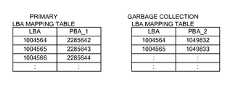
- FIG. 5Ashows an LBA mapping table for storing a primary mapping and a secondary mapping corresponding to a valid garbage collection memory segment according to an embodiment of the present invention.
- FIG. 5Bshows an embodiment of the present invention wherein a primary LBA mapping table stores the primary mapping and a garbage collection LBA mapping table stores the secondary mapping.
- FIG. 6Ashows an embodiment of the present invention wherein in-line mapping information is stored in a memory segment (page) of a block in a non-volatile semiconductor memory.
- FIG. 6Bshows an embodiment of the present invention wherein in-line mapping information is stored in a memory segment (data sector) of a disk in a disk drive.
- FIG. 7is a flow diagram according to an embodiment of the present invention wherein after a power failure the in-line mapping information is used to rebuild the first and second mappings.
- FIG. 8is a flow diagram according to an embodiment of the present invention wherein when the first LBA is overwritten, the first and second mapping are invalidated.
- FIG. 9is a flow diagram according to an embodiment of the present invention wherein when second data for a second LBA overwrites the first memory segment, the first mapping is invalidated.
- FIG. 10is a flow diagram according to an embodiment of the present invention wherein when the first memory segment is erased, the first mapping is invalidated.
- FIG. 11is a flow diagram according to an embodiment of the present invention wherein when the first data cannot be recovered from the second memory segment, the first data is read from the first memory segment.
- FIG. 12is a flow diagram according to an embodiment of the present invention wherein when a read command is received to read the first LBA, an RPO algorithm is executed to select between the first and second memory segments.
- FIG. 1Ashows a data storage device 2 according to an embodiment of the present invention comprising a non-volatile memory 4 comprising a plurality of memory segments.
- the data storage device 2further comprises control circuitry 6 operable to execute the flow diagram of FIG. 1B , wherein a first write command is received from a host (block 8 ) comprising first data and a first logical block address (LBA).
- LBAlogical block address
- the first datais written to a first memory segment (block 10 ) and the first LBA is first mapped to a first physical block address (PBA) of the first memory segment (block 12 ).
- PBAphysical block address
- the first datais copied from the first memory segment to a second memory segment (block 16 ) and the first LBA is second mapped to a second PBA of the second memory segment (block 18 ).
- a read commandis received from the host comprising the first LBA (block 20 ).
- a selectionis made between the first memory segment and the second memory segment (block 21 ), and at least part of the first data is read from the selected memory segment (block 22 ).
- FIG. 1Cillustrates an embodiment of the present invention wherein data is first written to a first memory segment 24 A when servicing a write command from a host.
- An LBA of the write commandis mapped to the PBA of the first memory segment 24 A.
- the first memory segment 24 Ais part of a block of memory segments that may comprise other invalid memory segments, and is therefore eventually garbage collected in order to free the invalid memory segments for future write commands.
- the data stored in the first memory segment 24 Amay still be valid and is therefore copied to a second memory segment 24 B with the LBA mapped to the PBA of the second memory segment 24 B.
- the data stored in first memory segment 24 Aremains valid after the copy operation (i.e., the first memory segment 24 A is not immediately erased).
- the first mapping of the LBA to the first memory segment 24 Ais retained in order to retain a copy of the data.
- the copy of the datamay be used for any suitable reason, such as for error recovery when the second memory segment 24 B is unrecoverable, or to increase throughput of the data storage device.
- FIG. 2Ashows a data storage device in the form of a non-volatile semiconductor memory-based storage device 26 comprising a memory controller 28 (e.g., a flash memory controller) and a memory device 30 (e.g., a flash memory) according to one embodiment.
- a memory controller 28e.g., a flash memory controller
- a memory device 30e.g., a flash memory
- non-volatile semiconductor memorymay comprise one or more of various types of memory devices such as flash integrated circuits, Chalcogenide RAM (C-RAM), Phase Change Memory (PC-RAM or PRAM), Programmable Metallization Cell RAM (PMC-RAM or PMCm), Ovonic Unified Memory (OUM), Resistance RAM (RRAM), NAND memory (e.g., single-level cell (SLC) memory, multi-level cell (MLC) memory, or any combination thereof), NOR memory, EEPROM, Ferroelectric Memory (FeRAM), Magnetoresistive RAM (MRAM), other discrete NVM (non-volatile memory) chips, or any combination thereof.
- flash integrated circuitse.g., Intel® 845555B Intel® 845555B Intel® 845555B Intel® 845555B Intel® 845555B Intel® 845555B Intel® 845555B Intel® 845555B Intel® 845555B Intel® 845555B Intel® 845555B Intel® 845555B Intel® 845555B Intel® 845
- the memory controller 28comprises a microprocessor 32 for implementing various algorithms, including LBA to PBA mapping, wear leveling, error correction code (etc.).
- the memory controller 28further comprises a buffer 34 for buffering write/read data, and interface circuitry 36 for interfacing with one or more memory devices 30 .
- the interface circuitry 36generates suitable control signals 38 and receives status information 40 from the memory device(s) 30 in connection with executing write/read commands initiated by the microprocessor 32 .
- the interface circuitry 36also transmits and receives data over an I/O bus 42 , including write/read data stored in the buffer 34 or command data generated by the microprocessor 32 and transmitted to a controller 44 integrated with the memory device(s) 30 .
- the memory device(s) 30comprises an array of memory cells 46 that are accessed in memory segments referred to as pages.
- write data received over the I/O bus 42 from the buffer 34is first stored in a data register 48 .
- the controller 44then transfers the write data from the data register 48 to a target page in the memory array 46 .
- a page in the memory array 46is read into the data register 48 and then transferred over the I/O bus 42 where it is stored in the buffer 34 .
- the memory array 46comprises a plurality of blocks, each block comprises a plurality of pages, and the pages in a block are erased together by erasing the block.
- FIG. 2Billustrates a first block 50 A storing invalid pages and valid pages.
- the valid pages in the first block 50 Aare copied to free pages of a second block 50 B. Conventionally, once this copying is completed, the valid pages in the first block 50 A would be marked invalid and subject to erasure.
- embodiments of the present inventionmaintain mapping data that reference those pages in the first block 50 A and exploit the redundancy rather than immediately erasing the pages in the first block 50 A.
- the garbage collection operation for the non-volatile semiconductor memory-based storage device 26 shown in FIG. 2Ais divided into two stages. During a first stage, the valid pages of old blocks are copied to new blocks without erasing the old blocks. The first and second mapping to the old and new blocks is maintained so that the resulting redundancy can be exploited. In a second stage, when the number of free blocks falls below a threshold or when other factors such as wear leveling trigger erasure of blocks, a number of the old blocks storing the redundant copies of data are erased and placed in the pool of free blocks. When a page of an old block storing redundant data is erased, the corresponding LBA mapping information is also invalidated.
- the pages of old blocks storing redundant copies of datamay be accessed during the interval between the first and second stages of the garbage collection operation, or until the LBA is overwritten as part of a new write command in which case the LBA mapping information to the page in the old block is also invalidated.
- valid/invalid datamay be operated upon and/or mapped at a sector level or a different unit of granularity.
- the same principleswould be applicable in implementations where a page may include multiple sectors or other units of granularity.
- FIG. 3Ashows a data storage device in the form of a disk drive comprising a head 52 actuated over a disk 54 by a voice coil motor (VCM).
- VCMvoice coil motor
- the disk drivefurther comprises control circuitry 56 for implementing the embodiments of the present invention, including to maintain first and second mappings for garbage collected LBAs.
- the diskcomprises a plurality of data tracks, wherein in an example shown in FIG. 3B each data track comprises a plurality of data sectors for storing user data and embedded servo sectors (SS) for storing servo positioning information (e.g., track address and servo bursts).
- each memory segmentcorresponds to a data sector accessed through a PBA. Similar to a flash based memory device described above, the disk drive of FIG.
- 3Amay implement a dynamic LBA to PBA mapping, for example, when implementing a log-structured file system.
- datais typically written to a new memory segment (data sector) during each write operation (including overwrite operations).
- the old memory segments (data sectors)are invalidated and then reallocated using a garbage collection algorithm.
- a disk drivemay implement a log-structured file system, for example, when implementing a shingled track system where write operations progress in the same radial direction so that the data tracks can overlap, thereby increasing the tracks per inch (TPI).
- TPItracks per inch
- the dynamic LBA to PBA mappingmay be implemented using any suitable technique, such as shown in FIG. 4A where the disk 54 is accessed as a circular buffer. The data tracks are written from the ID toward the OD (or vice versa), and when the last data track is reached, the writing operation wraps around so as to overwrite the old data tracks at the tail of the circular buffer.
- the diskmay be divided into a number of zoned blocks (Z 1 -ZN), wherein each zone comprises a plurality of contiguous data tracks. The zoned blocks are accessed similar to the blocks in the non-volatile semiconductor memory-based storage device described above with reference to FIG. 2A .
- one of the zonesis selected to service the current write commands, and when the current zone is filled, a new zone is selected from a pool of free zones.
- the valid data sectors of an old zoneare copied to a new zone, and the control circuitry 56 maintains the first mapping to the data sector of the old zone as well as the second mapping to the data sector of the new zone.
- the data sectors storing redundant dataare eventually overwritten when the corresponding zone is selected to service new write commands.
- An old zonemay or may not be erased prior to overwriting the data sectors.
- the LBA mapping to the old data sectoris invalidated when the data sector in the old zone is erased or overwritten, or when the same LBA is overwritten as part of a new write command.
- FIG. 5Ashows an embodiment wherein the control circuitry 6 of the data storage device 2 ( FIG. 1A ) maintains a LBA mapping table comprising a plurality of entries, wherein each entry maps an LBA to a primary PBA (PBA_ 1 ) and to a redundant PBA (PBA_ 2 ).
- the primary PBAstores newly written data for the LBA
- the redundant PBAstores a copy of the data when generated as part of the garbage collection operation.
- a NULL entryis assigned in the LBA mapping table.
- the LBA mapping table shown in FIG. 5Acomprises an entry for each LBA; however, other embodiments may employ run-length encoding in order to reduce the size of the LBA mapping table.
- FIG. 5Bshows an alternative embodiment of the present invention wherein the control circuitry 6 maintains two mapping tables: a primary LBA mapping table for storing the LBA to PBA mapping for the most recent write operation, and a garbage collection LBA mapping table for storing the LBA to PBA mapping to the redundant memory segments generated as part of the garbage collection operation.
- a primary LBA mapping tablefor storing the LBA to PBA mapping for the most recent write operation
- a garbage collection LBA mapping tablefor storing the LBA to PBA mapping to the redundant memory segments generated as part of the garbage collection operation.
- the control circuitry 6maintains the LBA mapping table(s) in a volatile semiconductor memory (e.g., a random access memory (RAM)) and updates the LBA mapping table(s) as new write commands are received by the host as well as when write commands are generated during the garbage collection operation. Periodically the control circuitry 6 writes (flushes) the updated LBA mapping table(s) to the non-volatile memory 4 so that the updates are saved when the data storage device is powered down. However, if the data storage device is subject to a power failure, the most recent updates to the LBA mapping table(s) that occur after the last flush operation will be lost.
- a volatile semiconductor memorye.g., a random access memory (RAM)
- the control circuitry 6writes in-line mapping information to a memory segment of the non-volatile memory 4 when servicing each write command so that the in-line mapping information can be used to rebuild the LBA mapping table(s) when recovering from a power failure.
- FIG. 6Ashows an embodiment of in-line mapping information written to the last page of the current block when servicing write commands in the non-volatile semiconductor memory-based storage device 26 of FIG. 2A
- FIG. 6Bshows an embodiment of in-line mapping information written to the last data sector following a write command to the disk of the disk drive of FIG. 3A .
- the in-line mapping informationcomprises the LBAs of the write command so that when the data storage devices recovers from a power failure, the in-line mapping information can be read from the most recently written blocks of memory segments and used to rebuild the LBA mapping table(s).
- the in-line mapping informationcomprises a flag (denoted by the example value [R] as shown) that indicates whether the LBA was written as part of a garbage collection operation so that the LBA mapping table(s) can be rebuilt with mapping to the primary PBA and the redundant PBA when appropriate.
- FIG. 7is a flow diagram according to an embodiment of the present invention for rebuilding the LBA mapping table(s) when the data storage device recovers from a power failure.
- the LBA mapping table(s)When the data storage device is powered on and a power fail condition is detected (block 58 ), the LBA mapping table(s) last flushed to the non-volatile memory 4 is read into a volatile semiconductor memory (e.g., RAM). The block(s) being written prior to the power failure operation are then accessed in order to recover the in-line mapping information (block 62 ).
- a volatile semiconductor memorye.g., RAM
- the primary entry of the LBA mapping tableis updated (block 64 ), and if the in-line mapping information indicates a redundant memory segment, the redundant entry of the LBA mapping table is updated (block 68 ), otherwise the redundant entry of the LBA mapping table is nullified or deleted (block 70 ).
- the flow diagramis then repeated from block 64 until all of the in-line mapping information has been processed (block 72 ).
- the updated LBA mapping table(s)is then written to the non-volatile memory (block 74 ).
- the data in the valid memory segmentsare copied to a reserved area of the non-volatile memory, such as a pool of reserved blocks in the non-volatile semiconductor memory-based storage device 26 of FIG. 2A , or a pool of reserved zones on the disk of the disk drive of FIG. 3A .
- the data for new write commands received from the hostare written to a different reserved area in the non-volatile memory.
- in-line mapping informationis written to both reserved areas, and when recovering from a power failure, the in-line information is recovered from both reserved areas.
- the in-line mapping information for the garbage collection areaneed not include a flag to indicate whether the LBA is a redundant copy since all LBAs in the garbage collection area are a redundant copy.
- the in-line mapping information for both reserved areasincludes a sequence number so that the order in which the garbage collection copy commands and the host write commands can be determined and used to accurately rebuild the LBA mapping table(s).
- FIG. 8is a flow diagram according to an embodiment of the present invention which is an extension to the flow diagram of FIG. 1B .
- a write commandis received from the host to overwrite the first LBA with second data (block 76 )
- the second datais written to a third memory segment (block 78 )
- the LBAis mapped to a third PBA of the third memory segment (block 80 )
- the first and second mappingsgenerated at block 12 and block 18 of FIG. 1B ) are invalidated (block 82 ). That is when an LBA is overwritten with new data, the previous LBA mappings (primary and redundant) are invalidated since they no longer correspond to the LBA (the primary and redundant memory segments become invalid).
- FIG. 9is a flow diagram according to an embodiment of the present invention which is an extension to the flow diagram of FIG. 1B .
- the second datamay overwrite the first memory segment (block 86 ). That is, the first memory segment may be part of a free block selected to service the new write commands, and therefore the first memory segment is eventually overwritten.
- the second LBAis mapped to the first PBA of the first memory segment (block 88 ) and the first mapping (generated at block 12 of FIG. 1B ) is invalidated. That is, the overwrite operation invalidates the redundant copy of the first LBA, but the primary copy for the first LBA (stored in the second memory segment) is still available.
- FIG. 10is a flow diagram according to an embodiment of the present invention which is an extension to the flow diagram of FIG. 1B .
- the garbage collection operationeventually erases the memory segments (block 92 )
- the first memory segmentis eventually erased (block 94 ) and the first mapping (generated at block 12 of FIG. 1B ) is invalidated. That is, the erase operation invalidates the redundant copy of the first LBA, but the primary copy for the first LBA (stored in the second memory segment) is still available.
- FIG. 11is a flow diagram according to an embodiment of the present invention wherein the redundant copy of data stored in a garbage collected memory segment may be used to recover data when the primary copy of the data cannot be recovered (e.g., due to a defect).
- the control circuitryWhen a read command is received to read the first LBA (block 98 ), the control circuitry first attempts to read the first data from the second memory segment (block 100 ) which stores the primary copy. If the first data cannot be recovered from the second memory segment (block 102 ), the control circuitry attempts to read the first data from the first memory segment (block 104 ) which stores the redundant copy.
- the first datais recoverable from the first memory segment (block 106 )
- the first datais copied to a third memory segment (block 108 ) and the first LBA is mapped to a third PBA of the third memory segment (block 110 ). That is, the garbage collection operation is repeated for the first LBA so as to store another primary copy of the data in a different memory segment.
- the second mapping of the LBA to the second memory segmentis invalidated (block 112 ) and in one embodiment the second memory segment may be mapped out as defective.
- FIG. 12is a flow diagram according to an embodiment of the present invention wherein the data storage device comprises the disk drive shown in FIG. 3A .
- the control circuitry 56queues a number of access commands received from the host, and then executes a rotational position optimization (RPO) algorithm in order to select and execute the access commands from the command queue in an order that minimizes the seek latency of the head 52 and the rotational latency of the disk 54 needed to access the corresponding memory segments (data sectors).
- RPOrotational position optimization
- the control circuitryselects between the first memory segment and the second memory segment using the RPO algorithm, and then reads the first data from the selected memory segment.
- the redundant memory segments generated through the garbage collection operationimproves performance of the RPO algorithm.
- the availability of the redundant copymay be used to improve data transfer performance in the non-volatile semiconductor memory-based storage device 26 of FIG. 2A .
- the redundant copymay enable the controller 28 to exploit the parallelism in data channels employing multiple memory devices 30 .
- a first memory device 30comprises a first memory array 46 accessed over a first channel
- a second memory device 30comprises a second memory array 46 accessed over a second channel.
- the controllermay choose to access the redundant copy if it resides in a different memory array serviced by a less busy channel.
- the controller 28may also choose to obtain a part of the data from the primary copy and a part of the data from the redundant copy and combine the parts to effectively increase the overall transfer rate.
- control circuitrymay be implemented within a read channel integrated circuit, or in a component separate from the read channel, such as a disk controller, or certain operations described above may be performed by a read channel and others by a disk controller.
- the read channel and disk controllerare implemented as separate integrated circuits, and in an alternative embodiment they are fabricated into a single integrated circuit or system on a chip (SOC).
- the control circuitrymay include a suitable preamp circuit implemented as a separate integrated circuit, integrated into the read channel or disk controller circuit, or integrated into a SOC.
- control circuitrycomprises a microprocessor executing instructions, the instructions being operable to cause the microprocessor to perform the flow diagrams described herein.
- the instructionsmay be stored in any computer-readable medium. In one embodiment, they may be stored on a non-volatile semiconductor memory external to the microprocessor, or integrated with the microprocessor in a SOC. In another embodiment, the instructions are stored on the disk and read into a volatile semiconductor memory when the disk drive is powered on. In yet another embodiment, the control circuitry comprises suitable logic circuitry, such as state machine circuitry.
Landscapes
- Engineering & Computer Science (AREA)
- Theoretical Computer Science (AREA)
- Physics & Mathematics (AREA)
- General Engineering & Computer Science (AREA)
- General Physics & Mathematics (AREA)
- Human Computer Interaction (AREA)
- Computer Security & Cryptography (AREA)
- Techniques For Improving Reliability Of Storages (AREA)
Abstract
Description
Claims (22)
Priority Applications (1)
| Application Number | Priority Date | Filing Date | Title |
|---|---|---|---|
| US13/675,211US9448919B1 (en) | 2012-11-13 | 2012-11-13 | Data storage device accessing garbage collected memory segments |
Applications Claiming Priority (1)
| Application Number | Priority Date | Filing Date | Title |
|---|---|---|---|
| US13/675,211US9448919B1 (en) | 2012-11-13 | 2012-11-13 | Data storage device accessing garbage collected memory segments |
Publications (1)
| Publication Number | Publication Date |
|---|---|
| US9448919B1true US9448919B1 (en) | 2016-09-20 |
Family
ID=56895643
Family Applications (1)
| Application Number | Title | Priority Date | Filing Date |
|---|---|---|---|
| US13/675,211Expired - Fee RelatedUS9448919B1 (en) | 2012-11-13 | 2012-11-13 | Data storage device accessing garbage collected memory segments |
Country Status (1)
| Country | Link |
|---|---|
| US (1) | US9448919B1 (en) |
Cited By (28)
| Publication number | Priority date | Publication date | Assignee | Title |
|---|---|---|---|---|
| US20150317326A1 (en)* | 2014-05-02 | 2015-11-05 | Vmware, Inc. | Inline garbage collection for log-structured file systems |
| US20170199687A1 (en)* | 2016-01-12 | 2017-07-13 | Kabushiki Kaisha Toshiba | Memory system and control method |
| US10083114B2 (en)* | 2016-11-24 | 2018-09-25 | SK Hynix Inc. | Data storage device and operating method thereof |
| CN108572922A (en)* | 2017-03-07 | 2018-09-25 | 慧荣科技股份有限公司 | data storage device and operation method thereof |
| CN108595115A (en)* | 2018-03-27 | 2018-09-28 | 深圳忆联信息系统有限公司 | A method of improving SSD garbage reclamation efficiency |
| US20180307440A1 (en)* | 2017-04-20 | 2018-10-25 | Fujitsu Limited | Storage control apparatus and storage control method |
| US20180307419A1 (en)* | 2017-04-20 | 2018-10-25 | Fujitsu Limited | Storage control apparatus and storage control method |
| US10235284B2 (en)* | 2017-03-23 | 2019-03-19 | Toshiba Memory Corporation | Memory system |
| CN109643292A (en)* | 2016-09-29 | 2019-04-16 | 英特尔公司 | Scalable Bandwidth Non-Volatile Memory |
| US10282260B2 (en)* | 2015-07-21 | 2019-05-07 | Samsung Electronics Co., Ltd. | Method of operating storage system and storage controller |
| CN110119360A (en)* | 2018-02-06 | 2019-08-13 | 爱思开海力士有限公司 | Storage device and its operating method |
| US10564884B1 (en)* | 2016-04-27 | 2020-02-18 | Pure Storage, Inc. | Intelligent data migration within a flash storage array |
| CN110825663A (en)* | 2018-08-14 | 2020-02-21 | 爱思开海力士有限公司 | Controller, memory system and method of operation |
| US10713157B2 (en)* | 2018-05-31 | 2020-07-14 | Western Digital Technologies, Inc. | Storage system and method for improving read performance using multiple copies of a logical-to-physical address table |
| CN111708480A (en)* | 2019-03-18 | 2020-09-25 | 爱思开海力士有限公司 | Data storage device and method of operation and controller thereof |
| US11030093B2 (en)* | 2018-09-17 | 2021-06-08 | Silicon Motion, Inc. | High efficiency garbage collection method, associated data storage device and controller thereof |
| US11112990B1 (en) | 2016-04-27 | 2021-09-07 | Pure Storage, Inc. | Managing storage device evacuation |
| US11126238B2 (en) | 2018-12-05 | 2021-09-21 | Samsung Electronics Co., Ltd. | Open channel solid state drive, nonvolatile memory system including the same and method of power loss protection of open channel solid state drive |
| CN113823346A (en)* | 2020-06-18 | 2021-12-21 | 美光科技公司 | Region-Aware Memory Management in Memory Subsystems |
| US11221773B2 (en)* | 2018-11-08 | 2022-01-11 | Silicon Motion, Inc. | Method and apparatus for performing mapping information management regarding redundant array of independent disks |
| US20220043607A1 (en)* | 2013-11-06 | 2022-02-10 | Pure Storage, Inc. | Expanding An Address Space Supported By A Storage System |
| US11360912B2 (en) | 2018-09-17 | 2022-06-14 | Silicon Motion, Inc. | Method for performing adaptive locking range management, associated data storage device and controller thereof |
| US11416144B2 (en) | 2019-12-12 | 2022-08-16 | Pure Storage, Inc. | Dynamic use of segment or zone power loss protection in a flash device |
| JP2022552804A (en)* | 2019-10-08 | 2022-12-20 | インターナショナル・ビジネス・マシーンズ・コーポレーション | Garbage collection in data storage systems |
| US11620234B2 (en)* | 2020-06-29 | 2023-04-04 | Western Digital Technologies, Inc. | Operation-deterministic write operations for data recovery and integrity checks |
| US11704192B2 (en) | 2019-12-12 | 2023-07-18 | Pure Storage, Inc. | Budgeting open blocks based on power loss protection |
| US11809727B1 (en) | 2016-04-27 | 2023-11-07 | Pure Storage, Inc. | Predicting failures in a storage system that includes a plurality of storage devices |
| US12061814B2 (en) | 2021-01-25 | 2024-08-13 | Pure Storage, Inc. | Using data similarity to select segments for garbage collection |
Citations (10)
| Publication number | Priority date | Publication date | Assignee | Title |
|---|---|---|---|---|
| US6061194A (en) | 1997-04-15 | 2000-05-09 | Lsi Logic Corporation | Device and method for storing and retrieving original and redundant data |
| US20080282024A1 (en)* | 2007-05-09 | 2008-11-13 | Sudeep Biswas | Management of erase operations in storage devices based on flash memories |
| US7599261B2 (en) | 2006-01-18 | 2009-10-06 | International Business Machines Corporation | Removable storage media with improved data integrity |
| US20100037001A1 (en)* | 2008-08-08 | 2010-02-11 | Imation Corp. | Flash memory based storage devices utilizing magnetoresistive random access memory (MRAM) |
| US7752381B2 (en)* | 2005-05-24 | 2010-07-06 | Micron Technology, Inc. | Version based non-volatile memory translation layer |
| US7783851B2 (en) | 2006-10-19 | 2010-08-24 | Samsung Electronics Co., Ltd. | Methods of reusing log blocks in non-volatile memories and related non-volatile memory devices |
| US7916421B1 (en) | 2005-05-05 | 2011-03-29 | Seagate Technology Llc | Methods and structure for recovery of write fault errors in a dynamically mapped mass storage device |
| US8194340B1 (en) | 2010-03-18 | 2012-06-05 | Western Digital Technologies, Inc. | Disk drive framing write data with in-line mapping data during write operations |
| US20140047161A1 (en)* | 2012-08-08 | 2014-02-13 | Avalanche Technology, Inc. | System Employing MRAM and Physically Addressed Solid State Disk |
| US8677203B1 (en)* | 2010-01-11 | 2014-03-18 | Apple Inc. | Redundant data storage schemes for multi-die memory systems |
- 2012
- 2012-11-13USUS13/675,211patent/US9448919B1/ennot_activeExpired - Fee Related
Patent Citations (10)
| Publication number | Priority date | Publication date | Assignee | Title |
|---|---|---|---|---|
| US6061194A (en) | 1997-04-15 | 2000-05-09 | Lsi Logic Corporation | Device and method for storing and retrieving original and redundant data |
| US7916421B1 (en) | 2005-05-05 | 2011-03-29 | Seagate Technology Llc | Methods and structure for recovery of write fault errors in a dynamically mapped mass storage device |
| US7752381B2 (en)* | 2005-05-24 | 2010-07-06 | Micron Technology, Inc. | Version based non-volatile memory translation layer |
| US7599261B2 (en) | 2006-01-18 | 2009-10-06 | International Business Machines Corporation | Removable storage media with improved data integrity |
| US7783851B2 (en) | 2006-10-19 | 2010-08-24 | Samsung Electronics Co., Ltd. | Methods of reusing log blocks in non-volatile memories and related non-volatile memory devices |
| US20080282024A1 (en)* | 2007-05-09 | 2008-11-13 | Sudeep Biswas | Management of erase operations in storage devices based on flash memories |
| US20100037001A1 (en)* | 2008-08-08 | 2010-02-11 | Imation Corp. | Flash memory based storage devices utilizing magnetoresistive random access memory (MRAM) |
| US8677203B1 (en)* | 2010-01-11 | 2014-03-18 | Apple Inc. | Redundant data storage schemes for multi-die memory systems |
| US8194340B1 (en) | 2010-03-18 | 2012-06-05 | Western Digital Technologies, Inc. | Disk drive framing write data with in-line mapping data during write operations |
| US20140047161A1 (en)* | 2012-08-08 | 2014-02-13 | Avalanche Technology, Inc. | System Employing MRAM and Physically Addressed Solid State Disk |
Non-Patent Citations (1)
| Title |
|---|
| Burkhard et al., "Rotational Position Optimization (RPO) Disk Scheduling", Jul. 2001.* |
Cited By (43)
| Publication number | Priority date | Publication date | Assignee | Title |
|---|---|---|---|---|
| US11899986B2 (en)* | 2013-11-06 | 2024-02-13 | Pure Storage, Inc. | Expanding an address space supported by a storage system |
| US20220043607A1 (en)* | 2013-11-06 | 2022-02-10 | Pure Storage, Inc. | Expanding An Address Space Supported By A Storage System |
| US9747298B2 (en)* | 2014-05-02 | 2017-08-29 | Vmware, Inc. | Inline garbage collection for log-structured file systems |
| US20150317326A1 (en)* | 2014-05-02 | 2015-11-05 | Vmware, Inc. | Inline garbage collection for log-structured file systems |
| US10282260B2 (en)* | 2015-07-21 | 2019-05-07 | Samsung Electronics Co., Ltd. | Method of operating storage system and storage controller |
| US20170199687A1 (en)* | 2016-01-12 | 2017-07-13 | Kabushiki Kaisha Toshiba | Memory system and control method |
| US11809727B1 (en) | 2016-04-27 | 2023-11-07 | Pure Storage, Inc. | Predicting failures in a storage system that includes a plurality of storage devices |
| US10564884B1 (en)* | 2016-04-27 | 2020-02-18 | Pure Storage, Inc. | Intelligent data migration within a flash storage array |
| US11934681B2 (en) | 2016-04-27 | 2024-03-19 | Pure Storage, Inc. | Data migration for write groups |
| US11112990B1 (en) | 2016-04-27 | 2021-09-07 | Pure Storage, Inc. | Managing storage device evacuation |
| CN109643292A (en)* | 2016-09-29 | 2019-04-16 | 英特尔公司 | Scalable Bandwidth Non-Volatile Memory |
| CN109643292B (en)* | 2016-09-29 | 2024-02-27 | 英特尔公司 | Scalable bandwidth non-volatile memory |
| US10083114B2 (en)* | 2016-11-24 | 2018-09-25 | SK Hynix Inc. | Data storage device and operating method thereof |
| CN108572922A (en)* | 2017-03-07 | 2018-09-25 | 慧荣科技股份有限公司 | data storage device and operation method thereof |
| US10235284B2 (en)* | 2017-03-23 | 2019-03-19 | Toshiba Memory Corporation | Memory system |
| US20180307440A1 (en)* | 2017-04-20 | 2018-10-25 | Fujitsu Limited | Storage control apparatus and storage control method |
| US20180307419A1 (en)* | 2017-04-20 | 2018-10-25 | Fujitsu Limited | Storage control apparatus and storage control method |
| CN110119360A (en)* | 2018-02-06 | 2019-08-13 | 爱思开海力士有限公司 | Storage device and its operating method |
| CN108595115A (en)* | 2018-03-27 | 2018-09-28 | 深圳忆联信息系统有限公司 | A method of improving SSD garbage reclamation efficiency |
| CN108595115B (en)* | 2018-03-27 | 2021-10-01 | 深圳忆联信息系统有限公司 | Method for improving SSD garbage recovery efficiency |
| US10713157B2 (en)* | 2018-05-31 | 2020-07-14 | Western Digital Technologies, Inc. | Storage system and method for improving read performance using multiple copies of a logical-to-physical address table |
| CN110825663B (en)* | 2018-08-14 | 2023-04-18 | 爱思开海力士有限公司 | Controller, memory system and operating method thereof |
| CN110825663A (en)* | 2018-08-14 | 2020-02-21 | 爱思开海力士有限公司 | Controller, memory system and method of operation |
| US11030093B2 (en)* | 2018-09-17 | 2021-06-08 | Silicon Motion, Inc. | High efficiency garbage collection method, associated data storage device and controller thereof |
| US11360912B2 (en) | 2018-09-17 | 2022-06-14 | Silicon Motion, Inc. | Method for performing adaptive locking range management, associated data storage device and controller thereof |
| US11221773B2 (en)* | 2018-11-08 | 2022-01-11 | Silicon Motion, Inc. | Method and apparatus for performing mapping information management regarding redundant array of independent disks |
| US11126238B2 (en) | 2018-12-05 | 2021-09-21 | Samsung Electronics Co., Ltd. | Open channel solid state drive, nonvolatile memory system including the same and method of power loss protection of open channel solid state drive |
| US11803223B2 (en) | 2018-12-05 | 2023-10-31 | Samsung Electronics Co., Ltd. | Open channel solid state drive, nonvolatile memory system including the same and method of power loss protection of open channel solid state drive |
| CN111708480A (en)* | 2019-03-18 | 2020-09-25 | 爱思开海力士有限公司 | Data storage device and method of operation and controller thereof |
| CN111708480B (en)* | 2019-03-18 | 2023-07-14 | 爱思开海力士有限公司 | Data storage device, operating method and controller thereof |
| JP2022552804A (en)* | 2019-10-08 | 2022-12-20 | インターナショナル・ビジネス・マシーンズ・コーポレーション | Garbage collection in data storage systems |
| US11416144B2 (en) | 2019-12-12 | 2022-08-16 | Pure Storage, Inc. | Dynamic use of segment or zone power loss protection in a flash device |
| US11704192B2 (en) | 2019-12-12 | 2023-07-18 | Pure Storage, Inc. | Budgeting open blocks based on power loss protection |
| CN113823346A (en)* | 2020-06-18 | 2021-12-21 | 美光科技公司 | Region-Aware Memory Management in Memory Subsystems |
| US20230161712A1 (en)* | 2020-06-18 | 2023-05-25 | Micron Technology, Inc. | Zone-aware memory management in memory sub-systems |
| US11550727B2 (en)* | 2020-06-18 | 2023-01-10 | Micron Technology, Inc. | Zone-aware memory management in memory subsystems |
| US20210397562A1 (en)* | 2020-06-18 | 2021-12-23 | Micron Technology, Inc. | Zone-aware memory management in memory sub-systems |
| US11960409B2 (en)* | 2020-06-18 | 2024-04-16 | Micron Technology, Inc. | Zone-aware memory management in memory sub-systems |
| US20240256463A1 (en)* | 2020-06-18 | 2024-08-01 | Micron Technology, Inc. | Zone-aware memory management in memory sub-systems |
| CN113823346B (en)* | 2020-06-18 | 2024-08-27 | 美光科技公司 | Region-aware memory management in a memory subsystem |
| US12332804B2 (en)* | 2020-06-18 | 2025-06-17 | Micron Technology, Inc. | Zone-aware memory management in memory sub-systems |
| US11620234B2 (en)* | 2020-06-29 | 2023-04-04 | Western Digital Technologies, Inc. | Operation-deterministic write operations for data recovery and integrity checks |
| US12061814B2 (en) | 2021-01-25 | 2024-08-13 | Pure Storage, Inc. | Using data similarity to select segments for garbage collection |
Similar Documents
| Publication | Publication Date | Title |
|---|---|---|
| US9448919B1 (en) | Data storage device accessing garbage collected memory segments | |
| US10936252B2 (en) | Storage system capable of invalidating data stored in a storage device thereof | |
| US20210073120A1 (en) | Directed sanitization of memory | |
| JP5728672B2 (en) | Hybrid memory management | |
| US9183132B2 (en) | Storage device, computer system, and storage system | |
| US8656256B2 (en) | Apparatus and method for multi-mode operation of a flash memory device | |
| US9923562B1 (en) | Data storage device state detection on power loss | |
| US11386005B2 (en) | Memory system, memory controller, and method of operating memory system for caching journal information for zone in the journal cache | |
| CN114341824B (en) | Unmapping for coarsely mapped memory subsystems | |
| US12298902B2 (en) | Storage device including nonvolatile memory device and operating method of storage device | |
| US8850160B2 (en) | Adaptive write behavior for a system having non-volatile memory | |
| US10282096B1 (en) | Identification of data with predetermined data pattern | |
| US11249838B2 (en) | Memory system, memory controller, and method of operating memory controller | |
| US20240078027A1 (en) | Storage device including nonvolatile memory device and operating method of storage device | |
| KR20220068535A (en) | Memory system and operating method of memory system | |
| US20250190344A1 (en) | Storage device including nonvolatile memory device and operating method of storage device | |
| US20250217286A1 (en) | Storage device including nonvolatile memory device and operating method of storage device |
Legal Events
| Date | Code | Title | Description |
|---|---|---|---|
| AS | Assignment | Owner name:WESTERN DIGITAL TECHNOLOGIES, INC., CALIFORNIA Free format text:ASSIGNMENT OF ASSIGNORS INTEREST;ASSIGNOR:BOYLE, WILLIAM B.;REEL/FRAME:029286/0551 Effective date:20121112 | |
| AS | Assignment | Owner name:JPMORGAN CHASE BANK, N.A., AS COLLATERAL AGENT, ILLINOIS Free format text:SECURITY AGREEMENT;ASSIGNOR:WESTERN DIGITAL TECHNOLOGIES, INC.;REEL/FRAME:038722/0229 Effective date:20160512 Owner name:U.S. BANK NATIONAL ASSOCIATION, AS COLLATERAL AGENT, CALIFORNIA Free format text:SECURITY AGREEMENT;ASSIGNOR:WESTERN DIGITAL TECHNOLOGIES, INC.;REEL/FRAME:038744/0281 Effective date:20160512 Owner name:JPMORGAN CHASE BANK, N.A., AS COLLATERAL AGENT, ILLINOIS Free format text:SECURITY AGREEMENT;ASSIGNOR:WESTERN DIGITAL TECHNOLOGIES, INC.;REEL/FRAME:038744/0481 Effective date:20160512 Owner name:JPMORGAN CHASE BANK, N.A., AS COLLATERAL AGENT, IL Free format text:SECURITY AGREEMENT;ASSIGNOR:WESTERN DIGITAL TECHNOLOGIES, INC.;REEL/FRAME:038722/0229 Effective date:20160512 Owner name:JPMORGAN CHASE BANK, N.A., AS COLLATERAL AGENT, IL Free format text:SECURITY AGREEMENT;ASSIGNOR:WESTERN DIGITAL TECHNOLOGIES, INC.;REEL/FRAME:038744/0481 Effective date:20160512 Owner name:U.S. BANK NATIONAL ASSOCIATION, AS COLLATERAL AGEN Free format text:SECURITY AGREEMENT;ASSIGNOR:WESTERN DIGITAL TECHNOLOGIES, INC.;REEL/FRAME:038744/0281 Effective date:20160512 | |
| STCF | Information on status: patent grant | Free format text:PATENTED CASE | |
| AS | Assignment | Owner name:WESTERN DIGITAL TECHNOLOGIES, INC., CALIFORNIA Free format text:RELEASE BY SECURED PARTY;ASSIGNOR:U.S. BANK NATIONAL ASSOCIATION, AS COLLATERAL AGENT;REEL/FRAME:045501/0714 Effective date:20180227 | |
| MAFP | Maintenance fee payment | Free format text:PAYMENT OF MAINTENANCE FEE, 4TH YEAR, LARGE ENTITY (ORIGINAL EVENT CODE: M1551); ENTITY STATUS OF PATENT OWNER: LARGE ENTITY Year of fee payment:4 | |
| AS | Assignment | Owner name:WESTERN DIGITAL TECHNOLOGIES, INC., CALIFORNIA Free format text:RELEASE OF SECURITY INTEREST AT REEL 038744 FRAME 0481;ASSIGNOR:JPMORGAN CHASE BANK, N.A.;REEL/FRAME:058982/0556 Effective date:20220203 | |
| AS | Assignment | Owner name:JPMORGAN CHASE BANK, N.A., ILLINOIS Free format text:PATENT COLLATERAL AGREEMENT - A&R LOAN AGREEMENT;ASSIGNOR:WESTERN DIGITAL TECHNOLOGIES, INC.;REEL/FRAME:064715/0001 Effective date:20230818 Owner name:JPMORGAN CHASE BANK, N.A., ILLINOIS Free format text:PATENT COLLATERAL AGREEMENT - DDTL LOAN AGREEMENT;ASSIGNOR:WESTERN DIGITAL TECHNOLOGIES, INC.;REEL/FRAME:067045/0156 Effective date:20230818 | |
| FEPP | Fee payment procedure | Free format text:MAINTENANCE FEE REMINDER MAILED (ORIGINAL EVENT CODE: REM.); ENTITY STATUS OF PATENT OWNER: LARGE ENTITY | |
| LAPS | Lapse for failure to pay maintenance fees | Free format text:PATENT EXPIRED FOR FAILURE TO PAY MAINTENANCE FEES (ORIGINAL EVENT CODE: EXP.); ENTITY STATUS OF PATENT OWNER: LARGE ENTITY | |
| STCH | Information on status: patent discontinuation | Free format text:PATENT EXPIRED DUE TO NONPAYMENT OF MAINTENANCE FEES UNDER 37 CFR 1.362 | |
| FP | Lapsed due to failure to pay maintenance fee | Effective date:20240920 |