US9443601B2 - Holdup capacitor energy harvesting - Google Patents
Holdup capacitor energy harvestingDownload PDFInfo
- Publication number
- US9443601B2 US9443601B2US14/479,559US201414479559AUS9443601B2US 9443601 B2US9443601 B2US 9443601B2US 201414479559 AUS201414479559 AUS 201414479559AUS 9443601 B2US9443601 B2US 9443601B2
- Authority
- US
- United States
- Prior art keywords
- storage device
- energy storage
- power
- signal
- memory
- Prior art date
- Legal status (The legal status is an assumption and is not a legal conclusion. Google has not performed a legal analysis and makes no representation as to the accuracy of the status listed.)
- Active
Links
Images


Classifications
- G—PHYSICS
- G11—INFORMATION STORAGE
- G11C—STATIC STORES
- G11C16/00—Erasable programmable read-only memories
- G11C16/02—Erasable programmable read-only memories electrically programmable
- G11C16/06—Auxiliary circuits, e.g. for writing into memory
- G11C16/30—Power supply circuits
- G—PHYSICS
- G06—COMPUTING OR CALCULATING; COUNTING
- G06F—ELECTRIC DIGITAL DATA PROCESSING
- G06F1/00—Details not covered by groups G06F3/00 - G06F13/00 and G06F21/00
- G06F1/26—Power supply means, e.g. regulation thereof
- G06F1/30—Means for acting in the event of power-supply failure or interruption, e.g. power-supply fluctuations
- G—PHYSICS
- G06—COMPUTING OR CALCULATING; COUNTING
- G06F—ELECTRIC DIGITAL DATA PROCESSING
- G06F11/00—Error detection; Error correction; Monitoring
- G06F11/07—Responding to the occurrence of a fault, e.g. fault tolerance
- G06F11/14—Error detection or correction of the data by redundancy in operation
- G06F11/1402—Saving, restoring, recovering or retrying
- G06F11/1412—
- G—PHYSICS
- G11—INFORMATION STORAGE
- G11C—STATIC STORES
- G11C16/00—Erasable programmable read-only memories
- G11C16/02—Erasable programmable read-only memories electrically programmable
- G11C16/06—Auxiliary circuits, e.g. for writing into memory
- G11C16/22—Safety or protection circuits preventing unauthorised or accidental access to memory cells
- G11C16/225—Preventing erasure, programming or reading when power supply voltages are outside the required ranges
- G—PHYSICS
- G11—INFORMATION STORAGE
- G11C—STATIC STORES
- G11C5/00—Details of stores covered by group G11C11/00
- G11C5/14—Power supply arrangements, e.g. power down, chip selection or deselection, layout of wirings or power grids, or multiple supply levels
- G11C5/148—Details of power up or power down circuits, standby circuits or recovery circuits
Definitions
- the disclosed embodimentsrelate generally to data storage systems, and in particular, to power management and data hardening architecture in storage devices (e.g., solid-state drives).
- storage devicese.g., solid-state drives
- Flash memorytypically utilize memory cells to store data as an electrical value, such as an electrical charge or voltage.
- a flash memory cellfor example, includes a single transistor with a floating gate that is used to store a charge representative of a data value.
- Flash memoryis a non-volatile data storage device that can be electrically erased and reprogrammed. More generally, non-volatile memory (e.g., flash memory, as well as other types of non-volatile memory implemented using any of a variety of technologies) retains stored information even when not powered, as opposed to volatile memory, which requires power to maintain the stored information.
- Data hardeningthe saving of data and mission critical metadata held in volatile storage, is an integral part of a storage device.
- mission critical datamay reside in volatile memory in a number of sub-system components. Coordinating and managing multiple sub-system components to ensure that volatile data is saved successfully is important for safeguarding data integrity of a storage device.
- Storage devices with data hardening functionalitysometimes use energy storage devices (e.g., holdup capacitor banks) to store energy for later use, if and when input power is lost. In these devices, power management is important to manage power demands on the host system during power-on conditions.
- a circuitcomprises an energy storage device for providing power during a power fail operation to harden data, and a selector to couple the energy storage device to the output of a boost regulator during normal operation of the storage device, and to couple the energy storage device to the input of the boost regulator in response to receiving a first signal.
- FIG. 1is a block diagram illustrating an implementation of a data storage system, in accordance with some embodiments.
- FIG. 2is a block diagram illustrating an implementation of a supervisory module, in accordance with some embodiments.
- FIG. 3Ais a block diagram illustrating an implementation of a power storage and distribution module, in accordance with some embodiments.
- FIG. 3Bis a block diagram illustrating another implementation of a power storage and distribution module, in accordance with some embodiments.
- FIG. 4is a voltage diagram corresponding to a power fail event, in accordance with some embodiments.
- FIG. 5is a block diagram illustrating an implementation of a power control processor (PCP), in accordance with some embodiments.
- PCPpower control processor
- FIG. 6is a block diagram illustrating an implementation of a storage device controller, in accordance with some embodiments.
- FIG. 7is a block diagram illustrating an implementation of a non-volatile memory (NVM) controller, in accordance with some embodiments.
- NVMnon-volatile memory
- FIGS. 8A-8Billustrate a flowchart representation of a method of power management in a storage device, in accordance with some embodiments.
- circuits, methods and/or devices used for power management and data hardening in storage devicesSome embodiments include circuits, methods and/or devices to perform a power fail operation.
- some embodimentsinclude a circuit to protect data in a storage device.
- the circuitcomprises (1) an energy storage device; (2) a boost regulator for boosting an input voltage; (3) a load switch for selectively coupling a power source to the input of the boost regulator, wherein the load switch is configured to de-couple the power source from the input of the boost regulator in response to receiving a power fail signal; (4) a selector for selectively coupling the energy storage device to either an input or an output of the boost regulator; and (5) a plurality of regulators coupled to the output of the boost regulator for supplying power to a first portion of the storage device.
- the selectoris configured to couple the energy storage device to the output of the boost regulator during normal operation of the storage device; and the selector is further configured to couple the energy storage device to the input of the boost regulator in response to receiving a first signal.
- the first signalis the power fail signal.
- the first signalis a switchover signal, the switchover signal generated in response to a voltage output of the energy storage device falling below a predetermined threshold.
- the circuitfurther comprises a comparator coupled to the energy storage device and the selector and the switchover signal is generated by the comparator.
- the predetermined thresholdcorresponds to a minimum input voltage required by at least one regulator in the plurality of regulators to supply useable power to the first portion of the storage device.
- the circuitfurther comprises a comparator having an output comprising the first signal.
- an input of the comparatoris coupled to a node of the circuit whose voltage is indicative of an operating condition of the circuit (e.g., V storage 311 , FIG. 3B ).
- the energy storage devicecomprises one or more capacitors.
- the first signalcorresponds to a power fail operation.
- the energy storage deviceis used to buffer power spikes.
- a method of power management in a storage deviceincludes performing a power fail operation on a first section of the storage device.
- the power fail operationincludes supplying power, via an energy storage device, to the first section of the storage device, where the energy storage device is distinct from a power source used during normal operation of the storage device, and where supplying power via the energy storage device includes switching the output of the energy storage device from an output of a boost regulator to an input of the boost regulator.
- the power fail operationalso includes performing data hardening on the first section of the storage device.
- switching the output of the energy storage device from the output of the boost regulator to the input of the boost regulatorcomprises switching the output of the energy storage device in response to receiving a first signal.
- the first signalis a power fail signal generated by a first controller on the storage device.
- the First Signalis a switchover signal, the switchover signal generated in response to a voltage output of the energy storage device falling below a predetermined threshold.
- the predetermined thresholdcorresponds to a minimum input voltage required by at least one regulator in the plurality of regulators to supply useable power to the first portion of the storage device.
- the energy storage devicecomprises one or more capacitors.
- the methodfurther comprises utilizing the energy storage device to buffer power spikes received from the power source used during normal operation of the storage device.
- the power fail operationis performed on the first section of the storage device in response to a second signal.
- the second signalis distinct from the first signal.
- the second signalis the first signal.
- the method of any of A9 to A16is performed by a storage device including: (1) memory, (2) one or more processors coupled to the memory, and (3) one or more programs, stored in the memory and executed by the one or more processors, the one or more programs including instructions for performing any of the methods described herein.
- some embodimentsinclude a non-transitory computer readable storage medium, storing one or more programs for execution by one or more processors of a storage device, the one or more programs including instructions for performing the method of any of A9 to A16.
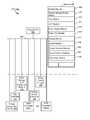
- FIG. 1is a block diagram illustrating an implementation of a data storage system 100 , in accordance with some embodiments. While some example features are illustrated, various other features have not been illustrated for the sake of brevity and so as not to obscure more pertinent aspects of the example embodiments disclosed herein.
- data storage system 100includes storage device 120 (also sometimes called a data storage device, or information storage device, or a memory device), which includes host interface 122 , supervisory module 126 , storage device controller 128 (also sometimes called a storage controller or a memory controller), one or more non-volatile memory (NVM) controllers 130 such as flash controllers, and non-volatile memory (e.g., one or more NVM device(s) 140 , 142 such as one or more flash memory devices), and is used in conjunction with computer system 110 .
- storage device 120includes a single NVM device while in other embodiments storage device 120 includes a plurality of NVM devices.
- NVM devices 140 , 142include NAND-type flash memory and/or NOR-type flash memory.
- NVM controller 130is a solid-state drive (SSD) controller.
- SSDsolid-state drive
- one or more other types of storage mediamay be included in accordance with aspects of a wide variety of embodiments.
- Computer system 110is coupled to storage device 120 through data connections 101 .
- computer system 110includes storage device 120 as a component and/or sub-system.
- Computer system 110may be any suitable computer device, such as a personal computer, a workstation, a computer server, or any other computing device.
- Computer system 110is sometimes called a host or host system.
- computer system 110includes one or more processors, one or more types of memory, and optionally includes a display and/or other user interface components such as a keyboard, a touch screen display, a mouse, a track-pad, a digital camera and/or any number of supplemental devices to add functionality.
- computer system 110sends one or more host commands (e.g., read commands and/or write commands) on control line 111 to storage device 120 .
- host interface 122provides an interface to computer system 110 through data connections 101 and/or control line 111 .
- computer system 110is a server system, such as a server system in a data center, and does not have a display and other user interface components.
- storage device 120includes NVM devices such as flash memory devices (e.g., NVM devices 140 - 1 through 140 - n and NVM devices 142 - 1 through 142 - k ) and NVM controllers 130 (e.g., NVM controllers 130 - 1 through 130 - m ).
- NVM controllers 130include one or more processing units (also sometimes called CPUs or processors or microprocessors or microcontrollers) configured to execute instructions in one or more programs (e.g., in NVM controllers 130 ).
- the one or more processorsare shared by one or more components within, and in some cases, beyond the function of NVM controllers 130 .
- NVM controllers 130are configured to receive (e.g., via reset module 710 , FIG. 7 ) reset 144 from various components of storage device 120 (e.g., from supervisory module 126 and/or from storage device controller 128 ). In some embodiments, reset 144 - 1 and reset 144 - m are the same signal.
- NVM devices 140 , 142are coupled to NVM controllers 130 through connections that typically convey commands in addition to data, and optionally convey metadata, error correction information and/or other information in addition to data values to be stored in NVM devices 140 , 142 and data values read from NVM devices 140 , 142 .
- NVM devices 140 , 142can be configured for enterprise storage suitable for applications such as cloud computing, or for caching data stored (or to be stored) in secondary storage, such as hard disk drives.
- flash memorye.g., NVM devices 140 , 142
- flash memory devices and flash controllersare used as an example here, in some embodiments storage device 120 includes other non-volatile memory device(s) and corresponding non-volatile memory controller(s).
- storage device 120includes supervisory module 126 and storage device controller 128 .
- Storage device 120may include various additional features that have not been illustrated for the sake of brevity and so as not to obscure more pertinent features of the example embodiments disclosed herein, and a different arrangement of features may be possible.
- supervisory module 126(also sometimes called a data hardening module) includes one or more processing units (also sometimes called CPUs or processors or microprocessors or microcontrollers) configured to execute instructions in one or more programs (e.g., in supervisory module 126 ).
- the one or more processorsare shared by one or more components within, and in some cases, beyond the function of supervisory module 126 .
- Supervisory module 126is coupled to host interface 122 , storage device controller 128 , and NVM controllers 130 in order to coordinate the operation of these components, including supervising and controlling functions such as power up, power down, data hardening, charging energy storage device(s), data logging, and other aspects of managing functions on storage device 120 .
- Storage device controller 128is coupled to host interface 122 , supervisory module 126 , and NVM controllers 130 . In some embodiments, during a write operation, storage device controller 128 receives data from computer system 110 through host interface 122 and during a read operation, storage device controller 128 sends data to computer system 110 through host interface 122 . Further, host interface 122 provides additional data, signals, voltages, and/or other information needed for communication between storage device controller 128 and computer system 110 . In some embodiments, storage device controller 128 and host interface 122 use a defined interface standard for communication, such as double data rate type three synchronous dynamic random access memory (DDR3).
- DDR3double data rate type three synchronous dynamic random access memory
- storage device controller 128 and NVM controllers 130use a defined interface standard for communication, such as serial advance technology attachment (SATA).
- the device interface used by storage device controller 128 to communicate with NVM controllers 130is SAS (serial attached SCSI), or other storage interface.
- storage device controller 128is configured to receive reset 143 from various components of storage device 120 (e.g., from supervisory module 126 and/or from host interface 122 ).
- reset 143 , reset 144 - 1 , and reset 144 - mare the same signal.
- reset 143 , reset 144 - 1 , and reset 144 - mare independent signals.
- reset 143 , reset 144 - 1 , and reset 144 - mare transmitted via the same communication bus. In some embodiments, reset 143 , reset 144 - 1 , and reset 144 - m are controlled separately.
- storage device controller 128includes one or more processing units (also sometimes called CPUs or processors or microprocessors or microcontrollers) configured to execute instructions in one or more programs (e.g., in storage device controller 128 ). In some embodiments, the one or more processors are shared by one or more components within, and in some cases, beyond the function of storage device controller 128 .
- FIG. 2is a block diagram illustrating an implementation of supervisory module 126 (of storage device 120 , as shown in FIG. 1 ), in accordance with some embodiments.
- Supervisory module 126is coupled to host interface 122 via communication bus 210 , voltage input 212 (e.g., V in 302 , FIG. 3A ) and voltage input 214 (e.g., V SPD 324 , FIG. 3A ).
- voltage input 212is a part of a communication bus.
- voltage input 212is the same as voltage input 214 , while in other embodiments voltage input 212 is different from voltage input 214 .
- communication bus 210includes a voltage source (e.g., V SPD 324 , FIG. 3A ) supplied through host interface 122 .
- Communication busesoptionally include circuitry (sometimes called a chipset) that interconnects and controls communications between system components.
- Supervisory module 126is coupled to host interface 122 , storage device controller 128 , and NVM controllers 130 (e.g., NVM controllers 130 - 1 through 130 - m ) via communication buses (e.g., communication bus 148 , FIG. 1 ).
- Supervisory module 126includes power control processor (PCP) 202 (including serial presence detect (SPD) 203 ) for executing modules, programs and/or instructions stored therein.
- PCP 202is coupled to NVM controllers 130 (e.g., NVM controllers 130 - 1 through 130 - m ) via PFAIL lines 226 .
- PFAIL lines 226are part of a communication bus.
- PFAIL lines 226are tri-state lines that are driven by PCP 202 , NVM controllers 130 , or neither, depending on the operations of supervisory module 126 .
- PCP 202is coupled to storage device controller 128 via communication bus 224 .
- communication bus 224includes a power test command and/or signal to notify storage device controller 128 of pending power fail operations affecting one or more NVM controllers 130 .
- Supervisory module 126also includes power storage and distribution module 204 (including energy storage device 205 ), power failure (PFAIL) control module 208 , voltage comparator circuitry 206 , and a plurality of communication buses (e.g., communication buses 210 , 216 , 222 , and 224 ).
- power storage and distribution module 204includes circuitry for monitoring, storing, and distributing power for a storage device (e.g., storage device 120 , FIG. 1 ), including monitoring, controlling, charging, and/or testing energy storage device 205 .
- energy storage device 205includes one or more capacitors.
- energy storage device 205includes one or more inductors or any other passive elements that store energy.
- energy storage device 205is charged by boosting voltage input 212 .
- Voltage comparator circuitry 206is coupled to PCP 202 and PFAIL control module 208 .
- voltage comparator circuitry 206includes circuitry for monitoring voltage input 214 , detecting undervoltage and overvoltage conditions, and signaling power failure conditions to various components (e.g., PFAIL control module 208 ) of supervisory module 126 . While voltage comparator circuitry 206 is shown in FIG. 2 as being external to PCP 202 , in some embodiments voltage comparator circuitry 206 , or portions of voltage comparator circuitry 206 , are embedded in PCP 202 .
- PCP 202includes analog to digital conversion (ADC) circuitry, for converting voltage input 214 to a digital value, and comparison circuitry or software for detecting undervoltage and overvoltage conditions.
- ADCanalog to digital conversion
- PFAIL control module 208is coupled to PCP 202 , voltage comparator circuitry 206 , storage device controller 128 , and NVM controllers 130 (e.g., NVM controllers 130 - 1 through 130 - m ).
- PFAIL control module 208includes circuitry to detect power fail conditions, signal power failures to storage device controller 128 via PFAIL line 228 , and signal power failures to NVM controllers (e.g., NVM controllers 130 - 1 through 130 - m ) via PFAIL lines 230 .
- PFAIL lines 230are part of a communication bus between PFAIL control module 208 and NVM controllers 130 .
- SPD device 203is coupled to host interface 122 .
- SPD 203is a part of (e.g., integrated into) PCP 202 , while in some other embodiments, SPD 203 is separate and distinct from PCP 202 .
- Serial presence detectrefers to a standardized way to automatically access information about a computer memory module (e.g., storage device 120 ). For example, information about the type of the device (e.g., where the device type is one of a predefined set of device types), and the storage capacity of the device can be communicated with a host system (e.g., computer system 110 ) through SPD device 203 . In another example, if the memory module has a failure, the failure can be communicated with a host system (e.g., computer system 110 ) through SPD device 203 .
- SPDSerial presence detect
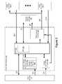
- FIG. 3Ais a block diagram illustrating an implementation of power storage and distribution module 204 and supervisory module 126 , in accordance with some embodiments. While some example features are illustrated, various other features have not been illustrated for the sake of brevity and so as not to obscure more pertinent aspects of the example embodiments disclosed herein. To that end, as a non-limiting example, power storage and distribution module 204 includes load switch 304 , boost regulator 308 , selector 310 , energy storage device 205 , regulator module 314 , and voltages V in 302 , V LS 306 , V storage 311 , and V Boost 312 .
- Regulator module 314comprises one or more regulators (also sometimes called power control systems or power regulators) used to power various components of storage device 120 (e.g., storage device controller 128 , NVM controllers 130 , NVMs 140 , and/or NVM 142 ) via one or more connections 316 .
- regulator module 314supplies power to a plurality of controllers coupled to power storage and distribution module 204 and to non-volatile memory associated with each controller.
- regulator module 314comprises a plurality of buck regulators and a plurality of low dropout (LDO) regulators.
- LDOlow dropout
- V Boost 312is provided to regulator module 314 , which converts V Boost 312 to the voltages required by various components of storage device 120 (e.g., 0.9 volts, 1.35 volts, 1.5 volts, 1.8 volts, and/or 2.5 volts) and provide those voltages to the appropriate components.
- regulator module 314is a component of power storage and distribution module 204 .
- regulator module 314is a component of supervisory module 126 .
- regulator module 314or portions thereof, are external to supervisory module 126 .
- V in 302is a voltage supplied by a host system (e.g., computer system 110 , FIG. 1 ) and has a target value of 5 volts or less.
- V Boost 312is a boosted voltage, boosted from V in 302 , and has a target value of 5.5 volts.
- V Boost 312is used to charge energy storage device 205 .
- V SPD 324is a voltage supplied for serial presence detect (SPD) functionality and has a target value of 3.3 volts.
- selector 310comprises a switch (e.g., a transistor). In some embodiments, selector 310 is configured to couple energy storage device 205 to the output of boost regulator 308 during normal operation so as to charge energy storage device 205 .
- selector 310is further configured to couple energy storage device 205 to the input of boost regulator 308 in response to receiving a power fail signal from PCP 202 (e.g., Pfail signal 325 ).
- a power fail signalfrom PCP 202 (e.g., Pfail signal 325 ).
- the lowest useful output voltage from energy storage device 205 during a power fail operationmight be a first voltage, such as 3 volts, but with energy storage device 205 coupled to the input of boost regulator 308 during at least a portion of the power fail operation, the lowest useful output voltage from energy storage device 205 during the power fail operation might be a second voltage, such as 2 volts or even 1 volt, which is lower than the first voltage.
- a smaller size energy storage device 205can be used to support a given power fail operation than would have been the case if the energy storage device 205 were coupled to the output of boost regulator 308 during performance of the power fail operation.
- selector 310is configured to decouple energy storage device 205 from both the input and output of boost regulator 308 .
- removing power from a component of storage device 120includes decoupling energy storage device 205 from both the input and output of boost regulator 308 .
- energy storage device 205comprises a power holdup circuit, implemented using one or more capacitors.
- energy storage device 205stores, immediately prior to a power fail condition being detected, at least approximately 30 to 70 millijoules of energy per NVM controller 130 in storage device 120 .
- PCP 202monitors and manages the functionality in power storage and distribution module 204 .
- PCP 202monitors voltages V in 302 and V SPD 324 .
- PFAIL control circuitrye.g., PFAIL control module 208 , FIG. 2
- PCP 202signals the power fail condition to a plurality of controllers on storage device 120 (e.g., storage device controller 128 and NVM controllers 130 , FIG. 1 ).
- the under-voltage thresholdvaries depending on the target value of the voltage.
- the under-voltage thresholdmay be 1.5 volts minus 5% (i.e., 1.425 volts), so PCP 202 would signal a power fail condition if V in 302 is lower than 1.425 volts.
- the under-voltage threshold for V in 302is different than the under-voltage threshold for V SPD 324 .
- V in 302is used to supply power to storage device 120 .
- energy storage device 205is used to provide power to storage device 120 .
- PCP 202controls load switch 304 and selector 310 such that V storage is used to power storage device 120 during a power fail or soft power fail operation.
- V in 302is used to supply power to storage device 120 , so load switch 304 is turned on (e.g., to complete the connection between V in 302 and V LS 306 ).
- energy storage device 205is used to provide power to storage device 120 , so load switch 304 is turned off (e.g., to disable the connection between V in 302 and V LS 306 ) and selector 310 is configured to couple energy storage device 205 to the input of boost regulator 308 (e.g., to enable the connection between V storage 311 and V LS 306 ).
- Any energy storage deviceincluding one or more capacitors, one or more inductors, or one or more other passive elements that store energy, may be used to store energy to be used during a power fail operation or a soft power fail operation.
- energy storage device 205is charged using V Boost 312 , a voltage higher than V LS 306 .
- boost regulator 308is controlled and enabled by PCP 202 .
- V Boost 312is used as an input to keeper circuitry 320 , which along with V SPD 324 provides power to PCP 202 .
- V Boost 312is provided via keeper circuitry 320 to PCP 202 so as to provide power to PCP 202 .
- PCP 202has one or more connections 326 used to monitor and control other functions within storage device 120 .
- V SPD 324provides power to keeper circuitry 320 .
- V SPD 324is provided to storage device 120 before V in 302 is provided to storage device 120 , allowing devices in storage device 120 to operate before main power V in 302 is provided to storage device 120 .
- keeper circuitry 320provides V ps 322 to PCP 202 .
- supervisory module 126uses an algorithm to selectively test one or more capacitors from energy storage device 205 during operation of the storage device.
- one or more capacitors from energy storage device 205are tested during regular operation of the storage device (as opposed to during a power fail operation). Since testing the capacitor(s) will discharge the capacitor(s), supervisory module 126 manages the coordination of testing the capacitor(s) to ensure that testing of the capacitor(s) from energy storage device 205 does not interfere with other operations.
- an energy storage device modulee.g., energy storage device module 510 , FIG. 5 ) is used to selectively test one or more capacitors from the energy storage device during operation of the storage device, as described below with respect to FIG. 5 .
- testing energy storage device 205includes charging the energy storage device using a higher voltage than the power supply voltage provided to the storage device and determining whether energy storage device 205 meets a predefined minimum charge level threshold (sometimes called the minimum charge level threshold) within a predefined charge time. For example, if the predefined minimum charge level threshold is 95% charge capacity and the predefined charge time is 25 ms, the storage device determines whether the energy storage device is charged to at least 95% charge capacity within 25 ms.
- an energy storage device modulee.g., energy storage device module 510 , FIG. 5 ) is used to determine whether energy storage device 205 meets a predefined minimum charge level threshold within a predefined charge time, as described below with respect to FIG. 5 .
- the storage deviceprevents operation of the storage device.
- a determination that energy storage device 205 does not meet the predefined minimum charge level threshold in the predefined charge timeindicates that there will be a data hardening failure when a power fail operation is performed in the future (e.g., a predictive failure detection).
- preventing operation of the storage deviceincludes communicating a failure message to a host system (e.g., computer system 110 , FIG. 1 ).
- the failure messageis communicated with the host system through a SPD device (e.g., SPD device 203 , FIG. 2 ) or a SPD bus controller.
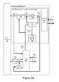
- FIG. 3Bis another block diagram illustrating an implementation of power storage and distribution module 204 and supervisory module 126 , in accordance with some embodiments. While some example features are illustrated, various other features have not been illustrated for the sake of brevity and so as not to obscure more pertinent aspects of the example embodiments disclosed herein. To that end, as a non-limiting example, FIG. 3B shows power storage and distribution module 204 further including comparator 330 . Comparator 330 is configured to determine whether an output of energy storage device 205 (e.g., V storage 311 ) falls below a predetermined voltage threshold and, in accordance with a determination that the output of energy storage device 205 has fallen below the predetermined threshold, signal selector 310 (e.g., via switch signal 332 ). In some embodiments, the predetermined voltage threshold is determined based on a minimum operating voltage of regulator module 314 . In some embodiments, the predetermined voltage threshold is based on an optimal operating voltage of regulator 314 .
- V storage 311e.g., V storage
- energy storage device 205is coupled, via selector 310 , to the output of boost regulator 308 (e.g., such that V storage is connected to V Boost ).
- boost regulator 308e.g., such that V storage is connected to V Boost .
- PCP 202in response to detecting a power fail condition, will signal (e.g., via pfail signal 325 ) load switch 304 to decouple V in 302 from V LS 306 .
- energy storage device 205is coupled to the output of boost regulator 308 and provides power to regulator module 314 until comparator 330 determines that V storage 311 has dropped below the predetermined threshold; at which time, comparator 330 signals (e.g., via switch signal 332 ) to selector 310 to selectively couple energy storage device 205 to the input of boost regulator 308 .
- comparator 330signals (e.g., via switch signal 332 ) to selector 310 to selectively couple energy storage device 205 to the input of boost regulator 308 .
- V storage 311is boosted by boost regulator 308 and continues to supply power to regulator module 314 until the power fail operations are complete or V Boost 312 falls below a predetermined minimum operating threshold.
- regulators in regulator module 314are operated more efficiently than if the selector 310 were to couple energy storage device 205 to the input of boost regulator 308 immediately upon detection of the power fail condition.
- FIG. 4is a voltage diagram corresponding to a power fail event, in accordance with some embodiments.
- a drop in the voltage supplied by V in 401occurs (e.g., a power fail event).
- V in 401is V in 302 .
- a drop in V LS 403e.g., V LS 306 ) occurs corresponding to the drop in V in 401 .
- the power failureis detected (e.g., by PCP 202 ) and, at time 404 , the energy storage device (e.g., energy storage device 205 ) is coupled to the input of the boost regulator (e.g., boost regulator 308 ).
- the boost regulatore.g., boost regulator 308
- the PCPdetects the power failure and signals the load switch (e.g., load switch 304 ) via a pfail signal (e.g., pfail signal 325 ) to decouple V LS 403 from V in 401 .
- the PCPalso signals the selector (e.g., selector 310 ) via a pfail signal (e.g., pfail signal 325 ) to couple the energy storage device to the input of the boost regulator (e.g., such that V storage 405 is connected to V LS 403 ).
- the boost regulatore.g., such that V storage 405 is connected to V LS 403 .
- V Boost 407begins to drop.
- V Boost 407drops below a minimum voltage threshold required by a regulator module (e.g., regulator module 314 ) to supply useable power to a corresponding portion of the storage device (e.g., storage device 120 ).
- a regulator modulee.g., regulator module 314
- FIG. 5is a block diagram illustrating an implementation of PCP 202 , in accordance with some embodiments.
- PCP 202includes one or more processors (also sometimes called CPUs or processing units or microprocessors or microcontrollers) 502 for executing modules, programs and/or instructions stored in memory 506 and thereby performing processing operations, memory 506 , and one or more communication buses 504 for interconnecting these components.
- Communication buses 504optionally include circuitry (sometimes called a chipset) that interconnects and controls communications between system components.
- PCP 202is coupled to host interface 122 , storage device controller 128 , NVM controllers 130 (e.g., NVM controllers 130 - 1 through 130 - m ), power storage and distribution module 204 , voltage comparator circuitry 206 , and PFAIL control module 208 by communication buses 508 .
- Memory 506includes high-speed random access memory, such as DRAM, SRAM, DDR RAM or other random access solid state memory devices, and may include non-volatile memory, such as one or more magnetic disk storage devices, optical disk storage devices, flash memory devices, or other non-volatile solid state storage devices. Memory 506 optionally includes one or more storage devices remotely located from processor(s) 502 .
- Memory 506or alternately the non-volatile memory device(s) within memory 506 , comprises a non-transitory computer readable storage medium.
- memory 506or the computer readable storage medium of memory 506 stores the following programs, modules, and data structures, or a subset thereof:
- memory 506or the computer readable storage medium of memory 506 further stores a configuration module for configuring storage device 120 and supervisory module 126 , and/or configuration values (such as one or more under-voltage threshold values) for configuring supervisory module 126 , neither of which is explicitly shown in FIG. 5 .
- the configuration moduleupon power up and upon reset, automatically sets the values of one or more configuration parameters of storage device 120 (and, optionally, determines which of two or more power fail modules, test modules, etc. to use) in accordance with the components of storage device 120 (e.g., the type of non-volatile memory components in storage device 120 ) and/or characteristics of the data storage system 100 that includes storage device 120 .
- power fail module 520includes the following modules or sub-modules, or a subset thereof:
- Each of the above identified elementsmay be stored in one or more of the previously mentioned memory devices, and corresponds to a set of instructions for performing a function described above.
- the above identified modules or programsi.e., sets of instructions
- memory 506may store a subset of the modules and data structures identified above.
- memory 506may store additional modules and data structures not described above.
- the programs, modules, and data structures stored in memory 506 , or the computer readable storage medium of memory 506provide instructions for implementing respective operations in the methods described below with reference to FIGS. 8A-8B .
- FIG. 5shows PCP 202
- FIG. 5is intended more as a functional description of the various features which may be present in a PCP than as a structural schematic of the embodiments described herein. In practice, and as recognized by those of ordinary skill in the art, items shown separately could be combined and some items could be separated.
- FIG. 6is a block diagram illustrating an implementation of storage device controller 128 , in accordance with some embodiments.
- Storage device controller 128typically includes: one or more processors (also sometimes called CPUs or processing units or microprocessors or microcontrollers) 602 for executing modules, programs and/or instructions stored in memory 606 and thereby performing processing operations; memory 606 ; and one or more communication buses 604 for interconnecting these components.
- processorsalso sometimes called CPUs or processing units or microprocessors or microcontrollers
- communication buses 604for interconnecting these components.
- One or more communication buses 604optionally, include circuitry (sometimes called a chipset) that interconnects and controls communications between system components.
- Storage device controller 128is operatively coupled to host interface 122 , supervisory module 126 , and NVM controllers 130 (e.g., NVM controllers 130 - 1 through 130 - m ) by communication buses 604 .
- Memory 606includes high-speed random access memory, such as DRAM, SRAM, DDR RAM or other random access solid state memory devices, and may include non-volatile memory, such as one or more magnetic disk storage devices, optical disk storage devices, flash memory devices, or other non-volatile solid state storage devices.
- the information stored in memory 606includes volatile data 618 corresponding to portions of non-volatile memory within data storage system 100 (e.g., NVMs 140 and/or NVMs 142 , FIG. 1 ).
- the information stored in memory 606comprises metadata 620 (e.g., metadata comprising age category, known-bad portion, etc.) corresponding to portions of the non-volatile memory.
- Memory 606optionally, includes one or more storage devices remotely located from the one or more CPUs 602 .
- Memory 606or alternatively the non-volatile memory device(s) within memory 606 , comprises a non-transitory computer readable storage medium.
- memory 606or the non-transitory computer readable storage medium of memory 606 , stores the following programs, modules, and data structures, or a subset or superset thereof:
- power fail module 628optionally includes a transfer sub-module that is used for transferring data held in volatile memory to non-volatile memory during a power fail operation.
- transfer module 624is used to transfer data held in volatile memory to non-volatile memory during a power fail operation.
- Each of the above identified elementsmay be stored in one or more of the previously mentioned memory devices, and corresponds to a set of instructions for performing a function described above.
- the above identified modules or programsi.e., sets of instructions
- memory 606may store a subset of the modules and data structures identified above.
- memory 606may store additional modules and data structures not described above.
- the programs, modules, and data structures stored in memory 606 , or the computer readable storage medium of memory 606provide instructions for implementing respective operations in the methods described below with reference to FIGS. 8A-8B .
- FIG. 6shows a storage device controller 128
- FIG. 6is intended more as a functional description of the various features which may be present in a memory controller than as a structural schematic of the embodiments described herein. In practice, and as recognized by those of ordinary skill in the art, items shown separately could be combined and some items could be separated.
- FIG. 7is a block diagram illustrating an implementation of NVM controller 130 - 1 , such as a flash controller, in accordance with some embodiments.
- NVM controller 130 - 1typically includes one or more processors (also sometimes called CPUs or processing units or microprocessors or microcontrollers) 702 for executing modules, programs and/or instructions stored in memory 706 and thereby performing processing operations, memory 706 , and one or more communication buses 704 for interconnecting these components.
- Communication buses 704optionally include circuitry (sometimes called a chipset) that interconnects and controls communications between system components.
- NVM controller 130 - 1is coupled to storage device controller 128 , supervisory module 126 , and NVM devices 140 (e.g., NVM devices 140 - 1 through 140 - n , such as flash memory devices) by communication buses 704 .
- Memory 706includes high-speed random access memory, such as DRAM, SRAM, DDR RAM or other random access solid state memory devices, and may include non-volatile memory, such as one or more magnetic disk storage devices, optical disk storage devices, flash memory devices, or other non-volatile solid state storage devices.
- memory 706includes volatile data 716 corresponding to portions of non-volatile memory within data storage system 100 (e.g., NVMs 140 and/or NVMs 142 , FIG. 1 ).
- Memory 706optionally includes one or more storage devices remotely located from processor(s) 702 .
- Memory 706or alternately the non-volatile memory device(s) within memory 706 , comprises a non-transitory computer readable storage medium.
- memory 706or the computer readable storage medium of memory 706 stores the following programs, modules, and data structures, or a subset thereof:
- power fail module 712optionally includes transfer submodule 714 that is used for transferring data held in volatile memory to non-volatile memory during a power fail operation.
- Each of the above identified elementsmay be stored in one or more of the previously mentioned memory devices, and corresponds to a set of instructions for performing a function described above.
- the above identified modules or programsi.e., sets of instructions
- memory 706may store a subset of the modules and data structures identified above.
- memory 706may store additional modules and data structures not described above.
- the programs, modules, and data structures stored in memory 706 , or the computer readable storage medium of memory 706provide instructions for implementing respective operations in the methods described below with reference to FIGS. 8A-8B .
- FIG. 7shows a NVM controller 130 - 1
- FIG. 7is intended more as a functional description of the various features which may be present in a NVM controller than as a structural schematic of the embodiments described herein. In practice, and as recognized by those of ordinary skill in the art, items shown separately could be combined and some items could be separated. Further, although FIG. 7 shows a NVM controller 130 - 1 , the description of FIG. 7 similarly applies to other NVM controllers (e.g., NVM controllers 130 - 2 through 130 - m ) in storage device 120 ( FIG. 1 ).
- NVM controllers 130 - 2 through 130 - min storage device 120 ( FIG. 1 ).
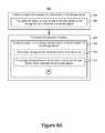
- FIGS. 8A-8Billustrate a flowchart representation of method 800 of power management in a storage device, in accordance with some embodiments.
- the storage devicecomprises a solid-state drive implemented as a dual in-line memory module (DIMM) device.
- DIMMdual in-line memory module
- the storage deviceis compatible with a DIMM memory slot.
- the storage deviceis compatible with a 240-pin DIMM memory slot using a DDR3 interface specification.
- the storage device(e.g., storage device 120 , FIG. 1 ) coordinates and manages multiple sub-system components to manage power and harden data, which initiates performance of method 800 .
- method 800is performed by a storage device (e.g., storage device 120 , FIG. 1 ) or one or more components of the storage device (e.g., supervisory module 126 , storage device controller 128 , and/or NVM controllers 130 , FIG. 1 ).
- method 800is governed by instructions that are stored in a non-transitory computer readable storage medium and that are executed by one or more processors of a device, such as the one or more processors 502 of PCP 202 , the one or more processors 602 of storage device controller 128 , and/or the one or more processors 702 of NVM controllers 130 , as shown in FIGS. 5-7 .
- the storage deviceperforms ( 802 ) a power fail operation on a first section of the storage device.
- the power fail operationis initiated by a host server (also sometimes called an end system) (e.g., computer system 110 , FIG. 1 ).
- the power fail operationis initiated by a supervisory module (e.g., supervisory module 126 , FIG. 1 ) or a component thereof (e.g., PCP 202 , FIG. 2 ).
- the first section of the storage devicecomprises the entire storage device.
- the first section of the storage deviceis the section of the storage device governed by a supervisory module (e.g., supervisory module 126 , FIG. 1 ).
- the first section of the storage deviceis the section of the storage device governed by a particular storage device controller (e.g., storage device controller 128 , FIG. 1 ).
- the power fail operationis performed in response to a first voltage dropping below a predetermined voltage threshold and the first section of the storage device is the section of the storage device that utilizes the first voltage or a voltage derived therefrom.
- the power fail operationis a simulated power fail operation (also sometimes called a soft power fail operation).
- the power fail operationis performed ( 804 ) on the first section of the storage device in response to a second signal.
- the second signalcorresponds to an input voltage (e.g., V in 302 , FIG. 3A ) dropping below a predetermined minimum voltage.
- the second signalis a power fail signal generated by a controller on the storage device.
- the second signalis a power fail signal generated by a PCP (e.g., pfail signal 325 generated by PCP 202 in FIG. 3A ).
- the second signalis a power fail signal received by the storage device from a device or source external to the storage device. For example, a power fail signal received from computer system 110 in FIG. 1 (e.g., via control line 111 ).
- the power fail operation ( 806 )includes supplying power ( 808 ), via an energy storage device, to the first section of the storage device.
- energy storage device 205 in FIG. 3Asupplies power to storage device controller 128 , NVM controllers 130 , and NVMs 140 - 142 via connections 316 .
- the energy storage devicecomprises one or more capacitors. In some embodiments, the energy storage device includes one or more inductors and/or one or more other passive elements that store energy.
- the energy storage deviceis distinct ( 812 ) from a power source used during normal operation of the storage device.
- V in 302 in FIG. 3Ais a power source used during normal operation of storage device 120 .
- energy storage device 205 in FIG. 3Ais used during a power fail operation and is distinct from V in 302 .
- normal operationalso sometimes called “standard” operation, is a mode of operation of the storage device in which the storage system is being used for its intended purposes (e.g., to read and write data) by a host system (e.g., computer system 110 , FIG. 1 ).
- a host systeme.g., computer system 110 , FIG. 1
- the storage deviceis receiving and responding to commands sent from a host system.
- Normal operationis distinguished from a power fail operation where the storage device is hardening data and/or resetting controllers rather than receiving and responding to commands sent from a host system.
- Normal operationis also distinguished from manufacturing of the storage device, which is completed prior to the storage device being coupled to a host system, and testing of the storage device (sometimes called a testing mode of operation), which is either done: (1) while coupled to a testing system; (2) prior to being coupled to a host system; and/or (3) is done in a manner that prevents the storage device from being used for its intended purposes during the testing process.
- failure detectionoptionally occurs in a storage device during manufacturing, testing, and/or normal operation.
- failure detection during the manufacturing processcomprises detecting that the storage device (and/or individual components therein) do not meet manufacturing parameters (e.g., one or more characteristics of the device are outside of predetermined acceptable boundaries).
- failure detection during a testing processcomprises testing the operability of a plurality of distinct portions on the storage device (e.g., systematically testing each portion of the storage device in a controlled manner).
- the testing processincludes more controlled parameters (e.g., controlled parameters specified by the testing protocol) than normal operation.
- write commandsoptionally involve known predetermined data to be written to each portion, whereas during normal operation, the data is variable and is based in part on the operation of the host system.
- manufacturing and testingare a combined process where testing is performed at various stages of the manufacturing.
- Supplying power via the energy storage deviceincludes switching ( 814 ) the output of the energy storage device from an output of a boost regulator to an input of the boost regulator.
- selector 310 in FIG. 3Aswitches the output of energy storage device 205 from the output of boost regulator 308 to the input of boost regulator 308 during a power fail operation.
- the energy storage deviceis switched as soon as the power fail event is detected. In some embodiments, however, the energy storage device is switched (from the output of boost regulator 308 to the input of boost regulator 308 ) when, or in accordance with a determination that, the voltage supplied by the energy storage device (e.g., V storage 311 , FIG. 3B ) falls below a predetermined threshold.
- switching the output of the energy storage device from the output of the boost regulator to the input of the boost regulatorcomprises switching ( 816 ) the output of the energy storage device in response to receiving a first signal.
- selector 310 in FIG. 3Aswitches the output of energy storage device 205 from the output of boost regulator 308 to the input of boost regulator 308 in response to a pfail signal (e.g., pfail signal 325 ).
- selector 310 in FIG. 3Bswitches the output of energy storage device 205 from the output of boost regulator 308 to the input of boost regulator 308 in response to a switchover signal (e.g., switchover signal 332 ).
- the first signalis a power fail signal ( 818 ) generated by a first controller on the storage device.
- the first controllercorresponds to the first section of the storage device.
- the first controlleris a storage device controller (e.g., storage device controller 128 , FIG. 1 ).
- the first controlleris a component of a supervisory module (e.g., PCP 202 , FIG. 2 ).
- the power fail signalis received from a device or source external to the storage device. For example, a power fail signal received from computer system 110 in FIG. 1 (e.g., via control line 111 ).
- the first signalis a switchover signal ( 820 ), the switchover signal generated in response to a voltage output of the energy storage device falling below a predetermined threshold.
- selector 310 in FIG. 3Bswitches the output of energy storage device 205 from the output of boost regulator 308 to the input of boost regulator 308 in response to switch signal 332 .
- the switchover signalis generated by a comparator (e.g., comparator 330 , FIG. 3B ) coupled to the output of the energy storage device.
- the predetermined thresholdcorresponds to ( 822 ) a minimum input voltage required by a first regulator to supply useable power to the first portion of the memory.
- the first regulatoris coupled to the output of the boost regulator and is used to supply power to a first portion of the storage device.
- a plurality of regulatorsare coupled to the output of the boost regulator and are used to supply power to a first portion of the storage device and the plurality of regulators include the first regulator.
- the first regulatoris a component of a regulator module coupled to the output of the boost regulator (e.g., regulator module 314 , FIG. 3A ).
- the first regulatoris a buck regulator used to supply a first voltage (e.g., 2.85 volts) from an input voltage (e.g., V Boost 312 , FIG. 3A ).
- the buck regulatoris unable to supply the first voltage once the input voltage drops below a minimum input voltage requirement of 3 volts.
- the predetermined thresholdcorresponds to a minimum input voltage required by one or more voltage regulators to operate correctly, where the one or more voltage regulators are coupled to the output of the energy storage device and correspond to the first section of the storage device.
- the power fail operation ( 806 )further includes performing ( 824 ) data hardening on the first section of the storage device.
- data hardeningis the process of saving data to non-volatile memory.
- the dataoptionally includes mission critical data and/or metadata.
- the storage devicee.g., storage device 120 , FIG. 1
- data hardeningcomprises transferring data from the volatile memory to the non-volatile memory.
- the storage deviceincludes volatile memory corresponding to a first controller (e.g., NVM controller 130 - 1 , FIG.
- the first controllerperforms data hardening by transferring data from the corresponding volatile memory to non-volatile memory (e.g., NVMs 140 ).
- non-volatile memorye.g., NVMs 140
- the first section of the memory devicecorresponds to a plurality of controllers, each controller of the plurality of controllers having associated volatile memory.
- performing data hardening on the first section of the storage devicecomprises transferring data from the associated volatile memory to non-volatile memory.
- the storage devicein addition to using the energy storage device to provide power during power fail operations, utilizes ( 826 ) the energy storage device to buffer power spikes received from the power source used during normal operation of the storage device.
- the storage devicecomprises one or more three-dimensional (3D) memory devices and circuitry associated with operation of memory elements in the one or more 3D memory devices.
- the circuitry and one or more memory elements in a respective 3D memory device, of the one or more 3D memory devicesare on the same substrate.
- Semiconductor memory devicesinclude volatile memory devices, such as dynamic random access memory (“DRAM”) or static random access memory (“SRAM”) devices, non-volatile memory devices, such as resistive random access memory (“ReRAM”), electrically erasable programmable read only memory (“EEPROM”), flash memory (which can also be considered a subset of EEPROM), ferroelectric random access memory (“FRAM”), and magnetoresistive random access memory (“MRAM”), and other semiconductor elements capable of storing information.
- volatile memory devicessuch as dynamic random access memory (“DRAM”) or static random access memory (“SRAM”) devices
- non-volatile memory devicessuch as resistive random access memory (“ReRAM”), electrically erasable programmable read only memory (“EEPROM”), flash memory (which can also be considered a subset of EEPROM), ferroelectric random access memory (“FRAM”), and magnetoresistive random access memory (“MRAM”), and other semiconductor elements capable of storing information.
- ReRAMresistive random access memory
- EEPROMelectrically erasable
- the memory devicescan be formed from passive and/or active elements, in any combinations.
- passive semiconductor memory elementsinclude ReRAM device elements, which in some embodiments include a resistivity switching storage element, such as an anti-fuse, phase change material, etc., and optionally a steering element, such as a diode, etc.
- active semiconductor memory elementsinclude EEPROM and flash memory device elements, which in some embodiments include elements containing a charge storage region, such as a floating gate, conductive nanoparticles, or a charge storage dielectric material.
- Multiple memory elementsmay be configured so that they are connected in series or so that each element is individually accessible.
- flash memory devices in a NAND configurationtypically contain memory elements connected in series.
- a NAND memory arraymay be configured so that the array is composed of multiple strings of memory in which a string is composed of multiple memory elements sharing a single bit line and accessed as a group.
- memory elementsmay be configured so that each element is individually accessible (e.g., a NOR memory array).
- NAND and NOR memory configurationsare exemplary, and memory elements may be otherwise configured.
- the semiconductor memory elements located within and/or over a substratemay be arranged in two or three dimensions, such as a two dimensional memory structure or a three dimensional memory structure.
- the semiconductor memory elementsare arranged in a single plane or a single memory device level.
- memory elementsare arranged in a plane (e.g., in an x-z direction plane) which extends substantially parallel to a major surface of a substrate that supports the memory elements.
- the substratemay be a wafer over or in which the layer of the memory elements are formed or it may be a carrier substrate which is attached to the memory elements after they are formed.
- the substratemay include a semiconductor such as silicon.
- the memory elementsmay be arranged in the single memory device level in an ordered array, such as in a plurality of rows and/or columns. However, the memory elements may be arrayed in non-regular or non-orthogonal configurations.
- the memory elementsmay each have two or more electrodes or contact lines, such as bit lines and word lines.
- a three dimensional memory arrayis arranged so that memory elements occupy multiple planes or multiple memory device levels, thereby forming a structure in three dimensions (i.e., in the x, y and z directions, where the y direction is substantially perpendicular and the x and z directions are substantially parallel to the major surface of the substrate).
- a three dimensional memory structuremay be vertically arranged as a stack of multiple two dimensional memory device levels.
- a three dimensional memory arraymay be arranged as multiple vertical columns (e.g., columns extending substantially perpendicular to the major surface of the substrate, i.e., in the y direction) with each column having multiple memory elements in each column.
- the columnsmay be arranged in a two dimensional configuration (e.g., in an x-z plane), resulting in a three dimensional arrangement of memory elements with elements on multiple vertically stacked memory planes.
- Other configurations of memory elements in three dimensionscan also constitute a three dimensional memory array.
- the memory elementsmay be coupled together to form a NAND string within a single horizontal (e.g., x-z) memory device level.
- the memory elementsmay be coupled together to form a vertical NAND string that traverses across multiple horizontal memory device levels.
- Other three dimensional configurationscan be envisioned wherein some NAND strings contain memory elements in a single memory level while other strings contain memory elements which span through multiple memory levels.
- Three dimensional memory arraysmay also be designed in a NOR configuration and in a ReRAM configuration.
- a monolithic three dimensional memory arraytypically, one or more memory device levels are formed above a single substrate.
- the monolithic three dimensional memory arraymay also have one or more memory layers at least partially within the single substrate.
- the substratemay include a semiconductor such as silicon.
- the layers constituting each memory device level of the arrayare typically formed on the layers of the underlying memory device levels of the array.
- layers of adjacent memory device levels of a monolithic three dimensional memory arraymay be shared or have intervening layers between memory device levels.
- non-monolithic stacked memoriescan be constructed by forming memory levels on separate substrates and then stacking the memory levels atop each other. The substrates may be thinned or removed from the memory device levels before stacking, but as the memory device levels are initially formed over separate substrates, the resulting memory arrays are not monolithic three dimensional memory arrays. Further, multiple two dimensional memory arrays or three dimensional memory arrays (monolithic or non-monolithic) may be formed on separate chips and then packaged together to form a stacked-chip memory device.
- Associated circuitryis typically required for operation of the memory elements and for communication with the memory elements.
- memory devicesmay have circuitry used for controlling and driving memory elements to accomplish functions such as programming and reading.
- This associated circuitrymay be on the same substrate as the memory elements and/or on a separate substrate.
- a controller for memory read-write operationsmay be located on a separate controller chip and/or on the same substrate as the memory elements.
- three-dimensional memory device(or 3D memory device) is herein defined to mean a memory device having multiple memory layers or multiple levels (e.g., sometimes called multiple memory device levels) of memory elements, including any of the following: a memory device having a monolithic or non-monolithic 3D memory array, some non-limiting examples of which are described above; or two or more 2D and/or 3D memory devices, packaged together to form a stacked-chip memory device, some non-limiting examples of which are described above.
- firstfirst
- secondsecond
- first contactfirst contact
- first contactsecond contact
- first contactsecond contact
- the term “if”may be construed to mean “when” or “upon” or “in response to determining” or “in accordance with a determination” or “in response to detecting,” that a stated condition precedent is true, depending on the context.
- the phrase “if it is determined [that a stated condition precedent is true]” or “if [a stated condition precedent is true]” or “when [a stated condition precedent is true]”may be construed to mean “upon determining” or “in response to determining” or “in accordance with a determination” or “upon detecting” or “in response to detecting” that the stated condition precedent is true, depending on the context.
Landscapes
- Engineering & Computer Science (AREA)
- Theoretical Computer Science (AREA)
- Physics & Mathematics (AREA)
- General Engineering & Computer Science (AREA)
- General Physics & Mathematics (AREA)
- Power Engineering (AREA)
- Computer Security & Cryptography (AREA)
- Quality & Reliability (AREA)
- Charge And Discharge Circuits For Batteries Or The Like (AREA)
Abstract
Description
monitor module 508 that is used for monitoring signals provided to a storage device (e.g.,storage device 120,FIG. 1 ), for example to monitor and determine whether a power supply voltage provided to the storage device is lower than an under-voltage threshold;- energy
storage device module 510 that is used for monitoring, controlling, charging, and/or testing an energy storage device (e.g., energy storage device205) on the storage device; test module 512 that is used for testing one or more functions of the storage device;SPD module 514 for accessing information about a computer memory module and/or communicating with a host system;power switch module 516 that is used for determining and controlling the voltage that is used to supply power to the storage device; and- power fail
module 520 that is used for performing a power fail operation or a soft power fail operation in response to certain criterion or signals.
signal module 522 that is used for signaling a power fail condition to a plurality of controllers on the storage device (e.g.,storage device controller 128 andNVM controllers 130,FIG. 1 );reset module 524 that is used for resetting one or more controllers (e.g.,storage device controller 128, and/or one or more of NVM controllers130) of the storage device;power removal module 526 that is used for removing power from one or more controllers (e.g.,storage device controller 128, and/or one or more of NVM controller130) of the storage device;guard banding module 528 that is used for tolerating power fluctuations in a power supply voltage provided to the storage device; anddischarge module 530 that is used for discharging an energy storage device (e.g.,energy storage device 205,FIG. 2 ) on the storage device.
interface module 608 that is used for communicating with other components, such ashost interface 122,supervisory module 126, andNVM controllers 130;- data read
module 610 for performing a read operation to read data from non-volatile memory (e.g., a persistent data store including non-volatile memory such as flash memory) according to a read command fromcomputer system 110; - data write
module 612 for performing a write operation to write data (e.g., a record including write data and a log entry) to non-volatile memory according to a write command fromcomputer system 110; - data erase
module 614 for performing an erase operation to erase data from non-volatile, according to an erase command fromcomputer system 110 and/or according to a garbage collection erase command (generated internally bystorage device controller 128, or externally to storage device controller128); log entry module 616 for generating a log entry associated with respective data;recovery module 622 for performing a recovery process, or causing a recovery process to be performed, in response to detecting an error condition or synchronization command;transfer module 624 that is used for transferring data held in volatile memory to non-volatile memory;mapping module 626, which maps logical addresses in a logical address space (e.g., a logical address space of a host or client system) to physical addresses in a physical address space (e.g., a physical address space of storage device120) for respective portions of the non-volatile memory withindata storage system 100, and optionally maps physical addresses for respective portions of the non-volatile memory to logical addresses. In some embodiments,mappings module 626 excludes known-bad portions of the non-volatile memory from the maps;- power fail
module 628 that is used for performing a power fail operation or a soft power fail operation; and reset module 630 that is used for resettingstorage device controller 128.
interface module 708 that is used for communicating with other components, such asstorage device controller 128,supervisory module 126, andNVM devices 140;reset module 710 that is used for resetting NVM controller130-1; and- power fail
module 712 that is used for performing a power fail operation or a soft power fail operation.
Claims (24)
Priority Applications (1)
| Application Number | Priority Date | Filing Date | Title |
|---|---|---|---|
| US14/479,559US9443601B2 (en) | 2014-09-08 | 2014-09-08 | Holdup capacitor energy harvesting |
Applications Claiming Priority (1)
| Application Number | Priority Date | Filing Date | Title |
|---|---|---|---|
| US14/479,559US9443601B2 (en) | 2014-09-08 | 2014-09-08 | Holdup capacitor energy harvesting |
Publications (2)
| Publication Number | Publication Date |
|---|---|
| US20160071609A1 US20160071609A1 (en) | 2016-03-10 |
| US9443601B2true US9443601B2 (en) | 2016-09-13 |
Family
ID=55438120
Family Applications (1)
| Application Number | Title | Priority Date | Filing Date |
|---|---|---|---|
| US14/479,559ActiveUS9443601B2 (en) | 2014-09-08 | 2014-09-08 | Holdup capacitor energy harvesting |
Country Status (1)
| Country | Link |
|---|---|
| US (1) | US9443601B2 (en) |
Cited By (1)
| Publication number | Priority date | Publication date | Assignee | Title |
|---|---|---|---|---|
| US10121519B2 (en) | 2017-03-29 | 2018-11-06 | Toshiba Memory Corporation | Semiconductor device and control method thereof |
Families Citing this family (6)
| Publication number | Priority date | Publication date | Assignee | Title |
|---|---|---|---|---|
| EP3213324B1 (en) | 2014-10-31 | 2021-12-01 | Hewlett-Packard Development Company, L.P. | Power-loss protection |
| US10387337B2 (en)* | 2016-01-05 | 2019-08-20 | Seagate Technology Llc | Portable storage device with charge reservoir for higher current operations |
| US10310975B2 (en)* | 2016-05-11 | 2019-06-04 | Seagate Technology Llc | Cache offload based on predictive power parameter |
| US10061655B2 (en) | 2016-05-11 | 2018-08-28 | Seagate Technology Llc | Volatile cache reconstruction after power failure |
| CN111049571B (en)* | 2019-12-29 | 2021-06-29 | 苏州浪潮智能科技有限公司 | Optical module failure prediction method, device and computer-readable storage medium |
| KR102434036B1 (en)* | 2021-06-17 | 2022-08-19 | 삼성전자주식회사 | Method of controlling charging voltage for lifetime of secondary power source and storage device performing the same |
Citations (422)
| Publication number | Priority date | Publication date | Assignee | Title |
|---|---|---|---|---|
| US4173737A (en) | 1978-05-04 | 1979-11-06 | Zenith Radio Corporation | Limited position, non-volatile memory tuning system |
| US4888750A (en) | 1986-03-07 | 1989-12-19 | Kryder Mark H | Method and system for erase before write magneto-optic recording |
| US4916652A (en) | 1987-09-30 | 1990-04-10 | International Business Machines Corporation | Dynamic multiple instruction stream multiple data multiple pipeline apparatus for floating-point single instruction stream single data architectures |
| US5129089A (en) | 1987-12-18 | 1992-07-07 | Digital Equipment Corporation | Distributed interlock apparatus and distributed interlock management method |
| US5270979A (en) | 1991-03-15 | 1993-12-14 | Sundisk Corporation | Method for optimum erasing of EEPROM |
| US5329491A (en) | 1993-06-30 | 1994-07-12 | Intel Corporation | Nonvolatile memory card with automatic power supply configuration |
| US5381528A (en) | 1992-10-15 | 1995-01-10 | Maxtor Corporation | Demand allocation of read/write buffer partitions favoring sequential read cache |
| US5404485A (en) | 1993-03-08 | 1995-04-04 | M-Systems Flash Disk Pioneers Ltd. | Flash file system |
| US5519847A (en) | 1993-06-30 | 1996-05-21 | Intel Corporation | Method of pipelining sequential writes in a flash memory |
| US5530705A (en) | 1995-02-08 | 1996-06-25 | International Business Machines Corporation | Soft error recovery system and method |
| US5537555A (en) | 1993-03-22 | 1996-07-16 | Compaq Computer Corporation | Fully pipelined and highly concurrent memory controller |
| US5551003A (en) | 1992-12-11 | 1996-08-27 | International Business Machines Corporation | System for managing log structured array (LSA) of DASDS by managing segment space availability and reclaiming regions of segments using garbage collection procedure |
| US5636342A (en) | 1995-02-17 | 1997-06-03 | Dell Usa, L.P. | Systems and method for assigning unique addresses to agents on a system management bus |
| US5657332A (en) | 1992-05-20 | 1997-08-12 | Sandisk Corporation | Soft errors handling in EEPROM devices |
| US5666114A (en) | 1994-11-22 | 1997-09-09 | International Business Machines Corporation | Method and means for managing linear mapped address spaces storing compressed data at the storage subsystem control unit or device level |
| US5708849A (en) | 1994-01-26 | 1998-01-13 | Intel Corporation | Implementing scatter/gather operations in a direct memory access device on a personal computer |
| US5765185A (en) | 1995-03-17 | 1998-06-09 | Atmel Corporation | EEPROM array with flash-like core having ECC or a write cache or interruptible load cycles |
| US5890193A (en) | 1995-07-28 | 1999-03-30 | Micron Technology, Inc. | Architecture for state machine for controlling internal operations of flash memory |
| US5936884A (en) | 1995-09-29 | 1999-08-10 | Intel Corporation | Multiple writes per a single erase for a nonvolatile memory |
| US5943692A (en) | 1997-04-30 | 1999-08-24 | International Business Machines Corporation | Mobile client computer system with flash memory management utilizing a virtual address map and variable length data |
| US5946714A (en) | 1996-10-21 | 1999-08-31 | Mitsubishi Denki Kabushiki Kaisha | Semiconductor storage device utilizing address management tables and table state maps for managing data storage and retrieval |
| US5982664A (en) | 1997-10-22 | 1999-11-09 | Oki Electric Industry Co., Ltd. | Semiconductor memory capable of writing and reading data |
| US6000006A (en) | 1997-08-25 | 1999-12-07 | Bit Microsystems, Inc. | Unified re-map and cache-index table with dual write-counters for wear-leveling of non-volatile flash RAM mass storage |
| US6006345A (en) | 1997-05-09 | 1999-12-21 | International Business Machines Corporation | Pattern generator for memory burn-in and test |
| US6016560A (en) | 1995-06-14 | 2000-01-18 | Hitachi, Ltd. | Semiconductor memory, memory device, and memory card |
| US6044472A (en) | 1996-06-21 | 2000-03-28 | Archos | Device and method for supplying power to an external data medium reader unit connected to a computer, and external reader unit including this device |
| US6119250A (en) | 1996-05-07 | 2000-09-12 | Matsushita Electric Industrial Co., Ltd. | Semiconductor integrated circuit |
| US6260120B1 (en) | 1998-06-29 | 2001-07-10 | Emc Corporation | Storage mapping and partitioning among multiple host processors in the presence of login state changes and host controller replacement |
| US6295592B1 (en) | 1998-07-31 | 2001-09-25 | Micron Technology, Inc. | Method of processing memory requests in a pipelined memory controller |
| US6311263B1 (en) | 1994-09-23 | 2001-10-30 | Cambridge Silicon Radio Limited | Data processing circuits and interfaces |
| US20010050824A1 (en) | 1999-01-04 | 2001-12-13 | Maxtor Corporation | Servo area numbering strategy for computer disk drives |
| US20020024846A1 (en) | 1996-09-30 | 2002-02-28 | Takayuki Kawahara | Semiconductor integrated circuit and data processing system |
| US20020036515A1 (en) | 2000-01-18 | 2002-03-28 | Formfactor, Inc. | Apparatus for reducing power supply noise in an integrated circuit |
| US6408394B1 (en) | 1998-11-18 | 2002-06-18 | Compaq Computer Corp. | System and method for applying initialization power to SCSI devices |
| US6412042B1 (en) | 1999-11-17 | 2002-06-25 | Maxtor Corporation | System and method for improved disk drive performance and reliability |
| US20020083299A1 (en) | 2000-12-22 | 2002-06-27 | International Business Machines Corporation | High speed remote storage controller |
| US20020099904A1 (en) | 2001-01-19 | 2002-07-25 | Conley Kevin M. | Partial block data programming and reading operations in a non-volatile memory |
| US20020116651A1 (en) | 2000-12-20 | 2002-08-22 | Beckert Richard Dennis | Automotive computing devices with emergency power shut down capabilities |
| US6442076B1 (en) | 2000-06-30 | 2002-08-27 | Micron Technology, Inc. | Flash memory with multiple status reading capability |
| US20020122334A1 (en) | 2001-01-03 | 2002-09-05 | Samsung Electronics Co., Ltd. | Flash memory device with cell current measuring scheme using write driver |
| US6449625B1 (en) | 1999-04-20 | 2002-09-10 | Lucent Technologies Inc. | Use of a two-way stack approach to optimize flash memory management for embedded database systems |
| JP2002532806A (en) | 1998-12-18 | 2002-10-02 | ユニシス コーポレーション | Computer system and method for operating multiple operating systems in different partitions of a computer system so that different partitions can communicate with each other via shared memory |
| US20020152305A1 (en) | 2000-03-03 | 2002-10-17 | Jackson Gregory J. | Systems and methods for resource utilization analysis in information management environments |
| US20020162075A1 (en) | 2001-04-30 | 2002-10-31 | Talagala Nisha D. | Storage array employing scrubbing operations at the disk-controller level |
| US20020165896A1 (en) | 2001-05-02 | 2002-11-07 | Kim Jason Seung-Min | Multiprocessor communication system and method |
| US6484224B1 (en) | 1999-11-29 | 2002-11-19 | Cisco Technology Inc. | Multi-interface symmetric multiprocessor |
| US20030041299A1 (en) | 2001-08-23 | 2003-02-27 | Fujitsu Limited | Memory controller for multilevel cell memory |
| US20030043829A1 (en) | 2001-07-06 | 2003-03-06 | Abbas Rashid | Cross-bar switch employing a multiple entry point FIFO |
| US20030079172A1 (en) | 2001-07-18 | 2003-04-24 | Hiroyuki Yamagishi | Encoding method and encoder |
| US20030088805A1 (en) | 2001-09-28 | 2003-05-08 | Tim Majni | Error indication in a raid memory system |
| US6564285B1 (en) | 1994-06-03 | 2003-05-13 | Intel Corporation | Synchronous interface for a nonvolatile memory |
| US20030093628A1 (en) | 2001-11-14 | 2003-05-15 | Matter Eugene P. | Memory adaptedt to provide dedicated and or shared memory to multiple processors and method therefor |
| US20030163629A1 (en) | 2002-02-22 | 2003-08-28 | Conley Kevin M. | Pipelined parallel programming operation in a non-volatile memory system |
| US20030163594A1 (en) | 2002-02-27 | 2003-08-28 | Aasheim Jered Donald | Open-architecture file system |
| US20030188045A1 (en) | 2000-04-13 | 2003-10-02 | Jacobson Michael B. | System and method for distributing storage controller tasks |
| US20030189856A1 (en) | 2002-04-04 | 2003-10-09 | Samsung Electronics Co., Ltd. | Multi-level flash memory with temperature compensation |
| US20030198100A1 (en) | 2001-12-04 | 2003-10-23 | Hitachi, Ltd. | Method of controlling the operation of non-volatile semiconductor memory chips |
| US20030204341A1 (en) | 2000-03-30 | 2003-10-30 | Guliani Sandeep K. | Method and apparatus for flash voltage detection and lockout |
| US6647387B1 (en) | 2000-04-27 | 2003-11-11 | International Business Machine Corporation | System, apparatus, and method for enhancing storage management in a storage area network |
| US20030212719A1 (en) | 2002-05-08 | 2003-11-13 | Hitachi, Ltd. | Method for heap memory management and computer system using the same method |
| US20030225961A1 (en) | 2002-06-03 | 2003-12-04 | James Chow | Flash memory management system and method |
| US6678788B1 (en) | 2000-05-26 | 2004-01-13 | Emc Corporation | Data type and topological data categorization and ordering for a mass storage system |
| US20040024957A1 (en) | 2001-08-07 | 2004-02-05 | Chun-Hung Lin | Window-based flash memory storage system and management and access methods thereof |
| US20040024963A1 (en) | 2002-08-05 | 2004-02-05 | Nisha Talagala | Method and system for striping data to accommodate integrity metadata |
| US20040057575A1 (en) | 2002-09-25 | 2004-03-25 | Tong Zhang | LDPC code and encoder/decoder regarding same |
| US20040062157A1 (en) | 2001-03-30 | 2004-04-01 | Fujitsu Limited | Storage apparatus and its focus control method |
| US20040073829A1 (en) | 1998-07-16 | 2004-04-15 | Olarig Sompong P. | Fail-over of multiple memory blocks in multiple memory modules in computer system |
| US20040085849A1 (en) | 2002-04-11 | 2004-05-06 | Samsung Electronics Co., Ltd. | Flash memory, and flash memory access method and apparatus |
| US20040114265A1 (en) | 2002-12-16 | 2004-06-17 | Xerox Corporation | User-selectable automatic secure data file erasure of job after job completion |
| US6757768B1 (en) | 2001-05-17 | 2004-06-29 | Cisco Technology, Inc. | Apparatus and technique for maintaining order among requests issued over an external bus of an intermediate network node |
| US20040143710A1 (en) | 2002-12-02 | 2004-07-22 | Walmsley Simon Robert | Cache updating method and apparatus |
| US20040148561A1 (en) | 2003-01-23 | 2004-07-29 | Ba-Zhong Shen | Stopping and/or reducing oscillations in low density parity check (LDPC) decoding |
| US20040153902A1 (en) | 2003-01-21 | 2004-08-05 | Nexflash Technologies, Inc. | Serial flash integrated circuit having error detection and correction |
| US6775792B2 (en) | 2001-01-29 | 2004-08-10 | Snap Appliance, Inc. | Discrete mapping of parity blocks |
| US20040167898A1 (en) | 2003-02-26 | 2004-08-26 | Margolus Norman H. | History preservation in a computer storage system |
| US20040181734A1 (en) | 2003-03-14 | 2004-09-16 | Saliba George A. | Extended error correction codes |
| EP1465203A1 (en) | 2003-04-03 | 2004-10-06 | Samsung Electronics Co., Ltd. | Nonvolatile memory with page copy capability and method thereof |
| US20040199714A1 (en) | 1995-07-31 | 2004-10-07 | Petro Estakhri | Increasing the memory performance of flash memory devices by writing sectors simultaneously to multiple flash memory devices |
| US20040210706A1 (en) | 2002-07-26 | 2004-10-21 | Samsung Electronics Co., Ltd. | Method for managing flash memory |
| US6810440B2 (en) | 1999-06-09 | 2004-10-26 | Qlogic Corporation | Method and apparatus for automatically transferring I/O blocks between a host system and a host adapter |
| US20040237018A1 (en) | 2003-05-23 | 2004-11-25 | Riley Dwight D. | Dual decode scheme |
| US6836815B1 (en) | 2001-07-11 | 2004-12-28 | Pasternak Solutions Llc | Layered crossbar for interconnection of multiple processors and shared memories |
| US6836808B2 (en) | 2002-02-25 | 2004-12-28 | International Business Machines Corporation | Pipelined packet processing |
| US6842436B2 (en) | 1999-12-17 | 2005-01-11 | Siemens Aktiengesellschaft | Multiport-RAM memory device |
| US6865650B1 (en) | 2000-09-29 | 2005-03-08 | Emc Corporation | System and method for hierarchical data storage |
| US20050060456A1 (en) | 2003-09-16 | 2005-03-17 | Denali Software, Inc. | Method and apparatus for multi-port memory controller |
| US20050060501A1 (en) | 2003-09-16 | 2005-03-17 | Denali Software, Inc. | Port independent data transaction interface for multi-port devices |
| US20050073884A1 (en) | 2003-10-03 | 2005-04-07 | Gonzalez Carlos J. | Flash memory data correction and scrub techniques |
| US20050108588A1 (en) | 2003-11-14 | 2005-05-19 | Ming-Huan Yuan | System and method for starting up plural electronic devices in an orderly manner |
| US20050114587A1 (en) | 2003-11-22 | 2005-05-26 | Super Talent Electronics Inc. | ExpressCard with On-Card Flash Memory with Shared Flash-Control Bus but Separate Ready Lines |
| US20050138442A1 (en) | 2003-12-22 | 2005-06-23 | International Business Machines Corporation | Method and system for energy management in a simultaneous multi-threaded (SMT) processing system including per-thread device usage monitoring |
| US20050144358A1 (en) | 2003-12-30 | 2005-06-30 | Conley Kevin M. | Management of non-volatile memory systems having large erase blocks |
| US20050144516A1 (en) | 2003-12-30 | 2005-06-30 | Gonzalez Carlos J. | Adaptive deterministic grouping of blocks into multi-block units |
| US20050144361A1 (en) | 2003-12-30 | 2005-06-30 | Gonzalez Carlos J. | Adaptive mode switching of flash memory address mapping based on host usage characteristics |
| US20050144367A1 (en) | 2003-12-30 | 2005-06-30 | Sinclair Alan W. | Data run programming |
| US20050154825A1 (en) | 2004-01-08 | 2005-07-14 | Fair Robert L. | Adaptive file readahead based on multiple factors |
| US20050172065A1 (en) | 2004-01-30 | 2005-08-04 | Micron Technology, Inc. | Data move method and apparatus |
| US20050193161A1 (en) | 2004-02-26 | 2005-09-01 | Lee Charles C. | System and method for controlling flash memory |
| US20050201148A1 (en) | 2004-03-12 | 2005-09-15 | Super Talent Electronics, Inc. | Flash memory device and architecture with multi level cells |
| US20050231765A1 (en) | 2003-12-16 | 2005-10-20 | Matsushita Electric Industrial Co., Ltd. | Information recording medium, data processing apparatus and data processing method |
| US20050249013A1 (en) | 2004-04-01 | 2005-11-10 | Janzen Jeffery W | Techniques for storing accurate operating current values |
| US20050251617A1 (en) | 2004-05-07 | 2005-11-10 | Sinclair Alan W | Hybrid non-volatile memory system |
| US6966006B2 (en) | 2002-05-09 | 2005-11-15 | International Business Machines Corporation | Adaptive startup policy for accelerating multi-disk array spin-up |
| US20050257120A1 (en) | 2004-05-13 | 2005-11-17 | Gorobets Sergey A | Pipelined data relocation and improved chip architectures |
| US20050273560A1 (en) | 2004-06-03 | 2005-12-08 | Hulbert Jared E | Method and apparatus to avoid incoherency between a cache memory and flash memory |
| US6978343B1 (en) | 2002-08-05 | 2005-12-20 | Netlogic Microsystems, Inc. | Error-correcting content addressable memory |
| US20050281088A1 (en) | 2004-01-09 | 2005-12-22 | Buffalo Inc. | External storage device |
| US6981205B2 (en) | 2001-10-23 | 2005-12-27 | Lenovo (Singapore) Pte Ltd | Data storage apparatus, read data processor, and read data processing method |
| US6980985B1 (en) | 2000-08-30 | 2005-12-27 | At&T Corp. | Distributed evalulation of directory queries using a topology cache |
| US20050289314A1 (en) | 2004-06-23 | 2005-12-29 | Adusumilli Vijaya P | Simultaneous external read operation during internal programming in a flash memory device |
| US20060010174A1 (en) | 2004-07-09 | 2006-01-12 | Lu Nguyen | Method and system for backing up and restoring data |
| US6988171B2 (en) | 1999-03-03 | 2006-01-17 | International Business Machines Corporation | Method and system for recovery of meta data in a storage controller |
| US20060039196A1 (en) | 2003-10-03 | 2006-02-23 | Gorobets Sergey A | Corrected data storage and handling methods |
| US20060039227A1 (en) | 2004-08-17 | 2006-02-23 | Lawrence Lai | Memory device having staggered memory operations |
| US20060053246A1 (en) | 2004-08-30 | 2006-03-09 | Lee Schweiray J | Systems and methods for providing nonvolatile memory management in wireless phones |
| US7020017B2 (en) | 2004-04-06 | 2006-03-28 | Sandisk Corporation | Variable programming of non-volatile memory |
| US20060069932A1 (en) | 2004-09-30 | 2006-03-30 | Hitachi Global Storage Technologies Netherlands B.V. | Data storage device and control method for power-saving modes of serial interface thereof |
| US7024514B2 (en) | 2001-06-19 | 2006-04-04 | Tdk Corporation | Memory controller, flash memory system employing memory controller and method for controlling flash memory device |
| US7028165B2 (en) | 2000-12-06 | 2006-04-11 | Intel Corporation | Processor stalling |
| US7032123B2 (en) | 2001-10-19 | 2006-04-18 | Sun Microsystems, Inc. | Error recovery |
| US20060087893A1 (en) | 2004-10-27 | 2006-04-27 | Sony Corporation | Storage device and information processing system |
| US7043505B1 (en) | 2003-01-28 | 2006-05-09 | Unisys Corporation | Method variation for collecting stability data from proprietary systems |
| US20060107181A1 (en) | 2004-10-13 | 2006-05-18 | Sameep Dave | Decoder architecture system and method |
| US20060103480A1 (en) | 2004-11-17 | 2006-05-18 | Seung-Hyun Moon | Method and apparatus for selectively performing lock-out function in integrated circuit device |
| US20060136570A1 (en) | 2003-06-10 | 2006-06-22 | Pandya Ashish A | Runtime adaptable search processor |
| US20060136681A1 (en) | 2004-12-21 | 2006-06-22 | Sanjeev Jain | Method and apparatus to support multiple memory banks with a memory block |
| US20060136655A1 (en) | 2004-12-16 | 2006-06-22 | Gorobets Sergey A | Cluster auto-alignment |
| US7076598B2 (en) | 2003-09-09 | 2006-07-11 | Solid State System Co., Ltd. | Pipeline accessing method to a large block memory |
| US20060156177A1 (en) | 2004-12-29 | 2006-07-13 | Sailesh Kottapalli | Method and apparatus for recovering from soft errors in register files |
| US20060195650A1 (en) | 2005-02-25 | 2006-08-31 | Su Zhiqiang J | Method to detect NAND-flash parameters by hardware automatically |
| US7102860B2 (en) | 2002-06-11 | 2006-09-05 | Stmicroelectronics, Inc. | Power limiting time delay circuit |
| US7111293B1 (en) | 1998-06-03 | 2006-09-19 | Ants Software, Inc. | Method for increased concurrency in a computer system |
| US7126873B2 (en) | 2004-06-29 | 2006-10-24 | Super Talent Electronics, Inc. | Method and system for expanding flash storage device capacity |
| US20060244049A1 (en) | 2002-10-04 | 2006-11-02 | Sharp Kabushiki Kaisha | Semiconductor memory device, method for controlling the same, and mobile electronic device |
| US7133282B2 (en) | 2004-05-19 | 2006-11-07 | Hitachi, Ltd. | Disk array device |
| US20060259528A1 (en) | 2005-05-13 | 2006-11-16 | Microsoft Corporation | Implementation for collecting unmanaged memory |
| US7155579B1 (en) | 2002-12-27 | 2006-12-26 | Unisys Corporation | Memory controller having programmable initialization sequence |
| US20060291301A1 (en) | 2005-06-24 | 2006-12-28 | Marco Ziegelmayer | Memory device and method for operating the memory device |
| US20070011413A1 (en) | 2004-01-29 | 2007-01-11 | Yusuke Nonaka | Storage system having a plurality of interfaces |
| US20070061597A1 (en) | 2005-09-14 | 2007-03-15 | Micky Holtzman | Secure yet flexible system architecture for secure devices with flash mass storage memory |
| US20070058446A1 (en) | 2005-09-15 | 2007-03-15 | Hynix Semiconductor Inc. | Erase and Program Method of Flash Memory Device for Increasing Program Speed of Flash Memory Device |
| US20070076479A1 (en) | 2005-09-30 | 2007-04-05 | Mosaid Technologies Incorporated | Multiple independent serial link memory |
| US20070081408A1 (en) | 2005-10-06 | 2007-04-12 | Oh Suk Kwon | Multi-chip semiconductor memory device having internal power supply voltage generation circuit for decreasing current consumption |
| US20070083697A1 (en) | 2005-10-07 | 2007-04-12 | Microsoft Corporation | Flash memory management |
| US20070088716A1 (en) | 2005-10-13 | 2007-04-19 | Microsoft Corporation | Extensible meta-data |
| US7212440B2 (en) | 2004-12-30 | 2007-05-01 | Sandisk Corporation | On-chip data grouping and alignment |
| US20070101096A1 (en) | 2005-10-27 | 2007-05-03 | Sandisk Corporation | Non-volatile memory with adaptive handling of data writes |
| US20070113019A1 (en) | 2005-11-17 | 2007-05-17 | International Business Machines Corporation | Fast path memory read request processing in a multi-level memory architecture |
| US20070133312A1 (en) | 2000-05-10 | 2007-06-14 | Micron Technology, Inc. | Flash with consistent latency for read operations |
| US20070147113A1 (en) | 2005-12-28 | 2007-06-28 | Nima Mokhlesi | Alternate sensing techniques for non-volatile memories |
| US20070150790A1 (en) | 2005-12-27 | 2007-06-28 | Gross Stephen J | Method of storing downloadable firmware on bulk media |
| US20070156842A1 (en) | 2005-12-29 | 2007-07-05 | Vermeulen Allan H | Distributed storage system with web services client interface |
| WO2007080586A2 (en) | 2006-01-10 | 2007-07-19 | Saifun Semiconductors Ltd. | Rd algorithm improvement for nrom technology |
| US20070174579A1 (en) | 2006-01-20 | 2007-07-26 | Samsung Electronics Co., Ltd. | Apparatus for collecting garbage block of nonvolatile memory according to power state and method of collecting the same |
| US20070180188A1 (en) | 2006-02-02 | 2007-08-02 | Akira Fujibayashi | Virtual path storage system and control method for the same |
| US20070180346A1 (en) | 2006-01-18 | 2007-08-02 | Sandisk Il Ltd. | Method Of Arranging Data In A Multi-Level Cell Memory Device |
| US20070191993A1 (en) | 2006-02-16 | 2007-08-16 | Intel Corporation | Thermal management using an on-die thermal sensor |
| US20070201274A1 (en) | 2000-01-06 | 2007-08-30 | Super Talent Electronics Inc. | Cell-Downgrading and Reference-Voltage Adjustment for a Multi-Bit-Cell Flash Memory |
| US20070204128A1 (en) | 2003-09-10 | 2007-08-30 | Super Talent Electronics Inc. | Two-Level RAM Lookup Table for Block and Page Allocation and Wear-Leveling in Limited-Write Flash-Memories |
| US7275170B2 (en) | 2003-02-04 | 2007-09-25 | Fujitsu Limited | Performance controller of electronic device, performance controlling method and computer program product |
| US20070234143A1 (en) | 2006-01-25 | 2007-10-04 | Samsung Electronics Co., Ltd. | Semiconductor memory devices and methods of testing for failed bits of semiconductor memory devices |
| US20070245061A1 (en) | 2006-04-13 | 2007-10-18 | Intel Corporation | Multiplexing a parallel bus interface and a flash memory interface |
| US20070245099A1 (en) | 2005-12-07 | 2007-10-18 | Microsoft Corporation | Cache metadata for implementing bounded transactional memory |
| US7295479B2 (en) | 2003-04-04 | 2007-11-13 | Samsung Electronics Co., Ltd. | Apparatus and method for managing bad blocks in a flash memory |
| US20070263442A1 (en) | 2006-05-15 | 2007-11-15 | Apple Inc. | Off-Die Charge Pump that Supplies Multiple Flash Devices |
| US20070268754A1 (en) | 2000-01-06 | 2007-11-22 | Super Talent Electronics Inc. | Recycling Partially-Stale Flash Blocks Using a Sliding Window for Multi-Level-Cell (MLC) Flash Memory |
| US20070277036A1 (en) | 2003-05-23 | 2007-11-29 | Washington University, A Corporation Of The State Of Missouri | Intelligent data storage and processing using fpga devices |
| US20070279988A1 (en) | 2006-05-17 | 2007-12-06 | Micron Technology, Inc. | Apparatus and method for reduced peak power consumption during common operation of multi-NAND flash memory devices |
| US20070291556A1 (en) | 2006-06-19 | 2007-12-20 | Teruhiko Kamei | Programming Differently Sized Margins and Sensing with Compensations at Select States for Improved Read Operations in Non-Volatile Memory |
| US20070294496A1 (en) | 2006-06-19 | 2007-12-20 | Texas Instruments Incorporated | Methods, apparatus, and systems for secure demand paging and other paging operations for processor devices |
| US20070300130A1 (en) | 2006-05-17 | 2007-12-27 | Sandisk Corporation | Method of Error Correction Coding for Multiple-Sector Pages in Flash Memory Devices |
| US20080013390A1 (en) | 2006-07-12 | 2008-01-17 | Volker Zipprich-Rasch | Memory array architecture and method for high-speed distribution measurements |
| US20080022163A1 (en) | 2006-06-28 | 2008-01-24 | Hitachi, Ltd. | Storage system and data protection method therefor |
| US20080019182A1 (en) | 2006-07-20 | 2008-01-24 | Kosuke Yanagidaira | Semiconductor memory device and control method of the same |
| US20080028275A1 (en) | 2006-06-29 | 2008-01-31 | Digital Fountain, Inc. | Efficient Encoding and Decoding Methods for Representing Schedules and Processing Forward Error Correction Codes |
| US7328377B1 (en) | 2004-01-27 | 2008-02-05 | Altera Corporation | Error correction for programmable logic integrated circuits |
| US20080043871A1 (en) | 2004-09-15 | 2008-02-21 | Eads Secure Networks | Insertion of a Secondary Binary Information Stream into a Main Symbol Stream of a Digital Modulation |
| EP1299800B1 (en) | 2000-06-02 | 2008-02-27 | Sun Microsystems, Inc. | System and method for migrating processes on a network |
| US20080052451A1 (en) | 2005-03-14 | 2008-02-28 | Phison Electronics Corp. | Flash storage chip and flash array storage system |
| US20080052446A1 (en) | 2006-08-28 | 2008-02-28 | Sandisk Il Ltd. | Logical super block mapping for NAND flash memory |
| US20080059602A1 (en) | 2006-08-31 | 2008-03-06 | Mari Matsuda | Load balancing method for data I/O paths between groups in which multi-path management is employed |
| US20080071971A1 (en) | 2006-09-20 | 2008-03-20 | Samsung Electronics Co., Ltd. | Apparatus and method for reorganization of mapping information in flash memory |
| US20080077841A1 (en) | 2006-09-27 | 2008-03-27 | Gonzalez Carlos J | Methods of Cell Population Distribution Assisted Read Margining |
| US20080077937A1 (en) | 2006-07-28 | 2008-03-27 | Samsung Electronics Co., Ltd. | Multipath accessible semiconductor memory device with host interface between processors |
| US20080112226A1 (en) | 2006-11-13 | 2008-05-15 | Nima Mokhlesi | Non-volatile memory with boost structures |
| US20080141043A1 (en) | 2006-12-06 | 2008-06-12 | David Flynn | Apparatus, system, and method for managing data using a data pipeline |
| US20080147714A1 (en) | 2006-12-19 | 2008-06-19 | Mauricio Breternitz | Efficient bloom filter |
| US20080147964A1 (en) | 2004-02-26 | 2008-06-19 | Chow David Q | Using various flash memory cells to build usb data flash cards with multiple partitions and autorun function |
| US20080147998A1 (en) | 2006-12-18 | 2008-06-19 | Samsung Electronics Co., Ltd. | Method and apparatus for detecting static data area, wear-leveling, and merging data units in nonvolatile data storage device |
| US20080144371A1 (en) | 2005-10-12 | 2008-06-19 | Macronix International Co., Ltd. | Systems and methods for programming a memory device |
| US20080148124A1 (en) | 2004-06-04 | 2008-06-19 | Yan Zhang | Method and system for detecting and correcting errors while accessing memory devices in microprocessor systems |
| WO2008075292A2 (en) | 2006-12-18 | 2008-06-26 | Nxp B.V. | Power-on temperature sensor/spd detect |
| US20080168191A1 (en) | 2007-01-10 | 2008-07-10 | Giora Biran | Barrier and Interrupt Mechanism for High Latency and Out of Order DMA Device |
| US20080168319A1 (en) | 2007-01-08 | 2008-07-10 | Samsung Electronics Co., Ltd. | Flash memory Device Error Correction Code Controllers and Related Methods and Memory Systems |
| US20080170460A1 (en) | 2007-01-17 | 2008-07-17 | Samsung Electronics Co., Ltd | Multi-path accessible semiconductor memory device having mailbox areas and mailbox access control method thereof |
| US20080229176A1 (en) | 2003-12-22 | 2008-09-18 | International Business Machines Corporation | Method for fast ecc memory testing by software including ecc check byte |
| US20080229003A1 (en) | 2007-03-15 | 2008-09-18 | Nagamasa Mizushima | Storage system and method of preventing deterioration of write performance in storage system |
| US20080229000A1 (en) | 2007-03-12 | 2008-09-18 | Samsung Electronics Co., Ltd. | Flash memory device and memory system |
| WO2008121553A1 (en) | 2007-03-29 | 2008-10-09 | Sandisk Corporation | Non-volatile storage with decoding of data using reliability metrics based on multiple reads |
| WO2008121577A1 (en) | 2007-03-31 | 2008-10-09 | Sandisk Corporation | Soft bit data transmission for error correction control in non-volatile memory |
| US20080270680A1 (en) | 2005-11-17 | 2008-10-30 | Chee Keng Chang | Controller for Non-Volatile Memories and Methods of Operating the Memory Controller |
| US20080282128A1 (en) | 1999-08-04 | 2008-11-13 | Super Talent Electronics, Inc. | Method of Error Correction Code on Solid State Disk to Gain Data Security and Higher Performance |
| US20080285351A1 (en) | 2007-05-14 | 2008-11-20 | Mark Shlick | Measuring threshold voltage distribution in memory using an aggregate characteristic |
| US20080313132A1 (en) | 2007-06-15 | 2008-12-18 | Fang Hao | High accuracy bloom filter using partitioned hashing |
| US20090003058A1 (en) | 2007-06-28 | 2009-01-01 | Samsung Electronics Co., Ltd. | Flash memory device and method for adjusting read voltage of flash memory device |
| US20090019216A1 (en) | 2007-07-15 | 2009-01-15 | Shuhji Yamada | Disk drive device and method for saving a table for managing data in non-volatile semiconductor memory in disk drive device |
| US20090031083A1 (en) | 2007-07-25 | 2009-01-29 | Kenneth Lewis Willis | Storage control unit with memory cash protection via recorded log |
| US20090037652A1 (en) | 2003-12-02 | 2009-02-05 | Super Talent Electronics Inc. | Command Queuing Smart Storage Transfer Manager for Striping Data to Raw-NAND Flash Modules |
| US20090070608A1 (en) | 2007-09-12 | 2009-03-12 | Denso Corporation | Electronic control unit and signal monitoring circuit |
| US7516292B2 (en) | 2003-05-09 | 2009-04-07 | Fujitsu Limited | Method for predicting and avoiding danger in execution environment |
| US7523157B2 (en) | 2003-09-25 | 2009-04-21 | International Business Machines Corporation | Managing a plurality of processors as devices |
| US7527466B2 (en) | 2003-04-03 | 2009-05-05 | Simmons Robert J | Building-erection structural member transporter |
| US7529466B2 (en) | 2001-08-06 | 2009-05-05 | Sony Corporation | Signal processing method and signal processing apparatus |
| US20090116283A1 (en) | 2007-11-07 | 2009-05-07 | Micron Technology, Inc. | Controlling a memory device responsive to degradation |
| WO2009058140A1 (en) | 2007-10-31 | 2009-05-07 | Agere Systems Inc. | Systematic error correction for multi-level flash memory |
| US20090125671A1 (en) | 2006-12-06 | 2009-05-14 | David Flynn | Apparatus, system, and method for storage space recovery after reaching a read count limit |
| US7546478B2 (en) | 2006-02-10 | 2009-06-09 | International Business Machines Corporation | Apparatus and method to provide power to a plurality of data storage devices disposed in a data storage system |
| US20090172258A1 (en) | 2007-12-27 | 2009-07-02 | Pliant Technology, Inc | Flash memory controller garbage collection operations performed independently in multiple flash memory groups |
| US20090172335A1 (en) | 2007-12-31 | 2009-07-02 | Anand Krishnamurthi Kulkarni | Flash devices with raid |
| WO2009084724A1 (en) | 2007-12-28 | 2009-07-09 | Kabushiki Kaisha Toshiba | Semiconductor storage device |
| US7566987B2 (en) | 2006-09-14 | 2009-07-28 | Lutron Electronics Co., Inc. | Method of powering up a plurality of loads in sequence |
| US20090193058A1 (en) | 2008-01-29 | 2009-07-30 | Denali Software, Inc. | System and method for providing copyback data integrity in a non-volatile memory system |
| US7571277B2 (en) | 2006-11-06 | 2009-08-04 | Hitachi, Ltd. | Semiconductor memory system for flash memory |
| US20090204823A1 (en) | 2008-02-07 | 2009-08-13 | Analog Devices, Inc. | Method and apparatus for controlling system access during protected modes of operation |
| US20090213649A1 (en) | 2002-08-29 | 2009-08-27 | Renesas Technology Corp. | Semiconductor processing device and IC card |
| US7596643B2 (en) | 2007-02-07 | 2009-09-29 | Siliconsystems, Inc. | Storage subsystem with configurable buffer |
| US20090249160A1 (en) | 2005-06-27 | 2009-10-01 | Wen Gao | Methods and apparatus for power reduction in iterative decoders |
| US20090268521A1 (en) | 2008-04-28 | 2009-10-29 | Koki Ueno | Non-volatile semiconductor memory device |
| WO2009134576A1 (en) | 2008-04-30 | 2009-11-05 | Apple Inc. | Copyback optimization for memory system |
| US20090292972A1 (en) | 2008-05-23 | 2009-11-26 | Samsung Electronics Co., Ltd. | Error correction apparatus, method thereof and memory device comprising the apparatus |
| US20090296486A1 (en) | 2008-05-28 | 2009-12-03 | Samsung Electronics Co., Ltd. | Memory device and memory programming method |
| US20090296466A1 (en) | 2008-05-28 | 2009-12-03 | Samsung Electronics Co., Ltd. | Memory device and memory programming method |
| US20090310422A1 (en) | 2008-06-11 | 2009-12-17 | Kabushiki Kaisha Toshiba | Non-volatile semiconductor storage device |
| US20090319864A1 (en) | 2008-06-20 | 2009-12-24 | Denali Software, Inc. | Method and apparatus for dynamically configurable multi level error correction |
| US20100002506A1 (en) | 2008-07-04 | 2010-01-07 | Samsung Electronics Co., Ltd. | Memory device and memory programming method |
| US20100011261A1 (en)* | 2008-07-08 | 2010-01-14 | International Business Machines Corporation | Verifying Data Integrity of a Non-Volatile Memory System during Data Caching Process |
| US20100008175A1 (en) | 2008-07-10 | 2010-01-14 | Sanmina-Sci Corporation | Battery-less cache memory module with integrated backup |
| US20100020620A1 (en) | 2008-07-23 | 2010-01-28 | Samsung Electronics Co., Ltd | Memory device and method of programming thereof |
| US7669003B2 (en) | 2005-08-03 | 2010-02-23 | Sandisk Corporation | Reprogrammable non-volatile memory systems with indexing of directly stored data files |
| US20100061151A1 (en) | 2008-09-11 | 2010-03-11 | Toru Miwa | Multi-pass programming for memory with reduced data storage requirement |
| US7681106B2 (en) | 2006-03-29 | 2010-03-16 | Freescale Semiconductor, Inc. | Error correction device and methods thereof |
| US20100091535A1 (en) | 2007-03-12 | 2010-04-15 | Anobit Technologies Ltd | Adaptive estimation of memory cell read thresholds |
| US7707481B2 (en) | 2006-05-16 | 2010-04-27 | Pitney Bowes Inc. | System and method for efficient uncorrectable error detection in flash memory |
| US20100103737A1 (en) | 2008-10-28 | 2010-04-29 | Ki Tae Park | Read Compensation Circuits and Apparatus Using Same |
| US20100115206A1 (en) | 2008-11-04 | 2010-05-06 | Gridlron Systems, Inc. | Storage device prefetch system using directed graph clusters |
| US20100110798A1 (en) | 2008-10-31 | 2010-05-06 | Jung-Sheng Hoei | Program window adjust for memory cell signal line delay |
| US20100118608A1 (en) | 2008-11-10 | 2010-05-13 | Samsung Electronics Co., Ltd. | Non-volatile memory device, memory card and system, and method determining read voltage in same |
| US20100138592A1 (en) | 2008-12-02 | 2010-06-03 | Samsung Electronics Co. Ltd. | Memory device, memory system and mapping information recovering method |
| US20100153616A1 (en) | 2008-12-16 | 2010-06-17 | Intel Corporation | Methods and systems to allocate addresses in a high-endurance/low-endurance hybrid flash memory |
| US20100161936A1 (en) | 2008-12-22 | 2010-06-24 | Robert Royer | Method and system for queuing transfers of multiple non-contiguous address ranges with a single command |
| US20100174959A1 (en) | 2009-01-06 | 2010-07-08 | Samsung Electronics Co., Ltd. | Decoding method and memory system device using the same |
| US7765454B2 (en) | 2005-05-24 | 2010-07-27 | Sgi International, Inc. | Fault tolerant memory system |
| US20100199027A1 (en) | 2007-05-04 | 2010-08-05 | Gemalto S.A. | System and method of managing indexation of flash memory |
| US20100199125A1 (en) | 2009-02-04 | 2010-08-05 | Micron Technology, Inc. | Systems and Methods for Storing and Recovering Controller Data in Non-Volatile Memory Devices |
| US20100199138A1 (en) | 2009-02-02 | 2010-08-05 | Jun Rye Rho | Nonvolatile memory device and method of operating the same |
| US20100202196A1 (en) | 2009-02-06 | 2010-08-12 | Sang Kyu Lee | Method of reading nonvolatile memory device and nonvolatile memory device for implementing the method |
| US20100202239A1 (en) | 2009-02-11 | 2010-08-12 | Stec, Inc. | Staged-backup flash backed dram module |
| US20100208521A1 (en) | 2009-02-17 | 2010-08-19 | Samsung Electronics Co., Ltd. | Nonvolatile memory device, method of operating nonvolatile memory device and memory system including nonvolatile memory device |
| US20100262889A1 (en) | 2006-06-30 | 2010-10-14 | Bains Kuljit S | Reliability, availability, and serviceability in a memory device |
| US20100281342A1 (en) | 2009-04-30 | 2010-11-04 | Samsung Electronics Co., Ltd. | Memory controller and memory system |
| US20100281207A1 (en) | 2009-04-30 | 2010-11-04 | Miller Steven C | Flash-based data archive storage system |
| US20100306222A1 (en) | 2009-05-29 | 2010-12-02 | Microsoft Corporation | Cache-friendly b-tree accelerator |
| US20100332858A1 (en) | 2009-06-26 | 2010-12-30 | Jon David Trantham | Systems, methods and devices for regulation or isolation of backup power in memory devices |
| US20100332863A1 (en) | 2009-06-26 | 2010-12-30 | Darren Edward Johnston | Systems, methods and devices for power control in mass storage devices |
| US7870326B2 (en) | 2006-07-28 | 2011-01-11 | Samsung Electronics Co., Ltd. | Multiprocessor system and method thereof |
| US20110010514A1 (en) | 2009-07-07 | 2011-01-13 | International Business Machines Corporation | Adjusting Location of Tiered Storage Residence Based on Usage Patterns |
| US20110022779A1 (en) | 2009-07-24 | 2011-01-27 | Lsi Corporation | Skip Operations for Solid State Disks |
| US20110022819A1 (en) | 2009-07-24 | 2011-01-27 | Daniel Jeffrey Post | Index cache tree |
| US7890818B2 (en) | 2007-03-28 | 2011-02-15 | Samsung Electronics Co., Ltd. | Read level control apparatuses and methods |
| US20110051513A1 (en) | 2009-08-25 | 2011-03-03 | Micron Technology, Inc. | Methods, devices, and systems for dealing with threshold voltage change in memory devices |
| WO2011024015A1 (en) | 2009-08-25 | 2011-03-03 | Sandisk Il Ltd. | Restoring data into a flash storage device |
| US20110066597A1 (en) | 2009-09-14 | 2011-03-17 | Vmware, Inc. | Method and System for Performing Live Migration of Persistent Data of a Virtual Machine |
| US20110066806A1 (en) | 2009-05-26 | 2011-03-17 | Jatin Chhugani | System and method for memory bandwidth friendly sorting on multi-core architectures |
| US7913022B1 (en) | 2007-02-14 | 2011-03-22 | Xilinx, Inc. | Port interface modules (PIMs) in a multi-port memory controller (MPMC) |
| US20110072302A1 (en) | 2009-09-24 | 2011-03-24 | Agiga Tech Inc. | Solid state memory cartridge with wear indication |
| US20110078407A1 (en) | 2009-09-25 | 2011-03-31 | Russell Lee Lewis | Determining an end of valid log in a log of write records |
| US20110083060A1 (en) | 2009-10-05 | 2011-04-07 | Kabushiki Kaisha Toshiba | Memory system and control method for the same |
| US7925960B2 (en) | 2006-11-07 | 2011-04-12 | Macronix International Co., Ltd. | Memory and method for checking reading errors thereof |
| US20110099460A1 (en) | 2009-10-28 | 2011-04-28 | Gautam Ashok Dusija | Non-Volatile Memory And Method With Post-Write Read And Adaptive Re-Write To Manage Errors |
| US20110113281A1 (en) | 2009-11-12 | 2011-05-12 | Via Technologies, Inc. | Data storage system and method |
| US7945825B2 (en) | 2007-11-25 | 2011-05-17 | Spansion Isreal, Ltd | Recovery while programming non-volatile memory (NVM) |
| US20110122691A1 (en) | 2009-11-20 | 2011-05-26 | Sandisk Corporation | Power management of memory systems |
| US20110131444A1 (en) | 2009-12-02 | 2011-06-02 | Seagate Technology Llc | Systems and methods for low wear operation of solid state memory |
| US20110138260A1 (en) | 2009-12-09 | 2011-06-09 | Commissariat A L'energie Atomique Et Aux Ene Alt | LDPC coding process with incremental redundancy |
| US7971112B2 (en) | 2008-02-05 | 2011-06-28 | Fujitsu Limited | Memory diagnosis method |
| US20110173378A1 (en) | 2009-08-24 | 2011-07-14 | Ocz Technology Group, Inc. | Computer system with backup function and method therefor |
| US20110179249A1 (en) | 2010-01-15 | 2011-07-21 | Silicon Motion, Inc. | Data Storage Device and Method for Handling Data Read Out from Memory |
| US7996642B1 (en) | 2007-04-25 | 2011-08-09 | Marvell International Ltd. | Digital locked loop on channel tagged memory requests for memory optimization |
| US20110199825A1 (en) | 2010-02-17 | 2011-08-18 | Samsung Electronics Co., Ltd. | Nonvolatile memory device, operating method thereof, and memory system including the same |
| US20110205823A1 (en) | 2010-02-19 | 2011-08-25 | Gerrit Jan Hemink | Non-Volatile Storage With Temperature Compensation Based On Neighbor State Information |
| US20110213920A1 (en) | 2009-08-11 | 2011-09-01 | Texas Memory Systems, Inc. | FLASH-based Memory System with Static or Variable Length Page Stripes Including Data Protection Information and Auxiliary Protection Stripes |
| US20110225346A1 (en) | 2010-03-10 | 2011-09-15 | Seagate Technology Llc | Garbage collection in a storage device |
| US20110222342A1 (en) | 2010-03-09 | 2011-09-15 | Samsung Electronics Co., Ltd. | Data storage system having multi-bit memory device and operating method thereof |
| US20110228601A1 (en) | 2010-03-17 | 2011-09-22 | Olbrich Aaron K | Mlc self-raid flash data protection scheme |
| US20110231600A1 (en) | 2006-03-29 | 2011-09-22 | Hitachi, Ltd. | Storage System Comprising Flash Memory Modules Subject to Two Wear - Leveling Process |
| US20110239077A1 (en) | 2006-10-20 | 2011-09-29 | Dong Bai | Method for constructing checking matrix of ldpc code and coding and decoding apparatus utilizing the method |
| US8032724B1 (en) | 2007-04-04 | 2011-10-04 | Marvell International Ltd. | Demand-driven opportunistic garbage collection in memory components |
| US8042011B2 (en) | 2009-04-28 | 2011-10-18 | Synopsys, Inc. | Runtime programmable BIST for testing a multi-port memory device |
| US20110264843A1 (en) | 2010-04-22 | 2011-10-27 | Seagate Technology Llc | Data segregation in a storage device |
| US20110271040A1 (en) | 2010-04-30 | 2011-11-03 | Kabushiki Kaisha Toshiba | Memory system having nonvolatile semiconductor storage devices |
| EP2386958A1 (en) | 2010-05-13 | 2011-11-16 | Assa Abloy AB | Method for incremental anti-tear garbage collection |
| US20110283119A1 (en) | 2010-05-13 | 2011-11-17 | GCCA Inc. | System and Method for Providing Energy Efficient Cloud Computing |
| US20110320733A1 (en) | 2010-06-04 | 2011-12-29 | Steven Ted Sanford | Cache management and acceleration of storage media |
| US20120011393A1 (en) | 2010-07-06 | 2012-01-12 | Roberts Richard B | Bios recovery |
| US20120017053A1 (en) | 2010-07-15 | 2012-01-19 | Hynix Semiconductor Inc. | Nonvolatile memory apparatus for performing wear-leveling and method for controlling the same |
| US20120023144A1 (en) | 2010-07-21 | 2012-01-26 | Seagate Technology Llc | Managing Wear in Flash Memory |
| US20120054414A1 (en) | 2010-09-01 | 2012-03-01 | Lite-On It Corp. | Solid state drive and data control method thereof |
| US20120063234A1 (en) | 2010-09-06 | 2012-03-15 | Hitoshi Shiga | Memory system having nonvolatile semiconductor memories |
| US20120072639A1 (en) | 2010-09-20 | 2012-03-22 | Seagate Technology Llc | Selection of Units for Garbage Collection in Flash Memory |
| US20120096217A1 (en) | 2010-10-15 | 2012-04-19 | Kyquang Son | File system-aware solid-state storage management system |
| US20120110250A1 (en) | 2010-11-03 | 2012-05-03 | Densbits Technologies Ltd. | Meethod, system and computer readable medium for copy back |
| US20120117317A1 (en) | 2009-08-20 | 2012-05-10 | Rambus Inc. | Atomic memory device |
| US20120117397A1 (en) | 2010-11-04 | 2012-05-10 | International Business Machines Corporation | Dynamic voltage adjustment to computer system memory |
| US20120131286A1 (en) | 2010-11-19 | 2012-05-24 | Faith Rickard E | Dynamic detection and reduction of unaligned i/o operations |
| US20120151294A1 (en) | 2010-12-09 | 2012-06-14 | Samsung Electronics Co., Ltd. | Method and apparatus for correcting errors in memory device |
| US20120151253A1 (en) | 2010-12-14 | 2012-06-14 | Western Digital Technologies, Inc. | System and method for maintaining a data redundancy scheme in a solid state memory in the event of a power loss |
| US20120151124A1 (en) | 2010-12-08 | 2012-06-14 | Sung Hoon Baek | Non-Volatile Memory Device, Devices Having the Same, and Method of Operating the Same |
| US20120173797A1 (en) | 2010-12-31 | 2012-07-05 | Yang-Chih Shen | Method for performing block management/flash memory management, and associated memory device and controller thereof |
| US20120173826A1 (en) | 2009-09-25 | 2012-07-05 | Fujitsu Limited | Memory system and method for controlling memory system |
| US20120185750A1 (en) | 2011-01-19 | 2012-07-19 | JVC Kenwood Corporation | Decoding device and decoding method for decoding data encoded by ldpc |
| US20120195126A1 (en) | 2008-01-22 | 2012-08-02 | Micron Technology, Inc. | Cell operation monitoring |
| US20120203951A1 (en) | 2010-01-27 | 2012-08-09 | Fusion-Io, Inc. | Apparatus, system, and method for determining a configuration parameter for solid-state storage media |
| US20120210095A1 (en) | 2011-02-11 | 2012-08-16 | Fusion-Io, Inc. | Apparatus, system, and method for application direct virtual memory management |
| US8250380B2 (en) | 2009-12-17 | 2012-08-21 | Hitachi Global Storage Technologies Netherlands B.V. | Implementing secure erase for solid state drives |
| US20120216079A1 (en) | 2011-02-22 | 2012-08-23 | Apple Inc. | Obtaining Debug Information from a Flash Memory Device |
| US8254181B2 (en) | 2008-11-24 | 2012-08-28 | Samsung Electronics Co., Ltd. | Nonvolatile memory device and programming method |
| US8259506B1 (en) | 2009-03-25 | 2012-09-04 | Apple Inc. | Database of memory read thresholds |
| US20120233391A1 (en) | 2009-08-12 | 2012-09-13 | Texas Memory Systems, Inc. | Efficient Reduction of Read Disturb Errors in NAND FLASH Memory |
| US20120239858A1 (en) | 2010-07-07 | 2012-09-20 | Stec, Inc. | Apparatus and method for determining an operating condition of a memory cell based on cycle information |
| US20120239868A1 (en) | 2009-09-23 | 2012-09-20 | National Digital Research Centre Limited | Flash Memory Device and Control Method |
| US20120239976A1 (en) | 2010-07-09 | 2012-09-20 | Stec, Inc. | Apparatus and method for determining a read level of a flash memory after an inactive period of time |
| US20120236658A1 (en) | 2010-03-24 | 2012-09-20 | Apple Inc. | Systems and methods for refreshing non-volatile memory |
| US20120259863A1 (en) | 2011-04-11 | 2012-10-11 | Bodwin James M | Low Level Object Version Tracking Using Non-Volatile Memory Write Generations |
| US20120275466A1 (en) | 2010-10-21 | 2012-11-01 | Texas Instruments Incorporated | System and method for classifying packets |
| US20120278564A1 (en) | 2011-04-29 | 2012-11-01 | Seagate Technology Llc | Secure erasure of data from a non-volatile memory |
| US20120284574A1 (en) | 2011-05-03 | 2012-11-08 | Chris Nga Yee Avila | Non-Volatile Memory and Method Having Efficient On-Chip Block-Copying with Controlled Error Rate |
| US20120284587A1 (en) | 2008-06-18 | 2012-11-08 | Super Talent Electronics, Inc. | Super-Endurance Solid-State Drive with Endurance Translation Layer (ETL) and Diversion of Temp Files for Reduced Flash Wear |
| US8312349B2 (en) | 2009-10-27 | 2012-11-13 | Micron Technology, Inc. | Error detection/correction based memory management |
| US20130007543A1 (en) | 2011-06-30 | 2013-01-03 | Seagate Technology Llc | Estimating temporal degradation of non-volatile solid-state memory |
| US20130007343A1 (en) | 2011-06-28 | 2013-01-03 | Seagate Technology Llc | Parameter Tracking for Memory Devices |
| US20130007073A1 (en) | 2011-06-29 | 2013-01-03 | International Business Machines Corporation | Conservative garbage collection and access protection |
| US20130024735A1 (en) | 2011-07-19 | 2013-01-24 | Ocz Technology Group Inc. | Solid-state memory-based storage method and device with low error rate |
| US20130031438A1 (en) | 2011-07-29 | 2013-01-31 | Stec, Inc. | Multi-rate ldpc decoding |
| US20130036418A1 (en) | 2010-12-22 | 2013-02-07 | Vmware, Inc. | In-Place Snapshots of a Virtual Disk Configured with Sparse Extent |
| US20130038380A1 (en) | 2011-08-11 | 2013-02-14 | International Business Machines Corporation | Iimplementing chip to chip calibration within a tsv stack |
| US20130047045A1 (en) | 2011-08-19 | 2013-02-21 | Stec, Inc. | Error indicator from ecc decoder |
| US20130073924A1 (en) | 2011-09-15 | 2013-03-21 | Sandisk Technologies Inc. | Data storage device and method to correct bit values using multiple read voltages |
| US20130070527A1 (en) | 2011-09-21 | 2013-03-21 | Erez Sabbag | System and method for managing erase operations in a non-volatile memory |
| US20130079942A1 (en) | 2010-06-01 | 2013-03-28 | Koninklijke Philips Electronics N.V. | System and method for sequential application of power to electrical loads |
| US8412985B1 (en) | 2009-06-30 | 2013-04-02 | Micron Technology, Inc. | Hardwired remapped memory |
| US20130086131A1 (en) | 2011-10-03 | 2013-04-04 | Oracle International Corporation | Time-based object aging for generational garbage collectors |
| US20130086132A1 (en) | 2011-10-03 | 2013-04-04 | Oracle International Corporation | Time-based object aging for generational garbage collectors |
| US20130094288A1 (en) | 2011-10-18 | 2013-04-18 | Seagate Technology Llc | Categorizing bit errors of solid-state, non-volatile memory |
| US8429436B2 (en) | 2009-09-09 | 2013-04-23 | Fusion-Io, Inc. | Apparatus, system, and method for power reduction in a storage device |
| US20130111279A1 (en) | 2011-11-02 | 2013-05-02 | Sandisk Technologies Inc. | Systems and methods of generating a replacement default read threshold |
| US20130111298A1 (en) | 2011-10-31 | 2013-05-02 | Apple Inc. | Systems and methods for obtaining and using nonvolatile memory health information |
| US8438459B2 (en) | 2004-12-22 | 2013-05-07 | Lg Electronics Inc. | Apparatus and method for decoding using channel code |
| US20130117606A1 (en) | 2011-11-09 | 2013-05-09 | Micha Anholt | Data protection from write failures in nonvolatile memory |
| US20130124888A1 (en) | 2010-06-29 | 2013-05-16 | Panasonic Corporation | Nonvolatile storage system, power supply circuit for memory system, flash memory, flash memory controller, and nonvolatile semiconductor storage device |
| US20130124792A1 (en) | 2011-02-03 | 2013-05-16 | Stec, Inc. | Erase-suspend system and method |
| US20130121084A1 (en) | 2011-11-10 | 2013-05-16 | Sandisk Technologies Inc. | Method and apparatus to provide data including hard bit data and soft bit data to a rank modulation decoder |
| US20130132652A1 (en) | 2010-01-27 | 2013-05-23 | Fusion-Io, Inc. | Managing non-volatile media |
| US20130128666A1 (en) | 2011-11-21 | 2013-05-23 | Chris Avila | Scrub Techniques for Use with Dynamic Read |
| US8453022B2 (en) | 2007-12-05 | 2013-05-28 | Densbits Technologies Ltd. | Apparatus and methods for generating row-specific reading thresholds in flash memory |
| US20130176784A1 (en) | 2011-03-30 | 2013-07-11 | Stec, Inc. | Adjusting operating parameters for memory cells based on wordline address and cycle information |
| US20130179646A1 (en) | 2012-01-10 | 2013-07-11 | Sony Corporation | Storage control device, storage device, and control method for controlling storage control device |
| US20130191601A1 (en) | 2012-01-24 | 2013-07-25 | Fusion-Io, Inc. | Apparatus, system, and method for managing a cache |
| EP2620946A2 (en) | 2012-01-24 | 2013-07-31 | Apple Inc. | Adaptive programming and erasure methods for analog memory cells |
| US20130194865A1 (en) | 2012-01-30 | 2013-08-01 | Hitachi Global Storage Technologies Netherlands B.V. | Implementing enhanced data read for multi-level cell (mlc) memory using threshold voltage-drift or resistance drift tolerant moving baseline memory data encoding |
| US20130194874A1 (en) | 2012-01-30 | 2013-08-01 | Fuchen Mu | Dynamic Healing Of Non-Volatile Memory Cells |
| US20130232289A1 (en) | 2008-11-10 | 2013-09-05 | Fusion-Io, Inc. | Apparatus, system, and method for wear management |
| US20130238576A1 (en) | 2012-03-09 | 2013-09-12 | Nathan L. Binkert | Validation of distributed balanced trees |
| US20130254507A1 (en) | 2012-03-26 | 2013-09-26 | International Business Machines Corporation | Using different secure erase algorithms to erase chunks from a file associated with different security levels |
| US20130258738A1 (en) | 2011-12-28 | 2013-10-03 | Apple Inc. | Optimized threshold search in analog memory cells using separator pages of the same type as read pages |
| US20130265838A1 (en) | 2012-03-19 | 2013-10-10 | Sandisk Technologies Inc. | Immunity Against Temporary and Short Power Drops in Non-Volatile Memory: Pausing Techninques |
| US20130282955A1 (en) | 2012-04-19 | 2013-10-24 | Liam M. Parker | System and method for limiting fragmentation |
| US20130290611A1 (en) | 2012-03-23 | 2013-10-31 | Violin Memory Inc. | Power management in a flash memory |
| US20130297613A1 (en) | 2012-05-04 | 2013-11-07 | Monmouth University | Indexing based on key ranges |
| US20130304980A1 (en) | 2011-09-30 | 2013-11-14 | Intel Corporation | Autonomous initialization of non-volatile random access memory in a computer system |
| US20130301373A1 (en) | 2012-05-14 | 2013-11-14 | Eugene Jinglun Tam | Memory Chip Power Management |
| US20130346672A1 (en) | 2012-06-22 | 2013-12-26 | Microsoft Corporation | Multi-Tiered Cache with Storage Medium Awareness |
| US20130343131A1 (en) | 2012-06-26 | 2013-12-26 | Lsi Corporation | Fast tracking for flash channels |
| US20140013027A1 (en) | 2012-07-06 | 2014-01-09 | Seagate Technology Llc | Layered architecture for hybrid controller |
| US20140013188A1 (en) | 2010-07-21 | 2014-01-09 | Sk Hynix Memory Solutions Inc. | Error recovery for flash memory |
| US8634248B1 (en) | 2012-11-09 | 2014-01-21 | Sandisk Technologies Inc. | On-device data analytics using NAND flash based intelligent memory |
| US20140032890A1 (en) | 2012-07-26 | 2014-01-30 | Wonseok Lee | Storage device comprising variable resistance memory and related method of operation |
| US20140063905A1 (en) | 2012-08-29 | 2014-03-06 | SK Hynix Inc. | Semiconductor memory device capable of measuring write current and method for measuring write current |
| US20140075133A1 (en) | 2012-09-10 | 2014-03-13 | Sandisk Technologies Inc. | Peak Current Management in Multi-Die Non-Volatile Memory Devices |
| US20140082310A1 (en) | 2012-09-14 | 2014-03-20 | Hitachi, Ltd. | Method and apparatus of storage tier and cache management |
| US20140082456A1 (en) | 2012-09-14 | 2014-03-20 | Sandisk Technologies Inc. | Data storage device with intermediate ecc stage |
| US20140082261A1 (en) | 2011-10-05 | 2014-03-20 | Lsi Corporation | Self-journaling and hierarchical consistency for non-volatile storage |
| US20140095775A1 (en) | 2012-01-12 | 2014-04-03 | Fusion-io-Inc. | Systems and methods for cache endurance |
| US8694854B1 (en) | 2010-08-17 | 2014-04-08 | Apple Inc. | Read threshold setting based on soft readout statistics |
| US20140101389A1 (en) | 2012-10-08 | 2014-04-10 | Fusion-Io | Cache management |
| US20140122818A1 (en) | 2012-10-31 | 2014-05-01 | Hitachi Computer Peripherals Co., Ltd. | Storage apparatus and method for controlling storage apparatus |
| US8724789B2 (en) | 2007-08-06 | 2014-05-13 | Yellow Pages | Systems and methods to connect people for real time communications via directory assistance |
| US20140136883A1 (en) | 2012-11-15 | 2014-05-15 | Lsi Corporation | Read disturb effect determination |
| US20140136927A1 (en) | 2010-10-27 | 2014-05-15 | Lsi Corporation | Adaptive ecc techniques for flash memory based data storage |
| US20140136762A1 (en) | 2012-11-09 | 2014-05-15 | Sandisk Technologies Inc. | Data search using bloom filters and nand based content addressable memory |
| US20140143505A1 (en) | 2012-11-19 | 2014-05-22 | Advanced Micro Devices, Inc. | Dynamically Configuring Regions of a Main Memory in a Write-Back Mode or a Write-Through Mode |
| US20140181458A1 (en) | 2012-12-23 | 2014-06-26 | Advanced Micro Devices, Inc. | Die-stacked memory device providing data translation |
| US20140201596A1 (en) | 2013-01-17 | 2014-07-17 | Apple Inc. | Adaptation of Analog Memory Cell Read Thresholds Using Partial ECC Syndromes |
| US20140223084A1 (en) | 2013-02-06 | 2014-08-07 | Samsung Electronics Co., Ltd. | Memory system and related method of operation |
| US8832384B1 (en) | 2010-07-29 | 2014-09-09 | Violin Memory, Inc. | Reassembling abstracted memory accesses for prefetching |
| US20140258755A1 (en)* | 2013-03-10 | 2014-09-11 | Lsi Corporation | Storage device power failure infrastructure |
| US20140269090A1 (en) | 2013-03-15 | 2014-09-18 | Fusion-Io, Inc. | Periodic Erase Operation for a Non-Volatile Medium |
| US20140269053A1 (en)* | 2013-03-14 | 2014-09-18 | Lsi Corporation | Nonvolatile memory data recovery after power failure |
| US20140310494A1 (en) | 2013-04-12 | 2014-10-16 | SMART Storage Systems, Inc. | Storage control system with data management mechanism and method of operation thereof |
| US8885434B2 (en) | 2009-06-17 | 2014-11-11 | Stmicroelectronics International N.V. | Retention of data during stand-by mode |
| US8898373B1 (en) | 2011-06-29 | 2014-11-25 | Western Digital Technologies, Inc. | System and method for improving wear-leveling performance in solid-state memory |
| US20140359381A1 (en) | 2011-11-02 | 2014-12-04 | The University Of Tokyo | Memory controller and data storage device |
| US8910030B2 (en) | 2008-09-24 | 2014-12-09 | Netapp, Inc. | Redistributing parity in a storage system |
| US8909894B1 (en) | 2011-03-16 | 2014-12-09 | Tintri Inc. | Automatically aligning virtual blocks to physical blocks |
| US8923066B1 (en) | 2012-04-09 | 2014-12-30 | Sk Hynix Memory Solutions Inc. | Storage of read thresholds for NAND flash storage using linear approximation |
| US20150023097A1 (en) | 2013-07-16 | 2015-01-22 | Seagate Technology Llc | Partial reprogramming of solid-state non-volatile memory cells |
| US20150037624A1 (en) | 2013-07-31 | 2015-02-05 | Dell Products, Lp | System and Method of Cell Block Voltage Analytics to Improve Balancing Effectiveness and Identify Self-discharge Rate |
| US9043517B1 (en) | 2013-07-25 | 2015-05-26 | Sandisk Enterprise Ip Llc | Multipass programming in buffers implemented in non-volatile data storage systems |
| US20150149806A1 (en)* | 2013-11-27 | 2015-05-28 | Sandisk Enterprise Ip Llc | Hard Power Fail Architecture |
| US20150153799A1 (en)* | 2013-12-04 | 2015-06-04 | Sandisk Enterprise Ip Llc | Startup Performance and Power Isolation |
| US20150153802A1 (en)* | 2013-11-29 | 2015-06-04 | Sandisk Enterprise Ip Llc | Power Failure Architecture and Verification |
| US20150212943A1 (en) | 2014-01-24 | 2015-07-30 | Netapp, Inc. | Methods for combining access history and sequentiality for intelligent prefetching and devices thereof |
| US9128690B2 (en) | 2012-09-24 | 2015-09-08 | Texas Instruments Incorporated | Bus pin reduction and power management |
- 2014
- 2014-09-08USUS14/479,559patent/US9443601B2/enactiveActive
Patent Citations (451)
| Publication number | Priority date | Publication date | Assignee | Title |
|---|---|---|---|---|
| US4173737A (en) | 1978-05-04 | 1979-11-06 | Zenith Radio Corporation | Limited position, non-volatile memory tuning system |
| US4888750A (en) | 1986-03-07 | 1989-12-19 | Kryder Mark H | Method and system for erase before write magneto-optic recording |
| US4916652A (en) | 1987-09-30 | 1990-04-10 | International Business Machines Corporation | Dynamic multiple instruction stream multiple data multiple pipeline apparatus for floating-point single instruction stream single data architectures |
| US5129089A (en) | 1987-12-18 | 1992-07-07 | Digital Equipment Corporation | Distributed interlock apparatus and distributed interlock management method |
| US5270979A (en) | 1991-03-15 | 1993-12-14 | Sundisk Corporation | Method for optimum erasing of EEPROM |
| US5657332A (en) | 1992-05-20 | 1997-08-12 | Sandisk Corporation | Soft errors handling in EEPROM devices |
| US5381528A (en) | 1992-10-15 | 1995-01-10 | Maxtor Corporation | Demand allocation of read/write buffer partitions favoring sequential read cache |
| US5551003A (en) | 1992-12-11 | 1996-08-27 | International Business Machines Corporation | System for managing log structured array (LSA) of DASDS by managing segment space availability and reclaiming regions of segments using garbage collection procedure |
| US5404485A (en) | 1993-03-08 | 1995-04-04 | M-Systems Flash Disk Pioneers Ltd. | Flash file system |
| US5537555A (en) | 1993-03-22 | 1996-07-16 | Compaq Computer Corporation | Fully pipelined and highly concurrent memory controller |
| US5519847A (en) | 1993-06-30 | 1996-05-21 | Intel Corporation | Method of pipelining sequential writes in a flash memory |
| US5329491A (en) | 1993-06-30 | 1994-07-12 | Intel Corporation | Nonvolatile memory card with automatic power supply configuration |
| US5708849A (en) | 1994-01-26 | 1998-01-13 | Intel Corporation | Implementing scatter/gather operations in a direct memory access device on a personal computer |
| US6564285B1 (en) | 1994-06-03 | 2003-05-13 | Intel Corporation | Synchronous interface for a nonvolatile memory |
| US6311263B1 (en) | 1994-09-23 | 2001-10-30 | Cambridge Silicon Radio Limited | Data processing circuits and interfaces |
| US5666114A (en) | 1994-11-22 | 1997-09-09 | International Business Machines Corporation | Method and means for managing linear mapped address spaces storing compressed data at the storage subsystem control unit or device level |
| US5530705A (en) | 1995-02-08 | 1996-06-25 | International Business Machines Corporation | Soft error recovery system and method |
| US5636342A (en) | 1995-02-17 | 1997-06-03 | Dell Usa, L.P. | Systems and method for assigning unique addresses to agents on a system management bus |
| US5765185A (en) | 1995-03-17 | 1998-06-09 | Atmel Corporation | EEPROM array with flash-like core having ECC or a write cache or interruptible load cycles |
| US6016560A (en) | 1995-06-14 | 2000-01-18 | Hitachi, Ltd. | Semiconductor memory, memory device, and memory card |
| US5890193A (en) | 1995-07-28 | 1999-03-30 | Micron Technology, Inc. | Architecture for state machine for controlling internal operations of flash memory |
| US20040199714A1 (en) | 1995-07-31 | 2004-10-07 | Petro Estakhri | Increasing the memory performance of flash memory devices by writing sectors simultaneously to multiple flash memory devices |
| US5936884A (en) | 1995-09-29 | 1999-08-10 | Intel Corporation | Multiple writes per a single erase for a nonvolatile memory |
| US6119250A (en) | 1996-05-07 | 2000-09-12 | Matsushita Electric Industrial Co., Ltd. | Semiconductor integrated circuit |
| US6044472A (en) | 1996-06-21 | 2000-03-28 | Archos | Device and method for supplying power to an external data medium reader unit connected to a computer, and external reader unit including this device |
| US20020024846A1 (en) | 1996-09-30 | 2002-02-28 | Takayuki Kawahara | Semiconductor integrated circuit and data processing system |
| US5946714A (en) | 1996-10-21 | 1999-08-31 | Mitsubishi Denki Kabushiki Kaisha | Semiconductor storage device utilizing address management tables and table state maps for managing data storage and retrieval |
| US5943692A (en) | 1997-04-30 | 1999-08-24 | International Business Machines Corporation | Mobile client computer system with flash memory management utilizing a virtual address map and variable length data |
| US6006345A (en) | 1997-05-09 | 1999-12-21 | International Business Machines Corporation | Pattern generator for memory burn-in and test |
| US6000006A (en) | 1997-08-25 | 1999-12-07 | Bit Microsystems, Inc. | Unified re-map and cache-index table with dual write-counters for wear-leveling of non-volatile flash RAM mass storage |
| US5982664A (en) | 1997-10-22 | 1999-11-09 | Oki Electric Industry Co., Ltd. | Semiconductor memory capable of writing and reading data |
| US7111293B1 (en) | 1998-06-03 | 2006-09-19 | Ants Software, Inc. | Method for increased concurrency in a computer system |
| US6260120B1 (en) | 1998-06-29 | 2001-07-10 | Emc Corporation | Storage mapping and partitioning among multiple host processors in the presence of login state changes and host controller replacement |
| US20040073829A1 (en) | 1998-07-16 | 2004-04-15 | Olarig Sompong P. | Fail-over of multiple memory blocks in multiple memory modules in computer system |
| US6295592B1 (en) | 1998-07-31 | 2001-09-25 | Micron Technology, Inc. | Method of processing memory requests in a pipelined memory controller |
| US6408394B1 (en) | 1998-11-18 | 2002-06-18 | Compaq Computer Corp. | System and method for applying initialization power to SCSI devices |
| JP2002532806A (en) | 1998-12-18 | 2002-10-02 | ユニシス コーポレーション | Computer system and method for operating multiple operating systems in different partitions of a computer system so that different partitions can communicate with each other via shared memory |
| US20010050824A1 (en) | 1999-01-04 | 2001-12-13 | Maxtor Corporation | Servo area numbering strategy for computer disk drives |
| US6988171B2 (en) | 1999-03-03 | 2006-01-17 | International Business Machines Corporation | Method and system for recovery of meta data in a storage controller |
| US6449625B1 (en) | 1999-04-20 | 2002-09-10 | Lucent Technologies Inc. | Use of a two-way stack approach to optimize flash memory management for embedded database systems |
| US6810440B2 (en) | 1999-06-09 | 2004-10-26 | Qlogic Corporation | Method and apparatus for automatically transferring I/O blocks between a host system and a host adapter |
| US20080282128A1 (en) | 1999-08-04 | 2008-11-13 | Super Talent Electronics, Inc. | Method of Error Correction Code on Solid State Disk to Gain Data Security and Higher Performance |
| US6412042B1 (en) | 1999-11-17 | 2002-06-25 | Maxtor Corporation | System and method for improved disk drive performance and reliability |
| US6484224B1 (en) | 1999-11-29 | 2002-11-19 | Cisco Technology Inc. | Multi-interface symmetric multiprocessor |
| US6842436B2 (en) | 1999-12-17 | 2005-01-11 | Siemens Aktiengesellschaft | Multiport-RAM memory device |
| US20070268754A1 (en) | 2000-01-06 | 2007-11-22 | Super Talent Electronics Inc. | Recycling Partially-Stale Flash Blocks Using a Sliding Window for Multi-Level-Cell (MLC) Flash Memory |
| US20070201274A1 (en) | 2000-01-06 | 2007-08-30 | Super Talent Electronics Inc. | Cell-Downgrading and Reference-Voltage Adjustment for a Multi-Bit-Cell Flash Memory |
| US20020036515A1 (en) | 2000-01-18 | 2002-03-28 | Formfactor, Inc. | Apparatus for reducing power supply noise in an integrated circuit |
| US20020152305A1 (en) | 2000-03-03 | 2002-10-17 | Jackson Gregory J. | Systems and methods for resource utilization analysis in information management environments |
| US20030204341A1 (en) | 2000-03-30 | 2003-10-30 | Guliani Sandeep K. | Method and apparatus for flash voltage detection and lockout |
| US20030188045A1 (en) | 2000-04-13 | 2003-10-02 | Jacobson Michael B. | System and method for distributing storage controller tasks |
| US6647387B1 (en) | 2000-04-27 | 2003-11-11 | International Business Machine Corporation | System, apparatus, and method for enhancing storage management in a storage area network |
| US20070133312A1 (en) | 2000-05-10 | 2007-06-14 | Micron Technology, Inc. | Flash with consistent latency for read operations |
| US6678788B1 (en) | 2000-05-26 | 2004-01-13 | Emc Corporation | Data type and topological data categorization and ordering for a mass storage system |
| EP1299800B1 (en) | 2000-06-02 | 2008-02-27 | Sun Microsystems, Inc. | System and method for migrating processes on a network |
| US6442076B1 (en) | 2000-06-30 | 2002-08-27 | Micron Technology, Inc. | Flash memory with multiple status reading capability |
| US6980985B1 (en) | 2000-08-30 | 2005-12-27 | At&T Corp. | Distributed evalulation of directory queries using a topology cache |
| US6865650B1 (en) | 2000-09-29 | 2005-03-08 | Emc Corporation | System and method for hierarchical data storage |
| US7028165B2 (en) | 2000-12-06 | 2006-04-11 | Intel Corporation | Processor stalling |
| US20020116651A1 (en) | 2000-12-20 | 2002-08-22 | Beckert Richard Dennis | Automotive computing devices with emergency power shut down capabilities |
| US20020083299A1 (en) | 2000-12-22 | 2002-06-27 | International Business Machines Corporation | High speed remote storage controller |
| US20020122334A1 (en) | 2001-01-03 | 2002-09-05 | Samsung Electronics Co., Ltd. | Flash memory device with cell current measuring scheme using write driver |
| US20020099904A1 (en) | 2001-01-19 | 2002-07-25 | Conley Kevin M. | Partial block data programming and reading operations in a non-volatile memory |
| US6775792B2 (en) | 2001-01-29 | 2004-08-10 | Snap Appliance, Inc. | Discrete mapping of parity blocks |
| US20040062157A1 (en) | 2001-03-30 | 2004-04-01 | Fujitsu Limited | Storage apparatus and its focus control method |
| US20020162075A1 (en) | 2001-04-30 | 2002-10-31 | Talagala Nisha D. | Storage array employing scrubbing operations at the disk-controller level |
| US20020165896A1 (en) | 2001-05-02 | 2002-11-07 | Kim Jason Seung-Min | Multiprocessor communication system and method |
| US6757768B1 (en) | 2001-05-17 | 2004-06-29 | Cisco Technology, Inc. | Apparatus and technique for maintaining order among requests issued over an external bus of an intermediate network node |
| US7024514B2 (en) | 2001-06-19 | 2006-04-04 | Tdk Corporation | Memory controller, flash memory system employing memory controller and method for controlling flash memory device |
| US7184446B2 (en) | 2001-07-06 | 2007-02-27 | Juniper Networks, Inc. | Cross-bar switch employing a multiple entry point FIFO |
| US20030043829A1 (en) | 2001-07-06 | 2003-03-06 | Abbas Rashid | Cross-bar switch employing a multiple entry point FIFO |
| US6836815B1 (en) | 2001-07-11 | 2004-12-28 | Pasternak Solutions Llc | Layered crossbar for interconnection of multiple processors and shared memories |
| US20070208901A1 (en) | 2001-07-11 | 2007-09-06 | Purcell Stephen C | Layered crossbar for interconnection of multiple processors and shared memories |
| US20030079172A1 (en) | 2001-07-18 | 2003-04-24 | Hiroyuki Yamagishi | Encoding method and encoder |
| US7529466B2 (en) | 2001-08-06 | 2009-05-05 | Sony Corporation | Signal processing method and signal processing apparatus |
| US20040024957A1 (en) | 2001-08-07 | 2004-02-05 | Chun-Hung Lin | Window-based flash memory storage system and management and access methods thereof |
| US20030041299A1 (en) | 2001-08-23 | 2003-02-27 | Fujitsu Limited | Memory controller for multilevel cell memory |
| US20030088805A1 (en) | 2001-09-28 | 2003-05-08 | Tim Majni | Error indication in a raid memory system |
| US20060085671A1 (en) | 2001-09-28 | 2006-04-20 | Tim Majni | Error indication in a raid memory system |
| US7032123B2 (en) | 2001-10-19 | 2006-04-18 | Sun Microsystems, Inc. | Error recovery |
| US6981205B2 (en) | 2001-10-23 | 2005-12-27 | Lenovo (Singapore) Pte Ltd | Data storage apparatus, read data processor, and read data processing method |
| US20030093628A1 (en) | 2001-11-14 | 2003-05-15 | Matter Eugene P. | Memory adaptedt to provide dedicated and or shared memory to multiple processors and method therefor |
| US20030198100A1 (en) | 2001-12-04 | 2003-10-23 | Hitachi, Ltd. | Method of controlling the operation of non-volatile semiconductor memory chips |
| US6871257B2 (en) | 2002-02-22 | 2005-03-22 | Sandisk Corporation | Pipelined parallel programming operation in a non-volatile memory system |
| US20030163629A1 (en) | 2002-02-22 | 2003-08-28 | Conley Kevin M. | Pipelined parallel programming operation in a non-volatile memory system |
| US6836808B2 (en) | 2002-02-25 | 2004-12-28 | International Business Machines Corporation | Pipelined packet processing |
| US7533214B2 (en) | 2002-02-27 | 2009-05-12 | Microsoft Corporation | Open architecture flash driver |
| US20030163594A1 (en) | 2002-02-27 | 2003-08-28 | Aasheim Jered Donald | Open-architecture file system |
| US20030189856A1 (en) | 2002-04-04 | 2003-10-09 | Samsung Electronics Co., Ltd. | Multi-level flash memory with temperature compensation |
| US20040085849A1 (en) | 2002-04-11 | 2004-05-06 | Samsung Electronics Co., Ltd. | Flash memory, and flash memory access method and apparatus |
| US20030212719A1 (en) | 2002-05-08 | 2003-11-13 | Hitachi, Ltd. | Method for heap memory management and computer system using the same method |
| US6966006B2 (en) | 2002-05-09 | 2005-11-15 | International Business Machines Corporation | Adaptive startup policy for accelerating multi-disk array spin-up |
| US20030225961A1 (en) | 2002-06-03 | 2003-12-04 | James Chow | Flash memory management system and method |
| US6895464B2 (en) | 2002-06-03 | 2005-05-17 | Honeywell International Inc. | Flash memory management system and method utilizing multiple block list windows |
| US7102860B2 (en) | 2002-06-11 | 2006-09-05 | Stmicroelectronics, Inc. | Power limiting time delay circuit |
| US20040210706A1 (en) | 2002-07-26 | 2004-10-21 | Samsung Electronics Co., Ltd. | Method for managing flash memory |
| US6978343B1 (en) | 2002-08-05 | 2005-12-20 | Netlogic Microsystems, Inc. | Error-correcting content addressable memory |
| US20040024963A1 (en) | 2002-08-05 | 2004-02-05 | Nisha Talagala | Method and system for striping data to accommodate integrity metadata |
| US20090213649A1 (en) | 2002-08-29 | 2009-08-27 | Renesas Technology Corp. | Semiconductor processing device and IC card |
| US20040057575A1 (en) | 2002-09-25 | 2004-03-25 | Tong Zhang | LDPC code and encoder/decoder regarding same |
| US20060244049A1 (en) | 2002-10-04 | 2006-11-02 | Sharp Kabushiki Kaisha | Semiconductor memory device, method for controlling the same, and mobile electronic device |
| US20040143710A1 (en) | 2002-12-02 | 2004-07-22 | Walmsley Simon Robert | Cache updating method and apparatus |
| US20040114265A1 (en) | 2002-12-16 | 2004-06-17 | Xerox Corporation | User-selectable automatic secure data file erasure of job after job completion |
| US7155579B1 (en) | 2002-12-27 | 2006-12-26 | Unisys Corporation | Memory controller having programmable initialization sequence |
| US20040153902A1 (en) | 2003-01-21 | 2004-08-05 | Nexflash Technologies, Inc. | Serial flash integrated circuit having error detection and correction |
| US20040148561A1 (en) | 2003-01-23 | 2004-07-29 | Ba-Zhong Shen | Stopping and/or reducing oscillations in low density parity check (LDPC) decoding |
| US7043505B1 (en) | 2003-01-28 | 2006-05-09 | Unisys Corporation | Method variation for collecting stability data from proprietary systems |
| US7275170B2 (en) | 2003-02-04 | 2007-09-25 | Fujitsu Limited | Performance controller of electronic device, performance controlling method and computer program product |
| US20040167898A1 (en) | 2003-02-26 | 2004-08-26 | Margolus Norman H. | History preservation in a computer storage system |
| US7162678B2 (en) | 2003-03-14 | 2007-01-09 | Quantum Corporation | Extended error correction codes |
| US20040181734A1 (en) | 2003-03-14 | 2004-09-16 | Saliba George A. | Extended error correction codes |
| US7527466B2 (en) | 2003-04-03 | 2009-05-05 | Simmons Robert J | Building-erection structural member transporter |
| US20080163030A1 (en) | 2003-04-03 | 2008-07-03 | Samsung Electronics Co., Ltd. | Nonvolatile memory with error correction for page copy operation and method thereof |
| EP1465203A1 (en) | 2003-04-03 | 2004-10-06 | Samsung Electronics Co., Ltd. | Nonvolatile memory with page copy capability and method thereof |
| US7295479B2 (en) | 2003-04-04 | 2007-11-13 | Samsung Electronics Co., Ltd. | Apparatus and method for managing bad blocks in a flash memory |
| US7516292B2 (en) | 2003-05-09 | 2009-04-07 | Fujitsu Limited | Method for predicting and avoiding danger in execution environment |
| US20070277036A1 (en) | 2003-05-23 | 2007-11-29 | Washington University, A Corporation Of The State Of Missouri | Intelligent data storage and processing using fpga devices |
| US20040237018A1 (en) | 2003-05-23 | 2004-11-25 | Riley Dwight D. | Dual decode scheme |
| US20060136570A1 (en) | 2003-06-10 | 2006-06-22 | Pandya Ashish A | Runtime adaptable search processor |
| US7076598B2 (en) | 2003-09-09 | 2006-07-11 | Solid State System Co., Ltd. | Pipeline accessing method to a large block memory |
| US20070204128A1 (en) | 2003-09-10 | 2007-08-30 | Super Talent Electronics Inc. | Two-Level RAM Lookup Table for Block and Page Allocation and Wear-Leveling in Limited-Write Flash-Memories |
| US7100002B2 (en) | 2003-09-16 | 2006-08-29 | Denali Software, Inc. | Port independent data transaction interface for multi-port devices |
| US20050060456A1 (en) | 2003-09-16 | 2005-03-17 | Denali Software, Inc. | Method and apparatus for multi-port memory controller |
| US20050060501A1 (en) | 2003-09-16 | 2005-03-17 | Denali Software, Inc. | Port independent data transaction interface for multi-port devices |
| US7523157B2 (en) | 2003-09-25 | 2009-04-21 | International Business Machines Corporation | Managing a plurality of processors as devices |
| US7173852B2 (en) | 2003-10-03 | 2007-02-06 | Sandisk Corporation | Corrected data storage and handling methods |
| US20060039196A1 (en) | 2003-10-03 | 2006-02-23 | Gorobets Sergey A | Corrected data storage and handling methods |
| US20050073884A1 (en) | 2003-10-03 | 2005-04-07 | Gonzalez Carlos J. | Flash memory data correction and scrub techniques |
| US20050108588A1 (en) | 2003-11-14 | 2005-05-19 | Ming-Huan Yuan | System and method for starting up plural electronic devices in an orderly manner |
| US20050114587A1 (en) | 2003-11-22 | 2005-05-26 | Super Talent Electronics Inc. | ExpressCard with On-Card Flash Memory with Shared Flash-Control Bus but Separate Ready Lines |
| US20090037652A1 (en) | 2003-12-02 | 2009-02-05 | Super Talent Electronics Inc. | Command Queuing Smart Storage Transfer Manager for Striping Data to Raw-NAND Flash Modules |
| US20050231765A1 (en) | 2003-12-16 | 2005-10-20 | Matsushita Electric Industrial Co., Ltd. | Information recording medium, data processing apparatus and data processing method |
| US20080229176A1 (en) | 2003-12-22 | 2008-09-18 | International Business Machines Corporation | Method for fast ecc memory testing by software including ecc check byte |
| US20050138442A1 (en) | 2003-12-22 | 2005-06-23 | International Business Machines Corporation | Method and system for energy management in a simultaneous multi-threaded (SMT) processing system including per-thread device usage monitoring |
| US20050144358A1 (en) | 2003-12-30 | 2005-06-30 | Conley Kevin M. | Management of non-volatile memory systems having large erase blocks |
| US20050144516A1 (en) | 2003-12-30 | 2005-06-30 | Gonzalez Carlos J. | Adaptive deterministic grouping of blocks into multi-block units |
| US20050144361A1 (en) | 2003-12-30 | 2005-06-30 | Gonzalez Carlos J. | Adaptive mode switching of flash memory address mapping based on host usage characteristics |
| US20050144367A1 (en) | 2003-12-30 | 2005-06-30 | Sinclair Alan W. | Data run programming |
| US20050154825A1 (en) | 2004-01-08 | 2005-07-14 | Fair Robert L. | Adaptive file readahead based on multiple factors |
| US20050281088A1 (en) | 2004-01-09 | 2005-12-22 | Buffalo Inc. | External storage device |
| US7328377B1 (en) | 2004-01-27 | 2008-02-05 | Altera Corporation | Error correction for programmable logic integrated circuits |
| US20070011413A1 (en) | 2004-01-29 | 2007-01-11 | Yusuke Nonaka | Storage system having a plurality of interfaces |
| US20050172065A1 (en) | 2004-01-30 | 2005-08-04 | Micron Technology, Inc. | Data move method and apparatus |
| US20080147964A1 (en) | 2004-02-26 | 2008-06-19 | Chow David Q | Using various flash memory cells to build usb data flash cards with multiple partitions and autorun function |
| US20050193161A1 (en) | 2004-02-26 | 2005-09-01 | Lee Charles C. | System and method for controlling flash memory |
| US20050201148A1 (en) | 2004-03-12 | 2005-09-15 | Super Talent Electronics, Inc. | Flash memory device and architecture with multi level cells |
| US20050249013A1 (en) | 2004-04-01 | 2005-11-10 | Janzen Jeffery W | Techniques for storing accurate operating current values |
| US7020017B2 (en) | 2004-04-06 | 2006-03-28 | Sandisk Corporation | Variable programming of non-volatile memory |
| US20050251617A1 (en) | 2004-05-07 | 2005-11-10 | Sinclair Alan W | Hybrid non-volatile memory system |
| US20050257120A1 (en) | 2004-05-13 | 2005-11-17 | Gorobets Sergey A | Pipelined data relocation and improved chip architectures |
| US7133282B2 (en) | 2004-05-19 | 2006-11-07 | Hitachi, Ltd. | Disk array device |
| US20050273560A1 (en) | 2004-06-03 | 2005-12-08 | Hulbert Jared E | Method and apparatus to avoid incoherency between a cache memory and flash memory |
| US20080148124A1 (en) | 2004-06-04 | 2008-06-19 | Yan Zhang | Method and system for detecting and correcting errors while accessing memory devices in microprocessor systems |
| US20050289314A1 (en) | 2004-06-23 | 2005-12-29 | Adusumilli Vijaya P | Simultaneous external read operation during internal programming in a flash memory device |
| US7126873B2 (en) | 2004-06-29 | 2006-10-24 | Super Talent Electronics, Inc. | Method and system for expanding flash storage device capacity |
| US20060010174A1 (en) | 2004-07-09 | 2006-01-12 | Lu Nguyen | Method and system for backing up and restoring data |
| US20060039227A1 (en) | 2004-08-17 | 2006-02-23 | Lawrence Lai | Memory device having staggered memory operations |
| US20060053246A1 (en) | 2004-08-30 | 2006-03-09 | Lee Schweiray J | Systems and methods for providing nonvolatile memory management in wireless phones |
| US20080043871A1 (en) | 2004-09-15 | 2008-02-21 | Eads Secure Networks | Insertion of a Secondary Binary Information Stream into a Main Symbol Stream of a Digital Modulation |
| US20060069932A1 (en) | 2004-09-30 | 2006-03-30 | Hitachi Global Storage Technologies Netherlands B.V. | Data storage device and control method for power-saving modes of serial interface thereof |
| US20060107181A1 (en) | 2004-10-13 | 2006-05-18 | Sameep Dave | Decoder architecture system and method |
| US20060087893A1 (en) | 2004-10-27 | 2006-04-27 | Sony Corporation | Storage device and information processing system |
| US20060103480A1 (en) | 2004-11-17 | 2006-05-18 | Seung-Hyun Moon | Method and apparatus for selectively performing lock-out function in integrated circuit device |
| US20060136655A1 (en) | 2004-12-16 | 2006-06-22 | Gorobets Sergey A | Cluster auto-alignment |
| US20060136681A1 (en) | 2004-12-21 | 2006-06-22 | Sanjeev Jain | Method and apparatus to support multiple memory banks with a memory block |
| US8438459B2 (en) | 2004-12-22 | 2013-05-07 | Lg Electronics Inc. | Apparatus and method for decoding using channel code |
| US20060156177A1 (en) | 2004-12-29 | 2006-07-13 | Sailesh Kottapalli | Method and apparatus for recovering from soft errors in register files |
| US7212440B2 (en) | 2004-12-30 | 2007-05-01 | Sandisk Corporation | On-chip data grouping and alignment |
| US20060195650A1 (en) | 2005-02-25 | 2006-08-31 | Su Zhiqiang J | Method to detect NAND-flash parameters by hardware automatically |
| US20080052451A1 (en) | 2005-03-14 | 2008-02-28 | Phison Electronics Corp. | Flash storage chip and flash array storage system |
| US20060259528A1 (en) | 2005-05-13 | 2006-11-16 | Microsoft Corporation | Implementation for collecting unmanaged memory |
| US7765454B2 (en) | 2005-05-24 | 2010-07-27 | Sgi International, Inc. | Fault tolerant memory system |
| US20060291301A1 (en) | 2005-06-24 | 2006-12-28 | Marco Ziegelmayer | Memory device and method for operating the memory device |
| US20090249160A1 (en) | 2005-06-27 | 2009-10-01 | Wen Gao | Methods and apparatus for power reduction in iterative decoders |
| US7669003B2 (en) | 2005-08-03 | 2010-02-23 | Sandisk Corporation | Reprogrammable non-volatile memory systems with indexing of directly stored data files |
| US20070061597A1 (en) | 2005-09-14 | 2007-03-15 | Micky Holtzman | Secure yet flexible system architecture for secure devices with flash mass storage memory |
| US20090207660A1 (en) | 2005-09-15 | 2009-08-20 | Hynix Semiconductor Inc. | Program method of flash memory device |
| US20070058446A1 (en) | 2005-09-15 | 2007-03-15 | Hynix Semiconductor Inc. | Erase and Program Method of Flash Memory Device for Increasing Program Speed of Flash Memory Device |
| US20070076479A1 (en) | 2005-09-30 | 2007-04-05 | Mosaid Technologies Incorporated | Multiple independent serial link memory |
| US20070081408A1 (en) | 2005-10-06 | 2007-04-12 | Oh Suk Kwon | Multi-chip semiconductor memory device having internal power supply voltage generation circuit for decreasing current consumption |
| US20070083697A1 (en) | 2005-10-07 | 2007-04-12 | Microsoft Corporation | Flash memory management |
| US20080144371A1 (en) | 2005-10-12 | 2008-06-19 | Macronix International Co., Ltd. | Systems and methods for programming a memory device |
| US20070088716A1 (en) | 2005-10-13 | 2007-04-19 | Microsoft Corporation | Extensible meta-data |
| US20070101096A1 (en) | 2005-10-27 | 2007-05-03 | Sandisk Corporation | Non-volatile memory with adaptive handling of data writes |
| US20080270680A1 (en) | 2005-11-17 | 2008-10-30 | Chee Keng Chang | Controller for Non-Volatile Memories and Methods of Operating the Memory Controller |
| US20070113019A1 (en) | 2005-11-17 | 2007-05-17 | International Business Machines Corporation | Fast path memory read request processing in a multi-level memory architecture |
| US8041884B2 (en) | 2005-11-17 | 2011-10-18 | Chee Keng Chang | Controller for non-volatile memories and methods of operating the memory controller |
| US20070245099A1 (en) | 2005-12-07 | 2007-10-18 | Microsoft Corporation | Cache metadata for implementing bounded transactional memory |
| US20070150790A1 (en) | 2005-12-27 | 2007-06-28 | Gross Stephen J | Method of storing downloadable firmware on bulk media |
| US20070147113A1 (en) | 2005-12-28 | 2007-06-28 | Nima Mokhlesi | Alternate sensing techniques for non-volatile memories |
| US20070156842A1 (en) | 2005-12-29 | 2007-07-05 | Vermeulen Allan H | Distributed storage system with web services client interface |
| WO2007080586A2 (en) | 2006-01-10 | 2007-07-19 | Saifun Semiconductors Ltd. | Rd algorithm improvement for nrom technology |
| US20070180346A1 (en) | 2006-01-18 | 2007-08-02 | Sandisk Il Ltd. | Method Of Arranging Data In A Multi-Level Cell Memory Device |
| US7774390B2 (en) | 2006-01-20 | 2010-08-10 | Samsung Electronics Co., Ltd. | Apparatus for collecting garbage block of nonvolatile memory according to power state and method of collecting the same |
| US20070174579A1 (en) | 2006-01-20 | 2007-07-26 | Samsung Electronics Co., Ltd. | Apparatus for collecting garbage block of nonvolatile memory according to power state and method of collecting the same |
| US20070234143A1 (en) | 2006-01-25 | 2007-10-04 | Samsung Electronics Co., Ltd. | Semiconductor memory devices and methods of testing for failed bits of semiconductor memory devices |
| US20070180188A1 (en) | 2006-02-02 | 2007-08-02 | Akira Fujibayashi | Virtual path storage system and control method for the same |
| US7546478B2 (en) | 2006-02-10 | 2009-06-09 | International Business Machines Corporation | Apparatus and method to provide power to a plurality of data storage devices disposed in a data storage system |
| US20070191993A1 (en) | 2006-02-16 | 2007-08-16 | Intel Corporation | Thermal management using an on-die thermal sensor |
| US7681106B2 (en) | 2006-03-29 | 2010-03-16 | Freescale Semiconductor, Inc. | Error correction device and methods thereof |
| US20110231600A1 (en) | 2006-03-29 | 2011-09-22 | Hitachi, Ltd. | Storage System Comprising Flash Memory Modules Subject to Two Wear - Leveling Process |
| US20070245061A1 (en) | 2006-04-13 | 2007-10-18 | Intel Corporation | Multiplexing a parallel bus interface and a flash memory interface |
| US20070263442A1 (en) | 2006-05-15 | 2007-11-15 | Apple Inc. | Off-Die Charge Pump that Supplies Multiple Flash Devices |
| US7707481B2 (en) | 2006-05-16 | 2010-04-27 | Pitney Bowes Inc. | System and method for efficient uncorrectable error detection in flash memory |
| US20070300130A1 (en) | 2006-05-17 | 2007-12-27 | Sandisk Corporation | Method of Error Correction Coding for Multiple-Sector Pages in Flash Memory Devices |
| US20070279988A1 (en) | 2006-05-17 | 2007-12-06 | Micron Technology, Inc. | Apparatus and method for reduced peak power consumption during common operation of multi-NAND flash memory devices |
| US20070294496A1 (en) | 2006-06-19 | 2007-12-20 | Texas Instruments Incorporated | Methods, apparatus, and systems for secure demand paging and other paging operations for processor devices |
| US20070291556A1 (en) | 2006-06-19 | 2007-12-20 | Teruhiko Kamei | Programming Differently Sized Margins and Sensing with Compensations at Select States for Improved Read Operations in Non-Volatile Memory |
| US20080022163A1 (en) | 2006-06-28 | 2008-01-24 | Hitachi, Ltd. | Storage system and data protection method therefor |
| US7574554B2 (en) | 2006-06-28 | 2009-08-11 | Hitachi, Ltd. | Storage system and data protection method therefor |
| US20080028275A1 (en) | 2006-06-29 | 2008-01-31 | Digital Fountain, Inc. | Efficient Encoding and Decoding Methods for Representing Schedules and Processing Forward Error Correction Codes |
| US20100262889A1 (en) | 2006-06-30 | 2010-10-14 | Bains Kuljit S | Reliability, availability, and serviceability in a memory device |
| US20080013390A1 (en) | 2006-07-12 | 2008-01-17 | Volker Zipprich-Rasch | Memory array architecture and method for high-speed distribution measurements |
| US20080019182A1 (en) | 2006-07-20 | 2008-01-24 | Kosuke Yanagidaira | Semiconductor memory device and control method of the same |
| US7870326B2 (en) | 2006-07-28 | 2011-01-11 | Samsung Electronics Co., Ltd. | Multiprocessor system and method thereof |
| US20080077937A1 (en) | 2006-07-28 | 2008-03-27 | Samsung Electronics Co., Ltd. | Multipath accessible semiconductor memory device with host interface between processors |
| US20080052446A1 (en) | 2006-08-28 | 2008-02-28 | Sandisk Il Ltd. | Logical super block mapping for NAND flash memory |
| US20080059602A1 (en) | 2006-08-31 | 2008-03-06 | Mari Matsuda | Load balancing method for data I/O paths between groups in which multi-path management is employed |
| US7566987B2 (en) | 2006-09-14 | 2009-07-28 | Lutron Electronics Co., Inc. | Method of powering up a plurality of loads in sequence |
| US20080071971A1 (en) | 2006-09-20 | 2008-03-20 | Samsung Electronics Co., Ltd. | Apparatus and method for reorganization of mapping information in flash memory |
| US20080077841A1 (en) | 2006-09-27 | 2008-03-27 | Gonzalez Carlos J | Methods of Cell Population Distribution Assisted Read Margining |
| US20110239077A1 (en) | 2006-10-20 | 2011-09-29 | Dong Bai | Method for constructing checking matrix of ldpc code and coding and decoding apparatus utilizing the method |
| US7571277B2 (en) | 2006-11-06 | 2009-08-04 | Hitachi, Ltd. | Semiconductor memory system for flash memory |
| US7925960B2 (en) | 2006-11-07 | 2011-04-12 | Macronix International Co., Ltd. | Memory and method for checking reading errors thereof |
| US20080112226A1 (en) | 2006-11-13 | 2008-05-15 | Nima Mokhlesi | Non-volatile memory with boost structures |
| US20090125671A1 (en) | 2006-12-06 | 2009-05-14 | David Flynn | Apparatus, system, and method for storage space recovery after reaching a read count limit |
| US20080141043A1 (en) | 2006-12-06 | 2008-06-12 | David Flynn | Apparatus, system, and method for managing data using a data pipeline |
| WO2008075292A2 (en) | 2006-12-18 | 2008-06-26 | Nxp B.V. | Power-on temperature sensor/spd detect |
| US20080147998A1 (en) | 2006-12-18 | 2008-06-19 | Samsung Electronics Co., Ltd. | Method and apparatus for detecting static data area, wear-leveling, and merging data units in nonvolatile data storage device |
| US20080147714A1 (en) | 2006-12-19 | 2008-06-19 | Mauricio Breternitz | Efficient bloom filter |
| US20080168319A1 (en) | 2007-01-08 | 2008-07-10 | Samsung Electronics Co., Ltd. | Flash memory Device Error Correction Code Controllers and Related Methods and Memory Systems |
| US20080168191A1 (en) | 2007-01-10 | 2008-07-10 | Giora Biran | Barrier and Interrupt Mechanism for High Latency and Out of Order DMA Device |
| US20080170460A1 (en) | 2007-01-17 | 2008-07-17 | Samsung Electronics Co., Ltd | Multi-path accessible semiconductor memory device having mailbox areas and mailbox access control method thereof |
| US7840762B2 (en) | 2007-01-17 | 2010-11-23 | Samsung Electronics Co., Ltd | Multi-path accessible semiconductor memory device having mailbox areas and mailbox access control method thereof |
| US7596643B2 (en) | 2007-02-07 | 2009-09-29 | Siliconsystems, Inc. | Storage subsystem with configurable buffer |
| US7913022B1 (en) | 2007-02-14 | 2011-03-22 | Xilinx, Inc. | Port interface modules (PIMs) in a multi-port memory controller (MPMC) |
| US20100091535A1 (en) | 2007-03-12 | 2010-04-15 | Anobit Technologies Ltd | Adaptive estimation of memory cell read thresholds |
| US20080229000A1 (en) | 2007-03-12 | 2008-09-18 | Samsung Electronics Co., Ltd. | Flash memory device and memory system |
| US20080229003A1 (en) | 2007-03-15 | 2008-09-18 | Nagamasa Mizushima | Storage system and method of preventing deterioration of write performance in storage system |
| US7761655B2 (en) | 2007-03-15 | 2010-07-20 | Hitachi, Ltd. | Storage system and method of preventing deterioration of write performance in storage system |
| US7890818B2 (en) | 2007-03-28 | 2011-02-15 | Samsung Electronics Co., Ltd. | Read level control apparatuses and methods |
| WO2008121553A1 (en) | 2007-03-29 | 2008-10-09 | Sandisk Corporation | Non-volatile storage with decoding of data using reliability metrics based on multiple reads |
| WO2008121577A1 (en) | 2007-03-31 | 2008-10-09 | Sandisk Corporation | Soft bit data transmission for error correction control in non-volatile memory |
| US8032724B1 (en) | 2007-04-04 | 2011-10-04 | Marvell International Ltd. | Demand-driven opportunistic garbage collection in memory components |
| US7996642B1 (en) | 2007-04-25 | 2011-08-09 | Marvell International Ltd. | Digital locked loop on channel tagged memory requests for memory optimization |
| US20100199027A1 (en) | 2007-05-04 | 2010-08-05 | Gemalto S.A. | System and method of managing indexation of flash memory |
| US20080285351A1 (en) | 2007-05-14 | 2008-11-20 | Mark Shlick | Measuring threshold voltage distribution in memory using an aggregate characteristic |
| US20080313132A1 (en) | 2007-06-15 | 2008-12-18 | Fang Hao | High accuracy bloom filter using partitioned hashing |
| US20090003058A1 (en) | 2007-06-28 | 2009-01-01 | Samsung Electronics Co., Ltd. | Flash memory device and method for adjusting read voltage of flash memory device |
| US20090019216A1 (en) | 2007-07-15 | 2009-01-15 | Shuhji Yamada | Disk drive device and method for saving a table for managing data in non-volatile semiconductor memory in disk drive device |
| US20090031083A1 (en) | 2007-07-25 | 2009-01-29 | Kenneth Lewis Willis | Storage control unit with memory cash protection via recorded log |
| US8724789B2 (en) | 2007-08-06 | 2014-05-13 | Yellow Pages | Systems and methods to connect people for real time communications via directory assistance |
| US20090070608A1 (en) | 2007-09-12 | 2009-03-12 | Denso Corporation | Electronic control unit and signal monitoring circuit |
| WO2009058140A1 (en) | 2007-10-31 | 2009-05-07 | Agere Systems Inc. | Systematic error correction for multi-level flash memory |
| US20090116283A1 (en) | 2007-11-07 | 2009-05-07 | Micron Technology, Inc. | Controlling a memory device responsive to degradation |
| US7945825B2 (en) | 2007-11-25 | 2011-05-17 | Spansion Isreal, Ltd | Recovery while programming non-volatile memory (NVM) |
| US8453022B2 (en) | 2007-12-05 | 2013-05-28 | Densbits Technologies Ltd. | Apparatus and methods for generating row-specific reading thresholds in flash memory |
| US20090172259A1 (en) | 2007-12-27 | 2009-07-02 | Pliant Technology, Inc. | Mass storage controller volatile memory containing metadata related to flash memory storage |
| US7978516B2 (en) | 2007-12-27 | 2011-07-12 | Pliant Technology, Inc. | Flash memory controller having reduced pinout |
| US20090172308A1 (en) | 2007-12-27 | 2009-07-02 | Pliant Technology, Inc. | Storage controller for flash memory including a crossbar switch connecting a plurality of processors with a plurality of internal memories |
| US20090172258A1 (en) | 2007-12-27 | 2009-07-02 | Pliant Technology, Inc | Flash memory controller garbage collection operations performed independently in multiple flash memory groups |
| US20090172260A1 (en) | 2007-12-27 | 2009-07-02 | Pliant Technology, Inc. | Flash memory controller and system including data pipelines incorporating multiple buffers |
| US20090168525A1 (en) | 2007-12-27 | 2009-07-02 | Pliant Technology, Inc. | Flash memory controller having reduced pinout |
| US7934052B2 (en) | 2007-12-27 | 2011-04-26 | Pliant Technology, Inc. | System and method for performing host initiated mass storage commands using a hierarchy of data structures |
| US20090172261A1 (en) | 2007-12-27 | 2009-07-02 | Pliant Technology, Inc. | Multiprocessor storage controller |
| US20090172262A1 (en) | 2007-12-27 | 2009-07-02 | Pliant Technology, Inc. | Metadata rebuild in a flash memory controller following a loss of power |
| US20090172499A1 (en) | 2007-12-27 | 2009-07-02 | Pliant Technology, Inc. | Patrol function used in flash storage controller to detect data errors |
| WO2009084724A1 (en) | 2007-12-28 | 2009-07-09 | Kabushiki Kaisha Toshiba | Semiconductor storage device |
| US20100037012A1 (en) | 2007-12-28 | 2010-02-11 | Hirokuni Yano | Semiconductor Storage Device, Method of Controlling the Same, Controller and Information Processing Apparatus |
| US20090172335A1 (en) | 2007-12-31 | 2009-07-02 | Anand Krishnamurthi Kulkarni | Flash devices with raid |
| US20120195126A1 (en) | 2008-01-22 | 2012-08-02 | Micron Technology, Inc. | Cell operation monitoring |
| US20090193058A1 (en) | 2008-01-29 | 2009-07-30 | Denali Software, Inc. | System and method for providing copyback data integrity in a non-volatile memory system |
| US7971112B2 (en) | 2008-02-05 | 2011-06-28 | Fujitsu Limited | Memory diagnosis method |
| US20090204823A1 (en) | 2008-02-07 | 2009-08-13 | Analog Devices, Inc. | Method and apparatus for controlling system access during protected modes of operation |
| US20090268521A1 (en) | 2008-04-28 | 2009-10-29 | Koki Ueno | Non-volatile semiconductor memory device |
| WO2009134576A1 (en) | 2008-04-30 | 2009-11-05 | Apple Inc. | Copyback optimization for memory system |
| US20090292972A1 (en) | 2008-05-23 | 2009-11-26 | Samsung Electronics Co., Ltd. | Error correction apparatus, method thereof and memory device comprising the apparatus |
| US20090296486A1 (en) | 2008-05-28 | 2009-12-03 | Samsung Electronics Co., Ltd. | Memory device and memory programming method |
| US20090296466A1 (en) | 2008-05-28 | 2009-12-03 | Samsung Electronics Co., Ltd. | Memory device and memory programming method |
| US20090310422A1 (en) | 2008-06-11 | 2009-12-17 | Kabushiki Kaisha Toshiba | Non-volatile semiconductor storage device |
| US20120284587A1 (en) | 2008-06-18 | 2012-11-08 | Super Talent Electronics, Inc. | Super-Endurance Solid-State Drive with Endurance Translation Layer (ETL) and Diversion of Temp Files for Reduced Flash Wear |
| US20090319864A1 (en) | 2008-06-20 | 2009-12-24 | Denali Software, Inc. | Method and apparatus for dynamically configurable multi level error correction |
| US20100002506A1 (en) | 2008-07-04 | 2010-01-07 | Samsung Electronics Co., Ltd. | Memory device and memory programming method |
| US20100011261A1 (en)* | 2008-07-08 | 2010-01-14 | International Business Machines Corporation | Verifying Data Integrity of a Non-Volatile Memory System during Data Caching Process |
| US20100008175A1 (en) | 2008-07-10 | 2010-01-14 | Sanmina-Sci Corporation | Battery-less cache memory module with integrated backup |
| US20100020620A1 (en) | 2008-07-23 | 2010-01-28 | Samsung Electronics Co., Ltd | Memory device and method of programming thereof |
| US20100061151A1 (en) | 2008-09-11 | 2010-03-11 | Toru Miwa | Multi-pass programming for memory with reduced data storage requirement |
| US8910030B2 (en) | 2008-09-24 | 2014-12-09 | Netapp, Inc. | Redistributing parity in a storage system |
| US20100103737A1 (en) | 2008-10-28 | 2010-04-29 | Ki Tae Park | Read Compensation Circuits and Apparatus Using Same |
| US20100110798A1 (en) | 2008-10-31 | 2010-05-06 | Jung-Sheng Hoei | Program window adjust for memory cell signal line delay |
| US20100115206A1 (en) | 2008-11-04 | 2010-05-06 | Gridlron Systems, Inc. | Storage device prefetch system using directed graph clusters |
| US20130232289A1 (en) | 2008-11-10 | 2013-09-05 | Fusion-Io, Inc. | Apparatus, system, and method for wear management |
| US20100118608A1 (en) | 2008-11-10 | 2010-05-13 | Samsung Electronics Co., Ltd. | Non-volatile memory device, memory card and system, and method determining read voltage in same |
| US8254181B2 (en) | 2008-11-24 | 2012-08-28 | Samsung Electronics Co., Ltd. | Nonvolatile memory device and programming method |
| US20100138592A1 (en) | 2008-12-02 | 2010-06-03 | Samsung Electronics Co. Ltd. | Memory device, memory system and mapping information recovering method |
| US20100153616A1 (en) | 2008-12-16 | 2010-06-17 | Intel Corporation | Methods and systems to allocate addresses in a high-endurance/low-endurance hybrid flash memory |
| US20100161936A1 (en) | 2008-12-22 | 2010-06-24 | Robert Royer | Method and system for queuing transfers of multiple non-contiguous address ranges with a single command |
| US20100174959A1 (en) | 2009-01-06 | 2010-07-08 | Samsung Electronics Co., Ltd. | Decoding method and memory system device using the same |
| US20100199138A1 (en) | 2009-02-02 | 2010-08-05 | Jun Rye Rho | Nonvolatile memory device and method of operating the same |
| US20100199125A1 (en) | 2009-02-04 | 2010-08-05 | Micron Technology, Inc. | Systems and Methods for Storing and Recovering Controller Data in Non-Volatile Memory Devices |
| US20100202196A1 (en) | 2009-02-06 | 2010-08-12 | Sang Kyu Lee | Method of reading nonvolatile memory device and nonvolatile memory device for implementing the method |
| US20100202239A1 (en) | 2009-02-11 | 2010-08-12 | Stec, Inc. | Staged-backup flash backed dram module |
| US20100208521A1 (en) | 2009-02-17 | 2010-08-19 | Samsung Electronics Co., Ltd. | Nonvolatile memory device, method of operating nonvolatile memory device and memory system including nonvolatile memory device |
| US8259506B1 (en) | 2009-03-25 | 2012-09-04 | Apple Inc. | Database of memory read thresholds |
| US8042011B2 (en) | 2009-04-28 | 2011-10-18 | Synopsys, Inc. | Runtime programmable BIST for testing a multi-port memory device |
| US20100281207A1 (en) | 2009-04-30 | 2010-11-04 | Miller Steven C | Flash-based data archive storage system |
| US20100281342A1 (en) | 2009-04-30 | 2010-11-04 | Samsung Electronics Co., Ltd. | Memory controller and memory system |
| US20110066806A1 (en) | 2009-05-26 | 2011-03-17 | Jatin Chhugani | System and method for memory bandwidth friendly sorting on multi-core architectures |
| US20100306222A1 (en) | 2009-05-29 | 2010-12-02 | Microsoft Corporation | Cache-friendly b-tree accelerator |
| US8885434B2 (en) | 2009-06-17 | 2014-11-11 | Stmicroelectronics International N.V. | Retention of data during stand-by mode |
| US8627117B2 (en) | 2009-06-26 | 2014-01-07 | Seagate Technology Llc | Device with power control feature involving backup power reservoir circuit |
| US20100332858A1 (en) | 2009-06-26 | 2010-12-30 | Jon David Trantham | Systems, methods and devices for regulation or isolation of backup power in memory devices |
| US20100332863A1 (en) | 2009-06-26 | 2010-12-30 | Darren Edward Johnston | Systems, methods and devices for power control in mass storage devices |
| US20140122907A1 (en) | 2009-06-26 | 2014-05-01 | Seagate Technology Llc | Device with power control feature involving backup power reservoir circuit |
| US8412985B1 (en) | 2009-06-30 | 2013-04-02 | Micron Technology, Inc. | Hardwired remapped memory |
| US20110010514A1 (en) | 2009-07-07 | 2011-01-13 | International Business Machines Corporation | Adjusting Location of Tiered Storage Residence Based on Usage Patterns |
| US20110022819A1 (en) | 2009-07-24 | 2011-01-27 | Daniel Jeffrey Post | Index cache tree |
| US20110022779A1 (en) | 2009-07-24 | 2011-01-27 | Lsi Corporation | Skip Operations for Solid State Disks |
| US20110213920A1 (en) | 2009-08-11 | 2011-09-01 | Texas Memory Systems, Inc. | FLASH-based Memory System with Static or Variable Length Page Stripes Including Data Protection Information and Auxiliary Protection Stripes |
| US20120233391A1 (en) | 2009-08-12 | 2012-09-13 | Texas Memory Systems, Inc. | Efficient Reduction of Read Disturb Errors in NAND FLASH Memory |
| US20120117317A1 (en) | 2009-08-20 | 2012-05-10 | Rambus Inc. | Atomic memory device |
| US20110173378A1 (en) | 2009-08-24 | 2011-07-14 | Ocz Technology Group, Inc. | Computer system with backup function and method therefor |
| US20110051513A1 (en) | 2009-08-25 | 2011-03-03 | Micron Technology, Inc. | Methods, devices, and systems for dealing with threshold voltage change in memory devices |
| WO2011024015A1 (en) | 2009-08-25 | 2011-03-03 | Sandisk Il Ltd. | Restoring data into a flash storage device |
| US8429436B2 (en) | 2009-09-09 | 2013-04-23 | Fusion-Io, Inc. | Apparatus, system, and method for power reduction in a storage device |
| US20110066597A1 (en) | 2009-09-14 | 2011-03-17 | Vmware, Inc. | Method and System for Performing Live Migration of Persistent Data of a Virtual Machine |
| US20120239868A1 (en) | 2009-09-23 | 2012-09-20 | National Digital Research Centre Limited | Flash Memory Device and Control Method |
| US20110072302A1 (en) | 2009-09-24 | 2011-03-24 | Agiga Tech Inc. | Solid state memory cartridge with wear indication |
| US20120173826A1 (en) | 2009-09-25 | 2012-07-05 | Fujitsu Limited | Memory system and method for controlling memory system |
| US20110078407A1 (en) | 2009-09-25 | 2011-03-31 | Russell Lee Lewis | Determining an end of valid log in a log of write records |
| US20110083060A1 (en) | 2009-10-05 | 2011-04-07 | Kabushiki Kaisha Toshiba | Memory system and control method for the same |
| US8312349B2 (en) | 2009-10-27 | 2012-11-13 | Micron Technology, Inc. | Error detection/correction based memory management |
| US20110099460A1 (en) | 2009-10-28 | 2011-04-28 | Gautam Ashok Dusija | Non-Volatile Memory And Method With Post-Write Read And Adaptive Re-Write To Manage Errors |
| US20110113281A1 (en) | 2009-11-12 | 2011-05-12 | Via Technologies, Inc. | Data storage system and method |
| US20110122691A1 (en) | 2009-11-20 | 2011-05-26 | Sandisk Corporation | Power management of memory systems |
| US20110131444A1 (en) | 2009-12-02 | 2011-06-02 | Seagate Technology Llc | Systems and methods for low wear operation of solid state memory |
| US20110138260A1 (en) | 2009-12-09 | 2011-06-09 | Commissariat A L'energie Atomique Et Aux Ene Alt | LDPC coding process with incremental redundancy |
| US8250380B2 (en) | 2009-12-17 | 2012-08-21 | Hitachi Global Storage Technologies Netherlands B.V. | Implementing secure erase for solid state drives |
| US20110179249A1 (en) | 2010-01-15 | 2011-07-21 | Silicon Motion, Inc. | Data Storage Device and Method for Handling Data Read Out from Memory |
| US20120203951A1 (en) | 2010-01-27 | 2012-08-09 | Fusion-Io, Inc. | Apparatus, system, and method for determining a configuration parameter for solid-state storage media |
| US20130132652A1 (en) | 2010-01-27 | 2013-05-23 | Fusion-Io, Inc. | Managing non-volatile media |
| US20110199825A1 (en) | 2010-02-17 | 2011-08-18 | Samsung Electronics Co., Ltd. | Nonvolatile memory device, operating method thereof, and memory system including the same |
| US20110205823A1 (en) | 2010-02-19 | 2011-08-25 | Gerrit Jan Hemink | Non-Volatile Storage With Temperature Compensation Based On Neighbor State Information |
| US20110222342A1 (en) | 2010-03-09 | 2011-09-15 | Samsung Electronics Co., Ltd. | Data storage system having multi-bit memory device and operating method thereof |
| US20110225346A1 (en) | 2010-03-10 | 2011-09-15 | Seagate Technology Llc | Garbage collection in a storage device |
| US20110228601A1 (en) | 2010-03-17 | 2011-09-22 | Olbrich Aaron K | Mlc self-raid flash data protection scheme |
| US20120236658A1 (en) | 2010-03-24 | 2012-09-20 | Apple Inc. | Systems and methods for refreshing non-volatile memory |
| US20110264843A1 (en) | 2010-04-22 | 2011-10-27 | Seagate Technology Llc | Data segregation in a storage device |
| US20110271040A1 (en) | 2010-04-30 | 2011-11-03 | Kabushiki Kaisha Toshiba | Memory system having nonvolatile semiconductor storage devices |
| US20110283119A1 (en) | 2010-05-13 | 2011-11-17 | GCCA Inc. | System and Method for Providing Energy Efficient Cloud Computing |
| EP2386958A1 (en) | 2010-05-13 | 2011-11-16 | Assa Abloy AB | Method for incremental anti-tear garbage collection |
| US20110289125A1 (en) | 2010-05-13 | 2011-11-24 | Assa Abloy Ab | Method for incremental anti-tear garbage collection |
| US20130079942A1 (en) | 2010-06-01 | 2013-03-28 | Koninklijke Philips Electronics N.V. | System and method for sequential application of power to electrical loads |
| US20110320733A1 (en) | 2010-06-04 | 2011-12-29 | Steven Ted Sanford | Cache management and acceleration of storage media |
| US20130124888A1 (en) | 2010-06-29 | 2013-05-16 | Panasonic Corporation | Nonvolatile storage system, power supply circuit for memory system, flash memory, flash memory controller, and nonvolatile semiconductor storage device |
| US20120011393A1 (en) | 2010-07-06 | 2012-01-12 | Roberts Richard B | Bios recovery |
| US20120239858A1 (en) | 2010-07-07 | 2012-09-20 | Stec, Inc. | Apparatus and method for determining an operating condition of a memory cell based on cycle information |
| US20120239976A1 (en) | 2010-07-09 | 2012-09-20 | Stec, Inc. | Apparatus and method for determining a read level of a flash memory after an inactive period of time |
| US20120017053A1 (en) | 2010-07-15 | 2012-01-19 | Hynix Semiconductor Inc. | Nonvolatile memory apparatus for performing wear-leveling and method for controlling the same |
| US20140013188A1 (en) | 2010-07-21 | 2014-01-09 | Sk Hynix Memory Solutions Inc. | Error recovery for flash memory |
| US20120023144A1 (en) | 2010-07-21 | 2012-01-26 | Seagate Technology Llc | Managing Wear in Flash Memory |
| US8832384B1 (en) | 2010-07-29 | 2014-09-09 | Violin Memory, Inc. | Reassembling abstracted memory accesses for prefetching |
| US8694854B1 (en) | 2010-08-17 | 2014-04-08 | Apple Inc. | Read threshold setting based on soft readout statistics |
| US20120054414A1 (en) | 2010-09-01 | 2012-03-01 | Lite-On It Corp. | Solid state drive and data control method thereof |
| US20120063234A1 (en) | 2010-09-06 | 2012-03-15 | Hitoshi Shiga | Memory system having nonvolatile semiconductor memories |
| US20120072639A1 (en) | 2010-09-20 | 2012-03-22 | Seagate Technology Llc | Selection of Units for Garbage Collection in Flash Memory |
| US20120096217A1 (en) | 2010-10-15 | 2012-04-19 | Kyquang Son | File system-aware solid-state storage management system |
| US20120275466A1 (en) | 2010-10-21 | 2012-11-01 | Texas Instruments Incorporated | System and method for classifying packets |
| US20140136927A1 (en) | 2010-10-27 | 2014-05-15 | Lsi Corporation | Adaptive ecc techniques for flash memory based data storage |
| US20120110250A1 (en) | 2010-11-03 | 2012-05-03 | Densbits Technologies Ltd. | Meethod, system and computer readable medium for copy back |
| US20120117397A1 (en) | 2010-11-04 | 2012-05-10 | International Business Machines Corporation | Dynamic voltage adjustment to computer system memory |
| US20120131286A1 (en) | 2010-11-19 | 2012-05-24 | Faith Rickard E | Dynamic detection and reduction of unaligned i/o operations |
| US20120151124A1 (en) | 2010-12-08 | 2012-06-14 | Sung Hoon Baek | Non-Volatile Memory Device, Devices Having the Same, and Method of Operating the Same |
| US20120151294A1 (en) | 2010-12-09 | 2012-06-14 | Samsung Electronics Co., Ltd. | Method and apparatus for correcting errors in memory device |
| US20120151253A1 (en) | 2010-12-14 | 2012-06-14 | Western Digital Technologies, Inc. | System and method for maintaining a data redundancy scheme in a solid state memory in the event of a power loss |
| US20130036418A1 (en) | 2010-12-22 | 2013-02-07 | Vmware, Inc. | In-Place Snapshots of a Virtual Disk Configured with Sparse Extent |
| US20120173797A1 (en) | 2010-12-31 | 2012-07-05 | Yang-Chih Shen | Method for performing block management/flash memory management, and associated memory device and controller thereof |
| US20120185750A1 (en) | 2011-01-19 | 2012-07-19 | JVC Kenwood Corporation | Decoding device and decoding method for decoding data encoded by ldpc |
| US20130124792A1 (en) | 2011-02-03 | 2013-05-16 | Stec, Inc. | Erase-suspend system and method |
| US20120210095A1 (en) | 2011-02-11 | 2012-08-16 | Fusion-Io, Inc. | Apparatus, system, and method for application direct virtual memory management |
| US20120216079A1 (en) | 2011-02-22 | 2012-08-23 | Apple Inc. | Obtaining Debug Information from a Flash Memory Device |
| US8909894B1 (en) | 2011-03-16 | 2014-12-09 | Tintri Inc. | Automatically aligning virtual blocks to physical blocks |
| US20130176784A1 (en) | 2011-03-30 | 2013-07-11 | Stec, Inc. | Adjusting operating parameters for memory cells based on wordline address and cycle information |
| US20120259863A1 (en) | 2011-04-11 | 2012-10-11 | Bodwin James M | Low Level Object Version Tracking Using Non-Volatile Memory Write Generations |
| US20120278564A1 (en) | 2011-04-29 | 2012-11-01 | Seagate Technology Llc | Secure erasure of data from a non-volatile memory |
| US20120284574A1 (en) | 2011-05-03 | 2012-11-08 | Chris Nga Yee Avila | Non-Volatile Memory and Method Having Efficient On-Chip Block-Copying with Controlled Error Rate |
| US20130007343A1 (en) | 2011-06-28 | 2013-01-03 | Seagate Technology Llc | Parameter Tracking for Memory Devices |
| US20130007073A1 (en) | 2011-06-29 | 2013-01-03 | International Business Machines Corporation | Conservative garbage collection and access protection |
| US8898373B1 (en) | 2011-06-29 | 2014-11-25 | Western Digital Technologies, Inc. | System and method for improving wear-leveling performance in solid-state memory |
| US20130007543A1 (en) | 2011-06-30 | 2013-01-03 | Seagate Technology Llc | Estimating temporal degradation of non-volatile solid-state memory |
| US20130024735A1 (en) | 2011-07-19 | 2013-01-24 | Ocz Technology Group Inc. | Solid-state memory-based storage method and device with low error rate |
| US20130031438A1 (en) | 2011-07-29 | 2013-01-31 | Stec, Inc. | Multi-rate ldpc decoding |
| US20130038380A1 (en) | 2011-08-11 | 2013-02-14 | International Business Machines Corporation | Iimplementing chip to chip calibration within a tsv stack |
| US20130047045A1 (en) | 2011-08-19 | 2013-02-21 | Stec, Inc. | Error indicator from ecc decoder |
| US20130073924A1 (en) | 2011-09-15 | 2013-03-21 | Sandisk Technologies Inc. | Data storage device and method to correct bit values using multiple read voltages |
| US20130070527A1 (en) | 2011-09-21 | 2013-03-21 | Erez Sabbag | System and method for managing erase operations in a non-volatile memory |
| US20130304980A1 (en) | 2011-09-30 | 2013-11-14 | Intel Corporation | Autonomous initialization of non-volatile random access memory in a computer system |
| US20130086132A1 (en) | 2011-10-03 | 2013-04-04 | Oracle International Corporation | Time-based object aging for generational garbage collectors |
| US20130086131A1 (en) | 2011-10-03 | 2013-04-04 | Oracle International Corporation | Time-based object aging for generational garbage collectors |
| US20140082261A1 (en) | 2011-10-05 | 2014-03-20 | Lsi Corporation | Self-journaling and hierarchical consistency for non-volatile storage |
| US20130094288A1 (en) | 2011-10-18 | 2013-04-18 | Seagate Technology Llc | Categorizing bit errors of solid-state, non-volatile memory |
| US20130111298A1 (en) | 2011-10-31 | 2013-05-02 | Apple Inc. | Systems and methods for obtaining and using nonvolatile memory health information |
| US20130111279A1 (en) | 2011-11-02 | 2013-05-02 | Sandisk Technologies Inc. | Systems and methods of generating a replacement default read threshold |
| US20140359381A1 (en) | 2011-11-02 | 2014-12-04 | The University Of Tokyo | Memory controller and data storage device |
| US20130117606A1 (en) | 2011-11-09 | 2013-05-09 | Micha Anholt | Data protection from write failures in nonvolatile memory |
| US20130121084A1 (en) | 2011-11-10 | 2013-05-16 | Sandisk Technologies Inc. | Method and apparatus to provide data including hard bit data and soft bit data to a rank modulation decoder |
| US20130128666A1 (en) | 2011-11-21 | 2013-05-23 | Chris Avila | Scrub Techniques for Use with Dynamic Read |
| US20130258738A1 (en) | 2011-12-28 | 2013-10-03 | Apple Inc. | Optimized threshold search in analog memory cells using separator pages of the same type as read pages |
| US20130179646A1 (en) | 2012-01-10 | 2013-07-11 | Sony Corporation | Storage control device, storage device, and control method for controlling storage control device |
| US20140095775A1 (en) | 2012-01-12 | 2014-04-03 | Fusion-io-Inc. | Systems and methods for cache endurance |
| EP2620946A2 (en) | 2012-01-24 | 2013-07-31 | Apple Inc. | Adaptive programming and erasure methods for analog memory cells |
| US20130191601A1 (en) | 2012-01-24 | 2013-07-25 | Fusion-Io, Inc. | Apparatus, system, and method for managing a cache |
| US20130194865A1 (en) | 2012-01-30 | 2013-08-01 | Hitachi Global Storage Technologies Netherlands B.V. | Implementing enhanced data read for multi-level cell (mlc) memory using threshold voltage-drift or resistance drift tolerant moving baseline memory data encoding |
| US20130194874A1 (en) | 2012-01-30 | 2013-08-01 | Fuchen Mu | Dynamic Healing Of Non-Volatile Memory Cells |
| US20130238576A1 (en) | 2012-03-09 | 2013-09-12 | Nathan L. Binkert | Validation of distributed balanced trees |
| US20130265838A1 (en) | 2012-03-19 | 2013-10-10 | Sandisk Technologies Inc. | Immunity Against Temporary and Short Power Drops in Non-Volatile Memory: Pausing Techninques |
| US20130290611A1 (en) | 2012-03-23 | 2013-10-31 | Violin Memory Inc. | Power management in a flash memory |
| US20130254507A1 (en) | 2012-03-26 | 2013-09-26 | International Business Machines Corporation | Using different secure erase algorithms to erase chunks from a file associated with different security levels |
| US8923066B1 (en) | 2012-04-09 | 2014-12-30 | Sk Hynix Memory Solutions Inc. | Storage of read thresholds for NAND flash storage using linear approximation |
| US20130282955A1 (en) | 2012-04-19 | 2013-10-24 | Liam M. Parker | System and method for limiting fragmentation |
| US20130297613A1 (en) | 2012-05-04 | 2013-11-07 | Monmouth University | Indexing based on key ranges |
| US20130301373A1 (en) | 2012-05-14 | 2013-11-14 | Eugene Jinglun Tam | Memory Chip Power Management |
| US20130346672A1 (en) | 2012-06-22 | 2013-12-26 | Microsoft Corporation | Multi-Tiered Cache with Storage Medium Awareness |
| US20130343131A1 (en) | 2012-06-26 | 2013-12-26 | Lsi Corporation | Fast tracking for flash channels |
| US20140013027A1 (en) | 2012-07-06 | 2014-01-09 | Seagate Technology Llc | Layered architecture for hybrid controller |
| US20140032890A1 (en) | 2012-07-26 | 2014-01-30 | Wonseok Lee | Storage device comprising variable resistance memory and related method of operation |
| US20140063905A1 (en) | 2012-08-29 | 2014-03-06 | SK Hynix Inc. | Semiconductor memory device capable of measuring write current and method for measuring write current |
| US20140075133A1 (en) | 2012-09-10 | 2014-03-13 | Sandisk Technologies Inc. | Peak Current Management in Multi-Die Non-Volatile Memory Devices |
| US20140082310A1 (en) | 2012-09-14 | 2014-03-20 | Hitachi, Ltd. | Method and apparatus of storage tier and cache management |
| US20140082456A1 (en) | 2012-09-14 | 2014-03-20 | Sandisk Technologies Inc. | Data storage device with intermediate ecc stage |
| US9128690B2 (en) | 2012-09-24 | 2015-09-08 | Texas Instruments Incorporated | Bus pin reduction and power management |
| US20140101389A1 (en) | 2012-10-08 | 2014-04-10 | Fusion-Io | Cache management |
| US20140122818A1 (en) | 2012-10-31 | 2014-05-01 | Hitachi Computer Peripherals Co., Ltd. | Storage apparatus and method for controlling storage apparatus |
| US8634248B1 (en) | 2012-11-09 | 2014-01-21 | Sandisk Technologies Inc. | On-device data analytics using NAND flash based intelligent memory |
| US20140136762A1 (en) | 2012-11-09 | 2014-05-15 | Sandisk Technologies Inc. | Data search using bloom filters and nand based content addressable memory |
| US20140136883A1 (en) | 2012-11-15 | 2014-05-15 | Lsi Corporation | Read disturb effect determination |
| US20140143505A1 (en) | 2012-11-19 | 2014-05-22 | Advanced Micro Devices, Inc. | Dynamically Configuring Regions of a Main Memory in a Write-Back Mode or a Write-Through Mode |
| US20140181458A1 (en) | 2012-12-23 | 2014-06-26 | Advanced Micro Devices, Inc. | Die-stacked memory device providing data translation |
| US20140201596A1 (en) | 2013-01-17 | 2014-07-17 | Apple Inc. | Adaptation of Analog Memory Cell Read Thresholds Using Partial ECC Syndromes |
| US20140223084A1 (en) | 2013-02-06 | 2014-08-07 | Samsung Electronics Co., Ltd. | Memory system and related method of operation |
| US20140258755A1 (en)* | 2013-03-10 | 2014-09-11 | Lsi Corporation | Storage device power failure infrastructure |
| US20140269053A1 (en)* | 2013-03-14 | 2014-09-18 | Lsi Corporation | Nonvolatile memory data recovery after power failure |
| US20140269090A1 (en) | 2013-03-15 | 2014-09-18 | Fusion-Io, Inc. | Periodic Erase Operation for a Non-Volatile Medium |
| US20140310494A1 (en) | 2013-04-12 | 2014-10-16 | SMART Storage Systems, Inc. | Storage control system with data management mechanism and method of operation thereof |
| US20150023097A1 (en) | 2013-07-16 | 2015-01-22 | Seagate Technology Llc | Partial reprogramming of solid-state non-volatile memory cells |
| US9043517B1 (en) | 2013-07-25 | 2015-05-26 | Sandisk Enterprise Ip Llc | Multipass programming in buffers implemented in non-volatile data storage systems |
| US20150037624A1 (en) | 2013-07-31 | 2015-02-05 | Dell Products, Lp | System and Method of Cell Block Voltage Analytics to Improve Balancing Effectiveness and Identify Self-discharge Rate |
| US20150149806A1 (en)* | 2013-11-27 | 2015-05-28 | Sandisk Enterprise Ip Llc | Hard Power Fail Architecture |
| US20150153802A1 (en)* | 2013-11-29 | 2015-06-04 | Sandisk Enterprise Ip Llc | Power Failure Architecture and Verification |
| US20150153799A1 (en)* | 2013-12-04 | 2015-06-04 | Sandisk Enterprise Ip Llc | Startup Performance and Power Isolation |
| US20150212943A1 (en) | 2014-01-24 | 2015-07-30 | Netapp, Inc. | Methods for combining access history and sequentiality for intelligent prefetching and devices thereof |
Non-Patent Citations (59)
| Title |
|---|
| Ashkenazi et al., "Platform independent overall security architecture in multi-processor system-on-chip integrated circuits for use in mobile phones and handheld devices," ScienceDirect, Computers and Electrical Engineering 33 (2007), 18 pages. |
| Barr, "Introduction to Watchdog Timers," Oct. 2001, 3 pgs. |
| Bayer, "Prefix B-Trees", IP.com Journal, IP.com Inc., West Henrietta, NY, Mar. 30, 2007, 29 pages. |
| Bhattacharjee et al., "Efficient Index Compression in DB2 LUW", IBM Research Report, Jun. 23, 2009, http://domino.research.ibm.com/library/cyberdig.nsf/papers/40B2C45876D0D747852575E100620CE7/$File/rc24815.pdf, 13 pages. |
| Canim, "Buffered Bloom Filters on Solid State Storage," ADMS*10, Singapore, Sep. 13-17, 2010, 8 pgs. |
| European Search Report dated Feb. 23, 2012, received in European Patent Application No. 08866997.3, which corresponds to U.S. Appl. No. 12/082,207, 6 pgs (Prins). |
| Gasior, "Gigabyte's i-Ram storage device, Ram disk without the fuss," The Tech Report, p. 1, Jan. 25, 2006, 5 pages. |
| IBM Research-Zurich, "The Fundamental Limit of Flash Random Write Performance: Understanding, Analysis and Performance Modeling," Mar. 31, 2010, pp. 1-15. |
| International Search Report and Written Opinion dated Apr. 20, 2015, recieved in International Patent Application No. PCT/US2014/063949, which corresponds to U.S. Appl. No. 14/135,433, 21 pages (Delpapa). |
| International Search Report and Written Opinion dated Aug. 31, 2012, received in International Patent Application PCT/US2012/042764 which corresponds to U.S. Appl. No. 13/285,873, 12 pgs (Frayer). |
| International Search Report and Written Opinion dated Feb. 13, 2009, received in International Patent Application No. PCT/US08/88164, which corresponds to U.S. Appl. No. 12/082,220, 6 pgs (Olbrich). |
| International Search Report and Written Opinion dated Feb. 13, 2009, received in International Patent Application No. PCT/US08/88229, which corresponds to U.S. Appl. No. 12/082,223, 7 pgs. (Olbrich). |
| International Search Report and Written Opinion dated Feb. 14, 2013, received in International Patent Application No. PCT/US2012/059459, which corresponds to U.S. Appl. No. 13/602,047, 9 pgs (Tai). |
| International Search Report and Written Opinion dated Feb. 18, 2009, received in International Patent Application No. PCT/US08/88206, which corresponds to U.S. Appl. No. 12/082,206, 7 pgs (Prins). |
| International Search Report and Written Opinion dated Feb. 18, 2015, received in International Application No. PCT/US2014/066921, which corresponds to U.S. Appl. No. 14/135,260, 13 pages (Fitzpatrick). |
| International Search Report and Written Opinion dated Feb. 19, 2009, received in International Patent Application No. PCT/US08/88217, which corresponds to U.S. Appl. No. 12/082,204, 7 pgs (Olbrich). |
| International Search Report and Written Opinion dated Feb. 19, 2009, received in International Patent Application No. PCT/US08/88232, which corresponds to U.S. Appl. No. 12/082,222, 8 pgs (Olbrich.). |
| International Search Report and Written Opinion dated Feb. 19, 2009, received in International Patent Application No. PCT/US08/88236, which corresponds to U.S. Appl. No. 12/082,203, 7 pgs (Olbrich). |
| International Search Report and Written Opinion dated Feb. 26, 2009, received in International Patent Application No. PCT/US08/88146, which corresponds to U.S. Appl. No. 12/082,221, 10 pgs (Prins). |
| International Search Report and Written Opinion dated Feb. 27, 2009, received in International Patent Application No. PCT/US2008/088154, which corresponds to U.S. Appl. No. 12/082,207, 8 pgs (Prins). |
| International Search Report and Written Opinion dated Jan. 21, 2015, received in International Application No. PCT/US2014/059748, which corresponds to U.S. Appl. No. 14/137,511, 13 pages (Dancho). |
| International Search Report and Written Opinion dated Jul. 23, 2015, received in International Patent Application No. PCT/US2015/030850, which corresponds to U.S. Appl. No. 14/298,843, 12 pages (Ellis). |
| International Search Report and Written Opinion dated Jul. 25, 2014, received in International Patent Application No. PCT/US2014/029453, which corresponds to U.S. Appl. No. 13/963,444, 9 pages (Frayer). |
| International Search Report and Written Opinion dated Jun. 2, 2015, received in International Patent Application No. PCT/US2015/018255, which corresponds to U.S. Appl. No. 14/336,967, 14 pages (Chander). |
| International Search Report and Written Opinion dated Jun. 30, 2015, received in International Patent Application No. PCT/US2015/023927, which corresponds to U.S. Appl. No. 14/454,687, 11 pages (Kadayam). |
| International Search Report and Written Opinion dated Jun. 6, 2013, received in International Patent Application No. PCT/US2012/059447, which corresponds to U.S. Appl. No. 13/602,031, 12 pgs (Tai). |
| International Search Report and Written Opinion dated Jun. 6, 2013, received in International Patent Application No. PCT/US2012/059453, which corresponds to U.S. Appl. No. 13/602,039, 12 pgs (Frayer). |
| International Search Report and Written Opinion dated Jun. 8, 2015, received in International Patent Application No. PCT/US2015/018252, which corresponds to U.S. Appl. No. 14/339,072, 9 pages (Busch). |
| International Search Report and Written Opinion dated Mar. 17, 2015, received in International Patent Application No. PCT/US2014/067467, which corresponds to U.S. Appl. No. 14/135,420, 13 pages (Lucas). |
| International Search Report and Written Opinion dated Mar. 24, 2014, received in International Patent Application No. PCT/US2013/074777, which corresponds to U.S. Appl. No. 13/831,308, 10 pages (George). |
| International Search Report and Written Opinion dated Mar. 4, 2013, received in PCT/US2012/042771, which corresponds to U.S. Appl. No. 13/286,012, 14 pgs (Stonelake). |
| International Search Report and Written Opinion dated Mar. 7, 2014, received in International Patent Application No. PCT/US2013/074772, which corresponds to U.S. Appl. No. 13/831,218, 10 pages (George). |
| International Search Report and Written Opinion dated Mar. 7, 2014, received in International Patent Application No. PCT/US2013/074779, which corresponds to U.S. Appl. No. 13/831,374, 8 pages (George). |
| International Search Report and Written Opinion dated Mar. 9, 2015, received in International Patent Application No. PCT/US2014/059747, which corresponds to U.S. Appl. No. 14/137,440, 9 pages (Fitzpatrick). |
| International Search Report and Written Opinion dated May 4, 2015, received in International Patent Application No. PCT/US2014/065987, which corresponds to U.S. Appl. No. 14/135,400, 12 pages (George). |
| International Search Report and Written Opinion dated Oct. 27, 2011, received in International Patent Application No. PCT/US2011/028637, which corresponds to U.S. Appl. No. 12/726,200, 13 pgs (Olbrich). |
| International Search Report and Written Opinion dated Sep. 14, 2015, received in International Patent Application No. PCT/US2015/036807, which corresponds to U.S. Appl. No. 14/311,152, 9 pages (Higgins). |
| International Search Report and Written Opinion dated Sep. 26, 2012, received in International Patent Application No. PCT/US2012/042775, which corresponds to U.S. Appl. No. 13/285,892, 8 pgs (Weston-Lewis et al.). |
| International Search Report and Written Opinion, dated Mar. 19, 2009 received in International Patent Application No. PCT/US08/88133, which corresponds to U.S. Appl. No. 12/082,202, 7 pgs (Prins). |
| International Search Report and Written Opinion, dated Mar. 19, 2009, received in International Patent Application No. PCT/US08/88136, which corresponds to U.S. Appl. No. 12/082,205, 7 pgs (Olbrich). |
| Invitation to Pay Additional Fees dated Feb. 13, 2015, received in International Patent Application No. PCT/US2014/063949, which corresponds to U.S. Appl. No. 14/135,433, 6 pages (Delpapa). |
| Kang, "A Multi-Channel Architecture for High-Performance NAND Flash-Based Storage System," J. Syst. Archit., vol. 53, Issue 9, Sep. 2007, 15 pgs. |
| Kim, "A Space-Efficient Flash Translation Layer for CompactFlash Systems," May 2002, IEEE vol. 48, No. 2, 10 pgs. |
| Lee et al., "A Semi-Preemptive Garbage Collector for Solid State Drives," Apr. 2011, IEEE, pp. 12-21. |
| Lu, "A Forest-structured Bloom Filter with Flash Memory," MSST 2011, Denver, CO, May 23-27, 2011, presentation slides, 25 pgs. |
| Lu, "A Forest-structured Bloom Filter with Flash Memory." MSST 2011, Denver, CO, May 23-27, 2011, article, 6 pgs. |
| McLean, "Information Technology-AT Attachment with Packet Interface Extension," Aug. 19, 1998, 339 pgs. |
| Microchip Technology, "Section 10. Watchdog Timer and Power-Saving Modes," 2005, 14 pages. |
| Notification of the Decision to Grant a Patent Right for Patent for Invention dated Jul. 4, 2013, received in Chinese Patent Application No. 200880127623.8, which corresponds to U.S. Appl. No. 12/082,207, 1 pg (Prins). |
| Oestreicher et al., "Object Lifetimes in Java Card," 1999, USENIX, 10 pages. |
| Office Action dated Apr. 18, 2012, received in Chinese Patent Application No. 200880127623.8, which corresponds to U.S. Appl. No. 12/082,207, 12 pgs (Prins). |
| Office Action dated Dec. 31, 2012, received in Chinese Patent Application No. 200880127623.8, which corresponds to U.S. Appl. No. 12/082,207, 9 pgs (Prins). |
| Office Action dated Dec. 8, 2014, received in Chinese Patent Application No. 201180021660.2, which corresponds to U.S. Appl. No. 12/726,200, 7 pages (Olbrich). |
| Office Action dated Feb. 17, 2015, received in Chinese Patent Application No. 201210334987.1, which corresponds to U.S. Appl. No. 12/082,207, 9 pages (Prins). |
| Office Action dated Jul. 24, 2012, received in Japanese Patent Application No. JP 2010-540863, 3 pgs (Prins). |
| Office Action dated Jul. 31, 2015, received in Chinese Patent Application No. 201180021660.2, which corresponds to U.S. Appl. No. 12/726,200, 9 pages (Olbrich). |
| Oracle, "Oracle9i: Database Concepts", Jul. 2001, http://docs.oracle.com/cd/A91202-01/901-doc/server.901/a88856.pdf, 49 pages. |
| Park et al., "A High Performance Controller for NAND Flash-Based Solid State Disk (NSSD)," Proceedings of Non-Volatile Semiconductor Memory Workshop, Feb. 2006, 4 pgs. |
| Zeidman, 1999 Verilog Designer's Library, 9 pgs. |
Cited By (1)
| Publication number | Priority date | Publication date | Assignee | Title |
|---|---|---|---|---|
| US10121519B2 (en) | 2017-03-29 | 2018-11-06 | Toshiba Memory Corporation | Semiconductor device and control method thereof |
Also Published As
| Publication number | Publication date |
|---|---|
| US20160071609A1 (en) | 2016-03-10 |
Similar Documents
| Publication | Publication Date | Title |
|---|---|---|
| US9443601B2 (en) | Holdup capacitor energy harvesting | |
| US9665451B2 (en) | Method and device for distributing holdup energy to memory arrays | |
| US9235245B2 (en) | Startup performance and power isolation | |
| US9645744B2 (en) | Suspending and resuming non-volatile memory operations | |
| US9582211B2 (en) | Throttling command execution in non-volatile memory systems based on power usage | |
| US9070481B1 (en) | Internal current measurement for age measurements | |
| US9653184B2 (en) | Non-volatile memory module with physical-to-physical address remapping | |
| US9093160B1 (en) | Methods and systems for staggered memory operations | |
| US20160018998A1 (en) | Methods and Systems for Scalable Reliability Management of Non-Volatile Memory Modules | |
| US20160019160A1 (en) | Methods and Systems for Scalable and Distributed Address Mapping Using Non-Volatile Memory Modules | |
| US9214198B2 (en) | Continuous capacitor health monitoring and power supply system | |
| US8976609B1 (en) | Low-test memory stack for non-volatile storage | |
| US9122636B2 (en) | Hard power fail architecture | |
| US9703636B2 (en) | Firmware reversion trigger and control | |
| US20150135008A1 (en) | Simulated Power Failure and Data Hardening | |
| US12067293B2 (en) | Data storage device and method for host multi-command queue grouping based on write-size alignment in a multi-queue-depth environment | |
| US11550487B2 (en) | Data storage device and method for enabling endurance re-evaluation | |
| US20220197557A1 (en) | Storage System and Method for Dual Fast Release and Slow Release Responses | |
| US9323637B2 (en) | Power sequencing and data hardening architecture | |
| US12248685B2 (en) | Data storage device and method for reducing read disturbs when reading redundantly-stored data | |
| US12379878B1 (en) | Data storage device and method for storing selected data in relatively-lower data retention pages of a quad-level cell memory | |
| US12360673B1 (en) | Data storage device and method for garbage collection in a multi-tier memory | |
| US12271261B2 (en) | Data storage device and method for host-assisted improved error recovery using a correlation factor | |
| US11372559B1 (en) | Data storage device and method for enabling a compare command with built-in data transformations | |
| US20250273278A1 (en) | Data Storage Device and Method for Managing a Hot Count Difference in Sub-Block Mode |
Legal Events
| Date | Code | Title | Description |
|---|---|---|---|
| AS | Assignment | Owner name:SANDISK ENTERPRISE IP LLC, CALIFORNIA Free format text:ASSIGNMENT OF ASSIGNORS INTEREST;ASSIGNORS:LUCAS, GREGG S.;ELLIS, ROBERT W.;REEL/FRAME:034031/0352 Effective date:20140905 | |
| AS | Assignment | Owner name:SANDISK TECHNOLOGIES INC., TEXAS Free format text:ASSIGNMENT OF ASSIGNORS INTEREST;ASSIGNOR:SANDISK ENTERPRISE IP LLC;REEL/FRAME:038295/0225 Effective date:20160324 | |
| AS | Assignment | Owner name:SANDISK TECHNOLOGIES LLC, TEXAS Free format text:CHANGE OF NAME;ASSIGNOR:SANDISK TECHNOLOGIES INC;REEL/FRAME:038807/0807 Effective date:20160516 | |
| STCF | Information on status: patent grant | Free format text:PATENTED CASE | |
| MAFP | Maintenance fee payment | Free format text:PAYMENT OF MAINTENANCE FEE, 4TH YEAR, LARGE ENTITY (ORIGINAL EVENT CODE: M1551); ENTITY STATUS OF PATENT OWNER: LARGE ENTITY Year of fee payment:4 | |
| FEPP | Fee payment procedure | Free format text:MAINTENANCE FEE REMINDER MAILED (ORIGINAL EVENT CODE: REM.); ENTITY STATUS OF PATENT OWNER: LARGE ENTITY | |
| AS | Assignment | Owner name:SANDISK TECHNOLOGIES, INC., CALIFORNIA Free format text:ASSIGNMENT OF ASSIGNORS INTEREST;ASSIGNOR:SANDISK TECHNOLOGIES LLC;REEL/FRAME:069796/0423 Effective date:20241227 | |
| AS | Assignment | Owner name:SANDISK TECHNOLOGIES, INC., CALIFORNIA Free format text:PARTIAL RELEASE OF SECURITY INTERESTS;ASSIGNOR:JPMORGAN CHASE BANK, N.A., AS AGENT;REEL/FRAME:071382/0001 Effective date:20250424 Owner name:JPMORGAN CHASE BANK, N.A., AS COLLATERAL AGENT, ILLINOIS Free format text:SECURITY AGREEMENT;ASSIGNOR:SANDISK TECHNOLOGIES, INC.;REEL/FRAME:071050/0001 Effective date:20250424 |