US9442559B2 - Exploiting process variation in a multicore processor - Google Patents
Exploiting process variation in a multicore processorDownload PDFInfo
- Publication number
- US9442559B2 US9442559B2US13/830,157US201313830157AUS9442559B2US 9442559 B2US9442559 B2US 9442559B2US 201313830157 AUS201313830157 AUS 201313830157AUS 9442559 B2US9442559 B2US 9442559B2
- Authority
- US
- United States
- Prior art keywords
- processing core
- core
- processor
- power state
- power
- Prior art date
- Legal status (The legal status is an assumption and is not a legal conclusion. Google has not performed a legal analysis and makes no representation as to the accuracy of the status listed.)
- Expired - Fee Related, expires
Links
Images


Classifications
- G—PHYSICS
- G06—COMPUTING OR CALCULATING; COUNTING
- G06F—ELECTRIC DIGITAL DATA PROCESSING
- G06F1/00—Details not covered by groups G06F3/00 - G06F13/00 and G06F21/00
- G06F1/26—Power supply means, e.g. regulation thereof
- G06F1/32—Means for saving power
- G06F1/3203—Power management, i.e. event-based initiation of a power-saving mode
- G06F1/3234—Power saving characterised by the action undertaken
- G06F1/324—Power saving characterised by the action undertaken by lowering clock frequency
- G—PHYSICS
- G06—COMPUTING OR CALCULATING; COUNTING
- G06F—ELECTRIC DIGITAL DATA PROCESSING
- G06F1/00—Details not covered by groups G06F3/00 - G06F13/00 and G06F21/00
- G06F1/26—Power supply means, e.g. regulation thereof
- G06F1/32—Means for saving power
- G06F1/3203—Power management, i.e. event-based initiation of a power-saving mode
- G06F1/3234—Power saving characterised by the action undertaken
- G06F1/3296—Power saving characterised by the action undertaken by lowering the supply or operating voltage
- Y02B60/1217—
- Y02B60/1285—
- Y—GENERAL TAGGING OF NEW TECHNOLOGICAL DEVELOPMENTS; GENERAL TAGGING OF CROSS-SECTIONAL TECHNOLOGIES SPANNING OVER SEVERAL SECTIONS OF THE IPC; TECHNICAL SUBJECTS COVERED BY FORMER USPC CROSS-REFERENCE ART COLLECTIONS [XRACs] AND DIGESTS
- Y02—TECHNOLOGIES OR APPLICATIONS FOR MITIGATION OR ADAPTATION AGAINST CLIMATE CHANGE
- Y02D—CLIMATE CHANGE MITIGATION TECHNOLOGIES IN INFORMATION AND COMMUNICATION TECHNOLOGIES [ICT], I.E. INFORMATION AND COMMUNICATION TECHNOLOGIES AIMING AT THE REDUCTION OF THEIR OWN ENERGY USE
- Y02D10/00—Energy efficient computing, e.g. low power processors, power management or thermal management
Definitions
- Embodiments described hereingenerally relate to microprocessors and, in particular, microprocessors that include multiple processing cores.
- FIG. 1illustrates a multicore processor used in conjunction with at least one embodiment
- FIG. 2illustrates a power control unit in a multicore processor used in conjunction with at least one embodiment
- FIG. 3illustrates one embodiment of a method to manage the supply voltage and clock frequency provided to individual cores in a multicore processor
- FIG. 4illustrates a computer system used in conjunction with at least one embodiment
- FIG. 5illustrates a representation for simulation, emulation, and fabrication of a design implementing the disclosed techniques.
- Embodiments described hereinpertain to techniques for recognizing and exploiting operational differences resulting from fabrication process variation among individual execution cores of a processor or system by accessing performance characteristics of individual processing cores and allocating processing resources to complete pending tasks based on the performance characteristics of individual cores and one or more desired performance objectives.
- the individual cores in a multicore processorare tested or otherwise characterized during fabrication or soon thereafter to obtain characterization data indicative of one or more performance characteristics of the applicable cores.
- the performance characteristics that are captured in the characterization datainclude characteristics indicative of the power consumption and speed of a corresponding processing core.
- the characterization dataindicates, for each processing core, a maximum clock frequency, obtained when operating at a maximum specified supply voltage, and a minimum supply voltage required to operate at a minimum specified operating frequency, or both.
- the characterization datamay, in some embodiments, be obtained or otherwise determined before the processor is packaged.
- the characterization datamay be stored in a table, referred to herein as the core physical characteristics table, in a fuse block, or in other non-volatile storage within or otherwise accessible to the processor.
- a multicore processorincludes a power control unit (PCU) to access characterization data indicating, for each core, a maximum clock frequency and a minimum voltage. From this characterization data, in some embodiments, a PCU could determine the fastest core, i.e., the core having the highest maximum frequency, and the lowest power core, i.e., the core having the lowest minimum voltage. In some embodiments, the PCU may leverage this characterization information to implement a single-core turbo feature by allocating a single pending thread to the fastest core when speed is a primary objective. The PCU may, in some embodiments, also allocate a single pending thread to the lowest power core when power conservation is a primary objective. In the context of multiple pending threads and multiple processing cores, embodiments of the PCU may extend the turbo feature by allocating a group of threads to the fastest group of processing cores or the lowest power group of operating threads.
- PCUpower control unit
- embodiments of the PCUmay be operable to migrate threads to different cores so that as threads executing on the fastest cores are completed, the PCU may migrate remaining pending threads to faster cores as they become available. If four threads are executing on the four fastest processing cores and the thread executing on the second fastest core completes, the PCU may, in some embodiments, migrate the remaining pending threads executing on the third and fourth fastest cores to execute on the second and third fastest processing cores. The migration may, in these embodiments, include migrating the thread executing on the fourth fastest processing core to the second fastest processing core so that the three remaining threads are executing on the three fastest cores. In at least one embodiment, the PCU is operable to perform an analogous allocation and migration of a group of threads to the lowest power cores that are available at any given time.
- the characterization datamay further include, for each core, a minimum voltage for each of a defined set of available clock frequencies to create a core characterization matrix that may be consulted to determine core voltage and frequency conditions. If a clock frequency required to complete a specified task is specified, selected, or otherwise imposed on a system, the matrix may, in some embodiments, be consulted to determine which set of processing cores may complete that task at the lowest power. In this manner, the matrix information may allow the PCU to choose the optimal subset of specific cores for operating points that are intermediate between the minimum voltage and maximum frequency performance corners.
- the per-core characterization datais exposed to an operating system which may then use the data to make thread scheduling decisions using a task scheduler.
- the operating systemmay schedule threads on a favored core and may have the ability to migrate a thread to a different processing core that better achieves a desired objective, transparent to the user.
- the processorincludes, in addition to multiple processing cores, un-core elements including, without limitation, a crossbar, a last level cache, a cache controller, and an integrated voltage regulator in communication with a favored core controller of a PCU.
- the crossbarmay, in some embodiments, be implemented as an intelligent uncore controller to interconnect processing cores, the last level cache (LLC), and the cache controller.
- the characterization dataincludes a set of performance characteristics for the uncore and the PCU determines a power state for the uncore independent of the core power states.
- a disclosed microprocessor systemidentifies favored cores to achieve a desired processing objective that may include a performance component, a power consumption component, or both.
- the systemincludes a processor and storage, accessible to the processor, to store all or portions of an operating system.
- the operating systemmay include additional features including, in some embodiments, operating system support for a touch screen interface, a processor-executable resume module including executable instructions to reduce latency associated with transitioning from a power conservation performance objective, and a processor-executable connect module including instructions to maintain a currency of a dynamic application during the power conservation performance objective.
- a processor in the systemincludes multiple processing cores and an uncore that includes an LLC, a cache controller, a crossbar or other form of inter-core interconnect, and a PCU.
- the PCUincludes a favored core controller to access characterization data indicating, for each processing core and for the uncore, performance characteristics including a maximum frequency at a fixed maximum voltage and a minimum voltage at a fixed minimum frequency.
- the PCUaccesses the characterization data from a core physical characteristics table and determines a power state for each independently controllable power domain based on the characterization data and a desired performance-power objective.
- a power staterefers to the combination of supply voltage and clock signal frequency that represents the primary determinants of performance and power consumption for a given core executing a given sequence of instructions.
- the uncore and each individual processing coreare associated with their own power domains. In other embodiments, the processing cores may share one power domain while the uncore has its own power domain.
- a PCUmay select per-core power states emphasizing reduced power consumption by powering each core at the minimum voltage indicated for each core in the characterization data. Conversely, in some embodiments, the PCU may select per-core performance objectives emphasizing speed or performance by selecting power states that operate each core at the maximum voltage and clocking each core at the maximum frequency indicated for each core in the characterization data. In conjunction with voltage regulation and clock generation hardware associated with each power domain, embodiments of the PCU implement the determined power states for each domain.
- widget 12 - 1refers to an instance of a widget class, which may be referred to collectively as widgets 12 and any one of which may be referred to generically as a widget 12 .
- FIG. 1illustrates a multicore processor used in conjunction with at least one embodiment.
- processor 101includes a core region 120 and an uncore 122 .
- core region 120includes multiple processing cores 102 , but disclosed functionality may be applicable to single core processors in a multi-processor system.
- processor 101includes a first processing core 102 - 1 , a second processing core 102 - 2 , and so forth through an n-th processing core 102 - n.
- processing cores 102include sub-elements or clusters that provide different aspects of overall functionality.
- processing cores 102include a front-end 104 , an execution pipeline 106 , and a first level (L1) data cache 110 .
- front-end 104is operable to fetch instructions from an instruction cache (not depicted) and schedule the fetched instructions for execution.
- execution pipeline 106decodes and performs various mathematical, logical, memory access, and flow control instructions in conjunction with a register file (not depicted) and L1 data cache 110 .
- front-end 104may be responsible for ensuring that a steady stream of instructions is fed to execution pipeline 106 while execution pipeline 106 may be responsible for executing instructions and processing the results.
- execution pipeline 106may include two or more arithmetic pipelines in parallel, two or more memory access or load/store pipelines in parallel, and two or more flow control or branch pipelines.
- execution pipelines 106may further include one or more floating point pipelines.
- execution pipelines 106may include register and logical resources for executing instructions out of order, executing instructions speculatively, or both.
- execution pipeline 106attempts to execute the instruction by accessing a copy of the applicable memory address residing in the lowest level cache memory of a cache memory subsystem that may include two or more cache memories arranged in a hierarchical configuration.
- a cache memory subsystemincludes the L1 data caches 110 and an LLC 118 in the uncore 122 .
- other elements of the cache memory subsystemmay include a per-core instruction cache (not depicted) that operates in conjunction with front end 104 and one or more per-core intermediate caches (not depicted).
- the cache memory subsystem for processor 101includes L1 data and instruction caches per-core, an intermediate or L2 cache memory per-core that includes both instructions and data, and the LLC 118 , which includes instructions and data and is shared among multiple processing cores 102 .
- the cache memory subsystemif a memory access instruction misses in the L1 data cache, execution of the applicable program or thread may stall or slow while the cache memory subsystem accesses the various cache memories until a copy of the applicable memory address is found.
- processor 101first processing core 102 - 1 , second processing core 102 - 2 and processing core 102 - n communicate via a crossbar 112 , which may support data queuing, point to point protocols, and multicore interfacing.
- processor 101may employ a shared bus interconnect or direct core-to-core interconnections and protocols.
- crossbar 112serves as an uncore controller that interconnects processing cores 102 with LLC 118 .
- uncore 122includes a cache controller 117 to implement a cache coherency policy and, in conjunction with a memory controller (not depicted), maintain coherency between a system memory (not depicted) and the various cache memories.
- PCU 124includes a favored core controller (FCC) 126 to determine individual power states for cores 102 based on a performance-power objective and individual performance characteristics of the various cores 102 .
- FCCfavored core controller
- the performance characteristics of individual cores 102may be indicated in a core physical characteristics table or another data structure located in or accessible to processor 101 .
- core region 120includes, in addition to processing cores 102 , voltage regulator/clock generator (VRCG) circuits 114 for each core processor 102 .
- VRCGvoltage regulator/clock generator
- VRCG circuits 114support per-core power states by applying a power state indicated by the applicable supply voltage signal 115 and clock frequency signal 116 to the applicable core 102 , as well as to uncore 122 .
- PCU 124are further operable to select processing cores 102 for execution of specific threads and to migrate a thread and its corresponding performance objective or context information from a first core, e.g., first core 102 - 1 , to a second core, e.g., second core 102 - 2 , when the performance characteristics of second core 102 - 2 make second core 102 - 2 better suited to achieve a desired power-performance objective than first core 102 - 1 .
- processor 101may include a hybrid assortment of cores including, in addition to processing cores, graphics cores and other types of core logic.
- the core physical characteristics tableindicates maximum frequency and minimum voltage characteristics for each type and instance of a core element and PCU 124 determines an optimal or desirable power state, not only for processing cores 102 , but also for these other types of core elements in core region 120 .
- processor 101includes a VRCG circuit 114 - u that provides the power state for uncore 122 and, in this embodiment, the core physical characteristics table may include characteristic data for uncore 122 and PCU 124 may determine the optimal or preferred power states for uncore 122 .
- processor 101supports individualized power states for each core 102 , any other types of cores in core region 120 , and uncore 122 .
- Other embodimentsmay support one power state for an entire core region 120 and one power state for uncore 122 .
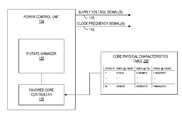
- FIG. 2illustrates a power control unit in a multicore processor used in conjunction with at least one embodiment.
- PCU 124includes a power state manager 125 that operates in conjunction with FCC 126 to determine an optimal or desirable power state for individual cores in a multicore processor based on core-specific performance characteristics of the individual cores and an operational input is presented.
- PCU 124generates instances of a supply voltage signal 115 and a clock frequency signal 116 to indicate corresponding power states.
- power state manager 125controls various standby or other low power modes that processor 101 may support, but also works in conjunction with FCC 126 to define power states per core and uncore.
- FCC 126is operable to read characterization data stored in a core physical characteristics table (CPCT) 220 .
- CPCT 220may be stored in a fuse block (not depicted explicitly) or other non-volatile storage within or accessible to processor 101 .
- CPCT 220includes a table with one row or entry for each core and one or more columns for each of various performance characteristics of the applicable core.
- CPCT 220indicates, in addition to the minimum voltage (VMIN @ FMIN) and the maximum frequency (FMAX @ VMAX), one or more columns indicating a minimum voltage at one or more intermediate clock frequencies (VMINFN).
- VMINFNintermediate clock frequencies
- CPCT 220conveys, in addition to the minimum voltage and maximum frequency corners of a core's power-performance window, minimum voltage values for clock signal frequencies intermediate between the minimum and maximum frequencies.
- FIG. 3illustrates one embodiment of a method to manage the supply voltage and clock frequency provided to individual cores in a multicore processor.
- method 300includes determining (operation 310 ) a set of performance characteristics, including a maximum frequency and a minimum voltage, for each core of a multicore processor.
- the characterization datamay be obtained during testing or other functional verification of processor 101 that occurs at the time of fabrication, typically, but not necessarily after the point at which the wafer is sawed into individual die or devices.
- method 300includes storing (operation 320 ) the characterization data in CPCT 220 or a different table or data structure of non-volatile memory located in or accessible to processor 101 .
- method 300includes accessing (operation 330 ) characterization data from CPCT 220 .
- message method 300identifies (operation 345 ) a performance objective.
- the identified performance objectivemay be indicated by one or more status bits stored in one or more status registers or configuration registers.
- the performance objectives identified in operation 345may, in some embodiments, indicate low-power operation as a desired objective, high performance or fast operation as an objective, or a combination thereof.
- FCC 126may signal the power state manager 125 accordingly based on the operating corners indicated in CPCT 220 .
- FCC 126may determine a power state not explicitly represented in CPCT 220 by performing linear or non-linear interpolation between the operating corners or other representations of power states that are explicitly indicated in CPCT 220 .
- the indication of intermediate power state datamay be fulfilled by retrieving one of the intermediate columns of CPCT 220 .
- method 300further includes determining (operation 350 ) individualized power states for individual cores based on the characterization data and the identified performance objective. In addition to determining the individualized power states, in some embodiments, method 300 further includes applying (operation 360 ) the power states to the corresponding cores.
- method 300further includes scheduling (operation 370 ) an individual thread for execution on a specified core that is best suited to achieve the performance objective and migrating an executing thread from a first core to a better suited core when the better suited core indicates availability according to the identified performance objectives (i.e., scheduling and migrating of currently executing cores to faster cores, in the case of a performance-based operation objective, and scheduling and migrating threads to lower power cores, in the case of a power based performance objective).
- the applying represented in operation 360may, in some embodiments, include ensuring that, when less than all core resources are being utilized, the threads that are being executed are allocated to or migrated to the subset of cores best able to achieve the applicable performance objective.
- the PCUis operable, in some embodiments, to migrate the still executing threads to the processing cores that have the best power consumption characteristics.
- method 300suggests execution by operating system code, other embodiments may expose the core physical characteristics table to an application program through an application programming interface to enable application programs to access and utilize the characterization data to influence power state management.
- the characterization datamay be exposed so that an application program could monitor the current operating condition, and, based upon core characteristic information, provide key performance objective recommendations to the operating system.
- FIG. 4illustrates a computer system used in conjunction with at least one embodiment.
- a processor, memory, and input/output devices of a processor systemare interconnected by a number of point-to-point (P-P) interfaces, as will be described in further detail.
- P-Ppoint-to-point
- the processor systemmay employ different bus architectures, such as a front side bus, a multi-drop bus, and/or another implementation.
- a processoris shown in in FIG. 4 for descriptive clarity, in various embodiments, a different number of processors may be employed using elements of the illustrated architecture.
- system 400is a point-to-point interconnect system, and includes processor 101 . While in some embodiments system 400 may include only a single processor, in other embodiments, system 400 may support multiple processors.
- processor 101is a multicore processor including first processing core 102 - 1 and second processing core 102 - 2 . It is noted that other elements of processor 101 besides processing cores 102 may be referred to as an uncore 122 , while processing cores 102 may also be referred to as core region 120 . In different embodiments, a varying number of cores may be present in a particular processor. In at least one embodiment, processing cores 102 may comprise a number of sub-elements (not shown in FIG.
- Processing cores 102may, in some embodiments, each include a memory cluster (not shown in FIG. 4 ) that may comprise one or more levels of cache memory. In some embodiments, other clusters (not shown in FIG. 4 ) in processing cores 102 may include a front-end cluster and an execution pipeline cluster. In at least one embodiment, processing cores 102 may include an L1 data cache. In some embodiments, uncore 122 may include crossbar 112 , LLC 118 , memory controller (MC) 472 , PCU 124 and P-P interface 476 . In some embodiments, PCU 124 may be used to select a specific core based on the individual characteristics of each core on the die and the requirements of the task.
- MCmemory controller
- PCU 124may be used to select a specific core based on the individual characteristics of each core on the die and the requirements of the task.
- processing cores 102 within processor 101are not equipped with direct means of communicating with each other, but rather, communicate via crossbar 112 , which may include intelligent functionality such as cache control, data queuing, P-P protocols, and multicore interfacing.
- crossbar 112may thus represent an intelligent uncore controller that interconnects processing cores 102 with MC 472 , LLC 118 , and P-P interface 476 , among other elements.
- cache controller functionality within crossbar 112may, in some embodiments, enable selective caching of data within a cache hierarchy including LLC 118 and one or more caches present in processing cores 102 .
- crossbar 112is referred to as a global queue.
- LLC 118may be coupled to a pair of processor processing cores 102 , respectively. In some embodiments, LLC 118 may be shared by processing core 102 - 1 and processing core 102 - 2 . In some embodiments, LLC 118 may be fully shared such that any single one of processing cores 102 may fill or access the full storage capacity of LLC 118 . Additionally, in some embodiments, MC 472 may provide for direct access by processor 101 to memory 432 via memory interface 482 . In some embodiments, memory 432 may be a double-data rate (DDR) type dynamic random-access memory (DRAM) while memory interface 482 and MC 472 comply with a DDR interface specification. In at least one embodiment, memory 432 may represent a bank of memory interfaces (or slots) that may be populated with corresponding memory circuits for a desired DRAM capacity.
- DDRdouble-data rate
- DRAMdynamic random-access memory
- processor 101may also communicate with other elements of system 400 , such as near hub 490 and far hub 418 , which are also collectively referred to as a chipset that supports processor 101 .
- P-P interface 476may be used by processor 101 to communicate with near hub 490 via interconnect link 452 .
- P-P interfaces 476 , 494 and interconnect link 452are implemented using Intel QuickPath Interconnect architecture.
- near hub 490includes interface 492 to couple near hub 490 with first bus 416 , which may support high-performance I/O with corresponding bus devices, such as graphics 438 and/or other bus devices.
- graphics 438may represent a high-performance graphics engine that outputs to a display device (not shown in FIG. 4 ).
- first bus 416is a Peripheral Component Interconnect (PCI) bus, such as a PCI Express (PCIe) bus and/or another computer expansion bus.
- PCIePeripheral Component Interconnect
- near hub 490may also be coupled to far hub 418 at interface 496 via interconnect link 456 .
- interface 496is referred to as a south bridge.
- Far hub 418may, in some embodiments, provide I/O interconnections for various computer system peripheral devices and interfaces and may provide backward compatibility with legacy computer system peripheral devices and interfaces.
- far hub 418provides network interface 430 and audio I/O 434 , as well as, provides interfaces to second bus 420 , third bus 422 , and fourth bus 421 , as will be described in further detail.
- second bus 420may support expanded functionality for system 400 with I/O devices 412 and touchscreen controller 414 , and may be a PCI-type computer bus.
- third bus 422may be a peripheral bus for end-user consumer devices, represented by desktop devices 424 and communication devices 426 , which may include various types of keyboards, computer mice, communication devices, data storage devices, bus expansion devices, etc.
- third bus 422represents a Universal Serial Bus (USB) or similar peripheral interconnect bus.
- fourth bus 421may represent a computer interface bus for connecting mass storage devices, such as hard disk drives, optical drives, and disk arrays, which are generically represented by persistent storage 428 that may be executable by processor 101 .
- system 400emphasizes a computer system that incorporates various features that facilitate handheld or tablet type of operation and other features that facilitate laptop or desktop operation.
- system 400includes features that cooperate to aggressively conserve power while simultaneously reducing latency associated with traditional power conservation performance objectives.
- system 400includes an operating system 440 that may be entirely or partially stored in persistent storage 428 .
- operating system 440may include various modules, application programming interfaces, and the like that expose to varying degrees various hardware and software features of system 400 .
- system 400includes a sensor application programming interface (API) 442 , a resume module 444 , a connect module 446 , and a touchscreen user interface 448 .
- APIapplication programming interface
- system 400may further include various hardware/firmware features including a capacitive or resistive touchscreen controller 414 and a second source of persistent storage such as a solid state drive (SSD) 450 .
- SSDsolid state drive
- sensor API 442provides application program access to one or more sensors (not depicted) that may be included in system 400 .
- sensors that system 400 might have in some embodimentsinclude an accelerometer, a global positioning system (GPS) device, a gyro meter, an inclinometer, and a light sensor.
- the resume module 444may, in some embodiments, be implemented as software that, when executed, performs operations for reducing latency when transitioning system 400 from a power conservation performance objective to an operating performance objective. In at least one embodiment, resume module 444 may work in conjunction with SSD 450 to reduce the amount of SSD storage required when system 400 enters a power conservation mode.
- Resume module 444may, in some embodiments, flush standby and temporary memory pages before transitioning to a sleep mode. In some embodiments, by reducing the amount of system memory space that system 400 is required to preserve upon entering a low power state, resume module 444 beneficially reduces the amount of time required to perform the transition from the low power state to an operating performance objective.
- connect module 446may include software instructions that, when executed, perform complementary functions for conserving power while reducing the amount of latency or delay associated with traditional “wake up” sequences. Connect module 446 may, in some embodiments, periodically update certain “dynamic” applications including email and social network applications, so that, when system 400 wakes from a low power mode, the applications that are often most likely to require refreshing are up to date.
- touchscreen user interface 448supports touchscreen controller 414 that enables user input via touchscreens traditionally reserved for handheld applications.
- the inclusion of touchscreen support in conjunction with support for communication devices 426enables system 400 to provide features traditionally found in dedicated tablet devices as well as features found in dedicated laptop and desktop type systems.
- FIG. 5illustrates a representation for simulation, emulation, and fabrication of a design implementing the disclosed techniques.
- Data representing a designmay represent the design in a number of manners.
- the hardwaremay be represented using a hardware description language or another functional description language which basically provides a computerized model of how the designed hardware is expected to perform.
- hardware model 514may be stored in a storage medium 510 such as a computer memory so that the model may be simulated using simulation software 512 that applies a particular test suite to the hardware model 514 to determine if it indeed functions as intended.
- simulation software 512is not recorded, captured or contained in the medium.
- a circuit level model with logic and/or transistor gatesmay be produced at some stages of the design process.
- This modelmay be similarly simulated, sometimes by dedicated hardware simulators that form the model using programmable logic. This type of simulation, taken a degree further, may be an emulation technique.
- re-configurable hardwareis another embodiment that may involve a tangible machine readable medium storing a model employing the disclosed techniques.
- the data representing the hardware modelmay be the data specifying the presence or absence of various features on different mask layers for masks used to produce the integrated circuit.
- this data representing the integrated circuitembodies the techniques disclosed in that the circuitry or logic in the data can be simulated or fabricated to perform these techniques.
- the datamay be stored in any form of a tangible machine readable medium.
- an optical or electrical wave 540 modulated or otherwise generated to transmit such information, a memory 530 , or a magnetic or optical storage 520 such as a discmay be the tangible machine readable medium. Any of these mediums may “carry” the design information.
- the term “carry”e.g., a tangible machine readable medium carrying information
- the set of bits describing the design or the particular part of the designare (when embodied in a machine readable medium such as a carrier or storage medium) an article that may be sold in and of itself or used by others for further design or fabrication.
- Embodiment 1is a method for allocating processing resources comprising: (i) accessing characterization data indicating a first set of performance characteristics for a first processing core of a processor; and a second set of performance characteristics for a second processing core of the processor; (ii) determining, based on a performance objective and the characterization data: a first power state for the first processing core; and a second power state for the second processing core; and (iii) applying the first power state to the first processing core and the second power state to the second processing core.
- the performance characteristics included in the subject matter of embodiment 1can optionally include a maximum clock frequency (FMAX) attainable at a maximum supply voltage and a minimum supply voltage (VMIN) required for operation at a minimum clock frequency.
- FMAXmaximum clock frequency
- VMINminimum supply voltage
- the subject matter of embodiment 2can optionally include: (i) identifying a fastest processing core comprising a processing core having a highest value of FMAX; (ii) identifying a lowest power processing core comprising a processing core having a lowest value of VMIN; (iii) preferentially allocating a thread to the fastest processing core when the performance objective includes throughput; and (iv) preferentially allocating the thread to the lowest power processing core when the performance objective includes power conservation.
- the subject matter of embodiment 2can optionally include: (i) allocating a first pending thread to a fastest available processing core; (ii) migrating a first executing thread from a present processing core to a faster processing core responsive to the faster processing core indicating availability; (iii) allocating a second pending thread to an available processing core having the lowest value of VMIN; and (iv) migrating a second executing thread from a present processing core to a lower power processing core responsive to the lower power processing core indicating availability.
- the applying of the first power state to the first processing core included in the subject matter of embodiment 1can optionally include powering the first processing core at a first supply voltage and clocking the first processing core at a first clock signal frequency; and the applying of the second power state to the second processing core included in the subject matter of embodiment 1 can optionally include powering the second processing core at a second supply voltage and clocking the second processing core at a second clock signal frequency.
- the subject matter of embodiment 1can optionally include the first power state selected from a first minimum voltage power state and a first maximum frequency power state.
- embodiment 7the subject matter of embodiment 1 can optionally include scheduling execution of a thread based on the characterization data.
- the processor included in the subject matter of embodiment 1can optionally include an uncore
- the characterization data included in the subject matter of embodiment 1can optionally include an uncore set of performance characteristics for the uncore
- the subject matter of embodiment 1can optionally include: (i) determining, based on the performance objective and the uncore set of performance characteristics, an uncore power state and (ii) applying the uncore power state to the uncore.
- Embodiment 9is a processor comprising: (i) a plurality of processing cores to execute instructions; (ii) storage to store characterization data indicative of performance characteristics of each of the plurality of processing cores; and (iii) a power control unit (PCU) to: access the characterization data; and control a power state of each processing core to operate at a core specific power and frequency corner indicated by the characterization data.
- PCUpower control unit
- the characterization data included in the subject matter of embodiment 9can optionally include a maximum frequency and a minimum voltage for each of the plurality of processing cores.
- the PCU included in the subject matter of embodiment 9is optionally operable to control a power state of an uncore portion of the processor.
- embodiment 12the subject matter of embodiment 11 can optionally include a plurality of voltage regulators, accessible to the PCU, each of the plurality of voltage regulators associated with a processing core to provide a core specific supply voltage.
- embodiment 13the subject matter of embodiment 12 can optionally include an uncore voltage regulator, accessible to the PCU, and associated with the processing core.
- the plurality of voltage regulators included in the subject matter of embodiment 13can optionally include clock generators to provide core specific clock signals.
- Embodiment 15is a data processing system comprising: (i) first storage to store performance characterization data; and (ii) a processor, comprising: a plurality of processing cores to execute instructions; and a power control unit (PCU) to: access the performance characterization data; identify a highest frequency processing core and a lowest voltage processing core; control a power state associated with a first processing core to operate at a first power and frequency corner; and control a power state associated with a second processing core to operate at a second power and frequency corner.
- PCUpower control unit
- the first storage included in the subject matter of embodiment 15optionally comprises non-volatile memory.
- embodiment 17the subject matter of embodiment 15 can optionally include second storage to store an operating system, and the operating system is operable to schedule threads for execution on a specific processing core based on the performance characterization data.
- the operating system included in the subject matter of embodiment 17is optionally operable to migrate a first thread from a first execution core to a second execution core.
- system included in the subject matter of embodiment 15optionally includes voltage regulators associated with each processing core and the PCU is operable to control the voltage regulators to provide supply voltages per processing core.
- the voltage regulators included in the subject matter of embodiment 19optionally include clock generators to provide per core clock signals.
- embodiment 21the subject matter of embodiment 15 can optionally include a voltage regulator and clock generator associated with an uncore region of the processor.
- the performance characterization data included in the subject matter of embodiment 15optionally includes maximum frequency data and minimum supply voltage data corresponding to each of the plurality of processing cores.
- the applying of the first power state to the first processing core included in the subject matter of any one of embodiments 1, 2, 3, or 4can optionally include powering the first processing core at a first supply voltage and clocking the first processing core at a first clock signal frequency; and the applying of the second power state to the second processing core included in the subject matter of any one of embodiments 1, 2, 3, or 4 can optionally include powering the second processing core at a second supply voltage and clocking the second processing core at a second clock signal frequency.
- any one of embodiments 9 or 10can optionally include a plurality of voltage regulators, accessible to the PCU, each of the plurality of voltage regulators associated with a processing core to provide a core specific supply voltage.
- system included in the subject matter of any one of embodiments 15 or 16optionally includes voltage regulators associated with each processing core and the PCU is operable to control the voltage regulators to provide supply voltages per processing core.
- any one of embodiments 15 or 17can optionally include a voltage regulator and clock generator associated with an uncore region of the processor.
Landscapes
- Engineering & Computer Science (AREA)
- Theoretical Computer Science (AREA)
- Physics & Mathematics (AREA)
- General Engineering & Computer Science (AREA)
- General Physics & Mathematics (AREA)
- Power Sources (AREA)
Abstract
Description
Claims (12)
Priority Applications (1)
| Application Number | Priority Date | Filing Date | Title |
|---|---|---|---|
| US13/830,157US9442559B2 (en) | 2013-03-14 | 2013-03-14 | Exploiting process variation in a multicore processor |
Applications Claiming Priority (1)
| Application Number | Priority Date | Filing Date | Title |
|---|---|---|---|
| US13/830,157US9442559B2 (en) | 2013-03-14 | 2013-03-14 | Exploiting process variation in a multicore processor |
Publications (2)
| Publication Number | Publication Date |
|---|---|
| US20140281610A1 US20140281610A1 (en) | 2014-09-18 |
| US9442559B2true US9442559B2 (en) | 2016-09-13 |
Family
ID=51534118
Family Applications (1)
| Application Number | Title | Priority Date | Filing Date |
|---|---|---|---|
| US13/830,157Expired - Fee RelatedUS9442559B2 (en) | 2013-03-14 | 2013-03-14 | Exploiting process variation in a multicore processor |
Country Status (1)
| Country | Link |
|---|---|
| US (1) | US9442559B2 (en) |
Cited By (5)
| Publication number | Priority date | Publication date | Assignee | Title |
|---|---|---|---|---|
| US20180074566A1 (en)* | 2016-09-12 | 2018-03-15 | Canon Kabushiki Kaisha | Information processing apparatus, method for controlling the same, and non-transitory computer-readable storage medium |
| TWI637398B (en)* | 2016-11-08 | 2018-10-01 | 格羅方德半導體公司 | Bending circuit for static random access memory (sram) self-timer |
| US10372495B2 (en) | 2017-02-17 | 2019-08-06 | Qualcomm Incorporated | Circuits and methods providing thread assignment for a multi-core processor |
| US10733017B2 (en)* | 2014-01-29 | 2020-08-04 | Samsung Electronics Co., Ltd. | Task scheduling based on performance control conditions for multiple processing units |
| US12293237B2 (en) | 2016-01-15 | 2025-05-06 | Intel Corporation | Systems, methods and devices for determining work placement on processor cores |
Families Citing this family (10)
| Publication number | Priority date | Publication date | Assignee | Title |
|---|---|---|---|---|
| US9129071B2 (en)* | 2012-10-24 | 2015-09-08 | Texas Instruments Incorporated | Coherence controller slot architecture allowing zero latency write commit |
| US9195606B2 (en)* | 2013-03-15 | 2015-11-24 | Intel Corporation | Dead block predictors for cooperative execution in the last level cache |
| US9170854B2 (en)* | 2013-06-04 | 2015-10-27 | Advanced Micro Devices, Inc. | Thread assignment for power and performance efficiency using multiple power states |
| US9779058B2 (en)* | 2015-07-13 | 2017-10-03 | Google Inc. | Modulating processsor core operations |
| US9864423B2 (en) | 2015-12-24 | 2018-01-09 | Intel Corporation | Mitigating component performance variation |
| US11061429B2 (en)* | 2017-10-26 | 2021-07-13 | Advanced Micro Devices, Inc. | Fine-grained speed binning in an accelerated processing device |
| US11940859B2 (en)* | 2018-11-16 | 2024-03-26 | Hewlett Packard Enterprise Development Lp | Adjusting power consumption limits for processors of a server |
| US11360827B2 (en) | 2019-06-04 | 2022-06-14 | Hewlett Packard Enterprise Development Lp | Regulating core and un-core processor frequencies of computing node clusters |
| CN112181124B (en) | 2020-09-11 | 2023-09-01 | 华为技术有限公司 | Method for managing power consumption and related equipment |
| US12117885B2 (en)* | 2021-12-28 | 2024-10-15 | Seagate Technology Llc | Electronic device power consumption grading |
Citations (62)
| Publication number | Priority date | Publication date | Assignee | Title |
|---|---|---|---|---|
| US4228496A (en) | 1976-09-07 | 1980-10-14 | Tandem Computers Incorporated | Multiprocessor system |
| US4958273A (en) | 1987-08-26 | 1990-09-18 | International Business Machines Corporation | Multiprocessor system architecture with high availability |
| US5367697A (en) | 1991-10-22 | 1994-11-22 | Bull Hn Information Systems Inc. | Means for providing a graceful power shut-down capability in a multiprocessor system having certain processors not inherently having a power shut-down capability |
| US5491788A (en) | 1993-09-10 | 1996-02-13 | Compaq Computer Corp. | Method of booting a multiprocessor computer where execution is transferring from a first processor to a second processor based on the first processor having had a critical error |
| US5761516A (en) | 1996-05-03 | 1998-06-02 | Lsi Logic Corporation | Single chip multiprocessor architecture with internal task switching synchronization bus |
| US6141762A (en) | 1998-08-03 | 2000-10-31 | Nicol; Christopher J. | Power reduction in a multiprocessor digital signal processor based on processor load |
| US6407575B1 (en) | 2000-05-31 | 2002-06-18 | Compaq Computer Corporation | Load insensitive clock source to enable hot swap of a node in a multiprocessor computer system |
| US6425068B1 (en) | 1996-12-09 | 2002-07-23 | Pact Gmbh | Unit for processing numeric and logic operations for use in central processing units (cpus), multiprocessor systems, data-flow processors (dsps), systolic processors and field programmable gate arrays (epgas) |
| US20020099976A1 (en) | 1999-02-12 | 2002-07-25 | Sanders Michael C. | Auto processor bus scaling |
| US20020120882A1 (en) | 2000-12-22 | 2002-08-29 | Ananda Sarangi | Dynamic processor configuration and power-up |
| US20020147932A1 (en) | 2001-04-05 | 2002-10-10 | International Business Machines Corporation | Controlling power and performance in a multiprocessing system |
| US20020156611A1 (en) | 2001-02-05 | 2002-10-24 | Thales | Performance simulation process, and multiprocessor application production process, and devices for implementing said processes |
| US20030033490A1 (en) | 2001-07-18 | 2003-02-13 | Steffen Gappisch | Non-volatile memory arrangement and method in a multiprocessor device |
| US20030076183A1 (en)* | 2001-10-22 | 2003-04-24 | Tam Simon M. | Adaptive variable frequency clock system for high performance low power microprocessors |
| US20040015888A1 (en) | 2001-04-11 | 2004-01-22 | Hiroaki Fujii | Processor system including dynamic translation facility, binary translation program that runs in computer having processor system implemented therein, and semiconductor device having processor system implemented therein |
| US6691216B2 (en) | 2000-11-08 | 2004-02-10 | Texas Instruments Incorporated | Shared program memory for use in multicore DSP devices |
| US6772189B1 (en) | 1999-12-14 | 2004-08-03 | International Business Machines Corporation | Method and system for balancing deferred procedure queues in multiprocessor computer systems |
| US6826656B2 (en) | 2002-01-28 | 2004-11-30 | International Business Machines Corporation | Reducing power in a snooping cache based multiprocessor environment |
| US20050107967A1 (en)* | 2003-11-14 | 2005-05-19 | Arm Limited | Operating voltage determination for an integrated circuit |
| US6928566B2 (en) | 2001-01-18 | 2005-08-09 | Renesas Technology Corp. | Multiprocessor system controlling frequency of clock input to processor according to ratio of processing times of processors, and method thereof |
| US20050240735A1 (en) | 2004-04-27 | 2005-10-27 | International Business Machines Corporation | Location-aware cache-to-cache transfers |
| US20060005056A1 (en) | 2004-07-01 | 2006-01-05 | Shinichiro Nishioka | Multiprocessor control apparatus, control method thereof, and integrated circuit |
| US7111178B2 (en) | 2001-09-28 | 2006-09-19 | Intel Corporation | Method and apparatus for adjusting the voltage and frequency to minimize power dissipation in a multiprocessor system |
| US7146514B2 (en) | 2003-07-23 | 2006-12-05 | Intel Corporation | Determining target operating frequencies for a multiprocessor system |
| US20070043964A1 (en) | 2005-08-22 | 2007-02-22 | Intel Corporation | Reducing power consumption in multiprocessor systems |
| US20070174829A1 (en) | 2005-07-15 | 2007-07-26 | Erik Brockmeyer | Method for mapping applications on a multiprocessor platform/system |
| US7268570B1 (en) | 2006-06-27 | 2007-09-11 | International Business Machines Corporation | Apparatus and method for customized burn-in of cores on a multicore microprocessor integrated circuit chip |
| US20070255929A1 (en) | 2005-04-12 | 2007-11-01 | Hironori Kasahara | Multiprocessor System and Multigrain Parallelizing Compiler |
| US20070283128A1 (en) | 2006-06-06 | 2007-12-06 | Matsushita Electric Industrial Co., Ltd. | Asymmetric multiprocessor |
| US20080022052A1 (en) | 2006-07-18 | 2008-01-24 | Renesas Technology Corp. | Bus Coupled Multiprocessor |
| US20080077815A1 (en) | 2006-09-22 | 2008-03-27 | Sony Computer Entertainment Inc. | Power consumption reduction in a multiprocessor system |
| US20080104425A1 (en)* | 2006-11-01 | 2008-05-01 | Gunther Stephen H | Independent power control of processing cores |
| US20080235364A1 (en)* | 2006-03-07 | 2008-09-25 | Eugene Gorbatov | Method and apparatus for using dynamic workload characteristics to control CPU frequency and voltage scaling |
| US20080301474A1 (en) | 2005-12-23 | 2008-12-04 | Nxp B.V. | Performance Analysis Based System Level Power Management |
| US7463992B2 (en)* | 2006-09-29 | 2008-12-09 | Intel Corporation | Method and system to self-test single and multi-core CPU systems |
| US20090049312A1 (en)* | 2007-08-14 | 2009-02-19 | Mips Technologies, Inc. | Power Management for System Having One or More Integrated Circuits |
| US20090070772A1 (en) | 2007-09-11 | 2009-03-12 | Hitachi, Ltd. | Multiprocessor system |
| US20090165007A1 (en)* | 2007-12-19 | 2009-06-25 | Microsoft Corporation | Task-level thread scheduling and resource allocation |
| US20090222654A1 (en)* | 2008-02-29 | 2009-09-03 | Herbert Hum | Distribution of tasks among asymmetric processing elements |
| US7596708B1 (en)* | 2000-01-18 | 2009-09-29 | Sameer Halepete | Adaptive power control |
| US20100058086A1 (en)* | 2008-08-28 | 2010-03-04 | Industry Academic Cooperation Foundation, Hallym University | Energy-efficient multi-core processor |
| US20100053005A1 (en) | 2008-08-28 | 2010-03-04 | Kouichi Mukai | Receiver apparatus, junction cable, and power supply apparatus |
| US20100094572A1 (en)* | 2008-10-15 | 2010-04-15 | International Business Machines Corporation | Dynamic Frequency And Voltage Scaling For A Computer Processor |
| US20100095137A1 (en)* | 2008-10-13 | 2010-04-15 | International Business Machines Corporation | Dynamic Frequency And Voltage Scaling For A Computer Processor |
| US7702933B2 (en) | 2007-01-30 | 2010-04-20 | Inventec Corporation | Multiprocessor power-on switch circuit |
| US20100169609A1 (en)* | 2008-12-30 | 2010-07-01 | Lev Finkelstein | Method for optimizing voltage-frequency setup in multi-core processor systems |
| US20110004774A1 (en) | 2009-07-02 | 2011-01-06 | Qualcomm Incorporated | Temperature Compensating Adaptive Voltage Scalers (AVSs), Systems, and Methods |
| US20110119508A1 (en) | 2009-11-16 | 2011-05-19 | International Business Machines Corporation | Power Efficient Stack of Multicore Microprocessors |
| US20110173477A1 (en) | 2008-09-24 | 2011-07-14 | Fujitsu Limited | Power consumption control method in multicore cpu |
| US20110252267A1 (en)* | 2004-07-27 | 2011-10-13 | Alon Naveh | Power management coordination in multi-core processors |
| US20120042176A1 (en) | 2010-08-16 | 2012-02-16 | Nam Sung Kim | Method and Apparatus for Optimizing Clock Speed and Power Dissipation in Multicore Architectures |
| US20120079235A1 (en) | 2010-09-25 | 2012-03-29 | Ravishankar Iyer | Application scheduling in heterogeneous multiprocessor computing platforms |
| US20120144217A1 (en) | 2011-12-15 | 2012-06-07 | Sistla Krishnakanth V | Dynamically Modifying A Power/Performance Tradeoff Based On Processor Utilization |
| US20120144218A1 (en) | 2010-12-03 | 2012-06-07 | International Business Machines Corporation | Transferring Power and Speed from a Lock Requester to a Lock Holder on a System with Multiple Processors |
| US20120146708A1 (en) | 2010-12-14 | 2012-06-14 | Advanced Micro Devices, Inc. | Method and apparatus for application of power density multipliers optimally in a multicore system |
| US20120324250A1 (en) | 2011-06-14 | 2012-12-20 | Utah State University | Architecturally Homogeneous Power-Performance Heterogeneous Multicore Processor |
| US20130007413A1 (en)* | 2011-06-10 | 2013-01-03 | Qualcomm Incorporated | System and Apparatus For Consolidated Dynamic Frequency/Voltage Control |
| US20130041977A1 (en)* | 2011-08-11 | 2013-02-14 | Fujitsu Limited | Computer product, migration executing apparatus, and migration method |
| US20130080795A1 (en) | 2011-09-28 | 2013-03-28 | Krishnakanth Sistla | Dynamically Adjusting Power Of Non-Core Processor Circuitry |
| US20130111226A1 (en) | 2011-10-31 | 2013-05-02 | Avinash N. Ananthakrishnan | Controlling A Turbo Mode Frequency Of A Processor |
| US20140024145A1 (en)* | 2012-07-20 | 2014-01-23 | International Business Machines Corporation | Method and structure for multi-core chip product test and selective voltage binning disposition |
| US20140189704A1 (en)* | 2012-12-28 | 2014-07-03 | Paolo Narvaez | Hetergeneous processor apparatus and method |
- 2013
- 2013-03-14USUS13/830,157patent/US9442559B2/ennot_activeExpired - Fee Related
Patent Citations (76)
| Publication number | Priority date | Publication date | Assignee | Title |
|---|---|---|---|---|
| US4356550A (en) | 1976-09-07 | 1982-10-26 | Tandem Computers Incorporated | Multiprocessor system |
| US4228496A (en) | 1976-09-07 | 1980-10-14 | Tandem Computers Incorporated | Multiprocessor system |
| US4958273A (en) | 1987-08-26 | 1990-09-18 | International Business Machines Corporation | Multiprocessor system architecture with high availability |
| US5367697A (en) | 1991-10-22 | 1994-11-22 | Bull Hn Information Systems Inc. | Means for providing a graceful power shut-down capability in a multiprocessor system having certain processors not inherently having a power shut-down capability |
| US5491788A (en) | 1993-09-10 | 1996-02-13 | Compaq Computer Corp. | Method of booting a multiprocessor computer where execution is transferring from a first processor to a second processor based on the first processor having had a critical error |
| US5761516A (en) | 1996-05-03 | 1998-06-02 | Lsi Logic Corporation | Single chip multiprocessor architecture with internal task switching synchronization bus |
| US6425068B1 (en) | 1996-12-09 | 2002-07-23 | Pact Gmbh | Unit for processing numeric and logic operations for use in central processing units (cpus), multiprocessor systems, data-flow processors (dsps), systolic processors and field programmable gate arrays (epgas) |
| US6141762A (en) | 1998-08-03 | 2000-10-31 | Nicol; Christopher J. | Power reduction in a multiprocessor digital signal processor based on processor load |
| US20020099976A1 (en) | 1999-02-12 | 2002-07-25 | Sanders Michael C. | Auto processor bus scaling |
| US6772189B1 (en) | 1999-12-14 | 2004-08-03 | International Business Machines Corporation | Method and system for balancing deferred procedure queues in multiprocessor computer systems |
| US7596708B1 (en)* | 2000-01-18 | 2009-09-29 | Sameer Halepete | Adaptive power control |
| US6407575B1 (en) | 2000-05-31 | 2002-06-18 | Compaq Computer Corporation | Load insensitive clock source to enable hot swap of a node in a multiprocessor computer system |
| US6691216B2 (en) | 2000-11-08 | 2004-02-10 | Texas Instruments Incorporated | Shared program memory for use in multicore DSP devices |
| US20020120882A1 (en) | 2000-12-22 | 2002-08-29 | Ananda Sarangi | Dynamic processor configuration and power-up |
| US6928566B2 (en) | 2001-01-18 | 2005-08-09 | Renesas Technology Corp. | Multiprocessor system controlling frequency of clock input to processor according to ratio of processing times of processors, and method thereof |
| US20020156611A1 (en) | 2001-02-05 | 2002-10-24 | Thales | Performance simulation process, and multiprocessor application production process, and devices for implementing said processes |
| US20020147932A1 (en) | 2001-04-05 | 2002-10-10 | International Business Machines Corporation | Controlling power and performance in a multiprocessing system |
| US20040015888A1 (en) | 2001-04-11 | 2004-01-22 | Hiroaki Fujii | Processor system including dynamic translation facility, binary translation program that runs in computer having processor system implemented therein, and semiconductor device having processor system implemented therein |
| US20030033490A1 (en) | 2001-07-18 | 2003-02-13 | Steffen Gappisch | Non-volatile memory arrangement and method in a multiprocessor device |
| US7565563B2 (en) | 2001-07-18 | 2009-07-21 | Nxp B.V. | Non-volatile memory arrangement and method in a multiprocessor device |
| US7464276B2 (en) | 2001-09-28 | 2008-12-09 | Intel Corporation | Method and apparatus for adjusting the voltage and frequency to minimize power dissipation in a multiprocessor system in response to compute load |
| US7111178B2 (en) | 2001-09-28 | 2006-09-19 | Intel Corporation | Method and apparatus for adjusting the voltage and frequency to minimize power dissipation in a multiprocessor system |
| US20030076183A1 (en)* | 2001-10-22 | 2003-04-24 | Tam Simon M. | Adaptive variable frequency clock system for high performance low power microprocessors |
| US6826656B2 (en) | 2002-01-28 | 2004-11-30 | International Business Machines Corporation | Reducing power in a snooping cache based multiprocessor environment |
| US7146514B2 (en) | 2003-07-23 | 2006-12-05 | Intel Corporation | Determining target operating frequencies for a multiprocessor system |
| US20050107967A1 (en)* | 2003-11-14 | 2005-05-19 | Arm Limited | Operating voltage determination for an integrated circuit |
| US20050240735A1 (en) | 2004-04-27 | 2005-10-27 | International Business Machines Corporation | Location-aware cache-to-cache transfers |
| US7398403B2 (en) | 2004-07-01 | 2008-07-08 | Matsushita Electric Industrial Co., Ltd. | Multiprocessor control apparatus, control method thereof, and integrated circuit |
| US20060005056A1 (en) | 2004-07-01 | 2006-01-05 | Shinichiro Nishioka | Multiprocessor control apparatus, control method thereof, and integrated circuit |
| US20110252267A1 (en)* | 2004-07-27 | 2011-10-13 | Alon Naveh | Power management coordination in multi-core processors |
| US7895453B2 (en) | 2005-04-12 | 2011-02-22 | Waseda University | Multiprocessor system and multigrain parallelizing compiler |
| US20100146310A1 (en) | 2005-04-12 | 2010-06-10 | Waseda University | Multiprocessor system and multigrain parallelizing compiler |
| US20070255929A1 (en) | 2005-04-12 | 2007-11-01 | Hironori Kasahara | Multiprocessor System and Multigrain Parallelizing Compiler |
| US20070174829A1 (en) | 2005-07-15 | 2007-07-26 | Erik Brockmeyer | Method for mapping applications on a multiprocessor platform/system |
| US7779287B2 (en) | 2005-08-22 | 2010-08-17 | Intel Corporation | Reducing power consumption in multiprocessor systems |
| US20070043964A1 (en) | 2005-08-22 | 2007-02-22 | Intel Corporation | Reducing power consumption in multiprocessor systems |
| US20080301474A1 (en) | 2005-12-23 | 2008-12-04 | Nxp B.V. | Performance Analysis Based System Level Power Management |
| US20080235364A1 (en)* | 2006-03-07 | 2008-09-25 | Eugene Gorbatov | Method and apparatus for using dynamic workload characteristics to control CPU frequency and voltage scaling |
| US7814252B2 (en) | 2006-06-06 | 2010-10-12 | Panasonic Corporation | Asymmetric multiprocessor |
| US20070283128A1 (en) | 2006-06-06 | 2007-12-06 | Matsushita Electric Industrial Co., Ltd. | Asymmetric multiprocessor |
| US7268570B1 (en) | 2006-06-27 | 2007-09-11 | International Business Machines Corporation | Apparatus and method for customized burn-in of cores on a multicore microprocessor integrated circuit chip |
| US20080022052A1 (en) | 2006-07-18 | 2008-01-24 | Renesas Technology Corp. | Bus Coupled Multiprocessor |
| US20080077815A1 (en) | 2006-09-22 | 2008-03-27 | Sony Computer Entertainment Inc. | Power consumption reduction in a multiprocessor system |
| US20110087909A1 (en) | 2006-09-22 | 2011-04-14 | Sony Computer Entertainment Inc. | Power Consumption Reduction In A Multiprocessor System |
| US7882379B2 (en) | 2006-09-22 | 2011-02-01 | Sony Computer Entertainment Inc. | Power consumption reduction in a multiprocessor system |
| US7463992B2 (en)* | 2006-09-29 | 2008-12-09 | Intel Corporation | Method and system to self-test single and multi-core CPU systems |
| US20080104425A1 (en)* | 2006-11-01 | 2008-05-01 | Gunther Stephen H | Independent power control of processing cores |
| US7702933B2 (en) | 2007-01-30 | 2010-04-20 | Inventec Corporation | Multiprocessor power-on switch circuit |
| US20090049312A1 (en)* | 2007-08-14 | 2009-02-19 | Mips Technologies, Inc. | Power Management for System Having One or More Integrated Circuits |
| US8112754B2 (en) | 2007-09-11 | 2012-02-07 | Hitachi, Ltd. | Controlling body-bias voltage and clock frequency in a multiprocessor system for processing tasks |
| US20090070772A1 (en) | 2007-09-11 | 2009-03-12 | Hitachi, Ltd. | Multiprocessor system |
| US20090165007A1 (en)* | 2007-12-19 | 2009-06-25 | Microsoft Corporation | Task-level thread scheduling and resource allocation |
| US20090222654A1 (en)* | 2008-02-29 | 2009-09-03 | Herbert Hum | Distribution of tasks among asymmetric processing elements |
| US20100053005A1 (en) | 2008-08-28 | 2010-03-04 | Kouichi Mukai | Receiver apparatus, junction cable, and power supply apparatus |
| US20100058086A1 (en)* | 2008-08-28 | 2010-03-04 | Industry Academic Cooperation Foundation, Hallym University | Energy-efficient multi-core processor |
| US8407505B2 (en) | 2008-09-24 | 2013-03-26 | Fujitsu Limited | Power consumption control method in multicore CPU |
| US20110173477A1 (en) | 2008-09-24 | 2011-07-14 | Fujitsu Limited | Power consumption control method in multicore cpu |
| US20100095137A1 (en)* | 2008-10-13 | 2010-04-15 | International Business Machines Corporation | Dynamic Frequency And Voltage Scaling For A Computer Processor |
| US20100094572A1 (en)* | 2008-10-15 | 2010-04-15 | International Business Machines Corporation | Dynamic Frequency And Voltage Scaling For A Computer Processor |
| US20100169609A1 (en)* | 2008-12-30 | 2010-07-01 | Lev Finkelstein | Method for optimizing voltage-frequency setup in multi-core processor systems |
| US20110004774A1 (en) | 2009-07-02 | 2011-01-06 | Qualcomm Incorporated | Temperature Compensating Adaptive Voltage Scalers (AVSs), Systems, and Methods |
| US20110119508A1 (en) | 2009-11-16 | 2011-05-19 | International Business Machines Corporation | Power Efficient Stack of Multicore Microprocessors |
| US8417974B2 (en) | 2009-11-16 | 2013-04-09 | International Business Machines Corporation | Power efficient stack of multicore microprocessors |
| US20120042176A1 (en) | 2010-08-16 | 2012-02-16 | Nam Sung Kim | Method and Apparatus for Optimizing Clock Speed and Power Dissipation in Multicore Architectures |
| US8281164B2 (en) | 2010-08-16 | 2012-10-02 | Wisconsin Alumni Research Foundation | Method and apparatus for optimizing clock speed and power dissipation in multicore architectures |
| US20120079235A1 (en) | 2010-09-25 | 2012-03-29 | Ravishankar Iyer | Application scheduling in heterogeneous multiprocessor computing platforms |
| US20120144218A1 (en) | 2010-12-03 | 2012-06-07 | International Business Machines Corporation | Transferring Power and Speed from a Lock Requester to a Lock Holder on a System with Multiple Processors |
| US20120146708A1 (en) | 2010-12-14 | 2012-06-14 | Advanced Micro Devices, Inc. | Method and apparatus for application of power density multipliers optimally in a multicore system |
| US20130007413A1 (en)* | 2011-06-10 | 2013-01-03 | Qualcomm Incorporated | System and Apparatus For Consolidated Dynamic Frequency/Voltage Control |
| US20120324250A1 (en) | 2011-06-14 | 2012-12-20 | Utah State University | Architecturally Homogeneous Power-Performance Heterogeneous Multicore Processor |
| US20130041977A1 (en)* | 2011-08-11 | 2013-02-14 | Fujitsu Limited | Computer product, migration executing apparatus, and migration method |
| US20130080795A1 (en) | 2011-09-28 | 2013-03-28 | Krishnakanth Sistla | Dynamically Adjusting Power Of Non-Core Processor Circuitry |
| US20130111226A1 (en) | 2011-10-31 | 2013-05-02 | Avinash N. Ananthakrishnan | Controlling A Turbo Mode Frequency Of A Processor |
| US20120144217A1 (en) | 2011-12-15 | 2012-06-07 | Sistla Krishnakanth V | Dynamically Modifying A Power/Performance Tradeoff Based On Processor Utilization |
| US20140024145A1 (en)* | 2012-07-20 | 2014-01-23 | International Business Machines Corporation | Method and structure for multi-core chip product test and selective voltage binning disposition |
| US20140189704A1 (en)* | 2012-12-28 | 2014-07-03 | Paolo Narvaez | Hetergeneous processor apparatus and method |
Cited By (7)
| Publication number | Priority date | Publication date | Assignee | Title |
|---|---|---|---|---|
| US10733017B2 (en)* | 2014-01-29 | 2020-08-04 | Samsung Electronics Co., Ltd. | Task scheduling based on performance control conditions for multiple processing units |
| US11429439B2 (en) | 2014-01-29 | 2022-08-30 | Samsung Electronics Co., Ltd. | Task scheduling based on performance control conditions for multiple processing units |
| US12293237B2 (en) | 2016-01-15 | 2025-05-06 | Intel Corporation | Systems, methods and devices for determining work placement on processor cores |
| US20180074566A1 (en)* | 2016-09-12 | 2018-03-15 | Canon Kabushiki Kaisha | Information processing apparatus, method for controlling the same, and non-transitory computer-readable storage medium |
| US11209885B2 (en)* | 2016-09-12 | 2021-12-28 | Canon Kabushiki Kaisha | Information processing apparatus, method for controlling the same, and non-transitory computer-readable storage medium |
| TWI637398B (en)* | 2016-11-08 | 2018-10-01 | 格羅方德半導體公司 | Bending circuit for static random access memory (sram) self-timer |
| US10372495B2 (en) | 2017-02-17 | 2019-08-06 | Qualcomm Incorporated | Circuits and methods providing thread assignment for a multi-core processor |
Also Published As
| Publication number | Publication date |
|---|---|
| US20140281610A1 (en) | 2014-09-18 |
Similar Documents
| Publication | Publication Date | Title |
|---|---|---|
| US9442559B2 (en) | Exploiting process variation in a multicore processor | |
| US10503542B2 (en) | Systems, methods and devices for work placement on processor cores | |
| US8954977B2 (en) | Software-based thread remapping for power savings | |
| CN103229122B (en) | Provides per-core voltage and frequency control | |
| US9098274B2 (en) | Methods and apparatuses to improve turbo performance for events handling | |
| CN108780342B (en) | Systems, methods, and apparatus for using thermal margins of cores in a processor | |
| US20190065243A1 (en) | Dynamic memory power capping with criticality awareness | |
| US9176895B2 (en) | Increased error correction for cache memories through adaptive replacement policies | |
| US9298243B2 (en) | Selection of an operating point of a memory physical layer interface and a memory controller based on memory bandwidth utilization | |
| US9875108B2 (en) | Shared memory interleavings for instruction atomicity violations | |
| CN104115093A (en) | Methods, apparatus and systems for energy efficiency and conservation including power and performance balancing among multiple processing elements | |
| WO2014143053A1 (en) | Dead block predictors for cooperative execution in the last level cache | |
| US9329936B2 (en) | Redundant execution for reliability in a super FMA ALU | |
| KR20240004361A (en) | Processing-in-memory concurrent processing system and method | |
| US9513688B2 (en) | Measurement of performance scalability in a microprocessor | |
| EP3475783B1 (en) | Systems, methods and devices for standby power entry without latency tolerance information | |
| US20130173933A1 (en) | Performance of a power constrained processor | |
| WO2014031384A1 (en) | Power management of multiple compute units sharing a cache | |
| US9286137B2 (en) | Achieving deterministic execution of time critical code sections in multi-core systems | |
| Boyer | Improving Resource Utilization in Heterogeneous CPU-GPU Systems | |
| US11880231B2 (en) | Accurate timestamp or derived counter value generation on a complex CPU | |
| Zhu et al. | Memory power optimisation on low-bit multi-access cross memory address mapping schema | |
| CN113767370A (en) | Avoiding garbage collection in high performance memory management systems |
Legal Events
| Date | Code | Title | Description |
|---|---|---|---|
| AS | Assignment | Owner name:INTEL CORPORATION, CALIFORNIA Free format text:ASSIGNMENT OF ASSIGNORS INTEREST;ASSIGNORS:BISWAS, ARIJIT;POWELL, MICHAEL D.;REEL/FRAME:030598/0860 Effective date:20130403 | |
| ZAAA | Notice of allowance and fees due | Free format text:ORIGINAL CODE: NOA | |
| ZAAB | Notice of allowance mailed | Free format text:ORIGINAL CODE: MN/=. | |
| ZAAA | Notice of allowance and fees due | Free format text:ORIGINAL CODE: NOA | |
| STCF | Information on status: patent grant | Free format text:PATENTED CASE | |
| MAFP | Maintenance fee payment | Free format text:PAYMENT OF MAINTENANCE FEE, 4TH YEAR, LARGE ENTITY (ORIGINAL EVENT CODE: M1551); ENTITY STATUS OF PATENT OWNER: LARGE ENTITY Year of fee payment:4 | |
| FEPP | Fee payment procedure | Free format text:MAINTENANCE FEE REMINDER MAILED (ORIGINAL EVENT CODE: REM.); ENTITY STATUS OF PATENT OWNER: LARGE ENTITY | |
| LAPS | Lapse for failure to pay maintenance fees | Free format text:PATENT EXPIRED FOR FAILURE TO PAY MAINTENANCE FEES (ORIGINAL EVENT CODE: EXP.); ENTITY STATUS OF PATENT OWNER: LARGE ENTITY | |
| STCH | Information on status: patent discontinuation | Free format text:PATENT EXPIRED DUE TO NONPAYMENT OF MAINTENANCE FEES UNDER 37 CFR 1.362 | |
| FP | Lapsed due to failure to pay maintenance fee | Effective date:20240913 |