US9440846B2 - System on a chip using integrated MEMS and CMOS devices - Google Patents
System on a chip using integrated MEMS and CMOS devicesDownload PDFInfo
- Publication number
- US9440846B2 US9440846B2US14/445,012US201414445012AUS9440846B2US 9440846 B2US9440846 B2US 9440846B2US 201414445012 AUS201414445012 AUS 201414445012AUS 9440846 B2US9440846 B2US 9440846B2
- Authority
- US
- United States
- Prior art keywords
- mems
- gyro
- structures
- cmos
- coupled
- Prior art date
- Legal status (The legal status is an assumption and is not a legal conclusion. Google has not performed a legal analysis and makes no representation as to the accuracy of the status listed.)
- Active, expires
Links
Images


Classifications
- B—PERFORMING OPERATIONS; TRANSPORTING
- B81—MICROSTRUCTURAL TECHNOLOGY
- B81C—PROCESSES OR APPARATUS SPECIALLY ADAPTED FOR THE MANUFACTURE OR TREATMENT OF MICROSTRUCTURAL DEVICES OR SYSTEMS
- B81C1/00—Manufacture or treatment of devices or systems in or on a substrate
- B81C1/00015—Manufacture or treatment of devices or systems in or on a substrate for manufacturing microsystems
- B81C1/00222—Integrating an electronic processing unit with a micromechanical structure
- B81C1/00246—Monolithic integration, i.e. micromechanical structure and electronic processing unit are integrated on the same substrate
- B—PERFORMING OPERATIONS; TRANSPORTING
- B81—MICROSTRUCTURAL TECHNOLOGY
- B81B—MICROSTRUCTURAL DEVICES OR SYSTEMS, e.g. MICROMECHANICAL DEVICES
- B81B2207/00—Microstructural systems or auxiliary parts thereof
- B81B2207/01—Microstructural systems or auxiliary parts thereof comprising a micromechanical device connected to control or processing electronics, i.e. Smart-MEMS
- B81B2207/015—Microstructural systems or auxiliary parts thereof comprising a micromechanical device connected to control or processing electronics, i.e. Smart-MEMS the micromechanical device and the control or processing electronics being integrated on the same substrate
- B—PERFORMING OPERATIONS; TRANSPORTING
- B81—MICROSTRUCTURAL TECHNOLOGY
- B81C—PROCESSES OR APPARATUS SPECIALLY ADAPTED FOR THE MANUFACTURE OR TREATMENT OF MICROSTRUCTURAL DEVICES OR SYSTEMS
- B81C1/00—Manufacture or treatment of devices or systems in or on a substrate
- B81C1/00388—Etch mask forming
- B81C1/00396—Mask characterised by its composition, e.g. multilayer masks
- B—PERFORMING OPERATIONS; TRANSPORTING
- B81—MICROSTRUCTURAL TECHNOLOGY
- B81C—PROCESSES OR APPARATUS SPECIALLY ADAPTED FOR THE MANUFACTURE OR TREATMENT OF MICROSTRUCTURAL DEVICES OR SYSTEMS
- B81C1/00—Manufacture or treatment of devices or systems in or on a substrate
- B81C1/00436—Shaping materials, i.e. techniques for structuring the substrate or the layers on the substrate
- B81C1/00555—Achieving a desired geometry, i.e. controlling etch rates, anisotropy or selectivity
- B81C1/00626—Processes for achieving a desired geometry not provided for in groups B81C1/00563 - B81C1/00619
- B—PERFORMING OPERATIONS; TRANSPORTING
- B81—MICROSTRUCTURAL TECHNOLOGY
- B81C—PROCESSES OR APPARATUS SPECIALLY ADAPTED FOR THE MANUFACTURE OR TREATMENT OF MICROSTRUCTURAL DEVICES OR SYSTEMS
- B81C2201/00—Manufacture or treatment of microstructural devices or systems
- B81C2201/01—Manufacture or treatment of microstructural devices or systems in or on a substrate
- B81C2201/0198—Manufacture or treatment of microstructural devices or systems in or on a substrate for making a masking layer
- B—PERFORMING OPERATIONS; TRANSPORTING
- B81—MICROSTRUCTURAL TECHNOLOGY
- B81C—PROCESSES OR APPARATUS SPECIALLY ADAPTED FOR THE MANUFACTURE OR TREATMENT OF MICROSTRUCTURAL DEVICES OR SYSTEMS
- B81C2203/00—Forming microstructural systems
- B81C2203/01—Packaging MEMS
- B81C2203/0136—Growing or depositing of a covering layer
Definitions
- the present inventionrelates generally to integrated devices. More particularly, the present invention provides a system and method for integrating at least two different micro electro mechanical systems (MEMS) devices with one or more complementary metal oxide semiconductor (CMOS) devices, but can be others.
- MEMSmicro electro mechanical systems
- CMOScomplementary metal oxide semiconductor
- the MEMS devicescan include an accelerometer, a gyroscope, a magnetic sensor, a pressure sensor, a microphone, a humidity sensor, a temperature sensor, a chemical sensor, a biosensor, an inertial sensor, and others. But it will be recognized that the invention has a much broader range of applicability.
- CMOS technologyhas become the predominant fabrication technology for integrated circuits (IC).
- MEMScontinues to rely upon conventional process technologies.
- microelectronic ICsare the “brains” of an integrated device which provides decision-making capabilities
- MEMSare the “eyes” and “arms” that provide the ability to sense and control the environment.
- RFradio frequency
- IC and MEMShave limitless applications through modular measurement devices such as accelerometers, gyroscopes, actuators, and sensors.
- accelerometers and gyroscopesare used to deploy airbags and trigger dynamic stability control functions, respectively.
- MEMS gyroscopescan also be used for image stabilization systems in video and still cameras, and automatic steering systems in airplanes and torpedoes.
- Biological MEMSBio-MEMS
- Bio-MEMSimplement biosensors and chemical sensors for Lab-On-Chip applications, which integrate one or more laboratory functions on a single millimeter-sized chip only.
- Other applicationsinclude Internet and telephone networks, security and financial applications, and health care and medical systems.
- ICs and MEMScan be used to practically engage in various type of environmental interaction.
- the present inventionprovides a system and method for integrating at least two different micro electro mechanical systems (MEMS) devices with one or more complementary metal oxide semiconductor (CMOS) devices, but can be others.
- MEMS devicescan include at least an accelerometer, a gyroscope, a magnetic sensor, a pressure sensor, a microphone, a humidity sensor, a temperature sensor, a chemical sensor, a biosensor, an inertial sensor, and others. But it will be recognized that the invention has a much broader range of applicability.
- the present inventionprovides an integrated system including a substrate layer, a semiconductor layer, integrated devices, and an encapsulation layer.
- each of the devicesis integrated with the semiconductor layer and is covered by the encapsulation layer.
- the semiconductor layerforms an interface region, on which CMOS and MEMS devices can be configured.
- one or more mask layersmay be used to simultaneously form two or more MEMS devices upon the interface region, such as an accelerometer and a gyroscope, a gyroscope and a pressure sensor, or the like.
- the integrated systemcan include a silicon substrate layer, a CMOS layer, MEMS and CMOS devices, and a wafer level packaging (WLP) layer.
- the CMOS layercan form an interface region, upon which any number of CMOS and MEMS devices can be configured.
- the CMOS layercan be deposited on the silicon substrate and can include any number of metal layers and can be provided on any type of design rule, such as a 0.18 micron design rule or less.
- the integrated CMOS devicescan be configured from a foundry compatible process.
- the integrated MEMS devicescan include, but not exclusively, any combination of the following types of sensors: magnetic, pressure, humidity, temperature, chemical, biological, or inertial. These MEMS devices can also comprise one or more deposited materials, one or more bonded materials, or other materials unique to such MEMS devices or common to other MEMS devices.
- the overlying WLP layercan be configured to hermetically seal any number of these integrated devices.
- the present techniquesprovide easy to use processes that rely upon conventional fabrication technologies.
- the methodsprovide higher device yields in dies per wafer as a result of the integrated approach.
- the methodsprovide processes and systems that are compatible with conventional process technologies without substantial modifications to conventional equipment and processes.
- Various embodiments of these techniquescan reduce off-chip connections, which make the mass production of smaller and thinner units possible.
- various embodiments of the integrated CMOS-MEMS technologies described hereincan achieve high accuracy through the minimization or reduction of parasitic resistances and capacitances due to joint (e.g. simultaneous) fabrication of CMOS and MEMS devices, and in particular, CMOS and multiple (e.g. different) MEMS devices.
- FIG. 1is a simplified perspective diagram of an integrated CMOS-MEMS system according to an embodiment of the present invention
- FIG. 2is a simplified top diagram of an integrated CMOS-MEMS system according to an embodiment of the present invention
- FIG. 3is a simplified side diagram of an integrated CMOS-MEMS system according to an embodiment of the present invention.
- FIG. 4is a simplified side diagram of an integrated CMOS-MEMS system according to another embodiment of the present invention.
- FIG. 5is a simplified side diagram of an integrated CMOS-MEMS system according to yet another embodiment of the present invention.
- FIG. 6is a simplified side diagram of an integrated CMOS-MEMS system according to yet another embodiment of the present invention.
- FIG. 7is a simplified side diagram of an integrated CMOS-MEMS system according to yet another embodiment of the present invention.
- FIG. 8is a simplified side diagram of an integrated CMOS-MEMS system according to yet another embodiment of the present invention.
- FIG. 9is a simplified top diagram of a component of an integrated CMOS-MEMS system according to an embodiment of the present invention.
- FIG. 10is a simplified top diagram of a component of an integrated CMOS-MEMS system according to an embodiment of the present invention.
- FIG. 11is a simplified top diagram of a component of an integrated CMOS-MEMS system according to an embodiment of the present invention.
- FIG. 12is a simplified block diagram of a device incorporating various embodiments of the present invention.
- FIG. 13is a simplified perspective diagram of a transducer apparatus according to an embodiment of the present invention.
- FIG. 14is a simplified cross-sectional side diagram of a transducer apparatus according to an embodiment of the present invention.
- FIG. 15is a simplified cross-sectional close-up diagram of a transducer apparatus according to an embodiment of the present invention.
- the present inventionprovides systems and methods for integrating one or more MEMS devices with other system applications configured on at least CMOS integrated circuit devices.
- the MEMS devicescan include at least an accelerometer, a gyroscope, a magnetic sensor, a pressure sensor, a microphone, a humidity sensor, a temperature sensor, a chemical sensor, a biosensor, an inertial sensor, and others.
- the other applicationsinclude at least a sensor application or applications, system applications, and broadband applications, among others. But it will be recognized that the invention has a much broader range of applicability.
- FIG. 1is a simplified perspective diagram of an integrated CMOS-MEMS system according to an embodiment of the present invention.
- the system 100includes a substrate layer 110 , a semiconductor layer 120 , integrated devices 140 - 143 , and an encapsulation layer 150 .
- each device 140 - 143can include a MEMS device.
- the MEMS devicesinclude an accelerometer 140 , a gyroscope 141 , a magnetic sensor 142 , and a pressure sensor 143 .
- MEMS devicesmay be substantially simultaneously fabricated and are integrated with the common semiconductor layer 120 on top of the common substrate layer 110 .
- multiple MEMS devicesmay be patterned within the same fabrication masks and utilize the same deposited material layers or processes during fabrication. Additionally, MEMS devices need not utilize the same masks, the same, deposited material layers, or the same fabrication processes.
- the common semiconductor layer 120can be made of a silicon material or any other appropriate semiconductor.
- the semiconductor layer 120can include a CMOS layer or any other appropriate layer for implementing microelectronics.
- the CMOS layer 120creates a surface region which forms an interface region 130 , upon which the devices 140 - 143 can be configured or fabricated. Further details of various integration techniques of the component layers and devices are provided below.
- the MEMS devices 140 - 143can include any combination of MEMS devices. These can include accelerometers, gyroscopes, microphones, and sensors. Though not exclusively, the sensors can by any of the following types: magnetic, pressure, humidity, temperature, chemical, biological, or inertial. In further embodiments, any number of MEMS devices can be included or fabricated in the integrated system 100 . Each of these devices can comprise one or more deposited materials, one or more bonded materials, or others that are also used to fabricated other MEMS devices in integrated system 100 or are unique to the MEMS device. Of course, there can be other variations, modifications, and alternatives.
- the semiconductor layer 120can include a CMOS layer comprised of any number of metal layers and can be provided on any type of design rule, such as a 0.18 micron design rule or less.
- the interface region 130 formed by the semiconductor layercan be integrated with any number of CMOS devices, which can be configured from a foundry compatible process.
- the devices 140 - 143 , and possibly additional devices,can all be configured or fabricated individually or at the same time as other devices 140 - 143 , in separate portions of the interface region 130 .
- the MEMS devices 140 - 143 , and additional devicesand comprise an upper surface region that faces away from the CMOS layer 120 and CMOS devices.
- One skilled in the artwould recognize other variations, modifications, and alternatives.
- the overlying encapsulation layer 150can include a chip scale packaging (CSP) layer, such as a wafer level chip scale package (WL-CSP), also known as a wafer level package (WLP). Any other CSP method may be substituted if deemed appropriate by those skilled in the art. Additionally, the CSP layer 150 can be configured to hermetically seal any number of the integrated devices on the interface region 130 . Again, there can be many other variations, modifications, and alternatives.
- CSPchip scale packaging
- WL-CSPwafer level chip scale package
- WLPwafer level package
- the present techniqueprovides an easy to use process that relies upon conventional technology. This technique can reduce off-chip connections, which makes the mass production of integrated CMOS and MEMS devices that are small and thin as possible. Also, integrated CMOS-MEMS technology can achieve high accuracy through the minimization or reduction of parasitic resistances and capacitances due to joint fabrication. In some embodiments, the novel methods for integrated CMOS and MEMS devices provide higher device yields in dies per wafer. Additionally, the method provides a process and system that are compatible with conventional semiconductor fabrication process technology without substantial modifications to conventional semiconductor fabrication equipment and processes.
- FIG. 2is a simplified top diagram of an integrated CMOS-MEMS system according to an embodiment of the present invention.
- the system 200includes a semiconductor layer 210 , devices 220 - 223 , and an interface region 230 .
- the each of the devices 220 - 223can include a MEMS device;
- FIG. 2depicts the integrated system 200 as having an accelerometer 220 , a gyroscope 221 , a magnetic sensor 222 , and a pressure sensor 223 .
- the common semiconductor layer 210can be made of a silicon material or any other appropriate semiconductor.
- the semiconductor layer 210can include a CMOS layer or any other appropriate layer for implementing microelectronics.
- the CMOS layer 210creates a surface region which forms an interface region 230 , on which the devices 220 - 223 can be configured.
- the MEMS devices 220 - 223can include any combination of MEMS devices. These can include accelerometers, gyroscopes, microphones, and sensors. Though not exclusively, the sensors can by any of the following types: magnetic, pressure, humidity, temperature, chemical, biological, or inertial. In further embodiments, any number of
- MEMS devicescan be included in the integrated system 200 , and each of these devices can comprise one or more deposited materials, one or more bonded materials, or others. Of course, there can be other variations, modifications, and alternatives.
- the semiconductor layer 210can include a CMOS layer comprised of any number of metal layers and can be provided on any type of design rule, such as a 0.18 micron design rule or less.
- the interface region 230 formed by the semiconductor layercan be integrated with any number of CMOS devices, which can be configured from a foundry compatible process.
- the devices 220 - 223 , and possibly additional devices,can all be configured individually in separate portions of the interface region 230 .
- the MEMS devices 220 - 223 , and additional devicesand comprise an upper surface region that faces away from the CMOS layer 210 and devices.
- One skilled in the artwould recognize other variations, modifications, and alternatives.
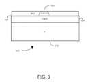
- FIG. 3is a simplified side diagram of an integrated CMOS-MEMS system according to an embodiment of the present invention.
- the system 300includes a substrate layer 310 , a semiconductor layer 320 , and an encapsulation layer 340 .
- the semiconductor layer 320covers the substrate layer 310 while also creating a surface region that forms an interface region 330 .
- the common semiconductor layer 320can be made of a silicon material or any other appropriate semiconductor.
- the semiconductor layer 320can include a CMOS layer or any other appropriate layer for implementing microelectronics.
- the semiconductor layer 320can include a CMOS layer comprised of any number of metal layers and can be provided on any type of design rule, such as a 0.18 micron design rule or less.
- the interface region 330 formed by the semiconductor layercan be integrated with any number of MEMS devices and CMOS devices; the CMOS devices can be configured from a foundry compatible process. The CMOS and MEMS devices can all be configured individually in separate portions of the interface region 330 .
- One skilled in the artwould recognize other variations, modifications, and alternatives.
- the overlying encapsulation layer 340can include a chip scale packaging (CSP) layer, such as a wafer level chip scale package (WL-CSP), also known as a wafer level package (WLP). Any other CSP method may be substituted if deemed appropriate by those skilled in the art. Additionally, the CSP layer 340 can be configured to hermetically seal any number of the integrated devices on the interface region 330 . Again, there can be many other variations, modifications, and alternatives.
- CSPchip scale packaging
- WL-CSPwafer level chip scale package
- WLPwafer level package
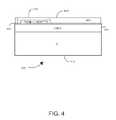
- FIG. 4is a simplified side diagram of an integrated CMOS-MEMS system according to another embodiment of the present invention.
- the system 400includes a substrate layer 410 , a semiconductor layer 420 , an integrated device 440 , and an encapsulation layer 450 .
- the semiconductor layer 420covers the substrate layer 410 while also creating a surface region that forms an interface region 430 .
- the common semiconductor layer 420can be made of a silicon material or any other appropriate semiconductor.
- the semiconductor layer 420can include a CMOS layer or any other appropriate layer for implementing microelectronics.
- the semiconductor layer 420can include a CMOS layer comprised of any number of metal layers and can be provided on any type of design rule, such as a 0.18 micron design rule or less.
- the interface region 430 formed by the semiconductor layercan be integrated with any number of MEMS devices and CMOS devices; the CMOS devices can be configured from a foundry compatible process.
- the CMOS and MEMS devicescan all be configured individually in separate portions of the interface region 430 .
- One skilled in the artwould recognize other variations, modifications, and alternatives.
- the integrated device 440can be an accelerometer.
- any number of MEMS devicescan be included in the integrated system 400 , and each of these devices can comprise one or more deposited materials, one or more bonded materials, or others.
- each of these devicescan comprise one or more deposited materials, one or more bonded materials, or others.
- the overlying encapsulation layer 440can include a chip scale packaging (CSP) layer, such as a wafer level chip scale package (WL-CSP), also known as a wafer level package (WLP). Any other CSP method may be substituted if deemed appropriate by those skilled in the art. Additionally, the CSP layer 440 can be configured to hermetically seal any number of the integrated devices on the interface region 430 . Again, there can be many other variations, modifications, and alternatives.
- CSPchip scale packaging
- WL-CSPwafer level chip scale package
- WLPwafer level package
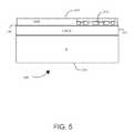
- FIG. 5is a simplified side diagram of an integrated CMOS-MEMS system according to yet another embodiment of the present invention.
- the system 500includes a substrate layer 510 , a semiconductor layer 520 , an integrated device 540 , and an encapsulation layer 550 .
- the semiconductor layer 520covers the substrate layer 510 while also creating a surface region that forms an interface region 530 .
- the common semiconductor layer 520can be made of a silicon material or any other appropriate semiconductor.
- the semiconductor layer 520can include a CMOS layer or any other appropriate layer for implementing microelectronics.
- the semiconductor layer 520can include a CMOS layer comprised of any number of metal layers and can be provided on any type of design rule, such as a 0.18 micron design rule or less.
- the interface region 530 formed by the semiconductor layercan be integrated with any number of MEMS devices and CMOS devices; the CMOS devices can be configured from a foundry compatible process. The CMOS and MEMS devices can all be configured individually in separate portions of the interface region 530 .
- One skilled in the artwould recognize other variations, modifications, and alternatives.
- the integrated device 540can be a gyroscope.
- any number of MEMS devicescan be included in the integrated system 500 , and each of these devices can comprise one or more deposited materials, one or more bonded materials, or others.
- each of these devicescan comprise one or more deposited materials, one or more bonded materials, or others.
- the overlying encapsulation layer 540can include a chip scale packaging (CSP) layer, such as a wafer level chip scale package (WL-CSP), also known as a wafer level package (WLP). Any other CSP method may be substituted if deemed appropriate by those skilled in the art. Additionally, the CSP layer 540 can be configured to hermetically seal any number of the integrated devices on the interface region 530 . Again, there can be many other variations, modifications, and alternatives.
- CSPchip scale packaging
- WL-CSPwafer level chip scale package
- WLPwafer level package
- FIG. 6is a simplified side diagram of an integrated CMOS-MEMS system according to yet another embodiment of the present invention.
- the system 600includes a substrate layer 610 , a semiconductor layer 620 , an integrated device 640 , and an encapsulation layer 650 .
- the semiconductor layer 620covers the substrate layer 610 while also creating a surface region that forms an interface region 630 .
- the common semiconductor layer 620can be made of a silicon material or any other appropriate semiconductor.
- the semiconductor layer 620can include a CMOS layer or any other appropriate layer for implementing microelectronics.
- the semiconductor layer 620can include a CMOS layer comprised of any number of metal layers and can be provided on any type of design rule, such as a 0.18 micron design rule or less.
- the interface region 630 formed by the semiconductor layercan be integrated with any number of MEMS devices and CMOS devices; the CMOS devices can be configured from a foundry compatible process. The CMOS and MEMS devices can all be configured individually in separate portions of the interface region 630 .
- One skilled in the artwould recognize other variations, modifications, and alternatives.
- the integrated device 640can be a magnetic sensor.
- any number of MEMS devicescan be included in the integrated system 600 , and each of these devices can comprise one or more deposited materials, one or more bonded materials, or others.
- each of these devicescan comprise one or more deposited materials, one or more bonded materials, or others.
- the overlying encapsulation layer 640can include a chip scale packaging (CSP) layer, such as a wafer level chip scale package (WL-CSP), also known as a wafer level package (WLP). Any other CSP method may be substituted if deemed appropriate by those skilled in the art. Additionally, the CSP layer 640 can be configured to hermetically seal any number of the integrated devices on the interface region 630 . Again, there can be many other variations, modifications, and alternatives.
- CSPchip scale packaging
- WL-CSPwafer level chip scale package
- WLPwafer level package
- FIG. 7is a simplified side diagram of an integrated CMOS-MEMS system according to yet another embodiment of the present invention.
- the system 700includes a substrate layer 710 , a semiconductor layer 720 , an integrated device 740 , and an encapsulation layer 750 .
- the semiconductor layer 720covers the substrate layer 510 while also creating a surface region that forms an interface region 730 .
- the common semiconductor layer 720can be made of a silicon material or any other appropriate semiconductor.
- the semiconductor layer 720can include a CMOS layer or any other appropriate layer for implementing microelectronics.
- the semiconductor layer 720can include a CMOS layer comprised of any number of metal layers and can be provided on any type of design rule, such as a 0.18 micron design rule or less.
- the interface region 730 formed by the semiconductor layercan be integrated with any number of MEMS devices and CMOS devices; the CMOS devices can be configured from a foundry compatible process.
- the CMOS and MEMS devicescan all be configured individually in separate portions of the interface region 730 .
- One skilled in the artwould recognize other variations, modifications, and alternatives.
- the integrated device 740can be a pressure sensor.
- any number of MEMS devicescan be included in the integrated system 700 , and each of these devices can comprise one or more deposited materials, one or more bonded materials, or others.
- each of these devicescan comprise one or more deposited materials, one or more bonded materials, or others.
- the overlying encapsulation layer 740can include a chip scale packaging (CSP) layer, such as a wafer level chip scale package (WL-CSP), also known as a wafer level package (WLP). Any other CSP method may be substituted if deemed appropriate by those skilled in the art. Additionally, the CSP layer 740 can be configured to hermetically seal any number of the integrated devices on the interface region 730 . Again, there can be many other variations, modifications, and alternatives.
- CSPchip scale packaging
- WL-CSPwafer level chip scale package
- WLPwafer level package
- FIG. 8is a simplified side diagram of an integrated CMOS-MEMS system according to yet another embodiment of the present invention.
- the system 800includes a substrate layer 810 , a semiconductor layer 820 , a CMOS device 840 , and an encapsulation layer 850 .
- the semiconductor layer 820covers the substrate layer 810 while also creating a surface region that forms an interface region 830 .
- the common semiconductor layer 820can be made of a silicon material or any other appropriate semiconductor.
- the semiconductor layer 820can include a CMOS layer or any other appropriate layer for implementing microelectronics.
- the semiconductor layer 820can include a CMOS layer comprised of any number of metal layers and can be provided on any type of design rule, such as a 0.18 micron design rule or less.
- the CMOS device 840can be integrated into the CMOS layer 820 and configured with the interface region 830 . Also, the CMOS device 840 can be configured from a foundry compatible process. Also, the interface region 830 formed by the semiconductor layer can be integrated with any number of MEMS devices and CMOS devices; the CMOS devices can be configured from a foundry compatible process. In various embodiments, any number of MEMS devices may be fabricated substantially simultaneously upon interface region 830 .
- MEMS devicesmay or may not be patterned using the same masks as other MEMS devices, MEMS devices may or may not be fabricated using deposited material that is used for other MEMS devices, MEMS devices may or may not be fabricated using the same process steps that are used to fabricate other MEMS devices, or the like.
- MEMS devicesmay or may not be fabricated using the same process steps that are used to fabricate other MEMS devices, or the like.
- FIGS. 9-11illustrate an example of some of the MEMS devices that can be fabricated approximately in parallel using the techniques described above.
- the CMOS and MEMS devicescan all be configured individually in separate portions of the interface region 830 .
- One skilled in the artwould recognize other variations, modifications, and alternatives.
- the overlying encapsulation layer 850can include a chip scale packaging (CSP) layer, such as a wafer level chip scale package (WL-CSP), also known as a wafer level package (WLP). Any other CSP method may be substituted if deemed appropriate by those skilled in the art. Additionally, the CSP layer 850 can be configured to hermetically seal any number of the integrated devices on the interface region 830 . Again, there can be many other variations, modifications, and alternatives.
- CSPchip scale packaging
- WL-CSPwafer level chip scale package
- WLPwafer level package
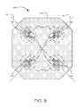
- FIG. 9is a simplified top diagram of a component of an integrated MEMS-CMOS system according to an embodiment of the present invention. More particularly, the component can be a transducer apparatus, which can be a component of an inertial sensing device, such as an accelerometer. As shown, apparatus 900 includes a movable base structure 910 , at least one intermediate anchor structure 920 , and at least one intermediate spring structure 930 . In an embodiment, apparatus 900 can be configured to improve tolerance of external deformations. Those of ordinary skill in the art will recognize other variations, modifications, and alternatives.
- movable base structure 910can have an outer surface region, and have at least one portion removed to form at least one inner surface region 902 .
- movable base structure 910can be formed from a single crystal silicon, polycrystalline silicon, or amorphous silicon material.
- Moveable base structure 910can also include a thickness of a polymer or a thickness of a metal material.
- movable base structure 910can include other materials and combinations thereof.
- movable base structure 910can be a rectangular movable base structure, a patterned polygonal base structure, or the like.
- intermediate anchor structure(s) 920can be spatially disposed within a vicinity of inner surface region(s) 902 of the movable base structure.
- intermediate anchor structure(s) 920can be formed from single crystal silicon, polycrystalline silicon, amorphous silicon material, or the like.
- Intermediate anchor structure(s) 920can also include a polymer or metal material, or other materials or combinations thereof.
- intermediate spring structure(s) 930can be operably coupled to the intermediate anchor structure(s) 920 and at least one portion of inner surface region(s) 902 of movable base structure 910 .
- intermediate spring structure(s) 930can be formed from single crystal silicon, polycrystalline silicon, amorphous silicon material, or the like.
- Intermediate spring structure(s) 930can also include a polymer or metal material, or other materials or combinations thereof.
- intermediate spring structure(s) 930can be spatially oriented to be substantially 45 degrees or substantially (pi/4) radians to the edges of the die.
- the intermediate spring structure(s)can have at least one segment having a segment length.
- the segments of the springwhich are connected by folds, are used as a reference.
- the segmentswould be positioned such that the segments are perpendicular to diagonal lines 901 .
- Another way to determine the orientation of a springcan be done by drawing a “line” connecting the contacts of the spring from the anchor to the movable base (i.e. the end points of the spring). In this case, the proper orientation of the spring would have the “line” forming a substantially 45 degree or (pi/4) radian angle with the edges of a die (pointed along diagonal lines 901 ).
- apparatus 900can include at least one capacitor element spatially disposed within a vicinity of inner surface region(s) 902 of movable base structure 910 .
- the capacitor element(s)can include a fixed capacitor element and a movable capacitor element.
- the movable capacitor elementwill generally be disposed in a portion of the movable base structure 910 .
- the physical basis of apparatus 900is to have the average displacement of the fixed capacitor element(s) match the average displacement of the movable capacitor element(s) in response to external deformations.
- apparatus 900can be coupled to another MEMS device or an electronic device.
- apparatus 900can be configured to be tolerant of external deformations.
- Apparatus 900can be a transducer apparatus which reduces the area needed for anchors and springs and provides more area for other MEMS components. There can be other variations, modifications, and alternatives as well. Further embodiments of the above device may be found in the co-pending patent application, referred to above.
- Another desirable design aspect contemplated by the inventorsis the reduction of the area used for springs. This can be achieved via two approaches. First, by having the springs oriented at substantially 45 degrees or substantially (pi/4) radians with respect to the edges of a die (i.e. aligned to diagonal lines 901 ), the Young's modulus is reduced and/or minimized with respect to orientation angle for single crystal silicon and standard silicon wafer crystal orientations.
- One way to determine the orientation of a springcan be done by using the segments of the spring, which are connected by folds, as a reference. The segments would be positioned such that the segments are perpendicular to diagonal lines 901 .
- Another way to determine the orientation of a springcan be done by drawing a “line” connecting the contacts of the spring from the anchor to the movable base (i.e. the end points of the spring). In this case, the proper orientation of the spring would have the “line” forming a substantially 45 degree or (pi/4) radian angle with the edges of a die (pointed along diagonal lines 901 ). However, the orientations of the springs may only be approximately oriented at the suggested angles due to manufacturing tolerances (orientation angles may be less than or greater than 45 degrees or (pi/4) radians). Second, the number of spring segments, which are connected by folds, should be regulated as too many spring segments may cause the spring structure to be not stiff enough.
- the number of segmentscannot be below a certain number, or the spring segment length will exceed the available die size, or make it impossible to put the anchor for the springs at the properly optimized “intermediate” locations to minimize undesirable variations of output with temperature.
- the spring configuration with variable number of spring segments and spring segment length in either of two perpendicular directionsrepresents various embodiments of the present invention. In such embodiments, the area is reduced while keeping the anchor and attachment point to the movable mass along a diagonal center line.
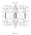
- FIG. 10is a simplified top diagram of a component of an integrated MEMS-CMOS system according to various embodiments of the present invention. More particularly, the component can be an inertial sensing device, such as a gyroscope.
- device 1000which can be disposed upon a substrate having a surface region, includes at least one anchor structure 1010 , at least one frame structure 1020 , at least one movable structure, at least one first flexible member, and at least one second flexible member.
- the movable structure(s)can include at least one peripheral movable structure 1030 and at least one central movable structure 1040 .
- the first flexible member(s)can include flexible anchor member(s) 1050 and the second flexible member(s) can include at least one flexible frame member 1060 and/or at least one flexible structure member 1070 .
- the second flexible member(s)can include at least one flexible frame member 1060 and/or at least one flexible structure member 1070 .
- the substratecan include a buried oxide (BOX) substrate.
- the substratecan include an epitaxial (EPI) material.
- the substratecan have a silicon, single crystal silicon, or polycrystalline silicon material.
- the substratecan also include a dielectric material, a metal material, a metal alloy, or other materials or combination of materials thereof.
- the substratecan have an integrated circuit layer, such as a CMOS device layer, formed overlying the substrate.
- the substrateincludes a surface region. At least one anchor structure 1010 can be formed overlying the surface region. At least one flexible anchor member 1050 is coupled to at least a portion of the anchor structure(s).
- anchor structure(s) 1010 and flexible anchor member(s) 1050can include a silicon, dielectric, metal, alloy, or other materials or combination thereof.
- flexible anchor members 1050can include torsion spring(s) or bending spring(s).
- anchor structure(s) 1010 and flexible anchor member(s) 1050can be formed together during the same fabrication processes or separately by performing a wet or dry etching or mechanical process. Of course, there can be other variations, modifications, and alternatives.
- frame structure(s) 1020can be formed having at least a portion coupled to flexible anchor member(s) 1050 .
- Flexible frame member(s) 1060can be formed and coupled to at least a portion of frame structure(s) 1020 .
- at least one flexible coupling member 1080can be formed to couple frame structure(s) 1020 .
- frame structure(s) 1020 , flexible coupling member(s) 1080 and flexible frame member(s) 1060can include a silicon, dielectric, metal, alloy, or other materials or combinations thereof.
- flexible frame member(s) 1060 and flexible coupling member(s) 1080can include torsion spring(s) or bending spring(s).
- frame structure(s) 1020 , flexible coupling member(s) 1080 , and flexible frame member(s) 1060can be formed together during the same fabrication processes or separately by performing a wet or dry etching or mechanical process. As stated previously, there can be other variations, modifications, and alternatives.
- peripheral movable structure(s) 1030can be formed overlying the substrate, having at least one portion coupled to flexible frame member(s) 1060 .
- the movable structure(s), which can be peripheral movable structure(s) 1030can have at least one flexible tilting member.
- Flexible structure member(s) 1070can be formed and coupled to at least a portion of peripheral movable structure(s) 1030 .
- flexible structure member(s) 1070can be coupled to central movable structure(s) 1040 , which can be formed overlying the substrate.
- peripheral movable structure 1030 , central movable structure 1040 , flexible structure and tilting member(s)can include a silicon, dielectric, metal, alloy, or other materials or combinations thereof.
- the flexible structure and tilting member(s)can include torsion spring(s) or bending spring(s).
- Other torsion springs or bending springscan also be formed within at least one portion of central movable structure(s) 1040 , such as the underside of central movable structure(s) 240 which overlies the substrate.
- the movable structurescan be formed within frame structure(s) 1020 .
- four peripheral movable structures 1030 and two central movable structures 1040are shown formed within two frame structures 1020 .
- Each frame structures 1020are coupled to two peripheral movable structures 1030 and one central movable structure 1040 .
- the peripheral and central movable structures 1030 / 1040can be proof masses, which can be predetermined test masses used in a measuring device.
- the peripheral and central movable structure(s) 1030 / 1040 and the flexible structure and tilting member(s) [referring to flexible structure member(s) 1070 ]can be formed together or separately by performing a wet or dry etching or mechanical process. Again, there can be other variations, modifications, and alternatives.
- At least one comb structure 1090can be formed and coupled to at least one portion of frame structure(s) 1020 .
- comb structure(s) 1090can be anti-phase driving comb structure(s), which can include a silicon, dielectric, metal, alloy, or other materials or combinations thereof.
- the peripheral and central movable structure(s) 1030 / 1040can have stop structures 1001 , which can be used to set the boundaries of any vibration, movement, or displacement. A portion of peripheral movable structure 1030 and central movable structure 1040 may be removed.
- peripheral movable structure 1030 and central movable structure 1040perforations within a line or an array of perforations.
- the perforationscan be formed by performing an etching process or mechanical process.
- all elements mentioned previouscan be formed by performing an etching process on one wafer or material.
- there can be other variations, modifications, and alternatives. Further embodiments of the above deviceare disclosed in the co-pending patent application referred to above.
- FIG. 11is a simplified top diagram of a component of an integrated MEMS-CMOS system according to an embodiment of the present invention.
- This diagramwhich can represent a partially formed three-axis magnetic field sensor device or a two-axis magnetic field sensor device, is merely an example, which should not unduly limit the scope of the claims herein.
- device 1100includes a substrate 1110 , an integrated circuit (IC) layer 1120 , a first magnetic field sensor element 1130 , and a second magnetic field sensor element 1140 .
- ICintegrated circuit
- substrate 1110can have a surface region.
- substrate 1110can include a buried oxide (BOX) substrate.
- substrate 1110can include a substrate-on-insulator (SOI) substrate.
- substrate 1110can include an epitaxial (EPI) material.
- substrate 1110can have a silicon, single crystal silicon, or polycrystalline silicon material.
- substrate 1110can also include metals, dielectrics, polymers, and other materials and combinations thereof. Those skilled in the art will recognize other variations, modifications, and alternatives.
- IC layer 1120can be formed overlying at least one portion of the surface region.
- IC layer 1120can include an application specific integrated circuit (ASIC) layer, or other type of IC layer or combination thereof.
- ASICapplication specific integrated circuit
- IC layer 1120can include at least one IC device, CMOS device, or other device.
- IC layer 1120can be coupled to the first and second magnetic field sensor elements 1130 and 1140 .
- first magnetic field sensor element(s) 1130 and second magnetic field sensor element 1140can be formed overlying at least one portion of the surface region.
- Magnetic field sensor elements 1130 and 1140can include ordinary magneto-resistive (OMR) device(s), anisotropic magneto-resistive (AMR) device(s), giant magneto-resistive (GMR) device(s), or tunnel junction magneto-resistive (TMR) device(s).
- Elements 1130 and 1140can also be other types of magnetic field sensor devices, sensors, or combinations thereof.
- magnetic field sensor elements 1130 and 1140can include thin film devices that can be deposited overlying at least one portion of the surface region.
- the thin film device(s)can be deposited by a sputtering process or an electric plating process.
- magnetic field sensor elements 1130 and 1140are formed as a Wheatstone bridge, a half bridge, or a single element configuration.
- magnetic field sensor elements 1130 and 1140can include at least one layer of dielectric material and/or metal material. As stated previously, there can be other variations, modifications, and alternatives. Further embodiments of the above device are disclosed in the co-pending patent application referred to above.
- FIG. 12illustrates a functional block diagram of various embodiments of the present invention.
- a computing device 1200typically includes an applications processor 1210 , memory 1220 , a touch screen display 1230 and driver 1240 , an image acquisition device 1250 , audio input/output devices 1260 , and the like. Additional communications from and to computing device are typically provided by via a wired interface 1270 , a GPS/Wi-Fi/Bluetooth interface 1280 , RF interfaces 1290 and driver 1300 , and the like. Also included in various embodiments are physical sensors 1310 .
- computing device 1200may be a hand-held computing device (e.g. Apple iPad, Apple iTouch, Dell Mini slate/Streak, Lenovo Skylight/IdeaPad, Samsung Galaxy Tab, Asus EEE series, HP Slate, Notion Ink Adam), a portable telephone (e.g. Apple iPhone, Motorola Droid, Google Nexus One, HTC Incredible/EVO 4G, Palm Pre series, Nokia N900), a portable computer (e.g. netbook, laptop), a media player (e.g. Microsoft Zune, Apple iPod), a reading device (e.g. Amazon Kindle, Barnes and Noble Nook), or the like.
- a hand-held computing devicee.g. Apple iPad, Apple iTouch, Dell Mini slate/Streak, Lenovo Skylight/IdeaPad, Samsung Galaxy Tab, Asus EEE series, HP Slate, Notion Ink Adam
- a portable telephonee.g. Apple iPhone, Motorola Droid, Google Nexus One, HTC Incredible/EVO 4G, Palm Pre series, Nokia N900
- computing device 1200may include one or more processors 1210 .
- processors 1210may also be termed application processors, and may include a processor core, a video/graphics core, and other cores.
- Processors 1210may be a processor from Apple (A4), Intel (Atom), NVidia (Tegra 2), Marvell (Armada), Qualcomm (Snapdragon), Samsung, TI (OMAP), or the like.
- the processor coremay be an Intel processor, an ARM Holdings processor such as the Cortex-A, -M, -R or ARM series processors, or the like.
- the video/graphics coremay be an Imagination Technologies processor PowerVR -SGX, -MBX, -VGX graphics, an Nvidia graphics processor (e.g. GeForce), or the like.
- Other processing capabilitymay include audio processors, interface controllers, and the like. It is contemplated that other existing and/or later-developed processors may be used in various embodiments of the present invention.
- memory 1220may include different types of memory (including memory controllers), such as flash memory (e.g. NOR, NAND), pseudo SRAM, DDR SDRAM, or the like.
- Memory 1220may be fixed within computing device 1200 or removable (e.g. SD, SDHC, MMC, MINI SD, MICRO SD, CF, SIM).
- computer-executable software codee.g. firmware, application programs
- application dataoperating system data or the like. It is contemplated that other existing and/or later-developed memory and memory technology may be used in various embodiments of the present invention.
- touch screen display 1230 and driver 1240may be based upon a variety of later-developed or current touch screen technology including resistive displays, capacitive displays, optical sensor displays, electromagnetic resonance, or the like. Additionally, touch screen display 1230 may include single touch or multiple-touch sensing capability. Any later-developed or conventional output display technology may be used for the output display, such as TFT-LCD, OLED, Plasma, trans-reflective (Pixel Qi), electronic ink (e.g. electrophoretic, electrowetting, interferometric modulating). In various embodiments, the resolution of such displays and the resolution of such touch sensors may be set based upon engineering or non-engineering factors (e.g. sales, marketing). In some embodiments of the present invention, a display output port, such as an HDMI-based port or DVI-based port may also be included.
- a display output portsuch as an HDMI-based port or DVI-based port may also be included.
- image capture device 1250may include a sensor, driver, lens and the like.
- the sensormay be based upon any later-developed or convention sensor technology, such as CMOS, CCD, or the like.
- image recognition software programsare provided to process the image data.
- such softwaremay provide functionality such as: facial recognition, head tracking, camera parameter control, or the like.
- audio input/output 1260may include conventional microphone(s)/speakers. In some embodiments of the present invention, three-wire or four-wire audio connector ports are included to enable the user to use an external audio device such as external speakers, headphones or combination headphone/microphones.
- voice processing and/or recognition softwaremay be provided to applications processor 1210 to enable the user to operate computing device 1200 by stating voice commands.
- a speech enginemay be provided in various embodiments to enable computing device 1200 to provide audio status messages, audio response messages, or the like.
- wired interface 1270may be used to provide data transfers between computing device 1200 and an external source, such as a computer, a remote server, a storage network, another computing device 1200 , or the like.
- datamay include application data, operating system data, firmware, or the like.
- Embodimentsmay include any later-developed or conventional physical interface/protocol, such as: USB 2.0, 3.0, micro USB, mini USB, Firewire, Apple iPod connector, Ethernet, POTS, or the like. Additionally, software that enables communications over such networks is typically provided.
- a wireless interface 1280may also be provided to provide wireless data transfers between computing device 1200 and external sources, such as computers, storage networks, headphones, microphones, cameras, or the like.
- wireless protocolsmay include Wi-Fi (e.g. IEEE 802.11 a/b/g/n, WiMax), Bluetooth, IR and the like.
- GPS receiving capabilitymay also be included in various embodiments of the present invention, however is not required. As illustrated in FIG. 12 , GPS functionality is included as part of wireless interface 1280 merely for sake of convenience, although in implementation, such functionality is currently performed by circuitry that is distinct from the Wi-Fi circuitry and distinct from the Bluetooth circuitry.
- RF interfaces 1290may support any future-developed or conventional radio frequency communications protocol, such as CDMA-based protocols (e.g. WCDMA), GSM-based protocols, HSUPA-based protocols, or the like.
- driver 1300is illustrated as being distinct from applications processor 1210 . However, in some embodiments, these functionality are provided upon a single IC package, for example the Marvel PXA330 processor, and the like. It is contemplated that some embodiments of computing device 1200 need not include the RF functionality provided by RF interface 1290 and driver 1300 .
- FIG. 12also illustrates computing device 1200 to include physical sensors 1310 .
- physical sensors 1310can be single axis or multi-axis Micro-Electro-Mechanical Systems (MEMS) based devices being developed by M-cube, the assignee of the present patent application.
- Physical sensors 1310can include accelerometers, gyroscopes, pressure sensors, magnetic field sensors, bio sensors, and the like.
- physical sensors 1310may fabricated using the combined CMOS MEMS fabrication techniques described above. More specifically, one or more MEMS devices may be fabricated approximately in parallel using common masks, layers, and processes, above a substrate. In various embodiments, the substrate may be on top of a CMOS device. Both the CMOS and MEMS device may be fabricated using foundry-compatible processes.
- conventional physical sensors 1310from Bosch, STMicroelectronics, Analog Devices, Kionix or the like may be used.
- any number of future developed or current operating systemsmay be supported, such as iPhone OS (e.g. iOS), WindowsMobile (e.g. 7), Google Android (e.g. 2.2), Symbian, or the like.
- the operating systemmay be a multi-threaded multi-tasking operating system. Accordingly, inputs and/or outputs from and to touch screen display 1230 and driver 1240 and inputs/or outputs to physical sensors 1310 may be processed in parallel processing threads. In other embodiments, such events or outputs may be processed serially, or the like. Inputs and outputs from other functional blocks may also be processed in parallel or serially, in other embodiments of the present invention, such as image acquisition device 1250 and physical sensors 1310 .
- FIG. 12is representative of one computing device 1200 capable of embodying the present invention. It will be readily apparent to one of ordinary skill in the art that many other hardware and software configurations are suitable for use with the present invention. Embodiments of the present invention may include at least some but need not include all of the functional blocks illustrated in FIG. 12 .
- computing device 1200may lack image acquisition unit 1250 , or RF interface 1290 and/or driver 1300 , or GPS capability, or the like. Additional functions may also be added to various embodiments of computing device 1200 , such as a physical keyboard, an additional image acquisition device, a trackball or trackpad, a joystick, or the like.
- multiple functional blocksmay be embodied into a single physical package or device, and various functional blocks may be divided and be performed among separate physical packages or devices.
- FIG. 13is a simplified perspective diagram of a transducer apparatus according to an embodiment of the present invention.
- apparatus 1300includes a movable base structure 1310 , at least one intermediate anchor structure 1320 , and at least one intermediate spring structure 1330 .
- apparatus 1300can be configured to improve tolerance of external deformations. A detailed description regarding the elements and configuration of apparatus 1300 can be found above in the description for FIG. 9 . Those of ordinary skill in the art will recognize other variations, modifications, and alternatives.
- FIG. 14is a simplified cross-sectional side diagram of a transducer apparatus according to an embodiment of the present invention.
- apparatus 1400includes a movable base structure 1410 , at least one intermediate anchor structure 1420 , and at least one intermediate spring structure 1430 .
- apparatus 1400can be configured to improve tolerance of external deformations. A detailed description regarding the elements and configuration of apparatus 1400 can be found above in the description for FIG. 14 . Those of ordinary skill in the art will recognize other variations, modifications, and alternatives.
- FIG. 15is a simplified cross-sectional close-up diagram of a transducer apparatus according to an embodiment of the present invention.
- apparatus 1500includes a movable base structure 1510 and at least one capacitor element 1560 .
- capacitor element(s) 1560can include a fixed capacitor element and a movable capacitor element.
- the movable capacitor elementcan be disposed on a portion of the movable base structure and the fixed capacitor element can be disposed on a portion of the anchor structure(s).
- the capacitor element(s)can be tall vertical structures, which can include silicon materials and the like.
- apparatus 1500can be configured to improve tolerance of external deformations.
- Capacitor element(s) 1560can be spatially disposed within a vicinity of inner surface region(s) 1502 of the movable base structure.
- Capacitor element(s) 1560can also include differential capacitor element pair(s).
- the differential capacitor element pair(s)can operate during motion of movable base structure 1510 . The charge on one element of the pair can increase while the charge on the other complementary element can decrease.
- Each differential paircan also be spatially disposed within a vicinity of inner surface region(s) 1502 , and each pair can be disposed within a vicinity of its own inner surface region, isolated from other pairs.
Landscapes
- Engineering & Computer Science (AREA)
- Manufacturing & Machinery (AREA)
- Microelectronics & Electronic Packaging (AREA)
- Micromachines (AREA)
- Pressure Sensors (AREA)
Abstract
Description
spring constant,kis proportional toNspring/[Nsegment*(L^3)], whereNspring=# of springs,Nsegment=# of segments per spring, andL=segment length.
Claims (11)
Priority Applications (1)
| Application Number | Priority Date | Filing Date | Title |
|---|---|---|---|
| US14/445,012US9440846B2 (en) | 2009-10-28 | 2014-07-28 | System on a chip using integrated MEMS and CMOS devices |
Applications Claiming Priority (7)
| Application Number | Priority Date | Filing Date | Title |
|---|---|---|---|
| US25549009P | 2009-10-28 | 2009-10-28 | |
| US35646710P | 2010-06-18 | 2010-06-18 | |
| US12/859,631US8486723B1 (en) | 2010-08-19 | 2010-08-19 | Three axis magnetic sensor device and method |
| US12/859,647US8553389B1 (en) | 2010-08-19 | 2010-08-19 | Anchor design and method for MEMS transducer apparatuses |
| US12/859,672US8477473B1 (en) | 2010-08-19 | 2010-08-19 | Transducer structure and method for MEMS devices |
| US12/913,440US8823007B2 (en) | 2009-10-28 | 2010-10-27 | Integrated system on chip using multiple MEMS and CMOS devices |
| US14/445,012US9440846B2 (en) | 2009-10-28 | 2014-07-28 | System on a chip using integrated MEMS and CMOS devices |
Related Parent Applications (1)
| Application Number | Title | Priority Date | Filing Date |
|---|---|---|---|
| US12/913,440DivisionUS8823007B2 (en) | 2009-06-23 | 2010-10-27 | Integrated system on chip using multiple MEMS and CMOS devices |
Publications (2)
| Publication Number | Publication Date |
|---|---|
| US20150307347A1 US20150307347A1 (en) | 2015-10-29 |
| US9440846B2true US9440846B2 (en) | 2016-09-13 |
Family
ID=43922555
Family Applications (2)
| Application Number | Title | Priority Date | Filing Date |
|---|---|---|---|
| US12/913,440Active2031-03-08US8823007B2 (en) | 2009-06-23 | 2010-10-27 | Integrated system on chip using multiple MEMS and CMOS devices |
| US14/445,012Active2030-11-27US9440846B2 (en) | 2009-10-28 | 2014-07-28 | System on a chip using integrated MEMS and CMOS devices |
Family Applications Before (1)
| Application Number | Title | Priority Date | Filing Date |
|---|---|---|---|
| US12/913,440Active2031-03-08US8823007B2 (en) | 2009-06-23 | 2010-10-27 | Integrated system on chip using multiple MEMS and CMOS devices |
Country Status (3)
| Country | Link |
|---|---|
| US (2) | US8823007B2 (en) |
| CN (1) | CN202717577U (en) |
| WO (1) | WO2011053734A1 (en) |
Cited By (1)
| Publication number | Priority date | Publication date | Assignee | Title |
|---|---|---|---|---|
| US11574943B2 (en) | 2019-12-20 | 2023-02-07 | Samsung Electronics Co., Ltd. | Semiconductor package |
Families Citing this family (61)
| Publication number | Priority date | Publication date | Assignee | Title |
|---|---|---|---|---|
| US7302648B1 (en)* | 2002-07-10 | 2007-11-27 | Apple Inc. | Method and apparatus for resizing buffered windows |
| US8928602B1 (en) | 2009-03-03 | 2015-01-06 | MCube Inc. | Methods and apparatus for object tracking on a hand-held device |
| US8797279B2 (en) | 2010-05-25 | 2014-08-05 | MCube Inc. | Analog touchscreen methods and apparatus |
| US8486723B1 (en) | 2010-08-19 | 2013-07-16 | MCube Inc. | Three axis magnetic sensor device and method |
| US8823007B2 (en) | 2009-10-28 | 2014-09-02 | MCube Inc. | Integrated system on chip using multiple MEMS and CMOS devices |
| US8476129B1 (en) | 2010-05-24 | 2013-07-02 | MCube Inc. | Method and structure of sensors and MEMS devices using vertical mounting with interconnections |
| US8477473B1 (en) | 2010-08-19 | 2013-07-02 | MCube Inc. | Transducer structure and method for MEMS devices |
| US8553389B1 (en) | 2010-08-19 | 2013-10-08 | MCube Inc. | Anchor design and method for MEMS transducer apparatuses |
| US8710597B1 (en) | 2010-04-21 | 2014-04-29 | MCube Inc. | Method and structure for adding mass with stress isolation to MEMS structures |
| US8421082B1 (en) | 2010-01-19 | 2013-04-16 | Mcube, Inc. | Integrated CMOS and MEMS with air dielectric method and system |
| US8395252B1 (en)* | 2009-11-13 | 2013-03-12 | MCube Inc. | Integrated MEMS and CMOS package and method |
| US9709509B1 (en)* | 2009-11-13 | 2017-07-18 | MCube Inc. | System configured for integrated communication, MEMS, Processor, and applications using a foundry compatible semiconductor process |
| US8637943B1 (en) | 2010-01-04 | 2014-01-28 | MCube Inc. | Multi-axis integrated MEMS devices with CMOS circuits and method therefor |
| US8236577B1 (en) | 2010-01-15 | 2012-08-07 | MCube Inc. | Foundry compatible process for manufacturing a magneto meter using lorentz force for integrated systems |
| US8407905B1 (en) | 2010-01-15 | 2013-04-02 | Mcube, Inc. | Multiple magneto meters using Lorentz force for integrated systems |
| US8584521B1 (en) | 2010-01-19 | 2013-11-19 | MCube Inc. | Accurate gyroscope device using MEMS and quartz |
| US8794065B1 (en)* | 2010-02-27 | 2014-08-05 | MCube Inc. | Integrated inertial sensing apparatus using MEMS and quartz configured on crystallographic planes |
| US8936959B1 (en) | 2010-02-27 | 2015-01-20 | MCube Inc. | Integrated rf MEMS, control systems and methods |
| US8367522B1 (en) | 2010-04-08 | 2013-02-05 | MCube Inc. | Method and structure of integrated micro electro-mechanical systems and electronic devices using edge bond pads |
| US8564075B1 (en) | 2010-04-21 | 2013-10-22 | MCube Inc. | Package tolerate design and method |
| US8476084B1 (en) | 2010-05-24 | 2013-07-02 | MCube Inc. | Method and structure of sensors or electronic devices using vertical mounting |
| US8928696B1 (en) | 2010-05-25 | 2015-01-06 | MCube Inc. | Methods and apparatus for operating hysteresis on a hand held device |
| US8652961B1 (en) | 2010-06-18 | 2014-02-18 | MCube Inc. | Methods and structure for adapting MEMS structures to form electrical interconnections for integrated circuits |
| US8869616B1 (en) | 2010-06-18 | 2014-10-28 | MCube Inc. | Method and structure of an inertial sensor using tilt conversion |
| US8993362B1 (en) | 2010-07-23 | 2015-03-31 | MCube Inc. | Oxide retainer method for MEMS devices |
| US8723986B1 (en) | 2010-11-04 | 2014-05-13 | MCube Inc. | Methods and apparatus for initiating image capture on a hand-held device |
| US8969101B1 (en) | 2011-08-17 | 2015-03-03 | MCube Inc. | Three axis magnetic sensor device and method using flex cables |
| US9000556B2 (en) | 2011-10-07 | 2015-04-07 | International Business Machines Corporation | Lateral etch stop for NEMS release etch for high density NEMS/CMOS monolithic integration |
| US20130120919A1 (en)* | 2011-11-11 | 2013-05-16 | Kyle Erickson | Media Control Device |
| US9246017B2 (en)* | 2012-02-07 | 2016-01-26 | Mcube, Inc. | MEMS-based dual and single proof-mass accelerometer methods and apparatus |
| US10324108B2 (en) | 2012-02-07 | 2019-06-18 | Mcube, Inc. | Dynamic offset correction for calibration of MEMS sensor |
| US9103705B2 (en)* | 2012-02-27 | 2015-08-11 | Freescale Semiconductor, Inc. | Combined environmental parameter sensor |
| US10197587B2 (en) | 2012-03-17 | 2019-02-05 | MCube Inc. | Device and method for using time rate of change of sensor data to determine device rotation |
| DE102012210049A1 (en)* | 2012-06-14 | 2013-12-19 | Robert Bosch Gmbh | Hybrid integrated component and method for its production |
| US20130334531A1 (en)* | 2012-06-15 | 2013-12-19 | Franz Jost | Systems and methods for measuring temperature and current in integrated circuit devices |
| DE102012213313B4 (en) | 2012-07-30 | 2020-11-12 | Robert Bosch Gmbh | Micromechanical structure |
| DE102012217133A1 (en) | 2012-09-24 | 2014-03-27 | Robert Bosch Gmbh | Microelectronic component and corresponding manufacturing method |
| EP2720034B1 (en)* | 2012-10-12 | 2016-04-27 | ams International AG | Integrated Circuit comprising a relative humidity sensor and a thermal conductivity based gas sensor |
| US10132630B2 (en) | 2013-01-25 | 2018-11-20 | MCube Inc. | Multi-axis integrated MEMS inertial sensing device on single packaged chip |
| US10036635B2 (en) | 2013-01-25 | 2018-07-31 | MCube Inc. | Multi-axis MEMS rate sensor device |
| US9249012B2 (en)* | 2013-01-25 | 2016-02-02 | Mcube, Inc. | Method and device of MEMS process control monitoring and packaged MEMS with different cavity pressures |
| US10046964B2 (en) | 2013-03-07 | 2018-08-14 | MCube Inc. | MEMS structure with improved shielding and method |
| US9862594B2 (en)* | 2013-03-15 | 2018-01-09 | Versana Micro Inc. | Wearable device having a monolithically integrated multi-sensor device on a semiconductor substrate and method therefor |
| US8958592B2 (en)* | 2013-05-23 | 2015-02-17 | Fortemedia, Inc. | Microphone array housing with acoustic extending structure and electronic device utilizing the same |
| US8786130B1 (en) | 2013-08-23 | 2014-07-22 | Inoso, Llc | Method of forming an electromechanical power switch for controlling power to integrated circuit devices and related devices |
| US9793080B2 (en) | 2013-08-23 | 2017-10-17 | Inoso, Llc | Electromechanical power switch integrated circuits and devices and methods thereof |
| US20160302729A1 (en) | 2013-12-11 | 2016-10-20 | The Board Of Regents Of The University Of Texas System | Devices and methods for parameter measurement |
| DE102014208177A1 (en)* | 2014-04-30 | 2015-11-05 | Robert Bosch Gmbh | Forming a logical microcontroller by at least two physical microcontrollers on a common semiconductor substrate |
| CN105293424B (en)* | 2014-05-26 | 2017-04-05 | 中芯国际集成电路制造(上海)有限公司 | A kind of semiconductor devices and preparation method, electronic installation |
| CN105984834B (en)* | 2015-02-04 | 2018-07-06 | 中芯国际集成电路制造(上海)有限公司 | A kind of integrated sensor and preparation method thereof |
| CN104634832B (en)* | 2015-02-28 | 2018-01-05 | 苏州工业园区纳米产业技术研究院有限公司 | CMOS MEMS capacitive humidity sensors and preparation method thereof |
| US9505611B1 (en) | 2015-07-30 | 2016-11-29 | Global Foundries Inc. | Integration of electromechanical and CMOS devices in front-end-of-line using replacement metal gate process flow |
| US10252920B2 (en) | 2015-09-07 | 2019-04-09 | International Business Machines Corporation | Flowfield sensors for monitoring liquid flow |
| US10605823B2 (en) | 2016-02-25 | 2020-03-31 | m.Cube, Inc. | Multiple MEMS device and methods |
| TWI721147B (en)* | 2016-04-04 | 2021-03-11 | 美商矽立科技有限公司 | Apparatus and methods for integrated mems devices |
| DE102017200725A1 (en) | 2017-01-18 | 2018-07-19 | Robert Bosch Gmbh | Micromechanical sensor |
| DE102018221102B4 (en) | 2018-12-06 | 2020-06-25 | Robert Bosch Gmbh | Inertial sensor with a movable detection element of a field effect transistor and method for producing the same |
| CN111377395B (en)* | 2018-12-27 | 2023-09-08 | 中芯集成电路(宁波)有限公司上海分公司 | MEMS packaging structure and manufacturing method thereof |
| CN111060192B (en)* | 2019-10-21 | 2022-02-15 | 张国基 | A calculation chip system for abnormal vibration of mechanical equipment |
| US11420866B2 (en)* | 2020-03-23 | 2022-08-23 | Taiwan Semiconductor Manufacturing Company, Ltd. | Composite spring structure to reinforce mechanical robustness of a MEMS device |
| CN111505210B (en)* | 2020-04-29 | 2021-07-27 | 华中科技大学 | A gas sensor chip integrated micromachining device |
Citations (38)
| Publication number | Priority date | Publication date | Assignee | Title |
|---|---|---|---|---|
| US3614677A (en) | 1966-04-29 | 1971-10-19 | Ibm | Electromechanical monolithic resonator |
| US20040227201A1 (en) | 2003-05-13 | 2004-11-18 | Innovative Technology Licensing, Llc | Modules integrating MEMS devices with pre-processed electronic circuitry, and methods for fabricating such modules |
| US20050252293A1 (en) | 2004-05-11 | 2005-11-17 | Samsung Electronics Co., Ltd. | Magnetic MEMS device and method of forming thereof |
| US20060049826A1 (en) | 2001-03-01 | 2006-03-09 | Onix Microsystems | Optical cross-connect system |
| US20070181962A1 (en)* | 2006-01-20 | 2007-08-09 | Aaron Partridge | Wafer encapsulated microelectromechanical structure and method of manufacturing same |
| US20070281379A1 (en) | 2006-06-04 | 2007-12-06 | Stark Brian H | Microelectromechanical systems having stored charge and methods for fabricating and using same |
| US20080014682A1 (en) | 2003-10-24 | 2008-01-17 | Miradia Inc. | Method and system for sealing packages for optics |
| US20100083756A1 (en) | 2007-04-05 | 2010-04-08 | Fraunhofer-Gesellschaft zur Foeerderung der angewa | Micromechanical Inertial Sensor for Measuring Rotation Rates |
| US20100236327A1 (en) | 2009-03-17 | 2010-09-23 | Minyao Mao | Tri-axis Angular Rate Sensor |
| US20110154905A1 (en) | 2009-12-25 | 2011-06-30 | Industrial Technology Research Institute | Capacitive sensor and manufacturing method thereof |
| US8181874B1 (en) | 2010-11-04 | 2012-05-22 | MCube Inc. | Methods and apparatus for facilitating capture of magnetic credit card data on a hand held device |
| US8227285B1 (en) | 2008-06-25 | 2012-07-24 | MCube Inc. | Method and structure of monolithetically integrated inertial sensor using IC foundry-compatible processes |
| US8236577B1 (en) | 2010-01-15 | 2012-08-07 | MCube Inc. | Foundry compatible process for manufacturing a magneto meter using lorentz force for integrated systems |
| US8245923B1 (en) | 2010-11-04 | 2012-08-21 | MCube Inc. | Methods and apparatus for capturing magnetic credit card data on a hand held device |
| US8324047B1 (en) | 2009-11-13 | 2012-12-04 | MCube Inc. | Method and structure of an integrated CMOS and MEMS device using air dielectric |
| US8367522B1 (en) | 2010-04-08 | 2013-02-05 | MCube Inc. | Method and structure of integrated micro electro-mechanical systems and electronic devices using edge bond pads |
| US8395252B1 (en) | 2009-11-13 | 2013-03-12 | MCube Inc. | Integrated MEMS and CMOS package and method |
| US8402666B1 (en) | 2009-11-30 | 2013-03-26 | Mcube, Inc. | Magneto meter using lorentz force for integrated systems |
| US8407905B1 (en) | 2010-01-15 | 2013-04-02 | Mcube, Inc. | Multiple magneto meters using Lorentz force for integrated systems |
| US8421082B1 (en) | 2010-01-19 | 2013-04-16 | Mcube, Inc. | Integrated CMOS and MEMS with air dielectric method and system |
| US8476084B1 (en) | 2010-05-24 | 2013-07-02 | MCube Inc. | Method and structure of sensors or electronic devices using vertical mounting |
| US8476129B1 (en) | 2010-05-24 | 2013-07-02 | MCube Inc. | Method and structure of sensors and MEMS devices using vertical mounting with interconnections |
| US8477473B1 (en) | 2010-08-19 | 2013-07-02 | MCube Inc. | Transducer structure and method for MEMS devices |
| US8486723B1 (en) | 2010-08-19 | 2013-07-16 | MCube Inc. | Three axis magnetic sensor device and method |
| US8553389B1 (en) | 2010-08-19 | 2013-10-08 | MCube Inc. | Anchor design and method for MEMS transducer apparatuses |
| US8584521B1 (en) | 2010-01-19 | 2013-11-19 | MCube Inc. | Accurate gyroscope device using MEMS and quartz |
| US8637943B1 (en) | 2010-01-04 | 2014-01-28 | MCube Inc. | Multi-axis integrated MEMS devices with CMOS circuits and method therefor |
| US8643612B2 (en) | 2010-05-25 | 2014-02-04 | MCube Inc. | Touchscreen operation threshold methods and apparatus |
| US8652961B1 (en) | 2010-06-18 | 2014-02-18 | MCube Inc. | Methods and structure for adapting MEMS structures to form electrical interconnections for integrated circuits |
| US8723986B1 (en) | 2010-11-04 | 2014-05-13 | MCube Inc. | Methods and apparatus for initiating image capture on a hand-held device |
| US8797279B2 (en) | 2010-05-25 | 2014-08-05 | MCube Inc. | Analog touchscreen methods and apparatus |
| US8794065B1 (en) | 2010-02-27 | 2014-08-05 | MCube Inc. | Integrated inertial sensing apparatus using MEMS and quartz configured on crystallographic planes |
| US8869616B1 (en) | 2010-06-18 | 2014-10-28 | MCube Inc. | Method and structure of an inertial sensor using tilt conversion |
| US8928696B1 (en) | 2010-05-25 | 2015-01-06 | MCube Inc. | Methods and apparatus for operating hysteresis on a hand held device |
| US8928602B1 (en) | 2009-03-03 | 2015-01-06 | MCube Inc. | Methods and apparatus for object tracking on a hand-held device |
| US8936959B1 (en) | 2010-02-27 | 2015-01-20 | MCube Inc. | Integrated rf MEMS, control systems and methods |
| US8969101B1 (en) | 2011-08-17 | 2015-03-03 | MCube Inc. | Three axis magnetic sensor device and method using flex cables |
| US8993362B1 (en) | 2010-07-23 | 2015-03-31 | MCube Inc. | Oxide retainer method for MEMS devices |
Family Cites Families (134)
| Publication number | Priority date | Publication date | Assignee | Title |
|---|---|---|---|---|
| JPS61120963U (en) | 1985-01-14 | 1986-07-30 | ||
| US5140745A (en) | 1990-07-23 | 1992-08-25 | Mckenzie Jr Joseph A | Method for forming traces on side edges of printed circuit boards and devices formed thereby |
| US5173597A (en) | 1990-11-23 | 1992-12-22 | Verifone, Inc. | Card reader with tapered card slot guide surface |
| US5157841A (en) | 1991-02-01 | 1992-10-27 | Dinsmore Robert C | Portable electronic compass |
| US5610414A (en) | 1993-07-28 | 1997-03-11 | Sharp Kabushiki Kaisha | Semiconductor device |
| JP2870371B2 (en) | 1993-08-05 | 1999-03-17 | 株式会社村田製作所 | LAMINATED ELECTRONIC COMPONENT, ITS MANUFACTURING METHOD AND ITS CHARACTERISTIC MEASUREMENT METHOD |
| US5729074A (en) | 1994-03-24 | 1998-03-17 | Sumitomo Electric Industries, Ltd. | Micro mechanical component and production process thereof |
| JP3613838B2 (en) | 1995-05-18 | 2005-01-26 | 株式会社デンソー | Manufacturing method of semiconductor device |
| US8140358B1 (en) | 1996-01-29 | 2012-03-20 | Progressive Casualty Insurance Company | Vehicle monitoring system |
| JPH10241996A (en) | 1997-02-26 | 1998-09-11 | Ngk Spark Plug Co Ltd | Laminated circuit |
| US6076731A (en) | 1997-04-10 | 2000-06-20 | Intermec Ip Corp. | Magnetic stripe reader with signature scanner |
| KR100259359B1 (en) | 1998-02-10 | 2000-06-15 | 김영환 | Substrate for semiconductor device package, semiconductor device package using the same and manufacturing method thereof |
| TW457555B (en) | 1998-03-09 | 2001-10-01 | Siemens Ag | Surface passivation using silicon oxynitride |
| US7523856B2 (en) | 1998-04-17 | 2009-04-28 | Diebold Self-Service Systems | Cash dispensing automated banking machine with flexible display |
| JP2000010141A (en) | 1998-06-26 | 2000-01-14 | Ricoh Co Ltd | Digital camera with image stabilization function |
| US6480699B1 (en) | 1998-08-28 | 2002-11-12 | Woodtoga Holdings Company | Stand-alone device for transmitting a wireless signal containing data from a memory or a sensor |
| DE69929456T2 (en) | 1998-11-09 | 2006-07-20 | Seiko Instruments Inc. | NAHFELDABTASTKOPF AND MANUFACTURING PROCESS |
| US6115261A (en) | 1999-06-14 | 2000-09-05 | Honeywell Inc. | Wedge mount for integrated circuit sensors |
| US6188322B1 (en) | 1999-09-28 | 2001-02-13 | Rockwell Technologies, Llc | Method for sensing electrical current |
| US6263736B1 (en) | 1999-09-24 | 2001-07-24 | Ut-Battelle, Llc | Electrostatically tunable resonance frequency beam utilizing a stress-sensitive film |
| JP3664001B2 (en) | 1999-10-25 | 2005-06-22 | 株式会社村田製作所 | Method for manufacturing module substrate |
| US6710454B1 (en) | 2000-02-16 | 2004-03-23 | Micron Technology, Inc. | Adhesive layer for an electronic apparatus having multiple semiconductor devices |
| US6771289B1 (en) | 2000-03-02 | 2004-08-03 | Microsoft Corporation | Cluster-based visualization of user traffic on an internet site |
| JP3607850B2 (en) | 2000-04-06 | 2005-01-05 | アルプス電気株式会社 | Magnetoresistive thin film magnetic element, method of manufacturing the same, and thin film magnetic head including the magnetoresistive thin film magnetic element |
| TW492114B (en) | 2000-06-19 | 2002-06-21 | Advantest Corp | Method and apparatus for edge connection between elements of an integrated circuit |
| US6485273B1 (en) | 2000-09-01 | 2002-11-26 | Mcnc | Distributed MEMS electrostatic pumping devices |
| JP3965119B2 (en) | 2000-11-22 | 2007-08-29 | サーク・コーポレーション | Stylus input device using permanent magnet |
| US7196599B2 (en) | 2000-12-11 | 2007-03-27 | Dabbaj Rad H | Electrostatic device |
| US20020134837A1 (en) | 2001-01-23 | 2002-09-26 | Jakob Kishon | Method and apparatus for electronically exchanging data |
| US6753664B2 (en) | 2001-03-22 | 2004-06-22 | Creo Products Inc. | Method for linearization of an actuator via force gradient modification |
| US20040177045A1 (en) | 2001-04-17 | 2004-09-09 | Brown Kerry Dennis | Three-legacy mode payment card with parametric authentication and data input elements |
| US6625004B1 (en) | 2001-08-31 | 2003-09-23 | Superconductor Technologies, Inc. | Electrostatic actuators with intrinsic stress gradient |
| US6731492B2 (en) | 2001-09-07 | 2004-05-04 | Mcnc Research And Development Institute | Overdrive structures for flexible electrostatic switch |
| WO2003028059A1 (en) | 2001-09-21 | 2003-04-03 | Hrl Laboratories, Llc | Mems switches and methods of making same |
| US20030095115A1 (en) | 2001-11-22 | 2003-05-22 | Taylor Brian | Stylus input device utilizing a permanent magnet |
| JP2003207391A (en) | 2002-01-17 | 2003-07-25 | Nissan Motor Co Ltd | Infrared detecting element, method for manufacturing the same and apparatus for manufacturing the same |
| US7430674B2 (en) | 2002-02-12 | 2008-09-30 | Semtek Innovative Solutions, Inc. | Magnetic stripe reader with power management control for attachment to a PDA device |
| US6912336B2 (en) | 2002-03-15 | 2005-06-28 | Nippon Telegraph And Telephone Corporation | Optical switch device |
| US7053519B2 (en) | 2002-03-29 | 2006-05-30 | Microsoft Corporation | Electrostatic bimorph actuator |
| US6608366B1 (en) | 2002-04-15 | 2003-08-19 | Harry J. Fogelson | Lead frame with plated end leads |
| US7253079B2 (en) | 2002-05-09 | 2007-08-07 | The Charles Stark Draper Laboratory, Inc. | Coplanar mounting member for a MEM sensor |
| US7708189B1 (en) | 2002-05-17 | 2010-05-04 | Cipriano Joseph J | Identification verification system and method |
| FR2841022B1 (en) | 2002-06-12 | 2004-08-27 | Centre Nat Rech Scient | METHOD FOR LOCATING AN IMPACT ON A SURFACE AND DEVICE FOR IMPLEMENTING SAID METHOD |
| SG142115A1 (en) | 2002-06-14 | 2008-05-28 | Micron Technology Inc | Wafer level packaging |
| JP4121318B2 (en) | 2002-06-26 | 2008-07-23 | 三菱電機株式会社 | Engine control device for vehicle |
| US20040016995A1 (en) | 2002-07-25 | 2004-01-29 | Kuo Shun Meen | MEMS control chip integration |
| US20040104268A1 (en) | 2002-07-30 | 2004-06-03 | Bailey Kenneth Stephen | Plug in credit card reader module for wireless cellular phone verifications |
| US6855572B2 (en) | 2002-08-28 | 2005-02-15 | Micron Technology, Inc. | Castellation wafer level packaging of integrated circuit chips |
| US7208809B2 (en) | 2002-09-19 | 2007-04-24 | Nippon Telegraph And Telephone Corporation | Semiconductor device having MEMS |
| US7019434B2 (en) | 2002-11-08 | 2006-03-28 | Iris Ao, Inc. | Deformable mirror method and apparatus including bimorph flexures and integrated drive |
| US20040140962A1 (en) | 2003-01-21 | 2004-07-22 | Microsoft Corporation | Inertial sensors integration |
| ATE352517T1 (en) | 2003-02-11 | 2007-02-15 | Koninkl Philips Electronics Nv | METHOD FOR PRODUCING AN ELECTRONIC DEVICE AND ELECTRONIC DEVICE |
| WO2004076678A2 (en) | 2003-02-24 | 2004-09-10 | Pritest, Inc. | Translucent solid matrix assay device for microarray analysis |
| US7239000B2 (en) | 2003-04-15 | 2007-07-03 | Honeywell International Inc. | Semiconductor device and magneto-resistive sensor integration |
| US7612443B1 (en) | 2003-09-04 | 2009-11-03 | University Of Notre Dame Du Lac | Inter-chip communication |
| GB2406424A (en) | 2003-09-23 | 2005-03-30 | Ncr Int Inc | Biometric system provides feedback if the biometric capture was not complete |
| US7095226B2 (en) | 2003-12-04 | 2006-08-22 | Honeywell International, Inc. | Vertical die chip-on-board |
| JP2005241625A (en) | 2004-01-27 | 2005-09-08 | Seiko Epson Corp | Clock generation device, vibration gyro sensor, navigation device, imaging device, and electronic device |
| JP4377265B2 (en) | 2004-03-12 | 2009-12-02 | 株式会社東海理化電機製作所 | Encoder |
| CN101095277A (en) | 2004-03-12 | 2007-12-26 | 斯里国际 | Mechanical meta-materials |
| US20070132733A1 (en) | 2004-06-08 | 2007-06-14 | Pranil Ram | Computer Apparatus with added functionality |
| US7102159B2 (en) | 2004-06-12 | 2006-09-05 | Macronix International Co., Ltd. | Ultra thin image sensor package structure and method for fabrication |
| US7318550B2 (en) | 2004-07-01 | 2008-01-15 | American Express Travel Related Services Company, Inc. | Biometric safeguard method for use with a smartcard |
| US7370530B2 (en) | 2004-09-01 | 2008-05-13 | Honeywell International Inc. | Package for MEMS devices |
| US7195945B1 (en) | 2004-09-15 | 2007-03-27 | United States Of America As Represented By The Secretary Of The Army | Minimizing the effect of 1/ƒ noise with a MEMS flux concentrator |
| US7391091B2 (en) | 2004-09-29 | 2008-06-24 | Nve Corporation | Magnetic particle flow detector |
| CN1879006B (en) | 2004-10-07 | 2012-09-05 | 雅马哈株式会社 | Geomagnetic sensor and method for obtaining temperature coefficient of its offset, temperature sensor and temperature sensor calibration method |
| WO2006038669A1 (en) | 2004-10-07 | 2006-04-13 | Matsushita Electric Industrial Co., Ltd. | Angular velocity sensor unit and angular velocity sensor diagnosing device |
| SE528404C2 (en) | 2004-10-20 | 2006-11-07 | Imego Ab | The sensor arrangement |
| JP4724488B2 (en) | 2005-02-25 | 2011-07-13 | 日立オートモティブシステムズ株式会社 | Integrated microelectromechanical system |
| US7442570B2 (en) | 2005-03-18 | 2008-10-28 | Invensence Inc. | Method of fabrication of a AL/GE bonding in a wafer packaging environment and a product produced therefrom |
| US20090115412A1 (en) | 2005-03-24 | 2009-05-07 | Alps Electric Co., Ltd. | Magnetic sensing device and electronic compass using the same |
| JP2006308543A (en) | 2005-03-31 | 2006-11-09 | Fujitsu Media Device Kk | Angular velocity sensor |
| US7714890B2 (en) | 2005-04-26 | 2010-05-11 | Olympus Imaging Corp. | Image pickup apparatus and method for controlling pixel reading using a shake determination |
| JP2006308498A (en) | 2005-04-28 | 2006-11-09 | Fujitsu Media Device Kk | Angular velocity sensor |
| US7358724B2 (en) | 2005-05-16 | 2008-04-15 | Allegro Microsystems, Inc. | Integrated magnetic flux concentrator |
| US7202989B2 (en) | 2005-06-01 | 2007-04-10 | Miradia Inc. | Method and device for fabricating a release structure to facilitate bonding of mirror devices onto a substrate |
| EP1757486B1 (en) | 2005-08-26 | 2014-04-30 | Nissan Motor Co., Ltd. | Device and method for controlling vehicle headlamps |
| US7671478B2 (en) | 2005-09-02 | 2010-03-02 | Honeywell International Inc. | Low height vertical sensor packaging |
| US7498715B2 (en) | 2005-10-31 | 2009-03-03 | Xiao Yang | Method and structure for an out-of plane compliant micro actuator |
| US8018440B2 (en) | 2005-12-30 | 2011-09-13 | Microsoft Corporation | Unintentional touch rejection |
| US7536909B2 (en) | 2006-01-20 | 2009-05-26 | Memsic, Inc. | Three-dimensional multi-chips and tri-axial sensors and methods of manufacturing the same |
| DE102006022336B8 (en) | 2006-02-28 | 2015-12-31 | Infineon Technologies Ag | Magnetic field sensor and sensor arrangement with the same |
| CN103196437B (en) | 2006-03-15 | 2016-04-06 | 松下知识产权经营株式会社 | Angular-rate sensor and manufacture method thereof |
| US7511379B1 (en) | 2006-03-23 | 2009-03-31 | National Semiconductor Corporation | Surface mountable direct chip attach device and method including integral integrated circuit |
| US7690255B2 (en) | 2006-08-31 | 2010-04-06 | Evigia Systems, Inc. | Three-axis inertial sensor and method of forming |
| EP2063223B1 (en) | 2006-09-15 | 2014-06-18 | Hitachi, Ltd. | Angular velocity sensor |
| US7875484B2 (en) | 2006-11-20 | 2011-01-25 | Alces Technology, Inc. | Monolithic IC and MEMS microfabrication process |
| US8165323B2 (en) | 2006-11-28 | 2012-04-24 | Zhou Tiansheng | Monolithic capacitive transducer |
| KR101206210B1 (en) | 2006-11-30 | 2012-11-28 | 아사히 가세이 가부시키가이샤 | Thin film laminated body, thin film magnetic sensor using the thin film laminated body and method for manufacturing the thin film laminated body |
| US8250921B2 (en) | 2007-07-06 | 2012-08-28 | Invensense, Inc. | Integrated motion processing unit (MPU) with MEMS inertial sensing and embedded digital electronics |
| US20100071467A1 (en) | 2008-09-24 | 2010-03-25 | Invensense | Integrated multiaxis motion sensor |
| US20090262074A1 (en) | 2007-01-05 | 2009-10-22 | Invensense Inc. | Controlling and accessing content using motion processing on mobile devices |
| JP2008180511A (en) | 2007-01-23 | 2008-08-07 | Fujitsu Media Device Kk | Angular velocity sensor |
| JP4893335B2 (en) | 2007-01-26 | 2012-03-07 | セイコーエプソン株式会社 | Gyro module |
| JP4285548B2 (en) | 2007-02-05 | 2009-06-24 | エプソントヨコム株式会社 | Gyro sensor module and angular velocity detection method |
| US7779689B2 (en) | 2007-02-21 | 2010-08-24 | Freescale Semiconductor, Inc. | Multiple axis transducer with multiple sensing range capability |
| US7723144B2 (en) | 2007-03-02 | 2010-05-25 | Miradia Inc. | Method and system for flip chip packaging of micro-mirror devices |
| JP4320743B2 (en) | 2007-03-02 | 2009-08-26 | 株式会社デンソー | Rotating machine control device |
| US7514760B1 (en) | 2007-03-09 | 2009-04-07 | Silicon Clocks, Inc. | IC-compatible MEMS structure |
| US20080277747A1 (en) | 2007-05-08 | 2008-11-13 | Nazir Ahmad | MEMS device support structure for sensor packaging |
| EP1990649A1 (en) | 2007-05-10 | 2008-11-12 | Leica Geosystems AG | Positioning method, laser beam detector and detector-reflector device for a positioning system |
| DE102008025599B4 (en) | 2007-05-14 | 2013-02-21 | Fraunhofer-Gesellschaft zur Förderung der angewandten Forschung e.V. | Housed active microstructures with direct contacting to a substrate |
| US8134361B2 (en) | 2007-06-13 | 2012-03-13 | Ricoh Company, Ltd. | Magnetic sensor including magnetic field detectors and field resistors arranged on inclined surfaces |
| JP2009002735A (en) | 2007-06-20 | 2009-01-08 | Epson Toyocom Corp | Angular velocity detector |
| US8148808B2 (en) | 2007-08-13 | 2012-04-03 | Lv Sensors, Inc. | Partitioning of electronic packages |
| US7690123B2 (en) | 2007-08-22 | 2010-04-06 | Solmetric Corporation | Skyline imaging system for solar access determination |
| US7906860B2 (en) | 2007-10-26 | 2011-03-15 | Infineon Technologies Ag | Semiconductor device |
| KR20090065040A (en) | 2007-12-17 | 2009-06-22 | 삼성전자주식회사 | Dual pointing device and method using motion and touch |
| US20090159682A1 (en) | 2007-12-24 | 2009-06-25 | Dynamics Inc. | Cards and devices with multi-function magnetic emulators and methods for using same |
| US20090267906A1 (en) | 2008-04-25 | 2009-10-29 | Nokia Corporation | Touch sensitive apparatus |
| US20090321510A1 (en) | 2008-05-30 | 2009-12-31 | Ncr Corporation | Token communication |
| US8151155B2 (en) | 2008-06-06 | 2012-04-03 | Redpine Signals, Inc. | Packet Re-transmission controller for block acknowledgement in a communications system |
| US20100075481A1 (en) | 2008-07-08 | 2010-03-25 | Xiao (Charles) Yang | Method and structure of monolithically integrated ic-mems oscillator using ic foundry-compatible processes |
| US8604364B2 (en) | 2008-08-15 | 2013-12-10 | Lester F. Ludwig | Sensors, algorithms and applications for a high dimensional touchpad |
| US8056412B2 (en) | 2008-09-10 | 2011-11-15 | Rosemount Aerospace Inc. | Inertial measurement unit and method of constructing the same using two orthogonal surfaces |
| US8390398B2 (en) | 2008-10-29 | 2013-03-05 | Cornell Center For Technology, Enterprise And Commercialization | Digitally programmable RF MEMS filters with mechanically coupled resonators |
| US9536238B2 (en) | 2008-12-31 | 2017-01-03 | Peter Garrett | Hand-held electronics device for aggregation of and management of personal electronic data |
| US9363428B2 (en) | 2009-02-17 | 2016-06-07 | Canon Kabushiki Kaisha | Image processing apparatus and method |
| JP2010217170A (en) | 2009-02-17 | 2010-09-30 | Seiko Epson Corp | Composite sensor and electronic device |
| US8195108B2 (en) | 2009-03-25 | 2012-06-05 | Qualcomm Incorporated | Altitude-dependent power management |
| US8400410B2 (en) | 2009-05-26 | 2013-03-19 | Microsoft Corporation | Ferromagnetic user interfaces |
| JP2010277442A (en) | 2009-05-29 | 2010-12-09 | Fujifilm Corp | Construction inspection system, portable terminal, construction inspection method and program |
| US8898034B2 (en) | 2009-06-03 | 2014-11-25 | Apple Inc. | Automatically identifying geographic direction |
| US7891103B2 (en) | 2009-06-05 | 2011-02-22 | Apple Inc. | Magnetometer accuracy and use |
| US8823007B2 (en) | 2009-10-28 | 2014-09-02 | MCube Inc. | Integrated system on chip using multiple MEMS and CMOS devices |
| JP2011133246A (en) | 2009-12-22 | 2011-07-07 | Sony Corp | Angular velocity sensor and electronic apparatus |
| US20110172918A1 (en) | 2010-01-13 | 2011-07-14 | Qualcomm Incorporated | Motion state detection for mobile device |
| US8030112B2 (en) | 2010-01-22 | 2011-10-04 | Solid State System Co., Ltd. | Method for fabricating MEMS device |
| US20110198395A1 (en) | 2010-02-16 | 2011-08-18 | Mike Chen | Handheld mobile credit card reader |
| US8954099B2 (en) | 2010-06-16 | 2015-02-10 | Qualcomm Incorporated | Layout design of proximity sensors to enable shortcuts |
| US8395381B2 (en) | 2010-07-09 | 2013-03-12 | Invensense, Inc. | Micromachined magnetic field sensors |
| US20120007597A1 (en) | 2010-07-09 | 2012-01-12 | Invensense, Inc. | Micromachined offset reduction structures for magnetic field sensing |
| WO2012024661A1 (en) | 2010-08-20 | 2012-02-23 | Seektech, Inc. | Magnetic sensing user interface device methods and apparatus |
- 2010
- 2010-10-27USUS12/913,440patent/US8823007B2/enactiveActive
- 2010-10-28WOPCT/US2010/054567patent/WO2011053734A1/enactiveApplication Filing
- 2010-10-28CNCN2010900014122Upatent/CN202717577U/ennot_activeExpired - Lifetime
- 2014
- 2014-07-28USUS14/445,012patent/US9440846B2/enactiveActive
Patent Citations (45)
| Publication number | Priority date | Publication date | Assignee | Title |
|---|---|---|---|---|
| US3614677A (en) | 1966-04-29 | 1971-10-19 | Ibm | Electromechanical monolithic resonator |
| US20060049826A1 (en) | 2001-03-01 | 2006-03-09 | Onix Microsystems | Optical cross-connect system |
| US20040227201A1 (en) | 2003-05-13 | 2004-11-18 | Innovative Technology Licensing, Llc | Modules integrating MEMS devices with pre-processed electronic circuitry, and methods for fabricating such modules |
| US20080014682A1 (en) | 2003-10-24 | 2008-01-17 | Miradia Inc. | Method and system for sealing packages for optics |
| US20050252293A1 (en) | 2004-05-11 | 2005-11-17 | Samsung Electronics Co., Ltd. | Magnetic MEMS device and method of forming thereof |
| US20070181962A1 (en)* | 2006-01-20 | 2007-08-09 | Aaron Partridge | Wafer encapsulated microelectromechanical structure and method of manufacturing same |
| US20070281379A1 (en) | 2006-06-04 | 2007-12-06 | Stark Brian H | Microelectromechanical systems having stored charge and methods for fabricating and using same |
| US20100083756A1 (en) | 2007-04-05 | 2010-04-08 | Fraunhofer-Gesellschaft zur Foeerderung der angewa | Micromechanical Inertial Sensor for Measuring Rotation Rates |
| US8227285B1 (en) | 2008-06-25 | 2012-07-24 | MCube Inc. | Method and structure of monolithetically integrated inertial sensor using IC foundry-compatible processes |
| US8432005B2 (en) | 2008-06-25 | 2013-04-30 | Mcube, Inc. | Method and structure of monolithetically integrated inertial sensor using IC foundry-compatible processes |
| US8928602B1 (en) | 2009-03-03 | 2015-01-06 | MCube Inc. | Methods and apparatus for object tracking on a hand-held device |
| US20100236327A1 (en) | 2009-03-17 | 2010-09-23 | Minyao Mao | Tri-axis Angular Rate Sensor |
| US8981560B2 (en) | 2009-06-23 | 2015-03-17 | MCube Inc. | Method and structure of sensors and MEMS devices using vertical mounting with interconnections |
| US8324047B1 (en) | 2009-11-13 | 2012-12-04 | MCube Inc. | Method and structure of an integrated CMOS and MEMS device using air dielectric |
| US8395252B1 (en) | 2009-11-13 | 2013-03-12 | MCube Inc. | Integrated MEMS and CMOS package and method |
| US8402666B1 (en) | 2009-11-30 | 2013-03-26 | Mcube, Inc. | Magneto meter using lorentz force for integrated systems |
| US20110154905A1 (en) | 2009-12-25 | 2011-06-30 | Industrial Technology Research Institute | Capacitive sensor and manufacturing method thereof |
| US8637943B1 (en) | 2010-01-04 | 2014-01-28 | MCube Inc. | Multi-axis integrated MEMS devices with CMOS circuits and method therefor |
| US9150406B2 (en) | 2010-01-04 | 2015-10-06 | MCube Inc. | Multi-axis integrated MEMS devices with CMOS circuits and method therefor |
| US8236577B1 (en) | 2010-01-15 | 2012-08-07 | MCube Inc. | Foundry compatible process for manufacturing a magneto meter using lorentz force for integrated systems |
| US8407905B1 (en) | 2010-01-15 | 2013-04-02 | Mcube, Inc. | Multiple magneto meters using Lorentz force for integrated systems |
| US8421082B1 (en) | 2010-01-19 | 2013-04-16 | Mcube, Inc. | Integrated CMOS and MEMS with air dielectric method and system |
| US8584521B1 (en) | 2010-01-19 | 2013-11-19 | MCube Inc. | Accurate gyroscope device using MEMS and quartz |
| US8936959B1 (en) | 2010-02-27 | 2015-01-20 | MCube Inc. | Integrated rf MEMS, control systems and methods |
| US8794065B1 (en) | 2010-02-27 | 2014-08-05 | MCube Inc. | Integrated inertial sensing apparatus using MEMS and quartz configured on crystallographic planes |
| US8367522B1 (en) | 2010-04-08 | 2013-02-05 | MCube Inc. | Method and structure of integrated micro electro-mechanical systems and electronic devices using edge bond pads |
| US8592993B2 (en) | 2010-04-08 | 2013-11-26 | MCube Inc. | Method and structure of integrated micro electro-mechanical systems and electronic devices using edge bond pads |
| US8476129B1 (en) | 2010-05-24 | 2013-07-02 | MCube Inc. | Method and structure of sensors and MEMS devices using vertical mounting with interconnections |
| US8476084B1 (en) | 2010-05-24 | 2013-07-02 | MCube Inc. | Method and structure of sensors or electronic devices using vertical mounting |
| US8749004B2 (en) | 2010-05-24 | 2014-06-10 | MCube Inc. | Method and structure of sensors or electronic devices using vertical mounting |
| US8643612B2 (en) | 2010-05-25 | 2014-02-04 | MCube Inc. | Touchscreen operation threshold methods and apparatus |
| US8797279B2 (en) | 2010-05-25 | 2014-08-05 | MCube Inc. | Analog touchscreen methods and apparatus |
| US8928696B1 (en) | 2010-05-25 | 2015-01-06 | MCube Inc. | Methods and apparatus for operating hysteresis on a hand held device |
| US8869616B1 (en) | 2010-06-18 | 2014-10-28 | MCube Inc. | Method and structure of an inertial sensor using tilt conversion |
| US8652961B1 (en) | 2010-06-18 | 2014-02-18 | MCube Inc. | Methods and structure for adapting MEMS structures to form electrical interconnections for integrated circuits |
| US8993362B1 (en) | 2010-07-23 | 2015-03-31 | MCube Inc. | Oxide retainer method for MEMS devices |
| US8742520B2 (en) | 2010-08-19 | 2014-06-03 | MCube Inc. | Three axis magnetic sensor device and method |
| US8486723B1 (en) | 2010-08-19 | 2013-07-16 | MCube Inc. | Three axis magnetic sensor device and method |
| US8477473B1 (en) | 2010-08-19 | 2013-07-02 | MCube Inc. | Transducer structure and method for MEMS devices |
| US8553389B1 (en) | 2010-08-19 | 2013-10-08 | MCube Inc. | Anchor design and method for MEMS transducer apparatuses |
| US8245923B1 (en) | 2010-11-04 | 2012-08-21 | MCube Inc. | Methods and apparatus for capturing magnetic credit card data on a hand held device |
| US8723986B1 (en) | 2010-11-04 | 2014-05-13 | MCube Inc. | Methods and apparatus for initiating image capture on a hand-held device |
| US8181874B1 (en) | 2010-11-04 | 2012-05-22 | MCube Inc. | Methods and apparatus for facilitating capture of magnetic credit card data on a hand held device |
| US8969101B1 (en) | 2011-08-17 | 2015-03-03 | MCube Inc. | Three axis magnetic sensor device and method using flex cables |
| US20150137806A1 (en) | 2011-08-17 | 2015-05-21 | MCube Inc. | Three axis magnetic sensor device and method using flex cables |
Non-Patent Citations (7)
| Title |
|---|
| Final Office Action for U.S. Appl. No. 12/913,440 dated Feb. 10, 2014, 16 pages. |
| Final Office Action for U.S. Appl. No. 12/913,440 dated Jan. 2, 2013, 6 pages. |
| Final Office Action for U.S. Appl. No. 12/913,440 dated Oct. 10, 2013, 16 pages. |
| International Search Report and Written Opinion dated Jan. 6, 2011 for PCT/US2010/054567, 10 Pages. |
| Notice of Allowance for U.S. Appl. No. 12/913,440 dated Apr. 25, 2014, 7 pages. |
| Office Action for U.S. Appl. No. 12/913,440 dated Jun. 11, 2013, 14 pages. |
| Office Action for U.S. Appl. No. 12/913,440 dated Sep. 10, 2012, 10 pages. |
Cited By (2)
| Publication number | Priority date | Publication date | Assignee | Title |
|---|---|---|---|---|
| US11574943B2 (en) | 2019-12-20 | 2023-02-07 | Samsung Electronics Co., Ltd. | Semiconductor package |
| US12243886B2 (en) | 2019-12-20 | 2025-03-04 | Samsung Electronics Co., Ltd. | Semiconductor package |
Also Published As
| Publication number | Publication date |
|---|---|
| CN202717577U (en) | 2013-02-06 |
| US20150307347A1 (en) | 2015-10-29 |
| WO2011053734A1 (en) | 2011-05-05 |
| US8823007B2 (en) | 2014-09-02 |
| US20110265574A1 (en) | 2011-11-03 |
Similar Documents
| Publication | Publication Date | Title |
|---|---|---|
| US9440846B2 (en) | System on a chip using integrated MEMS and CMOS devices | |
| US9150406B2 (en) | Multi-axis integrated MEMS devices with CMOS circuits and method therefor | |
| US9377487B2 (en) | Transducer structure and method for MEMS devices | |
| US8395252B1 (en) | Integrated MEMS and CMOS package and method | |
| US8749004B2 (en) | Method and structure of sensors or electronic devices using vertical mounting | |
| US8936959B1 (en) | Integrated rf MEMS, control systems and methods | |
| US9950924B2 (en) | Methods and structures of integrated MEMS-CMOS devices | |
| US8869616B1 (en) | Method and structure of an inertial sensor using tilt conversion | |
| US9709509B1 (en) | System configured for integrated communication, MEMS, Processor, and applications using a foundry compatible semiconductor process | |
| US8969101B1 (en) | Three axis magnetic sensor device and method using flex cables | |
| US20130214367A1 (en) | Mems-based dual and single proof-mass accelerometer methods and apparatus | |
| US10343896B2 (en) | Method and device of MEMS process control monitoring and packaged MEMS with different cavity pressures | |
| US8652961B1 (en) | Methods and structure for adapting MEMS structures to form electrical interconnections for integrated circuits | |
| US8794065B1 (en) | Integrated inertial sensing apparatus using MEMS and quartz configured on crystallographic planes | |
| US8367522B1 (en) | Method and structure of integrated micro electro-mechanical systems and electronic devices using edge bond pads | |
| US9376312B2 (en) | Method for fabricating a transducer apparatus | |
| US9540232B2 (en) | Method and structure of MEMS WLCSP fabrication | |
| US9291638B2 (en) | Substrate curvature compensation methods and apparatus | |
| US20100312468A1 (en) | Integrated micro-electro-mechanical systems (mems) sensor device | |
| US8928696B1 (en) | Methods and apparatus for operating hysteresis on a hand held device | |
| US20140311247A1 (en) | Multi-axis mems rate sensor device | |
| US8993362B1 (en) | Oxide retainer method for MEMS devices | |
| US8584521B1 (en) | Accurate gyroscope device using MEMS and quartz | |
| US9321629B2 (en) | Method and structure for adding mass with stress isolation to MEMS structures | |
| US9588194B2 (en) | Method and device for magnetoresistive sensor |
Legal Events
| Date | Code | Title | Description |
|---|---|---|---|
| AS | Assignment | Owner name:MCUBE, INC., CALIFORNIA Free format text:ASSIGNMENT OF ASSIGNORS INTEREST;ASSIGNOR:YANG, XIAO "CHARLES";REEL/FRAME:039317/0710 Effective date:20101102 | |
| STCF | Information on status: patent grant | Free format text:PATENTED CASE | |
| MAFP | Maintenance fee payment | Free format text:PAYMENT OF MAINTENANCE FEE, 4TH YR, SMALL ENTITY (ORIGINAL EVENT CODE: M2551); ENTITY STATUS OF PATENT OWNER: SMALL ENTITY Year of fee payment:4 | |
| AS | Assignment | Owner name:SILICON VALLEY BANK, CALIFORNIA Free format text:SECURITY INTEREST;ASSIGNOR:MCUBE, INC.;REEL/FRAME:052909/0119 Effective date:20200608 | |
| AS | Assignment | Owner name:EASTWARD FUND MANAGEMENT, LLC, MASSACHUSETTS Free format text:SECURITY INTEREST;ASSIGNOR:MCUBE, INC.;REEL/FRAME:053826/0626 Effective date:20200608 | |
| AS | Assignment | Owner name:EASTWARD FUND MANAGEMENT, LLC, MASSACHUSETTS Free format text:SECURITY INTEREST;ASSIGNOR:MOVELLA INC.;REEL/FRAME:058520/0690 Effective date:20211210 | |
| AS | Assignment | Owner name:MOVELLA INC., CALIFORNIA Free format text:CHANGE OF NAME;ASSIGNOR:MCUBE, INC.;REEL/FRAME:061601/0136 Effective date:20221031 | |
| AS | Assignment | Owner name:MOVELLA INC. (FORMERLY KNOWN AS MCUBE, INC.), CALIFORNIA Free format text:RELEASE BY SECURED PARTY;ASSIGNOR:SILICON VALLEY BANK;REEL/FRAME:061936/0024 Effective date:20221114 | |
| AS | Assignment | Owner name:WILMINGTON SAVINGS FUND SOCIETY, FSB, AS AGENT, DELAWARE Free format text:NOTICE OF GRANT OF SECURITY INTEREST IN PATENTS;ASSIGNOR:MOVELLA INC.;REEL/FRAME:061948/0764 Effective date:20221114 Owner name:MOVELLA INC. (FORMERLY KNOWN AS MCUBE, INC.), CALIFORNIA Free format text:RELEASE BY SECURED PARTY;ASSIGNOR:EASTWARD FUND MANAGEMENT, LLC;REEL/FRAME:061940/0635 Effective date:20221114 Owner name:MOVELLA INC., CALIFORNIA Free format text:RELEASE BY SECURED PARTY;ASSIGNOR:EASTWARD FUND MANAGEMENT, LLC;REEL/FRAME:061940/0602 Effective date:20221114 | |
| MAFP | Maintenance fee payment | Free format text:PAYMENT OF MAINTENANCE FEE, 8TH YR, SMALL ENTITY (ORIGINAL EVENT CODE: M2552); ENTITY STATUS OF PATENT OWNER: SMALL ENTITY Year of fee payment:8 |