US9438319B2 - Method and apparatus for antenna selection - Google Patents
Method and apparatus for antenna selectionDownload PDFInfo
- Publication number
- US9438319B2 US9438319B2US14/571,928US201414571928AUS9438319B2US 9438319 B2US9438319 B2US 9438319B2US 201414571928 AUS201414571928 AUS 201414571928AUS 9438319 B2US9438319 B2US 9438319B2
- Authority
- US
- United States
- Prior art keywords
- antenna
- switch
- communication device
- tuning
- reflection measurements
- Prior art date
- Legal status (The legal status is an assumption and is not a legal conclusion. Google has not performed a legal analysis and makes no representation as to the accuracy of the status listed.)
- Active
Links
- 238000000034methodMethods0.000titleclaimsdescription60
- 238000005259measurementMethods0.000claimsabstractdescription83
- 238000004891communicationMethods0.000claimsdescription111
- 230000006854communicationEffects0.000claimsdescription111
- 230000006870functionEffects0.000claimsdescription23
- 230000005540biological transmissionEffects0.000claimsdescription15
- 238000010295mobile communicationMethods0.000claimsdescription9
- 238000005516engineering processMethods0.000description44
- 238000004422calculation algorithmMethods0.000description19
- 230000005855radiationEffects0.000description18
- 239000003990capacitorSubstances0.000description14
- 230000001413cellular effectEffects0.000description12
- 230000008859changeEffects0.000description11
- 230000015654memoryEffects0.000description11
- 238000012545processingMethods0.000description10
- 230000008569processEffects0.000description9
- 230000008878couplingEffects0.000description8
- 238000010168coupling processMethods0.000description8
- 238000005859coupling reactionMethods0.000description8
- 229910052454barium strontium titanateInorganic materials0.000description5
- 238000010521absorption reactionMethods0.000description4
- 239000003989dielectric materialSubstances0.000description4
- 239000000203mixtureSubstances0.000description4
- 238000004458analytical methodMethods0.000description3
- 238000013461designMethods0.000description3
- 230000000694effectsEffects0.000description3
- 239000000463materialSubstances0.000description3
- 239000004065semiconductorSubstances0.000description3
- 230000002776aggregationEffects0.000description2
- 238000004220aggregationMethods0.000description2
- 238000003491arrayMethods0.000description2
- 239000000872bufferSubstances0.000description2
- 238000004364calculation methodMethods0.000description2
- 238000012512characterization methodMethods0.000description2
- 238000006880cross-coupling reactionMethods0.000description2
- 230000001419dependent effectEffects0.000description2
- 230000002349favourable effectEffects0.000description2
- 239000004973liquid crystal related substanceSubstances0.000description2
- 230000007774longtermEffects0.000description2
- 230000000116mitigating effectEffects0.000description2
- 238000012544monitoring processMethods0.000description2
- 230000035945sensitivityEffects0.000description2
- 230000003068static effectEffects0.000description2
- 238000012935AveragingMethods0.000description1
- 230000006978adaptationEffects0.000description1
- 230000008901benefitEffects0.000description1
- 230000007175bidirectional communicationEffects0.000description1
- 230000010267cellular communicationEffects0.000description1
- 238000004590computer programMethods0.000description1
- 238000001514detection methodMethods0.000description1
- 238000011156evaluationMethods0.000description1
- 230000007274generation of a signal involved in cell-cell signalingEffects0.000description1
- 238000003780insertionMethods0.000description1
- 230000037431insertionEffects0.000description1
- 239000011159matrix materialSubstances0.000description1
- 230000007246mechanismEffects0.000description1
- 230000003287optical effectEffects0.000description1
- 230000002093peripheral effectEffects0.000description1
- 230000004044responseEffects0.000description1
- 239000007787solidSubstances0.000description1
- 238000001228spectrumMethods0.000description1
- 238000006467substitution reactionMethods0.000description1
Images


Classifications
- H—ELECTRICITY
- H04—ELECTRIC COMMUNICATION TECHNIQUE
- H04B—TRANSMISSION
- H04B7/00—Radio transmission systems, i.e. using radiation field
- H04B7/02—Diversity systems; Multi-antenna system, i.e. transmission or reception using multiple antennas
- H04B7/04—Diversity systems; Multi-antenna system, i.e. transmission or reception using multiple antennas using two or more spaced independent antennas
- H04B7/08—Diversity systems; Multi-antenna system, i.e. transmission or reception using multiple antennas using two or more spaced independent antennas at the receiving station
- H04B7/0802—Diversity systems; Multi-antenna system, i.e. transmission or reception using multiple antennas using two or more spaced independent antennas at the receiving station using antenna selection
- H—ELECTRICITY
- H04—ELECTRIC COMMUNICATION TECHNIQUE
- H04B—TRANSMISSION
- H04B1/00—Details of transmission systems, not covered by a single one of groups H04B3/00 - H04B13/00; Details of transmission systems not characterised by the medium used for transmission
- H04B1/38—Transceivers, i.e. devices in which transmitter and receiver form a structural unit and in which at least one part is used for functions of transmitting and receiving
- H04B1/40—Circuits
- H04B1/401—Circuits for selecting or indicating operating mode
- H—ELECTRICITY
- H01—ELECTRIC ELEMENTS
- H01Q—ANTENNAS, i.e. RADIO AERIALS
- H01Q21/00—Antenna arrays or systems
- H01Q21/0006—Particular feeding systems
- H—ELECTRICITY
- H03—ELECTRONIC CIRCUITRY
- H03H—IMPEDANCE NETWORKS, e.g. RESONANT CIRCUITS; RESONATORS
- H03H7/00—Multiple-port networks comprising only passive electrical elements as network components
- H03H7/38—Impedance-matching networks
- H03H7/40—Automatic matching of load impedance to source impedance
- H—ELECTRICITY
- H04—ELECTRIC COMMUNICATION TECHNIQUE
- H04B—TRANSMISSION
- H04B1/00—Details of transmission systems, not covered by a single one of groups H04B3/00 - H04B13/00; Details of transmission systems not characterised by the medium used for transmission
- H04B1/02—Transmitters
- H04B1/04—Circuits
- H04B1/0458—Arrangements for matching and coupling between power amplifier and antenna or between amplifying stages
- H—ELECTRICITY
- H04—ELECTRIC COMMUNICATION TECHNIQUE
- H04B—TRANSMISSION
- H04B1/00—Details of transmission systems, not covered by a single one of groups H04B3/00 - H04B13/00; Details of transmission systems not characterised by the medium used for transmission
- H04B1/06—Receivers
- H04B1/16—Circuits
- H04B1/18—Input circuits, e.g. for coupling to an antenna or a transmission line
- H—ELECTRICITY
- H04—ELECTRIC COMMUNICATION TECHNIQUE
- H04B—TRANSMISSION
- H04B7/00—Radio transmission systems, i.e. using radiation field
- H04B7/02—Diversity systems; Multi-antenna system, i.e. transmission or reception using multiple antennas
- H04B7/04—Diversity systems; Multi-antenna system, i.e. transmission or reception using multiple antennas using two or more spaced independent antennas
- H04B7/0404—Diversity systems; Multi-antenna system, i.e. transmission or reception using multiple antennas using two or more spaced independent antennas the mobile station comprising multiple antennas, e.g. to provide uplink diversity
- H—ELECTRICITY
- H04—ELECTRIC COMMUNICATION TECHNIQUE
- H04B—TRANSMISSION
- H04B7/00—Radio transmission systems, i.e. using radiation field
- H04B7/02—Diversity systems; Multi-antenna system, i.e. transmission or reception using multiple antennas
- H04B7/04—Diversity systems; Multi-antenna system, i.e. transmission or reception using multiple antennas using two or more spaced independent antennas
- H04B7/06—Diversity systems; Multi-antenna system, i.e. transmission or reception using multiple antennas using two or more spaced independent antennas at the transmitting station
- H04B7/0602—Diversity systems; Multi-antenna system, i.e. transmission or reception using multiple antennas using two or more spaced independent antennas at the transmitting station using antenna switching
- H04B7/0608—Antenna selection according to transmission parameters
- H—ELECTRICITY
- H04—ELECTRIC COMMUNICATION TECHNIQUE
- H04B—TRANSMISSION
- H04B7/00—Radio transmission systems, i.e. using radiation field
- H04B7/02—Diversity systems; Multi-antenna system, i.e. transmission or reception using multiple antennas
- H04B7/04—Diversity systems; Multi-antenna system, i.e. transmission or reception using multiple antennas using two or more spaced independent antennas
- H04B7/08—Diversity systems; Multi-antenna system, i.e. transmission or reception using multiple antennas using two or more spaced independent antennas at the receiving station
- H04B7/0802—Diversity systems; Multi-antenna system, i.e. transmission or reception using multiple antennas using two or more spaced independent antennas at the receiving station using antenna selection
- H04B7/0825—Diversity systems; Multi-antenna system, i.e. transmission or reception using multiple antennas using two or more spaced independent antennas at the receiving station using antenna selection with main and with auxiliary or diversity antennas
- H—ELECTRICITY
- H04—ELECTRIC COMMUNICATION TECHNIQUE
- H04W—WIRELESS COMMUNICATION NETWORKS
- H04W24/00—Supervisory, monitoring or testing arrangements
- H04W24/10—Scheduling measurement reports ; Arrangements for measurement reports
Definitions
- the subject disclosurerelates to communication devices and, in particular, selection of an antenna in an antenna system.
- Wireless communication devicescan operate over a wide range of frequencies such as from 700 to 2700 MHz.
- Antenna designis made more challenging by handset requirements that include long battery life, more frequency bands, larger display screens with reduced borders, and thinner form factors.
- Communication devicessuch as cellular telephones, tablets, and laptops can support multi-cellular access technologies, peer-to-peer access technologies, personal area network access technologies, and location receiver access technologies, which can operate concurrently. Communication devices have also integrated a variety of consumer features such as MP3 players, color displays, gaming applications, cameras, and other features.
- Communication devicescan be required to communicate at a variety of frequencies, and in some instances are subjected to a variety of physical and functional use conditions. For instance, when handling the communication device, a user may detune the antenna and/or affect its radiation efficiency by the users grip, body, or other materials around the communication device.
- FIGS. 1 and 2depict illustrative embodiments of communication devices that provide antenna selection to improve radiation efficiency
- FIGS. 3A-3Fdepict communication devices that provide antenna selection to improve radiation efficiency and depict graphical representations of tuning grids utilized for antenna selection;
- FIGS. 4 and 5depict illustrative embodiments of methods of antenna selection to improve radiation efficiency
- FIGS. 6-12depict a communication device that provides antenna selection to improve radiation efficiency, graphical representations of tuning grids and efficiency data utilized for antenna selection;
- FIG. 13depicts an illustrative embodiment of a method of antenna selection to improve radiation efficiency
- FIGS. 14-15depict graphical representations of tuning data utilized for antenna selection in the method of FIG. 13 ;
- FIG. 16depicts a communication device that provides antenna selection to improve radiation efficiency
- FIG. 17depicts an illustrative embodiment of a method of antenna selection to improve radiation efficiency
- FIG. 18depicts an illustrative embodiment of a portion of a transceiver of the communication device of FIG. 1 ;
- FIGS. 19-22depict illustrative embodiments of a tunable matching network of the transceiver of FIG. 8 ;
- FIG. 23depicts an illustrative embodiment of a look-up table utilized by the communication device of FIG. 1 for controlling tunable reactive elements and antenna selection utilized by the communication device;
- FIGS. 24-27depict illustrative physical and operational use cases of a communication device.
- FIG. 28depicts an illustrative diagrammatic representation of a machine in the form of a computer system within which a set of instructions, when executed, may cause the machine to perform any one or more of the methodologies disclosed herein.
- the subject disclosuredescribes, among other things, illustrative embodiments of devices that selectively switch antennas operating as primary and diversity antennas.
- the antenna selectioncan be based on various factors including measuring operating parameters (e.g., reflection measurements).
- the reflection measurementscan be used for determining a use case of the communication device and determining a preferred or desired antenna to operate as the primary antenna according to the use case.
- the use casecan be a positioning of the communication device with respect to the user such as Beside Head and Hand Right (BHHR) or Beside Head and Hand Left (BHHL).
- the use casecan also include a physical state of the communication device, such as open flip or closed flip for a flip phone.
- the use casecan also include a functional state of the communication device, such as speaker phone or Bluetooth operation.
- selective antenna switchingcan be utilized in conjunction with impedance tuning for one or both of the primary and diversity antenna.
- the particular number of antennas utilizedcan be just two or can be more than two antennas.
- the same measured parameter(s)can be used for both the selective antenna switching and the impedance tuning, such as reflection measurements.
- the impedance tuningcan be a closed loop feedback process and/or an open loop feedback process.
- a sense integrated circuitcan perform or otherwise obtain reflection measurements that are used as feedback for closed loop antenna tuning.
- a Double Pole Double Throw switch (DPDT) switchcan be utilized for antenna selection, so that the transmitter can be routed to the antenna that has the most favorable loading conditions for radiation.
- the reflection measurements from the sense ICcan be used to determine the loading conditions of each antenna and can be used as the selection criteria for the antenna selection.
- transmission Gamma measurementscan be utilized for antenna selection according to a tuning grid.
- a grid location determined by a closed-loop tuning algorithmcan be used as an input for antenna selection.
- each grid location in a lookup tablecan have an entry for efficiency.
- the grid locationcan be determined by coarse tune.
- the grid locationcan be further refined using fine tune.
- a metriccan be a distance from the grid location to freespace antenna S11.
- measurementse.g., from the sense IC can be directly utilized.
- a selection criteriacan be based solely on measurements with the antenna currently connected to the transmitter, rather than requiring measurements for both antennas.
- the antenna switchingis subject to control by the modem such as a controller indicating to the modem (e.g., according to reflection measurements) which antenna is preferred for transmitting while the modem indicates to the control which antenna is transmitting.
- the reflection measurements that are utilized to determine whether or not to switch antennascan be limited to the antenna that is currently transmitting.
- the monitoring of the reflection measurements and assessment as to the preferred antennacan continue to be executed while the controller is waiting for permission from the modem to switch antennas.
- the antenna selection systems and processes described hereincan be utilized with or without impedance tuning. Where impedance tuning is utilized, it can be based on the same operational parameter(s) as is used in the antenna selection process or can be based on different operational parameter(s).
- the impedance tuningcan be for one, some or all of the antennas being utilized by the communication device.
- different tunable reactive elementscan be utilized for impedance tuning of different antennas or the same tunable reactive element can be used for impedance tuning of some or all of the antennas.
- closed loop tuning on both antennascan be performed by toggling an antenna selection switch to perform reflection measurements for tuning algorithm.
- the modempermits frequent antenna switching.
- the communication devicecan efficiently operate over a wide frequency range such as of 700 to 960 (LB), 1700 to 2200 MHz (MB) and 2300-2700 MHz (HB).
- the exemplary embodimentscan improve antenna efficiency and radiation efficiency while also enabling selection of the more efficient antenna for transmission.
- Antenna efficiencyis essentially the ratio (e.g., in % or dB) of total power radiating out of the antenna divided by total power injected into the antenna.
- Radiation efficiencyis the ratio of “calculated total power radiated out of the antenna if no power was lost due to mismatch”, divided by total power injected into the antenna.
- radiation efficiencycan be a better measure of the antenna's ability to radiate, and a better measure of how much power is lost as dissipative energy, either in the ohmic losses in the antenna/phone device, or if in use case, into the user.
- the primary and diversity antennascan include parallel coupled radiating elements for LB and for MB and HB communications.
- the antennascan be set on or in proximity to the bottom (or the top) of the wireless devices (e.g., a mobile phone).
- single feed antennascan be utilized.
- high antenna efficiency and high radiation efficiency for tunable matching applicationscan be provided.
- a small dimension in the y directioncan be utilized, which is suitable for a small ground clearance device which enables larger screens and/or larger batteries without making the device overall dimensions larger.
- low ground clearancecan be utilized.
- good antenna performancecan be provided, such as in BHHR for primary and in BHHL for diversity.
- low antenna pattern correlation coefficientscan be provided.
- One or more of the exemplary embodimentscan be utilized in multi-antenna and/or multi-port antenna systems used to address Carrier Aggregation (CA) requirements for handsets, such as LB antennas that must cover 700-960 MHz under all use-cases.
- CACarrier Aggregation
- One embodiment of the subject disclosureincludes a mobile communication device having a transceiver, an antenna system, an RF switch, a matching network, and a controller.
- the antenna systemis coupled with the transceiver, where the antenna system includes a first antenna and a second antenna, and where one of the first or second antennas is operating as a primary antenna and the other of the first or second antennas is operating as a diversity antenna.
- the RF switchis connected with the antenna system, where the RF switch has a first position in which the first antenna is the primary antenna and the second antenna is the diversity antenna, and where the RF switch has a second position in which the second antenna is the primary antenna and the first antenna is the diversity antenna.
- the matching networkis coupled with the transceiver and the antenna system, wherein the matching network comprises a tunable reactive element.
- the controlleris coupled with the matching network and with the RF switch, where the controller receives first reflection measurements associated with the antenna system, where the controller adjusts the tunable reactive element according to the first reflection measurements to provide impedance tuning, and where the controller adjusts the RF switch to select between the first and second positions according to the first reflection measurements.
- One embodiment of the subject disclosureis a method that includes obtaining, by a controller of a communication device, first reflection measurements for a first antenna of the communication device operating as a primary antenna when an RF switch of the communication device is in a first position.
- the methodincludes adjusting, by the controller, a tunable reactive element of a matching network according to the first reflection measurements to perform impedance tuning.
- the methodincludes analyzing, by the controller, the first reflection measurements to determine a desired antenna for transmission.
- the methodincludes switching, by the controller, the RF switch to a second position responsive to a determination that a second antenna of the communication device is the desired antenna for transmission, where the switching to the second position causes the second antenna to operate as the primary antenna.
- the methodincludes obtaining, by the controller, second reflection measurements for the second antenna operating as the primary antenna when the RF switch is in the second position.
- the methodincludes adjusting, by the controller, the tunable reactive element according to the second reflection measurements to perform the impedance tuning.
- the methodincludes analyzing, by the controller, the second reflection measurements to determine the desired antenna for transmission.
- the methodincludes switching, by the controller, the RF switch to the first position responsive to a determination that the first antenna is the desired antenna for transmission.
- One embodiment of the subject disclosureis a communication device that includes a modem, a transceiver, an antenna system, an RF switch and a controller.
- the antenna systemis coupled with the transceiver, where the antenna system includes a first antenna and a second antenna, where one of the first or second antennas is operating as a primary antenna and the other of the first or second antennas is operating as a diversity antenna.
- the RF switchis connected with the antenna system, where the RF switch has a first position in which the first antenna is the primary antenna and the second antenna is the diversity antenna, and where the RF switch has a second position in which the second antenna is the primary antenna and the first antenna is the diversity antenna.
- the controlleris coupled with the RF switch, where the controller receives first reflection measurements associated with the antenna system, and where the controller adjusts the RF switch to select between the first and second positions according to the first reflection measurements and during a time period in which the modem enables an antenna switch.
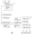
- FIG. 1depicts an illustrative embodiment of a communication device 100 .
- Communication device 100enables selection antenna selection in a multi-antenna device to improve radiation efficiency.
- Device 100can measure the complex input reflection coefficient that is used as feedback for an impedance tuning algorithm.
- the complex input reflection coefficientcan be measured for both antennas (main and diversity). With averaging, this measurement can be performed in less than 100 us to provide a fast and direct evaluation of how the antenna(s) is loaded.
- device 100can utilize a sense IC for antenna selection.
- a feedback receiver integrated in a transceiver ICcan be utilized for obtaining the reflection measurements (or other measured parameters).
- communication device 100can compare a current Sense IC reading (e.g., the complex input reflection coefficient) to a Sense reading that was recorded in freespace.
- the antenna selection criteria in this examplecan then be based on a difference between the current loading conditions and freespace as determined in a Sense IC measurement plane.
- closed loop tuningcan be performed by the communication device 100 and a comparison can be performed of a converged grid location of the current antenna loading condition to a grid location for freespace.
- the antenna selection criteria in this examplecan then be based on a difference between the current loading conditions and freespace as determined in the antenna plane.
- communication device 100can use a converged grid location as described above.
- the antenna selection criteria in this examplecan then be based on a lookup table estimating antenna efficiency as a function of grid location.
- a scalar reflection measurementmay be utilized.
- the communication device 100can include various components that are arranged in various configurations.
- the communication device 100can comprise one or more transceivers 102 coupled to an antenna system 101 , which can be any number of antennas.
- each transceivercan have transmitter and receiver sections herein described as transceiver 102 or transceivers 102 .
- the communication device 100can have one or more tunable circuits 122 including reactive element(s) 190 , one or more tuning sensors 124 , a user interface (UI) 104 , a power supply 114 , a location receiver 116 , a motion sensor 118 , an orientation sensor 120 , and/or a controller 106 for managing operations thereof.
- UIuser interface
- the transceiver 102can support short-range and/or long-range wireless access technologies, including Bluetooth, ZigBee, Wireless Fidelity (WiFi), Digital Enhance Cordless Telecommunications (DECT), or cellular communication technologies, just to mention a few.
- the communication device 100can be a multi-mode device capable of providing communication services via various wireless access technologies, including two or more such services simultaneously.
- Cellular technologies used by the communication device 100can include, for example, Global System for Mobile (GSM), Code Division Multiple Access (CDMA), Time Division Multiple Access (TDMA), Universal Mobile Telecommunications (UMTS), World interoperability for Microwave (WiMAX), Software Defined Radio (SDR), Long Term Evolution (LTE), as well as other next generation wireless communication technologies as they arise.
- the transceiver 102can also be adapted to support circuit-switched wireline access technologies such as Public Switched Telephone Network (PSTN), packet-switched wireline access technologies such as TCP/IP, Voice over IP-VoIP, etc., or combinations thereof.
- PSTNPublic Switched Telephone Network
- packet-switched wireline access technologiessuch as TCP/IP, Voice over IP-VoIP, etc., or combinations thereof.
- dimensions, shapes and/or positions for the group of antennas of antenna system 101can achieve a desired performance characteristic while fitting different mechanical arrangements. These dimensions, shapes and/or positions can be adjusted to achieve other desired performance characteristic and/or for fitting other mechanical arrangements.
- the communication device 100can include an RF switch 150 (or other component) for switching the functionality of antennas of the antenna system 101 including switching primary antennas to diversity antennas and vice versa.
- parameters of the communication device 100e.g., reflection measurements for one, some or all of the antennas
- the impedance changecan result from a change in use case (e.g., switching from left hand to right hand to hold phone).
- the identification of the impedance changecan trigger a change in the antenna system configuration via the RF switch 150 (e.g., controlled by controller 106 ).
- the number of times this switch occurscan be based on the detected parameters, such as according to a user that keeps switching hands during a communication session.
- the switching of antennascan also be limited by a modem of the communication device 100 .
- the tunable circuit 122can comprise one or more variable reactive elements such as variable capacitors, variable inductors, or combinations thereof that are tunable with digital and/or analog bias signals.
- the tunable circuit 122can represent a tunable matching network coupled to the antenna system 101 to compensate for a change in impedance of the antenna 101 , a compensation circuit to compensate for mutual coupling in a multi-antenna system, an amplifier tuning circuit to control operations of an amplifier of the transceiver 102 , a filter tuning circuit to alter a pass band of a filter used by the transceiver 102 , and so on.
- the tunable circuit 122can be connected with one, some or all of the antennas of antenna system 101 to enable impedance tuning.
- tuning sensors 124can be placed at any stage of the transceiver 102 such as, for example, before or after a matching network, and/or at a power amplifier.
- the tuning sensors 124can utilize any suitable sensing technology such as directional couplers, voltage dividers, or other sensing technologies to measure signals at any stage of the transceiver 102 .
- the digital samples of the measured signalscan be provided to the controller 106 by way of analog-to-digital converters included in the tuning sensors 124 .
- Data provided to the controller 106 by the tuning sensors 124can be used to measure, for example, transmit power, transmitter efficiency, receiver sensitivity, power consumption of the communication device 100 , frequency band selectivity by adjusting filter passbands, linearity and efficiency of power amplifiers, specific absorption rate (SAR) requirements, and so on.
- the controller 106can be configured to execute one or more tuning algorithms to determine desired tuning states of the tunable circuit 122 based on the foregoing measurements.
- the controller 106can also switch the primary and diversity antennas via RF switch 150 based on data obtained from the tuning sensors 124 , including based on reflection measurements.
- the UI 104can include a depressible or touch-sensitive keypad 108 with a navigation mechanism such as a roller ball, a joystick, a mouse, or a navigation disk for manipulating operations of the communication device 100 .
- the keypad 108can be an integral part of a housing assembly of the communication device 100 or an independent device operably coupled thereto by a tethered wireline interface (such as a USB cable) or a wireless interface supporting, for example, Bluetooth.
- the keypad 108can represent a numeric keypad commonly used by phones, and/or a QWERTY keypad with alphanumeric keys.
- the UI 104can further include a display 110 such as monochrome or color LCD (Liquid Crystal Display), OLED (Organic Light Emitting Diode) or other suitable display technology for conveying images to an end user of the communication device 100 .
- a display 110such as monochrome or color LCD (Liquid Crystal Display), OLED (Organic Light Emitting Diode) or other suitable display technology for conveying images to an end user of the communication device 100 .
- a display 110is touch-sensitive, a portion or all of the keypad 108 can be presented by way of the display 110 with navigation features.
- the display 110can use touch screen technology to also serve as a user interface for detecting user input.
- the communication device 100can be adapted to present a user interface with graphical user interface (GUI) elements that can be selected by a user with a touch of a finger.
- GUIgraphical user interface
- the touch screen display 110can be equipped with capacitive, resistive or other forms of sensing technology to detect how much surface area of a user's finger has been placed on a portion of the touch screen display. This sensing information can be used to control the manipulation of the GUI elements or other functions of the user interface.
- the display 110can be an integral part of the housing assembly of the communication device 100 or an independent device communicatively coupled thereto by a tethered wireline interface (such as a cable) or a wireless interface.
- the UI 104can also include an audio system 112 that utilizes audio technology for conveying low volume audio (such as audio heard in proximity of a human ear) and high volume audio (such as speakerphone for hands free operation).
- the audio system 112can further include a microphone for receiving audible signals of an end user.
- the audio system 112can also be used for voice recognition applications.
- the UI 104can further include an image sensor 113 such as a charged coupled device (CCD) camera for capturing still or moving images.
- CCDcharged coupled device
- the power supply 114can utilize common power management technologies such as replaceable and rechargeable batteries, supply regulation technologies, and/or charging system technologies for supplying energy to the components of the communication device 100 to facilitate long-range or short-range portable applications.
- the charging systemcan utilize external power sources such as DC power supplied over a physical interface such as a USB port or other suitable tethering technologies.
- the location receiver 116can utilize location technology such as a global positioning system (GPS) receiver capable of assisted GPS for identifying a location of the communication device 100 based on signals generated by a constellation of GPS satellites, which can be used for facilitating location services such as navigation.
- GPSglobal positioning system
- the motion sensor 118can utilize motion sensing technology such as an accelerometer, a gyroscope, or other suitable motion sensing technology to detect motion of the communication device 100 in three-dimensional space.
- the orientation sensor 120can utilize orientation sensing technology such as a magnetometer to detect the orientation of the communication device 100 (north, south, west, and east, as well as combined orientations in degrees, minutes, or other suitable orientation metrics).
- the communication device 100can use the transceiver 102 to also determine a proximity to or distance to cellular, WiFi, Bluetooth, or other wireless access points by sensing techniques such as utilizing a received signal strength indicator (RSSI) and/or signal time of arrival (TOA) or time of flight (TOF) measurements.
- RSSIreceived signal strength indicator
- TOAsignal time of arrival
- TOFtime of flight
- the controller 106can utilize computing technologies such as a microprocessor, a digital signal processor (DSP), programmable gate arrays, application specific integrated circuits, and/or a video processor with associated storage memory such as Flash, ROM, RAM, SRAM, DRAM or other storage technologies for executing computer instructions, controlling, and processing data supplied by the aforementioned components of the communication device 100 .
- computing technologiessuch as a microprocessor, a digital signal processor (DSP), programmable gate arrays, application specific integrated circuits, and/or a video processor with associated storage memory such as Flash, ROM, RAM, SRAM, DRAM or other storage technologies for executing computer instructions, controlling, and processing data supplied by the aforementioned components of the communication device 100 .
- the communication device 100can include a slot for inserting or removing an identity module such as a Subscriber Identity Module (SIM) card.
- SIM cardscan be used for identifying and registering for subscriber services, executing computer programs, storing subscriber data, and so forth.
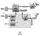
- the device 200can have any number of antennas, only two of which are shown ( 210 , 215 ).
- a Sense IC 220can perform reflection measurements that are used as feedback for closed loop antenna tuning via one or both of tuners 222 and 223 .
- An RF switch 250which is depicted as a DPDT switch, can be utilized for antenna selection so that the transmitter 202 can be routed to the antenna that has the most favorable loading conditions for radiation.
- the reflection measurements from the Sense IC 224can be used to determine the loading conditions of each antenna 210 , 215 and can be used as the selection criteria for the antenna selection.
- a feedback receiver(not shown) can be integrated in the transceiver integrated circuit (e.g., in place of the Sense IC 224 ) for obtaining operational parameters such as the reflection measurements of the transmitting antenna.
- the tuners 222 and/or 223can utilize various tunable reactive elements including capacitors and/or indictors.
- tuners 222 and/or 223can include voltage or current tunable dielectric materials.
- the tunable dielectric materialscan utilize, among other things, a composition of barium strontium titanate (BST).
- BSTbarium strontium titanate
- the tunable reactive elementscan utilize semiconductor varactors, or micro-electromechanical systems (MEMS) technology capable of mechanically varying the dielectric constant of a capacitor.
- MEMSmicro-electromechanical systems
- Other present or next generation methods or material compositions that result in a voltage or current tunable reactive elementare applicable to the subject disclosure for use by the tuners 222 and/or 223 .
- a tuning grid 300is illustrated that can be used for antenna selection by way of transmission Gamma measurements.
- a grid locationcan be determined by a closed-loop tuning algorithm and can be used as an input for the antenna selection.
- each grid location in a lookup table stored in the communication device 200can have an entry for efficiency.
- the grid locationcan be determined by coarse tuning.
- the grid locationcan be further refined using fine tuning.
- a distance from the grid location to the freespace antenna S11 location(referred to as FS_delta) can be utilized for the antenna selection.
- the communication device 200can perform the antenna selection based directly on measurements from the Sense IC 224 .
- a schematic of a portion of a communication deviceis illustrated along with corresponding Smith charts for the device's operation.
- the antenna S11 parameter for all use casescan be examined in each band (or subband).
- a tuning grid in the antenna planecan be set or determined to sufficiently cover the entire range of use cases.
- ⁇ ANTis antenna S11 at the antenna plane.
- ⁇ OPTis tuner S11 at the tuner input plane for each ⁇ ANT with the optimal tuning state applied to the tuner for each ⁇ ANT .
- ⁇ OPT(SENSE)is ⁇ OPT as measured by the Sense IC at the Sense plane.
- FIGS. 3B and Cillustrate implementation of 2D tuning.
- the tuning domaincan be on a 2-dimensional grid in the Antenna Gamma space which sufficiently covers all antenna uses cases.
- the gridcan be rectangular, polar, or annular, and is not required to be uniform.
- Each grid locationcan correspond to the antenna gamma at the TX frequency.
- the antenna gamma at the RX frequencycan be estimated based on S-parameter characterization of the antenna.
- the tuner S-parameterscan be evaluated at all tuning states and the optimal tuning state (e.g., set of DAC values) can be recorded in a table or other data structure.
- the optimal or improved tuning statecan be optimized or improved for TX, RX, both TX and RX, or other combinations such as carrier aggregation.
- a compromise between operational parameters and/or TX and RX modecan also be utilized during the tuning and/or antenna selection.
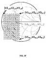
- FIG. 3Dillustrates a tuning grid established and utilized for bands 4 and 5 .
- the antenna S11 for all use casescan be examined in each band (or subband).
- a tuning grid in the antenna planeis set to sufficiently cover the entire range of use cases.
- V1 and V2can be determined in advance and stored in a lookup table in the communication device for each point in the 2D, M ⁇ N grid.
- V1 and V2can be restricted to the pairs listed in the table.
- the tuningcan be performed in the 2D grid space varying m and n.
- V1 and V2can be retrieved from the lookup table based on the grid position.
- V1 and V2cannot vary independently.
- M and ncan be the two independent variables and V1 and V2 can be strictly dependent on m and n.
- V1, V2 and V3can be determined in advance and stored in a lookup table for each point in the 2D, M ⁇ N grid.
- V1, V2 and V3can be restricted to the pairs listed in the table.
- the tuningcan be performed in the 2D grid space varying m and n.
- V1, V2 and V3can be retrieved from the lookup table based on the grid position.
- V1, V2 and V3cannot vary independently.
- M and nare the two independent variables and V1, V2 and V3 can be strictly dependent on m and n.
- the exemplary embodimentcan avoid a failure of convergence and/or solutions trapped at local minima With 3D tuning, determined tuning values can have low reflection loss but high dissipative loss which is still undesired.
- the 2D tuning algorithm of the exemplary embodimentsfilters out such lossy solutions for tuning values.
- Method 400is illustrated for performing antenna selection in a communication device, such as the communication device 200 of FIG. 2 .
- Method 400utilizes the Sense plane and FS_Delta for antenna selection.
- the main tunere.g., tuner 222
- the couplercan be connected with the coupler.
- freespace DAC valuescan be applied to the main tuner and at 406 the reflection measurements can be obtained and recorded for the primary antenna.
- the difference or deltacan be determined between the measured values and a pre-stored FS SENSE reference.
- an FS referencecan be stored for each individual unit by using a factory calibration.
- the FS referencemay include offsets for efficiency differences.
- the diversity tuner(e.g., tuner 223 ) can be connected with the coupler.
- freespace DAC valuescan be applied to the diversity tuner and at 414 the reflection measurements can be obtained and recorded for the diversity antenna.
- the difference or deltacan be determined between the measured values and a pre-stored FS SENSE reference.
- the antenna with the smallest delta from the FS referencecan be selected for transmitting.
- Method 400can be repeated during a communication session since operating conditions can change, such as a user changing hands or interference patterns changing. In one embodiment, the switching to a selected antenna is subject to permission from the modem.
- Method 500is illustrated for performing antenna selection in a communication device, such as the communication device 200 of FIG. 2 .
- Method 500utilizes the antenna plane and FS Grid Delta for antenna selection.
- the main tunere.g., tuner 222
- the couplercan be connected with the coupler.
- freespace DAC valuescan be applied to the main tuner and at 506 the reflection measurements can be obtained and recorded for the primary antenna.
- tuningsuch as coarse tuning
- the tuning gride.g., grid 300
- the difference or deltacan be determined between the location of the tuning grid and a FS location on the tuning grid.
- antenna selectioncan be performed based on the determined delta, such as satisfying a threshold.
- method 500can proceed from 508 to 510 without switching antennas.
- the diversity tuner(e.g., tuner 223 ) can be connected with the coupler.
- freespace DAC valuescan be applied to the diversity tuner and at 514 the reflection measurements can be obtained and recorded for the diversity antenna.
- tuningsuch as coarse tuning, can be performed and/or the tuning grid (e.g., grid 300 ) can be calculated for the coarse tune.
- the difference or deltacan be determined between the location of the tuning grid and a FS location on the tuning grid.
- the antenna with the smallest grid delta from the FS reference locationcan be selected for transmitting.
- Method 500can be repeated during a communication session since operating conditions can change, such as a user changing hands or interference patterns changing. In one embodiment, the switching to a selected antenna is subject to permission from the modem.
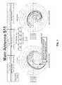
- Device 600can include switchable primary and diversity antennas 610 , 615 . Radiation efficiency between the antennas 610 , 615 can be different based on a number of factors, such as which user hand is holding the phone and so forth. Reflection measurement data is illustrated In FIGS. 7 and 8 for the main and diversity antennas 610 , 615 for different use cases (e.g., BHHR and BHHL) in different frequency bands.
- the Smith chartsdepict the distance or delta between the location on the Smith chart and a location corresponding to free space. In some instance, differentiating between different use cases based solely on reflection measurements can be difficult.
- a proximity sensorcan be utilized to gather proximity data that can be utilized in distinguishing between use cases (e.g., BHHR vs Freespace).
- capacitive informationsuch as from a capacitive sensor attached to one, some or all of the antennas or from a capacitive sensor attached to the touch screen, can be utilized in distinguishing between the use cases.
- Other inputscan also be used in facilitating distinguishing between use cases, such as the operational frequency range. In these examples, reflection measurements and other obtained information can be utilized for the antenna selection and/or for impedance tuning.
- radiation efficiency for the main and diversity antennas at different frequencies in a lowband according to different use casesis illustrated based on a calculation of subtracting mismatch loss from antenna efficiency.
- FIG. 10illustrates antenna selection by applying the process of method 500 according to FS_delta criteria.
- other inputssuch as the operating frequency range can be utilized in combination with the reflection measurements to facilitate in distinguishing between different use cases.
- the other inputsare not limited to frequency data, and can include proximity information from a proximity sensor, capacitive data from a capacitive sensor (e.g., attached to the antenna or attached to a touch screen), and so forth.
- FIG. 11radiation efficiency for the main and diversity antennas at different frequencies in a mid/highband according to different use cases is illustrated based on a calculation of subtracting mismatch loss from antenna efficiency.
- FIG. 12illustrates antenna selection by applying the process of method 500 according to FS_delta criteria.
- Method 1300is illustrated for performing antenna selection in a communication device, such as the communication device 200 of FIG. 2 .
- Method 1300utilizes the antenna plane and an efficiency lookup table for antenna selection.
- the main tunere.g., tuner 222
- the couplercan be connected with the coupler.
- freespace DAC valuescan be applied to the main tuner and at 1306 the reflection measurements can be obtained and recorded for the primary antenna.
- tuningsuch as coarse tuning
- the tuning gride.g., grid 300
- the antenna efficiencycan be determined by looking it up in a lookup table according to the grid location. As described earlier with respect to tuning grid 300 , each grid location can have an entry in a lookup table for efficiency.
- the grid locationcan be determined by coarse tuning and/or the grid location can be further refined using fine tuning.
- the diversity tuner(e.g., tuner 223 ) can be connected with the coupler.
- freespace DAC valuescan be applied to the diversity tuner and at 514 the reflection measurements can be obtained and recorded for the diversity antenna.
- tuningsuch as coarse tuning, can be performed and/or the tuning grid (e.g., grid 300 ) can be calculated for the coarse tune.
- the antenna efficiencycan be determined by looking it up in a lookup table according to the grid location.
- the antenna with the higher efficiencycan be selected for transmitting.
- Method 1300can be repeated during a communication session since operating conditions can change, such as a user changing hands or interference patterns changing. In one embodiment, the switching to a selected antenna is subject to permission from the modem.
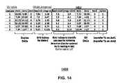
- a table 1400is illustrated which can be used for antenna selection.
- the devicecan be transmitting on antenna 215 as the primary antenna.
- a closed loop tuning algorithm for antenna 215can be executed by a processor of device 200 utilizing the Sense IC 224 .
- antenna 210can be operating as the diversity antenna, which can be executing an open loop tuning algorithm.
- the current grid winnercan be compared to RealIndSW and ImagIndSw and the nearest use case can be determined.
- the antenna selection bitcan be updated based on the SwAnt value in the table for the nearest use case.
- the modem permits switching antennasRX_ON
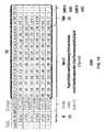
- a table 1500is illustrated which can be used for antenna selection.
- the devicecan be transmitting on antenna 210 .
- the processor of the device 200can switch from an open loop tuning algorithm to a closed loop tuning algorithm utilizing the Sense IC 224 .
- the closed loop tuning algorithmcan utilize coarse tuning.
- the processorcan continue to perform reflection measurements readings (via the Sense IC 224 ) at a same rate as used in the closed loop algorithm on antenna 215 .
- the Sense IC readingcan be compared by the processor to each gamma_UC to find a nearest use case.
- a Sense IC validity checkcan be performed according to obtaining consecutive readings within 0.1.
- the processorcan update the tuning based on a derived use case.
- the processorcan update the antenna selection bit based on SwAnt value in the table for the nearest use case.
- RX_ONwhen the modem permits switching antennas
- the switching of antennascan cause different tuning to be applied to the different antennas.
- an antenna switchoccurs (e.g., via RF switch 250 of FIG. 2 )
- one of the antennascan switch from a main antenna to a diversity antenna while the other antenna can switch from the diversity antenna to the main antenna.
- the antennasalso switch functions from a combination of transmit and receive functions to a receive-only function, and vice versa.
- the switching of functionscan cause switching of tuning states for each of the antennas.
- the antenna which is now only a receive antennacan be tuned to optimize or otherwise improve receiving via a first tunable reactance circuit while the antenna which is now both a transmit and receive antenna can be tuned for a compromise between improving receiving and improving transmitting via a second tunable reactance circuit.
- different tuning valuescan be utilized without changing antennas according to whether the particular antenna is set to optimize receiving or whether the particular antenna is set to compromise between transmit and receive. For instance, while an antenna is in the receive mode a first set of tuning values can be utilized via the RX DAC's and while the antenna is in a transmit mode a second set of tuning values can be utilized via the duplex DAC's.
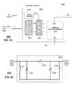
- a portion of a communication device 1600is illustrated which can utilize antenna selection based on operational parameters obtained from a Sense IC 1624 .
- Various other componentscan be utilized to facilitate the capturing and analysis of operational parameters (e.g., reflection measurements) including directional couplers, as well as to facilitate the switching antennas, such as switches 1650 .
- device 1600can measure power coupled to the other antennas to estimate absorption.
- the tuningcan be specifically set for LB operation. This example makes use of the HB antenna(s) to perform the transmission measurements. Alternatively, a strategically located, separate antenna may be used.
- Method 1700is illustrated for performing antenna selection according to transmission measurements.
- Method 1700can operate utilizing an antenna plane delta.
- 1702
- connection the LB Main tunerto the coupler.
- perform coarse tuningsuch as to improve or optimize the match.
- perform coarse tuningAt 1714 , measure any coupling to the MB/HB 1 and/or MB/HB 2 antennas.
- FIG. 18depicts an illustrative embodiment of a portion of the wireless transceiver 102 of the communication device 100 of FIG. 1 .
- the transmit and receive portions of the transceiver 102can include amplifiers 1801 , 1803 coupled to a tunable matching network 1802 that is in turn coupled to an impedance load 1806 (which can be one or more antennas including primary and diversity antennas).
- Antenna switching, via switch 150can be performed based on operational parameters associated with one, some, or all of the antennas, such as based on reflection measurements.
- a full duplex configuration without switch 1804can be utilized such as for an LTE or WCDMA application.
- the tunable matching network 1802can include all or a portion of the tuning circuit 122 of FIG. 1 , such as variable capacitors to enable high linearity tuning while satisfying performance criteria such as insertion loss thresholds and/or response time speed.
- the impedance load 1806 in the present illustrationcan be all or a portion of the antenna system (e.g., reconfigurable via RF switch 150 ) as shown in FIG. 1 (herein antenna 1806 ).
- the RF switch 150can be on the Tx/Rx side of the matching network(s) 1802 .
- a separate matching network 1802can be used for each antenna.
- a transmit signal in the form of a radio frequency (RF) signal (TX)can be directed to the amplifier 1801 which amplifies the signal and directs the amplified signal to the antenna 1806 by way of the tunable matching network 2018 when switch 1804 is enabled for a transmission session.
- the receive portion of the transceiver 102can utilize a pre-amplifier 1803 which amplifies signals received from the antenna 1806 by way of the tunable matching network 1802 when switch 1804 is enabled for a receive session.
- Other configurations of FIG. 18are possible for other types of cellular access technologies such as CDMA, UMTS, LTE, and so forth.
- the exemplary embodimentsare applicable to all types of radio technologies including WiFi, GPS and so forth, and are not intended to be limited to cellular access technologies. These undisclosed configurations are applicable to the subject disclosure.
- FIGS. 19-20depict illustrative embodiments of the tunable matching network 1802 of the transceiver 102 of FIG. 18 .
- the tunable matching network 1802can comprise a control circuit 302 and a tunable reactive element 1910 .
- the control circuit 1902can comprise a DC-to-DC converter 1904 , one or more digital to analog converters (DACs) 1906 and one or more corresponding buffers 1908 to amplify the voltage generated by each DAC.
- the amplified signalcan be fed to one or more tunable reactive components 404 , 406 and 408 such as shown in FIG. 4 , which depicts a possible circuit configuration for the tunable reactive element 310 .
- the tunable reactive element 310includes three tunable capacitors 2004 - 2008 and two inductors 2002 - 2003 with a fixed inductance.
- Circuit configurationssuch as “Tee”, “Pi”, and “L” configurations for a matching circuit are also suitable configurations that can be used in the subject disclosure.
- the tunable capacitors 2004 - 2008can each utilize technology that enables tunability of the reactance of the component.
- One embodiment of the tunable capacitors 2004 - 2008can utilize voltage or current tunable dielectric materials.
- the tunable dielectric materialscan utilize, among other things, a composition of barium strontium titanate (BST).
- BSTbarium strontium titanate
- the tunable reactive element 310can utilize semiconductor varactors, or micro-electromechanical systems (MEMS) technology capable of mechanically varying the dielectric constant of a capacitor.
- MEMSmicro-electromechanical systems
- Other present or next generation methods or material compositions that result in a voltage or current tunable reactive elementare applicable to the subject disclosure for use by the tunable reactive element 1910 of FIG. 19 .
- the DC-to-DC converter 1904can receive a DC signal such as 3 volts from the power supply 114 of the communication device 100 in FIG. 1A .
- the DC-to-DC converter 1904can use technology to amplify a DC signal to a higher range (e.g., 30 volts) such as shown.
- the controller 106can supply digital signals to each of the DACs 1906 by way of a control bus 1907 of “n” or more wires or traces to individually control the capacitance of tunable capacitors 2004 - 2008 , thereby varying the collective reactive impedance of the tunable matching network 202 .
- the control bus 1907can be implemented with a two-wire serial bus technology such as a Serial Peripheral Interface (SPI) bus (referred to herein as SPI bus 1907 ).
- SPISerial Peripheral Interface
- the controller 106can transmit serialized digital signals to configure each DAC in FIG. 19 .
- the control circuit 1902 of FIG. 19can utilize digital state machine logic to implement the SPI bus 1907 , which can direct digital signals supplied by the controller 106 to the DACs to control the analog output of each DAC, which is then amplified by buffers 1908 .
- the control circuit 1902can be a stand-alone component coupled to the tunable reactive element 1910 .
- the control circuit 1902can be integrated in whole or in part with another device such as the controller 106 .
- the tunable reactive element 1910is shown in a unidirectional fashion with an RF input and RF output, the RF signal direction is illustrative and can be interchanged. Additionally, either port of the tunable reactive element 1910 can be connected to a feed point of the antenna 1806 , a structural element of the antenna 1806 in an on-antenna configuration, or between antennas for compensating mutual coupling when diversity antennas are used, or when antennas of differing wireless access technologies are physically in close proximity to each other and thereby are susceptible to mutual coupling.
- the tunable reactive element 1910can also be connected to other circuit components of a transmitter or a receiver section such as filters, amplifiers, and so on, to control operations thereof.
- the tunable matching network 1802 of FIG. 18can comprise a control circuit 2102 in the form of a decoder and a tunable reactive element 2104 comprising switchable reactive elements such as shown in FIG. 6 .
- the controller 106can supply the control circuit 2102 signals via the SPI bus 1907 , which can be decoded with Boolean or state machine logic to individually enable or disable the switching elements 2202 .
- the switching elements 2202can be implemented with semiconductor switches, MEMS, or other suitable switching technology. By independently enabling and disabling the reactive elements 2204 (capacitor or inductor) of FIG. 22 with the switching elements 2202 , the collective reactive impedance of the tunable reactive element 2104 can be varied by the controller 106 .
- the tunable reactive elements 1910 and 2104 of FIGS. 19 and 21can be used with various circuit components of the transceiver 102 to enable the controller 106 to manage performance factors such as, for example, but not limited to, transmit power, transmitter efficiency, receiver sensitivity, power consumption of the communication device 100 , frequency band selectivity by adjusting filter passbands, linearity and efficiency of power amplifiers, SAR requirements, among other operational parameters.
- FIG. 23depicts an illustration of a look-up table stored in memory, which can be indexed by the controller 106 of the communication device 100 of FIG. 1 according to physical and/or functional use cases of the communication device 100 .
- the desired tuning statecan include values for the biasing signals and/or capacitance values to be employed for tuning of the variable capacitors, such as BST variable capacitors.
- a physical use casecan represent a physical state of the communication device 100
- a functional use casecan represent an operational state of the communication device 100 .
- an open flipcan represent one physical use case
- a closed flipcan represent another physical use case.
- a userIn a closed flip state (i.e., bottom and top flips 2402 - 2404 are aligned), a user is likely to have his/her hands surrounding the top flip 2404 and the bottom flip 2402 while holding the phone 2400 , which can result in one range of load impedances experienced by an internal or retrievable antenna (not shown) of the phone 2400 .
- the range of load impedances of the internal or retrievable antennacan be determined by empirical analysis.
- a userWith the flip open a user is likely to hold the bottom flip 2402 with one hand while positioning the top flip 2404 near the user's ear when an audio system of the phone 2400 , such audio system 112 of FIG. 1 , is set to low volume, and voice channel is active. If, on the other hand, the audio system 112 is in speakerphone mode, it is likely that the user is positioning the top flip 2404 away from the user's ear.
- different ranges of load impedancescan be experienced by the internal or retrievable antenna, which can be analyzed empirically.
- the low and high volume states of the audio system 112as well as, a determination that a voice channel is active, illustrates varying functional use cases.
- the keypad in an outward positioncan present one range of load impedances of an internal antenna, while the keypad in a hidden position can present another range of load impedances, each of which can be analyzed empirically.
- a smartphone 2600illustrated in FIG. 26
- an assumptioncan be made that the user is likely to hold the phone away from the user's ear in order to view the game. Placing the smartphone 2600 in a portrait position 2602 can represent one physical and operational use case, while utilizing the smartphone 2600 in a landscape position 1004 presents another physical and operational use case.
- the number of hands and fingers used in the portrait modemay be determined by the particular type of game being played by the user. For example, a particular video game may require a user interface where a single finger in portrait mode may be sufficient for controlling the game. In this scenario, it may be assumed that the user is holding the smartphone 2600 in one hand in portrait mode and using a finger with the other.
- a possible range of impedances of the internal antenna(s) of the communication devicecan be determined when using the video game in portrait mode.
- the video game selectedhas a user interface that is known to require two hands in landscape mode
- another estimated range of impedances of the internal antennacan be determined empirically.
- a multimode phone 2700 capable of facilitating multiple access technologies such as GSM, CDMA, LTE, WiFi, GPS, and/or Bluetooth in two or more combinationscan provide additional insight into possible ranges of impedances experienced by two or more internal antennas of the multimode phone 2700 .
- a multimode phone 2700 that provides GPS services by processing signals received from a constellation of satellites 2702 , 2704can be empirically analyzed when other access technologies are also in use.
- the multimode phone 2700is facilitating voice communications by exchanging wireless messages with a cellular base station 2706 .
- an internal antenna of the GPS receivermay be affected by a use case of a user holding the multimode phone 2700 (e.g., near the user's ear or away from the user's ear).
- the effect on the GPS receiver antenna and the GSM antenna by the user's hand positioncan be empirically analyzed.
- the antenna of a GSM transceiveris in close proximity to the antenna of a WiFi transceiver.
- the GSM frequency band used to facilitate voice communicationsis near the operational frequency of the WiFi transceiver.
- a use case for voice communicationsmay result in certain physical states of the multimode phone 2700 (e.g., slider out), which can result in a probable hand position of the user of the multimode phone 2700 .
- Such a physical and functional use casecan affect the impedance range of the antenna of the WiFi transceiver as well as the antenna of the GSM transceiver.
- a close proximity between the WiFi and GSM antennas and the near operational frequency of the antennasmay also result in cross-coupling between the antennas.
- Mutual or cross-coupling under these circumstancescan be measured empirically.
- empirical measurements of the impedances of other internal antennascan be measured for particular physical and functional use configurations when utilizing Bluetooth, WiFi, Zigbee, or other access technologies in peer-to-peer communications with another communication device 2708 or with a wireless access point 2710 .
- MIMOmultiple-input and multiple output
- the number of physical and functional use cases of a communication device 100can be substantial when accounting for combinations of access technologies, frequency bands, antennas of different access technologies, antennas configured for diversity designs, and so on. These combinations, however, can be empirically analyzed to determine load impedances of the antenna(s), mutual coupling between them, and the effects on transmitter and receiver performance metrics. Mitigation strategies to reduce mutual coupling, counter the effect of varying load impedances, and to improve other performance metrics of the transceiver 102 can also be determined empirically.
- the empirical data collected and corresponding mitigation strategiescan be recorded in the look-up table of FIG. 23 and indexed according to combinations of physical and functional use cases detected by the communication device 100 .
- the information stored in the look-up tablecan be used in open-loop RF tuning applications to initialize tunable circuit components of the transceiver 102 , as well as, tuning algorithms that control operational aspects of the tunable circuit components.
- information in the look-up table of FIG. 23can be used for impedance tuning in conjunction with re-configuring or switching the primary and diversity antennas.
- devices described in the exemplary embodimentscan be in communication with each other via various wireless and/or wired methodologies.
- the methodologiescan be links that are described as coupled, connected and so forth, which can include unidirectional and/or bidirectional communication over wireless paths and/or wired paths that utilize one or more of various protocols or methodologies, where the coupling and/or connection can be direct (e.g., no intervening processing device) and/or indirect (e.g., an intermediary processing device such as a router).
- Radio band informationcan be generally available or otherwise retrievable in communication devices, which provides the broadest definition of where in a frequency spectrum a communication device such as a handset is operating (e.g., transmitting).
- frequenciescan be commonly allocated for usage in a block or range of frequencies. This block or range of frequencies is commonly known as a radio band.
- Multiple radio bandscan be present in any given cellular system, and in any geographic location there can be multiple cellular systems present.
- a radio channelcan identify a discrete set of frequencies in a cellular system that contains the downlink (from base station to the handset) and uplink (from handset to base station) radio signals.
- Downlinkis also referred to as Rx and uplink is also referred to as Tx.
- uplink and downlinkcan use separate frequencies that are separated by the duplex distance, which is the number of Hz separating the uplink and downlink paths.
- TD-LTETime Division Long Term Evolution
- One or more of the exemplary embodimentscan utilize radio band information, including only radio band information in some embodiments or radio band information in combination with other information (e.g., measured operational parameters), for antenna tuning.
- the exemplary embodimentscan apply to various types of devices, including wireless handsets operating utilizing one or more of various communication protocols.
- RF tuningbased on limited information, such as only the radio band, can create a number of problems.
- the tunerwould be set to match every frequency on which the radio receives or transmits, with the understanding that typically a single antenna is used for both Rx and Tx which requires the RF tuner to change tuning state as the RF signal on the antenna changes frequency.
- half-duplex systemssuch as GSM that would be for every Rx and Tx, including neighbor cells.
- the RF tunerhas to change when the frequency changes for handoffs and neighbor cell monitoring, and additionally the tuning state has to be a duplex setting for Rx and Tx on a frequency between the Rx and Tx frequencies.
- the entity controlling the tunercould require exact knowledge in real time of all relevant information pertaining to operating the tuner, such as the radio timing, radio band, radio channel, RF duplex information, and transmit state. Tuning based on limited information occurs when the entity controlling the tuner does not have all the information required to set the RF tuner to match an exact frequency at a given time. For example, real time channel information could be missing, in which case the tuner control entity could set the RF tuner based on information pertaining to the Radio Band only.
- Duplex tuningrefers to where the tunable element for a particular sub-band or radio channel is tuned to a frequency between uplink and downlink; one tuning state can be used for both Rx and Tx in this case.
- full-duplexconcurrent uplink and downlink, such as WCDMA
- duplex tuningis commonly used.
- uplink and downlinkare not concurrent, such as GSM
- the tunercan be tuned for both Rx and Tx.
- Sub-banddescribes a grouping of frequencies (e.g., radio channels) consisting of one or more radio channels.
- frequenciese.g., radio channels
- Sub-bandscan be used in conjunction with storage and application of calibration data in cellular handsets, providing a compromise between accuracy and amount of storage needed to hold said calibration data.
- An example of a radio bandis the GSM 900 band, in which the uplink frequencies can occupy the range 880.0 to 915.0 MHz and the downlink frequencies can occupy the range 925.0 to 960.0 MHz.
- the duplex spacingcan be 45 MHz.
- the first channelcan be channel 975 which has uplink at 880.2 MHz and downlink at 915.2 MHz.
- the last channelcan be channel 124 which has uplink at 914.8 MHz and downlink at 959.8 MHz.
- the GSM 900 bandcan, for example, be subdivided into 3 sub bands as follows: Sub band 1 ranging from channel 975 to channel 1023 (48 channels, 9.6 MHz wide), Sub Band 2 ranging from channel 0 to channel 66 (66 channels, 13.2 MHz wide), and sub band 3 ranging from channel 67 to channel 124 (57 channels, 11.4 MHz wide).
- Sub band 1ranging from channel 975 to channel 1023 (48 channels, 9.6 MHz wide
- Sub Band 2ranging from channel 0 to channel 66 (66 channels, 13.2 MHz wide)
- sub band 3ranging from channel 67 to channel 124 (57 channels, 11.4 MHz wide).
- Thisis an example of a radio band and sub-bands, and the present disclosure can include various configurations of radio bands and sub-bands.
- FIG. 28depicts an exemplary diagrammatic representation of a machine in the form of a computer system 2800 within which a set of instructions, when executed, may cause the machine to perform any one or more of the methods discussed above.
- One or more instances of the machinecan operate, for example, as the communication device 100 or other devices described herein for performing antenna selection and/or impedance tuning in a multi-antenna device.
- the machinemay be connected (e.g., using a network 2826 ) to other machines.
- the machinemay operate in the capacity of a server or a client user machine in server-client user network environment, or as a peer machine in a peer-to-peer (or distributed) network environment.
- the machinemay comprise a server computer, a client user computer, a personal computer (PC), a tablet PC, a smart phone, a laptop computer, a desktop computer, a control system, a network router, switch or bridge, or any machine capable of executing a set of instructions (sequential or otherwise) that specify actions to be taken by that machine.
- a communication device of the subject disclosureincludes broadly any electronic device that provides voice, video or data communication.
- the term “machine”shall also be taken to include any collection of machines that individually or jointly execute a set (or multiple sets) of instructions to perform any one or more of the methods discussed herein.
- the computer system 2800may include a processor (or controller) 2802 (e.g., a central processing unit (CPU), a graphics processing unit (GPU, or both), a main memory 2804 and a static memory 2806 , which communicate with each other via a bus 2808 .
- the computer system 2800may further include a display unit 2810 (e.g., a liquid crystal display (LCD), a flat panel, or a solid state display.
- the computer system 2800may include an input device 2812 (e.g., a keyboard), a cursor control device 2814 (e.g., a mouse), a disk drive unit 2816 , a signal generation device 2818 (e.g., a speaker or remote control) and a network interface device 2820 .
- the embodiments described in the subject disclosurecan be adapted to utilize multiple display units 2810 controlled by two or more computer systems 2800 .
- presentations described by the subject disclosuremay in part be shown in a first of the display units 2810 , while the remaining portion is presented in a second of the display units 2810 .
- the disk drive unit 2816may include a tangible computer-readable storage medium 2822 on which is stored one or more sets of instructions (e.g., software 2824 ) embodying any one or more of the methods or functions described herein, including those methods illustrated above.
- the instructions 2824may also reside, completely or at least partially, within the main memory 2804 , the static memory 2806 , and/or within the processor 2802 during execution thereof by the computer system 2800 .
- the main memory 2804 and the processor 2802also may constitute tangible computer-readable storage media.
- Dedicated hardware implementationsincluding, but not limited to, application specific integrated circuits, programmable logic arrays and other hardware devices can likewise be constructed to implement the methods described herein.
- Applicationsthat may include the apparatus and systems of various embodiments broadly include a variety of electronic and computer systems. Some embodiments implement functions in two or more specific interconnected hardware modules or devices with related control and data signals communicated between and through the modules, or as portions of an application-specific integrated circuit.
- the example systemis applicable to software, firmware, and hardware implementations.
- tangible computer-readable storage medium 2822is shown in an example embodiment to be a single medium, the term “tangible computer-readable storage medium” should be taken to include a single medium or multiple media (e.g., a centralized or distributed database, and/or associated caches and servers) that store the one or more sets of instructions.
- tangible computer-readable storage mediumshall also be taken to include any non-transitory medium that is capable of storing or encoding a set of instructions for execution by the machine and that cause the machine to perform any one or more of the methods of the subject disclosure.
- tangible computer-readable storage mediumshall accordingly be taken to include, but not be limited to: solid-state memories such as a memory card or other package that houses one or more read-only (non-volatile) memories, random access memories, or other re-writable (volatile) memories, a magneto-optical or optical medium such as a disk or tape, or other tangible media which can be used to store information. Accordingly, the disclosure is considered to include any one or more of a tangible computer-readable storage medium, as listed herein and including art-recognized equivalents and successor media, in which the software implementations herein are stored.
- Each of the standards for Internet and other packet switched network transmission(e.g., TCP/IP, UDP/IP, HTML, HTTP) represent examples of the state of the art. Such standards are from time-to-time superseded by faster or more efficient equivalents having essentially the same functions.
- Wireless standards for device detectione.g., RFID
- short-range communicationse.g., Bluetooth, WiFi, Zigbee
- long-range communicationse.g., WiMAX, GSM, CDMA, LTE
- facilitatinge.g., facilitating access or facilitating establishing a connection
- the facilitatingcan include less than every step needed to perform the function or can include all of the steps needed to perform the function.
Landscapes
- Engineering & Computer Science (AREA)
- Computer Networks & Wireless Communication (AREA)
- Signal Processing (AREA)
- Variable-Direction Aerials And Aerial Arrays (AREA)
- Transceivers (AREA)
- Radio Transmission System (AREA)
- Mobile Radio Communication Systems (AREA)
Abstract
Description
- If AntSel=0, then do not switch. Continue closed loop algorithm.
- If AntSel=1: switch antennas; apply RX DACs to main antenna; and apply DX DACs to diversity antenna.
- If AntSel=0, then do not switch. Continue applying coarse tuning algorithm on diversity.
- If AntSel=1, switch antennas; apply RX DACs to diversity antenna; and apply DX DACs to main Antenna.
MeasureLB1 toMB1(P_L1M1=L1_INC−M1_DEL)
MeasureLB2 toMB1(P_L2M1=L2_INC−M1_DEL)
MeasureLB1 toMB2(P_L1M2=L1_INC−M2_DEL)
MeasureLB2 toMB2(P_L2M2=L2_INC−M2_DEL)
ABS11=P_L1M1−P_L1M1_FS
ABS21=P_L2M1−P_L2M1_FS
ABS12=P_L1M2−P_L1M2_FS
ABS22=P_L2M2−P_L2M2_FS
Claims (17)
Priority Applications (6)
| Application Number | Priority Date | Filing Date | Title |
|---|---|---|---|
| US14/571,928US9438319B2 (en) | 2014-12-16 | 2014-12-16 | Method and apparatus for antenna selection |
| EP15198585.0AEP3035542B1 (en) | 2014-12-16 | 2015-12-09 | Method and apparatus for antenna selection |
| CA2914562ACA2914562C (en) | 2014-12-16 | 2015-12-11 | Method and apparatus for antenna selection |
| CN201510941292.3ACN105703797B (en) | 2014-12-16 | 2015-12-16 | Method and apparatus for antenna selection |
| US15/233,538US10003393B2 (en) | 2014-12-16 | 2016-08-10 | Method and apparatus for antenna selection |
| US15/978,650US10651918B2 (en) | 2014-12-16 | 2018-05-14 | Method and apparatus for antenna selection |
Applications Claiming Priority (1)
| Application Number | Priority Date | Filing Date | Title |
|---|---|---|---|
| US14/571,928US9438319B2 (en) | 2014-12-16 | 2014-12-16 | Method and apparatus for antenna selection |
Related Child Applications (1)
| Application Number | Title | Priority Date | Filing Date |
|---|---|---|---|
| US15/233,538ContinuationUS10003393B2 (en) | 2014-12-16 | 2016-08-10 | Method and apparatus for antenna selection |
Publications (2)
| Publication Number | Publication Date |
|---|---|
| US20160173172A1 US20160173172A1 (en) | 2016-06-16 |
| US9438319B2true US9438319B2 (en) | 2016-09-06 |
Family
ID=55027247
Family Applications (3)
| Application Number | Title | Priority Date | Filing Date |
|---|---|---|---|
| US14/571,928ActiveUS9438319B2 (en) | 2014-12-16 | 2014-12-16 | Method and apparatus for antenna selection |
| US15/233,538Expired - Fee RelatedUS10003393B2 (en) | 2014-12-16 | 2016-08-10 | Method and apparatus for antenna selection |
| US15/978,650ActiveUS10651918B2 (en) | 2014-12-16 | 2018-05-14 | Method and apparatus for antenna selection |
Family Applications After (2)
| Application Number | Title | Priority Date | Filing Date |
|---|---|---|---|
| US15/233,538Expired - Fee RelatedUS10003393B2 (en) | 2014-12-16 | 2016-08-10 | Method and apparatus for antenna selection |
| US15/978,650ActiveUS10651918B2 (en) | 2014-12-16 | 2018-05-14 | Method and apparatus for antenna selection |
Country Status (4)
| Country | Link |
|---|---|
| US (3) | US9438319B2 (en) |
| EP (1) | EP3035542B1 (en) |
| CN (1) | CN105703797B (en) |
| CA (1) | CA2914562C (en) |
Cited By (3)
| Publication number | Priority date | Publication date | Assignee | Title |
|---|---|---|---|---|
| WO2021194235A1 (en)* | 2020-03-23 | 2021-09-30 | Samsung Electronics Co., Ltd. | An electronic device with a plurality of antenna circuitries and a method for controlling the same |
| US11336308B2 (en) | 2018-01-31 | 2022-05-17 | Samsung Electronics Co., Ltd. | Apparatus and method for determining reflection coefficient of antenna |
| US11469740B2 (en)* | 2013-12-09 | 2022-10-11 | Shure Acquisition Holdings, Inc. | Adaptive self-tunable antenna system and method |
Families Citing this family (57)
| Publication number | Priority date | Publication date | Assignee | Title |
|---|---|---|---|---|
| US8744384B2 (en) | 2000-07-20 | 2014-06-03 | Blackberry Limited | Tunable microwave devices with auto-adjusting matching circuit |
| US7711337B2 (en) | 2006-01-14 | 2010-05-04 | Paratek Microwave, Inc. | Adaptive impedance matching module (AIMM) control architectures |
| US7714676B2 (en) | 2006-11-08 | 2010-05-11 | Paratek Microwave, Inc. | Adaptive impedance matching apparatus, system and method |
| US7991363B2 (en) | 2007-11-14 | 2011-08-02 | Paratek Microwave, Inc. | Tuning matching circuits for transmitter and receiver bands as a function of transmitter metrics |
| US9026062B2 (en) | 2009-10-10 | 2015-05-05 | Blackberry Limited | Method and apparatus for managing operations of a communication device |
| US8803631B2 (en) | 2010-03-22 | 2014-08-12 | Blackberry Limited | Method and apparatus for adapting a variable impedance network |
| JP5901612B2 (en) | 2010-04-20 | 2016-04-13 | ブラックベリー リミテッド | Method and apparatus for managing interference in a communication device |
| US8712340B2 (en) | 2011-02-18 | 2014-04-29 | Blackberry Limited | Method and apparatus for radio antenna frequency tuning |
| US8594584B2 (en) | 2011-05-16 | 2013-11-26 | Blackberry Limited | Method and apparatus for tuning a communication device |
| US10404295B2 (en) | 2012-12-21 | 2019-09-03 | Blackberry Limited | Method and apparatus for adjusting the timing of radio antenna tuning |
| US10062680B2 (en) | 2014-05-08 | 2018-08-28 | Qualcomm Incorporated | Silicon-on-insulator (SOI) complementary metal oxide semiconductor (CMOS) standard library cell circuits having a gate back-bias rail(s), and related systems and methods |
| US9973228B2 (en) | 2014-08-26 | 2018-05-15 | Pulse Finland Oy | Antenna apparatus with an integrated proximity sensor and methods |
| US9948002B2 (en) | 2014-08-26 | 2018-04-17 | Pulse Finland Oy | Antenna apparatus with an integrated proximity sensor and methods |
| US9438319B2 (en) | 2014-12-16 | 2016-09-06 | Blackberry Limited | Method and apparatus for antenna selection |
| US9906260B2 (en)* | 2015-07-30 | 2018-02-27 | Pulse Finland Oy | Sensor-based closed loop antenna swapping apparatus and methods |
| US9935676B2 (en)* | 2015-08-21 | 2018-04-03 | Qualcomm Incorporated | Opportunistic antenna switch diversity (ASDIV) in carrier aggregation |
| US9634697B2 (en)* | 2015-09-09 | 2017-04-25 | Qualcomm Incorporated | Antenna selection and tuning |
| US9923610B2 (en) | 2015-10-29 | 2018-03-20 | Qualcomm Incorporated | Selective usage of antennas for improved call performance |
| US9692478B1 (en)* | 2015-12-16 | 2017-06-27 | Dell Products L.P. | Information handling system dynamic antenna management |
| US10554240B2 (en)* | 2015-12-28 | 2020-02-04 | Apple, Inc. | Wireless electronic device with radio-frequency sensors |
| US10122403B2 (en) | 2016-01-12 | 2018-11-06 | Fractus Antennas, S.L. | Wireless device |
| KR102516621B1 (en)* | 2016-04-08 | 2023-03-31 | 삼성전자주식회사 | Method for controlling antenna and electronic device thereof |
| US10431889B2 (en)* | 2016-04-22 | 2019-10-01 | The Charles Stark Draper Laboratory, Inc. | Low-loss compact transmit impedance matching tuning technique |
| US10110261B2 (en)* | 2016-04-22 | 2018-10-23 | The Charles Stark Draper Laboratory, Inc. | Transceiver system to adapt to antenna de-tuning |
| US10523292B2 (en)* | 2016-07-21 | 2019-12-31 | Motorola Mobility Llc | Closed loop tuning operation with antenna switching |
| US10128885B2 (en)* | 2016-07-25 | 2018-11-13 | Blackberry Limited | Method and apparatus for dynamic tuning |
| US10461782B2 (en) | 2016-07-25 | 2019-10-29 | Blackberry Limited | Method and apparatus for dynamic tuning |
| US10536943B2 (en)* | 2016-07-25 | 2020-01-14 | Blackberry Limited | Method and apparatus for dynamic tuning |
| KR102123283B1 (en)* | 2016-08-18 | 2020-06-16 | 삼성전자 주식회사 | Electronic device and a method of identifying whether electronic device is gripped |
| WO2018037776A1 (en)* | 2016-08-24 | 2018-03-01 | 株式会社日立製作所 | Battery control system |
| CN106374964B (en)* | 2016-09-06 | 2019-01-22 | 深圳市广和通无线股份有限公司 | Wireless communication module and its method for reducing radiation dispersion |
| CN107979395A (en)* | 2016-10-19 | 2018-05-01 | 中兴通讯股份有限公司 | A kind of method, apparatus and wireless terminal using dual-antenna reception signal |
| CN109478906B (en)* | 2016-11-04 | 2021-03-30 | 华为技术有限公司 | Antenna system, terminal equipment, antenna switching control method and device |
| WO2018082334A1 (en)* | 2016-11-04 | 2018-05-11 | 华为技术有限公司 | Antenna system, terminal device and antenna switching control method and apparatus |
| WO2018194536A1 (en)* | 2017-04-17 | 2018-10-25 | Hewlett-Packard Development Company, L.P. | Channel polling for multi-frequency band antenna tuning |
| WO2018199875A1 (en)* | 2017-04-24 | 2018-11-01 | Hewlett-Packard Development Company, L.P. | Short-range and long-range wireless communications |
| US10587329B2 (en)* | 2017-09-22 | 2020-03-10 | Qualcomm Incorporated | Transmit antenna diversity in radio front end architectures |
| US10432292B2 (en) | 2017-12-11 | 2019-10-01 | Apple Inc. | Adaptive multiplexing and transmit/receive diversity |
| CN109963323A (en)* | 2017-12-22 | 2019-07-02 | 中兴通讯股份有限公司 | The method of mobile terminal and switching antenna |
| KR102423049B1 (en)* | 2018-02-23 | 2022-07-21 | 삼성전자주식회사 | Electronic device for performing antenna tuning and method thereof |
| CN110572177B (en)* | 2018-06-06 | 2021-09-03 | 鹤壁天海电子信息系统有限公司 | Communication method based on antenna, communication terminal and device with storage function |
| US10276923B1 (en)* | 2018-08-17 | 2019-04-30 | Harris Global Communications, Inc. | Wireless communications device with antenna element ID and related devices and methods |
| US10623239B1 (en)* | 2019-02-22 | 2020-04-14 | Ford Global Technologies, Llc | Multiple antenna telematics controller radio recovery |
| US11700038B2 (en) | 2019-05-30 | 2023-07-11 | Cypress Semiconductor Corporation | Enhancement of range and throughput for multi-antenna wireless communications devices |
| US10797788B1 (en)* | 2019-12-02 | 2020-10-06 | Amazon Technologies, Inc. | Reducing power consumption in a receiver of a communications device |
| CN111031496A (en)* | 2020-01-08 | 2020-04-17 | 惠州高盛达科技有限公司 | Switching device and lamp device pairing method and system based on SIG MESH network |
| CN112104771B (en)* | 2020-09-04 | 2022-08-05 | Tcl通讯(宁波)有限公司 | Antenna tuning method, antenna tuning device, storage medium and electronic terminal |
| US11438850B2 (en)* | 2020-09-09 | 2022-09-06 | Samsung Electronics Co., Ltd. | Data-driven methods for look up table-free closed-loop antenna impedance tuning |
| CN112218314B (en)* | 2020-09-25 | 2021-12-14 | 珠海格力电器股份有限公司 | Terminal control method, device, terminal and storage medium |
| CN112532285B (en)* | 2020-11-17 | 2021-10-08 | 广州技象科技有限公司 | Diversity antenna self-adaptive selection method and device based on regional signal test |
| JP6923836B1 (en)* | 2021-01-12 | 2021-08-25 | 富士通クライアントコンピューティング株式会社 | Electronic devices and programs |
| US11172060B1 (en)* | 2021-02-13 | 2021-11-09 | Motorola Mobility Llc | Communication device having antenna tuning based on hand position detected by edge display |
| CN113295082B (en)* | 2021-05-20 | 2022-11-29 | 浙江波誓盾科技有限公司 | Crack detection method, crack detection system, computer device and readable storage medium |
| US20230369767A1 (en)* | 2022-05-12 | 2023-11-16 | Qorvo Us, Inc. | Antenna tuning circuit |
| CN116722881B (en)* | 2022-09-20 | 2024-07-12 | 荣耀终端有限公司 | Antenna tuning method and electronic equipment |
| US12407101B2 (en)* | 2022-09-21 | 2025-09-02 | Qualcomm Incorporated | Antenna impedance detection and tuning |
| CN116566510A (en)* | 2023-05-16 | 2023-08-08 | 中国信息通信研究院 | Method and device for testing switching performance of transmitting antenna of wireless terminal |
Citations (36)
| Publication number | Priority date | Publication date | Assignee | Title |
|---|---|---|---|---|
| US6125266A (en) | 1997-12-31 | 2000-09-26 | Nokia Mobile Phones Limited | Dual band architectures for mobile stations having transmitter linearization feedback |
| US20020183013A1 (en) | 2001-05-25 | 2002-12-05 | Auckland David T. | Programmable radio frequency sub-system with integrated antennas and filters and wireless communication device using same |
| US20040009754A1 (en) | 2002-07-12 | 2004-01-15 | Smith Edward Lee | Apparatus and methods for tuning antenna impedance using transmitter and receiver parameters |
| US20040232982A1 (en) | 2002-07-19 | 2004-11-25 | Ikuroh Ichitsubo | RF front-end module for wireless communication devices |
| US20040264610A1 (en) | 2001-10-25 | 2004-12-30 | Claude Marro | Interference cancelling method and system for multisensor antenna |
| US20060022882A1 (en)* | 2004-07-29 | 2006-02-02 | Drager Safety Ag & Co. Kgaa | Process and device for the radio transmission of signals generated near the body |
| US20060195161A1 (en) | 2005-02-28 | 2006-08-31 | Hui Li | Method and apparatus for operating a diversity antenna system for communicating with implantable medical device |
| US20070093282A1 (en) | 2005-10-25 | 2007-04-26 | Henry Chang | Apparatus, system, and method for transmission antenna switching in a portable communication device |
| US20080055168A1 (en) | 2004-09-09 | 2008-03-06 | Koninklijke Philips Electronics N.V. | Antenna Matching In Video Receivers |
| US20080111748A1 (en) | 2006-11-10 | 2008-05-15 | Dunn Doug L | Antenna system having plural selectable antenna feed points and method of operation thereof |
| US20080261544A1 (en) | 2007-04-23 | 2008-10-23 | Guillaume Blin | Techniques for improved adaptive impedance matching |
| US7528674B2 (en) | 2005-01-31 | 2009-05-05 | Panasonic Corporation | Mobile radio apparatus capable of adaptive impedance matching |
| US20090121963A1 (en) | 2007-11-14 | 2009-05-14 | Greene Matthew R | Tuning matching circuits for transmitter and receiver bands as a function of transmitter metrics |
| US20090231220A1 (en) | 2008-03-14 | 2009-09-17 | Qualcomm Incorporated | Adaptive tunable antennas for wireless devices |
| CN101640949A (en) | 2009-06-29 | 2010-02-03 | 惠州Tcl移动通信有限公司 | Multi-antenna wireless transceiving device |
| US20100053009A1 (en) | 2006-09-28 | 2010-03-04 | Broadcom Corporation | Multiple frequency antenna array for use with an rf transmitter or receiver |
| US20100073103A1 (en) | 2008-09-24 | 2010-03-25 | Spears John H | Methods for tuning an adaptive impedance matching network with a look-up table |
| US7705692B2 (en) | 2005-04-07 | 2010-04-27 | Hitachi Metals, Ltd. | High-frequency circuit and communications apparatus comprising same |
| WO2010121914A1 (en) | 2009-04-23 | 2010-10-28 | Epcos Ag | Front end module comprising an antenna tuner |
| US20100285836A1 (en) | 2008-01-10 | 2010-11-11 | Panasonic Corporation | Radio communication device |
| US20100304684A1 (en) | 2009-06-02 | 2010-12-02 | Mark Duron | Method and System for Chopped Antenna Impedance Measurements with an RFID Radio |
| US7907094B2 (en) | 2006-01-20 | 2011-03-15 | Panasonic Corporation | Portable terminal apparatus |
| US7940223B2 (en)* | 2006-02-24 | 2011-05-10 | Hewlett-Packard Development Company L.P. | Internal diversity antenna architecture |
| US20110249760A1 (en) | 2009-12-21 | 2011-10-13 | Qualcomm Incorporated | Antenna selection based on measurements in a wireless device |
| US20120112970A1 (en) | 2010-11-05 | 2012-05-10 | Ruben Caballero | Antenna system with antenna swapping and antenna tuning |
| US20120112851A1 (en)* | 2010-11-08 | 2012-05-10 | Paratek Microwave, Inc. | Method and apparatus for tuning antennas in a communication device |
| US20120139810A1 (en) | 2010-12-07 | 2012-06-07 | Motorola, Inc. | Multiple-input multiple-output (mimo) antenna system |
| US20120295555A1 (en) | 2011-05-16 | 2012-11-22 | Paratek Microwave, Inc. | Method and apparatus for tuning a communication device |
| US8320850B1 (en) | 2009-03-18 | 2012-11-27 | Rf Micro Devices, Inc. | Power control loop using a tunable antenna matching circuit |
| US20130194054A1 (en) | 2012-01-30 | 2013-08-01 | Qualcomm Incorporated | Combined directional coupler and impedance matching circuit |
| US20130231155A1 (en) | 2010-11-19 | 2013-09-05 | Research In Motion Limited | Dynamic real-time calibration for antenna matching in a radio frequency receiver system |
| US20130265912A1 (en) | 2010-10-13 | 2013-10-10 | Epcos Ag | Antenna and RF Front-end Arrangement |
| US20140009360A1 (en) | 2010-11-25 | 2014-01-09 | Epcos Ag | Mobile communication device with improved antenna performance |
| US20140162572A1 (en) | 2012-12-12 | 2014-06-12 | Sony Corporation | Antenna device and communication device |
| US8774743B2 (en) | 2009-10-14 | 2014-07-08 | Blackberry Limited | Dynamic real-time calibration for antenna matching in a radio frequency receiver system |
| US20140287698A1 (en) | 2011-11-14 | 2014-09-25 | Blackberry Limited | Perturbation-based dynamic measurement of antenna impedance in real-time |
Family Cites Families (448)
| Publication number | Priority date | Publication date | Assignee | Title |
|---|---|---|---|---|
| US2745067A (en) | 1951-06-28 | 1956-05-08 | True Virgil | Automatic impedance matching apparatus |
| US3160832A (en) | 1961-12-22 | 1964-12-08 | Collins Radio Co | Automatic coupling and impedance matching network |
| US3117279A (en) | 1962-06-04 | 1964-01-07 | Collins Radio Co | Automatically controlled antenna tuning and loading system |
| US3390337A (en) | 1966-03-15 | 1968-06-25 | Avco Corp | Band changing and automatic tuning apparatus for transmitter tau-pad output filter |
| US3443231A (en) | 1966-04-27 | 1969-05-06 | Gulf General Atomic Inc | Impedance matching system |
| US3509500A (en) | 1966-12-05 | 1970-04-28 | Avco Corp | Automatic digital tuning apparatus |
| US3571716A (en) | 1968-04-16 | 1971-03-23 | Motorola Inc | Electronically tuned antenna system |
| US3590385A (en) | 1969-07-25 | 1971-06-29 | Avco Corp | Semi-automatic tuning circuit for an antenna coupler |
| US3601717A (en) | 1969-11-20 | 1971-08-24 | Gen Dynamics Corp | System for automatically matching a radio frequency power output circuit to a load |
| US3919644A (en) | 1970-02-02 | 1975-11-11 | Gen Dynamics Corp | Automatic antenna coupler utilizing system for measuring the real part of the complex impedance or admittance presented by an antenna or other network |
| US3742279A (en) | 1971-02-10 | 1973-06-26 | Burroughs Corp | Segmented electrode display panel having closed structure |
| US3749491A (en) | 1972-02-07 | 1973-07-31 | Stromberg Datagraphix Inc | Microfiche duplicator |
| US3794941A (en) | 1972-05-08 | 1974-02-26 | Hughes Aircraft Co | Automatic antenna impedance tuner including digital control circuits |
| GB1524965A (en) | 1974-10-15 | 1978-09-13 | Cincinnati Electronics Corp | Technique for automatic matching of high q-loads |
| US3990024A (en) | 1975-01-06 | 1976-11-02 | Xerox Corporation | Microstrip/stripline impedance transformer |
| US4186359A (en) | 1977-08-22 | 1980-01-29 | Tx Rx Systems Inc. | Notch filter network |
| US4227256A (en) | 1978-01-06 | 1980-10-07 | Quadracast Systems, Inc. | AM Broadcast tuner with automatic gain control |
| US4201960A (en) | 1978-05-24 | 1980-05-06 | Motorola, Inc. | Method for automatically matching a radio frequency transmitter to an antenna |
| US4383441A (en) | 1981-07-20 | 1983-05-17 | Ford Motor Company | Method for generating a table of engine calibration control values |
| US4493112A (en) | 1981-11-19 | 1985-01-08 | Rockwell International Corporation | Antenna tuner discriminator |
| FR2517493A1 (en) | 1981-11-27 | 1983-06-03 | Thomson Csf | OPTIMUM IMPEDANCE DETECTION DEVICE FOR ANODE LOAD OF A TUBE TRANSMITTER IN A HIGH FREQUENCY TRANSMISSION CHAIN |
| US4509019A (en) | 1983-01-27 | 1985-04-02 | At&T Bell Laboratories | Tunable active filter |
| GB2178616B (en) | 1985-07-26 | 1989-04-26 | Marconi Co Ltd | Impedance matching arrangement |
| US4716921A (en) | 1986-04-14 | 1988-01-05 | Ex-Cell-O Corporation | Filler sterilization system |
| US4777490A (en) | 1986-04-22 | 1988-10-11 | General Electric Company | Monolithic antenna with integral pin diode tuning |
| US4965607A (en) | 1987-04-30 | 1990-10-23 | Br Communications, Inc. | Antenna coupler |
| US5258728A (en) | 1987-09-30 | 1993-11-02 | Fujitsu Ten Limited | Antenna circuit for a multi-band antenna |
| US5524281A (en) | 1988-03-31 | 1996-06-04 | Wiltron Company | Apparatus and method for measuring the phase and magnitude of microwave signals |
| JPH0277580A (en) | 1988-09-12 | 1990-03-16 | Sekisui Chem Co Ltd | Production of ceramic coated body |
| US5136719A (en) | 1988-12-05 | 1992-08-04 | Seiko Corp. | Automatic antenna tubing method and apparatus |
| US4970478A (en) | 1989-06-14 | 1990-11-13 | Honeywell, Inc. | Matched microwave variable attenuator |
| FI83717C (en) | 1989-09-25 | 1991-08-12 | Nokia Mobile Phones Ltd | Procedure for tuning and compensating power levels in a radiophone |
| US5032805A (en) | 1989-10-23 | 1991-07-16 | The United States Of America As Represented By The Secretary Of The Army | RF phase shifter |
| US4980656A (en) | 1989-12-01 | 1990-12-25 | Motorola, Inc. | Active input impedance tuner for compensating for power loss |
| US5276912A (en) | 1990-02-06 | 1994-01-04 | Motorola, Inc. | Radio frequency power amplifier having variable output power |
| JPH03276901A (en) | 1990-03-27 | 1991-12-09 | Mitsubishi Electric Corp | Hybrid integrated circuit device |
| US5142255A (en) | 1990-05-07 | 1992-08-25 | The Texas A&M University System | Planar active endfire radiating elements and coplanar waveguide filters with wide electronic tuning bandwidth |
| KR920001946A (en) | 1990-06-21 | 1992-01-30 | 강진구 | TV signal reception tuning method and circuit |
| US5136478A (en) | 1990-08-03 | 1992-08-04 | Quadri Electronics Corporation | Solid electrolyte capacitor and method of making |
| JP3086512B2 (en) | 1990-11-14 | 2000-09-11 | エリクソン−ジーイー モービル コミュニケーションズ ホールディング インコーポレイテッド | Transmitter and its power amplifier circuit |
| US5177670A (en) | 1991-02-08 | 1993-01-05 | Hitachi, Ltd. | Capacitor-carrying semiconductor module |
| US5195045A (en) | 1991-02-27 | 1993-03-16 | Astec America, Inc. | Automatic impedance matching apparatus and method |
| EP0506333B1 (en) | 1991-03-26 | 1997-08-06 | Sumitomo Chemical Company Limited | Window glass antenna system for automobile |
| DE4122290C1 (en) | 1991-07-05 | 1992-11-19 | Ant Nachrichtentechnik Gmbh, 7150 Backnang, De | |
| US5216392A (en) | 1991-07-05 | 1993-06-01 | Motorola, Inc. | Automatically controlled varactor tuned matching networks for a crystal filter |
| CA2071715A1 (en) | 1991-07-15 | 1993-01-16 | Gary George Sanford | Directional scanning circular phased array antenna |
| US5215463A (en) | 1991-11-05 | 1993-06-01 | Marshall Albert H | Disappearing target |
| US5212463A (en) | 1992-07-22 | 1993-05-18 | The United States Of America As Represented By The Secretary Of The Army | Planar ferro-electric phase shifter |
| FI953834A0 (en) | 1992-12-01 | 1995-08-14 | Superconducting Core Technolog | Tunable microwave devices incorporating high temperature superconducting and ferroelectric films |
| US5472935A (en) | 1992-12-01 | 1995-12-05 | Yandrofski; Robert M. | Tuneable microwave devices incorporating high temperature superconducting and ferroelectric films |
| US5310358A (en) | 1992-12-22 | 1994-05-10 | The Whitaker Corporation | Computer docking system |
| US5307033A (en) | 1993-01-19 | 1994-04-26 | The United States Of America As Represented By The Secretary Of The Army | Planar digital ferroelectric phase shifter |
| US5457394A (en) | 1993-04-12 | 1995-10-10 | The Regents Of The University Of California | Impulse radar studfinder |
| US5409889A (en) | 1993-05-03 | 1995-04-25 | Das; Satyendranath | Ferroelectric high Tc superconductor RF phase shifter |
| US5312790A (en) | 1993-06-09 | 1994-05-17 | The United States Of America As Represented By The Secretary Of The Army | Ceramic ferroelectric material |
| US5561086A (en) | 1993-06-18 | 1996-10-01 | Lsi Logic Corporation | Techniques for mounting semiconductor dies in die-receiving areas having support structure having notches |
| US5334958A (en) | 1993-07-06 | 1994-08-02 | The United States Of America As Represented By The Secretary Of The Army | Microwave ferroelectric phase shifters and methods for fabricating the same |
| US5371473A (en) | 1993-09-10 | 1994-12-06 | Hughes Aircraft Company | Thermally stable ALC for pulsed output amplifier |
| US7171016B1 (en) | 1993-11-18 | 2007-01-30 | Digimarc Corporation | Method for monitoring internet dissemination of image, video and/or audio files |
| US5564086A (en) | 1993-11-29 | 1996-10-08 | Motorola, Inc. | Method and apparatus for enhancing an operating characteristic of a radio transmitter |
| US5446447A (en) | 1994-02-16 | 1995-08-29 | Motorola, Inc. | RF tagging system including RF tags with variable frequency resonant circuits |
| US5448252A (en) | 1994-03-15 | 1995-09-05 | The United States Of America As Represented By The Secretary Of The Air Force | Wide bandwidth microstrip patch antenna |
| US5548837A (en) | 1994-03-28 | 1996-08-20 | Hess; Garry C. | Method and apparatus for producing diversity gain of a received signal |
| US5451567A (en) | 1994-03-30 | 1995-09-19 | Das; Satyendranath | High power ferroelectric RF phase shifter |
| GB2289989B (en) | 1994-05-25 | 1999-01-06 | Nokia Mobile Phones Ltd | Adaptive antenna matching |
| JP3007795B2 (en) | 1994-06-16 | 2000-02-07 | シャープ株式会社 | Method for producing composite metal oxide dielectric thin film |
| FI96550C (en) | 1994-06-30 | 1996-07-10 | Nokia Telecommunications Oy | summation |
| US5451914A (en) | 1994-07-05 | 1995-09-19 | Motorola, Inc. | Multi-layer radio frequency transformer |
| US5496795A (en) | 1994-08-16 | 1996-03-05 | Das; Satyendranath | High TC superconducting monolithic ferroelectric junable b and pass filter |
| US5502372A (en) | 1994-10-07 | 1996-03-26 | Hughes Aircraft Company | Microstrip diagnostic probe for thick metal flared notch and ridged waveguide radiators |
| US5693429A (en) | 1995-01-20 | 1997-12-02 | The United States Of America As Represented By The Secretary Of The Army | Electronically graded multilayer ferroelectric composites |
| US5561407A (en) | 1995-01-31 | 1996-10-01 | The United States Of America As Represented By The Secretary Of The Army | Single substrate planar digital ferroelectric phase shifter |
| US5679624A (en) | 1995-02-24 | 1997-10-21 | Das; Satyendranath | High Tc superconductive KTN ferroelectric time delay device |
| US5583359A (en) | 1995-03-03 | 1996-12-10 | Northern Telecom Limited | Capacitor structure for an integrated circuit |
| WO1996029725A1 (en) | 1995-03-21 | 1996-09-26 | Northern Telecom Limited | Ferroelectric dielectric for integrated circuit applications at microwave frequencies |
| US5479139A (en) | 1995-04-19 | 1995-12-26 | The United States Of America As Represented By The Secretary Of The Army | System and method for calibrating a ferroelectric phase shifter |
| US6384785B1 (en) | 1995-05-29 | 2002-05-07 | Nippon Telegraph And Telephone Corporation | Heterogeneous multi-lamination microstrip antenna |
| US5589844A (en) | 1995-06-06 | 1996-12-31 | Flash Comm, Inc. | Automatic antenna tuner for low-cost mobile radio |
| US5673001A (en) | 1995-06-07 | 1997-09-30 | Motorola, Inc. | Method and apparatus for amplifying a signal |
| JPH0969724A (en) | 1995-09-01 | 1997-03-11 | Kokusai Chodendo Sangyo Gijutsu Kenkyu Center | Wide frequency band high temperature superconductor mixer antenna |
| US5635434A (en) | 1995-09-11 | 1997-06-03 | The United States Of America As Represented By The Secretary Of The Army | Ceramic ferroelectric composite material-BSTO-magnesium based compound |
| US5635433A (en) | 1995-09-11 | 1997-06-03 | The United States Of America As Represented By The Secretary Of The Army | Ceramic ferroelectric composite material-BSTO-ZnO |
| US6061025A (en) | 1995-12-07 | 2000-05-09 | Atlantic Aerospace Electronics Corporation | Tunable microstrip patch antenna and control system therefor |
| US5777581A (en) | 1995-12-07 | 1998-07-07 | Atlantic Aerospace Electronics Corporation | Tunable microstrip patch antennas |
| US5846893A (en) | 1995-12-08 | 1998-12-08 | Sengupta; Somnath | Thin film ferroelectric composites and method of making |
| US5766697A (en) | 1995-12-08 | 1998-06-16 | The United States Of America As Represented By The Secretary Of The Army | Method of making ferrolectric thin film composites |
| US5640042A (en) | 1995-12-14 | 1997-06-17 | The United States Of America As Represented By The Secretary Of The Army | Thin film ferroelectric varactor |
| US5874926A (en) | 1996-03-11 | 1999-02-23 | Murata Mfg Co. Ltd | Matching circuit and antenna apparatus |
| US5982099A (en) | 1996-03-29 | 1999-11-09 | Lam Research Corporation | Method of and apparatus for igniting a plasma in an r.f. plasma processor |
| DE19614655B4 (en) | 1996-04-13 | 2007-03-01 | Telefunken Radio Communication Systems Gmbh & Co. Kg | Antenna tuner |
| US5830591A (en) | 1996-04-29 | 1998-11-03 | Sengupta; Louise | Multilayered ferroelectric composite waveguides |
| JPH09321526A (en) | 1996-05-27 | 1997-12-12 | Kokusai Electric Co Ltd | Adaptive array antenna |
| US5990766A (en) | 1996-06-28 | 1999-11-23 | Superconducting Core Technologies, Inc. | Electrically tunable microwave filters |
| US5812572A (en) | 1996-07-01 | 1998-09-22 | Pacific Fiberoptics, Inc. | Intelligent fiberoptic transmitters and methods of operating and manufacturing the same |
| US5768691A (en) | 1996-08-07 | 1998-06-16 | Nokia Mobile Phones Limited | Antenna switching circuits for radio telephones |
| US5963871A (en) | 1996-10-04 | 1999-10-05 | Telefonaktiebolaget Lm Ericsson | Retractable multi-band antennas |
| US5786727A (en) | 1996-10-15 | 1998-07-28 | Motorola, Inc. | Multi-stage high efficiency linear power amplifier and method therefor |
| US5892482A (en) | 1996-12-06 | 1999-04-06 | Raytheon Company | Antenna mutual coupling neutralizer |
| JPH10209722A (en) | 1997-01-20 | 1998-08-07 | Seiko Epson Corp | High frequency circuit and method of manufacturing the same |
| US5926751A (en) | 1997-02-19 | 1999-07-20 | Motorola, Inc. | Method and apparatus for receiving communication signals |
| US6096127A (en) | 1997-02-28 | 2000-08-01 | Superconducting Core Technologies, Inc. | Tuneable dielectric films having low electrical losses |
| JP3475037B2 (en) | 1997-03-14 | 2003-12-08 | 株式会社東芝 | transceiver |
| US5880635A (en) | 1997-04-16 | 1999-03-09 | Sony Corporation | Apparatus for optimizing the performance of a power amplifier |
| US6029075A (en) | 1997-04-17 | 2000-02-22 | Manoj K. Bhattacharygia | High Tc superconducting ferroelectric variable time delay devices of the coplanar type |
| KR100247005B1 (en) | 1997-05-19 | 2000-04-01 | 윤종용 | Impedance matching apparatus which is controled by electric signal in rf amplifier |
| US6414562B1 (en) | 1997-05-27 | 2002-07-02 | Motorola, Inc. | Circuit and method for impedance matching |
| US5969582A (en) | 1997-07-03 | 1999-10-19 | Ericsson Inc. | Impedance matching circuit for power amplifier |
| US6009124A (en) | 1997-09-22 | 1999-12-28 | Intel Corporation | High data rate communications network employing an adaptive sectored antenna |
| JPH11111566A (en) | 1997-10-07 | 1999-04-23 | Sharp Corp | Impedance matching device |
| US6127908A (en) | 1997-11-17 | 2000-10-03 | Massachusetts Institute Of Technology | Microelectro-mechanical system actuator device and reconfigurable circuits utilizing same |
| DE19753932A1 (en) | 1997-12-05 | 1999-06-10 | Cit Alcatel | Method for determining the direction of reception by means of a group antenna, base station and radio system |
| US6628962B1 (en) | 1997-12-24 | 2003-09-30 | Mitsubishi Denki Kabushiki Kaisha | PDA antenna device for switching between antennae of a PDA unit based on detected use condition |
| US5929717A (en) | 1998-01-09 | 1999-07-27 | Lam Research Corporation | Method of and apparatus for minimizing plasma instability in an RF processor |
| US5940030A (en) | 1998-03-18 | 1999-08-17 | Lucent Technologies, Inc. | Steerable phased-array antenna having series feed network |
| US5973568A (en) | 1998-06-01 | 1999-10-26 | Motorola Inc. | Power amplifier output module for dual-mode digital systems |
| US6133868A (en) | 1998-06-05 | 2000-10-17 | Metawave Communications Corporation | System and method for fully self-contained calibration of an antenna array |
| US6100733A (en) | 1998-06-09 | 2000-08-08 | Siemens Aktiengesellschaft | Clock latency compensation circuit for DDR timing |
| US6541812B2 (en) | 1998-06-19 | 2003-04-01 | Micron Technology, Inc. | Capacitor and method for forming the same |
| WO2000001030A1 (en) | 1998-06-26 | 2000-01-06 | Racal Antennas Limited | Signal coupling methods and arrangements |
| US6535722B1 (en) | 1998-07-09 | 2003-03-18 | Sarnoff Corporation | Television tuner employing micro-electro-mechanically-switched tuning matrix |
| JP2000036702A (en) | 1998-07-21 | 2000-02-02 | Hitachi Ltd | Wireless terminal |
| US6045932A (en) | 1998-08-28 | 2000-04-04 | The Regents Of The Universitiy Of California | Formation of nonlinear dielectric films for electrically tunable microwave devices |
| US6242989B1 (en) | 1998-09-12 | 2001-06-05 | Agere Systems Guardian Corp. | Article comprising a multi-port variable capacitor |
| US6600456B2 (en) | 1998-09-21 | 2003-07-29 | Tantivy Communications, Inc. | Adaptive antenna for use in wireless communication systems |
| JP2000124066A (en) | 1998-10-13 | 2000-04-28 | Oki Electric Ind Co Ltd | Microchip capacitor and method of mounting thereof |
| EA200100448A1 (en) | 1998-10-16 | 2001-10-22 | Паратек Майкровэйв, Инк. | VARIABLE VARIABLES AND ADJUSTABLE DEVICES BASED ON THEIR BASIS |
| KR20010089305A (en) | 1998-10-16 | 2001-09-29 | 추후기재 | Voltage tunable laminated dielectric materials for microwave applications |
| US6337664B1 (en) | 1998-10-21 | 2002-01-08 | Paul E. Mayes | Tuning circuit for edge-loaded nested resonant radiators that provides switching among several wide frequency bands |
| TW396502B (en) | 1998-10-27 | 2000-07-01 | Prec Instr Devl Ctr Nsc Execut | capacitor containing amorphous and poly-crystalline ferroelectric films, its fabrication, and method for forming the amorphous ferroelectric film |
| US6172385B1 (en) | 1998-10-30 | 2001-01-09 | International Business Machines Corporation | Multilayer ferroelectric capacitor structure |
| US6415562B1 (en) | 1998-11-09 | 2002-07-09 | Benchmark Outdoor Products, Inc. | Artificial board |
| US6074971A (en) | 1998-11-13 | 2000-06-13 | The United States Of America As Represented By The Secretary Of The Army | Ceramic ferroelectric composite materials with enhanced electronic properties BSTO-Mg based compound-rare earth oxide |
| US6049314A (en) | 1998-11-17 | 2000-04-11 | Xertex Technologies, Inc. | Wide band antenna having unitary radiator/ground plane |
| US6724890B1 (en) | 1998-11-24 | 2004-04-20 | Premisenet Incorporated | Adaptive transmission line impedance matching device and method |
| DE19857191A1 (en) | 1998-12-11 | 2000-07-06 | Bosch Gmbh Robert | Half loop antenna |
| US6343208B1 (en) | 1998-12-16 | 2002-01-29 | Telefonaktiebolaget Lm Ericsson (Publ) | Printed multi-band patch antenna |
| US6281847B1 (en) | 1998-12-17 | 2001-08-28 | Southern Methodist University | Electronically steerable and direction finding microstrip array antenna |
| US6266528B1 (en) | 1998-12-23 | 2001-07-24 | Arraycomm, Inc. | Performance monitor for antenna arrays |
| DE19902029A1 (en) | 1999-01-20 | 2000-07-27 | Philips Corp Intellectual Pty | Withstand voltage thin film capacitor with interdigital structure |
| US6064865A (en) | 1999-03-01 | 2000-05-16 | Ford Motor Company | Proportional diversity radio receiver system with dynamic noise-controlled antenna phasers |
| US6101102A (en) | 1999-04-28 | 2000-08-08 | Raytheon Company | Fixed frequency regulation circuit employing a voltage variable dielectric capacitor |
| US6978126B1 (en) | 1999-06-07 | 2005-12-20 | Johnson Controls Technology Company | Transceiver with closed loop control of antenna tuning and power level |
| US6556814B1 (en) | 1999-07-22 | 2003-04-29 | Motorola, Inc. | Memory-based amplifier load adjust system |
| US6438360B1 (en) | 1999-07-22 | 2002-08-20 | Motorola, Inc. | Amplifier system with load control to produce an amplitude envelope |
| KR100358444B1 (en) | 1999-07-27 | 2002-10-25 | 엘지전자 주식회사 | Antenna Matching Apparatus of Portable Radio Telephone |
| EP1079296A2 (en) | 1999-08-06 | 2001-02-28 | Lucent Technologies Inc. | Electronically steerable embedded laptop computer antenna array |
| US6408190B1 (en) | 1999-09-01 | 2002-06-18 | Telefonaktiebolaget Lm Ericsson (Publ) | Semi built-in multi-band printed antenna |
| US6640085B1 (en) | 1999-09-01 | 2003-10-28 | Xm Satellite Radio Inc. | Electronically steerable antenna array using user-specified location data for maximum signal reception based on elevation angle |
| US6215644B1 (en) | 1999-09-09 | 2001-04-10 | Jds Uniphase Inc. | High frequency tunable capacitors |
| WO2001020720A1 (en) | 1999-09-14 | 2001-03-22 | Paratek Microwave, Inc. | Serially-fed phased array antennas with dielectric phase shifters |
| US6507476B1 (en) | 1999-11-01 | 2003-01-14 | International Business Machines Corporation | Tuneable ferroelectric decoupling capacitor |
| WO2001033660A1 (en) | 1999-11-04 | 2001-05-10 | Paratek Microwave, Inc. | Microstrip tunable filters tuned by dielectric varactors |
| US6556102B1 (en) | 1999-11-18 | 2003-04-29 | Paratek Microwave, Inc. | RF/microwave tunable delay line |
| KR20010108226A (en) | 1999-12-15 | 2001-12-07 | 다니구찌 이찌로오, 기타오카 다카시 | Impedance matching circuit and antenna using impedance matching circuit |
| US6281748B1 (en) | 2000-01-14 | 2001-08-28 | Motorola, Inc. | Method of and apparatus for modulation dependent signal amplification |
| US6417537B1 (en) | 2000-01-18 | 2002-07-09 | Micron Technology, Inc. | Metal oxynitride capacitor barrier layer |
| DE60024225T2 (en) | 2000-03-18 | 2006-08-03 | Siemens Ag | radio transmitter |
| US6920315B1 (en) | 2000-03-22 | 2005-07-19 | Ericsson Inc. | Multiple antenna impedance optimization |
| US6724611B1 (en) | 2000-03-29 | 2004-04-20 | Intel Corporation | Multi-layer chip capacitor |
| SE0002980D0 (en)* | 2000-03-31 | 2000-08-23 | Kildal Antenn Consulting Ab | A method and apparatus for measuring the performance of antennas |
| US6452776B1 (en) | 2000-04-06 | 2002-09-17 | Intel Corporation | Capacitor with defect isolation and bypass |
| US6822312B2 (en) | 2000-04-07 | 2004-11-23 | Koninklijke Philips Electronics N.V. | Interdigitated multilayer capacitor structure for deep sub-micron CMOS |
| WO2001084660A1 (en) | 2000-05-02 | 2001-11-08 | Paratek Microwave, Inc. | Voltage tuned dielectric varactors with bottom electrodes |
| GB0013156D0 (en) | 2000-06-01 | 2000-07-19 | Koninkl Philips Electronics Nv | Dual band patch antenna |
| US6774077B2 (en) | 2001-01-24 | 2004-08-10 | Paratek Microwave, Inc. | Electronically tunable, low-loss ceramic materials including a tunable dielectric phase and multiple metal oxide phases |
| US6514895B1 (en) | 2000-06-15 | 2003-02-04 | Paratek Microwave, Inc. | Electronically tunable ceramic materials including tunable dielectric and metal silicate phases |
| AU2001268428A1 (en) | 2000-06-16 | 2002-01-02 | Paratek Microwave, Inc. | Electronically tunable dielectric composite thick films |
| US8744384B2 (en) | 2000-07-20 | 2014-06-03 | Blackberry Limited | Tunable microwave devices with auto-adjusting matching circuit |
| EP1301960A1 (en) | 2000-07-20 | 2003-04-16 | Paratek Microwave, Inc. | Tunable microwave devices with auto-adjusting matching circuit |
| US7865154B2 (en) | 2000-07-20 | 2011-01-04 | Paratek Microwave, Inc. | Tunable microwave devices with auto-adjusting matching circuit |
| EP1182778A1 (en) | 2000-07-21 | 2002-02-27 | Semiconductor Ideas to The Market (ItoM) BV | Receiver comprising a digitally controlled capacitor bank |
| US6538603B1 (en) | 2000-07-21 | 2003-03-25 | Paratek Microwave, Inc. | Phased array antennas incorporating voltage-tunable phase shifters |
| US6943078B1 (en) | 2000-08-31 | 2005-09-13 | Micron Technology, Inc. | Method and structure for reducing leakage current in capacitors |
| US6377440B1 (en) | 2000-09-12 | 2002-04-23 | Paratek Microwave, Inc. | Dielectric varactors with offset two-layer electrodes |
| US6795712B1 (en) | 2000-09-20 | 2004-09-21 | Skyworks Solutions, Inc. | System for allowing a TDMA/CDMA portable transceiver to operate with closed loop power control |
| US6906653B2 (en) | 2000-10-18 | 2005-06-14 | Linear Cell Design Co., Ltd. | Digital to analog converter with a weighted capacitive circuit |
| ATE295632T1 (en) | 2000-11-03 | 2005-05-15 | Paratek Microwave Inc | METHOD FOR CHANNEL FREQUENCY ALLOCATION FOR RF AND MICROWAVE DULEXERS |
| US6570462B2 (en) | 2000-11-08 | 2003-05-27 | Research In Motion Limited | Adaptive tuning device and method utilizing a surface acoustic wave device for tuning a wireless communication device |
| EP1340285A1 (en) | 2000-11-14 | 2003-09-03 | Paratek Microwave, Inc. | Hybrid resonator microstrip line filters |
| US6529088B2 (en) | 2000-12-26 | 2003-03-04 | Vistar Telecommunications Inc. | Closed loop antenna tuning system |
| US6845126B2 (en) | 2001-01-26 | 2005-01-18 | Telefonaktiebolaget L.M. Ericsson (Publ) | System and method for adaptive antenna impedance matching |
| US6961368B2 (en) | 2001-01-26 | 2005-11-01 | Ericsson Inc. | Adaptive antenna optimization network |
| US6964296B2 (en) | 2001-02-07 | 2005-11-15 | Modine Manufacturing Company | Heat exchanger |
| US6989750B2 (en) | 2001-02-12 | 2006-01-24 | Symbol Technologies, Inc. | Radio frequency identification architecture |
| US7142811B2 (en) | 2001-03-16 | 2006-11-28 | Aura Communications Technology, Inc. | Wireless communication over a transducer device |
| US7333778B2 (en) | 2001-03-21 | 2008-02-19 | Ericsson Inc. | System and method for current-mode amplitude modulation |
| US6771706B2 (en) | 2001-03-23 | 2004-08-03 | Qualcomm Incorporated | Method and apparatus for utilizing channel state information in a wireless communication system |
| EP1378021A1 (en) | 2001-03-23 | 2004-01-07 | Telefonaktiebolaget LM Ericsson (publ) | A built-in, multi band, multi antenna system |
| US20020167963A1 (en) | 2001-03-27 | 2002-11-14 | Mario Joa-Ng | Method and apparatus for spread spectrum medium access protocol with collision avoidance using controlled time of arrival |
| US6806553B2 (en) | 2001-03-30 | 2004-10-19 | Kyocera Corporation | Tunable thin film capacitor |
| US6690251B2 (en) | 2001-04-11 | 2004-02-10 | Kyocera Wireless Corporation | Tunable ferro-electric filter |
| US6535076B2 (en) | 2001-05-15 | 2003-03-18 | Silicon Valley Bank | Switched charge voltage driver and method for applying voltage to tunable dielectric devices |
| US6829481B2 (en) | 2001-05-15 | 2004-12-07 | Novatel Wireless, Inc. | Systems and methods for intelligent inter-system handoff |
| US7224943B2 (en) | 2001-05-21 | 2007-05-29 | Nokia Corporation | Communication system and method using transmit diversity |
| WO2002098818A1 (en) | 2001-06-01 | 2002-12-12 | Paratek Microwave, Inc. | Tunable dielectric compositions including low loss glass |
| KR20020096008A (en) | 2001-06-19 | 2002-12-28 | 엘지전자 주식회사 | Antena matching network |
| WO2003015214A1 (en) | 2001-08-10 | 2003-02-20 | Southern Methodist University | Microstrip antenna employing width discontinuities |
| US6608603B2 (en) | 2001-08-24 | 2003-08-19 | Broadcom Corporation | Active impedance matching in communications systems |
| CN1572045A (en) | 2001-08-31 | 2005-01-26 | 纽约市哥伦比亚大学托管会 | Systems and methods for providing optimized patch antenna excitation for mutually coupled patches |
| US6934557B2 (en) | 2001-09-27 | 2005-08-23 | Kabushiki Kaisha Toshiba | Portable type radio equipment |
| US7071776B2 (en) | 2001-10-22 | 2006-07-04 | Kyocera Wireless Corp. | Systems and methods for controlling output power in a communication device |
| US6710651B2 (en) | 2001-10-22 | 2004-03-23 | Kyocera Wireless Corp. | Systems and methods for controlling output power in a communication device |
| US6549687B1 (en) | 2001-10-26 | 2003-04-15 | Lake Shore Cryotronics, Inc. | System and method for measuring physical, chemical and biological stimuli using vertical cavity surface emitting lasers with integrated tuner |
| US6907234B2 (en) | 2001-10-26 | 2005-06-14 | Microsoft Corporation | System and method for automatically tuning an antenna |
| US7106715B1 (en) | 2001-11-16 | 2006-09-12 | Vixs Systems, Inc. | System for providing data to multiple devices and method thereof |
| US6683341B1 (en) | 2001-12-05 | 2004-01-27 | Agile Materials & Technologies, Inc. | Voltage-variable capacitor with increased current conducting perimeter |
| US6661638B2 (en) | 2001-12-07 | 2003-12-09 | Avaya Technology Corp. | Capacitor employing both fringe and plate capacitance and method of manufacture thereof |
| JP3928421B2 (en) | 2001-12-13 | 2007-06-13 | 三菱電機株式会社 | Transmission output control apparatus and control method |
| US6650295B2 (en) | 2002-01-28 | 2003-11-18 | Nokia Corporation | Tunable antenna for wireless communication terminals |
| US6946847B2 (en) | 2002-02-08 | 2005-09-20 | Daihen Corporation | Impedance matching device provided with reactance-impedance table |
| US7184727B2 (en) | 2002-02-12 | 2007-02-27 | Kyocera Wireless Corp. | Full-duplex antenna system and method |
| US7176845B2 (en) | 2002-02-12 | 2007-02-13 | Kyocera Wireless Corp. | System and method for impedance matching an antenna to sub-bands in a communication band |
| US7180467B2 (en) | 2002-02-12 | 2007-02-20 | Kyocera Wireless Corp. | System and method for dual-band antenna matching |
| FR2837647B1 (en) | 2002-03-25 | 2006-11-24 | Canon Kk | WIRELESS TRANSMITTER WITH REDUCED POWER CONSUMPTION |
| US6987493B2 (en) | 2002-04-15 | 2006-01-17 | Paratek Microwave, Inc. | Electronically steerable passive array antenna |
| US7107033B2 (en) | 2002-04-17 | 2006-09-12 | Paratek Microwave, Inc. | Smart radio incorporating Parascan® varactors embodied within an intelligent adaptive RF front end |
| US6922330B2 (en) | 2002-04-18 | 2005-07-26 | Medtronic, Inc. | Implantable medical device having flat electrolytic capacitor fabricated with laser welded anode sheets |
| US6914487B1 (en) | 2002-04-19 | 2005-07-05 | National Semiconductor Corporation | Method and system for providing power management in a radio frequency power amplifier using adaptive envelope tracking |
| US6706632B2 (en) | 2002-04-25 | 2004-03-16 | Micron Technology, Inc. | Methods for forming capacitor structures; and methods for removal of organic materials |
| US6747522B2 (en) | 2002-05-03 | 2004-06-08 | Silicon Laboratories, Inc. | Digitally controlled crystal oscillator with integrated coarse and fine control |
| US6657595B1 (en) | 2002-05-09 | 2003-12-02 | Motorola, Inc. | Sensor-driven adaptive counterpoise antenna system |
| US6765536B2 (en) | 2002-05-09 | 2004-07-20 | Motorola, Inc. | Antenna with variably tuned parasitic element |
| JP4096294B2 (en) | 2002-05-14 | 2008-06-04 | 日本電気株式会社 | Mobile phone equipment |
| US6819052B2 (en) | 2002-05-31 | 2004-11-16 | Nagano Japan Radio Co., Ltd. | Coaxial type impedance matching device and impedance detecting method for plasma generation |
| US6882245B2 (en) | 2002-06-05 | 2005-04-19 | Rf Stream Corporation | Frequency discrete LC filter bank |
| WO2003107704A1 (en) | 2002-06-13 | 2003-12-24 | Docomo Communications Laboratories Europe Gmbh | Proactive deployment of decision mechanisms for optimal handover |
| FI114057B (en) | 2002-10-18 | 2004-07-30 | Nokia Corp | A method and arrangement for detecting a load mismatch, and a radio device using such |
| US6762723B2 (en) | 2002-11-08 | 2004-07-13 | Motorola, Inc. | Wireless communication device having multiband antenna |
| ATE433606T1 (en) | 2002-11-20 | 2009-06-15 | Nokia Corp | TUNABLE ANTENNA ARRANGEMENT |
| US6992543B2 (en) | 2002-11-22 | 2006-01-31 | Raytheon Company | Mems-tuned high power, high efficiency, wide bandwidth power amplifier |
| JP2004179419A (en) | 2002-11-27 | 2004-06-24 | Toshiba Corp | Semiconductor device and manufacturing method thereof |
| DE10258805B4 (en) | 2002-12-16 | 2005-03-24 | Siemens Ag | Method for reducing the radiation exposure of an antenna |
| US6933893B2 (en) | 2002-12-27 | 2005-08-23 | Motorola, Inc. | Electronically tunable planar antenna and method of tuning the same |
| US7212789B2 (en) | 2002-12-30 | 2007-05-01 | Motorola, Inc. | Tunable duplexer |
| US7369828B2 (en) | 2003-02-05 | 2008-05-06 | Paratek Microwave, Inc. | Electronically tunable quad-band antennas for handset applications |
| TWI222212B (en) | 2003-03-17 | 2004-10-11 | Taiwan Semiconductor Mfg | Crown-type capacitor and its manufacturing method |
| US6949442B2 (en) | 2003-05-05 | 2005-09-27 | Infineon Technologies Ag | Methods of forming MIM capacitors |
| US7280856B2 (en) | 2003-05-24 | 2007-10-09 | Samsung Electronics Co., Ltd. | Portable terminal having tuner for changing radiation pattern |
| DE10325399A1 (en) | 2003-05-28 | 2004-12-30 | Atmel Germany Gmbh | Circuit arrangement for phase modulation for backscatter-based transporters |
| TWI234973B (en) | 2003-07-01 | 2005-06-21 | Benq Corp | A data throughput adjusting method |
| US7202747B2 (en) | 2003-08-05 | 2007-04-10 | Agile Materials And Technologies, Inc. | Self-tuning variable impedance circuit for impedance matching of power amplifiers |
| US7512386B2 (en) | 2003-08-29 | 2009-03-31 | Nokia Corporation | Method and apparatus providing integrated load matching using adaptive power amplifier compensation |
| JP2005130441A (en) | 2003-09-29 | 2005-05-19 | Mitsubishi Materials Corp | Wireless interface apparatus |
| US7039370B2 (en) | 2003-10-16 | 2006-05-02 | Flarion Technologies, Inc. | Methods and apparatus of providing transmit and/or receive diversity with multiple antennas in wireless communication systems |
| KR100980598B1 (en) | 2003-11-27 | 2010-09-07 | 가부시키가이샤 다이헨 | High frequency power supply system |
| GB2409582B (en) | 2003-12-24 | 2007-04-18 | Nokia Corp | Antenna for mobile communication terminals |
| JP4937495B2 (en) | 2003-12-25 | 2012-05-23 | 新光電気工業株式会社 | Capacitor device, electronic component mounting structure, and method of manufacturing capacitor device |
| US7218186B2 (en) | 2004-01-02 | 2007-05-15 | Scientific Components Corporation | Directional coupler |
| US7557507B2 (en) | 2004-01-05 | 2009-07-07 | Au Optronics Corporation | Electrode and method of manufacture |
| JP4525965B2 (en) | 2004-01-06 | 2010-08-18 | ルネサスエレクトロニクス株式会社 | Semiconductor device |
| WO2005074093A1 (en) | 2004-01-29 | 2005-08-11 | Bozidar Konjevic Lisac | Method and device for supplying a charge with electric energy recovery |
| GB2411078B (en) | 2004-02-10 | 2009-02-04 | Samsung Electronics Co Ltd | Mobile communications |
| US7508898B2 (en) | 2004-02-10 | 2009-03-24 | Bitwave Semiconductor, Inc. | Programmable radio transceiver |
| TWI373925B (en) | 2004-02-10 | 2012-10-01 | Tridev Res L L C | Tunable resonant circuit, tunable voltage controlled oscillator circuit, tunable low noise amplifier circuit and method of tuning a resonant circuit |
| US7596357B2 (en) | 2004-02-27 | 2009-09-29 | Kyocera Corporation | High-frequency switching circuit, high-frequency module, and wireless communications device |
| US7151411B2 (en) | 2004-03-17 | 2006-12-19 | Paratek Microwave, Inc. | Amplifier system and method |
| US8270927B2 (en) | 2004-03-29 | 2012-09-18 | Qualcom, Incorporated | Adaptive interference filtering |
| US7747226B2 (en) | 2004-04-13 | 2010-06-29 | Sony Ericsson Mobile Communications Ab | Portable electronic devices including multi-mode matching circuits and methods of operating the same |
| JP2005311762A (en) | 2004-04-22 | 2005-11-04 | Matsushita Electric Ind Co Ltd | Variable matching circuit |
| US7109924B2 (en) | 2004-05-18 | 2006-09-19 | Sony Ericsson Mobile Communications Ab | Multi-band antenna systems including a plurality of separate low-band frequency antennas, wireless terminals and radiotelephones incorporating the same |
| US8385910B2 (en) | 2004-05-20 | 2013-02-26 | Qualcomm Incorporated | Systems and methods for testing signal processing control |
| US20050264455A1 (en) | 2004-05-26 | 2005-12-01 | Nokia Corporation | Actively tunable planar antenna |
| JP4199697B2 (en) | 2004-05-31 | 2008-12-17 | パナソニック株式会社 | Portable radio |
| US7202821B2 (en) | 2004-06-18 | 2007-04-10 | Matsushita Electric Industrial Co., Ltd. | Antenna |
| US7660562B2 (en) | 2004-06-21 | 2010-02-09 | M/A-Com Technology Solutions Holdings, Inc. | Combined matching and filter circuit |
| DE102004033268A1 (en) | 2004-07-09 | 2006-02-02 | Atmel Germany Gmbh | RF circuit |
| SE528088C2 (en) | 2004-09-13 | 2006-08-29 | Amc Centurion Ab | Antenna device and portable radio communication device including such antenna device |
| US7834813B2 (en) | 2004-10-15 | 2010-11-16 | Skycross, Inc. | Methods and apparatuses for adaptively controlling antenna parameters to enhance efficiency and maintain antenna size compactness |
| US8000737B2 (en) | 2004-10-15 | 2011-08-16 | Sky Cross, Inc. | Methods and apparatuses for adaptively controlling antenna parameters to enhance efficiency and maintain antenna size compactness |
| JP4975291B2 (en) | 2004-11-09 | 2012-07-11 | 株式会社ダイヘン | Impedance matching device |
| US7362266B2 (en) | 2004-12-07 | 2008-04-22 | Lockheed Martin Corporation | Mutual coupling method for calibrating a phased array |
| KR100773929B1 (en) | 2004-12-27 | 2007-11-07 | 엘지전자 주식회사 | Switching antenna matching device and terminal thereof |
| US7426373B2 (en) | 2005-01-11 | 2008-09-16 | The Boeing Company | Electrically tuned resonance circuit using piezo and magnetostrictive materials |
| JP2006229333A (en) | 2005-02-15 | 2006-08-31 | Sony Corp | Wireless communication device |
| US8396431B2 (en) | 2005-02-17 | 2013-03-12 | Kyocera Corporation | Mobile station traffic state antenna tuning systems and methods |
| US7796963B2 (en) | 2005-02-17 | 2010-09-14 | Kyocera Corporation | Mobile station acquisition state antenna tuning systems and methods |
| US20060205368A1 (en) | 2005-03-14 | 2006-09-14 | Motorola, Inc. | Selecting an optimal antenna according to an operating state of a device |
| JP4651441B2 (en) | 2005-04-11 | 2011-03-16 | 株式会社エヌ・ティ・ティ・ドコモ | Mobile communication system and mobile device |
| US7132989B1 (en) | 2005-05-04 | 2006-11-07 | Kyocera Wireless Corp. | Apparatus, system, and method for adjusting antenna characteristics using tunable parasitic elements |
| US7742000B2 (en) | 2005-05-31 | 2010-06-22 | Tialinx, Inc. | Control of an integrated beamforming array using near-field-coupled or far-field-coupled commands |
| WO2007000578A2 (en) | 2005-06-25 | 2007-01-04 | Omni-Id Limited | Electromagnetic radiation decoupler |
| US7535080B2 (en) | 2005-06-30 | 2009-05-19 | Intel Corporation | Reducing parasitic mutual capacitances |
| JP4345719B2 (en) | 2005-06-30 | 2009-10-14 | ソニー株式会社 | ANTENNA DEVICE AND WIRELESS COMMUNICATION DEVICE |
| US7528725B2 (en) | 2005-07-15 | 2009-05-05 | Allflex U.S.A., Inc. | Passive dynamic antenna tuning circuit for a radio frequency identification reader |
| US7453114B2 (en) | 2005-08-05 | 2008-11-18 | Sbe, Inc. | Segmented end electrode capacitor and method of segmenting an end electrode of a capacitor |
| JP4707495B2 (en) | 2005-08-09 | 2011-06-22 | 株式会社東芝 | Antenna device and radio device |
| KR100736045B1 (en) | 2005-08-17 | 2007-07-06 | 삼성전자주식회사 | Tuner and apparatus for receiving broadcast signal including same |
| US7640040B2 (en) | 2005-08-22 | 2009-12-29 | Kyocera Corporation | Systems and methods for tuning an antenna configuration in a mobile communication device |
| US8416745B2 (en) | 2005-08-22 | 2013-04-09 | Qualcomm Incorporated | Open-loop power adjustment for CQI repointing based on RL quality indicators |
| US7515575B1 (en) | 2005-08-26 | 2009-04-07 | Kineto Wireless, Inc. | Intelligent access point scanning with self-learning capability |
| US7332980B2 (en) | 2005-09-22 | 2008-02-19 | Samsung Electronics Co., Ltd. | System and method for a digitally tunable impedance matching network |
| US20080094149A1 (en) | 2005-09-22 | 2008-04-24 | Sungsung Electronics Co., Ltd. | Power amplifier matching circuit and method using tunable mems devices |
| DE102005047155B4 (en) | 2005-09-30 | 2011-05-19 | Infineon Technologies Ag | Transmission arrangement and method for impedance matching |
| US7592961B2 (en) | 2005-10-21 | 2009-09-22 | Sanimina-Sci Corporation | Self-tuning radio frequency identification antenna system |
| US9406444B2 (en) | 2005-11-14 | 2016-08-02 | Blackberry Limited | Thin film capacitors |
| US7869186B2 (en) | 2005-11-14 | 2011-01-11 | Paratek Microwave, Inc. | High Q and low stress capacitor electrode array |
| US20070111681A1 (en) | 2005-11-14 | 2007-05-17 | Alberth William P Jr | Transmit power allocation in wireless communication devices |
| US7427949B2 (en) | 2005-12-05 | 2008-09-23 | M/A-Com, Inc. | System and method of using absorber-walls for mutual coupling reduction between microstrip antennas or brick wall antennas |
| WO2007070508A2 (en) | 2005-12-13 | 2007-06-21 | Marcio Marc Abreu | Biologically fit wearable electronics apparatus and methods |
| KR100752280B1 (en) | 2005-12-14 | 2007-08-28 | 삼성전자주식회사 | Device for matching frequency of antenna automatically in wireless terminal |
| US7555276B2 (en) | 2005-12-19 | 2009-06-30 | Sony Ericsson Mobile Communications Ab | Devices, methods, and computer program products for controlling power transfer to an antenna in a wireless mobile terminal |
| US7697913B2 (en) | 2005-12-19 | 2010-04-13 | Delphi Technologies, Inc. | Dual tuner diversity for background processing and to reduce multipath distortion |
| KR100645526B1 (en) | 2005-12-21 | 2006-11-15 | 주식회사 팬택 | Method for outputting signal using a plurality of antennas in mobile communication terminal and mobile communication terminal employing the method |
| KR100842633B1 (en) | 2006-01-09 | 2008-06-30 | 삼성전자주식회사 | Method for selecting a visited network to be used by a terminal in a wireless communication system and system therefor |
| US7711337B2 (en) | 2006-01-14 | 2010-05-04 | Paratek Microwave, Inc. | Adaptive impedance matching module (AIMM) control architectures |
| US8325097B2 (en) | 2006-01-14 | 2012-12-04 | Research In Motion Rf, Inc. | Adaptively tunable antennas and method of operation therefore |
| US8125399B2 (en) | 2006-01-14 | 2012-02-28 | Paratek Microwave, Inc. | Adaptively tunable antennas incorporating an external probe to monitor radiated power |
| US8199731B2 (en) | 2006-01-25 | 2012-06-12 | Motorola Mobility, Inc. | Method and apparatus for facilitating switched packet data services on multiple networks |
| US20070182636A1 (en) | 2006-02-06 | 2007-08-09 | Nokia Corporation | Dual band trace antenna for WLAN frequencies in a mobile phone |
| US7671693B2 (en) | 2006-02-17 | 2010-03-02 | Samsung Electronics Co., Ltd. | System and method for a tunable impedance matching network |
| US7856228B2 (en) | 2006-02-28 | 2010-12-21 | At&T Mobility Ii Llc | Measurement, collection, distribution and reporting of atmospheric data |
| CN101438366B (en) | 2006-03-08 | 2011-10-26 | 维斯普瑞公司 | Microelectromechanical systems (MEMS) variable capacitors, actuation components, and related methods |
| JP4695210B2 (en) | 2006-04-28 | 2011-06-08 | テレフオンアクチーボラゲット エル エム エリクソン(パブル) | Method and apparatus for coupling elimination of closely spaced antennas |
| KR101229564B1 (en) | 2006-06-12 | 2013-02-04 | 삼성전자주식회사 | power control and scheduling method considering neighbor interference for communication systems |
| US7603092B2 (en) | 2006-06-19 | 2009-10-13 | Motorola, Inc. | Estimation of CINR and RSSI in a wireless communication system |
| US7468638B1 (en) | 2006-06-20 | 2008-12-23 | Marvell International Ltd. | Transmit/receive switch device |
| US8478344B2 (en) | 2006-06-21 | 2013-07-02 | Broadcom Corporation | Power recovery circuit based on partial standing waves |
| KR100742343B1 (en) | 2006-07-04 | 2007-07-25 | 삼성전자주식회사 | Uncoupled Multiband Antenna |
| US7936307B2 (en) | 2006-07-24 | 2011-05-03 | Nokia Corporation | Cover antennas |
| US7567782B2 (en) | 2006-07-28 | 2009-07-28 | Freescale Semiconductor, Inc. | Re-configurable impedance matching and harmonic filter system |
| US7760699B1 (en) | 2006-08-05 | 2010-07-20 | Sandeep Malik | System and method for efficient transmission of electronic information |
| EP2084778A4 (en) | 2006-09-05 | 2010-06-09 | Sony Ericsson Mobile Comm Ab | Antenna system and method for operating an antenna system |
| US7639199B2 (en) | 2006-09-22 | 2009-12-29 | Broadcom Corporation | Programmable antenna with programmable impedance matching and methods for use therewith |
| US8280323B2 (en) | 2006-10-11 | 2012-10-02 | Bae Systems Information And Electronic Systems Integration Inc. | Fuzzy logic control of an RF power amplifier for automatic self-tuning |
| AU2007312944A1 (en) | 2006-10-17 | 2008-04-24 | Altec Lansing Australia Pty Ltd | Configuring and connecting to a media wireless network |
| US8774079B2 (en) | 2006-10-26 | 2014-07-08 | Qualcomm Incorporated | Repeater techniques for multiple input multiple output utilizing beam formers |
| US7535312B2 (en) | 2006-11-08 | 2009-05-19 | Paratek Microwave, Inc. | Adaptive impedance matching apparatus, system and method with improved dynamic range |
| US8299867B2 (en) | 2006-11-08 | 2012-10-30 | Research In Motion Rf, Inc. | Adaptive impedance matching module |
| US7714676B2 (en) | 2006-11-08 | 2010-05-11 | Paratek Microwave, Inc. | Adaptive impedance matching apparatus, system and method |
| FI119404B (en) | 2006-11-15 | 2008-10-31 | Pulse Finland Oy | Built-in multi-band antenna |
| KR100740177B1 (en) | 2006-11-27 | 2007-07-16 | (주)카이로넷 | Method and apparatus for compensating mismatch of transmitter using nonlinear envelope detector |
| US20080158076A1 (en) | 2006-12-28 | 2008-07-03 | Broadcom Corporation | Dynamically adjustable narrow bandwidth antenna for wide band systems |
| JP4571988B2 (en) | 2007-01-19 | 2010-10-27 | パナソニック株式会社 | Array antenna device and wireless communication device |
| US20110043328A1 (en) | 2007-01-29 | 2011-02-24 | Fred Bassali | Advanced Vehicular Universal Transmitter Using Time Domain With Vehicle LocationLoggin System |
| US7409245B1 (en) | 2007-01-30 | 2008-08-05 | Cardiac Pacemakers, Inc. | Variable antenna matching network for an implantable antenna |
| TW200835056A (en) | 2007-02-15 | 2008-08-16 | Advanced Connectek Inc | Loop-type coupling antenna |
| US7764932B2 (en) | 2007-03-14 | 2010-07-27 | Broadcom Corporation | Antenna system for use within a wireless communication device |
| US20080233869A1 (en) | 2007-03-19 | 2008-09-25 | Thomas Baker | Method and system for a single-chip fm tuning system for transmit and receive antennas |
| JP2008278219A (en) | 2007-04-27 | 2008-11-13 | Toshiba Corp | Antenna device |
| US20080274706A1 (en) | 2007-05-01 | 2008-11-06 | Guillaume Blin | Techniques for antenna retuning utilizing transmit power information |
| US8213886B2 (en) | 2007-05-07 | 2012-07-03 | Paratek Microwave, Inc. | Hybrid techniques for antenna retuning utilizing transmit and receive power information |
| US20080285729A1 (en) | 2007-05-16 | 2008-11-20 | Jay Glasgow | Communication Modalities Management |
| JP2008287674A (en) | 2007-05-21 | 2008-11-27 | Olympus Corp | Information processor, client device, information processing system and service connection method |
| US8224400B2 (en) | 2007-05-31 | 2012-07-17 | Hewlett-Packard Development Company, L.P. | Systems and techniques for reducing power consumption in a mobile computing device |
| US8126410B2 (en) | 2007-06-07 | 2012-02-28 | Vishay Intertechnology, Inc. | Miniature sub-resonant multi-band VHF-UHF antenna |
| US8583065B2 (en) | 2007-06-07 | 2013-11-12 | Vishay Intertechnology, Inc. | Digitally controlled antenna tuning circuit for radio frequency receivers |
| US8711102B2 (en) | 2007-06-15 | 2014-04-29 | Microsoft Corporation | Graphical communication user interface with graphical position user input mechanism for selecting a display image |
| US7567129B2 (en) | 2007-06-29 | 2009-07-28 | Intel Corporation | Monolithic flexible power amplifier using integrated tunable matching networks |
| JP4419157B2 (en) | 2007-07-06 | 2010-02-24 | エム・テクニック株式会社 | Production method of fine particles for living ingestion |
| JP4966125B2 (en) | 2007-07-27 | 2012-07-04 | 株式会社東芝 | Antenna device and radio |
| US7830320B2 (en) | 2007-08-20 | 2010-11-09 | Ethertronics, Inc. | Antenna with active elements |
| FI120427B (en) | 2007-08-30 | 2009-10-15 | Pulse Finland Oy | Adjustable multiband antenna |
| US7786819B2 (en) | 2007-08-31 | 2010-08-31 | Nokia Corporation | Apparatus comprising an antenna element, which efficiently performs at both a first resonant frequency band and a second resonant frequency band, method and computer program therefore |
| US8073500B2 (en) | 2007-09-21 | 2011-12-06 | Kyocera Corporation | Detecting the presence of multiple communication access technologies |
| FI20075690A0 (en) | 2007-10-01 | 2007-10-01 | Nokia Corp | Signal pre-distortion in radio transmitters |
| US7986924B2 (en) | 2007-10-31 | 2011-07-26 | Lg Electronics Inc. | Impedance control apparatus and method for portable mobile communication terminal |
| WO2009066132A1 (en) | 2007-11-20 | 2009-05-28 | Nokia Corporation | User-executable antenna array calibration |
| US20090149136A1 (en) | 2007-12-05 | 2009-06-11 | Broadcom Corporation | Terminal with Programmable Antenna and Methods for use Therewith |
| US20090180403A1 (en) | 2008-01-11 | 2009-07-16 | Bogdan Tudosoiu | Multi-band and multi-mode radio frequency front-end module architecture |
| US9024700B2 (en) | 2008-02-28 | 2015-05-05 | Peregrine Semiconductor Corporation | Method and apparatus for use in digitally tuning a capacitor in an integrated circuit device |
| US8351874B2 (en) | 2008-04-08 | 2013-01-08 | Telefonaktiebolaget Lm Ericsson (Publ) | System and method for adaptive antenna impedance matching |
| US8112043B2 (en) | 2008-04-11 | 2012-02-07 | Infineon Technologies Ag | Radio frequency communication devices and methods |
| KR20090110669A (en) | 2008-04-18 | 2009-10-22 | 주식회사 에이디알에프코리아 | Variable gain flatness compensation circuit for repeaters, variable gain flatness compensation device for repeaters and method thereof |
| US7911345B2 (en) | 2008-05-12 | 2011-03-22 | General Electric Company | Methods and systems for calibration of RFID sensors |
| WO2009155966A1 (en) | 2008-06-23 | 2009-12-30 | Nokia Corporation | Tunable antenna arrangement |
| PL2304843T3 (en) | 2008-06-26 | 2019-08-30 | Nokia Technologies Oy | An apparatus, method and computer program for wireless communication |
| US8350763B2 (en) | 2008-08-14 | 2013-01-08 | Rappaport Theodore S | Active antennas for multiple bands in wireless portable devices |
| US8068798B2 (en) | 2008-08-15 | 2011-11-29 | Sony Ericsson Mobile Communications Ab | Full closed loop auto antenna tuning for wireless communications |
| CN101821902B (en) | 2008-09-11 | 2012-12-19 | 香港应用科技研究院有限公司 | System and method for improving antenna isolation using coupling elements |
| US8260207B2 (en) | 2008-09-30 | 2012-09-04 | Spidercloud Wireless, Inc. | Measuring communicating and using interference information |
| DE102008050743B4 (en) | 2008-10-08 | 2016-11-17 | Qualcomm Technologies, Inc. (N.D.Ges.D. Staates Delaware) | Impedance matching circuit for adapting planar antennas |
| JP5260749B2 (en) | 2008-10-23 | 2013-08-14 | ザ プロクター アンド ギャンブル カンパニー | Material distribution system and manufacturing method thereof |
| US20100107067A1 (en) | 2008-10-27 | 2010-04-29 | Nokia Corporation | Input on touch based user interfaces |
| US8447255B2 (en) | 2008-10-28 | 2013-05-21 | Sony Ericsson Mobile Communications Ab | Variable impedance matching network and method for the same |
| US8174341B2 (en) | 2008-12-01 | 2012-05-08 | Toyota Motor Engineering & Manufacturing North America, Inc. | Thin film based split resonator tunable metamaterial |
| JP4670970B2 (en) | 2009-01-28 | 2011-04-13 | ソニー株式会社 | Display input device |
| JP5412871B2 (en) | 2009-02-24 | 2014-02-12 | 富士通株式会社 | Antenna, radiation pattern switching method thereof, and wireless communication apparatus |
| US8711047B2 (en)* | 2009-03-13 | 2014-04-29 | Qualcomm Incorporated | Orthogonal tunable antenna array for wireless communication devices |
| US8803474B2 (en) | 2009-03-25 | 2014-08-12 | Qualcomm Incorporated | Optimization of wireless power devices |
| US8086174B2 (en) | 2009-04-10 | 2011-12-27 | Nextivity, Inc. | Short-range cellular booster |
| US8232925B2 (en) | 2009-05-29 | 2012-07-31 | Intel Mobile Communications GmbH | Impedance tuning of transmitting and receiving antennas |
| US8170510B2 (en) | 2009-05-29 | 2012-05-01 | Intel Mobile Communications GmbH | Minimizing mutual coupling |
| US9087281B2 (en) | 2009-06-12 | 2015-07-21 | Impinj, Inc. | Dual-frequency RFID tag with isolated inputs |
| US20110014879A1 (en) | 2009-07-17 | 2011-01-20 | Motorola, Inc. | Customized antenna arrangement |
| US20110012792A1 (en) | 2009-07-17 | 2011-01-20 | Motorola, Inc. | Antenna arrangement for multimode communication device |
| EP2284946B1 (en) | 2009-07-17 | 2013-11-20 | BlackBerry Limited | Multi-slot antenna and mobile device |
| US7996035B2 (en) | 2009-08-17 | 2011-08-09 | Sony Corporation | Matching circuit for adaptive impedance matching in radio |
| US8472888B2 (en) | 2009-08-25 | 2013-06-25 | Research In Motion Rf, Inc. | Method and apparatus for calibrating a communication device |
| WO2011024280A1 (en) | 2009-08-27 | 2011-03-03 | 株式会社 東芝 | Antenna device and communication device |
| US8442457B2 (en) | 2009-09-08 | 2013-05-14 | Google Inc. | System and method for adaptive beamforming for specific absorption rate control |
| US8131232B2 (en) | 2009-10-09 | 2012-03-06 | Texas Instruments Incorporated | Method and apparatus for antenna tuning |
| US9026062B2 (en) | 2009-10-10 | 2015-05-05 | Blackberry Limited | Method and apparatus for managing operations of a communication device |
| US8190109B2 (en) | 2009-10-14 | 2012-05-29 | Research In Motion Limited | Dynamic real-time calibration for antenna matching in a radio frequency transmitter system |
| US8204446B2 (en) | 2009-10-29 | 2012-06-19 | Motorola Mobility, Inc. | Adaptive antenna tuning systems and methods |
| EP2522074A1 (en) | 2009-11-09 | 2012-11-14 | Epcos AG | Impedance circuit and method for signal transformation |
| US8483632B2 (en) | 2009-11-13 | 2013-07-09 | Motorola Mobility Llc | Radiated power control systems and methods in wireless communication devices |
| US8774067B2 (en) | 2009-11-17 | 2014-07-08 | Nokia Corporation | Antenna impedance stabilization with stabilization load in second antenna circuitry |
| US8706053B2 (en) | 2009-11-19 | 2014-04-22 | Sony Corporation | Communications circuitry for an electronic device |
| JP5532847B2 (en) | 2009-11-20 | 2014-06-25 | 船井電機株式会社 | Multi-antenna device and portable device |
| JP5531582B2 (en) | 2009-11-27 | 2014-06-25 | 富士通株式会社 | Antenna and wireless communication device |
| US8543176B1 (en) | 2009-12-08 | 2013-09-24 | Cellco Partnership | Method and system for optimizing impedance match in a mobile communication device |
| US20110195679A1 (en) | 2010-02-11 | 2011-08-11 | Qualcomm Incorporated | Ic component benchmarking without external references |
| WO2011102143A1 (en) | 2010-02-19 | 2011-08-25 | パナソニック株式会社 | Antenna device and portable wireless terminal equipped with same |
| GB201003456D0 (en) | 2010-03-02 | 2010-04-14 | Trw Ltd | Current sensor error compensation |
| US8803631B2 (en) | 2010-03-22 | 2014-08-12 | Blackberry Limited | Method and apparatus for adapting a variable impedance network |
| US9112277B2 (en) | 2010-03-23 | 2015-08-18 | Rf Micro Devices, Inc. | Adaptive antenna neutralization network |
| US20110256857A1 (en) | 2010-04-20 | 2011-10-20 | Intersil Americas Inc. | Systems and Methods for Improving Antenna Isolation Using Signal Cancellation |
| JP5901612B2 (en) | 2010-04-20 | 2016-04-13 | ブラックベリー リミテッド | Method and apparatus for managing interference in a communication device |
| US8644779B2 (en) | 2010-05-12 | 2014-02-04 | Samsung Electronics Co., Ltd. | Apparatus and method for antenna matching in mobile device |
| US8294632B2 (en) | 2010-05-18 | 2012-10-23 | Sony Ericsson Mobile Communications Ab | Antenna interface circuits including tunable impedance matching networks, electronic devices incorporating the same, and methods of tuning antenna interface circuits |
| WO2011148225A1 (en) | 2010-05-24 | 2011-12-01 | Nokia Corporation | Apparatus, methods, computer programs and computer readable storage mediums for wireless communication |
| US8923168B2 (en) | 2010-06-03 | 2014-12-30 | Broadcom Corporation | Front end module with an antenna tuning unit |
| US8446318B2 (en) | 2010-06-22 | 2013-05-21 | Shirook Ali | Controlling a beamforming antenna using reconfigurable parasitic elements |
| US9083405B2 (en) | 2010-06-29 | 2015-07-14 | Telefonaktiebolaget L M Ericsson (Publ) | Uplink switched antenna transmit diversity method and apparatus |
| CN201765685U (en) | 2010-08-19 | 2011-03-16 | 西北工业大学 | A Sensing Node Circuit Adapting to Multiple Types of Sensors |
| TWI407691B (en) | 2010-08-24 | 2013-09-01 | Htc Corp | Antenna module and impedance matching method thereof |
| US8712348B2 (en) | 2010-09-01 | 2014-04-29 | Samsung Electronics Co., Ltd. | Apparatus and method for controlling a tunable matching network in a wireless network |
| TWI452850B (en) | 2010-09-29 | 2014-09-11 | Asustek Comp Inc | Antenna matching circuit control device |
| US20120084537A1 (en) | 2010-09-30 | 2012-04-05 | International Business Machines Corporation | System and method for execution based filtering of instructions of a processor to manage dynamic code optimization |
| KR101682384B1 (en) | 2010-10-13 | 2016-12-05 | 삼성전자 주식회사 | Method and apparatus for optimizing radio frequency transmission performance according to network |
| WO2012085932A2 (en) | 2010-12-20 | 2012-06-28 | Muthukumar Prasad | Smart rf signal quality enhancement system for mobile device with active dynamic radiation pattern achieved by sensing device proximity environment with property, position, orientation, signal quality and operating modes |
| US8712340B2 (en) | 2011-02-18 | 2014-04-29 | Blackberry Limited | Method and apparatus for radio antenna frequency tuning |
| US8655286B2 (en) | 2011-02-25 | 2014-02-18 | Blackberry Limited | Method and apparatus for tuning a communication device |
| US8938026B2 (en) | 2011-03-22 | 2015-01-20 | Intel IP Corporation | System and method for tuning an antenna in a wireless communication device |
| US9722324B2 (en) | 2011-03-15 | 2017-08-01 | Blackberry Limited | Method and apparatus to control mutual coupling and correlation for multi-antenna applications |
| US8594584B2 (en) | 2011-05-16 | 2013-11-26 | Blackberry Limited | Method and apparatus for tuning a communication device |
| TWI423601B (en) | 2011-05-30 | 2014-01-11 | Ralink Technology Corp | Rf processing circuit and wireless communication device using the same |
| US8929838B2 (en) | 2011-06-30 | 2015-01-06 | Motorola Mobility Llc | System and methods for adaptive antenna optimization |
| US8712355B2 (en) | 2011-08-30 | 2014-04-29 | Motorola Mobility Llc | Antenna tuning on an impedance trajectory |
| US8502329B2 (en) | 2011-09-01 | 2013-08-06 | Solid State System Co., Ltd. | Micro-electro-mechanical systems (MEMS) device and method for fabricating the same |
| US9583824B2 (en) | 2011-09-28 | 2017-02-28 | Sony Corporation | Multi-band wireless terminals with a hybrid antenna along an end portion, and related multi-band antenna systems |
| US9673520B2 (en) | 2011-09-28 | 2017-06-06 | Sony Corporation | Multi-band wireless terminals with multiple antennas along an end portion, and related multi-band antenna systems |
| US8995936B2 (en) | 2011-11-14 | 2015-03-31 | Ethertronics, Inc. | Communication system with band, mode, impedance and linearization self-adjustment |
| KR101888852B1 (en)* | 2011-12-02 | 2018-09-21 | 삼성전자주식회사 | Apparatus and method for providing diversity service antenna in portable terminal |
| US9041617B2 (en) | 2011-12-20 | 2015-05-26 | Apple Inc. | Methods and apparatus for controlling tunable antenna systems |
| WO2013112596A1 (en)* | 2012-01-23 | 2013-08-01 | Stc.Unm | Multi-source optimal reconfigurable energy harvester |
| US9307489B2 (en) | 2012-02-20 | 2016-04-05 | Apple Inc. | Methods and apparatus for preferred data traffic (application) mode |
| US8773019B2 (en) | 2012-02-23 | 2014-07-08 | Mks Instruments, Inc. | Feedback control and coherency of multiple power supplies in radio frequency power delivery systems for pulsed mode schemes in thin film processing |
| US9281849B2 (en) | 2012-03-26 | 2016-03-08 | Google Technology Holdings LLC | Method and apparatus for compensating for phase shift in a communication device |
| US9203139B2 (en) | 2012-05-04 | 2015-12-01 | Apple Inc. | Antenna structures having slot-based parasitic elements |
| US8948889B2 (en) | 2012-06-01 | 2015-02-03 | Blackberry Limited | Methods and apparatus for tuning circuit components of a communication device |
| US9853363B2 (en) | 2012-07-06 | 2017-12-26 | Blackberry Limited | Methods and apparatus to control mutual coupling between antennas |
| US9350405B2 (en) | 2012-07-19 | 2016-05-24 | Blackberry Limited | Method and apparatus for antenna tuning and power consumption management in a communication device |
| US10404295B2 (en) | 2012-12-21 | 2019-09-03 | Blackberry Limited | Method and apparatus for adjusting the timing of radio antenna tuning |
| US9374113B2 (en) | 2012-12-21 | 2016-06-21 | Blackberry Limited | Method and apparatus for adjusting the timing of radio antenna tuning |
| US9473194B2 (en) | 2014-02-27 | 2016-10-18 | Skywoods Solutions, Inc. | Systems, devices and methods related to radio-frequency step attenuators |
| US9438319B2 (en) | 2014-12-16 | 2016-09-06 | Blackberry Limited | Method and apparatus for antenna selection |
| US9762416B2 (en) | 2015-09-08 | 2017-09-12 | Abtum Inc. | Reflection coefficient reader |
- 2014
- 2014-12-16USUS14/571,928patent/US9438319B2/enactiveActive
- 2015
- 2015-12-09EPEP15198585.0Apatent/EP3035542B1/enactiveActive
- 2015-12-11CACA2914562Apatent/CA2914562C/enactiveActive
- 2015-12-16CNCN201510941292.3Apatent/CN105703797B/enactiveActive
- 2016
- 2016-08-10USUS15/233,538patent/US10003393B2/ennot_activeExpired - Fee Related
- 2018
- 2018-05-14USUS15/978,650patent/US10651918B2/enactiveActive
Patent Citations (39)
| Publication number | Priority date | Publication date | Assignee | Title |
|---|---|---|---|---|
| US6125266A (en) | 1997-12-31 | 2000-09-26 | Nokia Mobile Phones Limited | Dual band architectures for mobile stations having transmitter linearization feedback |
| US20020183013A1 (en) | 2001-05-25 | 2002-12-05 | Auckland David T. | Programmable radio frequency sub-system with integrated antennas and filters and wireless communication device using same |
| US20040264610A1 (en) | 2001-10-25 | 2004-12-30 | Claude Marro | Interference cancelling method and system for multisensor antenna |
| US20040009754A1 (en) | 2002-07-12 | 2004-01-15 | Smith Edward Lee | Apparatus and methods for tuning antenna impedance using transmitter and receiver parameters |
| US20040232982A1 (en) | 2002-07-19 | 2004-11-25 | Ikuroh Ichitsubo | RF front-end module for wireless communication devices |
| US20060022882A1 (en)* | 2004-07-29 | 2006-02-02 | Drager Safety Ag & Co. Kgaa | Process and device for the radio transmission of signals generated near the body |
| US20080055168A1 (en) | 2004-09-09 | 2008-03-06 | Koninklijke Philips Electronics N.V. | Antenna Matching In Video Receivers |
| US7528674B2 (en) | 2005-01-31 | 2009-05-05 | Panasonic Corporation | Mobile radio apparatus capable of adaptive impedance matching |
| US20060195161A1 (en) | 2005-02-28 | 2006-08-31 | Hui Li | Method and apparatus for operating a diversity antenna system for communicating with implantable medical device |
| US7705692B2 (en) | 2005-04-07 | 2010-04-27 | Hitachi Metals, Ltd. | High-frequency circuit and communications apparatus comprising same |
| US20070093282A1 (en) | 2005-10-25 | 2007-04-26 | Henry Chang | Apparatus, system, and method for transmission antenna switching in a portable communication device |
| US7907094B2 (en) | 2006-01-20 | 2011-03-15 | Panasonic Corporation | Portable terminal apparatus |
| US7940223B2 (en)* | 2006-02-24 | 2011-05-10 | Hewlett-Packard Development Company L.P. | Internal diversity antenna architecture |
| US20100053009A1 (en) | 2006-09-28 | 2010-03-04 | Broadcom Corporation | Multiple frequency antenna array for use with an rf transmitter or receiver |
| US20080111748A1 (en) | 2006-11-10 | 2008-05-15 | Dunn Doug L | Antenna system having plural selectable antenna feed points and method of operation thereof |
| US20080261544A1 (en) | 2007-04-23 | 2008-10-23 | Guillaume Blin | Techniques for improved adaptive impedance matching |
| US20090121963A1 (en) | 2007-11-14 | 2009-05-14 | Greene Matthew R | Tuning matching circuits for transmitter and receiver bands as a function of transmitter metrics |
| US20100285836A1 (en) | 2008-01-10 | 2010-11-11 | Panasonic Corporation | Radio communication device |
| US20090231220A1 (en) | 2008-03-14 | 2009-09-17 | Qualcomm Incorporated | Adaptive tunable antennas for wireless devices |
| US20100073103A1 (en) | 2008-09-24 | 2010-03-25 | Spears John H | Methods for tuning an adaptive impedance matching network with a look-up table |
| US8320850B1 (en) | 2009-03-18 | 2012-11-27 | Rf Micro Devices, Inc. | Power control loop using a tunable antenna matching circuit |
| WO2010121914A1 (en) | 2009-04-23 | 2010-10-28 | Epcos Ag | Front end module comprising an antenna tuner |
| DE102009018648A1 (en) | 2009-04-23 | 2010-10-28 | Epcos Ag | Front end module with antenna tuner |
| US20100304684A1 (en) | 2009-06-02 | 2010-12-02 | Mark Duron | Method and System for Chopped Antenna Impedance Measurements with an RFID Radio |
| CN101640949A (en) | 2009-06-29 | 2010-02-03 | 惠州Tcl移动通信有限公司 | Multi-antenna wireless transceiving device |
| US20140210686A1 (en) | 2009-10-14 | 2014-07-31 | Blackberry Limited | Dynamic real-time calibration for antenna matching in a radio frequency receiver system |
| US8774743B2 (en) | 2009-10-14 | 2014-07-08 | Blackberry Limited | Dynamic real-time calibration for antenna matching in a radio frequency receiver system |
| US20110249760A1 (en) | 2009-12-21 | 2011-10-13 | Qualcomm Incorporated | Antenna selection based on measurements in a wireless device |
| US20130265912A1 (en) | 2010-10-13 | 2013-10-10 | Epcos Ag | Antenna and RF Front-end Arrangement |
| US20120112970A1 (en) | 2010-11-05 | 2012-05-10 | Ruben Caballero | Antenna system with antenna swapping and antenna tuning |
| US8432234B2 (en) | 2010-11-08 | 2013-04-30 | Research In Motion Rf, Inc. | Method and apparatus for tuning antennas in a communication device |
| US20120112851A1 (en)* | 2010-11-08 | 2012-05-10 | Paratek Microwave, Inc. | Method and apparatus for tuning antennas in a communication device |
| US20130231155A1 (en) | 2010-11-19 | 2013-09-05 | Research In Motion Limited | Dynamic real-time calibration for antenna matching in a radio frequency receiver system |
| US20140009360A1 (en) | 2010-11-25 | 2014-01-09 | Epcos Ag | Mobile communication device with improved antenna performance |
| US20120139810A1 (en) | 2010-12-07 | 2012-06-07 | Motorola, Inc. | Multiple-input multiple-output (mimo) antenna system |
| US20120295555A1 (en) | 2011-05-16 | 2012-11-22 | Paratek Microwave, Inc. | Method and apparatus for tuning a communication device |
| US20140287698A1 (en) | 2011-11-14 | 2014-09-25 | Blackberry Limited | Perturbation-based dynamic measurement of antenna impedance in real-time |
| US20130194054A1 (en) | 2012-01-30 | 2013-08-01 | Qualcomm Incorporated | Combined directional coupler and impedance matching circuit |
| US20140162572A1 (en) | 2012-12-12 | 2014-06-12 | Sony Corporation | Antenna device and communication device |
Non-Patent Citations (1)
| Title |
|---|
| Bezooijen, A. et al., "A GSM/EDGE/WCDMA Adaptive Series-LC Matching Network Using RF-MEMS Switches", IEEE Journal of Solid-State Circuits, vol. 43, No. 10, Oct. 2008, 2259-2268. |
Cited By (5)
| Publication number | Priority date | Publication date | Assignee | Title |
|---|---|---|---|---|
| US11469740B2 (en)* | 2013-12-09 | 2022-10-11 | Shure Acquisition Holdings, Inc. | Adaptive self-tunable antenna system and method |
| US11336308B2 (en) | 2018-01-31 | 2022-05-17 | Samsung Electronics Co., Ltd. | Apparatus and method for determining reflection coefficient of antenna |
| WO2021194235A1 (en)* | 2020-03-23 | 2021-09-30 | Samsung Electronics Co., Ltd. | An electronic device with a plurality of antenna circuitries and a method for controlling the same |
| KR20210118615A (en)* | 2020-03-23 | 2021-10-01 | 삼성전자주식회사 | An electronic device with a plurality of antenna moudulea and a method for controlling the same |
| US11462821B2 (en) | 2020-03-23 | 2022-10-04 | Samsung Electronics Co., Ltd. | Electronic device with a plurality of antenna circuitries and a method for controlling the same |
Also Published As
| Publication number | Publication date |
|---|---|
| US10003393B2 (en) | 2018-06-19 |
| CA2914562A1 (en) | 2016-06-16 |
| EP3035542B1 (en) | 2019-11-13 |
| US20160352408A1 (en) | 2016-12-01 |
| US20160173172A1 (en) | 2016-06-16 |
| US20180262257A1 (en) | 2018-09-13 |
| US10651918B2 (en) | 2020-05-12 |
| CN105703797B (en) | 2020-02-07 |
| CN105703797A (en) | 2016-06-22 |
| CA2914562C (en) | 2023-07-25 |
| EP3035542A1 (en) | 2016-06-22 |
Similar Documents
| Publication | Publication Date | Title |
|---|---|---|
| US10651918B2 (en) | Method and apparatus for antenna selection | |
| US9853363B2 (en) | Methods and apparatus to control mutual coupling between antennas | |
| EP2722996B1 (en) | Method and apparatus for radio frequency tuning utilizing a determined use case | |
| US11115065B2 (en) | Method and apparatus for dynamic tuning | |
| US9520904B2 (en) | Apparatus and method for high linearity tuning | |
| EP3276840B1 (en) | Method and apparatus for dynamic tuning | |
| EP3276841B1 (en) | Method and apparatus for dynamic tuning | |
| EP3079282B1 (en) | Mutual coupling mitigation in a multi-port antenna system | |
| US9853684B2 (en) | High radiation efficiency antenna systems | |
| US9847807B2 (en) | Wide band antenna systems |
Legal Events
| Date | Code | Title | Description |
|---|---|---|---|
| AS | Assignment | Owner name:BLACKBERRY RF, INC., DELAWARE Free format text:ASSIGNMENT OF ASSIGNORS INTEREST;ASSIGNOR:GREENE, MATTHEW RUSSELL;REEL/FRAME:036834/0588 Effective date:20151016 | |
| AS | Assignment | Owner name:BLACKBERRY CORPORATION, CALIFORNIA Free format text:ASSIGNMENT OF ASSIGNORS INTEREST;ASSIGNOR:BLACKBERRY RF, INC.;REEL/FRAME:036892/0044 Effective date:20151026 Owner name:BLACKBERRY LIMITED, ONTARIO Free format text:ASSIGNMENT OF ASSIGNORS INTEREST;ASSIGNOR:BLACKBERRY CORPORATION;REEL/FRAME:036892/0248 Effective date:20151026 | |
| STCF | Information on status: patent grant | Free format text:PATENTED CASE | |
| AS | Assignment | Owner name:NXP USA, INC., TEXAS Free format text:ASSIGNMENT OF ASSIGNORS INTEREST;ASSIGNOR:BLACKBERRY LIMITED;REEL/FRAME:052095/0443 Effective date:20200228 | |
| MAFP | Maintenance fee payment | Free format text:PAYMENT OF MAINTENANCE FEE, 4TH YEAR, LARGE ENTITY (ORIGINAL EVENT CODE: M1551); ENTITY STATUS OF PATENT OWNER: LARGE ENTITY Year of fee payment:4 | |
| FEPP | Fee payment procedure | Free format text:MAINTENANCE FEE REMINDER MAILED (ORIGINAL EVENT CODE: REM.); ENTITY STATUS OF PATENT OWNER: LARGE ENTITY | |
| FEPP | Fee payment procedure | Free format text:7.5 YR SURCHARGE - LATE PMT W/IN 6 MO, LARGE ENTITY (ORIGINAL EVENT CODE: M1555); ENTITY STATUS OF PATENT OWNER: LARGE ENTITY | |
| MAFP | Maintenance fee payment | Free format text:PAYMENT OF MAINTENANCE FEE, 8TH YEAR, LARGE ENTITY (ORIGINAL EVENT CODE: M1552); ENTITY STATUS OF PATENT OWNER: LARGE ENTITY Year of fee payment:8 | |
| AS | Assignment | Owner name:VELOCITY COMMUNICATION TECHNOLOGIES LLC, MINNESOTA Free format text:ASSIGNMENT OF ASSIGNORS INTEREST;ASSIGNORS:NXP USA, INC.;NXP B.V.;SIGNING DATES FROM 20240321 TO 20240322;REEL/FRAME:068667/0011 |