US9437816B2 - Phase change memory structures and methods - Google Patents
Phase change memory structures and methodsDownload PDFInfo
- Publication number
- US9437816B2 US9437816B2US14/812,284US201514812284AUS9437816B2US 9437816 B2US9437816 B2US 9437816B2US 201514812284 AUS201514812284 AUS 201514812284AUS 9437816 B2US9437816 B2US 9437816B2
- Authority
- US
- United States
- Prior art keywords
- phase change
- spacer
- change material
- memory cell
- electrode
- Prior art date
- Legal status (The legal status is an assumption and is not a legal conclusion. Google has not performed a legal analysis and makes no representation as to the accuracy of the status listed.)
- Active
Links
- 230000015654memoryEffects0.000titleclaimsabstractdescription104
- 238000000034methodMethods0.000titleabstractdescription38
- 239000012782phase change materialSubstances0.000claimsabstractdescription59
- 239000012212insulatorSubstances0.000claimsabstractdescription54
- 239000000463materialSubstances0.000claimsabstractdescription41
- 125000006850spacer groupChemical group0.000claimsabstractdescription39
- 239000004020conductorSubstances0.000claimsdescription18
- 239000003989dielectric materialSubstances0.000claimsdescription4
- 229910000618GeSbTeInorganic materials0.000claimsdescription2
- 239000007772electrode materialSubstances0.000abstractdescription31
- BOTDANWDWHJENH-UHFFFAOYSA-NTetraethyl orthosilicateChemical compoundCCO[Si](OCC)(OCC)OCCBOTDANWDWHJENH-UHFFFAOYSA-N0.000description11
- 229910052714telluriumInorganic materials0.000description9
- 150000004767nitridesChemical class0.000description7
- KRHYYFGTRYWZRS-UHFFFAOYSA-NFluoraneChemical compoundFKRHYYFGTRYWZRS-UHFFFAOYSA-N0.000description6
- 239000000758substrateSubstances0.000description6
- XUIMIQQOPSSXEZ-UHFFFAOYSA-NSiliconChemical compound[Si]XUIMIQQOPSSXEZ-UHFFFAOYSA-N0.000description5
- NRTOMJZYCJJWKI-UHFFFAOYSA-NTitanium nitrideChemical compound[Ti]#NNRTOMJZYCJJWKI-UHFFFAOYSA-N0.000description5
- 229910045601alloyInorganic materials0.000description5
- 239000000956alloySubstances0.000description5
- 150000004770chalcogenidesChemical class0.000description5
- 238000001020plasma etchingMethods0.000description5
- 229910052710siliconInorganic materials0.000description5
- 239000010703siliconSubstances0.000description5
- 238000005530etchingMethods0.000description4
- 230000003071parasitic effectEffects0.000description4
- 239000010936titaniumSubstances0.000description4
- RTAQQCXQSZGOHL-UHFFFAOYSA-NTitaniumChemical compound[Ti]RTAQQCXQSZGOHL-UHFFFAOYSA-N0.000description3
- 229910052787antimonyInorganic materials0.000description3
- 239000004065semiconductorSubstances0.000description3
- 239000000126substanceSubstances0.000description3
- 229910052719titaniumInorganic materials0.000description3
- WFKWXMTUELFFGS-UHFFFAOYSA-NtungstenChemical compound[W]WFKWXMTUELFFGS-UHFFFAOYSA-N0.000description3
- 229910052721tungstenInorganic materials0.000description3
- 239000010937tungstenSubstances0.000description3
- OAICVXFJPJFONN-UHFFFAOYSA-NPhosphorusChemical compound[P]OAICVXFJPJFONN-UHFFFAOYSA-N0.000description2
- 229910018110Se—TeInorganic materials0.000description2
- 238000003491arrayMethods0.000description2
- 229910052785arsenicInorganic materials0.000description2
- 238000000231atomic layer depositionMethods0.000description2
- 238000004140cleaningMethods0.000description2
- 239000000203mixtureSubstances0.000description2
- 238000005240physical vapour depositionMethods0.000description2
- 229910052711seleniumInorganic materials0.000description2
- VHUUQVKOLVNVRT-UHFFFAOYSA-NAmmonium hydroxideChemical compound[NH4+].[OH-]VHUUQVKOLVNVRT-UHFFFAOYSA-N0.000description1
- ZOXJGFHDIHLPTG-UHFFFAOYSA-NBoronChemical compound[B]ZOXJGFHDIHLPTG-UHFFFAOYSA-N0.000description1
- 229910005939Ge—SnInorganic materials0.000description1
- 229910020938Sn-NiInorganic materials0.000description1
- 229910020923Sn-OInorganic materials0.000description1
- 229910002855Sn-PdInorganic materials0.000description1
- 229910018731Sn—AuInorganic materials0.000description1
- 229910008937Sn—NiInorganic materials0.000description1
- 229910008772Sn—SeInorganic materials0.000description1
- 229910008486TiSixInorganic materials0.000description1
- UGACIEPFGXRWCH-UHFFFAOYSA-N[Si].[Ti]Chemical compound[Si].[Ti]UGACIEPFGXRWCH-UHFFFAOYSA-N0.000description1
- 230000006978adaptationEffects0.000description1
- 239000000908ammonium hydroxideSubstances0.000description1
- 238000013459approachMethods0.000description1
- RQNWIZPPADIBDY-UHFFFAOYSA-Narsenic atomChemical compound[As]RQNWIZPPADIBDY-UHFFFAOYSA-N0.000description1
- 230000015572biosynthetic processEffects0.000description1
- 229910052796boronInorganic materials0.000description1
- 150000001875compoundsChemical class0.000description1
- 230000001747exhibiting effectEffects0.000description1
- 230000005669field effectEffects0.000description1
- 229910052733galliumInorganic materials0.000description1
- 229910052732germaniumInorganic materials0.000description1
- 238000002955isolationMethods0.000description1
- 229910052751metalInorganic materials0.000description1
- 239000002184metalSubstances0.000description1
- 238000013508migrationMethods0.000description1
- 229910052763palladiumInorganic materials0.000description1
- 238000000059patterningMethods0.000description1
- 238000005191phase separationMethods0.000description1
- 229910052698phosphorusInorganic materials0.000description1
- 239000011574phosphorusSubstances0.000description1
- 229910021420polycrystalline siliconInorganic materials0.000description1
- 229920005591polysiliconPolymers0.000description1
- 230000002441reversible effectEffects0.000description1
- 229910052594sapphireInorganic materials0.000description1
- 239000010980sapphireSubstances0.000description1
- 239000005368silicate glassSubstances0.000description1
- 229910052717sulfurInorganic materials0.000description1
- 230000001360synchronised effectEffects0.000description1
Images


Classifications
- H—ELECTRICITY
- H10—SEMICONDUCTOR DEVICES; ELECTRIC SOLID-STATE DEVICES NOT OTHERWISE PROVIDED FOR
- H10N—ELECTRIC SOLID-STATE DEVICES NOT OTHERWISE PROVIDED FOR
- H10N70/00—Solid-state devices having no potential barriers, and specially adapted for rectifying, amplifying, oscillating or switching
- H10N70/20—Multistable switching devices, e.g. memristors
- H10N70/231—Multistable switching devices, e.g. memristors based on solid-state phase change, e.g. between amorphous and crystalline phases, Ovshinsky effect
- H01L45/1253—
- H01L27/2409—
- H01L27/2463—
- H01L45/04—
- H01L45/06—
- H01L45/1233—
- H01L45/14—
- H01L45/144—
- H01L45/148—
- H01L45/1675—
- H01L45/1683—
- H—ELECTRICITY
- H10—SEMICONDUCTOR DEVICES; ELECTRIC SOLID-STATE DEVICES NOT OTHERWISE PROVIDED FOR
- H10B—ELECTRONIC MEMORY DEVICES
- H10B63/00—Resistance change memory devices, e.g. resistive RAM [ReRAM] devices
- H10B63/20—Resistance change memory devices, e.g. resistive RAM [ReRAM] devices comprising selection components having two electrodes, e.g. diodes
- H—ELECTRICITY
- H10—SEMICONDUCTOR DEVICES; ELECTRIC SOLID-STATE DEVICES NOT OTHERWISE PROVIDED FOR
- H10B—ELECTRONIC MEMORY DEVICES
- H10B63/00—Resistance change memory devices, e.g. resistive RAM [ReRAM] devices
- H10B63/80—Arrangements comprising multiple bistable or multi-stable switching components of the same type on a plane parallel to the substrate, e.g. cross-point arrays
- H—ELECTRICITY
- H10—SEMICONDUCTOR DEVICES; ELECTRIC SOLID-STATE DEVICES NOT OTHERWISE PROVIDED FOR
- H10N—ELECTRIC SOLID-STATE DEVICES NOT OTHERWISE PROVIDED FOR
- H10N70/00—Solid-state devices having no potential barriers, and specially adapted for rectifying, amplifying, oscillating or switching
- H10N70/011—Manufacture or treatment of multistable switching devices
- H10N70/061—Shaping switching materials
- H10N70/063—Shaping switching materials by etching of pre-deposited switching material layers, e.g. lithography
- H—ELECTRICITY
- H10—SEMICONDUCTOR DEVICES; ELECTRIC SOLID-STATE DEVICES NOT OTHERWISE PROVIDED FOR
- H10N—ELECTRIC SOLID-STATE DEVICES NOT OTHERWISE PROVIDED FOR
- H10N70/00—Solid-state devices having no potential barriers, and specially adapted for rectifying, amplifying, oscillating or switching
- H10N70/011—Manufacture or treatment of multistable switching devices
- H10N70/061—Shaping switching materials
- H10N70/066—Shaping switching materials by filling of openings, e.g. damascene method
- H—ELECTRICITY
- H10—SEMICONDUCTOR DEVICES; ELECTRIC SOLID-STATE DEVICES NOT OTHERWISE PROVIDED FOR
- H10N—ELECTRIC SOLID-STATE DEVICES NOT OTHERWISE PROVIDED FOR
- H10N70/00—Solid-state devices having no potential barriers, and specially adapted for rectifying, amplifying, oscillating or switching
- H10N70/20—Multistable switching devices, e.g. memristors
- H—ELECTRICITY
- H10—SEMICONDUCTOR DEVICES; ELECTRIC SOLID-STATE DEVICES NOT OTHERWISE PROVIDED FOR
- H10N—ELECTRIC SOLID-STATE DEVICES NOT OTHERWISE PROVIDED FOR
- H10N70/00—Solid-state devices having no potential barriers, and specially adapted for rectifying, amplifying, oscillating or switching
- H10N70/801—Constructional details of multistable switching devices
- H10N70/821—Device geometry
- H10N70/826—Device geometry adapted for essentially vertical current flow, e.g. sandwich or pillar type devices
- H—ELECTRICITY
- H10—SEMICONDUCTOR DEVICES; ELECTRIC SOLID-STATE DEVICES NOT OTHERWISE PROVIDED FOR
- H10N—ELECTRIC SOLID-STATE DEVICES NOT OTHERWISE PROVIDED FOR
- H10N70/00—Solid-state devices having no potential barriers, and specially adapted for rectifying, amplifying, oscillating or switching
- H10N70/801—Constructional details of multistable switching devices
- H10N70/841—Electrodes
- H—ELECTRICITY
- H10—SEMICONDUCTOR DEVICES; ELECTRIC SOLID-STATE DEVICES NOT OTHERWISE PROVIDED FOR
- H10N—ELECTRIC SOLID-STATE DEVICES NOT OTHERWISE PROVIDED FOR
- H10N70/00—Solid-state devices having no potential barriers, and specially adapted for rectifying, amplifying, oscillating or switching
- H10N70/801—Constructional details of multistable switching devices
- H10N70/881—Switching materials
- H10N70/882—Compounds of sulfur, selenium or tellurium, e.g. chalcogenides
- H10N70/8825—Selenides, e.g. GeSe
- H—ELECTRICITY
- H10—SEMICONDUCTOR DEVICES; ELECTRIC SOLID-STATE DEVICES NOT OTHERWISE PROVIDED FOR
- H10N—ELECTRIC SOLID-STATE DEVICES NOT OTHERWISE PROVIDED FOR
- H10N70/00—Solid-state devices having no potential barriers, and specially adapted for rectifying, amplifying, oscillating or switching
- H10N70/801—Constructional details of multistable switching devices
- H10N70/881—Switching materials
- H10N70/882—Compounds of sulfur, selenium or tellurium, e.g. chalcogenides
- H10N70/8828—Tellurides, e.g. GeSbTe
- H—ELECTRICITY
- H10—SEMICONDUCTOR DEVICES; ELECTRIC SOLID-STATE DEVICES NOT OTHERWISE PROVIDED FOR
- H10N—ELECTRIC SOLID-STATE DEVICES NOT OTHERWISE PROVIDED FOR
- H10N70/00—Solid-state devices having no potential barriers, and specially adapted for rectifying, amplifying, oscillating or switching
- H10N70/801—Constructional details of multistable switching devices
- H10N70/881—Switching materials
- H10N70/884—Switching materials based on at least one element of group IIIA, IVA or VA, e.g. elemental or compound semiconductors
- G—PHYSICS
- G11—INFORMATION STORAGE
- G11C—STATIC STORES
- G11C13/00—Digital stores characterised by the use of storage elements not covered by groups G11C11/00, G11C23/00, or G11C25/00
- G11C13/0002—Digital stores characterised by the use of storage elements not covered by groups G11C11/00, G11C23/00, or G11C25/00 using resistive RAM [RRAM] elements
- G11C13/0004—Digital stores characterised by the use of storage elements not covered by groups G11C11/00, G11C23/00, or G11C25/00 using resistive RAM [RRAM] elements comprising amorphous/crystalline phase transition cells
Definitions
- the present disclosurerelates generally to semiconductor memory devices and methods, and more particularly, to phase change memory structures and methods.
- RAMrandom-access memory
- ROMread only memory
- DRAMdynamic random access memory
- SDRAMsynchronous dynamic random access memory
- PCRAMphase change random access memory
- flash memoryamong other types of memory.
- Resistance variable memory devicessuch as PCRAM devices
- PCRAM devicescan include a structural phase change material such as a chalcogenide alloy, for instance, which can be programmed into different resistivity states to store data.
- the phase change memory cellsare nonvolatile and the particular data stored in a phase change memory cell can be read by sensing the cell's resistance, e.g., by sensing current and/or voltage variations based on the resistance of the phase change material.
- the chalcogenide alloycan exhibit a reversible structural phase change, e.g., from amorphous to crystalline.
- a small volume of the chalcogenide alloycan be integrated into a circuit that can allow the cell to act as a fast switching programmable resistor.
- This programmable resistorcan exhibit a greater dynamic range of resistivity between the crystalline state (low resistivity) and the amorphous state (high resistivity), and is also capable of exhibiting multiple intermediate states that allow multi-bit storage in each cell. That is, resistance variable memories may achieve multi-level cell (MLC) functionality via programming of memory cells to one of a number of different resistance levels.
- MLCmulti-level cell
- phase change memory cellscan be affected by various factors such as the isolation between the phase change memory cell in an array and underlying substrate and/or the current densities used to provide sufficient power to alter the phase change material, among other factors.
- parasitic resistancecan be introduced to a cell from adjacent cells that are not properly isolated. This parasitic resistance can cause undesired electro-migration in conductive materials of a phase change memory cell and may cause phase separation in the phase change material, in some instances.
- FIGS. 1A-1, 1A-2, 1A-3, 1B-1, 1B-2, 1B-3, 1C-1, 1C-2, 1C-3, 1D-1, 1D - 2 , 1 D- 3 , 1 E- 1 , 1 E- 2 , 1 E- 3 , 1 F- 1 , 1 F- 2 , 1 F- 3 , 1 G- 1 , 1 G- 2 , 1 G- 3 , 1 H- 1 , 1 H- 2 , and 1 H- 3illustrate process steps associated with forming phase change memory cells in accordance with embodiments of the present disclosure.
- FIGS. 2A-1, 2A-2, 2A-3, 2B-1, 2B-2, 2B-3, 2C-1, 2C-2, 2C-3, 2D-1, 2D - 2 , and 2 D- 3illustrate process steps associated with forming phase change memory cells in accordance with embodiments of the present disclosure.
- FIG. 3is a schematic of a portion of a phase change memory array in accordance with embodiments of the present disclosure.
- a method of forming a phase change material memory cellincludes forming a number of memory structure regions, wherein the memory structure regions include a bottom electrode material and a sacrificial material, forming a number of insulator regions between the number of memory structure regions, forming a number of openings between the number of insulator regions and forming a contoured surface on the number of insulator regions by removing the sacrificial material and a portion of the number of insulator regions, forming a number of spacers on the number of insulator regions, forming a contoured opening between the number of insulator regions and exposing the bottom electrode material by removing a portion of the number of spacers, and forming a phase change material in the opening between the number of insulator regions.
- One or more embodiments of the present disclosurecan provide benefits such as reducing the parasitic resistance between phase change memory cells in an array. For instance, one or more embodiments can provide the ability to isolate the contact between the bottom electrode and the phase change material and the contact between the phase change material and the top electrode, thus reducing the parasitic resistance in a phase change memory cell caused by current applied to neighboring phase change memory cells.
- One or more embodiments of the present disclosurecan provide a self-aligned contact and a self-aligned contact area for the bottom electrode and the phase change material and/or for the top electrode and the phase change material.
- the phase change memory arrayscan be formed to allow for pitch doubling as compare to prior approaches of forming phase change memory arrays.
- FIGS. 1A-1Hillustrate process steps associated with forming phase change memory cells in accordance with embodiments of the present disclosure.
- FIGS. 1A-1H and FIGS. 2A-2Dfor each sub-figure, e.g., 1 A, 1 B, . . . , 1 H and 2 A, 2 B, . . . , 2 D, there are three views.
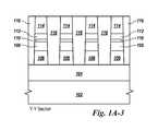
- FIG. 1A-1is a top view
- FIG. 1A-2is a cross-sectional view taken along the line x-x shown in FIG. 1A-1
- FIG. 1A-3is a cross-sectional view taken along line y-y show in FIG. 1A-1 .
- the phase change memory array illustrated in FIGS. 1A-1Hcan be formed with a cross-point architecture, but embodiments of the present disclosure are not limited to such architectures.
- the memory structure shown in FIGS. 1A-1Hincludes a base semiconductor structure that includes a substrate 102 and a buried oxide (BOX) 104 .
- the substrate 102can be a silicon substrate, silicon on insulator (SOI) substrate, or silicon on sapphire (SOS) substrate, among others.
- Silicon implanted with phosphorus or arsenic, among other elements,can be used to form an N+/N ⁇ region 106 of an access device, such as a diode, and an access line, for example a word line, for the memory structures.
- Silicon, which can be epitaxially grown,can be formed over the N+/N ⁇ region 106 and implanted with boron, or other suitable material, to form a positive (P+) region 108 of the access device for the memory structures.
- the bottom electrode material 112can be formed over the P+ region 108 .
- the bottom electrode material 112can be titanium (Ti), tungsten (W), and/or titanium nitride (TiN), for example.
- an adhesion improvement material 110which can improve adhesion of the bottom electrode to the P+ region 108 , can be formed over the P+ region 108 .
- the adhesion improvement material 110can be metal mode titanium (MMTi), titanium nitride (TiN), titanium rich TiN, titanium silicon (TiSix), among other materials.
- a sacrificial material 114such as polysilicon, can be formed over the bottom electrode material 112 .
- the sacrificial material 114can be approximately 600-1000 angstroms ( ⁇ ) thick. As illustrated in the cross-sectional views in FIGS. 1A-2 and 1A-4 , portions of the sacrificial material 114 , the bottom electrode material 112 , the adhesion improvement material 110 , the P+ region 108 , the N+/N ⁇ region 106 , and the BOX 104 can be removed along the x axis to pattern the phase change memory array. The removal of material can remove a portion of the BOX 106 and can stop in and/or on the BOX 106 .
- Portions of the sacrificial material 114 , the bottom electrode material 112 , the adhesion improvement material 110 , the P+ region 108 , and the N+/N ⁇ region 106can be removed along the y-axis to pattern the phase change memory array.
- the removal of materialcan remove a portion of the N+/N ⁇ region 106 and stop in the N+/N ⁇ region 106 , which can define individual diodes for each memory cell of the memory array.
- the sacrificial material 114 , the bottom electrode material 112 , the adhesion improvement material 110 , the P+ region 108 , the N+/N ⁇ region 106 , and BOX 104can be removed by reactive ion etching (RIE).
- RIEreactive ion etching
- the openings created by removing portions of the sacrificial material 114 , the bottom electrode material 112 , the adhesion improvement material 110 , the P+ region 108 , the N+/N ⁇ region 106 , and the BOX 104can be filled with an dielectric 116 , as illustrated in FIGS. 1A-1, 1A-2, 1A-3, and 1A-4 .
- Dielectric 116can be boron-doped phosphor silicate glass (BPSG), a high aspect ratio process dielectric (HARP), and/or a spin-on dielectric (SOD), among other dielectric materials and formation processes. Removing portions of sacrificial material 114 , the bottom electrode material 112 , the adhesion improvement material 110 , the P+ region 108 , the N+/N ⁇ region 106 , and the BOX 104 can further define memory structure regions. Filling openings with dielectric 116 can create insulator regions that separate the memory structure regions from each other and each memory structure region can include a memory cell after further process steps, which are described below.
- BPSGboron-doped phosphor silicate glass
- HTPhigh aspect ratio process dielectric
- SODspin-on dielectric
- FIGS. 1B-1, 1B-2, 1B-3, and 1B-4illustrate further process steps in forming phase change memory cells in accordance with embodiments of the present disclosure.
- a portion of the sacrificial material 114 and dielectric 116can be removed.
- the removal of a portion of the dielectric 116can create a contoured shape for the insulator regions that include dielectric 116 .
- the removal of a portion of the dielectric 116can also define the contact area for the bottom electrode 112 and the phase change material by creating and defining an opening in which to form the phase change material.
- approximately 1 ⁇ 3 of the sacrificial material 114can be removed via RIE and a portion of the dielectric 116 can be removed to contour the dielectric 116 via physical plasma faceting, among other methods.
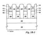
- FIGS. 1C-1, 1C-2, 1C-3, and 1C-4illustrate further process steps in forming phase change memory cells in accordance with embodiments of the present disclosure.
- dielectric 116 and the sacrificial material 114can be further contoured and removed.
- Dielectric 116can be cleaned and removed with a diluted hydrofluoric acid to further contour the dielectric 116 .
- the remaining sacrificial material 114can be removed via trimethane ammonium hydroxide (TMAH) etching, among other methods.
- TMAHtrimethane ammonium hydroxide
- Cleaning the dielectric 116 with diluted hydrofluoric acid to further contour the dielectric 116 and removing the sacrificial material 114 via TMAH etchingcan define the vertical sidewall contact area in the opening created by the hydrofluoric acid cleaning and the TMAH etching.
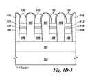
- FIGS. 1D-1, 1D-2, 1D-3, and 1D-4illustrate further process steps in forming phase change memory cells in accordance with embodiments of the present disclosure.
- Spacers 120can be formed on the dielectric 116 .
- the spacers 120can define the contact area for the bottom electrode material 112 .
- the spacers 120can also create a contoured profile for the opening between the insulator regions and can define the size of the opening between the insulator regions where the phase change material can be formed, e.g., contact area for the bottom electrode material and the phase change material.
- Spacers 120can be formed with various suitable materials, e.g., a suitable dielectric.
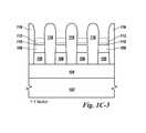
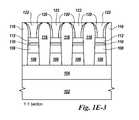
- FIGS. 1E-1, 1E-2, 1E-3, and 1E-4illustrate further process steps in forming phase change memory cells in accordance with embodiments of the present disclosure.
- phase change material 122can be formed in the opening between the insulator regions 116 .
- the phase change material 122can contact the bottom electrode material 112 in the opening.
- the contact area for the phase change material 122 and the bottom electrode material 112can be determined by the amount of dielectric removed during previous process steps and by the size of the spacers 120 formed over the insulator regions.
- the contact area between the bottom electrode 112 and the phase change material 122is defined by the distance between the number of insulator regions and/or the number of spacers on the insulator regions.
- the phase change material 122can be formed in the opening by physical vapor deposition (PVD) and chemical mechanical planariztion (CMP) can be used to remove a portion of the phase change material 122 to the top of the dielectric 116 .
- PVDphysical vapor deposition
- FIGS. 1F-1, 1F-2, 1F-3, and 1F-4illustrate further process steps in forming phase change memory cells in accordance with embodiments of the present disclosure.
- a nitride material 124can be formed over the phase change material 122 and the dielectric 116 .
- the nitride material 124can be used as an etch stop in future processing steps.
- Tetraethyl orthosilicate (TEOS) 126can be form over the nitride material 124 .
- the thickness of the TEOScan determine the thickness of the bit line that is formed in future process steps.
- FIGS. 1G-1, 1G-2, 1G-3, and 1G-4illustrate further process steps in forming phase change memory cells in accordance with embodiments of the present disclosure.
- a portion of the TEOS 126can be removed, e.g., via photo patterning and etching by RIE.
- the removal of the TEOS 126does not remove the nitride material 124 .
- the TEOSis removed along the y-axis over the phase change material 122 .
- the nitride material 124is also removed via a nitride punch where the TEOS above it has been removed to expose the phase change material 122 .
- FIGS. 1H-1, 1H-2, 1H-3, and 1H-4illustrate further process steps in forming phase change memory cells in accordance with embodiments of the present disclosure.
- the top electrode material 128can be formed in the openings formed by removing the TEOS and the nitride material as discussed above.
- the top electrode material 128can be titanium nitride (TiN) or tungsten (W), among other materials.
- the top electrode material 128can be the top electrode for the memory cells in the memory array and can serve as the bit line for the memory cells.
- FIGS. 2A-2Dillustrate process steps associated with forming phase change memory cells in accordance with embodiments of the present disclosure.
- a conductive material 230is formed in the opening between the insulator regions 216 and the phase change material 222 is formed over the conductive material 230 .
- the contact between the phase change material 222 and the bottom electrode 212is via the conductive material 230 .
- the process steps illustrated in FIGS. 2A-2Dstart after the process steps discussed above in association with FIGS. 1A-1D .
- FIGS. 2A-1, 2A-2, 2A-3, and 2A-4illustrate further process steps in forming phase change memory cells in accordance with embodiments of the present disclosure.
- conductive material 230can be formed in the opening between the insulator regions 216 .
- the conductive material 230can contact the bottom electrode material 212 in the opening.
- the contact area for the conductive material 230 and the bottom electrode material 212can be determined by the amount of dielectric removed during process steps and the size of the spacer 220 formed over the insulator regions 216 .
- the conductive material 230can be formed in the opening by PDV and chemical mechanical planarization (CMP) can be used to remove a portion of the conductive material 230 to the top surface of the dielectric 216 .
- CMPchemical mechanical planarization
- FIGS. 2B-1, 2B-2, 2B-3, and 2B-4illustrate a further process step in forming phase change memory cells in accordance with embodiments of the present disclosure.
- phase change material 222can be formed over dielectric 216 and conductive material 230 .
- Top electrode material 228can be formed over the phase change material 222 .
- the top electrode materialcan be formed using atomic layer deposition (ALD), among other suitable processes.
- the top electrode material 228can be titanium nitride (TiN) or tungsten (W), among other materials.
- the top electrode material 228can be the top electrode for the memory cells in the memory array and can be the bit line for the memory cells in the memory array.
- FIGS. 2C-1, 2C-2, 2C-3, and 2C-4illustrate further process steps in forming phase change memory cells in accordance with embodiments of the present disclosure.
- portions of the phase change material 222 and top electrode material 228can be removed via an etch process, such as RIE.
- the phase change material 222 and top electrode material 228can be removed along the y-axis over the phase change material 222 to expose the dielectric 216 .
- FIGS. 2D-1, 2D-2, 2D-3, and 2D-4illustrate further process steps in forming phase change memory cells in accordance with embodiments of the present disclosure.
- a dielectric 232can be formed in the openings formed by removing the top electrode material 228 and the phase change material 222 as discussed above.
- the dielectric 232can be formed to isolate the memory cells from adjacent memory cells.
- a portion of the dielectric and the top electrode material 228can be removed via CMP to form a surface for building further access devices, memory structures and/or other related circuitry.
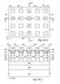
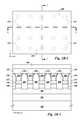
- FIG. 3is a schematic of a portion of a phase change memory array 300 having one or more phase change memory cells in accordance with one or more embodiments of the present disclosure.
- the memory array 300includes a number of phase change memory cells each having an associated access device 352 and resistance variable element 354 , e.g., a phase change material 354 .
- Access devices 352can be operated, e.g., turned on/off, to access the memory cells in order to perform operations such as programming, e.g., writing, and/or sensing, e.g., reading, operations on the memory cells.
- access devices 352are diodes. Diodes can include, for example, p-n diodes, Zener diodes, and Schottky diodes.
- access devices 352can be field effect transistors (FETs) or bipolar junction transistors (BJTs), for example. Embodiments of the present disclosure are not limited to a particular type of access device 352 . As shown in FIG.
- each access device 352 associated with each memory cellis coupled to one of a number of access lines 355 - 0 (WL 0 ), 355 - 1 (WL 1 ), . . . , 355 -N (WLN) (i.e., each access line 355 - 0 , 355 - 1 , . . . , 355 -N is coupled to a row of phase change memory cells).
- the access lines 355 - 0 , 355 - 1 , . . . , 355 -Nmay be referred to herein as “word lines.”
- the designator “N”is used to indicate that a memory array can include a number of word lines.
- the resistance variable elements 354can be a phase change chalcogenide alloy such as a Germanium-Antimony-Tellurium (GST) material, e.g., a Ge—Sb—Te material such as Ge 2 Sb 2 Te 5 , Ge 2 Sb 2 Te 7 , Ge 1 Sb 2 Te 4 , Ge 1 Sb 4 Te 7 , etc.
- GSTGermanium-Antimony-Tellurium
- phase change materialscan include Ge—Te, In—Se, Sb—Te, Ga—Sb, In—Sb, As—Te, Al—Te, Ge—Sb—Te, Te—Ge—As, In—Sb—Te, Te—Sn—Se, Ge—Se—Ga, Bi—Se—Sb, Ga—Se—Te, Sn—Sb—Te, In—Sb—Ge, Te—Ge—Sb—S, Te—Ge—Sn—O, Te—Ge—Sn—Au, Pd—Te—Ge—Sn, In—Se—Ti—Co, Ge—Sb—Te—Pd, Ge—Sb—Te—Co, Sb—Te—Bi—Se, Ag—In—Sb—Te, Ge—Sb—Se—Te, Ge—Sn—Sb—Te, Ge—Te—Sn—Ni, Ge—Te—Sn—Pd,
- each resistance variable element 354is coupled to one of a number of data lines 357 - 0 (BL 0 ), 357 - 1 (BL 1 ), . . . , 357 -M (BLM) (i.e., each data line 357 - 0 , 357 - 1 , . . . , 357 -M is coupled to a column of phase change memory cells).
- the data lines 357 - 0 , 357 - 1 , . . . , 357 -Mmay be referred to herein as “bit lines” or “sense lines.”
- the designator “M”is used to indicate that a memory array can include a number of bit lines.
- the number of word lines 355 - 1 , . . . , 355 -N and the number of bit lines 357 - 1 , . . . , 357 -Mcan each be some power of two, e.g., 256 word lines by 4,096 bit lines.
- embodimentsare not limited to particular numbers of word lines and/or bit lines.
- appropriate voltage and/or current signalscan be applied to the bit lines 357 - 0 , 357 - 1 , . . . , 357 -M and word lines 355 - 0 , 355 - 1 , . . . , 355 -N in order to program data to and/or read data from the phase change memory cells of the array 300 .
- the data stored by a phase change memory cell of array 300can be determined by turning on an access device 352 and sensing a current passing through the phase change element 354 .
- the current sensed on the bit line associated with the memory cell being readcorresponds to a resistance level of the phase change element 354 , which in turn corresponds to a particular data value, e.g., a binary value such as 1, 0, 001, 111, 1011, etc.
- the access device 352 associated with a particular memory cellcan be a device other than a MOSFET.
- the access device 352can be a bipolar junction transistor (BJT) or a diode, e.g., p-n diode, a Schottky diode, or a Zener diode, among other types of access devices.
- BJTbipolar junction transistor
- the phase change memory array 300can be coupled to other memory components including a controller and various write/read circuitry and/or other control circuitry.
- a method of forming a phase change material memory cellincludes forming a number of memory structure regions, wherein the memory structure regions include a bottom electrode material and a sacrificial material, forming a number of insulator regions between the number of memory structure regions, forming a number of openings between the number of insulator regions and forming a contoured surface on the number of insulator regions by removing the sacrificial material and a portion of the number of insulator regions, forming a number of dielectric spacers on the number of insulator regions, forming a contoured opening between the number of insulator regions and exposing the bottom electrode material by removing a portion of the number of dielectric spacers, and forming a phase change material in the opening between the number of insulator regions.
Landscapes
- Engineering & Computer Science (AREA)
- Manufacturing & Machinery (AREA)
- Chemical & Material Sciences (AREA)
- Crystallography & Structural Chemistry (AREA)
- Semiconductor Memories (AREA)
Abstract
Description
Claims (18)
Priority Applications (1)
| Application Number | Priority Date | Filing Date | Title |
|---|---|---|---|
| US14/812,284US9437816B2 (en) | 2010-08-31 | 2015-07-29 | Phase change memory structures and methods |
Applications Claiming Priority (3)
| Application Number | Priority Date | Filing Date | Title |
|---|---|---|---|
| US12/872,945US8574954B2 (en) | 2010-08-31 | 2010-08-31 | Phase change memory structures and methods |
| US14/051,212US9130163B2 (en) | 2010-08-31 | 2013-10-10 | Phase change memory structures and methods |
| US14/812,284US9437816B2 (en) | 2010-08-31 | 2015-07-29 | Phase change memory structures and methods |
Related Parent Applications (1)
| Application Number | Title | Priority Date | Filing Date |
|---|---|---|---|
| US14/051,212ContinuationUS9130163B2 (en) | 2010-08-31 | 2013-10-10 | Phase change memory structures and methods |
Publications (2)
| Publication Number | Publication Date |
|---|---|
| US20150349248A1 US20150349248A1 (en) | 2015-12-03 |
| US9437816B2true US9437816B2 (en) | 2016-09-06 |
Family
ID=45697096
Family Applications (3)
| Application Number | Title | Priority Date | Filing Date |
|---|---|---|---|
| US12/872,945Active2031-08-23US8574954B2 (en) | 2010-08-31 | 2010-08-31 | Phase change memory structures and methods |
| US14/051,212Active2030-11-14US9130163B2 (en) | 2010-08-31 | 2013-10-10 | Phase change memory structures and methods |
| US14/812,284ActiveUS9437816B2 (en) | 2010-08-31 | 2015-07-29 | Phase change memory structures and methods |
Family Applications Before (2)
| Application Number | Title | Priority Date | Filing Date |
|---|---|---|---|
| US12/872,945Active2031-08-23US8574954B2 (en) | 2010-08-31 | 2010-08-31 | Phase change memory structures and methods |
| US14/051,212Active2030-11-14US9130163B2 (en) | 2010-08-31 | 2013-10-10 | Phase change memory structures and methods |
Country Status (7)
| Country | Link |
|---|---|
| US (3) | US8574954B2 (en) |
| JP (1) | JP5923090B2 (en) |
| KR (1) | KR101456808B1 (en) |
| CN (1) | CN103119709B (en) |
| SG (1) | SG187961A1 (en) |
| TW (1) | TWI489460B (en) |
| WO (1) | WO2012030379A2 (en) |
Families Citing this family (9)
| Publication number | Priority date | Publication date | Assignee | Title |
|---|---|---|---|---|
| KR101812687B1 (en) | 2011-06-13 | 2017-12-27 | 삼성전자주식회사 | Method for forming resistance variable memory device |
| CN106611814B (en)* | 2015-10-23 | 2020-05-05 | 中国科学院上海微系统与信息技术研究所 | Phase change material for phase change memory and preparation method thereof |
| KR102465967B1 (en) | 2016-02-22 | 2022-11-10 | 삼성전자주식회사 | Memory device and method for fabricating the same |
| KR102483704B1 (en) | 2016-03-30 | 2023-01-02 | 삼성전자주식회사 | Variable resistance memory devices and methods of manufacturing the same |
| DE112017008120T5 (en)* | 2017-09-29 | 2020-11-26 | Intel Corporation | Self-aligned, embedded phase change memory cell |
| US10468596B2 (en)* | 2018-02-21 | 2019-11-05 | Sandisk Technologies Llc | Damascene process for forming three-dimensional cross rail phase change memory devices |
| JP2020047743A (en)* | 2018-09-18 | 2020-03-26 | キオクシア株式会社 | Storage device |
| KR102722150B1 (en) | 2019-07-23 | 2024-10-28 | 삼성전자주식회사 | Variable resistance memory devices and methods of manufacturing the same |
| WO2023008432A1 (en) | 2021-07-29 | 2023-02-02 | 日本電気硝子株式会社 | Phase change material |
Citations (27)
| Publication number | Priority date | Publication date | Assignee | Title |
|---|---|---|---|---|
| JP2004128486A (en) | 2002-09-30 | 2004-04-22 | Sharp Corp | Manufacturing method of self-aligned cross-point memory array |
| KR20040047272A (en) | 2002-11-29 | 2004-06-05 | 삼성전자주식회사 | Phase changing type semiconductor memory device |
| KR20040054250A (en) | 2002-12-18 | 2004-06-25 | 삼성전자주식회사 | Phase changeable memory cell and method for forming the same |
| JP2006019688A (en) | 2004-06-30 | 2006-01-19 | Hynix Semiconductor Inc | Phase change storage element and manufacturing method thereof |
| JP2006060235A (en) | 2004-08-20 | 2006-03-02 | Samsung Electronics Co Ltd | Method for forming via structure and method for manufacturing phase change memory element incorporating such via structure |
| US7045383B2 (en) | 2001-09-19 | 2006-05-16 | BAE Systems Information and Ovonyx, Inc | Method for making tapered opening for programmable resistance memory element |
| US20060237756A1 (en) | 2005-04-20 | 2006-10-26 | Jae-Hyun Park | Phase change memory devices and their methods of fabrication |
| JP2006313898A (en) | 2005-05-02 | 2006-11-16 | Sharp Corp | Method for manufacturing cross-point resistive memory array and method for manufacturing cross-point resistive memory array stack |
| US20070205438A1 (en) | 2006-03-02 | 2007-09-06 | Werner Juengling | Masking process for simultaneously patterning separate regions |
| US7295463B2 (en)* | 2004-02-25 | 2007-11-13 | Samsung Electronics Co., Ltd. | Phase-changeable memory device and method of manufacturing the same |
| US20070296039A1 (en) | 2006-06-21 | 2007-12-27 | Dureseti Chidambarrao | Semiconductor Device Structures Incorporating Voids and Methods of Fabricating Such Structures |
| US20080029752A1 (en)* | 2004-12-30 | 2008-02-07 | Stmicroelectronics S.R.L. | Phase change memory and manufacturing method thereof |
| US20080142776A1 (en) | 2006-12-15 | 2008-06-19 | Harald Seidl | Phase change random access memory device with transistor, and method for fabricating a memory device |
| US20080164453A1 (en) | 2007-01-07 | 2008-07-10 | Breitwisch Matthew J | Uniform critical dimension size pore for pcram application |
| US20080191188A1 (en) | 2007-02-09 | 2008-08-14 | Samsung Electronics Co., Ltd. | Multi bit phase-change random access memory devices and methods of forming the same |
| US7442602B2 (en) | 2005-06-20 | 2008-10-28 | Samsung Electronics Co., Ltd. | Methods of fabricating phase change memory cells having a cell diode and a bottom electrode self-aligned with each other |
| US20080265239A1 (en) | 2007-04-26 | 2008-10-30 | Jan Boris Philipp | Integrated circuit including spacer material layer |
| KR20090017087A (en) | 2007-08-14 | 2009-02-18 | 주식회사 하이닉스반도체 | Phase change memory device and manufacturing method thereof |
| US7551473B2 (en) | 2007-10-12 | 2009-06-23 | Macronix International Co., Ltd. | Programmable resistive memory with diode structure |
| US20090196091A1 (en) | 2008-01-31 | 2009-08-06 | Kau Derchang | Self-aligned phase change memory |
| KR20090113675A (en) | 2008-04-28 | 2009-11-02 | 주식회사 하이닉스반도체 | Manufacturing method of phase change memory device |
| US7666578B2 (en) | 2006-09-14 | 2010-02-23 | Micron Technology, Inc. | Efficient pitch multiplication process |
| US20100061145A1 (en) | 2008-09-09 | 2010-03-11 | Rolf Weis | Phase Change Memory Cell with MOSFET Driven Bipolar Access Device |
| US7732343B2 (en) | 2006-04-07 | 2010-06-08 | Micron Technology, Inc. | Simplified pitch doubling process flow |
| KR20100063937A (en) | 2008-12-04 | 2010-06-14 | 삼성전자주식회사 | Phase changable memory unit, method of manufacturing the same, and method of manufacturing of phase changable memory device |
| US20100207095A1 (en) | 2006-05-30 | 2010-08-19 | Macronix International Co., Ltd. | Resistor random access memory cell with l-shaped electrode |
| US7816661B2 (en) | 2005-11-21 | 2010-10-19 | Macronix International Co., Ltd. | Air cell thermal isolation for a memory array formed of a programmable resistive material |
Family Cites Families (1)
| Publication number | Priority date | Publication date | Assignee | Title |
|---|---|---|---|---|
| US7049623B2 (en) | 2002-12-13 | 2006-05-23 | Ovonyx, Inc. | Vertical elevated pore phase change memory |
- 2010
- 2010-08-31USUS12/872,945patent/US8574954B2/enactiveActive
- 2011
- 2011-08-24SGSG2013014097Apatent/SG187961A1/enunknown
- 2011-08-24CNCN201180045419.3Apatent/CN103119709B/enactiveActive
- 2011-08-24KRKR1020137007953Apatent/KR101456808B1/enactiveActive
- 2011-08-24WOPCT/US2011/001483patent/WO2012030379A2/enactiveApplication Filing
- 2011-08-24JPJP2013525894Apatent/JP5923090B2/enactiveActive
- 2011-08-31TWTW100131351Apatent/TWI489460B/enactive
- 2013
- 2013-10-10USUS14/051,212patent/US9130163B2/enactiveActive
- 2015
- 2015-07-29USUS14/812,284patent/US9437816B2/enactiveActive
Patent Citations (34)
| Publication number | Priority date | Publication date | Assignee | Title |
|---|---|---|---|---|
| US7045383B2 (en) | 2001-09-19 | 2006-05-16 | BAE Systems Information and Ovonyx, Inc | Method for making tapered opening for programmable resistance memory element |
| US6746910B2 (en) | 2002-09-30 | 2004-06-08 | Sharp Laboratories Of America, Inc. | Method of fabricating self-aligned cross-point memory array |
| JP2004128486A (en) | 2002-09-30 | 2004-04-22 | Sharp Corp | Manufacturing method of self-aligned cross-point memory array |
| KR20040047272A (en) | 2002-11-29 | 2004-06-05 | 삼성전자주식회사 | Phase changing type semiconductor memory device |
| KR20040054250A (en) | 2002-12-18 | 2004-06-25 | 삼성전자주식회사 | Phase changeable memory cell and method for forming the same |
| US7295463B2 (en)* | 2004-02-25 | 2007-11-13 | Samsung Electronics Co., Ltd. | Phase-changeable memory device and method of manufacturing the same |
| JP2006019688A (en) | 2004-06-30 | 2006-01-19 | Hynix Semiconductor Inc | Phase change storage element and manufacturing method thereof |
| US7173271B2 (en) | 2004-06-30 | 2007-02-06 | Hynix Semiconductor Inc. | Phase-change memory device and method of manufacturing the same |
| JP2006060235A (en) | 2004-08-20 | 2006-03-02 | Samsung Electronics Co Ltd | Method for forming via structure and method for manufacturing phase change memory element incorporating such via structure |
| US7473597B2 (en) | 2004-08-20 | 2009-01-06 | Samsung Electronics Co., Ltd | Method of forming via structures and method of fabricating phase change memory devices incorporating such via structures |
| US20080029752A1 (en)* | 2004-12-30 | 2008-02-07 | Stmicroelectronics S.R.L. | Phase change memory and manufacturing method thereof |
| US20060237756A1 (en) | 2005-04-20 | 2006-10-26 | Jae-Hyun Park | Phase change memory devices and their methods of fabrication |
| JP2006313898A (en) | 2005-05-02 | 2006-11-16 | Sharp Corp | Method for manufacturing cross-point resistive memory array and method for manufacturing cross-point resistive memory array stack |
| US7323349B2 (en) | 2005-05-02 | 2008-01-29 | Sharp Laboratories Of America, Inc. | Self-aligned cross point resistor memory array |
| US7442602B2 (en) | 2005-06-20 | 2008-10-28 | Samsung Electronics Co., Ltd. | Methods of fabricating phase change memory cells having a cell diode and a bottom electrode self-aligned with each other |
| US7816661B2 (en) | 2005-11-21 | 2010-10-19 | Macronix International Co., Ltd. | Air cell thermal isolation for a memory array formed of a programmable resistive material |
| US20070205438A1 (en) | 2006-03-02 | 2007-09-06 | Werner Juengling | Masking process for simultaneously patterning separate regions |
| US7732343B2 (en) | 2006-04-07 | 2010-06-08 | Micron Technology, Inc. | Simplified pitch doubling process flow |
| US20100207095A1 (en) | 2006-05-30 | 2010-08-19 | Macronix International Co., Ltd. | Resistor random access memory cell with l-shaped electrode |
| US20070296039A1 (en) | 2006-06-21 | 2007-12-27 | Dureseti Chidambarrao | Semiconductor Device Structures Incorporating Voids and Methods of Fabricating Such Structures |
| US7666578B2 (en) | 2006-09-14 | 2010-02-23 | Micron Technology, Inc. | Efficient pitch multiplication process |
| US20080142776A1 (en) | 2006-12-15 | 2008-06-19 | Harald Seidl | Phase change random access memory device with transistor, and method for fabricating a memory device |
| US20080164453A1 (en) | 2007-01-07 | 2008-07-10 | Breitwisch Matthew J | Uniform critical dimension size pore for pcram application |
| JP2008198979A (en) | 2007-02-09 | 2008-08-28 | Samsung Electronics Co Ltd | Multi-bit phase change memory device and manufacturing method thereof |
| US20080191188A1 (en) | 2007-02-09 | 2008-08-14 | Samsung Electronics Co., Ltd. | Multi bit phase-change random access memory devices and methods of forming the same |
| JP2009010337A (en) | 2007-04-26 | 2009-01-15 | Qimonda Ag | Integrated circuit having a spacer material layer |
| US20080265239A1 (en) | 2007-04-26 | 2008-10-30 | Jan Boris Philipp | Integrated circuit including spacer material layer |
| KR20090017087A (en) | 2007-08-14 | 2009-02-18 | 주식회사 하이닉스반도체 | Phase change memory device and manufacturing method thereof |
| US7551473B2 (en) | 2007-10-12 | 2009-06-23 | Macronix International Co., Ltd. | Programmable resistive memory with diode structure |
| US20090196091A1 (en) | 2008-01-31 | 2009-08-06 | Kau Derchang | Self-aligned phase change memory |
| KR20090113675A (en) | 2008-04-28 | 2009-11-02 | 주식회사 하이닉스반도체 | Manufacturing method of phase change memory device |
| US20100061145A1 (en) | 2008-09-09 | 2010-03-11 | Rolf Weis | Phase Change Memory Cell with MOSFET Driven Bipolar Access Device |
| KR20100063937A (en) | 2008-12-04 | 2010-06-14 | 삼성전자주식회사 | Phase changable memory unit, method of manufacturing the same, and method of manufacturing of phase changable memory device |
| US8133757B2 (en) | 2008-12-04 | 2012-03-13 | Samsung Electronics Co., Ltd. | Method of manufacturing a phase changeable memory unit having an enhanced structure to reduce a reset current |
Non-Patent Citations (13)
| Title |
|---|
| Decision of Rejection from related Chinese patent application No. 201180045419.3, dated Sep. 6, 2015, 24 pp. |
| First Office Action from related Chinese patent application No. 201180045419.3, dated Jun. 30, 2014, 22 pp. |
| International Search Report and Written Opinion for related PCT Application No. PCT/US2011/001483, Mailed Apr. 6, 2012, (13 pages). |
| Kai-Liang Zhang, et al. "Study on Chemical Mechanical Polishing of GeSbTe for Chalcogenide Phase Change Memory", IEEE 2006 (3 pgs.). |
| Kwang-Jin Lee, et al. "A 90 nm 1.8 V 512 Mb Diode-Switch PRAM With 266 MB/s Read Throughput", IEEE Journal of Solid-State Circuts, vol. 43, No. 1, Jan. 2008 (13 pgs.). |
| Notice of Final Rejection from related Korean patent application No. 10-2013-7007953, dated Aug. 14, 2014, 7 pp. |
| Notice of Initiation of Examination by Administrative Patent Judges from related Japanese patent application No. 2013-525894, dated Nov. 18, 2014, 5 pp. |
| Notice of Preliminary Rejection from related Korean patent application No. 10-2013-7007953, dated Feb. 20, 2014, 9 pp. |
| Notice of Rejection from related Japanese patent application No. 2013-525894, dated Aug. 11, 2015, 8 pp. |
| Notice of Rejection Ground from related Japanese patent application No. 2013-525894, dated Jul. 1, 2014, 7 pp. |
| Notice of Rejection Grounds from related Japanese patent application No. 2013-525894, dated Feb. 26, 2014, 9 pp. |
| Office Action from related Taiwan patent application No. 100131351, dated Aug. 26, 2014, 9 pp. |
| Second Office Action from related Chinese patent application No. 201180045419.3, dated Feb. 28, 2015, 22 pp. |
Also Published As
| Publication number | Publication date |
|---|---|
| US9130163B2 (en) | 2015-09-08 |
| CN103119709B (en) | 2016-10-12 |
| WO2012030379A2 (en) | 2012-03-08 |
| JP2013536983A (en) | 2013-09-26 |
| KR101456808B1 (en) | 2014-10-31 |
| CN103119709A (en) | 2013-05-22 |
| US20120051124A1 (en) | 2012-03-01 |
| TWI489460B (en) | 2015-06-21 |
| US8574954B2 (en) | 2013-11-05 |
| KR20130050989A (en) | 2013-05-16 |
| US20140097399A1 (en) | 2014-04-10 |
| JP5923090B2 (en) | 2016-05-24 |
| SG187961A1 (en) | 2013-03-28 |
| WO2012030379A3 (en) | 2012-05-24 |
| TW201222548A (en) | 2012-06-01 |
| US20150349248A1 (en) | 2015-12-03 |
Similar Documents
| Publication | Publication Date | Title |
|---|---|---|
| US9437816B2 (en) | Phase change memory structures and methods | |
| US9287502B2 (en) | Resistance variable memory cell structures and methods | |
| EP3309838B1 (en) | Vertical transistor phase change memory cell and fabrication method therefor | |
| US8698209B2 (en) | Encapsulated phase change cell structures and methods | |
| WO2020242534A1 (en) | Three-dimensional nand memory device containing two terminal selector and methods of using and making thereof | |
| US20100019215A1 (en) | Mushroom type memory cell having self-aligned bottom electrode and diode access device | |
| US8592790B2 (en) | Phase-change random access memory device and method of manufacturing the same | |
| US6733956B2 (en) | Method for making programmable resistance memory element | |
| US7545019B2 (en) | Integrated circuit including logic portion and memory portion | |
| US20030122156A1 (en) | Programmable resistance memory element and method for making same | |
| US9362495B2 (en) | Confined resistance variable memory cells and methods | |
| US8395140B2 (en) | Cross-point memory utilizing Ru/Si diode | |
| TW200908205A (en) | 3D R/W cell with reduced reverse leakage and method of making thereof | |
| US8546778B2 (en) | Resistance variable memory cells and methods |
Legal Events
| Date | Code | Title | Description |
|---|---|---|---|
| AS | Assignment | Owner name:MICRON TECHNOLOGY, INC., IDAHO Free format text:ASSIGNMENT OF ASSIGNORS INTEREST;ASSIGNOR:TANG, SANH D.;REEL/FRAME:036208/0363 Effective date:20100830 | |
| FEPP | Fee payment procedure | Free format text:PAYOR NUMBER ASSIGNED (ORIGINAL EVENT CODE: ASPN); ENTITY STATUS OF PATENT OWNER: LARGE ENTITY | |
| AS | Assignment | Owner name:U.S. BANK NATIONAL ASSOCIATION, AS COLLATERAL AGENT, CALIFORNIA Free format text:SECURITY INTEREST;ASSIGNOR:MICRON TECHNOLOGY, INC.;REEL/FRAME:038669/0001 Effective date:20160426 Owner name:U.S. BANK NATIONAL ASSOCIATION, AS COLLATERAL AGEN Free format text:SECURITY INTEREST;ASSIGNOR:MICRON TECHNOLOGY, INC.;REEL/FRAME:038669/0001 Effective date:20160426 | |
| AS | Assignment | Owner name:MORGAN STANLEY SENIOR FUNDING, INC., AS COLLATERAL AGENT, MARYLAND Free format text:PATENT SECURITY AGREEMENT;ASSIGNOR:MICRON TECHNOLOGY, INC.;REEL/FRAME:038954/0001 Effective date:20160426 Owner name:MORGAN STANLEY SENIOR FUNDING, INC., AS COLLATERAL Free format text:PATENT SECURITY AGREEMENT;ASSIGNOR:MICRON TECHNOLOGY, INC.;REEL/FRAME:038954/0001 Effective date:20160426 | |
| STCF | Information on status: patent grant | Free format text:PATENTED CASE | |
| AS | Assignment | Owner name:U.S. BANK NATIONAL ASSOCIATION, AS COLLATERAL AGENT, CALIFORNIA Free format text:CORRECTIVE ASSIGNMENT TO CORRECT THE REPLACE ERRONEOUSLY FILED PATENT #7358718 WITH THE CORRECT PATENT #7358178 PREVIOUSLY RECORDED ON REEL 038669 FRAME 0001. ASSIGNOR(S) HEREBY CONFIRMS THE SECURITY INTEREST;ASSIGNOR:MICRON TECHNOLOGY, INC.;REEL/FRAME:043079/0001 Effective date:20160426 Owner name:U.S. BANK NATIONAL ASSOCIATION, AS COLLATERAL AGEN Free format text:CORRECTIVE ASSIGNMENT TO CORRECT THE REPLACE ERRONEOUSLY FILED PATENT #7358718 WITH THE CORRECT PATENT #7358178 PREVIOUSLY RECORDED ON REEL 038669 FRAME 0001. ASSIGNOR(S) HEREBY CONFIRMS THE SECURITY INTEREST;ASSIGNOR:MICRON TECHNOLOGY, INC.;REEL/FRAME:043079/0001 Effective date:20160426 | |
| AS | Assignment | Owner name:JPMORGAN CHASE BANK, N.A., AS COLLATERAL AGENT, ILLINOIS Free format text:SECURITY INTEREST;ASSIGNORS:MICRON TECHNOLOGY, INC.;MICRON SEMICONDUCTOR PRODUCTS, INC.;REEL/FRAME:047540/0001 Effective date:20180703 Owner name:JPMORGAN CHASE BANK, N.A., AS COLLATERAL AGENT, IL Free format text:SECURITY INTEREST;ASSIGNORS:MICRON TECHNOLOGY, INC.;MICRON SEMICONDUCTOR PRODUCTS, INC.;REEL/FRAME:047540/0001 Effective date:20180703 | |
| AS | Assignment | Owner name:MICRON TECHNOLOGY, INC., IDAHO Free format text:RELEASE BY SECURED PARTY;ASSIGNOR:U.S. BANK NATIONAL ASSOCIATION, AS COLLATERAL AGENT;REEL/FRAME:047243/0001 Effective date:20180629 | |
| AS | Assignment | Owner name:MICRON TECHNOLOGY, INC., IDAHO Free format text:RELEASE BY SECURED PARTY;ASSIGNOR:MORGAN STANLEY SENIOR FUNDING, INC., AS COLLATERAL AGENT;REEL/FRAME:050937/0001 Effective date:20190731 | |
| AS | Assignment | Owner name:MICRON SEMICONDUCTOR PRODUCTS, INC., IDAHO Free format text:RELEASE BY SECURED PARTY;ASSIGNOR:JPMORGAN CHASE BANK, N.A., AS COLLATERAL AGENT;REEL/FRAME:051028/0001 Effective date:20190731 Owner name:MICRON TECHNOLOGY, INC., IDAHO Free format text:RELEASE BY SECURED PARTY;ASSIGNOR:JPMORGAN CHASE BANK, N.A., AS COLLATERAL AGENT;REEL/FRAME:051028/0001 Effective date:20190731 | |
| MAFP | Maintenance fee payment | Free format text:PAYMENT OF MAINTENANCE FEE, 4TH YEAR, LARGE ENTITY (ORIGINAL EVENT CODE: M1551); ENTITY STATUS OF PATENT OWNER: LARGE ENTITY Year of fee payment:4 | |
| MAFP | Maintenance fee payment | Free format text:PAYMENT OF MAINTENANCE FEE, 8TH YEAR, LARGE ENTITY (ORIGINAL EVENT CODE: M1552); ENTITY STATUS OF PATENT OWNER: LARGE ENTITY Year of fee payment:8 |