US9437443B2 - Low-temperature sidewall image transfer process using ALD metals, metal oxides and metal nitrides - Google Patents
Low-temperature sidewall image transfer process using ALD metals, metal oxides and metal nitridesDownload PDFInfo
- Publication number
- US9437443B2 US9437443B2US13/916,109US201313916109AUS9437443B2US 9437443 B2US9437443 B2US 9437443B2US 201313916109 AUS201313916109 AUS 201313916109AUS 9437443 B2US9437443 B2US 9437443B2
- Authority
- US
- United States
- Prior art keywords
- sit
- sidewall spacers
- mandrels
- pattern
- oxide
- Prior art date
- Legal status (The legal status is an assumption and is not a legal conclusion. Google has not performed a legal analysis and makes no representation as to the accuracy of the status listed.)
- Expired - Fee Related, expires
Links
- 238000000034methodMethods0.000titleclaimsabstractdescription77
- 229910052751metalInorganic materials0.000titleclaimsabstractdescription30
- 239000002184metalSubstances0.000titleclaimsabstractdescription30
- 150000004767nitridesChemical class0.000titleclaimsabstractdescription16
- 229910044991metal oxideInorganic materials0.000titleclaimsabstractdescription14
- 150000004706metal oxidesChemical class0.000titleclaimsabstractdescription14
- 150000002739metalsChemical class0.000titleclaimsdescription8
- 239000000463materialSubstances0.000claimsabstractdescription125
- 125000006850spacer groupChemical group0.000claimsabstractdescription113
- 239000000758substrateSubstances0.000claimsabstractdescription41
- 238000000231atomic layer depositionMethods0.000claimsabstractdescription18
- 239000010409thin filmSubstances0.000claimsdescription33
- 238000001020plasma etchingMethods0.000claimsdescription17
- 238000000151depositionMethods0.000claimsdescription11
- 238000005530etchingMethods0.000claimsdescription9
- XEEYBQQBJWHFJM-UHFFFAOYSA-NIronChemical compound[Fe]XEEYBQQBJWHFJM-UHFFFAOYSA-N0.000claimsdescription6
- PXHVJJICTQNCMI-UHFFFAOYSA-NNickelChemical compound[Ni]PXHVJJICTQNCMI-UHFFFAOYSA-N0.000claimsdescription6
- BASFCYQUMIYNBI-UHFFFAOYSA-NplatinumChemical compound[Pt]BASFCYQUMIYNBI-UHFFFAOYSA-N0.000claimsdescription6
- XLOMVQKBTHCTTD-UHFFFAOYSA-NZinc monoxideChemical compound[Zn]=OXLOMVQKBTHCTTD-UHFFFAOYSA-N0.000claimsdescription4
- -1hafnium nitrideChemical class0.000claimsdescription4
- MRELNEQAGSRDBK-UHFFFAOYSA-Nlanthanum(3+);oxygen(2-)Chemical compound[O-2].[O-2].[O-2].[La+3].[La+3]MRELNEQAGSRDBK-UHFFFAOYSA-N0.000claimsdescription4
- 239000004065semiconductorSubstances0.000claimsdescription4
- KJTLSVCANCCWHF-UHFFFAOYSA-NRutheniumChemical compound[Ru]KJTLSVCANCCWHF-UHFFFAOYSA-N0.000claimsdescription3
- 229910052742ironInorganic materials0.000claimsdescription3
- 229910052759nickelInorganic materials0.000claimsdescription3
- 229910052697platinumInorganic materials0.000claimsdescription3
- 229910052707rutheniumInorganic materials0.000claimsdescription3
- GWEVSGVZZGPLCZ-UHFFFAOYSA-NTitan oxideChemical compoundO=[Ti]=OGWEVSGVZZGPLCZ-UHFFFAOYSA-N0.000claimsdescription2
- NRTOMJZYCJJWKI-UHFFFAOYSA-NTitanium nitrideChemical compound[Ti]#NNRTOMJZYCJJWKI-UHFFFAOYSA-N0.000claimsdescription2
- CFJRGWXELQQLSA-UHFFFAOYSA-NazanylidyneniobiumChemical compound[Nb]#NCFJRGWXELQQLSA-UHFFFAOYSA-N0.000claimsdescription2
- 229910000428cobalt oxideInorganic materials0.000claimsdescription2
- IVMYJDGYRUAWML-UHFFFAOYSA-Ncobalt(ii) oxideChemical compound[Co]=OIVMYJDGYRUAWML-UHFFFAOYSA-N0.000claimsdescription2
- 238000001312dry etchingMethods0.000claimsdescription2
- 229910052735hafniumInorganic materials0.000claimsdescription2
- 229910000449hafnium oxideInorganic materials0.000claimsdescription2
- WIHZLLGSGQNAGK-UHFFFAOYSA-Nhafnium(4+);oxygen(2-)Chemical compound[O-2].[O-2].[Hf+4]WIHZLLGSGQNAGK-UHFFFAOYSA-N0.000claimsdescription2
- 239000012212insulatorSubstances0.000claimsdescription2
- CPLXHLVBOLITMK-UHFFFAOYSA-Nmagnesium oxideInorganic materials[Mg]=OCPLXHLVBOLITMK-UHFFFAOYSA-N0.000claimsdescription2
- 239000000395magnesium oxideSubstances0.000claimsdescription2
- AXZKOIWUVFPNLO-UHFFFAOYSA-Nmagnesium;oxygen(2-)Chemical compound[O-2].[Mg+2]AXZKOIWUVFPNLO-UHFFFAOYSA-N0.000claimsdescription2
- 229910000484niobium oxideInorganic materials0.000claimsdescription2
- URLJKFSTXLNXLG-UHFFFAOYSA-Nniobium(5+);oxygen(2-)Chemical compound[O-2].[O-2].[O-2].[O-2].[O-2].[Nb+5].[Nb+5]URLJKFSTXLNXLG-UHFFFAOYSA-N0.000claimsdescription2
- TWNQGVIAIRXVLR-UHFFFAOYSA-Noxo(oxoalumanyloxy)alumaneChemical compoundO=[Al]O[Al]=OTWNQGVIAIRXVLR-UHFFFAOYSA-N0.000claimsdescription2
- BPUBBGLMJRNUCC-UHFFFAOYSA-Noxygen(2-);tantalum(5+)Chemical compound[O-2].[O-2].[O-2].[O-2].[O-2].[Ta+5].[Ta+5]BPUBBGLMJRNUCC-UHFFFAOYSA-N0.000claimsdescription2
- RVTZCBVAJQQJTK-UHFFFAOYSA-Noxygen(2-);zirconium(4+)Chemical compound[O-2].[O-2].[Zr+4]RVTZCBVAJQQJTK-UHFFFAOYSA-N0.000claimsdescription2
- MZLGASXMSKOWSE-UHFFFAOYSA-Ntantalum nitrideChemical compound[Ta]#NMZLGASXMSKOWSE-UHFFFAOYSA-N0.000claimsdescription2
- 229910001936tantalum oxideInorganic materials0.000claimsdescription2
- XOLBLPGZBRYERU-UHFFFAOYSA-Ntin dioxideChemical compoundO=[Sn]=OXOLBLPGZBRYERU-UHFFFAOYSA-N0.000claimsdescription2
- 229910001887tin oxideInorganic materials0.000claimsdescription2
- OGIDPMRJRNCKJF-UHFFFAOYSA-Ntitanium oxideInorganic materials[Ti]=OOGIDPMRJRNCKJF-UHFFFAOYSA-N0.000claimsdescription2
- 229910052721tungstenInorganic materials0.000claimsdescription2
- 239000010937tungstenSubstances0.000claimsdescription2
- 238000001039wet etchingMethods0.000claimsdescription2
- 239000011787zinc oxideSubstances0.000claimsdescription2
- ZVWKZXLXHLZXLS-UHFFFAOYSA-Nzirconium nitrideChemical compound[Zr]#NZVWKZXLXHLZXLS-UHFFFAOYSA-N0.000claimsdescription2
- 229910001928zirconium oxideInorganic materials0.000claimsdescription2
- 239000002210silicon-based materialSubstances0.000claims2
- 235000012431wafersNutrition0.000description21
- 238000010586diagramMethods0.000description10
- 238000001459lithographyMethods0.000description7
- 239000010408filmSubstances0.000description6
- 238000000059patterningMethods0.000description6
- 238000012986modificationMethods0.000description5
- 230000004048modificationEffects0.000description5
- 238000001878scanning electron micrographMethods0.000description4
- XUIMIQQOPSSXEZ-UHFFFAOYSA-NSiliconChemical compound[Si]XUIMIQQOPSSXEZ-UHFFFAOYSA-N0.000description3
- 238000005229chemical vapour depositionMethods0.000description3
- 230000008021depositionEffects0.000description3
- 238000005240physical vapour depositionMethods0.000description3
- 229910052710siliconInorganic materials0.000description3
- 239000010703siliconSubstances0.000description3
- 229910052581Si3N4Inorganic materials0.000description2
- 238000005137deposition processMethods0.000description2
- 238000002408directed self-assemblyMethods0.000description2
- 238000001704evaporationMethods0.000description2
- 230000008020evaporationEffects0.000description2
- 238000004519manufacturing processMethods0.000description2
- 238000007781pre-processingMethods0.000description2
- HQVNEWCFYHHQES-UHFFFAOYSA-Nsilicon nitrideChemical compoundN12[Si]34N5[Si]62N3[Si]51N64HQVNEWCFYHHQES-UHFFFAOYSA-N0.000description2
- 238000004528spin coatingMethods0.000description2
- ZOKXTWBITQBERF-UHFFFAOYSA-NMolybdenumChemical compound[Mo]ZOKXTWBITQBERF-UHFFFAOYSA-N0.000description1
- VYPSYNLAJGMNEJ-UHFFFAOYSA-NSilicium dioxideChemical compoundO=[Si]=OVYPSYNLAJGMNEJ-UHFFFAOYSA-N0.000description1
- 239000006227byproductSubstances0.000description1
- 239000003989dielectric materialSubstances0.000description1
- 239000002019doping agentSubstances0.000description1
- 239000007772electrode materialSubstances0.000description1
- 238000005516engineering processMethods0.000description1
- 229910052750molybdenumInorganic materials0.000description1
- 239000011733molybdenumSubstances0.000description1
- 238000005457optimizationMethods0.000description1
- 229910021420polycrystalline siliconInorganic materials0.000description1
- 229920005591polysiliconPolymers0.000description1
- 238000005389semiconductor device fabricationMethods0.000description1
- 229910052814silicon oxideInorganic materials0.000description1
Images


Classifications
- H—ELECTRICITY
- H01—ELECTRIC ELEMENTS
- H01L—SEMICONDUCTOR DEVICES NOT COVERED BY CLASS H10
- H01L21/00—Processes or apparatus adapted for the manufacture or treatment of semiconductor or solid state devices or of parts thereof
- H01L21/02—Manufacture or treatment of semiconductor devices or of parts thereof
- H01L21/04—Manufacture or treatment of semiconductor devices or of parts thereof the devices having potential barriers, e.g. a PN junction, depletion layer or carrier concentration layer
- H01L21/18—Manufacture or treatment of semiconductor devices or of parts thereof the devices having potential barriers, e.g. a PN junction, depletion layer or carrier concentration layer the devices having semiconductor bodies comprising elements of Group IV of the Periodic Table or AIIIBV compounds with or without impurities, e.g. doping materials
- H01L21/30—Treatment of semiconductor bodies using processes or apparatus not provided for in groups H01L21/20 - H01L21/26
- H01L21/302—Treatment of semiconductor bodies using processes or apparatus not provided for in groups H01L21/20 - H01L21/26 to change their surface-physical characteristics or shape, e.g. etching, polishing, cutting
- H01L21/306—Chemical or electrical treatment, e.g. electrolytic etching
- H01L21/308—Chemical or electrical treatment, e.g. electrolytic etching using masks
- H01L21/3083—Chemical or electrical treatment, e.g. electrolytic etching using masks characterised by their size, orientation, disposition, behaviour, shape, in horizontal or vertical plane
- H01L21/3086—Chemical or electrical treatment, e.g. electrolytic etching using masks characterised by their size, orientation, disposition, behaviour, shape, in horizontal or vertical plane characterised by the process involved to create the mask, e.g. lift-off masks, sidewalls, or to modify the mask, e.g. pre-treatment, post-treatment
- H—ELECTRICITY
- H01—ELECTRIC ELEMENTS
- H01L—SEMICONDUCTOR DEVICES NOT COVERED BY CLASS H10
- H01L21/00—Processes or apparatus adapted for the manufacture or treatment of semiconductor or solid state devices or of parts thereof
- H01L21/02—Manufacture or treatment of semiconductor devices or of parts thereof
- H01L21/02104—Forming layers
- H01L21/02107—Forming insulating materials on a substrate
- H01L21/02225—Forming insulating materials on a substrate characterised by the process for the formation of the insulating layer
- H01L21/0226—Forming insulating materials on a substrate characterised by the process for the formation of the insulating layer formation by a deposition process
- H01L21/02263—Forming insulating materials on a substrate characterised by the process for the formation of the insulating layer formation by a deposition process deposition from the gas or vapour phase
- H01L21/02271—Forming insulating materials on a substrate characterised by the process for the formation of the insulating layer formation by a deposition process deposition from the gas or vapour phase deposition by decomposition or reaction of gaseous or vapour phase compounds, i.e. chemical vapour deposition
- H01L21/0228—Forming insulating materials on a substrate characterised by the process for the formation of the insulating layer formation by a deposition process deposition from the gas or vapour phase deposition by decomposition or reaction of gaseous or vapour phase compounds, i.e. chemical vapour deposition deposition by cyclic CVD, e.g. ALD, ALE, pulsed CVD
- H—ELECTRICITY
- H01—ELECTRIC ELEMENTS
- H01L—SEMICONDUCTOR DEVICES NOT COVERED BY CLASS H10
- H01L21/00—Processes or apparatus adapted for the manufacture or treatment of semiconductor or solid state devices or of parts thereof
- H01L21/02—Manufacture or treatment of semiconductor devices or of parts thereof
- H01L21/027—Making masks on semiconductor bodies for further photolithographic processing not provided for in group H01L21/18 or H01L21/34
- H01L21/033—Making masks on semiconductor bodies for further photolithographic processing not provided for in group H01L21/18 or H01L21/34 comprising inorganic layers
- H01L21/0334—Making masks on semiconductor bodies for further photolithographic processing not provided for in group H01L21/18 or H01L21/34 comprising inorganic layers characterised by their size, orientation, disposition, behaviour, shape, in horizontal or vertical plane
- H01L21/0337—Making masks on semiconductor bodies for further photolithographic processing not provided for in group H01L21/18 or H01L21/34 comprising inorganic layers characterised by their size, orientation, disposition, behaviour, shape, in horizontal or vertical plane characterised by the process involved to create the mask, e.g. lift-off masks, sidewalls, or to modify the mask, e.g. pre-treatment, post-treatment
- H—ELECTRICITY
- H01—ELECTRIC ELEMENTS
- H01L—SEMICONDUCTOR DEVICES NOT COVERED BY CLASS H10
- H01L21/00—Processes or apparatus adapted for the manufacture or treatment of semiconductor or solid state devices or of parts thereof
- H01L21/02—Manufacture or treatment of semiconductor devices or of parts thereof
- H01L21/027—Making masks on semiconductor bodies for further photolithographic processing not provided for in group H01L21/18 or H01L21/34
- H01L21/033—Making masks on semiconductor bodies for further photolithographic processing not provided for in group H01L21/18 or H01L21/34 comprising inorganic layers
- H01L21/0334—Making masks on semiconductor bodies for further photolithographic processing not provided for in group H01L21/18 or H01L21/34 comprising inorganic layers characterised by their size, orientation, disposition, behaviour, shape, in horizontal or vertical plane
- H01L21/0338—Process specially adapted to improve the resolution of the mask
- H—ELECTRICITY
- H01—ELECTRIC ELEMENTS
- H01L—SEMICONDUCTOR DEVICES NOT COVERED BY CLASS H10
- H01L21/00—Processes or apparatus adapted for the manufacture or treatment of semiconductor or solid state devices or of parts thereof
- H01L21/02—Manufacture or treatment of semiconductor devices or of parts thereof
- H01L21/04—Manufacture or treatment of semiconductor devices or of parts thereof the devices having potential barriers, e.g. a PN junction, depletion layer or carrier concentration layer
- H01L21/18—Manufacture or treatment of semiconductor devices or of parts thereof the devices having potential barriers, e.g. a PN junction, depletion layer or carrier concentration layer the devices having semiconductor bodies comprising elements of Group IV of the Periodic Table or AIIIBV compounds with or without impurities, e.g. doping materials
- H01L21/30—Treatment of semiconductor bodies using processes or apparatus not provided for in groups H01L21/20 - H01L21/26
- H01L21/302—Treatment of semiconductor bodies using processes or apparatus not provided for in groups H01L21/20 - H01L21/26 to change their surface-physical characteristics or shape, e.g. etching, polishing, cutting
- H01L21/306—Chemical or electrical treatment, e.g. electrolytic etching
- H01L21/308—Chemical or electrical treatment, e.g. electrolytic etching using masks
- H01L21/3083—Chemical or electrical treatment, e.g. electrolytic etching using masks characterised by their size, orientation, disposition, behaviour, shape, in horizontal or vertical plane
- H01L21/3088—Process specially adapted to improve the resolution of the mask
- H—ELECTRICITY
- H01—ELECTRIC ELEMENTS
- H01L—SEMICONDUCTOR DEVICES NOT COVERED BY CLASS H10
- H01L21/00—Processes or apparatus adapted for the manufacture or treatment of semiconductor or solid state devices or of parts thereof
- H01L21/02—Manufacture or treatment of semiconductor devices or of parts thereof
- H01L21/04—Manufacture or treatment of semiconductor devices or of parts thereof the devices having potential barriers, e.g. a PN junction, depletion layer or carrier concentration layer
- H01L21/18—Manufacture or treatment of semiconductor devices or of parts thereof the devices having potential barriers, e.g. a PN junction, depletion layer or carrier concentration layer the devices having semiconductor bodies comprising elements of Group IV of the Periodic Table or AIIIBV compounds with or without impurities, e.g. doping materials
- H01L21/30—Treatment of semiconductor bodies using processes or apparatus not provided for in groups H01L21/20 - H01L21/26
- H01L21/31—Treatment of semiconductor bodies using processes or apparatus not provided for in groups H01L21/20 - H01L21/26 to form insulating layers thereon, e.g. for masking or by using photolithographic techniques; After treatment of these layers; Selection of materials for these layers
- H01L21/3205—Deposition of non-insulating-, e.g. conductive- or resistive-, layers on insulating layers; After-treatment of these layers
- H01L21/321—After treatment
- H01L21/3213—Physical or chemical etching of the layers, e.g. to produce a patterned layer from a pre-deposited extensive layer
- H01L21/32139—Physical or chemical etching of the layers, e.g. to produce a patterned layer from a pre-deposited extensive layer using masks
- H—ELECTRICITY
- H01—ELECTRIC ELEMENTS
- H01L—SEMICONDUCTOR DEVICES NOT COVERED BY CLASS H10
- H01L21/00—Processes or apparatus adapted for the manufacture or treatment of semiconductor or solid state devices or of parts thereof
- H01L21/02—Manufacture or treatment of semiconductor devices or of parts thereof
- H01L21/04—Manufacture or treatment of semiconductor devices or of parts thereof the devices having potential barriers, e.g. a PN junction, depletion layer or carrier concentration layer
- H01L21/18—Manufacture or treatment of semiconductor devices or of parts thereof the devices having potential barriers, e.g. a PN junction, depletion layer or carrier concentration layer the devices having semiconductor bodies comprising elements of Group IV of the Periodic Table or AIIIBV compounds with or without impurities, e.g. doping materials
- H01L21/28—Manufacture of electrodes on semiconductor bodies using processes or apparatus not provided for in groups H01L21/20 - H01L21/268
- H01L21/28008—Making conductor-insulator-semiconductor electrodes
- H01L21/28017—Making conductor-insulator-semiconductor electrodes the insulator being formed after the semiconductor body, the semiconductor being silicon
- H01L21/28026—Making conductor-insulator-semiconductor electrodes the insulator being formed after the semiconductor body, the semiconductor being silicon characterised by the conductor
- H01L21/28123—Lithography-related aspects, e.g. sub-lithography lengths; Isolation-related aspects, e.g. to solve problems arising at the crossing with the side of the device isolation; Planarisation aspects
- H01L21/28132—Lithography-related aspects, e.g. sub-lithography lengths; Isolation-related aspects, e.g. to solve problems arising at the crossing with the side of the device isolation; Planarisation aspects conducting part of electrode is difined by a sidewall spacer or a similar technique, e.g. oxidation under mask, plating
Definitions
- the present inventionrelates to a Sidewall Image Transfer (SIT) process and more particularly, to SIT techniques using atomic layer deposition (ALD) metals, metal oxide and/or metal nitrides.
- SITSidewall Image Transfer
- ALDatomic layer deposition
- SITSidewall Image Transfer
- SITcan only be integrated into otherwise high-temperature compatible process flows, for example, excluding SIT from back-end of the line (BEOL) patterning.
- BEOLback-end of the line
- the present inventionrelates to Sidewall Image Transfer (SIT) techniques using atomic layer deposition (ALD) metals, metal oxide and/or metal nitrides.
- a SIT methodis provided. The method includes the following steps. A SIT mandrel material is deposited onto a substrate. A patterned resist is formed on the SIT mandrel material, wherein the patterned resist has a line pattern defined therein. The line pattern from the patterned resist is transferred to the SIT mandrel material, forming a plurality of SIT mandrels. A spacer material is conformally deposited onto the substrate covering a top and sides of each of the SIT mandrels.
- the spacer materialis selected from the group including a metal, a metal oxide, a metal nitride and combinations including at least one of the foregoing materials.
- the spacer materialis removed from all but the sides of each of the SIT mandrels to form SIT sidewall spacers on the sides of each of the SIT mandrels.
- the SIT mandrelsare removed selective to the SIT sidewall spacers revealing a pattern of the SIT sidewall spacers.
- the pattern of the SIT sidewall spacersis transferred to the substrate.
- another SIT methodincludes the following steps.
- a SIT mandrel materialis deposited onto a stack of thin films.
- a patterned resistis formed on the SIT mandrel material, wherein the patterned resist has a line pattern defined therein.
- the line patternis transferred from the patterned resist to the SIT mandrel material, forming a plurality of SIT mandrels.
- a spacer materialis conformally deposited onto the substrate covering a top and sides of each of the SIT mandrels, wherein the spacer material is selected from the group consisting of a metal, a metal oxide, a metal nitride and combinations comprising at least one of the foregoing materials.
- the spacer materialis removed from all but the sides of each of the SIT mandrels to form SIT sidewall spacers on the sides of each of the SIT mandrels.
- the SIT mandrelsare removed selective to the SIT sidewall spacers revealing a pattern of the SIT sidewall spacers.
- the pattern of the SIT sidewall spacersis transferred to one or more layers in the stack of thin films.
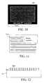
- FIG. 1is a cross-sectional diagram illustrating a starting structure for the present Sidewall Image Transfer (SIT) process including a substrate (or stack), a hardmask material on the substrate (or stack), a SIT mandrel material on the hardmask material, and a patterned resist on the SIT mandrel material according to an embodiment of the present invention;
- SITSidewall Image Transfer
- FIG. 2is a top-down image of the starting structure illustrating the patterned resist having a line pattern defined therein according to an embodiment of the present invention
- FIG. 3is a cross-sectional diagram illustrating the line pattern from the patterned resist having been transferred to the SIT mandrel material forming SIT mandrels according to an embodiment of the present invention
- FIG. 4is a top-down image of the starting structure illustrating the line pattern from the patterned resist having been transferred to the SIT mandrel material forming the SIT mandrels according to an embodiment of the present invention
- FIG. 5is a cross-sectional diagram illustrating a conformal film of spacer material having been deposited on the wafer covering a top and sides of each of the SIT mandrels and exposed surfaces of the hardmask material according to an embodiment of the present invention
- FIG. 6is a top-down image of the spacer material having been deposited using atomic layer deposition (ALD) onto the top and sides of each of the SIT mandrels according to an embodiment of the present invention
- FIG. 7is a cross-sectional diagram illustrating an anisotropic etch having been used to remove the spacer material from the top and the bottom of each of the SIT mandrels according to an embodiment of the present invention
- FIG. 8is a top-down image of the spacer material having been removed from the top and the bottom of each of the SIT mandrels according to an embodiment of the present invention.
- FIG. 9is a cross-sectional diagram illustrating the SIT mandrels having been removed selective to the SIT sidewall spacers according to an embodiment of the present invention.
- FIG. 10is a top-down image of the SIT mandrels having been removed according to an embodiment of the present invention.
- FIG. 11is a top-down diagram illustrating an optional modification of a pattern of the SIT sidewall spacers having been performed according to an embodiment of the present invention
- FIG. 12is a cross-sectional diagram illustrating the SIT sidewall spacers having been used to transfer the pattern to the hardmask material and/or the substrate according to an embodiment of the present invention
- FIG. 13is a top-down image of the pattern having been transferred to the hardmask material using the SIT sidewall spacers according to an embodiment of the present invention
- FIG. 14is a top-down image of sample where the present techniques were used to transfer a pitch doubled pattern into a silicon substrate according to an embodiment of the present invention
- FIG. 15is a perspective image of the sample of FIG. 14 according to an embodiment of the present invention.
- FIG. 16is a cross-sectional image of the sample of FIG. 14 according to an embodiment of the present invention.
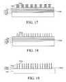
- FIG. 17is a cross-sectional diagram illustrating a starting structure for an exemplary implementation of the present SIT process for use in patterning a stack of thin films on a wafer having a hardmask material on the or stack, patterned SIT mandrels on the hardmask and spacers on the sidewalls of the SIT mandrels according to an embodiment of the present invention
- FIG. 18which follows from FIG. 17 , is a cross-sectional diagram illustrating the SIT mandrels having been removed selective to the SIT sidewall spacers according to an embodiment of the present invention.
- FIG. 19is a cross-sectional diagram illustrating the SIT sidewall spacers having been used to transfer their pattern to the hardmask material and (via the hardmask) to one or more of the layers in the stack of thin films according to an embodiment of the present invention.
- SITSidewall Image Transfer
- SITwhich is also referred to as Self-Aligned Double Patterning (SADP)
- SADPSelf-Aligned Double Patterning
- Other sub-lithographic patterning techniquesinclude, but are not limited to, pitch split techniques, such as tone-inversion pitch split (TIPS), directed self-assembly (DSA), etc.
- TIPStone-inversion pitch split
- DSAdirected self-assembly
- a semiconductor device fabrication process flowtypically begins with a wafer or other suitable substrate.
- Typical wafer configurationsinclude, but are not limited to, silicon-on-insulator (SOI) wafers, bulk semiconductor wafers, wafers with a sequence of thin films (stack) deposited, etc.
- SOI waferincludes a SOI layer separated from a substrate by a buried oxide or BOX. Any desired processing of the wafer that may be required prior to the SIT module is then performed. Of course, the particular processing steps are application-specific. However, for illustrative purposes only, the wafer may be processed, one or more active areas may be defined in the wafer, dopants may be implanted, etc. Any application-specific pre-processing steps would be apparent to one skilled in the art and thus are not described further herein.
- substrate 102The starting structure for the present SIT process flow is generally referred to herein as substrate 102 . It is to be understood that substrate 102 generically represents any of the wafer/substrate configurations described above, and that pre-processing of the substrate, as described above, may have been performed. As shown in FIG. 1 , a thin film of a hardmask material 104 is first deposited onto the substrate 102 .
- hardmask material 104is formed from a nitride material, such as silicon nitride, that is deposited to a thickness of from about 5 nanometers (nm) to about 20 nm using a deposition process such as chemical vapor deposition (CVD), physical vapor deposition (PVD), atomic layer deposition (ALD), evaporation, or spin-coating.
- CVDchemical vapor deposition
- PVDphysical vapor deposition
- ALDatomic layer deposition
- evaporationspin-coating
- spin-coatingspin-coating.
- CVDchemical vapor deposition
- PVDphysical vapor deposition
- ALDatomic layer deposition
- evaporationspin-coating
- the present processcan be used to pattern the hardmask, which in turn can be used to pattern the underlying substrate.
- the SIT spacer materialcan serve to pattern the substrate directly by the present techniques.
- SIT mandrel material 106is then deposited onto the hardmask material 104 .
- SIT mandrel material 106is formed from an oxide material, such as silicon oxide, that is deposited to a thickness of from about 10 nm to about 100 nm using a deposition process such as CVD, PVD, ALD, evaporation, or spin-coating.
- a patterned resist 108is then formed on the SIT mandrel material 106 . See FIG. 1 .
- the patterned resist 108can be formed using standard lithography techniques.
- the waferis first coated with a resist material (i.e., on the SIT mandrel material 106 ).
- the resist materialis exposed using a lithography tool, and then developed.
- FIG. 2described below, the resulting patterned resist 108 will have a line pattern defined therein.
- FIG. 2is a top-down image 200 of the device structure following deposition of the hardmask material, the SIT mandrel material and the patterned resist. As shown in FIG. 2 , the patterned resist has an exposed line pattern defined therein.
- the line pattern from the patterned resist 108is transferred to the SIT mandrel material 106 forming SIT mandrels 106 a .
- this patterning stepis carried out using reactive ion etching (RIE). RIE will likely remove some (as shown in FIG. 3 ), or all of the patterned resist 108 . If any portion of the patterned resist is remaining, it is preferably removed at this point in the process.
- FIG. 4is a top-down image 400 of the line pattern from the patterned resist having been transferred to the SIT mandrel material forming the SIT mandrels.
- the spacer material 502is formed from a metal, a metal oxide, a metal nitride, or a combination including at least one of the foregoing materials, that is deposited to a thickness of from about 2 nm to about 20 nm using ALD at a temperature of less than or equal to about 550° C., for example, less than or equal to about 350° C., e.g., from about 200° C. to about 350° C.
- use of these “low-temperature” deposited materialsavoids the temperature-compatibility problems described above, thus expanding the availability of materials that can be used prior to (and during) the SIT process.
- Suitable metals for use as spacer material 502include, but are not limited to, platinum, ruthenium, molybdenum, iron, nickel, and combinations including at least one of the foregoing metals.
- Suitable metal oxides for use as spacer material 502include, but are not limited to, aluminum oxide, titanium oxide, tantalum oxide, hafnium oxide, zirconium oxide, tin oxide, zinc oxide, magnesium oxide, niobium oxide, lanthanum oxide, cobalt oxide, and combinations including at least one of the foregoing metal oxides.
- Suitable metal nitrides for use as spacer material 502include, but are not limited to, titanium nitride, tantalum nitride, hafnium nitride, zirconium nitride, tungsten nitride, niobium nitride, and combinations including at least one of the foregoing metal nitrides.
- FIG. 6is a top-down image 600 of the spacer material having been deposited using ALD onto the top and sides of each of the SIT mandrels.
- An anisotropic etchis used to remove the spacer material 502 from the top and the bottom of each of the SIT mandrels 106 a . See FIG. 7 .
- the bottom of the SIT mandrels 106 ait is meant that the spacer material (based on the example shown in the FIG. 7 ) is removed from the surfaces of the hardmask material 104 .
- the spacer materialwill remain intact on the sides of each of the SIT mandrels 106 a .
- This spacer material on the sides of the SIT mandrels 106 awill be referred to hereinafter as SIT sidewall spacers 502 a .
- a suitable anisotropic etching processincludes, but is not limited to, a RIE process.
- FIG. 8is a top-down image 800 of the spacer material having been removed from the top and the bottom of each of the SIT mandrels. As shown in FIG. 8 , the spacer material remains intact on the side of each of the SIT mandrels, forming the SIT sidewall spacers 502 a.
- the SIT mandrels 106 aare then removed selective to the SIT sidewall spacers 502 a . See FIG. 9 .
- the SIT mandrels 106 aare removed using a wet etching or dry etching process. The result is that a pattern of the SIT sidewall spacers 502 a is revealed. That pattern will be used to pattern the underlying stack or substrate—see below.
- FIG. 10is a top-down image 1000 of the SIT mandrels having been removed. As shown in FIG. 10 , what remains are the SIT sidewall spacers.
- a pattern of the SIT sidewall spacersmay be modified/customized as needed. This step is optional.
- the SIT sidewall spacers 502 amay be used to pattern fins in the underlying substrate. See below.
- FIG. 11wherein the length of one or more of the SIT sidewall spacers has been altered (in this case reduced) thus altering the pattern of the SIT sidewall spacers.
- Modification of the pattern of the SIT sidewall spacerscan be achieved using standard lithography techniques where a resist can be used as a mask, and an etching process (such as RIE) can be used to alter the pattern.
- FIG. 11is a top-down view of the SIT sidewall spacer pattern.
- the SIT sidewall spacers 502 aare then used to transfer the pattern to the hardmask material 104 and/or the substrate 102 . See FIG. 12 .
- the hardmask material 104once patterned, is referred to hereinafter as patterned hardmask 104 a .
- the pattern of the SIT sidewall spacersis first transferred to the hardmask material, forming the patterned hardmasks 104 a . This step may be carried out using a RIE process.
- the patterned hardmasks 104 acan then be used to pattern the substrate.
- a RIE processmay be used to pattern the substrate.
- the particular etch chemistry usedcan be varied for etching selectivity between the hardmask and the substrate.
- the use of a hardmask in this process flowis optional.
- the pattern of the SIT sidewall spacersis at this step transferred directly into the stack or substrate (e.g., using RIE).
- this patterning stepis carried out using RIE.
- RIEwill likely remove some (as shown in FIG. 12 ), or all of the SIT sidewall spacers 502 a . If any portion(s) of the SIT sidewall spacers 502 a remain, they may be removed at this point in the process.
- FIG. 13is a top-down image 1300 of the pattern having been transferred to the hardmask material using the SIT sidewall spacers.
- FIGS. 14-16are images of an exemplary implementation where the present techniques were used to transfer a pitch doubled pattern into a silicon substrate.
- the image shown in FIG. 14is a top-down scanning electron micrograph (SEM) image 1400 of the sample.
- FIG. 15is a perspective SEM view image 1500 of the same sample.
- FIG. 16is a cross-sectional SEM image 1600 also of the same sample.
- the starting structure for the present SIT process flowis a substrate which can generally include a wafer, such as an SOI wafer, a bulk semiconductor wafer and/or a wafer with a sequence of thin films (stack) deposited thereon, for illustrative purposes an exemplary embodiment is now described where the present SIT process is used to pattern a film stack.
- a wafersuch as an SOI wafer, a bulk semiconductor wafer and/or a wafer with a sequence of thin films (stack) deposited thereon
- a wafersuch as an SOI wafer, a bulk semiconductor wafer and/or a wafer with a sequence of thin films (stack) deposited thereon
- the substrateis made up of a stack of thin films ( 1704 a , 1704 b , 1704 c , etc.) on a wafer 1702 .
- the stack of thin filmscan be a stack of the materials used in forming a gate stack over a semiconductor wafer 1702 .
- thin film 1704 amight be a gate dielectric material, thin film 1704 b a liner material, thin film 1704 c a gate electrode material (such as polysilicon), etc.
- a thin film of a hardmask material 104is deposited onto the substrate (in this case onto the stack of thin films), SIT mandrels 106 a are formed (from an SIT mandrel material 106 ) based on a line pattern transferred from a patterned resist 108 , and SIT sidewall spacers 502 a are formed from a spacer material 502 on the sidewalls of the SIT mandrel 106 a .
- the SIT mandrels 106 aare removed selective to the SIT sidewall spacers 502 a . See FIG. 18 .
- the resultis that a pattern of the SIT sidewall spacers 502 a is revealed. That pattern will be used to pattern the underlying stack of thin films—see below.
- a pattern of the SIT sidewall spacersmay (optionally) be modified/customized if/as needed.
- the SIT sidewall spacersso as to modify/customize one or more of the corresponding structures that are to be patterned in the stack of thin films (e.g., so as to produce a particular configuration of gate lines in the stack).
- this modificationcan be achieved, e.g., using standard lithography and etching techniques.
- the SIT sidewall spacers 502 aare used to transfer the pattern to the hardmask material 104 and (via the hardmask) to one or more of the layers in the stack of thin films ( 1704 a , 1704 b , 1704 c , etc.). See FIG. 19 .
- the hardmask material 104once patterned, is referred to hereinafter as patterned hardmask 104 a .
- the pattern of the SIT sidewall spacersis first transferred to the hardmask material, forming the patterned hardmasks 104 a . This step may be carried out using a RIE process.
- the patterned hardmasks 104 acan then be used to pattern one or more of the layers in the stack of thin films. Again a RIE process may be used to pattern the stack. The particular etch chemistry used can be varied for etching selectivity between the hardmask and the thin films and/or for etching selectivity between the various layers in the stack.
- etch the pattern into only some (but not all) of the layers in the stackit may be desirable to etch the pattern into only some (but not all) of the layers in the stack. Determining the particular etch chemistries for selectively etching the layers in the thin film stack for a given device application would be within the capabilities of one skilled in the art.
- the SIT mandrel patternis etched into each of the thin film layers ( 1704 a , 1704 b , 1704 c , etc.) in the stack.
- the RIE step(s) used to etch the thin filmsis/are endpointed on the wafer 1702 which serves as an etch stop.
- the resultis etched thin film layers 1704 a ′, 1704 b ′, 1704 c ′, etc., respectively.
- the use of a hardmask in this process flowis optional.
- the pattern of the SIT sidewall spacersis at this step transferred directly into the stack (e.g., using RIE).
- this patterning stepis carried out using RIE.
- RIEwill likely remove some (as shown in FIG. 19 ), or all of the SIT sidewall spacers 502 a . If any portion(s) of the SIT sidewall spacers 502 a remain, they may be removed at this point in the process.
Landscapes
- Engineering & Computer Science (AREA)
- Physics & Mathematics (AREA)
- Manufacturing & Machinery (AREA)
- Condensed Matter Physics & Semiconductors (AREA)
- General Physics & Mathematics (AREA)
- Computer Hardware Design (AREA)
- Microelectronics & Electronic Packaging (AREA)
- Power Engineering (AREA)
- Chemical & Material Sciences (AREA)
- Inorganic Chemistry (AREA)
- Chemical Kinetics & Catalysis (AREA)
- Junction Field-Effect Transistors (AREA)
- Plasma & Fusion (AREA)
Abstract
Description
Claims (19)
Priority Applications (1)
| Application Number | Priority Date | Filing Date | Title |
|---|---|---|---|
| US13/916,109US9437443B2 (en) | 2013-06-12 | 2013-06-12 | Low-temperature sidewall image transfer process using ALD metals, metal oxides and metal nitrides |
Applications Claiming Priority (1)
| Application Number | Priority Date | Filing Date | Title |
|---|---|---|---|
| US13/916,109US9437443B2 (en) | 2013-06-12 | 2013-06-12 | Low-temperature sidewall image transfer process using ALD metals, metal oxides and metal nitrides |
Publications (2)
| Publication Number | Publication Date |
|---|---|
| US20140367833A1 US20140367833A1 (en) | 2014-12-18 |
| US9437443B2true US9437443B2 (en) | 2016-09-06 |
Family
ID=52018529
Family Applications (1)
| Application Number | Title | Priority Date | Filing Date |
|---|---|---|---|
| US13/916,109Expired - Fee RelatedUS9437443B2 (en) | 2013-06-12 | 2013-06-12 | Low-temperature sidewall image transfer process using ALD metals, metal oxides and metal nitrides |
Country Status (1)
| Country | Link |
|---|---|
| US (1) | US9437443B2 (en) |
Cited By (10)
| Publication number | Priority date | Publication date | Assignee | Title |
|---|---|---|---|---|
| US20170069571A1 (en)* | 2015-09-03 | 2017-03-09 | Kabushiki Kaisha Toshiba | Semiconductor device and method of manufacturing the same |
| WO2019152362A1 (en)* | 2018-01-30 | 2019-08-08 | Lam Research Corporation | Tin oxide mandrels in patterning |
| US10546748B2 (en) | 2017-02-17 | 2020-01-28 | Lam Research Corporation | Tin oxide films in semiconductor device manufacturing |
| US10593870B2 (en) | 2017-12-14 | 2020-03-17 | International Business Machines Corporation | Sidewall image transfer on magnetic tunnel junction stack for magnetoresistive random-access memory patterning |
| US10672986B2 (en) | 2018-04-13 | 2020-06-02 | International Business Machines Corporation | Self-assembly of nanostructures |
| US11031245B2 (en) | 2016-06-28 | 2021-06-08 | Lan Research Corporation | Tin oxide thin film spacers in semiconductor device manufacturing |
| US11088019B2 (en) | 2017-02-13 | 2021-08-10 | Lam Research Corporation | Method to create air gaps |
| US11551938B2 (en) | 2019-06-27 | 2023-01-10 | Lam Research Corporation | Alternating etch and passivation process |
| US11987876B2 (en) | 2018-03-19 | 2024-05-21 | Lam Research Corporation | Chamfer-less via integration scheme |
| US12051589B2 (en) | 2016-06-28 | 2024-07-30 | Lam Research Corporation | Tin oxide thin film spacers in semiconductor device manufacturing |
Families Citing this family (11)
| Publication number | Priority date | Publication date | Assignee | Title |
|---|---|---|---|---|
| US9711368B2 (en)* | 2013-04-15 | 2017-07-18 | United Microelectronics Corp. | Sidewall image transfer process |
| US9099400B2 (en)* | 2013-09-30 | 2015-08-04 | Taiwan Semiconductor Manufacturing Company, Ltd. | Semiconductor device manufacturing methods |
| US9368348B2 (en)* | 2013-10-01 | 2016-06-14 | Taiwan Semiconductor Manufacturing Company, Ltd. | Self-aligned patterning process |
| TW201543564A (en)* | 2014-05-09 | 2015-11-16 | Powerchip Technology Corp | Semiconductor fabrication method |
| US9842843B2 (en)* | 2015-12-03 | 2017-12-12 | Taiwan Semiconductor Manufacturing Company, Ltd. | Method for manufacturing static random access memory device |
| US9466534B1 (en) | 2015-12-09 | 2016-10-11 | International Business Machines Corporation | Cointegration of directed self assembly and sidewall image transfer patterning for sublithographic patterning with improved design flexibility |
| US9779944B1 (en) | 2016-09-13 | 2017-10-03 | International Business Machines Corporation | Method and structure for cut material selection |
| US10347583B1 (en) | 2018-01-02 | 2019-07-09 | Globalfoundries Inc. | Methods of patterning dielectric layers for metallization and related structures |
| US20190390341A1 (en)* | 2018-06-26 | 2019-12-26 | Lam Research Corporation | Deposition tool and method for depositing metal oxide films on organic materials |
| CN113016053B (en)* | 2018-11-16 | 2025-08-19 | 朗姆研究公司 | Bubble defect reduction |
| TWI773628B (en)* | 2022-01-19 | 2022-08-01 | 華邦電子股份有限公司 | Semiconductor structure and method of forming the same |
Citations (12)
| Publication number | Priority date | Publication date | Assignee | Title |
|---|---|---|---|---|
| US4838991A (en) | 1987-10-30 | 1989-06-13 | International Business Machines Corporation | Process for defining organic sidewall structures |
| US20010051444A1 (en)* | 1999-12-29 | 2001-12-13 | Chan Lim | Method for manufacturing aluminum oxide film for use in semiconductor device |
| US6982221B1 (en)* | 2005-06-10 | 2006-01-03 | Sharp Laboratories Of America, Inc. | Method of forming 2/3F pitch high density line array |
| US20060046422A1 (en)* | 2004-08-31 | 2006-03-02 | Micron Technology, Inc. | Methods for increasing photo alignment margins |
| US20060046200A1 (en)* | 2004-09-01 | 2006-03-02 | Abatchev Mirzafer K | Mask material conversion |
| US20070049040A1 (en)* | 2005-03-15 | 2007-03-01 | Micron Technology, Inc., A Corporation | Multiple deposition for integration of spacers in pitch multiplication process |
| US20080076070A1 (en) | 2006-09-08 | 2008-03-27 | Samsung Electronics Co., Ltd. | Methods of Forming Fine Patterns In Integrated Circuits Using Atomic Layer Deposition |
| US20080122125A1 (en) | 2006-11-29 | 2008-05-29 | Micron Technology, Inc. | Methods to reduce the critical dimension of semiconductor devices and partially fabricated semiconductor devices having reduced critical dimensions |
| US7732343B2 (en) | 2006-04-07 | 2010-06-08 | Micron Technology, Inc. | Simplified pitch doubling process flow |
| US20110033786A1 (en) | 2007-06-04 | 2011-02-10 | Micron Technology, Inc. | Pitch multiplication using self-assembling materials |
| US20110111596A1 (en) | 2009-11-06 | 2011-05-12 | International Business Machine Corporation | Sidewall Image Transfer Using the Lithographic Stack as the Mandrel |
| US20120108068A1 (en) | 2010-11-03 | 2012-05-03 | Texas Instruments Incorporated | Method for Patterning Sublithographic Features |
- 2013
- 2013-06-12USUS13/916,109patent/US9437443B2/ennot_activeExpired - Fee Related
Patent Citations (16)
| Publication number | Priority date | Publication date | Assignee | Title |
|---|---|---|---|---|
| US4838991A (en) | 1987-10-30 | 1989-06-13 | International Business Machines Corporation | Process for defining organic sidewall structures |
| US20010051444A1 (en)* | 1999-12-29 | 2001-12-13 | Chan Lim | Method for manufacturing aluminum oxide film for use in semiconductor device |
| US20060046422A1 (en)* | 2004-08-31 | 2006-03-02 | Micron Technology, Inc. | Methods for increasing photo alignment margins |
| US20060046200A1 (en)* | 2004-09-01 | 2006-03-02 | Abatchev Mirzafer K | Mask material conversion |
| US20070049040A1 (en)* | 2005-03-15 | 2007-03-01 | Micron Technology, Inc., A Corporation | Multiple deposition for integration of spacers in pitch multiplication process |
| US6982221B1 (en)* | 2005-06-10 | 2006-01-03 | Sharp Laboratories Of America, Inc. | Method of forming 2/3F pitch high density line array |
| US7732343B2 (en) | 2006-04-07 | 2010-06-08 | Micron Technology, Inc. | Simplified pitch doubling process flow |
| US20100216307A1 (en) | 2006-04-07 | 2010-08-26 | Micron Technology, Inc. | Simplified pitch doubling process flow |
| US7902074B2 (en) | 2006-04-07 | 2011-03-08 | Micron Technology, Inc. | Simplified pitch doubling process flow |
| US8030217B2 (en) | 2006-04-07 | 2011-10-04 | Micron Technology, Inc. | Simplified pitch doubling process flow |
| US20110316114A1 (en) | 2006-04-07 | 2011-12-29 | Micron Technology, Inc. | Simplified pitch doubling process flow |
| US20080076070A1 (en) | 2006-09-08 | 2008-03-27 | Samsung Electronics Co., Ltd. | Methods of Forming Fine Patterns In Integrated Circuits Using Atomic Layer Deposition |
| US20080122125A1 (en) | 2006-11-29 | 2008-05-29 | Micron Technology, Inc. | Methods to reduce the critical dimension of semiconductor devices and partially fabricated semiconductor devices having reduced critical dimensions |
| US20110033786A1 (en) | 2007-06-04 | 2011-02-10 | Micron Technology, Inc. | Pitch multiplication using self-assembling materials |
| US20110111596A1 (en) | 2009-11-06 | 2011-05-12 | International Business Machine Corporation | Sidewall Image Transfer Using the Lithographic Stack as the Mandrel |
| US20120108068A1 (en) | 2010-11-03 | 2012-05-03 | Texas Instruments Incorporated | Method for Patterning Sublithographic Features |
Non-Patent Citations (1)
| Title |
|---|
| H. Kim and S.M. Rossnagal, J. Vac. Sci. Tech. A. vol. 20, year 2002, pp. 802-808.* |
Cited By (24)
| Publication number | Priority date | Publication date | Assignee | Title |
|---|---|---|---|---|
| US9640481B2 (en)* | 2015-09-03 | 2017-05-02 | Kabushiki Kaisha Toshiba | Semiconductor device and method of manufacturing the same |
| US20170069571A1 (en)* | 2015-09-03 | 2017-03-09 | Kabushiki Kaisha Toshiba | Semiconductor device and method of manufacturing the same |
| US12051589B2 (en) | 2016-06-28 | 2024-07-30 | Lam Research Corporation | Tin oxide thin film spacers in semiconductor device manufacturing |
| US11784047B2 (en) | 2016-06-28 | 2023-10-10 | Lam Research Corporation | Tin oxide thin film spacers in semiconductor device manufacturing |
| US11031245B2 (en) | 2016-06-28 | 2021-06-08 | Lan Research Corporation | Tin oxide thin film spacers in semiconductor device manufacturing |
| US11183383B2 (en) | 2016-06-28 | 2021-11-23 | Lam Research Corporation | Tin oxide thin film spacers in semiconductor device manufacturing |
| US11637037B2 (en) | 2017-02-13 | 2023-04-25 | Lam Research Corporation | Method to create air gaps |
| US12112980B2 (en) | 2017-02-13 | 2024-10-08 | Lam Research Corporation | Method to create air gaps |
| US11088019B2 (en) | 2017-02-13 | 2021-08-10 | Lam Research Corporation | Method to create air gaps |
| US12094711B2 (en) | 2017-02-17 | 2024-09-17 | Lam Research Corporation | Tin oxide films in semiconductor device manufacturing |
| US10546748B2 (en) | 2017-02-17 | 2020-01-28 | Lam Research Corporation | Tin oxide films in semiconductor device manufacturing |
| US12437995B2 (en) | 2017-02-17 | 2025-10-07 | Lam Research Corporation | Tin oxide films in semiconductor device manufacturing |
| US12417916B2 (en) | 2017-02-17 | 2025-09-16 | Lam Research Corporation | Tin oxide films in semiconductor device manufacturing |
| US11322351B2 (en) | 2017-02-17 | 2022-05-03 | Lam Research Corporation | Tin oxide films in semiconductor device manufacturing |
| US10593870B2 (en) | 2017-12-14 | 2020-03-17 | International Business Machines Corporation | Sidewall image transfer on magnetic tunnel junction stack for magnetoresistive random-access memory patterning |
| US11355353B2 (en) | 2018-01-30 | 2022-06-07 | Lam Research Corporation | Tin oxide mandrels in patterning |
| US12183589B2 (en) | 2018-01-30 | 2024-12-31 | Lam Research Corporation | Tin oxide mandrels in patterning |
| WO2019152362A1 (en)* | 2018-01-30 | 2019-08-08 | Lam Research Corporation | Tin oxide mandrels in patterning |
| US11987876B2 (en) | 2018-03-19 | 2024-05-21 | Lam Research Corporation | Chamfer-less via integration scheme |
| US10672986B2 (en) | 2018-04-13 | 2020-06-02 | International Business Machines Corporation | Self-assembly of nanostructures |
| US11211560B2 (en) | 2018-04-13 | 2021-12-28 | International Business Machines Corporation | Self-assembly of nanostructures |
| US11848212B2 (en) | 2019-06-27 | 2023-12-19 | Lam Research Corporation | Alternating etch and passivation process |
| US12293919B2 (en) | 2019-06-27 | 2025-05-06 | Lam Research Corporation | Alternating etch and passivation process |
| US11551938B2 (en) | 2019-06-27 | 2023-01-10 | Lam Research Corporation | Alternating etch and passivation process |
Also Published As
| Publication number | Publication date |
|---|---|
| US20140367833A1 (en) | 2014-12-18 |
Similar Documents
| Publication | Publication Date | Title |
|---|---|---|
| US9437443B2 (en) | Low-temperature sidewall image transfer process using ALD metals, metal oxides and metal nitrides | |
| TWI644363B (en) | Semiconductor structure and method of forming same | |
| US9653571B2 (en) | Freestanding spacer having sub-lithographic lateral dimension and method of forming same | |
| US10038066B2 (en) | Uniform vertical field effect transistor spacers | |
| US11315922B2 (en) | Fin cut to prevent replacement gate collapse on STI | |
| TWI824237B (en) | Semiconductor devices and methods for forming the same | |
| US9466534B1 (en) | Cointegration of directed self assembly and sidewall image transfer patterning for sublithographic patterning with improved design flexibility | |
| US10497796B1 (en) | Vertical transistor with reduced gate length variation | |
| TW202141803A (en) | Semiconductor device and method for fabricating the same | |
| CN107017286A (en) | Semiconductor device and method for manufacturing the same | |
| CN104733322A (en) | Method for fabricating fins for multigate devices and core structure for fabricating fins | |
| KR20200066576A (en) | Semiconductor device and method of manufacture | |
| CN108573864B (en) | Substantially defect free polysilicon gate array | |
| CN111863826B (en) | Manufacturing method of graphical mask and manufacturing method of three-dimensional NAND memory | |
| CN105428317B (en) | Semiconductor device manufacturing method | |
| US10020202B2 (en) | Fabrication of multi threshold-voltage devices | |
| US20080237751A1 (en) | CMOS Structure and method of manufacturing same | |
| US10763118B2 (en) | Cyclic selective deposition for tight pitch patterning | |
| US12243920B2 (en) | Method to form selective high-k deposition on 2D materials | |
| US10756163B2 (en) | Conformal capacitor structure formed by a single process | |
| CN103676493B (en) | Hybrid photoetching method for reducing line roughness | |
| TWI869083B (en) | Method for fabricating and etching semiconductor device | |
| US20250062124A1 (en) | Methods and structures for improving etch profile of underlying layers | |
| TWI745789B (en) | Semiconductor device and method of manufacturing the same | |
| CN108573850B (en) | Method for manufacturing semiconductor device |
Legal Events
| Date | Code | Title | Description |
|---|---|---|---|
| AS | Assignment | Owner name:INTERNATIONAL BUSINESS MACHINES CORPORATION, NEW Y Free format text:ASSIGNMENT OF ASSIGNORS INTEREST;ASSIGNORS:BRINK, MARKUS;GUILLORN, MICHAEL A.;ENGELMANN, SEBASTIAN U.;AND OTHERS;REEL/FRAME:030597/0135 Effective date:20130611 | |
| AS | Assignment | Owner name:GLOBALFOUNDRIES U.S. 2 LLC, NEW YORK Free format text:ASSIGNMENT OF ASSIGNORS INTEREST;ASSIGNOR:INTERNATIONAL BUSINESS MACHINES CORPORATION;REEL/FRAME:036550/0001 Effective date:20150629 | |
| AS | Assignment | Owner name:GLOBALFOUNDRIES INC., CAYMAN ISLANDS Free format text:ASSIGNMENT OF ASSIGNORS INTEREST;ASSIGNORS:GLOBALFOUNDRIES U.S. 2 LLC;GLOBALFOUNDRIES U.S. INC.;REEL/FRAME:036779/0001 Effective date:20150910 | |
| FEPP | Fee payment procedure | Free format text:PAYOR NUMBER ASSIGNED (ORIGINAL EVENT CODE: ASPN); ENTITY STATUS OF PATENT OWNER: LARGE ENTITY | |
| STCF | Information on status: patent grant | Free format text:PATENTED CASE | |
| AS | Assignment | Owner name:WILMINGTON TRUST, NATIONAL ASSOCIATION, DELAWARE Free format text:SECURITY AGREEMENT;ASSIGNOR:GLOBALFOUNDRIES INC.;REEL/FRAME:049490/0001 Effective date:20181127 | |
| FEPP | Fee payment procedure | Free format text:MAINTENANCE FEE REMINDER MAILED (ORIGINAL EVENT CODE: REM.); ENTITY STATUS OF PATENT OWNER: LARGE ENTITY | |
| LAPS | Lapse for failure to pay maintenance fees | Free format text:PATENT EXPIRED FOR FAILURE TO PAY MAINTENANCE FEES (ORIGINAL EVENT CODE: EXP.); ENTITY STATUS OF PATENT OWNER: LARGE ENTITY | |
| STCH | Information on status: patent discontinuation | Free format text:PATENT EXPIRED DUE TO NONPAYMENT OF MAINTENANCE FEES UNDER 37 CFR 1.362 | |
| FP | Lapsed due to failure to pay maintenance fee | Effective date:20200906 | |
| AS | Assignment | Owner name:GLOBALFOUNDRIES INC., CAYMAN ISLANDS Free format text:RELEASE BY SECURED PARTY;ASSIGNOR:WILMINGTON TRUST, NATIONAL ASSOCIATION;REEL/FRAME:054636/0001 Effective date:20201117 | |
| AS | Assignment | Owner name:GLOBALFOUNDRIES U.S. INC., NEW YORK Free format text:RELEASE BY SECURED PARTY;ASSIGNOR:WILMINGTON TRUST, NATIONAL ASSOCIATION;REEL/FRAME:056987/0001 Effective date:20201117 |