US9437423B2 - Method for fabricating an inter dielectric layer in semiconductor device - Google Patents
Method for fabricating an inter dielectric layer in semiconductor deviceDownload PDFInfo
- Publication number
- US9437423B2 US9437423B2US14/059,756US201314059756AUS9437423B2US 9437423 B2US9437423 B2US 9437423B2US 201314059756 AUS201314059756 AUS 201314059756AUS 9437423 B2US9437423 B2US 9437423B2
- Authority
- US
- United States
- Prior art keywords
- bit line
- oxide layer
- gas
- hdp
- layer
- Prior art date
- Legal status (The legal status is an assumption and is not a legal conclusion. Google has not performed a legal analysis and makes no representation as to the accuracy of the status listed.)
- Active
Links
- 238000000034methodMethods0.000titleclaimsabstractdescription45
- 239000004065semiconductorSubstances0.000titleclaimsabstractdescription23
- 239000000758substrateSubstances0.000claimsabstractdescription14
- 230000008021depositionEffects0.000claimsabstractdescription10
- 239000007789gasSubstances0.000claimsdescription51
- 230000009969flowable effectEffects0.000claimsdescription16
- 125000006850spacer groupChemical group0.000claimsdescription14
- BLRPTPMANUNPDV-UHFFFAOYSA-NSilaneChemical compound[SiH4]BLRPTPMANUNPDV-UHFFFAOYSA-N0.000claimsdescription8
- QVGXLLKOCUKJST-UHFFFAOYSA-Natomic oxygenChemical compound[O]QVGXLLKOCUKJST-UHFFFAOYSA-N0.000claimsdescription8
- 230000004888barrier functionEffects0.000claimsdescription8
- 238000005452bendingMethods0.000claimsdescription8
- 229910052751metalInorganic materials0.000claimsdescription8
- 239000002184metalSubstances0.000claimsdescription8
- 239000001301oxygenSubstances0.000claimsdescription8
- 229910052760oxygenInorganic materials0.000claimsdescription8
- 238000005530etchingMethods0.000claimsdescription7
- XKRFYHLGVUSROY-UHFFFAOYSA-NArgonChemical compound[Ar]XKRFYHLGVUSROY-UHFFFAOYSA-N0.000claimsdescription6
- 239000001307heliumSubstances0.000claimsdescription6
- 229910052734heliumInorganic materials0.000claimsdescription6
- SWQJXJOGLNCZEY-UHFFFAOYSA-Nhelium atomChemical compound[He]SWQJXJOGLNCZEY-UHFFFAOYSA-N0.000claimsdescription6
- 239000000654additiveSubstances0.000claimsdescription4
- 230000000996additive effectEffects0.000claimsdescription4
- 229910000077silaneInorganic materials0.000claimsdescription4
- YCKRFDGAMUMZLT-UHFFFAOYSA-NFluorine atomChemical compound[F]YCKRFDGAMUMZLT-UHFFFAOYSA-N0.000claimsdescription3
- 229910052786argonInorganic materials0.000claimsdescription3
- 238000011049fillingMethods0.000claimsdescription3
- 229910052731fluorineInorganic materials0.000claimsdescription3
- 239000011737fluorineSubstances0.000claimsdescription3
- 239000001257hydrogenSubstances0.000claimsdescription2
- 229910052739hydrogenInorganic materials0.000claimsdescription2
- 125000004435hydrogen atomChemical class[H]*0.000claimsdescription2
- 238000011068loading methodMethods0.000claimsdescription2
- 230000015572biosynthetic processEffects0.000claims1
- 239000010410layerSubstances0.000abstractdescription75
- 239000011229interlayerSubstances0.000abstractdescription10
- 238000000151depositionMethods0.000description8
- 238000001878scanning electron micrographMethods0.000description6
- 239000000463materialSubstances0.000description3
- 239000002904solventSubstances0.000description3
- 238000003860storageMethods0.000description3
- 239000011248coating agentSubstances0.000description2
- 238000000576coating methodMethods0.000description2
- 230000007423decreaseEffects0.000description2
- 230000007547defectEffects0.000description2
- 238000002955isolationMethods0.000description2
- 239000010936titaniumSubstances0.000description2
- 229910052721tungstenInorganic materials0.000description2
- RTAQQCXQSZGOHL-UHFFFAOYSA-NTitaniumChemical compound[Ti]RTAQQCXQSZGOHL-UHFFFAOYSA-N0.000description1
- 238000007792additionMethods0.000description1
- 238000001816coolingMethods0.000description1
- 230000003247decreasing effectEffects0.000description1
- 238000010586diagramMethods0.000description1
- 238000005516engineering processMethods0.000description1
- 238000001704evaporationMethods0.000description1
- 238000010438heat treatmentMethods0.000description1
- 238000012986modificationMethods0.000description1
- 230000004048modificationEffects0.000description1
- 150000004767nitridesChemical class0.000description1
- 238000005498polishingMethods0.000description1
- 229920001709polysilazanePolymers0.000description1
- 238000005389semiconductor device fabricationMethods0.000description1
- 238000004528spin coatingMethods0.000description1
- 239000000126substanceSubstances0.000description1
- 238000006467substitution reactionMethods0.000description1
- 229910052719titaniumInorganic materials0.000description1
- WFKWXMTUELFFGS-UHFFFAOYSA-NtungstenChemical compound[W]WFKWXMTUELFFGS-UHFFFAOYSA-N0.000description1
- 239000010937tungstenSubstances0.000description1
Images


Classifications
- H—ELECTRICITY
- H01—ELECTRIC ELEMENTS
- H01L—SEMICONDUCTOR DEVICES NOT COVERED BY CLASS H10
- H01L21/00—Processes or apparatus adapted for the manufacture or treatment of semiconductor or solid state devices or of parts thereof
- H01L21/02—Manufacture or treatment of semiconductor devices or of parts thereof
- H01L21/04—Manufacture or treatment of semiconductor devices or of parts thereof the devices having potential barriers, e.g. a PN junction, depletion layer or carrier concentration layer
- H01L21/18—Manufacture or treatment of semiconductor devices or of parts thereof the devices having potential barriers, e.g. a PN junction, depletion layer or carrier concentration layer the devices having semiconductor bodies comprising elements of Group IV of the Periodic Table or AIIIBV compounds with or without impurities, e.g. doping materials
- H01L21/30—Treatment of semiconductor bodies using processes or apparatus not provided for in groups H01L21/20 - H01L21/26
- H01L21/31—Treatment of semiconductor bodies using processes or apparatus not provided for in groups H01L21/20 - H01L21/26 to form insulating layers thereon, e.g. for masking or by using photolithographic techniques; After treatment of these layers; Selection of materials for these layers
- H—ELECTRICITY
- H01—ELECTRIC ELEMENTS
- H01L—SEMICONDUCTOR DEVICES NOT COVERED BY CLASS H10
- H01L21/00—Processes or apparatus adapted for the manufacture or treatment of semiconductor or solid state devices or of parts thereof
- H01L21/02—Manufacture or treatment of semiconductor devices or of parts thereof
- H01L21/02104—Forming layers
- H01L21/02107—Forming insulating materials on a substrate
- H01L21/02225—Forming insulating materials on a substrate characterised by the process for the formation of the insulating layer
- H01L21/0226—Forming insulating materials on a substrate characterised by the process for the formation of the insulating layer formation by a deposition process
- H01L21/02263—Forming insulating materials on a substrate characterised by the process for the formation of the insulating layer formation by a deposition process deposition from the gas or vapour phase
- H01L21/02271—Forming insulating materials on a substrate characterised by the process for the formation of the insulating layer formation by a deposition process deposition from the gas or vapour phase deposition by decomposition or reaction of gaseous or vapour phase compounds, i.e. chemical vapour deposition
- H01L21/02274—Forming insulating materials on a substrate characterised by the process for the formation of the insulating layer formation by a deposition process deposition from the gas or vapour phase deposition by decomposition or reaction of gaseous or vapour phase compounds, i.e. chemical vapour deposition in the presence of a plasma [PECVD]
- H—ELECTRICITY
- H01—ELECTRIC ELEMENTS
- H01L—SEMICONDUCTOR DEVICES NOT COVERED BY CLASS H10
- H01L21/00—Processes or apparatus adapted for the manufacture or treatment of semiconductor or solid state devices or of parts thereof
- H01L21/02—Manufacture or treatment of semiconductor devices or of parts thereof
- H01L21/04—Manufacture or treatment of semiconductor devices or of parts thereof the devices having potential barriers, e.g. a PN junction, depletion layer or carrier concentration layer
- H01L21/18—Manufacture or treatment of semiconductor devices or of parts thereof the devices having potential barriers, e.g. a PN junction, depletion layer or carrier concentration layer the devices having semiconductor bodies comprising elements of Group IV of the Periodic Table or AIIIBV compounds with or without impurities, e.g. doping materials
- H01L21/30—Treatment of semiconductor bodies using processes or apparatus not provided for in groups H01L21/20 - H01L21/26
- H01L21/302—Treatment of semiconductor bodies using processes or apparatus not provided for in groups H01L21/20 - H01L21/26 to change their surface-physical characteristics or shape, e.g. etching, polishing, cutting
- H01L21/306—Chemical or electrical treatment, e.g. electrolytic etching
- H01L21/30604—Chemical etching
- H—ELECTRICITY
- H01—ELECTRIC ELEMENTS
- H01L—SEMICONDUCTOR DEVICES NOT COVERED BY CLASS H10
- H01L21/00—Processes or apparatus adapted for the manufacture or treatment of semiconductor or solid state devices or of parts thereof
- H01L21/70—Manufacture or treatment of devices consisting of a plurality of solid state components formed in or on a common substrate or of parts thereof; Manufacture of integrated circuit devices or of parts thereof
- H01L21/71—Manufacture of specific parts of devices defined in group H01L21/70
- H01L21/768—Applying interconnections to be used for carrying current between separate components within a device comprising conductors and dielectrics
- H01L21/76801—Applying interconnections to be used for carrying current between separate components within a device comprising conductors and dielectrics characterised by the formation and the after-treatment of the dielectrics, e.g. smoothing
- H01L21/76837—Filling up the space between adjacent conductive structures; Gap-filling properties of dielectrics
- H01L27/10885—
- H—ELECTRICITY
- H10—SEMICONDUCTOR DEVICES; ELECTRIC SOLID-STATE DEVICES NOT OTHERWISE PROVIDED FOR
- H10B—ELECTRONIC MEMORY DEVICES
- H10B12/00—Dynamic random access memory [DRAM] devices
- H10B12/30—DRAM devices comprising one-transistor - one-capacitor [1T-1C] memory cells
- H10B12/48—Data lines or contacts therefor
- H10B12/482—Bit lines
Definitions
- the inventionrelates to a semiconductor device, and more particularly, to a method for fabricating an inter dielectric layer in a semiconductor device.
- bit line stacksWith development of semiconductor device fabrication technology, the critical dimension (CD) of bit line stacks is rapidly decreasing. As the CD of the bit line stacks decreases, a space defined between the bit line stacks also decreases. Therefore, there is a limitation in a high density plasma (HDP) process used as a gap filling method.
- HDPhigh density plasma
- One exampleis a bending phenomenon in which a bit line stack becomes bent.
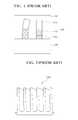
- FIG. 1illustrates a cross-sectional view of a conventional bit line stack
- FIG. 2illustrates a scanning electron micrograph (SEM) of bit lines having a high aspect ratio
- FIG. 3illustrates a SEM of a defect in which a storage node contact is not formed.
- SEMscanning electron micrograph
- bit line stacks 120including barrier metal patterns 105 , conductive patterns 110 , and hard mask patterns 115 , are formed on a semiconductor substrate 100 , and an interlayer dielectric layer 125 is formed to fill the areas surrounding the bit line stacks 120 .
- the interlayer dielectric layer 125is formed using an HDP process.
- a bending phenomenonmay occur so that a given bit line stack 120 is bent. The bending phenomenon may occur when unequal attraction is applied to one of the bit stacks 120 by a difference in an amount of charges applied to the left and right side of the bit line stack 120 due to plasma generated during the HDP process, or it may occur as a result of a damage caused by plasma.
- a bit line stack in a 50 nm deviceis filled using a flowable layer.
- the flowable layerwas developed as a material for device isolation, many studies have been conducted to use the flowable layer in a process requiring a gap fill, such as an isolation layer, a gate stack, or a bit line stack.
- the bit line stacks 120have a large aspect ratio (i.e., height to width ratio), and the flowable layer is softer than an HDP oxide layer. Therefore, when the flowable layer is used, it does not endure a subsequent thermal process and a self align contact (SAC) process, and the bit line stacks 120 may be bent to one side due to an unequal attraction. When a subsequent process is performed and the bit line stack 120 is bent in one direction, a storage node contact hole 300 may not be formed, as indicated by a reference symbol “A” in FIG. 3 .
- SACself align contact
- a method for fabricating an inter dielectric layer in semiconductor deviceincludes: forming a primary liner HDP oxide layer on a bit line stack formed over a semiconductor substrate by supplying a high density plasma (HDP) deposition source to the bit line stack; forming a secondary liner HDP oxide layer by etching the primary liner HDP oxide layer to a predetermined thickness; and forming an interlayer dielectric layer to fill areas defined by the bit line stack where the secondary liner HDP oxide layer is formed.
- HDPhigh density plasma
- the methodmay further include preheating the bit line stack before forming the primary liner HDP oxide layer.
- the preheating of the bit line stackmay include: loading the semiconductor substrate into an HDP chamber, and applying a predetermined power to the HDP chamber while supplying oxygen (O 2 ) gas, argon (Ar) gas, and helium (He) gas into the HDP chamber.
- oxygen (O 2 ) gas, argon (Ar) gas, and helium (He) gasinto the HDP chamber.
- the HDP deposition sourcemay include a source gas containing silane (SiH 4 ) gas and oxygen (O 2 ) gas, and an additive gas containing helium (He) gas.
- the forming of the primary liner HDP oxide layermay include maintaining a bottom bias at less than 500 W.
- the primary liner HDP oxide layermay be formed to a thickness ranging from about 500 ⁇ to about 600 ⁇ .
- the secondary liner HDP oxide layermay be formed using a fluorine-based etch gas.
- the secondary liner HDP oxide layermay be formed by etching the primary liner HDP oxide layer to a thickness ranging from about 150 ⁇ to about 190 ⁇ .
- the forming of the interlayer dielectric layermay include: coating a flowable layer including a solvent on the semiconductor substrate where the secondary liner HDP oxide layer; evaporating the solvent by heating the flowable layer to a temperature between about 130° C. to about 150° C.; and performing a curing process on the flowable layer to form an oxide layer.
- the flowable layermay include a spin-on dielectric (SOD) layer containing polysilizane (PSZ).
- SODspin-on dielectric
- PSZpolysilizane
- the curing processmay be performed for about 1 hour while supplying 1 L of hydrogen (H 2 ) gas and 2 L of oxygen (O 2 ) gas at a temperature between about 450° C. and about 550° C.
- FIG. 1illustrates a cross-sectional view of a conventional bit line stack.
- FIG. 2illustrates a scanning electron micrograph (SEM) of bit lines having variable heights.
- FIG. 3illustrates an SEM of a defect in which a storage node contact is not formed.
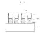
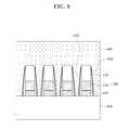
- FIGS. 4 to 9illustrate a method for fabricating an inter dielectric layer in semiconductor device according to an embodiment of the invention.
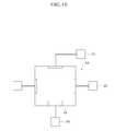
- FIG. 10illustrates a block diagram of an HDP chamber.
- FIGS. 4 to 9illustrate a method for fabricating an inter dielectric layer in semiconductor device according to an embodiment of the invention.
- a bit line stack 420is formed on a semiconductor substrate 400 .
- a barrier metal layer, a conductive layer for bit lines, and a hard mask layerare deposited on the semiconductor substrate 400 .
- the barrier metal layermay be formed of titanium (Ti)
- the conductive layer for the bit linesmay be formed of tungsten (W)
- the hard mask layermay be formed of nitride.
- the hard mask layeris patterned to form hard mask patterns 415 .
- the conductive layer for the bit lines and the barrier metal layerare etched using the hard mask patterns 415 as an etch mask to form barrier metal patterns 405 and conductive patterns 410 for the bit lines.
- the barrier metal patterns 405 , the conductive patterns 410 for the bit lines, and the hard mask patterns 415constitute the bit line stack 420 .
- bit line spacers 425are formed on both sides of the bit line stack 420 .
- the forming of the bit line spacers 425may include depositing a spacer layer on the semiconductor substrate 400 where the bit line stack 420 is formed, and performing an etch-back process on the deposited spacer layer.
- the bit line stack 420 where the bit line spacers 425 are formedis preheated in an atmosphere including oxygen (O 2 ) and helium (He).
- the semiconductor substrate 400is loaded in a stage 15 of an HDP chamber 10 illustrated in FIG. 10 .
- Oxygen (O 2 ) gas and argon (Ar) gasare supplied into the HDP chamber 10 as a source gas, and helium (He) gas is supplied as an additive gas.
- the preheating processis performed for about 20-30 seconds by supplying a predetermined power.
- the O 2 gasis supplied at a flow rate ranging from about 50 sccm to about 150 sccm
- the Ar gasis supplied at a flow rate ranging from about 40 sccm to about 50 sccm
- the He gasis supplied at a flow rate ranging from about 200 sccm to about 300 sccm.
- the He gasis additionally supplied from the top of the HDP chamber 10 at a flow rate ranging from about 200 sccm to about 300 sccm.
- a top bias 20is applied in the range from about 4,500 W to about 5,500 W
- a side bias 25is applied in the range from about 3,500 W to about 4,500 W
- no bottom bias 30is applied.
- a primary liner HDP oxide layer 430is formed on the bit line stack 420 .
- the primary liner HDP oxide layer 430is formed by supplying an HDP deposition source into the HDP chamber 10 where the preheating process has been performed.
- the HDP deposition sourcecontains a source gas including silane (SiH 4 ) gas and O 2 gas, and an additive gas including He gas.
- the O 2 gas as the HDP deposition sourceis supplied at a flow rate ranging from about 100 sccm to about 120 sccm.
- the silane (SiH 4 ) gasis supplied from the top of the HDP chamber 10 at a flow rate ranging from about 10 sccm to about 50 sccm and is supplied from the side of the HDP chamber 10 at a flow rate ranging from about 50 sccm to about 150 sccm.
- the top bias 20is applied in the range from about 4,500 W to about 5,500 W and the side bias 25 is applied in the range from about 2,500 W to about 3,500 W.
- the bottom bias 30is applied in the range from about 450 W to about 500 W.
- the primary liner HDP oxide layer 430is deposited on the bit line stack 420 to a thickness ranging from about 500 ⁇ to about 600 ⁇ by using the HDP deposition source and the bias applied to the HDP chamber.
- a He cooling processis performed on the back side of the semiconductor substrate 400 , such that an overall temperature of the semiconductor substrate 400 is adjusted to below 350° C. during the process of forming the primary liner HDP oxide layer 430 . Therefore, a gate insulating layer in the middle of the lower structure is prevented from being damaged by the high temperature plasma. Further, in forming the primary liner HDP oxide layer 430 , a bending phenomenon of the bit line stack 420 due to plasma charge can be minimized by maintaining the bottom bias to below 500 W. Accordingly, it is possible to prevent the bending phenomenon caused by unstable charging, which has been generated in the bit line stack due to the high bias during the process of depositing the HDP oxide layer under the bottom bias higher than 1,500 W.
- the primary liner HDP oxide layer 430is etched by a predetermined thickness to form a sidewall spacer 435 .
- an etch gasis supplied into the HDP chamber 10 in which the primary liner HDP oxide layer 430 has been formed.
- a fluorine-based gase.g., NF 3 gas
- H 2 gas and He gasare supplied.
- the NF 3 gasis supplied at a flow rate ranging from about 100 sccm to about 200 sccm.
- the H 2 gasis supplied at a flow rate ranging from about 100 sccm to about 200 sccm.
- the He gasis supplied from the top of the HDP chamber 10 at a flow rate ranging from about 50 sccm to about 70 sccm.
- the He gasis also supplied from the side of the HDP chamber 10 at a flow rate ranging from about 50 sccm to about 70 sccm.
- the primary liner HDP oxide layer 430is etched to a thickness ranging from about 150 ⁇ to about 190 ⁇ by the etching process, thereby forming the sidewall spacer 435 . After the etching process, the sidewall spacer 435 remains only at the both sides of the bit line stack 420 .
- an interlayer dielectric layer 440is formed to fill the area between adjacent bit line stacks 420 where the sidewall spacer 435 is formed.
- the interlayer dielectric layer 440 filling the bit line stack 420is formed by coating a flowable spin-on dielectric (SOD) layer using a spin coating process. Since the SOD layer has excellent gap-fill characteristics, it is used as a gap-fill material in places where the gap between patterns is narrow. Polysilazane (PSZ) may be used as the SOD.
- SODflowable spin-on dielectric
- a solvent in the gap-fill materialis evaporated by maintaining the flowable SOD layer in a chuck at a high temperature range between about 130° C. and about 150° C. for about 150-200 seconds. Then, a curing process is performed on the SOD layer. The curing process is performed for about 1 hour while supplying 1 L of H 2 gas and 2 L of O 2 gas at a temperature between about 450° C. and about 550° C. Due to the curing process, the SOD layer is oxidized to form an oxide layer as the interlayer dielectric layer 440 . Then, the interlayer dielectric layer 440 is planarized using a planarization process, e.g., a chemical mechanical polishing (CMP) process.
- CMPchemical mechanical polishing
- the bit line stackis covered with the liner HDP oxide layer and then is filled with the SOD layer, thereby preventing the bending phenomenon of the bit line stack.
Landscapes
- Engineering & Computer Science (AREA)
- Physics & Mathematics (AREA)
- Microelectronics & Electronic Packaging (AREA)
- Condensed Matter Physics & Semiconductors (AREA)
- General Physics & Mathematics (AREA)
- Manufacturing & Machinery (AREA)
- Computer Hardware Design (AREA)
- Power Engineering (AREA)
- Chemical & Material Sciences (AREA)
- Chemical Kinetics & Catalysis (AREA)
- Plasma & Fusion (AREA)
- General Chemical & Material Sciences (AREA)
- Internal Circuitry In Semiconductor Integrated Circuit Devices (AREA)
Abstract
Description
This is a division of U.S. application Ser. No. 11/945,659 filed Nov. 27, 2007, which claims the priority benefit under USC 119 of Korean patent application number 10-2007-0064760, filed on Jun. 28, 2007, the entire respective disclosures of which are incorporated herein by reference.
The invention relates to a semiconductor device, and more particularly, to a method for fabricating an inter dielectric layer in a semiconductor device.
With development of semiconductor device fabrication technology, the critical dimension (CD) of bit line stacks is rapidly decreasing. As the CD of the bit line stacks decreases, a space defined between the bit line stacks also decreases. Therefore, there is a limitation in a high density plasma (HDP) process used as a gap filling method. One example is a bending phenomenon in which a bit line stack becomes bent.
Referring toFIG. 1 ,bit line stacks 120, includingbarrier metal patterns 105,conductive patterns 110, andhard mask patterns 115, are formed on asemiconductor substrate 100, and an interlayerdielectric layer 125 is formed to fill the areas surrounding thebit line stacks 120. The interlayerdielectric layer 125 is formed using an HDP process. However, when the interlayer dielectric layer is formed using the HDP process, a bending phenomenon may occur so that a givenbit line stack 120 is bent. The bending phenomenon may occur when unequal attraction is applied to one of the bit stacks120 by a difference in an amount of charges applied to the left and right side of thebit line stack 120 due to plasma generated during the HDP process, or it may occur as a result of a damage caused by plasma. Due to limitations of the fabricating process, a bit line stack in a 50 nm device is filled using a flowable layer. Although the flowable layer was developed as a material for device isolation, many studies have been conducted to use the flowable layer in a process requiring a gap fill, such as an isolation layer, a gate stack, or a bit line stack.
However, the bending phenomenon occurs even though the gap fill process is performed using the flowable layer. As illustrated inFIG. 2 , thebit line stacks 120 have a large aspect ratio (i.e., height to width ratio), and the flowable layer is softer than an HDP oxide layer. Therefore, when the flowable layer is used, it does not endure a subsequent thermal process and a self align contact (SAC) process, and thebit line stacks 120 may be bent to one side due to an unequal attraction. When a subsequent process is performed and thebit line stack 120 is bent in one direction, a storagenode contact hole 300 may not be formed, as indicated by a reference symbol “A” inFIG. 3 .
In one embodiment, a method for fabricating an inter dielectric layer in semiconductor device includes: forming a primary liner HDP oxide layer on a bit line stack formed over a semiconductor substrate by supplying a high density plasma (HDP) deposition source to the bit line stack; forming a secondary liner HDP oxide layer by etching the primary liner HDP oxide layer to a predetermined thickness; and forming an interlayer dielectric layer to fill areas defined by the bit line stack where the secondary liner HDP oxide layer is formed.
The method may further include preheating the bit line stack before forming the primary liner HDP oxide layer.
The preheating of the bit line stack may include: loading the semiconductor substrate into an HDP chamber, and applying a predetermined power to the HDP chamber while supplying oxygen (O2) gas, argon (Ar) gas, and helium (He) gas into the HDP chamber.
The HDP deposition source may include a source gas containing silane (SiH4) gas and oxygen (O2) gas, and an additive gas containing helium (He) gas.
The forming of the primary liner HDP oxide layer may include maintaining a bottom bias at less than 500 W.
The primary liner HDP oxide layer may be formed to a thickness ranging from about 500 Å to about 600 Å.
The secondary liner HDP oxide layer may be formed using a fluorine-based etch gas.
The secondary liner HDP oxide layer may be formed by etching the primary liner HDP oxide layer to a thickness ranging from about 150 Å to about 190 Å.
The forming of the interlayer dielectric layer may include: coating a flowable layer including a solvent on the semiconductor substrate where the secondary liner HDP oxide layer; evaporating the solvent by heating the flowable layer to a temperature between about 130° C. to about 150° C.; and performing a curing process on the flowable layer to form an oxide layer.
The flowable layer may include a spin-on dielectric (SOD) layer containing polysilizane (PSZ).
The curing process may be performed for about 1 hour while supplying 1 L of hydrogen (H2) gas and 2 L of oxygen (O2) gas at a temperature between about 450° C. and about 550° C.
Hereinafter, a method for fabricating an inter dielectric layer in semiconductor device in accordance with the invention will be described in detail with reference to the accompanying drawings.
Referring toFIG. 4 , abit line stack 420 is formed on asemiconductor substrate 400.
Specifically, a barrier metal layer, a conductive layer for bit lines, and a hard mask layer are deposited on thesemiconductor substrate 400. The barrier metal layer may be formed of titanium (Ti), the conductive layer for the bit lines may be formed of tungsten (W), and the hard mask layer may be formed of nitride. At this point, a lower structure (not shown) including a word line has been already formed on thesemiconductor substrate 400.
The hard mask layer is patterned to formhard mask patterns 415. The conductive layer for the bit lines and the barrier metal layer are etched using thehard mask patterns 415 as an etch mask to formbarrier metal patterns 405 andconductive patterns 410 for the bit lines. Thebarrier metal patterns 405, theconductive patterns 410 for the bit lines, and thehard mask patterns 415 constitute thebit line stack 420.
Referring toFIG. 5 ,bit line spacers 425 are formed on both sides of thebit line stack 420. The forming of thebit line spacers 425 may include depositing a spacer layer on thesemiconductor substrate 400 where thebit line stack 420 is formed, and performing an etch-back process on the deposited spacer layer.
Referring toFIGS. 6 and 10 , thebit line stack 420 where thebit line spacers 425 are formed is preheated in an atmosphere including oxygen (O2) and helium (He).
More specifically, thesemiconductor substrate 400 is loaded in astage 15 of anHDP chamber 10 illustrated inFIG. 10 . Oxygen (O2) gas and argon (Ar) gas are supplied into theHDP chamber 10 as a source gas, and helium (He) gas is supplied as an additive gas. The preheating process is performed for about 20-30 seconds by supplying a predetermined power. The O2gas is supplied at a flow rate ranging from about 50 sccm to about 150 sccm, the Ar gas is supplied at a flow rate ranging from about 40 sccm to about 50 sccm, and the He gas is supplied at a flow rate ranging from about 200 sccm to about 300 sccm. At this point, the He gas is additionally supplied from the top of theHDP chamber 10 at a flow rate ranging from about 200 sccm to about 300 sccm. As a source power for generating plasma, atop bias 20 is applied in the range from about 4,500 W to about 5,500 W, aside bias 25 is applied in the range from about 3,500 W to about 4,500 W, and nobottom bias 30 is applied.
Referring toFIGS. 7 and 10 , a primary linerHDP oxide layer 430 is formed on thebit line stack 420.
The primary linerHDP oxide layer 430 is formed by supplying an HDP deposition source into theHDP chamber 10 where the preheating process has been performed. The HDP deposition source contains a source gas including silane (SiH4) gas and O2gas, and an additive gas including He gas. The O2gas as the HDP deposition source is supplied at a flow rate ranging from about 100 sccm to about 120 sccm. The silane (SiH4) gas is supplied from the top of theHDP chamber 10 at a flow rate ranging from about 10 sccm to about 50 sccm and is supplied from the side of theHDP chamber 10 at a flow rate ranging from about 50 sccm to about 150 sccm. At this point, as the source power for generating plasma, thetop bias 20 is applied in the range from about 4,500 W to about 5,500 W and theside bias 25 is applied in the range from about 2,500 W to about 3,500 W. In addition, thebottom bias 30 is applied in the range from about 450 W to about 500 W. The primary linerHDP oxide layer 430 is deposited on thebit line stack 420 to a thickness ranging from about 500 Å to about 600 Å by using the HDP deposition source and the bias applied to the HDP chamber.
Meanwhile, a He cooling process is performed on the back side of thesemiconductor substrate 400, such that an overall temperature of thesemiconductor substrate 400 is adjusted to below 350° C. during the process of forming the primary linerHDP oxide layer 430. Therefore, a gate insulating layer in the middle of the lower structure is prevented from being damaged by the high temperature plasma. Further, in forming the primary linerHDP oxide layer 430, a bending phenomenon of thebit line stack 420 due to plasma charge can be minimized by maintaining the bottom bias to below 500 W. Accordingly, it is possible to prevent the bending phenomenon caused by unstable charging, which has been generated in the bit line stack due to the high bias during the process of depositing the HDP oxide layer under the bottom bias higher than 1,500 W.
Referring toFIGS. 8 and 10 , the primary linerHDP oxide layer 430 is etched by a predetermined thickness to form asidewall spacer 435.
More specifically, an etch gas is supplied into theHDP chamber 10 in which the primary linerHDP oxide layer 430 has been formed. A fluorine-based gas, e.g., NF3gas, is used as the etch gas. In addition to the NF3gas, H2gas and He gas are supplied. The NF3gas is supplied at a flow rate ranging from about 100 sccm to about 200 sccm. The H2gas is supplied at a flow rate ranging from about 100 sccm to about 200 sccm. The He gas is supplied from the top of theHDP chamber 10 at a flow rate ranging from about 50 sccm to about 70 sccm. In addition, the He gas is also supplied from the side of theHDP chamber 10 at a flow rate ranging from about 50 sccm to about 70 sccm. The primary linerHDP oxide layer 430 is etched to a thickness ranging from about 150 Å to about 190 Å by the etching process, thereby forming thesidewall spacer 435. After the etching process, thesidewall spacer 435 remains only at the both sides of thebit line stack 420.
Referring toFIG. 9 , aninterlayer dielectric layer 440 is formed to fill the area between adjacent bit line stacks420 where thesidewall spacer 435 is formed.
Theinterlayer dielectric layer 440 filling thebit line stack 420 is formed by coating a flowable spin-on dielectric (SOD) layer using a spin coating process. Since the SOD layer has excellent gap-fill characteristics, it is used as a gap-fill material in places where the gap between patterns is narrow. Polysilazane (PSZ) may be used as the SOD.
A solvent in the gap-fill material is evaporated by maintaining the flowable SOD layer in a chuck at a high temperature range between about 130° C. and about 150° C. for about 150-200 seconds. Then, a curing process is performed on the SOD layer. The curing process is performed for about 1 hour while supplying 1 L of H2gas and 2 L of O2gas at a temperature between about 450° C. and about 550° C. Due to the curing process, the SOD layer is oxidized to form an oxide layer as theinterlayer dielectric layer 440. Then, theinterlayer dielectric layer 440 is planarized using a planarization process, e.g., a chemical mechanical polishing (CMP) process.
According to the embodiments of the invention, the bit line stack is covered with the liner HDP oxide layer and then is filled with the SOD layer, thereby preventing the bending phenomenon of the bit line stack.
The embodiments of the invention have been disclosed above for illustrative purposes. Those skilled in the art will appreciate that various modifications, additions and substitutions are possible, without departing from the scope and spirit of the invention as disclosed in the accompanying claims.
Claims (10)
1. A method for fabricating an inter dielectric layer in a semiconductor device, comprising:
forming a bit line stack over a semiconductor substrate, the bit line stack comprising a barrier metal pattern, a conductive pattern, and a hard mask pattern, the hard mask pattern having two sides, wherein the barrier metal pattern, the conductive pattern and the hard mask pattern are sequentially stacked;
forming a bit line spacer on both sides of the bit line stack to expose a top surface of the hard mask pattern, the bit line spacer covers entirely both sides of the bit line stack;
supplying a high density plasma (HDP) deposition source to the bit line stack to form a primary liner HDP oxide layer on the bit line spacer while maintaining a bottom bias of an HDP chamber at less than 500 W during formation of the primary liner HDP oxide layer, wherein the primary liner HDP oxide layer covers both sides of the bit line spacer and a top surface of the hard mask pattern;
etching the primary liner HDP oxide layer to a predetermined thickness to form a secondary liner HDP oxide layer, wherein the secondary liner HDP entirely covers both sides of the bit line spacer while exposing the top surface of the hard mask pattern;
filling an area defined by adjacent bit line stacks where the secondary liner HDP oxide layer is formed with a flowable spin on dielectric (SOD) layer such that the SOD layer contacts the secondary liner HDP oxide layer; and,
curing the flowable SOD layer to form an oxide layer.
2. The method ofclaim 1 , further comprising preheating the bit line stack before forming the primary liner HDP oxide layer.
3. The method ofclaim 2 , wherein the preheating of the bit line stack comprises:
loading the semiconductor substrate into the HDP chamber; and
applying a predetermined source power to the HDP chamber while supplying oxygen (O2) gas, argon (Ar) gas, and helium (He) gas into the HDP chamber, wherein source power is applied from a top bias and a side bias of the HDP chamber while a bottom bias is not applied.
4. The method ofclaim 1 , wherein the HDP deposition source comprises a source gas comprising silane (SiH4) gas and oxygen (O2) gas, and an additive gas comprising helium (He) gas.
5. The method ofclaim 1 , comprising forming the primary liner HDP oxide layer to a thickness ranging from about 500 Å to about 600 Å.
6. The method ofclaim 1 , comprising forming the secondary liner HDP oxide layer using a fluorine-based etch gas.
7. The method ofclaim 1 , wherein the secondary liner HDP oxide layer is formed by etching the primary liner HDP oxide layer by an etching thickness ranging from about 150 Å to about 190 Å.
8. The method ofclaim 1 , wherein the flowable spin on dielectric (SOD) layer comprises polysilizane (PSZ).
9. The method ofclaim 1 , wherein the curing the flowable SOD layer comprises curing for about one hour while supplying 1 L of hydrogen (H2) gas and 2 L of oxygen (O2) gas at a temperature between about 450° C. and about 550° C.
10. The method ofclaim 1 , wherein a bending phenomenon of the bit line stack due to plasma charge is minimized by maintaining the bottom bias at less than 500 W.
Priority Applications (1)
| Application Number | Priority Date | Filing Date | Title |
|---|---|---|---|
| US14/059,756US9437423B2 (en) | 2007-06-28 | 2013-10-22 | Method for fabricating an inter dielectric layer in semiconductor device |
Applications Claiming Priority (4)
| Application Number | Priority Date | Filing Date | Title |
|---|---|---|---|
| KR10-2007-0064760 | 2007-06-28 | ||
| KR1020070064760AKR100877107B1 (en) | 2007-06-28 | 2007-06-28 | Method of forming interlayer insulating film of semiconductor device |
| US11/945,659US8592326B2 (en) | 2007-06-28 | 2007-11-27 | Method for fabricating an inter dielectric layer in semiconductor device |
| US14/059,756US9437423B2 (en) | 2007-06-28 | 2013-10-22 | Method for fabricating an inter dielectric layer in semiconductor device |
Related Parent Applications (1)
| Application Number | Title | Priority Date | Filing Date |
|---|---|---|---|
| US11/945,659DivisionUS8592326B2 (en) | 2007-06-28 | 2007-11-27 | Method for fabricating an inter dielectric layer in semiconductor device |
Publications (2)
| Publication Number | Publication Date |
|---|---|
| US20140045325A1 US20140045325A1 (en) | 2014-02-13 |
| US9437423B2true US9437423B2 (en) | 2016-09-06 |
Family
ID=40161100
Family Applications (2)
| Application Number | Title | Priority Date | Filing Date |
|---|---|---|---|
| US11/945,659Active2031-05-05US8592326B2 (en) | 2007-06-28 | 2007-11-27 | Method for fabricating an inter dielectric layer in semiconductor device |
| US14/059,756ActiveUS9437423B2 (en) | 2007-06-28 | 2013-10-22 | Method for fabricating an inter dielectric layer in semiconductor device |
Family Applications Before (1)
| Application Number | Title | Priority Date | Filing Date |
|---|---|---|---|
| US11/945,659Active2031-05-05US8592326B2 (en) | 2007-06-28 | 2007-11-27 | Method for fabricating an inter dielectric layer in semiconductor device |
Country Status (2)
| Country | Link |
|---|---|
| US (2) | US8592326B2 (en) |
| KR (1) | KR100877107B1 (en) |
Cited By (1)
| Publication number | Priority date | Publication date | Assignee | Title |
|---|---|---|---|---|
| CN110246759A (en)* | 2019-06-03 | 2019-09-17 | 武汉新芯集成电路制造有限公司 | A kind of preparation method of flush memory device |
Families Citing this family (156)
| Publication number | Priority date | Publication date | Assignee | Title |
|---|---|---|---|---|
| KR100877107B1 (en)* | 2007-06-28 | 2009-01-07 | 주식회사 하이닉스반도체 | Method of forming interlayer insulating film of semiconductor device |
| CA2737134C (en) | 2007-10-15 | 2017-10-10 | Ampt, Llc | Systems for highly efficient solar power |
| US7674684B2 (en)* | 2008-07-23 | 2010-03-09 | Applied Materials, Inc. | Deposition methods for releasing stress buildup |
| SG175717A1 (en) | 2009-04-17 | 2011-12-29 | Ampt Llc | Methods and apparatus for adaptive operation of solar power systems |
| US9466737B2 (en) | 2009-10-19 | 2016-10-11 | Ampt, Llc | Solar panel string converter topology |
| US9324576B2 (en) | 2010-05-27 | 2016-04-26 | Applied Materials, Inc. | Selective etch for silicon films |
| US10283321B2 (en) | 2011-01-18 | 2019-05-07 | Applied Materials, Inc. | Semiconductor processing system and methods using capacitively coupled plasma |
| US8999856B2 (en) | 2011-03-14 | 2015-04-07 | Applied Materials, Inc. | Methods for etch of sin films |
| US9064815B2 (en) | 2011-03-14 | 2015-06-23 | Applied Materials, Inc. | Methods for etch of metal and metal-oxide films |
| US8771536B2 (en) | 2011-08-01 | 2014-07-08 | Applied Materials, Inc. | Dry-etch for silicon-and-carbon-containing films |
| US20130260564A1 (en)* | 2011-09-26 | 2013-10-03 | Applied Materials, Inc. | Insensitive dry removal process for semiconductor integration |
| US8927390B2 (en) | 2011-09-26 | 2015-01-06 | Applied Materials, Inc. | Intrench profile |
| US8808563B2 (en) | 2011-10-07 | 2014-08-19 | Applied Materials, Inc. | Selective etch of silicon by way of metastable hydrogen termination |
| US9267739B2 (en) | 2012-07-18 | 2016-02-23 | Applied Materials, Inc. | Pedestal with multi-zone temperature control and multiple purge capabilities |
| US9373517B2 (en) | 2012-08-02 | 2016-06-21 | Applied Materials, Inc. | Semiconductor processing with DC assisted RF power for improved control |
| US9034770B2 (en) | 2012-09-17 | 2015-05-19 | Applied Materials, Inc. | Differential silicon oxide etch |
| US9023734B2 (en) | 2012-09-18 | 2015-05-05 | Applied Materials, Inc. | Radical-component oxide etch |
| US9390937B2 (en) | 2012-09-20 | 2016-07-12 | Applied Materials, Inc. | Silicon-carbon-nitride selective etch |
| US9132436B2 (en) | 2012-09-21 | 2015-09-15 | Applied Materials, Inc. | Chemical control features in wafer process equipment |
| US8969212B2 (en) | 2012-11-20 | 2015-03-03 | Applied Materials, Inc. | Dry-etch selectivity |
| US8980763B2 (en) | 2012-11-30 | 2015-03-17 | Applied Materials, Inc. | Dry-etch for selective tungsten removal |
| US9064816B2 (en) | 2012-11-30 | 2015-06-23 | Applied Materials, Inc. | Dry-etch for selective oxidation removal |
| US9111877B2 (en) | 2012-12-18 | 2015-08-18 | Applied Materials, Inc. | Non-local plasma oxide etch |
| US8921234B2 (en) | 2012-12-21 | 2014-12-30 | Applied Materials, Inc. | Selective titanium nitride etching |
| US10256079B2 (en) | 2013-02-08 | 2019-04-09 | Applied Materials, Inc. | Semiconductor processing systems having multiple plasma configurations |
| US9362130B2 (en) | 2013-03-01 | 2016-06-07 | Applied Materials, Inc. | Enhanced etching processes using remote plasma sources |
| US9040422B2 (en) | 2013-03-05 | 2015-05-26 | Applied Materials, Inc. | Selective titanium nitride removal |
| US8801952B1 (en) | 2013-03-07 | 2014-08-12 | Applied Materials, Inc. | Conformal oxide dry etch |
| US10170282B2 (en) | 2013-03-08 | 2019-01-01 | Applied Materials, Inc. | Insulated semiconductor faceplate designs |
| US9397497B2 (en) | 2013-03-15 | 2016-07-19 | Ampt, Llc | High efficiency interleaved solar power supply system |
| US20140271097A1 (en) | 2013-03-15 | 2014-09-18 | Applied Materials, Inc. | Processing systems and methods for halide scavenging |
| US8895449B1 (en) | 2013-05-16 | 2014-11-25 | Applied Materials, Inc. | Delicate dry clean |
| US9114438B2 (en) | 2013-05-21 | 2015-08-25 | Applied Materials, Inc. | Copper residue chamber clean |
| US9493879B2 (en) | 2013-07-12 | 2016-11-15 | Applied Materials, Inc. | Selective sputtering for pattern transfer |
| US9773648B2 (en) | 2013-08-30 | 2017-09-26 | Applied Materials, Inc. | Dual discharge modes operation for remote plasma |
| US8956980B1 (en) | 2013-09-16 | 2015-02-17 | Applied Materials, Inc. | Selective etch of silicon nitride |
| US8951429B1 (en) | 2013-10-29 | 2015-02-10 | Applied Materials, Inc. | Tungsten oxide processing |
| US9236265B2 (en) | 2013-11-04 | 2016-01-12 | Applied Materials, Inc. | Silicon germanium processing |
| US9576809B2 (en) | 2013-11-04 | 2017-02-21 | Applied Materials, Inc. | Etch suppression with germanium |
| US9520303B2 (en) | 2013-11-12 | 2016-12-13 | Applied Materials, Inc. | Aluminum selective etch |
| US9245762B2 (en) | 2013-12-02 | 2016-01-26 | Applied Materials, Inc. | Procedure for etch rate consistency |
| US9117855B2 (en) | 2013-12-04 | 2015-08-25 | Applied Materials, Inc. | Polarity control for remote plasma |
| KR102004242B1 (en)* | 2013-12-13 | 2019-07-26 | 삼성전자주식회사 | Semiconductor device and method for fabricating the same |
| US9263278B2 (en) | 2013-12-17 | 2016-02-16 | Applied Materials, Inc. | Dopant etch selectivity control |
| US9287095B2 (en) | 2013-12-17 | 2016-03-15 | Applied Materials, Inc. | Semiconductor system assemblies and methods of operation |
| US9190293B2 (en) | 2013-12-18 | 2015-11-17 | Applied Materials, Inc. | Even tungsten etch for high aspect ratio trenches |
| US9287134B2 (en) | 2014-01-17 | 2016-03-15 | Applied Materials, Inc. | Titanium oxide etch |
| US9396989B2 (en) | 2014-01-27 | 2016-07-19 | Applied Materials, Inc. | Air gaps between copper lines |
| US9293568B2 (en) | 2014-01-27 | 2016-03-22 | Applied Materials, Inc. | Method of fin patterning |
| US9385028B2 (en) | 2014-02-03 | 2016-07-05 | Applied Materials, Inc. | Air gap process |
| US9499898B2 (en) | 2014-03-03 | 2016-11-22 | Applied Materials, Inc. | Layered thin film heater and method of fabrication |
| US9299575B2 (en) | 2014-03-17 | 2016-03-29 | Applied Materials, Inc. | Gas-phase tungsten etch |
| US9299537B2 (en) | 2014-03-20 | 2016-03-29 | Applied Materials, Inc. | Radial waveguide systems and methods for post-match control of microwaves |
| US9299538B2 (en) | 2014-03-20 | 2016-03-29 | Applied Materials, Inc. | Radial waveguide systems and methods for post-match control of microwaves |
| US9136273B1 (en) | 2014-03-21 | 2015-09-15 | Applied Materials, Inc. | Flash gate air gap |
| US9903020B2 (en) | 2014-03-31 | 2018-02-27 | Applied Materials, Inc. | Generation of compact alumina passivation layers on aluminum plasma equipment components |
| US9269590B2 (en) | 2014-04-07 | 2016-02-23 | Applied Materials, Inc. | Spacer formation |
| US9309598B2 (en) | 2014-05-28 | 2016-04-12 | Applied Materials, Inc. | Oxide and metal removal |
| US9847289B2 (en) | 2014-05-30 | 2017-12-19 | Applied Materials, Inc. | Protective via cap for improved interconnect performance |
| US9406523B2 (en) | 2014-06-19 | 2016-08-02 | Applied Materials, Inc. | Highly selective doped oxide removal method |
| US9378969B2 (en) | 2014-06-19 | 2016-06-28 | Applied Materials, Inc. | Low temperature gas-phase carbon removal |
| US9401474B2 (en)* | 2014-07-01 | 2016-07-26 | Micron Technology, Inc. | Methods of forming structures |
| US9425058B2 (en) | 2014-07-24 | 2016-08-23 | Applied Materials, Inc. | Simplified litho-etch-litho-etch process |
| US9159606B1 (en) | 2014-07-31 | 2015-10-13 | Applied Materials, Inc. | Metal air gap |
| US9378978B2 (en) | 2014-07-31 | 2016-06-28 | Applied Materials, Inc. | Integrated oxide recess and floating gate fin trimming |
| US10278675B2 (en)* | 2014-07-31 | 2019-05-07 | Palo Alto Research Center Incorporated | Implantable estrus detection devices, systems, and methods |
| US9496167B2 (en) | 2014-07-31 | 2016-11-15 | Applied Materials, Inc. | Integrated bit-line airgap formation and gate stack post clean |
| US9165786B1 (en) | 2014-08-05 | 2015-10-20 | Applied Materials, Inc. | Integrated oxide and nitride recess for better channel contact in 3D architectures |
| US9659753B2 (en) | 2014-08-07 | 2017-05-23 | Applied Materials, Inc. | Grooved insulator to reduce leakage current |
| US9553102B2 (en) | 2014-08-19 | 2017-01-24 | Applied Materials, Inc. | Tungsten separation |
| US9355856B2 (en) | 2014-09-12 | 2016-05-31 | Applied Materials, Inc. | V trench dry etch |
| US9368364B2 (en) | 2014-09-24 | 2016-06-14 | Applied Materials, Inc. | Silicon etch process with tunable selectivity to SiO2 and other materials |
| US9355862B2 (en) | 2014-09-24 | 2016-05-31 | Applied Materials, Inc. | Fluorine-based hardmask removal |
| US9613822B2 (en) | 2014-09-25 | 2017-04-04 | Applied Materials, Inc. | Oxide etch selectivity enhancement |
| US9966240B2 (en) | 2014-10-14 | 2018-05-08 | Applied Materials, Inc. | Systems and methods for internal surface conditioning assessment in plasma processing equipment |
| US9355922B2 (en) | 2014-10-14 | 2016-05-31 | Applied Materials, Inc. | Systems and methods for internal surface conditioning in plasma processing equipment |
| US11637002B2 (en) | 2014-11-26 | 2023-04-25 | Applied Materials, Inc. | Methods and systems to enhance process uniformity |
| US9299583B1 (en) | 2014-12-05 | 2016-03-29 | Applied Materials, Inc. | Aluminum oxide selective etch |
| US10573496B2 (en) | 2014-12-09 | 2020-02-25 | Applied Materials, Inc. | Direct outlet toroidal plasma source |
| US10224210B2 (en) | 2014-12-09 | 2019-03-05 | Applied Materials, Inc. | Plasma processing system with direct outlet toroidal plasma source |
| US9502258B2 (en) | 2014-12-23 | 2016-11-22 | Applied Materials, Inc. | Anisotropic gap etch |
| US9343272B1 (en) | 2015-01-08 | 2016-05-17 | Applied Materials, Inc. | Self-aligned process |
| US11257693B2 (en) | 2015-01-09 | 2022-02-22 | Applied Materials, Inc. | Methods and systems to improve pedestal temperature control |
| US9373522B1 (en) | 2015-01-22 | 2016-06-21 | Applied Mateials, Inc. | Titanium nitride removal |
| US9449846B2 (en) | 2015-01-28 | 2016-09-20 | Applied Materials, Inc. | Vertical gate separation |
| US20160225652A1 (en) | 2015-02-03 | 2016-08-04 | Applied Materials, Inc. | Low temperature chuck for plasma processing systems |
| US9728437B2 (en) | 2015-02-03 | 2017-08-08 | Applied Materials, Inc. | High temperature chuck for plasma processing systems |
| US9881805B2 (en) | 2015-03-02 | 2018-01-30 | Applied Materials, Inc. | Silicon selective removal |
| US9741593B2 (en) | 2015-08-06 | 2017-08-22 | Applied Materials, Inc. | Thermal management systems and methods for wafer processing systems |
| US9691645B2 (en) | 2015-08-06 | 2017-06-27 | Applied Materials, Inc. | Bolted wafer chuck thermal management systems and methods for wafer processing systems |
| US9349605B1 (en) | 2015-08-07 | 2016-05-24 | Applied Materials, Inc. | Oxide etch selectivity systems and methods |
| US10504700B2 (en) | 2015-08-27 | 2019-12-10 | Applied Materials, Inc. | Plasma etching systems and methods with secondary plasma injection |
| US10504754B2 (en) | 2016-05-19 | 2019-12-10 | Applied Materials, Inc. | Systems and methods for improved semiconductor etching and component protection |
| US10522371B2 (en) | 2016-05-19 | 2019-12-31 | Applied Materials, Inc. | Systems and methods for improved semiconductor etching and component protection |
| US9865484B1 (en) | 2016-06-29 | 2018-01-09 | Applied Materials, Inc. | Selective etch using material modification and RF pulsing |
| US10062575B2 (en) | 2016-09-09 | 2018-08-28 | Applied Materials, Inc. | Poly directional etch by oxidation |
| US10629473B2 (en) | 2016-09-09 | 2020-04-21 | Applied Materials, Inc. | Footing removal for nitride spacer |
| US10546729B2 (en) | 2016-10-04 | 2020-01-28 | Applied Materials, Inc. | Dual-channel showerhead with improved profile |
| US9721789B1 (en) | 2016-10-04 | 2017-08-01 | Applied Materials, Inc. | Saving ion-damaged spacers |
| US9934942B1 (en) | 2016-10-04 | 2018-04-03 | Applied Materials, Inc. | Chamber with flow-through source |
| US10062585B2 (en) | 2016-10-04 | 2018-08-28 | Applied Materials, Inc. | Oxygen compatible plasma source |
| US10062579B2 (en) | 2016-10-07 | 2018-08-28 | Applied Materials, Inc. | Selective SiN lateral recess |
| US9947549B1 (en) | 2016-10-10 | 2018-04-17 | Applied Materials, Inc. | Cobalt-containing material removal |
| US10163696B2 (en) | 2016-11-11 | 2018-12-25 | Applied Materials, Inc. | Selective cobalt removal for bottom up gapfill |
| US9768034B1 (en) | 2016-11-11 | 2017-09-19 | Applied Materials, Inc. | Removal methods for high aspect ratio structures |
| US10242908B2 (en) | 2016-11-14 | 2019-03-26 | Applied Materials, Inc. | Airgap formation with damage-free copper |
| US10026621B2 (en) | 2016-11-14 | 2018-07-17 | Applied Materials, Inc. | SiN spacer profile patterning |
| US10566206B2 (en) | 2016-12-27 | 2020-02-18 | Applied Materials, Inc. | Systems and methods for anisotropic material breakthrough |
| US10403507B2 (en) | 2017-02-03 | 2019-09-03 | Applied Materials, Inc. | Shaped etch profile with oxidation |
| US10431429B2 (en) | 2017-02-03 | 2019-10-01 | Applied Materials, Inc. | Systems and methods for radial and azimuthal control of plasma uniformity |
| US10043684B1 (en) | 2017-02-06 | 2018-08-07 | Applied Materials, Inc. | Self-limiting atomic thermal etching systems and methods |
| US10319739B2 (en) | 2017-02-08 | 2019-06-11 | Applied Materials, Inc. | Accommodating imperfectly aligned memory holes |
| US10943834B2 (en) | 2017-03-13 | 2021-03-09 | Applied Materials, Inc. | Replacement contact process |
| US10319649B2 (en) | 2017-04-11 | 2019-06-11 | Applied Materials, Inc. | Optical emission spectroscopy (OES) for remote plasma monitoring |
| US11276590B2 (en) | 2017-05-17 | 2022-03-15 | Applied Materials, Inc. | Multi-zone semiconductor substrate supports |
| US11276559B2 (en) | 2017-05-17 | 2022-03-15 | Applied Materials, Inc. | Semiconductor processing chamber for multiple precursor flow |
| JP7176860B6 (en) | 2017-05-17 | 2022-12-16 | アプライド マテリアルズ インコーポレイテッド | Semiconductor processing chamber to improve precursor flow |
| US10497579B2 (en) | 2017-05-31 | 2019-12-03 | Applied Materials, Inc. | Water-free etching methods |
| US10049891B1 (en) | 2017-05-31 | 2018-08-14 | Applied Materials, Inc. | Selective in situ cobalt residue removal |
| US10920320B2 (en) | 2017-06-16 | 2021-02-16 | Applied Materials, Inc. | Plasma health determination in semiconductor substrate processing reactors |
| US10541246B2 (en) | 2017-06-26 | 2020-01-21 | Applied Materials, Inc. | 3D flash memory cells which discourage cross-cell electrical tunneling |
| US10727080B2 (en) | 2017-07-07 | 2020-07-28 | Applied Materials, Inc. | Tantalum-containing material removal |
| US10541184B2 (en) | 2017-07-11 | 2020-01-21 | Applied Materials, Inc. | Optical emission spectroscopic techniques for monitoring etching |
| US10354889B2 (en) | 2017-07-17 | 2019-07-16 | Applied Materials, Inc. | Non-halogen etching of silicon-containing materials |
| US10170336B1 (en) | 2017-08-04 | 2019-01-01 | Applied Materials, Inc. | Methods for anisotropic control of selective silicon removal |
| US10043674B1 (en) | 2017-08-04 | 2018-08-07 | Applied Materials, Inc. | Germanium etching systems and methods |
| US10297458B2 (en) | 2017-08-07 | 2019-05-21 | Applied Materials, Inc. | Process window widening using coated parts in plasma etch processes |
| US10128086B1 (en) | 2017-10-24 | 2018-11-13 | Applied Materials, Inc. | Silicon pretreatment for nitride removal |
| US10283324B1 (en) | 2017-10-24 | 2019-05-07 | Applied Materials, Inc. | Oxygen treatment for nitride etching |
| US10256112B1 (en) | 2017-12-08 | 2019-04-09 | Applied Materials, Inc. | Selective tungsten removal |
| US10903054B2 (en) | 2017-12-19 | 2021-01-26 | Applied Materials, Inc. | Multi-zone gas distribution systems and methods |
| US11328909B2 (en) | 2017-12-22 | 2022-05-10 | Applied Materials, Inc. | Chamber conditioning and removal processes |
| US10854426B2 (en) | 2018-01-08 | 2020-12-01 | Applied Materials, Inc. | Metal recess for semiconductor structures |
| US10964512B2 (en) | 2018-02-15 | 2021-03-30 | Applied Materials, Inc. | Semiconductor processing chamber multistage mixing apparatus and methods |
| US10679870B2 (en) | 2018-02-15 | 2020-06-09 | Applied Materials, Inc. | Semiconductor processing chamber multistage mixing apparatus |
| TWI766433B (en) | 2018-02-28 | 2022-06-01 | 美商應用材料股份有限公司 | Systems and methods to form airgaps |
| US10593560B2 (en) | 2018-03-01 | 2020-03-17 | Applied Materials, Inc. | Magnetic induction plasma source for semiconductor processes and equipment |
| US10319600B1 (en) | 2018-03-12 | 2019-06-11 | Applied Materials, Inc. | Thermal silicon etch |
| US10497573B2 (en) | 2018-03-13 | 2019-12-03 | Applied Materials, Inc. | Selective atomic layer etching of semiconductor materials |
| US10573527B2 (en) | 2018-04-06 | 2020-02-25 | Applied Materials, Inc. | Gas-phase selective etching systems and methods |
| US10490406B2 (en) | 2018-04-10 | 2019-11-26 | Appled Materials, Inc. | Systems and methods for material breakthrough |
| US10699879B2 (en) | 2018-04-17 | 2020-06-30 | Applied Materials, Inc. | Two piece electrode assembly with gap for plasma control |
| US10886137B2 (en) | 2018-04-30 | 2021-01-05 | Applied Materials, Inc. | Selective nitride removal |
| US10755941B2 (en) | 2018-07-06 | 2020-08-25 | Applied Materials, Inc. | Self-limiting selective etching systems and methods |
| US10872778B2 (en) | 2018-07-06 | 2020-12-22 | Applied Materials, Inc. | Systems and methods utilizing solid-phase etchants |
| US10672642B2 (en) | 2018-07-24 | 2020-06-02 | Applied Materials, Inc. | Systems and methods for pedestal configuration |
| US11049755B2 (en) | 2018-09-14 | 2021-06-29 | Applied Materials, Inc. | Semiconductor substrate supports with embedded RF shield |
| US10892198B2 (en) | 2018-09-14 | 2021-01-12 | Applied Materials, Inc. | Systems and methods for improved performance in semiconductor processing |
| US11062887B2 (en) | 2018-09-17 | 2021-07-13 | Applied Materials, Inc. | High temperature RF heater pedestals |
| US11417534B2 (en) | 2018-09-21 | 2022-08-16 | Applied Materials, Inc. | Selective material removal |
| US11387138B2 (en)* | 2018-09-25 | 2022-07-12 | Taiwan Semiconductor Manufacturing Co., Ltd. | Integrated circuit isolation feature and method of forming the same |
| US11682560B2 (en) | 2018-10-11 | 2023-06-20 | Applied Materials, Inc. | Systems and methods for hafnium-containing film removal |
| US11121002B2 (en) | 2018-10-24 | 2021-09-14 | Applied Materials, Inc. | Systems and methods for etching metals and metal derivatives |
| US11437242B2 (en) | 2018-11-27 | 2022-09-06 | Applied Materials, Inc. | Selective removal of silicon-containing materials |
| US11721527B2 (en) | 2019-01-07 | 2023-08-08 | Applied Materials, Inc. | Processing chamber mixing systems |
| US10920319B2 (en) | 2019-01-11 | 2021-02-16 | Applied Materials, Inc. | Ceramic showerheads with conductive electrodes |
Citations (74)
| Publication number | Priority date | Publication date | Assignee | Title |
|---|---|---|---|---|
| US5310720A (en)* | 1992-02-28 | 1994-05-10 | Fujitsu Limited | Process for fabricating an integrated circuit device by forming a planarized polysilazane layer and oxidizing to form oxide layer |
| US5343063A (en)* | 1990-12-18 | 1994-08-30 | Sundisk Corporation | Dense vertical programmable read only memory cell structure and processes for making them |
| US5780891A (en)* | 1994-12-05 | 1998-07-14 | Micron Technology, Inc. | Nonvolatile floating gate memory with improved interploy dielectric |
| US5789289A (en)* | 1996-06-18 | 1998-08-04 | Vanguard International Semiconductor Corporation | Method for fabricating vertical fin capacitor structures |
| US5976618A (en)* | 1993-07-29 | 1999-11-02 | Fujitsu Limited | Process for forming silicon dioxide film |
| US6288419B1 (en)* | 1999-07-09 | 2001-09-11 | Micron Technology, Inc. | Low resistance gate flash memory |
| US20010030351A1 (en)* | 1999-10-14 | 2001-10-18 | Taiwan Semiconductor Manufacturing Company | Low temperature process for forming intermetal gap-filling insulating layers in silicon wafer integrated circuitry |
| US20020024093A1 (en)* | 2000-08-23 | 2002-02-28 | Tae-Hyuk Ahn | Semiconductor device with self-aligned contact structure employing dual spacers and method of manufacturing the same |
| US20020055271A1 (en) | 2000-10-12 | 2002-05-09 | Jung-Ho Lee | Method of forming silicon oxide layer in semiconductor manufacturing process using spin-on glass composition and isolation method using the same method |
| US20020064968A1 (en) | 2000-11-30 | 2002-05-30 | Won-Jin Kim | Methods of fabricating integrated circuit devices having spin on glass (SOG) insulating layers and integrated circuit devices fabricated thereby |
| US20020064937A1 (en) | 2000-11-30 | 2002-05-30 | Jae-Hak Kim | Methods of manufacturing integrated circuit devices in which a spin on glass insulation layer is dissolved so as to recess the spin on glass insulation layer from the upper surface of a pattern |
| US20020090808A1 (en)* | 2000-12-07 | 2002-07-11 | Jeon Jeong-Sic | Method of manufacturing a self-aligned contact from a conductive layer that is free of voids |
| US20020096701A1 (en)* | 2000-10-31 | 2002-07-25 | Hitachi, Ltd. | Semiconductor device and process for manufacturing the same |
| US20020135072A1 (en)* | 2001-03-21 | 2002-09-26 | Samsung Electronics Co., Ltd. | Semiconductor memory device for reducing parasitic bit line capacitance and method of fabricating the same |
| US6461529B1 (en) | 1999-04-26 | 2002-10-08 | International Business Machines Corporation | Anisotropic nitride etch process with high selectivity to oxide and photoresist layers in a damascene etch scheme |
| US6465828B2 (en)* | 1999-07-30 | 2002-10-15 | Micron Technology, Inc. | Semiconductor container structure with diffusion barrier |
| US20020171146A1 (en)* | 2001-05-16 | 2002-11-21 | Micron Technology, Inc. | Compound structure for reduced contact resistance |
| US20020187656A1 (en)* | 2001-05-11 | 2002-12-12 | Applied Materials, Inc. | Hydrogen assisted undoped silicon oxide deposition process for HDP-CVD |
| US20030008453A1 (en) | 2001-07-04 | 2003-01-09 | Samsung Electronics Co., Ltd. | Semiconductor device having a contact window and fabrication method thereof |
| KR20030004930A (en) | 2001-07-07 | 2003-01-15 | 삼성전자 주식회사 | Manufacturing method for semiconductor device and method for forming the Inter-layer dielectric film of the device by HDP CVD |
| US6570213B1 (en)* | 2002-02-08 | 2003-05-27 | Silicon Based Technology Corp. | Self-aligned split-gate flash memory cell and its contactless NOR-type memory array |
| US20030124861A1 (en)* | 2001-12-28 | 2003-07-03 | Kwon Pan Ki | Method for manufacturing metal line contact plug semiconductor device |
| US20030203637A1 (en)* | 2002-04-30 | 2003-10-30 | Applied Materials, Inc. | Method for high aspect ratio HDP CVD gapfill |
| US20030207580A1 (en)* | 2002-05-03 | 2003-11-06 | Applied Materials, Inc. | HDP-CVD dep/etch/dep process for improved deposition into high aspect ratio features |
| US6653203B1 (en)* | 2002-05-23 | 2003-11-25 | Taiwan Semiconductor Manufacturing Company | Thin sidewall multi-step HDP deposition method to achieve completely filled high aspect ratio trenches |
| US20040092074A1 (en) | 2002-11-07 | 2004-05-13 | Nanya Technology Corporation | Method of forming source/drain regions in semiconductor devices |
| US20040121590A1 (en)* | 2002-07-09 | 2004-06-24 | Bong-Ho Moon | Method of forming a contact hole of a semiconductor device |
| US20040127052A1 (en)* | 2002-12-26 | 2004-07-01 | Sung-Kwon Lee | Method for fabricating semiconductor device |
| US20040161918A1 (en)* | 2003-02-13 | 2004-08-19 | Yun Cheol-Ju | Semiconductor device and method for forming same using multi-layered hard mask |
| US6780731B1 (en)* | 2002-08-22 | 2004-08-24 | Taiwan Semiconductory Manufacturing Co., Ltd. | HDP gap-filling process for structures with extra step at side-wall |
| US20040164328A1 (en)* | 2003-02-24 | 2004-08-26 | Jae-Goo Lee | Semiconductor device and method of manufacturing the same |
| US20040180494A1 (en)* | 2003-03-14 | 2004-09-16 | Hyinx Semiconductor Inc. | Method for fabricating semiconductor device |
| US6802944B2 (en)* | 2002-10-23 | 2004-10-12 | Applied Materials, Inc. | High density plasma CVD process for gapfill into high aspect ratio features |
| US20040209427A1 (en)* | 2003-04-15 | 2004-10-21 | Nanya Technology Corporation | Method of filling bit line contact via |
| US20040224094A1 (en) | 2000-05-02 | 2004-11-11 | Samsung Electronics Co., Ltd. | Method of forming a silicon oxide layer in a semiconductor manufacturing process |
| US20040224537A1 (en) | 2000-10-12 | 2004-11-11 | Jung-Ho Lee | Spin-on glass composition and method of forming silicon oxide layer in semiconductor manufacturing process using the same |
| US20040229050A1 (en)* | 2003-05-12 | 2004-11-18 | Weimin Li | Use of spin-on, photopatternable, interlayer dielectric materials and intermediate semiconductor device structure utilizing the same |
| US20040238868A1 (en)* | 2003-05-28 | 2004-12-02 | Infineon Technologies North America Corp. | Vertical 8F2 cell dram with active area self-aligned to bit line |
| US20040238482A1 (en)* | 2003-06-02 | 2004-12-02 | Hynix Semiconductor Inc. | Method for fabricating semiconductor device |
| US20050026443A1 (en) | 2003-08-01 | 2005-02-03 | Goo Ju-Seon | Method for forming a silicon oxide layer using spin-on glass |
| US20050048708A1 (en)* | 2003-08-25 | 2005-03-03 | Renesas Technology Corp. | Method of manufacturing a semiconductor device |
| US20050054189A9 (en)* | 2001-01-19 | 2005-03-10 | Kim Hyoung-Joon | Methods of fabricating integrated circuit devices providing improved short prevention |
| US20050087828A1 (en)* | 2000-10-19 | 2005-04-28 | Samsung Electronics Co., Ltd. | Semiconductor device having thin film formed by atomic layer deposition and method for fabricating the same |
| US20050090054A1 (en)* | 2003-10-22 | 2005-04-28 | Hynix Semiconductor Inc. | Method for forming contact of semiconductor device |
| US20050093042A1 (en) | 2003-10-02 | 2005-05-05 | Keisuke Nakazawa | Semiconductor device and method of manufacturing the same |
| KR20050053245A (en) | 2003-12-02 | 2005-06-08 | 주식회사 하이닉스반도체 | Method of manufacturing semiconductor device |
| KR20050067559A (en) | 2003-12-29 | 2005-07-05 | 주식회사 하이닉스반도체 | Method of forming intermediate insulating layer for semiconductor device |
| US20050157549A1 (en) | 2004-01-21 | 2005-07-21 | Nima Mokhlesi | Non-volatile memory cell using high-k material and inter-gate programming |
| US6949436B2 (en) | 2001-12-19 | 2005-09-27 | Advanced Micro Devices, Inc. | Composite spacer liner for improved transistor performance |
| US20050218442A1 (en)* | 2004-03-25 | 2005-10-06 | Katsuhiko Hieda | Semiconductor device and method of manufacturing the same |
| US20060017118A1 (en)* | 2004-07-21 | 2006-01-26 | Park Je-Min | Semiconductor device having spacer pattern and method of forming the same |
| US20060084243A1 (en) | 2004-10-20 | 2006-04-20 | Ying Zhang | Oxidation sidewall image transfer patterning method |
| US7034408B1 (en)* | 2004-12-07 | 2006-04-25 | Infineon Technologies, Ag | Memory device and method of manufacturing a memory device |
| US20060110910A1 (en)* | 2004-11-19 | 2006-05-25 | Lee Jung S | Method for forming landing plug poly of semiconductor device |
| US7056828B2 (en)* | 2003-03-31 | 2006-06-06 | Samsung Electronics Co., Ltd | Sidewall spacer structure for self-aligned contact and method for forming the same |
| US7064087B1 (en)* | 2001-11-15 | 2006-06-20 | Novellus Systems, Inc. | Phosphorous-doped silicon dioxide process to customize contact etch profiles |
| US20060194432A1 (en) | 2003-02-17 | 2006-08-31 | Park Hee-Sook | Methods of fabricating integrated circuit devices having self-aligned contact structures |
| US20060205202A1 (en) | 2005-03-14 | 2006-09-14 | Hynix Semiconductor Inc. | Method for forming interlayer dielectric film in semiconductor device |
| US20060231900A1 (en) | 2005-04-19 | 2006-10-19 | Ji-Young Lee | Semiconductor device having fine contacts and method of fabricating the same |
| US20060292801A1 (en)* | 2005-06-22 | 2006-12-28 | Hynix Semicoductor Inc. | Bit line of a semiconductor device and method for fabricating the same |
| US20070034938A1 (en)* | 2005-05-31 | 2007-02-15 | Samsung Electronics Co., Ltd. | Non-volatile memory devices and methods of forming non-volatile memory devices |
| US20070034517A1 (en) | 2005-08-04 | 2007-02-15 | Taiwan Semiconductor Manufacturing Company, Ltd. | Interconnect structure for semiconductor devices |
| US20070059898A1 (en)* | 2005-09-09 | 2007-03-15 | Dong-Suk Shin | Semiconductor devices including trench isolation structures and methods of forming the same |
| US20070107749A1 (en)* | 2005-11-14 | 2007-05-17 | Il-Kwon Sin | Process chamber cleaning method |
| US7253099B2 (en)* | 2003-11-08 | 2007-08-07 | Samsung Electronics Co., Ltd. | Method of manufacturing semiconductor device that includes forming self-aligned contact pad |
| US20070215950A1 (en) | 2006-03-20 | 2007-09-20 | Tomonori Aoyama | Semiconductor device and manufacturing method thereof |
| US20070252199A1 (en) | 2006-04-28 | 2007-11-01 | Hynix Semiconductor Inc. | Semiconductor device having a recess channel transistor |
| US20080014711A1 (en)* | 2006-07-12 | 2008-01-17 | Samsung Electronics Co., Ltd. | Semiconductor device isolation structures and methods of fabricating such structures |
| US7335589B2 (en)* | 2003-02-22 | 2008-02-26 | Samsung Electronics Co., Ltd. | Method of forming contact via through multiple layers of dielectric material |
| US20080067604A1 (en)* | 2006-09-18 | 2008-03-20 | Lars Bach | Field effect transistor arrangement, memory device and methods of forming the same |
| US20080121961A1 (en)* | 2006-09-08 | 2008-05-29 | Till Schloesser | Transistor and memory cell array |
| US20080179715A1 (en)* | 2007-01-30 | 2008-07-31 | Micron Technology, Inc. | Shallow trench isolation using atomic layer deposition during fabrication of a semiconductor device |
| US20090004849A1 (en)* | 2007-06-28 | 2009-01-01 | Hynix Semiconductor Inc. | Method for fabricating an inter dielectric layer in semiconductor device |
| US20090227091A1 (en) | 2005-12-22 | 2009-09-10 | Nxp B.V. | Method of manufacturing a semiconductor device |
- 2007
- 2007-06-28KRKR1020070064760Apatent/KR100877107B1/ennot_activeExpired - Fee Related
- 2007-11-27USUS11/945,659patent/US8592326B2/enactiveActive
- 2013
- 2013-10-22USUS14/059,756patent/US9437423B2/enactiveActive
Patent Citations (116)
| Publication number | Priority date | Publication date | Assignee | Title |
|---|---|---|---|---|
| US5343063A (en)* | 1990-12-18 | 1994-08-30 | Sundisk Corporation | Dense vertical programmable read only memory cell structure and processes for making them |
| US5310720A (en)* | 1992-02-28 | 1994-05-10 | Fujitsu Limited | Process for fabricating an integrated circuit device by forming a planarized polysilazane layer and oxidizing to form oxide layer |
| US5976618A (en)* | 1993-07-29 | 1999-11-02 | Fujitsu Limited | Process for forming silicon dioxide film |
| US5780891A (en)* | 1994-12-05 | 1998-07-14 | Micron Technology, Inc. | Nonvolatile floating gate memory with improved interploy dielectric |
| US5789289A (en)* | 1996-06-18 | 1998-08-04 | Vanguard International Semiconductor Corporation | Method for fabricating vertical fin capacitor structures |
| US6461529B1 (en) | 1999-04-26 | 2002-10-08 | International Business Machines Corporation | Anisotropic nitride etch process with high selectivity to oxide and photoresist layers in a damascene etch scheme |
| US6288419B1 (en)* | 1999-07-09 | 2001-09-11 | Micron Technology, Inc. | Low resistance gate flash memory |
| US6465828B2 (en)* | 1999-07-30 | 2002-10-15 | Micron Technology, Inc. | Semiconductor container structure with diffusion barrier |
| US20010030351A1 (en)* | 1999-10-14 | 2001-10-18 | Taiwan Semiconductor Manufacturing Company | Low temperature process for forming intermetal gap-filling insulating layers in silicon wafer integrated circuitry |
| US20040224094A1 (en) | 2000-05-02 | 2004-11-11 | Samsung Electronics Co., Ltd. | Method of forming a silicon oxide layer in a semiconductor manufacturing process |
| US20020024093A1 (en)* | 2000-08-23 | 2002-02-28 | Tae-Hyuk Ahn | Semiconductor device with self-aligned contact structure employing dual spacers and method of manufacturing the same |
| US20040224537A1 (en) | 2000-10-12 | 2004-11-11 | Jung-Ho Lee | Spin-on glass composition and method of forming silicon oxide layer in semiconductor manufacturing process using the same |
| US6479405B2 (en)* | 2000-10-12 | 2002-11-12 | Samsung Electronics Co., Ltd. | Method of forming silicon oxide layer in semiconductor manufacturing process using spin-on glass composition and isolation method using the same method |
| US20020055271A1 (en) | 2000-10-12 | 2002-05-09 | Jung-Ho Lee | Method of forming silicon oxide layer in semiconductor manufacturing process using spin-on glass composition and isolation method using the same method |
| US20050087828A1 (en)* | 2000-10-19 | 2005-04-28 | Samsung Electronics Co., Ltd. | Semiconductor device having thin film formed by atomic layer deposition and method for fabricating the same |
| US20020096701A1 (en)* | 2000-10-31 | 2002-07-25 | Hitachi, Ltd. | Semiconductor device and process for manufacturing the same |
| US20020064937A1 (en) | 2000-11-30 | 2002-05-30 | Jae-Hak Kim | Methods of manufacturing integrated circuit devices in which a spin on glass insulation layer is dissolved so as to recess the spin on glass insulation layer from the upper surface of a pattern |
| US20020064968A1 (en) | 2000-11-30 | 2002-05-30 | Won-Jin Kim | Methods of fabricating integrated circuit devices having spin on glass (SOG) insulating layers and integrated circuit devices fabricated thereby |
| US20020090808A1 (en)* | 2000-12-07 | 2002-07-11 | Jeon Jeong-Sic | Method of manufacturing a self-aligned contact from a conductive layer that is free of voids |
| US20050054189A9 (en)* | 2001-01-19 | 2005-03-10 | Kim Hyoung-Joon | Methods of fabricating integrated circuit devices providing improved short prevention |
| US20020135072A1 (en)* | 2001-03-21 | 2002-09-26 | Samsung Electronics Co., Ltd. | Semiconductor memory device for reducing parasitic bit line capacitance and method of fabricating the same |
| US6563162B2 (en)* | 2001-03-21 | 2003-05-13 | Samsung Electronics Co., Ltd. | Semiconductor memory device for reducing parasitic bit line capacitance and method of fabricating the same |
| US6596653B2 (en)* | 2001-05-11 | 2003-07-22 | Applied Materials, Inc. | Hydrogen assisted undoped silicon oxide deposition process for HDP-CVD |
| US6929700B2 (en)* | 2001-05-11 | 2005-08-16 | Applied Materials, Inc. | Hydrogen assisted undoped silicon oxide deposition process for HDP-CVD |
| US20020187656A1 (en)* | 2001-05-11 | 2002-12-12 | Applied Materials, Inc. | Hydrogen assisted undoped silicon oxide deposition process for HDP-CVD |
| US20030159656A1 (en)* | 2001-05-11 | 2003-08-28 | Applied Materials, Inc. | Hydrogen assisted undoped silicon oxide deposition process for HDP-CVD |
| US20030181036A1 (en)* | 2001-05-16 | 2003-09-25 | Micron Technology, Inc. | Compound structure for reduced contact resistance |
| US20050161721A1 (en)* | 2001-05-16 | 2005-07-28 | Micron Technology, Inc. | Word lines for memory cells |
| US7109115B2 (en)* | 2001-05-16 | 2006-09-19 | Micron Technology, Inc. | Methods of providing ohmic contact |
| US20050181599A1 (en)* | 2001-05-16 | 2005-08-18 | Micron Technology, Inc. | Methods of providing ohmic contact |
| US6688584B2 (en)* | 2001-05-16 | 2004-02-10 | Micron Technology, Inc. | Compound structure for reduced contact resistance |
| US20040084772A1 (en)* | 2001-05-16 | 2004-05-06 | Micron Technology, Inc. | Compound structure for reduced contact resistance |
| US7037829B2 (en)* | 2001-05-16 | 2006-05-02 | Micron Technology, Inc. | Compound structure for reduced contact resistance |
| US7545009B2 (en)* | 2001-05-16 | 2009-06-09 | Micron Technology, Inc. | Word lines for memory cells |
| US20020171146A1 (en)* | 2001-05-16 | 2002-11-21 | Micron Technology, Inc. | Compound structure for reduced contact resistance |
| US7038318B2 (en)* | 2001-05-16 | 2006-05-02 | Micron Technology, Inc. | Compound structure for reduced contact resistance |
| US20030008453A1 (en) | 2001-07-04 | 2003-01-09 | Samsung Electronics Co., Ltd. | Semiconductor device having a contact window and fabrication method thereof |
| KR20030004930A (en) | 2001-07-07 | 2003-01-15 | 삼성전자 주식회사 | Manufacturing method for semiconductor device and method for forming the Inter-layer dielectric film of the device by HDP CVD |
| US7064087B1 (en)* | 2001-11-15 | 2006-06-20 | Novellus Systems, Inc. | Phosphorous-doped silicon dioxide process to customize contact etch profiles |
| US6949436B2 (en) | 2001-12-19 | 2005-09-27 | Advanced Micro Devices, Inc. | Composite spacer liner for improved transistor performance |
| US20030124861A1 (en)* | 2001-12-28 | 2003-07-03 | Kwon Pan Ki | Method for manufacturing metal line contact plug semiconductor device |
| US6570213B1 (en)* | 2002-02-08 | 2003-05-27 | Silicon Based Technology Corp. | Self-aligned split-gate flash memory cell and its contactless NOR-type memory array |
| US7064077B2 (en)* | 2002-04-30 | 2006-06-20 | Applied Materials | Method for high aspect ratio HDP CVD gapfill |
| US20030203637A1 (en)* | 2002-04-30 | 2003-10-30 | Applied Materials, Inc. | Method for high aspect ratio HDP CVD gapfill |
| US6812153B2 (en)* | 2002-04-30 | 2004-11-02 | Applied Materials Inc. | Method for high aspect ratio HDP CVD gapfill |
| US6908862B2 (en)* | 2002-05-03 | 2005-06-21 | Applied Materials, Inc. | HDP-CVD dep/etch/dep process for improved deposition into high aspect ratio features |
| US20030207580A1 (en)* | 2002-05-03 | 2003-11-06 | Applied Materials, Inc. | HDP-CVD dep/etch/dep process for improved deposition into high aspect ratio features |
| US6653203B1 (en)* | 2002-05-23 | 2003-11-25 | Taiwan Semiconductor Manufacturing Company | Thin sidewall multi-step HDP deposition method to achieve completely filled high aspect ratio trenches |
| US20040121590A1 (en)* | 2002-07-09 | 2004-06-24 | Bong-Ho Moon | Method of forming a contact hole of a semiconductor device |
| US6780731B1 (en)* | 2002-08-22 | 2004-08-24 | Taiwan Semiconductory Manufacturing Co., Ltd. | HDP gap-filling process for structures with extra step at side-wall |
| US6802944B2 (en)* | 2002-10-23 | 2004-10-12 | Applied Materials, Inc. | High density plasma CVD process for gapfill into high aspect ratio features |
| US20040092074A1 (en) | 2002-11-07 | 2004-05-13 | Nanya Technology Corporation | Method of forming source/drain regions in semiconductor devices |
| US20040127052A1 (en)* | 2002-12-26 | 2004-07-01 | Sung-Kwon Lee | Method for fabricating semiconductor device |
| US20040161918A1 (en)* | 2003-02-13 | 2004-08-19 | Yun Cheol-Ju | Semiconductor device and method for forming same using multi-layered hard mask |
| US20060194432A1 (en) | 2003-02-17 | 2006-08-31 | Park Hee-Sook | Methods of fabricating integrated circuit devices having self-aligned contact structures |
| US7335589B2 (en)* | 2003-02-22 | 2008-02-26 | Samsung Electronics Co., Ltd. | Method of forming contact via through multiple layers of dielectric material |
| US6916738B2 (en)* | 2003-02-24 | 2005-07-12 | Samsung Electronics Co., Ltd. | Semiconductor device and method of manufacturing the same |
| US20050218439A1 (en)* | 2003-02-24 | 2005-10-06 | Samsung Electronics Co., Ltd. | Semiconductor device and method of manufacturing the same |
| US20040164328A1 (en)* | 2003-02-24 | 2004-08-26 | Jae-Goo Lee | Semiconductor device and method of manufacturing the same |
| US7488644B2 (en)* | 2003-02-24 | 2009-02-10 | Samsung Electronics Co., Ltd. | Method of fabricating a semiconductor device |
| US20070218682A1 (en)* | 2003-02-24 | 2007-09-20 | Samsung Electronics Co., Ltd. | Semiconductor device |
| US7307305B2 (en)* | 2003-02-24 | 2007-12-11 | Samsung Electronics Co., Ltd. | Semiconductor device |
| US7226829B2 (en)* | 2003-03-14 | 2007-06-05 | Hynix Semiconductor Inc. | Method for fabricating semiconductor device |
| US20040180494A1 (en)* | 2003-03-14 | 2004-09-16 | Hyinx Semiconductor Inc. | Method for fabricating semiconductor device |
| US7056828B2 (en)* | 2003-03-31 | 2006-06-06 | Samsung Electronics Co., Ltd | Sidewall spacer structure for self-aligned contact and method for forming the same |
| US20040209427A1 (en)* | 2003-04-15 | 2004-10-21 | Nanya Technology Corporation | Method of filling bit line contact via |
| US20060172079A1 (en)* | 2003-05-12 | 2006-08-03 | Weimin Li | Methods of forming intermediate semiconductor device structures using spin-on, photopatternable, interlayer dielectric materials |
| US7855154B2 (en)* | 2003-05-12 | 2010-12-21 | Micron Technology, Inc. | Methods of forming intermediate semiconductor device structures using spin-on, photopatternable, interlayer dielectric materials |
| US7678460B2 (en)* | 2003-05-12 | 2010-03-16 | Micron Technology, Inc. | Intermediate semiconductor device structures using photopatternable, dielectric materials |
| US20060205236A1 (en)* | 2003-05-12 | 2006-09-14 | Weimin Li | Intermediate semiconductor device structures using photopatternable, dielectric materials |
| US20040229050A1 (en)* | 2003-05-12 | 2004-11-18 | Weimin Li | Use of spin-on, photopatternable, interlayer dielectric materials and intermediate semiconductor device structure utilizing the same |
| US7060637B2 (en)* | 2003-05-12 | 2006-06-13 | Micron Technology, Inc. | Methods of forming intermediate semiconductor device structures using spin-on, photopatternable, interlayer dielectric materials |
| US6884676B2 (en)* | 2003-05-28 | 2005-04-26 | Infineon Technologies Ag | Vertical 8F2 cell dram with active area self-aligned to bit line |
| US20040238868A1 (en)* | 2003-05-28 | 2004-12-02 | Infineon Technologies North America Corp. | Vertical 8F2 cell dram with active area self-aligned to bit line |
| US20040238482A1 (en)* | 2003-06-02 | 2004-12-02 | Hynix Semiconductor Inc. | Method for fabricating semiconductor device |
| US20050026443A1 (en) | 2003-08-01 | 2005-02-03 | Goo Ju-Seon | Method for forming a silicon oxide layer using spin-on glass |
| US20070117412A1 (en) | 2003-08-01 | 2007-05-24 | Goo Ju-Seon | Method for forming a silicon oxide layer using spin-on glass |
| US20050048708A1 (en)* | 2003-08-25 | 2005-03-03 | Renesas Technology Corp. | Method of manufacturing a semiconductor device |
| US20050093042A1 (en) | 2003-10-02 | 2005-05-05 | Keisuke Nakazawa | Semiconductor device and method of manufacturing the same |
| US20050090054A1 (en)* | 2003-10-22 | 2005-04-28 | Hynix Semiconductor Inc. | Method for forming contact of semiconductor device |
| US7253099B2 (en)* | 2003-11-08 | 2007-08-07 | Samsung Electronics Co., Ltd. | Method of manufacturing semiconductor device that includes forming self-aligned contact pad |
| KR20050053245A (en) | 2003-12-02 | 2005-06-08 | 주식회사 하이닉스반도체 | Method of manufacturing semiconductor device |
| KR20050067559A (en) | 2003-12-29 | 2005-07-05 | 주식회사 하이닉스반도체 | Method of forming intermediate insulating layer for semiconductor device |
| US7405968B2 (en)* | 2004-01-21 | 2008-07-29 | Sandisk Corporation | Non-volatile memory cell using high-K material and inter-gate programming |
| US20060245245A1 (en) | 2004-01-21 | 2006-11-02 | Nima Mokhlesi | Non-volatile memory cell using high-k material and inter-gate programming |
| US7154779B2 (en)* | 2004-01-21 | 2006-12-26 | Sandisk Corporation | Non-volatile memory cell using high-k material inter-gate programming |
| US20070025145A1 (en) | 2004-01-21 | 2007-02-01 | Sandisk Corporation | Non-volatile memory cell using high-k material and inter-gate programming |
| US20050157549A1 (en) | 2004-01-21 | 2005-07-21 | Nima Mokhlesi | Non-volatile memory cell using high-k material and inter-gate programming |
| US7180121B2 (en)* | 2004-03-25 | 2007-02-20 | Kabushiki Kaisha Toshiba | Semiconductor device and method of manufacturing the same |
| US7759174B2 (en)* | 2004-03-25 | 2010-07-20 | Kabushiki Kaisha Toshiba | Method of manufacturing a semiconductor device |
| US20070122946A1 (en)* | 2004-03-25 | 2007-05-31 | Kabushiki Kaisha Toshiba | Semiconductor device and method of manufacturing the same |
| US20050218442A1 (en)* | 2004-03-25 | 2005-10-06 | Katsuhiko Hieda | Semiconductor device and method of manufacturing the same |
| US20060017118A1 (en)* | 2004-07-21 | 2006-01-26 | Park Je-Min | Semiconductor device having spacer pattern and method of forming the same |
| US20060084243A1 (en) | 2004-10-20 | 2006-04-20 | Ying Zhang | Oxidation sidewall image transfer patterning method |
| US20060110910A1 (en)* | 2004-11-19 | 2006-05-25 | Lee Jung S | Method for forming landing plug poly of semiconductor device |
| US7034408B1 (en)* | 2004-12-07 | 2006-04-25 | Infineon Technologies, Ag | Memory device and method of manufacturing a memory device |
| US20060205202A1 (en) | 2005-03-14 | 2006-09-14 | Hynix Semiconductor Inc. | Method for forming interlayer dielectric film in semiconductor device |
| US7462568B2 (en)* | 2005-03-14 | 2008-12-09 | Hynix Semiconductor Inc. | Method for forming interlayer dielectric film in semiconductor device |
| US20060231900A1 (en) | 2005-04-19 | 2006-10-19 | Ji-Young Lee | Semiconductor device having fine contacts and method of fabricating the same |
| US20070034938A1 (en)* | 2005-05-31 | 2007-02-15 | Samsung Electronics Co., Ltd. | Non-volatile memory devices and methods of forming non-volatile memory devices |
| US7598564B2 (en)* | 2005-05-31 | 2009-10-06 | Samsung Electronics Co., Ltd. | Non-volatile memory devices and methods of forming non-volatile memory devices |
| US20060292801A1 (en)* | 2005-06-22 | 2006-12-28 | Hynix Semicoductor Inc. | Bit line of a semiconductor device and method for fabricating the same |
| US20070034517A1 (en) | 2005-08-04 | 2007-02-15 | Taiwan Semiconductor Manufacturing Company, Ltd. | Interconnect structure for semiconductor devices |
| US20070059898A1 (en)* | 2005-09-09 | 2007-03-15 | Dong-Suk Shin | Semiconductor devices including trench isolation structures and methods of forming the same |
| US20070107749A1 (en)* | 2005-11-14 | 2007-05-17 | Il-Kwon Sin | Process chamber cleaning method |
| US20090227091A1 (en) | 2005-12-22 | 2009-09-10 | Nxp B.V. | Method of manufacturing a semiconductor device |
| US20070215950A1 (en) | 2006-03-20 | 2007-09-20 | Tomonori Aoyama | Semiconductor device and manufacturing method thereof |
| US20070252199A1 (en) | 2006-04-28 | 2007-11-01 | Hynix Semiconductor Inc. | Semiconductor device having a recess channel transistor |
| US20080014711A1 (en)* | 2006-07-12 | 2008-01-17 | Samsung Electronics Co., Ltd. | Semiconductor device isolation structures and methods of fabricating such structures |
| US20080121961A1 (en)* | 2006-09-08 | 2008-05-29 | Till Schloesser | Transistor and memory cell array |
| US7956387B2 (en)* | 2006-09-08 | 2011-06-07 | Qimonda Ag | Transistor and memory cell array |
| US20080067604A1 (en)* | 2006-09-18 | 2008-03-20 | Lars Bach | Field effect transistor arrangement, memory device and methods of forming the same |
| US20080179715A1 (en)* | 2007-01-30 | 2008-07-31 | Micron Technology, Inc. | Shallow trench isolation using atomic layer deposition during fabrication of a semiconductor device |
| US20090004849A1 (en)* | 2007-06-28 | 2009-01-01 | Hynix Semiconductor Inc. | Method for fabricating an inter dielectric layer in semiconductor device |
| US8592326B2 (en)* | 2007-06-28 | 2013-11-26 | SK Hynix Inc. | Method for fabricating an inter dielectric layer in semiconductor device |
| US20140045325A1 (en)* | 2007-06-28 | 2014-02-13 | SK Hynix Inc. | Method for fabricating an inter dielectric layer in semiconductor device |
Cited By (2)
| Publication number | Priority date | Publication date | Assignee | Title |
|---|---|---|---|---|
| CN110246759A (en)* | 2019-06-03 | 2019-09-17 | 武汉新芯集成电路制造有限公司 | A kind of preparation method of flush memory device |
| CN110246759B (en)* | 2019-06-03 | 2021-11-02 | 武汉新芯集成电路制造有限公司 | A kind of preparation method of flash memory device |
Also Published As
| Publication number | Publication date |
|---|---|
| US20140045325A1 (en) | 2014-02-13 |
| US20090004849A1 (en) | 2009-01-01 |
| KR100877107B1 (en) | 2009-01-07 |
| US8592326B2 (en) | 2013-11-26 |
Similar Documents
| Publication | Publication Date | Title |
|---|---|---|
| US9437423B2 (en) | Method for fabricating an inter dielectric layer in semiconductor device | |
| US6972262B2 (en) | Method for fabricating semiconductor device with improved tolerance to wet cleaning process | |
| US7538007B2 (en) | Semiconductor device with flowable insulation layer formed on capacitor and method for fabricating the same | |
| US8309448B2 (en) | Method for forming buried word line in semiconductor device | |
| US7902037B2 (en) | Isolation structure in memory device and method for fabricating the same | |
| US6995056B2 (en) | Method for fabricating semiconductor device capable of preventing damage by wet cleaning process | |
| KR100876976B1 (en) | Wiring of Semiconductor Devices and Formation Methods | |
| US7365000B2 (en) | Method for fabricating semiconductor device | |
| US7445997B2 (en) | Methods of forming non-volatile memory devices having floating gate electrodes | |
| CN1333456C (en) | Method for fabricating semiconductor device with fine patterns | |
| US7332391B2 (en) | Method for forming storage node contacts in semiconductor device | |
| US20080268612A1 (en) | Method of forming isolation layer in semiconductor device | |
| US20090004839A1 (en) | Method for fabricating an interlayer dielectric in a semiconductor device | |
| US7087515B2 (en) | Method for forming flowable dielectric layer in semiconductor device | |
| US20070082482A1 (en) | Method for forming contact hole of semiconductor device | |
| KR100950470B1 (en) | Storage electrode formation method of semiconductor memory device | |
| US7101786B2 (en) | Method for forming a metal line in a semiconductor device | |
| US7026256B2 (en) | Method for forming flowable dielectric layer in semiconductor device | |
| KR100670925B1 (en) | Semiconductor device and manufacturing method thereof | |
| US7566924B2 (en) | Semiconductor device with gate spacer of positive slope and fabrication method thereof | |
| KR20130059790A (en) | Method for fabricating a memory device | |
| KR100972861B1 (en) | Method of forming interlayer insulating film of semiconductor device | |
| KR20100077617A (en) | Method for forming titanium nitride and method for forming buried gate | |
| KR20130039067A (en) | Method for fabricating an isolation structure in memory device | |
| KR100784094B1 (en) | Method of forming insulating film of semiconductor device |
Legal Events
| Date | Code | Title | Description |
|---|---|---|---|
| AS | Assignment | Owner name:SK HYNIX, INC., KOREA, REPUBLIC OF Free format text:ASSIGNMENT OF ASSIGNORS INTEREST;ASSIGNOR:EUN, BYUNG SOO;REEL/FRAME:031894/0591 Effective date:20131212 | |
| FEPP | Fee payment procedure | Free format text:PAYOR NUMBER ASSIGNED (ORIGINAL EVENT CODE: ASPN); ENTITY STATUS OF PATENT OWNER: LARGE ENTITY | |
| STCF | Information on status: patent grant | Free format text:PATENTED CASE | |
| MAFP | Maintenance fee payment | Free format text:PAYMENT OF MAINTENANCE FEE, 4TH YEAR, LARGE ENTITY (ORIGINAL EVENT CODE: M1551); ENTITY STATUS OF PATENT OWNER: LARGE ENTITY Year of fee payment:4 | |
| MAFP | Maintenance fee payment | Free format text:PAYMENT OF MAINTENANCE FEE, 8TH YEAR, LARGE ENTITY (ORIGINAL EVENT CODE: M1552); ENTITY STATUS OF PATENT OWNER: LARGE ENTITY Year of fee payment:8 |