US9429742B1 - High power laser imaging systems - Google Patents
High power laser imaging systemsDownload PDFInfo
- Publication number
- US9429742B1 US9429742B1US13/486,896US201213486896AUS9429742B1US 9429742 B1US9429742 B1US 9429742B1US 201213486896 AUS201213486896 AUS 201213486896AUS 9429742 B1US9429742 B1US 9429742B1
- Authority
- US
- United States
- Prior art keywords
- relay
- optical
- reflective
- laser
- mask
- Prior art date
- Legal status (The legal status is an assumption and is not a legal conclusion. Google has not performed a legal analysis and makes no representation as to the accuracy of the status listed.)
- Expired - Fee Related, expires
Links
Images


Classifications
- G—PHYSICS
- G02—OPTICS
- G02B—OPTICAL ELEMENTS, SYSTEMS OR APPARATUS
- G02B17/00—Systems with reflecting surfaces, with or without refracting elements
- G02B17/08—Catadioptric systems
- G02B17/0804—Catadioptric systems using two curved mirrors
- G02B17/0812—Catadioptric systems using two curved mirrors off-axis or unobscured systems in which all of the mirrors share a common axis of rotational symmetry
- B—PERFORMING OPERATIONS; TRANSPORTING
- B23—MACHINE TOOLS; METAL-WORKING NOT OTHERWISE PROVIDED FOR
- B23K—SOLDERING OR UNSOLDERING; WELDING; CLADDING OR PLATING BY SOLDERING OR WELDING; CUTTING BY APPLYING HEAT LOCALLY, e.g. FLAME CUTTING; WORKING BY LASER BEAM
- B23K26/00—Working by laser beam, e.g. welding, cutting or boring
- B23K26/02—Positioning or observing the workpiece, e.g. with respect to the point of impact; Aligning, aiming or focusing the laser beam
- B23K26/06—Shaping the laser beam, e.g. by masks or multi-focusing
- B23K26/064—Shaping the laser beam, e.g. by masks or multi-focusing by means of optical elements, e.g. lenses, mirrors or prisms
- B23K26/0643—Shaping the laser beam, e.g. by masks or multi-focusing by means of optical elements, e.g. lenses, mirrors or prisms comprising mirrors
- G—PHYSICS
- G02—OPTICS
- G02B—OPTICAL ELEMENTS, SYSTEMS OR APPARATUS
- G02B17/00—Systems with reflecting surfaces, with or without refracting elements
- G02B17/02—Catoptric systems, e.g. image erecting and reversing system
- G02B17/06—Catoptric systems, e.g. image erecting and reversing system using mirrors only, i.e. having only one curved mirror
- G02B17/0605—Catoptric systems, e.g. image erecting and reversing system using mirrors only, i.e. having only one curved mirror using two curved mirrors
- G02B17/0615—Catoptric systems, e.g. image erecting and reversing system using mirrors only, i.e. having only one curved mirror using two curved mirrors off-axis or unobscured systems in wich all of the mirrors share a common axis of rotational symmetry
- G—PHYSICS
- G02—OPTICS
- G02B—OPTICAL ELEMENTS, SYSTEMS OR APPARATUS
- G02B19/00—Condensers, e.g. light collectors or similar non-imaging optics
- G02B19/0004—Condensers, e.g. light collectors or similar non-imaging optics characterised by the optical means employed
- G02B19/0028—Condensers, e.g. light collectors or similar non-imaging optics characterised by the optical means employed refractive and reflective surfaces, e.g. non-imaging catadioptric systems
- G—PHYSICS
- G02—OPTICS
- G02B—OPTICAL ELEMENTS, SYSTEMS OR APPARATUS
- G02B19/00—Condensers, e.g. light collectors or similar non-imaging optics
- G02B19/0033—Condensers, e.g. light collectors or similar non-imaging optics characterised by the use
- G02B19/0047—Condensers, e.g. light collectors or similar non-imaging optics characterised by the use for use with a light source
- G02B19/0052—Condensers, e.g. light collectors or similar non-imaging optics characterised by the use for use with a light source the light source comprising a laser diode
Definitions
- the field of the present inventionis high power laser systems. More particularly, the present invention relates to high power laser systems with high accuracy requirements.
- Advances in semiconductor laserspermit manufacturers to offer increasingly higher laser powers at a variety of wavelengths for a wide variety of applications.
- Typical applications of semiconductor lasersinclude materials processing, communications systems, medical devices, lighting, and analytical instrumentation.
- outputs from multiple devicesare combined using combinations of lenses, mirrors, bulk beamsplitters, and fused fiber couplers.
- laser beams produced by semiconductor lasersare not circular but elliptical, and typically have differing beam waists based on the elongated shape of the laser emission area.
- an imaging systemfor use with an input light beam having power of 2 kW or greater and a predetermined intensity profile across at least on axis transverse to a propagation axis thereof, includes a mask disposed in relation to the input light beam, the mask configured to direct selected portions of the input light beam, and an optical relay disposed in relation to the mask and configured to reflectively direct the selected portions of the input light beam to a target.
- a method of processing materials with an optical beam of 2 kW or greater generated by one or more laser sourcesincludes directing an object optical beam generated by the one or more laser sources towards a reflective optical relay, reflecting the optical beam through the reflective optical relay, and imaging the optical beam at unit magnification at a work surface.
- FIG. 1is a block diagram showing a high power imaging system according to an aspect of the present invention.
- FIG. 2is a flow-chart diagram showing an exemplary method according to an aspect of the present invention.
- FIG. 3is a combined perspective and cross-sectional view of an imaging system according to an aspect of the present invention, incorporating one embodiment of an optical relay.
- FIG. 4is a cross-sectional view of another embodiment of an optical relay in accordance with another aspect of the present invention.
- FIG. 5is a cross-sectional view of still another optical relay in accordance with another aspect of the present invention.
- FIG. 6is a side view of the optical relay in FIG. 3 or 4 in accordance with an aspect of the present invention.
- FIG. 7is another side view of the optical relay in FIG. 3 or 4 in accordance with an aspect of the present invention.
- FIG. 8is a side view of the optical relay in FIG. 5 in accordance with an aspect of the present invention.
- FIG. 1a block diagram shows basic aspects of an embodiment of an imaging system 10 providing very high power light in a very accurate manner for materials processing and the like in accordance with the present invention.
- the imaging system 10generally includes a light generating system 12 providing an input optical beam 14 at one or more suitable wavelengths, e.g., less than 2 ⁇ m, directed to a pattern mask 16 , optical relay 18 , and target 22 .
- suitable wavelengthse.g., less than 2 ⁇ m
- the input optical beam 14 provided by the light generating system 12is directed to the pattern mask 16 and the mask 16 allows at least some selected portion 20 of the input optical beam 14 to be transmitted therethrough towards the optical relay 18 , for example, as shown in block 15 .
- the portion 20 of the input optical beam 14 that is transmittedis substantially all of the beam 14 while in others the portion 20 that is transmitted is less than substantially all of the beam 14 , such as 2%, 10%, 50%, or other percentages of the input beam 14 .
- the power of the input optical beam 14is very high, such as 2 kW or more and the beam 14 is provided at a focus thereof in a very small well-defined area, such as a thin rectangle, or line, having dimensions of 250 mm by 1 mm, though other lengths, widths, and aspect ratios are possible.
- the input beam 14has a power of 5 kW, 10 kW, 15 kW, or even 20 kW or greater and the area in which the beam 14 is provided can be larger, with exemplary rectangular dimensions increasing to or exceeding 750 mm by 1 mm.
- the imaging system 10is sufficiently modular that it includes pattern mask 16 and optical relay 18 disposed in relation to each other without the presence of target 22 and light generating system 12 .
- the imaging system 10includes the pattern mask 16 and optical relay 18 together with the light generating system 12 or the target 22 or both.
- light generated system 12includes a plurality of diode laser modules which are optically coupled to optical fiber.
- the beamsare coupled into one or more beam homogenizers capable of homogenizing and providing the beams as an input beam 14 with a predetermined intensity profile.
- Optical relay 18receives the transmitted optical beam 20 and reflectively directs, or relays, the beam 20 with high precision and low aberration to target 22 , for example, as shown in blocks 17 and 19 .
- the numerical aperture of the relayed beamis 0.1 or less across a first axis transverse to the direction of propagation, and approximately 0.01 across a second axis transverse to the direction of propagation.
- Some examplesprovide beams 20 projected with a field curvature of less than 500 ⁇ m while other examples field curvatures of 50 ⁇ m or less are achieved.
- the telecentricity of the transmitted beam 20is less than 40 mrad while in other embodiments telecentricity is less than 4 mrad.
- One suitable target 22 for the transmitted beam 20 in imaging system 10is a laser induced thermal imaging (LITI) target which is configured to receive the beam 20 so that thermal imaging can occur.
- LITIlaser induced thermal imaging
- a variety of surfacesmay be targeted, though typically beams are directed to a LITI donor film comprised of a base film, a light to heat conversion layer, and a transfer layer, such as an electroluminescent layer made of small molecules or light emitting polymer. Ultra fast heating caused by the selected incidence of laser radiation on the donor film transfers the electroluminescent layer onto to an adjacent substrate.
- Such selective material transfercan be used for pixel formation in various display technologies, such as organic LED manufacture, and is achievable with higher efficiency than other techniques by using lasers and systems described herein which exhibit high accuracy and precision. To satisfy such heightened requirements, particularly at higher powers, numerous problems are encountered which are solved by the many innovative aspects of the present invention.
- the mask 16is shown disposed in relation to an object plane 24 , or focus, of the input light beam 14 propagating along a propagation axis 26 .
- the mask 16includes a thickness that is generally thin, typically ranging several microns to a few millimeters, compared to length and width dimensions which define a planar surface 28 thereof. While the planar surface 28 is generally preferred to be flat, in some embodiments the surface 28 may have contour that is other than flat.
- the positional relationship between the mask 16 and beam 14is generally defined such that propagation axis 26 of beam 14 is perpendicular to the surface 28 of the mask 16 .
- the mask 16may be arranged at an angle ⁇ with respect to the perpendicularly arranged propagation axis 26 such that the propagation axis 26 is not perpendicular to the mask 16 .
- the mask 16is typically fixed such that the transmitted beam 20 has a constant shape and profile.
- the mask 16may be moved laterally so that a different patterned portion 30 is provided for an input beam 14 so that a different transmitted beam 20 is produced during subsequent operation.
- the mask 16may also be adjusted rotationally and vertically for optimal performance, during or prior to operation.
- Mask 16typically includes one or more patterned portions 30 that transmit at the wavelength of the beam 14 so that portions of beam 14 may propagate past mask 16 .
- the patterned portions 30can include holes or perforations in the mask 16 or areas upon which no reflective coating is applied.
- non-patterned areas 32can include regions where reflective coating is applied.
- a beam dump 23may be disposed in relation to the mask 16 such that reflected light 21 at the mask 16 , i.e., the non-transmitted portions of the beam 14 , may be optically coupled to the dump 23 .
- the angle ⁇that can be defined between a perpendicularly arranged propagation axis allows the non-transmitted portions of the beam 14 to be reflected away from the propagation axis 26 of the beam 14 instead of backwards therealong, thereby preventing potential damage to one or more components of the imaging system 10 , including components of the light generating system 12 .
- mask 16is instead a diffractive, reflective, or absorptive mask.
- mask 16is configured to filter and provide an input beam 20 through one or more conventional techniques. Moreover, in some embodiments mask 16 can be patterned to account for distortion or aberrations in relay 18 , particularly for multi-mirror embodiments such as four-mirror embodiments.
- the input light beam 14is focused to a narrow aspect rectangle, or line.
- the transmitted portion 20begins to diverge after propagating past the mask 16 and object plane 24 .
- the target 22would need to be disposed in close relation to the object plane 24 .
- This proximitycauses various engineering problems that are largely difficult to directly overcome, especially for advanced applications which typically have heightened accuracy requirements and require high power. Included among these problems is a very narrow range for a working distance between the mask 16 and target 22 . The short working distance can in turn cause other problems, such as difficulties associated with thermal management, potential damage to the mask, tooling design, etc.
- the transmitted beam 20is directed through optical components that allow the imaging of the beam 20 at a location separate from the mask 16 .
- various laser systemsincluding high power laser systems, direct a focused beam through a refractive lens system which refocuses the beam at a separate location, thereby providing additional working distance.
- the lens systemmay also provide aberration correction and magnification.
- the limits of refractive lens systemsbecome more apparent.
- the heightened requirements of complex laser systemsincluding but not limited to high power line generators, can be met. For example, working distances of 0.5 m or greater can be achieved in some embodiments.
- catoptric as well as catadioptric relayscan be used, including Offner and Dyson designs.
- the divergent path of the transmitted portion 20 of the beam propagating past the mask 16is shown generally for exemplary rays 34 , 36 near opposite lengthwise ends of a laser line object 38 at object plane 24 .
- Marginal rays 34 B, 34 C of ray 34diverge from principal ray 34 A as the transmitted portion 20 propagates on towards optical relay 18 .
- the propagation of ray 36 through relay 18is omitted for clarity.
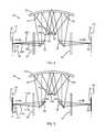
- Optical relay 18is illustrated in FIG. 3 as a reflective relay, may be one similar to those disclosed in U.S. Pat. No. 3,748,015 to Offner, which is incorporated herein by reference.
- optical relay 18includes a pair of transmissive windows 40 , 42 defining a respective beam inlet and outlet thereof, a pair of reflective turning mirrors 44 , 46 , a concave mirror 48 having a reflective surfaces 50 , 52 for respectively receiving the transmitted beam 20 from and directing the beam 20 towards the respective turning mirrors 44 , 46 , and a convex mirror 54 having a reflective surface 56 and positioned in relation to the concave mirror 48 so that the beam reflected off surface 50 is convergently received and divergently reflected towards surface 52 .
- Concave mirror 48may include reflective surfaces, such as surfaces 50 , 52 , that are separate and spaced apart from each other or the surfaces may be formed in one piece.
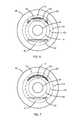
- the respective concave and convex reflective surfacesare spherical and concentrically disposed about a common origin, resulting in a generally superior image quality over a rotationally symmetric ring field 114 of the relay 18 , and resulting in unit magnification with automatic correction for all primary aberrations.
- magnifications other than unit magnificationare produced.
- a four mirror systemmay be used to produce four times unit magnification.
- the ring field 114generally shows where the imaging relay 18 provides a concentric region of focus and reduced aberration.
- lines 116 , 118 of constant aberrationare similarly concentric and provide general boundaries for the ring field 114 .
- a cross-hatched region 120 of superior focusis shown about a central line 122 of best focus and aberration.
- Ray 34reflects off second turning mirror 46 and out through transmissive window 42 towards a convergent focus forming a laser line image 58 at an image plane 60 , which is generally coincident with target 22 .
- the turning mirrors 44 , 46are positioned in the relay 18 so as to provide a co-linear projection from object 38 to image 58 , typically oriented at 45° with respect to the incident beam 20 .
- Previously omitted ray 36is shown convergently propagating towards image plane 60 after second window 42 .
- the optical path distance between the object 38 and the reflective surface 50 of the concave mirror 48is nominally twice the path length from either one of the surfaces 50 , 52 to the convex mirror 54 .
- FIG. 7shows a similar depiction as FIG. 6 except that a different transmitted portion 20 of the input light beam 14 is shown incident on the concave mirror 48 .
- an optical relay 62includes a pair of transmissive windows 64 , 66 forming a general inlet and outlet for a light beam entering and exiting the relay 62 , a pair of reflective planar turning mirrors 68 , 70 , an aspheric concave mirror 72 having a reflective surfaces 74 , 76 for respectively receiving the transmitted beam 20 from and directing the beam 20 towards the respective turning mirrors 68 , 70 , and a convex mirror 78 positioned in relation to the concave mirror 72 so that the beam reflected off surface 74 is convergently received and divergently reflected towards surface 76 .
- Convex mirror 78includes a refractive first surface 80 , a reflective second surface 82 and an interior portion 84 , allowing a beam incident on first surface 80 to refract through interior portion 84 , reflect at second surface 82 , and to propagate through interior portion 84 and out first surface 80 .
- An example ray 86which includes principal ray 86 A and corresponding marginal rays 86 B, 86 C propagates through relay 62 from an initial starting point at the object plane 24 .
- the ray 86passes through window 64 , reflects off turning mirror 68 , and is directed towards first aspheric surface 74 of concave mirror 72 .
- Ray 86reflects off surface 74 and is directed towards convex mirror 78 where it refracts through first surface 80 of convex mirror 78 and propagates through the interior region 84 thereof before reflecting off second surface 82 back towards first surface 80 and out divergently towards second surface 76 of aspheric concave mirror 72 .
- Ray 86reflects off second surface 76 and convergently propagates towards second turning mirror 70 which causes the ray 86 to reflect and continue convergently propagate through second transmissive window 66 towards image plane 60 .
- the turning mirrors 68 , 70are positioned in the relay 62 so as to provide a co-linear projection from object plane 24 to image plane 60 . In some embodiments the projection is other than co-linear.
- the addition of the refractive first surface 80 to convex mirror 78provides correction for optical aberrations, including astigmatism.
- the aspheric aspect of the surfaces 74 , 76 of the concave mirrorfurther improves image quality.
- the orientation of the turning mirrors 68 , 70can vary from 45° orientation with respect to the incident beam 20 in order to maintain the aforementioned co-linearity as well as telecentricity of the image and object.
- the path length between the object 38 and reflective surface 74 or between surface 76 and image 58 , and the path length between surface 74 and convex mirror 78is a ratio that is less than two, and in some examples significantly less than two.
- an optical relay 88includes a pair of transmissive windows 90 , 92 forming a general inlet and outlet for a light beam entering and exiting the relay 88 , a pair of reflective turning mirrors 94 , 96 having respective bilaterally symmetric aspheric surfaces 98 , 100 , a concave mirror 102 having a reflective surfaces 104 , 106 for respectively receiving the transmitted beam 20 from and directing the beam 20 towards the respective turning mirrors 94 , 96 , and a convex mirror 108 having a reflective surface 110 and positioned in relation to the concave mirror 102 so that the beam reflected off surface 104 is convergently received and divergently reflected towards surface 106 .
- concave and convex mirrors 102 , 108are disposed about a common origin while in others mirrors 102 , 108 are not concentrically disposed about a common origin.
- An example ray 112which includes principal ray 112 A and corresponding marginal rays 112 B, 112 C propagates through relay 88 from an initial starting point at the object plane 24 .
- the ray 112pass through window 90 , reflects off turning mirror 94 , and is directed towards surface 104 for reflection thereat and towards convex mirror 108 .
- Ray 112reflects at mirror 108 and is directed towards surface 106 of concave mirror 102 .
- Ray 112reflects at surface 106 and is convergently directed towards second turning mirror 96 and reflects off the surface thereof and propagates out transmissive window 92 convergently towards image plane 60 .
- the turning mirrors 94 , 96are positioned in the relay 88 so as to provide a co-linear projection from object plane 24 to image plane 60 .
- the projectionis other than co-linear.
- the turning mirrors 94 , 96can vary from a 45° orientation with respect to the incident beam 20 in order to maintain the aforementioned co-linearity as well as telecentricity of the image and object.
- the respective surfaces 98 , 100 of the turning mirrors 94 , 96can be described by off-axis sections of a bilaterally symmetric polynomial such that the surfaces 98 , 100 are mirror images of each other. There are many suitable solutions, and corresponding embodiments, for the shape of the surfaces 98 , 100 which give superior performance.
- the surfaces 98 , 100are described by an off-axis section of a rotationally symmetric asphere, or a conic.
- the surfaces 104 , 106 of the concave mirror 102are aspheric.
- a ring field 124is shown for one optical configuration of relay 88 .
- Ring field 124includes lines of constant aberration 126 , 128 which bound a central line 132 of best focus and aberration.
- a cross-hatched region 130 of superior focusis shown in relation to the reflected beam 20 .
- the lines 126 , 128 , 132 as well as region 130are nominally bilaterally symmetric though not rotationally symmetric.
- the ring field 124 and region 130may be characterized as an oblate, oblong, or elongated annulus or field.
- the transmitted beam 20can be reflected in better overlap therewith, so as to provide better image quality.
Landscapes
- Physics & Mathematics (AREA)
- Optics & Photonics (AREA)
- General Physics & Mathematics (AREA)
- Engineering & Computer Science (AREA)
- Plasma & Fusion (AREA)
- Mechanical Engineering (AREA)
- Lenses (AREA)
Abstract
Description
Claims (35)
Priority Applications (2)
| Application Number | Priority Date | Filing Date | Title |
|---|---|---|---|
| US13/486,896US9429742B1 (en) | 2011-01-04 | 2012-06-01 | High power laser imaging systems |
| US13/540,461US9409255B1 (en) | 2011-01-04 | 2012-07-02 | High power laser imaging systems |
Applications Claiming Priority (2)
| Application Number | Priority Date | Filing Date | Title |
|---|---|---|---|
| US12/984,085US8835804B2 (en) | 2011-01-04 | 2011-01-04 | Beam homogenizer |
| US13/486,896US9429742B1 (en) | 2011-01-04 | 2012-06-01 | High power laser imaging systems |
Related Parent Applications (1)
| Application Number | Title | Priority Date | Filing Date |
|---|---|---|---|
| US12/984,085Continuation-In-PartUS8835804B2 (en) | 2011-01-04 | 2011-01-04 | Beam homogenizer |
Related Child Applications (1)
| Application Number | Title | Priority Date | Filing Date |
|---|---|---|---|
| US13/540,461Continuation-In-PartUS9409255B1 (en) | 2011-01-04 | 2012-07-02 | High power laser imaging systems |
Publications (1)
| Publication Number | Publication Date |
|---|---|
| US9429742B1true US9429742B1 (en) | 2016-08-30 |
Family
ID=56739435
Family Applications (1)
| Application Number | Title | Priority Date | Filing Date |
|---|---|---|---|
| US13/486,896Expired - Fee RelatedUS9429742B1 (en) | 2011-01-04 | 2012-06-01 | High power laser imaging systems |
Country Status (1)
| Country | Link |
|---|---|
| US (1) | US9429742B1 (en) |
Cited By (2)
| Publication number | Priority date | Publication date | Assignee | Title |
|---|---|---|---|---|
| US10705348B2 (en) | 2016-09-29 | 2020-07-07 | Nlight, Inc. | Optical power density control in fiber-coupled laser |
| WO2022125305A1 (en)* | 2020-12-08 | 2022-06-16 | Electro Scientific Industries, Inc. | Optical relay system and methods of use and manufacture |
Citations (94)
| Publication number | Priority date | Publication date | Assignee | Title |
|---|---|---|---|---|
| US3748015A (en)* | 1971-06-21 | 1973-07-24 | Perkin Elmer Corp | Unit power imaging catoptric anastigmat |
| US4293186A (en)* | 1977-02-11 | 1981-10-06 | The Perkin-Elmer Corporation | Restricted off-axis field optical system |
| US4377339A (en) | 1981-08-03 | 1983-03-22 | Gte Products Corporation | Projection optical lithography apparatus |
| US4492427A (en) | 1981-03-09 | 1985-01-08 | Litton Systems, Inc. | Optical slip ring assembly |
| US4688904A (en)* | 1983-10-27 | 1987-08-25 | Canon Kabushiki Kaisha | Reflecting optical system |
| US4711535A (en)* | 1985-05-10 | 1987-12-08 | The Perkin-Elmer Corporation | Ring field projection system |
| US4932747A (en) | 1989-09-07 | 1990-06-12 | The United States Of America As Represented By The Secretary Of The Navy | Fiber bundle homogenizer and method utilizing same |
| US5153773A (en) | 1989-06-08 | 1992-10-06 | Canon Kabushiki Kaisha | Illumination device including amplitude-division and beam movements |
| US5224200A (en) | 1991-11-27 | 1993-06-29 | The United States Of America As Represented By The Department Of Energy | Coherence delay augmented laser beam homogenizer |
| JPH05277776A (en)* | 1992-03-31 | 1993-10-26 | Toshiba Corp | Mask device for laser beam |
| US5517359A (en) | 1995-01-23 | 1996-05-14 | Gelbart; Daniel | Apparatus for imaging light from a laser diode onto a multi-channel linear light valve |
| US5586132A (en) | 1994-07-27 | 1996-12-17 | Laser Industries Ltd. | Method and apparatus for generating bright light sources |
| US5619245A (en) | 1994-07-29 | 1997-04-08 | Eastman Kodak Company | Multi-beam optical system using lenslet arrays in laser multi-beam printers and recorders |
| US5638220A (en)* | 1994-06-22 | 1997-06-10 | Kabushiki Kaisha Topcon | Device for producing ring-shaped laser spot |
| US5673135A (en)* | 1993-08-17 | 1997-09-30 | Kabushiki Kaisha Topcon | Scanning projection optical device |
| US5719704A (en) | 1991-09-11 | 1998-02-17 | Nikon Corporation | Projection exposure apparatus |
| US5936761A (en) | 1996-05-28 | 1999-08-10 | Sony Corporation | Wavelength conversion apparatus |
| US6040553A (en) | 1998-10-29 | 2000-03-21 | Gebo Conveyors Consultants & Systems, Inc. | Method of manufacturing air conveyor panels by laser ablation drilling |
| US6114088A (en) | 1999-01-15 | 2000-09-05 | 3M Innovative Properties Company | Thermal transfer element for forming multilayer devices |
| JP2000343257A (en)* | 1999-06-07 | 2000-12-12 | Sumitomo Heavy Ind Ltd | Method and device for return beam removal |
| US6169565B1 (en) | 1999-03-31 | 2001-01-02 | Eastman Kodak Company | Laser printer utilizing a spatial light modulator |
| US6498680B1 (en) | 1996-10-29 | 2002-12-24 | Chorum Technologies Lp | Compact tunable optical wavelength interleaver |
| US6509547B1 (en) | 2000-04-07 | 2003-01-21 | Resonetics, Inc. | Method for laser stripping of optical fiber and flat cable |
| US20030016450A1 (en) | 2001-07-23 | 2003-01-23 | Jena-Laserdiode Gmbh | Laser radiation source for generating a working beam |
| US6529542B1 (en) | 2000-04-04 | 2003-03-04 | Aculight Corporation | Incoherent beam combined optical system utilizing a lens array |
| US6531681B1 (en)* | 2000-03-27 | 2003-03-11 | Ultratech Stepper, Inc. | Apparatus having line source of radiant energy for exposing a substrate |
| US6560039B1 (en)* | 1999-09-28 | 2003-05-06 | Tropel Corporation | Double mirror catadioptric objective lens system with three optical surface multifunction component |
| US20030128543A1 (en) | 2002-01-07 | 2003-07-10 | Rekow Mathew N. | Apparatus for projecting a line of light from a diode-laser array |
| US6618174B2 (en) | 1996-11-15 | 2003-09-09 | Diffraction, Ltd | In-line holographic mask for micromachining |
| US6678308B1 (en)* | 2002-09-06 | 2004-01-13 | The Boeing Company | Laser resonator system using offner relay |
| US20040036961A1 (en) | 2002-08-22 | 2004-02-26 | Mcguire James P. | Structures and methods for reducing polarization aberration in optical systems |
| US6707532B2 (en)* | 2000-02-23 | 2004-03-16 | Canon Kabushiki Kaisha | Projection exposure apparatus |
| US20040065646A1 (en) | 2002-09-26 | 2004-04-08 | The Regents Of The University Of California | High energy laser beam dump |
| US20040090609A1 (en) | 1998-02-27 | 2004-05-13 | Nikon Corporation | Illumination system and exposure apparatus and method |
| US20040223330A1 (en) | 2003-05-07 | 2004-11-11 | Broude Sergey V. | Methods and apparatuses for homogenzing light |
| US20050045604A1 (en)* | 2003-09-02 | 2005-03-03 | Ultratech Stepper, Inc. | Laser thermal processing with laser diode radiation |
| US6873398B2 (en) | 2003-05-21 | 2005-03-29 | Esko-Graphics A/S | Method and apparatus for multi-track imaging using single-mode beams and diffraction-limited optics |
| US20050098260A1 (en) | 2003-10-21 | 2005-05-12 | Chen Jie W. | Method and apparatus for heating plastics by means of laser beams |
| US6980295B2 (en) | 2003-10-06 | 2005-12-27 | The Regents Of The University Of California | Compact catadioptric imaging spectrometer utilizing reflective grating |
| US6985226B2 (en) | 2004-05-11 | 2006-01-10 | The Regents Of The University Of California | Compact imaging spectrometer utilizing an immersed grating and anamorphic mirror |
| US20060012842A1 (en) | 2003-06-10 | 2006-01-19 | Abu-Ageel Nayef M | Method and apparatus for reducing laser speckle |
| US7006217B2 (en) | 2003-09-09 | 2006-02-28 | The Regents Of The University Of California | Compact catadioptric imaging spectrometer utilizing immersed gratings |
| US20060102605A1 (en) | 2004-11-12 | 2006-05-18 | Applied Materials, Inc. | Single axis light pipe for homogenizing slow axis of illumination systems bases on laser diodes |
| US20060176912A1 (en) | 2005-02-07 | 2006-08-10 | Anikitchev Serguei G | Apparatus for projecting a line of light from a diode-laser array |
| JP2006278491A (en)* | 2005-03-28 | 2006-10-12 | Sony Corp | Irradiating apparatus |
| US20060246693A1 (en) | 2005-04-28 | 2006-11-02 | Koichiro Tanaka | Method for manufacturing semiconductor device and laser irradiation apparatus |
| US7158215B2 (en)* | 2003-06-30 | 2007-01-02 | Asml Holding N.V. | Large field of view protection optical system with aberration correctability for flat panel displays |
| US7167630B2 (en) | 2004-11-08 | 2007-01-23 | Kodak Il, Ltd. | Beam shaper and imaging head having beam shapers |
| US20070063226A1 (en)* | 2004-10-29 | 2007-03-22 | Semiconductor Energy Laboratory Co., Ltd. | Laser irradiation apparatus and laser irradiation method |
| US20070147065A1 (en) | 2005-12-28 | 2007-06-28 | Seiko Epson Corporation | Lighting device and projector |
| US20070153847A1 (en)* | 2005-12-21 | 2007-07-05 | Nuvonyx, Inc | Manufacturing and the design of assemblies for high power laser diode array modules |
| US7253376B2 (en)* | 2005-01-21 | 2007-08-07 | Ultratech, Inc. | Methods and apparatus for truncating an image formed with coherent radiation |
| USRE39846E1 (en) | 1992-11-05 | 2007-09-18 | Nikon Corporation | Illumination optical apparatus and scanning exposure apparatus |
| US7277229B2 (en) | 2005-05-23 | 2007-10-02 | Fujifilm Corporation | Linear light beam generating optical system |
| US7293882B2 (en) | 2004-09-15 | 2007-11-13 | Hewlett-Packard Development Company, L.P. | Optical relay |
| US7317469B2 (en) | 2004-08-30 | 2008-01-08 | Samsung Sdi Co., Ltd. | Laser induced thermal imaging apparatus |
| US20080025732A1 (en) | 2006-07-26 | 2008-01-31 | Hitachi Cable, Ltd | Optical transmitter and optical transmission method |
| US7418172B2 (en) | 2003-04-24 | 2008-08-26 | Semiconductor Energy Laboratory Co., Ltd. | Beam homogenizer, laser irradiation apparatus, and method for manufacturing semiconductor device |
| US20080210671A1 (en) | 2006-08-23 | 2008-09-04 | Applied Maerials, Inc. | Fast axis beam profile shaping by collimation lenslets for high power laser diode based annealing system |
| US20080308534A1 (en)* | 2007-06-18 | 2008-12-18 | Jiping Li | Pyrometer for laser annealing system compatible with amorphous carbon optical absorber layer |
| US7502537B2 (en) | 2005-08-31 | 2009-03-10 | Panasonic Corporation | Optical fiber-bundle and fiber-optic processing equipment using the same |
| US7519493B2 (en) | 2002-02-14 | 2009-04-14 | Faro Technologies, Inc. | Portable coordinate measurement machine with integrated line laser scanner |
| US20090127477A1 (en) | 2005-05-02 | 2009-05-21 | Semiconductor Energy Laboratory Co., Ltd | Laser irradiation apparatus and laser irradiation method |
| US7545403B2 (en) | 2004-10-26 | 2009-06-09 | Samsung Mobile Display Co., Ltd. | Optical system having image direction modulator and LITI apparatus including the system |
| US7545446B2 (en) | 2005-08-27 | 2009-06-09 | Hewlett-Packard Development Company, L.P. | Offner relay for projection system |
| US20090219491A1 (en) | 2007-10-18 | 2009-09-03 | Evans & Sutherland Computer Corporation | Method of combining multiple Gaussian beams for efficient uniform illumination of one-dimensional light modulators |
| US20090236495A1 (en) | 2004-11-12 | 2009-09-24 | Dean Jennings | Autofocus for high power laser diode based annealing system |
| US20100097680A1 (en) | 2002-09-30 | 2010-04-22 | Ron Naftali | Illumination system for optical inspection |
| US7704666B2 (en) | 2005-08-30 | 2010-04-27 | Samsung Mobile Display Co., Ltd. | Laser induced thermal imaging apparatus and laser induced thermal imaging method |
| US20100140478A1 (en) | 2006-12-22 | 2010-06-10 | Photonic Innovations Limited | Gas Detector |
| US7745991B2 (en) | 1999-10-12 | 2010-06-29 | Semiconductor Energy Laboratory Co., Ltd. | Electro-optical device having an EL layer over a plurality of pixels |
| US20100171931A1 (en) | 2009-01-07 | 2010-07-08 | David Kessler | Line illumination apparatus using laser arrays |
| US7776493B2 (en) | 2005-08-25 | 2010-08-17 | Samsung Mobile Display Co., Ltd. | Mask for LITI and LITI method using the same |
| US7792249B2 (en) | 2007-12-23 | 2010-09-07 | Oraya Therapeutics, Inc. | Methods and devices for detecting, controlling, and predicting radiation delivery |
| US20100254717A1 (en) | 2009-04-06 | 2010-10-07 | Avago Technologies Fiber Ip (Singapore) Pte. Ltd. | Apparatus and method for controlling the optical output power of a laser in an optical transmitter (tx) |
| US7821718B1 (en) | 2009-04-06 | 2010-10-26 | Hewlett-Packard Development Company, L.P. | Laser line generator |
| US7847940B2 (en) | 2005-04-06 | 2010-12-07 | Eastman Kodak Company | Methods and apparatus for correcting banding of imaged regular patterns |
| US7851725B2 (en) | 2004-11-17 | 2010-12-14 | Metal Improvement Company Llc | Active beam delivery system with image relay |
| US7885012B2 (en) | 2008-07-23 | 2011-02-08 | Eastman Kodak Company | Shearing radiation beam for imaging printing media |
| US7892382B2 (en) | 2003-11-18 | 2011-02-22 | Samsung Mobile Display Co., Ltd. | Electroluminescent devices and methods of making electroluminescent devices including a color conversion element |
| US20110043900A1 (en)* | 2009-08-19 | 2011-02-24 | Lawrence Livermore National Security, Llc | Method and system for homogenizing diode laser pump arrays |
| US7995298B2 (en) | 2007-04-16 | 2011-08-09 | Young Optics Inc. | Illumination system |
| WO2011142849A2 (en) | 2010-01-21 | 2011-11-17 | Rudolph Wolfgang G | Gas filled hollow fiber laser |
| US8062986B2 (en) | 2007-07-27 | 2011-11-22 | Corning Incorporated | Fused silica having low OH, OD levels and method of making |
| US20120045169A1 (en) | 2010-08-23 | 2012-02-23 | Lockheed Martin Corporation | Optical-fiber array method and apparatus |
| US20120057345A1 (en) | 2010-09-07 | 2012-03-08 | Coherent, Inc. | Line-projection apparatus for arrays of diode-laser bar stacks |
| US20120069861A1 (en) | 2009-05-27 | 2012-03-22 | Wolfgang Neuberger | Precisely-Shaped Core Fibers and Method of Manufacture |
| US20120248078A1 (en) | 2008-08-20 | 2012-10-04 | Zediker Mark S | Control system for high power laser drilling workover and completion unit |
| US20120268836A1 (en)* | 2011-04-22 | 2012-10-25 | Coherent, Inc. | Unit-magnification catadioptric and catoptric projection optical systems |
| US20120273269A1 (en) | 2008-08-20 | 2012-11-01 | Rinzler Charles C | Long distance high power optical laser fiber break detection and continuity monitoring systems and methods |
| US20130058092A1 (en) | 2011-09-06 | 2013-03-07 | Government Of The United States, As Represented By The Secretary Of The Air Force | Dynamic Laser Pointer |
| US20130107360A1 (en)* | 2011-10-27 | 2013-05-02 | Andrew F. Kurtz | Low thermal stress catadioptric imaging optics |
| US8483533B1 (en) | 2008-04-10 | 2013-07-09 | Nlight Photonics Corporation | Fiber-coupled laser diode illumination systems with stable beam propagation |
| US8821963B2 (en) | 2008-02-04 | 2014-09-02 | Semiconductor Energy Laboratory Co., Ltd. | Deposition method and method for manufacturing light-emitting device |
- 2012
- 2012-06-01USUS13/486,896patent/US9429742B1/ennot_activeExpired - Fee Related
Patent Citations (96)
| Publication number | Priority date | Publication date | Assignee | Title |
|---|---|---|---|---|
| US3748015A (en)* | 1971-06-21 | 1973-07-24 | Perkin Elmer Corp | Unit power imaging catoptric anastigmat |
| US4293186A (en)* | 1977-02-11 | 1981-10-06 | The Perkin-Elmer Corporation | Restricted off-axis field optical system |
| US4492427A (en) | 1981-03-09 | 1985-01-08 | Litton Systems, Inc. | Optical slip ring assembly |
| US4377339A (en) | 1981-08-03 | 1983-03-22 | Gte Products Corporation | Projection optical lithography apparatus |
| US4688904A (en)* | 1983-10-27 | 1987-08-25 | Canon Kabushiki Kaisha | Reflecting optical system |
| US4711535A (en)* | 1985-05-10 | 1987-12-08 | The Perkin-Elmer Corporation | Ring field projection system |
| US5153773A (en) | 1989-06-08 | 1992-10-06 | Canon Kabushiki Kaisha | Illumination device including amplitude-division and beam movements |
| US4932747A (en) | 1989-09-07 | 1990-06-12 | The United States Of America As Represented By The Secretary Of The Navy | Fiber bundle homogenizer and method utilizing same |
| US5719704A (en) | 1991-09-11 | 1998-02-17 | Nikon Corporation | Projection exposure apparatus |
| US5224200A (en) | 1991-11-27 | 1993-06-29 | The United States Of America As Represented By The Department Of Energy | Coherence delay augmented laser beam homogenizer |
| JPH05277776A (en)* | 1992-03-31 | 1993-10-26 | Toshiba Corp | Mask device for laser beam |
| USRE39846E1 (en) | 1992-11-05 | 2007-09-18 | Nikon Corporation | Illumination optical apparatus and scanning exposure apparatus |
| US5673135A (en)* | 1993-08-17 | 1997-09-30 | Kabushiki Kaisha Topcon | Scanning projection optical device |
| US5638220A (en)* | 1994-06-22 | 1997-06-10 | Kabushiki Kaisha Topcon | Device for producing ring-shaped laser spot |
| US5586132A (en) | 1994-07-27 | 1996-12-17 | Laser Industries Ltd. | Method and apparatus for generating bright light sources |
| US5619245A (en) | 1994-07-29 | 1997-04-08 | Eastman Kodak Company | Multi-beam optical system using lenslet arrays in laser multi-beam printers and recorders |
| US5517359A (en) | 1995-01-23 | 1996-05-14 | Gelbart; Daniel | Apparatus for imaging light from a laser diode onto a multi-channel linear light valve |
| US5936761A (en) | 1996-05-28 | 1999-08-10 | Sony Corporation | Wavelength conversion apparatus |
| US6498680B1 (en) | 1996-10-29 | 2002-12-24 | Chorum Technologies Lp | Compact tunable optical wavelength interleaver |
| US6618174B2 (en) | 1996-11-15 | 2003-09-09 | Diffraction, Ltd | In-line holographic mask for micromachining |
| US20040090609A1 (en) | 1998-02-27 | 2004-05-13 | Nikon Corporation | Illumination system and exposure apparatus and method |
| US6040553A (en) | 1998-10-29 | 2000-03-21 | Gebo Conveyors Consultants & Systems, Inc. | Method of manufacturing air conveyor panels by laser ablation drilling |
| US6114088A (en) | 1999-01-15 | 2000-09-05 | 3M Innovative Properties Company | Thermal transfer element for forming multilayer devices |
| US6169565B1 (en) | 1999-03-31 | 2001-01-02 | Eastman Kodak Company | Laser printer utilizing a spatial light modulator |
| JP2000343257A (en)* | 1999-06-07 | 2000-12-12 | Sumitomo Heavy Ind Ltd | Method and device for return beam removal |
| US6560039B1 (en)* | 1999-09-28 | 2003-05-06 | Tropel Corporation | Double mirror catadioptric objective lens system with three optical surface multifunction component |
| US7745991B2 (en) | 1999-10-12 | 2010-06-29 | Semiconductor Energy Laboratory Co., Ltd. | Electro-optical device having an EL layer over a plurality of pixels |
| US6707532B2 (en)* | 2000-02-23 | 2004-03-16 | Canon Kabushiki Kaisha | Projection exposure apparatus |
| US6531681B1 (en)* | 2000-03-27 | 2003-03-11 | Ultratech Stepper, Inc. | Apparatus having line source of radiant energy for exposing a substrate |
| US6529542B1 (en) | 2000-04-04 | 2003-03-04 | Aculight Corporation | Incoherent beam combined optical system utilizing a lens array |
| US6509547B1 (en) | 2000-04-07 | 2003-01-21 | Resonetics, Inc. | Method for laser stripping of optical fiber and flat cable |
| US20030016450A1 (en) | 2001-07-23 | 2003-01-23 | Jena-Laserdiode Gmbh | Laser radiation source for generating a working beam |
| US20030128543A1 (en) | 2002-01-07 | 2003-07-10 | Rekow Mathew N. | Apparatus for projecting a line of light from a diode-laser array |
| US7519493B2 (en) | 2002-02-14 | 2009-04-14 | Faro Technologies, Inc. | Portable coordinate measurement machine with integrated line laser scanner |
| US20040036961A1 (en) | 2002-08-22 | 2004-02-26 | Mcguire James P. | Structures and methods for reducing polarization aberration in optical systems |
| US6678308B1 (en)* | 2002-09-06 | 2004-01-13 | The Boeing Company | Laser resonator system using offner relay |
| US20040065646A1 (en) | 2002-09-26 | 2004-04-08 | The Regents Of The University Of California | High energy laser beam dump |
| US20100097680A1 (en) | 2002-09-30 | 2010-04-22 | Ron Naftali | Illumination system for optical inspection |
| US7418172B2 (en) | 2003-04-24 | 2008-08-26 | Semiconductor Energy Laboratory Co., Ltd. | Beam homogenizer, laser irradiation apparatus, and method for manufacturing semiconductor device |
| US20040223330A1 (en) | 2003-05-07 | 2004-11-11 | Broude Sergey V. | Methods and apparatuses for homogenzing light |
| US6873398B2 (en) | 2003-05-21 | 2005-03-29 | Esko-Graphics A/S | Method and apparatus for multi-track imaging using single-mode beams and diffraction-limited optics |
| US20060012842A1 (en) | 2003-06-10 | 2006-01-19 | Abu-Ageel Nayef M | Method and apparatus for reducing laser speckle |
| US7158215B2 (en)* | 2003-06-30 | 2007-01-02 | Asml Holding N.V. | Large field of view protection optical system with aberration correctability for flat panel displays |
| US20050045604A1 (en)* | 2003-09-02 | 2005-03-03 | Ultratech Stepper, Inc. | Laser thermal processing with laser diode radiation |
| US7006217B2 (en) | 2003-09-09 | 2006-02-28 | The Regents Of The University Of California | Compact catadioptric imaging spectrometer utilizing immersed gratings |
| US6980295B2 (en) | 2003-10-06 | 2005-12-27 | The Regents Of The University Of California | Compact catadioptric imaging spectrometer utilizing reflective grating |
| US20050098260A1 (en) | 2003-10-21 | 2005-05-12 | Chen Jie W. | Method and apparatus for heating plastics by means of laser beams |
| US7892382B2 (en) | 2003-11-18 | 2011-02-22 | Samsung Mobile Display Co., Ltd. | Electroluminescent devices and methods of making electroluminescent devices including a color conversion element |
| US6985226B2 (en) | 2004-05-11 | 2006-01-10 | The Regents Of The University Of California | Compact imaging spectrometer utilizing an immersed grating and anamorphic mirror |
| US7317469B2 (en) | 2004-08-30 | 2008-01-08 | Samsung Sdi Co., Ltd. | Laser induced thermal imaging apparatus |
| US7293882B2 (en) | 2004-09-15 | 2007-11-13 | Hewlett-Packard Development Company, L.P. | Optical relay |
| US7545403B2 (en) | 2004-10-26 | 2009-06-09 | Samsung Mobile Display Co., Ltd. | Optical system having image direction modulator and LITI apparatus including the system |
| US20070063226A1 (en)* | 2004-10-29 | 2007-03-22 | Semiconductor Energy Laboratory Co., Ltd. | Laser irradiation apparatus and laser irradiation method |
| US7167630B2 (en) | 2004-11-08 | 2007-01-23 | Kodak Il, Ltd. | Beam shaper and imaging head having beam shapers |
| US20090236495A1 (en) | 2004-11-12 | 2009-09-24 | Dean Jennings | Autofocus for high power laser diode based annealing system |
| US20060102605A1 (en) | 2004-11-12 | 2006-05-18 | Applied Materials, Inc. | Single axis light pipe for homogenizing slow axis of illumination systems bases on laser diodes |
| US7851725B2 (en) | 2004-11-17 | 2010-12-14 | Metal Improvement Company Llc | Active beam delivery system with image relay |
| US7253376B2 (en)* | 2005-01-21 | 2007-08-07 | Ultratech, Inc. | Methods and apparatus for truncating an image formed with coherent radiation |
| US7355800B2 (en) | 2005-02-07 | 2008-04-08 | Coherent, Inc. | Apparatus for projecting a line of light from a diode-laser array |
| US20060176912A1 (en) | 2005-02-07 | 2006-08-10 | Anikitchev Serguei G | Apparatus for projecting a line of light from a diode-laser array |
| JP2006278491A (en)* | 2005-03-28 | 2006-10-12 | Sony Corp | Irradiating apparatus |
| US7847940B2 (en) | 2005-04-06 | 2010-12-07 | Eastman Kodak Company | Methods and apparatus for correcting banding of imaged regular patterns |
| US20060246693A1 (en) | 2005-04-28 | 2006-11-02 | Koichiro Tanaka | Method for manufacturing semiconductor device and laser irradiation apparatus |
| US20100048036A1 (en) | 2005-04-28 | 2010-02-25 | Semiconductor Energy Laboratory Co., Ltd. | Method for manufacturing semiconductor device and laser irradiation apparatus |
| US20090127477A1 (en) | 2005-05-02 | 2009-05-21 | Semiconductor Energy Laboratory Co., Ltd | Laser irradiation apparatus and laser irradiation method |
| US7277229B2 (en) | 2005-05-23 | 2007-10-02 | Fujifilm Corporation | Linear light beam generating optical system |
| US7776493B2 (en) | 2005-08-25 | 2010-08-17 | Samsung Mobile Display Co., Ltd. | Mask for LITI and LITI method using the same |
| US7545446B2 (en) | 2005-08-27 | 2009-06-09 | Hewlett-Packard Development Company, L.P. | Offner relay for projection system |
| US7704666B2 (en) | 2005-08-30 | 2010-04-27 | Samsung Mobile Display Co., Ltd. | Laser induced thermal imaging apparatus and laser induced thermal imaging method |
| US7502537B2 (en) | 2005-08-31 | 2009-03-10 | Panasonic Corporation | Optical fiber-bundle and fiber-optic processing equipment using the same |
| US20070153847A1 (en)* | 2005-12-21 | 2007-07-05 | Nuvonyx, Inc | Manufacturing and the design of assemblies for high power laser diode array modules |
| US20070147065A1 (en) | 2005-12-28 | 2007-06-28 | Seiko Epson Corporation | Lighting device and projector |
| US20080025732A1 (en) | 2006-07-26 | 2008-01-31 | Hitachi Cable, Ltd | Optical transmitter and optical transmission method |
| US20080210671A1 (en) | 2006-08-23 | 2008-09-04 | Applied Maerials, Inc. | Fast axis beam profile shaping by collimation lenslets for high power laser diode based annealing system |
| US20100140478A1 (en) | 2006-12-22 | 2010-06-10 | Photonic Innovations Limited | Gas Detector |
| US7995298B2 (en) | 2007-04-16 | 2011-08-09 | Young Optics Inc. | Illumination system |
| US20080308534A1 (en)* | 2007-06-18 | 2008-12-18 | Jiping Li | Pyrometer for laser annealing system compatible with amorphous carbon optical absorber layer |
| US8062986B2 (en) | 2007-07-27 | 2011-11-22 | Corning Incorporated | Fused silica having low OH, OD levels and method of making |
| US20090219491A1 (en) | 2007-10-18 | 2009-09-03 | Evans & Sutherland Computer Corporation | Method of combining multiple Gaussian beams for efficient uniform illumination of one-dimensional light modulators |
| US7792249B2 (en) | 2007-12-23 | 2010-09-07 | Oraya Therapeutics, Inc. | Methods and devices for detecting, controlling, and predicting radiation delivery |
| US8821963B2 (en) | 2008-02-04 | 2014-09-02 | Semiconductor Energy Laboratory Co., Ltd. | Deposition method and method for manufacturing light-emitting device |
| US8483533B1 (en) | 2008-04-10 | 2013-07-09 | Nlight Photonics Corporation | Fiber-coupled laser diode illumination systems with stable beam propagation |
| US7885012B2 (en) | 2008-07-23 | 2011-02-08 | Eastman Kodak Company | Shearing radiation beam for imaging printing media |
| US20120273269A1 (en) | 2008-08-20 | 2012-11-01 | Rinzler Charles C | Long distance high power optical laser fiber break detection and continuity monitoring systems and methods |
| US20120248078A1 (en) | 2008-08-20 | 2012-10-04 | Zediker Mark S | Control system for high power laser drilling workover and completion unit |
| US20100171931A1 (en) | 2009-01-07 | 2010-07-08 | David Kessler | Line illumination apparatus using laser arrays |
| US20100254717A1 (en) | 2009-04-06 | 2010-10-07 | Avago Technologies Fiber Ip (Singapore) Pte. Ltd. | Apparatus and method for controlling the optical output power of a laser in an optical transmitter (tx) |
| US7821718B1 (en) | 2009-04-06 | 2010-10-26 | Hewlett-Packard Development Company, L.P. | Laser line generator |
| US20120069861A1 (en) | 2009-05-27 | 2012-03-22 | Wolfgang Neuberger | Precisely-Shaped Core Fibers and Method of Manufacture |
| US20110043900A1 (en)* | 2009-08-19 | 2011-02-24 | Lawrence Livermore National Security, Llc | Method and system for homogenizing diode laser pump arrays |
| WO2011142849A2 (en) | 2010-01-21 | 2011-11-17 | Rudolph Wolfgang G | Gas filled hollow fiber laser |
| US20120045169A1 (en) | 2010-08-23 | 2012-02-23 | Lockheed Martin Corporation | Optical-fiber array method and apparatus |
| US20120057345A1 (en) | 2010-09-07 | 2012-03-08 | Coherent, Inc. | Line-projection apparatus for arrays of diode-laser bar stacks |
| US20120268836A1 (en)* | 2011-04-22 | 2012-10-25 | Coherent, Inc. | Unit-magnification catadioptric and catoptric projection optical systems |
| US20130058092A1 (en) | 2011-09-06 | 2013-03-07 | Government Of The United States, As Represented By The Secretary Of The Air Force | Dynamic Laser Pointer |
| US20130107360A1 (en)* | 2011-10-27 | 2013-05-02 | Andrew F. Kurtz | Low thermal stress catadioptric imaging optics |
Non-Patent Citations (7)
| Title |
|---|
| Erdmann et al., "Coherence management for microlens laser beam homogenizers," Proceedings of SPIE, 4775:145-154 (Aug. 2002). |
| French et al., "Absorption Edge and Band Gap of SiO2 Fused Silica Glass," Ceramic Transactions, 28:63-80 (1992). |
| International Search Report and Written Opinion for International Application No. PCT/US2013/033424, 9 pages, mailed Jul. 18, 2013. |
| Machine translation of Japan Patent document No. 2000-343,257, Nov. 2015.* |
| Positive Light, Inc. "Relay Imaging in Rod Amplifier Systems," Technical Bulletin, 2 pages, (May 2002) (copy attached). |
| Schmitt et al., "Illumination uniformity of laserfusion pellets using induced spatial incoherence," Journal of Applied Physics, vol. 60(1), pp. 6-13 (Jul. 1, 1986) (copy attached). |
| Summary of First Office Action from the State Intellectual Property Office of the People's Republic of China for Chinese App. No. 201380012279.9, mailed Oct. 26, 2015, 4 pages. |
Cited By (2)
| Publication number | Priority date | Publication date | Assignee | Title |
|---|---|---|---|---|
| US10705348B2 (en) | 2016-09-29 | 2020-07-07 | Nlight, Inc. | Optical power density control in fiber-coupled laser |
| WO2022125305A1 (en)* | 2020-12-08 | 2022-06-16 | Electro Scientific Industries, Inc. | Optical relay system and methods of use and manufacture |
Similar Documents
| Publication | Publication Date | Title |
|---|---|---|
| US11256076B2 (en) | High power laser system | |
| US8835804B2 (en) | Beam homogenizer | |
| US11759886B2 (en) | Laser line illumination | |
| CN102844143B (en) | For applying the device of laser emission | |
| US8270084B2 (en) | Device for beam shaping | |
| US10437072B2 (en) | Line beam forming device | |
| KR101984759B1 (en) | Multiple beam combiner for laser processing apparatus and a radiation source | |
| US8750344B2 (en) | Laser pump arrangement and laser pump method with beam homogenization | |
| US20140003456A1 (en) | Device For Converting The Profile of a Laser Beam Into a Laser Beam With a Rotationally Symmetrical Intensity Distribution | |
| US10151929B2 (en) | Illumination optical unit for projection lithography and hollow waveguide component therefor | |
| CN111880315A (en) | Laser lighting equipment | |
| US7331676B2 (en) | Apparatus for projecting a reduced image of a photomask using a schwarzschild objective | |
| TWI834736B (en) | Laser machining system | |
| WO2019024359A1 (en) | Laser beam homogenizing device and method | |
| US9409255B1 (en) | High power laser imaging systems | |
| CN104953465B (en) | Homogenizing device for laser diode array light beam based on space spectrum division processing | |
| US9429742B1 (en) | High power laser imaging systems | |
| CN105223697A (en) | A kind of terahertz light expands uniforming device | |
| US9798047B2 (en) | Device for applying light to an inner surface of a cylinder and beam transformation device for such a device | |
| CN104136961B (en) | High power laser system | |
| JP2012528748A (en) | Optical system for direct imaging of optically printable materials | |
| CN113515023A (en) | Dual-waveband illumination system and maskless direct-writing photoetching equipment with same | |
| TW202450204A (en) | Laser-beam homogenization or shaping | |
| US20140118843A1 (en) | Optical arrangement for converting an incident light beam, method for converting a light beam to a line focus, and optical device therefor | |
| CN120161623A (en) | A focusing system and laser-supported plasma light source |
Legal Events
| Date | Code | Title | Description |
|---|---|---|---|
| AS | Assignment | Owner name:NLIGHT PHOTONICS CORPORATION, WASHINGTON Free format text:ASSIGNMENT OF ASSIGNORS INTEREST;ASSIGNORS:MARTINSEN, ROBERT J.;KARLSEN, SCOTT R;LERNER, SC A.;SIGNING DATES FROM 20120618 TO 20120629;REEL/FRAME:028482/0990 | |
| AS | Assignment | Owner name:SQUARE 1 BANK, NORTH CAROLINA Free format text:SECURITY INTEREST;ASSIGNOR:NLIGHT PHOTONICS CORPORATION;REEL/FRAME:034925/0007 Effective date:20140313 | |
| AS | Assignment | Owner name:NLIGHT PHOTONICS CORPORATION, WASHINGTON Free format text:CORRECTIVE ASSIGNMENT TO CORRECT THE LAST INVENTOR'S NAME PREVIOUSLY RECORDED AT REEL: 031197 FRAME: 0591. ASSIGNOR(S) HEREBY CONFIRMS THE ASSIGNMENT;ASSIGNORS:MARTINSEN, ROBERT J.;KARLSEN, SCOTT R.;LERNER, SCOTT A.;SIGNING DATES FROM 20120618 TO 20120629;REEL/FRAME:035135/0145 | |
| ZAAA | Notice of allowance and fees due | Free format text:ORIGINAL CODE: NOA | |
| ZAAB | Notice of allowance mailed | Free format text:ORIGINAL CODE: MN/=. | |
| ZAAA | Notice of allowance and fees due | Free format text:ORIGINAL CODE: NOA | |
| STCF | Information on status: patent grant | Free format text:PATENTED CASE | |
| AS | Assignment | Owner name:NLIGHT, INC., WASHINGTON Free format text:CHANGE OF NAME;ASSIGNOR:NLIGHT PHOTONICS CORPORATION;REEL/FRAME:046531/0151 Effective date:20160111 | |
| AS | Assignment | Owner name:PACIFIC WESTERN BANK, NORTH CAROLINA Free format text:SECURITY INTEREST;ASSIGNOR:NLIGHT, INC.;REEL/FRAME:047291/0833 Effective date:20181017 | |
| MAFP | Maintenance fee payment | Free format text:PAYMENT OF MAINTENANCE FEE, 4TH YEAR, LARGE ENTITY (ORIGINAL EVENT CODE: M1551); ENTITY STATUS OF PATENT OWNER: LARGE ENTITY Year of fee payment:4 | |
| FEPP | Fee payment procedure | Free format text:MAINTENANCE FEE REMINDER MAILED (ORIGINAL EVENT CODE: REM.); ENTITY STATUS OF PATENT OWNER: LARGE ENTITY | |
| LAPS | Lapse for failure to pay maintenance fees | Free format text:PATENT EXPIRED FOR FAILURE TO PAY MAINTENANCE FEES (ORIGINAL EVENT CODE: EXP.); ENTITY STATUS OF PATENT OWNER: LARGE ENTITY | |
| STCH | Information on status: patent discontinuation | Free format text:PATENT EXPIRED DUE TO NONPAYMENT OF MAINTENANCE FEES UNDER 37 CFR 1.362 | |
| FP | Lapsed due to failure to pay maintenance fee | Effective date:20240830 |