US9429692B1 - Optical components - Google Patents
Optical componentsDownload PDFInfo
- Publication number
- US9429692B1 US9429692B1US14/617,746US201514617746AUS9429692B1US 9429692 B1US9429692 B1US 9429692B1US 201514617746 AUS201514617746 AUS 201514617746AUS 9429692 B1US9429692 B1US 9429692B1
- Authority
- US
- United States
- Prior art keywords
- gratings
- moulding
- polymer
- light
- orientation angle
- Prior art date
- Legal status (The legal status is an assumption and is not a legal conclusion. Google has not performed a legal analysis and makes no representation as to the accuracy of the status listed.)
- Active
Links
- 230000003287optical effectEffects0.000titleclaimsabstractdescription72
- 238000000465mouldingMethods0.000claimsabstractdescription102
- 229920000642polymerPolymers0.000claimsabstractdescription91
- 239000007788liquidSubstances0.000claimsabstractdescription20
- 238000000034methodMethods0.000claimsdescription51
- 230000008569processEffects0.000claimsdescription34
- 239000000758substrateSubstances0.000claimsdescription21
- 230000007246mechanismEffects0.000claimsdescription14
- 230000007423decreaseEffects0.000claimsdescription7
- 230000008859changeEffects0.000claimsdescription6
- 230000001747exhibiting effectEffects0.000claimsdescription4
- 238000001514detection methodMethods0.000claimsdescription3
- 239000013598vectorSubstances0.000description8
- 230000000737periodic effectEffects0.000description6
- 238000002347injectionMethods0.000description4
- 239000007924injectionSubstances0.000description4
- 230000001902propagating effectEffects0.000description4
- 238000000926separation methodMethods0.000description4
- 230000008021depositionEffects0.000description3
- 238000005530etchingMethods0.000description3
- 230000006870functionEffects0.000description3
- 238000004519manufacturing processMethods0.000description3
- 230000010355oscillationEffects0.000description3
- 101100096627Caenorhabditis elegans srg-4 geneProteins0.000description2
- 230000001276controlling effectEffects0.000description2
- 238000010586diagramMethods0.000description2
- 230000000694effectsEffects0.000description2
- VYPSYNLAJGMNEJ-UHFFFAOYSA-NSilicium dioxideChemical compoundO=[Si]=OVYPSYNLAJGMNEJ-UHFFFAOYSA-N0.000description1
- 210000000988bone and boneAnatomy0.000description1
- 239000003086colorantSubstances0.000description1
- 238000007796conventional methodMethods0.000description1
- 230000008878couplingEffects0.000description1
- 238000010168coupling processMethods0.000description1
- 238000005859coupling reactionMethods0.000description1
- 230000003247decreasing effectEffects0.000description1
- 230000001419dependent effectEffects0.000description1
- 239000006185dispersionSubstances0.000description1
- 239000005350fused silica glassSubstances0.000description1
- 239000011521glassSubstances0.000description1
- 238000005286illuminationMethods0.000description1
- 239000000463materialSubstances0.000description1
- 238000000059patterningMethods0.000description1
- 230000001105regulatory effectEffects0.000description1
- 239000007787solidSubstances0.000description1
- 230000009466transformationEffects0.000description1
Images


Classifications
- G—PHYSICS
- G02—OPTICS
- G02B—OPTICAL ELEMENTS, SYSTEMS OR APPARATUS
- G02B5/00—Optical elements other than lenses
- G02B5/18—Diffraction gratings
- G02B5/1847—Manufacturing methods
- G02B5/1852—Manufacturing methods using mechanical means, e.g. ruling with diamond tool, moulding
- B—PERFORMING OPERATIONS; TRANSPORTING
- B29—WORKING OF PLASTICS; WORKING OF SUBSTANCES IN A PLASTIC STATE IN GENERAL
- B29D—PRODUCING PARTICULAR ARTICLES FROM PLASTICS OR FROM SUBSTANCES IN A PLASTIC STATE
- B29D11/00—Producing optical elements, e.g. lenses or prisms
- B29D11/00663—Production of light guides
- G—PHYSICS
- G02—OPTICS
- G02B—OPTICAL ELEMENTS, SYSTEMS OR APPARATUS
- G02B27/00—Optical systems or apparatus not provided for by any of the groups G02B1/00 - G02B26/00, G02B30/00
- G02B27/01—Head-up displays
- G02B27/017—Head mounted
- G02B27/0172—Head mounted characterised by optical features
- G—PHYSICS
- G02—OPTICS
- G02B—OPTICAL ELEMENTS, SYSTEMS OR APPARATUS
- G02B5/00—Optical elements other than lenses
- G02B5/18—Diffraction gratings
- G02B5/1847—Manufacturing methods
- G02B5/1857—Manufacturing methods using exposure or etching means, e.g. holography, photolithography, exposure to electron or ion beams
- G—PHYSICS
- G02—OPTICS
- G02B—OPTICAL ELEMENTS, SYSTEMS OR APPARATUS
- G02B5/00—Optical elements other than lenses
- G02B5/18—Diffraction gratings
- G02B5/1866—Transmission gratings characterised by their structure, e.g. step profile, contours of substrate or grooves, pitch variations, materials
- G—PHYSICS
- G02—OPTICS
- G02B—OPTICAL ELEMENTS, SYSTEMS OR APPARATUS
- G02B27/00—Optical systems or apparatus not provided for by any of the groups G02B1/00 - G02B26/00, G02B30/00
- G02B27/01—Head-up displays
- G02B27/0101—Head-up displays characterised by optical features
- G02B27/0103—Head-up displays characterised by optical features comprising holographic elements
- G02B2027/0109—Head-up displays characterised by optical features comprising holographic elements comprising details concerning the making of holograms
- G—PHYSICS
- G02—OPTICS
- G02B—OPTICAL ELEMENTS, SYSTEMS OR APPARATUS
- G02B27/00—Optical systems or apparatus not provided for by any of the groups G02B1/00 - G02B26/00, G02B30/00
- G02B27/01—Head-up displays
- G02B27/0101—Head-up displays characterised by optical features
- G02B27/0103—Head-up displays characterised by optical features comprising holographic elements
Definitions
- Optical componentscan be used in optical systems to alter the state of visible light in a predictable and desired manner, for example in display systems to make a desired image visible to a user.
- Optical componentscan interact with light by way of reflection, refractions, diffraction etc.
- Diffractionoccurs when a propagating wave interacts with a structure, such as an obstacle or slit. Diffraction can be described as the interference of waves and is most pronounced when that structure is comparable in size to the wavelength of the wave.
- Optical diffraction of visible lightis due to the wave nature of light and can be described as the interference of light waves. Visible light has wavelengths between approximately 390 and 700 nanometers (nm) and diffraction of visible light is most pronounced when propagating light encounters structures similar scale e.g. of order 100 or 1000 nm in scale.
- a light guide(also referred to herein as a “waveguide”) is an optical component used to transport light by way of internal reflection e.g. total internal reflection (TIR) within the light guide.
- TIRtotal internal reflection
- a light guidemay be used, for instance, in a light guide-based display system for transporting light of a desired image from a light engine to a human eye to make the image visible to the eye.
- Incoupling and outcoupling SRGs on surface(s) of the light guidecan be used for inputting light to and outputting light from the waveguide respectively.
- Microfabricationrefers to the fabrication of desired structures of micrometer scales and smaller (such as surface gratings). Microfabrication may involve etching of and/or deposition on a substrate (and possibly etching of and/or deposition on a film deposited on the substrate) to create the desired microstructure on the substrate (or film on the substrate). As used herein, the term “patterning a substrate” or similar encompasses all such etching of/deposition on a substrate or substrate film.
- a first aspectis directed to a moulding process for making a substantially transparent optical component which comprises polymer.
- the optical componenthas substantially matching grating imprints on respective portions of its surface.
- the grating imprintshave a substantially zero relative orientation angle.
- the processcomprises the following steps.
- Substantially transparent molten polymeris forced between two surfaces of a moulding component.
- the surfaceshave surface modulations which form two substantially matching gratings.
- the molten polymeris forced into contact with the surface modulations so as to imprint the gratings in the polymer.
- the moulding componentis configurable to change the relative orientation angle of the gratings. At least an alignment portion of the moulding component is substantially transparent.
- the alignment portionis located so that light which has interacted with both gratings is observable from the alignment portion when the substantially transparent polymer is between the surfaces, whereby an observable fringe pattern is formed as the relative orientation angle of the gratings is changed towards zero.
- the fringe patternexhibits a fringe spacing which increases as the relative orientation angle decreases. Whilst the polymer is still liquid, the moulding component is reconfigured from a current configuration to a new configuration in which the fringe spacing of the fringe pattern is substantially maximal, thus aligning the gratings to have a substantially zero relative orientation angle. The new configuration is maintained whilst the polymer sets.
- At least an alignment portion of the moulding componentis substantially transparent, the alignment portion located so that light which has interacted with both gratings is observable from the alignment portion when the substantially transparent polymer is between the surfaces, whereby an observable fringe pattern is formed as the relative orientation angle of the gratings is changed towards zero.
- the fringe patternexhibits a fringe spacing which increases as the relative orientation angle decreases.
- the light sensoris configured to receive at least some of the light which has interacted with both gratings.
- the controlleris configured, whilst the polymer is still liquid, to control the drive mechanism based on sensed data received from the image sensor to reconfigure the moulding component from a current configuration to a new configuration in which the fringe spacing of the fringe pattern is substantially maximal, thus aligning the gratings to have a substantially zero relative orientation angle.
- the new configurationis maintained whilst the polymer sets.
- Such productsinclude an optical component for use in an optical system, which optical component is substantially transparent, formed of polymer, and has substantially matching gratings on opposing portions of its surface, the gratings having a relative orientation angle that is zero to within one thousandth of a degree.
- FIG. 2Ais a schematic illustration of a straight binary grating, shown interacting with incident light and viewed from the side;
- FIG. 2Bis a schematic illustration of a slanted binary grating, shown interacting with incident light and viewed from the side;
- FIG. 2Cis a schematic illustration of an overhanging triangular grating, shown interacting with incident light and viewed from the side;
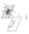
- FIG. 3is a perspective view of an optical component
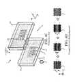
- FIGS. 4A, 4B and 4Care side, plan and perspective views of parts of a moulding apparatus respectively;
- FIG. 4Dshows various views of a fringe observed at different points in time during a moulding process of one embodiment
- FIG. 5is a block diagram of a moulding apparatus
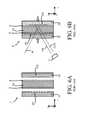
- FIGS. 6A and 6Bare side views of a moulding apparatus during a moulding process of another embodiment.
- FIGS. 1A and 1Bshow from the top and the side respectively a substantially transparent optical component 2 , such as a wave guide, having an outer surface S. At least a portion of the surface S exhibits surface modulations that form a surface grating 4 , which is a SRG. Such a portion is referred to as a “grating area”.
- the modulationscomprise grating lines which are substantially parallel and elongate (substantially longer than they are wide), and also substantially straight in this example (though they need not be straight in general).
- FIG. 1Bshows the optical component 2 , and in particular the grating 4 , interacting with an incoming illuminating light beam I that is inwardly incident on the SRG 4 .
- the light Iis white light in this example, and thus has multiple colour components.
- the light Iinteracts with the grating 4 which splits the light into several beams directed inwardly into the optical component 2 . Some of the light I may also be reflected back from the surface S as a reflected beam R 0 .
- a zero-order mode inward beam T 0 and any reflection R 0are created in accordance with the normal principles of diffraction as well as other non-zero-order ( ⁇ n-order) modes (which can be explained as wave interference).
- FIG. 1Bshows the optical component 2 , and in particular the grating 4 , interacting with an incoming illuminating light beam I that is inwardly incident on the SRG 4 .
- the light Iis white light in this example, and thus has multiple colour components.
- FIG. 1Bshows first-order inward beams T 1 , T- 1 ; it will be appreciated that higher-order beams may or may not also be created depending on the configuration of the optical component 2 . Because the nature of the diffraction is dependent on wavelength, for higher-order modes, different colour components (i.e. wavelength components) of the incident light I are, when present, split into beams of different colours at different angles of propagation relative to one another as illustrated in FIG. 1B .
- FIGS. 2A-2Care close-up schematic cross sectional views of different exemplary SRGs 4 a - 4 c (collectively referenced as 4 herein) that may be formed by modulations of the surface S of the optical component 2 (which is viewed from the side in these figures).
- Light beamsare denoted as arrows whose thicknesses denote approximate relative intensity (with higher intensity beams shown as thicker arrows).
- FIG. 2Ashows an example of a straight binary SRG 4 a .
- the straight binary grating 4 ais formed of a series of grooves 7 a in the surface S separated by protruding groove spacing regions 9 a which are also referred to herein as “filling regions”, “grating lines” or simply “lines”.
- the grating 4 ahas a spatial period of d (referred to as the “grating period”), which is the distance over which the modulations' shape repeats.
- the grooves 7 ahave a depth h and have substantially straight walls and substantially flat bases.
- each +n-order mode beam (e.g. T 1 ) created by the grating 4 ahas substantially the same intensity as the corresponding ⁇ n-order mode beam (e.g. T- 1 ), typically less than about one fifth (0.2) of the intensity of the incident beam I.
- FIG. 2Bshows an example of a slanted binary grating 4 b .
- the slanted grating 4 bis also formed of grooves, labelled 7 b , in the surface S having substantially straight walls and substantially flat bases separated by lines 9 b of width w.
- the wallsare slanted by an amount relative to the normal, denoted by the angle ⁇ in FIG. 2B .
- the grooves 7 bhave a depth h as measured along the normal. Due to the asymmetry introduced by the non-zero slant, ⁇ n-order mode inward beams travelling away from the slant direction have greater intensity that their ⁇ n-order mode counterparts (e.g.
- the T 1 beamis directed away from the direction of slant and has usually greater intensity than the T- 1 beam, though this depends on e.g. the grating period d); by increasing the slant by a sufficient amount, those ⁇ n counterparts can be substantially eliminated (i.e. to have substantially zero intensity).
- the intensity of the T 0 beamis typically also reduced very much by a slanted binary grating such that, in the example of FIG. 2B , the first-order beam T 1 typically has an intensity of at most about four fifths (0.8) the intensity of the incident beam I.
- the binary gratings 4 a and 4 bcan be viewed as spatial waveforms embedded in the surface S that have a substantially square wave shape (with period d).
- the shapeis a skewed square wave shape skewed by ⁇ .
- FIG. 2Cshows an example of an overhanging triangular grating 4 c which is a special case of an overhanging trapezoidal grating.
- the triangular 4 cis formed of grooves 7 c in the surface S that are triangular in shape (and which thus have discernible tips) and which have a depth h as measured along the normal.
- Filling regions 9 ctake the form of triangular, tooth-like protrusions (teeth), having medians that make an angle ⁇ with the normal ( ⁇ being the slant angle of the grating 4 c ).
- the teethhave tips that are separated by d (which is the grating period of the grating 4 c ), a width that is w at the base of the teeth and which narrows to substantially zero at the tips of the teeth.
- dwhich is the grating period of the grating 4 c
- w ⁇ dbut generally can be w ⁇ d.
- the gratingis overhanging in that the tips of the teeth extend over the tips of the grooves. It is possible to construct overhanging triangular grating gratings that substantially eliminate both the transmission-mode T 0 beam and the ⁇ n-mode beams, leaving only ⁇ n-order mode beams (e.g. only T 1 ).
- the grooveshave walls which are at an angle ⁇ to the median (wall angle).
- the grating 4 ccan be viewed as a spatial waveform embedded in S that has a substantially triangular wave shape, which is skewed by a.
- the grooves and spacing regions that form the gratings 4 a - 4 cconstitute surface modulations.
- gratingOther type of grating are also possible, for example other types of trapezoidal grating patterns (which may not narrow in width all the way to zero), sinusoidal grating patterns etc. and have a modulation width that can be readily defined in a suitable manner. Such other patterns also exhibit depth h, linewidth w, slant angle ⁇ and wall angles ⁇ which can be defined in a similar manner to FIG. 2A-C .
- a grating 4has a grating vector (generally denoted as d), whose size (magnitude) is the grating period d, and which is in a direction perpendicular to the grating lines which form that grating—see FIG. 1A .
- dis typically between about 250 and 500 nm, and h between about 30 and 400 nm.
- the slant angle ⁇is typically between about ⁇ 45 and 45 degrees and is measured in the direction of the grating vector.
- FIG. 3Ashows a perspective view of an optical component 2 having two separate gratings 4 F and 4 B on respective portions of the component's surface, which are opposing, substantially parallel and substantially flat. Viewed as in FIG. 3A , these are front and rear portions of the surface.
- Each of the gratings 4 B, 4 Fis formed of substantially parallel, elongate grating lines and grooved, which are also substantially straight in this example.
- the gratings 4 B, 4 Fhave respective grating periods d F , d B , which may or may not be the same.
- the gratings 4 B, 4 Fcan be of the type described above (and may, but need not be, of the same type).
- the gratings 4 F and 4 Bhave respective grating vectors d F , d B (front and back grating vectors) which run parallel to their respective grating lines.
- a plane 3is shown, which has a normal ⁇ circumflex over (n) ⁇ ( 3 ) (unit vector perpendicular to the plane 3 ) shown as a dotted arrow.
- nnormal ⁇ circumflex over (n) ⁇ ( 3 )
- the front and rear surface portionsare substantially parallel, they have substantially the same normals as the plane ( ⁇ circumflex over (n) ⁇ ( 3 )) so that the front and rear surface portions and the plane 3 are all substantially parallel (more generally, for non-parallel surface portions, the plane 3 could be defined to have a normal ⁇ circumflex over (n) ⁇ ( 3 ) in the approximate direction of the vector sum of the normals to the front and rear surface portions as this represents a direction of the mean of those normals, which normal ⁇ circumflex over (n) ⁇ ( 3 ) is considered to substantially match those normals when so defined).
- Vectors 15 F, 15 Blie in the plane 3 , which are geometric projections of the front and back grating vectors d F , d B onto the plane 3 .
- the projections 15 F, 15 Bhave an angular separation ⁇ , which is an angle in the plane 3 (azimuth), and which is the angular separation of d F , d B when viewed along the normal ⁇ circumflex over (n) ⁇ ( 3 ).
- the angular separation ⁇is a measure of the relative orientation of the gratings 4 F, 4 B and is referred to herein as the relative orientation angle of the gratings 4 F, 4 B.
- the grating lines of the gratings 4 F, 4 Bare aligned, at least when viewed along the normal 3 ′, and the gratings 4 F, 4 B are said to be aligned.
- ⁇affects the optical characteristics of the optical component 2 .
- misalignment of the gratingscan—depending on the function of the gratings—cause unwanted distortion of the image.
- FIGS. 4A-4Dshow various views of a moulding apparatus 1 during the process.
- the polymeris substantially transparent, which makes the process suitable for (among other things) moulding waveguides for waveguide-based display systems (see above).
- FIG. 4Ashows the apparatus 1 from the side.
- the apparatuscomprises blocks 5 F, 5 B (front, back), 5 U, 5 D (upper, lower—visible in FIG. 4A only) and 5 L (left—visible in FIG. 4B only), which are formed of a rigid material.
- the reference numeral 5is used to refer to the blocks collectively.
- the blocksare arranged in contact so as to form a cavity 11 (moulding cavity), with regions of their surfaces (inner surface regions) forming the surface of the cavity 11 .
- the rigid blocks 5constitute a moulding component.
- each cavity grating 4 ′F, 4 ′Bis formed by surface modulations in the form of substantially parallel, elongate and substantially straight grating lines/grooves, and have periods d F , d B respectively.
- These inner surface portionsconstitute opposing portions of the surface of the cavity 11 , which are also substantially parallel to one another.
- the cavity gratings 4 ′F, 4 ′Bcan be patterned on the front and rear blocks 5 F, 5 B, for instance, by way of a suitable microfabrication process, or they may themselves be moulded from a suitably patterned substrate.
- An injection component 10forces polymer 8 into the moulding cavity 11 (from the right as viewed in FIG. 4B ) when the polymer 8 is in a molten (and thus liquid) state.
- the liquid polymer 8is forced into contact with the front and rear cavity gratings 4 ′F, 4 ′B—that is, into contact with the grooved and lines that form those gratings, which has the effect of imprinting the structure of the cavity gratings 4 ′F, 4 ′B in the polymer 8 .
- the blocks 5are sufficiently rigid to resist distortion from the force of the liquid polymer, so the gratings are imprinted undistorted.
- the gratings 4 F, 4 B of the final optical component 2are referred to hereinbelow as front and rear “imprint gratings” or equivalently “grating imprints” 4 F, 4 B.
- the front and rear surface portions of the final optical component 2 on which the imprint gratings 4 F, 4 B are formedcorrespond to the front and rear surface portions of the moulding cavity.
- the overall size and shape of the final component 2matches that of the cavity 11 when the polymer was allowed to set therein.
- the z-directionis that of the normal ⁇ circumflex over (n) ⁇ ( 3 ) as defined in relation to the final optical component (which is perpendicular to the cavity surface portions on which the cavity gratings 4 ′F, 4 ′B are formed in this example), the xy-plane corresponds to the plane 3 of FIG. 3 (which lies parallel to those cavity surface portions in this example), and the cavity gratings 4 ′F, 4 ′B have a relative orientation angle ⁇ ′ that is defined in an equivalent manner to that of the imprint gratings 4 F, 4 B (i.e. as their angular separation measured in the xy-plane).
- the arrangement of the rigid blocks 5is not fixed: at least one of the front and back blocks 5 B, 4 F (the back block 5 B in this example) is susceptible to xy-rotation whilst still maintaining the integrity of the moulding cavity 11 so that it can be rotated whilst continuing to hold the liquid polymer in the cavity 11 .
- Controlled xy-rotation of the back block 5 Bis effected by controlling a suitable drive mechanism coupled to the back block 5 B. Using commercially available drive mechanisms, it is possible to controller xy-rotation of the back block 5 B to effect controlled rotation of the back block 5 B by miniscule amounts (fractions of a thousandth of a degree, or less) in a regulated manner.
- FIG. 4Cshows a perspective view of components of the moulding apparatus 1 .
- a light sensor 6(also shown in FIGS. 4A-4B ) is positioned forward of the moulding cavity 5 to receive light propagating towards the sensor along a line of sight (LOS—shown as a dotted line) that has passed through a portion 7 of the moulding component 5 (alignment portion), which is a portion of the front block 4 ′F in this example.
- the LOSis oriented so as to intersect both of the cavity gratings 4 F, 4 B.
- At least the alignment portion 7 of the moulding componentis substantially transparent along the LOS, so that light which has interacted with both gratings can propagate out of the moulding component along the LOS.
- a “fringe pattern”means a pattern created when light interacts with two substantially matching gratings (in this cast, the patterns of the cavity gratings 4 ′F, 4 ′B, which are perceived to overlap when viewed along the LOS) to create a pattern with fringes, the fringe spacing of which depends on the relative orientation angle of the gratings.
- the fringe patternis formed of a series of alternating light and dark fringes, whose spacing increases as the relative orientation angle of the cavity gratings 4 ′F, 4 ′B is changed towards zero, at which the fringe spacing become maximal (theoretically infinite were the patterns to be exactly aligned with a relative orientation angle of exactly zero).
- Near alignmentmeans that ⁇ ′ is within a range near zero that the fringe spacing is detectable (i.e. not so close to zero that the fringe spacing is too large to be detectable, but not so far from zero that the fringe spacing is too small to be detectable).
- the Fringe patternis best observed using diffracted light from the gratings.
- the diffracted lightwill generally propagate along almost the same path as the incident light but in the opposite direction.
- the path along which incident/diffracted light propagatesis labelled I/D in FIG. 4A (R denotes the path followed by light reflected from the back grating 4 ′B)
- the LOSis substantially parallel to I/D, thus light visible along the LOS will include light which has interacted with both of the cavity gratings 4 ′F, 4 ′B, including when the polymer 8 is in the cavity 11 (as the polymer 8 is also substantially transparent and thus permits the passage of such light to the sensor 6 ).
- the senor 6is able to receive light from inside the moulding cavity which has interacted with both cavity gratings 4 ′F, 4 ′B.
- this lightwill have been reflected from the back grating 4 ′B (the reflected light being of a reflective diffraction mode) before passing through the front grating 4 ′F.
- the fringe patternWhen the relative orientation angle ⁇ ′ ⁇ (5/1000)°, the fringe pattern will typically have a fringe spacing around 2 mm, which is readily observable. As this angle ⁇ ′ is decreased, the fringe spacing increases to the point at which it becomes substantially maximal—this is the point at the fringe spacing is so large that the pattern is no longer observable because the fringes are larger than the cavity gratings, or at least larger than a portion of the grating being if only that portion is being observed. At this point of substantially maximal fringe spacing, ⁇ ′ is substantially zero—in practice, when ⁇ ′ is no more than about (0.5*1/1000)° to (1/1000)°.
- FIG. 4Dshows views of the alignment portion 7 along the LOS at various points in time during the moulding process.
- a fringe patternis visible at these points in time, which exhibits a changing fringe spacing D.
- the left-most viewrepresents a view at a point in time when the gratings are in near alignment. Moving to the right, views are shown at points in time as the relative orientation angle ⁇ ′ is changed towards zero (with D increasing accordingly) until reaching the point at which D is substantially maximal as shown in the left-most view (which represents an exemplary view in or near the new and final configuration).
- visibility of the fringe patterncan be increased by suitable illumination of the apparatus.
- a laser(not shown) may be used to provide a beam that is directed towards the alignment portion 7 .
- the beamis reflectively diffracted back of the back grating 4 ′B and the diffracted beam then passes thought the front grating 4 ′F towards the sensor 6 .
- a beam expander(not shown) may be used to expand the beam before reaching the alignment portion 7 , so as to increase the area over which the visibility is enhanced.
- the beammay be expanded to encompass the cavity gratings 4 ′F, 4 ′B to provide the enhanced visibility of the fringe patterns over the full extent of the cavity gratings 4 ′F, 4 ′B.
- Curved componentscan be made using a curved mould i.e. the surfaces of the moulding component on which the gratings 4 ′F and 4 ′B care formed can be curved, whereby the curvature is imparted to the polymer as well as the structure of the gratings 4 ′ f , 4 ′B.
- FIG. 5is a block diagram of the moulding apparatus 1 , which comprises a controller 20 connected to control both the drive mechanism 22 and the injection component 10 , and to receive sensed data from the sensor 6 .
- the drive mechanismis coupled to at least one of the back blocks 5 F, 5 B that form part of the moulding component (back block 5 B in this example) for fine-tuning the relative orientation angle ⁇ ′ of the front and back cavity gratings 4 ′B, 4 ′B.
- the controller 20can adjust ⁇ ′ automatically by controlling the drive mechanism 22 , once it has controlled the injection component 10 force the polymer 8 into the cavity 11 .
- the controller 20receives the sensed data from the sensor 6 , and adjusts the relative orientation angle ⁇ ′ of the front and back cavity gratings 4 ′B, 4 ′F based on the sensed data until ⁇ ′ is substantially zero by effecting the procedure outlined above.
- the controllermay be implemented by code executed on a processor.
- the senor 6comprises an image sensing component in the form of a camera, which supplies images of the alignment portion 7 , taken along the LOS, to the controller 20 (such images capturing the views shown in FIG. 4D ).
- the controllercomprises an image recognition module which performs an automatic image recognition procedure on the received images to detect the fringes of the fringe pattern when captured in the images. The controller adjusts ⁇ ′ until the results of the image recognition procedure indicate that the fringe spacing D is maximal, and maintains that ⁇ ′ until the polymer has set.
- the fringe patternWhen illuminated with the laser beam, the fringe pattern is formed by light of the laser beam which has interacted with both gratings.
- the fringe patternmay not, and need not, be visible on any surface of either mould as the fringe pattern obtained with expanded laser beam can be recorded directly to a pixelated detector (for example, an array of individual pixel detectors), i.e. light reflected back from both alignment gratings interferes and creates the fringe patters on a detection surface of detector.
- the detectorfor example may part of the camera. In this manner, the pattern is observed on the surface of a detector instead on the surface of the moulds.
- the detectoris used to detect the fringe spacing as created on the detector, and the moulding process is controlled based on the detected fringe spacing to align the gratings to the maximal fringe spacing.
- the senor 6comprises a photodiode, which is shielded from surrounding light but for a small pinhole—e.g. having a diameter ⁇ 1 mm (order of magnitude)—through which only a small portion of the fringe pattern is observable. That is, such that the only light received by the photodiode is from a small portion of the fringe pattern the size of the pinhole, so that once the cavity gratings are in near alignment, the fringes are larger than the pinhole.
- the controller 20then changes ⁇ ′, e.g. at a uniform rate. As the cavity gratings 4 ′F, 4 ′B are brought into alignment, the fringe spacing increases, which effectively results in movement of the fringes (this is evident in FIG. 4D ).
- the intensity of the light received by the photodiodeoscillates between high (when only part of a light fringe is observable through the pinhole) and low (when only part of a dark fringe is perceivable through the pinhole) as ⁇ ′ is changed.
- the controlleradjusts ⁇ ′ until that minimum rate of oscillation is achieved, and maintains that ⁇ ′ until the polymer has set.
- the gratings 4 ′F, 4 ′D as shown in FIG. 4Ccan be used in the same way as described above, with a first further grating formed on a distinct portion of the front block's inner surface that is oriented at an angle ⁇ 1 relative to 4 ′F, and a second further grating formed on a distinct portion of the rear block's inner surface that is oriented at an angle ⁇ 2 relative to 4 ′B.
- the gratings 4 ′F, 4 ′Bare aligned to have a substantially zero relative orientation angle ⁇ ′ (relative to one another) using the above techniques, the further gratings will have an orientation angle relative to one another that is substantially ⁇ i.e. that deviates from ⁇ by at most an amount of the order of ⁇ ′ (which is, of course, substantially zero).
- the further gratingswill also be imprinted in the polymer as the polymer is forced into contact with these gratings when liquid in a similar manner to 4 ′F, 4 ′B, so that the further gratings as imprinted in the polymer have substantially the desired relative orientation angle ⁇ .
- FIGS. 6A and 6Bexemplify an alternative moulding process.
- a transparent substratesuch as a glass or suitable plastic plate 30 .
- Thin layers of polymer on the substrateare used to replicate the gratings from the mould i.e. the substrate acts as a “back bone” of the optical component and the gratings are formed on thin layers of polymer 8 on the substrate.
- FIG. 6Ashow an alternative moulding apparatus 1 ′ in an initial arrangement, in which the plate 30 , having thin layers of liquid polymer 8 deposited on portions of its outer surface, is disposed between two blocks 5 F, 5 B.
- These blockscan be substantially the same as in the apparatus of FIGS. 4A-C , with equivalent gratings 4 ′F, 4 ′B.
- the blocks 5 F, 5 Bare then forced towards one another so that the gratings 4 ′F, 4 ′B are forced into contact with the liquid polymer layers as shown in FIG. 6B . In this manner, their structure is imprinted in the polymer layers.
- the relative orientation angle of the modulations 4 ′F, 4 ′Bis then changed to substantially zero using the fringe pattern formed by the gratings 4 ′F, 4 ′B, and remains thus whilst the polymer layers set.
- the final optical componentcomprises the plate 30 and the set polymer layers on the plate's surface.
- the alignment portioncould alternatively be an uncovered gap between the components 5 F and 5 B (e.g. the sensor 6 could be located below the apparatus 1 ′ to receive light reflected of both gratings 4 ′F, 4 ′B, the alignment portion being the gap between 5 F and 5 B at the bottom of the apparatus 1 ′).
- the alternative apparatus 1 ′does not need an injection component, but otherwise has a similar configuration to that shown in FIG. 5 .
- the exemplary gratings 4 F, 4 Bmatch due to the fact that they are both formed of substantially straight grating lines
- gratings which are considered to “substantially match”do not necessarily have to be formed of straight grating lines, nor do they have to be formed of identically shaped curved grating lines.
- two gratings “substantially match”provided some parts of their respective structures are similar enough for it to be possible to create an observable fringe pattern that exhibits a discernible fringe spacing by overlaying those parts (even though other parts of their structure may be markedly different).
- the alignment gratingsneed not overlap, provided it is possible to receive light which has interacted with (e.g. been reflected from) both at a location in space (e.g. at a detector) so that a fringe pattern is formed at that location.
- gratingsare formed on opposing, substantially parallel surfaces
- opposite surfaces portionsencompasses surface portions which are not parallel. Note that the definition of the relative orientation angle (azimuth) between two gratings as set out above with reference to FIG. 3B can be applied to gratings on non-parallel surface portions.
- the techniquescan be applied to non-opposing gratings, whereby the fringe pattern is formed for instance by a beam which has been guided by reflection onto both gratings, and which thus interacts with both.
- the cavity gratings 4 ′F, 4 ′Bcan be binary (slanted/non-slanted), sinusoidal, trapezoidal (e.g. triangular) in shape (among others) and need not have the same shape, slant ⁇ , width w, depth h etc. as one another (though this is not excluded).
- the functionality of the controllercan be implemented using software, firmware, hardware (e.g., fixed logic circuitry), or a combination of these implementations.
- the terms “module,” “functionality,” “component” and “logic” as used hereingenerally represent, where applicable, software, firmware, hardware, or a combination thereof.
- the module, functionality, or logicrepresents program code that performs specified tasks when executed on a processor (e.g. CPU or CPUs).
- the program codecan be stored in one or more computer readable memory devices.
- the apparatusmay also include an entity (e.g. software) that causes hardware of a computer of the apparatus to perform operations, e.g., processors functional blocks, and so on.
- the computermay include a computer-readable medium that may be configured to maintain instructions that cause the computer, and more particularly the operating system and associated hardware of the computer to perform operations.
- the instructionsfunction to configure the operating system and associated hardware to perform the operations and in this way result in transformation of the operating system and associated hardware to perform functions.
- the instructionsmay be provided by the computer-readable medium to the computer through a variety of different configurations.
- One such configuration of a computer-readable mediumis signal bearing medium and thus is configured to transmit the instructions (e.g. as a carrier wave) to the computing device, such as via a network.
- the computer-readable mediummay also be configured as a computer-readable storage medium and thus is not a signal bearing medium. Examples of a computer-readable storage medium include a random-access memory (RAM), read-only memory (ROM), an optical disc, flash memory, hard disk memory, and other memory devices that may us magnetic, optical, and other techniques to store instructions and other data.
- images of the fringe patternmay be captured as the cavity is reconfigured and an automatic image recognition procedure may be performed to detect the fringe pattern in the images, the step of reconfiguring being based on the results of the image recognition procedure.
- Light of only a small portion of the fringe patternmay be sensed as the cavity is reconfigured, the step of reconfiguring being based on the rate at which the intensity of that light changes.
- Each of the gratingsmay lie substantially parallel to a plane, and the gratings may not overlap or may only partially overlap with one another when viewed along a direction normal to the plane.
- the gratingsmay be illuminated with an expanded laser beam, the fringe pattern being formed by light of the laser beam which has interacted with both gratings.
- the light of the laser beammay for instance be received at a detector, part of the received light having been reflected from one of the gratings and another part of the light having been reflected from the other of the gratings, whereby the part and the other part interfere at the detector to form the fringe pattern on a detection surface of the detector.
- An output of the detectormay be used to control the reconfiguring step.
- the opposing portions of the cavity's surfacemay be substantially parallel, so that the opposing portions of the moulded optical component's surface are substantially parallel.
- a first and a second further gratingmay be formed on other opposing portions of the cavity's surface, the first further grating having a first orientation angle ⁇ 1 relative to the one of the gratings and the second further grating having a second orientation angle ⁇ 2 relative to the other of the gratings, so that the first and second further gratings are imprinted in the polymer having a relative orientation angle that is substantially
- At least one of the surfaces of the moulding componentmay be curved so that the polymer sets in a curved configuration.
- the moulding componentmay be arranged to provide a moulding cavity, the surfaces being of the moulding cavity, and the polymer may be forced into the moulding cavity to force the polymer into contact with the surface modulations, the moulding component reconfigured to the new configuration whilst the polymer in the cavity is still liquid.
- the polymermay be arranged in layers on the surface of a substantially transparent substrate, whereby the gratings are imprinted in the layers, the moulding component reconfigured to the new configuration whilst the layers are still liquid, the optical component comprising the substrate and the layers once set.
- the light sensormay comprise a camera which captures images of the fringe pattern as the cavity is reconfigured
- the controllermay comprise an image recognition module which performs an automatic image recognition procedure to detect the fringe pattern in the images, and the controller may reconfigure the cavity based on the results of the image recognition procedure.
- the light sensormay sense light of only a small portion of the fringe pattern as the cavity is reconfigured, and the controller may be reconfigured based on the rate at which the intensity of that light changes.
- an optical component for use in an optical systemis substantially transparent and has two opposing outer surfaces. At least a respective portion of each of the opposing surfaces is formed of polymer in which a respective grating is imprinted.
- the gratingssubstantially match one another and have a relative orientation angle that is zero to within one thousandth of a degree.
- the relative orientation anglemay for instance be zero to within one half of one thousandth of a degree.
- the optical componentmay be used as a waveguide in a display system to transport light of an image to a user's eye, for example a wearable display system that is wearable by the user.
- the gratingsmay be binary, trapezoidal or sinusoidal in shape.
- a moulding apparatusfor moulding a substantially transparent optical component which comprises polymer, the optical component having substantially matching grating imprints on opposing portions of its surface, wherein the grating imprints have a substantially zero relative orientation angle
- the apparatuscomprising: a moulding component having two surfaces, the surfaces having surface modulations which form two substantially matching gratings, wherein the moulding component is configurable to change the relative orientation angle of the gratings; a drive mechanism coupled to the moulding component controllable to configure the moulding component; wherein at least an alignment portion of the moulding component is substantially transparent, the alignment portion located so that light which has interacted with both gratings is observable from the alignment portion when the substantially transparent polymer is between the surfaces, whereby an observable fringe pattern is formed as the relative orientation angle of the gratings is changed towards zero, the fringe pattern exhibiting a fringe spacing which increases as the relative orientation angle decreases, the apparatus further comprising: a light sensor configured to receive at least some of the light which
- Yet another aspectis directed to a moulding process for moulding a substantially transparent optical component from polymer, the optical component having substantially matching grating imprints on opposing portions of its surface, wherein the grating imprints have a substantially zero relative orientation angle
- the processcomprising: forcing substantially transparent molten polymer into a moulding cavity provided by a moulding component, the cavity's surface having surface modulations which form two substantially matching gratings on opposing portions of the cavity's surface, the molten polymer forced into contact with the surface modulations so as to imprint the gratings in the polymer, wherein the cavity is configurable to change the relative orientation angle of the gratings; wherein at least an alignment portion of the moulding component is substantially transparent along a line of sight that intersects both gratings so that light which has interacted with both gratings is observable along the line of sight when the substantially transparent polymer is in the cavity, whereby an observable fringe pattern is formed as the relative orientation angle of the gratings is changed towards
Landscapes
- Physics & Mathematics (AREA)
- Engineering & Computer Science (AREA)
- General Physics & Mathematics (AREA)
- Optics & Photonics (AREA)
- Manufacturing & Machinery (AREA)
- Health & Medical Sciences (AREA)
- Ophthalmology & Optometry (AREA)
- Mechanical Engineering (AREA)
- Diffracting Gratings Or Hologram Optical Elements (AREA)
- Optical Integrated Circuits (AREA)
Abstract
Description
Optical components can be used in optical systems to alter the state of visible light in a predictable and desired manner, for example in display systems to make a desired image visible to a user. Optical components can interact with light by way of reflection, refractions, diffraction etc. Diffraction occurs when a propagating wave interacts with a structure, such as an obstacle or slit. Diffraction can be described as the interference of waves and is most pronounced when that structure is comparable in size to the wavelength of the wave. Optical diffraction of visible light is due to the wave nature of light and can be described as the interference of light waves. Visible light has wavelengths between approximately 390 and 700 nanometers (nm) and diffraction of visible light is most pronounced when propagating light encounters structures similar scale e.g. of order 100 or 1000 nm in scale.
One example of a diffractive structure is a periodic structure. Periodic structures can cause diffraction of light which is typically most pronounced when the periodic structure has a spatial period of similar size to the wavelength of the light. Types of periodic structures include, for instance, surface modulations on a surface of an optical component, refractive index modulations, holograms etc. When propagating light encounters the periodic structure, diffraction causes the light to be split into multiple beams in different directions. These directions depend on the wavelength of the light thus diffractions gratings cause dispersion of polychromatic (e.g. white) light, whereby the polychromatic light is split into different coloured beams travelling in different directions.
When the period structure is on a surface of an optical component, it is referred to a surface grating. When the periodic structure is due to modulation of the surface itself, it is referred to as a surface relief grating (SRG). An example of a SRG is uniform straight grooves in a surface of an optical component that are separated by uniform straight groove spacing regions. Groove spacing regions are referred to herein as “lines”, “grating lines” and “filling regions”. The nature of the diffraction by a SRG depends both on the wavelength of light incident on the grating and various optical characteristics of the SRG, such as line spacing, groove depth and groove slant angle. SRGs have many useful applications. One example is an SRG light guide application. A light guide (also referred to herein as a “waveguide”) is an optical component used to transport light by way of internal reflection e.g. total internal reflection (TIR) within the light guide. A light guide may be used, for instance, in a light guide-based display system for transporting light of a desired image from a light engine to a human eye to make the image visible to the eye. Incoupling and outcoupling SRGs on surface(s) of the light guide can be used for inputting light to and outputting light from the waveguide respectively.
Surface gratings can be fabricated by way of a suitable microfabrication process to create appropriate surface modulations on a substrate. Microfabrication refers to the fabrication of desired structures of micrometer scales and smaller (such as surface gratings). Microfabrication may involve etching of and/or deposition on a substrate (and possibly etching of and/or deposition on a film deposited on the substrate) to create the desired microstructure on the substrate (or film on the substrate). As used herein, the term “patterning a substrate” or similar encompasses all such etching of/deposition on a substrate or substrate film. Whilst a substrate patterned with a surface grating may be suitable for use as an optical component in an optical system itself, a patterned substrate can also be used as a production masters for manufacturing such optical components. For example, a fused silica substrate (or similar), once patterned with a surface grating, can then be used as part of a moulding component for moulding optical components from polymer e.g. the moulding component may be arranged to provide a moulding cavity with the surface grating on the surface of the cavity. When liquid polymer is forced into the moulding cavity, it is forced into contact with the surface grating so as to imprint the surface grating in the polymer, which then sets to form a solid polymer optical component with the surface grating imprinted on its surface. Thus, large numbers of polymer optical components can be mass-manufactured using the same patterned substrate in an inexpensive, quick and straightforward manner.
This Summary is provided to introduce a selection of concepts in a simplified form that are further described below in the Detailed Description. This Summary is not intended to identify key features or essential features of the claimed subject matter, nor is it intended to be used to limit the scope of the claimed subject matter. Nor is the claimed subject matter limited to implementations that solve any or all of the disadvantages noted in the Background section.
A first aspect is directed to a moulding process for making a substantially transparent optical component which comprises polymer. The optical component has substantially matching grating imprints on respective portions of its surface. The grating imprints have a substantially zero relative orientation angle. The process comprises the following steps. Substantially transparent molten polymer is forced between two surfaces of a moulding component. The surfaces have surface modulations which form two substantially matching gratings. The molten polymer is forced into contact with the surface modulations so as to imprint the gratings in the polymer. The moulding component is configurable to change the relative orientation angle of the gratings. At least an alignment portion of the moulding component is substantially transparent. The alignment portion is located so that light which has interacted with both gratings is observable from the alignment portion when the substantially transparent polymer is between the surfaces, whereby an observable fringe pattern is formed as the relative orientation angle of the gratings is changed towards zero. The fringe pattern exhibits a fringe spacing which increases as the relative orientation angle decreases. Whilst the polymer is still liquid, the moulding component is reconfigured from a current configuration to a new configuration in which the fringe spacing of the fringe pattern is substantially maximal, thus aligning the gratings to have a substantially zero relative orientation angle. The new configuration is maintained whilst the polymer sets.
A second aspect is directed to a moulding apparatus for moulding a substantially transparent optical component which comprises polymer. The optical component has substantially matching grating imprints on opposing portions of its surface. The grating imprints have a substantially zero relative orientation angle. The apparatus comprises a moulding component, a drive mechanism, a light sensor and a controller. The moulding component has two surfaces, the surfaces having surface modulations which form two substantially matching gratings. The moulding component is configurable to change the relative orientation angle of the gratings. The drive mechanism is coupled to the moulding component and is controllable to configure the moulding component. At least an alignment portion of the moulding component is substantially transparent, the alignment portion located so that light which has interacted with both gratings is observable from the alignment portion when the substantially transparent polymer is between the surfaces, whereby an observable fringe pattern is formed as the relative orientation angle of the gratings is changed towards zero. The fringe pattern exhibits a fringe spacing which increases as the relative orientation angle decreases. The light sensor is configured to receive at least some of the light which has interacted with both gratings. The controller is configured, whilst the polymer is still liquid, to control the drive mechanism based on sensed data received from the image sensor to reconfigure the moulding component from a current configuration to a new configuration in which the fringe spacing of the fringe pattern is substantially maximal, thus aligning the gratings to have a substantially zero relative orientation angle. The new configuration is maintained whilst the polymer sets.
Products obtained by any of the processes disclosed herein are also provided. Such products include an optical component for use in an optical system, which optical component is substantially transparent, formed of polymer, and has substantially matching gratings on opposing portions of its surface, the gratings having a relative orientation angle that is zero to within one thousandth of a degree.
To aid understanding of the subject matter, reference will now be made by way of example only to the following drawings in which:
For a straight binary grating, the walls are substantially perpendicular to the surface S. For this reason, thegrating 4acauses symmetric diffraction of incident light I that is entering perpendicularly to the surface, in that each +n-order mode beam (e.g. T1) created by thegrating 4ahas substantially the same intensity as the corresponding −n-order mode beam (e.g. T-1), typically less than about one fifth (0.2) of the intensity of the incident beam I.
Thebinary gratings grating 4b, the shape is a skewed square wave shape skewed by α.
The grooves and spacing regions that form thegratings 4a-4cconstitute surface modulations.
Other type of grating are also possible, for example other types of trapezoidal grating patterns (which may not narrow in width all the way to zero), sinusoidal grating patterns etc. and have a modulation width that can be readily defined in a suitable manner. Such other patterns also exhibit depth h, linewidth w, slant angle α and wall angles γ which can be defined in a similar manner toFIG. 2A-C .
Agrating 4 has a grating vector (generally denoted as d), whose size (magnitude) is the grating period d, and which is in a direction perpendicular to the grating lines which form that grating—seeFIG. 1A .
In light guide-based display applications (e.g. where SRGs are used for coupling of light into and out of a light guide of the display system, and/or for providing beam expansion of beams coupled into the waveguide), d is typically between about 250 and 500 nm, and h between about 30 and 400 nm. The slant angle α is typically between about −45 and 45 degrees and is measured in the direction of the grating vector.
Thegratings plane 3 is shown, which has a normal {circumflex over (n)}(3) (unit vector perpendicular to the plane3) shown as a dotted arrow. In the example ofFIG. 3A , because the front and rear surface portions are substantially parallel, they have substantially the same normals as the plane (≈{circumflex over (n)}(3)) so that the front and rear surface portions and theplane 3 are all substantially parallel (more generally, for non-parallel surface portions, theplane 3 could be defined to have a normal {circumflex over (n)}(3) in the approximate direction of the vector sum of the normals to the front and rear surface portions as this represents a direction of the mean of those normals, which normal {circumflex over (n)}(3) is considered to substantially match those normals when so defined).
As will be apparent, the value of Δφ affects the optical characteristics of theoptical component 2. In waveguide-based display applications, in which theoptical component 2 forms part of a waveguide-based display system, misalignment of the gratings (that is deviation from zero in Δφ) can—depending on the function of the gratings—cause unwanted distortion of the image.
A moulding process for moulding optical components of the type shown inFIG. 3 from polymer will now be described with reference toFIGS. 4A-4D , which show various views of amoulding apparatus 1 during the process. The polymer is substantially transparent, which makes the process suitable for (among other things) moulding waveguides for waveguide-based display systems (see above).
Portions of the front and back blocks' inner surface regions are modulated to formrespective gratings 4′F,4′B (front and rear cavity gratings) on each of those inner surface portions, which have structures corresponding to thegratings optical component 2 shown inFIG. 3 respectively—in this case, each cavity grating4′F,4′B is formed by surface modulations in the form of substantially parallel, elongate and substantially straight grating lines/grooves, and have periods dF, dBrespectively. These inner surface portions constitute opposing portions of the surface of thecavity 11, which are also substantially parallel to one another.
Thecavity gratings 4′F,4′B can be patterned on the front andrear blocks
Aninjection component 10forces polymer 8 into the moulding cavity11 (from the right as viewed inFIG. 4B ) when thepolymer 8 is in a molten (and thus liquid) state. In this manner, theliquid polymer 8 is forced into contact with the front andrear cavity gratings 4′F,4′B—that is, into contact with the grooved and lines that form those gratings, which has the effect of imprinting the structure of thecavity gratings 4′F,4′B in thepolymer 8. The blocks5 are sufficiently rigid to resist distortion from the force of the liquid polymer, so the gratings are imprinted undistorted. This is ultimately the mechanism by which thegratings optical component 2, itself formed by thepolymer 8 upon setting, and for this reason thegratings optical component 2 are referred to hereinbelow as front and rear “imprint gratings” or equivalently “grating imprints”4F,4B. The front and rear surface portions of the finaloptical component 2 on which theimprint gratings final component 2 matches that of thecavity 11 when the polymer was allowed to set therein.
InFIGS. 4A-4D , the z-direction is that of the normal {circumflex over (n)}(3) as defined in relation to the final optical component (which is perpendicular to the cavity surface portions on which thecavity gratings 4′F,4′B are formed in this example), the xy-plane corresponds to theplane 3 ofFIG. 3 (which lies parallel to those cavity surface portions in this example), and thecavity gratings 4′F,4′B have a relative orientation angle Δφ′ that is defined in an equivalent manner to that of theimprint gratings
The arrangement of the rigid blocks5 is not fixed: at least one of the front andback blocks back block 5B in this example) is susceptible to xy-rotation whilst still maintaining the integrity of themoulding cavity 11 so that it can be rotated whilst continuing to hold the liquid polymer in thecavity 11. Controlled xy-rotation of theback block 5B is effected by controlling a suitable drive mechanism coupled to theback block 5B. Using commercially available drive mechanisms, it is possible to controller xy-rotation of theback block 5B to effect controlled rotation of theback block 5B by miniscule amounts (fractions of a thousandth of a degree, or less) in a regulated manner.
By adjusting the xy-orientation angle of the front andback blocks cavity gratings 4′F,4′B, it is possible to precisely align thecavity gratings 4′F,4′B (that is, to have a substantially zero Δφ′) before thepolymer 8 sets. By maintaining a substantially zero Δφ′ whilst the polymer sets, theimprint gratings optical component 2—as formed when thepolymer 8 finished setting—are as aligned with equal precision as (i.e. with substantially zero Δφ=Δφ′). The mechanism by which this precise alignment is achieved will now be described with reference toFIGS. 4C and 4D .
The disclosure recognizes that, when thecavity gratings 4′F,4′B are in near alignment, an observable fringe pattern is formed that is observable along the LOS. A “fringe pattern” means a pattern created when light interacts with two substantially matching gratings (in this cast, the patterns of thecavity gratings 4′F,4′B, which are perceived to overlap when viewed along the LOS) to create a pattern with fringes, the fringe spacing of which depends on the relative orientation angle of the gratings. The fringe pattern is formed of a series of alternating light and dark fringes, whose spacing increases as the relative orientation angle of thecavity gratings 4′F,4′B is changed towards zero, at which the fringe spacing become maximal (theoretically infinite were the patterns to be exactly aligned with a relative orientation angle of exactly zero). “Near alignment” means that Δφ′ is within a range near zero that the fringe spacing is detectable (i.e. not so close to zero that the fringe spacing is too large to be detectable, but not so far from zero that the fringe spacing is too small to be detectable).
In practice, the Fringe pattern is best observed using diffracted light from the gratings. The diffracted light will generally propagate along almost the same path as the incident light but in the opposite direction. The path along which incident/diffracted light propagates is labelled I/D inFIG. 4A (R denotes the path followed by light reflected from the back grating4′B) The LOS is substantially parallel to I/D, thus light visible along the LOS will include light which has interacted with both of thecavity gratings 4′F,4′B, including when thepolymer 8 is in the cavity11 (as thepolymer 8 is also substantially transparent and thus permits the passage of such light to the sensor6). Thus, thesensor 6 is able to receive light from inside the moulding cavity which has interacted with bothcavity gratings 4′F,4′B. In the example ofFIG. 4A , this light will have been reflected from the back grating4′B (the reflected light being of a reflective diffraction mode) before passing through thefront grating 4′F.
When the relative orientation angle Δφ′≈(5/1000)°, the fringe pattern will typically have a fringe spacing around 2 mm, which is readily observable. As this angle Δφ′ is decreased, the fringe spacing increases to the point at which it becomes substantially maximal—this is the point at the fringe spacing is so large that the pattern is no longer observable because the fringes are larger than the cavity gratings, or at least larger than a portion of the grating being if only that portion is being observed. At this point of substantially maximal fringe spacing, Δφ′ is substantially zero—in practice, when Δφ′ is no more than about (0.5*1/1000)° to (1/1000)°.
This is exploited present moulding process as follows. Whilst thepolymer 8 in themoulding cavity 11 is still liquid, the front andback blocks polymer 8 sets to form theoptical component 2, with the relative orientation angle Δφ of theimprint gratings final component 2.
In practice, visibility of the fringe pattern can be increased by suitable illumination of the apparatus. For instance, to enhance the visibility of the fringe pattern, a laser (not shown) may be used to provide a beam that is directed towards thealignment portion 7. The beam is reflectively diffracted back of the back grating4′B and the diffracted beam then passes thought thefront grating 4′F towards thesensor 6. A beam expander (not shown) may be used to expand the beam before reaching thealignment portion 7, so as to increase the area over which the visibility is enhanced. For example, the beam may be expanded to encompass thecavity gratings 4′F,4′B to provide the enhanced visibility of the fringe patterns over the full extent of thecavity gratings 4′F,4′B. Curved components can be made using a curved mould i.e. the surfaces of the moulding component on which thegratings 4′F and4′B care formed can be curved, whereby the curvature is imparted to the polymer as well as the structure of thegratings 4′f,4′B.
Thecontroller 20 receives the sensed data from thesensor 6, and adjusts the relative orientation angle Δφ′ of the front andback cavity gratings 4′B,4′F based on the sensed data until Δφ′ is substantially zero by effecting the procedure outlined above. The controller may be implemented by code executed on a processor.
In a first embodiment, thesensor 6 comprises an image sensing component in the form of a camera, which supplies images of thealignment portion 7, taken along the LOS, to the controller20 (such images capturing the views shown inFIG. 4D ). The controller comprises an image recognition module which performs an automatic image recognition procedure on the received images to detect the fringes of the fringe pattern when captured in the images. The controller adjusts Δφ′ until the results of the image recognition procedure indicate that the fringe spacing D is maximal, and maintains that Δφ′ until the polymer has set.
When illuminated with the laser beam, the fringe pattern is formed by light of the laser beam which has interacted with both gratings. The fringe pattern may not, and need not, be visible on any surface of either mould as the fringe pattern obtained with expanded laser beam can be recorded directly to a pixelated detector (for example, an array of individual pixel detectors), i.e. light reflected back from both alignment gratings interferes and creates the fringe patters on a detection surface of detector. The detector for example may part of the camera. In this manner, the pattern is observed on the surface of a detector instead on the surface of the moulds. The detector is used to detect the fringe spacing as created on the detector, and the moulding process is controlled based on the detected fringe spacing to align the gratings to the maximal fringe spacing.
In a second embodiment, thesensor 6 comprises a photodiode, which is shielded from surrounding light but for a small pinhole—e.g. having a diameter ˜1 mm (order of magnitude)—through which only a small portion of the fringe pattern is observable. That is, such that the only light received by the photodiode is from a small portion of the fringe pattern the size of the pinhole, so that once the cavity gratings are in near alignment, the fringes are larger than the pinhole. Thecontroller 20 then changes Δφ′, e.g. at a uniform rate. As thecavity gratings 4′F,4′B are brought into alignment, the fringe spacing increases, which effectively results in movement of the fringes (this is evident inFIG. 4D ). Thus the intensity of the light received by the photodiode oscillates between high (when only part of a light fringe is observable through the pinhole) and low (when only part of a dark fringe is perceivable through the pinhole) as Δφ′ is changed. As the fringe spacing increases, the rate of this oscillation will decrease due to the light and dark fringes becoming progressively larger so that the rate of oscillation is minimal as Δφ′ becomes substantially zero—in the second embodiment, the controller adjusts Δφ′ until that minimum rate of oscillation is achieved, and maintains that Δφ′ until the polymer has set.
In some optical components, it may be desirable to have additional surface gratings that have a relative orientation angle, which does not deviate from a non-zero amount Φ by more than an amount which is substantially zero (i.e. which is Φ+Δφ, where Δφ is substantially zero). In this case, thegratings 4′F,4′D as shown inFIG. 4C can be used in the same way as described above, with a first further grating formed on a distinct portion of the front block's inner surface that is oriented at an angle Φ1 relative to4′F, and a second further grating formed on a distinct portion of the rear block's inner surface that is oriented at an angle Φ2 relative to4′B. The angles Φ1, Φ2 are such that Φ=|Φ2−Φ1|, which can be achieved to a high level of accuracy using conventional techniques e.g. conventional microfabrication techniques. When thegratings 4′F,4′B are aligned to have a substantially zero relative orientation angle Δφ′ (relative to one another) using the above techniques, the further gratings will have an orientation angle relative to one another that is substantially Φ i.e. that deviates from Φ by at most an amount of the order of Δφ′ (which is, of course, substantially zero). The further gratings will also be imprinted in the polymer as the polymer is forced into contact with these gratings when liquid in a similar manner to4′F,4′B, so that the further gratings as imprinted in the polymer have substantially the desired relative orientation angle Φ.
Note that, in this case, the area in which the polymer is imprinted does not necessarily have to be sealed, and the alignment portion could alternatively be an uncovered gap between thecomponents sensor 6 could be located below theapparatus 1′ to receive light reflected of bothgratings 4′F,4′B, the alignment portion being the gap between5F and5B at the bottom of theapparatus 1′).
As will be apparent, thealternative apparatus 1′ does not need an injection component, but otherwise has a similar configuration to that shown inFIG. 5 .
Whilst in the above, theexemplary gratings
Note that the alignment gratings need not overlap, provided it is possible to receive light which has interacted with (e.g. been reflected from) both at a location in space (e.g. at a detector) so that a fringe pattern is formed at that location.
Whilst in the above, gratings are formed on opposing, substantially parallel surfaces, in general the terminology “opposing surfaces portions” (or similar) encompasses surface portions which are not parallel. Note that the definition of the relative orientation angle (azimuth) between two gratings as set out above with reference toFIG. 3B can be applied to gratings on non-parallel surface portions.
Whilst the above has been described with reference to opposing gratings, the techniques can be applied to non-opposing gratings, whereby the fringe pattern is formed for instance by a beam which has been guided by reflection onto both gratings, and which thus interacts with both.
Thecavity gratings 4′F,4′B (and thus theimprint gratings
Whilst the above considers a substantially software-implementedcontroller 20, the functionality of the controller can be implemented using software, firmware, hardware (e.g., fixed logic circuitry), or a combination of these implementations. The terms “module,” “functionality,” “component” and “logic” as used herein generally represent, where applicable, software, firmware, hardware, or a combination thereof. In the case of a software implementation, the module, functionality, or logic represents program code that performs specified tasks when executed on a processor (e.g. CPU or CPUs). The program code can be stored in one or more computer readable memory devices. The features of the techniques described below are platform-independent, meaning that the techniques may be implemented on a variety of commercial computing platforms having a variety of processors.
For example, the apparatus may also include an entity (e.g. software) that causes hardware of a computer of the apparatus to perform operations, e.g., processors functional blocks, and so on. For example, the computer may include a computer-readable medium that may be configured to maintain instructions that cause the computer, and more particularly the operating system and associated hardware of the computer to perform operations. Thus, the instructions function to configure the operating system and associated hardware to perform the operations and in this way result in transformation of the operating system and associated hardware to perform functions. The instructions may be provided by the computer-readable medium to the computer through a variety of different configurations.
One such configuration of a computer-readable medium is signal bearing medium and thus is configured to transmit the instructions (e.g. as a carrier wave) to the computing device, such as via a network. The computer-readable medium may also be configured as a computer-readable storage medium and thus is not a signal bearing medium. Examples of a computer-readable storage medium include a random-access memory (RAM), read-only memory (ROM), an optical disc, flash memory, hard disk memory, and other memory devices that may us magnetic, optical, and other techniques to store instructions and other data.
Moreover, whilst the above alignment process is automated, manual or partially manual processes are not excluded.
In embodiments of the various aspects set out above, images of the fringe pattern may be captured as the cavity is reconfigured and an automatic image recognition procedure may be performed to detect the fringe pattern in the images, the step of reconfiguring being based on the results of the image recognition procedure.
Light of only a small portion of the fringe pattern may be sensed as the cavity is reconfigured, the step of reconfiguring being based on the rate at which the intensity of that light changes.
Each of the gratings may lie substantially parallel to a plane, and the gratings may not overlap or may only partially overlap with one another when viewed along a direction normal to the plane.
The gratings may be illuminated with an expanded laser beam, the fringe pattern being formed by light of the laser beam which has interacted with both gratings. The light of the laser beam may for instance be received at a detector, part of the received light having been reflected from one of the gratings and another part of the light having been reflected from the other of the gratings, whereby the part and the other part interfere at the detector to form the fringe pattern on a detection surface of the detector. An output of the detector may be used to control the reconfiguring step.
The opposing portions of the cavity's surface may be substantially parallel, so that the opposing portions of the moulded optical component's surface are substantially parallel.
A first and a second further grating may be formed on other opposing portions of the cavity's surface, the first further grating having a first orientation angle Φ1 relative to the one of the gratings and the second further grating having a second orientation angle Φ2 relative to the other of the gratings, so that the first and second further gratings are imprinted in the polymer having a relative orientation angle that is substantially |Φ2−Φ1| in the new configuration.
At least one of the surfaces of the moulding component may be curved so that the polymer sets in a curved configuration.
The moulding component may be arranged to provide a moulding cavity, the surfaces being of the moulding cavity, and the polymer may be forced into the moulding cavity to force the polymer into contact with the surface modulations, the moulding component reconfigured to the new configuration whilst the polymer in the cavity is still liquid.
The polymer may be arranged in layers on the surface of a substantially transparent substrate, whereby the gratings are imprinted in the layers, the moulding component reconfigured to the new configuration whilst the layers are still liquid, the optical component comprising the substrate and the layers once set.
The light sensor may comprise a camera which captures images of the fringe pattern as the cavity is reconfigured, the controller may comprise an image recognition module which performs an automatic image recognition procedure to detect the fringe pattern in the images, and the controller may reconfigure the cavity based on the results of the image recognition procedure.
The light sensor may sense light of only a small portion of the fringe pattern as the cavity is reconfigured, and the controller may be reconfigured based on the rate at which the intensity of that light changes.
According to a third aspect an optical component for use in an optical system is substantially transparent and has two opposing outer surfaces. At least a respective portion of each of the opposing surfaces is formed of polymer in which a respective grating is imprinted. The gratings substantially match one another and have a relative orientation angle that is zero to within one thousandth of a degree.
The relative orientation angle may for instance be zero to within one half of one thousandth of a degree.
The opposing surface portions may be substantially parallel.
The optical component may be used as a waveguide in a display system to transport light of an image to a user's eye, for example a wearable display system that is wearable by the user.
The gratings may be binary, trapezoidal or sinusoidal in shape.
Another aspect of the subject matter is directed to a moulding apparatus for moulding a substantially transparent optical component which comprises polymer, the optical component having substantially matching grating imprints on opposing portions of its surface, wherein the grating imprints have a substantially zero relative orientation angle, the apparatus comprising: a moulding component having two surfaces, the surfaces having surface modulations which form two substantially matching gratings, wherein the moulding component is configurable to change the relative orientation angle of the gratings; a drive mechanism coupled to the moulding component controllable to configure the moulding component; wherein at least an alignment portion of the moulding component is substantially transparent, the alignment portion located so that light which has interacted with both gratings is observable from the alignment portion when the substantially transparent polymer is between the surfaces, whereby an observable fringe pattern is formed as the relative orientation angle of the gratings is changed towards zero, the fringe pattern exhibiting a fringe spacing which increases as the relative orientation angle decreases, the apparatus further comprising: a light sensor configured to receive at least some of the light which has interacted with both gratings; and a controller configured, whilst the polymer is still liquid, to control the drive mechanism based on sensed data received from the image sensor to reconfigure the moulding component from a current configuration to a new configuration in which the fringe spacing of the fringe pattern is substantially maximal, thus aligning the gratings to have a substantially zero relative orientation angle, wherein the new configuration is maintained whilst the polymer sets.
Yet another aspect is directed to a moulding process for moulding a substantially transparent optical component from polymer, the optical component having substantially matching grating imprints on opposing portions of its surface, wherein the grating imprints have a substantially zero relative orientation angle, the process comprising: forcing substantially transparent molten polymer into a moulding cavity provided by a moulding component, the cavity's surface having surface modulations which form two substantially matching gratings on opposing portions of the cavity's surface, the molten polymer forced into contact with the surface modulations so as to imprint the gratings in the polymer, wherein the cavity is configurable to change the relative orientation angle of the gratings; wherein at least an alignment portion of the moulding component is substantially transparent along a line of sight that intersects both gratings so that light which has interacted with both gratings is observable along the line of sight when the substantially transparent polymer is in the cavity, whereby an observable fringe pattern is formed as the relative orientation angle of the gratings is changed towards zero, the fringe pattern exhibiting a fringe spacing which increases as the relative orientation angle decreases, the process further comprising: whilst the polymer in the cavity is still liquid, reconfiguring the cavity from a current configuration to a new configuration in which the fringe spacing of the fringe pattern is substantially maximal, thus aligning the gratings to have a substantially zero relative orientation angle, wherein the new configuration is maintained whilst the polymer sets.
Although the subject matter has been described in language specific to structural features and/or methodological acts, it is to be understood that the subject matter defined in the appended claims is not necessarily limited to the specific features or acts described above. Rather, the specific features and acts described above are disclosed as example forms of implementing the claims.
Claims (20)
1. A moulding process for making a substantially transparent optical component which comprises polymer, the optical component having substantially matching grating imprints on respective portions of its surface, wherein the grating imprints have a substantially zero relative orientation angle, the process comprising:
forcing substantially transparent molten polymer between two surfaces of a moulding component, the surfaces having surface modulations which form two substantially matching gratings, the molten polymer forced into contact with the surface modulations so as to imprint the gratings in the polymer, wherein the moulding component is configurable to change the relative orientation angle of the gratings;
wherein at least an alignment portion of the moulding component is substantially transparent, the alignment portion located so that light which has interacted with both gratings is observable from the alignment portion when the substantially transparent polymer is between the surfaces, whereby an observable fringe pattern is formed as the relative orientation angle of the gratings is changed towards zero, the fringe pattern exhibiting a fringe spacing which increases as the relative orientation angle decreases, the process further comprising:
whilst the polymer is still liquid, reconfiguring the moulding component from a current configuration to a new configuration in which the fringe spacing of the fringe pattern is substantially maximal, thus aligning the gratings to have a substantially zero relative orientation angle, wherein the new configuration is maintained whilst the polymer sets.
2. A moulding process according toclaim 1 comprising capturing images of the fringe pattern as the cavity is reconfigured and performing an automatic image recognition procedure to detect the fringe pattern in the images, wherein the step of reconfiguring is based on the results of the image recognition procedure.
3. A moulding process according toclaim 1 comprising sensing light of only a small portion of the fringe pattern as the cavity is reconfigured, wherein the step of reconfiguring is based on the rate at which the intensity of that light changes.
4. A moulding process according toclaim 1 wherein each of the gratings lies substantially parallel to a plane, and the gratings do not overlap or only partially overlap with one another when viewed along a direction normal to the plane.
5. A moulding process according toclaim 1 comprising illuminating the gratings with an expanded laser beam, the fringe pattern formed by light of the laser beam which has interacted with both gratings.
6. A moulding process according toclaim 5 comprising:
receiving the light of the laser beam at a detector, part of the received light having been reflected from one of the gratings and another part of the light having been reflected from the other of the gratings, whereby the part and the other part interfere at the detector to form the fringe pattern on a detection surface of the detector; and
using an output of the detector to control the reconfiguring step.
7. A moulding process according toclaim 1 wherein the opposing portions of the cavity's surface are substantially parallel, so that the opposing portions of the moulded optical component's surface are substantially parallel.
8. A moulding process according toclaim 1 , wherein a first and a second further grating are formed on other opposing portions of the cavity's surface, the first further grating having a first orientation angle Φ1 relative to the one of the gratings and the second further grating having a second orientation angle Φ2 relative to the other of the gratings, so that the first and second further gratings are imprinted in the polymer having a relative orientation angle that is substantially |Φ2−Φ1| in the new configuration.
9. A moulding process according toclaim 1 wherein at least one of the surfaces of the moulding component is curved so that the polymer sets in a curved configuration.
10. A moulding process according toclaim 1 wherein the moulding component is arranged to provide a moulding cavity, the surfaces being of the moulding cavity, and wherein the polymer is forced into the moulding cavity to force the polymer into contact with the surface modulations, the moulding component reconfigured to the new configuration whilst the polymer in the cavity is still liquid.
11. A moulding process according toclaim 1 wherein the polymer is arranged in layers on the surface of a substantially transparent substrate, whereby the gratings are imprinted in the layers, the moulding component reconfigured to the new configuration whilst the layers are still liquid, wherein the optical component comprises the substrate and the layers once set.
12. A product obtained by the process ofclaim 1 .
13. A moulding apparatus for moulding a substantially transparent optical component which comprises polymer, the optical component having substantially matching grating imprints on opposing portions of its surface, wherein the grating imprints have a substantially zero relative orientation angle, the apparatus comprising:
a moulding component having two surfaces, the surfaces having surface modulations which form two substantially matching gratings, wherein the moulding component is configurable to change the relative orientation angle of the gratings;
a drive mechanism coupled to the moulding component controllable to configure the moulding component;
wherein at least an alignment portion of the moulding component is substantially transparent, the alignment portion located so that light which has interacted with both gratings is observable from the alignment portion when the substantially transparent polymer is between the surfaces, whereby an observable fringe pattern is formed as the relative orientation angle of the gratings is changed towards zero, the fringe pattern exhibiting a fringe spacing which increases as the relative orientation angle decreases, the apparatus further comprising:
a light sensor configured to receive at least some of the light which has interacted with both gratings; and
a controller configured, whilst the polymer is still liquid, to control the drive mechanism based on sensed data received from the image sensor to reconfigure the moulding component from a current configuration to a new configuration in which the fringe spacing of the fringe pattern is substantially maximal, thus aligning the gratings to have a substantially zero relative orientation angle, wherein the new configuration is maintained whilst the polymer sets.
14. A moulding apparatus according toclaim 13 wherein the light sensor comprises a camera which captures images of the fringe pattern as the cavity is reconfigured, and wherein the controller comprises an image recognition module which performs an automatic image recognition procedure to detect the fringe pattern in the images, wherein the controller reconfigures the cavity based on the results of the image recognition procedure.
15. A moulding apparatus according toclaim 13 wherein the light sensor senses light of only a small portion of the fringe pattern as the cavity is reconfigured, and the controller is reconfigured based on the rate at which the intensity of that light changes.
16. An optical component for use in an optical system, wherein the optical component is substantially transparent and has two opposing outer surfaces, wherein at least a respective portion of each of the opposing surfaces is formed of polymer in which a respective grating is imprinted, wherein the gratings substantially match one another and have a relative orientation angle that is zero to within one thousandth of a degree.
17. An optical component according toclaim 16 , wherein the relative orientation angle is zero to within one half of one thousandth of a degree.
18. An optical component according toclaim 16 , wherein the opposing surface portions are substantially parallel.
19. An optical component according toclaim 16 , when used as a waveguide in a display system to transport light of an image to a user's eye.
20. An optical component according toclaim 16 , when used in a wearable display system that is wearable by the user.
Priority Applications (3)
| Application Number | Priority Date | Filing Date | Title |
|---|---|---|---|
| US14/617,746US9429692B1 (en) | 2015-02-09 | 2015-02-09 | Optical components |
| CN201680009467.XACN107249868B (en) | 2015-02-09 | 2016-02-03 | Molding process and apparatus for molding optical components and optical components |
| PCT/US2016/016242WO2016130370A1 (en) | 2015-02-09 | 2016-02-03 | Moulding process and apparatus for moulding optical components and optical components |
Applications Claiming Priority (1)
| Application Number | Priority Date | Filing Date | Title |
|---|---|---|---|
| US14/617,746US9429692B1 (en) | 2015-02-09 | 2015-02-09 | Optical components |
Publications (2)
| Publication Number | Publication Date |
|---|---|
| US20160231477A1 US20160231477A1 (en) | 2016-08-11 |
| US9429692B1true US9429692B1 (en) | 2016-08-30 |
Family
ID=55447117
Family Applications (1)
| Application Number | Title | Priority Date | Filing Date |
|---|---|---|---|
| US14/617,746ActiveUS9429692B1 (en) | 2015-02-09 | 2015-02-09 | Optical components |
Country Status (3)
| Country | Link |
|---|---|
| US (1) | US9429692B1 (en) |
| CN (1) | CN107249868B (en) |
| WO (1) | WO2016130370A1 (en) |
Cited By (52)
| Publication number | Priority date | Publication date | Assignee | Title |
|---|---|---|---|---|
| US9513480B2 (en) | 2015-02-09 | 2016-12-06 | Microsoft Technology Licensing, Llc | Waveguide |
| US9535253B2 (en) | 2015-02-09 | 2017-01-03 | Microsoft Technology Licensing, Llc | Display system |
| US9827209B2 (en) | 2015-02-09 | 2017-11-28 | Microsoft Technology Licensing, Llc | Display system |
| US20180059305A1 (en)* | 2015-03-16 | 2018-03-01 | Digilens, Inc. | Waveguide device incorporating a light pipe |
| US10018844B2 (en) | 2015-02-09 | 2018-07-10 | Microsoft Technology Licensing, Llc | Wearable image display system |
| US10089516B2 (en) | 2013-07-31 | 2018-10-02 | Digilens, Inc. | Method and apparatus for contact image sensing |
| US10156681B2 (en) | 2015-02-12 | 2018-12-18 | Digilens Inc. | Waveguide grating device |
| US10241330B2 (en) | 2014-09-19 | 2019-03-26 | Digilens, Inc. | Method and apparatus for generating input images for holographic waveguide displays |
| US10254942B2 (en) | 2014-07-31 | 2019-04-09 | Microsoft Technology Licensing, Llc | Adaptive sizing and positioning of application windows |
| US10317677B2 (en) | 2015-02-09 | 2019-06-11 | Microsoft Technology Licensing, Llc | Display system |
| US10359736B2 (en) | 2014-08-08 | 2019-07-23 | Digilens Inc. | Method for holographic mastering and replication |
| US10545346B2 (en) | 2017-01-05 | 2020-01-28 | Digilens Inc. | Wearable heads up displays |
| US10592080B2 (en) | 2014-07-31 | 2020-03-17 | Microsoft Technology Licensing, Llc | Assisted presentation of application windows |
| US10642058B2 (en) | 2011-08-24 | 2020-05-05 | Digilens Inc. | Wearable data display |
| US10670876B2 (en) | 2011-08-24 | 2020-06-02 | Digilens Inc. | Waveguide laser illuminator incorporating a despeckler |
| US10678412B2 (en) | 2014-07-31 | 2020-06-09 | Microsoft Technology Licensing, Llc | Dynamic joint dividers for application windows |
| US10678053B2 (en) | 2009-04-27 | 2020-06-09 | Digilens Inc. | Diffractive projection apparatus |
| US10690916B2 (en) | 2015-10-05 | 2020-06-23 | Digilens Inc. | Apparatus for providing waveguide displays with two-dimensional pupil expansion |
| US10712571B2 (en) | 2013-05-20 | 2020-07-14 | Digilens Inc. | Holograghic waveguide eye tracker |
| US10725312B2 (en) | 2007-07-26 | 2020-07-28 | Digilens Inc. | Laser illumination device |
| US10732266B2 (en) | 2015-01-20 | 2020-08-04 | Digilens Inc. | Holograghic waveguide LIDAR |
| US10732569B2 (en) | 2018-01-08 | 2020-08-04 | Digilens Inc. | Systems and methods for high-throughput recording of holographic gratings in waveguide cells |
| US10859768B2 (en) | 2016-03-24 | 2020-12-08 | Digilens Inc. | Method and apparatus for providing a polarization selective holographic waveguide device |
| US10890707B2 (en) | 2016-04-11 | 2021-01-12 | Digilens Inc. | Holographic waveguide apparatus for structured light projection |
| US10914950B2 (en) | 2018-01-08 | 2021-02-09 | Digilens Inc. | Waveguide architectures and related methods of manufacturing |
| US10942430B2 (en) | 2017-10-16 | 2021-03-09 | Digilens Inc. | Systems and methods for multiplying the image resolution of a pixelated display |
| US10983340B2 (en) | 2016-02-04 | 2021-04-20 | Digilens Inc. | Holographic waveguide optical tracker |
| US11009699B2 (en) | 2012-05-11 | 2021-05-18 | Digilens Inc. | Apparatus for eye tracking |
| US11086216B2 (en) | 2015-02-09 | 2021-08-10 | Microsoft Technology Licensing, Llc | Generating electronic components |
| US11194159B2 (en) | 2015-01-12 | 2021-12-07 | Digilens Inc. | Environmentally isolated waveguide display |
| US11256155B2 (en) | 2012-01-06 | 2022-02-22 | Digilens Inc. | Contact image sensor using switchable Bragg gratings |
| US20220075109A1 (en)* | 2019-01-31 | 2022-03-10 | Facebook Technologies, Llc | Duty cycle range increase for waveguide combiners |
| US11307432B2 (en) | 2014-08-08 | 2022-04-19 | Digilens Inc. | Waveguide laser illuminator incorporating a Despeckler |
| US11378732B2 (en) | 2019-03-12 | 2022-07-05 | DigLens Inc. | Holographic waveguide backlight and related methods of manufacturing |
| US11402801B2 (en) | 2018-07-25 | 2022-08-02 | Digilens Inc. | Systems and methods for fabricating a multilayer optical structure |
| US11442222B2 (en) | 2019-08-29 | 2022-09-13 | Digilens Inc. | Evacuated gratings and methods of manufacturing |
| US11448937B2 (en) | 2012-11-16 | 2022-09-20 | Digilens Inc. | Transparent waveguide display for tiling a display having plural optical powers using overlapping and offset FOV tiles |
| US11460621B2 (en) | 2012-04-25 | 2022-10-04 | Rockwell Collins, Inc. | Holographic wide angle display |
| US11480788B2 (en) | 2015-01-12 | 2022-10-25 | Digilens Inc. | Light field displays incorporating holographic waveguides |
| US11487131B2 (en) | 2011-04-07 | 2022-11-01 | Digilens Inc. | Laser despeckler based on angular diversity |
| US11513350B2 (en) | 2016-12-02 | 2022-11-29 | Digilens Inc. | Waveguide device with uniform output illumination |
| US11543594B2 (en) | 2019-02-15 | 2023-01-03 | Digilens Inc. | Methods and apparatuses for providing a holographic waveguide display using integrated gratings |
| US11681143B2 (en) | 2019-07-29 | 2023-06-20 | Digilens Inc. | Methods and apparatus for multiplying the image resolution and field-of-view of a pixelated display |
| US11726332B2 (en) | 2009-04-27 | 2023-08-15 | Digilens Inc. | Diffractive projection apparatus |
| US11747568B2 (en) | 2019-06-07 | 2023-09-05 | Digilens Inc. | Waveguides incorporating transmissive and reflective gratings and related methods of manufacturing |
| US12092914B2 (en) | 2018-01-08 | 2024-09-17 | Digilens Inc. | Systems and methods for manufacturing waveguide cells |
| US12140764B2 (en) | 2019-02-15 | 2024-11-12 | Digilens Inc. | Wide angle waveguide display |
| US12158612B2 (en) | 2021-03-05 | 2024-12-03 | Digilens Inc. | Evacuated periodic structures and methods of manufacturing |
| US12210153B2 (en) | 2019-01-14 | 2025-01-28 | Digilens Inc. | Holographic waveguide display with light control layer |
| US12306585B2 (en) | 2018-01-08 | 2025-05-20 | Digilens Inc. | Methods for fabricating optical waveguides |
| US12397477B2 (en) | 2019-02-05 | 2025-08-26 | Digilens Inc. | Methods for compensating for optical surface nonuniformity |
| US12399326B2 (en) | 2021-01-07 | 2025-08-26 | Digilens Inc. | Grating structures for color waveguides |
Families Citing this family (10)
| Publication number | Priority date | Publication date | Assignee | Title |
|---|---|---|---|---|
| KR102077614B1 (en)* | 2017-08-18 | 2020-02-17 | 주식회사 엘지화학 | Method for manufacturing a module having multiple pattern area,the modue, and method manufacturing diffraction grating module or mold of diffraction grating module |
| AU2018352982A1 (en) | 2017-10-17 | 2020-05-07 | Magic Leap, Inc. | Methods and apparatuses for casting polymer products |
| US10955606B2 (en) | 2018-05-30 | 2021-03-23 | Applied Materials, Inc. | Method of imprinting tilt angle light gratings |
| JP7190563B2 (en) | 2018-10-16 | 2022-12-15 | マジック リープ, インコーポレイテッド | Method and apparatus for casting polymer products |
| EP3650937B1 (en) | 2018-11-08 | 2024-05-22 | Canon Kabushiki Kaisha | Imprint apparatus and product manufacturing method |
| CN109784119B (en)* | 2018-12-11 | 2021-10-26 | 北京天立秀科技有限公司 | Optical code generating device, decoding device, encoding method, decoding method, and system |
| CN109901298A (en)* | 2019-02-28 | 2019-06-18 | 京东方科技集团股份有限公司 | Optical waveguide and display equipment |
| US10838489B2 (en)* | 2019-03-04 | 2020-11-17 | Microsoft Technology Licensing, Llc | IR illumination module for MEMS-based eye tracking |
| US10832052B2 (en) | 2019-03-04 | 2020-11-10 | Microsoft Technology Licensing, Llc | IR illumination module for MEMS-based eye tracking |
| US11624906B2 (en) | 2019-03-04 | 2023-04-11 | Microsoft Technology Licensing, Llc | IR illumination module for MEMS-based eye tracking |
Citations (564)
| Publication number | Priority date | Publication date | Assignee | Title |
|---|---|---|---|---|
| US3227888A (en) | 1961-03-29 | 1966-01-04 | Ferranti Ltd | Photoelectric or magnetic apparatus for determining the extent and sense of relativemovement |
| US3542453A (en) | 1967-10-25 | 1970-11-24 | Frederick W Kantor | Grating device composed of elongated layers |
| US3836258A (en) | 1972-12-15 | 1974-09-17 | Grumman Aerospace Corp | Angular orientation measuring apparatus |
| US3906528A (en) | 1970-06-29 | 1975-09-16 | Polaroid Corp | Photographic composing aid enclosed within a camera handle |
| US3971065A (en) | 1975-03-05 | 1976-07-20 | Eastman Kodak Company | Color imaging array |
| US4200395A (en) | 1977-05-03 | 1980-04-29 | Massachusetts Institute Of Technology | Alignment of diffraction gratings |
| US4294507A (en) | 1980-01-25 | 1981-10-13 | International Business Machines Corporation | Controllably deformed elastic waveguide elements |
| JPS57109618U (en) | 1980-12-24 | 1982-07-06 | ||
| US4402610A (en) | 1979-12-18 | 1983-09-06 | Thomson-Csf | Optical system for the automatic alignment of two motifs comprising alignment marks of the grating type, particularly in direct photorepetition on silicon |
| US4664524A (en) | 1983-09-24 | 1987-05-12 | The President Of Nagoya University | Optical self-alignment system |
| US4711512A (en) | 1985-07-12 | 1987-12-08 | Environmental Research Institute Of Michigan | Compact head-up display |
| US4758087A (en) | 1981-03-09 | 1988-07-19 | Polaroid Corporation | Fiber optic transducer |
| US4799752A (en) | 1987-09-21 | 1989-01-24 | Litton Systems, Inc. | Fiber optic gradient hydrophone and method of using same |
| US4822145A (en) | 1986-05-14 | 1989-04-18 | Massachusetts Institute Of Technology | Method and apparatus utilizing waveguide and polarized light for display of dynamic images |
| US4860361A (en) | 1987-09-02 | 1989-08-22 | Pioneer Electronic Corporation | Acoustic-device cooling unit |
| US4900129A (en) | 1988-12-16 | 1990-02-13 | Minnesota Mining And Manufacturing Company | Dual grooved Fresnel lens for overhead projection |
| US4957351A (en) | 1988-05-10 | 1990-09-18 | Sharp Kabushiki Kaisha | Stereo image display device |
| US5004673A (en) | 1987-04-20 | 1991-04-02 | Environmental Research Institute Of Michigan | Method of manufacturing surface relief patterns of variable cross-sectional geometry |
| US5019808A (en) | 1986-10-23 | 1991-05-28 | Litton Systems Canada Limited | Full color liquid crystal display |
| US5019898A (en) | 1989-04-26 | 1991-05-28 | The California Institute Of Technology | Real-time pseudocolor density encoding of an image |
| US5106181A (en) | 1989-04-12 | 1992-04-21 | Rockwell Iii Marshall A | Optical waveguide display system |
| US5114236A (en) | 1989-08-04 | 1992-05-19 | Canon Kabushiki Kaisha | Position detection method and apparatus |
| JPH0422358Y2 (en) | 1986-09-30 | 1992-05-21 | ||
| US5146355A (en) | 1986-10-23 | 1992-09-08 | Litton Systems Canada Limited | Transflective mode liquid crystal display with phosphor illumination |
| US5162656A (en) | 1988-02-16 | 1992-11-10 | Canon Kabushiki Kaisha | Position detecting device employing marks and oblique projection |
| US5309169A (en) | 1993-02-01 | 1994-05-03 | Honeywell Inc. | Visor display with fiber optic faceplate correction |
| US5313535A (en) | 1992-02-27 | 1994-05-17 | Nynex Corporation | Optical path length modulator |
| US5359444A (en) | 1992-12-24 | 1994-10-25 | Motorola, Inc. | Auto-focusing optical apparatus |
| US5413884A (en) | 1992-12-14 | 1995-05-09 | American Telephone And Telegraph Company | Grating fabrication using electron beam lithography |
| US5453877A (en) | 1988-10-21 | 1995-09-26 | Thomson-Csf | Optical system of collimation notably for helmet display unit |
| US5455458A (en) | 1993-08-09 | 1995-10-03 | Hughes Aircraft Company | Phase change cooling of semiconductor power modules |
| US5459611A (en) | 1993-08-18 | 1995-10-17 | Hewlett-Packard Company | Beam splitter/combiner with path length compensator and method for making the same |
| US5483307A (en) | 1994-09-29 | 1996-01-09 | Texas Instruments, Inc. | Wide field of view head-mounted display |
| US5543588A (en) | 1992-06-08 | 1996-08-06 | Synaptics, Incorporated | Touch pad driven handheld computing device |
| US5549212A (en) | 1993-12-28 | 1996-08-27 | Nec Corporation | Method for forming rough surface with controlled convex shape |
| US5574473A (en) | 1993-08-26 | 1996-11-12 | Olympus Optical Co., Ltd. | Image display apparatus |
| US5579830A (en) | 1995-11-28 | 1996-12-03 | Hudson Products Corporation | Passive cooling of enclosures using heat pipes |
| US5583609A (en) | 1993-04-23 | 1996-12-10 | Nikon Corporation | Projection exposure apparatus |
| US5606455A (en) | 1993-05-06 | 1997-02-25 | Dimension Technologies, Inc. | Autostereoscopic display with high power efficiency |
| US5614941A (en) | 1993-11-24 | 1997-03-25 | Hines; Stephen P. | Multi-image autostereoscopic imaging system |
| US5630902A (en)* | 1994-12-30 | 1997-05-20 | Honeywell Inc. | Apparatus for use in high fidelty replication of diffractive optical elements |
| US5648643A (en) | 1995-06-16 | 1997-07-15 | Knowles; Terence J. | Acoustic wave touch panel with inlayed, etched arrays and method of making the panel |
| US5651414A (en) | 1993-12-28 | 1997-07-29 | Hitachi, Ltd. | Heat-pipe type cooling apparatus |
| US5673146A (en) | 1994-08-09 | 1997-09-30 | Kelly; Shawn L. | Binocular imaging system |
| US5708449A (en) | 1993-10-07 | 1998-01-13 | Virtual Vision, Inc. | Binocular head mounted display system |
| US5712995A (en) | 1995-09-20 | 1998-01-27 | Galileo Frames, Inc. | Non-overlapping tiling apparatus and method for multiple window displays |
| US5714967A (en) | 1994-05-16 | 1998-02-03 | Olympus Optical Co., Ltd. | Head-mounted or face-mounted image display apparatus with an increased exit pupil |
| US5737171A (en) | 1996-07-15 | 1998-04-07 | International Business Machines Corporation | Switched management of thermal impedence to reduce temperature excursions |
| US5751476A (en) | 1995-02-28 | 1998-05-12 | Sony Corporation | Display device |
| US5771042A (en) | 1996-07-17 | 1998-06-23 | International Business Machines Corporation | Multi-size control for multiple adjacent workspaces |
| US5771320A (en) | 1996-04-30 | 1998-06-23 | Wavefront Research, Inc. | Optical switching and routing system |
| US5772903A (en) | 1996-09-27 | 1998-06-30 | Hirsch; Gregory | Tapered capillary optics |
| US5856842A (en) | 1996-08-26 | 1999-01-05 | Kaiser Optical Systems Corporation | Apparatus facilitating eye-contact video communications |
| US5861931A (en) | 1995-10-13 | 1999-01-19 | Sharp Kabushiki Kaisha | Patterned polarization-rotating optical element and method of making the same, and 3D display |
| US5880725A (en) | 1994-04-06 | 1999-03-09 | Altera Corporation | Computer user interface having tiled and overlapped window areas |
| US5886822A (en) | 1996-10-08 | 1999-03-23 | The Microoptical Corporation | Image combining system for eyeglasses and face masks |
| US5940149A (en) | 1997-12-11 | 1999-08-17 | Minnesota Mining And Manufacturing Company | Planar polarizer for LCD projectors |
| US5959664A (en) | 1994-12-29 | 1999-09-28 | Sharp Kabushiki Kaisha | Observer tracking autostereoscopic display and method of tracking an observer |
| WO1999052002A1 (en) | 1998-04-02 | 1999-10-14 | Elop Electro-Optics Industries Ltd. | Holographic optical devices |
| US5982553A (en) | 1997-03-20 | 1999-11-09 | Silicon Light Machines | Display device incorporating one-dimensional grating light-valve array |
| US5991087A (en) | 1993-11-12 | 1999-11-23 | I-O Display System Llc | Non-orthogonal plate in a virtual reality or heads up display |
| US6101008A (en) | 1998-10-16 | 2000-08-08 | Digilens, Inc. | Autostereoscopic display based on electrically switchable holograms |
| US6144439A (en) | 1997-07-29 | 2000-11-07 | Kaiser Electro-Optics, Inc. | Method and apparatus for reducing ghost images with a tilted cholesteric liquid crystal panel |
| US6160667A (en) | 1997-08-11 | 2000-12-12 | Telcordia Technologies, Inc. | Apparatus and method for creating and displaying planar virtual images |
| JP2000347037A (en) | 1999-06-07 | 2000-12-15 | Nippon Mitsubishi Oil Corp | Method for producing cholesteric liquid crystal film |
| US6169829B1 (en) | 1995-02-22 | 2001-01-02 | Pirelli Cavi E Sistemi S.P.A. | Chirped optical fibre grating |
| US6181852B1 (en) | 1998-09-23 | 2001-01-30 | Lucent Technologies Inc. | Optical grating device with variable coating |
| JP2001078234A (en) | 1999-09-07 | 2001-03-23 | Mixed Reality Systems Laboratory Inc | Image input device and image display device |
| US6226178B1 (en) | 1999-10-12 | 2001-05-01 | Dell Usa, L.P. | Apparatus for cooling a heat generating component in a computer |
| WO2001033282A1 (en) | 1999-10-29 | 2001-05-10 | Microvision, Inc. | Personal display with vision tracking |
| US6239502B1 (en) | 1999-11-22 | 2001-05-29 | Bae Systems Controls | Phase change assisted heat sink |
| US6271808B1 (en) | 1998-06-05 | 2001-08-07 | Silicon Light Machines | Stereo head mounted display using a single display device |
| US6307142B1 (en) | 2000-04-13 | 2001-10-23 | Hi-Z Technology, Inc. | Combustion heat powered portable electronic device |
| US20010043208A1 (en) | 1992-10-22 | 2001-11-22 | Furness Thomas Adrian | Retinal display scanning |
| US6323970B1 (en) | 1999-09-29 | 2001-11-27 | Digilents, Inc. | Method of producing switchable holograms |
| US6323949B1 (en) | 1994-07-08 | 2001-11-27 | Forskningscenter Riso | Optical measurement method and apparatus which determine a condition based on quasi-elastic-interaction |
| US20020035455A1 (en) | 2000-09-15 | 2002-03-21 | Xinhui Niu | Generation of a library of periodic grating diffraction signals |
| US20020038196A1 (en) | 2000-08-10 | 2002-03-28 | Johnson Kenneth C. | Database interpolation method for optical measurement of diffractive microstructures |
| US20020041735A1 (en) | 1999-10-28 | 2002-04-11 | Yongming Cai | Multiple grating optical waveguide monitor |
| US20020044162A1 (en) | 2000-07-05 | 2002-04-18 | Ryusuke Sawatari | Device for displaying link information and method for displaying the same |
| US20020044152A1 (en) | 2000-10-16 | 2002-04-18 | Abbott Kenneth H. | Dynamic integration of computer generated and real world images |
| US6377401B1 (en) | 1999-07-28 | 2002-04-23 | Bae Systems Electronics Limited | Head tracker system |
| US20020063820A1 (en) | 2000-10-17 | 2002-05-30 | Koninklijke Philips Electronics N.V. | Light valve and device provided with a light valve |
| US6411512B1 (en) | 1999-06-29 | 2002-06-25 | Delta Engineers | High performance cold plate |
| US6417892B1 (en) | 1995-05-23 | 2002-07-09 | Colorlink, Inc. | Color filters, sequencers and displays using color selective light modulators |
| US20020097558A1 (en) | 1998-07-27 | 2002-07-25 | Stone Lawrence A. | Heat dissipation structure for electronic apparatus component |
| WO2001095027A3 (en) | 2000-06-05 | 2002-08-15 | Lumus Ltd | Substrate-guided optical beam expander |
| US6446442B1 (en) | 1999-10-07 | 2002-09-10 | Hydrocool Pty Limited | Heat exchanger for an electronic heat pump |
| US20020138772A1 (en) | 2001-03-22 | 2002-09-26 | Crawford Timothy James | Battery management system employing software controls upon power failure to estimate battery duration based on battery/equipment profiles and real-time battery usage |
| US6466198B1 (en) | 1999-11-05 | 2002-10-15 | Innoventions, Inc. | View navigation and magnification of a hand-held device with a display |
| US6470289B1 (en) | 1999-08-05 | 2002-10-22 | Compaq Information Technologies Group, L.P. | Independently controlling passive and active cooling in a computer system |
| US6483580B1 (en) | 1998-03-06 | 2002-11-19 | Kla-Tencor Technologies Corporation | Spectroscopic scatterometer system |
| US6481851B1 (en) | 1995-09-20 | 2002-11-19 | Videotronic Systems | Adjustable contrast reflected display system |
| US20020171939A1 (en) | 2001-04-30 | 2002-11-21 | Song Young-Ran | Wearable display system |
| US20020180659A1 (en) | 2001-05-31 | 2002-12-05 | Susumu Takahashi | 3-D display device |
| US6496218B2 (en) | 1997-02-20 | 2002-12-17 | Canon Kabushiki Kaisha | Stereoscopic image display apparatus for detecting viewpoint and forming stereoscopic image while following up viewpoint position |
| US20030006364A1 (en) | 2001-06-22 | 2003-01-09 | Orbotech Ltd. | High-sensitivity optical scanning using memory integration |
| US20030023889A1 (en) | 2001-07-26 | 2003-01-30 | Hofstee Harm Peter | Apparatus and method for controlling power dissipation and convective cooling to reduce temperature excursion rates in a processing system |
| US6529331B2 (en) | 2001-04-20 | 2003-03-04 | Johns Hopkins University | Head mounted display with full field of view and high resolution |
| US6542307B2 (en) | 2000-10-20 | 2003-04-01 | Three-Five Systems, Inc. | Compact near-eye illumination system |
| US6545650B1 (en) | 1998-06-23 | 2003-04-08 | Nec Corporation | Apparatus for three-dimensionally displaying object and method of doing the same |
| US6553165B1 (en) | 2000-07-14 | 2003-04-22 | Applied Wdm, Inc. | Optical waveguide gratings |
| US6554428B2 (en) | 2000-09-07 | 2003-04-29 | I-O Display Systems Llc | Method and apparatus for adjusting optical device to correspond to eye positions |
| US6577411B1 (en) | 1996-11-12 | 2003-06-10 | Planop-Planar Optics Ltd. | Optical system for alternative or simultaneous direction of light originating from two scenes to the eye of a viewer |
| US20030137706A1 (en) | 2000-02-07 | 2003-07-24 | P.S. Rmanujam | Method and system for recording of information on a holographic medium |
| US6606152B2 (en) | 2000-09-06 | 2003-08-12 | Accent Optical Technologies, Inc. | Determination of center of focus by diffraction signature analysis |
| US6621702B2 (en) | 2002-01-25 | 2003-09-16 | Lockheed Martin Corporation | Method and apparatus for absorbing thermal energy |
| US20030179453A1 (en) | 2002-03-25 | 2003-09-25 | Sanyo Electric Co., Ltd. | Element having microstructure and manufacturing method thereof |
| US6631755B1 (en) | 2002-07-17 | 2003-10-14 | Compal Electronics, Inc. | Thermal module with temporary heat storage |
| US6635999B2 (en) | 2001-06-08 | 2003-10-21 | Richard S. Belliveau | Method and apparatus for controlling the temperature of a multiparameter light and/or a component thereof using orientation and/or parameter information |
| US6639201B2 (en) | 2001-11-07 | 2003-10-28 | Applied Materials, Inc. | Spot grid array imaging system |
| WO2003090611A1 (en) | 2002-04-25 | 2003-11-06 | E-Vision, Llc | Electro-active multi-focal spectacle lens |
| US20030214728A1 (en) | 2002-05-20 | 2003-11-20 | General Electric Company | Optical substrate and method of making |
| US6661436B2 (en) | 2000-12-07 | 2003-12-09 | International Business Machines Corporation | Method for providing window snap control for a split screen computer program GUI |
| EP0977022B1 (en) | 1998-07-31 | 2004-02-25 | Litton Systems, Inc. | Optical waveguide vibration sensor system for remote detection |
| US20040042724A1 (en) | 2000-11-29 | 2004-03-04 | Andreas Gombert | Method and device for producing a coupling grating for a waveguide |
| US20040085649A1 (en) | 2002-07-17 | 2004-05-06 | C.R.F. Societa Consortile Per Azioni | Light guide for display devices of the head-mounted or head-up type |
| US6735499B2 (en) | 2001-03-06 | 2004-05-11 | International Business Machines Corporation | Method and apparatus for controlling cooling fan |
| US20040108971A1 (en) | 1998-04-09 | 2004-06-10 | Digilens, Inc. | Method of and apparatus for viewing an image |
| US20040109234A1 (en) | 2002-09-19 | 2004-06-10 | Nokia Corporation | Electrically tunable diffractive grating element |
| US6753828B2 (en) | 2000-09-25 | 2004-06-22 | Siemens Corporated Research, Inc. | System and method for calibrating a stereo optical see-through head-mounted display system for augmented reality |
| US20040135209A1 (en) | 2002-02-05 | 2004-07-15 | Tzu-Chiang Hsieh | Camera with MOS or CMOS sensor array |
| US20040151466A1 (en) | 2003-01-24 | 2004-08-05 | Janet Crossman-Bosworth | Optical beam scanning system for compact image display or image acquisition |
| US6775460B2 (en) | 1998-07-07 | 2004-08-10 | Honeywell International Inc. | Optical array and collimated light distribution |
| US20040176928A1 (en) | 2003-01-28 | 2004-09-09 | Johnson Kenneth C. | CD metrology method |
| US6792328B2 (en) | 2002-03-29 | 2004-09-14 | Timbre Technologies, Inc. | Metrology diffraction signal adaptation for tool-to-tool matching |
| US6804115B2 (en) | 2002-11-28 | 2004-10-12 | Quanta Computer Inc. | Heat dissipation apparatus |
| US6809925B2 (en) | 2003-01-31 | 2004-10-26 | Hewlett-Packard Development Company, L.P. | Dual-purpose computer having gravity-actuated fan speed control |
| US6819426B2 (en) | 2001-02-12 | 2004-11-16 | Therma-Wave, Inc. | Overlay alignment metrology using diffraction gratings |
| US20040267990A1 (en) | 2003-06-24 | 2004-12-30 | Wen-Yen Lin | Portable computer and system controlling method thereof |
| US6867753B2 (en) | 2002-10-28 | 2005-03-15 | University Of Washington | Virtual image registration in augmented display field |
| US6888613B2 (en) | 2002-03-01 | 2005-05-03 | Hewlett-Packard Development Company, L.P. | Diffractive focusing using multiple selectively light opaque elements |
| US6889755B2 (en) | 2003-02-18 | 2005-05-10 | Thermal Corp. | Heat pipe having a wick structure containing phase change materials |
| US20050100272A1 (en) | 2003-11-10 | 2005-05-12 | Brois Gilman | Integrated demultiplexer/photoreceiver for optical networks and method of controlling transparency of optical signal transmission layer |
| US6906901B1 (en) | 1999-04-26 | 2005-06-14 | Twinhead International Corp. | Cooling apparatus for integrated circuit |
| US6916584B2 (en) | 2002-08-01 | 2005-07-12 | Molecular Imprints, Inc. | Alignment methods for imprint lithography |
| US6919867B2 (en) | 2001-03-29 | 2005-07-19 | Siemens Corporate Research, Inc. | Method and apparatus for augmented reality visualization |
| US20050174737A1 (en) | 2001-12-30 | 2005-08-11 | Ronen Meir | Quiet cooling system for a computer |
| US6947020B2 (en) | 2002-05-23 | 2005-09-20 | Oregonlabs, Llc | Multi-array spatial light modulating devices and methods of fabrication |
| US20050207120A1 (en) | 2004-03-16 | 2005-09-22 | Industrial Technology Research Institute | Thermal module with heat reservoir and method of applying the same on electronic products |
| US20050243107A1 (en) | 2004-04-30 | 2005-11-03 | Haim Victoria P | Liquid crystal color display system and method |
| US20050248705A1 (en) | 2004-03-06 | 2005-11-10 | Nathan Smith | Control of liquid crystal alignment in an optical device |
| US6964731B1 (en) | 1998-12-21 | 2005-11-15 | Cardinal Cg Company | Soil-resistant coating for glass surfaces |
| US20050285878A1 (en) | 2004-05-28 | 2005-12-29 | Siddharth Singh | Mobile platform |
| US20060018025A1 (en) | 2003-01-08 | 2006-01-26 | Explay Ltd. | Image projecting device and method |
| US6992738B2 (en) | 2002-07-15 | 2006-01-31 | Hitachi Displays, Ltd. | Liquid crystal display device including an electrode constituting pixel electrode connected to another electrode through opening formed in color filter |
| US6997241B2 (en) | 2001-01-13 | 2006-02-14 | Enertron, Inc. | Phase-change heat reservoir device for transient thermal management |
| US20060032616A1 (en) | 2004-08-11 | 2006-02-16 | Giga-Byte Technology Co., Ltd. | Compound heat-dissipating device |
| US20060038881A1 (en) | 2004-08-19 | 2006-02-23 | Microsoft Corporation | Stereoscopic image display |
| US7006215B2 (en) | 2001-09-28 | 2006-02-28 | Applera Corporation Applied Biosystems Group | Shaped illumination geometry and intensity using a diffractive optical element |
| US20060054787A1 (en) | 2004-08-25 | 2006-03-16 | Olsen Richard I | Apparatus for multiple camera devices and method of operating same |
| US7015876B1 (en) | 1998-06-03 | 2006-03-21 | Lear Corporation | Heads-up display with improved contrast |
| US20060072206A1 (en) | 2004-10-01 | 2006-04-06 | Takashi Tsuyuki | Image display apparatus and image display system |
| US7031894B2 (en) | 2002-01-16 | 2006-04-18 | Timbre Technologies, Inc. | Generating a library of simulated-diffraction signals and hypothetical profiles of periodic gratings |
| US7048385B2 (en) | 2004-06-16 | 2006-05-23 | Goldeneye, Inc. | Projection display systems utilizing color scrolling and light emitting diodes |
| WO2006054056A1 (en) | 2004-11-16 | 2006-05-26 | Cambridge Flat Projection Displays Ltd | Light selector for flat projection displays |
| US20060118280A1 (en) | 2004-12-03 | 2006-06-08 | Foxconn Technology Co.,Ltd | Cooling device incorporating boiling chamber |
| US7061624B2 (en) | 2003-01-06 | 2006-06-13 | Canon Kabushiki Kaisha | Grating interference type optical encoder |
| US20060126181A1 (en) | 2004-12-13 | 2006-06-15 | Nokia Corporation | Method and system for beam expansion in a display device |
| US20060129951A1 (en) | 2001-05-16 | 2006-06-15 | Johannes Vaananen | Method and device for browsing information on a display |
| WO2006064334A1 (en) | 2004-12-13 | 2006-06-22 | Nokia Corporation | General diffractive optics method for expanding an exit pupil |
| US20060132914A1 (en) | 2003-06-10 | 2006-06-22 | Victor Weiss | Method and system for displaying an informative image against a background image |
| US20060132806A1 (en) | 2000-12-19 | 2006-06-22 | Shchegrov Andrei V | Parametric profiling using optical spectroscopic systems to adjust processing parameter |
| US20060139447A1 (en) | 2004-12-23 | 2006-06-29 | Unkrich Mark A | Eye detection system and method for control of a three-dimensional display |
| US7069975B1 (en) | 1999-09-16 | 2006-07-04 | Raytheon Company | Method and apparatus for cooling with a phase change material and heat pipes |
| US20060152646A1 (en) | 2002-08-21 | 2006-07-13 | Martin Schrader | Switchable lens display |
| US20060164382A1 (en) | 2005-01-25 | 2006-07-27 | Technology Licensing Company, Inc. | Image manipulation in response to a movement of a display |
| US20060183331A1 (en) | 2002-03-12 | 2006-08-17 | Hofmann James J | Methods for patterning dielectric material, and methods for aligning semiconductor fabrication molds and semiconductor substrates |
| US7099005B1 (en) | 2000-09-27 | 2006-08-29 | Kla-Tencor Technologies Corporation | System for scatterometric measurements and applications |
| US20060196643A1 (en) | 2005-03-03 | 2006-09-07 | Yukihiko Hata | Cooling system and electronic apparatus |
| US7113605B2 (en) | 2003-03-31 | 2006-09-26 | Microsoft Corporation | System and process for time delay estimation in the presence of correlated noise and reverberation |
| US7116555B2 (en) | 2003-12-29 | 2006-10-03 | International Business Machines Corporation | Acoustic and thermal energy management system |
| US20060221448A1 (en) | 2005-04-04 | 2006-10-05 | Mirage Innovations Ltd. | Multi-plane optical apparatus |
| US20060228073A1 (en) | 2004-03-29 | 2006-10-12 | Hiroshi Mukawa | Optical device and virtual image display device |
| US20060249765A1 (en) | 2002-02-05 | 2006-11-09 | Tzu-Chiang Hsieh | MOS or CMOS sensor with micro-lens array |
| US20060250541A1 (en) | 2003-07-01 | 2006-11-09 | Huck Hubertina P M | Illumination system |
| US7151635B2 (en) | 2004-03-24 | 2006-12-19 | Enablence, Inc. | Planar waveguide reflective diffraction grating |
| US20070002412A1 (en) | 2005-07-01 | 2007-01-04 | Masami Aihara | Head-up display apparatus |
| KR20070001771A (en) | 2005-06-29 | 2007-01-04 | 정순애 | Screen Information Control Method |
| US20070008456A1 (en) | 2005-07-08 | 2007-01-11 | Etienne Lesage | Illumination system and a display incorporating the same |
| US20070027591A1 (en) | 2005-07-27 | 2007-02-01 | Rafael-Armament Development Authority Ltd. | Real-time geographic information system and method |
| US20070023703A1 (en) | 2005-07-04 | 2007-02-01 | Nuflare Technology, Inc. | Electron beam writing apparatus and writing method |
| US7181699B2 (en) | 2001-06-13 | 2007-02-20 | Microsoft Corporation | Dynamic resizing of dialogs |
| US20070041684A1 (en) | 2003-05-09 | 2007-02-22 | Sbg Labs Inc. A Delaware Corporation | Switchable viewfinder display |
| US7189362B2 (en) | 2004-03-05 | 2007-03-13 | University Of Alabama In Huntsville | Optical waveguide microcantilever with differential output and associated methods of cantilever sensing |
| US7191820B2 (en) | 2001-01-26 | 2007-03-20 | Enertron, Inc. | Phase-change heat reservoir device for transient thermal management |
| US7193584B2 (en) | 2001-02-19 | 2007-03-20 | Samsung Electronics Co., Ltd. | Wearable display apparatus |
| US7196758B2 (en) | 2003-12-30 | 2007-03-27 | 3M Innovative Properties Company | Method of alignment of liquid crystals comprising exposing an alignment material to an interference pattern |
| US7206107B2 (en) | 2004-12-13 | 2007-04-17 | Nokia Corporation | Method and system for beam expansion in a display device |
| US7212723B2 (en) | 2005-02-19 | 2007-05-01 | The Regents Of The University Of Colorado | Monolithic waveguide arrays |
| US7212709B2 (en) | 2004-07-02 | 2007-05-01 | Nec Corporation | Optical waveguide device and optical waveguide module |
| US20070097019A1 (en) | 2005-10-31 | 2007-05-03 | Wynne-Powell Thomas | Multi-depth displays |
| WO2007057500A1 (en) | 2005-11-18 | 2007-05-24 | Nanocomp Oy Ltd | Method of producing a diffraction grating element |
| WO2007052265A3 (en) | 2005-11-03 | 2007-06-28 | Mirage Innovations Ltd | Binocular optical relay device |
| US20070147673A1 (en) | 2005-07-01 | 2007-06-28 | Aperio Techologies, Inc. | System and Method for Single Optical Axis Multi-Detector Microscope Slide Scanner |
| US20070153395A1 (en) | 2005-12-29 | 2007-07-05 | C.R.F. Societa Conrostile Per Azioni | Optical system for image transmission, particularly for projection devices of the head-mounted type |
| US20070171328A1 (en) | 2005-11-21 | 2007-07-26 | Freeman Mark O | Substrate-guided display |
| US7250930B2 (en) | 2003-02-07 | 2007-07-31 | Hewlett-Packard Development Company, L.P. | Transparent active-matrix display |
| US20070177260A1 (en) | 2003-04-24 | 2007-08-02 | Kuppenheimer Robert B | Singlet telescopes with controllable ghosts for laser beam forming |
| US7261827B2 (en) | 2000-12-27 | 2007-08-28 | Japan Aviation Electronics Industry Limited | Method of processing end portions of optical fibers and optical fibers having their end portions processed |
| US7261453B2 (en) | 2005-01-25 | 2007-08-28 | Morejon Israel J | LED polarizing optics for color illumination system and method of using same |
| CN101029968A (en) | 2007-04-06 | 2007-09-05 | 北京理工大学 | Optical perspective helmet display device of addressing light-ray shielding mechanism |
| US20070214180A1 (en) | 2005-11-14 | 2007-09-13 | Crawford C S L | Social network application for processing image or video data from wireless devices of users and methods of operation |
| US7271795B2 (en) | 2001-03-29 | 2007-09-18 | Intel Corporation | Intuitive mobile device interface to virtual spaces |
| US7277282B2 (en) | 2004-12-27 | 2007-10-02 | Intel Corporation | Integrated circuit cooling system including heat pipes and external heat sink |
| US20070236959A1 (en) | 2006-04-11 | 2007-10-11 | William Haywood Tolbert | Light guide display systems and related methods, systems, and computer program products |
| EP1847924A1 (en) | 2006-04-20 | 2007-10-24 | International Business Machines Corporation | Optimal display of multiple windows within a computer display |
| US7301587B2 (en) | 2003-02-28 | 2007-11-27 | Nec Corporation | Image display device and portable terminal device using the same |
| US20070284093A1 (en) | 2006-05-25 | 2007-12-13 | Mohinder Singh Bhatti | Orientation insensitive thermosiphon capable of operation in upside down position |
| US20080008076A1 (en) | 2004-04-16 | 2008-01-10 | Raguin Daniel H | Calibration of Holographic Data Storage Systems Using Holographic Media Calibration Features |
| CN101105512A (en) | 2007-03-22 | 2008-01-16 | 浙江大学 | Circular waveguide standing wave measurement device for dielectric measurement in the eight millimeter wave band |
| US20080014534A1 (en) | 2006-07-11 | 2008-01-17 | Massachusetts Institute Of Technology | Microphotonic maskless lithography |
| JP2008017135A (en) | 2006-07-05 | 2008-01-24 | Brother Ind Ltd | Image processing apparatus and image processing method |
| US20080025350A1 (en) | 2006-04-03 | 2008-01-31 | Collinear Corporation | Wavelength combining using a arrayed waveguide grating having a switchable output |
| US7333690B1 (en) | 2005-03-28 | 2008-02-19 | Kla-Tencor Technologies Corporation | Evanescent waveguide couplers |
| US20080043100A1 (en) | 2006-07-31 | 2008-02-21 | Irwin Sobel | Projection screen and camera array |
| US20080043425A1 (en) | 2006-08-17 | 2008-02-21 | Justin Richard Hebert | Methods and systems for cooling a computing device |
| US7337018B2 (en) | 2003-07-31 | 2008-02-26 | Hewlett-Packard Development Company, L.P. | Heat sink fan management based on performance requirements |
| US7359420B2 (en) | 2004-07-30 | 2008-04-15 | Arasor Corporation | Manufacturable vertical extended cavity surface emitting laser arrays |
| US20080088624A1 (en) | 2006-10-11 | 2008-04-17 | International Business Machines Corporation | Virtual window with simulated parallax and field of view change |
| US20080088603A1 (en) | 2006-10-16 | 2008-04-17 | O-Pen A/S | Interactive display system, tool for use with the system, and tool management apparatus |
| US7365734B2 (en) | 2002-08-06 | 2008-04-29 | Rembrandt Ip Management, Llc | Control of display content by movement on a fixed spherical space |
| US7369101B2 (en) | 2003-06-12 | 2008-05-06 | Siemens Medical Solutions Usa, Inc. | Calibrating real and virtual views |
| US20080106677A1 (en) | 2006-11-03 | 2008-05-08 | United Microdisplay Optronics Corp. | Electrode structure capable of reflecting color light and lcos panel |
| US7372565B1 (en) | 2000-09-25 | 2008-05-13 | Nanometrics Incorporated | Spectrometer measurement of diffracting structures |
| US7376852B2 (en) | 2003-11-04 | 2008-05-20 | International Business Machines Corporation | Method for controlling power change for a semiconductor module |
| US20080117341A1 (en) | 2006-11-11 | 2008-05-22 | Vuzix Corporation | Traveling lens for video display |
| US20080141681A1 (en) | 2004-02-10 | 2008-06-19 | Its Kool, Llc | Personal Heat Control Device and Method |
| US20080150913A1 (en) | 2002-05-28 | 2008-06-26 | Matthew Bell | Computer vision based touch screen |
| US7396133B2 (en) | 2004-12-06 | 2008-07-08 | N-Lighten Technologies | System and method for self-aligning collapsible display |
| WO2008081070A1 (en) | 2006-12-28 | 2008-07-10 | Nokia Corporation | Device for expanding an exit pupil in two dimensions |
| US20080174735A1 (en) | 2007-01-23 | 2008-07-24 | Emiscape, Inc. | Projection Display with Holographic Screen |
| US7412306B2 (en) | 2005-01-11 | 2008-08-12 | Lenovo (Singapore) Pte. Ltd. | Thermal management of a personal computing apparatus |
| US7417617B2 (en) | 1999-05-18 | 2008-08-26 | Dimension Technologies, Inc. | Enhanced resolution for image generation |
| US7428001B2 (en) | 2002-03-15 | 2008-09-23 | University Of Washington | Materials and methods for simulating focal shifts in viewers using large depth of focus displays |
| US20080232680A1 (en) | 2007-03-19 | 2008-09-25 | Alexander Berestov | Two dimensional/three dimensional digital information acquisition and display device |
| US7430349B2 (en) | 2004-02-13 | 2008-09-30 | Lockheed Martin Corporation | Method for increasing daylight display brightness for helmet mounted displays |
| US7430355B2 (en) | 2003-12-08 | 2008-09-30 | University Of Cincinnati | Light emissive signage devices based on lightwave coupling |
| US20080248852A1 (en) | 2005-09-09 | 2008-10-09 | Wms Gaming Inc. | Wagering Game System with Waveguide Projection Display |
| US7437678B2 (en) | 2005-10-27 | 2008-10-14 | International Business Machines Corporation | Maximizing window display area using window flowing |
| US20080285140A1 (en) | 2003-09-10 | 2008-11-20 | Lumus Ltd. | Substrate-guided optical devices |
| US7455102B2 (en) | 2005-12-22 | 2008-11-25 | Golden Sun News Techniques Co., Ltd. | Method for manufacturing heat pipe cooling device |
| US20080297535A1 (en) | 2007-05-30 | 2008-12-04 | Touch Of Life Technologies | Terminal device for presenting an improved virtual environment to a user |
| US20080303918A1 (en) | 2007-06-11 | 2008-12-11 | Micron Technology, Inc. | Color correcting for ambient light |
| US20080311386A1 (en) | 2002-11-27 | 2008-12-18 | Karl-Heinz Wendt | Coated Glasses and Method for their Manufacture |
| US20090002939A1 (en) | 2007-06-29 | 2009-01-01 | Eric Baugh | Systems and methods for fan speed optimization |
| US20090015742A1 (en) | 2004-09-14 | 2009-01-15 | Himax Technologies Limited | Liquid Crystal on Silicon Display Panel with Reducing Fringe Effect |
| US20090021908A1 (en) | 2007-07-18 | 2009-01-22 | Chandrakant Patel | System and method for cooling an electronic device |
| US20090051283A1 (en) | 2007-08-21 | 2009-02-26 | Cok Ronald S | Led device having improved contrast |
| US20090059376A1 (en)* | 2006-06-16 | 2009-03-05 | Nikon Corporation | Diffractive optical device, optical system using the diffractive optical device and method for manufacturing diffractive optical device |
| WO2009029826A1 (en) | 2007-08-31 | 2009-03-05 | Applied Materials, Inc. | Resolution enhancement techniques combining four beam interference-assisted lithography with other photolithography techniques |
| US7505269B1 (en) | 2007-10-11 | 2009-03-17 | Valere Power Inc. | Thermal energy storage transfer system |
| US20090084525A1 (en) | 2007-09-28 | 2009-04-02 | Matsushita Electric Industrial Co., Ltd. | Heatsink apparatus and electronic device having the same |
| US7513627B2 (en) | 2005-12-30 | 2009-04-07 | Honeywell International Inc. | Image projection system with vibration compensation |
| US7515143B2 (en) | 2006-02-28 | 2009-04-07 | Microsoft Corporation | Uniform illumination of interactive display panel |
| US20090092261A1 (en) | 2007-10-04 | 2009-04-09 | Apple Inc. | Reducing annoyance by managing the acoustic noise produced by a device |
| US20090097127A1 (en) | 2002-03-21 | 2009-04-16 | Lumus Ltd. | Light guide optical device |
| US7532227B2 (en) | 2002-07-02 | 2009-05-12 | Ricoh Company, Ltd. | Optical scanner and image forming apparatus |
| US20090128449A1 (en) | 2007-11-15 | 2009-05-21 | International Business Machines Corporation | Augmenting Reality For A User |
| US20090128901A1 (en) | 2007-10-09 | 2009-05-21 | Tilleman Michael M | Pupil scan apparatus |
| US7542665B2 (en) | 2006-02-24 | 2009-06-02 | Tianmo Lei | Fully automatic, head mounted, hand and eye free camera system and photography |
| US7551814B1 (en) | 2006-02-21 | 2009-06-23 | National Semiconductor Corporation | Optical detection of user interaction based on external light source |
| WO2009077601A1 (en) | 2007-12-18 | 2009-06-25 | Thales | Device for cooling an electronic card by conduction comprising heat pipes, and corresponding method of fabrication |
| KR20090076539A (en) | 2008-01-09 | 2009-07-13 | 에스케이 텔레콤주식회사 | 3D image display device and method of adjusting display unit position in 3D image display device |
| US20090180250A1 (en) | 2008-01-11 | 2009-07-16 | Airbus Deutschland Gmbh | Peak-load cooling of electronic components by phase-change materials |
| EP2083310A2 (en) | 2008-01-24 | 2009-07-29 | Carl Zeiss AG | Optical display device |
| US20090190003A1 (en) | 2004-07-30 | 2009-07-30 | Industry-University Cooperation Foundation Hanyang University | Vision-based augmented reality system using invisible marker |
| US20090189974A1 (en) | 2008-01-23 | 2009-07-30 | Deering Michael F | Systems Using Eye Mounted Displays |
| KR20090084316A (en) | 2008-01-31 | 2009-08-05 | 고려대학교 산학협력단 | Fiber Bragg Grating Manufacturing Method |
| US20090199128A1 (en) | 2008-02-01 | 2009-08-06 | Microsoft Corporation | Arranging display areas utilizing enhanced window states |
| US20090195756A1 (en) | 2008-02-01 | 2009-08-06 | Fu Zhun Precision Industry (Shen Zhen) Co., Ltd. | Portable projector using an led and related heat dissipation system |
| US7583327B2 (en) | 2004-03-11 | 2009-09-01 | Sharp Kabushiki Kaisha | Liquid crystal display panel and liquid crystal display device |
| US20090222147A1 (en) | 2008-02-29 | 2009-09-03 | Fujitsu Limited | Temperature controlling apparatus, information processing apparatus, and recording medium |
| US20090235203A1 (en) | 2008-03-13 | 2009-09-17 | Panasonic Corporation | Information device and window display method |
| US20090246707A1 (en) | 2008-03-27 | 2009-10-01 | Yabo Li | Semiconductor buried grating fabrication method |
| US20090244413A1 (en) | 2008-03-28 | 2009-10-01 | Tomohiro Ishikawa | Semi-Transparent Display Apparatus |
| US20090256837A1 (en) | 2008-04-11 | 2009-10-15 | Sidhartha Deb | Directing camera behavior in 3-d imaging system |
| US20090262419A1 (en) | 2007-02-01 | 2009-10-22 | Real D | Soft aperture correction for lenticular screens |
| WO2009127849A1 (en) | 2008-04-14 | 2009-10-22 | Bae Systems Plc | Improvements in or relating to waveguides |
| EP2112547A2 (en) | 2008-04-24 | 2009-10-28 | Sony Corporation | Image processing apparatus, image processing method, program, and recording medium |
| US7612882B2 (en) | 2006-10-20 | 2009-11-03 | Hewlett-Packard Development Company, L.P. | Optical gratings, lithography tools including such optical gratings and methods for using same for alignment |
| US7619895B1 (en) | 2008-06-09 | 2009-11-17 | Hon Hai Precision Ind. Co., Ltd. | Socket connector with flexible orientation heat pipe |
| US20090303599A1 (en) | 2005-06-03 | 2009-12-10 | Nokia Corporation | General diffractive optics method for expanding an exit pupil |
| US7631687B2 (en) | 2006-01-24 | 2009-12-15 | Delta Electronics, Inc. | Heat exchanger |
| US20100002989A1 (en) | 2006-12-01 | 2010-01-07 | Masatoshi Tokushima | Polarization rotator and method for manufacturing the same |
| US7646606B2 (en) | 2008-05-13 | 2010-01-12 | Honeywell International Inc. | IGBT packaging and cooling using PCM and liquid |
| US7649594B2 (en) | 2005-04-29 | 2010-01-19 | Samsung Electronics Co., Ltd. | Photo-luminescent liquid crystal display |
| US20100021108A1 (en) | 2008-07-22 | 2010-01-28 | Kang Hyun-Seo | Optical waveguide device and optical communication module |
| US7656912B2 (en) | 2007-03-27 | 2010-02-02 | Stc.Unm | Tunable infrared lasers for gas-phase spectroscopy |
| US7660500B2 (en) | 2007-05-22 | 2010-02-09 | Epicrystals Oy | Light emitting array |
| US20100053151A1 (en) | 2008-09-02 | 2010-03-04 | Samsung Electronics Co., Ltd | In-line mediation for manipulating three-dimensional content on a display device |
| US20100060551A1 (en) | 2007-09-26 | 2010-03-11 | Keiji Sugiyama | Beam scanning-type display device, method, program and integrated circuit |
| US20100061078A1 (en) | 2008-09-10 | 2010-03-11 | Samsung Electronics Co., Ltd. | Light emitting device and system providing white light with various color temperatures |
| US7679641B2 (en) | 2006-04-07 | 2010-03-16 | Real D | Vertical surround parallax correction |
| US20100074291A1 (en) | 2007-03-15 | 2010-03-25 | Oki Electric Industry Co., Ltd. | Distributed Feedback Semiconductor Laser Device |
| US20100079865A1 (en) | 2008-09-26 | 2010-04-01 | Nokia Corporation | Near-to-eye scanning display with exit-pupil expansion |
| US7693292B1 (en) | 2005-08-16 | 2010-04-06 | Sun Microsystems, Inc. | Method and apparatus for canceling fan noise in a computer system |
| US20100084674A1 (en) | 2007-02-27 | 2010-04-08 | Ralph Paetzold | OLED with Color Conversion |
| US7701716B2 (en) | 2008-06-18 | 2010-04-20 | Apple Inc. | Heat-transfer mechanism including a liquid-metal thermal coupling |
| US20100096617A1 (en) | 2008-10-17 | 2010-04-22 | Bloominescence, Inc. | Transparent polarized light-emitting device |
| US7706785B2 (en) | 2003-01-22 | 2010-04-27 | International Business Machines Corporation | System and method for context-aware unified communications |
| US20100103078A1 (en) | 2008-10-23 | 2010-04-29 | Sony Corporation | Head-mounted display apparatus |
| US7716003B1 (en) | 2007-07-16 | 2010-05-11 | Kla-Tencor Technologies Corporation | Model-based measurement of semiconductor device features with feed forward use of data for dimensionality reduction |
| US7719769B2 (en) | 2004-05-17 | 2010-05-18 | Olympus Corporation | Head mount type image display system |
| US7728933B2 (en) | 2005-02-07 | 2010-06-01 | Lg Display Co., Ltd. | Method and apparatus of forming alignment layer for liquid crystal display device |
| US20100134534A1 (en) | 2007-05-04 | 2010-06-03 | Carl Zeiss Ag | Display unit, and displaying method for the binocular representation of a multicolor image |
| US20100141905A1 (en) | 2008-12-05 | 2010-06-10 | Vuzix Corporation | Controllable light array for projection image display |
| US20100149073A1 (en) | 2008-11-02 | 2010-06-17 | David Chaum | Near to Eye Display System and Appliance |
| US20100188353A1 (en) | 2009-01-23 | 2010-07-29 | Samsung Electronics Co., Ltd. | Mobile terminal having dual touch screen and method of controlling content therein |
| US7768534B2 (en) | 2005-12-23 | 2010-08-03 | Metaio Gmbh | Method of and system for determining inaccuracy information in an augmented reality system |
| EP2216678A1 (en) | 2009-02-05 | 2010-08-11 | Sony Ericsson Mobile Communications Ab | Image photoraphing apparatus, method of controliing image photoraphing apparatus and control program |
| US20100200736A1 (en) | 2007-08-16 | 2010-08-12 | Leslie Charles Laycock | Imaging device |
| US20100202725A1 (en) | 2007-07-26 | 2010-08-12 | Sbg Labs Inc. | Laser illumination device |
| US7777944B2 (en) | 2006-06-08 | 2010-08-17 | Delta Electronics, Inc. | Reflective screens |
| WO2010092409A1 (en) | 2009-02-16 | 2010-08-19 | Light Blue Optics Limited | Laser-based image display system |
| US20100211575A1 (en) | 2009-02-13 | 2010-08-19 | Maura Collins | System and method for automatically presenting a media file on a mobile device based on relevance to a user |
| US20100213467A1 (en) | 2007-08-16 | 2010-08-26 | The Trustees Of Columbia University In The City Of New York | Direct bandgap substrates and methods of making and using |
| US7788474B2 (en) | 2005-08-30 | 2010-08-31 | Microsoft Corporation | Operating system shut down |
| US20100220439A1 (en) | 2007-09-29 | 2010-09-02 | Biao Qin | Flat heat pipe radiator and application thereof |
| US20100229853A1 (en) | 2009-01-13 | 2010-09-16 | Vandal Robert A | Mounting brackets for mirrors, and associated methods |
| US20100238270A1 (en) | 2009-03-20 | 2010-09-23 | Intrepid Management Group, Inc. | Endoscopic apparatus and method for producing via a holographic optical element an autostereoscopic 3-d image |
| US20100245387A1 (en) | 2005-04-11 | 2010-09-30 | Systems Technology, Inc. | Systems and methods for combining virtual and real-time physical environments |
| US20100259889A1 (en) | 2009-04-08 | 2010-10-14 | Wistron Corp. | Electronic Device |
| US7817104B2 (en) | 2006-01-18 | 2010-10-19 | Samsung Electronics Co., Ltd. | Augmented reality apparatus and method |
| EP2241926A1 (en) | 2009-04-14 | 2010-10-20 | BAE Systems PLC | Optical waveguide and display device |
| US20100271467A1 (en) | 2009-04-28 | 2010-10-28 | Microsoft Corporation | Light-field display |
| US7826508B2 (en) | 2005-09-29 | 2010-11-02 | Oclaro Technology Limited | Bragg grating structure |
| US20100277779A1 (en) | 2007-10-19 | 2010-11-04 | Seereal Technologies S.A. | Light Modulating Device |
| WO2010125337A2 (en) | 2009-04-27 | 2010-11-04 | Milan Momcilo Popovich | Compact holographic edge illuminated wearable display |
| US20100277421A1 (en) | 2009-04-30 | 2010-11-04 | Motorola, Inc. | Device with a Transparent Display Module and Method of Incorporating the Display Module into the Device |
| US20100277439A1 (en) | 2009-04-30 | 2010-11-04 | Motorola, Inc. | Dual Sided Transparent Display Module and Portable Electronic Device Incorporating the Same |
| US20100277803A1 (en) | 2006-12-14 | 2010-11-04 | Nokia Corporation | Display Device Having Two Operating Modes |
| US20100284085A1 (en) | 2006-09-28 | 2010-11-11 | Nokia Corporation | Beam expansion with three-dimensional diffractive elements |
| US7832885B2 (en) | 2008-02-05 | 2010-11-16 | Kismart Corporation | Patterned wavelength converting structure |
| US7843691B2 (en) | 2008-02-01 | 2010-11-30 | Telefonaktiebolaget L M Ericsson (Publ) | Techniques for cooling portable devices |
| US20100300654A1 (en) | 2009-05-29 | 2010-12-02 | Darvin Renne Edwards | Modified heat pipe for phase change cooling of electronic devices |
| US20100309687A1 (en) | 2007-04-30 | 2010-12-09 | Qualcomm Mems Technologies, Inc. | Dual film light guide for illuminating displays |
| US20100317132A1 (en) | 2009-05-12 | 2010-12-16 | Rogers John A | Printed Assemblies of Ultrathin, Microscale Inorganic Light Emitting Diodes for Deformable and Semitransparent Displays |
| US20100315781A1 (en) | 2009-06-10 | 2010-12-16 | Abb Research Ltd | Anti-gravity thermosyphon heat exchanger and a power module |
| US20100321609A1 (en) | 2009-06-19 | 2010-12-23 | Apple Inc. | Edge-lit backlight unit with thin profile |
| US20100328351A1 (en) | 2009-06-29 | 2010-12-30 | Razer (Asia-Pacific) Pte Ltd | User interface |
| WO2011003381A1 (en) | 2009-07-06 | 2011-01-13 | Conti Temic Microelectronic Gmbh | Optical module for simultaneously focusing on two fields of view |
| US7871811B2 (en) | 2005-04-07 | 2011-01-18 | Corning Incorporated | Method for eliminating crosstalk between waveguide grating-based biosensors located in a microplate and the resulting microplate |
| US20110012814A1 (en) | 2009-07-15 | 2011-01-20 | Brother Kogyo Kabushiki Kaisha | Adjustable Attachment for Attaching Head-Mounted Display to Eyeglasses-Type Frame |
| US20110021251A1 (en) | 2009-07-22 | 2011-01-27 | Sony Ericsson Mobile Communications Ab | Electronic device with touch-sensitive control |
| US20110025605A1 (en) | 2002-06-14 | 2011-02-03 | Kwitek Benjamin J | Phase change material hand pads for laptop computers and other electronic devices |
| US20110032482A1 (en) | 2009-08-07 | 2011-02-10 | Light Prescriptions Innovators, Llc | 3d autostereoscopic display with true depth perception |
| US7890882B1 (en) | 2006-04-20 | 2011-02-15 | Adobe Systems Incorporated | Content and proximity based window layout optimization |
| US20110038049A1 (en) | 2007-02-23 | 2011-02-17 | Nanocomp Ltd | Method for designing a diffraction grating structure and a diffraction grating structure |
| US7894613B1 (en) | 2006-05-10 | 2011-02-22 | Oracle America, Inc. | Active noise control rack enclosures |
| US20110050655A1 (en) | 2009-08-31 | 2011-03-03 | Sony Corporation | Image display apparatus and head mounted display |
| US20110050547A1 (en) | 2009-08-31 | 2011-03-03 | Sony Corporation | Image display apparatus and head mounted display |
| US20110051660A1 (en) | 2009-08-28 | 2011-03-03 | Research In Motion Limited | Method and system for acquisition of neighbour cell information |
| US7904832B2 (en) | 2003-04-06 | 2011-03-08 | Apple Inc. | Method and apparatus for dynamically resizing windows |
| US20110063795A1 (en) | 2009-09-11 | 2011-03-17 | HON FU JIN PRECISION INDUSTRY (ShenZhen) CO., LTD | Computer device with low acoustic noise |
| US7909958B2 (en) | 2004-12-23 | 2011-03-22 | Coadna Photonics, Inc. | Apparatus and method for optical switching with liquid crystals and birefringent wedges |
| US20110075442A1 (en) | 2009-09-30 | 2011-03-31 | Hon Hai Precision Industry Co., Ltd. | Portable electronic device |
| US20110084893A1 (en) | 2009-10-09 | 2011-04-14 | Lg Electronics Inc. | Mobile terminal and controlling method thereof |
| US20110090343A1 (en) | 2008-03-27 | 2011-04-21 | Metaio Gmbh | Composite image generating system, overlaying condition determining method, image processing apparatus, and image processing program |
| US20110091156A1 (en) | 2009-10-15 | 2011-04-21 | Laughlin Richard H | Environmentally rugged free-space fiber waveguide connector and method of manufacture thereof |
| US20110096401A1 (en) | 2006-06-02 | 2011-04-28 | Tapani Levola | Split Exit Pupil Expander |
| US20110099512A1 (en) | 2009-10-28 | 2011-04-28 | Lg Electronics Inc. | Method for displaying windows |
| WO2011051660A1 (en) | 2009-10-27 | 2011-05-05 | Milan Momcilo Popovich | Compact holographic edge illuminated eyeglass display |
| FR2942811B1 (en) | 2009-03-04 | 2011-05-06 | Oberthur Technologies | SECURITY ELEMENT FOR DOCUMENT-VALUE. |
| US7941231B1 (en) | 2007-12-27 | 2011-05-10 | Motion Computing, Inc. | Ambient noise level sampling system for cooling an electronic device |
| US20110115340A1 (en) | 2009-11-17 | 2011-05-19 | Samsung Electronics Co., Ltd. | Touch panel device |
| US7949214B2 (en) | 2008-11-06 | 2011-05-24 | Microvision, Inc. | Substrate guided relay with pupil expanding input coupler |
| US20110134017A1 (en) | 2009-12-04 | 2011-06-09 | Vuzix Corporation | Compact near eye display with scanned image generation |
| US20110134645A1 (en) | 2010-02-12 | 2011-06-09 | Lumenetix, Inc. | Led lamp assembly with thermal management system |
| US20110141388A1 (en) | 2009-12-10 | 2011-06-16 | Jong-Sin Park | Transparent display device and electronic apparatus having the same |
| US20110148931A1 (en) | 2009-12-18 | 2011-06-23 | Samsung Electronics Co. Ltd. | Apparatus and method for controlling size of display data in portable terminal |
| US20110163986A1 (en) | 2010-01-06 | 2011-07-07 | Samsung Electronics Co. Ltd. | Mobile device and method for operating content displayed on transparent display panel |
| US20110175930A1 (en) | 2010-01-19 | 2011-07-21 | Hwang Inyong | Mobile terminal and control method thereof |
| US7986462B2 (en) | 2006-08-11 | 2011-07-26 | Canon Kabushiki Kaisha | Scanning image display apparatus |
| WO2011090455A1 (en) | 2010-01-25 | 2011-07-28 | Hewlett-Packard Development Company, L.P. | Automatic shutter in a multiple exhaust port device |
| US20110194029A1 (en) | 2010-02-05 | 2011-08-11 | Kopin Corporation | Touch sensor for controlling eyewear |
| US8004621B2 (en) | 2003-02-05 | 2011-08-23 | Au Optronics Corporation | Switchable lens |
| US20110205251A1 (en) | 2010-02-22 | 2011-08-25 | David Auld | Passive eyewear stereoscopic viewing system with frequency selective emitter |
| US20110210946A1 (en) | 2002-12-10 | 2011-09-01 | Neonode, Inc. | Light-based touch screen using elongated light guides |
| US20110214082A1 (en) | 2010-02-28 | 2011-09-01 | Osterhout Group, Inc. | Projection triggering through an external marker in an augmented reality eyepiece |
| US8014644B2 (en) | 2004-04-05 | 2011-09-06 | The Furukawa Electric Co., Ltd | Optical waveguide, optical waveguide module and method for forming optical waveguide |
| US20110215349A1 (en) | 2010-04-24 | 2011-09-08 | Joong In An | Light emitting device and light unit having the same |
| US20110221659A1 (en) | 2010-02-28 | 2011-09-15 | Osterhout Group, Inc. | Augmented reality eyepiece with freeform optic, image source, and optical display |
| US20110222236A1 (en) | 2010-03-12 | 2011-09-15 | Hong Fu Jin Precision Industry (Shenzhen) Co., Ltd | Portable computer with heat dissipation unit |
| WO2011110728A1 (en) | 2010-03-12 | 2011-09-15 | Nokia Corporation | Light-guiding structures |
| US20110227913A1 (en) | 2008-11-28 | 2011-09-22 | Arn Hyndman | Method and Apparatus for Controlling a Camera View into a Three Dimensional Computer-Generated Virtual Environment |
| US20110235179A1 (en) | 2008-12-12 | 2011-09-29 | Bae Systems Plc | waveguides |
| US20110242757A1 (en) | 2008-12-11 | 2011-10-06 | Mark S Tracy | Laptop computer user thermal isolation apparatus |
| US20110242392A1 (en) | 2004-11-15 | 2011-10-06 | Kuo-Ching Chiang | Portable Image Capturing Device with Embedded Projector |
| US20110242145A1 (en) | 2010-03-30 | 2011-10-06 | Renesas Electronics Corporation | Display device, differential amplifier, and data line drive method for display device |
| US8033709B2 (en) | 2006-03-15 | 2011-10-11 | Au Optronics Corp. | Light guide plate, and backlight module and liquid crystal display incorporating same |
| US20110248904A1 (en) | 2010-04-08 | 2011-10-13 | Sony Corporation | Head mounted display and optical position adjustment method of the same |
| US20110248958A1 (en) | 2010-04-08 | 2011-10-13 | Qualcomm Mems Technologies, Inc. | Holographic based optical touchscreen |
| WO2011131978A1 (en) | 2010-04-23 | 2011-10-27 | Bae Systems Plc | Optical waveguide and display device |
| US20110267799A1 (en) | 2004-06-01 | 2011-11-03 | 3M Innovative Properties Company | LED Array Systems |
| US20110283223A1 (en) | 2010-05-16 | 2011-11-17 | Nokia Corporation | Method and apparatus for rendering user interface for location-based service having main view portion and preview portion |
| US8061411B2 (en) | 2008-10-24 | 2011-11-22 | Fu Zhun Precision Industry (Shen Zhen) Co., Ltd. | Heat dissipation device |
| US20110295913A1 (en) | 2010-05-28 | 2011-12-01 | Fujitsu Limited | Database apparatus |
| US20110299044A1 (en) | 2009-06-22 | 2011-12-08 | Industrial Technology Research Institute | Projection apparatus |
| US20110304640A1 (en) | 2010-06-11 | 2011-12-15 | Hal Laboratory Inc. | Storage medium having information processing program stored therein, information processing apparatus, information processing system, and information processing method |
| US20110309378A1 (en) | 2009-12-09 | 2011-12-22 | Nano And Advanced Materials Institute Limited | Method for manufacturing a monolithic led micro-display on an active matrix panel using flip-chip technology and display apparatus having the monolithic led micro-display |
| US20110310232A1 (en) | 2010-06-21 | 2011-12-22 | Microsoft Corporation | Spatial and temporal multiplexing display |
| US20110310312A1 (en) | 2010-06-18 | 2011-12-22 | Kabushiki Kaisha Toshiba | Television apparatus and electronic device |
| US8085948B2 (en) | 2007-01-25 | 2011-12-27 | Hewlett-Packard Development Company, L.P. | Noise reduction in a system |
| US8092064B2 (en) | 2007-02-23 | 2012-01-10 | Rambus International Ltd. | Tiled illumination assembly and related methods |
| US20120013651A1 (en) | 2009-01-22 | 2012-01-19 | David John Trayner | Autostereoscopic Display Device |
| US20120019434A1 (en) | 2010-07-21 | 2012-01-26 | Delphi Technologies, Inc. | Dual view display system using a transparent display |
| US20120030616A1 (en) | 2010-07-27 | 2012-02-02 | Timothy Howes | System and method for optimizing window display |
| US20120026161A1 (en) | 2010-07-30 | 2012-02-02 | Industrial Technology Research Institute | Stereoscopic display |
| US20120033306A1 (en) | 2009-04-14 | 2012-02-09 | Bae Systems Plc | Optical waveguide and display device |
| US20120038629A1 (en) | 2008-11-13 | 2012-02-16 | Queen's University At Kingston | System and Method for Integrating Gaze Tracking with Virtual Reality or Augmented Reality |
| US20120041721A1 (en) | 2010-08-12 | 2012-02-16 | Kuan Wen Chen | Flat panel display device |
| US20120044573A1 (en) | 2009-04-29 | 2012-02-23 | Bae Systems Plc | Head mounted display |
| US8125579B2 (en) | 2007-12-19 | 2012-02-28 | Texas Instruments Incorporated | Polarized light emitting diode and use thereof |
| US20120052934A1 (en) | 2008-06-03 | 2012-03-01 | Tweedletech, Llc | board game with dynamic characteristic tracking |
| US20120050144A1 (en) | 2010-08-26 | 2012-03-01 | Clayton Richard Morlock | Wearable augmented reality computing apparatus |
| US8128800B2 (en) | 2006-12-07 | 2012-03-06 | Samsung Electronics Co., Ltd. | Method of manufacturing light guide panel with pattern accuracy |
| KR20120023458A (en) | 2010-09-03 | 2012-03-13 | 엘지전자 주식회사 | Method for providing user interface based on multiple display and mobile terminal using this method |
| US20120062998A1 (en) | 2010-09-13 | 2012-03-15 | Vuzix Corporation | Prismatic multiple waveguide for near-eye display |
| US8139504B2 (en) | 2009-04-07 | 2012-03-20 | Raytheon Bbn Technologies Corp. | System, device, and method for unifying differently-routed networks using virtual topology representations |
| US20120069413A1 (en) | 2010-09-22 | 2012-03-22 | Vuzix Corporation | Near-eye display with on-axis symmetry |
| US8150893B2 (en) | 2004-12-29 | 2012-04-03 | Alcatel Lucent | Method and apparatus for incremental evaluation of schema-directed XML publishing |
| US20120084710A1 (en) | 2010-10-01 | 2012-04-05 | Imerj, Llc | Repositioning windows in the pop-up window |
| US8162524B2 (en) | 2008-10-06 | 2012-04-24 | Rambus Inc. | Cavity reflector light injection for flat panel displays |
| US8165988B2 (en) | 2008-06-23 | 2012-04-24 | Teradata Us, Inc. | Fast batch loading and incremental loading of data into a database |
| US20120106170A1 (en) | 2010-10-28 | 2012-05-03 | Surefire, Llc | Sight system |
| US8176436B2 (en) | 2002-06-05 | 2012-05-08 | Sap Aktiengesellschaft | Temporary communication areas for a computer user interface |
| EP1494109B1 (en) | 2003-06-09 | 2012-05-09 | LG Electronics Inc. | Heat dissipating structure for mobile device |
| US20120113092A1 (en) | 2010-11-08 | 2012-05-10 | Avi Bar-Zeev | Automatic variable virtual focus for augmented reality displays |
| US20120120493A1 (en) | 2009-04-20 | 2012-05-17 | Bae Systems Plc | Optical waveguides |
| US8189263B1 (en) | 2011-04-01 | 2012-05-29 | Google Inc. | Image waveguide with mirror arrays |
| US20120134623A1 (en) | 2009-03-16 | 2012-05-31 | Marcel Boudreau | Ridge waveguide serial interferometers |
| US8195220B2 (en) | 2008-02-01 | 2012-06-05 | Lg Electronics Inc. | User interface for mobile devices |
| US20120144331A1 (en) | 2010-12-03 | 2012-06-07 | Ari Tolonen | Method for Arranging Application Windows on a Display |
| US20120157114A1 (en) | 2010-12-16 | 2012-06-21 | Motorola-Mobility, Inc. | System and method for adapting an attribute magnification for a mobile communication device |
| US20120162764A1 (en) | 2010-12-24 | 2012-06-28 | Sony Corporation | Head-mounted display |
| US20120176322A1 (en) | 2011-01-07 | 2012-07-12 | Qualcomm Incorporated | Systems and methods to present multiple frames on a touch screen |
| US20120176474A1 (en) | 2011-01-10 | 2012-07-12 | John Norvold Border | Rotational adjustment for stereo viewing |
| US20120182687A1 (en) | 2011-01-14 | 2012-07-19 | Microsoft Corporation | Adaptive thermal management for devices |
| US20120188205A1 (en) | 2001-11-02 | 2012-07-26 | Neonode, Inc. | Asic controller for light-based touch screen |
| US8233204B1 (en) | 2009-09-30 | 2012-07-31 | Rockwell Collins, Inc. | Optical displays |
| US20120195553A1 (en) | 2010-07-02 | 2012-08-02 | Furukawa Electric Co., Ltd. | Arrayed waveguide grating type optical multiplexer and demultiplexer |
| US20120200495A1 (en) | 2009-10-14 | 2012-08-09 | Nokia Corporation | Autostereoscopic Rendering and Display Apparatus |
| US8244667B1 (en) | 2007-10-18 | 2012-08-14 | Google Inc. | Querying multidimensional data with independent fact and dimension pipelines combined at query time |
| US20120206880A1 (en) | 2011-02-14 | 2012-08-16 | Hamilton Sundstrand Corporation | Thermal spreader with phase change thermal capacitor for electrical cooling |
| US8246170B2 (en) | 2007-11-21 | 2012-08-21 | Panasonic Corporation | Display apparatus |
| US20120218301A1 (en) | 2010-02-28 | 2012-08-30 | Osterhout Group, Inc. | See-through display with an optical assembly including a wedge-shaped illumination system |
| US20120227006A1 (en) | 2011-03-03 | 2012-09-06 | Apple Inc. | Configurable input device |
| US20120235885A1 (en) | 2010-02-28 | 2012-09-20 | Osterhout Group, Inc. | Grating in a light transmissive illumination system for see-through near-eye display glasses |
| US20120242561A1 (en) | 2011-03-24 | 2012-09-27 | Ryohei Sugihara | Head-Mounted Display Device |
| US20120256963A1 (en) | 2011-04-06 | 2012-10-11 | Seiji Suzuki | Information processing apparatus, information processing method, and computer-readable storage medium |
| US20120256856A1 (en) | 2011-04-06 | 2012-10-11 | Seiji Suzuki | Information processing apparatus, information processing method, and computer-readable storage medium |
| EP2144177B1 (en) | 2008-07-11 | 2012-10-17 | Adobe Software Trading Company Limited | System and method for a log-based data storage |
| US20120262657A1 (en) | 2004-09-13 | 2012-10-18 | Sharp Kabushiki Kaisha | Liquid crystal display device and manufacturing method thereof |
| US8300614B2 (en) | 2009-05-14 | 2012-10-30 | Avaya Inc. | Preventing packet loops in unified networks |
| US20120287381A1 (en) | 2006-07-06 | 2012-11-15 | Intematix Corporation | Photoluminescence color display |
| US20120292535A1 (en) | 2011-05-18 | 2012-11-22 | Jin Choi | Exposure systems for integrated circuit fabrication |
| US8320032B2 (en) | 2007-06-04 | 2012-11-27 | Nokia Corporation | Diffractive beam expander and a virtual display based on a diffractive beam expander |
| US20120304108A1 (en) | 2011-05-27 | 2012-11-29 | Jarrett Robert J | Multi-application environment |
| US20120304092A1 (en) | 2011-05-27 | 2012-11-29 | Jarrett Robert J | Multi-application environment |
| US8332402B2 (en) | 2007-06-28 | 2012-12-11 | Apple Inc. | Location based media items |
| WO2012172295A1 (en) | 2011-06-16 | 2012-12-20 | Milan Momcilo Popovich | Holographic beam deflector for autostereoscopic displays |
| WO2012177811A1 (en) | 2011-06-20 | 2012-12-27 | BENTON, Steven Lynn | System and method for application management on device having a touch screen display |
| US20130000871A1 (en) | 2011-06-30 | 2013-01-03 | Ian Olson | Systems and Methods for Extending Operating Temperatures of Electronic Components |
| US8358400B2 (en) | 2007-04-16 | 2013-01-22 | North Carolina State University | Methods of fabricating liquid crystal polarization gratings on substrates and related devices |
| US20130033485A1 (en) | 2011-08-02 | 2013-02-07 | Microsoft Corporation | Changing between display device viewing modes |
| US8384999B1 (en) | 2012-01-09 | 2013-02-26 | Cerr Limited | Optical modules |
| WO2013033274A1 (en) | 2011-08-29 | 2013-03-07 | Vuzix Corporation | Controllable waveguide for near-eye display applications |
| US8395898B1 (en) | 2011-03-14 | 2013-03-12 | Dell Products, Lp | System, apparatus and method for cooling electronic components |
| EP2065750B1 (en) | 2007-11-29 | 2013-03-13 | Sony Corporation | Image display apparatus |
| US20130081779A1 (en) | 2011-09-30 | 2013-04-04 | Quanta Computer Inc. | Electronic device and temperature modulation method thereof |
| US8418083B1 (en) | 2007-11-26 | 2013-04-09 | Sprint Communications Company L.P. | Applying a navigational mode to a device |
| US20130093741A1 (en) | 2011-10-14 | 2013-04-18 | Japan Display East Inc. | Display device and driving method of the display device |
| WO2013058769A1 (en) | 2011-10-21 | 2013-04-25 | Hewlett-Packard Development Company, L.P. | Grating couplers with deep-groove non-uniform gratings |
| US8434019B2 (en) | 2008-06-02 | 2013-04-30 | Daniel Paul Nelson | Apparatus and method for positioning windows on a display |
| US20130106674A1 (en) | 2011-11-02 | 2013-05-02 | Google Inc. | Eye Gaze Detection to Determine Speed of Image Movement |
| US8446340B2 (en) | 2006-03-08 | 2013-05-21 | Lumus Ltd. | Device and method for alignment of binocular personal display |
| US20130148864A1 (en) | 2011-12-09 | 2013-06-13 | Jennifer Dolson | Automatic Photo Album Creation Based on Social Information |
| US8466953B2 (en) | 2006-06-02 | 2013-06-18 | Nokia Corporation | Stereoscopic exit pupil expander display |
| US8472119B1 (en) | 2011-08-12 | 2013-06-25 | Google Inc. | Image waveguide having a bend |
| US20130162673A1 (en) | 2011-12-23 | 2013-06-27 | David D. Bohn | Pixel opacity for augmented reality |
| US20130163089A1 (en) | 2011-12-23 | 2013-06-27 | David D. Bohn | Reflective array waveguide |
| US20130170802A1 (en) | 2012-01-03 | 2013-07-04 | Xyratex Technology Limited | Optical waveguide and a method for making an optical waveguide |
| US20130170031A1 (en) | 2012-01-04 | 2013-07-04 | David D. Bohn | Eyebox adjustment for interpupillary distance |
| US20130187943A1 (en) | 2012-01-23 | 2013-07-25 | David D. Bohn | Wearable display device calibration |
| US20130186596A1 (en) | 2012-01-23 | 2013-07-25 | Microsoft Corporation | Heat transfer device with phase change material |
| US20130186598A1 (en) | 2012-01-23 | 2013-07-25 | Microsoft Corporation | Heat Transfer Device |
| US20130198176A1 (en) | 2012-01-26 | 2013-08-01 | Lg Electronics Inc. | Mobile terminal and photo searching method thereof |
| US20130208003A1 (en) | 2012-02-15 | 2013-08-15 | David D. Bohn | Imaging structure emitter configurations |
| US20130207964A1 (en) | 2012-02-15 | 2013-08-15 | Rod G. Fleck | Imaging structure with embedded light sources |
| US20130208362A1 (en) | 2012-02-15 | 2013-08-15 | David D. Bohn | Laser illumination scanning |
| US20130208482A1 (en) | 2012-02-15 | 2013-08-15 | Rod G. Fleck | Imaging structure color conversion |
| US20130215081A1 (en) | 2010-11-04 | 2013-08-22 | Grippity Ltd. | Method of illuminating semi transparent and transparent input device and a device having a back illuminated man machine interface |
| US20130226931A1 (en) | 2012-02-28 | 2013-08-29 | Cloudtree, Inc. | Method and system for append-only storage and retrieval of information |
| US20130242056A1 (en) | 2012-03-14 | 2013-09-19 | Rod G. Fleck | Imaging structure emitter calibration |
| US20130242555A1 (en) | 2012-03-14 | 2013-09-19 | Sony Corporation | Image display device and image generating device |
| US20130250431A1 (en) | 2012-03-21 | 2013-09-26 | Steve Robbins | Two-dimensional exit-pupil expansion |
| US20130254412A1 (en) | 2012-03-23 | 2013-09-26 | Microsoft Corporation | Unified communication aware networks |
| US20130252628A1 (en) | 2012-03-23 | 2013-09-26 | Microsoft Corporation | Crowd Sourcing With Robust Device Position Determination |
| GB2500631A (en) | 2012-03-27 | 2013-10-02 | Bae Systems Plc | Optical waveguide |
| US20130258701A1 (en) | 2012-03-28 | 2013-10-03 | Microsoft Corporation | Mobile Device Light Guide Display |
| US20130257848A1 (en) | 2012-03-28 | 2013-10-03 | Microsoft Corporation | Augmented Reality Light Guide Display |
| US20130267309A1 (en) | 2012-04-05 | 2013-10-10 | Microsoft Corporation | Augmented reality and physical games |
| US8571539B1 (en) | 2012-07-30 | 2013-10-29 | Siemens Enterprise Communications Gmbh & Co. Kg | Method, device, and system for providing a notification of a shutdown |
| US8576143B1 (en) | 2010-12-20 | 2013-11-05 | Google Inc. | Head mounted display with deformation sensors |
| US20130294030A1 (en) | 2012-05-04 | 2013-11-07 | Inventec Corporation | Electronic device and heat dissipation module thereof |
| WO2013164665A1 (en) | 2012-05-03 | 2013-11-07 | Nokia Corporation | Image providing apparatus, method and computer program |
| EP2662761A1 (en) | 2012-05-11 | 2013-11-13 | Samsung Electronics Co., Ltd | Multiple window providing apparatus and method |
| US8589341B2 (en) | 2006-12-04 | 2013-11-19 | Sandisk Il Ltd. | Incremental transparent file updating |
| US20130307875A1 (en) | 2012-02-08 | 2013-11-21 | Glen J. Anderson | Augmented reality creation using a real scene |
| US8594702B2 (en) | 2006-11-06 | 2013-11-26 | Yahoo! Inc. | Context server for associating information based on context |
| US20130314789A1 (en) | 2010-03-04 | 2013-11-28 | Nokia Corporation | Optical Apparatus and Method for Expanding an Exit Pupil |
| US20130314793A1 (en) | 2012-05-22 | 2013-11-28 | Steven John Robbins | Waveguide optics focus elements |
| US20130322810A1 (en) | 2012-06-04 | 2013-12-05 | Steven John Robbins | Multiple waveguide imaging structure |
| US8605700B2 (en) | 2001-01-16 | 2013-12-10 | Michael Gurin | Dynamic communication and method of use |
| US20130332159A1 (en) | 2012-06-08 | 2013-12-12 | Apple Inc. | Using fan throttling to enhance dictation accuracy |
| US20130339446A1 (en) | 2012-06-15 | 2013-12-19 | Be Labs, Llc | System, method, and product for capturing memories |
| US20130335671A1 (en) | 2012-06-18 | 2013-12-19 | Rod G. Fleck | Active reflective surfaces |
| US20130346725A1 (en) | 2012-06-20 | 2013-12-26 | Microsoft Corporation | Structuring storage based on latch-free b-trees |
| US20130342674A1 (en) | 2012-06-25 | 2013-12-26 | Arthur Edward Dixon | Pathology Slide Scanners For Fluorescence And Brightfield Imaging And Method Of Operation |
| US8627228B2 (en) | 2009-05-24 | 2014-01-07 | International Business Machines Corporation | Automatic sash configuration in a GUI environment |
| US20140010265A1 (en) | 2012-07-06 | 2014-01-09 | Ta-Min Peng | Tire temperature and tire pressure wireless sensing device |
| US8629815B2 (en) | 2011-08-09 | 2014-01-14 | Google Inc. | Laser alignment of binocular head mounted display |
| US8634139B1 (en) | 2011-09-30 | 2014-01-21 | Rockwell Collins, Inc. | System for and method of catadioptric collimation in a compact head up display (HUD) |
| US20140022265A1 (en) | 2012-07-17 | 2014-01-23 | Ramona P. Canan | Image Curation |
| US8645871B2 (en) | 2008-11-21 | 2014-02-04 | Microsoft Corporation | Tiltable user interface |
| US20140041827A1 (en) | 2012-08-08 | 2014-02-13 | Edward C. Giaimo, III | Heat Transfer Device Management |
| TW201407202A (en) | 2012-08-08 | 2014-02-16 | C Sun Mfg Ltd | Electronic device with micro-gratings, light splitter device and method for manufacturing the same |
| US20140059139A1 (en) | 2012-08-21 | 2014-02-27 | Google Inc. | Real-Time Notifications and Sharing of Photos |
| US8666212B1 (en) | 2011-04-28 | 2014-03-04 | Google Inc. | Head mounted display using a fused fiber bundle |
| US20140063367A1 (en) | 2012-05-03 | 2014-03-06 | Beijing Boe Optoelectronics Technology Co., Ltd. | Liquid crystal grating, method for manufacturing the same and 3d display device |
| US20140078130A1 (en) | 2005-11-14 | 2014-03-20 | Sony Corporation | Pixel circuit and display apparatus |
| US20140089833A1 (en) | 2012-09-24 | 2014-03-27 | Samsung Electronics Co. Ltd. | Method and apparatus for providing multi-window in touch device |
| US20140094973A1 (en) | 2012-09-28 | 2014-04-03 | Microsoft Corporation | Sensed sound level based fan speed adjustment |
| WO2014051920A1 (en) | 2012-09-26 | 2014-04-03 | Google Inc. | Intelligent window placement |
| US8693500B2 (en) | 2007-11-19 | 2014-04-08 | Avistar Communications Corporation | Hierarchical closed-loop control of policy, goal, and resource allocation in bandwidth management |
| US20140098671A1 (en) | 2009-01-28 | 2014-04-10 | Headwater Partners I Llc | Intermediate Networking Devices |
| US8700931B2 (en) | 2012-03-30 | 2014-04-15 | Verizon Patent And Licensing Inc. | Method and system for managing power of a mobile device |
| US8698845B2 (en) | 2010-01-06 | 2014-04-15 | Apple Inc. | Device, method, and graphical user interface with interactive popup views |
| US20140104665A1 (en) | 2012-04-25 | 2014-04-17 | Milan Momcilo Popovich | Holographic wide angle display |
| US20140111865A1 (en) | 2012-10-22 | 2014-04-24 | Seiko Epson Corporation | Optical device, image display apparatus, and method for manufacturing optical device |
| US20140116982A1 (en) | 2005-09-15 | 2014-05-01 | Franklin Mark Schellenberg | Illuminating waveguide fabrication method |
| US8717676B2 (en) | 2006-10-31 | 2014-05-06 | Modilis Holdings Llc | Light outcoupling structure for a lighting device |
| US20140140654A1 (en) | 2012-11-16 | 2014-05-22 | Sbg Labs, Inc. | Transparent waveguide display |
| US20140140653A1 (en) | 2012-11-16 | 2014-05-22 | Rockwell Collins, Inc. | Transparent waveguide display |
| US20140143247A1 (en) | 2012-11-19 | 2014-05-22 | Realnetworks, Inc. | Method and system to curate media collections |
| US20140143351A1 (en) | 2012-11-20 | 2014-05-22 | Peter Xiu Deng | Ambient-Location-Push Notification |
| WO2014085502A1 (en) | 2012-11-29 | 2014-06-05 | Edsense, L.L.C. | System and method for displaying multiple applications |
| WO2014088343A1 (en) | 2012-12-06 | 2014-06-12 | Samsung Electronics Co., Ltd. | Display device and method of controlling the same |
| US20140176528A1 (en) | 2012-12-20 | 2014-06-26 | Microsoft Corporation | Auto-stereoscopic augmented reality display |
| US20140184699A1 (en) | 2012-12-27 | 2014-07-03 | Seiko Epson Corporation | Film member and liquid ejecting apparatus |
| EP2752691A1 (en) | 2013-01-08 | 2014-07-09 | BAE Systems PLC | Variable-efficiency diffraction grating |
| WO2014111163A1 (en) | 2013-01-21 | 2014-07-24 | Lemoptix Sa | A method for reducing speckle |
| US20140204455A1 (en) | 2011-08-24 | 2014-07-24 | Milan Momcilo Popovich | Wearable data display |
| US20140240842A1 (en) | 2013-02-22 | 2014-08-28 | Ian Nguyen | Alignment-insensitive image input coupling |
| US8823531B1 (en) | 2011-04-14 | 2014-09-02 | Adtran, Inc. | Systems and methods for sensing and indicating orientation of electrical equipment with active cooling |
| US8885997B2 (en) | 2012-08-31 | 2014-11-11 | Microsoft Corporation | NED polarization system for wavelength pass-through |
| US8909384B1 (en) | 2007-08-27 | 2014-12-09 | Hewlett-Packard Development Company, L.P. | Computing apparatus operable under multiple operational policies |
| US8941683B2 (en) | 2010-11-01 | 2015-01-27 | Microsoft Corporation | Transparent display interaction |
| EP2887121A1 (en) | 2013-12-19 | 2015-06-24 | BAE Systems PLC | Improvements in and relating to waveguides |
| US20160033697A1 (en) | 2014-07-30 | 2016-02-04 | Lauri SAINIEMI | Microfabrication |
| US20160035539A1 (en) | 2014-07-30 | 2016-02-04 | Lauri SAINIEMI | Microfabrication |
| US20160033784A1 (en) | 2014-07-30 | 2016-02-04 | Tapani Levola | Optical Components |
| US9372347B1 (en) | 2015-02-09 | 2016-06-21 | Microsoft Technology Licensing, Llc | Display system |
Family Cites Families (4)
| Publication number | Priority date | Publication date | Assignee | Title |
|---|---|---|---|---|
| JPS57109618A (en)* | 1980-12-27 | 1982-07-08 | Dainippon Printing Co Ltd | Both faces fresnel lens and its manufacture |
| JP2000315642A (en)* | 1999-04-30 | 2000-11-14 | Nec Corp | Method and device for measuring deviation in position and distortion due to aberration and reticle |
| JP3808348B2 (en)* | 2001-11-13 | 2006-08-09 | アルプス電気株式会社 | Diffraction grating member and manufacturing method thereof |
| CN202394002U (en)* | 2011-12-14 | 2012-08-22 | 东南大学 | Bielectrode temperature tuning polymer waveguide Bragg double-sided grating filter |
- 2015
- 2015-02-09USUS14/617,746patent/US9429692B1/enactiveActive
- 2016
- 2016-02-03CNCN201680009467.XApatent/CN107249868B/enactiveActive
- 2016-02-03WOPCT/US2016/016242patent/WO2016130370A1/ennot_activeCeased
Patent Citations (615)
| Publication number | Priority date | Publication date | Assignee | Title |
|---|---|---|---|---|
| US3227888A (en) | 1961-03-29 | 1966-01-04 | Ferranti Ltd | Photoelectric or magnetic apparatus for determining the extent and sense of relativemovement |
| US3542453A (en) | 1967-10-25 | 1970-11-24 | Frederick W Kantor | Grating device composed of elongated layers |
| US3906528A (en) | 1970-06-29 | 1975-09-16 | Polaroid Corp | Photographic composing aid enclosed within a camera handle |
| US3836258A (en) | 1972-12-15 | 1974-09-17 | Grumman Aerospace Corp | Angular orientation measuring apparatus |
| US3971065A (en) | 1975-03-05 | 1976-07-20 | Eastman Kodak Company | Color imaging array |
| US4200395A (en) | 1977-05-03 | 1980-04-29 | Massachusetts Institute Of Technology | Alignment of diffraction gratings |
| US4402610A (en) | 1979-12-18 | 1983-09-06 | Thomson-Csf | Optical system for the automatic alignment of two motifs comprising alignment marks of the grating type, particularly in direct photorepetition on silicon |
| US4294507A (en) | 1980-01-25 | 1981-10-13 | International Business Machines Corporation | Controllably deformed elastic waveguide elements |
| JPS57109618U (en) | 1980-12-24 | 1982-07-06 | ||
| US4758087A (en) | 1981-03-09 | 1988-07-19 | Polaroid Corporation | Fiber optic transducer |
| US4664524A (en) | 1983-09-24 | 1987-05-12 | The President Of Nagoya University | Optical self-alignment system |
| US4711512A (en) | 1985-07-12 | 1987-12-08 | Environmental Research Institute Of Michigan | Compact head-up display |
| US4822145A (en) | 1986-05-14 | 1989-04-18 | Massachusetts Institute Of Technology | Method and apparatus utilizing waveguide and polarized light for display of dynamic images |
| JPH0422358Y2 (en) | 1986-09-30 | 1992-05-21 | ||
| US5019808A (en) | 1986-10-23 | 1991-05-28 | Litton Systems Canada Limited | Full color liquid crystal display |
| US5146355A (en) | 1986-10-23 | 1992-09-08 | Litton Systems Canada Limited | Transflective mode liquid crystal display with phosphor illumination |
| US5004673A (en) | 1987-04-20 | 1991-04-02 | Environmental Research Institute Of Michigan | Method of manufacturing surface relief patterns of variable cross-sectional geometry |
| US4860361A (en) | 1987-09-02 | 1989-08-22 | Pioneer Electronic Corporation | Acoustic-device cooling unit |
| US4799752A (en) | 1987-09-21 | 1989-01-24 | Litton Systems, Inc. | Fiber optic gradient hydrophone and method of using same |
| US5162656A (en) | 1988-02-16 | 1992-11-10 | Canon Kabushiki Kaisha | Position detecting device employing marks and oblique projection |
| US4957351A (en) | 1988-05-10 | 1990-09-18 | Sharp Kabushiki Kaisha | Stereo image display device |
| US5453877A (en) | 1988-10-21 | 1995-09-26 | Thomson-Csf | Optical system of collimation notably for helmet display unit |
| US4900129A (en) | 1988-12-16 | 1990-02-13 | Minnesota Mining And Manufacturing Company | Dual grooved Fresnel lens for overhead projection |
| US5106181A (en) | 1989-04-12 | 1992-04-21 | Rockwell Iii Marshall A | Optical waveguide display system |
| US5019898A (en) | 1989-04-26 | 1991-05-28 | The California Institute Of Technology | Real-time pseudocolor density encoding of an image |
| US5114236A (en) | 1989-08-04 | 1992-05-19 | Canon Kabushiki Kaisha | Position detection method and apparatus |
| US5313535A (en) | 1992-02-27 | 1994-05-17 | Nynex Corporation | Optical path length modulator |
| US5543588A (en) | 1992-06-08 | 1996-08-06 | Synaptics, Incorporated | Touch pad driven handheld computing device |
| US20010043208A1 (en) | 1992-10-22 | 2001-11-22 | Furness Thomas Adrian | Retinal display scanning |
| US5413884A (en) | 1992-12-14 | 1995-05-09 | American Telephone And Telegraph Company | Grating fabrication using electron beam lithography |
| US5359444A (en) | 1992-12-24 | 1994-10-25 | Motorola, Inc. | Auto-focusing optical apparatus |
| US5309169A (en) | 1993-02-01 | 1994-05-03 | Honeywell Inc. | Visor display with fiber optic faceplate correction |
| WO1994018595A1 (en) | 1993-02-01 | 1994-08-18 | Honeywell Inc. | Visor display with fiber optic faceplate correction |
| US5583609A (en) | 1993-04-23 | 1996-12-10 | Nikon Corporation | Projection exposure apparatus |
| US5606455A (en) | 1993-05-06 | 1997-02-25 | Dimension Technologies, Inc. | Autostereoscopic display with high power efficiency |
| US5455458A (en) | 1993-08-09 | 1995-10-03 | Hughes Aircraft Company | Phase change cooling of semiconductor power modules |
| US5459611A (en) | 1993-08-18 | 1995-10-17 | Hewlett-Packard Company | Beam splitter/combiner with path length compensator and method for making the same |
| US5574473A (en) | 1993-08-26 | 1996-11-12 | Olympus Optical Co., Ltd. | Image display apparatus |
| US5708449A (en) | 1993-10-07 | 1998-01-13 | Virtual Vision, Inc. | Binocular head mounted display system |
| US5991087A (en) | 1993-11-12 | 1999-11-23 | I-O Display System Llc | Non-orthogonal plate in a virtual reality or heads up display |
| US5614941A (en) | 1993-11-24 | 1997-03-25 | Hines; Stephen P. | Multi-image autostereoscopic imaging system |
| US5549212A (en) | 1993-12-28 | 1996-08-27 | Nec Corporation | Method for forming rough surface with controlled convex shape |
| US5651414A (en) | 1993-12-28 | 1997-07-29 | Hitachi, Ltd. | Heat-pipe type cooling apparatus |
| US5880725A (en) | 1994-04-06 | 1999-03-09 | Altera Corporation | Computer user interface having tiled and overlapped window areas |
| US5714967A (en) | 1994-05-16 | 1998-02-03 | Olympus Optical Co., Ltd. | Head-mounted or face-mounted image display apparatus with an increased exit pupil |
| US6323949B1 (en) | 1994-07-08 | 2001-11-27 | Forskningscenter Riso | Optical measurement method and apparatus which determine a condition based on quasi-elastic-interaction |
| US5673146A (en) | 1994-08-09 | 1997-09-30 | Kelly; Shawn L. | Binocular imaging system |
| US5483307A (en) | 1994-09-29 | 1996-01-09 | Texas Instruments, Inc. | Wide field of view head-mounted display |
| US5959664A (en) | 1994-12-29 | 1999-09-28 | Sharp Kabushiki Kaisha | Observer tracking autostereoscopic display and method of tracking an observer |
| US5630902A (en)* | 1994-12-30 | 1997-05-20 | Honeywell Inc. | Apparatus for use in high fidelty replication of diffractive optical elements |
| US6169829B1 (en) | 1995-02-22 | 2001-01-02 | Pirelli Cavi E Sistemi S.P.A. | Chirped optical fibre grating |
| US5751476A (en) | 1995-02-28 | 1998-05-12 | Sony Corporation | Display device |
| US6417892B1 (en) | 1995-05-23 | 2002-07-09 | Colorlink, Inc. | Color filters, sequencers and displays using color selective light modulators |
| US5648643A (en) | 1995-06-16 | 1997-07-15 | Knowles; Terence J. | Acoustic wave touch panel with inlayed, etched arrays and method of making the panel |
| US6481851B1 (en) | 1995-09-20 | 2002-11-19 | Videotronic Systems | Adjustable contrast reflected display system |
| US5712995A (en) | 1995-09-20 | 1998-01-27 | Galileo Frames, Inc. | Non-overlapping tiling apparatus and method for multiple window displays |
| US5861931A (en) | 1995-10-13 | 1999-01-19 | Sharp Kabushiki Kaisha | Patterned polarization-rotating optical element and method of making the same, and 3D display |
| US5579830A (en) | 1995-11-28 | 1996-12-03 | Hudson Products Corporation | Passive cooling of enclosures using heat pipes |
| US5771320A (en) | 1996-04-30 | 1998-06-23 | Wavefront Research, Inc. | Optical switching and routing system |
| US5737171A (en) | 1996-07-15 | 1998-04-07 | International Business Machines Corporation | Switched management of thermal impedence to reduce temperature excursions |
| US5771042A (en) | 1996-07-17 | 1998-06-23 | International Business Machines Corporation | Multi-size control for multiple adjacent workspaces |
| US5856842A (en) | 1996-08-26 | 1999-01-05 | Kaiser Optical Systems Corporation | Apparatus facilitating eye-contact video communications |
| US5772903A (en) | 1996-09-27 | 1998-06-30 | Hirsch; Gregory | Tapered capillary optics |
| US5886822A (en) | 1996-10-08 | 1999-03-23 | The Microoptical Corporation | Image combining system for eyeglasses and face masks |
| US6577411B1 (en) | 1996-11-12 | 2003-06-10 | Planop-Planar Optics Ltd. | Optical system for alternative or simultaneous direction of light originating from two scenes to the eye of a viewer |
| US6496218B2 (en) | 1997-02-20 | 2002-12-17 | Canon Kabushiki Kaisha | Stereoscopic image display apparatus for detecting viewpoint and forming stereoscopic image while following up viewpoint position |
| US5982553A (en) | 1997-03-20 | 1999-11-09 | Silicon Light Machines | Display device incorporating one-dimensional grating light-valve array |
| US6144439A (en) | 1997-07-29 | 2000-11-07 | Kaiser Electro-Optics, Inc. | Method and apparatus for reducing ghost images with a tilted cholesteric liquid crystal panel |
| US6160667A (en) | 1997-08-11 | 2000-12-12 | Telcordia Technologies, Inc. | Apparatus and method for creating and displaying planar virtual images |
| US5940149A (en) | 1997-12-11 | 1999-08-17 | Minnesota Mining And Manufacturing Company | Planar polarizer for LCD projectors |
| US6483580B1 (en) | 1998-03-06 | 2002-11-19 | Kla-Tencor Technologies Corporation | Spectroscopic scatterometer system |
| WO1999052002A1 (en) | 1998-04-02 | 1999-10-14 | Elop Electro-Optics Industries Ltd. | Holographic optical devices |
| US6580529B1 (en) | 1998-04-02 | 2003-06-17 | Elop Electro -Optics Industries Ltd. | Holographic optical devices |
| US20040108971A1 (en) | 1998-04-09 | 2004-06-10 | Digilens, Inc. | Method of and apparatus for viewing an image |
| US7015876B1 (en) | 1998-06-03 | 2006-03-21 | Lear Corporation | Heads-up display with improved contrast |
| US6271808B1 (en) | 1998-06-05 | 2001-08-07 | Silicon Light Machines | Stereo head mounted display using a single display device |
| US6545650B1 (en) | 1998-06-23 | 2003-04-08 | Nec Corporation | Apparatus for three-dimensionally displaying object and method of doing the same |
| US6775460B2 (en) | 1998-07-07 | 2004-08-10 | Honeywell International Inc. | Optical array and collimated light distribution |
| US20020097558A1 (en) | 1998-07-27 | 2002-07-25 | Stone Lawrence A. | Heat dissipation structure for electronic apparatus component |
| EP0977022B1 (en) | 1998-07-31 | 2004-02-25 | Litton Systems, Inc. | Optical waveguide vibration sensor system for remote detection |
| US6181852B1 (en) | 1998-09-23 | 2001-01-30 | Lucent Technologies Inc. | Optical grating device with variable coating |
| US6101008A (en) | 1998-10-16 | 2000-08-08 | Digilens, Inc. | Autostereoscopic display based on electrically switchable holograms |
| US6964731B1 (en) | 1998-12-21 | 2005-11-15 | Cardinal Cg Company | Soil-resistant coating for glass surfaces |
| US6906901B1 (en) | 1999-04-26 | 2005-06-14 | Twinhead International Corp. | Cooling apparatus for integrated circuit |
| US7417617B2 (en) | 1999-05-18 | 2008-08-26 | Dimension Technologies, Inc. | Enhanced resolution for image generation |
| JP2000347037A (en) | 1999-06-07 | 2000-12-15 | Nippon Mitsubishi Oil Corp | Method for producing cholesteric liquid crystal film |
| US6411512B1 (en) | 1999-06-29 | 2002-06-25 | Delta Engineers | High performance cold plate |
| US6377401B1 (en) | 1999-07-28 | 2002-04-23 | Bae Systems Electronics Limited | Head tracker system |
| US6470289B1 (en) | 1999-08-05 | 2002-10-22 | Compaq Information Technologies Group, L.P. | Independently controlling passive and active cooling in a computer system |
| JP2001078234A (en) | 1999-09-07 | 2001-03-23 | Mixed Reality Systems Laboratory Inc | Image input device and image display device |
| US7416017B2 (en) | 1999-09-16 | 2008-08-26 | Raytheon Company | Method and apparatus for cooling with a phase change material and heat pipes |
| US7069975B1 (en) | 1999-09-16 | 2006-07-04 | Raytheon Company | Method and apparatus for cooling with a phase change material and heat pipes |
| US6323970B1 (en) | 1999-09-29 | 2001-11-27 | Digilents, Inc. | Method of producing switchable holograms |
| US6446442B1 (en) | 1999-10-07 | 2002-09-10 | Hydrocool Pty Limited | Heat exchanger for an electronic heat pump |
| US6226178B1 (en) | 1999-10-12 | 2001-05-01 | Dell Usa, L.P. | Apparatus for cooling a heat generating component in a computer |
| US20020041735A1 (en) | 1999-10-28 | 2002-04-11 | Yongming Cai | Multiple grating optical waveguide monitor |
| WO2001033282A1 (en) | 1999-10-29 | 2001-05-10 | Microvision, Inc. | Personal display with vision tracking |
| US6466198B1 (en) | 1999-11-05 | 2002-10-15 | Innoventions, Inc. | View navigation and magnification of a hand-held device with a display |
| US6239502B1 (en) | 1999-11-22 | 2001-05-29 | Bae Systems Controls | Phase change assisted heat sink |
| US20030137706A1 (en) | 2000-02-07 | 2003-07-24 | P.S. Rmanujam | Method and system for recording of information on a holographic medium |
| US6307142B1 (en) | 2000-04-13 | 2001-10-23 | Hi-Z Technology, Inc. | Combustion heat powered portable electronic device |
| CN1440513A (en) | 2000-06-05 | 2003-09-03 | 鲁姆斯有限公司 | Substrate-guided optical beam expander |
| US6829095B2 (en) | 2000-06-05 | 2004-12-07 | Lumus, Ltd. | Substrate-guided optical beam expander |
| WO2001095027A3 (en) | 2000-06-05 | 2002-08-15 | Lumus Ltd | Substrate-guided optical beam expander |
| US20020044162A1 (en) | 2000-07-05 | 2002-04-18 | Ryusuke Sawatari | Device for displaying link information and method for displaying the same |
| US6553165B1 (en) | 2000-07-14 | 2003-04-22 | Applied Wdm, Inc. | Optical waveguide gratings |
| US20020038196A1 (en) | 2000-08-10 | 2002-03-28 | Johnson Kenneth C. | Database interpolation method for optical measurement of diffractive microstructures |
| US6606152B2 (en) | 2000-09-06 | 2003-08-12 | Accent Optical Technologies, Inc. | Determination of center of focus by diffraction signature analysis |
| US6554428B2 (en) | 2000-09-07 | 2003-04-29 | I-O Display Systems Llc | Method and apparatus for adjusting optical device to correspond to eye positions |
| US20020035455A1 (en) | 2000-09-15 | 2002-03-21 | Xinhui Niu | Generation of a library of periodic grating diffraction signals |
| US6753828B2 (en) | 2000-09-25 | 2004-06-22 | Siemens Corporated Research, Inc. | System and method for calibrating a stereo optical see-through head-mounted display system for augmented reality |
| US7372565B1 (en) | 2000-09-25 | 2008-05-13 | Nanometrics Incorporated | Spectrometer measurement of diffracting structures |
| US7099005B1 (en) | 2000-09-27 | 2006-08-29 | Kla-Tencor Technologies Corporation | System for scatterometric measurements and applications |
| US20020044152A1 (en) | 2000-10-16 | 2002-04-18 | Abbott Kenneth H. | Dynamic integration of computer generated and real world images |
| US20020063820A1 (en) | 2000-10-17 | 2002-05-30 | Koninklijke Philips Electronics N.V. | Light valve and device provided with a light valve |
| US6542307B2 (en) | 2000-10-20 | 2003-04-01 | Three-Five Systems, Inc. | Compact near-eye illumination system |
| US20040042724A1 (en) | 2000-11-29 | 2004-03-04 | Andreas Gombert | Method and device for producing a coupling grating for a waveguide |
| US6661436B2 (en) | 2000-12-07 | 2003-12-09 | International Business Machines Corporation | Method for providing window snap control for a split screen computer program GUI |
| US20060132806A1 (en) | 2000-12-19 | 2006-06-22 | Shchegrov Andrei V | Parametric profiling using optical spectroscopic systems to adjust processing parameter |
| US7261827B2 (en) | 2000-12-27 | 2007-08-28 | Japan Aviation Electronics Industry Limited | Method of processing end portions of optical fibers and optical fibers having their end portions processed |
| US6997241B2 (en) | 2001-01-13 | 2006-02-14 | Enertron, Inc. | Phase-change heat reservoir device for transient thermal management |
| US8605700B2 (en) | 2001-01-16 | 2013-12-10 | Michael Gurin | Dynamic communication and method of use |
| US7191820B2 (en) | 2001-01-26 | 2007-03-20 | Enertron, Inc. | Phase-change heat reservoir device for transient thermal management |
| US6819426B2 (en) | 2001-02-12 | 2004-11-16 | Therma-Wave, Inc. | Overlay alignment metrology using diffraction gratings |
| US7193584B2 (en) | 2001-02-19 | 2007-03-20 | Samsung Electronics Co., Ltd. | Wearable display apparatus |
| US6735499B2 (en) | 2001-03-06 | 2004-05-11 | International Business Machines Corporation | Method and apparatus for controlling cooling fan |
| US20020138772A1 (en) | 2001-03-22 | 2002-09-26 | Crawford Timothy James | Battery management system employing software controls upon power failure to estimate battery duration based on battery/equipment profiles and real-time battery usage |
| US6919867B2 (en) | 2001-03-29 | 2005-07-19 | Siemens Corporate Research, Inc. | Method and apparatus for augmented reality visualization |
| US7271795B2 (en) | 2001-03-29 | 2007-09-18 | Intel Corporation | Intuitive mobile device interface to virtual spaces |
| US6529331B2 (en) | 2001-04-20 | 2003-03-04 | Johns Hopkins University | Head mounted display with full field of view and high resolution |
| US20020171939A1 (en) | 2001-04-30 | 2002-11-21 | Song Young-Ran | Wearable display system |
| US7607111B2 (en) | 2001-05-16 | 2009-10-20 | Motionip Llc | Method and device for browsing information on a display |
| US20060129951A1 (en) | 2001-05-16 | 2006-06-15 | Johannes Vaananen | Method and device for browsing information on a display |
| US20020180659A1 (en) | 2001-05-31 | 2002-12-05 | Susumu Takahashi | 3-D display device |
| US6635999B2 (en) | 2001-06-08 | 2003-10-21 | Richard S. Belliveau | Method and apparatus for controlling the temperature of a multiparameter light and/or a component thereof using orientation and/or parameter information |
| US7181699B2 (en) | 2001-06-13 | 2007-02-20 | Microsoft Corporation | Dynamic resizing of dialogs |
| US20030006364A1 (en) | 2001-06-22 | 2003-01-09 | Orbotech Ltd. | High-sensitivity optical scanning using memory integration |
| US20110114823A1 (en) | 2001-06-22 | 2011-05-19 | Orbotech Ltd. | Imaging device and method for high-sensitivity optical scanning and integrated circuit therefor |
| US20030023889A1 (en) | 2001-07-26 | 2003-01-30 | Hofstee Harm Peter | Apparatus and method for controlling power dissipation and convective cooling to reduce temperature excursion rates in a processing system |
| US7006215B2 (en) | 2001-09-28 | 2006-02-28 | Applera Corporation Applied Biosystems Group | Shaped illumination geometry and intensity using a diffractive optical element |
| US20120188205A1 (en) | 2001-11-02 | 2012-07-26 | Neonode, Inc. | Asic controller for light-based touch screen |
| US6639201B2 (en) | 2001-11-07 | 2003-10-28 | Applied Materials, Inc. | Spot grid array imaging system |
| US20050174737A1 (en) | 2001-12-30 | 2005-08-11 | Ronen Meir | Quiet cooling system for a computer |
| US7031894B2 (en) | 2002-01-16 | 2006-04-18 | Timbre Technologies, Inc. | Generating a library of simulated-diffraction signals and hypothetical profiles of periodic gratings |
| US6621702B2 (en) | 2002-01-25 | 2003-09-16 | Lockheed Martin Corporation | Method and apparatus for absorbing thermal energy |
| US20040135209A1 (en) | 2002-02-05 | 2004-07-15 | Tzu-Chiang Hsieh | Camera with MOS or CMOS sensor array |
| US20060249765A1 (en) | 2002-02-05 | 2006-11-09 | Tzu-Chiang Hsieh | MOS or CMOS sensor with micro-lens array |
| US6888613B2 (en) | 2002-03-01 | 2005-05-03 | Hewlett-Packard Development Company, L.P. | Diffractive focusing using multiple selectively light opaque elements |
| US20060183331A1 (en) | 2002-03-12 | 2006-08-17 | Hofmann James J | Methods for patterning dielectric material, and methods for aligning semiconductor fabrication molds and semiconductor substrates |
| US7428001B2 (en) | 2002-03-15 | 2008-09-23 | University Of Washington | Materials and methods for simulating focal shifts in viewers using large depth of focus displays |
| US7576916B2 (en) | 2002-03-21 | 2009-08-18 | Lumus Ltd. | Light guide optical device |
| US20090097127A1 (en) | 2002-03-21 | 2009-04-16 | Lumus Ltd. | Light guide optical device |
| US20030179453A1 (en) | 2002-03-25 | 2003-09-25 | Sanyo Electric Co., Ltd. | Element having microstructure and manufacturing method thereof |
| US6792328B2 (en) | 2002-03-29 | 2004-09-14 | Timbre Technologies, Inc. | Metrology diffraction signal adaptation for tool-to-tool matching |
| WO2003090611A1 (en) | 2002-04-25 | 2003-11-06 | E-Vision, Llc | Electro-active multi-focal spectacle lens |
| US20030214728A1 (en) | 2002-05-20 | 2003-11-20 | General Electric Company | Optical substrate and method of making |
| US6947020B2 (en) | 2002-05-23 | 2005-09-20 | Oregonlabs, Llc | Multi-array spatial light modulating devices and methods of fabrication |
| US20080150913A1 (en) | 2002-05-28 | 2008-06-26 | Matthew Bell | Computer vision based touch screen |
| US8176436B2 (en) | 2002-06-05 | 2012-05-08 | Sap Aktiengesellschaft | Temporary communication areas for a computer user interface |
| US20110025605A1 (en) | 2002-06-14 | 2011-02-03 | Kwitek Benjamin J | Phase change material hand pads for laptop computers and other electronic devices |
| US7532227B2 (en) | 2002-07-02 | 2009-05-12 | Ricoh Company, Ltd. | Optical scanner and image forming apparatus |
| US6992738B2 (en) | 2002-07-15 | 2006-01-31 | Hitachi Displays, Ltd. | Liquid crystal display device including an electrode constituting pixel electrode connected to another electrode through opening formed in color filter |
| US6631755B1 (en) | 2002-07-17 | 2003-10-14 | Compal Electronics, Inc. | Thermal module with temporary heat storage |
| US20040085649A1 (en) | 2002-07-17 | 2004-05-06 | C.R.F. Societa Consortile Per Azioni | Light guide for display devices of the head-mounted or head-up type |
| US6971443B2 (en) | 2002-07-17 | 2005-12-06 | Compal Electronics, Inc. | Thermal module with temporary heat storage |
| US6825987B2 (en) | 2002-07-17 | 2004-11-30 | C.R.F. Societa Consortile Per Azioni | Light guide for display devices of the head-mounted or head-up type |
| US20040011503A1 (en) | 2002-07-17 | 2004-01-22 | Shao-Tsu Kung | Thermal module with temporary heat storage |
| US6916584B2 (en) | 2002-08-01 | 2005-07-12 | Molecular Imprints, Inc. | Alignment methods for imprint lithography |
| US7365734B2 (en) | 2002-08-06 | 2008-04-29 | Rembrandt Ip Management, Llc | Control of display content by movement on a fixed spherical space |
| US20060152646A1 (en) | 2002-08-21 | 2006-07-13 | Martin Schrader | Switchable lens display |
| US20040109234A1 (en) | 2002-09-19 | 2004-06-10 | Nokia Corporation | Electrically tunable diffractive grating element |
| US7184615B2 (en) | 2002-09-19 | 2007-02-27 | Nokia Corporation | Electrically tunable diffractive grating element |
| US6867753B2 (en) | 2002-10-28 | 2005-03-15 | University Of Washington | Virtual image registration in augmented display field |
| US20080311386A1 (en) | 2002-11-27 | 2008-12-18 | Karl-Heinz Wendt | Coated Glasses and Method for their Manufacture |
| US6804115B2 (en) | 2002-11-28 | 2004-10-12 | Quanta Computer Inc. | Heat dissipation apparatus |
| US20110210946A1 (en) | 2002-12-10 | 2011-09-01 | Neonode, Inc. | Light-based touch screen using elongated light guides |
| US7061624B2 (en) | 2003-01-06 | 2006-06-13 | Canon Kabushiki Kaisha | Grating interference type optical encoder |
| US20060018025A1 (en) | 2003-01-08 | 2006-01-26 | Explay Ltd. | Image projecting device and method |
| US7706785B2 (en) | 2003-01-22 | 2010-04-27 | International Business Machines Corporation | System and method for context-aware unified communications |
| US20040151466A1 (en) | 2003-01-24 | 2004-08-05 | Janet Crossman-Bosworth | Optical beam scanning system for compact image display or image acquisition |
| US20040176928A1 (en) | 2003-01-28 | 2004-09-09 | Johnson Kenneth C. | CD metrology method |
| US6809925B2 (en) | 2003-01-31 | 2004-10-26 | Hewlett-Packard Development Company, L.P. | Dual-purpose computer having gravity-actuated fan speed control |
| US8004621B2 (en) | 2003-02-05 | 2011-08-23 | Au Optronics Corporation | Switchable lens |
| US7250930B2 (en) | 2003-02-07 | 2007-07-31 | Hewlett-Packard Development Company, L.P. | Transparent active-matrix display |
| US6889755B2 (en) | 2003-02-18 | 2005-05-10 | Thermal Corp. | Heat pipe having a wick structure containing phase change materials |
| US7301587B2 (en) | 2003-02-28 | 2007-11-27 | Nec Corporation | Image display device and portable terminal device using the same |
| US7113605B2 (en) | 2003-03-31 | 2006-09-26 | Microsoft Corporation | System and process for time delay estimation in the presence of correlated noise and reverberation |
| US7904832B2 (en) | 2003-04-06 | 2011-03-08 | Apple Inc. | Method and apparatus for dynamically resizing windows |
| US20070177260A1 (en) | 2003-04-24 | 2007-08-02 | Kuppenheimer Robert B | Singlet telescopes with controllable ghosts for laser beam forming |
| US20070041684A1 (en) | 2003-05-09 | 2007-02-22 | Sbg Labs Inc. A Delaware Corporation | Switchable viewfinder display |
| EP1494109B1 (en) | 2003-06-09 | 2012-05-09 | LG Electronics Inc. | Heat dissipating structure for mobile device |
| US20060132914A1 (en) | 2003-06-10 | 2006-06-22 | Victor Weiss | Method and system for displaying an informative image against a background image |
| US7369101B2 (en) | 2003-06-12 | 2008-05-06 | Siemens Medical Solutions Usa, Inc. | Calibrating real and virtual views |
| US20040267990A1 (en) | 2003-06-24 | 2004-12-30 | Wen-Yen Lin | Portable computer and system controlling method thereof |
| US20060250541A1 (en) | 2003-07-01 | 2006-11-09 | Huck Hubertina P M | Illumination system |
| US7337018B2 (en) | 2003-07-31 | 2008-02-26 | Hewlett-Packard Development Company, L.P. | Heat sink fan management based on performance requirements |
| US20080285140A1 (en) | 2003-09-10 | 2008-11-20 | Lumus Ltd. | Substrate-guided optical devices |
| US7376852B2 (en) | 2003-11-04 | 2008-05-20 | International Business Machines Corporation | Method for controlling power change for a semiconductor module |
| US8046616B2 (en) | 2003-11-04 | 2011-10-25 | International Business Machines Corporation | Controlling power change for a semiconductor module to preserve thermal interface therein |
| US20050100272A1 (en) | 2003-11-10 | 2005-05-12 | Brois Gilman | Integrated demultiplexer/photoreceiver for optical networks and method of controlling transparency of optical signal transmission layer |
| US7430355B2 (en) | 2003-12-08 | 2008-09-30 | University Of Cincinnati | Light emissive signage devices based on lightwave coupling |
| US7116555B2 (en) | 2003-12-29 | 2006-10-03 | International Business Machines Corporation | Acoustic and thermal energy management system |
| US7196758B2 (en) | 2003-12-30 | 2007-03-27 | 3M Innovative Properties Company | Method of alignment of liquid crystals comprising exposing an alignment material to an interference pattern |
| US20080141681A1 (en) | 2004-02-10 | 2008-06-19 | Its Kool, Llc | Personal Heat Control Device and Method |
| US7430349B2 (en) | 2004-02-13 | 2008-09-30 | Lockheed Martin Corporation | Method for increasing daylight display brightness for helmet mounted displays |
| US7189362B2 (en) | 2004-03-05 | 2007-03-13 | University Of Alabama In Huntsville | Optical waveguide microcantilever with differential output and associated methods of cantilever sensing |
| US20050248705A1 (en) | 2004-03-06 | 2005-11-10 | Nathan Smith | Control of liquid crystal alignment in an optical device |
| US7583327B2 (en) | 2004-03-11 | 2009-09-01 | Sharp Kabushiki Kaisha | Liquid crystal display panel and liquid crystal display device |
| US20050207120A1 (en) | 2004-03-16 | 2005-09-22 | Industrial Technology Research Institute | Thermal module with heat reservoir and method of applying the same on electronic products |
| US7151635B2 (en) | 2004-03-24 | 2006-12-19 | Enablence, Inc. | Planar waveguide reflective diffraction grating |
| US20060228073A1 (en) | 2004-03-29 | 2006-10-12 | Hiroshi Mukawa | Optical device and virtual image display device |
| US7418170B2 (en) | 2004-03-29 | 2008-08-26 | Sony Corporation | Optical device and virtual image display device |
| US8014644B2 (en) | 2004-04-05 | 2011-09-06 | The Furukawa Electric Co., Ltd | Optical waveguide, optical waveguide module and method for forming optical waveguide |
| US20080008076A1 (en) | 2004-04-16 | 2008-01-10 | Raguin Daniel H | Calibration of Holographic Data Storage Systems Using Holographic Media Calibration Features |
| US20050243107A1 (en) | 2004-04-30 | 2005-11-03 | Haim Victoria P | Liquid crystal color display system and method |
| US7719769B2 (en) | 2004-05-17 | 2010-05-18 | Olympus Corporation | Head mount type image display system |
| US20050285878A1 (en) | 2004-05-28 | 2005-12-29 | Siddharth Singh | Mobile platform |
| US20110267799A1 (en) | 2004-06-01 | 2011-11-03 | 3M Innovative Properties Company | LED Array Systems |
| US7048385B2 (en) | 2004-06-16 | 2006-05-23 | Goldeneye, Inc. | Projection display systems utilizing color scrolling and light emitting diodes |
| US7212709B2 (en) | 2004-07-02 | 2007-05-01 | Nec Corporation | Optical waveguide device and optical waveguide module |
| US20090190003A1 (en) | 2004-07-30 | 2009-07-30 | Industry-University Cooperation Foundation Hanyang University | Vision-based augmented reality system using invisible marker |
| US7359420B2 (en) | 2004-07-30 | 2008-04-15 | Arasor Corporation | Manufacturable vertical extended cavity surface emitting laser arrays |
| US20060032616A1 (en) | 2004-08-11 | 2006-02-16 | Giga-Byte Technology Co., Ltd. | Compound heat-dissipating device |
| US20060038881A1 (en) | 2004-08-19 | 2006-02-23 | Microsoft Corporation | Stereoscopic image display |
| US20060054787A1 (en) | 2004-08-25 | 2006-03-16 | Olsen Richard I | Apparatus for multiple camera devices and method of operating same |
| US20120262657A1 (en) | 2004-09-13 | 2012-10-18 | Sharp Kabushiki Kaisha | Liquid crystal display device and manufacturing method thereof |
| US20090015742A1 (en) | 2004-09-14 | 2009-01-15 | Himax Technologies Limited | Liquid Crystal on Silicon Display Panel with Reducing Fringe Effect |
| US20060072206A1 (en) | 2004-10-01 | 2006-04-06 | Takashi Tsuyuki | Image display apparatus and image display system |
| US20110242392A1 (en) | 2004-11-15 | 2011-10-06 | Kuo-Ching Chiang | Portable Image Capturing Device with Embedded Projector |
| WO2006054056A1 (en) | 2004-11-16 | 2006-05-26 | Cambridge Flat Projection Displays Ltd | Light selector for flat projection displays |
| US20060118280A1 (en) | 2004-12-03 | 2006-06-08 | Foxconn Technology Co.,Ltd | Cooling device incorporating boiling chamber |
| US7396133B2 (en) | 2004-12-06 | 2008-07-08 | N-Lighten Technologies | System and method for self-aligning collapsible display |
| US20060126181A1 (en) | 2004-12-13 | 2006-06-15 | Nokia Corporation | Method and system for beam expansion in a display device |
| WO2006064334A1 (en) | 2004-12-13 | 2006-06-22 | Nokia Corporation | General diffractive optics method for expanding an exit pupil |
| US7764413B2 (en) | 2004-12-13 | 2010-07-27 | Nokia Corporation | General diffractive optics method for expanding an exit pupil |
| US7206107B2 (en) | 2004-12-13 | 2007-04-17 | Nokia Corporation | Method and system for beam expansion in a display device |
| US20060139447A1 (en) | 2004-12-23 | 2006-06-29 | Unkrich Mark A | Eye detection system and method for control of a three-dimensional display |
| US7909958B2 (en) | 2004-12-23 | 2011-03-22 | Coadna Photonics, Inc. | Apparatus and method for optical switching with liquid crystals and birefringent wedges |
| US7277282B2 (en) | 2004-12-27 | 2007-10-02 | Intel Corporation | Integrated circuit cooling system including heat pipes and external heat sink |
| US8150893B2 (en) | 2004-12-29 | 2012-04-03 | Alcatel Lucent | Method and apparatus for incremental evaluation of schema-directed XML publishing |
| US7412306B2 (en) | 2005-01-11 | 2008-08-12 | Lenovo (Singapore) Pte. Ltd. | Thermal management of a personal computing apparatus |
| US20060164382A1 (en) | 2005-01-25 | 2006-07-27 | Technology Licensing Company, Inc. | Image manipulation in response to a movement of a display |
| US7261453B2 (en) | 2005-01-25 | 2007-08-28 | Morejon Israel J | LED polarizing optics for color illumination system and method of using same |
| US7728933B2 (en) | 2005-02-07 | 2010-06-01 | Lg Display Co., Ltd. | Method and apparatus of forming alignment layer for liquid crystal display device |
| US7212723B2 (en) | 2005-02-19 | 2007-05-01 | The Regents Of The University Of Colorado | Monolithic waveguide arrays |
| US20060196643A1 (en) | 2005-03-03 | 2006-09-07 | Yukihiko Hata | Cooling system and electronic apparatus |
| US7333690B1 (en) | 2005-03-28 | 2008-02-19 | Kla-Tencor Technologies Corporation | Evanescent waveguide couplers |
| US20060221448A1 (en) | 2005-04-04 | 2006-10-05 | Mirage Innovations Ltd. | Multi-plane optical apparatus |
| US7871811B2 (en) | 2005-04-07 | 2011-01-18 | Corning Incorporated | Method for eliminating crosstalk between waveguide grating-based biosensors located in a microplate and the resulting microplate |
| US20100245387A1 (en) | 2005-04-11 | 2010-09-30 | Systems Technology, Inc. | Systems and methods for combining virtual and real-time physical environments |
| US7649594B2 (en) | 2005-04-29 | 2010-01-19 | Samsung Electronics Co., Ltd. | Photo-luminescent liquid crystal display |
| US20090303599A1 (en) | 2005-06-03 | 2009-12-10 | Nokia Corporation | General diffractive optics method for expanding an exit pupil |
| KR20070001771A (en) | 2005-06-29 | 2007-01-04 | 정순애 | Screen Information Control Method |
| US20120206589A1 (en) | 2005-07-01 | 2012-08-16 | Aperio Technologies, Inc. | System and Method for Single Optical Axis Multi-Detector Microscope Slide Scanner |
| US20070002412A1 (en) | 2005-07-01 | 2007-01-04 | Masami Aihara | Head-up display apparatus |
| US20070147673A1 (en) | 2005-07-01 | 2007-06-28 | Aperio Techologies, Inc. | System and Method for Single Optical Axis Multi-Detector Microscope Slide Scanner |
| US20070023703A1 (en) | 2005-07-04 | 2007-02-01 | Nuflare Technology, Inc. | Electron beam writing apparatus and writing method |
| US20070008456A1 (en) | 2005-07-08 | 2007-01-11 | Etienne Lesage | Illumination system and a display incorporating the same |
| US20070027591A1 (en) | 2005-07-27 | 2007-02-01 | Rafael-Armament Development Authority Ltd. | Real-time geographic information system and method |
| US7693292B1 (en) | 2005-08-16 | 2010-04-06 | Sun Microsystems, Inc. | Method and apparatus for canceling fan noise in a computer system |
| US7788474B2 (en) | 2005-08-30 | 2010-08-31 | Microsoft Corporation | Operating system shut down |
| US20080248852A1 (en) | 2005-09-09 | 2008-10-09 | Wms Gaming Inc. | Wagering Game System with Waveguide Projection Display |
| US20140116982A1 (en) | 2005-09-15 | 2014-05-01 | Franklin Mark Schellenberg | Illuminating waveguide fabrication method |
| US7826508B2 (en) | 2005-09-29 | 2010-11-02 | Oclaro Technology Limited | Bragg grating structure |
| US7437678B2 (en) | 2005-10-27 | 2008-10-14 | International Business Machines Corporation | Maximizing window display area using window flowing |
| US20070097019A1 (en) | 2005-10-31 | 2007-05-03 | Wynne-Powell Thomas | Multi-depth displays |
| WO2007052265A3 (en) | 2005-11-03 | 2007-06-28 | Mirage Innovations Ltd | Binocular optical relay device |
| US20070214180A1 (en) | 2005-11-14 | 2007-09-13 | Crawford C S L | Social network application for processing image or video data from wireless devices of users and methods of operation |
| US20140078130A1 (en) | 2005-11-14 | 2014-03-20 | Sony Corporation | Pixel circuit and display apparatus |
| US20090224416A1 (en) | 2005-11-18 | 2009-09-10 | Pasi Laakkonen | Method of producing a diffraction grating element |
| WO2007057500A1 (en) | 2005-11-18 | 2007-05-24 | Nanocomp Oy Ltd | Method of producing a diffraction grating element |
| US20070171328A1 (en) | 2005-11-21 | 2007-07-26 | Freeman Mark O | Substrate-guided display |
| US20100201953A1 (en) | 2005-11-21 | 2010-08-12 | Microvision, Inc. | Substrate-Guided Display Having Polarization Selective Input Structure |
| US7455102B2 (en) | 2005-12-22 | 2008-11-25 | Golden Sun News Techniques Co., Ltd. | Method for manufacturing heat pipe cooling device |
| US7768534B2 (en) | 2005-12-23 | 2010-08-03 | Metaio Gmbh | Method of and system for determining inaccuracy information in an augmented reality system |
| US20070153395A1 (en) | 2005-12-29 | 2007-07-05 | C.R.F. Societa Conrostile Per Azioni | Optical system for image transmission, particularly for projection devices of the head-mounted type |
| US7513627B2 (en) | 2005-12-30 | 2009-04-07 | Honeywell International Inc. | Image projection system with vibration compensation |
| US7817104B2 (en) | 2006-01-18 | 2010-10-19 | Samsung Electronics Co., Ltd. | Augmented reality apparatus and method |
| US7631687B2 (en) | 2006-01-24 | 2009-12-15 | Delta Electronics, Inc. | Heat exchanger |
| US7551814B1 (en) | 2006-02-21 | 2009-06-23 | National Semiconductor Corporation | Optical detection of user interaction based on external light source |
| US7542665B2 (en) | 2006-02-24 | 2009-06-02 | Tianmo Lei | Fully automatic, head mounted, hand and eye free camera system and photography |
| US7515143B2 (en) | 2006-02-28 | 2009-04-07 | Microsoft Corporation | Uniform illumination of interactive display panel |
| US8446340B2 (en) | 2006-03-08 | 2013-05-21 | Lumus Ltd. | Device and method for alignment of binocular personal display |
| US8033709B2 (en) | 2006-03-15 | 2011-10-11 | Au Optronics Corp. | Light guide plate, and backlight module and liquid crystal display incorporating same |
| US20080025350A1 (en) | 2006-04-03 | 2008-01-31 | Collinear Corporation | Wavelength combining using a arrayed waveguide grating having a switchable output |
| US7679641B2 (en) | 2006-04-07 | 2010-03-16 | Real D | Vertical surround parallax correction |
| US20070236959A1 (en) | 2006-04-11 | 2007-10-11 | William Haywood Tolbert | Light guide display systems and related methods, systems, and computer program products |
| EP1847924A1 (en) | 2006-04-20 | 2007-10-24 | International Business Machines Corporation | Optimal display of multiple windows within a computer display |
| US7890882B1 (en) | 2006-04-20 | 2011-02-15 | Adobe Systems Incorporated | Content and proximity based window layout optimization |
| US7894613B1 (en) | 2006-05-10 | 2011-02-22 | Oracle America, Inc. | Active noise control rack enclosures |
| US20070284093A1 (en) | 2006-05-25 | 2007-12-13 | Mohinder Singh Bhatti | Orientation insensitive thermosiphon capable of operation in upside down position |
| US8466953B2 (en) | 2006-06-02 | 2013-06-18 | Nokia Corporation | Stereoscopic exit pupil expander display |
| US20110096401A1 (en) | 2006-06-02 | 2011-04-28 | Tapani Levola | Split Exit Pupil Expander |
| US7777944B2 (en) | 2006-06-08 | 2010-08-17 | Delta Electronics, Inc. | Reflective screens |
| US20090059376A1 (en)* | 2006-06-16 | 2009-03-05 | Nikon Corporation | Diffractive optical device, optical system using the diffractive optical device and method for manufacturing diffractive optical device |
| JP2008017135A (en) | 2006-07-05 | 2008-01-24 | Brother Ind Ltd | Image processing apparatus and image processing method |
| US20120287381A1 (en) | 2006-07-06 | 2012-11-15 | Intematix Corporation | Photoluminescence color display |
| US20080014534A1 (en) | 2006-07-11 | 2008-01-17 | Massachusetts Institute Of Technology | Microphotonic maskless lithography |
| US20080043100A1 (en) | 2006-07-31 | 2008-02-21 | Irwin Sobel | Projection screen and camera array |
| US7986462B2 (en) | 2006-08-11 | 2011-07-26 | Canon Kabushiki Kaisha | Scanning image display apparatus |
| US20080043425A1 (en) | 2006-08-17 | 2008-02-21 | Justin Richard Hebert | Methods and systems for cooling a computing device |
| WO2008021504A1 (en) | 2006-08-17 | 2008-02-21 | Hewlett-Packard Development Company, L.P. | Methods and systems for cooling a computing device |
| US20100284085A1 (en) | 2006-09-28 | 2010-11-11 | Nokia Corporation | Beam expansion with three-dimensional diffractive elements |
| US8593734B2 (en) | 2006-09-28 | 2013-11-26 | Nokia Corporation | Beam expansion with three-dimensional diffractive elements |
| US20080088624A1 (en) | 2006-10-11 | 2008-04-17 | International Business Machines Corporation | Virtual window with simulated parallax and field of view change |
| US20080088603A1 (en) | 2006-10-16 | 2008-04-17 | O-Pen A/S | Interactive display system, tool for use with the system, and tool management apparatus |
| US7612882B2 (en) | 2006-10-20 | 2009-11-03 | Hewlett-Packard Development Company, L.P. | Optical gratings, lithography tools including such optical gratings and methods for using same for alignment |
| US8717676B2 (en) | 2006-10-31 | 2014-05-06 | Modilis Holdings Llc | Light outcoupling structure for a lighting device |
| US20080106677A1 (en) | 2006-11-03 | 2008-05-08 | United Microdisplay Optronics Corp. | Electrode structure capable of reflecting color light and lcos panel |
| US8594702B2 (en) | 2006-11-06 | 2013-11-26 | Yahoo! Inc. | Context server for associating information based on context |
| US20080117341A1 (en) | 2006-11-11 | 2008-05-22 | Vuzix Corporation | Traveling lens for video display |
| US20100002989A1 (en) | 2006-12-01 | 2010-01-07 | Masatoshi Tokushima | Polarization rotator and method for manufacturing the same |
| US8589341B2 (en) | 2006-12-04 | 2013-11-19 | Sandisk Il Ltd. | Incremental transparent file updating |
| US8128800B2 (en) | 2006-12-07 | 2012-03-06 | Samsung Electronics Co., Ltd. | Method of manufacturing light guide panel with pattern accuracy |
| US20100277803A1 (en) | 2006-12-14 | 2010-11-04 | Nokia Corporation | Display Device Having Two Operating Modes |
| WO2008081070A1 (en) | 2006-12-28 | 2008-07-10 | Nokia Corporation | Device for expanding an exit pupil in two dimensions |
| US8160411B2 (en) | 2006-12-28 | 2012-04-17 | Nokia Corporation | Device for expanding an exit pupil in two dimensions |
| US20100321781A1 (en) | 2006-12-28 | 2010-12-23 | Nokia Corporation | Device for expanding an exit pupil in two dimensions |
| US20080174735A1 (en) | 2007-01-23 | 2008-07-24 | Emiscape, Inc. | Projection Display with Holographic Screen |
| US8085948B2 (en) | 2007-01-25 | 2011-12-27 | Hewlett-Packard Development Company, L.P. | Noise reduction in a system |
| US20090262419A1 (en) | 2007-02-01 | 2009-10-22 | Real D | Soft aperture correction for lenticular screens |
| US8092064B2 (en) | 2007-02-23 | 2012-01-10 | Rambus International Ltd. | Tiled illumination assembly and related methods |
| US20110038049A1 (en) | 2007-02-23 | 2011-02-17 | Nanocomp Ltd | Method for designing a diffraction grating structure and a diffraction grating structure |
| US20100084674A1 (en) | 2007-02-27 | 2010-04-08 | Ralph Paetzold | OLED with Color Conversion |
| US20100074291A1 (en) | 2007-03-15 | 2010-03-25 | Oki Electric Industry Co., Ltd. | Distributed Feedback Semiconductor Laser Device |
| US20080232680A1 (en) | 2007-03-19 | 2008-09-25 | Alexander Berestov | Two dimensional/three dimensional digital information acquisition and display device |
| CN101105512A (en) | 2007-03-22 | 2008-01-16 | 浙江大学 | Circular waveguide standing wave measurement device for dielectric measurement in the eight millimeter wave band |
| US7656912B2 (en) | 2007-03-27 | 2010-02-02 | Stc.Unm | Tunable infrared lasers for gas-phase spectroscopy |
| CN101029968A (en) | 2007-04-06 | 2007-09-05 | 北京理工大学 | Optical perspective helmet display device of addressing light-ray shielding mechanism |
| US8358400B2 (en) | 2007-04-16 | 2013-01-22 | North Carolina State University | Methods of fabricating liquid crystal polarization gratings on substrates and related devices |
| US20100309687A1 (en) | 2007-04-30 | 2010-12-09 | Qualcomm Mems Technologies, Inc. | Dual film light guide for illuminating displays |
| US20100134534A1 (en) | 2007-05-04 | 2010-06-03 | Carl Zeiss Ag | Display unit, and displaying method for the binocular representation of a multicolor image |
| US7660500B2 (en) | 2007-05-22 | 2010-02-09 | Epicrystals Oy | Light emitting array |
| US20080297535A1 (en) | 2007-05-30 | 2008-12-04 | Touch Of Life Technologies | Terminal device for presenting an improved virtual environment to a user |
| US8320032B2 (en) | 2007-06-04 | 2012-11-27 | Nokia Corporation | Diffractive beam expander and a virtual display based on a diffractive beam expander |
| US20080303918A1 (en) | 2007-06-11 | 2008-12-11 | Micron Technology, Inc. | Color correcting for ambient light |
| US8332402B2 (en) | 2007-06-28 | 2012-12-11 | Apple Inc. | Location based media items |
| US20090002939A1 (en) | 2007-06-29 | 2009-01-01 | Eric Baugh | Systems and methods for fan speed optimization |
| US7716003B1 (en) | 2007-07-16 | 2010-05-11 | Kla-Tencor Technologies Corporation | Model-based measurement of semiconductor device features with feed forward use of data for dimensionality reduction |
| US7903409B2 (en) | 2007-07-18 | 2011-03-08 | Hewlett-Packard Development Company, L.P. | System and method for cooling an electronic device |
| US20110127024A1 (en) | 2007-07-18 | 2011-06-02 | Chandrakant Patel | System and method for cooling an electronic device |
| US8392035B2 (en) | 2007-07-18 | 2013-03-05 | Hewlett-Packard Development Company, L. P. | System and method for cooling an electronic device |
| US20090021908A1 (en) | 2007-07-18 | 2009-01-22 | Chandrakant Patel | System and method for cooling an electronic device |
| US20100202725A1 (en) | 2007-07-26 | 2010-08-12 | Sbg Labs Inc. | Laser illumination device |
| US20100213467A1 (en) | 2007-08-16 | 2010-08-26 | The Trustees Of Columbia University In The City Of New York | Direct bandgap substrates and methods of making and using |
| US20100200736A1 (en) | 2007-08-16 | 2010-08-12 | Leslie Charles Laycock | Imaging device |
| US20090051283A1 (en) | 2007-08-21 | 2009-02-26 | Cok Ronald S | Led device having improved contrast |
| US8909384B1 (en) | 2007-08-27 | 2014-12-09 | Hewlett-Packard Development Company, L.P. | Computing apparatus operable under multiple operational policies |
| WO2009029826A1 (en) | 2007-08-31 | 2009-03-05 | Applied Materials, Inc. | Resolution enhancement techniques combining four beam interference-assisted lithography with other photolithography techniques |
| US20100060551A1 (en) | 2007-09-26 | 2010-03-11 | Keiji Sugiyama | Beam scanning-type display device, method, program and integrated circuit |
| US20090084525A1 (en) | 2007-09-28 | 2009-04-02 | Matsushita Electric Industrial Co., Ltd. | Heatsink apparatus and electronic device having the same |
| US20100220439A1 (en) | 2007-09-29 | 2010-09-02 | Biao Qin | Flat heat pipe radiator and application thereof |
| US20090092261A1 (en) | 2007-10-04 | 2009-04-09 | Apple Inc. | Reducing annoyance by managing the acoustic noise produced by a device |
| US20090128901A1 (en) | 2007-10-09 | 2009-05-21 | Tilleman Michael M | Pupil scan apparatus |
| US7505269B1 (en) | 2007-10-11 | 2009-03-17 | Valere Power Inc. | Thermal energy storage transfer system |
| US8244667B1 (en) | 2007-10-18 | 2012-08-14 | Google Inc. | Querying multidimensional data with independent fact and dimension pipelines combined at query time |
| US20100277779A1 (en) | 2007-10-19 | 2010-11-04 | Seereal Technologies S.A. | Light Modulating Device |
| US20090128449A1 (en) | 2007-11-15 | 2009-05-21 | International Business Machines Corporation | Augmenting Reality For A User |
| US8693500B2 (en) | 2007-11-19 | 2014-04-08 | Avistar Communications Corporation | Hierarchical closed-loop control of policy, goal, and resource allocation in bandwidth management |
| US8246170B2 (en) | 2007-11-21 | 2012-08-21 | Panasonic Corporation | Display apparatus |
| US8418083B1 (en) | 2007-11-26 | 2013-04-09 | Sprint Communications Company L.P. | Applying a navigational mode to a device |
| EP2065750B1 (en) | 2007-11-29 | 2013-03-13 | Sony Corporation | Image display apparatus |
| WO2009077601A1 (en) | 2007-12-18 | 2009-06-25 | Thales | Device for cooling an electronic card by conduction comprising heat pipes, and corresponding method of fabrication |
| US8482920B2 (en) | 2007-12-18 | 2013-07-09 | Thales | Device for cooling an electronic card by conduction comprising heat pipes, and corresponding method of fabrication |
| US8125579B2 (en) | 2007-12-19 | 2012-02-28 | Texas Instruments Incorporated | Polarized light emitting diode and use thereof |
| US7941231B1 (en) | 2007-12-27 | 2011-05-10 | Motion Computing, Inc. | Ambient noise level sampling system for cooling an electronic device |
| KR20090076539A (en) | 2008-01-09 | 2009-07-13 | 에스케이 텔레콤주식회사 | 3D image display device and method of adjusting display unit position in 3D image display device |
| US20090180250A1 (en) | 2008-01-11 | 2009-07-16 | Airbus Deutschland Gmbh | Peak-load cooling of electronic components by phase-change materials |
| US20090189974A1 (en) | 2008-01-23 | 2009-07-30 | Deering Michael F | Systems Using Eye Mounted Displays |
| EP2083310A2 (en) | 2008-01-24 | 2009-07-29 | Carl Zeiss AG | Optical display device |
| KR20090084316A (en) | 2008-01-31 | 2009-08-05 | 고려대학교 산학협력단 | Fiber Bragg Grating Manufacturing Method |
| US8195220B2 (en) | 2008-02-01 | 2012-06-05 | Lg Electronics Inc. | User interface for mobile devices |
| US7843691B2 (en) | 2008-02-01 | 2010-11-30 | Telefonaktiebolaget L M Ericsson (Publ) | Techniques for cooling portable devices |
| US20090195756A1 (en) | 2008-02-01 | 2009-08-06 | Fu Zhun Precision Industry (Shen Zhen) Co., Ltd. | Portable projector using an led and related heat dissipation system |
| US20090199128A1 (en) | 2008-02-01 | 2009-08-06 | Microsoft Corporation | Arranging display areas utilizing enhanced window states |
| US7832885B2 (en) | 2008-02-05 | 2010-11-16 | Kismart Corporation | Patterned wavelength converting structure |
| US20090222147A1 (en) | 2008-02-29 | 2009-09-03 | Fujitsu Limited | Temperature controlling apparatus, information processing apparatus, and recording medium |
| US20090235203A1 (en) | 2008-03-13 | 2009-09-17 | Panasonic Corporation | Information device and window display method |
| US20090246707A1 (en) | 2008-03-27 | 2009-10-01 | Yabo Li | Semiconductor buried grating fabrication method |
| US20110090343A1 (en) | 2008-03-27 | 2011-04-21 | Metaio Gmbh | Composite image generating system, overlaying condition determining method, image processing apparatus, and image processing program |
| US20090244413A1 (en) | 2008-03-28 | 2009-10-01 | Tomohiro Ishikawa | Semi-Transparent Display Apparatus |
| US20090256837A1 (en) | 2008-04-11 | 2009-10-15 | Sidhartha Deb | Directing camera behavior in 3-d imaging system |
| WO2009127849A1 (en) | 2008-04-14 | 2009-10-22 | Bae Systems Plc | Improvements in or relating to waveguides |
| US20110026128A1 (en) | 2008-04-14 | 2011-02-03 | Bae Systems Plc | waveguides |
| EP2112547A2 (en) | 2008-04-24 | 2009-10-28 | Sony Corporation | Image processing apparatus, image processing method, program, and recording medium |
| US7646606B2 (en) | 2008-05-13 | 2010-01-12 | Honeywell International Inc. | IGBT packaging and cooling using PCM and liquid |
| US8434019B2 (en) | 2008-06-02 | 2013-04-30 | Daniel Paul Nelson | Apparatus and method for positioning windows on a display |
| US20120052934A1 (en) | 2008-06-03 | 2012-03-01 | Tweedletech, Llc | board game with dynamic characteristic tracking |
| US7619895B1 (en) | 2008-06-09 | 2009-11-17 | Hon Hai Precision Ind. Co., Ltd. | Socket connector with flexible orientation heat pipe |
| US7701716B2 (en) | 2008-06-18 | 2010-04-20 | Apple Inc. | Heat-transfer mechanism including a liquid-metal thermal coupling |
| US8165988B2 (en) | 2008-06-23 | 2012-04-24 | Teradata Us, Inc. | Fast batch loading and incremental loading of data into a database |
| EP2144177B1 (en) | 2008-07-11 | 2012-10-17 | Adobe Software Trading Company Limited | System and method for a log-based data storage |
| US20100021108A1 (en) | 2008-07-22 | 2010-01-28 | Kang Hyun-Seo | Optical waveguide device and optical communication module |
| US20100053151A1 (en) | 2008-09-02 | 2010-03-04 | Samsung Electronics Co., Ltd | In-line mediation for manipulating three-dimensional content on a display device |
| US20100061078A1 (en) | 2008-09-10 | 2010-03-11 | Samsung Electronics Co., Ltd. | Light emitting device and system providing white light with various color temperatures |
| US20100079865A1 (en) | 2008-09-26 | 2010-04-01 | Nokia Corporation | Near-to-eye scanning display with exit-pupil expansion |
| US8162524B2 (en) | 2008-10-06 | 2012-04-24 | Rambus Inc. | Cavity reflector light injection for flat panel displays |
| US20100096617A1 (en) | 2008-10-17 | 2010-04-22 | Bloominescence, Inc. | Transparent polarized light-emitting device |
| US20100103078A1 (en) | 2008-10-23 | 2010-04-29 | Sony Corporation | Head-mounted display apparatus |
| US8061411B2 (en) | 2008-10-24 | 2011-11-22 | Fu Zhun Precision Industry (Shen Zhen) Co., Ltd. | Heat dissipation device |
| US20100149073A1 (en) | 2008-11-02 | 2010-06-17 | David Chaum | Near to Eye Display System and Appliance |
| US7949214B2 (en) | 2008-11-06 | 2011-05-24 | Microvision, Inc. | Substrate guided relay with pupil expanding input coupler |
| US20120038629A1 (en) | 2008-11-13 | 2012-02-16 | Queen's University At Kingston | System and Method for Integrating Gaze Tracking with Virtual Reality or Augmented Reality |
| US8645871B2 (en) | 2008-11-21 | 2014-02-04 | Microsoft Corporation | Tiltable user interface |
| US20110227913A1 (en) | 2008-11-28 | 2011-09-22 | Arn Hyndman | Method and Apparatus for Controlling a Camera View into a Three Dimensional Computer-Generated Virtual Environment |
| US20100141905A1 (en) | 2008-12-05 | 2010-06-10 | Vuzix Corporation | Controllable light array for projection image display |
| US20110242757A1 (en) | 2008-12-11 | 2011-10-06 | Mark S Tracy | Laptop computer user thermal isolation apparatus |
| US20110235179A1 (en) | 2008-12-12 | 2011-09-29 | Bae Systems Plc | waveguides |
| US20100229853A1 (en) | 2009-01-13 | 2010-09-16 | Vandal Robert A | Mounting brackets for mirrors, and associated methods |
| US20120013651A1 (en) | 2009-01-22 | 2012-01-19 | David John Trayner | Autostereoscopic Display Device |
| US20100188353A1 (en) | 2009-01-23 | 2010-07-29 | Samsung Electronics Co., Ltd. | Mobile terminal having dual touch screen and method of controlling content therein |
| US20140098671A1 (en) | 2009-01-28 | 2014-04-10 | Headwater Partners I Llc | Intermediate Networking Devices |
| EP2216678A1 (en) | 2009-02-05 | 2010-08-11 | Sony Ericsson Mobile Communications Ab | Image photoraphing apparatus, method of controliing image photoraphing apparatus and control program |
| US20100211575A1 (en) | 2009-02-13 | 2010-08-19 | Maura Collins | System and method for automatically presenting a media file on a mobile device based on relevance to a user |
| WO2010092409A1 (en) | 2009-02-16 | 2010-08-19 | Light Blue Optics Limited | Laser-based image display system |
| FR2942811B1 (en) | 2009-03-04 | 2011-05-06 | Oberthur Technologies | SECURITY ELEMENT FOR DOCUMENT-VALUE. |
| US20120134623A1 (en) | 2009-03-16 | 2012-05-31 | Marcel Boudreau | Ridge waveguide serial interferometers |
| US20100238270A1 (en) | 2009-03-20 | 2010-09-23 | Intrepid Management Group, Inc. | Endoscopic apparatus and method for producing via a holographic optical element an autostereoscopic 3-d image |
| US8139504B2 (en) | 2009-04-07 | 2012-03-20 | Raytheon Bbn Technologies Corp. | System, device, and method for unifying differently-routed networks using virtual topology representations |
| US20100259889A1 (en) | 2009-04-08 | 2010-10-14 | Wistron Corp. | Electronic Device |
| US8233273B2 (en) | 2009-04-08 | 2012-07-31 | Wistron Corp. | Electronic device |
| EP2241926A1 (en) | 2009-04-14 | 2010-10-20 | BAE Systems PLC | Optical waveguide and display device |
| US8611014B2 (en) | 2009-04-14 | 2013-12-17 | Bae Systems Plc | Optical waveguide and display device |
| US20120033306A1 (en) | 2009-04-14 | 2012-02-09 | Bae Systems Plc | Optical waveguide and display device |
| US20120120493A1 (en) | 2009-04-20 | 2012-05-17 | Bae Systems Plc | Optical waveguides |
| WO2010125337A2 (en) | 2009-04-27 | 2010-11-04 | Milan Momcilo Popovich | Compact holographic edge illuminated wearable display |
| US20100271467A1 (en) | 2009-04-28 | 2010-10-28 | Microsoft Corporation | Light-field display |
| US20120044573A1 (en) | 2009-04-29 | 2012-02-23 | Bae Systems Plc | Head mounted display |
| US20100277421A1 (en) | 2009-04-30 | 2010-11-04 | Motorola, Inc. | Device with a Transparent Display Module and Method of Incorporating the Display Module into the Device |
| US20100277439A1 (en) | 2009-04-30 | 2010-11-04 | Motorola, Inc. | Dual Sided Transparent Display Module and Portable Electronic Device Incorporating the Same |
| US20100317132A1 (en) | 2009-05-12 | 2010-12-16 | Rogers John A | Printed Assemblies of Ultrathin, Microscale Inorganic Light Emitting Diodes for Deformable and Semitransparent Displays |
| US8300614B2 (en) | 2009-05-14 | 2012-10-30 | Avaya Inc. | Preventing packet loops in unified networks |
| US8627228B2 (en) | 2009-05-24 | 2014-01-07 | International Business Machines Corporation | Automatic sash configuration in a GUI environment |
| US20100300654A1 (en) | 2009-05-29 | 2010-12-02 | Darvin Renne Edwards | Modified heat pipe for phase change cooling of electronic devices |
| US20100315781A1 (en) | 2009-06-10 | 2010-12-16 | Abb Research Ltd | Anti-gravity thermosyphon heat exchanger and a power module |
| US20100321609A1 (en) | 2009-06-19 | 2010-12-23 | Apple Inc. | Edge-lit backlight unit with thin profile |
| US20110299044A1 (en) | 2009-06-22 | 2011-12-08 | Industrial Technology Research Institute | Projection apparatus |
| US20100328351A1 (en) | 2009-06-29 | 2010-12-30 | Razer (Asia-Pacific) Pte Ltd | User interface |
| WO2011003381A1 (en) | 2009-07-06 | 2011-01-13 | Conti Temic Microelectronic Gmbh | Optical module for simultaneously focusing on two fields of view |
| US20110012814A1 (en) | 2009-07-15 | 2011-01-20 | Brother Kogyo Kabushiki Kaisha | Adjustable Attachment for Attaching Head-Mounted Display to Eyeglasses-Type Frame |
| US20110021251A1 (en) | 2009-07-22 | 2011-01-27 | Sony Ericsson Mobile Communications Ab | Electronic device with touch-sensitive control |
| US20110032482A1 (en) | 2009-08-07 | 2011-02-10 | Light Prescriptions Innovators, Llc | 3d autostereoscopic display with true depth perception |
| US20110051660A1 (en) | 2009-08-28 | 2011-03-03 | Research In Motion Limited | Method and system for acquisition of neighbour cell information |
| CN102004315B (en) | 2009-08-31 | 2016-08-24 | 索尼公司 | Image display device and head mounted display |
| US20110050655A1 (en) | 2009-08-31 | 2011-03-03 | Sony Corporation | Image display apparatus and head mounted display |
| US20110050547A1 (en) | 2009-08-31 | 2011-03-03 | Sony Corporation | Image display apparatus and head mounted display |
| US20110063795A1 (en) | 2009-09-11 | 2011-03-17 | HON FU JIN PRECISION INDUSTRY (ShenZhen) CO., LTD | Computer device with low acoustic noise |
| US8817350B1 (en) | 2009-09-30 | 2014-08-26 | Rockwell Collins, Inc. | Optical displays |
| US8233204B1 (en) | 2009-09-30 | 2012-07-31 | Rockwell Collins, Inc. | Optical displays |
| US20110075442A1 (en) | 2009-09-30 | 2011-03-31 | Hon Hai Precision Industry Co., Ltd. | Portable electronic device |
| US20110084893A1 (en) | 2009-10-09 | 2011-04-14 | Lg Electronics Inc. | Mobile terminal and controlling method thereof |
| US20120200495A1 (en) | 2009-10-14 | 2012-08-09 | Nokia Corporation | Autostereoscopic Rendering and Display Apparatus |
| US20110091156A1 (en) | 2009-10-15 | 2011-04-21 | Laughlin Richard H | Environmentally rugged free-space fiber waveguide connector and method of manufacture thereof |
| WO2011051660A1 (en) | 2009-10-27 | 2011-05-05 | Milan Momcilo Popovich | Compact holographic edge illuminated eyeglass display |
| US20110099512A1 (en) | 2009-10-28 | 2011-04-28 | Lg Electronics Inc. | Method for displaying windows |
| US20110115340A1 (en) | 2009-11-17 | 2011-05-19 | Samsung Electronics Co., Ltd. | Touch panel device |
| US20110134017A1 (en) | 2009-12-04 | 2011-06-09 | Vuzix Corporation | Compact near eye display with scanned image generation |
| US20110309378A1 (en) | 2009-12-09 | 2011-12-22 | Nano And Advanced Materials Institute Limited | Method for manufacturing a monolithic led micro-display on an active matrix panel using flip-chip technology and display apparatus having the monolithic led micro-display |
| US20110141388A1 (en) | 2009-12-10 | 2011-06-16 | Jong-Sin Park | Transparent display device and electronic apparatus having the same |
| KR20110070087A (en) | 2009-12-18 | 2011-06-24 | 삼성전자주식회사 | Apparatus and method for adjusting the size of output data in a portable terminal |
| US20110148931A1 (en) | 2009-12-18 | 2011-06-23 | Samsung Electronics Co. Ltd. | Apparatus and method for controlling size of display data in portable terminal |
| US20110163986A1 (en) | 2010-01-06 | 2011-07-07 | Samsung Electronics Co. Ltd. | Mobile device and method for operating content displayed on transparent display panel |
| US8698845B2 (en) | 2010-01-06 | 2014-04-15 | Apple Inc. | Device, method, and graphical user interface with interactive popup views |
| US20110175930A1 (en) | 2010-01-19 | 2011-07-21 | Hwang Inyong | Mobile terminal and control method thereof |
| US20120111544A1 (en) | 2010-01-25 | 2012-05-10 | Mark Senatori | Automatic shutter in a multiple exhaust port device |
| WO2011090455A1 (en) | 2010-01-25 | 2011-07-28 | Hewlett-Packard Development Company, L.P. | Automatic shutter in a multiple exhaust port device |
| US20110194029A1 (en) | 2010-02-05 | 2011-08-11 | Kopin Corporation | Touch sensor for controlling eyewear |
| US20110134645A1 (en) | 2010-02-12 | 2011-06-09 | Lumenetix, Inc. | Led lamp assembly with thermal management system |
| US20110205251A1 (en) | 2010-02-22 | 2011-08-25 | David Auld | Passive eyewear stereoscopic viewing system with frequency selective emitter |
| US20110214082A1 (en) | 2010-02-28 | 2011-09-01 | Osterhout Group, Inc. | Projection triggering through an external marker in an augmented reality eyepiece |
| US20110221659A1 (en) | 2010-02-28 | 2011-09-15 | Osterhout Group, Inc. | Augmented reality eyepiece with freeform optic, image source, and optical display |
| US20110221658A1 (en) | 2010-02-28 | 2011-09-15 | Osterhout Group, Inc. | Augmented reality eyepiece with waveguide having a mirrored surface |
| US20120218301A1 (en) | 2010-02-28 | 2012-08-30 | Osterhout Group, Inc. | See-through display with an optical assembly including a wedge-shaped illumination system |
| US20120235885A1 (en) | 2010-02-28 | 2012-09-20 | Osterhout Group, Inc. | Grating in a light transmissive illumination system for see-through near-eye display glasses |
| US20110227820A1 (en) | 2010-02-28 | 2011-09-22 | Osterhout Group, Inc. | Lock virtual keyboard position in an augmented reality eyepiece |
| US20130314789A1 (en) | 2010-03-04 | 2013-11-28 | Nokia Corporation | Optical Apparatus and Method for Expanding an Exit Pupil |
| US20110222236A1 (en) | 2010-03-12 | 2011-09-15 | Hong Fu Jin Precision Industry (Shenzhen) Co., Ltd | Portable computer with heat dissipation unit |
| WO2011110728A1 (en) | 2010-03-12 | 2011-09-15 | Nokia Corporation | Light-guiding structures |
| US20110242145A1 (en) | 2010-03-30 | 2011-10-06 | Renesas Electronics Corporation | Display device, differential amplifier, and data line drive method for display device |
| US20110248904A1 (en) | 2010-04-08 | 2011-10-13 | Sony Corporation | Head mounted display and optical position adjustment method of the same |
| US20110248958A1 (en) | 2010-04-08 | 2011-10-13 | Qualcomm Mems Technologies, Inc. | Holographic based optical touchscreen |
| WO2011131978A1 (en) | 2010-04-23 | 2011-10-27 | Bae Systems Plc | Optical waveguide and display device |
| US20110215349A1 (en) | 2010-04-24 | 2011-09-08 | Joong In An | Light emitting device and light unit having the same |
| US20110283223A1 (en) | 2010-05-16 | 2011-11-17 | Nokia Corporation | Method and apparatus for rendering user interface for location-based service having main view portion and preview portion |
| US20110295913A1 (en) | 2010-05-28 | 2011-12-01 | Fujitsu Limited | Database apparatus |
| US20110304640A1 (en) | 2010-06-11 | 2011-12-15 | Hal Laboratory Inc. | Storage medium having information processing program stored therein, information processing apparatus, information processing system, and information processing method |
| US20110310312A1 (en) | 2010-06-18 | 2011-12-22 | Kabushiki Kaisha Toshiba | Television apparatus and electronic device |
| US8274614B2 (en) | 2010-06-18 | 2012-09-25 | Kabushiki Kaisha Toshiba | Television apparatus and electronic device |
| US20110310232A1 (en) | 2010-06-21 | 2011-12-22 | Microsoft Corporation | Spatial and temporal multiplexing display |
| US20120195553A1 (en) | 2010-07-02 | 2012-08-02 | Furukawa Electric Co., Ltd. | Arrayed waveguide grating type optical multiplexer and demultiplexer |
| US20120019434A1 (en) | 2010-07-21 | 2012-01-26 | Delphi Technologies, Inc. | Dual view display system using a transparent display |
| US20120030616A1 (en) | 2010-07-27 | 2012-02-02 | Timothy Howes | System and method for optimizing window display |
| US20120026161A1 (en) | 2010-07-30 | 2012-02-02 | Industrial Technology Research Institute | Stereoscopic display |
| US20120041721A1 (en) | 2010-08-12 | 2012-02-16 | Kuan Wen Chen | Flat panel display device |
| US20120050144A1 (en) | 2010-08-26 | 2012-03-01 | Clayton Richard Morlock | Wearable augmented reality computing apparatus |
| KR20120023458A (en) | 2010-09-03 | 2012-03-13 | 엘지전자 주식회사 | Method for providing user interface based on multiple display and mobile terminal using this method |
| US20120062998A1 (en) | 2010-09-13 | 2012-03-15 | Vuzix Corporation | Prismatic multiple waveguide for near-eye display |
| US20120069413A1 (en) | 2010-09-22 | 2012-03-22 | Vuzix Corporation | Near-eye display with on-axis symmetry |
| US20120084710A1 (en) | 2010-10-01 | 2012-04-05 | Imerj, Llc | Repositioning windows in the pop-up window |
| US20120106170A1 (en) | 2010-10-28 | 2012-05-03 | Surefire, Llc | Sight system |
| US8941683B2 (en) | 2010-11-01 | 2015-01-27 | Microsoft Corporation | Transparent display interaction |
| US20130215081A1 (en) | 2010-11-04 | 2013-08-22 | Grippity Ltd. | Method of illuminating semi transparent and transparent input device and a device having a back illuminated man machine interface |
| US20120113092A1 (en) | 2010-11-08 | 2012-05-10 | Avi Bar-Zeev | Automatic variable virtual focus for augmented reality displays |
| US20120144331A1 (en) | 2010-12-03 | 2012-06-07 | Ari Tolonen | Method for Arranging Application Windows on a Display |
| US20120157114A1 (en) | 2010-12-16 | 2012-06-21 | Motorola-Mobility, Inc. | System and method for adapting an attribute magnification for a mobile communication device |
| US8576143B1 (en) | 2010-12-20 | 2013-11-05 | Google Inc. | Head mounted display with deformation sensors |
| US20120162764A1 (en) | 2010-12-24 | 2012-06-28 | Sony Corporation | Head-mounted display |
| US20120176322A1 (en) | 2011-01-07 | 2012-07-12 | Qualcomm Incorporated | Systems and methods to present multiple frames on a touch screen |
| US20120176474A1 (en) | 2011-01-10 | 2012-07-12 | John Norvold Border | Rotational adjustment for stereo viewing |
| US8712598B2 (en) | 2011-01-14 | 2014-04-29 | Microsoft Corporation | Adaptive flow for thermal cooling of devices |
| US20120182687A1 (en) | 2011-01-14 | 2012-07-19 | Microsoft Corporation | Adaptive thermal management for devices |
| US20120206880A1 (en) | 2011-02-14 | 2012-08-16 | Hamilton Sundstrand Corporation | Thermal spreader with phase change thermal capacitor for electrical cooling |
| US20120227006A1 (en) | 2011-03-03 | 2012-09-06 | Apple Inc. | Configurable input device |
| US8395898B1 (en) | 2011-03-14 | 2013-03-12 | Dell Products, Lp | System, apparatus and method for cooling electronic components |
| US20120242561A1 (en) | 2011-03-24 | 2012-09-27 | Ryohei Sugihara | Head-Mounted Display Device |
| US8189263B1 (en) | 2011-04-01 | 2012-05-29 | Google Inc. | Image waveguide with mirror arrays |
| US20120256856A1 (en) | 2011-04-06 | 2012-10-11 | Seiji Suzuki | Information processing apparatus, information processing method, and computer-readable storage medium |
| US20120256963A1 (en) | 2011-04-06 | 2012-10-11 | Seiji Suzuki | Information processing apparatus, information processing method, and computer-readable storage medium |
| US8823531B1 (en) | 2011-04-14 | 2014-09-02 | Adtran, Inc. | Systems and methods for sensing and indicating orientation of electrical equipment with active cooling |
| US8666212B1 (en) | 2011-04-28 | 2014-03-04 | Google Inc. | Head mounted display using a fused fiber bundle |
| US20120292535A1 (en) | 2011-05-18 | 2012-11-22 | Jin Choi | Exposure systems for integrated circuit fabrication |
| US20120304092A1 (en) | 2011-05-27 | 2012-11-29 | Jarrett Robert J | Multi-application environment |
| US20120304108A1 (en) | 2011-05-27 | 2012-11-29 | Jarrett Robert J | Multi-application environment |
| WO2012172295A1 (en) | 2011-06-16 | 2012-12-20 | Milan Momcilo Popovich | Holographic beam deflector for autostereoscopic displays |
| WO2012177811A1 (en) | 2011-06-20 | 2012-12-27 | BENTON, Steven Lynn | System and method for application management on device having a touch screen display |
| US20130000871A1 (en) | 2011-06-30 | 2013-01-03 | Ian Olson | Systems and Methods for Extending Operating Temperatures of Electronic Components |
| US8754831B2 (en) | 2011-08-02 | 2014-06-17 | Microsoft Corporation | Changing between display device viewing modes |
| US20130033485A1 (en) | 2011-08-02 | 2013-02-07 | Microsoft Corporation | Changing between display device viewing modes |
| US8629815B2 (en) | 2011-08-09 | 2014-01-14 | Google Inc. | Laser alignment of binocular head mounted display |
| US8472119B1 (en) | 2011-08-12 | 2013-06-25 | Google Inc. | Image waveguide having a bend |
| US20140204455A1 (en) | 2011-08-24 | 2014-07-24 | Milan Momcilo Popovich | Wearable data display |
| WO2013033274A1 (en) | 2011-08-29 | 2013-03-07 | Vuzix Corporation | Controllable waveguide for near-eye display applications |
| US20140300966A1 (en) | 2011-08-29 | 2014-10-09 | Vuzix Corporation | Controllable waveguide for near-eye display applications |
| US20130081779A1 (en) | 2011-09-30 | 2013-04-04 | Quanta Computer Inc. | Electronic device and temperature modulation method thereof |
| US8634139B1 (en) | 2011-09-30 | 2014-01-21 | Rockwell Collins, Inc. | System for and method of catadioptric collimation in a compact head up display (HUD) |
| US20130093741A1 (en) | 2011-10-14 | 2013-04-18 | Japan Display East Inc. | Display device and driving method of the display device |
| US20140314374A1 (en) | 2011-10-21 | 2014-10-23 | David A. Fattal | Grating couplers with deep-groove non-uniform gratings |
| WO2013058769A1 (en) | 2011-10-21 | 2013-04-25 | Hewlett-Packard Development Company, L.P. | Grating couplers with deep-groove non-uniform gratings |
| US20130106674A1 (en) | 2011-11-02 | 2013-05-02 | Google Inc. | Eye Gaze Detection to Determine Speed of Image Movement |
| US20130148864A1 (en) | 2011-12-09 | 2013-06-13 | Jennifer Dolson | Automatic Photo Album Creation Based on Social Information |
| US20130163089A1 (en) | 2011-12-23 | 2013-06-27 | David D. Bohn | Reflective array waveguide |
| US20130162673A1 (en) | 2011-12-23 | 2013-06-27 | David D. Bohn | Pixel opacity for augmented reality |
| US8917453B2 (en) | 2011-12-23 | 2014-12-23 | Microsoft Corporation | Reflective array waveguide |
| US20130170802A1 (en) | 2012-01-03 | 2013-07-04 | Xyratex Technology Limited | Optical waveguide and a method for making an optical waveguide |
| US20140104685A1 (en) | 2012-01-04 | 2014-04-17 | David D. Bohn | Eyebox adjustment for interpupillary distance |
| US20130170031A1 (en) | 2012-01-04 | 2013-07-04 | David D. Bohn | Eyebox adjustment for interpupillary distance |
| US8638498B2 (en) | 2012-01-04 | 2014-01-28 | David D. Bohn | Eyebox adjustment for interpupillary distance |
| US8384999B1 (en) | 2012-01-09 | 2013-02-26 | Cerr Limited | Optical modules |
| US8810600B2 (en) | 2012-01-23 | 2014-08-19 | Microsoft Corporation | Wearable display device calibration |
| US8934235B2 (en) | 2012-01-23 | 2015-01-13 | Microsoft Corporation | Heat transfer device with phase change material |
| US20130187943A1 (en) | 2012-01-23 | 2013-07-25 | David D. Bohn | Wearable display device calibration |
| US20130186596A1 (en) | 2012-01-23 | 2013-07-25 | Microsoft Corporation | Heat transfer device with phase change material |
| US20130186598A1 (en) | 2012-01-23 | 2013-07-25 | Microsoft Corporation | Heat Transfer Device |
| US20130198176A1 (en) | 2012-01-26 | 2013-08-01 | Lg Electronics Inc. | Mobile terminal and photo searching method thereof |
| US20130307875A1 (en) | 2012-02-08 | 2013-11-21 | Glen J. Anderson | Augmented reality creation using a real scene |
| US20130207964A1 (en) | 2012-02-15 | 2013-08-15 | Rod G. Fleck | Imaging structure with embedded light sources |
| US20130208362A1 (en) | 2012-02-15 | 2013-08-15 | David D. Bohn | Laser illumination scanning |
| US20130208482A1 (en) | 2012-02-15 | 2013-08-15 | Rod G. Fleck | Imaging structure color conversion |
| US20130208003A1 (en) | 2012-02-15 | 2013-08-15 | David D. Bohn | Imaging structure emitter configurations |
| US20130226931A1 (en) | 2012-02-28 | 2013-08-29 | Cloudtree, Inc. | Method and system for append-only storage and retrieval of information |
| US20130242056A1 (en) | 2012-03-14 | 2013-09-19 | Rod G. Fleck | Imaging structure emitter calibration |
| US20130242555A1 (en) | 2012-03-14 | 2013-09-19 | Sony Corporation | Image display device and image generating device |
| US20130250431A1 (en) | 2012-03-21 | 2013-09-26 | Steve Robbins | Two-dimensional exit-pupil expansion |
| US20130254412A1 (en) | 2012-03-23 | 2013-09-26 | Microsoft Corporation | Unified communication aware networks |
| US20130252628A1 (en) | 2012-03-23 | 2013-09-26 | Microsoft Corporation | Crowd Sourcing With Robust Device Position Determination |
| GB2500631A (en) | 2012-03-27 | 2013-10-02 | Bae Systems Plc | Optical waveguide |
| US20150086163A1 (en) | 2012-03-27 | 2015-03-26 | Bae Systems Plc | Optical waveguides |
| US20130257848A1 (en) | 2012-03-28 | 2013-10-03 | Microsoft Corporation | Augmented Reality Light Guide Display |
| US20130258701A1 (en) | 2012-03-28 | 2013-10-03 | Microsoft Corporation | Mobile Device Light Guide Display |
| US8700931B2 (en) | 2012-03-30 | 2014-04-15 | Verizon Patent And Licensing Inc. | Method and system for managing power of a mobile device |
| US20130267309A1 (en) | 2012-04-05 | 2013-10-10 | Microsoft Corporation | Augmented reality and physical games |
| US20140104665A1 (en) | 2012-04-25 | 2014-04-17 | Milan Momcilo Popovich | Holographic wide angle display |
| WO2013164665A1 (en) | 2012-05-03 | 2013-11-07 | Nokia Corporation | Image providing apparatus, method and computer program |
| US20140063367A1 (en) | 2012-05-03 | 2014-03-06 | Beijing Boe Optoelectronics Technology Co., Ltd. | Liquid crystal grating, method for manufacturing the same and 3d display device |
| US20130294030A1 (en) | 2012-05-04 | 2013-11-07 | Inventec Corporation | Electronic device and heat dissipation module thereof |
| US20130305184A1 (en) | 2012-05-11 | 2013-11-14 | Samsung Electronics Co., Ltd. | Multiple window providing apparatus and method |
| EP2662761A1 (en) | 2012-05-11 | 2013-11-13 | Samsung Electronics Co., Ltd | Multiple window providing apparatus and method |
| US20130314793A1 (en) | 2012-05-22 | 2013-11-28 | Steven John Robbins | Waveguide optics focus elements |
| US20150168731A1 (en) | 2012-06-04 | 2015-06-18 | Microsoft Technology Licensing, Llc | Multiple Waveguide Imaging Structure |
| US8989535B2 (en) | 2012-06-04 | 2015-03-24 | Microsoft Technology Licensing, Llc | Multiple waveguide imaging structure |
| US20130322810A1 (en) | 2012-06-04 | 2013-12-05 | Steven John Robbins | Multiple waveguide imaging structure |
| US20130332159A1 (en) | 2012-06-08 | 2013-12-12 | Apple Inc. | Using fan throttling to enhance dictation accuracy |
| US20130339446A1 (en) | 2012-06-15 | 2013-12-19 | Be Labs, Llc | System, method, and product for capturing memories |
| US20130335671A1 (en) | 2012-06-18 | 2013-12-19 | Rod G. Fleck | Active reflective surfaces |
| US20130346725A1 (en) | 2012-06-20 | 2013-12-26 | Microsoft Corporation | Structuring storage based on latch-free b-trees |
| US20130342674A1 (en) | 2012-06-25 | 2013-12-26 | Arthur Edward Dixon | Pathology Slide Scanners For Fluorescence And Brightfield Imaging And Method Of Operation |
| US20140010265A1 (en) | 2012-07-06 | 2014-01-09 | Ta-Min Peng | Tire temperature and tire pressure wireless sensing device |
| US20140022265A1 (en) | 2012-07-17 | 2014-01-23 | Ramona P. Canan | Image Curation |
| US8571539B1 (en) | 2012-07-30 | 2013-10-29 | Siemens Enterprise Communications Gmbh & Co. Kg | Method, device, and system for providing a notification of a shutdown |
| TW201407202A (en) | 2012-08-08 | 2014-02-16 | C Sun Mfg Ltd | Electronic device with micro-gratings, light splitter device and method for manufacturing the same |
| US20140041827A1 (en) | 2012-08-08 | 2014-02-13 | Edward C. Giaimo, III | Heat Transfer Device Management |
| US20140059139A1 (en) | 2012-08-21 | 2014-02-27 | Google Inc. | Real-Time Notifications and Sharing of Photos |
| US8885997B2 (en) | 2012-08-31 | 2014-11-11 | Microsoft Corporation | NED polarization system for wavelength pass-through |
| US20140089833A1 (en) | 2012-09-24 | 2014-03-27 | Samsung Electronics Co. Ltd. | Method and apparatus for providing multi-window in touch device |
| WO2014051920A1 (en) | 2012-09-26 | 2014-04-03 | Google Inc. | Intelligent window placement |
| US20140094973A1 (en) | 2012-09-28 | 2014-04-03 | Microsoft Corporation | Sensed sound level based fan speed adjustment |
| US20140111865A1 (en) | 2012-10-22 | 2014-04-24 | Seiko Epson Corporation | Optical device, image display apparatus, and method for manufacturing optical device |
| US20140140653A1 (en) | 2012-11-16 | 2014-05-22 | Rockwell Collins, Inc. | Transparent waveguide display |
| US20140140654A1 (en) | 2012-11-16 | 2014-05-22 | Sbg Labs, Inc. | Transparent waveguide display |
| US20140143247A1 (en) | 2012-11-19 | 2014-05-22 | Realnetworks, Inc. | Method and system to curate media collections |
| US20140143351A1 (en) | 2012-11-20 | 2014-05-22 | Peter Xiu Deng | Ambient-Location-Push Notification |
| WO2014085502A1 (en) | 2012-11-29 | 2014-06-05 | Edsense, L.L.C. | System and method for displaying multiple applications |
| WO2014088343A1 (en) | 2012-12-06 | 2014-06-12 | Samsung Electronics Co., Ltd. | Display device and method of controlling the same |
| US20140176528A1 (en) | 2012-12-20 | 2014-06-26 | Microsoft Corporation | Auto-stereoscopic augmented reality display |
| US20140184699A1 (en) | 2012-12-27 | 2014-07-03 | Seiko Epson Corporation | Film member and liquid ejecting apparatus |
| EP2752691A1 (en) | 2013-01-08 | 2014-07-09 | BAE Systems PLC | Variable-efficiency diffraction grating |
| WO2014111163A1 (en) | 2013-01-21 | 2014-07-24 | Lemoptix Sa | A method for reducing speckle |
| WO2014130383A1 (en) | 2013-02-22 | 2014-08-28 | Microsoft Corporation | Alignment-insensitive image input coupling in a near-eye display |
| US20140240842A1 (en) | 2013-02-22 | 2014-08-28 | Ian Nguyen | Alignment-insensitive image input coupling |
| EP2887121A1 (en) | 2013-12-19 | 2015-06-24 | BAE Systems PLC | Improvements in and relating to waveguides |
| US20160033697A1 (en) | 2014-07-30 | 2016-02-04 | Lauri SAINIEMI | Microfabrication |
| US20160035539A1 (en) | 2014-07-30 | 2016-02-04 | Lauri SAINIEMI | Microfabrication |
| US20160033784A1 (en) | 2014-07-30 | 2016-02-04 | Tapani Levola | Optical Components |
| US9304235B2 (en) | 2014-07-30 | 2016-04-05 | Microsoft Technology Licensing, Llc | Microfabrication |
| US9372347B1 (en) | 2015-02-09 | 2016-06-21 | Microsoft Technology Licensing, Llc | Display system |
Non-Patent Citations (248)
| Title |
|---|
| "Adobe Audition / Customizing Workspaces", Retrieved From: <http://help.adobe.com/en-US/audition/cs/using/WS9FA7B8D7-5991-4e05-B13C-4C85DAF1F051.html> Jul. 5, 2014, May 18, 2011, 6 Pages. |
| "Advisory Action", U.S. Appl. No. 13/428,879, Sep. 19, 2014, 3 pages. |
| "Always Connected", Available at: http://www.samsung.com/global/microsite/galaxycamera/nx/, Jun. 24, 2013, 5 pages. |
| "Augmented Reality and Physical Games", U.S. Appl. No. 13/440,165, Apr. 5, 2012, 49 pages. |
| "Controlling Your Desktop's Power Management", Retrieved From: <http://www.vorkon.de/SU1210.001/drittanbieter/Dokumentation/openSUSE-11.2/manual/sec.gnomeuser.start.power-mgmt.html> Jul. 7, 2014, 6 Pages. |
| "Corrected Final Office Action", U.S. Appl. No. 13/432,311, Dec. 24, 2014, 25 pages. |
| "Corrected Notice of Allowance", U.S. Appl. No. 13/355,836, Dec. 15, 2014, 2 pages. |
| "Corrected Notice of Allowance", U.S. Appl. No. 13/355,836, Sep. 11, 2014, 2 pages. |
| "DigiLens", SBG Labs-retrieved from <http://www.digilens.com/products.html> on Jun. 19, 2012, 1 page. |
| "DigiLens", SBG Labs-retrieved from on Jun. 19, 2012, 1 page. |
| "Display Control", Retrieved From: <http://www.portrait.com/technology/display-control.html> Jul. 4, 2014, Jun. 24, 2013, 5 Pages. |
| "Final Office Action", U.S. Appl. No. 13/336,873, Jan. 5, 2015, 21 pages. |
| "Final Office Action", U.S. Appl. No. 13/336,895, May 27, 2014, 11 pages. |
| "Final Office Action", U.S. Appl. No. 13/355,836, Mar. 10, 2014, 18 pages. |
| "Final Office Action", U.S. Appl. No. 13/355,914, Feb. 23, 2015, 21 pages. |
| "Final Office Action", U.S. Appl. No. 13/355,914, Jun. 19, 2014, 11 pages. |
| "Final Office Action", U.S. Appl. No. 13/397,495, May 29, 2014, 10 pages. |
| "Final Office Action", U.S. Appl. No. 13/397,516, Jan. 29, 2015, 13 pages. |
| "Final Office Action", U.S. Appl. No. 13/397,539, Jun. 29, 2015, 11 pages. |
| "Final Office Action", U.S. Appl. No. 13/428,879, Jul. 14, 2014, 12 pages. |
| "Final Office Action", U.S. Appl. No. 13/432,311, Dec. 15, 2014, 24 pages. |
| "Final Office Action", U.S. Appl. No. 13/432,372, Jan. 29, 2015, 33 pages. |
| "Final Office Action", U.S. Appl. No. 13/440,165, Jul. 21, 2015, 11 pages. |
| "Final Office Action", U.S. Appl. No. 13/440,165, Jun. 6, 2014, 12 pages. |
| "Final Office Action", U.S. Appl. No. 13/477,646, Feb. 23, 2015, 36 pages. |
| "Final Office Action", U.S. Appl. No. 13/477,646, May 5, 2014, 26 pages. |
| "Final Office Action", U.S. Appl. No. 13/525,649, Oct. 9, 2014, 8 pages. |
| "Final Office Action", U.S. Appl. No. 13/774,875, Jun. 4, 2015, 10 pages. |
| "Final Office Action", U.S. Appl. No. 14/134,993, Aug. 20, 2014, 15 pages. |
| "Final Office Action", U.S. Appl. No. 14/134,993, Jul. 16, 2015, 19 pages. |
| "Foreign Notice of Allowance", CN Application No. 201320034345.X, Aug. 14, 2013, 2 Pages. |
| "Foreign Office Action", CN Application No. 201210563730.3, Jan. 7, 2015, 16 pages. |
| "Foreign Office Action", CN Application No. 201210567932.5, Aug. 14, 2014, 12 pages. |
| "Foreign Office Action", EP Application No. 13769961.7, Jun. 30, 2015, 6 pages. |
| "Foreign Office Action", EP Application No. 13769961.7, Mar. 11, 2015, 8 pages. |
| "HDTV Helmet Mounted Display", Available at , Jan. 26, 2005, 1 page. |
| "HDTV Helmet Mounted Display", Available at <http://defense-update.com/products/h/HDTV-HMD.htm>, Jan. 26, 2005, 1 page. |
| "International Search Report and Written Opinion", Application No. PCT/US2012/069330, Mar. 28, 2013, 9 pages. |
| "International Search Report and Written Opinion", Application No. PCT/US2012/069331, Mar. 29, 2013, 10 pages. |
| "International Search Report and Written Opinion", Application No. PCT/US2012/071563, Apr. 25, 2013, 13 pages. |
| "International Search Report and Written Opinion", Application No. PCT/US2013/021783, May 15, 2013, 9 pages. |
| "International Search Report and Written Opinion", Application No. PCT/US2013/021784, Apr. 30, 2013, 9 pages. |
| "International Search Report and Written Opinion", Application No. PCT/US2013/026200, Jun. 3, 2013, 9 pages. |
| "International Search Report and Written Opinion", Application No. PCT/US2013/028477, Jun. 21, 2013, 11 pages. |
| "International Search Report and Written Opinion", Application No. PCT/US2013/030632, Jun. 26, 2013, 10 pages. |
| "International Search Report and Written Opinion", Application No. PCT/US2013/031111, Jun. 26, 2013, 11 pages. |
| "International Search Report and Written Opinion", Application No. PCT/US2013/053676, Oct. 16, 2013, 10 pages. |
| "International Search Report and Written Opinion", Application No. PCT/US2013/061225, Jun. 4, 2014, 12 pages. |
| "International Search Report and Written Opinion", Application No. PCT/US2013/076832, Mar. 17, 2014, 12 pages. |
| "International Search Report and Written Opinion", Application No. PCT/US2014/016658, Apr. 23, 2014, 10 pages. |
| "International Search Report and Written Opinion", Application No. PCT/US2015/041046, Nov. 9, 2015, 15 pages. |
| "International Search Report and Written Opinion", Application No. PCT/US2015/041900, Oct. 21, 2015, 12 pages. |
| "International Search Report and Written Opinion", Application No. PCT/US2015/041909, Oct. 20, 2015, 13 pages. |
| "International Search Report and Written Opinion", Application No. PCT/US2015/041930, Oct. 20, 2015, 12 Pages. |
| "International Search Report and Written Opinion", Application No. PCT/US2015/042187, Oct. 20, 2015, 10 pages. |
| "International Search Report and Written Opinion", Application No. PCT/US2015/042205, Oct. 30, 2015, 10 pages. |
| "International Search Report and Written Opinion", Application No. PCT/US2015/042218, Nov. 6, 2015, 10 pages. |
| "International Search Report and Written Opinion", Application No. PCT/US2015/042226, Oct. 27, 2015, 10 Pages. |
| "International Search Report and Written Opinion", Application No. PCT/US2015/042259, Oct. 12, 2015, 11 pages. |
| "International Search Report and Written Opinion", Application No. PCT/US2015/042371, Oct. 2, 2015, 10 pages. |
| "Light Guide Techniques using LED Lamps", Application Brief I-003, retrieved from <http://www.ciri.org.nz/downloads/Lightpipe%20design.pdf> on Jan. 12, 2012, Oct. 14, 2008, 22 pages. |
| "Light Guide Techniques using LED Lamps", Application Brief I-003, retrieved from on Jan. 12, 2012, Oct. 14, 2008, 22 pages. |
| "Manage Multiple Windows", Retrieved From: <http://windows.microsoft.com/en-hk/windows/manage-multiple-windows#1TC=windows-7> Jul. 8, 2014, 4 Pages. |
| "Merge Operator", Retrieved on: Jun. 3, 2014, Available at: https://github.com/facebook/rocksdb/wiki/Merge-Operator, 10 pages. |
| "New Technology from MIT may Enable Cheap, Color, Holographic Video Displays", Retrieved from <http://www.gizmag.com/holograph-3d-color-video-display-inexpensive-mit/28029/> on Feb. 25, 2015, Jun. 24, 2013, 8 pages. |
| "New Technology from MIT may Enable Cheap, Color, Holographic Video Displays", Retrieved from on Feb. 25, 2015, Jun. 24, 2013, 8 pages. |
| "Non-Final Office Action", U.S. Appl. No. 13/336,873, Apr. 9, 2015, 18 pages. |
| "Non-Final Office Action", U.S. Appl. No. 13/336,873, Jul. 25, 2014, 16 pages. |
| "Non-Final Office Action", U.S. Appl. No. 13/336,895, Oct. 24, 2013, 9 pages. |
| "Non-Final Office Action", U.S. Appl. No. 13/343,675, Jul. 16, 2013, 9 pages. |
| "Non-Final Office Action", U.S. Appl. No. 13/355,836, Nov. 4, 2013, 15 pages. |
| "Non-Final Office Action", U.S. Appl. No. 13/355,914, Feb. 14, 2014, 10 pages. |
| "Non-Final Office Action", U.S. Appl. No. 13/355,914, Oct. 28, 2014, 18 pages. |
| "Non-Final Office Action", U.S. Appl. No. 13/397,495, Apr. 3, 2015, 11 pages. |
| "Non-Final Office Action", U.S. Appl. No. 13/397,495, Nov. 13, 2013, 8 pages. |
| "Non-Final Office Action", U.S. Appl. No. 13/397,516, Jun. 12, 2014, 11 pages. |
| "Non-Final Office Action", U.S. Appl. No. 13/397,516, Nov. 25, 2013, 10 pages. |
| "Non-Final Office Action", U.S. Appl. No. 13/397,539, Mar. 16, 2015, 9 pages. |
| "Non-Final Office Action", U.S. Appl. No. 13/397,617, May 5, 2015, 6 pages. |
| "Non-Final Office Action", U.S. Appl. No. 13/397,617, Oct. 9, 2014, 6 pages. |
| "Non-Final Office Action", U.S. Appl. No. 13/428,879, Feb. 24, 2015, 10 pages. |
| "Non-Final Office Action", U.S. Appl. No. 13/428,879, Jun. 26, 2015, 13 pages. |
| "Non-Final Office Action", U.S. Appl. No. 13/428,879, Mar. 17, 2014, 10 pages. |
| "Non-Final Office Action", U.S. Appl. No. 13/432,311, Jul. 8, 2014, 33 pages. |
| "Non-Final Office Action", U.S. Appl. No. 13/432,311, Jun. 2, 2015, 25 pages. |
| "Non-Final Office Action", U.S. Appl. No. 13/432,372, May 9, 2014, 26 pages. |
| "Non-Final Office Action", U.S. Appl. No. 13/432,372, Oct. 24, 2014, 27 pages. |
| "Non-Final Office Action", U.S. Appl. No. 13/440,165, Feb. 13, 2015, 10 pages. |
| "Non-Final Office Action", U.S. Appl. No. 13/440,165, Feb. 6, 2014, 12 pages. |
| "Non-Final Office Action", U.S. Appl. No. 13/440,165, Oct. 16, 2014, 11 pages. |
| "Non-Final Office Action", U.S. Appl. No. 13/477,646, Jun. 18, 2015, 43 pages. |
| "Non-Final Office Action", U.S. Appl. No. 13/477,646, Nov. 22, 2013, 20 pages. |
| "Non-Final Office Action", U.S. Appl. No. 13/477,646, Oct. 6, 2014, 34 pages. |
| "Non-Final Office Action", U.S. Appl. No. 13/525,649, Feb. 5, 2015, 7 pages. |
| "Non-Final Office Action", U.S. Appl. No. 13/525,649, Jan. 29, 2014, 7 pages. |
| "Non-Final Office Action", U.S. Appl. No. 13/525,649, Jun. 5, 2014, 7 pages. |
| "Non-Final Office Action", U.S. Appl. No. 13/570,073, Jan. 23, 2015, 7 pages. |
| "Non-Final Office Action", U.S. Appl. No. 13/631,308, Feb. 23, 2015, 9 pages. |
| "Non-Final Office Action", U.S. Appl. No. 13/722,917, May 21, 2015, 12 pages. |
| "Non-Final Office Action", U.S. Appl. No. 13/774,875, Nov. 24, 2014, 8 pages. |
| "Non-Final Office Action", U.S. Appl. No. 13/774,875, Sep. 16, 2015, 8 pages. |
| "Non-Final Office Action", U.S. Appl. No. 14/134,993, Apr. 17, 2014, 34 pages. |
| "Non-Final Office Action", U.S. Appl. No. 14/134,993, Jan. 22, 2015, 17 pages. |
| "Non-Final Office Action", U.S. Appl. No. 14/447,419, Feb. 2, 2016, 8 pages. |
| "Non-Final Office Action", U.S. Appl. No. 14/617,574, Feb. 26, 2016, 22 pages. |
| "Non-Final Office Action", U.S. Appl. No. 14/617,710, Mar. 2, 2016, 16 pages. |
| "Notice of Allowance", U.S. Appl. No. 13/336,895, Aug. 11, 2014, 6 pages. |
| "Notice of Allowance", U.S. Appl. No. 13/343,675, Sep. 16, 2013, 8 pages. |
| "Notice of Allowance", U.S. Appl. No. 13/355,836, Jun. 13, 2014, 11 pages. |
| "Notice of Allowance", U.S. Appl. No. 13/355,836, Oct. 8, 2014, 11 pages. |
| "Notice of Allowance", U.S. Appl. No. 13/356,545, Mar. 28, 2014, 6 pages. |
| "Notice of Allowance", U.S. Appl. No. 13/488,145, Nov. 19, 2014, 8 pages. |
| "Notice of Allowance", U.S. Appl. No. 14/447,464, Nov. 9, 2015, 10 pages. |
| "Notice of Allowance", U.S. Appl. No. 14/617,697, Feb. 29, 2016, 7 pages. |
| "Notice of Allowance", U.S. Appl. No. 14/617,723, Feb. 9, 2016, 10 pages. |
| "Organize Your Desktop Workspace for More Comfort with Window Space", Retrieved From: <http://www.ntwind.com/software/windowspace.html> Jul. 4, 2014, Sep. 19, 2008, 5 Pages. |
| "Restriction Requirement", U.S. Appl. No. 13/355,836, Sep. 27, 2013, 6 pages. |
| "Restriction Requirement", U.S. Appl. No. 13/397,539, Dec. 1, 2014, 6 pages. |
| "Restriction Requirement", U.S. Appl. No. 13/488,145, Sep. 8, 2014, 14 pages. |
| "Restriction Requirement", U.S. Appl. No. 13/570,073, Nov. 18, 2014, 7 pages. |
| "Restriction Requirement", U.S. Appl. No. 14/447,419, Aug. 4, 2015, 6 pages. |
| "Restriction Requirement", U.S. Appl. No. 14/617,697, Nov. 30, 2015, 6 pages. |
| "SizeUp The Missing Window Manager", Retrieved From: <https://www.irradiatedsoftware.com/sizeup/> Jul. 4, 2014, Jan. 17, 2013, 4 Pages. |
| "Supplemental Notice of Allowance", U.S. Appl. No. 13/356,545, Jul. 22, 2014, 2 pages. |
| "Supplemental Notice of Allowance", U.S. Appl. No. 14/447,464, Jan. 12, 2016, 2 pages. |
| "Supplementary European Search Report", EP Application No. 13769961.7, Mar. 3, 2015, 3 pages. |
| "Two-Faced: Transparent Phone with Dual Touch Screens", Retrieved from <http://gajitz.com/two-faced-transparent-phone-with-dual-touch-screens/>, Jun. 7, 2012, 3 pages. |
| "Using Flickr to Organize a Collection of Images", Available at: http://www.jiscdigitalmedia.ac.uk/guide/using-flickr-to-organise-a-collection-of-images, Apr. 2, 2013, 17 pages. |
| "Variable Groove Depth (VGD) Master Gratings", Retrieved From: <http://www.horiba.com/scientific/products/diffraction-gratings/catalog/variable-groove-depth-vgd/> May 28, 2014, 2 pages. |
| "Window Magnet", Retrieved From: <http://magnet.crowdcafe.com/> Jul. 4, 2014, Jun. 23, 2011, 2 Pages. |
| "Windows 7: Display Reminder When Click on Shutdown?", Retrieved From: <http://www.sevenforums.com/customization/118688-display-reminder-when-click-shutdown.html> Jul. 8, 2014, Oct. 18, 2010, 5 Pages. |
| "Working with Windows", Retrieved From: <http://windows.microsoft.com/en-us/windows/working-with-windows#1TC=windows-7> Jul. 4, 2014, 10 Pages. |
| "Written Opinion", Application No. PCT/US2013/061225, Oct. 10, 2014, 6 Pages. |
| Allen,"ELiXIR-Solid-State Luminaire with Enhanced Light Extraction by Internal Reflection", Journal of Display Technology, vol. 3, No. 2, Available at <http://www.nanolab.uc.edu/Publications/PDFfiles/355.pdf>, Jun. 2007, pp. 155-159. |
| Ando,"Development of Three-Dimensional Microstages Using Inclined Deep-Reactive Ion Etching", Journal of Microelectromechanical Systems, Jun. 1, 2007, 10 pages. |
| Antonopoulos,"Efficient Updates for Web-Scale Indexes over the Cloud", IEEE 28th International Conference on Data Engineering Workshops, Apr. 2012, 8 pages. |
| Aron,"'Sprinting' chips could push phones to the speed limit", New Scientist, Feb. 20, 2012, Issue #2852, Feb. 20, 2012, 2 pages. |
| Ashraf,"Winsplit Revolution: Tile, Resize, and Position Windows for Efficient Use of Your Screen", Retrieved From: <http://dottech.org/11240/winsplit-revolution-tile-resize-and-position-windows-for-efficient-use-of-your-screen/> Jul. 8, 2014, Dec. 18, 2011, 4 Pages. |
| Baluja,"Non-Intrusive Gaze Tracking Using Artificial Neural Networks", Technical Report CMU-CS-94-102, Available at <http://citeseerx.ist.psu.edu/viewdoc/download?doi=10.1.1.33.4027&rep=rep1&type=pdf> , Jan. 5, 1994, 14 pages. |
| Barger,"COTS Cooling", Publication of the National Electronics Manufacturing Center of Excellence, Retrieved from: <http://www.empf.org/empfasis/2009/Oct09/cots.html > on Jul. 9, 2012, Oct. 2009, 4 pages. |
| Baudisch,"Back-of-Device Interaction Allows Creating Very Small Touch Devices", In Proceedings of 27th International Conference on Human Factors in Computing Systems, Retrieved from <http://citeseerx.ist.psu.edu/viewdoc/download?doi=10.1.1.160.3337&rep=rep1&type=pdf >, Apr. 2005, 10 pages. |
| Baxtor,"TwinTech GeForce GTS 250 XT OC 1GB Graphics Card", retrieved from <http://www.tweaktown.com/reviews/2733/twintech-geforce-gts-250-xt-oc-1gb-graphics-card/index3.html> on Dec. 30, 2011, Apr. 24, 2009, 4 pages. |
| Callaghan,"Types of writes", Available at: http://smalldatum.blogspot.in/2014/04/types-of-writes.html, Apr. 17, 2014, 3 pages. |
| Chang-Yen,"A Monolithic PDMS Waveguide System Fabricated Using Soft-Lithography Techniques", In Journal of Lightwave Technology, vol. 23, No. 6, Jun. 2005, 6 pages. |
| Charles,"Design of Optically Path Length Matched, Three-Dimensional Photonic Circuits Comprising Uniquely Routed Waveguides", In Proceedings of Applied Optics, vol. 51, Issue 27, Sep. 20, 2012, 11 pages. |
| Chen,"A Study of Fiber-to-Fiber Losses in Waveguide Grating Routers", In Journal of Lightwave Technology, vol. 15, No. 10, Oct. 1997, 5 pages. |
| Chen,"Strategies for 3D Video with Wide Fields-of-View", IEEE Proceeding Optoelectronics, vol. 148, Issue 2, Available at <http://ieeexplore.ieee.org/stamp/stamp.jsp?tp=&arnumber=926823>, Apr. 2001, pp. 85-90. |
| Cheng,"Waveguide Displays Based on Polymer-dispersed Liquid Crystals", SPIE Newsroom, Available at <http://spie.org/documents/Newsroom/Imported/003805/003805-10.pdf>, Aug. 12, 2011, 2 pages. |
| Chirgwin,"Researchers propose 'overclock' scheme for mobiles-Processing at a sprint to overcome tech limitations", The Register, Feb. 21, 2012, 2 pages. |
| Cohen,"Automatic Strategies in the Siemens RTL Tiled Window Manager", In Proceedings: The 2nd IEEE Conference on Computer Workstations, Mar. 7, 1988, pp. 111-119. |
| Coldewey,"Researchers Propose "Computational Sprinting" To Speed Up Chips By 1000%-But Only for a Second", TechCrunch, Feb. 28, 2012, 2 pages. |
| Corrected Notice of Allowance, U.S. Appl. No. 14/617,723, Apr. 20, 2016, 7 pages. |
| Corrected Notice of Allowance, U.S. Appl. No. 14/617,735, Jun. 20, 2016, 2 pages. |
| Cottier,"Label-free Highly Sensitive Detection of (small) Molecules by Wavelength Interrogation of Integrated Optical Chips", n Proceedings of Sensors and Actuators B: Chemical, vol. 91, Issue 1-3, Jun. 1, 2003, pp. 241-251. |
| DeAgazio,"Selecting Display Backlighting for Portable, Handheld Devices", Hearst Electronics Products, retrieved from <http://www2.electronicproducts.com/Selecting-display-backlighting-for-portable-handheld-devices-article-farcglobal-feb2008-html.aspx> on Jan. 12, 2012, Jan. 2, 2008, 4 pages. |
| Dumon,"Compact Arrayed Waveguide Grating Devices in Silicon-on-Insulator", In Proceedings of the IEEE/LEOS Symposium Benelux Chapter, May 27, 2014, 4 pages. |
| Eadicicco,"First Transparent Tablet Lets You Touch From Both Sides", Retrieved from <http://blog.laptopmag.com/first-transparent-tablet>, Dec. 26, 2013, 4 pages. |
| Eckel,"Personalize Alerts with the Help of OS X Mavericks Notifications", Retrieved From: <http://www.techrepublic.com/article/customize-os-x-mavericks-notifications-to-personalize-alerts/> Jul. 8, 2014, Mar. 10, 2014, 7 Pages. |
| Elnaka,"Real-Time Traffic Classification for Unified Communication Networks", In Proceedings of International Conference on Selected Topics in Mobile and Wireless Networking, Aug. 19, 2013, 6 pages. |
| Final Office Action, U.S. Appl. No. 13/774,875, Apr. 22, 2016, 10 pages. |
| Final Office Action, U.S. Appl. No. 14/447,419, May 17, 2016, 10 pages. |
| Garcia,"COMET: Content Mediator Architecture for Content-Aware Networks", In IEEE Future Network & Mobile Summit, 2011, 8 pages. |
| Gila,"First Results From A Multi-Ion Beam Lithography And Processing System At The University Of Florida", AIP Conference Proceedings, Jun. 1, 2011, 6 pages. |
| Glendenning, "Polymer Micro-Optics via Micro Injection Moulding", Available at: https://web.archive.org/web/20120310003606/http://www.microsystems.uk.com/english/polymer-optics-injection-moulding.html, Jan. 10, 2011, 6 pages. |
| Grabarnik,"Concave Diffraction Gratings Fabricated With Planar Lithography", In Proceedings of SPIE, vol. 6992, May 3, 2008, 8 pages. |
| Greenemeier,"Could "Computational Sprinting" Speed Up Smart Phones without Burning Them Out?", Scientific American, Feb. 29, 2012, 2 pages. |
| Greiner,"Bandpass engineering of lithographically scribed channel-waveguide Bragg gratings", In Proceedings of Optics Letters, vol. 29, No. 8, Apr. 15, 2004, pp. 806-808. |
| Han,"Accurate diffraction efficiency control for multiplexed volume holographic gratings", Retrieved at: opticalengineering.spiedigitallibrary.org/data/Journals/.../2799-1, 2002, 4 pages. |
| Hepburn,"Color: The Location Based Social Photo App", Available at: http://www.digitalbuzzblog.com/color-the-location-based-social-photo-iphone-app/, Mar. 27, 2011, 12 pages. |
| Hua,"Engineering of Head-mounted Projective Displays", In Proceedings of Applied Optics, vol. 39, No. 22, Aug. 1, 2000, 11 pages. |
| International Search Report and Written Opinion, Application No. PCT/US2016/015496, Apr. 11, 2016, 11 pages. |
| International Search Report and Written Opinion, Application No. PCT/US2016/015497, May 19, 2016, 17 pages. |
| International Search Report and Written Opinion, Application No. PCT/US2016/015869, May 12, 2016, 12 pages. |
| International Search Report and Written Opinion, Application No. PCT/US2016/015871, Jun. 13, 2016, 13 pages. |
| International Search Report and Written Opinion, Application No. PCT/US2016/015873, May 23, 2016, 11 pages. |
| International Search Report and Written Opinion, Application No. PCT/US2016/016027, May 17, 2016, 13 pages. |
| International Search Report and Written Opinion, Application No. PCT/US2016/016028, May 25, 2016, 11 pages. |
| International Search Report and Written Opinion, Application No. PCT/US2016/016029, May 12, 2016, 12 pages. |
| International Search Report and Written Opinion, Application No. PCT/US2016/016241, Apr. 20, 2016, 12 pages. |
| International Search Report and Written Opinion, Application No. PCT/US2016/016242, May 27, 2016, 14 pages. |
| International Search Report and Written Opinion, Application No. PCT/US2016/019006, May 12, 2016, 14 pages. |
| Ismail,"Improved Arrayed-Waveguide-Grating Layout Avoiding Systematic Phase Errors", In Proceedings of Optics Express, vol. 19, No. 9, Apr. 25, 2011, pp. 8781-8794. |
| Jacques,"Polarized Light Imaging of Tissue", Available at <http://www.lumamed.com/documents/5-polarized%20light%20imaging.pdf>, 2004, 17 pages. |
| Jarvenpaa,"Compact near-to-eye display with integrated gaze tracker", Second International Conference on Computer Engineering and Applications, Mar. 19, 2010, 9 pages. |
| Jaworski,"A Novel Design of Heat Sink with PCM for Electronics Cooling", 10th International Conference on Thermal Energy Storage, Stockton, May 31-Jun. 2, 2006, retrieved from <https://intraweb.stockton.edu/eyos/energy-studies/content/docs/FINAL-PRESENTATIONS/4b-6%20.pdf> on Jan. 5, 2012, May 31, 2006, 8 pages. |
| Johnson,"Samsung Galaxy Tab Pro 10.1 Review", Retrieved From: <http://hothardware.com/Reviews/Samsung-Galaxy-Tab-Pro-101-Review/?p.=3#!baG2DY > Jul. 9, 2014, Mar. 21, 2014, 10 Pages. |
| Kandogan,"Elastic Windows: Improved Spatial Layout and Rapid Multiple Window Operations", In Proceedings of the Workshop on Advanced Visual Interfaces, May 27, 1996, 10 Pages. |
| Karp,"Planar Micro-optic Solar Concentration using Multiple Imaging Lenses into a Common Slab Waveguide", In Proceedings of SPIE vol. 7407, Available at <http://psilab.ucsd.edu/research/slab-concentration/files/SPIE-Slab-Published.pdf>, Jan. 2009, 11 pages. |
| Kim,"Determination of small angular displacement by moire fringes of matched radial-parallel gratings", Applied Optics, vol. 36, No. 13, May 1997, 8 pages. |
| Kress,"Exit Pupil for Wearable See-through displays", Downloaded From: http://proceedings.spiedigitallibrary.org/ on Jan. 31, 2015 Terms of Use: http://spiedl.org/terms, 2012, 8 pages. |
| Krishnan,"A Novel Hybrid Heat Sink Using Phase Change Materials for Transient Thermal Management of Electronics", IEEE transactions on components and packaging technologies, vol. 28, No. 2, retrieved from <http://ieeexplore.ieee.org/stamp/stamp.jsp?tp=&arnumber=1432936> on Jan. 5, 2012, Jun. 2005, pp. 281-289. |
| L, et al., "All-Nanoparticle Concave Diffraction Grating Fabricated by Self-Assembly onto Magnetically-Recorded Templates", In Proceedings of Optical Express, vol. 21, Issue 1, Jan. 2013, 1 page. |
| Lanman,"Near-eye Light Field Displays", In Journal of ACM Transactions on Graphics, vol. 32, No. 6, Nov. 2013, 10 pages. |
| Large,"Parallel Optics in Waveguide Displays: a Flat Panel Autostereoscopic", Display Technology, Journal of, Retrieved from <http://download.microsoft.com/download/D/2/E/D2E425F8-CF3C-4C71-A4A2-70F9D4081007/ParallelOpticsinWaveguideDisplaysMS090925.Final.pdf>, Jun. 21, 2010, pp. 1-7. |
| Lerner,"Penn Helps Rethink Smartphone Design With 'Computational Sprinting'", Penn News Release, Feb. 28, 2012, 2 pages. |
| Levandoski,"Latch-Free, Log-Structured Storage for Multiple Access Methods", U.S. Appl. No. 13/924,567, filed Jun. 22, 2013, 51 pages. |
| Levandoski,"Ranking and New Database Architectures", In Proceedings of the 7th International Workshop on Ranking in Databases, Aug. 2013, 4 pages. |
| Levandoski,"The Bw-Tree: A B-tree for New Hardware Platforms", In IEEE 29th International Conference on Data Engineering, Apr. 8, 2013, 12 pages. |
| Levola,"Diffractive optics for virtual reality displays", Journal of the Society for Information Display-SID, Jan. 1, 2006, 9 pages. |
| Li,"Design Optimization of Reflective Polarizers for LCD Backlight Recycling", Journal of Display Technology, vol. 5, No. 8, Available at <http://ieeexplore.ieee.org/stamp/stamp.jsp?tp=&arnumber=5196840 >, Aug. 2009, pp. 335-340. |
| Li,"QRON: QoS-Aware Routing in Overlay Networks", In Proceedings of IEEE Journal on Selected Areas in Communications, vol. 22, No. 1, Jan. 2004, 12 pages. |
| Li,"Switchable Electro-optic Diffractive Lens with High Efficiency for Ophthalmic Applications", PNAS Apr. 18, 2006 vol. 103 No. 16 6100-6104, Retrieved from: <http://www.pnas.org/content/103/16/6100.long> Feb. 22. 2012, Feb. 2, 2006, 4 pages. |
| Lindau,"Controlling The Groove Depth Of Holographic Gratings", In Proceedings of Optical System Design, Analysis, and Production, vol. 0399, Oct. 26, 1983, 2 pages. |
| Mack,"Moto X: The First Two Weeks", Retrieved From: <http://www.gizmag.com/two-weeks-motorola-google-moto-x-review/28722/> Jul. 8, 2014, Aug. 16, 2013, 8 pages. |
| Man,"IT Equipment Noise Emission Standards: Overview of New Development in the Next Edition of ISO/ECMA Standards", In Proceedings of 37th International Congress and Exposition on Noise Control Engineering, Available at <http://www.ecma-international.org/activities/Acoustics/Inter-noise%202008%20paper%20on%20ECMA-74%20updates.pdf >, Oct. 26, 2008, 8 pages. |
| Massenot,"Multiplexed holographic transmission gratings recorded in holographic polymer-dispersed liquid crystals: static and dynamic studies", Retrieved at: http://oatao.univ-toulouse.fr/2874/, 2005, 8 pages. |
| McMillan,"Your Future iPhone May Be Stuffed With Wax", Aug. 23, 2013, 3 pages. |
| Mei,"An all fiber interferometric gradient hydrophone with optical path length compensation", In Proceedings of Summaries of Papers Presented at the Conference on Lasers and Electro-Optics, May 28, 1999, 2 pages. |
| Melcher,"LCoS for High Performance Displays", In Proceedings of LEOS 2003, Available at <http://ieeexplore.ieee.org/stamp/stamp.jsp?tp=&arnumber=1253048>, Oct. 27, 2003, pp. 812-813. |
| Minier,"Diffraction Characteristics of Superimposed Holographic gratings in Planar Optical waveguides", IEEE Photonics Technology Letters, vol. 4, No. 10, Oct. 1992, 4 pages. |
| Moore,"Computational sprinting pushes smartphones till they're tired", Michigan News Release, Feb. 28, 2012, 2 pages. |
| Morga,"History of Saw Devices", In Proceedings of the IEEE International Frequency Control Symposium, May 27, 1998, 22 pages. |
| Nguyen,"Advanced Cooling System Using Miniature Heat Pipes in Mobile PC", IEEE Transactions on Components and Packaging Technology, vol. 23, No. 1, Available at <http://ieeexplore.ieee.org/stamp/stamp.jsp?tp=&arnumber=833046&userType=inst>, Mar. 2000, pp. 86-90. |
| Non-Final Office Action, U.S. Appl. No. 14/335,927, Jun. 3, 2016, 8 pages. |
| Non-Final Office Action, U.S. Appl. No. 14/617,606, May 23, 2016, 12 pages. |
| Notice of Allowance, U.S. Appl. No. 14/617,723, May 24, 2016, 7 pages. |
| Notice of Allowance, U.S. Appl. No. 14/617,735, Apr. 5, 2016, 12 pages. |
| O'Reilly,"How to Use the Microsoft Surface Touch Screen and Keyboard", Retrieved From: <http://www.cnet.com/how-to/how-to-use-the-microsoft-surface-touch-screen-and-keyboard/> Jul. 5, 2014, Nov. 6, 2012, 5 Pages. |
| Owano,"Study explores computing bursts for smartphones", PhysOrg.com, Feb. 21, 2012, 2 pages. |
| Papaefthymiou,"Computational Sprinting on a Hardware/Software Testbed", In the Proceedings of the 18th Eighteenth International Conference on Architectural Support for Programming Languages and Operating Systems (ASPLOS), Mar. 2013., 12 pages. |
| Patrizio,"Researchers Working on Ways to Put 16-Core Processors in Smartphones", Brighthand, Mar. 18, 2012, 2 pages. |
| Paul,"Three Windows Multitasking Features That Help Maximize Your Screen Space", Retrieved From: <http://www.pcworld.com/article/2094124/three-windows-multitasking-features-that-help-maximize-your-screen-space.html> Jul. 4, 2014, Feb. 4, 2014, 4 Pages. |
| Prohaska,"Fast Updates with TokuDB", Available at: http://www.tokutek.com/2013/02/fast-updates-with-tokudb/, Feb. 12, 2013, 2 pages. |
| Pu,"Exposure schedule for multiplexing holograms in photopolymer films", Retrieved at: lo.epfl.ch/webdav/site/lo/shared/1996/OE-35-2824-Oct1996.pdf, Oct. 1996, 6 pages. |
| Raghavan,"Computational Sprinting", In the Proceedings of the 18th Symposium on High Performance Computer Architecture (HPCA), Feb. 2012, 12 pages. |
| Raghavan,"Designing for Responsiveness With Computational Sprinting", IEEE Micro's "Top Picks of 2012" Issue, May 2013, 8 pages. |
| Restriction Requirement, U.S. Appl. No. 14/617,683, May 9, 2016, 6 pages. |
| Scott,"RearType: Text Entry Using Keys on the Back of a Device", In Proceedings of 12th Conference on Human-Computer Interaction with Mobile Devices and Services, Retrieved from <https://research.microsoft.com/pubs/135609/reartype%20mobilehci.pdf>, Sep. 7, 2010, 9 pages. |
| Second Written Opinion, Application No. PCT/US2015/041930, Jun. 21, 2016, 5 pages. |
| Singh"Laser-Based Head-Tracked 3D Display Research", Journal of Display Technology, vol. 6, No. 10, Available at <http://ieeexplore.ieee.org/stamp/stamp.jsp?tp=&arnumber=5462999>, Oct. 2010, pp. 531-543. |
| Smalley,"Anisotropic Leaky-Mode Modulator for Holographic Video Displays", In Proceedings of Nature, vol. 498, Jun. 20, 2013, 6 pages. |
| Stupar,"Optimization of Phase Change Material Heat Sinks for Low Duty Cycle High Peak Load Power Supplies", IEEE transactions on components, packaging and manufacturing technology, retrieved from <http://ieeexplore.ieee.org/stamp/stamp.jsp?tp=&arnumber=6081913> on Jan. 5, 2012, Nov. 15, 2011, 14 pages. |
| Tari,"CFD Analyses of a Notebook Computer Thermal Management System and a Proposed Passive Cooling Alternative", IEEE Transactions on Components and Packaging Technologies, vol. 33, No. 2, retrieved from <http://ieeexplore.ieee.org/stamp/stamp.jsp?tp=&arnumber=5466211> on Dec. 30, 2011, Jun. 2010, pp. 443-452. |
| Teng,"Fabrication of nanoscale zero-mode waveguides using microlithography for single molecule sensing", In Proceedings of Nanotechnology, vol. 23, No. 45, Jul. 7, 2012, 7 pages. |
| Theocaris,"Radial Gratings as Moire Gauges", Journal of Physics E. Scientific Instruments, Jun. 1, 1968, 6 pages. |
| Thurrott,"Nokia Lumia "Black": Glance 2.0", Retrieved From:<http://winsupersite.com/windows-phone/nokia-lumia-black-glance-20> Jul. 8, 2014, Jan. 11, 2014, 3 Pages. |
| Tien,"Microcontact Printing of SAMs", In Proceedings of Thin Films, vol. 24, May 28, 2014, 24 pages. |
| Travis,"Collimated Light from a Waveguide for a Display Backlight", Optics Express-Retrieved from <http://download.microsoft.com/download/D/2/E/D2E425F8-CF3C-4C71-A4A2-70F9D4081007/OpticsExpressbacklightpaper.pdf>, Oct. 15, 2009, pp. 19714-19719. |
| Travis,"The Design of Backlights for View-Sequential 3D", Microsoft Corporation, Available at <http://download.microsoft.com/download/D/2/E/D2E425F8-CF3C-4C71-A4A2-70F9D4081007/Backlightforviewsequentialautostereo.docx>, Jul. 3, 2010, 4 pages. |
| Van"A Survey of Augmented Reality Technologies, Applications and Limitations", The International Journal of Virtual Reality, 2010, 9(2), Available at <http://www.ijyr.org/issues/issue2-2010/paper1%20.pdf>, Jun. 2010, pp. 1-19. |
| Vranjes,"Application Window Divider Control for Window Layout Management", U.S. Appl. No. 13/863,369, filed Apr. 15, 2013, 21 pages. |
| Walker,"Thermalright Ultra-120 Extreme CPU Cooler", retrieved from <http://www.pro-clockers.com/cooling/66-thermalright-ultra-120-extreme-cpu-cooler.html> on Dec. 30, 2011, Jul. 2, 2009, 7 pages. |
| Westerinen,"Light Guide Display and Field of View", U.S. Appl. No. 13/428,879, filed Mar. 23, 2012, 46 pages. |
| Wiebe,"Using screen space efficiently with Gridmove", Available at: http://lowerthought.wordpress.com/2010/05/15/using-screen-space-efficiently-with-gridmove/, May 15, 2010, 2 pages. |
| Wigdor,"LucidTouch: A See-Through Mobile Device", In Proceedings of 20th Annual ACM symposium on User Interface Software and Technology, Retrieved from <http://dl.acm.org/citation.cfm?id=1294259>, Oct. 7, 2007, 10 pages. |
| Xie,"Fabrication of Varied-Line-Spacing Grating by Elastic Medium", In Proceedings SPIE 5636, Holography, Diffractive Optics, and Applications II, Nov. 2004, 4 pages. |
| Yan,"Multiplexing holograms in the photopolymer with equal diffraction efficiency", 2005, 9 pages. |
| Zharkova,"Study of the Dynamics of Transmission Gratings Growth on Holographic Polymer-Dispersed Liquid Crystals", International Conference on Methods of Aerophysical Research, ICMAR 2008, 2008, 4 pages. |
Cited By (85)
| Publication number | Priority date | Publication date | Assignee | Title |
|---|---|---|---|---|
| US10725312B2 (en) | 2007-07-26 | 2020-07-28 | Digilens Inc. | Laser illumination device |
| US11726332B2 (en) | 2009-04-27 | 2023-08-15 | Digilens Inc. | Diffractive projection apparatus |
| US11175512B2 (en) | 2009-04-27 | 2021-11-16 | Digilens Inc. | Diffractive projection apparatus |
| US10678053B2 (en) | 2009-04-27 | 2020-06-09 | Digilens Inc. | Diffractive projection apparatus |
| US11487131B2 (en) | 2011-04-07 | 2022-11-01 | Digilens Inc. | Laser despeckler based on angular diversity |
| US10642058B2 (en) | 2011-08-24 | 2020-05-05 | Digilens Inc. | Wearable data display |
| US11287666B2 (en) | 2011-08-24 | 2022-03-29 | Digilens, Inc. | Wearable data display |
| US12306418B2 (en) | 2011-08-24 | 2025-05-20 | Rockwell Collins, Inc. | Wearable data display |
| US10670876B2 (en) | 2011-08-24 | 2020-06-02 | Digilens Inc. | Waveguide laser illuminator incorporating a despeckler |
| US11256155B2 (en) | 2012-01-06 | 2022-02-22 | Digilens Inc. | Contact image sensor using switchable Bragg gratings |
| US11460621B2 (en) | 2012-04-25 | 2022-10-04 | Rockwell Collins, Inc. | Holographic wide angle display |
| US11994674B2 (en) | 2012-05-11 | 2024-05-28 | Digilens Inc. | Apparatus for eye tracking |
| US11009699B2 (en) | 2012-05-11 | 2021-05-18 | Digilens Inc. | Apparatus for eye tracking |
| US11448937B2 (en) | 2012-11-16 | 2022-09-20 | Digilens Inc. | Transparent waveguide display for tiling a display having plural optical powers using overlapping and offset FOV tiles |
| US12405507B2 (en) | 2012-11-16 | 2025-09-02 | Digilens Inc. | Transparent waveguide display with grating lamina that both couple and extract modulated light |
| US11815781B2 (en)* | 2012-11-16 | 2023-11-14 | Rockwell Collins, Inc. | Transparent waveguide display |
| US20230114549A1 (en)* | 2012-11-16 | 2023-04-13 | Rockwell Collins, Inc. | Transparent waveguide display |
| US10712571B2 (en) | 2013-05-20 | 2020-07-14 | Digilens Inc. | Holograghic waveguide eye tracker |
| US11662590B2 (en) | 2013-05-20 | 2023-05-30 | Digilens Inc. | Holographic waveguide eye tracker |
| US10423813B2 (en) | 2013-07-31 | 2019-09-24 | Digilens Inc. | Method and apparatus for contact image sensing |
| US10089516B2 (en) | 2013-07-31 | 2018-10-02 | Digilens, Inc. | Method and apparatus for contact image sensing |
| US10678412B2 (en) | 2014-07-31 | 2020-06-09 | Microsoft Technology Licensing, Llc | Dynamic joint dividers for application windows |
| US10254942B2 (en) | 2014-07-31 | 2019-04-09 | Microsoft Technology Licensing, Llc | Adaptive sizing and positioning of application windows |
| US10592080B2 (en) | 2014-07-31 | 2020-03-17 | Microsoft Technology Licensing, Llc | Assisted presentation of application windows |
| US10359736B2 (en) | 2014-08-08 | 2019-07-23 | Digilens Inc. | Method for holographic mastering and replication |
| US11307432B2 (en) | 2014-08-08 | 2022-04-19 | Digilens Inc. | Waveguide laser illuminator incorporating a Despeckler |
| US11709373B2 (en) | 2014-08-08 | 2023-07-25 | Digilens Inc. | Waveguide laser illuminator incorporating a despeckler |
| US11726323B2 (en) | 2014-09-19 | 2023-08-15 | Digilens Inc. | Method and apparatus for generating input images for holographic waveguide displays |
| US10241330B2 (en) | 2014-09-19 | 2019-03-26 | Digilens, Inc. | Method and apparatus for generating input images for holographic waveguide displays |
| US11740472B2 (en) | 2015-01-12 | 2023-08-29 | Digilens Inc. | Environmentally isolated waveguide display |
| US11480788B2 (en) | 2015-01-12 | 2022-10-25 | Digilens Inc. | Light field displays incorporating holographic waveguides |
| US11194159B2 (en) | 2015-01-12 | 2021-12-07 | Digilens Inc. | Environmentally isolated waveguide display |
| US11726329B2 (en) | 2015-01-12 | 2023-08-15 | Digilens Inc. | Environmentally isolated waveguide display |
| US10732266B2 (en) | 2015-01-20 | 2020-08-04 | Digilens Inc. | Holograghic waveguide LIDAR |
| US9535253B2 (en) | 2015-02-09 | 2017-01-03 | Microsoft Technology Licensing, Llc | Display system |
| US11086216B2 (en) | 2015-02-09 | 2021-08-10 | Microsoft Technology Licensing, Llc | Generating electronic components |
| US10018844B2 (en) | 2015-02-09 | 2018-07-10 | Microsoft Technology Licensing, Llc | Wearable image display system |
| US10317677B2 (en) | 2015-02-09 | 2019-06-11 | Microsoft Technology Licensing, Llc | Display system |
| US9513480B2 (en) | 2015-02-09 | 2016-12-06 | Microsoft Technology Licensing, Llc | Waveguide |
| US9827209B2 (en) | 2015-02-09 | 2017-11-28 | Microsoft Technology Licensing, Llc | Display system |
| US11703645B2 (en) | 2015-02-12 | 2023-07-18 | Digilens Inc. | Waveguide grating device |
| US12379547B2 (en) | 2015-02-12 | 2025-08-05 | Digilens Inc. | Waveguide grating device |
| US10156681B2 (en) | 2015-02-12 | 2018-12-18 | Digilens Inc. | Waveguide grating device |
| US10527797B2 (en) | 2015-02-12 | 2020-01-07 | Digilens Inc. | Waveguide grating device |
| US20220128754A1 (en)* | 2015-03-16 | 2022-04-28 | Digilens Inc. | Waveguide Device Incorporating a Light Pipe |
| US20180059305A1 (en)* | 2015-03-16 | 2018-03-01 | Digilens, Inc. | Waveguide device incorporating a light pipe |
| US10459145B2 (en)* | 2015-03-16 | 2019-10-29 | Digilens Inc. | Waveguide device incorporating a light pipe |
| US11169314B2 (en)* | 2015-03-16 | 2021-11-09 | Digilens Inc. | Waveguide device incorporating a light pipe |
| US12013561B2 (en)* | 2015-03-16 | 2024-06-18 | Digilens Inc. | Waveguide device incorporating a light pipe |
| US11754842B2 (en) | 2015-10-05 | 2023-09-12 | Digilens Inc. | Apparatus for providing waveguide displays with two-dimensional pupil expansion |
| US12405471B2 (en) | 2015-10-05 | 2025-09-02 | Digilens Inc. | Apparatus for providing waveguide displays with two-dimensional pupil expansion |
| US10690916B2 (en) | 2015-10-05 | 2020-06-23 | Digilens Inc. | Apparatus for providing waveguide displays with two-dimensional pupil expansion |
| US11281013B2 (en) | 2015-10-05 | 2022-03-22 | Digilens Inc. | Apparatus for providing waveguide displays with two-dimensional pupil expansion |
| US10983340B2 (en) | 2016-02-04 | 2021-04-20 | Digilens Inc. | Holographic waveguide optical tracker |
| US10859768B2 (en) | 2016-03-24 | 2020-12-08 | Digilens Inc. | Method and apparatus for providing a polarization selective holographic waveguide device |
| US11604314B2 (en) | 2016-03-24 | 2023-03-14 | Digilens Inc. | Method and apparatus for providing a polarization selective holographic waveguide device |
| US10890707B2 (en) | 2016-04-11 | 2021-01-12 | Digilens Inc. | Holographic waveguide apparatus for structured light projection |
| US12298513B2 (en) | 2016-12-02 | 2025-05-13 | Digilens Inc. | Waveguide device with uniform output illumination |
| US11513350B2 (en) | 2016-12-02 | 2022-11-29 | Digilens Inc. | Waveguide device with uniform output illumination |
| US12248150B2 (en) | 2017-01-05 | 2025-03-11 | Digilens Inc. | Wearable heads up displays |
| US11194162B2 (en) | 2017-01-05 | 2021-12-07 | Digilens Inc. | Wearable heads up displays |
| US11586046B2 (en) | 2017-01-05 | 2023-02-21 | Digilens Inc. | Wearable heads up displays |
| US10545346B2 (en) | 2017-01-05 | 2020-01-28 | Digilens Inc. | Wearable heads up displays |
| US10942430B2 (en) | 2017-10-16 | 2021-03-09 | Digilens Inc. | Systems and methods for multiplying the image resolution of a pixelated display |
| US10914950B2 (en) | 2018-01-08 | 2021-02-09 | Digilens Inc. | Waveguide architectures and related methods of manufacturing |
| US12366823B2 (en) | 2018-01-08 | 2025-07-22 | Digilens Inc. | Systems and methods for high-throughput recording of holographic gratings in waveguide cells |
| US10732569B2 (en) | 2018-01-08 | 2020-08-04 | Digilens Inc. | Systems and methods for high-throughput recording of holographic gratings in waveguide cells |
| US12092914B2 (en) | 2018-01-08 | 2024-09-17 | Digilens Inc. | Systems and methods for manufacturing waveguide cells |
| US12306585B2 (en) | 2018-01-08 | 2025-05-20 | Digilens Inc. | Methods for fabricating optical waveguides |
| US12352960B2 (en) | 2018-01-08 | 2025-07-08 | Digilens Inc. | Waveguide architectures and related methods of manufacturing |
| US11402801B2 (en) | 2018-07-25 | 2022-08-02 | Digilens Inc. | Systems and methods for fabricating a multilayer optical structure |
| US12210153B2 (en) | 2019-01-14 | 2025-01-28 | Digilens Inc. | Holographic waveguide display with light control layer |
| US20220075109A1 (en)* | 2019-01-31 | 2022-03-10 | Facebook Technologies, Llc | Duty cycle range increase for waveguide combiners |
| US12397477B2 (en) | 2019-02-05 | 2025-08-26 | Digilens Inc. | Methods for compensating for optical surface nonuniformity |
| US12140764B2 (en) | 2019-02-15 | 2024-11-12 | Digilens Inc. | Wide angle waveguide display |
| US11543594B2 (en) | 2019-02-15 | 2023-01-03 | Digilens Inc. | Methods and apparatuses for providing a holographic waveguide display using integrated gratings |
| US11378732B2 (en) | 2019-03-12 | 2022-07-05 | DigLens Inc. | Holographic waveguide backlight and related methods of manufacturing |
| US12271035B2 (en) | 2019-06-07 | 2025-04-08 | Digilens Inc. | Waveguides incorporating transmissive and reflective gratings and related methods of manufacturing |
| US11747568B2 (en) | 2019-06-07 | 2023-09-05 | Digilens Inc. | Waveguides incorporating transmissive and reflective gratings and related methods of manufacturing |
| US11681143B2 (en) | 2019-07-29 | 2023-06-20 | Digilens Inc. | Methods and apparatus for multiplying the image resolution and field-of-view of a pixelated display |
| US11899238B2 (en) | 2019-08-29 | 2024-02-13 | Digilens Inc. | Evacuated gratings and methods of manufacturing |
| US11442222B2 (en) | 2019-08-29 | 2022-09-13 | Digilens Inc. | Evacuated gratings and methods of manufacturing |
| US11592614B2 (en) | 2019-08-29 | 2023-02-28 | Digilens Inc. | Evacuated gratings and methods of manufacturing |
| US12399326B2 (en) | 2021-01-07 | 2025-08-26 | Digilens Inc. | Grating structures for color waveguides |
| US12158612B2 (en) | 2021-03-05 | 2024-12-03 | Digilens Inc. | Evacuated periodic structures and methods of manufacturing |
Also Published As
| Publication number | Publication date |
|---|---|
| WO2016130370A1 (en) | 2016-08-18 |
| CN107249868A (en) | 2017-10-13 |
| CN107249868B (en) | 2020-05-05 |
| US20160231477A1 (en) | 2016-08-11 |
Similar Documents
| Publication | Publication Date | Title |
|---|---|---|
| US9429692B1 (en) | Optical components | |
| US9423360B1 (en) | Optical components | |
| US11802997B2 (en) | Optical apparatus with structure for liquid invariant performance | |
| US9513480B2 (en) | Waveguide | |
| US10845596B2 (en) | Slanted surface relief grating for rainbow reduction in waveguide display | |
| US10989527B2 (en) | Position detection apparatus, position detection method, imprint apparatus, and method of manufacturing article | |
| US9304235B2 (en) | Microfabrication | |
| CN112334290A (en) | Duty cycle, depth and surface energy control in nanofabrication | |
| US12038721B2 (en) | Systems, devices, and methods for side lobe control in holograms | |
| US20200004036A1 (en) | Diffractive optical device providing structured light | |
| US11143873B1 (en) | Integrated optical chip for generating patterned illumination | |
| EP3528032A2 (en) | Slanted surface relief grating for rainbow reduction in waveguide display | |
| US20210157265A1 (en) | Method and system for patterning a liquid crystal layer | |
| US20230048367A1 (en) | Volume bragg grating, fabrication method and system | |
| US20230400691A1 (en) | Light guiding plate, light guiding plate module, and image display device | |
| HK40069276A (en) | Optical apparatus with structure for liquid invariant performance | |
| CN114365031A (en) | Diffractive Optical Elements | |
| JPH08294976A (en) | Lens and mold | |
| JPH09329412A (en) | Zone plate interferometer |
Legal Events
| Date | Code | Title | Description |
|---|---|---|---|
| AS | Assignment | Owner name:MICROSOFT TECHNOLOGY LICENSING, LLC, WASHINGTON Free format text:ASSIGNMENT OF ASSIGNORS INTEREST;ASSIGNORS:SAARIKKO, PASI;KOSTAMO, PASI;REEL/FRAME:039126/0810 Effective date:20150902 | |
| STCF | Information on status: patent grant | Free format text:PATENTED CASE | |
| MAFP | Maintenance fee payment | Free format text:PAYMENT OF MAINTENANCE FEE, 4TH YEAR, LARGE ENTITY (ORIGINAL EVENT CODE: M1551); ENTITY STATUS OF PATENT OWNER: LARGE ENTITY Year of fee payment:4 | |
| MAFP | Maintenance fee payment | Free format text:PAYMENT OF MAINTENANCE FEE, 8TH YEAR, LARGE ENTITY (ORIGINAL EVENT CODE: M1552); ENTITY STATUS OF PATENT OWNER: LARGE ENTITY Year of fee payment:8 |