US9425190B2 - Techniques for providing a direct injection semiconductor memory device - Google Patents
Techniques for providing a direct injection semiconductor memory deviceDownload PDFInfo
- Publication number
- US9425190B2 US9425190B2US14/503,784US201414503784AUS9425190B2US 9425190 B2US9425190 B2US 9425190B2US 201414503784 AUS201414503784 AUS 201414503784AUS 9425190 B2US9425190 B2US 9425190B2
- Authority
- US
- United States
- Prior art keywords
- region
- semiconductor memory
- memory device
- direct injection
- memory cell
- Prior art date
- Legal status (The legal status is an assumption and is not a legal conclusion. Google has not performed a legal analysis and makes no representation as to the accuracy of the status listed.)
- Expired - Fee Related
Links
Images


Classifications
- H—ELECTRICITY
- H10—SEMICONDUCTOR DEVICES; ELECTRIC SOLID-STATE DEVICES NOT OTHERWISE PROVIDED FOR
- H10D—INORGANIC ELECTRIC SEMICONDUCTOR DEVICES
- H10D84/00—Integrated devices formed in or on semiconductor substrates that comprise only semiconducting layers, e.g. on Si wafers or on GaAs-on-Si wafers
- H10D84/60—Integrated devices formed in or on semiconductor substrates that comprise only semiconducting layers, e.g. on Si wafers or on GaAs-on-Si wafers characterised by the integration of at least one component covered by groups H10D10/00 or H10D18/00, e.g. integration of BJTs
- H10D84/611—Combinations of BJTs and one or more of diodes, resistors or capacitors
- H10D84/613—Combinations of vertical BJTs and one or more of diodes, resistors or capacitors
- H10D84/617—Combinations of vertical BJTs and only diodes
- H01L27/0664—
- G—PHYSICS
- G11—INFORMATION STORAGE
- G11C—STATIC STORES
- G11C5/00—Details of stores covered by group G11C11/00
- G11C5/02—Disposition of storage elements, e.g. in the form of a matrix array
- G11C5/025—Geometric lay-out considerations of storage- and peripheral-blocks in a semiconductor storage device
- G—PHYSICS
- G11—INFORMATION STORAGE
- G11C—STATIC STORES
- G11C11/00—Digital stores characterised by the use of particular electric or magnetic storage elements; Storage elements therefor
- G11C11/21—Digital stores characterised by the use of particular electric or magnetic storage elements; Storage elements therefor using electric elements
- G11C11/34—Digital stores characterised by the use of particular electric or magnetic storage elements; Storage elements therefor using electric elements using semiconductor devices
- G11C11/40—Digital stores characterised by the use of particular electric or magnetic storage elements; Storage elements therefor using electric elements using semiconductor devices using transistors
- G11C11/401—Digital stores characterised by the use of particular electric or magnetic storage elements; Storage elements therefor using electric elements using semiconductor devices using transistors forming cells needing refreshing or charge regeneration, i.e. dynamic cells
- G11C11/4063—Auxiliary circuits, e.g. for addressing, decoding, driving, writing, sensing or timing
- G11C11/407—Auxiliary circuits, e.g. for addressing, decoding, driving, writing, sensing or timing for memory cells of the field-effect type
- G11C11/4074—Power supply or voltage generation circuits, e.g. bias voltage generators, substrate voltage generators, back-up power, power control circuits
- G—PHYSICS
- G11—INFORMATION STORAGE
- G11C—STATIC STORES
- G11C11/00—Digital stores characterised by the use of particular electric or magnetic storage elements; Storage elements therefor
- G11C11/21—Digital stores characterised by the use of particular electric or magnetic storage elements; Storage elements therefor using electric elements
- G11C11/34—Digital stores characterised by the use of particular electric or magnetic storage elements; Storage elements therefor using electric elements using semiconductor devices
- G11C11/40—Digital stores characterised by the use of particular electric or magnetic storage elements; Storage elements therefor using electric elements using semiconductor devices using transistors
- G11C11/401—Digital stores characterised by the use of particular electric or magnetic storage elements; Storage elements therefor using electric elements using semiconductor devices using transistors forming cells needing refreshing or charge regeneration, i.e. dynamic cells
- G11C11/4063—Auxiliary circuits, e.g. for addressing, decoding, driving, writing, sensing or timing
- G11C11/407—Auxiliary circuits, e.g. for addressing, decoding, driving, writing, sensing or timing for memory cells of the field-effect type
- G11C11/409—Read-write [R-W] circuits
- G11C11/4094—Bit-line management or control circuits
- G—PHYSICS
- G11—INFORMATION STORAGE
- G11C—STATIC STORES
- G11C5/00—Details of stores covered by group G11C11/00
- G11C5/06—Arrangements for interconnecting storage elements electrically, e.g. by wiring
- G—PHYSICS
- G11—INFORMATION STORAGE
- G11C—STATIC STORES
- G11C5/00—Details of stores covered by group G11C11/00
- G11C5/06—Arrangements for interconnecting storage elements electrically, e.g. by wiring
- G11C5/063—Voltage and signal distribution in integrated semi-conductor memory access lines, e.g. word-line, bit-line, cross-over resistance, propagation delay
- G—PHYSICS
- G11—INFORMATION STORAGE
- G11C—STATIC STORES
- G11C7/00—Arrangements for writing information into, or reading information out from, a digital store
- G—PHYSICS
- G11—INFORMATION STORAGE
- G11C—STATIC STORES
- G11C8/00—Arrangements for selecting an address in a digital store
- G11C8/08—Word line control circuits, e.g. drivers, boosters, pull-up circuits, pull-down circuits, precharging circuits, for word lines
- G—PHYSICS
- G11—INFORMATION STORAGE
- G11C—STATIC STORES
- G11C8/00—Arrangements for selecting an address in a digital store
- G11C8/10—Decoders
- H01L29/7302—
- H01L29/732—
- H—ELECTRICITY
- H10—SEMICONDUCTOR DEVICES; ELECTRIC SOLID-STATE DEVICES NOT OTHERWISE PROVIDED FOR
- H10D—INORGANIC ELECTRIC SEMICONDUCTOR DEVICES
- H10D10/00—Bipolar junction transistors [BJT]
- H10D10/40—Vertical BJTs
- H—ELECTRICITY
- H10—SEMICONDUCTOR DEVICES; ELECTRIC SOLID-STATE DEVICES NOT OTHERWISE PROVIDED FOR
- H10D—INORGANIC ELECTRIC SEMICONDUCTOR DEVICES
- H10D84/00—Integrated devices formed in or on semiconductor substrates that comprise only semiconducting layers, e.g. on Si wafers or on GaAs-on-Si wafers
- H10D84/101—Integrated devices comprising main components and built-in components, e.g. IGBT having built-in freewheel diode
- H10D84/121—BJTs having built-in components
- G—PHYSICS
- G11—INFORMATION STORAGE
- G11C—STATIC STORES
- G11C2211/00—Indexing scheme relating to digital stores characterized by the use of particular electric or magnetic storage elements; Storage elements therefor
- G11C2211/401—Indexing scheme relating to cells needing refreshing or charge regeneration, i.e. dynamic cells
- G11C2211/4016—Memory devices with silicon-on-insulator cells
Definitions
- the present disclosurerelates generally to semiconductor memory devices and, more particularly, to techniques for providing a direct injection semiconductor memory device.
- semiconductor industryhas experienced technological advances that have permitted increases in density and/or complexity of semiconductor memory devices. Also, the technological advances have allowed decreases in power consumption and package sizes of various types of semiconductor memory devices. There is a continuing trend to employ and/or fabricate advanced semiconductor memory devices using techniques, materials, and devices that improve performance, reduce leakage current, and enhance overall scaling. Silicon-on-insulator (SOI) and bulk substrates are examples of materials that may be used to fabricate such semiconductor memory devices.
- SOISilicon-on-insulator
- Such semiconductor memory devicesmay include, for example, partially depleted (PD) devices, fully depleted (FD) devices, multiple gate devices (for example, double, triple gate, or surrounding gate), and Fin-FET devices.
- a semiconductor memory devicemay include a memory cell having a memory transistor with an electrically floating body region wherein electrical charges may be stored. When excess majority electrical charges carriers are stored in the electrically floating body region, the memory cell may store a logic high (e.g., binary “1” data state). When the electrical floating body region is depleted of majority electrical charge carriers, the memory cell may store a logic low (e.g., binary “0” data state).
- a semiconductor memory devicemay be fabricated on silicon-on-insulator (SOI) substrates or bulk substrates (e.g., enabling body isolation). For example, a semiconductor memory device may be fabricated as a three-dimensional (3-D) device (e.g., multiple gate devices, Fin-FETs, recessed gates and pillars).
- the memory cell of the semiconductor memory devicemay be read by applying bias signals to a source/drain region and/or a gate of the memory transistor.
- a conventional reading techniquemay involve sensing an amount of current provided/generated by/in the electrically floating body region of the memory cell in response to the application of the source/drain region or gate bias signals to determine a data state stored in the memory cell.
- the memory cellmay have two or more different current states corresponding to two or more different logical states (e.g., two different current conditions/states corresponding to two different logic states: a binary “0” data state and a binary “1” data state).
- the memory cell of the semiconductor memory devicemay be written to by applying bias signals to the source/drain region(s) and/or the gate of the memory transistor.
- a conventional writing techniquemay result in an increase/decrease of majority charge carriers in the electrically floating body region of the memory cell which, in turn, may determine the data state of the memory cell.
- An increase of majority charge carriers in the electrically floating body regionmay result from impact ionization, band-to-band tunneling (gate-induced drain leakage “GIDL”), or direct injection.
- GDLgate-induced drain leakage
- a decrease of majority charge carriers in the electrically floating body regionmay result from charge carriers being removed via drain region charge carrier removal, source region charge carrier removal, or drain and source region charge carrier removal, for example, using back gate pulsing.
- Some of the trapped minority charge carriersmay recombine with majority charge carriers, which may be attracted to the gate as a result of the applied bias. As a result, the net quantity of majority charge carriers in the electrically floating body region may be reduced. This phenomenon, which is typically characterized as charge pumping, is problematic because the net quantity of majority charge carriers may be reduced in the electrically floating body region of the memory cell, which, in turn, may result in an inaccurate determination of the state of the memory cell.
- the techniquesmay be realized as a method for biasing a direct injection semiconductor memory device.
- the methodmay comprise applying a first voltage potential to a first N-doped region via a bit line and applying a second voltage potential to a second N-doped region via a source line.
- the methodmay also comprise applying a third voltage potential to a word line, wherein the word line is spaced apart from and capacitively coupled to a body region that is electrically floating and disposed between the first N-doped region and the second N-doped region.
- the methodmay further comprise applying a fourth voltage potential to a P-type substrate via a carrier injection line.
- the methodmay further comprise increasing the third voltage potential applied to the word line from the third voltage potential applied to the word line during a hold operation to perform a read operation.
- the methodmay further comprise increasing the second voltage potential applied to the source line from the second voltage potential applied to the source line during a hold operation to perform a read operation.
- the methodmay further comprise maintaining the second voltage potential applied to the source line during a hold operation to perform a read operation.
- the methodmay further comprise increasing the first voltage potential applied to the bit line from the first voltage potential applied to the bit line during a hold operation in order to reduce a disturbance during a read operation.
- the methodmay further comprise increasing the third voltage potential applied to the word line from the third voltage potential applied to the word line during a hold operation to perform a write logic high operation.
- the methodmay further comprise lowering the second voltage potential applied to the source line from the second voltage potential applied to the source line during a hold operation to perform a write logic high operation.
- the second voltage potential applied to the source line to perform the write logic high operationmay be lowered to forward bias a junction between the second N-doped region and the P-type substrate.
- the methodmay further comprise increasing the third voltage potential applied to the respective word line from the third voltage potential applied to the respective word line during a hold operation to perform a write logic low operation.
- the methodmay further comprise increasing the second voltage potential applied to the source line from the second voltage potential applied to the source line during a hold operation to perform a write logic low operation.
- the methodmay further comprise maintaining the second voltage potential applied to the source line during a hold operation to perform a write logic low operation.
- the methodmay further comprise maintaining the first voltage potential applied to the bit line during a hold operation to perform a write logic low operation.
- the methodmay further comprise increasing the first voltage potential applied to the bit line during a write logic low operation from the first voltage potential applied to the bit line during a hold operation to maintain a logic high stored in the memory cell.
- the second voltage potential applied to the source linemay be equal to the fourth voltage potential applied to the carrier injection line during a hold operation.
- the techniquesmay realized as a direct injection semiconductor memory device comprising a first N-doped region coupled to a bit line and a second N-doped region coupled to a source line.
- the direct injection semiconductor memory devicemay also comprise a body region spaced apart from and capacitively coupled to a word line, wherein the body region is electrically floating and disposed between the first N-doped region and the second N-doped region.
- the direct injection semiconductor memory devicemay further comprise a P-type substrate coupled to a carrier injection line.
- the first N-doped region, the body region, and the second N-doped regionmay form a bipolar transistor.
- the second N-doped region and the P-type substratemay form a PN junction diode.
- the bit linemay extend from the first N-doped region perpendicular to at least a portion of at least one of the source line, the word line, and the carrier injection line.
- the word linemay extend from near the body region horizontally parallel to at least a portion of at least one of the source line and the carrier injection line.
- the source linemay extend from the second N-doped region parallel to at least one of the word line and the carrier injection line.
- the techniquesmay be realized as a method for biasing a direct injection semiconductor memory device.
- the methodmay comprise applying a first voltage potential to a first P-doped region via a bit line and applying a second voltage potential to a second P-doped region via a source line.
- the methodmay also comprise applying a third voltage potential to a word line, wherein the word line is spaced apart from and capacitively coupled to a body region that is electrically floating and disposed between the first P-doped region and the second P-doped region.
- the methodmay further comprise applying a fourth voltage potential to an N-type substrate via a carrier injection line.
- the techniquesmay be realized as a direct injection semiconductor memory device that may comprise a first P-doped region coupled to a bit line and a second P-doped region coupled to a source line.
- the direct injection semiconductor memory devicemay also comprise a body region spaced apart from and capacitively coupled to a word line, wherein the body region is electrically floating and disposed between the first N-doped region and the second N-doped region.
- the direct injection semiconductor memory devicemay further comprise a P-type substrate coupled to a carrier injection line.
- FIG. 1shows a block diagram of a semiconductor memory device including a memory cell array, data write and sense circuitry, and memory cell selection and control circuitry in accordance with an embodiment of the present disclosure.
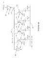
- FIG. 2shows a cross-sectional view and a schematic representation of a memory cell in the memory cell array shown in FIG. 1 in accordance with an embodiment of the present disclosure.
- FIG. 3shows a cross-sectional view and a schematic representation of at least a portion of the memory cell array having the plurality of memory cells in accordance with an embodiment of the present disclosure.
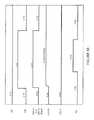
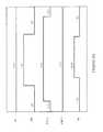
- FIGS. 4A and 4Bshow a schematic representation and control signal voltage waveforms for performing a hold operation on a memory cell in accordance with an embodiment of the present disclosure.
- FIGS. 5A and 5Bshow a schematic representation and control signal voltage waveforms for performing a read operation on a memory cell in accordance with an embodiment of the present disclosure.
- FIGS. 6A and 6Bshow a schematic representation and control signal voltage waveforms for performing a read operation on a memory cell in accordance with an alternative embodiment of the present disclosure.
- FIGS. 7A and 7Bshow a schematic representation and control signal voltage waveforms for performing a write logic high (e.g., binary “1” data state) operation on a memory cell in accordance with an embodiment of the present disclosure.
- a write logic highe.g., binary “1” data state
- FIGS. 8A and 8Bshow a schematic representation and control signal voltage waveforms for performing a write logic high (e.g., binary “1” data state) operation on a memory cell in accordance with an alternative embodiment of the present disclosure.
- a write logic highe.g., binary “1” data state
- FIGS. 9A and 9Bshow a schematic representation and control signal voltage waveforms for performing a write logic low (e.g., binary “0” data state) operation on a memory cell in accordance with an embodiment of the present disclosure.
- a write logic lowe.g., binary “0” data state
- FIGS. 10A and 10Bshow a schematic representation and control signal voltage waveforms for performing a write logic low (e.g., binary “0” data state) operation on a memory cell in accordance with an alternative embodiment of the present disclosure.
- a write logic lowe.g., binary “0” data state
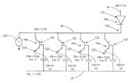
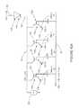
- FIG. 1there is shown a block diagram of a semiconductor memory device 10 comprising a memory cell array 20 , data write and sense circuitry 36 , and memory cell selection and control circuitry 38 in accordance with an embodiment of the present disclosure.
- the memory cell array 20may comprise a plurality of memory cells 12 each coupled to the memory cell selection and control circuitry 38 via a word line (WL) 28 , a source line (CN) 30 , and a carrier injection line (EP) 34 , and to the data write and sense circuitry 36 via a bit line (EN) 32 .
- WLword line
- CNsource line
- EPcarrier injection line
- ENbit line
- the source line (CN) 30 and the bit line (EN) 32are designations used to distinguish between two signal lines and they may be used interchangeably.
- the data write and sense circuitry 36may read data from and may write data to selected memory cells 12 .
- the data write and sense circuitry 36may include a plurality of data sense amplifiers. Each data sense amplifier may receive at least one bit line (EN) 32 and a current or voltage reference signal.
- each data sense amplifiermay be a cross-coupled type sense amplifier to sense a data state stored in a memory cell 12 .
- Each data sense amplifiermay employ voltage and/or current sensing circuitry and/or techniques.
- each data sense amplifiermay employ current sensing circuitry and/or techniques. For example, a current sense amplifier may compare current from a selected memory cell 12 to a reference current (e.g., the current of one or more reference cells). From that comparison, it may be determined whether the selected memory cell 12 stores a logic high (e.g., binary “1” data state) or a logic low (e.g., binary “0” data state).
- a logic highe.g., binary “1” data state
- a logic lowe.g., binary “0” data state
- data write and sense circuitry 36may be employed to read data stored in memory cells 12 and/or write data to memory cells 12 .
- the memory cell selection and control circuitry 38may select and/or enable one or more predetermined memory cells 12 to facilitate reading data therefrom and/or writing data thereto by applying control signals on one or more word lines (WL) 28 , source lines (CN) 30 , and/or carrier injection lines (EP) 34 .
- the memory cell selection and control circuitry 38may generate such control signals from address signals, for example, row address signals.
- the memory cell selection and control circuitry 38may include a word line decoder and/or driver.
- the memory cell selection and control circuitry 38may include one or more different control/selection techniques (and circuitry therefor) to select and/or enable one or more predetermined memory cells 12 . Notably, all such control/selection techniques, and circuitry therefor, whether now known or later developed, are intended to fall within the scope of the present disclosure.
- the semiconductor memory device 10may implement a two step write operation whereby all the memory cells 12 in a row of memory cells 12 may be written to a predetermined data state by first executing a “clear” or a logic low (e.g., binary “0” data state) write operation, whereby all of the memory cells 12 in the row of memory cells 12 are written to logic low (e.g., binary “0” data state). Thereafter, selected memory cells 12 in the row of memory cells 12 may be selectively written to the predetermined data state (e.g., a logic high (binary “1” data state)).
- a logic lowe.g., binary “0” data state
- the semiconductor memory device 10may also implement a one step write operation whereby selective memory cells 12 in a row of memory cells 12 may be selectively written to either a logic high (e.g., binary “1” data state) or a logic low (e.g., binary “0” data state) without first implementing a “clear” operation.
- the semiconductor memory device 10may employ any of the exemplary writing, preparation, holding, refresh, and/or reading techniques described herein.
- the memory cells 12may comprise N-type, P-type and/or both types of transistors. Circuitry that is peripheral to the memory array 20 (for example, sense amplifiers or comparators, row and column address decoders, as well as line drivers (not illustrated herein)) may also include P-type and/or N-type transistors. Regardless of whether P-type or N-type transistors are employed in memory cells 12 in the memory cell array 20 , suitable voltage potentials (for example, positive or negative voltage potentials) for reading from and/or writing to the memory cells 12 will be described further herein.
- suitable voltage potentialsfor example, positive or negative voltage potentials
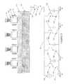
- Each memory cell 12may comprise a bipolar transistor 14 a and a diode 14 b .
- the bipolar transistor 14 amay be a NPN bipolar transistor or a PNP bipolar transistor and the diode 14 b may be a PN junction diode.
- the bipolar transistor 14 a and the diode 14 bmay share one or more common regions.
- the NPN bipolar transistor 14 amay comprise an N+ emitter region 120 , a P ⁇ base region 122 , and an N+ collector region 124 .
- the diode 14 bmay comprise the N+ region 124 and a P+ region 126 .
- the N+ region 120 , the P ⁇ region 122 , the N+ region 124 , and/or the P+ region 126may be disposed in sequential contiguous relationship within a pillar or fin configuration that may extend vertically from and/or perpendicularly to a plane defined by the P+ region 126 .
- the P ⁇ region 122may be an electrically floating body region of the memory cell 12 configured to accumulate/store charges, and may be spaced apart from and capacitively coupled to the word line (WL) 28 .
- the N+ emitter region 120 of the bipolar transistor 14 amay be coupled to a corresponding bit line (EN) 32 .
- the N+ emitter region 120 of the bipolar transistor 14 amay be formed of a semiconductor material (e.g., silicon) comprising donor impurities.
- the N+ emitter region 120may be formed of a silicon material doped with phosphorous or arsenic impurities.
- the bit line (EN) 32may be formed of a metal layer.
- the bit line (EN) 32may be formed of a polycide layer (e.g., a combination of a metal material and a silicon material).
- the bit line (EN) 32may provide means for accessing one or more selected memory cells 12 on a selected row of the memory cell array 20 .
- the P ⁇ base region 122 of the bipolar transistor 14 amay be capacitively coupled to a corresponding word line (WL) 28 .
- the P ⁇ region 122may be formed of a semiconductor material (e.g., silicon) comprising acceptor impurities.
- the P ⁇ region 122may be formed of a silicon material doped with boron impurities.
- the P ⁇ region 122 and the word line (WL) 28may be capacitively coupled via an insulating or dielectric material.
- the word line (WL) 28may be formed of a polycide layer or a metal layer extending in a row direction of the memory cell array 20 .
- the N+ region 124 of the memory cell 12may be coupled to a source line (CN) 30 .
- the N+ region 124may be formed of a semiconductor material (e.g., silicon) comprising donor impurities.
- the N+ region 124may be formed of a silicon material doped with phosphorous or arsenic impurities.
- the source line (CN) 30may be formed of a polycide layer.
- the source line (CN) 30may be formed of a metal layer. The source line (CN) 30 may reduce a disturbance in the memory cell 12 .
- the source line (CN) 30may be formed of a metal layer and therefore may reduce a hole disturbance in the memory cell 12 .
- the source line (CN) 30may extend horizontally in a row direction of the memory cell array 20 , parallel to the word line (WL) 28 and/or the carrier injection line (EP) 34 , and may be coupled to a plurality of memory cells 12 (e.g., a row of memory cells 12 ).
- the source line (CN) 30 , the word line (WL) 28 , and/or the carrier injection line (EP) 34may be arranged in different planes and configured to be parallel to each other.
- the source line (CN) 30may be arranged in a plane between a plane containing the word line (WL) 28 and a plane containing the carrier injection line (EP) 34 .
- the P+ region 126 of the diode 14 bmay be coupled to the carrier injection line (EP) 34 .
- the P+ region 126may be formed of a semiconductor material (e.g., silicon) comprising acceptor impurities.
- the P+ region 126may be formed of a silicon material doped with boron impurities.
- a plurality of P+ regions 126may form a base of the memory cell array 20 or a single P+ region 126 may form the base of the memory cell array 20 .
- the P+126may be made in the form of a P-well of a bulk substrate of the memory cell array 20 .
- the P+ region 126may be configured as an input region for charges to be stored in the P ⁇ region 122 of the memory cell 12 .
- the charges to be stored in the P ⁇ region 122 of the memory cell 12may be supplied by the carrier injection line (EP) 34 and input into the P ⁇ region 122 via the P+ region 126 and the N+ region 124 .
- EPcarrier injection line
- the carrier injection line (EP) 34may be formed of a polycide layer or a metal layer extending in a row direction of the memory cell array 20 .
- the carrier injection line (EP) 34may extend horizontally in parallel to the word line (WL) 28 and/or the source line (CN) 30 , and may be coupled to a plurality of memory cells 12 (e.g., a row of memory cells 12 ).
- the carrier injection line (EP) 34 and the word line (WL) 28 and/or the source line (CN) 30may be arranged in different planes and configured to be parallel to each other.
- the carrier injection line (EP) 34may be arranged in a plane below a plane containing the word line (WL) 28 and a plane containing the source line (CN) 30 .
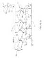
- each of the memory cells 12may comprise a bipolar transistor 14 a and a PN junction diode 14 b coupled to each other.
- the bipolar transistor 14 amay be an NPN bipolar transistor or an PNP bipolar transistor.
- the bipolar transistor 14 amay be an NPN bipolar transistor and may share a common region (e.g., N-region) with the PN junction diode 14 b .
- the memory transistor 14 amay be an PNP bipolar transistor and may share a common region (e.g., P-region) with the PN junction diode 14 b.
- Each memory cell 12may be coupled to a respective word line (WL) 28 , a respective source line (CN) 30 , a respective bit line (EN) 32 , and a respective carrier injection line (EP) 34 .
- Datamay be written to or read from a selected memory cell 12 by applying suitable control signals to a selected word line (WL) 28 , a selected source line (CN) 30 , a selected bit line (EN) 32 , and/or a selected carrier injection line (EP) 34 .
- each word line (WL) 28 , source line (CN) 30 , and carrier injection line (EP) 34may extend horizontally parallel to each other in a row direction.
- Each bit line (EN) 32may extend vertically in a column direction perpendicular to each word line (WL) 28 , source line (CN) 30 , and/or carrier injection line (EP) 34 .
- one or more respective bit lines (EN) 32may be coupled to one or more data sense amplifiers (not shown) of the data write and sense circuitry 36 to read data states of one or more memory cells 12 in the column direction.
- a data statemay be read from one or more selected memory cells 12 by applying one or more control signals to the one or more selected memory cells 12 via a selected word line (WL) 28 , a selected source line (CN) 30 , and/or a selected carrier injection line (EP) 34 in order to generate a voltage potential and/or a current in the one or more selected memory cells 12 .
- the generated voltage potential and/or currentmay be output to the data write and sense circuitry 36 via a corresponding bit line (EN) 32 in order to read a data state stored in each selected memory cell 12 .
- bit line (EN) 32may be coupled to the data sense amplifier of the data write and sense circuitry 36 .
- the data write and sense circuitry 36may be configured on opposite sides of the memory cell array 20 .
- a data statemay be written to one or more selected memory cells 12 by applying one or more control signals to the one or more selected memory cells 12 via a selected word line (WL) 28 , a selected source line (CN) 30 , a selected bit line (EN) 32 , and/or a selected carrier injection line (EP) 34 .
- the one or more control signals applied to the one or more selected memory cells 12 via a selected word line (WL) 28 , a selected source line (CN) 30 , a selected bit line (EN) 32 , and/or a selected carrier injection line (EP) 34may control the bipolar transistor 14 a and/or the diode 14 b of each selected memory cell 12 in order to write a desired data state to each selected memory cell 12 .
- the source line (CN) 30may be subcircuits 302 of the memory cell selection and control circuitry 38 (e.g., driver, inverter, and/or logic circuits).
- the carrier injection lines (EP) 34may be driven by subcircuits of the memory cell selection and control circuitry 38 (e.g., driver, inverter, and/or logic circuits).
- the subcircuits coupled to each carrier injection line (EP) 34may be independent voltage drivers located within and/or integrated with the memory cell selection and control circuitry 38 .
- a plurality of carrier injection lines (EP) 34 of the memory cell array 20may be coupled to a single subcircuit within the memory cell selection and control circuitry 38 .
- the subcircuits of the memory cell selection and control circuitry 38may bias a plurality of carrier injection lines (EP) 34 coupled together to different voltage potentials and/or current levels (e.g., 0V, 1.0V, etc).
- the memory cell 12e.g., corresponding to bit line EN ⁇ 0>32 located near the subcircuits (e.g., drivers) within the memory cell selection and control circuitry 38 may be activated before the memory cells 12 (e.g., correspond to bit lines EN ⁇ 1>, EN ⁇ 2>, and EN ⁇ 3>) located farther from the subcircuits (e.g., drivers) within the memory cell selection and control circuitry 38 .
- the memory cell 12located near the subcircuits (e.g., drivers) within the memory cell selection and control circuitry 38 may impact a voltage potential and/or current applied to the source line (CN) 30 .
- control signalsare applied to the memory cell 12 (e.g., corresponding to bit line EN ⁇ 0> 32 ) located near the subcircuits (e.g., drivers) within the memory cell selection and control circuitry 38 , thereby turning the bipolar transistor 14 a of the memory cell 12 to an “ON” state
- the actions performed by the bipolar transistor 14 a of the memory cell 12may impact a voltage potential and/or current applied to the source line (CN) 30 (e.g., raise or lower the voltage potential).
- the memory cell 12located near the subcircuits (e.g., drivers) within the memory cell selection and control circuitry 38 may impact an operation performed by the memory cells 12 located farther from the subcircuits (e.g., drivers) within the memory cell selection and control circuitry 38 .
- control signalsmay be configured to perform a hold operation in order to maintain a data state (e.g., a logic high (binary “1” data state) or a logic low (binary “0” data state)) stored in the memory cell 12 .
- the control signalsmay be configured to perform a hold operation in order to maximize a retention time of a data state (e.g., a logic low (binary “0” data state) and/or a logic high (binary “1” data state)) stored in the memory cell 12 .
- the control signals for the hold operationmay be configured to eliminate or reduce activities or fields (e.g., electrical fields between junctions which may lead to leakage of charges) within the memory cell 12 .
- a negative voltage potentialmay be applied to the word line (WL) 28 that may be capacitively coupled to the P ⁇ region 122 of the memory cell 12 , while a voltage potential applied to the N+ region 120 may be maintained at approximately 0V.
- the voltage potential applied to the N+ region 124may be the same as the voltage potential applied to the P+ region 126 .
- the negative voltage potential applied to the word line (WL) 28e.g., capacitively coupled to the P ⁇ region 122 of the memory cell 12
- the voltage potentials applied to the N+ region 124 and the P+ region 126may range between 0.7V to 1.0V.
- the junction between the N+ region 124 and the P ⁇ region 122 and the junction between the N+ region 120 and the P ⁇ region 122may be reverse biased in order to retain a data state (e.g., a logic high (binary “1” data state) or a logic low (binary “0” data state)) stored in the memory cell 12 .
- a data statee.g., a logic high (binary “1” data state) or a logic low (binary “0” data state) stored in the memory cell 12 .
- a read operationmay involve control signals that are configured to read a data state (e.g., a logic low (binary “0” data state) and/or a logic high (binary “1” data state)) stored in one or more selected memory cells 12 of one or more selected rows of the memory cell array 20 .
- the control signalsmay be configured to predetermined voltage potentials to implement a read operation via the bit line (EN) 32 .
- a voltage potential applied to the word line (WL) 28may be raised to predetermined voltage potentials in order to read a data state stored in each respective memory cell 12 .
- the voltage potential applied to the word line (WL) 28e.g., capacitively coupled to the P ⁇ region 122 of the memory cell 12
- the voltage potential applied to the N+ region 124 of the memory cell 12 via the source line (CN) 30may be raised to 1.1V from 0.7V.
- the voltage potential applied to the carrier injection line (EP) 34may be maintained at 0.7V.
- the voltage potential applied to the word line (WL) 28(e.g., capacitively coupled to the P ⁇ region 122 of the memory cell 12 ) may be raised to ⁇ 0.5V and the voltage potential applied to the source line (CN) 30 may be raised to 1.1V. Under such biasing, the junction between the P ⁇ region 122 and the N+ region 120 may become forward biased.
- the junction between the P ⁇ region 122 and the N+ region 124may be reverse biased or become weakly forward biased (e.g., above a reverse bias voltage and below a forward bias threshold voltage, or a voltage potential at a p-diffusion region in the P ⁇ region 122 may be higher than a voltage potential at an n-diffusion region in the N+ region 124 ).
- a voltage potential or currentmay be generated when forward biasing the junction between the P ⁇ region 122 and the N+ region 120 .
- the voltage potential or current generatedmay be output to a data sense amplifier via the bit line (EN) 32 coupled to the N+ region 120 .
- An amount of voltage potential or current generatedmay be representative of a data state (e.g., a logic low (binary “0” data state) and/or a logic high (binary “1” data state)) stored in the memory cell 12 .
- the junction between the P ⁇ region 122 and the N+ region 120may remain reverse biased or become weakly forward biased (e.g., above a reverse bias voltage and below a forward bias threshold voltage, or a voltage potential at a p-diffusion region in the P ⁇ region 122 may be higher than a voltage potential at an n-diffusion region in the N+ region 124 ).
- a small amount of voltage potential or current or no voltage potential or currentmay be generated when the junction between the P ⁇ region 122 and the N+ region 120 is reverse biased or weakly forward biased.
- a data sense amplifier in the data write and sense circuitry 36may detect the small amount of voltage potential or current or no voltage potential or current via the bit line (EN ⁇ 1>) 32 coupled to the N+ region 120 .
- a logic highe.g., binary “1” data state
- the junction between the P ⁇ region 122 and the N+ region 120may be forward biased.
- a larger amount of voltage potential or currente.g., compared to a reference voltage potential or current
- a data sense amplifier in the data write and sense circuitry 36may detect the larger amount of voltage potential or current via the bit line (EN ⁇ 0>) 32 coupled to the N+ region 120 .
- voltage potentialsmay be applied to every memory cell 12 along an active row via a corresponding word line (WL) 28 , a corresponding source line (CN) 30 , and/or a corresponding carrier injection line (EP) 34 .
- WLword line
- CNsource line
- EPcarrier injection line
- one or more unselected memory cells 12may experience a disturbance caused by the voltage potentials applied via the corresponding word line (WL) 28 , the corresponding source line (CN) 30 , and/or the corresponding carrier injection line (EP) 34 during the active operations.
- a masking operationmay be performed on the one or more unselected memory cells 12 .
- a voltage potentialmay be applied to the one or more unselected memory cells 12 on an active row via corresponding bit lines (EN ⁇ 2>) and (EN ⁇ 3>) 32 .
- the voltage potential applied via the corresponding bit lines (EN ⁇ 2>) and (EN ⁇ 3>) 32 to the one or more unselected memory cells 12 on the active rowmay be raised to a predetermined voltage potential.
- the voltage potential applied to the corresponding bit lines (EN ⁇ 2>) and (EN ⁇ 3>) 32 associated with the one or more unselected memory cells 12 along the active rowmay be 1.1V in order to reduce a disturbance caused by the other voltage potentials applied during the active operations.
- a read operationmay involve control signals that are configured to read a data state (e.g., a logic low (binary “0” data state) and/or a logic high (binary “1” data state)) stored in one or more selected memory cells 12 of one or more selected rows of the memory cell array 20 .
- the control signalsmay be configured to predetermined voltage potentials to implement a read operation via the bit line (EN) 32 .
- a voltage potential applied to the word line (WL) 28may be raised to a predetermined voltage potential.
- a voltage potential applied to the N+ region 124 via the source line (CN) 30may be maintained at a predetermined voltage potential in order to read a data state stored in the memory cell 12 .
- the voltage potential applied to the word line (WL) 28e.g., capacitively coupled to the P ⁇ region 122 of the memory cell 12
- the voltage potential applied to the N+ region 124 of the memory cell 12 via the source line (CN) 30may be maintained at 1.1V.
- the voltage potential applied to the carrier injection line (EP) 34may be maintained at 1.0V.
- the junction between the P ⁇ region 122 and the N+ region 120may become forward biased.
- the junction between the P ⁇ region 122 and the N+ region 124may be reverse biased or become weakly forward biased (e.g., above a reverse bias voltage and below a forward bias threshold voltage, or a voltage potential at a p-diffusion region in the P ⁇ region 122 may be higher than a voltage potential at an n-diffusion region in the N+ region 124 ).
- a voltage potential or currentmay be generated when forward biasing the junction between the P ⁇ region 122 and the N+ region 120 .
- the voltage potential or current generatedmay be output to a data sense amplifier via the bit line (EN) 32 coupled to the N+ region 120 .
- An amount of voltage potential or current generatedmay be representative of a data state (e.g., a logic low (binary “0” data state) and/or a logic high (binary “1” data state)) stored in the memory cell 12 .
- the junction between the P ⁇ region 122 and the N+ region 120may remain reverse biased or become weakly forward biased (e.g., above a reverse bias voltage and below a forward bias threshold voltage, or a voltage potential at a p-diffusion region in the P ⁇ region 122 may be higher than a voltage potential at an n-diffusion region in the N+ region 124 ).
- a small amount of voltage potential or current or no voltage potential or currentmay be generated when the junction between the P ⁇ region 122 and the N+ region 120 is reverse biased or weakly forward biased.
- a data sense amplifier in the data write and sense circuitry 36may detect the small amount of voltage potential or current or no voltage potential or current via the bit line (EN ⁇ 1>) 32 coupled to the N+ region 120 .
- a logic highe.g., binary “1” data state
- the junction between the P ⁇ region 122 and the N+ region 120may be forward biased.
- a larger amount of voltage potential or currente.g., compared to a reference voltage potential or current
- a data sense amplifier in the data write and sense circuitry 36may detect the larger amount of voltage potential or current via the bit line (EN ⁇ 0>) 32 coupled to the N+ region 120 .
- voltage potentialsmay be applied to every memory cell 12 along an active row via a corresponding word line (WL) 28 , a corresponding source line (CN) 30 , and/or a corresponding carrier injection line (EP) 34 .
- WLword line
- CNsource line
- EPcarrier injection line
- one or more unselected memory cells 12may experience a disturbance caused by the voltage potentials applied via the corresponding word line (WL) 28 , the corresponding source line (CN) 30 , and/or the corresponding carrier injection line (EP) 34 during the active operations.
- a masking operationmay be performed on the one or more unselected memory cells 12 .
- a voltage potentialmay be applied to the one or more unselected memory cells 12 on an active row via corresponding bit lines (EN ⁇ 2>) and (EN ⁇ 3>) 32 .
- the voltage potential applied via the corresponding bit lines (EN ⁇ 2>) and (EN ⁇ 3>) 32 to the one or more unselected memory cells 12 on the active rowmay be raised to a predetermined voltage potential.
- the voltage potential applied to the corresponding bit lines (EN ⁇ 2>) and (EN ⁇ 3>) 32 associated with the one or more unselected memory cells 12 along the active rowmay be 1.1V in order to reduce a disturbance caused by the other voltage potentials applied during the active operations.
- the write logic high (e.g., binary “1” data state) operationmay involve control signals that are configured to perform a write logic high (e.g., binary “1” data state) operation to one or more selected memory cells 12 of one or more selected rows of the memory cell array 20 .
- the write logic high (e.g., binary “1” data state) operationmay be performed on one or more selected rows of the memory cell array 20 or the entire memory cell array 20 .
- a voltage potential applied to the N+ region 120 of a selected memory cell 12 via a corresponding bit line (EN) 32may be maintained at 0V
- a voltage potential applied to the P+ region 126 of the selected memory cell 12 via a corresponding carrier injection line (EP) 34may be maintained at 0.7V
- a voltage potential applied to the word line (WL) 28e.g., capacitively coupled to the P ⁇ region 122
- a voltage potential applied to the source line (CN) 30may be lowered to 0V from 0.7V.
- the junction between the N+ region 120 and the P ⁇ region 122may be reverse biased and the junction between the P+ region 126 and the N+ region 124 may become forward biased.
- a logic high(e.g., binary “1” data state) may be written to the P ⁇ region 122 (e.g., majority charge carriers injected into the P ⁇ region 122 from the P+ region 126 via the N+ region 124 ) via the forward biased junction between the P+ region 126 and the N+ region 124 .
- the voltage potential at the P ⁇ region 122may increase to approximately 0.7V to 1.0V above the voltage potential at the N+ region 124 .
- a sufficient amount of majority charge carriersmay be injected into the P ⁇ region 122 to represent that a logic high (e.g., binary “1” data state) is stored in the memory cell 12 .
- the write logic high (e.g., binary “1” data state) operationmay involve control signals that are configured to perform a write logic high (e.g., binary “1” data state) operation on one or more selected memory cells 12 of one or more selected rows of the memory cell array 20 .
- the write logic high (e.g., binary “1” data state) operationmay be performed on one or more selected rows of the memory cell array 20 or the entire memory cell array 20 .
- a voltage potential applied to the N+ region 120 of a selected memory cell 12 via a corresponding bit line (EN) 32may be maintained at 0V
- a voltage potential applied to the P+ region 126 of the selected memory cell 12 via a corresponding carrier injection line (EP) 34may be maintained at 1.0V
- a voltage potential applied to the word line (WL) 28e.g., capacitively coupled to the P ⁇ region 122
- a voltage potential applied to the source line (CN) 30may be lowered to 0.3V from 1.0V.
- the junction between the N+ region 120 and the P ⁇ region 122may be reverse biased and the junction between the P+ region 126 and the N+ region 124 may become forward biased.
- a logic high(e.g., binary “1” data state) may be written to the P ⁇ region 122 (e.g., majority charge carriers injected into the P ⁇ region 122 from the P+ region 126 via the N+ region 124 ) via the forward biased junction between the P+ region 126 and the N+ region 124 .
- the voltage potential at the P ⁇ region 122may increase to approximately 0.7V to 1.0V above the voltage potential at the N+ region 124 .
- a sufficient amount of majority charge carriersmay be injected into the P ⁇ region 122 to represent that a logic high (e.g., binary “1” data state) is stored in the memory cell 12 .
- a write logic low (e.g., binary “0” data state) operationmay involve control signals that are configured to perform one or more write operations on one or more selected memory cells 12 .
- the write logic low (e.g., binary “0” data state) operationmay be performed on one or more selected memory cells 12 after a write logic high (e.g., binary “1” data state) operation in order to deplete majority charge carriers that may have accumulated in the P ⁇ regions 122 of the one or more selected memory cells 12 .
- a write logic highe.g., binary “1” data state
- a voltage potential applied to the N+ region 120 via the bit line (EN(“0”)) 32may be maintained at 0V in order to perform the write logic low (e.g., binary “0” data state) operation.
- a voltage potential applied to the N+ region 124 via the source line (CN) 30may be raised to 1.1V from 0V in order to perform a write logic low (e.g., binary “0” data state) operation.
- a voltage potential applied to the word line (WL) 28may be raised to approximately 0.5V from ⁇ 1.0V.
- the junction between the N+ region 120 and the P ⁇ region 122may become forward biased.
- the junction between the N+ region 124 and the P ⁇ region 122may become reverse biased or become weakly forward biased (e.g., above a reverse bias voltage and below a forward bias threshold voltage, or a voltage potential at a p-diffusion region in the P ⁇ region 122 may be higher than a voltage potential at an n-diffusion region in the N+ region 124 ).
- Majority charge carriers that may have accumulated in the P ⁇ region 122 during a write logic high (e.g., binary “1” data state) operationmay be removed via the forward biased junction between the N+ region 120 and the P ⁇ region 122 .
- a logic lowe.g., binary “0” data state
- a masking operationmay be performed on the one or more unselected memory cells 12 .
- a voltage potential applied to the N+ region 120 via a bit line (EN(“1”)) 32 of the one or more unselected memory cells 12may be raised to 1.1V from 0.7V or higher (e.g., 1.2V) in order to prevent the depletion of majority charge carriers accumulated in the P ⁇ region 122 .
- the junction between the N+ region 120 and the P ⁇ region 122may not be forward biased and the junction between the P ⁇ region 122 and the N+ region 124 may not be forward biased in order to prevent the depletion of majority charge carriers accumulated in the P ⁇ region 122 so as to allow the logic high (e.g., binary “1” data state) to be maintained in the memory cell 12 .
- the logic highe.g., binary “1” data state
- a write logic low (e.g., binary “0” data state) operationmay involve control signals that are configured to perform one or more write operations on one or more selected memory cells 12 .
- the write logic low (e.g., binary “0” data state) operationmay be performed on one or more selected memory cells 12 after a write logic high (e.g., binary “1” data state) operation in order to deplete majority charge carriers that may have accumulated in the P ⁇ regions 122 of the one or more selected memory cells 12 .
- a write logic highe.g., binary “1” data state
- a voltage potential applied to the N+ region 120 via the bit line (EN(“0”)) 32may be maintained at 0V in order to perform the write logic low (e.g., binary “0” data state) operation.
- a voltage potential applied to the N+ region 124 via the source line (CN) 30may be maintained at 1.0V in order to perform a write logic low (e.g., binary “0” data state) operation.
- a voltage potential applied to the P+ region 126 via the carrier injection line (EP) 34may be maintained at 1.0V.
- a voltage potential applied to the word line (WL) 28may be raised to approximately 0.5V from ⁇ 1.0V.
- the junction between the N+ region 120 and the P ⁇ region 122may become forward biased.
- the junction between the N+ region 124 and the P ⁇ region 122may become reverse biased or become weakly forward biased (e.g., above a reverse bias voltage and below a forward bias threshold voltage, or a voltage potential at a p-diffusion region in the P ⁇ region 122 may be higher than a voltage potential at an n-diffusion region in the N+ region 124 ).
- Majority charge carriers that may have accumulated in the P ⁇ region 122 during a write logic high (e.g., binary “1” data state) operationmay be removed via the forward biased junction between the N+ region 120 and the P ⁇ region 122 .
- a logic lowe.g., binary “0” data state
- a masking operationmay be performed on the one or more unselected memory cells 12 .
- a voltage potential applied to the N+ region 120 via a bit line (EN(“1”)) 32 of the one or more unselected memory cells 12may be raised to 1.0V from 0V or higher (e.g., 1.2V) in order to prevent the depletion of majority charge carriers accumulated in the P ⁇ region 122 .
- the junction between the N+ region 120 and the P ⁇ region 122may not be forward biased and the junction between the P ⁇ region 122 and the N+ region 124 may not be forward biased in order to prevent the depletion of majority charge carriers accumulated in the P ⁇ region 122 so as to allow the logic high (e.g., binary “1” data state) to be maintained in the memory cell 12 .
- the logic highe.g., binary “1” data state
- providing a direct injection semiconductor memory device in accordance with the present disclosure as described abovetypically involves the processing of input data and the generation of output data to some extent.
- This input data processing and output data generationmay be implemented in hardware or software.
- specific electronic componentsmay be employed in a direct injection semiconductor memory device or similar or related circuitry for implementing the functions associated with providing a direct injection semiconductor memory device in accordance with the present disclosure as described above.
- one or more processors operating in accordance with instructionsmay implement the functions associated with providing a direct injection semiconductor memory device in accordance with the present disclosure as described above.
- Such instructionsmay be stored on one or more processor readable media (e.g., a magnetic disk or other storage medium), or transmitted to one or more processors via one or more signals embodied in one or more carrier waves.
- processor readable mediae.g., a magnetic disk or other storage medium
Landscapes
- Engineering & Computer Science (AREA)
- Microelectronics & Electronic Packaging (AREA)
- Computer Hardware Design (AREA)
- Semiconductor Memories (AREA)
Abstract
Description
Claims (20)
Priority Applications (1)
| Application Number | Priority Date | Filing Date | Title |
|---|---|---|---|
| US14/503,784US9425190B2 (en) | 2009-04-27 | 2014-10-01 | Techniques for providing a direct injection semiconductor memory device |
Applications Claiming Priority (4)
| Application Number | Priority Date | Filing Date | Title |
|---|---|---|---|
| US17301409P | 2009-04-27 | 2009-04-27 | |
| US12/768,322US8508970B2 (en) | 2009-04-27 | 2010-04-27 | Techniques for providing a direct injection semiconductor memory device |
| US13/964,927US8861247B2 (en) | 2009-04-27 | 2013-08-12 | Techniques for providing a direct injection semiconductor memory device |
| US14/503,784US9425190B2 (en) | 2009-04-27 | 2014-10-01 | Techniques for providing a direct injection semiconductor memory device |
Related Parent Applications (1)
| Application Number | Title | Priority Date | Filing Date |
|---|---|---|---|
| US13/964,927ContinuationUS8861247B2 (en) | 2009-04-27 | 2013-08-12 | Techniques for providing a direct injection semiconductor memory device |
Publications (2)
| Publication Number | Publication Date |
|---|---|
| US20150054133A1 US20150054133A1 (en) | 2015-02-26 |
| US9425190B2true US9425190B2 (en) | 2016-08-23 |
Family
ID=42991980
Family Applications (6)
| Application Number | Title | Priority Date | Filing Date |
|---|---|---|---|
| US12/725,057Expired - Fee RelatedUS8139418B2 (en) | 2009-04-27 | 2010-03-16 | Techniques for controlling a direct injection semiconductor memory device |
| US12/768,363Active2030-11-12US8400811B2 (en) | 2009-04-27 | 2010-04-27 | Techniques for providing a direct injection semiconductor memory device having ganged carrier injection lines |
| US12/768,322Expired - Fee RelatedUS8508970B2 (en) | 2009-04-27 | 2010-04-27 | Techniques for providing a direct injection semiconductor memory device |
| US13/425,325ActiveUS8351266B2 (en) | 2009-04-27 | 2012-03-20 | Techniques for controlling a direct injection semiconductor memory device |
| US13/964,927ActiveUS8861247B2 (en) | 2009-04-27 | 2013-08-12 | Techniques for providing a direct injection semiconductor memory device |
| US14/503,784Expired - Fee RelatedUS9425190B2 (en) | 2009-04-27 | 2014-10-01 | Techniques for providing a direct injection semiconductor memory device |
Family Applications Before (5)
| Application Number | Title | Priority Date | Filing Date |
|---|---|---|---|
| US12/725,057Expired - Fee RelatedUS8139418B2 (en) | 2009-04-27 | 2010-03-16 | Techniques for controlling a direct injection semiconductor memory device |
| US12/768,363Active2030-11-12US8400811B2 (en) | 2009-04-27 | 2010-04-27 | Techniques for providing a direct injection semiconductor memory device having ganged carrier injection lines |
| US12/768,322Expired - Fee RelatedUS8508970B2 (en) | 2009-04-27 | 2010-04-27 | Techniques for providing a direct injection semiconductor memory device |
| US13/425,325ActiveUS8351266B2 (en) | 2009-04-27 | 2012-03-20 | Techniques for controlling a direct injection semiconductor memory device |
| US13/964,927ActiveUS8861247B2 (en) | 2009-04-27 | 2013-08-12 | Techniques for providing a direct injection semiconductor memory device |
Country Status (1)
| Country | Link |
|---|---|
| US (6) | US8139418B2 (en) |
Families Citing this family (39)
| Publication number | Priority date | Publication date | Assignee | Title |
|---|---|---|---|---|
| US8139418B2 (en) | 2009-04-27 | 2012-03-20 | Micron Technology, Inc. | Techniques for controlling a direct injection semiconductor memory device |
| US8537610B2 (en)* | 2009-07-10 | 2013-09-17 | Micron Technology, Inc. | Techniques for providing a semiconductor memory device |
| US9076543B2 (en) | 2009-07-27 | 2015-07-07 | Micron Technology, Inc. | Techniques for providing a direct injection semiconductor memory device |
| US8411524B2 (en)* | 2010-05-06 | 2013-04-02 | Micron Technology, Inc. | Techniques for refreshing a semiconductor memory device |
| JP2012234940A (en)* | 2011-04-28 | 2012-11-29 | Elpida Memory Inc | Semiconductor device |
| US9559216B2 (en)* | 2011-06-06 | 2017-01-31 | Micron Technology, Inc. | Semiconductor memory device and method for biasing same |
| JP2014022548A (en)* | 2012-07-18 | 2014-02-03 | Ps4 Luxco S A R L | Semiconductor device and manufacturing method of the same |
| KR102191215B1 (en) | 2013-12-20 | 2020-12-16 | 삼성전자주식회사 | Static random access memory (sram) cell and method of manufacturing the same |
| US9653563B2 (en)* | 2014-04-18 | 2017-05-16 | Taiwan Semiconductor Manufacturing Company Limited | Connection structure for vertical gate all around (VGAA) devices on semiconductor on insulator (SOI) substrate |
| US10121553B2 (en) | 2015-09-30 | 2018-11-06 | Sunrise Memory Corporation | Capacitive-coupled non-volatile thin-film transistor NOR strings in three-dimensional arrays |
| US9892800B2 (en) | 2015-09-30 | 2018-02-13 | Sunrise Memory Corporation | Multi-gate NOR flash thin-film transistor strings arranged in stacked horizontal active strips with vertical control gates |
| US11120884B2 (en) | 2015-09-30 | 2021-09-14 | Sunrise Memory Corporation | Implementing logic function and generating analog signals using NOR memory strings |
| US9842651B2 (en) | 2015-11-25 | 2017-12-12 | Sunrise Memory Corporation | Three-dimensional vertical NOR flash thin film transistor strings |
| US9768231B2 (en)* | 2016-02-12 | 2017-09-19 | Globalfoundries Singapore Pte. Ltd. | High density multi-time programmable resistive memory devices and method of forming thereof |
| KR102719982B1 (en) | 2017-06-20 | 2024-10-22 | 선라이즈 메모리 코포레이션 | 3D NOR memory array architecture and its manufacturing method |
| US10608008B2 (en) | 2017-06-20 | 2020-03-31 | Sunrise Memory Corporation | 3-dimensional nor strings with segmented shared source regions |
| US10692874B2 (en) | 2017-06-20 | 2020-06-23 | Sunrise Memory Corporation | 3-dimensional NOR string arrays in segmented stacks |
| WO2019133534A1 (en) | 2017-12-28 | 2019-07-04 | Sunrise Memory Corporation | 3-dimensional nor memory array with very fine pitch: device and method |
| US10475812B2 (en) | 2018-02-02 | 2019-11-12 | Sunrise Memory Corporation | Three-dimensional vertical NOR flash thin-film transistor strings |
| US11751391B2 (en) | 2018-07-12 | 2023-09-05 | Sunrise Memory Corporation | Methods for fabricating a 3-dimensional memory structure of nor memory strings |
| CN112567516B (en) | 2018-07-12 | 2025-02-25 | 日升存储公司 | Method for manufacturing three-dimensional NOR memory array |
| US11069696B2 (en)* | 2018-07-12 | 2021-07-20 | Sunrise Memory Corporation | Device structure for a 3-dimensional NOR memory array and methods for improved erase operations applied thereto |
| TWI713195B (en) | 2018-09-24 | 2020-12-11 | 美商森恩萊斯記憶體公司 | Wafer bonding in fabrication of 3-dimensional nor memory circuits and integrated circuit formed therefrom |
| EP3891780A4 (en) | 2018-12-07 | 2022-12-21 | Sunrise Memory Corporation | METHOD OF FABRICATION OF MULTILAYER VERTICAL NOR STORAGE STRING ARRAYS |
| WO2020160169A1 (en) | 2019-01-30 | 2020-08-06 | Sunrise Memory Corporation | Device with embedded high-bandwidth, high-capacity memory using wafer bonding |
| EP3925004A4 (en) | 2019-02-11 | 2023-03-08 | Sunrise Memory Corporation | VERTICAL THIN-FILM TRANSISTOR AND APPLICATION AS A BITLINE CONNECTOR FOR THREE-DIMENSIONAL MEMORY ARRAYS |
| WO2021127218A1 (en) | 2019-12-19 | 2021-06-24 | Sunrise Memory Corporation | Process for preparing a channel region of a thin-film transistor |
| TWI767512B (en) | 2020-01-22 | 2022-06-11 | 美商森恩萊斯記憶體公司 | Cool electron erasing in thin-film storage transistors |
| WO2021158994A1 (en) | 2020-02-07 | 2021-08-12 | Sunrise Memory Corporation | Quasi-volatile system-level memory |
| TWI836184B (en) | 2020-02-07 | 2024-03-21 | 美商森恩萊斯記憶體公司 | High capacity memory circuit with low effective latency |
| US11561911B2 (en) | 2020-02-24 | 2023-01-24 | Sunrise Memory Corporation | Channel controller for shared memory access |
| US11507301B2 (en) | 2020-02-24 | 2022-11-22 | Sunrise Memory Corporation | Memory module implementing memory centric architecture |
| US11705496B2 (en) | 2020-04-08 | 2023-07-18 | Sunrise Memory Corporation | Charge-trapping layer with optimized number of charge-trapping sites for fast program and erase of a memory cell in a 3-dimensional NOR memory string array |
| US11937424B2 (en) | 2020-08-31 | 2024-03-19 | Sunrise Memory Corporation | Thin-film storage transistors in a 3-dimensional array of nor memory strings and process for fabricating the same |
| WO2022108848A1 (en) | 2020-11-17 | 2022-05-27 | Sunrise Memory Corporation | Methods for reducing disturb errors by refreshing data alongside programming or erase operations |
| US11848056B2 (en) | 2020-12-08 | 2023-12-19 | Sunrise Memory Corporation | Quasi-volatile memory with enhanced sense amplifier operation |
| TW202310429A (en) | 2021-07-16 | 2023-03-01 | 美商日升存儲公司 | 3-dimensional memory string array of thin-film ferroelectric transistors |
| US20230078883A1 (en)* | 2021-09-14 | 2023-03-16 | Sunrise Memory Corporation | Three-dimensional memory string array of thin-film ferroelectric transistors formed with an oxide semiconductor channel in a channel last process |
| US12402319B2 (en) | 2021-09-14 | 2025-08-26 | Sunrise Memory Corporation | Three-dimensional memory string array of thin-film ferroelectric transistors formed with an oxide semiconductor channel |
Citations (333)
| Publication number | Priority date | Publication date | Assignee | Title |
|---|---|---|---|---|
| CA272437A (en) | 1925-10-22 | 1927-07-19 | Edgar Lilienfeld Julius | Electric current control mechanism |
| US3439214A (en) | 1968-03-04 | 1969-04-15 | Fairchild Camera Instr Co | Beam-junction scan converter |
| FR2197494A5 (en) | 1972-08-25 | 1974-03-22 | Radiotechnique Compelec | |
| GB1414228A (en) | 1972-04-25 | 1975-11-19 | Ibm | Semiconductor storage devices |
| US3997799A (en) | 1975-09-15 | 1976-12-14 | Baker Roger T | Semiconductor-device for the storage of binary data |
| US4032947A (en) | 1971-10-20 | 1977-06-28 | Siemens Aktiengesellschaft | Controllable charge-coupled semiconductor device |
| US4250569A (en) | 1978-11-15 | 1981-02-10 | Fujitsu Limited | Semiconductor memory device |
| US4262340A (en) | 1978-11-14 | 1981-04-14 | Fujitsu Limited | Semiconductor memory device |
| EP0030856A1 (en) | 1979-12-13 | 1981-06-24 | Fujitsu Limited | Charge-pumping semiconductor memory cell comprising a charge-storage region and memory device using such a cell |
| US4298962A (en) | 1979-01-25 | 1981-11-03 | Nippon Electric Co., Ltd. | Memory |
| US4371955A (en) | 1979-02-22 | 1983-02-01 | Fujitsu Limited | Charge-pumping MOS FET memory device |
| EP0175378A2 (en) | 1984-09-21 | 1986-03-26 | Fujitsu Limited | Dynamic random access memory (DRAM) |
| EP0202515A1 (en) | 1982-11-04 | 1986-11-26 | Hitachi, Ltd. | Semiconductor memory |
| US4630089A (en) | 1983-09-27 | 1986-12-16 | Fujitsu Limited | Semiconductor memory device |
| EP0207619A1 (en) | 1985-05-24 | 1987-01-07 | Fujitsu Limited | Semiconductor memory device |
| JPS627149B2 (en) | 1978-11-06 | 1987-02-16 | Mitsubishi Metal Corp | |
| US4658377A (en) | 1984-07-26 | 1987-04-14 | Texas Instruments Incorporated | Dynamic memory array with segmented bit lines |
| EP0245515A1 (en) | 1985-11-20 | 1987-11-19 | Hitachi, Ltd. | Semiconductor device |
| JPS62272561A (en) | 1986-05-20 | 1987-11-26 | Seiko Epson Corp | 1 transistor memory cell |
| EP0253631A2 (en) | 1986-07-14 | 1988-01-20 | Oki Electric Industry Company, Limited | Semiconductor memory device |
| EP0300157A2 (en) | 1987-07-20 | 1989-01-25 | International Business Machines Corporation | Vertical transistor capacitor memory cell structure and fabrication method therefor |
| US4807195A (en) | 1987-05-18 | 1989-02-21 | International Business Machines Corporation | Apparatus and method for providing a dual sense amplifier with divided bit line isolation |
| EP0333426A2 (en) | 1988-03-15 | 1989-09-20 | Kabushiki Kaisha Toshiba | Dynamic RAM |
| EP0350057A1 (en) | 1988-07-07 | 1990-01-10 | Kabushiki Kaisha Toshiba | Semiconductor memory |
| EP0354348A2 (en) | 1988-08-10 | 1990-02-14 | International Business Machines Corporation | CMOS-transistor and one-capacitor dram cell and fabrication process therefor |
| EP0359551A2 (en) | 1988-09-14 | 1990-03-21 | Kawasaki Steel Corporation | Semicoductor memory circuit |
| EP0362961A1 (en) | 1988-10-03 | 1990-04-11 | Interuniversitair Microelektronica Centrum Vzw | A method of operating a MOS-structure and MOS-structure therefor |
| EP0366882A2 (en) | 1988-10-31 | 1990-05-09 | International Business Machines Corporation | An ultra dense DRAM cell array and its method of fabrication |
| US4954989A (en) | 1988-04-12 | 1990-09-04 | Commissariat A L'energie Atomique | MIS type static memory cell and memory and storage process |
| JPH02294076A (en) | 1989-05-08 | 1990-12-05 | Hitachi Ltd | Semiconductor integrated circuit device |
| US4979014A (en) | 1987-08-10 | 1990-12-18 | Kabushiki Kaisha Toshiba | MOS transistor |
| US5010524A (en) | 1989-04-20 | 1991-04-23 | International Business Machines Corporation | Crosstalk-shielded-bit-line dram |
| JPH03171768A (en) | 1989-11-30 | 1991-07-25 | Toshiba Corp | semiconductor storage device |
| EP0465961A1 (en) | 1990-07-09 | 1992-01-15 | Sony Corporation | Semiconductor device on a dielectric isolated substrate |
| JPH04239177A (en) | 1991-01-11 | 1992-08-27 | Mitsubishi Electric Corp | Semiconductor device with field-effect transistor |
| US5144390A (en) | 1988-09-02 | 1992-09-01 | Texas Instruments Incorporated | Silicon-on insulator transistor with internal body node to source node connection |
| EP0510607A1 (en) | 1991-04-23 | 1992-10-28 | Canon Kabushiki Kaisha | Semiconductor memory device |
| US5164805A (en) | 1988-08-22 | 1992-11-17 | Massachusetts Institute Of Technology | Near-intrinsic thin-film SOI FETS |
| EP0513923A2 (en) | 1991-05-15 | 1992-11-19 | Koninklijke Philips Electronics N.V. | Protected programmable transistor with reduced parasitic capacitances and method of fabrication |
| EP0537677A2 (en) | 1991-10-16 | 1993-04-21 | Sony Corporation | Method of forming an SOI structure and a semiconductor memory device formed using that method |
| EP0564204A2 (en) | 1992-03-30 | 1993-10-06 | Mitsubishi Denki Kabushiki Kaisha | Semiconductor device |
| US5258635A (en) | 1988-09-06 | 1993-11-02 | Kabushiki Kaisha Toshiba | MOS-type semiconductor integrated circuit device |
| JPH05347419A (en) | 1991-08-29 | 1993-12-27 | Hitachi Ltd | Semiconductor memory device |
| EP0579566A2 (en) | 1992-06-17 | 1994-01-19 | International Business Machines Corporation | High-density dram structure on SOI |
| US5295107A (en) | 1992-03-02 | 1994-03-15 | Nec Corporation | Method of erasing data stored in flash type nonvolatile memory cell |
| US5313432A (en) | 1990-05-23 | 1994-05-17 | Texas Instruments Incorporated | Segmented, multiple-decoder memory array and method for programming a memory array |
| US5315541A (en) | 1992-07-24 | 1994-05-24 | Sundisk Corporation | Segmented column memory array |
| EP0599506A1 (en) | 1992-11-27 | 1994-06-01 | International Business Machines Corporation | Semiconductor memory cell with SOI MOSFET |
| EP0599388A1 (en) | 1992-11-20 | 1994-06-01 | Koninklijke Philips Electronics N.V. | Semiconductor device provided with a programmable element |
| EP0601590A2 (en) | 1992-12-10 | 1994-06-15 | Sony Corporation | Semiconductor memory cell |
| EP0606758A1 (en) | 1992-12-30 | 1994-07-20 | Samsung Electronics Co., Ltd. | SOI transistor DRAM device and method of producing the same |
| US5350938A (en) | 1990-06-27 | 1994-09-27 | Kabushiki Kaisha Toshiba | Nonvolatile semiconductor memory circuit with high speed read-out |
| US5355330A (en) | 1991-08-29 | 1994-10-11 | Hitachi, Ltd. | Capacitive memory having a PN junction writing and tunneling through an insulator of a charge holding electrode |
| US5388068A (en) | 1990-05-02 | 1995-02-07 | Microelectronics & Computer Technology Corp. | Superconductor-semiconductor hybrid memory circuits with superconducting three-terminal switching devices |
| EP0642173A1 (en) | 1993-08-19 | 1995-03-08 | Hitachi, Ltd. | Semiconductor element and semiconductor memory device using the same |
| US5397726A (en) | 1992-02-04 | 1995-03-14 | National Semiconductor Corporation | Segment-erasable flash EPROM |
| US5432730A (en) | 1993-12-20 | 1995-07-11 | Waferscale Integration, Inc. | Electrically programmable read only memory array |
| US5446299A (en) | 1994-04-29 | 1995-08-29 | International Business Machines Corporation | Semiconductor random access memory cell on silicon-on-insulator with dual control gates |
| US5448513A (en) | 1993-12-02 | 1995-09-05 | Regents Of The University Of California | Capacitorless DRAM device on silicon-on-insulator substrate |
| EP0682370A1 (en) | 1994-05-13 | 1995-11-15 | Canon Kabushiki Kaisha | Storage device |
| EP0689252A1 (en) | 1990-03-20 | 1995-12-27 | Nec Corporation | Semiconductor device |
| EP0694977A2 (en) | 1994-07-14 | 1996-01-31 | Nec Corporation | SOI-type semiconductor device with suppressed spread of depletion region |
| US5489792A (en) | 1994-04-07 | 1996-02-06 | Regents Of The University Of California | Silicon-on-insulator transistors having improved current characteristics and reduced electrostatic discharge susceptibility |
| US5515383A (en) | 1991-05-28 | 1996-05-07 | The Boeing Company | Built-in self-test system and method for self test of an integrated circuit |
| US5526307A (en) | 1992-01-22 | 1996-06-11 | Macronix International Co., Ltd. | Flash EPROM integrated circuit architecture |
| EP0725402A2 (en) | 1995-01-05 | 1996-08-07 | Kabushiki Kaisha Toshiba | Semiconductor memory device |
| EP0726601A1 (en) | 1995-02-07 | 1996-08-14 | Nec Corporation | Semiconductor memory device having peripheral circuit and interface circuit fabricated on bulk region out of silicon-on-insulator region for memory cells |
| JPH08213624A (en) | 1995-02-08 | 1996-08-20 | Fujitsu Ltd | Semiconductor memory device and operating method thereof |
| EP0727822A2 (en) | 1995-02-14 | 1996-08-21 | Canon Kabushiki Kaisha | Semiconductor memory device |
| EP0727820A1 (en) | 1995-02-17 | 1996-08-21 | Hitachi, Ltd. | Semiconductor memory device and method of manufacturing the same |
| JPH08274277A (en) | 1995-03-31 | 1996-10-18 | Toyota Central Res & Dev Lab Inc | Semiconductor memory device and manufacturing method thereof |
| US5568356A (en) | 1995-04-18 | 1996-10-22 | Hughes Aircraft Company | Stacked module assembly including electrically interconnected switching module and plural electronic modules |
| EP0739097A2 (en) | 1995-04-21 | 1996-10-23 | Nippon Telegraph And Telephone Corporation | MOSFET circuit and CMOS logic circuit using the same |
| EP0744772A1 (en) | 1995-05-24 | 1996-11-27 | Siemens Aktiengesellschaft | DRAM storage cell with vertical transistor and method for production thereof |
| JPH08316337A (en) | 1995-05-12 | 1996-11-29 | Nec Corp | Semiconductor memory device |
| US5583808A (en) | 1994-09-16 | 1996-12-10 | National Semiconductor Corporation | EPROM array segmented for high performance and method for controlling same |
| US5593912A (en) | 1994-10-06 | 1997-01-14 | International Business Machines Corporation | SOI trench DRAM cell for 256 MB DRAM and beyond |
| JPH0946688A (en) | 1995-07-26 | 1997-02-14 | Fujitsu Ltd | Video information provision / reception system |
| US5606188A (en) | 1995-04-26 | 1997-02-25 | International Business Machines Corporation | Fabrication process and structure for a contacted-body silicon-on-insulator dynamic random access memory |
| US5608250A (en) | 1993-11-29 | 1997-03-04 | Sgs-Thomson Microelectronics S.A. | Volatile memory cell with interface charge traps |
| JPH0982912A (en) | 1995-09-13 | 1997-03-28 | Toshiba Corp | Semiconductor memory device and manufacturing method thereof |
| US5627092A (en) | 1994-09-26 | 1997-05-06 | Siemens Aktiengesellschaft | Deep trench dram process on SOI for low leakage DRAM cell |
| EP0788165A2 (en) | 1996-02-02 | 1997-08-06 | Siemens Aktiengesellschaft | Storage cell arrangement and method for making the same |
| US5656838A (en)* | 1994-04-19 | 1997-08-12 | Nec Corporation | Non-volatile semiconductor memory having programming region for injecting and ejecting carriers into and from floating gate |
| US5659504A (en) | 1995-05-25 | 1997-08-19 | Lucent Technologies Inc. | Method and apparatus for hot carrier injection |
| US5677867A (en) | 1991-06-12 | 1997-10-14 | Hazani; Emanuel | Memory with isolatable expandable bit lines |
| EP0801427A2 (en) | 1996-04-11 | 1997-10-15 | Matsushita Electric Industrial Co., Ltd. | Field effect transistor, semiconductor storage device, method of manufacturing the same and method of driving semiconductor storage device |
| US5696718A (en) | 1994-11-10 | 1997-12-09 | Commissariat A L'energie Atomique | Device having an electrically erasable non-volatile memory and process for producing such a device |
| US5754469A (en) | 1996-06-14 | 1998-05-19 | Macronix International Co., Ltd. | Page mode floating gate memory device storing multiple bits per cell |
| US5774411A (en) | 1996-09-12 | 1998-06-30 | International Business Machines Corporation | Methods to enhance SOI SRAM cell stability |
| US5778243A (en) | 1996-07-03 | 1998-07-07 | International Business Machines Corporation | Multi-threaded cell for a memory |
| US5780906A (en) | 1995-06-21 | 1998-07-14 | Micron Technology, Inc. | Static memory cell and method of manufacturing a static memory cell |
| US5784311A (en) | 1997-06-13 | 1998-07-21 | International Business Machines Corporation | Two-device memory cell on SOI for merged logic and memory applications |
| EP0858109A2 (en) | 1997-02-07 | 1998-08-12 | Nec Corporation | Semiconductor memory device and method for manufacturing thereof |
| US5798968A (en) | 1996-09-24 | 1998-08-25 | Sandisk Corporation | Plane decode/virtual sector architecture |
| EP0860878A2 (en) | 1997-02-20 | 1998-08-26 | Texas Instruments Incorporated | An integrated circuit with programmable elements |
| JPH10242470A (en) | 1997-02-28 | 1998-09-11 | Toshiba Corp | Semiconductor device and manufacturing method thereof |
| US5811283A (en) | 1996-08-13 | 1998-09-22 | United Microelectronics Corporation | Silicon on insulator (SOI) dram cell structure and process |
| EP0869511A2 (en) | 1997-04-02 | 1998-10-07 | Sony Corporation | Semiconductor memory cell and method of manufacturing the same |
| EP0878804A2 (en) | 1997-05-15 | 1998-11-18 | STMicroelectronics, Inc. | Multiple transistor dynamic random access memory array architecture with simultaneous refresh of multiple memory cells during a read operation |
| US5877978A (en) | 1996-03-04 | 1999-03-02 | Mitsubishi Denki Kabushiki Kaisha | Semiconductor memory device |
| US5886385A (en) | 1996-08-22 | 1999-03-23 | Kabushiki Kaisha Toshiba | Semiconductor device and manufacturing method thereof |
| US5886376A (en) | 1996-07-01 | 1999-03-23 | International Business Machines Corporation | EEPROM having coplanar on-insulator FET and control gate |
| JPH1187649A (en) | 1997-09-04 | 1999-03-30 | Hitachi Ltd | Semiconductor storage device |
| US5897351A (en) | 1997-02-20 | 1999-04-27 | Micron Technology, Inc. | Method for forming merged transistor structure for gain memory cell |
| EP0920059A2 (en) | 1997-11-28 | 1999-06-02 | Siemens Aktiengesellschaft | Memory cell array and method of producing the same |
| EP0924766A2 (en) | 1997-12-17 | 1999-06-23 | Siemens Aktiengesellschaft | Memory cell array, method of its manufacture and method of its use |
| US5930648A (en) | 1996-12-30 | 1999-07-27 | Hyundai Electronics Industries Co., Ltd. | Semiconductor memory device having different substrate thickness between memory cell area and peripheral area and manufacturing method thereof |
| US5929479A (en) | 1996-10-21 | 1999-07-27 | Nec Corporation | Floating gate type non-volatile semiconductor memory for storing multi-value information |
| US5936265A (en) | 1996-03-25 | 1999-08-10 | Kabushiki Kaisha Toshiba | Semiconductor device including a tunnel effect element |
| US5943581A (en) | 1997-11-05 | 1999-08-24 | Vanguard International Semiconductor Corporation | Method of fabricating a buried reservoir capacitor structure for high-density dynamic random access memory (DRAM) circuits |
| US5943258A (en) | 1997-12-24 | 1999-08-24 | Texas Instruments Incorporated | Memory with storage cells having SOI drive and access transistors with tied floating body connections |
| US5963473A (en) | 1996-05-23 | 1999-10-05 | Micron Technology, Inc. | Flash memory system and method for monitoring the disturb effect on memory cell blocks due to high voltage conditions of other memory cell blocks |
| EP0951072A1 (en) | 1996-04-08 | 1999-10-20 | Hitachi, Ltd. | Semiconductor integrated circuit device |
| US5977578A (en) | 1995-12-06 | 1999-11-02 | Micron Technology, Inc. | Method of forming dynamic random access memory circuitry and dynamic random access memory |
| US5986914A (en) | 1993-03-31 | 1999-11-16 | Stmicroelectronics, Inc. | Active hierarchical bitline memory architecture |
| US6018172A (en) | 1994-09-26 | 2000-01-25 | Mitsubishi Denki Kabushiki Kaisha | Semiconductor memory device including memory cell transistors formed on SOI substrate and having fixed body regions |
| EP0980101A2 (en) | 1998-08-11 | 2000-02-16 | Hitachi, Ltd. | Semiconductor integrated circuit and method for manufacturing the same |
| US6048756A (en) | 1997-07-31 | 2000-04-11 | Electronics And Telecommunications Research Institute | Method for making a silicon-on-insulator MOS transistor using a selective SiGe epitaxy |
| EP0993037A2 (en) | 1998-09-29 | 2000-04-12 | Texas Instruments Incorporated | Method for two-sided fabrication of a memory array |
| US6097624A (en) | 1997-09-17 | 2000-08-01 | Samsung Electronics Co., Ltd. | Methods of operating ferroelectric memory devices having reconfigurable bit lines |
| US6097056A (en) | 1998-04-28 | 2000-08-01 | International Business Machines Corporation | Field effect transistor having a floating gate |
| US6096598A (en) | 1998-10-29 | 2000-08-01 | International Business Machines Corporation | Method for forming pillar memory cells and device formed thereby |
| US6111778A (en) | 1999-05-10 | 2000-08-29 | International Business Machines Corporation | Body contacted dynamic memory |
| US6133597A (en) | 1997-07-25 | 2000-10-17 | Mosel Vitelic Corporation | Biasing an integrated circuit well with a transistor electrode |
| US6157216A (en) | 1999-04-22 | 2000-12-05 | International Business Machines Corporation | Circuit driver on SOI for merged logic and memory circuits |
| US6171923B1 (en) | 1997-11-20 | 2001-01-09 | Vanguard International Semiconductor Corporation | Method for fabricating a DRAM cell structure on an SOI wafer incorporating a two dimensional trench capacitor |
| US6177708B1 (en) | 1998-08-07 | 2001-01-23 | International Business Machines Corporation | SOI FET body contact structure |
| US6177698B1 (en) | 1999-02-01 | 2001-01-23 | Infineon Technologies North America Corp. | Formation of controlled trench top isolation layers for vertical transistors |
| EP1073121A2 (en) | 1999-07-29 | 2001-01-31 | Fujitsu Limited | Semiconductor memory device and method for manufacturing the same |
| WO2001024268A1 (en) | 1999-09-24 | 2001-04-05 | Intel Corporation | A nonvolatile memory device with a high work function floating-gate and method of fabrication |
| US6214694B1 (en) | 1998-11-17 | 2001-04-10 | International Business Machines Corporation | Process of making densely patterned silicon-on-insulator (SOI) region on a wafer |
| US6222217B1 (en) | 1997-11-27 | 2001-04-24 | Mitsubishi Denki Kabushiki Kaisha | Semiconductor device and manufacturing method thereof |
| US6225158B1 (en) | 1998-05-28 | 2001-05-01 | International Business Machines Corporation | Trench storage dynamic random access memory cell with vertical transfer device |
| US6229161B1 (en) | 1998-06-05 | 2001-05-08 | Stanford University | Semiconductor capacitively-coupled NDR device and its applications in high-density high-speed memories and in power switches |
| US6252281B1 (en) | 1995-03-27 | 2001-06-26 | Kabushiki Kaisha Toshiba | Semiconductor device having an SOI substrate |
| US6255166B1 (en) | 1999-08-05 | 2001-07-03 | Aalo Lsi Design & Device Technology, Inc. | Nonvolatile memory cell, method of programming the same and nonvolatile memory array |
| US6262935B1 (en) | 2000-06-17 | 2001-07-17 | United Memories, Inc. | Shift redundancy scheme for wordlines in memory circuits |
| US6292424B1 (en) | 1995-01-20 | 2001-09-18 | Kabushiki Kaisha Toshiba | DRAM having a power supply voltage lowering circuit |
| US6297090B1 (en) | 1998-08-14 | 2001-10-02 | Samsung Electronics Co., Ltd. | Method for fabricating a high-density semiconductor memory device |
| EP1162663A2 (en) | 2000-06-06 | 2001-12-12 | Infineon Technologies AG | DRAM memory cell and method of making the same |
| EP1162744A1 (en) | 2000-06-05 | 2001-12-12 | Mitsubishi Denki Kabushiki Kaisha | Semiconductor integrated circuit device operating with low power consumption |
| US20010050406A1 (en) | 2000-06-09 | 2001-12-13 | Hironobu Akita | Fuse programming circuit for programming fuses |
| US6333866B1 (en) | 1998-09-28 | 2001-12-25 | Texas Instruments Incorporated | Semiconductor device array having dense memory cell array and heirarchical bit line scheme |
| US6333532B1 (en) | 1999-07-16 | 2001-12-25 | International Business Machines Corporation | Patterned SOI regions in semiconductor chips |
| US20010055859A1 (en) | 2000-06-26 | 2001-12-27 | Kabushiki Kaisha Toshiba | Semiconductor device and method of fabricating the same |
| EP1179850A2 (en) | 2000-08-11 | 2002-02-13 | Fujio Masuoka | A semiconductor memory and its production process |
| EP1180799A2 (en) | 2000-08-17 | 2002-02-20 | Kabushiki Kaisha Toshiba | Semiconductor memory device and method of manufacturing the same |
| US6351426B1 (en) | 1995-01-20 | 2002-02-26 | Kabushiki Kaisha Toshiba | DRAM having a power supply voltage lowering circuit |
| US6350653B1 (en) | 2000-10-12 | 2002-02-26 | International Business Machines Corporation | Embedded DRAM on silicon-on-insulator substrate |
| US20020030214A1 (en) | 2000-09-11 | 2002-03-14 | Fumio Horiguchi | Semiconductor device and method for manufacturing the same |
| US6359802B1 (en) | 2000-03-28 | 2002-03-19 | Intel Corporation | One-transistor and one-capacitor DRAM cell for logic process technology |
| US20020034855A1 (en) | 2000-09-08 | 2002-03-21 | Fumio Horiguchi | Semiconductor memory device and its manufacturing method |
| US20020036322A1 (en) | 2000-03-17 | 2002-03-28 | Ramachandra Divakauni | SOI stacked dram logic |
| US6391658B1 (en) | 1999-10-26 | 2002-05-21 | International Business Machines Corporation | Formation of arrays of microelectronic elements |
| US6403435B1 (en) | 2000-07-21 | 2002-06-11 | Hyundai Electronics Industries Co., Ltd. | Method for fabricating a semiconductor device having recessed SOI structure |
| US20020072155A1 (en) | 2000-12-08 | 2002-06-13 | Chih-Cheng Liu | Method of fabricating a DRAM unit |
| US20020070411A1 (en) | 2000-09-08 | 2002-06-13 | Alcatel | Method of processing a high voltage p++/n-well junction and a device manufactured by the method |
| US20020076880A1 (en) | 2000-06-12 | 2002-06-20 | Takashi Yamada | Semiconductor device and method of fabricating the same |
| US20020086463A1 (en) | 2000-12-30 | 2002-07-04 | Houston Theodore W. | Means for forming SOI |
| US20020089038A1 (en) | 2000-10-20 | 2002-07-11 | International Business Machines Corporation | Fully-depleted-collector silicon-on-insulator (SOI) bipolar transistor useful alone or in SOI BiCMOS |
| US6421269B1 (en) | 2000-10-17 | 2002-07-16 | Intel Corporation | Low-leakage MOS planar capacitors for use within DRAM storage cells |
| US6424011B1 (en) | 1997-04-14 | 2002-07-23 | International Business Machines Corporation | Mixed memory integration with NVRAM, dram and sram cell structures on same substrate |
| US6424016B1 (en) | 1996-05-24 | 2002-07-23 | Texas Instruments Incorporated | SOI DRAM having P-doped polysilicon gate for a memory pass transistor |
| US6429477B1 (en) | 2000-10-31 | 2002-08-06 | International Business Machines Corporation | Shared body and diffusion contact structure and method for fabricating same |
| US6432769B1 (en) | 1995-10-27 | 2002-08-13 | Hitachi, Ltd. | Semiconductor integrated circuit device and process for manufacture the same |
| US20020110018A1 (en) | 2001-02-15 | 2002-08-15 | Takashi Ohsawa | Semiconductor memory device |
| EP1233454A2 (en) | 2001-02-19 | 2002-08-21 | Kabushiki Kaisha Toshiba | Semiconductor memory device and method of manufacturing the same |
| US6441435B1 (en) | 2001-01-31 | 2002-08-27 | Advanced Micro Devices, Inc. | SOI device with wrap-around contact to underside of body, and method of making |
| US6440872B1 (en) | 2000-11-03 | 2002-08-27 | International Business Machines Corporation | Method for hybrid DRAM cell utilizing confined strap isolation |
| US6441436B1 (en) | 2000-11-29 | 2002-08-27 | United Microelectronics Corp. | SOI device and method of fabrication |
| EP1241708A2 (en) | 2001-03-15 | 2002-09-18 | Kabushiki Kaisha Toshiba | Semiconductor memory device with floating body |
| US6466511B2 (en) | 2000-06-30 | 2002-10-15 | Kabushiki Kaisha Toshiba | Semiconductor memory having double data rate transfer technique |
| EP1253634A2 (en) | 2001-04-26 | 2002-10-30 | Kabushiki Kaisha Toshiba | Semiconductor device |
| US6480407B1 (en) | 1995-08-25 | 2002-11-12 | Micron Technology, Inc. | Reduced area sense amplifier isolation layout in a dynamic RAM architecture |
| US6479862B1 (en) | 2000-06-22 | 2002-11-12 | Progressant Technologies, Inc. | Charge trapping device and method for implementing a transistor having a negative differential resistance mode |
| JP2002329795A (en) | 2001-04-26 | 2002-11-15 | Toshiba Corp | Semiconductor memory device and method of manufacturing the same |
| JP2002343886A (en) | 2001-03-15 | 2002-11-29 | Toshiba Corp | Semiconductor memory device |
| JP2002353080A (en) | 2001-03-21 | 2002-12-06 | Toshiba Corp | Semiconductor wafer, semiconductor device manufacturing apparatus, semiconductor device manufacturing method, and semiconductor wafer manufacturing method |
| US6492211B1 (en) | 2000-09-07 | 2002-12-10 | International Business Machines Corporation | Method for novel SOI DRAM BICMOS NPN |
| US20030015757A1 (en) | 2001-07-19 | 2003-01-23 | Takashi Ohsawa | Semiconductor memory device |
| US6518105B1 (en) | 2001-12-10 | 2003-02-11 | Taiwan Semiconductor Manufacturing Company | High performance PD SOI tunneling-biased MOSFET |
| US20030035324A1 (en) | 2001-08-17 | 2003-02-20 | Kabushiki Kaisha Toshiba | Semiconductor memory device |
| US20030042938A1 (en) | 2001-09-06 | 2003-03-06 | Shvarts Emanuil Y. | Equivalent shottky or emanuil shvarts diode (ESD) |
| US20030042516A1 (en) | 2001-08-30 | 2003-03-06 | Micron Technology, Inc. | Technique to control tunneling currents in dram capacitors, cells, and devices |
| JP2003068877A (en) | 2000-08-17 | 2003-03-07 | Toshiba Corp | Semiconductor memory device and method of manufacturing the same |
| US6531754B1 (en) | 2001-12-28 | 2003-03-11 | Kabushiki Kaisha Toshiba | Manufacturing method of partial SOI wafer, semiconductor device using the partial SOI wafer and manufacturing method thereof |
| US20030047784A1 (en) | 1999-07-23 | 2003-03-13 | Mitsubishi Denki Kabushiki Kaisha | Semiconductor device |
| US6537871B2 (en) | 1997-10-06 | 2003-03-25 | Micron Technology, Inc. | Circuit and method for an open bit line memory cell with a vertical transistor and trench plate trench capacitor |
| US20030057490A1 (en) | 2001-09-26 | 2003-03-27 | Kabushiki Kaisha Toshiba | Semiconductor device substrate and method of manufacturing semiconductor device substrate |
| US20030057487A1 (en) | 2001-09-27 | 2003-03-27 | Kabushiki Kaisha Toshiba | Semiconductor chip having multiple functional blocks integrated in a single chip and method for fabricating the same |
| US6549450B1 (en) | 2000-11-08 | 2003-04-15 | Ibm Corporation | Method and system for improving the performance on SOI memory arrays in an SRAM architecture system |
| US6552932B1 (en) | 2001-09-21 | 2003-04-22 | Sandisk Corporation | Segmented metal bitlines |
| US6552398B2 (en) | 2001-01-16 | 2003-04-22 | Ibm Corporation | T-Ram array having a planar cell structure and method for fabricating the same |
| US6556477B2 (en) | 2001-05-21 | 2003-04-29 | Ibm Corporation | Integrated chip having SRAM, DRAM and flash memory and method for fabricating the same |
| US6560142B1 (en) | 2002-03-22 | 2003-05-06 | Yoshiyuki Ando | Capacitorless DRAM gain cell |
| JP2003132682A (en) | 2001-08-17 | 2003-05-09 | Toshiba Corp | Semiconductor memory device |
| US6563733B2 (en) | 2001-05-24 | 2003-05-13 | Winbond Electronics Corporation | Memory array architectures based on a triple-polysilicon source-side injection non-volatile memory cell |
| US6566177B1 (en) | 1999-10-25 | 2003-05-20 | International Business Machines Corporation | Silicon-on-insulator vertical array device trench capacitor DRAM |
| US6574135B1 (en) | 2002-04-19 | 2003-06-03 | Texas Instruments Incorporated | Shared sense amplifier for ferro-electric memory cell |
| US6573566B2 (en) | 2001-07-09 | 2003-06-03 | United Microelectronics Corp. | Low-voltage-triggered SOI-SCR device and associated ESD protection circuit |
| US20030102497A1 (en) | 2001-12-04 | 2003-06-05 | International Business Machines Corporation | Multiple-plane finFET CMOS |
| US20030123279A1 (en) | 2002-01-03 | 2003-07-03 | International Business Machines Corporation | Silicon-on-insulator SRAM cells with increased stability and yield |
| US6597047B2 (en) | 2000-03-22 | 2003-07-22 | Matsushita Electric Industrial Co., Ltd. | Method for fabricating a nonvolatile semiconductor device |
| US20030146474A1 (en) | 2002-02-05 | 2003-08-07 | Industrial Technology Research Institute | SCR devices in silicon-on-insulator CMOS process for on-chip ESD protection |
| US20030151112A1 (en) | 2002-02-13 | 2003-08-14 | Takashi Yamada | Semiconductor device having one of patterned SOI and SON structure |
| US20030197217A1 (en)* | 2002-02-20 | 2003-10-23 | Stmicroelectronics S.R.I | Electrically-programmable non-volatile memory cell |
| US6650565B1 (en) | 2002-09-11 | 2003-11-18 | Kabushiki Kaisha Toshiba | Semiconductor memory device |
| US6653175B1 (en) | 2001-03-22 | 2003-11-25 | T-Ram, Inc. | Stability in thyristor-based memory device |
| US20030231521A1 (en) | 2002-06-18 | 2003-12-18 | Kabushiki Kaisha Toshiba | Semiconductor memory device and semiconductor device |
| US6686624B2 (en) | 2002-03-11 | 2004-02-03 | Monolithic System Technology, Inc. | Vertical one-transistor floating-body DRAM cell in bulk CMOS process with electrically isolated charge storage region |
| US20040021179A1 (en) | 2002-08-05 | 2004-02-05 | Byeong-Chan Lee | Metal oxide semiconductor transistors having a drain punch through blocking region and methods for fabricating metal oxide semiconductor transistors having a drain punch through blocking region |
| US20040021137A1 (en) | 2001-06-18 | 2004-02-05 | Pierre Fazan | Semiconductor device |
| US20040029335A1 (en) | 2001-02-27 | 2004-02-12 | Aplus Flash Technology, Inc. | Novel set of three level concurrent word line bias conditions for a NOR type flash memory array |
| US6707118B2 (en) | 2000-03-31 | 2004-03-16 | Intel Corporation | Semiconductor-on-insulator resistor-capacitor circuit |
| US6714436B1 (en) | 2003-03-20 | 2004-03-30 | Motorola, Inc. | Write operation for capacitorless RAM |
| US6721222B2 (en) | 2000-10-17 | 2004-04-13 | Intel Corporation | Noise suppression for open bit line DRAM architectures |
| US20040075143A1 (en) | 2000-01-07 | 2004-04-22 | Geum-Jong Bae | CMOS integrated circuit devices and substrates having buried silicon germanium layers therein and methods of forming same |
| US20040108532A1 (en) | 2002-12-04 | 2004-06-10 | Micron Technology, Inc. | Embedded DRAM gain memory cell |
| US20040188714A1 (en) | 2003-03-31 | 2004-09-30 | Scheuerlein Roy E. | Three-dimensional memory device incorporating segmented bit line memory array |
| US6804149B2 (en) | 1999-10-12 | 2004-10-12 | New Halo, Inc. | Nonvolatile memory cell, operating method of the same and nonvolatile memory array |
| US20040217420A1 (en) | 2003-04-30 | 2004-11-04 | Yee-Chia Yeo | Semiconductor-on-insulator chip incorporating strained-channel partially-depleted, fully-depleted, and multiple-gate transistors |
| US20040233715A1 (en) | 2003-05-22 | 2004-11-25 | Kabushiki Kaisha Toshiba | Channel erase type nonvolatile semiconductor memory device and electronic card and electronic apparatus using the device |
| JP2004335553A (en) | 2003-04-30 | 2004-11-25 | Toshiba Corp | Semiconductor device and method of manufacturing the same |
| US6825524B1 (en) | 2003-08-29 | 2004-11-30 | Kabushiki Kaisha Toshiba | Semiconductor integrated circuit device |
| US20050001269A1 (en) | 2002-04-10 | 2005-01-06 | Yutaka Hayashi | Thin film memory, array, and operation method and manufacture method therefor |
| US20050001257A1 (en) | 2003-02-14 | 2005-01-06 | Till Schloesser | Method of fabricating and architecture for vertical transistor cells and transistor-controlled memory cells |
| US20050017240A1 (en) | 2003-07-22 | 2005-01-27 | Pierre Fazan | Integrated circuit device, and method of fabricating same |
| US6861689B2 (en) | 2002-11-08 | 2005-03-01 | Freescale Semiconductor, Inc. | One transistor DRAM cell structure and method for forming |
| US20050047240A1 (en) | 2003-05-09 | 2005-03-03 | Kabushiki Kaisha Toshiba | Semiconductor memory device |
| US6870225B2 (en) | 2001-11-02 | 2005-03-22 | International Business Machines Corporation | Transistor structure with thick recessed source/drain structures and fabrication process of same |
| US20050063224A1 (en) | 2003-09-24 | 2005-03-24 | Pierre Fazan | Low power programming technique for a floating body memory transistor, memory cell, and memory array |
| US20050062088A1 (en) | 2003-09-22 | 2005-03-24 | Texas Instruments Incorporated | Multi-gate one-transistor dynamic random access memory |
| US20050064659A1 (en) | 2002-02-06 | 2005-03-24 | Josef Willer | Capacitorless 1-transistor DRAM cell and fabrication method |
| US6882566B2 (en) | 2002-05-16 | 2005-04-19 | Micron Technology, Inc. | Stacked 1T-nMTJ MRAM structure |
| US6888770B2 (en) | 2003-05-09 | 2005-05-03 | Kabushiki Kaisha Toshiba | Semiconductor memory device |
| US6894913B2 (en) | 2001-12-17 | 2005-05-17 | Sharp Kabushiki Kaisha | Non-volatile semiconductor memory and method of operating the same |
| US20050105342A1 (en) | 2003-11-19 | 2005-05-19 | Intel Corporation | Floating-body dram with two-phase write |
| US6897098B2 (en) | 2003-07-28 | 2005-05-24 | Intel Corporation | Method of fabricating an ultra-narrow channel semiconductor device |
| US20050111255A1 (en) | 2003-11-26 | 2005-05-26 | Intel Corporation | Floating-body dynamic random access memory with purge line |
| US6903984B1 (en) | 2003-12-31 | 2005-06-07 | Intel Corporation | Floating-body DRAM using write word line for increased retention time |
| US20050121710A1 (en) | 2003-12-09 | 2005-06-09 | Kabushiki Kaisha Toshiba | Semiconductor memory device for storing data as state of majority carriers accumulated in channel body and method of manufacturing the same |
| US6909151B2 (en) | 2003-06-27 | 2005-06-21 | Intel Corporation | Nonplanar device with stress incorporation layer and method of fabrication |
| US20050135169A1 (en) | 2003-12-22 | 2005-06-23 | Intel Corporation | Method and apparatus to generate a reference value in a memory array |
| US6912150B2 (en) | 2003-05-13 | 2005-06-28 | Lionel Portman | Reference current generator, and method of programming, adjusting and/or operating same |
| US20050141262A1 (en) | 2003-12-26 | 2005-06-30 | Takashi Yamada | Semiconductor memory device for dynamically storing data with channel body of transistor used as storage node |
| US6913964B2 (en) | 2002-03-11 | 2005-07-05 | Monolithic System Technology, Inc. | Method of fabricating a one transistor floating-body DRAM cell in bulk CMOS process with electrically isolated charge storage region |
| US20050145886A1 (en) | 2003-12-31 | 2005-07-07 | Ali Keshavarzi | Asymmetric memory cell |
| US20050145935A1 (en) | 2003-12-31 | 2005-07-07 | Ali Keshavarzi | Memory cell without halo implant |
| US20050167751A1 (en) | 2004-02-02 | 2005-08-04 | Kabushiki Kaisha Toshiba | Semiconductor memory device for storing data as state of majority carriers accumulated in channel body and method of manufacturing the same |
| US6936508B2 (en) | 2003-09-12 | 2005-08-30 | Texas Instruments Incorporated | Metal gate MOS transistors and methods for making the same |
| US20050189576A1 (en) | 2004-03-01 | 2005-09-01 | Kabushiki Kaisha Toshiba | Semiconductor storage device |
| US20050208716A1 (en) | 2001-07-11 | 2005-09-22 | Hitachi, Ltd. | Semiconductor integrated circuit device and production method thereof |
| US20050226070A1 (en) | 2004-04-06 | 2005-10-13 | Kabushiki Kaisha Toshiba | Semiconductor memory device |
| US20050232043A1 (en) | 2004-04-15 | 2005-10-20 | Kabushiki Kaisha Toshiba | Semiconductor storage device |
| US20050242396A1 (en) | 2002-01-30 | 2005-11-03 | Sumitomo Mitsubishi Silicon Corporation | SOI structure having a sige layer interposed between the silicon and the insulator |
| US20050265107A1 (en) | 2004-05-31 | 2005-12-01 | Sharp Kabushiki Kaisha | Semiconductor memory device |
| US6975536B2 (en) | 2002-01-31 | 2005-12-13 | Saifun Semiconductors Ltd. | Mass storage array and methods for operation thereof |
| US6982902B2 (en) | 2003-10-03 | 2006-01-03 | Infineon Technologies Ag | MRAM array having a segmented bit line |
| US6987041B2 (en) | 1998-10-02 | 2006-01-17 | Fujitsu Limited | Semiconductor device having both memory and logic circuit and its manufacture |
| US20060043484A1 (en) | 2000-05-11 | 2006-03-02 | International Business Machines Corporation | Self-aligned silicide (salicide) process for low resistivity contacts to thin film silicon-on-insulator and bulk mosfets and for shallow junctions |
| US20060084247A1 (en) | 2004-10-20 | 2006-04-20 | Kaiping Liu | Transistors, integrated circuits, systems, and processes of manufacture with improved work function modulation |
| US7037790B2 (en) | 2004-09-29 | 2006-05-02 | Intel Corporation | Independently accessed double-gate and tri-gate transistors in same process flow |
| US20060091462A1 (en) | 2004-11-04 | 2006-05-04 | Serguei Okhonin | Memory cell having an electrically floating body transistor and programming technique therefor |
| US7041538B2 (en) | 2002-04-05 | 2006-05-09 | International Business Machines Corporation | Method of manufacturing a disposable reversed spacer process for high performance recessed channel CMOS |
| US7042765B2 (en) | 2004-08-06 | 2006-05-09 | Freescale Semiconductor, Inc. | Memory bit line segment isolation |
| US20060098481A1 (en) | 2004-11-10 | 2006-05-11 | Serguei Okhonin | Circuitry for and method of improving statistical distribution of integrated circuits |
| US7061806B2 (en) | 2004-09-30 | 2006-06-13 | Intel Corporation | Floating-body memory cell write |
| US20060126374A1 (en) | 2004-12-13 | 2006-06-15 | Waller William K | Sense amplifier circuitry and architecture to write data into and/or read from memory cells |
| US20060131650A1 (en) | 2004-12-22 | 2006-06-22 | Serguei Okhonin | Bipolar reading technique for a memory cell having an electrically floating body transistor |
| US7085153B2 (en) | 2003-05-13 | 2006-08-01 | Innovative Silicon S.A. | Semiconductor memory cell, array, architecture and device, and method of operating same |
| US7085156B2 (en) | 2003-05-13 | 2006-08-01 | Innovative Silicon S.A. | Semiconductor memory device and method of operating same |
| US20060215477A1 (en) | 2004-11-30 | 2006-09-28 | Masaru Yano | Semiconductor device and method of controlling said semiconductor device |
| US20060223302A1 (en) | 2005-03-31 | 2006-10-05 | Chang Peter L | Self-aligned contacts for transistors |
| US20060256606A1 (en) | 2005-05-13 | 2006-11-16 | Nexflash Technologies, Inc. | Small sector floating gate flash memory |
| US20070008811A1 (en) | 1997-05-30 | 2007-01-11 | Brent Keeth | 256 Meg dynamic random access memory |
| US7170807B2 (en) | 2002-04-18 | 2007-01-30 | Innovative Silicon S.A. | Data storage device and refreshing method for use with such device |
| US20070023833A1 (en) | 2005-07-28 | 2007-02-01 | Serguei Okhonin | Method for reading a memory cell having an electrically floating body transistor, and memory cell and array implementing same |
| US20070045709A1 (en) | 2005-08-29 | 2007-03-01 | Taiwan Semiconductor Manufacturing Co., Ltd. | Vertical flash memory |
| US20070058427A1 (en) | 2005-09-07 | 2007-03-15 | Serguei Okhonin | Memory cell and memory cell array having an electrically floating body transistor, and methods of operating same |
| US20070064489A1 (en) | 2005-09-19 | 2007-03-22 | Philippe Bauser | Method and circuitry to generate a reference current for reading a memory cell, and device implementing same |
| US20070085140A1 (en) | 2005-10-19 | 2007-04-19 | Cedric Bassin | One transistor memory cell having strained electrically floating body region, and method of operating same |
| US20070091655A1 (en) | 2005-09-06 | 2007-04-26 | Manabu Oyama | Switching power supply apparatus provided with series-connected charge pump circuits |
| US20070097751A1 (en) | 2005-10-31 | 2007-05-03 | Popoff Gregory A | Method and apparatus for varying the programming duration and/or voltage of an electrically floating body transistor, and memory cell array implementing same |
| US20070103975A1 (en) | 2005-04-05 | 2007-05-10 | Yan Li | Read operation for non-volatile storage that includes compensation for coupling |
| US20070114599A1 (en) | 2005-11-23 | 2007-05-24 | M-Mos Sdn. Bhd. | High density trench MOSFET with reduced on-resistance |
| US7230846B2 (en) | 2005-06-14 | 2007-06-12 | Intel Corporation | Purge-based floating body memory |
| US20070133330A1 (en) | 2005-12-08 | 2007-06-14 | Kabushiki Kaisha Toshiba | Semiconductor memory device |
| US20070138530A1 (en) | 2005-12-19 | 2007-06-21 | Serguei Okhonin | Electrically floating body memory cell and array, and method of operating or controlling same |
| US20070138524A1 (en) | 2005-12-19 | 2007-06-21 | Samsung Electronics Co. Ltd. | Semiconductor memory device and methods thereof |
| US7256459B2 (en) | 2004-09-09 | 2007-08-14 | Kabushiki Kaisha Toshiba | Floating body-type DRAM cell with increased capacitance |
| US20070187751A1 (en) | 2006-02-14 | 2007-08-16 | Alpha & Omega Semiconductor, Ltd | Method of fabrication and device configuration of asymmetrical DMOSFET with Schottky barrier source |
| US20070187775A1 (en) | 2006-02-16 | 2007-08-16 | Serguei Okhonin | Multi-bit memory cell having electrically floating body transistor, and method of programming and reading same |
| US20070200176A1 (en) | 2006-02-28 | 2007-08-30 | Thorsten Kammler | Formation of silicided surfaces for silicon/carbon source/drain regions |
| US20070252205A1 (en) | 2006-04-28 | 2007-11-01 | Jan Hoentschel | Soi transistor having a reduced body potential and a method of forming the same |
| US20070263466A1 (en) | 2006-05-11 | 2007-11-15 | Renesas Technology Corp. | Semiconductor memory device |
| US20070278578A1 (en) | 2005-02-18 | 2007-12-06 | Fujitsu Limited | Memory cell array, method of producing the same, and semiconductor memory device using the same |
| US7317641B2 (en) | 2005-06-20 | 2008-01-08 | Sandisk Corporation | Volatile memory cell two-pass writing method |
| US20080009117A1 (en)* | 2005-05-12 | 2008-01-10 | Micron Technology, Inc. | Band-engineered multi-gated non-volatile memory device with enhanced attributes |
| US7324387B1 (en) | 2006-04-18 | 2008-01-29 | Maxim Integrated Products, Inc. | Low power high density random access memory flash cells and arrays |
| US20080049486A1 (en) | 2006-08-28 | 2008-02-28 | Qimonda Ag | Transistor, memory cell array and method for forming and operating a memory device |
| US20080083949A1 (en) | 2006-10-04 | 2008-04-10 | International Business Machines Corporation | Mosfet with body contacts |
| US20080099808A1 (en) | 2006-10-31 | 2008-05-01 | Burnett James D | One transistor dram cell structure and method for forming |
| US20080133849A1 (en) | 2006-12-01 | 2008-06-05 | Christoph Deml | Memory device, method for operating a memory device, and apparatus for use with a memory device |
| US20080130379A1 (en) | 2006-11-07 | 2008-06-05 | Kabushiki Kaisha Toshiba | Semiconductor memory device |
| US20080144378A1 (en) | 2006-12-14 | 2008-06-19 | Samsung Electronics Co., Ltd. | Nonvolatile semiconductor memory device having reduced electrical stress |
| US7416943B2 (en) | 2005-09-01 | 2008-08-26 | Micron Technology, Inc. | Peripheral gate stacks and recessed array gates |
| US20080251830A1 (en) | 2007-04-13 | 2008-10-16 | Kabushiki Kaisha Toshiba | Semiconductor storage device and driving method thereof |
| US20080253179A1 (en) | 2007-04-12 | 2008-10-16 | Qimonda Ag | Semiconductor device, an electronic device and a method for operating the same |
| US20080258206A1 (en) | 2007-04-17 | 2008-10-23 | Qimonda Ag | Self-Aligned Gate Structure, Memory Cell Array, and Methods of Making the Same |
| US7456439B1 (en) | 2001-03-22 | 2008-11-25 | T-Ram Semiconductor, Inc. | Vertical thyristor-based memory with trench isolation and its method of fabrication |
| US7460395B1 (en) | 2005-06-22 | 2008-12-02 | T-Ram Semiconductor, Inc. | Thyristor-based semiconductor memory and memory array with data refresh |
| US20090021984A1 (en) | 2007-07-18 | 2009-01-22 | Flashsilicon, Incorporation | Methods and structures for highly efficient hot carrier injection programming for non-volatile memories |
| US7492632B2 (en) | 2006-04-07 | 2009-02-17 | Innovative Silicon Isi Sa | Memory array having a programmable word length, and method of operating same |
| US20090086535A1 (en) | 2007-06-04 | 2009-04-02 | Stmicroelectronics Sa | Semiconductor array |
| US7517744B2 (en) | 2005-06-08 | 2009-04-14 | Micron Technology, Inc. | Capacitorless DRAM on bulk silicon |
| US20090116286A1 (en) | 2007-11-06 | 2009-05-07 | Macronix International Co., Ltd. | Operation methods for memory cell and array for reducing punch through leakage |
| US20090121269A1 (en) | 2007-07-16 | 2009-05-14 | Stmicroelectronics (Crolles 2) Sas | Integrated circuit comprising a transistor and a capacitor, and fabrication method |
| US20090127592A1 (en) | 2007-11-19 | 2009-05-21 | Micron Technology, Inc. | Fin-jfet |
| US7539041B2 (en) | 2006-10-30 | 2009-05-26 | Samsung Electronics Co., Ltd. | Floating body semiconductor memory device and method of operating the same |
| US7542340B2 (en) | 2006-07-11 | 2009-06-02 | Innovative Silicon Isi Sa | Integrated circuit including memory array having a segmented bit line architecture and method of controlling and/or operating same |
| US7545694B2 (en) | 2006-08-16 | 2009-06-09 | Cypress Semiconductor Corporation | Sense amplifier with leakage testing and read debug capability |
| US20090201723A1 (en) | 2008-02-06 | 2009-08-13 | Serguei Okhonin | Single Transistor Memory Cell |
| US20100046290A1 (en) | 2008-08-21 | 2010-02-25 | Samsung Electronics Co., Ltd. | Flash memory device and memory system |
| US7688629B2 (en) | 2007-09-21 | 2010-03-30 | Juhan Kim | Flash memory including reduced swing amplifiers |
| US20100085813A1 (en) | 2007-06-29 | 2010-04-08 | Kabushiki Kaisha Toshiba | Method of driving a semiconductor memory device and a semiconductor memory device |
| US7696032B2 (en) | 2005-11-18 | 2010-04-13 | Samsung Electronics Co., Ltd. | Semiconductor device including a crystal semiconductor layer, its fabrication and its operation |
| US20100091586A1 (en) | 2008-10-15 | 2010-04-15 | Innovative Silicon Isi Sa | Techniques for simultaneously driving a plurality of source lines |
| US20100110816A1 (en) | 2008-11-05 | 2010-05-06 | Innovative Silicon Isi Sa | Techniques for block refreshing a semiconductor memory device |
| US20110019481A1 (en) | 2009-07-27 | 2011-01-27 | Innovative Silicon Isi Sa | Techniques for providing a direct injection semiconductor memory device |
| US8159875B2 (en) | 2005-09-01 | 2012-04-17 | Micron Technology, Inc. | Methods of storing multiple data-bits in a non-volatile memory cell |
| US8199595B2 (en) | 2009-09-04 | 2012-06-12 | Micron Technology, Inc. | Techniques for sensing a semiconductor memory device |
| US8508970B2 (en) | 2009-04-27 | 2013-08-13 | Micron Technology, Inc. | Techniques for providing a direct injection semiconductor memory device |
Family Cites Families (8)
| Publication number | Priority date | Publication date | Assignee | Title |
|---|---|---|---|---|
| JPS5742161A (en) | 1980-08-28 | 1982-03-09 | Fujitsu Ltd | Semiconductor and production thereof |
| JPH04176163A (en) | 1990-11-08 | 1992-06-23 | Fujitsu Ltd | Semiconductor device and manufacture thereof |
| KR100290787B1 (en) | 1998-12-26 | 2001-07-12 | 박종섭 | Manufacturing Method of Semiconductor Memory Device |
| JP3384350B2 (en) | 1999-03-01 | 2003-03-10 | 株式会社村田製作所 | Method for producing low-temperature sintered ceramic composition |
| US6956256B2 (en)* | 2003-03-04 | 2005-10-18 | Micron Technology Inc. | Vertical gain cell |
| EP2033660A1 (en) | 2007-09-05 | 2009-03-11 | Freie Universität Berlin | Functionalized nanoparticles for the inhibition of selectin-mediated cell adhesion |
| US20090179262A1 (en)* | 2008-01-16 | 2009-07-16 | Qimonda Ag | Floating Body Memory Cell with a Non-Overlapping Gate Electrode |
| US8258542B2 (en)* | 2008-02-27 | 2012-09-04 | Samsung Electronics Co., Ltd. | Semiconductor devices and semiconductor apparatuses including the same |
- 2010
- 2010-03-16USUS12/725,057patent/US8139418B2/ennot_activeExpired - Fee Related
- 2010-04-27USUS12/768,363patent/US8400811B2/enactiveActive
- 2010-04-27USUS12/768,322patent/US8508970B2/ennot_activeExpired - Fee Related
- 2012
- 2012-03-20USUS13/425,325patent/US8351266B2/enactiveActive
- 2013
- 2013-08-12USUS13/964,927patent/US8861247B2/enactiveActive
- 2014
- 2014-10-01USUS14/503,784patent/US9425190B2/ennot_activeExpired - Fee Related
Patent Citations (412)
| Publication number | Priority date | Publication date | Assignee | Title |
|---|---|---|---|---|
| CA272437A (en) | 1925-10-22 | 1927-07-19 | Edgar Lilienfeld Julius | Electric current control mechanism |
| US3439214A (en) | 1968-03-04 | 1969-04-15 | Fairchild Camera Instr Co | Beam-junction scan converter |
| US4032947A (en) | 1971-10-20 | 1977-06-28 | Siemens Aktiengesellschaft | Controllable charge-coupled semiconductor device |
| GB1414228A (en) | 1972-04-25 | 1975-11-19 | Ibm | Semiconductor storage devices |
| FR2197494A5 (en) | 1972-08-25 | 1974-03-22 | Radiotechnique Compelec | |
| US3997799A (en) | 1975-09-15 | 1976-12-14 | Baker Roger T | Semiconductor-device for the storage of binary data |
| JPS627149B2 (en) | 1978-11-06 | 1987-02-16 | Mitsubishi Metal Corp | |
| US4262340A (en) | 1978-11-14 | 1981-04-14 | Fujitsu Limited | Semiconductor memory device |
| US4250569A (en) | 1978-11-15 | 1981-02-10 | Fujitsu Limited | Semiconductor memory device |
| US4298962A (en) | 1979-01-25 | 1981-11-03 | Nippon Electric Co., Ltd. | Memory |
| US4371955A (en) | 1979-02-22 | 1983-02-01 | Fujitsu Limited | Charge-pumping MOS FET memory device |
| EP0030856A1 (en) | 1979-12-13 | 1981-06-24 | Fujitsu Limited | Charge-pumping semiconductor memory cell comprising a charge-storage region and memory device using such a cell |
| EP0202515A1 (en) | 1982-11-04 | 1986-11-26 | Hitachi, Ltd. | Semiconductor memory |
| US4630089A (en) | 1983-09-27 | 1986-12-16 | Fujitsu Limited | Semiconductor memory device |
| US4658377A (en) | 1984-07-26 | 1987-04-14 | Texas Instruments Incorporated | Dynamic memory array with segmented bit lines |
| EP0175378A2 (en) | 1984-09-21 | 1986-03-26 | Fujitsu Limited | Dynamic random access memory (DRAM) |
| US4791610A (en) | 1985-05-24 | 1988-12-13 | Fujitsu Limited | Semiconductor memory device formed of a SOI-type transistor and a capacitor |
| EP0207619A1 (en) | 1985-05-24 | 1987-01-07 | Fujitsu Limited | Semiconductor memory device |
| EP0245515A1 (en) | 1985-11-20 | 1987-11-19 | Hitachi, Ltd. | Semiconductor device |
| JPS62272561A (en) | 1986-05-20 | 1987-11-26 | Seiko Epson Corp | 1 transistor memory cell |
| EP0253631A2 (en) | 1986-07-14 | 1988-01-20 | Oki Electric Industry Company, Limited | Semiconductor memory device |
| US4807195A (en) | 1987-05-18 | 1989-02-21 | International Business Machines Corporation | Apparatus and method for providing a dual sense amplifier with divided bit line isolation |
| EP0300157A2 (en) | 1987-07-20 | 1989-01-25 | International Business Machines Corporation | Vertical transistor capacitor memory cell structure and fabrication method therefor |
| US4979014A (en) | 1987-08-10 | 1990-12-18 | Kabushiki Kaisha Toshiba | MOS transistor |
| EP0333426A2 (en) | 1988-03-15 | 1989-09-20 | Kabushiki Kaisha Toshiba | Dynamic RAM |
| US4954989A (en) | 1988-04-12 | 1990-09-04 | Commissariat A L'energie Atomique | MIS type static memory cell and memory and storage process |
| EP0350057A1 (en) | 1988-07-07 | 1990-01-10 | Kabushiki Kaisha Toshiba | Semiconductor memory |
| EP0354348A2 (en) | 1988-08-10 | 1990-02-14 | International Business Machines Corporation | CMOS-transistor and one-capacitor dram cell and fabrication process therefor |
| US5164805A (en) | 1988-08-22 | 1992-11-17 | Massachusetts Institute Of Technology | Near-intrinsic thin-film SOI FETS |
| US5144390A (en) | 1988-09-02 | 1992-09-01 | Texas Instruments Incorporated | Silicon-on insulator transistor with internal body node to source node connection |
| US5258635A (en) | 1988-09-06 | 1993-11-02 | Kabushiki Kaisha Toshiba | MOS-type semiconductor integrated circuit device |
| EP0359551A2 (en) | 1988-09-14 | 1990-03-21 | Kawasaki Steel Corporation | Semicoductor memory circuit |
| EP0362961A1 (en) | 1988-10-03 | 1990-04-11 | Interuniversitair Microelektronica Centrum Vzw | A method of operating a MOS-structure and MOS-structure therefor |
| EP0366882A2 (en) | 1988-10-31 | 1990-05-09 | International Business Machines Corporation | An ultra dense DRAM cell array and its method of fabrication |
| US5010524A (en) | 1989-04-20 | 1991-04-23 | International Business Machines Corporation | Crosstalk-shielded-bit-line dram |
| JPH02294076A (en) | 1989-05-08 | 1990-12-05 | Hitachi Ltd | Semiconductor integrated circuit device |
| JPH03171768A (en) | 1989-11-30 | 1991-07-25 | Toshiba Corp | semiconductor storage device |
| EP0689252A1 (en) | 1990-03-20 | 1995-12-27 | Nec Corporation | Semiconductor device |
| US5388068A (en) | 1990-05-02 | 1995-02-07 | Microelectronics & Computer Technology Corp. | Superconductor-semiconductor hybrid memory circuits with superconducting three-terminal switching devices |
| US5313432A (en) | 1990-05-23 | 1994-05-17 | Texas Instruments Incorporated | Segmented, multiple-decoder memory array and method for programming a memory array |
| US5350938A (en) | 1990-06-27 | 1994-09-27 | Kabushiki Kaisha Toshiba | Nonvolatile semiconductor memory circuit with high speed read-out |
| EP0465961A1 (en) | 1990-07-09 | 1992-01-15 | Sony Corporation | Semiconductor device on a dielectric isolated substrate |
| JPH04239177A (en) | 1991-01-11 | 1992-08-27 | Mitsubishi Electric Corp | Semiconductor device with field-effect transistor |
| EP0510607A1 (en) | 1991-04-23 | 1992-10-28 | Canon Kabushiki Kaisha | Semiconductor memory device |
| EP0513923A2 (en) | 1991-05-15 | 1992-11-19 | Koninklijke Philips Electronics N.V. | Protected programmable transistor with reduced parasitic capacitances and method of fabrication |
| US5515383A (en) | 1991-05-28 | 1996-05-07 | The Boeing Company | Built-in self-test system and method for self test of an integrated circuit |
| US5677867A (en) | 1991-06-12 | 1997-10-14 | Hazani; Emanuel | Memory with isolatable expandable bit lines |
| US5355330A (en) | 1991-08-29 | 1994-10-11 | Hitachi, Ltd. | Capacitive memory having a PN junction writing and tunneling through an insulator of a charge holding electrode |
| JPH05347419A (en) | 1991-08-29 | 1993-12-27 | Hitachi Ltd | Semiconductor memory device |
| EP0537677A2 (en) | 1991-10-16 | 1993-04-21 | Sony Corporation | Method of forming an SOI structure and a semiconductor memory device formed using that method |
| US5526307A (en) | 1992-01-22 | 1996-06-11 | Macronix International Co., Ltd. | Flash EPROM integrated circuit architecture |
| US5397726A (en) | 1992-02-04 | 1995-03-14 | National Semiconductor Corporation | Segment-erasable flash EPROM |
| US5295107A (en) | 1992-03-02 | 1994-03-15 | Nec Corporation | Method of erasing data stored in flash type nonvolatile memory cell |
| EP0836194A2 (en) | 1992-03-30 | 1998-04-15 | Mitsubishi Denki Kabushiki Kaisha | Semiconductor device |
| EP0564204A2 (en) | 1992-03-30 | 1993-10-06 | Mitsubishi Denki Kabushiki Kaisha | Semiconductor device |
| US5466625A (en) | 1992-06-17 | 1995-11-14 | International Business Machines Corporation | Method of making a high-density DRAM structure on SOI |
| US5528062A (en) | 1992-06-17 | 1996-06-18 | International Business Machines Corporation | High-density DRAM structure on soi |
| EP0579566A2 (en) | 1992-06-17 | 1994-01-19 | International Business Machines Corporation | High-density dram structure on SOI |
| US5315541A (en) | 1992-07-24 | 1994-05-24 | Sundisk Corporation | Segmented column memory array |
| EP0599388A1 (en) | 1992-11-20 | 1994-06-01 | Koninklijke Philips Electronics N.V. | Semiconductor device provided with a programmable element |
| EP0599506A1 (en) | 1992-11-27 | 1994-06-01 | International Business Machines Corporation | Semiconductor memory cell with SOI MOSFET |
| EP0601590A2 (en) | 1992-12-10 | 1994-06-15 | Sony Corporation | Semiconductor memory cell |
| EP0971360A1 (en) | 1992-12-10 | 2000-01-12 | Sony Corporation | Semiconductor memory cell |
| US5506436A (en) | 1992-12-10 | 1996-04-09 | Sony Corporation | Semiconductor memory cell |
| EP0606758A1 (en) | 1992-12-30 | 1994-07-20 | Samsung Electronics Co., Ltd. | SOI transistor DRAM device and method of producing the same |
| US5631186A (en) | 1992-12-30 | 1997-05-20 | Samsung Electronics Co., Ltd. | Method for making a dynamic random access memory using silicon-on-insulator techniques |
| US5939745A (en) | 1992-12-30 | 1999-08-17 | Samsung Electronics Co., Ltd. | Dynamic access memory using silicon-on-insulator |
| US5968840A (en) | 1992-12-30 | 1999-10-19 | Samsung Electronics Co., Ltd. | Dynamic random access memory using silicon-on-insulator techniques |
| US5986914A (en) | 1993-03-31 | 1999-11-16 | Stmicroelectronics, Inc. | Active hierarchical bitline memory architecture |
| EP0844671A1 (en) | 1993-08-19 | 1998-05-27 | Hitachi, Ltd. | Semiconductor element and semiconductor memory device using the same |
| EP0642173A1 (en) | 1993-08-19 | 1995-03-08 | Hitachi, Ltd. | Semiconductor element and semiconductor memory device using the same |
| EP1204146A1 (en) | 1993-08-19 | 2002-05-08 | Hitachi, Ltd. | Semiconductor element and semiconductor memory device using the same |
| EP1204147A1 (en) | 1993-08-19 | 2002-05-08 | Hitachi, Ltd. | Semiconductor element and semiconductor memory device using the same |
| EP0933820A1 (en) | 1993-08-19 | 1999-08-04 | Hitachi, Ltd. | Semiconductor element and semiconductor memory device using the same |
| US5608250A (en) | 1993-11-29 | 1997-03-04 | Sgs-Thomson Microelectronics S.A. | Volatile memory cell with interface charge traps |
| US5448513A (en) | 1993-12-02 | 1995-09-05 | Regents Of The University Of California | Capacitorless DRAM device on silicon-on-insulator substrate |
| EP0731972A1 (en) | 1993-12-02 | 1996-09-18 | The Regents Of The University Of California | A capacitorless dram device on silicon-on-insulator substrate |
| US5432730A (en) | 1993-12-20 | 1995-07-11 | Waferscale Integration, Inc. | Electrically programmable read only memory array |
| US6121077A (en) | 1994-04-07 | 2000-09-19 | The Regents Of The University Of California | Silicon-on-insulator transistors having improved current characteristics and reduced electrostatic discharge susceptibility |
| US6300649B1 (en) | 1994-04-07 | 2001-10-09 | The Regents Of The University Of California | Silicon-on-insulator transistors having improved current characteristics and reduced electrostatic discharge susceptibility |
| US5489792A (en) | 1994-04-07 | 1996-02-06 | Regents Of The University Of California | Silicon-on-insulator transistors having improved current characteristics and reduced electrostatic discharge susceptibility |
| US5982003A (en) | 1994-04-07 | 1999-11-09 | The Regents Of The University Of California | Silicon-on-insulator transistors having improved current characteristics and reduced electrostatic discharge susceptibility |
| US5656838A (en)* | 1994-04-19 | 1997-08-12 | Nec Corporation | Non-volatile semiconductor memory having programming region for injecting and ejecting carriers into and from floating gate |
| US5446299A (en) | 1994-04-29 | 1995-08-29 | International Business Machines Corporation | Semiconductor random access memory cell on silicon-on-insulator with dual control gates |
| EP0682370A1 (en) | 1994-05-13 | 1995-11-15 | Canon Kabushiki Kaisha | Storage device |
| EP0694977A2 (en) | 1994-07-14 | 1996-01-31 | Nec Corporation | SOI-type semiconductor device with suppressed spread of depletion region |
| US5583808A (en) | 1994-09-16 | 1996-12-10 | National Semiconductor Corporation | EPROM array segmented for high performance and method for controlling same |
| US5627092A (en) | 1994-09-26 | 1997-05-06 | Siemens Aktiengesellschaft | Deep trench dram process on SOI for low leakage DRAM cell |
| US6384445B1 (en) | 1994-09-26 | 2002-05-07 | Mitsubishi Denki Kabushiki Kaisha | Semiconductor memory device including memory cell transistors formed on SOI substrate and having fixed body regions |
| US6018172A (en) | 1994-09-26 | 2000-01-25 | Mitsubishi Denki Kabushiki Kaisha | Semiconductor memory device including memory cell transistors formed on SOI substrate and having fixed body regions |
| US5593912A (en) | 1994-10-06 | 1997-01-14 | International Business Machines Corporation | SOI trench DRAM cell for 256 MB DRAM and beyond |
| US5696718A (en) | 1994-11-10 | 1997-12-09 | Commissariat A L'energie Atomique | Device having an electrically erasable non-volatile memory and process for producing such a device |
| EP0725402A2 (en) | 1995-01-05 | 1996-08-07 | Kabushiki Kaisha Toshiba | Semiconductor memory device |
| US6351426B1 (en) | 1995-01-20 | 2002-02-26 | Kabushiki Kaisha Toshiba | DRAM having a power supply voltage lowering circuit |
| US6292424B1 (en) | 1995-01-20 | 2001-09-18 | Kabushiki Kaisha Toshiba | DRAM having a power supply voltage lowering circuit |
| US5740099A (en) | 1995-02-07 | 1998-04-14 | Nec Corporation | Semiconductor memory device having peripheral circuit and interface circuit fabricated on bulk region out of silicon-on-insulator region for memory cells |
| EP0726601A1 (en) | 1995-02-07 | 1996-08-14 | Nec Corporation | Semiconductor memory device having peripheral circuit and interface circuit fabricated on bulk region out of silicon-on-insulator region for memory cells |
| JPH08213624A (en) | 1995-02-08 | 1996-08-20 | Fujitsu Ltd | Semiconductor memory device and operating method thereof |
| EP0727822A2 (en) | 1995-02-14 | 1996-08-21 | Canon Kabushiki Kaisha | Semiconductor memory device |
| EP0727820A1 (en) | 1995-02-17 | 1996-08-21 | Hitachi, Ltd. | Semiconductor memory device and method of manufacturing the same |
| EP1209747A2 (en) | 1995-02-17 | 2002-05-29 | Hitachi, Ltd. | Semiconductor memory element |
| US6252281B1 (en) | 1995-03-27 | 2001-06-26 | Kabushiki Kaisha Toshiba | Semiconductor device having an SOI substrate |
| JPH08274277A (en) | 1995-03-31 | 1996-10-18 | Toyota Central Res & Dev Lab Inc | Semiconductor memory device and manufacturing method thereof |
| US5568356A (en) | 1995-04-18 | 1996-10-22 | Hughes Aircraft Company | Stacked module assembly including electrically interconnected switching module and plural electronic modules |
| EP0739097A2 (en) | 1995-04-21 | 1996-10-23 | Nippon Telegraph And Telephone Corporation | MOSFET circuit and CMOS logic circuit using the same |
| US5606188A (en) | 1995-04-26 | 1997-02-25 | International Business Machines Corporation | Fabrication process and structure for a contacted-body silicon-on-insulator dynamic random access memory |
| JPH08316337A (en) | 1995-05-12 | 1996-11-29 | Nec Corp | Semiconductor memory device |
| EP0744772A1 (en) | 1995-05-24 | 1996-11-27 | Siemens Aktiengesellschaft | DRAM storage cell with vertical transistor and method for production thereof |
| US5659504A (en) | 1995-05-25 | 1997-08-19 | Lucent Technologies Inc. | Method and apparatus for hot carrier injection |
| US5780906A (en) | 1995-06-21 | 1998-07-14 | Micron Technology, Inc. | Static memory cell and method of manufacturing a static memory cell |
| JPH0946688A (en) | 1995-07-26 | 1997-02-14 | Fujitsu Ltd | Video information provision / reception system |
| US6480407B1 (en) | 1995-08-25 | 2002-11-12 | Micron Technology, Inc. | Reduced area sense amplifier isolation layout in a dynamic RAM architecture |
| JPH0982912A (en) | 1995-09-13 | 1997-03-28 | Toshiba Corp | Semiconductor memory device and manufacturing method thereof |
| US6432769B1 (en) | 1995-10-27 | 2002-08-13 | Hitachi, Ltd. | Semiconductor integrated circuit device and process for manufacture the same |
| US5977578A (en) | 1995-12-06 | 1999-11-02 | Micron Technology, Inc. | Method of forming dynamic random access memory circuitry and dynamic random access memory |
| EP0788165A2 (en) | 1996-02-02 | 1997-08-06 | Siemens Aktiengesellschaft | Storage cell arrangement and method for making the same |
| US6081443A (en) | 1996-03-04 | 2000-06-27 | Mitsubishi Denki Kabushiki Kaisha | Semiconductor memory device |
| US5877978A (en) | 1996-03-04 | 1999-03-02 | Mitsubishi Denki Kabushiki Kaisha | Semiconductor memory device |
| US5936265A (en) | 1996-03-25 | 1999-08-10 | Kabushiki Kaisha Toshiba | Semiconductor device including a tunnel effect element |
| EP0951072A1 (en) | 1996-04-08 | 1999-10-20 | Hitachi, Ltd. | Semiconductor integrated circuit device |
| US5847411A (en) | 1996-04-11 | 1998-12-08 | Matsushita Electric Industrial Co., Ltd. | Semiconductor device having a channel region including a vacancy-introduced polysilicon layer |
| EP0801427A2 (en) | 1996-04-11 | 1997-10-15 | Matsushita Electric Industrial Co., Ltd. | Field effect transistor, semiconductor storage device, method of manufacturing the same and method of driving semiconductor storage device |
| US5963473A (en) | 1996-05-23 | 1999-10-05 | Micron Technology, Inc. | Flash memory system and method for monitoring the disturb effect on memory cell blocks due to high voltage conditions of other memory cell blocks |
| US6703673B2 (en) | 1996-05-24 | 2004-03-09 | Texas Instruments Incorporated | SOI DRAM having P-doped poly gate for a memory pass transistor |
| US6424016B1 (en) | 1996-05-24 | 2002-07-23 | Texas Instruments Incorporated | SOI DRAM having P-doped polysilicon gate for a memory pass transistor |
| US20020180069A1 (en) | 1996-05-24 | 2002-12-05 | Houston Theodore W. | SOI DRAM having P-doped poly gate for a memory pass transistor |
| US5754469A (en) | 1996-06-14 | 1998-05-19 | Macronix International Co., Ltd. | Page mode floating gate memory device storing multiple bits per cell |
| US5960265A (en) | 1996-07-01 | 1999-09-28 | International Business Machines Corporation | Method of making EEPROM having coplanar on-insulator FET and control gate |
| US5886376A (en) | 1996-07-01 | 1999-03-23 | International Business Machines Corporation | EEPROM having coplanar on-insulator FET and control gate |
| US5778243A (en) | 1996-07-03 | 1998-07-07 | International Business Machines Corporation | Multi-threaded cell for a memory |
| US5811283A (en) | 1996-08-13 | 1998-09-22 | United Microelectronics Corporation | Silicon on insulator (SOI) dram cell structure and process |
| US5886385A (en) | 1996-08-22 | 1999-03-23 | Kabushiki Kaisha Toshiba | Semiconductor device and manufacturing method thereof |
| US5774411A (en) | 1996-09-12 | 1998-06-30 | International Business Machines Corporation | Methods to enhance SOI SRAM cell stability |
| US5798968A (en) | 1996-09-24 | 1998-08-25 | Sandisk Corporation | Plane decode/virtual sector architecture |
| US5929479A (en) | 1996-10-21 | 1999-07-27 | Nec Corporation | Floating gate type non-volatile semiconductor memory for storing multi-value information |
| US5930648A (en) | 1996-12-30 | 1999-07-27 | Hyundai Electronics Industries Co., Ltd. | Semiconductor memory device having different substrate thickness between memory cell area and peripheral area and manufacturing method thereof |
| EP0858109A2 (en) | 1997-02-07 | 1998-08-12 | Nec Corporation | Semiconductor memory device and method for manufacturing thereof |
| US5897351A (en) | 1997-02-20 | 1999-04-27 | Micron Technology, Inc. | Method for forming merged transistor structure for gain memory cell |
| EP0860878A2 (en) | 1997-02-20 | 1998-08-26 | Texas Instruments Incorporated | An integrated circuit with programmable elements |
| JPH10242470A (en) | 1997-02-28 | 1998-09-11 | Toshiba Corp | Semiconductor device and manufacturing method thereof |
| US20020098643A1 (en) | 1997-02-28 | 2002-07-25 | Kabushiki Kaisha Toshiba | Method of manufacturing SOI element having body contact |
| EP0869511A2 (en) | 1997-04-02 | 1998-10-07 | Sony Corporation | Semiconductor memory cell and method of manufacturing the same |
| US6424011B1 (en) | 1997-04-14 | 2002-07-23 | International Business Machines Corporation | Mixed memory integration with NVRAM, dram and sram cell structures on same substrate |
| EP0878804A2 (en) | 1997-05-15 | 1998-11-18 | STMicroelectronics, Inc. | Multiple transistor dynamic random access memory array architecture with simultaneous refresh of multiple memory cells during a read operation |
| US20070008811A1 (en) | 1997-05-30 | 2007-01-11 | Brent Keeth | 256 Meg dynamic random access memory |
| US5784311A (en) | 1997-06-13 | 1998-07-21 | International Business Machines Corporation | Two-device memory cell on SOI for merged logic and memory applications |
| US6133597A (en) | 1997-07-25 | 2000-10-17 | Mosel Vitelic Corporation | Biasing an integrated circuit well with a transistor electrode |
| US6048756A (en) | 1997-07-31 | 2000-04-11 | Electronics And Telecommunications Research Institute | Method for making a silicon-on-insulator MOS transistor using a selective SiGe epitaxy |
| JPH1187649A (en) | 1997-09-04 | 1999-03-30 | Hitachi Ltd | Semiconductor storage device |
| US6097624A (en) | 1997-09-17 | 2000-08-01 | Samsung Electronics Co., Ltd. | Methods of operating ferroelectric memory devices having reconfigurable bit lines |
| US6537871B2 (en) | 1997-10-06 | 2003-03-25 | Micron Technology, Inc. | Circuit and method for an open bit line memory cell with a vertical transistor and trench plate trench capacitor |
| US5943581A (en) | 1997-11-05 | 1999-08-24 | Vanguard International Semiconductor Corporation | Method of fabricating a buried reservoir capacitor structure for high-density dynamic random access memory (DRAM) circuits |
| US6171923B1 (en) | 1997-11-20 | 2001-01-09 | Vanguard International Semiconductor Corporation | Method for fabricating a DRAM cell structure on an SOI wafer incorporating a two dimensional trench capacitor |
| US6222217B1 (en) | 1997-11-27 | 2001-04-24 | Mitsubishi Denki Kabushiki Kaisha | Semiconductor device and manufacturing method thereof |
| EP0920059A2 (en) | 1997-11-28 | 1999-06-02 | Siemens Aktiengesellschaft | Memory cell array and method of producing the same |
| EP0924766A2 (en) | 1997-12-17 | 1999-06-23 | Siemens Aktiengesellschaft | Memory cell array, method of its manufacture and method of its use |
| US5943258A (en) | 1997-12-24 | 1999-08-24 | Texas Instruments Incorporated | Memory with storage cells having SOI drive and access transistors with tied floating body connections |
| US6177300B1 (en) | 1997-12-24 | 2001-01-23 | Texas Instruments Incorporated | Memory with storage cells having SOI drive and access transistors with tied floating body connections |
| US6245613B1 (en) | 1998-04-28 | 2001-06-12 | International Business Machines Corporation | Field effect transistor having a floating gate |
| US6097056A (en) | 1998-04-28 | 2000-08-01 | International Business Machines Corporation | Field effect transistor having a floating gate |
| US6225158B1 (en) | 1998-05-28 | 2001-05-01 | International Business Machines Corporation | Trench storage dynamic random access memory cell with vertical transfer device |
| US6229161B1 (en) | 1998-06-05 | 2001-05-08 | Stanford University | Semiconductor capacitively-coupled NDR device and its applications in high-density high-speed memories and in power switches |
| US6177708B1 (en) | 1998-08-07 | 2001-01-23 | International Business Machines Corporation | SOI FET body contact structure |
| EP0980101A2 (en) | 1998-08-11 | 2000-02-16 | Hitachi, Ltd. | Semiconductor integrated circuit and method for manufacturing the same |
| US6297090B1 (en) | 1998-08-14 | 2001-10-02 | Samsung Electronics Co., Ltd. | Method for fabricating a high-density semiconductor memory device |
| US6333866B1 (en) | 1998-09-28 | 2001-12-25 | Texas Instruments Incorporated | Semiconductor device array having dense memory cell array and heirarchical bit line scheme |
| EP0993037A2 (en) | 1998-09-29 | 2000-04-12 | Texas Instruments Incorporated | Method for two-sided fabrication of a memory array |
| US6987041B2 (en) | 1998-10-02 | 2006-01-17 | Fujitsu Limited | Semiconductor device having both memory and logic circuit and its manufacture |
| US6096598A (en) | 1998-10-29 | 2000-08-01 | International Business Machines Corporation | Method for forming pillar memory cells and device formed thereby |
| US6214694B1 (en) | 1998-11-17 | 2001-04-10 | International Business Machines Corporation | Process of making densely patterned silicon-on-insulator (SOI) region on a wafer |
| US6177698B1 (en) | 1999-02-01 | 2001-01-23 | Infineon Technologies North America Corp. | Formation of controlled trench top isolation layers for vertical transistors |
| US6157216A (en) | 1999-04-22 | 2000-12-05 | International Business Machines Corporation | Circuit driver on SOI for merged logic and memory circuits |
| US6111778A (en) | 1999-05-10 | 2000-08-29 | International Business Machines Corporation | Body contacted dynamic memory |
| US6333532B1 (en) | 1999-07-16 | 2001-12-25 | International Business Machines Corporation | Patterned SOI regions in semiconductor chips |
| US20030047784A1 (en) | 1999-07-23 | 2003-03-13 | Mitsubishi Denki Kabushiki Kaisha | Semiconductor device |
| EP1073121A2 (en) | 1999-07-29 | 2001-01-31 | Fujitsu Limited | Semiconductor memory device and method for manufacturing the same |
| US6255166B1 (en) | 1999-08-05 | 2001-07-03 | Aalo Lsi Design & Device Technology, Inc. | Nonvolatile memory cell, method of programming the same and nonvolatile memory array |
| US6399441B1 (en) | 1999-08-05 | 2002-06-04 | Halo Lsi Device & Design Technology, Inc. | Nonvolatile memory cell, method of programming the same and nonvolatile memory array |
| WO2001024268A1 (en) | 1999-09-24 | 2001-04-05 | Intel Corporation | A nonvolatile memory device with a high work function floating-gate and method of fabrication |
| US6804149B2 (en) | 1999-10-12 | 2004-10-12 | New Halo, Inc. | Nonvolatile memory cell, operating method of the same and nonvolatile memory array |
| US6566177B1 (en) | 1999-10-25 | 2003-05-20 | International Business Machines Corporation | Silicon-on-insulator vertical array device trench capacitor DRAM |
| US6391658B1 (en) | 1999-10-26 | 2002-05-21 | International Business Machines Corporation | Formation of arrays of microelectronic elements |
| US20040075143A1 (en) | 2000-01-07 | 2004-04-22 | Geum-Jong Bae | CMOS integrated circuit devices and substrates having buried silicon germanium layers therein and methods of forming same |
| US6544837B1 (en) | 2000-03-17 | 2003-04-08 | International Business Machines Corporation | SOI stacked DRAM logic |
| US20020036322A1 (en) | 2000-03-17 | 2002-03-28 | Ramachandra Divakauni | SOI stacked dram logic |
| US6590258B2 (en) | 2000-03-17 | 2003-07-08 | International Business Machines Corporation | SIO stacked DRAM logic |
| US6597047B2 (en) | 2000-03-22 | 2003-07-22 | Matsushita Electric Industrial Co., Ltd. | Method for fabricating a nonvolatile semiconductor device |
| US6359802B1 (en) | 2000-03-28 | 2002-03-19 | Intel Corporation | One-transistor and one-capacitor DRAM cell for logic process technology |
| US6707118B2 (en) | 2000-03-31 | 2004-03-16 | Intel Corporation | Semiconductor-on-insulator resistor-capacitor circuit |
| US20060043484A1 (en) | 2000-05-11 | 2006-03-02 | International Business Machines Corporation | Self-aligned silicide (salicide) process for low resistivity contacts to thin film silicon-on-insulator and bulk mosfets and for shallow junctions |
| EP1162744A1 (en) | 2000-06-05 | 2001-12-12 | Mitsubishi Denki Kabushiki Kaisha | Semiconductor integrated circuit device operating with low power consumption |
| EP1162663A2 (en) | 2000-06-06 | 2001-12-12 | Infineon Technologies AG | DRAM memory cell and method of making the same |
| US20010050406A1 (en) | 2000-06-09 | 2001-12-13 | Hironobu Akita | Fuse programming circuit for programming fuses |
| US20020076880A1 (en) | 2000-06-12 | 2002-06-20 | Takashi Yamada | Semiconductor device and method of fabricating the same |
| US6262935B1 (en) | 2000-06-17 | 2001-07-17 | United Memories, Inc. | Shift redundancy scheme for wordlines in memory circuits |
| US6479862B1 (en) | 2000-06-22 | 2002-11-12 | Progressant Technologies, Inc. | Charge trapping device and method for implementing a transistor having a negative differential resistance mode |
| JP2002009081A (en) | 2000-06-26 | 2002-01-11 | Toshiba Corp | Semiconductor device and manufacturing method thereof |
| US20010055859A1 (en) | 2000-06-26 | 2001-12-27 | Kabushiki Kaisha Toshiba | Semiconductor device and method of fabricating the same |
| US6466511B2 (en) | 2000-06-30 | 2002-10-15 | Kabushiki Kaisha Toshiba | Semiconductor memory having double data rate transfer technique |
| US6403435B1 (en) | 2000-07-21 | 2002-06-11 | Hyundai Electronics Industries Co., Ltd. | Method for fabricating a semiconductor device having recessed SOI structure |
| EP1179850A2 (en) | 2000-08-11 | 2002-02-13 | Fujio Masuoka | A semiconductor memory and its production process |
| JP2003068877A (en) | 2000-08-17 | 2003-03-07 | Toshiba Corp | Semiconductor memory device and method of manufacturing the same |
| US20020051378A1 (en) | 2000-08-17 | 2002-05-02 | Takashi Ohsawa | Semiconductor memory device and method of manufacturing the same |
| US6621725B2 (en) | 2000-08-17 | 2003-09-16 | Kabushiki Kaisha Toshiba | Semiconductor memory device with floating storage bulk region and method of manufacturing the same |
| EP1180799A2 (en) | 2000-08-17 | 2002-02-20 | Kabushiki Kaisha Toshiba | Semiconductor memory device and method of manufacturing the same |
| US6492211B1 (en) | 2000-09-07 | 2002-12-10 | International Business Machines Corporation | Method for novel SOI DRAM BICMOS NPN |
| US20020034855A1 (en) | 2000-09-08 | 2002-03-21 | Fumio Horiguchi | Semiconductor memory device and its manufacturing method |
| US6891225B2 (en) | 2000-09-08 | 2005-05-10 | Kabushiki Kaisha Toshiba | Dynamic semiconductor memory device |
| US20020070411A1 (en) | 2000-09-08 | 2002-06-13 | Alcatel | Method of processing a high voltage p++/n-well junction and a device manufactured by the method |
| EP1191596A2 (en) | 2000-09-08 | 2002-03-27 | Kabushiki Kaisha Toshiba | Semiconductor memory device and its manufacturing method |
| JP2002094027A (en) | 2000-09-11 | 2002-03-29 | Toshiba Corp | Semiconductor memory device and manufacturing method thereof |
| US20020030214A1 (en) | 2000-09-11 | 2002-03-14 | Fumio Horiguchi | Semiconductor device and method for manufacturing the same |
| US20020064913A1 (en) | 2000-10-12 | 2002-05-30 | Adkisson James W. | Embedded dram on silicon-on-insulator substrate |
| US6590259B2 (en) | 2000-10-12 | 2003-07-08 | International Business Machines Corporation | Semiconductor device of an embedded DRAM on SOI substrate |
| US6350653B1 (en) | 2000-10-12 | 2002-02-26 | International Business Machines Corporation | Embedded DRAM on silicon-on-insulator substrate |
| US6721222B2 (en) | 2000-10-17 | 2004-04-13 | Intel Corporation | Noise suppression for open bit line DRAM architectures |
| US6421269B1 (en) | 2000-10-17 | 2002-07-16 | Intel Corporation | Low-leakage MOS planar capacitors for use within DRAM storage cells |
| US20020089038A1 (en) | 2000-10-20 | 2002-07-11 | International Business Machines Corporation | Fully-depleted-collector silicon-on-insulator (SOI) bipolar transistor useful alone or in SOI BiCMOS |
| US6429477B1 (en) | 2000-10-31 | 2002-08-06 | International Business Machines Corporation | Shared body and diffusion contact structure and method for fabricating same |
| US6440872B1 (en) | 2000-11-03 | 2002-08-27 | International Business Machines Corporation | Method for hybrid DRAM cell utilizing confined strap isolation |
| US6549450B1 (en) | 2000-11-08 | 2003-04-15 | Ibm Corporation | Method and system for improving the performance on SOI memory arrays in an SRAM architecture system |
| US6441436B1 (en) | 2000-11-29 | 2002-08-27 | United Microelectronics Corp. | SOI device and method of fabrication |
| JP2002176154A (en) | 2000-12-06 | 2002-06-21 | Toshiba Corp | Semiconductor device and manufacturing method thereof |
| US20020072155A1 (en) | 2000-12-08 | 2002-06-13 | Chih-Cheng Liu | Method of fabricating a DRAM unit |
| US20020086463A1 (en) | 2000-12-30 | 2002-07-04 | Houston Theodore W. | Means for forming SOI |
| US6552398B2 (en) | 2001-01-16 | 2003-04-22 | Ibm Corporation | T-Ram array having a planar cell structure and method for fabricating the same |
| US6441435B1 (en) | 2001-01-31 | 2002-08-27 | Advanced Micro Devices, Inc. | SOI device with wrap-around contact to underside of body, and method of making |
| EP1237193A2 (en) | 2001-02-15 | 2002-09-04 | Kabushiki Kaisha Toshiba | Semiconductor memory device |
| US6538916B2 (en) | 2001-02-15 | 2003-03-25 | Kabushiki Kaisha Toshiba | Semiconductor memory device |
| US20030112659A1 (en) | 2001-02-15 | 2003-06-19 | Kabushiki Kaisha Toshiba | Semiconductor memory device |
| US20020110018A1 (en) | 2001-02-15 | 2002-08-15 | Takashi Ohsawa | Semiconductor memory device |
| JP2002246571A (en) | 2001-02-15 | 2002-08-30 | Toshiba Corp | Semiconductor memory device |
| US20020114191A1 (en) | 2001-02-19 | 2002-08-22 | Yoshihisa Iwata | Semiconductor memory device and method of manufacturing the same |
| EP1233454A2 (en) | 2001-02-19 | 2002-08-21 | Kabushiki Kaisha Toshiba | Semiconductor memory device and method of manufacturing the same |
| JP2003086712A (en) | 2001-02-19 | 2003-03-20 | Toshiba Corp | Semiconductor memory device and method of manufacturing the same |
| US20040029335A1 (en) | 2001-02-27 | 2004-02-12 | Aplus Flash Technology, Inc. | Novel set of three level concurrent word line bias conditions for a NOR type flash memory array |
| JP2002343886A (en) | 2001-03-15 | 2002-11-29 | Toshiba Corp | Semiconductor memory device |
| US6548848B2 (en) | 2001-03-15 | 2003-04-15 | Kabushiki Kaisha Toshiba | Semiconductor memory device |
| EP1241708A2 (en) | 2001-03-15 | 2002-09-18 | Kabushiki Kaisha Toshiba | Semiconductor memory device with floating body |
| US20020130341A1 (en) | 2001-03-15 | 2002-09-19 | Kabushiki Kaisha Toshiba | Semiconductor memory device |
| JP2002353080A (en) | 2001-03-21 | 2002-12-06 | Toshiba Corp | Semiconductor wafer, semiconductor device manufacturing apparatus, semiconductor device manufacturing method, and semiconductor wafer manufacturing method |
| US20030003608A1 (en) | 2001-03-21 | 2003-01-02 | Tsunetoshi Arikado | Semiconductor wafer with ID mark, equipment for and method of manufacturing semiconductor device from them |
| US7456439B1 (en) | 2001-03-22 | 2008-11-25 | T-Ram Semiconductor, Inc. | Vertical thyristor-based memory with trench isolation and its method of fabrication |
| US6653175B1 (en) | 2001-03-22 | 2003-11-25 | T-Ram, Inc. | Stability in thyristor-based memory device |
| JP2002329795A (en) | 2001-04-26 | 2002-11-15 | Toshiba Corp | Semiconductor memory device and method of manufacturing the same |
| US20020160581A1 (en) | 2001-04-26 | 2002-10-31 | Shinichi Watanabe | Semiconductor device |
| US6632723B2 (en) | 2001-04-26 | 2003-10-14 | Kabushiki Kaisha Toshiba | Semiconductor device |
| EP1253634A2 (en) | 2001-04-26 | 2002-10-30 | Kabushiki Kaisha Toshiba | Semiconductor device |
| US6556477B2 (en) | 2001-05-21 | 2003-04-29 | Ibm Corporation | Integrated chip having SRAM, DRAM and flash memory and method for fabricating the same |
| US6563733B2 (en) | 2001-05-24 | 2003-05-13 | Winbond Electronics Corporation | Memory array architectures based on a triple-polysilicon source-side injection non-volatile memory cell |
| US20080165577A1 (en) | 2001-06-18 | 2008-07-10 | Pierre Fazan | Semiconductor device |
| US6969662B2 (en) | 2001-06-18 | 2005-11-29 | Pierre Fazan | Semiconductor device |
| US20040021137A1 (en) | 2001-06-18 | 2004-02-05 | Pierre Fazan | Semiconductor device |
| US6573566B2 (en) | 2001-07-09 | 2003-06-03 | United Microelectronics Corp. | Low-voltage-triggered SOI-SCR device and associated ESD protection circuit |
| US20050208716A1 (en) | 2001-07-11 | 2005-09-22 | Hitachi, Ltd. | Semiconductor integrated circuit device and production method thereof |
| US20030015757A1 (en) | 2001-07-19 | 2003-01-23 | Takashi Ohsawa | Semiconductor memory device |
| JP2003031693A (en) | 2001-07-19 | 2003-01-31 | Toshiba Corp | Semiconductor memory |
| EP1280205A2 (en) | 2001-07-19 | 2003-01-29 | Kabushiki Kaisha Toshiba | Semiconductor memory device |
| US6617651B2 (en) | 2001-07-19 | 2003-09-09 | Kabushiki Kaisha Toshiba | Semiconductor memory device |
| US20030035324A1 (en) | 2001-08-17 | 2003-02-20 | Kabushiki Kaisha Toshiba | Semiconductor memory device |
| JP2003132682A (en) | 2001-08-17 | 2003-05-09 | Toshiba Corp | Semiconductor memory device |
| EP1288955A2 (en) | 2001-08-17 | 2003-03-05 | Kabushiki Kaisha Toshiba | Semiconductor memory device |
| US6567330B2 (en) | 2001-08-17 | 2003-05-20 | Kabushiki Kaisha Toshiba | Semiconductor memory device |
| US20030042516A1 (en) | 2001-08-30 | 2003-03-06 | Micron Technology, Inc. | Technique to control tunneling currents in dram capacitors, cells, and devices |
| US20030042938A1 (en) | 2001-09-06 | 2003-03-06 | Shvarts Emanuil Y. | Equivalent shottky or emanuil shvarts diode (ESD) |
| US6552932B1 (en) | 2001-09-21 | 2003-04-22 | Sandisk Corporation | Segmented metal bitlines |
| US20030057490A1 (en) | 2001-09-26 | 2003-03-27 | Kabushiki Kaisha Toshiba | Semiconductor device substrate and method of manufacturing semiconductor device substrate |
| JP2003100641A (en) | 2001-09-26 | 2003-04-04 | Toshiba Corp | Method of manufacturing substrate for semiconductor device and substrate for semiconductor device |
| JP2003100900A (en) | 2001-09-27 | 2003-04-04 | Toshiba Corp | Semiconductor device and method of manufacturing the same |
| US20030057487A1 (en) | 2001-09-27 | 2003-03-27 | Kabushiki Kaisha Toshiba | Semiconductor chip having multiple functional blocks integrated in a single chip and method for fabricating the same |
| US6870225B2 (en) | 2001-11-02 | 2005-03-22 | International Business Machines Corporation | Transistor structure with thick recessed source/drain structures and fabrication process of same |
| US20030102497A1 (en) | 2001-12-04 | 2003-06-05 | International Business Machines Corporation | Multiple-plane finFET CMOS |
| US6518105B1 (en) | 2001-12-10 | 2003-02-11 | Taiwan Semiconductor Manufacturing Company | High performance PD SOI tunneling-biased MOSFET |
| US6894913B2 (en) | 2001-12-17 | 2005-05-17 | Sharp Kabushiki Kaisha | Non-volatile semiconductor memory and method of operating the same |
| US20030146488A1 (en) | 2001-12-28 | 2003-08-07 | Hajime Nagano | Manufacturing method of partial SOI wafer, semiconductor device using the partial SOI wafer and manufacturing method thereof |
| US6531754B1 (en) | 2001-12-28 | 2003-03-11 | Kabushiki Kaisha Toshiba | Manufacturing method of partial SOI wafer, semiconductor device using the partial SOI wafer and manufacturing method thereof |
| JP2003203967A (en) | 2001-12-28 | 2003-07-18 | Toshiba Corp | Method for manufacturing partial SOI wafer, semiconductor device, and method for manufacturing the same |
| US20030123279A1 (en) | 2002-01-03 | 2003-07-03 | International Business Machines Corporation | Silicon-on-insulator SRAM cells with increased stability and yield |
| US20050242396A1 (en) | 2002-01-30 | 2005-11-03 | Sumitomo Mitsubishi Silicon Corporation | SOI structure having a sige layer interposed between the silicon and the insulator |
| US6975536B2 (en) | 2002-01-31 | 2005-12-13 | Saifun Semiconductors Ltd. | Mass storage array and methods for operation thereof |
| US20030146474A1 (en) | 2002-02-05 | 2003-08-07 | Industrial Technology Research Institute | SCR devices in silicon-on-insulator CMOS process for on-chip ESD protection |
| US7341904B2 (en) | 2002-02-06 | 2008-03-11 | Infineon Technologies Ag | Capacitorless 1-transistor DRAM cell and fabrication method |
| US20050064659A1 (en) | 2002-02-06 | 2005-03-24 | Josef Willer | Capacitorless 1-transistor DRAM cell and fabrication method |
| JP2003243528A (en) | 2002-02-13 | 2003-08-29 | Toshiba Corp | Semiconductor device |
| US20030151112A1 (en) | 2002-02-13 | 2003-08-14 | Takashi Yamada | Semiconductor device having one of patterned SOI and SON structure |
| US20030197217A1 (en)* | 2002-02-20 | 2003-10-23 | Stmicroelectronics S.R.I | Electrically-programmable non-volatile memory cell |
| US6686624B2 (en) | 2002-03-11 | 2004-02-03 | Monolithic System Technology, Inc. | Vertical one-transistor floating-body DRAM cell in bulk CMOS process with electrically isolated charge storage region |
| US6913964B2 (en) | 2002-03-11 | 2005-07-05 | Monolithic System Technology, Inc. | Method of fabricating a one transistor floating-body DRAM cell in bulk CMOS process with electrically isolated charge storage region |
| US6560142B1 (en) | 2002-03-22 | 2003-05-06 | Yoshiyuki Ando | Capacitorless DRAM gain cell |
| US7041538B2 (en) | 2002-04-05 | 2006-05-09 | International Business Machines Corporation | Method of manufacturing a disposable reversed spacer process for high performance recessed channel CMOS |
| US20050001269A1 (en) | 2002-04-10 | 2005-01-06 | Yutaka Hayashi | Thin film memory, array, and operation method and manufacture method therefor |
| US7170807B2 (en) | 2002-04-18 | 2007-01-30 | Innovative Silicon S.A. | Data storage device and refreshing method for use with such device |
| US6574135B1 (en) | 2002-04-19 | 2003-06-03 | Texas Instruments Incorporated | Shared sense amplifier for ferro-electric memory cell |
| US6882566B2 (en) | 2002-05-16 | 2005-04-19 | Micron Technology, Inc. | Stacked 1T-nMTJ MRAM structure |
| US20030231521A1 (en) | 2002-06-18 | 2003-12-18 | Kabushiki Kaisha Toshiba | Semiconductor memory device and semiconductor device |
| US20040021179A1 (en) | 2002-08-05 | 2004-02-05 | Byeong-Chan Lee | Metal oxide semiconductor transistors having a drain punch through blocking region and methods for fabricating metal oxide semiconductor transistors having a drain punch through blocking region |
| US6650565B1 (en) | 2002-09-11 | 2003-11-18 | Kabushiki Kaisha Toshiba | Semiconductor memory device |
| US6861689B2 (en) | 2002-11-08 | 2005-03-01 | Freescale Semiconductor, Inc. | One transistor DRAM cell structure and method for forming |
| US20040108532A1 (en) | 2002-12-04 | 2004-06-10 | Micron Technology, Inc. | Embedded DRAM gain memory cell |
| US7030436B2 (en) | 2002-12-04 | 2006-04-18 | Micron Technology, Inc. | Embedded DRAM gain memory cell having MOS transistor body provided with a bi-polar transistor charge injecting means |
| US20050001257A1 (en) | 2003-02-14 | 2005-01-06 | Till Schloesser | Method of fabricating and architecture for vertical transistor cells and transistor-controlled memory cells |
| US6714436B1 (en) | 2003-03-20 | 2004-03-30 | Motorola, Inc. | Write operation for capacitorless RAM |
| US7233024B2 (en) | 2003-03-31 | 2007-06-19 | Sandisk 3D Llc | Three-dimensional memory device incorporating segmented bit line memory array |
| US20040188714A1 (en) | 2003-03-31 | 2004-09-30 | Scheuerlein Roy E. | Three-dimensional memory device incorporating segmented bit line memory array |
| US20040217420A1 (en) | 2003-04-30 | 2004-11-04 | Yee-Chia Yeo | Semiconductor-on-insulator chip incorporating strained-channel partially-depleted, fully-depleted, and multiple-gate transistors |
| JP2004335553A (en) | 2003-04-30 | 2004-11-25 | Toshiba Corp | Semiconductor device and method of manufacturing the same |
| US6888770B2 (en) | 2003-05-09 | 2005-05-03 | Kabushiki Kaisha Toshiba | Semiconductor memory device |
| US20050047240A1 (en) | 2003-05-09 | 2005-03-03 | Kabushiki Kaisha Toshiba | Semiconductor memory device |
| US7085156B2 (en) | 2003-05-13 | 2006-08-01 | Innovative Silicon S.A. | Semiconductor memory device and method of operating same |
| US7085153B2 (en) | 2003-05-13 | 2006-08-01 | Innovative Silicon S.A. | Semiconductor memory cell, array, architecture and device, and method of operating same |
| US6912150B2 (en) | 2003-05-13 | 2005-06-28 | Lionel Portman | Reference current generator, and method of programming, adjusting and/or operating same |
| US7187581B2 (en) | 2003-05-13 | 2007-03-06 | Innovative Silicon S.A. | Semiconductor memory device and method of operating same |
| US20040233715A1 (en) | 2003-05-22 | 2004-11-25 | Kabushiki Kaisha Toshiba | Channel erase type nonvolatile semiconductor memory device and electronic card and electronic apparatus using the device |
| US6909151B2 (en) | 2003-06-27 | 2005-06-21 | Intel Corporation | Nonplanar device with stress incorporation layer and method of fabrication |
| US7335934B2 (en) | 2003-07-22 | 2008-02-26 | Innovative Silicon S.A. | Integrated circuit device, and method of fabricating same |
| WO2005008778A1 (en) | 2003-07-22 | 2005-01-27 | Innovative Silicon S.A. | Integrated circuit device, and method of fabricating same |
| US20050017240A1 (en) | 2003-07-22 | 2005-01-27 | Pierre Fazan | Integrated circuit device, and method of fabricating same |
| US6897098B2 (en) | 2003-07-28 | 2005-05-24 | Intel Corporation | Method of fabricating an ultra-narrow channel semiconductor device |
| US6825524B1 (en) | 2003-08-29 | 2004-11-30 | Kabushiki Kaisha Toshiba | Semiconductor integrated circuit device |
| US6936508B2 (en) | 2003-09-12 | 2005-08-30 | Texas Instruments Incorporated | Metal gate MOS transistors and methods for making the same |
| US20050062088A1 (en) | 2003-09-22 | 2005-03-24 | Texas Instruments Incorporated | Multi-gate one-transistor dynamic random access memory |
| US7177175B2 (en) | 2003-09-24 | 2007-02-13 | Innovative Silicon S.A. | Low power programming technique for a floating body memory transistor, memory cell, and memory array |
| US20050063224A1 (en) | 2003-09-24 | 2005-03-24 | Pierre Fazan | Low power programming technique for a floating body memory transistor, memory cell, and memory array |
| US6982902B2 (en) | 2003-10-03 | 2006-01-03 | Infineon Technologies Ag | MRAM array having a segmented bit line |
| US20050105342A1 (en) | 2003-11-19 | 2005-05-19 | Intel Corporation | Floating-body dram with two-phase write |
| US20050111255A1 (en) | 2003-11-26 | 2005-05-26 | Intel Corporation | Floating-body dynamic random access memory with purge line |
| US20050121710A1 (en) | 2003-12-09 | 2005-06-09 | Kabushiki Kaisha Toshiba | Semiconductor memory device for storing data as state of majority carriers accumulated in channel body and method of manufacturing the same |
| US20050135169A1 (en) | 2003-12-22 | 2005-06-23 | Intel Corporation | Method and apparatus to generate a reference value in a memory array |
| US20050141262A1 (en) | 2003-12-26 | 2005-06-30 | Takashi Yamada | Semiconductor memory device for dynamically storing data with channel body of transistor used as storage node |
| US20050145935A1 (en) | 2003-12-31 | 2005-07-07 | Ali Keshavarzi | Memory cell without halo implant |
| US20050145886A1 (en) | 2003-12-31 | 2005-07-07 | Ali Keshavarzi | Asymmetric memory cell |
| US20050141290A1 (en) | 2003-12-31 | 2005-06-30 | Intel Corporation | Floating-body dram using write word line for increased retention time |
| US6903984B1 (en) | 2003-12-31 | 2005-06-07 | Intel Corporation | Floating-body DRAM using write word line for increased retention time |
| US20050167751A1 (en) | 2004-02-02 | 2005-08-04 | Kabushiki Kaisha Toshiba | Semiconductor memory device for storing data as state of majority carriers accumulated in channel body and method of manufacturing the same |
| US20050189576A1 (en) | 2004-03-01 | 2005-09-01 | Kabushiki Kaisha Toshiba | Semiconductor storage device |
| US20050226070A1 (en) | 2004-04-06 | 2005-10-13 | Kabushiki Kaisha Toshiba | Semiconductor memory device |
| US20050232043A1 (en) | 2004-04-15 | 2005-10-20 | Kabushiki Kaisha Toshiba | Semiconductor storage device |
| US20050265107A1 (en) | 2004-05-31 | 2005-12-01 | Sharp Kabushiki Kaisha | Semiconductor memory device |
| US7042765B2 (en) | 2004-08-06 | 2006-05-09 | Freescale Semiconductor, Inc. | Memory bit line segment isolation |
| US7256459B2 (en) | 2004-09-09 | 2007-08-14 | Kabushiki Kaisha Toshiba | Floating body-type DRAM cell with increased capacitance |
| US7037790B2 (en) | 2004-09-29 | 2006-05-02 | Intel Corporation | Independently accessed double-gate and tri-gate transistors in same process flow |
| US7061806B2 (en) | 2004-09-30 | 2006-06-13 | Intel Corporation | Floating-body memory cell write |
| US20060084247A1 (en) | 2004-10-20 | 2006-04-20 | Kaiping Liu | Transistors, integrated circuits, systems, and processes of manufacture with improved work function modulation |
| US20060091462A1 (en) | 2004-11-04 | 2006-05-04 | Serguei Okhonin | Memory cell having an electrically floating body transistor and programming technique therefor |
| US20060098481A1 (en) | 2004-11-10 | 2006-05-11 | Serguei Okhonin | Circuitry for and method of improving statistical distribution of integrated circuits |
| US20060215477A1 (en) | 2004-11-30 | 2006-09-28 | Masaru Yano | Semiconductor device and method of controlling said semiconductor device |
| US7301838B2 (en) | 2004-12-13 | 2007-11-27 | Innovative Silicon S.A. | Sense amplifier circuitry and architecture to write data into and/or read from memory cells |
| US20060126374A1 (en) | 2004-12-13 | 2006-06-15 | Waller William K | Sense amplifier circuitry and architecture to write data into and/or read from memory cells |
| US7477540B2 (en) | 2004-12-22 | 2009-01-13 | Innovative Silicon Isi Sa | Bipolar reading technique for a memory cell having an electrically floating body transistor |
| US7301803B2 (en) | 2004-12-22 | 2007-11-27 | Innovative Silicon S.A. | Bipolar reading technique for a memory cell having an electrically floating body transistor |
| US20060131650A1 (en) | 2004-12-22 | 2006-06-22 | Serguei Okhonin | Bipolar reading technique for a memory cell having an electrically floating body transistor |
| US20070278578A1 (en) | 2005-02-18 | 2007-12-06 | Fujitsu Limited | Memory cell array, method of producing the same, and semiconductor memory device using the same |
| US20060223302A1 (en) | 2005-03-31 | 2006-10-05 | Chang Peter L | Self-aligned contacts for transistors |
| US20070103975A1 (en) | 2005-04-05 | 2007-05-10 | Yan Li | Read operation for non-volatile storage that includes compensation for coupling |
| US20080009117A1 (en)* | 2005-05-12 | 2008-01-10 | Micron Technology, Inc. | Band-engineered multi-gated non-volatile memory device with enhanced attributes |
| US20060256606A1 (en) | 2005-05-13 | 2006-11-16 | Nexflash Technologies, Inc. | Small sector floating gate flash memory |
| US7517744B2 (en) | 2005-06-08 | 2009-04-14 | Micron Technology, Inc. | Capacitorless DRAM on bulk silicon |
| US7230846B2 (en) | 2005-06-14 | 2007-06-12 | Intel Corporation | Purge-based floating body memory |
| US7317641B2 (en) | 2005-06-20 | 2008-01-08 | Sandisk Corporation | Volatile memory cell two-pass writing method |
| US7460395B1 (en) | 2005-06-22 | 2008-12-02 | T-Ram Semiconductor, Inc. | Thyristor-based semiconductor memory and memory array with data refresh |
| US20070023833A1 (en) | 2005-07-28 | 2007-02-01 | Serguei Okhonin | Method for reading a memory cell having an electrically floating body transistor, and memory cell and array implementing same |
| US20070045709A1 (en) | 2005-08-29 | 2007-03-01 | Taiwan Semiconductor Manufacturing Co., Ltd. | Vertical flash memory |
| US7416943B2 (en) | 2005-09-01 | 2008-08-26 | Micron Technology, Inc. | Peripheral gate stacks and recessed array gates |
| US8159875B2 (en) | 2005-09-01 | 2012-04-17 | Micron Technology, Inc. | Methods of storing multiple data-bits in a non-volatile memory cell |
| US20070091655A1 (en) | 2005-09-06 | 2007-04-26 | Manabu Oyama | Switching power supply apparatus provided with series-connected charge pump circuits |
| US20070058427A1 (en) | 2005-09-07 | 2007-03-15 | Serguei Okhonin | Memory cell and memory cell array having an electrically floating body transistor, and methods of operating same |
| US7606066B2 (en) | 2005-09-07 | 2009-10-20 | Innovative Silicon Isi Sa | Memory cell and memory cell array having an electrically floating body transistor, and methods of operating same |
| US20070064489A1 (en) | 2005-09-19 | 2007-03-22 | Philippe Bauser | Method and circuitry to generate a reference current for reading a memory cell, and device implementing same |
| US20070085140A1 (en) | 2005-10-19 | 2007-04-19 | Cedric Bassin | One transistor memory cell having strained electrically floating body region, and method of operating same |
| US20070097751A1 (en) | 2005-10-31 | 2007-05-03 | Popoff Gregory A | Method and apparatus for varying the programming duration and/or voltage of an electrically floating body transistor, and memory cell array implementing same |
| US7696032B2 (en) | 2005-11-18 | 2010-04-13 | Samsung Electronics Co., Ltd. | Semiconductor device including a crystal semiconductor layer, its fabrication and its operation |
| US20070114599A1 (en) | 2005-11-23 | 2007-05-24 | M-Mos Sdn. Bhd. | High density trench MOSFET with reduced on-resistance |
| US20070133330A1 (en) | 2005-12-08 | 2007-06-14 | Kabushiki Kaisha Toshiba | Semiconductor memory device |
| US20070138524A1 (en) | 2005-12-19 | 2007-06-21 | Samsung Electronics Co. Ltd. | Semiconductor memory device and methods thereof |
| US20070138530A1 (en) | 2005-12-19 | 2007-06-21 | Serguei Okhonin | Electrically floating body memory cell and array, and method of operating or controlling same |
| US20070187751A1 (en) | 2006-02-14 | 2007-08-16 | Alpha & Omega Semiconductor, Ltd | Method of fabrication and device configuration of asymmetrical DMOSFET with Schottky barrier source |
| US7542345B2 (en) | 2006-02-16 | 2009-06-02 | Innovative Silicon Isi Sa | Multi-bit memory cell having electrically floating body transistor, and method of programming and reading same |
| US20070187775A1 (en) | 2006-02-16 | 2007-08-16 | Serguei Okhonin | Multi-bit memory cell having electrically floating body transistor, and method of programming and reading same |
| US20070200176A1 (en) | 2006-02-28 | 2007-08-30 | Thorsten Kammler | Formation of silicided surfaces for silicon/carbon source/drain regions |
| US7492632B2 (en) | 2006-04-07 | 2009-02-17 | Innovative Silicon Isi Sa | Memory array having a programmable word length, and method of operating same |
| US7324387B1 (en) | 2006-04-18 | 2008-01-29 | Maxim Integrated Products, Inc. | Low power high density random access memory flash cells and arrays |
| US20070252205A1 (en) | 2006-04-28 | 2007-11-01 | Jan Hoentschel | Soi transistor having a reduced body potential and a method of forming the same |
| US20070263466A1 (en) | 2006-05-11 | 2007-11-15 | Renesas Technology Corp. | Semiconductor memory device |
| US7542340B2 (en) | 2006-07-11 | 2009-06-02 | Innovative Silicon Isi Sa | Integrated circuit including memory array having a segmented bit line architecture and method of controlling and/or operating same |
| US7545694B2 (en) | 2006-08-16 | 2009-06-09 | Cypress Semiconductor Corporation | Sense amplifier with leakage testing and read debug capability |
| US20080049486A1 (en) | 2006-08-28 | 2008-02-28 | Qimonda Ag | Transistor, memory cell array and method for forming and operating a memory device |
| US20080083949A1 (en) | 2006-10-04 | 2008-04-10 | International Business Machines Corporation | Mosfet with body contacts |
| US7539041B2 (en) | 2006-10-30 | 2009-05-26 | Samsung Electronics Co., Ltd. | Floating body semiconductor memory device and method of operating the same |
| US20080099808A1 (en) | 2006-10-31 | 2008-05-01 | Burnett James D | One transistor dram cell structure and method for forming |
| US20080130379A1 (en) | 2006-11-07 | 2008-06-05 | Kabushiki Kaisha Toshiba | Semiconductor memory device |
| US20080133849A1 (en) | 2006-12-01 | 2008-06-05 | Christoph Deml | Memory device, method for operating a memory device, and apparatus for use with a memory device |
| US20080144378A1 (en) | 2006-12-14 | 2008-06-19 | Samsung Electronics Co., Ltd. | Nonvolatile semiconductor memory device having reduced electrical stress |
| US20080253179A1 (en) | 2007-04-12 | 2008-10-16 | Qimonda Ag | Semiconductor device, an electronic device and a method for operating the same |
| US20080251830A1 (en) | 2007-04-13 | 2008-10-16 | Kabushiki Kaisha Toshiba | Semiconductor storage device and driving method thereof |
| US20080258206A1 (en) | 2007-04-17 | 2008-10-23 | Qimonda Ag | Self-Aligned Gate Structure, Memory Cell Array, and Methods of Making the Same |
| US20090086535A1 (en) | 2007-06-04 | 2009-04-02 | Stmicroelectronics Sa | Semiconductor array |
| US20100085813A1 (en) | 2007-06-29 | 2010-04-08 | Kabushiki Kaisha Toshiba | Method of driving a semiconductor memory device and a semiconductor memory device |
| US20090121269A1 (en) | 2007-07-16 | 2009-05-14 | Stmicroelectronics (Crolles 2) Sas | Integrated circuit comprising a transistor and a capacitor, and fabrication method |
| US20090021984A1 (en) | 2007-07-18 | 2009-01-22 | Flashsilicon, Incorporation | Methods and structures for highly efficient hot carrier injection programming for non-volatile memories |
| US7688629B2 (en) | 2007-09-21 | 2010-03-30 | Juhan Kim | Flash memory including reduced swing amplifiers |
| US7974127B2 (en) | 2007-11-06 | 2011-07-05 | Macronix International Co., Ltd. | Operation methods for memory cell and array for reducing punch through leakage |
| US20090116286A1 (en) | 2007-11-06 | 2009-05-07 | Macronix International Co., Ltd. | Operation methods for memory cell and array for reducing punch through leakage |
| US20090127592A1 (en) | 2007-11-19 | 2009-05-21 | Micron Technology, Inc. | Fin-jfet |
| US20090201723A1 (en) | 2008-02-06 | 2009-08-13 | Serguei Okhonin | Single Transistor Memory Cell |
| US20100046290A1 (en) | 2008-08-21 | 2010-02-25 | Samsung Electronics Co., Ltd. | Flash memory device and memory system |
| US20100091586A1 (en) | 2008-10-15 | 2010-04-15 | Innovative Silicon Isi Sa | Techniques for simultaneously driving a plurality of source lines |
| US20100110816A1 (en) | 2008-11-05 | 2010-05-06 | Innovative Silicon Isi Sa | Techniques for block refreshing a semiconductor memory device |
| US8508970B2 (en) | 2009-04-27 | 2013-08-13 | Micron Technology, Inc. | Techniques for providing a direct injection semiconductor memory device |
| US20110019482A1 (en) | 2009-07-27 | 2011-01-27 | Innovative Silicon Isi Sa | Techniques for providing a direct injection semiconductor memory device |
| US20110019481A1 (en) | 2009-07-27 | 2011-01-27 | Innovative Silicon Isi Sa | Techniques for providing a direct injection semiconductor memory device |
| US8315099B2 (en) | 2009-07-27 | 2012-11-20 | Micron Technology, Inc. | Techniques for providing a direct injection semiconductor memory device |
| US8199595B2 (en) | 2009-09-04 | 2012-06-12 | Micron Technology, Inc. | Techniques for sensing a semiconductor memory device |
Non-Patent Citations (174)
| Title |
|---|
| Arimoto et al., A Configurable Enhanced T2RAM Macro for System-Level Power Management Unified Memory, 2006, VLSI Symposium, 2 pages. |
| Arimoto, A High-Density Scalable Twin Transistor RAM (TTRAM) With Verify Control for SOI Platform Memory IPs, Nov. 2007, IEEE J. Solid-State Circuits, vol. 22, No. 11, p. 2611-2619. |
| Asian Technology Information Program (ATIP) Scoops(TM), "Novel Capacitorless 1T-DRAM From Single-Gate PD-SOI to Double-Gate FinDRAM", May 9, 2005, 9 pages. |
| Asian Technology Information Program (ATIP) Scoops™, "Novel Capacitorless 1T-DRAM From Single-Gate PD-SOI to Double-Gate FinDRAM", May 9, 2005, 9 pages. |
| Assaderaghi et al., "A Dynamic Threshold Voltage MOSFET (DTMOS) for Ultra-Low Voltage Operation", IEEE IEDM, 1994, p. 809-812. |
| Assaderaghi et al., "A Dynamic Threshold Voltage MOSFET (DTMOS) for Very Low Voltage Operation", IEEE Electron Device Letters, vol. 15, No. 12, Dec. 1994, p. 510-512. |
| Assaderaghi et al., "A Novel Silicon-On-Insulator (SOI) MOSFET for Ultra Low Voltage Operation", 1994 IEEE Symposium on Low Power Electronics, p. 58-59. |
| Assaderaghi et al., "Dynamic Threshold-Voltage MOSFET (DTMOS) for Ultra-Low Voltage VLSI", IEEE Transactions on Electron Devices, vol. 44, No. 3, Mar. 1997, p. 414-422. |
| Assaderaghi et al., "High-Field Transport of Inversion-Layer Electrons and Holes Including Velocity Overshoot", IEEE Transactions on Electron Devices, vol. 44, No. 4, Apr. 1997, p. 664-671. |
| Avci, Floating Body Cell (FBC) Memory for 16-nm Technology with Low Variation on Thin Silicon and 10-nm BOX, Oct. 2008, SOI Conference, 2 pages. |
| Bae, Evaluation of 1T RAM using Various Operation Methods with SOONO (Silicon-On-ONO) device, Dec. 2008, IEDM, p. 805-808. |
| Ban et al., Integration of Back-Gate Doping for 15-nm Node Floating Body Cell (FBC) Memory, Components Research, Process Technology Modeling, presented in the 2010 VLSI Symposium on Jun. 17, 2010, 2 pages. |
| Ban, A Scaled Floating Body Cell (FBC) Memory with High-k+Metal Gate on Thin-Silicon and Thin-BOX for 16-nm Technology Node and Beyond, Jun. 2008, VLSI Symposium, p. 92-93. |
| Ban, Ibrahim, et al., "Floating Body Cell with Independently-Controlled Double Gates for High Density Memory," Electron Devices Meeting, 2006. IEDM '06. International, IEEE, p. 1-4, Dec. 2006. |
| Bawedin, Maryline, et al., A Capacitorless 1T Dram on SOI Based on Dynamic Coupling and Double-Gate Operation, IEEE Electron Device Letters, vol. 29, No. 7, Jul. 2008, p. 795-798. |
| Blagojevic et al., Capacitorless 1T DRAM Sensing Scheme Automatic Reference Generation, IEEE J. Solid State Circuits, vol. 41, No. 6, pp. 1463-1470, 2006. |
| Blalock, T., "A High-Speed Clamped Bit-Line Current-Mode Sense Amplifier", IEEE Journal of Solid-State Circuits, vol. 26, No. 4, Apr. 1991, p. 542-548. |
| Butt, Scaling Limits of Double Gate and Surround Gate Z-RAM Cells, IEEE Trans. Elec. Dev., vol. 54, No. 9, p. 2255-2262, Sep. 2007. |
| Chan et al., "Effects of Floating Body on Double Polysilicon Partially Depleted SOI Nonvolatile Memory Cell", IEEE Electron Device Letters, vol. 24, No. 2, Feb. 2003, p. 75-77. |
| Chan, et al., "SOI MOSFET Design for All-Dimensional Scaling with Short Channel, Narrow Width and Ultra-thin Films", IEEE IEDM, 1995, pp. 631-634. |
| Chi et al., "Programming and Erase with Floating-Body for High Density Low Voltage Flash EEPROM Fabricated on SOI Wafers", Proceedings 1995 IEEE International SOI Conference, Oct. 1995, pp. 129-130. |
| Cho et al., "Novel DRAM Cell with Amplified Capacitor for Embedded Application", IEEE, Jun. 2009, p. 11.2.1-11.2.4. |
| Cho, A novel capacitor-less DRAM cell using Thin Capacitively-Coupled Thyristor (TCCT), 2005, IEDM, 4 pages. |
| Choi et al., Current Flow Mechanism in Schottky-Barrier MOSFET and Application to the 1T-DRAM, 2008, International Conference on SSDM, pp. 226-227. |
| Choi, High Speed Flash Memory and 1T-DRAM on Dopant Segregated Schottky Barrier (DSSB) FinFET SONOS Device for Multi-functional SoC Applications, Dec. 2008, IEDM, pp. 223-226. |
| Clarke, Junctionless Transistors Could Simply Chip Making, Say Researchers, EE Times, Feb. 2010, www.eetimes.com/showArticle.jhtml?articleID=223100050, 3 pages. |
| Colinge, J.P., "An SOI voltage-controlled bipolar-MOS device", IEEE Transactions on Electron Devices, vol. ED-34, No. 4, Apr. 1987, pp. 845-849. |
| Colinge, Nanowire Transistors Without Junctions, Nature NanoTechnology, vol. 5, 2010, pp. 225-229. |
| Collaert et al., Optimizing the Readout Bias for the Capacitorless 1T Bulk FinFET RAM Cell, IEEE EDL, vol. 30, No. 12, pp. 1377-1379, Dec. 2009. |
| Collaert, Comparison of scaled floating body RAM architectures, Oct. 2008, SOI Conference, 2 pages. |
| Ershov, Optimization of Substrate Doping for Back-Gate Control in SOI T-RAM Memory Technology, 2005, SOI Conference, pp. 1-2. |
| Ertosun et al., A Highly Scalable Capacitorless Double Gate Quantum Well Single Transistor DRAM: 1T-QW DRAM, 2008, IEEE EDL, pp. 1-3. |
| Fazan et al., "A Simple 1-Transistor Capacitor-Less Memory Cell for High Performance Embedded DRAMs", IEEE 2002 Custom Integrated Circuits Conference, Jun. 2002, pp. 99-102. |
| Fazan, A Highly Manufacturable Capacitor-less 1T-DRAM Concept, 2002, SPIE, 14 pages. |
| Fazan, et al., "Capacitor-Less 1-Transistor DRAM", 2002 IEEE International SOI Conference, Oct. 2002, pp. 10-13. |
| Fazan, P., "MOSFET Design Simplifies DRAM", EE Times, May 14, 2002 (3 pages). |
| Fisch, et al., Customizing SOI Floating Body Memory Architecture for System Performance and Lower Cost, 2006, SAME Forum, Lausanne, Switzerland, 3 pages. |
| Fisch, et al., Soft Error Performance of Z-RAM Floating Body Memory, 2006, SOI Conference, Lausanne, Switzerland, 2 pages. |
| Fisch, Z-RAM® Ultra-Dense Memory for 90nm and Below, 2006, Hot Chips, 35 pages. |
| Fossum et al., New Insights on Capacitorless Floating Body DRAM Cells, IEEE EDL, vol. 28, No. 6, pp. 513-516, Jun. 2007. |
| Fujita, Array Architecture of Floating Body Cell (FBC) with Quasi-Shielded Open Bit Line Scheme for sub-40nm Node, 2008, SOI Conference, 2 pages. |
| Furuhashi, et al., Scaling Scenario of Floating Body Cell (FBC) Suppressing Vth Variation Due to Random Dopant Fluctuation, Dec. 2008, SOI Conference, 2 pages. |
| Furuyama et al., "An Experimental 2-bit/Cell Storage DRAM for Macrocell or Memory-on-Logic Application", IEEE Journal of Solid-State Circuits, vol. 24, No. 2, Apr. 1989, pp. 388-393. |
| Giffard et al., "Dynamic Effects in SOI MOSFET's", IEEE, 1991, pp. 160-161. |
| Gupta et al., SPICE Modeling of Self Sustained Operation (SSO) to Program Sub-90nm Floating Body Cells, Oct. 2009, Conf on Simulation of Semiconductor Processes & Devices, 4 pages. |
| Han et al., Bulk FinFET Unified-RAM (URAM) Cell for Multifunctioning NVM and Capacitorless 1T-DRAM, IEEE EDL, vol. 29, No. 6, pp. 632-634, Jun. 2008. |
| Han et al., Partially Depleted SONOS FinFET for Unified RAM (URAM) Unified Function for High-Speed 1T DRAM and Nonvolatile Memory, IEEE EDL, vol. 29, No. 7, pp. 781-783, Jul. 2008. |
| Han, Energy Band Engineered Unified-RAM (URAM) for Multi-Functioning 1T-DRAM and NVM, Dec. 2008, IEDM, pp. 227-230. |
| Han, Parasitic BJT Read Method for High-Performance Capacitorless 1T-DRAM Mode in Unified RAM, IEEE EDL, vol. 30, No. 10, pp. 1108-1110, Oct. 2009. |
| Hara, Y., "Toshiba's DRAM Cell Piggybacks on SOI Wafer", EE Times, Jun. 2003, 1 page. |
| Hu, C., "SOI (Silicon-on-Insulator) for High Speed Ultra Large Scale Integration", Jpn. J. Appl. Phys. vol. 33 (1994) pp. 365-369, Part 1, No. 1B, Jan. 1994. |
| Idei et al., "Soft-Error Characteristics in Bipolar Memory Cells with Small Critical Charge", IEEE Transactions on Electron Devices, vol. 38, No. 11, Nov. 1991, pp. 2465-2471. |
| Ikeda et al., "3-Dimensional Simulation of Turn-off Current in Partially Depleted SOI MOSFETs", IEIC Technical Report, Institute of Electronics, Information and Communication Engineers, 1998, vol. 97, No. 557 (SDM97 186-198), pp. 27-34. |
| Inoh et al., "FBC (Floating Body Cell) for Embedded DRAM on SOI", 2003 Symposium on VLSI Circuits Digest of Technical Papers, Jun. 2003 (2 pages). |
| Iyer et al., "SOI MOSFET on Low Cost SPIMOX Substrate", IEEE IEDM, Sep. 1998, pp. 1001-1004. |
| Jang et al., Highly scalable Z-RAM with remarkably long data retention for DRAM application, Jun. 2009, VLSI, 21 pages. |
| Jeong et al., "A Capacitor-less 1T DRAM Cell Based on a Surrounding Gate MOSFET with a Vertical Channel", Technology Development Team, Technology Development Team, Samsung Electronics Co., Ltd., pp. 92-93, May 2007. |
| Jeong et al., "A New Capacitorless 1T DRAM Cell: Surrounding Gate MOSFET with Vertical Channel (SGVC Cell)", IEEE Transactions on Nanotechnology, vol. 6, No. 3, May 2007, pp. 352-357. |
| Jeong et al., "Capacitorless DRAM Cell with Highly Scalable Surrounding Gate Structure", Extended Abstracts of the 2006 International Conference on Solid State Devices and Materials, pp. 574-575, Yokohama (2006). |
| Jeong et al., "Capacitorless Dynamic Random Access Memory Cell with Highly Scalable Surrounding Gate Structure", Japanese Journal of Applied Physics, vol. 46, No. 4B, pp. 2143-2147 (2007). |
| Kedzierski, J.; "Design Analysis of Thin-Body Silicide Source/Drain Devices", 2001 IEEE International SOI Conference, Oct. 2001, pp. 21-22. |
| Kim et al., "Chip Level Reliability on SOI Embedded Memory", Proceedings 1998 IEEE International SOI Conference, Oct. 1998, pp. 135-136. |
| Kuo et al., "A Capacitorless Double-Gate DRAM Cell Design for High Density Applications", IEEE IEDM, Feb. 2002, pp. 843-846. |
| Kuo et al., "A Capacitorless Double-Gate DRAM Cell", IEEE Electron Device Letters, vol. 23, No. 6, Jun. 2002, pp. 345-347. |
| Kuo et al., A Capacitorless Double Gate DRAM Technology for Sub- 100-nm Embedded and Stand-Alone Memory Applications, IEEE Trans. Elec.. Dev., vol. 50, No. 12, pp. 2408-2416, Dec. 2003. |
| Kwon et al., "A Highly Scalable 4F2 DRAM Cell Utilizing a Doubly Gated Vertical Channel", Extended Abstracts of the 2009 International Conference on Solid State Devices and Materials, UC Berkley, p. 142-143, Sendai (2009). |
| Lee et al., "A Novel Pattern Transfer Process for Bonded SOI Giga-bit DRAMs", Proceedings 1996 IEEE International SOI Conference, Oct. 1996, pp. 114-115. |
| Leiss et al., dRAM Design Using the Taper-Isolated Dynamic RAM Cell, IEEE Transactions on Electron Devices, vol. ED-29, No. 4, Apr. 1982, pp. 707-714. |
| Lin et al., "Opposite Side Floating Gate SOI FLASH Memory Cell", IEEE, Mar. 2000, pp. 12-15. |
| Liu et al., Surface Generation-Recombination Processes of Gate and STI Oxide Interfaces Responsible for Junction Leakage on SOI, Sep. 2009, ECS Transactions, vol. 25, 10 pages. |
| Liu, Surface Recombination-Generation Processes of Gate, STI and Buried Oxide Interfaces, Responsible for Junction Leakage on SOI, ICSI, May 19, 2009, 2 pages. |
| Loncar et al., "One of Application of SOI Memory Cell-Memory Array", IEEE Proc. 22nd International Conference on Microelectronics (MIEL 2000), vol. 2, NI{hacek over (S)}, Serbia, May 14-17, 2000, pp. 455-458. |
| Lu et al., A Novel Two-Transistor Floating Body/Gate Cell for Low Power Nanoscale Embedded DRAM, Jun. 2008, IEEE Trans. Elec. Dev., vol. 55, No. 6, pp. 1511-1518. |
| Ma, et al., "Hot-Carrier Effects in Thin-Film Fully Depleted SOI MOSFET's", IEEE Electron Device Letters, vol. 15, No. 6, Jun. 1994, pp. 218-220. |
| Malhi et al., "Characteristics and Three-Dimensional Integration of MOSFET's in Small-Grain LPCVD Polycrystalline Silicon", IEEE Transactions on Electron Devices, vol. ED-32, No. 2, Feb. 1985, pp. 258-281. |
| Malinge, An 8Mbit DRAM Design Using a 1TBulk Cell, 2005 Symposium on VLSI Circuits Digest of Technical Papers, pp. 358-361. |
| Mandelman et al, "Floating-Body Concerns for SOI Dynamic Random Access Memory (DRAM)", Proceedings 1996 IEEE International SOI Conference, Oct. 1996, pp. 136-137. |
| Matsuoka et al., FBC Potential of 6F2 Single Cell Operation in Multi Gbit Memories Confirmed by a Newly Developed Method for Measuring Signal Sense Margin, 2007, IEEE, pp. 39-42. |
| Minami, A Floating Body Cell (FBC) fully Compatible with 90nm CMOS Technology(CMOS IV) for 128Mb SOI DRAM, 2005, IEDM Tech. Digest, pp. 317-320 (4 pages). |
| Mohapatra et al., Effect of Source/Drain Asymmetry on the Performance of Z-RAM® Devices, Oct. 2009, SOI conference, 2 pages. |
| Morishita, A Capacitorless Twin-Transistor Random Access Memory (TTRAM) on SOI, 2005, CICC, 4 pages. |
| Morishita, F. et al., "A Configurable Enhanced TTRAM Macro for System-Level Power Management Unified Memory", IEEE Journal of Solid-State Circuits, vol. 42, No. 4, pp. 853-861, Apr. 2007. |
| Morishita, F., et al., "A 312-MHz 16-Mb Random-Cycle Embedded DRAM Macro With a Power-Down Data Retention Mode for Mobile Applications", J. Solid-State Circuits, vol. 40, No. 1, pp. 204-212, 2005. |
| Morishita, F., et al., "Dynamic Floating Body Control SOI CMOS Circuits for Power Managed Multimedia ULSIs", Proc. CICC, pp. 263-266, 1997. |
| Morishita, F., et al., "Leakage Mechanism due to Floating Body and Countermeasure on Dynamic Retention Mode of SOI-DRAM", Symposium on VLSI Technology Digest of Technical Papers, pp. 141-142, 1995. |
| Nagoga, Studying of Hot Carrier Effect in Floating Body Soi Mosfets by the Transient Charge Pumping Technique, Switzerland 2003, 2 pages. |
| Nayfeh, A Leakage Current Model for SOI based Floating Body Memory that Includes the Poole-Frenkel Effect, 2008, SOI Conference, 2 pages. |
| Nemati, A Novel High Density, Low Voltage SRAM Cell with a Vertical NDR Device, 1998, VLSI Tech. Symp., 2 pages. |
| Nemati, A Novel Thyristor-based SRAM Cell (T-RAM) for High-Speed, Low-Voltage, Giga-scale Memories, 1999, IEDM Conference, 4 pages. |
| Nemati, Embedded Volatile Memories-Embedded Tutorial: The New Memory Revolution, New Drives Circuits and Systems, ICCAD 2008, Nov. 2008, San Jose, CA, 23 pages. |
| Nemati, Fully Planar 0.562mum2 T-RAM Cell in a 130nm SOI CMOS Logic Technology for High-Density High-Performance SRAMs, 2004, IEDM, 4 pages. |
| Nemati, Fully Planar 0.562μm2 T-RAM Cell in a 130nm SOI CMOS Logic Technology for High-Density High-Performance SRAMs, 2004, IEDM, 4 pages. |
| Nemati, Thyristor RAM (T-RAM): A High-Speed High-Density Embedded Memory Technology for Nano-scale CMOS, 2007, Hot Chips Conference, Milpitas, CA, 24 pages. |
| Nemati, Thyristor-RAM: A Novel Embedded Memory Technology that Outperforms Embedded S RAM/DRAM, 2008, Linley Tech Tour, San Jose, CA, 11 pages. |
| Nishiguchi et al., Long Retention of Gain-Cell Dynamic Random Access Memory with Undoped Memory Node, IEEE EDL, vol. 28, No. 1, pp. 48-50, Jan. 2007. |
| Oh, Floating Body DRAM Characteristics of Silicon-On-Ono (SOONO) Devices for System-on-Chip (SoC) Applications, 2007, Symposium on VLSI Technology Digest of Technical Papers, pp. 168-169. |
| Ohno et al., "Suppression of Parasitic Bipolar Action in Ultra-Thin-Film Fully-Depleted CMOS/SIMOX Devices by Ar-Ion Implantation into Source/Drain Regions", IEEE Transactions on Electron Devices, vol. 45, No. 5, May 1998, pp. 1071-1076. |
| Ohsawa et al., "A Memory Using One-Transistor Gain Cell on SOI (FBC) with Performance Suitable for Embedded DRAM's", 2003 Symposium on VLSI Circuits Digest of Technical Papers, Jun. 2003 (4 pages). |
| Ohsawa et al., "Memory Design Using a One-Transistor Gain Cell on SOI", IEEE Journal of Solid-State Circuits, vol. 37, No. 11, Nov. 2002, pp. 1510-1522. |
| Ohsawa, A 128Mb Floating Body RAM (FBRAM) on SOI with a Multi-Averaging Scheme of Dummy Cell, 2006 Symposium of VLSI Circuits Digest of Tech Papers, (2006), 2 pages. |
| Ohsawa, Autonomous Refresh of Floating Body Cell (FBC), Dec. 2008, IEDM, pp. 801-804. |
| Ohsawa, Design of a 128-Mb SOI DRAM Using the Floating Body Cell (FBC), IEEE J. Solid-State Circuits, vol. 41, No. 1, Jan. 2006, pp. 135-145. |
| Ohsawa, et al., An 18.5ns 128Mb SOI DRAM with a Floating Body Cell, 2005, ISSCC, pp. 458-459 & 609 (3 pages). |
| Okhonin, A Capacitor-Less 1T-DRAM Cell, IEEE Electron Device Letters, vol. 23, No. 2, Feb. 2002, pp. 85-87. |
| Okhonin, A SOI Capacitor-less 1T-DRAM Concept, pp. 153-154, 2001, SOI Conference. |
| Okhonin, et al., Charge Pumping Effects in Partially Depleted SOI MOSFETs, 2003, SOI Conference, 2 pages. |
| Okhonin, et al., New characterization techniques for SOI and related devices, 2003, ECCTD, 1 page. |
| Okhonin, et al., New Generation of Z-RAM, 2007, IEDM, Lausanne, Switzerland, 3 pages. |
| Okhonin, et al., Transient Charge Pumping for Partially and Fully Depleted SOI MOSFETs, 2002, SOI Conference, 2 pages. |
| Okhonin, et al., Ultra-scaled Z-RAM cell, 2008, SOI Conference, 2 pages. |
| Okhonin, Principles of Transient Charge Pumping on Partially Depleted SOI MOSFETs, May 2002, IEEE Electron Device Letters, vol. 23, No. 5, pp. 279-281. |
| Okhonin, Transient effects in PD SOI MOSFETs and potential DRAM applications, 2002, Solid-State Electronics, vol. 46, pp. 1709-1713. |
| Okhonin, Z-RAM® (Limits of DRAM), 2009, ESSDERC, Lausanne, Switzerland, 64 pages. |
| Padilla, Alvaro, et al., "Feedback FET: A Novel Transistor Exhibiting Steep Switching Behavior at Low Bias Voltages," Electron Devices Meeting, 2008. IEDM 2008. IEEE International, Dec. 5-17, 2008, pp. 171-174. |
| Park, Fully Depleted Double-Gate 1T-DRAM Cell with NVM Function for High Performance and High Density Embedded DRAM, 2009, IMW, pp. 32-33. |
| Pelella et al., "Low-Voltage Transient Bipolar Effect Induced by Dynamic Floating-Body Charging in PD/SOI MOSFETs", Final Camera Ready Art, SOI Conference, Oct. 1995, 2 pages. |
| Portmann et al., "A SOI Current Memory for Analog Signal Processing at High Temperature", 1999 IEEE International SOI Conference, Oct. 1999, pp. 18-19. |
| Puget et al., 1T Bulk eDRAM using Gate-Induced Drain-Leakage (GIDL) Current for High Speed and Low Power applications, 2008, pp. 224-225, SSDM. |
| Puget et al., Quantum effects influence on thin silicon film capacitor-less DRAM performance, 2006, SOI Conference, 2 pages. |
| Puget, FDSOI Floating Body Cell eDRAM Using Gate-Induced Drain-Leakage (GIDL) Write Current for High Speed and Low Power Applications, 2009, IMW, pp. 28-29. |
| Ranica et al., 1T-Bulk DRAM cell with improved performances: the way to scaling, 2005, ICMTD, 4 pages. |
| Ranica, A One Transistor Cell on Bulk Substrate (1T-Bulk) for Low-Cost and High Density eDRAM, 2004, Symposium on VLSI Technology Digest of Technical Papers, pp. 128-129 (2 pages). |
| Ranica, et al., A capacitor-less DRAM cell on 75nm gate length, 16nm thin Fully Depleted SOI device for high density embedded memories, 2004, IEDM, 4 pages. |
| Rodder et al., "Silicon-On-Insulator Bipolar Transistors", IEEE Electron Device Letters, vol. EDL-4, No. 6, Jun. 1983, pp. 193-195. |
| Rodriguez, Noel, et al., A-RAM: Novel Capacitor-less DRAM Memory, SOI Conference, 2009 IEEE International, Oct. 5-8, 2009 pp. 1-2. |
| Roy, et al., Thyristor-Based Volatile Memory in Nano-Scale CMOS, 2006, ISSCC, 10 pages. |
| Sailing et al., Reliability of Thyristor Based Memory Cells, 2009, IRPS, 7 pages. |
| Sasaki et al., Charge Pumping in SOS-MOS Transistors, IEEE Trans. Elec. Dev., vol. ED-28, No. 1, Jan. 1981, pp. 48-52. |
| Sasaki et al., Charge Pumping SOS-MOS Transistor Memory, 1978, IEDM, pp. 356-359 (4 pages and clear graph of Fig. 10). |
| Schloesser et al., "A 6F2 Buried Wordline DRAM Cell for 40nm and Beyond", IEEE, Qimonda Dresden GmbH & Co., pp. 809-812 (2008). |
| Shino et al., Floating Body RAM Technology and its Scalability to 32nm Node and Beyond, 2006, IEDM, 4 pages. |
| Shino et al., Operation Voltage Dependence of Memory Cell Characteristics in Fully Depleted Floating Body Cell, IEEE Trans. Elec. Dev., vol. 25, No. 10, Oct. 2005, pp. 2220-2226. |
| Shino, et al. Highly Scalable FBC (Floating Body Cell) with 25nm BOX Structure for Embedded DRAM Applications, 2004, Symposium on VLSI Technology, pp. 132-133 (2 pages). |
| Shino, et al., Fully-Depleted FBC (Floating Body Cell) with Enlarged Signal Window and Excellent Logic Process Compatibility, 2004, IEDM, 4 pages. |
| Sim et al., "Source-Bias Dependent Charge Accumulation in P+-Poly Gate SOI Dynamic Random Access Memory Cell Transistors", Jpn. J. Appl. Phys. vol. 37 (1998) pp. 1260-1263, Part 1, No. 3B, Mar. 1998. |
| Singh, et al., A 2ns-Read-Latency 4Mb Embedded Floating-Body Memory Macro in 45nm SOI Technology, Feb. 2009, ISSCC, 3 pages. |
| Sinha et al., "In-Depth Analysis of Opposite Channel Based Charge Injection in SOI MOSFETs and Related Defect Creation and Annihilation", Elsevier Science, Microelectronic Engineering 28, 1995, pp. 383-386. |
| Song, et al., 55 nm Capacitor-less 1T DRAM Cell Transistor with Non-Overlap Structure, Dec. 2008, IEDM, pp. 797-800. |
| Stanojevic et al., "Design of a SOI Memory Cell", IEEE Proc. 21st International Conference on Microelectronics (MIEL '97), vol. 1, NIS, Yugoslavia, Sep. 14-17, 1997, pp. 297-300. |
| Su et al., "Studying the Impact of Gate Tunneling on Dynamic Behaviors of Partially-Depleted SOI CMOS Using BSIMPD", IEEE Proceedings of the International Symposium on Quality Electronic Design (ISQED '02), Apr. 2002 (5 pages). |
| Suma et al., "An SOI-DRAM with Wide Operating Voltage Range by CMOS/SIMOX Technology", 1994 IEEE International Solid-State Circuits Conference, pp. 138-139. |
| Tack et al., "The Multi-Stable Behaviour of SOI-NMOS Transistors at Low Temperatures", Proc. 1988 SOS/SOI Technology Workshop (Sea Palms Resort, St. Simons Island, GA, Oct. 1988), p. 78. |
| Tack et al., "The Multistable Charge Controlled Memory Effect in SOI Transistors at Low Temperatures", IEEE Workshop on Low Temperature Electronics, Aug. 7-8, 1989, University of Vermont, Burlington, pp. 137-141. |
| Tack et al., "The Multistable Charge-Controlled Memory Effect in SOI MOS Transistors at Low Temperatures", IEEE Transactions on Electron Devices, vol. 37, No. 5, May 1990, pp. 1373-1382. |
| Tack, et al., "An Analytical Model for the Misis Structure in SOI MOS Devices", Solid-State Electronics vol. 33, No. 3, 1990, pp. 357-364. |
| Tanabe et al., A 30-ns 64-MB DRAM with Built-in-Self-Test and Self-Repair Function, IEEE Journal of Solid State Circuits, vol. 27, No. 11, Nov. 1992, pp. 1525-1533. |
| Tanaka et al., "Scalability Study on a Capacitorless 1T-DRAM: From Single-gate PD-SOI to Double-gate FINDRAM", 2004 IEEE, 4 pages. |
| Tang, et al., Highly Scalable Capacitorless DRAM Cell on Thin-Body with Band-gap Engineered Source and Drain, Extended Abstracts of the 2009 ICSSDM, Sendai, 2009, pp. 144-145. |
| Terauchi et al., "Analysis of Floating-Body-Induced Leakage Current in 0.15μ m SOI DRAM", Proceedings 1996 IEEE International SOI Conference, Oct. 1996, pp. 138-139. |
| Thomas et al., "An SOI 4 Transistors Self-Refresh Ultra-Low-Voltage Memory Cell", IEEE, Mar. 2003, pp. 401-404. |
| Tomishima, et al., "A Long Data Retention SOI DRAM with the Body Refresh Function", IEICE Trans. Electron., vol. E80-C, No. 7, Jul. 1997, pp. 899-904. |
| Tsaur et al., "Fully Isolated Lateral Bipolar-MOS Transistors Fabricated in Zone-Melting-Recrystallized Si Films on SiO2", IEEE Electron Device Letters, vol. EDL-4, No. 8, Aug. 1983, pp. 269-271. |
| Tu, et al., "Simulation of Floating Body Effect in SOI Circuits Using BSIM3SOI", Proceedings of Technical Papers (IEEE Cat No. 97TH8303), Jun. 1997, pp. 339-342. |
| Villaret et al., "Mechanisms of Charge Modulation in the Floating Body of Triple-Well nMOSFET Capacitor-less DRAMs", Proceedings of the INFOS 2003, Insulating Films on Semiconductors, 13th Bi-annual Conference, Jun. 18-20, 2003, Barcelona (Spain), (2 pages). |
| Villaret et al., "Triple-Well nMOSFET Evaluated as a Capacitor-Less DRAM Cell for Nanoscale Low-Cost & High Density Applications", Handout at Proceedings of 2003 Silicon Nanoelectronics Workshop, Jun. 8-9, 2003, Kyoto, Japan (2 pages). |
| Villaret et al., Further Insight into the Physics and Modeling of Floating Body Capacitorless DRAMs, IEEE Trans. Elec. Dev., vol. 52, No. 11, Nov. 2005, pp. 2447-2454. |
| Wang et al., A Novel 4.5F2 Capacitorless Semiconductor Memory Device, 2008, IEEE EDL, pp. 1-2. |
| Wann et al., "A Capacitorless DRAM Cell on SOI Substrate", IEEE IEDM, 1993, pp. 635-638. |
| Wann et al., "High-Endurance Ultra-Thin Tunnel Oxide in MONOS Device Structure for Dynamic Memory Application", IEEE Electron Device Letters, vol. 16, No. 11, Nov. 1995, pp. 491-493. |
| Wei, A., "Measurement of Transient Effects in SOI DRAM/SRAM Access Transistors", IEEE Electron Device Letters, vol. 17, No. 5, May 1996, pp. 193-195. |
| Wouters, et al., "Characterization of Front and Back Si-SiO2 Interfaces in Thick- and Thin-Film Silicon-on-Insulator MOS Structures by the Charge-Pumping Technique", IEEE Transactions on Electron Devices, vol. 36, No. 9, Sep. 1989, pp. 1746-1750. |
| Wu, Dake, "Performance Improvement of the Capacitorless DRAM Cell with Quasi-SOI Structure Based on Bulk Substrate," Extended Abstracts of the 2009 ICSSDM, Sendai, 2009, pp. 146-147. |
| Yamanaka et al., "Advanced TFT SRAM Cell Technology Using a Phase-Shift Lithography", IEEE Transactions on Electron Devices, vol. 42, No. 7, Jul. 1995, pp. 1305-1313. |
| Yamauchi et al., "High-Performance Embedded SOI DRAM Architecture for the Low-Power Supply", IEEE Journal of Solid-State Circuits, vol. 35, No. 8, Aug. 2000, pp. 1169-1178. |
| Yamawaki, M., "Embedded DRAM Process Technology", Proceedings of the Symposium on Semiconductors and Integrated Circuits Technology, 1998, vol. 55, pp. 38-43. |
| Yang, et al., Optimization of Nanoscale Thyristors on SOI for High-Performance High-Density Memories, 2006, SOI Conference, 2 pages. |
| Yoshida et al., "A Design of a Capacitorless 1-T-DRAM Cell Using Gate-induced Drain Leakage (GIDL) Current for Low-Power and High-speed Embedded Memory", 2003 IEEE, 4 pages. |
| Yoshida et al., "A Study of High Scalable DG-FinDRAM", IEEE Electron Device Letters, vol. 26, No. 9, Sep. 2005, pp. 655-657. |
| Yoshida et al., A Capacitorless 1T-DRAM Technology Using Gate-Induced Drain-Leakage (GIDL) Current for Low Power and High Speed Embedded Memory, IEEE Trans. Elec. Dev., vol. 53, No. 4, Apr. 2006, pp. 692-697. |
| Yu et al., "Hot-Carrier-Induced Degradation in Ultra-Thin-Film Fully-Depleted SOI MOSFETs", Solid-State Electronics, vol. 39, No. 12, 1996, pp. 1791-1794. |
| Yu et al., "Interface Characterization of Fully-Depleted SOI MOSFET by a Subthreshold I-V Method", Proceedings 1994 IEEE International SOI Conference, Oct. 1994, pp. 63-64. |
| Yu et al., Hot-Carrier Effect in Ultra-Thin-Film (UTF) Fully-Depleted SOI MOSFET's, 54th Annual Device Research Conference Digest (Cat. No. 96TH8193), Jun. 1996, pp. 22-23. |
| Yun et al., Analysis of Sensing Margin in Silicon-On-ONO (SOONO) Device for the Capacitor-less RAM Applications, 2007, SOI Conference, 2 pages. |
| Zhou, Physical Insights on BJT-Based 1T DRAM Cells, IEEE Electron Device Letters, vol. 30, No. 5, May 2009, pp. 565-567. |
Also Published As
| Publication number | Publication date |
|---|---|
| US20130322148A1 (en) | 2013-12-05 |
| US8351266B2 (en) | 2013-01-08 |
| US20100271858A1 (en) | 2010-10-28 |
| US20100271857A1 (en) | 2010-10-28 |
| US20120176845A1 (en) | 2012-07-12 |
| US8861247B2 (en) | 2014-10-14 |
| US8139418B2 (en) | 2012-03-20 |
| US20150054133A1 (en) | 2015-02-26 |
| US8400811B2 (en) | 2013-03-19 |
| US20100271880A1 (en) | 2010-10-28 |
| US8508970B2 (en) | 2013-08-13 |
Similar Documents
| Publication | Publication Date | Title |
|---|---|---|
| US9425190B2 (en) | Techniques for providing a direct injection semiconductor memory device | |
| US8964461B2 (en) | Techniques for providing a direct injection semiconductor memory device | |
| US9524971B2 (en) | Techniques for providing a semiconductor memory device | |
| US9142264B2 (en) | Techniques for refreshing a semiconductor memory device | |
| US9263133B2 (en) | Techniques for providing a semiconductor memory device | |
| US8982633B2 (en) | Techniques for providing a direct injection semiconductor memory device |
Legal Events
| Date | Code | Title | Description |
|---|---|---|---|
| FEPP | Fee payment procedure | Free format text:PAYOR NUMBER ASSIGNED (ORIGINAL EVENT CODE: ASPN); ENTITY STATUS OF PATENT OWNER: LARGE ENTITY | |
| STCF | Information on status: patent grant | Free format text:PATENTED CASE | |
| AS | Assignment | Owner name:OVONYX MEMORY TECHNOLOGY, LLC, VIRGINIA Free format text:ASSIGNMENT OF ASSIGNORS INTEREST;ASSIGNOR:MICRON TECHNOLOGY, INC;REEL/FRAME:039974/0496 Effective date:20160829 | |
| MAFP | Maintenance fee payment | Free format text:PAYMENT OF MAINTENANCE FEE, 4TH YEAR, LARGE ENTITY (ORIGINAL EVENT CODE: M1551); ENTITY STATUS OF PATENT OWNER: LARGE ENTITY Year of fee payment:4 | |
| FEPP | Fee payment procedure | Free format text:MAINTENANCE FEE REMINDER MAILED (ORIGINAL EVENT CODE: REM.); ENTITY STATUS OF PATENT OWNER: LARGE ENTITY | |
| LAPS | Lapse for failure to pay maintenance fees | Free format text:PATENT EXPIRED FOR FAILURE TO PAY MAINTENANCE FEES (ORIGINAL EVENT CODE: EXP.); ENTITY STATUS OF PATENT OWNER: LARGE ENTITY | |
| STCH | Information on status: patent discontinuation | Free format text:PATENT EXPIRED DUE TO NONPAYMENT OF MAINTENANCE FEES UNDER 37 CFR 1.362 | |
| FP | Lapsed due to failure to pay maintenance fee | Effective date:20240823 |