US9425136B2 - Conical-shaped or tier-shaped pillar connections - Google Patents
Conical-shaped or tier-shaped pillar connectionsDownload PDFInfo
- Publication number
- US9425136B2 US9425136B2US13/449,078US201213449078AUS9425136B2US 9425136 B2US9425136 B2US 9425136B2US 201213449078 AUS201213449078 AUS 201213449078AUS 9425136 B2US9425136 B2US 9425136B2
- Authority
- US
- United States
- Prior art keywords
- conductive
- substrate
- trace
- conductive pillar
- tier
- Prior art date
- Legal status (The legal status is an assumption and is not a legal conclusion. Google has not performed a legal analysis and makes no representation as to the accuracy of the status listed.)
- Active
Links
- 239000000758substrateSubstances0.000claimsabstractdescription79
- 239000000463materialSubstances0.000claimsdescription30
- 230000003247decreasing effectEffects0.000claims1
- 239000010410layerSubstances0.000description63
- 238000000034methodMethods0.000description37
- 230000008569processEffects0.000description24
- 229910000679solderInorganic materials0.000description16
- 239000004065semiconductorSubstances0.000description10
- 239000010949copperSubstances0.000description9
- 229910052802copperInorganic materials0.000description8
- 238000002161passivationMethods0.000description8
- RYGMFSIKBFXOCR-UHFFFAOYSA-NCopperChemical compound[Cu]RYGMFSIKBFXOCR-UHFFFAOYSA-N0.000description7
- 238000004806packaging method and processMethods0.000description7
- 239000004020conductorSubstances0.000description6
- 239000003989dielectric materialSubstances0.000description6
- 238000001465metallisationMethods0.000description6
- 229920002120photoresistant polymerPolymers0.000description6
- 238000009713electroplatingMethods0.000description5
- 229910000765intermetallicInorganic materials0.000description5
- 230000015572biosynthetic processEffects0.000description4
- 238000005229chemical vapour depositionMethods0.000description4
- 230000006870functionEffects0.000description4
- 239000012212insulatorSubstances0.000description4
- 229910052751metalInorganic materials0.000description4
- 239000002184metalSubstances0.000description4
- 239000011241protective layerSubstances0.000description4
- QAOWNCQODCNURD-UHFFFAOYSA-NSulfuric acidChemical compoundOS(O)(=O)=OQAOWNCQODCNURD-UHFFFAOYSA-N0.000description3
- 229910052782aluminiumInorganic materials0.000description3
- XAGFODPZIPBFFR-UHFFFAOYSA-NaluminiumChemical compound[Al]XAGFODPZIPBFFR-UHFFFAOYSA-N0.000description3
- 230000032798delaminationEffects0.000description3
- 238000004519manufacturing processMethods0.000description3
- 239000000203mixtureSubstances0.000description3
- 239000010703siliconSubstances0.000description3
- 229910052710siliconInorganic materials0.000description3
- WFKWXMTUELFFGS-UHFFFAOYSA-NtungstenChemical compound[W]WFKWXMTUELFFGS-UHFFFAOYSA-N0.000description3
- 229910052721tungstenInorganic materials0.000description3
- 239000010937tungstenSubstances0.000description3
- PXHVJJICTQNCMI-UHFFFAOYSA-NNickelChemical compound[Ni]PXHVJJICTQNCMI-UHFFFAOYSA-N0.000description2
- 239000000919ceramicSubstances0.000description2
- 238000000151depositionMethods0.000description2
- 238000005516engineering processMethods0.000description2
- 229910044991metal oxideInorganic materials0.000description2
- 150000004706metal oxidesChemical class0.000description2
- 229910052709silverInorganic materials0.000description2
- 229910000881Cu alloyInorganic materials0.000description1
- 239000004642PolyimideSubstances0.000description1
- VYPSYNLAJGMNEJ-UHFFFAOYSA-NSilicium dioxideChemical compoundO=[Si]=OVYPSYNLAJGMNEJ-UHFFFAOYSA-N0.000description1
- BQCADISMDOOEFD-UHFFFAOYSA-NSilverChemical compound[Ag]BQCADISMDOOEFD-UHFFFAOYSA-N0.000description1
- 229910007637SnAgInorganic materials0.000description1
- 229910007116SnPbInorganic materials0.000description1
- 229910004166TaNInorganic materials0.000description1
- ATJFFYVFTNAWJD-UHFFFAOYSA-NTinChemical compound[Sn]ATJFFYVFTNAWJD-UHFFFAOYSA-N0.000description1
- 230000004075alterationEffects0.000description1
- 238000004380ashingMethods0.000description1
- 238000000231atomic layer depositionMethods0.000description1
- 230000004888barrier functionEffects0.000description1
- 230000009286beneficial effectEffects0.000description1
- 239000003990capacitorSubstances0.000description1
- 239000002131composite materialSubstances0.000description1
- 239000000356contaminantSubstances0.000description1
- 230000008878couplingEffects0.000description1
- 238000010168coupling processMethods0.000description1
- 238000005859coupling reactionMethods0.000description1
- 230000007812deficiencyEffects0.000description1
- 230000008021depositionEffects0.000description1
- 238000009792diffusion processMethods0.000description1
- 238000009826distributionMethods0.000description1
- 230000009977dual effectEffects0.000description1
- 238000007772electroless platingMethods0.000description1
- 238000001211electron capture detectionMethods0.000description1
- 230000007613environmental effectEffects0.000description1
- 238000005530etchingMethods0.000description1
- 239000011521glassSubstances0.000description1
- 229910052737goldInorganic materials0.000description1
- 239000010931goldSubstances0.000description1
- PCHJSUWPFVWCPO-UHFFFAOYSA-NgoldChemical compound[Au]PCHJSUWPFVWCPO-UHFFFAOYSA-N0.000description1
- 230000001788irregularEffects0.000description1
- 238000005304joiningMethods0.000description1
- 238000005007materials handlingMethods0.000description1
- 150000002739metalsChemical class0.000description1
- 238000001451molecular beam epitaxyMethods0.000description1
- 229910052759nickelInorganic materials0.000description1
- 238000000059patterningMethods0.000description1
- 238000007747platingMethods0.000description1
- 229910052697platinumInorganic materials0.000description1
- 238000005498polishingMethods0.000description1
- 229920001721polyimidePolymers0.000description1
- 239000011347resinSubstances0.000description1
- 229920005989resinPolymers0.000description1
- 229910052814silicon oxideInorganic materials0.000description1
- 239000004332silverSubstances0.000description1
- 239000002356single layerSubstances0.000description1
- 238000005476solderingMethods0.000description1
- 239000007787solidSubstances0.000description1
- 238000004528spin coatingMethods0.000description1
- 230000007480spreadingEffects0.000description1
- 238000003892spreadingMethods0.000description1
- 239000000126substanceSubstances0.000description1
- 238000006467substitution reactionMethods0.000description1
- 229910052715tantalumInorganic materials0.000description1
- 229910052718tinInorganic materials0.000description1
- 229910052719titaniumInorganic materials0.000description1
- 238000007740vapor depositionMethods0.000description1
- 238000001039wet etchingMethods0.000description1
Images


Classifications
- H—ELECTRICITY
- H01—ELECTRIC ELEMENTS
- H01L—SEMICONDUCTOR DEVICES NOT COVERED BY CLASS H10
- H01L23/00—Details of semiconductor or other solid state devices
- H01L23/48—Arrangements for conducting electric current to or from the solid state body in operation, e.g. leads, terminal arrangements ; Selection of materials therefor
- H01L23/488—Arrangements for conducting electric current to or from the solid state body in operation, e.g. leads, terminal arrangements ; Selection of materials therefor consisting of soldered or bonded constructions
- H01L23/498—Leads, i.e. metallisations or lead-frames on insulating substrates, e.g. chip carriers
- H01L23/49811—Additional leads joined to the metallisation on the insulating substrate, e.g. pins, bumps, wires, flat leads
- H01L23/49816—Spherical bumps on the substrate for external connection, e.g. ball grid arrays [BGA]
- H—ELECTRICITY
- H01—ELECTRIC ELEMENTS
- H01L—SEMICONDUCTOR DEVICES NOT COVERED BY CLASS H10
- H01L24/00—Arrangements for connecting or disconnecting semiconductor or solid-state bodies; Methods or apparatus related thereto
- H01L24/01—Means for bonding being attached to, or being formed on, the surface to be connected, e.g. chip-to-package, die-attach, "first-level" interconnects; Manufacturing methods related thereto
- H01L24/10—Bump connectors ; Manufacturing methods related thereto
- H01L24/11—Manufacturing methods
- H—ELECTRICITY
- H01—ELECTRIC ELEMENTS
- H01L—SEMICONDUCTOR DEVICES NOT COVERED BY CLASS H10
- H01L24/00—Arrangements for connecting or disconnecting semiconductor or solid-state bodies; Methods or apparatus related thereto
- H01L24/01—Means for bonding being attached to, or being formed on, the surface to be connected, e.g. chip-to-package, die-attach, "first-level" interconnects; Manufacturing methods related thereto
- H01L24/10—Bump connectors ; Manufacturing methods related thereto
- H01L24/12—Structure, shape, material or disposition of the bump connectors prior to the connecting process
- H01L24/13—Structure, shape, material or disposition of the bump connectors prior to the connecting process of an individual bump connector
- H—ELECTRICITY
- H01—ELECTRIC ELEMENTS
- H01L—SEMICONDUCTOR DEVICES NOT COVERED BY CLASS H10
- H01L2224/00—Indexing scheme for arrangements for connecting or disconnecting semiconductor or solid-state bodies and methods related thereto as covered by H01L24/00
- H01L2224/01—Means for bonding being attached to, or being formed on, the surface to be connected, e.g. chip-to-package, die-attach, "first-level" interconnects; Manufacturing methods related thereto
- H01L2224/02—Bonding areas; Manufacturing methods related thereto
- H01L2224/03—Manufacturing methods
- H01L2224/036—Manufacturing methods by patterning a pre-deposited material
- H01L2224/0361—Physical or chemical etching
- H—ELECTRICITY
- H01—ELECTRIC ELEMENTS
- H01L—SEMICONDUCTOR DEVICES NOT COVERED BY CLASS H10
- H01L2224/00—Indexing scheme for arrangements for connecting or disconnecting semiconductor or solid-state bodies and methods related thereto as covered by H01L24/00
- H01L2224/01—Means for bonding being attached to, or being formed on, the surface to be connected, e.g. chip-to-package, die-attach, "first-level" interconnects; Manufacturing methods related thereto
- H01L2224/02—Bonding areas; Manufacturing methods related thereto
- H01L2224/03—Manufacturing methods
- H01L2224/039—Methods of manufacturing bonding areas involving a specific sequence of method steps
- H01L2224/03912—Methods of manufacturing bonding areas involving a specific sequence of method steps the bump being used as a mask for patterning the bonding area
- H—ELECTRICITY
- H01—ELECTRIC ELEMENTS
- H01L—SEMICONDUCTOR DEVICES NOT COVERED BY CLASS H10
- H01L2224/00—Indexing scheme for arrangements for connecting or disconnecting semiconductor or solid-state bodies and methods related thereto as covered by H01L24/00
- H01L2224/01—Means for bonding being attached to, or being formed on, the surface to be connected, e.g. chip-to-package, die-attach, "first-level" interconnects; Manufacturing methods related thereto
- H01L2224/10—Bump connectors; Manufacturing methods related thereto
- H01L2224/11—Manufacturing methods
- H01L2224/114—Manufacturing methods by blanket deposition of the material of the bump connector
- H01L2224/1146—Plating
- H01L2224/11462—Electroplating
- H—ELECTRICITY
- H01—ELECTRIC ELEMENTS
- H01L—SEMICONDUCTOR DEVICES NOT COVERED BY CLASS H10
- H01L2224/00—Indexing scheme for arrangements for connecting or disconnecting semiconductor or solid-state bodies and methods related thereto as covered by H01L24/00
- H01L2224/01—Means for bonding being attached to, or being formed on, the surface to be connected, e.g. chip-to-package, die-attach, "first-level" interconnects; Manufacturing methods related thereto
- H01L2224/10—Bump connectors; Manufacturing methods related thereto
- H01L2224/11—Manufacturing methods
- H01L2224/114—Manufacturing methods by blanket deposition of the material of the bump connector
- H01L2224/1146—Plating
- H01L2224/11464—Electroless plating
- H—ELECTRICITY
- H01—ELECTRIC ELEMENTS
- H01L—SEMICONDUCTOR DEVICES NOT COVERED BY CLASS H10
- H01L2224/00—Indexing scheme for arrangements for connecting or disconnecting semiconductor or solid-state bodies and methods related thereto as covered by H01L24/00
- H01L2224/01—Means for bonding being attached to, or being formed on, the surface to be connected, e.g. chip-to-package, die-attach, "first-level" interconnects; Manufacturing methods related thereto
- H01L2224/10—Bump connectors; Manufacturing methods related thereto
- H01L2224/11—Manufacturing methods
- H01L2224/1147—Manufacturing methods using a lift-off mask
- H01L2224/11472—Profile of the lift-off mask
- H—ELECTRICITY
- H01—ELECTRIC ELEMENTS
- H01L—SEMICONDUCTOR DEVICES NOT COVERED BY CLASS H10
- H01L2224/00—Indexing scheme for arrangements for connecting or disconnecting semiconductor or solid-state bodies and methods related thereto as covered by H01L24/00
- H01L2224/01—Means for bonding being attached to, or being formed on, the surface to be connected, e.g. chip-to-package, die-attach, "first-level" interconnects; Manufacturing methods related thereto
- H01L2224/10—Bump connectors; Manufacturing methods related thereto
- H01L2224/11—Manufacturing methods
- H01L2224/1147—Manufacturing methods using a lift-off mask
- H01L2224/11474—Multilayer masks
- H—ELECTRICITY
- H01—ELECTRIC ELEMENTS
- H01L—SEMICONDUCTOR DEVICES NOT COVERED BY CLASS H10
- H01L2224/00—Indexing scheme for arrangements for connecting or disconnecting semiconductor or solid-state bodies and methods related thereto as covered by H01L24/00
- H01L2224/01—Means for bonding being attached to, or being formed on, the surface to be connected, e.g. chip-to-package, die-attach, "first-level" interconnects; Manufacturing methods related thereto
- H01L2224/10—Bump connectors; Manufacturing methods related thereto
- H01L2224/11—Manufacturing methods
- H01L2224/119—Methods of manufacturing bump connectors involving a specific sequence of method steps
- H01L2224/11901—Methods of manufacturing bump connectors involving a specific sequence of method steps with repetition of the same manufacturing step
- H01L2224/11902—Multiple masking steps
- H01L2224/11903—Multiple masking steps using different masks
- H—ELECTRICITY
- H01—ELECTRIC ELEMENTS
- H01L—SEMICONDUCTOR DEVICES NOT COVERED BY CLASS H10
- H01L2224/00—Indexing scheme for arrangements for connecting or disconnecting semiconductor or solid-state bodies and methods related thereto as covered by H01L24/00
- H01L2224/01—Means for bonding being attached to, or being formed on, the surface to be connected, e.g. chip-to-package, die-attach, "first-level" interconnects; Manufacturing methods related thereto
- H01L2224/10—Bump connectors; Manufacturing methods related thereto
- H01L2224/12—Structure, shape, material or disposition of the bump connectors prior to the connecting process
- H01L2224/13—Structure, shape, material or disposition of the bump connectors prior to the connecting process of an individual bump connector
- H01L2224/13001—Core members of the bump connector
- H01L2224/1301—Shape
- H01L2224/13012—Shape in top view
- H01L2224/13014—Shape in top view being circular or elliptic
- H—ELECTRICITY
- H01—ELECTRIC ELEMENTS
- H01L—SEMICONDUCTOR DEVICES NOT COVERED BY CLASS H10
- H01L2224/00—Indexing scheme for arrangements for connecting or disconnecting semiconductor or solid-state bodies and methods related thereto as covered by H01L24/00
- H01L2224/01—Means for bonding being attached to, or being formed on, the surface to be connected, e.g. chip-to-package, die-attach, "first-level" interconnects; Manufacturing methods related thereto
- H01L2224/10—Bump connectors; Manufacturing methods related thereto
- H01L2224/12—Structure, shape, material or disposition of the bump connectors prior to the connecting process
- H01L2224/13—Structure, shape, material or disposition of the bump connectors prior to the connecting process of an individual bump connector
- H01L2224/13001—Core members of the bump connector
- H01L2224/1301—Shape
- H01L2224/13016—Shape in side view
- H01L2224/13017—Shape in side view being non uniform along the bump connector
- H—ELECTRICITY
- H01—ELECTRIC ELEMENTS
- H01L—SEMICONDUCTOR DEVICES NOT COVERED BY CLASS H10
- H01L2224/00—Indexing scheme for arrangements for connecting or disconnecting semiconductor or solid-state bodies and methods related thereto as covered by H01L24/00
- H01L2224/01—Means for bonding being attached to, or being formed on, the surface to be connected, e.g. chip-to-package, die-attach, "first-level" interconnects; Manufacturing methods related thereto
- H01L2224/10—Bump connectors; Manufacturing methods related thereto
- H01L2224/12—Structure, shape, material or disposition of the bump connectors prior to the connecting process
- H01L2224/13—Structure, shape, material or disposition of the bump connectors prior to the connecting process of an individual bump connector
- H01L2224/13001—Core members of the bump connector
- H01L2224/1302—Disposition
- H01L2224/13025—Disposition the bump connector being disposed on a via connection of the semiconductor or solid-state body
- H—ELECTRICITY
- H01—ELECTRIC ELEMENTS
- H01L—SEMICONDUCTOR DEVICES NOT COVERED BY CLASS H10
- H01L2224/00—Indexing scheme for arrangements for connecting or disconnecting semiconductor or solid-state bodies and methods related thereto as covered by H01L24/00
- H01L2224/01—Means for bonding being attached to, or being formed on, the surface to be connected, e.g. chip-to-package, die-attach, "first-level" interconnects; Manufacturing methods related thereto
- H01L2224/10—Bump connectors; Manufacturing methods related thereto
- H01L2224/12—Structure, shape, material or disposition of the bump connectors prior to the connecting process
- H01L2224/13—Structure, shape, material or disposition of the bump connectors prior to the connecting process of an individual bump connector
- H01L2224/13001—Core members of the bump connector
- H01L2224/13075—Plural core members
- H01L2224/1308—Plural core members being stacked
- H01L2224/13083—Three-layer arrangements
- H—ELECTRICITY
- H01—ELECTRIC ELEMENTS
- H01L—SEMICONDUCTOR DEVICES NOT COVERED BY CLASS H10
- H01L2224/00—Indexing scheme for arrangements for connecting or disconnecting semiconductor or solid-state bodies and methods related thereto as covered by H01L24/00
- H01L2224/01—Means for bonding being attached to, or being formed on, the surface to be connected, e.g. chip-to-package, die-attach, "first-level" interconnects; Manufacturing methods related thereto
- H01L2224/10—Bump connectors; Manufacturing methods related thereto
- H01L2224/12—Structure, shape, material or disposition of the bump connectors prior to the connecting process
- H01L2224/13—Structure, shape, material or disposition of the bump connectors prior to the connecting process of an individual bump connector
- H01L2224/13001—Core members of the bump connector
- H01L2224/13099—Material
- H01L2224/131—Material with a principal constituent of the material being a metal or a metalloid, e.g. boron [B], silicon [Si], germanium [Ge], arsenic [As], antimony [Sb], tellurium [Te] and polonium [Po], and alloys thereof
- H01L2224/13101—Material with a principal constituent of the material being a metal or a metalloid, e.g. boron [B], silicon [Si], germanium [Ge], arsenic [As], antimony [Sb], tellurium [Te] and polonium [Po], and alloys thereof the principal constituent melting at a temperature of less than 400°C
- H01L2224/13111—Tin [Sn] as principal constituent
- H—ELECTRICITY
- H01—ELECTRIC ELEMENTS
- H01L—SEMICONDUCTOR DEVICES NOT COVERED BY CLASS H10
- H01L2224/00—Indexing scheme for arrangements for connecting or disconnecting semiconductor or solid-state bodies and methods related thereto as covered by H01L24/00
- H01L2224/01—Means for bonding being attached to, or being formed on, the surface to be connected, e.g. chip-to-package, die-attach, "first-level" interconnects; Manufacturing methods related thereto
- H01L2224/10—Bump connectors; Manufacturing methods related thereto
- H01L2224/12—Structure, shape, material or disposition of the bump connectors prior to the connecting process
- H01L2224/13—Structure, shape, material or disposition of the bump connectors prior to the connecting process of an individual bump connector
- H01L2224/13001—Core members of the bump connector
- H01L2224/13099—Material
- H01L2224/131—Material with a principal constituent of the material being a metal or a metalloid, e.g. boron [B], silicon [Si], germanium [Ge], arsenic [As], antimony [Sb], tellurium [Te] and polonium [Po], and alloys thereof
- H01L2224/13138—Material with a principal constituent of the material being a metal or a metalloid, e.g. boron [B], silicon [Si], germanium [Ge], arsenic [As], antimony [Sb], tellurium [Te] and polonium [Po], and alloys thereof the principal constituent melting at a temperature of greater than or equal to 950°C and less than 1550°C
- H01L2224/13147—Copper [Cu] as principal constituent
- H—ELECTRICITY
- H01—ELECTRIC ELEMENTS
- H01L—SEMICONDUCTOR DEVICES NOT COVERED BY CLASS H10
- H01L2224/00—Indexing scheme for arrangements for connecting or disconnecting semiconductor or solid-state bodies and methods related thereto as covered by H01L24/00
- H01L2224/01—Means for bonding being attached to, or being formed on, the surface to be connected, e.g. chip-to-package, die-attach, "first-level" interconnects; Manufacturing methods related thereto
- H01L2224/10—Bump connectors; Manufacturing methods related thereto
- H01L2224/12—Structure, shape, material or disposition of the bump connectors prior to the connecting process
- H01L2224/13—Structure, shape, material or disposition of the bump connectors prior to the connecting process of an individual bump connector
- H01L2224/13001—Core members of the bump connector
- H01L2224/13099—Material
- H01L2224/131—Material with a principal constituent of the material being a metal or a metalloid, e.g. boron [B], silicon [Si], germanium [Ge], arsenic [As], antimony [Sb], tellurium [Te] and polonium [Po], and alloys thereof
- H01L2224/13138—Material with a principal constituent of the material being a metal or a metalloid, e.g. boron [B], silicon [Si], germanium [Ge], arsenic [As], antimony [Sb], tellurium [Te] and polonium [Po], and alloys thereof the principal constituent melting at a temperature of greater than or equal to 950°C and less than 1550°C
- H01L2224/13155—Nickel [Ni] as principal constituent
- H—ELECTRICITY
- H01—ELECTRIC ELEMENTS
- H01L—SEMICONDUCTOR DEVICES NOT COVERED BY CLASS H10
- H01L2224/00—Indexing scheme for arrangements for connecting or disconnecting semiconductor or solid-state bodies and methods related thereto as covered by H01L24/00
- H01L2224/01—Means for bonding being attached to, or being formed on, the surface to be connected, e.g. chip-to-package, die-attach, "first-level" interconnects; Manufacturing methods related thereto
- H01L2224/10—Bump connectors; Manufacturing methods related thereto
- H01L2224/12—Structure, shape, material or disposition of the bump connectors prior to the connecting process
- H01L2224/13—Structure, shape, material or disposition of the bump connectors prior to the connecting process of an individual bump connector
- H01L2224/13001—Core members of the bump connector
- H01L2224/13099—Material
- H01L2224/131—Material with a principal constituent of the material being a metal or a metalloid, e.g. boron [B], silicon [Si], germanium [Ge], arsenic [As], antimony [Sb], tellurium [Te] and polonium [Po], and alloys thereof
- H01L2224/13163—Material with a principal constituent of the material being a metal or a metalloid, e.g. boron [B], silicon [Si], germanium [Ge], arsenic [As], antimony [Sb], tellurium [Te] and polonium [Po], and alloys thereof the principal constituent melting at a temperature of greater than 1550°C
- H01L2224/13184—Tungsten [W] as principal constituent
- H—ELECTRICITY
- H01—ELECTRIC ELEMENTS
- H01L—SEMICONDUCTOR DEVICES NOT COVERED BY CLASS H10
- H01L2224/00—Indexing scheme for arrangements for connecting or disconnecting semiconductor or solid-state bodies and methods related thereto as covered by H01L24/00
- H01L2224/01—Means for bonding being attached to, or being formed on, the surface to be connected, e.g. chip-to-package, die-attach, "first-level" interconnects; Manufacturing methods related thereto
- H01L2224/10—Bump connectors; Manufacturing methods related thereto
- H01L2224/15—Structure, shape, material or disposition of the bump connectors after the connecting process
- H01L2224/16—Structure, shape, material or disposition of the bump connectors after the connecting process of an individual bump connector
- H01L2224/161—Disposition
- H01L2224/16151—Disposition the bump connector connecting between a semiconductor or solid-state body and an item not being a semiconductor or solid-state body, e.g. chip-to-substrate, chip-to-passive
- H01L2224/16221—Disposition the bump connector connecting between a semiconductor or solid-state body and an item not being a semiconductor or solid-state body, e.g. chip-to-substrate, chip-to-passive the body and the item being stacked
- H01L2224/16225—Disposition the bump connector connecting between a semiconductor or solid-state body and an item not being a semiconductor or solid-state body, e.g. chip-to-substrate, chip-to-passive the body and the item being stacked the item being non-metallic, e.g. insulating substrate with or without metallisation
- H01L2224/16238—Disposition the bump connector connecting between a semiconductor or solid-state body and an item not being a semiconductor or solid-state body, e.g. chip-to-substrate, chip-to-passive the body and the item being stacked the item being non-metallic, e.g. insulating substrate with or without metallisation the bump connector connecting to a bonding area protruding from the surface of the item
- H—ELECTRICITY
- H01—ELECTRIC ELEMENTS
- H01L—SEMICONDUCTOR DEVICES NOT COVERED BY CLASS H10
- H01L2224/00—Indexing scheme for arrangements for connecting or disconnecting semiconductor or solid-state bodies and methods related thereto as covered by H01L24/00
- H01L2224/80—Methods for connecting semiconductor or other solid state bodies using means for bonding being attached to, or being formed on, the surface to be connected
- H01L2224/81—Methods for connecting semiconductor or other solid state bodies using means for bonding being attached to, or being formed on, the surface to be connected using a bump connector
- H01L2224/8119—Arrangement of the bump connectors prior to mounting
- H01L2224/81191—Arrangement of the bump connectors prior to mounting wherein the bump connectors are disposed only on the semiconductor or solid-state body
- H—ELECTRICITY
- H01—ELECTRIC ELEMENTS
- H01L—SEMICONDUCTOR DEVICES NOT COVERED BY CLASS H10
- H01L24/00—Arrangements for connecting or disconnecting semiconductor or solid-state bodies; Methods or apparatus related thereto
- H01L24/01—Means for bonding being attached to, or being formed on, the surface to be connected, e.g. chip-to-package, die-attach, "first-level" interconnects; Manufacturing methods related thereto
- H01L24/10—Bump connectors ; Manufacturing methods related thereto
- H01L24/15—Structure, shape, material or disposition of the bump connectors after the connecting process
- H01L24/16—Structure, shape, material or disposition of the bump connectors after the connecting process of an individual bump connector
- H—ELECTRICITY
- H01—ELECTRIC ELEMENTS
- H01L—SEMICONDUCTOR DEVICES NOT COVERED BY CLASS H10
- H01L2924/00—Indexing scheme for arrangements or methods for connecting or disconnecting semiconductor or solid-state bodies as covered by H01L24/00
- H—ELECTRICITY
- H01—ELECTRIC ELEMENTS
- H01L—SEMICONDUCTOR DEVICES NOT COVERED BY CLASS H10
- H01L2924/00—Indexing scheme for arrangements or methods for connecting or disconnecting semiconductor or solid-state bodies as covered by H01L24/00
- H01L2924/0001—Technical content checked by a classifier
- H01L2924/00012—Relevant to the scope of the group, the symbol of which is combined with the symbol of this group
- H—ELECTRICITY
- H01—ELECTRIC ELEMENTS
- H01L—SEMICONDUCTOR DEVICES NOT COVERED BY CLASS H10
- H01L2924/00—Indexing scheme for arrangements or methods for connecting or disconnecting semiconductor or solid-state bodies as covered by H01L24/00
- H01L2924/0001—Technical content checked by a classifier
- H01L2924/00014—Technical content checked by a classifier the subject-matter covered by the group, the symbol of which is combined with the symbol of this group, being disclosed without further technical details
- H—ELECTRICITY
- H01—ELECTRIC ELEMENTS
- H01L—SEMICONDUCTOR DEVICES NOT COVERED BY CLASS H10
- H01L2924/00—Indexing scheme for arrangements or methods for connecting or disconnecting semiconductor or solid-state bodies as covered by H01L24/00
- H01L2924/01—Chemical elements
- H01L2924/01029—Copper [Cu]
- H—ELECTRICITY
- H01—ELECTRIC ELEMENTS
- H01L—SEMICONDUCTOR DEVICES NOT COVERED BY CLASS H10
- H01L2924/00—Indexing scheme for arrangements or methods for connecting or disconnecting semiconductor or solid-state bodies as covered by H01L24/00
- H01L2924/01—Chemical elements
- H01L2924/01047—Silver [Ag]
- H—ELECTRICITY
- H01—ELECTRIC ELEMENTS
- H01L—SEMICONDUCTOR DEVICES NOT COVERED BY CLASS H10
- H01L2924/00—Indexing scheme for arrangements or methods for connecting or disconnecting semiconductor or solid-state bodies as covered by H01L24/00
- H01L2924/01—Chemical elements
- H01L2924/0105—Tin [Sn]
- H—ELECTRICITY
- H01—ELECTRIC ELEMENTS
- H01L—SEMICONDUCTOR DEVICES NOT COVERED BY CLASS H10
- H01L2924/00—Indexing scheme for arrangements or methods for connecting or disconnecting semiconductor or solid-state bodies as covered by H01L24/00
- H01L2924/01—Chemical elements
- H01L2924/01079—Gold [Au]
- H—ELECTRICITY
- H01—ELECTRIC ELEMENTS
- H01L—SEMICONDUCTOR DEVICES NOT COVERED BY CLASS H10
- H01L2924/00—Indexing scheme for arrangements or methods for connecting or disconnecting semiconductor or solid-state bodies as covered by H01L24/00
- H01L2924/01—Chemical elements
- H01L2924/01082—Lead [Pb]
- H—ELECTRICITY
- H01—ELECTRIC ELEMENTS
- H01L—SEMICONDUCTOR DEVICES NOT COVERED BY CLASS H10
- H01L2924/00—Indexing scheme for arrangements or methods for connecting or disconnecting semiconductor or solid-state bodies as covered by H01L24/00
- H01L2924/013—Alloys
- H01L2924/0132—Binary Alloys
- H01L2924/01327—Intermediate phases, i.e. intermetallics compounds
- H—ELECTRICITY
- H01—ELECTRIC ELEMENTS
- H01L—SEMICONDUCTOR DEVICES NOT COVERED BY CLASS H10
- H01L2924/00—Indexing scheme for arrangements or methods for connecting or disconnecting semiconductor or solid-state bodies as covered by H01L24/00
- H01L2924/15—Details of package parts other than the semiconductor or other solid state devices to be connected
- H01L2924/151—Die mounting substrate
- H01L2924/156—Material
- H01L2924/15786—Material with a principal constituent of the material being a non metallic, non metalloid inorganic material
- H01L2924/15787—Ceramics, e.g. crystalline carbides, nitrides or oxides
- H—ELECTRICITY
- H01—ELECTRIC ELEMENTS
- H01L—SEMICONDUCTOR DEVICES NOT COVERED BY CLASS H10
- H01L2924/00—Indexing scheme for arrangements or methods for connecting or disconnecting semiconductor or solid-state bodies as covered by H01L24/00
- H01L2924/15—Details of package parts other than the semiconductor or other solid state devices to be connected
- H01L2924/151—Die mounting substrate
- H01L2924/156—Material
- H01L2924/15786—Material with a principal constituent of the material being a non metallic, non metalloid inorganic material
- H01L2924/15788—Glasses, e.g. amorphous oxides, nitrides or fluorides
- H—ELECTRICITY
- H01—ELECTRIC ELEMENTS
- H01L—SEMICONDUCTOR DEVICES NOT COVERED BY CLASS H10
- H01L2924/00—Indexing scheme for arrangements or methods for connecting or disconnecting semiconductor or solid-state bodies as covered by H01L24/00
- H01L2924/15—Details of package parts other than the semiconductor or other solid state devices to be connected
- H01L2924/181—Encapsulation
- H—ELECTRICITY
- H01—ELECTRIC ELEMENTS
- H01L—SEMICONDUCTOR DEVICES NOT COVERED BY CLASS H10
- H01L2924/00—Indexing scheme for arrangements or methods for connecting or disconnecting semiconductor or solid-state bodies as covered by H01L24/00
- H01L2924/30—Technical effects
- H01L2924/35—Mechanical effects
- H01L2924/351—Thermal stress
- H01L2924/3512—Cracking
- H01L2924/35121—Peeling or delaminating
Definitions
- semiconductor diescomprise active devices, metallization layers forming connections to the active devices, and I/O contacts to provide the metallization layers (and active devices) signals and power.
- the metallization layersgenerally comprise a series of dielectric layers and metal layers in order to provide all of the required connections between the active devices and the I/O contacts (and between individual active devices).
- These dielectric layersmay be formed from low-k dielectric materials with dielectric constants (k value) between about 2.9 and 3.8, ultra low-k (ULK) dielectric materials, with k values less than about 2.5, or even extra low-k (ELK) dielectric materials with k values between about 2.5 and about 2.9, or some combination of low-k dielectric materials.
- these low-k, ULK, and ELK materialsmay be used to improve the electrical characteristics of the metallization layers and thereby increase the overall speed or efficiency of the semiconductor device, these materials may also exhibit structural deficiencies. For example, some of these materials may have greater trouble than other dielectric materials handling the stresses applied to them in the semiconductor device. As such, the low-k, ULK, and ELK materials tend to delaminate or crack when too much pressure is applied to the low-K, ELK, and ULK materials, thereby damaging or destroying the semiconductor device and reducing yields and increasing costs.
- FIGS. 1-7illustrate intermediate stages in forming a semiconductor device having a conical shaped pillar structure in accordance with an embodiment
- FIGS. 8A and 8Billustrate a first substrate connected to a second substrate using a conical shaped pillar in accordance with an embodiment
- FIGS. 9-12illustrate intermediate stages in forming a semiconductor device having a tiered pillar structure in accordance with an embodiment
- FIGS. 13-15illustrate various shapes of tiered pillar structures in accordance with embodiments.
- FIGS. 16A-16Eillustrate various shapes in a plan view of pillar structures in accordance with various embodiments.
- Embodiments described hereinrelate to the use of bumps or balls (collectively referred to herein as bumps) for use with interconnecting one substrate with another substrate, wherein each substrate may be an integrated circuit die, an interposer, packaging substrate, printed circuit board, organic substrate, ceramic substrate, high-density interconnect, and/or the like.
- each substratemay be an integrated circuit die, an interposer, packaging substrate, printed circuit board, organic substrate, ceramic substrate, high-density interconnect, and/or the like.
- embodimentsare disclosed that utilize a pillar and/or a bump having a smaller tip section relative to a base section, such as a conical or tiered shape. It has been found that embodiments such as those discussed herein may reduce delamination issues as well as reducing bridging between adjacent connections, thereby increasing throughput and reliability.
- FIGS. 1-7illustrate various intermediate stages of a method of forming a semiconductor device having a pillar and/or bump having a conical cross-sectional shape in accordance with an embodiment.
- the substrate 100may comprise, for example, bulk silicon, doped or undoped, or an active layer of a semiconductor-on-insulator (SOI) substrate.
- SOI substratecomprises a layer of a semiconductor material, such as silicon, formed on an insulator layer.
- the insulator layermay be, for example, a buried oxide (BOX) layer or a silicon oxide layer.
- the insulator layeris provided on a substrate, typically a silicon or glass substrate.
- the substrate 100may comprise a substrate to which an integrated circuit die may be attached.
- the substrate 100may be an interposer, a packaging substrate, a high-density interconnect, a printed circuit board, another integrated circuit die, or the like.
- the substrate 100may include electrical circuitry (not shown).
- the electrical circuitryincludes electrical devices formed on the substrate 100 with one or more dielectric layers overlying the electrical devices. Metal layers may be formed between dielectric layers to route electrical signals between the electrical devices. Electrical devices may also be formed in one or more dielectric layers.
- the substrate 100includes one or more low-k and/or ELK dielectric layers.
- the electrical circuitrymay include various N-type metal-oxide semiconductor (NMOS) and/or P-type metal-oxide semiconductor (PMOS) devices, such as transistors, capacitors, resistors, diodes, photo-diodes, fuses, and the like, interconnected to perform one or more functions.
- the functionsmay include memory structures, processing structures, sensors, amplifiers, power distribution circuitry, input/output circuitry, or the like.
- Conductive traces 102are provided in an upper surface of the substrate 100 to provide external electrical connections. It should be noted that the conductive traces 102 represent an electrical connection to electrical circuitry formed on the substrate 100 , an electrical connection to a through-substrate via, a redistribution line, and/or the like.
- the conductive traces 102may comprise a conductive material such as copper, although other conductive materials, such as tungsten, aluminum, copper alloy, or the like, may alternatively be used.
- the conductive traces 102may be formed using a damascene or dual damascene process which may include a copper overfill into an opening followed by the removal of the excess copper through a process such as chemical mechanical polishing (CMP). However, any suitable material (such as, e.g., aluminum) and any suitable process (such as deposition and etching) may alternatively be used to form the conductive traces 102 .
- CMPchemical mechanical polishing
- Embodiments such as those disclosed hereinmay be particularly beneficial in a system using bump-on-trace (BOT) technology.
- BOTbump-on-trace
- these techniquesprovide for a bump to be coupled directly to the conductive traces (such as conductive traces 852 of the second substrate 850 illustrated in FIG. 8 ).
- a solder resistmay be used to protect other portions of the trace and/or other traces.
- passivation layer 104One or more passivation layers, such as passivation layer 104 , are formed and patterned over the substrate 100 to provide an opening over the conductive traces 102 and to protect the underlying layers from various environmental contaminants.
- the passivation layer 104may be formed of a dielectric material, such as PE-USG, PE-SiN, combinations thereof, and/or the like, by any suitable method, such as CVD, PVD, or the like.
- the passivation layer 104has a thickness of about 10,000 ⁇ to about 15,000 ⁇ .
- the passivation layer 104comprises a multi-layer structure of 750 ⁇ of SiN, 6,500 ⁇ of PE-USG, and 6,000 ⁇ of PE-SiN.
- the protective layer 106formed and patterned over the passivation layer 104 .
- the protective layer 106may be, for example, a polyimide material formed by any suitable process, such as spin coating of a photo resister, or the like.
- the protective layer 106has a thickness between about 2.5 ⁇ m and about 10 ⁇ m.
- a single layer of conductive/bond pads and a passivation layerare shown for illustrative purposes only. As such, other embodiments may include any number of conductive layers and/or passivation layers. Furthermore, it should be appreciated that one or more of the conductive layers may act as a RDL to provide the desired pin or ball layout.
- a conformal seed layer 210is deposited over the surface of the protective layer 106 and the exposed portions of the conductive traces 102 .
- the seed layer 210is a thin layer of a conductive material that aids in the formation of a thicker layer during subsequent processing steps.
- the seed layer 210may be formed by depositing a thin conductive layer, such as a thin layer of Cu, Ti, Ta, TiN, TaN, or the like, using chemical vapor deposition (CVD) or plasma vapor deposition (PVD) techniques.
- the seed layer 210is a composite layer including a layer of Ti deposited by a PVD process to a thickness of about 500 ⁇ and a layer of Cu deposited by a PVD process to a thickness of about 3,000 ⁇ .
- Other materials, processes, and thicknessesmay be used.
- FIG. 2illustrates an intermediate step in forming a BOT configuration in which a pillar structure, e.g., including a seed layer (if any) and a pillar, is formed directly on the trace.
- a pillar structuree.g., including a seed layer (if any) and a pillar
- UBMunder-bump metallization
- additional layers and/or UBM structuresmay be utilized.
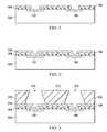
- FIG. 3illustrates a first patterned mask 312 formed over the seed layer 210 in accordance with an embodiment.
- the first patterned mask 312will act as a mold for forming conductive pillars in subsequent processing steps.
- the first patterned mask 312may be a patterned photoresist mask, hard mask, and/or the like.
- a photoresist materialis deposited and patterned to form openings 314 .
- the embodiment illustrated in FIG. 3utilizes sloped sidewalls such that the openings 314 are wider along the bottom of the openings along the seed layer 210 than the top portion of the openings 314 , thereby resulting in a conical shape.
- the tapered profilemay be created by any suitable technique, such as the use of multiple photoresist layers with different patterning properties and one or more exposures, diffusion techniques, an image reversal process, multiple exposures using different masks, and/or the like.
- conductive pillar 416is formed in the openings 314 (see FIG. 3 ) as illustrated in FIG. 4 .
- the conductive pillar 416comprises one or more conductive materials, such as copper, tungsten, other conductive metals, or the like, and may be formed, for example, by electroplating, electroless plating, or the like.
- an electroplating processis used wherein the wafer is submerged or immersed in the electroplating solution.
- the wafer surfaceis electrically connected to the negative side of an external DC power supply such that the wafer functions as the cathode in the electroplating process.
- a solid conductive anode, such as a copper anodeis also immersed in the solution and is attached to the positive side of the power supply.
- the atoms from the anodeare dissolved into the solution, from which the cathode, e.g., the wafer, acquires, thereby plating the exposed conductive areas of the wafer, e.g., exposed portions of the seed layer 210 within the openings 314 .
- FIG. 5illustrates formation of an optional conductive cap layer 518 formed over the conductive pillar 416 .
- solder materialwill be formed over the conductive pillar 416 .
- an inter-metallic compound (IMC) layeris naturally formed at the joint between the solder material and the underlying surface. It has been found that some materials may create a stronger, more durable IMC layer than others. As such, it may be desirable to form a cap layer, such as the conductive cap layer 518 , to provide an IMC layer having more desirable characteristics. For example, in an embodiment in which the conductive pillar 416 is formed of copper, a conductive cap layer 518 formed of nickel may be desirable.
- the conductive cap layer 518may be formed through any number of suitable techniques, including PVD, CVD, ECD, MBE, ALD, electroplating, and the like.
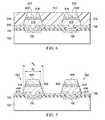
- FIG. 6illustrates formation of solder material 620 and an IMC layer 622 .
- the solder material 620comprises SnPb, a high-Pb material, a Sn-based solder, a lead-free solder, a SnAg solder, a SnAgCu solder, or other suitable conductive material.
- FIG. 6illustrates an embodiment in which the solder material 620 is formed while the first patterned mask 312 is present and exhibits a conical shape similar to the underlying conductive pillar 416 .
- the solder material 620(or other suitable material) may be placed on the conductive pillars after removal of the first patterned mask 312 .
- FIG. 7illustrates the removal of the first patterned mask 312 (see FIG. 3 ) in accordance with an embodiment.
- a plasma ashing or wet strip processmay be used to remove the first patterned mask 312 .
- the exposed portions of the seed layer 210may be removed by, for example, a wet etching process.
- a wet dip in a sulfuric acid (H 2 SO 4 ) solutionmay be used to clean the wafer and remove remaining photoresist material.
- a reflow processmay be performed, which may cause the solder material 620 to have a rounded shape.
- the conductive pillar 416 and, optionally, the conductive cap layer 518form a conductive bump 724 having a conical shape such that sidewalls of the conductive bump 724 are tapered.
- a width of the base portion W Bis greater than a width of the tip portion W T .
- the relatively wide base dimensionmay reduce current density and the narrower top portion may reduce the probability of misalignment when coupling the first substrate 100 to another substrate.
- a ratio of the width of the tip portion W T to the width of the base portion W Bmay be adjusted for a particular purpose or application.
- the ratio of W T to W Bmay be from about 0.5 to about 0.99.
- the ratio of W T to W Bmay be from about 0.6 to about 0.98.
- the ratio of W T to W Bmay be from about 0.7 to about 0.93.
- the ratio of WT to WBmay be from about 0.75 to about 0.92.
- the ratio of WT to WBmay be from about 0.75 to about 0.97.
- FIGS. 8A and 8Billustrate joining two substrates in accordance with an embodiment, wherein FIG. 8A is a side view and FIG. 8B is a perspective view.
- the first substrate 800represents a substrate such as the substrate 100 discussed above with reference to FIGS. 1-7 , wherein like reference numerals refer to like elements.
- the second substrate 850represents a substrate to be attached to the first substrate 800 and may be an organic substrate, a PCB, a ceramic substrate, integrated circuit die, an interposer, a packaging substrate, a high-density interconnect, or the like.
- the second substrate 850includes conductive traces 852 formed thereon.
- the conductive tracesmay be formed of any suitable conductive material, such as copper, tungsten, aluminum, silver, combinations thereof, or the like. It should be noted that the conductive traces 852 may be a portion of redistribution layer.
- the solder material 620 of the first substrate 100is brought into contact with the conductive trace 852 and a reflow process is performed. Due to the conical shape of the pillar 416 and/or solder material 620 , the solder material may be brought into direct contact with the raised conductive traces 852 while reducing the risk of bridging between adjacent ones of the conductive traces 852 .
- FIGS. 9-12illustrate another embodiment in which a tiered pillar is utilized.
- FIGS. 9-12illustrate another embodiment in which a multi-tiered pillar structure is formed, rather than a single-tiered pillar structure illustrated in FIGS. 8A and 8B .
- the multi-tiered pillar structure of FIGS. 9-12may be connected to the second substrate (see FIGS. 8A and 8B ) by replacing the single-tiered pillar structure of FIGS. 8A and 8B .
- FIG. 9there is shown a structure similar to that discussed above with reference to FIG.
- first patterned mask 312is replaced with a first tier patterned mask 912 that is formed and patterned to form a first tier of a pillar structure in openings 914 as explained in greater detail below.
- first tier pillar structure 1010formed in the openings 914 .
- the first tier pillar structure 1010is formed to an upper surface of the first tier patterned mask 912 .
- the first tier patterned mask 912 and the first tier pillar structure 1010 of FIG. 10may be formed in a similar manner using similar processes and similar materials as those used to form the first patterned mask 312 and the conductive pillar 416 of FIG. 3 .
- a planarization processsuch as a CMP process may be used to remove excess material.
- FIG. 11illustrates a second tier patterned mask 1112 formed over the first tier patterned mask 912 .
- the second tier patterned mask 1112may be formed in a similar manner using similar processes and similar materials as those used to form the first tier patterned mask 912 .
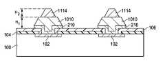
- FIG. 11further illustrates a second tier pillar structure 1114 formed overlying the first tier pillar structure 1010 .
- the first tier patterned mask 912 and the second tier patterned mask 1112may be removed, thereby resulting in the pillar structure as illustrated in FIG. 12 .
- the first tier pillar structure 1010 and the second tier pillar structure 1114form a step pattern such that a lower level tier pillar structure (e.g., the first tier pillar structure 1010 ) has a larger width than an upper level tier pillar structure (e.g., the second tier pillar structure 1114 ).
- the first tier pillar structure 1010has a height H 1 of about 100,000 ⁇ to about 600,000 ⁇
- the second tier pillar structure 1114has a height H 2 of about 50,000 ⁇ to about 600,000 ⁇ .
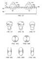
- FIG. 12illustrates an embodiment in which both tiers of the pillar structure exhibit tapered edges of a portion of a generally conical shape.
- Other embodimentsmay utilize one or more cylindrical sections rather than conical-shaped sections.
- FIG. 13illustrates an example embodiment in which the lower tier and the upper tier exhibit a cylindrical shape.
- the embodiment illustrated in FIG. 13may be formed using similar materials and processes as those discussed above, except that the photoresist mask is exposed and developed such that vertical sidewalls are obtained rather than the tapered sidewalls.
- FIG. 14illustrates an embodiment in which the lower tier exhibits a cylindrical shape and the upper tier exhibits a conical shape.
- Another embodimentmay utilize a lower tier having a conical shape and an upper tier having a cylindrical shape as illustrated in FIG. 15 .
- embodimentsmay utilize various shapes in a plan view, such as those illustrated in FIGS. 16A-16E . These embodiments include elongated shapes, such as those illustrated in FIGS. 16C-16E . Each of these shapes may be used in embodiments having a continuous shape (e.g., FIGS. 1-7 ) or tiered shape (e.g., FIGS. 8-14 ).
- Embodiments using an oblong or irregular shapemay exhibit similar ratios as those discussed above along the other axis, e.g., the major and minor axis.
- a devicecomprising a first substrate and a second substrate.
- the first substrateincludes a conductive trace formed thereon with a conductive pillar formed directly on the conductive trace.
- the conductive traceexhibits a planar upper surface and at least a portion of the conductive pillar has a conical shape.
- the second substrateincludes conductive traces formed thereon, such that an upper surface of the conductive traces is raised above an upper surface of the second substrate.
- the conductive pillar of the first substrateis coupled to the conductive traces on the second substrate.
- a deviceis provided.
- a substrate having a conductive trace formed thereonis provided.
- a conductive pillaris coupled to the conductive trace, wherein the conductive pillar has a plurality of tiers such that an upper tier has a smaller area in a plan view than a lower tier.
- a substrate having a conductive trace formed thereonis provided such that at least a portion of the conductive trace is exposed.
- a conductive pillaris positioned over the conductive trace, wherein the conductive pillar has one or more tiers, at least one of the one or more tiers having an elongated shape.
Landscapes
- Engineering & Computer Science (AREA)
- Computer Hardware Design (AREA)
- Microelectronics & Electronic Packaging (AREA)
- Power Engineering (AREA)
- Manufacturing & Machinery (AREA)
- Physics & Mathematics (AREA)
- Condensed Matter Physics & Semiconductors (AREA)
- General Physics & Mathematics (AREA)
- Internal Circuitry In Semiconductor Integrated Circuit Devices (AREA)
Abstract
Description
Generally, semiconductor dies comprise active devices, metallization layers forming connections to the active devices, and I/O contacts to provide the metallization layers (and active devices) signals and power. The metallization layers generally comprise a series of dielectric layers and metal layers in order to provide all of the required connections between the active devices and the I/O contacts (and between individual active devices). These dielectric layers may be formed from low-k dielectric materials with dielectric constants (k value) between about 2.9 and 3.8, ultra low-k (ULK) dielectric materials, with k values less than about 2.5, or even extra low-k (ELK) dielectric materials with k values between about 2.5 and about 2.9, or some combination of low-k dielectric materials.
However, while these low-k, ULK, and ELK materials may be used to improve the electrical characteristics of the metallization layers and thereby increase the overall speed or efficiency of the semiconductor device, these materials may also exhibit structural deficiencies. For example, some of these materials may have greater trouble than other dielectric materials handling the stresses applied to them in the semiconductor device. As such, the low-k, ULK, and ELK materials tend to delaminate or crack when too much pressure is applied to the low-K, ELK, and ULK materials, thereby damaging or destroying the semiconductor device and reducing yields and increasing costs.
These delamination issues related to stress can be particularly troublesome when using packaging techniques such as surface-mount technology (SMT) and flip-chip packaging. As opposed to more conventional packaged integrated circuits (ICs) that have a structure basically interconnected by fine gold wire between metal pads on the die and electrodes spreading out of molded resin packages, these packaging techniques rely on bumps of solder to provide an electrical connection between contacts on the die and contacts on a substrate, such as a packaging substrate, a printed circuit board (PCB), another die/wafer, or the like. The different layers making up the interconnection typically have different coefficients of thermal expansion (CTEs). As a result, additional stress derived from this difference is exhibited on the joint area, which also may cause cracks to form and/or delamination.
For a more complete understanding of the embodiments, and the advantages thereof, reference is now made to the following descriptions taken in conjunction with the accompanying drawings, in which:
The making and using of embodiments are discussed in detail below. It should be appreciated, however, that this disclosure provides many applicable inventive concepts that can be embodied in a wide variety of specific contexts. The specific embodiments discussed herein are merely illustrative of specific ways to make and use the embodiments, and do not limit the scope of the disclosure.
Embodiments described herein relate to the use of bumps or balls (collectively referred to herein as bumps) for use with interconnecting one substrate with another substrate, wherein each substrate may be an integrated circuit die, an interposer, packaging substrate, printed circuit board, organic substrate, ceramic substrate, high-density interconnect, and/or the like. As will be discussed below, embodiments are disclosed that utilize a pillar and/or a bump having a smaller tip section relative to a base section, such as a conical or tiered shape. It has been found that embodiments such as those discussed herein may reduce delamination issues as well as reducing bridging between adjacent connections, thereby increasing throughput and reliability. The intermediate stages of a method for forming a conical or tiered shape pillar and/or bump are disclosed herein. Embodiments such as these may be suitable for use in flip-chip configuration, three-dimensional (3D) IC or stacked die configurations, and/or the like. Throughout the various views and illustrative embodiments, like reference numbers are used to designate like elements.
It should be noted that in some embodiments, particularly in embodiments in which thesubstrate 100 is an integrated circuit die, thesubstrate 100 may include electrical circuitry (not shown). In an embodiment, the electrical circuitry includes electrical devices formed on thesubstrate 100 with one or more dielectric layers overlying the electrical devices. Metal layers may be formed between dielectric layers to route electrical signals between the electrical devices. Electrical devices may also be formed in one or more dielectric layers. In an embodiment, thesubstrate 100 includes one or more low-k and/or ELK dielectric layers.
For example, the electrical circuitry may include various N-type metal-oxide semiconductor (NMOS) and/or P-type metal-oxide semiconductor (PMOS) devices, such as transistors, capacitors, resistors, diodes, photo-diodes, fuses, and the like, interconnected to perform one or more functions. The functions may include memory structures, processing structures, sensors, amplifiers, power distribution circuitry, input/output circuitry, or the like. One of ordinary skill in the art will appreciate that the above examples are provided for illustrative purposes only to further explain applications of some illustrative embodiments and are not meant to limit the disclosure in any manner. Other circuitry may be used as appropriate for a given application.
Embodiments such as those disclosed herein may be particularly beneficial in a system using bump-on-trace (BOT) technology. Generally, these techniques provide for a bump to be coupled directly to the conductive traces (such asconductive traces 852 of thesecond substrate 850 illustrated inFIG. 8 ). A solder resist may be used to protect other portions of the trace and/or other traces.
One or more passivation layers, such aspassivation layer 104, are formed and patterned over thesubstrate 100 to provide an opening over theconductive traces 102 and to protect the underlying layers from various environmental contaminants. Thepassivation layer 104 may be formed of a dielectric material, such as PE-USG, PE-SiN, combinations thereof, and/or the like, by any suitable method, such as CVD, PVD, or the like. In an embodiment, thepassivation layer 104 has a thickness of about 10,000 Å to about 15,000 Å. In an embodiment, thepassivation layer 104 comprises a multi-layer structure of 750 Å of SiN, 6,500 Å of PE-USG, and 6,000 Å of PE-SiN.
Aprotective layer 106 formed and patterned over thepassivation layer 104. Theprotective layer 106 may be, for example, a polyimide material formed by any suitable process, such as spin coating of a photo resister, or the like. In an embodiment, theprotective layer 106 has a thickness between about 2.5 μm and about 10 μm.
One of ordinary skill in the art will appreciate that a single layer of conductive/bond pads and a passivation layer are shown for illustrative purposes only. As such, other embodiments may include any number of conductive layers and/or passivation layers. Furthermore, it should be appreciated that one or more of the conductive layers may act as a RDL to provide the desired pin or ball layout.
Any suitable process may be used to form the structures discussed above and will not be discussed in greater detail herein. As one of ordinary skill in the art will realize, the above description provides a general description of the features of the embodiment and that numerous other features may be present. For example, other circuitry, liners, barrier layers, under-bump metallization configurations, and the like, may be present. The above description is meant only to provide a context for embodiments discussed herein and is not meant to limit the disclosure or the scope of any claims to those specific embodiments.
Referring now toFIG. 2 , aconformal seed layer 210 is deposited over the surface of theprotective layer 106 and the exposed portions of the conductive traces102. Theseed layer 210 is a thin layer of a conductive material that aids in the formation of a thicker layer during subsequent processing steps. In an embodiment, theseed layer 210 may be formed by depositing a thin conductive layer, such as a thin layer of Cu, Ti, Ta, TiN, TaN, or the like, using chemical vapor deposition (CVD) or plasma vapor deposition (PVD) techniques. For example, in an embodiment, theseed layer 210 is a composite layer including a layer of Ti deposited by a PVD process to a thickness of about 500 Å and a layer of Cu deposited by a PVD process to a thickness of about 3,000 Å. Other materials, processes, and thicknesses may be used.
The embodiment illustrated inFIG. 2 illustrates an intermediate step in forming a BOT configuration in which a pillar structure, e.g., including a seed layer (if any) and a pillar, is formed directly on the trace. In such an embodiment, an under-bump metallization (UBM) layer may be omitted. In other embodiments, however, additional layers and/or UBM structures may be utilized.
It should be noted that the embodiment illustrated inFIG. 3 utilizes sloped sidewalls such that theopenings 314 are wider along the bottom of the openings along theseed layer 210 than the top portion of theopenings 314, thereby resulting in a conical shape. The tapered profile may be created by any suitable technique, such as the use of multiple photoresist layers with different patterning properties and one or more exposures, diffusion techniques, an image reversal process, multiple exposures using different masks, and/or the like.
Thereafter,conductive pillar 416 is formed in the openings314 (seeFIG. 3 ) as illustrated inFIG. 4 . Theconductive pillar 416 comprises one or more conductive materials, such as copper, tungsten, other conductive metals, or the like, and may be formed, for example, by electroplating, electroless plating, or the like. In an embodiment, an electroplating process is used wherein the wafer is submerged or immersed in the electroplating solution. The wafer surface is electrically connected to the negative side of an external DC power supply such that the wafer functions as the cathode in the electroplating process. A solid conductive anode, such as a copper anode, is also immersed in the solution and is attached to the positive side of the power supply. The atoms from the anode are dissolved into the solution, from which the cathode, e.g., the wafer, acquires, thereby plating the exposed conductive areas of the wafer, e.g., exposed portions of theseed layer 210 within theopenings 314.
Theconductive pillar 416 and, optionally, theconductive cap layer 518 form aconductive bump 724 having a conical shape such that sidewalls of theconductive bump 724 are tapered. In this situation, a width of the base portion WBis greater than a width of the tip portion WT. The relatively wide base dimension may reduce current density and the narrower top portion may reduce the probability of misalignment when coupling thefirst substrate 100 to another substrate.
A ratio of the width of the tip portion WTto the width of the base portion WBmay be adjusted for a particular purpose or application. For example, in an embodiment, the ratio of WTto WBmay be from about 0.5 to about 0.99. In another embodiment, the ratio of WTto WBmay be from about 0.6 to about 0.98. In another embodiment, the ratio of WTto WBmay be from about 0.7 to about 0.93. In another embodiment, the ratio of WT to WB may be from about 0.75 to about 0.92. In another embodiment, the ratio of WT to WB may be from about 0.75 to about 0.97.
Thesecond substrate 850 includesconductive traces 852 formed thereon. The conductive traces may be formed of any suitable conductive material, such as copper, tungsten, aluminum, silver, combinations thereof, or the like. It should be noted that theconductive traces 852 may be a portion of redistribution layer. As illustrated inFIGS. 8A and 8B , thesolder material 620 of thefirst substrate 100 is brought into contact with theconductive trace 852 and a reflow process is performed. Due to the conical shape of thepillar 416 and/orsolder material 620, the solder material may be brought into direct contact with the raisedconductive traces 852 while reducing the risk of bridging between adjacent ones of the conductive traces852.
Referring now toFIG. 10 , there is shown a firsttier pillar structure 1010 formed in theopenings 914. In this embodiment, the firsttier pillar structure 1010 is formed to an upper surface of the first tier patternedmask 912. The first tier patternedmask 912 and the firsttier pillar structure 1010 ofFIG. 10 may be formed in a similar manner using similar processes and similar materials as those used to form the firstpatterned mask 312 and theconductive pillar 416 ofFIG. 3 . A planarization process, such as a CMP process may be used to remove excess material.
It should be noted, however, that two tiers are illustrated in this embodiment for illustrative purposes only and that other embodiments may utilize more tiers. After forming the uppermost tier pillar structure, such as the secondtier pillar structure 1114, the first tier patternedmask 912 and the second tier patternedmask 1112 may be removed, thereby resulting in the pillar structure as illustrated inFIG. 12 .
As illustrated inFIG. 12 , the firsttier pillar structure 1010 and the secondtier pillar structure 1114 form a step pattern such that a lower level tier pillar structure (e.g., the first tier pillar structure1010) has a larger width than an upper level tier pillar structure (e.g., the second tier pillar structure1114). In an embodiment, the firsttier pillar structure 1010 has a height H1of about 100,000 Å to about 600,000 Å, and the secondtier pillar structure 1114 has a height H2of about 50,000 Å to about 600,000 Å.
In yet other embodiments, a combination of cylindrical shaped tiers and conical shaped tiers may be used. For example,FIG. 14 illustrates an embodiment in which the lower tier exhibits a cylindrical shape and the upper tier exhibits a conical shape. Another embodiment may utilize a lower tier having a conical shape and an upper tier having a cylindrical shape as illustrated inFIG. 15 .
As discussed above, embodiments may utilize various shapes in a plan view, such as those illustrated inFIGS. 16A-16E . These embodiments include elongated shapes, such as those illustrated inFIGS. 16C-16E . Each of these shapes may be used in embodiments having a continuous shape (e.g.,FIGS. 1-7 ) or tiered shape (e.g.,FIGS. 8-14 ).
Embodiments using an oblong or irregular shape may exhibit similar ratios as those discussed above along the other axis, e.g., the major and minor axis.
In accordance with an embodiment, a device comprising a first substrate and a second substrate is provided. The first substrate includes a conductive trace formed thereon with a conductive pillar formed directly on the conductive trace. The conductive trace exhibits a planar upper surface and at least a portion of the conductive pillar has a conical shape. The second substrate includes conductive traces formed thereon, such that an upper surface of the conductive traces is raised above an upper surface of the second substrate. The conductive pillar of the first substrate is coupled to the conductive traces on the second substrate.
In accordance with another embodiment, a device is provided. A substrate having a conductive trace formed thereon is provided. A conductive pillar is coupled to the conductive trace, wherein the conductive pillar has a plurality of tiers such that an upper tier has a smaller area in a plan view than a lower tier.
In accordance with yet another embodiment, another device is provided. A substrate having a conductive trace formed thereon is provided such that at least a portion of the conductive trace is exposed. A conductive pillar is positioned over the conductive trace, wherein the conductive pillar has one or more tiers, at least one of the one or more tiers having an elongated shape.
Although the present disclosure and its advantages have been described in detail, it should be understood that various changes, substitutions and alterations can be made herein without departing from the spirit and scope of the disclosure as defined by the appended claims. Moreover, the scope of the present application is not intended to be limited to the particular embodiments of the process, machine, manufacture, and composition of matter, means, methods and steps described in the specification. As one of ordinary skill in the art will readily appreciate from the disclosure, processes, machines, manufacture, compositions of matter, means, methods, or steps, presently existing or later to be developed, that perform substantially the same function or achieve substantially the same result as the corresponding embodiments described herein may be utilized. Accordingly, the appended claims are intended to include within their scope such processes, machines, manufacture, compositions of matter, means, methods, or steps.
Claims (17)
1. A device comprising:
a first substrate having a first conductive trace formed thereon, a conductive pillar structure formed directly on the first conductive trace, the conductive pillar structure comprising a conductive pillar, the conductive trace having a planar upper surface, at least a portion of the conductive pillar having a conical shape, the conductive pillar having a plurality of tiers, each tier of the plurality of tiers having a bottom surface of a width of greater than a width of a top surface;
a second substrate having a plurality of second conductive traces formed thereon, an upper surface of each of the second conductive traces of the plurality of second conductive traces being raised above an upper surface of the second substrate, wherein one of plurality of the second conductive traces of the second substrate is elongated in a direction of elongation along a major surface of the second substrate; and
a bump-on-trace bonding the conductive pillar structure of the first substrate to the one of the plurality of second conductive traces of the second substrate, wherein at least the one of the plurality of second conductive traces extends beyond the bump-on-trace on both sides of the bump-on-trace in the direction of elongation, the bump-on-trace being formed of a different material than the conductive pillar, the bump-on-trace not extending along sidewalls of the conductive pillar.
2. The device ofclaim 1 , wherein the conductive pillar has a circular shape in a plan view.
3. The device ofclaim 1 , wherein the conductive pillar has an elongated shape in a plan view.
4. The device ofclaim 1 , wherein each of the plurality of tiers have a conical shape.
5. The device ofclaim 1 , wherein one or more of the plurality of tiers has a cylindrical shape.
6. The device ofclaim 1 , wherein one or more of the plurality of tiers has a cylindrical shape and wherein one or more of the plurality of tiers has a conical shape.
7. A device comprising:
a first substrate having a conductive trace formed thereon;
a conductive pillar structure coupled to the conductive trace, the conductive pillar structure comprising a seed layer and a conductive pillar over the seed layer, sidewalls of the seed layer not extending beyond sidewalls of the conductive pillar a plan view, the conductive pillar having a plurality of tiers, wherein each tier has a conical shape and a bottom surface of an overlying tier has a smaller area in a plan view than an upper surface of a lower tier;
a second substrate having a raised trace formed thereon, wherein the raised trace of the second substrate is elongated in a direction of elongation along a major surface of the second substrate; and
a bump electrically connecting the conductive pillar on the first substrate to the raised trace on the second substrate, the bump not extending along sidewalls of the conductive pillar, wherein the raised trace extends beyond the bump on both sides of the bump in the direction of elongation.
8. The device ofclaim 7 , wherein the lower tier has tapered sidewalls.
9. The device ofclaim 8 , wherein the upper tier has tapered sidewalls.
10. The device ofclaim 7 , wherein the upper tier has tapered sidewalls.
11. The device ofclaim 7 , wherein the conductive pillar has an elongated shape.
12. A device comprising:
a first substrate;
a conductive trace on the first substrate, wherein the conductive trace comprises a redistribution line, at least a portion of the conductive trace being exposed; and
a conductive pillar formed over the conductive trace, the conductive pillar having a plurality of tiers, at least one of the plurality of tiers having an elongated shape, the conductive pillar having a cap layer over an uppermost surface, each tier of the plurality of tiers having a constantly decreasing or a constant width as the conductive pillar extends away from the conductive trace;
a second substrate having a raised trace formed thereon, wherein the raised trace of the second substrate is elongated in a direction of elongation along a major surface of the second substrate; and
a bump formed on the cap layer electrically connecting the conductive pillar on the first substrate to the raised trace on the second substrate, the bump not extending along sidewalls of the conductive pillar, wherein the raised trace extends beyond the bump on both sides of the bump in the direction of elongation.
13. The device ofclaim 12 , wherein the conductive pillar has a lower tier and an upper tier, the lower tier and the upper tier having tapered sidewalls.
14. The device ofclaim 12 , wherein the conductive pillar has a lower tier and an upper tier, the lower tier and the upper tier having vertical sidewalls.
15. The device ofclaim 12 , wherein the conductive pillar has a lower tier and an upper tier, only one of the lower tier and the upper tier having tapered sidewalls.
16. The device ofclaim 12 , wherein a ratio of a bottom width to a top width is between about 0.75 and 0.92.
17. The device ofclaim 1 , wherein the conductive pillar structure comprises a seed layer.
Priority Applications (5)
| Application Number | Priority Date | Filing Date | Title |
|---|---|---|---|
| US13/449,078US9425136B2 (en) | 2012-04-17 | 2012-04-17 | Conical-shaped or tier-shaped pillar connections |
| US13/719,019US9646923B2 (en) | 2012-04-17 | 2012-12-18 | Semiconductor devices, methods of manufacture thereof, and packaged semiconductor devices |
| US15/243,523US10056345B2 (en) | 2012-04-17 | 2016-08-22 | Conical-shaped or tier-shaped pillar connections |
| US15/497,408US10153243B2 (en) | 2012-04-17 | 2017-04-26 | Semiconductor devices, methods of manufacture thereof, and packaged semiconductor devices |
| US16/105,014US11315896B2 (en) | 2012-04-17 | 2018-08-20 | Conical-shaped or tier-shaped pillar connections |
Applications Claiming Priority (1)
| Application Number | Priority Date | Filing Date | Title |
|---|---|---|---|
| US13/449,078US9425136B2 (en) | 2012-04-17 | 2012-04-17 | Conical-shaped or tier-shaped pillar connections |
Related Child Applications (1)
| Application Number | Title | Priority Date | Filing Date |
|---|---|---|---|
| US15/243,523ContinuationUS10056345B2 (en) | 2012-04-17 | 2016-08-22 | Conical-shaped or tier-shaped pillar connections |
Publications (2)
| Publication Number | Publication Date |
|---|---|
| US20130270699A1 US20130270699A1 (en) | 2013-10-17 |
| US9425136B2true US9425136B2 (en) | 2016-08-23 |
Family
ID=49324350
Family Applications (3)
| Application Number | Title | Priority Date | Filing Date |
|---|---|---|---|
| US13/449,078ActiveUS9425136B2 (en) | 2012-04-17 | 2012-04-17 | Conical-shaped or tier-shaped pillar connections |
| US15/243,523ActiveUS10056345B2 (en) | 2012-04-17 | 2016-08-22 | Conical-shaped or tier-shaped pillar connections |
| US16/105,014Active2032-05-21US11315896B2 (en) | 2012-04-17 | 2018-08-20 | Conical-shaped or tier-shaped pillar connections |
Family Applications After (2)
| Application Number | Title | Priority Date | Filing Date |
|---|---|---|---|
| US15/243,523ActiveUS10056345B2 (en) | 2012-04-17 | 2016-08-22 | Conical-shaped or tier-shaped pillar connections |
| US16/105,014Active2032-05-21US11315896B2 (en) | 2012-04-17 | 2018-08-20 | Conical-shaped or tier-shaped pillar connections |
Country Status (1)
| Country | Link |
|---|---|
| US (3) | US9425136B2 (en) |
Cited By (13)
| Publication number | Priority date | Publication date | Assignee | Title |
|---|---|---|---|---|
| US20170084562A1 (en)* | 2014-05-09 | 2017-03-23 | Siliconware Precision Industries Co., Ltd. | Package structure, chip structure and fabrication method thereof |
| EP3361502A1 (en)* | 2017-02-13 | 2018-08-15 | MediaTek Inc. | Semiconductor package with rigid under bump metallurgy (ubm) stack |
| US20180358316A1 (en)* | 2012-04-17 | 2018-12-13 | Taiwan Semiconductor Manufacturing Company, Ltd. | Conical-Shaped or Tier-Shaped Pillar Connections |
| US10186493B2 (en)* | 2016-09-01 | 2019-01-22 | Semiconductor Components Industries, Llc | Semiconductor copper metallization structure and related methods |
| US10319691B2 (en) | 2012-09-18 | 2019-06-11 | Taiwan Semiconductor Manufacturing Company | Solderless interconnection structure and method of forming same |
| US10424552B2 (en) | 2017-09-20 | 2019-09-24 | Texas Instruments Incorporated | Alloy diffusion barrier layer |
| US10930610B2 (en) | 2018-07-03 | 2021-02-23 | Samsung Electronics Co., Ltd | Semiconductor chip including a bump structure and semiconductor package including the same |
| US11024757B2 (en)* | 2016-01-15 | 2021-06-01 | Sony Corporation | Semiconductor device and imaging apparatus |
| US11094659B2 (en) | 2019-09-30 | 2021-08-17 | Texas Instruments Incorporated | Microelectronic device with pillars having flared ends |
| US20230067143A1 (en)* | 2021-08-30 | 2023-03-02 | Taiwan Semiconductor Manufacturing Company, Ltd. | Chip structure and method for forming the same |
| US20230108516A1 (en)* | 2020-04-09 | 2023-04-06 | Samsung Electronics Co., Ltd. | Semiconductor device |
| US11682651B2 (en) | 2012-04-18 | 2023-06-20 | Taiwan Semiconductor Manufacturing Company | Bump-on-trace interconnect |
| US11749616B2 (en) | 2017-10-05 | 2023-09-05 | Texas Instruments Incorporated | Industrial chip scale package for microelectronic device |
Families Citing this family (26)
| Publication number | Priority date | Publication date | Assignee | Title |
|---|---|---|---|---|
| US9142533B2 (en) | 2010-05-20 | 2015-09-22 | Taiwan Semiconductor Manufacturing Company, Ltd. | Substrate interconnections having different sizes |
| US8823166B2 (en)* | 2010-08-30 | 2014-09-02 | Taiwan Semiconductor Manufacturing Company, Ltd. | Pillar bumps and process for making same |
| US9646923B2 (en) | 2012-04-17 | 2017-05-09 | Taiwan Semiconductor Manufacturing Company, Ltd. | Semiconductor devices, methods of manufacture thereof, and packaged semiconductor devices |
| JP2014116367A (en)* | 2012-12-06 | 2014-06-26 | Fujitsu Ltd | Electronic component, method of manufacturing electronic device and electronic device |
| CN107170689B (en)* | 2013-06-11 | 2019-12-31 | 唐山国芯晶源电子有限公司 | Chip packaging substrate |
| US20150279793A1 (en)* | 2014-03-27 | 2015-10-01 | Taiwan Semiconductor Manufacturing Company Ltd. | Semiconductor structure and manufacturing method thereof |
| US9496154B2 (en) | 2014-09-16 | 2016-11-15 | Invensas Corporation | Use of underfill tape in microelectronic components, and microelectronic components with cavities coupled to through-substrate vias |
| TWI662657B (en) | 2015-04-07 | 2019-06-11 | 聯華電子股份有限公司 | Stacked semiconductor device |
| US10008797B2 (en)* | 2015-07-10 | 2018-06-26 | Te Connectivity Corporation | Flexible printed circuit connector and connector assembly including the same |
| JP2017152646A (en)* | 2016-02-26 | 2017-08-31 | 富士通株式会社 | Electronic components, electronic devices and electronic equipment |
| US10643965B2 (en) | 2016-05-25 | 2020-05-05 | Taiwan Semiconductor Manufacturing Company, Ltd. | Structure and method of forming a joint assembly |
| US9960137B1 (en)* | 2016-11-01 | 2018-05-01 | Advanced Semiconductor Engineering, Inc. | Semiconductor device package and method for forming the same |
| US10453811B2 (en) | 2016-11-29 | 2019-10-22 | Taiwan Semiconductor Manufacturing Company, Ltd. | Post passivation interconnect and fabrication method therefor |
| JP6986704B2 (en)* | 2017-02-28 | 2021-12-22 | パナソニックIpマネジメント株式会社 | Manufacturing method of housing, electronic equipment and housing |
| US10256114B2 (en) | 2017-03-23 | 2019-04-09 | Amkor Technology, Inc. | Semiconductor device with tiered pillar and manufacturing method thereof |
| JP7117615B2 (en)* | 2017-12-08 | 2022-08-15 | パナソニックIpマネジメント株式会社 | Semiconductor device manufacturing method |
| US11289373B2 (en)* | 2018-07-31 | 2022-03-29 | Taiwan Semiconductor Manufacturing Company, Ltd. | Semiconductor package and manufacturing method thereof |
| KR20200097977A (en)* | 2019-02-11 | 2020-08-20 | 삼성전기주식회사 | Printed circuit board |
| JP7240909B2 (en)* | 2019-03-13 | 2023-03-16 | 新光電気工業株式会社 | Wiring board and its manufacturing method |
| US11133244B2 (en)* | 2019-06-19 | 2021-09-28 | Advanced Semiconductor Engineering, Inc. | Semiconductor device package and method for manufacturing the same |
| US10861711B1 (en)* | 2019-10-23 | 2020-12-08 | Nanya Technology Corporation | Method of manufacturing a semiconductor structure |
| KR102803130B1 (en)* | 2020-08-14 | 2025-05-07 | 삼성전자주식회사 | Semiconductor package and method of manufacturing the semiconductor package |
| US11955447B2 (en) | 2021-11-17 | 2024-04-09 | Advanced Micro Devices, Inc. | Semiconductor chip having stepped conductive pillars |
| US12324361B2 (en) | 2022-05-09 | 2025-06-03 | International Business Machines Corporation | Electrical connections between dissimilar materials at cryogenic temperatures |
| US12150390B2 (en)* | 2022-05-09 | 2024-11-19 | International Business Machines Corporation | Downstop and bump bonds formation on substrates |
| US20240088012A1 (en)* | 2022-09-09 | 2024-03-14 | Stmicroelectronics S.R.L. | Semiconductor package or device with sealing layer |
Citations (188)
| Publication number | Priority date | Publication date | Assignee | Title |
|---|---|---|---|---|
| US4811082A (en) | 1986-11-12 | 1989-03-07 | International Business Machines Corporation | High performance integrated circuit packaging structure |
| US4990462A (en) | 1989-04-12 | 1991-02-05 | Advanced Micro Devices, Inc. | Method for coplanar integration of semiconductor ic devices |
| US5075253A (en) | 1989-04-12 | 1991-12-24 | Advanced Micro Devices, Inc. | Method of coplanar integration of semiconductor IC devices |
| US5075965A (en) | 1990-11-05 | 1991-12-31 | International Business Machines | Low temperature controlled collapse chip attach process |
| US5130779A (en) | 1990-06-19 | 1992-07-14 | International Business Machines Corporation | Solder mass having conductive encapsulating arrangement |
| US5277756A (en) | 1990-07-02 | 1994-01-11 | Digital Equipment Corporation | Post fabrication processing of semiconductor chips |
| US5334804A (en) | 1992-11-17 | 1994-08-02 | Fujitsu Limited | Wire interconnect structures for connecting an integrated circuit to a substrate |
| US5380681A (en) | 1994-03-21 | 1995-01-10 | United Microelectronics Corporation | Three-dimensional multichip package and methods of fabricating |
| US5431328A (en) | 1994-05-06 | 1995-07-11 | Industrial Technology Research Institute | Composite bump flip chip bonding |
| US5440239A (en) | 1994-04-25 | 1995-08-08 | Rockwell International Corporation | Transferable solder bumps for interconnect and assembly of MCM substrates |
| US5470787A (en) | 1994-05-02 | 1995-11-28 | Motorola, Inc. | Semiconductor device solder bump having intrinsic potential for forming an extended eutectic region and method for making and using the same |
| US5542601A (en)* | 1995-02-24 | 1996-08-06 | International Business Machines Corporation | Rework process for semiconductor chips mounted in a flip chip configuration on an organic substrate |
| US5587337A (en) | 1993-05-28 | 1996-12-24 | Kabushiki Kaisha Toshiba | Semiconductor process for forming bump electrodes with tapered sidewalls |
| US5790377A (en) | 1996-09-12 | 1998-08-04 | Packard Hughes Interconnect Company | Integral copper column with solder bump flip chip |
| US5796591A (en) | 1995-06-07 | 1998-08-18 | International Business Machines Corporation | Direct chip attach circuit card |
| US5816478A (en) | 1995-06-05 | 1998-10-06 | Motorola, Inc. | Fluxless flip-chip bond and a method for making |
| US5889326A (en) | 1996-02-27 | 1999-03-30 | Nec Corporation | Structure for bonding semiconductor device to substrate |
| US5977599A (en) | 1996-04-29 | 1999-11-02 | Chartered Semiconductor Manufacturing | Formation of a metal via using a raised metal plug structure |
| US6002172A (en) | 1997-03-12 | 1999-12-14 | International Business Machines Corporation | Substrate structure and method for improving attachment reliability of semiconductor chips and modules |
| US6002177A (en) | 1995-12-27 | 1999-12-14 | International Business Machines Corporation | High density integrated circuit packaging with chip stacking and via interconnections |
| US6025650A (en)* | 1994-08-24 | 2000-02-15 | Fujitsu Limited | Semiconductor device including a frame terminal |
| US6082610A (en) | 1997-06-23 | 2000-07-04 | Ford Motor Company | Method of forming interconnections on electronic modules |
| US6091141A (en)* | 1996-03-11 | 2000-07-18 | Anam Semiconductor Inc. | Bump chip scale semiconductor package |
| US6130476A (en) | 1994-01-31 | 2000-10-10 | International Business Machines Corporation | Semiconductor chip package having chip-to-carrier mechanical/electrical connection formed via solid state diffusion |
| US6137184A (en) | 1997-04-28 | 2000-10-24 | Nec Corporation | Flip-chip type semiconductor device having recessed-protruded electrodes in press-fit contact |
| US6181010B1 (en) | 1998-03-27 | 2001-01-30 | Seiko Epson Corporation | Semiconductor device and method of manufacturing the same, circuit board and electronic instrument |
| US6229216B1 (en) | 1999-01-11 | 2001-05-08 | Intel Corporation | Silicon interposer and multi-chip-module (MCM) with through substrate vias |
| US6271059B1 (en) | 1999-01-04 | 2001-08-07 | International Business Machines Corporation | Chip interconnection structure using stub terminals |
| US20010013423A1 (en) | 1996-10-31 | 2001-08-16 | Hormazdyar M. Dalal | Flip chip attach on flexible circuit carrier using chip with metallic cap on solder |
| US6279815B1 (en) | 1998-06-17 | 2001-08-28 | International Business Machines Corporation | Stacked chip process carrier |
| US6291891B1 (en) | 1998-01-13 | 2001-09-18 | Kabushiki Kaisha Toshiba | Semiconductor device manufacturing method and semiconductor device |
| US6346469B1 (en) | 2000-01-03 | 2002-02-12 | Motorola, Inc. | Semiconductor device and a process for forming the semiconductor device |
| US6355501B1 (en) | 2000-09-21 | 2002-03-12 | International Business Machines Corporation | Three-dimensional chip stacking assembly |
| US6358847B1 (en) | 1999-03-31 | 2002-03-19 | Lam Research Corporation | Method for enabling conventional wire bonding to copper-based bond pad features |
| US20020033412A1 (en) | 2000-04-27 | 2002-03-21 | Francisca Tung | Pillar connections for semiconductor chips and method of manufacture |
| US20020084528A1 (en) | 2000-12-29 | 2002-07-04 | Samsung Electronics Co., Ltd. | Wafer level package and method for manufacturing the same |
| US6424037B1 (en) | 1999-11-30 | 2002-07-23 | Aptos Corporation | Process to make a tall solder ball by placing a eutectic solder ball on top of a high lead solder ball |
| US20020100974A1 (en) | 1999-03-08 | 2002-08-01 | Kenji Uchiyama | Semiconductor device, semiconductor device mounting structure, liquid crystal device, and electronic apparatus |
| US20020106832A1 (en) | 1996-11-26 | 2002-08-08 | Gregory B. Hotchkiss | Method and apparatus for attaching solder members to a substrate |
| US6434016B2 (en) | 1999-06-18 | 2002-08-13 | Intel Corporation | Apparatus for interconnecting multiple devices on a circuit board |
| US6448661B1 (en) | 2001-02-09 | 2002-09-10 | Samsung Electornics Co., Ltd. | Three-dimensional multi-chip package having chip selection pads and manufacturing method thereof |
| US6461895B1 (en) | 1999-01-05 | 2002-10-08 | Intel Corporation | Process for making active interposer for high performance packaging applications |
| US6492197B1 (en) | 2000-05-23 | 2002-12-10 | Unitive Electronics Inc. | Trilayer/bilayer solder bumps and fabrication methods therefor |
| US6498308B2 (en) | 1999-04-02 | 2002-12-24 | Oki Electric Industry Co., Ltd. | Semiconductor module |
| US20020197811A1 (en) | 2001-06-20 | 2002-12-26 | Alps Electric Co., Ltd. | Thin-film resistor and method for manufacturing the same |
| US6562657B1 (en) | 2000-08-22 | 2003-05-13 | Charles W. C. Lin | Semiconductor chip assembly with simultaneously electrolessly plated contact terminal and connection joint |
| US20030092219A1 (en) | 1999-04-06 | 2003-05-15 | Oki Electric Industry Co., Ltd. | Semiconductor device and method of fabricating the same |
| US6570248B1 (en) | 1998-08-31 | 2003-05-27 | Micron Technology, Inc. | Structure and method for a high-performance electronic packaging assembly |
| US6578754B1 (en) | 2000-04-27 | 2003-06-17 | Advanpack Solutions Pte. Ltd. | Pillar connections for semiconductor chips and method of manufacture |
| US6583846B1 (en) | 1999-04-14 | 2003-06-24 | Hitachi, Ltd. | Liquid crystal display device with spacer covered with an electrode |
| US6600222B1 (en) | 2002-07-17 | 2003-07-29 | Intel Corporation | Stacked microelectronic packages |
| US6607938B2 (en) | 2001-07-19 | 2003-08-19 | Samsung Electronics Co., Ltd. | Wafer level stack chip package and method for manufacturing same |
| US20030218250A1 (en)* | 2002-05-27 | 2003-11-27 | Moriss Kung | Method for high layout density integrated circuit package substrate |
| US6661085B2 (en) | 2002-02-06 | 2003-12-09 | Intel Corporation | Barrier structure against corrosion and contamination in three-dimensional (3-D) wafer-to-wafer vertical stack |
| US20040007779A1 (en) | 2002-07-15 | 2004-01-15 | Diane Arbuthnot | Wafer-level method for fine-pitch, high aspect ratio chip interconnect |
| US6713844B2 (en) | 2000-12-28 | 2004-03-30 | Matsushita Electric Works, Ltd. | Semiconductor-chip mounting substrate having at least one projection thereon and a pressure holding means |
| US6762076B2 (en) | 2002-02-20 | 2004-07-13 | Intel Corporation | Process of vertically stacking multiple wafers supporting different active integrated circuit (IC) devices |
| US20040140538A1 (en) | 2003-01-16 | 2004-07-22 | International Business Machines Corporation | Flex-based ic package construction employing a balanced lamination |
| US20040159944A1 (en) | 2001-09-21 | 2004-08-19 | Madhav Datta | Copper-containing C4 ball-limiting metallurgy stack for enhanced reliability of packaged structures and method of making same |
| US6790748B2 (en) | 2002-12-19 | 2004-09-14 | Intel Corporation | Thinning techniques for wafer-to-wafer vertical stacks |
| US20040212098A1 (en) | 2000-03-10 | 2004-10-28 | Chippac, Inc | Flip chip interconnection structure |
| US20050062153A1 (en) | 2003-08-21 | 2005-03-24 | Seiko Epson Corporation | Mounting structure of electronic component, electro-optic device, electronic equipment, and method for mounting electronic component |
| US6887769B2 (en) | 2002-02-06 | 2005-05-03 | Intel Corporation | Dielectric recess for wafer-to-wafer and die-to-die metal bonding and method of fabricating the same |
| US6908565B2 (en) | 2002-12-24 | 2005-06-21 | Intel Corporation | Etch thinning techniques for wafer-to-wafer vertical stacks |
| US6908785B2 (en) | 2001-12-06 | 2005-06-21 | Samsung Electronics Co., Ltd. | Multi-chip package (MCP) with a conductive bar and method for manufacturing the same |
| US6924551B2 (en) | 2003-05-28 | 2005-08-02 | Intel Corporation | Through silicon via, folded flex microelectronic package |
| US6940169B2 (en) | 2002-05-21 | 2005-09-06 | Stats Chippac Ltd. | Torch bump |
| US6940178B2 (en) | 2001-02-27 | 2005-09-06 | Chippac, Inc. | Self-coplanarity bumping shape for flip chip |
| US6943067B2 (en) | 2002-01-08 | 2005-09-13 | Advanced Micro Devices, Inc. | Three-dimensional integrated semiconductor devices |
| US6946384B2 (en) | 2003-06-06 | 2005-09-20 | Intel Corporation | Stacked device underfill and a method of fabrication |
| US20050212114A1 (en) | 2004-03-29 | 2005-09-29 | Nec Electronics Corporation | Semiconductor device |
| US20050224991A1 (en) | 2004-04-08 | 2005-10-13 | Yong-Woon Yeo | Bump for semiconductor package, semiconductor package applying the bump, and method for fabricating the semiconductor package |
| US20050253264A1 (en) | 2004-05-12 | 2005-11-17 | Fujitsu Limited | Semiconductor device and method of manufacturing the semiconductor device |
| US6972490B2 (en) | 2003-11-06 | 2005-12-06 | Industrial Technology Research Institute | Bonding structure with compliant bumps |
| US6975016B2 (en) | 2002-02-06 | 2005-12-13 | Intel Corporation | Wafer bonding using a flexible bladder press and thinned wafers for three-dimensional (3D) wafer-to-wafer vertical stack integration, and application thereof |
| US20060012024A1 (en) | 2000-10-13 | 2006-01-19 | Bridge Semiconductor Corporation | Semiconductor chip assembly with metal containment wall and solder terminal |
| US6998216B2 (en) | 2002-09-24 | 2006-02-14 | Intel Corporation | Mechanically robust interconnect for low-k dielectric material using post treatment |
| US20060038303A1 (en) | 2004-08-23 | 2006-02-23 | Sterrett Terry L | Etched interposer for integrated circuit devices |
| US20060051954A1 (en)* | 2004-09-07 | 2006-03-09 | Siliconware Precision Industries Co, Ltd. | Bump structure of semiconductor package and method for fabricating the same |
| US20060055032A1 (en)* | 2004-09-14 | 2006-03-16 | Kuo-Chin Chang | Packaging with metal studs formed on solder pads |
| US7087538B2 (en) | 2004-08-16 | 2006-08-08 | Intel Corporation | Method to fill the gap between coupled wafers |
| US20060209245A1 (en) | 2000-08-14 | 2006-09-21 | Joong-Hyun Mun | Liquid crystal display and a method for fabricating the same |
| US7135766B1 (en) | 2004-11-30 | 2006-11-14 | Rf Micro Devices, Inc. | Integrated power devices and signal isolation structure |
| US7151009B2 (en) | 2004-06-18 | 2006-12-19 | Samsung Electronics Co., Ltd. | Method for manufacturing wafer level chip stack package |
| US20060292824A1 (en) | 2005-06-08 | 2006-12-28 | Eric Beyne | Methods for bonding and micro-electronic devices produced according to such methods |
| US20070001280A1 (en) | 2005-06-30 | 2007-01-04 | Fay Hua | Electromigration-resistant and compliant wire interconnects, nano-sized solder compositions, systems made thereof, and methods of assembling soldered packages |
| US20070012337A1 (en) | 2005-07-15 | 2007-01-18 | Tokyo Electron Limited | In-line metrology for supercritical fluid processing |
| US20070018294A1 (en) | 2005-07-22 | 2007-01-25 | Sehat Sutardja | Packaging for high speed integrated circuits |
| US20070020906A1 (en) | 2005-07-21 | 2007-01-25 | Taiwan Semiconductor Manufacturing Co., Ltd. | Method for forming high reliability bump structure |
| US20070023483A1 (en) | 2005-07-27 | 2007-02-01 | Denso Corporation | Packaging method |
| US20070045840A1 (en)* | 2005-09-01 | 2007-03-01 | Delphi Technologies, Inc. | Method of solder bumping a circuit component and circuit component formed thereby |
| US20070057022A1 (en) | 2005-08-24 | 2007-03-15 | Sony Corporation | Component mounting method and component-mounted body |
| US7192803B1 (en)* | 2000-10-13 | 2007-03-20 | Bridge Semiconductor Corporation | Method of making a semiconductor chip assembly with simultaneously formed interconnect and connection joint |
| US7215033B2 (en) | 2003-11-19 | 2007-05-08 | Samsung Electronics Co., Ltd. | Wafer level stack structure for system-in-package and method thereof |
| US20070114663A1 (en) | 2005-11-23 | 2007-05-24 | Brown Derrick L | Alloys for flip chip interconnects and bumps |
| US7245023B1 (en)* | 2004-06-11 | 2007-07-17 | Bridge Semiconductor Corporation | Semiconductor chip assembly with solder-attached ground plane |
| US20070200234A1 (en) | 2006-02-28 | 2007-08-30 | Texas Instruments Incorporated | Flip-Chip Device Having Underfill in Controlled Gap |
| US7271484B2 (en)* | 2003-09-25 | 2007-09-18 | Infineon Technologies Ag | Substrate for producing a soldering connection |
| US7276799B2 (en) | 2003-08-26 | 2007-10-02 | Samsung Electronics Co., Ltd. | Chip stack package and manufacturing method thereof |
| US7279795B2 (en) | 2005-12-29 | 2007-10-09 | Intel Corporation | Stacked die semiconductor package |
| US7307005B2 (en) | 2004-06-30 | 2007-12-11 | Intel Corporation | Wafer bonding with highly compliant plate having filler material enclosed hollow core |
| US20080003402A1 (en) | 2003-10-06 | 2008-01-03 | Tessera, Inc. | Fine pitch microcontacts and method for forming thereof |
| US7317256B2 (en) | 2005-06-01 | 2008-01-08 | Intel Corporation | Electronic packaging including die with through silicon via |
| US7320928B2 (en) | 2003-06-20 | 2008-01-22 | Intel Corporation | Method of forming a stacked device filler |
| US20080023850A1 (en) | 2006-07-26 | 2008-01-31 | Szu Wei Lu | Silicon-based thin substrate and packaging schemes |
| US7345350B2 (en) | 2003-09-23 | 2008-03-18 | Micron Technology, Inc. | Process and integration scheme for fabricating conductive components, through-vias and semiconductor components including conductive through-wafer vias |
| US7382049B2 (en) | 2005-08-30 | 2008-06-03 | Via Technologies, Inc. | Chip package and bump connecting structure thereof |
| US20080128911A1 (en) | 2006-11-15 | 2008-06-05 | Shinko Electric Industries Co., Ltd. | Semiconductor package and method for manufacturing the same |
| US20080150135A1 (en)* | 2006-12-26 | 2008-06-26 | Yukifumi Oyama | Mounting method for semiconductor parts on circuit substrate |
| US20080169544A1 (en) | 2006-01-17 | 2008-07-17 | Junji Tanaka | Semiconductor device and method of fabricating the same |
| US7402442B2 (en) | 2005-12-21 | 2008-07-22 | International Business Machines Corporation | Physically highly secure multi-chip assembly |
| US7402515B2 (en) | 2005-06-28 | 2008-07-22 | Intel Corporation | Method of forming through-silicon vias with stress buffer collars and resulting devices |
| US7402508B2 (en) | 2003-06-13 | 2008-07-22 | Seiko Epson Corporation | Bump structure and method of manufacturing the same, and mounting structure for IC chip and circuit board |
| US7410884B2 (en) | 2005-11-21 | 2008-08-12 | Intel Corporation | 3D integrated circuits using thick metal for backside connections and offset bumps |
| US20080194095A1 (en) | 2007-02-12 | 2008-08-14 | Daubenspeck Timothy H | Undercut-free blm process for pb-free and pb-reduced c4 |
| US20080218061A1 (en) | 2007-03-07 | 2008-09-11 | Ching-Ian Chao | Pixel structure of organic electroluminescent display panel and method of making the same |
| US7432592B2 (en) | 2005-10-13 | 2008-10-07 | Intel Corporation | Integrated micro-channels for 3D through silicon architectures |
| US20080277785A1 (en) | 2007-05-08 | 2008-11-13 | Mutual-Pak Technology Co., Ltd. | Package structure for integrated circuit device and method of the same |
| US7459785B2 (en) | 2005-11-10 | 2008-12-02 | International Business Machines Corporation | Electrical interconnection structure formation |
| US20090025215A1 (en) | 2005-03-14 | 2009-01-29 | Akishige Murakami | Multilayer wiring structure and method of manufacturing the same |
| US20090042144A1 (en) | 2006-05-25 | 2009-02-12 | Fujikura Ltd. | Printed wiring board, method for forming the printed wiring board, and board interconnection structure |
| US7494845B2 (en) | 2004-06-22 | 2009-02-24 | Samsung Electronics Co., Ltd. | Method of forming a thin wafer stack for a wafer level package |
| US7495179B2 (en) | 2003-10-06 | 2009-02-24 | Tessera, Inc. | Components with posts and pads |
| US20090075469A1 (en) | 2007-09-14 | 2009-03-19 | Furman Bruce K | Thermo-compression bonded electrical interconnect structure and method |
| TW200915452A (en) | 2007-06-11 | 2009-04-01 | Texas Instruments Inc | Stable gold bump solder connections |
| US20090096092A1 (en) | 2007-10-11 | 2009-04-16 | Patel Pradip D | Bump I/O Contact for Semiconductor Device |
| US20090108443A1 (en) | 2007-10-30 | 2009-04-30 | Monolithic Power Systems, Inc. | Flip-Chip Interconnect Structure |
| US7528494B2 (en) | 2005-11-03 | 2009-05-05 | International Business Machines Corporation | Accessible chip stack and process of manufacturing thereof |
| US20090149016A1 (en) | 2007-12-06 | 2009-06-11 | Samsung Electronics Co., Ltd. | Semiconductor device and method of fabricating the same |
| US7554201B2 (en) | 2005-12-29 | 2009-06-30 | Samsung Electronics Co., Ltd. | Tin-bismuth (Sn-Bi) family alloy solder and semiconductor device using the same |
| US20090166861A1 (en) | 2007-12-31 | 2009-07-02 | Matthias Lehr | Wire bonding of aluminum-free metallization layers by surface conditioning |
| US7557597B2 (en) | 2005-06-03 | 2009-07-07 | International Business Machines Corporation | Stacked chip security |
| US20090174067A1 (en) | 2008-01-09 | 2009-07-09 | International Business Machines Corporation | Airgap-containing interconnect structure with patternable low-k material and method of fabricating |
| US7576435B2 (en) | 2007-04-27 | 2009-08-18 | Taiwan Semiconductor Manufacturing Company, Ltd. | Low-cost and ultra-fine integrated circuit packaging technique |
| US20090250814A1 (en)* | 2008-04-03 | 2009-10-08 | Stats Chippac, Ltd. | Flip Chip Interconnection Structure Having Void-Free Fine Pitch and Method Thereof |
| WO2009140238A2 (en) | 2008-05-12 | 2009-11-19 | Texas Instruments Incorporated | Structure and method for reliable solder joints |
| US20100007019A1 (en) | 2008-04-03 | 2010-01-14 | Stats Chippac, Ltd. | Semiconductor Device and Method of Forming Composite Bump-on-Lead Interconnection |
| US7659631B2 (en) | 2006-10-12 | 2010-02-09 | Hewlett-Packard Development Company, L.P. | Interconnection between different circuit types |
| US20100044860A1 (en) | 2008-08-21 | 2010-02-25 | Tessera Interconnect Materials, Inc. | Microelectronic substrate or element having conductive pads and metal posts joined thereto using bond layer |
| US20100141880A1 (en) | 2008-12-09 | 2010-06-10 | Sony Corporation | Liquid crystal panel and liquid crystal display device |
| US20100193944A1 (en) | 2009-02-04 | 2010-08-05 | Texas Instrument Incorporated | Semiconductor Flip-Chip System Having Oblong Connectors and Reduced Trace Pitches |
| US20100200279A1 (en) | 2008-12-29 | 2010-08-12 | Ibiden Co., Ltd. | Electronic component mounting substrate and method for manufacturing electronic component mounting substrate |
| US20100276787A1 (en) | 2009-04-30 | 2010-11-04 | Taiwan Semiconductor Manufacturing Company, Ltd. | Wafer Backside Structures Having Copper Pillars |
| US7834450B2 (en) | 2007-08-20 | 2010-11-16 | Samsung Electronics Co., Ltd. | Semiconductor package having memory devices stacked on logic device |
| US20100314745A1 (en)* | 2009-06-11 | 2010-12-16 | Kenji Masumoto | Copper pillar bonding for fine pitch flip chip devices |
| US20100327422A1 (en) | 2009-06-29 | 2010-12-30 | Samsung Electronics Co., Ltd | Semiconductor chip, method of fabricating the same, and stack module and memory card including the same |
| US20110001250A1 (en) | 2009-07-02 | 2011-01-06 | Taiwan Semiconductor Manufacturing Company, Ltd. | Method and structure for adhesion of intermetallic compound (imc) on cu pillar bump |
| US20110024902A1 (en) | 2001-03-05 | 2011-02-03 | Megica Corporation | Structure and manufacturing method of a chip scale package with low fabrication cost, fine pitch and high reliability solder bump |
| US20110038147A1 (en) | 2009-08-12 | 2011-02-17 | Kuo-Len Lin | Assembly structure for led lamp |
| US7946331B2 (en) | 2005-06-14 | 2011-05-24 | Cufer Asset Ltd. L.L.C. | Pin-type chip tooling |
| US20110169158A1 (en)* | 2010-01-14 | 2011-07-14 | Qualcomm Incorporated | Solder Pillars in Flip Chip Assembly |
| US20110186986A1 (en) | 2010-01-29 | 2011-08-04 | Taiwan Semiconductor Manufacturing Company, Ltd. | T-Shaped Post for Semiconductor Devices |
| US20110193220A1 (en) | 2010-02-11 | 2011-08-11 | Taiwan Semiconductor Manufacturing Company, Ltd. | Pillar Structure having a Non-Planar Surface for Semiconductor Devices |
| TW201133662A (en) | 2010-03-31 | 2011-10-01 | Nat Univ Tsing Hua | Copper-Manganese compound structure for electronic packaging application |
| US20110244675A1 (en)* | 2010-04-01 | 2011-10-06 | Jung-Tang Huang | Structure and method of forming pillar bumps with controllable shape and size |
| US20110260317A1 (en) | 2010-04-22 | 2011-10-27 | Taiwan Semiconductor Manufacturing Company, Ltd. | Cu pillar bump with electrolytic metal sidewall protection |
| CN102254871A (en) | 2010-05-20 | 2011-11-23 | 台湾积体电路制造股份有限公司 | Semiconductor device and manufacturing method thereof |
| US20110285011A1 (en) | 2010-05-18 | 2011-11-24 | Taiwan Semiconductor Manufacturing Company, Ltd. | Cu pillar bump with l-shaped non-metal sidewall protection structure |
| KR20110128532A (en) | 2010-05-24 | 2011-11-30 | 삼성전기주식회사 | Semiconductor package substrate and manufacturing method thereof |
| US8093729B2 (en) | 2005-06-14 | 2012-01-10 | Cufer Asset Ltd. L.L.C. | Electrically conductive interconnect system and method |
| US20120007231A1 (en) | 2010-07-08 | 2012-01-12 | Taiwan Semiconductor Manufacturing Company, Ltd. | Method of forming cu pillar capped by barrier layer |
| US20120007230A1 (en)* | 2010-07-08 | 2012-01-12 | Taiwan Semiconductor Manufacturing Company, Ltd. | Conductive bump for semiconductor substrate and method of manufacture |
| US20120012997A1 (en) | 2010-07-13 | 2012-01-19 | Taiwan Semiconductor Manufacturing Company, Ltd. | Recessed Pillar Structure |
| US8120175B2 (en) | 2007-11-30 | 2012-02-21 | International Business Machines Corporation | Soft error rate mitigation by interconnect structure |
| US20120049346A1 (en) | 2010-08-30 | 2012-03-01 | Taiwan Semiconductor Manufacturing Company, Ltd. | Pillar Bumps and Process for Making Same |
| US8158489B2 (en) | 2009-06-26 | 2012-04-17 | Taiwan Semiconductor Manufacturing Company, Ltd. | Formation of TSV backside interconnects by modifying carrier wafers |
| US20120091577A1 (en) | 2010-07-26 | 2012-04-19 | Taiwan Semiconductor Manufacturing Company, Ltd. | Copper pillar bump with cobalt-containing sidewall protection |
| US20120098120A1 (en) | 2010-10-21 | 2012-04-26 | Taiwan Semiconductor Manufacturing Company, Ltd. | Centripetal layout for low stress chip package |
| US20120098124A1 (en) | 2010-10-21 | 2012-04-26 | Taiwan Semiconductor Manufacturing Company, Ltd. | Semiconductor device having under-bump metallization (ubm) structure and method of forming the same |
| CN102468197A (en) | 2010-11-16 | 2012-05-23 | 新科金朋有限公司 | Semiconductor device and method of forming flipchip interconnect structure |
| US20120146168A1 (en) | 2010-03-31 | 2012-06-14 | Chun-I Hsieh | Magnetoresistive random access memory element and fabrication method thereof |
| US8207604B2 (en) | 2003-12-30 | 2012-06-26 | Tessera, Inc. | Microelectronic package comprising offset conductive posts on compliant layer |
| US8232640B2 (en) | 2006-07-18 | 2012-07-31 | Sony Corporation | Device, method of manufacturing device, board, method of manufacturing board, mounting structure, mounting method, LED display, LED backlight and electronic device |
| CN101080138B (en) | 2006-05-25 | 2012-10-24 | 株式会社藤仓 | Printed wiring board, method for forming printed wiring board, and board interconnection structure |
| US20120306080A1 (en) | 2011-05-30 | 2012-12-06 | Taiwan Semiconductor Manufacturing Company, Ltd. | Packaging Structures and Methods |
| US20130026622A1 (en) | 2011-07-29 | 2013-01-31 | Taiwan Semiconductor Manufacturing Company, Ltd. | Bump structures in semiconductor device and packaging assembly |
| US20130087920A1 (en) | 2011-10-11 | 2013-04-11 | Taiwan Semiconductor Manufacturing Company, Ltd. | Integrated Circuit Structure Having Dies with Connectors of Different Sizes |
| US20130093079A1 (en) | 2011-10-18 | 2013-04-18 | Taiwan Semiconductor Manufacturing Company, Ltd. | Connector Structures of Integrated Circuits |
| US8435881B2 (en) | 2011-06-23 | 2013-05-07 | STAT ChipPAC, Ltd. | Semiconductor device and method of forming protective coating over interconnect structure to inhibit surface oxidation |
| US20130270699A1 (en)* | 2012-04-17 | 2013-10-17 | Taiwan Semiconductor Manufacturing Company, Ltd. | Conical-Shaped or Tier-Shaped Pillar Connections |
| US20130277830A1 (en) | 2012-04-18 | 2013-10-24 | Taiwan Semiconductor Manufacturing Company, Ltd. | Bump-on-Trace Interconnect |
| US20130288473A1 (en) | 2011-11-30 | 2013-10-31 | Taiwan Semiconductor Manufacturing Company, Ltd. | Electrical Connection Structure |
| US20140054764A1 (en) | 2012-08-24 | 2014-02-27 | Taiwan Semiconductor Manufacturing Company, Ltd. | Semiconductor package and method of manufacturing the same |
| US20140061897A1 (en) | 2012-08-31 | 2014-03-06 | Taiwan Semiconductor Manufacturing Company, Ltd. | Bump Structures for Semiconductor Package |
| US20140061924A1 (en) | 2012-08-31 | 2014-03-06 | Taiwan Semiconductor Manufacturing Company, Ltd. | Interconnect Structure and Method |
| US20140077360A1 (en) | 2012-09-18 | 2014-03-20 | Taiwan Semiconductor Manufacturing Company, Ltd. | Interconnection Structure and Method of Forming Same |
| US20140264890A1 (en)* | 2013-03-15 | 2014-09-18 | Globalfoundries Inc. | Novel pillar structure for use in packaging integrated circuit products and methods of making such a pillar structure |
| US20140353820A1 (en) | 2013-06-03 | 2014-12-04 | Samsung Electronics Co., Ltd. | Semiconductor device and method for fabricating the same |
Family Cites Families (79)
| Publication number | Priority date | Publication date | Assignee | Title |
|---|---|---|---|---|
| US4258382A (en) | 1978-07-03 | 1981-03-24 | National Semiconductor Corporation | Expanded pad structure |
| JPS5730829A (en) | 1980-08-01 | 1982-02-19 | Hitachi Ltd | Micropattern formation method |
| US5134460A (en) | 1986-08-11 | 1992-07-28 | International Business Machines Corporation | Aluminum bump, reworkable bump, and titanium nitride structure for tab bonding |
| US4830723A (en) | 1988-06-22 | 1989-05-16 | Avx Corporation | Method of encapsulating conductors |
| JP3258740B2 (en) | 1993-01-29 | 2002-02-18 | 三菱電機株式会社 | Method for manufacturing semiconductor device having bump electrode |
| US5508561A (en) | 1993-11-15 | 1996-04-16 | Nec Corporation | Apparatus for forming a double-bump structure used for flip-chip mounting |
| JP2547523B2 (en) | 1994-04-04 | 1996-10-23 | インターナショナル・ビジネス・マシーンズ・コーポレイション | Liquid crystal display device and manufacturing method thereof |
| US5492266A (en) | 1994-08-31 | 1996-02-20 | International Business Machines Corporation | Fine pitch solder deposits on printed circuit board process and product |
| US5644838A (en) | 1995-01-03 | 1997-07-08 | Texas Instruments Incorporated | Method of fabricating a focal plane array for hybrid thermal imaging system |
| EP0747954A3 (en) | 1995-06-07 | 1997-05-07 | Ibm | Reflowed solder ball with low melting point metal cap |
| US6344234B1 (en) | 1995-06-07 | 2002-02-05 | International Business Machines Corportion | Method for forming reflowed solder ball with low melting point metal cap |
| JPH0997791A (en) | 1995-09-27 | 1997-04-08 | Internatl Business Mach Corp <Ibm> | Bump structure, formation of bump and installation connection body |
| US6099935A (en) | 1995-12-15 | 2000-08-08 | International Business Machines Corporation | Apparatus for providing solder interconnections to semiconductor and electronic packaging devices |
| US6336262B1 (en) | 1996-10-31 | 2002-01-08 | International Business Machines Corporation | Process of forming a capacitor with multi-level interconnection technology |
| US7714235B1 (en)* | 1997-05-06 | 2010-05-11 | Formfactor, Inc. | Lithographically defined microelectronic contact structures |
| US6051273A (en) | 1997-11-18 | 2000-04-18 | International Business Machines Corporation | Method for forming features upon a substrate |
| US5922496A (en) | 1997-11-18 | 1999-07-13 | International Business Machines Corporation | Selective deposition mask and method for making the same |
| JP4526651B2 (en) | 1999-08-12 | 2010-08-18 | 富士通セミコンダクター株式会社 | Semiconductor device |
| JP3672297B2 (en) | 1999-11-10 | 2005-07-20 | セイコーインスツル株式会社 | Manufacturing method of semiconductor device |
| US6469394B1 (en) | 2000-01-31 | 2002-10-22 | Fujitsu Limited | Conductive interconnect structures and methods for forming conductive interconnect structures |
| US6426556B1 (en) | 2001-01-16 | 2002-07-30 | Megic Corporation | Reliable metal bumps on top of I/O pads with test probe marks |
| US6388322B1 (en) | 2001-01-17 | 2002-05-14 | Aralight, Inc. | Article comprising a mechanically compliant bump |
| US6592657B2 (en) | 2001-02-12 | 2003-07-15 | Hewlett-Packard Development Company, L.P. | Additives for ink-jet inks |
| US6927471B2 (en) | 2001-09-07 | 2005-08-09 | Peter C. Salmon | Electronic system modules and method of fabrication |
| TW526337B (en) | 2001-11-16 | 2003-04-01 | Advanced Semiconductor Eng | Device for testing the electrical characteristics of chip |
| TW521361B (en) | 2002-02-27 | 2003-02-21 | Advanced Semiconductor Eng | Bump process |
| AU2003218085A1 (en) | 2002-03-12 | 2003-09-29 | Fairchild Semiconductor Corporation | Wafer-level coated copper stud bumps |
| US7211103B2 (en) | 2002-04-11 | 2007-05-01 | Second Sight Medical Products, Inc. | Biocompatible bonding method and electronics package suitable for implantation |
| KR20050060032A (en) | 2002-05-16 | 2005-06-21 | 내셔널 유니버시티 오브 싱가포르 | Wafer level electroless copper metallization and bumping process, and plating solutions for semiconductor wafer and microchip |
| US6756671B2 (en) | 2002-07-05 | 2004-06-29 | Taiwan Semiconductor Manufacturing Co., Ltd | Microelectronic device with a redistribution layer having a step shaped portion and method of making the same |
| US7008867B2 (en) | 2003-02-21 | 2006-03-07 | Aptos Corporation | Method for forming copper bump antioxidation surface |
| JP2007505594A (en) | 2003-06-09 | 2007-03-08 | トモトゥ,インコーポレイティド | A cellular telephone system including a multi-function base unit with a radio telephone data management function |
| KR100539235B1 (en) | 2003-06-12 | 2005-12-27 | 삼성전자주식회사 | Method of mnufacturing package with bonding between gold plated lead and gold bump |
| TWI221335B (en) | 2003-07-23 | 2004-09-21 | Advanced Semiconductor Eng | IC chip with improved pillar bumps |
| US8026128B2 (en) | 2004-11-10 | 2011-09-27 | Stats Chippac, Ltd. | Semiconductor device and method of self-confinement of conductive bump material during reflow without solder mask |
| US9029196B2 (en) | 2003-11-10 | 2015-05-12 | Stats Chippac, Ltd. | Semiconductor device and method of self-confinement of conductive bump material during reflow without solder mask |
| TWI277815B (en) | 2004-01-16 | 2007-04-01 | Hannstar Display Corp | Liquid crystal display and manufacturing method of liquid crystal display including substrate |
| TWI240977B (en) | 2004-07-23 | 2005-10-01 | Advanced Semiconductor Eng | Structure and formation method for conductive bump |
| US7452803B2 (en) | 2004-08-12 | 2008-11-18 | Megica Corporation | Method for fabricating chip structure |
| US20060076677A1 (en) | 2004-10-12 | 2006-04-13 | International Business Machines Corporation | Resist sidewall spacer for C4 BLM undercut control |
| US8072058B2 (en) | 2004-10-25 | 2011-12-06 | Amkor Technology, Inc. | Semiconductor package having a plurality input/output members |
| US8841779B2 (en) | 2005-03-25 | 2014-09-23 | Stats Chippac, Ltd. | Semiconductor device and method of forming high routing density BOL BONL and BONP interconnect sites on substrate |
| US20060223313A1 (en) | 2005-04-01 | 2006-10-05 | Agency For Science, Technology And Research | Copper interconnect post for connecting a semiconductor chip to a substrate and method of fabricating the same |
| JP2006344728A (en) | 2005-06-08 | 2006-12-21 | Alps Electric Co Ltd | Magnetic sensing element and manufacturing method thereof |
| US20080003715A1 (en) | 2006-06-30 | 2008-01-03 | Lee Kevin J | Tapered die-side bumps |
| US9847309B2 (en) | 2006-09-22 | 2017-12-19 | STATS ChipPAC Pte. Ltd. | Semiconductor device and method of forming vertical interconnect structure between semiconductor die and substrate |
| KR101309319B1 (en) | 2006-11-22 | 2013-09-13 | 삼성디스플레이 주식회사 | Driving circuit, method of manufacturing thereof and liquid crystal display apparatus having the same |
| TWI331494B (en) | 2007-03-07 | 2010-10-01 | Unimicron Technology Corp | Circuit board structure |
| CN101796622B (en) | 2007-09-04 | 2011-12-28 | 京瓷株式会社 | Semiconductor element, semiconductor element manufacturing method, and mounting structure having semiconductor element mounted thereon |
| KR101374932B1 (en) | 2007-09-28 | 2014-03-17 | 재단법인서울대학교산학협력재단 | The method for laterally graded porous optical filter by diffusion limited etch process and structure using thereof |
| US7952207B2 (en) | 2007-12-05 | 2011-05-31 | International Business Machines Corporation | Flip-chip assembly with organic chip carrier having mushroom-plated solder resist opening |
| US20090233436A1 (en) | 2008-03-12 | 2009-09-17 | Stats Chippac, Ltd. | Semiconductor Device Having High-Density Interconnect Array with Core Pillars Formed With OSP Coating |
| JP4567775B2 (en) | 2008-08-26 | 2010-10-20 | 富士通メディアデバイス株式会社 | Surface acoustic wave device and manufacturing method thereof |
| US7968446B2 (en) | 2008-10-06 | 2011-06-28 | Wan-Ling Yu | Metallic bump structure without under bump metallurgy and manufacturing method thereof |
| US7569935B1 (en) | 2008-11-12 | 2009-08-04 | Powertech Technology Inc. | Pillar-to-pillar flip-chip assembly |
| JP5142967B2 (en) | 2008-12-10 | 2013-02-13 | ルネサスエレクトロニクス株式会社 | Semiconductor device |
| US8536458B1 (en) | 2009-03-30 | 2013-09-17 | Amkor Technology, Inc. | Fine pitch copper pillar package and method |
| CN101533832A (en) | 2009-04-14 | 2009-09-16 | 李刚 | Integrated chips of Micro-electro-mechanism system device and integrated circuit, and integration method |
| US20100270458A1 (en) | 2009-04-24 | 2010-10-28 | Aptina Imaging Corporation | Liquid electrical interconnect and devices using same |
| US8130475B2 (en) | 2009-10-20 | 2012-03-06 | Tdk Corporation | Method for manufacturing CPP-type thin film magnetic head provided with a pair of magnetically free layers |
| US8847387B2 (en) | 2009-10-29 | 2014-09-30 | Taiwan Semiconductor Manufacturing Company, Ltd. | Robust joint structure for flip-chip bonding |
| US9607936B2 (en) | 2009-10-29 | 2017-03-28 | Taiwan Semiconductor Manufacturing Company, Ltd. | Copper bump joint structures with improved crack resistance |
| US8264089B2 (en) | 2010-03-17 | 2012-09-11 | Maxim Integrated Products, Inc. | Enhanced WLP for superior temp cycling, drop test and high current applications |
| US8580607B2 (en) | 2010-07-27 | 2013-11-12 | Tessera, Inc. | Microelectronic packages with nanoparticle joining |
| US8598030B2 (en) | 2010-08-12 | 2013-12-03 | Taiwan Semiconductor Manufacturing Company, Ltd. | Process for making conductive post with footing profile |
| JPWO2012035688A1 (en) | 2010-09-16 | 2014-01-20 | パナソニック株式会社 | Semiconductor device, semiconductor device unit, and manufacturing method of semiconductor device |
| US9324667B2 (en) | 2012-01-13 | 2016-04-26 | Freescale Semiconductor, Inc. | Semiconductor devices with compliant interconnects |
| US20130249066A1 (en) | 2012-03-23 | 2013-09-26 | International Business Machines Corporation | Electromigration-resistant lead-free solder interconnect structures |
| US20130341785A1 (en) | 2012-06-22 | 2013-12-26 | Lei Fu | Semiconductor chip with expansive underbump metallization structures |
| US9406632B2 (en) | 2012-08-14 | 2016-08-02 | Taiwan Semiconductor Manufacturing Company, Ltd. | Semiconductor package including a substrate with a stepped sidewall structure |
| US8829673B2 (en) | 2012-08-17 | 2014-09-09 | Taiwan Semiconductor Manufacturing Company, Ltd. | Bonded structures for package and substrate |
| US9673161B2 (en) | 2012-08-17 | 2017-06-06 | Taiwan Semiconductor Manufacturing Company, Ltd. | Bonded structures for package and substrate |
| JP6015239B2 (en) | 2012-08-24 | 2016-10-26 | Tdk株式会社 | Terminal structure, and semiconductor element and module substrate having the same |
| JP6155571B2 (en) | 2012-08-24 | 2017-07-05 | Tdk株式会社 | Terminal structure, and semiconductor element and module substrate having the same |
| US10269747B2 (en) | 2012-10-25 | 2019-04-23 | Taiwan Semiconductor Manufacturing Company | Semiconductor devices, methods of manufacture thereof, and packaged semiconductor devices |
| US9355980B2 (en) | 2013-09-03 | 2016-05-31 | Taiwan Semiconductor Manufacturing Company, Ltd. | Three-dimensional chip stack and method of forming the same |
| US9508702B2 (en) | 2013-09-27 | 2016-11-29 | Freescale Semiconductor, Inc. | 3D device packaging using through-substrate posts |
| KR102307062B1 (en) | 2014-11-10 | 2021-10-05 | 삼성전자주식회사 | Semiconductor device, semiconductor device package and lighting apparatus |
| US10497660B2 (en) | 2015-02-26 | 2019-12-03 | Taiwan Semiconductor Manufacturing Company, Ltd. | Interconnect structures, packaged semiconductor devices, and methods of packaging semiconductor devices |
- 2012
- 2012-04-17USUS13/449,078patent/US9425136B2/enactiveActive
- 2016
- 2016-08-22USUS15/243,523patent/US10056345B2/enactiveActive
- 2018
- 2018-08-20USUS16/105,014patent/US11315896B2/enactiveActive
Patent Citations (214)
| Publication number | Priority date | Publication date | Assignee | Title |
|---|---|---|---|---|
| US4811082A (en) | 1986-11-12 | 1989-03-07 | International Business Machines Corporation | High performance integrated circuit packaging structure |
| US4990462A (en) | 1989-04-12 | 1991-02-05 | Advanced Micro Devices, Inc. | Method for coplanar integration of semiconductor ic devices |
| US5075253A (en) | 1989-04-12 | 1991-12-24 | Advanced Micro Devices, Inc. | Method of coplanar integration of semiconductor IC devices |
| US5130779A (en) | 1990-06-19 | 1992-07-14 | International Business Machines Corporation | Solder mass having conductive encapsulating arrangement |
| US5277756A (en) | 1990-07-02 | 1994-01-11 | Digital Equipment Corporation | Post fabrication processing of semiconductor chips |
| US5075965A (en) | 1990-11-05 | 1991-12-31 | International Business Machines | Low temperature controlled collapse chip attach process |
| US5334804A (en) | 1992-11-17 | 1994-08-02 | Fujitsu Limited | Wire interconnect structures for connecting an integrated circuit to a substrate |
| US5587337A (en) | 1993-05-28 | 1996-12-24 | Kabushiki Kaisha Toshiba | Semiconductor process for forming bump electrodes with tapered sidewalls |
| US6130476A (en) | 1994-01-31 | 2000-10-10 | International Business Machines Corporation | Semiconductor chip package having chip-to-carrier mechanical/electrical connection formed via solid state diffusion |
| US5380681A (en) | 1994-03-21 | 1995-01-10 | United Microelectronics Corporation | Three-dimensional multichip package and methods of fabricating |
| US5481133A (en) | 1994-03-21 | 1996-01-02 | United Microelectronics Corporation | Three-dimensional multichip package |
| US5440239A (en) | 1994-04-25 | 1995-08-08 | Rockwell International Corporation | Transferable solder bumps for interconnect and assembly of MCM substrates |
| US5470787A (en) | 1994-05-02 | 1995-11-28 | Motorola, Inc. | Semiconductor device solder bump having intrinsic potential for forming an extended eutectic region and method for making and using the same |
| US5431328A (en) | 1994-05-06 | 1995-07-11 | Industrial Technology Research Institute | Composite bump flip chip bonding |
| US6249051B1 (en) | 1994-05-06 | 2001-06-19 | Industrial Technology Research Institute | Composite bump flip chip bonding |
| US6025650A (en)* | 1994-08-24 | 2000-02-15 | Fujitsu Limited | Semiconductor device including a frame terminal |
| US5542601A (en)* | 1995-02-24 | 1996-08-06 | International Business Machines Corporation | Rework process for semiconductor chips mounted in a flip chip configuration on an organic substrate |
| US5816478A (en) | 1995-06-05 | 1998-10-06 | Motorola, Inc. | Fluxless flip-chip bond and a method for making |
| US5796591A (en) | 1995-06-07 | 1998-08-18 | International Business Machines Corporation | Direct chip attach circuit card |
| US6187678B1 (en) | 1995-12-27 | 2001-02-13 | International Business Machines Corporation | High density integrated circuit packaging with chip stacking and via interconnections |
| US6002177A (en) | 1995-12-27 | 1999-12-14 | International Business Machines Corporation | High density integrated circuit packaging with chip stacking and via interconnections |
| US6236115B1 (en) | 1995-12-27 | 2001-05-22 | International Business Machines Corporation | High density integrated circuit packaging with chip stacking and via interconnections |
| US5889326A (en) | 1996-02-27 | 1999-03-30 | Nec Corporation | Structure for bonding semiconductor device to substrate |
| US6091141A (en)* | 1996-03-11 | 2000-07-18 | Anam Semiconductor Inc. | Bump chip scale semiconductor package |
| US5977599A (en) | 1996-04-29 | 1999-11-02 | Chartered Semiconductor Manufacturing | Formation of a metal via using a raised metal plug structure |
| US5790377A (en) | 1996-09-12 | 1998-08-04 | Packard Hughes Interconnect Company | Integral copper column with solder bump flip chip |
| US20010013423A1 (en) | 1996-10-31 | 2001-08-16 | Hormazdyar M. Dalal | Flip chip attach on flexible circuit carrier using chip with metallic cap on solder |
| US20020106832A1 (en) | 1996-11-26 | 2002-08-08 | Gregory B. Hotchkiss | Method and apparatus for attaching solder members to a substrate |
| US6002172A (en) | 1997-03-12 | 1999-12-14 | International Business Machines Corporation | Substrate structure and method for improving attachment reliability of semiconductor chips and modules |
| US6137184A (en) | 1997-04-28 | 2000-10-24 | Nec Corporation | Flip-chip type semiconductor device having recessed-protruded electrodes in press-fit contact |
| US6250541B1 (en) | 1997-06-23 | 2001-06-26 | Visteon Global Technologies, Inc. | Method of forming interconnections on electronic modules |
| US6082610A (en) | 1997-06-23 | 2000-07-04 | Ford Motor Company | Method of forming interconnections on electronic modules |
| US6291891B1 (en) | 1998-01-13 | 2001-09-18 | Kabushiki Kaisha Toshiba | Semiconductor device manufacturing method and semiconductor device |
| US6181010B1 (en) | 1998-03-27 | 2001-01-30 | Seiko Epson Corporation | Semiconductor device and method of manufacturing the same, circuit board and electronic instrument |
| US6279815B1 (en) | 1998-06-17 | 2001-08-28 | International Business Machines Corporation | Stacked chip process carrier |
| US6570248B1 (en) | 1998-08-31 | 2003-05-27 | Micron Technology, Inc. | Structure and method for a high-performance electronic packaging assembly |
| US6271059B1 (en) | 1999-01-04 | 2001-08-07 | International Business Machines Corporation | Chip interconnection structure using stub terminals |
| US6461895B1 (en) | 1999-01-05 | 2002-10-08 | Intel Corporation | Process for making active interposer for high performance packaging applications |
| US6562653B1 (en) | 1999-01-11 | 2003-05-13 | Intel Corporation | Silicon interposer and multi-chip-module (MCM) with through substrate vias |
| US6229216B1 (en) | 1999-01-11 | 2001-05-08 | Intel Corporation | Silicon interposer and multi-chip-module (MCM) with through substrate vias |
| US20020100974A1 (en) | 1999-03-08 | 2002-08-01 | Kenji Uchiyama | Semiconductor device, semiconductor device mounting structure, liquid crystal device, and electronic apparatus |
| US6358847B1 (en) | 1999-03-31 | 2002-03-19 | Lam Research Corporation | Method for enabling conventional wire bonding to copper-based bond pad features |
| US6498308B2 (en) | 1999-04-02 | 2002-12-24 | Oki Electric Industry Co., Ltd. | Semiconductor module |
| US20030092219A1 (en) | 1999-04-06 | 2003-05-15 | Oki Electric Industry Co., Ltd. | Semiconductor device and method of fabricating the same |
| US6573598B2 (en) | 1999-04-06 | 2003-06-03 | Oki Electric Industry Co, Ltd. | Semiconductor device and method of fabricating the same |
| US6583846B1 (en) | 1999-04-14 | 2003-06-24 | Hitachi, Ltd. | Liquid crystal display device with spacer covered with an electrode |
| US6434016B2 (en) | 1999-06-18 | 2002-08-13 | Intel Corporation | Apparatus for interconnecting multiple devices on a circuit board |
| US6424037B1 (en) | 1999-11-30 | 2002-07-23 | Aptos Corporation | Process to make a tall solder ball by placing a eutectic solder ball on top of a high lead solder ball |
| US6346469B1 (en) | 2000-01-03 | 2002-02-12 | Motorola, Inc. | Semiconductor device and a process for forming the semiconductor device |
| US20040212098A1 (en) | 2000-03-10 | 2004-10-28 | Chippac, Inc | Flip chip interconnection structure |
| US20020033412A1 (en) | 2000-04-27 | 2002-03-21 | Francisca Tung | Pillar connections for semiconductor chips and method of manufacture |
| US6592019B2 (en) | 2000-04-27 | 2003-07-15 | Advanpack Solutions Pte. Ltd | Pillar connections for semiconductor chips and method of manufacture |
| US6578754B1 (en) | 2000-04-27 | 2003-06-17 | Advanpack Solutions Pte. Ltd. | Pillar connections for semiconductor chips and method of manufacture |
| US6492197B1 (en) | 2000-05-23 | 2002-12-10 | Unitive Electronics Inc. | Trilayer/bilayer solder bumps and fabrication methods therefor |
| US20060209245A1 (en) | 2000-08-14 | 2006-09-21 | Joong-Hyun Mun | Liquid crystal display and a method for fabricating the same |
| US6562657B1 (en) | 2000-08-22 | 2003-05-13 | Charles W. C. Lin | Semiconductor chip assembly with simultaneously electrolessly plated contact terminal and connection joint |
| US6355501B1 (en) | 2000-09-21 | 2002-03-12 | International Business Machines Corporation | Three-dimensional chip stacking assembly |
| US20060012024A1 (en) | 2000-10-13 | 2006-01-19 | Bridge Semiconductor Corporation | Semiconductor chip assembly with metal containment wall and solder terminal |
| US7192803B1 (en)* | 2000-10-13 | 2007-03-20 | Bridge Semiconductor Corporation | Method of making a semiconductor chip assembly with simultaneously formed interconnect and connection joint |
| US6713844B2 (en) | 2000-12-28 | 2004-03-30 | Matsushita Electric Works, Ltd. | Semiconductor-chip mounting substrate having at least one projection thereon and a pressure holding means |
| US20020084528A1 (en) | 2000-12-29 | 2002-07-04 | Samsung Electronics Co., Ltd. | Wafer level package and method for manufacturing the same |
| US6448661B1 (en) | 2001-02-09 | 2002-09-10 | Samsung Electornics Co., Ltd. | Three-dimensional multi-chip package having chip selection pads and manufacturing method thereof |
| US6940178B2 (en) | 2001-02-27 | 2005-09-06 | Chippac, Inc. | Self-coplanarity bumping shape for flip chip |
| US20110024902A1 (en) | 2001-03-05 | 2011-02-03 | Megica Corporation | Structure and manufacturing method of a chip scale package with low fabrication cost, fine pitch and high reliability solder bump |
| US20020197811A1 (en) | 2001-06-20 | 2002-12-26 | Alps Electric Co., Ltd. | Thin-film resistor and method for manufacturing the same |
| US6607938B2 (en) | 2001-07-19 | 2003-08-19 | Samsung Electronics Co., Ltd. | Wafer level stack chip package and method for manufacturing same |
| US20040159944A1 (en) | 2001-09-21 | 2004-08-19 | Madhav Datta | Copper-containing C4 ball-limiting metallurgy stack for enhanced reliability of packaged structures and method of making same |
| US7531890B2 (en) | 2001-12-06 | 2009-05-12 | Samsung Electronics Co., Ltd. | Multi-chip package (MCP) with a conductive bar and method for manufacturing the same |
| US6908785B2 (en) | 2001-12-06 | 2005-06-21 | Samsung Electronics Co., Ltd. | Multi-chip package (MCP) with a conductive bar and method for manufacturing the same |
| US6943067B2 (en) | 2002-01-08 | 2005-09-13 | Advanced Micro Devices, Inc. | Three-dimensional integrated semiconductor devices |
| US7037804B2 (en) | 2002-02-06 | 2006-05-02 | Intel Corporation | Wafer bonding using a flexible bladder press for three dimensional (3D) vertical stack integration |
| US6975016B2 (en) | 2002-02-06 | 2005-12-13 | Intel Corporation | Wafer bonding using a flexible bladder press and thinned wafers for three-dimensional (3D) wafer-to-wafer vertical stack integration, and application thereof |
| US7056807B2 (en) | 2002-02-06 | 2006-06-06 | Intel Corporation | Barrier structure against corrosion and contamination in three-dimensional (3-D) wafer-to-wafer vertical stack |
| US6661085B2 (en) | 2002-02-06 | 2003-12-09 | Intel Corporation | Barrier structure against corrosion and contamination in three-dimensional (3-D) wafer-to-wafer vertical stack |
| US6887769B2 (en) | 2002-02-06 | 2005-05-03 | Intel Corporation | Dielectric recess for wafer-to-wafer and die-to-die metal bonding and method of fabricating the same |
| US7157787B2 (en) | 2002-02-20 | 2007-01-02 | Intel Corporation | Process of vertically stacking multiple wafers supporting different active integrated circuit (IC) devices |
| US6762076B2 (en) | 2002-02-20 | 2004-07-13 | Intel Corporation | Process of vertically stacking multiple wafers supporting different active integrated circuit (IC) devices |
| US6940169B2 (en) | 2002-05-21 | 2005-09-06 | Stats Chippac Ltd. | Torch bump |
| US20030218250A1 (en)* | 2002-05-27 | 2003-11-27 | Moriss Kung | Method for high layout density integrated circuit package substrate |
| US20040007779A1 (en) | 2002-07-15 | 2004-01-15 | Diane Arbuthnot | Wafer-level method for fine-pitch, high aspect ratio chip interconnect |
| EP1387402A2 (en) | 2002-07-15 | 2004-02-04 | Texas Instruments Incorporated | Wafer-level method for fine-pitch, high aspect ratio chip interconnect |
| US6600222B1 (en) | 2002-07-17 | 2003-07-29 | Intel Corporation | Stacked microelectronic packages |
| US6998216B2 (en) | 2002-09-24 | 2006-02-14 | Intel Corporation | Mechanically robust interconnect for low-k dielectric material using post treatment |
| US6790748B2 (en) | 2002-12-19 | 2004-09-14 | Intel Corporation | Thinning techniques for wafer-to-wafer vertical stacks |
| US6908565B2 (en) | 2002-12-24 | 2005-06-21 | Intel Corporation | Etch thinning techniques for wafer-to-wafer vertical stacks |
| US20040140538A1 (en) | 2003-01-16 | 2004-07-22 | International Business Machines Corporation | Flex-based ic package construction employing a balanced lamination |
| US6924551B2 (en) | 2003-05-28 | 2005-08-02 | Intel Corporation | Through silicon via, folded flex microelectronic package |
| US6946384B2 (en) | 2003-06-06 | 2005-09-20 | Intel Corporation | Stacked device underfill and a method of fabrication |
| US7402508B2 (en) | 2003-06-13 | 2008-07-22 | Seiko Epson Corporation | Bump structure and method of manufacturing the same, and mounting structure for IC chip and circuit board |
| US7320928B2 (en) | 2003-06-20 | 2008-01-22 | Intel Corporation | Method of forming a stacked device filler |
| US20050062153A1 (en) | 2003-08-21 | 2005-03-24 | Seiko Epson Corporation | Mounting structure of electronic component, electro-optic device, electronic equipment, and method for mounting electronic component |
| US7276799B2 (en) | 2003-08-26 | 2007-10-02 | Samsung Electronics Co., Ltd. | Chip stack package and manufacturing method thereof |
| US7345350B2 (en) | 2003-09-23 | 2008-03-18 | Micron Technology, Inc. | Process and integration scheme for fabricating conductive components, through-vias and semiconductor components including conductive through-wafer vias |
| US7271484B2 (en)* | 2003-09-25 | 2007-09-18 | Infineon Technologies Ag | Substrate for producing a soldering connection |
| US7495179B2 (en) | 2003-10-06 | 2009-02-24 | Tessera, Inc. | Components with posts and pads |
| US20080003402A1 (en) | 2003-10-06 | 2008-01-03 | Tessera, Inc. | Fine pitch microcontacts and method for forming thereof |
| US6972490B2 (en) | 2003-11-06 | 2005-12-06 | Industrial Technology Research Institute | Bonding structure with compliant bumps |
| US7215033B2 (en) | 2003-11-19 | 2007-05-08 | Samsung Electronics Co., Ltd. | Wafer level stack structure for system-in-package and method thereof |
| US8207604B2 (en) | 2003-12-30 | 2012-06-26 | Tessera, Inc. | Microelectronic package comprising offset conductive posts on compliant layer |
| US20050212114A1 (en) | 2004-03-29 | 2005-09-29 | Nec Electronics Corporation | Semiconductor device |
| US20050224991A1 (en) | 2004-04-08 | 2005-10-13 | Yong-Woon Yeo | Bump for semiconductor package, semiconductor package applying the bump, and method for fabricating the semiconductor package |
| US20050253264A1 (en) | 2004-05-12 | 2005-11-17 | Fujitsu Limited | Semiconductor device and method of manufacturing the semiconductor device |
| US7245023B1 (en)* | 2004-06-11 | 2007-07-17 | Bridge Semiconductor Corporation | Semiconductor chip assembly with solder-attached ground plane |
| US7151009B2 (en) | 2004-06-18 | 2006-12-19 | Samsung Electronics Co., Ltd. | Method for manufacturing wafer level chip stack package |
| US7494845B2 (en) | 2004-06-22 | 2009-02-24 | Samsung Electronics Co., Ltd. | Method of forming a thin wafer stack for a wafer level package |
| US7307005B2 (en) | 2004-06-30 | 2007-12-11 | Intel Corporation | Wafer bonding with highly compliant plate having filler material enclosed hollow core |
| US7087538B2 (en) | 2004-08-16 | 2006-08-08 | Intel Corporation | Method to fill the gap between coupled wafers |
| US20060038303A1 (en) | 2004-08-23 | 2006-02-23 | Sterrett Terry L | Etched interposer for integrated circuit devices |
| US20060051954A1 (en)* | 2004-09-07 | 2006-03-09 | Siliconware Precision Industries Co, Ltd. | Bump structure of semiconductor package and method for fabricating the same |
| US7271483B2 (en) | 2004-09-07 | 2007-09-18 | Siliconware Precision Industries Co., Ltd. | Bump structure of semiconductor package and method for fabricating the same |
| US20060055032A1 (en)* | 2004-09-14 | 2006-03-16 | Kuo-Chin Chang | Packaging with metal studs formed on solder pads |
| US7135766B1 (en) | 2004-11-30 | 2006-11-14 | Rf Micro Devices, Inc. | Integrated power devices and signal isolation structure |
| US20090025215A1 (en) | 2005-03-14 | 2009-01-29 | Akishige Murakami | Multilayer wiring structure and method of manufacturing the same |
| US7317256B2 (en) | 2005-06-01 | 2008-01-08 | Intel Corporation | Electronic packaging including die with through silicon via |
| US7557597B2 (en) | 2005-06-03 | 2009-07-07 | International Business Machines Corporation | Stacked chip security |
| US20090218702A1 (en) | 2005-06-08 | 2009-09-03 | Interuniversitair Microelektronica Centrum Vzw (Imec) | Methods for bonding and micro-electronic devices produced according to such methods |
| US20060292824A1 (en) | 2005-06-08 | 2006-12-28 | Eric Beyne | Methods for bonding and micro-electronic devices produced according to such methods |
| US7946331B2 (en) | 2005-06-14 | 2011-05-24 | Cufer Asset Ltd. L.L.C. | Pin-type chip tooling |
| US8093729B2 (en) | 2005-06-14 | 2012-01-10 | Cufer Asset Ltd. L.L.C. | Electrically conductive interconnect system and method |
| US7402515B2 (en) | 2005-06-28 | 2008-07-22 | Intel Corporation | Method of forming through-silicon vias with stress buffer collars and resulting devices |
| US20070001280A1 (en) | 2005-06-30 | 2007-01-04 | Fay Hua | Electromigration-resistant and compliant wire interconnects, nano-sized solder compositions, systems made thereof, and methods of assembling soldered packages |
| US20070012337A1 (en) | 2005-07-15 | 2007-01-18 | Tokyo Electron Limited | In-line metrology for supercritical fluid processing |
| US20070020906A1 (en) | 2005-07-21 | 2007-01-25 | Taiwan Semiconductor Manufacturing Co., Ltd. | Method for forming high reliability bump structure |
| US20070018294A1 (en) | 2005-07-22 | 2007-01-25 | Sehat Sutardja | Packaging for high speed integrated circuits |
| US7470996B2 (en) | 2005-07-27 | 2008-12-30 | Denso Corporation | Packaging method |
| US20070023483A1 (en) | 2005-07-27 | 2007-02-01 | Denso Corporation | Packaging method |
| US20070057022A1 (en) | 2005-08-24 | 2007-03-15 | Sony Corporation | Component mounting method and component-mounted body |
| US7382049B2 (en) | 2005-08-30 | 2008-06-03 | Via Technologies, Inc. | Chip package and bump connecting structure thereof |
| US20070045840A1 (en)* | 2005-09-01 | 2007-03-01 | Delphi Technologies, Inc. | Method of solder bumping a circuit component and circuit component formed thereby |
| US7432592B2 (en) | 2005-10-13 | 2008-10-07 | Intel Corporation | Integrated micro-channels for 3D through silicon architectures |
| US7528494B2 (en) | 2005-11-03 | 2009-05-05 | International Business Machines Corporation | Accessible chip stack and process of manufacturing thereof |
| US7459785B2 (en) | 2005-11-10 | 2008-12-02 | International Business Machines Corporation | Electrical interconnection structure formation |
| US7410884B2 (en) | 2005-11-21 | 2008-08-12 | Intel Corporation | 3D integrated circuits using thick metal for backside connections and offset bumps |
| US20070114663A1 (en) | 2005-11-23 | 2007-05-24 | Brown Derrick L | Alloys for flip chip interconnects and bumps |
| US7402442B2 (en) | 2005-12-21 | 2008-07-22 | International Business Machines Corporation | Physically highly secure multi-chip assembly |
| US7279795B2 (en) | 2005-12-29 | 2007-10-09 | Intel Corporation | Stacked die semiconductor package |
| US7554201B2 (en) | 2005-12-29 | 2009-06-30 | Samsung Electronics Co., Ltd. | Tin-bismuth (Sn-Bi) family alloy solder and semiconductor device using the same |
| US20080169544A1 (en) | 2006-01-17 | 2008-07-17 | Junji Tanaka | Semiconductor device and method of fabricating the same |
| US20070200234A1 (en) | 2006-02-28 | 2007-08-30 | Texas Instruments Incorporated | Flip-Chip Device Having Underfill in Controlled Gap |
| US20090042144A1 (en) | 2006-05-25 | 2009-02-12 | Fujikura Ltd. | Printed wiring board, method for forming the printed wiring board, and board interconnection structure |
| CN101080138B (en) | 2006-05-25 | 2012-10-24 | 株式会社藤仓 | Printed wiring board, method for forming printed wiring board, and board interconnection structure |
| US8232640B2 (en) | 2006-07-18 | 2012-07-31 | Sony Corporation | Device, method of manufacturing device, board, method of manufacturing board, mounting structure, mounting method, LED display, LED backlight and electronic device |
| TW200826265A (en) | 2006-07-26 | 2008-06-16 | Taiwan Semiconductor Mfg | Semiconductor package assembly and silicon-based package substrate |
| US20080023850A1 (en) | 2006-07-26 | 2008-01-31 | Szu Wei Lu | Silicon-based thin substrate and packaging schemes |
| US7804177B2 (en) | 2006-07-26 | 2010-09-28 | Taiwan Semiconductor Manufacturing Company, Ltd. | Silicon-based thin substrate and packaging schemes |
| US7659631B2 (en) | 2006-10-12 | 2010-02-09 | Hewlett-Packard Development Company, L.P. | Interconnection between different circuit types |
| US20080128911A1 (en) | 2006-11-15 | 2008-06-05 | Shinko Electric Industries Co., Ltd. | Semiconductor package and method for manufacturing the same |
| US20080150135A1 (en)* | 2006-12-26 | 2008-06-26 | Yukifumi Oyama | Mounting method for semiconductor parts on circuit substrate |
| US20080194095A1 (en) | 2007-02-12 | 2008-08-14 | Daubenspeck Timothy H | Undercut-free blm process for pb-free and pb-reduced c4 |
| US20080218061A1 (en) | 2007-03-07 | 2008-09-11 | Ching-Ian Chao | Pixel structure of organic electroluminescent display panel and method of making the same |
| US7576435B2 (en) | 2007-04-27 | 2009-08-18 | Taiwan Semiconductor Manufacturing Company, Ltd. | Low-cost and ultra-fine integrated circuit packaging technique |
| US20080277785A1 (en) | 2007-05-08 | 2008-11-13 | Mutual-Pak Technology Co., Ltd. | Package structure for integrated circuit device and method of the same |
| TW200915452A (en) | 2007-06-11 | 2009-04-01 | Texas Instruments Inc | Stable gold bump solder connections |
| US20110177686A1 (en) | 2007-06-11 | 2011-07-21 | Texas Instruments Incorporated | Stable Gold Bump Solder Connections |
| US7834450B2 (en) | 2007-08-20 | 2010-11-16 | Samsung Electronics Co., Ltd. | Semiconductor package having memory devices stacked on logic device |
| US20090075469A1 (en) | 2007-09-14 | 2009-03-19 | Furman Bruce K | Thermo-compression bonded electrical interconnect structure and method |
| US20090096092A1 (en) | 2007-10-11 | 2009-04-16 | Patel Pradip D | Bump I/O Contact for Semiconductor Device |
| US20090108443A1 (en) | 2007-10-30 | 2009-04-30 | Monolithic Power Systems, Inc. | Flip-Chip Interconnect Structure |
| US8120175B2 (en) | 2007-11-30 | 2012-02-21 | International Business Machines Corporation | Soft error rate mitigation by interconnect structure |
| US20090149016A1 (en) | 2007-12-06 | 2009-06-11 | Samsung Electronics Co., Ltd. | Semiconductor device and method of fabricating the same |
| US20090166861A1 (en) | 2007-12-31 | 2009-07-02 | Matthias Lehr | Wire bonding of aluminum-free metallization layers by surface conditioning |
| US20090174067A1 (en) | 2008-01-09 | 2009-07-09 | International Business Machines Corporation | Airgap-containing interconnect structure with patternable low-k material and method of fabricating |
| US20100007019A1 (en) | 2008-04-03 | 2010-01-14 | Stats Chippac, Ltd. | Semiconductor Device and Method of Forming Composite Bump-on-Lead Interconnection |
| US20090250814A1 (en)* | 2008-04-03 | 2009-10-08 | Stats Chippac, Ltd. | Flip Chip Interconnection Structure Having Void-Free Fine Pitch and Method Thereof |
| US8076232B2 (en) | 2008-04-03 | 2011-12-13 | Stats Chippac, Ltd. | Semiconductor device and method of forming composite bump-on-lead interconnection |
| WO2009140238A2 (en) | 2008-05-12 | 2009-11-19 | Texas Instruments Incorporated | Structure and method for reliable solder joints |
| US20100044860A1 (en) | 2008-08-21 | 2010-02-25 | Tessera Interconnect Materials, Inc. | Microelectronic substrate or element having conductive pads and metal posts joined thereto using bond layer |
| US20100141880A1 (en) | 2008-12-09 | 2010-06-10 | Sony Corporation | Liquid crystal panel and liquid crystal display device |
| US20100200279A1 (en) | 2008-12-29 | 2010-08-12 | Ibiden Co., Ltd. | Electronic component mounting substrate and method for manufacturing electronic component mounting substrate |
| US20100193944A1 (en) | 2009-02-04 | 2010-08-05 | Texas Instrument Incorporated | Semiconductor Flip-Chip System Having Oblong Connectors and Reduced Trace Pitches |
| US20100276787A1 (en) | 2009-04-30 | 2010-11-04 | Taiwan Semiconductor Manufacturing Company, Ltd. | Wafer Backside Structures Having Copper Pillars |
| US20100314745A1 (en)* | 2009-06-11 | 2010-12-16 | Kenji Masumoto | Copper pillar bonding for fine pitch flip chip devices |
| US8158489B2 (en) | 2009-06-26 | 2012-04-17 | Taiwan Semiconductor Manufacturing Company, Ltd. | Formation of TSV backside interconnects by modifying carrier wafers |
| US20100327422A1 (en) | 2009-06-29 | 2010-12-30 | Samsung Electronics Co., Ltd | Semiconductor chip, method of fabricating the same, and stack module and memory card including the same |
| US20110001250A1 (en) | 2009-07-02 | 2011-01-06 | Taiwan Semiconductor Manufacturing Company, Ltd. | Method and structure for adhesion of intermetallic compound (imc) on cu pillar bump |
| KR20110002816A (en) | 2009-07-02 | 2011-01-10 | 타이완 세미콘덕터 매뉴팩쳐링 컴퍼니 리미티드 | Method and Structure for Adhesion of Intermetallic Compounds on Copper Filler Bumps |
| US20110038147A1 (en) | 2009-08-12 | 2011-02-17 | Kuo-Len Lin | Assembly structure for led lamp |
| US20110169158A1 (en)* | 2010-01-14 | 2011-07-14 | Qualcomm Incorporated | Solder Pillars in Flip Chip Assembly |
| US20110186986A1 (en) | 2010-01-29 | 2011-08-04 | Taiwan Semiconductor Manufacturing Company, Ltd. | T-Shaped Post for Semiconductor Devices |
| US20110193220A1 (en) | 2010-02-11 | 2011-08-11 | Taiwan Semiconductor Manufacturing Company, Ltd. | Pillar Structure having a Non-Planar Surface for Semiconductor Devices |
| TW201133662A (en) | 2010-03-31 | 2011-10-01 | Nat Univ Tsing Hua | Copper-Manganese compound structure for electronic packaging application |
| US20120146168A1 (en) | 2010-03-31 | 2012-06-14 | Chun-I Hsieh | Magnetoresistive random access memory element and fabrication method thereof |
| US20110244675A1 (en)* | 2010-04-01 | 2011-10-06 | Jung-Tang Huang | Structure and method of forming pillar bumps with controllable shape and size |
| US20110260317A1 (en) | 2010-04-22 | 2011-10-27 | Taiwan Semiconductor Manufacturing Company, Ltd. | Cu pillar bump with electrolytic metal sidewall protection |
| US20110285011A1 (en) | 2010-05-18 | 2011-11-24 | Taiwan Semiconductor Manufacturing Company, Ltd. | Cu pillar bump with l-shaped non-metal sidewall protection structure |
| CN102254871A (en) | 2010-05-20 | 2011-11-23 | 台湾积体电路制造股份有限公司 | Semiconductor device and manufacturing method thereof |
| US20110285023A1 (en) | 2010-05-20 | 2011-11-24 | Taiwan Semiconductor Manufacturing Company, Ltd. | Substrate Interconnections having Different Sizes |
| KR20110128532A (en) | 2010-05-24 | 2011-11-30 | 삼성전기주식회사 | Semiconductor package substrate and manufacturing method thereof |
| US20120007231A1 (en) | 2010-07-08 | 2012-01-12 | Taiwan Semiconductor Manufacturing Company, Ltd. | Method of forming cu pillar capped by barrier layer |
| US20120007230A1 (en)* | 2010-07-08 | 2012-01-12 | Taiwan Semiconductor Manufacturing Company, Ltd. | Conductive bump for semiconductor substrate and method of manufacture |
| US8258055B2 (en)* | 2010-07-08 | 2012-09-04 | Taiwan Semiconductor Manufacturing Company, Ltd. | Method of forming semiconductor die |
| US20120012997A1 (en) | 2010-07-13 | 2012-01-19 | Taiwan Semiconductor Manufacturing Company, Ltd. | Recessed Pillar Structure |
| US20120091577A1 (en) | 2010-07-26 | 2012-04-19 | Taiwan Semiconductor Manufacturing Company, Ltd. | Copper pillar bump with cobalt-containing sidewall protection |
| US20120049346A1 (en) | 2010-08-30 | 2012-03-01 | Taiwan Semiconductor Manufacturing Company, Ltd. | Pillar Bumps and Process for Making Same |
| US20120098124A1 (en) | 2010-10-21 | 2012-04-26 | Taiwan Semiconductor Manufacturing Company, Ltd. | Semiconductor device having under-bump metallization (ubm) structure and method of forming the same |
| US20120098120A1 (en) | 2010-10-21 | 2012-04-26 | Taiwan Semiconductor Manufacturing Company, Ltd. | Centripetal layout for low stress chip package |
| CN102468197A (en) | 2010-11-16 | 2012-05-23 | 新科金朋有限公司 | Semiconductor device and method of forming flipchip interconnect structure |
| US20120306080A1 (en) | 2011-05-30 | 2012-12-06 | Taiwan Semiconductor Manufacturing Company, Ltd. | Packaging Structures and Methods |
| US8435881B2 (en) | 2011-06-23 | 2013-05-07 | STAT ChipPAC, Ltd. | Semiconductor device and method of forming protective coating over interconnect structure to inhibit surface oxidation |
| US20130026622A1 (en) | 2011-07-29 | 2013-01-31 | Taiwan Semiconductor Manufacturing Company, Ltd. | Bump structures in semiconductor device and packaging assembly |
| US20130087920A1 (en) | 2011-10-11 | 2013-04-11 | Taiwan Semiconductor Manufacturing Company, Ltd. | Integrated Circuit Structure Having Dies with Connectors of Different Sizes |
| US20130093079A1 (en) | 2011-10-18 | 2013-04-18 | Taiwan Semiconductor Manufacturing Company, Ltd. | Connector Structures of Integrated Circuits |
| US20130288473A1 (en) | 2011-11-30 | 2013-10-31 | Taiwan Semiconductor Manufacturing Company, Ltd. | Electrical Connection Structure |
| US20130270699A1 (en)* | 2012-04-17 | 2013-10-17 | Taiwan Semiconductor Manufacturing Company, Ltd. | Conical-Shaped or Tier-Shaped Pillar Connections |
| US20130277830A1 (en) | 2012-04-18 | 2013-10-24 | Taiwan Semiconductor Manufacturing Company, Ltd. | Bump-on-Trace Interconnect |
| US20140054764A1 (en) | 2012-08-24 | 2014-02-27 | Taiwan Semiconductor Manufacturing Company, Ltd. | Semiconductor package and method of manufacturing the same |
| US20140061897A1 (en) | 2012-08-31 | 2014-03-06 | Taiwan Semiconductor Manufacturing Company, Ltd. | Bump Structures for Semiconductor Package |
| US20140061924A1 (en) | 2012-08-31 | 2014-03-06 | Taiwan Semiconductor Manufacturing Company, Ltd. | Interconnect Structure and Method |
| US20140077360A1 (en) | 2012-09-18 | 2014-03-20 | Taiwan Semiconductor Manufacturing Company, Ltd. | Interconnection Structure and Method of Forming Same |
| US20140077358A1 (en) | 2012-09-18 | 2014-03-20 | Taiwan Semiconductor Manufacturing Company, Ltd. | Bump Structure and Method of Forming Same |
| US20140077365A1 (en) | 2012-09-18 | 2014-03-20 | Taiwan Semiconductor Manufacturing Company, Ltd. | Metal Bump and Method of Manufacturing Same |
| US9105530B2 (en) | 2012-09-18 | 2015-08-11 | Taiwan Semiconductor Manufacturing Company, Ltd. | Conductive contacts having varying widths and method of manufacturing same |
| US20140264890A1 (en)* | 2013-03-15 | 2014-09-18 | Globalfoundries Inc. | Novel pillar structure for use in packaging integrated circuit products and methods of making such a pillar structure |
| US20140353820A1 (en) | 2013-06-03 | 2014-12-04 | Samsung Electronics Co., Ltd. | Semiconductor device and method for fabricating the same |
Non-Patent Citations (1)
| Title |
|---|
| Garrou, Phil, "IFTLE 58 Fine Pitch Microjoints, Cu Pillar Bump-on-Lead, Xillinx Interposer Reliability," Solid State Technology, Insights for Electronic Manufacturing, Jul. 18, 2011, 3 pages. |
Cited By (22)
| Publication number | Priority date | Publication date | Assignee | Title |
|---|---|---|---|---|
| US11315896B2 (en)* | 2012-04-17 | 2022-04-26 | Taiwan Semiconductor Manufacturing Company, Ltd. | Conical-shaped or tier-shaped pillar connections |
| US20180358316A1 (en)* | 2012-04-17 | 2018-12-13 | Taiwan Semiconductor Manufacturing Company, Ltd. | Conical-Shaped or Tier-Shaped Pillar Connections |
| US11682651B2 (en) | 2012-04-18 | 2023-06-20 | Taiwan Semiconductor Manufacturing Company | Bump-on-trace interconnect |
| US11043462B2 (en) | 2012-09-18 | 2021-06-22 | Taiwan Semiconductor Manufacturing Company | Solderless interconnection structure and method of forming same |
| US11961810B2 (en) | 2012-09-18 | 2024-04-16 | Taiwan Semiconductor Manufacturing Company | Solderless interconnection structure and method of forming same |
| US10319691B2 (en) | 2012-09-18 | 2019-06-11 | Taiwan Semiconductor Manufacturing Company | Solderless interconnection structure and method of forming same |
| US20170084562A1 (en)* | 2014-05-09 | 2017-03-23 | Siliconware Precision Industries Co., Ltd. | Package structure, chip structure and fabrication method thereof |
| US11024757B2 (en)* | 2016-01-15 | 2021-06-01 | Sony Corporation | Semiconductor device and imaging apparatus |
| US11728447B2 (en) | 2016-01-15 | 2023-08-15 | Sony Group Corporation | Semiconductor device and imaging apparatus |
| US10186493B2 (en)* | 2016-09-01 | 2019-01-22 | Semiconductor Components Industries, Llc | Semiconductor copper metallization structure and related methods |
| US10700027B2 (en) | 2016-09-01 | 2020-06-30 | Semiconductor Components Industries, Llc | Semiconductor copper metallization structure and related methods |
| US10756040B2 (en) | 2017-02-13 | 2020-08-25 | Mediatek Inc. | Semiconductor package with rigid under bump metallurgy (UBM) stack |
| EP3361502A1 (en)* | 2017-02-13 | 2018-08-15 | MediaTek Inc. | Semiconductor package with rigid under bump metallurgy (ubm) stack |
| US10424552B2 (en) | 2017-09-20 | 2019-09-24 | Texas Instruments Incorporated | Alloy diffusion barrier layer |
| US11749616B2 (en) | 2017-10-05 | 2023-09-05 | Texas Instruments Incorporated | Industrial chip scale package for microelectronic device |
| US10930610B2 (en) | 2018-07-03 | 2021-02-23 | Samsung Electronics Co., Ltd | Semiconductor chip including a bump structure and semiconductor package including the same |
| US11094659B2 (en) | 2019-09-30 | 2021-08-17 | Texas Instruments Incorporated | Microelectronic device with pillars having flared ends |
| US11756914B2 (en) | 2019-09-30 | 2023-09-12 | Texas Instruments Incorporated | Microelectronic device with pillars having flared ends |
| US20230108516A1 (en)* | 2020-04-09 | 2023-04-06 | Samsung Electronics Co., Ltd. | Semiconductor device |
| US11887957B2 (en)* | 2020-04-09 | 2024-01-30 | Samsung Electronics Co., Ltd. | Semiconductor device |
| US20230067143A1 (en)* | 2021-08-30 | 2023-03-02 | Taiwan Semiconductor Manufacturing Company, Ltd. | Chip structure and method for forming the same |
| US12015002B2 (en)* | 2021-08-30 | 2024-06-18 | Taiwan Semiconductor Manufacturing Company, Ltd. | Chip structure and method for forming the same |
Also Published As
| Publication number | Publication date |
|---|---|
| US11315896B2 (en) | 2022-04-26 |
| US20180358316A1 (en) | 2018-12-13 |
| US20160358876A1 (en) | 2016-12-08 |
| US20130270699A1 (en) | 2013-10-17 |
| US10056345B2 (en) | 2018-08-21 |
Similar Documents
| Publication | Publication Date | Title |
|---|---|---|
| US11315896B2 (en) | Conical-shaped or tier-shaped pillar connections | |
| US9773755B2 (en) | Substrate interconnections having different sizes | |
| US8241963B2 (en) | Recessed pillar structure | |
| US8318596B2 (en) | Pillar structure having a non-planar surface for semiconductor devices | |
| US10083928B2 (en) | Metal bump joint structure | |
| US10867810B2 (en) | Substrate pad structure | |
| US8921222B2 (en) | Pillar structure having a non-planar surface for semiconductor devices | |
| US8299616B2 (en) | T-shaped post for semiconductor devices | |
| US8466059B2 (en) | Multi-layer interconnect structure for stacked dies | |
| US8294264B2 (en) | Radiate under-bump metallization structure for semiconductor devices | |
| US20110227216A1 (en) | Under-Bump Metallization Structure for Semiconductor Devices | |
| US9093332B2 (en) | Elongated bump structure for semiconductor devices | |
| US9673125B2 (en) | Interconnection structure |
Legal Events
| Date | Code | Title | Description |
|---|---|---|---|
| AS | Assignment | Owner name:TAIWAN SEMICONDUCTOR MANUFACTURING COMPANY, LTD., Free format text:ASSIGNMENT OF ASSIGNORS INTEREST;ASSIGNORS:KUO, TIN-HAO;CHEN, CHEN-SHIEN;LII, MIRNG-JI;AND OTHERS;REEL/FRAME:028440/0913 Effective date:20120424 | |
| STCF | Information on status: patent grant | Free format text:PATENTED CASE | |
| MAFP | Maintenance fee payment | Free format text:PAYMENT OF MAINTENANCE FEE, 4TH YEAR, LARGE ENTITY (ORIGINAL EVENT CODE: M1551); ENTITY STATUS OF PATENT OWNER: LARGE ENTITY Year of fee payment:4 | |
| MAFP | Maintenance fee payment | Free format text:PAYMENT OF MAINTENANCE FEE, 8TH YEAR, LARGE ENTITY (ORIGINAL EVENT CODE: M1552); ENTITY STATUS OF PATENT OWNER: LARGE ENTITY Year of fee payment:8 |