US9425058B2 - Simplified litho-etch-litho-etch process - Google Patents
Simplified litho-etch-litho-etch processDownload PDFInfo
- Publication number
- US9425058B2 US9425058B2US14/340,110US201414340110AUS9425058B2US 9425058 B2US9425058 B2US 9425058B2US 201414340110 AUS201414340110 AUS 201414340110AUS 9425058 B2US9425058 B2US 9425058B2
- Authority
- US
- United States
- Prior art keywords
- layer
- pattern
- mask layer
- top mask
- photoresist
- Prior art date
- Legal status (The legal status is an assumption and is not a legal conclusion. Google has not performed a legal analysis and makes no representation as to the accuracy of the status listed.)
- Expired - Fee Related
Links
- 238000000034methodMethods0.000titleclaimsabstractdescription99
- 230000008569processEffects0.000titledescription46
- 239000000758substrateSubstances0.000claimsabstractdescription75
- 238000000059patterningMethods0.000claimsabstractdescription41
- 229920002120photoresistant polymerPolymers0.000claimsdescription46
- 239000000463materialSubstances0.000claimsdescription39
- 238000005530etchingMethods0.000claimsdescription31
- XUIMIQQOPSSXEZ-UHFFFAOYSA-NSiliconChemical compound[Si]XUIMIQQOPSSXEZ-UHFFFAOYSA-N0.000claimsdescription21
- 239000006117anti-reflective coatingSubstances0.000claimsdescription21
- 229910052710siliconInorganic materials0.000claimsdescription21
- 239000010703siliconSubstances0.000claimsdescription21
- IJGRMHOSHXDMSA-UHFFFAOYSA-NAtomic nitrogenChemical compoundN#NIJGRMHOSHXDMSA-UHFFFAOYSA-N0.000claimsdescription10
- NRTOMJZYCJJWKI-UHFFFAOYSA-NTitanium nitrideChemical compound[Ti]#NNRTOMJZYCJJWKI-UHFFFAOYSA-N0.000claimsdescription7
- QVGXLLKOCUKJST-UHFFFAOYSA-Natomic oxygenChemical compound[O]QVGXLLKOCUKJST-UHFFFAOYSA-N0.000claimsdescription5
- 229910052757nitrogenInorganic materials0.000claimsdescription5
- 239000001301oxygenSubstances0.000claimsdescription5
- 229910052760oxygenInorganic materials0.000claimsdescription5
- 239000004020conductorSubstances0.000claimsdescription3
- 150000001875compoundsChemical class0.000abstractdescription9
- 210000002381plasmaAnatomy0.000description81
- 150000002500ionsChemical class0.000description41
- 238000012545processingMethods0.000description30
- 239000002243precursorSubstances0.000description26
- VYPSYNLAJGMNEJ-UHFFFAOYSA-NSilicium dioxideChemical compoundO=[Si]=OVYPSYNLAJGMNEJ-UHFFFAOYSA-N0.000description24
- 239000007789gasSubstances0.000description22
- 229910052814silicon oxideInorganic materials0.000description18
- 150000003254radicalsChemical class0.000description13
- 229910052731fluorineInorganic materials0.000description12
- 239000011737fluorineSubstances0.000description12
- 229910052736halogenInorganic materials0.000description8
- 150000002367halogensChemical class0.000description8
- 230000007935neutral effectEffects0.000description8
- OKTJSMMVPCPJKN-UHFFFAOYSA-NCarbonChemical compound[C]OKTJSMMVPCPJKN-UHFFFAOYSA-N0.000description7
- 229910052799carbonInorganic materials0.000description7
- 238000010894electron beam technologyMethods0.000description7
- XKRFYHLGVUSROY-UHFFFAOYSA-NArgonChemical compound[Ar]XKRFYHLGVUSROY-UHFFFAOYSA-N0.000description6
- YCKRFDGAMUMZLT-UHFFFAOYSA-NFluorine atomChemical compound[F]YCKRFDGAMUMZLT-UHFFFAOYSA-N0.000description6
- 229910052581Si3N4Inorganic materials0.000description6
- 230000005284excitationEffects0.000description5
- HQVNEWCFYHHQES-UHFFFAOYSA-Nsilicon nitrideChemical compoundN12[Si]34N5[Si]62N3[Si]51N64HQVNEWCFYHHQES-UHFFFAOYSA-N0.000description5
- 239000000460chlorineSubstances0.000description4
- 229910052801chlorineInorganic materials0.000description4
- 239000000470constituentSubstances0.000description4
- 239000011261inert gasSubstances0.000description4
- 230000001629suppressionEffects0.000description4
- ZAMOUSCENKQFHK-UHFFFAOYSA-NChlorine atomChemical compound[Cl]ZAMOUSCENKQFHK-UHFFFAOYSA-N0.000description3
- 229910052786argonInorganic materials0.000description3
- 230000008901benefitEffects0.000description3
- 238000005516engineering processMethods0.000description3
- 239000001257hydrogenSubstances0.000description3
- 229910052739hydrogenInorganic materials0.000description3
- 150000002431hydrogenChemical class0.000description3
- 229910052751metalInorganic materials0.000description3
- 239000000203mixtureSubstances0.000description3
- NJPPVKZQTLUDBO-UHFFFAOYSA-NnovaluronChemical compoundC1=C(Cl)C(OC(F)(F)C(OC(F)(F)F)F)=CC=C1NC(=O)NC(=O)C1=C(F)C=CC=C1FNJPPVKZQTLUDBO-UHFFFAOYSA-N0.000description3
- 239000004065semiconductorSubstances0.000description3
- 239000000126substanceSubstances0.000description3
- 239000000654additiveSubstances0.000description2
- 238000005452bendingMethods0.000description2
- 230000008033biological extinctionEffects0.000description2
- 239000006227byproductSubstances0.000description2
- 230000009977dual effectEffects0.000description2
- 230000005281excited stateEffects0.000description2
- 239000001307heliumSubstances0.000description2
- 229910052734heliumInorganic materials0.000description2
- SWQJXJOGLNCZEY-UHFFFAOYSA-Nhelium atomChemical compound[He]SWQJXJOGLNCZEY-UHFFFAOYSA-N0.000description2
- 239000007788liquidSubstances0.000description2
- 238000004519manufacturing processMethods0.000description2
- 230000005012migrationEffects0.000description2
- 238000013508migrationMethods0.000description2
- 230000000996additive effectEffects0.000description1
- 229910052782aluminiumInorganic materials0.000description1
- XAGFODPZIPBFFR-UHFFFAOYSA-NaluminiumChemical compound[Al]XAGFODPZIPBFFR-UHFFFAOYSA-N0.000description1
- 238000000429assemblyMethods0.000description1
- 230000000712assemblyEffects0.000description1
- 230000015572biosynthetic processEffects0.000description1
- 239000012159carrier gasSubstances0.000description1
- 239000000919ceramicSubstances0.000description1
- 238000003486chemical etchingMethods0.000description1
- 239000003153chemical reaction reagentSubstances0.000description1
- 229910052681coesiteInorganic materials0.000description1
- 230000000295complement effectEffects0.000description1
- 238000010276constructionMethods0.000description1
- 238000001816coolingMethods0.000description1
- 229910052906cristobaliteInorganic materials0.000description1
- 230000003247decreasing effectEffects0.000description1
- 238000000151depositionMethods0.000description1
- 238000009826distributionMethods0.000description1
- 238000001914filtrationMethods0.000description1
- 239000012530fluidSubstances0.000description1
- 239000003574free electronSubstances0.000description1
- 239000012212insulatorSubstances0.000description1
- 230000003993interactionEffects0.000description1
- 238000005259measurementMethods0.000description1
- 239000002184metalSubstances0.000description1
- 238000012986modificationMethods0.000description1
- 230000004048modificationEffects0.000description1
- 230000003472neutralizing effectEffects0.000description1
- 229910052756noble gasInorganic materials0.000description1
- 150000002835noble gasesChemical class0.000description1
- 230000003287optical effectEffects0.000description1
- 239000002245particleSubstances0.000description1
- 238000005192partitionMethods0.000description1
- 238000000206photolithographyMethods0.000description1
- 229910021420polycrystalline siliconInorganic materials0.000description1
- 229920005591polysiliconPolymers0.000description1
- 239000011148porous materialSubstances0.000description1
- 230000005855radiationEffects0.000description1
- 230000009467reductionEffects0.000description1
- 239000000523sampleSubstances0.000description1
- 238000000926separation methodMethods0.000description1
- 239000000377silicon dioxideSubstances0.000description1
- 238000004544sputter depositionMethods0.000description1
- 229910052682stishoviteInorganic materials0.000description1
- MZLGASXMSKOWSE-UHFFFAOYSA-Ntantalum nitrideChemical compound[Ta]#NMZLGASXMSKOWSE-UHFFFAOYSA-N0.000description1
- 229910052905tridymiteInorganic materials0.000description1
- WFKWXMTUELFFGS-UHFFFAOYSA-NtungstenChemical compound[W]WFKWXMTUELFFGS-UHFFFAOYSA-N0.000description1
- 229910052721tungstenInorganic materials0.000description1
- 239000010937tungstenSubstances0.000description1
- 238000011144upstream manufacturingMethods0.000description1
Images


Classifications
- H—ELECTRICITY
- H01—ELECTRIC ELEMENTS
- H01L—SEMICONDUCTOR DEVICES NOT COVERED BY CLASS H10
- H01L21/00—Processes or apparatus adapted for the manufacture or treatment of semiconductor or solid state devices or of parts thereof
- H01L21/02—Manufacture or treatment of semiconductor devices or of parts thereof
- H01L21/04—Manufacture or treatment of semiconductor devices or of parts thereof the devices having potential barriers, e.g. a PN junction, depletion layer or carrier concentration layer
- H01L21/18—Manufacture or treatment of semiconductor devices or of parts thereof the devices having potential barriers, e.g. a PN junction, depletion layer or carrier concentration layer the devices having semiconductor bodies comprising elements of Group IV of the Periodic Table or AIIIBV compounds with or without impurities, e.g. doping materials
- H01L21/30—Treatment of semiconductor bodies using processes or apparatus not provided for in groups H01L21/20 - H01L21/26
- H01L21/302—Treatment of semiconductor bodies using processes or apparatus not provided for in groups H01L21/20 - H01L21/26 to change their surface-physical characteristics or shape, e.g. etching, polishing, cutting
- H01L21/306—Chemical or electrical treatment, e.g. electrolytic etching
- H01L21/308—Chemical or electrical treatment, e.g. electrolytic etching using masks
- H01L21/3083—Chemical or electrical treatment, e.g. electrolytic etching using masks characterised by their size, orientation, disposition, behaviour, shape, in horizontal or vertical plane
- H01L21/3085—Chemical or electrical treatment, e.g. electrolytic etching using masks characterised by their size, orientation, disposition, behaviour, shape, in horizontal or vertical plane characterised by their behaviour during the process, e.g. soluble masks, redeposited masks
- H—ELECTRICITY
- H01—ELECTRIC ELEMENTS
- H01L—SEMICONDUCTOR DEVICES NOT COVERED BY CLASS H10
- H01L21/00—Processes or apparatus adapted for the manufacture or treatment of semiconductor or solid state devices or of parts thereof
- H01L21/02—Manufacture or treatment of semiconductor devices or of parts thereof
- H01L21/027—Making masks on semiconductor bodies for further photolithographic processing not provided for in group H01L21/18 or H01L21/34
- H01L21/033—Making masks on semiconductor bodies for further photolithographic processing not provided for in group H01L21/18 or H01L21/34 comprising inorganic layers
- H01L21/0334—Making masks on semiconductor bodies for further photolithographic processing not provided for in group H01L21/18 or H01L21/34 comprising inorganic layers characterised by their size, orientation, disposition, behaviour, shape, in horizontal or vertical plane
- H01L21/0337—Making masks on semiconductor bodies for further photolithographic processing not provided for in group H01L21/18 or H01L21/34 comprising inorganic layers characterised by their size, orientation, disposition, behaviour, shape, in horizontal or vertical plane characterised by the process involved to create the mask, e.g. lift-off masks, sidewalls, or to modify the mask, e.g. pre-treatment, post-treatment
- H—ELECTRICITY
- H01—ELECTRIC ELEMENTS
- H01L—SEMICONDUCTOR DEVICES NOT COVERED BY CLASS H10
- H01L21/00—Processes or apparatus adapted for the manufacture or treatment of semiconductor or solid state devices or of parts thereof
- H01L21/02—Manufacture or treatment of semiconductor devices or of parts thereof
- H01L21/04—Manufacture or treatment of semiconductor devices or of parts thereof the devices having potential barriers, e.g. a PN junction, depletion layer or carrier concentration layer
- H01L21/18—Manufacture or treatment of semiconductor devices or of parts thereof the devices having potential barriers, e.g. a PN junction, depletion layer or carrier concentration layer the devices having semiconductor bodies comprising elements of Group IV of the Periodic Table or AIIIBV compounds with or without impurities, e.g. doping materials
- H01L21/30—Treatment of semiconductor bodies using processes or apparatus not provided for in groups H01L21/20 - H01L21/26
- H01L21/302—Treatment of semiconductor bodies using processes or apparatus not provided for in groups H01L21/20 - H01L21/26 to change their surface-physical characteristics or shape, e.g. etching, polishing, cutting
- H01L21/306—Chemical or electrical treatment, e.g. electrolytic etching
- H01L21/308—Chemical or electrical treatment, e.g. electrolytic etching using masks
- H01L21/3081—Chemical or electrical treatment, e.g. electrolytic etching using masks characterised by their composition, e.g. multilayer masks, materials
- H—ELECTRICITY
- H01—ELECTRIC ELEMENTS
- H01L—SEMICONDUCTOR DEVICES NOT COVERED BY CLASS H10
- H01L21/00—Processes or apparatus adapted for the manufacture or treatment of semiconductor or solid state devices or of parts thereof
- H01L21/02—Manufacture or treatment of semiconductor devices or of parts thereof
- H01L21/04—Manufacture or treatment of semiconductor devices or of parts thereof the devices having potential barriers, e.g. a PN junction, depletion layer or carrier concentration layer
- H01L21/18—Manufacture or treatment of semiconductor devices or of parts thereof the devices having potential barriers, e.g. a PN junction, depletion layer or carrier concentration layer the devices having semiconductor bodies comprising elements of Group IV of the Periodic Table or AIIIBV compounds with or without impurities, e.g. doping materials
- H01L21/30—Treatment of semiconductor bodies using processes or apparatus not provided for in groups H01L21/20 - H01L21/26
- H01L21/31—Treatment of semiconductor bodies using processes or apparatus not provided for in groups H01L21/20 - H01L21/26 to form insulating layers thereon, e.g. for masking or by using photolithographic techniques; After treatment of these layers; Selection of materials for these layers
- H01L21/3105—After-treatment
- H01L21/311—Etching the insulating layers by chemical or physical means
- H01L21/31144—Etching the insulating layers by chemical or physical means using masks
- H—ELECTRICITY
- H01—ELECTRIC ELEMENTS
- H01L—SEMICONDUCTOR DEVICES NOT COVERED BY CLASS H10
- H01L21/00—Processes or apparatus adapted for the manufacture or treatment of semiconductor or solid state devices or of parts thereof
- H01L21/02—Manufacture or treatment of semiconductor devices or of parts thereof
- H01L21/04—Manufacture or treatment of semiconductor devices or of parts thereof the devices having potential barriers, e.g. a PN junction, depletion layer or carrier concentration layer
- H01L21/18—Manufacture or treatment of semiconductor devices or of parts thereof the devices having potential barriers, e.g. a PN junction, depletion layer or carrier concentration layer the devices having semiconductor bodies comprising elements of Group IV of the Periodic Table or AIIIBV compounds with or without impurities, e.g. doping materials
- H01L21/30—Treatment of semiconductor bodies using processes or apparatus not provided for in groups H01L21/20 - H01L21/26
- H01L21/31—Treatment of semiconductor bodies using processes or apparatus not provided for in groups H01L21/20 - H01L21/26 to form insulating layers thereon, e.g. for masking or by using photolithographic techniques; After treatment of these layers; Selection of materials for these layers
- H01L21/3205—Deposition of non-insulating-, e.g. conductive- or resistive-, layers on insulating layers; After-treatment of these layers
- H01L21/321—After treatment
- H01L21/3213—Physical or chemical etching of the layers, e.g. to produce a patterned layer from a pre-deposited extensive layer
- H01L21/32139—Physical or chemical etching of the layers, e.g. to produce a patterned layer from a pre-deposited extensive layer using masks
Definitions
- Embodiments of the inventionrelate to efficient multi-patterning.
- Integrated circuitsare made possible by processes which produce intricately patterned material layers on substrate surfaces. Producing patterned material on a substrate is enabled by controlled methods for removal of exposed material. Chemical etching is used for a variety of purposes including transferring a pattern in photoresist into underlying layers, thinning layers or thinning lateral dimensions of features already present on the surface. Pattern transfers require etch process which removes one material faster than another. Such an etch process is said to be selective of the first material relative to the second material. As a result of the diversity of materials, circuits and processes, etch processes have been developed with a selectivity towards a variety of materials.
- Dry etch processesare desirable for selectively removing material from semiconductor substrates. The desirability stems from the ability to gently remove material from miniature structures with minimal physical disturbance. Dry etch processes also allow the etch rate to be abruptly stopped by removing the gas phase reagents. Some dry-etch processes involve the exposure of a substrate to remote plasma by-products formed from one or more precursors. The remote plasma by-products may be ionically filtered to increase selectivity or may be further excited in a local plasma to enhance etch rate or directionality. These selective gas-phase etch processes can enable new patterning process flows. New process flows are needed to take advantage of these selective gas-phase etch processes.
- Methods of patterning a blanket layer (a target etch layer) on a substrateare described.
- the methodsinvolve multiple patterning steps of a mask layer several layers above the target etch layer.
- the compound pattern, made from multiple patterning steps,is later transferred in one set of operations through the stack to save process steps.
- Embodiments of the inventioninclude methods of patterning a substrate.
- the methodsincludes forming a first layer of photoresist on a stack of materials on the substrate.
- the stack of materialsincludes a blanket top mask layer over a blanket etch stop layer over an anti-reflective coating over a target etch layer.
- the methodsfurther include patterning the first layer of photoresist to form a first pattern.
- the methodsfurther include etching the first pattern into the blanket top mask layer to form a first patterned top mask layer.
- the methodsfurther include removing any remaining material from the first layer of photoresist.
- the methodsfurther include forming a second layer of photoresist on the first patterned top mask layer.
- the methodsfurther include patterning the second layer of photoresist to form a second pattern.
- the methodsfurther include etching the second pattern into the first patterned top mask layer to form a second patterned top mask layer.
- the methodsfurther include etching the first pattern and the second pattern into the stack of materials. The first pattern and the second pattern are formed in the stack of materials during the same etching operations.
- Embodiments of the inventioninclude methods of patterning a substrate.
- the methodsinclude forming a first layer of photoresist on a stack of materials on the substrate.
- the stack of materialsincludes a blanket top mask layer over a blanket etch stop layer over an anti-reflective coating over a target etch layer.
- the methodsfurther include patterning the first layer of photoresist to form a first pattern.
- the methodsfurther include etching the first pattern into the blanket top mask layer to form a first patterned top mask layer.
- the methodsfurther include forming a second layer of photoresist on the first patterned top mask layer.
- the methodsfurther include patterning the second layer of photoresist to form a second pattern.
- the methodsfurther include etching the second pattern into the first patterned top mask layer to form a second patterned top mask layer.
- the methodsfurther include forming a third layer of photoresist on the second patterned top mask layer.
- the methodsfurther include patterning the third layer of photoresist to form a third pattern.
- the methodsfurther include etching the third pattern into the second patterned top mask layer to form a third patterned top mask layer.
- the methodsfurther include etching the first pattern, the second pattern and the third pattern into the stack of materials. The first pattern, the second pattern and the third pattern are formed in the stack of materials during the same etching operations.
- FIGS. 1A, 1B, 1C, 1D, 1E, 1F and 1Gshow cross-sectional views of a substrate at various stages during multi-patterning.
- FIG. 2is a flow chart of a multi-patterning process according to embodiments.
- FIGS. 3A, 3B, 3C, 3D, 3E, 3F, 3G and 3Hshow cross-sectional views of a substrate at various stages during multi-patterning according to embodiments.
- Methods of patterning a blanket layer (a target etch layer) on a substrateare described.
- the methodsinvolve multiple patterning steps of a mask layer several layers above the target etch layer.
- the compound pattern, made from multiple patterning steps,is later transferred in one set of operations through the stack to save process steps.
- Embodiments of the present inventionpertain to a method of multi-patterning a stack of layers while reducing the cost associated with the production sequence.
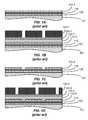
- FIGS. 1A, 1B, 1C, 1D, 1E, 1F and 1Gare cross-sectional views of a substrate at various stages during multi-patterning according to a prior art process.
- a substrate 101has a silicon oxide layer 105 deposited on substrate 101 and a titanium nitride layer 110 is deposited on silicon oxide layer 105 .
- Another silicon oxide layer 115 - 1is deposited on the titanium nitride layer 110 as shown in FIG. 1A .
- Patterning titanium nitride layer multiple timeshas been accomplished in the past by multiply-patterning silicon oxide layer 115 - 1 and later transferring the multiple-pattern into an underlying layer, e.g. titanium nitride layer 110 , at the same time.
- the first of the multiple patternsinvolved depositing silicon anti-reflective coating 120 - 1 on silicon oxide layer 115 - 1 and carbon anti-reflective coating 125 - 1 on silicon anti-reflective coating 120 - 1 .
- Photoresist 130 - 1is deposited on carbon anti-reflective coating 125 - 1 and patterned.
- the pattern of photoresist 130 - 1is transferred down into the carbon anti-reflective coating 125 - 1 , then into the silicon anti-reflective coating 120 - 1 and then again into silicon oxide layer 115 - 1 to form silicon oxide layer 115 - 2 .
- a schematic side viewis shown in FIG. 1C .
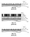
- the processis repeated with another pattern using photoresist 130 - 2 , carbon anti-reflective coating 125 - 2 , silicon anti-reflective coating 120 - 2 .
- the second patternis depicted in FIG. 1D in the photoresist 130 - 2 right before the pattern is transferred into the stack.
- FIG. 1Eshows a side view of silicon oxide 115 - 3 after the second pattern is transferred into silicon oxide 115 - 2 .
- the second patterncreates holes in different locations or sizes across the substrate surface.
- the pattern of silicon oxide 115 - 3shows that the second pattern is shifted one third of a pitch relative to the first pattern depicted in FIGS. 1B and 1C .
- Each pattern described in the example of FIGS. 1A-1Ginvolves etching through a thick stack of material to get to (and pattern) the target etch layer 110 .
- the present inventionreduces the number of times a multi-layer stack needs to be etched through and therefore reduces cost and processing complexity.
- the process sequenceis enabled by recently developed remote plasma etch processes which offer the necessary etch selectivities.
- FIG. 2is a flow chart of a multi-patterning process 201 according to embodiments.
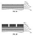
- FIGS. 3A-3Hare cross-sectional views of a substrate at stages during multi-patterning during a multi-patterning process according to embodiments.
- a substrateis provided in operation 210 .
- the substrateinitially has a blanket top mask layer 355 - 1 over a blanket etch stop layer 350 over a silicon anti-reflective coating 320 over a target etch layer 310 .
- Blanket top mask layer 355 - 1may contact blanket etch stop layer 350 in embodiments.
- Blanket etch stop layer 350may contact silicon anti-reflective coating 320 according to embodiments.
- silicon anti-reflective coating 320may contact target etch layer 310 in embodiments.
- Photoresist 360 - 1is deposited and patterned in operation 220 to achieve the cross-sectional view of FIG. 3B .
- Patterning photoresist 360 - 1may involve exposing photoresist 360 - 1 to light of a well-defined wavelength in the form of an image focused at the plane of photoresist 360 - 1 in embodiments. Patterning photoresist 360 - 1 may further involve developing the latent image using a chemical which preferentially removes either the exposed regions or the unexposed regions in embodiments.
- Blanket top mask layer 355 - 1is then patterned in operation 230 using patterned photoresist 360 - 1 as a mask template and the patterned photoresist may then be removed to achieve the cross-sectional view of FIG. 3C . After patterning, the layer will be referred to as first patterned top mask layer 355 - 2 .
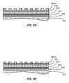
- Another layer of photoresist 360 - 2is formed on first patterned top mask layer 355 - 2 and patterned (with a different image from photoresist 360 - 1 ) in operation 240 .
- First patterned top mask layer 355 - 2is then patterned in operation 250 to form second patterned top mask layer 355 - 3 .
- Patterned photoresist 360 - 2is used as a mask template to achieve the cross-sectional view of FIG. 3E following optional removal of patterned photoresist 360 - 2 .
- a third layer of photoresist 360 - 3is also formed on second patterned top mask layer 355 - 3 and patterned in operation 260 .
- third layer of photoresist 360 - 3is transferred into second patterned top mask layer 355 - 3 to form third patterned top mask layer 355 - 4 in operation 270 .
- Third patterned top mask layer 355 - 4is shown in FIG. 3G following removal of third layer of photoresist 360 - 3 .
- Third patterned top mask layer 355 - 4embodies three independent patterns from each of patterned photoresist 360 - 1 , 360 - 2 and 360 - 3 .
- a combination of patterns in the mannermay be referred to herein as a compound pattern.
- a compound patternmay include a combination of two, three, four, five or any integer other than one according to embodiments.
- the compound patternhas a higher density of features in a dimension of the pattern compared to the corresponding density with any single photoresist pattern. In other words, the pitch of the compound pattern is decreased compared to any single photoresist pattern.
- the compound patternmay have half the pitch/twice the density, one third the pitch/thrice the density, one fourth the pitch/four times the density or one fifth the pitch/five times the density.
- the linear density of features along a direction of the second or third patterned top mask layersmay be an integer greater than one (e.g. two or three) times a linear density of features along the direction of the first patterned top mask layer in embodiments.
- the compound pattern of the top mask layermay then be used to pattern (operation 280 ) the underlying film stack including etch stop 350 , silicon anti-reflective coating 320 , target etch layer 310 and/or silicon oxide 305 according to embodiments.
- the dotted lines of FIG. 3Hshow vertical demarcation which may be used to perform a directional etch into the film stack. Only one instance of etching into the completed stack is necessary when using the process sequences outlined herein and the resulting process flow has fewer steps as a consequence.
- Etching through the stack in operation 280may include etching through target etch layer 310 or through silicon oxide 305 or even into substrate 301 according to embodiments.
- Target etch layer 310may be titanium nitride in embodiments.
- the anti-reflective coating 320may comprise silicon oxynitride according to embodiments.
- Anti-reflective coating 320may comprise or consist of silicon, oxygen and nitrogen in embodiments.
- Target etch layer 310may be a conductor or may be dielectric in embodiments.
- Target etch layer 310may comprise a metallic element, in other words an element which would form a conductor in a material consisting predominantly or only of the metallic element.
- top mask layer 355(including blanket top mask layer, first patterned top mask layer, second patterned top mask layer and/or third patterned top mask layer) are transparent for optical radiation from 20 nm to 700 nm to facilitate the measurement of overlay registration.
- Top mask layer 355may have a relatively high extinction coefficient (the imaginary part of the index of refraction) at the photolithography wavelength(s) in order to avoid back-reflections.
- the extinction coefficient of the top mask layermay be greater than 0.05, greater than 0.1 or greater than 0.15 according to embodiments.
- Remote plasma excitationis used to create the diverse set of selectivities needed to enable the new process sequences described herein.
- a local plasma in the substrate processing regionis used in tandem with the remote plasma in embodiments. In other embodiments, a local plasma is not used and the ions excited in the remote plasma are filtered out from the plasma effluents entering the substrate processing region. Ion suppression techniques will be described first, followed by the local plasma and exemplary hardware which may be used for all etch processes described herein.
- An ion suppression elementmay be included in the remote etch processes described herein. When included, the ion suppression element functions to reduce or eliminate ionic/charged species traveling from the plasma generation region to the substrate. Uncharged neutral and radical species may pass through the openings in the ion suppressor to react at the substrate. The ion suppressor helps control the concentration of ionic species in the reaction region at a level that increases selectivity.
- an ion suppressor described further in the exemplary equipment sectionmay be used to provide radical and/or neutral species for selectively etching substrates.
- an ion suppressoris used to provide fluorine-containing plasma effluents to selectively etch the target etch layer.
- the ion suppressormay be used to provide a reactive gas having a higher concentration of radicals than ions. Because most (or essentially all in embodiments) of the charged particles of a plasma are filtered or removed by the ion suppressor, the substrate is not necessarily biased during the etch process. By filtering ions from the plasma effluents before they reach the substrate processing region, a high etch rate selectivity may be achieved.
- Embodiments of the present inventionare also advantageous over conventional wet etch processes where surface tension of liquids can cause bending and peeling of small features.
- multi-patterning process 201includes applying energy to plasma-effluents (including radical-fluorine or radical-chlorine) while in the substrate processing region to selectively etch layers in a directional manner.
- the plasmamay be generated using known techniques (e.g., radio frequency excitations, capacitively-coupled power or inductively coupled power).
- the energyis applied using a capacitively-coupled plasma unit.
- the local plasma powermay be between about 10 watts and about 500 watts, between about 20 watts and about 400 watts, between about 30 watts and about 300 watts, or between about 50 watts and about 200 watts in embodiments of the invention. Higher powers in combination with higher operating pressures enable a reduction in force of impact of accelerated ions and preserve the integrity of patterned features other than material to-be-removed on the exposed silicon on the patterned substrate surface.
- a DC accelerating voltagemay be applied such that positive ions formed in the local plasma are accelerated in the direction of the patterned substrate.
- the local plasmamay be formed by applying a DC bias power such that the local plasma power comprises both an AC portion and a DC portion.
- the DC bias powersupplies a DC accelerating voltage which may be greater than 400 volts, greater than 500 volts, greater than 600 volts, or greater than 700 volts in embodiments of the invention.
- the DC voltagemay be less than 2000 volts, less than 1500 volts, less than 1300 volts or less than 1100 volts to preserve the integrity of non-silicon components.
- the pressure in the substrate processing regionmay be between about 0.5 mTorr and about 500 mTorr, between about 2 mTorr and about 200 mTorr or between about 5 mTorr and about 100 mTorr in embodiments.
- the multi-patterning process 201includes applying energy to the fluorine-containing precursor while in the remote plasma region to generate the plasma effluents regardless of whether a local plasma is excited.
- the plasmamay include a number of charged and neutral species including radicals and ions.
- the plasmamay be generated using known techniques (e.g., radio frequency excitations, capacitively-coupled power, inductively coupled power, and the like).
- the energyis applied using a capacitively-coupled plasma unit.
- the remote plasma source powermay be between about 300 watts and about 5000 watts, between about 500 watts and about 3000 watts, between about 750 watts and about 2000 watts, or between about 900 watts and about 1500 watts in embodiments of the invention. As with all complementary ranges provided herein, upper limits may be combined with any suitable lower limits to obtain additional embodiments.
- the pressure in the remote plasma regionmay be such that the pressure in the substrate processing region ends up between about 0.01 Torr and about 50 Torr or between about 0.1 Torr and about 5 Torr in embodiments. The pressure in the remote plasma region and the substrate processing region may be roughly the same according to embodiments.
- the capacitively-coupled plasma unitmay be disposed remote from a substrate processing region of the processing chamber. For example, the capacitively-coupled plasma unit and the plasma generation region may be separated from the gas reaction region by a showerhead.
- the RF frequency applied for either the local or remote plasmas described hereinmay be low RF frequencies less than about 200 kHz, high RF frequencies between about 10 MHz and about 15 MHz, or microwave frequencies greater than or about 1 GHz in embodiments.
- a halogen-containing precursor(e.g. a fluorine-containing precursor or a chlorine-containing precursor) is flowed into the remote plasma region during all etch processes described herein.
- the flow of the halogen-containing precursormay further include one or more relatively inert gases such as He, N 2 , Ar.
- the inert gascan be used to improve plasma stability, process uniformity and the like.
- Argonis helpful, as an additive, to promote the formation of a stable plasma, however, current experimentation has established that inclusion of argon results in a nonuniform (bumpy) post etch surface. Process uniformity is generally increased when helium is included. In one embodiment, helium does not cause the bumpiness associated with argon.
- These additivesare present in embodiments throughout this specification. Flow rates and ratios of the different gases may be used to control etch rates and etch selectivity.
- the halogen-containing precursor(chlorine-containing precursor, fluorine-containing precursor e.g. NF 3 ) is supplied at a flow rate of between about 5 sccm (standard cubic centimeters per minute) and 400 sccm, He at a flow rate of between about 0 slm (standard liters per minute) and 3 slm, and N 2 at a flow rate of between about 0 slm and 3 slm.
- the chlorine-containing precursor or fluorine-containing precursormay be flowed into chamber plasma region 1015 at rates between about 5 sccm and about 500 sccm, between about 10 sccm and about 150 sccm, or between about 25 sccm and about 125 sccm in embodiments.
- gases and/or flowsmay be used depending on a number of factors including processing chamber configuration, substrate size, geometry and layout of features being etched, and the like.
- the temperature of the substratemay be between about ⁇ 20° C. and about 200° C. during both the any of the etch processes described herein.
- an ion suppressor(which may be the showerhead) may be used to provide radical and/or neutral species for gas-phase etching.
- the ion suppressormay also be referred to as an ion suppression element.
- the ion suppressoris used to filter etching plasma effluents (including radical-fluorine) en route from the remote plasma region to the substrate processing region.
- the ion suppressormay be used to provide a reactive gas having a higher concentration of radicals than ions.
- Plasma effluentspass through the ion suppressor disposed between the remote plasma region and the substrate processing region.
- the ion suppressorfunctions to dramatically reduce or substantially eliminate ionic species traveling from the plasma generation region to the substrate.
- the ion suppressors described hereinare simply one way to achieve a low electron temperature in the substrate processing region during the silicon nitride etch and/or the silicon oxide etch described above.
- an electron beamis passed through the substrate processing region in a plane parallel to the substrate to reduce the electron temperature of the plasma effluents.
- a simpler showerheadmay be used if an electron beam is applied in this manner.
- the electron beammay be passed as a laminar sheet disposed above the substrate in embodiments.
- the electron beamprovides a source of neutralizing negative charge and provides a more active means for reducing the flow of positively charged ions towards the substrate and increasing the selectivity of silicon nitride in embodiments.
- the flow of plasma effluents and various parameters governing the operation of the electron beammay be adjusted to lower the electron temperature measured in the substrate processing region.
- the electron temperaturemay be measured using a Langmuir probe in the substrate processing region during excitation of a plasma in the remote plasma.
- the electron temperaturemay be less than 0.5 eV, less than 0.45 eV, less than 0.4 eV, or less than 0.35 eV.
- Uncharged neutral and radical speciesmay pass through the electron beam and/or the openings in the ion suppressor to react at the substrate.
- Such a process using radicals and other neutral speciescan reduce plasma damage compared to conventional plasma etch processes that include sputtering and bombardment.
- Embodiments of the present inventionare also advantageous over conventional wet etch processes where surface tension of liquids can cause bending and peeling of small features.
- the substrate processing regionmay be described herein as “plasma-free” during the etch processes described herein.
- “Plasma-free”does not necessarily mean the region is devoid of plasma. Ionized species and free electrons created within the plasma region may travel through pores (apertures) in the partition (showerhead) at exceedingly small concentrations. The borders of the plasma in the chamber plasma region are hard to define and may encroach upon the substrate processing region through the apertures in the showerhead. Furthermore, a low intensity plasma may be created in the substrate processing region without eliminating desirable features of the etch processes described herein. All causes for a plasma having much lower intensity ion density than the chamber plasma region during the creation of the excited plasma effluents do not deviate from the scope of “plasma-free” as used herein.
- a halogen-containing precursormay be flowed into a remote plasma region through a gas inlet assembly.
- a remote plasma systemmay optionally be included in the system, and may process the halogen-containing precursor which then travels through the gas inlet assembly into the remote plasma region.
- the halogen-containing precursormay be delivered to the processing chamber in an unexcited state.
- the halogen-containing precursormay be excited within the RPS prior to entering the remote plasma region located inside the substrate processing chamber.
- the halogen-containing precursormay pass through RPS or bypass the RPS unit in embodiments.
- a cooling plate, faceplate, ion suppressor, showerhead, and a substrate support(also known as a pedestal), having a substrate disposed thereon, are shown and may each be included according to embodiments.
- the pedestalmay have a heat exchange channel through which a heat exchange fluid flows to control the temperature of the substrate. This configuration may allow the substrate temperature to be cooled or heated to maintain relatively low temperatures, such as between about ⁇ 20° C. to about 200° C., or there between.
- the wafer support platter of the pedestal 1065which may comprise aluminum, ceramic, or a combination thereof, may also be resistively heated to relatively high temperatures, such as from up to or about 100° C. to above or about 1100° C., using an embedded resistive heater element.
- the ion suppressormay comprise a plate or other geometry that defines a plurality of apertures throughout the structure that are configured to suppress the migration of ionically-charged species out of chamber plasma region while allowing uncharged neutral or radical species to pass through the ion suppressor into an activated gas delivery region between the ion suppressor and the showerhead.
- the ion suppressormay comprise a perforated plate with a variety of aperture configurations. These uncharged species may include highly reactive species that are transported with less reactive carrier gas through the apertures. As noted above, the migration of ionic species through the holes may be significantly reduced as quantified earlier.
- Controlling the amount of ionic species passing through the ion suppressormay provide increased control over the gas mixture brought into contact with the underlying wafer substrate, which in turn may increase control of the etch characteristics of the gas mixture. For example, adjustments in the ion concentration of the gas mixture can significantly alter its etch selectivity.
- the plurality of holes in the ion suppressormay be configured to control the passage of the activated gas, i.e., the ionic, radical, and/or neutral species, through the ion suppressor.
- the aspect ratio of the holes, or the hole diameter to length, and/or the geometry of the holesmay be controlled so that the flow of ionically-charged species in the activated gas passing through the ion suppressor is reduced.
- the holes in the ion suppressormay include a tapered portion that faces chamber plasma region, and a cylindrical portion that faces the showerhead. The cylindrical portion may be shaped and dimensioned to control the flow of ionic species passing to the showerhead.
- An adjustable electrical biasmay also be applied to the ion suppressor as an additional means to control the flow of ionic species through the suppressor.
- showerhead in combination with ion suppressormay allow a plasma present in chamber plasma region to avoid directly exciting gases in substrate processing region, while still allowing excited species to travel from chamber plasma region into substrate processing region.
- the chambermay be configured to prevent the plasma from contacting a substrate being etched. This may advantageously protect a variety of intricate structures and films patterned on the substrate, which may be damaged, dislocated, or otherwise warped if directly contacted by a generated plasma.
- the gas distribution assembliesfor use in the processing chamber section may be referred to as dual channel showerheads (DCSH).
- the dual channel showerheadmay provide for etching processes that allow for separation of etchants outside of the processing region to provide limited interaction with chamber components and each other prior to being delivered into the processing region.
- the showerheadthrough-holes and closed-end holes. Through-holes transmit plasma effluents whereas the closed-end holes introduce separate precursors which have not flowed through any plasma prior to entering the substrate processing region.
- the chamber plasma region upstream from the showerhead or a region in an RPSmay be referred to as a remote plasma region.
- the radical precursore.g., a radical-fluorine precursor
- the additional precursorsare excited only by the radical-fluorine precursor.
- Plasma powermay essentially be applied only to the remote plasma region in embodiments to ensure that the radical-fluorine precursor provides the dominant excitation.
- substratemay be a support substrate with or without layers formed thereon.
- the patterned substratemay be an insulator or a semiconductor of a variety of doping concentrations and profiles and may, for example, be a semiconductor substrate of the type used in the manufacture of integrated circuits.
- siliconof the patterned substrate is predominantly Si but may include minority concentrations of other elemental constituents such as nitrogen, oxygen, hydrogen, carbon and the like.
- siliconmay consist of or consist essentially of silicon.
- Si nitrideof the patterned substrate is predominantly Si 3 N 4 but may include minority concentrations of other elemental constituents such as oxygen, hydrogen, carbon and the like.
- Exposed silicon nitridemay consist essentially of or consist of silicon and nitrogen.
- Exposed “silicon oxide” of the patterned substrateis predominantly SiO 2 but may include minority concentrations of other elemental constituents such as nitrogen, hydrogen, carbon and the like.
- silicon oxide films etched using the methods taught hereinconsist essentially of or consist of silicon and oxygen.
- plasma effluentsdescribe gas exiting from the chamber plasma region and entering the substrate processing region. Plasma effluents are in an “excited state” wherein at least some of the gas molecules are in vibrationally-excited, dissociated and/or ionized states.
- a “radical precursor”is used to describe plasma effluents (a gas in an excited state which is exiting a plasma) which participate in a reaction to either remove material from or deposit material on a surface.
- Radar-fluorineare radical precursors which contain fluorine but may contain other elemental constituents.
- inert gasrefers to any gas which does not form chemical bonds when etching or being incorporated into a film.
- exemplary inert gasesinclude noble gases but may include other gases so long as no chemical bonds are formed when (typically) trace amounts are trapped in a film.
- trench and trenchare used throughout with no implication that the etched geometry has a large horizontal aspect ratio. Viewed from above the surface, trenches may appear circular, oval, polygonal, rectangular, or a variety of other shapes. A trench may be in the shape of a moat around an island of material.
- viais used to refer to a low aspect ratio trench (as viewed from above) which may or may not be filled with metal to form a vertical electrical connection.
- a conformal etch processrefers to a generally uniform removal of material on a surface in the same shape as the surface, i.e., the surface of the etched layer and the pre-etch surface are generally parallel. A person having ordinary skill in the art will recognize that the etched interface likely cannot be 100% conformal and thus the term “generally” allows for acceptable tolerances.
Landscapes
- Engineering & Computer Science (AREA)
- Physics & Mathematics (AREA)
- Condensed Matter Physics & Semiconductors (AREA)
- General Physics & Mathematics (AREA)
- Manufacturing & Machinery (AREA)
- Computer Hardware Design (AREA)
- Microelectronics & Electronic Packaging (AREA)
- Power Engineering (AREA)
- Chemical & Material Sciences (AREA)
- Inorganic Chemistry (AREA)
- Drying Of Semiconductors (AREA)
Abstract
Description
Embodiments of the invention relate to efficient multi-patterning.
Integrated circuits are made possible by processes which produce intricately patterned material layers on substrate surfaces. Producing patterned material on a substrate is enabled by controlled methods for removal of exposed material. Chemical etching is used for a variety of purposes including transferring a pattern in photoresist into underlying layers, thinning layers or thinning lateral dimensions of features already present on the surface. Pattern transfers require etch process which removes one material faster than another. Such an etch process is said to be selective of the first material relative to the second material. As a result of the diversity of materials, circuits and processes, etch processes have been developed with a selectivity towards a variety of materials.
Dry etch processes are desirable for selectively removing material from semiconductor substrates. The desirability stems from the ability to gently remove material from miniature structures with minimal physical disturbance. Dry etch processes also allow the etch rate to be abruptly stopped by removing the gas phase reagents. Some dry-etch processes involve the exposure of a substrate to remote plasma by-products formed from one or more precursors. The remote plasma by-products may be ionically filtered to increase selectivity or may be further excited in a local plasma to enhance etch rate or directionality. These selective gas-phase etch processes can enable new patterning process flows. New process flows are needed to take advantage of these selective gas-phase etch processes.
Methods of patterning a blanket layer (a target etch layer) on a substrate are described. The methods involve multiple patterning steps of a mask layer several layers above the target etch layer. The compound pattern, made from multiple patterning steps, is later transferred in one set of operations through the stack to save process steps.
Embodiments of the invention include methods of patterning a substrate. The methods includes forming a first layer of photoresist on a stack of materials on the substrate. The stack of materials includes a blanket top mask layer over a blanket etch stop layer over an anti-reflective coating over a target etch layer. The methods further include patterning the first layer of photoresist to form a first pattern. The methods further include etching the first pattern into the blanket top mask layer to form a first patterned top mask layer. The methods further include removing any remaining material from the first layer of photoresist. The methods further include forming a second layer of photoresist on the first patterned top mask layer. The methods further include patterning the second layer of photoresist to form a second pattern. The methods further include etching the second pattern into the first patterned top mask layer to form a second patterned top mask layer. The methods further include etching the first pattern and the second pattern into the stack of materials. The first pattern and the second pattern are formed in the stack of materials during the same etching operations.
Embodiments of the invention include methods of patterning a substrate. The methods include forming a first layer of photoresist on a stack of materials on the substrate. The stack of materials includes a blanket top mask layer over a blanket etch stop layer over an anti-reflective coating over a target etch layer. The methods further include patterning the first layer of photoresist to form a first pattern. The methods further include etching the first pattern into the blanket top mask layer to form a first patterned top mask layer. The methods further include forming a second layer of photoresist on the first patterned top mask layer. The methods further include patterning the second layer of photoresist to form a second pattern. The methods further include etching the second pattern into the first patterned top mask layer to form a second patterned top mask layer. The methods further include forming a third layer of photoresist on the second patterned top mask layer. The methods further include patterning the third layer of photoresist to form a third pattern. The methods further include etching the third pattern into the second patterned top mask layer to form a third patterned top mask layer. The methods further include etching the first pattern, the second pattern and the third pattern into the stack of materials. The first pattern, the second pattern and the third pattern are formed in the stack of materials during the same etching operations.
Additional embodiments and features are set forth in part in the description that follows, and in part will become apparent to those skilled in the art upon examination of the specification or may be learned by the practice of the embodiments. The features and advantages of the embodiments may be realized and attained by means of the instrumentalities, combinations, and methods described in the specification.
A further understanding of the nature and advantages of the embodiments may be realized by reference to the remaining portions of the specification and the drawings.
In the appended figures, similar components and/or features may have the same reference label. Further, various components of the same type may be distinguished by following the reference label by a dash and a second label that distinguishes among the similar components. If only the first reference label is used in the specification, the description is applicable to any one of the similar components having the same first reference label irrespective of the second reference label.
Methods of patterning a blanket layer (a target etch layer) on a substrate are described. The methods involve multiple patterning steps of a mask layer several layers above the target etch layer. The compound pattern, made from multiple patterning steps, is later transferred in one set of operations through the stack to save process steps.
Embodiments of the present invention pertain to a method of multi-patterning a stack of layers while reducing the cost associated with the production sequence. In order to provide contrast, reference is now made toFIGS. 1A, 1B, 1C, 1D, 1E, 1F and 1G , which are cross-sectional views of a substrate at various stages during multi-patterning according to a prior art process. Asubstrate 101 has asilicon oxide layer 105 deposited onsubstrate 101 and atitanium nitride layer 110 is deposited onsilicon oxide layer 105. Another silicon oxide layer115-1 is deposited on thetitanium nitride layer 110 as shown inFIG. 1A . Patterning titanium nitride layer multiple times has been accomplished in the past by multiply-patterning silicon oxide layer115-1 and later transferring the multiple-pattern into an underlying layer, e.g.titanium nitride layer 110, at the same time. The first of the multiple patterns involved depositing silicon anti-reflective coating120-1 on silicon oxide layer115-1 and carbon anti-reflective coating125-1 on silicon anti-reflective coating120-1. Photoresist130-1 is deposited on carbon anti-reflective coating125-1 and patterned. The pattern of photoresist130-1 is transferred down into the carbon anti-reflective coating125-1, then into the silicon anti-reflective coating120-1 and then again into silicon oxide layer115-1 to form silicon oxide layer115-2. After patterning and removal of all the patterned layers above silicon oxide layer115-2, a schematic side view is shown inFIG. 1C .
The process is repeated with another pattern using photoresist130-2, carbon anti-reflective coating125-2, silicon anti-reflective coating120-2. The second pattern is depicted inFIG. 1D in the photoresist130-2 right before the pattern is transferred into the stack.FIG. 1E shows a side view of silicon oxide115-3 after the second pattern is transferred into silicon oxide115-2. The second pattern creates holes in different locations or sizes across the substrate surface. The pattern of silicon oxide115-3 shows that the second pattern is shifted one third of a pitch relative to the first pattern depicted inFIGS. 1B and 1C . A third pattern, depicted inFIGS. 1F and 1G , uses photoresist130-3 to ultimately pattern silicon oxide115-4. The third pattern completes the process of reducing the pitch by a factor of three relative to the initial pitch shown inFIG. 1C . The process shown represents an example of a prior art litho-etch-litho-etch (LELE) process.
Each pattern described in the example ofFIGS. 1A-1G involves etching through a thick stack of material to get to (and pattern) thetarget etch layer 110. The present invention reduces the number of times a multi-layer stack needs to be etched through and therefore reduces cost and processing complexity. The process sequence is enabled by recently developed remote plasma etch processes which offer the necessary etch selectivities.
In order to better understand and appreciate the invention, reference is now made toFIG. 2 which is a flow chart of amulti-patterning process 201 according to embodiments. Reference will concurrently be made toFIGS. 3A-3H which are cross-sectional views of a substrate at stages during multi-patterning during a multi-patterning process according to embodiments. A substrate is provided inoperation 210. The substrate initially has a blanket top mask layer355-1 over a blanketetch stop layer 350 over a siliconanti-reflective coating 320 over atarget etch layer 310. Blanket top mask layer355-1 may contact blanketetch stop layer 350 in embodiments. Blanketetch stop layer 350 may contact siliconanti-reflective coating 320 according to embodiments. Finally, siliconanti-reflective coating 320 may contacttarget etch layer 310 in embodiments.
Photoresist360-1 is deposited and patterned inoperation 220 to achieve the cross-sectional view ofFIG. 3B . Patterning photoresist360-1 may involve exposing photoresist360-1 to light of a well-defined wavelength in the form of an image focused at the plane of photoresist360-1 in embodiments. Patterning photoresist360-1 may further involve developing the latent image using a chemical which preferentially removes either the exposed regions or the unexposed regions in embodiments. Blanket top mask layer355-1 is then patterned inoperation 230 using patterned photoresist360-1 as a mask template and the patterned photoresist may then be removed to achieve the cross-sectional view ofFIG. 3C . After patterning, the layer will be referred to as first patterned top mask layer355-2.
Another layer of photoresist360-2 is formed on first patterned top mask layer355-2 and patterned (with a different image from photoresist360-1) inoperation 240. First patterned top mask layer355-2 is then patterned inoperation 250 to form second patterned top mask layer355-3. Patterned photoresist360-2 is used as a mask template to achieve the cross-sectional view ofFIG. 3E following optional removal of patterned photoresist360-2. In this example, a third layer of photoresist360-3 is also formed on second patterned top mask layer355-3 and patterned inoperation 260. The pattern of third layer of photoresist360-3 is transferred into second patterned top mask layer355-3 to form third patterned top mask layer355-4 inoperation 270. Third patterned top mask layer355-4 is shown inFIG. 3G following removal of third layer of photoresist360-3.
Third patterned top mask layer355-4 embodies three independent patterns from each of patterned photoresist360-1,360-2 and360-3. A combination of patterns in the manner may be referred to herein as a compound pattern. Generally speaking, a compound pattern may include a combination of two, three, four, five or any integer other than one according to embodiments. In the example, the compound pattern has a higher density of features in a dimension of the pattern compared to the corresponding density with any single photoresist pattern. In other words, the pitch of the compound pattern is decreased compared to any single photoresist pattern. In embodiments, the compound pattern may have half the pitch/twice the density, one third the pitch/thrice the density, one fourth the pitch/four times the density or one fifth the pitch/five times the density. The linear density of features along a direction of the second or third patterned top mask layers may be an integer greater than one (e.g. two or three) times a linear density of features along the direction of the first patterned top mask layer in embodiments.
The compound pattern of the top mask layer (e.g. third patterned top mask layer355-4) may then be used to pattern (operation280) the underlying film stack includingetch stop 350, siliconanti-reflective coating 320,target etch layer 310 and/orsilicon oxide 305 according to embodiments. The dotted lines ofFIG. 3H show vertical demarcation which may be used to perform a directional etch into the film stack. Only one instance of etching into the completed stack is necessary when using the process sequences outlined herein and the resulting process flow has fewer steps as a consequence. Etching through the stack inoperation 280 may include etching throughtarget etch layer 310 or throughsilicon oxide 305 or even intosubstrate 301 according to embodiments.
In embodiments, top mask layer355 (including blanket top mask layer, first patterned top mask layer, second patterned top mask layer and/or third patterned top mask layer) are transparent for optical radiation from 20 nm to 700 nm to facilitate the measurement of overlay registration. Top mask layer355 may have a relatively high extinction coefficient (the imaginary part of the index of refraction) at the photolithography wavelength(s) in order to avoid back-reflections. The extinction coefficient of the top mask layer may be greater than 0.05, greater than 0.1 or greater than 0.15 according to embodiments.
Remote plasma excitation is used to create the diverse set of selectivities needed to enable the new process sequences described herein. A local plasma in the substrate processing region is used in tandem with the remote plasma in embodiments. In other embodiments, a local plasma is not used and the ions excited in the remote plasma are filtered out from the plasma effluents entering the substrate processing region. Ion suppression techniques will be described first, followed by the local plasma and exemplary hardware which may be used for all etch processes described herein.
An ion suppression element may be included in the remote etch processes described herein. When included, the ion suppression element functions to reduce or eliminate ionic/charged species traveling from the plasma generation region to the substrate. Uncharged neutral and radical species may pass through the openings in the ion suppressor to react at the substrate. The ion suppressor helps control the concentration of ionic species in the reaction region at a level that increases selectivity.
In accordance with some embodiments of the invention, an ion suppressor described further in the exemplary equipment section may be used to provide radical and/or neutral species for selectively etching substrates. In one embodiment, for example, an ion suppressor is used to provide fluorine-containing plasma effluents to selectively etch the target etch layer. The ion suppressor may be used to provide a reactive gas having a higher concentration of radicals than ions. Because most (or essentially all in embodiments) of the charged particles of a plasma are filtered or removed by the ion suppressor, the substrate is not necessarily biased during the etch process. By filtering ions from the plasma effluents before they reach the substrate processing region, a high etch rate selectivity may be achieved. Embodiments of the present invention are also advantageous over conventional wet etch processes where surface tension of liquids can cause bending and peeling of small features.
When a local plasma is used,multi-patterning process 201 includes applying energy to plasma-effluents (including radical-fluorine or radical-chlorine) while in the substrate processing region to selectively etch layers in a directional manner. The plasma may be generated using known techniques (e.g., radio frequency excitations, capacitively-coupled power or inductively coupled power). In an embodiment, the energy is applied using a capacitively-coupled plasma unit. The local plasma power may be between about 10 watts and about 500 watts, between about 20 watts and about 400 watts, between about 30 watts and about 300 watts, or between about 50 watts and about 200 watts in embodiments of the invention. Higher powers in combination with higher operating pressures enable a reduction in force of impact of accelerated ions and preserve the integrity of patterned features other than material to-be-removed on the exposed silicon on the patterned substrate surface.
A DC accelerating voltage may be applied such that positive ions formed in the local plasma are accelerated in the direction of the patterned substrate. In other words, the local plasma may be formed by applying a DC bias power such that the local plasma power comprises both an AC portion and a DC portion. The DC bias power supplies a DC accelerating voltage which may be greater than 400 volts, greater than 500 volts, greater than 600 volts, or greater than 700 volts in embodiments of the invention. The DC voltage may be less than 2000 volts, less than 1500 volts, less than 1300 volts or less than 1100 volts to preserve the integrity of non-silicon components. The pressure in the substrate processing region may be between about 0.5 mTorr and about 500 mTorr, between about 2 mTorr and about 200 mTorr or between about 5 mTorr and about 100 mTorr in embodiments.
Themulti-patterning process 201 includes applying energy to the fluorine-containing precursor while in the remote plasma region to generate the plasma effluents regardless of whether a local plasma is excited. As would be appreciated by one of ordinary skill in the art, the plasma may include a number of charged and neutral species including radicals and ions. The plasma may be generated using known techniques (e.g., radio frequency excitations, capacitively-coupled power, inductively coupled power, and the like). In an embodiment, the energy is applied using a capacitively-coupled plasma unit. The remote plasma source power may be between about 300 watts and about 5000 watts, between about 500 watts and about 3000 watts, between about 750 watts and about 2000 watts, or between about 900 watts and about 1500 watts in embodiments of the invention. As with all complementary ranges provided herein, upper limits may be combined with any suitable lower limits to obtain additional embodiments. The pressure in the remote plasma region may be such that the pressure in the substrate processing region ends up between about 0.01 Torr and about 50 Torr or between about 0.1 Torr and about 5 Torr in embodiments. The pressure in the remote plasma region and the substrate processing region may be roughly the same according to embodiments. The capacitively-coupled plasma unit may be disposed remote from a substrate processing region of the processing chamber. For example, the capacitively-coupled plasma unit and the plasma generation region may be separated from the gas reaction region by a showerhead.
The RF frequency applied for either the local or remote plasmas described herein may be low RF frequencies less than about 200 kHz, high RF frequencies between about 10 MHz and about 15 MHz, or microwave frequencies greater than or about 1 GHz in embodiments.
A halogen-containing precursor (e.g. a fluorine-containing precursor or a chlorine-containing precursor) is flowed into the remote plasma region during all etch processes described herein. The flow of the halogen-containing precursor may further include one or more relatively inert gases such as He, N2, Ar. The inert gas can be used to improve plasma stability, process uniformity and the like. Argon is helpful, as an additive, to promote the formation of a stable plasma, however, current experimentation has established that inclusion of argon results in a nonuniform (bumpy) post etch surface. Process uniformity is generally increased when helium is included. In one embodiment, helium does not cause the bumpiness associated with argon. These additives are present in embodiments throughout this specification. Flow rates and ratios of the different gases may be used to control etch rates and etch selectivity.
In embodiments, the halogen-containing precursor (chlorine-containing precursor, fluorine-containing precursor e.g. NF3) is supplied at a flow rate of between about 5 sccm (standard cubic centimeters per minute) and 400 sccm, He at a flow rate of between about 0 slm (standard liters per minute) and 3 slm, and N2at a flow rate of between about 0 slm and 3 slm. The chlorine-containing precursor or fluorine-containing precursor may be flowed into chamber plasma region1015 at rates between about 5 sccm and about 500 sccm, between about 10 sccm and about 150 sccm, or between about 25 sccm and about 125 sccm in embodiments. One of ordinary skill in the art would recognize that other gases and/or flows may be used depending on a number of factors including processing chamber configuration, substrate size, geometry and layout of features being etched, and the like. The temperature of the substrate may be between about −20° C. and about 200° C. during both the any of the etch processes described herein.
In embodiments, an ion suppressor (which may be the showerhead) may be used to provide radical and/or neutral species for gas-phase etching. The ion suppressor may also be referred to as an ion suppression element. In embodiments, for example, the ion suppressor is used to filter etching plasma effluents (including radical-fluorine) en route from the remote plasma region to the substrate processing region. The ion suppressor may be used to provide a reactive gas having a higher concentration of radicals than ions. Plasma effluents pass through the ion suppressor disposed between the remote plasma region and the substrate processing region. The ion suppressor functions to dramatically reduce or substantially eliminate ionic species traveling from the plasma generation region to the substrate. The ion suppressors described herein are simply one way to achieve a low electron temperature in the substrate processing region during the silicon nitride etch and/or the silicon oxide etch described above.
In embodiments, an electron beam is passed through the substrate processing region in a plane parallel to the substrate to reduce the electron temperature of the plasma effluents. A simpler showerhead may be used if an electron beam is applied in this manner. The electron beam may be passed as a laminar sheet disposed above the substrate in embodiments. The electron beam provides a source of neutralizing negative charge and provides a more active means for reducing the flow of positively charged ions towards the substrate and increasing the selectivity of silicon nitride in embodiments. The flow of plasma effluents and various parameters governing the operation of the electron beam may be adjusted to lower the electron temperature measured in the substrate processing region.
The electron temperature may be measured using a Langmuir probe in the substrate processing region during excitation of a plasma in the remote plasma. In embodiments, the electron temperature may be less than 0.5 eV, less than 0.45 eV, less than 0.4 eV, or less than 0.35 eV. These extremely low values for the electron temperature are enabled by the presence of the electron beam, showerhead and/or the ion suppressor. Uncharged neutral and radical species may pass through the electron beam and/or the openings in the ion suppressor to react at the substrate. Such a process using radicals and other neutral species can reduce plasma damage compared to conventional plasma etch processes that include sputtering and bombardment. Embodiments of the present invention are also advantageous over conventional wet etch processes where surface tension of liquids can cause bending and peeling of small features.
The substrate processing region may be described herein as “plasma-free” during the etch processes described herein. “Plasma-free” does not necessarily mean the region is devoid of plasma. Ionized species and free electrons created within the plasma region may travel through pores (apertures) in the partition (showerhead) at exceedingly small concentrations. The borders of the plasma in the chamber plasma region are hard to define and may encroach upon the substrate processing region through the apertures in the showerhead. Furthermore, a low intensity plasma may be created in the substrate processing region without eliminating desirable features of the etch processes described herein. All causes for a plasma having much lower intensity ion density than the chamber plasma region during the creation of the excited plasma effluents do not deviate from the scope of “plasma-free” as used herein.
During film etching, e.g., titanium nitride, tantalum nitride, tungsten, silicon, polysilicon, silicon oxide, silicon nitride, silicon oxynitride, silicon oxycarbide, etc., a halogen-containing precursor may be flowed into a remote plasma region through a gas inlet assembly. A remote plasma system (RPS) may optionally be included in the system, and may process the halogen-containing precursor which then travels through the gas inlet assembly into the remote plasma region. The halogen-containing precursor may be delivered to the processing chamber in an unexcited state. The halogen-containing precursor may be excited within the RPS prior to entering the remote plasma region located inside the substrate processing chamber. The halogen-containing precursor may pass through RPS or bypass the RPS unit in embodiments.
A cooling plate, faceplate, ion suppressor, showerhead, and a substrate support (also known as a pedestal), having a substrate disposed thereon, are shown and may each be included according to embodiments. The pedestal may have a heat exchange channel through which a heat exchange fluid flows to control the temperature of the substrate. This configuration may allow the substrate temperature to be cooled or heated to maintain relatively low temperatures, such as between about −20° C. to about 200° C., or there between. The wafer support platter of the pedestal1065, which may comprise aluminum, ceramic, or a combination thereof, may also be resistively heated to relatively high temperatures, such as from up to or about 100° C. to above or about 1100° C., using an embedded resistive heater element.
The ion suppressor may comprise a plate or other geometry that defines a plurality of apertures throughout the structure that are configured to suppress the migration of ionically-charged species out of chamber plasma region while allowing uncharged neutral or radical species to pass through the ion suppressor into an activated gas delivery region between the ion suppressor and the showerhead. In embodiments, the ion suppressor may comprise a perforated plate with a variety of aperture configurations. These uncharged species may include highly reactive species that are transported with less reactive carrier gas through the apertures. As noted above, the migration of ionic species through the holes may be significantly reduced as quantified earlier. Controlling the amount of ionic species passing through the ion suppressor may provide increased control over the gas mixture brought into contact with the underlying wafer substrate, which in turn may increase control of the etch characteristics of the gas mixture. For example, adjustments in the ion concentration of the gas mixture can significantly alter its etch selectivity.
The plurality of holes in the ion suppressor may be configured to control the passage of the activated gas, i.e., the ionic, radical, and/or neutral species, through the ion suppressor. For example, the aspect ratio of the holes, or the hole diameter to length, and/or the geometry of the holes may be controlled so that the flow of ionically-charged species in the activated gas passing through the ion suppressor is reduced. The holes in the ion suppressor may include a tapered portion that faces chamber plasma region, and a cylindrical portion that faces the showerhead. The cylindrical portion may be shaped and dimensioned to control the flow of ionic species passing to the showerhead. An adjustable electrical bias may also be applied to the ion suppressor as an additional means to control the flow of ionic species through the suppressor.
Showerhead in combination with ion suppressor may allow a plasma present in chamber plasma region to avoid directly exciting gases in substrate processing region, while still allowing excited species to travel from chamber plasma region into substrate processing region. In this way, the chamber may be configured to prevent the plasma from contacting a substrate being etched. This may advantageously protect a variety of intricate structures and films patterned on the substrate, which may be damaged, dislocated, or otherwise warped if directly contacted by a generated plasma.
The gas distribution assemblies (e.g. the showerhead) for use in the processing chamber section may be referred to as dual channel showerheads (DCSH). The dual channel showerhead may provide for etching processes that allow for separation of etchants outside of the processing region to provide limited interaction with chamber components and each other prior to being delivered into the processing region. The showerhead through-holes and closed-end holes. Through-holes transmit plasma effluents whereas the closed-end holes introduce separate precursors which have not flowed through any plasma prior to entering the substrate processing region.
The chamber plasma region upstream from the showerhead or a region in an RPS may be referred to as a remote plasma region. In embodiments, the radical precursor, e.g., a radical-fluorine precursor, is created in the remote plasma region and travels into the substrate processing region where it may or may not combine with additional precursors. In embodiments, the additional precursors are excited only by the radical-fluorine precursor. Plasma power may essentially be applied only to the remote plasma region in embodiments to ensure that the radical-fluorine precursor provides the dominant excitation.
As used herein “substrate” may be a support substrate with or without layers formed thereon. The patterned substrate may be an insulator or a semiconductor of a variety of doping concentrations and profiles and may, for example, be a semiconductor substrate of the type used in the manufacture of integrated circuits. Exposed “silicon” of the patterned substrate is predominantly Si but may include minority concentrations of other elemental constituents such as nitrogen, oxygen, hydrogen, carbon and the like. Exposed “silicon” may consist of or consist essentially of silicon. Exposed “silicon nitride” of the patterned substrate is predominantly Si3N4but may include minority concentrations of other elemental constituents such as oxygen, hydrogen, carbon and the like. “Exposed silicon nitride” may consist essentially of or consist of silicon and nitrogen. Exposed “silicon oxide” of the patterned substrate is predominantly SiO2but may include minority concentrations of other elemental constituents such as nitrogen, hydrogen, carbon and the like. In embodiments, silicon oxide films etched using the methods taught herein consist essentially of or consist of silicon and oxygen.
The term “precursor” is used to refer to any process gas which takes part in a reaction to either remove material from or deposit material onto a surface. “Plasma effluents” describe gas exiting from the chamber plasma region and entering the substrate processing region. Plasma effluents are in an “excited state” wherein at least some of the gas molecules are in vibrationally-excited, dissociated and/or ionized states. A “radical precursor” is used to describe plasma effluents (a gas in an excited state which is exiting a plasma) which participate in a reaction to either remove material from or deposit material on a surface. “Radical-fluorine” are radical precursors which contain fluorine but may contain other elemental constituents. The phrase “inert gas” refers to any gas which does not form chemical bonds when etching or being incorporated into a film. Exemplary inert gases include noble gases but may include other gases so long as no chemical bonds are formed when (typically) trace amounts are trapped in a film.
The terms “gap” and “trench” are used throughout with no implication that the etched geometry has a large horizontal aspect ratio. Viewed from above the surface, trenches may appear circular, oval, polygonal, rectangular, or a variety of other shapes. A trench may be in the shape of a moat around an island of material. The term “via” is used to refer to a low aspect ratio trench (as viewed from above) which may or may not be filled with metal to form a vertical electrical connection. As used herein, a conformal etch process refers to a generally uniform removal of material on a surface in the same shape as the surface, i.e., the surface of the etched layer and the pre-etch surface are generally parallel. A person having ordinary skill in the art will recognize that the etched interface likely cannot be 100% conformal and thus the term “generally” allows for acceptable tolerances.
In the preceding description, for the purposes of explanation, numerous details have been set forth to provide an understanding of various embodiments of the present invention. It will be apparent to one skilled in the art, however, that certain embodiments may be practiced without some of these details, or with additional details.
Having disclosed several embodiments, it will be recognized by those of skill in the art that various modifications, alternative constructions, and equivalents may be used without departing from the spirit of the embodiments. Additionally, a number of well-known processes and elements have not been described in order to avoid unnecessarily obscuring the present technology. Accordingly, the above description should not be taken as limiting the scope of the technology.
Where a range of values is provided, it is understood that each intervening value, to the smallest fraction of the unit of the lower limit, unless the context clearly dictates otherwise, between the upper and lower limits of that range is also specifically disclosed. Any narrower range between any stated values or unstated intervening values in a stated range and any other stated or intervening value in that stated range is encompassed. The upper and lower limits of those smaller ranges may independently be included or excluded in the range, and each range where either, neither, or both limits are included in the smaller ranges is also encompassed within the technology, subject to any specifically excluded limit in the stated range. Where the stated range includes one or both of the limits, ranges excluding either or both of those included limits are also included.
As used herein and in the appended claims, the singular forms “a”, “an”, and “the” include plural references unless the context clearly dictates otherwise. Thus, for example, reference to “a trench” includes a plurality of such trenches, and reference to “the layer” includes reference to one or more layers and equivalents thereof known to those skilled in the art, and so forth.
Also, the words “comprise(s)”, “comprising”, “contain(s)”, “containing”, “include(s)”, and “including”, when used in this specification and in the following claims, are intended to specify the presence of stated features, integers, components, or operations, but they do not preclude the presence or addition of one or more other features, integers, components, operations, acts, or groups.
Claims (15)
1. A method of patterning a substrate, the method comprising
forming a first layer of photoresist on a stack of materials on the substrate, wherein the stack of materials comprises a blanket top mask layer over a blanket etch stop layer over an anti-reflective coating over a target etch layer;
patterning the first layer of photoresist to form a first pattern;
etching the first pattern into the blanket top mask layer to form a first patterned top mask layer;
removing any remaining material from the first layer of photoresist;
forming a second layer of photoresist on the first patterned top mask layer;
patterning the second layer of photoresist to form a second pattern;
etching the second pattern into the first patterned top mask layer to form a second patterned top mask layer; and
etching the first pattern and the second pattern into the stack of materials, wherein the first pattern and the second pattern are formed in the stack of materials during the same etching operations.
2. The method ofclaim 1 wherein the blanket top mask layer, first patterned top mask layer and second patterned top mask layer are transparent from 20 nm to 700 nm.
3. The method ofclaim 1 further comprising removing any remaining material from the second layer of photoresist after etching the second pattern into the first patterned top mask layer.
4. The method ofclaim 1 wherein the blanket top mask layer contacts the blanket etch stop layer, the blanket etch stop layer contacts the anti-reflective coating, and the anti-reflective coating contacts the target etch layer.
5. The method ofclaim 1 wherein the operation of etching the first pattern and the second pattern into the stack of materials comprises etching through the target etch layer.
6. The method ofclaim 1 wherein a linear density of features along a direction of the second patterned top mask layer is twice a linear density of features along the direction of the first patterned top mask layer.
7. The method ofclaim 1 wherein a linear density of features along a direction of the second patterned top mask layer is an integer greater than one times a linear density of features along the direction of the first patterned top mask layer.
8. The method ofclaim 1 wherein the anti-reflective coating comprises silicon, oxygen and nitrogen.
9. A method of patterning a substrate, the method comprising
forming a first layer of photoresist on a stack of materials on the substrate, wherein the stack of materials comprises a blanket top mask layer over a blanket etch stop layer over an anti-reflective coating over a target etch layer;
patterning the first layer of photoresist to form a first pattern;
etching the first pattern into the blanket top mask layer to form a first patterned top mask layer;
forming a second layer of photoresist on the first patterned top mask layer;
patterning the second layer of photoresist to form a second pattern;
etching the second pattern into the first patterned top mask layer to form a second patterned top mask layer;
forming a third layer of photoresist on the second patterned top mask layer;
patterning the third layer of photoresist to form a third pattern;
etching the third pattern into the second patterned top mask layer to form a third patterned top mask layer; and
etching the first pattern, the second pattern and the third pattern into the stack of materials, wherein the first pattern, the second pattern and the third pattern are formed in the stack of materials during the same etching operations.
10. The method ofclaim 9 wherein a linear density of features along a direction of the second patterned top mask layer is an integer greater than one times a linear density of features along the direction of the first patterned top mask layer.
11. The method ofclaim 9 wherein a linear density of features along a direction of the third patterned top mask layer is an integer greater than one times a linear density of features along the direction of the first patterned top mask layer.
12. The method ofclaim 9 wherein a linear density of features along a direction of the third patterned top mask layer is three times a linear density of features along the direction of the first patterned top mask layer.
13. The method ofclaim 9 wherein the target etch layer is a conductor.
14. The method ofclaim 9 wherein the target etch layer is a dielectric.
15. The method ofclaim 9 wherein the target etch layer comprises titanium nitride.
Priority Applications (1)
| Application Number | Priority Date | Filing Date | Title |
|---|---|---|---|
| US14/340,110US9425058B2 (en) | 2014-07-24 | 2014-07-24 | Simplified litho-etch-litho-etch process |
Applications Claiming Priority (1)
| Application Number | Priority Date | Filing Date | Title |
|---|---|---|---|
| US14/340,110US9425058B2 (en) | 2014-07-24 | 2014-07-24 | Simplified litho-etch-litho-etch process |
Publications (2)
| Publication Number | Publication Date |
|---|---|
| US20160027654A1 US20160027654A1 (en) | 2016-01-28 |
| US9425058B2true US9425058B2 (en) | 2016-08-23 |
Family
ID=55167295
Family Applications (1)
| Application Number | Title | Priority Date | Filing Date |
|---|---|---|---|
| US14/340,110Expired - Fee RelatedUS9425058B2 (en) | 2014-07-24 | 2014-07-24 | Simplified litho-etch-litho-etch process |
Country Status (1)
| Country | Link |
|---|---|
| US (1) | US9425058B2 (en) |
Cited By (101)
| Publication number | Priority date | Publication date | Assignee | Title |
|---|---|---|---|---|
| US20160148786A1 (en)* | 2010-08-04 | 2016-05-26 | Lam Research Corporation | Pulsed plasma chamber in dual chamber configuration |
| US9576809B2 (en) | 2013-11-04 | 2017-02-21 | Applied Materials, Inc. | Etch suppression with germanium |
| US9613822B2 (en) | 2014-09-25 | 2017-04-04 | Applied Materials, Inc. | Oxide etch selectivity enhancement |
| US9659753B2 (en) | 2014-08-07 | 2017-05-23 | Applied Materials, Inc. | Grooved insulator to reduce leakage current |
| US9691645B2 (en) | 2015-08-06 | 2017-06-27 | Applied Materials, Inc. | Bolted wafer chuck thermal management systems and methods for wafer processing systems |
| US9704723B2 (en) | 2013-03-15 | 2017-07-11 | Applied Materials, Inc. | Processing systems and methods for halide scavenging |
| US9711366B2 (en) | 2013-11-12 | 2017-07-18 | Applied Materials, Inc. | Selective etch for metal-containing materials |
| US9721789B1 (en) | 2016-10-04 | 2017-08-01 | Applied Materials, Inc. | Saving ion-damaged spacers |
| US9728437B2 (en) | 2015-02-03 | 2017-08-08 | Applied Materials, Inc. | High temperature chuck for plasma processing systems |
| US9741593B2 (en) | 2015-08-06 | 2017-08-22 | Applied Materials, Inc. | Thermal management systems and methods for wafer processing systems |
| US9754800B2 (en) | 2010-05-27 | 2017-09-05 | Applied Materials, Inc. | Selective etch for silicon films |
| US9768034B1 (en) | 2016-11-11 | 2017-09-19 | Applied Materials, Inc. | Removal methods for high aspect ratio structures |
| US9773648B2 (en) | 2013-08-30 | 2017-09-26 | Applied Materials, Inc. | Dual discharge modes operation for remote plasma |
| US9773695B2 (en) | 2014-07-31 | 2017-09-26 | Applied Materials, Inc. | Integrated bit-line airgap formation and gate stack post clean |
| US9837249B2 (en) | 2014-03-20 | 2017-12-05 | Applied Materials, Inc. | Radial waveguide systems and methods for post-match control of microwaves |
| US9842744B2 (en) | 2011-03-14 | 2017-12-12 | Applied Materials, Inc. | Methods for etch of SiN films |
| US9865484B1 (en) | 2016-06-29 | 2018-01-09 | Applied Materials, Inc. | Selective etch using material modification and RF pulsing |
| US9881805B2 (en) | 2015-03-02 | 2018-01-30 | Applied Materials, Inc. | Silicon selective removal |
| US9885117B2 (en) | 2014-03-31 | 2018-02-06 | Applied Materials, Inc. | Conditioned semiconductor system parts |
| US9934942B1 (en) | 2016-10-04 | 2018-04-03 | Applied Materials, Inc. | Chamber with flow-through source |
| US9947549B1 (en) | 2016-10-10 | 2018-04-17 | Applied Materials, Inc. | Cobalt-containing material removal |
| US9966240B2 (en) | 2014-10-14 | 2018-05-08 | Applied Materials, Inc. | Systems and methods for internal surface conditioning assessment in plasma processing equipment |
| US9978564B2 (en) | 2012-09-21 | 2018-05-22 | Applied Materials, Inc. | Chemical control features in wafer process equipment |
| US10026621B2 (en) | 2016-11-14 | 2018-07-17 | Applied Materials, Inc. | SiN spacer profile patterning |
| US10032606B2 (en) | 2012-08-02 | 2018-07-24 | Applied Materials, Inc. | Semiconductor processing with DC assisted RF power for improved control |
| US10043684B1 (en) | 2017-02-06 | 2018-08-07 | Applied Materials, Inc. | Self-limiting atomic thermal etching systems and methods |
| US10043674B1 (en) | 2017-08-04 | 2018-08-07 | Applied Materials, Inc. | Germanium etching systems and methods |
| US10049891B1 (en) | 2017-05-31 | 2018-08-14 | Applied Materials, Inc. | Selective in situ cobalt residue removal |
| US10062575B2 (en) | 2016-09-09 | 2018-08-28 | Applied Materials, Inc. | Poly directional etch by oxidation |
| US10062587B2 (en) | 2012-07-18 | 2018-08-28 | Applied Materials, Inc. | Pedestal with multi-zone temperature control and multiple purge capabilities |
| US10062578B2 (en) | 2011-03-14 | 2018-08-28 | Applied Materials, Inc. | Methods for etch of metal and metal-oxide films |
| US10062585B2 (en) | 2016-10-04 | 2018-08-28 | Applied Materials, Inc. | Oxygen compatible plasma source |
| US10062579B2 (en) | 2016-10-07 | 2018-08-28 | Applied Materials, Inc. | Selective SiN lateral recess |
| US10128086B1 (en) | 2017-10-24 | 2018-11-13 | Applied Materials, Inc. | Silicon pretreatment for nitride removal |
| US10163696B2 (en) | 2016-11-11 | 2018-12-25 | Applied Materials, Inc. | Selective cobalt removal for bottom up gapfill |
| US10170336B1 (en) | 2017-08-04 | 2019-01-01 | Applied Materials, Inc. | Methods for anisotropic control of selective silicon removal |
| US10224210B2 (en) | 2014-12-09 | 2019-03-05 | Applied Materials, Inc. | Plasma processing system with direct outlet toroidal plasma source |
| US10242908B2 (en) | 2016-11-14 | 2019-03-26 | Applied Materials, Inc. | Airgap formation with damage-free copper |
| US10256079B2 (en) | 2013-02-08 | 2019-04-09 | Applied Materials, Inc. | Semiconductor processing systems having multiple plasma configurations |
| US10256112B1 (en) | 2017-12-08 | 2019-04-09 | Applied Materials, Inc. | Selective tungsten removal |
| US10283324B1 (en) | 2017-10-24 | 2019-05-07 | Applied Materials, Inc. | Oxygen treatment for nitride etching |
| US10283321B2 (en) | 2011-01-18 | 2019-05-07 | Applied Materials, Inc. | Semiconductor processing system and methods using capacitively coupled plasma |
| US10297458B2 (en) | 2017-08-07 | 2019-05-21 | Applied Materials, Inc. | Process window widening using coated parts in plasma etch processes |
| US10312103B2 (en) | 2017-02-28 | 2019-06-04 | International Business Machines Corporation | Alternating hardmasks for tight-pitch line formation |
| US10319600B1 (en) | 2018-03-12 | 2019-06-11 | Applied Materials, Inc. | Thermal silicon etch |
| US10319739B2 (en) | 2017-02-08 | 2019-06-11 | Applied Materials, Inc. | Accommodating imperfectly aligned memory holes |
| US10319649B2 (en) | 2017-04-11 | 2019-06-11 | Applied Materials, Inc. | Optical emission spectroscopy (OES) for remote plasma monitoring |
| US10354889B2 (en) | 2017-07-17 | 2019-07-16 | Applied Materials, Inc. | Non-halogen etching of silicon-containing materials |
| US10403507B2 (en) | 2017-02-03 | 2019-09-03 | Applied Materials, Inc. | Shaped etch profile with oxidation |
| US10424464B2 (en) | 2015-08-07 | 2019-09-24 | Applied Materials, Inc. | Oxide etch selectivity systems and methods |
| US10424485B2 (en) | 2013-03-01 | 2019-09-24 | Applied Materials, Inc. | Enhanced etching processes using remote plasma sources |
| US10431429B2 (en) | 2017-02-03 | 2019-10-01 | Applied Materials, Inc. | Systems and methods for radial and azimuthal control of plasma uniformity |
| US10465294B2 (en) | 2014-05-28 | 2019-11-05 | Applied Materials, Inc. | Oxide and metal removal |
| US10468267B2 (en) | 2017-05-31 | 2019-11-05 | Applied Materials, Inc. | Water-free etching methods |
| US10490406B2 (en) | 2018-04-10 | 2019-11-26 | Appled Materials, Inc. | Systems and methods for material breakthrough |
| US10497573B2 (en) | 2018-03-13 | 2019-12-03 | Applied Materials, Inc. | Selective atomic layer etching of semiconductor materials |
| US10504754B2 (en) | 2016-05-19 | 2019-12-10 | Applied Materials, Inc. | Systems and methods for improved semiconductor etching and component protection |
| US10504700B2 (en) | 2015-08-27 | 2019-12-10 | Applied Materials, Inc. | Plasma etching systems and methods with secondary plasma injection |
| US10522371B2 (en) | 2016-05-19 | 2019-12-31 | Applied Materials, Inc. | Systems and methods for improved semiconductor etching and component protection |
| US10541184B2 (en) | 2017-07-11 | 2020-01-21 | Applied Materials, Inc. | Optical emission spectroscopic techniques for monitoring etching |
| US10541246B2 (en) | 2017-06-26 | 2020-01-21 | Applied Materials, Inc. | 3D flash memory cells which discourage cross-cell electrical tunneling |
| US10546729B2 (en) | 2016-10-04 | 2020-01-28 | Applied Materials, Inc. | Dual-channel showerhead with improved profile |
| US10566206B2 (en) | 2016-12-27 | 2020-02-18 | Applied Materials, Inc. | Systems and methods for anisotropic material breakthrough |
| US10573496B2 (en) | 2014-12-09 | 2020-02-25 | Applied Materials, Inc. | Direct outlet toroidal plasma source |
| US10573527B2 (en) | 2018-04-06 | 2020-02-25 | Applied Materials, Inc. | Gas-phase selective etching systems and methods |
| US10580652B2 (en) | 2017-03-20 | 2020-03-03 | Tessera, Inc. | Alternating hardmasks for tight-pitch line formation |
| US10593523B2 (en) | 2014-10-14 | 2020-03-17 | Applied Materials, Inc. | Systems and methods for internal surface conditioning in plasma processing equipment |
| US10593560B2 (en) | 2018-03-01 | 2020-03-17 | Applied Materials, Inc. | Magnetic induction plasma source for semiconductor processes and equipment |
| US10615047B2 (en) | 2018-02-28 | 2020-04-07 | Applied Materials, Inc. | Systems and methods to form airgaps |
| US10629473B2 (en) | 2016-09-09 | 2020-04-21 | Applied Materials, Inc. | Footing removal for nitride spacer |
| US10672642B2 (en) | 2018-07-24 | 2020-06-02 | Applied Materials, Inc. | Systems and methods for pedestal configuration |
| US10679870B2 (en) | 2018-02-15 | 2020-06-09 | Applied Materials, Inc. | Semiconductor processing chamber multistage mixing apparatus |
| US10699879B2 (en) | 2018-04-17 | 2020-06-30 | Applied Materials, Inc. | Two piece electrode assembly with gap for plasma control |
| US10727080B2 (en) | 2017-07-07 | 2020-07-28 | Applied Materials, Inc. | Tantalum-containing material removal |
| US10755941B2 (en) | 2018-07-06 | 2020-08-25 | Applied Materials, Inc. | Self-limiting selective etching systems and methods |
| US10854426B2 (en) | 2018-01-08 | 2020-12-01 | Applied Materials, Inc. | Metal recess for semiconductor structures |
| US10872778B2 (en) | 2018-07-06 | 2020-12-22 | Applied Materials, Inc. | Systems and methods utilizing solid-phase etchants |
| US10886137B2 (en) | 2018-04-30 | 2021-01-05 | Applied Materials, Inc. | Selective nitride removal |
| US10892198B2 (en) | 2018-09-14 | 2021-01-12 | Applied Materials, Inc. | Systems and methods for improved performance in semiconductor processing |
| US10903054B2 (en) | 2017-12-19 | 2021-01-26 | Applied Materials, Inc. | Multi-zone gas distribution systems and methods |
| US10920319B2 (en) | 2019-01-11 | 2021-02-16 | Applied Materials, Inc. | Ceramic showerheads with conductive electrodes |
| US10920320B2 (en) | 2017-06-16 | 2021-02-16 | Applied Materials, Inc. | Plasma health determination in semiconductor substrate processing reactors |
| US10943834B2 (en) | 2017-03-13 | 2021-03-09 | Applied Materials, Inc. | Replacement contact process |
| US10964512B2 (en) | 2018-02-15 | 2021-03-30 | Applied Materials, Inc. | Semiconductor processing chamber multistage mixing apparatus and methods |
| US11049755B2 (en) | 2018-09-14 | 2021-06-29 | Applied Materials, Inc. | Semiconductor substrate supports with embedded RF shield |
| US11062887B2 (en) | 2018-09-17 | 2021-07-13 | Applied Materials, Inc. | High temperature RF heater pedestals |
| US11121002B2 (en) | 2018-10-24 | 2021-09-14 | Applied Materials, Inc. | Systems and methods for etching metals and metal derivatives |
| US11239061B2 (en) | 2014-11-26 | 2022-02-01 | Applied Materials, Inc. | Methods and systems to enhance process uniformity |
| US11257693B2 (en) | 2015-01-09 | 2022-02-22 | Applied Materials, Inc. | Methods and systems to improve pedestal temperature control |
| US11276590B2 (en) | 2017-05-17 | 2022-03-15 | Applied Materials, Inc. | Multi-zone semiconductor substrate supports |
| US11276559B2 (en) | 2017-05-17 | 2022-03-15 | Applied Materials, Inc. | Semiconductor processing chamber for multiple precursor flow |
| US11328909B2 (en) | 2017-12-22 | 2022-05-10 | Applied Materials, Inc. | Chamber conditioning and removal processes |
| US11417534B2 (en) | 2018-09-21 | 2022-08-16 | Applied Materials, Inc. | Selective material removal |
| US11437242B2 (en) | 2018-11-27 | 2022-09-06 | Applied Materials, Inc. | Selective removal of silicon-containing materials |
| US11515159B2 (en)* | 2018-07-11 | 2022-11-29 | United Microelectronics Corp. | Forming contact holes using litho-etch-litho-etch approach |
| US11594428B2 (en) | 2015-02-03 | 2023-02-28 | Applied Materials, Inc. | Low temperature chuck for plasma processing systems |
| US11682560B2 (en) | 2018-10-11 | 2023-06-20 | Applied Materials, Inc. | Systems and methods for hafnium-containing film removal |
| US11721527B2 (en) | 2019-01-07 | 2023-08-08 | Applied Materials, Inc. | Processing chamber mixing systems |
| US20240085810A1 (en)* | 2022-09-09 | 2024-03-14 | Applied Materials, Inc. | Vacuum bake for euv lithography |
| US12033856B2 (en) | 2021-09-29 | 2024-07-09 | International Business Machines Corporation | Litho-litho-etch (LLE) multi color resist |
| US12340979B2 (en) | 2017-05-17 | 2025-06-24 | Applied Materials, Inc. | Semiconductor processing chamber for improved precursor flow |
Families Citing this family (23)
| Publication number | Priority date | Publication date | Assignee | Title |
|---|---|---|---|---|
| US8808563B2 (en) | 2011-10-07 | 2014-08-19 | Applied Materials, Inc. | Selective etch of silicon by way of metastable hydrogen termination |
| US9023734B2 (en) | 2012-09-18 | 2015-05-05 | Applied Materials, Inc. | Radical-component oxide etch |
| US9390937B2 (en) | 2012-09-20 | 2016-07-12 | Applied Materials, Inc. | Silicon-carbon-nitride selective etch |
| US8969212B2 (en) | 2012-11-20 | 2015-03-03 | Applied Materials, Inc. | Dry-etch selectivity |
| US8980763B2 (en) | 2012-11-30 | 2015-03-17 | Applied Materials, Inc. | Dry-etch for selective tungsten removal |
| US8921234B2 (en) | 2012-12-21 | 2014-12-30 | Applied Materials, Inc. | Selective titanium nitride etching |
| US9040422B2 (en) | 2013-03-05 | 2015-05-26 | Applied Materials, Inc. | Selective titanium nitride removal |
| US9493879B2 (en) | 2013-07-12 | 2016-11-15 | Applied Materials, Inc. | Selective sputtering for pattern transfer |
| US9245762B2 (en) | 2013-12-02 | 2016-01-26 | Applied Materials, Inc. | Procedure for etch rate consistency |
| US9396989B2 (en) | 2014-01-27 | 2016-07-19 | Applied Materials, Inc. | Air gaps between copper lines |
| US9385028B2 (en) | 2014-02-03 | 2016-07-05 | Applied Materials, Inc. | Air gap process |
| US9499898B2 (en) | 2014-03-03 | 2016-11-22 | Applied Materials, Inc. | Layered thin film heater and method of fabrication |
| US9406523B2 (en) | 2014-06-19 | 2016-08-02 | Applied Materials, Inc. | Highly selective doped oxide removal method |
| US9378969B2 (en) | 2014-06-19 | 2016-06-28 | Applied Materials, Inc. | Low temperature gas-phase carbon removal |
| US9425058B2 (en) | 2014-07-24 | 2016-08-23 | Applied Materials, Inc. | Simplified litho-etch-litho-etch process |
| US9378978B2 (en) | 2014-07-31 | 2016-06-28 | Applied Materials, Inc. | Integrated oxide recess and floating gate fin trimming |
| US9553102B2 (en) | 2014-08-19 | 2017-01-24 | Applied Materials, Inc. | Tungsten separation |
| US9368364B2 (en) | 2014-09-24 | 2016-06-14 | Applied Materials, Inc. | Silicon etch process with tunable selectivity to SiO2 and other materials |
| US9355862B2 (en) | 2014-09-24 | 2016-05-31 | Applied Materials, Inc. | Fluorine-based hardmask removal |
| US9502258B2 (en) | 2014-12-23 | 2016-11-22 | Applied Materials, Inc. | Anisotropic gap etch |
| US9373522B1 (en) | 2015-01-22 | 2016-06-21 | Applied Mateials, Inc. | Titanium nitride removal |
| US9449846B2 (en) | 2015-01-28 | 2016-09-20 | Applied Materials, Inc. | Vertical gate separation |
| US9947548B2 (en)* | 2016-08-09 | 2018-04-17 | International Business Machines Corporation | Self-aligned single dummy fin cut with tight pitch |
Citations (1178)
| Publication number | Priority date | Publication date | Assignee | Title |
|---|---|---|---|---|
| US2369620A (en) | 1941-03-07 | 1945-02-13 | Battelle Development Corp | Method of coating cupreous metal with tin |
| US3451840A (en) | 1965-10-06 | 1969-06-24 | Us Air Force | Wire coated with boron nitride and boron |
| US3537474A (en) | 1968-02-19 | 1970-11-03 | Varian Associates | Push button vacuum control valve and vacuum system using same |
| US3937857A (en) | 1974-07-22 | 1976-02-10 | Amp Incorporated | Catalyst for electroless deposition of metals |
| US3969077A (en) | 1971-12-16 | 1976-07-13 | Varian Associates | Alkali metal leak detection method and apparatus |
| US4006047A (en) | 1974-07-22 | 1977-02-01 | Amp Incorporated | Catalysts for electroless deposition of metals on comparatively low-temperature polyolefin and polyester substrates |
| US4209357A (en) | 1979-05-18 | 1980-06-24 | Tegal Corporation | Plasma reactor apparatus |
| US4214946A (en) | 1979-02-21 | 1980-07-29 | International Business Machines Corporation | Selective reactive ion etching of polysilicon against SiO2 utilizing SF6 -Cl2 -inert gas etchant |
| US4232060A (en) | 1979-01-22 | 1980-11-04 | Richardson Chemical Company | Method of preparing substrate surface for electroless plating and products produced thereby |
| US4234628A (en) | 1978-11-28 | 1980-11-18 | The Harshaw Chemical Company | Two-step preplate system for polymeric surfaces |
| US4265943A (en) | 1978-11-27 | 1981-05-05 | Macdermid Incorporated | Method and composition for continuous electroless copper deposition using a hypophosphite reducing agent in the presence of cobalt or nickel ions |
| US4361418A (en) | 1980-05-06 | 1982-11-30 | Risdon Corporation | High vacuum processing system having improved recycle draw-down capability under high humidity ambient atmospheric conditions |
| US4361441A (en) | 1979-04-17 | 1982-11-30 | Plasma Holdings N.V. | Treatment of matter in low temperature plasmas |
| US4364803A (en) | 1980-03-11 | 1982-12-21 | Oronzio De Nora Impianti Elettrochimici S.P.A. | Deposition of catalytic electrodes on ion-exchange membranes |
| US4368223A (en) | 1981-06-01 | 1983-01-11 | Asahi Glass Company, Ltd. | Process for preparing nickel layer |
| US4374698A (en) | 1980-07-11 | 1983-02-22 | U.S. Philips Corporation | Method of manufacturing a semiconductor device |
| US4397812A (en) | 1974-05-24 | 1983-08-09 | Richardson Chemical Company | Electroless nickel polyalloys |
| US4468413A (en) | 1982-02-15 | 1984-08-28 | U.S. Philips Corporation | Method of manufacturing fluorine-doped optical fibers |
| US4565601A (en) | 1983-09-12 | 1986-01-21 | Hitachi, Ltd. | Method and apparatus for controlling sample temperature |
| US4571819A (en) | 1984-11-01 | 1986-02-25 | Ncr Corporation | Method for forming trench isolation structures |
| US4579618A (en) | 1984-01-06 | 1986-04-01 | Tegal Corporation | Plasma reactor apparatus |
| US4585920A (en) | 1982-05-21 | 1986-04-29 | Tegal Corporation | Plasma reactor removable insert |
| US4625678A (en) | 1982-05-28 | 1986-12-02 | Fujitsu Limited | Apparatus for plasma chemical vapor deposition |
| JPS61276977A (en) | 1985-05-30 | 1986-12-06 | Canon Inc | Deposited film formation method |
| US4632857A (en) | 1974-05-24 | 1986-12-30 | Richardson Chemical Company | Electrolessly plated product having a polymetallic catalytic film underlayer |
| US4656052A (en) | 1984-02-13 | 1987-04-07 | Kyocera Corporation | Process for production of high-hardness boron nitride film |
| US4690746A (en) | 1986-02-24 | 1987-09-01 | Genus, Inc. | Interlayer dielectric process |
| US4714520A (en) | 1985-07-25 | 1987-12-22 | Advanced Micro Devices, Inc. | Method for filling a trench in an integrated circuit structure without producing voids |
| US4715937A (en) | 1986-05-05 | 1987-12-29 | The Board Of Trustees Of The Leland Stanford Junior University | Low-temperature direct nitridation of silicon in nitrogen plasma generated by microwave discharge |
| US4749440A (en) | 1985-08-28 | 1988-06-07 | Fsi Corporation | Gaseous process and apparatus for removing films from substrates |
| US4753898A (en) | 1987-07-09 | 1988-06-28 | Motorola, Inc. | LDD CMOS process |
| US4786360A (en) | 1987-03-30 | 1988-11-22 | International Business Machines Corporation | Anisotropic etch process for tungsten metallurgy |
| US4793897A (en) | 1987-03-20 | 1988-12-27 | Applied Materials, Inc. | Selective thin film etch process |
| US4807016A (en) | 1985-07-15 | 1989-02-21 | Texas Instruments Incorporated | Dry etch of phosphosilicate glass with selectivity to undoped oxide |
| US4810520A (en) | 1987-09-23 | 1989-03-07 | Magnetic Peripherals Inc. | Method for controlling electroless magnetic plating |
| US4816638A (en) | 1987-02-20 | 1989-03-28 | Anelva Corporation | Vacuum processing apparatus |
| US4820377A (en) | 1987-07-16 | 1989-04-11 | Texas Instruments Incorporated | Method for cleanup processing chamber and vacuum process module |
| US4828649A (en) | 1987-07-16 | 1989-05-09 | Texas Instruments Incorporated | Method for etching an aluminum film doped with silicon |
| US4838990A (en) | 1987-07-16 | 1989-06-13 | Texas Instruments Incorporated | Method for plasma etching tungsten |
| US4851370A (en) | 1987-12-28 | 1989-07-25 | American Telephone And Telegraph Company, At&T Bell Laboratories | Fabricating a semiconductor device with low defect density oxide |
| US4857140A (en) | 1987-07-16 | 1989-08-15 | Texas Instruments Incorporated | Method for etching silicon nitride |
| EP0329406A1 (en) | 1988-02-16 | 1989-08-23 | Polyonics Corporation | Metal coated laminate products made from textured polymide film |
| US4865685A (en) | 1987-11-03 | 1989-09-12 | North Carolina State University | Dry etching of silicon carbide |
| US4872947A (en) | 1986-12-19 | 1989-10-10 | Applied Materials, Inc. | CVD of silicon oxide using TEOS decomposition and in-situ planarization process |
| US4878994A (en) | 1987-07-16 | 1989-11-07 | Texas Instruments Incorporated | Method for etching titanium nitride local interconnects |
| US4886570A (en) | 1987-07-16 | 1989-12-12 | Texas Instruments Incorporated | Processing apparatus and method |
| US4892753A (en) | 1986-12-19 | 1990-01-09 | Applied Materials, Inc. | Process for PECVD of silicon oxide using TEOS decomposition |
| US4894352A (en) | 1988-10-26 | 1990-01-16 | Texas Instruments Inc. | Deposition of silicon-containing films using organosilicon compounds and nitrogen trifluoride |
| US4904621A (en) | 1987-07-16 | 1990-02-27 | Texas Instruments Incorporated | Remote plasma generation process using a two-stage showerhead |
| US4904341A (en) | 1988-08-22 | 1990-02-27 | Westinghouse Electric Corp. | Selective silicon dioxide etchant for superconductor integrated circuits |
| US4913929A (en) | 1987-04-21 | 1990-04-03 | The Board Of Trustees Of The Leland Stanford Junior University | Thermal/microwave remote plasma multiprocessing reactor and method of use |
| JPH02121330A (en) | 1988-10-31 | 1990-05-09 | Hitachi Ltd | Plasma treatment method and device |
| EP0376252A2 (en) | 1988-12-27 | 1990-07-04 | Kabushiki Kaisha Toshiba | Method of removing an oxide film on a substrate |
| US4946903A (en) | 1989-03-27 | 1990-08-07 | The Research Foundation Of State University Of Ny | Oxyfluoropolymers having chemically reactive surface functionality and increased surface energies |
| US4951601A (en) | 1986-12-19 | 1990-08-28 | Applied Materials, Inc. | Multi-chamber integrated process system |
| US4960488A (en) | 1986-12-19 | 1990-10-02 | Applied Materials, Inc. | Reactor chamber self-cleaning process |
| JPH02256235A (en) | 1988-12-27 | 1990-10-17 | Toshiba Corp | Surface treatment method |
| US4980018A (en) | 1989-11-14 | 1990-12-25 | Intel Corporation | Plasma etching process for refractory metal vias |
| US4981551A (en) | 1987-11-03 | 1991-01-01 | North Carolina State University | Dry etching of silicon carbide |
| US4985372A (en) | 1989-02-17 | 1991-01-15 | Tokyo Electron Limited | Method of forming conductive layer including removal of native oxide |
| US4991542A (en) | 1987-10-14 | 1991-02-12 | The Furukawa Electric Co., Ltd. | Method of forming a thin film by plasma CVD and apapratus for forming a thin film |
| US4992136A (en) | 1987-07-29 | 1991-02-12 | Hitachi, Ltd. | Dry etching method |
| US4994404A (en) | 1989-08-28 | 1991-02-19 | Motorola, Inc. | Method for forming a lightly-doped drain (LDD) structure in a semiconductor device |
| US5000113A (en) | 1986-12-19 | 1991-03-19 | Applied Materials, Inc. | Thermal CVD/PECVD reactor and use for thermal chemical vapor deposition of silicon dioxide and in-situ multi-step planarized process |
| US5006192A (en) | 1988-06-28 | 1991-04-09 | Mitsubishi Denki Kabushiki Kaisha | Apparatus for producing semiconductor devices |
| US5013691A (en) | 1989-07-31 | 1991-05-07 | At&T Bell Laboratories | Anisotropic deposition of silicon dioxide |
| US5028565A (en) | 1989-08-25 | 1991-07-02 | Applied Materials, Inc. | Process for CVD deposition of tungsten layer on semiconductor wafer |
| US5061838A (en) | 1989-06-23 | 1991-10-29 | Massachusetts Institute Of Technology | Toroidal electron cyclotron resonance reactor |
| US5083030A (en) | 1990-07-18 | 1992-01-21 | Applied Photonics Research | Double-sided radiation-assisted processing apparatus |
| US5089441A (en) | 1990-04-16 | 1992-02-18 | Texas Instruments Incorporated | Low-temperature in-situ dry cleaning process for semiconductor wafers |
| US5089442A (en) | 1990-09-20 | 1992-02-18 | At&T Bell Laboratories | Silicon dioxide deposition method using a magnetic field and both sputter deposition and plasma-enhanced cvd |
| EP0496543A2 (en) | 1991-01-23 | 1992-07-29 | Nec Corporation | Method of forming silicon oxide film containing fluorine |
| JPH04239723A (en) | 1991-01-23 | 1992-08-27 | Nec Corp | Manufacture of semiconductor device |
| US5147692A (en) | 1990-05-08 | 1992-09-15 | Macdermid, Incorporated | Electroless plating of nickel onto surfaces such as copper or fused tungston |
| US5156881A (en) | 1987-03-18 | 1992-10-20 | Kabushiki Kaisha Toshiba | Method for forming a film on a substrate by activating a reactive gas |
| WO1992020833A1 (en) | 1991-05-17 | 1992-11-26 | Lam Research Corporation | A PROCESS FOR DEPOSITING A SIOx FILM HAVING REDUCED INTRINSIC STRESS AND/OR REDUCED HYDROGEN CONTENT |
| JPH04341568A (en) | 1991-05-16 | 1992-11-27 | Toshiba Corp | Thin film forming method and thin film forming apparatus |
| US5180435A (en) | 1987-09-24 | 1993-01-19 | Research Triangle Institute, Inc. | Remote plasma enhanced CVD method and apparatus for growing an epitaxial semiconductor layer |
| US5186718A (en) | 1989-05-19 | 1993-02-16 | Applied Materials, Inc. | Staged-vacuum wafer processing system and method |
| US5188706A (en) | 1989-03-18 | 1993-02-23 | Kabushiki Kaisha Toshiba | Method of manufacturing an x-ray exposure mask and device for controlling the internal stress of thin films |
| US5198034A (en) | 1987-03-31 | 1993-03-30 | Epsilon Technology, Inc. | Rotatable substrate supporting mechanism with temperature sensing device for use in chemical vapor deposition equipment |
| US5203911A (en) | 1991-06-24 | 1993-04-20 | Shipley Company Inc. | Controlled electroless plating |
| US5228501A (en) | 1986-12-19 | 1993-07-20 | Applied Materials, Inc. | Physical vapor deposition clamping mechanism and heater/cooler |
| US5231690A (en) | 1990-03-12 | 1993-07-27 | Ngk Insulators, Ltd. | Wafer heaters for use in semiconductor-producing apparatus and heating units using such wafer heaters |
| US5235139A (en) | 1990-09-12 | 1993-08-10 | Macdermid, Incorprated | Method for fabricating printed circuits |
| US5238499A (en) | 1990-07-16 | 1993-08-24 | Novellus Systems, Inc. | Gas-based substrate protection during processing |
| US5240497A (en) | 1991-10-08 | 1993-08-31 | Cornell Research Foundation, Inc. | Alkaline free electroless deposition |
| US5248371A (en) | 1992-08-13 | 1993-09-28 | General Signal Corporation | Hollow-anode glow discharge apparatus |
| US5248527A (en) | 1991-03-01 | 1993-09-28 | C. Uyemura And Company, Limited | Process for electroless plating tin, lead or tin-lead alloy |
| US5252178A (en) | 1992-06-24 | 1993-10-12 | Texas Instruments Incorporated | Multi-zone plasma processing method and apparatus |
| US5266157A (en) | 1990-10-04 | 1993-11-30 | Sony Corporation | Dry etching method |
| US5270125A (en) | 1989-07-11 | 1993-12-14 | Redwood Microsystems, Inc. | Boron nutride membrane in wafer structure |
| US5269881A (en) | 1991-09-03 | 1993-12-14 | Mitsubishi Denki Kabushiki Kaisha | Plasma processing apparatus and plasma cleaning method |
| US5271972A (en) | 1992-08-17 | 1993-12-21 | Applied Materials, Inc. | Method for depositing ozone/TEOS silicon oxide films of reduced surface sensitivity |
| US5275977A (en) | 1990-03-19 | 1994-01-04 | Hitachi, Ltd. | Insulating film forming method for semiconductor device interconnection |
| US5279865A (en) | 1991-06-28 | 1994-01-18 | Digital Equipment Corporation | High throughput interlevel dielectric gap filling process |
| US5279669A (en) | 1991-12-13 | 1994-01-18 | International Business Machines Corporation | Plasma reactor for processing substrates comprising means for inducing electron cyclotron resonance (ECR) and ion cyclotron resonance (ICR) conditions |
| US5288518A (en) | 1991-06-07 | 1994-02-22 | Nec Corproation | Chemical vapor deposition method for forming fluorine containing silicon oxide film |
| US5290382A (en) | 1991-12-13 | 1994-03-01 | Hughes Aircraft Company | Methods and apparatus for generating a plasma for "downstream" rapid shaping of surfaces of substrates and films |
| US5292370A (en) | 1992-08-14 | 1994-03-08 | Martin Marietta Energy Systems, Inc. | Coupled microwave ECR and radio-frequency plasma source for plasma processing |
| US5300463A (en) | 1992-03-06 | 1994-04-05 | Micron Technology, Inc. | Method of selectively etching silicon dioxide dielectric layers on semiconductor wafers |
| US5302233A (en) | 1993-03-19 | 1994-04-12 | Micron Semiconductor, Inc. | Method for shaping features of a semiconductor structure using chemical mechanical planarization (CMP) |
| US5306530A (en) | 1992-11-23 | 1994-04-26 | Associated Universities, Inc. | Method for producing high quality thin layer films on substrates |
| US5314724A (en) | 1991-01-08 | 1994-05-24 | Fujitsu Limited | Process for forming silicon oxide film |
| US5316804A (en) | 1990-08-10 | 1994-05-31 | Sumitomo Electric Industries, Ltd. | Process for the synthesis of hard boron nitride |
| US5319247A (en) | 1990-10-30 | 1994-06-07 | Mitsubishi Denki Kabushiki Kaisha | Semiconductor device having an interlayer insulating film of high crack resistance |
| US5326427A (en) | 1992-09-11 | 1994-07-05 | Lsi Logic Corporation | Method of selectively etching titanium-containing materials on a semiconductor wafer using remote plasma generation |
| US5328558A (en) | 1992-03-25 | 1994-07-12 | Tokyo Electron Limited | Method for etching an SiO2 film |
| US5328810A (en) | 1990-05-07 | 1994-07-12 | Micron Technology, Inc. | Method for reducing, by a factor or 2-N, the minimum masking pitch of a photolithographic process |
| US5334552A (en) | 1991-12-04 | 1994-08-02 | Nec Corporation | Method for fabricating a semiconductor device having a multi-layered interconnection structure |
| US5345999A (en) | 1993-03-17 | 1994-09-13 | Applied Materials, Inc. | Method and apparatus for cooling semiconductor wafers |
| US5352636A (en) | 1992-01-16 | 1994-10-04 | Applied Materials, Inc. | In situ method for cleaning silicon surface and forming layer thereon in same chamber |
| US5356478A (en) | 1992-06-22 | 1994-10-18 | Lam Research Corporation | Plasma cleaning method for removing residues in a plasma treatment chamber |
| US5368897A (en) | 1987-04-03 | 1994-11-29 | Fujitsu Limited | Method for arc discharge plasma vapor deposition of diamond |
| US5380560A (en) | 1992-07-28 | 1995-01-10 | International Business Machines Corporation | Palladium sulfate solution for the selective seeding of the metal interconnections on polyimide dielectrics for electroless metal deposition |
| US5382311A (en) | 1992-12-17 | 1995-01-17 | Tokyo Electron Limited | Stage having electrostatic chuck and plasma processing apparatus using same |
| US5384284A (en) | 1993-10-01 | 1995-01-24 | Micron Semiconductor, Inc. | Method to form a low resistant bond pad interconnect |
| US5399529A (en) | 1992-05-27 | 1995-03-21 | Nec Corporation | Process for producing semiconductor devices |
| US5399237A (en) | 1994-01-27 | 1995-03-21 | Applied Materials, Inc. | Etching titanium nitride using carbon-fluoride and carbon-oxide gas |
| US5403434A (en) | 1994-01-06 | 1995-04-04 | Texas Instruments Incorporated | Low-temperature in-situ dry cleaning process for semiconductor wafer |
| US5413670A (en) | 1993-07-08 | 1995-05-09 | Air Products And Chemicals, Inc. | Method for plasma etching or cleaning with diluted NF3 |
| US5416048A (en) | 1993-04-16 | 1995-05-16 | Micron Semiconductor, Inc. | Method to slope conductor profile prior to dielectric deposition to improve dielectric step-coverage |
| US5415890A (en) | 1994-01-03 | 1995-05-16 | Eaton Corporation | Modular apparatus and method for surface treatment of parts with liquid baths |
| JPH07130713A (en) | 1993-11-04 | 1995-05-19 | Fujitsu Ltd | Downflow etching equipment |
| US5420075A (en) | 1992-04-15 | 1995-05-30 | Nec Corporation | Forming multi-layered interconnections with fluorine compound treatment permitting selective deposition of insulator |
| EP0658928A1 (en) | 1993-12-16 | 1995-06-21 | International Business Machines Corporation | Method of plasma etching silicon dioxide, selectively to silicon nitride and polysilicon |
| JPH07161703A (en) | 1993-12-03 | 1995-06-23 | Ricoh Co Ltd | Method for manufacturing semiconductor device |
| GB2285174A (en) | 1993-12-27 | 1995-06-28 | Mitsubishi Electric Corp | Via-hole and production method of via-hole |
| US5429995A (en) | 1992-07-17 | 1995-07-04 | Kabushiki Kaisha Toshiba | Method of manufacturing silicon oxide film containing fluorine |
| US5439553A (en) | 1994-03-30 | 1995-08-08 | Penn State Research Foundation | Controlled etching of oxides via gas phase reactions |
| US5451259A (en) | 1994-02-17 | 1995-09-19 | Krogh; Ole D. | ECR plasma source for remote processing |
| US5464499A (en) | 1992-06-24 | 1995-11-07 | Texas Instruments Incorporated | Multi-electrode plasma processing apparatus |
| US5468342A (en) | 1994-04-28 | 1995-11-21 | Cypress Semiconductor Corp. | Method of etching an oxide layer |
| US5474589A (en) | 1990-11-28 | 1995-12-12 | Sumitomo Electric Industries, Ltd. | UV light-permeable glass and article comprising the same |
| US5478462A (en) | 1987-02-24 | 1995-12-26 | Polyonics Corporation, Inc. | Process for forming polyimide-metal laminates |
| US5478403A (en) | 1988-10-31 | 1995-12-26 | Fujitsu Limited | Process and apparatus for ashing treatment |
| US5483920A (en) | 1993-08-05 | 1996-01-16 | Board Of Governors Of Wayne State University | Method of forming cubic boron nitride films |
| EP0697467A1 (en) | 1994-07-21 | 1996-02-21 | Applied Materials, Inc. | Method and apparatus for cleaning a deposition chamber |
| US5500249A (en) | 1992-12-22 | 1996-03-19 | Applied Materials, Inc. | Uniform tungsten silicide films produced by chemical vapor deposition |
| US5510216A (en) | 1993-08-25 | 1996-04-23 | Shipley Company Inc. | Selective metallization process |
| US5516367A (en) | 1993-04-05 | 1996-05-14 | Applied Materials, Inc. | Chemical vapor deposition chamber with a purge guide |
| US5518962A (en) | 1992-11-26 | 1996-05-21 | Nec Corporation | Planarized interlayer insulating film formed of stacked BPSG film and ozone-teos NSG film in semiconductor device and method for forming the same |
| JPH08148470A (en) | 1994-11-21 | 1996-06-07 | Sanyo Electric Co Ltd | Manufacture of semiconductor device |
| US5531835A (en) | 1994-05-18 | 1996-07-02 | Applied Materials, Inc. | Patterned susceptor to reduce electrostatic force in a CVD chamber |
| US5534070A (en) | 1993-03-31 | 1996-07-09 | Canon Kabushiki Kaisha | Plasma CVD process using a very-high-frequency and plasma CVD apparatus |
| US5536360A (en) | 1993-04-09 | 1996-07-16 | International Business Machines Corporation | Method for etching boron nitride |
| US5549780A (en) | 1990-10-23 | 1996-08-27 | Semiconductor Energy Laboratory Co., Ltd. | Method for plasma processing and apparatus for plasma processing |
| US5558717A (en) | 1994-11-30 | 1996-09-24 | Applied Materials | CVD Processing chamber |
| US5560779A (en) | 1993-07-12 | 1996-10-01 | Olin Corporation | Apparatus for synthesizing diamond films utilizing an arc plasma |
| US5563105A (en) | 1994-09-30 | 1996-10-08 | International Business Machines Corporation | PECVD method of depositing fluorine doped oxide using a fluorine precursor containing a glass-forming element |
| JPH08264510A (en) | 1995-03-27 | 1996-10-11 | Toshiba Corp | Silicon nitride film etching method and etching apparatus |
| US5567243A (en) | 1994-06-03 | 1996-10-22 | Sony Corporation | Apparatus for producing thin films by low temperature plasma-enhanced chemical vapor deposition using a rotating susceptor reactor |
| US5571576A (en) | 1995-02-10 | 1996-11-05 | Watkins-Johnson | Method of forming a fluorinated silicon oxide layer using plasma chemical vapor deposition |
| JPH08306671A (en) | 1995-05-08 | 1996-11-22 | Yasuhiro Horiike | Plasma etching equipment |
| US5578130A (en) | 1990-12-12 | 1996-11-26 | Semiconductor Energy Laboratory Co., Ltd. | Apparatus and method for depositing a film |
| US5578161A (en) | 1991-04-30 | 1996-11-26 | International Business Machines Corporation | Method and apparatus for in-situ and on-line monitoring of trench formation process |
| US5580421A (en) | 1994-06-14 | 1996-12-03 | Fsi International | Apparatus for surface conditioning |
| US5591269A (en) | 1993-06-24 | 1997-01-07 | Tokyo Electron Limited | Vacuum processing apparatus |
| US5599740A (en) | 1995-11-16 | 1997-02-04 | Taiwan Semiconductor Manufacturing Company, Ltd. | Deposit-etch-deposit ozone/teos insulator layer method |
| US5614055A (en) | 1993-08-27 | 1997-03-25 | Applied Materials, Inc. | High density plasma CVD and etching reactor |
| US5616518A (en) | 1990-09-27 | 1997-04-01 | Lucent Technologies Inc. | Process for fabricating integrating circuits |
| US5624582A (en) | 1993-01-21 | 1997-04-29 | Vlsi Technology, Inc. | Optimization of dry etching through the control of helium backside pressure |
| US5626922A (en) | 1990-09-25 | 1997-05-06 | Semiconductor Energy Laboratory Co., Ltd. | Plasma processing method |
| US5628829A (en) | 1994-06-03 | 1997-05-13 | Materials Research Corporation | Method and apparatus for low temperature deposition of CVD and PECVD films |
| US5635086A (en) | 1995-10-10 | 1997-06-03 | The Esab Group, Inc. | Laser-plasma arc metal cutting apparatus |
| JPH09153481A (en) | 1995-11-30 | 1997-06-10 | Sumitomo Metal Ind Ltd | Plasma processing equipment |
| US5645645A (en) | 1995-04-07 | 1997-07-08 | Board Of Trustees Operating Michigan State University | Method and apparatus for plasma treatment of a surface |
| US5648175A (en) | 1996-02-14 | 1997-07-15 | Applied Materials, Inc. | Chemical vapor deposition reactor system and integrated circuit |
| US5648125A (en) | 1995-11-16 | 1997-07-15 | Cane; Frank N. | Electroless plating process for the manufacture of printed circuit boards |
| JPH09205140A (en) | 1995-11-21 | 1997-08-05 | Toshiba Corp | Element-isolated semiconductor substrate and manufacturing method thereof |
| US5656093A (en) | 1996-03-08 | 1997-08-12 | Applied Materials, Inc. | Wafer spacing mask for a substrate support chuck and method of fabricating same |
| US5661093A (en) | 1996-09-12 | 1997-08-26 | Applied Materials, Inc. | Method for the stabilization of halogen-doped films through the use of multiple sealing layers |
| US5674787A (en) | 1996-01-16 | 1997-10-07 | Sematech, Inc. | Selective electroless copper deposited interconnect plugs for ULSI applications |
| US5676758A (en) | 1995-06-08 | 1997-10-14 | Anelva Corporation | CVD apparatus |
| US5679606A (en) | 1995-12-27 | 1997-10-21 | Taiwan Semiconductor Manufacturing Company, Ltd. | method of forming inter-metal-dielectric structure |
| US5685946A (en) | 1993-08-11 | 1997-11-11 | The United States Of America As Represented By The Administrator Of The National Aeronautics And Space Administration | Method of producing buried porous silicon-geramanium layers in monocrystalline silicon lattices |
| US5688331A (en) | 1993-05-27 | 1997-11-18 | Applied Materisls, Inc. | Resistance heated stem mounted aluminum susceptor assembly |
| US5695810A (en) | 1996-11-20 | 1997-12-09 | Cornell Research Foundation, Inc. | Use of cobalt tungsten phosphide as a barrier material for copper metallization |
| US5712185A (en) | 1996-04-23 | 1998-01-27 | United Microelectronics | Method for forming shallow trench isolation |
| US5716500A (en) | 1993-10-18 | 1998-02-10 | Surfcoat Oy | Method and an apparatus for generation of a discharge in own vapors of a radio frequency electrode for sustained self-sputtering and evaporation of the electrode |
| US5716506A (en) | 1995-10-06 | 1998-02-10 | Board Of Trustees Of The University Of Illinois | Electrochemical sensors for gas detection |
| US5719085A (en) | 1995-09-29 | 1998-02-17 | Intel Corporation | Shallow trench isolation technique |
| US5733816A (en) | 1995-12-13 | 1998-03-31 | Micron Technology, Inc. | Method for depositing a tungsten layer on silicon |
| US5747373A (en) | 1996-09-24 | 1998-05-05 | Taiwan Semiconductor Manufacturing Company Ltd. | Nitride-oxide sidewall spacer for salicide formation |
| US5753886A (en) | 1995-02-07 | 1998-05-19 | Seiko Epson Corporation | Plasma treatment apparatus and method |
| US5755859A (en) | 1995-08-24 | 1998-05-26 | International Business Machines Corporation | Cobalt-tin alloys and their applications for devices, chip interconnections and packaging |
| US5756402A (en) | 1992-12-28 | 1998-05-26 | Kabushiki Kaisha Toshiba | Method of etching silicon nitride film |
| US5756400A (en) | 1995-12-08 | 1998-05-26 | Applied Materials, Inc. | Method and apparatus for cleaning by-products from plasma chamber surfaces |
| US5772770A (en) | 1995-01-27 | 1998-06-30 | Kokusai Electric Co, Ltd. | Substrate processing apparatus |
| JPH10178004A (en) | 1996-11-13 | 1998-06-30 | Applied Materials Inc | Method and apparatus for cleaning a surface in a substrate processing system |
| US5781693A (en) | 1996-07-24 | 1998-07-14 | Applied Materials, Inc. | Gas introduction showerhead for an RTP chamber with upper and lower transparent plates and gas flow therebetween |
| US5786276A (en) | 1997-03-31 | 1998-07-28 | Applied Materials, Inc. | Selective plasma etching of silicon nitride in presence of silicon or silicon oxides using mixture of CH3F or CH2F2 and CF4 and O2 |
| US5789300A (en) | 1997-02-25 | 1998-08-04 | Advanced Micro Devices, Inc. | Method of making IGFETs in densely and sparsely populated areas of a substrate |
| US5804259A (en) | 1996-11-07 | 1998-09-08 | Applied Materials, Inc. | Method and apparatus for depositing a multilayered low dielectric constant film |
| US5814365A (en) | 1997-08-15 | 1998-09-29 | Micro C Technologies, Inc. | Reactor and method of processing a semiconductor substate |
| US5820723A (en) | 1996-06-05 | 1998-10-13 | Lam Research Corporation | Universal vacuum chamber including equipment modules such as a plasma generating source, vacuum pumping arrangement and/or cantilevered substrate support |
| US5824599A (en) | 1996-01-16 | 1998-10-20 | Cornell Research Foundation, Inc. | Protected encapsulation of catalytic layer for electroless copper interconnect |
| US5830805A (en) | 1996-11-18 | 1998-11-03 | Cornell Research Foundation | Electroless deposition equipment or apparatus and method of performing electroless deposition |
| US5838055A (en) | 1997-05-29 | 1998-11-17 | International Business Machines Corporation | Trench sidewall patterned by vapor phase etching |
| US5843847A (en) | 1996-04-29 | 1998-12-01 | Applied Materials, Inc. | Method for etching dielectric layers with high selectivity and low microloading |
| US5844195A (en) | 1996-11-18 | 1998-12-01 | Applied Materials, Inc. | Remote plasma source |
| US5843538A (en) | 1996-12-09 | 1998-12-01 | John L. Raymond | Method for electroless nickel plating of metal substrates |
| US5846598A (en) | 1995-11-30 | 1998-12-08 | International Business Machines Corporation | Electroless plating of metallic features on nonmetallic or semiconductor layer without extraneous plating |
| US5846375A (en) | 1996-09-26 | 1998-12-08 | Micron Technology, Inc. | Area specific temperature control for electrode plates and chucks used in semiconductor processing equipment |
| US5846332A (en) | 1996-07-12 | 1998-12-08 | Applied Materials, Inc. | Thermally floating pedestal collar in a chemical vapor deposition chamber |
| US5850105A (en) | 1997-03-21 | 1998-12-15 | Advanced Micro Devices, Inc. | Substantially planar semiconductor topography using dielectrics and chemical mechanical polish |
| US5849639A (en) | 1997-11-26 | 1998-12-15 | Lucent Technologies Inc. | Method for removing etching residues and contaminants |
| US5855681A (en) | 1996-11-18 | 1999-01-05 | Applied Materials, Inc. | Ultra high throughput wafer vacuum processing system |
| US5858876A (en) | 1996-04-01 | 1999-01-12 | Chartered Semiconductor Manufacturing, Ltd. | Simultaneous deposit and etch method for forming a void-free and gap-filling insulator layer upon a patterned substrate layer |
| US5865896A (en) | 1993-08-27 | 1999-02-02 | Applied Materials, Inc. | High density plasma CVD reactor with combined inductive and capacitive coupling |
| US5866483A (en) | 1997-04-04 | 1999-02-02 | Applied Materials, Inc. | Method for anisotropically etching tungsten using SF6, CHF3, and N2 |
| US5872052A (en) | 1996-02-12 | 1999-02-16 | Micron Technology, Inc. | Planarization using plasma oxidized amorphous silicon |
| US5872058A (en) | 1997-06-17 | 1999-02-16 | Novellus Systems, Inc. | High aspect ratio gapfill process by using HDP |
| US5882424A (en) | 1997-01-21 | 1999-03-16 | Applied Materials, Inc. | Plasma cleaning of a CVD or etch reactor using a low or mixed frequency excitation field |
| US5882786A (en) | 1996-11-15 | 1999-03-16 | C3, Inc. | Gemstones formed of silicon carbide with diamond coating |
| US5883012A (en) | 1995-12-21 | 1999-03-16 | Motorola, Inc. | Method of etching a trench into a semiconductor substrate |
| US5885749A (en) | 1997-06-20 | 1999-03-23 | Clear Logic, Inc. | Method of customizing integrated circuits by selective secondary deposition of layer interconnect material |
| US5885404A (en) | 1996-11-05 | 1999-03-23 | Samsung Electronics Co., Ltd. | Pedestal with self retaining sealing ring for semiconductor device etching system |
| US5888906A (en) | 1996-09-16 | 1999-03-30 | Micron Technology, Inc. | Plasmaless dry contact cleaning method using interhalogen compounds |
| US5891513A (en) | 1996-01-16 | 1999-04-06 | Cornell Research Foundation | Electroless CU deposition on a barrier layer by CU contact displacement for ULSI applications |
| US5891349A (en) | 1995-10-11 | 1999-04-06 | Anelva Corporation | Plasma enhanced CVD apparatus and process, and dry etching apparatus and process |
| US5897751A (en) | 1991-03-11 | 1999-04-27 | Regents Of The University Of California | Method of fabricating boron containing coatings |
| US5899752A (en) | 1993-07-30 | 1999-05-04 | Applied Materials, Inc. | Method for in-situ cleaning of native oxide from silicon surfaces |
| JPH11124682A (en) | 1997-10-15 | 1999-05-11 | Sumitomo Special Metals Co Ltd | Method for plating plastic microbead |
| US5904827A (en) | 1996-10-15 | 1999-05-18 | Reynolds Tech Fabricators, Inc. | Plating cell with rotary wiper and megasonic transducer |
| US5907790A (en) | 1993-07-15 | 1999-05-25 | Astarix Inc. | Aluminum-palladium alloy for initiation of electroless plating |
| WO1999026277A1 (en) | 1997-11-17 | 1999-05-27 | Mattson Technology, Inc. | Systems and methods for plasma enhanced processing of semiconductor wafers |
| US5910340A (en) | 1995-10-23 | 1999-06-08 | C. Uyemura & Co., Ltd. | Electroless nickel plating solution and method |
| US5913147A (en) | 1997-01-21 | 1999-06-15 | Advanced Micro Devices, Inc. | Method for fabricating copper-aluminum metallization |
| US5913140A (en) | 1996-12-23 | 1999-06-15 | Lam Research Corporation | Method for reduction of plasma charging damage during chemical vapor deposition |
| US5915190A (en) | 1995-12-27 | 1999-06-22 | Lam Research Corporation | Methods for filling trenches in a semiconductor wafer |
| US5918116A (en) | 1994-11-30 | 1999-06-29 | Lucent Technologies Inc. | Process for forming gate oxides possessing different thicknesses on a semiconductor substrate |
| US5920792A (en) | 1998-03-19 | 1999-07-06 | Winbond Electronics Corp | High density plasma enhanced chemical vapor deposition process in combination with chemical mechanical polishing process for preparation and planarization of intemetal dielectric layers |
| US5926737A (en) | 1997-08-19 | 1999-07-20 | Tokyo Electron Limited | Use of TiCl4 etchback process during integrated CVD-Ti/TiN wafer processing |
| JPH11204442A (en) | 1998-01-12 | 1999-07-30 | Tokyo Electron Ltd | Single wafer heat treatment device |
| US5933757A (en) | 1997-06-23 | 1999-08-03 | Lsi Logic Corporation | Etch process selective to cobalt silicide for formation of integrated circuit structures |
| US5932077A (en) | 1998-02-09 | 1999-08-03 | Reynolds Tech Fabricators, Inc. | Plating cell with horizontal product load mechanism |
| US5935334A (en) | 1996-11-13 | 1999-08-10 | Applied Materials, Inc. | Substrate processing apparatus with bottom-mounted remote plasma system |
| US5937323A (en) | 1997-06-03 | 1999-08-10 | Applied Materials, Inc. | Sequencing of the recipe steps for the optimal low-k HDP-CVD processing |
| US5939831A (en) | 1996-11-13 | 1999-08-17 | Applied Materials, Inc. | Methods and apparatus for pre-stabilized plasma generation for microwave clean applications |
| US5942075A (en) | 1995-06-18 | 1999-08-24 | Tokyo Electron Limited | Plasma processing apparatus |
| US5944902A (en) | 1997-02-10 | 1999-08-31 | Applied Materials, Inc. | Plasma source for HDP-CVD chamber |
| US5944049A (en) | 1997-07-15 | 1999-08-31 | Applied Materials, Inc. | Apparatus and method for regulating a pressure in a chamber |
| US5948702A (en) | 1996-12-19 | 1999-09-07 | Texas Instruments Incorporated | Selective removal of TixNy |
| US5951776A (en) | 1996-10-25 | 1999-09-14 | Applied Materials, Inc. | Self aligning lift mechanism |
| US5953635A (en) | 1996-12-19 | 1999-09-14 | Intel Corporation | Interlayer dielectric with a composite dielectric stack |
| US5951601A (en) | 1996-03-25 | 1999-09-14 | Lesinski; S. George | Attaching an implantable hearing aid microactuator |
| US5953591A (en) | 1995-12-28 | 1999-09-14 | Nippon Sanso Corporation | Process for laser detection of gas and contaminants in a wafer transport gas tunnel |
| US5951896A (en) | 1996-12-04 | 1999-09-14 | Micro C Technologies, Inc. | Rapid thermal processing heater technology and method of use |
| US5969422A (en) | 1997-05-15 | 1999-10-19 | Advanced Micro Devices, Inc. | Plated copper interconnect structure |
| US5968610A (en) | 1997-04-02 | 1999-10-19 | United Microelectronics Corp. | Multi-step high density plasma chemical vapor deposition process |
| WO1999054920A2 (en) | 1998-04-21 | 1999-10-28 | Applied Materials, Inc. | Electro-chemical deposition cell for face-up processing of single semiconductor substrates |
| US5976327A (en) | 1997-12-12 | 1999-11-02 | Applied Materials, Inc. | Step coverage and overhang improvement by pedestal bias voltage modulation |
| US5990000A (en) | 1997-02-20 | 1999-11-23 | Applied Materials, Inc. | Method and apparatus for improving gap-fill capability using chemical and physical etchbacks |
| US5990013A (en) | 1996-12-04 | 1999-11-23 | France Telecom | Process for treating a semiconductor substrate comprising a surface-treatment step |
| US5993916A (en) | 1996-07-12 | 1999-11-30 | Applied Materials, Inc. | Method for substrate processing with improved throughput and yield |
| WO1999062108A2 (en) | 1998-05-22 | 1999-12-02 | Applied Materials, Inc. | Methods for forming self-planarized dielectric layer for shallow trench isolation |
| US6004884A (en) | 1996-02-15 | 1999-12-21 | Lam Research Corporation | Methods and apparatus for etching semiconductor wafers |
| US6007785A (en) | 1998-05-20 | 1999-12-28 | Academia Sinica | Apparatus for efficient ozone generation |
| US6007635A (en) | 1997-11-26 | 1999-12-28 | Micro C Technologies, Inc. | Platform for supporting a semiconductor substrate and method of supporting a substrate during rapid high temperature processing |
| US6010962A (en) | 1999-02-12 | 2000-01-04 | Taiwan Semiconductor Manufacturing Company | Copper chemical-mechanical-polishing (CMP) dishing |
| US6013584A (en) | 1997-02-19 | 2000-01-11 | Applied Materials, Inc. | Methods and apparatus for forming HDP-CVD PSG film used for advanced pre-metal dielectric layer applications |
| US6013191A (en) | 1997-10-27 | 2000-01-11 | Advanced Refractory Technologies, Inc. | Method of polishing CVD diamond films by oxygen plasma |
| JP2000012514A (en) | 1998-06-19 | 2000-01-14 | Hitachi Ltd | Post-treating method |
| US6015724A (en) | 1995-11-02 | 2000-01-18 | Semiconductor Energy Laboratory Co. | Manufacturing method of a semiconductor device |
| US6015747A (en) | 1998-12-07 | 2000-01-18 | Advanced Micro Device | Method of metal/polysilicon gate formation in a field effect transistor |
| US6020271A (en) | 1997-02-04 | 2000-02-01 | Sony Corporation | Manufacturing method of semiconductor device |
| KR20000008278A (en) | 1998-07-11 | 2000-02-07 | 황철주 | Apparatus for fabricating semiconductor |
| US6030881A (en) | 1998-05-05 | 2000-02-29 | Novellus Systems, Inc. | High throughput chemical vapor deposition process capable of filling high aspect ratio structures |
| US6030666A (en) | 1997-03-31 | 2000-02-29 | Lam Research Corporation | Method for microwave plasma substrate heating |
| US6035101A (en) | 1997-02-12 | 2000-03-07 | Applied Materials, Inc. | High temperature multi-layered alloy heater assembly and related methods |
| WO2000013225A1 (en) | 1998-08-31 | 2000-03-09 | Applied Materials, Inc. | A process for back-etching polysilicon and application to the fabrication of a trench capacitor |
| US6037018A (en) | 1998-07-01 | 2000-03-14 | Taiwan Semiconductor Maufacturing Company | Shallow trench isolation filled by high density plasma chemical vapor deposition |
| US6037266A (en) | 1998-09-28 | 2000-03-14 | Taiwan Semiconductor Manufacturing Company | Method for patterning a polysilicon gate with a thin gate oxide in a polysilicon etcher |
| US6039851A (en) | 1995-03-22 | 2000-03-21 | Micron Technology, Inc. | Reactive sputter faceting of silicon dioxide to enhance gap fill of spaces between metal lines |
| WO2000022671A1 (en) | 1998-10-14 | 2000-04-20 | Advanced Micro Devices, Inc. | Method of making dual damascene conductive interconnections and integrated circuit device comprising same |
| US6053982A (en) | 1995-09-01 | 2000-04-25 | Asm America, Inc. | Wafer support system |
| US6059643A (en) | 1997-02-21 | 2000-05-09 | Aplex, Inc. | Apparatus and method for polishing a flat surface using a belted polishing pad |
| US6063712A (en) | 1997-11-25 | 2000-05-16 | Micron Technology, Inc. | Oxide etch and method of etching |
| US6063683A (en) | 1998-07-27 | 2000-05-16 | Acer Semiconductor Manufacturing, Inc. | Method of fabricating a self-aligned crown-shaped capacitor for high density DRAM cells |
| US6065424A (en) | 1995-12-19 | 2000-05-23 | Cornell Research Foundation, Inc. | Electroless deposition of metal films with spray processor |
| US6072147A (en) | 1996-12-05 | 2000-06-06 | Tokyo Electron Limited | Plasma processing system |
| US6072227A (en) | 1998-02-11 | 2000-06-06 | Applied Materials, Inc. | Low power method of depositing a low k dielectric with organo silane |
| US6074512A (en) | 1991-06-27 | 2000-06-13 | Applied Materials, Inc. | Inductively coupled RF plasma reactor having an overhead solenoidal antenna and modular confinement magnet liners |
| US6077780A (en) | 1997-12-03 | 2000-06-20 | Advanced Micro Devices, Inc. | Method for filling high aspect ratio openings of an integrated circuit to minimize electromigration failure |
| US6080529A (en) | 1997-12-12 | 2000-06-27 | Applied Materials, Inc. | Method of etching patterned layers useful as masking during subsequent etching or for damascene structures |
| US6083344A (en) | 1997-05-29 | 2000-07-04 | Applied Materials, Inc. | Multi-zone RF inductively coupled source configuration |
| US6083844A (en) | 1997-12-22 | 2000-07-04 | Lam Research Corporation | Techniques for etching an oxide layer |
| US6086677A (en) | 1998-06-16 | 2000-07-11 | Applied Materials, Inc. | Dual gas faceplate for a showerhead in a semiconductor wafer processing system |
| US6087278A (en) | 1998-06-16 | 2000-07-11 | Hyundai Electronics Industries Co., Ltd. | Method for fabricating semiconductor devices having an HDP-CVD oxide layer as a passivation layer |
| KR20000044928A (en) | 1998-12-30 | 2000-07-15 | 김영환 | Method for forming trench of semiconductor device |
| US6090212A (en) | 1997-08-15 | 2000-07-18 | Micro C Technologies, Inc. | Substrate platform for a semiconductor substrate during rapid high temperature processing and method of supporting a substrate |
| US6093594A (en) | 1998-04-29 | 2000-07-25 | Advanced Micro Devices, Inc. | CMOS optimization method utilizing sacrificial sidewall spacer |
| US6093457A (en) | 1997-03-27 | 2000-07-25 | Matsushita Electric Industrial Co., Ltd. | Method for plasma processing |
| US6099697A (en) | 1999-04-13 | 2000-08-08 | Applied Materials, Inc. | Method of and apparatus for restoring a support surface in a semiconductor wafer processing system |
| US6107199A (en) | 1998-10-24 | 2000-08-22 | International Business Machines Corporation | Method for improving the morphology of refractory metal thin films |
| US6110838A (en) | 1994-04-29 | 2000-08-29 | Texas Instruments Incorporated | Isotropic polysilicon plus nitride stripping |
| US6110530A (en) | 1999-06-25 | 2000-08-29 | Applied Materials, Inc. | CVD method of depositing copper films by using improved organocopper precursor blend |
| US6110836A (en) | 1999-04-22 | 2000-08-29 | Applied Materials, Inc. | Reactive plasma etch cleaning of high aspect ratio openings |
| US6113771A (en) | 1998-04-21 | 2000-09-05 | Applied Materials, Inc. | Electro deposition chemistry |
| US6117245A (en) | 1998-04-08 | 2000-09-12 | Applied Materials, Inc. | Method and apparatus for controlling cooling and heating fluids for a gas distribution plate |
| US6120640A (en) | 1996-12-19 | 2000-09-19 | Applied Materials, Inc. | Boron carbide parts and coatings in a plasma reactor |
| US6136693A (en) | 1997-10-27 | 2000-10-24 | Chartered Semiconductor Manufacturing Ltd. | Method for planarized interconnect vias using electroless plating and CMP |
| US6136685A (en) | 1997-06-03 | 2000-10-24 | Applied Materials, Inc. | High deposition rate recipe for low dielectric constant films |
| US6136163A (en) | 1999-03-05 | 2000-10-24 | Applied Materials, Inc. | Apparatus for electro-chemical deposition with thermal anneal chamber |
| US6140234A (en) | 1998-01-20 | 2000-10-31 | International Business Machines Corporation | Method to selectively fill recesses with conductive metal |
| US6144099A (en) | 1999-03-30 | 2000-11-07 | Advanced Micro Devices, Inc. | Semiconductor metalization barrier |
| US6147009A (en) | 1998-06-29 | 2000-11-14 | International Business Machines Corporation | Hydrogenated oxidized silicon carbon material |
| US6150628A (en) | 1997-06-26 | 2000-11-21 | Applied Science And Technology, Inc. | Toroidal low-field reactive gas source |
| US6149828A (en) | 1997-05-05 | 2000-11-21 | Micron Technology, Inc. | Supercritical etching compositions and method of using same |
| US6153935A (en) | 1999-09-30 | 2000-11-28 | International Business Machines Corporation | Dual etch stop/diffusion barrier for damascene interconnects |
| US6161576A (en) | 1999-06-23 | 2000-12-19 | Mks Instruments, Inc. | Integrated turbo pump and control valve system |
| US6165912A (en) | 1998-09-17 | 2000-12-26 | Cfmt, Inc. | Electroless metal deposition of electronic components in an enclosable vessel |
| US6169021B1 (en) | 1998-07-06 | 2001-01-02 | Micron Technology, Inc. | Method of making a metallized recess in a substrate |
| US6171661B1 (en) | 1998-02-25 | 2001-01-09 | Applied Materials, Inc. | Deposition of copper with increased adhesion |
| US6170428B1 (en) | 1996-07-15 | 2001-01-09 | Applied Materials, Inc. | Symmetric tunable inductively coupled HDP-CVD reactor |
| US6174450B1 (en) | 1997-04-16 | 2001-01-16 | Lam Research Corporation | Methods and apparatus for controlling ion energy and plasma density in a plasma processing system |
| US6174812B1 (en) | 1999-06-08 | 2001-01-16 | United Microelectronics Corp. | Copper damascene technology for ultra large scale integration circuits |
| US6176667B1 (en) | 1996-04-30 | 2001-01-23 | Applied Materials, Inc. | Multideck wafer processing system |
| US6176198B1 (en) | 1998-11-02 | 2001-01-23 | Applied Materials, Inc. | Apparatus and method for depositing low K dielectric materials |
| US6177245B1 (en) | 1994-06-16 | 2001-01-23 | Novartis Finance Corporation | Manipulation of protoporphyrinogen oxidase enzyme activity in eukaryotic organisms |
| US6179924B1 (en) | 1998-04-28 | 2001-01-30 | Applied Materials, Inc. | Heater for use in substrate processing apparatus to deposit tungsten |
| US6180523B1 (en) | 1998-10-13 | 2001-01-30 | Industrial Technology Research Institute | Copper metallization of USLI by electroless process |
| US6184121B1 (en) | 1997-07-10 | 2001-02-06 | International Business Machines Corporation | Chip interconnect wiring structure with low dielectric constant insulator and methods for fabricating the same |
| US6190233B1 (en) | 1997-02-20 | 2001-02-20 | Applied Materials, Inc. | Method and apparatus for improving gap-fill capability using chemical and physical etchbacks |
| US6189483B1 (en) | 1997-05-29 | 2001-02-20 | Applied Materials, Inc. | Process kit |
| US6191026B1 (en) | 1996-01-09 | 2001-02-20 | Applied Materials, Inc. | Method for submicron gap filling on a semiconductor substrate |
| US6194038B1 (en) | 1998-03-20 | 2001-02-27 | Applied Materials, Inc. | Method for deposition of a conformal layer on a substrate |
| US6197680B1 (en) | 1999-01-25 | 2001-03-06 | United Semiconductor Corp. | Method for forming conductive line |
| US6197688B1 (en) | 1998-02-12 | 2001-03-06 | Motorola Inc. | Interconnect structure in a semiconductor device and method of formation |
| US6197364B1 (en) | 1995-08-22 | 2001-03-06 | International Business Machines Corporation | Production of electroless Co(P) with designed coercivity |
| US6197181B1 (en) | 1998-03-20 | 2001-03-06 | Semitool, Inc. | Apparatus and method for electrolytically depositing a metal on a microelectronic workpiece |
| US6197705B1 (en) | 1999-03-18 | 2001-03-06 | Chartered Semiconductor Manufacturing Ltd. | Method of silicon oxide and silicon glass films deposition |
| US6203863B1 (en) | 1998-11-27 | 2001-03-20 | United Microelectronics Corp. | Method of gap filling |
| US6204200B1 (en) | 1997-05-05 | 2001-03-20 | Texas Instruments Incorporated | Process scheme to form controlled airgaps between interconnect lines to reduce capacitance |
| US6210486B1 (en) | 1997-07-16 | 2001-04-03 | Tokyo Electron Limited | CVD film forming method in which a film formation preventing gas is supplied in a direction from a rear surface of an object to be processed |
| US6228751B1 (en) | 1995-09-08 | 2001-05-08 | Semiconductor Energy Laboratory Co., Ltd. | Method of manufacturing a semiconductor device |
| US6228233B1 (en) | 1998-11-30 | 2001-05-08 | Applied Materials, Inc. | Inflatable compliant bladder assembly |
| EP1099776A1 (en) | 1999-11-09 | 2001-05-16 | Applied Materials, Inc. | Plasma cleaning step in a salicide process |
| US6235643B1 (en) | 1999-08-10 | 2001-05-22 | Applied Materials, Inc. | Method for etching a trench having rounded top and bottom corners in a silicon substrate |
| US6237527B1 (en) | 1999-08-06 | 2001-05-29 | Axcelis Technologies, Inc. | System for improving energy purity and implant consistency, and for minimizing charge accumulation of an implanted substrate |
| US6238513B1 (en) | 1999-12-28 | 2001-05-29 | International Business Machines Corporation | Wafer lift assembly |
| US6238582B1 (en) | 1999-03-30 | 2001-05-29 | Veeco Instruments, Inc. | Reactive ion beam etching method and a thin film head fabricated using the method |
| US6242349B1 (en) | 1998-12-09 | 2001-06-05 | Advanced Micro Devices, Inc. | Method of forming copper/copper alloy interconnection with reduced electromigration |
| US6241845B1 (en) | 1996-06-05 | 2001-06-05 | Lam Research Corporation | Apparatus for reducing process drift in inductive coupled plasma etching such as oxide layer |
| US6245670B1 (en) | 1999-02-19 | 2001-06-12 | Advanced Micro Devices, Inc. | Method for filling a dual damascene opening having high aspect ratio to minimize electromigration failure |
| US6245396B1 (en) | 1998-02-26 | 2001-06-12 | Anelva Corporation | CVD apparatus and method of using same |
| US6244211B1 (en) | 1999-05-19 | 2001-06-12 | Mitsubishi Denki Kabushiki Kaisha | Plasma processing apparatus |
| EP1107288A2 (en) | 1999-11-30 | 2001-06-13 | Applied Materials, Inc. | Substrate processing system and method |
| US6251802B1 (en) | 1998-10-19 | 2001-06-26 | Micron Technology, Inc. | Methods of forming carbon-containing layers |
| US6251236B1 (en) | 1998-11-30 | 2001-06-26 | Applied Materials, Inc. | Cathode contact ring for electrochemical deposition |
| KR20010058774A (en) | 1999-12-30 | 2001-07-06 | 박종섭 | Method for manufacturing semiconductor device |
| US6258223B1 (en) | 1999-07-09 | 2001-07-10 | Applied Materials, Inc. | In-situ electroless copper seed layer enhancement in an electroplating system |
| US6258270B1 (en) | 1997-01-07 | 2001-07-10 | Gkss-Forschungszentrum Geesthacht Gmbh | Filtration apparatus having channeled flow guide elements |
| US6258220B1 (en) | 1998-11-30 | 2001-07-10 | Applied Materials, Inc. | Electro-chemical deposition system |
| US6261637B1 (en) | 1995-12-15 | 2001-07-17 | Enthone-Omi, Inc. | Use of palladium immersion deposition to selectively initiate electroless plating on Ti and W alloys for wafer fabrication |
| US20010008803A1 (en) | 1998-03-17 | 2001-07-19 | Toshi Takamatsu | Plasma surface treatment method and resulting device |
| US6277763B1 (en) | 1999-12-16 | 2001-08-21 | Applied Materials, Inc. | Plasma processing of tungsten using a gas mixture comprising a fluorinated gas and oxygen |
| US6277733B1 (en) | 1998-10-05 | 2001-08-21 | Texas Instruments Incorporated | Oxygen-free, dry plasma process for polymer removal |
| US6277752B1 (en) | 1999-06-28 | 2001-08-21 | Taiwan Semiconductor Manufacturing Company | Multiple etch method for forming residue free patterned hard mask layer |
| US20010015261A1 (en) | 1997-06-04 | 2001-08-23 | Tokyo Electro Limited | Processing method and apparatus for removing oxide film |
| US6281135B1 (en) | 1999-08-05 | 2001-08-28 | Axcelis Technologies, Inc. | Oxygen free plasma stripping process |
| US6281072B1 (en) | 1998-05-11 | 2001-08-28 | Micron Technology, Inc. | Multiple step methods for forming conformal layers |
| KR20010082109A (en) | 2000-02-10 | 2001-08-29 | 엔도 마코토 | Substrate processing apparatus and substrate processing method |
| US6291348B1 (en) | 2000-11-30 | 2001-09-18 | Advanced Micro Devices, Inc. | Method of forming Cu-Ca-O thin films on Cu surfaces in a chemical solution and semiconductor device thereby formed |
| US6291282B1 (en) | 1999-02-26 | 2001-09-18 | Texas Instruments Incorporated | Method of forming dual metal gate structures or CMOS devices |
| US20010028922A1 (en) | 1995-06-07 | 2001-10-11 | Sandhu Gurtej S. | High throughput ILD fill process for high aspect ratio gap fill |
| US20010028093A1 (en) | 2000-03-30 | 2001-10-11 | Kazuo Yamazaki | Fabrication method for semiconductor integrated circuit devices and semiconductor integrated circuit device |
| US6303044B1 (en) | 1997-03-31 | 2001-10-16 | Lam Research Corporation | Method of and apparatus for detecting and controlling in situ cleaning time of vacuum processing chambers |
| US6303418B1 (en) | 2000-06-30 | 2001-10-16 | Chartered Semiconductor Manufacturing Ltd. | Method of fabricating CMOS devices featuring dual gate structures and a high dielectric constant gate insulator layer |
| US20010030366A1 (en) | 2000-03-08 | 2001-10-18 | Hiroshi Nakano | Semiconducting system and production method |
| US6306772B1 (en) | 2000-03-31 | 2001-10-23 | Promos Technology, Inc | Deep trench bottle-shaped etching using Cl2 gas |
| US20010034121A1 (en) | 1999-02-05 | 2001-10-25 | Taiwan Semiconductor Manufacturing Company | High selectivity Si-rich SiON etch-stop layer |
| US20010034106A1 (en) | 1999-12-22 | 2001-10-25 | Theodore Moise | Hardmask designs for dry etching FeRAM capacitor stacks |
| US20010036706A1 (en) | 2000-04-21 | 2001-11-01 | Masayuki Kitamura | Thermal processing apparatus for introducing gas between a target object and a cooling unit for cooling the target object |
| US6312995B1 (en) | 1999-03-08 | 2001-11-06 | Advanced Micro Devices, Inc. | MOS transistor with assisted-gates and ultra-shallow “Psuedo” source and drain extensions for ultra-large-scale integration |
| US6312554B1 (en) | 1996-12-05 | 2001-11-06 | Applied Materials, Inc. | Apparatus and method for controlling the ratio of reactive to non-reactive ions in a semiconductor wafer processing chamber |
| US6313035B1 (en) | 1996-05-31 | 2001-11-06 | Micron Technology, Inc. | Chemical vapor deposition using organometallic precursors |
| US20010037856A1 (en) | 1996-12-24 | 2001-11-08 | Choul-Gue Park | Etching apparatus for manufacturing semiconductor devices |
| US20010037941A1 (en) | 1999-05-14 | 2001-11-08 | Thompson Donald E. | Electrostatic filter for dielectric fluid |
| US20010041444A1 (en) | 1999-10-29 | 2001-11-15 | Jeffrey A. Shields | Tin contact barc for tungsten polished contacts |
| US6319387B1 (en) | 1998-06-30 | 2001-11-20 | Semitool, Inc. | Copper alloy electroplating bath for microelectronic applications |
| US6321587B1 (en) | 1999-10-15 | 2001-11-27 | Radian International Llc | Solid state fluorine sensor system and method |
| US6323128B1 (en) | 1999-05-26 | 2001-11-27 | International Business Machines Corporation | Method for forming Co-W-P-Au films |
| US6322716B1 (en) | 1999-08-30 | 2001-11-27 | Cypress Semiconductor Corp. | Method for conditioning a plasma etch chamber |
| US20010047760A1 (en) | 1996-07-10 | 2001-12-06 | Moslehi Mehrdad M. | Apparatus and method for multi-zone high-density inductively-coupled plasma generation |
| WO2001094719A1 (en) | 2000-06-09 | 2001-12-13 | United Solar System Corporation | Self-adhesive photovoltaic module |
| US20010053585A1 (en) | 2000-05-09 | 2001-12-20 | M-Fsi Ltd. | Cleaning process for substrate surface |
| US20010053610A1 (en) | 1999-09-14 | 2001-12-20 | Satish D. Athavale | Method of plasma etching thin films of difficult to dry etch materials |
| US20010055842A1 (en) | 2000-03-09 | 2001-12-27 | Hyung-Soo Uh | Methods of forming self-aligned contact pads using a damascene gate process |
| US20010054381A1 (en) | 1998-12-14 | 2001-12-27 | Salvador P Umotoy | High temperature chemical vapor deposition chamber |
| US6335261B1 (en) | 2000-05-31 | 2002-01-01 | International Business Machines Corporation | Directional CVD process with optimized etchback |
| US6335288B1 (en) | 2000-08-24 | 2002-01-01 | Applied Materials, Inc. | Gas chemistry cycling to achieve high aspect ratio gapfill with HDP-CVD |
| US20020000202A1 (en) | 2000-06-29 | 2002-01-03 | Katsuhisa Yuda | Remote plasma apparatus for processing sustrate with two types of gases |
| US6340435B1 (en) | 1998-02-11 | 2002-01-22 | Applied Materials, Inc. | Integrated low K dielectrics and etch stops |
| US6342733B1 (en) | 1999-07-27 | 2002-01-29 | International Business Machines Corporation | Reduced electromigration and stressed induced migration of Cu wires by surface coating |
| US20020011210A1 (en) | 2000-01-18 | 2002-01-31 | Kiyoshi Satoh | Semiconductor-processing device provided with a remote plasma source for self-cleaning |
| US20020016080A1 (en) | 2000-02-25 | 2002-02-07 | Anisul Khan | Two etchant etch method |
| US20020016085A1 (en) | 2000-07-14 | 2002-02-07 | Kegang Huang | Method and apparatus for treating low k dielectric layers to reduce diffusion |
| US6348407B1 (en) | 2001-03-15 | 2002-02-19 | Chartered Semiconductor Manufacturing Inc. | Method to improve adhesion of organic dielectrics in dual damascene interconnects |
| US6350320B1 (en) | 2000-02-22 | 2002-02-26 | Applied Materials, Inc. | Heater for processing chamber |
| US6350697B1 (en) | 1999-12-22 | 2002-02-26 | Lam Research Corporation | Method of cleaning and conditioning plasma reaction chamber |
| US6351013B1 (en) | 1999-07-13 | 2002-02-26 | Advanced Micro Devices, Inc. | Low-K sub spacer pocket formation for gate capacitance reduction |
| US6352081B1 (en) | 1999-07-09 | 2002-03-05 | Applied Materials, Inc. | Method of cleaning a semiconductor device processing chamber after a copper etch process |
| US20020028582A1 (en) | 2000-07-12 | 2002-03-07 | Applied Materials, Inc. | Method of etching tungsten or tungsten nitride electrode gates in semiconductor structures |
| US20020028585A1 (en) | 2000-07-18 | 2002-03-07 | Samsung Electronics Co., Ltd. | Method of removing contaminants from integrated circuit substrates using cleaning solutions |
| US6355573B1 (en) | 1999-05-10 | 2002-03-12 | Matsushita Electric Industrial Co., Ltd. | Plasma processing method and apparatus |
| US20020029747A1 (en) | 1999-09-30 | 2002-03-14 | Novellus Systems, Inc. | Apparatus and method for injecting and modifying gas concentration of a meta-stable or atomic species in a downstream plasma reactor |
| US20020033233A1 (en) | 1999-06-08 | 2002-03-21 | Stephen E. Savas | Icp reactor having a conically-shaped plasma-generating section |
| US20020036143A1 (en) | 2000-04-10 | 2002-03-28 | Yuji Segawa | Method of electroless plating and electroless plating apparatus |
| US6364949B1 (en) | 1999-10-19 | 2002-04-02 | Applied Materials, Inc. | 300 mm CVD chamber design for metal-organic thin film deposition |
| US6364957B1 (en) | 1997-10-09 | 2002-04-02 | Applied Materials, Inc. | Support assembly with thermal expansion compensation |
| JP2002100578A (en) | 2000-09-25 | 2002-04-05 | Crystage Co Ltd | Thin film forming system |
| US20020040766A1 (en) | 1998-10-12 | 2002-04-11 | Kazue Takahashi | Plasma processing apparatus and a plasma processing method |
| US6372657B1 (en) | 2000-08-31 | 2002-04-16 | Micron Technology, Inc. | Method for selective etching of oxides |
| US20020043690A1 (en)* | 1997-09-29 | 2002-04-18 | Doyle Brian S. | Fabrication of deep submicron structures and quantum wire transistors using hard-mask transistor width definition |
| US20020045966A1 (en) | 2000-10-18 | 2002-04-18 | Hee-Tae Lee | Chemical vapor deposition process and apparatus for performing the same |
| US6376386B1 (en) | 1997-02-25 | 2002-04-23 | Fujitsu Limited | Method of etching silicon nitride by a mixture of CH2 F2, CH3F or CHF3 and an inert gas |
| US6375748B1 (en) | 1999-09-01 | 2002-04-23 | Applied Materials, Inc. | Method and apparatus for preventing edge deposition |
| US6379575B1 (en) | 1997-10-21 | 2002-04-30 | Applied Materials, Inc. | Treatment of etching chambers using activated cleaning gas |
| US6383951B1 (en) | 1998-09-03 | 2002-05-07 | Micron Technology, Inc. | Low dielectric constant material for integrated circuit fabrication |
| US20020054962A1 (en) | 1999-06-18 | 2002-05-09 | Judy Huang | Plasma treatment to enhance adhesion and to minimize oxidation of carbon-containing layers |
| US6387207B1 (en) | 2000-04-28 | 2002-05-14 | Applied Materials, Inc. | Integration of remote plasma generator with semiconductor processing chamber |
| US6391753B1 (en) | 2000-06-20 | 2002-05-21 | Advanced Micro Devices, Inc. | Process for forming gate conductors |
| US6395150B1 (en) | 1998-04-01 | 2002-05-28 | Novellus Systems, Inc. | Very high aspect ratio gapfill using HDP |
| US6403491B1 (en) | 2000-11-01 | 2002-06-11 | Applied Materials, Inc. | Etch method using a dielectric etch chamber with expanded process window |
| US20020070414A1 (en) | 1999-01-14 | 2002-06-13 | Dirk Drescher | Semiconductor component and process for its fabrication |
| US20020069820A1 (en) | 2000-12-08 | 2002-06-13 | Applied Materials, Inc. | Heater with detachable ceramic top plate |
| US20020074573A1 (en) | 1998-09-29 | 2002-06-20 | Yuji Takeuchi | Semiconductor device and semiconductor integrated circuit having a conductive film on element region |
| US6415736B1 (en) | 1999-06-30 | 2002-07-09 | Lam Research Corporation | Gas distribution apparatus for semiconductor processing |
| US20020090781A1 (en) | 2001-01-11 | 2002-07-11 | Stmicroelectronics S.A. | DRAM cell with high integration density, and associated method |
| US20020090835A1 (en) | 2001-01-08 | 2002-07-11 | Chakravarti Ashima B. | Methods and materials for depositing films on semiconductor substrates |
| US6418874B1 (en) | 2000-05-25 | 2002-07-16 | Applied Materials, Inc. | Toroidal plasma source for plasma processing |
| US20020094378A1 (en) | 2000-12-29 | 2002-07-18 | O'donnell Robert J. | Carbonitride coated component of semiconductor processing equipment and method of manufacturing thereof |
| US6423284B1 (en) | 1999-10-18 | 2002-07-23 | Advanced Technology Materials, Inc. | Fluorine abatement using steam injection in oxidation treatment of semiconductor manufacturing effluent gases |
| US20020096493A1 (en) | 2000-03-28 | 2002-07-25 | Kazuhiro Hattori | Dry etching method, microfabrication process and dry etching mask |
| US6427623B2 (en) | 2000-06-23 | 2002-08-06 | Anelva Corporation | Chemical vapor deposition system |
| US20020106845A1 (en) | 1999-11-29 | 2002-08-08 | John Chao | Method for rounding corners and removing damaged outer surfaces of a trench |
| JP2002222861A (en) | 2000-11-24 | 2002-08-09 | Samsung Electronics Co Ltd | Method for manufacturing semiconductor device in apparatus having plasma pretreatment module |
| US6432831B2 (en) | 1999-06-30 | 2002-08-13 | Lam Research Corporation | Gas distribution apparatus for semiconductor processing |
| US6432819B1 (en) | 1999-09-27 | 2002-08-13 | Applied Materials, Inc. | Method and apparatus of forming a sputtered doped seed layer |
| US6436816B1 (en) | 1998-07-31 | 2002-08-20 | Industrial Technology Research Institute | Method of electroless plating copper on nitride barrier |
| US6436193B1 (en) | 1999-04-07 | 2002-08-20 | Tokyo Electron Limited | Gas processing apparatus baffle member, and gas processing method |
| US20020112819A1 (en) | 1999-04-12 | 2002-08-22 | Mohammad Kamarehi | Remote plasma generator with sliding short tuner |
| US6441492B1 (en) | 1999-09-10 | 2002-08-27 | James A. Cunningham | Diffusion barriers for copper interconnect systems |
| US6440863B1 (en) | 1998-09-04 | 2002-08-27 | Taiwan Semiconductor Manufacturing Company | Plasma etch method for forming patterned oxygen containing plasma etchable layer |
| US6446572B1 (en) | 2000-08-18 | 2002-09-10 | Tokyo Electron Limited | Embedded plasma source for plasma density improvement |
| US6448537B1 (en) | 2000-12-11 | 2002-09-10 | Eric Anton Nering | Single-wafer process chamber thermal convection processes |
| US20020124867A1 (en) | 2001-01-08 | 2002-09-12 | Apl Co., Ltd. | Apparatus and method for surface cleaning using plasma |
| US20020129902A1 (en) | 1999-05-14 | 2002-09-19 | Babayan Steven E. | Low-temperature compatible wide-pressure-range plasma flow device |
| US20020129769A1 (en) | 2001-03-19 | 2002-09-19 | Apex Co. Ltd. | Chemical vapor deposition apparatus |
| US6458718B1 (en) | 2000-04-28 | 2002-10-01 | Asm Japan K.K. | Fluorine-containing materials and processes |
| US6462371B1 (en) | 1998-11-24 | 2002-10-08 | Micron Technology Inc. | Films doped with carbon for use in integrated circuit technology |
| US6461974B1 (en) | 2000-10-06 | 2002-10-08 | Lam Research Corporation | High temperature tungsten etching process |
| US6465366B1 (en) | 2000-09-12 | 2002-10-15 | Applied Materials, Inc. | Dual frequency plasma enhanced chemical vapor deposition of silicon carbide layers |
| US6465051B1 (en) | 1994-04-28 | 2002-10-15 | Applied Materials, Inc. | Method of operating high density plasma CVD reactor with combined inductive and capacitive coupling |
| US20020153808A1 (en) | 2001-04-03 | 2002-10-24 | Thomas Skotnicki | Vibratory beam electromechanical resonator |
| WO2002083981A1 (en) | 2001-04-06 | 2002-10-24 | Sony Corporation | Device and method for electroless plating |
| US20020164885A1 (en) | 2001-05-07 | 2002-11-07 | Lill Thorsten B. | Method of making small transistor lengths |
| US6479373B2 (en) | 1997-02-20 | 2002-11-12 | Infineon Technologies Ag | Method of structuring layers with a polysilicon layer and an overlying metal or metal silicide layer using a three step etching process with fluorine, chlorine, bromine containing gases |
| US6477980B1 (en) | 2000-01-20 | 2002-11-12 | Applied Materials, Inc. | Flexibly suspended gas distribution manifold for plasma chamber |
| US20020177322A1 (en) | 2001-03-30 | 2002-11-28 | Li Si Yi | Method of plasma etching of silicon carbide |
| US6488984B1 (en) | 1998-10-29 | 2002-12-03 | Applied Materials Inc. | Film deposition method and apparatus |
| US20020187655A1 (en) | 2001-05-11 | 2002-12-12 | Applied Materials, Inc. | HDP-CVD deposition process for filling high aspect ratio gaps |
| US20020187280A1 (en) | 1999-12-22 | 2002-12-12 | Tokyo Electron Limited | Method and system for reducing damage to substrates during plasma processing with a resonator source |
| US6494959B1 (en) | 2000-01-28 | 2002-12-17 | Applied Materials, Inc. | Process and apparatus for cleaning a silicon surface |
| US20020197823A1 (en) | 2001-05-18 | 2002-12-26 | Yoo Jae-Yoon | Isolation method for semiconductor device |
| US6500728B1 (en) | 2002-05-24 | 2002-12-31 | Taiwan Semiconductor Manufacturing Company | Shallow trench isolation (STI) module to improve contact etch process window |
| US6499425B1 (en) | 1999-01-22 | 2002-12-31 | Micron Technology, Inc. | Quasi-remote plasma processing method and apparatus |
| US6503843B1 (en) | 1999-09-21 | 2003-01-07 | Applied Materials, Inc. | Multistep chamber cleaning and film deposition process using a remote plasma that also enhances film gap fill |
| US20030007910A1 (en) | 2001-06-22 | 2003-01-09 | Stela Diamant Lazarovich | Plasma treatment of processing gases |
| US6506291B2 (en) | 2001-06-14 | 2003-01-14 | Applied Materials, Inc. | Substrate support with multilevel heat transfer mechanism |
| US20030010645A1 (en) | 2001-06-14 | 2003-01-16 | Mattson Technology, Inc. | Barrier enhancement process for copper interconnects |
| JP2003019433A (en) | 2001-07-06 | 2003-01-21 | Sekisui Chem Co Ltd | Discharge plasma treating apparatus and treating method using the same |
| US6509623B2 (en) | 2000-06-15 | 2003-01-21 | Newport Fab, Llc | Microelectronic air-gap structures and methods of forming the same |
| US20030019428A1 (en) | 2001-04-28 | 2003-01-30 | Applied Materials, Inc. | Chemical vapor deposition chamber |
| US20030019580A1 (en) | 2000-03-30 | 2003-01-30 | Strang Eric J. | Method of and apparatus for tunable gas injection in a plasma processing system |
| US20030026060A1 (en) | 2000-05-10 | 2003-02-06 | Yasuji Hiramatsu | Electrostatic chuck |
| US6518548B2 (en) | 1997-04-02 | 2003-02-11 | Hitachi, Ltd. | Substrate temperature control system and method for controlling temperature of substrate |
| US6516815B1 (en) | 1999-07-09 | 2003-02-11 | Applied Materials, Inc. | Edge bead removal/spin rinse dry (EBR/SRD) module |
| US20030032284A1 (en) | 2001-08-07 | 2003-02-13 | Hiroyuki Enomoto | Fabrication method of semiconductor integrated circuit device |
| US20030029566A1 (en) | 1998-01-08 | 2003-02-13 | The University Of Tennessee Research Corporation | Remote exposure of workpieces using a plasma |
| US20030029715A1 (en) | 2001-07-25 | 2003-02-13 | Applied Materials, Inc. | An Apparatus For Annealing Substrates In Physical Vapor Deposition Systems |
| US20030029567A1 (en) | 2001-08-08 | 2003-02-13 | Rajinder Dhindsa | Dual frequency plasma processor |
| US20030038127A1 (en) | 2001-08-23 | 2003-02-27 | Yong Liu | System and method of fast ambient switching for rapid thermal processing |
| US20030038305A1 (en) | 2001-08-21 | 2003-02-27 | Wasshuber Christoph A. | Method for manufacturing and structure of transistor with low-k spacer |
| JP2003059914A (en) | 2001-08-21 | 2003-02-28 | Hitachi Kokusai Electric Inc | Plasma processing equipment |
| US6528409B1 (en) | 2002-04-29 | 2003-03-04 | Advanced Micro Devices, Inc. | Interconnect structure formed in porous dielectric material with minimized degradation and electromigration |
| US6527968B1 (en) | 2000-03-27 | 2003-03-04 | Applied Materials Inc. | Two-stage self-cleaning silicon etch process |
| US6531377B2 (en) | 2001-07-13 | 2003-03-11 | Infineon Technologies Ag | Method for high aspect ratio gap fill using sequential HDP-CVD |
| US6537733B2 (en) | 2001-02-23 | 2003-03-25 | Applied Materials, Inc. | Method of depositing low dielectric constant silicon carbide layers |
| US6541397B1 (en) | 2002-03-29 | 2003-04-01 | Applied Materials, Inc. | Removable amorphous carbon CMP stop |
| US6541671B1 (en) | 2002-02-13 | 2003-04-01 | The Regents Of The University Of California | Synthesis of 2H- and 13C-substituted dithanes |
| US6547977B1 (en) | 1998-04-02 | 2003-04-15 | Applied Materials Inc. | Method for etching low k dielectrics |
| US20030072639A1 (en) | 2001-10-17 | 2003-04-17 | Applied Materials, Inc. | Substrate support |
| US6551924B1 (en) | 1999-11-02 | 2003-04-22 | International Business Machines Corporation | Post metalization chem-mech polishing dielectric etch |
| CN1412861A (en) | 2001-10-12 | 2003-04-23 | 拜尔公司 | Photoelectric assembly with thermoplastic hotmelt adhesive layer, and its producing method |
| US20030077909A1 (en) | 2001-10-24 | 2003-04-24 | Nobuhiro Jiwari | Etching method |
| US20030075808A1 (en) | 2001-08-13 | 2003-04-24 | Hiroaki Inoue | Semiconductor device, method for manufacturing the same, and plating solution |
| US20030079686A1 (en) | 2001-10-26 | 2003-05-01 | Ling Chen | Gas delivery apparatus and method for atomic layer deposition |
| US6558564B1 (en) | 2000-04-05 | 2003-05-06 | Applied Materials Inc. | Plasma energy control by inducing plasma instability |
| US20030087531A1 (en) | 2001-03-30 | 2003-05-08 | Lam Research Corporation | Method for etching silicon carbide |
| US20030091938A1 (en) | 2000-02-17 | 2003-05-15 | Applied Materials, Inc. | Method of depositing an amorphous carbon layer |
| US6565729B2 (en) | 1998-03-20 | 2003-05-20 | Semitool, Inc. | Method for electrochemically depositing metal on a semiconductor workpiece |
| US6569773B1 (en) | 1998-12-24 | 2003-05-27 | Temic Semiconductor Gmbh | Method for anisotropic plasma-chemical dry etching of silicon nitride layers using a gas mixture containing fluorine |
| US20030098125A1 (en) | 2001-11-29 | 2003-05-29 | Jae-Hyuck An | Method of and apparatus for performing sequential processes requiring different amounts of time in the manufacturing of semiconductor devices |
| US6573606B2 (en) | 2001-06-14 | 2003-06-03 | International Business Machines Corporation | Chip to wiring interface with single metal alloy layer applied to surface of copper interconnect |
| US20030109143A1 (en) | 2001-12-12 | 2003-06-12 | Applied Materials, Inc. | Process for selectively etching dielectric layers |
| US20030116439A1 (en) | 2001-12-21 | 2003-06-26 | International Business Machines Corporation | Method for forming encapsulated metal interconnect structures in semiconductor integrated circuit devices |
| US20030116087A1 (en) | 2001-12-21 | 2003-06-26 | Nguyen Anh N. | Chamber hardware design for titanium nitride atomic layer deposition |
| JP2003179038A (en) | 2002-12-17 | 2003-06-27 | Oki Electric Ind Co Ltd | Dry etching method |
| US6585851B1 (en) | 1997-03-07 | 2003-07-01 | Tadahiro Ohmi | Plasma etching device |
| US6586163B1 (en) | 1999-06-02 | 2003-07-01 | Semiconductor Leading Edge Technologies Inc. | Method of forming fine pattern |
| KR20030054726A (en) | 2001-12-26 | 2003-07-02 | 주성엔지니어링(주) | Method of removing native oxide film |
| US20030124842A1 (en) | 2001-12-27 | 2003-07-03 | Applied Materials, Inc. | Dual-gas delivery system for chemical vapor deposition processes |
| US20030121609A1 (en) | 1999-11-26 | 2003-07-03 | Tadahiro Ohmi | Plasma etching device |
| US20030124465A1 (en) | 2001-12-27 | 2003-07-03 | Sung-Kwon Lee | Method for fabricating semiconductor device capable of covering facet on plug |
| US20030121608A1 (en) | 2001-10-26 | 2003-07-03 | Applied Materials, Inc. | Gas delivery apparatus for atomic layer deposition |
| US20030129106A1 (en) | 2001-08-29 | 2003-07-10 | Applied Materials, Inc. | Semiconductor processing using an efficiently coupled gas source |
| US20030127740A1 (en) | 2001-09-28 | 2003-07-10 | Sharp Laboratories Of America, Inc. | Air gaps copper interconnect structure |
| US20030129827A1 (en) | 2001-12-14 | 2003-07-10 | Applied Materials, Inc. | Method of depositing dielectric materials in damascene applications |
| US20030132319A1 (en) | 2002-01-15 | 2003-07-17 | Hytros Mark M. | Showerhead assembly for a processing chamber |
| US6596602B2 (en) | 2001-01-29 | 2003-07-22 | Nec Corporation | Method of fabricating a high dielectric constant metal oxide capacity insulator film using atomic layer CVD |
| US6596599B1 (en) | 2001-07-16 | 2003-07-22 | Taiwan Semiconductor Manufacturing Company | Gate stack for high performance sub-micron CMOS devices |
| US6596654B1 (en) | 2001-08-24 | 2003-07-22 | Novellus Systems, Inc. | Gap fill for high aspect ratio structures |
| JP2003217898A (en) | 2002-01-16 | 2003-07-31 | Sekisui Chem Co Ltd | Discharge plasma processing device |
| US20030143328A1 (en) | 2002-01-26 | 2003-07-31 | Applied Materials, Inc. | Apparatus and method for plasma assisted deposition |
| US20030140844A1 (en) | 2002-01-31 | 2003-07-31 | Maa Jer-Shen | Method to form thick relaxed SiGe Layer with trench structure |
| US6603269B1 (en) | 2000-06-13 | 2003-08-05 | Applied Materials, Inc. | Resonant chamber applicator for remote plasma source |
| US6602434B1 (en) | 1998-03-27 | 2003-08-05 | Applied Materials, Inc. | Process for etching oxide using hexafluorobutadiene or related fluorocarbons and manifesting a wide process window |
| US20030148035A1 (en) | 2002-02-07 | 2003-08-07 | Applied Materials, Inc. | Article for use in a semiconductor processing chamber and method of fabricating same |
| US6605874B2 (en) | 2001-12-19 | 2003-08-12 | Intel Corporation | Method of making semiconductor device using an interconnect |
| US20030152691A1 (en) | 2002-02-14 | 2003-08-14 | 3M Innovative Properties Company | In-line deposition processes for circuit fabrication |
| US20030159307A1 (en) | 2002-02-28 | 2003-08-28 | Anelva Corporation | Substrate processing apparatus |
| US6616967B1 (en) | 2002-04-15 | 2003-09-09 | Texas Instruments Incorporated | Method to achieve continuous hydrogen saturation in sparingly used electroless nickel plating process |
| US20030170945A1 (en) | 2001-12-07 | 2003-09-11 | Tokyo Electron Limited | Radical processing of a sub-nanometer insulation film |
| US20030173347A1 (en) | 2002-03-15 | 2003-09-18 | Guiver Harold Chris | Vacuum thermal annealer |
| US20030173675A1 (en) | 2002-03-15 | 2003-09-18 | Fujitsu Limited | Semiconductor device, method of manufacturing the same, and phase shift mask |
| US20030181040A1 (en) | 2002-03-22 | 2003-09-25 | Igor Ivanov | Apparatus and method for electroless deposition of materials on semiconductor substrates |
| US6627532B1 (en) | 1998-02-11 | 2003-09-30 | Applied Materials, Inc. | Method of decreasing the K value in SiOC layer deposited by chemical vapor deposition |
| US20030183244A1 (en) | 2002-04-02 | 2003-10-02 | Applied Materials, Inc. | Method of cleaning a semiconductor processing chamber |
| US20030190426A1 (en) | 2002-04-03 | 2003-10-09 | Deenesh Padhi | Electroless deposition method |
| US6635578B1 (en) | 1998-02-09 | 2003-10-21 | Applied Materials, Inc | Method of operating a dual chamber reactor with neutral density decoupled from ion density |
| US6638810B2 (en) | 2000-02-22 | 2003-10-28 | Applied Materials, Inc. | Tantalum nitride CVD deposition by tantalum oxide densification |
| US20030200929A1 (en) | 1999-12-10 | 2003-10-30 | Hayashi Otsuki | Processing apparatus with a chamber having therein a high-corrosion-resistant sprayed film |
| US20030205329A1 (en) | 2000-02-28 | 2003-11-06 | Rudolf Gujer | Semiconductor wafer support lift-pin assembly |
| JP2003318158A (en) | 2002-04-19 | 2003-11-07 | Nordson Corp | Plasma treatment system |
| US6645301B2 (en) | 2000-11-30 | 2003-11-11 | Saintech Pty Limited | Ion source |
| US6645550B1 (en) | 2000-06-22 | 2003-11-11 | Applied Materials, Inc. | Method of treating a substrate |
| US20030215963A1 (en) | 2002-05-17 | 2003-11-20 | Amrhein Fred | Plasma etch resistant coating and process |
| US20030216044A1 (en) | 2002-05-16 | 2003-11-20 | Nanya Technology Corporation | Method for forming bottle trenches |
| US6656831B1 (en) | 2000-01-26 | 2003-12-02 | Applied Materials, Inc. | Plasma-enhanced chemical vapor deposition of a metal nitride layer |
| US6656837B2 (en) | 2001-10-11 | 2003-12-02 | Applied Materials, Inc. | Method of eliminating photoresist poisoning in damascene applications |
| US20030221780A1 (en) | 2002-01-26 | 2003-12-04 | Lei Lawrence C. | Clamshell and small volume chamber with fixed substrate support |
| US20030224217A1 (en) | 2002-05-31 | 2003-12-04 | Applied Materials, Inc. | Metal nitride formation |
| US20030224617A1 (en) | 2002-06-04 | 2003-12-04 | Eun-Kyung Baek | Method of manufacturing a semiconductor device |
| JP2003347278A (en) | 2002-05-23 | 2003-12-05 | Hitachi Kokusai Electric Inc | Substrate treatment apparatus and method for manufacturing semiconductor device |
| US6663715B1 (en) | 1999-11-10 | 2003-12-16 | Nec Corporation | Plasma CVD apparatus for large area CVD film |
| KR20030096140A (en) | 2003-11-17 | 2003-12-24 | 주식회사 에스테크 | The multi-layer type sheet for shielding from electromagnetic waves and the method for making it |
| US20040005726A1 (en) | 2002-07-03 | 2004-01-08 | Taiwan Semiconductor Manufacturing Co., Ltd. | Plasma chamber equipped with temperature-controlled focus ring and method of operating |
| US6677247B2 (en) | 2002-01-07 | 2004-01-13 | Applied Materials Inc. | Method of increasing the etch selectivity of a contact sidewall to a preclean etchant |
| US6677242B1 (en) | 2000-08-12 | 2004-01-13 | Applied Materials Inc. | Integrated shallow trench isolation approach |
| US6679981B1 (en) | 2000-05-11 | 2004-01-20 | Applied Materials, Inc. | Inductive plasma loop enhancing magnetron sputtering |
| US20040020601A1 (en) | 2000-02-10 | 2004-02-05 | Applied Materials, Inc. | Process and an integrated tool for low k dielectric deposition including a pecvd capping module |
| US6688375B1 (en) | 1997-10-14 | 2004-02-10 | Applied Materials, Inc. | Vacuum processing system having improved substrate heating and cooling |
| JP2004047956A (en) | 2002-04-24 | 2004-02-12 | Samsung Electronics Co Ltd | Insulating film of semiconductor device having multilayer nanolaminate structure and method of forming the same |
| US20040026371A1 (en) | 2002-08-06 | 2004-02-12 | Tue Nguyen | Two-compartment chamber for sequential processing method |
| US20040033684A1 (en) | 2002-08-13 | 2004-02-19 | Li Li | Methods for forming openings in doped silicon dioxide |
| US20040033678A1 (en) | 2002-08-14 | 2004-02-19 | Reza Arghavani | Method and apparatus to prevent lateral oxidation in a transistor utilizing an ultra thin oxygen-diffusion barrier |
| US20040050328A1 (en) | 2002-09-17 | 2004-03-18 | Akira Kumagai | Film-forming system and film-forming method |
| US20040058293A1 (en) | 2002-08-06 | 2004-03-25 | Tue Nguyen | Assembly line processing system |
| US6713356B1 (en) | 1999-06-28 | 2004-03-30 | FRANCE TéLéCOM | Method for making a semiconductor device comprising a stack alternately consisting of silicon layers and dielectric material layers |
| US6713835B1 (en) | 2003-05-22 | 2004-03-30 | International Business Machines Corporation | Method for manufacturing a multi-level interconnect structure |
| US6717189B2 (en) | 2001-06-01 | 2004-04-06 | Ebara Corporation | Electroless plating liquid and semiconductor device |
| US6720213B1 (en) | 2003-01-15 | 2004-04-13 | International Business Machines Corporation | Low-K gate spacers by fluorine implantation |
| US20040072446A1 (en) | 2002-07-02 | 2004-04-15 | Applied Materials, Inc. | Method for fabricating an ultra shallow junction of a field effect transistor |
| US20040069225A1 (en) | 1996-11-18 | 2004-04-15 | Applied Materials, Inc. | Tandem process chamber |
| US20040070346A1 (en) | 2002-10-10 | 2004-04-15 | Dae-Kyu Choi | Remote plasma generator |
| US20040076529A1 (en) | 2000-07-07 | 2004-04-22 | Peter Gnauck | Particle beam device with a particle source to be operated in high vacuum and cascade-type pump arrangement for such a particle beam device |
| US20040087139A1 (en) | 2002-11-04 | 2004-05-06 | Applied Materials, Inc. | Nitrogen-free antireflective coating for use with photolithographic patterning |
| US20040092063A1 (en) | 2002-11-12 | 2004-05-13 | Renesas Technology Corp. | Semiconductor device and manufacturing method thereof |
| US20040101667A1 (en) | 2002-11-27 | 2004-05-27 | O'loughlin Jennifer | Adhesion between dielectric materials |
| US20040099378A1 (en) | 2002-11-15 | 2004-05-27 | Tae-Wan Kim | Gas injection apparatus for semiconductor processing system |
| US6743473B1 (en) | 2000-02-16 | 2004-06-01 | Applied Materials, Inc. | Chemical vapor deposition of barriers from novel precursors |
| US6743732B1 (en) | 2001-01-26 | 2004-06-01 | Taiwan Semiconductor Manufacturing Company | Organic low K dielectric etch with NH3 chemistry |
| US20040110354A1 (en) | 2002-12-10 | 2004-06-10 | International Business Machines Corporation | Low defect pre-emitter and pre-base oxide etch for bipolar transistors and related tooling |
| US20040108068A1 (en) | 2000-05-17 | 2004-06-10 | Shigeru Senzaki | Processing device and method of maintaining the device, mechanism and method for assembling processing device part, and lock mechanism and method for locking the lock mechanism |
| KR20040049739A (en) | 2002-12-07 | 2004-06-12 | 주식회사 하이닉스반도체 | Method of forming isolation layer for semiconductor device |
| US20040115876A1 (en) | 2002-10-10 | 2004-06-17 | Asm Japan K.K. | Method of manufacturing silicon carbide film |
| US6756235B1 (en) | 1999-08-20 | 2004-06-29 | Tokyo Electron Limited | Metal oxide film formation method and apparatus |
| US6759261B2 (en) | 1999-05-07 | 2004-07-06 | Tokyo Institute Of Technology | Thin film-structure and a method for producing the same |
| US20040129671A1 (en) | 2002-07-18 | 2004-07-08 | Bing Ji | Method for etching high dielectric constant materials and for cleaning deposition chambers for high dielectric constant materials |
| US20040129224A1 (en) | 2001-05-18 | 2004-07-08 | Koichi Yamazaki | Cooling mechanism with coolant, and treatment device with cooling mechanism |
| US6762127B2 (en) | 2001-08-23 | 2004-07-13 | Yves Pierre Boiteux | Etch process for dielectric materials comprising oxidized organo silane materials |
| US6762435B2 (en) | 2000-11-20 | 2004-07-13 | Intel Corporation | Semiconductor device with boron containing carbon doped silicon oxide layer |
| US6765273B1 (en) | 1997-06-30 | 2004-07-20 | Intel Corporation | Device structure and method for reducing silicide encroachment |
| US6764958B1 (en) | 2000-07-28 | 2004-07-20 | Applied Materials Inc. | Method of depositing dielectric films |
| US20040144490A1 (en) | 2003-01-27 | 2004-07-29 | Applied Materials, Inc. | Method and apparatus for cleaning a CVD chamber |
| US20040147126A1 (en) | 2000-04-19 | 2004-07-29 | Matsushita Electric Industrial Co., Ltd. | Dry etching method, fabrication method for semiconductor device, and dry etching apparatus |
| US6770166B1 (en) | 2001-06-29 | 2004-08-03 | Lam Research Corp. | Apparatus and method for radio frequency de-coupling and bias voltage control in a plasma reactor |
| US20040152342A1 (en) | 2003-02-04 | 2004-08-05 | Micron Technology, Inc. | Method of eliminating residual carbon from flowable oxide fill |
| US20040149394A1 (en) | 2003-02-03 | 2004-08-05 | Applied Materials, Inc. | Apparatus for uniformly etching a dielectric layer |
| US6772827B2 (en) | 2000-01-20 | 2004-08-10 | Applied Materials, Inc. | Suspended gas distribution manifold for plasma chamber |
| US20040157444A1 (en) | 2003-02-10 | 2004-08-12 | Taiwan Semiconductor Manufacturing Company | Photoresist intensive patterning and processing |
| US20040154535A1 (en) | 2002-10-18 | 2004-08-12 | Applied Materials, Inc. | Modular electrochemical processing system |
| WO2003014416A3 (en) | 2001-08-10 | 2004-08-19 | Ebara Corp | Plating device and method |
| US20040175929A1 (en) | 2003-03-07 | 2004-09-09 | Applied Materials, Inc. | Method of improving interlayer adhesion |
| US6792889B2 (en) | 2002-01-30 | 2004-09-21 | Alps Electric Co., Ltd. | Plasma processing apparatus and method capable of performing uniform plasma treatment by control of excitation power |
| US6794290B1 (en) | 2001-12-03 | 2004-09-21 | Novellus Systems, Inc. | Method of chemical modification of structure topography |
| US20040182315A1 (en) | 2003-03-17 | 2004-09-23 | Tokyo Electron Limited | Reduced maintenance chemical oxide removal (COR) processing system |
| US6797189B2 (en) | 1999-03-25 | 2004-09-28 | Hoiman (Raymond) Hung | Enhancement of silicon oxide etch rate and nitride selectivity using hexafluorobutadiene or other heavy perfluorocarbon |
| US6796314B1 (en) | 2001-09-07 | 2004-09-28 | Novellus Systems, Inc. | Using hydrogen gas in a post-etch radio frequency-plasma contact cleaning process |
| US20040192032A1 (en) | 2002-10-17 | 2004-09-30 | Renesas Technology Corp. | Semiconductor device and manufacturing method thereof |
| US6800336B1 (en) | 1999-10-30 | 2004-10-05 | Foernsel Peter | Method and device for plasma coating surfaces |
| US6800830B2 (en) | 2000-08-18 | 2004-10-05 | Hitachi Kokusai Electric, Inc. | Chemistry for boron diffusion barrier layer and method of application in semiconductor device fabrication |
| US6802944B2 (en) | 2002-10-23 | 2004-10-12 | Applied Materials, Inc. | High density plasma CVD process for gapfill into high aspect ratio features |
| US20040200499A1 (en) | 2003-04-11 | 2004-10-14 | Applied Materials, Inc. | Backflush chamber clean |
| WO2004074932A3 (en) | 2003-02-14 | 2004-10-21 | Applied Materials Inc | Method and apparatus for cleaning of native oxides with hydroge-containing radicals |
| US6808748B2 (en) | 2003-01-23 | 2004-10-26 | Applied Materials, Inc. | Hydrogen assisted HDP-CVD deposition process for aggressive gap-fill technology |
| US6808564B2 (en) | 1998-06-30 | 2004-10-26 | Seh America, Inc. | In-situ post epitaxial treatment process |
| US20040211357A1 (en) | 2003-04-24 | 2004-10-28 | Gadgil Pradad N. | Method of manufacturing a gap-filled structure of a semiconductor device |
| US20040219737A1 (en) | 2001-12-20 | 2004-11-04 | Tokyo Electron Limited | Method and apparatus for processing a workpiece with a plasma |
| KR20040096365A (en) | 2003-05-09 | 2004-11-16 | 주식회사 하이닉스반도체 | Manufacturing method for semiconductor device |
| US20040245091A1 (en) | 2003-06-04 | 2004-12-09 | Applied Materials, Inc. | Hdp-cvd multistep gapfill process |
| US6830624B2 (en) | 2003-05-02 | 2004-12-14 | Applied Materials, Inc. | Blocker plate by-pass for remote plasma clean |
| US20040263827A1 (en) | 2003-06-26 | 2004-12-30 | Applied Materials, Inc. | Novel methodology for in-situ and real-time chamber condition monitoring and process recovery during plasma processing |
| US20050001276A1 (en) | 2003-07-03 | 2005-01-06 | The Regents Of The University Of California | Selective etching of silicon carbide films |
| US20050003676A1 (en) | 2001-02-12 | 2005-01-06 | Ho Chok W. | Use of ammonia for etching organic low-k dielectrics |
| EP1496542A2 (en) | 2003-07-07 | 2005-01-12 | Ebara Corporation | Method and apparatus for forming capping film |
| US20050009358A1 (en) | 2003-07-10 | 2005-01-13 | Applied Materials, Inc. | Method of fabricating a gate structure of a field effect transistor having a metal-containing gate electrode |
| US6846745B1 (en) | 2001-08-03 | 2005-01-25 | Novellus Systems, Inc. | High-density plasma process for filling high aspect ratio structures |
| US20050026430A1 (en) | 2003-08-01 | 2005-02-03 | Applied Materials, Inc. | Selective etching of carbon-doped low-k dielectrics |
| JP2005033023A (en) | 2003-07-07 | 2005-02-03 | Sony Corp | Semiconductor device and manufacturing method thereof |
| US20050026431A1 (en) | 2003-07-30 | 2005-02-03 | Hitachi High-Technologies Corporation | LSI device etching method and apparatus thereof |
| US6852550B2 (en) | 2002-08-29 | 2005-02-08 | Micron Technology, Inc. | MRAM sense layer area control |
| US20050035455A1 (en) | 2003-08-14 | 2005-02-17 | Chenming Hu | Device with low-k dielectric in close proximity thereto and its method of fabrication |
| US6861097B1 (en) | 1997-10-17 | 2005-03-01 | Shipley Company, L.L.C. | Electroless plating processes |
| US6861332B2 (en) | 2002-11-21 | 2005-03-01 | Intel Corporation | Air gap interconnect method |
| US20050048801A1 (en) | 2003-09-03 | 2005-03-03 | Applied Materials, Inc. | In-situ-etch-assisted HDP deposition using SiF4 and hydrogen |
| US20050051094A1 (en) | 2003-09-05 | 2005-03-10 | Mark Schaepkens | Replaceable plate expanded thermal plasma apparatus and method |
| US6867141B2 (en) | 2001-07-07 | 2005-03-15 | Samsung Electronics Co., Ltd. | Method for fabricating semiconductor device and forming interlayer dielectric film using high-density plasma |
| US6869880B2 (en) | 2002-01-24 | 2005-03-22 | Applied Materials, Inc. | In situ application of etch back for improved deposition into high-aspect-ratio features |
| US20050073051A1 (en) | 2003-09-24 | 2005-04-07 | Naoki Yamamoto | Semiconductor integrated circuit device and manufacturing method thereof |
| US6878206B2 (en) | 2001-07-16 | 2005-04-12 | Applied Materials, Inc. | Lid assembly for a processing system to facilitate sequential deposition techniques |
| US6879981B2 (en) | 2001-01-16 | 2005-04-12 | Corigin Ltd. | Sharing live data with a non cooperative DBMS |
| US20050079706A1 (en) | 2003-10-14 | 2005-04-14 | Kaushik Kumar | Dual damascene structure and method |
| WO2005036615A2 (en) | 2003-10-06 | 2005-04-21 | Applied Materials, Inc. | Apparatus to improve wafer temperature uniformity for face-up wet processing |
| US20050090120A1 (en) | 2003-10-23 | 2005-04-28 | Norio Hasegawa | Manufacturing method of semiconductor integrated circuit device |
| KR20050042701A (en) | 2003-11-04 | 2005-05-10 | 삼성전자주식회사 | Helical resonator type plasma processing apparatus |
| US20050098111A1 (en) | 2002-04-12 | 2005-05-12 | Asm Japan K.K. | Apparatus for single-wafer-processing type CVD |
| US6893967B1 (en) | 2004-01-13 | 2005-05-17 | Advanced Micro Devices, Inc. | L-shaped spacer incorporating or patterned using amorphous carbon or CVD organic materials |
| US6892669B2 (en) | 1998-02-26 | 2005-05-17 | Anelva Corporation | CVD apparatus |
| US20050105991A1 (en) | 2002-07-22 | 2005-05-19 | Christopher Hofmeister | Substrate processing apparatus |
| US6897532B1 (en) | 2002-04-15 | 2005-05-24 | Cypress Semiconductor Corp. | Magnetic tunneling junction configuration and a method for making the same |
| US20050112876A1 (en) | 2003-11-26 | 2005-05-26 | Chih-Ta Wu | Method to form a robust TiCI4 based CVD TiN film |
| US20050112901A1 (en) | 2003-09-30 | 2005-05-26 | Bing Ji | Removal of transition metal ternary and/or quaternary barrier materials from a substrate |
| US6900596B2 (en) | 2002-07-09 | 2005-05-31 | Applied Materials, Inc. | Capacitively coupled plasma reactor with uniform radial distribution of plasma |
| US6903511B2 (en) | 2003-05-06 | 2005-06-07 | Zond, Inc. | Generation of uniformly-distributed plasma |
| US20050121750A1 (en) | 2003-12-05 | 2005-06-09 | Taiwan Semiconductor Manufacturing Co., Ltd. | Microelectronic device having disposable spacer |
| US6908862B2 (en) | 2002-05-03 | 2005-06-21 | Applied Materials, Inc. | HDP-CVD dep/etch/dep process for improved deposition into high aspect ratio features |
| US6911401B2 (en) | 1999-12-03 | 2005-06-28 | Applied Materials, Inc. | Method for CVD process control for enhancing device performance |
| US20050164479A1 (en) | 2004-01-27 | 2005-07-28 | Taiwan Semiconductor Manufacturing Co. | Zirconium oxide and hafnium oxide etching using halogen containing chemicals |
| US6924191B2 (en) | 2002-06-20 | 2005-08-02 | Applied Materials, Inc. | Method for fabricating a gate structure of a field effect transistor |
| US20050167394A1 (en) | 2004-01-30 | 2005-08-04 | Wei Liu | Techniques for the use of amorphous carbon (APF) for various etch and litho integration scheme |
| US6930047B2 (en) | 2000-10-04 | 2005-08-16 | Semiconductor Energy Laboratory Co., Ltd. | Dry etching apparatus, etching method, and method of forming a wiring |
| US20050181588A1 (en) | 2004-02-13 | 2005-08-18 | Kim Jeong-Ho | Method to form a contact hole |
| US6935269B2 (en) | 2000-05-02 | 2005-08-30 | Sem Technology Co., Ltd. | Apparatus for treating the surface with neutral particle beams |
| US20050196967A1 (en) | 2004-01-20 | 2005-09-08 | Savas Stephen E. | System and method for removal of photoresist and residues following contact etch with a stop layer present |
| US6942753B2 (en) | 2003-04-16 | 2005-09-13 | Applied Materials, Inc. | Gas distribution plate assembly for large area plasma enhanced chemical vapor deposition |
| US20050199489A1 (en) | 2002-01-28 | 2005-09-15 | Applied Materials, Inc. | Electroless deposition apparatus |
| US6946033B2 (en) | 2002-09-16 | 2005-09-20 | Applied Materials Inc. | Heated gas distribution plate for a processing chamber |
| US20050208215A1 (en) | 2002-06-14 | 2005-09-22 | Yuji Eguchi | Oxide film forming method and oxide film forming apparatus |
| US20050205862A1 (en) | 2004-03-17 | 2005-09-22 | Lam Research Corporation | Dual doped polysilicon and silicon germanium etch |
| US20050205110A1 (en) | 2004-02-26 | 2005-09-22 | Applied Materials, Inc. | Method for front end of line fabrication |
| US20050214477A1 (en) | 2004-03-26 | 2005-09-29 | Applied Materials, Inc. | Chemical vapor deposition plasma process using an ion shower grid |
| US6951821B2 (en) | 2003-03-17 | 2005-10-04 | Tokyo Electron Limited | Processing system and method for chemically treating a substrate |
| US6958175B2 (en) | 2001-03-28 | 2005-10-25 | Kabushiki Kaisha Watanabe Shoko | Film forming method and film forming device |
| US6958286B2 (en) | 2004-01-02 | 2005-10-25 | International Business Machines Corporation | Method of preventing surface roughening during hydrogen prebake of SiGe substrates |
| US20050239282A1 (en) | 2004-04-23 | 2005-10-27 | Meng-Hung Chen | Method for forming self-aligned contact in semiconductor device |
| US20050236694A1 (en) | 2004-04-27 | 2005-10-27 | Zhen-Cheng Wu | Silicon oxycarbide and silicon carbonitride based materials for MOS devices |
| US20050251990A1 (en) | 2004-05-12 | 2005-11-17 | Applied Materials, Inc. | Plasma uniformity control by gas diffuser hole design |
| US20050266691A1 (en) | 2004-05-11 | 2005-12-01 | Applied Materials Inc. | Carbon-doped-Si oxide etch using H2 additive in fluorocarbon etch chemistry |
| US20050266622A1 (en) | 2004-05-25 | 2005-12-01 | Applied Materials, Inc., A Delaware Corporation | Method for forming a low thermal budget spacer |
| US20050269030A1 (en) | 2004-06-04 | 2005-12-08 | Tokyo Electron Limited | Processing system and method for treating a substrate |
| US6974780B2 (en) | 1996-08-13 | 2005-12-13 | Micron Technology, Inc. | Semiconductor processing methods of chemical vapor depositing SiO2 on a substrate |
| US20050279454A1 (en) | 2004-06-17 | 2005-12-22 | Snijders Gert J | Pressure control system |
| US20050287755A1 (en) | 2002-12-20 | 2005-12-29 | Jens Bachmann | Capacitor assemblies |
| US20050287771A1 (en) | 2004-03-05 | 2005-12-29 | Applied Materials, Inc. | Liquid precursors for the CVD deposition of amorphous carbon films |
| US20060000805A1 (en) | 2004-06-30 | 2006-01-05 | Applied Materials, Inc. | Method and apparatus for stable plasma processing |
| US20060000802A1 (en) | 2004-06-30 | 2006-01-05 | Ajay Kumar | Method and apparatus for photomask plasma etching |
| US20060005856A1 (en) | 2004-06-29 | 2006-01-12 | Applied Materials, Inc. | Reduction of reactive gas attack on substrate heater |
| US20060006057A1 (en) | 2002-06-28 | 2006-01-12 | Robert Bosch Gmbh | Device and method for the production of chlorotriflouride and system for etching semiconductor substrates using said device |
| US20060011298A1 (en) | 2004-07-15 | 2006-01-19 | Ji-Eun Lim | Showerhead with branched gas receiving channel and apparatus including the same for use in manufacturing semiconductor substrates |
| US20060011299A1 (en) | 2004-07-13 | 2006-01-19 | Condrashoff Robert S | Ultra high speed uniform plasma processing system |
| US20060019486A1 (en) | 2003-09-24 | 2006-01-26 | Novellus Systems, Inc. | Novel film for copper diffusion barrier |
| US20060019456A1 (en) | 2004-07-26 | 2006-01-26 | Haowen Bu | Transistor fabrication methods using dual sidewall spacers |
| US20060016783A1 (en) | 2004-07-22 | 2006-01-26 | Dingjun Wu | Process for titanium nitride removal |
| US20060024954A1 (en) | 2004-08-02 | 2006-02-02 | Zhen-Cheng Wu | Copper damascene barrier and capping layer |
| US20060024956A1 (en) | 2004-07-30 | 2006-02-02 | Lu Zhijian | Method of eliminating etch ridges in a dual damascene process |
| US20060021574A1 (en) | 2004-08-02 | 2006-02-02 | Veeco Instruments Inc. | Multi-gas distribution injector for chemical vapor deposition reactors |
| US6995073B2 (en) | 2003-07-16 | 2006-02-07 | Intel Corporation | Air gap integration |
| US20060033678A1 (en) | 2004-01-26 | 2006-02-16 | Applied Materials, Inc. | Integrated electroless deposition system |
| US20060040055A1 (en) | 2002-08-06 | 2006-02-23 | Tegal Corporation | Method and system for sequential processing in a two-compartment chamber |
| US20060043066A1 (en) | 2004-08-26 | 2006-03-02 | Kamp Thomas A | Processes for pre-tapering silicon or silicon-germanium prior to etching shallow trenches |
| US20060046412A1 (en) | 2002-08-06 | 2006-03-02 | Tegal Corporation | Method and system for sequential processing in a two-compartment chamber |
| US20060046470A1 (en) | 2004-09-01 | 2006-03-02 | Becknell Alan F | Apparatus and plasma ashing process for increasing photoresist removal rate |
| US20060046419A1 (en) | 2004-09-02 | 2006-03-02 | Sandhu Gurtej S | Double-sided container capacitors using a sacrificial layer |
| US20060046484A1 (en) | 2004-09-02 | 2006-03-02 | Abatchev Mirzafer K | Method for integrated circuit fabrication using pitch multiplication |
| US20060051968A1 (en) | 2001-12-13 | 2006-03-09 | Joshi Ajey M | Self-aligned contact etch with high sensitivity to nitride shoulder |
| US20060051966A1 (en) | 2004-02-26 | 2006-03-09 | Applied Materials, Inc. | In-situ chamber clean process to remove by-product deposits from chemical vapor etch chamber |
| US20060054184A1 (en) | 2003-05-08 | 2006-03-16 | Miran Mozetic | Plasma treatment for purifying copper or nickel |
| US20060060942A1 (en) | 2003-02-28 | 2006-03-23 | Austriamicrosystems Ag | Bipolar transistor with an improved base emitter junction and method for the production thereof |
| US7018941B2 (en) | 2004-04-21 | 2006-03-28 | Applied Materials, Inc. | Post treatment of low k dielectric films |
| US7030034B2 (en) | 2003-09-18 | 2006-04-18 | Micron Technology, Inc. | Methods of etching silicon nitride substantially selectively relative to an oxide of aluminum |
| US20060093756A1 (en) | 2004-11-03 | 2006-05-04 | Nagarajan Rajagopalan | High-power dielectric seasoning for stable wafer-to-wafer thickness uniformity of dielectric CVD films |
| US20060097397A1 (en) | 2004-11-10 | 2006-05-11 | Russell Stephen W | Method for forming a dual layer, low resistance metallization during the formation of a semiconductor device |
| US20060102076A1 (en) | 2003-11-25 | 2006-05-18 | Applied Materials, Inc. | Apparatus and method for the deposition of silicon nitride films |
| US20060102587A1 (en) | 2003-04-11 | 2006-05-18 | Yasuki Kimura | Method for etching chromium thin film and method for producing photomask |
| US20060118178A1 (en) | 2004-12-03 | 2006-06-08 | Alcatel | Controlling gas partial pressures for process optimization |
| US20060121724A1 (en) | 2004-12-02 | 2006-06-08 | Texas Instruments, Inc. | Contact resistance reduction by new barrier stack process |
| US20060124242A1 (en) | 2004-10-27 | 2006-06-15 | Kanarik Keren J | Photoresist conditioning with hydrogen ramping |
| US20060130971A1 (en) | 2004-12-21 | 2006-06-22 | Applied Materials, Inc. | Apparatus for generating plasma by RF power |
| WO2006069085A2 (en) | 2004-12-21 | 2006-06-29 | Applied Materials, Inc. | An in-situ chamber clean process to remove by-product deposits from chemical vapor etch chamber |
| US7071532B2 (en) | 2003-09-30 | 2006-07-04 | International Business Machines Corporation | Adjustable self-aligned air gap dielectric for low capacitance wiring |
| US7078312B1 (en) | 2003-09-02 | 2006-07-18 | Novellus Systems, Inc. | Method for controlling etch process repeatability |
| US7081414B2 (en) | 2003-05-23 | 2006-07-25 | Applied Materials, Inc. | Deposition-selective etch-deposition process for dielectric film gapfill |
| US20060162661A1 (en) | 2005-01-22 | 2006-07-27 | Applied Materials, Inc. | Mixing energized and non-energized gases for silicon nitride deposition |
| US20060166107A1 (en) | 2005-01-27 | 2006-07-27 | Applied Materials, Inc. | Method for plasma etching a chromium layer suitable for photomask fabrication |
| US7084070B1 (en) | 2001-03-30 | 2006-08-01 | Lam Research Corporation | Treatment for corrosion in substrate processing |
| US20060169327A1 (en) | 2004-03-09 | 2006-08-03 | Mks Instruments, Inc. | Pressure regulation in remote zones |
| US20060178008A1 (en) | 2005-02-08 | 2006-08-10 | Taiwan Semiconductor Manufacturing Company, Ltd. | Post etch copper cleaning using dry plasma |
| US20060185592A1 (en) | 2005-02-18 | 2006-08-24 | Hiroyuki Matsuura | Vertical batch processing apparatus |
| US20060191637A1 (en) | 2001-06-21 | 2006-08-31 | John Zajac | Etching Apparatus and Process with Thickness and Uniformity Control |
| US20060191479A1 (en) | 1998-07-09 | 2006-08-31 | Hiroyuki Mizukami | Surface treatment apparatus |
| US20060210723A1 (en) | 2005-03-21 | 2006-09-21 | Tokyo Electron Limited | Plasma enhanced atomic layer deposition system and method |
| US20060207504A1 (en) | 2005-03-11 | 2006-09-21 | Kazuhide Hasebe | Film formation method and apparatus for semiconductor process |
| US20060207595A1 (en) | 2003-10-06 | 2006-09-21 | Tadahiro Ohmi | Internal pressure controller of chamber and internal pressure subject -to- control type chamber |
| US20060211260A1 (en) | 2005-03-15 | 2006-09-21 | Luan Tran | Pitch reduced patterns relative to photolithography features |
| US20060216923A1 (en) | 2005-03-28 | 2006-09-28 | Tran Luan C | Integrated circuit fabrication |
| US20060216878A1 (en) | 2005-03-25 | 2006-09-28 | Hynix Semiconductor Inc. | Method for fabricating semiconductor device |
| US20060222481A1 (en) | 2002-03-08 | 2006-10-05 | Foree Michael T | Method of supporting a substrate in a gas cushion susceptor system |
| US20060226121A1 (en) | 1999-01-27 | 2006-10-12 | Matsushita Electric Industrial Co., Ltd. | Etching method |
| US20060228889A1 (en) | 2005-03-31 | 2006-10-12 | Edelberg Erik A | Methods of removing resist from substrates in resist stripping chambers |
| US7122949B2 (en) | 2004-06-21 | 2006-10-17 | Neocera, Inc. | Cylindrical electron beam generating/triggering device and method for generation of electrons |
| US20060240661A1 (en) | 2003-12-16 | 2006-10-26 | Rao Annapragada | Method of preventing damage to porous low-K materials during resist stripping |
| US20060244107A1 (en) | 2003-06-20 | 2006-11-02 | Toshinori Sugihara | Semiconductor device, manufacturing method, and electronic device |
| US20060246217A1 (en) | 2005-03-18 | 2006-11-02 | Weidman Timothy W | Electroless deposition process on a silicide contact |
| US20060252265A1 (en) | 2002-03-06 | 2006-11-09 | Guangxiang Jin | Etching high-kappa dielectric materials with good high-kappa foot control and silicon recess control |
| US20060251800A1 (en) | 2005-03-18 | 2006-11-09 | Weidman Timothy W | Contact metallization scheme using a barrier layer over a silicide layer |
| US20060254716A1 (en) | 2004-07-06 | 2006-11-16 | Tokyo Electron Limited | Processing system and method for chemically treating a tera layer |
| US20060264003A1 (en) | 2005-05-18 | 2006-11-23 | Hynix Semiconductor Inc. | Trench isolation structure in a semiconductor device and method for fabricating the same |
| US20060260750A1 (en) | 2004-08-30 | 2006-11-23 | Rueger Neal R | Plasma processing apparatuses and methods |
| US20060261490A1 (en) | 2003-04-15 | 2006-11-23 | Chao-Yuan Su | Apparatus and method for manufacturing a semiconductor wafer with reduced delamination and peeling |
| US20060266288A1 (en) | 2005-05-27 | 2006-11-30 | Applied Materials, Inc. | High plasma utilization for remote plasma clean |
| US7145725B2 (en) | 2003-08-13 | 2006-12-05 | Seiko Epson Corporation | Micro lens and fabrication method of micro lens, optical device, optical transmitter, laser printer head, and laser printer |
| US7148155B1 (en) | 2004-10-26 | 2006-12-12 | Novellus Systems, Inc. | Sequential deposition/anneal film densification method |
| US7166233B2 (en) | 1999-08-17 | 2007-01-23 | Tokyo Electron Limited | Pulsed plasma processing method and apparatus |
| US20070025907A1 (en) | 2005-05-18 | 2007-02-01 | National Research Council Of Canada And University Of Alberta | Nano-tip fabrication by spatially controlled etching |
| KR100681390B1 (en) | 2005-03-18 | 2007-02-09 | (주)한빛레이저 | Laser dicing and scribing method of a semiconductor wafer using an optical focusing device and an optical deflecting device capable of moving the focus position of the laser beam in any three-dimensional high speed |
| US7183214B2 (en) | 2005-03-29 | 2007-02-27 | Samsung Electronics Co., Lgd. | High-density plasma (HDP) chemical vapor deposition (CVD) methods and methods of fabricating semiconductor devices employing the same |
| US20070048977A1 (en) | 2005-08-24 | 2007-03-01 | Jung-Wook Lee | Method of depositing Ge-Sb-Te thin film |
| US20070056925A1 (en) | 2005-09-09 | 2007-03-15 | Lam Research Corporation | Selective etch of films with high dielectric constant with H2 addition |
| US20070062453A1 (en) | 2005-06-15 | 2007-03-22 | Tokyo Electron Limited | Substrate processing method, computer readable recording medium and substrate processing apparatus |
| US7196342B2 (en) | 2004-03-10 | 2007-03-27 | Cymer, Inc. | Systems and methods for reducing the influence of plasma-generated debris on the internal components of an EUV light source |
| US20070071888A1 (en) | 2005-09-21 | 2007-03-29 | Arulkumar Shanmugasundram | Method and apparatus for forming device features in an integrated electroless deposition system |
| US20070090325A1 (en) | 2005-10-26 | 2007-04-26 | Hwang Dong-Won | Etching solution for silicon oxide and method of manufacturing a semiconductor device using the same |
| US20070099431A1 (en)* | 2005-11-01 | 2007-05-03 | Micron Technology, Inc. | Process for increasing feature density during the manufacture of a semiconductor device |
| US20070099438A1 (en) | 2005-10-28 | 2007-05-03 | Applied Materials, Inc. | Thin film deposition |
| US20070099428A1 (en) | 2005-10-28 | 2007-05-03 | Denis Shamiryan | Plasma for patterning advanced gate stacks |
| US20070111519A1 (en) | 2003-10-15 | 2007-05-17 | Applied Materials, Inc. | Integrated electroless deposition system |
| US20070107750A1 (en) | 2005-11-14 | 2007-05-17 | Sawin Herbert H | Method of using NF3 for removing surface deposits from the interior of chemical vapor deposition chambers |
| US20070108404A1 (en) | 2005-10-28 | 2007-05-17 | Stewart Michael P | Method of selectively depositing a thin film material at a semiconductor interface |
| US20070117396A1 (en) | 2005-11-22 | 2007-05-24 | Dingjun Wu | Selective etching of titanium nitride with xenon difluoride |
| US7223701B2 (en) | 2002-09-06 | 2007-05-29 | Intel Corporation | In-situ sequential high density plasma deposition and etch processing for gap fill |
| US20070119371A1 (en) | 2005-11-04 | 2007-05-31 | Paul Ma | Apparatus and process for plasma-enhanced atomic layer deposition |
| US20070123051A1 (en) | 2004-02-26 | 2007-05-31 | Reza Arghavani | Oxide etch with nh4-nf3 chemistry |
| US7226805B2 (en) | 2004-03-18 | 2007-06-05 | Cree, Inc. | Sequential lithographic methods to reduce stacking fault nucleation sites |
| US7235137B2 (en) | 2001-01-23 | 2007-06-26 | Tokyo Electron Limited | Conductor treating single-wafer type treating device and method for semi-conductor treating |
| US20070154838A1 (en) | 2005-12-30 | 2007-07-05 | Hynix Semiconductor Inc. | Hard Mask Composition and Method for Manufacturing Semiconductor Device |
| JP2007173383A (en) | 2005-12-20 | 2007-07-05 | Sharp Corp | Method for forming trench element isolation region, method for forming silicon nitride film liner, and method for manufacturing semiconductor device |
| US20070163440A1 (en) | 2006-01-19 | 2007-07-19 | Atto Co., Ltd. | Gas separation type showerhead |
| US20070175861A1 (en) | 2005-12-13 | 2007-08-02 | Guang-Yaw Hwang | Methods and apparatus for in-situ substrate processing |
| US7253123B2 (en) | 2005-01-10 | 2007-08-07 | Applied Materials, Inc. | Method for producing gate stack sidewall spacers |
| US20070181057A1 (en) | 2006-02-03 | 2007-08-09 | Applied Materials, Inc. | Epitaxial deposition process and apparatus |
| US20070193515A1 (en) | 2006-02-17 | 2007-08-23 | Industry-University Cooperation Foundation Hanyang University | Apparatus for generating remote plasma |
| US20070197028A1 (en) | 2000-06-27 | 2007-08-23 | Byun Jeong S | Formation of boride barrier layers using chemisorption techniques |
| US20070207275A1 (en) | 2006-02-21 | 2007-09-06 | Applied Materials, Inc. | Enhancement of remote plasma source clean for dielectric films |
| US20070212288A1 (en) | 1996-12-31 | 2007-09-13 | Mark Holst | Effluent gas stream treatment system having utility for oxidation treatment of semiconductor manufacturing effluent gases |
| US20070232071A1 (en) | 2006-03-31 | 2007-10-04 | Applied Materials, Inc. | Method to improve the step coverage and pattern loading for dielectric films |
| US20070231109A1 (en) | 2006-03-28 | 2007-10-04 | Pak Samuel S | Apparatus and method for processing substrates using one or more vacuum transfer chamber units |
| US20070238199A1 (en) | 2006-03-31 | 2007-10-11 | Tokyo Electron Limited | Method for conditioning a process chamber |
| US20070235134A1 (en) | 2006-03-28 | 2007-10-11 | Shunichi Iimuro | Multi-zone substrate temperature control system and method of operating |
| US20070238321A1 (en) | 2006-04-10 | 2007-10-11 | Takuya Futase | Method of manufacturing semiconductor device |
| US20070243685A1 (en) | 2006-04-12 | 2007-10-18 | Semiconductor Manufacturing International (Shanghai) Corporation | Method and structure for self aligned formation of a gate polysilicon layer |
| US7288482B2 (en) | 2005-05-04 | 2007-10-30 | International Business Machines Corporation | Silicon nitride etching methods |
| US7291360B2 (en) | 2004-03-26 | 2007-11-06 | Applied Materials, Inc. | Chemical vapor deposition plasma process using plural ion shower grids |
| US20070259467A1 (en) | 2006-05-02 | 2007-11-08 | Sharp Laboratories Of America, Inc. | Fabrication of vertical sidewalls on (110) silicon substrates for use in si/sige photodetectors |
| US20070264820A1 (en) | 2006-05-15 | 2007-11-15 | Chartered Semiconductor Manufacturing Ltd | Protruded contact and insertion of inter-layer-dielectric material to match damascene hardmask to improve undercut for low-k interconnects |
| US20070269976A1 (en) | 2006-05-18 | 2007-11-22 | Takuya Futase | Method of manufacturing semiconductor device |
| US20070266946A1 (en) | 2006-05-22 | 2007-11-22 | Byung-Chul Choi | Semiconductor device manufacturing apparatus and method of using the same |
| US20070281106A1 (en) | 2006-05-30 | 2007-12-06 | Applied Materials, Inc. | Process chamber for dielectric gapfill |
| US20070277734A1 (en) | 2006-05-30 | 2007-12-06 | Applied Materials, Inc. | Process chamber for dielectric gapfill |
| US20070287292A1 (en) | 2004-06-10 | 2007-12-13 | Lam Research Corporation | Preventing damage to low-k materials during resist stripping |
| US20080020570A1 (en) | 2006-07-18 | 2008-01-24 | Applied Materials, Inc. | Dual damascene fabrication with low k materials |
| US7329608B2 (en) | 1999-05-14 | 2008-02-12 | The Regents Of The University Of California | Method of processing a substrate |
| KR20080013174A (en) | 2006-08-07 | 2008-02-13 | 주식회사 하이닉스반도체 | How to remove a storage node from a capacitor |
| US20080044990A1 (en) | 2006-08-18 | 2008-02-21 | Hynix Semiconductor Inc. | Method for Fabricating A Semiconductor Device Comprising Surface Cleaning |
| US7341633B2 (en) | 2003-10-15 | 2008-03-11 | Applied Materials, Inc. | Apparatus for electroless deposition |
| US20080063810A1 (en) | 2006-08-23 | 2008-03-13 | Applied Materials, Inc. | In-situ process state monitoring of chamber |
| US7344912B1 (en) | 2005-03-01 | 2008-03-18 | Spansion Llc | Method for patterning electrically conducting poly(phenyl acetylene) and poly(diphenyl acetylene) |
| US20080075668A1 (en) | 2006-09-27 | 2008-03-27 | Goldstein Alan H | Security Device Using Reversibly Self-Assembling Systems |
| US20080081483A1 (en) | 2006-09-30 | 2008-04-03 | Semiconductor Manufacturing International (Shanghai) Corporation | Pulsed plasma etching method and apparatus |
| US20080085604A1 (en) | 2004-07-07 | 2008-04-10 | Showa Denko K.K. | Plasma Treatment Method and Plasma Etching Method |
| US7358192B2 (en) | 2004-04-08 | 2008-04-15 | Applied Materials, Inc. | Method and apparatus for in-situ film stack processing |
| US7364956B2 (en) | 2005-07-26 | 2008-04-29 | Hitachi High-Technologies Corporation | Method for manufacturing semiconductor devices |
| US7365016B2 (en) | 2004-12-27 | 2008-04-29 | Dalsa Semiconductor Inc. | Anhydrous HF release of process for MEMS devices |
| US20080102570A1 (en) | 2006-11-01 | 2008-05-01 | Micron Technology, Inc. | Fin field emission transistor apparatus and processes |
| US20080099431A1 (en) | 2006-10-30 | 2008-05-01 | Applied Materials, Inc. | Method and apparatus for photomask plasma etching |
| US20080099147A1 (en) | 2006-10-26 | 2008-05-01 | Nyi Oo Myo | Temperature controlled multi-gas distribution assembly |
| US20080102640A1 (en) | 2006-10-30 | 2008-05-01 | Applied Materials, Inc. | Etching oxide with high selectivity to titanium nitride |
| US20080099876A1 (en) | 2006-10-27 | 2008-05-01 | Oki Electric Industry Co., Ltd. | Manufacturing method of semiconductor device and semiconductor device |
| US20080115726A1 (en) | 2004-08-27 | 2008-05-22 | Applied Materials, Inc. | gap-fill depositions introducing hydroxyl-containing precursors in the formation of silicon containing dielectric materials |
| US20080121970A1 (en) | 2006-08-31 | 2008-05-29 | Micron Technology, Inc. | Finned memory cells and the fabrication thereof |
| US20080124919A1 (en) | 2006-11-06 | 2008-05-29 | Cheng-Lin Huang | Cleaning processes in the formation of integrated circuit interconnect structures |
| US20080124937A1 (en) | 2006-08-16 | 2008-05-29 | Songlin Xu | Selective etching method and apparatus |
| US20080142483A1 (en) | 2006-12-07 | 2008-06-19 | Applied Materials, Inc. | Multi-step dep-etch-dep high density plasma chemical vapor deposition processes for dielectric gapfills |
| US7390710B2 (en) | 2004-09-02 | 2008-06-24 | Micron Technology, Inc. | Protection of tunnel dielectric using epitaxial silicon |
| US20080153306A1 (en) | 2006-12-11 | 2008-06-26 | Applied Materials, Inc. | Dry photoresist stripping process and apparatus |
| US20080156771A1 (en) | 2007-01-03 | 2008-07-03 | Samsung Electronics Co., Ltd. | Etching apparatus using neutral beam and method thereof |
| US20080160210A1 (en) | 2004-02-26 | 2008-07-03 | Haichun Yang | Passivation layer formation by plasma clean process to reduce native oxide growth |
| US20080162781A1 (en) | 2006-12-29 | 2008-07-03 | Gordon Haller | Method, apparatus, and system for flash memory |
| US20080157225A1 (en) | 2006-12-29 | 2008-07-03 | Suman Datta | SRAM and logic transistors with variable height multi-gate transistor architecture |
| US20080171407A1 (en) | 2007-01-17 | 2008-07-17 | Tokyo Electron Limited | Manufacturing method of fin-type field effect transistor |
| US20080173906A1 (en) | 2007-01-19 | 2008-07-24 | International Business Machines Corporation | Enhanced mobility cmos transistors with a v-shaped channel with self-alignment to shallow trench isolation |
| US20080182382A1 (en) | 2006-12-07 | 2008-07-31 | Applied Materials, Inc. | Methods of thin film process |
| US20080182381A1 (en) | 2006-10-20 | 2008-07-31 | Masahiro Kiyotoshi | Manufacturing method of semiconductor device using sti technique |
| US20080182383A1 (en) | 2007-01-31 | 2008-07-31 | Seung-Heon Lee | Method of removing an oxide and method of filling a trench using the same |
| US7416989B1 (en) | 2006-06-30 | 2008-08-26 | Novellus Systems, Inc. | Adsorption based material removal process |
| US20080202892A1 (en) | 2007-02-27 | 2008-08-28 | Smith John M | Stacked process chambers for substrate vacuum processing tool |
| US20080230519A1 (en) | 2007-03-23 | 2008-09-25 | Tokyo Electron Limited | Method and system for dry etching a metal nitride |
| US20080233709A1 (en) | 2007-03-22 | 2008-09-25 | Infineon Technologies North America Corp. | Method for removing material from a semiconductor |
| US20080236751A1 (en) | 2007-03-30 | 2008-10-02 | Tooru Aramaki | Plasma Processing Apparatus |
| US20080254635A1 (en) | 2005-09-30 | 2008-10-16 | Hubert Benzel | Method for Accelerated Etching of Silicon |
| US20080261404A1 (en) | 2005-12-13 | 2008-10-23 | Tokyo Electron Limited | Method of making semiconductor device |
| US20080293248A1 (en) | 2007-05-22 | 2008-11-27 | Tes Co., Ltd. | Method of forming amorphous carbon film and method of manufacturing semiconductor device using the same |
| US20080292798A1 (en) | 2007-05-23 | 2008-11-27 | Jeong-Uk Huh | Boron nitride and boron nitride-derived materials deposition method |
| US7468319B2 (en) | 2004-07-20 | 2008-12-23 | Dongbu Electronics Co., Ltd. | Method for preventing a metal corrosion in a semiconductor device |
| US20090004849A1 (en) | 2007-06-28 | 2009-01-01 | Hynix Semiconductor Inc. | Method for fabricating an inter dielectric layer in semiconductor device |
| US20090001480A1 (en) | 2007-06-27 | 2009-01-01 | International Business Machines Corporation | HIGH-k/METAL GATE MOSFET WITH REDUCED PARASITIC CAPACITANCE |
| US20090017227A1 (en) | 2007-07-11 | 2009-01-15 | Applied Materials, Inc. | Remote Plasma Source for Pre-Treatment of Substrates Prior to Deposition |
| US7488688B2 (en) | 1999-10-25 | 2009-02-10 | Samsung Electronics Co., Ltd. | Method of removing oxide layer and semiconductor manufacturing apparatus for removing oxide layer |
| US20090045167A1 (en) | 2005-03-28 | 2009-02-19 | Tokyo Electron Limited | Plasma etching method and apparatus therefor |
| JP2009044129A (en) | 2007-07-13 | 2009-02-26 | Tokyo Ohka Kogyo Co Ltd | Titanium nitride-stripping liquid, and method for stripping titanium nitride coating film |
| US20090072401A1 (en) | 2007-09-19 | 2009-03-19 | International Business Machines Corporation | Methods to mitigate plasma damage in organosilicate dielectrics using a protective sidewall spacer |
| US20090081878A1 (en) | 2007-09-25 | 2009-03-26 | Lam Research Corporation | Temperature control modules for showerhead electrode assemblies for plasma processing apparatuses |
| US20090087979A1 (en) | 2007-09-28 | 2009-04-02 | Usha Raghuram | Dual damascene with amorphous carbon for 3d deep via/trench application |
| US20090084317A1 (en) | 2007-09-28 | 2009-04-02 | Applied Materials, Inc. | Atomic layer deposition chamber and components |
| US20090087960A1 (en) | 2007-09-28 | 2009-04-02 | Hynix Semiconductor Inc. | Method for fabricating recess gate in semiconductor device |
| US20090098706A1 (en) | 2007-10-12 | 2009-04-16 | Samsung Electronics Co., Ltd. | Methods of Forming Integrated Circuit Devices Having Ion-Cured Electrically Insulating Layers Therein |
| US20090104764A1 (en) | 2007-10-22 | 2009-04-23 | Applied Materials, Inc. | Methods and Systems for Forming at Least One Dielectric Layer |
| US20090104738A1 (en) | 2000-04-11 | 2009-04-23 | Cree, Inc. | Method of Forming Vias in Silicon Carbide and Resulting Devices and Circuits |
| US20090104782A1 (en) | 2007-10-22 | 2009-04-23 | Applied Materials, Inc. | Selective etching of silicon nitride |
| US20090120464A1 (en) | 2007-11-08 | 2009-05-14 | Applied Materials, Inc. | Multi-port pumping system for substrate processing chambers |
| WO2009071627A2 (en) | 2007-12-04 | 2009-06-11 | Parabel Ag | Multilayer solar element |
| CN101465386A (en) | 2007-12-18 | 2009-06-24 | 高岛株式会社 | Flexible film-like solar cell composite layer |
| US7553756B2 (en) | 2005-11-16 | 2009-06-30 | Hitachi, Ltd. | Process for producing semiconductor integrated circuit device |
| US20090170331A1 (en) | 2007-12-27 | 2009-07-02 | International Business Machines Corporation | Method of forming a bottle-shaped trench by ion implantation |
| US20090170221A1 (en) | 2007-12-28 | 2009-07-02 | Texas Instruments Incorporated | Etch residue reduction by ash methodology |
| US20090179300A1 (en) | 2008-01-14 | 2009-07-16 | Toshiba America Electronic Components, Inc. | Trench Sidewall Protection by a Carbon-Rich Layer in a Semiconductor Device |
| US20090189246A1 (en) | 2008-01-30 | 2009-07-30 | Hsiao-Che Wu | Method of forming trench isolation structures and semiconductor device produced thereby |
| US20090194810A1 (en) | 2008-01-31 | 2009-08-06 | Masahiro Kiyotoshi | Semiconductor device using element isolation region of trench isolation structure and manufacturing method thereof |
| US20090202721A1 (en) | 2005-03-15 | 2009-08-13 | Hiroshi Nogami | Method for Thin Film Formation |
| US7575007B2 (en) | 2006-08-23 | 2009-08-18 | Applied Materials, Inc. | Chamber recovery after opening barrier over copper |
| US7581511B2 (en) | 2003-10-10 | 2009-09-01 | Micron Technology, Inc. | Apparatus and methods for manufacturing microfeatures on workpieces using plasma vapor processes |
| US20090258162A1 (en) | 2008-04-12 | 2009-10-15 | Applied Materials, Inc. | Plasma processing apparatus and method |
| US20090255902A1 (en) | 2004-11-15 | 2009-10-15 | Tokyo Electron Limited | Focus ring, plasma etching apparatus and plasma etching method |
| US20090269934A1 (en) | 2008-04-25 | 2009-10-29 | Applied Materials, Inc. | Plasma treatment method for preventing defects in doped silicon oxide surfaces during exposure to atmosphere |
| US7611980B2 (en)* | 2006-08-30 | 2009-11-03 | Micron Technology, Inc. | Single spacer process for multiplying pitch by a factor greater than two and related intermediate IC structures |
| US20090275206A1 (en) | 2008-05-05 | 2009-11-05 | Applied Materials, Inc. | Plasma process employing multiple zone gas distribution for improved uniformity of critical dimension bias |
| US20090275146A1 (en) | 2008-04-23 | 2009-11-05 | Ulvac, Inc. | Method and apparatus for manufacturing device |
| US20090275205A1 (en) | 2008-05-02 | 2009-11-05 | Micron Technology, Inc. | Methods of removing silicon oxide and gaseous mixtures for achieving same |
| US20090280650A1 (en) | 2008-05-09 | 2009-11-12 | Applied Materials, Inc. | Flowable dielectric equipment and processes |
| US20090277874A1 (en) | 2008-05-09 | 2009-11-12 | Applied Materials, Inc. | Method and apparatus for removing polymer from a substrate |
| US20090277587A1 (en) | 2008-05-09 | 2009-11-12 | Applied Materials, Inc. | Flowable dielectric equipment and processes |
| US20090286400A1 (en) | 2008-05-13 | 2009-11-19 | Lam Research Corporation | Plasma process with photoresist mask pretreatment |
| US20090294898A1 (en) | 2008-05-30 | 2009-12-03 | Frank Feustel | Microstructure device including a metallization structure with self-aligned air gaps between closely spaced metal lines |
| US7628897B2 (en) | 2002-10-23 | 2009-12-08 | Applied Materials, Inc. | Reactive ion etching for semiconductor device feature topography modification |
| US20090317978A1 (en)* | 2008-06-19 | 2009-12-24 | Kabushiki Kaisha Toshiba | Manufacturing method of semiconductor device |
| US20100003824A1 (en) | 2008-07-07 | 2010-01-07 | Lam Research Corporation | Clamped showerhead electrode assembly |
| US20100022030A1 (en) | 2006-03-16 | 2010-01-28 | Tegal Corporation | Dry etch stop process for eliminating electrical shorting in mram device structures |
| KR20100013980A (en) | 2008-08-01 | 2010-02-10 | 주식회사 하이닉스반도체 | Method of fabricating the trench isolation layer for semiconductor device |
| US20100048027A1 (en) | 2008-08-21 | 2010-02-25 | International Business Machines Corporation | Smooth and vertical semiconductor fin structure |
| US20100047080A1 (en) | 2005-02-02 | 2010-02-25 | The Boc Group Plc | Method of operating a pumping system |
| US20100055917A1 (en) | 2008-09-02 | 2010-03-04 | Myung-Ok Kim | Method for forming active pillar of vertical channel transistor |
| US20100055408A1 (en) | 2008-08-26 | 2010-03-04 | Korea Kumho Petrochemical Co., Ltd. | Organic anti-reflective layer composition containing ring-opened phthalic anhydride and method for preparation thereof |
| US20100062603A1 (en) | 2008-09-11 | 2010-03-11 | Udayan Ganguly | Semiconductor devices suitable for narrow pitch applications and methods of fabrication thereof |
| US20100059889A1 (en) | 2006-12-20 | 2010-03-11 | Nxp, B.V. | Adhesion of diffusion barrier on copper-containing interconnect element |
| US7682518B2 (en) | 2003-08-28 | 2010-03-23 | Applied Materials, Inc. | Process for etching a metal layer suitable for use in photomask fabrication |
| US20100075503A1 (en) | 2008-09-19 | 2010-03-25 | Applied Materials, Inc. | Integral patterning of large features along with array using spacer mask patterning process flow |
| US7695590B2 (en) | 2004-03-26 | 2010-04-13 | Applied Materials, Inc. | Chemical vapor deposition plasma reactor having plural ion shower grids |
| US20100093168A1 (en) | 2008-10-10 | 2010-04-15 | Mehul Naik | Air gap interconnects using carbon-based films |
| US20100098884A1 (en) | 2008-10-16 | 2010-04-22 | Applied Materials, Inc. | Boron film interface engineering |
| US20100099236A1 (en) | 2008-10-16 | 2010-04-22 | Applied Materials, Inc. | Gapfill improvement with low etch rate dielectric liners |
| US20100099263A1 (en) | 2008-10-20 | 2010-04-22 | Applied Materials, Inc. | Nf3/h2 remote plasma process with high etch selectivity of psg/bpsg over thermal oxide and low density surface defects |
| US20100101727A1 (en) | 2008-10-27 | 2010-04-29 | Helin Ji | Capacitively coupled remote plasma source with large operating pressure range |
| US20100105209A1 (en) | 2008-10-23 | 2010-04-29 | Lam Research Corporation | Silicon etch with passivation using plasma enhanced oxidation |
| US7708859B2 (en) | 2004-04-30 | 2010-05-04 | Lam Research Corporation | Gas distribution system having fast gas switching capabilities |
| US7723221B2 (en) | 2006-05-16 | 2010-05-25 | Nec Corporation | Stacked film patterning method and gate electrode forming method |
| US7722925B2 (en) | 2004-02-24 | 2010-05-25 | Applied Materials, Inc. | Showerhead mounting to accommodate thermal expansion |
| US20100130001A1 (en) | 2008-10-28 | 2010-05-27 | Hitachi, Ltd. | Semiconductor device and manufacturing method thereof |
| US20100144140A1 (en) | 2008-12-10 | 2010-06-10 | Novellus Systems, Inc. | Methods for depositing tungsten films having low resistivity for gapfill applications |
| US20100164422A1 (en) | 2008-12-26 | 2010-07-01 | Hitachi, Ltd. | Variable magnetic flux electric rotary machine |
| KR20100074508A (en) | 2008-12-24 | 2010-07-02 | 주식회사 동부하이텍 | Method of manufacturing semiconductor device |
| US7749326B2 (en) | 2008-05-22 | 2010-07-06 | Samsung Led Co., Ltd. | Chemical vapor deposition apparatus |
| US20100173499A1 (en) | 2003-11-05 | 2010-07-08 | Taiwan Semiconductor Manufacturing Co., Ltd. | Low k dielectric surface damage control |
| US20100178755A1 (en) | 2009-01-14 | 2010-07-15 | Samsung Electronics Co., Ltd. | Method of fabricating nonvolatile memory device |
| US20100178748A1 (en) | 2007-12-03 | 2010-07-15 | Micron Technology, Inc. | Methods of Etching Trenches Into Silicon of a Semiconductor Substrate, Methods of Forming Trench Isolation in Silicon of a Semiconductor Substrate, and Methods of Forming a Plurality of Diodes |
| US20100183825A1 (en) | 2008-12-31 | 2010-07-22 | Cambridge Nanotech Inc. | Plasma atomic layer deposition system and method |
| US20100180819A1 (en) | 2007-04-17 | 2010-07-22 | Ulvac, Inc. | Film-forming apparatus |
| US20100187588A1 (en) | 2009-01-29 | 2010-07-29 | Kim Gil-Sub | Semiconductor memory device including a cylinder type storage node and a method of fabricating the same |
| US20100187534A1 (en) | 2004-05-21 | 2010-07-29 | Semiconductor Energy Laboratory Co., Ltd. | Semiconductor device and manufacturing method thereof |
| US20100190352A1 (en) | 2009-01-29 | 2010-07-29 | Rajneesh Jaiswal | Use of a biased precoat for reduced first wafer defects in high-density plasma process |
| US20100187694A1 (en) | 2009-01-28 | 2010-07-29 | Chen-Hua Yu | Through-Silicon Via Sidewall Isolation Structure |
| US20100197143A1 (en) | 2009-02-03 | 2010-08-05 | Tokyo Electron Limited | Dry etching method for silicon nitride film |
| US20100203739A1 (en) | 2007-07-19 | 2010-08-12 | Volker Becker | Method for etching a layer on a silicon semiconductor substrate |
| US20100207205A1 (en) | 2009-02-19 | 2010-08-19 | Grebs Thomas E | Structures and Methods for Improving Trench-Shielded Semiconductor Devices and Schottky Barrier Rectifier Devices |
| US7785672B2 (en) | 2004-04-20 | 2010-08-31 | Applied Materials, Inc. | Method of controlling the film properties of PECVD-deposited thin films |
| US7790634B2 (en) | 2006-05-30 | 2010-09-07 | Applied Materials, Inc | Method for depositing and curing low-k films for gapfill and conformal film applications |
| KR20100099535A (en) | 2009-03-03 | 2010-09-13 | 주성엔지니어링(주) | Substrate Processing Apparatus and Manufacturing Method Thereof |
| US20100240205A1 (en) | 2009-03-19 | 2010-09-23 | Samsung Electronics Co., Ltd. | Methods of fabricating three-dimensional nonvolatile memory devices using expansions |
| US7806078B2 (en) | 2002-08-09 | 2010-10-05 | Mitsubishi Heavy Industries, Ltd. | Plasma treatment apparatus |
| US7807578B2 (en) | 2007-06-01 | 2010-10-05 | Applied Materials, Inc. | Frequency doubling using spacer mask |
| US20100258913A1 (en)* | 2009-04-09 | 2010-10-14 | Macronix International Co., Ltd. | Patterning method and integrated circuit structure |
| US7825038B2 (en) | 2006-05-30 | 2010-11-02 | Applied Materials, Inc. | Chemical vapor deposition of high quality flow-like silicon dioxide using a silicon containing precursor and atomic oxygen |
| US7837828B2 (en) | 2003-03-12 | 2010-11-23 | Tokyo Electron Limited | Substrate supporting structure for semiconductor processing, and plasma processing device |
| US20100294199A1 (en) | 2009-04-21 | 2010-11-25 | Applied Materials, Inc. | Cvd apparatus for improved film thickness non-uniformity and particle performance |
| US20100330814A1 (en) | 2009-06-29 | 2010-12-30 | Applied Materials, Inc. | Methods of forming oxide layers on substrates |
| US20110008950A1 (en) | 2009-04-20 | 2011-01-13 | Applied Materials, Inc. | Remote Hydrogen Plasma With Ion Filter for Terminating Silicon Dangling Bonds |
| US20110011338A1 (en) | 2009-07-15 | 2011-01-20 | Applied Materials, Inc. | Flow control features of cvd chambers |
| US20110034035A1 (en) | 2009-08-06 | 2011-02-10 | Applied Materials, Inc. | Stress management for tensile films |
| US20110039407A1 (en) | 2007-08-31 | 2011-02-17 | Tokyo Electron Limited | Semiconductor device manufacturing method |
| US20110045676A1 (en) | 2009-08-18 | 2011-02-24 | Applied Materials, Inc. | Remote plasma source seasoning |
| US20110053380A1 (en) | 2009-08-31 | 2011-03-03 | Applied Materials, Inc. | Silicon-selective dry etch for carbon-containing films |
| US20110061812A1 (en) | 2009-09-11 | 2011-03-17 | Applied Materials, Inc. | Apparatus and Methods for Cyclical Oxidation and Etching |
| US20110065276A1 (en) | 2009-09-11 | 2011-03-17 | Applied Materials, Inc. | Apparatus and Methods for Cyclical Oxidation and Etching |
| US20110061810A1 (en) | 2009-09-11 | 2011-03-17 | Applied Materials, Inc. | Apparatus and Methods for Cyclical Oxidation and Etching |
| US7915139B1 (en) | 2005-12-29 | 2011-03-29 | Novellus Systems, Inc. | CVD flowable gap fill |
| US20110081782A1 (en) | 2009-10-05 | 2011-04-07 | Applied Materials, Inc. | Post-planarization densification |
| US7932181B2 (en) | 2006-06-20 | 2011-04-26 | Lam Research Corporation | Edge gas injection for critical dimension uniformity improvement |
| US20110100489A1 (en) | 2009-11-04 | 2011-05-05 | Tokyo Electron Limited | Substrate process apparatus, substrate process method, and computer readable storage medium |
| US20110111596A1 (en) | 2009-11-06 | 2011-05-12 | International Business Machine Corporation | Sidewall Image Transfer Using the Lithographic Stack as the Mandrel |
| US20110115378A1 (en) | 2009-11-18 | 2011-05-19 | Applied Materials, Inc. | Plasma source design |
| US20110114601A1 (en) | 2009-11-18 | 2011-05-19 | Applied Materials, Inc. | Plasma source design |
| US20110124144A1 (en) | 2009-03-17 | 2011-05-26 | Roth & Rau Ag | Substrate processing system and substrate processing method |
| US20110127156A1 (en) | 2009-11-30 | 2011-06-02 | Applied Materials, Inc. | Chamber for processing hard disk drive substrates |
| US20110143542A1 (en) | 2009-12-11 | 2011-06-16 | Tokyo Electron Limited | Method to remove capping layer of insulation dielectric in interconnect structures |
| US20110151677A1 (en) | 2009-12-21 | 2011-06-23 | Applied Materials, Inc. | Wet oxidation process performed on a dielectric material formed from a flowable cvd process |
| US20110151678A1 (en) | 2009-12-09 | 2011-06-23 | Kaihan Ashtiani | Novel gap fill integration |
| US20110151674A1 (en) | 2009-12-23 | 2011-06-23 | Applied Materials, Inc. | Smooth siconi etch for silicon-containing films |
| US7968441B2 (en) | 2008-10-08 | 2011-06-28 | Applied Materials, Inc. | Dopant activation anneal to achieve less dopant diffusion (better USJ profile) and higher activation percentage |
| US20110155181A1 (en) | 2009-12-25 | 2011-06-30 | Tokyo Electron Limited | Substrate processing method, storage medium storing program for executing substrate processing method and substrate processing apparatus |
| US20110159690A1 (en) | 2009-08-04 | 2011-06-30 | Anand Chandrashekar | Depositing tungsten into high aspect ratio features |
| US7976631B2 (en) | 2007-10-16 | 2011-07-12 | Applied Materials, Inc. | Multi-gas straight channel showerhead |
| KR101050454B1 (en) | 2007-07-02 | 2011-07-19 | 주식회사 하이닉스반도체 | Device Separation Film of Semiconductor Device and Formation Method Thereof |
| US7981806B2 (en) | 2007-03-19 | 2011-07-19 | Hynix Semiconductor Inc. | Method for forming trench and method for fabricating semiconductor device using the same |
| US20110180847A1 (en) | 2010-01-22 | 2011-07-28 | Keiji Ikeda | Semiconductor device and fabrication method thereof |
| KR20110086540A (en) | 2011-07-12 | 2011-07-28 | 조인숙 | Selective Etching Method of Film Using Fluorine Compound |
| US20110195575A1 (en) | 2010-02-11 | 2011-08-11 | Taiwan Semiconductor Manufacturing Company, Ltd. | novel hard mask removal method |
| US8008166B2 (en) | 2007-07-26 | 2011-08-30 | Applied Materials, Inc. | Method and apparatus for cleaning a substrate surface |
| US20110217851A1 (en) | 2010-03-05 | 2011-09-08 | Applied Materials, Inc. | Conformal layers by radical-component cvd |
| US20110230052A1 (en) | 2010-03-17 | 2011-09-22 | Applied Materials, Inc. | Invertable pattern loading with dry etch |
| US20110226734A1 (en) | 2010-03-16 | 2011-09-22 | Masahiro Sumiya | Plasma processing apparatus and plasma processing method |
| US20110227028A1 (en) | 2010-03-16 | 2011-09-22 | Deepak Chandra Sekar | Bottom electrodes for use with metal oxide resistivity switching layers |
| US8048811B2 (en) | 2008-03-31 | 2011-11-01 | Advanced Micro Devices, Inc. | Method for patterning a metallization layer by reducing resist strip induced damage of the dielectric material |
| US20110266682A1 (en) | 2010-04-29 | 2011-11-03 | International Business Machines Corporation | Microelectronic structure including air gap |
| US20110266252A1 (en) | 2010-04-30 | 2011-11-03 | Applied Materials, Inc. | High-temperature selective dry etch having reduced post-etch solid residue |
| US8058179B1 (en) | 2008-12-23 | 2011-11-15 | Novellus Systems, Inc. | Atomic layer removal process with higher etch amount |
| KR20110126675A (en) | 2009-02-13 | 2011-11-23 | 어플라이드 머티어리얼스, 인코포레이티드 | RF bus and RF return bus for plasma chamber electrodes |
| US20110294300A1 (en) | 2010-05-27 | 2011-12-01 | Applied Materials, Inc. | Selective etch for silicon films |
| US8071482B2 (en) | 2007-05-21 | 2011-12-06 | Fuji Electric Co., Ltd. | Manufacturing method of a silicon carbide semiconductor device |
| US20110298061A1 (en) | 2010-06-08 | 2011-12-08 | International Business Machines Corporation | Structure and method for replacement gate mosfet with self-aligned contact using sacrificial mandrel dielectric |
| US8074599B2 (en) | 2004-05-12 | 2011-12-13 | Applied Materials, Inc. | Plasma uniformity control by gas diffuser curvature |
| US20120003782A1 (en) | 2006-08-23 | 2012-01-05 | Jeong Soo Byun | Method for forming image sensor with shield structures |
| US20120009796A1 (en) | 2010-07-09 | 2012-01-12 | Applied Materials, Inc. | Post-ash sidewall healing |
| US20120025289A1 (en) | 2010-07-28 | 2012-02-02 | Jarrett Jun Liang | Metal control gate formation in non-volatile storage |
| US20120031559A1 (en) | 2010-08-04 | 2012-02-09 | Lam Research Corporation | Dual Plasma Volume Processing Apparatus for Neutral/Ion Flux Control |
| US20120034786A1 (en) | 2010-08-04 | 2012-02-09 | Lam Research Corporation | Plasma Processing Chamber with Dual Axial Gas Injection and Exhaust |
| US8119530B2 (en) | 2006-12-25 | 2012-02-21 | National University Corporation Nagoya University | Pattern forming method and semiconductor device manufacturing method |
| US20120052683A1 (en) | 2007-11-08 | 2012-03-01 | Lam Research Corporation | Pitch reduction using oxide spacer |
| US8133349B1 (en) | 2010-11-03 | 2012-03-13 | Lam Research Corporation | Rapid and uniform gas switching for a plasma etch process |
| US20120068242A1 (en) | 2010-09-16 | 2012-03-22 | Seung-Mok Shin | Semiconductor devices and methods of fabricating the same |
| US20120104564A1 (en) | 2010-11-01 | 2012-05-03 | Magnachip Semiconductor, Ltd. | Semiconductor device and method of fabricating the same |
| US20120103518A1 (en) | 2010-10-29 | 2012-05-03 | Tokyo Electron Limited | Film formation apparatus |
| US8183134B2 (en) | 2010-10-19 | 2012-05-22 | Taiwan Semiconductor Manufacturing Company, Ltd. | Semiconductor device and manufacturing method with improved epitaxial quality of III-V compound on silicon surfaces |
| US20120129354A1 (en) | 2010-11-22 | 2012-05-24 | Tokyo Electron Limited | Process for etching silicon with selectivity to silicon-germanium |
| US8187486B1 (en) | 2007-12-13 | 2012-05-29 | Novellus Systems, Inc. | Modulating etch selectivity and etch rate of silicon nitride thin films |
| US20120135576A1 (en) | 2010-11-30 | 2012-05-31 | Hyun-Jung Lee | Method of fabricating semiconductor device |
| US20120164839A1 (en) | 2010-12-24 | 2012-06-28 | Tokyo Electron Limited | Substrate processing method |
| US20120161405A1 (en) | 2010-12-20 | 2012-06-28 | Mohn Jonathan D | System and apparatus for flowable deposition in semiconductor fabrication |
| US20120181599A1 (en) | 2011-01-19 | 2012-07-19 | Macronix International Co., Ltd. | Low cost scalable 3d memory |
| US20120180954A1 (en) | 2011-01-18 | 2012-07-19 | Applied Materials, Inc. | Semiconductor processing system and methods using capacitively coupled plasma |
| KR20120082640A (en) | 2011-01-14 | 2012-07-24 | 성균관대학교산학협력단 | Apparatus and method for treating substrate using plasma |
| US20120196447A1 (en) | 2010-12-14 | 2012-08-02 | Applied Materials, Inc. | Uniform dry etch in two stages |
| US20120208361A1 (en)* | 2011-02-14 | 2012-08-16 | Samsung Electronics Co., Ltd. | Method for forming fine patterns of a semiconductor device |
| US20120211462A1 (en) | 2011-02-22 | 2012-08-23 | Applied Materials, Inc. | Remotely-excited fluorine and water vapor etch |
| US20120223418A1 (en)* | 2011-02-28 | 2012-09-06 | Stowers Jason K | Solution processible hardmasks for high resolution lithography |
| US20120223048A1 (en) | 2009-08-26 | 2012-09-06 | Veeco Process Equipment Inc. | System for Fabricating a Pattern on Magnetic Recording Media |
| US20120225557A1 (en) | 2011-03-01 | 2012-09-06 | The American University In Cairo | Silicon germanium mask for deep silicon etching |
| US20120228642A1 (en) | 2011-03-07 | 2012-09-13 | Michel Aube | Method of treating an oxidized layer of metal nitride |
| US20120238103A1 (en) | 2011-03-14 | 2012-09-20 | Applied Materials, Inc. | Methods for etch of metal and metal-oxide films |
| US20120238102A1 (en) | 2011-03-14 | 2012-09-20 | Applied Materials, Inc. | Methods for etch of sin films |
| US8272346B2 (en) | 2009-04-10 | 2012-09-25 | Lam Research Corporation | Gasket with positioning feature for clamped monolithic showerhead electrode |
| US20120241411A1 (en)* | 2011-03-24 | 2012-09-27 | Uchicago Argonne Llc | Sequential infiltration synthesis for advanced lithography |
| US20120247670A1 (en) | 2011-03-31 | 2012-10-04 | Iwatani Corporation | Substrate cleaning apparatus and vacuum processing system |
| US20120247671A1 (en) | 2011-03-31 | 2012-10-04 | Tokyo Electron Limited | Substrate processing apparatus |
| US20120247390A1 (en) | 2009-09-17 | 2012-10-04 | Tokyo Electron Limited | Film formation apparatus |
| US8298627B2 (en) | 2008-07-15 | 2012-10-30 | Canon Anelva Corporation | Method and apparatus of plasma treatment |
| US20120282779A1 (en)* | 2011-05-06 | 2012-11-08 | International Business Machines Corporation | Sidewall image transfer process employing a cap material layer for a metal nitride layer |
| US20120285621A1 (en) | 2011-05-10 | 2012-11-15 | Applied Materials, Inc. | Semiconductor chamber apparatus for dielectric processing |
| US8312839B2 (en) | 2009-03-24 | 2012-11-20 | Applied Materials, Inc. | Mixing frequency at multiple feeding points |
| US20120292664A1 (en) | 2011-05-16 | 2012-11-22 | International Business Machines Corporation | Integrated Circuit (IC) Chip Having Both Metal and Silicon Gate Field Effect Transistors (FETs) and Method of Manufacture |
| US20120309204A1 (en) | 2011-05-31 | 2012-12-06 | Lam Research Corporation | Gas distribution showerhead for inductively coupled plasma etch reactor |
| US8328939B2 (en) | 2004-05-12 | 2012-12-11 | Applied Materials, Inc. | Diffuser plate with slit valve compensation |
| US20130005140A1 (en) | 2011-06-30 | 2013-01-03 | Novellus Systems, Inc. | Systems and methods for controlling etch selectivity of various materials |
| US20130005103A1 (en) | 2011-06-29 | 2013-01-03 | Globalfoundries Inc. | Methods for fabricating a finfet integrated circuit on a bulk silicon substrate |
| US20130012032A1 (en) | 2011-07-05 | 2013-01-10 | Applied Materials, Inc. | Nh3 containing plasma nitridation of a layer on a substrate |
| US8368308B2 (en) | 2009-03-05 | 2013-02-05 | Applied Materials, Inc. | Inductively coupled plasma reactor having RF phase control and methods of use thereof |
| US20130034666A1 (en) | 2011-08-01 | 2013-02-07 | Applied Materials, Inc. | Inductive plasma sources for wafer processing and chamber cleaning |
| US20130034968A1 (en) | 2011-08-01 | 2013-02-07 | Applied Materials, Inc. | Dry-etch for silicon-and-carbon-containing films |
| US20130032574A1 (en) | 2011-08-02 | 2013-02-07 | Zhongdu Liu | Capacitive-coupled plasma processing apparatus and method for processing substrate |
| US20130045605A1 (en) | 2011-08-18 | 2013-02-21 | Applied Materials, Inc. | Dry-etch for silicon-and-nitrogen-containing films |
| US20130052827A1 (en) | 2011-08-26 | 2013-02-28 | Applied Materials, Inc. | Selective suppression of dry-etch rate of materials containing both silicon and oxygen |
| US20130052833A1 (en) | 2011-08-25 | 2013-02-28 | Tokyo Electron Limited | Method for etching high-k dielectric using pulsed bias power |
| US20130059440A1 (en) | 2011-09-01 | 2013-03-07 | Applied Materials, Inc. | Selective suppression of dry-etch rate of materials containing both silicon and nitrogen |
| US20130062675A1 (en)* | 2004-08-19 | 2013-03-14 | Micron Technology, Inc. | Pillars for vertical transistors |
| US20130065398A1 (en) | 2011-09-12 | 2013-03-14 | Tokyo Electron Limited | Dry metal etching method |
| US20130082197A1 (en) | 2011-01-18 | 2013-04-04 | Applied Materials, Inc. | Semiconductor processing system and methods using capacitively coupled plasma |
| US20130089988A1 (en) | 2011-10-07 | 2013-04-11 | Applied Materials, Inc. | Selective etch of silicon by way of metastable hydrogen termination |
| US8427067B2 (en) | 2005-10-04 | 2013-04-23 | Topanga Technologies, Inc. | External resonator electrode-less plasma lamp and method of exciting with radio-frequency energy |
| US20130098868A1 (en) | 2011-10-20 | 2013-04-25 | Tokyo Electron Limited | Dry etching method for metal film |
| US20130105948A1 (en)* | 2006-04-25 | 2013-05-02 | Micron Technology, Inc. | Process for improving critical dimension uniformity of integrated circuit arrays |
| US20130119483A1 (en) | 2011-04-29 | 2013-05-16 | International Business Machines Corporation | Silicide contacts having different shapes on regions of a semiconductor device |
| US20130119016A1 (en) | 2011-11-15 | 2013-05-16 | Hitachi High-Technologies Corporation | Plasma processing apparatus and plasma processing method |
| US20130119457A1 (en) | 2011-01-19 | 2013-05-16 | Macronix International Co., Ltd. | Memory device, manufacturing method and operating method of the same |
| US20130175654A1 (en)* | 2012-02-10 | 2013-07-11 | Sylvain Muckenhirn | Bulk nanohole structures for thermoelectric devices and methods for making the same |
| US8491805B2 (en) | 2010-02-05 | 2013-07-23 | Tokyo Electron Limited | Semiconductor device manufacturing method and plasma etching apparatus |
| US20130187220A1 (en) | 2012-01-20 | 2013-07-25 | Micron Technology, Inc. | Vertical memory devices, apparatuses including vertical memory devices, and methods for forming such vertical memory devices and apparatuses |
| US20130193108A1 (en) | 2012-01-27 | 2013-08-01 | Applied Materials, Inc. | Methods of end point detection for substrate fabrication processes |
| US8506713B2 (en) | 2007-09-12 | 2013-08-13 | Tokyo Electron Limited | Film deposition apparatus and film deposition method |
| US8512509B2 (en) | 2007-12-19 | 2013-08-20 | Applied Materials, Inc. | Plasma reactor gas distribution plate with radially distributed path splitting manifold |
| US20130217243A1 (en) | 2011-09-09 | 2013-08-22 | Applied Materials, Inc. | Doping of dielectric layers |
| US20130224960A1 (en) | 2010-10-29 | 2013-08-29 | Applied Materials, Inc. | Methods for etching oxide layers using process gas pulsing |
| US8540844B2 (en) | 2008-12-19 | 2013-09-24 | Lam Research Corporation | Plasma confinement structures in plasma processing systems |
| US20130260533A1 (en) | 2011-09-26 | 2013-10-03 | Applied Materials, Inc. | Intrench profile |
| US20130260564A1 (en) | 2011-09-26 | 2013-10-03 | Applied Materials, Inc. | Insensitive dry removal process for semiconductor integration |
| US8551891B2 (en) | 2011-10-04 | 2013-10-08 | Applied Materials, Inc. | Remote plasma burn-in |
| US20130284369A1 (en) | 2012-04-26 | 2013-10-31 | Applied Materials, Inc. | Two-phase operation of plasma chamber by phase locked loop |
| US20130284370A1 (en) | 2012-04-26 | 2013-10-31 | Applied Materials, Inc. | Independent control of rf phases of separate coils of an inductively coupled plasma reactor |
| US8573152B2 (en) | 2010-09-03 | 2013-11-05 | Lam Research Corporation | Showerhead electrode |
| US20130302980A1 (en) | 2009-08-04 | 2013-11-14 | Anand Chandrashekar | Tungsten feature fill |
| US20130298942A1 (en) | 2012-05-14 | 2013-11-14 | Applied Materials, Inc. | Etch remnant removal |
| US20130337655A1 (en) | 2011-03-01 | 2013-12-19 | Applied Materials, Inc. | Abatement and strip process chamber in a dual loadlock configuration |
| US20140004708A1 (en) | 2012-07-02 | 2014-01-02 | Novellus Systems, Inc. | Removal of native oxide with high selectivity |
| US8623148B2 (en) | 2009-09-10 | 2014-01-07 | Matheson Tri-Gas, Inc. | NF3 chamber clean additive |
| US8622021B2 (en) | 2007-10-31 | 2014-01-07 | Lam Research Corporation | High lifetime consumable silicon nitride-silicon dioxide plasma processing components |
| US20140020708A1 (en) | 2012-07-19 | 2014-01-23 | Lam Research Corporation | Edge exclusion control with adjustable plasma exclusion zone ring |
| US20140021673A1 (en) | 2012-07-18 | 2014-01-23 | Applied Materials, Inc. | Pedestal with multi-zone temperature control and multiple purge capabilities |
| US8652298B2 (en) | 2011-11-21 | 2014-02-18 | Lam Research Corporation | Triode reactor design with multiple radiofrequency powers |
| US20140057447A1 (en) | 2012-08-02 | 2014-02-27 | Applied Materials, Inc. | Semiconductor processing with dc assisted rf power for improved control |
| US20140065842A1 (en) | 2012-08-28 | 2014-03-06 | Jeffrey W. Anthis | Methods And Apparatus For Forming Tantalum Silicate Layers On Germanium Or III-V Semiconductor Devices |
| US20140080309A1 (en) | 2012-09-17 | 2014-03-20 | Applied Materials, Inc. | Differential silicon oxide etch |
| US20140080310A1 (en) | 2012-09-20 | 2014-03-20 | Applied Materials Inc. | Silicon-carbon-nitride selective etch |
| US20140080308A1 (en) | 2012-09-18 | 2014-03-20 | Applied Materials, Inc. | Radical-component oxide etch |
| US20140087488A1 (en) | 2012-09-24 | 2014-03-27 | Lam Research Corporation | Showerhead electrode assembly in a capacitively coupled plasma processing apparatus |
| US20140099794A1 (en) | 2012-09-21 | 2014-04-10 | Applied Materials, Inc. | Radical chemistry modulation and control using multiple flow pathways |
| US20140097270A1 (en) | 2012-09-21 | 2014-04-10 | Applied Materials, Inc. | Chemical control features in wafer process equipment |
| US8702902B2 (en) | 2008-08-20 | 2014-04-22 | Vision Dynamics Holding B.V. | Device for generating a plasma discharge for patterning the surface of a substrate |
| US20140134847A1 (en) | 2012-11-09 | 2014-05-15 | Tokyo Electron Limited | Plasma etching method and plasma etching apparatus |
| US20140141621A1 (en) | 2012-11-20 | 2014-05-22 | Applied Materials, Inc. | Dry-etch selectivity |
| US8747680B1 (en) | 2012-08-14 | 2014-06-10 | Everspin Technologies, Inc. | Method of manufacturing a magnetoresistive-based device |
| US20140166618A1 (en) | 2012-12-14 | 2014-06-19 | The Penn State Research Foundation | Ultra-high speed anisotropic reactive ion etching |
| US20140166617A1 (en) | 2012-12-18 | 2014-06-19 | Applied Materials, Inc. | Non-local plasma oxide etch |
| US8765574B2 (en) | 2012-11-09 | 2014-07-01 | Applied Materials, Inc. | Dry etch process |
| US20140186772A1 (en)* | 2012-12-31 | 2014-07-03 | Rohm And Haas Electronic Materials Llc | Photoresist pattern trimming methods |
| US8772888B2 (en) | 2012-08-10 | 2014-07-08 | Avalanche Technology Inc. | MTJ MRAM with stud patterning |
| US20140190410A1 (en) | 2011-08-02 | 2014-07-10 | Eugene Technology Co., Ltd. | Equipment for manufacturing semiconductor |
| US8778079B2 (en) | 2007-10-11 | 2014-07-15 | Valence Process Equipment, Inc. | Chemical vapor deposition reactor |
| US20140199851A1 (en) | 2013-01-16 | 2014-07-17 | Applied Materials, Inc. | Method of patterning a silicon nitride dielectric film |
| US8801952B1 (en) | 2013-03-07 | 2014-08-12 | Applied Materials, Inc. | Conformal oxide dry etch |
| US20140225504A1 (en) | 2013-02-12 | 2014-08-14 | Tokyo Electron Limited | Plasma processing apparatus, plasma processing method and high frequency generator |
| US20140227881A1 (en) | 2013-02-08 | 2014-08-14 | Applied Materials, Inc. | Semiconductor processing systems having multiple plasma configurations |
| US20140234466A1 (en)* | 2013-02-21 | 2014-08-21 | HGST Netherlands B.V. | Imprint mold and method for making using sidewall spacer line doubling |
| US20140248773A1 (en)* | 2013-03-01 | 2014-09-04 | Winbond Electronics Corp. | Patterning method and method of forming memory device |
| US20140248780A1 (en) | 2013-03-01 | 2014-09-04 | Applied Materials, Inc. | Enhanced etching processes using remote plasma sources |
| US20140256131A1 (en) | 2013-03-05 | 2014-09-11 | Applied Materials, Inc. | Selective titanium nitride removal |
| US20140256145A1 (en)* | 2013-03-11 | 2014-09-11 | International Business Machines Corporation | Dsa grapho-epitaxy process with etch stop material |
| US20140273406A1 (en) | 2013-03-15 | 2014-09-18 | Applied Materials, Inc. | Processing systems and methods for halide scavenging |
| US20140273462A1 (en) | 2013-03-15 | 2014-09-18 | Micron Technology, Inc. | Methods of Fabricating Integrated Structures, and Methods of Forming Vertically-Stacked Memory Cells |
| US20140273492A1 (en) | 2013-03-13 | 2014-09-18 | Jeffrey W. Anthis | Methods Of Etching Films Comprising Transition Metals |
| US20140263272A1 (en) | 2013-03-14 | 2014-09-18 | Applied Materials, Inc. | Yttria-based material coated chemical vapor deposition chamber heater |
| US20140262031A1 (en) | 2013-03-12 | 2014-09-18 | Sergey G. BELOSTOTSKIY | Multi-mode etch chamber source assembly |
| US20140273496A1 (en) | 2013-03-14 | 2014-09-18 | Chia-Ling Kao | Method of removing a metal hardmask |
| US20140264533A1 (en) | 2013-03-15 | 2014-09-18 | Micron Technology, Inc. | Cell pillar structures and integrated flows |
| US20140273451A1 (en) | 2013-03-13 | 2014-09-18 | Applied Materials, Inc. | Tungsten deposition sequence |
| US20140273373A1 (en) | 2013-03-12 | 2014-09-18 | SanDisk Technologies, Inc. | Method of making a vertical nand device using sequential etching of multilayer stacks |
| US20140288528A1 (en) | 2013-03-15 | 2014-09-25 | Dr. Py Institute, Llc | Single-use needle assembly and method |
| US20140302680A1 (en) | 2013-04-05 | 2014-10-09 | Lam Research Corporation | Internal plasma grid for semiconductor fabrication |
| US20140302678A1 (en) | 2013-04-05 | 2014-10-09 | Lam Research Corporation | Internal plasma grid applications for semiconductor fabrication |
| US20140308758A1 (en) | 2013-04-10 | 2014-10-16 | Applied Materials, Inc. | Patterning magnetic memory |
| US20140311581A1 (en) | 2013-04-19 | 2014-10-23 | Applied Materials, Inc. | Pressure controller configuration for semiconductor processing applications |
| US20140342569A1 (en) | 2013-05-16 | 2014-11-20 | Applied Materials, Inc. | Near surface etch selectivity enhancement |
| US20140342532A1 (en) | 2013-05-16 | 2014-11-20 | Applied Materials, Inc. | Delicate dry clean |
| US20140349477A1 (en) | 2013-05-24 | 2014-11-27 | Lam Research Corporation | Methods and apparatuses for void-free tungsten fill in three-dimensional semiconductor features |
| US8900364B2 (en) | 2011-11-29 | 2014-12-02 | Intermolecular, Inc. | High productivity vapor processing system |
| US8921234B2 (en) | 2012-12-21 | 2014-12-30 | Applied Materials, Inc. | Selective titanium nitride etching |
| US20150011096A1 (en) | 2013-07-03 | 2015-01-08 | Lam Research Corporation | Deposition apparatus including an isothermal processing zone |
| US20150014152A1 (en) | 2013-07-12 | 2015-01-15 | International Business Machines Corporation | Selective sputtering for pattern transfer |
| US20150037980A1 (en) | 2013-08-01 | 2015-02-05 | Sangho Rha | Semiconductor devices including a capping layer and methods of forming semiconductor devices including a capping layer |
| US8951429B1 (en) | 2013-10-29 | 2015-02-10 | Applied Materials, Inc. | Tungsten oxide processing |
| US8956980B1 (en) | 2013-09-16 | 2015-02-17 | Applied Materials, Inc. | Selective etch of silicon nitride |
| US20150060265A1 (en) | 2013-08-30 | 2015-03-05 | Applied Materials, Inc. | Dual discharge modes operation for remote plasma |
| US8980763B2 (en) | 2012-11-30 | 2015-03-17 | Applied Materials, Inc. | Dry-etch for selective tungsten removal |
| US8980758B1 (en) | 2013-09-17 | 2015-03-17 | Applied Materials, Inc. | Methods for etching an etching stop layer utilizing a cyclical etching process |
| US8980005B2 (en) | 2011-03-22 | 2015-03-17 | Applied Materials, Inc. | Liner assembly for chemical vapor deposition chamber |
| US20150076110A1 (en) | 2013-09-16 | 2015-03-19 | Applied Materials, Inc. | Boron ionization for aluminum oxide etch enhancement |
| US8999839B2 (en) | 2010-02-18 | 2015-04-07 | Taiwan Semiconductor Manufacturing Company, Ltd. | Semiconductor structure having an air-gap region and a method of manufacturing the same |
| US9017481B1 (en) | 2011-10-28 | 2015-04-28 | Asm America, Inc. | Process feed management for semiconductor substrate processing |
| US20150118858A1 (en) | 2012-05-08 | 2015-04-30 | Tokyo Electron Limited | Etching method for substrate to be processed and plasma-etching device |
| US20150126035A1 (en) | 2013-11-06 | 2015-05-07 | Mattson Technology, Inc. | Novel Mask Removal Process Strategy for Vertical NAND Device |
| US20150126040A1 (en) | 2013-11-04 | 2015-05-07 | Applied Materials, Inc. | Silicon germanium processing |
| US20150126039A1 (en) | 2013-11-04 | 2015-05-07 | Applied Materials, Inc. | Etch suppression with germanium |
| US20150129541A1 (en) | 2013-11-12 | 2015-05-14 | Applied Materials, Inc. | Aluminum selective etch |
| US20150132953A1 (en) | 2013-11-13 | 2015-05-14 | Intermolecular Inc. | Etching of semiconductor structures that include titanium-based layers |
| US20150155177A1 (en) | 2013-12-02 | 2015-06-04 | Applied Materials, Inc. | Procedure for etch rate consistency |
| US20150171008A1 (en) | 2013-12-17 | 2015-06-18 | GLOBAL FOUNDRIES Singapore Ptd. Ltd. | Integrated circuits with dummy contacts and methods for producing such integrated circuits |
| US20150170924A1 (en) | 2013-12-17 | 2015-06-18 | Applied Materials, Inc. | Semiconductor system assemblies and methods of operation |
| US20150170943A1 (en) | 2013-12-17 | 2015-06-18 | Applied Materials, Inc. | Semiconductor system assemblies and methods of operation |
| US20150170879A1 (en) | 2013-12-17 | 2015-06-18 | Applied Materials, Inc. | Semiconductor system assemblies and methods of operation |
| US20150170920A1 (en) | 2013-12-17 | 2015-06-18 | Applied Materials, Inc. | Dopant etch selectivity control |
| US20150170935A1 (en) | 2013-12-18 | 2015-06-18 | Applied Materials, Inc. | Even tungsten etch for high aspect ratio trenches |
| US20150170926A1 (en) | 2013-12-16 | 2015-06-18 | David J. Michalak | Dielectric layers having ordered elongate pores |
| US9064816B2 (en) | 2012-11-30 | 2015-06-23 | Applied Materials, Inc. | Dry-etch for selective oxidation removal |
| US9072158B2 (en) | 2010-01-18 | 2015-06-30 | Tokyo Electron Limited | Electromagnetic-radiation power-supply mechanism for exciting a coaxial waveguide by using first and second poles and a ring-shaped reflection portion |
| US20150206764A1 (en) | 2014-01-17 | 2015-07-23 | Applied Materials, Inc. | Titanium oxide etch |
| US20150214066A1 (en) | 2014-01-27 | 2015-07-30 | Applied Materials, Inc. | Method for material removal in dry etch reactor |
| US20150214092A1 (en) | 2014-01-27 | 2015-07-30 | Applied Materials, Inc. | Air gaps between copper lines |
| US20150214337A1 (en) | 2014-01-27 | 2015-07-30 | Applied Materials, Inc. | Method of fin patterning |
| US20150221541A1 (en) | 2014-02-03 | 2015-08-06 | Applied Materials, Inc. | Air gap process |
| US9111907B2 (en) | 2014-01-02 | 2015-08-18 | Globalfoundries Inc. | Silicide protection during contact metallization and resulting semiconductor structures |
| US20150235809A1 (en) | 2012-09-12 | 2015-08-20 | Tokyo Electron Limited | Plasma processing apparatus and filter unit |
| US9114438B2 (en) | 2013-05-21 | 2015-08-25 | Applied Materials, Inc. | Copper residue chamber clean |
| US9117855B2 (en) | 2013-12-04 | 2015-08-25 | Applied Materials, Inc. | Polarity control for remote plasma |
| US20150247231A1 (en) | 2014-03-03 | 2015-09-03 | Applied Materials, Inc. | Layered thin film heater and method of fabrication |
| US9136273B1 (en) | 2014-03-21 | 2015-09-15 | Applied Materials, Inc. | Flash gate air gap |
| US20150270140A1 (en) | 2014-06-09 | 2015-09-24 | American Air Liquide, Inc. | Atomic layer or cyclic plasma etching chemistries and processes |
| US20150275361A1 (en) | 2014-03-31 | 2015-10-01 | Applied Materials, Inc. | Conditioned semiconductor system parts |
| US9159606B1 (en) | 2014-07-31 | 2015-10-13 | Applied Materials, Inc. | Metal air gap |
| US20150294980A1 (en) | 2014-04-09 | 2015-10-15 | Jaegoo Lee | Semiconductor Memory Devices Including Fine Patterns and Methods of Fabricatring the Same |
| US9165786B1 (en) | 2014-08-05 | 2015-10-20 | Applied Materials, Inc. | Integrated oxide and nitride recess for better channel contact in 3D architectures |
| US9190302B2 (en) | 2002-12-20 | 2015-11-17 | Lam Research Corporation | System and method for controlling plasma with an adjustable coupling to ground circuit |
| US20150340225A1 (en) | 2014-05-22 | 2015-11-26 | Lam Research Corporation | Back side deposition apparatus and applications |
| US20150371861A1 (en) | 2014-06-23 | 2015-12-24 | Applied Materials, Inc. | Protective silicon oxide patterning |
| US20150371866A1 (en) | 2014-06-19 | 2015-12-24 | Applied Materials, Inc. | Highly selective doped oxide removal method |
| US20160005833A1 (en) | 2014-07-03 | 2016-01-07 | Applied Materials, Inc. | Feol low-k spacers |
| US20160027654A1 (en) | 2014-07-24 | 2016-01-28 | Applied Materials, Inc. | Simplified litho-etch-litho-etch process |
| US20160035586A1 (en) | 2014-07-31 | 2016-02-04 | Applied Materials, Inc. | Integrated oxide recess and floating gate fin trimming |
| US20160035614A1 (en) | 2014-07-31 | 2016-02-04 | Applied Materials, Inc. | Integrated bit-line airgap formation and gate stack post clean |
| US9269590B2 (en) | 2014-04-07 | 2016-02-23 | Applied Materials, Inc. | Spacer formation |
| US20160056167A1 (en) | 2014-08-19 | 2016-02-25 | Applied Materials, Inc. | Tungsten separation |
| US9275834B1 (en) | 2015-02-20 | 2016-03-01 | Applied Materials, Inc. | Selective titanium nitride etch |
| US20160079072A1 (en) | 2014-09-12 | 2016-03-17 | Applied Materials, Inc. | V trench dry etch |
| US20160086807A1 (en) | 2014-09-24 | 2016-03-24 | Applied Materials, Inc. | SILICON ETCH PROCESS WITH TUNABLE SELECTIVITY TO SiO2 AND OTHER MATERIALS |
| US20160086815A1 (en) | 2014-09-24 | 2016-03-24 | Applied Materials, Inc. | Fluorine-based hardmask removal |
| US9299583B1 (en) | 2014-12-05 | 2016-03-29 | Applied Materials, Inc. | Aluminum oxide selective etch |
| US9299575B2 (en) | 2014-03-17 | 2016-03-29 | Applied Materials, Inc. | Gas-phase tungsten etch |
| US9299537B2 (en) | 2014-03-20 | 2016-03-29 | Applied Materials, Inc. | Radial waveguide systems and methods for post-match control of microwaves |
| US9299538B2 (en) | 2014-03-20 | 2016-03-29 | Applied Materials, Inc. | Radial waveguide systems and methods for post-match control of microwaves |
| US20160093505A1 (en) | 2014-09-25 | 2016-03-31 | Applied Materials, Inc. | Oxide etch selectivity enhancement |
- 2014
- 2014-07-24USUS14/340,110patent/US9425058B2/ennot_activeExpired - Fee Related
Patent Citations (1363)
| Publication number | Priority date | Publication date | Assignee | Title |
|---|---|---|---|---|
| US2369620A (en) | 1941-03-07 | 1945-02-13 | Battelle Development Corp | Method of coating cupreous metal with tin |
| US3451840A (en) | 1965-10-06 | 1969-06-24 | Us Air Force | Wire coated with boron nitride and boron |
| US3537474A (en) | 1968-02-19 | 1970-11-03 | Varian Associates | Push button vacuum control valve and vacuum system using same |
| US3969077A (en) | 1971-12-16 | 1976-07-13 | Varian Associates | Alkali metal leak detection method and apparatus |
| US4397812A (en) | 1974-05-24 | 1983-08-09 | Richardson Chemical Company | Electroless nickel polyalloys |
| US4632857A (en) | 1974-05-24 | 1986-12-30 | Richardson Chemical Company | Electrolessly plated product having a polymetallic catalytic film underlayer |
| US3937857A (en) | 1974-07-22 | 1976-02-10 | Amp Incorporated | Catalyst for electroless deposition of metals |
| US4006047A (en) | 1974-07-22 | 1977-02-01 | Amp Incorporated | Catalysts for electroless deposition of metals on comparatively low-temperature polyolefin and polyester substrates |
| US4265943A (en) | 1978-11-27 | 1981-05-05 | Macdermid Incorporated | Method and composition for continuous electroless copper deposition using a hypophosphite reducing agent in the presence of cobalt or nickel ions |
| US4234628A (en) | 1978-11-28 | 1980-11-18 | The Harshaw Chemical Company | Two-step preplate system for polymeric surfaces |
| US4232060A (en) | 1979-01-22 | 1980-11-04 | Richardson Chemical Company | Method of preparing substrate surface for electroless plating and products produced thereby |
| US4214946A (en) | 1979-02-21 | 1980-07-29 | International Business Machines Corporation | Selective reactive ion etching of polysilicon against SiO2 utilizing SF6 -Cl2 -inert gas etchant |
| US4361441A (en) | 1979-04-17 | 1982-11-30 | Plasma Holdings N.V. | Treatment of matter in low temperature plasmas |
| US4209357A (en) | 1979-05-18 | 1980-06-24 | Tegal Corporation | Plasma reactor apparatus |
| US4364803A (en) | 1980-03-11 | 1982-12-21 | Oronzio De Nora Impianti Elettrochimici S.P.A. | Deposition of catalytic electrodes on ion-exchange membranes |
| US4361418A (en) | 1980-05-06 | 1982-11-30 | Risdon Corporation | High vacuum processing system having improved recycle draw-down capability under high humidity ambient atmospheric conditions |
| US4374698A (en) | 1980-07-11 | 1983-02-22 | U.S. Philips Corporation | Method of manufacturing a semiconductor device |
| US4368223A (en) | 1981-06-01 | 1983-01-11 | Asahi Glass Company, Ltd. | Process for preparing nickel layer |
| US4468413A (en) | 1982-02-15 | 1984-08-28 | U.S. Philips Corporation | Method of manufacturing fluorine-doped optical fibers |
| US4585920A (en) | 1982-05-21 | 1986-04-29 | Tegal Corporation | Plasma reactor removable insert |
| US4625678A (en) | 1982-05-28 | 1986-12-02 | Fujitsu Limited | Apparatus for plasma chemical vapor deposition |
| US4565601A (en) | 1983-09-12 | 1986-01-21 | Hitachi, Ltd. | Method and apparatus for controlling sample temperature |
| US4579618A (en) | 1984-01-06 | 1986-04-01 | Tegal Corporation | Plasma reactor apparatus |
| US4656052A (en) | 1984-02-13 | 1987-04-07 | Kyocera Corporation | Process for production of high-hardness boron nitride film |
| US4571819A (en) | 1984-11-01 | 1986-02-25 | Ncr Corporation | Method for forming trench isolation structures |
| JPS61276977A (en) | 1985-05-30 | 1986-12-06 | Canon Inc | Deposited film formation method |
| US4807016A (en) | 1985-07-15 | 1989-02-21 | Texas Instruments Incorporated | Dry etch of phosphosilicate glass with selectivity to undoped oxide |
| US4714520A (en) | 1985-07-25 | 1987-12-22 | Advanced Micro Devices, Inc. | Method for filling a trench in an integrated circuit structure without producing voids |
| US4749440A (en) | 1985-08-28 | 1988-06-07 | Fsi Corporation | Gaseous process and apparatus for removing films from substrates |
| US4690746A (en) | 1986-02-24 | 1987-09-01 | Genus, Inc. | Interlayer dielectric process |
| US4715937A (en) | 1986-05-05 | 1987-12-29 | The Board Of Trustees Of The Leland Stanford Junior University | Low-temperature direct nitridation of silicon in nitrogen plasma generated by microwave discharge |
| US4892753A (en) | 1986-12-19 | 1990-01-09 | Applied Materials, Inc. | Process for PECVD of silicon oxide using TEOS decomposition |
| US5362526A (en) | 1986-12-19 | 1994-11-08 | Applied Materials, Inc. | Plasma-enhanced CVD process using TEOS for depositing silicon oxide |
| US5000113A (en) | 1986-12-19 | 1991-03-19 | Applied Materials, Inc. | Thermal CVD/PECVD reactor and use for thermal chemical vapor deposition of silicon dioxide and in-situ multi-step planarized process |
| US4872947A (en) | 1986-12-19 | 1989-10-10 | Applied Materials, Inc. | CVD of silicon oxide using TEOS decomposition and in-situ planarization process |
| US6167834B1 (en) | 1986-12-19 | 2001-01-02 | Applied Materials, Inc. | Thermal CVD/PECVD reactor and use for thermal chemical vapor deposition of silicon dioxide and in-situ multi-step planarized process |
| US4960488A (en) | 1986-12-19 | 1990-10-02 | Applied Materials, Inc. | Reactor chamber self-cleaning process |
| US4951601A (en) | 1986-12-19 | 1990-08-28 | Applied Materials, Inc. | Multi-chamber integrated process system |
| US5228501A (en) | 1986-12-19 | 1993-07-20 | Applied Materials, Inc. | Physical vapor deposition clamping mechanism and heater/cooler |
| US4816638A (en) | 1987-02-20 | 1989-03-28 | Anelva Corporation | Vacuum processing apparatus |
| US5478462A (en) | 1987-02-24 | 1995-12-26 | Polyonics Corporation, Inc. | Process for forming polyimide-metal laminates |
| US4868071A (en) | 1987-02-24 | 1989-09-19 | Polyonics Corporation | Thermally stable dual metal coated laminate products made from textured polyimide film |
| US5385763A (en) | 1987-03-18 | 1995-01-31 | Kabushiki Kaisha Toshiba | Method for forming a film on a substrate by activating a reactive gas |
| US5156881A (en) | 1987-03-18 | 1992-10-20 | Kabushiki Kaisha Toshiba | Method for forming a film on a substrate by activating a reactive gas |
| US4793897A (en) | 1987-03-20 | 1988-12-27 | Applied Materials, Inc. | Selective thin film etch process |
| US4786360A (en) | 1987-03-30 | 1988-11-22 | International Business Machines Corporation | Anisotropic etch process for tungsten metallurgy |
| US5198034A (en) | 1987-03-31 | 1993-03-30 | Epsilon Technology, Inc. | Rotatable substrate supporting mechanism with temperature sensing device for use in chemical vapor deposition equipment |
| US5368897A (en) | 1987-04-03 | 1994-11-29 | Fujitsu Limited | Method for arc discharge plasma vapor deposition of diamond |
| US4913929A (en) | 1987-04-21 | 1990-04-03 | The Board Of Trustees Of The Leland Stanford Junior University | Thermal/microwave remote plasma multiprocessing reactor and method of use |
| US4753898A (en) | 1987-07-09 | 1988-06-28 | Motorola, Inc. | LDD CMOS process |
| US4838990A (en) | 1987-07-16 | 1989-06-13 | Texas Instruments Incorporated | Method for plasma etching tungsten |
| US4904621A (en) | 1987-07-16 | 1990-02-27 | Texas Instruments Incorporated | Remote plasma generation process using a two-stage showerhead |
| US4886570A (en) | 1987-07-16 | 1989-12-12 | Texas Instruments Incorporated | Processing apparatus and method |
| US4857140A (en) | 1987-07-16 | 1989-08-15 | Texas Instruments Incorporated | Method for etching silicon nitride |
| US4828649A (en) | 1987-07-16 | 1989-05-09 | Texas Instruments Incorporated | Method for etching an aluminum film doped with silicon |
| US4820377A (en) | 1987-07-16 | 1989-04-11 | Texas Instruments Incorporated | Method for cleanup processing chamber and vacuum process module |
| US4878994A (en) | 1987-07-16 | 1989-11-07 | Texas Instruments Incorporated | Method for etching titanium nitride local interconnects |
| US4992136A (en) | 1987-07-29 | 1991-02-12 | Hitachi, Ltd. | Dry etching method |
| US4810520A (en) | 1987-09-23 | 1989-03-07 | Magnetic Peripherals Inc. | Method for controlling electroless magnetic plating |
| US5180435A (en) | 1987-09-24 | 1993-01-19 | Research Triangle Institute, Inc. | Remote plasma enhanced CVD method and apparatus for growing an epitaxial semiconductor layer |
| US4991542A (en) | 1987-10-14 | 1991-02-12 | The Furukawa Electric Co., Ltd. | Method of forming a thin film by plasma CVD and apapratus for forming a thin film |
| US4981551A (en) | 1987-11-03 | 1991-01-01 | North Carolina State University | Dry etching of silicon carbide |
| US4865685A (en) | 1987-11-03 | 1989-09-12 | North Carolina State University | Dry etching of silicon carbide |
| US4851370A (en) | 1987-12-28 | 1989-07-25 | American Telephone And Telegraph Company, At&T Bell Laboratories | Fabricating a semiconductor device with low defect density oxide |
| EP0329406A1 (en) | 1988-02-16 | 1989-08-23 | Polyonics Corporation | Metal coated laminate products made from textured polymide film |
| US5006192A (en) | 1988-06-28 | 1991-04-09 | Mitsubishi Denki Kabushiki Kaisha | Apparatus for producing semiconductor devices |
| US4904341A (en) | 1988-08-22 | 1990-02-27 | Westinghouse Electric Corp. | Selective silicon dioxide etchant for superconductor integrated circuits |
| US4894352A (en) | 1988-10-26 | 1990-01-16 | Texas Instruments Inc. | Deposition of silicon-containing films using organosilicon compounds and nitrogen trifluoride |
| JPH02121330A (en) | 1988-10-31 | 1990-05-09 | Hitachi Ltd | Plasma treatment method and device |
| US5478403A (en) | 1988-10-31 | 1995-12-26 | Fujitsu Limited | Process and apparatus for ashing treatment |
| EP0376252A2 (en) | 1988-12-27 | 1990-07-04 | Kabushiki Kaisha Toshiba | Method of removing an oxide film on a substrate |
| US5030319A (en) | 1988-12-27 | 1991-07-09 | Kabushiki Kaisha Toshiba | Method of oxide etching with condensed plasma reaction product |
| JPH02256235A (en) | 1988-12-27 | 1990-10-17 | Toshiba Corp | Surface treatment method |
| US4985372A (en) | 1989-02-17 | 1991-01-15 | Tokyo Electron Limited | Method of forming conductive layer including removal of native oxide |
| US5188706A (en) | 1989-03-18 | 1993-02-23 | Kabushiki Kaisha Toshiba | Method of manufacturing an x-ray exposure mask and device for controlling the internal stress of thin films |
| US4946903A (en) | 1989-03-27 | 1990-08-07 | The Research Foundation Of State University Of Ny | Oxyfluoropolymers having chemically reactive surface functionality and increased surface energies |
| US5186718A (en) | 1989-05-19 | 1993-02-16 | Applied Materials, Inc. | Staged-vacuum wafer processing system and method |
| US5061838A (en) | 1989-06-23 | 1991-10-29 | Massachusetts Institute Of Technology | Toroidal electron cyclotron resonance reactor |
| US5270125A (en) | 1989-07-11 | 1993-12-14 | Redwood Microsystems, Inc. | Boron nutride membrane in wafer structure |
| US5013691A (en) | 1989-07-31 | 1991-05-07 | At&T Bell Laboratories | Anisotropic deposition of silicon dioxide |
| US5028565A (en) | 1989-08-25 | 1991-07-02 | Applied Materials, Inc. | Process for CVD deposition of tungsten layer on semiconductor wafer |
| US4994404A (en) | 1989-08-28 | 1991-02-19 | Motorola, Inc. | Method for forming a lightly-doped drain (LDD) structure in a semiconductor device |
| US4980018A (en) | 1989-11-14 | 1990-12-25 | Intel Corporation | Plasma etching process for refractory metal vias |
| US5231690A (en) | 1990-03-12 | 1993-07-27 | Ngk Insulators, Ltd. | Wafer heaters for use in semiconductor-producing apparatus and heating units using such wafer heaters |
| US5275977A (en) | 1990-03-19 | 1994-01-04 | Hitachi, Ltd. | Insulating film forming method for semiconductor device interconnection |
| US5089441A (en) | 1990-04-16 | 1992-02-18 | Texas Instruments Incorporated | Low-temperature in-situ dry cleaning process for semiconductor wafers |
| US5328810A (en) | 1990-05-07 | 1994-07-12 | Micron Technology, Inc. | Method for reducing, by a factor or 2-N, the minimum masking pitch of a photolithographic process |
| US5147692A (en) | 1990-05-08 | 1992-09-15 | Macdermid, Incorporated | Electroless plating of nickel onto surfaces such as copper or fused tungston |
| US5238499A (en) | 1990-07-16 | 1993-08-24 | Novellus Systems, Inc. | Gas-based substrate protection during processing |
| US5083030A (en) | 1990-07-18 | 1992-01-21 | Applied Photonics Research | Double-sided radiation-assisted processing apparatus |
| US5316804A (en) | 1990-08-10 | 1994-05-31 | Sumitomo Electric Industries, Ltd. | Process for the synthesis of hard boron nitride |
| US5235139A (en) | 1990-09-12 | 1993-08-10 | Macdermid, Incorprated | Method for fabricating printed circuits |
| EP0475567B1 (en) | 1990-09-12 | 1997-03-19 | Macdermid Incorporated | Method for fabricating printed circuits |
| US5089442A (en) | 1990-09-20 | 1992-02-18 | At&T Bell Laboratories | Silicon dioxide deposition method using a magnetic field and both sputter deposition and plasma-enhanced cvd |
| US5626922A (en) | 1990-09-25 | 1997-05-06 | Semiconductor Energy Laboratory Co., Ltd. | Plasma processing method |
| US5616518A (en) | 1990-09-27 | 1997-04-01 | Lucent Technologies Inc. | Process for fabricating integrating circuits |
| US5266157A (en) | 1990-10-04 | 1993-11-30 | Sony Corporation | Dry etching method |
| US5549780A (en) | 1990-10-23 | 1996-08-27 | Semiconductor Energy Laboratory Co., Ltd. | Method for plasma processing and apparatus for plasma processing |
| US5319247A (en) | 1990-10-30 | 1994-06-07 | Mitsubishi Denki Kabushiki Kaisha | Semiconductor device having an interlayer insulating film of high crack resistance |
| US5474589A (en) | 1990-11-28 | 1995-12-12 | Sumitomo Electric Industries, Ltd. | UV light-permeable glass and article comprising the same |
| US5578130A (en) | 1990-12-12 | 1996-11-26 | Semiconductor Energy Laboratory Co., Ltd. | Apparatus and method for depositing a film |
| US5314724A (en) | 1991-01-08 | 1994-05-24 | Fujitsu Limited | Process for forming silicon oxide film |
| EP0496543A2 (en) | 1991-01-23 | 1992-07-29 | Nec Corporation | Method of forming silicon oxide film containing fluorine |
| JPH04239750A (en) | 1991-01-23 | 1992-08-27 | Nec Corp | Forming method for fluorine-containing silicon oxide film |
| US5215787A (en) | 1991-01-23 | 1993-06-01 | Nec Corporation | Method of forming silicon oxide film containing fluorine |
| JPH04239723A (en) | 1991-01-23 | 1992-08-27 | Nec Corp | Manufacture of semiconductor device |
| US5248527A (en) | 1991-03-01 | 1993-09-28 | C. Uyemura And Company, Limited | Process for electroless plating tin, lead or tin-lead alloy |
| US5897751A (en) | 1991-03-11 | 1999-04-27 | Regents Of The University Of California | Method of fabricating boron containing coatings |
| US5578161A (en) | 1991-04-30 | 1996-11-26 | International Business Machines Corporation | Method and apparatus for in-situ and on-line monitoring of trench formation process |
| JPH04341568A (en) | 1991-05-16 | 1992-11-27 | Toshiba Corp | Thin film forming method and thin film forming apparatus |
| US5413967A (en) | 1991-05-16 | 1995-05-09 | Kabushiki Kaisha Toshiba | Method of manufacturing semiconductor devices |
| WO1992020833A1 (en) | 1991-05-17 | 1992-11-26 | Lam Research Corporation | A PROCESS FOR DEPOSITING A SIOx FILM HAVING REDUCED INTRINSIC STRESS AND/OR REDUCED HYDROGEN CONTENT |
| US5288518A (en) | 1991-06-07 | 1994-02-22 | Nec Corproation | Chemical vapor deposition method for forming fluorine containing silicon oxide film |
| US5203911A (en) | 1991-06-24 | 1993-04-20 | Shipley Company Inc. | Controlled electroless plating |
| US6074512A (en) | 1991-06-27 | 2000-06-13 | Applied Materials, Inc. | Inductively coupled RF plasma reactor having an overhead solenoidal antenna and modular confinement magnet liners |
| US5279865A (en) | 1991-06-28 | 1994-01-18 | Digital Equipment Corporation | High throughput interlevel dielectric gap filling process |
| US5269881A (en) | 1991-09-03 | 1993-12-14 | Mitsubishi Denki Kabushiki Kaisha | Plasma processing apparatus and plasma cleaning method |
| US5240497A (en) | 1991-10-08 | 1993-08-31 | Cornell Research Foundation, Inc. | Alkaline free electroless deposition |
| US5334552A (en) | 1991-12-04 | 1994-08-02 | Nec Corporation | Method for fabricating a semiconductor device having a multi-layered interconnection structure |
| US5290382A (en) | 1991-12-13 | 1994-03-01 | Hughes Aircraft Company | Methods and apparatus for generating a plasma for "downstream" rapid shaping of surfaces of substrates and films |
| US5279669A (en) | 1991-12-13 | 1994-01-18 | International Business Machines Corporation | Plasma reactor for processing substrates comprising means for inducing electron cyclotron resonance (ECR) and ion cyclotron resonance (ICR) conditions |
| US5352636A (en) | 1992-01-16 | 1994-10-04 | Applied Materials, Inc. | In situ method for cleaning silicon surface and forming layer thereon in same chamber |
| US5300463A (en) | 1992-03-06 | 1994-04-05 | Micron Technology, Inc. | Method of selectively etching silicon dioxide dielectric layers on semiconductor wafers |
| US5328558A (en) | 1992-03-25 | 1994-07-12 | Tokyo Electron Limited | Method for etching an SiO2 film |
| US5420075A (en) | 1992-04-15 | 1995-05-30 | Nec Corporation | Forming multi-layered interconnections with fluorine compound treatment permitting selective deposition of insulator |
| US5399529A (en) | 1992-05-27 | 1995-03-21 | Nec Corporation | Process for producing semiconductor devices |
| US5356478A (en) | 1992-06-22 | 1994-10-18 | Lam Research Corporation | Plasma cleaning method for removing residues in a plasma treatment chamber |
| US5252178A (en) | 1992-06-24 | 1993-10-12 | Texas Instruments Incorporated | Multi-zone plasma processing method and apparatus |
| US5464499A (en) | 1992-06-24 | 1995-11-07 | Texas Instruments Incorporated | Multi-electrode plasma processing apparatus |
| US5429995A (en) | 1992-07-17 | 1995-07-04 | Kabushiki Kaisha Toshiba | Method of manufacturing silicon oxide film containing fluorine |
| US5380560A (en) | 1992-07-28 | 1995-01-10 | International Business Machines Corporation | Palladium sulfate solution for the selective seeding of the metal interconnections on polyimide dielectrics for electroless metal deposition |
| US5248371A (en) | 1992-08-13 | 1993-09-28 | General Signal Corporation | Hollow-anode glow discharge apparatus |
| US5292370A (en) | 1992-08-14 | 1994-03-08 | Martin Marietta Energy Systems, Inc. | Coupled microwave ECR and radio-frequency plasma source for plasma processing |
| US5271972A (en) | 1992-08-17 | 1993-12-21 | Applied Materials, Inc. | Method for depositing ozone/TEOS silicon oxide films of reduced surface sensitivity |
| US5326427A (en) | 1992-09-11 | 1994-07-05 | Lsi Logic Corporation | Method of selectively etching titanium-containing materials on a semiconductor wafer using remote plasma generation |
| US5306530A (en) | 1992-11-23 | 1994-04-26 | Associated Universities, Inc. | Method for producing high quality thin layer films on substrates |
| US5518962A (en) | 1992-11-26 | 1996-05-21 | Nec Corporation | Planarized interlayer insulating film formed of stacked BPSG film and ozone-teos NSG film in semiconductor device and method for forming the same |
| US5382311A (en) | 1992-12-17 | 1995-01-17 | Tokyo Electron Limited | Stage having electrostatic chuck and plasma processing apparatus using same |
| US5500249A (en) | 1992-12-22 | 1996-03-19 | Applied Materials, Inc. | Uniform tungsten silicide films produced by chemical vapor deposition |
| US5756402A (en) | 1992-12-28 | 1998-05-26 | Kabushiki Kaisha Toshiba | Method of etching silicon nitride film |
| US5624582A (en) | 1993-01-21 | 1997-04-29 | Vlsi Technology, Inc. | Optimization of dry etching through the control of helium backside pressure |
| US5345999A (en) | 1993-03-17 | 1994-09-13 | Applied Materials, Inc. | Method and apparatus for cooling semiconductor wafers |
| US5302233A (en) | 1993-03-19 | 1994-04-12 | Micron Semiconductor, Inc. | Method for shaping features of a semiconductor structure using chemical mechanical planarization (CMP) |
| US5534070A (en) | 1993-03-31 | 1996-07-09 | Canon Kabushiki Kaisha | Plasma CVD process using a very-high-frequency and plasma CVD apparatus |
| US5800686A (en) | 1993-04-05 | 1998-09-01 | Applied Materials, Inc. | Chemical vapor deposition chamber with substrate edge protection |
| US5856240A (en) | 1993-04-05 | 1999-01-05 | Applied Materials, Inc. | Chemical vapor deposition of a thin film onto a substrate |
| US5516367A (en) | 1993-04-05 | 1996-05-14 | Applied Materials, Inc. | Chemical vapor deposition chamber with a purge guide |
| US5536360A (en) | 1993-04-09 | 1996-07-16 | International Business Machines Corporation | Method for etching boron nitride |
| US5416048A (en) | 1993-04-16 | 1995-05-16 | Micron Semiconductor, Inc. | Method to slope conductor profile prior to dielectric deposition to improve dielectric step-coverage |
| US5688331A (en) | 1993-05-27 | 1997-11-18 | Applied Materisls, Inc. | Resistance heated stem mounted aluminum susceptor assembly |
| US5591269A (en) | 1993-06-24 | 1997-01-07 | Tokyo Electron Limited | Vacuum processing apparatus |
| US5413670A (en) | 1993-07-08 | 1995-05-09 | Air Products And Chemicals, Inc. | Method for plasma etching or cleaning with diluted NF3 |
| US5560779A (en) | 1993-07-12 | 1996-10-01 | Olin Corporation | Apparatus for synthesizing diamond films utilizing an arc plasma |
| US5907790A (en) | 1993-07-15 | 1999-05-25 | Astarix Inc. | Aluminum-palladium alloy for initiation of electroless plating |
| US5899752A (en) | 1993-07-30 | 1999-05-04 | Applied Materials, Inc. | Method for in-situ cleaning of native oxide from silicon surfaces |
| US5483920A (en) | 1993-08-05 | 1996-01-16 | Board Of Governors Of Wayne State University | Method of forming cubic boron nitride films |
| US5685946A (en) | 1993-08-11 | 1997-11-11 | The United States Of America As Represented By The Administrator Of The National Aeronautics And Space Administration | Method of producing buried porous silicon-geramanium layers in monocrystalline silicon lattices |
| US5510216A (en) | 1993-08-25 | 1996-04-23 | Shipley Company Inc. | Selective metallization process |
| US5865896A (en) | 1993-08-27 | 1999-02-02 | Applied Materials, Inc. | High density plasma CVD reactor with combined inductive and capacitive coupling |
| US5614055A (en) | 1993-08-27 | 1997-03-25 | Applied Materials, Inc. | High density plasma CVD and etching reactor |
| US6220201B1 (en) | 1993-08-27 | 2001-04-24 | Applied Materials, Inc. | High density plasma CVD reactor with combined inductive and capacitive coupling |
| US5384284A (en) | 1993-10-01 | 1995-01-24 | Micron Semiconductor, Inc. | Method to form a low resistant bond pad interconnect |
| US5716500A (en) | 1993-10-18 | 1998-02-10 | Surfcoat Oy | Method and an apparatus for generation of a discharge in own vapors of a radio frequency electrode for sustained self-sputtering and evaporation of the electrode |
| JPH07130713A (en) | 1993-11-04 | 1995-05-19 | Fujitsu Ltd | Downflow etching equipment |
| JPH07161703A (en) | 1993-12-03 | 1995-06-23 | Ricoh Co Ltd | Method for manufacturing semiconductor device |
| EP0658928A1 (en) | 1993-12-16 | 1995-06-21 | International Business Machines Corporation | Method of plasma etching silicon dioxide, selectively to silicon nitride and polysilicon |
| US5505816A (en) | 1993-12-16 | 1996-04-09 | International Business Machines Corporation | Etching of silicon dioxide selectively to silicon nitride and polysilicon |
| GB2285174A (en) | 1993-12-27 | 1995-06-28 | Mitsubishi Electric Corp | Via-hole and production method of via-hole |
| US5415890A (en) | 1994-01-03 | 1995-05-16 | Eaton Corporation | Modular apparatus and method for surface treatment of parts with liquid baths |
| US5403434A (en) | 1994-01-06 | 1995-04-04 | Texas Instruments Incorporated | Low-temperature in-situ dry cleaning process for semiconductor wafer |
| US5399237A (en) | 1994-01-27 | 1995-03-21 | Applied Materials, Inc. | Etching titanium nitride using carbon-fluoride and carbon-oxide gas |
| US5451259A (en) | 1994-02-17 | 1995-09-19 | Krogh; Ole D. | ECR plasma source for remote processing |
| US5439553A (en) | 1994-03-30 | 1995-08-08 | Penn State Research Foundation | Controlled etching of oxides via gas phase reactions |
| US5468342A (en) | 1994-04-28 | 1995-11-21 | Cypress Semiconductor Corp. | Method of etching an oxide layer |
| US6465051B1 (en) | 1994-04-28 | 2002-10-15 | Applied Materials, Inc. | Method of operating high density plasma CVD reactor with combined inductive and capacitive coupling |
| US6110838A (en) | 1994-04-29 | 2000-08-29 | Texas Instruments Incorporated | Isotropic polysilicon plus nitride stripping |
| US5531835A (en) | 1994-05-18 | 1996-07-02 | Applied Materials, Inc. | Patterned susceptor to reduce electrostatic force in a CVD chamber |
| KR100236219B1 (en) | 1994-05-18 | 1999-12-15 | 제임스 조셉 드롱 | PATTERNED SUSCEPTOR TO REDUCE ELECTROSTATIC FORCE |
| US5628829A (en) | 1994-06-03 | 1997-05-13 | Materials Research Corporation | Method and apparatus for low temperature deposition of CVD and PECVD films |
| US5567243A (en) | 1994-06-03 | 1996-10-22 | Sony Corporation | Apparatus for producing thin films by low temperature plasma-enhanced chemical vapor deposition using a rotating susceptor reactor |
| US5580421A (en) | 1994-06-14 | 1996-12-03 | Fsi International | Apparatus for surface conditioning |
| US6177245B1 (en) | 1994-06-16 | 2001-01-23 | Novartis Finance Corporation | Manipulation of protoporphyrinogen oxidase enzyme activity in eukaryotic organisms |
| EP0697467A1 (en) | 1994-07-21 | 1996-02-21 | Applied Materials, Inc. | Method and apparatus for cleaning a deposition chamber |
| JP2004156143A (en) | 1994-07-21 | 2004-06-03 | Akt America Inc | Technique for cleaning deposition chamber using remote excitation source |
| US5563105A (en) | 1994-09-30 | 1996-10-08 | International Business Machines Corporation | PECVD method of depositing fluorine doped oxide using a fluorine precursor containing a glass-forming element |
| JPH08148470A (en) | 1994-11-21 | 1996-06-07 | Sanyo Electric Co Ltd | Manufacture of semiconductor device |
| US5558717A (en) | 1994-11-30 | 1996-09-24 | Applied Materials | CVD Processing chamber |
| US5918116A (en) | 1994-11-30 | 1999-06-29 | Lucent Technologies Inc. | Process for forming gate oxides possessing different thicknesses on a semiconductor substrate |
| US5772770A (en) | 1995-01-27 | 1998-06-30 | Kokusai Electric Co, Ltd. | Substrate processing apparatus |
| US5753886A (en) | 1995-02-07 | 1998-05-19 | Seiko Epson Corporation | Plasma treatment apparatus and method |
| US5571576A (en) | 1995-02-10 | 1996-11-05 | Watkins-Johnson | Method of forming a fluorinated silicon oxide layer using plasma chemical vapor deposition |
| US6039851A (en) | 1995-03-22 | 2000-03-21 | Micron Technology, Inc. | Reactive sputter faceting of silicon dioxide to enhance gap fill of spaces between metal lines |
| JPH08264510A (en) | 1995-03-27 | 1996-10-11 | Toshiba Corp | Silicon nitride film etching method and etching apparatus |
| US5645645A (en) | 1995-04-07 | 1997-07-08 | Board Of Trustees Operating Michigan State University | Method and apparatus for plasma treatment of a surface |
| JPH08306671A (en) | 1995-05-08 | 1996-11-22 | Yasuhiro Horiike | Plasma etching equipment |
| US20010028922A1 (en) | 1995-06-07 | 2001-10-11 | Sandhu Gurtej S. | High throughput ILD fill process for high aspect ratio gap fill |
| US5676758A (en) | 1995-06-08 | 1997-10-14 | Anelva Corporation | CVD apparatus |
| US5942075A (en) | 1995-06-18 | 1999-08-24 | Tokyo Electron Limited | Plasma processing apparatus |
| US6197364B1 (en) | 1995-08-22 | 2001-03-06 | International Business Machines Corporation | Production of electroless Co(P) with designed coercivity |
| US5755859A (en) | 1995-08-24 | 1998-05-26 | International Business Machines Corporation | Cobalt-tin alloys and their applications for devices, chip interconnections and packaging |
| US6053982A (en) | 1995-09-01 | 2000-04-25 | Asm America, Inc. | Wafer support system |
| US6228751B1 (en) | 1995-09-08 | 2001-05-08 | Semiconductor Energy Laboratory Co., Ltd. | Method of manufacturing a semiconductor device |
| US5719085A (en) | 1995-09-29 | 1998-02-17 | Intel Corporation | Shallow trench isolation technique |
| US5716506A (en) | 1995-10-06 | 1998-02-10 | Board Of Trustees Of The University Of Illinois | Electrochemical sensors for gas detection |
| US5635086A (en) | 1995-10-10 | 1997-06-03 | The Esab Group, Inc. | Laser-plasma arc metal cutting apparatus |
| US5891349A (en) | 1995-10-11 | 1999-04-06 | Anelva Corporation | Plasma enhanced CVD apparatus and process, and dry etching apparatus and process |
| US5910340A (en) | 1995-10-23 | 1999-06-08 | C. Uyemura & Co., Ltd. | Electroless nickel plating solution and method |
| US6015724A (en) | 1995-11-02 | 2000-01-18 | Semiconductor Energy Laboratory Co. | Manufacturing method of a semiconductor device |
| US5648125A (en) | 1995-11-16 | 1997-07-15 | Cane; Frank N. | Electroless plating process for the manufacture of printed circuit boards |
| US5599740A (en) | 1995-11-16 | 1997-02-04 | Taiwan Semiconductor Manufacturing Company, Ltd. | Deposit-etch-deposit ozone/teos insulator layer method |
| JPH09205140A (en) | 1995-11-21 | 1997-08-05 | Toshiba Corp | Element-isolated semiconductor substrate and manufacturing method thereof |
| JPH09153481A (en) | 1995-11-30 | 1997-06-10 | Sumitomo Metal Ind Ltd | Plasma processing equipment |
| US5846598A (en) | 1995-11-30 | 1998-12-08 | International Business Machines Corporation | Electroless plating of metallic features on nonmetallic or semiconductor layer without extraneous plating |
| US5756400A (en) | 1995-12-08 | 1998-05-26 | Applied Materials, Inc. | Method and apparatus for cleaning by-products from plasma chamber surfaces |
| US5733816A (en) | 1995-12-13 | 1998-03-31 | Micron Technology, Inc. | Method for depositing a tungsten layer on silicon |
| US6261637B1 (en) | 1995-12-15 | 2001-07-17 | Enthone-Omi, Inc. | Use of palladium immersion deposition to selectively initiate electroless plating on Ti and W alloys for wafer fabrication |
| US6065424A (en) | 1995-12-19 | 2000-05-23 | Cornell Research Foundation, Inc. | Electroless deposition of metal films with spray processor |
| US5883012A (en) | 1995-12-21 | 1999-03-16 | Motorola, Inc. | Method of etching a trench into a semiconductor substrate |
| US5915190A (en) | 1995-12-27 | 1999-06-22 | Lam Research Corporation | Methods for filling trenches in a semiconductor wafer |
| US5679606A (en) | 1995-12-27 | 1997-10-21 | Taiwan Semiconductor Manufacturing Company, Ltd. | method of forming inter-metal-dielectric structure |
| US5953591A (en) | 1995-12-28 | 1999-09-14 | Nippon Sanso Corporation | Process for laser detection of gas and contaminants in a wafer transport gas tunnel |
| US6191026B1 (en) | 1996-01-09 | 2001-02-20 | Applied Materials, Inc. | Method for submicron gap filling on a semiconductor substrate |
| US5674787A (en) | 1996-01-16 | 1997-10-07 | Sematech, Inc. | Selective electroless copper deposited interconnect plugs for ULSI applications |
| US5824599A (en) | 1996-01-16 | 1998-10-20 | Cornell Research Foundation, Inc. | Protected encapsulation of catalytic layer for electroless copper interconnect |
| US5891513A (en) | 1996-01-16 | 1999-04-06 | Cornell Research Foundation | Electroless CU deposition on a barrier layer by CU contact displacement for ULSI applications |
| US5872052A (en) | 1996-02-12 | 1999-02-16 | Micron Technology, Inc. | Planarization using plasma oxidized amorphous silicon |
| US5648175A (en) | 1996-02-14 | 1997-07-15 | Applied Materials, Inc. | Chemical vapor deposition reactor system and integrated circuit |
| US6004884A (en) | 1996-02-15 | 1999-12-21 | Lam Research Corporation | Methods and apparatus for etching semiconductor wafers |
| US5656093A (en) | 1996-03-08 | 1997-08-12 | Applied Materials, Inc. | Wafer spacing mask for a substrate support chuck and method of fabricating same |
| US5951601A (en) | 1996-03-25 | 1999-09-14 | Lesinski; S. George | Attaching an implantable hearing aid microactuator |
| US5858876A (en) | 1996-04-01 | 1999-01-12 | Chartered Semiconductor Manufacturing, Ltd. | Simultaneous deposit and etch method for forming a void-free and gap-filling insulator layer upon a patterned substrate layer |
| US5712185A (en) | 1996-04-23 | 1998-01-27 | United Microelectronics | Method for forming shallow trench isolation |
| US5843847A (en) | 1996-04-29 | 1998-12-01 | Applied Materials, Inc. | Method for etching dielectric layers with high selectivity and low microloading |
| US6176667B1 (en) | 1996-04-30 | 2001-01-23 | Applied Materials, Inc. | Multideck wafer processing system |
| US6313035B1 (en) | 1996-05-31 | 2001-11-06 | Micron Technology, Inc. | Chemical vapor deposition using organometallic precursors |
| US5820723A (en) | 1996-06-05 | 1998-10-13 | Lam Research Corporation | Universal vacuum chamber including equipment modules such as a plasma generating source, vacuum pumping arrangement and/or cantilevered substrate support |
| US6241845B1 (en) | 1996-06-05 | 2001-06-05 | Lam Research Corporation | Apparatus for reducing process drift in inductive coupled plasma etching such as oxide layer |
| US20010047760A1 (en) | 1996-07-10 | 2001-12-06 | Moslehi Mehrdad M. | Apparatus and method for multi-zone high-density inductively-coupled plasma generation |
| US5993916A (en) | 1996-07-12 | 1999-11-30 | Applied Materials, Inc. | Method for substrate processing with improved throughput and yield |
| US5846332A (en) | 1996-07-12 | 1998-12-08 | Applied Materials, Inc. | Thermally floating pedestal collar in a chemical vapor deposition chamber |
| US6170428B1 (en) | 1996-07-15 | 2001-01-09 | Applied Materials, Inc. | Symmetric tunable inductively coupled HDP-CVD reactor |
| US6182602B1 (en) | 1996-07-15 | 2001-02-06 | Applied Materials, Inc. | Inductively coupled HDP-CVD reactor |
| US5781693A (en) | 1996-07-24 | 1998-07-14 | Applied Materials, Inc. | Gas introduction showerhead for an RTP chamber with upper and lower transparent plates and gas flow therebetween |
| US6974780B2 (en) | 1996-08-13 | 2005-12-13 | Micron Technology, Inc. | Semiconductor processing methods of chemical vapor depositing SiO2 on a substrate |
| US5661093A (en) | 1996-09-12 | 1997-08-26 | Applied Materials, Inc. | Method for the stabilization of halogen-doped films through the use of multiple sealing layers |
| US5888906A (en) | 1996-09-16 | 1999-03-30 | Micron Technology, Inc. | Plasmaless dry contact cleaning method using interhalogen compounds |
| US5747373A (en) | 1996-09-24 | 1998-05-05 | Taiwan Semiconductor Manufacturing Company Ltd. | Nitride-oxide sidewall spacer for salicide formation |
| US5846375A (en) | 1996-09-26 | 1998-12-08 | Micron Technology, Inc. | Area specific temperature control for electrode plates and chucks used in semiconductor processing equipment |
| US5904827A (en) | 1996-10-15 | 1999-05-18 | Reynolds Tech Fabricators, Inc. | Plating cell with rotary wiper and megasonic transducer |
| US5951776A (en) | 1996-10-25 | 1999-09-14 | Applied Materials, Inc. | Self aligning lift mechanism |
| US5885404A (en) | 1996-11-05 | 1999-03-23 | Samsung Electronics Co., Ltd. | Pedestal with self retaining sealing ring for semiconductor device etching system |
| US5804259A (en) | 1996-11-07 | 1998-09-08 | Applied Materials, Inc. | Method and apparatus for depositing a multilayered low dielectric constant film |
| US5939831A (en) | 1996-11-13 | 1999-08-17 | Applied Materials, Inc. | Methods and apparatus for pre-stabilized plasma generation for microwave clean applications |
| US5935334A (en) | 1996-11-13 | 1999-08-10 | Applied Materials, Inc. | Substrate processing apparatus with bottom-mounted remote plasma system |
| US5812403A (en) | 1996-11-13 | 1998-09-22 | Applied Materials, Inc. | Methods and apparatus for cleaning surfaces in a substrate processing system |
| JPH10178004A (en) | 1996-11-13 | 1998-06-30 | Applied Materials Inc | Method and apparatus for cleaning a surface in a substrate processing system |
| US5882786A (en) | 1996-11-15 | 1999-03-16 | C3, Inc. | Gemstones formed of silicon carbide with diamond coating |
| US5855681A (en) | 1996-11-18 | 1999-01-05 | Applied Materials, Inc. | Ultra high throughput wafer vacuum processing system |
| US20040069225A1 (en) | 1996-11-18 | 2004-04-15 | Applied Materials, Inc. | Tandem process chamber |
| US5830805A (en) | 1996-11-18 | 1998-11-03 | Cornell Research Foundation | Electroless deposition equipment or apparatus and method of performing electroless deposition |
| US5844195A (en) | 1996-11-18 | 1998-12-01 | Applied Materials, Inc. | Remote plasma source |
| US5695810A (en) | 1996-11-20 | 1997-12-09 | Cornell Research Foundation, Inc. | Use of cobalt tungsten phosphide as a barrier material for copper metallization |
| US5951896A (en) | 1996-12-04 | 1999-09-14 | Micro C Technologies, Inc. | Rapid thermal processing heater technology and method of use |
| US5990013A (en) | 1996-12-04 | 1999-11-23 | France Telecom | Process for treating a semiconductor substrate comprising a surface-treatment step |
| US6312554B1 (en) | 1996-12-05 | 2001-11-06 | Applied Materials, Inc. | Apparatus and method for controlling the ratio of reactive to non-reactive ions in a semiconductor wafer processing chamber |
| US6072147A (en) | 1996-12-05 | 2000-06-06 | Tokyo Electron Limited | Plasma processing system |
| US5843538A (en) | 1996-12-09 | 1998-12-01 | John L. Raymond | Method for electroless nickel plating of metal substrates |
| US6120640A (en) | 1996-12-19 | 2000-09-19 | Applied Materials, Inc. | Boron carbide parts and coatings in a plasma reactor |
| US5948702A (en) | 1996-12-19 | 1999-09-07 | Texas Instruments Incorporated | Selective removal of TixNy |
| US5953635A (en) | 1996-12-19 | 1999-09-14 | Intel Corporation | Interlayer dielectric with a composite dielectric stack |
| US5913140A (en) | 1996-12-23 | 1999-06-15 | Lam Research Corporation | Method for reduction of plasma charging damage during chemical vapor deposition |
| US20010037856A1 (en) | 1996-12-24 | 2001-11-08 | Choul-Gue Park | Etching apparatus for manufacturing semiconductor devices |
| US20070212288A1 (en) | 1996-12-31 | 2007-09-13 | Mark Holst | Effluent gas stream treatment system having utility for oxidation treatment of semiconductor manufacturing effluent gases |
| US6258270B1 (en) | 1997-01-07 | 2001-07-10 | Gkss-Forschungszentrum Geesthacht Gmbh | Filtration apparatus having channeled flow guide elements |
| US5882424A (en) | 1997-01-21 | 1999-03-16 | Applied Materials, Inc. | Plasma cleaning of a CVD or etch reactor using a low or mixed frequency excitation field |
| US5913147A (en) | 1997-01-21 | 1999-06-15 | Advanced Micro Devices, Inc. | Method for fabricating copper-aluminum metallization |
| US6020271A (en) | 1997-02-04 | 2000-02-01 | Sony Corporation | Manufacturing method of semiconductor device |
| US5944902A (en) | 1997-02-10 | 1999-08-31 | Applied Materials, Inc. | Plasma source for HDP-CVD chamber |
| US6035101A (en) | 1997-02-12 | 2000-03-07 | Applied Materials, Inc. | High temperature multi-layered alloy heater assembly and related methods |
| US6013584A (en) | 1997-02-19 | 2000-01-11 | Applied Materials, Inc. | Methods and apparatus for forming HDP-CVD PSG film used for advanced pre-metal dielectric layer applications |
| US5990000A (en) | 1997-02-20 | 1999-11-23 | Applied Materials, Inc. | Method and apparatus for improving gap-fill capability using chemical and physical etchbacks |
| US6190233B1 (en) | 1997-02-20 | 2001-02-20 | Applied Materials, Inc. | Method and apparatus for improving gap-fill capability using chemical and physical etchbacks |
| US6479373B2 (en) | 1997-02-20 | 2002-11-12 | Infineon Technologies Ag | Method of structuring layers with a polysilicon layer and an overlying metal or metal silicide layer using a three step etching process with fluorine, chlorine, bromine containing gases |
| US6059643A (en) | 1997-02-21 | 2000-05-09 | Aplex, Inc. | Apparatus and method for polishing a flat surface using a belted polishing pad |
| US6376386B1 (en) | 1997-02-25 | 2002-04-23 | Fujitsu Limited | Method of etching silicon nitride by a mixture of CH2 F2, CH3F or CHF3 and an inert gas |
| US5789300A (en) | 1997-02-25 | 1998-08-04 | Advanced Micro Devices, Inc. | Method of making IGFETs in densely and sparsely populated areas of a substrate |
| US6585851B1 (en) | 1997-03-07 | 2003-07-01 | Tadahiro Ohmi | Plasma etching device |
| US5850105A (en) | 1997-03-21 | 1998-12-15 | Advanced Micro Devices, Inc. | Substantially planar semiconductor topography using dielectrics and chemical mechanical polish |
| US6093457A (en) | 1997-03-27 | 2000-07-25 | Matsushita Electric Industrial Co., Ltd. | Method for plasma processing |
| US6303044B1 (en) | 1997-03-31 | 2001-10-16 | Lam Research Corporation | Method of and apparatus for detecting and controlling in situ cleaning time of vacuum processing chambers |
| US5786276A (en) | 1997-03-31 | 1998-07-28 | Applied Materials, Inc. | Selective plasma etching of silicon nitride in presence of silicon or silicon oxides using mixture of CH3F or CH2F2 and CF4 and O2 |
| US6030666A (en) | 1997-03-31 | 2000-02-29 | Lam Research Corporation | Method for microwave plasma substrate heating |
| US6518548B2 (en) | 1997-04-02 | 2003-02-11 | Hitachi, Ltd. | Substrate temperature control system and method for controlling temperature of substrate |
| US5968610A (en) | 1997-04-02 | 1999-10-19 | United Microelectronics Corp. | Multi-step high density plasma chemical vapor deposition process |
| US5866483A (en) | 1997-04-04 | 1999-02-02 | Applied Materials, Inc. | Method for anisotropically etching tungsten using SF6, CHF3, and N2 |
| US6174450B1 (en) | 1997-04-16 | 2001-01-16 | Lam Research Corporation | Methods and apparatus for controlling ion energy and plasma density in a plasma processing system |
| US6204200B1 (en) | 1997-05-05 | 2001-03-20 | Texas Instruments Incorporated | Process scheme to form controlled airgaps between interconnect lines to reduce capacitance |
| US6149828A (en) | 1997-05-05 | 2000-11-21 | Micron Technology, Inc. | Supercritical etching compositions and method of using same |
| US5969422A (en) | 1997-05-15 | 1999-10-19 | Advanced Micro Devices, Inc. | Plated copper interconnect structure |
| US5838055A (en) | 1997-05-29 | 1998-11-17 | International Business Machines Corporation | Trench sidewall patterned by vapor phase etching |
| US6083344A (en) | 1997-05-29 | 2000-07-04 | Applied Materials, Inc. | Multi-zone RF inductively coupled source configuration |
| US6189483B1 (en) | 1997-05-29 | 2001-02-20 | Applied Materials, Inc. | Process kit |
| US6217658B1 (en) | 1997-06-03 | 2001-04-17 | Applied Materials, Inc. | Sequencing of the recipe steps for the optimal low-dielectric constant HDP-CVD Processing |
| US5937323A (en) | 1997-06-03 | 1999-08-10 | Applied Materials, Inc. | Sequencing of the recipe steps for the optimal low-k HDP-CVD processing |
| US6136685A (en) | 1997-06-03 | 2000-10-24 | Applied Materials, Inc. | High deposition rate recipe for low dielectric constant films |
| US20010015261A1 (en) | 1997-06-04 | 2001-08-23 | Tokyo Electro Limited | Processing method and apparatus for removing oxide film |
| US5872058A (en) | 1997-06-17 | 1999-02-16 | Novellus Systems, Inc. | High aspect ratio gapfill process by using HDP |
| US5885749A (en) | 1997-06-20 | 1999-03-23 | Clear Logic, Inc. | Method of customizing integrated circuits by selective secondary deposition of layer interconnect material |
| US5933757A (en) | 1997-06-23 | 1999-08-03 | Lsi Logic Corporation | Etch process selective to cobalt silicide for formation of integrated circuit structures |
| US6150628A (en) | 1997-06-26 | 2000-11-21 | Applied Science And Technology, Inc. | Toroidal low-field reactive gas source |
| US6765273B1 (en) | 1997-06-30 | 2004-07-20 | Intel Corporation | Device structure and method for reducing silicide encroachment |
| US6184121B1 (en) | 1997-07-10 | 2001-02-06 | International Business Machines Corporation | Chip interconnect wiring structure with low dielectric constant insulator and methods for fabricating the same |
| US5944049A (en) | 1997-07-15 | 1999-08-31 | Applied Materials, Inc. | Apparatus and method for regulating a pressure in a chamber |
| US6210486B1 (en) | 1997-07-16 | 2001-04-03 | Tokyo Electron Limited | CVD film forming method in which a film formation preventing gas is supplied in a direction from a rear surface of an object to be processed |
| USRE37546E1 (en) | 1997-08-15 | 2002-02-12 | Micro C Technologies, Inc. | Reactor and method of processing a semiconductor substrate |
| US5814365A (en) | 1997-08-15 | 1998-09-29 | Micro C Technologies, Inc. | Reactor and method of processing a semiconductor substate |
| US6090212A (en) | 1997-08-15 | 2000-07-18 | Micro C Technologies, Inc. | Substrate platform for a semiconductor substrate during rapid high temperature processing and method of supporting a substrate |
| US5926737A (en) | 1997-08-19 | 1999-07-20 | Tokyo Electron Limited | Use of TiCl4 etchback process during integrated CVD-Ti/TiN wafer processing |
| US20020043690A1 (en)* | 1997-09-29 | 2002-04-18 | Doyle Brian S. | Fabrication of deep submicron structures and quantum wire transistors using hard-mask transistor width definition |
| US6364957B1 (en) | 1997-10-09 | 2002-04-02 | Applied Materials, Inc. | Support assembly with thermal expansion compensation |
| US6688375B1 (en) | 1997-10-14 | 2004-02-10 | Applied Materials, Inc. | Vacuum processing system having improved substrate heating and cooling |
| JPH11124682A (en) | 1997-10-15 | 1999-05-11 | Sumitomo Special Metals Co Ltd | Method for plating plastic microbead |
| EP0913498B1 (en) | 1997-10-17 | 2005-05-25 | Shipley Company LLC | Electroless plating processes |
| US6861097B1 (en) | 1997-10-17 | 2005-03-01 | Shipley Company, L.L.C. | Electroless plating processes |
| US6379575B1 (en) | 1997-10-21 | 2002-04-30 | Applied Materials, Inc. | Treatment of etching chambers using activated cleaning gas |
| US6136693A (en) | 1997-10-27 | 2000-10-24 | Chartered Semiconductor Manufacturing Ltd. | Method for planarized interconnect vias using electroless plating and CMP |
| US6013191A (en) | 1997-10-27 | 2000-01-11 | Advanced Refractory Technologies, Inc. | Method of polishing CVD diamond films by oxygen plasma |
| WO1999026277A1 (en) | 1997-11-17 | 1999-05-27 | Mattson Technology, Inc. | Systems and methods for plasma enhanced processing of semiconductor wafers |
| US6063712A (en) | 1997-11-25 | 2000-05-16 | Micron Technology, Inc. | Oxide etch and method of etching |
| US5849639A (en) | 1997-11-26 | 1998-12-15 | Lucent Technologies Inc. | Method for removing etching residues and contaminants |
| US6007635A (en) | 1997-11-26 | 1999-12-28 | Micro C Technologies, Inc. | Platform for supporting a semiconductor substrate and method of supporting a substrate during rapid high temperature processing |
| US6077780A (en) | 1997-12-03 | 2000-06-20 | Advanced Micro Devices, Inc. | Method for filling high aspect ratio openings of an integrated circuit to minimize electromigration failure |
| US6080529A (en) | 1997-12-12 | 2000-06-27 | Applied Materials, Inc. | Method of etching patterned layers useful as masking during subsequent etching or for damascene structures |
| US5976327A (en) | 1997-12-12 | 1999-11-02 | Applied Materials, Inc. | Step coverage and overhang improvement by pedestal bias voltage modulation |
| US6083844A (en) | 1997-12-22 | 2000-07-04 | Lam Research Corporation | Techniques for etching an oxide layer |
| US20030029566A1 (en) | 1998-01-08 | 2003-02-13 | The University Of Tennessee Research Corporation | Remote exposure of workpieces using a plasma |
| JPH11204442A (en) | 1998-01-12 | 1999-07-30 | Tokyo Electron Ltd | Single wafer heat treatment device |
| US6140234A (en) | 1998-01-20 | 2000-10-31 | International Business Machines Corporation | Method to selectively fill recesses with conductive metal |
| US6635578B1 (en) | 1998-02-09 | 2003-10-21 | Applied Materials, Inc | Method of operating a dual chamber reactor with neutral density decoupled from ion density |
| US5932077A (en) | 1998-02-09 | 1999-08-03 | Reynolds Tech Fabricators, Inc. | Plating cell with horizontal product load mechanism |
| US6340435B1 (en) | 1998-02-11 | 2002-01-22 | Applied Materials, Inc. | Integrated low K dielectrics and etch stops |
| US6627532B1 (en) | 1998-02-11 | 2003-09-30 | Applied Materials, Inc. | Method of decreasing the K value in SiOC layer deposited by chemical vapor deposition |
| US6858153B2 (en) | 1998-02-11 | 2005-02-22 | Applied Materials Inc. | Integrated low K dielectrics and etch stops |
| US6072227A (en) | 1998-02-11 | 2000-06-06 | Applied Materials, Inc. | Low power method of depositing a low k dielectric with organo silane |
| US6197688B1 (en) | 1998-02-12 | 2001-03-06 | Motorola Inc. | Interconnect structure in a semiconductor device and method of formation |
| US6171661B1 (en) | 1998-02-25 | 2001-01-09 | Applied Materials, Inc. | Deposition of copper with increased adhesion |
| US6245396B1 (en) | 1998-02-26 | 2001-06-12 | Anelva Corporation | CVD apparatus and method of using same |
| US6892669B2 (en) | 1998-02-26 | 2005-05-17 | Anelva Corporation | CVD apparatus |
| US20010008803A1 (en) | 1998-03-17 | 2001-07-19 | Toshi Takamatsu | Plasma surface treatment method and resulting device |
| US5920792A (en) | 1998-03-19 | 1999-07-06 | Winbond Electronics Corp | High density plasma enhanced chemical vapor deposition process in combination with chemical mechanical polishing process for preparation and planarization of intemetal dielectric layers |
| US6194038B1 (en) | 1998-03-20 | 2001-02-27 | Applied Materials, Inc. | Method for deposition of a conformal layer on a substrate |
| US6197181B1 (en) | 1998-03-20 | 2001-03-06 | Semitool, Inc. | Apparatus and method for electrolytically depositing a metal on a microelectronic workpiece |
| US6565729B2 (en) | 1998-03-20 | 2003-05-20 | Semitool, Inc. | Method for electrochemically depositing metal on a semiconductor workpiece |
| US6602434B1 (en) | 1998-03-27 | 2003-08-05 | Applied Materials, Inc. | Process for etching oxide using hexafluorobutadiene or related fluorocarbons and manifesting a wide process window |
| US6395150B1 (en) | 1998-04-01 | 2002-05-28 | Novellus Systems, Inc. | Very high aspect ratio gapfill using HDP |
| US6547977B1 (en) | 1998-04-02 | 2003-04-15 | Applied Materials Inc. | Method for etching low k dielectrics |
| US6117245A (en) | 1998-04-08 | 2000-09-12 | Applied Materials, Inc. | Method and apparatus for controlling cooling and heating fluids for a gas distribution plate |
| US6113771A (en) | 1998-04-21 | 2000-09-05 | Applied Materials, Inc. | Electro deposition chemistry |
| WO1999054920A2 (en) | 1998-04-21 | 1999-10-28 | Applied Materials, Inc. | Electro-chemical deposition cell for face-up processing of single semiconductor substrates |
| US6416647B1 (en) | 1998-04-21 | 2002-07-09 | Applied Materials, Inc. | Electro-chemical deposition cell for face-up processing of single semiconductor substrates |
| KR20010014064A (en) | 1998-04-21 | 2001-02-26 | 조셉 제이. 스위니 | Electro-chemical deposition cell for face-up processing of single semiconductor substrates |
| US6179924B1 (en) | 1998-04-28 | 2001-01-30 | Applied Materials, Inc. | Heater for use in substrate processing apparatus to deposit tungsten |
| US6093594A (en) | 1998-04-29 | 2000-07-25 | Advanced Micro Devices, Inc. | CMOS optimization method utilizing sacrificial sidewall spacer |
| US6030881A (en) | 1998-05-05 | 2000-02-29 | Novellus Systems, Inc. | High throughput chemical vapor deposition process capable of filling high aspect ratio structures |
| US6281072B1 (en) | 1998-05-11 | 2001-08-28 | Micron Technology, Inc. | Multiple step methods for forming conformal layers |
| US6007785A (en) | 1998-05-20 | 1999-12-28 | Academia Sinica | Apparatus for efficient ozone generation |
| WO1999062108A2 (en) | 1998-05-22 | 1999-12-02 | Applied Materials, Inc. | Methods for forming self-planarized dielectric layer for shallow trench isolation |
| US6087278A (en) | 1998-06-16 | 2000-07-11 | Hyundai Electronics Industries Co., Ltd. | Method for fabricating semiconductor devices having an HDP-CVD oxide layer as a passivation layer |
| US6086677A (en) | 1998-06-16 | 2000-07-11 | Applied Materials, Inc. | Dual gas faceplate for a showerhead in a semiconductor wafer processing system |
| JP2000012514A (en) | 1998-06-19 | 2000-01-14 | Hitachi Ltd | Post-treating method |
| US6147009A (en) | 1998-06-29 | 2000-11-14 | International Business Machines Corporation | Hydrogenated oxidized silicon carbon material |
| US6808564B2 (en) | 1998-06-30 | 2004-10-26 | Seh America, Inc. | In-situ post epitaxial treatment process |
| US6319387B1 (en) | 1998-06-30 | 2001-11-20 | Semitool, Inc. | Copper alloy electroplating bath for microelectronic applications |
| US6037018A (en) | 1998-07-01 | 2000-03-14 | Taiwan Semiconductor Maufacturing Company | Shallow trench isolation filled by high density plasma chemical vapor deposition |
| US6169021B1 (en) | 1998-07-06 | 2001-01-02 | Micron Technology, Inc. | Method of making a metallized recess in a substrate |
| US20060191479A1 (en) | 1998-07-09 | 2006-08-31 | Hiroyuki Mizukami | Surface treatment apparatus |
| KR20000008278A (en) | 1998-07-11 | 2000-02-07 | 황철주 | Apparatus for fabricating semiconductor |
| US6063683A (en) | 1998-07-27 | 2000-05-16 | Acer Semiconductor Manufacturing, Inc. | Method of fabricating a self-aligned crown-shaped capacitor for high density DRAM cells |
| US6436816B1 (en) | 1998-07-31 | 2002-08-20 | Industrial Technology Research Institute | Method of electroless plating copper on nitride barrier |
| WO2000013225A1 (en) | 1998-08-31 | 2000-03-09 | Applied Materials, Inc. | A process for back-etching polysilicon and application to the fabrication of a trench capacitor |
| US6835995B2 (en) | 1998-09-03 | 2004-12-28 | Micron Technology, Inc. | Low dielectric constant material for integrated circuit fabrication |
| US6383951B1 (en) | 1998-09-03 | 2002-05-07 | Micron Technology, Inc. | Low dielectric constant material for integrated circuit fabrication |
| US6440863B1 (en) | 1998-09-04 | 2002-08-27 | Taiwan Semiconductor Manufacturing Company | Plasma etch method for forming patterned oxygen containing plasma etchable layer |
| US6165912A (en) | 1998-09-17 | 2000-12-26 | Cfmt, Inc. | Electroless metal deposition of electronic components in an enclosable vessel |
| US6037266A (en) | 1998-09-28 | 2000-03-14 | Taiwan Semiconductor Manufacturing Company | Method for patterning a polysilicon gate with a thin gate oxide in a polysilicon etcher |
| US20020074573A1 (en) | 1998-09-29 | 2002-06-20 | Yuji Takeuchi | Semiconductor device and semiconductor integrated circuit having a conductive film on element region |
| US6277733B1 (en) | 1998-10-05 | 2001-08-21 | Texas Instruments Incorporated | Oxygen-free, dry plasma process for polymer removal |
| US20020040766A1 (en) | 1998-10-12 | 2002-04-11 | Kazue Takahashi | Plasma processing apparatus and a plasma processing method |
| US20060157449A1 (en) | 1998-10-12 | 2006-07-20 | Kazue Takahashi | Plasma processing apparatus and a plasma processing method |
| US6180523B1 (en) | 1998-10-13 | 2001-01-30 | Industrial Technology Research Institute | Copper metallization of USLI by electroless process |
| US6228758B1 (en) | 1998-10-14 | 2001-05-08 | Advanced Micro Devices, Inc. | Method of making dual damascene conductive interconnections and integrated circuit device comprising same |
| WO2000022671A1 (en) | 1998-10-14 | 2000-04-20 | Advanced Micro Devices, Inc. | Method of making dual damascene conductive interconnections and integrated circuit device comprising same |
| US6251802B1 (en) | 1998-10-19 | 2001-06-26 | Micron Technology, Inc. | Methods of forming carbon-containing layers |
| US6107199A (en) | 1998-10-24 | 2000-08-22 | International Business Machines Corporation | Method for improving the morphology of refractory metal thin films |
| US6488984B1 (en) | 1998-10-29 | 2002-12-03 | Applied Materials Inc. | Film deposition method and apparatus |
| US6176198B1 (en) | 1998-11-02 | 2001-01-23 | Applied Materials, Inc. | Apparatus and method for depositing low K dielectric materials |
| US6462371B1 (en) | 1998-11-24 | 2002-10-08 | Micron Technology Inc. | Films doped with carbon for use in integrated circuit technology |
| US6203863B1 (en) | 1998-11-27 | 2001-03-20 | United Microelectronics Corp. | Method of gap filling |
| US6228233B1 (en) | 1998-11-30 | 2001-05-08 | Applied Materials, Inc. | Inflatable compliant bladder assembly |
| US6251236B1 (en) | 1998-11-30 | 2001-06-26 | Applied Materials, Inc. | Cathode contact ring for electrochemical deposition |
| US6258220B1 (en) | 1998-11-30 | 2001-07-10 | Applied Materials, Inc. | Electro-chemical deposition system |
| US6015747A (en) | 1998-12-07 | 2000-01-18 | Advanced Micro Device | Method of metal/polysilicon gate formation in a field effect transistor |
| US6242349B1 (en) | 1998-12-09 | 2001-06-05 | Advanced Micro Devices, Inc. | Method of forming copper/copper alloy interconnection with reduced electromigration |
| US6364954B2 (en) | 1998-12-14 | 2002-04-02 | Applied Materials, Inc. | High temperature chemical vapor deposition chamber |
| US20010054381A1 (en) | 1998-12-14 | 2001-12-27 | Salvador P Umotoy | High temperature chemical vapor deposition chamber |
| US6569773B1 (en) | 1998-12-24 | 2003-05-27 | Temic Semiconductor Gmbh | Method for anisotropic plasma-chemical dry etching of silicon nitride layers using a gas mixture containing fluorine |
| KR20000044928A (en) | 1998-12-30 | 2000-07-15 | 김영환 | Method for forming trench of semiconductor device |
| US20020070414A1 (en) | 1999-01-14 | 2002-06-13 | Dirk Drescher | Semiconductor component and process for its fabrication |
| US6499425B1 (en) | 1999-01-22 | 2002-12-31 | Micron Technology, Inc. | Quasi-remote plasma processing method and apparatus |
| US6197680B1 (en) | 1999-01-25 | 2001-03-06 | United Semiconductor Corp. | Method for forming conductive line |
| US20060226121A1 (en) | 1999-01-27 | 2006-10-12 | Matsushita Electric Industrial Co., Ltd. | Etching method |
| US20010034121A1 (en) | 1999-02-05 | 2001-10-25 | Taiwan Semiconductor Manufacturing Company | High selectivity Si-rich SiON etch-stop layer |
| US6010962A (en) | 1999-02-12 | 2000-01-04 | Taiwan Semiconductor Manufacturing Company | Copper chemical-mechanical-polishing (CMP) dishing |
| US6245670B1 (en) | 1999-02-19 | 2001-06-12 | Advanced Micro Devices, Inc. | Method for filling a dual damascene opening having high aspect ratio to minimize electromigration failure |
| US6291282B1 (en) | 1999-02-26 | 2001-09-18 | Texas Instruments Incorporated | Method of forming dual metal gate structures or CMOS devices |
| US6136163A (en) | 1999-03-05 | 2000-10-24 | Applied Materials, Inc. | Apparatus for electro-chemical deposition with thermal anneal chamber |
| US6312995B1 (en) | 1999-03-08 | 2001-11-06 | Advanced Micro Devices, Inc. | MOS transistor with assisted-gates and ultra-shallow “Psuedo” source and drain extensions for ultra-large-scale integration |
| US6197705B1 (en) | 1999-03-18 | 2001-03-06 | Chartered Semiconductor Manufacturing Ltd. | Method of silicon oxide and silicon glass films deposition |
| US6797189B2 (en) | 1999-03-25 | 2004-09-28 | Hoiman (Raymond) Hung | Enhancement of silicon oxide etch rate and nitride selectivity using hexafluorobutadiene or other heavy perfluorocarbon |
| US6344410B1 (en) | 1999-03-30 | 2002-02-05 | Advanced Micro Devices, Inc. | Manufacturing method for semiconductor metalization barrier |
| US6144099A (en) | 1999-03-30 | 2000-11-07 | Advanced Micro Devices, Inc. | Semiconductor metalization barrier |
| US6238582B1 (en) | 1999-03-30 | 2001-05-29 | Veeco Instruments, Inc. | Reactive ion beam etching method and a thin film head fabricated using the method |
| US6436193B1 (en) | 1999-04-07 | 2002-08-20 | Tokyo Electron Limited | Gas processing apparatus baffle member, and gas processing method |
| US20020112819A1 (en) | 1999-04-12 | 2002-08-22 | Mohammad Kamarehi | Remote plasma generator with sliding short tuner |
| US6099697A (en) | 1999-04-13 | 2000-08-08 | Applied Materials, Inc. | Method of and apparatus for restoring a support surface in a semiconductor wafer processing system |
| KR20010049274A (en) | 1999-04-22 | 2001-06-15 | 조셉 제이. 스위니 | Reactive plasma etch cleaning of high aspect ratio openings |
| US6110836A (en) | 1999-04-22 | 2000-08-29 | Applied Materials, Inc. | Reactive plasma etch cleaning of high aspect ratio openings |
| US6759261B2 (en) | 1999-05-07 | 2004-07-06 | Tokyo Institute Of Technology | Thin film-structure and a method for producing the same |
| US6355573B1 (en) | 1999-05-10 | 2002-03-12 | Matsushita Electric Industrial Co., Ltd. | Plasma processing method and apparatus |
| US7329608B2 (en) | 1999-05-14 | 2008-02-12 | The Regents Of The University Of California | Method of processing a substrate |
| US20020129902A1 (en) | 1999-05-14 | 2002-09-19 | Babayan Steven E. | Low-temperature compatible wide-pressure-range plasma flow device |
| US20010037941A1 (en) | 1999-05-14 | 2001-11-08 | Thompson Donald E. | Electrostatic filter for dielectric fluid |
| US6244211B1 (en) | 1999-05-19 | 2001-06-12 | Mitsubishi Denki Kabushiki Kaisha | Plasma processing apparatus |
| US6323128B1 (en) | 1999-05-26 | 2001-11-27 | International Business Machines Corporation | Method for forming Co-W-P-Au films |
| US6586163B1 (en) | 1999-06-02 | 2003-07-01 | Semiconductor Leading Edge Technologies Inc. | Method of forming fine pattern |
| US20020033233A1 (en) | 1999-06-08 | 2002-03-21 | Stephen E. Savas | Icp reactor having a conically-shaped plasma-generating section |
| US6174812B1 (en) | 1999-06-08 | 2001-01-16 | United Microelectronics Corp. | Copper damascene technology for ultra large scale integration circuits |
| US20020054962A1 (en) | 1999-06-18 | 2002-05-09 | Judy Huang | Plasma treatment to enhance adhesion and to minimize oxidation of carbon-containing layers |
| US6821571B2 (en) | 1999-06-18 | 2004-11-23 | Applied Materials Inc. | Plasma treatment to enhance adhesion and to minimize oxidation of carbon-containing layers |
| US6161576A (en) | 1999-06-23 | 2000-12-19 | Mks Instruments, Inc. | Integrated turbo pump and control valve system |
| US6110530A (en) | 1999-06-25 | 2000-08-29 | Applied Materials, Inc. | CVD method of depositing copper films by using improved organocopper precursor blend |
| US6277752B1 (en) | 1999-06-28 | 2001-08-21 | Taiwan Semiconductor Manufacturing Company | Multiple etch method for forming residue free patterned hard mask layer |
| US6713356B1 (en) | 1999-06-28 | 2004-03-30 | FRANCE TéLéCOM | Method for making a semiconductor device comprising a stack alternately consisting of silicon layers and dielectric material layers |
| US6415736B1 (en) | 1999-06-30 | 2002-07-09 | Lam Research Corporation | Gas distribution apparatus for semiconductor processing |
| US6432831B2 (en) | 1999-06-30 | 2002-08-13 | Lam Research Corporation | Gas distribution apparatus for semiconductor processing |
| US6516815B1 (en) | 1999-07-09 | 2003-02-11 | Applied Materials, Inc. | Edge bead removal/spin rinse dry (EBR/SRD) module |
| US6352081B1 (en) | 1999-07-09 | 2002-03-05 | Applied Materials, Inc. | Method of cleaning a semiconductor device processing chamber after a copper etch process |
| US6258223B1 (en) | 1999-07-09 | 2001-07-10 | Applied Materials, Inc. | In-situ electroless copper seed layer enhancement in an electroplating system |
| US6351013B1 (en) | 1999-07-13 | 2002-02-26 | Advanced Micro Devices, Inc. | Low-K sub spacer pocket formation for gate capacitance reduction |
| US6342733B1 (en) | 1999-07-27 | 2002-01-29 | International Business Machines Corporation | Reduced electromigration and stressed induced migration of Cu wires by surface coating |
| US20020098681A1 (en) | 1999-07-27 | 2002-07-25 | Chao-Kun Hu | Reduced electromigration and stressed induced migration of Cu wires by surface coating |
| US6281135B1 (en) | 1999-08-05 | 2001-08-28 | Axcelis Technologies, Inc. | Oxygen free plasma stripping process |
| US6237527B1 (en) | 1999-08-06 | 2001-05-29 | Axcelis Technologies, Inc. | System for improving energy purity and implant consistency, and for minimizing charge accumulation of an implanted substrate |
| US6235643B1 (en) | 1999-08-10 | 2001-05-22 | Applied Materials, Inc. | Method for etching a trench having rounded top and bottom corners in a silicon substrate |
| US7166233B2 (en) | 1999-08-17 | 2007-01-23 | Tokyo Electron Limited | Pulsed plasma processing method and apparatus |
| US6756235B1 (en) | 1999-08-20 | 2004-06-29 | Tokyo Electron Limited | Metal oxide film formation method and apparatus |
| US6322716B1 (en) | 1999-08-30 | 2001-11-27 | Cypress Semiconductor Corp. | Method for conditioning a plasma etch chamber |
| US6375748B1 (en) | 1999-09-01 | 2002-04-23 | Applied Materials, Inc. | Method and apparatus for preventing edge deposition |
| US6441492B1 (en) | 1999-09-10 | 2002-08-27 | James A. Cunningham | Diffusion barriers for copper interconnect systems |
| US20010053610A1 (en) | 1999-09-14 | 2001-12-20 | Satish D. Athavale | Method of plasma etching thin films of difficult to dry etch materials |
| US6503843B1 (en) | 1999-09-21 | 2003-01-07 | Applied Materials, Inc. | Multistep chamber cleaning and film deposition process using a remote plasma that also enhances film gap fill |
| US6432819B1 (en) | 1999-09-27 | 2002-08-13 | Applied Materials, Inc. | Method and apparatus of forming a sputtered doped seed layer |
| US6153935A (en) | 1999-09-30 | 2000-11-28 | International Business Machines Corporation | Dual etch stop/diffusion barrier for damascene interconnects |
| US20020029747A1 (en) | 1999-09-30 | 2002-03-14 | Novellus Systems, Inc. | Apparatus and method for injecting and modifying gas concentration of a meta-stable or atomic species in a downstream plasma reactor |
| US6321587B1 (en) | 1999-10-15 | 2001-11-27 | Radian International Llc | Solid state fluorine sensor system and method |
| US6423284B1 (en) | 1999-10-18 | 2002-07-23 | Advanced Technology Materials, Inc. | Fluorine abatement using steam injection in oxidation treatment of semiconductor manufacturing effluent gases |
| US6364949B1 (en) | 1999-10-19 | 2002-04-02 | Applied Materials, Inc. | 300 mm CVD chamber design for metal-organic thin film deposition |
| US7488688B2 (en) | 1999-10-25 | 2009-02-10 | Samsung Electronics Co., Ltd. | Method of removing oxide layer and semiconductor manufacturing apparatus for removing oxide layer |
| US20010041444A1 (en) | 1999-10-29 | 2001-11-15 | Jeffrey A. Shields | Tin contact barc for tungsten polished contacts |
| US6800336B1 (en) | 1999-10-30 | 2004-10-05 | Foernsel Peter | Method and device for plasma coating surfaces |
| US6551924B1 (en) | 1999-11-02 | 2003-04-22 | International Business Machines Corporation | Post metalization chem-mech polishing dielectric etch |
| EP1099776A1 (en) | 1999-11-09 | 2001-05-16 | Applied Materials, Inc. | Plasma cleaning step in a salicide process |
| US6663715B1 (en) | 1999-11-10 | 2003-12-16 | Nec Corporation | Plasma CVD apparatus for large area CVD film |
| US20030121609A1 (en) | 1999-11-26 | 2003-07-03 | Tadahiro Ohmi | Plasma etching device |
| US8114245B2 (en) | 1999-11-26 | 2012-02-14 | Tadahiro Ohmi | Plasma etching device |
| US20020106845A1 (en) | 1999-11-29 | 2002-08-08 | John Chao | Method for rounding corners and removing damaged outer surfaces of a trench |
| EP1107288A2 (en) | 1999-11-30 | 2001-06-13 | Applied Materials, Inc. | Substrate processing system and method |
| US6911401B2 (en) | 1999-12-03 | 2005-06-28 | Applied Materials, Inc. | Method for CVD process control for enhancing device performance |
| US20030200929A1 (en) | 1999-12-10 | 2003-10-30 | Hayashi Otsuki | Processing apparatus with a chamber having therein a high-corrosion-resistant sprayed film |
| US6277763B1 (en) | 1999-12-16 | 2001-08-21 | Applied Materials, Inc. | Plasma processing of tungsten using a gas mixture comprising a fluorinated gas and oxygen |
| US20010034106A1 (en) | 1999-12-22 | 2001-10-25 | Theodore Moise | Hardmask designs for dry etching FeRAM capacitor stacks |
| US6350697B1 (en) | 1999-12-22 | 2002-02-26 | Lam Research Corporation | Method of cleaning and conditioning plasma reaction chamber |
| US20020187280A1 (en) | 1999-12-22 | 2002-12-12 | Tokyo Electron Limited | Method and system for reducing damage to substrates during plasma processing with a resonator source |
| US6238513B1 (en) | 1999-12-28 | 2001-05-29 | International Business Machines Corporation | Wafer lift assembly |
| KR20010058774A (en) | 1999-12-30 | 2001-07-06 | 박종섭 | Method for manufacturing semiconductor device |
| US20070227554A1 (en) | 2000-01-18 | 2007-10-04 | Asm Japan K.K. | Semiconductor processing with a remote plasma source for self-cleaning |
| US20020011210A1 (en) | 2000-01-18 | 2002-01-31 | Kiyoshi Satoh | Semiconductor-processing device provided with a remote plasma source for self-cleaning |
| US7017269B2 (en) | 2000-01-20 | 2006-03-28 | Applied Materials, Inc. | Suspended gas distribution plate |
| US6477980B1 (en) | 2000-01-20 | 2002-11-12 | Applied Materials, Inc. | Flexibly suspended gas distribution manifold for plasma chamber |
| US6823589B2 (en) | 2000-01-20 | 2004-11-30 | Applied Materials, Inc. | Flexibly suspended gas distribution manifold for plasma chamber |
| US6772827B2 (en) | 2000-01-20 | 2004-08-10 | Applied Materials, Inc. | Suspended gas distribution manifold for plasma chamber |
| US7484473B2 (en) | 2000-01-20 | 2009-02-03 | Applied Materials, Inc. | Suspended gas distribution manifold for plasma chamber |
| US6656831B1 (en) | 2000-01-26 | 2003-12-02 | Applied Materials, Inc. | Plasma-enhanced chemical vapor deposition of a metal nitride layer |
| US6494959B1 (en) | 2000-01-28 | 2002-12-17 | Applied Materials, Inc. | Process and apparatus for cleaning a silicon surface |
| KR20010082109A (en) | 2000-02-10 | 2001-08-29 | 엔도 마코토 | Substrate processing apparatus and substrate processing method |
| US6875280B2 (en) | 2000-02-10 | 2005-04-05 | Hitachi Kokusai Electric Inc | Substrate processing apparatus and substrate processing method |
| US20040020601A1 (en) | 2000-02-10 | 2004-02-05 | Applied Materials, Inc. | Process and an integrated tool for low k dielectric deposition including a pecvd capping module |
| US6743473B1 (en) | 2000-02-16 | 2004-06-01 | Applied Materials, Inc. | Chemical vapor deposition of barriers from novel precursors |
| US6573030B1 (en) | 2000-02-17 | 2003-06-03 | Applied Materials, Inc. | Method for depositing an amorphous carbon layer |
| US20030091938A1 (en) | 2000-02-17 | 2003-05-15 | Applied Materials, Inc. | Method of depositing an amorphous carbon layer |
| US6638810B2 (en) | 2000-02-22 | 2003-10-28 | Applied Materials, Inc. | Tantalum nitride CVD deposition by tantalum oxide densification |
| US6350320B1 (en) | 2000-02-22 | 2002-02-26 | Applied Materials, Inc. | Heater for processing chamber |
| US20020016080A1 (en) | 2000-02-25 | 2002-02-07 | Anisul Khan | Two etchant etch method |
| US20030205329A1 (en) | 2000-02-28 | 2003-11-06 | Rudolf Gujer | Semiconductor wafer support lift-pin assembly |
| US20010030366A1 (en) | 2000-03-08 | 2001-10-18 | Hiroshi Nakano | Semiconducting system and production method |
| US20010055842A1 (en) | 2000-03-09 | 2001-12-27 | Hyung-Soo Uh | Methods of forming self-aligned contact pads using a damascene gate process |
| US6527968B1 (en) | 2000-03-27 | 2003-03-04 | Applied Materials Inc. | Two-stage self-cleaning silicon etch process |
| US20030173333A1 (en) | 2000-03-27 | 2003-09-18 | Applied Materials, Inc. | Two-stage etching process |
| US20020096493A1 (en) | 2000-03-28 | 2002-07-25 | Kazuhiro Hattori | Dry etching method, microfabrication process and dry etching mask |
| US20010028093A1 (en) | 2000-03-30 | 2001-10-11 | Kazuo Yamazaki | Fabrication method for semiconductor integrated circuit devices and semiconductor integrated circuit device |
| US20030019580A1 (en) | 2000-03-30 | 2003-01-30 | Strang Eric J. | Method of and apparatus for tunable gas injection in a plasma processing system |
| US6306772B1 (en) | 2000-03-31 | 2001-10-23 | Promos Technology, Inc | Deep trench bottle-shaped etching using Cl2 gas |
| US6558564B1 (en) | 2000-04-05 | 2003-05-06 | Applied Materials Inc. | Plasma energy control by inducing plasma instability |
| US20020036143A1 (en) | 2000-04-10 | 2002-03-28 | Yuji Segawa | Method of electroless plating and electroless plating apparatus |
| US20110165771A1 (en) | 2000-04-11 | 2011-07-07 | Cree, Inc. | Method of forming vias in silicon carbide and resulting devices and circuits |
| US20090104738A1 (en) | 2000-04-11 | 2009-04-23 | Cree, Inc. | Method of Forming Vias in Silicon Carbide and Resulting Devices and Circuits |
| US20040147126A1 (en) | 2000-04-19 | 2004-07-29 | Matsushita Electric Industrial Co., Ltd. | Dry etching method, fabrication method for semiconductor device, and dry etching apparatus |
| JP2001308023A (en) | 2000-04-21 | 2001-11-02 | Tokyo Electron Ltd | Heat treatment apparatus and method |
| US20010036706A1 (en) | 2000-04-21 | 2001-11-01 | Masayuki Kitamura | Thermal processing apparatus for introducing gas between a target object and a cooling unit for cooling the target object |
| US6458718B1 (en) | 2000-04-28 | 2002-10-01 | Asm Japan K.K. | Fluorine-containing materials and processes |
| US6387207B1 (en) | 2000-04-28 | 2002-05-14 | Applied Materials, Inc. | Integration of remote plasma generator with semiconductor processing chamber |
| US6935269B2 (en) | 2000-05-02 | 2005-08-30 | Sem Technology Co., Ltd. | Apparatus for treating the surface with neutral particle beams |
| US20010053585A1 (en) | 2000-05-09 | 2001-12-20 | M-Fsi Ltd. | Cleaning process for substrate surface |
| US20030026060A1 (en) | 2000-05-10 | 2003-02-06 | Yasuji Hiramatsu | Electrostatic chuck |
| US6679981B1 (en) | 2000-05-11 | 2004-01-20 | Applied Materials, Inc. | Inductive plasma loop enhancing magnetron sputtering |
| US20040108068A1 (en) | 2000-05-17 | 2004-06-10 | Shigeru Senzaki | Processing device and method of maintaining the device, mechanism and method for assembling processing device part, and lock mechanism and method for locking the lock mechanism |
| US6418874B1 (en) | 2000-05-25 | 2002-07-16 | Applied Materials, Inc. | Toroidal plasma source for plasma processing |
| US6335261B1 (en) | 2000-05-31 | 2002-01-01 | International Business Machines Corporation | Directional CVD process with optimized etchback |
| WO2001094719A1 (en) | 2000-06-09 | 2001-12-13 | United Solar System Corporation | Self-adhesive photovoltaic module |
| US6603269B1 (en) | 2000-06-13 | 2003-08-05 | Applied Materials, Inc. | Resonant chamber applicator for remote plasma source |
| US6509623B2 (en) | 2000-06-15 | 2003-01-21 | Newport Fab, Llc | Microelectronic air-gap structures and methods of forming the same |
| US6391753B1 (en) | 2000-06-20 | 2002-05-21 | Advanced Micro Devices, Inc. | Process for forming gate conductors |
| US6645550B1 (en) | 2000-06-22 | 2003-11-11 | Applied Materials, Inc. | Method of treating a substrate |
| US6427623B2 (en) | 2000-06-23 | 2002-08-06 | Anelva Corporation | Chemical vapor deposition system |
| US20070197028A1 (en) | 2000-06-27 | 2007-08-23 | Byun Jeong S | Formation of boride barrier layers using chemisorption techniques |
| US20020000202A1 (en) | 2000-06-29 | 2002-01-03 | Katsuhisa Yuda | Remote plasma apparatus for processing sustrate with two types of gases |
| US6303418B1 (en) | 2000-06-30 | 2001-10-16 | Chartered Semiconductor Manufacturing Ltd. | Method of fabricating CMOS devices featuring dual gate structures and a high dielectric constant gate insulator layer |
| US20040076529A1 (en) | 2000-07-07 | 2004-04-22 | Peter Gnauck | Particle beam device with a particle source to be operated in high vacuum and cascade-type pump arrangement for such a particle beam device |
| US20030003757A1 (en) | 2000-07-12 | 2003-01-02 | Padmapani Nallan | Method of etching tungsten or tungsten nitride in semiconductor structures |
| US20020028582A1 (en) | 2000-07-12 | 2002-03-07 | Applied Materials, Inc. | Method of etching tungsten or tungsten nitride electrode gates in semiconductor structures |
| US6794311B2 (en) | 2000-07-14 | 2004-09-21 | Applied Materials Inc. | Method and apparatus for treating low k dielectric layers to reduce diffusion |
| US20020016085A1 (en) | 2000-07-14 | 2002-02-07 | Kegang Huang | Method and apparatus for treating low k dielectric layers to reduce diffusion |
| US20020028585A1 (en) | 2000-07-18 | 2002-03-07 | Samsung Electronics Co., Ltd. | Method of removing contaminants from integrated circuit substrates using cleaning solutions |
| US6764958B1 (en) | 2000-07-28 | 2004-07-20 | Applied Materials Inc. | Method of depositing dielectric films |
| US6677242B1 (en) | 2000-08-12 | 2004-01-13 | Applied Materials Inc. | Integrated shallow trench isolation approach |
| US6800830B2 (en) | 2000-08-18 | 2004-10-05 | Hitachi Kokusai Electric, Inc. | Chemistry for boron diffusion barrier layer and method of application in semiconductor device fabrication |
| US6446572B1 (en) | 2000-08-18 | 2002-09-10 | Tokyo Electron Limited | Embedded plasma source for plasma density improvement |
| US6335288B1 (en) | 2000-08-24 | 2002-01-01 | Applied Materials, Inc. | Gas chemistry cycling to achieve high aspect ratio gapfill with HDP-CVD |
| US20020040764A1 (en) | 2000-08-24 | 2002-04-11 | Applied Materials, Inc. | Gas chemistry cycling to achieve high aspect ratio gapfill with HDP-CVD |
| JP2002141349A (en) | 2000-08-24 | 2002-05-17 | Applied Materials Inc | Gas-chemical cycling to achieve high aspect ratio gap fill using HDP-CVD |
| US6372657B1 (en) | 2000-08-31 | 2002-04-16 | Micron Technology, Inc. | Method for selective etching of oxides |
| US6465366B1 (en) | 2000-09-12 | 2002-10-15 | Applied Materials, Inc. | Dual frequency plasma enhanced chemical vapor deposition of silicon carbide layers |
| JP2002100578A (en) | 2000-09-25 | 2002-04-05 | Crystage Co Ltd | Thin film forming system |
| US6930047B2 (en) | 2000-10-04 | 2005-08-16 | Semiconductor Energy Laboratory Co., Ltd. | Dry etching apparatus, etching method, and method of forming a wiring |
| US6461974B1 (en) | 2000-10-06 | 2002-10-08 | Lam Research Corporation | High temperature tungsten etching process |
| US20020045966A1 (en) | 2000-10-18 | 2002-04-18 | Hee-Tae Lee | Chemical vapor deposition process and apparatus for performing the same |
| US6403491B1 (en) | 2000-11-01 | 2002-06-11 | Applied Materials, Inc. | Etch method using a dielectric etch chamber with expanded process window |
| US6762435B2 (en) | 2000-11-20 | 2004-07-13 | Intel Corporation | Semiconductor device with boron containing carbon doped silicon oxide layer |
| US6767834B2 (en) | 2000-11-24 | 2004-07-27 | Samsung Electronics Co., Ltd. | Method of manufacturing a contact of a semiconductor device using cluster apparatus having at least one plasma pretreatment module |
| JP2002222861A (en) | 2000-11-24 | 2002-08-09 | Samsung Electronics Co Ltd | Method for manufacturing semiconductor device in apparatus having plasma pretreatment module |
| US6291348B1 (en) | 2000-11-30 | 2001-09-18 | Advanced Micro Devices, Inc. | Method of forming Cu-Ca-O thin films on Cu surfaces in a chemical solution and semiconductor device thereby formed |
| US6645301B2 (en) | 2000-11-30 | 2003-11-11 | Saintech Pty Limited | Ion source |
| US20020069820A1 (en) | 2000-12-08 | 2002-06-13 | Applied Materials, Inc. | Heater with detachable ceramic top plate |
| US6544340B2 (en) | 2000-12-08 | 2003-04-08 | Applied Materials, Inc. | Heater with detachable ceramic top plate |
| US6448537B1 (en) | 2000-12-11 | 2002-09-10 | Eric Anton Nering | Single-wafer process chamber thermal convection processes |
| US20020094378A1 (en) | 2000-12-29 | 2002-07-18 | O'donnell Robert J. | Carbonitride coated component of semiconductor processing equipment and method of manufacturing thereof |
| US20040194799A1 (en) | 2001-01-08 | 2004-10-07 | Kim Jeong-Ho | Apparatus and method for surface cleaning using plasma |
| US20020090835A1 (en) | 2001-01-08 | 2002-07-11 | Chakravarti Ashima B. | Methods and materials for depositing films on semiconductor substrates |
| US20020124867A1 (en) | 2001-01-08 | 2002-09-12 | Apl Co., Ltd. | Apparatus and method for surface cleaning using plasma |
| US20020090781A1 (en) | 2001-01-11 | 2002-07-11 | Stmicroelectronics S.A. | DRAM cell with high integration density, and associated method |
| US6879981B2 (en) | 2001-01-16 | 2005-04-12 | Corigin Ltd. | Sharing live data with a non cooperative DBMS |
| US7235137B2 (en) | 2001-01-23 | 2007-06-26 | Tokyo Electron Limited | Conductor treating single-wafer type treating device and method for semi-conductor treating |
| US6743732B1 (en) | 2001-01-26 | 2004-06-01 | Taiwan Semiconductor Manufacturing Company | Organic low K dielectric etch with NH3 chemistry |
| US6596602B2 (en) | 2001-01-29 | 2003-07-22 | Nec Corporation | Method of fabricating a high dielectric constant metal oxide capacity insulator film using atomic layer CVD |
| US20050003676A1 (en) | 2001-02-12 | 2005-01-06 | Ho Chok W. | Use of ammonia for etching organic low-k dielectrics |
| US6537733B2 (en) | 2001-02-23 | 2003-03-25 | Applied Materials, Inc. | Method of depositing low dielectric constant silicon carbide layers |
| US6348407B1 (en) | 2001-03-15 | 2002-02-19 | Chartered Semiconductor Manufacturing Inc. | Method to improve adhesion of organic dielectrics in dual damascene interconnects |
| CN1375575A (en) | 2001-03-19 | 2002-10-23 | 株式会社Apex | Chemical Vapor Deposition Equipment |
| US6886491B2 (en) | 2001-03-19 | 2005-05-03 | Apex Co. Ltd. | Plasma chemical vapor deposition apparatus |
| US20020129769A1 (en) | 2001-03-19 | 2002-09-19 | Apex Co. Ltd. | Chemical vapor deposition apparatus |
| US6958175B2 (en) | 2001-03-28 | 2005-10-25 | Kabushiki Kaisha Watanabe Shoko | Film forming method and film forming device |
| US20020177322A1 (en) | 2001-03-30 | 2002-11-28 | Li Si Yi | Method of plasma etching of silicon carbide |
| US20030087531A1 (en) | 2001-03-30 | 2003-05-08 | Lam Research Corporation | Method for etching silicon carbide |
| US20030199170A1 (en) | 2001-03-30 | 2003-10-23 | Li Si Yi | Plasma etching of silicon carbide |
| US7084070B1 (en) | 2001-03-30 | 2006-08-01 | Lam Research Corporation | Treatment for corrosion in substrate processing |
| US20020153808A1 (en) | 2001-04-03 | 2002-10-24 | Thomas Skotnicki | Vibratory beam electromechanical resonator |
| US20040137161A1 (en) | 2001-04-06 | 2004-07-15 | Yuji Segawa | Device and method for electroless plating |
| WO2002083981A1 (en) | 2001-04-06 | 2002-10-24 | Sony Corporation | Device and method for electroless plating |
| US20030019428A1 (en) | 2001-04-28 | 2003-01-30 | Applied Materials, Inc. | Chemical vapor deposition chamber |
| US20020164885A1 (en) | 2001-05-07 | 2002-11-07 | Lill Thorsten B. | Method of making small transistor lengths |
| US20020187655A1 (en) | 2001-05-11 | 2002-12-12 | Applied Materials, Inc. | HDP-CVD deposition process for filling high aspect ratio gaps |
| US20020197823A1 (en) | 2001-05-18 | 2002-12-26 | Yoo Jae-Yoon | Isolation method for semiconductor device |
| US20040129224A1 (en) | 2001-05-18 | 2004-07-08 | Koichi Yamazaki | Cooling mechanism with coolant, and treatment device with cooling mechanism |
| US6717189B2 (en) | 2001-06-01 | 2004-04-06 | Ebara Corporation | Electroless plating liquid and semiconductor device |
| US20030010645A1 (en) | 2001-06-14 | 2003-01-16 | Mattson Technology, Inc. | Barrier enhancement process for copper interconnects |
| US6573606B2 (en) | 2001-06-14 | 2003-06-03 | International Business Machines Corporation | Chip to wiring interface with single metal alloy layer applied to surface of copper interconnect |
| US6506291B2 (en) | 2001-06-14 | 2003-01-14 | Applied Materials, Inc. | Substrate support with multilevel heat transfer mechanism |
| US20060191637A1 (en) | 2001-06-21 | 2006-08-31 | John Zajac | Etching Apparatus and Process with Thickness and Uniformity Control |
| US20030007910A1 (en) | 2001-06-22 | 2003-01-09 | Stela Diamant Lazarovich | Plasma treatment of processing gases |
| US6770166B1 (en) | 2001-06-29 | 2004-08-03 | Lam Research Corp. | Apparatus and method for radio frequency de-coupling and bias voltage control in a plasma reactor |
| JP2003019433A (en) | 2001-07-06 | 2003-01-21 | Sekisui Chem Co Ltd | Discharge plasma treating apparatus and treating method using the same |
| US6867141B2 (en) | 2001-07-07 | 2005-03-15 | Samsung Electronics Co., Ltd. | Method for fabricating semiconductor device and forming interlayer dielectric film using high-density plasma |
| US6531377B2 (en) | 2001-07-13 | 2003-03-11 | Infineon Technologies Ag | Method for high aspect ratio gap fill using sequential HDP-CVD |
| US6878206B2 (en) | 2001-07-16 | 2005-04-12 | Applied Materials, Inc. | Lid assembly for a processing system to facilitate sequential deposition techniques |
| US6596599B1 (en) | 2001-07-16 | 2003-07-22 | Taiwan Semiconductor Manufacturing Company | Gate stack for high performance sub-micron CMOS devices |
| US6740585B2 (en) | 2001-07-25 | 2004-05-25 | Applied Materials, Inc. | Barrier formation using novel sputter deposition method with PVD, CVD, or ALD |
| US20030029715A1 (en) | 2001-07-25 | 2003-02-13 | Applied Materials, Inc. | An Apparatus For Annealing Substrates In Physical Vapor Deposition Systems |
| US6846745B1 (en) | 2001-08-03 | 2005-01-25 | Novellus Systems, Inc. | High-density plasma process for filling high aspect ratio structures |
| US20030032284A1 (en) | 2001-08-07 | 2003-02-13 | Hiroyuki Enomoto | Fabrication method of semiconductor integrated circuit device |
| US20070072408A1 (en) | 2001-08-07 | 2007-03-29 | Hiroyuki Enomoto | Fabrication Method of Semiconductor Integrated Circuit Device |
| US20030029567A1 (en) | 2001-08-08 | 2003-02-13 | Rajinder Dhindsa | Dual frequency plasma processor |
| WO2003014416A3 (en) | 2001-08-10 | 2004-08-19 | Ebara Corp | Plating device and method |
| US20030075808A1 (en) | 2001-08-13 | 2003-04-24 | Hiroaki Inoue | Semiconductor device, method for manufacturing the same, and plating solution |
| US20030038305A1 (en) | 2001-08-21 | 2003-02-27 | Wasshuber Christoph A. | Method for manufacturing and structure of transistor with low-k spacer |
| JP2003059914A (en) | 2001-08-21 | 2003-02-28 | Hitachi Kokusai Electric Inc | Plasma processing equipment |
| US20030038127A1 (en) | 2001-08-23 | 2003-02-27 | Yong Liu | System and method of fast ambient switching for rapid thermal processing |
| US6762127B2 (en) | 2001-08-23 | 2004-07-13 | Yves Pierre Boiteux | Etch process for dielectric materials comprising oxidized organo silane materials |
| US6596654B1 (en) | 2001-08-24 | 2003-07-22 | Novellus Systems, Inc. | Gap fill for high aspect ratio structures |
| US20030129106A1 (en) | 2001-08-29 | 2003-07-10 | Applied Materials, Inc. | Semiconductor processing using an efficiently coupled gas source |
| US6796314B1 (en) | 2001-09-07 | 2004-09-28 | Novellus Systems, Inc. | Using hydrogen gas in a post-etch radio frequency-plasma contact cleaning process |
| US20030127740A1 (en) | 2001-09-28 | 2003-07-10 | Sharp Laboratories Of America, Inc. | Air gaps copper interconnect structure |
| US6656837B2 (en) | 2001-10-11 | 2003-12-02 | Applied Materials, Inc. | Method of eliminating photoresist poisoning in damascene applications |
| CN1412861A (en) | 2001-10-12 | 2003-04-23 | 拜尔公司 | Photoelectric assembly with thermoplastic hotmelt adhesive layer, and its producing method |
| US20070131274A1 (en) | 2001-10-12 | 2007-06-14 | Gunther Stollwerck | Photovoltaic modules with a thermoplastic hot-melt adhesive layer and a process for their production |
| US20030072639A1 (en) | 2001-10-17 | 2003-04-17 | Applied Materials, Inc. | Substrate support |
| US20030077909A1 (en) | 2001-10-24 | 2003-04-24 | Nobuhiro Jiwari | Etching method |
| US20030121608A1 (en) | 2001-10-26 | 2003-07-03 | Applied Materials, Inc. | Gas delivery apparatus for atomic layer deposition |
| US20030079686A1 (en) | 2001-10-26 | 2003-05-01 | Ling Chen | Gas delivery apparatus and method for atomic layer deposition |
| US6911112B2 (en) | 2001-11-29 | 2005-06-28 | Samsung Electronics Co., Ltd. | Method of and apparatus for performing sequential processes requiring different amounts of time in the manufacturing of semiconductor devices |
| US20030098125A1 (en) | 2001-11-29 | 2003-05-29 | Jae-Hyuck An | Method of and apparatus for performing sequential processes requiring different amounts of time in the manufacturing of semiconductor devices |
| US6794290B1 (en) | 2001-12-03 | 2004-09-21 | Novellus Systems, Inc. | Method of chemical modification of structure topography |
| US20030170945A1 (en) | 2001-12-07 | 2003-09-11 | Tokyo Electron Limited | Radical processing of a sub-nanometer insulation film |
| US20030109143A1 (en) | 2001-12-12 | 2003-06-12 | Applied Materials, Inc. | Process for selectively etching dielectric layers |
| US20060051968A1 (en) | 2001-12-13 | 2006-03-09 | Joshi Ajey M | Self-aligned contact etch with high sensitivity to nitride shoulder |
| US20030129827A1 (en) | 2001-12-14 | 2003-07-10 | Applied Materials, Inc. | Method of depositing dielectric materials in damascene applications |
| US6605874B2 (en) | 2001-12-19 | 2003-08-12 | Intel Corporation | Method of making semiconductor device using an interconnect |
| US20040219737A1 (en) | 2001-12-20 | 2004-11-04 | Tokyo Electron Limited | Method and apparatus for processing a workpiece with a plasma |
| US20030116439A1 (en) | 2001-12-21 | 2003-06-26 | International Business Machines Corporation | Method for forming encapsulated metal interconnect structures in semiconductor integrated circuit devices |
| US20030116087A1 (en) | 2001-12-21 | 2003-06-26 | Nguyen Anh N. | Chamber hardware design for titanium nitride atomic layer deposition |
| KR20030054726A (en) | 2001-12-26 | 2003-07-02 | 주성엔지니어링(주) | Method of removing native oxide film |
| US20030124465A1 (en) | 2001-12-27 | 2003-07-03 | Sung-Kwon Lee | Method for fabricating semiconductor device capable of covering facet on plug |
| US20030124842A1 (en) | 2001-12-27 | 2003-07-03 | Applied Materials, Inc. | Dual-gas delivery system for chemical vapor deposition processes |
| US6677247B2 (en) | 2002-01-07 | 2004-01-13 | Applied Materials Inc. | Method of increasing the etch selectivity of a contact sidewall to a preclean etchant |
| US20030132319A1 (en) | 2002-01-15 | 2003-07-17 | Hytros Mark M. | Showerhead assembly for a processing chamber |
| JP2003217898A (en) | 2002-01-16 | 2003-07-31 | Sekisui Chem Co Ltd | Discharge plasma processing device |
| US6869880B2 (en) | 2002-01-24 | 2005-03-22 | Applied Materials, Inc. | In situ application of etch back for improved deposition into high-aspect-ratio features |
| US20030221780A1 (en) | 2002-01-26 | 2003-12-04 | Lei Lawrence C. | Clamshell and small volume chamber with fixed substrate support |
| US20030143328A1 (en) | 2002-01-26 | 2003-07-31 | Applied Materials, Inc. | Apparatus and method for plasma assisted deposition |
| US20050199489A1 (en) | 2002-01-28 | 2005-09-15 | Applied Materials, Inc. | Electroless deposition apparatus |
| US6792889B2 (en) | 2002-01-30 | 2004-09-21 | Alps Electric Co., Ltd. | Plasma processing apparatus and method capable of performing uniform plasma treatment by control of excitation power |
| US20030140844A1 (en) | 2002-01-31 | 2003-07-31 | Maa Jer-Shen | Method to form thick relaxed SiGe Layer with trench structure |
| US20030148035A1 (en) | 2002-02-07 | 2003-08-07 | Applied Materials, Inc. | Article for use in a semiconductor processing chamber and method of fabricating same |
| US6541671B1 (en) | 2002-02-13 | 2003-04-01 | The Regents Of The University Of California | Synthesis of 2H- and 13C-substituted dithanes |
| US20030152691A1 (en) | 2002-02-14 | 2003-08-14 | 3M Innovative Properties Company | In-line deposition processes for circuit fabrication |
| US20090197418A1 (en) | 2002-02-28 | 2009-08-06 | Canon Anelva Corporation | Substrate processing apparatus |
| US20030159307A1 (en) | 2002-02-28 | 2003-08-28 | Anelva Corporation | Substrate processing apparatus |
| US20060252265A1 (en) | 2002-03-06 | 2006-11-09 | Guangxiang Jin | Etching high-kappa dielectric materials with good high-kappa foot control and silicon recess control |
| US20060222481A1 (en) | 2002-03-08 | 2006-10-05 | Foree Michael T | Method of supporting a substrate in a gas cushion susceptor system |
| US7256370B2 (en) | 2002-03-15 | 2007-08-14 | Steed Technology, Inc. | Vacuum thermal annealer |
| US20030173347A1 (en) | 2002-03-15 | 2003-09-18 | Guiver Harold Chris | Vacuum thermal annealer |
| US20030173675A1 (en) | 2002-03-15 | 2003-09-18 | Fujitsu Limited | Semiconductor device, method of manufacturing the same, and phase shift mask |
| US20030181040A1 (en) | 2002-03-22 | 2003-09-25 | Igor Ivanov | Apparatus and method for electroless deposition of materials on semiconductor substrates |
| US6541397B1 (en) | 2002-03-29 | 2003-04-01 | Applied Materials, Inc. | Removable amorphous carbon CMP stop |
| US20030183244A1 (en) | 2002-04-02 | 2003-10-02 | Applied Materials, Inc. | Method of cleaning a semiconductor processing chamber |
| US20030190426A1 (en) | 2002-04-03 | 2003-10-09 | Deenesh Padhi | Electroless deposition method |
| US20050098111A1 (en) | 2002-04-12 | 2005-05-12 | Asm Japan K.K. | Apparatus for single-wafer-processing type CVD |
| US6921556B2 (en) | 2002-04-12 | 2005-07-26 | Asm Japan K.K. | Method of film deposition using single-wafer-processing type CVD |
| US6897532B1 (en) | 2002-04-15 | 2005-05-24 | Cypress Semiconductor Corp. | Magnetic tunneling junction configuration and a method for making the same |
| US6616967B1 (en) | 2002-04-15 | 2003-09-09 | Texas Instruments Incorporated | Method to achieve continuous hydrogen saturation in sparingly used electroless nickel plating process |
| JP2003318158A (en) | 2002-04-19 | 2003-11-07 | Nordson Corp | Plasma treatment system |
| US8623471B2 (en) | 2002-04-19 | 2014-01-07 | Nordson Corporation | Plasma treatment system |
| US8480850B2 (en) | 2002-04-19 | 2013-07-09 | Nordson Corporation | Plasma treatment system |
| JP2004047956A (en) | 2002-04-24 | 2004-02-12 | Samsung Electronics Co Ltd | Insulating film of semiconductor device having multilayer nanolaminate structure and method of forming the same |
| US6740977B2 (en) | 2002-04-24 | 2004-05-25 | Samsung Electronics Co., Ltd. | Insulating layers in semiconductor devices having a multi-layer nanolaminate structure of SiNx thin film and BN thin film and methods for forming the same |
| US6528409B1 (en) | 2002-04-29 | 2003-03-04 | Advanced Micro Devices, Inc. | Interconnect structure formed in porous dielectric material with minimized degradation and electromigration |
| US6908862B2 (en) | 2002-05-03 | 2005-06-21 | Applied Materials, Inc. | HDP-CVD dep/etch/dep process for improved deposition into high aspect ratio features |
| US20030216044A1 (en) | 2002-05-16 | 2003-11-20 | Nanya Technology Corporation | Method for forming bottle trenches |
| US20030215963A1 (en) | 2002-05-17 | 2003-11-20 | Amrhein Fred | Plasma etch resistant coating and process |
| JP2003347278A (en) | 2002-05-23 | 2003-12-05 | Hitachi Kokusai Electric Inc | Substrate treatment apparatus and method for manufacturing semiconductor device |
| US6500728B1 (en) | 2002-05-24 | 2002-12-31 | Taiwan Semiconductor Manufacturing Company | Shallow trench isolation (STI) module to improve contact etch process window |
| US20030224217A1 (en) | 2002-05-31 | 2003-12-04 | Applied Materials, Inc. | Metal nitride formation |
| US20030224617A1 (en) | 2002-06-04 | 2003-12-04 | Eun-Kyung Baek | Method of manufacturing a semiconductor device |
| US20050208215A1 (en) | 2002-06-14 | 2005-09-22 | Yuji Eguchi | Oxide film forming method and oxide film forming apparatus |
| US6924191B2 (en) | 2002-06-20 | 2005-08-02 | Applied Materials, Inc. | Method for fabricating a gate structure of a field effect transistor |
| US20060006057A1 (en) | 2002-06-28 | 2006-01-12 | Robert Bosch Gmbh | Device and method for the production of chlorotriflouride and system for etching semiconductor substrates using said device |
| US20040072446A1 (en) | 2002-07-02 | 2004-04-15 | Applied Materials, Inc. | Method for fabricating an ultra shallow junction of a field effect transistor |
| WO2004006303A3 (en) | 2002-07-02 | 2004-04-15 | Applied Materials Inc | Method for fabricating an ultra shallow junction of a field effect transistor |
| US20040005726A1 (en) | 2002-07-03 | 2004-01-08 | Taiwan Semiconductor Manufacturing Co., Ltd. | Plasma chamber equipped with temperature-controlled focus ring and method of operating |
| US6900596B2 (en) | 2002-07-09 | 2005-05-31 | Applied Materials, Inc. | Capacitively coupled plasma reactor with uniform radial distribution of plasma |
| US20040129671A1 (en) | 2002-07-18 | 2004-07-08 | Bing Ji | Method for etching high dielectric constant materials and for cleaning deposition chambers for high dielectric constant materials |
| US20050105991A1 (en) | 2002-07-22 | 2005-05-19 | Christopher Hofmeister | Substrate processing apparatus |
| US20060040055A1 (en) | 2002-08-06 | 2006-02-23 | Tegal Corporation | Method and system for sequential processing in a two-compartment chamber |
| US20060046412A1 (en) | 2002-08-06 | 2006-03-02 | Tegal Corporation | Method and system for sequential processing in a two-compartment chamber |
| US20040058293A1 (en) | 2002-08-06 | 2004-03-25 | Tue Nguyen | Assembly line processing system |
| US20040026371A1 (en) | 2002-08-06 | 2004-02-12 | Tue Nguyen | Two-compartment chamber for sequential processing method |
| US7806078B2 (en) | 2002-08-09 | 2010-10-05 | Mitsubishi Heavy Industries, Ltd. | Plasma treatment apparatus |
| US20040033684A1 (en) | 2002-08-13 | 2004-02-19 | Li Li | Methods for forming openings in doped silicon dioxide |
| US20040033678A1 (en) | 2002-08-14 | 2004-02-19 | Reza Arghavani | Method and apparatus to prevent lateral oxidation in a transistor utilizing an ultra thin oxygen-diffusion barrier |
| US6852550B2 (en) | 2002-08-29 | 2005-02-08 | Micron Technology, Inc. | MRAM sense layer area control |
| US7223701B2 (en) | 2002-09-06 | 2007-05-29 | Intel Corporation | In-situ sequential high density plasma deposition and etch processing for gap fill |
| US6946033B2 (en) | 2002-09-16 | 2005-09-20 | Applied Materials Inc. | Heated gas distribution plate for a processing chamber |
| US20040050328A1 (en) | 2002-09-17 | 2004-03-18 | Akira Kumagai | Film-forming system and film-forming method |
| US20040070346A1 (en) | 2002-10-10 | 2004-04-15 | Dae-Kyu Choi | Remote plasma generator |
| US20040115876A1 (en) | 2002-10-10 | 2004-06-17 | Asm Japan K.K. | Method of manufacturing silicon carbide film |
| US20040192032A1 (en) | 2002-10-17 | 2004-09-30 | Renesas Technology Corp. | Semiconductor device and manufacturing method thereof |
| US20040154535A1 (en) | 2002-10-18 | 2004-08-12 | Applied Materials, Inc. | Modular electrochemical processing system |
| US7628897B2 (en) | 2002-10-23 | 2009-12-08 | Applied Materials, Inc. | Reactive ion etching for semiconductor device feature topography modification |
| US6802944B2 (en) | 2002-10-23 | 2004-10-12 | Applied Materials, Inc. | High density plasma CVD process for gapfill into high aspect ratio features |
| US20040087139A1 (en) | 2002-11-04 | 2004-05-06 | Applied Materials, Inc. | Nitrogen-free antireflective coating for use with photolithographic patterning |
| US20040092063A1 (en) | 2002-11-12 | 2004-05-13 | Renesas Technology Corp. | Semiconductor device and manufacturing method thereof |
| US20040099378A1 (en) | 2002-11-15 | 2004-05-27 | Tae-Wan Kim | Gas injection apparatus for semiconductor processing system |
| US7252716B2 (en) | 2002-11-15 | 2007-08-07 | Samsung Electronics Co., Ltd. | Gas injection apparatus for semiconductor processing system |
| US6861332B2 (en) | 2002-11-21 | 2005-03-01 | Intel Corporation | Air gap interconnect method |
| US20040101667A1 (en) | 2002-11-27 | 2004-05-27 | O'loughlin Jennifer | Adhesion between dielectric materials |
| KR20040049739A (en) | 2002-12-07 | 2004-06-12 | 주식회사 하이닉스반도체 | Method of forming isolation layer for semiconductor device |
| US20040110354A1 (en) | 2002-12-10 | 2004-06-10 | International Business Machines Corporation | Low defect pre-emitter and pre-base oxide etch for bipolar transistors and related tooling |
| JP2003179038A (en) | 2002-12-17 | 2003-06-27 | Oki Electric Ind Co Ltd | Dry etching method |
| US9190302B2 (en) | 2002-12-20 | 2015-11-17 | Lam Research Corporation | System and method for controlling plasma with an adjustable coupling to ground circuit |
| US20050287755A1 (en) | 2002-12-20 | 2005-12-29 | Jens Bachmann | Capacitor assemblies |
| US6720213B1 (en) | 2003-01-15 | 2004-04-13 | International Business Machines Corporation | Low-K gate spacers by fluorine implantation |
| US6808748B2 (en) | 2003-01-23 | 2004-10-26 | Applied Materials, Inc. | Hydrogen assisted HDP-CVD deposition process for aggressive gap-fill technology |
| US20040144490A1 (en) | 2003-01-27 | 2004-07-29 | Applied Materials, Inc. | Method and apparatus for cleaning a CVD chamber |
| US7500445B2 (en) | 2003-01-27 | 2009-03-10 | Applied Materials, Inc. | Method and apparatus for cleaning a CVD chamber |
| US20040149394A1 (en) | 2003-02-03 | 2004-08-05 | Applied Materials, Inc. | Apparatus for uniformly etching a dielectric layer |
| US7316761B2 (en) | 2003-02-03 | 2008-01-08 | Applied Materials, Inc. | Apparatus for uniformly etching a dielectric layer |
| US20040152342A1 (en) | 2003-02-04 | 2004-08-05 | Micron Technology, Inc. | Method of eliminating residual carbon from flowable oxide fill |
| US20040157444A1 (en) | 2003-02-10 | 2004-08-12 | Taiwan Semiconductor Manufacturing Company | Photoresist intensive patterning and processing |
| US20040219789A1 (en) | 2003-02-14 | 2004-11-04 | Applied Materials, Inc. | Cleaning of native oxide with hydrogen-containing radicals |
| WO2004074932A3 (en) | 2003-02-14 | 2004-10-21 | Applied Materials Inc | Method and apparatus for cleaning of native oxides with hydroge-containing radicals |
| US7604708B2 (en) | 2003-02-14 | 2009-10-20 | Applied Materials, Inc. | Cleaning of native oxide with hydrogen-containing radicals |
| US20060060942A1 (en) | 2003-02-28 | 2006-03-23 | Austriamicrosystems Ag | Bipolar transistor with an improved base emitter junction and method for the production thereof |
| US20040175929A1 (en) | 2003-03-07 | 2004-09-09 | Applied Materials, Inc. | Method of improving interlayer adhesion |
| US7837828B2 (en) | 2003-03-12 | 2010-11-23 | Tokyo Electron Limited | Substrate supporting structure for semiconductor processing, and plasma processing device |
| US6951821B2 (en) | 2003-03-17 | 2005-10-04 | Tokyo Electron Limited | Processing system and method for chemically treating a substrate |
| US20040182315A1 (en) | 2003-03-17 | 2004-09-23 | Tokyo Electron Limited | Reduced maintenance chemical oxide removal (COR) processing system |
| US20040200499A1 (en) | 2003-04-11 | 2004-10-14 | Applied Materials, Inc. | Backflush chamber clean |
| US20060102587A1 (en) | 2003-04-11 | 2006-05-18 | Yasuki Kimura | Method for etching chromium thin film and method for producing photomask |
| US20060261490A1 (en) | 2003-04-15 | 2006-11-23 | Chao-Yuan Su | Apparatus and method for manufacturing a semiconductor wafer with reduced delamination and peeling |
| US6942753B2 (en) | 2003-04-16 | 2005-09-13 | Applied Materials, Inc. | Gas distribution plate assembly for large area plasma enhanced chemical vapor deposition |
| US20040211357A1 (en) | 2003-04-24 | 2004-10-28 | Gadgil Pradad N. | Method of manufacturing a gap-filled structure of a semiconductor device |
| US6830624B2 (en) | 2003-05-02 | 2004-12-14 | Applied Materials, Inc. | Blocker plate by-pass for remote plasma clean |
| US6903511B2 (en) | 2003-05-06 | 2005-06-07 | Zond, Inc. | Generation of uniformly-distributed plasma |
| US20060054184A1 (en) | 2003-05-08 | 2006-03-16 | Miran Mozetic | Plasma treatment for purifying copper or nickel |
| KR20040096365A (en) | 2003-05-09 | 2004-11-16 | 주식회사 하이닉스반도체 | Manufacturing method for semiconductor device |
| US6713835B1 (en) | 2003-05-22 | 2004-03-30 | International Business Machines Corporation | Method for manufacturing a multi-level interconnect structure |
| US7081414B2 (en) | 2003-05-23 | 2006-07-25 | Applied Materials, Inc. | Deposition-selective etch-deposition process for dielectric film gapfill |
| WO2004114366A2 (en) | 2003-06-04 | 2004-12-29 | Applied Materials, Inc. | Hdp-cvd multistep gapfill process |
| US20040245091A1 (en) | 2003-06-04 | 2004-12-09 | Applied Materials, Inc. | Hdp-cvd multistep gapfill process |
| US7205240B2 (en) | 2003-06-04 | 2007-04-17 | Applied Materials, Inc. | HDP-CVD multistep gapfill process |
| US20060244107A1 (en) | 2003-06-20 | 2006-11-02 | Toshinori Sugihara | Semiconductor device, manufacturing method, and electronic device |
| US20040263827A1 (en) | 2003-06-26 | 2004-12-30 | Applied Materials, Inc. | Novel methodology for in-situ and real-time chamber condition monitoring and process recovery during plasma processing |
| US20050001276A1 (en) | 2003-07-03 | 2005-01-06 | The Regents Of The University Of California | Selective etching of silicon carbide films |
| EP1496542A2 (en) | 2003-07-07 | 2005-01-12 | Ebara Corporation | Method and apparatus for forming capping film |
| US20050009340A1 (en) | 2003-07-07 | 2005-01-13 | Yasuhiko Saijo | Method and apparatus for forming capping film |
| JP2005033023A (en) | 2003-07-07 | 2005-02-03 | Sony Corp | Semiconductor device and manufacturing method thereof |
| US20050009358A1 (en) | 2003-07-10 | 2005-01-13 | Applied Materials, Inc. | Method of fabricating a gate structure of a field effect transistor having a metal-containing gate electrode |
| US6995073B2 (en) | 2003-07-16 | 2006-02-07 | Intel Corporation | Air gap integration |
| US20050026431A1 (en) | 2003-07-30 | 2005-02-03 | Hitachi High-Technologies Corporation | LSI device etching method and apparatus thereof |
| US20050026430A1 (en) | 2003-08-01 | 2005-02-03 | Applied Materials, Inc. | Selective etching of carbon-doped low-k dielectrics |
| US7145725B2 (en) | 2003-08-13 | 2006-12-05 | Seiko Epson Corporation | Micro lens and fabrication method of micro lens, optical device, optical transmitter, laser printer head, and laser printer |
| US20050035455A1 (en) | 2003-08-14 | 2005-02-17 | Chenming Hu | Device with low-k dielectric in close proximity thereto and its method of fabrication |
| US7682518B2 (en) | 2003-08-28 | 2010-03-23 | Applied Materials, Inc. | Process for etching a metal layer suitable for use in photomask fabrication |
| US7078312B1 (en) | 2003-09-02 | 2006-07-18 | Novellus Systems, Inc. | Method for controlling etch process repeatability |
| US6903031B2 (en) | 2003-09-03 | 2005-06-07 | Applied Materials, Inc. | In-situ-etch-assisted HDP deposition using SiF4 and hydrogen |
| US20050048801A1 (en) | 2003-09-03 | 2005-03-03 | Applied Materials, Inc. | In-situ-etch-assisted HDP deposition using SiF4 and hydrogen |
| US20060166515A1 (en) | 2003-09-03 | 2006-07-27 | Applied Materials, Inc. | In-situ-etch-assisted HDP deposition |
| US20050051094A1 (en) | 2003-09-05 | 2005-03-10 | Mark Schaepkens | Replaceable plate expanded thermal plasma apparatus and method |
| US7030034B2 (en) | 2003-09-18 | 2006-04-18 | Micron Technology, Inc. | Methods of etching silicon nitride substantially selectively relative to an oxide of aluminum |
| US20050073051A1 (en) | 2003-09-24 | 2005-04-07 | Naoki Yamamoto | Semiconductor integrated circuit device and manufacturing method thereof |
| US20060019486A1 (en) | 2003-09-24 | 2006-01-26 | Novellus Systems, Inc. | Novel film for copper diffusion barrier |
| US20050112901A1 (en) | 2003-09-30 | 2005-05-26 | Bing Ji | Removal of transition metal ternary and/or quaternary barrier materials from a substrate |
| US7071532B2 (en) | 2003-09-30 | 2006-07-04 | International Business Machines Corporation | Adjustable self-aligned air gap dielectric for low capacitance wiring |
| WO2005036615A2 (en) | 2003-10-06 | 2005-04-21 | Applied Materials, Inc. | Apparatus to improve wafer temperature uniformity for face-up wet processing |
| US20060207595A1 (en) | 2003-10-06 | 2006-09-21 | Tadahiro Ohmi | Internal pressure controller of chamber and internal pressure subject -to- control type chamber |
| US7581511B2 (en) | 2003-10-10 | 2009-09-01 | Micron Technology, Inc. | Apparatus and methods for manufacturing microfeatures on workpieces using plasma vapor processes |
| US20050079706A1 (en) | 2003-10-14 | 2005-04-14 | Kaushik Kumar | Dual damascene structure and method |
| US7341633B2 (en) | 2003-10-15 | 2008-03-11 | Applied Materials, Inc. | Apparatus for electroless deposition |
| US20070111519A1 (en) | 2003-10-15 | 2007-05-17 | Applied Materials, Inc. | Integrated electroless deposition system |
| US7465358B2 (en) | 2003-10-15 | 2008-12-16 | Applied Materials, Inc. | Measurement techniques for controlling aspects of a electroless deposition process |
| US20050090120A1 (en) | 2003-10-23 | 2005-04-28 | Norio Hasegawa | Manufacturing method of semiconductor integrated circuit device |
| KR20050042701A (en) | 2003-11-04 | 2005-05-10 | 삼성전자주식회사 | Helical resonator type plasma processing apparatus |
| US20100173499A1 (en) | 2003-11-05 | 2010-07-08 | Taiwan Semiconductor Manufacturing Co., Ltd. | Low k dielectric surface damage control |
| KR20030096140A (en) | 2003-11-17 | 2003-12-24 | 주식회사 에스테크 | The multi-layer type sheet for shielding from electromagnetic waves and the method for making it |
| US20060102076A1 (en) | 2003-11-25 | 2006-05-18 | Applied Materials, Inc. | Apparatus and method for the deposition of silicon nitride films |
| US20050112876A1 (en) | 2003-11-26 | 2005-05-26 | Chih-Ta Wu | Method to form a robust TiCI4 based CVD TiN film |
| US20050121750A1 (en) | 2003-12-05 | 2005-06-09 | Taiwan Semiconductor Manufacturing Co., Ltd. | Microelectronic device having disposable spacer |
| US20060240661A1 (en) | 2003-12-16 | 2006-10-26 | Rao Annapragada | Method of preventing damage to porous low-K materials during resist stripping |
| US6958286B2 (en) | 2004-01-02 | 2005-10-25 | International Business Machines Corporation | Method of preventing surface roughening during hydrogen prebake of SiGe substrates |
| US6893967B1 (en) | 2004-01-13 | 2005-05-17 | Advanced Micro Devices, Inc. | L-shaped spacer incorporating or patterned using amorphous carbon or CVD organic materials |
| US20050196967A1 (en) | 2004-01-20 | 2005-09-08 | Savas Stephen E. | System and method for removal of photoresist and residues following contact etch with a stop layer present |
| US20060033678A1 (en) | 2004-01-26 | 2006-02-16 | Applied Materials, Inc. | Integrated electroless deposition system |
| US20050164479A1 (en) | 2004-01-27 | 2005-07-28 | Taiwan Semiconductor Manufacturing Co. | Zirconium oxide and hafnium oxide etching using halogen containing chemicals |
| US20050167394A1 (en) | 2004-01-30 | 2005-08-04 | Wei Liu | Techniques for the use of amorphous carbon (APF) for various etch and litho integration scheme |
| US20050181588A1 (en) | 2004-02-13 | 2005-08-18 | Kim Jeong-Ho | Method to form a contact hole |
| US7722925B2 (en) | 2004-02-24 | 2010-05-25 | Applied Materials, Inc. | Showerhead mounting to accommodate thermal expansion |
| US7396480B2 (en) | 2004-02-26 | 2008-07-08 | Applied Materials, Inc. | Method for front end of line fabrication |
| US20090111280A1 (en) | 2004-02-26 | 2009-04-30 | Applied Materials, Inc. | Method for removing oxides |
| EP1568797B1 (en) | 2004-02-26 | 2014-07-23 | Applied Materials, Inc. | In-situ dry clean chamber for front end of line fabrication |
| US20090095621A1 (en) | 2004-02-26 | 2009-04-16 | Chien-Teh Kao | Support assembly |
| US20120267346A1 (en) | 2004-02-26 | 2012-10-25 | Chien-Teh Kao | Support assembly |
| US8846163B2 (en) | 2004-02-26 | 2014-09-30 | Applied Materials, Inc. | Method for removing oxides |
| US20080268645A1 (en) | 2004-02-26 | 2008-10-30 | Chien-Teh Kao | Method for front end of line fabrication |
| US20060051966A1 (en) | 2004-02-26 | 2006-03-09 | Applied Materials, Inc. | In-situ chamber clean process to remove by-product deposits from chemical vapor etch chamber |
| US20050218507A1 (en) | 2004-02-26 | 2005-10-06 | Applied Materials, Inc. | Lid assembly for front end of line fabrication |
| US20050221552A1 (en) | 2004-02-26 | 2005-10-06 | Applied Materials, Inc. | Substrate support for in-situ dry clean chamber for front end of line fabrication |
| US20050230350A1 (en) | 2004-02-26 | 2005-10-20 | Applied Materials, Inc. | In-situ dry clean chamber for front end of line fabrication |
| US20070123051A1 (en) | 2004-02-26 | 2007-05-31 | Reza Arghavani | Oxide etch with nh4-nf3 chemistry |
| US20050205110A1 (en) | 2004-02-26 | 2005-09-22 | Applied Materials, Inc. | Method for front end of line fabrication |
| US20080160210A1 (en) | 2004-02-26 | 2008-07-03 | Haichun Yang | Passivation layer formation by plasma clean process to reduce native oxide growth |
| US20050287771A1 (en) | 2004-03-05 | 2005-12-29 | Applied Materials, Inc. | Liquid precursors for the CVD deposition of amorphous carbon films |
| US20120202408A1 (en) | 2004-03-09 | 2012-08-09 | Mks Instruments, Inc. | Pressure regulation in remote zones |
| US20060169327A1 (en) | 2004-03-09 | 2006-08-03 | Mks Instruments, Inc. | Pressure regulation in remote zones |
| US7196342B2 (en) | 2004-03-10 | 2007-03-27 | Cymer, Inc. | Systems and methods for reducing the influence of plasma-generated debris on the internal components of an EUV light source |
| US20050205862A1 (en) | 2004-03-17 | 2005-09-22 | Lam Research Corporation | Dual doped polysilicon and silicon germanium etch |
| US7226805B2 (en) | 2004-03-18 | 2007-06-05 | Cree, Inc. | Sequential lithographic methods to reduce stacking fault nucleation sites |
| US7244474B2 (en) | 2004-03-26 | 2007-07-17 | Applied Materials, Inc. | Chemical vapor deposition plasma process using an ion shower grid |
| US7291360B2 (en) | 2004-03-26 | 2007-11-06 | Applied Materials, Inc. | Chemical vapor deposition plasma process using plural ion shower grids |
| US20050214477A1 (en) | 2004-03-26 | 2005-09-29 | Applied Materials, Inc. | Chemical vapor deposition plasma process using an ion shower grid |
| US7695590B2 (en) | 2004-03-26 | 2010-04-13 | Applied Materials, Inc. | Chemical vapor deposition plasma reactor having plural ion shower grids |
| US7358192B2 (en) | 2004-04-08 | 2008-04-15 | Applied Materials, Inc. | Method and apparatus for in-situ film stack processing |
| US7785672B2 (en) | 2004-04-20 | 2010-08-31 | Applied Materials, Inc. | Method of controlling the film properties of PECVD-deposited thin films |
| US7018941B2 (en) | 2004-04-21 | 2006-03-28 | Applied Materials, Inc. | Post treatment of low k dielectric films |
| US20050239282A1 (en) | 2004-04-23 | 2005-10-27 | Meng-Hung Chen | Method for forming self-aligned contact in semiconductor device |
| US20050236694A1 (en) | 2004-04-27 | 2005-10-27 | Zhen-Cheng Wu | Silicon oxycarbide and silicon carbonitride based materials for MOS devices |
| US7708859B2 (en) | 2004-04-30 | 2010-05-04 | Lam Research Corporation | Gas distribution system having fast gas switching capabilities |
| US20050266691A1 (en) | 2004-05-11 | 2005-12-01 | Applied Materials Inc. | Carbon-doped-Si oxide etch using H2 additive in fluorocarbon etch chemistry |
| US8074599B2 (en) | 2004-05-12 | 2011-12-13 | Applied Materials, Inc. | Plasma uniformity control by gas diffuser curvature |
| US8083853B2 (en) | 2004-05-12 | 2011-12-27 | Applied Materials, Inc. | Plasma uniformity control by gas diffuser hole design |
| US8328939B2 (en) | 2004-05-12 | 2012-12-11 | Applied Materials, Inc. | Diffuser plate with slit valve compensation |
| US20050251990A1 (en) | 2004-05-12 | 2005-11-17 | Applied Materials, Inc. | Plasma uniformity control by gas diffuser hole design |
| US20100187534A1 (en) | 2004-05-21 | 2010-07-29 | Semiconductor Energy Laboratory Co., Ltd. | Semiconductor device and manufacturing method thereof |
| US7049200B2 (en) | 2004-05-25 | 2006-05-23 | Applied Materials Inc. | Method for forming a low thermal budget spacer |
| US20050266622A1 (en) | 2004-05-25 | 2005-12-01 | Applied Materials, Inc., A Delaware Corporation | Method for forming a low thermal budget spacer |
| US20050269030A1 (en) | 2004-06-04 | 2005-12-08 | Tokyo Electron Limited | Processing system and method for treating a substrate |
| US20070287292A1 (en) | 2004-06-10 | 2007-12-13 | Lam Research Corporation | Preventing damage to low-k materials during resist stripping |
| US20050279454A1 (en) | 2004-06-17 | 2005-12-22 | Snijders Gert J | Pressure control system |
| US7122949B2 (en) | 2004-06-21 | 2006-10-17 | Neocera, Inc. | Cylindrical electron beam generating/triggering device and method for generation of electrons |
| US20060005856A1 (en) | 2004-06-29 | 2006-01-12 | Applied Materials, Inc. | Reduction of reactive gas attack on substrate heater |
| US20060000805A1 (en) | 2004-06-30 | 2006-01-05 | Applied Materials, Inc. | Method and apparatus for stable plasma processing |
| US20060000802A1 (en) | 2004-06-30 | 2006-01-05 | Ajay Kumar | Method and apparatus for photomask plasma etching |
| US20060254716A1 (en) | 2004-07-06 | 2006-11-16 | Tokyo Electron Limited | Processing system and method for chemically treating a tera layer |
| US20080085604A1 (en) | 2004-07-07 | 2008-04-10 | Showa Denko K.K. | Plasma Treatment Method and Plasma Etching Method |
| US20060011299A1 (en) | 2004-07-13 | 2006-01-19 | Condrashoff Robert S | Ultra high speed uniform plasma processing system |
| US7845309B2 (en) | 2004-07-13 | 2010-12-07 | Nordson Corporation | Ultra high speed uniform plasma processing system |
| US20060011298A1 (en) | 2004-07-15 | 2006-01-19 | Ji-Eun Lim | Showerhead with branched gas receiving channel and apparatus including the same for use in manufacturing semiconductor substrates |
| US7468319B2 (en) | 2004-07-20 | 2008-12-23 | Dongbu Electronics Co., Ltd. | Method for preventing a metal corrosion in a semiconductor device |
| US20060016783A1 (en) | 2004-07-22 | 2006-01-26 | Dingjun Wu | Process for titanium nitride removal |
| US20060019456A1 (en) | 2004-07-26 | 2006-01-26 | Haowen Bu | Transistor fabrication methods using dual sidewall spacers |
| US20060024956A1 (en) | 2004-07-30 | 2006-02-02 | Lu Zhijian | Method of eliminating etch ridges in a dual damascene process |
| US20060024954A1 (en) | 2004-08-02 | 2006-02-02 | Zhen-Cheng Wu | Copper damascene barrier and capping layer |
| US20060021574A1 (en) | 2004-08-02 | 2006-02-02 | Veeco Instruments Inc. | Multi-gas distribution injector for chemical vapor deposition reactors |
| US20130062675A1 (en)* | 2004-08-19 | 2013-03-14 | Micron Technology, Inc. | Pillars for vertical transistors |
| US20060043066A1 (en) | 2004-08-26 | 2006-03-02 | Kamp Thomas A | Processes for pre-tapering silicon or silicon-germanium prior to etching shallow trenches |
| US20080115726A1 (en) | 2004-08-27 | 2008-05-22 | Applied Materials, Inc. | gap-fill depositions introducing hydroxyl-containing precursors in the formation of silicon containing dielectric materials |
| US20060260750A1 (en) | 2004-08-30 | 2006-11-23 | Rueger Neal R | Plasma processing apparatuses and methods |
| US20060046470A1 (en) | 2004-09-01 | 2006-03-02 | Becknell Alan F | Apparatus and plasma ashing process for increasing photoresist removal rate |
| US7115525B2 (en) | 2004-09-02 | 2006-10-03 | Micron Technology, Inc. | Method for integrated circuit fabrication using pitch multiplication |
| US20060046484A1 (en) | 2004-09-02 | 2006-03-02 | Abatchev Mirzafer K | Method for integrated circuit fabrication using pitch multiplication |
| US20060046419A1 (en) | 2004-09-02 | 2006-03-02 | Sandhu Gurtej S | Double-sided container capacitors using a sacrificial layer |
| US7390710B2 (en) | 2004-09-02 | 2008-06-24 | Micron Technology, Inc. | Protection of tunnel dielectric using epitaxial silicon |
| US7148155B1 (en) | 2004-10-26 | 2006-12-12 | Novellus Systems, Inc. | Sequential deposition/anneal film densification method |
| US20060124242A1 (en) | 2004-10-27 | 2006-06-15 | Kanarik Keren J | Photoresist conditioning with hydrogen ramping |
| US20060093756A1 (en) | 2004-11-03 | 2006-05-04 | Nagarajan Rajagopalan | High-power dielectric seasoning for stable wafer-to-wafer thickness uniformity of dielectric CVD films |
| US20060097397A1 (en) | 2004-11-10 | 2006-05-11 | Russell Stephen W | Method for forming a dual layer, low resistance metallization during the formation of a semiconductor device |
| US20090255902A1 (en) | 2004-11-15 | 2009-10-15 | Tokyo Electron Limited | Focus ring, plasma etching apparatus and plasma etching method |
| US20060121724A1 (en) | 2004-12-02 | 2006-06-08 | Texas Instruments, Inc. | Contact resistance reduction by new barrier stack process |
| US20110005607A1 (en) | 2004-12-03 | 2011-01-13 | Jean-Pierre Desbiolles | Controlling gas partial pressures for process optimization |
| US20060118178A1 (en) | 2004-12-03 | 2006-06-08 | Alcatel | Controlling gas partial pressures for process optimization |
| US20060130971A1 (en) | 2004-12-21 | 2006-06-22 | Applied Materials, Inc. | Apparatus for generating plasma by RF power |
| WO2006069085A2 (en) | 2004-12-21 | 2006-06-29 | Applied Materials, Inc. | An in-situ chamber clean process to remove by-product deposits from chemical vapor etch chamber |
| US7365016B2 (en) | 2004-12-27 | 2008-04-29 | Dalsa Semiconductor Inc. | Anhydrous HF release of process for MEMS devices |
| US7253123B2 (en) | 2005-01-10 | 2007-08-07 | Applied Materials, Inc. | Method for producing gate stack sidewall spacers |
| US20060162661A1 (en) | 2005-01-22 | 2006-07-27 | Applied Materials, Inc. | Mixing energized and non-energized gases for silicon nitride deposition |
| US20060166107A1 (en) | 2005-01-27 | 2006-07-27 | Applied Materials, Inc. | Method for plasma etching a chromium layer suitable for photomask fabrication |
| US20100047080A1 (en) | 2005-02-02 | 2010-02-25 | The Boc Group Plc | Method of operating a pumping system |
| US20060178008A1 (en) | 2005-02-08 | 2006-08-10 | Taiwan Semiconductor Manufacturing Company, Ltd. | Post etch copper cleaning using dry plasma |
| US20060185592A1 (en) | 2005-02-18 | 2006-08-24 | Hiroyuki Matsuura | Vertical batch processing apparatus |
| US7344912B1 (en) | 2005-03-01 | 2008-03-18 | Spansion Llc | Method for patterning electrically conducting poly(phenyl acetylene) and poly(diphenyl acetylene) |
| US20060207504A1 (en) | 2005-03-11 | 2006-09-21 | Kazuhide Hasebe | Film formation method and apparatus for semiconductor process |
| US20060211260A1 (en) | 2005-03-15 | 2006-09-21 | Luan Tran | Pitch reduced patterns relative to photolithography features |
| US20090202721A1 (en) | 2005-03-15 | 2009-08-13 | Hiroshi Nogami | Method for Thin Film Formation |
| KR100681390B1 (en) | 2005-03-18 | 2007-02-09 | (주)한빛레이저 | Laser dicing and scribing method of a semiconductor wafer using an optical focusing device and an optical deflecting device capable of moving the focus position of the laser beam in any three-dimensional high speed |
| US20060252252A1 (en) | 2005-03-18 | 2006-11-09 | Zhize Zhu | Electroless deposition processes and compositions for forming interconnects |
| US20060264043A1 (en) | 2005-03-18 | 2006-11-23 | Stewart Michael P | Electroless deposition process on a silicon contact |
| US20060246217A1 (en) | 2005-03-18 | 2006-11-02 | Weidman Timothy W | Electroless deposition process on a silicide contact |
| US20060251800A1 (en) | 2005-03-18 | 2006-11-09 | Weidman Timothy W | Contact metallization scheme using a barrier layer over a silicide layer |
| US20060251801A1 (en) | 2005-03-18 | 2006-11-09 | Weidman Timothy W | In-situ silicidation metallization process |
| US20060210723A1 (en) | 2005-03-21 | 2006-09-21 | Tokyo Electron Limited | Plasma enhanced atomic layer deposition system and method |
| US20060216878A1 (en) | 2005-03-25 | 2006-09-28 | Hynix Semiconductor Inc. | Method for fabricating semiconductor device |
| US20060216923A1 (en) | 2005-03-28 | 2006-09-28 | Tran Luan C | Integrated circuit fabrication |
| US20090045167A1 (en) | 2005-03-28 | 2009-02-19 | Tokyo Electron Limited | Plasma etching method and apparatus therefor |
| US7183214B2 (en) | 2005-03-29 | 2007-02-27 | Samsung Electronics Co., Lgd. | High-density plasma (HDP) chemical vapor deposition (CVD) methods and methods of fabricating semiconductor devices employing the same |
| US20060228889A1 (en) | 2005-03-31 | 2006-10-12 | Edelberg Erik A | Methods of removing resist from substrates in resist stripping chambers |
| US7288482B2 (en) | 2005-05-04 | 2007-10-30 | International Business Machines Corporation | Silicon nitride etching methods |
| US20070025907A1 (en) | 2005-05-18 | 2007-02-01 | National Research Council Of Canada And University Of Alberta | Nano-tip fabrication by spatially controlled etching |
| US20060264003A1 (en) | 2005-05-18 | 2006-11-23 | Hynix Semiconductor Inc. | Trench isolation structure in a semiconductor device and method for fabricating the same |
| US20060266288A1 (en) | 2005-05-27 | 2006-11-30 | Applied Materials, Inc. | High plasma utilization for remote plasma clean |
| US20070062453A1 (en) | 2005-06-15 | 2007-03-22 | Tokyo Electron Limited | Substrate processing method, computer readable recording medium and substrate processing apparatus |
| US7364956B2 (en) | 2005-07-26 | 2008-04-29 | Hitachi High-Technologies Corporation | Method for manufacturing semiconductor devices |
| US20070048977A1 (en) | 2005-08-24 | 2007-03-01 | Jung-Wook Lee | Method of depositing Ge-Sb-Te thin film |
| US20070056925A1 (en) | 2005-09-09 | 2007-03-15 | Lam Research Corporation | Selective etch of films with high dielectric constant with H2 addition |
| US20070071888A1 (en) | 2005-09-21 | 2007-03-29 | Arulkumar Shanmugasundram | Method and apparatus for forming device features in an integrated electroless deposition system |
| US20080254635A1 (en) | 2005-09-30 | 2008-10-16 | Hubert Benzel | Method for Accelerated Etching of Silicon |
| US8427067B2 (en) | 2005-10-04 | 2013-04-23 | Topanga Technologies, Inc. | External resonator electrode-less plasma lamp and method of exciting with radio-frequency energy |
| US20070090325A1 (en) | 2005-10-26 | 2007-04-26 | Hwang Dong-Won | Etching solution for silicon oxide and method of manufacturing a semiconductor device using the same |
| US20070099428A1 (en) | 2005-10-28 | 2007-05-03 | Denis Shamiryan | Plasma for patterning advanced gate stacks |
| US20070099438A1 (en) | 2005-10-28 | 2007-05-03 | Applied Materials, Inc. | Thin film deposition |
| US20070108404A1 (en) | 2005-10-28 | 2007-05-17 | Stewart Michael P | Method of selectively depositing a thin film material at a semiconductor interface |
| US20070099431A1 (en)* | 2005-11-01 | 2007-05-03 | Micron Technology, Inc. | Process for increasing feature density during the manufacture of a semiconductor device |
| US20070119371A1 (en) | 2005-11-04 | 2007-05-31 | Paul Ma | Apparatus and process for plasma-enhanced atomic layer deposition |
| US20070119370A1 (en) | 2005-11-04 | 2007-05-31 | Paul Ma | Apparatus and process for plasma-enhanced atomic layer deposition |
| US20070107750A1 (en) | 2005-11-14 | 2007-05-17 | Sawin Herbert H | Method of using NF3 for removing surface deposits from the interior of chemical vapor deposition chambers |
| US7553756B2 (en) | 2005-11-16 | 2009-06-30 | Hitachi, Ltd. | Process for producing semiconductor integrated circuit device |
| US20070117396A1 (en) | 2005-11-22 | 2007-05-24 | Dingjun Wu | Selective etching of titanium nitride with xenon difluoride |
| US20070175861A1 (en) | 2005-12-13 | 2007-08-02 | Guang-Yaw Hwang | Methods and apparatus for in-situ substrate processing |
| US20080261404A1 (en) | 2005-12-13 | 2008-10-23 | Tokyo Electron Limited | Method of making semiconductor device |
| JP2007173383A (en) | 2005-12-20 | 2007-07-05 | Sharp Corp | Method for forming trench element isolation region, method for forming silicon nitride film liner, and method for manufacturing semiconductor device |
| US7915139B1 (en) | 2005-12-29 | 2011-03-29 | Novellus Systems, Inc. | CVD flowable gap fill |
| US20070154838A1 (en) | 2005-12-30 | 2007-07-05 | Hynix Semiconductor Inc. | Hard Mask Composition and Method for Manufacturing Semiconductor Device |
| US20070163440A1 (en) | 2006-01-19 | 2007-07-19 | Atto Co., Ltd. | Gas separation type showerhead |
| US7494545B2 (en) | 2006-02-03 | 2009-02-24 | Applied Materials, Inc. | Epitaxial deposition process and apparatus |
| US20070181057A1 (en) | 2006-02-03 | 2007-08-09 | Applied Materials, Inc. | Epitaxial deposition process and apparatus |
| US20070193515A1 (en) | 2006-02-17 | 2007-08-23 | Industry-University Cooperation Foundation Hanyang University | Apparatus for generating remote plasma |
| US20070207275A1 (en) | 2006-02-21 | 2007-09-06 | Applied Materials, Inc. | Enhancement of remote plasma source clean for dielectric films |
| US20100022030A1 (en) | 2006-03-16 | 2010-01-28 | Tegal Corporation | Dry etch stop process for eliminating electrical shorting in mram device structures |
| US20070231109A1 (en) | 2006-03-28 | 2007-10-04 | Pak Samuel S | Apparatus and method for processing substrates using one or more vacuum transfer chamber units |
| US20070235134A1 (en) | 2006-03-28 | 2007-10-11 | Shunichi Iimuro | Multi-zone substrate temperature control system and method of operating |
| US20070238199A1 (en) | 2006-03-31 | 2007-10-11 | Tokyo Electron Limited | Method for conditioning a process chamber |
| US20070232071A1 (en) | 2006-03-31 | 2007-10-04 | Applied Materials, Inc. | Method to improve the step coverage and pattern loading for dielectric films |
| US20070238321A1 (en) | 2006-04-10 | 2007-10-11 | Takuya Futase | Method of manufacturing semiconductor device |
| US20070243685A1 (en) | 2006-04-12 | 2007-10-18 | Semiconductor Manufacturing International (Shanghai) Corporation | Method and structure for self aligned formation of a gate polysilicon layer |
| US20130105948A1 (en)* | 2006-04-25 | 2013-05-02 | Micron Technology, Inc. | Process for improving critical dimension uniformity of integrated circuit arrays |
| US20070259467A1 (en) | 2006-05-02 | 2007-11-08 | Sharp Laboratories Of America, Inc. | Fabrication of vertical sidewalls on (110) silicon substrates for use in si/sige photodetectors |
| US20070264820A1 (en) | 2006-05-15 | 2007-11-15 | Chartered Semiconductor Manufacturing Ltd | Protruded contact and insertion of inter-layer-dielectric material to match damascene hardmask to improve undercut for low-k interconnects |
| US7723221B2 (en) | 2006-05-16 | 2010-05-25 | Nec Corporation | Stacked film patterning method and gate electrode forming method |
| US20070269976A1 (en) | 2006-05-18 | 2007-11-22 | Takuya Futase | Method of manufacturing semiconductor device |
| US20070266946A1 (en) | 2006-05-22 | 2007-11-22 | Byung-Chul Choi | Semiconductor device manufacturing apparatus and method of using the same |
| US20140083362A1 (en) | 2006-05-30 | 2014-03-27 | Applied Materials, Inc. | Process chamber for dielectric gapfill |
| US20070281106A1 (en) | 2006-05-30 | 2007-12-06 | Applied Materials, Inc. | Process chamber for dielectric gapfill |
| US20070277734A1 (en) | 2006-05-30 | 2007-12-06 | Applied Materials, Inc. | Process chamber for dielectric gapfill |
| US7825038B2 (en) | 2006-05-30 | 2010-11-02 | Applied Materials, Inc. | Chemical vapor deposition of high quality flow-like silicon dioxide using a silicon containing precursor and atomic oxygen |
| US7790634B2 (en) | 2006-05-30 | 2010-09-07 | Applied Materials, Inc | Method for depositing and curing low-k films for gapfill and conformal film applications |
| US7932181B2 (en) | 2006-06-20 | 2011-04-26 | Lam Research Corporation | Edge gas injection for critical dimension uniformity improvement |
| US7416989B1 (en) | 2006-06-30 | 2008-08-26 | Novellus Systems, Inc. | Adsorption based material removal process |
| US20080020570A1 (en) | 2006-07-18 | 2008-01-24 | Applied Materials, Inc. | Dual damascene fabrication with low k materials |
| KR20080013174A (en) | 2006-08-07 | 2008-02-13 | 주식회사 하이닉스반도체 | How to remove a storage node from a capacitor |
| US20080124937A1 (en) | 2006-08-16 | 2008-05-29 | Songlin Xu | Selective etching method and apparatus |
| US20080044990A1 (en) | 2006-08-18 | 2008-02-21 | Hynix Semiconductor Inc. | Method for Fabricating A Semiconductor Device Comprising Surface Cleaning |
| US20120003782A1 (en) | 2006-08-23 | 2012-01-05 | Jeong Soo Byun | Method for forming image sensor with shield structures |
| US20080063810A1 (en) | 2006-08-23 | 2008-03-13 | Applied Materials, Inc. | In-situ process state monitoring of chamber |
| US7575007B2 (en) | 2006-08-23 | 2009-08-18 | Applied Materials, Inc. | Chamber recovery after opening barrier over copper |
| US7611980B2 (en)* | 2006-08-30 | 2009-11-03 | Micron Technology, Inc. | Single spacer process for multiplying pitch by a factor greater than two and related intermediate IC structures |
| US20080121970A1 (en) | 2006-08-31 | 2008-05-29 | Micron Technology, Inc. | Finned memory cells and the fabrication thereof |
| US20080075668A1 (en) | 2006-09-27 | 2008-03-27 | Goldstein Alan H | Security Device Using Reversibly Self-Assembling Systems |
| US20080081483A1 (en) | 2006-09-30 | 2008-04-03 | Semiconductor Manufacturing International (Shanghai) Corporation | Pulsed plasma etching method and apparatus |
| US20080182381A1 (en) | 2006-10-20 | 2008-07-31 | Masahiro Kiyotoshi | Manufacturing method of semiconductor device using sti technique |
| US20080099147A1 (en) | 2006-10-26 | 2008-05-01 | Nyi Oo Myo | Temperature controlled multi-gas distribution assembly |
| KR20090080533A (en) | 2006-10-26 | 2009-07-24 | 어플라이드 머티어리얼스, 인코포레이티드 | Temperature Controlled Multiple Gas Distribution Assemblies |
| US20080099876A1 (en) | 2006-10-27 | 2008-05-01 | Oki Electric Industry Co., Ltd. | Manufacturing method of semiconductor device and semiconductor device |
| US20080099431A1 (en) | 2006-10-30 | 2008-05-01 | Applied Materials, Inc. | Method and apparatus for photomask plasma etching |
| US20080102640A1 (en) | 2006-10-30 | 2008-05-01 | Applied Materials, Inc. | Etching oxide with high selectivity to titanium nitride |
| US20080102570A1 (en) | 2006-11-01 | 2008-05-01 | Micron Technology, Inc. | Fin field emission transistor apparatus and processes |
| US20080124919A1 (en) | 2006-11-06 | 2008-05-29 | Cheng-Lin Huang | Cleaning processes in the formation of integrated circuit interconnect structures |
| US20110151676A1 (en) | 2006-12-07 | 2011-06-23 | Applied Materials, Inc. | Methods of thin film process |
| US20080142483A1 (en) | 2006-12-07 | 2008-06-19 | Applied Materials, Inc. | Multi-step dep-etch-dep high density plasma chemical vapor deposition processes for dielectric gapfills |
| US7939422B2 (en) | 2006-12-07 | 2011-05-10 | Applied Materials, Inc. | Methods of thin film process |
| US20080182382A1 (en) | 2006-12-07 | 2008-07-31 | Applied Materials, Inc. | Methods of thin film process |
| US20080153306A1 (en) | 2006-12-11 | 2008-06-26 | Applied Materials, Inc. | Dry photoresist stripping process and apparatus |
| US20100059889A1 (en) | 2006-12-20 | 2010-03-11 | Nxp, B.V. | Adhesion of diffusion barrier on copper-containing interconnect element |
| US8119530B2 (en) | 2006-12-25 | 2012-02-21 | National University Corporation Nagoya University | Pattern forming method and semiconductor device manufacturing method |
| US20080162781A1 (en) | 2006-12-29 | 2008-07-03 | Gordon Haller | Method, apparatus, and system for flash memory |
| US20080157225A1 (en) | 2006-12-29 | 2008-07-03 | Suman Datta | SRAM and logic transistors with variable height multi-gate transistor architecture |
| US20080156771A1 (en) | 2007-01-03 | 2008-07-03 | Samsung Electronics Co., Ltd. | Etching apparatus using neutral beam and method thereof |
| KR20080063988A (en) | 2007-01-03 | 2008-07-08 | 삼성전자주식회사 | Etching Device Using Neutral Beam |
| US20100093151A1 (en) | 2007-01-11 | 2010-04-15 | Reza Arghavani | Oxide etch with nh4-nf3 chemistry |
| US20080171407A1 (en) | 2007-01-17 | 2008-07-17 | Tokyo Electron Limited | Manufacturing method of fin-type field effect transistor |
| US20080173906A1 (en) | 2007-01-19 | 2008-07-24 | International Business Machines Corporation | Enhanced mobility cmos transistors with a v-shaped channel with self-alignment to shallow trench isolation |
| US20080182383A1 (en) | 2007-01-31 | 2008-07-31 | Seung-Heon Lee | Method of removing an oxide and method of filling a trench using the same |
| US20080202892A1 (en) | 2007-02-27 | 2008-08-28 | Smith John M | Stacked process chambers for substrate vacuum processing tool |
| US7981806B2 (en) | 2007-03-19 | 2011-07-19 | Hynix Semiconductor Inc. | Method for forming trench and method for fabricating semiconductor device using the same |
| US20080233709A1 (en) | 2007-03-22 | 2008-09-25 | Infineon Technologies North America Corp. | Method for removing material from a semiconductor |
| US20080230519A1 (en) | 2007-03-23 | 2008-09-25 | Tokyo Electron Limited | Method and system for dry etching a metal nitride |
| US20080236751A1 (en) | 2007-03-30 | 2008-10-02 | Tooru Aramaki | Plasma Processing Apparatus |
| US20100180819A1 (en) | 2007-04-17 | 2010-07-22 | Ulvac, Inc. | Film-forming apparatus |
| US8071482B2 (en) | 2007-05-21 | 2011-12-06 | Fuji Electric Co., Ltd. | Manufacturing method of a silicon carbide semiconductor device |
| US20080293248A1 (en) | 2007-05-22 | 2008-11-27 | Tes Co., Ltd. | Method of forming amorphous carbon film and method of manufacturing semiconductor device using the same |
| US20080292798A1 (en) | 2007-05-23 | 2008-11-27 | Jeong-Uk Huh | Boron nitride and boron nitride-derived materials deposition method |
| US7807578B2 (en) | 2007-06-01 | 2010-10-05 | Applied Materials, Inc. | Frequency doubling using spacer mask |
| US20090001480A1 (en) | 2007-06-27 | 2009-01-01 | International Business Machines Corporation | HIGH-k/METAL GATE MOSFET WITH REDUCED PARASITIC CAPACITANCE |
| US20090004849A1 (en) | 2007-06-28 | 2009-01-01 | Hynix Semiconductor Inc. | Method for fabricating an inter dielectric layer in semiconductor device |
| KR101050454B1 (en) | 2007-07-02 | 2011-07-19 | 주식회사 하이닉스반도체 | Device Separation Film of Semiconductor Device and Formation Method Thereof |
| US20090017227A1 (en) | 2007-07-11 | 2009-01-15 | Applied Materials, Inc. | Remote Plasma Source for Pre-Treatment of Substrates Prior to Deposition |
| JP2009044129A (en) | 2007-07-13 | 2009-02-26 | Tokyo Ohka Kogyo Co Ltd | Titanium nitride-stripping liquid, and method for stripping titanium nitride coating film |
| US20100203739A1 (en) | 2007-07-19 | 2010-08-12 | Volker Becker | Method for etching a layer on a silicon semiconductor substrate |
| US8309440B2 (en) | 2007-07-26 | 2012-11-13 | Applied Materials, Inc. | Method and apparatus for cleaning a substrate surface |
| US8008166B2 (en) | 2007-07-26 | 2011-08-30 | Applied Materials, Inc. | Method and apparatus for cleaning a substrate surface |
| US20110039407A1 (en) | 2007-08-31 | 2011-02-17 | Tokyo Electron Limited | Semiconductor device manufacturing method |
| US20150235867A1 (en) | 2007-08-31 | 2015-08-20 | Tokyo Electron Limited | Semiconductor device manufacturing method |
| US8506713B2 (en) | 2007-09-12 | 2013-08-13 | Tokyo Electron Limited | Film deposition apparatus and film deposition method |
| US20090072401A1 (en) | 2007-09-19 | 2009-03-19 | International Business Machines Corporation | Methods to mitigate plasma damage in organosilicate dielectrics using a protective sidewall spacer |
| US8313610B2 (en) | 2007-09-25 | 2012-11-20 | Lam Research Corporation | Temperature control modules for showerhead electrode assemblies for plasma processing apparatuses |
| KR20100075957A (en) | 2007-09-25 | 2010-07-05 | 램 리써치 코포레이션 | Temperature control modules for showerhead electrode assemblies for plasma processing apparatuses |
| US20090081878A1 (en) | 2007-09-25 | 2009-03-26 | Lam Research Corporation | Temperature control modules for showerhead electrode assemblies for plasma processing apparatuses |
| US20090087960A1 (en) | 2007-09-28 | 2009-04-02 | Hynix Semiconductor Inc. | Method for fabricating recess gate in semiconductor device |
| US20090084317A1 (en) | 2007-09-28 | 2009-04-02 | Applied Materials, Inc. | Atomic layer deposition chamber and components |
| US20090087979A1 (en) | 2007-09-28 | 2009-04-02 | Usha Raghuram | Dual damascene with amorphous carbon for 3d deep via/trench application |
| US8778079B2 (en) | 2007-10-11 | 2014-07-15 | Valence Process Equipment, Inc. | Chemical vapor deposition reactor |
| US20090098706A1 (en) | 2007-10-12 | 2009-04-16 | Samsung Electronics Co., Ltd. | Methods of Forming Integrated Circuit Devices Having Ion-Cured Electrically Insulating Layers Therein |
| US7976631B2 (en) | 2007-10-16 | 2011-07-12 | Applied Materials, Inc. | Multi-gas straight channel showerhead |
| US7871926B2 (en) | 2007-10-22 | 2011-01-18 | Applied Materials, Inc. | Methods and systems for forming at least one dielectric layer |
| US20090104764A1 (en) | 2007-10-22 | 2009-04-23 | Applied Materials, Inc. | Methods and Systems for Forming at Least One Dielectric Layer |
| US20090104782A1 (en) | 2007-10-22 | 2009-04-23 | Applied Materials, Inc. | Selective etching of silicon nitride |
| US8622021B2 (en) | 2007-10-31 | 2014-01-07 | Lam Research Corporation | High lifetime consumable silicon nitride-silicon dioxide plasma processing components |
| US20120052683A1 (en) | 2007-11-08 | 2012-03-01 | Lam Research Corporation | Pitch reduction using oxide spacer |
| US20090120464A1 (en) | 2007-11-08 | 2009-05-14 | Applied Materials, Inc. | Multi-port pumping system for substrate processing chambers |
| US20100178748A1 (en) | 2007-12-03 | 2010-07-15 | Micron Technology, Inc. | Methods of Etching Trenches Into Silicon of a Semiconductor Substrate, Methods of Forming Trench Isolation in Silicon of a Semiconductor Substrate, and Methods of Forming a Plurality of Diodes |
| WO2009071627A2 (en) | 2007-12-04 | 2009-06-11 | Parabel Ag | Multilayer solar element |
| US20110232737A1 (en) | 2007-12-04 | 2011-09-29 | Parabel Ag | Multilayer solar element |
| US8187486B1 (en) | 2007-12-13 | 2012-05-29 | Novellus Systems, Inc. | Modulating etch selectivity and etch rate of silicon nitride thin films |
| CN101465386A (en) | 2007-12-18 | 2009-06-24 | 高岛株式会社 | Flexible film-like solar cell composite layer |
| US8512509B2 (en) | 2007-12-19 | 2013-08-20 | Applied Materials, Inc. | Plasma reactor gas distribution plate with radially distributed path splitting manifold |
| US20090170331A1 (en) | 2007-12-27 | 2009-07-02 | International Business Machines Corporation | Method of forming a bottle-shaped trench by ion implantation |
| US20090170221A1 (en) | 2007-12-28 | 2009-07-02 | Texas Instruments Incorporated | Etch residue reduction by ash methodology |
| US20090179300A1 (en) | 2008-01-14 | 2009-07-16 | Toshiba America Electronic Components, Inc. | Trench Sidewall Protection by a Carbon-Rich Layer in a Semiconductor Device |
| US20090189246A1 (en) | 2008-01-30 | 2009-07-30 | Hsiao-Che Wu | Method of forming trench isolation structures and semiconductor device produced thereby |
| US20090194810A1 (en) | 2008-01-31 | 2009-08-06 | Masahiro Kiyotoshi | Semiconductor device using element isolation region of trench isolation structure and manufacturing method thereof |
| US8048811B2 (en) | 2008-03-31 | 2011-11-01 | Advanced Micro Devices, Inc. | Method for patterning a metallization layer by reducing resist strip induced damage of the dielectric material |
| US20090258162A1 (en) | 2008-04-12 | 2009-10-15 | Applied Materials, Inc. | Plasma processing apparatus and method |
| US20090275146A1 (en) | 2008-04-23 | 2009-11-05 | Ulvac, Inc. | Method and apparatus for manufacturing device |
| US20090269934A1 (en) | 2008-04-25 | 2009-10-29 | Applied Materials, Inc. | Plasma treatment method for preventing defects in doped silicon oxide surfaces during exposure to atmosphere |
| US20090275205A1 (en) | 2008-05-02 | 2009-11-05 | Micron Technology, Inc. | Methods of removing silicon oxide and gaseous mixtures for achieving same |
| US20090275206A1 (en) | 2008-05-05 | 2009-11-05 | Applied Materials, Inc. | Plasma process employing multiple zone gas distribution for improved uniformity of critical dimension bias |
| US20090280650A1 (en) | 2008-05-09 | 2009-11-12 | Applied Materials, Inc. | Flowable dielectric equipment and processes |
| US8357435B2 (en) | 2008-05-09 | 2013-01-22 | Applied Materials, Inc. | Flowable dielectric equipment and processes |
| US20090277874A1 (en) | 2008-05-09 | 2009-11-12 | Applied Materials, Inc. | Method and apparatus for removing polymer from a substrate |
| US20090277587A1 (en) | 2008-05-09 | 2009-11-12 | Applied Materials, Inc. | Flowable dielectric equipment and processes |
| US20090286400A1 (en) | 2008-05-13 | 2009-11-19 | Lam Research Corporation | Plasma process with photoresist mask pretreatment |
| US7749326B2 (en) | 2008-05-22 | 2010-07-06 | Samsung Led Co., Ltd. | Chemical vapor deposition apparatus |
| US20090294898A1 (en) | 2008-05-30 | 2009-12-03 | Frank Feustel | Microstructure device including a metallization structure with self-aligned air gaps between closely spaced metal lines |
| US20090317978A1 (en)* | 2008-06-19 | 2009-12-24 | Kabushiki Kaisha Toshiba | Manufacturing method of semiconductor device |
| US20100003824A1 (en) | 2008-07-07 | 2010-01-07 | Lam Research Corporation | Clamped showerhead electrode assembly |
| US8298627B2 (en) | 2008-07-15 | 2012-10-30 | Canon Anelva Corporation | Method and apparatus of plasma treatment |
| KR20100013980A (en) | 2008-08-01 | 2010-02-10 | 주식회사 하이닉스반도체 | Method of fabricating the trench isolation layer for semiconductor device |
| US8702902B2 (en) | 2008-08-20 | 2014-04-22 | Vision Dynamics Holding B.V. | Device for generating a plasma discharge for patterning the surface of a substrate |
| US20100048027A1 (en) | 2008-08-21 | 2010-02-25 | International Business Machines Corporation | Smooth and vertical semiconductor fin structure |
| US20100055408A1 (en) | 2008-08-26 | 2010-03-04 | Korea Kumho Petrochemical Co., Ltd. | Organic anti-reflective layer composition containing ring-opened phthalic anhydride and method for preparation thereof |
| US20100055917A1 (en) | 2008-09-02 | 2010-03-04 | Myung-Ok Kim | Method for forming active pillar of vertical channel transistor |
| US20100062603A1 (en) | 2008-09-11 | 2010-03-11 | Udayan Ganguly | Semiconductor devices suitable for narrow pitch applications and methods of fabrication thereof |
| US20100075503A1 (en) | 2008-09-19 | 2010-03-25 | Applied Materials, Inc. | Integral patterning of large features along with array using spacer mask patterning process flow |
| US7709396B2 (en) | 2008-09-19 | 2010-05-04 | Applied Materials, Inc. | Integral patterning of large features along with array using spacer mask patterning process flow |
| US7968441B2 (en) | 2008-10-08 | 2011-06-28 | Applied Materials, Inc. | Dopant activation anneal to achieve less dopant diffusion (better USJ profile) and higher activation percentage |
| US20100093168A1 (en) | 2008-10-10 | 2010-04-15 | Mehul Naik | Air gap interconnects using carbon-based films |
| US20100098884A1 (en) | 2008-10-16 | 2010-04-22 | Applied Materials, Inc. | Boron film interface engineering |
| US20100099236A1 (en) | 2008-10-16 | 2010-04-22 | Applied Materials, Inc. | Gapfill improvement with low etch rate dielectric liners |
| US7910491B2 (en) | 2008-10-16 | 2011-03-22 | Applied Materials, Inc. | Gapfill improvement with low etch rate dielectric liners |
| US20100099263A1 (en) | 2008-10-20 | 2010-04-22 | Applied Materials, Inc. | Nf3/h2 remote plasma process with high etch selectivity of psg/bpsg over thermal oxide and low density surface defects |
| US20100105209A1 (en) | 2008-10-23 | 2010-04-29 | Lam Research Corporation | Silicon etch with passivation using plasma enhanced oxidation |
| US20100101727A1 (en) | 2008-10-27 | 2010-04-29 | Helin Ji | Capacitively coupled remote plasma source with large operating pressure range |
| US20100130001A1 (en) | 2008-10-28 | 2010-05-27 | Hitachi, Ltd. | Semiconductor device and manufacturing method thereof |
| US20100144140A1 (en) | 2008-12-10 | 2010-06-10 | Novellus Systems, Inc. | Methods for depositing tungsten films having low resistivity for gapfill applications |
| US8540844B2 (en) | 2008-12-19 | 2013-09-24 | Lam Research Corporation | Plasma confinement structures in plasma processing systems |
| US8058179B1 (en) | 2008-12-23 | 2011-11-15 | Novellus Systems, Inc. | Atomic layer removal process with higher etch amount |
| KR20100074508A (en) | 2008-12-24 | 2010-07-02 | 주식회사 동부하이텍 | Method of manufacturing semiconductor device |
| JP2010154699A (en) | 2008-12-26 | 2010-07-08 | Hitachi Ltd | Magnetic flux variable type rotating electrical machine |
| US20100164422A1 (en) | 2008-12-26 | 2010-07-01 | Hitachi, Ltd. | Variable magnetic flux electric rotary machine |
| US20100183825A1 (en) | 2008-12-31 | 2010-07-22 | Cambridge Nanotech Inc. | Plasma atomic layer deposition system and method |
| KR20100083629A (en) | 2009-01-14 | 2010-07-22 | 삼성전자주식회사 | Method for fabricating nonvolatile memory devices |
| US20100178755A1 (en) | 2009-01-14 | 2010-07-15 | Samsung Electronics Co., Ltd. | Method of fabricating nonvolatile memory device |
| US8076198B2 (en) | 2009-01-14 | 2011-12-13 | Samsung Electronics Co., Ltd. | Method of fabricating nonvolatile memory device |
| US20100187694A1 (en) | 2009-01-28 | 2010-07-29 | Chen-Hua Yu | Through-Silicon Via Sidewall Isolation Structure |
| US20100190352A1 (en) | 2009-01-29 | 2010-07-29 | Rajneesh Jaiswal | Use of a biased precoat for reduced first wafer defects in high-density plasma process |
| US20100187588A1 (en) | 2009-01-29 | 2010-07-29 | Kim Gil-Sub | Semiconductor memory device including a cylinder type storage node and a method of fabricating the same |
| US20100197143A1 (en) | 2009-02-03 | 2010-08-05 | Tokyo Electron Limited | Dry etching method for silicon nitride film |
| US8992723B2 (en) | 2009-02-13 | 2015-03-31 | Applied Material, Inc. | RF bus and RF return bus for plasma chamber electrode |
| KR20110126675A (en) | 2009-02-13 | 2011-11-23 | 어플라이드 머티어리얼스, 인코포레이티드 | RF bus and RF return bus for plasma chamber electrodes |
| US20100207205A1 (en) | 2009-02-19 | 2010-08-19 | Grebs Thomas E | Structures and Methods for Improving Trench-Shielded Semiconductor Devices and Schottky Barrier Rectifier Devices |
| KR20100099535A (en) | 2009-03-03 | 2010-09-13 | 주성엔지니어링(주) | Substrate Processing Apparatus and Manufacturing Method Thereof |
| US8368308B2 (en) | 2009-03-05 | 2013-02-05 | Applied Materials, Inc. | Inductively coupled plasma reactor having RF phase control and methods of use thereof |
| US20110124144A1 (en) | 2009-03-17 | 2011-05-26 | Roth & Rau Ag | Substrate processing system and substrate processing method |
| US20100240205A1 (en) | 2009-03-19 | 2010-09-23 | Samsung Electronics Co., Ltd. | Methods of fabricating three-dimensional nonvolatile memory devices using expansions |
| US8312839B2 (en) | 2009-03-24 | 2012-11-20 | Applied Materials, Inc. | Mixing frequency at multiple feeding points |
| US20100258913A1 (en)* | 2009-04-09 | 2010-10-14 | Macronix International Co., Ltd. | Patterning method and integrated circuit structure |
| US8272346B2 (en) | 2009-04-10 | 2012-09-25 | Lam Research Corporation | Gasket with positioning feature for clamped monolithic showerhead electrode |
| US20110008950A1 (en) | 2009-04-20 | 2011-01-13 | Applied Materials, Inc. | Remote Hydrogen Plasma With Ion Filter for Terminating Silicon Dangling Bonds |
| US20100294199A1 (en) | 2009-04-21 | 2010-11-25 | Applied Materials, Inc. | Cvd apparatus for improved film thickness non-uniformity and particle performance |
| US20100330814A1 (en) | 2009-06-29 | 2010-12-30 | Applied Materials, Inc. | Methods of forming oxide layers on substrates |
| US20110011338A1 (en) | 2009-07-15 | 2011-01-20 | Applied Materials, Inc. | Flow control features of cvd chambers |
| US20130302980A1 (en) | 2009-08-04 | 2013-11-14 | Anand Chandrashekar | Tungsten feature fill |
| US20110159690A1 (en) | 2009-08-04 | 2011-06-30 | Anand Chandrashekar | Depositing tungsten into high aspect ratio features |
| US20110034035A1 (en) | 2009-08-06 | 2011-02-10 | Applied Materials, Inc. | Stress management for tensile films |
| US7989365B2 (en) | 2009-08-18 | 2011-08-02 | Applied Materials, Inc. | Remote plasma source seasoning |
| US20110045676A1 (en) | 2009-08-18 | 2011-02-24 | Applied Materials, Inc. | Remote plasma source seasoning |
| US20120223048A1 (en) | 2009-08-26 | 2012-09-06 | Veeco Process Equipment Inc. | System for Fabricating a Pattern on Magnetic Recording Media |
| US20110053380A1 (en) | 2009-08-31 | 2011-03-03 | Applied Materials, Inc. | Silicon-selective dry etch for carbon-containing films |
| US8211808B2 (en) | 2009-08-31 | 2012-07-03 | Applied Materials, Inc. | Silicon-selective dry etch for carbon-containing films |
| US8623148B2 (en) | 2009-09-10 | 2014-01-07 | Matheson Tri-Gas, Inc. | NF3 chamber clean additive |
| US20110061812A1 (en) | 2009-09-11 | 2011-03-17 | Applied Materials, Inc. | Apparatus and Methods for Cyclical Oxidation and Etching |
| US20110061810A1 (en) | 2009-09-11 | 2011-03-17 | Applied Materials, Inc. | Apparatus and Methods for Cyclical Oxidation and Etching |
| US20110065276A1 (en) | 2009-09-11 | 2011-03-17 | Applied Materials, Inc. | Apparatus and Methods for Cyclical Oxidation and Etching |
| US20120247390A1 (en) | 2009-09-17 | 2012-10-04 | Tokyo Electron Limited | Film formation apparatus |
| US20110081782A1 (en) | 2009-10-05 | 2011-04-07 | Applied Materials, Inc. | Post-planarization densification |
| US20110100489A1 (en) | 2009-11-04 | 2011-05-05 | Tokyo Electron Limited | Substrate process apparatus, substrate process method, and computer readable storage medium |
| US20110111596A1 (en) | 2009-11-06 | 2011-05-12 | International Business Machine Corporation | Sidewall Image Transfer Using the Lithographic Stack as the Mandrel |
| US20110114601A1 (en) | 2009-11-18 | 2011-05-19 | Applied Materials, Inc. | Plasma source design |
| US20110115378A1 (en) | 2009-11-18 | 2011-05-19 | Applied Materials, Inc. | Plasma source design |
| US20110127156A1 (en) | 2009-11-30 | 2011-06-02 | Applied Materials, Inc. | Chamber for processing hard disk drive substrates |
| US20110151678A1 (en) | 2009-12-09 | 2011-06-23 | Kaihan Ashtiani | Novel gap fill integration |
| US20110143542A1 (en) | 2009-12-11 | 2011-06-16 | Tokyo Electron Limited | Method to remove capping layer of insulation dielectric in interconnect structures |
| US20110151677A1 (en) | 2009-12-21 | 2011-06-23 | Applied Materials, Inc. | Wet oxidation process performed on a dielectric material formed from a flowable cvd process |
| WO2011087580A1 (en) | 2009-12-23 | 2011-07-21 | Applied Materials, Inc. | Smooth siconi etch for silicon-containing films |
| US8501629B2 (en) | 2009-12-23 | 2013-08-06 | Applied Materials, Inc. | Smooth SiConi etch for silicon-containing films |
| US20110151674A1 (en) | 2009-12-23 | 2011-06-23 | Applied Materials, Inc. | Smooth siconi etch for silicon-containing films |
| US20110155181A1 (en) | 2009-12-25 | 2011-06-30 | Tokyo Electron Limited | Substrate processing method, storage medium storing program for executing substrate processing method and substrate processing apparatus |
| US9072158B2 (en) | 2010-01-18 | 2015-06-30 | Tokyo Electron Limited | Electromagnetic-radiation power-supply mechanism for exciting a coaxial waveguide by using first and second poles and a ring-shaped reflection portion |
| US20110180847A1 (en) | 2010-01-22 | 2011-07-28 | Keiji Ikeda | Semiconductor device and fabrication method thereof |
| US8491805B2 (en) | 2010-02-05 | 2013-07-23 | Tokyo Electron Limited | Semiconductor device manufacturing method and plasma etching apparatus |
| US20110195575A1 (en) | 2010-02-11 | 2011-08-11 | Taiwan Semiconductor Manufacturing Company, Ltd. | novel hard mask removal method |
| US8999839B2 (en) | 2010-02-18 | 2015-04-07 | Taiwan Semiconductor Manufacturing Company, Ltd. | Semiconductor structure having an air-gap region and a method of manufacturing the same |
| US20110217851A1 (en) | 2010-03-05 | 2011-09-08 | Applied Materials, Inc. | Conformal layers by radical-component cvd |
| US20110227028A1 (en) | 2010-03-16 | 2011-09-22 | Deepak Chandra Sekar | Bottom electrodes for use with metal oxide resistivity switching layers |
| US20110226734A1 (en) | 2010-03-16 | 2011-09-22 | Masahiro Sumiya | Plasma processing apparatus and plasma processing method |
| US8435902B2 (en) | 2010-03-17 | 2013-05-07 | Applied Materials, Inc. | Invertable pattern loading with dry etch |
| WO2011115761A2 (en) | 2010-03-17 | 2011-09-22 | Applied Materials, Inc. | Invertable pattern loading with dry etch |
| US20110230052A1 (en) | 2010-03-17 | 2011-09-22 | Applied Materials, Inc. | Invertable pattern loading with dry etch |
| US20110266682A1 (en) | 2010-04-29 | 2011-11-03 | International Business Machines Corporation | Microelectronic structure including air gap |
| US8475674B2 (en) | 2010-04-30 | 2013-07-02 | Applied Materials, Inc. | High-temperature selective dry etch having reduced post-etch solid residue |
| US20110266252A1 (en) | 2010-04-30 | 2011-11-03 | Applied Materials, Inc. | High-temperature selective dry etch having reduced post-etch solid residue |
| WO2011139435A2 (en) | 2010-04-30 | 2011-11-10 | Applied Materials, Inc. | High-temperature selective dry etch having reduced post-etch solid residue |
| US20110294300A1 (en) | 2010-05-27 | 2011-12-01 | Applied Materials, Inc. | Selective etch for silicon films |
| US20110298061A1 (en) | 2010-06-08 | 2011-12-08 | International Business Machines Corporation | Structure and method for replacement gate mosfet with self-aligned contact using sacrificial mandrel dielectric |
| US20120009796A1 (en) | 2010-07-09 | 2012-01-12 | Applied Materials, Inc. | Post-ash sidewall healing |
| US20120025289A1 (en) | 2010-07-28 | 2012-02-02 | Jarrett Jun Liang | Metal control gate formation in non-volatile storage |
| US20120034786A1 (en) | 2010-08-04 | 2012-02-09 | Lam Research Corporation | Plasma Processing Chamber with Dual Axial Gas Injection and Exhaust |
| WO2012018449A2 (en) | 2010-08-04 | 2012-02-09 | Lam Research Corporation | Dual plasma volume processing apparatus for neutral/ion flux control |
| US20120031559A1 (en) | 2010-08-04 | 2012-02-09 | Lam Research Corporation | Dual Plasma Volume Processing Apparatus for Neutral/Ion Flux Control |
| US8869742B2 (en) | 2010-08-04 | 2014-10-28 | Lam Research Corporation | Plasma processing chamber with dual axial gas injection and exhaust |
| US8573152B2 (en) | 2010-09-03 | 2013-11-05 | Lam Research Corporation | Showerhead electrode |
| US20120068242A1 (en) | 2010-09-16 | 2012-03-22 | Seung-Mok Shin | Semiconductor devices and methods of fabricating the same |
| US8183134B2 (en) | 2010-10-19 | 2012-05-22 | Taiwan Semiconductor Manufacturing Company, Ltd. | Semiconductor device and manufacturing method with improved epitaxial quality of III-V compound on silicon surfaces |
| US20130224960A1 (en) | 2010-10-29 | 2013-08-29 | Applied Materials, Inc. | Methods for etching oxide layers using process gas pulsing |
| US20120103518A1 (en) | 2010-10-29 | 2012-05-03 | Tokyo Electron Limited | Film formation apparatus |
| US20120104564A1 (en) | 2010-11-01 | 2012-05-03 | Magnachip Semiconductor, Ltd. | Semiconductor device and method of fabricating the same |
| US8133349B1 (en) | 2010-11-03 | 2012-03-13 | Lam Research Corporation | Rapid and uniform gas switching for a plasma etch process |
| US20120129354A1 (en) | 2010-11-22 | 2012-05-24 | Tokyo Electron Limited | Process for etching silicon with selectivity to silicon-germanium |
| US20120135576A1 (en) | 2010-11-30 | 2012-05-31 | Hyun-Jung Lee | Method of fabricating semiconductor device |
| US20120196447A1 (en) | 2010-12-14 | 2012-08-02 | Applied Materials, Inc. | Uniform dry etch in two stages |
| US8741778B2 (en) | 2010-12-14 | 2014-06-03 | Applied Materials, Inc. | Uniform dry etch in two stages |
| US20120161405A1 (en) | 2010-12-20 | 2012-06-28 | Mohn Jonathan D | System and apparatus for flowable deposition in semiconductor fabrication |
| US20120164839A1 (en) | 2010-12-24 | 2012-06-28 | Tokyo Electron Limited | Substrate processing method |
| KR20120082640A (en) | 2011-01-14 | 2012-07-24 | 성균관대학교산학협력단 | Apparatus and method for treating substrate using plasma |
| US20120180954A1 (en) | 2011-01-18 | 2012-07-19 | Applied Materials, Inc. | Semiconductor processing system and methods using capacitively coupled plasma |
| US20130082197A1 (en) | 2011-01-18 | 2013-04-04 | Applied Materials, Inc. | Semiconductor processing system and methods using capacitively coupled plasma |
| US9144147B2 (en) | 2011-01-18 | 2015-09-22 | Applied Materials, Inc. | Semiconductor processing system and methods using capacitively coupled plasma |
| US20120181599A1 (en) | 2011-01-19 | 2012-07-19 | Macronix International Co., Ltd. | Low cost scalable 3d memory |
| US20130119457A1 (en) | 2011-01-19 | 2013-05-16 | Macronix International Co., Ltd. | Memory device, manufacturing method and operating method of the same |
| US20120208361A1 (en)* | 2011-02-14 | 2012-08-16 | Samsung Electronics Co., Ltd. | Method for forming fine patterns of a semiconductor device |
| US8771539B2 (en) | 2011-02-22 | 2014-07-08 | Applied Materials, Inc. | Remotely-excited fluorine and water vapor etch |
| US20120211462A1 (en) | 2011-02-22 | 2012-08-23 | Applied Materials, Inc. | Remotely-excited fluorine and water vapor etch |
| US20120223418A1 (en)* | 2011-02-28 | 2012-09-06 | Stowers Jason K | Solution processible hardmasks for high resolution lithography |
| US20130337655A1 (en) | 2011-03-01 | 2013-12-19 | Applied Materials, Inc. | Abatement and strip process chamber in a dual loadlock configuration |
| US20120225557A1 (en) | 2011-03-01 | 2012-09-06 | The American University In Cairo | Silicon germanium mask for deep silicon etching |
| US20120228642A1 (en) | 2011-03-07 | 2012-09-13 | Michel Aube | Method of treating an oxidized layer of metal nitride |
| US20120238103A1 (en) | 2011-03-14 | 2012-09-20 | Applied Materials, Inc. | Methods for etch of metal and metal-oxide films |
| US9064815B2 (en) | 2011-03-14 | 2015-06-23 | Applied Materials, Inc. | Methods for etch of metal and metal-oxide films |
| US8999856B2 (en) | 2011-03-14 | 2015-04-07 | Applied Materials, Inc. | Methods for etch of sin films |
| WO2012125654A2 (en) | 2011-03-14 | 2012-09-20 | Applied Materials, Inc. | Methods for etch of metal and metal-oxide films |
| US20150214067A1 (en) | 2011-03-14 | 2015-07-30 | Applied Materials, Inc. | Methods for etch of sin films |
| US20120238102A1 (en) | 2011-03-14 | 2012-09-20 | Applied Materials, Inc. | Methods for etch of sin films |
| US8980005B2 (en) | 2011-03-22 | 2015-03-17 | Applied Materials, Inc. | Liner assembly for chemical vapor deposition chamber |
| US20120241411A1 (en)* | 2011-03-24 | 2012-09-27 | Uchicago Argonne Llc | Sequential infiltration synthesis for advanced lithography |
| US20120247670A1 (en) | 2011-03-31 | 2012-10-04 | Iwatani Corporation | Substrate cleaning apparatus and vacuum processing system |
| US20120247671A1 (en) | 2011-03-31 | 2012-10-04 | Tokyo Electron Limited | Substrate processing apparatus |
| US20130119483A1 (en) | 2011-04-29 | 2013-05-16 | International Business Machines Corporation | Silicide contacts having different shapes on regions of a semiconductor device |
| US20120282779A1 (en)* | 2011-05-06 | 2012-11-08 | International Business Machines Corporation | Sidewall image transfer process employing a cap material layer for a metal nitride layer |
| US20120285621A1 (en) | 2011-05-10 | 2012-11-15 | Applied Materials, Inc. | Semiconductor chamber apparatus for dielectric processing |
| US20120292664A1 (en) | 2011-05-16 | 2012-11-22 | International Business Machines Corporation | Integrated Circuit (IC) Chip Having Both Metal and Silicon Gate Field Effect Transistors (FETs) and Method of Manufacture |
| US20120309204A1 (en) | 2011-05-31 | 2012-12-06 | Lam Research Corporation | Gas distribution showerhead for inductively coupled plasma etch reactor |
| US20130005103A1 (en) | 2011-06-29 | 2013-01-03 | Globalfoundries Inc. | Methods for fabricating a finfet integrated circuit on a bulk silicon substrate |
| US20130005140A1 (en) | 2011-06-30 | 2013-01-03 | Novellus Systems, Inc. | Systems and methods for controlling etch selectivity of various materials |
| US20130012032A1 (en) | 2011-07-05 | 2013-01-10 | Applied Materials, Inc. | Nh3 containing plasma nitridation of a layer on a substrate |
| KR20110086540A (en) | 2011-07-12 | 2011-07-28 | 조인숙 | Selective Etching Method of Film Using Fluorine Compound |
| US20130034968A1 (en) | 2011-08-01 | 2013-02-07 | Applied Materials, Inc. | Dry-etch for silicon-and-carbon-containing films |
| US9236266B2 (en) | 2011-08-01 | 2016-01-12 | Applied Materials, Inc. | Dry-etch for silicon-and-carbon-containing films |
| US20140273491A1 (en) | 2011-08-01 | 2014-09-18 | Applied Materials, Inc. | Dry-etch for silicon-and-carbon-containing films |
| US8771536B2 (en) | 2011-08-01 | 2014-07-08 | Applied Materials, Inc. | Dry-etch for silicon-and-carbon-containing films |
| US20130034666A1 (en) | 2011-08-01 | 2013-02-07 | Applied Materials, Inc. | Inductive plasma sources for wafer processing and chamber cleaning |
| US20140190410A1 (en) | 2011-08-02 | 2014-07-10 | Eugene Technology Co., Ltd. | Equipment for manufacturing semiconductor |
| US20130032574A1 (en) | 2011-08-02 | 2013-02-07 | Zhongdu Liu | Capacitive-coupled plasma processing apparatus and method for processing substrate |
| US8642481B2 (en) | 2011-08-18 | 2014-02-04 | Applied Materials, Inc. | Dry-etch for silicon-and-nitrogen-containing films |
| US20130045605A1 (en) | 2011-08-18 | 2013-02-21 | Applied Materials, Inc. | Dry-etch for silicon-and-nitrogen-containing films |
| US20130130507A1 (en) | 2011-08-18 | 2013-05-23 | Applied Materials, Inc. | Dry-etch for silicon-and-nitrogen-containing films |
| US20130052833A1 (en) | 2011-08-25 | 2013-02-28 | Tokyo Electron Limited | Method for etching high-k dielectric using pulsed bias power |
| US20130052827A1 (en) | 2011-08-26 | 2013-02-28 | Applied Materials, Inc. | Selective suppression of dry-etch rate of materials containing both silicon and oxygen |
| US8679982B2 (en) | 2011-08-26 | 2014-03-25 | Applied Materials, Inc. | Selective suppression of dry-etch rate of materials containing both silicon and oxygen |
| US8679983B2 (en) | 2011-09-01 | 2014-03-25 | Applied Materials, Inc. | Selective suppression of dry-etch rate of materials containing both silicon and nitrogen |
| US20130059440A1 (en) | 2011-09-01 | 2013-03-07 | Applied Materials, Inc. | Selective suppression of dry-etch rate of materials containing both silicon and nitrogen |
| US20130217243A1 (en) | 2011-09-09 | 2013-08-22 | Applied Materials, Inc. | Doping of dielectric layers |
| US20130065398A1 (en) | 2011-09-12 | 2013-03-14 | Tokyo Electron Limited | Dry metal etching method |
| US20130260564A1 (en) | 2011-09-26 | 2013-10-03 | Applied Materials, Inc. | Insensitive dry removal process for semiconductor integration |
| US20150031211A1 (en) | 2011-09-26 | 2015-01-29 | Applied Materials, Inc. | Intrench profile |
| US9012302B2 (en) | 2011-09-26 | 2015-04-21 | Applied Materials, Inc. | Intrench profile |
| US20130260533A1 (en) | 2011-09-26 | 2013-10-03 | Applied Materials, Inc. | Intrench profile |
| US8927390B2 (en) | 2011-09-26 | 2015-01-06 | Applied Materials, Inc. | Intrench profile |
| US8551891B2 (en) | 2011-10-04 | 2013-10-08 | Applied Materials, Inc. | Remote plasma burn-in |
| US20140308816A1 (en) | 2011-10-07 | 2014-10-16 | Applied Materials, Inc. | Selective etch of silicon by way of metastable hydrogen termination |
| US8808563B2 (en) | 2011-10-07 | 2014-08-19 | Applied Materials, Inc. | Selective etch of silicon by way of metastable hydrogen termination |
| US20130089988A1 (en) | 2011-10-07 | 2013-04-11 | Applied Materials, Inc. | Selective etch of silicon by way of metastable hydrogen termination |
| US20130098868A1 (en) | 2011-10-20 | 2013-04-25 | Tokyo Electron Limited | Dry etching method for metal film |
| US9017481B1 (en) | 2011-10-28 | 2015-04-28 | Asm America, Inc. | Process feed management for semiconductor substrate processing |
| US20130119016A1 (en) | 2011-11-15 | 2013-05-16 | Hitachi High-Technologies Corporation | Plasma processing apparatus and plasma processing method |
| US8652298B2 (en) | 2011-11-21 | 2014-02-18 | Lam Research Corporation | Triode reactor design with multiple radiofrequency powers |
| US8900364B2 (en) | 2011-11-29 | 2014-12-02 | Intermolecular, Inc. | High productivity vapor processing system |
| US20130187220A1 (en) | 2012-01-20 | 2013-07-25 | Micron Technology, Inc. | Vertical memory devices, apparatuses including vertical memory devices, and methods for forming such vertical memory devices and apparatuses |
| US20130193108A1 (en) | 2012-01-27 | 2013-08-01 | Applied Materials, Inc. | Methods of end point detection for substrate fabrication processes |
| US20130175654A1 (en)* | 2012-02-10 | 2013-07-11 | Sylvain Muckenhirn | Bulk nanohole structures for thermoelectric devices and methods for making the same |
| US20130284369A1 (en) | 2012-04-26 | 2013-10-31 | Applied Materials, Inc. | Two-phase operation of plasma chamber by phase locked loop |
| US20130284370A1 (en) | 2012-04-26 | 2013-10-31 | Applied Materials, Inc. | Independent control of rf phases of separate coils of an inductively coupled plasma reactor |
| US20150118858A1 (en) | 2012-05-08 | 2015-04-30 | Tokyo Electron Limited | Etching method for substrate to be processed and plasma-etching device |
| US20130298942A1 (en) | 2012-05-14 | 2013-11-14 | Applied Materials, Inc. | Etch remnant removal |
| US20140004708A1 (en) | 2012-07-02 | 2014-01-02 | Novellus Systems, Inc. | Removal of native oxide with high selectivity |
| US20140021673A1 (en) | 2012-07-18 | 2014-01-23 | Applied Materials, Inc. | Pedestal with multi-zone temperature control and multiple purge capabilities |
| US20140020708A1 (en) | 2012-07-19 | 2014-01-23 | Lam Research Corporation | Edge exclusion control with adjustable plasma exclusion zone ring |
| US20140057447A1 (en) | 2012-08-02 | 2014-02-27 | Applied Materials, Inc. | Semiconductor processing with dc assisted rf power for improved control |
| US8772888B2 (en) | 2012-08-10 | 2014-07-08 | Avalanche Technology Inc. | MTJ MRAM with stud patterning |
| US8747680B1 (en) | 2012-08-14 | 2014-06-10 | Everspin Technologies, Inc. | Method of manufacturing a magnetoresistive-based device |
| US20140065842A1 (en) | 2012-08-28 | 2014-03-06 | Jeffrey W. Anthis | Methods And Apparatus For Forming Tantalum Silicate Layers On Germanium Or III-V Semiconductor Devices |
| US20150235809A1 (en) | 2012-09-12 | 2015-08-20 | Tokyo Electron Limited | Plasma processing apparatus and filter unit |
| US20140080309A1 (en) | 2012-09-17 | 2014-03-20 | Applied Materials, Inc. | Differential silicon oxide etch |
| US20150249018A1 (en) | 2012-09-17 | 2015-09-03 | Applied Materials, Inc. | Differential silicon oxide etch |
| US9034770B2 (en) | 2012-09-17 | 2015-05-19 | Applied Materials, Inc. | Differential silicon oxide etch |
| US20140080308A1 (en) | 2012-09-18 | 2014-03-20 | Applied Materials, Inc. | Radical-component oxide etch |
| US9023734B2 (en) | 2012-09-18 | 2015-05-05 | Applied Materials, Inc. | Radical-component oxide etch |
| US20150235863A1 (en) | 2012-09-18 | 2015-08-20 | Applied Materials, Inc. | Radical-component oxide etch |
| US20140080310A1 (en) | 2012-09-20 | 2014-03-20 | Applied Materials Inc. | Silicon-carbon-nitride selective etch |
| US20140099794A1 (en) | 2012-09-21 | 2014-04-10 | Applied Materials, Inc. | Radical chemistry modulation and control using multiple flow pathways |
| US20140097270A1 (en) | 2012-09-21 | 2014-04-10 | Applied Materials, Inc. | Chemical control features in wafer process equipment |
| US20160005572A1 (en) | 2012-09-21 | 2016-01-07 | Applied Materials, Inc. | Chemical control features in wafer process equipment |
| US9132436B2 (en) | 2012-09-21 | 2015-09-15 | Applied Materials, Inc. | Chemical control features in wafer process equipment |
| US20140087488A1 (en) | 2012-09-24 | 2014-03-27 | Lam Research Corporation | Showerhead electrode assembly in a capacitively coupled plasma processing apparatus |
| US8765574B2 (en) | 2012-11-09 | 2014-07-01 | Applied Materials, Inc. | Dry etch process |
| US20140134847A1 (en) | 2012-11-09 | 2014-05-15 | Tokyo Electron Limited | Plasma etching method and plasma etching apparatus |
| US8969212B2 (en) | 2012-11-20 | 2015-03-03 | Applied Materials, Inc. | Dry-etch selectivity |
| US20140141621A1 (en) | 2012-11-20 | 2014-05-22 | Applied Materials, Inc. | Dry-etch selectivity |
| US20150132968A1 (en) | 2012-11-20 | 2015-05-14 | Applied Materials, Inc. | Dry-etch selectivity |
| US8980763B2 (en) | 2012-11-30 | 2015-03-17 | Applied Materials, Inc. | Dry-etch for selective tungsten removal |
| US20150179464A1 (en) | 2012-11-30 | 2015-06-25 | Applied Materials, Inc. | Dry-etch for selective tungsten removal |
| US9064816B2 (en) | 2012-11-30 | 2015-06-23 | Applied Materials, Inc. | Dry-etch for selective oxidation removal |
| US20140166618A1 (en) | 2012-12-14 | 2014-06-19 | The Penn State Research Foundation | Ultra-high speed anisotropic reactive ion etching |
| US9111877B2 (en) | 2012-12-18 | 2015-08-18 | Applied Materials, Inc. | Non-local plasma oxide etch |
| US20150357201A1 (en) | 2012-12-18 | 2015-12-10 | Applied Materials, Inc. | Non-local plasma oxide etch |
| US20140166617A1 (en) | 2012-12-18 | 2014-06-19 | Applied Materials, Inc. | Non-local plasma oxide etch |
| US8921234B2 (en) | 2012-12-21 | 2014-12-30 | Applied Materials, Inc. | Selective titanium nitride etching |
| US20140186772A1 (en)* | 2012-12-31 | 2014-07-03 | Rohm And Haas Electronic Materials Llc | Photoresist pattern trimming methods |
| US20140199851A1 (en) | 2013-01-16 | 2014-07-17 | Applied Materials, Inc. | Method of patterning a silicon nitride dielectric film |
| US20140227881A1 (en) | 2013-02-08 | 2014-08-14 | Applied Materials, Inc. | Semiconductor processing systems having multiple plasma configurations |
| US20140225504A1 (en) | 2013-02-12 | 2014-08-14 | Tokyo Electron Limited | Plasma processing apparatus, plasma processing method and high frequency generator |
| US20140234466A1 (en)* | 2013-02-21 | 2014-08-21 | HGST Netherlands B.V. | Imprint mold and method for making using sidewall spacer line doubling |
| US20140248780A1 (en) | 2013-03-01 | 2014-09-04 | Applied Materials, Inc. | Enhanced etching processes using remote plasma sources |
| US20140248773A1 (en)* | 2013-03-01 | 2014-09-04 | Winbond Electronics Corp. | Patterning method and method of forming memory device |
| US20150357205A1 (en) | 2013-03-05 | 2015-12-10 | Applied Materials, Inc. | Selective titanium nitride removal |
| US20140256131A1 (en) | 2013-03-05 | 2014-09-11 | Applied Materials, Inc. | Selective titanium nitride removal |
| US9040422B2 (en) | 2013-03-05 | 2015-05-26 | Applied Materials, Inc. | Selective titanium nitride removal |
| US8801952B1 (en) | 2013-03-07 | 2014-08-12 | Applied Materials, Inc. | Conformal oxide dry etch |
| US9093390B2 (en) | 2013-03-07 | 2015-07-28 | Applied Materials, Inc. | Conformal oxide dry etch |
| US20140256145A1 (en)* | 2013-03-11 | 2014-09-11 | International Business Machines Corporation | Dsa grapho-epitaxy process with etch stop material |
| US20140273373A1 (en) | 2013-03-12 | 2014-09-18 | SanDisk Technologies, Inc. | Method of making a vertical nand device using sequential etching of multilayer stacks |
| US20140262031A1 (en) | 2013-03-12 | 2014-09-18 | Sergey G. BELOSTOTSKIY | Multi-mode etch chamber source assembly |
| US20140273451A1 (en) | 2013-03-13 | 2014-09-18 | Applied Materials, Inc. | Tungsten deposition sequence |
| US20140273492A1 (en) | 2013-03-13 | 2014-09-18 | Jeffrey W. Anthis | Methods Of Etching Films Comprising Transition Metals |
| US20140273496A1 (en) | 2013-03-14 | 2014-09-18 | Chia-Ling Kao | Method of removing a metal hardmask |
| US20140263272A1 (en) | 2013-03-14 | 2014-09-18 | Applied Materials, Inc. | Yttria-based material coated chemical vapor deposition chamber heater |
| US9023732B2 (en) | 2013-03-15 | 2015-05-05 | Applied Materials, Inc. | Processing systems and methods for halide scavenging |
| US20140262038A1 (en) | 2013-03-15 | 2014-09-18 | Applied Materials, Inc. | Processing systems and methods for halide scavenging |
| US20150235865A1 (en) | 2013-03-15 | 2015-08-20 | Applied Materials, Inc. | Processing systems and methods for halide scavenging |
| US20140273489A1 (en) | 2013-03-15 | 2014-09-18 | Applied Materials, Inc. | Processing systems and methods for halide scavenging |
| US9184055B2 (en) | 2013-03-15 | 2015-11-10 | Applied Materials, Inc. | Processing systems and methods for halide scavenging |
| US20160064233A1 (en) | 2013-03-15 | 2016-03-03 | Applied Materials, Inc. | Processing systems and methods for halide scavenging |
| US20140273406A1 (en) | 2013-03-15 | 2014-09-18 | Applied Materials, Inc. | Processing systems and methods for halide scavenging |
| US9153442B2 (en) | 2013-03-15 | 2015-10-06 | Applied Materials, Inc. | Processing systems and methods for halide scavenging |
| US20140273462A1 (en) | 2013-03-15 | 2014-09-18 | Micron Technology, Inc. | Methods of Fabricating Integrated Structures, and Methods of Forming Vertically-Stacked Memory Cells |
| US9093371B2 (en) | 2013-03-15 | 2015-07-28 | Applied Materials, Inc. | Processing systems and methods for halide scavenging |
| US20140271097A1 (en) | 2013-03-15 | 2014-09-18 | Applied Materials, Inc. | Processing systems and methods for halide scavenging |
| US20140264533A1 (en) | 2013-03-15 | 2014-09-18 | Micron Technology, Inc. | Cell pillar structures and integrated flows |
| US20150332930A1 (en) | 2013-03-15 | 2015-11-19 | Applied Materials, Inc. | Processing systems and methods for halide scavenging |
| US20140288528A1 (en) | 2013-03-15 | 2014-09-25 | Dr. Py Institute, Llc | Single-use needle assembly and method |
| US20160027673A1 (en) | 2013-03-15 | 2016-01-28 | Applied Materials, Inc. | Processing systems and methods for halide scavenging |
| US20140302678A1 (en) | 2013-04-05 | 2014-10-09 | Lam Research Corporation | Internal plasma grid applications for semiconductor fabrication |
| US20140302680A1 (en) | 2013-04-05 | 2014-10-09 | Lam Research Corporation | Internal plasma grid for semiconductor fabrication |
| US20140308758A1 (en) | 2013-04-10 | 2014-10-16 | Applied Materials, Inc. | Patterning magnetic memory |
| US20140311581A1 (en) | 2013-04-19 | 2014-10-23 | Applied Materials, Inc. | Pressure controller configuration for semiconductor processing applications |
| US8895449B1 (en) | 2013-05-16 | 2014-11-25 | Applied Materials, Inc. | Delicate dry clean |
| US20140342569A1 (en) | 2013-05-16 | 2014-11-20 | Applied Materials, Inc. | Near surface etch selectivity enhancement |
| US20140342532A1 (en) | 2013-05-16 | 2014-11-20 | Applied Materials, Inc. | Delicate dry clean |
| US9114438B2 (en) | 2013-05-21 | 2015-08-25 | Applied Materials, Inc. | Copper residue chamber clean |
| US20140349477A1 (en) | 2013-05-24 | 2014-11-27 | Lam Research Corporation | Methods and apparatuses for void-free tungsten fill in three-dimensional semiconductor features |
| US20150011096A1 (en) | 2013-07-03 | 2015-01-08 | Lam Research Corporation | Deposition apparatus including an isothermal processing zone |
| US20150014152A1 (en) | 2013-07-12 | 2015-01-15 | International Business Machines Corporation | Selective sputtering for pattern transfer |
| US20150037980A1 (en) | 2013-08-01 | 2015-02-05 | Sangho Rha | Semiconductor devices including a capping layer and methods of forming semiconductor devices including a capping layer |
| US20150060265A1 (en) | 2013-08-30 | 2015-03-05 | Applied Materials, Inc. | Dual discharge modes operation for remote plasma |
| US20150079797A1 (en) | 2013-09-16 | 2015-03-19 | Applied Materials, Inc. | Selective etch of silicon nitride |
| US20150076110A1 (en) | 2013-09-16 | 2015-03-19 | Applied Materials, Inc. | Boron ionization for aluminum oxide etch enhancement |
| US8956980B1 (en) | 2013-09-16 | 2015-02-17 | Applied Materials, Inc. | Selective etch of silicon nitride |
| US9209012B2 (en) | 2013-09-16 | 2015-12-08 | Applied Materials, Inc. | Selective etch of silicon nitride |
| US8980758B1 (en) | 2013-09-17 | 2015-03-17 | Applied Materials, Inc. | Methods for etching an etching stop layer utilizing a cyclical etching process |
| US8951429B1 (en) | 2013-10-29 | 2015-02-10 | Applied Materials, Inc. | Tungsten oxide processing |
| US20150126040A1 (en) | 2013-11-04 | 2015-05-07 | Applied Materials, Inc. | Silicon germanium processing |
| US9236265B2 (en) | 2013-11-04 | 2016-01-12 | Applied Materials, Inc. | Silicon germanium processing |
| US20150126039A1 (en) | 2013-11-04 | 2015-05-07 | Applied Materials, Inc. | Etch suppression with germanium |
| US20150126035A1 (en) | 2013-11-06 | 2015-05-07 | Mattson Technology, Inc. | Novel Mask Removal Process Strategy for Vertical NAND Device |
| US20150129541A1 (en) | 2013-11-12 | 2015-05-14 | Applied Materials, Inc. | Aluminum selective etch |
| US20150129546A1 (en) | 2013-11-12 | 2015-05-14 | Applied Materials, Inc. | Plasma-free metal etch |
| US20150129545A1 (en) | 2013-11-12 | 2015-05-14 | Applied Materials, Inc. | Selective etch for metal-containing materials |
| US9299582B2 (en) | 2013-11-12 | 2016-03-29 | Applied Materials, Inc. | Selective etch for metal-containing materials |
| US20150132953A1 (en) | 2013-11-13 | 2015-05-14 | Intermolecular Inc. | Etching of semiconductor structures that include titanium-based layers |
| US20160086808A1 (en) | 2013-12-02 | 2016-03-24 | Applied Materials, Inc. | Procedure for etch rate consistency |
| US9245762B2 (en) | 2013-12-02 | 2016-01-26 | Applied Materials, Inc. | Procedure for etch rate consistency |
| US20150155177A1 (en) | 2013-12-02 | 2015-06-04 | Applied Materials, Inc. | Procedure for etch rate consistency |
| US9117855B2 (en) | 2013-12-04 | 2015-08-25 | Applied Materials, Inc. | Polarity control for remote plasma |
| US20150170926A1 (en) | 2013-12-16 | 2015-06-18 | David J. Michalak | Dielectric layers having ordered elongate pores |
| US20150170920A1 (en) | 2013-12-17 | 2015-06-18 | Applied Materials, Inc. | Dopant etch selectivity control |
| US20150171008A1 (en) | 2013-12-17 | 2015-06-18 | GLOBAL FOUNDRIES Singapore Ptd. Ltd. | Integrated circuits with dummy contacts and methods for producing such integrated circuits |
| US20150170924A1 (en) | 2013-12-17 | 2015-06-18 | Applied Materials, Inc. | Semiconductor system assemblies and methods of operation |
| US20150170943A1 (en) | 2013-12-17 | 2015-06-18 | Applied Materials, Inc. | Semiconductor system assemblies and methods of operation |
| US20150170879A1 (en) | 2013-12-17 | 2015-06-18 | Applied Materials, Inc. | Semiconductor system assemblies and methods of operation |
| US9263278B2 (en) | 2013-12-17 | 2016-02-16 | Applied Materials, Inc. | Dopant etch selectivity control |
| US9287095B2 (en) | 2013-12-17 | 2016-03-15 | Applied Materials, Inc. | Semiconductor system assemblies and methods of operation |
| US20150170935A1 (en) | 2013-12-18 | 2015-06-18 | Applied Materials, Inc. | Even tungsten etch for high aspect ratio trenches |
| US9190293B2 (en) | 2013-12-18 | 2015-11-17 | Applied Materials, Inc. | Even tungsten etch for high aspect ratio trenches |
| US9111907B2 (en) | 2014-01-02 | 2015-08-18 | Globalfoundries Inc. | Silicide protection during contact metallization and resulting semiconductor structures |
| US20150206764A1 (en) | 2014-01-17 | 2015-07-23 | Applied Materials, Inc. | Titanium oxide etch |
| US9287134B2 (en) | 2014-01-17 | 2016-03-15 | Applied Materials, Inc. | Titanium oxide etch |
| US20150214066A1 (en) | 2014-01-27 | 2015-07-30 | Applied Materials, Inc. | Method for material removal in dry etch reactor |
| US9293568B2 (en) | 2014-01-27 | 2016-03-22 | Applied Materials, Inc. | Method of fin patterning |
| US20150214092A1 (en) | 2014-01-27 | 2015-07-30 | Applied Materials, Inc. | Air gaps between copper lines |
| US20150214337A1 (en) | 2014-01-27 | 2015-07-30 | Applied Materials, Inc. | Method of fin patterning |
| US20150221541A1 (en) | 2014-02-03 | 2015-08-06 | Applied Materials, Inc. | Air gap process |
| US20150247231A1 (en) | 2014-03-03 | 2015-09-03 | Applied Materials, Inc. | Layered thin film heater and method of fabrication |
| US9299575B2 (en) | 2014-03-17 | 2016-03-29 | Applied Materials, Inc. | Gas-phase tungsten etch |
| US9299538B2 (en) | 2014-03-20 | 2016-03-29 | Applied Materials, Inc. | Radial waveguide systems and methods for post-match control of microwaves |
| US9299537B2 (en) | 2014-03-20 | 2016-03-29 | Applied Materials, Inc. | Radial waveguide systems and methods for post-match control of microwaves |
| US9136273B1 (en) | 2014-03-21 | 2015-09-15 | Applied Materials, Inc. | Flash gate air gap |
| US20150275361A1 (en) | 2014-03-31 | 2015-10-01 | Applied Materials, Inc. | Conditioned semiconductor system parts |
| US20150275375A1 (en) | 2014-03-31 | 2015-10-01 | Applied Materials, Inc. | Generation of compact alumina passivation layers on aluminum plasma equipment components |
| US9269590B2 (en) | 2014-04-07 | 2016-02-23 | Applied Materials, Inc. | Spacer formation |
| US20150294980A1 (en) | 2014-04-09 | 2015-10-15 | Jaegoo Lee | Semiconductor Memory Devices Including Fine Patterns and Methods of Fabricatring the Same |
| US20150340225A1 (en) | 2014-05-22 | 2015-11-26 | Lam Research Corporation | Back side deposition apparatus and applications |
| US20150270140A1 (en) | 2014-06-09 | 2015-09-24 | American Air Liquide, Inc. | Atomic layer or cyclic plasma etching chemistries and processes |
| US20150371866A1 (en) | 2014-06-19 | 2015-12-24 | Applied Materials, Inc. | Highly selective doped oxide removal method |
| US20150371861A1 (en) | 2014-06-23 | 2015-12-24 | Applied Materials, Inc. | Protective silicon oxide patterning |
| US20160005833A1 (en) | 2014-07-03 | 2016-01-07 | Applied Materials, Inc. | Feol low-k spacers |
| US20160027654A1 (en) | 2014-07-24 | 2016-01-28 | Applied Materials, Inc. | Simplified litho-etch-litho-etch process |
| US20160035586A1 (en) | 2014-07-31 | 2016-02-04 | Applied Materials, Inc. | Integrated oxide recess and floating gate fin trimming |
| US20160035614A1 (en) | 2014-07-31 | 2016-02-04 | Applied Materials, Inc. | Integrated bit-line airgap formation and gate stack post clean |
| US9159606B1 (en) | 2014-07-31 | 2015-10-13 | Applied Materials, Inc. | Metal air gap |
| US9165786B1 (en) | 2014-08-05 | 2015-10-20 | Applied Materials, Inc. | Integrated oxide and nitride recess for better channel contact in 3D architectures |
| US20160056167A1 (en) | 2014-08-19 | 2016-02-25 | Applied Materials, Inc. | Tungsten separation |
| US20160079072A1 (en) | 2014-09-12 | 2016-03-17 | Applied Materials, Inc. | V trench dry etch |
| US20160086816A1 (en) | 2014-09-24 | 2016-03-24 | Applied Materials, Inc. | Chlorine-based hardmask removal |
| US20160086815A1 (en) | 2014-09-24 | 2016-03-24 | Applied Materials, Inc. | Fluorine-based hardmask removal |
| US20160086807A1 (en) | 2014-09-24 | 2016-03-24 | Applied Materials, Inc. | SILICON ETCH PROCESS WITH TUNABLE SELECTIVITY TO SiO2 AND OTHER MATERIALS |
| US20160093505A1 (en) | 2014-09-25 | 2016-03-31 | Applied Materials, Inc. | Oxide etch selectivity enhancement |
| US9299583B1 (en) | 2014-12-05 | 2016-03-29 | Applied Materials, Inc. | Aluminum oxide selective etch |
| US9275834B1 (en) | 2015-02-20 | 2016-03-01 | Applied Materials, Inc. | Selective titanium nitride etch |
Non-Patent Citations (83)
| Title |
|---|
| Abe et al., "Developments of plasma etching technology for fabricating semiconductor devices," Jpn. J. Appl. Phys., vol. 47, No. 3R, Mar. 2008, 21 pgs. |
| Abraham, "Reactive Facet Tapering of Plasma Oxide for Multilevel Interconnect Applications", IEEE, V-MIC Conference, Jun. 15-16, 1987, pp. 115-121. |
| Applied Materials, Inc., "Applied Siconi(TM) Preclean," printed on Aug. 7, 2009, 8 pages. |
| Applied Materials, Inc., "Applied Siconi™ Preclean," printed on Aug. 7, 2009, 8 pages. |
| C.C. Tang and D. W. Hess, Tungsten Etching in CF4 and SF6 Discharges, J. Electrochem. Soc., 1984, 131 (1984) p. 115-120. |
| C.K. Hu, et al. "Reduced Electromigration of Cu Wires by Surface Coating" Applied Physics Letters, vol. 81, No. 10, Sep. 2, 2002-pp. 1782-1784. |
| Carlson, et al., "A Negative Spacer Lithography Process for Sub-100nm Contact Holes and Vias", University of California at Berkeley, Jun. 19, 2007, 4 pp. |
| Chang et al. "Frequency Effects and Properties of Plasma Deposited Fluorinated Silicon Nitride", J. Vac Sci Technol B 6(2), Mar./Apr. 1988, pp. 524-532. |
| Cheng, et al., "New Test Structure to Identify Step Coverage Mechanisms in Chemical Vapor Deposition of Silicon Dioxide," Appl. Phys. Lett., 58 (19), May 13, 1991, p. 2147-2149. |
| Cho et al., "Analysis of address discharge modes by using a three-dimensional plasma display panel," IEEE Trans. Plasma Sci. , vol. 36, Oct. 2008, 4 pgs. |
| Cho et al., "Dielectric-barrier microdischarge structure for effic ient positive-column plasma using a thick-film ceramic sheet," IEEE Trans. Plasma Sci., vol. 37, No. 8, Aug. 2009, 4 pgs. |
| Cho et al., "Three-dimensional spatiotemporal behaviors of light emission from discharge plasma of alternating current plasma display panels," Appl. Phys. Lett. , vol. 92, No. 22, Jun. 2008, 3pgs. |
| Cho, T.S., "Dual Discharge Modes Operation of an Argon Plasma Generated by Commercial Electronic Ballast for Remote Plasma Removal Process," IEEE Transactions on Plasma Science, vol. 42, No. 6, , Jun. 2014, 4 pages. |
| EP Partial Search Report, Application No. 08150111.601235/1944796, dated Aug. 22, 2008. |
| European Examination Report dated Nov. 13, 2007 for EP Application No. 05251143.3. |
| European Search Report dated May 23, 2006 for EP Application No. 05251143.3. |
| Examination Report dated Jun. 28, 2010 for European Patent Application No. 05251143.3. I. |
| Eze, F. C., "Electroless deposition of CoO thin films," J. Phys. D: Appl. Phys. 32 (1999), pp. 533-540. |
| Formation of multilayer enscapulating film over substrate, e.g. displace device, comprising delivering mixture precursors and hydrogen gas into substrate processing system, 2006. |
| Fukada et al., "Preperation of SiOF Films with Low Dielectric Constant By ECR Plasma CVD," ISMIC, DUMIC Conference, Feb. 21-22, 1995, pp. 43-49. |
| Galiano et al. "Stress-Temperature Behavior of Oxide Films Used for Intermetal Dielectric Applications", VMIC Conference, Jun. 9-10, 1992, pp. 100-106. |
| Goebels, F.J. et al. "Arbitrary Polarization from Annular Slot Planar Antennas." Ire Transaction on Antennas and Propagation, Jul. 1961, 8 pgs. |
| Hashim et al., "Characterization of thin oxide removal by RTA Treatment," ICSE 1998 Proc. Nov. 1998, Rangi, Malaysia, pp. 213-216. |
| Hausmann, et al., "Rapid Vapor Deposition of Highly Conformal Silica Nanolaminates," Science, Oct. 11, 2002, p. 402-406, vol. 298. |
| Hayasaka, N. et al. "High Quality Low Dielectric Constant SiO2 CVD Using High Density Plasma," Proceedings of the Dry Process Symposium, 1993, pp. 163-168. |
| Hwang et al., "Smallest Bit-Line Contact of 76nm pitch on NAND Flash Cell by using Reversal PR (Photo Resist) and SADP (Self-Align Double Patterning) Process," IEEE/SEMI Advanced Semiconductor Manufacturing Conference, 2007, 3 pages. |
| Iijima, et al., "Highly Selective SiO2 Etch Employing Inductively Coupled Hydro-Fluorocarbon Plasma Chemistry for Self Aligned Contact Etch", Jpn. J. Appl. Phys., Sep. 1997, pp. 5498-5501, vol. 36, Part 1, No. 9A. |
| International Search Report and Written Opinion for PCT Application No. PCT/US2011/027221, mailed on Nov. 1, 2011, 8 pages. |
| International Search report and Written Opinion of PCT/CN2010/000932 dated Mar. 31, 2011, 8 pages. |
| International Search Report and Written Opinion of PCT/US2010/057676 mailed on Jun. 27, 2011, 9 pages. |
| International Search Report and Written Opinion of PCT/US2011/030582 mailed Dec. 7, 2011, 9 pages. |
| International Search Report and Written Opinion of PCT/US2011/064724 mailed on Oct. 12, 2012, 8 pages. |
| International Search Report and Written Opinion of PCT/US2012/028952 mailed on Oct. 29, 2012, 9 pages. |
| International Search Report and Written Opinion of PCT/US2012/048842 mailed on Nov. 28, 2012, 10 pages. |
| International Search Report and Written Opinion of PCT/US2012/053329 mailed on Feb. 15, 2013, 8 pages. |
| International Search Report and Written Opinion of PCT/US2012/057294 mailed on Mar. 18, 2013, 12 pages. |
| International Search Report and Written Opinion of PCT/US2012/057358 mailed on Mar. 25, 2013, 10 pages. |
| International Search Report and Written Opinion of PCT/US2012/058818 mailed on Apr. 1, 2013, 9 pages. |
| International Search Report and Written Opinion of PCT/US2013/076217 mailed on Apr. 28, 2014, 11 pages. |
| International Search Report and Written Opinion of the International Searching Authority for PCT Application No. PCT/US2012/028957, mailed on Oct. 18, 2012, 9 pages. |
| International Search Report and Written Opinion of the International Searching Authority mailed Jul. 3, 2008 (PCT/US05/46226; APPM8802PC02). |
| International Search Report of PCT/2013/037202 mailed on Aug. 23, 2013, 11 pages. |
| International Search Report of PCT/2013/052039 mailed on Nov. 8, 2013, 9 pages. |
| International Search Report of PCT/US2009/059743 mailed on Apr. 26, 2010, 4 pages. |
| International Search Report of PCT/US2012/061726 mailed on May 16, 2013, 3 pages. |
| Japanese Patent Office, Official Action for Application No. 2007-317207 mailed on Dec. 21, 2011, 2 pages. |
| Jung, et al., "Patterning with amorphous carbon spacer for expanding the resolution limit of current lithography tool", Proc. SPIE , 2007, 9 pages, vol. 6520, 65201C. |
| Kim et al., "Pendulum electrons in micro hollow cathode di scharges," IEEE Trans. Plasma Sci. , vol. 36, No. 4, pp. Aug. 2008, 2 pgs. |
| Laxman, "Low epsilon Dielectrics: CVD Fluorinated Silicon Dioxides", Semiconductor International, May 1995, pp. 71-74. |
| Laxman, "Low ε Dielectrics: CVD Fluorinated Silicon Dioxides", Semiconductor International, May 1995, pp. 71-74. |
| Lee, et al., "Dielectric Planarization Techniques for Narrow Pitch Multilevel Interconnects," IEEE, V-MIC Conference Jun. 15-16, 1987, pp. 85-92 (1987). |
| Lin, et al., "Manufacturing of Cu Electroless Nickel/Sn-Pb Flip Chip Solder Bumps", IEEE Transactions on Advanced Packaging, vol. 22, No. 4 (Nov. 1999), pp. 575-579. |
| Lopatin, et al., "Thin Electroless barrier for copper films", Part of the SPIE Conference of Multilevel Interconnect technology II, SPIE vol. 3508 (1998), pp. 65-77. |
| Manual No. TQMA72E1. "Bayard-Alpert Pirani Gauge FRG-730: Short Operating Instructions" Mar. 2012. Agilent Technologies, Lexington, MA 02421, USA. pp. 1-45. |
| Matsuda, et al. "Dual Frequency Plasma CVD Fluorosilicate Glass Deposition for 0.25 um Interlevel Dielectrics", ISMIC, Dumic Conference Feb. 21-22, 1995, pp. 22-28. |
| Meeks, Ellen et al., "Modeling of SiO2 deposition in high density plasma reactors and comparisons of model predictions with experimental measurements," J. Vac. Sci. Technol. A, Mar./Apr. 1998, pp. 544-563, vol. 16(2). |
| Mukai, et al., "A Study of CD Budget in Spacer Patterning Process", Toshiba, SPIE 2008, Feb. 26, 2008, 12 pages. |
| Musaka, "Single Step Gap Filling Technology fo Subhalf Micron Metal Spacings on Plasma Enhanced TEOS/O2 Chemical Vapor Deposition System," Extended Abstracts of the 1993 International Conference on Solid State Devices and Materials pp. 1993, 510-512. |
| Nishino, et al.; Damage-Free Selective Etching of SI Native Oxides Using NH3/NF3 and SF6/H20 Down-Flow Etching, The Japanese of Applied Physics, vol. 74, No. 2, pp. 1345-1348, XP-002491959, Jul. 15, 1993. |
| Ogawa, et al., "Dry Cleaning Technology for Removal of Silicon Native Oxide Employing Hot NH3/NF3 Exposure", Japanese Journal of Applied Physics, pp. 5349-5358, Aug. 2002, vol. 41 Part 1, No. 8. |
| Ota, et al., "Stress Controlled Shallow Trench Isolation Technology to Suppress the Novel Anti-Isotropic Impurity Diffusion for 45nm-Node High Performance CMOSFETs," Symposium on VLSI Technology Digest of Technical Papers, 2005, pp. 138-139. |
| Pearlstein, Fred. "Electroless Plating," J. Res. Natl. Bur. Stan., Ch. 31 (1974), pp. 710-747. |
| Qian, et al., "High Density Plasma Deposition and Deep Submicron Gap Fill with Low Dielectric Constant SiOF Films," ISMIC, DUMIC Conference Feb. 21-22, 1995, 1995, pp. 50-56. |
| Redolfi et al., "Bulk FinFET fabrication with new approaches for oxide topography control using dry removal techniques," Solid-State Electron., vol. 71, May 2012, 7 pgs. |
| Robles, et al. "Effects of RF Frequency and Deposition Rates on the Moisture Resistance of PECVD TEOS-Based Oxide Films", ECS Extended Abstracts, Abstract No. 129, May 1992, pp. 215-216, vol. 92-1. |
| S.M. Sze, VLSI Technology, McGraw-Hill Book Company, pp. 107, 108. |
| Saito, et al., "Electroless deposition of Ni-B, Co-B and Ni-Co-B alloys using dimethylamineborane as a reducing agent," Journal of Applied Electrochemistry 28 (1998), pp. 559-563. |
| Schacham-Diamond, et al. "Material properties of electroless 100-200 nm thick CoWP films," Electrochemical Society Proceedings, vol. 99-34, pp. 102-110. |
| Schacham-Diamond, et al., "Electrochemically deposited thin film alloys for ULSI and MEMS applications," Microelectronic Engineering 50 (2000), pp. 525-531. |
| Schoenbach et al.,"High-pressure hollow cathode di scharges," Plasma Sources Sci. Te chnol.,vol. 6, No. 4, Nov. 1997, 10 pgs. |
| Shapiro, et al. "Dual Frequency Plasma CVD Fluorosilicate Glass: Water Absorption and Stability", ISMIC, DUMIC Conference Feb. 21-22, 1995. pp. 118-123. |
| Smayling, et al., "APF® Pitch-Halving for 2nm Logic Cells using Gridded Design Rules", proceedings of the SPIE, 2008, 8 pages. |
| Usami, et al., "Low Dielectric Constant Interlayer Using Fluorine-Doped Silicon Oxide", Jpn. J. Appl. Phys., Jan. 19, 1994. pp. 408-412, vol. 33 Part 1, No. 1B. |
| Vassiliev, et al., "Trends in void-free pre-metal CVD dielectrics," Solid State Technology, Mar. 2001, pp. 129-136. |
| Wang et al.; Ultra High-selectivity silicon nitride etch process using an inductively coupled plasma source; J. Vac. Sci. Techno!. A 16(3), May/Jun. 1998, pp. 1582-1587. |
| Weston, et al., "Ammonium Compounds," Kirk-Othmer Encyclopedia of Chemical Technology, 2003,30 pages see pp. 717-718, John Wiley & Sons, Inc. |
| Wolf et al.; Silicon Processing for the VLSI Era; vol. 1; 1986; Lattice Press, pp. 546, 547, 618, 619. |
| Yang, R., "Advanced in situ pre-Ni silicide (Siconi) cleaning at 65 nm to resolve defects in NiSix modules," J. Vac. Sci., Technol. B, Microelectron. Nanometer Struct., vol. 28, No. 1, Jan. 2010, 6 pgs. |
| Yasaka, Y. et al. "Planar microwave discharges with active control of plasma uniformity". Physics of Plasmas, vol. 9 No. 3, Mar. 2002, 7 pgs. |
| Yasuda et al., "Dual-function remote plasma etching/cleaning system applied to selective etching of Si02 and removal of polymeric residues," J. Vac. Sci. Technol., A, vol. 11, No. 5, 1993, 12 pgs. |
| Yosi Shacham-Diamond, et al. "High Aspect Ratio Quarter-Micron Electroless Copper Integrated Technology", Microelectronic Engineering 37/38 (1997) pp. 77-88. |
| Yu, et al., "Step Coverage Study of Peteos Deposition for Intermetal Dielectric Applications," abstract, VMIC conference, Jun. 12-13, 1990, 7 pages, No. 82. |
| Yutaka, et al., "Selective Etching of Silicon Native Oxide with Remote-Plasma-Excited Anhydrous Hydrogen Fluoride," Japanese Journal of Applied Physics, 1998, vol. 37, pp. L536-L538. |
Cited By (145)
| Publication number | Priority date | Publication date | Assignee | Title |
|---|---|---|---|---|
| US9754800B2 (en) | 2010-05-27 | 2017-09-05 | Applied Materials, Inc. | Selective etch for silicon films |
| US20160148786A1 (en)* | 2010-08-04 | 2016-05-26 | Lam Research Corporation | Pulsed plasma chamber in dual chamber configuration |
| US10553399B2 (en)* | 2010-08-04 | 2020-02-04 | Lam Research Corporation | Pulsed plasma chamber in dual chamber configuration |
| US10283321B2 (en) | 2011-01-18 | 2019-05-07 | Applied Materials, Inc. | Semiconductor processing system and methods using capacitively coupled plasma |
| US9842744B2 (en) | 2011-03-14 | 2017-12-12 | Applied Materials, Inc. | Methods for etch of SiN films |
| US10062578B2 (en) | 2011-03-14 | 2018-08-28 | Applied Materials, Inc. | Methods for etch of metal and metal-oxide films |
| US10062587B2 (en) | 2012-07-18 | 2018-08-28 | Applied Materials, Inc. | Pedestal with multi-zone temperature control and multiple purge capabilities |
| US10032606B2 (en) | 2012-08-02 | 2018-07-24 | Applied Materials, Inc. | Semiconductor processing with DC assisted RF power for improved control |
| US11264213B2 (en) | 2012-09-21 | 2022-03-01 | Applied Materials, Inc. | Chemical control features in wafer process equipment |
| US10354843B2 (en) | 2012-09-21 | 2019-07-16 | Applied Materials, Inc. | Chemical control features in wafer process equipment |
| US9978564B2 (en) | 2012-09-21 | 2018-05-22 | Applied Materials, Inc. | Chemical control features in wafer process equipment |
| US11024486B2 (en) | 2013-02-08 | 2021-06-01 | Applied Materials, Inc. | Semiconductor processing systems having multiple plasma configurations |
| US10256079B2 (en) | 2013-02-08 | 2019-04-09 | Applied Materials, Inc. | Semiconductor processing systems having multiple plasma configurations |
| US10424485B2 (en) | 2013-03-01 | 2019-09-24 | Applied Materials, Inc. | Enhanced etching processes using remote plasma sources |
| US9704723B2 (en) | 2013-03-15 | 2017-07-11 | Applied Materials, Inc. | Processing systems and methods for halide scavenging |
| US9773648B2 (en) | 2013-08-30 | 2017-09-26 | Applied Materials, Inc. | Dual discharge modes operation for remote plasma |
| US9576809B2 (en) | 2013-11-04 | 2017-02-21 | Applied Materials, Inc. | Etch suppression with germanium |
| US9711366B2 (en) | 2013-11-12 | 2017-07-18 | Applied Materials, Inc. | Selective etch for metal-containing materials |
| US9837249B2 (en) | 2014-03-20 | 2017-12-05 | Applied Materials, Inc. | Radial waveguide systems and methods for post-match control of microwaves |
| US9885117B2 (en) | 2014-03-31 | 2018-02-06 | Applied Materials, Inc. | Conditioned semiconductor system parts |
| US9903020B2 (en) | 2014-03-31 | 2018-02-27 | Applied Materials, Inc. | Generation of compact alumina passivation layers on aluminum plasma equipment components |
| US10465294B2 (en) | 2014-05-28 | 2019-11-05 | Applied Materials, Inc. | Oxide and metal removal |
| US9773695B2 (en) | 2014-07-31 | 2017-09-26 | Applied Materials, Inc. | Integrated bit-line airgap formation and gate stack post clean |
| US9659753B2 (en) | 2014-08-07 | 2017-05-23 | Applied Materials, Inc. | Grooved insulator to reduce leakage current |
| US9837284B2 (en) | 2014-09-25 | 2017-12-05 | Applied Materials, Inc. | Oxide etch selectivity enhancement |
| US9613822B2 (en) | 2014-09-25 | 2017-04-04 | Applied Materials, Inc. | Oxide etch selectivity enhancement |
| US9966240B2 (en) | 2014-10-14 | 2018-05-08 | Applied Materials, Inc. | Systems and methods for internal surface conditioning assessment in plasma processing equipment |
| US10796922B2 (en) | 2014-10-14 | 2020-10-06 | Applied Materials, Inc. | Systems and methods for internal surface conditioning assessment in plasma processing equipment |
| US10707061B2 (en) | 2014-10-14 | 2020-07-07 | Applied Materials, Inc. | Systems and methods for internal surface conditioning in plasma processing equipment |
| US10593523B2 (en) | 2014-10-14 | 2020-03-17 | Applied Materials, Inc. | Systems and methods for internal surface conditioning in plasma processing equipment |
| US10490418B2 (en) | 2014-10-14 | 2019-11-26 | Applied Materials, Inc. | Systems and methods for internal surface conditioning assessment in plasma processing equipment |
| US11239061B2 (en) | 2014-11-26 | 2022-02-01 | Applied Materials, Inc. | Methods and systems to enhance process uniformity |
| US11637002B2 (en) | 2014-11-26 | 2023-04-25 | Applied Materials, Inc. | Methods and systems to enhance process uniformity |
| US10573496B2 (en) | 2014-12-09 | 2020-02-25 | Applied Materials, Inc. | Direct outlet toroidal plasma source |
| US10224210B2 (en) | 2014-12-09 | 2019-03-05 | Applied Materials, Inc. | Plasma processing system with direct outlet toroidal plasma source |
| US11257693B2 (en) | 2015-01-09 | 2022-02-22 | Applied Materials, Inc. | Methods and systems to improve pedestal temperature control |
| US12009228B2 (en) | 2015-02-03 | 2024-06-11 | Applied Materials, Inc. | Low temperature chuck for plasma processing systems |
| US9728437B2 (en) | 2015-02-03 | 2017-08-08 | Applied Materials, Inc. | High temperature chuck for plasma processing systems |
| US10468285B2 (en) | 2015-02-03 | 2019-11-05 | Applied Materials, Inc. | High temperature chuck for plasma processing systems |
| US11594428B2 (en) | 2015-02-03 | 2023-02-28 | Applied Materials, Inc. | Low temperature chuck for plasma processing systems |
| US9881805B2 (en) | 2015-03-02 | 2018-01-30 | Applied Materials, Inc. | Silicon selective removal |
| US10147620B2 (en) | 2015-08-06 | 2018-12-04 | Applied Materials, Inc. | Bolted wafer chuck thermal management systems and methods for wafer processing systems |
| US10607867B2 (en) | 2015-08-06 | 2020-03-31 | Applied Materials, Inc. | Bolted wafer chuck thermal management systems and methods for wafer processing systems |
| US11158527B2 (en) | 2015-08-06 | 2021-10-26 | Applied Materials, Inc. | Thermal management systems and methods for wafer processing systems |
| US9691645B2 (en) | 2015-08-06 | 2017-06-27 | Applied Materials, Inc. | Bolted wafer chuck thermal management systems and methods for wafer processing systems |
| US10468276B2 (en) | 2015-08-06 | 2019-11-05 | Applied Materials, Inc. | Thermal management systems and methods for wafer processing systems |
| US9741593B2 (en) | 2015-08-06 | 2017-08-22 | Applied Materials, Inc. | Thermal management systems and methods for wafer processing systems |
| US10424463B2 (en) | 2015-08-07 | 2019-09-24 | Applied Materials, Inc. | Oxide etch selectivity systems and methods |
| US10424464B2 (en) | 2015-08-07 | 2019-09-24 | Applied Materials, Inc. | Oxide etch selectivity systems and methods |
| US10504700B2 (en) | 2015-08-27 | 2019-12-10 | Applied Materials, Inc. | Plasma etching systems and methods with secondary plasma injection |
| US11476093B2 (en) | 2015-08-27 | 2022-10-18 | Applied Materials, Inc. | Plasma etching systems and methods with secondary plasma injection |
| US11735441B2 (en) | 2016-05-19 | 2023-08-22 | Applied Materials, Inc. | Systems and methods for improved semiconductor etching and component protection |
| US10504754B2 (en) | 2016-05-19 | 2019-12-10 | Applied Materials, Inc. | Systems and methods for improved semiconductor etching and component protection |
| US10522371B2 (en) | 2016-05-19 | 2019-12-31 | Applied Materials, Inc. | Systems and methods for improved semiconductor etching and component protection |
| US12057329B2 (en) | 2016-06-29 | 2024-08-06 | Applied Materials, Inc. | Selective etch using material modification and RF pulsing |
| US9865484B1 (en) | 2016-06-29 | 2018-01-09 | Applied Materials, Inc. | Selective etch using material modification and RF pulsing |
| US10629473B2 (en) | 2016-09-09 | 2020-04-21 | Applied Materials, Inc. | Footing removal for nitride spacer |
| US10062575B2 (en) | 2016-09-09 | 2018-08-28 | Applied Materials, Inc. | Poly directional etch by oxidation |
| US10546729B2 (en) | 2016-10-04 | 2020-01-28 | Applied Materials, Inc. | Dual-channel showerhead with improved profile |
| US11049698B2 (en) | 2016-10-04 | 2021-06-29 | Applied Materials, Inc. | Dual-channel showerhead with improved profile |
| US10224180B2 (en) | 2016-10-04 | 2019-03-05 | Applied Materials, Inc. | Chamber with flow-through source |
| US10541113B2 (en) | 2016-10-04 | 2020-01-21 | Applied Materials, Inc. | Chamber with flow-through source |
| US10062585B2 (en) | 2016-10-04 | 2018-08-28 | Applied Materials, Inc. | Oxygen compatible plasma source |
| US9934942B1 (en) | 2016-10-04 | 2018-04-03 | Applied Materials, Inc. | Chamber with flow-through source |
| US9721789B1 (en) | 2016-10-04 | 2017-08-01 | Applied Materials, Inc. | Saving ion-damaged spacers |
| US10319603B2 (en) | 2016-10-07 | 2019-06-11 | Applied Materials, Inc. | Selective SiN lateral recess |
| US10062579B2 (en) | 2016-10-07 | 2018-08-28 | Applied Materials, Inc. | Selective SiN lateral recess |
| US9947549B1 (en) | 2016-10-10 | 2018-04-17 | Applied Materials, Inc. | Cobalt-containing material removal |
| US10163696B2 (en) | 2016-11-11 | 2018-12-25 | Applied Materials, Inc. | Selective cobalt removal for bottom up gapfill |
| US10770346B2 (en) | 2016-11-11 | 2020-09-08 | Applied Materials, Inc. | Selective cobalt removal for bottom up gapfill |
| US10186428B2 (en) | 2016-11-11 | 2019-01-22 | Applied Materials, Inc. | Removal methods for high aspect ratio structures |
| US9768034B1 (en) | 2016-11-11 | 2017-09-19 | Applied Materials, Inc. | Removal methods for high aspect ratio structures |
| US10242908B2 (en) | 2016-11-14 | 2019-03-26 | Applied Materials, Inc. | Airgap formation with damage-free copper |
| US10600639B2 (en) | 2016-11-14 | 2020-03-24 | Applied Materials, Inc. | SiN spacer profile patterning |
| US10026621B2 (en) | 2016-11-14 | 2018-07-17 | Applied Materials, Inc. | SiN spacer profile patterning |
| US10566206B2 (en) | 2016-12-27 | 2020-02-18 | Applied Materials, Inc. | Systems and methods for anisotropic material breakthrough |
| US10903052B2 (en) | 2017-02-03 | 2021-01-26 | Applied Materials, Inc. | Systems and methods for radial and azimuthal control of plasma uniformity |
| US10431429B2 (en) | 2017-02-03 | 2019-10-01 | Applied Materials, Inc. | Systems and methods for radial and azimuthal control of plasma uniformity |
| US10403507B2 (en) | 2017-02-03 | 2019-09-03 | Applied Materials, Inc. | Shaped etch profile with oxidation |
| US10043684B1 (en) | 2017-02-06 | 2018-08-07 | Applied Materials, Inc. | Self-limiting atomic thermal etching systems and methods |
| US10319739B2 (en) | 2017-02-08 | 2019-06-11 | Applied Materials, Inc. | Accommodating imperfectly aligned memory holes |
| US10325923B2 (en) | 2017-02-08 | 2019-06-18 | Applied Materials, Inc. | Accommodating imperfectly aligned memory holes |
| US10529737B2 (en) | 2017-02-08 | 2020-01-07 | Applied Materials, Inc. | Accommodating imperfectly aligned memory holes |
| US10312103B2 (en) | 2017-02-28 | 2019-06-04 | International Business Machines Corporation | Alternating hardmasks for tight-pitch line formation |
| US12322601B2 (en) | 2017-02-28 | 2025-06-03 | Adeia Semiconductor Solutions Llc | Alternating hardmasks for tight-pitch line formation |
| US11610780B2 (en) | 2017-02-28 | 2023-03-21 | Tessera Llc | Alternating hardmasks for tight-pitch line formation |
| US11031248B2 (en) | 2017-02-28 | 2021-06-08 | Tessera, Inc. | Alternating hardmasks for tight-pitch line formation |
| US10410875B2 (en) | 2017-02-28 | 2019-09-10 | International Business Machines Corporation | Alternating hardmasks for tight-pitch line formation |
| US10943834B2 (en) | 2017-03-13 | 2021-03-09 | Applied Materials, Inc. | Replacement contact process |
| US11171002B2 (en) | 2017-03-20 | 2021-11-09 | Tessera, Inc. | Alternating hardmasks for tight-pitch line formation |
| US10580652B2 (en) | 2017-03-20 | 2020-03-03 | Tessera, Inc. | Alternating hardmasks for tight-pitch line formation |
| US10319649B2 (en) | 2017-04-11 | 2019-06-11 | Applied Materials, Inc. | Optical emission spectroscopy (OES) for remote plasma monitoring |
| US11361939B2 (en) | 2017-05-17 | 2022-06-14 | Applied Materials, Inc. | Semiconductor processing chamber for multiple precursor flow |
| US11276559B2 (en) | 2017-05-17 | 2022-03-15 | Applied Materials, Inc. | Semiconductor processing chamber for multiple precursor flow |
| US11276590B2 (en) | 2017-05-17 | 2022-03-15 | Applied Materials, Inc. | Multi-zone semiconductor substrate supports |
| US12340979B2 (en) | 2017-05-17 | 2025-06-24 | Applied Materials, Inc. | Semiconductor processing chamber for improved precursor flow |
| US11915950B2 (en) | 2017-05-17 | 2024-02-27 | Applied Materials, Inc. | Multi-zone semiconductor substrate supports |
| US10468267B2 (en) | 2017-05-31 | 2019-11-05 | Applied Materials, Inc. | Water-free etching methods |
| US10049891B1 (en) | 2017-05-31 | 2018-08-14 | Applied Materials, Inc. | Selective in situ cobalt residue removal |
| US10497579B2 (en) | 2017-05-31 | 2019-12-03 | Applied Materials, Inc. | Water-free etching methods |
| US10920320B2 (en) | 2017-06-16 | 2021-02-16 | Applied Materials, Inc. | Plasma health determination in semiconductor substrate processing reactors |
| US10541246B2 (en) | 2017-06-26 | 2020-01-21 | Applied Materials, Inc. | 3D flash memory cells which discourage cross-cell electrical tunneling |
| US10727080B2 (en) | 2017-07-07 | 2020-07-28 | Applied Materials, Inc. | Tantalum-containing material removal |
| US10541184B2 (en) | 2017-07-11 | 2020-01-21 | Applied Materials, Inc. | Optical emission spectroscopic techniques for monitoring etching |
| US10354889B2 (en) | 2017-07-17 | 2019-07-16 | Applied Materials, Inc. | Non-halogen etching of silicon-containing materials |
| US10170336B1 (en) | 2017-08-04 | 2019-01-01 | Applied Materials, Inc. | Methods for anisotropic control of selective silicon removal |
| US10043674B1 (en) | 2017-08-04 | 2018-08-07 | Applied Materials, Inc. | Germanium etching systems and methods |
| US10593553B2 (en) | 2017-08-04 | 2020-03-17 | Applied Materials, Inc. | Germanium etching systems and methods |
| US10297458B2 (en) | 2017-08-07 | 2019-05-21 | Applied Materials, Inc. | Process window widening using coated parts in plasma etch processes |
| US11101136B2 (en) | 2017-08-07 | 2021-08-24 | Applied Materials, Inc. | Process window widening using coated parts in plasma etch processes |
| US10283324B1 (en) | 2017-10-24 | 2019-05-07 | Applied Materials, Inc. | Oxygen treatment for nitride etching |
| US10128086B1 (en) | 2017-10-24 | 2018-11-13 | Applied Materials, Inc. | Silicon pretreatment for nitride removal |
| US10256112B1 (en) | 2017-12-08 | 2019-04-09 | Applied Materials, Inc. | Selective tungsten removal |
| US12148597B2 (en) | 2017-12-19 | 2024-11-19 | Applied Materials, Inc. | Multi-zone gas distribution systems and methods |
| US10903054B2 (en) | 2017-12-19 | 2021-01-26 | Applied Materials, Inc. | Multi-zone gas distribution systems and methods |
| US11328909B2 (en) | 2017-12-22 | 2022-05-10 | Applied Materials, Inc. | Chamber conditioning and removal processes |
| US10854426B2 (en) | 2018-01-08 | 2020-12-01 | Applied Materials, Inc. | Metal recess for semiconductor structures |
| US10861676B2 (en) | 2018-01-08 | 2020-12-08 | Applied Materials, Inc. | Metal recess for semiconductor structures |
| US10699921B2 (en) | 2018-02-15 | 2020-06-30 | Applied Materials, Inc. | Semiconductor processing chamber multistage mixing apparatus |
| US10964512B2 (en) | 2018-02-15 | 2021-03-30 | Applied Materials, Inc. | Semiconductor processing chamber multistage mixing apparatus and methods |
| US10679870B2 (en) | 2018-02-15 | 2020-06-09 | Applied Materials, Inc. | Semiconductor processing chamber multistage mixing apparatus |
| US10615047B2 (en) | 2018-02-28 | 2020-04-07 | Applied Materials, Inc. | Systems and methods to form airgaps |
| US10593560B2 (en) | 2018-03-01 | 2020-03-17 | Applied Materials, Inc. | Magnetic induction plasma source for semiconductor processes and equipment |
| US10319600B1 (en) | 2018-03-12 | 2019-06-11 | Applied Materials, Inc. | Thermal silicon etch |
| US11004689B2 (en) | 2018-03-12 | 2021-05-11 | Applied Materials, Inc. | Thermal silicon etch |
| US10497573B2 (en) | 2018-03-13 | 2019-12-03 | Applied Materials, Inc. | Selective atomic layer etching of semiconductor materials |
| US10573527B2 (en) | 2018-04-06 | 2020-02-25 | Applied Materials, Inc. | Gas-phase selective etching systems and methods |
| US10490406B2 (en) | 2018-04-10 | 2019-11-26 | Appled Materials, Inc. | Systems and methods for material breakthrough |
| US10699879B2 (en) | 2018-04-17 | 2020-06-30 | Applied Materials, Inc. | Two piece electrode assembly with gap for plasma control |
| US10886137B2 (en) | 2018-04-30 | 2021-01-05 | Applied Materials, Inc. | Selective nitride removal |
| US10755941B2 (en) | 2018-07-06 | 2020-08-25 | Applied Materials, Inc. | Self-limiting selective etching systems and methods |
| US10872778B2 (en) | 2018-07-06 | 2020-12-22 | Applied Materials, Inc. | Systems and methods utilizing solid-phase etchants |
| US11515159B2 (en)* | 2018-07-11 | 2022-11-29 | United Microelectronics Corp. | Forming contact holes using litho-etch-litho-etch approach |
| US10672642B2 (en) | 2018-07-24 | 2020-06-02 | Applied Materials, Inc. | Systems and methods for pedestal configuration |
| US10892198B2 (en) | 2018-09-14 | 2021-01-12 | Applied Materials, Inc. | Systems and methods for improved performance in semiconductor processing |
| US11049755B2 (en) | 2018-09-14 | 2021-06-29 | Applied Materials, Inc. | Semiconductor substrate supports with embedded RF shield |
| US11062887B2 (en) | 2018-09-17 | 2021-07-13 | Applied Materials, Inc. | High temperature RF heater pedestals |
| US11417534B2 (en) | 2018-09-21 | 2022-08-16 | Applied Materials, Inc. | Selective material removal |
| US11682560B2 (en) | 2018-10-11 | 2023-06-20 | Applied Materials, Inc. | Systems and methods for hafnium-containing film removal |
| US11121002B2 (en) | 2018-10-24 | 2021-09-14 | Applied Materials, Inc. | Systems and methods for etching metals and metal derivatives |
| US11437242B2 (en) | 2018-11-27 | 2022-09-06 | Applied Materials, Inc. | Selective removal of silicon-containing materials |
| US11721527B2 (en) | 2019-01-07 | 2023-08-08 | Applied Materials, Inc. | Processing chamber mixing systems |
| US10920319B2 (en) | 2019-01-11 | 2021-02-16 | Applied Materials, Inc. | Ceramic showerheads with conductive electrodes |
| US12033856B2 (en) | 2021-09-29 | 2024-07-09 | International Business Machines Corporation | Litho-litho-etch (LLE) multi color resist |
| US20240085810A1 (en)* | 2022-09-09 | 2024-03-14 | Applied Materials, Inc. | Vacuum bake for euv lithography |
Also Published As
| Publication number | Publication date |
|---|---|
| US20160027654A1 (en) | 2016-01-28 |
Similar Documents
| Publication | Publication Date | Title |
|---|---|---|
| US9425058B2 (en) | Simplified litho-etch-litho-etch process | |
| US9837284B2 (en) | Oxide etch selectivity enhancement | |
| US9275834B1 (en) | Selective titanium nitride etch | |
| US9412608B2 (en) | Dry-etch for selective tungsten removal | |
| US9773695B2 (en) | Integrated bit-line airgap formation and gate stack post clean | |
| US9881805B2 (en) | Silicon selective removal | |
| US9449846B2 (en) | Vertical gate separation | |
| US9406523B2 (en) | Highly selective doped oxide removal method | |
| US9378969B2 (en) | Low temperature gas-phase carbon removal | |
| US9190290B2 (en) | Halogen-free gas-phase silicon etch | |
| US9355862B2 (en) | Fluorine-based hardmask removal | |
| US9165786B1 (en) | Integrated oxide and nitride recess for better channel contact in 3D architectures | |
| US20160005833A1 (en) | Feol low-k spacers | |
| US9520303B2 (en) | Aluminum selective etch | |
| US9502258B2 (en) | Anisotropic gap etch | |
| US9287134B2 (en) | Titanium oxide etch | |
| US20150371865A1 (en) | High selectivity gas phase silicon nitride removal | |
| US20160042968A1 (en) | Integrated oxide and si etch for 3d cell channel mobility improvements | |
| US20150079797A1 (en) | Selective etch of silicon nitride | |
| WO2014113177A1 (en) | Dry-etch for selective tungsten removal | |
| KR102638568B1 (en) | adjustable remote harrier | |
| US20240290623A1 (en) | Processing methods to improve etched silicon-and-germanium-containing material surface roughness | |
| US20160068969A1 (en) | Integrated processing for microcontamination prevention |
Legal Events
| Date | Code | Title | Description |
|---|---|---|---|
| AS | Assignment | Owner name:APPLIED MATERIALS, INC., CALIFORNIA Free format text:ASSIGNMENT OF ASSIGNORS INTEREST;ASSIGNORS:KIM, HUN SANG;CHOI, JINHAN;KOSEKI, SHINICHI;SIGNING DATES FROM 20140805 TO 20140811;REEL/FRAME:033980/0614 | |
| FEPP | Fee payment procedure | Free format text:PAYOR NUMBER ASSIGNED (ORIGINAL EVENT CODE: ASPN); ENTITY STATUS OF PATENT OWNER: LARGE ENTITY | |
| STCF | Information on status: patent grant | Free format text:PATENTED CASE | |
| FEPP | Fee payment procedure | Free format text:MAINTENANCE FEE REMINDER MAILED (ORIGINAL EVENT CODE: REM.); ENTITY STATUS OF PATENT OWNER: LARGE ENTITY | |
| LAPS | Lapse for failure to pay maintenance fees | Free format text:PATENT EXPIRED FOR FAILURE TO PAY MAINTENANCE FEES (ORIGINAL EVENT CODE: EXP.); ENTITY STATUS OF PATENT OWNER: LARGE ENTITY | |
| STCH | Information on status: patent discontinuation | Free format text:PATENT EXPIRED DUE TO NONPAYMENT OF MAINTENANCE FEES UNDER 37 CFR 1.362 | |
| FP | Lapsed due to failure to pay maintenance fee | Effective date:20200823 |