US9425041B2 - Isotropic atomic layer etch for silicon oxides using no activation - Google Patents
Isotropic atomic layer etch for silicon oxides using no activationDownload PDFInfo
- Publication number
- US9425041B2 US9425041B2US14/590,801US201514590801AUS9425041B2US 9425041 B2US9425041 B2US 9425041B2US 201514590801 AUS201514590801 AUS 201514590801AUS 9425041 B2US9425041 B2US 9425041B2
- Authority
- US
- United States
- Prior art keywords
- oxide
- substrate
- etching
- etchant
- silicon
- Prior art date
- Legal status (The legal status is an assumption and is not a legal conclusion. Google has not performed a legal analysis and makes no representation as to the accuracy of the status listed.)
- Active
Links
- 229910052814silicon oxideInorganic materials0.000titleclaimsabstractdescription60
- 230000004913activationEffects0.000titleabstractdescription3
- LIVNPJMFVYWSIS-UHFFFAOYSA-Nsilicon monoxideChemical class[Si-]#[O+]LIVNPJMFVYWSIS-UHFFFAOYSA-N0.000titledescription5
- 238000000034methodMethods0.000claimsabstractdescription152
- 238000005530etchingMethods0.000claimsabstractdescription74
- VYPSYNLAJGMNEJ-UHFFFAOYSA-NSilicium dioxideChemical compoundO=[Si]=OVYPSYNLAJGMNEJ-UHFFFAOYSA-N0.000claimsabstractdescription59
- 229910052731fluorineInorganic materials0.000claimsabstractdescription22
- YBMRDBCBODYGJE-UHFFFAOYSA-Ngermanium oxideInorganic materialsO=[Ge]=OYBMRDBCBODYGJE-UHFFFAOYSA-N0.000claimsabstractdescription13
- PVADDRMAFCOOPC-UHFFFAOYSA-NoxogermaniumChemical compound[Ge]=OPVADDRMAFCOOPC-UHFFFAOYSA-N0.000claimsabstractdescription11
- MWUXSHHQAYIFBG-UHFFFAOYSA-NNitric oxideChemical compoundO=[N]MWUXSHHQAYIFBG-UHFFFAOYSA-N0.000claimsdescription254
- 230000008569processEffects0.000claimsdescription90
- 239000000758substrateSubstances0.000claimsdescription76
- 238000003795desorptionMethods0.000claimsdescription35
- 239000010410layerSubstances0.000claimsdescription30
- 239000007789gasSubstances0.000claimsdescription26
- 239000010703siliconSubstances0.000claimsdescription23
- 229910052710siliconInorganic materials0.000claimsdescription18
- 239000004065semiconductorSubstances0.000claimsdescription17
- 238000001179sorption measurementMethods0.000claimsdescription14
- 229920006395saturated elastomerPolymers0.000claimsdescription13
- 229920002120photoresistant polymerPolymers0.000claimsdescription7
- 229910004014SiF4Inorganic materials0.000claimsdescription6
- 239000011261inert gasSubstances0.000claimsdescription6
- 235000012239silicon dioxideNutrition0.000claimsdescription6
- ABTOQLMXBSRXSM-UHFFFAOYSA-Nsilicon tetrafluorideChemical compoundF[Si](F)(F)FABTOQLMXBSRXSM-UHFFFAOYSA-N0.000claimsdescription6
- 239000000377silicon dioxideSubstances0.000claimsdescription4
- 239000002356single layerSubstances0.000claimsdescription4
- IGELFKKMDLGCJO-UHFFFAOYSA-Nxenon difluorideChemical compoundF[Xe]FIGELFKKMDLGCJO-UHFFFAOYSA-N0.000claimsdescription4
- 238000000059patterningMethods0.000claims1
- 238000012545processingMethods0.000abstractdescription23
- YCKRFDGAMUMZLT-UHFFFAOYSA-NFluorine atomChemical compound[F]YCKRFDGAMUMZLT-UHFFFAOYSA-N0.000abstractdescription21
- 239000011737fluorineSubstances0.000abstractdescription21
- 238000004519manufacturing processMethods0.000abstractdescription19
- 239000000463materialSubstances0.000abstractdescription15
- XUIMIQQOPSSXEZ-UHFFFAOYSA-NSiliconChemical compound[Si]XUIMIQQOPSSXEZ-UHFFFAOYSA-N0.000description21
- 239000003153chemical reaction reagentSubstances0.000description14
- 235000012431wafersNutrition0.000description12
- 238000006243chemical reactionMethods0.000description11
- 238000010438heat treatmentMethods0.000description7
- PXHVJJICTQNCMI-UHFFFAOYSA-NNickelChemical compound[Ni]PXHVJJICTQNCMI-UHFFFAOYSA-N0.000description6
- 229910021332silicideInorganic materials0.000description6
- 238000005229chemical vapour depositionMethods0.000description5
- 238000010586diagramMethods0.000description5
- 229910052732germaniumInorganic materials0.000description5
- IJGRMHOSHXDMSA-UHFFFAOYSA-NAtomic nitrogenChemical compoundN#NIJGRMHOSHXDMSA-UHFFFAOYSA-N0.000description4
- GQPLMRYTRLFLPF-UHFFFAOYSA-NNitrous OxideChemical compound[O-][N+]#NGQPLMRYTRLFLPF-UHFFFAOYSA-N0.000description4
- 229910000577Silicon-germaniumInorganic materials0.000description4
- 238000000231atomic layer depositionMethods0.000description4
- 239000007795chemical reaction productSubstances0.000description4
- 239000010408filmSubstances0.000description4
- GNPVGFCGXDBREM-UHFFFAOYSA-Ngermanium atomChemical compound[Ge]GNPVGFCGXDBREM-UHFFFAOYSA-N0.000description4
- 238000010926purgeMethods0.000description4
- 239000000376reactantSubstances0.000description4
- LEVVHYCKPQWKOP-UHFFFAOYSA-N[Si].[Ge]Chemical compound[Si].[Ge]LEVVHYCKPQWKOP-UHFFFAOYSA-N0.000description3
- 230000005670electromagnetic radiationEffects0.000description3
- 239000000203mixtureSubstances0.000description3
- 238000012986modificationMethods0.000description3
- 230000004048modificationEffects0.000description3
- 229910052759nickelInorganic materials0.000description3
- FVBUAEGBCNSCDD-UHFFFAOYSA-Nsilicide(4-)Chemical compound[Si-4]FVBUAEGBCNSCDD-UHFFFAOYSA-N0.000description3
- XKRFYHLGVUSROY-UHFFFAOYSA-NArgonChemical compound[Ar]XKRFYHLGVUSROY-UHFFFAOYSA-N0.000description2
- UFHFLCQGNIYNRP-UHFFFAOYSA-NHydrogenChemical compound[H][H]UFHFLCQGNIYNRP-UHFFFAOYSA-N0.000description2
- BOTDANWDWHJENH-UHFFFAOYSA-NTetraethyl orthosilicateChemical compoundCCO[Si](OCC)(OCC)OCCBOTDANWDWHJENH-UHFFFAOYSA-N0.000description2
- 239000005380borophosphosilicate glassSubstances0.000description2
- 239000005388borosilicate glassSubstances0.000description2
- 239000006227byproductSubstances0.000description2
- 239000003990capacitorSubstances0.000description2
- 238000000151depositionMethods0.000description2
- 230000008021depositionEffects0.000description2
- 230000005284excitationEffects0.000description2
- 230000008570general processEffects0.000description2
- 239000001257hydrogenSubstances0.000description2
- 229910052739hydrogenInorganic materials0.000description2
- 238000009616inductively coupled plasmaMethods0.000description2
- 238000002347injectionMethods0.000description2
- 239000007924injectionSubstances0.000description2
- 238000001459lithographyMethods0.000description2
- 238000005259measurementMethods0.000description2
- 230000007246mechanismEffects0.000description2
- 229910052751metalInorganic materials0.000description2
- 239000002184metalSubstances0.000description2
- 150000004767nitridesChemical class0.000description2
- 229910052757nitrogenInorganic materials0.000description2
- NJPPVKZQTLUDBO-UHFFFAOYSA-NnovaluronChemical compoundC1=C(Cl)C(OC(F)(F)C(OC(F)(F)F)F)=CC=C1NC(=O)NC(=O)C1=C(F)C=CC=C1FNJPPVKZQTLUDBO-UHFFFAOYSA-N0.000description2
- 238000005240physical vapour depositionMethods0.000description2
- 238000002203pretreatmentMethods0.000description2
- 239000010453quartzSubstances0.000description2
- 238000006557surface reactionMethods0.000description2
- 238000012546transferMethods0.000description2
- ZOXJGFHDIHLPTG-UHFFFAOYSA-NBoronChemical compound[B]ZOXJGFHDIHLPTG-UHFFFAOYSA-N0.000description1
- OKTJSMMVPCPJKN-UHFFFAOYSA-NCarbonChemical compound[C]OKTJSMMVPCPJKN-UHFFFAOYSA-N0.000description1
- 229920001780ECTFEPolymers0.000description1
- VGGSQFUCUMXWEO-UHFFFAOYSA-NEtheneChemical compoundC=CVGGSQFUCUMXWEO-UHFFFAOYSA-N0.000description1
- 239000005977EthyleneSubstances0.000description1
- 229910006160GeF4Inorganic materials0.000description1
- BPQQTUXANYXVAA-UHFFFAOYSA-NOrthosilicateChemical compound[O-][Si]([O-])([O-])[O-]BPQQTUXANYXVAA-UHFFFAOYSA-N0.000description1
- OAICVXFJPJFONN-UHFFFAOYSA-NPhosphorusChemical compound[P]OAICVXFJPJFONN-UHFFFAOYSA-N0.000description1
- 229910052581Si3N4Inorganic materials0.000description1
- 238000003848UV Light-CuringMethods0.000description1
- 239000002156adsorbateSubstances0.000description1
- LDDQLRUQCUTJBB-UHFFFAOYSA-Nammonium fluorideChemical compound[NH4+].[F-]LDDQLRUQCUTJBB-UHFFFAOYSA-N0.000description1
- 229910052786argonInorganic materials0.000description1
- 238000004380ashingMethods0.000description1
- 230000005540biological transmissionEffects0.000description1
- 230000015572biosynthetic processEffects0.000description1
- 229910052796boronInorganic materials0.000description1
- 229910052799carbonInorganic materials0.000description1
- 239000003518causticsSubstances0.000description1
- 230000008859changeEffects0.000description1
- UUAGAQFQZIEFAH-UHFFFAOYSA-NchlorotrifluoroethyleneChemical groupFC(F)=C(F)ClUUAGAQFQZIEFAH-UHFFFAOYSA-N0.000description1
- 238000004140cleaningMethods0.000description1
- 229910017052cobaltInorganic materials0.000description1
- 239000010941cobaltSubstances0.000description1
- GUTLYIVDDKVIGB-UHFFFAOYSA-Ncobalt atomChemical compound[Co]GUTLYIVDDKVIGB-UHFFFAOYSA-N0.000description1
- 238000004891communicationMethods0.000description1
- 238000009833condensationMethods0.000description1
- 230000005494condensationEffects0.000description1
- 239000004020conductorSubstances0.000description1
- 239000000356contaminantSubstances0.000description1
- 238000001816coolingMethods0.000description1
- 229920001577copolymerPolymers0.000description1
- 238000001723curingMethods0.000description1
- 238000013461designMethods0.000description1
- 239000003989dielectric materialSubstances0.000description1
- 239000012530fluidSubstances0.000description1
- 230000006870functionEffects0.000description1
- 238000007429general methodMethods0.000description1
- GGJOARIBACGTDV-UHFFFAOYSA-Ngermanium difluorideChemical compoundF[Ge]FGGJOARIBACGTDV-UHFFFAOYSA-N0.000description1
- 229940119177germanium dioxideDrugs0.000description1
- 239000011521glassSubstances0.000description1
- 229930195733hydrocarbonNatural products0.000description1
- 150000002430hydrocarbonsChemical class0.000description1
- 239000012212insulatorSubstances0.000description1
- 238000005468ion implantationMethods0.000description1
- 238000011068loading methodMethods0.000description1
- PCLURTMBFDTLSK-UHFFFAOYSA-Nnickel platinumChemical compound[Ni].[Pt]PCLURTMBFDTLSK-UHFFFAOYSA-N0.000description1
- 229910021334nickel silicideInorganic materials0.000description1
- 238000002161passivationMethods0.000description1
- 229910052698phosphorusInorganic materials0.000description1
- 239000011574phosphorusSubstances0.000description1
- -1plasma powerSubstances0.000description1
- 238000007747platingMethods0.000description1
- 229910021420polycrystalline siliconInorganic materials0.000description1
- 229920000642polymerPolymers0.000description1
- 229920005591polysiliconPolymers0.000description1
- 238000011112process operationMethods0.000description1
- 238000005086pumpingMethods0.000description1
- 230000005855radiationEffects0.000description1
- 238000009790rate-determining step (RDS)Methods0.000description1
- 230000004044responseEffects0.000description1
- 229910052594sapphireInorganic materials0.000description1
- 239000010980sapphireSubstances0.000description1
- 150000004760silicatesChemical class0.000description1
- HQVNEWCFYHHQES-UHFFFAOYSA-Nsilicon nitrideChemical compoundN12[Si]34N5[Si]62N3[Si]51N64HQVNEWCFYHHQES-UHFFFAOYSA-N0.000description1
- 239000002210silicon-based materialSubstances0.000description1
- 239000007787solidSubstances0.000description1
- 239000000126substanceSubstances0.000description1
- 239000002344surface layerSubstances0.000description1
- PPMWWXLUCOODDK-UHFFFAOYSA-NtetrafluorogermaneChemical compoundF[Ge](F)(F)FPPMWWXLUCOODDK-UHFFFAOYSA-N0.000description1
- 239000010409thin filmSubstances0.000description1
- 238000011282treatmentMethods0.000description1
- 238000009281ultraviolet germicidal irradiationMethods0.000description1
Images


Classifications
- H—ELECTRICITY
- H01—ELECTRIC ELEMENTS
- H01L—SEMICONDUCTOR DEVICES NOT COVERED BY CLASS H10
- H01L21/00—Processes or apparatus adapted for the manufacture or treatment of semiconductor or solid state devices or of parts thereof
- H01L21/67—Apparatus specially adapted for handling semiconductor or electric solid state devices during manufacture or treatment thereof; Apparatus specially adapted for handling wafers during manufacture or treatment of semiconductor or electric solid state devices or components ; Apparatus not specifically provided for elsewhere
- H01L21/67005—Apparatus not specifically provided for elsewhere
- H01L21/67011—Apparatus for manufacture or treatment
- H01L21/67017—Apparatus for fluid treatment
- H01L21/67063—Apparatus for fluid treatment for etching
- H01L21/67069—Apparatus for fluid treatment for etching for drying etching
- H—ELECTRICITY
- H01—ELECTRIC ELEMENTS
- H01L—SEMICONDUCTOR DEVICES NOT COVERED BY CLASS H10
- H01L21/00—Processes or apparatus adapted for the manufacture or treatment of semiconductor or solid state devices or of parts thereof
- H01L21/02—Manufacture or treatment of semiconductor devices or of parts thereof
- H01L21/04—Manufacture or treatment of semiconductor devices or of parts thereof the devices having potential barriers, e.g. a PN junction, depletion layer or carrier concentration layer
- H01L21/18—Manufacture or treatment of semiconductor devices or of parts thereof the devices having potential barriers, e.g. a PN junction, depletion layer or carrier concentration layer the devices having semiconductor bodies comprising elements of Group IV of the Periodic Table or AIIIBV compounds with or without impurities, e.g. doping materials
- H01L21/30—Treatment of semiconductor bodies using processes or apparatus not provided for in groups H01L21/20 - H01L21/26
- H01L21/31—Treatment of semiconductor bodies using processes or apparatus not provided for in groups H01L21/20 - H01L21/26 to form insulating layers thereon, e.g. for masking or by using photolithographic techniques; After treatment of these layers; Selection of materials for these layers
- H01L21/3105—After-treatment
- H01L21/311—Etching the insulating layers by chemical or physical means
- H01L21/31105—Etching inorganic layers
- H01L21/31111—Etching inorganic layers by chemical means
- H01L21/31116—Etching inorganic layers by chemical means by dry-etching
- H—ELECTRICITY
- H01—ELECTRIC ELEMENTS
- H01J—ELECTRIC DISCHARGE TUBES OR DISCHARGE LAMPS
- H01J37/00—Discharge tubes with provision for introducing objects or material to be exposed to the discharge, e.g. for the purpose of examination or processing thereof
- H01J37/32—Gas-filled discharge tubes
- H01J37/32009—Arrangements for generation of plasma specially adapted for examination or treatment of objects, e.g. plasma sources
- H—ELECTRICITY
- H01—ELECTRIC ELEMENTS
- H01J—ELECTRIC DISCHARGE TUBES OR DISCHARGE LAMPS
- H01J37/00—Discharge tubes with provision for introducing objects or material to be exposed to the discharge, e.g. for the purpose of examination or processing thereof
- H01J37/32—Gas-filled discharge tubes
- H01J37/32431—Constructional details of the reactor
- H01J37/3244—Gas supply means
- H01J37/32449—Gas control, e.g. control of the gas flow
- H—ELECTRICITY
- H01—ELECTRIC ELEMENTS
- H01J—ELECTRIC DISCHARGE TUBES OR DISCHARGE LAMPS
- H01J37/00—Discharge tubes with provision for introducing objects or material to be exposed to the discharge, e.g. for the purpose of examination or processing thereof
- H01J37/32—Gas-filled discharge tubes
- H01J37/32431—Constructional details of the reactor
- H01J37/32715—Workpiece holder
- H—ELECTRICITY
- H01—ELECTRIC ELEMENTS
- H01L—SEMICONDUCTOR DEVICES NOT COVERED BY CLASS H10
- H01L21/00—Processes or apparatus adapted for the manufacture or treatment of semiconductor or solid state devices or of parts thereof
- H01L21/02—Manufacture or treatment of semiconductor devices or of parts thereof
- H01L21/02041—Cleaning
- H01L21/02057—Cleaning during device manufacture
- H—ELECTRICITY
- H01—ELECTRIC ELEMENTS
- H01L—SEMICONDUCTOR DEVICES NOT COVERED BY CLASS H10
- H01L21/00—Processes or apparatus adapted for the manufacture or treatment of semiconductor or solid state devices or of parts thereof
- H01L21/02—Manufacture or treatment of semiconductor devices or of parts thereof
- H01L21/02104—Forming layers
- H01L21/02107—Forming insulating materials on a substrate
- H01L21/02225—Forming insulating materials on a substrate characterised by the process for the formation of the insulating layer
- H01L21/02227—Forming insulating materials on a substrate characterised by the process for the formation of the insulating layer formation by a process other than a deposition process
- H01L21/02252—Forming insulating materials on a substrate characterised by the process for the formation of the insulating layer formation by a process other than a deposition process formation by plasma treatment, e.g. plasma oxidation of the substrate
- H—ELECTRICITY
- H01—ELECTRIC ELEMENTS
- H01L—SEMICONDUCTOR DEVICES NOT COVERED BY CLASS H10
- H01L21/00—Processes or apparatus adapted for the manufacture or treatment of semiconductor or solid state devices or of parts thereof
- H01L21/02—Manufacture or treatment of semiconductor devices or of parts thereof
- H01L21/027—Making masks on semiconductor bodies for further photolithographic processing not provided for in group H01L21/18 or H01L21/34
- H01L21/0271—Making masks on semiconductor bodies for further photolithographic processing not provided for in group H01L21/18 or H01L21/34 comprising organic layers
- H01L21/0273—Making masks on semiconductor bodies for further photolithographic processing not provided for in group H01L21/18 or H01L21/34 comprising organic layers characterised by the treatment of photoresist layers
- H01L21/0274—Photolithographic processes
- H—ELECTRICITY
- H01—ELECTRIC ELEMENTS
- H01L—SEMICONDUCTOR DEVICES NOT COVERED BY CLASS H10
- H01L21/00—Processes or apparatus adapted for the manufacture or treatment of semiconductor or solid state devices or of parts thereof
- H01L21/02—Manufacture or treatment of semiconductor devices or of parts thereof
- H01L21/04—Manufacture or treatment of semiconductor devices or of parts thereof the devices having potential barriers, e.g. a PN junction, depletion layer or carrier concentration layer
- H01L21/18—Manufacture or treatment of semiconductor devices or of parts thereof the devices having potential barriers, e.g. a PN junction, depletion layer or carrier concentration layer the devices having semiconductor bodies comprising elements of Group IV of the Periodic Table or AIIIBV compounds with or without impurities, e.g. doping materials
- H01L21/30—Treatment of semiconductor bodies using processes or apparatus not provided for in groups H01L21/20 - H01L21/26
- H01L21/31—Treatment of semiconductor bodies using processes or apparatus not provided for in groups H01L21/20 - H01L21/26 to form insulating layers thereon, e.g. for masking or by using photolithographic techniques; After treatment of these layers; Selection of materials for these layers
- H01L21/3105—After-treatment
- H01L21/311—Etching the insulating layers by chemical or physical means
- H01L21/31105—Etching inorganic layers
- H01L21/31111—Etching inorganic layers by chemical means
- H01L21/31116—Etching inorganic layers by chemical means by dry-etching
- H01L21/31122—Etching inorganic layers by chemical means by dry-etching of layers not containing Si, e.g. PZT, Al2O3
- H—ELECTRICITY
- H01—ELECTRIC ELEMENTS
- H01L—SEMICONDUCTOR DEVICES NOT COVERED BY CLASS H10
- H01L21/00—Processes or apparatus adapted for the manufacture or treatment of semiconductor or solid state devices or of parts thereof
- H01L21/02—Manufacture or treatment of semiconductor devices or of parts thereof
- H01L21/04—Manufacture or treatment of semiconductor devices or of parts thereof the devices having potential barriers, e.g. a PN junction, depletion layer or carrier concentration layer
- H01L21/18—Manufacture or treatment of semiconductor devices or of parts thereof the devices having potential barriers, e.g. a PN junction, depletion layer or carrier concentration layer the devices having semiconductor bodies comprising elements of Group IV of the Periodic Table or AIIIBV compounds with or without impurities, e.g. doping materials
- H01L21/30—Treatment of semiconductor bodies using processes or apparatus not provided for in groups H01L21/20 - H01L21/26
- H01L21/31—Treatment of semiconductor bodies using processes or apparatus not provided for in groups H01L21/20 - H01L21/26 to form insulating layers thereon, e.g. for masking or by using photolithographic techniques; After treatment of these layers; Selection of materials for these layers
- H01L21/3105—After-treatment
- H01L21/311—Etching the insulating layers by chemical or physical means
- H01L21/31144—Etching the insulating layers by chemical or physical means using masks
- H—ELECTRICITY
- H01—ELECTRIC ELEMENTS
- H01J—ELECTRIC DISCHARGE TUBES OR DISCHARGE LAMPS
- H01J2237/00—Discharge tubes exposing object to beam, e.g. for analysis treatment, etching, imaging
- H01J2237/32—Processing objects by plasma generation
- H01J2237/33—Processing objects by plasma generation characterised by the type of processing
- H01J2237/334—Etching
Definitions
- the present inventionpertains to methods of removing layers of material on a substrate.
- the methodsare particularly useful for accurate isotropic removal of silicon dioxide and germanium dioxide with atomic scale fidelity on a semiconductor substrate.
- ICintegrated circuit
- Certain components of IC devicesnow have dimensions of tens of Angströms, corresponding to only a few atomic layers of material.
- gate dielectric in modern IC transistorscan have a thickness of only 12 ⁇ , corresponding to only four atomic layers of silicon dioxide. It is often desirable to fine-tune the electronic properties of these components by altering their dimensions, which would involve deposition or removal of only a few atomic layers of material.
- ALDatomic layer deposition
- atomic-scale epitaxial growth techniqueshave been developed, the methods for controlled removal of one or several atomic layers are still limited.
- Silicon oxides, silicon dioxide and its carbon-doped, boron-doped, and phosphorous-doped variantsare important dielectric materials used in IC devices. Silicon oxides serve as an insulator in bulk dielectric layers, as a gate dielectric in transistors, and as a capacitor dielectric in memory devices, such as dynamic random-access memory (DRAM). Silicon oxide also is inadvertently formed on layers of silicon when a partially fabricated wafer is exposed to air. This type of silicon oxide, known as native oxide, forms a thin film on the layer of silicon. Native oxide film together with oxide residue produced during etching and/or ashing frequently presents a problem for further processing steps. When formed in the bottom of a silicon landed via or contact hole, native oxide and other oxides are highly undesired, since they raise the overall electrical resistance of the via after it is filled with conductive materials.
- DRAMdynamic random-access memory
- Sub-10 nm deviceswill require a large number of isotropic etches with high selectivity, excellent loading performance and low defectivity.
- a reliable method for removal of defined amounts of material on an atomic scale with atomic-scale uniformity and low defectivityuses nitric oxide (NO) to activate the oxide surface. Once activated, a fluorine-containing gas or vapor etches the activated surface. Etching is self-limiting; once the activated surface is removed, etching stops since the fluorine species does not spontaneously react with the un-activated oxide surface.
- NOnitric oxide
- the methods provided hereinmay be used in the processes for manufacturing integrated circuits such as in interconnect and contact pre-clean applications, gate dielectric processing, manufacturing of memory and logic devices, or any other applications where precise removal of one or several atomic layers of material is desired. Processes for isotropic removal of controlled amounts of silicon and germanium oxides are provided.
- a method of controllably etching a semiconductor (e.g., silicon, germanium or silicon germanium) oxide layer on a substrateinvolves contacting the substrate housed in a process chamber with excess NO species to modify the surface of silicon or germanium oxide on the substrate by forming Si/Ge (silicon and/or germanium, depending on the base semiconductor material)-O—N—O bonds, and contacting the substrate with an F etchant after the surface of the treated oxide is saturated with Si/Ge—O—N—O bonds. Desorption of nitrogen oxide from the surface of the treated oxide then results in controlled etching of the oxide surface in a variety of ways.
- Si/Gesilicon and/or germanium, depending on the base semiconductor material
- the inventionrelates to a method of controllably etching a silicon oxide layer on a substrate.
- the methodinvolves contacting the substrate housed in a process chamber with excess NO species to modify the surface of silicon oxide on the substrate by forming Si—O—N—O bonds.
- Suitable NO speciescan be a plasma-excited NO gas or a NO radical. Nitrogen oxide is then desorbed from the surface of the treated oxide, while leaving a surface activated towards etching.
- the substrateis also contacted with an F etchant, such as F radical, NF 3 , F 2 , CF 4 , C 2 F 6 , HF, and XeF 2 , such that the F etchant etches the activated surface.
- F etchantsuch as F radical, NF 3 , F 2 , CF 4 , C 2 F 6 , HF, and XeF 2 , such that the F etchant etches the activated surface.
- the F etchantmay be introduced into the process chamber together with the NO species, coincident with the nitrogen oxide desorption under conditions in which it reacts to etch a layer of the activated oxide surface.
- the F etchantmay be introduced into the process chamber after nitrogen oxide is desorbed from the modified surface of the silicon oxide to react to etch a layer of the activated oxide surface.
- the methodinvolves contacting the substrate housed in a process chamber with excess NO species to modify and passivate the surface of silicon oxide on the substrate by forming Si—O—N—O bonds.
- Suitable NO speciescan be a plasma-excited NO gas or a NO radical.
- the substrateis also contacted with an F etchant, such as F radical, NF 3 , F 2 , CF 4 , C 2 F 6 , HF, and XeF 2 , and fluorine chemisorbs onto the NO-terminated surface forming NOF bonds.
- F etchantsuch as F radical, NF 3 , F 2 , CF 4 , C 2 F 6 , HF, and XeF 2 , and fluorine chemisorbs onto the NO-terminated surface forming NOF bonds.
- the NOFis desorbed from the surface, it desorbs as NO 2 +SiF 4 , etching a surface layer of oxide.
- the etchingis accomplished by the chemisorbed F reacting with the activated oxide surface
- the F etchantmay be introduced into the process chamber together with the NO species coincident with the nitric oxide desorption under conditions in which it reacts to chemisorb onto the NO-terminated surface forming NOF bonds.
- the F etchantmay be introduced into the process chamber after Si—O—N—O bonds are formed on the surface of the treated oxide and before nitrogen oxide is desorbed from the modified surface of silicon oxide.
- the adsorptionmay be suitably performed at a temperature of between about 0-300° C., with the desorption operation performed at the same or higher temperature.
- the desorptionis performed at a temperature between about 0-80° C. higher than the adsorption temperature.
- the etchmay be controlled by preventing desorption of nitrogen oxide from the surface of the silicon oxide modified by NO chemisorption by continuously supplying the NO species into the process chamber. By stopping supplying NO species into the process chamber or reducing supply of NO species, NO will be allowed to desorb from the modified oxide surface, allowing the etch to proceed in the presence of an adsorbed or applied F etchant.
- the chambermay be pumped out or purged with an inert gas.
- a single cycle of operationsremoves about 0.5-10 atomic layers of silicon oxide, for example an atomic monolayer of silicon oxide. In many instances, at least two cycles of operations, and often more, are performed in order to remove a desired amount of material.
- the controllerincludes instructions for: (i) contacting the substrate housed in a process chamber with excess NO species to modify the surface of semiconductor oxide on the substrate by forming Si/Ge—O—N—O bonds, (ii) contacting the substrate with an F etchant, (iii) desorbing the chemisorbed layer (iv) etching the surface of the oxide, and (v) optionally purging the chamber with an inert gas.
- the controllermay further include instruction to conduct the etching operations two or more times.
- FIG. 1is a general process flow diagram for an etching method as described herein.
- FIG. 2is a process flow diagram for one etching method in accordance with an embodiment provided herein.
- FIGS. 3A-3Dpresent cross-sectional depictions of a substrate undergoing etching in accordance with the embodiment of FIG. 2 .
- FIG. 4is process flow diagram for an etching method in accordance with another embodiment provided herein.
- FIGS. 5A-5Dpresent cross-sectional depictions of a substrate undergoing etching in accordance with the embodiment of FIG. 4 .
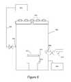
- FIG. 6is a schematic presentation of an apparatus suitable for performing etching reactions provided herein, in accordance with one embodiment.
- a reliable method for removal of defined amounts of silicon oxide on an atomic scale with atomic-scale uniformity and low defectivityuses nitric oxide (NO) to both activate and passivate the oxide surface.
- NOnitric oxide
- a fluorine-containing gas or vaporetches the activated surface or alternatively attaches to the NO passivated surface.
- the substrateis etched. Etching is self-limiting; once the activated surface is removed, etching stops since the fluorine species does not spontaneously react with the un-activated oxide surface.
- aspects of the present inventionare directed to controlled etching of silicon oxide and germanium oxide (including doped and undoped silicon and germanium oxides) from substrates, such as partially fabricated integrated circuits. While the methods of present invention find particular use in the processing of semiconductor substrates, they can also be employed in other applications. Provided methods achieve accurate and isotropic removal of material on small scales, e.g. on the scale of about 150 ⁇ or smaller. In fact, they can be employed when removal of layers of only several Angstroms or tens of angstroms is desired. Atomic layer etching methods provided herein allow control of the depth of etching by repeating the etching cycles, where each cycle may remove as little as only an atomic monolayer or submonolayer of material. These methods can be performed in a CVD-type or plasma-type apparatus (e.g., in a resist strip chamber), and can be easily integrated with existing wafer manufacturing processes.
- CVD-type or plasma-type apparatuse.g., in a resist strip chamber
- the methodscan be used to etch silicon oxide, germanium oxide and mixtures of these oxides.
- the oxidescan be doped (e.g., with nitrogen, carbon, boron, phosphorus, etc.) or undoped.
- the term “silicon oxide” as used hereinincludes a variety of types of silicon oxides, silicates, and silicate-based glasses, such as tetraethylorthosilicate (TEOS), borosilicate glass (BSG), borophosphosilicate glass (BPSG), high density plasma (HDP) CVD oxide, and subatmospheric (SA) CVD oxide.
- TEOStetraethylorthosilicate
- BSGborosilicate glass
- BPSGborophosphosilicate glass
- HDPhigh density plasma
- SAsubatmospheric
- the applications of atomic layer removal methodsinclude but are not limited to pre-clean operations, gate dielectric fabrication, processing of fin oxide recesses, and processing of capacitor dielectric in memory devices, such as dynamic random access memory (DRAM) and flash memory devices.
- the atomic layer etching pre-clean of interconnectsmay involve removal of silicon oxide from silicon, active silicon, polysilicon, and silicide contacts.
- Silicide contactscomprise metal silicides, such as nickel and cobalt silicides, ternary silicides, such as platinum nickel silicides and other silicide materials, commonly used in interconnects.
- Active silicon contactsrefer to electrically active contacts typically formed with electrically active doped silicon material.
- the methodsare particularly suitable in fabrication of devices at sub-10 nm level and can be used in fabrication of double-gate transistors, such as FinFETs and Gate-all-around (GAA) FETs.
- GAAGate-all-around
- Provided methodsallow for selective etching of silicon oxide, germanium oxide or their combinations in a presence of exposed silicon, germanium or silicon germanium.
- Selective etchingrefers to a selectivity of at least 5:1, where the ratio refers to the etch rate ratio.
- FIG. 1is a general process flow diagram for an etching method as described herein.
- a method of controllably etching a semiconductor (e.g., silicon, germanium or silicon germanium) oxide layer on a substrateinvolves contacting the substrate housed in a process chamber with excess NO species to modify the surface of silicon or germanium oxide on the substrate by forming surface-O—N—O bonds at 101 . Thereafter the general method proceeds by desorbing the adsorbed NO and contacting the substrate with an F etchant after the surface of the treated oxide is saturated with —O—N—O bonds at 103 . If the F etchant is added after NO desorption, the F will etch a layer of activated oxide.
- a semiconductore.g., silicon, germanium or silicon germanium
- the F etchantis applied during or while the oxide surface is saturated with NO bonds, F chemisorbs to the NO terminated surface forming F—O bonds, and subsequent desorption of nitrogen oxide from the surface of the treated oxide then results in controlled etching of the modified oxide by chemisorbed F.
- the etchresults from desorption of silicon or germanium fluoride (Si/GeF 4 ), depending upon whether the semiconductor substrate is Si, Ge or SiGe, at 105 .
- Si/GeF 4silicon or germanium fluoride
- Etchingcan be performed on substrates with or without recessed features (such as vias, trenches, and contact holes), and silicon oxide can be removed from any location on the substrate including the field region, sidewalls of a recessed feature and bottom of a recessed feature. Due to the self-limiting adsorption-based mechanism of the etching reaction, silicon oxide can be removed isotropically, that is, substantially the same amount of oxide is removed from the field region, sidewall and the bottom of the recessed feature, and the amount of removed oxide is substantially independent of the aspect ratio of the recessed feature. Further, oxide can be removed with high uniformity, that is, substantially same amounts of oxide can be removed from the center and edge of a semiconductor wafer substrate. It is important to note that the methods provided herein, unlike those that rely on NH 4 F etchant, do not produce solid reaction products, therefore resulting in low defectivity and in excellent repeatable isotropic etching within high aspect ratio recessed features.
- NOcan chemisorb onto silicon oxide surfaces forming Si—O—N—O bonds.
- This chemisorptionis a form of adsorption that involves a chemical reaction between the oxide adsorbant surface and the NO adsorbate. New chemical bonds are generated at the oxide surface.
- F etchantIf the F etchant is applied during or while the oxide surface is saturated with NO bonds, F cannot etch the oxide, but instead chemisorbs to the NO terminated surface forming F—O bonds.
- the NOdesorbs from the surface in the form of NO 2 , leaving a silicon dangling bond which reacts with an applied F etchant or with the adsorbed F to form of SiF 4 causing etching of the surface.
- the NO desorptionactivates the oxide surface for etching in that this dangling bond can react with an applied or chemisorbed fluorine.
- Atomic layer etchcan occur, by this process of NO adsorption and passivation, followed by F adsorption and etching, then repeating the cycle.
- the disclosed processis different from known methods of isotropically etching silicon oxide in that the reaction is broken up into four discrete and self-limiting steps that can be applied in two different ways.
- the stepsinclude: (1) NO surface adsorption (chemisorption), 2) NO surface desorption combined with Fluorine surface reaction and 3) SiF 4 reactant desorption.
- the stepsinclude: (1) NO surface adsorption (chemisorption), 2) F surface adsorption 3) NO surface desorption, 4) Fluorine surface reaction and 5) SiF 4 reactant desorption.
- Other materialssuch as Silicon Nitride experience similar reactions with NO, however the adsorption and desorption thermal response is very different.
- nitrideFor nitride, chemisorption occurs at lower temperatures than for oxide, and at a given temperature desorption occurs much faster than for oxide. This provides a temperature and NO concentration window where oxide can be selectively etched while not etching nitride.
- Previous NO-based oxide etching techniquesdid not separate the processes into multiple rate limiting steps. NO was used to enhance the fluorine etch rate by supplying NO and fluorine together at concentrations and temperatures where adsorption and desorption occurred simultaneously in the presence of fluorine. As such the etching reaction occurred continuously and therefore was not atomic layer etching.
- FIG. 2is a process flow diagram illustrating an etching method for silicon oxide, in accordance with one embodiment described herein, in which the F etchant is added after NO desorption, or during NO desorption under conditions in which it reacts to etch a layer of the activated oxide surface.
- FIGS. 3A-3Dillustrate a schematic presentation of cross-sectional views of a silicon oxide containing substrate undergoing the controlled etching.
- a processing chambersuch as an inductively coupled plasma chamber
- NOnitric oxide
- Suitable NO species for this exposure operation 201can be a plasma-excited NO gas or a NO radical generated in a variety of ways.
- NO gasmay be plasma excited by injecting directly into a plasma source in the process chamber, or indirectly excited by injection downstream of a plasma source and being excited by plasma of Ar, N2, He, Ne, Xe, for example.
- NO radicalsmay be formed by a plasma reaction using O 2 and N 2 O gases, as follows: O 2 +Plasma->2O*, O*+N 2 O( g )->2NO* or N 2 O+plasma->N 2 +O*, O*+N 2 O->2NO*.
- NO*may be formed by a plasma reaction using O 2 and N 2 gases, as follows: O 2 +Plasma->2O*, O*+N 2 ->N 2 O, N 2 O+O*->2NO*.
- the NO exposure 201is conducted such that there is chemisorption onto the silicon oxide surface forming Si—O—N—O bonds, as depicted in FIG. 3B .
- Suitable conditions for this chemisorption operationmay be a temperature of about 0 to 300° C., for example 80 to 150° C., and a pressure of about 0.1-760 Torr, for example between about 1-20 Torr.
- excess NO/NO*is provided to the oxide surface so that the oxide surface is saturated with NO bonding, preventing any etching from occurring, as further discussed below.
- Suitable conditions for this chemisorption operationmay be a temperature of about 0 to 300° C., for example 80 to 150° C., and a pressure of about 0.1-760 Torr, for example between about 1-20 Torr.
- etchingcan occur by contacting the substrate surface with an F species to etch silicon oxide, in operation 205 .
- fluorine (F)will not react with the surface as it is prevented from reaching the surface to adsorb.
- the reaction with the fluorinewill only take place when the NO supply is reduced or eliminated and the NO starts desorbing from the surface. Therefore, the etch may be controlled by preventing desorption of nitrogen oxide from the surface of the silicon oxide modified by NO chemisorption by continuously supplying the NO species into the process chamber. By stopping supplying NO species into the process chamber or reducing supply of NO species, NO will be allowed to desorb from the modified oxide surface, allowing the etch to proceed in the presence of a F etchant. Once the etch cycle is completed, the chamber may be purged with an inert gas.
- the processstarts at 401 by contacting a substrate in a processing chamber, such as an inductively coupled plasma chamber, with an excess of a suitable nitric oxide (NO) species, as depicted in FIG. 5A .
- a suitable nitric oxide (NO) speciesfor this exposure operation 401 can be a plasma-excited NO gas or a NO radical generated in a variety of ways.
- NO gasmay be plasma excited by injecting directly into a plasma source in the process chamber, or indirectly excited by injection downstream of a plasma source and being excited by plasma of Ar, N2, He, Ne, Xe, for example.
- NO radicals (NO*)may be formed as described above with reference to FIG. 2 .
- the NO exposure 401is conducted such that there is chemisorption onto the silicon oxide surface forming Si—O—N—O bonds, as depicted in FIG. 5B .
- Suitable conditions for this chemisorption operationmay be a temperature of about 0 to 300° C., for example 80 to 150° C., and a pressure of about 0.1-760 Torr, for example between about 1-20 Torr.
- Excess NO/NO*is provided to the oxide surface so that the oxide surface is saturated with NO bonding, preventing any etching from occurring, as further discussed below.
- a fluorine etchantis applied causing F to chemisorb onto the adsorbed NO.
- the fluorine sourceis turned off leaving the oxide surface saturated with O—N—O—F bonds as depicted in FIG. 5C .
- the O—N—O—Fis desorbed, causing some of the surface oxide to be removed.
- the desorptionstarts once the source of the NO is turned off.
- the desorption rateis a function of the operation temperature and can be accelerated by heating the substrate. At 10° C. the NO desorption process can take on the order of about 10 seconds.
- the desorption rateincreases with increasing temperature. Suitable temperatures for this desorption operation may range from about 0 to 300° C., for example about 80-150° C.
- the etchmay be controlled by preventing desorption of nitrogen oxide from the surface of the silicon oxide modified by NO chemisorption by continuously supplying the NO species into the process chamber. By stopping supplying NO species into the process chamber or reducing supply of NO species, NO will be allowed to desorb from the modified oxide surface, allowing the etch to proceed in the presence the adsorbed F etchant. Once the etch cycle is completed, the chamber may be purged with an inert gas.
- Suitable etchantsare F-based, including, for example F radical (F*), NF 3 , F 2 , CF 4 , C 2 F 6 , HF, and XeF 2 .
- the F etchantmay be introduced into the process chamber together with the NO species coincident with the nitrogen oxide desorption.
- the F etchantmay be introduced into the process chamber after Si—O—N—O bonds are formed on the surface of the treated oxide and before or while the nitrogen oxide is desorbed from the modified surface of silicon oxide.
- Suitable conditions for the adsorption of the F etchant species to No passivated oxide surfacemay be a temperature of about 0 to 300° C., for example 80-150° C., and a pressure of about 100 mTorr to 760 Torr, for example about 1-2 Torr.
- the process chambermay be purged or evacuated to remove reaction byproducts if needed, before commencement of the next cycle.
- the processcan be performed for as many cycles as needed. In some embodiments at least two cycles are performed, such as between about 2-10 cycles.
- the process shown in FIG. 1can be modified with a variety of pre-treatments and post-treatments to condition the surface of the substrate.
- the substrateprior to operation 101 , the substrate is treated with dry HF to remove silanol bonds on the surface of the silicon oxide.
- the process chamberis then purged or evacuated to remove HF.
- Other pretreatmentsmay include a plasma process or wet clean process to remove surface contaminants such as hydrocarbons or hydro-fluorocarbons.
- the process conditionssuch as temperature and pressure for each of the operations of the etching cycle will depend on the nature of the NO species, the F etchant, and the speed of the process, and can be varied within the guidelines provided herein. In most examples the temperature ranges from between about 0 to about 300° C., and the pressure ranges between about 100 mTorr to about 760 Torr.
- the Example provided belowillustrates a particular embodiment.
- the methods described hereincan be practiced in a variety of apparatuses that are equipped with delivery lines and control mechanisms configured for sequential delivery of gaseous reagents.
- suitable process chambersinclude plasma etch, isotropic etch, and chemical vapor deposition process chambers, as well as resist strip chambers.
- the apparatusmay include resistant materials at least for the parts that are in direct contact with corrosive reagents.
- the process chamberis coated with a F etchant-resistant polymer, such as a copolymer of ethylene and chlorotrifluoroethylene known as Halar®.
- the chamberis anodized or nickel plated.
- the delivery lines delivering the reagentsin some embodiments are made of nickel.
- the suitable apparatusincludes a process chamber having a substrate support for holding the substrate in position during etching, an inlet for introduction of the reagents, an outlet that is typically connected with a pump for evacuating the process chamber, and a controller having program instructions for performing any of the steps of the provided methods.
- the apparatusis equipped with a heater and/or a cooler configured to heat or cool the substrate, as desired.
- the heater and/or coolermay be integrated into the substrate support.
- the heating of the substratemay be implemented with the use of lamps positioned above the substrate, where the lamps radiate heat onto the substrate. The lamps may be used as the main method of heating or in addition to the substrate holder heating.
- the substrate holderincludes a motor and is configured to rotate the substrate during processing.
- the apparatusis equipped with an RF or microwave plasma generator.
- the apparatusincludes a separate chamber in which the remote plasma is generated using a RF or microwave plasma generator.
- the remote plasma chamberis connected through a feed conduit to the process chamber housing the substrate and is configured to deliver species generated in the remote plasma to the surface of the substrate.
- the apparatuswill also include a source of electromagnetic radiation, such as a UV lamp, or a microwave generator.
- sourcesare typically separated from the substrate by a window that can transmit the specific type of electromagnetic radiation in use.
- a windowthat can transmit the specific type of electromagnetic radiation in use.
- an F etchant-resistant, UV-transmitting windowsuch as sapphire-coated quartz or bulk quartz window may replace the ceiling of the process chamber allowing transmission of UV radiation from a UV lamp positioned over the window.
- the process chamber 600includes an inlet 602 for introduction of gaseous reagents, where the inlet is coupled with a shut-off valve or a flow control valve.
- a delivery line 604connects a source of reagents 606 to the inlet 602 .
- the delivery line 604may include a plurality of individual lines, e.g., a NO delivery line and a F etchant delivery line.
- the delivery linesare connected with a source of heat and are heated during the delivery of reagents in order to prevent condensation of reagents within the lines.
- the controller 622includes program instructions or built-in logic to perform the etching methods in accordance with any of the embodiments described herein.
- the controllermay include the code specifying the timing of delivery of reagents, the temperature and pressure during each stage of the etching cycle, and parameters associated with substrate irradiation.
- a controlleris part of a system, which may be part of the above-described examples.
- Such systemscan comprise semiconductor processing equipment, including a processing tool or tools, chamber or chambers, a platform or platforms for processing, and/or specific processing components (a wafer pedestal, a gas flow system, etc.).
- These systemsmay be integrated with electronics for controlling their operation before, during, and after processing of a semiconductor wafer or substrate.
- the electronicsmay be referred to as the “controller,” which may control various components or subparts of the system or systems.
- the controllermay be programmed to control any of the processes disclosed herein, including the delivery of processing gases, temperature settings (e.g., heating and/or cooling), pressure settings, vacuum settings, power settings, radio frequency (RF) generator settings, RF matching circuit settings, frequency settings, flow rate settings, fluid delivery settings, positional and operation settings, wafer transfers into and out of a tool and other transfer tools and/or load locks connected to or interfaced with a specific system.
- temperature settingse.g., heating and/or cooling
- RFradio frequency
- the controllermay be defined as electronics having various integrated circuits, logic, memory, and/or software that receive instructions, issue instructions, control operation, enable cleaning operations, enable endpoint measurements, and the like.
- the integrated circuitsmay include chips in the form of firmware that store program instructions, digital signal processors (DSPs), chips defined as application specific integrated circuits (ASICs), and/or one or more microprocessors, or microcontrollers that execute program instructions (e.g., software).
- Program instructionsmay be instructions communicated to the controller in the form of various individual settings (or program files), defining operational parameters for carrying out a particular process on or for a semiconductor wafer or to a system.
- the operational parametersmay, in some embodiments, be part of a recipe defined by process engineers to accomplish one or more processing steps during the fabrication of one or more layers, and/or dies of a wafer.
- the controllermay be a part of or coupled to a computer that is integrated with, coupled to the system, otherwise networked to the system, or a combination thereof.
- the controllermay be in the “cloud” or all or a part of a fab host computer system, which can allow for remote access of the wafer processing.
- the computermay enable remote access to the system to monitor current progress of fabrication operations, examine a history of past fabrication operations, examine trends or performance metrics from a plurality of fabrication operations, to change parameters of current processing, to set processing steps to follow a current processing, or to start a new process.
- a remote computere.g. a server
- the remote computermay include a user interface that enables entry or programming of parameters and/or settings, which are then communicated to the system from the remote computer.
- the controllerreceives instructions in the form of data, which specify parameters for each of the processing steps to be performed during one or more operations. It should be understood that the parameters may be specific to the type of process to be performed and the type of tool that the controller is configured to interface with or control.
- the controllermay be distributed, such as by comprising one or more discrete controllers that are networked together and working towards a common purpose, such as the processes and controls described herein.
- An example of a distributed controller for such purposeswould be one or more integrated circuits on a chamber in communication with one or more integrated circuits located remotely (such as at the platform level or as part of a remote computer) that combine to control a process on the chamber.
- the controllermight communicate with one or more of other tool circuits or modules, other tool components, cluster tools, other tool interfaces, adjacent tools, neighboring tools, tools located throughout a factory, a main computer, another controller, or tools used in material transport that bring containers of wafers to and from tool locations and/or load ports in a semiconductor manufacturing factory.
- the apparatus/process described hereinabovemay be used in conjunction with lithographic patterning tools or processes, for example, for the fabrication or manufacture of semiconductor devices, displays, LEDs, photovoltaic panels and the like. Typically, though not necessarily, such tools/processes will be used or conducted together in a common fabrication facility.
- Lithographic patterning of a filmtypically comprises some or all of the following steps, each step enabled with a number of possible tools: (1) application of photoresist on a workpiece, i.e., substrate, using a spin-on or spray-on tool; (2) curing of photoresist using a hot plate or furnace or UV curing tool; (3) exposing the photoresist to visible or UV or x-ray light with a tool such as a wafer stepper; (4) developing the resist so as to selectively remove resist and thereby pattern it using a tool such as a wet bench; (5) transferring the resist pattern into an underlying film or workpiece by using a dry or plasma-assisted etching tool; and (6) removing the resist using a tool such as an RF or microwave plasma resist stripper.
- a toolsuch as an RF or microwave plasma resist stripper.
Landscapes
- Engineering & Computer Science (AREA)
- Physics & Mathematics (AREA)
- Chemical & Material Sciences (AREA)
- General Physics & Mathematics (AREA)
- Manufacturing & Machinery (AREA)
- Computer Hardware Design (AREA)
- Microelectronics & Electronic Packaging (AREA)
- Power Engineering (AREA)
- Condensed Matter Physics & Semiconductors (AREA)
- Chemical Kinetics & Catalysis (AREA)
- General Chemical & Material Sciences (AREA)
- Inorganic Chemistry (AREA)
- Plasma & Fusion (AREA)
- Analytical Chemistry (AREA)
- Drying Of Semiconductors (AREA)
Abstract
Description
The present invention pertains to methods of removing layers of material on a substrate. The methods are particularly useful for accurate isotropic removal of silicon dioxide and germanium dioxide with atomic scale fidelity on a semiconductor substrate.
Fabrication of integrated circuit (IC) devices at a modern level of miniaturization demands techniques that can operate at an atomic scale. Certain components of IC devices now have dimensions of tens of Angströms, corresponding to only a few atomic layers of material. For example, gate dielectric in modern IC transistors can have a thickness of only 12 Å, corresponding to only four atomic layers of silicon dioxide. It is often desirable to fine-tune the electronic properties of these components by altering their dimensions, which would involve deposition or removal of only a few atomic layers of material. While atomic layer deposition (ALD) and atomic-scale epitaxial growth techniques have been developed, the methods for controlled removal of one or several atomic layers are still limited.
Silicon oxides, silicon dioxide and its carbon-doped, boron-doped, and phosphorous-doped variants are important dielectric materials used in IC devices. Silicon oxides serve as an insulator in bulk dielectric layers, as a gate dielectric in transistors, and as a capacitor dielectric in memory devices, such as dynamic random-access memory (DRAM). Silicon oxide also is inadvertently formed on layers of silicon when a partially fabricated wafer is exposed to air. This type of silicon oxide, known as native oxide, forms a thin film on the layer of silicon. Native oxide film together with oxide residue produced during etching and/or ashing frequently presents a problem for further processing steps. When formed in the bottom of a silicon landed via or contact hole, native oxide and other oxides are highly undesired, since they raise the overall electrical resistance of the via after it is filled with conductive materials.
There is a wealth of literature describing gas phase etching of silicon oxides. The majority of these processes are essentially plasma processes, in which the reactant gases are introduced into a plasma source located in a process chamber to generate ionic and metastable species which react with the silicon oxide surface and form volatile etch by-products. In most of these processes the etch rate of the silicon oxide is controlled by the flow rate and composition of the reactant gases, plasma power, substrate temperature, or chamber pressure. The etch rate of the silicon oxide is nearly constant over time; as such, these types of processes are not well suited to accurately control the amount of a layer to be etched uniformly and precisely over all the exposed surface on the substrate. These processes cannot be applied for removal of defined amounts of material on an atomic scale.
Sub-10 nm devices will require a large number of isotropic etches with high selectivity, excellent loading performance and low defectivity. A reliable method for removal of defined amounts of material on an atomic scale with atomic-scale uniformity and low defectivity uses nitric oxide (NO) to activate the oxide surface. Once activated, a fluorine-containing gas or vapor etches the activated surface. Etching is self-limiting; once the activated surface is removed, etching stops since the fluorine species does not spontaneously react with the un-activated oxide surface. The methods provided herein may be used in the processes for manufacturing integrated circuits such as in interconnect and contact pre-clean applications, gate dielectric processing, manufacturing of memory and logic devices, or any other applications where precise removal of one or several atomic layers of material is desired. Processes for isotropic removal of controlled amounts of silicon and germanium oxides are provided.
Generally disclosed herein is a method of controllably etching a semiconductor (e.g., silicon, germanium or silicon germanium) oxide layer on a substrate. The method involves contacting the substrate housed in a process chamber with excess NO species to modify the surface of silicon or germanium oxide on the substrate by forming Si/Ge (silicon and/or germanium, depending on the base semiconductor material)-O—N—O bonds, and contacting the substrate with an F etchant after the surface of the treated oxide is saturated with Si/Ge—O—N—O bonds. Desorption of nitrogen oxide from the surface of the treated oxide then results in controlled etching of the oxide surface in a variety of ways.
In one aspect, the invention relates to a method of controllably etching a silicon oxide layer on a substrate. The method involves contacting the substrate housed in a process chamber with excess NO species to modify the surface of silicon oxide on the substrate by forming Si—O—N—O bonds. Suitable NO species can be a plasma-excited NO gas or a NO radical. Nitrogen oxide is then desorbed from the surface of the treated oxide, while leaving a surface activated towards etching. After the surface of the treated oxide is saturated with Si—O—N—O bonds, the substrate is also contacted with an F etchant, such as F radical, NF3, F2, CF4, C2F6, HF, and XeF2, such that the F etchant etches the activated surface. In this embodiment, the F etchant may be introduced into the process chamber together with the NO species, coincident with the nitrogen oxide desorption under conditions in which it reacts to etch a layer of the activated oxide surface. Or, the F etchant may be introduced into the process chamber after nitrogen oxide is desorbed from the modified surface of the silicon oxide to react to etch a layer of the activated oxide surface.
In another aspect, the method involves contacting the substrate housed in a process chamber with excess NO species to modify and passivate the surface of silicon oxide on the substrate by forming Si—O—N—O bonds. Suitable NO species can be a plasma-excited NO gas or a NO radical. The substrate is also contacted with an F etchant, such as F radical, NF3, F2, CF4, C2F6, HF, and XeF2, and fluorine chemisorbs onto the NO-terminated surface forming NOF bonds. When the NOF is desorbed from the surface, it desorbs as NO2+SiF4, etching a surface layer of oxide. In this embodiment, the etching is accomplished by the chemisorbed F reacting with the activated oxide surface, and the F etchant may be introduced into the process chamber together with the NO species coincident with the nitric oxide desorption under conditions in which it reacts to chemisorb onto the NO-terminated surface forming NOF bonds. Or, the F etchant may be introduced into the process chamber after Si—O—N—O bonds are formed on the surface of the treated oxide and before nitrogen oxide is desorbed from the modified surface of silicon oxide.
The adsorption may be suitably performed at a temperature of between about 0-300° C., with the desorption operation performed at the same or higher temperature. The desorption is performed at a temperature between about 0-80° C. higher than the adsorption temperature.
The etch may be controlled by preventing desorption of nitrogen oxide from the surface of the silicon oxide modified by NO chemisorption by continuously supplying the NO species into the process chamber. By stopping supplying NO species into the process chamber or reducing supply of NO species, NO will be allowed to desorb from the modified oxide surface, allowing the etch to proceed in the presence of an adsorbed or applied F etchant.
Once the etch cycle is completed, the chamber may be pumped out or purged with an inert gas.
In some embodiments, a single cycle of operations removes about 0.5-10 atomic layers of silicon oxide, for example an atomic monolayer of silicon oxide. In many instances, at least two cycles of operations, and often more, are performed in order to remove a desired amount of material.
In another aspect, an etching apparatus for controllably etching silicon oxide on a substrate includes a process chamber having an inlet for introduction of process gases, a substrate support in the process chamber configured for holding the substrate in position during etching of the silicon oxide on the substrate, and a controller. The controller includes instructions for: (i) contacting the substrate housed in a process chamber with excess NO species to modify the surface of semiconductor oxide on the substrate by forming Si/Ge—O—N—O bonds, (ii) contacting the substrate with an F etchant, (iii) desorbing the chemisorbed layer (iv) etching the surface of the oxide, and (v) optionally purging the chamber with an inert gas. The controller may further include instruction to conduct the etching operations two or more times.
These and other features and advantages of the invention will be described in more detail below with reference to the associated drawings.
Reference will now be made in detail to specific embodiments of the invention. Examples of the specific embodiments are illustrated in the accompanying drawings. While the invention will be described in conjunction with these specific embodiments, it will be understood that it is not intended to limit the invention to such specific embodiments. On the contrary, it is intended to cover alternatives, modifications, and equivalents as may be included within the spirit and scope of the invention. In the following description, numerous specific details are set forth in order to provide a thorough understanding of the present invention. The present invention may be practiced without some or all of these specific details. In other instances, well known process operations have not been described in detail so as to not unnecessarily obscure the present invention.
Introduction
A reliable method for removal of defined amounts of silicon oxide on an atomic scale with atomic-scale uniformity and low defectivity uses nitric oxide (NO) to both activate and passivate the oxide surface. Once passivated, a fluorine-containing gas or vapor etches the activated surface or alternatively attaches to the NO passivated surface. During the desorption process, the substrate is etched. Etching is self-limiting; once the activated surface is removed, etching stops since the fluorine species does not spontaneously react with the un-activated oxide surface.
Aspects of the present invention are directed to controlled etching of silicon oxide and germanium oxide (including doped and undoped silicon and germanium oxides) from substrates, such as partially fabricated integrated circuits. While the methods of present invention find particular use in the processing of semiconductor substrates, they can also be employed in other applications. Provided methods achieve accurate and isotropic removal of material on small scales, e.g. on the scale of about 150 Å or smaller. In fact, they can be employed when removal of layers of only several Angstroms or tens of angstroms is desired. Atomic layer etching methods provided herein allow control of the depth of etching by repeating the etching cycles, where each cycle may remove as little as only an atomic monolayer or submonolayer of material. These methods can be performed in a CVD-type or plasma-type apparatus (e.g., in a resist strip chamber), and can be easily integrated with existing wafer manufacturing processes.
The methods can be used to etch silicon oxide, germanium oxide and mixtures of these oxides. The oxides can be doped (e.g., with nitrogen, carbon, boron, phosphorus, etc.) or undoped. The term “silicon oxide” as used herein includes a variety of types of silicon oxides, silicates, and silicate-based glasses, such as tetraethylorthosilicate (TEOS), borosilicate glass (BSG), borophosphosilicate glass (BPSG), high density plasma (HDP) CVD oxide, and subatmospheric (SA) CVD oxide.
The applications of atomic layer removal methods include but are not limited to pre-clean operations, gate dielectric fabrication, processing of fin oxide recesses, and processing of capacitor dielectric in memory devices, such as dynamic random access memory (DRAM) and flash memory devices. The atomic layer etching pre-clean of interconnects may involve removal of silicon oxide from silicon, active silicon, polysilicon, and silicide contacts. Silicide contacts comprise metal silicides, such as nickel and cobalt silicides, ternary silicides, such as platinum nickel silicides and other silicide materials, commonly used in interconnects. Active silicon contacts refer to electrically active contacts typically formed with electrically active doped silicon material. The methods are particularly suitable in fabrication of devices at sub-10 nm level and can be used in fabrication of double-gate transistors, such as FinFETs and Gate-all-around (GAA) FETs.
Provided methods allow for selective etching of silicon oxide, germanium oxide or their combinations in a presence of exposed silicon, germanium or silicon germanium. Selective etching refers to a selectivity of at least 5:1, where the ratio refers to the etch rate ratio.
While provided methods can be used to etch both silicon and germanium oxides, the methods will be further illustrated using silicon oxide as an example. It is understood that all of the described principles and embodiment illustrations also apply to the etching of germanium oxide.
Etching can be performed on substrates with or without recessed features (such as vias, trenches, and contact holes), and silicon oxide can be removed from any location on the substrate including the field region, sidewalls of a recessed feature and bottom of a recessed feature. Due to the self-limiting adsorption-based mechanism of the etching reaction, silicon oxide can be removed isotropically, that is, substantially the same amount of oxide is removed from the field region, sidewall and the bottom of the recessed feature, and the amount of removed oxide is substantially independent of the aspect ratio of the recessed feature. Further, oxide can be removed with high uniformity, that is, substantially same amounts of oxide can be removed from the center and edge of a semiconductor wafer substrate. It is important to note that the methods provided herein, unlike those that rely on NH4F etchant, do not produce solid reaction products, therefore resulting in low defectivity and in excellent repeatable isotropic etching within high aspect ratio recessed features.
Etching of Silicon Oxide with NO Activation
NO can chemisorb onto silicon oxide surfaces forming Si—O—N—O bonds. This chemisorption is a form of adsorption that involves a chemical reaction between the oxide adsorbant surface and the NO adsorbate. New chemical bonds are generated at the oxide surface.
If the F etchant is applied during or while the oxide surface is saturated with NO bonds, F cannot etch the oxide, but instead chemisorbs to the NO terminated surface forming F—O bonds.
Thereafter, in the desorption cycle the NO desorbs from the surface in the form of NO2, leaving a silicon dangling bond which reacts with an applied F etchant or with the adsorbed F to form of SiF4causing etching of the surface. The NO desorption activates the oxide surface for etching in that this dangling bond can react with an applied or chemisorbed fluorine.
Atomic layer etch (ALE) can occur, by this process of NO adsorption and passivation, followed by F adsorption and etching, then repeating the cycle.
The disclosed process is different from known methods of isotropically etching silicon oxide in that the reaction is broken up into four discrete and self-limiting steps that can be applied in two different ways. In the first embodiment, the steps include: (1) NO surface adsorption (chemisorption), 2) NO surface desorption combined with Fluorine surface reaction and 3) SiF4reactant desorption. In the second embodiment the steps include: (1) NO surface adsorption (chemisorption), 2) F surface adsorption 3) NO surface desorption, 4) Fluorine surface reaction and 5) SiF4reactant desorption. Other materials such as Silicon Nitride experience similar reactions with NO, however the adsorption and desorption thermal response is very different. For nitride, chemisorption occurs at lower temperatures than for oxide, and at a given temperature desorption occurs much faster than for oxide. This provides a temperature and NO concentration window where oxide can be selectively etched while not etching nitride. Previous NO-based oxide etching techniques did not separate the processes into multiple rate limiting steps. NO was used to enhance the fluorine etch rate by supplying NO and fluorine together at concentrations and temperatures where adsorption and desorption occurred simultaneously in the presence of fluorine. As such the etching reaction occurred continuously and therefore was not atomic layer etching.
Referring toFIG. 2 , the process starts at201 by contacting a substrate in a processing chamber, such as an inductively coupled plasma chamber, with an excess of a suitable nitric oxide (NO) species, as depicted inFIG. 3A . Suitable NO species for thisexposure operation 201 can be a plasma-excited NO gas or a NO radical generated in a variety of ways. For example, NO gas may be plasma excited by injecting directly into a plasma source in the process chamber, or indirectly excited by injection downstream of a plasma source and being excited by plasma of Ar, N2, He, Ne, Xe, for example. NO radicals (NO*) may be formed by a plasma reaction using O2and N2O gases, as follows:
O2+Plasma->2O*, O*+N2O(g)->2NO*
or
N2O+plasma->N2+O*, O*+N2O->2NO*.
Or, NO* may be formed by a plasma reaction using O2and N2gases, as follows:
O2+Plasma->2O*, O*+N2->N2O, N2O+O*->2NO*.
O2+Plasma->2O*, O*+N2O(g)->2NO*
or
N2O+plasma->N2+O*, O*+N2O->2NO*.
Or, NO* may be formed by a plasma reaction using O2and N2gases, as follows:
O2+Plasma->2O*, O*+N2->N2O, N2O+O*->2NO*.
TheNO exposure 201 is conducted such that there is chemisorption onto the silicon oxide surface forming Si—O—N—O bonds, as depicted inFIG. 3B . Suitable conditions for this chemisorption operation may be a temperature of about 0 to 300° C., for example 80 to 150° C., and a pressure of about 0.1-760 Torr, for example between about 1-20 Torr. In general, excess NO/NO* is provided to the oxide surface so that the oxide surface is saturated with NO bonding, preventing any etching from occurring, as further discussed below.
Referring again toFIG. 2 , after the NO species has adsorbed onto the surface of silicon oxide, inoperation 203 the NO desorbs from the surface in the form of NO2, leaving an activated surface of silicon dangling bonds, as depicted inFIG. 3C . Suitable conditions for this chemisorption operation may be a temperature of about 0 to 300° C., for example 80 to 150° C., and a pressure of about 0.1-760 Torr, for example between about 1-20 Torr.
Once NO desorption occurs, etching can occur by contacting the substrate surface with an F species to etch silicon oxide, inoperation 205. When the surface is saturated with NO bonding, fluorine (F) will not react with the surface as it is prevented from reaching the surface to adsorb. The reaction with the fluorine will only take place when the NO supply is reduced or eliminated and the NO starts desorbing from the surface. Therefore, the etch may be controlled by preventing desorption of nitrogen oxide from the surface of the silicon oxide modified by NO chemisorption by continuously supplying the NO species into the process chamber. By stopping supplying NO species into the process chamber or reducing supply of NO species, NO will be allowed to desorb from the modified oxide surface, allowing the etch to proceed in the presence of a F etchant. Once the etch cycle is completed, the chamber may be purged with an inert gas.
In an alternate embodiment, referring toFIG. 4 , the process starts at401 by contacting a substrate in a processing chamber, such as an inductively coupled plasma chamber, with an excess of a suitable nitric oxide (NO) species, as depicted inFIG. 5A . Suitable NO species for thisexposure operation 401 can be a plasma-excited NO gas or a NO radical generated in a variety of ways. For example, NO gas may be plasma excited by injecting directly into a plasma source in the process chamber, or indirectly excited by injection downstream of a plasma source and being excited by plasma of Ar, N2, He, Ne, Xe, for example. NO radicals (NO*) may be formed as described above with reference toFIG. 2 .
TheNO exposure 401 is conducted such that there is chemisorption onto the silicon oxide surface forming Si—O—N—O bonds, as depicted inFIG. 5B . Suitable conditions for this chemisorption operation may be a temperature of about 0 to 300° C., for example 80 to 150° C., and a pressure of about 0.1-760 Torr, for example between about 1-20 Torr. Excess NO/NO* is provided to the oxide surface so that the oxide surface is saturated with NO bonding, preventing any etching from occurring, as further discussed below.
Referring again toFIG. 4 , after the NO species has adsorbed onto the surface of silicon oxide, in operation403 a fluorine etchant is applied causing F to chemisorb onto the adsorbed NO. Inoperation 405, the fluorine source is turned off leaving the oxide surface saturated with O—N—O—F bonds as depicted inFIG. 5C . Inoperation 407, the O—N—O—F is desorbed, causing some of the surface oxide to be removed. The desorption starts once the source of the NO is turned off. The desorption rate is a function of the operation temperature and can be accelerated by heating the substrate. At 10° C. the NO desorption process can take on the order of about 10 seconds. The desorption rate increases with increasing temperature. Suitable temperatures for this desorption operation may range from about 0 to 300° C., for example about 80-150° C.
When the surface is saturated with NO bonding, fluorine (F) will not react with the surface silicon as it is prevented from reaching silicon sites. Since NO adsorption and desorption occurs simultaneously, the reaction of silicon with the fluorine will only take place when the NO supply is reduced or eliminated and the NO starts desorbing from the surface. Therefore, the etch may be controlled by preventing desorption of nitrogen oxide from the surface of the silicon oxide modified by NO chemisorption by continuously supplying the NO species into the process chamber. By stopping supplying NO species into the process chamber or reducing supply of NO species, NO will be allowed to desorb from the modified oxide surface, allowing the etch to proceed in the presence the adsorbed F etchant. Once the etch cycle is completed, the chamber may be purged with an inert gas.
Suitable etchants are F-based, including, for example F radical (F*), NF3, F2, CF4, C2F6, HF, and XeF2. According to various embodiments, the F etchant may be introduced into the process chamber together with the NO species coincident with the nitrogen oxide desorption. Alternatively, the F etchant may be introduced into the process chamber after Si—O—N—O bonds are formed on the surface of the treated oxide and before or while the nitrogen oxide is desorbed from the modified surface of silicon oxide. Suitable conditions for the adsorption of the F etchant species to No passivated oxide surface may be a temperature of about 0 to 300° C., for example 80-150° C., and a pressure of about 100 mTorr to 760 Torr, for example about 1-2 Torr.
The etch is typically limited to removal of a fraction of a monolayer to several monolayers per cycle described above. The etch may be tailored to remove between about 0.5-10 atomic layers of silicon oxide through modification of conditions. The etch portion of the cycle is completed by desorption of the F etch reaction product, SiF4, after a desired amount of etching has occurred, as depicted inFIG. 3D or 5D . It can be seen that in the processed substrate shown inFIG. 3D or 5D , a controlled amount of silicon oxide has been removed. The amount of removed silicon oxide is determined by the amount of NO adsorbed in the embodiment described inFIGS. 2 and 3 , or by the amount F adsorbed as described inFIGS. 4 and 5 , by the process temperature and pressure.
Referring again toFIGS. 2 and 4 , next, inoperation 209/409, it is decided if further etching is required in order to etch a target thickness of silicon oxide. If the amount removed in the first cycle of etching is sufficient, then the etching is complete. The process chamber is purged and/or evacuated if any reaction products or F etchant remains in the chamber.
If, inoperation 209/409 it is determined that further etching is needed to etch a target thickness of silicon oxide, the sequence of operations is repeated. The process chamber may be purged or evacuated to remove reaction byproducts if needed, before commencement of the next cycle. The process can be performed for as many cycles as needed. In some embodiments at least two cycles are performed, such as between about 2-10 cycles.
The process shown inFIG. 1 can be modified with a variety of pre-treatments and post-treatments to condition the surface of the substrate. In some embodiments, prior tooperation 101, the substrate is treated with dry HF to remove silanol bonds on the surface of the silicon oxide. The process chamber is then purged or evacuated to remove HF. Other pretreatments may include a plasma process or wet clean process to remove surface contaminants such as hydrocarbons or hydro-fluorocarbons.
The process conditions, such as temperature and pressure for each of the operations of the etching cycle will depend on the nature of the NO species, the F etchant, and the speed of the process, and can be varied within the guidelines provided herein. In most examples the temperature ranges from between about 0 to about 300° C., and the pressure ranges between about 100 mTorr to about 760 Torr. The Example provided below illustrates a particular embodiment.
In order to more fully illustrate features of a specific embodiment, the following non-limiting example of an etch process in accordance withFIGS. 4 and 5 is provided. An example of an etch process is to 1) load a substrate containing an oxide into a vacuum housing; 2) optionally pre-treat the sample to remove surface oxides or silanol bonds; 3) strike a plasma of NO gas (or a gas mixture of about 50% O2+50% N2O by volume) at 1.0-3.0 Torr to passivate the oxide surface; 4) add a fluorine containing gas to the plasma such as CF4(about 5-7% by volume); 5) turn off the plasma and fluorine source and let the NO desorb and initiate etching; 6) optionally purge the vacuum chamber with an inter gas such as nitrogen or argon; 7) repeat steps 3-6 as needed to etch target film thickness.
Apparatus
The methods described herein can be practiced in a variety of apparatuses that are equipped with delivery lines and control mechanisms configured for sequential delivery of gaseous reagents. Examples of suitable process chambers include plasma etch, isotropic etch, and chemical vapor deposition process chambers, as well as resist strip chambers. To prevent damage from the use of corrosive agents, the apparatus may include resistant materials at least for the parts that are in direct contact with corrosive reagents. For example, in some embodiments, the process chamber is coated with a F etchant-resistant polymer, such as a copolymer of ethylene and chlorotrifluoroethylene known as Halar®. In some embodiments, the chamber is anodized or nickel plated. The delivery lines delivering the reagents, in some embodiments are made of nickel.
The suitable apparatus includes a process chamber having a substrate support for holding the substrate in position during etching, an inlet for introduction of the reagents, an outlet that is typically connected with a pump for evacuating the process chamber, and a controller having program instructions for performing any of the steps of the provided methods. In some embodiments the apparatus is equipped with a heater and/or a cooler configured to heat or cool the substrate, as desired. The heater and/or cooler may be integrated into the substrate support. In some embodiments, the heating of the substrate may be implemented with the use of lamps positioned above the substrate, where the lamps radiate heat onto the substrate. The lamps may be used as the main method of heating or in addition to the substrate holder heating. In some embodiments the substrate holder includes a motor and is configured to rotate the substrate during processing. In those embodiments where direct plasma is used in the process chamber (either for NO gas excitation or generation of NO radicals), the apparatus is equipped with an RF or microwave plasma generator. In those embodiments, where remote plasma is used (either for NO gas excitation or generation of NO radicals) the apparatus includes a separate chamber in which the remote plasma is generated using a RF or microwave plasma generator. The remote plasma chamber is connected through a feed conduit to the process chamber housing the substrate and is configured to deliver species generated in the remote plasma to the surface of the substrate.
In those embodiments where electromagnetic radiation such as UV irradiation and/or microwave irradiation are used for heating the surface of the substrate, the apparatus will also include a source of electromagnetic radiation, such as a UV lamp, or a microwave generator. These sources are typically separated from the substrate by a window that can transmit the specific type of electromagnetic radiation in use. For example, an F etchant-resistant, UV-transmitting window, such as sapphire-coated quartz or bulk quartz window may replace the ceiling of the process chamber allowing transmission of UV radiation from a UV lamp positioned over the window.
A schematic presentation of an example of a process chamber suitable for implementing etching methods provided herein is shown inFIG. 6 . Theprocess chamber 600 includes aninlet 602 for introduction of gaseous reagents, where the inlet is coupled with a shut-off valve or a flow control valve. Adelivery line 604 connects a source ofreagents 606 to theinlet 602. In some embodiments, thedelivery line 604 may include a plurality of individual lines, e.g., a NO delivery line and a F etchant delivery line. In some embodiments the delivery lines are connected with a source of heat and are heated during the delivery of reagents in order to prevent condensation of reagents within the lines. The source of reagents includes a source of NO and a source of F etchant species. The source of reagents may also include sources of inert gases for purging the process chamber, and sources of hydrogen-containing gas for formation of hydrogen-containing plasma. The delivery system, containing the delivery lines will also typically include one or more flow meters that are used for accurate measurement of doses of reagents admitted into the process chamber. The process chamber also has anoutlet 608 connected with an outlet valve and apump 610. Excess reagents, reaction products and purging gases exit the chamber through the outlet when the outlet valve is open. The pressure in the process chamber can be accurately controlled by controlling the flow rates of the reagents and by pumping out the excess gases from the process chamber.
Thesubstrate 612 is secured on thesubstrate holder pedestal 616, which further includes athermoelectric chuck 614, configured to heat the substrate. In the illustrated embodiment, the ceiling of the process chamber is an optional transparent ortranslucent window 618, which separates the process chamber fromUV lamps 620 that are used to irradiate the substrate with UV light for substrate heating. In other embodiments IR lamps that can emit radiative heat are positioned over the ceiling of the process chamber, and are used to heat the surface of the substrate. In some embodiments, the apparatus may include both a UV lamp and an IR lamp or other source of heat above the substrate. Acontroller 622 is electrically connected to the apparatus and is used to control all stages of the etching process. Thecontroller 622 includes program instructions or built-in logic to perform the etching methods in accordance with any of the embodiments described herein. For example the controller may include the code specifying the timing of delivery of reagents, the temperature and pressure during each stage of the etching cycle, and parameters associated with substrate irradiation.
In some implementations, a controller is part of a system, which may be part of the above-described examples. Such systems can comprise semiconductor processing equipment, including a processing tool or tools, chamber or chambers, a platform or platforms for processing, and/or specific processing components (a wafer pedestal, a gas flow system, etc.). These systems may be integrated with electronics for controlling their operation before, during, and after processing of a semiconductor wafer or substrate. The electronics may be referred to as the “controller,” which may control various components or subparts of the system or systems. The controller, depending on the processing requirements and/or the type of system, may be programmed to control any of the processes disclosed herein, including the delivery of processing gases, temperature settings (e.g., heating and/or cooling), pressure settings, vacuum settings, power settings, radio frequency (RF) generator settings, RF matching circuit settings, frequency settings, flow rate settings, fluid delivery settings, positional and operation settings, wafer transfers into and out of a tool and other transfer tools and/or load locks connected to or interfaced with a specific system.
Broadly speaking, the controller may be defined as electronics having various integrated circuits, logic, memory, and/or software that receive instructions, issue instructions, control operation, enable cleaning operations, enable endpoint measurements, and the like. The integrated circuits may include chips in the form of firmware that store program instructions, digital signal processors (DSPs), chips defined as application specific integrated circuits (ASICs), and/or one or more microprocessors, or microcontrollers that execute program instructions (e.g., software). Program instructions may be instructions communicated to the controller in the form of various individual settings (or program files), defining operational parameters for carrying out a particular process on or for a semiconductor wafer or to a system. The operational parameters may, in some embodiments, be part of a recipe defined by process engineers to accomplish one or more processing steps during the fabrication of one or more layers, and/or dies of a wafer.
The controller, in some implementations, may be a part of or coupled to a computer that is integrated with, coupled to the system, otherwise networked to the system, or a combination thereof. For example, the controller may be in the “cloud” or all or a part of a fab host computer system, which can allow for remote access of the wafer processing. The computer may enable remote access to the system to monitor current progress of fabrication operations, examine a history of past fabrication operations, examine trends or performance metrics from a plurality of fabrication operations, to change parameters of current processing, to set processing steps to follow a current processing, or to start a new process. In some examples, a remote computer (e.g. a server) can provide process recipes to a system over a network, which may include a local network or the Internet. The remote computer may include a user interface that enables entry or programming of parameters and/or settings, which are then communicated to the system from the remote computer. In some examples, the controller receives instructions in the form of data, which specify parameters for each of the processing steps to be performed during one or more operations. It should be understood that the parameters may be specific to the type of process to be performed and the type of tool that the controller is configured to interface with or control. Thus as described above, the controller may be distributed, such as by comprising one or more discrete controllers that are networked together and working towards a common purpose, such as the processes and controls described herein. An example of a distributed controller for such purposes would be one or more integrated circuits on a chamber in communication with one or more integrated circuits located remotely (such as at the platform level or as part of a remote computer) that combine to control a process on the chamber.
Without limitation, example systems may include a plasma etch chamber or module, a deposition chamber or module, a spin-rinse chamber or module, a metal plating chamber or module, a clean chamber or module, a bevel edge etch chamber or module, a physical vapor deposition (PVD) chamber or module, a chemical vapor deposition (CVD) chamber or module, an atomic layer deposition (ALD) chamber or module, an atomic layer etch (ALE) chamber or module, an ion implantation chamber or module, a track chamber or module, and any other semiconductor processing systems that may be associated or used in the fabrication and/or manufacturing of semiconductor wafers. The various systems may be used in one fabrication facility with the ALE chamber or module described above.
As noted above, depending on the process step or steps to be performed by the tool, the controller might communicate with one or more of other tool circuits or modules, other tool components, cluster tools, other tool interfaces, adjacent tools, neighboring tools, tools located throughout a factory, a main computer, another controller, or tools used in material transport that bring containers of wafers to and from tool locations and/or load ports in a semiconductor manufacturing factory.
The apparatus/process described hereinabove may be used in conjunction with lithographic patterning tools or processes, for example, for the fabrication or manufacture of semiconductor devices, displays, LEDs, photovoltaic panels and the like. Typically, though not necessarily, such tools/processes will be used or conducted together in a common fabrication facility. Lithographic patterning of a film typically comprises some or all of the following steps, each step enabled with a number of possible tools: (1) application of photoresist on a workpiece, i.e., substrate, using a spin-on or spray-on tool; (2) curing of photoresist using a hot plate or furnace or UV curing tool; (3) exposing the photoresist to visible or UV or x-ray light with a tool such as a wafer stepper; (4) developing the resist so as to selectively remove resist and thereby pattern it using a tool such as a wet bench; (5) transferring the resist pattern into an underlying film or workpiece by using a dry or plasma-assisted etching tool; and (6) removing the resist using a tool such as an RF or microwave plasma resist stripper.
It is understood that the examples and embodiments described herein are for illustrative purposes only and that various modifications or changes in light thereof will be suggested to persons skilled in the art. Although various details have been omitted for clarity's sake, various design alternatives may be implemented. Therefore, the present examples are to be considered as illustrative and not restrictive, and the invention is not to be limited to the details given herein, but may be modified within the scope of the appended claims.
Claims (18)
1. A method of controllably etching a semiconductor oxide layer on a substrate, the method comprising:
(a) contacting the substrate housed in a process chamber with excess NO species to modify the surface of silicon or germanium oxide on the substrate by adsorption, forming Si/Ge—O—N—O bonds, such that the oxide on the substrate surface is saturated with NO bonding, preventing etching from occurring;
(b) contacting the substrate with an F etchant after the surface of the modified oxide is saturated with Si/Ge—O—N—O bonds;
(c) desorbing nitrogen oxide from the surface of the modified oxide, while leaving a surface activated towards etching;
(d) allowing the F etchant to etch the activated surface.
2. The method ofclaim 1 , wherein the semiconductor is silicon and etching operation (d) comprises desorption of SiF4from the oxide surface.
3. The method ofclaim 2 , wherein a single cycle of operations (a)-(d) removes about 0.5 -10 atomic layers of silicon oxide.
4. The method ofclaim 2 , wherein a single cycle of operations (a)-(d) removes about an atomic monolayer of silicon oxide.
5. The method ofclaim 2 , comprising performing at least two cycles, wherein each cycle comprises operations (a)-(d).
6. The method ofclaim 2 , wherein the NO species is a plasma-excited NO gas.
7. The method ofclaim 2 , wherein the NO species is a NO radical generated in a plasma.
8. The method ofclaim 2 , wherein the F etchant is selected from the group consisting of F radical, NF3, F2, CF4, C2F6, HF, and XeF2.
9. The method ofclaim 2 , wherein the F etchant is introduced into the process chamber coincident with the nitrogen oxide desorption.
10. The method ofclaim 2 , wherein the F etchant is introduced into the process chamber before nitrogen oxide is desorbed from the modified surface of silicon oxide.
11. The method ofclaim 10 , wherein the F etchant chemisorbs on the surface of the Si—O—N—O such that the modified oxide is saturated with Si—O—N—O—F bonds before nitrogen oxide is desorbed as N—O—F, and the activated surface is etched by the chemisorbed F.
12. The method ofclaim 2 , wherein the F etchant is introduced into the process chamber after nitrogen oxide is desorbed from the modified surface of silicon oxide as NO2, leaving a surface activated towards etching, and the F etchant is allowed to etch the activated surface.
13. The method ofclaim 2 , wherein (a)-(d) are performed at a temperature of between about 0-300° C.
14. The method ofclaim 2 , wherein operations (a) and (b) comprise continuously supplying the NO species into the process chamber, to prevent desorption of nitrogen oxide from the modified surface of silicon oxide.
15. The method ofclaim 2 , wherein operations (c) and (d) comprise stopping supplying the NO species into the process chamber or reducing supply of the NO species to allow nitrogen oxide to desorb from the modified surface of silicon dioxide.
16. The method ofclaim 2 , wherein operations (c) and (d) comprises stopping supply of the F etchant into the process chamber.
17. The method ofclaim 1 , wherein following step (d) the process chamber is purged with an inert gas.
18. The method ofclaim 1 , further comprising:
applying photoresist to the substrate;
exposing the photoresist to light;
patterning the photoresist and transferring the pattern to the substrate;
and selectively removing the photoresist from the substrate.
Priority Applications (6)
| Application Number | Priority Date | Filing Date | Title |
|---|---|---|---|
| US14/590,801US9425041B2 (en) | 2015-01-06 | 2015-01-06 | Isotropic atomic layer etch for silicon oxides using no activation |
| TW104143036ATW201635383A (en) | 2015-01-06 | 2015-12-22 | Isotropic atomic layer etch for silicon oxides using no activation |
| JP2015250924AJP2016127285A (en) | 2015-01-06 | 2015-12-24 | Isotropic atomic layer etching for silicon oxides using no activation |
| CN201511021815.9ACN105762072B (en) | 2015-01-06 | 2015-12-30 | Isotropic atomic layer etching for silicon oxide using NO activation |
| KR1020160000444AKR102538779B1 (en) | 2015-01-06 | 2016-01-04 | Isotropic atomic layer etch for silicon oxides using no activation |
| US15/216,257US10679868B2 (en) | 2015-01-06 | 2016-07-21 | Isotropic atomic layer etch for silicon oxides using no activation |
Applications Claiming Priority (1)
| Application Number | Priority Date | Filing Date | Title |
|---|---|---|---|
| US14/590,801US9425041B2 (en) | 2015-01-06 | 2015-01-06 | Isotropic atomic layer etch for silicon oxides using no activation |
Related Child Applications (1)
| Application Number | Title | Priority Date | Filing Date |
|---|---|---|---|
| US15/216,257DivisionUS10679868B2 (en) | 2015-01-06 | 2016-07-21 | Isotropic atomic layer etch for silicon oxides using no activation |
Publications (2)
| Publication Number | Publication Date |
|---|---|
| US20160196969A1 US20160196969A1 (en) | 2016-07-07 |
| US9425041B2true US9425041B2 (en) | 2016-08-23 |
Family
ID=56286870
Family Applications (2)
| Application Number | Title | Priority Date | Filing Date |
|---|---|---|---|
| US14/590,801ActiveUS9425041B2 (en) | 2015-01-06 | 2015-01-06 | Isotropic atomic layer etch for silicon oxides using no activation |
| US15/216,257Active2036-06-30US10679868B2 (en) | 2015-01-06 | 2016-07-21 | Isotropic atomic layer etch for silicon oxides using no activation |
Family Applications After (1)
| Application Number | Title | Priority Date | Filing Date |
|---|---|---|---|
| US15/216,257Active2036-06-30US10679868B2 (en) | 2015-01-06 | 2016-07-21 | Isotropic atomic layer etch for silicon oxides using no activation |
Country Status (5)
| Country | Link |
|---|---|
| US (2) | US9425041B2 (en) |
| JP (1) | JP2016127285A (en) |
| KR (1) | KR102538779B1 (en) |
| CN (1) | CN105762072B (en) |
| TW (1) | TW201635383A (en) |
Cited By (95)
| Publication number | Priority date | Publication date | Assignee | Title |
|---|---|---|---|---|
| US20160276162A1 (en)* | 2015-03-20 | 2016-09-22 | Applied Materials, Inc. | Atomic layer process chamber for 3d conformal processing |
| US20170316949A1 (en)* | 2016-04-27 | 2017-11-02 | Research & Business Foundation Sungkyunkwan University | Method of etching atomic layer |
| US20180025940A1 (en)* | 2015-02-15 | 2018-01-25 | Acm Research (Shanghai) Inc. | Method for removing barrier layer for minimizing sidewall recess |
| WO2018048594A1 (en)* | 2016-09-09 | 2018-03-15 | Applied Materials, Inc. | Footing removal for nitride spacer |
| WO2018048595A1 (en)* | 2016-09-09 | 2018-03-15 | Applied Materials, Inc. | Poly directional etch by oxidation |
| US9947549B1 (en) | 2016-10-10 | 2018-04-17 | Applied Materials, Inc. | Cobalt-containing material removal |
| US9966240B2 (en) | 2014-10-14 | 2018-05-08 | Applied Materials, Inc. | Systems and methods for internal surface conditioning assessment in plasma processing equipment |
| US9978564B2 (en) | 2012-09-21 | 2018-05-22 | Applied Materials, Inc. | Chemical control features in wafer process equipment |
| US10026621B2 (en) | 2016-11-14 | 2018-07-17 | Applied Materials, Inc. | SiN spacer profile patterning |
| US10032606B2 (en) | 2012-08-02 | 2018-07-24 | Applied Materials, Inc. | Semiconductor processing with DC assisted RF power for improved control |
| US10043684B1 (en) | 2017-02-06 | 2018-08-07 | Applied Materials, Inc. | Self-limiting atomic thermal etching systems and methods |
| US10043674B1 (en) | 2017-08-04 | 2018-08-07 | Applied Materials, Inc. | Germanium etching systems and methods |
| US10049891B1 (en) | 2017-05-31 | 2018-08-14 | Applied Materials, Inc. | Selective in situ cobalt residue removal |
| US10062585B2 (en) | 2016-10-04 | 2018-08-28 | Applied Materials, Inc. | Oxygen compatible plasma source |
| US10128086B1 (en) | 2017-10-24 | 2018-11-13 | Applied Materials, Inc. | Silicon pretreatment for nitride removal |
| US10147620B2 (en) | 2015-08-06 | 2018-12-04 | Applied Materials, Inc. | Bolted wafer chuck thermal management systems and methods for wafer processing systems |
| US10163696B2 (en) | 2016-11-11 | 2018-12-25 | Applied Materials, Inc. | Selective cobalt removal for bottom up gapfill |
| US10170336B1 (en) | 2017-08-04 | 2019-01-01 | Applied Materials, Inc. | Methods for anisotropic control of selective silicon removal |
| US10186428B2 (en) | 2016-11-11 | 2019-01-22 | Applied Materials, Inc. | Removal methods for high aspect ratio structures |
| US10224180B2 (en) | 2016-10-04 | 2019-03-05 | Applied Materials, Inc. | Chamber with flow-through source |
| US10224210B2 (en) | 2014-12-09 | 2019-03-05 | Applied Materials, Inc. | Plasma processing system with direct outlet toroidal plasma source |
| US10242908B2 (en) | 2016-11-14 | 2019-03-26 | Applied Materials, Inc. | Airgap formation with damage-free copper |
| US10256112B1 (en) | 2017-12-08 | 2019-04-09 | Applied Materials, Inc. | Selective tungsten removal |
| US10256079B2 (en) | 2013-02-08 | 2019-04-09 | Applied Materials, Inc. | Semiconductor processing systems having multiple plasma configurations |
| US10273584B2 (en) | 2016-12-09 | 2019-04-30 | Asm Ip Holding B.V. | Thermal atomic layer etching processes |
| US10283321B2 (en) | 2011-01-18 | 2019-05-07 | Applied Materials, Inc. | Semiconductor processing system and methods using capacitively coupled plasma |
| US10283319B2 (en) | 2016-12-22 | 2019-05-07 | Asm Ip Holding B.V. | Atomic layer etching processes |
| US10283324B1 (en) | 2017-10-24 | 2019-05-07 | Applied Materials, Inc. | Oxygen treatment for nitride etching |
| US10297458B2 (en) | 2017-08-07 | 2019-05-21 | Applied Materials, Inc. | Process window widening using coated parts in plasma etch processes |
| US10319603B2 (en) | 2016-10-07 | 2019-06-11 | Applied Materials, Inc. | Selective SiN lateral recess |
| US10319739B2 (en) | 2017-02-08 | 2019-06-11 | Applied Materials, Inc. | Accommodating imperfectly aligned memory holes |
| US10319649B2 (en) | 2017-04-11 | 2019-06-11 | Applied Materials, Inc. | Optical emission spectroscopy (OES) for remote plasma monitoring |
| US10319600B1 (en) | 2018-03-12 | 2019-06-11 | Applied Materials, Inc. | Thermal silicon etch |
| US10332810B2 (en) | 2016-10-24 | 2019-06-25 | Kla-Tencor Corp. | Process modules integrated into a metrology and/or inspection tool |
| US10354889B2 (en) | 2017-07-17 | 2019-07-16 | Applied Materials, Inc. | Non-halogen etching of silicon-containing materials |
| US10403507B2 (en) | 2017-02-03 | 2019-09-03 | Applied Materials, Inc. | Shaped etch profile with oxidation |
| US10424485B2 (en) | 2013-03-01 | 2019-09-24 | Applied Materials, Inc. | Enhanced etching processes using remote plasma sources |
| US10424487B2 (en) | 2017-10-24 | 2019-09-24 | Applied Materials, Inc. | Atomic layer etching processes |
| US10424463B2 (en) | 2015-08-07 | 2019-09-24 | Applied Materials, Inc. | Oxide etch selectivity systems and methods |
| US10431429B2 (en) | 2017-02-03 | 2019-10-01 | Applied Materials, Inc. | Systems and methods for radial and azimuthal control of plasma uniformity |
| US10468285B2 (en) | 2015-02-03 | 2019-11-05 | Applied Materials, Inc. | High temperature chuck for plasma processing systems |
| US10465294B2 (en) | 2014-05-28 | 2019-11-05 | Applied Materials, Inc. | Oxide and metal removal |
| US10468267B2 (en) | 2017-05-31 | 2019-11-05 | Applied Materials, Inc. | Water-free etching methods |
| US10468276B2 (en) | 2015-08-06 | 2019-11-05 | Applied Materials, Inc. | Thermal management systems and methods for wafer processing systems |
| US10490406B2 (en) | 2018-04-10 | 2019-11-26 | Appled Materials, Inc. | Systems and methods for material breakthrough |
| US10497573B2 (en) | 2018-03-13 | 2019-12-03 | Applied Materials, Inc. | Selective atomic layer etching of semiconductor materials |
| US10504700B2 (en) | 2015-08-27 | 2019-12-10 | Applied Materials, Inc. | Plasma etching systems and methods with secondary plasma injection |
| US10504754B2 (en) | 2016-05-19 | 2019-12-10 | Applied Materials, Inc. | Systems and methods for improved semiconductor etching and component protection |
| US10522371B2 (en) | 2016-05-19 | 2019-12-31 | Applied Materials, Inc. | Systems and methods for improved semiconductor etching and component protection |
| US10541184B2 (en) | 2017-07-11 | 2020-01-21 | Applied Materials, Inc. | Optical emission spectroscopic techniques for monitoring etching |
| US10541246B2 (en) | 2017-06-26 | 2020-01-21 | Applied Materials, Inc. | 3D flash memory cells which discourage cross-cell electrical tunneling |
| US10546729B2 (en) | 2016-10-04 | 2020-01-28 | Applied Materials, Inc. | Dual-channel showerhead with improved profile |
| US10566206B2 (en) | 2016-12-27 | 2020-02-18 | Applied Materials, Inc. | Systems and methods for anisotropic material breakthrough |
| US10573496B2 (en) | 2014-12-09 | 2020-02-25 | Applied Materials, Inc. | Direct outlet toroidal plasma source |
| US10573527B2 (en) | 2018-04-06 | 2020-02-25 | Applied Materials, Inc. | Gas-phase selective etching systems and methods |
| US10593523B2 (en) | 2014-10-14 | 2020-03-17 | Applied Materials, Inc. | Systems and methods for internal surface conditioning in plasma processing equipment |
| US10593560B2 (en) | 2018-03-01 | 2020-03-17 | Applied Materials, Inc. | Magnetic induction plasma source for semiconductor processes and equipment |
| US10615047B2 (en) | 2018-02-28 | 2020-04-07 | Applied Materials, Inc. | Systems and methods to form airgaps |
| US10672642B2 (en) | 2018-07-24 | 2020-06-02 | Applied Materials, Inc. | Systems and methods for pedestal configuration |
| US10679870B2 (en) | 2018-02-15 | 2020-06-09 | Applied Materials, Inc. | Semiconductor processing chamber multistage mixing apparatus |
| US10679868B2 (en) | 2015-01-06 | 2020-06-09 | Lam Research Corporation | Isotropic atomic layer etch for silicon oxides using no activation |
| US10699879B2 (en) | 2018-04-17 | 2020-06-30 | Applied Materials, Inc. | Two piece electrode assembly with gap for plasma control |
| US10727080B2 (en) | 2017-07-07 | 2020-07-28 | Applied Materials, Inc. | Tantalum-containing material removal |
| US10755941B2 (en) | 2018-07-06 | 2020-08-25 | Applied Materials, Inc. | Self-limiting selective etching systems and methods |
| US10854426B2 (en) | 2018-01-08 | 2020-12-01 | Applied Materials, Inc. | Metal recess for semiconductor structures |
| US10872778B2 (en) | 2018-07-06 | 2020-12-22 | Applied Materials, Inc. | Systems and methods utilizing solid-phase etchants |
| US10886137B2 (en) | 2018-04-30 | 2021-01-05 | Applied Materials, Inc. | Selective nitride removal |
| US10892198B2 (en) | 2018-09-14 | 2021-01-12 | Applied Materials, Inc. | Systems and methods for improved performance in semiconductor processing |
| US10903054B2 (en) | 2017-12-19 | 2021-01-26 | Applied Materials, Inc. | Multi-zone gas distribution systems and methods |
| US10920320B2 (en) | 2017-06-16 | 2021-02-16 | Applied Materials, Inc. | Plasma health determination in semiconductor substrate processing reactors |
| US10920319B2 (en) | 2019-01-11 | 2021-02-16 | Applied Materials, Inc. | Ceramic showerheads with conductive electrodes |
| US10943834B2 (en) | 2017-03-13 | 2021-03-09 | Applied Materials, Inc. | Replacement contact process |
| US10964512B2 (en) | 2018-02-15 | 2021-03-30 | Applied Materials, Inc. | Semiconductor processing chamber multistage mixing apparatus and methods |
| US11049755B2 (en) | 2018-09-14 | 2021-06-29 | Applied Materials, Inc. | Semiconductor substrate supports with embedded RF shield |
| US11062887B2 (en) | 2018-09-17 | 2021-07-13 | Applied Materials, Inc. | High temperature RF heater pedestals |
| US11121002B2 (en) | 2018-10-24 | 2021-09-14 | Applied Materials, Inc. | Systems and methods for etching metals and metal derivatives |
| TWI745657B (en)* | 2018-06-28 | 2021-11-11 | 日商日立全球先端科技股份有限公司 | Etching processing method and etching processing device |
| US11239061B2 (en) | 2014-11-26 | 2022-02-01 | Applied Materials, Inc. | Methods and systems to enhance process uniformity |
| US11257693B2 (en) | 2015-01-09 | 2022-02-22 | Applied Materials, Inc. | Methods and systems to improve pedestal temperature control |
| US11276559B2 (en) | 2017-05-17 | 2022-03-15 | Applied Materials, Inc. | Semiconductor processing chamber for multiple precursor flow |
| US11276590B2 (en) | 2017-05-17 | 2022-03-15 | Applied Materials, Inc. | Multi-zone semiconductor substrate supports |
| US11328909B2 (en) | 2017-12-22 | 2022-05-10 | Applied Materials, Inc. | Chamber conditioning and removal processes |
| US11380556B2 (en) | 2018-05-25 | 2022-07-05 | Lam Research Corporation | Thermal atomic layer etch with rapid temperature cycling |
| US11417534B2 (en) | 2018-09-21 | 2022-08-16 | Applied Materials, Inc. | Selective material removal |
| US11437242B2 (en) | 2018-11-27 | 2022-09-06 | Applied Materials, Inc. | Selective removal of silicon-containing materials |
| US11437249B2 (en) | 2019-07-18 | 2022-09-06 | Asm Ip Holding B.V. | Showerhead device for semiconductor processing system |
| US11574813B2 (en) | 2019-12-10 | 2023-02-07 | Asm Ip Holding B.V. | Atomic layer etching |
| US11594428B2 (en) | 2015-02-03 | 2023-02-28 | Applied Materials, Inc. | Low temperature chuck for plasma processing systems |
| US11637022B2 (en) | 2018-07-09 | 2023-04-25 | Lam Research Corporation | Electron excitation atomic layer etch |
| US11682560B2 (en) | 2018-10-11 | 2023-06-20 | Applied Materials, Inc. | Systems and methods for hafnium-containing film removal |
| US11721527B2 (en) | 2019-01-07 | 2023-08-08 | Applied Materials, Inc. | Processing chamber mixing systems |
| US12057329B2 (en) | 2016-06-29 | 2024-08-06 | Applied Materials, Inc. | Selective etch using material modification and RF pulsing |
| US12255072B2 (en)* | 2021-06-29 | 2025-03-18 | Kokusai Electric Corporation | Method of processing substrate, substrate processing apparatus, recording medium, and method of manufacturing semiconductor device |
| US12280091B2 (en) | 2021-02-03 | 2025-04-22 | Lam Research Corporation | Etch selectivity control in atomic layer etching |
| US12340979B2 (en) | 2017-05-17 | 2025-06-24 | Applied Materials, Inc. | Semiconductor processing chamber for improved precursor flow |
Families Citing this family (281)
| Publication number | Priority date | Publication date | Assignee | Title |
|---|---|---|---|---|
| US9064815B2 (en) | 2011-03-14 | 2015-06-23 | Applied Materials, Inc. | Methods for etch of metal and metal-oxide films |
| US20130023129A1 (en) | 2011-07-20 | 2013-01-24 | Asm America, Inc. | Pressure transmitter for a semiconductor processing environment |
| US9267739B2 (en) | 2012-07-18 | 2016-02-23 | Applied Materials, Inc. | Pedestal with multi-zone temperature control and multiple purge capabilities |
| US10714315B2 (en) | 2012-10-12 | 2020-07-14 | Asm Ip Holdings B.V. | Semiconductor reaction chamber showerhead |
| US20160376700A1 (en) | 2013-02-01 | 2016-12-29 | Asm Ip Holding B.V. | System for treatment of deposition reactor |
| US10941490B2 (en) | 2014-10-07 | 2021-03-09 | Asm Ip Holding B.V. | Multiple temperature range susceptor, assembly, reactor and system including the susceptor, and methods of using the same |
| US10276355B2 (en) | 2015-03-12 | 2019-04-30 | Asm Ip Holding B.V. | Multi-zone reactor, system including the reactor, and method of using the same |
| US10458018B2 (en) | 2015-06-26 | 2019-10-29 | Asm Ip Holding B.V. | Structures including metal carbide material, devices including the structures, and methods of forming same |
| US10211308B2 (en) | 2015-10-21 | 2019-02-19 | Asm Ip Holding B.V. | NbMC layers |
| US11139308B2 (en) | 2015-12-29 | 2021-10-05 | Asm Ip Holding B.V. | Atomic layer deposition of III-V compounds to form V-NAND devices |
| US10229837B2 (en)* | 2016-02-04 | 2019-03-12 | Lam Research Corporation | Control of directionality in atomic layer etching |
| US10529554B2 (en) | 2016-02-19 | 2020-01-07 | Asm Ip Holding B.V. | Method for forming silicon nitride film selectively on sidewalls or flat surfaces of trenches |
| US10343920B2 (en) | 2016-03-18 | 2019-07-09 | Asm Ip Holding B.V. | Aligned carbon nanotubes |
| US10367080B2 (en) | 2016-05-02 | 2019-07-30 | Asm Ip Holding B.V. | Method of forming a germanium oxynitride film |
| US10612137B2 (en) | 2016-07-08 | 2020-04-07 | Asm Ip Holdings B.V. | Organic reactants for atomic layer deposition |
| US9859151B1 (en) | 2016-07-08 | 2018-01-02 | Asm Ip Holding B.V. | Selective film deposition method to form air gaps |
| US9887082B1 (en) | 2016-07-28 | 2018-02-06 | Asm Ip Holding B.V. | Method and apparatus for filling a gap |
| US9812320B1 (en) | 2016-07-28 | 2017-11-07 | Asm Ip Holding B.V. | Method and apparatus for filling a gap |
| KR102532607B1 (en) | 2016-07-28 | 2023-05-15 | 에이에스엠 아이피 홀딩 비.브이. | Substrate processing apparatus and method of operating the same |
| US11532757B2 (en) | 2016-10-27 | 2022-12-20 | Asm Ip Holding B.V. | Deposition of charge trapping layers |
| US10714350B2 (en) | 2016-11-01 | 2020-07-14 | ASM IP Holdings, B.V. | Methods for forming a transition metal niobium nitride film on a substrate by atomic layer deposition and related semiconductor device structures |
| JP6763750B2 (en)* | 2016-11-07 | 2020-09-30 | 東京エレクトロン株式会社 | How to process the object to be processed |
| KR102546317B1 (en) | 2016-11-15 | 2023-06-21 | 에이에스엠 아이피 홀딩 비.브이. | Gas supply unit and substrate processing apparatus including the same |
| KR102762543B1 (en) | 2016-12-14 | 2025-02-05 | 에이에스엠 아이피 홀딩 비.브이. | Substrate processing apparatus |
| US11581186B2 (en) | 2016-12-15 | 2023-02-14 | Asm Ip Holding B.V. | Sequential infiltration synthesis apparatus |
| US11447861B2 (en) | 2016-12-15 | 2022-09-20 | Asm Ip Holding B.V. | Sequential infiltration synthesis apparatus and a method of forming a patterned structure |
| US10269558B2 (en) | 2016-12-22 | 2019-04-23 | Asm Ip Holding B.V. | Method of forming a structure on a substrate |
| US10692724B2 (en)* | 2016-12-23 | 2020-06-23 | Lam Research Corporation | Atomic layer etching methods and apparatus |
| US11390950B2 (en) | 2017-01-10 | 2022-07-19 | Asm Ip Holding B.V. | Reactor system and method to reduce residue buildup during a film deposition process |
| US10224212B2 (en)* | 2017-01-27 | 2019-03-05 | Lam Research Corporation | Isotropic etching of film with atomic layer control |
| US10468261B2 (en) | 2017-02-15 | 2019-11-05 | Asm Ip Holding B.V. | Methods for forming a metallic film on a substrate by cyclical deposition and related semiconductor device structures |
| US10770286B2 (en) | 2017-05-08 | 2020-09-08 | Asm Ip Holdings B.V. | Methods for selectively forming a silicon nitride film on a substrate and related semiconductor device structures |
| JP6887307B2 (en)* | 2017-05-19 | 2021-06-16 | ルネサスエレクトロニクス株式会社 | Manufacturing method of semiconductor devices |
| US12040200B2 (en) | 2017-06-20 | 2024-07-16 | Asm Ip Holding B.V. | Semiconductor processing apparatus and methods for calibrating a semiconductor processing apparatus |
| US11306395B2 (en) | 2017-06-28 | 2022-04-19 | Asm Ip Holding B.V. | Methods for depositing a transition metal nitride film on a substrate by atomic layer deposition and related deposition apparatus |
| KR20190009245A (en) | 2017-07-18 | 2019-01-28 | 에이에스엠 아이피 홀딩 비.브이. | Methods for forming a semiconductor device structure and related semiconductor device structures |
| US11374112B2 (en) | 2017-07-19 | 2022-06-28 | Asm Ip Holding B.V. | Method for depositing a group IV semiconductor and related semiconductor device structures |
| US10590535B2 (en) | 2017-07-26 | 2020-03-17 | Asm Ip Holdings B.V. | Chemical treatment, deposition and/or infiltration apparatus and method for using the same |
| TWI815813B (en) | 2017-08-04 | 2023-09-21 | 荷蘭商Asm智慧財產控股公司 | Showerhead assembly for distributing a gas within a reaction chamber |
| US10770336B2 (en) | 2017-08-08 | 2020-09-08 | Asm Ip Holding B.V. | Substrate lift mechanism and reactor including same |
| US10692741B2 (en) | 2017-08-08 | 2020-06-23 | Asm Ip Holdings B.V. | Radiation shield |
| US11769682B2 (en) | 2017-08-09 | 2023-09-26 | Asm Ip Holding B.V. | Storage apparatus for storing cassettes for substrates and processing apparatus equipped therewith |
| JP6913569B2 (en)* | 2017-08-25 | 2021-08-04 | 東京エレクトロン株式会社 | How to process the object to be processed |
| US11830730B2 (en) | 2017-08-29 | 2023-11-28 | Asm Ip Holding B.V. | Layer forming method and apparatus |
| US11295980B2 (en) | 2017-08-30 | 2022-04-05 | Asm Ip Holding B.V. | Methods for depositing a molybdenum metal film over a dielectric surface of a substrate by a cyclical deposition process and related semiconductor device structures |
| US11056344B2 (en) | 2017-08-30 | 2021-07-06 | Asm Ip Holding B.V. | Layer forming method |
| KR102491945B1 (en) | 2017-08-30 | 2023-01-26 | 에이에스엠 아이피 홀딩 비.브이. | Substrate processing apparatus |
| CN107731845B (en)* | 2017-08-31 | 2020-09-11 | 长江存储科技有限责任公司 | Method for enlarging contact window of step region by ion implantation |
| US10658205B2 (en) | 2017-09-28 | 2020-05-19 | Asm Ip Holdings B.V. | Chemical dispensing apparatus and methods for dispensing a chemical to a reaction chamber |
| US10403504B2 (en) | 2017-10-05 | 2019-09-03 | Asm Ip Holding B.V. | Method for selectively depositing a metallic film on a substrate |
| US10923344B2 (en) | 2017-10-30 | 2021-02-16 | Asm Ip Holding B.V. | Methods for forming a semiconductor structure and related semiconductor structures |
| CN111344522B (en) | 2017-11-27 | 2022-04-12 | 阿斯莫Ip控股公司 | Including clean mini-environment device |
| WO2019103613A1 (en) | 2017-11-27 | 2019-05-31 | Asm Ip Holding B.V. | A storage device for storing wafer cassettes for use with a batch furnace |
| US10529633B2 (en)* | 2017-12-06 | 2020-01-07 | International Business Machines Corporation | Method of integrated circuit (IC) chip fabrication |
| US10872771B2 (en) | 2018-01-16 | 2020-12-22 | Asm Ip Holding B. V. | Method for depositing a material film on a substrate within a reaction chamber by a cyclical deposition process and related device structures |
| TWI799494B (en) | 2018-01-19 | 2023-04-21 | 荷蘭商Asm 智慧財產控股公司 | Deposition method |
| KR102695659B1 (en) | 2018-01-19 | 2024-08-14 | 에이에스엠 아이피 홀딩 비.브이. | Method for depositing a gap filling layer by plasma assisted deposition |
| US11081345B2 (en) | 2018-02-06 | 2021-08-03 | Asm Ip Holding B.V. | Method of post-deposition treatment for silicon oxide film |
| WO2019158960A1 (en) | 2018-02-14 | 2019-08-22 | Asm Ip Holding B.V. | A method for depositing a ruthenium-containing film on a substrate by a cyclical deposition process |
| US10896820B2 (en) | 2018-02-14 | 2021-01-19 | Asm Ip Holding B.V. | Method for depositing a ruthenium-containing film on a substrate by a cyclical deposition process |
| US10731249B2 (en) | 2018-02-15 | 2020-08-04 | Asm Ip Holding B.V. | Method of forming a transition metal containing film on a substrate by a cyclical deposition process, a method for supplying a transition metal halide compound to a reaction chamber, and related vapor deposition apparatus |
| KR102636427B1 (en) | 2018-02-20 | 2024-02-13 | 에이에스엠 아이피 홀딩 비.브이. | Substrate processing method and apparatus |
| US10975470B2 (en) | 2018-02-23 | 2021-04-13 | Asm Ip Holding B.V. | Apparatus for detecting or monitoring for a chemical precursor in a high temperature environment |
| US11473195B2 (en) | 2018-03-01 | 2022-10-18 | Asm Ip Holding B.V. | Semiconductor processing apparatus and a method for processing a substrate |
| US11629406B2 (en) | 2018-03-09 | 2023-04-18 | Asm Ip Holding B.V. | Semiconductor processing apparatus comprising one or more pyrometers for measuring a temperature of a substrate during transfer of the substrate |
| US11114283B2 (en) | 2018-03-16 | 2021-09-07 | Asm Ip Holding B.V. | Reactor, system including the reactor, and methods of manufacturing and using same |
| KR102646467B1 (en) | 2018-03-27 | 2024-03-11 | 에이에스엠 아이피 홀딩 비.브이. | Method of forming an electrode on a substrate and a semiconductor device structure including an electrode |
| US11230766B2 (en) | 2018-03-29 | 2022-01-25 | Asm Ip Holding B.V. | Substrate processing apparatus and method |
| KR102600229B1 (en) | 2018-04-09 | 2023-11-10 | 에이에스엠 아이피 홀딩 비.브이. | Substrate supporting device, substrate processing apparatus including the same and substrate processing method |
| TWI811348B (en) | 2018-05-08 | 2023-08-11 | 荷蘭商Asm 智慧財產控股公司 | Methods for depositing an oxide film on a substrate by a cyclical deposition process and related device structures |
| US12025484B2 (en) | 2018-05-08 | 2024-07-02 | Asm Ip Holding B.V. | Thin film forming method |
| US12272527B2 (en) | 2018-05-09 | 2025-04-08 | Asm Ip Holding B.V. | Apparatus for use with hydrogen radicals and method of using same |
| US10770305B2 (en)* | 2018-05-11 | 2020-09-08 | Tokyo Electron Limited | Method of atomic layer etching of oxide |
| KR102596988B1 (en) | 2018-05-28 | 2023-10-31 | 에이에스엠 아이피 홀딩 비.브이. | Method of processing a substrate and a device manufactured by the same |
| CN108766869A (en)* | 2018-05-30 | 2018-11-06 | 苏州日弈新电子科技有限公司 | A kind of silicon chip of solar cell slot type cleaning method |
| US11718913B2 (en) | 2018-06-04 | 2023-08-08 | Asm Ip Holding B.V. | Gas distribution system and reactor system including same |
| TWI840362B (en) | 2018-06-04 | 2024-05-01 | 荷蘭商Asm Ip私人控股有限公司 | Wafer handling chamber with moisture reduction |
| US11286562B2 (en) | 2018-06-08 | 2022-03-29 | Asm Ip Holding B.V. | Gas-phase chemical reactor and method of using same |
| KR102568797B1 (en) | 2018-06-21 | 2023-08-21 | 에이에스엠 아이피 홀딩 비.브이. | Substrate processing system |
| US10797133B2 (en) | 2018-06-21 | 2020-10-06 | Asm Ip Holding B.V. | Method for depositing a phosphorus doped silicon arsenide film and related semiconductor device structures |
| TWI873894B (en) | 2018-06-27 | 2025-02-21 | 荷蘭商Asm Ip私人控股有限公司 | Cyclic deposition methods for forming metal-containing material and films and structures including the metal-containing material |
| KR102854019B1 (en) | 2018-06-27 | 2025-09-02 | 에이에스엠 아이피 홀딩 비.브이. | Periodic deposition method for forming a metal-containing material and films and structures comprising the metal-containing material |
| US10612136B2 (en) | 2018-06-29 | 2020-04-07 | ASM IP Holding, B.V. | Temperature-controlled flange and reactor system including same |
| US10388513B1 (en) | 2018-07-03 | 2019-08-20 | Asm Ip Holding B.V. | Method for depositing silicon-free carbon-containing film as gap-fill layer by pulse plasma-assisted deposition |
| US10755922B2 (en) | 2018-07-03 | 2020-08-25 | Asm Ip Holding B.V. | Method for depositing silicon-free carbon-containing film as gap-fill layer by pulse plasma-assisted deposition |
| US10720337B2 (en)* | 2018-07-20 | 2020-07-21 | Asm Ip Holding B.V. | Pre-cleaning for etching of dielectric materials |
| US11430674B2 (en) | 2018-08-22 | 2022-08-30 | Asm Ip Holding B.V. | Sensor array, apparatus for dispensing a vapor phase reactant to a reaction chamber and related methods |
| KR20210044303A (en)* | 2018-09-10 | 2021-04-22 | 램 리써치 코포레이션 | Atomic layer treatment process using metastable activated radical species |
| US11024523B2 (en) | 2018-09-11 | 2021-06-01 | Asm Ip Holding B.V. | Substrate processing apparatus and method |
| KR102707956B1 (en) | 2018-09-11 | 2024-09-19 | 에이에스엠 아이피 홀딩 비.브이. | Method for deposition of a thin film |
| CN110970344B (en) | 2018-10-01 | 2024-10-25 | Asmip控股有限公司 | Substrate holding apparatus, system comprising the same and method of using the same |
| US11232963B2 (en) | 2018-10-03 | 2022-01-25 | Asm Ip Holding B.V. | Substrate processing apparatus and method |
| KR102592699B1 (en) | 2018-10-08 | 2023-10-23 | 에이에스엠 아이피 홀딩 비.브이. | Substrate support unit and apparatuses for depositing thin film and processing the substrate including the same |
| KR102605121B1 (en) | 2018-10-19 | 2023-11-23 | 에이에스엠 아이피 홀딩 비.브이. | Substrate processing apparatus and substrate processing method |
| KR102546322B1 (en) | 2018-10-19 | 2023-06-21 | 에이에스엠 아이피 홀딩 비.브이. | Substrate processing apparatus and substrate processing method |
| US12378665B2 (en) | 2018-10-26 | 2025-08-05 | Asm Ip Holding B.V. | High temperature coatings for a preclean and etch apparatus and related methods |
| US11087997B2 (en) | 2018-10-31 | 2021-08-10 | Asm Ip Holding B.V. | Substrate processing apparatus for processing substrates |
| KR102748291B1 (en) | 2018-11-02 | 2024-12-31 | 에이에스엠 아이피 홀딩 비.브이. | Substrate support unit and substrate processing apparatus including the same |
| US11572620B2 (en) | 2018-11-06 | 2023-02-07 | Asm Ip Holding B.V. | Methods for selectively depositing an amorphous silicon film on a substrate |
| JP7478146B2 (en)* | 2018-11-15 | 2024-05-02 | ラム リサーチ コーポレーション | Atomic layer etching system for selective etching using halogen-based compounds |
| US10847366B2 (en) | 2018-11-16 | 2020-11-24 | Asm Ip Holding B.V. | Methods for depositing a transition metal chalcogenide film on a substrate by a cyclical deposition process |
| US10818758B2 (en) | 2018-11-16 | 2020-10-27 | Asm Ip Holding B.V. | Methods for forming a metal silicate film on a substrate in a reaction chamber and related semiconductor device structures |
| US12040199B2 (en) | 2018-11-28 | 2024-07-16 | Asm Ip Holding B.V. | Substrate processing apparatus for processing substrates |
| US11217444B2 (en) | 2018-11-30 | 2022-01-04 | Asm Ip Holding B.V. | Method for forming an ultraviolet radiation responsive metal oxide-containing film |
| KR102636428B1 (en) | 2018-12-04 | 2024-02-13 | 에이에스엠 아이피 홀딩 비.브이. | A method for cleaning a substrate processing apparatus |
| US11158513B2 (en) | 2018-12-13 | 2021-10-26 | Asm Ip Holding B.V. | Methods for forming a rhenium-containing film on a substrate by a cyclical deposition process and related semiconductor device structures |
| TWI874340B (en) | 2018-12-14 | 2025-03-01 | 荷蘭商Asm Ip私人控股有限公司 | Method of forming device structure, structure formed by the method and system for performing the method |
| TWI866480B (en) | 2019-01-17 | 2024-12-11 | 荷蘭商Asm Ip 私人控股有限公司 | Methods of forming a transition metal containing film on a substrate by a cyclical deposition process |
| JP2020115498A (en)* | 2019-01-17 | 2020-07-30 | 東京エレクトロン株式会社 | Etching method and etching equipment |
| KR102727227B1 (en) | 2019-01-22 | 2024-11-07 | 에이에스엠 아이피 홀딩 비.브이. | Semiconductor processing device |
| CN111524788B (en)* | 2019-02-01 | 2023-11-24 | Asm Ip私人控股有限公司 | Method for forming topologically selective films of silicon oxide |
| TWI845607B (en) | 2019-02-20 | 2024-06-21 | 荷蘭商Asm Ip私人控股有限公司 | Cyclical deposition method and apparatus for filling a recess formed within a substrate surface |
| TWI873122B (en) | 2019-02-20 | 2025-02-21 | 荷蘭商Asm Ip私人控股有限公司 | Method of filling a recess formed within a surface of a substrate, semiconductor structure formed according to the method, and semiconductor processing apparatus |
| KR102626263B1 (en) | 2019-02-20 | 2024-01-16 | 에이에스엠 아이피 홀딩 비.브이. | Cyclical deposition method including treatment step and apparatus for same |
| TWI838458B (en) | 2019-02-20 | 2024-04-11 | 荷蘭商Asm Ip私人控股有限公司 | Apparatus and methods for plug fill deposition in 3-d nand applications |
| TWI842826B (en) | 2019-02-22 | 2024-05-21 | 荷蘭商Asm Ip私人控股有限公司 | Substrate processing apparatus and method for processing substrate |
| US11742198B2 (en) | 2019-03-08 | 2023-08-29 | Asm Ip Holding B.V. | Structure including SiOCN layer and method of forming same |
| KR102858005B1 (en) | 2019-03-08 | 2025-09-09 | 에이에스엠 아이피 홀딩 비.브이. | Method for Selective Deposition of Silicon Nitride Layer and Structure Including Selectively-Deposited Silicon Nitride Layer |
| KR102782593B1 (en) | 2019-03-08 | 2025-03-14 | 에이에스엠 아이피 홀딩 비.브이. | Structure Including SiOC Layer and Method of Forming Same |
| JP2020167398A (en) | 2019-03-28 | 2020-10-08 | エーエスエム・アイピー・ホールディング・ベー・フェー | Door openers and substrate processing equipment provided with door openers |
| KR102809999B1 (en) | 2019-04-01 | 2025-05-19 | 에이에스엠 아이피 홀딩 비.브이. | Method of manufacturing semiconductor device |
| KR20200123380A (en) | 2019-04-19 | 2020-10-29 | 에이에스엠 아이피 홀딩 비.브이. | Layer forming method and apparatus |
| KR20200125453A (en) | 2019-04-24 | 2020-11-04 | 에이에스엠 아이피 홀딩 비.브이. | Gas-phase reactor system and method of using same |
| US11289326B2 (en) | 2019-05-07 | 2022-03-29 | Asm Ip Holding B.V. | Method for reforming amorphous carbon polymer film |
| KR20200130121A (en) | 2019-05-07 | 2020-11-18 | 에이에스엠 아이피 홀딩 비.브이. | Chemical source vessel with dip tube |
| KR20200130652A (en) | 2019-05-10 | 2020-11-19 | 에이에스엠 아이피 홀딩 비.브이. | Method of depositing material onto a surface and structure formed according to the method |
| JP7612342B2 (en) | 2019-05-16 | 2025-01-14 | エーエスエム・アイピー・ホールディング・ベー・フェー | Wafer boat handling apparatus, vertical batch furnace and method |
| JP7598201B2 (en) | 2019-05-16 | 2024-12-11 | エーエスエム・アイピー・ホールディング・ベー・フェー | Wafer boat handling apparatus, vertical batch furnace and method |
| USD947913S1 (en) | 2019-05-17 | 2022-04-05 | Asm Ip Holding B.V. | Susceptor shaft |
| USD975665S1 (en) | 2019-05-17 | 2023-01-17 | Asm Ip Holding B.V. | Susceptor shaft |
| USD935572S1 (en) | 2019-05-24 | 2021-11-09 | Asm Ip Holding B.V. | Gas channel plate |
| KR20200141002A (en) | 2019-06-06 | 2020-12-17 | 에이에스엠 아이피 홀딩 비.브이. | Method of using a gas-phase reactor system including analyzing exhausted gas |
| KR20200141931A (en) | 2019-06-10 | 2020-12-21 | 에이에스엠 아이피 홀딩 비.브이. | Method for cleaning quartz epitaxial chambers |
| KR20200143254A (en) | 2019-06-11 | 2020-12-23 | 에이에스엠 아이피 홀딩 비.브이. | Method of forming an electronic structure using an reforming gas, system for performing the method, and structure formed using the method |
| USD944946S1 (en) | 2019-06-14 | 2022-03-01 | Asm Ip Holding B.V. | Shower plate |
| USD931978S1 (en) | 2019-06-27 | 2021-09-28 | Asm Ip Holding B.V. | Showerhead vacuum transport |
| KR20210005515A (en) | 2019-07-03 | 2021-01-14 | 에이에스엠 아이피 홀딩 비.브이. | Temperature control assembly for substrate processing apparatus and method of using same |
| JP7499079B2 (en) | 2019-07-09 | 2024-06-13 | エーエスエム・アイピー・ホールディング・ベー・フェー | Plasma device using coaxial waveguide and substrate processing method |
| CN112216646A (en) | 2019-07-10 | 2021-01-12 | Asm Ip私人控股有限公司 | Substrate supporting assembly and substrate processing device comprising same |
| KR20210010307A (en) | 2019-07-16 | 2021-01-27 | 에이에스엠 아이피 홀딩 비.브이. | Substrate processing apparatus |
| KR102860110B1 (en) | 2019-07-17 | 2025-09-16 | 에이에스엠 아이피 홀딩 비.브이. | Methods of forming silicon germanium structures |
| KR20210010816A (en) | 2019-07-17 | 2021-01-28 | 에이에스엠 아이피 홀딩 비.브이. | Radical assist ignition plasma system and method |
| US11643724B2 (en) | 2019-07-18 | 2023-05-09 | Asm Ip Holding B.V. | Method of forming structures using a neutral beam |
| US11651969B2 (en)* | 2019-07-18 | 2023-05-16 | Kioxia Corporation | Etching method, semiconductor manufacturing apparatus, and method of manufacturing semiconductor device |
| KR20210010817A (en) | 2019-07-19 | 2021-01-28 | 에이에스엠 아이피 홀딩 비.브이. | Method of Forming Topology-Controlled Amorphous Carbon Polymer Film |
| TWI839544B (en) | 2019-07-19 | 2024-04-21 | 荷蘭商Asm Ip私人控股有限公司 | Method of forming topology-controlled amorphous carbon polymer film |
| TWI851767B (en) | 2019-07-29 | 2024-08-11 | 荷蘭商Asm Ip私人控股有限公司 | Methods for selective deposition utilizing n-type dopants and/or alternative dopants to achieve high dopant incorporation |
| CN112309899A (en) | 2019-07-30 | 2021-02-02 | Asm Ip私人控股有限公司 | Substrate processing apparatus |
| US12169361B2 (en) | 2019-07-30 | 2024-12-17 | Asm Ip Holding B.V. | Substrate processing apparatus and method |
| CN112309900A (en) | 2019-07-30 | 2021-02-02 | Asm Ip私人控股有限公司 | Substrate processing apparatus |
| US11227782B2 (en) | 2019-07-31 | 2022-01-18 | Asm Ip Holding B.V. | Vertical batch furnace assembly |
| US11587814B2 (en) | 2019-07-31 | 2023-02-21 | Asm Ip Holding B.V. | Vertical batch furnace assembly |
| US11587815B2 (en) | 2019-07-31 | 2023-02-21 | Asm Ip Holding B.V. | Vertical batch furnace assembly |
| CN112323048B (en) | 2019-08-05 | 2024-02-09 | Asm Ip私人控股有限公司 | Liquid level sensor for chemical source container |
| CN112342526A (en) | 2019-08-09 | 2021-02-09 | Asm Ip私人控股有限公司 | Heater assembly including cooling device and method of using same |
| USD965524S1 (en) | 2019-08-19 | 2022-10-04 | Asm Ip Holding B.V. | Susceptor support |
| USD965044S1 (en) | 2019-08-19 | 2022-09-27 | Asm Ip Holding B.V. | Susceptor shaft |
| JP2021031769A (en) | 2019-08-21 | 2021-03-01 | エーエスエム アイピー ホールディング ビー.ブイ. | Production apparatus of mixed gas of film deposition raw material and film deposition apparatus |
| USD940837S1 (en) | 2019-08-22 | 2022-01-11 | Asm Ip Holding B.V. | Electrode |
| USD930782S1 (en) | 2019-08-22 | 2021-09-14 | Asm Ip Holding B.V. | Gas distributor |
| KR20210024423A (en) | 2019-08-22 | 2021-03-05 | 에이에스엠 아이피 홀딩 비.브이. | Method for forming a structure with a hole |
| USD949319S1 (en) | 2019-08-22 | 2022-04-19 | Asm Ip Holding B.V. | Exhaust duct |
| USD979506S1 (en) | 2019-08-22 | 2023-02-28 | Asm Ip Holding B.V. | Insulator |
| KR20210024420A (en) | 2019-08-23 | 2021-03-05 | 에이에스엠 아이피 홀딩 비.브이. | Method for depositing silicon oxide film having improved quality by peald using bis(diethylamino)silane |
| US11286558B2 (en) | 2019-08-23 | 2022-03-29 | Asm Ip Holding B.V. | Methods for depositing a molybdenum nitride film on a surface of a substrate by a cyclical deposition process and related semiconductor device structures including a molybdenum nitride film |
| KR102806450B1 (en) | 2019-09-04 | 2025-05-12 | 에이에스엠 아이피 홀딩 비.브이. | Methods for selective deposition using a sacrificial capping layer |
| KR102733104B1 (en) | 2019-09-05 | 2024-11-22 | 에이에스엠 아이피 홀딩 비.브이. | Substrate processing apparatus |
| US11562901B2 (en) | 2019-09-25 | 2023-01-24 | Asm Ip Holding B.V. | Substrate processing method |
| CN112593212B (en) | 2019-10-02 | 2023-12-22 | Asm Ip私人控股有限公司 | Method for forming topologically selective silicon oxide film by cyclic plasma enhanced deposition process |
| KR20210042810A (en) | 2019-10-08 | 2021-04-20 | 에이에스엠 아이피 홀딩 비.브이. | Reactor system including a gas distribution assembly for use with activated species and method of using same |
| TW202128273A (en) | 2019-10-08 | 2021-08-01 | 荷蘭商Asm Ip私人控股有限公司 | Gas injection system, reactor system, and method of depositing material on surface of substratewithin reaction chamber |
| TWI846953B (en) | 2019-10-08 | 2024-07-01 | 荷蘭商Asm Ip私人控股有限公司 | Substrate processing device |
| TWI846966B (en) | 2019-10-10 | 2024-07-01 | 荷蘭商Asm Ip私人控股有限公司 | Method of forming a photoresist underlayer and structure including same |
| US12009241B2 (en) | 2019-10-14 | 2024-06-11 | Asm Ip Holding B.V. | Vertical batch furnace assembly with detector to detect cassette |
| TWI834919B (en) | 2019-10-16 | 2024-03-11 | 荷蘭商Asm Ip私人控股有限公司 | Method of topology-selective film formation of silicon oxide |
| US11637014B2 (en) | 2019-10-17 | 2023-04-25 | Asm Ip Holding B.V. | Methods for selective deposition of doped semiconductor material |
| KR102845724B1 (en) | 2019-10-21 | 2025-08-13 | 에이에스엠 아이피 홀딩 비.브이. | Apparatus and methods for selectively etching films |
| KR20210050453A (en) | 2019-10-25 | 2021-05-07 | 에이에스엠 아이피 홀딩 비.브이. | Methods for filling a gap feature on a substrate surface and related semiconductor structures |
| US11646205B2 (en) | 2019-10-29 | 2023-05-09 | Asm Ip Holding B.V. | Methods of selectively forming n-type doped material on a surface, systems for selectively forming n-type doped material, and structures formed using same |
| KR20210054983A (en) | 2019-11-05 | 2021-05-14 | 에이에스엠 아이피 홀딩 비.브이. | Structures with doped semiconductor layers and methods and systems for forming same |
| US11501968B2 (en) | 2019-11-15 | 2022-11-15 | Asm Ip Holding B.V. | Method for providing a semiconductor device with silicon filled gaps |
| KR102861314B1 (en) | 2019-11-20 | 2025-09-17 | 에이에스엠 아이피 홀딩 비.브이. | Method of depositing carbon-containing material on a surface of a substrate, structure formed using the method, and system for forming the structure |
| JP7114554B2 (en)* | 2019-11-22 | 2022-08-08 | 株式会社Kokusai Electric | Substrate processing method, semiconductor device manufacturing method, substrate processing apparatus, and program |
| US11450529B2 (en) | 2019-11-26 | 2022-09-20 | Asm Ip Holding B.V. | Methods for selectively forming a target film on a substrate comprising a first dielectric surface and a second metallic surface |
| CN112951697B (en) | 2019-11-26 | 2025-07-29 | Asmip私人控股有限公司 | Substrate processing apparatus |
| CN112885692B (en) | 2019-11-29 | 2025-08-15 | Asmip私人控股有限公司 | Substrate processing apparatus |
| CN120432376A (en) | 2019-11-29 | 2025-08-05 | Asm Ip私人控股有限公司 | Substrate processing apparatus |
| JP7527928B2 (en) | 2019-12-02 | 2024-08-05 | エーエスエム・アイピー・ホールディング・ベー・フェー | Substrate processing apparatus and substrate processing method |
| KR20210070898A (en) | 2019-12-04 | 2021-06-15 | 에이에스엠 아이피 홀딩 비.브이. | Substrate processing apparatus |
| KR20210078405A (en) | 2019-12-17 | 2021-06-28 | 에이에스엠 아이피 홀딩 비.브이. | Method of forming vanadium nitride layer and structure including the vanadium nitride layer |
| KR20210080214A (en) | 2019-12-19 | 2021-06-30 | 에이에스엠 아이피 홀딩 비.브이. | Methods for filling a gap feature on a substrate and related semiconductor structures |
| JP7730637B2 (en) | 2020-01-06 | 2025-08-28 | エーエスエム・アイピー・ホールディング・ベー・フェー | Gas delivery assembly, components thereof, and reactor system including same |
| JP7636892B2 (en) | 2020-01-06 | 2025-02-27 | エーエスエム・アイピー・ホールディング・ベー・フェー | Channeled Lift Pins |
| US11993847B2 (en) | 2020-01-08 | 2024-05-28 | Asm Ip Holding B.V. | Injector |
| KR20210093163A (en) | 2020-01-16 | 2021-07-27 | 에이에스엠 아이피 홀딩 비.브이. | Method of forming high aspect ratio features |
| KR102675856B1 (en) | 2020-01-20 | 2024-06-17 | 에이에스엠 아이피 홀딩 비.브이. | Method of forming thin film and method of modifying surface of thin film |
| TWI889744B (en) | 2020-01-29 | 2025-07-11 | 荷蘭商Asm Ip私人控股有限公司 | Contaminant trap system, and baffle plate stack |
| TW202513845A (en) | 2020-02-03 | 2025-04-01 | 荷蘭商Asm Ip私人控股有限公司 | Semiconductor structures and methods for forming the same |
| KR20210100010A (en) | 2020-02-04 | 2021-08-13 | 에이에스엠 아이피 홀딩 비.브이. | Method and apparatus for transmittance measurements of large articles |
| US11776846B2 (en) | 2020-02-07 | 2023-10-03 | Asm Ip Holding B.V. | Methods for depositing gap filling fluids and related systems and devices |
| KR20210103956A (en) | 2020-02-13 | 2021-08-24 | 에이에스엠 아이피 홀딩 비.브이. | Substrate processing apparatus including light receiving device and calibration method of light receiving device |
| TW202146691A (en) | 2020-02-13 | 2021-12-16 | 荷蘭商Asm Ip私人控股有限公司 | Gas distribution assembly, shower plate assembly, and method of adjusting conductance of gas to reaction chamber |
| TWI855223B (en) | 2020-02-17 | 2024-09-11 | 荷蘭商Asm Ip私人控股有限公司 | Method for growing phosphorous-doped silicon layer |
| CN113410160A (en) | 2020-02-28 | 2021-09-17 | Asm Ip私人控股有限公司 | System specially used for cleaning parts |
| KR20210113043A (en) | 2020-03-04 | 2021-09-15 | 에이에스엠 아이피 홀딩 비.브이. | Alignment fixture for a reactor system |
| US11876356B2 (en) | 2020-03-11 | 2024-01-16 | Asm Ip Holding B.V. | Lockout tagout assembly and system and method of using same |
| KR20210116240A (en) | 2020-03-11 | 2021-09-27 | 에이에스엠 아이피 홀딩 비.브이. | Substrate handling device with adjustable joints |
| KR102775390B1 (en) | 2020-03-12 | 2025-02-28 | 에이에스엠 아이피 홀딩 비.브이. | Method for Fabricating Layer Structure Having Target Topological Profile |
| US12173404B2 (en) | 2020-03-17 | 2024-12-24 | Asm Ip Holding B.V. | Method of depositing epitaxial material, structure formed using the method, and system for performing the method |
| KR102755229B1 (en) | 2020-04-02 | 2025-01-14 | 에이에스엠 아이피 홀딩 비.브이. | Thin film forming method |
| TWI887376B (en) | 2020-04-03 | 2025-06-21 | 荷蘭商Asm Ip私人控股有限公司 | Method for manufacturing semiconductor device |
| TWI888525B (en) | 2020-04-08 | 2025-07-01 | 荷蘭商Asm Ip私人控股有限公司 | Apparatus and methods for selectively etching silcon oxide films |
| US11821078B2 (en) | 2020-04-15 | 2023-11-21 | Asm Ip Holding B.V. | Method for forming precoat film and method for forming silicon-containing film |
| KR20210128343A (en) | 2020-04-15 | 2021-10-26 | 에이에스엠 아이피 홀딩 비.브이. | Method of forming chromium nitride layer and structure including the chromium nitride layer |
| US11996289B2 (en) | 2020-04-16 | 2024-05-28 | Asm Ip Holding B.V. | Methods of forming structures including silicon germanium and silicon layers, devices formed using the methods, and systems for performing the methods |
| KR20210130646A (en) | 2020-04-21 | 2021-11-01 | 에이에스엠 아이피 홀딩 비.브이. | Method for processing a substrate |
| KR20210132612A (en) | 2020-04-24 | 2021-11-04 | 에이에스엠 아이피 홀딩 비.브이. | Methods and apparatus for stabilizing vanadium compounds |
| TW202208671A (en) | 2020-04-24 | 2022-03-01 | 荷蘭商Asm Ip私人控股有限公司 | Methods of forming structures including vanadium boride and vanadium phosphide layers |
| CN113555279A (en) | 2020-04-24 | 2021-10-26 | Asm Ip私人控股有限公司 | Methods of forming vanadium nitride-containing layers and structures comprising the same |
| KR102866804B1 (en) | 2020-04-24 | 2025-09-30 | 에이에스엠 아이피 홀딩 비.브이. | Vertical batch furnace assembly comprising a cooling gas supply |
| KR20210132600A (en) | 2020-04-24 | 2021-11-04 | 에이에스엠 아이피 홀딩 비.브이. | Methods and systems for depositing a layer comprising vanadium, nitrogen, and a further element |
| KR102783898B1 (en) | 2020-04-29 | 2025-03-18 | 에이에스엠 아이피 홀딩 비.브이. | Solid source precursor vessel |
| KR20210134869A (en) | 2020-05-01 | 2021-11-11 | 에이에스엠 아이피 홀딩 비.브이. | Fast FOUP swapping with a FOUP handler |
| JP7726664B2 (en) | 2020-05-04 | 2025-08-20 | エーエスエム・アイピー・ホールディング・ベー・フェー | Substrate processing system for processing a substrate |
| KR102788543B1 (en) | 2020-05-13 | 2025-03-27 | 에이에스엠 아이피 홀딩 비.브이. | Laser alignment fixture for a reactor system |
| TW202146699A (en) | 2020-05-15 | 2021-12-16 | 荷蘭商Asm Ip私人控股有限公司 | Method of forming a silicon germanium layer, semiconductor structure, semiconductor device, method of forming a deposition layer, and deposition system |
| KR20210143653A (en) | 2020-05-19 | 2021-11-29 | 에이에스엠 아이피 홀딩 비.브이. | Substrate processing apparatus |
| KR20210145079A (en) | 2020-05-21 | 2021-12-01 | 에이에스엠 아이피 홀딩 비.브이. | Flange and apparatus for processing substrates |
| KR102795476B1 (en) | 2020-05-21 | 2025-04-11 | 에이에스엠 아이피 홀딩 비.브이. | Structures including multiple carbon layers and methods of forming and using same |
| TWI873343B (en) | 2020-05-22 | 2025-02-21 | 荷蘭商Asm Ip私人控股有限公司 | Reaction system for forming thin film on substrate |
| KR20210146802A (en) | 2020-05-26 | 2021-12-06 | 에이에스엠 아이피 홀딩 비.브이. | Method for depositing boron and gallium containing silicon germanium layers |
| TWI876048B (en) | 2020-05-29 | 2025-03-11 | 荷蘭商Asm Ip私人控股有限公司 | Substrate processing device |
| TW202212620A (en) | 2020-06-02 | 2022-04-01 | 荷蘭商Asm Ip私人控股有限公司 | Apparatus for processing substrate, method of forming film, and method of controlling apparatus for processing substrate |
| TW202208659A (en) | 2020-06-16 | 2022-03-01 | 荷蘭商Asm Ip私人控股有限公司 | Method for depositing boron containing silicon germanium layers |
| TW202218133A (en) | 2020-06-24 | 2022-05-01 | 荷蘭商Asm Ip私人控股有限公司 | Method for forming a layer provided with silicon |
| TWI873359B (en) | 2020-06-30 | 2025-02-21 | 荷蘭商Asm Ip私人控股有限公司 | Substrate processing method |
| US12431354B2 (en) | 2020-07-01 | 2025-09-30 | Asm Ip Holding B.V. | Silicon nitride and silicon oxide deposition methods using fluorine inhibitor |
| TW202202649A (en) | 2020-07-08 | 2022-01-16 | 荷蘭商Asm Ip私人控股有限公司 | Substrate processing method |
| KR20220010438A (en) | 2020-07-17 | 2022-01-25 | 에이에스엠 아이피 홀딩 비.브이. | Structures and methods for use in photolithography |
| TWI878570B (en) | 2020-07-20 | 2025-04-01 | 荷蘭商Asm Ip私人控股有限公司 | Method and system for depositing molybdenum layers |
| KR20220011092A (en) | 2020-07-20 | 2022-01-27 | 에이에스엠 아이피 홀딩 비.브이. | Method and system for forming structures including transition metal layers |
| US12322591B2 (en) | 2020-07-27 | 2025-06-03 | Asm Ip Holding B.V. | Thin film deposition process |
| KR20220021863A (en) | 2020-08-14 | 2022-02-22 | 에이에스엠 아이피 홀딩 비.브이. | Method for processing a substrate |
| US12040177B2 (en) | 2020-08-18 | 2024-07-16 | Asm Ip Holding B.V. | Methods for forming a laminate film by cyclical plasma-enhanced deposition processes |
| TW202228863A (en) | 2020-08-25 | 2022-08-01 | 荷蘭商Asm Ip私人控股有限公司 | Method for cleaning a substrate, method for selectively depositing, and reaction system |
| US11725280B2 (en) | 2020-08-26 | 2023-08-15 | Asm Ip Holding B.V. | Method for forming metal silicon oxide and metal silicon oxynitride layers |
| TW202229601A (en) | 2020-08-27 | 2022-08-01 | 荷蘭商Asm Ip私人控股有限公司 | Method of forming patterned structures, method of manipulating mechanical property, device structure, and substrate processing system |
| TW202217045A (en) | 2020-09-10 | 2022-05-01 | 荷蘭商Asm Ip私人控股有限公司 | Methods for depositing gap filing fluids and related systems and devices |
| USD990534S1 (en) | 2020-09-11 | 2023-06-27 | Asm Ip Holding B.V. | Weighted lift pin |
| KR20220036866A (en) | 2020-09-16 | 2022-03-23 | 에이에스엠 아이피 홀딩 비.브이. | Silicon oxide deposition method |
| USD1012873S1 (en) | 2020-09-24 | 2024-01-30 | Asm Ip Holding B.V. | Electrode for semiconductor processing apparatus |
| TWI889903B (en) | 2020-09-25 | 2025-07-11 | 荷蘭商Asm Ip私人控股有限公司 | Semiconductor processing method |
| US12009224B2 (en) | 2020-09-29 | 2024-06-11 | Asm Ip Holding B.V. | Apparatus and method for etching metal nitrides |
| KR20220045900A (en) | 2020-10-06 | 2022-04-13 | 에이에스엠 아이피 홀딩 비.브이. | Deposition method and an apparatus for depositing a silicon-containing material |
| CN114293174A (en) | 2020-10-07 | 2022-04-08 | Asm Ip私人控股有限公司 | Gas supply unit and substrate processing apparatus including the same |
| TW202229613A (en) | 2020-10-14 | 2022-08-01 | 荷蘭商Asm Ip私人控股有限公司 | Method of depositing material on stepped structure |
| TW202232565A (en) | 2020-10-15 | 2022-08-16 | 荷蘭商Asm Ip私人控股有限公司 | Method of manufacturing semiconductor device, and substrate treatment apparatus using ether-cat |
| TW202217037A (en) | 2020-10-22 | 2022-05-01 | 荷蘭商Asm Ip私人控股有限公司 | Method of depositing vanadium metal, structure, device and a deposition assembly |
| TW202223136A (en) | 2020-10-28 | 2022-06-16 | 荷蘭商Asm Ip私人控股有限公司 | Method for forming layer on substrate, and semiconductor processing system |
| TW202229620A (en) | 2020-11-12 | 2022-08-01 | 特文特大學 | Deposition system, method for controlling reaction condition, method for depositing |
| TW202229795A (en) | 2020-11-23 | 2022-08-01 | 荷蘭商Asm Ip私人控股有限公司 | A substrate processing apparatus with an injector |
| TW202235649A (en) | 2020-11-24 | 2022-09-16 | 荷蘭商Asm Ip私人控股有限公司 | Methods for filling a gap and related systems and devices |
| TW202235675A (en) | 2020-11-30 | 2022-09-16 | 荷蘭商Asm Ip私人控股有限公司 | Injector, and substrate processing apparatus |
| US12255053B2 (en) | 2020-12-10 | 2025-03-18 | Asm Ip Holding B.V. | Methods and systems for depositing a layer |
| TW202233884A (en) | 2020-12-14 | 2022-09-01 | 荷蘭商Asm Ip私人控股有限公司 | Method of forming structures for threshold voltage control |
| US11946137B2 (en) | 2020-12-16 | 2024-04-02 | Asm Ip Holding B.V. | Runout and wobble measurement fixtures |
| TW202232639A (en) | 2020-12-18 | 2022-08-16 | 荷蘭商Asm Ip私人控股有限公司 | Wafer processing apparatus with a rotatable table |
| TW202231903A (en) | 2020-12-22 | 2022-08-16 | 荷蘭商Asm Ip私人控股有限公司 | Transition metal deposition method, transition metal layer, and deposition assembly for depositing transition metal on substrate |
| TW202226899A (en) | 2020-12-22 | 2022-07-01 | 荷蘭商Asm Ip私人控股有限公司 | Plasma treatment device having matching box |
| TW202242184A (en) | 2020-12-22 | 2022-11-01 | 荷蘭商Asm Ip私人控股有限公司 | Precursor capsule, precursor vessel, vapor deposition assembly, and method of loading solid precursor into precursor vessel |
| KR102563298B1 (en)* | 2021-01-18 | 2023-08-03 | 주식회사 유진테크 | Method for removing impurities in thin film and substrate processing apparatus |
| USD1023959S1 (en) | 2021-05-11 | 2024-04-23 | Asm Ip Holding B.V. | Electrode for substrate processing apparatus |
| USD981973S1 (en) | 2021-05-11 | 2023-03-28 | Asm Ip Holding B.V. | Reactor wall for substrate processing apparatus |
| USD980813S1 (en) | 2021-05-11 | 2023-03-14 | Asm Ip Holding B.V. | Gas flow control plate for substrate processing apparatus |
| USD980814S1 (en) | 2021-05-11 | 2023-03-14 | Asm Ip Holding B.V. | Gas distributor for substrate processing apparatus |
| WO2023017696A1 (en)* | 2021-08-10 | 2023-02-16 | 昭和電工株式会社 | Etching method and method for producing semiconductor element |
| KR20230035796A (en)* | 2021-09-06 | 2023-03-14 | 세메스 주식회사 | Method and apparatus for treating substrate |
| USD990441S1 (en) | 2021-09-07 | 2023-06-27 | Asm Ip Holding B.V. | Gas flow control plate |
| USD1060598S1 (en) | 2021-12-03 | 2025-02-04 | Asm Ip Holding B.V. | Split showerhead cover |
| CN117157734A (en)* | 2022-03-29 | 2023-12-01 | 株式会社国际电气 | Substrate processing method, semiconductor device manufacturing method, program, and substrate processing apparatus |
| US20250079181A1 (en)* | 2023-08-30 | 2025-03-06 | Tokyo Electron Limited | Method to selectively etch silicon nitride to silicon oxide using surface alkylation |
Citations (89)
| Publication number | Priority date | Publication date | Assignee | Title |
|---|---|---|---|---|
| JPS4941461A (en) | 1972-04-03 | 1974-04-18 | ||
| US4313782A (en) | 1979-11-14 | 1982-02-02 | Rca Corporation | Method of manufacturing submicron channel transistors |
| US4414069A (en) | 1982-06-30 | 1983-11-08 | International Business Machines Corporation | Negative ion beam selective etching process |
| US4695327A (en) | 1985-06-13 | 1987-09-22 | Purusar Corporation | Surface treatment to remove impurities in microrecesses |
| US4756794A (en) | 1987-08-31 | 1988-07-12 | The United States Of America As Represented By The Secretary Of The Navy | Atomic layer etching |
| EP0298879A1 (en) | 1987-06-25 | 1989-01-11 | France Telecom | Process for removing silicon nitride or oxynitride |
| US5030319A (en) | 1988-12-27 | 1991-07-09 | Kabushiki Kaisha Toshiba | Method of oxide etching with condensed plasma reaction product |
| US5234540A (en) | 1992-04-30 | 1993-08-10 | Submicron Systems, Inc. | Process for etching oxide films in a sealed photochemical reactor |
| US5268069A (en) | 1991-10-28 | 1993-12-07 | International Business Machines Corporation | Safe method for etching silicon dioxide |
| US5282925A (en) | 1992-11-09 | 1994-02-01 | International Business Machines Corporation | Device and method for accurate etching and removal of thin film |
| US5439553A (en) | 1994-03-30 | 1995-08-08 | Penn State Research Foundation | Controlled etching of oxides via gas phase reactions |
| US5474641A (en) | 1992-10-23 | 1995-12-12 | Tokyo Electron Kabushiki Kaisha | Processing method and apparatus thereof |
| US5505816A (en) | 1993-12-16 | 1996-04-09 | International Business Machines Corporation | Etching of silicon dioxide selectively to silicon nitride and polysilicon |
| US5636320A (en) | 1995-05-26 | 1997-06-03 | International Business Machines Corporation | Sealed chamber with heating lamps provided within transparent tubes |
| US5635102A (en) | 1994-09-28 | 1997-06-03 | Fsi International | Highly selective silicon oxide etching method |
| US5766971A (en) | 1996-12-13 | 1998-06-16 | International Business Machines Corporation | Oxide strip that improves planarity |
| US5792275A (en) | 1995-06-06 | 1998-08-11 | International Business Machines Corporation | Film removal by chemical transformation and aerosol clean |
| US5838055A (en) | 1997-05-29 | 1998-11-17 | International Business Machines Corporation | Trench sidewall patterned by vapor phase etching |
| US5858830A (en) | 1997-06-12 | 1999-01-12 | Taiwan Semiconductor Manufacturing Company, Ltd. | Method of making dual isolation regions for logic and embedded memory devices |
| US5876879A (en) | 1997-05-29 | 1999-03-02 | International Business Machines Corporation | Oxide layer patterned by vapor phase etching |
| US5913140A (en) | 1996-12-23 | 1999-06-15 | Lam Research Corporation | Method for reduction of plasma charging damage during chemical vapor deposition |
| US5968279A (en) | 1997-06-13 | 1999-10-19 | Mattson Technology, Inc. | Method of cleaning wafer substrates |
| US5976973A (en) | 1996-11-25 | 1999-11-02 | Fujitsu Ltd. | Method of making a semiconductor device having planarized insulating layer |
| US5990019A (en) | 1996-02-15 | 1999-11-23 | Micron Technology, Inc. | Selective etching of oxides |
| US5994240A (en) | 1996-07-03 | 1999-11-30 | Micron Technology, Inc. | Method for cleaning semiconductor wafers |
| US6030881A (en) | 1998-05-05 | 2000-02-29 | Novellus Systems, Inc. | High throughput chemical vapor deposition process capable of filling high aspect ratio structures |
| US6069092A (en) | 1997-10-27 | 2000-05-30 | Matsushita Electronics Corporation | Dry etching method and semiconductor device fabrication method |
| US6074951A (en) | 1997-05-29 | 2000-06-13 | International Business Machines Corporation | Vapor phase etching of oxide masked by resist or masking material |
| US6146970A (en) | 1998-05-26 | 2000-11-14 | Motorola Inc. | Capped shallow trench isolation and method of formation |
| US6204198B1 (en) | 1998-11-24 | 2001-03-20 | Texas Instruments Incorporated | Rapid thermal annealing of doped polycrystalline silicon structures formed in a single-wafer cluster tool |
| US6265302B1 (en) | 1999-07-12 | 2001-07-24 | Chartered Semiconductor Manufacturing Ltd. | Partially recessed shallow trench isolation method for fabricating borderless contacts |
| US20010016226A1 (en) | 1999-12-15 | 2001-08-23 | International Business Machines Corporation | Method for preparing the surface of a dielectric |
| US6335261B1 (en) | 2000-05-31 | 2002-01-01 | International Business Machines Corporation | Directional CVD process with optimized etchback |
| US20020106908A1 (en) | 1999-09-02 | 2002-08-08 | Applied Materials, Inc. | Precleaning process for metal plug that minimizes damage to low-kappa dielectric |
| US6483154B1 (en)* | 2000-10-05 | 2002-11-19 | Advanced Micro Devices, Inc. | Nitrogen oxide plasma treatment for reduced nickel silicide bridging |
| US20030029568A1 (en) | 2001-08-09 | 2003-02-13 | Applied Materials, Inc. | Pedestal with integral shield |
| US6573181B1 (en) | 2000-10-26 | 2003-06-03 | Applied Materials, Inc. | Method of forming contact structures using nitrogen trifluoride preclean etch process and a titanium chemical vapor deposition step |
| US20030134038A1 (en) | 1997-08-11 | 2003-07-17 | Paranjpe Ajit P. | Method and apparatus for layer by layer deposition of thin films |
| US20040018740A1 (en) | 2002-03-18 | 2004-01-29 | Applied Materials, Inc. | Flat style coil for improved precision etch uniformity |
| US6693050B1 (en) | 2003-05-06 | 2004-02-17 | Applied Materials Inc. | Gapfill process using a combination of spin-on-glass deposition and chemical vapor deposition techniques |
| US6706334B1 (en) | 1997-06-04 | 2004-03-16 | Tokyo Electron Limited | Processing method and apparatus for removing oxide film |
| US6716691B1 (en) | 2003-06-25 | 2004-04-06 | Sharp Laboratories Of America, Inc. | Self-aligned shallow trench isolation process having improved polysilicon gate thickness control |
| WO2004001809A8 (en) | 2002-06-23 | 2004-05-13 | Aviza Tech Inc | Method for energy-assisted atomic layer deposition and removal |
| US6740247B1 (en) | 1999-02-05 | 2004-05-25 | Massachusetts Institute Of Technology | HF vapor phase wafer cleaning and oxide etching |
| US20040110354A1 (en) | 2002-12-10 | 2004-06-10 | International Business Machines Corporation | Low defect pre-emitter and pre-base oxide etch for bipolar transistors and related tooling |
| US6774000B2 (en) | 2002-11-20 | 2004-08-10 | International Business Machines Corporation | Method of manufacture of MOSFET device with in-situ doped, raised source and drain structures |
| US6790733B1 (en) | 2003-03-28 | 2004-09-14 | International Business Machines Corporation | Preserving TEOS hard mask using COR for raised source-drain including removable/disposable spacer |
| US20040184792A1 (en) | 2003-03-17 | 2004-09-23 | Tokyo Electron Limited | Processing system and method for thermally treating a substrate |
| US20040185670A1 (en) | 2003-03-17 | 2004-09-23 | Tokyo Electron Limited | Processing system and method for treating a substrate |
| US20040182324A1 (en) | 2003-03-17 | 2004-09-23 | Tokyo Electron Limited | Method and apparatus for thermally insulating adjacent temperature controlled processing chambers |
| US6803309B2 (en) | 2002-07-03 | 2004-10-12 | Taiwan Semiconductor Manufacturing Co., Ltd | Method for depositing an adhesion/barrier layer to improve adhesion and contact resistance |
| US20040200244A1 (en) | 2003-04-08 | 2004-10-14 | Samsung Electronics Co., Ltd | Remote plasma enhanced cleaning apparatus |
| US20040212035A1 (en) | 2003-04-25 | 2004-10-28 | Yee-Chia Yeo | Strained-channel transistor and methods of manufacture |
| US6817776B2 (en) | 2002-11-19 | 2004-11-16 | International Business Machines Corporation | Method of bonding optical fibers and optical fiber assembly |
| US6852584B1 (en) | 2004-01-14 | 2005-02-08 | Tokyo Electron Limited | Method of trimming a gate electrode structure |
| US20050101130A1 (en) | 2003-11-07 | 2005-05-12 | Applied Materials, Inc. | Method and tool of chemical doping CoW alloys with Re for increasing barrier properties of electroless capping layers for IC Cu interconnects |
| US20050106877A1 (en) | 1999-10-15 | 2005-05-19 | Kai-Erik Elers | Method for depositing nanolaminate thin films on sensitive surfaces |
| US20050116300A1 (en) | 2003-11-28 | 2005-06-02 | Katsuhiko Hieda | Semiconductor device and method of fabricating the same |
| US6905965B2 (en) | 1997-12-30 | 2005-06-14 | Applied Materials, Inc. | Reactive preclean prior to metallization for sub-quarter micron application |
| US20050153519A1 (en) | 2004-01-08 | 2005-07-14 | Taiwan Semiconductor Manufacturing Co. | Novel shallow trench isolation method for reducing oxide thickness variations at different pattern densities |
| US6926843B2 (en) | 2000-11-30 | 2005-08-09 | International Business Machines Corporation | Etching of hard masks |
| US20050205110A1 (en) | 2004-02-26 | 2005-09-22 | Applied Materials, Inc. | Method for front end of line fabrication |
| US6949481B1 (en) | 2003-12-09 | 2005-09-27 | Fasl, Llc | Process for fabrication of spacer layer with reduced hydrogen content in semiconductor device |
| US6951821B2 (en) | 2003-03-17 | 2005-10-04 | Tokyo Electron Limited | Processing system and method for chemically treating a substrate |
| US20050218113A1 (en) | 2004-03-30 | 2005-10-06 | Tokyo Electron Limited | Method and system for adjusting a chemical oxide removal process using partial pressure |
| US6967167B2 (en) | 2003-09-30 | 2005-11-22 | International Business Machines Corporation | Silicon dioxide removing method |
| KR20050110751A (en) | 2004-05-19 | 2005-11-23 | 주식회사 하이닉스반도체 | Method for forming isolation film of semiconductor device |
| US20050266684A1 (en) | 2003-08-19 | 2005-12-01 | Sang-Woo Lee | Methods of fabricating tungsten contacts with tungsten nitride barrier layers in semiconductor devices, tungsten contacts with tungsten nitride barrier layers, and apparatus for fabricating the same |
| US20050270895A1 (en) | 2003-02-14 | 2005-12-08 | Tokyo Electron Limited | Chemical processing system and method |
| US20060003596A1 (en) | 2004-07-01 | 2006-01-05 | Micron Technology, Inc. | Low temperature process for polysilazane oxidation/densification |
| KR20060000876A (en) | 2004-06-30 | 2006-01-06 | 주식회사 하이닉스반도체 | Device Separation Method of Semiconductor Devices |
| US6992011B2 (en) | 2003-01-15 | 2006-01-31 | Tokyo Electron Limited | Method and apparatus for removing material from chamber and wafer surfaces by high temperature hydrogen-containing plasma |
| US20060051966A1 (en) | 2004-02-26 | 2006-03-09 | Applied Materials, Inc. | In-situ chamber clean process to remove by-product deposits from chemical vapor etch chamber |
| US7033909B2 (en) | 2003-07-10 | 2006-04-25 | Samsung Electronics Co., Ltd. | Method of forming trench isolations |
| US7052941B2 (en) | 2003-06-24 | 2006-05-30 | Sang-Yun Lee | Method for making a three-dimensional integrated circuit structure |
| US20060115937A1 (en) | 2003-08-28 | 2006-06-01 | Barnett Joel M | Devices for an insulated dielectric interface between high-k material and silicon |
| US7163899B1 (en) | 2004-10-26 | 2007-01-16 | Novellus Systems, Inc. | Localized energy pulse rapid thermal anneal dielectric film densification method |
| KR20070029851A (en) | 2005-09-09 | 2007-03-15 | 삼성전자주식회사 | Trench device isolation method for semiconductor devices |
| US20070063277A1 (en) | 2005-09-22 | 2007-03-22 | International Business Machines Corporation | Multiple low and high k gate oxides on single gate for lower miller capacitance and improved drive current |
| US20070215975A1 (en) | 2006-03-20 | 2007-09-20 | Fujitsu Limited | Method of fabricating semiconductor device |
| US7416989B1 (en) | 2006-06-30 | 2008-08-26 | Novellus Systems, Inc. | Adsorption based material removal process |
| US20080233709A1 (en) | 2007-03-22 | 2008-09-25 | Infineon Technologies North America Corp. | Method for removing material from a semiconductor |
| US7435661B2 (en) | 2006-01-27 | 2008-10-14 | Atmel Corporation | Polish stop and sealing layer for manufacture of semiconductor devices with deep trench isolation |
| US7651922B2 (en) | 2007-02-26 | 2010-01-26 | Kabushiki Kaisha Toshiba | Semiconductor device fabrication method |
| US20100062602A1 (en) | 2005-04-28 | 2010-03-11 | Phyzchemix Corporation | Etching method, method for producing dielectric film of low dielectric constant, method for producing porous member, etching system and thin film forming equipment |
| US7977249B1 (en) | 2007-03-07 | 2011-07-12 | Novellus Systems, Inc. | Methods for removing silicon nitride and other materials during fabrication of contacts |
| US7981763B1 (en) | 2008-08-15 | 2011-07-19 | Novellus Systems, Inc. | Atomic layer removal for high aspect ratio gapfill |
| US8058179B1 (en)* | 2008-12-23 | 2011-11-15 | Novellus Systems, Inc. | Atomic layer removal process with higher etch amount |
| US8187486B1 (en) | 2007-12-13 | 2012-05-29 | Novellus Systems, Inc. | Modulating etch selectivity and etch rate of silicon nitride thin films |
Family Cites Families (13)
| Publication number | Priority date | Publication date | Assignee | Title |
|---|---|---|---|---|
| JPH069195B2 (en) | 1989-05-06 | 1994-02-02 | 大日本スクリーン製造株式会社 | Substrate surface treatment method |
| US5431772A (en)* | 1991-05-09 | 1995-07-11 | International Business Machines Corporation | Selective silicon nitride plasma etching process |
| US5922624A (en) | 1993-05-13 | 1999-07-13 | Imec Vzw | Method for semiconductor processing using mixtures of HF and carboxylic acid |
| JP3328416B2 (en) | 1994-03-18 | 2002-09-24 | 富士通株式会社 | Semiconductor device manufacturing method and manufacturing apparatus |
| JPH09102490A (en) | 1995-07-31 | 1997-04-15 | Toshiba Corp | Semiconductor device manufacturing method and semiconductor manufacturing apparatus |
| KR100232664B1 (en) | 1995-07-31 | 1999-12-01 | 니시무로 타이죠 | Method and appartus for manufacturing a semiconductor device |
| JPH1149461A (en) | 1997-07-29 | 1999-02-23 | Mitsubishi Denki Bill Techno Service Kk | Door opening time extension controller of elevator |
| WO2008088300A2 (en) | 2005-03-08 | 2008-07-24 | Primaxx, Inc. | Selective etching of oxides from substrates |
| JP2006261451A (en) | 2005-03-17 | 2006-09-28 | Sony Corp | Etching method |
| US20110139748A1 (en)* | 2009-12-15 | 2011-06-16 | University Of Houston | Atomic layer etching with pulsed plasmas |
| CN103117216B (en) | 2011-11-17 | 2015-08-05 | 中芯国际集成电路制造(上海)有限公司 | Fleet plough groove isolation structure is avoided to produce the manufacture method of the semiconductor device of unfilled corner |
| US9431268B2 (en) | 2015-01-05 | 2016-08-30 | Lam Research Corporation | Isotropic atomic layer etch for silicon and germanium oxides |
| US9425041B2 (en) | 2015-01-06 | 2016-08-23 | Lam Research Corporation | Isotropic atomic layer etch for silicon oxides using no activation |
- 2015
- 2015-01-06USUS14/590,801patent/US9425041B2/enactiveActive
- 2015-12-22TWTW104143036Apatent/TW201635383A/enunknown
- 2015-12-24JPJP2015250924Apatent/JP2016127285A/enactivePending
- 2015-12-30CNCN201511021815.9Apatent/CN105762072B/enactiveActive
- 2016
- 2016-01-04KRKR1020160000444Apatent/KR102538779B1/enactiveActive
- 2016-07-21USUS15/216,257patent/US10679868B2/enactiveActive
Patent Citations (105)
| Publication number | Priority date | Publication date | Assignee | Title |
|---|---|---|---|---|
| JPS4941461A (en) | 1972-04-03 | 1974-04-18 | ||
| US4313782A (en) | 1979-11-14 | 1982-02-02 | Rca Corporation | Method of manufacturing submicron channel transistors |
| US4414069A (en) | 1982-06-30 | 1983-11-08 | International Business Machines Corporation | Negative ion beam selective etching process |
| US4695327A (en) | 1985-06-13 | 1987-09-22 | Purusar Corporation | Surface treatment to remove impurities in microrecesses |
| EP0298879A1 (en) | 1987-06-25 | 1989-01-11 | France Telecom | Process for removing silicon nitride or oxynitride |
| US4756794A (en) | 1987-08-31 | 1988-07-12 | The United States Of America As Represented By The Secretary Of The Navy | Atomic layer etching |
| US5030319A (en) | 1988-12-27 | 1991-07-09 | Kabushiki Kaisha Toshiba | Method of oxide etching with condensed plasma reaction product |
| US5268069A (en) | 1991-10-28 | 1993-12-07 | International Business Machines Corporation | Safe method for etching silicon dioxide |
| US5234540A (en) | 1992-04-30 | 1993-08-10 | Submicron Systems, Inc. | Process for etching oxide films in a sealed photochemical reactor |
| US5474641A (en) | 1992-10-23 | 1995-12-12 | Tokyo Electron Kabushiki Kaisha | Processing method and apparatus thereof |
| US5282925A (en) | 1992-11-09 | 1994-02-01 | International Business Machines Corporation | Device and method for accurate etching and removal of thin film |
| US5505816A (en) | 1993-12-16 | 1996-04-09 | International Business Machines Corporation | Etching of silicon dioxide selectively to silicon nitride and polysilicon |
| US5439553A (en) | 1994-03-30 | 1995-08-08 | Penn State Research Foundation | Controlled etching of oxides via gas phase reactions |
| US5635102A (en) | 1994-09-28 | 1997-06-03 | Fsi International | Highly selective silicon oxide etching method |
| US5636320A (en) | 1995-05-26 | 1997-06-03 | International Business Machines Corporation | Sealed chamber with heating lamps provided within transparent tubes |
| US5792275A (en) | 1995-06-06 | 1998-08-11 | International Business Machines Corporation | Film removal by chemical transformation and aerosol clean |
| US5990019A (en) | 1996-02-15 | 1999-11-23 | Micron Technology, Inc. | Selective etching of oxides |
| US5994240A (en) | 1996-07-03 | 1999-11-30 | Micron Technology, Inc. | Method for cleaning semiconductor wafers |
| US5976973A (en) | 1996-11-25 | 1999-11-02 | Fujitsu Ltd. | Method of making a semiconductor device having planarized insulating layer |
| US5766971A (en) | 1996-12-13 | 1998-06-16 | International Business Machines Corporation | Oxide strip that improves planarity |
| US5913140A (en) | 1996-12-23 | 1999-06-15 | Lam Research Corporation | Method for reduction of plasma charging damage during chemical vapor deposition |
| US6074951A (en) | 1997-05-29 | 2000-06-13 | International Business Machines Corporation | Vapor phase etching of oxide masked by resist or masking material |
| US5876879A (en) | 1997-05-29 | 1999-03-02 | International Business Machines Corporation | Oxide layer patterned by vapor phase etching |
| US6071815A (en) | 1997-05-29 | 2000-06-06 | International Business Machines Corporation | Method of patterning sidewalls of a trench in integrated circuit manufacturing |
| US5838055A (en) | 1997-05-29 | 1998-11-17 | International Business Machines Corporation | Trench sidewall patterned by vapor phase etching |
| US6776874B2 (en) | 1997-06-04 | 2004-08-17 | Tokyo Electron Limited | Processing method and apparatus for removing oxide film |
| US6706334B1 (en) | 1997-06-04 | 2004-03-16 | Tokyo Electron Limited | Processing method and apparatus for removing oxide film |
| US5858830A (en) | 1997-06-12 | 1999-01-12 | Taiwan Semiconductor Manufacturing Company, Ltd. | Method of making dual isolation regions for logic and embedded memory devices |
| US5968279A (en) | 1997-06-13 | 1999-10-19 | Mattson Technology, Inc. | Method of cleaning wafer substrates |
| US20030134038A1 (en) | 1997-08-11 | 2003-07-17 | Paranjpe Ajit P. | Method and apparatus for layer by layer deposition of thin films |
| US6069092A (en) | 1997-10-27 | 2000-05-30 | Matsushita Electronics Corporation | Dry etching method and semiconductor device fabrication method |
| US6905965B2 (en) | 1997-12-30 | 2005-06-14 | Applied Materials, Inc. | Reactive preclean prior to metallization for sub-quarter micron application |
| US6030881A (en) | 1998-05-05 | 2000-02-29 | Novellus Systems, Inc. | High throughput chemical vapor deposition process capable of filling high aspect ratio structures |
| US6146970A (en) | 1998-05-26 | 2000-11-14 | Motorola Inc. | Capped shallow trench isolation and method of formation |
| US6204198B1 (en) | 1998-11-24 | 2001-03-20 | Texas Instruments Incorporated | Rapid thermal annealing of doped polycrystalline silicon structures formed in a single-wafer cluster tool |
| US6740247B1 (en) | 1999-02-05 | 2004-05-25 | Massachusetts Institute Of Technology | HF vapor phase wafer cleaning and oxide etching |
| US6265302B1 (en) | 1999-07-12 | 2001-07-24 | Chartered Semiconductor Manufacturing Ltd. | Partially recessed shallow trench isolation method for fabricating borderless contacts |
| US20020106908A1 (en) | 1999-09-02 | 2002-08-08 | Applied Materials, Inc. | Precleaning process for metal plug that minimizes damage to low-kappa dielectric |
| US20050106877A1 (en) | 1999-10-15 | 2005-05-19 | Kai-Erik Elers | Method for depositing nanolaminate thin films on sensitive surfaces |
| US20010016226A1 (en) | 1999-12-15 | 2001-08-23 | International Business Machines Corporation | Method for preparing the surface of a dielectric |
| US6335261B1 (en) | 2000-05-31 | 2002-01-01 | International Business Machines Corporation | Directional CVD process with optimized etchback |
| US6483154B1 (en)* | 2000-10-05 | 2002-11-19 | Advanced Micro Devices, Inc. | Nitrogen oxide plasma treatment for reduced nickel silicide bridging |
| US6573181B1 (en) | 2000-10-26 | 2003-06-03 | Applied Materials, Inc. | Method of forming contact structures using nitrogen trifluoride preclean etch process and a titanium chemical vapor deposition step |
| US6926843B2 (en) | 2000-11-30 | 2005-08-09 | International Business Machines Corporation | Etching of hard masks |
| US6652713B2 (en) | 2001-08-09 | 2003-11-25 | Applied Materials, Inc. | Pedestal with integral shield |
| US20050056370A1 (en) | 2001-08-09 | 2005-03-17 | Applied Materials, Inc. | Pedestal with integral shield |
| US20030029568A1 (en) | 2001-08-09 | 2003-02-13 | Applied Materials, Inc. | Pedestal with integral shield |
| US6726805B2 (en) | 2001-08-09 | 2004-04-27 | Applied Materials, Inc. | Pedestal with integral shield |
| US20040083977A1 (en) | 2001-08-09 | 2004-05-06 | Applied Materials, Inc. | Lower pedestal shield |
| US6837968B2 (en) | 2001-08-09 | 2005-01-04 | Applied Materials, Inc. | Lower pedestal shield |
| US20040018740A1 (en) | 2002-03-18 | 2004-01-29 | Applied Materials, Inc. | Flat style coil for improved precision etch uniformity |
| WO2004001809A8 (en) | 2002-06-23 | 2004-05-13 | Aviza Tech Inc | Method for energy-assisted atomic layer deposition and removal |
| US6803309B2 (en) | 2002-07-03 | 2004-10-12 | Taiwan Semiconductor Manufacturing Co., Ltd | Method for depositing an adhesion/barrier layer to improve adhesion and contact resistance |
| US6817776B2 (en) | 2002-11-19 | 2004-11-16 | International Business Machines Corporation | Method of bonding optical fibers and optical fiber assembly |
| US6774000B2 (en) | 2002-11-20 | 2004-08-10 | International Business Machines Corporation | Method of manufacture of MOSFET device with in-situ doped, raised source and drain structures |
| US20040110354A1 (en) | 2002-12-10 | 2004-06-10 | International Business Machines Corporation | Low defect pre-emitter and pre-base oxide etch for bipolar transistors and related tooling |
| US6858532B2 (en) | 2002-12-10 | 2005-02-22 | International Business Machines Corporation | Low defect pre-emitter and pre-base oxide etch for bipolar transistors and related tooling |
| US6992011B2 (en) | 2003-01-15 | 2006-01-31 | Tokyo Electron Limited | Method and apparatus for removing material from chamber and wafer surfaces by high temperature hydrogen-containing plasma |
| US20050270895A1 (en) | 2003-02-14 | 2005-12-08 | Tokyo Electron Limited | Chemical processing system and method |
| US20040185670A1 (en) | 2003-03-17 | 2004-09-23 | Tokyo Electron Limited | Processing system and method for treating a substrate |
| US7079760B2 (en) | 2003-03-17 | 2006-07-18 | Tokyo Electron Limited | Processing system and method for thermally treating a substrate |
| US20040182324A1 (en) | 2003-03-17 | 2004-09-23 | Tokyo Electron Limited | Method and apparatus for thermally insulating adjacent temperature controlled processing chambers |
| US7029536B2 (en) | 2003-03-17 | 2006-04-18 | Tokyo Electron Limited | Processing system and method for treating a substrate |
| US20040184792A1 (en) | 2003-03-17 | 2004-09-23 | Tokyo Electron Limited | Processing system and method for thermally treating a substrate |
| US6951821B2 (en) | 2003-03-17 | 2005-10-04 | Tokyo Electron Limited | Processing system and method for chemically treating a substrate |
| US6790733B1 (en) | 2003-03-28 | 2004-09-14 | International Business Machines Corporation | Preserving TEOS hard mask using COR for raised source-drain including removable/disposable spacer |
| US20040200244A1 (en) | 2003-04-08 | 2004-10-14 | Samsung Electronics Co., Ltd | Remote plasma enhanced cleaning apparatus |
| US20040212035A1 (en) | 2003-04-25 | 2004-10-28 | Yee-Chia Yeo | Strained-channel transistor and methods of manufacture |
| US6693050B1 (en) | 2003-05-06 | 2004-02-17 | Applied Materials Inc. | Gapfill process using a combination of spin-on-glass deposition and chemical vapor deposition techniques |
| US7052941B2 (en) | 2003-06-24 | 2006-05-30 | Sang-Yun Lee | Method for making a three-dimensional integrated circuit structure |
| US6716691B1 (en) | 2003-06-25 | 2004-04-06 | Sharp Laboratories Of America, Inc. | Self-aligned shallow trench isolation process having improved polysilicon gate thickness control |
| US7033909B2 (en) | 2003-07-10 | 2006-04-25 | Samsung Electronics Co., Ltd. | Method of forming trench isolations |
| US20050266684A1 (en) | 2003-08-19 | 2005-12-01 | Sang-Woo Lee | Methods of fabricating tungsten contacts with tungsten nitride barrier layers in semiconductor devices, tungsten contacts with tungsten nitride barrier layers, and apparatus for fabricating the same |
| US20060115937A1 (en) | 2003-08-28 | 2006-06-01 | Barnett Joel M | Devices for an insulated dielectric interface between high-k material and silicon |
| US6967167B2 (en) | 2003-09-30 | 2005-11-22 | International Business Machines Corporation | Silicon dioxide removing method |
| US20050101130A1 (en) | 2003-11-07 | 2005-05-12 | Applied Materials, Inc. | Method and tool of chemical doping CoW alloys with Re for increasing barrier properties of electroless capping layers for IC Cu interconnects |
| US20050116300A1 (en) | 2003-11-28 | 2005-06-02 | Katsuhiko Hieda | Semiconductor device and method of fabricating the same |
| US6949481B1 (en) | 2003-12-09 | 2005-09-27 | Fasl, Llc | Process for fabrication of spacer layer with reduced hydrogen content in semiconductor device |
| US20050153519A1 (en) | 2004-01-08 | 2005-07-14 | Taiwan Semiconductor Manufacturing Co. | Novel shallow trench isolation method for reducing oxide thickness variations at different pattern densities |
| US6852584B1 (en) | 2004-01-14 | 2005-02-08 | Tokyo Electron Limited | Method of trimming a gate electrode structure |
| US20060051966A1 (en) | 2004-02-26 | 2006-03-09 | Applied Materials, Inc. | In-situ chamber clean process to remove by-product deposits from chemical vapor etch chamber |
| US20050221552A1 (en) | 2004-02-26 | 2005-10-06 | Applied Materials, Inc. | Substrate support for in-situ dry clean chamber for front end of line fabrication |
| US20050218507A1 (en) | 2004-02-26 | 2005-10-06 | Applied Materials, Inc. | Lid assembly for front end of line fabrication |
| US20050205110A1 (en) | 2004-02-26 | 2005-09-22 | Applied Materials, Inc. | Method for front end of line fabrication |
| US20050230350A1 (en) | 2004-02-26 | 2005-10-20 | Applied Materials, Inc. | In-situ dry clean chamber for front end of line fabrication |
| US20050218113A1 (en) | 2004-03-30 | 2005-10-06 | Tokyo Electron Limited | Method and system for adjusting a chemical oxide removal process using partial pressure |
| KR20050110751A (en) | 2004-05-19 | 2005-11-23 | 주식회사 하이닉스반도체 | Method for forming isolation film of semiconductor device |
| KR20060000876A (en) | 2004-06-30 | 2006-01-06 | 주식회사 하이닉스반도체 | Device Separation Method of Semiconductor Devices |
| US20060003596A1 (en) | 2004-07-01 | 2006-01-05 | Micron Technology, Inc. | Low temperature process for polysilazane oxidation/densification |
| US7163899B1 (en) | 2004-10-26 | 2007-01-16 | Novellus Systems, Inc. | Localized energy pulse rapid thermal anneal dielectric film densification method |
| US20100062602A1 (en) | 2005-04-28 | 2010-03-11 | Phyzchemix Corporation | Etching method, method for producing dielectric film of low dielectric constant, method for producing porous member, etching system and thin film forming equipment |
| KR20070029851A (en) | 2005-09-09 | 2007-03-15 | 삼성전자주식회사 | Trench device isolation method for semiconductor devices |
| US20070063277A1 (en) | 2005-09-22 | 2007-03-22 | International Business Machines Corporation | Multiple low and high k gate oxides on single gate for lower miller capacitance and improved drive current |
| US7435661B2 (en) | 2006-01-27 | 2008-10-14 | Atmel Corporation | Polish stop and sealing layer for manufacture of semiconductor devices with deep trench isolation |
| US20070215975A1 (en) | 2006-03-20 | 2007-09-20 | Fujitsu Limited | Method of fabricating semiconductor device |
| US8043972B1 (en) | 2006-06-30 | 2011-10-25 | Novellus Systems, Inc. | Adsorption based material removal process |
| US7416989B1 (en) | 2006-06-30 | 2008-08-26 | Novellus Systems, Inc. | Adsorption based material removal process |
| US7651922B2 (en) | 2007-02-26 | 2010-01-26 | Kabushiki Kaisha Toshiba | Semiconductor device fabrication method |
| US7977249B1 (en) | 2007-03-07 | 2011-07-12 | Novellus Systems, Inc. | Methods for removing silicon nitride and other materials during fabrication of contacts |
| US20080233709A1 (en) | 2007-03-22 | 2008-09-25 | Infineon Technologies North America Corp. | Method for removing material from a semiconductor |
| US8187486B1 (en) | 2007-12-13 | 2012-05-29 | Novellus Systems, Inc. | Modulating etch selectivity and etch rate of silicon nitride thin films |
| US8617348B1 (en) | 2007-12-13 | 2013-12-31 | Novellus Systems, Inc. | Modulating etch selectivity and etch rate of silicon nitride thin films |
| US7981763B1 (en) | 2008-08-15 | 2011-07-19 | Novellus Systems, Inc. | Atomic layer removal for high aspect ratio gapfill |
| US8058179B1 (en)* | 2008-12-23 | 2011-11-15 | Novellus Systems, Inc. | Atomic layer removal process with higher etch amount |
| US20150118848A1 (en) | 2008-12-23 | 2015-04-30 | Novellus System, Inc. | Atomic layer removal process with higher etch amount |
Non-Patent Citations (54)
| Title |
|---|
| Athavale et al. (1995) "Molecular dynamics simulation of atomic layer etching of silicon," J. Vac. Sci. Technol. A, 13(3):966-971. |
| Byun et al. (2001) "The Effects of Reactive Precleaning (RPC+) on the Formation of Titanium Silicide by PECVD TiC14-Ti Deposition, and Its Thermal Stability," IEEE, pp. 222-224. |
| Chang et al. (1997) "Interface Characteristics of Selective Tungsten on Silicon Using a New Pretreatment Technology for ULSI Application," IEEE, pp. 738 743. |
| Honda et al. (2005) "Chemical Dry Cleaning Technology for Reliable 65nm CMOS contact to NiSix," IITC, paper 9.4. |
| Jang et al. (2002) "Fabrication of MEMS devices by using anhydrous HF gas-phase etching with alcoholic vapor," Journal of Micromechanics and Microengineering, 12:297-306. |
| Kim et al. (2003) "New Contact Cleaning in HF & N2/H2 Microwave Plasma," Solid State Phenomena, 92:239-242. |
| Korean Office Action dated Apr. 8, 2014, issued in KR 10-2008-0063247. |
| Matsuo et al. J. Vac. Sci. Technol. A 17(5), Sep./Oct. (1999) , pp. 2431-2437.* |
| Meguro et al. (1990) "Digital etching of GaAs: New approach of dry etching to atomic ordered processing," American Institute of Physics pp. 1552-1554. |
| Natzle et al. (2004) "Trimming of hard-masks by Gaseous Chemical Oxide Removal (COR) for Sub-10nm Gates/Fins, for Gate Length Control and for Embedded Logic," 2004 IEEE/SEMI Advanced Semiconductor Manufacturing Conference, pp. 61-65. |
| Nishino et al. (1993) "Damage-free selective etching of Si native oxides using NH3/NF3 and SF6/H2O down-flow etching," J. Appl. Phys. 74(2):1345-1348. |
| Ogawa et al. (2002) "Dry Cleaning Technology for Removal of Silicon Native Oxide Employing Hot NH3/NF3 Exposure," The Japan Society of Applied Physics, Part I, No. 8, pp. 5349-5358. |
| Okamura et al. (2004) "Low Damage Via Formation with Low Resistance by NH3 Thermal Reduction for Cu / Ultra Low-k Interconnects," IEEE, pp. 42-44. |
| Park et al. (1996) "Low Damage In Situ Contact Cleaning Method by a Highly Dense and Directional ECR Plasma," Jpn J. Appl. Phys 35:1097-1101. |
| Park et al. (2005) "Atomic Layer Etching of Si(100) and Si(111) Using C12 and Ar Neutral Beam," Electrochemical and Solid-State Letters, 8(8) C106-C109. |
| Phan et al. (2006) "Integrated Clean Process Using NF3/NH3 Remote Plasma for Nickle Silicide Formation," SEMICON Korea STS 2006, pp. 159-163. |
| Taguwa et al. (2000) "ICP-Ar/H2 Precleaning and Plasma Damage-Free Ti-PECVD for Sub-Quarter Micron Contact of Logic with Embedded DRAM," Conference Proceedings USLI XV 2000, pp. 589-593. |
| U.S. Appl. No. 12/002,171, filed Dec. 14, 2007, entitled "Protective Layer to Enable Damage Free Gap Fill." |
| U.S. Appl. No. 12/144,518, filed Jun. 23, 2008, entitled "Gap fill using pulsed deposition layer and atomic layer removal." |
| U.S. Appl. No. 12/244,241, filed Oct. 2, 2008, entitled "Gap fill using pulsed deposition layer and atomic layer removal." |
| U.S. Appl. No. 13/244,032, filed Sep. 23, 2011, entitled "Atomic Layer Removal Process with Higher Etch Amount". |
| U.S. Appl. No. 14/531,483, filed Nov. 3, 2014, entitled "Atomic Layer Removal Process with Higher Etch Amount". |
| U.S. Appl. No. 14/589,610, filed Jan. 5, 2015, entitled "Isotropic Atomic Layer Etch for Silicon and Germanium Oxides". |
| US Final Office Action, dated Dec. 23, 2010, issued in U.S. Appl. No. 12/341,943. |
| US Final Office Action, dated Jul. 17, 2007, issued in U.S. Appl. No. 11/479,812. |
| US Final Office Action, dated Jul. 2, 2014, issued in U.S. Appl. No. 13/244,032. |
| US Final Office Action, dated Jun. 26, 2013, issued in U.S. Appl. No. 13/461,080. |
| US Final Office Action, dated May 7, 2008, issued in U.S. Appl. No. 11/479,812. |
| US Final Office Action, dated Nov. 17, 2011, issued in U.S. Appl. No. 12/002,171. |
| US Notice of Allowance, dated Aug. 28, 2013, issued in U.S. Appl. No. 13/461,080. |
| US Notice of Allowance, dated Feb. 3, 2012, issued in U.S. Appl. No. 12/002,085. |
| US Notice of Allowance, dated Jul. 1, 2008, issued in U.S. Appl. No. 11/479,812. |
| US Notice of Allowance, dated Jul. 13, 2011, issued in U.S. Appl. No. 12/174,402. |
| US Notice of Allowance, dated Mar. 15, 2011, issued in U.S. Appl. No. 12/341,943. |
| US Notice of Allowance, dated Mar. 7, 2011, issued in U.S. Appl. No. 12/074,912. |
| US Notice of Allowance, dated May 2, 2016, issued in U.S. Appl. No. 14/589,610. |
| US Notice of Allowance, dated Sep. 14, 2011, issued in U.S. Appl. No. 12/343,102. |
| US Office Action, dated Apr. 12, 2011, issued in U.S. Appl. No. 12/002,085. |
| US Office Action, dated Apr. 21, 2011, issued in U.S. Appl. No. 12/343,102. |
| US Office Action, dated Apr. 9, 2015, issued in U.S. Appl. No. 14/531,483. |
| US Office Action, dated Dec. 21, 2015, issued in U.S. Appl. No. 14/589,610. |
| US Office Action, dated Dec. 30, 2015, issued in U.S. Appl. No. 14/531,483. |
| US Office Action, dated Dec. 5, 2007, issued in U.S. Appl. No. 11/479,812. |
| US Office Action, dated Feb. 15, 2011, issued in U.S. Appl. No. 12/174,402. |
| US Office Action, dated Feb. 3, 2011, issued in U.S. Appl. No. 12/244,241. |
| US Office Action, dated Jan. 17, 2013, issued in U.S. Appl. No. 13/461,080. |
| US Office Action, dated Jan. 29, 2010, issued in U.S. Appl. No. 12/144,518. |
| US Office Action, dated Jun. 11, 2010, issued in U.S. Appl. No. 12/341,943. |
| US Office Action, dated Jun. 14, 2010, issued in U.S. Appl. No. 12/144,518. |
| US Office Action, dated Jun. 9, 2011, issued in U.S. Appl. No. 12/002,171. |
| US Office Action, dated May 2, 2007, issued in U.S. Appl. No. 11/479,812. |
| US Office Action, dated Nov. 22, 2013, issued in U.S. Appl. No. 13/244,032. |
| US Office Action, dated Sep. 30, 2011, issued in U.S. Appl. No. 12/002,085. |
| Yang et al. (1998) "Ultrahigh-selectivity silicon nitride etch process using an inductively coupled plasma source," J. Vac. Sci. Technol. A, 16(3):1582-1587. |
Cited By (143)
| Publication number | Priority date | Publication date | Assignee | Title |
|---|---|---|---|---|
| US10283321B2 (en) | 2011-01-18 | 2019-05-07 | Applied Materials, Inc. | Semiconductor processing system and methods using capacitively coupled plasma |
| US10032606B2 (en) | 2012-08-02 | 2018-07-24 | Applied Materials, Inc. | Semiconductor processing with DC assisted RF power for improved control |
| US9978564B2 (en) | 2012-09-21 | 2018-05-22 | Applied Materials, Inc. | Chemical control features in wafer process equipment |
| US11264213B2 (en) | 2012-09-21 | 2022-03-01 | Applied Materials, Inc. | Chemical control features in wafer process equipment |
| US10354843B2 (en) | 2012-09-21 | 2019-07-16 | Applied Materials, Inc. | Chemical control features in wafer process equipment |
| US11024486B2 (en) | 2013-02-08 | 2021-06-01 | Applied Materials, Inc. | Semiconductor processing systems having multiple plasma configurations |
| US10256079B2 (en) | 2013-02-08 | 2019-04-09 | Applied Materials, Inc. | Semiconductor processing systems having multiple plasma configurations |
| US10424485B2 (en) | 2013-03-01 | 2019-09-24 | Applied Materials, Inc. | Enhanced etching processes using remote plasma sources |
| US10465294B2 (en) | 2014-05-28 | 2019-11-05 | Applied Materials, Inc. | Oxide and metal removal |
| US10707061B2 (en) | 2014-10-14 | 2020-07-07 | Applied Materials, Inc. | Systems and methods for internal surface conditioning in plasma processing equipment |
| US10796922B2 (en) | 2014-10-14 | 2020-10-06 | Applied Materials, Inc. | Systems and methods for internal surface conditioning assessment in plasma processing equipment |
| US10490418B2 (en) | 2014-10-14 | 2019-11-26 | Applied Materials, Inc. | Systems and methods for internal surface conditioning assessment in plasma processing equipment |
| US10593523B2 (en) | 2014-10-14 | 2020-03-17 | Applied Materials, Inc. | Systems and methods for internal surface conditioning in plasma processing equipment |
| US9966240B2 (en) | 2014-10-14 | 2018-05-08 | Applied Materials, Inc. | Systems and methods for internal surface conditioning assessment in plasma processing equipment |
| US11637002B2 (en) | 2014-11-26 | 2023-04-25 | Applied Materials, Inc. | Methods and systems to enhance process uniformity |
| US11239061B2 (en) | 2014-11-26 | 2022-02-01 | Applied Materials, Inc. | Methods and systems to enhance process uniformity |
| US10224210B2 (en) | 2014-12-09 | 2019-03-05 | Applied Materials, Inc. | Plasma processing system with direct outlet toroidal plasma source |
| US10573496B2 (en) | 2014-12-09 | 2020-02-25 | Applied Materials, Inc. | Direct outlet toroidal plasma source |
| US10679868B2 (en) | 2015-01-06 | 2020-06-09 | Lam Research Corporation | Isotropic atomic layer etch for silicon oxides using no activation |
| US11257693B2 (en) | 2015-01-09 | 2022-02-22 | Applied Materials, Inc. | Methods and systems to improve pedestal temperature control |
| US12009228B2 (en) | 2015-02-03 | 2024-06-11 | Applied Materials, Inc. | Low temperature chuck for plasma processing systems |
| US10468285B2 (en) | 2015-02-03 | 2019-11-05 | Applied Materials, Inc. | High temperature chuck for plasma processing systems |
| US11594428B2 (en) | 2015-02-03 | 2023-02-28 | Applied Materials, Inc. | Low temperature chuck for plasma processing systems |
| US20180025940A1 (en)* | 2015-02-15 | 2018-01-25 | Acm Research (Shanghai) Inc. | Method for removing barrier layer for minimizing sidewall recess |
| US10615073B2 (en)* | 2015-02-15 | 2020-04-07 | Acm Research (Shanghai) Inc. | Method for removing barrier layer for minimizing sidewall recess |
| US20160276162A1 (en)* | 2015-03-20 | 2016-09-22 | Applied Materials, Inc. | Atomic layer process chamber for 3d conformal processing |
| US10468276B2 (en) | 2015-08-06 | 2019-11-05 | Applied Materials, Inc. | Thermal management systems and methods for wafer processing systems |
| US10147620B2 (en) | 2015-08-06 | 2018-12-04 | Applied Materials, Inc. | Bolted wafer chuck thermal management systems and methods for wafer processing systems |
| US10607867B2 (en) | 2015-08-06 | 2020-03-31 | Applied Materials, Inc. | Bolted wafer chuck thermal management systems and methods for wafer processing systems |
| US11158527B2 (en) | 2015-08-06 | 2021-10-26 | Applied Materials, Inc. | Thermal management systems and methods for wafer processing systems |
| US10424464B2 (en) | 2015-08-07 | 2019-09-24 | Applied Materials, Inc. | Oxide etch selectivity systems and methods |
| US10424463B2 (en) | 2015-08-07 | 2019-09-24 | Applied Materials, Inc. | Oxide etch selectivity systems and methods |
| US11476093B2 (en) | 2015-08-27 | 2022-10-18 | Applied Materials, Inc. | Plasma etching systems and methods with secondary plasma injection |
| US10504700B2 (en) | 2015-08-27 | 2019-12-10 | Applied Materials, Inc. | Plasma etching systems and methods with secondary plasma injection |
| US20170316949A1 (en)* | 2016-04-27 | 2017-11-02 | Research & Business Foundation Sungkyunkwan University | Method of etching atomic layer |
| US10522371B2 (en) | 2016-05-19 | 2019-12-31 | Applied Materials, Inc. | Systems and methods for improved semiconductor etching and component protection |
| US10504754B2 (en) | 2016-05-19 | 2019-12-10 | Applied Materials, Inc. | Systems and methods for improved semiconductor etching and component protection |
| US11735441B2 (en) | 2016-05-19 | 2023-08-22 | Applied Materials, Inc. | Systems and methods for improved semiconductor etching and component protection |
| US12057329B2 (en) | 2016-06-29 | 2024-08-06 | Applied Materials, Inc. | Selective etch using material modification and RF pulsing |
| US10062575B2 (en) | 2016-09-09 | 2018-08-28 | Applied Materials, Inc. | Poly directional etch by oxidation |
| WO2018048594A1 (en)* | 2016-09-09 | 2018-03-15 | Applied Materials, Inc. | Footing removal for nitride spacer |
| WO2018048595A1 (en)* | 2016-09-09 | 2018-03-15 | Applied Materials, Inc. | Poly directional etch by oxidation |
| US10629473B2 (en) | 2016-09-09 | 2020-04-21 | Applied Materials, Inc. | Footing removal for nitride spacer |
| US10541113B2 (en) | 2016-10-04 | 2020-01-21 | Applied Materials, Inc. | Chamber with flow-through source |
| US10546729B2 (en) | 2016-10-04 | 2020-01-28 | Applied Materials, Inc. | Dual-channel showerhead with improved profile |
| US10062585B2 (en) | 2016-10-04 | 2018-08-28 | Applied Materials, Inc. | Oxygen compatible plasma source |
| US11049698B2 (en) | 2016-10-04 | 2021-06-29 | Applied Materials, Inc. | Dual-channel showerhead with improved profile |
| US10224180B2 (en) | 2016-10-04 | 2019-03-05 | Applied Materials, Inc. | Chamber with flow-through source |
| US10319603B2 (en) | 2016-10-07 | 2019-06-11 | Applied Materials, Inc. | Selective SiN lateral recess |
| US9947549B1 (en) | 2016-10-10 | 2018-04-17 | Applied Materials, Inc. | Cobalt-containing material removal |
| US10332810B2 (en) | 2016-10-24 | 2019-06-25 | Kla-Tencor Corp. | Process modules integrated into a metrology and/or inspection tool |
| US10186428B2 (en) | 2016-11-11 | 2019-01-22 | Applied Materials, Inc. | Removal methods for high aspect ratio structures |
| US10770346B2 (en) | 2016-11-11 | 2020-09-08 | Applied Materials, Inc. | Selective cobalt removal for bottom up gapfill |
| US10163696B2 (en) | 2016-11-11 | 2018-12-25 | Applied Materials, Inc. | Selective cobalt removal for bottom up gapfill |
| US10600639B2 (en) | 2016-11-14 | 2020-03-24 | Applied Materials, Inc. | SiN spacer profile patterning |
| US10242908B2 (en) | 2016-11-14 | 2019-03-26 | Applied Materials, Inc. | Airgap formation with damage-free copper |
| US10026621B2 (en) | 2016-11-14 | 2018-07-17 | Applied Materials, Inc. | SiN spacer profile patterning |
| US12320012B2 (en) | 2016-12-09 | 2025-06-03 | Asm Ip Holding B.V. | Thermal atomic layer etching processes |
| US11739427B2 (en) | 2016-12-09 | 2023-08-29 | Asm Ip Holding B.V. | Thermal atomic layer etching processes |
| US10662533B2 (en) | 2016-12-09 | 2020-05-26 | Asm Ip Holding B.V. | Thermal atomic layer etching processes |
| US11230769B2 (en) | 2016-12-09 | 2022-01-25 | Asm Ip Holding B.V. | Thermal atomic layer etching processes |
| US10662534B2 (en) | 2016-12-09 | 2020-05-26 | Asm Ip Holding B.V. | Thermal atomic layer etching processes |
| US12312696B2 (en) | 2016-12-09 | 2025-05-27 | Asm Ip Holding B.V. | Thermal atomic layer etching processes |
| US11230770B2 (en) | 2016-12-09 | 2022-01-25 | Asm Ip Holding B.V. | Thermal atomic layer etching processes |
| US11739428B2 (en) | 2016-12-09 | 2023-08-29 | Asm Ip Holding B.V. | Thermal atomic layer etching processes |
| US10273584B2 (en) | 2016-12-09 | 2019-04-30 | Asm Ip Holding B.V. | Thermal atomic layer etching processes |
| US10280519B2 (en) | 2016-12-09 | 2019-05-07 | Asm Ip Holding B.V. | Thermal atomic layer etching processes |
| US11183367B2 (en) | 2016-12-22 | 2021-11-23 | Asm Ip Holding B.V. | Atomic layer etching processes |
| US10283319B2 (en) | 2016-12-22 | 2019-05-07 | Asm Ip Holding B.V. | Atomic layer etching processes |
| US10665425B2 (en) | 2016-12-22 | 2020-05-26 | Asm Ip Holding B.V. | Atomic layer etching processes |
| US12094686B2 (en) | 2016-12-22 | 2024-09-17 | Asm Ip Holding B.V. | Atomic layer etching processes |
| US11640899B2 (en) | 2016-12-22 | 2023-05-02 | Asm Ip Holding B.V. | Atomic layer etching processes |
| US10566206B2 (en) | 2016-12-27 | 2020-02-18 | Applied Materials, Inc. | Systems and methods for anisotropic material breakthrough |
| US10903052B2 (en) | 2017-02-03 | 2021-01-26 | Applied Materials, Inc. | Systems and methods for radial and azimuthal control of plasma uniformity |
| US10431429B2 (en) | 2017-02-03 | 2019-10-01 | Applied Materials, Inc. | Systems and methods for radial and azimuthal control of plasma uniformity |
| US10403507B2 (en) | 2017-02-03 | 2019-09-03 | Applied Materials, Inc. | Shaped etch profile with oxidation |
| US10043684B1 (en) | 2017-02-06 | 2018-08-07 | Applied Materials, Inc. | Self-limiting atomic thermal etching systems and methods |
| US10325923B2 (en) | 2017-02-08 | 2019-06-18 | Applied Materials, Inc. | Accommodating imperfectly aligned memory holes |
| US10529737B2 (en) | 2017-02-08 | 2020-01-07 | Applied Materials, Inc. | Accommodating imperfectly aligned memory holes |
| US10319739B2 (en) | 2017-02-08 | 2019-06-11 | Applied Materials, Inc. | Accommodating imperfectly aligned memory holes |
| US10943834B2 (en) | 2017-03-13 | 2021-03-09 | Applied Materials, Inc. | Replacement contact process |
| US10319649B2 (en) | 2017-04-11 | 2019-06-11 | Applied Materials, Inc. | Optical emission spectroscopy (OES) for remote plasma monitoring |
| US11915950B2 (en) | 2017-05-17 | 2024-02-27 | Applied Materials, Inc. | Multi-zone semiconductor substrate supports |
| US11276559B2 (en) | 2017-05-17 | 2022-03-15 | Applied Materials, Inc. | Semiconductor processing chamber for multiple precursor flow |
| US12340979B2 (en) | 2017-05-17 | 2025-06-24 | Applied Materials, Inc. | Semiconductor processing chamber for improved precursor flow |
| US11276590B2 (en) | 2017-05-17 | 2022-03-15 | Applied Materials, Inc. | Multi-zone semiconductor substrate supports |
| US11361939B2 (en) | 2017-05-17 | 2022-06-14 | Applied Materials, Inc. | Semiconductor processing chamber for multiple precursor flow |
| US10497579B2 (en) | 2017-05-31 | 2019-12-03 | Applied Materials, Inc. | Water-free etching methods |
| US10049891B1 (en) | 2017-05-31 | 2018-08-14 | Applied Materials, Inc. | Selective in situ cobalt residue removal |
| US10468267B2 (en) | 2017-05-31 | 2019-11-05 | Applied Materials, Inc. | Water-free etching methods |
| US10920320B2 (en) | 2017-06-16 | 2021-02-16 | Applied Materials, Inc. | Plasma health determination in semiconductor substrate processing reactors |
| US10541246B2 (en) | 2017-06-26 | 2020-01-21 | Applied Materials, Inc. | 3D flash memory cells which discourage cross-cell electrical tunneling |
| US10727080B2 (en) | 2017-07-07 | 2020-07-28 | Applied Materials, Inc. | Tantalum-containing material removal |
| US10541184B2 (en) | 2017-07-11 | 2020-01-21 | Applied Materials, Inc. | Optical emission spectroscopic techniques for monitoring etching |
| US10354889B2 (en) | 2017-07-17 | 2019-07-16 | Applied Materials, Inc. | Non-halogen etching of silicon-containing materials |
| US10593553B2 (en) | 2017-08-04 | 2020-03-17 | Applied Materials, Inc. | Germanium etching systems and methods |
| US10170336B1 (en) | 2017-08-04 | 2019-01-01 | Applied Materials, Inc. | Methods for anisotropic control of selective silicon removal |
| US10043674B1 (en) | 2017-08-04 | 2018-08-07 | Applied Materials, Inc. | Germanium etching systems and methods |
| US10297458B2 (en) | 2017-08-07 | 2019-05-21 | Applied Materials, Inc. | Process window widening using coated parts in plasma etch processes |
| US11101136B2 (en) | 2017-08-07 | 2021-08-24 | Applied Materials, Inc. | Process window widening using coated parts in plasma etch processes |
| US10283324B1 (en) | 2017-10-24 | 2019-05-07 | Applied Materials, Inc. | Oxygen treatment for nitride etching |
| US10128086B1 (en) | 2017-10-24 | 2018-11-13 | Applied Materials, Inc. | Silicon pretreatment for nitride removal |
| US10424487B2 (en) | 2017-10-24 | 2019-09-24 | Applied Materials, Inc. | Atomic layer etching processes |
| US10256112B1 (en) | 2017-12-08 | 2019-04-09 | Applied Materials, Inc. | Selective tungsten removal |
| US10903054B2 (en) | 2017-12-19 | 2021-01-26 | Applied Materials, Inc. | Multi-zone gas distribution systems and methods |
| US12148597B2 (en) | 2017-12-19 | 2024-11-19 | Applied Materials, Inc. | Multi-zone gas distribution systems and methods |
| US11328909B2 (en) | 2017-12-22 | 2022-05-10 | Applied Materials, Inc. | Chamber conditioning and removal processes |
| US10861676B2 (en) | 2018-01-08 | 2020-12-08 | Applied Materials, Inc. | Metal recess for semiconductor structures |
| US10854426B2 (en) | 2018-01-08 | 2020-12-01 | Applied Materials, Inc. | Metal recess for semiconductor structures |
| US10679870B2 (en) | 2018-02-15 | 2020-06-09 | Applied Materials, Inc. | Semiconductor processing chamber multistage mixing apparatus |
| US10699921B2 (en) | 2018-02-15 | 2020-06-30 | Applied Materials, Inc. | Semiconductor processing chamber multistage mixing apparatus |
| US10964512B2 (en) | 2018-02-15 | 2021-03-30 | Applied Materials, Inc. | Semiconductor processing chamber multistage mixing apparatus and methods |
| US10615047B2 (en) | 2018-02-28 | 2020-04-07 | Applied Materials, Inc. | Systems and methods to form airgaps |
| US10593560B2 (en) | 2018-03-01 | 2020-03-17 | Applied Materials, Inc. | Magnetic induction plasma source for semiconductor processes and equipment |
| US10319600B1 (en) | 2018-03-12 | 2019-06-11 | Applied Materials, Inc. | Thermal silicon etch |
| US11004689B2 (en) | 2018-03-12 | 2021-05-11 | Applied Materials, Inc. | Thermal silicon etch |
| US10497573B2 (en) | 2018-03-13 | 2019-12-03 | Applied Materials, Inc. | Selective atomic layer etching of semiconductor materials |
| US10573527B2 (en) | 2018-04-06 | 2020-02-25 | Applied Materials, Inc. | Gas-phase selective etching systems and methods |
| US10490406B2 (en) | 2018-04-10 | 2019-11-26 | Appled Materials, Inc. | Systems and methods for material breakthrough |
| US10699879B2 (en) | 2018-04-17 | 2020-06-30 | Applied Materials, Inc. | Two piece electrode assembly with gap for plasma control |
| US10886137B2 (en) | 2018-04-30 | 2021-01-05 | Applied Materials, Inc. | Selective nitride removal |
| US11380556B2 (en) | 2018-05-25 | 2022-07-05 | Lam Research Corporation | Thermal atomic layer etch with rapid temperature cycling |
| TWI745657B (en)* | 2018-06-28 | 2021-11-11 | 日商日立全球先端科技股份有限公司 | Etching processing method and etching processing device |
| US10872778B2 (en) | 2018-07-06 | 2020-12-22 | Applied Materials, Inc. | Systems and methods utilizing solid-phase etchants |
| US10755941B2 (en) | 2018-07-06 | 2020-08-25 | Applied Materials, Inc. | Self-limiting selective etching systems and methods |
| US11637022B2 (en) | 2018-07-09 | 2023-04-25 | Lam Research Corporation | Electron excitation atomic layer etch |
| US10672642B2 (en) | 2018-07-24 | 2020-06-02 | Applied Materials, Inc. | Systems and methods for pedestal configuration |
| US11049755B2 (en) | 2018-09-14 | 2021-06-29 | Applied Materials, Inc. | Semiconductor substrate supports with embedded RF shield |
| US10892198B2 (en) | 2018-09-14 | 2021-01-12 | Applied Materials, Inc. | Systems and methods for improved performance in semiconductor processing |
| US11062887B2 (en) | 2018-09-17 | 2021-07-13 | Applied Materials, Inc. | High temperature RF heater pedestals |
| US11417534B2 (en) | 2018-09-21 | 2022-08-16 | Applied Materials, Inc. | Selective material removal |
| US11682560B2 (en) | 2018-10-11 | 2023-06-20 | Applied Materials, Inc. | Systems and methods for hafnium-containing film removal |
| US11121002B2 (en) | 2018-10-24 | 2021-09-14 | Applied Materials, Inc. | Systems and methods for etching metals and metal derivatives |
| US11437242B2 (en) | 2018-11-27 | 2022-09-06 | Applied Materials, Inc. | Selective removal of silicon-containing materials |
| US11721527B2 (en) | 2019-01-07 | 2023-08-08 | Applied Materials, Inc. | Processing chamber mixing systems |
| US10920319B2 (en) | 2019-01-11 | 2021-02-16 | Applied Materials, Inc. | Ceramic showerheads with conductive electrodes |
| US11437249B2 (en) | 2019-07-18 | 2022-09-06 | Asm Ip Holding B.V. | Showerhead device for semiconductor processing system |
| US12237182B2 (en) | 2019-07-18 | 2025-02-25 | Asm Ip Holding B.V. | Showerhead device for semiconductor processing system |
| US11948813B2 (en) | 2019-07-18 | 2024-04-02 | Asm Ip Holding B.V. | Showerhead device for semiconductor processing system |
| US12040195B2 (en) | 2019-12-10 | 2024-07-16 | Asm Ip Holding B.V. | Atomic layer etching |
| US11574813B2 (en) | 2019-12-10 | 2023-02-07 | Asm Ip Holding B.V. | Atomic layer etching |
| US12280091B2 (en) | 2021-02-03 | 2025-04-22 | Lam Research Corporation | Etch selectivity control in atomic layer etching |
| US12255072B2 (en)* | 2021-06-29 | 2025-03-18 | Kokusai Electric Corporation | Method of processing substrate, substrate processing apparatus, recording medium, and method of manufacturing semiconductor device |
Also Published As
| Publication number | Publication date |
|---|---|
| US20160329221A1 (en) | 2016-11-10 |
| CN105762072A (en) | 2016-07-13 |
| JP2016127285A (en) | 2016-07-11 |
| TW201635383A (en) | 2016-10-01 |
| KR102538779B1 (en) | 2023-05-31 |
| US20160196969A1 (en) | 2016-07-07 |
| US10679868B2 (en) | 2020-06-09 |
| KR20160084812A (en) | 2016-07-14 |
| CN105762072B (en) | 2020-02-11 |
Similar Documents
| Publication | Publication Date | Title |
|---|---|---|
| US10679868B2 (en) | Isotropic atomic layer etch for silicon oxides using no activation | |
| US9431268B2 (en) | Isotropic atomic layer etch for silicon and germanium oxides | |
| US11257674B2 (en) | Eliminating yield impact of stochastics in lithography | |
| US10354888B2 (en) | Method and apparatus for anisotropic tungsten etching | |
| US8043972B1 (en) | Adsorption based material removal process | |
| KR102829108B1 (en) | Tin oxide films in semiconductor device manufacturing | |
| EP3038142A1 (en) | Selective nitride etch | |
| KR102841279B1 (en) | chamferless via integration scheme | |
| TW201437414A (en) | Methods for depositing films on sensitive substrates | |
| JP7539927B2 (en) | In-situ atomic layer deposition process | |
| US10622205B2 (en) | Substrate processing method and substrate processing apparatus | |
| US11548804B2 (en) | Method and apparatus for processing oxygen-containing workpiece |
Legal Events
| Date | Code | Title | Description |
|---|---|---|---|
| AS | Assignment | Owner name:LAM RESEARCH CORPORATION, CALIFORNIA Free format text:ASSIGNMENT OF ASSIGNORS INTEREST;ASSIGNORS:BERRY, IVAN L., III;PARK, PILYEON;YAQOOB, FAISAL;REEL/FRAME:034648/0185 Effective date:20150105 | |
| STCF | Information on status: patent grant | Free format text:PATENTED CASE | |
| MAFP | Maintenance fee payment | Free format text:PAYMENT OF MAINTENANCE FEE, 4TH YEAR, LARGE ENTITY (ORIGINAL EVENT CODE: M1551); ENTITY STATUS OF PATENT OWNER: LARGE ENTITY Year of fee payment:4 | |
| MAFP | Maintenance fee payment | Free format text:PAYMENT OF MAINTENANCE FEE, 8TH YEAR, LARGE ENTITY (ORIGINAL EVENT CODE: M1552); ENTITY STATUS OF PATENT OWNER: LARGE ENTITY Year of fee payment:8 |