US9424920B2 - Memory cells, methods of forming memory cells, and methods of programming memory cells - Google Patents
Memory cells, methods of forming memory cells, and methods of programming memory cellsDownload PDFInfo
- Publication number
- US9424920B2 US9424920B2US14/982,810US201514982810AUS9424920B2US 9424920 B2US9424920 B2US 9424920B2US 201514982810 AUS201514982810 AUS 201514982810AUS 9424920 B2US9424920 B2US 9424920B2
- Authority
- US
- United States
- Prior art keywords
- state
- region
- memory
- concentration
- programmable material
- Prior art date
- Legal status (The legal status is an assumption and is not a legal conclusion. Google has not performed a legal analysis and makes no representation as to the accuracy of the status listed.)
- Active
Links
- 238000000034methodMethods0.000titleclaimsabstractdescription19
- 150000002500ionsChemical class0.000claimsabstractdescription188
- 239000000463materialSubstances0.000claimsabstractdescription165
- 230000008859changeEffects0.000claimsabstractdescription15
- 230000005684electric fieldEffects0.000claimsdescription33
- 239000004065semiconductorSubstances0.000claimsdescription20
- 230000007704transitionEffects0.000description26
- 229910052760oxygenInorganic materials0.000description23
- 239000001301oxygenSubstances0.000description23
- QVGXLLKOCUKJST-UHFFFAOYSA-Natomic oxygenChemical compound[O]QVGXLLKOCUKJST-UHFFFAOYSA-N0.000description21
- 239000000203mixtureSubstances0.000description14
- 230000004888barrier functionEffects0.000description13
- 238000010276constructionMethods0.000description9
- 239000007772electrode materialSubstances0.000description9
- 238000009826distributionMethods0.000description7
- 239000000758substrateSubstances0.000description7
- 239000004020conductorSubstances0.000description6
- 238000009792diffusion processMethods0.000description6
- VYPSYNLAJGMNEJ-UHFFFAOYSA-NSilicium dioxideChemical compoundO=[Si]=OVYPSYNLAJGMNEJ-UHFFFAOYSA-N0.000description5
- XEEYBQQBJWHFJM-UHFFFAOYSA-NIronChemical compound[Fe]XEEYBQQBJWHFJM-UHFFFAOYSA-N0.000description4
- 230000015572biosynthetic processEffects0.000description3
- 239000002800charge carrierSubstances0.000description3
- -1oxygen ionsChemical class0.000description3
- 230000008569processEffects0.000description3
- IJGRMHOSHXDMSA-UHFFFAOYSA-NAtomic nitrogenChemical compoundN#NIJGRMHOSHXDMSA-UHFFFAOYSA-N0.000description2
- 229910052581Si3N4Inorganic materials0.000description2
- 229910002367SrTiOInorganic materials0.000description2
- RTAQQCXQSZGOHL-UHFFFAOYSA-NTitaniumChemical compound[Ti]RTAQQCXQSZGOHL-UHFFFAOYSA-N0.000description2
- 238000003491arrayMethods0.000description2
- 238000000429assemblyMethods0.000description2
- 230000000712assemblyEffects0.000description2
- 239000011575calciumSubstances0.000description2
- 229910052742ironInorganic materials0.000description2
- WPBNNNQJVZRUHP-UHFFFAOYSA-Lmanganese(2+);methyl n-[[2-(methoxycarbonylcarbamothioylamino)phenyl]carbamothioyl]carbamate;n-[2-(sulfidocarbothioylamino)ethyl]carbamodithioateChemical compound[Mn+2].[S-]C(=S)NCCNC([S-])=S.COC(=O)NC(=S)NC1=CC=CC=C1NC(=S)NC(=O)OCWPBNNNQJVZRUHP-UHFFFAOYSA-L0.000description2
- 229910052751metalInorganic materials0.000description2
- 239000002184metalSubstances0.000description2
- 230000005012migrationEffects0.000description2
- 238000013508migrationMethods0.000description2
- 229910021421monocrystalline siliconInorganic materials0.000description2
- 238000012545processingMethods0.000description2
- 239000005368silicate glassSubstances0.000description2
- 229910052710siliconInorganic materials0.000description2
- 239000010703siliconSubstances0.000description2
- 235000012239silicon dioxideNutrition0.000description2
- 239000000377silicon dioxideSubstances0.000description2
- HQVNEWCFYHHQES-UHFFFAOYSA-Nsilicon nitrideChemical compoundN12[Si]34N5[Si]62N3[Si]51N64HQVNEWCFYHHQES-UHFFFAOYSA-N0.000description2
- 229910052719titaniumInorganic materials0.000description2
- 239000010936titaniumSubstances0.000description2
- 238000012546transferMethods0.000description2
- 229910015801BaSrTiOInorganic materials0.000description1
- JMGZEFIQIZZSBH-UHFFFAOYSA-NBioquercetinNatural productsCC1OC(OCC(O)C2OC(OC3=C(Oc4cc(O)cc(O)c4C3=O)c5ccc(O)c(O)c5)C(O)C2O)C(O)C(O)C1OJMGZEFIQIZZSBH-UHFFFAOYSA-N0.000description1
- OYPRJOBELJOOCE-UHFFFAOYSA-NCalciumChemical compound[Ca]OYPRJOBELJOOCE-UHFFFAOYSA-N0.000description1
- 229910052777PraseodymiumInorganic materials0.000description1
- NINIDFKCEFEMDL-UHFFFAOYSA-NSulfurChemical compound[S]NINIDFKCEFEMDL-UHFFFAOYSA-N0.000description1
- 238000009825accumulationMethods0.000description1
- 230000002411adverseEffects0.000description1
- 230000004075alterationEffects0.000description1
- 229910052782aluminiumInorganic materials0.000description1
- 229910052788bariumInorganic materials0.000description1
- DSAJWYNOEDNPEQ-UHFFFAOYSA-Nbarium atomChemical compound[Ba]DSAJWYNOEDNPEQ-UHFFFAOYSA-N0.000description1
- 229910002056binary alloyInorganic materials0.000description1
- 239000005380borophosphosilicate glassSubstances0.000description1
- 229910052792caesiumInorganic materials0.000description1
- TVFDJXOCXUVLDH-UHFFFAOYSA-Ncaesium atomChemical compound[Cs]TVFDJXOCXUVLDH-UHFFFAOYSA-N0.000description1
- 229910052791calciumInorganic materials0.000description1
- 238000004891communicationMethods0.000description1
- 238000013500data storageMethods0.000description1
- 238000013461designMethods0.000description1
- 238000010586diagramMethods0.000description1
- 230000000694effectsEffects0.000description1
- IVTMALDHFAHOGL-UHFFFAOYSA-Neriodictyol 7-O-rutinosideNatural productsOC1C(O)C(O)C(C)OC1OCC1C(O)C(O)C(O)C(OC=2C=C3C(C(C(O)=C(O3)C=3C=C(O)C(O)=CC=3)=O)=C(O)C=2)O1IVTMALDHFAHOGL-UHFFFAOYSA-N0.000description1
- 229940104869fluorosilicateDrugs0.000description1
- 239000011521glassSubstances0.000description1
- 238000010348incorporationMethods0.000description1
- 239000011810insulating materialSubstances0.000description1
- 239000012212insulatorSubstances0.000description1
- 230000010354integrationEffects0.000description1
- 229910052741iridiumInorganic materials0.000description1
- 229910000473manganese(VI) oxideInorganic materials0.000description1
- 238000004519manufacturing processMethods0.000description1
- 150000002739metalsChemical class0.000description1
- 229910052757nitrogenInorganic materials0.000description1
- TWNQGVIAIRXVLR-UHFFFAOYSA-Noxo(oxoalumanyloxy)alumaneChemical compoundO=[Al]O[Al]=OTWNQGVIAIRXVLR-UHFFFAOYSA-N0.000description1
- 125000004430oxygen atomChemical groupO*0.000description1
- 238000000059patterningMethods0.000description1
- 239000005360phosphosilicate glassSubstances0.000description1
- 238000005498polishingMethods0.000description1
- PUDIUYLPXJFUGB-UHFFFAOYSA-Npraseodymium atomChemical compound[Pr]PUDIUYLPXJFUGB-UHFFFAOYSA-N0.000description1
- FDRQPMVGJOQVTL-UHFFFAOYSA-Nquercetin rutinosideNatural productsOC1C(O)C(O)C(CO)OC1OCC1C(O)C(O)C(O)C(OC=2C(C3=C(O)C=C(O)C=C3OC=2C=2C=C(O)C(O)=CC=2)=O)O1FDRQPMVGJOQVTL-UHFFFAOYSA-N0.000description1
- 239000003870refractory metalSubstances0.000description1
- 230000004044responseEffects0.000description1
- 229910052707rutheniumInorganic materials0.000description1
- IKGXIBQEEMLURG-BKUODXTLSA-NrutinChemical compoundO[C@H]1[C@H](O)[C@@H](O)[C@H](C)O[C@@H]1OC[C@H]1[C@H](O)[C@@H](O)[C@H](O)[C@@H](OC=2C(C3=C(O)C=C(O)C=C3OC=2C=2C=C(O)C(O)=CC=2)=O)O1IKGXIBQEEMLURG-BKUODXTLSA-N0.000description1
- ALABRVAAKCSLSC-UHFFFAOYSA-NrutinNatural productsCC1OC(OCC2OC(O)C(O)C(O)C2O)C(O)C(O)C1OC3=C(Oc4cc(O)cc(O)c4C3=O)c5ccc(O)c(O)c5ALABRVAAKCSLSC-UHFFFAOYSA-N0.000description1
- 235000005493rutinNutrition0.000description1
- 229960004555rutosideDrugs0.000description1
- 229910052814silicon oxideInorganic materials0.000description1
- 230000003068static effectEffects0.000description1
- 229910052712strontiumInorganic materials0.000description1
- CIOAGBVUUVVLOB-UHFFFAOYSA-Nstrontium atomChemical compound[Sr]CIOAGBVUUVVLOB-UHFFFAOYSA-N0.000description1
- 229910052717sulfurInorganic materials0.000description1
- 239000011593sulfurSubstances0.000description1
Images


Classifications
- G—PHYSICS
- G11—INFORMATION STORAGE
- G11C—STATIC STORES
- G11C13/00—Digital stores characterised by the use of storage elements not covered by groups G11C11/00, G11C23/00, or G11C25/00
- G11C13/0002—Digital stores characterised by the use of storage elements not covered by groups G11C11/00, G11C23/00, or G11C25/00 using resistive RAM [RRAM] elements
- G11C13/0021—Auxiliary circuits
- G11C13/0069—Writing or programming circuits or methods
- G—PHYSICS
- G11—INFORMATION STORAGE
- G11C—STATIC STORES
- G11C13/00—Digital stores characterised by the use of storage elements not covered by groups G11C11/00, G11C23/00, or G11C25/00
- G11C13/0002—Digital stores characterised by the use of storage elements not covered by groups G11C11/00, G11C23/00, or G11C25/00 using resistive RAM [RRAM] elements
- G11C13/0007—Digital stores characterised by the use of storage elements not covered by groups G11C11/00, G11C23/00, or G11C25/00 using resistive RAM [RRAM] elements comprising metal oxide memory material, e.g. perovskites
- H01L27/2409—
- H01L45/08—
- H01L45/1608—
- H—ELECTRICITY
- H10—SEMICONDUCTOR DEVICES; ELECTRIC SOLID-STATE DEVICES NOT OTHERWISE PROVIDED FOR
- H10B—ELECTRONIC MEMORY DEVICES
- H10B63/00—Resistance change memory devices, e.g. resistive RAM [ReRAM] devices
- H10B63/20—Resistance change memory devices, e.g. resistive RAM [ReRAM] devices comprising selection components having two electrodes, e.g. diodes
- H—ELECTRICITY
- H10—SEMICONDUCTOR DEVICES; ELECTRIC SOLID-STATE DEVICES NOT OTHERWISE PROVIDED FOR
- H10N—ELECTRIC SOLID-STATE DEVICES NOT OTHERWISE PROVIDED FOR
- H10N70/00—Solid-state devices having no potential barriers, and specially adapted for rectifying, amplifying, oscillating or switching
- H10N70/011—Manufacture or treatment of multistable switching devices
- H10N70/021—Formation of switching materials, e.g. deposition of layers
- H—ELECTRICITY
- H10—SEMICONDUCTOR DEVICES; ELECTRIC SOLID-STATE DEVICES NOT OTHERWISE PROVIDED FOR
- H10N—ELECTRIC SOLID-STATE DEVICES NOT OTHERWISE PROVIDED FOR
- H10N70/00—Solid-state devices having no potential barriers, and specially adapted for rectifying, amplifying, oscillating or switching
- H10N70/011—Manufacture or treatment of multistable switching devices
- H10N70/041—Modification of switching materials after formation, e.g. doping
- H10N70/043—Modification of switching materials after formation, e.g. doping by implantation
- H—ELECTRICITY
- H10—SEMICONDUCTOR DEVICES; ELECTRIC SOLID-STATE DEVICES NOT OTHERWISE PROVIDED FOR
- H10N—ELECTRIC SOLID-STATE DEVICES NOT OTHERWISE PROVIDED FOR
- H10N70/00—Solid-state devices having no potential barriers, and specially adapted for rectifying, amplifying, oscillating or switching
- H10N70/20—Multistable switching devices, e.g. memristors
- H10N70/24—Multistable switching devices, e.g. memristors based on migration or redistribution of ionic species, e.g. anions, vacancies
- H—ELECTRICITY
- H10—SEMICONDUCTOR DEVICES; ELECTRIC SOLID-STATE DEVICES NOT OTHERWISE PROVIDED FOR
- H10N—ELECTRIC SOLID-STATE DEVICES NOT OTHERWISE PROVIDED FOR
- H10N70/00—Solid-state devices having no potential barriers, and specially adapted for rectifying, amplifying, oscillating or switching
- H10N70/801—Constructional details of multistable switching devices
- H10N70/881—Switching materials
- H10N70/883—Oxides or nitrides
- G—PHYSICS
- G11—INFORMATION STORAGE
- G11C—STATIC STORES
- G11C13/00—Digital stores characterised by the use of storage elements not covered by groups G11C11/00, G11C23/00, or G11C25/00
- G11C13/0002—Digital stores characterised by the use of storage elements not covered by groups G11C11/00, G11C23/00, or G11C25/00 using resistive RAM [RRAM] elements
- G11C13/0021—Auxiliary circuits
- G11C13/0069—Writing or programming circuits or methods
- G11C2013/0073—Write using bi-directional cell biasing
- G—PHYSICS
- G11—INFORMATION STORAGE
- G11C—STATIC STORES
- G11C2213/00—Indexing scheme relating to G11C13/00 for features not covered by this group
- G11C2213/70—Resistive array aspects
- G11C2213/72—Array wherein the access device being a diode
- G—PHYSICS
- G11—INFORMATION STORAGE
- G11C—STATIC STORES
- G11C2213/00—Indexing scheme relating to G11C13/00 for features not covered by this group
- G11C2213/70—Resistive array aspects
- G11C2213/73—Array where access device function, e.g. diode function, being merged with memorizing function of memory element
Definitions
- Memory cellsmethods of forming memory cells, and methods of programming memory cells.
- Memoryis one type of integrated circuitry, and is used in computer systems for storing data.
- Integrated memoryis usually fabricated in one or more arrays of individual memory cells.
- the memory cellsmay be volatile, semi-volatile, or nonvolatile.
- Nonvolatile memory cellscan store data for extended periods of time, and in some instances can store data in the absence of power. Volatile memory dissipates and is therefore refreshed/rewritten to maintain data storage.
- the memory cellsare configured to retain or store memory in at least two different selectable states. In a binary system, the states are considered as either a “0” or a “1”. In other systems, at least some individual memory cells may be configured to store more than two levels or states of information.
- the smallest and simplest memory cellwill likely be comprised of two electrically conductive electrodes having a programmable material received between them. Such memory cells may be referred to as cross-point memory cells.
- Programmable materials suitable for utilization in cross-point memorywill have two or more selectable and electrically differentiable memory states.
- the multiple selectable memory statescan enable storing of information by an individual memory cell.
- the reading of the cellcomprises determination of which of the memory states the programmable material is in, and the writing of information to the cell comprises placing the programmable material in a predetermined memory state.
- Some programmable materialsretain a memory state in the absence of refresh, and thus may be incorporated into nonvolatile memory cells.
- RRAMResistive Random Access Memory
- a difficulty in utilizing memory cells that simply consist of programmable material received between a pair of electrodesis that there can be substantial leakage of current through the devices, and such may adversely lead to errors during retrieval of stored data from a memory array.
- diodes or other select devicesare commonly paired with the memory cells to assist in control of current through the memory cells.
- the select devicesconsume valuable space, and accordingly it would be desirable to develop memory cells which could perform suitably without adjacent select devices.
- FIGS. 1-3are graphical, diagrammatic illustrations of the effect of ion concentration on the conductivity type of some materials.
- FIG. 4shows diagrammatic views of an example embodiment memory cell in a first memory state (a “RESET” state) and a second memory state (a “SET” state), with such memory states being shown to be interchangeable through application of electric field (EF).
- a “RESET” statea first memory state
- a “SET” statea second memory state
- EFelectric field
- FIG. 5is a graphical illustration of an example curve of current (I) versus voltage (V) characteristics for the memory cell of FIG. 4 .
- FIG. 6is a schematic illustration of an example circuit layout that may be utilized for an array of memory cells having characteristics of the FIG. 4 memory cell.
- FIG. 7shows diagrammatic views of another example embodiment memory cell in a first memory state (a “RESET” state) and a second memory state (a “SET” state), with such memory states being shown to be interchangeable through application of electric field (EF).
- a “RESET” statea first memory state
- a “SET” statea second memory state
- EFelectric field
- FIG. 8is a graphical illustration of an example curve of current (I) versus voltage (V) characteristics for the memory cell of FIG. 7 .
- FIG. 9shows diagrammatic views of another example embodiment memory cell in a first memory state (a “RESET” state) and a second memory state (a “SET” state), with such memory states being shown to be interchangeable through application of electric field (EF).
- a “RESET” statea first memory state
- a “SET” statea second memory state
- EFelectric field
- FIG. 10is a graphical illustration of an example curve of current (I) versus voltage (V) characteristics for the memory cell of FIG. 9 .
- FIG. 11shows diagrammatic views of another example embodiment memory cell in a first memory state (a “RESET” state) and a second memory state (a “SET” state), with such memory states being shown to be interchangeable through application of electric field (EF).
- a first memory statea “RESET” state
- a second memory statea “SET” state
- FIG. 12is a diagrammatic view of another example embodiment memory cell.
- FIG. 13shows diagrammatic views of another example embodiment memory cell in a first memory state (a “RESET” state) and a second memory state (a “SET” state), with such memory states being shown to be interchangeable through application of electric field (EF).
- a “RESET” statea first memory state
- a “SET” statea second memory state
- EFelectric field
- FIG. 14shows diagrammatic views of another example embodiment memory cell in a first memory state (a “RESET” state) and a second memory state (a “SET” state), with such memory states being shown to be interchangeable through application of electric field (EF).
- a first memory statea “RESET” state
- a second memory statea “SET” state
- FIGS. 15-19show diagrammatic cross-sectional views of a portion of a semiconductor construction at various stages of an example embodiment process for fabricating a memory array.
- the inventionincludes memory cells which are programmed by altering a concentration of ions within at least one region of a programmable material.
- the memory cellsmay be further configured so that a pn diode forms within the programmable material simultaneously with a transition of the programmable material into a high-conductivity (i.e., low-resistance) memory state. Accordingly, the memory cells may have a pn diode intrinsically formed within a programmable material as the programmable material transitions into a high-conductivity memory state.
- a problem associated with prior art cross-point memory architecturescan be that such architectures have select devices external of the memory cells, and paired with each of the memory cells, which increases the space consumed by such architectures.
- some embodiments of the present inventionmay have a diode intrinsically formed within the programmable material, and may utilize such diode in place of the conventional select devices that would otherwise be formed externally of the memory cell. Such may enable higher integration density to be achieved than is achieved with prior art memory cells.
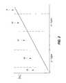
- FIG. 1graphically illustrates a system in which a conductivity type is influenced by the concentration of ions (represented as [I]). Specifically, at some ion concentrations the system is in a regime 10 having n-type characteristics, and at other ion concentrations the system is in a regime 14 having p-type characteristics.
- An intermediate regime 12is between the regimes 10 and 14 , and in such intermediate regime the system may have characteristics which are indeterminate relative to n-type and p-type, or may have other electrical characteristics (such as electrically insulative characteristics), depending on the system.
- the system of FIG. 1is also shown comprising a regime 9 in which the concentration of ions is less than that suitable to induce n-type characteristics, as well as a regime 15 in which the concentration of ions is greater than that which induces p-type characteristics.
- a regime 9 in which the concentration of ions is less than that suitable to induce n-type characteristicsas well as a regime 15 in which the concentration of ions is greater than that which induces p-type characteristics.
- Either of the regimes 9 and 15may have conventional electrically insulative characteristics, or conventional electrically conductive characteristics, depending on the system.
- FIG. 2illustrates the same system as FIG. 1 , but shown with an alternative convention relative to that of FIG. 1 .
- FIG. 2shows the conductivity type of the system being influenced by the concentration of ion vacancies (represented as [V 1 ]).
- the concentration of ion vacanciesmay be roughly inverse to the concentration of ions.
- FIG. 2shows the same regions 9 , 10 , 12 , 14 and 15 as FIG. 1 , but shows such regions having an inverse relationship relative to the relationship illustrated in FIG. 1 .
- the “vacancies”are typically not empty spaces, but rather are regions where ions could be present, and are not. Such regions may have any of numerous configurations, but are real physical moieties that can have measurable mobility within a system.
- a distribution of ions within a materialmay be described as either the concentration of the ions themselves, or as the concentration of vacancies of the ions.
- the vacancieswill typically have an opposite charge to the ions themselves.
- itis conventional to refer to positively-charged species in a system.
- itwill be the charge which will determine whether a system is described in terms of vacancy concentration or ion concentration.
- oxygen-containing ionstypically have a negative charge, it may be preferred to describe the charged species of an oxygen-based system as vacancies in some contexts.
- the concentration of ion vacanciesis sometimes considered as the inverse of the concentrations of ions, there may not be a simple correlation between the concentration of ions and the concentration of ion vacancies in some systems. For instance, there may be differences between ion mobility and ion vacancy mobility which leads to faster accumulation of either ions or vacancies, and thus leads to imbalance between a rate of change in ion concentration relative to a rate of change of ion vacancy concentration. Accordingly, many of the systems described herein may be considered to utilize alteration of either or both of ion concentration and ion vacancy concentration to achieve desired changes within the systems.
- FIG. 3graphically illustrates an oxygen-based system, or, more specifically, a system in which conductivity type is influenced by a concentration of oxygen-containing ions.
- concentration of oxygen atomsis approximated in FIG. 3 by the concentration of oxygen-containing ion vacancies (V O ).
- the systemhas the same regimes 9 , 10 , 12 , 14 and 15 discussed above with reference to FIGS. 1 and 2 .
- the system of FIG. 3may contain oxygen ions distributed within a composition that comprises oxygen in combination with one or more of praseodymium, barium, calcium, manganese, strontium, titanium, iron, cesium and lead.
- the compositionmay comprise one or more of PrCaMnO, BaSrTiO, SrTiO, SrCeFeO, and PbO, where such compositions are shown in terms of the elements contained therein, rather than in terms of a specific stoichiometry.
- the composition shown as PrCaMnOmay correspond to Pr (1-x) Ca x MnO 3 , where x is any number greater than 0 and less than 1.
- Oxygen-based systemsmay be highly sensitive to the concentration of oxygen-containing ions (and/or to the concentration of vacancies of oxygen-containing ions). For instance, a change in the concentration of oxygen ions of about 10 parts per million may shift SrTiO from the regime 10 having n-type characteristics to the regime 14 having p-type characteristics.
- the oxygen-based systems represented by FIG. 3may be considered to correspond to valence change material systems.
- the systemscomprise materials having one or more elements with multiple stable valence states (for instance, titanium, iron, manganese, etc.).
- Valence change systemsare example systems that may be utilized in some embodiments.
- Valance change systemsmay comprise mobile ions, and/or mobile ion vacancies, that can be moved within the systems to alter ion and ion vacancy concentrations throughout the systems. Mobile ions and mobile ion vacancies may or may not coexist in a single system, depending on the system. Thus, one or both of the mobile species corresponding to mobile ions and mobile ion vacancies may be utilized to alter ion concentration, and/or ion vacancy concentration, within a given system.
- Oxygen-based systems of the type represented in FIG. 3are examples of the types of systems that may be utilized in various embodiments of the invention. Any suitable systems may be utilized, and other example systems are sulfur-based systems, nitrogen-based systems, etc.
- the curves of FIGS. 1-3are qualitative representations of the relationship between ion concentration (and/or ion vacancy concentration) and conductivity type for various systems.
- the concept being illustratedis that the conductivity type of some systems may be influenced and changed by an ion concentration (and/or an ion vacancy concentration) within such systems.
- Actual systemsmay have a different relationship between the ion concentration (and/or the ion vacancy concentration) and the conductivity type besides the simple linear curves of FIGS. 1-3 .
- an ion concentration (and/or the ion vacancy concentration) within a systemcan influence and alter the conductivity type of the system, such system may be suitable for incorporation into the programmable material of memory cells in various aspects of the present invention.
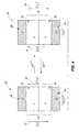
- FIG. 4illustrates an example memory cell 20 having a programmable material 22 sandwiched between a pair of electrodes 24 and 26 .
- the memory cellmay be considered to be an example of a bipolar switching RRAM diode cell.
- the electrodes 24 and 26comprise electrically conductive materials 25 and 27 , respectively.
- the materials 25 and 27may comprise any suitable electrically conductive compositions or combinations of compositions; and in some embodiments may comprise one or more of various metals, metal-containing compositions, and conductively-doped semiconductor materials.
- the materials 25 and 27may be compositionally the same as one another in some embodiments, and may be compositionally different from one another in other embodiments.
- the electrode 24may be part of a first linear segment that extends along a first direction (analogous to a first linear segment described below with reference to FIG. 19 ), and the electrode 26 may be part of a second linear segment that extends along a second direction that crosses the first direction (analogous to one of the second linear segments described below with reference to FIG. 19 ).
- the memory cell 20is formed at a location where the first and second linear segments overlap one another, and comprises the programmable material 22 directly between the first and second linear segments.
- the programmable material 22comprises two regions 30 and 32 which are compositionally different from one another, and which may both have characteristics of the various systems described above with reference to FIGS. 1-3 .
- the regions 30 and 32may comprise any of the various oxygen-based systems described with reference to FIG. 3 .
- the compositional difference between regions 30 and 32may be substantial, such as having a composition of one of the regions comprising one or more elements which are not common to the composition of the other of the regions.
- the compositional difference between regions 30 and 32may be subtle, such as having the same mixture of elements within both regions, and having a stoichiometric difference between the regions.
- the difference between regions 30 and 32is more than a transitory difference, and thus more than a mere difference in the population of ions between the two regions.
- the interface between the layers 30 and 32may be abrupt in some embodiments, diffuse in some embodiments, and/or may comprise a gradient in some embodiments.
- regions 30 and 32are described as being compositionally different than one another, in other embodiments the difference between regions 30 and 32 may be solely due to different concentrations of ions within the regions as induced by a programming operation.
- a programmable materialmay have more than two different regions. If the programmable material has more than two different regions, all of the regions may be compositionally different from one another; or two or more of the regions may be compositionally the same as one another, and spaced from one another by at least one region which is compositionally different from them.
- the regions 30 and 32are shown to be directly against one another. In other embodiments the regions may be spaced from one another by intervening materials or regions. For instance, an embodiment discussed below with reference to FIG. 11 comprises an insulating material between the regions 30 and 32 .
- the regions 30 and 32may comprise any suitable thicknesses, and may be about the same thickness as one another (as shown), or may be different thicknesses relative to one another. In some embodiments, each of the regions 30 and 32 may have a thickness of from about 5 nanometers to about 100 nanometers.
- each of the regions 30 and 32comprises a system which can be changed from one conductivity type to another by altering a concentration of ions (and/or ion vacancies) within the system. Both systems are influenced by the same ions (and/or ion vacancies), and thus the relative conductivity types of regions 30 and 32 may be tailored by altering the relative concentration of the ions (and/or ion vacancies) within the two regions 30 and 32 .
- the distribution of the ions and ion vacancies across programmable material 22is diagrammatically indicated along the sides of the programmable material with arrows 31 and 33 .
- arrow 31indicates that a concentration of ions ([I]) increases along one direction through the programmable material
- arrow 33indicates that there is an increase in vacancies of the ion ([V 1 ]) in a direction opposite to the direction of the arrow 31 .
- FIG. 4shows the region of programmable material having a high concentration of ions (or alternatively, a low concentration of ion vacancies) being p-type, and shows the region of the programmable material having the low concentration of ions (or alternatively, a high concentration of ion vacancies) being n-type.
- ion concentrationor ion vacancy concentration
- conductivity typeis consistent with the oxygen-based systems described above with reference to FIG. 3 .
- other systemsmay be utilized, and the relationship of conductivity to ion concentration (or ion vacancy concentration) may be opposite to that shown in FIG. 4 (e.g., a high ion concentration, or low ion vacancy concentration, may correspond to an n-type region rather than corresponding to the p-type region shown in FIG. 4 ).
- FIG. 4shows memory cell 20 in two different interchangeable memory states, which are designated as a “RESET” state and a “SET” state.
- the regions 30 and 32are of opposite conductivity type relative to one another in both of the “RESET” and “SET” memory states.
- the two memory states of FIG. 4are interchanged with one another by subjecting memory cell 20 to appropriate electric fields.
- An electric field oriented along a first direction(the field designated as EF (+) in FIG. 4 ) may shift the ion distribution (and/or the ion vacancy distribution) within the memory cell to cause the memory cell to transition from the “RESET” state to the “SET” state.
- An electric field oriented along a second direction opposite to that of the first direction(the field designated as EF ( ⁇ ) in FIG. 4 ) may shift the ion distribution (and/or the ion vacancy distribution) within the memory cell to cause the memory cell to transition from the “SET” state to the “RESET” state.
- the “RESET” memory statehas a pn diode in one orientation
- the “SET” memory statehas a pn diode in an opposite orientation relative to that of the “RESET” state.
- the regions 30 and 32may be referred to as first and second regions, and the conductivity types of such regions in the “SET” state may be referred to as first and second conductivity types, respectively; with the first and second conductivity types being opposite to another.
- the conductivity type of the first region 30is transitioned from the first conductivity type (shown as n-type), to the second conductivity type (shown as p-type) in changing the memory cell from the “SET” state to the “RESET” state; and the conductivity type of the second region 32 is transitioned from the second conductivity type to the first conductivity type in changing the memory cell from the “SET” state to the “RESET” state.
- the pn diodes of the “SET” and “RESET” memory statesare formed within the programmable material 22 simultaneously with the programming of the memory cell into such memory states.
- the embodiment of FIG. 4has conductivity types of the first and second regions 30 and 32 of the “SET” state induced by changes in concentrations of ions (and/or by changes in concentrations of ion vacancies) within each of such regions.
- one of the regions of the programmable materialmay have a static conductivity type (i.e., a conductivity type which is not changed in transitioning between the “RESET” and “SET” memory states). Accordingly, if the programmable material has two regions, it may be only one of such regions that has a conductivity type induced by a change in a concentration of ions (and/or by a change in a concentration of ion vacancies).
- the reading of the memory cell 20 of FIG. 4comprises determination of the amount of current passed through the memory cell when an electric field is provided across the programmable material. It is noted that the conditions utilized to transition the memory cell from one memory state to another will use some suitable combination of a sufficient magnitude of electric field, coupled with a sufficient duration of time to enable redistribution of ions (and/or ion vacancies) within the programmable material. The conditions utilized during the reading operation may be chosen to have one or both of the magnitude of electric field and the duration of time that the field is applied to be too low to transition the memory cell from one memory state to another.
- the electric field utilized to read the memory cellmay be applied along a direction which forward biases the pn diode of the “SET” memory state, and reverse biases the pn diode of the “RESET” memory state. Accordingly, memory cells in the “SET” memory state will pass greater current then memory cells in the “RESET” memory state, and thus may be distinguished from the memory cells in the “RESET” memory state.
- the ions (and/or ion vacancies) utilized for transitioning the memory cell from one state to anothermay be contained entirely within the programmable material, and diffused from one region to another during the programming of the memory cell.
- barriersmay be provided entirely around the programmable material 22 to trap the ions (and/or the ion vacancies) within the programmable material.
- the electrodes 24 and 26may comprise material which blocks diffusion of ions (and/or ion vacancies) therethrough (i.e., which is impermeable to the ions or ion vacancies), and may be directly against the programmable material.
- one or more layers of barrier materialmay be provided between the electrodes and the programmable material, and/or along the sides of the programmable material.
- Example barrier materialswhich may be used to block diffusion of oxygen-containing ions are described in U.S. Patent Publication No. 2010/0237442, as well as in U.S. Pat. Nos. 6,524,867, 7,727,908, 7,273,791, 7,393,785, 7,544,987 and 7,560,815.
- Example electrically conductive materials which may block diffusion of oxygen-containing ions, and which may be utilized in electrodes in some embodimentscan include, for example, Al, Ir, Ru, RuTiN, RuTiO, RuO—Ta, CeO—Ta, TaN, etc., where such materials are shown in terms of the elements contained therein, rather than in terms of a specific stoichiometry.
- the barrier materialmay be electrically insulative or electrically conductive. If the barrier material is electrically insulative, it may be formed to be thin enough that current can still pass through the barrier material during reading and programming of the memory cell. If the barrier material is electrically conductive, it may be considered to be comprised by the electrode that is directly adjacent to the barrier material.
- FIG. 5shows a “current vs. voltage” curve illustrating performance characteristics of the memory cell 20 of FIG. 4 .
- the curvehas four important events which are specifically labeled along such curve.
- the event ( 1 )corresponds to an increase in voltage while the memory cell remains in the “RESET” memory state.
- the next event ( 2 )corresponds to a transition that occurs when the voltage reaches a level Vset, whereupon the pn diode of the “RESET” memory state is reversed to transition the memory cell into the “SET” memory state.
- the current flow through the “SET” memory stateis cut-off (i.e., truncated) at a level 35 .
- Such truncationrepresents a current cut-off provided for current compliance to protect semiconductor devices. In theory, such cut-off would not exist for an idealized memory device utilized in the absence of other circuitry, but in practice it is generally utilized.
- the next event ( 3 )corresponds to a decrease in voltage while the memory device remains in the “SET” memory state.
- Vt 1There is a voltage level indicated as Vt 1 , which is below the level Vset, but at which substantial current flows through the memory cell in the “SET” memory state.
- Such levelmay correspond to a suitable voltage level for reading the memory device without inadvertently tripping the device into the “SET” or “RESET” memory state.
- the next event ( 4 )corresponds to a transition that occurs when the voltage reaches a level Vreset, whereupon the pn diode of the “SET” memory state is reversed to transition the memory cell into the “RESET” memory state.
- the current flow through the “RESET” memory statemay be cut-off at a level 37 for the current compliance reasons discussed above relative to the cut-off level 35 .
- the “RESET” memory state of the memory cell 20 of FIG. 4may be exactly the opposite of the “SET” memory state of such memory cell. Accordingly, reading of the memory cell may comprise utilization of electric field oriented such that the pn diode of the “RESET” is forward biased, while the pn diode of the “SET” state is reverse biased.
- Such read operationis diagrammatically illustrated in FIG. 5 by indicating a voltage level Vt 2 which could be utilized analogously to the above-discussed voltage level Vt 1 , but which would forward bias the pn diode of the “RESET” memory state.
- the memory cell 20 of FIG. 4has the two different and opposite read operations which may be accomplished by either forward biasing the pn diode of the “SET” memory state or the pn diode of the “RESET” memory state.
- suchcan provide additional flexibility for design of read operations to be utilized for ascertaining the memory states of the various memory cells in a memory cell array.
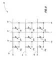
- FIG. 4shows a schematic diagram of a portion of a memory array 38 .
- Such memory arraycomprises a plurality of cross-point memory cells 20 a - 20 i .
- the memory arrayalso comprises a series of first access lines 40 - 42 extending along a first direction, and a series of second access lines 43 - 45 extending along a second direction, and intersecting with the first access lines.
- the memory cells 20 a - 20 iare provided at locations where the first access lines intersect the second access lines, and thus each memory cell may be uniquely addressed through the combination of a first access line and a second access line.
- FIG. 6shows that voltages of 1 ⁇ 2 unit, 0 unit and 1 ⁇ 2 unit, respectively are along the access lines 40 , 41 and 42 ; and that voltages of 1 ⁇ 2 unit, 1 unit and 1 ⁇ 2 unit, respectively are along access lines 43 , 44 and 45 .
- the memory cell 20 ewill experience an electric field of 1 unit, which will be significantly larger than the electric field experienced by any of the other memory cells.
- memory cells 20 a , 20 c , 20 g and 20 imay experience electric fields of about 0 units, while the memory cells 20 b , 20 d , 20 f and 20 h may experience electric fields of about 1 ⁇ 2 unit.
- the memory cell 20 emay be uniquely addressed for programming, and similarly may be uniquely addressed for reading.
- Each of the other of memory cellsmay be analogously uniquely addressed for programming and reading.
- the programming voltage utilized for programming the memory cells of FIG. 6may be, for example, from about 1 volt about 4 volts.
- FIG. 7shows an example embodiment memory cell 50 , which is different than the example embodiment memory cell 20 of FIG. 4 .
- similar numberingwill be used as is used above in describing the memory cell of FIG. 4 , where appropriate.
- the memory cell 50has a programmable material 52 sandwiched between the pair of electrodes 24 and 26 .
- the programmable materialcomprises two regions 60 and 62 which are compositionally different from one another.
- One or both of the regionsmay comprise a system which changes conductivity type depending upon the concentration of ions (and/or depending on the concentration of ion vacancies) within such system.
- one or both of the regionsmay comprise a system of any of the types described above with reference to FIGS. 1-3 .
- the memory cell 50is shown to have interchangeable “RESET” and “SET” memory states; with such states being interchanged using the electric fields EF (+) and EF ( ⁇ ) .
- the “SET” memory stateis similar to the “SET” memory state of the FIG. 4 memory cell, and accordingly comprises a pn diode within the programmable material 52 . Further, the “SET” state of memory cell 50 is shown to have ions (or vacancies) diffused within both of the regions 60 and 62 . The arrows 31 and 33 are provided along the memory cell in the “SET” memory state to illustrate that an ion concentration increases along a direction from region 60 to 62 , and that an ion vacancy concentration increases along a direction from region 62 to 60 .
- the shown embodimenthas a p-type region at high levels of the ion concentration (or alternatively considered, at low levels of the ion vacancy concentration); and has an n-type region at low levels of the ion concentration (or alternatively considered, at high levels of the ion vacancy concentration).
- the relative dependence on the ion concentration (or ion vacancy concentration) of the p-type and n-type regionsmay be reversed—i.e., the n-type region may occur at high concentrations of the ions (or low concentrations of ion vacancies), and the p-type region may occur at low concentrations of the ions (or high concentrations of ion vacancies).
- the regions 60 and 62 in the “RESET” memory state of the memory cellare not labeled relative to n-type and p-type.
- one or both of the regions 60 and 62may have electrically insulative properties in the “RESET” memory state.
- one or both of the regions 60 and 62may have ions (or vacancies) diffused therein to a concentration corresponding to the regime 12 of FIGS. 1-3 .
- Such regimeis neither n-type nor p-type, and in some embodiments may have characteristics of electrically insulative material.
- the electrically insulative regimemay occur in one or both of the regimes 9 and 15 of FIGS. 1-3 when the ion concentration (or ion vacancy concentration) is outside of appropriate concentrations for the n-type and p-type regimes 10 and 14 .
- regions 60 and 62 of the “RESET” stateare specifically labeled as n-type or p-type, in some embodiments one of the regions may be n-type or p-type, while the other is electrically insulative.
- region 60may be n-type or p-type, while region 62 is electrically insulative; or vice versa.
- the transition to the “SET” memory statecomprises changing conductivity of both regions. Specifically, region 62 is changed from electrically insulative to p-type, and region 60 is changed from p-type to n-type.
- the transition to the “SET” memory statecomprises changing conductivity of only region 62 .
- region 62is changed from electrically insulative to p-type, while region 60 remains n-type.
- region 60may remain n-type in both the “RESET” and “SET” memory states of the memory cell, the concentration of ion vacancies within region 60 may increase (and/or the concentration of ions may decrease) in going from the “RESET” memory state to the “SET” memory state.
- regions 60 and 62may comprise different systems, with the system of region 62 needing a higher concentration of ion vacancies (and/or a lower concentration of ions) to transition into a p-type regime than does the region 60 .
- the region 60in the “RESET” memory state the region 60 may be n-type even though it has a significant ion concentration (and/or has a low concentration of ion vacancies).
- the transition into the “SET” statemay comprise diffusion of ions from region 60 into region 62 (and/or diffusion of ion vacancies from region 62 to region 60 ), and there may be enough ions (and/or ion vacancies) migrating between regions 60 and 62 to convert the system of region 62 into the p-type regime.
- regions 62 and 60may comprise similar systems, but region 62 may be much thinner than region 60 .
- region 60may be an n-type semiconductor material that is not affected by the ion concentration (or ion vacancy concentration), analogously to constructions discussed below with reference to FIG. 13 .
- FIG. 8shows a “current vs. voltage” curve illustrating performance characteristics of the memory cell 50 of FIG. 7 .
- the curvehas four important events which are specifically labeled along such curve, with such events being analogous to the events described above with reference to the “current vs. voltage” curve of FIG. 5 .
- the event ( 1 )corresponds to an increase in voltage while the memory cell remains in the “RESET” memory state.
- the programmable material 52FIG. 7
- the programmable material 52has at least one electrically insulative region (i.e., at least one of the regions 60 and 62 of FIG. 7 is electrically insulative in the “RESET” state), and thus no current flows through the memory cell while the cell is in the “RESET” state.
- the next event ( 2 )corresponds to a transition that occurs when the voltage reaches a level Vset, whereupon the pn diode of the “SET” memory state is formed.
- the current flow through the “SET” memory statehas the cut-off at level 35 discussed above with reference to FIG. 5 .
- the next event ( 3 )corresponds to a decrease in voltage while the memory device remains in the “SET” memory state.
- Vt 1analogous to the level Vt 1 discussed above with reference to FIG. 5 .
- Such levelmay correspond to a suitable voltage level for reading the memory device.
- the next event ( 4 )corresponds to a transition that occurs when the voltage reaches a level Vreset, whereupon the at least one insulative region is reformed, and current ceases to flow through the memory device.
- FIG. 9shows another example embodiment memory cell 70 .
- the memory cell 70is equivalent to the memory cell 50 of FIG. 7 , but inverted relative to the memory cell of FIG. 7 .
- the memory cell 70has the programmable material 52 sandwiched between the pair of electrodes 24 and 26 .
- the programmable materialcomprises the two regions 60 and 62 described above.
- the memory cell 70has the interchangeable “RESET” and “SET” memory states described above with reference to FIG. 7 . However, the pn diode within the “SET” memory state of FIG. 9 is inverted relative to that of FIG. 7 . Arrows 31 and 33 are provided in FIG. 9 along the memory cell in the “SET” memory state to illustrate that an ion concentration increases along a direction from region 62 to 60 , and that an ion vacancy concentration increases along a direction from region 60 to 62 .
- neither of the regions 60 and 62 of the “RESET” state of FIG. 9is specifically labeled as n-type or p-type.
- both of the regions 60 and 62may be electrically insulative in the “RESET” state of FIG. 9 ; and in other embodiments one of the regions may be n-type or p-type, while the other is electrically insulative.
- region 60may be n-type or p-type, while region 62 is electrically insulative.
- the transition to the “SET” memory statecomprises changing conductivity of both regions. Specifically, region 62 is changed from electrically insulative to n-type, and region 60 is changed from n-type to p-type. Such may comprise diffusing ions (or vacancies) from the insulative region 62 of the “RESET” memory state into the region 60 to transition to the “SET” memory state.
- the transition to the “SET” memory statecomprises changing conductivity of only the region 62 .
- region 62is changed from electrically insulative to n-type, while region 60 remains p-type.
- Suchmay comprise diffusing ions (or vacancies) between the regions 60 and 62 .
- the shown configurationis an example configuration in which regions with a relatively high ion concentration (and a relatively low ion vacancy concentration) are p-type, and regions with a relatively low ion concentration are n-type (and a relatively high ion vacancy concentration).
- FIG. 10shows a “current vs. voltage” curve illustrating performance characteristics of the memory cell 70 of FIG. 9 .
- the curvehas four important events which are specifically labeled along such curve, with such events being analogous to those described above with reference to FIG. 8 , but of opposite orientation relative to those of FIG. 8 .
- the event ( 1 ) of FIG. 10corresponds to a decrease in voltage while the memory cell remains in the “RESET” memory state.
- the next event ( 2 )corresponds to a transition that occurs when the voltage reaches a level Vset, whereupon the pn diode of the “SET” memory state is formed.
- the next event ( 3 )corresponds to an increase in voltage while the memory device remains in the “SET” memory state.
- Vt 1analogous to the level Vt 1 discussed above with reference to FIG. 8 , which may correspond to a suitable voltage level for reading the memory device.
- the next event ( 4 )corresponds to a transition that occurs when the voltage reaches a level Vreset, whereupon the at least one insulative region is reformed, and current ceases to flow through the memory device.
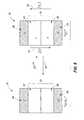
- FIG. 11shows another example embodiment memory cell 80 with interchangeable “RESET” and “SET” memory states.
- FIG. 11similar numbering will be used as is used above in describing the memory cell of FIG. 4 , where appropriate.
- the memory cell 80has a programmable material 82 between the pair of electrodes 24 and 26 .
- the programmable material 82comprises the two regions 30 and 32 described above with reference to the memory cell 20 of FIG. 4 .
- the memory cell 80differs from the memory cell 20 of FIG. 4 in that the memory cell 80 comprises an ion (and/or ion vacancy) reservoir 84 between the regions 30 and 32 .
- the reservoir 84may comprise electrically conductive material in some embodiments, and may comprise electrically insulative material in some embodiments.
- the ionsmay be oxygen-containing species
- the reservoirmay be a material which contains an excess of oxygen-containing species in at least one of the memory states.
- the reservoirmay be an insulative material comprising oxygen-enriched oxide (such as silicon oxide, aluminum oxide, etc.) in at least one of the memory states.
- the reservoirmay be permeable to the ions (and/or to the ion vacancies) in some embodiments.
- the ion (and/or ion vacancy) reservoirmay be kept very thin so that it does not substantially interfere with current flow through the programmable material in the “SET” memory state, and in example embodiments may have a thickness of less than or equal to about 50 angstroms, less than or equal to about 20 angstroms, or any other suitable thickness.
- the reservoirmay act as a source of ions (and/or ion vacancies) for altering one or both of ion density and ion vacancy density in one of the regions of the programmable material during a transition from the “RESET” memory state to the “SET” memory state, or vice versa; and/or may act as a sink for excess ions, or ion vacancies, during transitioning from one memory state to the other.
- the reservoirmay facilitate movement of ions (and/or ion vacancies), which may facilitate rapid switching from one memory state to another, and may thus improve one or both of reading speed and writing speed.
- the reservoir 84may be placed in any suitable location within the programmable material, and in some embodiments there may be more than one reservoir of ions (and/or ion vacancies) provided within the programmable material. In the shown embodiment, the reservoir 84 is between the regions 30 and 32 , and directly against both of such regions. In other embodiments, the reservoir may be placed in other locations.
- FIG. 12illustrates example embodiment memory cell 80 a analogous to the memory cell 80 of FIG. 11 , but comprising the reservoir 84 along a top of the programmable material, rather than in a middle of the programmable material; and specifically directly between the region 32 and the top electrode 26 .
- the reservoir 84may correspond to an electrically conductive material.
- the memory cell of FIG. 12may be considered to comprise an electrically conductive material 84 directly between the top electrode 26 and the top region 32 of the programmable material.
- FIG. 13shows another example embodiment memory cell 90 with interchangeable “RESET” and “SET” memory states.
- similar numberingwill be used as is used above in describing the memory cell of FIG. 4 , where appropriate.
- the memory cell 90has a programmable material 92 between the pair of electrodes 24 and 26 .
- the programmable materialcomprises two regions 94 and 96 which are compositionally different from one another.
- the region 94comprises p-type doped semiconductor material (for instance, p-type doped silicon) while the region 96 comprises a system which changes conductivity type depending upon the concentration of ions, or ion-vacancies, within such system.
- the region 96may comprise a system of any of the types described above with reference to FIGS. 1-3 .
- the conductivity of the doped semiconductor material of region 94does not change in transitioning between the “RESET” memory state and the “SET” memory state, and in the shown embodiment remains p-type in both memory states.
- the region 96is shown to have n-type conductivity in the “SET” memory state, so that regions 94 and 96 together form a pn diode in the “SET” memory state.
- the region 96may have electrically insulative properties in the “RESET” state, and an electric field which forward biases the pn diode of the “SET” may be utilized to distinguish the “RESET” memory state from the “SET” memory state.
- ions (or vacancies) within programmable material 92are only within the region 96 in both the “RESET” and “SET” memory states (as indicted by the concentration of ions ([I]) being shown only within the region 96 in FIG. 13 ). Accordingly, region 94 of the programmable material does not act as a reservoir of ions or vacancies during the transition between the “RESET” and “SET” memory states. Rather, electrode 26 may be configured to be permeable to the ions (and/or vacancies), so that ions (and/or vacancies) may pass through such electrode during transitioning between the “RESET” memory state and the “SET” memory state.
- any suitable electrically conductive material permeable to the ions and/or vacanciesmay be utilized for the electrode 26 .
- Example materials which are permeable to oxygen-containing ionsmay include Pt and/or materials described in U.S. Pat. No. 7,273,791.
- the region 96has a first concentration of ions and/or vacancies, shown as [I] 1 , in the “RESET” memory state; and a second concentration of ions and/or vacancies, shown as [I] 2 , in the “SET” memory state.
- the second concentration of ions and/or vacanciesis different than the first concentration, and such difference leads to the change in conductivity of the region 96 in transitioning from the “RESET” memory state to the “SET” memory state.
- the concentration [I] 1may be about 0 ions per unit volume, and in other embodiments it may be larger than 0 ions per unit volume.
- the upper region 96is shown to be the region which is altered in response to concentration of ions and vacancies in the embodiment of FIG. 13 , in other embodiments it may be the lower region 94 which is altered while the upper region 96 is the conductively-doped semiconductor material.
- the p-type doped region of the memory cellis shown to be the region corresponding to doped semiconductor material, in other embodiments it may be the n-type region which corresponds to doped semiconductor material. For instance, an embodiment analogous to that of FIG.
- region 96corresponding to n-type doped semiconductor material
- region 94corresponding to a system which is in an insulative regime in the “RESET” memory state, and then transitions to the p-type regime in the “SET” memory state due to migration of ions (and/or vacancies) from or to such system.
- FIG. 14shows another example embodiment memory cell 100 with interchangeable “RESET” and “SET” memory states.
- similar numberingwill be used as is used above in describing the memory cell of FIG. 4 , where appropriate.
- the memory cell 100has a programmable material 102 between the pair of electrodes 24 and 26 .
- the programmable materialcomprises two regions 104 and 108 which are compositionally different from one another.
- the region 104comprises p-type doped semiconductor material (for instance, p-type doped silicon) while the region 108 comprises a system which changes conductivity type depending upon the concentration of ions and/or vacancies within such system.
- the region 108may comprise a system of any of the types described above with reference to FIGS. 1-3 .
- the conductivity of the doped semiconductor material of region 104does not change in transitioning between the “RESET” memory state and the “SET” memory state, and in the shown embodiment remains p-type in both memory states.
- the memory cell 100may be fabricated with any suitable methodology.
- the constructionmay be fabricated by providing the material 108 over region 104 .
- the region 106may be formed during switching from the “RESET” to “SET” state—as a push (or growth) of a conductive filament through the material 108 , and may be removed during switching from the “SET” to “RESET” state by dissolving the conductive filament.
- the region 108has a first concentration of ions and/or ion-vacancies (shown as [I] 1 ) in the “RESET” memory state, and the region 106 has a second concentration of ions and/or ion-vacancies (shown as [I] 2 ) in the “SET” memory state.
- the second concentrationis different than the first concentration, and such difference leads to formation of the filamentous region 106 in transitioning from the “RESET” memory state to the “SET” memory state.
- the concentration [I] 1may be about 0 ions per unit volume, and in other embodiments it may be larger than 0 ions per unit volume.
- the memory cell 100may be operated identically to the memory cell 90 discussed above with reference to FIG. 13 .
- the filamentous region 106directly contacts both the p-type region 104 and the upper electrode 26 in the shown embodiment.
- the memory cell 100is an example memory cell having a first conductivity type filament extending between an electrode and a second conductivity type region, and other similar memory cells may be formed in other embodiments.
- the region 104may be n-type doped semiconductor material, and thus may be statically n-type in transitioning between the “RESET” memory state and the “SET” memory state.
- the filamentous region 106may be p-type.
- Any suitable processmay be utilized to form the various memory cells discussed above with reference to FIGS. 1-14 .
- An example process for forming an array of memory cellsis described with reference to FIGS. 15-19 .
- a construction 200is shown to comprise a base 212 , an electrically insulative material 214 over the base, and a line 215 of the electrically conductive electrode material 25 over such electrically insulative material.
- the base 212may comprise, consist essentially of, or consist of monocrystalline silicon, and may be referred to as a semiconductor substrate, or as a portion of a semiconductor substrate.
- semiconductor substratesemiconductor substrate
- semiconductor constructionsemiconductor substrate
- semiconductor substratesemiconductor substrate
- semiconductor substratesemiconductor substrate
- substratesemiconductor material layers
- substraterefers to any supporting structure, including, but not limited to, the semiconductive substrates described above.
- base 212is shown to be homogenous, the base may comprise numerous materials in some embodiments.
- base 212may correspond to a semiconductor substrate containing one or more materials associated with integrated circuit fabrication. In such embodiments, such materials may correspond to one or more of refractory metal materials, barrier materials, diffusion materials, insulator materials, etc.
- the electrically insulative material 214is shown to be spaced from the base 212 by other levels of integrated circuitry. Such levels may include logic, wiring, memory, etc. Alternatively, the electrically insulative material 214 may be directly against an upper surface of semiconductor material (for instance, monocrystalline silicon) of base 212 in some embodiments.
- semiconductor materialfor instance, monocrystalline silicon
- the electrically insulative material 214may comprise any suitable composition or combination of compositions, and may, for example, comprise one or more of silicon dioxide, silicon nitride, doped silicate glass (e.g., borophosphosilicate glass, phosphosilicate glass, fluorosilicate glass), etc.
- doped silicate glasse.g., borophosphosilicate glass, phosphosilicate glass, fluorosilicate glass
- the line 215 of the electrode material 25is shown extending along a direction within the plane of the cross-section of FIG. 15 .
- regions 320 and 322 of the programmable material 300are formed over electrode material 25 .
- a barrier material of the type described above with reference to FIG. 4may be formed over the electrode 25 prior to formation of programmable material 300 .
- the regions 320 and 322may comprise any suitable materials, including, for example, any of the materials of the regions 30 and 32 of FIG. 4 , the regions 60 and 62 of FIG. 7 , the regions 94 and 96 of FIG. 13 , etc.
- the regions 320 and 322may comprise one or more of the oxygen-containing materials of the systems described above with reference to FIG. 3 .
- the regions 320 and 322may be referred to as a first region and a second region respectively, with the second region being formed over the first region.
- the first regionmay ultimately correspond to an n-type doped region of a pn diode formed in the “SET” memory state of a memory cell (such as the memory cell 20 of FIG. 4 ), and in other embodiments the first region may ultimately correspond to the p-type doped region of such diode.
- reservoir material analogous to the material 84 of FIGS. 11 and 12may be incorporated into the programmable material 300 .
- the programmable material 300is patterned into a plurality of spaced-apart memory cell features 216 - 218 .
- Such patterningmay comprise formation of a photolithographically-patterned mask (not shown), or any other suitable mask (for instance, a mask formed with pitch-multiplication methodologies), over programmable material 300 , followed by a transfer of a pattern from the mask into material 300 with one or more suitable etches, and subsequent removal of the mask to leave the construction shown in FIG. 17 .
- electrically insulative material 220is formed within the spaces between features 216 - 218 .
- the electrically insulative material 220may comprise any suitable composition or combination of compositions, such as, for example, one or more of silicon dioxide, silicon nitride, doped silicate glass, etc.
- the electrically insulative material 220may be formed in the shown configuration by initially forming the electrically insulative material over and between features 216 - 218 , and then removing the electrically insulative from over the features with a suitable planarization methodology (for instance, chemical-mechanical polishing).
- a suitable planarization methodologyfor instance, chemical-mechanical polishing
- electrode material 27is formed over the features 216 - 218 of programmable material 300 , and patterned to form a plurality of lines 231 - 233 .
- the lines 231 - 233extend along a direction orthogonal to the cross-section of FIG. 19 , and specifically extend in and out of the page relative to the view of FIG. 19 . Accordingly, the lines 231 - 233 of top electrode material 27 extend substantially orthogonally relative to the line 215 of the bottom electrode material 25 .
- the top electrode material 27may be patterned into the lines 231 - 233 with any suitable processing, including, for example, utilization of a mask (not shown), one or more suitable etches to transfer a pattern from the mask into material 27 , and subsequent removal of the mask to leave the construction shown in FIG. 19 .
- electrically insulative material(not shown) may be formed over and between the lines 231 - 233 .
- the top electrode material 27is formed directly against programmable material 300 .
- one or more barrier materials(not shown) of the type described above with reference to FIG. 4 may be formed between the top electrode material and the programmable material.
- FIG. 19may correspond to a portion of a memory array.
- the line 215may be representative of a first series of access lines that extend along a first direction
- the lines 231 - 233may be representative of a second series of access lines that extend along a second direction, and which overlap the first series of access lines.
- Cross-point memory cells 250 a - care formed at locations where the second series of access lines overlap the first series of access lines.
- Such cross-point memory cellshaving programmable material 300 directly between the access lines of the first series and the access lines of the second series.
- the cross-point memory cellsmay have intrinsic pn diodes in a “SET” memory state, and may correspond to any of the memory cells described above with reference to FIGS. 4, 7, 9, and 11-14 .
- the pn diodemay be oriented with the p-type region as the upper region, or with the n-type region as the upper region.
- the lower region 320may be n-type in the “SET” memory state
- the upper region 322may be n-type in the “SET” memory state.
- the memory cells discussed abovemay be incorporated into memory arrays of electronic devices, and such devices may be incorporated into electronic systems.
- the electronic systemsmay be used in, for example, memory modules, device drivers, power modules, communication modems, processor modules, and application-specific modules, and may include multilayer, multichip modules.
- the electronic systemsmay be any of a broad range of systems, such as, for example, clocks, televisions, cell phones, personal computers, automobiles, industrial control systems, aircraft, etc.
Landscapes
- Engineering & Computer Science (AREA)
- Chemical & Material Sciences (AREA)
- Materials Engineering (AREA)
- Manufacturing & Machinery (AREA)
- Semiconductor Memories (AREA)
Abstract
Description
Claims (8)
Priority Applications (1)
| Application Number | Priority Date | Filing Date | Title |
|---|---|---|---|
| US14/982,810US9424920B2 (en) | 2011-02-24 | 2015-12-29 | Memory cells, methods of forming memory cells, and methods of programming memory cells |
Applications Claiming Priority (4)
| Application Number | Priority Date | Filing Date | Title |
|---|---|---|---|
| US13/034,031US8488365B2 (en) | 2011-02-24 | 2011-02-24 | Memory cells |
| US13/919,677US8681531B2 (en) | 2011-02-24 | 2013-06-17 | Memory cells, methods of forming memory cells, and methods of programming memory cells |
| US14/173,096US9257648B2 (en) | 2011-02-24 | 2014-02-05 | Memory cells, methods of forming memory cells, and methods of programming memory cells |
| US14/982,810US9424920B2 (en) | 2011-02-24 | 2015-12-29 | Memory cells, methods of forming memory cells, and methods of programming memory cells |
Related Parent Applications (1)
| Application Number | Title | Priority Date | Filing Date |
|---|---|---|---|
| US14/173,096DivisionUS9257648B2 (en) | 2011-02-24 | 2014-02-05 | Memory cells, methods of forming memory cells, and methods of programming memory cells |
Publications (2)
| Publication Number | Publication Date |
|---|---|
| US20160118118A1 US20160118118A1 (en) | 2016-04-28 |
| US9424920B2true US9424920B2 (en) | 2016-08-23 |
Family
ID=46718900
Family Applications (4)
| Application Number | Title | Priority Date | Filing Date |
|---|---|---|---|
| US13/034,031Active2031-09-24US8488365B2 (en) | 2011-02-24 | 2011-02-24 | Memory cells |
| US13/919,677ActiveUS8681531B2 (en) | 2011-02-24 | 2013-06-17 | Memory cells, methods of forming memory cells, and methods of programming memory cells |
| US14/173,096Active2031-08-07US9257648B2 (en) | 2011-02-24 | 2014-02-05 | Memory cells, methods of forming memory cells, and methods of programming memory cells |
| US14/982,810ActiveUS9424920B2 (en) | 2011-02-24 | 2015-12-29 | Memory cells, methods of forming memory cells, and methods of programming memory cells |
Family Applications Before (3)
| Application Number | Title | Priority Date | Filing Date |
|---|---|---|---|
| US13/034,031Active2031-09-24US8488365B2 (en) | 2011-02-24 | 2011-02-24 | Memory cells |
| US13/919,677ActiveUS8681531B2 (en) | 2011-02-24 | 2013-06-17 | Memory cells, methods of forming memory cells, and methods of programming memory cells |
| US14/173,096Active2031-08-07US9257648B2 (en) | 2011-02-24 | 2014-02-05 | Memory cells, methods of forming memory cells, and methods of programming memory cells |
Country Status (3)
| Country | Link |
|---|---|
| US (4) | US8488365B2 (en) |
| TW (1) | TWI506629B (en) |
| WO (1) | WO2012115732A1 (en) |
Cited By (1)
| Publication number | Priority date | Publication date | Assignee | Title |
|---|---|---|---|---|
| US11127459B1 (en)* | 2020-03-16 | 2021-09-21 | Globalfoundries Singapore Pte. Ltd. | Memory devices and methods of forming the same |
Families Citing this family (11)
| Publication number | Priority date | Publication date | Assignee | Title |
|---|---|---|---|---|
| JP2012203936A (en)* | 2011-03-24 | 2012-10-22 | Toshiba Corp | Semiconductor memory device |
| US8581224B2 (en) | 2012-01-20 | 2013-11-12 | Micron Technology, Inc. | Memory cells |
| US8558209B1 (en)* | 2012-05-04 | 2013-10-15 | Micron Technology, Inc. | Memory cells having-multi-portion data storage region |
| US8824188B2 (en)* | 2012-08-06 | 2014-09-02 | Macronix International Co., Ltd. | Operating method for memory device and memory array and operating method for the same |
| JP5826779B2 (en)* | 2013-02-27 | 2015-12-02 | 株式会社東芝 | Nonvolatile semiconductor memory device |
| US9153776B2 (en) | 2013-11-01 | 2015-10-06 | Micron Technology, Inc. | Memory cells and methods of forming memory cells |
| WO2016130134A1 (en)* | 2015-02-13 | 2016-08-18 | Hewlett Packard Enterprise Development Lp | Multilayered memristors |
| US11476416B2 (en) | 2018-03-29 | 2022-10-18 | Taiwan Semiconductor Manufacturing Company Ltd. | Semiconductor device and method for manufacturing the same |
| US11437573B2 (en)* | 2018-03-29 | 2022-09-06 | Taiwan Semiconductor Manufacturing Company Ltd. | Semiconductor device and method for manufacturing the same |
| US10985252B2 (en) | 2019-08-26 | 2021-04-20 | Micron Technology, Inc. | Integrated assemblies, and methods of forming integrated assemblies |
| US11545201B2 (en)* | 2020-06-23 | 2023-01-03 | Taiwan Semiconductor Manufacturing Company, Ltd. | Memory device with unipolar selector |
Citations (265)
| Publication number | Priority date | Publication date | Assignee | Title |
|---|---|---|---|---|
| US4715685A (en) | 1985-03-04 | 1987-12-29 | Energy Conversion Devices, Inc. | Liquid crystal display having potential source in a diode ring |
| US4964080A (en) | 1990-03-09 | 1990-10-16 | Intel Corporation | Three-dimensional memory cell with integral select transistor |
| US5049970A (en) | 1987-11-17 | 1991-09-17 | Sharp Kabushiki Kaisha | High resistive element |
| US5122476A (en) | 1991-01-28 | 1992-06-16 | Micron Technology, Inc. | Double DRAM cell |
| US6034882A (en) | 1998-11-16 | 2000-03-07 | Matrix Semiconductor, Inc. | Vertically stacked field programmable nonvolatile memory and method of fabrication |
| US6218696B1 (en) | 1999-06-07 | 2001-04-17 | Infineon Technologies North America Corp. | Layout and wiring scheme for memory cells with vertical transistors |
| US20020018355A1 (en) | 1998-11-16 | 2002-02-14 | Johnson Mark G. | Vertically stacked field programmable nonvolatile memory and method of fabrication |
| US20020034117A1 (en) | 2000-09-19 | 2002-03-21 | Takeshi Okazawa | Non-volatile semiconductor memory device with magnetic memory cell array |
| US20020079524A1 (en) | 2000-12-26 | 2002-06-27 | Charles Dennison | Lower electrode isolation in a double-wide trench |
| US6432767B2 (en) | 1995-12-05 | 2002-08-13 | Hitachi, Ltd. | Method of fabricating semiconductor device |
| US20020196695A1 (en) | 2001-05-30 | 2002-12-26 | Stmicroelectronics S.R.L. | Column multiplexer for semiconductor memories |
| US20030031047A1 (en) | 2001-08-09 | 2003-02-13 | Anthony Thomas C. | One-time programmable unit memory cell based on vertically oriented fuse and diode and one-time programmable memory using the same |
| US6524867B2 (en) | 2000-12-28 | 2003-02-25 | Micron Technology, Inc. | Method for forming platinum-rhodium stack as an oxygen barrier |
| US20030086313A1 (en) | 2001-11-07 | 2003-05-08 | Yoshiaki Asao | Magnetic memory device using SOI substrate and method of manufacturing the same |
| KR20030048421A (en) | 2000-11-01 | 2003-06-19 | 가가쿠 기쥬츠 신코 지교단 | Point contact array, not circuit, and electronic circuit comprising the same |
| US20030174570A1 (en) | 2002-03-12 | 2003-09-18 | Mitsubishi Denki Kabushiki Kaisha | Semiconductor memory device having potential control circuit |
| US20030185049A1 (en) | 2002-04-02 | 2003-10-02 | Peter Fricke | Cubic memory array |
| US20030218902A1 (en) | 2002-05-22 | 2003-11-27 | Perner Frederick A. | Triple sample sensing for magnetic random access memory (MRAM) with series diodes |
| US20030218929A1 (en) | 2002-05-24 | 2003-11-27 | Heiko Fibranz | Circuit configuration having a flow controller, integrated memory device, and test configuration having such a circuit configuration |
| US20030223283A1 (en) | 2002-04-03 | 2003-12-04 | Mitsubishi Denki Kabushiki Kaisha | Magnetic memory device |
| US20040002186A1 (en) | 2002-06-27 | 2004-01-01 | Vyvoda Michael A. | Electrically isolated pillars in active devices |
| US6693821B2 (en) | 2001-06-28 | 2004-02-17 | Sharp Laboratories Of America, Inc. | Low cross-talk electrically programmable resistance cross point memory |
| US20040100835A1 (en) | 2002-11-27 | 2004-05-27 | Nec Corporation | Magnetic memory cell and magnetic random access memory using the same |
| US20040108528A1 (en) | 2001-06-28 | 2004-06-10 | Sharp Laboratories Of America, Inc. | Cross-point resistor memory array and method of fabrication |
| US6753561B1 (en) | 2002-08-02 | 2004-06-22 | Unity Semiconductor Corporation | Cross point memory array using multiple thin films |
| US6753562B1 (en) | 2003-03-27 | 2004-06-22 | Sharp Laboratories Of America, Inc. | Spin transistor magnetic random access memory device |
| US20040124407A1 (en) | 2000-02-11 | 2004-07-01 | Kozicki Michael N. | Scalable programmable structure, an array including the structure, and methods of forming the same |
| US6778421B2 (en) | 2002-03-14 | 2004-08-17 | Hewlett-Packard Development Company, Lp. | Memory device array having a pair of magnetic bits sharing a common conductor line |
| US6785159B2 (en) | 2002-08-29 | 2004-08-31 | Micron Technology, Inc. | Combination etch stop and in situ resistor in a magnetoresistive memory and methods for fabricating same |
| US20040188714A1 (en) | 2003-03-31 | 2004-09-30 | Scheuerlein Roy E. | Three-dimensional memory device incorporating segmented bit line memory array |
| US6806531B1 (en) | 2003-04-07 | 2004-10-19 | Silicon Storage Technology, Inc. | Non-volatile floating gate memory cell with floating gates formed in cavities, and array thereof, and method of formation |
| US20040245547A1 (en) | 2003-06-03 | 2004-12-09 | Hitachi Global Storage Technologies B.V. | Ultra low-cost solid-state memory |
| US6834008B2 (en) | 2002-08-02 | 2004-12-21 | Unity Semiconductor Corporation | Cross point memory array using multiple modes of operation |
| US20050001257A1 (en) | 2003-02-14 | 2005-01-06 | Till Schloesser | Method of fabricating and architecture for vertical transistor cells and transistor-controlled memory cells |
| KR20050008353A (en) | 2003-07-15 | 2005-01-21 | 현대자동차주식회사 | Knocking sensor mounting position determining method |
| US20050032100A1 (en) | 2003-06-24 | 2005-02-10 | California Institute Of Technology | Electrochemical method and resulting structures for attaching molecular and biomolecular structures to semiconductor micro and nanostructures |
| US20050054119A1 (en) | 2003-09-05 | 2005-03-10 | Sharp Laboratories Of America, Inc. | Buffered-layer memory cell |
| US20050128799A1 (en) | 2003-12-05 | 2005-06-16 | Renesas Technology Corp. | Semiconductor integrated circuit device |
| JP2005175457A (en) | 2003-12-08 | 2005-06-30 | Sharp Corp | RRAM memory cell electrode |
| US20050161747A1 (en) | 2004-01-26 | 2005-07-28 | Hsiang-Lan Lung | Thin film phase-change memory |
| US20050174835A1 (en) | 2004-02-06 | 2005-08-11 | Unity Semiconductor Corporation | Multi-resistive state element with reactive metal |
| US6930324B2 (en) | 2002-12-31 | 2005-08-16 | Infineon Technologies Ag | Device architecture and process for improved vertical memory arrays |
| US6940113B2 (en) | 2001-06-28 | 2005-09-06 | Sharp Laboratories Of America, Inc. | Trench isolated cross-point memory array |
| US6946702B2 (en) | 2003-06-03 | 2005-09-20 | Winbond Electronics Corp. | Resistance random access memory |
| US20050205943A1 (en) | 2004-03-17 | 2005-09-22 | Sanyo Electric Co., Ltd. | Memory and method of fabricating the same |
| US6950369B2 (en) | 2001-02-06 | 2005-09-27 | Mitsubishi Denki Kabushiki Kaisha | Magnetic memory device capable of passing bidirectional currents through the bit lines |
| US6955992B2 (en) | 2003-09-30 | 2005-10-18 | Sharp Laboratories Of America, Inc. | One mask PT/PCMO/PT stack etching process for RRAM applications |
| US6958273B2 (en) | 2003-03-21 | 2005-10-25 | Silicon Storage Technology, Inc. | Self-aligned method of forming a semiconductor memory array of floating gate memory cells with buried floating gate, pointed floating gate and pointed channel region, and a memory array made thereby |
| US6961258B2 (en) | 2001-06-30 | 2005-11-01 | Ovonyx, Inc. | Pore structure for programmable device |
| US20050250281A1 (en) | 2004-04-26 | 2005-11-10 | Infineon Technologies Ag | Method for manufacturing resistively switching memory devices |
| US6970375B2 (en) | 2002-08-02 | 2005-11-29 | Unity Semiconductor Corporation | Providing a reference voltage to a cross point memory array |
| US20050275003A1 (en) | 2004-06-10 | 2005-12-15 | Sharp Kabushiki Kaisha | Crosspoint structure semiconductor memory device, and manufacturing method thereof |
| US20050287741A1 (en) | 2004-06-28 | 2005-12-29 | Yi Ding | Nonvolatile memory fabrication methods in which a dielectric layer underlying a floating gate layer is spaced from an edge of an isolation trench and/or an edge of the floating gate layer |
| US6985374B2 (en) | 2003-01-17 | 2006-01-10 | Seiko Epson Corporation | Ferroelectric memory device |
| WO2006003620A1 (en) | 2004-06-30 | 2006-01-12 | Koninklijke Philips Electronics N.V. | Method for manufacturing an electric device with a layer of conductive material contacted by nanowire |
| JP2006032729A (en) | 2004-07-16 | 2006-02-02 | Matsushita Electric Ind Co Ltd | Nonvolatile memory and manufacturing method thereof |
| JP2006040981A (en) | 2004-07-22 | 2006-02-09 | Sharp Corp | High density SOI crosspoint memory array and method for manufacturing the same |
| US20060035451A1 (en) | 2003-05-20 | 2006-02-16 | Sharp Laboratories Of America, Inc. | High-density SOI cross-point memory fabricating method |
| US7002197B2 (en) | 2004-01-23 | 2006-02-21 | Hewlett-Packard Development Company, L.P. | Cross point resistive memory array |
| US7005350B2 (en) | 2002-12-31 | 2006-02-28 | Matrix Semiconductor, Inc. | Method for fabricating programmable memory array structures incorporating series-connected transistor strings |
| US20060046509A1 (en) | 2004-08-31 | 2006-03-02 | Samsung Electronics Co., Ltd. | Method of forming a phase change memory device having a small area of contact |
| US7009278B2 (en) | 2003-11-24 | 2006-03-07 | Sharp Laboratories Of America, Inc. | 3d rram |
| US20060062049A1 (en) | 2004-09-17 | 2006-03-23 | Seok-Heon Lee | Methods for programming user data and confirmation information in nonvolatile memory devices |
| US7029925B2 (en) | 2002-01-31 | 2006-04-18 | Texas Instruments Incorporated | FeRAM capacitor stack etch |
| US7035141B1 (en) | 2004-11-17 | 2006-04-25 | Spansion Llc | Diode array architecture for addressing nanoscale resistive memory arrays |
| US20060097238A1 (en) | 2002-07-26 | 2006-05-11 | Laurent Breuil | Non-volatile memory element and production method thereof and storage memory arrangement |
| JP2006121044A (en) | 2004-10-21 | 2006-05-11 | Sharp Corp | Chemical mechanical polishing of PCMO thin film in RRAM equipment |
| US7046550B1 (en) | 2005-01-18 | 2006-05-16 | International Business Machines Corporation | Cross-point memory architecture with improved selectivity |
| US7050316B1 (en) | 2004-03-09 | 2006-05-23 | Silicon Storage Technology, Inc. | Differential non-volatile content addressable memory cell and array using phase changing resistor storage elements |
| US20060110878A1 (en) | 2004-11-22 | 2006-05-25 | Macronix International Co., Ltd. | Side wall active pin memory and manufacturing method |
| US7067862B2 (en) | 2002-08-02 | 2006-06-27 | Unity Semiconductor Corporation | Conductive memory device with conductive oxide electrodes |
| US20060160304A1 (en) | 2005-01-19 | 2006-07-20 | Sharp Laboratories Of America, Inc. | Non-volatile memory resistor cell with nanotip electrode |
| US20060170027A1 (en) | 2005-01-31 | 2006-08-03 | Samsung Electronics Co., Ltd. | Nonvolatile memory device made of resistance material and method of fabricating the same |
| US20060171200A1 (en) | 2004-02-06 | 2006-08-03 | Unity Semiconductor Corporation | Memory using mixed valence conductive oxides |
| US20060181920A1 (en) | 2005-02-09 | 2006-08-17 | Klaus-Dieter Ufert | Resistive memory element with shortened erase time |
| US20060215445A1 (en)* | 2005-03-28 | 2006-09-28 | In-Gyu Baek | Magneto-resistive memory cells and devices having asymmetrical contacts and methods of fabrication therefor |
| US20060258089A1 (en) | 2005-05-10 | 2006-11-16 | Chen Chung-Zen | FLASH memory device and method of manufacture |
| US7149108B2 (en) | 2002-08-02 | 2006-12-12 | Unity Semiconductor Corporation | Memory array of a non-volatile RAM |
| US20060284242A1 (en) | 2005-06-07 | 2006-12-21 | Jo Sang-Youn | Non-volatile memory device having floating gate and methods forming the same |
| US20060286709A1 (en) | 2005-06-17 | 2006-12-21 | Macronix International Co., Ltd. | Manufacturing methods for thin film fuse phase change ram |
| US20070010082A1 (en) | 2005-07-05 | 2007-01-11 | Cay-Uwe Pinnow | Structure and method for manufacturing phase change memories with particular switching characteristics |
| US20070015330A1 (en) | 2005-07-18 | 2007-01-18 | Sharp Laboratories Of America, Inc. | Metal/semiconductor/metal (MSM) back-to-back Schottky diode |
| US7167387B2 (en) | 2003-10-23 | 2007-01-23 | Matsushita Electric Industrial Co., Ltd. | Variable resistance element, method of manufacturing the element, memory containing the element, and method of driving the memory |
| US20070019923A1 (en) | 2005-07-22 | 2007-01-25 | Teruo Sasagawa | Support structure for MEMS device and methods therefor |
| US20070034848A1 (en) | 2005-08-15 | 2007-02-15 | Micron Technology, Inc. | Reproducible resistance variable insulating memory devices and methods for forming same |
| US7180160B2 (en) | 2004-07-30 | 2007-02-20 | Infineon Technologies Ag | MRAM storage device |
| US20070041235A1 (en) | 2005-08-17 | 2007-02-22 | Sharp Kabushiki Kaisha | Semiconductor storage device |
| US20070045615A1 (en) | 2005-08-31 | 2007-03-01 | Samsung Electronics Co., Ltd. | Non-volatile organic resistance random access memory device and method of manufacturing the same |
| US20070048990A1 (en) | 2005-08-30 | 2007-03-01 | Sharp Laboratories Of America, Inc. | Method of buffer layer formation for RRAM thin film deposition |
| US7187201B1 (en) | 2004-06-24 | 2007-03-06 | Xilinx, Inc. | Programmable logic device suitable for implementation in molecular electronics |
| US7193267B2 (en) | 2001-06-28 | 2007-03-20 | Sharp Laboratories Of America, Inc. | Cross-point resistor memory array |
| US20070086235A1 (en) | 2005-10-18 | 2007-04-19 | Du-Eung Kim | Phase-change memory device and method of fabricating the same |
| US20070109835A1 (en) | 2005-11-17 | 2007-05-17 | Sharp Laboratories Of America, Inc. | Cross-point RRAM memory array having low bit line crosstalk |
| US20070121369A1 (en) | 2004-05-27 | 2007-05-31 | Thomas Happ | Resistive memory cell arrangement and a semiconductor memory including the same |
| US20070123039A1 (en) | 2004-11-03 | 2007-05-31 | Elkins Patricia C | Electroless plating of metal caps for chalcogenide-based memory devices |
| US20070120124A1 (en) | 2005-11-30 | 2007-05-31 | I-Wei Chen | Resistance-switching oxide thin film devices |
| US20070132049A1 (en) | 2005-12-12 | 2007-06-14 | Stipe Barry C | Unipolar resistance random access memory (RRAM) device and vertically stacked architecture |
| US20070165434A1 (en) | 2006-01-19 | 2007-07-19 | Samsung Electronics Co., Ltd. | Resistive RAM having at least one varistor and methods of operating the same |
| US7247876B2 (en) | 2000-06-30 | 2007-07-24 | Intel Corporation | Three dimensional programmable device and method for fabricating the same |
| CN101005113A (en) | 2005-12-27 | 2007-07-25 | 旺宏电子股份有限公司 | Method for forming self-aligned thermally isolated cells in variable resistance memory arrays |
| US20070173019A1 (en) | 2006-01-09 | 2007-07-26 | Macronix International Co., Ltd. | Programmable Resistive Ram and Manufacturing Method |
| US20070171706A1 (en) | 2006-01-25 | 2007-07-26 | Elpida Memory, Inc. | Semiconductor memory device |
| US20070176261A1 (en) | 2006-01-30 | 2007-08-02 | Macronix International Co., Ltd. | Vertical Side Wall Active Pin Structures in a Phase Change Memory and Manufacturing Methods |
| US20070210348A1 (en) | 2005-12-23 | 2007-09-13 | Song Jongheui | Phase-change memory device and methods of fabricating the same |
| US7273791B2 (en) | 2000-11-09 | 2007-09-25 | Micron Technology, Inc. | Methods for forming a conductive structure using oxygen diffusion through one metal layer to oxidize a second metal layer |
| US20070224770A1 (en) | 2006-03-25 | 2007-09-27 | Makoto Nagashima | Systems and methods for fabricating self-aligned memory cell |
| US20070231988A1 (en) | 2006-03-09 | 2007-10-04 | Samsung Electronics Co., Ltd. | Method of fabricating nanowire memory device and system of controlling nanowire formation used in the same |
| CN101051670A (en) | 2007-04-19 | 2007-10-10 | 复旦大学 | Preparing method for RRAM to avoid forming phenomenon using CuxO as storage medium |
| US20070246795A1 (en) | 2006-04-20 | 2007-10-25 | Micron Technology, Inc. | Dual depth shallow trench isolation and methods to form same |
| US20070257257A1 (en) | 2006-02-20 | 2007-11-08 | Samsung Electronics Co., Ltd. | Nonvolatile memory device including amorphous alloy metal oxide layer and method of manufacturing the same |
| US20070269683A1 (en) | 2005-11-30 | 2007-11-22 | The Trustees Of The University Of Pennyslvani | Non-volatile resistance-switching oxide thin film devices |
| US20070268742A1 (en) | 2006-05-18 | 2007-11-22 | Micron Technology, Inc. | Memory Architecture and Cell Design Employing Two Access Transistors |
| US20070268739A1 (en) | 2006-03-08 | 2007-11-22 | Samsung Electronics Co., Ltd. | Nanowire memory device and method of manufacturing the same |
| US20070267675A1 (en) | 2006-05-19 | 2007-11-22 | Samsung Electronics Co., Ltd. | Nonvolatile memory devices including oxygen-deficient metal oxide layers and methods of manufacturing the same |
| US20070278578A1 (en) | 2005-02-18 | 2007-12-06 | Fujitsu Limited | Memory cell array, method of producing the same, and semiconductor memory device using the same |
| US20070285965A1 (en) | 2007-06-11 | 2007-12-13 | Kabushiki Kaisha Toshiba | Resistance change memory device |
| KR20070118865A (en) | 2006-06-13 | 2007-12-18 | 광주과학기술원 | Non-volatile Memory, Manufacturing Method and Device Thereof |
| US20070295950A1 (en) | 2006-06-27 | 2007-12-27 | Samsung Electronics Co., Ltd. | Variable resistance random access memory device and a method of fabricating the same |
| US20080001172A1 (en) | 2006-06-30 | 2008-01-03 | Karg Siegfried F | Nonvolatile programmable resistor memory cell |
| US20080008642A1 (en) | 2004-08-24 | 2008-01-10 | Osaka University | Process For Producing Aluminum Nitride Crystal And Aluminum Nitride Crystal Obtained Thereby |
| US20080012064A1 (en) | 2006-04-21 | 2008-01-17 | Samsung Electronics Co., Ltd. | Nonvolatile memory device and methods of operating and fabricating the same |
| US20080014750A1 (en) | 2006-07-14 | 2008-01-17 | Makoto Nagashima | Systems and methods for fabricating self-aligned memory cell |
| US20080013363A1 (en) | 2006-06-27 | 2008-01-17 | Samsung Electronics Co., Ltd | Operation method of nonvolatile memory device induced by pulse voltage |
| US7323349B2 (en) | 2005-05-02 | 2008-01-29 | Sharp Laboratories Of America, Inc. | Self-aligned cross point resistor memory array |
| US20080026547A1 (en) | 2006-07-27 | 2008-01-31 | Samsung Electronics Co. Ltd. | Method of forming poly-si pattern, diode having poly-si pattern, multi-layer cross point resistive memory device having poly-si pattern, and method of manufacturing the diode and the memory device |
| US20080029754A1 (en) | 2006-08-01 | 2008-02-07 | Samsung Electronics Co., Ltd. | Variable resistance non-volatile memory devices including a uniformly narrow contact layer and methods of manufacturing same |
| US20080029842A1 (en) | 2006-08-02 | 2008-02-07 | Ralf Symanczyk | CBRAM cell and CBRAM array, and method of operating thereof |
| US20080036508A1 (en) | 2004-12-27 | 2008-02-14 | Nec Corporation | Switching Element, Switching Element Drive Method and Fabrication Method, Reconfigurable Logic Integrated Circuit, and Memory Element |
| US20080048165A1 (en) | 2006-07-24 | 2008-02-28 | Seiko Epson Corporation | Variable resistance element and resistance variable type memory device |
| US20080049487A1 (en) | 2006-08-22 | 2008-02-28 | Sharp Kabushiki Kaisha | Semiconductor memory device |
| US20080062740A1 (en) | 2006-08-28 | 2008-03-13 | In-Gyu Baek | Methods of programming a resistive memory device |
| WO2008029446A1 (en) | 2006-09-05 | 2008-03-13 | Fujitsu Limited | Writing method of nonvolatile semiconductor storage apparatus |
| US20080073635A1 (en) | 2006-09-21 | 2008-03-27 | Masahiro Kiyotoshi | Semiconductor Memory and Method of Manufacturing the Same |
| US20080080229A1 (en) | 2006-10-02 | 2008-04-03 | Byung-Gil Choi | Variable resistive memory wordline switch |
| US20080078985A1 (en) | 2006-09-29 | 2008-04-03 | Rene Meyer | Electrochemical memory with internal boundary |
| US20080089105A1 (en) | 2006-10-02 | 2008-04-17 | Yu-Hwan Ro | Variable Resistance Memory Device and Method of Manufacturing the Same |
| US20080093591A1 (en) | 2006-10-18 | 2008-04-24 | Samsung Electronics Co., Ltd | Storage nodes, phase change memory devices, and methods of manufacturing the same |
| US20080102278A1 (en) | 2006-10-27 | 2008-05-01 | Franz Kreupl | Carbon filament memory and method for fabrication |
| US20080099753A1 (en) | 2006-10-31 | 2008-05-01 | Samsung Electronics Co., Ltd. | Phase change memory devices having dual lower electrodes and methods of fabricating the same |
| US20080105862A1 (en) | 2005-06-17 | 2008-05-08 | Macronix International Co., Ltd. | Thin film fuse phase change ram and manufacturing method |
| US20080106925A1 (en)* | 2006-11-08 | 2008-05-08 | Symetrix Corporation | Correlated electron memory |
| US20080123390A1 (en) | 2006-11-28 | 2008-05-29 | Kim Won-Joo | Non-volatile memory device and method of fabricating the same |
| US7388775B2 (en) | 2005-03-30 | 2008-06-17 | Ovonyx, Inc. | Detecting switching of access elements of phase change memory cells |
| US7393785B2 (en) | 1998-08-26 | 2008-07-01 | Micron Technology, Inc. | Methods and apparatus for forming rhodium-containing layers |
| US20080157257A1 (en) | 2005-05-09 | 2008-07-03 | Nantero, Inc. | Nonvolatile nanotube diodes and nonvolatile nanotube blocks and systems using same and methods of making same |
| US20080175032A1 (en) | 2007-01-23 | 2008-07-24 | Kabushiki Kaisha Toshiba | Semiconductor memory and method for manufacturing the same |
| US20080175031A1 (en) | 2007-01-23 | 2008-07-24 | Samsung Electronics Co., Ltd. | Memory cell of a resistive semiconductor memory device, a resistive semiconductor memory device having a three-dimensional stack structure, and related methods |
| US7405967B2 (en) | 1998-12-04 | 2008-07-29 | Axon Technologies Corporation | Microelectronic programmable device and methods of forming and programming the same |
| US20080185687A1 (en) | 2007-02-07 | 2008-08-07 | Industry-University Cooperation Foundation Hanyang University | Memory device and method for fabricating the same |
| US20080185571A1 (en) | 2007-02-01 | 2008-08-07 | Thomas Happ | Resistive memory including buried word lines |
| JP2008192995A (en) | 2007-02-07 | 2008-08-21 | Matsushita Electric Ind Co Ltd | RESISTANCE CHANGE ELEMENT, ITS MANUFACTURING METHOD, AND RESISTANCE CHANGE TYPE MEMORY USING THE SAME |
| CN101256831A (en) | 2007-01-30 | 2008-09-03 | 三星电子株式会社 | Memory device including multi-bit memory cells having magnetoresistive memory elements and related methods |
| US20080212361A1 (en) | 2005-05-09 | 2008-09-04 | Nantero, Inc. | Nonvolatile nanotube diodes and nonvolatile nanotube blocks and systems using same and methods of making same |
| US20080232160A1 (en) | 2007-02-27 | 2008-09-25 | International Business Machines Corporation | Rectifying element for a crosspoint based memory array architecture |
| US20080247219A1 (en) | 2007-04-04 | 2008-10-09 | Samsung Electronics Co., Ltd. | Resistive Random Access Memory Devices Including Sidewall Resistive Layers and Related Methods |
| US20080251779A1 (en) | 2007-04-11 | 2008-10-16 | Infineon Technologies Ag | Apparatus of memory array using finfets |
| US20080258126A1 (en) | 2007-04-17 | 2008-10-23 | Macronix International Co., Ltd. | Memory Cell Sidewall Contacting Side Electrode |
| US20080259672A1 (en) | 2007-04-17 | 2008-10-23 | Macronix International Co., Ltd. | 4f2 self align side wall active phase change memory |
| US7459715B2 (en) | 2003-04-03 | 2008-12-02 | Kabushiki Kaisha Toshiba | Resistance change memory device |
| US20080303014A1 (en) | 2005-12-20 | 2008-12-11 | Nxp B.V. | Vertical Phase Change Memory Cell and Methods For Manufacturing Thereof |
| US20090014706A1 (en) | 2007-07-13 | 2009-01-15 | Macronix International Co., Ltd. | 4f2 self align fin bottom electrodes fet drive phase change memory |
| US20090014707A1 (en) | 2006-10-20 | 2009-01-15 | Wei Lu | Non-volatile solid state resistive switching devices |
| US20090026436A1 (en) | 2007-07-25 | 2009-01-29 | Yoon-Jong Song | Phase change memory devices and methods of forming the same |
| US20090057640A1 (en) | 2007-09-04 | 2009-03-05 | Industrial Technology Research Institute | Phase-change memory element |
| US20090059644A1 (en) | 2007-08-29 | 2009-03-05 | Elpida Memory, Inc. | Semiconductor memory device having vertical transistors |
| US20090072217A1 (en) | 2007-09-17 | 2009-03-19 | Ulrich Klostermann | Integrated Circuits; Methods for Manufacturing an Integrated Circuit and Memory Module |
| US20090085121A1 (en) | 2007-09-28 | 2009-04-02 | Human Park | Condensed Memory Cell Structure Using a FinFET |
| US20090097295A1 (en) | 2005-12-16 | 2009-04-16 | Hidenori Morimoto | Nonvolatile Semiconductor Memory Device |
| JP2009081251A (en) | 2007-09-26 | 2009-04-16 | Panasonic Corp | Resistance change element, manufacturing method thereof, and resistance change type memory |
| US7538338B2 (en) | 2004-09-03 | 2009-05-26 | Unity Semiconductor Corporation | Memory using variable tunnel barrier widths |
| US20090141547A1 (en) | 2007-11-29 | 2009-06-04 | Samsung Electronics Co., Ltd. | Non-volatile memory devices and methods of fabricating and using the same |
| US7544987B2 (en) | 2000-08-30 | 2009-06-09 | Micron Technology, Inc. | High-k dielectric materials and processes for manufacturing them |
| US7557424B2 (en) | 2007-01-03 | 2009-07-07 | International Business Machines Corporation | Reversible electric fuse and antifuse structures for semiconductor devices |
| US20090173930A1 (en) | 2008-01-09 | 2009-07-09 | Sony Corporation | Memory element and memory device |
| US7560815B1 (en) | 1998-08-27 | 2009-07-14 | Micron Technology, Inc. | Device structures including ruthenium silicide diffusion barrier layers |
| US20090180309A1 (en) | 2008-01-15 | 2009-07-16 | Jun Liu | Memory Cells, Memory Cell Programming Methods, Memory Cell Reading Methods, Memory Cell Operating Methods, and Memory Devices |
| JP2009163867A (en) | 2007-06-01 | 2009-07-23 | Panasonic Corp | Resistance change type memory |
| US7570511B2 (en) | 2006-11-10 | 2009-08-04 | Samsung Electronics Co., Ltd. | Semiconductor memory device having a three-dimensional cell array structure |
| US20090207681A1 (en) | 2008-02-19 | 2009-08-20 | Micron Technology, Inc. | Systems and devices including local data lines and methods of using, making, and operating the same |
| US20090207647A1 (en) | 2008-02-14 | 2009-08-20 | Kabushiki Kaisha Toshiba | Nonvolatile semiconductor storage device and data writing method therefor |
| US20090218557A1 (en) | 2008-03-03 | 2009-09-03 | Elpida Memory, Inc. | Phase change memory device and fabrication method thereof |
| US20090250681A1 (en) | 2008-04-08 | 2009-10-08 | John Smythe | Non-Volatile Resistive Oxide Memory Cells, Non-Volatile Resistive Oxide Memory Arrays, And Methods Of Forming Non-Volatile Resistive Oxide Memory Cells And Memory Arrays |
| KR20090109804A (en) | 2008-04-16 | 2009-10-21 | 삼성전자주식회사 | Nonvolatile Memory Device and Manufacturing Method Thereof |
| WO2009127187A2 (en) | 2008-04-15 | 2009-10-22 | Technische Universität Dresden | Apparatus and method for producing switchable temporary magnetism in oxidic materials by means of electrical fields |
| US20090261343A1 (en) | 2002-12-19 | 2009-10-22 | Sandisk 3D Llc | High-density nonvolatile memory and methods of making the same |
| US20090268532A1 (en) | 2008-04-28 | 2009-10-29 | Qimonda Ag | Systems and Methods for Writing to a Memory |
| US20090267047A1 (en) | 2008-04-28 | 2009-10-29 | Hitachi, Ltd. | Semiconductor memory device and manufacturing method thereof |
| US20090272962A1 (en)* | 2008-05-01 | 2009-11-05 | Pragati Kumar | Reduction of forming voltage in semiconductor devices |
| US20090272960A1 (en) | 2008-05-02 | 2009-11-05 | Bhaskar Srinivasan | Non-Volatile Resistive Oxide Memory Cells, and Methods Of Forming Non-Volatile Resistive Oxide Memory Cells |
| US20090273087A1 (en)* | 2008-05-01 | 2009-11-05 | Wayne French | Closed-loop sputtering controlled to enhance electrical characteristics in deposited layer |
| US20090272961A1 (en)* | 2008-05-01 | 2009-11-05 | Michael Miller | Surface treatment to improve resistive-switching characteristics |
| US20090272959A1 (en)* | 2008-05-01 | 2009-11-05 | Prashant Phatak | Non-Volatile Resistive-Switching Memories |
| JP2009267411A (en) | 2008-04-25 | 2009-11-12 | Seagate Technology Llc | Storage device including memory cell having a plurality of memory layers |
| US20090278109A1 (en)* | 2008-05-10 | 2009-11-12 | Prashant Phatak | Confinement techniques for non-volatile resistive-switching memories |
| US20090303780A1 (en) | 2008-06-09 | 2009-12-10 | Qimonda Ag | Integrated circuit including an array of diodes coupled to a layer of resistance changing material |
| US20090315090A1 (en) | 2008-06-23 | 2009-12-24 | Rolf Weis | Isolation Trenches with Conductive Plates |
| US20090316467A1 (en) | 2008-06-18 | 2009-12-24 | Jun Liu | Memory Device Constructions, Memory Cell Forming Methods, and Semiconductor Construction Forming Methods |
| US20090316474A1 (en) | 2008-06-23 | 2009-12-24 | Samsung Electronics Co., Ltd. | Phase change memory |
| US20090317540A1 (en) | 2008-06-18 | 2009-12-24 | Gurtej Sandhu | Methods Of Forming A Non-Volatile Resistive Oxide Memory Array |
| US7639523B2 (en) | 2006-11-08 | 2009-12-29 | Symetrix Corporation | Stabilized resistive switching memory |
| US20090321878A1 (en) | 2008-06-26 | 2009-12-31 | Koo June-Mo | Non-volatile memory device and method of fabricating the same |
| US20090323385A1 (en) | 2008-06-30 | 2009-12-31 | ScanDisk 3D LLC | Method for fabricating high density pillar structures by double patterning using positive photoresist |
| US20100003782A1 (en) | 2008-07-02 | 2010-01-07 | Nishant Sinha | Methods Of Forming A Non-Volatile Resistive Oxide Memory Cell And Methods Of Forming A Non-Volatile Resistive Oxide Memory Array |
| JP2010009669A (en) | 2008-06-26 | 2010-01-14 | Toshiba Corp | Semiconductor memory device |
| US20100046273A1 (en) | 2007-06-22 | 2010-02-25 | Panasonic Corporation | Resistance change nonvolatile memory device |
| US20100061132A1 (en) | 2006-12-07 | 2010-03-11 | Yoshihisa Fujisaki | Semiconductor storage device |
| US20100065836A1 (en) | 2008-09-18 | 2010-03-18 | Hynix Semiconductor Inc. | Resistive memory device and method of fabricating the same |
| US20100072452A1 (en) | 2008-09-19 | 2010-03-25 | Samsung Electronics Co., Ltd. | Non-volatile memory device |
| US7687793B2 (en) | 2001-05-11 | 2010-03-30 | Micron Technology, Inc. | Resistance variable memory cells |
| US20100084741A1 (en) | 2008-10-08 | 2010-04-08 | Dieter Andres | Integrated Circuit |
| US20100085798A1 (en) | 2008-10-08 | 2010-04-08 | The Regents Of The University Of Michigan | Silicon-based nanoscale resistive device with adjustable resistance |
| US7696077B2 (en) | 2006-07-14 | 2010-04-13 | Micron Technology, Inc. | Bottom electrode contacts for semiconductor devices and methods of forming same |
| US20100090187A1 (en) | 2008-10-13 | 2010-04-15 | Samsung Electronics Co.,Ltd | Resistive memory device |
| US20100110759A1 (en) | 2008-11-03 | 2010-05-06 | Seagate Technology Llc | Programmable resistive memory cell with filament placement structure |
| US20100123542A1 (en) | 2008-11-18 | 2010-05-20 | Seagate Technology Llc | Nano-dimensional non-volatile memory cells |
| US7727908B2 (en) | 2006-08-03 | 2010-06-01 | Micron Technology, Inc. | Deposition of ZrA1ON films |
| US20100135061A1 (en) | 2008-12-02 | 2010-06-03 | Shaoping Li | Non-Volatile Memory Cell with Ferroelectric Layer Configurations |
| US20100140578A1 (en) | 2008-12-05 | 2010-06-10 | Seagate Technology Llc | Non volatile memory cells including a composite solid electrolyte layer |
| WO2010068221A1 (en) | 2008-12-12 | 2010-06-17 | Hewlett-Packard Development Company, L.P. | Memristive device |
| US20100157658A1 (en) | 2008-12-19 | 2010-06-24 | Unity Semiconductor Corporation | Conductive metal oxide structures in non-volatile re-writable memory devices |
| US20100163829A1 (en) | 2008-12-30 | 2010-07-01 | Industrial Technology Research Institute | Conductive bridging random access memory device and method of manufacturing the same |
| US20100163820A1 (en) | 2008-12-26 | 2010-07-01 | Min Seok Son | Phase change memory device having a reduced contact area and method for manufacturing the same |
| US7751163B2 (en) | 2006-09-29 | 2010-07-06 | Qimonda Ag | Electric device protection circuit and method for protecting an electric device |
| KR20100078808A (en) | 2008-12-30 | 2010-07-08 | 삼성전자주식회사 | Resistive memory device |
| US20100178729A1 (en) | 2009-01-13 | 2010-07-15 | Yoon Hongsik | Resistance-Type Random Access Memory Device Having Three-Dimensional Bit Line and Word Line Patterning |
| US20100176368A1 (en) | 2009-01-14 | 2010-07-15 | Ko Nikka | Method of manufacturing semiconductor memory device, and semiconductor memory device |
| WO2010082923A2 (en) | 2009-01-13 | 2010-07-22 | Hewlett-Packard Development Company, L.P. | Programmable bipolar electronic device |
| WO2010082928A1 (en) | 2009-01-15 | 2010-07-22 | Hewlett-Packard Development Company, L.P. | Silicon-based memristive device |
| WO2010082922A1 (en) | 2009-01-13 | 2010-07-22 | Hewlett-Packard Development Company, L.P. | Memristor having a triangular shaped electrode |
| WO2010085241A1 (en) | 2009-01-20 | 2010-07-29 | Hewlett-Packard Development Company, L.P. | Multilayer memristive devices |
| US20100193761A1 (en) | 2009-01-30 | 2010-08-05 | Seagate Technology Llc | Programmable metallization memory cell with layered solid electrolyte structure |
| WO2010087854A1 (en) | 2009-01-30 | 2010-08-05 | Hewlett-Packard Development Company, L.P. | Memristive transistor memory |
| US20100195371A1 (en) | 2007-08-06 | 2010-08-05 | Sony Corporation | Memory element and memory device |
| US20100193762A1 (en) | 2009-02-03 | 2010-08-05 | Nanya Technology Corp. | Non-volatile memory cell and fabrication method thereof |
| US20100193758A1 (en) | 2009-01-30 | 2010-08-05 | Seagate Technology Llc | Programmable metallization memory cell with planarized silver electrode |
| US7772580B2 (en) | 2007-08-10 | 2010-08-10 | Qimonda Ag | Integrated circuit having a cell with a resistivity changing layer |
| US7777215B2 (en) | 2007-07-20 | 2010-08-17 | Macronix International Co., Ltd. | Resistive memory structure with buffer layer |
| JP2010192569A (en) | 2009-02-17 | 2010-09-02 | Toshiba Corp | Nonvolatile semiconductor memory device and method for manufacturing the same |
| JP2010192646A (en) | 2009-02-18 | 2010-09-02 | Toshiba Corp | Semiconductor device and method of manufacturing the same |
| WO2010101340A1 (en) | 2009-03-05 | 2010-09-10 | 광주과학기술원 | Resistance change memory device with three-dimensional structure, and device array, electronic product and manufacturing method therefor |
| US20100232200A1 (en) | 2009-03-10 | 2010-09-16 | Shepard Daniel R | Vertical switch three-dimensional memory array |
| US20100237442A1 (en) | 2009-03-19 | 2010-09-23 | International Business Machines Corporation | Selectively self-assembling oxygen diffusion barrier |
| US20100243983A1 (en)* | 2009-03-31 | 2010-09-30 | Tony Chiang | Controlled localized defect paths for resistive memories |
| US20100258782A1 (en)* | 2009-04-10 | 2010-10-14 | Ronald John Kuse | Resistive-switching memory elements having improved switching characteristics |
| US20100259960A1 (en) | 2009-04-08 | 2010-10-14 | George Samachisa | Three-Dimensional Array of Re-Programmable Non-Volatile Memory Elements Having Vertical Bit Lines |
| US20100259962A1 (en) | 2009-04-08 | 2010-10-14 | Tianhong Yan | Three-Dimensional Array of Re-Programmable Non-Volatile Memory Elements Having Vertical Bit Lines and a Single-Sided Word Line Architecture |
| JP2010232214A (en) | 2009-03-25 | 2010-10-14 | Toshiba Corp | Nonvolatile memory device and method of manufacturing nonvolatile memory device |
| US20100259961A1 (en) | 2009-04-08 | 2010-10-14 | Luca Fasoli | Three-Dimensional Array of Re-Programmable Non-Volatile Memory Elements Having Vertical Bit Lines and a Double-Global-Bit-Line Architecture |
| JP2010263211A (en) | 2009-05-04 | 2010-11-18 | Samsung Electronics Co Ltd | Multilayer memory device |
| CN101034732B (en) | 2006-03-10 | 2011-06-01 | 三星电子株式会社 | resistive random access memory device |
| CN101350360B (en) | 2008-08-29 | 2011-06-01 | 中国科学院上海微系统与信息技术研究所 | A three-dimensional stack non-phase-change resistance switching memory device and its manufacturing method |
| US20110171836A1 (en) | 2007-02-21 | 2011-07-14 | Air Liquide Electronics U.S. Lp | Methods for forming a ruthenium-based film on a substrate |
| US20110193044A1 (en) | 2010-02-08 | 2011-08-11 | Micron Technology, Inc. | Resistive memory and methods of processing resistive memory |
| US8021897B2 (en) | 2009-02-19 | 2011-09-20 | Micron Technology, Inc. | Methods of fabricating a cross point memory array |
| US20110261607A1 (en) | 2010-04-22 | 2011-10-27 | Micron Technology, Inc. | Arrays Of Vertically Stacked Tiers Of Non-Volatile Cross Point Memory Cells, Methods Of Forming Arrays Of Vertically Stacked Tiers Of Non-Volatile Cross Point Memory Cells, And Methods Of Reading A Data Value Stored By An Array Of Vertically Stacked Tiers Of Non-Volatile Cross Point Memory Cells |
| US20110261606A1 (en) | 2010-04-22 | 2011-10-27 | Sandhu Gurtej S | Arrays Of Vertically Stacked Tiers Of Non-Volatile Cross Point Memory Cells, Methods Of Forming Arrays Of Vertically Stacked Tiers Of Non-Volatile Cross Point Memory Cells, And Methods Of Reading A Data Value Stored By An Array Of Vertically Stacked Tiers Of Non-Volatile Cross Point Memory Cells |
| US8094477B2 (en) | 2008-07-30 | 2012-01-10 | Kabushiki Kaisha Toshiba | Resistance change semiconductor storage device |
| US20120140542A1 (en) | 2010-12-02 | 2012-06-07 | Jun Liu | Arrays of Nonvolatile Memory Cells |
| US20120147648A1 (en) | 2010-12-14 | 2012-06-14 | Scheuerlein Roy E | Three dimensional non-volatile storage with dual gate selection of vertical bit lines |
| US20120164798A1 (en) | 2010-12-27 | 2012-06-28 | Sills Scott E | Methods of forming a nonvolatile memory cell and methods of forming an array of nonvolatile memory cells |
| US20120187363A1 (en) | 2011-01-20 | 2012-07-26 | Liu Zengtao T | Arrays Of Nonvolatile Memory Cells And Methods Of Forming Arrays Of Nonvolatile Memory Cells |
| US20120248399A1 (en) | 2009-12-17 | 2012-10-04 | Yoshitaka Sasago | Semiconductor storage device and method for manufacturing same |
| US8355274B2 (en) | 2008-09-19 | 2013-01-15 | Panasonic Corporation | Current steering element, storage element, storage device, and method for manufacturing current steering element |
| US8537592B2 (en) | 2011-04-15 | 2013-09-17 | Micron Technology, Inc. | Arrays of nonvolatile memory cells and methods of forming arrays of nonvolatile memory cells |
| CN101546602B (en) | 2008-03-27 | 2014-05-14 | 三星电子株式会社 | Nonvolatile memory device using variable resistance element |
Family Cites Families (4)
| Publication number | Priority date | Publication date | Assignee | Title |
|---|---|---|---|---|
| GB1266513A (en) | 1969-05-19 | 1972-03-08 | ||
| US6225234B1 (en) | 2000-03-30 | 2001-05-01 | Lam Research Corporation | In situ and ex situ hardmask process for STI with oxide collar application |
| US7666143B2 (en) | 2004-12-14 | 2010-02-23 | Siemens Medical Solutions Usa, Inc. | Array rotation for ultrasound catheters |
| JP5266632B2 (en)* | 2006-11-29 | 2013-08-21 | 富士通株式会社 | MIM element, electronic device, and method of manufacturing electronic device |
- 2011
- 2011-02-24USUS13/034,031patent/US8488365B2/enactiveActive
- 2012
- 2012-01-13WOPCT/US2012/021168patent/WO2012115732A1/enactiveApplication Filing
- 2012-02-03TWTW101103557Apatent/TWI506629B/enactive
- 2013
- 2013-06-17USUS13/919,677patent/US8681531B2/enactiveActive
- 2014
- 2014-02-05USUS14/173,096patent/US9257648B2/enactiveActive
- 2015
- 2015-12-29USUS14/982,810patent/US9424920B2/enactiveActive
Patent Citations (361)
| Publication number | Priority date | Publication date | Assignee | Title |
|---|---|---|---|---|
| US4715685A (en) | 1985-03-04 | 1987-12-29 | Energy Conversion Devices, Inc. | Liquid crystal display having potential source in a diode ring |
| US5049970A (en) | 1987-11-17 | 1991-09-17 | Sharp Kabushiki Kaisha | High resistive element |
| US4964080A (en) | 1990-03-09 | 1990-10-16 | Intel Corporation | Three-dimensional memory cell with integral select transistor |
| US5122476A (en) | 1991-01-28 | 1992-06-16 | Micron Technology, Inc. | Double DRAM cell |
| US6432767B2 (en) | 1995-12-05 | 2002-08-13 | Hitachi, Ltd. | Method of fabricating semiconductor device |
| US7393785B2 (en) | 1998-08-26 | 2008-07-01 | Micron Technology, Inc. | Methods and apparatus for forming rhodium-containing layers |
| US7560815B1 (en) | 1998-08-27 | 2009-07-14 | Micron Technology, Inc. | Device structures including ruthenium silicide diffusion barrier layers |
| US6034882A (en) | 1998-11-16 | 2000-03-07 | Matrix Semiconductor, Inc. | Vertically stacked field programmable nonvolatile memory and method of fabrication |
| US20020018355A1 (en) | 1998-11-16 | 2002-02-14 | Johnson Mark G. | Vertically stacked field programmable nonvolatile memory and method of fabrication |
| CN1339159A (en) | 1998-11-16 | 2002-03-06 | 矩阵半导体公司 | Vertical stack field programmable nonvolatile memory and method of manufacture |
| US7405967B2 (en) | 1998-12-04 | 2008-07-29 | Axon Technologies Corporation | Microelectronic programmable device and methods of forming and programming the same |
| US6218696B1 (en) | 1999-06-07 | 2001-04-17 | Infineon Technologies North America Corp. | Layout and wiring scheme for memory cells with vertical transistors |
| US20040124407A1 (en) | 2000-02-11 | 2004-07-01 | Kozicki Michael N. | Scalable programmable structure, an array including the structure, and methods of forming the same |
| US7247876B2 (en) | 2000-06-30 | 2007-07-24 | Intel Corporation | Three dimensional programmable device and method for fabricating the same |
| US7544987B2 (en) | 2000-08-30 | 2009-06-09 | Micron Technology, Inc. | High-k dielectric materials and processes for manufacturing them |
| US20020034117A1 (en) | 2000-09-19 | 2002-03-21 | Takeshi Okazawa | Non-volatile semiconductor memory device with magnetic memory cell array |
| KR100751736B1 (en) | 2000-11-01 | 2007-08-27 | 도꾸리쯔교세이호징 가가꾸 기쥬쯔 신꼬 기꼬 | Point contact array, not circuit, and electronic circuit using the same |
| US20030174042A1 (en) | 2000-11-01 | 2003-09-18 | Masakazu Aono | Point contact array, not circuit, and electronic circuit comprising the same |
| KR20030048421A (en) | 2000-11-01 | 2003-06-19 | 가가쿠 기쥬츠 신코 지교단 | Point contact array, not circuit, and electronic circuit comprising the same |
| US20050243844A1 (en) | 2000-11-01 | 2005-11-03 | Japan Science And Technology Corporation | Point contact array, not circuit, and electronic circuit using the same |
| US7473982B2 (en) | 2000-11-01 | 2009-01-06 | Japan Science And Technology Agency | Point contact array, not circuit, and electronic circuit comprising the same |
| US20050014325A1 (en) | 2000-11-01 | 2005-01-20 | Japan Science And Technology Corporation | Point contact array, not circuit, and electronic circuit comprising the same |
| US7525410B2 (en) | 2000-11-01 | 2009-04-28 | Japan Science And Technology Agency | Point contact array, not circuit, and electronic circuit using the same |
| US7026911B2 (en) | 2000-11-01 | 2006-04-11 | Japan Science And Technology Corporation | Point contact array, not circuit, and electronic circuit comprising the same |
| US7273791B2 (en) | 2000-11-09 | 2007-09-25 | Micron Technology, Inc. | Methods for forming a conductive structure using oxygen diffusion through one metal layer to oxidize a second metal layer |
| US20020079524A1 (en) | 2000-12-26 | 2002-06-27 | Charles Dennison | Lower electrode isolation in a double-wide trench |
| US6524867B2 (en) | 2000-12-28 | 2003-02-25 | Micron Technology, Inc. | Method for forming platinum-rhodium stack as an oxygen barrier |
| US6950369B2 (en) | 2001-02-06 | 2005-09-27 | Mitsubishi Denki Kabushiki Kaisha | Magnetic memory device capable of passing bidirectional currents through the bit lines |
| US7687793B2 (en) | 2001-05-11 | 2010-03-30 | Micron Technology, Inc. | Resistance variable memory cells |
| US6552952B2 (en) | 2001-05-30 | 2003-04-22 | Stmicroelectronics S.R.L. | Column multiplexer for semiconductor memories |
| US20020196695A1 (en) | 2001-05-30 | 2002-12-26 | Stmicroelectronics S.R.L. | Column multiplexer for semiconductor memories |
| US7193267B2 (en) | 2001-06-28 | 2007-03-20 | Sharp Laboratories Of America, Inc. | Cross-point resistor memory array |
| US20040108528A1 (en) | 2001-06-28 | 2004-06-10 | Sharp Laboratories Of America, Inc. | Cross-point resistor memory array and method of fabrication |
| US6940113B2 (en) | 2001-06-28 | 2005-09-06 | Sharp Laboratories Of America, Inc. | Trench isolated cross-point memory array |
| US6693821B2 (en) | 2001-06-28 | 2004-02-17 | Sharp Laboratories Of America, Inc. | Low cross-talk electrically programmable resistance cross point memory |
| US6972211B2 (en) | 2001-06-28 | 2005-12-06 | Sharp Laboratories Of America, Inc. | Method of fabricating trench isolated cross-point memory array |
| US6905937B2 (en) | 2001-06-28 | 2005-06-14 | Sharp Laboratories Of America, Inc. | Methods of fabricating a cross-point resistor memory array |
| US6961258B2 (en) | 2001-06-30 | 2005-11-01 | Ovonyx, Inc. | Pore structure for programmable device |
| US20030031047A1 (en) | 2001-08-09 | 2003-02-13 | Anthony Thomas C. | One-time programmable unit memory cell based on vertically oriented fuse and diode and one-time programmable memory using the same |
| US20030086313A1 (en) | 2001-11-07 | 2003-05-08 | Yoshiaki Asao | Magnetic memory device using SOI substrate and method of manufacturing the same |
| US7029925B2 (en) | 2002-01-31 | 2006-04-18 | Texas Instruments Incorporated | FeRAM capacitor stack etch |
| CN1444284A (en) | 2002-03-12 | 2003-09-24 | 三菱电机株式会社 | Semiconductor storage with electric potential control circuit |
| US20030174570A1 (en) | 2002-03-12 | 2003-09-18 | Mitsubishi Denki Kabushiki Kaisha | Semiconductor memory device having potential control circuit |
| US6717881B2 (en) | 2002-03-12 | 2004-04-06 | Renesas Technology Corp. | Semiconductor memory device having potential control circuit |
| US6778421B2 (en) | 2002-03-14 | 2004-08-17 | Hewlett-Packard Development Company, Lp. | Memory device array having a pair of magnetic bits sharing a common conductor line |
| US6687147B2 (en) | 2002-04-02 | 2004-02-03 | Hewlett-Packard Development Company, L.P. | Cubic memory array with diagonal select lines |
| US20030185049A1 (en) | 2002-04-02 | 2003-10-02 | Peter Fricke | Cubic memory array |
| US20030223283A1 (en) | 2002-04-03 | 2003-12-04 | Mitsubishi Denki Kabushiki Kaisha | Magnetic memory device |
| US6873544B2 (en) | 2002-05-22 | 2005-03-29 | Hewlett-Packard Company, L.P. | Triple sample sensing for magnetic random access memory (MRAM) with series diodes |
| US20030218902A1 (en) | 2002-05-22 | 2003-11-27 | Perner Frederick A. | Triple sample sensing for magnetic random access memory (MRAM) with series diodes |
| CN1459792A (en) | 2002-05-22 | 2003-12-03 | 惠普公司 | Triple sampling readout of magnetic RAM having series diode |
| US20040090841A1 (en) | 2002-05-22 | 2004-05-13 | Perner Frederick A. | Triple sample sensing for magnetic random access memory (MRAM) with series diodes |
| US6757188B2 (en) | 2002-05-22 | 2004-06-29 | Hewlett-Packard Development Company, L.P. | Triple sample sensing for magnetic random access memory (MRAM) with series diodes |
| US6693846B2 (en) | 2002-05-24 | 2004-02-17 | Infineon Technologies Ag | Command controller for an integrated circuit memory device and test circuitry thereof |
| US20030218929A1 (en) | 2002-05-24 | 2003-11-27 | Heiko Fibranz | Circuit configuration having a flow controller, integrated memory device, and test configuration having such a circuit configuration |
| US20040002186A1 (en) | 2002-06-27 | 2004-01-01 | Vyvoda Michael A. | Electrically isolated pillars in active devices |
| US20060097238A1 (en) | 2002-07-26 | 2006-05-11 | Laurent Breuil | Non-volatile memory element and production method thereof and storage memory arrangement |
| US6970375B2 (en) | 2002-08-02 | 2005-11-29 | Unity Semiconductor Corporation | Providing a reference voltage to a cross point memory array |
| US6834008B2 (en) | 2002-08-02 | 2004-12-21 | Unity Semiconductor Corporation | Cross point memory array using multiple modes of operation |
| US7149108B2 (en) | 2002-08-02 | 2006-12-12 | Unity Semiconductor Corporation | Memory array of a non-volatile RAM |
| US7067862B2 (en) | 2002-08-02 | 2006-06-27 | Unity Semiconductor Corporation | Conductive memory device with conductive oxide electrodes |
| US6753561B1 (en) | 2002-08-02 | 2004-06-22 | Unity Semiconductor Corporation | Cross point memory array using multiple thin films |
| US6785159B2 (en) | 2002-08-29 | 2004-08-31 | Micron Technology, Inc. | Combination etch stop and in situ resistor in a magnetoresistive memory and methods for fabricating same |
| US20040100835A1 (en) | 2002-11-27 | 2004-05-27 | Nec Corporation | Magnetic memory cell and magnetic random access memory using the same |
| US20090261343A1 (en) | 2002-12-19 | 2009-10-22 | Sandisk 3D Llc | High-density nonvolatile memory and methods of making the same |
| US6930324B2 (en) | 2002-12-31 | 2005-08-16 | Infineon Technologies Ag | Device architecture and process for improved vertical memory arrays |
| US7005350B2 (en) | 2002-12-31 | 2006-02-28 | Matrix Semiconductor, Inc. | Method for fabricating programmable memory array structures incorporating series-connected transistor strings |
| US6985374B2 (en) | 2003-01-17 | 2006-01-10 | Seiko Epson Corporation | Ferroelectric memory device |
| US7109544B2 (en) | 2003-02-14 | 2006-09-19 | Infineon Technologies Ag | Architecture for vertical transistor cells and transistor-controlled memory cells |
| US20050001257A1 (en) | 2003-02-14 | 2005-01-06 | Till Schloesser | Method of fabricating and architecture for vertical transistor cells and transistor-controlled memory cells |
| US6958273B2 (en) | 2003-03-21 | 2005-10-25 | Silicon Storage Technology, Inc. | Self-aligned method of forming a semiconductor memory array of floating gate memory cells with buried floating gate, pointed floating gate and pointed channel region, and a memory array made thereby |
| US6753562B1 (en) | 2003-03-27 | 2004-06-22 | Sharp Laboratories Of America, Inc. | Spin transistor magnetic random access memory device |
| US7233024B2 (en) | 2003-03-31 | 2007-06-19 | Sandisk 3D Llc | Three-dimensional memory device incorporating segmented bit line memory array |
| US20040188714A1 (en) | 2003-03-31 | 2004-09-30 | Scheuerlein Roy E. | Three-dimensional memory device incorporating segmented bit line memory array |
| US7459715B2 (en) | 2003-04-03 | 2008-12-02 | Kabushiki Kaisha Toshiba | Resistance change memory device |
| US6806531B1 (en) | 2003-04-07 | 2004-10-19 | Silicon Storage Technology, Inc. | Non-volatile floating gate memory cell with floating gates formed in cavities, and array thereof, and method of formation |
| US20060035451A1 (en) | 2003-05-20 | 2006-02-16 | Sharp Laboratories Of America, Inc. | High-density SOI cross-point memory fabricating method |
| US6946702B2 (en) | 2003-06-03 | 2005-09-20 | Winbond Electronics Corp. | Resistance random access memory |
| US20040245547A1 (en) | 2003-06-03 | 2004-12-09 | Hitachi Global Storage Technologies B.V. | Ultra low-cost solid-state memory |
| US20050032100A1 (en) | 2003-06-24 | 2005-02-10 | California Institute Of Technology | Electrochemical method and resulting structures for attaching molecular and biomolecular structures to semiconductor micro and nanostructures |
| KR20050008353A (en) | 2003-07-15 | 2005-01-21 | 현대자동차주식회사 | Knocking sensor mounting position determining method |
| US7029924B2 (en) | 2003-09-05 | 2006-04-18 | Sharp Laboratories Of America, Inc. | Buffered-layer memory cell |
| US20050054119A1 (en) | 2003-09-05 | 2005-03-10 | Sharp Laboratories Of America, Inc. | Buffered-layer memory cell |
| US6955992B2 (en) | 2003-09-30 | 2005-10-18 | Sharp Laboratories Of America, Inc. | One mask PT/PCMO/PT stack etching process for RRAM applications |
| US7167387B2 (en) | 2003-10-23 | 2007-01-23 | Matsushita Electric Industrial Co., Ltd. | Variable resistance element, method of manufacturing the element, memory containing the element, and method of driving the memory |
| US7009278B2 (en) | 2003-11-24 | 2006-03-07 | Sharp Laboratories Of America, Inc. | 3d rram |
| CN1624803B (en) | 2003-12-05 | 2010-12-15 | 瑞萨电子株式会社 | semiconductor integrated circuit device |
| US20050128799A1 (en) | 2003-12-05 | 2005-06-16 | Renesas Technology Corp. | Semiconductor integrated circuit device |
| US7123535B2 (en) | 2003-12-05 | 2006-10-17 | Renesas Technology Corp. | Semiconductor integrated circuit device |
| US7489552B2 (en) | 2003-12-05 | 2009-02-10 | Renesas Technology Corp. | Semiconductor integrated circuit device |
| US20060274593A1 (en) | 2003-12-05 | 2006-12-07 | Renesas Technology Corp. | Semiconductor integrated circuit device |
| JP2005175457A (en) | 2003-12-08 | 2005-06-30 | Sharp Corp | RRAM memory cell electrode |
| US7002197B2 (en) | 2004-01-23 | 2006-02-21 | Hewlett-Packard Development Company, L.P. | Cross point resistive memory array |
| US20070258279A1 (en) | 2004-01-26 | 2007-11-08 | Macronix International Co., Ltd. | Thin film phase-change memory |
| US20060258079A1 (en) | 2004-01-26 | 2006-11-16 | Hsiang-Lan Lung | Thin film phase-change memory |
| US20050161747A1 (en) | 2004-01-26 | 2005-07-28 | Hsiang-Lan Lung | Thin film phase-change memory |
| US20100157657A1 (en) | 2004-02-06 | 2010-06-24 | Unity Semiconductor Corporation | Multi-resistive state memory device with conductive oxide electrodes |
| US20060171200A1 (en) | 2004-02-06 | 2006-08-03 | Unity Semiconductor Corporation | Memory using mixed valence conductive oxides |
| US20050174835A1 (en) | 2004-02-06 | 2005-08-11 | Unity Semiconductor Corporation | Multi-resistive state element with reactive metal |
| US7050316B1 (en) | 2004-03-09 | 2006-05-23 | Silicon Storage Technology, Inc. | Differential non-volatile content addressable memory cell and array using phase changing resistor storage elements |
| US20050269646A1 (en) | 2004-03-17 | 2005-12-08 | Sanyo Electric Co., Ltd | Memory |
| US20050205943A1 (en) | 2004-03-17 | 2005-09-22 | Sanyo Electric Co., Ltd. | Memory and method of fabricating the same |
| US20050250281A1 (en) | 2004-04-26 | 2005-11-10 | Infineon Technologies Ag | Method for manufacturing resistively switching memory devices |
| US20070121369A1 (en) | 2004-05-27 | 2007-05-31 | Thomas Happ | Resistive memory cell arrangement and a semiconductor memory including the same |
| JP2005353779A (en) | 2004-06-10 | 2005-12-22 | Sharp Corp | Semiconductor memory device having cross-point structure and manufacturing method thereof |
| US7687840B2 (en) | 2004-06-10 | 2010-03-30 | Sharp Kabushiki Kaisha | Crosspoint structure semiconductor memory device, and manufacturing method thereof |
| US20050275003A1 (en) | 2004-06-10 | 2005-12-15 | Sharp Kabushiki Kaisha | Crosspoint structure semiconductor memory device, and manufacturing method thereof |
| US7187201B1 (en) | 2004-06-24 | 2007-03-06 | Xilinx, Inc. | Programmable logic device suitable for implementation in molecular electronics |
| US20050287741A1 (en) | 2004-06-28 | 2005-12-29 | Yi Ding | Nonvolatile memory fabrication methods in which a dielectric layer underlying a floating gate layer is spaced from an edge of an isolation trench and/or an edge of the floating gate layer |
| WO2006003620A1 (en) | 2004-06-30 | 2006-01-12 | Koninklijke Philips Electronics N.V. | Method for manufacturing an electric device with a layer of conductive material contacted by nanowire |
| JP2006032729A (en) | 2004-07-16 | 2006-02-02 | Matsushita Electric Ind Co Ltd | Nonvolatile memory and manufacturing method thereof |
| JP2006040981A (en) | 2004-07-22 | 2006-02-09 | Sharp Corp | High density SOI crosspoint memory array and method for manufacturing the same |
| US7180160B2 (en) | 2004-07-30 | 2007-02-20 | Infineon Technologies Ag | MRAM storage device |
| US20080008642A1 (en) | 2004-08-24 | 2008-01-10 | Osaka University | Process For Producing Aluminum Nitride Crystal And Aluminum Nitride Crystal Obtained Thereby |
| JP2006074028A (en) | 2004-08-31 | 2006-03-16 | Samsung Electronics Co Ltd | Method for manufacturing phase change memory element having small contacts |
| US7465675B2 (en) | 2004-08-31 | 2008-12-16 | Samsung Electronics Co., Ltd. | Method of forming a phase change memory device having a small area of contact |
| US20060046509A1 (en) | 2004-08-31 | 2006-03-02 | Samsung Electronics Co., Ltd. | Method of forming a phase change memory device having a small area of contact |
| US7538338B2 (en) | 2004-09-03 | 2009-05-26 | Unity Semiconductor Corporation | Memory using variable tunnel barrier widths |
| US20060062049A1 (en) | 2004-09-17 | 2006-03-23 | Seok-Heon Lee | Methods for programming user data and confirmation information in nonvolatile memory devices |
| US7085167B2 (en) | 2004-09-17 | 2006-08-01 | Samsung Electronics Co., Ltd. | Methods for programming user data and confirmation information in nonvolatile memory devices |
| US7205238B2 (en) | 2004-10-21 | 2007-04-17 | Sharp Laboratories Of America, Inc. | Chemical mechanical polish of PCMO thin films for RRAM applications |
| US20060099813A1 (en) | 2004-10-21 | 2006-05-11 | Sharp Laboratories Of America, Inc. | Chemical mechanical polish of PCMO thin films for RRAM applications |
| JP2006121044A (en) | 2004-10-21 | 2006-05-11 | Sharp Corp | Chemical mechanical polishing of PCMO thin film in RRAM equipment |
| US20070123039A1 (en) | 2004-11-03 | 2007-05-31 | Elkins Patricia C | Electroless plating of metal caps for chalcogenide-based memory devices |
| US20060104111A1 (en) | 2004-11-17 | 2006-05-18 | Spansion Llc | Diode array architecture for addressing nanoscale resistive memory arrays |
| US7035141B1 (en) | 2004-11-17 | 2006-04-25 | Spansion Llc | Diode array architecture for addressing nanoscale resistive memory arrays |
| US20060110878A1 (en) | 2004-11-22 | 2006-05-25 | Macronix International Co., Ltd. | Side wall active pin memory and manufacturing method |
| US20080036508A1 (en) | 2004-12-27 | 2008-02-14 | Nec Corporation | Switching Element, Switching Element Drive Method and Fabrication Method, Reconfigurable Logic Integrated Circuit, and Memory Element |
| US7046550B1 (en) | 2005-01-18 | 2006-05-16 | International Business Machines Corporation | Cross-point memory architecture with improved selectivity |
| US20070167008A1 (en) | 2005-01-19 | 2007-07-19 | Sharp Laboratories Of America, Inc. | Nanotip electrode non-volatile memory resistor cell |
| US20060160304A1 (en) | 2005-01-19 | 2006-07-20 | Sharp Laboratories Of America, Inc. | Non-volatile memory resistor cell with nanotip electrode |
| US20060170027A1 (en) | 2005-01-31 | 2006-08-03 | Samsung Electronics Co., Ltd. | Nonvolatile memory device made of resistance material and method of fabricating the same |
| KR20060087882A (en) | 2005-01-31 | 2006-08-03 | 삼성전자주식회사 | Nonvolatile Memory Device Using Resistor and Manufacturing Method Thereof |
| US20060181920A1 (en) | 2005-02-09 | 2006-08-17 | Klaus-Dieter Ufert | Resistive memory element with shortened erase time |
| US20070278578A1 (en) | 2005-02-18 | 2007-12-06 | Fujitsu Limited | Memory cell array, method of producing the same, and semiconductor memory device using the same |
| US7671417B2 (en) | 2005-02-18 | 2010-03-02 | Fujitsu Microelectronics Limited | Memory cell array, method of producing the same, and semiconductor memory device using the same |
| US20060215445A1 (en)* | 2005-03-28 | 2006-09-28 | In-Gyu Baek | Magneto-resistive memory cells and devices having asymmetrical contacts and methods of fabrication therefor |
| US20100044666A1 (en)* | 2005-03-28 | 2010-02-25 | Samsung Electronics Co., Ltd. | Resistive memory cells and devices having asymmetrical contacts |
| US7388775B2 (en) | 2005-03-30 | 2008-06-17 | Ovonyx, Inc. | Detecting switching of access elements of phase change memory cells |
| US7323349B2 (en) | 2005-05-02 | 2008-01-29 | Sharp Laboratories Of America, Inc. | Self-aligned cross point resistor memory array |
| US20080212361A1 (en) | 2005-05-09 | 2008-09-04 | Nantero, Inc. | Nonvolatile nanotube diodes and nonvolatile nanotube blocks and systems using same and methods of making same |
| US20080157257A1 (en) | 2005-05-09 | 2008-07-03 | Nantero, Inc. | Nonvolatile nanotube diodes and nonvolatile nanotube blocks and systems using same and methods of making same |
| US20060258089A1 (en) | 2005-05-10 | 2006-11-16 | Chen Chung-Zen | FLASH memory device and method of manufacture |
| US20060284242A1 (en) | 2005-06-07 | 2006-12-21 | Jo Sang-Youn | Non-volatile memory device having floating gate and methods forming the same |
| US20080105862A1 (en) | 2005-06-17 | 2008-05-08 | Macronix International Co., Ltd. | Thin film fuse phase change ram and manufacturing method |
| US20060286709A1 (en) | 2005-06-17 | 2006-12-21 | Macronix International Co., Ltd. | Manufacturing methods for thin film fuse phase change ram |
| US20070010082A1 (en) | 2005-07-05 | 2007-01-11 | Cay-Uwe Pinnow | Structure and method for manufacturing phase change memories with particular switching characteristics |
| US20070015330A1 (en) | 2005-07-18 | 2007-01-18 | Sharp Laboratories Of America, Inc. | Metal/semiconductor/metal (MSM) back-to-back Schottky diode |
| US7679812B2 (en) | 2005-07-22 | 2010-03-16 | Qualcomm Mems Technologies Inc. | Support structure for MEMS device and methods therefor |
| US20070019923A1 (en) | 2005-07-22 | 2007-01-25 | Teruo Sasagawa | Support structure for MEMS device and methods therefor |
| US20070034848A1 (en) | 2005-08-15 | 2007-02-15 | Micron Technology, Inc. | Reproducible resistance variable insulating memory devices and methods for forming same |
| US20070041235A1 (en) | 2005-08-17 | 2007-02-22 | Sharp Kabushiki Kaisha | Semiconductor storage device |
| US20070048990A1 (en) | 2005-08-30 | 2007-03-01 | Sharp Laboratories Of America, Inc. | Method of buffer layer formation for RRAM thin film deposition |
| US20070045615A1 (en) | 2005-08-31 | 2007-03-01 | Samsung Electronics Co., Ltd. | Non-volatile organic resistance random access memory device and method of manufacturing the same |
| US20070086235A1 (en) | 2005-10-18 | 2007-04-19 | Du-Eung Kim | Phase-change memory device and method of fabricating the same |
| US20070109835A1 (en) | 2005-11-17 | 2007-05-17 | Sharp Laboratories Of America, Inc. | Cross-point RRAM memory array having low bit line crosstalk |
| US7236389B2 (en) | 2005-11-17 | 2007-06-26 | Sharp Laboratories Of America, Inc. | Cross-point RRAM memory array having low bit line crosstalk |
| US8106375B2 (en) | 2005-11-30 | 2012-01-31 | The Trustees Of The University Of Pennsylvania | Resistance-switching memory based on semiconductor composition of perovskite conductor doped perovskite insulator |
| US20070120124A1 (en) | 2005-11-30 | 2007-05-31 | I-Wei Chen | Resistance-switching oxide thin film devices |
| US7666526B2 (en) | 2005-11-30 | 2010-02-23 | The Trustees Of The University Of Pennsylvania | Non-volatile resistance-switching oxide thin film devices |
| US20070269683A1 (en) | 2005-11-30 | 2007-11-22 | The Trustees Of The University Of Pennyslvani | Non-volatile resistance-switching oxide thin film devices |
| EP1796103A3 (en) | 2005-12-12 | 2007-07-18 | Hitachi Global Storage Technologies Netherlands B.V. | Unpolar resistance random access memory (pram) device and vertically stacked architecture |
| US20070132049A1 (en) | 2005-12-12 | 2007-06-14 | Stipe Barry C | Unipolar resistance random access memory (RRAM) device and vertically stacked architecture |
| US20090097295A1 (en) | 2005-12-16 | 2009-04-16 | Hidenori Morimoto | Nonvolatile Semiconductor Memory Device |
| US20080303014A1 (en) | 2005-12-20 | 2008-12-11 | Nxp B.V. | Vertical Phase Change Memory Cell and Methods For Manufacturing Thereof |
| US20070210348A1 (en) | 2005-12-23 | 2007-09-13 | Song Jongheui | Phase-change memory device and methods of fabricating the same |
| CN101005113A (en) | 2005-12-27 | 2007-07-25 | 旺宏电子股份有限公司 | Method for forming self-aligned thermally isolated cells in variable resistance memory arrays |
| US20070173019A1 (en) | 2006-01-09 | 2007-07-26 | Macronix International Co., Ltd. | Programmable Resistive Ram and Manufacturing Method |
| US20070165434A1 (en) | 2006-01-19 | 2007-07-19 | Samsung Electronics Co., Ltd. | Resistive RAM having at least one varistor and methods of operating the same |
| US20070171706A1 (en) | 2006-01-25 | 2007-07-26 | Elpida Memory, Inc. | Semiconductor memory device |
| US20070176261A1 (en) | 2006-01-30 | 2007-08-02 | Macronix International Co., Ltd. | Vertical Side Wall Active Pin Structures in a Phase Change Memory and Manufacturing Methods |
| US20070257257A1 (en) | 2006-02-20 | 2007-11-08 | Samsung Electronics Co., Ltd. | Nonvolatile memory device including amorphous alloy metal oxide layer and method of manufacturing the same |
| US20070268739A1 (en) | 2006-03-08 | 2007-11-22 | Samsung Electronics Co., Ltd. | Nanowire memory device and method of manufacturing the same |
| US20070231988A1 (en) | 2006-03-09 | 2007-10-04 | Samsung Electronics Co., Ltd. | Method of fabricating nanowire memory device and system of controlling nanowire formation used in the same |
| CN101034732B (en) | 2006-03-10 | 2011-06-01 | 三星电子株式会社 | resistive random access memory device |
| US20070224770A1 (en) | 2006-03-25 | 2007-09-27 | Makoto Nagashima | Systems and methods for fabricating self-aligned memory cell |
| US20070246795A1 (en) | 2006-04-20 | 2007-10-25 | Micron Technology, Inc. | Dual depth shallow trench isolation and methods to form same |
| US20080012064A1 (en) | 2006-04-21 | 2008-01-17 | Samsung Electronics Co., Ltd. | Nonvolatile memory device and methods of operating and fabricating the same |
| US20130021836A1 (en) | 2006-05-18 | 2013-01-24 | Jun Liu | Memory architecture and cell design employing two access transistors |
| US20140247640A1 (en) | 2006-05-18 | 2014-09-04 | Micron Technology, Inc. | Memory architecture and cell design employing two access transistors |
| US20100008163A1 (en) | 2006-05-18 | 2010-01-14 | Micron Technology, Inc. | Memory architecture and cell design employing two access transistors |
| US20070268742A1 (en) | 2006-05-18 | 2007-11-22 | Micron Technology, Inc. | Memory Architecture and Cell Design Employing Two Access Transistors |
| US20110059576A1 (en) | 2006-05-19 | 2011-03-10 | Cho Sung-Il | Nonvolatile memory devices including oxygen-deficient metal oxide layers and methods of manufacturing the same |
| US7842991B2 (en) | 2006-05-19 | 2010-11-30 | Samsung Electronics Co., Ltd. | Nonvolatile memory devices including oxygen-deficient metal oxide layers and methods of manufacturing the same |
| US8043926B2 (en) | 2006-05-19 | 2011-10-25 | Samsung Electronics Co., Ltd. | Nonvolatile memory devices including oxygen-deficient metal oxide layers and methods of manufacturing the same |
| US20070267675A1 (en) | 2006-05-19 | 2007-11-22 | Samsung Electronics Co., Ltd. | Nonvolatile memory devices including oxygen-deficient metal oxide layers and methods of manufacturing the same |
| KR20070111840A (en) | 2006-05-19 | 2007-11-22 | 삼성전자주식회사 | Nonvolatile Memory Device Using Oxygen-deficient Metal Oxide and Manufacturing Method Thereof |
| KR20070118865A (en) | 2006-06-13 | 2007-12-18 | 광주과학기술원 | Non-volatile Memory, Manufacturing Method and Device Thereof |
| US20070295950A1 (en) | 2006-06-27 | 2007-12-27 | Samsung Electronics Co., Ltd. | Variable resistance random access memory device and a method of fabricating the same |
| US20080013363A1 (en) | 2006-06-27 | 2008-01-17 | Samsung Electronics Co., Ltd | Operation method of nonvolatile memory device induced by pulse voltage |
| US20080001172A1 (en) | 2006-06-30 | 2008-01-03 | Karg Siegfried F | Nonvolatile programmable resistor memory cell |
| US7696077B2 (en) | 2006-07-14 | 2010-04-13 | Micron Technology, Inc. | Bottom electrode contacts for semiconductor devices and methods of forming same |
| US20080014750A1 (en) | 2006-07-14 | 2008-01-17 | Makoto Nagashima | Systems and methods for fabricating self-aligned memory cell |
| US20080048165A1 (en) | 2006-07-24 | 2008-02-28 | Seiko Epson Corporation | Variable resistance element and resistance variable type memory device |
| US20080026547A1 (en) | 2006-07-27 | 2008-01-31 | Samsung Electronics Co. Ltd. | Method of forming poly-si pattern, diode having poly-si pattern, multi-layer cross point resistive memory device having poly-si pattern, and method of manufacturing the diode and the memory device |
| US20080029754A1 (en) | 2006-08-01 | 2008-02-07 | Samsung Electronics Co., Ltd. | Variable resistance non-volatile memory devices including a uniformly narrow contact layer and methods of manufacturing same |
| US20080029842A1 (en) | 2006-08-02 | 2008-02-07 | Ralf Symanczyk | CBRAM cell and CBRAM array, and method of operating thereof |
| US7727908B2 (en) | 2006-08-03 | 2010-06-01 | Micron Technology, Inc. | Deposition of ZrA1ON films |
| US20080049487A1 (en) | 2006-08-22 | 2008-02-28 | Sharp Kabushiki Kaisha | Semiconductor memory device |
| US20080062740A1 (en) | 2006-08-28 | 2008-03-13 | In-Gyu Baek | Methods of programming a resistive memory device |
| WO2008029446A1 (en) | 2006-09-05 | 2008-03-13 | Fujitsu Limited | Writing method of nonvolatile semiconductor storage apparatus |
| US20090168495A1 (en) | 2006-09-05 | 2009-07-02 | Fujitsu Limited | Semiconductor memory device and method of writing into semiconductor memory device |
| US7898839B2 (en) | 2006-09-05 | 2011-03-01 | Fujitsu Limited | Semiconductor memory device and method of writing into semiconductor memory device |
| US20080073635A1 (en) | 2006-09-21 | 2008-03-27 | Masahiro Kiyotoshi | Semiconductor Memory and Method of Manufacturing the Same |
| US7751163B2 (en) | 2006-09-29 | 2010-07-06 | Qimonda Ag | Electric device protection circuit and method for protecting an electric device |
| US20080078985A1 (en) | 2006-09-29 | 2008-04-03 | Rene Meyer | Electrochemical memory with internal boundary |
| US20080080229A1 (en) | 2006-10-02 | 2008-04-03 | Byung-Gil Choi | Variable resistive memory wordline switch |
| US20080089105A1 (en) | 2006-10-02 | 2008-04-17 | Yu-Hwan Ro | Variable Resistance Memory Device and Method of Manufacturing the Same |
| US20080093591A1 (en) | 2006-10-18 | 2008-04-24 | Samsung Electronics Co., Ltd | Storage nodes, phase change memory devices, and methods of manufacturing the same |
| US20090014707A1 (en) | 2006-10-20 | 2009-01-15 | Wei Lu | Non-volatile solid state resistive switching devices |
| US20080102278A1 (en) | 2006-10-27 | 2008-05-01 | Franz Kreupl | Carbon filament memory and method for fabrication |
| US20080099753A1 (en) | 2006-10-31 | 2008-05-01 | Samsung Electronics Co., Ltd. | Phase change memory devices having dual lower electrodes and methods of fabricating the same |
| US20080106925A1 (en)* | 2006-11-08 | 2008-05-08 | Symetrix Corporation | Correlated electron memory |
| US7639523B2 (en) | 2006-11-08 | 2009-12-29 | Symetrix Corporation | Stabilized resistive switching memory |
| US7570511B2 (en) | 2006-11-10 | 2009-08-04 | Samsung Electronics Co., Ltd. | Semiconductor memory device having a three-dimensional cell array structure |
| US7700935B2 (en) | 2006-11-28 | 2010-04-20 | Samsung Electronics Co., Ltd. | Non-volatile memory device and method of fabricating the same |
| JP2008135744A (en) | 2006-11-28 | 2008-06-12 | Samsung Electronics Co Ltd | Nonvolatile memory device and manufacturing method thereof |
| US20080123390A1 (en) | 2006-11-28 | 2008-05-29 | Kim Won-Joo | Non-volatile memory device and method of fabricating the same |
| US20100061132A1 (en) | 2006-12-07 | 2010-03-11 | Yoshihisa Fujisaki | Semiconductor storage device |
| US7864568B2 (en) | 2006-12-07 | 2011-01-04 | Renesas Electronics Corporation | Semiconductor storage device |
| US7557424B2 (en) | 2007-01-03 | 2009-07-07 | International Business Machines Corporation | Reversible electric fuse and antifuse structures for semiconductor devices |
| US20080175032A1 (en) | 2007-01-23 | 2008-07-24 | Kabushiki Kaisha Toshiba | Semiconductor memory and method for manufacturing the same |
| US20080175031A1 (en) | 2007-01-23 | 2008-07-24 | Samsung Electronics Co., Ltd. | Memory cell of a resistive semiconductor memory device, a resistive semiconductor memory device having a three-dimensional stack structure, and related methods |
| CN101256831A (en) | 2007-01-30 | 2008-09-03 | 三星电子株式会社 | Memory device including multi-bit memory cells having magnetoresistive memory elements and related methods |
| US20080185571A1 (en) | 2007-02-01 | 2008-08-07 | Thomas Happ | Resistive memory including buried word lines |
| US20080185687A1 (en) | 2007-02-07 | 2008-08-07 | Industry-University Cooperation Foundation Hanyang University | Memory device and method for fabricating the same |
| JP2008192995A (en) | 2007-02-07 | 2008-08-21 | Matsushita Electric Ind Co Ltd | RESISTANCE CHANGE ELEMENT, ITS MANUFACTURING METHOD, AND RESISTANCE CHANGE TYPE MEMORY USING THE SAME |
| US20110171836A1 (en) | 2007-02-21 | 2011-07-14 | Air Liquide Electronics U.S. Lp | Methods for forming a ruthenium-based film on a substrate |
| US20080232160A1 (en) | 2007-02-27 | 2008-09-25 | International Business Machines Corporation | Rectifying element for a crosspoint based memory array architecture |
| US20080247219A1 (en) | 2007-04-04 | 2008-10-09 | Samsung Electronics Co., Ltd. | Resistive Random Access Memory Devices Including Sidewall Resistive Layers and Related Methods |
| US20080251779A1 (en) | 2007-04-11 | 2008-10-16 | Infineon Technologies Ag | Apparatus of memory array using finfets |
| US20080258126A1 (en) | 2007-04-17 | 2008-10-23 | Macronix International Co., Ltd. | Memory Cell Sidewall Contacting Side Electrode |
| US7755076B2 (en) | 2007-04-17 | 2010-07-13 | Macronix International Co., Ltd. | 4F2 self align side wall active phase change memory |
| US20080259672A1 (en) | 2007-04-17 | 2008-10-23 | Macronix International Co., Ltd. | 4f2 self align side wall active phase change memory |
| CN101051670A (en) | 2007-04-19 | 2007-10-10 | 复旦大学 | Preparing method for RRAM to avoid forming phenomenon using CuxO as storage medium |
| US20100172171A1 (en) | 2007-06-01 | 2010-07-08 | Ryotaro Azuma | Resistance variable memory apparatus |
| US20110249486A1 (en) | 2007-06-01 | 2011-10-13 | Panasonic Corporation | Resistance variable memory apparatus |
| US8154909B2 (en) | 2007-06-01 | 2012-04-10 | Panasonic Corporation | Resistance variable memory apparatus |
| US7990754B2 (en) | 2007-06-01 | 2011-08-02 | Panasonic Corporation | Resistance variable memory apparatus |
| JP2009163867A (en) | 2007-06-01 | 2009-07-23 | Panasonic Corp | Resistance change type memory |
| US20070285965A1 (en) | 2007-06-11 | 2007-12-13 | Kabushiki Kaisha Toshiba | Resistance change memory device |
| US20100046273A1 (en) | 2007-06-22 | 2010-02-25 | Panasonic Corporation | Resistance change nonvolatile memory device |
| US20090014706A1 (en) | 2007-07-13 | 2009-01-15 | Macronix International Co., Ltd. | 4f2 self align fin bottom electrodes fet drive phase change memory |
| US7777215B2 (en) | 2007-07-20 | 2010-08-17 | Macronix International Co., Ltd. | Resistive memory structure with buffer layer |
| US20090026436A1 (en) | 2007-07-25 | 2009-01-29 | Yoon-Jong Song | Phase change memory devices and methods of forming the same |
| US20100195371A1 (en) | 2007-08-06 | 2010-08-05 | Sony Corporation | Memory element and memory device |
| US7772580B2 (en) | 2007-08-10 | 2010-08-10 | Qimonda Ag | Integrated circuit having a cell with a resistivity changing layer |
| US7948784B2 (en) | 2007-08-29 | 2011-05-24 | Elpida Memory, Inc. | Semiconductor memory device having vertical transistors |
| US20090059644A1 (en) | 2007-08-29 | 2009-03-05 | Elpida Memory, Inc. | Semiconductor memory device having vertical transistors |
| US20090057640A1 (en) | 2007-09-04 | 2009-03-05 | Industrial Technology Research Institute | Phase-change memory element |
| US7838861B2 (en) | 2007-09-17 | 2010-11-23 | Qimonda Ag | Integrated circuits; methods for manufacturing an integrated circuit and memory module |
| US20090072217A1 (en) | 2007-09-17 | 2009-03-19 | Ulrich Klostermann | Integrated Circuits; Methods for Manufacturing an Integrated Circuit and Memory Module |
| JP2009081251A (en) | 2007-09-26 | 2009-04-16 | Panasonic Corp | Resistance change element, manufacturing method thereof, and resistance change type memory |
| US20090085121A1 (en) | 2007-09-28 | 2009-04-02 | Human Park | Condensed Memory Cell Structure Using a FinFET |
| US20090141547A1 (en) | 2007-11-29 | 2009-06-04 | Samsung Electronics Co., Ltd. | Non-volatile memory devices and methods of fabricating and using the same |
| US20090173930A1 (en) | 2008-01-09 | 2009-07-09 | Sony Corporation | Memory element and memory device |
| US20090180309A1 (en) | 2008-01-15 | 2009-07-16 | Jun Liu | Memory Cells, Memory Cell Programming Methods, Memory Cell Reading Methods, Memory Cell Operating Methods, and Memory Devices |
| US7768812B2 (en) | 2008-01-15 | 2010-08-03 | Micron Technology, Inc. | Memory cells, memory cell programming methods, memory cell reading methods, memory cell operating methods, and memory devices |
| US20090207647A1 (en) | 2008-02-14 | 2009-08-20 | Kabushiki Kaisha Toshiba | Nonvolatile semiconductor storage device and data writing method therefor |
| US7907436B2 (en) | 2008-02-14 | 2011-03-15 | Kabushiki Kaisha Toshiba | Nonvolatile semiconductor storage device and data writing method therefor |
| US8154908B2 (en) | 2008-02-14 | 2012-04-10 | Kabushiki Kaisha Toshiba | Nonvolatile semiconductor storage device and data writing method therefor |
| US20110128775A1 (en) | 2008-02-14 | 2011-06-02 | Kabushiki Kaisha Toshiba | Nonvolatile semiconductor storage device and data writing method therefor |
| US20090207681A1 (en) | 2008-02-19 | 2009-08-20 | Micron Technology, Inc. | Systems and devices including local data lines and methods of using, making, and operating the same |
| US20090218557A1 (en) | 2008-03-03 | 2009-09-03 | Elpida Memory, Inc. | Phase change memory device and fabrication method thereof |
| CN101546602B (en) | 2008-03-27 | 2014-05-14 | 三星电子株式会社 | Nonvolatile memory device using variable resistance element |
| US20090250681A1 (en) | 2008-04-08 | 2009-10-08 | John Smythe | Non-Volatile Resistive Oxide Memory Cells, Non-Volatile Resistive Oxide Memory Arrays, And Methods Of Forming Non-Volatile Resistive Oxide Memory Cells And Memory Arrays |
| WO2009127187A2 (en) | 2008-04-15 | 2009-10-22 | Technische Universität Dresden | Apparatus and method for producing switchable temporary magnetism in oxidic materials by means of electrical fields |
| KR20090109804A (en) | 2008-04-16 | 2009-10-21 | 삼성전자주식회사 | Nonvolatile Memory Device and Manufacturing Method Thereof |
| US7910909B2 (en) | 2008-04-16 | 2011-03-22 | Samsung Electronics Co., Ltd. | Non-volatile memory device and method of fabricating the same |
| US20090261314A1 (en) | 2008-04-16 | 2009-10-22 | Samsung Electronics Co., Ltd. | Non-volatile memory device and method of fabricating the same |
| US8098520B2 (en) | 2008-04-25 | 2012-01-17 | Seagate Technology Llc | Storage device including a memory cell having multiple memory layers |
| JP2009267411A (en) | 2008-04-25 | 2009-11-12 | Seagate Technology Llc | Storage device including memory cell having a plurality of memory layers |
| US20090267047A1 (en) | 2008-04-28 | 2009-10-29 | Hitachi, Ltd. | Semiconductor memory device and manufacturing method thereof |
| US20090268532A1 (en) | 2008-04-28 | 2009-10-29 | Qimonda Ag | Systems and Methods for Writing to a Memory |
| US20090272962A1 (en)* | 2008-05-01 | 2009-11-05 | Pragati Kumar | Reduction of forming voltage in semiconductor devices |
| US20090272961A1 (en)* | 2008-05-01 | 2009-11-05 | Michael Miller | Surface treatment to improve resistive-switching characteristics |
| US20090273087A1 (en)* | 2008-05-01 | 2009-11-05 | Wayne French | Closed-loop sputtering controlled to enhance electrical characteristics in deposited layer |
| US20090272959A1 (en)* | 2008-05-01 | 2009-11-05 | Prashant Phatak | Non-Volatile Resistive-Switching Memories |
| US20090272960A1 (en) | 2008-05-02 | 2009-11-05 | Bhaskar Srinivasan | Non-Volatile Resistive Oxide Memory Cells, and Methods Of Forming Non-Volatile Resistive Oxide Memory Cells |
| US20090278109A1 (en)* | 2008-05-10 | 2009-11-12 | Prashant Phatak | Confinement techniques for non-volatile resistive-switching memories |
| US20090303780A1 (en) | 2008-06-09 | 2009-12-10 | Qimonda Ag | Integrated circuit including an array of diodes coupled to a layer of resistance changing material |
| US8114468B2 (en) | 2008-06-18 | 2012-02-14 | Boise Technology, Inc. | Methods of forming a non-volatile resistive oxide memory array |
| US20090316467A1 (en) | 2008-06-18 | 2009-12-24 | Jun Liu | Memory Device Constructions, Memory Cell Forming Methods, and Semiconductor Construction Forming Methods |
| US20090317540A1 (en) | 2008-06-18 | 2009-12-24 | Gurtej Sandhu | Methods Of Forming A Non-Volatile Resistive Oxide Memory Array |
| US20090316474A1 (en) | 2008-06-23 | 2009-12-24 | Samsung Electronics Co., Ltd. | Phase change memory |
| US20090315090A1 (en) | 2008-06-23 | 2009-12-24 | Rolf Weis | Isolation Trenches with Conductive Plates |
| JP2010010688A (en) | 2008-06-26 | 2010-01-14 | Samsung Electronics Co Ltd | Non-volatile memory element, and method of manufacturing the same |
| US8124968B2 (en) | 2008-06-26 | 2012-02-28 | Samsung Electronics Co., Ltd. | Non-volatile memory device |
| US20090321878A1 (en) | 2008-06-26 | 2009-12-31 | Koo June-Mo | Non-volatile memory device and method of fabricating the same |
| US20120119180A1 (en) | 2008-06-26 | 2012-05-17 | Koo June-Mo | Non-volatile memory device and method of fabricating the same |
| US8295077B2 (en) | 2008-06-26 | 2012-10-23 | Kabushiki Kaisha Toshiba | Semiconductor memory device |
| JP2010009669A (en) | 2008-06-26 | 2010-01-14 | Toshiba Corp | Semiconductor memory device |
| US20110205783A1 (en) | 2008-06-26 | 2011-08-25 | Kabushiki Kaisha Toshiba | Semiconductor memory device |
| US20090323385A1 (en) | 2008-06-30 | 2009-12-31 | ScanDisk 3D LLC | Method for fabricating high density pillar structures by double patterning using positive photoresist |
| US20100003782A1 (en) | 2008-07-02 | 2010-01-07 | Nishant Sinha | Methods Of Forming A Non-Volatile Resistive Oxide Memory Cell And Methods Of Forming A Non-Volatile Resistive Oxide Memory Array |
| US8094477B2 (en) | 2008-07-30 | 2012-01-10 | Kabushiki Kaisha Toshiba | Resistance change semiconductor storage device |
| CN101350360B (en) | 2008-08-29 | 2011-06-01 | 中国科学院上海微系统与信息技术研究所 | A three-dimensional stack non-phase-change resistance switching memory device and its manufacturing method |
| US20100065836A1 (en) | 2008-09-18 | 2010-03-18 | Hynix Semiconductor Inc. | Resistive memory device and method of fabricating the same |
| US20100072452A1 (en) | 2008-09-19 | 2010-03-25 | Samsung Electronics Co., Ltd. | Non-volatile memory device |
| US8355274B2 (en) | 2008-09-19 | 2013-01-15 | Panasonic Corporation | Current steering element, storage element, storage device, and method for manufacturing current steering element |
| US20100084741A1 (en) | 2008-10-08 | 2010-04-08 | Dieter Andres | Integrated Circuit |
| US20100085798A1 (en) | 2008-10-08 | 2010-04-08 | The Regents Of The University Of Michigan | Silicon-based nanoscale resistive device with adjustable resistance |
| US20100090187A1 (en) | 2008-10-13 | 2010-04-15 | Samsung Electronics Co.,Ltd | Resistive memory device |
| US20100110759A1 (en) | 2008-11-03 | 2010-05-06 | Seagate Technology Llc | Programmable resistive memory cell with filament placement structure |
| US20100123542A1 (en) | 2008-11-18 | 2010-05-20 | Seagate Technology Llc | Nano-dimensional non-volatile memory cells |
| US20100135061A1 (en) | 2008-12-02 | 2010-06-03 | Shaoping Li | Non-Volatile Memory Cell with Ferroelectric Layer Configurations |
| US20100140578A1 (en) | 2008-12-05 | 2010-06-10 | Seagate Technology Llc | Non volatile memory cells including a composite solid electrolyte layer |
| WO2010068221A1 (en) | 2008-12-12 | 2010-06-17 | Hewlett-Packard Development Company, L.P. | Memristive device |
| US20100157658A1 (en) | 2008-12-19 | 2010-06-24 | Unity Semiconductor Corporation | Conductive metal oxide structures in non-volatile re-writable memory devices |
| US20100163820A1 (en) | 2008-12-26 | 2010-07-01 | Min Seok Son | Phase change memory device having a reduced contact area and method for manufacturing the same |
| KR20100078808A (en) | 2008-12-30 | 2010-07-08 | 삼성전자주식회사 | Resistive memory device |
| US20100163829A1 (en) | 2008-12-30 | 2010-07-01 | Industrial Technology Research Institute | Conductive bridging random access memory device and method of manufacturing the same |
| KR20100083402A (en) | 2009-01-13 | 2010-07-22 | 삼성전자주식회사 | Resistive random access memory device and method for fabricating the same |
| US20100178729A1 (en) | 2009-01-13 | 2010-07-15 | Yoon Hongsik | Resistance-Type Random Access Memory Device Having Three-Dimensional Bit Line and Word Line Patterning |
| CN101840995A (en) | 2009-01-13 | 2010-09-22 | 三星电子株式会社 | Resistive random access memory and manufacturing method thereof |
| WO2010082923A2 (en) | 2009-01-13 | 2010-07-22 | Hewlett-Packard Development Company, L.P. | Programmable bipolar electronic device |
| WO2010082922A1 (en) | 2009-01-13 | 2010-07-22 | Hewlett-Packard Development Company, L.P. | Memristor having a triangular shaped electrode |
| US20100176368A1 (en) | 2009-01-14 | 2010-07-15 | Ko Nikka | Method of manufacturing semiconductor memory device, and semiconductor memory device |
| WO2010082928A1 (en) | 2009-01-15 | 2010-07-22 | Hewlett-Packard Development Company, L.P. | Silicon-based memristive device |
| WO2010085241A1 (en) | 2009-01-20 | 2010-07-29 | Hewlett-Packard Development Company, L.P. | Multilayer memristive devices |
| WO2010087854A1 (en) | 2009-01-30 | 2010-08-05 | Hewlett-Packard Development Company, L.P. | Memristive transistor memory |
| US20100193761A1 (en) | 2009-01-30 | 2010-08-05 | Seagate Technology Llc | Programmable metallization memory cell with layered solid electrolyte structure |
| US20100193758A1 (en) | 2009-01-30 | 2010-08-05 | Seagate Technology Llc | Programmable metallization memory cell with planarized silver electrode |
| US20100193762A1 (en) | 2009-02-03 | 2010-08-05 | Nanya Technology Corp. | Non-volatile memory cell and fabrication method thereof |
| JP2010192569A (en) | 2009-02-17 | 2010-09-02 | Toshiba Corp | Nonvolatile semiconductor memory device and method for manufacturing the same |
| US8436414B2 (en) | 2009-02-17 | 2013-05-07 | Kabushiki Kaisha Toshiba | Non-volatile semiconductor stacked memory device having two semiconductor pillars in a through hole and method for manufacturing same |
| JP2010192646A (en) | 2009-02-18 | 2010-09-02 | Toshiba Corp | Semiconductor device and method of manufacturing the same |
| US7799672B2 (en) | 2009-02-18 | 2010-09-21 | Kabushiki Kaisha Toshiba | Semiconductor device and method for manufacturing same |
| US8021897B2 (en) | 2009-02-19 | 2011-09-20 | Micron Technology, Inc. | Methods of fabricating a cross point memory array |
| WO2010101340A1 (en) | 2009-03-05 | 2010-09-10 | 광주과학기술원 | Resistance change memory device with three-dimensional structure, and device array, electronic product and manufacturing method therefor |
| US20110309322A1 (en) | 2009-03-05 | 2011-12-22 | Gwangju Institute Of Science And Technology | Resistance change memory device with three-dimensional structure, and device array, electronic product and manufacturing method therefor |
| US20100232200A1 (en) | 2009-03-10 | 2010-09-16 | Shepard Daniel R | Vertical switch three-dimensional memory array |
| US20100237442A1 (en) | 2009-03-19 | 2010-09-23 | International Business Machines Corporation | Selectively self-assembling oxygen diffusion barrier |
| JP2010232214A (en) | 2009-03-25 | 2010-10-14 | Toshiba Corp | Nonvolatile memory device and method of manufacturing nonvolatile memory device |
| US8536556B2 (en) | 2009-03-25 | 2013-09-17 | Kabushiki Kaisha Toshiba | Nonvolatile memory device and method for manufacturing nonvolatile memory device |
| US20100243983A1 (en)* | 2009-03-31 | 2010-09-30 | Tony Chiang | Controlled localized defect paths for resistive memories |
| US20100259962A1 (en) | 2009-04-08 | 2010-10-14 | Tianhong Yan | Three-Dimensional Array of Re-Programmable Non-Volatile Memory Elements Having Vertical Bit Lines and a Single-Sided Word Line Architecture |
| US20100259961A1 (en) | 2009-04-08 | 2010-10-14 | Luca Fasoli | Three-Dimensional Array of Re-Programmable Non-Volatile Memory Elements Having Vertical Bit Lines and a Double-Global-Bit-Line Architecture |
| WO2010117911A2 (en) | 2009-04-08 | 2010-10-14 | Sandisk 3D Llc | Three-dimensional array of re-programmable non-volatile memory elements having vertical bit lines |
| US20100259960A1 (en) | 2009-04-08 | 2010-10-14 | George Samachisa | Three-Dimensional Array of Re-Programmable Non-Volatile Memory Elements Having Vertical Bit Lines |
| US20100258782A1 (en)* | 2009-04-10 | 2010-10-14 | Ronald John Kuse | Resistive-switching memory elements having improved switching characteristics |
| US8611121B2 (en) | 2009-05-04 | 2013-12-17 | Samsung Electronics Co., Ltd. | Stacked memory devices |
| JP2010263211A (en) | 2009-05-04 | 2010-11-18 | Samsung Electronics Co Ltd | Multilayer memory device |
| US20120248399A1 (en) | 2009-12-17 | 2012-10-04 | Yoshitaka Sasago | Semiconductor storage device and method for manufacturing same |
| US8048755B2 (en) | 2010-02-08 | 2011-11-01 | Micron Technology, Inc. | Resistive memory and methods of processing resistive memory |
| US20110193044A1 (en) | 2010-02-08 | 2011-08-11 | Micron Technology, Inc. | Resistive memory and methods of processing resistive memory |
| US8743589B2 (en) | 2010-04-22 | 2014-06-03 | Micron Technology, Inc. | Arrays of vertically stacked tiers of non-volatile cross point memory cells and methods of reading a data value stored by an array of vertically stacked tiers of non-volatile cross point memory cells |
| US8411477B2 (en) | 2010-04-22 | 2013-04-02 | Micron Technology, Inc. | Arrays of vertically stacked tiers of non-volatile cross point memory cells, methods of forming arrays of vertically stacked tiers of non-volatile cross point memory cells, and methods of reading a data value stored by an array of vertically stacked tiers of non-volatile cross point memory cells |
| US8427859B2 (en) | 2010-04-22 | 2013-04-23 | Micron Technology, Inc. | Arrays of vertically stacked tiers of non-volatile cross point memory cells, methods of forming arrays of vertically stacked tiers of non-volatile cross point memory cells, and methods of reading a data value stored by an array of vertically stacked tiers of non-volatile cross point memory cells |
| US20110261606A1 (en) | 2010-04-22 | 2011-10-27 | Sandhu Gurtej S | Arrays Of Vertically Stacked Tiers Of Non-Volatile Cross Point Memory Cells, Methods Of Forming Arrays Of Vertically Stacked Tiers Of Non-Volatile Cross Point Memory Cells, And Methods Of Reading A Data Value Stored By An Array Of Vertically Stacked Tiers Of Non-Volatile Cross Point Memory Cells |
| US20110261607A1 (en) | 2010-04-22 | 2011-10-27 | Micron Technology, Inc. | Arrays Of Vertically Stacked Tiers Of Non-Volatile Cross Point Memory Cells, Methods Of Forming Arrays Of Vertically Stacked Tiers Of Non-Volatile Cross Point Memory Cells, And Methods Of Reading A Data Value Stored By An Array Of Vertically Stacked Tiers Of Non-Volatile Cross Point Memory Cells |
| US8542513B2 (en) | 2010-04-22 | 2013-09-24 | Micron Technology, Inc. | Arrays of vertically stacked tiers of non-volatile cross point memory cells, methods of forming arrays of vertically stacked tiers of non-volatile cross point memory cells, and methods of reading a data value stored by an array of vertically stacked tiers of non-volatile cross point memory cells |
| US20120140542A1 (en) | 2010-12-02 | 2012-06-07 | Jun Liu | Arrays of Nonvolatile Memory Cells |
| US20120147648A1 (en) | 2010-12-14 | 2012-06-14 | Scheuerlein Roy E | Three dimensional non-volatile storage with dual gate selection of vertical bit lines |
| US8431458B2 (en) | 2010-12-27 | 2013-04-30 | Micron Technology, Inc. | Methods of forming a nonvolatile memory cell and methods of forming an array of nonvolatile memory cells |
| US8652909B2 (en) | 2010-12-27 | 2014-02-18 | Micron Technology, Inc. | Methods of forming a nonvolatile memory cell and methods of forming an array of nonvolatile memory cells array of nonvolatile memory cells |
| US20120164798A1 (en) | 2010-12-27 | 2012-06-28 | Sills Scott E | Methods of forming a nonvolatile memory cell and methods of forming an array of nonvolatile memory cells |
| US20120187363A1 (en) | 2011-01-20 | 2012-07-26 | Liu Zengtao T | Arrays Of Nonvolatile Memory Cells And Methods Of Forming Arrays Of Nonvolatile Memory Cells |
| US8791447B2 (en) | 2011-01-20 | 2014-07-29 | Micron Technology, Inc. | Arrays of nonvolatile memory cells and methods of forming arrays of nonvolatile memory cells |
| US8537592B2 (en) | 2011-04-15 | 2013-09-17 | Micron Technology, Inc. | Arrays of nonvolatile memory cells and methods of forming arrays of nonvolatile memory cells |
| US8854863B2 (en) | 2011-04-15 | 2014-10-07 | Micron Technology, Inc. | Arrays of nonvolatile memory cells and methods of forming arrays of nonvolatile memory cells |
Non-Patent Citations (47)
| Title |
|---|
| Baek et al., "Multi-Layer cross-point Binary Oxide resistive Memory (OxRRAM) for Post-NAND Storage Application", IEEE, 2005. |
| Bedeschi et al., "A Bipolar-Selected Phase Change Memory Featuring Multi-Level Cell Storage", IEEE, vol. 44, No. 1, Jan. 2009, pp. 217-227. |
| Chen et al., "Non-Volatile Resistive Switching for Advanced Memory Applications", IEEE, 2005, 4 pages. |
| Chen et al., Peroskite RRAM Devices with Metal/Insulator/PCMO/Metal Heterostructures, 2005; pp. 125-128. |
| Choi et al., "Defect Structure and Electrical Properties of single-Crystal Ba0.03SR0.97TiO3", J. Am Ceram. Soc., 71, [4], pp. 201-205, 1988. |
| Courtade et al., "Microsturcture and resistance switching in NiO binary oxide films obtained from Ni oxidation", IEEE, 2006, pp. 94-99. |
| Higaki et al., "Effects of Gas Phase Absorption into Si Substrates on Plasma doping Process" A208. |
| Ho et al., "A Highly Reliable Self-=Aligned Graded Oxide WOx Resistance Memory: Conduction Mechanisms and Reliability", 2007 Symposium on VLSI Technology Digest of Technical Papers, pp. 228-229. |
| Hosoi et al., "High Speed Unipolar Switching Resistance RAM (RRAM) Technology", Advanced Materials Res. Lab, Japan; Correlated Electron Res. Center (CERC), Japan; Nanotechnology Res. Inst. (NRI), Japan, Dec. 2006; 4 pp. |
| Hudgens et al., "Overview of Phase-Change Chalcogenide Nonvolatile Memory Technology", MRS Bulletin, Nov. 2004, pp. 829-832. |
| Ignatiev et al., "Resistance Non-volatile Memory-RRAM", Mater. Res. Soc. Symp. Proc., vol. 997, 2007, Materials Research Society, 9 pages. |
| Karg et al., "Nanoscale REsistive Memory Device using SrRiO3 Films", IEEE, 2007, pp. 68-70. |
| Kau et al., "A Stackable cross point phase change memory", IEEE, 2009, pp. 27.1.1-27.1.4. |
| Komori et al., Disturbless flash memory due to high boost efficiency on BiCS structure and optimal memory film stack for ultra high density storage device; Dec. 2008; pp. 851-854. |
| Kooij et al., "Photoselective Metal Deposition on Amorphous Silicon p-i-n Solar Cells", Electrochemical Society Letters, Journal of Electrochemical Society vol. 44, No. 10, Oct. 1997, pp. L271-L272. |
| Kozicki et al., "Non-Volatile Memory Based on Solid Electrolytes", Center for Solid States Electronics Research, Arizona State Univeristy, Nov. 2004; 8 pp. |
| Kozicki, "Memory Devices Based on Solid Electrolytes", Mater. Res. Soc. Symp. Proc., vol. 997, 2007, Materials Research Society, 10 pages. |
| Lee et al., "2-stack 1D-1R Cross-Point with Oxide Diodes as Switch Elements for High Density Resistance RAM Applications", IEEE, 2007, pp. 771-774. |
| Lee et al., "Resistance Switching of Al doped ZnO for Non-Volatile Memory Applications", Dept. of Materials Science and Engineering, Gwangju Institute of Science and Technology, 2 pages. |
| Lin et al., "Effect of Top Electrode Material on Resistive Switching Properties of ZrO2 Film Memory Devices", IEEE, May 2007, vol. 28, No. 5, pp. 366-368. |
| Meyer et al., "Oxide Dual-Layer Memory Element for Scalable Non-Volatile Cross-Point Memory Technology", IEEE, 2008, 5 pages. |
| Miyashita et al., "A Novel Bit-Line Process using Poly-Si Masked Dual-Damascene (PMDD) for 0.13 um DRAMs and Beyond", IEEE, 2000, pp. 15.4.1-15.4.4. |
| Muller et al., "Emerging Non-Volatile Memory Technologies", IEEE, 2003, pp. 37-44. |
| Oh, "Full Integration of Highly Manufacturable 512Mb PRAM based on 90nm Technology" 2006, IEEE, 4 pages. |
| Pein et al., "Performance of the 3-D Pencil Flash EPROM Cell and Memory Array", IEEE, 1995, pp. 1982-1991. |
| Pellizzer et al., "A 90nm Phase Change Memory Technology for Stand-Alone Non-Volatile Memory Applications", IEEE, 2006, Symposium on VLSI Technology Digest of Technical Papers, 2 pages. |
| Pirovano et al., "Self-Aligned u Trench Phase-Change Memory Cell Architecture for 90nm Technology and Beyond", IEEE, 2007, pp. 222-225. |
| Programmable metallization cell, Dec. 11, 2007; http://en.wikipedia.org/wiki/Programmable-metallization-cell on Dec. 13, 2011. |
| Scheck et al., "Selective Metal Electrodeposition Through Doping Modulation of Semiconductor Surfaces". Applied Physics Letters 86, 2005, 3 pgs. |
| U.S. Appl. No. 12/014,232, filed Jan. 15, 2008, Liu. |
| U.S. Appl. No. 12/099,267, filed Apr. 8, 2008, Smythe et al. |
| U.S. Appl. No. 12/114,096, filed May 2, 2008, Srinivasan et al. |
| U.S. Appl. No. 12/141,388, filed Jun. 18, 2008, Liu et al. |
| U.S. Appl. No. 12/141,559, filed Jun. 18, 2008, Sandhu et al. |
| U.S. Appl. No. 12/166,604, filed Jul. 2, 2008, Sinha et al. |
| U.S. Appl. No. 12/701,885, filed Feb. 8, 2010, Sandhu et al. |
| U.S. Appl. No. 12/765,598, filed Apr. 22, 2010, Sandhu et al. |
| U.S. Appl. No. 12/765,606, filed Apr. 22, 2010, Tang et al. |
| U.S. Appl. No. 12/959,015, filed Dec. 2, 2010, Liu. |
| U.S. Appl. No. 12/979,189, filed Dec. 27, 2010, Sills et al. |
| U.S. Appl. No. 13/010,048, filed Jan. 20, 2011, Liu et al. |
| Website, http://en.wikipedia.org/wiki/Programmable-metallization-cell, 4 pages. |
| Wuttig, "Towards a Universal Memory?", Nature Materials, vol. 4, Apr. 2005, pp. 265-266. |
| Xing et al., "Characterization of AlGaN/GaN p-n Diodes with Selectively Regrown n-AlGaN by Metal-Organic Chemical-Vapor Deposition and its Application to GaN-Based Bipolar Transistors", Journal of Allpied Physics 97, 2005, 4 pgs. |
| Yih et al., "SiC/Si Heterojunction Diodes Fabricated by Self-Selective and by Blanket Rapid Thermal Chemical Vapor Deposition", IEEE vol. 41 No. 3, Mar. 1994, pp. 281-287. |
| Yoon et al., "Vertical Cross-Point Resistance Change Memory for Ultra-High Density Non-volatile Memory Applications", 2009 Symposium on VLSI Technology Digest of Technical Papers, pp. 26-27. |
| Yu et al., "Structure Effects on Resistive Switching of Al/TiOx/A1 Devices for RRAM Applications", IEEE, 2008, pp. 331-333. |
Cited By (2)
| Publication number | Priority date | Publication date | Assignee | Title |
|---|---|---|---|---|
| US11127459B1 (en)* | 2020-03-16 | 2021-09-21 | Globalfoundries Singapore Pte. Ltd. | Memory devices and methods of forming the same |
| US11978510B2 (en) | 2020-03-16 | 2024-05-07 | Globalfoundries Singapore Pte. Ltd. | Memory devices and methods of forming the same |
Also Published As
| Publication number | Publication date |
|---|---|
| US20160118118A1 (en) | 2016-04-28 |
| WO2012115732A1 (en) | 2012-08-30 |
| US20120218806A1 (en) | 2012-08-30 |
| US9257648B2 (en) | 2016-02-09 |
| US8681531B2 (en) | 2014-03-25 |
| US8488365B2 (en) | 2013-07-16 |
| TW201241830A (en) | 2012-10-16 |
| TWI506629B (en) | 2015-11-01 |
| US20140154860A1 (en) | 2014-06-05 |
| US20130279239A1 (en) | 2013-10-24 |
Similar Documents
| Publication | Publication Date | Title |
|---|---|---|
| US9424920B2 (en) | Memory cells, methods of forming memory cells, and methods of programming memory cells | |
| US12167615B2 (en) | Arrays of memory cells and methods of forming an array of vertically stacked tiers of memory cells | |
| US9613689B1 (en) | Self-selecting local bit line for a three-dimensional memory array | |
| US9093368B2 (en) | Nonvolatile memory cells and arrays of nonvolatile memory cells | |
| US8796661B2 (en) | Nonvolatile memory cells and methods of forming nonvolatile memory cell | |
| TWI424562B (en) | Memory unit, memory unit structure and memory unit stylization method | |
| US8089137B2 (en) | Integrated circuit memory with single crystal silicon on silicide driver and manufacturing method | |
| US9236568B2 (en) | Sidewall thin film electrode with self-aligned top electrode and programmable resistance memory | |
| KR20070049139A (en) | Electrical device and method of manufacturing the same | |
| US8879300B2 (en) | Switchable two-terminal devices with diffusion/drift species | |
| EP3420603A1 (en) | Volatile memory device employing a resistive memory element |
Legal Events
| Date | Code | Title | Description |
|---|---|---|---|
| FEPP | Fee payment procedure | Free format text:PAYOR NUMBER ASSIGNED (ORIGINAL EVENT CODE: ASPN); ENTITY STATUS OF PATENT OWNER: LARGE ENTITY | |
| AS | Assignment | Owner name:U.S. BANK NATIONAL ASSOCIATION, AS COLLATERAL AGENT, CALIFORNIA Free format text:SECURITY INTEREST;ASSIGNOR:MICRON TECHNOLOGY, INC.;REEL/FRAME:038669/0001 Effective date:20160426 Owner name:U.S. BANK NATIONAL ASSOCIATION, AS COLLATERAL AGEN Free format text:SECURITY INTEREST;ASSIGNOR:MICRON TECHNOLOGY, INC.;REEL/FRAME:038669/0001 Effective date:20160426 | |
| AS | Assignment | Owner name:MORGAN STANLEY SENIOR FUNDING, INC., AS COLLATERAL AGENT, MARYLAND Free format text:PATENT SECURITY AGREEMENT;ASSIGNOR:MICRON TECHNOLOGY, INC.;REEL/FRAME:038954/0001 Effective date:20160426 Owner name:MORGAN STANLEY SENIOR FUNDING, INC., AS COLLATERAL Free format text:PATENT SECURITY AGREEMENT;ASSIGNOR:MICRON TECHNOLOGY, INC.;REEL/FRAME:038954/0001 Effective date:20160426 | |
| STCF | Information on status: patent grant | Free format text:PATENTED CASE | |
| AS | Assignment | Owner name:U.S. BANK NATIONAL ASSOCIATION, AS COLLATERAL AGENT, CALIFORNIA Free format text:CORRECTIVE ASSIGNMENT TO CORRECT THE REPLACE ERRONEOUSLY FILED PATENT #7358718 WITH THE CORRECT PATENT #7358178 PREVIOUSLY RECORDED ON REEL 038669 FRAME 0001. ASSIGNOR(S) HEREBY CONFIRMS THE SECURITY INTEREST;ASSIGNOR:MICRON TECHNOLOGY, INC.;REEL/FRAME:043079/0001 Effective date:20160426 Owner name:U.S. BANK NATIONAL ASSOCIATION, AS COLLATERAL AGEN Free format text:CORRECTIVE ASSIGNMENT TO CORRECT THE REPLACE ERRONEOUSLY FILED PATENT #7358718 WITH THE CORRECT PATENT #7358178 PREVIOUSLY RECORDED ON REEL 038669 FRAME 0001. ASSIGNOR(S) HEREBY CONFIRMS THE SECURITY INTEREST;ASSIGNOR:MICRON TECHNOLOGY, INC.;REEL/FRAME:043079/0001 Effective date:20160426 | |
| AS | Assignment | Owner name:JPMORGAN CHASE BANK, N.A., AS COLLATERAL AGENT, ILLINOIS Free format text:SECURITY INTEREST;ASSIGNORS:MICRON TECHNOLOGY, INC.;MICRON SEMICONDUCTOR PRODUCTS, INC.;REEL/FRAME:047540/0001 Effective date:20180703 Owner name:JPMORGAN CHASE BANK, N.A., AS COLLATERAL AGENT, IL Free format text:SECURITY INTEREST;ASSIGNORS:MICRON TECHNOLOGY, INC.;MICRON SEMICONDUCTOR PRODUCTS, INC.;REEL/FRAME:047540/0001 Effective date:20180703 | |
| AS | Assignment | Owner name:MICRON TECHNOLOGY, INC., IDAHO Free format text:RELEASE BY SECURED PARTY;ASSIGNOR:U.S. BANK NATIONAL ASSOCIATION, AS COLLATERAL AGENT;REEL/FRAME:047243/0001 Effective date:20180629 | |
| AS | Assignment | Owner name:MICRON TECHNOLOGY, INC., IDAHO Free format text:RELEASE BY SECURED PARTY;ASSIGNOR:MORGAN STANLEY SENIOR FUNDING, INC., AS COLLATERAL AGENT;REEL/FRAME:050937/0001 Effective date:20190731 | |
| AS | Assignment | Owner name:MICRON TECHNOLOGY, INC., IDAHO Free format text:RELEASE BY SECURED PARTY;ASSIGNOR:JPMORGAN CHASE BANK, N.A., AS COLLATERAL AGENT;REEL/FRAME:051028/0001 Effective date:20190731 Owner name:MICRON SEMICONDUCTOR PRODUCTS, INC., IDAHO Free format text:RELEASE BY SECURED PARTY;ASSIGNOR:JPMORGAN CHASE BANK, N.A., AS COLLATERAL AGENT;REEL/FRAME:051028/0001 Effective date:20190731 | |
| MAFP | Maintenance fee payment | Free format text:PAYMENT OF MAINTENANCE FEE, 4TH YEAR, LARGE ENTITY (ORIGINAL EVENT CODE: M1551); ENTITY STATUS OF PATENT OWNER: LARGE ENTITY Year of fee payment:4 | |
| MAFP | Maintenance fee payment | Free format text:PAYMENT OF MAINTENANCE FEE, 8TH YEAR, LARGE ENTITY (ORIGINAL EVENT CODE: M1552); ENTITY STATUS OF PATENT OWNER: LARGE ENTITY Year of fee payment:8 |