US9413491B1 - System and method for multiple dimension decoding and encoding a message - Google Patents
System and method for multiple dimension decoding and encoding a messageDownload PDFInfo
- Publication number
- US9413491B1 US9413491B1US14/953,448US201514953448AUS9413491B1US 9413491 B1US9413491 B1US 9413491B1US 201514953448 AUS201514953448 AUS 201514953448AUS 9413491 B1US9413491 B1US 9413491B1
- Authority
- US
- United States
- Prior art keywords
- encoder
- message
- dimension
- encoding
- data unit
- Prior art date
- Legal status (The legal status is an assumption and is not a legal conclusion. Google has not performed a legal analysis and makes no representation as to the accuracy of the status listed.)
- Active
Links
- 238000000034methodMethods0.000titleclaimsabstractdescription63
- 230000008569processEffects0.000claimsabstractdescription34
- 238000012937correctionMethods0.000claimsdescription9
- 238000005192partitionMethods0.000description7
- 238000012804iterative processMethods0.000description4
- 238000012986modificationMethods0.000description4
- 230000004048modificationEffects0.000description4
- 230000008901benefitEffects0.000description3
- 230000009191jumpingEffects0.000description3
- 230000002457bidirectional effectEffects0.000description2
- 230000003139buffering effectEffects0.000description2
- 238000004364calculation methodMethods0.000description2
- 230000008859changeEffects0.000description2
- 230000008520organizationEffects0.000description2
- 238000000638solvent extractionMethods0.000description2
- 208000011580syndromic diseaseDiseases0.000description2
- 238000012546transferMethods0.000description2
- 230000005540biological transmissionEffects0.000description1
- 239000000872bufferSubstances0.000description1
- 238000004891communicationMethods0.000description1
- 238000000354decomposition reactionMethods0.000description1
- 238000013461designMethods0.000description1
- 238000010586diagramMethods0.000description1
- 239000012464large bufferSubstances0.000description1
- 238000012913prioritisationMethods0.000description1
- 238000009877renderingMethods0.000description1
- 238000006467substitution reactionMethods0.000description1
- 230000002123temporal effectEffects0.000description1
Images


Classifications
- H—ELECTRICITY
- H04—ELECTRIC COMMUNICATION TECHNIQUE
- H04L—TRANSMISSION OF DIGITAL INFORMATION, e.g. TELEGRAPHIC COMMUNICATION
- H04L1/00—Arrangements for detecting or preventing errors in the information received
- H04L1/004—Arrangements for detecting or preventing errors in the information received by using forward error control
- H04L1/0041—Arrangements at the transmitter end
- H—ELECTRICITY
- H03—ELECTRONIC CIRCUITRY
- H03M—CODING; DECODING; CODE CONVERSION IN GENERAL
- H03M13/00—Coding, decoding or code conversion, for error detection or error correction; Coding theory basic assumptions; Coding bounds; Error probability evaluation methods; Channel models; Simulation or testing of codes
- H03M13/03—Error detection or forward error correction by redundancy in data representation, i.e. code words containing more digits than the source words
- H03M13/05—Error detection or forward error correction by redundancy in data representation, i.e. code words containing more digits than the source words using block codes, i.e. a predetermined number of check bits joined to a predetermined number of information bits
- H03M13/13—Linear codes
- H03M13/15—Cyclic codes, i.e. cyclic shifts of codewords produce other codewords, e.g. codes defined by a generator polynomial, Bose-Chaudhuri-Hocquenghem [BCH] codes
- H03M13/151—Cyclic codes, i.e. cyclic shifts of codewords produce other codewords, e.g. codes defined by a generator polynomial, Bose-Chaudhuri-Hocquenghem [BCH] codes using error location or error correction polynomials
- H—ELECTRICITY
- H03—ELECTRONIC CIRCUITRY
- H03M—CODING; DECODING; CODE CONVERSION IN GENERAL
- H03M13/00—Coding, decoding or code conversion, for error detection or error correction; Coding theory basic assumptions; Coding bounds; Error probability evaluation methods; Channel models; Simulation or testing of codes
- H03M13/27—Coding, decoding or code conversion, for error detection or error correction; Coding theory basic assumptions; Coding bounds; Error probability evaluation methods; Channel models; Simulation or testing of codes using interleaving techniques
- H—ELECTRICITY
- H03—ELECTRONIC CIRCUITRY
- H03M—CODING; DECODING; CODE CONVERSION IN GENERAL
- H03M13/00—Coding, decoding or code conversion, for error detection or error correction; Coding theory basic assumptions; Coding bounds; Error probability evaluation methods; Channel models; Simulation or testing of codes
- H03M13/29—Coding, decoding or code conversion, for error detection or error correction; Coding theory basic assumptions; Coding bounds; Error probability evaluation methods; Channel models; Simulation or testing of codes combining two or more codes or code structures, e.g. product codes, generalised product codes, concatenated codes, inner and outer codes
- H03M13/2906—Coding, decoding or code conversion, for error detection or error correction; Coding theory basic assumptions; Coding bounds; Error probability evaluation methods; Channel models; Simulation or testing of codes combining two or more codes or code structures, e.g. product codes, generalised product codes, concatenated codes, inner and outer codes using block codes
- H—ELECTRICITY
- H03—ELECTRONIC CIRCUITRY
- H03M—CODING; DECODING; CODE CONVERSION IN GENERAL
- H03M13/00—Coding, decoding or code conversion, for error detection or error correction; Coding theory basic assumptions; Coding bounds; Error probability evaluation methods; Channel models; Simulation or testing of codes
- H03M13/29—Coding, decoding or code conversion, for error detection or error correction; Coding theory basic assumptions; Coding bounds; Error probability evaluation methods; Channel models; Simulation or testing of codes combining two or more codes or code structures, e.g. product codes, generalised product codes, concatenated codes, inner and outer codes
- H03M13/2945—Coding, decoding or code conversion, for error detection or error correction; Coding theory basic assumptions; Coding bounds; Error probability evaluation methods; Channel models; Simulation or testing of codes combining two or more codes or code structures, e.g. product codes, generalised product codes, concatenated codes, inner and outer codes using at least three error correction codes
- H—ELECTRICITY
- H03—ELECTRONIC CIRCUITRY
- H03M—CODING; DECODING; CODE CONVERSION IN GENERAL
- H03M13/00—Coding, decoding or code conversion, for error detection or error correction; Coding theory basic assumptions; Coding bounds; Error probability evaluation methods; Channel models; Simulation or testing of codes
- H03M13/61—Aspects and characteristics of methods and arrangements for error correction or error detection, not provided for otherwise
- H03M13/611—Specific encoding aspects, e.g. encoding by means of decoding
- H—ELECTRICITY
- H03—ELECTRONIC CIRCUITRY
- H03M—CODING; DECODING; CODE CONVERSION IN GENERAL
- H03M13/00—Coding, decoding or code conversion, for error detection or error correction; Coding theory basic assumptions; Coding bounds; Error probability evaluation methods; Channel models; Simulation or testing of codes
- H03M13/65—Purpose and implementation aspects
- H03M13/6502—Reduction of hardware complexity or efficient processing
- H03M13/6505—Memory efficient implementations
- H—ELECTRICITY
- H04—ELECTRIC COMMUNICATION TECHNIQUE
- H04L—TRANSMISSION OF DIGITAL INFORMATION, e.g. TELEGRAPHIC COMMUNICATION
- H04L1/00—Arrangements for detecting or preventing errors in the information received
- H04L1/004—Arrangements for detecting or preventing errors in the information received by using forward error control
- H04L1/0045—Arrangements at the receiver end
- H—ELECTRICITY
- H04—ELECTRIC COMMUNICATION TECHNIQUE
- H04L—TRANSMISSION OF DIGITAL INFORMATION, e.g. TELEGRAPHIC COMMUNICATION
- H04L69/00—Network arrangements, protocols or services independent of the application payload and not provided for in the other groups of this subclass
- H04L69/22—Parsing or analysis of headers
- H—ELECTRICITY
- H03—ELECTRONIC CIRCUITRY
- H03M—CODING; DECODING; CODE CONVERSION IN GENERAL
- H03M13/00—Coding, decoding or code conversion, for error detection or error correction; Coding theory basic assumptions; Coding bounds; Error probability evaluation methods; Channel models; Simulation or testing of codes
- H03M13/03—Error detection or forward error correction by redundancy in data representation, i.e. code words containing more digits than the source words
- H03M13/05—Error detection or forward error correction by redundancy in data representation, i.e. code words containing more digits than the source words using block codes, i.e. a predetermined number of check bits joined to a predetermined number of information bits
- H03M13/13—Linear codes
- H03M13/15—Cyclic codes, i.e. cyclic shifts of codewords produce other codewords, e.g. codes defined by a generator polynomial, Bose-Chaudhuri-Hocquenghem [BCH] codes
- H03M13/151—Cyclic codes, i.e. cyclic shifts of codewords produce other codewords, e.g. codes defined by a generator polynomial, Bose-Chaudhuri-Hocquenghem [BCH] codes using error location or error correction polynomials
- H03M13/152—Bose-Chaudhuri-Hocquenghem [BCH] codes
Definitions
- ECCError-Correction-Coding is a process by which additional redundant information is appended to a message in order to render the message resilient to errors inflicted on it in the process of transmission and reception or equivalently, during storage and retrieval. This additional information is called the “redundancy”.
- redundancyThere are many various ways and algorithms to derive the redundancy, the exact algorithm is not pertinent to this invention, it is enough to note, that the redundancy is computed by the encoder from all of the message's bits.
- the decoderIn the decoder a reverse process occurs, the erroneous message with the redundancy is received and inspected. The errors are identified and fixed (if possible), the redundancy is stripped from the message, and the recovered message is passed to the client.
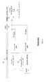
- FIG. 1illustrates a prior art ECC encoding and ECC decoding process.
- a message 11(illustrated as having content 0100111 . . . 1011010) is partitioned into packets m 1 , m 2 . . . mN (collectively denoted 21 ) that are fed to the first encoder 13 ( 1 ).
- the first encoder 13 ( 1 )computes redundancies r 1 , r 1 , r 2 . . . RN (collectively denoted R 1 21 ) for each packet which are appended (“append redundancy”) 14 to the message to provide an encoded message 15 .
- Encoded message 15is illustrated as having content “0100111 . . . 1011010 . . . 0110” and includes packets m 1 , m 2 . . . mN and redundancies r 1 , r 2 . . . rN.
- the encoded message 15is transmitted or stored in the “error inflicting” channel or media 16 to provide an error containing message 17 ⁇ m 1 , m 2 . . . Mn, r 1 . . . rN ⁇ + ⁇ e ⁇ (illustrated as having content (0101111 . . . 1010010 . . . 00000).
- the error containing message 17is received by the first decoder 18 ( 1 ).
- the first decoder 18 ( 1 )identifies and fixes the errors if possible. Redundancies are stripped from the data and a recovered message 19 including recovered (error corrected) packets ⁇ m 1 ′, m 2 ′, . . . mN′ ⁇ is fed to the client.
- N and Kfor example in the 2 dimensional case
- compute redundancies for this collectionalso i.e. ⁇ r 21 , r 22 . . . r 2 N ⁇ etc. . . . and repeat this process N times to produce an N dimensional ECC system.
- each bitis encoded in two different packets, which is simply means that each bit participates in the calculation of 2 redundancies one in each “dimension” as described previously for a single dimension.
- the redundanciesthen appended to the message and transmitted in a communication system (or stored in a storage system).
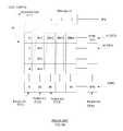
- FIG. 2depicts a pair of encoders that execute two dimensional encoding so that each bit of the message is decoded twice.
- First encoder 13 ( 1 )gets the original message 11 in order and generates a redundancy (collectively denoted R 1 20 ( 1 )) for each of the packets m 1 , m 2 . . . mN.
- Second encoder 13 ( 2 )receives the message after it was reordered in some different permutation, i.e. the second encoder 13 ( 2 ) gets a different series of packets n 0 , n 1 and generates redundancy (collectively denoted R 2 20 ( 2 )) for packets n 1 , n 2 . . . nN
- each bit of the messagebelongs both to some packet ‘m’ in the first dimension and one packet ‘n’ of a second dimension.
- FIG. 3depicts the partitioning of message 11 into packets m 1 . . . mN 21 ( 1 )- 21 (N).
- the first dimensionsimply partitions the data “in order” successively into each appropriate packet.
- second encoder 13 ( 2 )gets a different set of packets i.e. n 1 , n 2 . . . nN (denoted 22 ( 1 )- 22 (N) in FIG. 4 ) where each successive byte of a packet resides elsewhere in the original data according to some permutation.
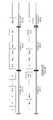
- FIGS. 6A and 6Bdepict this permutation, the original message 11 is depicted as being a stream of successive N ⁇ 2 bytes of data numbered by the order of arrival 1 . . . . N ⁇ 2 11 ( 1 )- 11 (N ⁇ 2). Wherein N ⁇ 2 means N by the power of two.
- This successive streamis fed into a two dimensional shift register 30 having N ⁇ 2 by N ⁇ 2 cells—to form N ⁇ 2 columns and N ⁇ 2 rows.
- Each cell of the 2 dimensional shift registeris marked with its byte number (with respect to the arrival order—illustrated by dashed line 34 ).
- FIGS. 3 and 4show packets m 1 and n 1 22 ( 1 ) and 21 ( 1 ) respectively and exemplify their byte composition.
- This latency problemcan be solved by employing N encoders as depicted in FIG. 5 encoders 13 ( 1 )- 13 (N ⁇ 1)—wherein the number of encoders equals the number of packets in the message.
- First encoder 13 ( 1 )starts computation as byte # 1 arrives, than stalls until byte #(N+1) (which is the 2nd byte of packet n 1 ) arrives, second encoder 13 ( 2 ) starts as byte # 2 is available etc. . . . .
- each encoderretains its state as each one is dedicated for each of the packets.
- Methods and systemsare provided for multi-dimensional encoding/decoding.
- a method for multiple dimensional encoding of a messagecomprises repeating, for each data unit that belongs to the message the stages of: (a) receiving by a processor the data unit; (b) executing by the processor, for each dimension of a plurality of dimensions of the multiple dimension, the stages of: (b.1) restoring a last state of an encoder during an encoding process of a packet that comprises the data unit, wherein the encoding process corresponds to the dimension; (b.2) encoding the data unit by the encoder in correspondence to the dimension to provide an updated state of the encoder; and (b.3) storing the updated state of the encoder as a last state of the encoder; wherein the updated state of the encoder following the encoding of all data units of the message represents redundancy bits; and (c) adding the redundancy bits to the message to provide a multiple dimensional encoded message.
- the plurality of dimensionsis a subset of the multiple dimensions.
- the methodmay include decoding, for a residual dimension that belongs to the multiple dimensions and does not belong to the plurality of dimensions, all data units that form the message in a sequential manner by a residual encoder allocated to the residual dimension without restoring the last state of the residual encoder at a memory unit that differs from the encoder.
- the methodmay include encoding data units of the message in correspondence to each of the plurality of dimensions by a same encoder.
- the methodmay include encoding data units of the message in correspondence to different dimensions of the plurality of dimensions by different encoders.
- the encodingmay include error correction encoding of the data unit.
- the receiving of the data unitcomprises storing the data unit by a memory that has a size that is smaller than a size of the message.
- a systemthat includes a memory and a processor.
- the memorymay be arranged to receive a data unit.
- the processormay be arranged to execute, for each dimension of a plurality of dimensions of the multiple dimension, the stages of (a) restoring from the memory a last state of an encoder during an encoding process of a packet that comprises the data unit, wherein the encoding process corresponds to the dimension, and (b) encoding the data unit by the encoder in correspondence to the dimension to provide an updated state of the encoder.
- the memorymay be arranged to store the updated state of the encoder as a last state of the encoder; wherein the updated state of the encoder following the encoding of all data units of the message represents redundancy bits.
- the processormay be arranged to add the redundancy bits to the message to provide a multiple dimensional encoded message.
- the plurality of dimensionsmay be a subset of the multiple dimensions.
- the processormay be arranged to decode, for a residual dimension that belongs to the multiple dimensions and does not belong to the plurality of dimensions, all data units that form the message in a sequential manner by a residual encoder allocated to the residual dimension without restoring the last state of the residual encoder at a memory unit that differs from the encoder.
- the processormay be arranged to encode data units of the message in correspondence to each of the plurality of dimensions by a same encoder.
- the processormay be arranged to encode data units of the message in correspondence to different dimensions of the plurality of dimensions by different encoders.
- the processormay be arranged to perform error correction encoding of the data unit.
- the memorymay have a size that is smaller than a size of the message.
- a method for multiple dimensional decoding of a decoded messagemay include repeating, for each decoded data unit that belongs to the decoded message the stages of: (a) receiving by a processor the decoded data unit; (b) executing by the processor, for each dimension of a plurality of dimensions of the multiple dimension, the stages of: (b.1) restoring a last state of an decoder during an encoding process of a decoded packet that comprises the decoded data unit, wherein the decoding process corresponds to the dimension; (b.2) decoding the decoded data unit by the decoder in correspondence to the dimension to provide an updated state of the decoder; and (b.3) storing the updated state of the decoder as a last state of the encoder; wherein the updated state of the encoder following the encoding of all data units of the message represents redundancy bits; and (c) adding the redundancy bits to the message to provide a multiple dimensional encoded message.
- a system for multiple dimensional decoding of a decoded messagemay include a memory and a processor; wherein the memory may be arranged to store a decoded message; wherein the processor may be arranged to repeat, for each decoded data unit that belongs to the decoded message: receive the decoded data unit; execute for each dimension of a plurality of dimensions of the multiple dimension, the stages of: restoring a last state of an decoder during an encoding process of a decoded packet that comprises the decoded data unit, wherein the decoding process corresponds to the dimension; decoding the decoded data unit by the decoder in correspondence to the dimension to provide an updated state of the decoder; and storing the updated state of the decoder as a last state of the encoder.
- the updated state of the encoder following the encoding of all data units of the messagerepresents redundancy bits.
- the processormay be further arranged to add the redundancy bits to the message to provide a multiple dimensional decoding of all data units of the
- FIG. 1illustrates a prior art single dimension ECC encoding and an ECC decoding process
- FIG. 2illustrates a prior art two dimensional ECC encoding process
- FIG. 3illustrates a prior art partition of a message to packets according to a first permutation
- FIG. 4illustrates a partition of a message to packets according to a second permutation (second order);
- FIG. 5illustrates a prior art ECC encoding process that used N prior art encoders, N being a number of packets per message;
- FIGS. 6A and 6Billustrate a packet and a prior art two dimensional shift register that facilitates a partition of a message to packets according to first and second permutations (first and second orders);
- FIG. 7illustrates a system for ECC encoding according to an embodiment of the invention
- FIG. 8illustrates a system for ECC encoding according to an embodiment of the invention
- FIG. 9illustrates a system for ECC encoding according to an embodiment of the invention.
- FIG. 10illustrates a method for multiple dimensional encoding of a message, according to an embodiment of the invention
- FIG. 11illustrates a system for ECC decoding according to an embodiment of the invention
- Any reference to an encoding process or to an encodercan be applied mutatis mutandis to a decoding process or to a decoder.
- the term data unitmay include one or multiple bits.
- the data unitmay have any size and is not limited to a byte. Multiple data units may form a packet.
- the term messagerefers to a group of data bits.
- the messagemay include multiple packets that in turn may include multiple data units.
- un-bufferedindicates that there is no need to buffer the entire message although small data units (fractions of the message) may be stored.
- An encodercan be allocated per each dimension or for more than a single dimension of a multiple encoding scheme.
- a decodercan be allocated per each dimension or for more than a single dimension of a multiple dimension ECC scheme.
- the systemmay include (a) an encoder, (b) a memory where the state of the encoder for each packet can be stored, and (c) a memory-read and memory-write logic that saves and restores the encoder state for the next packet in the queue.
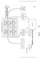
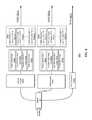
- FIG. 7illustrates a system 60 for ECC encoding according to an embodiment of the invention.
- FIG. 8illustrates a system 160 for ECC encoding according to an embodiment of the invention.
- FIG. 9illustrates a system 260 for ECC encoding according to an embodiment of the invention.
- Each one of these systemsmay be arranged to perform multiple dimensional encoding of multiple (K) dimensions.
- system 60may perform multiple dimensional encoding for three or more dimensions—but will require storing the state of the encoder for each data unit of the third and above dimensions.
- Each encoder in either of these figurescan be arranged to perform encoding of a dimension, of a part of a dimension or of more than a single dimension.
- each combination of encoder, memory and read and write logic enginecan perform an encoding of a single dimension while operating in the same rate of the system.
- the encoding rate of the systemshould not be substantially lower than the reception rate of the message—in order to prevent the need of large buffers for compensating for rate mismatches.
- an encoder that is expected to encode each data unit at more than a single dimensionshould be faster than an encoder that may be arranged to perform only a single dimension encoding process.
- system 60includes memory (encoder state memory 65 ) and processor 61 .
- the processor 61may include the memory 65 .
- the processor 61includes encoder 62 , encoder write state logic 63 , read generation address logic 64 , encoder write state logic 66 and write address logic 67 .
- Data units 40 ( 1 )- 40 (N*N) of a message 11arrive in a regular order 1 , 2 . . . . N*N, each successive data unit belongs to K packets—one packet per dimension.
- the packets of the first dimension (D 1 )are denoted m 1 . . . mN
- the packets of the second dimension (D 2 )are denoted n 1 . . . nN.
- the packets of the third dimension (D 3 )are denoted p 1 . . . pN.
- the read address logic 63 and 64sends to the memory 65 the address of the encoder state as it was at the time it finished computing the previous data unit of the same packet of the same dimension and the encoder read state logic 63 receives this so called last state and feeds it to the encoder engine subunit 62 .
- the encoder 62computes the next state for that packet of the same dimension, and the result is stored back in the memory in the appropriate location for this packet of the same dimension (same location), and prior to the arrival of next data unit of the next successive packet of either one of the dimensions.
- the write address logic 67sends to the memory 65 an address in which this state is stored and the write address logic 64 sends that state to that address.
- the states of the encoderare denoted “state of encoder packet m 1 of D 1 ”—“state of encoder packet mN of D 1 ” 65 ( 1 , 1 )- 65 (N, 1 ).
- the states of the encoderare denoted “state of encoder packet n 1 of D 2 ”—“state of encoder packet nN of D 2 ” 65 ( 1 , 2 )- 65 (N, 2 ).
- This iterative processis executed for each received data unit and for each dimension and does not require waiting till the entire message is received.
- the memory 65stores redundancy bits that can be read and appended to the transmitted (or stored) message.
- FIG. 8illustrates system 160 that differs from system 60 by having (instead of a single encoder 62 ) a second encoder 62 ( 2 ) for encoding packets of the second dimension and a residual encoder 62 ( 1 ) for encoding the packets m 1 . . . mN of the first dimension.
- FIG. 8also illustrates splitter 68 for feeding received data units to all of the encoders.
- the residual encoder 62 ( 1 )encodes the data units according to their reception order without re-arranging the data unit.
- Second encoder engine 62 ( 1 )maintains its state from data unit to data unit for the duration of the whole packet (each of m 1 . . . mN). It produces redundancies ready to be transmitted for each packet at the end of each packet.
- the second encoder 62 ( 2 )is coupled to memory 65 via encoder read state logic 53 , read address logic 64 , encoder write state logic 66 and write address logic 67 .
- Memory 65is used to store the state of second encoder 62 ( 2 ) only in relation to packets n 1 . . . nN of the second dimension.
- the second encoder 62( 2 ) computes the next state for that packet of D 2 , and the result is stored back in the memory in the appropriate location for this packet of D 2 , and prior to the arrival of next data unit of the next successive packet of D 2 .
- the write address logic 66sends to the memory 65 an address in which this state is stored and the write address logic 67 sends that state to that address.
- FIG. 9illustrates system 260 that differs from system 60 by having (instead of a single encoder 62 ) a third encoder 62 ( 3 ) for encoding packets of the third dimension, a second encoder 62 ( 2 ) for encoding packets of the second dimension and a residual encoder 62 ( 1 ) for encoding the packets m 1 . . . mN of the first dimension.
- FIG. 9also illustrates splitter 68 for feeding received data units to all of the encoders.
- System 260also differs from system 60 by having (instead of a memory 65 ) memory 65 ( 2 ) and memory 65 ( 3 ).
- the residual encoder 62 ( 1 )encodes the data units according to their reception order without re-arranging the data units, without storing the state of the encoder after each encoding of a data unit and retrieving the state of the encoder after the encoding of each data unit.
- the second encoder 62 ( 2 )is coupled to memory 65 ( 2 ) via encoder write state logic 63 ( 2 ), write address logic 64 ( 2 ), encoder read state logic 66 ( 2 ) and read address logic 67 ( 2 ).
- Memory 65 ( 2 )is used to store the state of second encoder 62 ( 2 ) only in relation to packets n 1 . . . nN of the second dimension.
- the second encoder 62 ( 2 )computes the next state for that packet of D 2 , and the result is stored back in the memory 65 ( 2 ) in the appropriate location for this packet of D 2 , and prior to the arrival of next data unit of the next successive packet of D 2 .
- the write address logic 64 ( 2 )sends to the memory 65 ( 2 ) an address in which this state is stored and the write address logic 64 ( 2 ) sends that state to that address.
- the third encoder 62 ( 3 )is coupled to memory 65 ( 3 ) via encoder write state logic 63 ( 3 ), write address logic 64 ( 3 ), encoder read state logic 66 ( 3 ) and read address logic 67 ( 3 ).
- Memory 65 ( 3 )is used to store the state of third encoder 62 ( 3 ) only in relation to packets p 1 . . . pN of the third dimension D 3 .
- the third encoder 62 ( 3 )computes the next state for that packet of D 3 , and the result is stored back in the memory 65 ( 3 ) in the appropriate location for this packet of D 3 , and prior to the arrival of next data unit of the next successive packet of D 3 .
- the write address logic 64 ( 3 )sends to the memory 65 ( 3 ) an address in which this state is stored and the write address logic 64 ( 3 ) sends that state to that address.
- Any permutation scheme(between data units and packets) can be used a not only the simplest as in the above example.
- Implementing any rational permutation schemerequires only changes to the logic that calculates the next-read/write address pointers that write or restore encoder/decoder states from memory for each packet (labels 4 , 6 ).
- the systemis supremely configurable, and the configuration range is limited only by the size of the state-memory (which is small and varies with number of packets, not the data—hence cheaply enlarged).
- Systems 60 , 160can apply any error correction algorithm, such as but not limited to BCH error correction algorithm.
- the message and the redundancy bitscan be sent to a flash memory module and the message with the possible errors and redundancy bits can be read from a flash memory module.
- Kis much smaller that the number N of packets per message
- Each dimensionmay be a T error correction BCH with a freely configurable number of packets per dimension.
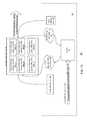
- FIG. 11illustrates a system 60 for ECC decoding according to an embodiment of the invention.
- System 60includes memory (decoder state memory 65 ) and processor 61 .
- the processor 61may include the memory 65 .
- the processor 61includes decoder 62 , decoder write state logic 63 , write address logic 64 , decoder read state logic 65 and read address logic 67 .
- the processor 61includes one or more hardware components.
- Data units 40 ( 1 )- 40 (N*N) and redundancy R( 1 )-R(N) 21 ( 1 )- 21 (N) with possible errorsarrive in a regular order—wherein each successive data unit belongs to K packets—one packet per dimension.
- the packets of the first dimension (D 1 )are denoted m 1 . . . mN
- the packets of the second dimension (D 2 )are denoted n 1 . . . nN.
- the read address logic 67sends to the memory 65 the address of the decoder state as it was at the time it finished computing the previous data unit of the same packet of the same dimension and the decoder read state logic 65 receives this so called last state and feeds it to the decoder 62 .
- the decoder 62computes the next state for that packet of the same dimension, and the result is stored back in the memory in the appropriate location for this packet of the same dimension, and prior to the arrival of next data unit of the next successive packet of either one of the dimensions.
- the write address logic 64sends to the memory 65 an address in which this state is stored and the write address logic 64 sends that state to that address.
- the states of the decoderare denoted “state of decoder packet m 1 of D 1 ”—“state of decoder packet mN of D 1 ” 65 ( 1 , 1 )- 65 (N, 1 ).
- the states of the decoderare denoted “state of decoder packet n 1 of D 2 ”—“state of decoder packet nN of D 2 ” 65 ( 1 , 2 )- 65 (N, 2 ).
- This iterative processis executed for each received data unit and for each dimension and does not require waiting till the entire message is received.
- the memory 65stores a reconstructed message.
- the states of the encodercan be the redundancies that are appended to the transmitted packet similar to CRC.
- the states in the decoderare also referred to as syndromes and they may be used to construct the equation that need to be solved in order to find the errors (the errors are the roots of the aforementioned equations).
- FIG. 10illustrates method 1000 for multiple dimensional encoding of a message, according to an embodiment of the invention.
- Method 1000starts by initialization stage 1010 .
- This stagemay include configuring a multiple dimensional decoding system—determining the number and size of packets, determining the allocation of decoders (if there are more than one decoder) to the decoding of different dimensions, determining the error correction algorithm, the number of errors that can be corrected, the number (K) of dimensions and the ordering (permutations) of packets per dimension, and the like.
- index jmay equal index k but this is not necessarily so.
- Dimension counter kmay range between 1 and K.
- Data unit countercan range between 1 and N.
- Encoder counter jranges between 1 and J.
- a residual encodercan be allocated for encoding the first dimension—and it may perform an in-order encoding that does not require restoring the last state of the residual encoder at a memory unit that differs from the encoder and does not require storing the updated state of the residual encoder as a last state of the residual encoder in the memory.
- jmay range between 2 and J.
- Stage 1010may be followed by stage 1020 of increasing n by one when receiving a data unit and checking if n>N*N meaning that all data units of a message have been encoded. If-so jumping to stage 1060 . Else—this data unit is to be referred to as the n'th data unit and stage 1020 is followed by stage 1030 .
- This stagemay include storing the n'th data unit by a memory that has a size that is smaller than a size of the message.
- Stage 1030includes restoring a last state of a j'th encoder during an encoding process of a packet (of the k'th dimension) that includes the n'th data unit, wherein the encoding process corresponds to the k'th dimension.
- Stage 1030may be followed by stage 1032 of encoding the n'th data unit by the j'th encoder in correspondence to the k'th dimension to provide an updated state of the j'th encoder (for the n'th packet of the k'th dimension).
- connections as discussed hereinmay be any type of connection suitable to transfer signals from or to the respective nodes, units or devices, for example via intermediate devices. Accordingly, unless implied or stated otherwise, the connections may for example be direct connections or indirect connections.
- the connectionsmay be illustrated or described in reference to being a single connection, a plurality of connections, unidirectional connections, or bidirectional connections. However, different embodiments may vary the implementation of the connections. For example, separate unidirectional connections may be used rather than bidirectional connections and vice versa.
- plurality of connectionsmay be replaced with a single connection that transfers multiple signals serially or in a time multiplexed manner. Likewise, single connections carrying multiple signals may be separated out into various different connections carrying subsets of these signals. Therefore, many options exist for transferring signals.
- Each signal described hereinmay be designed as positive or negative logic.
- the signalIn the case of a negative logic signal, the signal is active low where the logically true state corresponds to a logic level zero.
- the signalIn the case of a positive logic signal, the signal is active high where the logically true state corresponds to a logic level one.
- any of the signals described hereinmay be designed as either negative or positive logic signals. Therefore, in alternate embodiments, those signals described as positive logic signals may be implemented as negative logic signals, and those signals described as negative logic signals may be implemented as positive logic signals.
- assertor “set” and “negate” (or “deassert” or “clear”) are used herein when referring to the rendering of a signal, status bit, or similar apparatus into its logically true or logically false state, respectively. If the logically true state is a logic level one, the logically false state is a logic level zero. And if the logically true state is a logic level zero, the logically false state is a logic level one.
- logic blocksare merely illustrative and that alternative embodiments may merge logic blocks or circuit elements or impose an alternate decomposition of functionality upon various logic blocks or circuit elements.
- architectures depicted hereinare merely exemplary, and that in fact many other architectures may be implemented which achieve the same functionality.
- any arrangement of components to achieve the same functionalityis effectively “associated” such that the desired functionality is achieved.
- any two components herein combined to achieve a particular functionalitymay be seen as “associated with” each other such that the desired functionality is achieved, irrespective of architectures or intermedial components.
- any two components so associatedcan also be viewed as being “operably connected,” or “operably coupled,” to each other to achieve the desired functionality.
- the illustrated examplesmay be implemented as circuitry located on a single integrated circuit or within a same device.
- the examplesmay be implemented as any number of separate integrated circuits or separate devices interconnected with each other in a suitable manner.
- the examples, or portions thereofmay implemented as soft or code representations of physical circuitry or of logical representations convertible into physical circuitry, such as in a hardware description language of any appropriate type.
- any reference signs placed between parenthesesshall not be construed as limiting the claim.
- the word ‘comprising’does not exclude the presence of other elements or steps then those listed in a claim.
- the terms “a” or “an,” as used herein,are defined as one or more than one.
Landscapes
- Engineering & Computer Science (AREA)
- Physics & Mathematics (AREA)
- Probability & Statistics with Applications (AREA)
- Theoretical Computer Science (AREA)
- Computer Networks & Wireless Communication (AREA)
- Signal Processing (AREA)
- Mathematical Physics (AREA)
- Algebra (AREA)
- General Physics & Mathematics (AREA)
- Pure & Applied Mathematics (AREA)
- Computer Security & Cryptography (AREA)
- Detection And Prevention Of Errors In Transmission (AREA)
Abstract
Description
Claims (16)
Priority Applications (1)
| Application Number | Priority Date | Filing Date | Title |
|---|---|---|---|
| US14/953,448US9413491B1 (en) | 2013-10-08 | 2015-11-30 | System and method for multiple dimension decoding and encoding a message |
Applications Claiming Priority (2)
| Application Number | Priority Date | Filing Date | Title |
|---|---|---|---|
| US201314049070A | 2013-10-08 | 2013-10-08 | |
| US14/953,448US9413491B1 (en) | 2013-10-08 | 2015-11-30 | System and method for multiple dimension decoding and encoding a message |
Related Parent Applications (1)
| Application Number | Title | Priority Date | Filing Date |
|---|---|---|---|
| US201314049070AContinuation | 2013-10-08 | 2013-10-08 |
Publications (1)
| Publication Number | Publication Date |
|---|---|
| US9413491B1true US9413491B1 (en) | 2016-08-09 |
Family
ID=56556067
Family Applications (1)
| Application Number | Title | Priority Date | Filing Date |
|---|---|---|---|
| US14/953,448ActiveUS9413491B1 (en) | 2013-10-08 | 2015-11-30 | System and method for multiple dimension decoding and encoding a message |
Country Status (1)
| Country | Link |
|---|---|
| US (1) | US9413491B1 (en) |
Cited By (2)
| Publication number | Priority date | Publication date | Assignee | Title |
|---|---|---|---|---|
| US11016844B2 (en) | 2019-03-15 | 2021-05-25 | Toshiba Memory Corporation | Error correction code structure |
| US11734107B2 (en) | 2019-03-15 | 2023-08-22 | Kioxia Corporation | Decoding scheme for error correction code structure |
Citations (296)
| Publication number | Priority date | Publication date | Assignee | Title |
|---|---|---|---|---|
| US4430701A (en) | 1981-08-03 | 1984-02-07 | International Business Machines Corporation | Method and apparatus for a hierarchical paging storage system |
| US4463375A (en) | 1982-09-07 | 1984-07-31 | The Board Of Trustees Of The Leland Standford Junior University | Multiple-measurement noise-reducing system |
| US4584686A (en) | 1983-12-22 | 1986-04-22 | Optical Storage International | Reed-Solomon error correction apparatus |
| US4589084A (en) | 1983-05-16 | 1986-05-13 | Rca Corporation | Apparatus for symmetrically truncating two's complement binary signals as for use with interleaved quadrature signals |
| US4777589A (en) | 1985-06-28 | 1988-10-11 | Hewlett-Packard Company | Direct input/output in a virtual memory system |
| US4866716A (en) | 1987-05-15 | 1989-09-12 | Digital Equipment Corporation | Real-time BCH error correction code decoding mechanism |
| US5003597A (en) | 1989-12-21 | 1991-03-26 | Xerox Corporation | Method and apparatus for data encryption |
| US5077737A (en) | 1989-08-18 | 1991-12-31 | Micron Technology, Inc. | Method and apparatus for storing digital data in off-specification dynamic random access memory devices |
| US5297153A (en) | 1989-08-24 | 1994-03-22 | U.S. Philips Corporation | Method and apparatus for decoding code words protected wordwise by a non-binary BCH code from one or more symbol errors |
| US5305276A (en) | 1991-09-11 | 1994-04-19 | Rohm Co., Ltd. | Non-volatile IC memory |
| US5592641A (en) | 1993-06-30 | 1997-01-07 | Intel Corporation | Method and device for selectively locking write access to blocks in a memory array using write protect inputs and block enabled status |
| US5623620A (en) | 1993-06-30 | 1997-04-22 | Intel Corporation | Special test modes for a page buffer shared resource in a memory device |
| US5640529A (en) | 1993-07-29 | 1997-06-17 | Intel Corporation | Method and system for performing clean-up of a solid state disk during host command execution |
| US5657332A (en) | 1992-05-20 | 1997-08-12 | Sandisk Corporation | Soft errors handling in EEPROM devices |
| US5663901A (en) | 1991-04-11 | 1997-09-02 | Sandisk Corporation | Computer memory cards using flash EEPROM integrated circuit chips and memory-controller systems |
| US5724538A (en) | 1993-04-08 | 1998-03-03 | Hewlett-Packard Company | Computer memory address control apparatus utilizing hashed address tags in page tables which are compared to a combined address tag and index which are longer than the basic data width of the associated computer |
| US5729490A (en) | 1995-07-31 | 1998-03-17 | Sgs-Thomson Microelectronics S.R.L. | Parallel-dichotomic serial sensing method for sensing multiple-level non-volatile memory cells, and sensing circuit for actuating such method |
| US5740395A (en) | 1992-10-30 | 1998-04-14 | Intel Corporation | Method and apparatus for cleaning up a solid state memory disk storing floating sector data |
| US5745418A (en) | 1996-11-25 | 1998-04-28 | Macronix International Co., Ltd. | Flash memory mass storage system |
| US5778430A (en) | 1996-04-19 | 1998-07-07 | Eccs, Inc. | Method and apparatus for computer disk cache management |
| US5793774A (en) | 1994-11-04 | 1998-08-11 | Fujitsu Limited | Flash memory controlling system |
| US5920578A (en) | 1997-04-23 | 1999-07-06 | Cirrus Logic, Inc. | Method and apparatus for efficiently processing a multi-dimensional code |
| US5926409A (en) | 1997-09-05 | 1999-07-20 | Information Storage Devices, Inc. | Method and apparatus for an adaptive ramp amplitude controller in nonvolatile memory application |
| US5956473A (en) | 1996-11-25 | 1999-09-21 | Macronix International Co., Ltd. | Method and system for managing a flash memory mass storage system |
| US5956268A (en) | 1997-02-12 | 1999-09-21 | Hyundai Electronics America | Nonvolatile memory structure |
| US5968198A (en) | 1996-08-16 | 1999-10-19 | Ericsson, Inc. | Decoder utilizing soft information output to minimize error rates |
| US5982659A (en) | 1996-12-23 | 1999-11-09 | Lsi Logic Corporation | Memory cell capable of storing more than two logic states by using different via resistances |
| US6016275A (en) | 1998-03-13 | 2000-01-18 | Lg Semicon Co., Ltd. | Flash memory wear leveling system and method |
| US6038634A (en) | 1998-02-02 | 2000-03-14 | International Business Machines Corporation | Intra-unit block addressing system for memory |
| US6081878A (en) | 1997-03-31 | 2000-06-27 | Lexar Media, Inc. | Increasing the memory performance of flash memory devices by writing sectors simultaneously to multiple flash memory devices |
| US6094465A (en) | 1997-03-21 | 2000-07-25 | Qualcomm Incorporated | Method and apparatus for performing decoding of CRC outer concatenated codes |
| US6119245A (en) | 1997-08-06 | 2000-09-12 | Oki Electric Industry Co., Ltd. | Semiconductor storage device and method of controlling it |
| US6182261B1 (en) | 1998-11-05 | 2001-01-30 | Qualcomm Incorporated | Efficient iterative decoding |
| US6192497B1 (en) | 1998-08-27 | 2001-02-20 | Adaptec, Inc. | Parallel Chien search circuit |
| US6195287B1 (en) | 1999-02-03 | 2001-02-27 | Sharp Kabushiki Kaisha | Data programming method for a nonvolatile semiconductor storage |
| US6199188B1 (en) | 1997-10-07 | 2001-03-06 | Quantum Corporation | System for finding roots of degree three and degree four error locator polynomials over GF(2M) |
| US6209114B1 (en) | 1998-05-29 | 2001-03-27 | Texas Instruments Incorporated | Efficient hardware implementation of chien search polynomial reduction in reed-solomon decoding |
| US6259627B1 (en) | 2000-01-27 | 2001-07-10 | Multi Level Memory Technology | Read and write operations using constant row line voltage and variable column line load |
| US6272052B1 (en) | 1998-08-21 | 2001-08-07 | Mitsubishi Denki Kabushiki Kaisha | Block-erase type semiconductor storage device with independent memory groups having sequential logical addresses |
| US6279133B1 (en) | 1997-12-31 | 2001-08-21 | Kawasaki Steel Corporation | Method and apparatus for significantly improving the reliability of multilevel memory architecture |
| US6278633B1 (en) | 1999-11-05 | 2001-08-21 | Multi Level Memory Technology | High bandwidth flash memory that selects programming parameters according to measurements of previous programming operations |
| US6301151B1 (en) | 2000-08-09 | 2001-10-09 | Information Storage Devices, Inc. | Adaptive programming method and apparatus for flash memory analog storage |
| US20010034815A1 (en) | 2000-04-25 | 2001-10-25 | Dugan Michael K. | Apparatus and method for performing speculative cache directory tag updates |
| US6370061B1 (en) | 2001-06-19 | 2002-04-09 | Advanced Micro Devices, Inc. | Ceiling test mode to characterize the threshold voltage distribution of over programmed memory cells |
| US6374383B1 (en) | 1999-06-07 | 2002-04-16 | Maxtor Corporation | Determining error locations using error correction codes |
| US20020063774A1 (en) | 2000-11-29 | 2002-05-30 | Hillis William Daniel | Method and apparatus for maintaining eye contact in teleconferencing using reflected images |
| US20020085419A1 (en) | 2001-01-04 | 2002-07-04 | Seok-Cheon Kwon | Nonvolatile semiconductor memory device and data input/output control method thereof |
| US20020156988A1 (en) | 2001-03-22 | 2002-10-24 | Matsushita Electric Industrial Co., Ltd. | Memory device |
| US20020154769A1 (en) | 2000-12-07 | 2002-10-24 | Petersen Mette Vesterager | Method of generating pseudo-random numbers in an electronic device, and a method of encrypting and decrypting electronic data |
| US20020174156A1 (en) | 2001-03-29 | 2002-11-21 | Koninklijke Philips Electronics N.V. | Round-off algorithm without bias for 2's complemetnt data |
| US6504891B1 (en) | 1995-07-28 | 2003-01-07 | Micron Technology, Inc. | Timer circuit with programmable decode circuitry |
| US20030014582A1 (en) | 2000-12-28 | 2003-01-16 | Kenichi Nakanishi | Data recorder and method for recording data in flash memory |
| US6532169B1 (en) | 2001-06-26 | 2003-03-11 | Cypress Semiconductor Corp. | SONOS latch and application |
| US6532556B1 (en) | 2000-01-27 | 2003-03-11 | Multi Level Memory Technology | Data management for multi-bit-per-cell memories |
| US20030065876A1 (en) | 2001-09-28 | 2003-04-03 | Menahem Lasser | Flash management system using only sequential Write |
| US6553533B2 (en) | 1998-02-05 | 2003-04-22 | International Business Machines Corporation | Method and apparatus for detecting and correcting errors and erasures in product ECC-coded data arrays for DVD and similar storage subsystems |
| US6560747B1 (en) | 1999-11-10 | 2003-05-06 | Maxtor Corporation | Error counting mechanism |
| US20030101404A1 (en) | 2001-11-01 | 2003-05-29 | Lijun Zhao | Inner coding of higher priority data within a digital message |
| US20030105620A1 (en) | 2001-01-29 | 2003-06-05 | Matt Bowen | System, method and article of manufacture for interface constructs in a programming language capable of programming hardware architetures |
| US20030177300A1 (en) | 2002-03-18 | 2003-09-18 | Samsung Electro-Mechanics Co., Ltd. | Data processing method in high-capacity flash EEPROM card system |
| US20030192007A1 (en) | 2001-04-19 | 2003-10-09 | Miller David H. | Code-programmable field-programmable architecturally-systolic Reed-Solomon BCH error correction decoder integrated circuit and error correction decoding method |
| US6637002B1 (en) | 1998-10-21 | 2003-10-21 | Maxtor Corporation | Decoder for error correcting block codes |
| US6639865B2 (en) | 2000-10-25 | 2003-10-28 | Samsung Electronics Co., Ltd. | Memory device, method of accessing the memory device, and reed-solomon decoder including the memory device |
| US6675281B1 (en) | 2002-01-22 | 2004-01-06 | Icreate Technologies Corporation | Distributed mapping scheme for mass storage system |
| US20040015771A1 (en) | 2002-07-16 | 2004-01-22 | Menahem Lasser | Error correction for non-volatile memory |
| US20040030971A1 (en) | 1999-06-28 | 2004-02-12 | Kabushiki Kaisha Toshiba | Flash memory |
| US6704902B1 (en) | 1998-09-07 | 2004-03-09 | Sony Corporation | Decoding system for error correction code |
| US20040059768A1 (en) | 1999-12-10 | 2004-03-25 | Broadcom Corporation | Apparatus and method for reducing precision of data |
| US20040080985A1 (en) | 2002-10-28 | 2004-04-29 | Sandisk Corporation, A Delaware Corporation | Maintaining erase counts in non-volatile storage systems |
| US6751766B2 (en) | 2002-05-20 | 2004-06-15 | Sandisk Corporation | Increasing the effectiveness of error correction codes and operating multi-level memory systems by using information about the quality of the stored data |
| US6772274B1 (en) | 2000-09-13 | 2004-08-03 | Lexar Media, Inc. | Flash memory system and method implementing LBA to PBA correlation within flash memory array |
| US20040153722A1 (en) | 2002-12-25 | 2004-08-05 | Heng-Kuan Lee | Error correction code circuit with reduced hardware complexity |
| US20040153817A1 (en) | 1996-10-24 | 2004-08-05 | Micron Technologies, Inc. | Apparatus and method for detecting over-programming condition in multistate memory device |
| US6781910B2 (en) | 2002-05-17 | 2004-08-24 | Hewlett-Packard Development Company, L.P. | Small area magnetic memory devices |
| US6792569B2 (en) | 2001-04-24 | 2004-09-14 | International Business Machines Corporation | Root solver and associated method for solving finite field polynomial equations |
| US20040181735A1 (en) | 2003-03-04 | 2004-09-16 | Weizhuang (Wayne) Xin | Decoding a received BCH encoded signal |
| US20040203591A1 (en) | 2002-03-29 | 2004-10-14 | Lg Electronics Inc. | Method and apparatus for encrypting and decrypting data in wireless LAN |
| US20040210706A1 (en) | 2002-07-26 | 2004-10-21 | Samsung Electronics Co., Ltd. | Method for managing flash memory |
| US20050013165A1 (en) | 2003-06-17 | 2005-01-20 | Amir Ban | Flash memories with adaptive reference voltages |
| US20050018482A1 (en) | 2002-09-06 | 2005-01-27 | Raul-Adrian Cemea | Techniques for reducing effects of coupling between storage elements of adjacent rows of memory cells |
| US6873543B2 (en) | 2003-05-30 | 2005-03-29 | Hewlett-Packard Development Company, L.P. | Memory device |
| US20050083735A1 (en) | 2003-10-20 | 2005-04-21 | Jian Chen | Behavior based programming of non-volatile memory |
| US6891768B2 (en) | 2002-11-13 | 2005-05-10 | Hewlett-Packard Development Company, L.P. | Power-saving reading of magnetic memory devices |
| US20050120265A1 (en) | 2003-12-02 | 2005-06-02 | Pline Steven L. | Data storage system with error correction code and replaceable defective memory |
| US20050117401A1 (en) | 2002-01-18 | 2005-06-02 | Jian Chen | Techniques of recovering data from memory cells affected by field coupling with adjacent memory cells |
| US20050128811A1 (en) | 2002-05-23 | 2005-06-16 | Renesas Technology Corp. | Nonvolatile semiconductor memory device capable of uniformly inputting/outputting data |
| US20050138533A1 (en) | 2003-09-29 | 2005-06-23 | Canon Kabushiki Kaisha | Encoding/decoding device using a reed-solomon encoder/decoder |
| US20050144213A1 (en) | 2003-12-29 | 2005-06-30 | Xilinx, Inc. | Mathematical circuit with dynamic rounding |
| US20050144368A1 (en) | 2003-12-30 | 2005-06-30 | Samsung Electronics Co., Ltd. | Address mapping method and mapping information managing method for flash memory, and flash memory using the same |
| US6914809B2 (en) | 2003-07-07 | 2005-07-05 | Hewlett-Packard Development Company, L.P. | Memory cell strings |
| US6915477B2 (en) | 2001-12-28 | 2005-07-05 | Lucent Technologies Inc. | Delay sensitive adaptive quality control loop for rate adaptation |
| US20050172179A1 (en) | 2004-01-29 | 2005-08-04 | Brandenberger Sarah M. | System and method for configuring a solid-state storage device with error correction coding |
| US20050169057A1 (en) | 2004-01-30 | 2005-08-04 | Noboru Shibata | Semiconductor memory device which stores plural data in a cell |
| US20050213393A1 (en) | 2004-03-14 | 2005-09-29 | M-Systems Flash Disk Pioneers, Ltd. | States encoding in multi-bit flash cells for optimizing error rate |
| US6952365B2 (en) | 2002-01-18 | 2005-10-04 | Sandisk Corporation | Reducing the effects of noise in non-volatile memories through multiple reads |
| US6961890B2 (en) | 2001-08-16 | 2005-11-01 | Hewlett-Packard Development Company, L.P. | Dynamic variable-length error correction code |
| US20050243626A1 (en) | 2004-04-29 | 2005-11-03 | M-Systems Flash Disk Pioneers Ltd. | Refreshing data stored in a flash memory |
| US6968421B2 (en) | 2001-01-19 | 2005-11-22 | Sandisk Corporation | Partial block data programming and reading operations in a non-volatile memory |
| US6990012B2 (en) | 2003-10-07 | 2006-01-24 | Hewlett-Packard Development Company, L.P. | Magnetic memory device |
| US6996004B1 (en) | 2003-11-04 | 2006-02-07 | Advanced Micro Devices, Inc. | Minimization of FG-FG coupling in flash memory |
| US6999854B2 (en) | 2004-05-28 | 2006-02-14 | International Business Machines Corporation | Medical infusion pump capable of learning bolus time patterns and providing bolus alerts |
| US7010739B1 (en) | 2002-04-11 | 2006-03-07 | Marvell International Ltd. | Error evaluator for inversionless Berlekamp-Massey algorithm in Reed-Solomon decoders |
| US7012835B2 (en) | 2003-10-03 | 2006-03-14 | Sandisk Corporation | Flash memory data correction and scrub techniques |
| US20060059409A1 (en) | 2004-09-10 | 2006-03-16 | Hanho Lee | Reed-solomon decoder systems for high speed communication and data storage applications |
| US20060059406A1 (en) | 2004-09-10 | 2006-03-16 | Stmicroelectronics S.R.L. | Memory with embedded error correction codes |
| US20060064537A1 (en) | 2004-09-21 | 2006-03-23 | Takashi Oshima | Memory card having a storage cell and method of controlling the same |
| US7038950B1 (en) | 2004-11-05 | 2006-05-02 | Spansion Llc | Multi bit program algorithm |
| US20060101193A1 (en) | 2004-11-08 | 2006-05-11 | M-Systems Flash Disk Pioneers, Ltd. | States encoding in multi-bit flash cells for optimizing error rate |
| US7068539B2 (en) | 2004-01-27 | 2006-06-27 | Sandisk Corporation | Charge packet metering for coarse/fine programming of non-volatile memory |
| US7079436B2 (en) | 2003-09-30 | 2006-07-18 | Hewlett-Packard Development Company, L.P. | Resistive cross point memory |
| US20060195651A1 (en) | 1995-07-31 | 2006-08-31 | Petro Estakhri | Increasing the memory performance of flash memory devices by writing sectors simultaneously to multiple flash memory devices |
| US20060203587A1 (en) | 2005-03-11 | 2006-09-14 | Yan Li | Partition of non-volatile memory array to reduce bit line capacitance |
| US20060221692A1 (en) | 2005-04-05 | 2006-10-05 | Jian Chen | Compensating for coupling during read operations on non-volatile memory |
| US20060248434A1 (en) | 2005-04-28 | 2006-11-02 | Micron Technology, Inc. | Non-systematic coded error correction |
| US20060268608A1 (en) | 2003-04-22 | 2006-11-30 | Kabushiki Kaisha Toshiba | Data storage system |
| US7149950B2 (en) | 2003-09-12 | 2006-12-12 | Hewlett-Packard Development Company, L.P. | Assisted memory device for reading and writing single and multiple units of data |
| US20060282411A1 (en) | 2005-06-13 | 2006-12-14 | International Business Machines Corporation | System and method for performing a high-level multi-dimensional query on a multi-structural database |
| US20060284244A1 (en) | 2005-06-16 | 2006-12-21 | Micron Technology, Inc. | Erasable non-volatile memory device using hole trapping in high-k dielectrics |
| US20060294312A1 (en) | 2004-05-27 | 2006-12-28 | Silverbrook Research Pty Ltd | Generation sequences |
| US20070025157A1 (en) | 2005-08-01 | 2007-02-01 | Jun Wan | Method for programming non-volatile memory with self-adjusting maximum program loop |
| US7177977B2 (en) | 2004-03-19 | 2007-02-13 | Sandisk Corporation | Operating non-volatile memory without read disturb limitations |
| US7188228B1 (en) | 2003-10-01 | 2007-03-06 | Sandisk Corporation | Hybrid mapping implementation within a non-volatile memory system |
| US7191379B2 (en) | 2003-09-10 | 2007-03-13 | Hewlett-Packard Development Company, L.P. | Magnetic memory with error correction coding |
| US20070063180A1 (en) | 2005-09-07 | 2007-03-22 | Elpida Memory, Inc. | Electrically rewritable non-volatile memory element and method of manufacturing the same |
| US7196946B2 (en) | 2005-04-05 | 2007-03-27 | Sandisk Corporation | Compensating for coupling in non-volatile storage |
| US7203874B2 (en) | 2003-05-08 | 2007-04-10 | Micron Technology, Inc. | Error detection, documentation, and correction in a flash memory device |
| US20070081388A1 (en) | 2005-10-10 | 2007-04-12 | Hynix Semiconductor, Inc. | Program method of flash memory device |
| US7212426B2 (en) | 2003-12-31 | 2007-05-01 | Samsung Electronics Co., Ltd. | Flash memory system capable of inputting/outputting sector data at random |
| US20070098069A1 (en) | 2005-04-27 | 2007-05-03 | Stephen Gordon | Inverse scan, coefficient, inverse quantization and inverse transform system and method |
| US20070104004A1 (en) | 1997-09-08 | 2007-05-10 | So Hock C | Multi-Bit-Per-Cell Flash EEprom Memory with Refresh |
| US20070103992A1 (en) | 2005-11-10 | 2007-05-10 | Sony Corporation | Memory system |
| US20070109858A1 (en) | 2000-12-28 | 2007-05-17 | Conley Kevin M | Novel Method and Structure for Efficient Data Verification Operation for Non-Volatile Memories |
| US20070124652A1 (en) | 2005-11-15 | 2007-05-31 | Ramot At Tel Aviv University Ltd. | Method and device for multi phase error-correction |
| US20070143561A1 (en) | 2005-12-21 | 2007-06-21 | Gorobets Sergey A | Methods for adaptive file data handling in non-volatile memories with a directly mapped file storage system |
| US20070168625A1 (en) | 2006-01-18 | 2007-07-19 | Cornwell Michael J | Interleaving policies for flash memory |
| US20070171730A1 (en) | 2006-01-20 | 2007-07-26 | Marvell International Ltd. | Method and system for error correction in flash memory |
| US20070171714A1 (en) | 2006-01-20 | 2007-07-26 | Marvell International Ltd. | Flash memory with coding and signal processing |
| US20070180346A1 (en) | 2006-01-18 | 2007-08-02 | Sandisk Il Ltd. | Method Of Arranging Data In A Multi-Level Cell Memory Device |
| US20070226582A1 (en) | 2006-03-08 | 2007-09-27 | Marvell International Ltd. | Systems and methods for achieving higher coding rate using parity interleaving |
| US20070226592A1 (en) | 2006-03-20 | 2007-09-27 | Micron Technology, Inc. | Variable sector-count ECC |
| US20070228449A1 (en) | 2006-03-31 | 2007-10-04 | Tamae Takano | Nonvolatile semiconductor memory device |
| US7290203B2 (en) | 2004-10-29 | 2007-10-30 | International Business Machines Corporation | Dynamic memory architecture employing passive expiration of data |
| US20070253249A1 (en) | 2006-04-26 | 2007-11-01 | Sang-Gu Kang | Multi-bit nonvolatile memory device and related programming method |
| US7292365B2 (en) | 2003-01-15 | 2007-11-06 | Xerox Corporation | Methods and systems for determining distribution mean level without histogram measurement |
| US20070263439A1 (en) | 2006-05-15 | 2007-11-15 | Apple Inc. | Dynamic Cell Bit Resolution |
| US20070266291A1 (en) | 2006-05-15 | 2007-11-15 | Kabushiki Kaisha Toshiba | Semiconductor memory device |
| US20070271494A1 (en) | 2006-05-17 | 2007-11-22 | Sandisk Corporation | Error Correction Coding for Multiple-Sector Pages in Flash Memory Devices |
| US7301928B2 (en) | 2004-06-09 | 2007-11-27 | Hitachi Kokusai Electric Inc. | Wireless packet transfer apparatus and method |
| US20070297226A1 (en) | 2006-06-22 | 2007-12-27 | Nima Mokhlesi | Method for non-real time reprogramming of non-volatile memory to achieve tighter distribution of threshold voltages |
| US7315916B2 (en) | 2004-12-16 | 2008-01-01 | Sandisk Corporation | Scratch pad block |
| US20080010581A1 (en) | 2006-07-04 | 2008-01-10 | Ramot At Tel Aviv University Ltd. | Method of error correction in a multi-bit-per-cell flash memory |
| US20080028014A1 (en) | 2006-07-26 | 2008-01-31 | Hilt Jason W | N-BIT 2's COMPLEMENT SYMMETRIC ROUNDING METHOD AND LOGIC FOR IMPLEMENTING THE SAME |
| US20080049497A1 (en) | 2006-08-24 | 2008-02-28 | Hyun Sun Mo | Methods of Programming Multi-Bit Flash Memory Devices and Related Devices |
| US20080055989A1 (en) | 2006-09-06 | 2008-03-06 | Kyoong-Han Lee | Memory system including flash memory and method of operating the same |
| US20080082897A1 (en) | 2006-09-28 | 2008-04-03 | Yigal Brandman | Soft-Input Soft-Output Decoder for Nonvolatile Memory |
| US20080092026A1 (en) | 2006-09-28 | 2008-04-17 | Yigal Brandman | Methods of Soft-Input Soft-Output Decoding for Nonvolatile Memory |
| US20080104309A1 (en) | 2006-10-30 | 2008-05-01 | Cheon Won-Moon | Flash memory device with multi-level cells and method of writing data therein |
| US20080112238A1 (en) | 2006-10-25 | 2008-05-15 | Seon-Taek Kim | Hybrid flash memory device and method for assigning reserved blocks thereof |
| US20080116509A1 (en) | 2001-10-31 | 2008-05-22 | Eliyahou Harari | Multi-State Non-Volatile Integrated Circuit Memory Systems that Employ Dielectric Storage Elements |
| US20080127104A1 (en) | 2006-11-27 | 2008-05-29 | Yan Li | Apparatus with segemented bitscan for verification of programming |
| US20080126686A1 (en) | 2006-11-28 | 2008-05-29 | Anobit Technologies Ltd. | Memory power and performance management |
| US20080128790A1 (en) | 2006-11-30 | 2008-06-05 | Jin-Hyo Jung | Memory device |
| US20080130341A1 (en) | 2006-12-03 | 2008-06-05 | Anobit Technologies Ltd. | Adaptive programming of analog memory |
| US20080137414A1 (en) | 2006-12-06 | 2008-06-12 | Samsung Electronics Co., Ltd. | Multi-level cell memory device and method thereof |
| US20080137413A1 (en) | 2006-12-06 | 2008-06-12 | Samsung Electronics Co., Ltd | Multi-level cell memory devices using trellis coded modulation and methods of storing data in and reading data from the memory devices |
| US20080141043A1 (en) | 2006-12-06 | 2008-06-12 | David Flynn | Apparatus, system, and method for managing data using a data pipeline |
| US7388781B2 (en) | 2006-03-06 | 2008-06-17 | Sandisk Il Ltd. | Multi-bit-per-cell flash memory device with non-bijective mapping |
| US20080148115A1 (en) | 2006-12-17 | 2008-06-19 | Anobit Technologies Ltd. | High-speed programming of memory devices |
| US7395404B2 (en) | 2004-12-16 | 2008-07-01 | Sandisk Corporation | Cluster auto-alignment for storing addressable data packets in a non-volatile memory array |
| US20080158958A1 (en) | 2006-12-17 | 2008-07-03 | Anobit Technologies Ltd. | Memory device with reduced reading |
| US20080162079A1 (en) | 2006-10-05 | 2008-07-03 | International Business Machines Corp. | End of life prediction of flash memory |
| US20080159059A1 (en) | 2007-01-03 | 2008-07-03 | Freescale Semiconductor, Inc. | Progressive memory initialization with waitpoints |
| US20080168320A1 (en) | 2007-01-05 | 2008-07-10 | California Institute Of Technology | Codes For Limited Magnitude Asymetric Errors In Flash Memories |
| US20080168216A1 (en) | 2007-01-09 | 2008-07-10 | Lee Seung-Jae | Memory system, multi-bit flash memory device, and associated methods |
| US20080181001A1 (en) | 2007-01-24 | 2008-07-31 | Anobit Technologies | Memory device with negative thresholds |
| US20080198652A1 (en) | 2006-05-12 | 2008-08-21 | Anobit Technologies Ltd. | Memory Device Programming Using Combined Shaping And Linear Spreading |
| US20080198650A1 (en) | 2006-05-12 | 2008-08-21 | Anobit Technologies Ltd. | Distortion Estimation And Cancellation In Memory Devices |
| US20080201620A1 (en) | 2007-02-21 | 2008-08-21 | Marc A Gollub | Method and system for uncorrectable error detection |
| US20080209114A1 (en) | 1999-08-04 | 2008-08-28 | Super Talent Electronics, Inc. | Reliability High Endurance Non-Volatile Memory Device with Zone-Based Non-Volatile Memory File System |
| US20080219050A1 (en) | 2007-01-24 | 2008-09-11 | Anobit Technologies Ltd. | Reduction of back pattern dependency effects in memory devices |
| US20080225599A1 (en) | 2007-03-15 | 2008-09-18 | Samsung Electronics Co., Ltd. | Flash memory device with reduced coupling effect among cells and method of driving the same |
| US20080250195A1 (en) | 2000-01-06 | 2008-10-09 | Super Talent Electronics Inc. | Multi-Operation Write Aggregator Using a Page Buffer and a Scratch Flash Block in Each of Multiple Channels of a Large Array of Flash Memory to Reduce Block Wear |
| US7441067B2 (en) | 2004-11-15 | 2008-10-21 | Sandisk Corporation | Cyclic flash memory wear leveling |
| US20080263262A1 (en) | 2007-04-22 | 2008-10-23 | Anobit Technologies Ltd. | Command interface for memory devices |
| US7443729B2 (en) | 2006-07-20 | 2008-10-28 | Sandisk Corporation | System that compensates for coupling based on sensing a neighbor using coupling |
| US7450425B2 (en) | 2006-08-30 | 2008-11-11 | Micron Technology, Inc. | Non-volatile memory cell read failure reduction |
| US20080282106A1 (en) | 2007-05-12 | 2008-11-13 | Anobit Technologies Ltd | Data storage with incremental redundancy |
| US7454670B2 (en) | 2004-01-27 | 2008-11-18 | Samsung Electronics Co., Ltd. | Data management apparatus and method of flash memory |
| US20080285351A1 (en) | 2007-05-14 | 2008-11-20 | Mark Shlick | Measuring threshold voltage distribution in memory using an aggregate characteristic |
| US20080301532A1 (en) | 2006-09-25 | 2008-12-04 | Kabushiki Kaisha Toshiba | Non-volatile semiconductor memory device |
| US20090024905A1 (en) | 2006-05-12 | 2009-01-22 | Anobit Technologies Ltd. | Combined distortion estimation and error correction coding for memory devices |
| US20090027961A1 (en) | 2007-07-25 | 2009-01-29 | Samsung Electronics Co., Ltd. | Non-volatile memory cell programming method |
| US20090043951A1 (en) | 2007-08-06 | 2009-02-12 | Anobit Technologies Ltd. | Programming schemes for multi-level analog memory cells |
| US20090046507A1 (en) | 2006-08-22 | 2009-02-19 | Micron Technology, Inc. | Reducing effects of program disturb in a memory device |
| US20090072303A9 (en) | 2002-06-21 | 2009-03-19 | Micron Technology, Inc. | Nrom memory cell, memory array, related devices and methods |
| US20090091979A1 (en) | 2007-10-08 | 2009-04-09 | Anobit Technologies | Reliable data storage in analog memory cells in the presence of temperature variations |
| US20090106485A1 (en) | 2007-10-19 | 2009-04-23 | Anobit Technologies Ltd. | Reading analog memory cells using built-in multi-threshold commands |
| US20090103358A1 (en) | 2006-05-12 | 2009-04-23 | Anobit Technologies Ltd. | Reducing programming error in memory devices |
| US20090113275A1 (en) | 2007-10-29 | 2009-04-30 | Legend Silicon Corp. | Bch code with 256 information bytes and up to 8 bytes of parity check elements |
| WO2009053963A2 (en) | 2007-10-22 | 2009-04-30 | Densbits Technologies Ltd. | Methods for adaptively programming flash memory devices and flash memory systems incorporating same |
| US20090125671A1 (en) | 2006-12-06 | 2009-05-14 | David Flynn | Apparatus, system, and method for storage space recovery after reaching a read count limit |
| US20090132755A1 (en) | 2007-11-21 | 2009-05-21 | Micron Technology, Inc. | Fault-tolerant non-volatile integrated circuit memory |
| US20090144598A1 (en) | 2007-11-30 | 2009-06-04 | Tony Yoon | Error correcting code predication system and method |
| US20090144600A1 (en) | 2007-11-30 | 2009-06-04 | Anobit Technologies Ltd | Efficient re-read operations from memory devices |
| US20090150748A1 (en) | 2004-08-02 | 2009-06-11 | Koninklijke Philips Electronics N.V. | Data Storage and Replay Apparatus |
| US20090150599A1 (en) | 2005-04-21 | 2009-06-11 | Bennett Jon C R | Method and system for storage of data in non-volatile media |
| US20090157964A1 (en) | 2007-12-16 | 2009-06-18 | Anobit Technologies Ltd. | Efficient data storage in multi-plane memory devices |
| US20090158126A1 (en) | 2007-12-12 | 2009-06-18 | Anobit Technologies Ltd | Efficient interference cancellation in analog memory cell arrays |
| US20090168524A1 (en) | 2007-12-27 | 2009-07-02 | Anobit Technologies Ltd. | Wear level estimation in analog memory cells |
| US7558109B2 (en) | 2006-11-03 | 2009-07-07 | Sandisk Corporation | Nonvolatile memory with variable read threshold |
| US20090187803A1 (en) | 2008-01-21 | 2009-07-23 | Anobit Technologies Ltd. | Decoding of error correction code using partial bit inversion |
| US20090199074A1 (en) | 2008-02-05 | 2009-08-06 | Anobit Technologies Ltd. | Parameter estimation based on error correction code parity check equations |
| US20090213653A1 (en) | 2008-02-21 | 2009-08-27 | Anobit Technologies Ltd | Programming of analog memory cells using a single programming pulse per state transition |
| US20090213654A1 (en) | 2008-02-24 | 2009-08-27 | Anobit Technologies Ltd | Programming analog memory cells for reduced variance after retention |
| US20090228761A1 (en) | 2008-03-07 | 2009-09-10 | Anobit Technologies Ltd | Efficient readout from analog memory cells using data compression |
| US20090240872A1 (en) | 2008-03-18 | 2009-09-24 | Anobit Technologies Ltd | Memory device with multiple-accuracy read commands |
| US7610433B2 (en) | 2004-02-05 | 2009-10-27 | Research In Motion Limited | Memory controller interface |
| US7613043B2 (en) | 2006-05-15 | 2009-11-03 | Apple Inc. | Shifting reference values to account for voltage sag |
| US20090282186A1 (en) | 2008-05-09 | 2009-11-12 | Nima Mokhlesi | Dynamic and adaptive optimization of read compare levels based on memory cell threshold voltage distribution |
| US20090282185A1 (en) | 2006-06-30 | 2009-11-12 | Nxp B.V. | Flash memory device and a method for using the same |
| US7619922B2 (en) | 2005-04-01 | 2009-11-17 | Sandisk Corporation | Method for non-volatile memory with background data latch caching during erase operations |
| US20090287930A1 (en) | 2008-05-15 | 2009-11-19 | Qualcomm Incorporated | Identity based symmetric cryptosystem using secure biometric model |
| US20090300269A1 (en) | 2008-05-28 | 2009-12-03 | Radke William H | Hybrid memory management |
| US20090323942A1 (en) | 2008-06-30 | 2009-12-31 | Eran Sharon | Method for page- and block based scrambling in non-volatile memory |
| US20100005270A1 (en) | 2008-03-07 | 2010-01-07 | Via Technologies, Inc. | Storage unit management methods and systems |
| US20100030944A1 (en) | 2008-07-30 | 2010-02-04 | Torsten Hinz | Method and Apparatus for Storing Data in Solid State Memory |
| US20100025811A1 (en) | 2006-11-29 | 2010-02-04 | Gary Bronner | Integrated circuit with built-in heating circuitry to reverse operational degeneration |
| US20100058146A1 (en) | 2007-12-12 | 2010-03-04 | Hanan Weingarten | Chien-search system employing a clock-gating scheme to save power for error correction decoder and other applications |
| US20100064096A1 (en) | 2007-12-05 | 2010-03-11 | Hanan Weingarten | Systems and methods for temporarily retiring memory portions |
| US20100088557A1 (en) | 2007-10-25 | 2010-04-08 | Hanan Weingarten | Systems and methods for multiple coding rates in flash devices |
| US20100095186A1 (en) | 2008-08-20 | 2010-04-15 | Hanan Weingarten | Reprogramming non volatile memory portions |
| US20100091535A1 (en) | 2007-03-12 | 2010-04-15 | Anobit Technologies Ltd | Adaptive estimation of memory cell read thresholds |
| US20100110787A1 (en) | 2006-10-30 | 2010-05-06 | Anobit Technologies Ltd. | Memory cell readout using successive approximation |
| US20100115376A1 (en) | 2006-12-03 | 2010-05-06 | Anobit Technologies Ltd. | Automatic defect management in memory devices |
| US7716538B2 (en) | 2006-09-27 | 2010-05-11 | Sandisk Corporation | Memory with cell population distribution assisted read margining |
| US20100122113A1 (en) | 2007-09-20 | 2010-05-13 | Hanan Weingarten | Systems and methods for handling immediate data errors in flash memory |
| US20100124088A1 (en) | 2008-11-16 | 2010-05-20 | Anobit Technologies Ltd | Storage at m bits/cell density in n bits/cell analog memory cell devices, m>n |
| US20100131831A1 (en) | 2007-12-05 | 2010-05-27 | Hanan Weingarten | low power chien-search based bch/rs decoding system for flash memory, mobile communications devices and other applications |
| US20100131580A1 (en) | 2008-03-25 | 2010-05-27 | Densbits Technologies Ltd. | Apparatus and methods for hardware-efficient unbiased rounding |
| US20100131827A1 (en) | 2007-05-12 | 2010-05-27 | Anobit Technologies Ltd | Memory device with internal signap processing unit |
| US20100131806A1 (en) | 2007-12-18 | 2010-05-27 | Hanan Weingarten | Apparatus for coding at a plurality of rates in multi-level flash memory systems, and methods useful in conjunction therewith |
| US20100131826A1 (en) | 2006-08-27 | 2010-05-27 | Anobit Technologies Ltd. | Estimation of non-linear distortion in memory devices |
| US20100146192A1 (en) | 2007-10-22 | 2010-06-10 | Hanan Weingarten | Methods for adaptively programming flash memory devices and flash memory systems incorporating same |
| US20100149881A1 (en) | 2008-12-11 | 2010-06-17 | Shih-Chung Lee | Adaptive erase and soft programming for memory |
| US20100174853A1 (en) | 2009-01-08 | 2010-07-08 | Samsung Electronics Co., Ltd. | User device including flash and random write cache and method writing data |
| US20100172179A1 (en) | 2009-01-05 | 2010-07-08 | Sergey Anatolievich Gorobets | Spare Block Management of Non-Volatile Memories |
| US20100199149A1 (en) | 2007-12-05 | 2010-08-05 | Hanan Weingarten | Flash memory apparatus and methods using a plurality of decoding stages including optional use of concatenated bch codes and/or designation of "first below" cells |
| US20100211856A1 (en) | 2007-12-12 | 2010-08-19 | Hanan Weingarten | Systems and methods for error correction and decoding on multi-level physical media |
| US20100211833A1 (en) | 2007-10-22 | 2010-08-19 | Hanan Weingarten | Systems and methods for averaging error rates in non-volatile devices and storage systems |
| US20100211724A1 (en) | 2007-09-20 | 2010-08-19 | Hanan Weingarten | Systems and methods for determining logical values of coupled flash memory cells |
| US20100241793A1 (en) | 2008-04-25 | 2010-09-23 | Hitachi, Ltd. | Storage system and method for controlling storage system |
| US7805663B2 (en) | 2006-09-28 | 2010-09-28 | Sandisk Corporation | Methods of adapting operation of nonvolatile memory |
| US7804718B2 (en) | 2007-03-07 | 2010-09-28 | Mosaid Technologies Incorporated | Partial block erase architecture for flash memory |
| US7805664B1 (en) | 2006-10-05 | 2010-09-28 | Marvell International Ltd | Likelihood metric generation for trellis-based detection and/or decoding |
| US20100251066A1 (en) | 2006-08-31 | 2010-09-30 | Micron Technology, Inc. | Data handling |
| US20100246265A1 (en) | 2009-03-25 | 2010-09-30 | Micron Technology, Inc. | Erase cycle counter usage in a memory device |
| US20100257309A1 (en) | 2009-04-06 | 2010-10-07 | Boris Barsky | Device and method for managing a flash memory |
| US20100253555A1 (en)* | 2009-04-06 | 2010-10-07 | Hanan Weingarten | Encoding method and system, decoding method and system |
| US20100269008A1 (en) | 2009-04-20 | 2010-10-21 | Cleversafe, Inc. | Dispersed data storage system data decoding and decryption |
| US20100293321A1 (en) | 2009-05-12 | 2010-11-18 | Hanan Weingarten | Systems and method for flash memory management |
| US20100318724A1 (en) | 2009-06-16 | 2010-12-16 | Phison Electronics Corp. | Flash memory control circuit, flash memory storage system, and data transfer method |
| US20110051521A1 (en) | 2009-08-26 | 2011-03-03 | Shmuel Levy | Flash memory module and method for programming a page of flash memory cells |
| US20110055461A1 (en) | 2009-08-26 | 2011-03-03 | Steiner Avi | Systems and methods for pre-equalization and code design for a flash memory |
| US7911848B2 (en) | 2008-08-01 | 2011-03-22 | Samsung Electronics Co., Ltd. | Memory device and memory data determination method |
| US20110093650A1 (en) | 2009-10-16 | 2011-04-21 | Samsung Electronics Co., Ltd. | Nonvolatile memory system and related method of preserving stored data during power interruption |
| US20110096612A1 (en) | 2009-10-22 | 2011-04-28 | Steiner Avi | Method, system, and computer readable medium for reading and programming flash memory cells |
| US20110099460A1 (en) | 2009-10-28 | 2011-04-28 | Gautam Ashok Dusija | Non-Volatile Memory And Method With Post-Write Read And Adaptive Re-Write To Manage Errors |
| US20110119562A1 (en) | 2009-11-19 | 2011-05-19 | Steiner Avi | System and method for uncoded bit error rate equalization via interleaving |
| US7961797B1 (en) | 2006-10-10 | 2011-06-14 | Marvell International Ltd. | Nonlinear viterbi complexity reduction |
| US20110153919A1 (en) | 2009-12-22 | 2011-06-23 | Erez Sabbag | Device, system, and method for reducing program/read disturb in flash arrays |
| US20110161775A1 (en) | 2009-12-24 | 2011-06-30 | Hanan Weingarten | System and method for setting a flash memory cell read threshold |
| US7975192B2 (en) | 2006-10-30 | 2011-07-05 | Anobit Technologies Ltd. | Reading memory cells using multiple thresholds |
| US20110194353A1 (en) | 2010-02-08 | 2011-08-11 | Samsung Electronics Co., Ltd | Method of programming memory cells for a non-volatile memory device |
| US20110209028A1 (en) | 2010-02-24 | 2011-08-25 | Apple Inc. | Codeword remapping schemes for non-volatile memories |
| US20110214029A1 (en) | 2010-02-28 | 2011-09-01 | Steiner Avi | System and method for multi-dimensional decoding |
| US20110246792A1 (en) | 2010-04-06 | 2011-10-06 | Hanan Weingarten | Method, system and medium for analog encryption in a flash memory |
| US20110246852A1 (en) | 2010-04-06 | 2011-10-06 | Erez Sabbag | System and method for restoring damaged data programmed on a flash device |
| US20110252188A1 (en) | 2010-04-07 | 2011-10-13 | Hanan Weingarten | System and method for storing information in a multi-level cell memory |
| US20110252187A1 (en) | 2010-04-07 | 2011-10-13 | Avigdor Segal | System and method for operating a non-volatile memory including a portion operating as a single-level cell memory and a portion operating as a multi-level cell memory |
| US20110271043A1 (en) | 2010-04-29 | 2011-11-03 | Avigdor Segal | System and method for allocating and using spare blocks in a flash memory |
| US20120005560A1 (en) | 2010-07-01 | 2012-01-05 | Steiner Avi | System and method for multi-dimensional encoding and decoding |
| US20120005558A1 (en) | 2010-07-01 | 2012-01-05 | Steiner Avi | System and method for data recovery in multi-level cell memories |
| US20120008414A1 (en) | 2010-07-06 | 2012-01-12 | Michael Katz | Systems and methods for storing, retrieving, and adjusting read thresholds in flash memory storage system |
| US20120017136A1 (en) | 2010-07-14 | 2012-01-19 | Erik Ordentlich | Systems and methods for encoding information for storage in an electronic memory and for decoding encoded information retrieved from an electronic memory |
| US8122328B2 (en) | 2007-03-30 | 2012-02-21 | Samsung Electronics Co., Ltd. | Bose-Chaudhuri-Hocquenghem error correction method and circuit for checking error using error correction encoder |
| US20120051144A1 (en) | 2010-08-24 | 2012-03-01 | Hanan Weingarten | System and method for accelerated sampling |
| US20120063227A1 (en) | 2010-09-15 | 2012-03-15 | Hanan Weingarten | System and method for adjusting read voltage thresholds in memories |
| US20120066441A1 (en) | 2009-10-15 | 2012-03-15 | Densbits Technologies Ltd. | Systems and methods for averaging error rates in non-volatile devices and storage systems |
| US8159881B2 (en) | 2009-06-03 | 2012-04-17 | Marvell World Trade Ltd. | Reference voltage optimization for flash memory |
| US20120110250A1 (en) | 2010-11-03 | 2012-05-03 | Densbits Technologies Ltd. | Meethod, system and computer readable medium for copy back |
| US20120124273A1 (en) | 2010-11-12 | 2012-05-17 | Seagate Technology Llc | Estimating Wear of Non-Volatile, Solid State Memory |
| US8190961B1 (en) | 2006-11-28 | 2012-05-29 | Marvell International Ltd. | System and method for using pilot signals in non-volatile memory devices |
| US8250324B2 (en) | 2009-11-30 | 2012-08-21 | International Business Machines Corporation | Method to efficiently locate meta-data structures on a flash-based storage device |
| US20120246391A1 (en) | 2011-01-27 | 2012-09-27 | Anobit Technologies | Block management schemes in hybrid slc/mlc memory |
| US8300823B2 (en) | 2008-01-28 | 2012-10-30 | Netapp, Inc. | Encryption and compression of data for storage |
| US8417893B2 (en) | 2008-02-04 | 2013-04-09 | Apple Inc. | Memory mapping techniques |
- 2015
- 2015-11-30USUS14/953,448patent/US9413491B1/enactiveActive
Patent Citations (322)
| Publication number | Priority date | Publication date | Assignee | Title |
|---|---|---|---|---|
| US4430701A (en) | 1981-08-03 | 1984-02-07 | International Business Machines Corporation | Method and apparatus for a hierarchical paging storage system |
| US4463375A (en) | 1982-09-07 | 1984-07-31 | The Board Of Trustees Of The Leland Standford Junior University | Multiple-measurement noise-reducing system |
| US4589084A (en) | 1983-05-16 | 1986-05-13 | Rca Corporation | Apparatus for symmetrically truncating two's complement binary signals as for use with interleaved quadrature signals |
| US4584686A (en) | 1983-12-22 | 1986-04-22 | Optical Storage International | Reed-Solomon error correction apparatus |
| US4777589A (en) | 1985-06-28 | 1988-10-11 | Hewlett-Packard Company | Direct input/output in a virtual memory system |
| US4866716A (en) | 1987-05-15 | 1989-09-12 | Digital Equipment Corporation | Real-time BCH error correction code decoding mechanism |
| US5077737A (en) | 1989-08-18 | 1991-12-31 | Micron Technology, Inc. | Method and apparatus for storing digital data in off-specification dynamic random access memory devices |
| US5297153A (en) | 1989-08-24 | 1994-03-22 | U.S. Philips Corporation | Method and apparatus for decoding code words protected wordwise by a non-binary BCH code from one or more symbol errors |
| US5003597A (en) | 1989-12-21 | 1991-03-26 | Xerox Corporation | Method and apparatus for data encryption |
| US6011741A (en) | 1991-04-11 | 2000-01-04 | Sandisk Corporation | Computer memory cards using flash EEPROM integrated circuit chips and memory-controller systems |
| US5663901A (en) | 1991-04-11 | 1997-09-02 | Sandisk Corporation | Computer memory cards using flash EEPROM integrated circuit chips and memory-controller systems |
| US5305276A (en) | 1991-09-11 | 1994-04-19 | Rohm Co., Ltd. | Non-volatile IC memory |
| US5657332A (en) | 1992-05-20 | 1997-08-12 | Sandisk Corporation | Soft errors handling in EEPROM devices |
| US5740395A (en) | 1992-10-30 | 1998-04-14 | Intel Corporation | Method and apparatus for cleaning up a solid state memory disk storing floating sector data |
| US5724538A (en) | 1993-04-08 | 1998-03-03 | Hewlett-Packard Company | Computer memory address control apparatus utilizing hashed address tags in page tables which are compared to a combined address tag and index which are longer than the basic data width of the associated computer |
| US5592641A (en) | 1993-06-30 | 1997-01-07 | Intel Corporation | Method and device for selectively locking write access to blocks in a memory array using write protect inputs and block enabled status |
| US5623620A (en) | 1993-06-30 | 1997-04-22 | Intel Corporation | Special test modes for a page buffer shared resource in a memory device |
| US5640529A (en) | 1993-07-29 | 1997-06-17 | Intel Corporation | Method and system for performing clean-up of a solid state disk during host command execution |
| US5793774A (en) | 1994-11-04 | 1998-08-11 | Fujitsu Limited | Flash memory controlling system |
| US6504891B1 (en) | 1995-07-28 | 2003-01-07 | Micron Technology, Inc. | Timer circuit with programmable decode circuitry |
| US20060195651A1 (en) | 1995-07-31 | 2006-08-31 | Petro Estakhri | Increasing the memory performance of flash memory devices by writing sectors simultaneously to multiple flash memory devices |
| US5729490A (en) | 1995-07-31 | 1998-03-17 | Sgs-Thomson Microelectronics S.R.L. | Parallel-dichotomic serial sensing method for sensing multiple-level non-volatile memory cells, and sensing circuit for actuating such method |
| US5778430A (en) | 1996-04-19 | 1998-07-07 | Eccs, Inc. | Method and apparatus for computer disk cache management |
| US5968198A (en) | 1996-08-16 | 1999-10-19 | Ericsson, Inc. | Decoder utilizing soft information output to minimize error rates |
| US20040153817A1 (en) | 1996-10-24 | 2004-08-05 | Micron Technologies, Inc. | Apparatus and method for detecting over-programming condition in multistate memory device |
| US5956473A (en) | 1996-11-25 | 1999-09-21 | Macronix International Co., Ltd. | Method and system for managing a flash memory mass storage system |
| US5745418A (en) | 1996-11-25 | 1998-04-28 | Macronix International Co., Ltd. | Flash memory mass storage system |
| US5933368A (en) | 1996-11-25 | 1999-08-03 | Macronix International Co., Ltd. | Flash memory mass storage system |
| US5982659A (en) | 1996-12-23 | 1999-11-09 | Lsi Logic Corporation | Memory cell capable of storing more than two logic states by using different via resistances |
| US5956268A (en) | 1997-02-12 | 1999-09-21 | Hyundai Electronics America | Nonvolatile memory structure |
| US6094465A (en) | 1997-03-21 | 2000-07-25 | Qualcomm Incorporated | Method and apparatus for performing decoding of CRC outer concatenated codes |
| US6081878A (en) | 1997-03-31 | 2000-06-27 | Lexar Media, Inc. | Increasing the memory performance of flash memory devices by writing sectors simultaneously to multiple flash memory devices |
| US5920578A (en) | 1997-04-23 | 1999-07-06 | Cirrus Logic, Inc. | Method and apparatus for efficiently processing a multi-dimensional code |
| US6119245A (en) | 1997-08-06 | 2000-09-12 | Oki Electric Industry Co., Ltd. | Semiconductor storage device and method of controlling it |
| US5926409A (en) | 1997-09-05 | 1999-07-20 | Information Storage Devices, Inc. | Method and apparatus for an adaptive ramp amplitude controller in nonvolatile memory application |
| US20070104004A1 (en) | 1997-09-08 | 2007-05-10 | So Hock C | Multi-Bit-Per-Cell Flash EEprom Memory with Refresh |
| US6199188B1 (en) | 1997-10-07 | 2001-03-06 | Quantum Corporation | System for finding roots of degree three and degree four error locator polynomials over GF(2M) |
| US6279133B1 (en) | 1997-12-31 | 2001-08-21 | Kawasaki Steel Corporation | Method and apparatus for significantly improving the reliability of multilevel memory architecture |
| US6038634A (en) | 1998-02-02 | 2000-03-14 | International Business Machines Corporation | Intra-unit block addressing system for memory |
| US6553533B2 (en) | 1998-02-05 | 2003-04-22 | International Business Machines Corporation | Method and apparatus for detecting and correcting errors and erasures in product ECC-coded data arrays for DVD and similar storage subsystems |
| US6016275A (en) | 1998-03-13 | 2000-01-18 | Lg Semicon Co., Ltd. | Flash memory wear leveling system and method |
| US6209114B1 (en) | 1998-05-29 | 2001-03-27 | Texas Instruments Incorporated | Efficient hardware implementation of chien search polynomial reduction in reed-solomon decoding |
| US6272052B1 (en) | 1998-08-21 | 2001-08-07 | Mitsubishi Denki Kabushiki Kaisha | Block-erase type semiconductor storage device with independent memory groups having sequential logical addresses |
| US6192497B1 (en) | 1998-08-27 | 2001-02-20 | Adaptec, Inc. | Parallel Chien search circuit |
| US6704902B1 (en) | 1998-09-07 | 2004-03-09 | Sony Corporation | Decoding system for error correction code |
| US6637002B1 (en) | 1998-10-21 | 2003-10-21 | Maxtor Corporation | Decoder for error correcting block codes |
| US6182261B1 (en) | 1998-11-05 | 2001-01-30 | Qualcomm Incorporated | Efficient iterative decoding |
| US6195287B1 (en) | 1999-02-03 | 2001-02-27 | Sharp Kabushiki Kaisha | Data programming method for a nonvolatile semiconductor storage |
| US6374383B1 (en) | 1999-06-07 | 2002-04-16 | Maxtor Corporation | Determining error locations using error correction codes |
| US20040030971A1 (en) | 1999-06-28 | 2004-02-12 | Kabushiki Kaisha Toshiba | Flash memory |
| US20070223277A1 (en) | 1999-06-28 | 2007-09-27 | Kabushiki Kaisha Toshiba | Flash memory |
| US20080209114A1 (en) | 1999-08-04 | 2008-08-28 | Super Talent Electronics, Inc. | Reliability High Endurance Non-Volatile Memory Device with Zone-Based Non-Volatile Memory File System |
| US6278633B1 (en) | 1999-11-05 | 2001-08-21 | Multi Level Memory Technology | High bandwidth flash memory that selects programming parameters according to measurements of previous programming operations |
| US6560747B1 (en) | 1999-11-10 | 2003-05-06 | Maxtor Corporation | Error counting mechanism |
| US20040059768A1 (en) | 1999-12-10 | 2004-03-25 | Broadcom Corporation | Apparatus and method for reducing precision of data |
| US20080250195A1 (en) | 2000-01-06 | 2008-10-09 | Super Talent Electronics Inc. | Multi-Operation Write Aggregator Using a Page Buffer and a Scratch Flash Block in Each of Multiple Channels of a Large Array of Flash Memory to Reduce Block Wear |
| US8108590B2 (en) | 2000-01-06 | 2012-01-31 | Super Talent Electronics, Inc. | Multi-operation write aggregator using a page buffer and a scratch flash block in each of multiple channels of a large array of flash memory to reduce block wear |
| US6259627B1 (en) | 2000-01-27 | 2001-07-10 | Multi Level Memory Technology | Read and write operations using constant row line voltage and variable column line load |
| US6532556B1 (en) | 2000-01-27 | 2003-03-11 | Multi Level Memory Technology | Data management for multi-bit-per-cell memories |
| US20010034815A1 (en) | 2000-04-25 | 2001-10-25 | Dugan Michael K. | Apparatus and method for performing speculative cache directory tag updates |
| US6301151B1 (en) | 2000-08-09 | 2001-10-09 | Information Storage Devices, Inc. | Adaptive programming method and apparatus for flash memory analog storage |
| US6772274B1 (en) | 2000-09-13 | 2004-08-03 | Lexar Media, Inc. | Flash memory system and method implementing LBA to PBA correlation within flash memory array |
| US6639865B2 (en) | 2000-10-25 | 2003-10-28 | Samsung Electronics Co., Ltd. | Memory device, method of accessing the memory device, and reed-solomon decoder including the memory device |
| US20020063774A1 (en) | 2000-11-29 | 2002-05-30 | Hillis William Daniel | Method and apparatus for maintaining eye contact in teleconferencing using reflected images |
| US20020154769A1 (en) | 2000-12-07 | 2002-10-24 | Petersen Mette Vesterager | Method of generating pseudo-random numbers in an electronic device, and a method of encrypting and decrypting electronic data |
| US20070109858A1 (en) | 2000-12-28 | 2007-05-17 | Conley Kevin M | Novel Method and Structure for Efficient Data Verification Operation for Non-Volatile Memories |
| US20030014582A1 (en) | 2000-12-28 | 2003-01-16 | Kenichi Nakanishi | Data recorder and method for recording data in flash memory |
| US20020085419A1 (en) | 2001-01-04 | 2002-07-04 | Seok-Cheon Kwon | Nonvolatile semiconductor memory device and data input/output control method thereof |
| US6968421B2 (en) | 2001-01-19 | 2005-11-22 | Sandisk Corporation | Partial block data programming and reading operations in a non-volatile memory |
| US20030105620A1 (en) | 2001-01-29 | 2003-06-05 | Matt Bowen | System, method and article of manufacture for interface constructs in a programming language capable of programming hardware architetures |
| US20020156988A1 (en) | 2001-03-22 | 2002-10-24 | Matsushita Electric Industrial Co., Ltd. | Memory device |
| US20020174156A1 (en) | 2001-03-29 | 2002-11-21 | Koninklijke Philips Electronics N.V. | Round-off algorithm without bias for 2's complemetnt data |
| US20030192007A1 (en) | 2001-04-19 | 2003-10-09 | Miller David H. | Code-programmable field-programmable architecturally-systolic Reed-Solomon BCH error correction decoder integrated circuit and error correction decoding method |
| US6792569B2 (en) | 2001-04-24 | 2004-09-14 | International Business Machines Corporation | Root solver and associated method for solving finite field polynomial equations |
| US6370061B1 (en) | 2001-06-19 | 2002-04-09 | Advanced Micro Devices, Inc. | Ceiling test mode to characterize the threshold voltage distribution of over programmed memory cells |
| US6674665B1 (en) | 2001-06-26 | 2004-01-06 | Cypress Semiconductor Corp. | SONOS latch and application |
| US6532169B1 (en) | 2001-06-26 | 2003-03-11 | Cypress Semiconductor Corp. | SONOS latch and application |
| US6961890B2 (en) | 2001-08-16 | 2005-11-01 | Hewlett-Packard Development Company, L.P. | Dynamic variable-length error correction code |
| US20030065876A1 (en) | 2001-09-28 | 2003-04-03 | Menahem Lasser | Flash management system using only sequential Write |
| US20080116509A1 (en) | 2001-10-31 | 2008-05-22 | Eliyahou Harari | Multi-State Non-Volatile Integrated Circuit Memory Systems that Employ Dielectric Storage Elements |
| US20030101404A1 (en) | 2001-11-01 | 2003-05-29 | Lijun Zhao | Inner coding of higher priority data within a digital message |
| US6915477B2 (en) | 2001-12-28 | 2005-07-05 | Lucent Technologies Inc. | Delay sensitive adaptive quality control loop for rate adaptation |
| US6952365B2 (en) | 2002-01-18 | 2005-10-04 | Sandisk Corporation | Reducing the effects of noise in non-volatile memories through multiple reads |
| US20050117401A1 (en) | 2002-01-18 | 2005-06-02 | Jian Chen | Techniques of recovering data from memory cells affected by field coupling with adjacent memory cells |
| US6675281B1 (en) | 2002-01-22 | 2004-01-06 | Icreate Technologies Corporation | Distributed mapping scheme for mass storage system |
| US20030177300A1 (en) | 2002-03-18 | 2003-09-18 | Samsung Electro-Mechanics Co., Ltd. | Data processing method in high-capacity flash EEPROM card system |
| US20040203591A1 (en) | 2002-03-29 | 2004-10-14 | Lg Electronics Inc. | Method and apparatus for encrypting and decrypting data in wireless LAN |
| US7010739B1 (en) | 2002-04-11 | 2006-03-07 | Marvell International Ltd. | Error evaluator for inversionless Berlekamp-Massey algorithm in Reed-Solomon decoders |
| US6781910B2 (en) | 2002-05-17 | 2004-08-24 | Hewlett-Packard Development Company, L.P. | Small area magnetic memory devices |
| US6751766B2 (en) | 2002-05-20 | 2004-06-15 | Sandisk Corporation | Increasing the effectiveness of error correction codes and operating multi-level memory systems by using information about the quality of the stored data |
| US20050128811A1 (en) | 2002-05-23 | 2005-06-16 | Renesas Technology Corp. | Nonvolatile semiconductor memory device capable of uniformly inputting/outputting data |
| US20090072303A9 (en) | 2002-06-21 | 2009-03-19 | Micron Technology, Inc. | Nrom memory cell, memory array, related devices and methods |
| US20040015771A1 (en) | 2002-07-16 | 2004-01-22 | Menahem Lasser | Error correction for non-volatile memory |
| US20040210706A1 (en) | 2002-07-26 | 2004-10-21 | Samsung Electronics Co., Ltd. | Method for managing flash memory |
| US20050018482A1 (en) | 2002-09-06 | 2005-01-27 | Raul-Adrian Cemea | Techniques for reducing effects of coupling between storage elements of adjacent rows of memory cells |
| US20040080985A1 (en) | 2002-10-28 | 2004-04-29 | Sandisk Corporation, A Delaware Corporation | Maintaining erase counts in non-volatile storage systems |
| US6891768B2 (en) | 2002-11-13 | 2005-05-10 | Hewlett-Packard Development Company, L.P. | Power-saving reading of magnetic memory devices |
| US20040153722A1 (en) | 2002-12-25 | 2004-08-05 | Heng-Kuan Lee | Error correction code circuit with reduced hardware complexity |
| US7292365B2 (en) | 2003-01-15 | 2007-11-06 | Xerox Corporation | Methods and systems for determining distribution mean level without histogram measurement |
| US20040181735A1 (en) | 2003-03-04 | 2004-09-16 | Weizhuang (Wayne) Xin | Decoding a received BCH encoded signal |
| US20060268608A1 (en) | 2003-04-22 | 2006-11-30 | Kabushiki Kaisha Toshiba | Data storage system |
| US7203874B2 (en) | 2003-05-08 | 2007-04-10 | Micron Technology, Inc. | Error detection, documentation, and correction in a flash memory device |
| US6873543B2 (en) | 2003-05-30 | 2005-03-29 | Hewlett-Packard Development Company, L.P. | Memory device |
| US20050013165A1 (en) | 2003-06-17 | 2005-01-20 | Amir Ban | Flash memories with adaptive reference voltages |
| US6914809B2 (en) | 2003-07-07 | 2005-07-05 | Hewlett-Packard Development Company, L.P. | Memory cell strings |
| US7191379B2 (en) | 2003-09-10 | 2007-03-13 | Hewlett-Packard Development Company, L.P. | Magnetic memory with error correction coding |
| US7149950B2 (en) | 2003-09-12 | 2006-12-12 | Hewlett-Packard Development Company, L.P. | Assisted memory device for reading and writing single and multiple units of data |
| US20050138533A1 (en) | 2003-09-29 | 2005-06-23 | Canon Kabushiki Kaisha | Encoding/decoding device using a reed-solomon encoder/decoder |
| US7079436B2 (en) | 2003-09-30 | 2006-07-18 | Hewlett-Packard Development Company, L.P. | Resistive cross point memory |
| US20070150694A1 (en) | 2003-10-01 | 2007-06-28 | Sandisk Corporation | Hybrid Mapping Implementation Within a Non-Volatile Memory System |
| US7188228B1 (en) | 2003-10-01 | 2007-03-06 | Sandisk Corporation | Hybrid mapping implementation within a non-volatile memory system |
| US7012835B2 (en) | 2003-10-03 | 2006-03-14 | Sandisk Corporation | Flash memory data correction and scrub techniques |
| US6990012B2 (en) | 2003-10-07 | 2006-01-24 | Hewlett-Packard Development Company, L.P. | Magnetic memory device |
| US20050083735A1 (en) | 2003-10-20 | 2005-04-21 | Jian Chen | Behavior based programming of non-volatile memory |
| US6996004B1 (en) | 2003-11-04 | 2006-02-07 | Advanced Micro Devices, Inc. | Minimization of FG-FG coupling in flash memory |
| US20050120265A1 (en) | 2003-12-02 | 2005-06-02 | Pline Steven L. | Data storage system with error correction code and replaceable defective memory |
| US20050144213A1 (en) | 2003-12-29 | 2005-06-30 | Xilinx, Inc. | Mathematical circuit with dynamic rounding |
| US20050144368A1 (en) | 2003-12-30 | 2005-06-30 | Samsung Electronics Co., Ltd. | Address mapping method and mapping information managing method for flash memory, and flash memory using the same |
| US7212426B2 (en) | 2003-12-31 | 2007-05-01 | Samsung Electronics Co., Ltd. | Flash memory system capable of inputting/outputting sector data at random |
| US7068539B2 (en) | 2004-01-27 | 2006-06-27 | Sandisk Corporation | Charge packet metering for coarse/fine programming of non-volatile memory |
| US7454670B2 (en) | 2004-01-27 | 2008-11-18 | Samsung Electronics Co., Ltd. | Data management apparatus and method of flash memory |
| US20050172179A1 (en) | 2004-01-29 | 2005-08-04 | Brandenberger Sarah M. | System and method for configuring a solid-state storage device with error correction coding |
| US20070253250A1 (en) | 2004-01-30 | 2007-11-01 | Noboru Shibata | Semiconductor memory device which stores plural data in a cell |
| US20050169057A1 (en) | 2004-01-30 | 2005-08-04 | Noboru Shibata | Semiconductor memory device which stores plural data in a cell |
| US7610433B2 (en) | 2004-02-05 | 2009-10-27 | Research In Motion Limited | Memory controller interface |
| US20050213393A1 (en) | 2004-03-14 | 2005-09-29 | M-Systems Flash Disk Pioneers, Ltd. | States encoding in multi-bit flash cells for optimizing error rate |
| US7177977B2 (en) | 2004-03-19 | 2007-02-13 | Sandisk Corporation | Operating non-volatile memory without read disturb limitations |
| US20050243626A1 (en) | 2004-04-29 | 2005-11-03 | M-Systems Flash Disk Pioneers Ltd. | Refreshing data stored in a flash memory |
| US20060294312A1 (en) | 2004-05-27 | 2006-12-28 | Silverbrook Research Pty Ltd | Generation sequences |
| US6999854B2 (en) | 2004-05-28 | 2006-02-14 | International Business Machines Corporation | Medical infusion pump capable of learning bolus time patterns and providing bolus alerts |
| US7301928B2 (en) | 2004-06-09 | 2007-11-27 | Hitachi Kokusai Electric Inc. | Wireless packet transfer apparatus and method |
| US20090150748A1 (en) | 2004-08-02 | 2009-06-11 | Koninklijke Philips Electronics N.V. | Data Storage and Replay Apparatus |
| US20060059409A1 (en) | 2004-09-10 | 2006-03-16 | Hanho Lee | Reed-solomon decoder systems for high speed communication and data storage applications |
| US20060059406A1 (en) | 2004-09-10 | 2006-03-16 | Stmicroelectronics S.R.L. | Memory with embedded error correction codes |
| US20060064537A1 (en) | 2004-09-21 | 2006-03-23 | Takashi Oshima | Memory card having a storage cell and method of controlling the same |
| US7290203B2 (en) | 2004-10-29 | 2007-10-30 | International Business Machines Corporation | Dynamic memory architecture employing passive expiration of data |
| US8020073B2 (en) | 2004-10-29 | 2011-09-13 | International Business Machines Corporation | Dynamic memory architecture employing passive expiration of data |
| US7038950B1 (en) | 2004-11-05 | 2006-05-02 | Spansion Llc | Multi bit program algorithm |
| US20060101193A1 (en) | 2004-11-08 | 2006-05-11 | M-Systems Flash Disk Pioneers, Ltd. | States encoding in multi-bit flash cells for optimizing error rate |
| US7441067B2 (en) | 2004-11-15 | 2008-10-21 | Sandisk Corporation | Cyclic flash memory wear leveling |
| US7315916B2 (en) | 2004-12-16 | 2008-01-01 | Sandisk Corporation | Scratch pad block |
| US7395404B2 (en) | 2004-12-16 | 2008-07-01 | Sandisk Corporation | Cluster auto-alignment for storing addressable data packets in a non-volatile memory array |
| US20060203587A1 (en) | 2005-03-11 | 2006-09-14 | Yan Li | Partition of non-volatile memory array to reduce bit line capacitance |
| US7619922B2 (en) | 2005-04-01 | 2009-11-17 | Sandisk Corporation | Method for non-volatile memory with background data latch caching during erase operations |
| US7196946B2 (en) | 2005-04-05 | 2007-03-27 | Sandisk Corporation | Compensating for coupling in non-volatile storage |
| US20070140006A1 (en) | 2005-04-05 | 2007-06-21 | Jian Chen | Compensating for coupling in non-volatile storage |
| US20060221692A1 (en) | 2005-04-05 | 2006-10-05 | Jian Chen | Compensating for coupling during read operations on non-volatile memory |
| US20090150599A1 (en) | 2005-04-21 | 2009-06-11 | Bennett Jon C R | Method and system for storage of data in non-volatile media |
| US20070098069A1 (en) | 2005-04-27 | 2007-05-03 | Stephen Gordon | Inverse scan, coefficient, inverse quantization and inverse transform system and method |
| US20060248434A1 (en) | 2005-04-28 | 2006-11-02 | Micron Technology, Inc. | Non-systematic coded error correction |
| US20060282411A1 (en) | 2005-06-13 | 2006-12-14 | International Business Machines Corporation | System and method for performing a high-level multi-dimensional query on a multi-structural database |
| US20060284244A1 (en) | 2005-06-16 | 2006-12-21 | Micron Technology, Inc. | Erasable non-volatile memory device using hole trapping in high-k dielectrics |
| US20070025157A1 (en) | 2005-08-01 | 2007-02-01 | Jun Wan | Method for programming non-volatile memory with self-adjusting maximum program loop |
| US20070063180A1 (en) | 2005-09-07 | 2007-03-22 | Elpida Memory, Inc. | Electrically rewritable non-volatile memory element and method of manufacturing the same |
| US20070081388A1 (en) | 2005-10-10 | 2007-04-12 | Hynix Semiconductor, Inc. | Program method of flash memory device |
| US20070103992A1 (en) | 2005-11-10 | 2007-05-10 | Sony Corporation | Memory system |
| US7844877B2 (en) | 2005-11-15 | 2010-11-30 | Ramot At Tel Aviv University Ltd. | Method and device for multi phase error-correction |
| US20070124652A1 (en) | 2005-11-15 | 2007-05-31 | Ramot At Tel Aviv University Ltd. | Method and device for multi phase error-correction |
| US20070143561A1 (en) | 2005-12-21 | 2007-06-21 | Gorobets Sergey A | Methods for adaptive file data handling in non-volatile memories with a directly mapped file storage system |
| US20070168625A1 (en) | 2006-01-18 | 2007-07-19 | Cornwell Michael J | Interleaving policies for flash memory |
| US20070180346A1 (en) | 2006-01-18 | 2007-08-02 | Sandisk Il Ltd. | Method Of Arranging Data In A Multi-Level Cell Memory Device |
| US20070171730A1 (en) | 2006-01-20 | 2007-07-26 | Marvell International Ltd. | Method and system for error correction in flash memory |
| US20070171714A1 (en) | 2006-01-20 | 2007-07-26 | Marvell International Ltd. | Flash memory with coding and signal processing |
| US7388781B2 (en) | 2006-03-06 | 2008-06-17 | Sandisk Il Ltd. | Multi-bit-per-cell flash memory device with non-bijective mapping |
| US20070226582A1 (en) | 2006-03-08 | 2007-09-27 | Marvell International Ltd. | Systems and methods for achieving higher coding rate using parity interleaving |
| US20070226592A1 (en) | 2006-03-20 | 2007-09-27 | Micron Technology, Inc. | Variable sector-count ECC |
| US20070228449A1 (en) | 2006-03-31 | 2007-10-04 | Tamae Takano | Nonvolatile semiconductor memory device |
| US20070253249A1 (en) | 2006-04-26 | 2007-11-01 | Sang-Gu Kang | Multi-bit nonvolatile memory device and related programming method |
| US20090103358A1 (en) | 2006-05-12 | 2009-04-23 | Anobit Technologies Ltd. | Reducing programming error in memory devices |
| US7697326B2 (en) | 2006-05-12 | 2010-04-13 | Anobit Technologies Ltd. | Reducing programming error in memory devices |
| US20080198652A1 (en) | 2006-05-12 | 2008-08-21 | Anobit Technologies Ltd. | Memory Device Programming Using Combined Shaping And Linear Spreading |
| US20080198650A1 (en) | 2006-05-12 | 2008-08-21 | Anobit Technologies Ltd. | Distortion Estimation And Cancellation In Memory Devices |
| US20090024905A1 (en) | 2006-05-12 | 2009-01-22 | Anobit Technologies Ltd. | Combined distortion estimation and error correction coding for memory devices |
| US7466575B2 (en) | 2006-05-12 | 2008-12-16 | Anobit Technologies Ltd. | Memory device programming using combined shaping and linear spreading |
| US7613043B2 (en) | 2006-05-15 | 2009-11-03 | Apple Inc. | Shifting reference values to account for voltage sag |
| US20070263439A1 (en) | 2006-05-15 | 2007-11-15 | Apple Inc. | Dynamic Cell Bit Resolution |
| US20070266291A1 (en) | 2006-05-15 | 2007-11-15 | Kabushiki Kaisha Toshiba | Semiconductor memory device |
| US20070271494A1 (en) | 2006-05-17 | 2007-11-22 | Sandisk Corporation | Error Correction Coding for Multiple-Sector Pages in Flash Memory Devices |
| US20070297226A1 (en) | 2006-06-22 | 2007-12-27 | Nima Mokhlesi | Method for non-real time reprogramming of non-volatile memory to achieve tighter distribution of threshold voltages |
| US20090282185A1 (en) | 2006-06-30 | 2009-11-12 | Nxp B.V. | Flash memory device and a method for using the same |
| US7533328B2 (en) | 2006-07-04 | 2009-05-12 | Sandisk Il, Ltd. | Method of error correction in a multi-bit-per-cell flash memory |
| US20080010581A1 (en) | 2006-07-04 | 2008-01-10 | Ramot At Tel Aviv University Ltd. | Method of error correction in a multi-bit-per-cell flash memory |
| US7443729B2 (en) | 2006-07-20 | 2008-10-28 | Sandisk Corporation | System that compensates for coupling based on sensing a neighbor using coupling |
| US20080028014A1 (en) | 2006-07-26 | 2008-01-31 | Hilt Jason W | N-BIT 2's COMPLEMENT SYMMETRIC ROUNDING METHOD AND LOGIC FOR IMPLEMENTING THE SAME |
| US20090046507A1 (en) | 2006-08-22 | 2009-02-19 | Micron Technology, Inc. | Reducing effects of program disturb in a memory device |
| US20080049497A1 (en) | 2006-08-24 | 2008-02-28 | Hyun Sun Mo | Methods of Programming Multi-Bit Flash Memory Devices and Related Devices |
| US20100131826A1 (en) | 2006-08-27 | 2010-05-27 | Anobit Technologies Ltd. | Estimation of non-linear distortion in memory devices |
| US7450425B2 (en) | 2006-08-30 | 2008-11-11 | Micron Technology, Inc. | Non-volatile memory cell read failure reduction |
| US20100251066A1 (en) | 2006-08-31 | 2010-09-30 | Micron Technology, Inc. | Data handling |
| US20080055989A1 (en) | 2006-09-06 | 2008-03-06 | Kyoong-Han Lee | Memory system including flash memory and method of operating the same |
| US20080301532A1 (en) | 2006-09-25 | 2008-12-04 | Kabushiki Kaisha Toshiba | Non-volatile semiconductor memory device |
| US7716538B2 (en) | 2006-09-27 | 2010-05-11 | Sandisk Corporation | Memory with cell population distribution assisted read margining |
| US7805663B2 (en) | 2006-09-28 | 2010-09-28 | Sandisk Corporation | Methods of adapting operation of nonvolatile memory |
| US20080082897A1 (en) | 2006-09-28 | 2008-04-03 | Yigal Brandman | Soft-Input Soft-Output Decoder for Nonvolatile Memory |
| US20080092026A1 (en) | 2006-09-28 | 2008-04-17 | Yigal Brandman | Methods of Soft-Input Soft-Output Decoding for Nonvolatile Memory |
| US7805664B1 (en) | 2006-10-05 | 2010-09-28 | Marvell International Ltd | Likelihood metric generation for trellis-based detection and/or decoding |
| US20080162079A1 (en) | 2006-10-05 | 2008-07-03 | International Business Machines Corp. | End of life prediction of flash memory |
| US7961797B1 (en) | 2006-10-10 | 2011-06-14 | Marvell International Ltd. | Nonlinear viterbi complexity reduction |
| US20080112238A1 (en) | 2006-10-25 | 2008-05-15 | Seon-Taek Kim | Hybrid flash memory device and method for assigning reserved blocks thereof |
| US20080104309A1 (en) | 2006-10-30 | 2008-05-01 | Cheon Won-Moon | Flash memory device with multi-level cells and method of writing data therein |
| US20100110787A1 (en) | 2006-10-30 | 2010-05-06 | Anobit Technologies Ltd. | Memory cell readout using successive approximation |
| US7975192B2 (en) | 2006-10-30 | 2011-07-05 | Anobit Technologies Ltd. | Reading memory cells using multiple thresholds |
| US7558109B2 (en) | 2006-11-03 | 2009-07-07 | Sandisk Corporation | Nonvolatile memory with variable read threshold |
| US20080127104A1 (en) | 2006-11-27 | 2008-05-29 | Yan Li | Apparatus with segemented bitscan for verification of programming |
| US20080126686A1 (en) | 2006-11-28 | 2008-05-29 | Anobit Technologies Ltd. | Memory power and performance management |
| US8190961B1 (en) | 2006-11-28 | 2012-05-29 | Marvell International Ltd. | System and method for using pilot signals in non-volatile memory devices |
| US20100025811A1 (en) | 2006-11-29 | 2010-02-04 | Gary Bronner | Integrated circuit with built-in heating circuitry to reverse operational degeneration |
| US20080128790A1 (en) | 2006-11-30 | 2008-06-05 | Jin-Hyo Jung | Memory device |
| US7706182B2 (en) | 2006-12-03 | 2010-04-27 | Anobit Technologies Ltd. | Adaptive programming of analog memory cells using statistical characteristics |
| US20100115376A1 (en) | 2006-12-03 | 2010-05-06 | Anobit Technologies Ltd. | Automatic defect management in memory devices |
| US20080130341A1 (en) | 2006-12-03 | 2008-06-05 | Anobit Technologies Ltd. | Adaptive programming of analog memory |
| US20080137414A1 (en) | 2006-12-06 | 2008-06-12 | Samsung Electronics Co., Ltd. | Multi-level cell memory device and method thereof |
| US20090125671A1 (en) | 2006-12-06 | 2009-05-14 | David Flynn | Apparatus, system, and method for storage space recovery after reaching a read count limit |
| US20080141043A1 (en) | 2006-12-06 | 2008-06-12 | David Flynn | Apparatus, system, and method for managing data using a data pipeline |
| US20080137413A1 (en) | 2006-12-06 | 2008-06-12 | Samsung Electronics Co., Ltd | Multi-level cell memory devices using trellis coded modulation and methods of storing data in and reading data from the memory devices |
| US20080148115A1 (en) | 2006-12-17 | 2008-06-19 | Anobit Technologies Ltd. | High-speed programming of memory devices |
| US20080158958A1 (en) | 2006-12-17 | 2008-07-03 | Anobit Technologies Ltd. | Memory device with reduced reading |
| US7593263B2 (en) | 2006-12-17 | 2009-09-22 | Anobit Technologies Ltd. | Memory device with reduced reading latency |
| US20080159059A1 (en) | 2007-01-03 | 2008-07-03 | Freescale Semiconductor, Inc. | Progressive memory initialization with waitpoints |
| US20080168320A1 (en) | 2007-01-05 | 2008-07-10 | California Institute Of Technology | Codes For Limited Magnitude Asymetric Errors In Flash Memories |
| US20080168216A1 (en) | 2007-01-09 | 2008-07-10 | Lee Seung-Jae | Memory system, multi-bit flash memory device, and associated methods |
| US20080181001A1 (en) | 2007-01-24 | 2008-07-31 | Anobit Technologies | Memory device with negative thresholds |
| US20080219050A1 (en) | 2007-01-24 | 2008-09-11 | Anobit Technologies Ltd. | Reduction of back pattern dependency effects in memory devices |
| US20080201620A1 (en) | 2007-02-21 | 2008-08-21 | Marc A Gollub | Method and system for uncorrectable error detection |
| US7804718B2 (en) | 2007-03-07 | 2010-09-28 | Mosaid Technologies Incorporated | Partial block erase architecture for flash memory |
| US20100091535A1 (en) | 2007-03-12 | 2010-04-15 | Anobit Technologies Ltd | Adaptive estimation of memory cell read thresholds |
| US20080225599A1 (en) | 2007-03-15 | 2008-09-18 | Samsung Electronics Co., Ltd. | Flash memory device with reduced coupling effect among cells and method of driving the same |
| US8122328B2 (en) | 2007-03-30 | 2012-02-21 | Samsung Electronics Co., Ltd. | Bose-Chaudhuri-Hocquenghem error correction method and circuit for checking error using error correction encoder |
| US20080263262A1 (en) | 2007-04-22 | 2008-10-23 | Anobit Technologies Ltd. | Command interface for memory devices |
| US20100131827A1 (en) | 2007-05-12 | 2010-05-27 | Anobit Technologies Ltd | Memory device with internal signap processing unit |
| US20080282106A1 (en) | 2007-05-12 | 2008-11-13 | Anobit Technologies Ltd | Data storage with incremental redundancy |
| US20080285351A1 (en) | 2007-05-14 | 2008-11-20 | Mark Shlick | Measuring threshold voltage distribution in memory using an aggregate characteristic |
| US20090027961A1 (en) | 2007-07-25 | 2009-01-29 | Samsung Electronics Co., Ltd. | Non-volatile memory cell programming method |
| US20090043951A1 (en) | 2007-08-06 | 2009-02-12 | Anobit Technologies Ltd. | Programming schemes for multi-level analog memory cells |
| US20100122113A1 (en) | 2007-09-20 | 2010-05-13 | Hanan Weingarten | Systems and methods for handling immediate data errors in flash memory |
| US20100211724A1 (en) | 2007-09-20 | 2010-08-19 | Hanan Weingarten | Systems and methods for determining logical values of coupled flash memory cells |
| US20090091979A1 (en) | 2007-10-08 | 2009-04-09 | Anobit Technologies | Reliable data storage in analog memory cells in the presence of temperature variations |
| US20090106485A1 (en) | 2007-10-19 | 2009-04-23 | Anobit Technologies Ltd. | Reading analog memory cells using built-in multi-threshold commands |
| WO2009053963A2 (en) | 2007-10-22 | 2009-04-30 | Densbits Technologies Ltd. | Methods for adaptively programming flash memory devices and flash memory systems incorporating same |
| US20100146192A1 (en) | 2007-10-22 | 2010-06-10 | Hanan Weingarten | Methods for adaptively programming flash memory devices and flash memory systems incorporating same |
| US20100211833A1 (en) | 2007-10-22 | 2010-08-19 | Hanan Weingarten | Systems and methods for averaging error rates in non-volatile devices and storage systems |
| US20100088557A1 (en) | 2007-10-25 | 2010-04-08 | Hanan Weingarten | Systems and methods for multiple coding rates in flash devices |
| US20090113275A1 (en) | 2007-10-29 | 2009-04-30 | Legend Silicon Corp. | Bch code with 256 information bytes and up to 8 bytes of parity check elements |
| US20090132755A1 (en) | 2007-11-21 | 2009-05-21 | Micron Technology, Inc. | Fault-tolerant non-volatile integrated circuit memory |
| US20090144598A1 (en) | 2007-11-30 | 2009-06-04 | Tony Yoon | Error correcting code predication system and method |
| US20090144600A1 (en) | 2007-11-30 | 2009-06-04 | Anobit Technologies Ltd | Efficient re-read operations from memory devices |
| US20100064096A1 (en) | 2007-12-05 | 2010-03-11 | Hanan Weingarten | Systems and methods for temporarily retiring memory portions |
| US20100146191A1 (en) | 2007-12-05 | 2010-06-10 | Michael Katz | System and methods employing mock thresholds to generate actual reading thresholds in flash memory devices |
| US20100131809A1 (en) | 2007-12-05 | 2010-05-27 | Michael Katz | Apparatus and methods for generating row-specific reading thresholds in flash memory |
| US20100131831A1 (en) | 2007-12-05 | 2010-05-27 | Hanan Weingarten | low power chien-search based bch/rs decoding system for flash memory, mobile communications devices and other applications |
| US20100199149A1 (en) | 2007-12-05 | 2010-08-05 | Hanan Weingarten | Flash memory apparatus and methods using a plurality of decoding stages including optional use of concatenated bch codes and/or designation of "first below" cells |
| US20100180073A1 (en) | 2007-12-05 | 2010-07-15 | Hanan Weingarten | Flash memory device with physical cell value deterioration accommodation and methods useful in conjunction therewith |
| US20100211856A1 (en) | 2007-12-12 | 2010-08-19 | Hanan Weingarten | Systems and methods for error correction and decoding on multi-level physical media |
| US20090158126A1 (en) | 2007-12-12 | 2009-06-18 | Anobit Technologies Ltd | Efficient interference cancellation in analog memory cell arrays |
| US20100058146A1 (en) | 2007-12-12 | 2010-03-04 | Hanan Weingarten | Chien-search system employing a clock-gating scheme to save power for error correction decoder and other applications |
| US20090157964A1 (en) | 2007-12-16 | 2009-06-18 | Anobit Technologies Ltd. | Efficient data storage in multi-plane memory devices |
| US8327246B2 (en) | 2007-12-18 | 2012-12-04 | Densbits Technologies Ltd. | Apparatus for coding at a plurality of rates in multi-level flash memory systems, and methods useful in conjunction therewith |
| US20100131806A1 (en) | 2007-12-18 | 2010-05-27 | Hanan Weingarten | Apparatus for coding at a plurality of rates in multi-level flash memory systems, and methods useful in conjunction therewith |
| US20090168524A1 (en) | 2007-12-27 | 2009-07-02 | Anobit Technologies Ltd. | Wear level estimation in analog memory cells |
| US20090187803A1 (en) | 2008-01-21 | 2009-07-23 | Anobit Technologies Ltd. | Decoding of error correction code using partial bit inversion |
| US8300823B2 (en) | 2008-01-28 | 2012-10-30 | Netapp, Inc. | Encryption and compression of data for storage |
| US8417893B2 (en) | 2008-02-04 | 2013-04-09 | Apple Inc. | Memory mapping techniques |
| US20090199074A1 (en) | 2008-02-05 | 2009-08-06 | Anobit Technologies Ltd. | Parameter estimation based on error correction code parity check equations |
| US20090213653A1 (en) | 2008-02-21 | 2009-08-27 | Anobit Technologies Ltd | Programming of analog memory cells using a single programming pulse per state transition |
| US20090213654A1 (en) | 2008-02-24 | 2009-08-27 | Anobit Technologies Ltd | Programming analog memory cells for reduced variance after retention |
| US20090228761A1 (en) | 2008-03-07 | 2009-09-10 | Anobit Technologies Ltd | Efficient readout from analog memory cells using data compression |
| US20100005270A1 (en) | 2008-03-07 | 2010-01-07 | Via Technologies, Inc. | Storage unit management methods and systems |
| US20090240872A1 (en) | 2008-03-18 | 2009-09-24 | Anobit Technologies Ltd | Memory device with multiple-accuracy read commands |
| US20100131580A1 (en) | 2008-03-25 | 2010-05-27 | Densbits Technologies Ltd. | Apparatus and methods for hardware-efficient unbiased rounding |
| US20100241793A1 (en) | 2008-04-25 | 2010-09-23 | Hitachi, Ltd. | Storage system and method for controlling storage system |
| US20090282186A1 (en) | 2008-05-09 | 2009-11-12 | Nima Mokhlesi | Dynamic and adaptive optimization of read compare levels based on memory cell threshold voltage distribution |
| US20090287930A1 (en) | 2008-05-15 | 2009-11-19 | Qualcomm Incorporated | Identity based symmetric cryptosystem using secure biometric model |
| US20090300269A1 (en) | 2008-05-28 | 2009-12-03 | Radke William H | Hybrid memory management |
| US20090323942A1 (en) | 2008-06-30 | 2009-12-31 | Eran Sharon | Method for page- and block based scrambling in non-volatile memory |
| US20100030944A1 (en) | 2008-07-30 | 2010-02-04 | Torsten Hinz | Method and Apparatus for Storing Data in Solid State Memory |
| US7911848B2 (en) | 2008-08-01 | 2011-03-22 | Samsung Electronics Co., Ltd. | Memory device and memory data determination method |
| US20100095186A1 (en) | 2008-08-20 | 2010-04-15 | Hanan Weingarten | Reprogramming non volatile memory portions |
| US20100124088A1 (en) | 2008-11-16 | 2010-05-20 | Anobit Technologies Ltd | Storage at m bits/cell density in n bits/cell analog memory cell devices, m>n |
| US20100149881A1 (en) | 2008-12-11 | 2010-06-17 | Shih-Chung Lee | Adaptive erase and soft programming for memory |
| US20100172179A1 (en) | 2009-01-05 | 2010-07-08 | Sergey Anatolievich Gorobets | Spare Block Management of Non-Volatile Memories |
| US20100174853A1 (en) | 2009-01-08 | 2010-07-08 | Samsung Electronics Co., Ltd. | User device including flash and random write cache and method writing data |
| US20100246265A1 (en) | 2009-03-25 | 2010-09-30 | Micron Technology, Inc. | Erase cycle counter usage in a memory device |
| US20100253555A1 (en)* | 2009-04-06 | 2010-10-07 | Hanan Weingarten | Encoding method and system, decoding method and system |
| US20100257309A1 (en) | 2009-04-06 | 2010-10-07 | Boris Barsky | Device and method for managing a flash memory |
| US20100269008A1 (en) | 2009-04-20 | 2010-10-21 | Cleversafe, Inc. | Dispersed data storage system data decoding and decryption |
| US20100293321A1 (en) | 2009-05-12 | 2010-11-18 | Hanan Weingarten | Systems and method for flash memory management |
| US8159881B2 (en) | 2009-06-03 | 2012-04-17 | Marvell World Trade Ltd. | Reference voltage optimization for flash memory |
| US20100318724A1 (en) | 2009-06-16 | 2010-12-16 | Phison Electronics Corp. | Flash memory control circuit, flash memory storage system, and data transfer method |
| US20110055461A1 (en) | 2009-08-26 | 2011-03-03 | Steiner Avi | Systems and methods for pre-equalization and code design for a flash memory |
| US8305812B2 (en) | 2009-08-26 | 2012-11-06 | Densbits Technologies Ltd. | Flash memory module and method for programming a page of flash memory cells |
| US20110051521A1 (en) | 2009-08-26 | 2011-03-03 | Shmuel Levy | Flash memory module and method for programming a page of flash memory cells |
| US20120066441A1 (en) | 2009-10-15 | 2012-03-15 | Densbits Technologies Ltd. | Systems and methods for averaging error rates in non-volatile devices and storage systems |
| US20110093650A1 (en) | 2009-10-16 | 2011-04-21 | Samsung Electronics Co., Ltd. | Nonvolatile memory system and related method of preserving stored data during power interruption |
| US20110096612A1 (en) | 2009-10-22 | 2011-04-28 | Steiner Avi | Method, system, and computer readable medium for reading and programming flash memory cells |
| US20110099460A1 (en) | 2009-10-28 | 2011-04-28 | Gautam Ashok Dusija | Non-Volatile Memory And Method With Post-Write Read And Adaptive Re-Write To Manage Errors |
| US20110119562A1 (en) | 2009-11-19 | 2011-05-19 | Steiner Avi | System and method for uncoded bit error rate equalization via interleaving |
| US8250324B2 (en) | 2009-11-30 | 2012-08-21 | International Business Machines Corporation | Method to efficiently locate meta-data structures on a flash-based storage device |
| US20110153919A1 (en) | 2009-12-22 | 2011-06-23 | Erez Sabbag | Device, system, and method for reducing program/read disturb in flash arrays |
| US20110161775A1 (en) | 2009-12-24 | 2011-06-30 | Hanan Weingarten | System and method for setting a flash memory cell read threshold |
| US20110194353A1 (en) | 2010-02-08 | 2011-08-11 | Samsung Electronics Co., Ltd | Method of programming memory cells for a non-volatile memory device |
| US20110209028A1 (en) | 2010-02-24 | 2011-08-25 | Apple Inc. | Codeword remapping schemes for non-volatile memories |
| US20110214039A1 (en) | 2010-02-28 | 2011-09-01 | Steiner Avi | System and method for multi-dimensional decoding |
| US20110214029A1 (en) | 2010-02-28 | 2011-09-01 | Steiner Avi | System and method for multi-dimensional decoding |
| US20110246852A1 (en) | 2010-04-06 | 2011-10-06 | Erez Sabbag | System and method for restoring damaged data programmed on a flash device |
| US20110302428A1 (en) | 2010-04-06 | 2011-12-08 | Hanan Weingarten | Method, system and medium for analog encryption in a flash memory |
| US20110246792A1 (en) | 2010-04-06 | 2011-10-06 | Hanan Weingarten | Method, system and medium for analog encryption in a flash memory |
| US20110252188A1 (en) | 2010-04-07 | 2011-10-13 | Hanan Weingarten | System and method for storing information in a multi-level cell memory |
| US20110252187A1 (en) | 2010-04-07 | 2011-10-13 | Avigdor Segal | System and method for operating a non-volatile memory including a portion operating as a single-level cell memory and a portion operating as a multi-level cell memory |
| US20110271043A1 (en) | 2010-04-29 | 2011-11-03 | Avigdor Segal | System and method for allocating and using spare blocks in a flash memory |
| US20120005554A1 (en) | 2010-07-01 | 2012-01-05 | Steiner Avi | System and method for multi-dimensional encoding and decoding |
| US20120001778A1 (en) | 2010-07-01 | 2012-01-05 | Steiner Avi | System and method for multi-dimensional encoding and decoding |
| US20120005558A1 (en) | 2010-07-01 | 2012-01-05 | Steiner Avi | System and method for data recovery in multi-level cell memories |
| US20120005560A1 (en) | 2010-07-01 | 2012-01-05 | Steiner Avi | System and method for multi-dimensional encoding and decoding |
| US20120008401A1 (en) | 2010-07-06 | 2012-01-12 | Michael Katz | Systems and methods for storing, retrieving, and adjusting read thresholds in flash memory storage system |
| US20120008414A1 (en) | 2010-07-06 | 2012-01-12 | Michael Katz | Systems and methods for storing, retrieving, and adjusting read thresholds in flash memory storage system |
| US20120017136A1 (en) | 2010-07-14 | 2012-01-19 | Erik Ordentlich | Systems and methods for encoding information for storage in an electronic memory and for decoding encoded information retrieved from an electronic memory |
| US8407560B2 (en) | 2010-07-14 | 2013-03-26 | Hewlett-Packard Development Company, L.P. | Systems and methods for encoding information for storage in an electronic memory and for decoding encoded information retrieved from an electronic memory |
| US20120051144A1 (en) | 2010-08-24 | 2012-03-01 | Hanan Weingarten | System and method for accelerated sampling |
| US20120063227A1 (en) | 2010-09-15 | 2012-03-15 | Hanan Weingarten | System and method for adjusting read voltage thresholds in memories |
| US20120110250A1 (en) | 2010-11-03 | 2012-05-03 | Densbits Technologies Ltd. | Meethod, system and computer readable medium for copy back |
| US20120124273A1 (en) | 2010-11-12 | 2012-05-17 | Seagate Technology Llc | Estimating Wear of Non-Volatile, Solid State Memory |
| US20120246391A1 (en) | 2011-01-27 | 2012-09-27 | Anobit Technologies | Block management schemes in hybrid slc/mlc memory |
Non-Patent Citations (37)
| Title |
|---|
| Akash Kumar, Sergei Sawitzki, "High-Throughput and Low Power Architectures for Reed Solomon Decoder", (a.kumar at tue.nl, Eindhoven University of Technology and sergei.sawitzki at philips.com), Oct. 2005. |
| Berlekamp et al., "On the Solution of Algebraic Equations over Finite Fields", Inform. Cont. 10, Oct. 1967, pp. 553-564. |
| Boaz Eitan, Guy Cohen, Assaf Shappir, Eli Lusky, Amichai Givant, Meir Janai, Ilan Bloom, Yan Polansky, Oleg Dadashev, Avi Lavan, Ran Sahar, Eduardo Maayan, "4-bit per Cell NROM Reliability", Appears on the website of Saifun.com, 2005. |
| Chen, Formulas for the solutions of Quadratic Equations over GF (2), IEEE Trans. Inform. Theory, vol. IT-28, No. 5, Sep. 1982, pp. 792-794. |
| Daneshbeh, "Bit Serial Systolic Architectures for Multiplicative Inversion and Division over GF (2)", A thesis presented to the University of Waterloo, Ontario, Canada, 2005, pp. 1-118. |
| David Esseni, Bruno Ricco, "Trading-Off Programming Speed and Current Absorption in Flash Memories with the Ramped-Gate Programming Technique", Ieee Transactions On Electron Devices, vol. 47, No. 4, Apr. 2000. |
| Dempster, et al., "Maximum Likelihood from Incomplete Data via the EM Algorithm", Journal of the Royal Statistical Society. Series B (Methodological), vol. 39, No. 1 (1997), pp. 1-38. |
| G. Tao, A. Scarpa, J. Dijkstra, W. Stidl, F. Kuper, "Data retention prediction for modern floating gate non-volatile memories", Microelectronics Reliability 40 (2000), 1561-1566. |
| Giovanni Campardo, Rino Micheloni, David Novosel, "VLSI-Design of Non-Volatile Memories", Springer Berlin Heidelberg New York, 2005. |
| J.M. Portal, H. Aziza, D. Nee, "EEPROM Diagnosis Based on Threshold Voltage Embedded Measurement", Journal of Electronic Testing: Theory and Applications 21, 33-42, 2005. |
| J.M. Portal, H. Aziza, D. Nee, "EEPROM Memory: Threshold Voltage Built In Self Diagnosis", ITC International Test Conference, Paper 2.1, Feb. 2005. |
| JEDEC Standard, "Stress-Test-Driven Qualification of Integrated Circuits", JEDEC Solid State Technology Association. JEDEC Standard No. 47F pp. 1-26, Dec. 2007. |
| John G. Proakis, "Digital Communications", 3rd ed., New York: McGraw-Hill, 1995. |
| Michael Purser, "Introduction To Error Correcting Codes", Artech House Inc., 1995. |
| Mielke, et al., "Flash EEPROM Threshold Instabilities due to Charge Trapping During Program/Erase Cycling", IEEE Transactions on Device and Materials Reliability, vol. 4, No. 3, Sep. 2004, pp. 335-344. |
| Paulo Cappelletti, Clara Golla, Piero Olivo, Enrico Zanoni, "Flash Memories", Kluwer Academic Publishers, 1999. |
| Richard E. Blahut, "Algebraic Codes for Data Transmission", Cambridge University Press, 2003. |
| Ron M. Roth, "Introduction to Coding Theory", Cambridge University Press, 2006. |
| Search Report of PCT Patent Application WO 2009/037697 A3, Mar. 4, 2010. |
| Search Report of PCT Patent Application WO 2009/053961 A3, Mar. 4, 2010. |
| Search Report of PCT Patent Application WO 2009/053962 A3, Mar. 4, 2010. |
| Search Report of PCT Patent Application WO 2009/053963 A3, Mar. 4, 2010. |
| Search Report of PCT Patent Application WO 2009/072100 A3, Mar. 4, 2010. |
| Search Report of PCT Patent Application WO 2009/072101 A3, Mar. 4, 2010. |
| Search Report of PCT Patent Application WO 2009/072102 A3, Mar. 4, 2010. |
| Search Report of PCT Patent Application WO 2009/072103 A3, Mar. 4, 2010. |
| Search Report of PCT Patent Application WO 2009/072104 A3, Mar. 4, 2010. |
| Search Report of PCT Patent Application WO 2009/072105 A3, Mar. 4, 2010. |
| Search Report of PCT Patent Application WO 2009/074978 A3, Mar. 4, 2010. |
| Search Report of PCT Patent Application WO 2009/074979 A3, Mar. 4, 2010. |
| Search Report of PCT Patent Application WO 2009/078006 A3, Mar. 4, 2010. |
| Search Report of PCT Patent Application WO 2009/095902 A3, Mar. 4, 2010. |
| Search Report of PCT Patent Application WO 2009/118720 A3, Mar. 4, 2010. |
| T. Hirncno, N. Matsukawa, H. Hazama, K. Sakui, M. Oshikiri, K. Masuda, K. Kanda, Y. Itoh, J. Miyamoto, "A New Technique for Measuring Threshold Voltage Distribution in Flash EEPROM Devices", Proc. IEEE 1995 Int. Conference on Microelectronics Test Structures, vol. 8, Mar. 1995 |
| Todd K.Moon, "Error Correction Coding Mathematical Methods and Algorithms", A John Wiley & Sons, Inc., 2005. |
| Yani Chen, Kcshab K. Parhi, "Small Area Parallel Chien Search Architectures for Long BCH Codes", Ieee Transactions On Very Large Scale Integration (VLSI) Systems, vol. 12, No. 5, May 2004. |
| Yuejian Wu, "Low Power Decoding of BCH Codes", Nortel Networks, Ottawa, Ont., Canada, in Circuits and systems, 2004. ISCAS '04. Proceeding of the 2004 International Symposium on Circuits and Systems, published May 23-26, 2004, vol. 2, pp. II-369-72 vol. 2. |
Cited By (2)
| Publication number | Priority date | Publication date | Assignee | Title |
|---|---|---|---|---|
| US11016844B2 (en) | 2019-03-15 | 2021-05-25 | Toshiba Memory Corporation | Error correction code structure |
| US11734107B2 (en) | 2019-03-15 | 2023-08-22 | Kioxia Corporation | Decoding scheme for error correction code structure |
Similar Documents
| Publication | Publication Date | Title |
|---|---|---|
| CN1317643C (en) | Storage device, method for accessing storage device and Read-solomon decoder | |
| ES2673513T3 (en) | Procedures that use FEC codes with permanent inactivation of symbols for coding and decoding processes | |
| CN110572165B (en) | Method and device for processing rate matching of codes | |
| US20070283209A1 (en) | Loading the input memory of an ldpc decoder with data for decoding | |
| WO2012142914A1 (en) | Method and device for cyclic redundancy check of transmission block | |
| US8812917B2 (en) | Method and device for row and column interleaving of blocks of variable size | |
| US20120147988A1 (en) | Encoding module, apparatus and method for determining a position of a data bit within an interleaved data stream | |
| US9471416B2 (en) | Partitioned error code computation | |
| US9413491B1 (en) | System and method for multiple dimension decoding and encoding a message | |
| US8924829B2 (en) | Device and method for turbo-encoding a block of data | |
| US7725810B2 (en) | Decoding of multiple data streams encoded using a block coding algorithm | |
| US12395192B2 (en) | Data interleaving method and data interleaving apparatus | |
| US20170288697A1 (en) | Ldpc shuffle decoder with initialization circuit comprising ordered set memory | |
| US6360347B1 (en) | Error correction method for a memory device | |
| US20080229170A1 (en) | Parallel arrangement of serial concatenated convolutional code decoders with optimized organization of data for efficient use of memory resources | |
| US8621333B2 (en) | Encoding device, controller and system including the same | |
| WO2007082626A2 (en) | Method and apparatus for error correction decoding | |
| TWI520528B (en) | Supercharged codes | |
| US11070313B2 (en) | Staircase code decoding method and staircase code decoding apparatus | |
| US20130254499A1 (en) | Interleaving and de-interleaving method, interleaver and de-interleaver | |
| US6584594B1 (en) | Data pre-reading and error correction circuit for a memory device | |
| CN102751994B (en) | Short code length block code decoder device based on two finite group symbols | |
| EP1192544A1 (en) | Error correction circuit and method for a memory device | |
| CN115133938B (en) | Product code decoding device | |
| CN100536350C (en) | Circuit and method for realizing the coding |
Legal Events
| Date | Code | Title | Description |
|---|---|---|---|
| AS | Assignment | Owner name:AVAGO TECHNOLOGIES GENERAL IP (SINGAPORE) PTE. LTD., SINGAPORE Free format text:ASSIGNMENT OF ASSIGNORS INTEREST;ASSIGNOR:DENSBITS TECHNOLOGIES LTD.;REEL/FRAME:037622/0224 Effective date:20151214 Owner name:AVAGO TECHNOLOGIES GENERAL IP (SINGAPORE) PTE. LTD Free format text:ASSIGNMENT OF ASSIGNORS INTEREST;ASSIGNOR:DENSBITS TECHNOLOGIES LTD.;REEL/FRAME:037622/0224 Effective date:20151214 | |
| AS | Assignment | Owner name:DENSBITS TECHNOLOGIES LTD., ISRAEL Free format text:ASSIGNMENT OF ASSIGNORS INTEREST;ASSIGNOR:STERIN, ELI;REEL/FRAME:037875/0985 Effective date:20151108 | |
| STCF | Information on status: patent grant | Free format text:PATENTED CASE | |
| AS | Assignment | Owner name:AVAGO TECHNOLOGIES INTERNATIONAL SALES PTE. LIMITE Free format text:MERGER;ASSIGNOR:AVAGO TECHNOLOGIES GENERAL IP (SINGAPORE) PTE. LTD.;REEL/FRAME:047229/0408 Effective date:20180509 | |
| AS | Assignment | Owner name:AVAGO TECHNOLOGIES INTERNATIONAL SALES PTE. LIMITE Free format text:CORRECTIVE ASSIGNMENT TO CORRECT THE EFFECTIVE DATE PREVIOUSLY RECORDED ON REEL 047229 FRAME 0408. ASSIGNOR(S) HEREBY CONFIRMS THE THE EFFECTIVE DATE IS 09/05/2018;ASSIGNOR:AVAGO TECHNOLOGIES GENERAL IP (SINGAPORE) PTE. LTD.;REEL/FRAME:047349/0001 Effective date:20180905 | |
| AS | Assignment | Owner name:AVAGO TECHNOLOGIES INTERNATIONAL SALES PTE. LIMITE Free format text:CORRECTIVE ASSIGNMENT TO CORRECT THE PATENT NUMBER 9,385,856 TO 9,385,756 PREVIOUSLY RECORDED AT REEL: 47349 FRAME: 001. ASSIGNOR(S) HEREBY CONFIRMS THE MERGER;ASSIGNOR:AVAGO TECHNOLOGIES GENERAL IP (SINGAPORE) PTE. LTD.;REEL/FRAME:051144/0648 Effective date:20180905 | |
| MAFP | Maintenance fee payment | Free format text:PAYMENT OF MAINTENANCE FEE, 4TH YEAR, LARGE ENTITY (ORIGINAL EVENT CODE: M1551); ENTITY STATUS OF PATENT OWNER: LARGE ENTITY Year of fee payment:4 | |
| AS | Assignment | Owner name:BROADCOM INTERNATIONAL PTE. LTD., SINGAPORE Free format text:ASSIGNMENT OF ASSIGNORS INTEREST;ASSIGNOR:AVAGO TECHNOLOGIES INTERNATIONAL SALES PTE. LIMITED;REEL/FRAME:053771/0901 Effective date:20200826 | |
| AS | Assignment | Owner name:AVAGO TECHNOLOGIES INTERNATIONAL SALES PTE. LIMITED, SINGAPORE Free format text:MERGER;ASSIGNORS:AVAGO TECHNOLOGIES INTERNATIONAL SALES PTE. LIMITED;BROADCOM INTERNATIONAL PTE. LTD.;REEL/FRAME:062952/0850 Effective date:20230202 | |
| MAFP | Maintenance fee payment | Free format text:PAYMENT OF MAINTENANCE FEE, 8TH YEAR, LARGE ENTITY (ORIGINAL EVENT CODE: M1552); ENTITY STATUS OF PATENT OWNER: LARGE ENTITY Year of fee payment:8 |