US9411522B2 - High speed input/output performance in solid state devices - Google Patents
High speed input/output performance in solid state devicesDownload PDFInfo
- Publication number
- US9411522B2 US9411522B2US14/720,697US201514720697AUS9411522B2US 9411522 B2US9411522 B2US 9411522B2US 201514720697 AUS201514720697 AUS 201514720697AUS 9411522 B2US9411522 B2US 9411522B2
- Authority
- US
- United States
- Prior art keywords
- memory
- data
- flash
- data segments
- flash memory
- Prior art date
- Legal status (The legal status is an assumption and is not a legal conclusion. Google has not performed a legal analysis and makes no representation as to the accuracy of the status listed.)
- Active
Links
Images


Classifications
- G—PHYSICS
- G06—COMPUTING OR CALCULATING; COUNTING
- G06F—ELECTRIC DIGITAL DATA PROCESSING
- G06F3/00—Input arrangements for transferring data to be processed into a form capable of being handled by the computer; Output arrangements for transferring data from processing unit to output unit, e.g. interface arrangements
- G06F3/06—Digital input from, or digital output to, record carriers, e.g. RAID, emulated record carriers or networked record carriers
- G06F3/0601—Interfaces specially adapted for storage systems
- G06F3/0602—Interfaces specially adapted for storage systems specifically adapted to achieve a particular effect
- G06F3/061—Improving I/O performance
- G06F3/0613—Improving I/O performance in relation to throughput
- G—PHYSICS
- G06—COMPUTING OR CALCULATING; COUNTING
- G06F—ELECTRIC DIGITAL DATA PROCESSING
- G06F11/00—Error detection; Error correction; Monitoring
- G06F11/07—Responding to the occurrence of a fault, e.g. fault tolerance
- G06F11/14—Error detection or correction of the data by redundancy in operation
- G06F11/1402—Saving, restoring, recovering or retrying
- G06F11/1415—Saving, restoring, recovering or retrying at system level
- G06F11/1441—Resetting or repowering
- G—PHYSICS
- G06—COMPUTING OR CALCULATING; COUNTING
- G06F—ELECTRIC DIGITAL DATA PROCESSING
- G06F3/00—Input arrangements for transferring data to be processed into a form capable of being handled by the computer; Output arrangements for transferring data from processing unit to output unit, e.g. interface arrangements
- G06F3/06—Digital input from, or digital output to, record carriers, e.g. RAID, emulated record carriers or networked record carriers
- G06F3/0601—Interfaces specially adapted for storage systems
- G06F3/0628—Interfaces specially adapted for storage systems making use of a particular technique
- G06F3/0655—Vertical data movement, i.e. input-output transfer; data movement between one or more hosts and one or more storage devices
- G06F3/0659—Command handling arrangements, e.g. command buffers, queues, command scheduling
- G—PHYSICS
- G06—COMPUTING OR CALCULATING; COUNTING
- G06F—ELECTRIC DIGITAL DATA PROCESSING
- G06F3/00—Input arrangements for transferring data to be processed into a form capable of being handled by the computer; Output arrangements for transferring data from processing unit to output unit, e.g. interface arrangements
- G06F3/06—Digital input from, or digital output to, record carriers, e.g. RAID, emulated record carriers or networked record carriers
- G06F3/0601—Interfaces specially adapted for storage systems
- G06F3/0668—Interfaces specially adapted for storage systems adopting a particular infrastructure
- G06F3/0671—In-line storage system
- G06F3/0683—Plurality of storage devices
- G06F3/0688—Non-volatile semiconductor memory arrays
Definitions
- the disclosuregenerally relates to storage devices and, in particular, relates to data access in a flash storage device.
- Flash memoryis an improved form of Electrically-Erasable Programmable Read-Only Memory (EEPROM).
- EEPROMElectrically-Erasable Programmable Read-Only Memory
- Traditional EEPROM devicesare only capable of erasing or writing one memory location at a time.
- flash memoryallows multiple memory locations to be erased or written in one programming operation. Flash memory can thus operate at higher effective speeds than traditional EEPROM.
- Flash memoryenjoys a number of advantages over other storage devices. It generally offers faster read access times and better shock resistance than a hard disk drive (HDD). Unlike dynamic random access memory (DRAM), flash memory is non-volatile, meaning that data stored in a flash storage device is not lost when power to the device is removed. For this reason, a flash memory device is frequently referred to as a flash storage device, to differentiate it from volatile forms of memory.
- DRAMdynamic random access memory
- flash memoryis non-volatile, meaning that data stored in a flash storage device is not lost when power to the device is removed. For this reason, a flash memory device is frequently referred to as a flash storage device, to differentiate it from volatile forms of memory.
- flash memorycan be read or written at the physical page level, it can only be erased or rewritten at the block level. Beginning with a pre-erased block, data can be written to any physical page within that block. However, once data has been written to a physical page, the contents of that physical page cannot be changed until the entire block containing that physical page is erased. In other words, while flash memory can support random-access read and write operations, it can not support random-access rewrite or erase operations.
- a flash storage deviceis comprised of large physical blocks that are optimized for large block sequential data transfer. Consequently, there is considerable overhead in the block carry-over and garbage collection which adversely impacts write performance. As the density of a flash storage device increases, the number of blocks is increased, resulting in even more overhead and lower performance for write operations.
- a systemcomprises a memory buffer, a plurality of flash memory interfaces, each flash memory interface being for communicating with a respective one or more of a plurality of flash memory devices, and a memory controller.
- the memory controlleris operably connected to the memory buffer and the plurality of flash memory interfaces, the memory controller being configured to determine a plurality of data segments for transfer between the memory buffer and the plurality of flash memory devices via the plurality of flash memory interfaces, associate the plurality of data segments with a plurality of respective memory commands, allocate the plurality of memory commands among the plurality of flash memory interfaces, each respective memory command being queued at a respective memory interface for transfer of a respective data segment associated with the respective memory command, and transfer the plurality of data segments between the memory buffer and the plurality of flash memory devices based on the plurality of memory commands, each respective data segment being transferred via the memory interface to which the memory command associated with the respective data segment is queued, the data segments being transferred sequentially in an order corresponding to the queued memory commands.
- a computer-implemented methodcomprises determining a plurality of data segments for transfer between a memory buffer and a plurality of flash memory devices via a plurality of flash memory interfaces, associating the plurality of data segments with a plurality of respective memory commands, allocating the plurality of memory commands among the plurality of flash memory interfaces, each respective memory command being queued at a respective memory interface for transfer of a respective data segment associated with the respective memory command, and transferring the plurality of data segments between the memory buffer and the plurality of flash memory devices based on the plurality of memory commands, each respective data segment being transferred via the memory interface to which the memory command associated with the respective data segment is queued, the data segments being transferred sequentially in an order corresponding to the queued memory commands.
- a data storage systemcomprises a volatile memory device, a plurality of flash memory devices, a plurality of flash memory interfaces, each flash memory interface communicatively connected to one or more of the plurality of flash memory devices, and a memory controller.
- the memory controlleris operably connected to the memory device and each of the plurality of flash memory interfaces, the memory controller being configured to determine a plurality of data segments for transfer between the volatile memory device and the plurality of flash memory devices via the plurality of flash memory interfaces, associate the plurality of data segments with a plurality of respective memory commands, allocate the plurality data segments among the plurality of flash memory interfaces, each data segment being associated with a respective one of the memory commands queued at a respective one of the flash memory channels, and sequentially transfer the plurality of data segments between the volatile memory device and the plurality of flash memory devices, each respective data segment being transferred via the memory interface to which the respective data segment is allocated by the memory command associated with the data segment.
- FIG. 1depicts a block diagram of a flash storage device according to one aspect of the disclosure.
- FIG. 2depicts a block diagram of a flash memory according to an aspect of the disclosure.
- FIG. 3Aillustrates an example of a data segment comprising a plurality of data sectors according to an aspect of the disclosure.
- FIG. 3Billustrates a process for allocating data segment in a data cache among channels according to an aspect of the disclosure.
- FIGS. 4A and 4Billustrate a linked list for cache blocks according to an aspect of the disclosure.
- FIGS. 5A and 5Billustrate a linked list for cache blocks according to another aspect of the disclosure.
- FIG. 6illustrates an example of an address table according to an aspect of the disclosure.
- FIG. 7illustrates an example of linked lists for keeping track of valid data segments in data blocks according to an aspect of the disclosure.
- FIG. 8illustrates an example of linked lists for keeping track of erase counts of data blocks according to an aspect of the disclosure.
- FIG. 9is a flow chart illustrating a method of transferring data in a flash storage device according to an aspect of the disclosure.
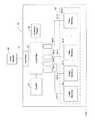
- FIG. 1is a block diagram of a multiple-channel flash storage device 10 according to an aspect.
- the multiple-channel flash storage device 10includes an interface 15 , a controller 20 and a flash array 22 .
- the interface 15interfaces the flash storage device 10 to a host system 80 , and allows the flash storage device 10 to receive data (e.g., to be written into the flash array 22 ) from the host system 80 and send data to the host system 80 (e.g., data read from the flash array 22 ).
- the controller 20controls operations of the flash storage device 10 and manages data flow between the host system 80 and the flash array 22 , as discussed further below.
- the controller 20may be implemented with a general purpose processor, a digital signal processor (DSP), an application specific integrated circuit (ASIC), a field programmable gate array (FPGA) or other programmable logic device, discrete gate or transistor logic, discrete hardware components, or any combination thereof designed to perform the functions described herein.
- the controller 20may also include firmware (e.g., software code) that is stored in a machine-readable medium and executed by a processor to perform the functions described herein.
- the flash array 22comprises a plurality of flash memories 25 - 1 to 25 -N split among N channels.
- Each flash memory 25 - 1 to 25 -Nmay comprise one or more physical flash chips, which may be implemented using NAND flash, NOR flash, or other flash technology.
- the flash memories 25 - 1 to 25 -Nmay comprise different numbers of flash chips. For example, within the same flash storage device 10 , some of the flash memories 25 - 1 to 25 -N may comprise one flash chip while others may comprise more than one flash chip.
- the flash storage device 10further comprises a plurality of flash memory interfaces 28 - 1 and 28 -N.
- Each flash memory interface 28 - 1 to 28 -Ninterfaces the controller 20 to one of the flash memories 25 - 1 to 25 -N via the corresponding channel.
- Each of the N channelsmay be implemented using one or more physical I/O buses coupled between one of the flash memory interfaces 28 - 1 to 28 -N and the corresponding flash memory 25 - 1 to 25 -N.
- Each of the N channelsallows the corresponding flash memory interface 28 - 1 to 28 -N to send read, write and/or erase commands to the corresponding flash memory 25 - 1 to 25 -N.
- each flash memory interface 28 - 1 to 28 -Nmay include a register (e.g., First-In-First-Out (FIFO) register) that queues read, write and/or erase commands from the controller 20 for the corresponding flash memory 25 - 1 to 25 -N.
- FIFOFirst-In-First-Out
- channelmay also refer to the corresponding flash memory 25 - 1 to 25 -N that is addressable through the bus.
- the flash memories 25 - 1 to 25 -Nmay be logically divided into data blocks.
- a data blockmay also be referred to as a memory block.
- Each data blockmay be further divided into data segments.
- a data segmentmay also be referred to as a page.
- each data blockmay be 128 kilobytes (K bytes) in size, and each data segment may be 4 kilobytes (K bytes) in size.
- each data blockhas 32 4 K byte data segments.
- the data blocksmay have other sizes besides 128 K bytes, including, but not limited, to 256 K bytes or 512 K bytes.
- a 256 K byte data blockmay have 64 4 K byte data segments.
- the data segmentsmay also have other sizes besides 4 K bytes.
- the data segmentsmay have any size that is a multiple of 1 K bytes or 2 K bytes.
- a data blockmay span one or more physical flash chips.
- the flash storage device 10also comprises a Dynamic Random Access Memory (DRAM) 30 .
- DRAMDynamic Random Access Memory
- Other types of random access memory and/or volatile memorymay also be used.
- the DRAM 30may be used to buffer data to be written into the flash array 22 and buffer data read from the flash array 22 .
- the data to be writtenmay be incoming data from a host system 80 and/or data being rewritten from one portion of the flash array 22 to another portion of the flash array 22 .
- the flash storage device 10also comprises an auxiliary power device 40 for providing backup power, which is described in further detail below.
- FIG. 2is a block diagram of an exemplary flash memory 25 according to an aspect.
- the flash memory 25includes an interface 210 , read/write/erase circuitry 215 , a buffer 220 , and a memory cell block 230 .
- the interface 210interfaces the flash memory 25 to the corresponding flash memory interface 28 - 1 to 28 -N via the corresponding channel, and allows the read/write/erase circuitry 215 to receive read, write and/or erase commands from the corresponding flash memory interface 28 - 1 to 28 - 1 and to send data read from the memory cell block 230 to the corresponding flash memory interface 28 - 1 to 28 -N in response to a read command.
- the memory cell block 230comprises an array of flash memory cells, where each cell may store one bit or multiple bits.
- the flash memory cellsmay be implemented using NAND flash, NOR flash, or other flash technology.
- the read/write/erase circuitry 215may write data to the memory cell block 230 based on a write command from the corresponding flash memory interface 28 - 1 to 28 -N.
- the write commandmay include an address of where the corresponding data is stored in the data cache and a physical address of where the data is to be written in the flash memory 25 .
- the read/write/erase circuitry 215may also read data from the memory cell block 230 based on a read command from the corresponding flash memory interface 28 - 1 to 28 -N and send the read data to the corresponding flash memory interface 28 - 1 to 28 -N.
- the corresponding flash memory interface 28 - 1 to 28 -Nmay then transfer the read data to the data cache.
- the read commandmay include a physical address of where the data is to be read from the flash memory 25 .
- the read/write/erase circuitry 215may also erase one or more data blocks in the memory cell block 230 based on an erase command from the corresponding flash memory interface 28 - 1 to 28 -N.
- the erase commandmay include a physical address of the data block to be erased.
- the buffer 220may be used to temporarily store data to be written to the memory cell block 230 .
- the flash memory interface 28 - 1 to 28 -Nmay also transfer the data (e.g., data segment) for the write command from the data cache to the flash memory 25 .
- the read/write/erase circuitry 215may temporarily store the received data in the buffer 220 and write the data from the buffer 220 to the memory cell block 230 at the physical address specified in the write command.
- the read/write/erase circuitry 215may send an indication to the corresponding flash memory interface 28 - 1 to 28 -N that the flash memory 25 has successfully completed the write operation for the write command and is ready for another command.
- the buffer 220may also be used to temporarily store data read from the memory cell block 230 .
- the read/write/erase circuitry 215may temporarily store the read data in the buffer 220 .
- the read/write/erase circuitry 215may send all of the data from the buffer 220 to the corresponding flash memory interface 28 - 1 to 28 -N.
- the flash memory interface 28 - 1 to 28 -Nmay then transfer the read data to the data cache.
- the host system 80may send data to and receive data from the flash storage device 10 in data sectors.
- each data sectormay be 512 bytes in size with eight data sectors per 4 K byte data segment.
- the host system 80may use different size data sectors.
- the host system 80may address data sectors stored in the flash storage device 10 using host Logical Block Addresses (LBAs).
- LBAsallow the host system 80 to address data sectors to be written to or read from the flash storage device 10 without having to know the physical locations of the data sectors in the flash storage device 10 .
- the host LBAsmay be implemented using an addressing scheme where data sectors are located by an index, with the host LBA of a first data sector being host LBA 0 , the host LBA of a second data sector being host LBA 1 , and so on.
- the flash storage device 10may store eight data sectors (e.g., 512 bytes) from the host system 80 into one data segment (e.g., 4 K bytes). The number of data sectors per data segment may be different depending on the size of a data sector and the size of a data segment.
- the controller 20may address data segments in the flash storage device 10 using flash LBAs, in which 8 host LBAs corresponds to one flash LBA identifying a data segment.
- flash LBArefers to an LBA for logically addressing a data segment
- host LBArefers to an LBA for logically addressing a data sector.
- the host LBAs and flash LBAsmay begin at zero so that host LBAs 0 - 7 correspond to flash LBA 0 , host LBAs 8 - 15 correspond to flash LBA 1 , and so on.
- a sequence of eight host LBAs identifying eight data sectorscorresponds to a flash LBA identifying a data segment that includes the eight data sectors.
- the controller 20may determine the flash LBA corresponding to a host LBA by dividing the host LBA by the number of data sectors in a data segment (e.g., 8 ) and using the integer quotient for the flash LBA.
- the data sector identified by host LBA 14is stored in the data segment identified by flash LBA 1 .
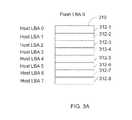
- FIG. 3Aillustrates an example of a data segment 310 comprising eight data sectors 312 - 1 to 312 - 8 .
- Each data sector 312 - 1 to 312 - 8may be stored at a know position within the data segment 310 relative to the other data sectors 312 - 1 to 312 - 8 .
- the controller 20may determine the flash LBA for the corresponding data segment, as discussed above.
- the controller 20may also determine the corresponding one of the data segments 312 - 1 to 312 - 8 within the data segment 310 based on the relative position of the received host LBA within the sequence of host LBAs corresponding to the flash LBA.
- FIG. 3Ashows an example of a data segment 310 identified by flash LBA 0 and the corresponding host LBAs 1 - 7 for the data sectors 312 - 1 to 312 - 8 .
- the data segment 310may include a sector index indicating which of the data sectors 312 - 1 to 312 - 8 in the data segment 310 are valid. For example, if the host system 80 sends a write command for only host LBAs 0 - 3 , then the data segment for flash LBA 0 would hold four valid data sectors.
- the host system 80may address data sectors to be written to and/or read from the flash storage device 10 using host LBAs. For example, when writing data to the flash storage device 10 , the host system 80 may send one or more data sectors with one or more corresponding host LBAs. Later, the host system 80 may randomly read any one of the data sectors from the flash storage device 10 using the corresponding host LBAs in a host read command. The controller 20 of the flash storage device 10 may write and/or read requested data sectors to and/or from the flash array 22 using the corresponding flash LBAs, which may be determined as discussed above.
- the flash LBAs in the flash storage device 10are split evenly among the N channels so that 1/N of the flash LBAs are assigned to the first channel, and so forth. Evenly splitting the flash LBAs among the channels increases the likelihood that, on a read corresponding to more than one flash LBA, not all of the data comes from one channel.
- the flash LBAsmay be evenly split among the N channels using any one of a number of methods.
- the controller 20may use an algorithm to determine which channel to assign each flash LBA.
- the algorithmmay be a MOD function that divides a flash LBA by the number of channels N and outputs the remainder of the division, where the remainder represents the channel assigned to the flash LBA.
- This algorithmprovides an even distribution of the flash LBAs among channels.
- the above algorithmprovides just one example of evenly splitting the flash LBAs among the channels.
- Other algorithmsmay be used to evenly split flash LBAs among the channels. An example in which flash LBAs are evenly split among channels is discussed below.
- An address table mapping all flash LBAs to physical addresses in the flash array 22is kept in the DRAM 30 .
- the controller 20 in the flash storage device 10stores data segments into physical addresses in the flash array 20 and maps each flash LBA to the physical address where the corresponding data segment is stored in the address table.
- the controller 20determines the corresponding LBAs, as discussed above.
- the controller 20maps the corresponding flash LBAs to physical addresses in the flash array 22 using the address table and reads the requested data from the physical addresses in the flash array 22 .
- a flash LBAmay be 28-bits in length or have another length depending on the amount of logically addressable memory in the flash array 22 .
- An example of an address tableis given below.
- the controller 20When the controller 20 writes a data segment to a physical address in the flash array 22 , the controller 20 may store the corresponding flash LBA in the physical address with the data segment, along with other information discussed below. This allows the controller 20 to reconstruct the address table by reading the flash LBAs stored in the physical addresses of the flash array 22 in the event that the address table is lost.
- the flash storage device 10has power back-up to make sure that certain functions are performed in the event of a power loss.
- One of these functionsmay be to store the address table in non-volatile memory to preserve the table, e.g., by writing the address table from the DRAM 30 to flash array 22 when the power goes off (either expectedly or unexpectedly).
- Thisenables the flash storage device 10 to start up or initialize faster because the address table can be read from flash (which may only take two seconds) instead of having to read all of the data in flash memory to reconstruct the address table.
- the address tabledoes not have to be reconstructed since the address table is stored in the flash array 22 by the back-up power.
- the auxiliary power device 40comprises super capacitors that charge when the flash storage device 10 receives power, and provides auxiliary power when the main power goes off by using energy stored in the super capacitors. This allows data (e.g., address table) to be written into flash array 22 when the power goes off unexpectedly.
- the controller 20may detect a power failure using a voltage threshold detector that detects when the voltage of a power supply falls below a threshold voltage. Upon detecting a power failure, the controller 20 may save all critical data (e.g., address table) to the flash array 22 using the auxiliary power provided by the auxiliary power device 40 .
- the controller 20may trigger this process on a sync cache command, flush cache command, power down immediate command, standby command, etc.
- the commandsmay come from the host system 80 and/or the controller 20 .
- the auxiliary power device 40may comprise one or capacitors, one or more batteries, or other forms of energy storage devices.
- Data received by the flash storage device 10is stored in the DRAM 30 and regardless of whether the data is received sequentially or randomly, the data is written from the DRAM 30 to the flash array 22 in a sequential manner on a per channel basis, as discussed further below. This makes data reads from the flash array 22 random. Since flash memory typically has good sequential write performance and random read performance, this arrangement takes advantage of the sequential write performance and random read performance of the flash memories 25 - 1 to 25 -N.
- datais buffered in a portion of the DRAM 30 referred to as a data cache.
- the data cachemay occupy all remaining DRAM 30 after everything else has been allocated in the DRAM 30 , for example, the address table and the linked lists discussed below. Therefore, the size of the data cache varies depending on the device size and configuration.
- the flash storage device 10does not start up unless there is a minimum amount of memory (e.g., at least 16 MB of DRAM) available for the data cache.
- the data cachemay be split up into a plurality (e.g., thousands) of small cache blocks which are each the size of one data segment (e.g., 4K bytes).
- All read and write datais transmitted between the host system 80 and the flash array 22 via the data cache in the DRAM 30 .
- the host system 80writes data
- the datais written into the data cache.
- the data cachereceives enough data to fill a complete data block
- the datais read from the data cache and written to the flash array 22 .
- the host system 80reads data
- the datais read from the flash array 22 , written into the data cache and then read from the data cache and transmitted to the host system 80 over the host interface.
- a central processing unit (CPU) of the host system 80does not have to copy the data to/from the data cache or receive the data.
- the CPUmay instruct hardware where to send the data or where to retrieve the data from and the hardware does the rest (e.g., via direct memory access (DMA)).
- DMAdirect memory access
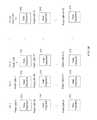
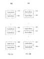
- FIG. 3Bis a diagram illustrating a process for allocating data segments 310 in the data cache of the DRAM 30 among the different channels.
- the data segments 310may be data received from the host system 80 in one or more host write commands.
- the data segments 310are given corresponding flash LBAs by the controller 20 .
- each flash LBAmay correspond to eight host LBAs.
- flash LBA 0may correspond to host LBAs 0 - 7
- flash LBA 1may correspond to host LBAs 8 - 15 , and so forth.
- the flash LBAsare split evenly among the 16 channels and striped across the 16 channels.
- flash LBA 0is assigned to channel 1
- flash LBA 1is assigned to channel 2
- flash LBA 2is assigned to channel 3
- the flash LBAsare sequential across the channels. However, this does not have to be the case.
- the flash LBAsmay comprise two or more random LBAs when the host system 80 writes data randomly to the flash storage device 10 (random host LBAs) instead of sequentially to the flash storage device 10 (sequential host LBAs).
- the controller 20can evenly split the corresponding flash LBAs among the N channels, for example, using the algorithm described above or other method.
- the controller 20When the number of data segments 310 for a channel in the data cache reaches enough to fill a data block (e.g., 32 data segments), the controller 20 writes the data segments 310 from the data cache to the corresponding flash memory 25 - 1 to 25 -N via the corresponding channel.
- the controller 20may write the data segments 310 for a channel to the corresponding flash memory 25 - 1 to 25 -N by queuing write commands for the data segments 310 in the register (e.g., FIFO register) of the corresponding flash memory interface 28 - 1 to 28 -N (e.g., one write command for each data segment 310 ).
- the flash memory interface 28 - 1 to 28 -Nmay then send the queued write commands to the corresponding flash memory 25 - 1 to 25 -N via the corresponding channel.
- the flash memory interface 28 - 1 to 28 -Nmay sequentially send the queued write commands to the corresponding flash memory 25 - 1 to 25 -N via the corresponding channel.
- the flash memory interface 28 - 1 to 28 -Nmay transfer the data segment for the write command from the data cache to the corresponding flash memory 25 - 1 to 25 -N via the corresponding channel.
- the flash memory interface 28 - 1 to 28 -Nmay send one write command to the corresponding flash memory 25 - 1 and 25 -N and wait until it receives an indication from the flash memory 25 - 1 to 25 -N that the data segment has been successfully written before sending the next write command in the register to the channel.
- the flash memory interfaces 28 - 1 to 28 -Nmay send write commands to their respective flash memories 25 - 1 to 25 -N substantially in parallel via the respective channels.
- a flash memory interface 28 - 1 to 28 -Nwaits for the corresponding flash memory 25 - 1 to 25 -N to complete a write command after transferring data for the write command from the data cache to the corresponding flash memory 25 - 1 to 250 -N
- other flash memory interfaces 28 - 1 to 28 -Nmay transfer data for other write commands from the data cache to corresponding flash memories 25 - 1 to 25 -N.
- the parallel write operations among the plurality of flash memories 25 - 1 to 25 -Nresults in faster write times and maximizes the write performance of the flash array 22 .
- the controller 20When the controller 20 receives a host read command from the host system 80 including host LBAs, the controller 20 determines the corresponding flash LBAs, as discussed above. The controller 20 then maps the flash LBAs to the corresponding physically addresses in the flash array 22 using the address table. The controller 20 then generates read commands corresponding to the physically addresses and queues the read commands in the registers of the respective flash memory interfaces 28 - 1 to 28 -N. Each flash memory interface 28 - 1 to 28 -N sends the corresponding read commands to the corresponding flash memory 25 - 1 to 25 -N via the corresponding channel and writes the resulting read data to the data cache.
- the controller 20may transfer the requested data from the data cache to the host system 80 via the interface 15 .
- Splitting flash LBAs evenly among the channelshelps ensure that, for a host read spanning several flash LBAs, the requested data is read from a plurality of the flash memories 25 - 1 to 25 -N.
- the data cache in the DRAM 30may be divided into cache blocks. Each cache block may correspond to a physical address in the DRAM 30 for storing one data segment (e.g., 4 K bytes).
- the cache blocksare all held in a linked list.
- the data segment in the cache block that is on the top of the linked listis removed from the data cache (assuming it is not active) and the cache block is allocated for the new data segment.
- the cache block with the new data segmentis then placed at the end of the linked list and the new data segment is stored in a physical address of the data cache corresponding to the cache block.
- the new data segmentmay come from data in a host write command or data read from the flash array 22 in response to a host read command. If the data in the cache block is not accessed again, then the cache block will slowly move up the linked list as cache blocks are allocated for new data segments and moved to the end of the linked list.
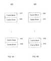
- FIGS. 4A and 4Billustrate an example of a linked list 405 according to an aspect.
- FIG. 4Ashows the linked list 405 in which cache block 410 is on the top of the linked list 405 and cache block 430 is on the end of the linked list 405 .
- the controller 20removes the data segment corresponding to cache block 410 from the data cache, allocates cache block 410 to the new data segment and moves the cache block 410 to the end of the linked list 405 .
- FIG. 4Bshows the linked list 405 after cache block 410 has been moved to the end of the linked list 405 .
- the other cache blocks in the linked list 405have been moved up one position in the linked list 405 .
- cache block 430has been moved up one position from the end of the linked list 405 , as shown in FIG. 4B .
- the controller 20may continue to store a data segment in the data cache after the data segment has been written to the flash array 22 .
- the controller 20removes the data segment from the data cache when the corresponding cache block reaches the top of the linked list and the controller 20 needs to allocate the cache block for a new data segment.
- the controller 20may retrieve the data from the data cache and the corresponding cache block is moved from the current position on the linked list to the end of the linked list. This way frequently accessed data will be retained in the data cache because a cache block that is being frequently accessed will be continually moved to the end of the linked list and not reach to the top of the linked list from where the data in the cache block will be removed from the data cache.
- FIGS. 5A and 5Billustrate an example of the linked list 405 according to an aspect.
- FIG. 5Ashows the linked list 405 in which cache block 410 is on the top of the linked list 405 , cache block 430 is on the end of the linked list 405 , and cache block 450 is at a position somewhere between cache blocks 410 and 430 .
- the controller 20retrieves the data segment from the data cache and moves cache block 450 to the end of the linked list 405 .
- FIG. 5Bshows the linked list 405 after cache block 450 has been moved to the end of the linked list 405 .
- cache block 430has been moved up one position from the end of the linked list 405 , as shown in FIG. 5B . If the data segment corresponding to cache block 450 is frequently read, then cache block 450 will continually move to the end of the linked list 405 .
- a cache block structureis maintained for each cache block.
- the cache block structureincludes a physical address of the cache block in the DRAM 30 where the corresponding data segment is stored and other information (e.g., the time that the data segment was written into the data cache).
- the cache block structuremay also include a physical address in the flash memory 22 where the corresponding data segment is stored if the data segment has already been written to the flash memory 22 .
- All data to be written to the flash array 22is buffered in the DRAM 30 for a predetermined amount of time (e.g., 10 seconds) to allow the next sequential data (e.g., data sectors) in a data sequence to arrive and fill the data cache of the DRAM 30 .
- a predetermined amount of timee.g. 10 seconds
- the controller 20to write a large amount of data from the DRAM 30 to the flash array 22 at one time and free up the controller 20 to perform other operations. If the next sequential data does not arrive in the predetermined amount of time (e.g., 10 seconds), then the data in the data cache of the DRAM 30 is written to the flash array 22 and may be combined with other data that needs to be written.
- a complete data blockmay not be written to a channel of the flash memory array 22 when power is turned off and there is not a complete data block in the DRAM 30 to write to the channel.
- the controller 20may write an incomplete data block to the channel of the flash array 22 .
- Data in the DRAM 30can also be written to the flash array 22 upon receiving a command to flush the data cache, clear the data cache, or clear the cache.
- the controller 20uses an address table to locate a data segment for a given flash LBA in either the flash array 22 or the data cache of the DRAM 30 .
- the address tablemay also be referred to as a virtual-to-physical (V2P) table since the address table maps a logical address to a physical address.
- V2Pvirtual-to-physical
- FIG. 6shows an example of an address table 605 according to an aspect of the disclosure.
- Each of the entries 610 - 1 to 610 - n in the address table 605corresponds to a flash LBA and may be arranged in order of the flash LBAs so that flash LBA 0 corresponds to the first entry, flash LBA 1 to the second entry, and so on.
- the entry 610 - 1 to 610 - n for each flash LBA 615may include a channel number 620 , a cache indicator 625 indicating whether the corresponding data segment is in the data cache, and depending on whether the data segment is in the data cache, a physical address of the data in the flash array 22 or a cache block number 630 .
- the entryincludes the physical address 630 of the data segment in the flash array 22 .
- the controller 20uses the physical address 630 to locate the data segment in the flash array 22 .
- the physical address 630can be in a hardware format so that the physical address can be passed directly to the hardware side of the flash storage device 10 to retrieve the data segment from the flash array 22 .
- the entry for the flash LBA 615includes a cache block number 630 .
- the cache block number 630points to the cache block corresponding to the flash LBA. This allows the controller 20 to retrieve the cache structure of the corresponding cache block.
- the cache structurein turn provides the controller 20 with the physical address where the data is located in the DRAM 30 and the NAND device information if required plus other useful information (e.g., the time that the corresponding data segment was written into the data cache).
- the NAND device informationmay include a physical address of the corresponding data segment in the flash array 22 .
- the controller 20updates the address table 605 when data sectors corresponding to a data segment are received from the host system 80 in a host write command or read from the flash array 22 in response to a host read command.
- the controller 20allocates a cache block from the top of the linked list for the corresponding data segment.
- the controller 20then creates an entry in the address table 605 for the data segment including the flash LBA 615 of the data segment and a cache block number 630 of the cache block allocated to the data segment.
- the controller 20also sets the cache indicator 625 to indicate that the data segment is located in the data cache. If the data segment is eventually written to the flash array 22 , then the controller 20 may include the physically address of the data segment in the flash array 22 in the corresponding cache block.
- the controller 20may update the entry for the data segment accordingly.
- the controller 20may set the cache indicator 625 to indicate that the data segment is not stored in the data cache and include the physical address of the data segment in the flash array 22 .
- the controller 20may retrieve the physical address from the cache structure in the cache block.
- each data block in the flash array 22can hold random data segments instead of consecutive data segments.
- random write datais received for a flash LBA (e.g., in a random host write command)
- the controller 20receives write data (updated data) for a flash LBA corresponding to a data segment in a data block (old data block) in the flash array 22
- the controller 20writes the write data (updated data) to another data block (new data block) in the flash array 22 instead of re-writing the old data block with the write data (updated data) for the flash LBA.
- the data segment corresponding to the flash LBA in the old data blockis invalid since the write data (updated data) for the flash LBA is stored in the new data block.
- a data blockcan hold a varying number of valid data segments at a given time, depending on how many data segments in the data block are updated and written to other data blocks.
- the controller 20maintains a table for each data block in the flash array 22 .
- the table for each data blockidentifies the number of valid data segments in the data block and the flash LBAs corresponding to valid data segments held in the data block.
- the controller 20uses this information to identify data blocks with the fewest valid data segments. After identifying the data blocks with the fewest valid data segments, the controller 20 copies the valid data segments of the identified data blocks to one or more other data blocks in the flash array 22 , and erases the identified data blocks to provide pre-erased data blocks for more write data. This allows the maximum number of data blocks to be freed up for write data while having to copy the least amount of data to other data blocks. As a result, fewer write operations are required to free up data blocks, providing more bandwidth for host read and write data.
- each data blockis kept in one of a plurality of linked lists depending on the number of valid data segments in the data block. All data blocks with only one valid data segment each are kept in one list, all data blocks with only two valid data segments are kept in another list, and so on.
- the controller 20performs dynamic wear leveling (to free up data blocks) using the lists of valid data segments to identify data blocks having only one valid data segment, data blocks having only two valid data segments, and so on. There are also separate lists for bad (e.g., defective) data blocks, empty data blocks, free data blocks and data blocks (e.g., data blocks being written to), etc.
- Each data blocksis also kept in one of a plurality of linked lists depending on the number of erase cycles performed on the data block. As discussed further below, the controller 20 performs static wear leveling using the linked lists of erase cycles.
- the controller 20places a time stamp on each data segment that is written into the flash array 22 allowing the controller 20 to know which data segments are newer than the old ones.
- the time stampsmay be generated by incrementing a counter when a write operation is performed and using the current count value of the counter for the time stamp for data being written during the write operation. For example, the time stamp for a write may be 11000, then 11001 for the next write, and so on.
- the time stampsallow the controller 20 to determine the order in which data segments were written into the flash array 22 by comparing their time stamps. In this example, a data segment with a time stamp having a higher count value is newer than a data segment with a time stamp having a lower count value.
- the time stamp for a data segmentmay be stored with the data segment in the flash array 20 and/or stored in a table.
- the controller 20compares the time stamps of data segments in the background and not during regular read/write operations. When two data segments in different data blocks correspond to the same flash LBA, then the older data segment (as indicated by the corresponding time stamp) is invalid. Eventually, a data block with many invalid data segments is erased and one or more valid data segments that were in the data block are combined with other incoming data or valid data from other blocks that are being erased. The combined data is written to a new data block, freeing up the erased block for write operations. When the one or more valid data segments are written to the new data block, the address table is updated with the new physical addresses of the valid data segments. In an aspect, the above operations are performed in the background to make pre-erased blocks available for write operations.
- the flash storage device 10may need to allocate more flash memory than is logically addressable by the controller 20 .
- a flash storage device 10 with 256 GB of memorymay only have 146 GB of addressable memory (e.g., addressable to the host system 80 ). This helps provide pre-erased blocks to write to most of the time.
- the time stampsare used if reconstruction of the address table is required.
- the time stamps of the corresponding data segmentsmay be used to determine which data segment is the most recent (e.g., data segment with the time stamp having the highest count value is the most recent).
- the physical address with the more recent time stampis used to reconstruct the address table entry for the flash LBA.
- FIG. 7illustrates linked lists that are used to determine which data block 710 to remove data from and erase to provide pre-erased blocks for high-speed writing according to one aspect.
- each data block 710may be 128 K bytes in size and hold 32 4 K bytes data segments. Normally, a data block 710 will be full when it is first written to and will therefore have 32 valid data segments in this example.
- the linked listsmay cover data blocks in the entire flash array 22 . Alternatively, the linked lists may be implemented for each channel of the flash array 22 .
- the link listsare used to keep track of the number of valid data segments in each data block 710 .
- each data block 710is in one of the linked lists of valid data segments.
- List 0comprises data blocks 710 with no data segment holding valid data.
- List 1comprises data blocks 710 with only one data segment holding valid data,
- list 2comprises data blocks 710 with two data segments holding valid data, and so forth.
- List 32comprises data blocks 710 with all 32 data segments holding valid data.
- the number of linked listsmay be different from 32 depending on the sizes of the data segments and/or data blocks. For example, the number of linked lists may be lower if larger data segments are used (fewer data segments in each data block 710 ).
- the number of linked listsmay be larger if larger data blocks 710 are used (more data segments per data block).
- the flash storage device 10may include lists of pre-erased data blocks 710 , bad data blocks 710 , system blocks, etc.
- the data blocks 710 in the listsmay be identified by addresses of or pointers to the data blocks 710 therein or other means.
- the data block XXwhen a data block XX is initially written to, the data block XX will be full and therefore go to the list with all valid data segments (list 32 in the example illustrated in FIG. 7 ). If one of the data segments in data block XX is subsequently written again, then the data segment will go into a different data block YY.
- the flash storage device 10receives a host write command from the host system 80 that results in a write to flash LBA 12100 and a data segment for flash LBA 12100 is already stored in data block XX, then the controller 20 writes the data in the write command for flash LBA 12100 to data block YY.
- the data segment for flash LBA 12100is rewritten to data block YY, invalidating the data segment for flash LBA 12100 in data block XX.
- the data block XXwill have only 31 valid data segments, and the controller 20 will move the data block XX from list 32 to list 31 in the example illustrated in FIG. 7 .
- the address table for flash LBA 12100is updated with the physical address of the data segment in data block YY. Each time another data segment in data block XX becomes invalid, data block XX is moved down to the appropriate list.
- Pre-erased blocks that are available for write operationsare identified in a pre-erased list.
- the controller 20may need to erase some of the data blocks 710 to increase the number of pre-erased data blocks available for write operations.
- the controller 20determines which data blocks 710 to erase by looking in the lists of valid data segments in ascending order. The controller 20 first looks in list 0 for data blocks 710 holding no valid data. Since data blocks in list 0 require no movement of data to erase, these data blocks 710 are erased and placed into the pre-erased list first.
- list 0is empty and/or additional pre-erased blocks are needed, then the controller looks in list 1 for data blocks 710 with only one valid data segment. Each data block 710 in list 1 only require the movement of one data segment to be erased. If list 1 is empty and/or additional pre-erased blocks are needed, then the controller looks in list 2 , and so forth. As data blocks 710 are erased, they are added to the end of the pre-erased list. When a pre-erased block is needed, it is taken from the top of the pre-erased list. This provides a form of dynamic wear leveling. The earlier pre-erased blocks are on the top of the list.
- the valid data segments of these erased data blocks 710may be combined and rewritten into a new single data block. For example, if there are 32 data blocks 710 with one valid segment each, then the 32 valid data segments of these data blocks 710 may be written into a new block 710 , and all 32 data blocks 710 can be erased or moved to list 0 . The new block 710 will have all valid data segments. The physical addresses of the 32 valid segments are updated in the address table accordingly.
- FIG. 8illustrates linked lists that are used to provide static wear leveling according to one aspect.
- the listskeep track of the erase counts of the data blocks 710 .
- the controller 20uses the lists to provide wear leveling by keeping the erase counts of the data blocks 710 within a certain range (e.g., 8192 erase counts) of each other.
- the data blocks 710(with the exception of BAD or System data blocks) are in one of a plurality of static wear lists.
- the example in FIG. 8has eight static wear lists. Each list comprises data blocks 710 that are within a certain range of the lowest erase count.
- the linked listsmay cover data blocks in the entire flash array 22 . Alternatively, the linked lists may be implemented for each channel of the flash array 22 .
- list 0comprises data blocks 710 with erase counts that are within 1023 of the lowest count.
- List 1comprises data blocks 710 with erase counts that are within a range of 1024-2047 of the lowest count, and so forth up to list 7 , which comprises data blocks 710 with erase counts that are within a range of 7168-8191 of the lowest count.
- list 7comprises data blocks 710 with erase counts that are within a range of 7168-8191 of the lowest count.
- each listtends to be in roughly an ascending numerical sequence. This may be especially true at the start of the list where data blocks with the lowest counts are located.
- the data blocks 710 in list 1are moved down to list 0
- the data blocks 710 in list 2are moved down to list 1
- so forthAfter the bump up, the lowest count is 1024 higher and list 7 is emptied since the data blocks previously in list 7 have been moved down to list 6 .
- the controller 20may use both the lists of valid data segments and the lists of erase counts to determine which data segments need to be moved and which data blocks 710 need to be erased.
- the lists described abovemay be stored in the DRAM 30 for fast access by the controller 20 during operation of the flash storage device 10 , and stored in the flash array 22 when the flash storage device 10 is turned off.
- FIG. 9is a flow chart illustrating a method of transferring data in a flash storage device comprising a random access memory and a plurality of channels of a flash array according to an aspect of the disclosure.
- the methodbegins with step 901 , in which the flash storage device receives a plurality of data segments from a host system. Each data segment may comprise data sectors.
- the plurality of data segmentsare stored in the random access memory (e.g., DRAM 30 ).
- the plurality of data segmentsare allocated among the plurality of channels of the flash array.
- the allocated data segmentsare written from the random access memory to the respective channels of the flash array.
Landscapes
- Engineering & Computer Science (AREA)
- Theoretical Computer Science (AREA)
- Physics & Mathematics (AREA)
- General Engineering & Computer Science (AREA)
- General Physics & Mathematics (AREA)
- Human Computer Interaction (AREA)
- Quality & Reliability (AREA)
- Techniques For Improving Reliability Of Storages (AREA)
- Information Retrieval, Db Structures And Fs Structures Therefor (AREA)
Abstract
Description
Claims (20)
Priority Applications (1)
| Application Number | Priority Date | Filing Date | Title |
|---|---|---|---|
| US14/720,697US9411522B2 (en) | 2008-06-25 | 2015-05-22 | High speed input/output performance in solid state devices |
Applications Claiming Priority (3)
| Application Number | Priority Date | Filing Date | Title |
|---|---|---|---|
| US7570908P | 2008-06-25 | 2008-06-25 | |
| US12/492,109US9043531B2 (en) | 2008-06-25 | 2009-06-25 | High speed input/output performance in solid state devices |
| US14/720,697US9411522B2 (en) | 2008-06-25 | 2015-05-22 | High speed input/output performance in solid state devices |
Related Parent Applications (1)
| Application Number | Title | Priority Date | Filing Date |
|---|---|---|---|
| US12/492,109ContinuationUS9043531B2 (en) | 2008-06-25 | 2009-06-25 | High speed input/output performance in solid state devices |
Publications (2)
| Publication Number | Publication Date |
|---|---|
| US20150254005A1 US20150254005A1 (en) | 2015-09-10 |
| US9411522B2true US9411522B2 (en) | 2016-08-09 |
Family
ID=41448931
Family Applications (10)
| Application Number | Title | Priority Date | Filing Date |
|---|---|---|---|
| US12/343,378Active2031-03-24US8843691B2 (en) | 2008-06-25 | 2008-12-23 | Prioritized erasure of data blocks in a flash storage device |
| US12/464,856AbandonedUS20090327804A1 (en) | 2008-06-25 | 2009-05-12 | Wear leveling in flash storage devices |
| US12/492,113Active2030-09-13US8825941B2 (en) | 2008-06-25 | 2009-06-25 | SLC-MLC combination flash storage device |
| US12/492,104Active2030-06-04US9311006B2 (en) | 2008-06-25 | 2009-06-25 | Table journaling in flash storage devices |
| US12/492,103Active2032-03-16US8572308B2 (en) | 2008-06-25 | 2009-06-25 | Supporting variable sector sizes in flash storage devices |
| US12/492,110AbandonedUS20120239853A1 (en) | 2008-06-25 | 2009-06-25 | Solid state device with allocated flash cache |
| US12/492,109Active2030-06-15US9043531B2 (en) | 2008-06-25 | 2009-06-25 | High speed input/output performance in solid state devices |
| US12/492,112Active2030-08-02US8762622B2 (en) | 2008-06-25 | 2009-06-25 | Enhanced MLC solid state device |
| US12/492,107Active2031-07-07US8347138B2 (en) | 2008-06-25 | 2009-06-25 | Redundant data distribution in a flash storage device |
| US14/720,697ActiveUS9411522B2 (en) | 2008-06-25 | 2015-05-22 | High speed input/output performance in solid state devices |
Family Applications Before (9)
| Application Number | Title | Priority Date | Filing Date |
|---|---|---|---|
| US12/343,378Active2031-03-24US8843691B2 (en) | 2008-06-25 | 2008-12-23 | Prioritized erasure of data blocks in a flash storage device |
| US12/464,856AbandonedUS20090327804A1 (en) | 2008-06-25 | 2009-05-12 | Wear leveling in flash storage devices |
| US12/492,113Active2030-09-13US8825941B2 (en) | 2008-06-25 | 2009-06-25 | SLC-MLC combination flash storage device |
| US12/492,104Active2030-06-04US9311006B2 (en) | 2008-06-25 | 2009-06-25 | Table journaling in flash storage devices |
| US12/492,103Active2032-03-16US8572308B2 (en) | 2008-06-25 | 2009-06-25 | Supporting variable sector sizes in flash storage devices |
| US12/492,110AbandonedUS20120239853A1 (en) | 2008-06-25 | 2009-06-25 | Solid state device with allocated flash cache |
| US12/492,109Active2030-06-15US9043531B2 (en) | 2008-06-25 | 2009-06-25 | High speed input/output performance in solid state devices |
| US12/492,112Active2030-08-02US8762622B2 (en) | 2008-06-25 | 2009-06-25 | Enhanced MLC solid state device |
| US12/492,107Active2031-07-07US8347138B2 (en) | 2008-06-25 | 2009-06-25 | Redundant data distribution in a flash storage device |
Country Status (1)
| Country | Link |
|---|---|
| US (10) | US8843691B2 (en) |
Cited By (1)
| Publication number | Priority date | Publication date | Assignee | Title |
|---|---|---|---|---|
| US20230325331A1 (en)* | 2015-08-03 | 2023-10-12 | Pure Storage, Inc. | Storage Array Controller Communication Using Multiple Channels |
Families Citing this family (405)
| Publication number | Priority date | Publication date | Assignee | Title |
|---|---|---|---|---|
| US8489817B2 (en) | 2007-12-06 | 2013-07-16 | Fusion-Io, Inc. | Apparatus, system, and method for caching data |
| US8443134B2 (en) | 2006-12-06 | 2013-05-14 | Fusion-Io, Inc. | Apparatus, system, and method for graceful cache device degradation |
| US8019938B2 (en) | 2006-12-06 | 2011-09-13 | Fusion-I0, Inc. | Apparatus, system, and method for solid-state storage as cache for high-capacity, non-volatile storage |
| US9104599B2 (en) | 2007-12-06 | 2015-08-11 | Intelligent Intellectual Property Holdings 2 Llc | Apparatus, system, and method for destaging cached data |
| US8706968B2 (en) | 2007-12-06 | 2014-04-22 | Fusion-Io, Inc. | Apparatus, system, and method for redundant write caching |
| US7852654B2 (en)* | 2006-12-28 | 2010-12-14 | Hynix Semiconductor Inc. | Semiconductor memory device, and multi-chip package and method of operating the same |
| JP5171448B2 (en)* | 2007-07-31 | 2013-03-27 | キヤノン株式会社 | Image forming apparatus and control method thereof |
| US7975105B1 (en)* | 2007-12-03 | 2011-07-05 | Yingju Sun | Solid state storage devices with changeable capacity |
| US9519540B2 (en) | 2007-12-06 | 2016-12-13 | Sandisk Technologies Llc | Apparatus, system, and method for destaging cached data |
| US7836226B2 (en) | 2007-12-06 | 2010-11-16 | Fusion-Io, Inc. | Apparatus, system, and method for coordinating storage requests in a multi-processor/multi-thread environment |
| KR101077339B1 (en)* | 2007-12-28 | 2011-10-26 | 가부시끼가이샤 도시바 | Semiconductor storage device |
| US8843691B2 (en) | 2008-06-25 | 2014-09-23 | Stec, Inc. | Prioritized erasure of data blocks in a flash storage device |
| US8891298B2 (en) | 2011-07-19 | 2014-11-18 | Greenthread, Llc | Lifetime mixed level non-volatile memory system |
| JP5192352B2 (en)* | 2008-10-30 | 2013-05-08 | 株式会社日立製作所 | Storage device and data storage area management method |
| TWI385672B (en)* | 2008-11-05 | 2013-02-11 | Lite On It Corp | Adaptive multi-channel controller and method for storage device |
| US8239613B2 (en)* | 2008-12-30 | 2012-08-07 | Intel Corporation | Hybrid memory device |
| TWI385527B (en)* | 2009-02-10 | 2013-02-11 | Phison Electronics Corp | Multi level cell nand flash memory storage system, and controller and accessing method thereof |
| KR20100097456A (en)* | 2009-02-26 | 2010-09-03 | 삼성전자주식회사 | Memory system and address allocating method of flash translation layer thereof |
| US8261158B2 (en) | 2009-03-13 | 2012-09-04 | Fusion-Io, Inc. | Apparatus, system, and method for using multi-level cell solid-state storage as single level cell solid-state storage |
| US8266503B2 (en) | 2009-03-13 | 2012-09-11 | Fusion-Io | Apparatus, system, and method for using multi-level cell storage in a single-level cell mode |
| KR101581679B1 (en)* | 2009-03-18 | 2015-12-31 | 삼성전자주식회사 | Storage device and method for managing buffer memory of storage device |
| US8195891B2 (en)* | 2009-03-30 | 2012-06-05 | Intel Corporation | Techniques to perform power fail-safe caching without atomic metadata |
| US8171219B2 (en)* | 2009-03-31 | 2012-05-01 | Intel Corporation | Method and system to perform caching based on file-level heuristics |
| US8341501B2 (en)* | 2009-04-30 | 2012-12-25 | International Business Machines Corporation | Adaptive endurance coding of non-volatile memories |
| US20100318746A1 (en)* | 2009-06-12 | 2010-12-16 | Seakr Engineering, Incorporated | Memory change track logging |
| US20100332726A1 (en)* | 2009-06-26 | 2010-12-30 | Solid State System Co., Ltd. | Structure and method for managing writing operation on mlc flash memory |
| US20100332922A1 (en)* | 2009-06-30 | 2010-12-30 | Mediatek Inc. | Method for managing device and solid state disk drive utilizing the same |
| US8510497B2 (en)* | 2009-07-29 | 2013-08-13 | Stec, Inc. | Flash storage device with flexible data format |
| US7941696B2 (en)* | 2009-08-11 | 2011-05-10 | Texas Memory Systems, Inc. | Flash-based memory system with static or variable length page stripes including data protection information and auxiliary protection stripes |
| US7856528B1 (en)* | 2009-08-11 | 2010-12-21 | Texas Memory Systems, Inc. | Method and apparatus for protecting data using variable size page stripes in a FLASH-based storage system |
| US8930622B2 (en) | 2009-08-11 | 2015-01-06 | International Business Machines Corporation | Multi-level data protection for flash memory system |
| US7818525B1 (en)* | 2009-08-12 | 2010-10-19 | Texas Memory Systems, Inc. | Efficient reduction of read disturb errors in NAND FLASH memory |
| US8189379B2 (en) | 2009-08-12 | 2012-05-29 | Texas Memory Systems, Inc. | Reduction of read disturb errors in NAND FLASH memory |
| JP5002629B2 (en)* | 2009-08-28 | 2012-08-15 | 株式会社東芝 | Memory system |
| JP5999645B2 (en) | 2009-09-08 | 2016-10-05 | ロンギチュード エンタープライズ フラッシュ エスエイアールエル | Apparatus, system, and method for caching data on a solid state storage device |
| US9122579B2 (en) | 2010-01-06 | 2015-09-01 | Intelligent Intellectual Property Holdings 2 Llc | Apparatus, system, and method for a storage layer |
| KR101769883B1 (en) | 2009-09-09 | 2017-08-21 | 샌디스크 테크놀로지스 엘엘씨 | Apparatus, system, and method for allocating storage |
| US8489804B1 (en)* | 2009-09-14 | 2013-07-16 | Marvell International Ltd. | System for using dynamic random access memory to reduce the effect of write amplification in flash memory |
| US8990476B2 (en)* | 2009-10-01 | 2015-03-24 | Micron Technology, Inc. | Power interrupt management |
| US8214700B2 (en)* | 2009-10-28 | 2012-07-03 | Sandisk Technologies Inc. | Non-volatile memory and method with post-write read and adaptive re-write to manage errors |
| US8423866B2 (en)* | 2009-10-28 | 2013-04-16 | SanDisk Technologies, Inc. | Non-volatile memory and method with post-write read and adaptive re-write to manage errors |
| US8634240B2 (en)* | 2009-10-28 | 2014-01-21 | SanDisk Technologies, Inc. | Non-volatile memory and method with accelerated post-write read to manage errors |
| US8560770B2 (en)* | 2009-11-13 | 2013-10-15 | Seagate Technology Llc | Non-volatile write cache for a data storage system |
| US8176235B2 (en)* | 2009-12-04 | 2012-05-08 | International Business Machines Corporation | Non-volatile memories with enhanced write performance and endurance |
| US8285918B2 (en)* | 2009-12-11 | 2012-10-09 | Nimble Storage, Inc. | Flash memory cache for data storage device |
| US9128762B2 (en) | 2009-12-15 | 2015-09-08 | Micron Technology, Inc. | Persistent content in nonvolatile memory |
| TWI497293B (en)* | 2009-12-17 | 2015-08-21 | Ibm | Data management in solid state storage devices |
| US8473808B2 (en)* | 2010-01-26 | 2013-06-25 | Qimonda Ag | Semiconductor memory having non-standard form factor |
| US8661184B2 (en) | 2010-01-27 | 2014-02-25 | Fusion-Io, Inc. | Managing non-volatile media |
| US8854882B2 (en) | 2010-01-27 | 2014-10-07 | Intelligent Intellectual Property Holdings 2 Llc | Configuring storage cells |
| US9245653B2 (en) | 2010-03-15 | 2016-01-26 | Intelligent Intellectual Property Holdings 2 Llc | Reduced level cell mode for non-volatile memory |
| US8725931B1 (en) | 2010-03-26 | 2014-05-13 | Western Digital Technologies, Inc. | System and method for managing the execution of memory commands in a solid-state memory |
| US8713066B1 (en)* | 2010-03-29 | 2014-04-29 | Western Digital Technologies, Inc. | Managing wear leveling and garbage collection operations in a solid-state memory using linked lists |
| JP2011209973A (en)* | 2010-03-30 | 2011-10-20 | Hitachi Ltd | Disk array configuration program, computer and computer system |
| US8751740B1 (en)* | 2010-03-31 | 2014-06-10 | Emc Corporation | Systems, methods, and computer readable media for performance optimization of storage allocation to virtual logical units |
| US8621141B2 (en)* | 2010-04-01 | 2013-12-31 | Intel Corporations | Method and system for wear leveling in a solid state drive |
| WO2011133145A1 (en)* | 2010-04-21 | 2011-10-27 | Hewlett-Packard Development Company, L.P. | Communicating operating system booting information |
| US8782327B1 (en) | 2010-05-11 | 2014-07-15 | Western Digital Technologies, Inc. | System and method for managing execution of internal commands and host commands in a solid-state memory |
| US9026716B2 (en)* | 2010-05-12 | 2015-05-05 | Western Digital Technologies, Inc. | System and method for managing garbage collection in solid-state memory |
| US8959300B2 (en) | 2010-05-18 | 2015-02-17 | International Business Machines Corporation | Cascade ordering |
| US8886870B2 (en)* | 2010-05-25 | 2014-11-11 | Marvell World Trade Ltd. | Memory access table saving and restoring system and methods |
| US8966176B2 (en) | 2010-05-27 | 2015-02-24 | Sandisk Il Ltd. | Memory management storage to a host device |
| US9043533B1 (en)* | 2010-06-29 | 2015-05-26 | Emc Corporation | Sizing volatile memory cache based on flash-based cache usage |
| US8656256B2 (en)* | 2010-07-07 | 2014-02-18 | Stec, Inc. | Apparatus and method for multi-mode operation of a flash memory device |
| JPWO2012020544A1 (en)* | 2010-08-11 | 2013-10-28 | 日本電気株式会社 | Data processing system, data processing method, and program |
| US12008266B2 (en) | 2010-09-15 | 2024-06-11 | Pure Storage, Inc. | Efficient read by reconstruction |
| US11614893B2 (en) | 2010-09-15 | 2023-03-28 | Pure Storage, Inc. | Optimizing storage device access based on latency |
| US8417878B2 (en) | 2010-09-20 | 2013-04-09 | Seagate Technology Llc | Selection of units for garbage collection in flash memory |
| US9021192B1 (en) | 2010-09-21 | 2015-04-28 | Western Digital Technologies, Inc. | System and method for enhancing processing of memory access requests |
| US9164886B1 (en) | 2010-09-21 | 2015-10-20 | Western Digital Technologies, Inc. | System and method for multistage processing in a memory storage subsystem |
| WO2012039983A1 (en) | 2010-09-24 | 2012-03-29 | Rambus Inc. | Memory device with ecc history table |
| TWI425357B (en) | 2010-09-27 | 2014-02-01 | Silicon Motion Inc | Method for performing block management, and associated memory device and controller thereof |
| TWI435216B (en)* | 2010-09-27 | 2014-04-21 | Silicon Motion Inc | Method for performing meta block management, and associated memory device and controller thereof |
| US8612804B1 (en) | 2010-09-30 | 2013-12-17 | Western Digital Technologies, Inc. | System and method for improving wear-leveling performance in solid-state memory |
| IL208641A0 (en)* | 2010-10-12 | 2010-12-30 | Eci Telecom Ltd | Method for accelerating start up of a computerized system |
| US8769374B2 (en) | 2010-10-13 | 2014-07-01 | International Business Machines Corporation | Multi-write endurance and error control coding of non-volatile memories |
| JP2012108627A (en)* | 2010-11-15 | 2012-06-07 | Toshiba Corp | Memory system |
| US8949502B2 (en)* | 2010-11-18 | 2015-02-03 | Nimble Storage, Inc. | PCIe NVRAM card based on NVDIMM |
| US8089807B1 (en) | 2010-11-22 | 2012-01-03 | Ge Aviation Systems, Llc | Method and system for data storage |
| CN102479156B (en)* | 2010-11-22 | 2015-03-11 | 慧荣科技股份有限公司 | Method for block management, memory device and controller thereof |
| US8495338B2 (en) | 2010-12-03 | 2013-07-23 | Micron Technology, Inc. | Transaction log recovery |
| KR101936311B1 (en)* | 2010-12-03 | 2019-01-09 | 삼성전자주식회사 | Method of processing data |
| US20120239860A1 (en) | 2010-12-17 | 2012-09-20 | Fusion-Io, Inc. | Apparatus, system, and method for persistent data management on a non-volatile storage media |
| US9268646B1 (en)* | 2010-12-21 | 2016-02-23 | Western Digital Technologies, Inc. | System and method for optimized management of operation data in a solid-state memory |
| US9092337B2 (en) | 2011-01-31 | 2015-07-28 | Intelligent Intellectual Property Holdings 2 Llc | Apparatus, system, and method for managing eviction of data |
| US8909851B2 (en) | 2011-02-08 | 2014-12-09 | SMART Storage Systems, Inc. | Storage control system with change logging mechanism and method of operation thereof |
| US9003104B2 (en) | 2011-02-15 | 2015-04-07 | Intelligent Intellectual Property Holdings 2 Llc | Systems and methods for a file-level cache |
| US9201677B2 (en) | 2011-05-23 | 2015-12-01 | Intelligent Intellectual Property Holdings 2 Llc | Managing data input/output operations |
| US8874823B2 (en) | 2011-02-15 | 2014-10-28 | Intellectual Property Holdings 2 Llc | Systems and methods for managing data input/output operations |
| WO2012116369A2 (en) | 2011-02-25 | 2012-08-30 | Fusion-Io, Inc. | Apparatus, system, and method for managing contents of a cache |
| US8966191B2 (en) | 2011-03-18 | 2015-02-24 | Fusion-Io, Inc. | Logical interface for contextual storage |
| US9563555B2 (en) | 2011-03-18 | 2017-02-07 | Sandisk Technologies Llc | Systems and methods for storage allocation |
| US8935466B2 (en) | 2011-03-28 | 2015-01-13 | SMART Storage Systems, Inc. | Data storage system with non-volatile memory and method of operation thereof |
| KR101800444B1 (en)* | 2011-03-28 | 2017-12-20 | 삼성전자주식회사 | Control method of nonvolatile memory and memory system including the same |
| US9361044B2 (en) | 2011-03-28 | 2016-06-07 | Western Digital Technologies, Inc. | Power-safe data management system |
| KR101810932B1 (en)* | 2011-04-27 | 2017-12-20 | 시게이트 테크놀로지 엘엘씨 | Method for managing address mapping information, accessing method of disk drive, method for managing address mapping information via network, and storage device, computer system and storage medium applying the same |
| US8886911B2 (en) | 2011-05-31 | 2014-11-11 | Micron Technology, Inc. | Dynamic memory cache size adjustment in a memory device |
| US8792273B2 (en) | 2011-06-13 | 2014-07-29 | SMART Storage Systems, Inc. | Data storage system with power cycle management and method of operation thereof |
| US8898373B1 (en) | 2011-06-29 | 2014-11-25 | Western Digital Technologies, Inc. | System and method for improving wear-leveling performance in solid-state memory |
| US9003101B1 (en) | 2011-06-29 | 2015-04-07 | Western Digital Technologies, Inc. | Prioritized access for media with heterogeneous access rates |
| US9158670B1 (en) | 2011-06-30 | 2015-10-13 | Western Digital Technologies, Inc. | System and method for dynamically adjusting garbage collection policies in solid-state memory |
| US20130007373A1 (en)* | 2011-06-30 | 2013-01-03 | Advanced Micro Devices, Inc. | Region based cache replacement policy utilizing usage information |
| US9318166B2 (en) | 2011-07-22 | 2016-04-19 | SanDisk Technologies, Inc. | Systems and methods of storing data |
| US8726104B2 (en) | 2011-07-28 | 2014-05-13 | Sandisk Technologies Inc. | Non-volatile memory and method with accelerated post-write read using combined verification of multiple pages |
| KR101861170B1 (en) | 2011-08-17 | 2018-05-25 | 삼성전자주식회사 | Memory system including migration manager |
| US9098399B2 (en) | 2011-08-31 | 2015-08-04 | SMART Storage Systems, Inc. | Electronic system with storage management mechanism and method of operation thereof |
| US9021231B2 (en) | 2011-09-02 | 2015-04-28 | SMART Storage Systems, Inc. | Storage control system with write amplification control mechanism and method of operation thereof |
| US9063844B2 (en) | 2011-09-02 | 2015-06-23 | SMART Storage Systems, Inc. | Non-volatile memory management system with time measure mechanism and method of operation thereof |
| US9021319B2 (en) | 2011-09-02 | 2015-04-28 | SMART Storage Systems, Inc. | Non-volatile memory management system with load leveling and method of operation thereof |
| CN102279808A (en)* | 2011-09-06 | 2011-12-14 | 晨星软件研发(深圳)有限公司 | Method and device for managing video memory of embedded equipment |
| US9298603B2 (en)* | 2011-09-09 | 2016-03-29 | OCZ Storage Solutions Inc. | NAND flash-based storage device and methods of using |
| US20130066882A1 (en)* | 2011-09-09 | 2013-03-14 | Onzo Limited | Data storage method and system |
| US9588883B2 (en)* | 2011-09-23 | 2017-03-07 | Conversant Intellectual Property Management Inc. | Flash memory system |
| US9367453B1 (en)* | 2011-09-30 | 2016-06-14 | Emc Corporation | System and method for migrating cache data |
| US9367452B1 (en)* | 2011-09-30 | 2016-06-14 | Emc Corporation | System and method for apportioning storage |
| US8635407B2 (en)* | 2011-09-30 | 2014-01-21 | International Business Machines Corporation | Direct memory address for solid-state drives |
| US20130086300A1 (en)* | 2011-10-04 | 2013-04-04 | Lsi Corporation | Storage caching acceleration through usage of r5 protected fast tier |
| US8539007B2 (en) | 2011-10-17 | 2013-09-17 | International Business Machines Corporation | Efficient garbage collection in a compressed journal file |
| US8949553B2 (en) | 2011-10-28 | 2015-02-03 | Dell Products L.P. | System and method for retention of historical data in storage resources |
| US8977803B2 (en)* | 2011-11-21 | 2015-03-10 | Western Digital Technologies, Inc. | Disk drive data caching using a multi-tiered memory |
| US9240240B2 (en)* | 2011-11-29 | 2016-01-19 | Micron Technology, Inc. | Apparatus having indications of memory cell density and methods of their determination and use |
| KR101893145B1 (en) | 2011-12-06 | 2018-10-05 | 삼성전자주식회사 | Memory systems and block copy methods thereof |
| US9274937B2 (en) | 2011-12-22 | 2016-03-01 | Longitude Enterprise Flash S.A.R.L. | Systems, methods, and interfaces for vector input/output operations |
| US9176862B2 (en) | 2011-12-29 | 2015-11-03 | Sandisk Technologies Inc. | SLC-MLC wear balancing |
| WO2013100783A1 (en) | 2011-12-29 | 2013-07-04 | Intel Corporation | Method and system for control signalling in a data path module |
| US9251052B2 (en) | 2012-01-12 | 2016-02-02 | Intelligent Intellectual Property Holdings 2 Llc | Systems and methods for profiling a non-volatile cache having a logical-to-physical translation layer |
| US9767032B2 (en) | 2012-01-12 | 2017-09-19 | Sandisk Technologies Llc | Systems and methods for cache endurance |
| US8782344B2 (en) | 2012-01-12 | 2014-07-15 | Fusion-Io, Inc. | Systems and methods for managing cache admission |
| US20130185503A1 (en)* | 2012-01-12 | 2013-07-18 | Vigneshwara Bhatta | Method for metadata persistence |
| US10102117B2 (en) | 2012-01-12 | 2018-10-16 | Sandisk Technologies Llc | Systems and methods for cache and storage device coordination |
| US9251086B2 (en) | 2012-01-24 | 2016-02-02 | SanDisk Technologies, Inc. | Apparatus, system, and method for managing a cache |
| US9116812B2 (en) | 2012-01-27 | 2015-08-25 | Intelligent Intellectual Property Holdings 2 Llc | Systems and methods for a de-duplication cache |
| US10359972B2 (en) | 2012-08-31 | 2019-07-23 | Sandisk Technologies Llc | Systems, methods, and interfaces for adaptive persistence |
| US8898423B1 (en)* | 2012-01-31 | 2014-11-25 | Western Digital Technologies, Inc. | High performance caching architecture for data storage systems |
| US9223686B1 (en)* | 2012-02-01 | 2015-12-29 | Amazon Technologies, Inc. | Cache memory data storage control system and method |
| US9239781B2 (en) | 2012-02-07 | 2016-01-19 | SMART Storage Systems, Inc. | Storage control system with erase block mechanism and method of operation thereof |
| KR101923157B1 (en) | 2012-02-22 | 2018-11-28 | 삼성전자주식회사 | Memory system and program method thereof |
| US10019353B2 (en) | 2012-03-02 | 2018-07-10 | Longitude Enterprise Flash S.A.R.L. | Systems and methods for referencing data on a storage medium |
| JP5659178B2 (en)* | 2012-03-16 | 2015-01-28 | 株式会社東芝 | NONVOLATILE MEMORY DEVICE AND NONVOLATILE MEMORY CONTROL METHOD |
| US9298252B2 (en) | 2012-04-17 | 2016-03-29 | SMART Storage Systems, Inc. | Storage control system with power down mechanism and method of operation thereof |
| US8868824B2 (en) | 2012-04-19 | 2014-10-21 | Microsoft Corporation | Solid-state drive management and control |
| US8990477B2 (en)* | 2012-04-19 | 2015-03-24 | Sandisk Technologies Inc. | System and method for limiting fragmentation |
| US9003224B2 (en) | 2012-04-25 | 2015-04-07 | Western Digital Technologies, Inc. | Managing unreliable memory in data storage systems |
| US9116792B2 (en)* | 2012-05-18 | 2015-08-25 | Silicon Motion, Inc. | Data storage device and method for flash block management |
| US20130311700A1 (en)* | 2012-05-20 | 2013-11-21 | Chung-Jwu Chen | Extending Lifetime For Non-volatile Memory Apparatus |
| US8996957B1 (en) | 2012-05-22 | 2015-03-31 | Pmc-Sierra, Inc. | Systems and methods for initializing regions of a flash drive having diverse error correction coding (ECC) schemes |
| US9021333B1 (en) | 2012-05-22 | 2015-04-28 | Pmc-Sierra, Inc. | Systems and methods for recovering data from failed portions of a flash drive |
| US9176812B1 (en) | 2012-05-22 | 2015-11-03 | Pmc-Sierra, Inc. | Systems and methods for storing data in page stripes of a flash drive |
| US9021336B1 (en) | 2012-05-22 | 2015-04-28 | Pmc-Sierra, Inc. | Systems and methods for redundantly storing error correction codes in a flash drive with secondary parity information spread out across each page of a group of pages |
| US9021337B1 (en) | 2012-05-22 | 2015-04-28 | Pmc-Sierra, Inc. | Systems and methods for adaptively selecting among different error correction coding schemes in a flash drive |
| US8972824B1 (en) | 2012-05-22 | 2015-03-03 | Pmc-Sierra, Inc. | Systems and methods for transparently varying error correction code strength in a flash drive |
| US8793556B1 (en) | 2012-05-22 | 2014-07-29 | Pmc-Sierra, Inc. | Systems and methods for reclaiming flash blocks of a flash drive |
| US9183085B1 (en) | 2012-05-22 | 2015-11-10 | Pmc-Sierra, Inc. | Systems and methods for adaptively selecting from among a plurality of error correction coding schemes in a flash drive for robustness and low latency |
| US9047214B1 (en)* | 2012-05-22 | 2015-06-02 | Pmc-Sierra, Inc. | System and method for tolerating a failed page in a flash device |
| US8788910B1 (en) | 2012-05-22 | 2014-07-22 | Pmc-Sierra, Inc. | Systems and methods for low latency, high reliability error correction in a flash drive |
| TWI477966B (en)* | 2012-05-31 | 2015-03-21 | Silicon Motion Inc | Data storage device and operating method for flash memory |
| US9195598B2 (en) | 2012-06-08 | 2015-11-24 | International Business Machines Corporation | Synchronous and asynchronous discard scans based on the type of cache memory |
| US9336150B2 (en) | 2012-06-08 | 2016-05-10 | International Business Machines Corporation | Performing asynchronous discard scans with staging and destaging operations |
| US8949689B2 (en) | 2012-06-11 | 2015-02-03 | SMART Storage Systems, Inc. | Storage control system with data management mechanism and method of operation thereof |
| US8954653B1 (en) | 2012-06-26 | 2015-02-10 | Western Digital Technologies, Inc. | Mechanisms for efficient management of system data in data storage systems |
| TWI454913B (en)* | 2012-06-26 | 2014-10-01 | Phison Electronics Corp | Data writing method, memory controller and memory storage device |
| KR101929584B1 (en)* | 2012-06-29 | 2018-12-17 | 에스케이하이닉스 주식회사 | Data storage device and operating method thereof |
| US8566671B1 (en) | 2012-06-29 | 2013-10-22 | Sandisk Technologies Inc. | Configurable accelerated post-write read to manage errors |
| US10339056B2 (en) | 2012-07-03 | 2019-07-02 | Sandisk Technologies Llc | Systems, methods and apparatus for cache transfers |
| US9612966B2 (en) | 2012-07-03 | 2017-04-04 | Sandisk Technologies Llc | Systems, methods and apparatus for a virtual machine cache |
| US8751730B2 (en)* | 2012-07-27 | 2014-06-10 | Winbond Electronics Corp. | Serial interface flash memory apparatus and writing method for status register thereof |
| US9208099B2 (en) | 2012-08-08 | 2015-12-08 | International Business Machines Corporation | Adjustment of the number of task control blocks allocated for discard scans |
| US10318495B2 (en) | 2012-09-24 | 2019-06-11 | Sandisk Technologies Llc | Snapshots for a non-volatile device |
| US10509776B2 (en) | 2012-09-24 | 2019-12-17 | Sandisk Technologies Llc | Time sequence data management |
| US9524800B2 (en) | 2012-09-26 | 2016-12-20 | International Business Machines Corporation | Performance evaluation of solid state memory device |
| US8880786B2 (en)* | 2012-09-28 | 2014-11-04 | Apple Inc. | Flash translation layer (FTL) database journaling schemes |
| KR102025263B1 (en) | 2012-10-05 | 2019-09-25 | 삼성전자주식회사 | Memory system and read reclaim method thereof |
| US9507523B1 (en) | 2012-10-12 | 2016-11-29 | Western Digital Technologies, Inc. | Methods, devices and systems for variable size logical page management in a solid state drive |
| US9489296B1 (en)* | 2012-10-17 | 2016-11-08 | Western Digital Technologies, Inc. | Methods, devices and systems for hardware-based garbage collection in solid state drives |
| US20140136575A1 (en)* | 2012-11-10 | 2014-05-15 | Yuanyuan Zhao | Log-structured garbage collection |
| US11037625B2 (en)* | 2012-11-20 | 2021-06-15 | Thstyme Bermuda Limited | Solid state drive architectures |
| MX364783B (en)* | 2012-11-20 | 2019-05-07 | Thstyme Bermuda Ltd | Solid state drive architectures. |
| US9671962B2 (en) | 2012-11-30 | 2017-06-06 | Sandisk Technologies Llc | Storage control system with data management mechanism of parity and method of operation thereof |
| CN103034603B (en)* | 2012-12-07 | 2014-06-18 | 天津瑞发科半导体技术有限公司 | Multi-channel flash memory card control device and control method thereof |
| US20150143021A1 (en)* | 2012-12-26 | 2015-05-21 | Unisys Corporation | Equalizing wear on storage devices through file system controls |
| KR20150105323A (en)* | 2013-01-08 | 2015-09-16 | 바이올린 메모리 인코포레이티드 | Method and system for data storage |
| CN103092770B (en)* | 2013-01-18 | 2015-08-12 | 山东华芯半导体有限公司 | The method of memory cost is reduced during a kind of abrasion equilibrium process |
| US9176892B2 (en)* | 2013-01-22 | 2015-11-03 | International Business Machines Corporation | Performing staging or destaging based on the number of waiting discard scans |
| US9123445B2 (en) | 2013-01-22 | 2015-09-01 | SMART Storage Systems, Inc. | Storage control system with data management mechanism and method of operation thereof |
| US20140223072A1 (en)* | 2013-02-07 | 2014-08-07 | Lsi Corporation | Tiered Caching Using Single Level Cell and Multi-Level Cell Flash Technology |
| US9329928B2 (en) | 2013-02-20 | 2016-05-03 | Sandisk Enterprise IP LLC. | Bandwidth optimization in a non-volatile memory system |
| US9214965B2 (en) | 2013-02-20 | 2015-12-15 | Sandisk Enterprise Ip Llc | Method and system for improving data integrity in non-volatile storage |
| US9183137B2 (en) | 2013-02-27 | 2015-11-10 | SMART Storage Systems, Inc. | Storage control system with data management mechanism and method of operation thereof |
| US20140250277A1 (en)* | 2013-03-04 | 2014-09-04 | Kabushiki Kaisha Toshiba | Memory system |
| US9470720B2 (en) | 2013-03-08 | 2016-10-18 | Sandisk Technologies Llc | Test system with localized heating and method of manufacture thereof |
| US9842053B2 (en) | 2013-03-15 | 2017-12-12 | Sandisk Technologies Llc | Systems and methods for persistent cache logging |
| US9208018B1 (en) | 2013-03-15 | 2015-12-08 | Pmc-Sierra, Inc. | Systems and methods for reclaiming memory for solid-state memory |
| US9026867B1 (en) | 2013-03-15 | 2015-05-05 | Pmc-Sierra, Inc. | Systems and methods for adapting to changing characteristics of multi-level cells in solid-state memory |
| US9053012B1 (en) | 2013-03-15 | 2015-06-09 | Pmc-Sierra, Inc. | Systems and methods for storing data for solid-state memory |
| US9081701B1 (en) | 2013-03-15 | 2015-07-14 | Pmc-Sierra, Inc. | Systems and methods for decoding data for solid-state memory |
| US9009565B1 (en) | 2013-03-15 | 2015-04-14 | Pmc-Sierra, Inc. | Systems and methods for mapping for solid-state memory |
| US9043780B2 (en) | 2013-03-27 | 2015-05-26 | SMART Storage Systems, Inc. | Electronic system with system modification control mechanism and method of operation thereof |
| US9170941B2 (en) | 2013-04-05 | 2015-10-27 | Sandisk Enterprises IP LLC | Data hardening in a storage system |
| US10049037B2 (en) | 2013-04-05 | 2018-08-14 | Sandisk Enterprise Ip Llc | Data management in a storage system |
| US9543025B2 (en) | 2013-04-11 | 2017-01-10 | Sandisk Technologies Llc | Storage control system with power-off time estimation mechanism and method of operation thereof |
| US10546648B2 (en) | 2013-04-12 | 2020-01-28 | Sandisk Technologies Llc | Storage control system with data management mechanism and method of operation thereof |
| US10558561B2 (en) | 2013-04-16 | 2020-02-11 | Sandisk Technologies Llc | Systems and methods for storage metadata management |
| US10102144B2 (en) | 2013-04-16 | 2018-10-16 | Sandisk Technologies Llc | Systems, methods and interfaces for data virtualization |
| US9830257B1 (en)* | 2013-06-12 | 2017-11-28 | Western Digital Technologies, Inc. | Fast saving of data during power interruption in data storage systems |
| US9313874B2 (en) | 2013-06-19 | 2016-04-12 | SMART Storage Systems, Inc. | Electronic system with heat extraction and method of manufacture thereof |
| US9898056B2 (en) | 2013-06-19 | 2018-02-20 | Sandisk Technologies Llc | Electronic assembly with thermal channel and method of manufacture thereof |
| US10331375B1 (en)* | 2013-06-21 | 2019-06-25 | Amazon Technologies, Inc. | Data storage area cleaner |
| US9244519B1 (en) | 2013-06-25 | 2016-01-26 | Smart Storage Systems. Inc. | Storage system with data transfer rate adjustment for power throttling |
| US9367353B1 (en) | 2013-06-25 | 2016-06-14 | Sandisk Technologies Inc. | Storage control system with power throttling mechanism and method of operation thereof |
| CN104298605A (en)* | 2013-07-17 | 2015-01-21 | 光宝科技股份有限公司 | Block grouping method for garbage collection action in solid-state storage device |
| CN104298465B (en)* | 2013-07-17 | 2017-06-20 | 光宝电子(广州)有限公司 | Block group technology in solid state storage device |
| US9274865B2 (en) | 2013-08-01 | 2016-03-01 | HGST Netherlands B.V. | Implementing enhanced buffer management for data storage devices |
| US9146850B2 (en) | 2013-08-01 | 2015-09-29 | SMART Storage Systems, Inc. | Data storage system with dynamic read threshold mechanism and method of operation thereof |
| US9842128B2 (en) | 2013-08-01 | 2017-12-12 | Sandisk Technologies Llc | Systems and methods for atomic storage operations |
| US9448946B2 (en) | 2013-08-07 | 2016-09-20 | Sandisk Technologies Llc | Data storage system with stale data mechanism and method of operation thereof |
| US9361222B2 (en) | 2013-08-07 | 2016-06-07 | SMART Storage Systems, Inc. | Electronic system with storage drive life estimation mechanism and method of operation thereof |
| US9431113B2 (en) | 2013-08-07 | 2016-08-30 | Sandisk Technologies Llc | Data storage system with dynamic erase block grouping mechanism and method of operation thereof |
| KR20150020385A (en)* | 2013-08-13 | 2015-02-26 | 에스케이하이닉스 주식회사 | Data storage device, operating method thereof and data processing system including the same |
| KR20150020384A (en)* | 2013-08-13 | 2015-02-26 | 에스케이하이닉스 주식회사 | Data storage device and operating method thereof |
| JP5768100B2 (en)* | 2013-09-10 | 2015-08-26 | 株式会社東芝 | MEMORY DEVICE, SERVER DEVICE, AND MEMORY CONTROL METHOD |
| US10331583B2 (en)* | 2013-09-26 | 2019-06-25 | Intel Corporation | Executing distributed memory operations using processing elements connected by distributed channels |
| US10019320B2 (en) | 2013-10-18 | 2018-07-10 | Sandisk Technologies Llc | Systems and methods for distributed atomic storage operations |
| US10073630B2 (en) | 2013-11-08 | 2018-09-11 | Sandisk Technologies Llc | Systems and methods for log coordination |
| US9152555B2 (en) | 2013-11-15 | 2015-10-06 | Sandisk Enterprise IP LLC. | Data management with modular erase in a data storage system |
| US9463737B2 (en) | 2013-11-21 | 2016-10-11 | Ford Global Technologies, Llc | Illuminated seatbelt assembly |
| US9213601B2 (en) | 2013-12-03 | 2015-12-15 | Sandisk Technologies Inc. | Adaptive data re-compaction after post-write read verification operations |
| US9542278B2 (en) | 2013-12-26 | 2017-01-10 | Silicon Motion, Inc. | Data storage device and flash memory control method |
| TWI523018B (en) | 2013-12-31 | 2016-02-21 | 群聯電子股份有限公司 | Decoding method, memory storage device, and memory controlling circuit unit |
| WO2015109128A1 (en)* | 2014-01-16 | 2015-07-23 | Pure Storage, Inc. | Data replacement based on data properties and data retention in a tiered storage device system |
| US8874835B1 (en) | 2014-01-16 | 2014-10-28 | Pure Storage, Inc. | Data placement based on data properties in a tiered storage device system |
| US9354955B1 (en) | 2014-03-19 | 2016-05-31 | Western Digital Technologies, Inc. | Partial garbage collection for fast error handling and optimized garbage collection for the invisible band |
| JP2015191336A (en)* | 2014-03-27 | 2015-11-02 | キヤノン株式会社 | Memory controller, information processor, control method of information processor and program |
| US9928169B2 (en)* | 2014-05-07 | 2018-03-27 | Sandisk Technologies Llc | Method and system for improving swap performance |
| US9529670B2 (en)* | 2014-05-16 | 2016-12-27 | International Business Machines Corporation | Storage element polymorphism to reduce performance degradation during error recovery |
| US9959203B2 (en) | 2014-06-23 | 2018-05-01 | Google Llc | Managing storage devices |
| JP2016028319A (en)* | 2014-07-08 | 2016-02-25 | 富士通株式会社 | Access control program, access control device, and access control method |
| US9495255B2 (en)* | 2014-08-07 | 2016-11-15 | Pure Storage, Inc. | Error recovery in a storage cluster |
| US9766972B2 (en) | 2014-08-07 | 2017-09-19 | Pure Storage, Inc. | Masking defective bits in a storage array |
| US9558069B2 (en) | 2014-08-07 | 2017-01-31 | Pure Storage, Inc. | Failure mapping in a storage array |
| KR20160024530A (en)* | 2014-08-26 | 2016-03-07 | 에스케이하이닉스 주식회사 | Semiconductor device and operating method thereof |
| US20160062832A1 (en)* | 2014-09-02 | 2016-03-03 | Netapp. Inc. | Wide spreading data storage architecture |
| US9823969B2 (en) | 2014-09-02 | 2017-11-21 | Netapp, Inc. | Hierarchical wide spreading of distributed storage |
| US9767104B2 (en) | 2014-09-02 | 2017-09-19 | Netapp, Inc. | File system for efficient object fragment access |
| US9632702B2 (en) | 2014-10-15 | 2017-04-25 | International Business Machines Corporation | Efficient initialization of a thinly provisioned storage array |
| US10042789B2 (en) | 2014-10-27 | 2018-08-07 | Micron Technology, Inc. | Programming interruption management |
| JP6193834B2 (en)* | 2014-10-29 | 2017-09-06 | ファナック株式会社 | Data storage system |
| CN105630638B (en) | 2014-10-31 | 2018-01-12 | 国际商业机器公司 | For the apparatus and method for disk array distribution caching |
| US9830087B2 (en)* | 2014-11-13 | 2017-11-28 | Micron Technology, Inc. | Memory wear leveling |
| KR102295208B1 (en) | 2014-12-19 | 2021-09-01 | 삼성전자주식회사 | Storage device dynamically allocating program area and program method thererof |
| US10014060B2 (en)* | 2015-01-30 | 2018-07-03 | Sandisk Technologies Llc | Memory system and method for reducing read disturb errors |
| US10156994B2 (en) | 2015-02-27 | 2018-12-18 | Western Digital Technologies, Inc. | Methods and systems to reduce SSD IO latency |
| US9946607B2 (en) | 2015-03-04 | 2018-04-17 | Sandisk Technologies Llc | Systems and methods for storage error management |
| JP6492835B2 (en)* | 2015-03-23 | 2019-04-03 | 富士通クライアントコンピューティング株式会社 | Portable device and information processing apparatus |
| US9431061B1 (en) | 2015-04-24 | 2016-08-30 | Netapp, Inc. | Data write deferral during hostile events |
| US9817715B2 (en) | 2015-04-24 | 2017-11-14 | Netapp, Inc. | Resiliency fragment tiering |
| US10120753B2 (en) | 2015-05-26 | 2018-11-06 | Micron Technology, Inc. | Methods and apparatuses for error correction |
| US9697134B2 (en) | 2015-06-10 | 2017-07-04 | Micron Technology, Inc. | Memory having a static cache and a dynamic cache |
| CN104991738B (en)* | 2015-06-19 | 2018-04-24 | 华中科技大学 | A kind of solid-state disk and its read-write operation method |
| KR102367982B1 (en)* | 2015-06-22 | 2022-02-25 | 삼성전자주식회사 | Data storage device and data processing system having the same |
| US10296236B2 (en)* | 2015-07-01 | 2019-05-21 | Pure Storage, Inc. | Offloading device management responsibilities from a storage device in an array of storage devices |
| US10055236B2 (en) | 2015-07-02 | 2018-08-21 | Sandisk Technologies Llc | Runtime data storage and/or retrieval |
| KR102401600B1 (en) | 2015-08-31 | 2022-05-25 | 삼성전자주식회사 | Storage device configured to manage a plurality of data streams based on data amount |
| US10096355B2 (en)* | 2015-09-01 | 2018-10-09 | Sandisk Technologies Llc | Dynamic management of programming states to improve endurance |
| US9792068B2 (en)* | 2015-09-10 | 2017-10-17 | Toshiba Memory Corporation | Memory system and method of controlling nonvolatile memory |
| US20170075812A1 (en)* | 2015-09-16 | 2017-03-16 | Intel Corporation | Technologies for managing a dynamic read cache of a solid state drive |
| US10506042B2 (en)* | 2015-09-22 | 2019-12-10 | Toshiba Memory Corporation | Storage system that includes a plurality of routing circuits and a plurality of node modules connected thereto |
| US9830108B2 (en) | 2015-10-12 | 2017-11-28 | Sandisk Technologies Llc | Write redirect |
| US10133490B2 (en) | 2015-10-30 | 2018-11-20 | Sandisk Technologies Llc | System and method for managing extended maintenance scheduling in a non-volatile memory |
| US9778855B2 (en) | 2015-10-30 | 2017-10-03 | Sandisk Technologies Llc | System and method for precision interleaving of data writes in a non-volatile memory |
| US10042553B2 (en) | 2015-10-30 | 2018-08-07 | Sandisk Technologies Llc | Method and system for programming a multi-layer non-volatile memory having a single fold data path |
| US10120613B2 (en)* | 2015-10-30 | 2018-11-06 | Sandisk Technologies Llc | System and method for rescheduling host and maintenance operations in a non-volatile memory |
| US10210041B2 (en)* | 2015-11-05 | 2019-02-19 | SK Hynix Inc. | Systems and methods for low latency copy operations in non-volatile memory |
| US9530491B1 (en)* | 2015-11-16 | 2016-12-27 | Sandisk Technologies Llc | System and method for direct write to MLC memory |
| KR20170059658A (en)* | 2015-11-23 | 2017-05-31 | 에스케이하이닉스 주식회사 | Memory system and operation method for the same |
| US10007458B2 (en)* | 2015-12-18 | 2018-06-26 | Microsemi Solutions (U.S.), Inc. | Method of configuring memory cells in a solid state drive based on read/write activity and controller therefor |
| US10379742B2 (en) | 2015-12-28 | 2019-08-13 | Netapp, Inc. | Storage zone set membership |
| US9990731B2 (en)* | 2016-01-13 | 2018-06-05 | Varian Medical Systems International Ag | Systems and methods for evaluating motion tracking for radiation therapy |
| TWI591635B (en)* | 2016-02-05 | 2017-07-11 | 群聯電子股份有限公司 | Memory management method, memory control circuit unit and memory storage device |
| KR20170099437A (en) | 2016-02-23 | 2017-09-01 | 에스케이하이닉스 주식회사 | Memory system and operation method of the same |
| US10514984B2 (en) | 2016-02-26 | 2019-12-24 | Netapp, Inc. | Risk based rebuild of data objects in an erasure coded storage system |
| US10372543B2 (en)* | 2016-03-04 | 2019-08-06 | Toshiba Memory Corporation | Memory system |
| US10162561B2 (en)* | 2016-03-21 | 2018-12-25 | Apple Inc. | Managing backup of logical-to-physical translation information to control boot-time and write amplification |
| US10055317B2 (en) | 2016-03-22 | 2018-08-21 | Netapp, Inc. | Deferred, bulk maintenance in a distributed storage system |
| US9792995B1 (en) | 2016-04-26 | 2017-10-17 | Sandisk Technologies Llc | Independent multi-plane read and low latency hybrid read |
| US10019314B2 (en) | 2016-04-27 | 2018-07-10 | Silicon Motion Inc. | Flash memory apparatus and storage management method for flash memory |
| CN111679787B (en) | 2016-04-27 | 2023-07-18 | 慧荣科技股份有限公司 | Flash memory device, flash memory controller, and flash memory storage management method |
| TWI689930B (en)* | 2016-04-27 | 2020-04-01 | 慧榮科技股份有限公司 | Flash memory apparatus and storage management method for flash memory |
| KR102601211B1 (en) | 2016-06-01 | 2023-11-10 | 삼성전자주식회사 | Method for detecting fast reuse memory block and memory block management method using the same |
| TWI597730B (en)* | 2016-06-17 | 2017-09-01 | 群聯電子股份有限公司 | Data writing method, memory control circuit unit and memory storage apparatus |
| US9672905B1 (en) | 2016-07-22 | 2017-06-06 | Pure Storage, Inc. | Optimize data protection layouts based on distributed flash wear leveling |
| KR20180023267A (en)* | 2016-08-25 | 2018-03-07 | 에스케이하이닉스 주식회사 | Memory system and operating method for the same |
| US10359933B2 (en) | 2016-09-19 | 2019-07-23 | Micron Technology, Inc. | Memory devices and electronic systems having a hybrid cache including static and dynamic caches with single and multiple bits per cell, and related methods |
| US10324959B2 (en)* | 2016-09-20 | 2019-06-18 | Futurewei Technologies, Inc. | Garbage collection in storage system |
| US10452301B1 (en) | 2016-09-29 | 2019-10-22 | Amazon Technologies, Inc. | Cluster-based storage device buffering |
| US10402168B2 (en) | 2016-10-01 | 2019-09-03 | Intel Corporation | Low energy consumption mantissa multiplication for floating point multiply-add operations |
| WO2018067743A1 (en)* | 2016-10-04 | 2018-04-12 | Pure Storage, Inc. | Maintaining data associated with a storage device related applications |
| US20180095788A1 (en)* | 2016-10-04 | 2018-04-05 | Pure Storage, Inc. | Scheduling operations for a storage device |
| US10528264B2 (en)* | 2016-11-04 | 2020-01-07 | Samsung Electronics Co., Ltd. | Storage device and data processing system including the same |
| US10649896B2 (en)* | 2016-11-04 | 2020-05-12 | Samsung Electronics Co., Ltd. | Storage device and data processing system including the same |
| KR102680418B1 (en)* | 2016-11-29 | 2024-07-03 | 삼성전자주식회사 | Controller and storage device including controller and nonvolatile memory devices |
| JP6667629B2 (en)* | 2016-12-29 | 2020-03-18 | 華為技術有限公司Huawei Technologies Co.,Ltd. | Storage systems and solid state disks |
| US10416999B2 (en) | 2016-12-30 | 2019-09-17 | Intel Corporation | Processors, methods, and systems with a configurable spatial accelerator |
| US10474375B2 (en) | 2016-12-30 | 2019-11-12 | Intel Corporation | Runtime address disambiguation in acceleration hardware |
| US10572376B2 (en) | 2016-12-30 | 2020-02-25 | Intel Corporation | Memory ordering in acceleration hardware |
| US10558575B2 (en) | 2016-12-30 | 2020-02-11 | Intel Corporation | Processors, methods, and systems with a configurable spatial accelerator |
| US9747158B1 (en) | 2017-01-13 | 2017-08-29 | Pure Storage, Inc. | Intelligent refresh of 3D NAND |
| JP2018120439A (en) | 2017-01-25 | 2018-08-02 | 東芝メモリ株式会社 | Memory system and control method |
| KR102747560B1 (en) | 2017-02-10 | 2024-12-31 | 삼성전자주식회사 | Storage device managing duplicated data based on the number of operations |
| US20180239532A1 (en) | 2017-02-23 | 2018-08-23 | Western Digital Technologies, Inc. | Techniques for performing a non-blocking control sync operation |
| CN106951186B (en)* | 2017-03-07 | 2020-02-07 | 合肥兆芯电子有限公司 | Data programming method, memory storage device and memory control circuit unit |
| US10049047B1 (en) | 2017-03-10 | 2018-08-14 | Toshiba Memory Corporation | Multibit NAND media using pseudo-SLC caching technique |
| US10095626B2 (en) | 2017-03-10 | 2018-10-09 | Toshiba Memory Corporation | Multibit NAND media using pseudo-SLC caching technique |
| US10452282B2 (en) | 2017-04-07 | 2019-10-22 | Micron Technology, Inc. | Memory management |
| US11221956B2 (en)* | 2017-05-31 | 2022-01-11 | Seagate Technology Llc | Hybrid storage device with three-level memory mapping |
| US10635654B2 (en) | 2017-06-12 | 2020-04-28 | Samsung Electronics Co., Ltd. | Data journaling for large solid state storage devices with low DRAM/SRAM |
| US10445451B2 (en) | 2017-07-01 | 2019-10-15 | Intel Corporation | Processors, methods, and systems for a configurable spatial accelerator with performance, correctness, and power reduction features |
| US10467183B2 (en) | 2017-07-01 | 2019-11-05 | Intel Corporation | Processors and methods for pipelined runtime services in a spatial array |
| US10515046B2 (en) | 2017-07-01 | 2019-12-24 | Intel Corporation | Processors, methods, and systems with a configurable spatial accelerator |
| US10469397B2 (en) | 2017-07-01 | 2019-11-05 | Intel Corporation | Processors and methods with configurable network-based dataflow operator circuits |
| US10515049B1 (en) | 2017-07-01 | 2019-12-24 | Intel Corporation | Memory circuits and methods for distributed memory hazard detection and error recovery |
| US10387319B2 (en) | 2017-07-01 | 2019-08-20 | Intel Corporation | Processors, methods, and systems for a configurable spatial accelerator with memory system performance, power reduction, and atomics support features |
| US10445234B2 (en) | 2017-07-01 | 2019-10-15 | Intel Corporation | Processors, methods, and systems for a configurable spatial accelerator with transactional and replay features |
| TWI641988B (en)* | 2017-07-21 | 2018-11-21 | 慧榮科技股份有限公司 | Method for programming management in a memory device, and memory device and controller thereof |
| US10379782B2 (en)* | 2017-08-18 | 2019-08-13 | Intel Corporation | Host managed solid state drivecaching using dynamic write acceleration |
| US10545685B2 (en) | 2017-08-30 | 2020-01-28 | Micron Technology, Inc. | SLC cache management |
| US10509722B2 (en) | 2017-08-31 | 2019-12-17 | Micron Technology, Inc. | Memory device with dynamic cache management |
| KR20190032809A (en)* | 2017-09-20 | 2019-03-28 | 에스케이하이닉스 주식회사 | Memory system and operating method thereof |
| US12189989B2 (en)* | 2017-09-20 | 2025-01-07 | SK Hynix Inc. | Memory device queuing a plurality of commands and memory system having memory device |
| US11086816B2 (en) | 2017-09-28 | 2021-08-10 | Intel Corporation | Processors, methods, and systems for debugging a configurable spatial accelerator |
| TWI649759B (en)* | 2017-09-28 | 2019-02-01 | 慧榮科技股份有限公司 | Data storage device and method for writing data into memory device |
| US10496574B2 (en) | 2017-09-28 | 2019-12-03 | Intel Corporation | Processors, methods, and systems for a memory fence in a configurable spatial accelerator |
| US11579789B2 (en)* | 2017-09-29 | 2023-02-14 | Apple Inc. | Techniques for managing context information for a storage device |
| TWI653632B (en)* | 2017-09-29 | 2019-03-11 | 群聯電子股份有限公司 | Memory management method, memory control circuit unit and memory storage device |
| US10445098B2 (en) | 2017-09-30 | 2019-10-15 | Intel Corporation | Processors and methods for privileged configuration in a spatial array |
| US10380063B2 (en) | 2017-09-30 | 2019-08-13 | Intel Corporation | Processors, methods, and systems with a configurable spatial accelerator having a sequencer dataflow operator |
| CN109656833B (en) | 2017-10-12 | 2022-11-11 | 慧荣科技股份有限公司 | data storage device |
| TWI685847B (en)* | 2017-10-12 | 2020-02-21 | 慧榮科技股份有限公司 | Namespace planning of non-volatile memory of data storage device |
| US11354058B2 (en) | 2018-09-06 | 2022-06-07 | Pure Storage, Inc. | Local relocation of data stored at a storage device of a storage system |
| TWI653538B (en)* | 2017-11-13 | 2019-03-11 | 慧榮科技股份有限公司 | Data storage device and data processing method of memory device |
| US20190155507A1 (en)* | 2017-11-21 | 2019-05-23 | Silicon Motion Inc. | Method for performing system backup in a memory device, associated memory device and controller thereof, and associated electronic device |
| US10565134B2 (en) | 2017-12-30 | 2020-02-18 | Intel Corporation | Apparatus, methods, and systems for multicast in a configurable spatial accelerator |
| US10417175B2 (en) | 2017-12-30 | 2019-09-17 | Intel Corporation | Apparatus, methods, and systems for memory consistency in a configurable spatial accelerator |
| US10445250B2 (en) | 2017-12-30 | 2019-10-15 | Intel Corporation | Apparatus, methods, and systems with a configurable spatial accelerator |
| KR102596407B1 (en)* | 2018-03-13 | 2023-11-01 | 에스케이하이닉스 주식회사 | Storage device and operating method thereof |
| US10564980B2 (en) | 2018-04-03 | 2020-02-18 | Intel Corporation | Apparatus, methods, and systems for conditional queues in a configurable spatial accelerator |
| US11307873B2 (en) | 2018-04-03 | 2022-04-19 | Intel Corporation | Apparatus, methods, and systems for unstructured data flow in a configurable spatial accelerator with predicate propagation and merging |
| US11163679B2 (en)* | 2018-04-04 | 2021-11-02 | SK Hynix Inc. | Garbage collection strategy for memory system and method of executing such garbage collection |
| US11003587B2 (en)* | 2018-05-03 | 2021-05-11 | SK Hynix Inc. | Memory system with configurable NAND to DRAM ratio and method of configuring and using such memory system |
| CN110515761B (en)* | 2018-05-22 | 2022-06-03 | 杭州海康威视数字技术股份有限公司 | Data acquisition method and device |
| US10854299B2 (en)* | 2018-05-31 | 2020-12-01 | Micron Technology, Inc. | Data erase operations for a memory system |
| US10713158B2 (en) | 2018-06-28 | 2020-07-14 | Western Digital Technologies, Inc. | Non-volatile storage system with dynamic allocation of applications to memory based on usage monitoring |
| US10459866B1 (en) | 2018-06-30 | 2019-10-29 | Intel Corporation | Apparatuses, methods, and systems for integrated control and data processing in a configurable spatial accelerator |
| US10891240B2 (en) | 2018-06-30 | 2021-01-12 | Intel Corporation | Apparatus, methods, and systems for low latency communication in a configurable spatial accelerator |
| US11200186B2 (en) | 2018-06-30 | 2021-12-14 | Intel Corporation | Apparatuses, methods, and systems for operations in a configurable spatial accelerator |
| US10853073B2 (en) | 2018-06-30 | 2020-12-01 | Intel Corporation | Apparatuses, methods, and systems for conditional operations in a configurable spatial accelerator |
| JP2020035128A (en)* | 2018-08-29 | 2020-03-05 | キオクシア株式会社 | Memory system |
| KR102545189B1 (en)* | 2018-09-07 | 2023-06-19 | 삼성전자주식회사 | Storage device, storage system and method of operating storage device |
| US10853199B2 (en)* | 2018-09-19 | 2020-12-01 | Apple Inc. | Techniques for managing context information for a storage device while maintaining responsiveness |
| US11106577B2 (en)* | 2018-10-30 | 2021-08-31 | Micron Technology, Inc. | Periodic flush in memory component that is using greedy garbage collection |
| US10963413B2 (en)* | 2018-11-02 | 2021-03-30 | Wipro Limited | Method and system for transmitting data using small computer system interface (SCSI) |
| KR20200066906A (en)* | 2018-12-03 | 2020-06-11 | 에스케이하이닉스 주식회사 | Memory system, operating method thereof and controller |
| KR102663661B1 (en)* | 2018-12-06 | 2024-05-10 | 에스케이하이닉스 주식회사 | Apparatus and method for controlling data stored in memory system |
| JP7435470B2 (en)* | 2018-12-19 | 2024-02-21 | ソニーグループ株式会社 | Information processing device, information processing method, and information processing program |
| CN109683823B (en)* | 2018-12-20 | 2022-02-11 | 湖南国科微电子股份有限公司 | Method and device for managing multiple concurrent requests of memory |
| US10678724B1 (en) | 2018-12-29 | 2020-06-09 | Intel Corporation | Apparatuses, methods, and systems for in-network storage in a configurable spatial accelerator |
| TWI734063B (en)* | 2019-01-02 | 2021-07-21 | 慧榮科技股份有限公司 | Flash memory controller, method for managing flash memory module and associated electronic device |
| US10895997B2 (en) | 2019-02-20 | 2021-01-19 | Nutanix, Inc. | Durable client-side caching for distributed storage |
| US11029927B2 (en) | 2019-03-30 | 2021-06-08 | Intel Corporation | Methods and apparatus to detect and annotate backedges in a dataflow graph |
| US10965536B2 (en) | 2019-03-30 | 2021-03-30 | Intel Corporation | Methods and apparatus to insert buffers in a dataflow graph |
| US10915471B2 (en) | 2019-03-30 | 2021-02-09 | Intel Corporation | Apparatuses, methods, and systems for memory interface circuit allocation in a configurable spatial accelerator |
| US10817291B2 (en) | 2019-03-30 | 2020-10-27 | Intel Corporation | Apparatuses, methods, and systems for swizzle operations in a configurable spatial accelerator |
| KR102858422B1 (en) | 2019-06-14 | 2025-09-12 | 삼성전자주식회사 | Storage device and operating method of storage device |
| JP2021002108A (en)* | 2019-06-20 | 2021-01-07 | 株式会社日立製作所 | Storage system |
| US11036411B2 (en)* | 2019-06-24 | 2021-06-15 | Western Digital Technologies, Inc. | Yield improvement through block budget optimization by using a transient pool of multi-level blocks |
| US11037050B2 (en) | 2019-06-29 | 2021-06-15 | Intel Corporation | Apparatuses, methods, and systems for memory interface circuit arbitration in a configurable spatial accelerator |
| KR102818463B1 (en)* | 2019-07-25 | 2025-06-10 | 삼성전자주식회사 | Master device and method of controlling the same |
| CN112748854B (en)* | 2019-10-30 | 2024-04-26 | 伊姆西Ip控股有限责任公司 | Optimized access to a fast storage device |
| CN110968524B (en)* | 2019-12-09 | 2022-04-12 | Oppo广东移动通信有限公司 | Data storage control method, device, storage medium and electronic device |
| US11416144B2 (en) | 2019-12-12 | 2022-08-16 | Pure Storage, Inc. | Dynamic use of segment or zone power loss protection in a flash device |
| US11704192B2 (en) | 2019-12-12 | 2023-07-18 | Pure Storage, Inc. | Budgeting open blocks based on power loss protection |
| US11907713B2 (en) | 2019-12-28 | 2024-02-20 | Intel Corporation | Apparatuses, methods, and systems for fused operations using sign modification in a processing element of a configurable spatial accelerator |
| US11205473B2 (en) | 2020-02-04 | 2021-12-21 | Western Digital Technologies, Inc. | Dual SLC/QLC programming and resource releasing |
| TWI733360B (en)* | 2020-03-09 | 2021-07-11 | 慧榮科技股份有限公司 | Data storage device and data processing method |
| KR20220020717A (en)* | 2020-08-12 | 2022-02-21 | 삼성전자주식회사 | A memory device, a memory controller and a memory system including them |
| US12086080B2 (en) | 2020-09-26 | 2024-09-10 | Intel Corporation | Apparatuses, methods, and systems for a configurable accelerator having dataflow execution circuits |
| US11256620B1 (en)* | 2020-11-13 | 2022-02-22 | Micron Technology, Inc. | Cache management based on memory device over-provisioning |
| US12229437B2 (en) | 2020-12-31 | 2025-02-18 | Pure Storage, Inc. | Dynamic buffer for storage system |
| US11614880B2 (en) | 2020-12-31 | 2023-03-28 | Pure Storage, Inc. | Storage system with selectable write paths |
| US12093545B2 (en) | 2020-12-31 | 2024-09-17 | Pure Storage, Inc. | Storage system with selectable write modes |
| US11847324B2 (en) | 2020-12-31 | 2023-12-19 | Pure Storage, Inc. | Optimizing resiliency groups for data regions of a storage system |
| US12067282B2 (en) | 2020-12-31 | 2024-08-20 | Pure Storage, Inc. | Write path selection |
| US11698745B2 (en)* | 2021-04-05 | 2023-07-11 | Western Digital Technologies, Inc. | Pre-erasure of memory in storage devices |
| US11733892B2 (en)* | 2021-06-29 | 2023-08-22 | Micron Technology, Inc. | Partial superblock memory management |
| US12008248B2 (en) | 2021-07-13 | 2024-06-11 | Samsung Electronics Co., Ltd. | Systems, methods, and devices for utilization aware memory allocation |
| KR20230027957A (en)* | 2021-08-20 | 2023-02-28 | 삼성전자주식회사 | Storage system including host and storage device and operation method thereof |
| US11816349B2 (en) | 2021-11-03 | 2023-11-14 | Western Digital Technologies, Inc. | Reduce command latency using block pre-erase |
| US11798643B1 (en) | 2022-03-15 | 2023-10-24 | Western Digital Technologies, Inc. | Non-volatile storage system with hybrid SLC wear leveling |
| US12067293B2 (en) | 2022-05-17 | 2024-08-20 | SanDisk Technologies, Inc. | Data storage device and method for host multi-command queue grouping based on write-size alignment in a multi-queue-depth environment |
| US11934266B2 (en)* | 2022-06-01 | 2024-03-19 | Micron Technology, Inc. | Memory compaction management in memory devices |
| KR20240019429A (en)* | 2022-08-04 | 2024-02-14 | 에스케이하이닉스 주식회사 | Storage device, electronic device including storage device and operating method thereof |
| US20240220130A1 (en)* | 2022-12-28 | 2024-07-04 | Western Digital Technologies, Inc. | Non-volatile memory that dynamically reduces the number of bits of data stored per memory cell |
| CN119604843A (en)* | 2023-06-09 | 2025-03-11 | 长江存储科技有限责任公司 | Memory controller and memory system performing data search |
| US12254188B1 (en)* | 2023-08-29 | 2025-03-18 | Smart Modular Technologies, Inc. | Systems and methods for memory snapshotting |
| US12386745B2 (en)* | 2023-11-10 | 2025-08-12 | Sk Hynix Nand Product Solutions Corp. | Dynamic single-level cell write through in memory devices |
| CN118689407B (en)* | 2024-08-26 | 2024-11-05 | 合肥康芯威存储技术有限公司 | Storage device and control method thereof |
Citations (28)
| Publication number | Priority date | Publication date | Assignee | Title |
|---|---|---|---|---|
| US5603001A (en) | 1994-05-09 | 1997-02-11 | Kabushiki Kaisha Toshiba | Semiconductor disk system having a plurality of flash memories |
| US5835741A (en)* | 1996-12-31 | 1998-11-10 | Compaq Computer Corporation | Bus-to-bus bridge in computer system, with fast burst memory range |
| US5870567A (en)* | 1996-12-31 | 1999-02-09 | Compaq Computer Corporation | Delayed transaction protocol for computer system bus |
| US5881253A (en)* | 1996-12-31 | 1999-03-09 | Compaq Computer Corporation | Computer system using posted memory write buffers in a bridge to implement system management mode |
| US6408357B1 (en) | 1999-01-15 | 2002-06-18 | Western Digital Technologies, Inc. | Disk drive having a cache portion for storing write data segments of a predetermined length |
| US6676022B1 (en) | 2002-10-04 | 2004-01-13 | Mobile-Mind, Inc. | Smart card system with command queuing |
| US7003620B2 (en) | 2002-11-26 | 2006-02-21 | M-Systems Flash Disk Pioneers Ltd. | Appliance, including a flash memory, that is robust under power failure |
| US7111140B2 (en) | 1995-07-31 | 2006-09-19 | Lexar Media, Inc. | Increasing the memory performance of flash memory devices by writing sectors simultaneously to multiple flash memory devices |
| US20070165457A1 (en) | 2005-09-30 | 2007-07-19 | Jin-Ki Kim | Nonvolatile memory system |
| US7263015B2 (en)* | 2005-11-07 | 2007-08-28 | Arm Limited | Address decoding |
| US20070294467A1 (en) | 2006-06-20 | 2007-12-20 | Kwok-Yan Leung | Multi-Channel Flash Memory Data Access Method |
| US20080098192A1 (en) | 2006-10-19 | 2008-04-24 | Samsung Electronics Co., Ltd. | Methods of reusing log blocks in non-volatile memories and related non-volatile memory devices |
| US7424587B2 (en) | 2006-05-23 | 2008-09-09 | Dataram, Inc. | Methods for managing data writes and reads to a hybrid solid-state disk drive |
| US7461229B2 (en) | 2006-05-23 | 2008-12-02 | Dataram, Inc. | Software program for managing and protecting data written to a hybrid solid-state disk drive |
| US7464240B2 (en) | 2006-05-23 | 2008-12-09 | Data Ram, Inc. | Hybrid solid state disk drive with controller |
| US20080307192A1 (en) | 2007-06-08 | 2008-12-11 | Sinclair Alan W | Method And System For Storage Address Re-Mapping For A Memory Device |
| US20090157950A1 (en) | 2007-12-14 | 2009-06-18 | Robert David Selinger | NAND flash module replacement for DRAM module |
| US20090172260A1 (en) | 2007-12-27 | 2009-07-02 | Pliant Technology, Inc. | Flash memory controller and system including data pipelines incorporating multiple buffers |
| US7574554B2 (en) | 2006-06-28 | 2009-08-11 | Hitachi, Ltd. | Storage system and data protection method therefor |
| US20090271562A1 (en) | 2008-04-25 | 2009-10-29 | Sinclair Alan W | Method and system for storage address re-mapping for a multi-bank memory device |
| US7660911B2 (en) | 2006-12-20 | 2010-02-09 | Smart Modular Technologies, Inc. | Block-based data striping to flash memory |
| US20100042901A1 (en) | 2008-06-25 | 2010-02-18 | Stec, Inc | Supporting variable sector sizes in flash storage devices |
| US7765359B2 (en) | 2006-08-23 | 2010-07-27 | Samsung Electronics Co., Ltd. | Flash memory system and programming method performed therein |
| US7882320B2 (en) | 2006-05-23 | 2011-02-01 | Dataram, Inc. | Multi-processor flash memory storage device and management system |
| US7930468B2 (en) | 2006-05-23 | 2011-04-19 | Dataram, Inc. | System for reading and writing on flash memory device having plural microprocessors |
| US7983051B2 (en) | 2008-04-09 | 2011-07-19 | Apacer Technology Inc. | DRAM module with solid state disk |
| US8037234B2 (en) | 2003-12-02 | 2011-10-11 | Super Talent Electronics, Inc. | Command queuing smart storage transfer manager for striping data to raw-NAND flash modules |
| US8661188B2 (en) | 2007-05-10 | 2014-02-25 | Memoright Memoritech (Wuhan) Co., Ltd. | Parallel flash memory controller, chip and control method thereof |
Family Cites Families (93)
| Publication number | Priority date | Publication date | Assignee | Title |
|---|---|---|---|---|
| GB2251324B (en)* | 1990-12-31 | 1995-05-10 | Intel Corp | File structure for a non-volatile semiconductor memory |
| US5822781A (en) | 1992-10-30 | 1998-10-13 | Intel Corporation | Sector-based storage device emulator having variable-sized sector |
| JP3641280B2 (en)* | 1992-10-30 | 2005-04-20 | インテル・コーポレーション | Method for determining blocks to be cleaned up in a flash EEPROM array |
| JP3215237B2 (en)* | 1993-10-01 | 2001-10-02 | 富士通株式会社 | Storage device and method for writing / erasing storage device |
| JPH08137634A (en)* | 1994-11-09 | 1996-05-31 | Mitsubishi Electric Corp | Flash disk card |
| DE19540915A1 (en)* | 1994-11-10 | 1996-05-15 | Raymond Engineering | Redundant arrangement of solid state memory modules |
| US5671388A (en)* | 1995-05-03 | 1997-09-23 | Intel Corporation | Method and apparatus for performing write operations in multi-level cell storage device |
| US5845313A (en)* | 1995-07-31 | 1998-12-01 | Lexar | Direct logical block addressing flash memory mass storage architecture |
| US5812335A (en) | 1995-09-01 | 1998-09-22 | Adaptec, Inc. | Programmable data transfer without sector pulses in a headerless disk drive architecture |
| US5956473A (en)* | 1996-11-25 | 1999-09-21 | Macronix International Co., Ltd. | Method and system for managing a flash memory mass storage system |
| US5930167A (en)* | 1997-07-30 | 1999-07-27 | Sandisk Corporation | Multi-state non-volatile flash memory capable of being its own two state write cache |
| JP4079506B2 (en)* | 1997-08-08 | 2008-04-23 | 株式会社東芝 | Method for controlling nonvolatile semiconductor memory system |
| US6041430A (en)* | 1997-11-03 | 2000-03-21 | Sun Microsystems, Inc. | Error detection and correction code for data and check code fields |
| US6567889B1 (en)* | 1997-12-19 | 2003-05-20 | Lsi Logic Corporation | Apparatus and method to provide virtual solid state disk in cache memory in a storage controller |
| US6449625B1 (en)* | 1999-04-20 | 2002-09-10 | Lucent Technologies Inc. | Use of a two-way stack approach to optimize flash memory management for embedded database systems |
| US7827348B2 (en)* | 2000-01-06 | 2010-11-02 | Super Talent Electronics, Inc. | High performance flash memory devices (FMD) |
| US8078794B2 (en)* | 2000-01-06 | 2011-12-13 | Super Talent Electronics, Inc. | Hybrid SSD using a combination of SLC and MLC flash memory arrays |
| US20080071973A1 (en) | 2000-01-06 | 2008-03-20 | Chow David Q | Electronic data flash card with various flash memory cells |
| US6426893B1 (en) | 2000-02-17 | 2002-07-30 | Sandisk Corporation | Flash eeprom system with simultaneous multiple data sector programming and storage of physical block characteristics in other designated blocks |
| US6799268B1 (en)* | 2000-06-30 | 2004-09-28 | Intel Corporation | Branch ordering buffer |
| US6684289B1 (en) | 2000-11-22 | 2004-01-27 | Sandisk Corporation | Techniques for operating non-volatile memory systems with data sectors having different sizes than the sizes of the pages and/or blocks of the memory |
| GB0028516D0 (en) | 2000-11-23 | 2001-01-10 | Ibm | Data logging method ,apparatus,system and computer program |
| JP4818812B2 (en)* | 2006-05-31 | 2011-11-16 | 株式会社日立製作所 | Flash memory storage system |
| US6732221B2 (en)* | 2001-06-01 | 2004-05-04 | M-Systems Flash Disk Pioneers Ltd | Wear leveling of static areas in flash memory |
| KR100389867B1 (en)* | 2001-06-04 | 2003-07-04 | 삼성전자주식회사 | Flash memory management method |
| US6456528B1 (en)* | 2001-09-17 | 2002-09-24 | Sandisk Corporation | Selective operation of a multi-state non-volatile memory system in a binary mode |
| GB0123415D0 (en) | 2001-09-28 | 2001-11-21 | Memquest Ltd | Method of writing data to non-volatile memory |
| US6711663B2 (en)* | 2001-11-15 | 2004-03-23 | Key Technology Corporation | Algorithm of flash memory capable of quickly building table and preventing improper operation and control system thereof |
| JP2003233993A (en) | 2002-02-08 | 2003-08-22 | Matsushita Electric Ind Co Ltd | Rewriting method of nonvolatile storage device |
| US7533214B2 (en)* | 2002-02-27 | 2009-05-12 | Microsoft Corporation | Open architecture flash driver |
| US6895464B2 (en)* | 2002-06-03 | 2005-05-17 | Honeywell International Inc. | Flash memory management system and method utilizing multiple block list windows |
| US6938140B2 (en)* | 2002-08-29 | 2005-08-30 | Micron Technology, Inc. | System and method for linear object reallocation in place |
| US6973531B1 (en)* | 2002-10-28 | 2005-12-06 | Sandisk Corporation | Tracking the most frequently erased blocks in non-volatile memory systems |
| US6831865B2 (en)* | 2002-10-28 | 2004-12-14 | Sandisk Corporation | Maintaining erase counts in non-volatile storage systems |
| EP1556868B1 (en)* | 2002-10-28 | 2007-09-05 | SanDisk Corporation | Automated wear leveling in non-volatile storage systems |
| AU2002353406A1 (en)* | 2002-12-27 | 2004-07-22 | Solid State System Co., Ltd. | Nonvolatile memory unit with specific cache |
| US8041878B2 (en)* | 2003-03-19 | 2011-10-18 | Samsung Electronics Co., Ltd. | Flash file system |
| JP2005108304A (en)* | 2003-09-29 | 2005-04-21 | Toshiba Corp | Semiconductor memory device and control method thereof |
| US7173852B2 (en)* | 2003-10-03 | 2007-02-06 | Sandisk Corporation | Corrected data storage and handling methods |
| US8112574B2 (en)* | 2004-02-26 | 2012-02-07 | Super Talent Electronics, Inc. | Swappable sets of partial-mapping tables in a flash-memory system with a command queue for combining flash writes |
| US7139864B2 (en)* | 2003-12-30 | 2006-11-21 | Sandisk Corporation | Non-volatile memory and method with block management system |
| US7127549B2 (en)* | 2004-02-04 | 2006-10-24 | Sandisk Corporation | Disk acceleration using first and second storage devices |
| KR100706242B1 (en)* | 2005-02-07 | 2007-04-11 | 삼성전자주식회사 | How to configure the memory system and its run unit address mapping table |
| US7275140B2 (en)* | 2005-05-12 | 2007-09-25 | Sandisk Il Ltd. | Flash memory management method that is resistant to data corruption by power loss |
| US7779218B2 (en)* | 2005-07-22 | 2010-08-17 | Hewlett-Packard Development Company, L.P. | Data synchronization management |
| KR100732628B1 (en)* | 2005-07-28 | 2007-06-27 | 삼성전자주식회사 | Flash memory device for storing multi-bit data and single-bit data |
| US7984084B2 (en) | 2005-08-03 | 2011-07-19 | SanDisk Technologies, Inc. | Non-volatile memory with scheduled reclaim operations |
| US7571275B2 (en) | 2005-08-31 | 2009-08-04 | Hamilton Sundstrand Corporation | Flash real-time operating system for small embedded applications |
| US7752382B2 (en)* | 2005-09-09 | 2010-07-06 | Sandisk Il Ltd | Flash memory storage system and method |
| US20070083697A1 (en)* | 2005-10-07 | 2007-04-12 | Microsoft Corporation | Flash memory management |
| US7366013B2 (en)* | 2005-12-09 | 2008-04-29 | Micron Technology, Inc. | Single level cell programming in a multiple level cell non-volatile memory device |
| US20070156998A1 (en) | 2005-12-21 | 2007-07-05 | Gorobets Sergey A | Methods for memory allocation in non-volatile memories with a directly mapped file storage system |
| US7793068B2 (en) | 2005-12-21 | 2010-09-07 | Sandisk Corporation | Dual mode access for non-volatile storage devices |
| US7653778B2 (en)* | 2006-05-08 | 2010-01-26 | Siliconsystems, Inc. | Systems and methods for measuring the useful life of solid-state storage devices |
| US8234457B2 (en)* | 2006-06-30 | 2012-07-31 | Seagate Technology Llc | Dynamic adaptive flushing of cached data |
| JP2008015769A (en)* | 2006-07-05 | 2008-01-24 | Hitachi Ltd | Storage system and write distribution method |
| US7844878B2 (en)* | 2006-08-09 | 2010-11-30 | Microsoft Corporation | Dynamic electronic correction code feedback to extend memory device lifetime |
| KR100771521B1 (en) | 2006-10-30 | 2007-10-30 | 삼성전자주식회사 | Flash memory device including multi-level cells and method of writing data thereof |
| US7840877B2 (en)* | 2006-10-31 | 2010-11-23 | Hewlett-Packard Development Company, L.P. | Mass storage system and method |
| KR100833188B1 (en)* | 2006-11-03 | 2008-05-28 | 삼성전자주식회사 | Nonvolatile memory system that stores data in single-level cells or multi-level cells, depending on the nature of the data |
| US8019938B2 (en)* | 2006-12-06 | 2011-09-13 | Fusion-I0, Inc. | Apparatus, system, and method for solid-state storage as cache for high-capacity, non-volatile storage |
| JP2008146254A (en) | 2006-12-07 | 2008-06-26 | Sony Corp | Storage device, computer system and data processing method for storage device |
| US20080140918A1 (en)* | 2006-12-11 | 2008-06-12 | Pantas Sutardja | Hybrid non-volatile solid state memory system |
| KR100881669B1 (en)* | 2006-12-18 | 2009-02-06 | 삼성전자주식회사 | Static data area detection method, wear leveling method, data unit merging method and non-volatile data storage device |
| TW200828320A (en)* | 2006-12-28 | 2008-07-01 | Genesys Logic Inc | Method for performing static wear leveling on flash memory |
| US8095723B2 (en) | 2007-02-16 | 2012-01-10 | Electronics And Telecommunications Research Institute | Log-based flash translation layer and operating method thereof |
| JP2008204041A (en)* | 2007-02-19 | 2008-09-04 | Hitachi Ltd | Storage apparatus and data arrangement control method |
| US7882301B2 (en) | 2007-05-09 | 2011-02-01 | Stmicroelectronics S.R.L. | Wear leveling in storage devices based on flash memories and related circuit, system, and method |
| US20080282024A1 (en) | 2007-05-09 | 2008-11-13 | Sudeep Biswas | Management of erase operations in storage devices based on flash memories |
| US7743203B2 (en)* | 2007-05-11 | 2010-06-22 | Spansion Llc | Managing flash memory based upon usage history |
| KR100857761B1 (en)* | 2007-06-14 | 2008-09-10 | 삼성전자주식회사 | Memory system performing wear leveling and its writing method |
| KR101413736B1 (en)* | 2007-09-13 | 2014-07-02 | 삼성전자주식회사 | Memory system with improved reliability and wear-leveling technique thereof |
| US7873803B2 (en)* | 2007-09-25 | 2011-01-18 | Sandisk Corporation | Nonvolatile memory with self recovery |
| TWI366828B (en)* | 2007-09-27 | 2012-06-21 | Phison Electronics Corp | Wear leveling method and controller using the same |
| US7876616B2 (en)* | 2007-11-12 | 2011-01-25 | Cadence Design Systems, Inc. | System and method for wear leveling utilizing a relative wear counter |
| US8296498B2 (en) | 2007-11-13 | 2012-10-23 | Sandisk Technologies Inc. | Method and system for virtual fast access non-volatile RAM |
| US8656083B2 (en)* | 2007-12-21 | 2014-02-18 | Spansion Llc | Frequency distributed flash memory allocation based on free page tables |
| US8239611B2 (en)* | 2007-12-28 | 2012-08-07 | Spansion Llc | Relocating data in a memory device |
| TWI354996B (en)* | 2007-12-31 | 2011-12-21 | Phison Electronics Corp | Wear leveling method and controller thereof |
| US7937521B2 (en)* | 2008-01-29 | 2011-05-03 | Cadence Design Systems, Inc. | Read disturbance management in a non-volatile memory system |
| JP4675985B2 (en)* | 2008-03-01 | 2011-04-27 | 株式会社東芝 | Memory system |
| US7873619B1 (en)* | 2008-03-31 | 2011-01-18 | Emc Corporation | Managing metadata |
| TWI385519B (en) | 2008-04-18 | 2013-02-11 | Phison Electronics Corp | Data writing method, and flash storage system and controller using the same |
| US7979626B2 (en)* | 2008-05-13 | 2011-07-12 | Microsoft Corporation | Flash recovery employing transaction log |
| JP2010003055A (en) | 2008-06-19 | 2010-01-07 | Oki Electric Ind Co Ltd | Control method of semiconductor auxiliary storage |
| US8130554B1 (en)* | 2008-09-29 | 2012-03-06 | Emc Corporation | Securely erasing flash-based memory |
| US8046530B2 (en) | 2008-10-02 | 2011-10-25 | Infineon Technologies Ag | Process and method for erase strategy in solid state disks |
| US8285970B2 (en)* | 2008-11-06 | 2012-10-09 | Silicon Motion Inc. | Method for managing a memory apparatus, and associated memory apparatus thereof |
| TWI385527B (en) | 2009-02-10 | 2013-02-11 | Phison Electronics Corp | Multi level cell nand flash memory storage system, and controller and accessing method thereof |
| US7945822B1 (en)* | 2009-04-27 | 2011-05-17 | Netapp, Inc. | Storing data to multi-chip low-latency random read memory device using non-aligned striping |
| US8453021B2 (en)* | 2009-07-29 | 2013-05-28 | Stec, Inc. | Wear leveling in solid-state device |
| US8266481B2 (en)* | 2009-07-29 | 2012-09-11 | Stec, Inc. | System and method of wear-leveling in flash storage |
| US8688894B2 (en)* | 2009-09-03 | 2014-04-01 | Pioneer Chip Technology Ltd. | Page based management of flash storage |
- 2008
- 2008-12-23USUS12/343,378patent/US8843691B2/enactiveActive
- 2009
- 2009-05-12USUS12/464,856patent/US20090327804A1/ennot_activeAbandoned
- 2009-06-25USUS12/492,113patent/US8825941B2/enactiveActive
- 2009-06-25USUS12/492,104patent/US9311006B2/enactiveActive
- 2009-06-25USUS12/492,103patent/US8572308B2/enactiveActive
- 2009-06-25USUS12/492,110patent/US20120239853A1/ennot_activeAbandoned
- 2009-06-25USUS12/492,109patent/US9043531B2/enactiveActive
- 2009-06-25USUS12/492,112patent/US8762622B2/enactiveActive
- 2009-06-25USUS12/492,107patent/US8347138B2/enactiveActive
- 2015
- 2015-05-22USUS14/720,697patent/US9411522B2/enactiveActive
Patent Citations (28)
| Publication number | Priority date | Publication date | Assignee | Title |
|---|---|---|---|---|
| US5603001A (en) | 1994-05-09 | 1997-02-11 | Kabushiki Kaisha Toshiba | Semiconductor disk system having a plurality of flash memories |
| US7111140B2 (en) | 1995-07-31 | 2006-09-19 | Lexar Media, Inc. | Increasing the memory performance of flash memory devices by writing sectors simultaneously to multiple flash memory devices |
| US5835741A (en)* | 1996-12-31 | 1998-11-10 | Compaq Computer Corporation | Bus-to-bus bridge in computer system, with fast burst memory range |
| US5870567A (en)* | 1996-12-31 | 1999-02-09 | Compaq Computer Corporation | Delayed transaction protocol for computer system bus |
| US5881253A (en)* | 1996-12-31 | 1999-03-09 | Compaq Computer Corporation | Computer system using posted memory write buffers in a bridge to implement system management mode |
| US6408357B1 (en) | 1999-01-15 | 2002-06-18 | Western Digital Technologies, Inc. | Disk drive having a cache portion for storing write data segments of a predetermined length |
| US6676022B1 (en) | 2002-10-04 | 2004-01-13 | Mobile-Mind, Inc. | Smart card system with command queuing |
| US7003620B2 (en) | 2002-11-26 | 2006-02-21 | M-Systems Flash Disk Pioneers Ltd. | Appliance, including a flash memory, that is robust under power failure |
| US8037234B2 (en) | 2003-12-02 | 2011-10-11 | Super Talent Electronics, Inc. | Command queuing smart storage transfer manager for striping data to raw-NAND flash modules |
| US20070165457A1 (en) | 2005-09-30 | 2007-07-19 | Jin-Ki Kim | Nonvolatile memory system |
| US7263015B2 (en)* | 2005-11-07 | 2007-08-28 | Arm Limited | Address decoding |
| US7464240B2 (en) | 2006-05-23 | 2008-12-09 | Data Ram, Inc. | Hybrid solid state disk drive with controller |
| US7424587B2 (en) | 2006-05-23 | 2008-09-09 | Dataram, Inc. | Methods for managing data writes and reads to a hybrid solid-state disk drive |
| US7461229B2 (en) | 2006-05-23 | 2008-12-02 | Dataram, Inc. | Software program for managing and protecting data written to a hybrid solid-state disk drive |
| US7930468B2 (en) | 2006-05-23 | 2011-04-19 | Dataram, Inc. | System for reading and writing on flash memory device having plural microprocessors |
| US7882320B2 (en) | 2006-05-23 | 2011-02-01 | Dataram, Inc. | Multi-processor flash memory storage device and management system |
| US20070294467A1 (en) | 2006-06-20 | 2007-12-20 | Kwok-Yan Leung | Multi-Channel Flash Memory Data Access Method |
| US7574554B2 (en) | 2006-06-28 | 2009-08-11 | Hitachi, Ltd. | Storage system and data protection method therefor |
| US7765359B2 (en) | 2006-08-23 | 2010-07-27 | Samsung Electronics Co., Ltd. | Flash memory system and programming method performed therein |
| US20080098192A1 (en) | 2006-10-19 | 2008-04-24 | Samsung Electronics Co., Ltd. | Methods of reusing log blocks in non-volatile memories and related non-volatile memory devices |
| US7660911B2 (en) | 2006-12-20 | 2010-02-09 | Smart Modular Technologies, Inc. | Block-based data striping to flash memory |
| US8661188B2 (en) | 2007-05-10 | 2014-02-25 | Memoright Memoritech (Wuhan) Co., Ltd. | Parallel flash memory controller, chip and control method thereof |
| US20080307192A1 (en) | 2007-06-08 | 2008-12-11 | Sinclair Alan W | Method And System For Storage Address Re-Mapping For A Memory Device |
| US20090157950A1 (en) | 2007-12-14 | 2009-06-18 | Robert David Selinger | NAND flash module replacement for DRAM module |
| US20090172260A1 (en) | 2007-12-27 | 2009-07-02 | Pliant Technology, Inc. | Flash memory controller and system including data pipelines incorporating multiple buffers |
| US7983051B2 (en) | 2008-04-09 | 2011-07-19 | Apacer Technology Inc. | DRAM module with solid state disk |
| US20090271562A1 (en) | 2008-04-25 | 2009-10-29 | Sinclair Alan W | Method and system for storage address re-mapping for a multi-bank memory device |
| US20100042901A1 (en) | 2008-06-25 | 2010-02-18 | Stec, Inc | Supporting variable sector sizes in flash storage devices |
Non-Patent Citations (1)
| Title |
|---|
| Hsu, et al., "Performance of Cached DRAM Organizations in Vector Supercomputers," ACM SIGARCH Computer Architecture News, 21.2, 1993, pp. 327-336. |
Cited By (1)
| Publication number | Priority date | Publication date | Assignee | Title |
|---|---|---|---|---|
| US20230325331A1 (en)* | 2015-08-03 | 2023-10-12 | Pure Storage, Inc. | Storage Array Controller Communication Using Multiple Channels |
Also Published As
| Publication number | Publication date |
|---|---|
| US20120239852A1 (en) | 2012-09-20 |
| US8762622B2 (en) | 2014-06-24 |
| US8572308B2 (en) | 2013-10-29 |
| US20100042901A1 (en) | 2010-02-18 |
| US20090327591A1 (en) | 2009-12-31 |
| US20120239853A1 (en) | 2012-09-20 |
| US8347138B2 (en) | 2013-01-01 |
| US9043531B2 (en) | 2015-05-26 |
| US20120239851A1 (en) | 2012-09-20 |
| US20090327590A1 (en) | 2009-12-31 |
| US20090327840A1 (en) | 2009-12-31 |
| US9311006B2 (en) | 2016-04-12 |
| US20150254005A1 (en) | 2015-09-10 |
| US20090327589A1 (en) | 2009-12-31 |
| US8843691B2 (en) | 2014-09-23 |
| US20090327804A1 (en) | 2009-12-31 |
| US8825941B2 (en) | 2014-09-02 |
Similar Documents
| Publication | Publication Date | Title |
|---|---|---|
| US9411522B2 (en) | High speed input/output performance in solid state devices | |
| CN107346290B (en) | Replaying partition logical to physical data address translation tables using parallelized log lists | |
| US9229876B2 (en) | Method and system for dynamic compression of address tables in a memory | |
| US8898371B2 (en) | Accessing logical-to-physical address translation data for solid state disks | |
| US8688894B2 (en) | Page based management of flash storage | |
| US9183132B2 (en) | Storage device, computer system, and storage system | |
| US9904490B2 (en) | Solid-state mass storage device and method for persisting volatile data to non-volatile media | |
| JP5728672B2 (en) | Hybrid memory management | |
| US6571326B2 (en) | Space allocation for data in a nonvolatile memory | |
| US9367451B2 (en) | Storage device management device and method for managing storage device | |
| CN1658171B (en) | Faster writes to non-volatile memory by controlling frequently accessed sectors | |
| US10061704B2 (en) | Systems and methods for managing cache of a data storage device | |
| US20140122783A1 (en) | Solid state memory (ssm), computer system including an ssm, and method of operating an ssm | |
| US20050251617A1 (en) | Hybrid non-volatile memory system | |
| US20130080687A1 (en) | Solid state disk employing flash and magnetic random access memory (mram) | |
| KR101718713B1 (en) | Non-volatile memory system | |
| US20140047161A1 (en) | System Employing MRAM and Physically Addressed Solid State Disk | |
| US20200081657A1 (en) | Data storage device and control method for non-volatile memory | |
| TW202522201A (en) | Systems and methods for reducing write buffer size in non-volatile storage devices |
Legal Events
| Date | Code | Title | Description |
|---|---|---|---|
| AS | Assignment | Owner name:HGST TECHNOLOGIES SANTA ANA, INC., CALIFORNIA Free format text:CHANGE OF NAME;ASSIGNOR:STEC, INC.;REEL/FRAME:036042/0390 Effective date:20131105 | |
| AS | Assignment | Owner name:STEC, INC., CALIFORNIA Free format text:ASSIGNMENT OF ASSIGNORS INTEREST;ASSIGNORS:CALVERT, WILLIAM;BOORMAN, STEPHEN RUSSELL;HAYNES, SIMON MARK;SIGNING DATES FROM 20091008 TO 20091009;REEL/FRAME:038166/0517 | |
| STCF | Information on status: patent grant | Free format text:PATENTED CASE | |
| AS | Assignment | Owner name:WESTERN DIGITAL TECHNOLOGIES, INC., CALIFORNIA Free format text:ASSIGNMENT OF ASSIGNORS INTEREST;ASSIGNOR:HGST TECHNOLOGIES SANTA ANA, INC.;REEL/FRAME:046174/0446 Effective date:20180410 | |
| MAFP | Maintenance fee payment | Free format text:PAYMENT OF MAINTENANCE FEE, 4TH YEAR, LARGE ENTITY (ORIGINAL EVENT CODE: M1551); ENTITY STATUS OF PATENT OWNER: LARGE ENTITY Year of fee payment:4 | |
| AS | Assignment | Owner name:JPMORGAN CHASE BANK, N.A., AS AGENT, ILLINOIS Free format text:SECURITY INTEREST;ASSIGNOR:WESTERN DIGITAL TECHNOLOGIES, INC.;REEL/FRAME:052915/0566 Effective date:20200113 | |
| AS | Assignment | Owner name:WESTERN DIGITAL TECHNOLOGIES, INC., CALIFORNIA Free format text:RELEASE OF SECURITY INTEREST AT REEL 052915 FRAME 0566;ASSIGNOR:JPMORGAN CHASE BANK, N.A.;REEL/FRAME:059127/0001 Effective date:20220203 | |
| AS | Assignment | Owner name:JPMORGAN CHASE BANK, N.A., ILLINOIS Free format text:PATENT COLLATERAL AGREEMENT - A&R LOAN AGREEMENT;ASSIGNOR:WESTERN DIGITAL TECHNOLOGIES, INC.;REEL/FRAME:064715/0001 Effective date:20230818 Owner name:JPMORGAN CHASE BANK, N.A., ILLINOIS Free format text:PATENT COLLATERAL AGREEMENT - DDTL LOAN AGREEMENT;ASSIGNOR:WESTERN DIGITAL TECHNOLOGIES, INC.;REEL/FRAME:067045/0156 Effective date:20230818 | |
| FEPP | Fee payment procedure | Free format text:MAINTENANCE FEE REMINDER MAILED (ORIGINAL EVENT CODE: REM.); ENTITY STATUS OF PATENT OWNER: LARGE ENTITY | |
| AS | Assignment | Owner name:SANDISK TECHNOLOGIES, INC., CALIFORNIA Free format text:ASSIGNMENT OF ASSIGNORS INTEREST;ASSIGNOR:WESTERN DIGITAL TECHNOLOGIES, INC.;REEL/FRAME:067567/0682 Effective date:20240503 | |
| AS | Assignment | Owner name:SANDISK TECHNOLOGIES, INC., CALIFORNIA Free format text:CHANGE OF NAME;ASSIGNOR:SANDISK TECHNOLOGIES, INC.;REEL/FRAME:067982/0032 Effective date:20240621 | |
| AS | Assignment | Owner name:JPMORGAN CHASE BANK, N.A., AS THE AGENT, ILLINOIS Free format text:PATENT COLLATERAL AGREEMENT;ASSIGNOR:SANDISK TECHNOLOGIES, INC.;REEL/FRAME:068762/0494 Effective date:20240820 | |
| AS | Assignment | Owner name:WESTERN DIGITAL TECHNOLOGIES, INC., CALIFORNIA Free format text:ASSIGNMENT OF ASSIGNORS INTEREST;ASSIGNOR:SANDISK TECHNOLOGIES, INC.;REEL/FRAME:069168/0273 Effective date:20241008 | |
| AS | Assignment | Owner name:JPMORGAN CHASE BANK, N.A., AS COLLATERAL AGENT, ILLINOIS Free format text:SECURITY AGREEMENT (SUPPLEMENTAL);ASSIGNOR:WESTERN DIGITAL TECHNOLOGIES, INC.;REEL/FRAME:069411/0208 Effective date:20241030 |