US9411474B2 - Shield electrode overlying portions of capacitive sensor electrodes - Google Patents
Shield electrode overlying portions of capacitive sensor electrodesDownload PDFInfo
- Publication number
- US9411474B2 US9411474B2US13/677,399US201213677399AUS9411474B2US 9411474 B2US9411474 B2US 9411474B2US 201213677399 AUS201213677399 AUS 201213677399AUS 9411474 B2US9411474 B2US 9411474B2
- Authority
- US
- United States
- Prior art keywords
- sensor electrodes
- shield electrode
- sensing area
- capacitive sensor
- conductive traces
- Prior art date
- Legal status (The legal status is an assumption and is not a legal conclusion. Google has not performed a legal analysis and makes no representation as to the accuracy of the status listed.)
- Expired - Fee Related, expires
Links
Images


Classifications
- G—PHYSICS
- G06—COMPUTING OR CALCULATING; COUNTING
- G06F—ELECTRIC DIGITAL DATA PROCESSING
- G06F3/00—Input arrangements for transferring data to be processed into a form capable of being handled by the computer; Output arrangements for transferring data from processing unit to output unit, e.g. interface arrangements
- G06F3/01—Input arrangements or combined input and output arrangements for interaction between user and computer
- G06F3/03—Arrangements for converting the position or the displacement of a member into a coded form
- G06F3/041—Digitisers, e.g. for touch screens or touch pads, characterised by the transducing means
- G06F3/044—Digitisers, e.g. for touch screens or touch pads, characterised by the transducing means by capacitive means
- G06F3/0443—Digitisers, e.g. for touch screens or touch pads, characterised by the transducing means by capacitive means using a single layer of sensing electrodes
- H—ELECTRICITY
- H03—ELECTRONIC CIRCUITRY
- H03K—PULSE TECHNIQUE
- H03K17/00—Electronic switching or gating, i.e. not by contact-making and –breaking
- H03K17/94—Electronic switching or gating, i.e. not by contact-making and –breaking characterised by the way in which the control signals are generated
- H03K17/96—Touch switches
- H03K17/962—Capacitive touch switches
- H03K17/9622—Capacitive touch switches using a plurality of detectors, e.g. keyboard
- H—ELECTRICITY
- H03—ELECTRONIC CIRCUITRY
- H03K—PULSE TECHNIQUE
- H03K17/00—Electronic switching or gating, i.e. not by contact-making and –breaking
- H03K17/94—Electronic switching or gating, i.e. not by contact-making and –breaking characterised by the way in which the control signals are generated
- H03K17/96—Touch switches
- H03K2017/9602—Touch switches characterised by the type or shape of the sensing electrodes
- H—ELECTRICITY
- H03—ELECTRONIC CIRCUITRY
- H03K—PULSE TECHNIQUE
- H03K2217/00—Indexing scheme related to electronic switching or gating, i.e. not by contact-making or -breaking covered by H03K17/00
- H03K2217/94—Indexing scheme related to electronic switching or gating, i.e. not by contact-making or -breaking covered by H03K17/00 characterised by the way in which the control signal is generated
- H03K2217/96—Touch switches
- H03K2217/9607—Capacitive touch switches
- H03K2217/960755—Constructional details of capacitive touch and proximity switches
- H03K2217/960765—Details of shielding arrangements
Definitions
- Embodiments of the present inventionrelate to an apparatus.
- theyrelate to an apparatus comprising a plurality of capacitive sensor electrodes distributed over a sensing area.
- Current touch sensitive displaysmay use a plurality of capacitive sensor electrodes distributed over a sensing area.
- the capacitive sensor electrodessense a proximal grounded object such as a user's finger touching the sensing area.
- an apparatuscomprising: an array of capacitive sensor electrodes comprising a plurality of distinct capacitive sensor electrodes distributed over a sensing area; conductive traces connected to respective ones of the plurality of distinct capacitive sensor electrodes; and a shield electrode overlying, in the sensing area, conductive traces.
- an apparatuscomprising: a sensing arrangement comprising a plurality of capacitive sensor electrodes distributed over a sensing area and conductive traces at least partially distributed over the sensing area; and a shield electrode partially overlying, in the sensing area, the sensing arrangement.
- FIG. 1illustrates an apparatus comprising a sensing arrangement comprising a plurality of capacitive sensor electrodes distributed over a sensing area;
- FIG. 2illustrates one example of a sensing arrangement 5 comprising a plurality of capacitive sensor electrodes distributed over a sensing area;
- FIG. 3illustrates a shield electrode overlying, in the sensing area, conductive traces
- FIG. 4illustrates the shield electrode used in FIG. 3 ;
- FIG. 5illustrates another example of a shield electrode
- FIGS. 6A and 6Bschematically illustrates cross-sections through the same sensing arrangement
- FIG. 7Aillustrates a touch panel module
- FIG. 7Billustrates a touch sensitive display module
- FIG. 7Cillustrates an electronic device.
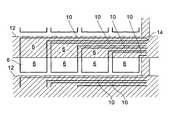
- the Figuresillustrate an apparatus 2 comprising: an array 4 of capacitive sensor electrodes 6 comprising a plurality of distinct capacitive sensor electrodes 6 distributed over a sensing area 8 ; conductive traces 10 connected to respective ones of the plurality of distinct capacitive sensor electrodes 6 ; and a shield electrode 12 overlying, in the sensing area 8 , conductive traces 10 .
- FIG. 1illustrates an apparatus 2 comprising: a sensing arrangement 5 comprising a plurality of capacitive sensor electrodes 6 distributed over a sensing area 8 and conductive traces 10 at least partially distributed over the sensing area 8 ; and a shield electrode 12 partially overlying, in the sensing area 8 , the sensing arrangement 5 .
- the apparatus 2overlies a display 40 and operates as a capacitive touch panel for the display 40 .
- the display 40 and the apparatus 2in combination form a touch sensitive display configured to detect a variation in capacitance arising from proximity of a user input device 32 to one or more of the plurality of sensor electrodes 6 .
- the sensing arrangement 5is configured to sense a variation in capacitance arising from proximity of a user input device 32 at or over the sensing area 8 of a touch surface 7 .
- the user input device 32is a user's finger.
- the apparatus 2is configured to sense not only the (x, y) position of the user's finger within the sensing area 8 when it touches the sensing area 8 of the touch surface 7 but may also, in this example, additionally provide a (z) position of the user's finger when it is close to but not touching the sensing area 8 of the touch surface 7 and/or provide an (x, y) position of the user's finger when it is close to but not yet touching the sensing area of the touch surface 7 .
- the apparatus 2therefore provides for not only two-dimensional sensing but also three-dimensional sensing.
- the apparatus 2may also comprise a further shield electrode 20 underlying, in the sensing area 8 , the conductive traces 10 and the sensor electrodes 6 .
- the further shield electrode 12may be a continuous uninterrupted electrode.
- the shield electrode 12 , the conductive traces 10 , the capacitive sensor electrodes 6 and, if present, the further shield electrode 20are all positioned at least within the sensing area 8 and overlie, in this example, a display 40 . As they overlie a display 40 they are preferably transparent.
- the shield electrode 12 , the conductive traces 10 , the capacitive sensor electrodes 6 and, if present, the further shield electrode 20may therefore be formed from conductive and transparent material. They may be formed from the same or similar material or mixtures of material. Examples of suitable conductive and transparent materials include, for example, Indium-Tin-Oxide (ITO), metal mesh, silver nanowires and carbon nanotube composite.
- ITOIndium-Tin-Oxide
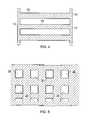
- FIG. 2illustrates one example of a sensing arrangement 5 comprising a plurality of capacitive sensor electrodes 6 distributed over a sensing area 8 and conductive traces 10 partially distributed over the sensing area 8 .
- the plurality of capacitive sensor electrodes 6are arranged as a regular array 4 in this example.
- the capacitive sensor electrodesare arranged as an N row by M column regular array 4 , with common fixed spacing between columns and common fixed spacing between rows.
- Each capacitive sensor electrode 6has an associated conductive trace 10 for conveying a signal generated by that sensor electrode 6 away from the sensor area 8 .
- each sensor electrode 6 and its associated conductive trace 10is physically connected.
- the sensor electrodes 6 and the conductive traces 10may be arranged within a common plane. They may, for example, be formed by patterning a planar layer of transparent conductive material.
- the sensor electrodes 6have different sizes.
- the sensor electrodes 6are larger towards a center region 8 C of the sensing area 8 and smaller towards a perimeter 8 P of the sensing area 8 . This is because the area 14 occupied by the conductive traces 10 becomes increasingly lager as one travels from the center 8 C to the perimeter 8 P.
- the sensor electrodes 6have sizes less than 0.5 cm 2 . They may for example have dimensions of less than 6 mm by 6 mm.
- FIG. 3illustrates a shield electrode 12 overlying, in the sensing area 8 , conductive traces 10 .
- the shield electrode 12in this example but not necessarily all examples, overlies at least portions of at least some of the sensor electrodes 6 .
- the portions of the sensor electrodes 6 that are uncovereddefine operational sensor electrodes 6 of equal operational size, in this example.
- the sensor electrodes 6are of similar construction they have the same capacitance per unit area. Therefore the operational sensor electrodes 6 of equal operational size have equal capacitance.
- the shield electrode 12overlies, in the sensing area 8 , all of the conductive traces 10 .
- the shield electrode 12does not overlie, in the sensing area 8 , all of the conductive traces 10 but instead overlies more than 80% of the area 14 occupied by the conductive traces 10 .
- RCresistance-capacitance
- the shield electrode 12may extends across the whole of the sensing area 8 as a strip 15 .
- a stripmay be associated with each row of capacitive sensor electrodes 6 (as illustrated in FIG. 3 ).
- the shield electrode 12may cover the whole of the sensing area 8 except at openings 18 through the shield electrode 18 to the underlying capacitive sensor electrodes 6 .
- the openings 18are of equal size.
- the openings 18can be of any shape (for example, rectangle (as shown in the attached drawing), round, star etc.).
- the portions of the sensor electrodes 6 that are uncovereddefine operational sensor electrodes 6 of equal operational size. As the sensor electrodes 6 are of similar construction they have the same capacitance per unit area. Therefore the operational sensor electrodes 6 of equal operational size have equal capacitance.
- FIG. 6Aschematically illustrates a cross-section through the sensing arrangement 5 along a line corresponding to an ‘operational’ capacitive sensor electrode. That is the shield electrode 12 along this cross-section does not cover the capacitive sensing electrodes 6 .
- the portion of the shield electrode 12 illustratedis part of the guard portion 13 .
- the portion of the shield electrode 12 illustratedmay be part of a guard portion 13 adjacent a perimeter of the sensing area 8 or a portion between two adjacent openings 18 to adjacent capacitive sensing electrodes 6 .
- FIG. 6Bschematically illustrates a cross-section through the sensing arrangement 5 along a line corresponding to where the shield electrode 12 is present in the sensing area 8 . That is the shield electrode 12 along this cross-section does covers all or some of the conductive traces 10 and, optionally, some of the capacitive sensor electrode 12 .
- the portion of the shield electrode 12 illustratedis part of the strip 15 .
- the portion of the shield electrode 12 illustratedmay be part of portion between two adjacent rows (or columns) of capacitive sensing electrodes 12 .
- the sensor electrodes 6 and the conductive traces 10may be arranged within a common plane 16 . They may, for example, be formed by patterning a planar layer of transparent conductive material.
- the apparatus 2may comprise circuitry as described below, however other circuitry is possible.
- Such circuitrymay be configured to provide a voltage to the shield electrode 12 . If the further shield electrode 20 is present, the same voltage may be provided to the shield electrode 12 and the further shield electrode 20 .
- the provided voltagemay be a fixed voltage or a time-varying voltage.
- One of many examples of a time varying voltageis an alternating sinusoidal voltage.
- the shield electrode 12is operatively connected to a node 22 .
- Operatively connectedmeans that there is a signal path but they may or may not be directly physically connected.
- the node 22is held at a constant potential such as, for example, ground potential.
- Circuitry 24is configured to provide the constant potential. This could be a simple galvanic connection to ground provided by, for example, a housing, a ground plane or a chassis.
- a further shield electrode 20is present. It is also operatively connected to the node 22 .
- Detection circuitry 26is operatively connected between the further shield electrode 20 and the array 4 of capacitive sensor electrodes 6 .
- a multiplexer 28is operatively connected between the detection circuitry 26 and the array 4 of capacitive sensor electrodes 6 .
- the multiplexer 28is configured to isolate, for detection, each of the plurality of capacitive sensor electrodes 6 of the array 4 .
- drive circuitry 30is configured to provide a time-varying voltage to the shield electrode 12 and, if present, the further shield electrode 20 .
- the time-varying voltagemay be, for example, an alternating sinusoidal voltage.
- the drive circuitry 30is thus configured to provide a time varying electric field at each of the sensor electrodes 6 .
- the detection circuitry 26is configured to detect a variation in capacitance arising from proximity of a user input device 32 to one or more of the plurality of sensor electrodes 6 .
- the detection circuitry 26may comprise a low-impedance charge amplifier.
- a capacitive currentflows from the shielding electrode 12 through the detection circuitry 26 to one or more capacitive sensing electrodes 6 .
- the charge amplifier in the detection circuitry 26registers a charge displacement due to the current.
- the output of the charge amplifiermay be rectified, for example synchronously rectified, and integrated, after which it is passed to an analog-to-digital converter and then provided as digital output 27 for processing in the digital domain.
- the drive voltage and the drive frequencytypically range from 1 V to 10 V and from 10 to 200 kHz, respectively.
- a single charge amplifier and a single analog-to-digital convertermay be used in the detection circuitry 26 for multiple capacitive sensing electrodes 6 and a multiplexer 28 may be used to isolate for sensing each capacitive sensing electrode 6 separately.
- FIG. 7Aillustrates a touch panel module 34 that comprise the apparatus 2 .
- the touch panel modulemay be used in combination with a display to form a touch screen display.
- FIG. 7Billustrates a touch sensitive display module 36 that comprises the apparatus 2 and a display 40 .
- FIG. 7Cillustrates an electronic device 38 that comprises at least the apparatus 2 . It may, for example, additionally comprise a processor 39 that processes the output 27 of the detection circuitry 26 .
- modulerefers to a unit or apparatus that excludes certain parts/components that would be added by an end manufacturer or a user.
Landscapes
- Engineering & Computer Science (AREA)
- General Engineering & Computer Science (AREA)
- Theoretical Computer Science (AREA)
- Human Computer Interaction (AREA)
- Physics & Mathematics (AREA)
- General Physics & Mathematics (AREA)
- Position Input By Displaying (AREA)
Abstract
Description
Claims (16)
Priority Applications (6)
| Application Number | Priority Date | Filing Date | Title |
|---|---|---|---|
| US13/677,399US9411474B2 (en) | 2012-11-15 | 2012-11-15 | Shield electrode overlying portions of capacitive sensor electrodes |
| EP13854578.5AEP2920677B1 (en) | 2012-11-15 | 2013-09-23 | A shield for capacitive touch sensors |
| KR1020157015799AKR101724978B1 (en) | 2012-11-15 | 2013-09-23 | A shield for capacitive touch sensors |
| PCT/FI2013/050914WO2014076363A1 (en) | 2012-11-15 | 2013-09-23 | A shield for capacitive touch sensors |
| CN201380059581.XACN104781772B (en) | 2012-11-15 | 2013-09-23 | Shielding for capacitive touch screen |
| TW102141444ATWI545486B (en) | 2012-11-15 | 2013-11-14 | Touch sensing apparatus |
Applications Claiming Priority (1)
| Application Number | Priority Date | Filing Date | Title |
|---|---|---|---|
| US13/677,399US9411474B2 (en) | 2012-11-15 | 2012-11-15 | Shield electrode overlying portions of capacitive sensor electrodes |
Publications (2)
| Publication Number | Publication Date |
|---|---|
| US20140132335A1 US20140132335A1 (en) | 2014-05-15 |
| US9411474B2true US9411474B2 (en) | 2016-08-09 |
Family
ID=50681142
Family Applications (1)
| Application Number | Title | Priority Date | Filing Date |
|---|---|---|---|
| US13/677,399Expired - Fee RelatedUS9411474B2 (en) | 2012-11-15 | 2012-11-15 | Shield electrode overlying portions of capacitive sensor electrodes |
Country Status (6)
| Country | Link |
|---|---|
| US (1) | US9411474B2 (en) |
| EP (1) | EP2920677B1 (en) |
| KR (1) | KR101724978B1 (en) |
| CN (1) | CN104781772B (en) |
| TW (1) | TWI545486B (en) |
| WO (1) | WO2014076363A1 (en) |
Cited By (4)
| Publication number | Priority date | Publication date | Assignee | Title |
|---|---|---|---|---|
| US10622996B1 (en) | 2019-03-29 | 2020-04-14 | Industrial Technology Research Institute | Adjustable sensing capacitance microelectromechanical system (MEMS) apparatus |
| US10824283B2 (en) | 2017-08-04 | 2020-11-03 | Samsung Electronics Co., Ltd. | Fingerprint recognizable touch screen apparatus and method of operating the same |
| US11543297B2 (en) | 2019-07-19 | 2023-01-03 | Industrial Technology Research Institute | Sensing devices |
| US12235684B2 (en) | 2021-07-02 | 2025-02-25 | Samsung Electronics Co., Ltd. | Shielding member and electronic device including the same |
Families Citing this family (38)
| Publication number | Priority date | Publication date | Assignee | Title |
|---|---|---|---|---|
| US8381135B2 (en) | 2004-07-30 | 2013-02-19 | Apple Inc. | Proximity detector in handheld device |
| US7920129B2 (en) | 2007-01-03 | 2011-04-05 | Apple Inc. | Double-sided touch-sensitive panel with shield and drive combined layer |
| FR2949007B1 (en) | 2009-08-07 | 2012-06-08 | Nanotec Solution | DEVICE AND METHOD FOR CONTROL INTERFACE SENSITIVE TO A MOVEMENT OF A BODY OR OBJECT AND CONTROL EQUIPMENT INCORPORATING THIS DEVICE. |
| FR2971066B1 (en) | 2011-01-31 | 2013-08-23 | Nanotec Solution | THREE-DIMENSIONAL MAN-MACHINE INTERFACE. |
| FR2976688B1 (en) | 2011-06-16 | 2021-04-23 | Nanotec Solution | DEVICE AND METHOD FOR GENERATING AN ELECTRICAL POWER SUPPLY IN AN ELECTRONIC SYSTEM WITH A VARIABLE REFERENCE POTENTIAL. |
| US9259904B2 (en) | 2011-10-20 | 2016-02-16 | Apple Inc. | Opaque thin film passivation |
| FR2985048B1 (en) | 2011-12-21 | 2014-08-15 | Nanotec Solution | PRESSURE-SENSITIVE CAPACITIVE MEASUREMENT DEVICE AND METHOD FOR TOUCH-FREE CONTACT INTERFACES |
| FR2985049B1 (en) | 2011-12-22 | 2014-01-31 | Nanotec Solution | CAPACITIVE MEASURING DEVICE WITH SWITCHED ELECTRODES FOR TOUCHLESS CONTACTLESS INTERFACES |
| FR2988176B1 (en) | 2012-03-13 | 2014-11-21 | Nanotec Solution | CAPACITIVE MEASUREMENT METHOD BETWEEN AN OBJECT AND AN ELECTRODE PLAN BY PARTIAL SYNCHRONOUS DEMODULATION |
| FR2988175B1 (en) | 2012-03-13 | 2014-04-11 | Nanotec Solution | METHOD FOR CAPACITIVE MEASUREMENT BY NON-REGULAR ELECTRODES, AND APPARATUS IMPLEMENTING SAID METHOD |
| TWI466003B (en)* | 2012-12-26 | 2014-12-21 | Hannstouch Solution Inc | Touch panel |
| KR102023436B1 (en)* | 2013-01-30 | 2019-09-20 | 엘지디스플레이 주식회사 | Apparatus for display including touch electrode |
| FR3002052B1 (en) | 2013-02-14 | 2016-12-09 | Fogale Nanotech | METHOD AND DEVICE FOR NAVIGATING A DISPLAY SCREEN AND APPARATUS COMPRISING SUCH A NAVIGATION |
| FR3003964B1 (en) | 2013-04-02 | 2016-08-26 | Fogale Nanotech | DEVICE FOR INTERACTING, WITHOUT CONTACT, AN ELECTRONIC AND / OR COMPUTER APPARATUS, AND APPARATUS PROVIDED WITH SUCH A DEVICE |
| FR3004551A1 (en) | 2013-04-15 | 2014-10-17 | Fogale Nanotech | MULTIZONE CAPACITIVE DETECTION METHOD, DEVICE AND APPARATUS USING THE METHOD |
| FR3005763B1 (en) | 2013-05-17 | 2016-10-14 | Fogale Nanotech | DEVICE AND METHOD FOR A CAPACITIVE CONTROL INTERFACE ADAPTED TO THE IMPLEMENTATION OF ELECTRODES OF HIGHLY RESISTIVE MEASUREMENTS |
| GB2518627A (en)* | 2013-09-25 | 2015-04-01 | Nokia Technologies Oy | An apparatus |
| FR3013472B1 (en) | 2013-11-19 | 2016-07-08 | Fogale Nanotech | COVERING ACCESSORY DEVICE FOR AN ELECTRONIC AND / OR COMPUTER PORTABLE APPARATUS, AND APPARATUS EQUIPPED WITH SUCH AN ACCESSORY DEVICE |
| FR3017723B1 (en) | 2014-02-19 | 2017-07-21 | Fogale Nanotech | METHOD OF MAN-MACHINE INTERACTION BY COMBINING TOUCH-FREE AND CONTACTLESS CONTROLS |
| FR3019320B1 (en) | 2014-03-28 | 2017-12-15 | Fogale Nanotech | BRACKET WATCH-TYPE ELECTRONIC DEVICE WITH CONTACTLESS CONTROL INTERFACE AND METHOD FOR CONTROLLING SUCH A DEVICE |
| WO2015200671A1 (en)* | 2014-06-26 | 2015-12-30 | Microchip Technology Incorporated | Compensation of a target object's coupling to feeding lines in capacitive sensing system |
| FR3025623B1 (en) | 2014-09-05 | 2017-12-15 | Fogale Nanotech | CONTROL INTERFACE DEVICE AND FINGERPRINT SENSOR |
| FR3028061B1 (en) | 2014-10-29 | 2016-12-30 | Fogale Nanotech | CAPACITIVE SENSOR DEVICE COMPRISING ADJUSTED ELECTRODES |
| KR101637422B1 (en)* | 2014-12-10 | 2016-07-08 | 주식회사 지2터치 | Touch screen panel |
| KR102320639B1 (en)* | 2015-02-04 | 2021-11-02 | 삼성디스플레이 주식회사 | Touch screen pannel and manufacturing method thereof |
| FR3032287B1 (en) | 2015-02-04 | 2018-03-09 | Quickstep Technologies Llc | MULTILAYER CAPACITIVE DETECTION DEVICE, AND APPARATUS COMPRISING THE DEVICE |
| FR3033203B1 (en) | 2015-02-27 | 2018-03-23 | Quickstep Technologies Llc | METHOD FOR INTERACTING WITH AN ELECTRONIC AND / OR COMPUTER APPARATUS IMPLEMENTING A CAPACITIVE CONTROL SURFACE AND A PERIPHERAL SURFACE, INTERFACE AND APPARATUS IMPLEMENTING SAID METHOD |
| KR102335116B1 (en)* | 2015-04-13 | 2021-12-03 | 삼성디스플레이 주식회사 | Touch screen pannel and manufacturing method thereof |
| US10186437B2 (en)* | 2015-10-05 | 2019-01-22 | Lam Research Corporation | Substrate holder having integrated temperature measurement electrical devices |
| CN114527893B (en) | 2016-09-23 | 2023-11-10 | 苹果公司 | Touch sensor panel with top shield and/or bottom shield |
| US10372282B2 (en) | 2016-12-01 | 2019-08-06 | Apple Inc. | Capacitive coupling reduction in touch sensor panels |
| US10521049B2 (en)* | 2017-09-29 | 2019-12-31 | Apple Inc. | Multi-via structures for touchscreens |
| KR102397356B1 (en)* | 2021-03-10 | 2022-05-12 | 이성호 | Detectors consisting of multiple different areas and object detection devices using them |
| CN113050840B (en)* | 2021-03-31 | 2024-05-17 | 京东方科技集团股份有限公司 | Touch substrate, touch module and display device |
| US12260045B2 (en) | 2021-09-24 | 2025-03-25 | Apple Inc. | Architecture for differential drive and sense for touch sensor panel |
| US11789561B2 (en) | 2021-09-24 | 2023-10-17 | Apple Inc. | Architecture for differential drive and sense touch technology |
| US12197679B2 (en) | 2022-05-06 | 2025-01-14 | Apple Inc. | Touch screen shield layer with ring and tapping points |
| JP2024169010A (en)* | 2023-05-25 | 2024-12-05 | 株式会社ジャパンディスプレイ | Sensor module, and sensor device and display device including the sensor module |
Citations (20)
| Publication number | Priority date | Publication date | Assignee | Title |
|---|---|---|---|---|
| US20030156098A1 (en) | 1999-11-04 | 2003-08-21 | Synaptics, Inc. | Capacitive mouse |
| WO2008104406A2 (en) | 2007-03-01 | 2008-09-04 | Ident Technology Ag | Electrode arrangement for generating a signal indicating the presence of an object within an observation range |
| US20080238881A1 (en) | 2007-03-27 | 2008-10-02 | N-Trig Ltd. | Shield for a digitizer sensor |
| JP2009169720A (en) | 2008-01-17 | 2009-07-30 | Smk Corp | Touch sensor |
| US20090273570A1 (en) | 2008-04-30 | 2009-11-05 | Apple Inc. | Multi-touch sensor patterns and stack-ups |
| EP2141573A2 (en) | 2008-07-03 | 2010-01-06 | Apple Inc. | Display with dual-function capacitive elements |
| US20100194699A1 (en) | 2009-02-02 | 2010-08-05 | Shih Chang Chang | Integrated Touch Screen |
| US20100201647A1 (en)* | 2009-02-11 | 2010-08-12 | Tpo Displays Corp. | Capacitive touch sensor |
| US20100220071A1 (en) | 2009-02-20 | 2010-09-02 | Kiyoshi Nishihara | Touch panel and display device including the same |
| US20110007021A1 (en)* | 2009-07-10 | 2011-01-13 | Jeffrey Traer Bernstein | Touch and hover sensing |
| EP2354901A1 (en) | 2009-06-04 | 2011-08-10 | Inferpoint Systems Limited | Tactile and touch control system |
| US20110279409A1 (en) | 2010-05-14 | 2011-11-17 | Salaverry Ricardo R | System and Method for Detecting Locations of Touches on a Touch Sensor |
| US20110279383A1 (en) | 2010-05-14 | 2011-11-17 | Wilson Stephen S | Touch Screen Shield |
| US20110285661A1 (en) | 2010-05-18 | 2011-11-24 | Steven Porter Hotelling | Periphery Conductive Element for Touch Screen |
| US20110310037A1 (en) | 2009-02-26 | 2011-12-22 | Moran Cristin E | Touch screen sensor and patterned substrate having overlaid micropatterns with low visibility |
| US20120044199A1 (en)* | 2010-08-23 | 2012-02-23 | Cypress Semiconductor Corporation | Capacitance Scanning Proximity Detection |
| US20120081328A1 (en) | 2009-06-24 | 2012-04-05 | Thomas Kandziora | Electrode arrangement for display device |
| US20120299868A1 (en)* | 2011-05-25 | 2012-11-29 | Broadcom Corporation | High Noise Immunity and High Spatial Resolution Mutual Capacitive Touch Panel |
| US20130033450A1 (en)* | 2011-08-01 | 2013-02-07 | Sharp Kabushiki Kaisha | Dual mode capacitive touch panel |
| US20130181949A1 (en)* | 2012-01-17 | 2013-07-18 | Apple Inc. | Finger sensor having pixel sensing circuitry for coupling electrodes and pixel sensing traces and related methods |
Family Cites Families (4)
| Publication number | Priority date | Publication date | Assignee | Title |
|---|---|---|---|---|
| US7663607B2 (en)* | 2004-05-06 | 2010-02-16 | Apple Inc. | Multipoint touchscreen |
| NO315017B1 (en)* | 2000-06-09 | 2003-06-23 | Idex Asa | Sensor chip, especially for measuring structures in a finger surface |
| US8054296B2 (en)* | 2007-01-03 | 2011-11-08 | Apple Inc. | Storing baseline information in EEPROM |
| US8217913B2 (en)* | 2009-02-02 | 2012-07-10 | Apple Inc. | Integrated touch screen |
- 2012
- 2012-11-15USUS13/677,399patent/US9411474B2/ennot_activeExpired - Fee Related
- 2013
- 2013-09-23EPEP13854578.5Apatent/EP2920677B1/enactiveActive
- 2013-09-23KRKR1020157015799Apatent/KR101724978B1/ennot_activeExpired - Fee Related
- 2013-09-23CNCN201380059581.XApatent/CN104781772B/ennot_activeExpired - Fee Related
- 2013-09-23WOPCT/FI2013/050914patent/WO2014076363A1/enactiveApplication Filing
- 2013-11-14TWTW102141444Apatent/TWI545486B/ennot_activeIP Right Cessation
Patent Citations (20)
| Publication number | Priority date | Publication date | Assignee | Title |
|---|---|---|---|---|
| US20030156098A1 (en) | 1999-11-04 | 2003-08-21 | Synaptics, Inc. | Capacitive mouse |
| WO2008104406A2 (en) | 2007-03-01 | 2008-09-04 | Ident Technology Ag | Electrode arrangement for generating a signal indicating the presence of an object within an observation range |
| US20080238881A1 (en) | 2007-03-27 | 2008-10-02 | N-Trig Ltd. | Shield for a digitizer sensor |
| JP2009169720A (en) | 2008-01-17 | 2009-07-30 | Smk Corp | Touch sensor |
| US20090273570A1 (en) | 2008-04-30 | 2009-11-05 | Apple Inc. | Multi-touch sensor patterns and stack-ups |
| EP2141573A2 (en) | 2008-07-03 | 2010-01-06 | Apple Inc. | Display with dual-function capacitive elements |
| US20100194699A1 (en) | 2009-02-02 | 2010-08-05 | Shih Chang Chang | Integrated Touch Screen |
| US20100201647A1 (en)* | 2009-02-11 | 2010-08-12 | Tpo Displays Corp. | Capacitive touch sensor |
| US20100220071A1 (en) | 2009-02-20 | 2010-09-02 | Kiyoshi Nishihara | Touch panel and display device including the same |
| US20110310037A1 (en) | 2009-02-26 | 2011-12-22 | Moran Cristin E | Touch screen sensor and patterned substrate having overlaid micropatterns with low visibility |
| EP2354901A1 (en) | 2009-06-04 | 2011-08-10 | Inferpoint Systems Limited | Tactile and touch control system |
| US20120081328A1 (en) | 2009-06-24 | 2012-04-05 | Thomas Kandziora | Electrode arrangement for display device |
| US20110007021A1 (en)* | 2009-07-10 | 2011-01-13 | Jeffrey Traer Bernstein | Touch and hover sensing |
| US20110279409A1 (en) | 2010-05-14 | 2011-11-17 | Salaverry Ricardo R | System and Method for Detecting Locations of Touches on a Touch Sensor |
| US20110279383A1 (en) | 2010-05-14 | 2011-11-17 | Wilson Stephen S | Touch Screen Shield |
| US20110285661A1 (en) | 2010-05-18 | 2011-11-24 | Steven Porter Hotelling | Periphery Conductive Element for Touch Screen |
| US20120044199A1 (en)* | 2010-08-23 | 2012-02-23 | Cypress Semiconductor Corporation | Capacitance Scanning Proximity Detection |
| US20120299868A1 (en)* | 2011-05-25 | 2012-11-29 | Broadcom Corporation | High Noise Immunity and High Spatial Resolution Mutual Capacitive Touch Panel |
| US20130033450A1 (en)* | 2011-08-01 | 2013-02-07 | Sharp Kabushiki Kaisha | Dual mode capacitive touch panel |
| US20130181949A1 (en)* | 2012-01-17 | 2013-07-18 | Apple Inc. | Finger sensor having pixel sensing circuitry for coupling electrodes and pixel sensing traces and related methods |
Cited By (4)
| Publication number | Priority date | Publication date | Assignee | Title |
|---|---|---|---|---|
| US10824283B2 (en) | 2017-08-04 | 2020-11-03 | Samsung Electronics Co., Ltd. | Fingerprint recognizable touch screen apparatus and method of operating the same |
| US10622996B1 (en) | 2019-03-29 | 2020-04-14 | Industrial Technology Research Institute | Adjustable sensing capacitance microelectromechanical system (MEMS) apparatus |
| US11543297B2 (en) | 2019-07-19 | 2023-01-03 | Industrial Technology Research Institute | Sensing devices |
| US12235684B2 (en) | 2021-07-02 | 2025-02-25 | Samsung Electronics Co., Ltd. | Shielding member and electronic device including the same |
Also Published As
| Publication number | Publication date |
|---|---|
| CN104781772A (en) | 2015-07-15 |
| TWI545486B (en) | 2016-08-11 |
| US20140132335A1 (en) | 2014-05-15 |
| TW201419111A (en) | 2014-05-16 |
| EP2920677B1 (en) | 2019-10-23 |
| KR20150085041A (en) | 2015-07-22 |
| CN104781772B (en) | 2017-07-14 |
| WO2014076363A1 (en) | 2014-05-22 |
| EP2920677A1 (en) | 2015-09-23 |
| KR101724978B1 (en) | 2017-04-07 |
| EP2920677A4 (en) | 2016-06-15 |
Similar Documents
| Publication | Publication Date | Title |
|---|---|---|
| US9411474B2 (en) | Shield electrode overlying portions of capacitive sensor electrodes | |
| EP2951636B1 (en) | Capacitive sensor integrated in a display device | |
| CN114527893B (en) | Touch sensor panel with top shield and/or bottom shield | |
| US8829926B2 (en) | Transparent proximity sensor | |
| CN111095174A (en) | Self-capacitance and mutual-capacitance hybrid touch sensor panel architecture | |
| EP2920676B1 (en) | A capacitive sensing apparatus comprising an active touch sensitive matrix and shield electrodes | |
| US9110551B2 (en) | Capacitive sensor electrodes | |
| US20160209962A1 (en) | Adjustable Shield Electrode Arrangement for Capacitive Touch Sensor Array | |
| JP6133732B2 (en) | Input device and detection method thereof | |
| US20140043278A1 (en) | Electrode configuration for large touch screen | |
| EP2994816B1 (en) | Touch sensor array and method therefor | |
| US9417742B2 (en) | Touch sensitive display | |
| US10042492B2 (en) | Apparatus and/or method |
Legal Events
| Date | Code | Title | Description |
|---|---|---|---|
| AS | Assignment | Owner name:NOKIA CORPORATION, FINLAND Free format text:ASSIGNMENT OF ASSIGNORS INTEREST;ASSIGNORS:RAUHALA, JYRI KALERVO;TURUNEN, SEPPO TAPIO;SIGNING DATES FROM 20121123 TO 20121127;REEL/FRAME:029666/0425 | |
| AS | Assignment | Owner name:NOKIA TECHNOLOGIES OY, FINLAND Free format text:ASSIGNMENT OF ASSIGNORS INTEREST;ASSIGNOR:NOKIA CORPORATION;REEL/FRAME:034781/0200 Effective date:20150116 | |
| ZAAA | Notice of allowance and fees due | Free format text:ORIGINAL CODE: NOA | |
| ZAAB | Notice of allowance mailed | Free format text:ORIGINAL CODE: MN/=. | |
| STCF | Information on status: patent grant | Free format text:PATENTED CASE | |
| MAFP | Maintenance fee payment | Free format text:PAYMENT OF MAINTENANCE FEE, 4TH YEAR, LARGE ENTITY (ORIGINAL EVENT CODE: M1551); ENTITY STATUS OF PATENT OWNER: LARGE ENTITY Year of fee payment:4 | |
| FEPP | Fee payment procedure | Free format text:MAINTENANCE FEE REMINDER MAILED (ORIGINAL EVENT CODE: REM.); ENTITY STATUS OF PATENT OWNER: LARGE ENTITY | |
| LAPS | Lapse for failure to pay maintenance fees | Free format text:PATENT EXPIRED FOR FAILURE TO PAY MAINTENANCE FEES (ORIGINAL EVENT CODE: EXP.); ENTITY STATUS OF PATENT OWNER: LARGE ENTITY | |
| STCH | Information on status: patent discontinuation | Free format text:PATENT EXPIRED DUE TO NONPAYMENT OF MAINTENANCE FEES UNDER 37 CFR 1.362 | |
| FP | Lapsed due to failure to pay maintenance fee | Effective date:20240809 |