US9410799B2 - Device package and methods for the fabrication and testing thereof - Google Patents
Device package and methods for the fabrication and testing thereofDownload PDFInfo
- Publication number
- US9410799B2 US9410799B2US14/657,131US201514657131AUS9410799B2US 9410799 B2US9410799 B2US 9410799B2US 201514657131 AUS201514657131 AUS 201514657131AUS 9410799 B2US9410799 B2US 9410799B2
- Authority
- US
- United States
- Prior art keywords
- lid
- optical
- wafer
- layer
- optoelectronic device
- Prior art date
- Legal status (The legal status is an assumption and is not a legal conclusion. Google has not performed a legal analysis and makes no representation as to the accuracy of the status listed.)
- Expired - Fee Related
Links
Images


Classifications
- G—PHYSICS
- G01—MEASURING; TESTING
- G01B—MEASURING LENGTH, THICKNESS OR SIMILAR LINEAR DIMENSIONS; MEASURING ANGLES; MEASURING AREAS; MEASURING IRREGULARITIES OF SURFACES OR CONTOURS
- G01B11/00—Measuring arrangements characterised by the use of optical techniques
- G01B11/16—Measuring arrangements characterised by the use of optical techniques for measuring the deformation in a solid, e.g. optical strain gauge
- H—ELECTRICITY
- H01—ELECTRIC ELEMENTS
- H01L—SEMICONDUCTOR DEVICES NOT COVERED BY CLASS H10
- H01L22/00—Testing or measuring during manufacture or treatment; Reliability measurements, i.e. testing of parts without further processing to modify the parts as such; Structural arrangements therefor
- G—PHYSICS
- G01—MEASURING; TESTING
- G01B—MEASURING LENGTH, THICKNESS OR SIMILAR LINEAR DIMENSIONS; MEASURING ANGLES; MEASURING AREAS; MEASURING IRREGULARITIES OF SURFACES OR CONTOURS
- G01B11/00—Measuring arrangements characterised by the use of optical techniques
- G01B11/26—Measuring arrangements characterised by the use of optical techniques for measuring angles or tapers; for testing the alignment of axes
- G—PHYSICS
- G02—OPTICS
- G02B—OPTICAL ELEMENTS, SYSTEMS OR APPARATUS
- G02B6/00—Light guides; Structural details of arrangements comprising light guides and other optical elements, e.g. couplings
- G02B6/24—Coupling light guides
- G02B6/36—Mechanical coupling means
- G02B6/3628—Mechanical coupling means for mounting fibres to supporting carriers
- G02B6/3684—Mechanical coupling means for mounting fibres to supporting carriers characterised by the manufacturing process of surface profiling of the supporting carrier
- G02B6/3692—Mechanical coupling means for mounting fibres to supporting carriers characterised by the manufacturing process of surface profiling of the supporting carrier with surface micromachining involving etching, e.g. wet or dry etching steps
- G—PHYSICS
- G02—OPTICS
- G02B—OPTICAL ELEMENTS, SYSTEMS OR APPARATUS
- G02B6/00—Light guides; Structural details of arrangements comprising light guides and other optical elements, e.g. couplings
- G02B6/24—Coupling light guides
- G02B6/42—Coupling light guides with opto-electronic elements
- G02B6/4201—Packages, e.g. shape, construction, internal or external details
- G02B6/4204—Packages, e.g. shape, construction, internal or external details the coupling comprising intermediate optical elements, e.g. lenses, holograms
- G02B6/4206—Optical features
- G—PHYSICS
- G02—OPTICS
- G02B—OPTICAL ELEMENTS, SYSTEMS OR APPARATUS
- G02B6/00—Light guides; Structural details of arrangements comprising light guides and other optical elements, e.g. couplings
- G02B6/24—Coupling light guides
- G02B6/42—Coupling light guides with opto-electronic elements
- G02B6/4201—Packages, e.g. shape, construction, internal or external details
- G02B6/4204—Packages, e.g. shape, construction, internal or external details the coupling comprising intermediate optical elements, e.g. lenses, holograms
- G02B6/421—Packages, e.g. shape, construction, internal or external details the coupling comprising intermediate optical elements, e.g. lenses, holograms the intermediate optical component consisting of a short length of fibre, e.g. fibre stub
- G—PHYSICS
- G02—OPTICS
- G02B—OPTICAL ELEMENTS, SYSTEMS OR APPARATUS
- G02B6/00—Light guides; Structural details of arrangements comprising light guides and other optical elements, e.g. couplings
- G02B6/24—Coupling light guides
- G02B6/42—Coupling light guides with opto-electronic elements
- G02B6/4201—Packages, e.g. shape, construction, internal or external details
- G02B6/4204—Packages, e.g. shape, construction, internal or external details the coupling comprising intermediate optical elements, e.g. lenses, holograms
- G02B6/4214—Packages, e.g. shape, construction, internal or external details the coupling comprising intermediate optical elements, e.g. lenses, holograms the intermediate optical element having redirecting reflective means, e.g. mirrors, prisms for deflecting the radiation from horizontal to down- or upward direction toward a device
- G—PHYSICS
- G02—OPTICS
- G02B—OPTICAL ELEMENTS, SYSTEMS OR APPARATUS
- G02B6/00—Light guides; Structural details of arrangements comprising light guides and other optical elements, e.g. couplings
- G02B6/24—Coupling light guides
- G02B6/42—Coupling light guides with opto-electronic elements
- G02B6/4201—Packages, e.g. shape, construction, internal or external details
- G02B6/4219—Mechanical fixtures for holding or positioning the elements relative to each other in the couplings; Alignment methods for the elements, e.g. measuring or observing methods especially used therefor
- G02B6/4228—Passive alignment, i.e. without a detection of the degree of coupling or the position of the elements
- G02B6/423—Passive alignment, i.e. without a detection of the degree of coupling or the position of the elements using guiding surfaces for the alignment
- G—PHYSICS
- G02—OPTICS
- G02B—OPTICAL ELEMENTS, SYSTEMS OR APPARATUS
- G02B6/00—Light guides; Structural details of arrangements comprising light guides and other optical elements, e.g. couplings
- G02B6/24—Coupling light guides
- G02B6/42—Coupling light guides with opto-electronic elements
- G02B6/4201—Packages, e.g. shape, construction, internal or external details
- G02B6/4219—Mechanical fixtures for holding or positioning the elements relative to each other in the couplings; Alignment methods for the elements, e.g. measuring or observing methods especially used therefor
- G02B6/4236—Fixing or mounting methods of the aligned elements
- G02B6/4239—Adhesive bonding; Encapsulation with polymer material
- G—PHYSICS
- G02—OPTICS
- G02B—OPTICAL ELEMENTS, SYSTEMS OR APPARATUS
- G02B6/00—Light guides; Structural details of arrangements comprising light guides and other optical elements, e.g. couplings
- G02B6/24—Coupling light guides
- G02B6/42—Coupling light guides with opto-electronic elements
- G02B6/4201—Packages, e.g. shape, construction, internal or external details
- G02B6/4219—Mechanical fixtures for holding or positioning the elements relative to each other in the couplings; Alignment methods for the elements, e.g. measuring or observing methods especially used therefor
- G02B6/4236—Fixing or mounting methods of the aligned elements
- G02B6/424—Mounting of the optical light guide
- G02B6/4243—Mounting of the optical light guide into a groove
- G—PHYSICS
- G02—OPTICS
- G02B—OPTICAL ELEMENTS, SYSTEMS OR APPARATUS
- G02B6/00—Light guides; Structural details of arrangements comprising light guides and other optical elements, e.g. couplings
- G02B6/24—Coupling light guides
- G02B6/42—Coupling light guides with opto-electronic elements
- G02B6/4201—Packages, e.g. shape, construction, internal or external details
- G02B6/4219—Mechanical fixtures for holding or positioning the elements relative to each other in the couplings; Alignment methods for the elements, e.g. measuring or observing methods especially used therefor
- G02B6/4236—Fixing or mounting methods of the aligned elements
- G02B6/4244—Mounting of the optical elements
- G—PHYSICS
- G02—OPTICS
- G02B—OPTICAL ELEMENTS, SYSTEMS OR APPARATUS
- G02B6/00—Light guides; Structural details of arrangements comprising light guides and other optical elements, e.g. couplings
- G02B6/24—Coupling light guides
- G02B6/42—Coupling light guides with opto-electronic elements
- G02B6/4201—Packages, e.g. shape, construction, internal or external details
- G02B6/4248—Feed-through connections for the hermetical passage of fibres through a package wall
- G—PHYSICS
- G02—OPTICS
- G02B—OPTICAL ELEMENTS, SYSTEMS OR APPARATUS
- G02B6/00—Light guides; Structural details of arrangements comprising light guides and other optical elements, e.g. couplings
- G02B6/24—Coupling light guides
- G02B6/42—Coupling light guides with opto-electronic elements
- G02B6/4201—Packages, e.g. shape, construction, internal or external details
- G02B6/4256—Details of housings
- G02B6/4257—Details of housings having a supporting carrier or a mounting substrate or a mounting plate
- G—PHYSICS
- G02—OPTICS
- G02B—OPTICAL ELEMENTS, SYSTEMS OR APPARATUS
- G02B6/00—Light guides; Structural details of arrangements comprising light guides and other optical elements, e.g. couplings
- G02B6/24—Coupling light guides
- G02B6/42—Coupling light guides with opto-electronic elements
- G02B6/4201—Packages, e.g. shape, construction, internal or external details
- G02B6/4266—Thermal aspects, temperature control or temperature monitoring
- G02B6/4268—Cooling
- G02B6/4271—Cooling with thermo electric cooling
- G—PHYSICS
- G02—OPTICS
- G02B—OPTICAL ELEMENTS, SYSTEMS OR APPARATUS
- G02B6/00—Light guides; Structural details of arrangements comprising light guides and other optical elements, e.g. couplings
- G02B6/24—Coupling light guides
- G02B6/42—Coupling light guides with opto-electronic elements
- G02B6/4292—Coupling light guides with opto-electronic elements the light guide being disconnectable from the opto-electronic element, e.g. mutually self aligning arrangements
- H—ELECTRICITY
- H01—ELECTRIC ELEMENTS
- H01L—SEMICONDUCTOR DEVICES NOT COVERED BY CLASS H10
- H01L23/00—Details of semiconductor or other solid state devices
- H01L23/48—Arrangements for conducting electric current to or from the solid state body in operation, e.g. leads, terminal arrangements ; Selection of materials therefor
- H—ELECTRICITY
- H01—ELECTRIC ELEMENTS
- H01S—DEVICES USING THE PROCESS OF LIGHT AMPLIFICATION BY STIMULATED EMISSION OF RADIATION [LASER] TO AMPLIFY OR GENERATE LIGHT; DEVICES USING STIMULATED EMISSION OF ELECTROMAGNETIC RADIATION IN WAVE RANGES OTHER THAN OPTICAL
- H01S5/00—Semiconductor lasers
- H01S5/02—Structural details or components not essential to laser action
- H01S5/022—Mountings; Housings
- H01S5/02218—Material of the housings; Filling of the housings
- H—ELECTRICITY
- H01—ELECTRIC ELEMENTS
- H01S—DEVICES USING THE PROCESS OF LIGHT AMPLIFICATION BY STIMULATED EMISSION OF RADIATION [LASER] TO AMPLIFY OR GENERATE LIGHT; DEVICES USING STIMULATED EMISSION OF ELECTROMAGNETIC RADIATION IN WAVE RANGES OTHER THAN OPTICAL
- H01S5/00—Semiconductor lasers
- H01S5/02—Structural details or components not essential to laser action
- H01S5/022—Mountings; Housings
- H01S5/0225—Out-coupling of light
- H01S5/02251—Out-coupling of light using optical fibres
- H01S5/02252—
- H—ELECTRICITY
- H01—ELECTRIC ELEMENTS
- H01S—DEVICES USING THE PROCESS OF LIGHT AMPLIFICATION BY STIMULATED EMISSION OF RADIATION [LASER] TO AMPLIFY OR GENERATE LIGHT; DEVICES USING STIMULATED EMISSION OF ELECTROMAGNETIC RADIATION IN WAVE RANGES OTHER THAN OPTICAL
- H01S5/00—Semiconductor lasers
- H01S5/02—Structural details or components not essential to laser action
- H01S5/022—Mountings; Housings
- H01S5/0225—Out-coupling of light
- H01S5/02253—Out-coupling of light using lenses
- H—ELECTRICITY
- H01—ELECTRIC ELEMENTS
- H01S—DEVICES USING THE PROCESS OF LIGHT AMPLIFICATION BY STIMULATED EMISSION OF RADIATION [LASER] TO AMPLIFY OR GENERATE LIGHT; DEVICES USING STIMULATED EMISSION OF ELECTROMAGNETIC RADIATION IN WAVE RANGES OTHER THAN OPTICAL
- H01S5/00—Semiconductor lasers
- H01S5/02—Structural details or components not essential to laser action
- H01S5/022—Mountings; Housings
- H01S5/023—Mount members, e.g. sub-mount members
- H01S5/02325—Mechanically integrated components on mount members or optical micro-benches
- H01S5/02326—Arrangements for relative positioning of laser diodes and optical components, e.g. grooves in the mount to fix optical fibres or lenses
- H—ELECTRICITY
- H01—ELECTRIC ELEMENTS
- H01S—DEVICES USING THE PROCESS OF LIGHT AMPLIFICATION BY STIMULATED EMISSION OF RADIATION [LASER] TO AMPLIFY OR GENERATE LIGHT; DEVICES USING STIMULATED EMISSION OF ELECTROMAGNETIC RADIATION IN WAVE RANGES OTHER THAN OPTICAL
- H01S5/00—Semiconductor lasers
- H01S5/02—Structural details or components not essential to laser action
- H01S5/022—Mountings; Housings
- H01S5/0235—Method for mounting laser chips
- H01S5/02355—Fixing laser chips on mounts
- H01S5/0237—Fixing laser chips on mounts by soldering
- H—ELECTRICITY
- H01—ELECTRIC ELEMENTS
- H01L—SEMICONDUCTOR DEVICES NOT COVERED BY CLASS H10
- H01L23/00—Details of semiconductor or other solid state devices
- H01L23/48—Arrangements for conducting electric current to or from the solid state body in operation, e.g. leads, terminal arrangements ; Selection of materials therefor
- H01L23/481—Internal lead connections, e.g. via connections, feedthrough structures
- H—ELECTRICITY
- H01—ELECTRIC ELEMENTS
- H01L—SEMICONDUCTOR DEVICES NOT COVERED BY CLASS H10
- H01L2924/00—Indexing scheme for arrangements or methods for connecting or disconnecting semiconductor or solid-state bodies as covered by H01L24/00
- H—ELECTRICITY
- H01—ELECTRIC ELEMENTS
- H01L—SEMICONDUCTOR DEVICES NOT COVERED BY CLASS H10
- H01L2924/00—Indexing scheme for arrangements or methods for connecting or disconnecting semiconductor or solid-state bodies as covered by H01L24/00
- H01L2924/0001—Technical content checked by a classifier
- H01L2924/00012—Relevant to the scope of the group, the symbol of which is combined with the symbol of this group
- H—ELECTRICITY
- H01—ELECTRIC ELEMENTS
- H01L—SEMICONDUCTOR DEVICES NOT COVERED BY CLASS H10
- H01L2924/00—Indexing scheme for arrangements or methods for connecting or disconnecting semiconductor or solid-state bodies as covered by H01L24/00
- H01L2924/0001—Technical content checked by a classifier
- H01L2924/0002—Not covered by any one of groups H01L24/00, H01L24/00 and H01L2224/00
- H—ELECTRICITY
- H01—ELECTRIC ELEMENTS
- H01S—DEVICES USING THE PROCESS OF LIGHT AMPLIFICATION BY STIMULATED EMISSION OF RADIATION [LASER] TO AMPLIFY OR GENERATE LIGHT; DEVICES USING STIMULATED EMISSION OF ELECTROMAGNETIC RADIATION IN WAVE RANGES OTHER THAN OPTICAL
- H01S5/00—Semiconductor lasers
- H01S5/0014—Measuring characteristics or properties thereof
- H—ELECTRICITY
- H01—ELECTRIC ELEMENTS
- H01S—DEVICES USING THE PROCESS OF LIGHT AMPLIFICATION BY STIMULATED EMISSION OF RADIATION [LASER] TO AMPLIFY OR GENERATE LIGHT; DEVICES USING STIMULATED EMISSION OF ELECTROMAGNETIC RADIATION IN WAVE RANGES OTHER THAN OPTICAL
- H01S5/00—Semiconductor lasers
- H01S5/02—Structural details or components not essential to laser action
- H01S5/022—Mountings; Housings
- H01S5/02208—Mountings; Housings characterised by the shape of the housings
- H01S5/02216—Butterfly-type, i.e. with electrode pins extending horizontally from the housings
- H—ELECTRICITY
- H01—ELECTRIC ELEMENTS
- H01S—DEVICES USING THE PROCESS OF LIGHT AMPLIFICATION BY STIMULATED EMISSION OF RADIATION [LASER] TO AMPLIFY OR GENERATE LIGHT; DEVICES USING STIMULATED EMISSION OF ELECTROMAGNETIC RADIATION IN WAVE RANGES OTHER THAN OPTICAL
- H01S5/00—Semiconductor lasers
- H01S5/02—Structural details or components not essential to laser action
- H01S5/022—Mountings; Housings
- H01S5/02218—Material of the housings; Filling of the housings
- H01S5/0222—Gas-filled housings
- H01S5/02284—
- H—ELECTRICITY
- H01—ELECTRIC ELEMENTS
- H01S—DEVICES USING THE PROCESS OF LIGHT AMPLIFICATION BY STIMULATED EMISSION OF RADIATION [LASER] TO AMPLIFY OR GENERATE LIGHT; DEVICES USING STIMULATED EMISSION OF ELECTROMAGNETIC RADIATION IN WAVE RANGES OTHER THAN OPTICAL
- H01S5/00—Semiconductor lasers
- H01S5/02—Structural details or components not essential to laser action
- H01S5/024—Arrangements for thermal management
- H01S5/02407—Active cooling, e.g. the laser temperature is controlled by a thermo-electric cooler or water cooling
- H01S5/02415—Active cooling, e.g. the laser temperature is controlled by a thermo-electric cooler or water cooling by using a thermo-electric cooler [TEC], e.g. Peltier element
- H—ELECTRICITY
- H01—ELECTRIC ELEMENTS
- H01S—DEVICES USING THE PROCESS OF LIGHT AMPLIFICATION BY STIMULATED EMISSION OF RADIATION [LASER] TO AMPLIFY OR GENERATE LIGHT; DEVICES USING STIMULATED EMISSION OF ELECTROMAGNETIC RADIATION IN WAVE RANGES OTHER THAN OPTICAL
- H01S5/00—Semiconductor lasers
- H01S5/02—Structural details or components not essential to laser action
- H01S5/024—Arrangements for thermal management
- H01S5/02469—Passive cooling, e.g. where heat is removed by the housing as a whole or by a heat pipe without any active cooling element like a TEC
- H—ELECTRICITY
- H01—ELECTRIC ELEMENTS
- H01S—DEVICES USING THE PROCESS OF LIGHT AMPLIFICATION BY STIMULATED EMISSION OF RADIATION [LASER] TO AMPLIFY OR GENERATE LIGHT; DEVICES USING STIMULATED EMISSION OF ELECTROMAGNETIC RADIATION IN WAVE RANGES OTHER THAN OPTICAL
- H01S5/00—Semiconductor lasers
- H01S5/06—Arrangements for controlling the laser output parameters, e.g. by operating on the active medium
- H01S5/068—Stabilisation of laser output parameters
- H01S5/0683—Stabilisation of laser output parameters by monitoring the optical output parameters
Definitions
- the present inventionrelates generally to device packages, and in particular but not exclusively to hermetically sealed micro-optical device packages.
- the inventionfurther relates to methods of testing device packages, such as methods of detecting leakage in and methods of electrically and optically testing device packages.
- the inventionstill further relates to sealed via structures, to connectorized optoelectronic devices, and to optoelectronic device package lids. Still further, the invention relates to methods of bonding components together.
- Optoelectronic devicesplay a crucial role in data communications. Yet, to advance the adoption and use of such devices, the ability to manufacture optoelectronic devices efficiently is desirable in reaching the low cost targets demanded. Of particular importance is reducing the cost of the process of packaging optoelectronic devices, since a large portion of the cost of an optoelectronic communications device (up to 75%) is packaging cost. Packaging is typically conducted on a unit-by-unit basis. Techniques which would allow for the manufacture of optoelectronic device packages on a large scale, for example, on a wafer- or grid-level would therefore be beneficial from the cost standpoint.
- Hermetically sealed optoelectronic device packagesare known. Such packages provide for containment and protection of the enclosed devices and components from contamination and water vapor present in the atmosphere outside of the package. Such packages also provide the ability to couple the packaged optoelectronic devices to other optical components, such as optical fibers. These packages typically include an open-top case made of Kovar which includes a cavity region in which a laser is mounted. An optical fiber is provided which extends into the cavity through a feedthrough in the sidewall of the case and a cover is attached to the case to seal the cavity. There are various drawbacks associated with the use of such a fiber feedthrough. For example, where a metallized fiber is used in forming the hermetic seal, the cost can be very high. In addition, it is difficult to effectively seal the fiber in the feedthrough, making the package susceptible to leakage and loss in hermeticity. A hermetic package not relying on a fiber feedthrough would therefore be desirable.
- leakage in device packagestypically result in exposure of the contained components to water vapor and contaminants, causing performance degradation of the components. This is particularly the case for optoelectronic and optical components. A simple technique for testing the hermeticity of the sealed device package would thus be beneficial.
- an optoelectronic device packageincludes a base substrate having an optoelectronic device mounting region on a surface of the base substrate and a lid mounting region.
- An optoelectronic deviceis mounted on the optoelectronic device mounting region.
- a lidis mounted on the lid mounting region to form an enclosed volume between the base substrate and the lid.
- the optoelectronic deviceis in the enclosed volume.
- the lidhas an optically transmissive region suitable for transmitting light of a given wavelength along an optical path to or from the optoelectronic device, wherein at least a portion of the lid mounting region is disposed along the optical path below the surface of the base substrate to a depth below the optical path.
- a wafer- or grid-level optoelectronic device package lidincludes a silicon wafer or grid having a plurality of die, wherein each die has a plurality of sidewalls and a roof connected to the sidewalls to form a cavity.
- One or more sidewallhas an optically transmissive region suitable for transmitting light of a given wavelength along an optical axis through the sidewall.
- a method of forming an optoelectronic device lid on a wafer or grid levelinvolves: providing a silicon wafer or grid having a plurality of die; and etching the wafer or grid to produce a plurality of lid structures each having a plurality of sidewalls and a roof connected to the sidewalls to form a cavity.
- One or more sidewall of each lid structurehas an optically transmissive region suitable for transmitting light of a given wavelength along an optical axis through the sidewall.
- a connectorized optoelectronic deviceincludes a connector having an interior cavity and an optical port, and an optoelectronic device package disposed in the cavity in optical communication with the optical port.
- the optoelectronic device packagemay include a base substrate having an optoelectronic device mounting region and a lid mounting region; an optoelectronic device mounted on the optoelectronic device mounting region; and a lid mounted on the lid mounting region to form an enclosed volume between the base substrate and the lid.
- the lidhas an optically transmissive region suitable for transmitting light of a given wavelength along an optical axis to or from the optoelectronic device.
- a method of forming a sealed via structureincludes: (a) providing a semiconductor substrate having a first surface and a second surface opposite the first surface; (b) forming a layer on the first surface of the substrate; (c) etching a via hole through the substrate from the second surface to the layer, the via hole having a first perimeter at the first surface; (d) forming an aperture in the layer, wherein the aperture has a second perimeter within the first perimeter; and (e) providing a conductive structure for sealing the via structure.
- a method of forming a sealed via structureincludes: (a) providing a semiconductor substrate having a first surface and a second surface opposite the first surface; (b) forming an insulating layer on the first surface of the substrate; (c) etching a via hole through the substrate from the second surface to the insulating layer; (d) forming an aperture in the layer; and (e) providing a metallization structure for sealing the via structure.
- a sealed via structureincludes: a semiconductor substrate having a first surface and a second surface opposite the first surface; a layer on the first surface of the substrate; a via hole through the substrate from the second surface to the layer, the via hole having a first perimeter in the first surface; an aperture in the layer, wherein the aperture has a second perimeter within the first perimeter; and a metallization structure sealing the via structure.
- a sealed via structureincludes: a semiconductor substrate having a first surface and a second surface opposite the first surface; an insulating layer on the first surface of the substrate; a via hole through the substrate from the second surface to the layer; an aperture in the insulating layer; and a metallization structure sealing the via structure.
- a method of detecting leakage in a sealed device packageinvolves: (a) providing a sealed package containing a device, wherein the package is sealed under conditions providing a measurable deflection in a wall of the package, and wherein the extent of deflection is dependent on the pressure inside the package; and (b) measuring the deflection of the wall after sealing the package.
- a sealed device packageincludes: a substrate; a lid including a semiconductor material over the substrate; a sealed volume between the substrate and the lid; and a device in the sealed volume.
- the sealed volumeis at a pressure such that a wall of the lid has a measurable deflection, and wherein the extent of deflection is dependent on the sealed volume pressure.
- a device packageincludes a substrate having a first surface; a device mounted on the first surface of the substrate; a cavity in the substrate; and a cooling structure in the cavity for removing heat generated by the device.
- a device packageincludes: a substrate including a lid mounting region and a device mounting region; a lid on the lid mounting region to form an enclosed volume between the substrate and the lid; a device on the device mounting region in the enclosed volume; and a cooling structure in the cavity.
- a method of bonding a first component to a second componentinvolves:
- FIGS. 1A-1Cschematically illustrate perspective views of an optical microbench in accordance with the present invention at various stages of fabrication
- FIGS. 2A and 2Bschematically illustrate side cross-sectional views of the microbenches of FIGS. 1A and 1C , respectively, taken along the respective sectioning lines 2 A and 2 B;
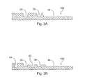
- FIGS. 3A and 3Bschematically illustrate side cross-sectional views of additional configurations of microbenches in accordance with present invention having a different arrangement of recessed areas than those illustrated in FIGS. 1A-C ;
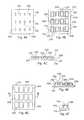
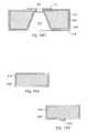
- FIG. 4Aschematically illustrates a top view of a base wafer comprising a plurality of optical microbenches in accordance with the present invention
- FIG. 4Bschematically illustrates a top view (looking into lid cavities) of a wafer comprising a plurality of lids in accordance with the present invention
- FIG. 4Cschematically illustrates a side cross-sectional view of the lid wafer of FIG. 4B sealed onto the base wafer of FIG. 4A with the cross-section taken along one of the rows of microbenches;
- FIG. 4D-Fschematically illustrate top and side cross-sectional views, respectively, of the assembled lid wafer and base wafer of FIG. 4C after the lids have been singulated from the lid wafer;
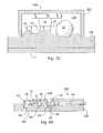
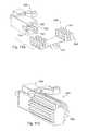
- FIG. 5Aschematically illustrates an exploded view of an exemplary micro-optical device package in accordance with the present invention
- FIG. 5Bschematically illustrates a perspective view of a micro optical device package in accordance with the present invention which is assembled from the components illustrated in FIG. 5A ;
- FIG. 6Aschematically illustrates a side cross-sectional view taken along the optical axis of the micro-optical device package of FIG. 5A ;
- FIG. 6Bschematically illustrates a side cross-sectional view taken along the optical axis of a micro-optical device package similar to that shown in FIG. 6A , but having a single lens that focuses the light emitting region of a laser onto the endface of a fiber;
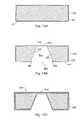
- FIGS. 7A-7Cschematically illustrate side cross-sectional views of micro-optical device packages in accordance with the present invention having various cooling structures
- FIGS. 8A and 8Bschematically illustrate side cross-sectional views of further a micro-optical device packages in accordance with the present invention
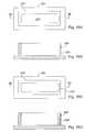
- FIGS. 9A and 9Bschematically illustrate a side cross-sectional view and a top view, respectively, of a micro-optical device package in accordance with the present invention having hermetic vias that extend from the interior of the hermetically sealed cavity to the exterior the package;
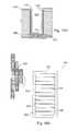
- FIGS. 10A and 10Bschematically illustrate a side cross-sectional view and a perspective view, respectively, of a connector in which a micro-optical device package in accordance with the present invention is housed;
- FIGS. 11A-11Cschematically illustrate perspective views of connectors for housing a micro-optical device package of the present invention along with heat sinks for cooling the micro-optical device package;
- FIGS. 12A and 12Billustrate a flowchart representing a process in accordance with the present invention for fabricating an optical microbench having conductive lead lines
- FIGS. 13A-13Cillustrate a flowchart representing a process in accordance with the present invention for fabricating an optical microbench having conductive hermetically sealed vias
- FIGS. 14A-14Gschematically illustrate a process in accordance with the present invention for fabricating conductive hermetically sealed vias
- FIGS. 15A-15Hschematically illustrate another process in accordance with the present invention for fabricating conductive hermetically sealed vias
- FIGS. 16A-16Dschematically illustrate top views of a process in accordance with the present invention for fabricating cavitated lids on a lid wafer
- FIGS. 17A and 17Bschematically illustrate a top view and a side elevational view, respectively, of another process in accordance with the present invention for fabricating cavitated lids on a lid wafer;
- FIGS. 18A-18Dschematically illustrate a lid having a glassy sidewall portion.
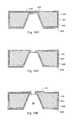
- the micro-optical device package 500has a configuration that facilitates hermetic sealing of a lid 200 to an optical microbench 100 by obviating the need for an optical passthrough opening in the lid 200 .
- the lid 200comprises a sidewall 220 that is sufficiently optically transparent to wavelengths of light to be received by or transmitted from an optoelectronic device 12 , 18 disposed under the lid.
- the term “light”is not limited to the visible spectrum, but includes electromagnetic radiation outside of the visible spectrum.
- a sealing surface 226 of the lid 200may be recessed into the optical microbench 100 so that the clear aperture of the optical system is not clipped by any surfaces of the optical microbench 100 .
- recessed clearance surfaces 50 , 52 , 54can be provided. The use of such clearance surfaces 50 , 52 , 54 and the recessed lid mounting is useful for many micro-optical systems.
- light generating sourcessuch as a laser die which may function as the optoelectronic device 12 , are usually bonded active stripe side down onto the microbench 100 to allow the active stripe to be accurately located with respect to features on the microbench 100 .
- the optical beammay interfere with the lid bond line and the microbench 100 .
- the lidor lid wafer
- the full aperture of a beamcan pass through the lid sidewall 220 and the remainder of the optical system on microbench 100 without unwanted loss of light due to occlusion of the beam. For example, up to half of the light generated by a light source may be lost without the recessed lid 200 . In certain applications, however, it may be acceptable to mount the lid 200 to a non-recessed portion of the microbench 100 .
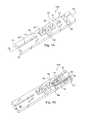
- FIGS. 1A-1C, 2A, and 2Ban exemplary optical microbench 100 for use as a base of a micro-optical device package 500 in accordance with the present invention is illustrated. While the microbench 100 is illustrated in FIGS. 1A-1C as a discrete component, the microbench 100 may be a portion of a base wafer (a grid) 110 or a complete base wafer 110 on which multiple optical microbenches 100 may be provided, as illustrated in FIG. 4A .
- the microbench substrate materialis chosen with regard to the features to be fabricated in the microbench 100 .
- the microbench materialmay comprise thermally conductive micro-molded plastics and slip-cast ceramics which may be replicated from a master micromachined wafer.
- One particularly well suited material for the microbench 100is single crystal silicon, which may be etched by an anisotropic process using established photolithographic techniques to provide for accurate orientation of components on the microbench 100 .
- the microbench 100is described below as comprising a single crystalline material that can be anisotropically etched, though it is understood that other materials and processes capable of achieving the structure of the optical microbench 100 are contemplated by the present invention.
- an exemplary microbench 100that includes an upper surface 70 into which one or more mounting features may be formed.
- the general layout of the mounting features that are to hold optical elementstypically involves an optical model of the interaction of those optical elements.
- first and second pits 20 , 30 , monitor groove 11 , fiber groove 40 , and front and rear lid mounting channels 62 , 64may be provided in the upper surface 70 .
- these featuresmay be anisotropically etched into a (100) silicon substrate.
- To provide precision alignment among pits 20 , 30 , grooves 11 , 40 , and mounting channels 62 , 64such features may be formed during the same masking and etching process.
- the resulting etched structureseach comprise inclined sidewalls that are ⁇ 111 ⁇ crystallographic planes.
- An un-etched portion of the upper surface 70provides a device mounting region 10 onto which one or more optoelectronic, electronic, mechanical (e.g., MEMS) or optomechanical devices may be mounted, bonded, and electrically interconnected.
- two lenses 22 , 32may be used, the first lens 22 to semi-collimate the beam, allowing the beam to pass through the transparent lid 200 and the optional isolator, and the second lens 32 to couple the light into the optical fiber 42 , as seen in FIGS. 5A, 5B, and 6A .
- the optical pathWhile the device is being described such that the optical path is in a direction away from the optoelectronic device 12 , it should be clear that the optical path may be in the reverse direction where the optoelectronic device receives the light.
- the spacing of the optical elements, and the corresponding mounting features used for their mechanical alignmentshould account for any encapsulants, solder pads, or other features that may ultimately affect their bonded locations or their optical performance.
- the mounting featuresare typically made as small as possible to minimize the etch depth into the silicon, allowing tighter tolerances to be held.
- the optical axismay be several microns above the upper surface 70 of the optical microbench 100 .
- the mounting element layoutmay be designed to place the centers of ball lenses 22 , 32 (e.g., 500 microns diameter Spinel with Grade 10 or tighter tolerances) and the center of an optical fiber 42 at the height of the laser die 12 active region, as shown in FIGS. 6A and 6B .
- the ball lenses 22 , 32may be coated with an antireflection coating.
- an antireflection coatingFor example, a silicon oxynitride 1 ⁇ 4 wave layer deposited through LPCVD may provide a suitable conformal coating.
- the antireflection coatingmay be made, for example, using N 2 O, NH 3 and SiCl 2 H 2 , with the gas flows and pressure adjusted to achieve the desired coating thickness and index uniformity.
- FIGS. 7A-Cillustrate exemplary cooling structures which may be used.
- FIG. 7Aillustrates a cooling cavity 74 in the microbench 100 below the location of the laser die 12 .
- the cooling cavitymay be formed, for example, by etching the base wafer using wet or dry etching (e.g. RIE etching) methods, typically to a depth of between 50 and 90% of the base wafer thickness.
- a cooling structure 76such as a miniature thermoelectric cooler (TEC or Peltier effect cooler) or a metal stud which may be connected to a TEC cooler can be made, allowing efficient, somewhat selective cooling (or temperature control) for the laser die region. This may be done both to reduce the power required for cooling and to control condensation.
- a heat sink 77may be attached the base substrate to aid in heat transfer.
- FIGS. 7B and 7Cillustrate further cooling configurations, in which cooling structures may be created within the hermetic cavity 230 directly on an upper or lower surface 70 , 72 of the base wafer 110 ( FIG. 7B ) or in or on lid 200 ( FIG. 7C ) using microfabrication techniques.
- a thermally conductive material 78such as thermally conductive grease, may be employed.
- two longitudinal lid mounting channels 66 , 68may be provided at the periphery of the optical microbench 100 and extend along the length of the optical microbench 100 .
- the longitudinal lid mounting channels 66 , 68intersect the front and rear lid mounting channels 62 , 64 provide a lid mounting region 60 having the shape of a moat.
- the lid mounting region 60may comprise a recessed perimeter that surrounds the device mounting region 10 , the first pit 20 , and the first recessed clearance surface 50 into which the lid 200 may be seated.
- the moatmay be rectangularly-shaped.
- the depth of the longitudinal channels 66 , 68may be the same as the depth of the lid mounting channels 62 , 64 . If sub-surface sealing of the lid 200 is desired, the moat may be recessed into the optical microbench 100 below the upper surface 70 to a depth below the optical path of the micro optical system.
- electrical connections in the form of electrically conductive lead lines 14may be patterned onto selected regions of the upper surface 70 of the microbench 100 , as illustrated in FIG. 1B .
- the electrically conductive lead lines 14may be oriented to permit electrical communication between the device mounting region 10 and a region of the microbench 100 exterior to the hermetically sealed lid 200 that covers and encloses the device mounting region 10 , as illustrated in FIGS. 5A and 5B .
- the electrically conductive lead lines 14may extend along the surfaces 61 , 63 of the rear lid mounting channel 64 .
- electrical signalsmay be transmitted along the electrically conductive lead lines 14 under an edge of the lid 200 seated in the rear mounting channel 64 .
- solder pads 16may be provided such as at the terminal ends of the electrically conductive lead lines 14 in the device mounting region 10 .
- one or more hermetically sealed conductive vias 90may be provided, as shown, for example, in FIGS. 9A and 9B .
- the conductive vias 90typically extend from the upper surface 70 of the device mounting region 10 through the microbench 100 to provide electrical communication with the lower surface 72 of the microbench 100 .
- the conductive viasare beneficial in that electrically conductive lead lines 14 and sealing of the lid 200 over such lines is unnecessary. This is believed to result in improved electrical transmission characteristics, such as transmission speeds, when compared with lead lines that extend under the lid.
- Hermetically sealed conductive vias 90may provide conductive pathways that are operable at high speeds, for example, from 10 to 60 GHz.
- use of conductive vias 90allow for use of a metal solder, such as a Au—Sn eutectic (e.g., from 3 to 8 microns thick), to seal the lid 200 to the microbench 100 instead of a dielectric seal such as solder glass or a dielectric encapsulant layer which is typically used when sealing over the conductive lines 14 .
- a metal soldersuch as a Au—Sn eutectic (e.g., from 3 to 8 microns thick)
- a dielectric sealsuch as solder glass or a dielectric encapsulant layer which is typically used when sealing over the conductive lines 14 .
- sloping sidewalls for the lead linesneed not be employed in which case lid moats, if employed, can be simply created by dicing.
- the hermetically sealed conductive vias 90may be provided by processes described here
- additional recessed featuresmay be provided in the optical microbench 100 to provide clearance, if necessary, for passage of an optical beam through the optical system installed on the microbench 100 .
- the recessed clearance surfaces 50 , 52 , 54are provided at locations along the optical path to permit the optical beam to freely pass through the regions of the microbench 100 at the clearance surfaces 50 , 52 , 54 without the beam striking the optical microbench 100 in those regions.
- a first recessed clearance surface 50is provided adjacent the first pit 20
- a second recessed clearance surface 52is provided adjacent the second pit 30
- a third recessed clearance surface 54is provided between the second pit 30 and the fiber groove 40 .
- the recessed clearance surfaceshave a depth determined, at minimum, by the depth required to clear the optical beam, and at maximum, by the depth of the contact points between the etched features and the bonded optical elements within the etched′features.
- the assembled micro-optical device package 500comprises optical elements and optoelectronic devices mounted on the optical microbench 100 at the mounting features, for example, at first and second pits 20 , 30 .
- the term “optoelectronic devices”includes active devices that emit, detect, or otherwise alter an optical beam, including, for example optical sources, optical detectors, and MEMS devices.
- the term “optical elements”includes optoelectronic devices as well as passive optical elements, such as lenses, gratings, prisms, filters, and so forth.
- the micro-optical device package 500includes the optical microbench 100 and lid 200 .
- An optoelectronic device 12such as a semiconductor laser die, is provided on the device mounting region 10 in electrical communication with the solder pads 16 .
- an optional back facet monitoring photodiode 18is provided on the device mounting region to monitor the laser die 12 .
- the monitoring photodiode 18is mounted in electrical contact with respective solder pads to permit electrical communication with respective conductive lead lines 14 .
- Additional solder padsmay be disposed on the surface for providing mechanical bonding and may be of the same or a different composition than those used for electrical connections.
- Various compositionsmay be used to make a compatible bonding hierarchy. These compositions may be split between the parts to be bonded and the microbench surface so that the solder alloy does not form or does not form completely until both parts are in contact with each other. This allows more freedom in the bonding hierarchy and can yield several melting and bonding temperatures for compositional variations around a given eutectic.
- the active devices of the present inventionmay incorporate suitable fiducials.
- the fiducialsmay be defined at the same time as the active region of the laser die 12 to avoid lithographic offset, which in turn minimizes the bonding error.
- the side of the die 12 directly opposite the die fiducialscan be provided with no metal. This allows IR passive inspection of the alignment by viewing the alignment of the silicon bench fiducials relative to the laser die fiducials when viewing both through the microbench 100 and the laser material.
- the passive inspection methodswhich typically use an intensity per quadrant based “weighted average” to determine the post bond accuracy, may be used on some precision bonders to improve their bonding accuracy. As well, they can provide an indication of the coupling efficiency that will be achieved before the laser die 12 is powered.
- This methodcan extend the reach of the FP die and can allow the DFB style die to be used without isolators. This can be achieved by producing less spectral width than would normally be present in an equivalent FP laser as well as helping to reduce the thermal drift of the center wavelength by making it dependent on the dn/dt of the grating rather than simply the dn/dt of the gain curve.
- the benefits of using a “several mode” die over a single mode DFBinclude the removability of an isolator from the system for some extended reach (e.g., 1 to 20 kM applications).
- a back reflectionwill not interfere all the modes to the same degree as it would in a single spectral mode laser (DFB).
- DFBspectral mode laser
- the clearance groove 11provides clearance for light emitted by the laser die 12 to propagate downward into the clearance groove 11 before being reflected upward and reaching the photodiode 18 .
- the clearance groove 11may include an inclined endface 13 for receiving light emitted from the laser die 12 and reflecting such received light upward away from the optical microbench 100 and into the photodiode 18 .
- the location of the monitor photodiode 18is chosen so as to receive the thus deflected optical beam.
- the location of the monitor photodiode 18may be adjusted away from the point of maximum coupling with the laser back facet if there is more light than desired to ensure the full scale of light is within the dynamic range of the monitor photodiode 18 .
- the endface 13may, for example, be metallized or otherwise coated to enhance its reflectivity.
- the optional clearance groove 11may be formed during an anisotropic etching step for providing the first and second pits 20 , 30 .
- the angled endface 13may comprise a ⁇ 111 ⁇ plane in anisotropically etched (100) single crystal silicon.
- the laser die 12typically emits a generally conical-shaped beam of light 80 having upper and lower marginal rays that lie within a plane perpendicular to the upper surface 70 of the microbench 100 and containing the optical axis.
- An optical elementsuch as first ball lens 22
- the first pit 20may be larger than required to permit the first lens 22 to seat therein.
- the first pit 20may be longer along the direction of the optical axis so that the first lens 22 seats in the first pit 20 by contacting only three of the four sidewalls for the pit 20 .
- the second pit 30may be larger than the second lens 32 .
- the first ball lens 22may be adhered to the pit 20 using a suitable adhesive or bonding agent, such as a solderglass or a solder that will wet the lens. Such solders may be deposited directly into the pit 20 by evaporation or sputtering through a shadow mask, or may be deposited by using solder balls, among other methods.
- a suitable adhesive or bonding agentsuch as a solderglass or a solder that will wet the lens.
- soldersmay be deposited directly into the pit 20 by evaporation or sputtering through a shadow mask, or may be deposited by using solder balls, among other methods.
- the light emitting edge of the laser die 12may desirably be placed adjacent to the pit 20 , so that the lower marginal ray propagates downward into the pit 20 to intercept the first lens 22 without striking any portion of the optical microbench 100 .
- the laser die 12may be spaced apart from the ball lens 22 and a recessed clearance surface 56 may be provided to permit the lower marginal ray to reach the ball lens 22 unobstructed, as illustrated in FIG. 9A .
- the optical properties of the first lens 22may be desirably selected with the focal point of the lens located at the light emitting region of the laser die 12 , so that the first lens 22 collimates the cone of light 80 received from the laser die 12 to a desired degree, as shown in FIG. 6A .
- the optical properties of the first lens 22may be selected to provide a converging beam that propagates along the optical axis towards the fiber groove 40 , as shown in FIG. 6B .
- the micro-optical device package 500also includes a lid 200 for seating on the microbench 100 to a lid mounting region, for example, in the lid mounting channels 62 , 64 , 66 , 68 if present, to provide a sealed enclosure about the laser die 12 , first lens 22 , photodiode 18 , and first recessed clearance surface 50 .
- the lid 200may, for example, include four sidewalls 220 and a roof 250 to provide a rectangularly shaped cavity 230 within the lid 200 .
- the lid 200may comprise a single arcuate sidewall or may include a lid sidewall having a lenticular shape to provide optical power.
- the roof 250 of the lid 200typically has a thickness ranging from 10 to 100 microns.
- the ratio of the thickness of the roof 250 to the longest dimension (span) of the cavity 230is typically 1/10 to 1/50. Such a ratio permits the roof 250 to bend sufficiently in response to a change or loss in hermeticity. Such bending may be measured to provide an indication of hermeticity of the package. For example, for a lid 200 having a cavity span of 1 mm, a 40 micron lid thickness can generally provide adequate deflection and durability.
- the lid cavity depthis typically determined by the depth of the recessed trench (if present) and the height of components it encases. A typical lid depth is, for example, from 100 to 600 microns.
- the inclined sidewalls 65 , 63 of the front and rear lid mounting channels 62 , 64may assist in guiding the respective sidewalls 220 of the lid 200 to seat at a desired location within the lid mounting channels 62 , 64 .
- the depth of the lid mounting channels 62 , 64 , 66 , 68 , as well as the width of the front and rear lid mounting channels 62 , 64may desirably be selected to permit a lower sealing surface 226 of the lid 200 to be attached to the optical microbench 100 at a sufficient depth so that sealing surface 226 lies outside of the optical path of the optical system.
- the width of the front and rear lid mounting channels 62 , 64may be equal to, larger than, or less than the width of the sidewalls 220 seated therein, so long as the lower sealing surface 226 lies outside of the optical path.
- the lid 200may be sealed to the optical microbench 100 so that the lid sidewall 221 that intersects the optical axis is disposed slightly off perpendicular with respect to the optical axis by an amount sufficient to prevent back reflections into the laser die 12 , for example, by one or two degrees. Back reflections allowed into the laser die 12 might detrimentally interfere with the optical performance of some devices, such as DFB lasers.
- the lid 200is typically configured so that at least a portion of sidewall 221 that lies within the optical path is optically transparent to the wavelength of light transmitted by the laser die 12 . This permits an optical signal to travel between the laser die 12 and the exterior of the lid 200 with minimal loss.
- the sidewall portioncomprises an optical waveguide.
- the transparent sidewall portionshould have physical characteristics compatible with transmitting a beam of light therethrough. For example, the thickness, parallelism, and smoothness of the sidewall surfaces through which the beam passes should provide acceptable optical performance and should not unacceptably degrade the beam.
- the lid sidewalls 220may comprise silicon and may have a thickness of 10-100 microns.
- the sidewall portionmay be coated with an antireflection coating, such as silicon nitride, that is 1 ⁇ 4 wavelength thick to reduce reflection.
- the lid 200can be hermetically sealed to the lid mounting region of the microbench 100 by any suitable bonding material 240 such as a solder glass or metal solder. Conveniently, the bonding material 240 may be applied first to the lid sealing surface 226 . Alternatively, the lid 200 may be hermetically sealed directly to the microbench 100 directly using welding or other technologies.
- any suitable bonding material 240such as a solder glass or metal solder.
- the bonding material 240may be applied first to the lid sealing surface 226 .
- the lid 200may be hermetically sealed directly to the microbench 100 directly using welding or other technologies.
- Suitable bonding materialsinclude, for example, solder glasses such as those containing one or more of SnF 2 , SnO, PO 2.5 , PbF 2 , NbO 2.5 , ZnF 2 , and BaF 2 , and those available from Diemat, Inc., Byfield, Mass., USA, such as DM2700PF solder glass, and metal solders, for example, eutectic or near eutectic Au—Sn on an underlayer, for example, Cr/Ni.
- solder glassessuch as those containing one or more of SnF 2 , SnO, PO 2.5 , PbF 2 , NbO 2.5 , ZnF 2 , and BaF 2 , and those available from Diemat, Inc., Byfield, Mass., USA, such as DM2700PF solder glass, and metal solders, for example, eutectic or near eutectic Au—Sn on an underlayer, for example, Cr/Ni.
- a conductive bonding material 240such as metal solder should not be allowed to electrically communicate with the lead lines 14 .
- a dielectricmay be placed between the conductive lead lines 14 and conductive bonding material.
- a dielectric bonding materialsuch as epoxy or glass solder may be used for hermetically sealing the lid 200 over the lead lines 14 .
- glass soldermay be unsuitable for high RF transmission applications, in which case hermetically sealed conductive vias 90 may be preferable.
- at least the lid sidewall 220 portion disposed over the lead lines 14may be made thin.
- a second optical elementsuch as ball lens 32
- the second ball lens 32may be adhered to the pit 30 using a suitable adhesive or bonding agent.
- the optical fiber 42may be seated in the fiber groove 40 and adhered with a suitable adhesive or bonding agent.
- the fiber groove 40has a depth sufficient to permit the optical fiber segment 42 to lie along the optical axis.
- the optical fiber 42may be disposed in a ceramic ferrule 44 that extends beyond the length of the optical microbench 100 to provide mechanical support of the fiber 42 and to assist in coupling the optical fiber 42 to other optical components.
- a ceramic split sleeve or plastic receptaclemay be bonded in place of a fiber as part of a fiber optic receptacle design. This allows for accurate registration of an external fiber optic connector which can then be plugged into the receptacle to make reproducible optical coupling with the device package 500 .
- the optical properties of the second lens 32may be beneficially selected with the focal point of the lens located at a proximate endface 43 of the fiber 42 . In this way, the second lens 32 focuses the collimated beam onto the fiber endface 43 to effectively couple the light emitted from the laser die 12 into the fiber 42 .
- an encapsulant 34may be provided over the fiber endface 43 and the second lens 32 , and may also fill the void along the optical path between the second lens 32 and the proximate sidewall 221 of the lid 200 , as shown in FIGS. 5A and 5B .
- the optical properties of the encapsulant 34 and the second lens 32are selected so that the desired focusing of the beam onto the fiber endface 43 occurs.
- silicone encapsulantsexamples include, for example, silicone encapsulants, index matching epoxies, SmartGelTM encapsulant available from Nye Optical Products, Inc., Fairhaven, Mass., USA, and other encapsulants available from Dow Corning.
- micro-optical device package 500may receive an optical beam through a first sidewall 220 , have the beam optically altered by an optical element in the device package 500 , and then have the altered beam transmitted out of the package 500 through one or more of the same sidewall 220 , a different sidewall 200 , or the lid roof 250 .
- a series of device packages 500 of the same or different configurationmay be daisy-chained together to provide an optical train of device packages 500 . Still further, with reference to FIGS.
- the micro-optical device packages 500may be provided that do not include one or more optical fiber segment 42 and second ball lens 32 . Instead, the micro-optical device packages 500 may be configured for attachment to a fiber ferrule 210 a , 210 b that may optionally include the spherical lens 32 in the ferrule.
- the gap 67 between the device package 500may include a bonding material to fixedly mount the ferrule 210 to the device package 500 . Further, an index matching material may be disposed in the gap 67 .
- the micro-optical device package 500may be used in a variety of optoelectronic system configurations, such as mounted to or on an electronic device substrate such as a printed wire board (PWB) or as part of a connectorized device.
- a connector 520may be provided for receiving a micro-optical device package 500 in accordance with the present invention to permit the micro-optical device package 500 to be optically connected to other system components.
- the micro-optical device package 500may be housed within an interior cavity 512 of the connector 520 .
- micro-optical device packages of the present inventionare well-suited for inclusion in connectors that are presently commercially available.
- the connector 520may be an LC connector or other suitable connector.
- a connector comprising an optical microbench of the present inventionpermits a fiber optic connector to function as an optical transmitter, receiver, or transceiver.
- the micro-optical device package 500may be mounted on a housing mount 506 using a suitable bonding material.
- the housing mount 506may be designed to provide both mechanical support and heat dissipation.
- a ferrule housing 508may be provided in the connector 520 for receiving and supporting the ferrule 44 containing the fiber segment 42 that is optically attached to micro-optical package device 500 .
- the ferrule housing 508is attached to the housing mount 506 using a suitable bonding material.
- the housing mount 506 and the ferrule housing 508may be formed of a single monolithic part.
- the ferrule housing 508 and housing mount 506may comprise a metal.
- the ferrule 44 of the micro-optical device package 500may conveniently have a length that permits the terminal end of the fiber ferrule 44 to coincide with the terminal end of the ferrule housing 508 .
- the ferrule housing 508may be swaged onto the fiber ferrule 44 .
- Electrical signals and powermay be supplied to the micro-optical device package 500 by a flex circuit 510 which is electrically connected to the conductive lead lines and/or to the vias, depending on whether conductive lead lines or vias are used.
- the flex circuit 510may be made, for example, of copper plated on polyimide such as that produced by 3M.
- the flex circuit 510allows the device package 500 to be mechanically coupled to and decoupled from an electronic device substrate such as a PWB which may be desirable to prevent CTE differences from causing bonding failure.
- Flex circuit 510can adjust for pitch difference between the PWB and the device package contact pads, may include solder on its ends, may include a terminating resistor along its length, and contains controlled impedance transmission lines to properly carry the RF signals between the PWB and the device package 500 .
- the ferrule housing 508may be slidably mounted within the connector 520 to permit the ferrule housing 508 to piston within the connector 520 .
- the connector 520may include a ferrule spring 502 , such as a helical spring, disposed over a portion of the ferrule housing 508 and within the connector cavity 512 .
- the front end 503 of the ferrule spring 502rests against a shoulder 509 of the ferrule housing 508
- the rear end 505 of the ferrule spring 502rests against a shoulder 507 of the connector cavity 512 .
- micro-optical device package 500may be fixedly mounted within the connector 520 without the ability to piston.
- a connector 520may be provided with a heat sink 540 , 545 , as illustrated in FIGS. 11A-11C .
- the connector 530including its internal components, may be substantially similar to the connector 520 .
- it may be desirable to modify the housing of the connector 520to provide slotways 532 in the housing of the connector to permit the heat sink 540 , 545 to extend beyond the confines of the cavity of the connector. As shown in FIG.
- the heat sink 540may include a passageway 543 having a cross-sectional shape similar to the cross-sectional shape of the proximal end 541 of the metal ferrule housing to permit the heat sink to be slidably mounted onto the proximal end 541 of the metal ferrule housing so that the heat sink is in thermal communication with the metal ferrule connector 508 which in turn is in thermal communication with the micro-optical device package 500 .
- the heat sink 545may be similarly connected to the metal ferrule housing 508 .
- the heat sinks 540 , 545may desirably include a plurality of fins 542 , 546 for assisting in the dissipation of heat from the heat sink.
- the heat sinkstypically comprise a material having sufficient thermal conductivity such as a metal.
- the back of the connector housing 519may be made of a thermally conductive plastic to aid in heat transfer in and out of the connector or receptacle housing. Suitable plastics are commercially available, for example, Cool PolyTM, available from Cool Polymers, of Warwick, R.I., USA.
- a heat sinkWhen mounted to a PWB, a heat sink may also be provided at the PWB to dissipate heat from the device package 500 .
- FIGS. 12A and 12Ba flowchart of an exemplary process for fabricating an optical microbench 100 having conductive lead lines 14 in accordance with the present invention is provided. While the flowchart and processes are described by way of example with regard to making a single optical microbench 100 on a base wafer 110 , it should be understood that in practice it is desirable to fabricate a plurality of optical microbenches 100 on a single base wafer 110 or grid removed from a wafer.
- a base wafer 110such as a (100) double-sided polished silicon wafer is provided.
- the thickness of the base wafer 110is 525 microns thick, and the resistivity may desirably be greater than 1000 ohm-cm for high frequency applications.
- the base wafer 110may desirably be selected to have the lowest oxygen concentrations and defect densities that are practically available to minimize defects in the micromachining process.
- a first hard maskis provided on the base wafer 110 , at step S 20 .
- the hard maskmay comprise, for example, a silicon nitride layer such as a low stress silicon nitride layer.
- a suitable thickness of the first hard mask layeris, for example, 200 to 250 nm.
- a crystal alignment stepmay be preformed to determine the precise axis of crystallographic alignment so that the features to be etched can be aligned to the crystal axis to the required degree of precision.
- the base wafer 110is patterned for metal lift-off.
- the patterning for metal lift-offmay utilize a lift-off resist layer disposed under a thicker resist patterned so that the thin lift-off resist may be undercut during subsequent processing.
- An optional re-entrant resist profilemay be use to achieve clean lift-off when patterning the metal.
- the processcontinues at step S 40 with the deposition of one or more metal layers onto areas of base wafer 110 exposed through the patterned hard mask.
- Thiscan be conducted by physical vapor deposition (PVD), for example, sputtering or evaporation, chemical vapor deposition (CVD), or other suitable processes.
- the metal layersmay include, for example, one or more of an adhesion layer (such as Ti, TiW, TiN, Cr, NiCr, W, or other suitable material), a diffusion barrier layer (such as Ni, Pt, or other suitable material), and a surface metal (such as Au, Al or other suitable material).
- a typical thickness (when present) for an adhesion layeris 5 to 100 nm, for example 40 to 60 nm, such as 50 nm, for a diffusion barrier is 100 to 300 nm, for example, from 200 to 275 nm, such as 250 nm, for a surface metal is 200 nm to 1 micron, for example, from 500 nm to 1 micron.
- the metalsshould be chosen so that they are compatible with subsequent processing such as wet etching, soldering, and thermal processing.
- Onemay utilize, for example, a stacked layer of Ti/Pt/Au, TiW/Au, TiN/Au, Cr/Ni/Au, or NiCr/Ni/Au.
- solder damsmay be put directly outside of a solder pad to prevent solder from wicking along the conductive (surface metal) lead lines 14 during reflow.
- Resistorsare often desirable to allow transmission line terminating resistors to match the laser die 12 to the impedance required by the driver, e.g., 25 or 50 ohms. Gaps in the metallization and bonding of surface mount discrete elements can take the place of integrated elements when desired.
- the patterned lift-off metal portionsmay be lifted off to create a first set of surface metallizations, e.g., the conductive lead lines 14 on upper surface 70 of the base wafer 110 and alignment fiducials, at step S 50 .
- Metal “rings” or traces of the shapes desired for subsequent silicon micromachiningmay also be provided for self alignment of the mounting features to be etched on the upper surface 70 of the base wafer 110 using another coating of resist and dry etch patterning through the hard mask (silicon nitride) as provided, for example, in co-pending U.S. patent application Ser. No. 09/519,165 entitled “Single Mask Lithographic Process for Patterning Multiple Types of Surface Features”, filed Mar. 6, 2000, the contents of which are incorporated herein by reference.
- the metallizations for the conductive lead lines 14 and for the metal ringsmay be performed as separate steps. Additionally, the more conventional process of applying metallizations for the conductive lead lines 14 and the general resist patterning and dry etching of the hard mask may be utilized.
- the metal mask to define the mounting featuresmay also be patterned.
- the patterning process to make the micromachined featurescomprises creating metal rings, typically 5 to 20 microns, that circumscribe those areas to be micromachined.
- the metallization for the transmission lines, metal alignment fiducials and the areas to be micromachinedcan often be accomplished in one lithographic step.
- a second lithographic step, of less precisioncan then be performed that leaves openings in a resist layer over these metal rings.
- the interior edge of the metal ringscan act as a precision hard mask for a plasma etch step which will remove the silicon nitride or silicon oxide from the ring interior.
- the waferscan have their silicon anisotropically etched. Variations on the masking materials may be used depending on the particular etch chemistry type of etch performed.
- the patterning process to make the micromachined featuresinvolves removing the nitride hard mask from the interiors of the metal rings.
- the interiorsare those areas to be micromachined by etching, which may be performed by dry etching in a CF 4 or other fluorine containing plasma. Details of these techniques are provided in the above-referenced U.S. patent application Ser. No. 09/519,165.
- the surface metal layermay be selectively stripped using an additional lithography step and wet etching in a solution, for example, an iodine or potassium iodide solution.
- a solutionfor example, an iodine or potassium iodide solution.
- the resistmay be, for example, a spin-coated or electrophoretic resist. Electrophoretic resists are commercially available from Shipley Company, L.L.C., Marlborough, Mass., USA.
- steps S 40 to S 60could also be accomplished by first placing the metal down, applying resist, and wet etching or dry etching the metal away to create the patterns.
- Solder pads 16which may be formed from, for example, roughly 80-20 Au—Sn solder, or other suitable solder, may be deposited using the same lift-off process as disclosed above, at step S 70 .
- the solder pads 16may be made slightly tin rich to allow longer reflow times. Typical thicknesses are, for example, from 2.5 to 3.5 microns.
- the solder pad compositionis typically designed to account for the ultimate inclusion in the composition of the metal, e.g., gold, in the base metallization and on the laser and monitor dies 12 , 18 that are to be bonded.
- a micromachining stepsuch as an anisotropic wet etch may be conducted.
- Suitable etchantsinclude, for example, ethylene diamine pyrocatechol (EDP), tetramethyl ammonium hydroxide (TMAH), hydrazine, or hydroxides of alkaline metals, for example, sodium hydroxide, potassium hydroxide, cesium hydroxide, or rubidium hydroxide, and the like.
- EDPethylene diamine pyrocatechol
- TMAHtetramethyl ammonium hydroxide
- hydrazineor hydroxides of alkaline metals, for example, sodium hydroxide, potassium hydroxide, cesium hydroxide, or rubidium hydroxide, and the like.
- the etchantwill depend, for example, on the specific selectivity to crystal planes, the choice of hard mask material, uniformity, surface roughness, protection of metals on the surface, and other design/fabrication considerations.
- step S 80formation of the recessed clearance surfaces 50 , 52 , 54 by mechanical methods, such as sawing, may be performed.
- Sawingmay be desirable over etching in certain instances.
- Etchingmay attack adjacent anisotropically etched mounting features, such as first pit 20 , potentially altering the precisely located boundaries of the anisotropically etched mounting feature(s).
- Such subsequent etching of the anisotropically etched mounting featuresmay alter the relative location between optical opponents disposed in the anisotropically etched mounting features.
- the use of mechanical methodsprevents the need for compensation features to be designed to protect the exposed exterior corners of each etched mounting element, and still provides ⁇ 111 ⁇ sidewalls on the etched mounting features.
- the front and rear lid mounting channels 62 , 64may also be provided by dicing, as illustrated in FIG. 3B , instead of by etching. In this regard, the front and rear lid mounting channels 62 , 64 may be made subsequent to the etching operation.
- a passivation step, step S 90may be desired, for example, if electrical isolation is desired between conductive lead lines 14 and the resistivity of the base wafer 110 does not provide adequate electrical isolation.
- a PECVD silicon oxide, silicon nitride or silicon oxynitridemay be deposited as a passivation coating in the rear mounting channel 64 .
- the passivation coatingtypically requires another lithography step using, for example, spin coating or plated resist, followed by dry etching or wet etching, for example, a buffered oxide etch (BOE) to open the contact and solder pad surfaces.
- the thickness of this layeris typically from 50 to 250 nm or as desired to provide pin-hole free coverage.
- an additional series of metal patterning stepsmay be performed, which may be similar to steps S 30 -S 50 .
- metalmay be patterned for lift-off in the rear mounting channel 64 using conformal resist techniques.
- conformal resist techniquesThe same metallization structures discussed above may be utilized.
- the inclined surfaces, e.g., rear mounting channel surfaces 61 , 63should be located relative to the evaporant angle such that both rear mounting channel surfaces 61 , 63 receive adequate coverage.
- a shadow maskmay be used to pattern the conductive lead lines 14 disposed on the rear mounting channel surfaces 61 , 63 .
- a conformal shadow maskmade from another etched wafer using wet etching to conform to the rear mounting channel 64 and dry etching to define conductive lead lines and electrical traces in the rear mounting channel 64 can be used.
- Step S 100may be preceded by a dry etch, for example, a reactive ion etch using fluorine at 50 to 250 mTorr.
- a dry etchfor example, a reactive ion etch using fluorine at 50 to 250 mTorr.
- a dry etchfor example, a reactive ion etch using fluorine at 50 to 250 mTorr.
- Thisallows for removal of a nitride shelf that may be present and extend from the upper surface 70 and overhang the rear lid mounting channel 64 without completely stripping the masking layer on the surface.
- Use of a relatively high pressure during etchingallows the shelf to be attacked from both sides by active ions creating a higher net etch rate than occurs on the surface. Removal of the shelf prevents shadowing effects on the metal below the shelf, such as electrical discontinuity between the metal 1 traces on either side of the rear mounting channel 64 .
- the size of the shelfis a function, for example, of the etch ratios between crystal planes and
- etchantssuch as EDP may result in significantly larger shelves than other etchants. If a surface passivation is not used, or will be added in a subsequent step, such as when passivating the trench to feed conductors out as previously described, one may remove all the surface passivation not masked by metal or resist.
- the soldermay be provided using an etched metal shadow mask in contact with the base wafer 110 at this time.
- Transient liquid phase (TLP) and thermally-activated diffusion (TAD) soldersmay be particularly useful for this application purpose.
- TLPTransient liquid phase
- TADthermally-activated diffusion
- the soldermay be provided in step S 100 or a subsequent step depending on the bonding hierarchy used.
- the bonding hierarchyis dependent, for example, on the complexity of the design (number of optical elements to be bonded using inorganic bonding, etc.).
- the soldersmay be from 3 to 5 microns thick. Uniformity and thickness control should be sufficiently tight to achieve the desired optical performance of the system, for example, when passive alignment is used among the optical elements from laser die 12 to the fiber 42 .
- optical microbench 100 with optical elementsmay be performed at step S 130 .
- the order of optical element populationmay vary. However, one typical method employed is to bond the first lens 22 first using a suitable bonding material, such as solder or solder glass. An entire wafer or a grid of parts removed from the wafer may be populated at the same time for maximum efficiency of the process. The laser die 12 may next be bonded.
- a suitable bonding materialsuch as solder or solder glass.
- Compression or thermocompression bondingare suitable techniques for bonding of the optical elements, as reaction of solder layers can be prevented until the die bonding steps are complete. Reaction of the solder layers may result in a compositional shift preventing the solder from reflowing adequately for successful die bonding.
- the optical fiber segment 42 , lenses 22 , 32 and other optical elementscan advantageously be secured in place on the substrate using thermally-activated diffusion (TAD) bonding techniques provided by the present invention.
- TADthermally-activated diffusion
- This techniquetypically makes use of an at least three layer bonding structure over the pit 20 , 30 , groove 11 , 40 , or other surface of the silicon substrate to which the optical fiber 42 or optical elements are to be fixed.
- the structureincludes at least first and second constituent layers separated by at least one diffusion inhibitor/barrier layer.
- the materials forming the first and second constituent layersdiffer compositionally, and are typically selected from metals and metal-alloys. Material selection is based on the ability of atoms in the first and second constituent layers to inter-diffuse, the result of which is a composition having a melting point higher than that of the second constituent layer as originally deposited. Suitable materials for the first and second constituent layer include, for example, gold and indium, copper and indium, silver and indium, copper and tin, silver and tin, and bismuth and tin, gold and bismuth, respectively. In each case, the higher melting point metal is typically disposed below the lower melting point metal.
- composition 1would have the higher melting point.
- ternary, quaternary and higher order systemscan be employed.
- the multicomponent compositionscan be modified to achieve known effects.
- the thicknesses for the first and second constituent layersare selected based, for example, on the desired melting point for making the bond, the subsequent higher temperature to which the bond should be stable after heat treatment and interdiffusion occurs. Typically, the layers have a combined thickness of 2 to 10 microns.
- the constituent layerscan be deposited using known techniques, for example, physical vapor deposition (PVD) such as evaporation or sputtering techniques, or chemical vapor deposition (CVD). The specific technique employed will depend, for example, on the material and thickness to be deposited.
- PVDphysical vapor deposition
- CVDchemical vapor deposition
- the one or more diffusion barrier layer between the first and second constituent layersminimizes or prevents inter-diffusion of atoms between the constituent layers during fabrication until the substrate is subjected to a predetermined threshold temperature.
- the diffusion barrierloses its effectiveness and allows significant inter-diffusion between the constituent layers, resulting in a composition having a melting point higher than the threshold temperature and the melting point of the second constituent layer.
- Suitable materials for the diffusion barrier layerinclude, for example, platinum, nickel, TiW, TiN, Ta, and the like.
- the thickness of the diffusion barrier layeris at least that thickness effective to suppress inter-diffusion between the constituent layers for practical working times, for example, at least dozens of hours to indefinitely at room temperature and for minutes or hours at the temperature at which the substrate is to be held for bonding parts to it (or for bonding two parts together.)
- the time requireddepends, for example, on the number of parts to be bonded on the same substrate and the time required to bond the parts.
- the diffusion barrier layer thicknesswill depend, for example, on the diffusion barrier layer and constituent layer materials, and the thermal history to which the structure is subjected. Typically, it is desired to minimize the thickness of the diffusion barrier layer in order to minimize the concentration of the layer's constituents in the final structure after heat treatment.
- the diffusion barrier layermay, however, be used to modify the characteristics of the final structure in a desired manner, for example, to harden or soften the final structure, to increase adhesion, to increase melting point, and the like.
- the diffusion barrier layer thicknessis typically from 5 to 100 nm.
- the diffusion barrier layercan be deposited by known techniques, for example, PVD or CVD.
- the TAD bonding layer structurecan optionally include one or more additional layers, for example, a barrier layer for preventing diffusion between the substrate and the first constituent layer and/or an adhesion layer under the first constituent layer for promoting good adhesion between the substrate and the layers thereon.
- a barrier layerfor preventing diffusion between the substrate and the first constituent layer and/or an adhesion layer under the first constituent layer for promoting good adhesion between the substrate and the layers thereon.
- a barrier layerfor preventing diffusion between the substrate and the first constituent layer and/or an adhesion layer under the first constituent layer for promoting good adhesion between the substrate and the layers thereon.
- a barrier layerfor preventing diffusion between the substrate and the first constituent layer and/or an adhesion layer under the first constituent layer for promoting good adhesion between the substrate and the layers thereon.
- the first constituent layeris a gold layer
- a chrome barrier layer and a nickel adhesion layercan be provided on the silicon substrate.
- an oxidation-inhibiting layerover the second
- the bonding layer structureis typically formed layer-by-layer on the substrate surface. Alternatively, one or more layer of the bonding layer structure can be preformed and then bonded to the substrate.
- a compression or thermo-compression bondmay be formed between the optical element and the second constituent layer. This can be accomplished, for example, by a thin layer of gold (e.g., 0.1 micron) over an indium layer, where the indium layer has other elements of the TAD system below it. A mechanical displacement of gold occurs by the compression or thermocompression bonding of a lens into a pit coated with such a system, followed by annealing to produce the desired reflow temperature increase for the TAD system. This process protects the indium surface from oxidation, and still allows the lens surface to come into mechanical and chemical contact with the indium to create an oxide to metal bond.
- the compression or thereto-compression bondcan be formed in the presence of a surface oxide formed on the second constituent layer. The thin oxide may be broken during the bonding, thus exposing virgin metal in the second constituent layer that can create the Si—O-metal bond.
- this processmechanically deforms the surface of and disrupts the surface oxide present on the second constituent layer, thus forming a bond, between the optical fiber 42 or element and the second constituent layer.
- a silicon oxide-coated lens and a structure formed from a gold (constituent layer 1) and indium (constituent layer 2) structurean Si—O—In bond interface may be formed.
- the structureis next heated to a temperature at which the diffusion barrier layer is no longer effective to prevent inter-diffusion of atoms between the first and second constituent layers.
- This temperaturemay be above or below the melting point of the constituent layers, but is typically below the melting point of each constituent layer to minimize or eliminate movement of the optical element.
- the temperaturewill depend, for example, on the constituent and diffusion barrier layer materials.
- the heat treatment temperaturecan be any temperature below the reflow temperature, for example, from 25 to 100° C. below the temperature used to make the bond. At this elevated temperature, and with sufficient time, the diffusion barrier layer breaks down, and atomic diffusion between the first and second constituent layers occurs.
- a homogenous composition, a mixed solution of various phases, or a graded composition for the bonding structuremay result.
- the resulting structurehas an overall melting point (the melting point within the structure may vary as a result of compositional non-uniformity) greater than both the heat treatment temperature and the melting point of the second constituent layer.
- the optical elementmay be securely bonded in place and can be subjected to further heat treatment processing even at temperatures higher than those used in bonding the element.
- Thin film Au—Sn eutectic and near eutectic soldershave a relatively short working life (e.g., 10 to 45 seconds) just above their melting points. Therefore, it is desirable to keep the base wafer 110 temperature below its melting point and as low as possible when attaching the laser die to the substrate. This can be accomplished by a combination of pressure and pulsing heat through the laser die 12 to tack each die in place. The same may be done for the back facet monitor photodiode 18 if it does not have solder deposited thereon.
- the base wafer 110may be heated, allowing the solder to solid state interdiffuse, raising its effective melting point to a sufficiently high temperature that it will prevent any significant die motion (caused by solder creep, relaxation, surface tension reshaping, etc) during any subsequent thermal processing (lid bonding, flex attach, board attach, etc).
- the laser die 12can be bonded, for example, with a high precision die bonding equipment commercially available from companies such as Karl Suss of Germany or Toray of Japan.
- Such equipmentcan be fitted with infra-red vision post inspection allowing the machine to image through laser die 12 and/or the base wafer 110 to view the fiducials of both the laser die 12 and the optical microbench 100 to determine die alignment non-destructively, and use this information to ensure high accuracy bonding. Due to the desire to bond die using high precision bonding equipment without the benefit of active feedback of the optical axis alignment of the laser die 12 , it is desired that the microbench parts and the laser die 12 have no metal obstructing vision through the parts of the fiducials and their respective alignment for non-destructive alignment inspection using IR cameras. In addition, laser die 12 are best constructed with the active region and alignment fiducials, if present, defined in the same lithographic step. This allows for accurate alignment of the laser, waveguide and microbench.
- the lid bonding step, step S 140may be performed, as detailed below.
- the remaining optical elementsmay be attached to the base wafer 110 , at step S 160 .
- the lid bonding material 240such as a solder glass, may be applied to the lid sealing surface 226 in paste form. Alternatively, the solder glass may be applied, for example, by screening, pad printing, or dispensing operations.
- the bonding material 240may be cured on the lid 200 to eliminate evolved gases that form during curing.
- the lid wafer 210may then be applied to the base wafer 110 (or lid wafer section applied to base wafer section), as shown in FIG. 4C .
- the lid wafer 210 and base wafer 110may then be baked at a temperature, for example, above 100° C. in partial vacuum, dry nitrogen or other dry inert gas, to dehydrate the wafers 110 , 210 .
- the wafersare then heated to the bonding temperature of the solder glass, and then pressure is applied between the lid wafer 210 and the base wafer 110 to make a hermetic seal between each lid 200 and the respective optical microbench 100 .
- the lid Wafer 210 and base wafer 110may be sealed in a helium atmosphere at several atmospheres allowing the lid 200 to bulge and allowing for an integrated leak checking through inspecting the degree of bulge.
- the lid wafer 210may have a dielectric layer, such as a silicon-oxynitride layer disposed over the lid wafer 210 , including the lid sidewalls 220 which can act as an antireflection coating.
- the lid wafer 210may have a hard mask pre-patterned on the upper surface of the lid wafer 210 . This allows the bonded assembly to be wet or dry etched at separation channels 228 to provide openings 232 through which electrical and/or optical probing may be performed on the micro-optical device packages from above the upper surface of the lid wafer 210 and prior to singulation of the micro-optical device packages, as shown in FIGS. 4B and 4E .
- a portion of the beammay be deflected upwards through the etched or diced openings 232 in the lid wafer 210 by a respective inclined surface in the base wafer 110 .
- the ability to test the optical microbenches 100 at the wafer levelcan be provided by a beam deflector, which directs an optical beam out of the plane of the microbench 100 for testing. Since the optical beam is directed upwardly away from the optical microbench 100 , the optical microbench 100 may be tested while multiple such microbenches 100 are connected to one another in wafer form.
- the inclined surfacemay comprise a ⁇ 111 ⁇ plane.
- the inclined surfacemay be an inclined sidewall 33 of the second lens pit 30 before the third recessed clearance surface 54 is added.
- the inclined sidewall 33may be disposed along the optical axis and faces the direction of the laser die 12 , as shown in FIGS. 1A and 2A .
- the inclined surfacemay be an inclined sidewall 41 of the fiber groove 40 , as shown in FIG. 2B .
- itmay be metallized or otherwise treated.
- the diced or etched openings 232 in the lid wafer 210may be located at a position to permit the light deflected from the inclined sidewall 33 , 41 to be directed through the openings 232 .
- the optical signalsmay be imaged and analyzed to allow many devices to be monitored at one time efficiently. These surfaces can be left intact if the package requires light to be emitted surface normal, and in these cases, (100) silicon cut off-axis can provide a 45 degree reflecting surface, if desired.
- the second ball lens 32outside the lid 200 , may be bonded using, for example, solder glass, epoxy, or other suitable materials and methods.
- the microbenches 100may then be diced apart leaving an open fiber v-groove on one end ready to accept a fiber segment 42 .
- the base wafer 110may be diced proximate the second lens 32 and may be actively aligned to a ferrule or sleeve assembly, as shown in FIG. 8B .
- FIGS. 13A-13Ca flowchart of an exemplary process for fabricating an optical microbench 100 having hermetically sealed conductive vias 90 in accordance with the present invention is provided.
- the processis illustrated in FIGS. 14A-14G .
- the processmay be similar in several respects to the process for fabricating a micro-optical device package 500 having conductive lead lines 14 , as shown in FIGS. 12A and 12B . Accordingly, where similar process steps are involved, the same reference numerals used in FIGS. 12A and 12B is also used in FIGS. 13A-13C .
- a base wafer 110such as a (100) double-sided polished silicon wafer is provided.
- the thickness of the base wafer 110may conveniently be 525 ⁇ 25 microns thick, and the resistivity is typically greater than 1000 ohm-cm for high frequency applications, although lower resistivities may be used.
- a first hard mask 301 of low stress silicon nitrideis provided on the base wafer 110 , at step S 20 , as described above. FIG. 14A .
- the hard mask 301 disposed on the back surface 72 of the base wafer 110may be patterned using standard lithography and dry etching techniques, for example, to provide an opening 304 for each via, as shown in FIG. 14B .
- the base wafer 110may then be anisotropically etched through the opening 304 in the hard mask 301 until a pyramidal pit 303 is formed through the base wafer 110 to leave a silicon nitride hard mask membrane 302 spanning a via aperture 307 across from the opening 304 , at step S 22 .
- the sidewalls 305 of the pyramidal pit 303comprise ⁇ 111 ⁇ crystal plane surfaces. Based on known base wafer thickness, sidewall angle, and desired membrane span 307 , one can calculate the size of the target opening 304 to be provided at the back surface 72 to produce the target via aperture 307 .
- the hard mask 301 at the opening 304may become undercut to create nitride shelves 306 on the sides of the opening 304 .
- Prevention of metallization under the shelves 306may prevent electrical continuity with later deposited metal layers.
- the nitride shelves 306may be removed by a dry etching step using, for example CF 4 at a pressure of typically 50 to 200 mT, at step S 23 .
- the pressureis typically a value sufficient to etch the nitride shelves 306 on the etched side of the wafer that will typically overhanging the pit sidewalls 305 without removing the membrane.
- nitride shelves 306can be removed without completely removing the aperture membrane 302 or the nitride on the rest of the base wafer 110 .
- This stepcan be conducted at other stages, such as after the next nitride coating if such a coating is used, but should be conducted before the metallization to ensure continuity of the metallization on the surface and on the sidewalls 305 .
- the stepmay be omitted, for example, where there is significant scattering during the deposition process, where the nitride shelf is small, or where a conformal conductor deposition is used.
- any other hard mask that does not self-erodefor example, silicon oxide or titanium dioxide, may be used.
- a second layer of low stress nitride 308is provided, as shown in FIG. 14C .
- the second nitride layer 308is an optional insulating layer of similar thickness (e.g., 200-500 nm) to the first nitride layer 301 and is used to electrically isolate the vias 90 .
- one planar surface 310is covered by nitride membrane(s) 302 and one etched surface 72 , with one or more etched pit-vias comprising ⁇ 111 ⁇ planes that terminate at a silicon nitride membrane 302 that is twice the thickness of the second nitride layer 308 plus the thickness of the first silicon nitride layer 301 .
- the present via methodswhether conducted with wet etching or dry etching, provide at least one surface of the base wafer 110 with a high degree of planarity, allowing precision spincoating of resist and optionally contact lithography to pattern the subsequent mounting features that will be used for alignment of the optical elements on the silicon bench.
- the present processallows one to perform the second nitride coating before any metals or solders are applied, allowing the use of LPCVD silicon nitrides and oxides with conformal coatings of determined stresses.
- the base wafer 110may have its back surface 72 metallized with a metal layer 309 , at step S 25 , as shown in FIG. 14D .
- this metallization stepmay be done through a shadow mask, through a conformal lift-off resist, through a laminated patterned resist, etc.
- An advantage of using a patterned technique on the sidewalls 305is that more than one independent conductive lead line 14 can be patterned through a single trench and membrane. For example in a rectangular trench with a single membrane, a series of feedthroughs can be made by patterning the back surface metal, the sidewall metal, patterning and etching the silicon nitride membrane appropriately, and patterning the top surface metal.
- This structureallows for the ability to make strip lines that maintain improved impedance down the sidewall and through the via, and higher packaging densities of electrical conductors. In this way a single trench can become the conduit for a plurality, and advantageously, many conductors.
- a blanket filmmay be deposited, for example, by evaporation in a rotary planetary.
- the metal layer 309can later be patterned, for example, by wet etching using resist methods as described above.
- This metallizationprovides a layer of metal 309 (e.g., Cr/Ni/Au, TiW/Au, or Ti/Pt/Au), which covers the silicon nitride membrane 302 from the back surface 72 and provides conductivity down the pit sidewall 305 to the back surface 72 .
- the metalis chosen to have sufficient mechanical strength to become free standing after the silicon nitride membrane 302 is removed or partially removed from the planar surface side of the base wafer 110 .
- Thisprovides a conductive and hermetic seal across the via aperture 307 .
- a stacked layer of 20 nm thick Cr, followed by 200 nm thick Ni, covered by 500 nm thick Auhas sufficient mechanical strength to span, for example, 20 to 35 microns across the via aperture 307 .
- Thinner or thicker metal layersmay be used.
- patterningshould allow the multiple electrical contacts to be separated. This step can be performed at any point that is convenient.
- the patterningcan be conducted using commercially available resists, for example, electrodeposited resists from Shipley Company, L.L.C., or laminated resists. It is further possible to mechanically dice the metal, penetrating into the silicon a small amount to electrically separate the film into separate vias 90 .
- it is possible to wet or dry etch vias from both sides of the base wafer 110which may allow a greater packing density of vias in the same space. For example, if double-sided wet etching is employed each sloping ⁇ 111 ⁇ plane may run close to another.
- solder balls or solder pillars of suitable height to clear any silicon topologycan be applied to the silicon package. This can be performed, for example, by a solder ball shooter, a mask template, plating, and the like.
- the packagescan be surface mounted directly to a PWB, if desired. Further, the electrical bond pads of the package can be laid out in such a way that they can be directly attached to a lead-frame assembly after separation.
- the base wafer 110has a hermetic metal layer 309 , typically topped with gold, which provides electrical continuity from the back surface 72 down one or more sidewalls, and covers the silicon nitride membrane 302 .
- the base wafer 110is coated with resist, patterned, and dry etched from the planar surface side to remove silicon nitride from the membrane without etching the metal layer 309 disposed in the via aperture, as shown in FIG. 14E . Any pattern can be opened from the planar surface 310 .
- the nitride layers 301 , 308can open a series of holes, grids, or other shapes in the nitride layers 301 , 308 over the metal layer 309 , allowing the nitride to provide added mechanical stability if desired.
- the metal layer 309may act as a suitable etch stop for a plasma etch.
- the via 90may be filled with a dielectric material 311 or may be plated thicker, as illustrated in FIG. 14G , at any suitable stage in the process.
- the nitridemay also be patterned in a way that allows multiple conductors if the metal on both sides and the sidewalls can be appropriately patterned. Typically, a rectangular shape would be used to make the patterning and spacing easier.
- steps S 30 to S 80 and S 110 to S 160may proceed with steps S 30 to S 80 and S 110 to S 160 in a fashion similar to that provided above with respect to the conductive line method illustrated in the flowchart of FIG. 12 .
- steps S 30 to S 50may provide metallization of the planar surface 310 to provide conductive lines 14 that electrically communicate with the metal layer 309 of the via 90 , as illustrated in FIG. 14F .
- Step S 90may be omitted from the present via method, because conductive lead lines 14 are not required in the rear lid mounting channel 64 .
- step S 100may be modified to provide a metal layer in the base of the lid mounting region 60 (or as a sealing ring if a moat is not used) for the purpose of sealing a lid 200 to the base wafer 110 , rather than provide conductive lead lines in the rear lid mounting channel 64 .
- a standard metallizationsuch as those described above may be used to provide a sealing ring that is the shape and size of the sealing surface 226 of the lid 200 .
- a metal or glass soldermay be deposited on the base wafer 110 or on the lid wafer 210 , or both. If a solder glass or other adhesive that will wet to the silicon base wafer 110 , or to any insulating dielectric film that may be on base wafer 110 , is used to seal the lid 200 , a metallization step, S 100 is not required.
- the metal layermay be applied, for example, by shadow masking, by lift off, or by chemical etching of the metal, among other methods known in the art of microelectronics.
- steps where evaporation or sputtering has been specifiedmay also utilize electro-chemical and electroless chemical metal deposition methods (plating) of one or more metals, for example, using a seed process and patterned mask if desired.
- platingelectro-chemical and electroless chemical metal deposition methods
- Thismay be especially useful for relatively thick layers, for example, thick gold-containing layers such as thick Au—Sn layers and some RF transmission lines. Any combination of chemical plating, CVD, and PVD methods may be employed.
- the lid bonding material 240may comprise a solder glass as explained for the previous method.
- the lid bonding materialmay comprise a metal solder, for example, 80:20 Au—Sn 3 to 8 microns thick on the lid sealing surface 226 , the base wafer 110 , or both.
- a surface not having the metal solderis typically metallized with a wettable and adherent metallization, such as Cr—Ni—Au, although other materials can be used.
- Ptmay be used in place or in conjunction with Ni.
- the Au layermay be patterned, or the entire sealing ring may be patterned, in such a way to cause the metal solder to selectively flow in given regions, wicking more or less solder where desired during the lid attachment step, S 140 .
- Such an arrangementcan be useful if there are regions of transition or higher surface roughness and a thicker metal solder layer is desired for the seal in that region.
- This techniquecan be used under the Au—Sn layer as well by patterning the underlying Cr—Ni adhesion/barrier layer, since the metal solder will not readily wet a silicon nitride or silicon surface as compared to a metal film coated with Au.
- the process of sealingmay typically involve baking the lid wafer and the base wafer 110 with the bonded laser die 12 in a controlled environment, for example, with an inert gas such as He, Ar, or N 2 or under vacuum, to remove any water vapor present.
- the lid 200is then applied with some pressure and the part is heated to the reflow temperature of the metal solder.
- the pressuremay be applied after the reflow temperature is reached. It may be beneficial to seal under a pressure of He such that when cooled, the sealed area has a pressure significantly higher than atmospheric pressure. This technique will allow for monitoring the level of hermeticity or leak rate in the package at any time subsequent to making the hermetic seal.
- the deflection or curvature of the lid 200can be inspected at any point using an automated interferometer.
- the results of such measurementcan provide an indication of the hermeticity level of the package and whether it has been compromised with a measurable leak. For example, when the package volume is less than 1000 nl, the dwell time for leaks greater than 10 ⁇ 8 torr liters/sec is relatively short, causing the lids 200 to substantially change their curvature.
- the balance of the process stepsmay proceed as given above for the conductive lead line method.
- the metal layer 309is formed on the etched side of the nitride membrane 302 and the nitride membrane 302 is cut through from the planar surface 310 . It is possible to reverse this, placing the metal layer first on the planar surface 310 of the nitride membrane 302 and cutting the nitride membrane 302 from the back surface 72 . This process would be aided by the use of a conformal resist. Further, the second nitride layer 308 may be omitted, for example, if the electrical design does not require this level of isolation.
- a thermal oxidation stepmay be performed instead of, or before the second nitride layer 308 is formed, which may help to prevent pinholes. This may be useful when vias 90 are made by dry etching, which may have high topology on its etched surfaces.
- PECVDplasma enhanced chemical vapor deposition
- OMCVDOrganometallic chemical vapor deposition
- Electroless seeding and electroless plating of nickel and goldmay be performed instead of vapor deposition methods.
- the chloride saltsare reduced in an acid dip rendering seed of Pd and/or Sn on the surface.
- the partsare then put into an electroless Ni solution and plating occurs. If the Ni is plated with tensile stress, the best results will be found for making a hermetic and rugged seal on the inside of a via so that the nickel is forced into intimate contact with the via pit 303 . This can be followed by an immersion in electroless gold.
- FIGS. 15A-15Hschematically illustrate another process in accordance with the present invention for fabricating conductive hermetically sealed vias that have a plurality of apertures formed therein.
- an etch stop layer 602is formed on wafer 610 .
- the etch stop layer 602is a material that can function effectively as an etch stop in subsequent via formation etching.
- the etch stop layercan be, for example, a silicon oxide such as silicon dioxide formed by thermal oxidation, or other known materials.
- the etch stop layeris deposited to a thickness such that it will not fully erode during subsequent etching processes. Typically, the thickness is from 0.5 to 2 microns, for example, from 1 to 2 microns.
- the etch stop layeris patterned by photolithography and dry etching processes to form an etch stop pattern 603 .
- the pattern remaining after etchingmay be of the same or different geometry than and extends beyond the periphery of the via hole to be formed.
- a structural coating 604 of a suitable material, thickness, and stressmay be provided for a future free standing membrane on one surface of the wafer 610 .
- the structural coating 604can include one or more layers, for example, of a low stress silicon nitride layer, a polysilicon layer, or a combination thereof.
- Structural coating 604is typically from 0.2 to 1 microns in thickness.
- the materials used in forming the etch stop pattern 603 and the structural coating 604can be the same or different, depending, for example, on the etchant.
- the same materialmay be used, for example, if the material of the membrane to be formed can act as a suitable etch stop in the via etching process, or if there is sufficiently high uniformity in the via etching process to create the membrane.
- the structural coatingis patterned using photolithography and etching processes. A metal mask may optionally be used for this purpose.
- via holes 606are etched in the nitride layer 604 and wafer 610 from a first side opposite the etch stop 603 down to the etch stop.
- the etchingis typically conducted anisotropically by dry etching, for example, deep reactive ion etching. Etching of the nitride and silicon may be conducted in the same or different steps.
- the via dimensionswill depend on various factors. The dimensions may be, for example, from 150 to 250 microns in diameter and about 500 microns in depth.
- the via holecan be of various geometries, and is typically cylindrical in shape.
- patterning of the previously formed membranesis conducted as follows.
- etching processfor example, dry etching such as reactive ion etching
- a plurality of apertures 609are formed in the etch stop pattern and structural coating.
- the mask remaining on the structureis removed.
- the aperturescan take various forms, for example, circular, square, rectangular, arcuate, and the like, and combinations thereof.
- the apertures 609can all be circular as illustrated or, alternatively, can include various aperture forms, for example, a series of arcs of circles around a central circle in a coaxial-like form, and the like.
- the apertures 609should allow them to be later filled with a metal or other conductive material, for example, doped polysilicon.
- the apertures 609have least one axis of from 1 to 3 microns across.
- the design employedshould allow signals to be transferred from one side of the wafer to another with minimal distortion and loss, when high frequencies are involved.
- the pattern of the apertures 609may be optimized for one or more parameters such as mechanical strength, conductivity, ease of filling, etc.
- the surface of the membrane opposite the via holeis generally planar, for example, within a few microns, making it suitable for spin coating and precision lithography.
- a resist maskis next formed on the wafer, and the sidewalls of the vias are passivated with one or more dielectric layer 605 , for example, a silicon nitride such as low stress silicon nitride, or an oxide such as thermal silicon dioxide or a low temperature silicon oxide, and combinations thereof.
- the dielectric layer 605protects exposed areas of the via sidewalls during subsequent processing.
- the dielectric layermay include a thermal silicon dioxide layer as a first layer to minimize or eliminate the presence of pinholes.
- Dielectric layer 605is typically deposited conformally to a thickness of from 0.1 to 0.25 microns and should not close off the apertures 609 .
- the dielectric layercan be formed prior to formation of the apertures 609 in the membrane 608 .
- the via holes 606are next hermetically sealed, for example, with one or more metal layer 612 .
- the coatingmay be applied to either or both sides of the wafer, and to the apertures 609 to form plugs therein.
- the one or more metal layersmay include, for example, one or more of an adhesion layer, a diffusion barrier, and a top conductor layer.
- the metal layer 612can comprise, for example, tungsten, titanium, platinum, palladium, chromium, copper, chromium, nickel, gold, and alloys and combinations thereof, for example, Cr/Ni/Au, Cr/Au, Cr/Cu, Ti/Pt/Au, and the like.
- the structuremay further include a polysilicon layer, for example, doped polysilicon.
- the metal layercan be deposited, for example, by PVD such as sputtering or evaporation, CVD or electroless or electrolytic plating processes. It can be selectively deposited, for example, by CVD or plating processes. Exemplary via sealing processes will now be described.
- a first exemplary processemploys a selective CVD-deposited metal such as tungsten.
- a seed layer for the selective metal layercan first be deposited on surfaces on which the metal is to be formed.
- a polysilicon filmsuch as a highly doped polysilicon can be deposited as a seed/adhesion layer.
- the polysilicon layeris patterned, optionally on upper and lower surfaces of the wafer 610 , and the via sidewalls.
- Tungstenis selectively and conformally deposited on the polysilicon by CVD, for example, using WF 6 and may fill the apertures 609 of the membrane.
- the apertures 609 in the top surfacecan alternatively be closed through other techniques known to those skilled in the art with conductive plugs.
- a further exemplary processemploys electroless plating.
- the waferscan first be seeded using various chemistries, for example, PdCl/SnCl, reduced and electrolessly plated with a metal, for example, with nickel to fill the apertures 609 and form a layer over the via sidewalls. This can be followed by an immersion plating process, for example, immersion gold. Other materials and plating processes can alternatively be employed.
- the thickness of the deposited filmshould be greater than half of the width of the largest aperture 609 .
- the metalcan be formed with compressive stress to help ensure adhesion to the surface.
- a still further exemplary process for metallizing the viasemploys evaporation using, for example, a rotary planetary evaporation system.
- additional surface metal patterning and/or micromachining stepscan be formed to create microbench elements.
- Conventional processes described elsewhere in this applicationcover the methods to process the top (planar) surface.
- the back side, containing the via holes 609 (if they are not plugged)can be patterned with a resist, for example, using an electrophoric resist such as EAGLETM resist, available from Shipley Company, L.L.C., a laminate resist, or a shadow mask.
- the viacan optionally be filled with a metal, for example, copper or nickel, through PVD, CVD or plating processes.
- the lids 200may be etched from a silicon lid wafer 210 to provide a grid of lids 200 , as shown in FIG. 4B .
- the gridcomprises a grid of cavities 230 , each cavity 230 surrounded by sidewalls.
- four sidewalls 220intersect at each sidewall end to form a rectangular perimeter that defines each cavity 230 .
- the sidewalls 220extend out of the plane of the paper.
- the space between each of the lids 200may also be etched away or diced away or both, optionally to the same depth as the lid cavities 230 , to provide separation channels 228 between the lids 200 .
- etching techniques and the lid wafers 210utilized.
- the choice of etching techniques and lid wafers 210depends, for example, on the design, capability of the process to achieve the desired optical finish of the sidewalls 220 , and the ultimate size of the lids 200 .
- the optical finish of those surfacesalso impacts the type of etching and the type of wafer (e.g., SOI) chosen to make the lid wafer 210 .
- the sidewall thicknessmay be chosen to be as thin as will give suitable mechanical performance, since minimizing thickness maximizes the packing density and minimizes impact on RF performance when conductive lead lines 14 pass under the lid 200 , or pass under a dielectric layer under the lid 200 when, for example, a sealing glass is used.
- minimization of RF discontinuityis desired. It may therefore be desired to keep the wall width to a small fraction of the RF wavelength at the highest frequency that will be transmitted along the lead lines 14 , or otherwise to minimize or control the field interactions at such changes in the boundary conditions. Larger lid wall thicknesses may employ a change in the lead line dimension to compensate for a net change in dielectric constant or absorption coefficient at the design frequencies.
- very low roughness anisotropic deep silicon dry or wet etching of (110) silicon wafers, or a combination of these two processesmay be used to fabricate the grid of thin sidewalls 220 to provide the grid of open cavities 230 for sealing into the lid mounting channels 62 , 64 , 66 , 68 or alternatively to the surface of the base wafer 110 .
- the vertical deep etchingmay be performed, for example, using Bosch or Cyrogenic processes or any other suitable anisotropic dry etching process.
- Commercial plasma etcherssuch as those made by Alcatel, Surface Technology System, and PlasmaTherm may be used.
- the etched sidewalls 220typically have highly smooth surfaces at least at those regions where light is to pass through the sidewalls 220 .
- roughnessof less than about 25 nm may be desired to keep the scattering losses below 10% at the 1250 to 1650 nm wavelengths.
- degree of scattering for a given roughness and a given wavelengthis a function, for example, of the type of surface roughness present, the wavelength of light, and the angle of incidence.
- the desired sidewall height and lid thicknessare a function, for example, of the height of the devices to be housed inside the cavity and the surface area they require.
- a first method for fabricating the lid grid in accordance with the present inventioncomprises dry etching, for example, anisotropic dry etching, of a silicon lid wafer 210 .
- the silicon wafer 210may comprise any standard orientation, such as (100), (110), or (111) silicon.
- the dry etchingmay be performed with alternating passivation and etch cycles using, for example, a Bosch process. Typically, the cycles have short intervals and relatively slow rates.
- Post polishing processingmay optionally be used to help attain the desired surface roughness level. Such polishing may involve, for example, oxidation and stripping processes or isotropic chemical polishing.
- a grid of lids 200may be fabricated by dry etching, for example, anisotropic dry etching of an SOI lid wafer 210 .
- the SOI lid wafer 210may include, for example, a thick oxide layer (e.g., 1 micron thick) disposed between a handle layer (e.g, 400 microns thick) and a device layer (e.g., 40 microns thick).
- the lid roof 250is formed from the device layer and the lid sidewalls 220 are formed from the handle layer.
- an SOI lid wafer 210is generally more expensive than a silicon wafer of the same quality, dry etching of an SOI wafer can provide better control of the etch depth as the oxide layer can act as a etch stop. Variations in etch depth across the wafer can be minimized, thus resulting in a uniform structure and a smooth, uniform device layer (or lid) surface.
- dry etchingcan be used to define optical sidewalls 220 having shapes other than the four plane parallel side-surfaces of a box.
- shapessuch as gratings, prisms, or cylindrical lenses may be defined on one or more of the silicon surfaces, such as on the sidewalls 220 .
- added optical functionalitycan be incorporated into the lid 200 to enable more complex optical and mechanical designs.
- a third method for fabricating the lids in accordance with the present inventioncomprises crystallographic etching of (110) silicon, where alignment of a selected edge of the mask aperture(s) is made along the [ 110 ] axis.
- the crystallographic etchmay then be performed by etching through the mask apertures using known crystallographic etches, such as those based on KOH and EDP, for example.
- the etchingproduces a plurality of lid cavities, each having two planar parallel opposing sidewalls which are substantially perpendicular to the plane of the lid wafer and which have very smooth sidewall surfaces.
- the etch ratesare approximately 60 to 150 times slower for the ⁇ 111 ⁇ plane than for the ⁇ 100 ⁇ plane.
- the etch rates of the ⁇ 111 ⁇ plane relative to the ⁇ 100 ⁇varies for different etchants.
- the differences in etch ratesmay be used to help planarize the ⁇ 111 ⁇ surfaces. This may be desired, for example, when misalignment of the mask and silicon wafer produce step defects, when the starting surface roughness is too high, and/or when a greater degree of sidewall planarization is desired.
- the other two sidewalls of the cavitymay be shaped with vertical sidewalls angled, for example, 70.5 degrees, relative to the first vertical sidewalls. Alternatively, a box with 90 degree angles can be etched.
- wedgingis believed to cause some deflection of a collimated beam passed through the walls. Without intending to be bound by any particular theory, it is believed that the wedging is caused by the slow ⁇ 111 ⁇ attack rate and the top of the etched sidewall 220 being exposed to this attack for a significantly longer period of time than the area of the ⁇ 111 ⁇ planes at the bottom of the sidewall that are only exposed at or near the end of the etch. Changing the agitation method, slowing the etch rate or changing the relative etch rates of the crystal planes may reduce or nearly eliminate this effect.
- an SOI wafer(of the type described above) may be used in the wet crystallographic etching method described above.
- the insulator layermay be used as an etch-stop. Crystallographic etching of an SOI wafer may result in a more uniform lid roof thickness and suitable smoothness for passing an optical beam through the lid roof 250 than the silicon wafer etching technique.
- a dry etchsuch as a deep reactive ion etch in an SOI wafer above may be performed, along with a subsequent wet etch step.
- the methodmay include a first, dry etch step such as described above with reference to “SOI Dry Etching in Silicon”.
- the dry etch stepmay be performed in a manner that provides a sidewall 220 , 221 that is optically smooth and perpendicular to the plane of the lid wafer 210 .
- the dry etchmay be carefully performed with the mask aligned to the crystal axes, so that minimal surface irregularity removal is required by the subsequent wet etch step.
- a crystallographic wet etchmay then be performed.
- the wet etchtypically proceeds for a few minutes up to 30 minutes depending on the degree of surface smoothing required. It may be preferable to achieve the smoothing using shorter etch times. Therefore, it is desirable to achieve a low surface roughness (e.g., less than 50 to 100 nm) in the initial dry etch step.
- Notchingcan reduce the quality of the ⁇ 111 ⁇ bound sidewall surfaces by exposing additional crystal planes that can be attacked during the crystallographic post etch. During the etching process, etching continues until the slower region planarizes on the oxide stop. During this “over etch” period, regions that first have exposed the oxide may experiences a surface charge build-up on the oxide surface due to interactions with the plasma etchant. This may destroy the local passivation on the lower surrounding sidewalls and cause the silicon to etch laterally, or undercut along the oxide surface. If only dry etching is used, this effect is not as significant as if post wet etching is used. The undercutting can expose crystal planes making anisotropic wet etch surface clean up of the sidewalls more challenging.
- Endpoint detection systemsare commercially available, for example, from STS Systems of Portsmouth, N.H., USA.
- a still a further lid fabrication method in accordance with the present inventionutilizes a “Venetian blind” approach.
- This approachcomprises a wet etch (wet anisotropic crystallographic etch) in which a series of thin rectangular pits 231 are etched into a lid wafer 210 proximate to one another.
- the lid wafer 210may comprise (110) silicon, for example.
- the pits 231are patterned into the surface of the lid wafer 210 to cover areas of a silicon lid wafer 210 at which each cavity 230 is to be formed, as shown in FIG. 16A .
- Thin separating walls 233are disposed between respective slot pairs, as shown FIG. 16A .
- the separating walls 233have a thickness, for example of 0 to 50 microns.
- the spacing between the etch pit apertures on the maskmay be chosen to allow the separating walls 233 to collapse and/or etch away near the end of the etching process.
- an isotropic etchmay be used to remove the separating walls 233 , although this may be less desirable as it can increase the surface roughness on the two sidewalls 221 that are to be used for optical signal transmission.
- the Venetian blind approachcan permit a smaller cavity to be formed than would otherwise be possible by etching through a mask having a single aperture for each cavity 230 .
- FIGS. 16C and 16Ddistinctions between forming a cavity as a single cavity 241 and the Venetian blind approach are illustrated.
- FIG. 16Cshows two approaches to making cavities with the same overall width (width refers to the dimension along the long axis of a pit 231 ) and same cleared width between dashed lines 222 .
- FIG. 16Dshows a single pit 242 having a length that matches that of the combined pits 231 .
- the region between the dashed lines 222represents the completely cleared area within the overall cavity 237 encompassed by the pits 231 . That is to say, one could insert a cube with sides parallel to the dashed lines 222 into the cavity 237 , and the cube would generally not interfere with any of the facets 235 seen in the cavity 237 . The cube would sit substantially flat on the bottom of the pit 231 . Of course the length of the cube would depend on the length of the cavity 237 .
- a representative cavity 241may be created by patterning a large opening and etching to a depth D.
- this cavity 241 , 242comprises a width disposed between the dashed lines 222 .
- the corresponding cleared lengthis set by the length of the cavity 241 .
- a series of pits 231are provided having an etched depth D.
- the two cavities 237 , 241 shown in the FIG. 16Cgenerally have the same width, the same cleared area, and different lengths.
- the cleared width of a pit 231 etched from a single contiguous mask aperturemay be extended, for example, by reducing the etch depth, widening the mask pattern, or a combination thereof. If the depth and width are fixed, or if it is desired to keep them to a minimum to provide a smaller lid, the length of the pit 231 is constrained by the depth and the width.
- FIG. 16Dshows the result if the single cavity 242 is extended in length without regard to the width. In this case, the depth remains the same.
- the cavity 241represents the limit of cavity length (or “unit length”) for a given width and depth. However, as shown in FIG.
- the length of the cavity 237can be extended without an increase in width or decrease in depth by dividing the cavity 237 into multiple pits 231 , as contrasted to the cavity 241 .
- the final length of the cavity 237may be freely chosen by varying the number of pits 231 utilized.
- the number of pits 231 to create the cavity 237is given by the ratio of the desired total length to the individual pit length, rounding the ratio up to the next whole number.
- the cavity 237may be created by a minimum of two pits 231 .
- the processmay begin with selecting a lid wafer 210 of appropriate orientation and size based on the desired dimensions of the preferred cavity 237 .
- an appropriate hard masking materialmay be deposited for wet silicon etching based on desired silicon etchant. (e.g., a silicon nitride mask with KOH etchant.)
- the hard maskis aligned and patterned with simple photolithography and dry or wet etching of silicon nitride.
- the lid wafer 219is etched in the etchant to a selected depth.
- the pits 231are created and finished. If multiple pits 231 are used to create a cavity 237 in the (110)-etch case, optionally additional steps may be used to remove the separating walls 233 between the pits 231 . Such additional steps include, for example, breaking the walls out mechanically, etching with an isotropic etchant, and the like.
- the original mask patternmay be designed such that the separating walls 231 disappear at the conclusion of the anisotropic wet etch due to mask undercut.
- An SOI lid wafermay be used as an etch stop if desired for this process as well.
- a crystallographic etch of (100) silicon with the mask oriented at a 45° angle to the ⁇ 110> directionmay be used, as illustrated in FIGS. 17A and 17B .
- a rectangular mask aperture 351may be provided over the lid wafer 210 .
- a large overall lid sizemay be required to create an appropriately sized sidewall 321 through which a beam may be passed.
- the lid 300may have a flat lid sealing surface 326 to which an adhesive may be applied.
- the size of the lid 300 formed by the present methodis dictated, for example, by the desired size of the sidewall 321 .
- the sidewall 321comprises a truncated triangle.
- the shape of the sidewall 321approaches a generally triangular shape by simultaneously getting deeper and narrower.
- the angles of the sidewall edgesare generally constant.
- the sidewalls 321meet to provide a generally triangular sidewall 321 .
- the edges of each sidewall 321continue to approach each other and the bottom apex moves toward the upper wafer surface from which the etching is performed. If etching continues for a sufficiently long period, the triangular vertical sidewall 321 disappears and only a pyramidal pit is left with no vertical surfaces. This is the same pit as if the lid wafer 310 were patterned with a larger aperture and aligned parallel to the ⁇ 111 ⁇ planes in typical manner.
- the finished size of the sidewall 321can be adjusted, for example, by changing the width of the mask pattern, changing the desired depth of the pit, or both. If the width of the mask pattern is fixed, the size of the sidewall 321 decreases with depth of the pit. If the depth of the pit is fixed, the size of the sidewall 321 decreases with decreasing mask pattern width. Furthermore, the overall width of the pit (and thus the sidewall 321 ) decreases with decreasing mask aperture width.
- the illustration of FIG. 17Bdepicts a minimum depth and width (and thus overall lid size) to allow a beam “B” to pass through the sidewall 321 while leaving the appropriate distance between the beam and lid surface for our design.
- etchantsfor example, alkaline hydroxides such as KOH and TMAH, or EDP, as well as other known, more oxide selective anisotropic etchants may be employed.
- EDPmay, for example, produce less surface roughness on ⁇ 111> crystal plane surfaces.
- techniquessuch as adding surfactants to improve surface roughness may be employed as is known in the art to achieve the desired final shape and surface finish in anisotropic etching.
- Low stress layersfor example, low stress nitrides, may be employed as a mask material for wet etching.
- a silicon oxidesuch as SiO 2 , a metal (e.g. Cr, Al, Ni), a resist, or a combination thereof may be used as a mask material for dry etching.
- the masksmay be patterned using known techniques.
- the pitswhen using wet etching processes, it is possible to define the pits using a hard mask of silicon nitride with a patterned thin film solder (e.g., eutectic or near eutectic Au—Sn composition, In, Sn—Pb, In—Cu, transient liquid phase (TLP) materials, TAD materials, and the like) on the top of the sidewalls 220 .
- the soldercan hold up to several of the anisotropic etches with suitable results, allowing one to have a solder ring on the surface ready for sealing the lids 200 to the base wafer 110 .
- the thickness, composition, melting point, and patternmay depend, for example, on roughness, the lid mounting region 60 , the bonding hierarchy, etc.
- a typical thickness for the solderis, for example, 3 to 8 microns.
- adhesion layers and diffusion barrierssuch as those described above, for example, Cr/Ni, Cr/Pt, Ti/W, and the like, may be used under the solder.
- the soldermay exist on the lid 200 , the base wafer 110 , or both.
- the soldermay be compositionally divided between the two to prevent it from reacting or diffusing deleteriously during other stages of the thermal processing. (In some cases, solder is not needed when the lid 200 is sealed by epoxy bonding, anodic bonding, fusion bonding, HF or other low temperature covalent bonding, Au—Au bonding, etc.)
- an antireflective (AR) coatingat a temperature higher than that compatible with the solder or metal on the sealing surface of the lid wafer.
- the maskis optionally stripped—metal masks are typically stripped.
- the wafermay then be AR coated, for example, by conformal CVD, using reactants such as an organometallic compound, silane, dichlorosilane, oxygen and nitrogen.
- the depositiontypically is conducted at a temperature above 400° C., which is incompatible with most solders and metals.
- the wafer or grid of partsmay be aligned on a shadow mask containing a series of rotationally asymmetric openings that trace the solder pattern desired. For example, if the grid of lids includes cavities 100 microns in thickness, a shadow mask can be employed.
- a shadow maskis typically an etched thin metal having openings through which an evaporated stream of metal can be deposited.
- the shadow maskmay be constructed, for example, with an open ring tracing the lid's sealing surface, repeated for each device on the wafer or grid.
- the shadow maskmay be aligned to the part with a desired accuracy, which is a function of the overlap and undersizing of the shadowmask on the lid sealing surface.
- a 100 micron wallmay utilize a 75 micron opening in the shadowmask, typically requiring at least ⁇ 12.5 microns of alignment between the two to prevent metallic overspray on the sidewalls.
- the alignmentis typically better than this minimum as there is often a gap between the shadow mask and the part which should be taken into account.
- the alignmentcan readily be determined based, for example, on the alignment technique, metals deposited, and separation and alignment of the evaporation source and substrate.
- the mask designmay include an open ring with a metal center, which shields the interior volume of the lid cavity.
- the open ringmay be broken in one or more places by a land which attaches the body of the shadow mask metal with the metal center.
- the land which attaches the center and the body of the maskmay be disposed in such a way that when the lid is rotated 180 degrees, a second metallization produces continuous coverage all around the sealing surface.
- the metal centers of the sealing maskare attached by more than one land, they may be placed asymmetrically so that uninterrupted metallization can be achieved.
- the maskmay be formed of 3 mil thick stainless steel with two lands that are each 2 to 3 mils, that attach the interior of the mask metal center to a 4 mil ring.
- the landsmay be placed asymmetrically so that when the wafer or grid is rotated 180 degrees, a complete metallization of the sealing surface can be achieved.
- the maskcan be formed by depositing a first wettable metallization, for example, Cr (50 nm)/Ni (200 nm)/Au (200 nm). The part is rotated by a designed value, for example, 90 or 180 degrees. A second metallization may be performed using the same or different structure and thickness as the first metallization structure.
- the solderfor example, Au—Sn (2 to 10 microns), is next deposited.
- a solder-wettable metal ringcan thus made from two deposition steps. The solder may be deposited continuously over the bonding surface and covers the same surface except for small gaps in the location of the metal lands.
- the small gapis filled with solder by wicking action. This gap may also help to prevent a vapor seal from forming during a subsequent bake-out step which may be used to remove moisture and condensable vapors prior to hermetic sealing of the lids to the bases.
- a sidewall portion in the silicon lid that is optically transparent at a desired wavelengthmay be provided.
- a silicon lid 200may be fabricated in (100) single crystal silicon by the methods described above. Then, a portion of the sidewall 222 may be thinned to a thickness of 5-30 microns, as shown in FIGS. 18A and 18B .
- the lid with a thinned sidewall 222may then be thermally oxidized for sufficient time period to cause the entire depth of the sidewall 22 to oxidized to silicon dioxide, which is optically transparent to the visible spectrum, as shown in FIGS. 18C and 18D .
- the use of etched posts or rectangles that grow into each other during oxidation to create a solid wallmay be utilized. Such posts may be created by dry etching, wet etching, or both.
- the lid wafer 210may comprise two separate wafers that are later bonded, one for sidewalls 220 and another sealed later for the roof 250 . Further, when dry etching is used, added alignment features such as holes for alignment pins, or a front nozzle to aid in aligning to ferrule sleeves can readily be incorporated into the design.
- the hermeticity of the device packagecan conveniently be tested.
- the lid dimensionsare selected such that the roof 250 deflects to a measurable degree in response to a change or loss in hermeticity.
- a measurement instrumentfor example, an interferometer, can be used for this purpose.
- the packageis filled with an inert gas, for example, helium or nitrogen, during fabrication to create a bulge in the lid.
- the ratio of the thickness of the roof 250 to the longest dimension (span) of the cavity 230is typically 1/10 to 1/50. For example, for a lid 200 having a cavity span of 1 mm, a 40 micron lid thickness may provide adequate deflection and durability.
- the lid thicknessis typically between 20 and 100 microns.
- the degree of the lid bulgeis related to the pressure in the package, the degree of change in the lid bulge is indicative of the hermeticity and leak rate.
- a detectable gasfor example, helium
Landscapes
- Physics & Mathematics (AREA)
- General Physics & Mathematics (AREA)
- Optics & Photonics (AREA)
- Condensed Matter Physics & Semiconductors (AREA)
- Electromagnetism (AREA)
- Engineering & Computer Science (AREA)
- Power Engineering (AREA)
- Microelectronics & Electronic Packaging (AREA)
- Computer Hardware Design (AREA)
- Manufacturing & Machinery (AREA)
- Semiconductor Lasers (AREA)
- Optical Couplings Of Light Guides (AREA)
- Internal Circuitry In Semiconductor Integrated Circuit Devices (AREA)
- Testing Of Individual Semiconductor Devices (AREA)
Abstract
Description
Claims (7)
Priority Applications (4)
| Application Number | Priority Date | Filing Date | Title |
|---|---|---|---|
| US14/657,131US9410799B2 (en) | 2003-09-15 | 2015-03-13 | Device package and methods for the fabrication and testing thereof |
| US15/230,944US9647420B2 (en) | 2003-09-15 | 2016-08-08 | Package and methods for the fabrication and testing thereof |
| US15/584,542US9817199B2 (en) | 2003-09-15 | 2017-05-02 | Device package and methods for the fabrication and testing thereof |
| US15/802,046US20180074272A1 (en) | 2003-09-15 | 2017-11-02 | Device package and methods for the fabrication and testing thereof |
Applications Claiming Priority (6)
| Application Number | Priority Date | Filing Date | Title |
|---|---|---|---|
| US50286803P | 2003-09-15 | 2003-09-15 | |
| US10/941,667US7129163B2 (en) | 2003-09-15 | 2004-09-15 | Device package and method for the fabrication and testing thereof |
| US11/590,099US7888793B2 (en) | 2003-09-15 | 2006-10-31 | Device package and methods for the fabrication and testing thereof |
| US12/944,040US8703603B2 (en) | 2003-09-15 | 2010-11-11 | Device package and methods for the fabrication and testing thereof |
| US14/258,358US8993450B2 (en) | 2003-09-15 | 2014-04-22 | Device package and methods for the fabrication and testing thereof |
| US14/657,131US9410799B2 (en) | 2003-09-15 | 2015-03-13 | Device package and methods for the fabrication and testing thereof |
Related Parent Applications (1)
| Application Number | Title | Priority Date | Filing Date |
|---|---|---|---|
| US14/258,358ContinuationUS8993450B2 (en) | 2003-09-15 | 2014-04-22 | Device package and methods for the fabrication and testing thereof |
Related Child Applications (1)
| Application Number | Title | Priority Date | Filing Date |
|---|---|---|---|
| US15/230,944ContinuationUS9647420B2 (en) | 2003-09-15 | 2016-08-08 | Package and methods for the fabrication and testing thereof |
Publications (2)
| Publication Number | Publication Date |
|---|---|
| US20150184998A1 US20150184998A1 (en) | 2015-07-02 |
| US9410799B2true US9410799B2 (en) | 2016-08-09 |
Family
ID=34135393
Family Applications (11)
| Application Number | Title | Priority Date | Filing Date |
|---|---|---|---|
| US10/941,668Expired - LifetimeUS7329056B2 (en) | 2003-09-15 | 2004-09-15 | Device package and methods for the fabrication and testing thereof |
| US10/941,667Expired - LifetimeUS7129163B2 (en) | 2003-09-15 | 2004-09-15 | Device package and method for the fabrication and testing thereof |
| US11/590,629Expired - Fee RelatedUS7508065B2 (en) | 2003-09-15 | 2006-10-31 | Device package and methods for the fabrication and testing thereof |
| US11/590,099Expired - Fee RelatedUS7888793B2 (en) | 2003-09-15 | 2006-10-31 | Device package and methods for the fabrication and testing thereof |
| US11/590,592Expired - Fee RelatedUS7449784B2 (en) | 2003-09-15 | 2006-10-31 | Device package and methods for the fabrication and testing thereof |
| US12/944,040Expired - Fee RelatedUS8703603B2 (en) | 2003-09-15 | 2010-11-11 | Device package and methods for the fabrication and testing thereof |
| US14/258,358Expired - Fee RelatedUS8993450B2 (en) | 2003-09-15 | 2014-04-22 | Device package and methods for the fabrication and testing thereof |
| US14/657,131Expired - Fee RelatedUS9410799B2 (en) | 2003-09-15 | 2015-03-13 | Device package and methods for the fabrication and testing thereof |
| US15/230,944Expired - Fee RelatedUS9647420B2 (en) | 2003-09-15 | 2016-08-08 | Package and methods for the fabrication and testing thereof |
| US15/584,542Expired - Fee RelatedUS9817199B2 (en) | 2003-09-15 | 2017-05-02 | Device package and methods for the fabrication and testing thereof |
| US15/802,046AbandonedUS20180074272A1 (en) | 2003-09-15 | 2017-11-02 | Device package and methods for the fabrication and testing thereof |
Family Applications Before (7)
| Application Number | Title | Priority Date | Filing Date |
|---|---|---|---|
| US10/941,668Expired - LifetimeUS7329056B2 (en) | 2003-09-15 | 2004-09-15 | Device package and methods for the fabrication and testing thereof |
| US10/941,667Expired - LifetimeUS7129163B2 (en) | 2003-09-15 | 2004-09-15 | Device package and method for the fabrication and testing thereof |
| US11/590,629Expired - Fee RelatedUS7508065B2 (en) | 2003-09-15 | 2006-10-31 | Device package and methods for the fabrication and testing thereof |
| US11/590,099Expired - Fee RelatedUS7888793B2 (en) | 2003-09-15 | 2006-10-31 | Device package and methods for the fabrication and testing thereof |
| US11/590,592Expired - Fee RelatedUS7449784B2 (en) | 2003-09-15 | 2006-10-31 | Device package and methods for the fabrication and testing thereof |
| US12/944,040Expired - Fee RelatedUS8703603B2 (en) | 2003-09-15 | 2010-11-11 | Device package and methods for the fabrication and testing thereof |
| US14/258,358Expired - Fee RelatedUS8993450B2 (en) | 2003-09-15 | 2014-04-22 | Device package and methods for the fabrication and testing thereof |
Family Applications After (3)
| Application Number | Title | Priority Date | Filing Date |
|---|---|---|---|
| US15/230,944Expired - Fee RelatedUS9647420B2 (en) | 2003-09-15 | 2016-08-08 | Package and methods for the fabrication and testing thereof |
| US15/584,542Expired - Fee RelatedUS9817199B2 (en) | 2003-09-15 | 2017-05-02 | Device package and methods for the fabrication and testing thereof |
| US15/802,046AbandonedUS20180074272A1 (en) | 2003-09-15 | 2017-11-02 | Device package and methods for the fabrication and testing thereof |
Country Status (7)
| Country | Link |
|---|---|
| US (11) | US7329056B2 (en) |
| EP (3) | EP1517166B1 (en) |
| JP (3) | JP5002123B2 (en) |
| KR (4) | KR101131654B1 (en) |
| CN (4) | CN100386867C (en) |
| CA (5) | CA2481616C (en) |
| TW (2) | TWI253761B (en) |
Cited By (5)
| Publication number | Priority date | Publication date | Assignee | Title |
|---|---|---|---|---|
| US20160322781A1 (en)* | 2014-01-13 | 2016-11-03 | Corning Optical Communications Wireless Ltd | Dissipating heat from electronic devices |
| US9647420B2 (en) | 2003-09-15 | 2017-05-09 | Nuvotronics, Inc. | Package and methods for the fabrication and testing thereof |
| RU181835U1 (en)* | 2017-09-14 | 2018-07-26 | Российская Федерация, от имени которой выступает ФОНД ПЕРСПЕКТИВНЫХ ИССЛЕДОВАНИЙ | Protective coatings for various purposes of installation of sensors on the surface of the structure |
| US10319654B1 (en) | 2017-12-01 | 2019-06-11 | Cubic Corporation | Integrated chip scale packages |
| US10782315B2 (en) | 2017-04-17 | 2020-09-22 | Rosemount Aerospace Inc. | Apparatus and method for packaging, handling or testing of sensors |
Families Citing this family (277)
| Publication number | Priority date | Publication date | Assignee | Title |
|---|---|---|---|---|
| ATE390712T1 (en)* | 2001-04-30 | 2008-04-15 | Mergeoptics Gmbh | ARRANGEMENT WITH AT LEAST TWO DIFFERENT ELECTRONIC SEMICONDUCTOR CIRCUITS |
| US7073954B1 (en)* | 2001-09-17 | 2006-07-11 | Stratos International, Inc. | Transceiver assembly for use in fiber optics communications |
| AU2002360464A1 (en) | 2001-12-03 | 2003-06-17 | Memgen Corporation | Miniature rf and microwave components and methods for fabricating such components |
| US9614266B2 (en) | 2001-12-03 | 2017-04-04 | Microfabrica Inc. | Miniature RF and microwave components and methods for fabricating such components |
| US8971679B2 (en)* | 2002-08-28 | 2015-03-03 | Optonet Inc. | Apparatus and method for passive alignment of optical devices |
| EP1609206B1 (en)* | 2003-03-04 | 2010-07-28 | Rohm and Haas Electronic Materials, L.L.C. | Coaxial waveguide microstructures and methods of formation thereof |
| US10297421B1 (en) | 2003-05-07 | 2019-05-21 | Microfabrica Inc. | Plasma etching of dielectric sacrificial material from reentrant multi-layer metal structures |
| US6985645B2 (en)* | 2003-09-24 | 2006-01-10 | International Business Machines Corporation | Apparatus and methods for integrally packaging optoelectronic devices, IC chips and optical transmission lines |
| WO2005043695A2 (en)* | 2003-10-20 | 2005-05-12 | Binoptics Corporation | Surface emitting and receiving photonic device |
| US7333521B1 (en)* | 2003-12-04 | 2008-02-19 | National Semiconductor Corporation | Method of sensing VCSEL light output power by monitoring electrical characteristics of the VCSEL |
| US7616444B2 (en) | 2004-06-04 | 2009-11-10 | Cooligy Inc. | Gimballed attachment for multiple heat exchangers |
| US7045827B2 (en)* | 2004-06-24 | 2006-05-16 | Gallup Kendra J | Lids for wafer-scale optoelectronic packages |
| DE102004031878B3 (en)* | 2004-07-01 | 2005-10-06 | Epcos Ag | Electrical multilayer component with reliable solder contact |
| KR100594716B1 (en)* | 2004-07-27 | 2006-06-30 | 삼성전자주식회사 | Cap wafer having a cavity, a semiconductor chip using the same, and a method of manufacturing the same |
| US20060046501A1 (en)* | 2004-08-27 | 2006-03-02 | Texas Instruments Incorporated | Screening of electroless nickel/immersion gold-plated substrates with black pad defect |
| US7833834B2 (en)* | 2004-09-30 | 2010-11-16 | Sharp Kabushiki Kaisha | Method for producing nitride semiconductor laser light source and apparatus for producing nitride semiconductor laser light source |
| JP2006119024A (en)* | 2004-10-22 | 2006-05-11 | Tokyo Electron Ltd | Probe and its manufacturing method |
| JP4451371B2 (en)* | 2004-12-20 | 2010-04-14 | シャープ株式会社 | Nitride semiconductor laser device |
| US20060132544A1 (en)* | 2004-12-21 | 2006-06-22 | Corley Richard E Jr | Laser tacking and singulating method and system |
| US7630422B1 (en) | 2005-01-14 | 2009-12-08 | National Semiconductor Corporation | Driver for vertical-cavity surface-emitting laser and method |
| US8050526B2 (en)* | 2005-02-08 | 2011-11-01 | Samsung Electronics Co., Ltd. | Micro-optical device and method of making same |
| KR20060104531A (en)* | 2005-03-30 | 2006-10-09 | 삼성에스디아이 주식회사 | Manufacturing method of light emitting display device |
| US7750356B2 (en)* | 2005-05-04 | 2010-07-06 | Avago Technologies Fiber Ip (Singapore) Pte. Ltd. | Silicon optical package with 45 degree turning mirror |
| TW200702762A (en)* | 2005-06-01 | 2007-01-16 | Rohm & Haas Elect Mat | Optical assemblies |
| US7790484B2 (en)* | 2005-06-08 | 2010-09-07 | Sharp Kabushiki Kaisha | Method for manufacturing laser devices |
| US20070012661A1 (en)* | 2005-07-13 | 2007-01-18 | Vasilyeva Irina V | Silicon nitride passivation layers having oxidized interface |
| CA2556117A1 (en)* | 2005-08-15 | 2007-02-15 | Rohm And Haas Electronic Materials Llc | Bonding methods and optical assemblies |
| US7572572B2 (en)* | 2005-09-01 | 2009-08-11 | Micron Technology, Inc. | Methods for forming arrays of small, closely spaced features |
| US7772116B2 (en) | 2005-09-01 | 2010-08-10 | Micron Technology, Inc. | Methods of forming blind wafer interconnects |
| KR100713121B1 (en)* | 2005-09-27 | 2007-05-02 | 한국전자통신연구원 | Chips and Chip Stacks Using the Same |
| US7619312B2 (en)* | 2005-10-03 | 2009-11-17 | Sun Microsystems, Inc. | Method and apparatus for precisely aligning integrated circuit chips |
| EP1780565B1 (en)* | 2005-10-11 | 2014-01-01 | Samsung Electronics Co., Ltd. | Micro-optical device with a U-shaped type alignment waveguide |
| US7913719B2 (en)* | 2006-01-30 | 2011-03-29 | Cooligy Inc. | Tape-wrapped multilayer tubing and methods for making the same |
| US7807547B2 (en)* | 2006-03-28 | 2010-10-05 | Innovative Micro Technology | Wafer bonding material with embedded rigid particles |
| JP2007294523A (en)* | 2006-04-21 | 2007-11-08 | Oki Electric Ind Co Ltd | Surface packaging type optical coupler, packaging method therefor and manufacturing method therefor |
| US20070262051A1 (en)* | 2006-05-12 | 2007-11-15 | Advanced Chip Engineering Technology Inc. | Method of plasma etching with pattern mask |
| US20070279885A1 (en)* | 2006-05-31 | 2007-12-06 | Basavanhally Nagesh R | Backages with buried electrical feedthroughs |
| JP2008010659A (en)* | 2006-06-29 | 2008-01-17 | Disco Abrasive Syst Ltd | Via hole processing method |
| JP5359272B2 (en)* | 2006-07-19 | 2013-12-04 | 株式会社ニコン | Optical fiber amplifier cassette, optical fiber amplifier, and light source device |
| JP2008028143A (en)* | 2006-07-21 | 2008-02-07 | Sumitomo Electric Ind Ltd | Optical module |
| US7531445B2 (en)* | 2006-09-26 | 2009-05-12 | Hymite A/S | Formation of through-wafer electrical interconnections and other structures using a thin dielectric membrane |
| US7704874B1 (en)* | 2006-10-02 | 2010-04-27 | Newport Fab, Llc | Method for fabricating a frontside through-wafer via in a processed wafer and related structure |
| US20080083611A1 (en)* | 2006-10-06 | 2008-04-10 | Tegal Corporation | High-adhesive backside metallization |
| US20080157353A1 (en)* | 2006-12-29 | 2008-07-03 | Texas Instruments Incorporated | Control of Standoff Height Between Packages with a Solder-Embedded Tape |
| US7656256B2 (en) | 2006-12-30 | 2010-02-02 | Nuvotronics, PLLC | Three-dimensional microstructures having an embedded support member with an aperture therein and method of formation thereof |
| US20080181558A1 (en)* | 2007-01-31 | 2008-07-31 | Hartwell Peter G | Electronic and optical circuit integration through wafer bonding |
| JP4919984B2 (en)* | 2007-02-25 | 2012-04-18 | サムスン エレクトロニクス カンパニー リミテッド | Electronic device package and method for forming the same |
| JP5010948B2 (en)* | 2007-03-06 | 2012-08-29 | オリンパス株式会社 | Semiconductor device |
| US7994594B2 (en) | 2007-03-15 | 2011-08-09 | Seiko Epson Corporation | Electronic device, resonator, oscillator and method for manufacturing electronic device |
| US7887243B2 (en) | 2007-03-16 | 2011-02-15 | Honeywell Federal Manufacturing & Technologies, Llc | Miniature mechanical transfer optical coupler |
| US7755174B2 (en) | 2007-03-20 | 2010-07-13 | Nuvotonics, LLC | Integrated electronic components and methods of formation thereof |
| KR101472134B1 (en) | 2007-03-20 | 2014-12-15 | 누보트로닉스, 엘.엘.씨 | Coaxial transmission line microstructure and method of forming the same |
| EP1986028A3 (en)* | 2007-03-27 | 2008-11-05 | Rohm and Haas Electronic Materials LLC | Optical assemblies and their methods of formation |
| US9018724B2 (en)* | 2007-03-28 | 2015-04-28 | Advancedmems Llp | Method of producing optical MEMS |
| SG148054A1 (en)* | 2007-05-17 | 2008-12-31 | Micron Technology Inc | Semiconductor packages and method for fabricating semiconductor packages with discrete components |
| US7923373B2 (en) | 2007-06-04 | 2011-04-12 | Micron Technology, Inc. | Pitch multiplication using self-assembling materials |
| US7919973B2 (en)* | 2007-06-22 | 2011-04-05 | Microchip Technology Incorporated | Method and apparatus for monitoring via's in a semiconductor fab |
| US20090026619A1 (en)* | 2007-07-24 | 2009-01-29 | Northrop Grumman Space & Mission Systems Corp. | Method for Backside Metallization for Semiconductor Substrate |
| USD597040S1 (en)* | 2007-11-09 | 2009-07-28 | Sanyo Electric Co., Ltd. | Light-emitting diode (LED) |
| USD597039S1 (en)* | 2007-11-09 | 2009-07-28 | Sanyo Electric Co., Ltd. | Light-emitting diode(LED) |
| US8217482B2 (en)* | 2007-12-21 | 2012-07-10 | Avago Technologies General Ip (Singapore) Pte. Ltd. | Infrared proximity sensor package with reduced crosstalk |
| JP2009259595A (en)* | 2008-04-16 | 2009-11-05 | Hitachi Cable Ltd | Metal material with electrical contact layer and method for manufacturing the same |
| US20090279172A1 (en)* | 2008-05-12 | 2009-11-12 | Higashi Robert E | Microelectromechanical lamellar grating |
| US8490678B2 (en)* | 2008-06-02 | 2013-07-23 | Gerald Ho Kim | Silicon-based thermal energy transfer device and apparatus |
| JP2010010447A (en)* | 2008-06-27 | 2010-01-14 | Disco Abrasive Syst Ltd | Method for forming electrode of semiconductor device |
| US20100015000A1 (en)* | 2008-07-17 | 2010-01-21 | Lawrence Pumps, Inc. | Apparatus for simultaneous support of pressurized and unpressurized mechanical shaft sealing barrier fluid systems |
| US8238401B2 (en)* | 2008-08-25 | 2012-08-07 | Gerald Ho Kim | Silicon-based lens support structure for diode laser |
| US8956904B2 (en) | 2008-09-10 | 2015-02-17 | Analog Devices, Inc. | Apparatus and method of wafer bonding using compatible alloy |
| US7943411B2 (en)* | 2008-09-10 | 2011-05-17 | Analog Devices, Inc. | Apparatus and method of wafer bonding using compatible alloy |
| DE102008058003B4 (en)* | 2008-11-19 | 2012-04-05 | Infineon Technologies Ag | Method for producing a semiconductor module and semiconductor module |
| US20100127407A1 (en)* | 2008-11-25 | 2010-05-27 | Leblanc John | Two-sided substrateless multichip module and method of manufacturing same |
| KR101275037B1 (en)* | 2008-12-12 | 2013-06-17 | 프레제니우스 메디칼 케어 도이칠란드 게엠베하 | Apparatus for the treatment of a medical liquid and method for checking its leak tightness |
| JP5532611B2 (en)* | 2009-01-23 | 2014-06-25 | 富士通セミコンダクター株式会社 | Semiconductor device manufacturing method and design support apparatus |
| JP5302020B2 (en)* | 2009-01-26 | 2013-10-02 | 浜松ホトニクス株式会社 | Optical module |
| JP5389464B2 (en)* | 2009-02-10 | 2014-01-15 | フリースケール セミコンダクター インコーポレイテッド | Manufacturing method of semiconductor device |
| US8659371B2 (en)* | 2009-03-03 | 2014-02-25 | Bae Systems Information And Electronic Systems Integration Inc. | Three-dimensional matrix structure for defining a coaxial transmission line channel |
| US8580596B2 (en)* | 2009-04-10 | 2013-11-12 | Nxp, B.V. | Front end micro cavity |
| US20100283138A1 (en)* | 2009-05-06 | 2010-11-11 | Analog Devices, Inc. | Nickel-Based Bonding of Semiconductor Wafers |
| US8420999B2 (en)* | 2009-05-08 | 2013-04-16 | Avago Technologies Ecbu Ip (Singapore) Pte. Ltd. | Metal shield and housing for optical proximity sensor with increased resistance to mechanical deformation |
| US8957380B2 (en)* | 2009-06-30 | 2015-02-17 | Avago Technologies General Ip (Singapore) Pte. Ltd. | Infrared attenuating or blocking layer in optical proximity sensor |
| US8779361B2 (en)* | 2009-06-30 | 2014-07-15 | Avago Technologies General Ip (Singapore) Pte. Ltd. | Optical proximity sensor package with molded infrared light rejection barrier and infrared pass components |
| US9525093B2 (en) | 2009-06-30 | 2016-12-20 | Avago Technologies General Ip (Singapore) Pte. Ltd. | Infrared attenuating or blocking layer in optical proximity sensor |
| US8350216B2 (en)* | 2009-09-10 | 2013-01-08 | Avago Technologies Ecbu Ip (Singapore) Pte. Ltd. | Miniaturized optical proximity sensor |
| US8716665B2 (en)* | 2009-09-10 | 2014-05-06 | Avago Technologies General Ip (Singapore) Pte. Ltd. | Compact optical proximity sensor with ball grid array and windowed substrate |
| US8143608B2 (en)* | 2009-09-10 | 2012-03-27 | Avago Technologies Ecbu Ip (Singapore) Pte. Ltd. | Package-on-package (POP) optical proximity sensor |
| US9733357B2 (en)* | 2009-11-23 | 2017-08-15 | Avago Technologies General Ip (Singapore) Pte. Ltd. | Infrared proximity sensor package with improved crosstalk isolation |
| US20110123783A1 (en)* | 2009-11-23 | 2011-05-26 | David Sherrer | Multilayer build processses and devices thereof |
| US8917150B2 (en)* | 2010-01-22 | 2014-12-23 | Nuvotronics, Llc | Waveguide balun having waveguide structures disposed over a ground plane and having probes located in channels |
| KR101917052B1 (en) | 2010-01-22 | 2019-01-30 | 누보트로닉스, 인크. | Thermal management |
| US8669569B2 (en)* | 2010-02-04 | 2014-03-11 | Yu-Nung Shen | Light emitting diode package and method for fabricating the same |
| TWI546925B (en)* | 2010-02-09 | 2016-08-21 | 精材科技股份有限公司 | Package and method for forming the same |
| CA2789672A1 (en)* | 2010-02-12 | 2011-08-18 | Eigenlight Corporation | Hermetic package with leaded feedthroughs for in-line fiber optic devices and method of making |
| TWI419383B (en)* | 2010-03-08 | 2013-12-11 | Harvatek Corp | Led package structure with high heat-dissipating efficiency and method of manufacturing the same |
| KR101637581B1 (en)* | 2010-03-09 | 2016-07-07 | 엘지이노텍 주식회사 | Light emitting device package and fabricating method thereof |
| CN102237632A (en)* | 2010-04-26 | 2011-11-09 | 无锡亮源激光技术有限公司 | Outdoor semiconductor laser module |
| US20110285840A1 (en)* | 2010-05-20 | 2011-11-24 | Applied Materials, Inc. | Solder bonding and inspection method and apparatus |
| DE102010029760B4 (en)* | 2010-06-07 | 2019-02-21 | Robert Bosch Gmbh | Device with a via and method for its preparation |
| US9341792B2 (en) | 2010-06-29 | 2016-05-17 | Cisco Technology, Inc. | Vent structures for encapsulated components on an SOI-based photonics platform |
| US10739460B2 (en) | 2010-08-11 | 2020-08-11 | Apple Inc. | Time-of-flight detector with single-axis scan |
| WO2012020380A1 (en) | 2010-08-11 | 2012-02-16 | Primesense Ltd. | Scanning projectors and image capture modules for 3d mapping |
| US8528397B2 (en)* | 2010-08-18 | 2013-09-10 | International Business Machines Corporation | Hermeticity sensor and related method |
| CN101997269B (en)* | 2010-09-15 | 2012-02-08 | 山东华光光电子有限公司 | Method for manufacturing semiconductor laser bar |
| GB2484486A (en)* | 2010-10-12 | 2012-04-18 | Oclaro Technology Ltd | Component Temperature Control |
| KR101430634B1 (en) | 2010-11-19 | 2014-08-18 | 한국전자통신연구원 | Optical Modules |
| CN102055132A (en)* | 2010-11-26 | 2011-05-11 | 中国科学院物理研究所 | Semiconductor laser device capable of deep cooling and sealing device thereof |
| US8841597B2 (en) | 2010-12-27 | 2014-09-23 | Avago Technologies Ip (Singapore) Pte. Ltd. | Housing for optical proximity sensor |
| JP2012137597A (en)* | 2010-12-27 | 2012-07-19 | Fujitsu Ltd | Optical device, optical transmission/reception unit and optical communication system |
| US8582618B2 (en) | 2011-01-18 | 2013-11-12 | Avago Technologies General Ip (Singapore) Pte. Ltd. | Surface-emitting semiconductor laser device in which an edge-emitting laser is integrated with a diffractive or refractive lens on the semiconductor laser device |
| JP5964813B2 (en) | 2011-03-24 | 2016-08-03 | シスメックス株式会社 | Sample analyzer, sample information processing apparatus, and sample analysis method |
| US8315287B1 (en) | 2011-05-03 | 2012-11-20 | Avago Technologies Fiber Ip (Singapore) Pte. Ltd | Surface-emitting semiconductor laser device in which an edge-emitting laser is integrated with a diffractive lens, and a method for making the device |
| JP5583632B2 (en)* | 2011-05-13 | 2014-09-03 | Nttエレクトロニクス株式会社 | Optical module |
| US8866300B1 (en) | 2011-06-05 | 2014-10-21 | Nuvotronics, Llc | Devices and methods for solder flow control in three-dimensional microstructures |
| US8814601B1 (en) | 2011-06-06 | 2014-08-26 | Nuvotronics, Llc | Batch fabricated microconnectors |
| US20120319710A1 (en)* | 2011-06-15 | 2012-12-20 | Probelogic, Inc. | Method and apparatus for implementing probes for electronic circuit testing |
| WO2013010108A1 (en) | 2011-07-13 | 2013-01-17 | Nuvotronics, Llc | Methods of fabricating electronic and mechanical structures |
| GB2494640A (en)* | 2011-09-13 | 2013-03-20 | Zinir Ltd | Optical substrate with recesses for passive alignment of optical components |
| EP2769253B1 (en)* | 2011-10-19 | 2020-07-15 | Cisco Technology, Inc. | Molded glass lid for wafer level packaging of opto-electronic assemblies |
| EP2769257B1 (en)* | 2011-10-20 | 2018-12-12 | SI-Ware Systems | Integrated monolithic optical bench containing a doubly-curved optical element and method of its fabrication |
| US8794501B2 (en) | 2011-11-18 | 2014-08-05 | LuxVue Technology Corporation | Method of transferring a light emitting diode |
| US8349116B1 (en) | 2011-11-18 | 2013-01-08 | LuxVue Technology Corporation | Micro device transfer head heater assembly and method of transferring a micro device |
| CN103163361B (en)* | 2011-12-13 | 2015-10-21 | 英业达股份有限公司 | Combination of electronic component and detection system and detection method of electronic component |
| US9773750B2 (en)* | 2012-02-09 | 2017-09-26 | Apple Inc. | Method of transferring and bonding an array of micro devices |
| CN104160240B (en)* | 2012-02-15 | 2017-02-22 | 苹果公司 | Scanning depth engine |
| US9981844B2 (en) | 2012-03-08 | 2018-05-29 | Infineon Technologies Ag | Method of manufacturing semiconductor device with glass pieces |
| WO2013144801A1 (en)* | 2012-03-30 | 2013-10-03 | Koninklijke Philips N.V. | Sealed semiconductor light emitting device. |
| CN104380545B (en) | 2012-05-08 | 2017-09-15 | 镁可微波技术有限公司 | Lasers with Beam Shape Modification |
| US9500808B2 (en) | 2012-05-09 | 2016-11-22 | The Boeing Company | Ruggedized photonic crystal sensor packaging |
| CN104350406B (en)* | 2012-06-05 | 2016-04-27 | 恩普乐股份有限公司 | Optical receptacle and possess the optical module of this optical receptacle |
| US9165723B2 (en) | 2012-08-23 | 2015-10-20 | Harris Corporation | Switches for use in microelectromechanical and other systems, and processes for making same |
| US9053873B2 (en) | 2012-09-20 | 2015-06-09 | Harris Corporation | Switches for use in microelectromechanical and other systems, and processes for making same |
| US9053874B2 (en) | 2012-09-20 | 2015-06-09 | Harris Corporation | MEMS switches and other miniaturized devices having encapsulating enclosures, and processes for fabricating same |
| US20140082935A1 (en)* | 2012-09-27 | 2014-03-27 | Volex Plc | Method for passive alignment of optical components to a substrate |
| KR102094995B1 (en)* | 2012-10-08 | 2020-03-31 | 삼성전자주식회사 | Thermoelectric module, thermoelectric device comprising the same, and process for preparing the thermoelectric element |
| JP6247495B2 (en)* | 2012-11-26 | 2017-12-13 | キヤノン株式会社 | Semiconductor device and manufacturing method thereof |
| US9325044B2 (en) | 2013-01-26 | 2016-04-26 | Nuvotronics, Inc. | Multi-layer digital elliptic filter and method |
| TW201430430A (en)* | 2013-01-31 | 2014-08-01 | Hon Hai Prec Ind Co Ltd | Optical communication module |
| US9306254B1 (en) | 2013-03-15 | 2016-04-05 | Nuvotronics, Inc. | Substrate-free mechanical interconnection of electronic sub-systems using a spring configuration |
| US9306255B1 (en) | 2013-03-15 | 2016-04-05 | Nuvotronics, Inc. | Microstructure including microstructural waveguide elements and/or IC chips that are mechanically interconnected to each other |
| US9267787B2 (en) | 2013-03-15 | 2016-02-23 | Apple Inc. | Depth scanning with multiple emitters |
| DE102013205594A1 (en)* | 2013-03-28 | 2014-10-02 | Osram Opto Semiconductors Gmbh | Laser component and method for its production |
| US9090461B2 (en) | 2013-04-30 | 2015-07-28 | Hewlett-Packard Development Company, L.P. | Temporary optical wave diffusion-promoting film adhered to lidded MEMS wafer for testing using interferometer |
| US9040386B2 (en)* | 2013-07-23 | 2015-05-26 | Maxim Integrated Products, Inc. | Method for varied topographic MEMS cap process |
| US9246592B2 (en)* | 2013-08-19 | 2016-01-26 | International Business Machines Corporation | Structured substrate for optical fiber alignment |
| CN103454052B (en)* | 2013-08-29 | 2017-03-01 | 上海华虹宏力半导体制造有限公司 | MEMS and the measuring method of wafer level encapsulant |
| US9810641B2 (en)* | 2013-09-03 | 2017-11-07 | Kulicke & Soffa Industries, Inc. | Systems and methods for measuring physical characteristics of semiconductor device elements using structured light |
| CN103647004B (en)* | 2013-11-28 | 2016-05-11 | 苏州百奥丽光电科技有限公司 | The apparatus for baking of LED fluorescent tube |
| US10056294B2 (en)* | 2013-12-02 | 2018-08-21 | Maxim Integrated Products, Inc. | Techniques for adhesive control between a substrate and a die |
| US9308596B2 (en)* | 2014-01-17 | 2016-04-12 | Alcatel Lucent | Method and assembly including a connection between metal layers and a fusible material |
| US10310009B2 (en) | 2014-01-17 | 2019-06-04 | Nuvotronics, Inc | Wafer scale test interface unit and contactors |
| US9389378B2 (en) | 2014-02-03 | 2016-07-12 | Luxtera, Inc. | Method and system for optical power monitoring of a light source assembly coupled to a silicon photonically-enabled integrated circuit |
| US9563021B2 (en) | 2014-03-17 | 2017-02-07 | Lumentum Operations Llc | Optical switching device |
| US9930793B2 (en)* | 2014-03-27 | 2018-03-27 | Intel Corporation | Electric circuit on flexible substrate |
| CN104948476B (en)* | 2014-03-31 | 2020-06-02 | 台达电子工业股份有限公司 | Thin fan, electronic system and manufacturing method of thin fan |
| US8999816B1 (en)* | 2014-04-18 | 2015-04-07 | Applied Materials, Inc. | Pre-patterned dry laminate mask for wafer dicing processes |
| US10847469B2 (en) | 2016-04-26 | 2020-11-24 | Cubic Corporation | CTE compensation for wafer-level and chip-scale packages and assemblies |
| EP3224899A4 (en) | 2014-12-03 | 2018-08-22 | Nuvotronics, Inc. | Systems and methods for manufacturing stacked circuits and transmission lines |
| US20160302335A1 (en)* | 2015-04-10 | 2016-10-13 | Mettler-Toledo Autochem, Inc. | Precision mounting systems and methods |
| US9525863B2 (en) | 2015-04-29 | 2016-12-20 | Apple Inc. | Time-of-flight depth mapping with flexible scan pattern |
| US9478494B1 (en) | 2015-05-12 | 2016-10-25 | Harris Corporation | Digital data device interconnects |
| US9551831B1 (en)* | 2015-05-18 | 2017-01-24 | Alliance Fiber Optic Products, Inc. | Pluggable LC adaptor having optical passive element |
| US9437911B1 (en) | 2015-05-21 | 2016-09-06 | Harris Corporation | Compliant high speed interconnects |
| JP6661901B2 (en)* | 2015-06-22 | 2020-03-11 | 住友電気工業株式会社 | Optical module, method of manufacturing optical module |
| US10315915B2 (en)* | 2015-07-02 | 2019-06-11 | Kionix, Inc. | Electronic systems with through-substrate interconnects and MEMS device |
| JP6551008B2 (en)* | 2015-07-27 | 2019-07-31 | 住友電気工業株式会社 | Optical module, optical device |
| JP6354704B2 (en)* | 2015-08-25 | 2018-07-11 | 日亜化学工業株式会社 | Optical member manufacturing method, semiconductor laser device manufacturing method, and semiconductor laser device |
| DE102015114292A1 (en) | 2015-08-27 | 2017-03-02 | Osram Opto Semiconductors Gmbh | Laser component and method for its production |
| JP6854242B2 (en)* | 2015-10-20 | 2021-04-07 | ヌヴォトンテクノロジージャパン株式会社 | Light source device and floodlight device |
| CN105304586A (en)* | 2015-11-20 | 2016-02-03 | 江阴长电先进封装有限公司 | Chip embedded-type encapsulation structure with reinforcing structure and encapsulation method of same |
| JP6489001B2 (en)* | 2015-12-09 | 2019-03-27 | 住友電気工業株式会社 | Optical module, method for manufacturing optical module, and optical apparatus |
| US10120133B2 (en)* | 2015-12-18 | 2018-11-06 | Mellanox Technologies Silicon Photonics Inc. | Edge construction on optical devices |
| US10324171B2 (en) | 2015-12-20 | 2019-06-18 | Apple Inc. | Light detection and ranging sensor |
| US9773764B2 (en)* | 2015-12-22 | 2017-09-26 | Intel Corporation | Solid state device miniaturization |
| US9638859B1 (en)* | 2016-01-12 | 2017-05-02 | Elenion Technologies, Llc | Optical fiber alignment device |
| US10234626B2 (en)* | 2016-02-08 | 2019-03-19 | Skorpios Technologies, Inc. | Stepped optical bridge for connecting semiconductor waveguides |
| FR3047842B1 (en)* | 2016-02-12 | 2018-05-18 | Commissariat A L'energie Atomique Et Aux Energies Alternatives | ELECTRONIC COMPONENT WITH METALLIC RESISTANCE SUSPENDED IN A CLOSED CAVITY |
| US10453760B2 (en)* | 2016-04-08 | 2019-10-22 | Advanced Semiconductor Engineering, Inc. | Lid array panel, package with lid and method of making the same |
| JP6636377B2 (en)* | 2016-04-08 | 2020-01-29 | 株式会社ディスコ | Package wafer manufacturing method and device chip manufacturing method |
| SG11201811135QA (en)* | 2016-04-18 | 2019-01-30 | Kyocera Corp | Light-emitting element housing member, array member, and light-emitting device |
| KR101843469B1 (en) | 2016-04-19 | 2018-03-30 | 옵티시스 주식회사 | Optical connector |
| US9684141B1 (en)* | 2016-04-25 | 2017-06-20 | Applied Optoelectronics, Inc. | Techniques for reducing ingress of foreign matter into an optical subassembly |
| CN109154704A (en)* | 2016-05-23 | 2019-01-04 | 奥林巴斯株式会社 | Optical signal sending assembly |
| WO2017203786A1 (en)* | 2016-05-23 | 2017-11-30 | オリンパス株式会社 | Optical signal transmission module |
| US10082271B2 (en) | 2016-06-29 | 2018-09-25 | Nichia Corporation | Laser light optical module utilizing reflective films for improved efficiency |
| US10168555B1 (en) | 2016-06-30 | 2019-01-01 | Google Llc | Wiring in a head-mountable device |
| US10298913B2 (en) | 2016-08-18 | 2019-05-21 | Apple Inc. | Standalone depth camera |
| US9835801B1 (en) | 2016-09-22 | 2017-12-05 | Mellanox Technologies Silicon Photonics Inc. | Edge construction on optical devices |
| US10539815B2 (en) | 2016-09-22 | 2020-01-21 | Mellanox Technologies Silicon Photonics Inc. | Edge construction on optical devices |
| KR101929465B1 (en)* | 2016-10-18 | 2019-03-14 | 주식회사 옵텔라 | Optical module |
| AU2017382871A1 (en) | 2016-12-22 | 2019-06-13 | Magic Leap, Inc. | Methods and systems for fabrication of shaped fiber elements for scanning fiber displays |
| US10761262B2 (en)* | 2017-08-01 | 2020-09-01 | Rockley Photonics Limited | Module with transmit and receive optical subassemblies with specific pic cooling architecture |
| US10193302B2 (en)* | 2017-05-10 | 2019-01-29 | Applied Optoelectronics, Inc. | Light engine with integrated turning mirror for direct coupling to photonically-enabled complementary metal-oxide semiconductor (CMOS) die |
| US10209477B1 (en)* | 2017-05-25 | 2019-02-19 | Lockheed Martin Coherent Technologies, Inc. | Systems and methods for reconfigurable micro-optic assemblies |
| JP6958098B2 (en)* | 2017-08-10 | 2021-11-02 | 住友電気工業株式会社 | Optical module |
| CN107422433A (en)* | 2017-09-08 | 2017-12-01 | 中航海信光电技术有限公司 | PSM photoelectric transceiver integrated with multiple optical ports |
| US10634717B2 (en)* | 2017-09-29 | 2020-04-28 | Taiwan Semiconductor Manufacturing Co., Ltd. | Testing apparatus and testing method |
| US10514511B2 (en)* | 2017-11-02 | 2019-12-24 | Panduit Corp. | Optical fiber termination using a reference source |
| US10921447B2 (en)* | 2018-01-29 | 2021-02-16 | Rohm Co., Ltd. | Control circuit of light emitting and receiving device |
| CN108323151B (en)* | 2018-01-29 | 2023-12-19 | 广东利元亨智能装备有限公司 | An automatic assembly production line for smoke alarms |
| US20190278036A1 (en)* | 2018-03-07 | 2019-09-12 | Lightwave Logic Inc. | Embedded hermetic capsule and method |
| US11427731B2 (en) | 2018-03-23 | 2022-08-30 | Teledyne Micralyne, Inc. | Adhesive silicon oxynitride film |
| WO2019229463A1 (en) | 2018-05-31 | 2019-12-05 | Micromass Uk Limited | Mass spectrometer having fragmentation region |
| GB201808936D0 (en) | 2018-05-31 | 2018-07-18 | Micromass Ltd | Bench-top time of flight mass spectrometer |
| GB201808932D0 (en) | 2018-05-31 | 2018-07-18 | Micromass Ltd | Bench-top time of flight mass spectrometer |
| GB201808893D0 (en) | 2018-05-31 | 2018-07-18 | Micromass Ltd | Bench-top time of flight mass spectrometer |
| GB201808912D0 (en) | 2018-05-31 | 2018-07-18 | Micromass Ltd | Bench-top time of flight mass spectrometer |
| GB201808894D0 (en) | 2018-05-31 | 2018-07-18 | Micromass Ltd | Mass spectrometer |
| GB201808890D0 (en) | 2018-05-31 | 2018-07-18 | Micromass Ltd | Bench-top time of flight mass spectrometer |
| GB201808949D0 (en) | 2018-05-31 | 2018-07-18 | Micromass Ltd | Bench-top time of flight mass spectrometer |
| GB201808892D0 (en) | 2018-05-31 | 2018-07-18 | Micromass Ltd | Mass spectrometer |
| GB2602188B (en) | 2018-05-31 | 2023-01-11 | Micromass Ltd | Mass spectrometer |
| US11036005B2 (en)* | 2018-08-06 | 2021-06-15 | Rockley Photonics Limited | Method for III-V/silicon hybrid integration |
| US11953728B2 (en) | 2018-08-06 | 2024-04-09 | Rockley Photonics Limited | Method for III-v/silicon hybrid integration |
| US11378762B2 (en) | 2018-08-06 | 2022-07-05 | Rockley Photonics Limited | Method for III-V/silicon hybrid integration |
| US11398406B2 (en)* | 2018-09-28 | 2022-07-26 | Taiwan Semiconductor Manufacturing Company, Ltd. | Selective deposition of metal barrier in damascene processes |
| US10712500B2 (en)* | 2018-10-17 | 2020-07-14 | Taiwan Semiconductor Manufacturing Company Ltd. | Semiconductor device and manufacturing method of the same |
| CN108957649B (en)* | 2018-10-17 | 2023-08-22 | 四川光恒通信技术有限公司 | Double-receiving double-transmitting box type sealing packaging optical device with parallel light structure |
| CN112868146B (en)* | 2018-10-17 | 2024-06-04 | 奥斯兰姆奥普托半导体股份有限两合公司 | Laser device and method for manufacturing a laser device |
| US11075173B2 (en)* | 2018-10-31 | 2021-07-27 | Taiwan Semiconductor Manufacturing Company, Ltd. | Semiconductor device and method of forming same |
| RU2698561C1 (en)* | 2018-12-03 | 2019-08-28 | Федеральное государственное бюджетное образовательное учреждение высшего образования "Саратовский национальный исследовательский государственный университет имени Н.Г. Чернышевского" | Microwave photon crystal |
| KR102052737B1 (en)* | 2018-12-15 | 2020-01-08 | 김현철 | Manufacturing method of pocket carrier plate for burn-in test apparatus and Jig assembly for burn-in test apparatus including the pocket carrier plate |
| RU187926U1 (en)* | 2019-01-10 | 2019-03-25 | Закрытое акционерное общество "ГРУППА КРЕМНИЙ ЭЛ" | SEMICONDUCTOR OUTPUT FRAME |
| US11342256B2 (en) | 2019-01-24 | 2022-05-24 | Applied Materials, Inc. | Method of fine redistribution interconnect formation for advanced packaging applications |
| IT201900006740A1 (en) | 2019-05-10 | 2020-11-10 | Applied Materials Inc | SUBSTRATE STRUCTURING PROCEDURES |
| IT201900006736A1 (en) | 2019-05-10 | 2020-11-10 | Applied Materials Inc | PACKAGE MANUFACTURING PROCEDURES |
| CN113841075B (en)* | 2019-05-13 | 2023-01-06 | 利派克株式会社 | Connector plug and active optical cable assembly using same |
| CN110296648B (en)* | 2019-06-12 | 2024-07-09 | 浙江万向精工有限公司 | Device and method for observing contact state of sealing ring of hub bearing unit |
| US11931855B2 (en) | 2019-06-17 | 2024-03-19 | Applied Materials, Inc. | Planarization methods for packaging substrates |
| CN112114207B (en)* | 2019-06-19 | 2024-05-10 | 泰克元有限公司 | Test panels and test chambers |
| WO2021003306A1 (en)* | 2019-07-02 | 2021-01-07 | Aayuna Inc. | Laser engine supporting multiple laser sources |
| JP7339062B2 (en)* | 2019-08-09 | 2023-09-05 | 東京エレクトロン株式会社 | Mounting table and substrate processing device |
| US11258229B2 (en)* | 2019-08-16 | 2022-02-22 | Cisco Technology, Inc. | Thermal gel application on electronic and optical components |
| US11862546B2 (en) | 2019-11-27 | 2024-01-02 | Applied Materials, Inc. | Package core assembly and fabrication methods |
| US11367664B2 (en)* | 2019-12-19 | 2022-06-21 | Amkor Technology Japan, Inc. | Semiconductor devices and methods of manufacturing semiconductor devices |
| KR102732446B1 (en)* | 2020-01-17 | 2024-11-21 | 삼성전자주식회사 | Wiring structures and vertical memory devices including the same |
| JP7470517B2 (en)* | 2020-02-05 | 2024-04-18 | 古河電気工業株式会社 | Optical equipment |
| US11257790B2 (en) | 2020-03-10 | 2022-02-22 | Applied Materials, Inc. | High connectivity device stacking |
| CN113410747B (en)* | 2020-03-17 | 2022-07-12 | 潍坊华光光电子有限公司 | Device and method for quickly repairing pins of semiconductor laser |
| JP7703567B2 (en)* | 2020-04-15 | 2025-07-07 | エクセリタス カナダ,インコーポレイテッド | Hermetic surface mount package for semiconductor side emitting laser and method of forming same - Patents.com |
| US11454884B2 (en) | 2020-04-15 | 2022-09-27 | Applied Materials, Inc. | Fluoropolymer stamp fabrication method |
| US11400545B2 (en) | 2020-05-11 | 2022-08-02 | Applied Materials, Inc. | Laser ablation for package fabrication |
| US11994718B2 (en)* | 2020-05-20 | 2024-05-28 | Lumentum Operations Llc | Mach-Zehnder interferometer with mirrored facet |
| US11676955B2 (en)* | 2020-06-10 | 2023-06-13 | Micron Technology, Inc. | Separation method and assembly for chip-on-wafer processing |
| US11232951B1 (en) | 2020-07-14 | 2022-01-25 | Applied Materials, Inc. | Method and apparatus for laser drilling blind vias |
| US11676832B2 (en) | 2020-07-24 | 2023-06-13 | Applied Materials, Inc. | Laser ablation system for package fabrication |
| US11747396B2 (en)* | 2020-07-30 | 2023-09-05 | Openlight Photonics, Inc. | Optical interconnections for hybrid testing using automated testing equipment |
| US12206032B2 (en) | 2020-07-31 | 2025-01-21 | Apple Inc. | Wideband back-illuminated electromagnetic radiation detectors |
| CN114077016B (en)* | 2020-08-11 | 2023-09-01 | 美国莫列斯有限公司 | Package structure with photonic integrated circuit |
| TWI725908B (en) | 2020-08-18 | 2021-04-21 | 合晶科技股份有限公司 | Fabricating method of semipolar gallium nitride |
| US12298573B1 (en)* | 2020-10-12 | 2025-05-13 | Poet Technologies, Inc. | Self-aligned structure and method on interposer-based PIC |
| CN112504574A (en)* | 2020-10-28 | 2021-03-16 | 北京中科科仪股份有限公司 | Detection tool and detection system of diaphragm adjusting device |
| US11521937B2 (en) | 2020-11-16 | 2022-12-06 | Applied Materials, Inc. | Package structures with built-in EMI shielding |
| US11404318B2 (en) | 2020-11-20 | 2022-08-02 | Applied Materials, Inc. | Methods of forming through-silicon vias in substrates for advanced packaging |
| DE102020215033A1 (en)* | 2020-11-30 | 2022-06-02 | Robert Bosch Gesellschaft mit beschränkter Haftung | laser diode device |
| JP2022094172A (en)* | 2020-12-14 | 2022-06-24 | パナソニックIpマネジメント株式会社 | Light emitting device, manufacturing method, and waveguide structure |
| US11474301B2 (en)* | 2021-01-07 | 2022-10-18 | Advanced Semiconductor Engineering, Inc. | Device for communication |
| US12125865B2 (en) | 2021-03-31 | 2024-10-22 | Apple Inc. | Electromagnetic radiation detectors integrated with immersion lenses |
| CN113295382B (en)* | 2021-04-29 | 2022-06-10 | 成都新锐鑫光通信技术有限公司 | Optical fiber connector capable of carrying out self-adaptive detection |
| CN115342842A (en)* | 2021-05-14 | 2022-11-15 | 中国海洋大学 | A packaging method for a micro-fiber coaxial Mach-Zehnder interferometer sensor |
| US11705365B2 (en) | 2021-05-18 | 2023-07-18 | Applied Materials, Inc. | Methods of micro-via formation for advanced packaging |
| US11502757B1 (en)* | 2021-07-28 | 2022-11-15 | QuantumZ Inc. | Method of manufacturing device with optical component disposed thereon and transmission device manufactured by the same |
| US12094986B1 (en) | 2021-08-25 | 2024-09-17 | Apple Inc. | Quantum-efficiency enhanced optical detector pixel having one or more optical scattering structures |
| CN113834527B (en)* | 2021-09-18 | 2024-09-27 | 重庆大学 | Crimping type power semiconductor structure and internal pressure online measurement method thereof |
| US12392970B2 (en) | 2021-09-22 | 2025-08-19 | Intel Corporation | Photonic integrated circuit packaging architectures |
| US12399334B2 (en) | 2021-09-22 | 2025-08-26 | Intel Corporation | Photonic integrated circuit packaging architectures |
| US20230089877A1 (en)* | 2021-09-22 | 2023-03-23 | Intel Corporation | Photonic integrated circuit packaging architectures |
| US20250226637A1 (en)* | 2021-10-15 | 2025-07-10 | Ams-Osram International Gmbh | Optoelectronic device |
| US12183684B2 (en) | 2021-10-26 | 2024-12-31 | Applied Materials, Inc. | Semiconductor device packaging methods |
| CN114705229A (en)* | 2022-03-29 | 2022-07-05 | 深圳市联创杰科技有限公司 | A substrate-tunable optical fiber FP composite temperature and humidity sensor chip based on sensitive materials |
| CN115032741A (en)* | 2022-05-22 | 2022-09-09 | 上海图灵智算量子科技有限公司 | Waveguide and optical chip comprising same |
| CN115767948B (en)* | 2022-11-14 | 2024-04-02 | 北京自动化控制设备研究所 | High-density and low-stress integration method for MEMS inertial systems |
| WO2025026974A1 (en)* | 2023-08-01 | 2025-02-06 | Ams-Osram International Gmbh | Method for producing an electronic device and electronic device |
| TWI853720B (en)* | 2023-09-26 | 2024-08-21 | 前鼎光電股份有限公司 | Electronic device |
| CN117103697A (en)* | 2023-10-20 | 2023-11-24 | 成都光创联科技有限公司 | Production method of airtight optical device |
| WO2025155980A1 (en)* | 2024-01-19 | 2025-07-24 | The Johns Hopkins University | System and method for ultrahigh temperature testing of a physical property of a sample |
| CN118096767B (en)* | 2024-04-28 | 2024-07-23 | 成都数之联科技股份有限公司 | A method, system, device and storage medium for detecting wafer cutting defects |
| CN119310684A (en)* | 2024-12-19 | 2025-01-14 | 中国科学院长春光学精密机械与物理研究所 | All-glass single-mode polarization-maintaining optical fiber collimator and preparation method thereof |
| CN119456460B (en)* | 2025-01-10 | 2025-05-09 | 珠海市申科谱工业科技有限公司 | Optical waveguide sheet detection and sorting equipment |
Citations (150)
| Publication number | Priority date | Publication date | Assignee | Title |
|---|---|---|---|---|
| US731445A (en) | 1902-09-16 | 1903-06-23 | Willis M Esterly | Laundry clothes-drier. |
| GB2136203A (en) | 1983-03-02 | 1984-09-12 | Standard Telephones Cables Ltd | Through-wafer integrated circuit connections |
| US4771630A (en) | 1985-12-20 | 1988-09-20 | Warner-Lambert Company | Method and apparatus for testing hermetic seal integrity of sealed packages and containers |
| US4893499A (en) | 1988-12-05 | 1990-01-16 | Unisys Corporation | Method and apparatus for detecting leaks in IC packages by sensing package deflections |
| US4897711A (en) | 1988-03-03 | 1990-01-30 | American Telephone And Telegraph Company | Subassembly for optoelectronic devices |
| EP0430593A2 (en) | 1989-11-22 | 1991-06-05 | Xerox Corporation | Method of cutting a silicon wafer by orientation dependent etching |
| US5032897A (en) | 1990-02-28 | 1991-07-16 | International Business Machines Corp. | Integrated thermoelectric cooling |
| EP0448713A1 (en) | 1988-07-22 | 1991-10-02 | Nippondenso Co., Ltd. | Semiconductor device |
| EP0465230A2 (en) | 1990-07-05 | 1992-01-08 | AT&T Corp. | Silicon-based optical subassembly |
| US5082339A (en) | 1988-07-11 | 1992-01-21 | Telefunken Electronic Gmbh | Optical read-write head with diffraction grating structure |
| US5082366A (en) | 1990-08-30 | 1992-01-21 | Laser Technology, Inc. | Apparatus and method for detecting leaks in packages |
| US5177753A (en) | 1990-06-14 | 1993-01-05 | Rohm Co., Ltd. | Semi-conductor laser unit |
| US5201987A (en) | 1990-06-04 | 1993-04-13 | Xerox Corporation | Fabricating method for silicon structures |
| US5231686A (en) | 1992-07-17 | 1993-07-27 | Honeywell Inc. | Optical connector configured to facilitate active alignment of a photoelectric device with an optical fiber |
| US5259054A (en) | 1992-01-10 | 1993-11-02 | At&T Bell Laboratories | Self-aligned optical subassembly |
| US5262921A (en) | 1990-03-03 | 1993-11-16 | Rheinmetall Gmbh | Directly cooled circuit board for an electronic power circuit |
| JPH0620930A (en) | 1992-03-31 | 1994-01-28 | Toppan Printing Co Ltd | Membrane manufacturing method, membrane and blank used therefor |
| US5287001A (en) | 1991-05-03 | 1994-02-15 | International Business Machines Corporation | Cooling structures and package modules for semiconductors |
| US5289345A (en) | 1989-05-19 | 1994-02-22 | Bt&D Technologies Ltd. | Opto-electronic device housing having self-healing elastomeric board mount with support pylons |
| US5291572A (en) | 1993-01-14 | 1994-03-01 | At&T Bell Laboratories | Article comprising compression bonded parts |
| EP0590393A1 (en) | 1992-09-26 | 1994-04-06 | Alcatel SEL Aktiengesellschaft | Semiconductor laser module |
| US5308442A (en) | 1993-01-25 | 1994-05-03 | Hewlett-Packard Company | Anisotropically etched ink fill slots in silicon |
| JPH06149483A (en) | 1992-11-13 | 1994-05-27 | Ricoh Co Ltd | Computer system |
| JPH0620930Y2 (en) | 1989-01-17 | 1994-06-01 | 栃木富士産業株式会社 | Slip limited differential |
| JPH0620766Y2 (en) | 1989-06-16 | 1994-06-01 | 忠 庄司 | Suction tool |
| JPH0620705Y2 (en) | 1987-09-29 | 1994-06-01 | 油谷重工株式会社 | Interior material mounting structure |
| US5327443A (en) | 1991-10-30 | 1994-07-05 | Rohm Co., Ltd. | Package-type semiconductor laser device |
| US5351163A (en) | 1992-12-30 | 1994-09-27 | Westinghouse Electric Corporation | High Q monolithic MIM capacitor |
| CN1094450A (en) | 1993-04-28 | 1994-11-02 | 德拉费有限公司 | Methods for alloy migration sintering |
| US5390271A (en) | 1993-05-03 | 1995-02-14 | Litton Systems, Inc. | Optical interface for hybrid circuit |
| US5412748A (en) | 1992-12-04 | 1995-05-02 | Kabushiki Kaisha Toshiba | Optical semiconductor module |
| US5432998A (en) | 1993-07-27 | 1995-07-18 | International Business Machines, Corporation | Method of solder bonding processor package |
| US5448014A (en) | 1993-01-27 | 1995-09-05 | Trw Inc. | Mass simultaneous sealing and electrical connection of electronic devices |
| JPH0786693B2 (en) | 1992-08-31 | 1995-09-20 | スタンレー電気株式会社 | Electrophotographic photoconductor |
| US5479540A (en) | 1994-06-30 | 1995-12-26 | The Whitaker Corporation | Passively aligned bi-directional optoelectronic transceiver module assembly |
| US5552635A (en) | 1994-01-11 | 1996-09-03 | Samsung Electronics Co., Ltd. | High thermal emissive semiconductor device package |
| GB2312551A (en) | 1996-04-27 | 1997-10-29 | Bosch Gmbh Robert | Encapsulating semiconductor optical devices |
| US5713508A (en) | 1994-12-30 | 1998-02-03 | International Business Machines Corporation | Stabilization of conductive adhesive by metallurgical bonding |
| US5727104A (en) | 1996-05-24 | 1998-03-10 | Fujitsu Limited | Optical transmission module and a method of producing the same |
| WO1998014813A1 (en) | 1996-09-30 | 1998-04-09 | The Whitaker Corporation | Fiber optic array transmitter/receiver based on flexible circuit technology |
| US5740261A (en) | 1996-11-21 | 1998-04-14 | Knowles Electronics, Inc. | Miniature silicon condenser microphone |
| US5742261A (en) | 1991-06-21 | 1998-04-21 | Canon Kabushiki Kaisha | Display control apparatus and display device with sampling frequency control for optimizing image size |
| WO1998027588A1 (en) | 1996-12-19 | 1998-06-25 | Telefonaktiebolaget Lm Ericsson (Publ) | A via structure |
| JPH10170771A (en) | 1996-12-13 | 1998-06-26 | Kyocera Corp | Optical module |
| US5812717A (en) | 1996-01-18 | 1998-09-22 | Methode Electronics, Inc. | Optical package with alignment means and method of assembling an optical package |
| JPH1186312A (en) | 1997-08-29 | 1999-03-30 | Mitsumi Electric Co Ltd | Optical pickup |
| US5891354A (en) | 1996-07-26 | 1999-04-06 | Fujitsu Limited | Methods of etching through wafers and substrates with a composite etch stop layer |
| EP0911111A2 (en) | 1997-10-22 | 1999-04-28 | Lucent Technologies Inc. | Method and compositions for achieving a kinetically controlled solder bond |
| US5915168A (en) | 1996-08-29 | 1999-06-22 | Harris Corporation | Lid wafer bond packaging and micromachining |
| WO1999050905A1 (en) | 1998-03-31 | 1999-10-07 | Honeywell Inc. | Wafer-pair having deposited layer sealed chambers |
| US5966291A (en) | 1996-11-06 | 1999-10-12 | Temic Telefunken Microelectronic Gmbh | Power module for the control of electric motors |
| JPH11295560A (en) | 1998-04-09 | 1999-10-29 | Matsushita Electric Ind Co Ltd | Optical communication module and inspection method thereof |
| US5978220A (en) | 1996-10-23 | 1999-11-02 | Asea Brown Boveri Ag | Liquid cooling device for a high-power semiconductor module |
| US6036872A (en) | 1998-03-31 | 2000-03-14 | Honeywell Inc. | Method for making a wafer-pair having sealed chambers |
| EP1002612A1 (en) | 1998-11-20 | 2000-05-24 | Lucent Technologies Inc. | Kinetically controlled solder bonding |
| WO2000031771A1 (en) | 1998-11-25 | 2000-06-02 | Act Micro Devices | Optoelectronic module and method of making same |
| US6091603A (en) | 1999-09-30 | 2000-07-18 | International Business Machines Corporation | Customizable lid for improved thermal performance of modules using flip chips |
| WO2000042464A1 (en) | 1999-01-11 | 2000-07-20 | Lightlogic, Inc. | Method for constructing an optoelectronic assembly |
| US6094919A (en) | 1999-01-04 | 2000-08-01 | Intel Corporation | Package with integrated thermoelectric module for cooling of integrated circuits |
| CN1261782A (en) | 1997-05-23 | 2000-08-02 | 普罗克特和甘保尔公司 | Skin care compositions and methods of improving skin appearance |
| US6110825A (en) | 1997-11-26 | 2000-08-29 | Stmicroelectronics, S.R.L. | Process for forming front-back through contacts in micro-integrated electronic devices |
| US6133631A (en) | 1997-05-30 | 2000-10-17 | Hewlett-Packard Company | Semiconductor package lid with internal heat pipe |
| US6139761A (en) | 1995-06-30 | 2000-10-31 | Canon Kabushiki Kaisha | Manufacturing method of ink jet head |
| JP2000311961A (en) | 1999-04-27 | 2000-11-07 | Omron Corp | Manufacture of semiconductor element |
| EP1061578A1 (en) | 1998-12-16 | 2000-12-20 | Seiko Epson Corporation | Semiconductor chip, semiconductor device, circuit board and electronic equipment and production methods for them |
| US6167751B1 (en) | 1997-11-26 | 2001-01-02 | Thermedics Detection, Inc. | Leak analysis |
| US6180261B1 (en) | 1997-10-21 | 2001-01-30 | Nitto Denko Corporation | Low thermal expansion circuit board and multilayer wiring circuit board |
| US6221769B1 (en) | 1999-03-05 | 2001-04-24 | International Business Machines Corporation | Method for integrated circuit power and electrical connections via through-wafer interconnects |
| US6228675B1 (en) | 1999-07-23 | 2001-05-08 | Agilent Technologies, Inc. | Microcap wafer-level package with vias |
| WO2001043181A1 (en) | 1999-12-10 | 2001-06-14 | Shellcase Ltd. | Methods for producing packaged integrated circuit devices & packaged integrated circuit devices produced thereby |
| US6275513B1 (en) | 1999-06-04 | 2001-08-14 | Bandwidth 9 | Hermetically sealed semiconductor laser device |
| EP1168021A2 (en) | 2000-06-26 | 2002-01-02 | Hitachi, Ltd. | Optical transmitter module |
| US6351027B1 (en) | 2000-02-29 | 2002-02-26 | Agilent Technologies, Inc. | Chip-mounted enclosure |
| US6354747B1 (en) | 1996-08-26 | 2002-03-12 | Sumitomo Electric Industries, Ltd. | Optical module |
| US6358066B1 (en) | 2001-02-28 | 2002-03-19 | Stratos Lightwave, Inc. | Surface mountable transceiver |
| US20020037143A1 (en) | 2000-08-07 | 2002-03-28 | Yoshiki Kuhara | Optical communication device |
| US6392158B1 (en) | 1997-10-27 | 2002-05-21 | Commissariat A L'energie Atomique | Structure equipped with electric contacts formed through said structure substrate and method for obtaining said structure |
| JP2002176039A (en) | 2000-12-05 | 2002-06-21 | Matsushita Electric Ind Co Ltd | Method for manufacturing semiconductor device |
| US6422766B1 (en) | 1998-05-27 | 2002-07-23 | Siemens Aktiengesellschaft Ag | Housing configuration for a laser module |
| US20020111035A1 (en) | 2001-01-26 | 2002-08-15 | Seiko Epson Corporation | System and methods for manufacturing and using a mask |
| US20020113296A1 (en) | 2001-02-03 | 2002-08-22 | Samsung Electronics Co., Ltd. | Wafer level hermetic sealing method |
| US6439032B1 (en) | 2000-09-26 | 2002-08-27 | Martin Lehmann | Method and apparatus for leak testing closed containers |
| US6452798B1 (en) | 2001-09-12 | 2002-09-17 | Harris Corporation | Electronic module including a cooling substrate having a fluid cooling circuit therein and related methods |
| US6477056B1 (en) | 2001-03-12 | 2002-11-05 | Phillip J. Edwards | Optoelectric mounting and interconnect apparatus |
| JP2002341189A (en) | 2001-05-17 | 2002-11-27 | Hitachi Ltd | Optical module |
| JP2002357743A (en) | 2001-06-01 | 2002-12-13 | Mitsubishi Electric Corp | Optical module package and method of manufacturing the same |
| JP2003046014A (en) | 2002-04-25 | 2003-02-14 | Hitachi Kokusai Electric Inc | Hermetic sealing method for devices |
| US20030034438A1 (en) | 1998-11-25 | 2003-02-20 | Sherrer David W. | Optoelectronic device-optical fiber connector having micromachined pit for passive alignment of the optoelectronic device |
| US20030045085A1 (en) | 2001-08-30 | 2003-03-06 | Fujitsu Limited | Thin-film circuit substrate and manufacturing method thereof, and a via formed substrate and manufacturing method thereof |
| US20030071283A1 (en) | 2001-10-17 | 2003-04-17 | Hymite A/S | Semiconductor structure with one or more through-holes |
| US20030081914A1 (en) | 2000-11-16 | 2003-05-01 | Steinberg Dan A. | Optical device package |
| US20030104651A1 (en) | 2001-12-04 | 2003-06-05 | Samsung Electronics Co., Ltd. | Low temperature hermetic sealing method having passivation layer |
| WO2003046640A1 (en) | 2001-11-27 | 2003-06-05 | Matsushita Electric Industrial Co., Ltd. | Single-panel projection type image display apparatus |
| WO2003046630A1 (en) | 2001-11-28 | 2003-06-05 | Aegis Semiconductor, Inc. | Package for electro-optical components |
| US6582992B2 (en) | 2001-11-16 | 2003-06-24 | Micron Technology, Inc. | Stackable semiconductor package and wafer level fabrication method |
| EP1321931A2 (en) | 2001-12-18 | 2003-06-25 | STMicroelectronics, Inc. | Integrated optical unit for use with minature optical discs |
| US20030128854A1 (en) | 1999-09-07 | 2003-07-10 | Matthias Mullenborn | Surface mountable transducer system |
| EP1333267A1 (en) | 2002-01-25 | 2003-08-06 | Sepha Limited | Method of leak detection |
| US20030161026A1 (en) | 2002-02-27 | 2003-08-28 | Optronx, Inc. | Optical isolator with improved mounting characteristics |
| US20030161363A1 (en) | 2002-02-27 | 2003-08-28 | Optronx, Inc. | Optical transmitter and transponder that operate without thermoelectric cooler |
| US20030159772A1 (en) | 2002-02-27 | 2003-08-28 | Optronx, Inc. | Method for improving heat dissipation in optical transmitter |
| US20030161133A1 (en) | 2002-02-27 | 2003-08-28 | Optronx | Optical transmitter header having passive electrical component |
| US20030161603A1 (en) | 2002-02-27 | 2003-08-28 | Nadeau Mary J. | Receiver optical bench formed using passive alignment |
| US20030169983A1 (en) | 2002-03-05 | 2003-09-11 | Jds Uniphase Corporation | Modular heat sinks |
| US20030183920A1 (en) | 2002-03-28 | 2003-10-02 | Goodrich Joel Lee | Hermetic electric component package |
| US20030183921A1 (en) | 2001-06-11 | 2003-10-02 | Hiroyoshi Komobuchi | Electronic device and method for manufacturing the same |
| US20030206703A1 (en) | 2002-05-01 | 2003-11-06 | Chiu Liew Chuang | Transmitters, receivers, and transceivers including an optical bench |
| US6660564B2 (en) | 2002-01-25 | 2003-12-09 | Sony Corporation | Wafer-level through-wafer packaging process for MEMS and MEMS package produced thereby |
| US20040012083A1 (en) | 2002-06-19 | 2004-01-22 | Brian Farrell | Electronic and optoelectronic component packaging technique |
| US20040016942A1 (en) | 2002-04-24 | 2004-01-29 | Seiko Epson Corporation | Semiconductor device and a method of manufacturing the same, a circuit board and an electronic apparatus |
| WO2004025239A2 (en) | 2002-08-29 | 2004-03-25 | Norcom Systems Inc. | System and process for detecting leaks in sealed articles |
| US20040067604A1 (en) | 2002-10-04 | 2004-04-08 | Luc Ouellet | Wafer level packaging technique for microdevices |
| US20040077117A1 (en) | 2002-10-18 | 2004-04-22 | Xiaoyi Ding | Feedthrough design and method for a hermetically sealed microdevice |
| US20040076384A1 (en) | 2002-08-02 | 2004-04-22 | Kiyoshi Kato | Optical module |
| US20040077139A1 (en) | 2001-01-10 | 2004-04-22 | Kia Silverbrook | Wafer scale fiber optic termination |
| US20040091268A1 (en) | 2002-11-01 | 2004-05-13 | Jds Uniphase Corporation | Transmitter optical sub-assembly |
| US20040101259A1 (en) | 2002-11-26 | 2004-05-27 | Arnd Kilian | Optical package with an integrated lens and optical assemblies incorporating the package |
| US20040104460A1 (en) | 2002-03-22 | 2004-06-03 | Stark David H. | Wafer-level hermetic micro-device packages |
| US6746158B2 (en) | 2002-01-31 | 2004-06-08 | Agilent Technologies, Inc. | Pull detach mechanism for fiber optic transceiver module |
| US6776623B1 (en) | 2001-06-11 | 2004-08-17 | Picolight Incorporated | Transceiver mounting adapters |
| US20040188822A1 (en) | 2003-01-15 | 2004-09-30 | Kazumi Hara | Semiconductor chip, semiconductor wafer, semiconductor device and method of manufacturing the same, circuit board, and electronic instrument |
| US20040240497A1 (en) | 2003-03-19 | 2004-12-02 | Hirotaka Oomori | Optical module having an extension member for connecting a device to a lead terminal disposed behind the sub-mount |
| US20040264866A1 (en) | 2000-10-25 | 2004-12-30 | Sherrer David W. | Wafer level packaging for optoelectronic devices |
| US6864172B2 (en) | 2002-06-18 | 2005-03-08 | Sanyo Electric Co., Ltd. | Manufacturing method of semiconductor device |
| JP2005136384A (en) | 2003-09-15 | 2005-05-26 | Rohm & Haas Electronic Materials Llc | Device package, manufacturing method and testing method thereof |
| US20050135758A1 (en) | 2001-02-28 | 2005-06-23 | Sumitomo Electric Industries, Ltd. | Optical data link |
| US20050141828A1 (en) | 2003-05-23 | 2005-06-30 | Intel Corporation | Package for housing an optoelectronic assembly |
| US20050250253A1 (en) | 2002-10-23 | 2005-11-10 | Cheung Kin P | Processes for hermetically packaging wafer level microscopic structures |
| US20050265722A1 (en) | 2003-09-19 | 2005-12-01 | Gallup Kendra J | Integrated optics and electronics |
| US20050286901A1 (en) | 2004-06-04 | 2005-12-29 | Gary Sasser | Modular optical device package compatible with multiple fiber connectors |
| US20060002667A1 (en) | 2004-07-02 | 2006-01-05 | Aronson Lewis B | Optical transceiver interface for multimode fibers |
| US6992887B2 (en) | 2003-10-15 | 2006-01-31 | Visteon Global Technologies, Inc. | Liquid cooled semiconductor device |
| US20060072883A1 (en) | 2004-09-13 | 2006-04-06 | Arnd Kilian | Optical module hermetically packaged in micro-machined structures |
| GB2419684A (en) | 2004-10-29 | 2006-05-03 | Agilent Technologies Inc | Through transmission laser welded electro optical subassembly and lens |
| US20060094231A1 (en) | 2004-10-28 | 2006-05-04 | Lane Ralph L | Method of creating a tapered via using a receding mask and resulting structure |
| US20060094158A1 (en) | 2004-10-28 | 2006-05-04 | Samsung Electronics Co., Ltd. | Fabrication method of packaging substrate and packaging method using the packaging substrate |
| WO2006097842A1 (en) | 2005-03-17 | 2006-09-21 | Hymite A/S | Thin package for a micro component |
| EP1729159A1 (en) | 2005-06-01 | 2006-12-06 | Rohm and Haas Electronic Materials, L.L.C. | Optical assemblies |
| US20060278821A1 (en) | 1998-11-25 | 2006-12-14 | Rohm And Haas Electronic Materials Llc | Optoelectronic component |
| US20070002927A1 (en) | 2005-06-30 | 2007-01-04 | Intel Corporation | Liquid crystal polymer optical filter carrier |
| US7160039B2 (en) | 2004-01-26 | 2007-01-09 | Jds Uniphase Corporation | Compact optical sub-assembly with integrated flexible circuit |
| JP4000782B2 (en) | 2001-03-22 | 2007-10-31 | 株式会社ジェイテクト | Electric power steering device |
| US20070262381A1 (en) | 2006-05-11 | 2007-11-15 | Olympus Corporation | Semiconductor device and method of manufacturing the same |
| US20070278666A1 (en) | 2004-04-13 | 2007-12-06 | Jean-Charles Garcia | Method for Production of Electronic and Optoelectronic Circuits |
| US20080076195A1 (en) | 2006-09-26 | 2008-03-27 | Hymite A/S | Formation of through-wafer electrical interconnections and other structures using a thin dielectric membrane |
| US20090065907A1 (en) | 2007-07-31 | 2009-03-12 | Tessera, Inc. | Semiconductor packaging process using through silicon vias |
| US20090267096A1 (en) | 2008-04-25 | 2009-10-29 | Samsung Electronics Co., Ltd. | Luminous devices, packages and systems containing the same, and fabricating methods thereof |
| US7633159B2 (en) | 2003-09-30 | 2009-12-15 | Micron Technology, Inc. | Semiconductor device assemblies and packages with edge contacts and sacrificial substrates and other intermediate structures used or formed in fabricating the assemblies or packages |
| US7704796B2 (en) | 2008-06-04 | 2010-04-27 | Stats Chippac, Ltd. | Semiconductor device and method of forming recessed conductive vias in saw streets |
| US8203207B2 (en) | 2007-02-25 | 2012-06-19 | Samsung Electronics Co., Ltd. | Electronic device packages and methods of formation |
Family Cites Families (22)
| Publication number | Priority date | Publication date | Assignee | Title |
|---|---|---|---|---|
| US73145A (en) | 1868-01-07 | wellman | ||
| JPH0253007A (en)* | 1988-08-18 | 1990-02-22 | Matsushita Electric Ind Co Ltd | Coupling method for semicodnuctor and optical fiber |
| JPH0766982B2 (en)* | 1989-03-29 | 1995-07-19 | シャープ株式会社 | Wavelength selective light receiving element |
| JPH04782A (en)* | 1990-04-18 | 1992-01-06 | Nec Corp | Package for semiconductor laser |
| DE4012396A1 (en)* | 1990-04-19 | 1991-10-31 | Roland Man Druckmasch | PRINTING MACHINE |
| US5080353A (en)* | 1990-11-08 | 1992-01-14 | Lee Tench | Aerobic exercise chair |
| JP3398165B2 (en) | 1992-06-30 | 2003-04-21 | 日立マクセル株式会社 | Inorganic non-aqueous electrolyte battery |
| JP3198628B2 (en) | 1992-07-07 | 2001-08-13 | 松下電器産業株式会社 | Cordless equipment |
| JPH0786693A (en)* | 1993-09-16 | 1995-03-31 | Toshiba Corp | Optical semiconductor module |
| DE69611282T2 (en) | 1995-12-22 | 2001-04-26 | Lucent Technologies Inc., Murray Hill | Low dimension optical subassembly |
| JPH10115556A (en)* | 1996-10-11 | 1998-05-06 | Mitsubishi Electric Corp | Infrared detector |
| JPH09307122A (en)* | 1996-05-17 | 1997-11-28 | Shinko Electric Ind Co Ltd | Optical element module |
| EP0895111A1 (en) | 1997-07-22 | 1999-02-03 | Lucent Technologies Inc. | Bonding of aluminum oxide components to silicon substrates |
| US5899836A (en)* | 1998-01-08 | 1999-05-04 | Chen; Paul | Exerciser for pulling and stepping exercises |
| US6196358B1 (en) | 1998-07-08 | 2001-03-06 | Shimano Inc. | Detachable fluid cooling system for bicycle disc brake |
| US6110081A (en)* | 1998-08-06 | 2000-08-29 | Barrett; Marilyn | Portable resistance-based exercise apparatus |
| JP2001174671A (en)* | 1999-12-16 | 2001-06-29 | Japan Aviation Electronics Industry Ltd | Optical element module |
| US6468891B2 (en) | 2000-02-24 | 2002-10-22 | Micron Technology, Inc. | Stereolithographically fabricated conductive elements, semiconductor device components and assemblies including such conductive elements, and methods |
| JP3519720B2 (en)* | 2001-06-11 | 2004-04-19 | 松下電器産業株式会社 | Electronic device |
| JP2004235440A (en)* | 2003-01-30 | 2004-08-19 | Mitsubishi Electric Corp | Micro package and its manufacturing method |
| JP2004267167A (en)* | 2003-03-12 | 2004-09-30 | Kanagawa Prefecture | Method for collecting aged epithelial stem cell |
| JP2005055670A (en)* | 2003-08-04 | 2005-03-03 | Seiko Epson Corp | MEMS device, manufacturing method thereof, and MEMS module |
- 2004
- 2004-09-13EPEP04255516.9Apatent/EP1517166B1/ennot_activeExpired - Lifetime
- 2004-09-13EPEP04255517.7Apatent/EP1515364B1/ennot_activeExpired - Lifetime
- 2004-09-13EPEP15171706.3Apatent/EP2937897A3/ennot_activeWithdrawn
- 2004-09-14JPJP2004267167Apatent/JP5002123B2/ennot_activeExpired - Fee Related
- 2004-09-14JPJP2004267295Apatent/JP4911885B2/ennot_activeExpired - Fee Related
- 2004-09-15TWTW093127827Apatent/TWI253761B/ennot_activeIP Right Cessation
- 2004-09-15CNCNB2004100820736Apatent/CN100386867C/ennot_activeExpired - Fee Related
- 2004-09-15KRKR1020040073928Apatent/KR101131654B1/ennot_activeExpired - Fee Related
- 2004-09-15CACA2481616Apatent/CA2481616C/ennot_activeExpired - Fee Related
- 2004-09-15USUS10/941,668patent/US7329056B2/ennot_activeExpired - Lifetime
- 2004-09-15CACA2884972Apatent/CA2884972C/ennot_activeExpired - Fee Related
- 2004-09-15CACA2481637Apatent/CA2481637C/ennot_activeExpired - Fee Related
- 2004-09-15USUS10/941,667patent/US7129163B2/ennot_activeExpired - Lifetime
- 2004-09-15CACA2793031Apatent/CA2793031C/ennot_activeExpired - Fee Related
- 2004-09-15CNCNB2007101264596Apatent/CN100511624C/ennot_activeExpired - Fee Related
- 2004-09-15CNCNB2007101040720Apatent/CN100539127C/ennot_activeExpired - Fee Related
- 2004-09-15TWTW093127829Apatent/TWI241722B/ennot_activeIP Right Cessation
- 2004-09-15CNCNB2004100820740Apatent/CN100378938C/ennot_activeExpired - Fee Related
- 2004-09-15KRKR1020040073927Apatent/KR101146019B1/ennot_activeExpired - Fee Related
- 2004-09-15CACA2843395Apatent/CA2843395C/ennot_activeExpired - Fee Related
- 2006
- 2006-10-31USUS11/590,629patent/US7508065B2/ennot_activeExpired - Fee Related
- 2006-10-31USUS11/590,099patent/US7888793B2/ennot_activeExpired - Fee Related
- 2006-10-31USUS11/590,592patent/US7449784B2/ennot_activeExpired - Fee Related
- 2010
- 2010-11-11USUS12/944,040patent/US8703603B2/ennot_activeExpired - Fee Related
- 2011
- 2011-09-21KRKR1020110095176Apatent/KR101194532B1/ennot_activeExpired - Fee Related
- 2012
- 2012-03-23JPJP2012067188Apatent/JP2012147007A/enactivePending
- 2012-03-26KRKR1020120030590Apatent/KR101264048B1/ennot_activeExpired - Fee Related
- 2014
- 2014-04-22USUS14/258,358patent/US8993450B2/ennot_activeExpired - Fee Related
- 2015
- 2015-03-13USUS14/657,131patent/US9410799B2/ennot_activeExpired - Fee Related
- 2016
- 2016-08-08USUS15/230,944patent/US9647420B2/ennot_activeExpired - Fee Related
- 2017
- 2017-05-02USUS15/584,542patent/US9817199B2/ennot_activeExpired - Fee Related
- 2017-11-02USUS15/802,046patent/US20180074272A1/ennot_activeAbandoned
Patent Citations (176)
| Publication number | Priority date | Publication date | Assignee | Title |
|---|---|---|---|---|
| US731445A (en) | 1902-09-16 | 1903-06-23 | Willis M Esterly | Laundry clothes-drier. |
| GB2136203A (en) | 1983-03-02 | 1984-09-12 | Standard Telephones Cables Ltd | Through-wafer integrated circuit connections |
| US4771630A (en) | 1985-12-20 | 1988-09-20 | Warner-Lambert Company | Method and apparatus for testing hermetic seal integrity of sealed packages and containers |
| JPH0620705Y2 (en) | 1987-09-29 | 1994-06-01 | 油谷重工株式会社 | Interior material mounting structure |
| US4897711A (en) | 1988-03-03 | 1990-01-30 | American Telephone And Telegraph Company | Subassembly for optoelectronic devices |
| US5082339A (en) | 1988-07-11 | 1992-01-21 | Telefunken Electronic Gmbh | Optical read-write head with diffraction grating structure |
| EP0448713A1 (en) | 1988-07-22 | 1991-10-02 | Nippondenso Co., Ltd. | Semiconductor device |
| US4893499A (en) | 1988-12-05 | 1990-01-16 | Unisys Corporation | Method and apparatus for detecting leaks in IC packages by sensing package deflections |
| JPH0620930Y2 (en) | 1989-01-17 | 1994-06-01 | 栃木富士産業株式会社 | Slip limited differential |
| US5289345A (en) | 1989-05-19 | 1994-02-22 | Bt&D Technologies Ltd. | Opto-electronic device housing having self-healing elastomeric board mount with support pylons |
| JPH0620766Y2 (en) | 1989-06-16 | 1994-06-01 | 忠 庄司 | Suction tool |
| EP0430593A2 (en) | 1989-11-22 | 1991-06-05 | Xerox Corporation | Method of cutting a silicon wafer by orientation dependent etching |
| US5032897A (en) | 1990-02-28 | 1991-07-16 | International Business Machines Corp. | Integrated thermoelectric cooling |
| US5262921A (en) | 1990-03-03 | 1993-11-16 | Rheinmetall Gmbh | Directly cooled circuit board for an electronic power circuit |
| US5201987A (en) | 1990-06-04 | 1993-04-13 | Xerox Corporation | Fabricating method for silicon structures |
| US5177753A (en) | 1990-06-14 | 1993-01-05 | Rohm Co., Ltd. | Semi-conductor laser unit |
| EP0465230A2 (en) | 1990-07-05 | 1992-01-08 | AT&T Corp. | Silicon-based optical subassembly |
| US5307139A (en) | 1990-08-30 | 1994-04-26 | Laser Technology, Inc. | Apparatus and method for detecting leaks in packages |
| US5082366A (en) | 1990-08-30 | 1992-01-21 | Laser Technology, Inc. | Apparatus and method for detecting leaks in packages |
| US5287001A (en) | 1991-05-03 | 1994-02-15 | International Business Machines Corporation | Cooling structures and package modules for semiconductors |
| US5742261A (en) | 1991-06-21 | 1998-04-21 | Canon Kabushiki Kaisha | Display control apparatus and display device with sampling frequency control for optimizing image size |
| US5327443A (en) | 1991-10-30 | 1994-07-05 | Rohm Co., Ltd. | Package-type semiconductor laser device |
| US5259054A (en) | 1992-01-10 | 1993-11-02 | At&T Bell Laboratories | Self-aligned optical subassembly |
| JPH0620930A (en) | 1992-03-31 | 1994-01-28 | Toppan Printing Co Ltd | Membrane manufacturing method, membrane and blank used therefor |
| US5231686A (en) | 1992-07-17 | 1993-07-27 | Honeywell Inc. | Optical connector configured to facilitate active alignment of a photoelectric device with an optical fiber |
| JPH0786693B2 (en) | 1992-08-31 | 1995-09-20 | スタンレー電気株式会社 | Electrophotographic photoconductor |
| EP0590393A1 (en) | 1992-09-26 | 1994-04-06 | Alcatel SEL Aktiengesellschaft | Semiconductor laser module |
| JPH06149483A (en) | 1992-11-13 | 1994-05-27 | Ricoh Co Ltd | Computer system |
| US5412748A (en) | 1992-12-04 | 1995-05-02 | Kabushiki Kaisha Toshiba | Optical semiconductor module |
| US5351163A (en) | 1992-12-30 | 1994-09-27 | Westinghouse Electric Corporation | High Q monolithic MIM capacitor |
| US5291572A (en) | 1993-01-14 | 1994-03-01 | At&T Bell Laboratories | Article comprising compression bonded parts |
| US5308442A (en) | 1993-01-25 | 1994-05-03 | Hewlett-Packard Company | Anisotropically etched ink fill slots in silicon |
| US5448014A (en) | 1993-01-27 | 1995-09-05 | Trw Inc. | Mass simultaneous sealing and electrical connection of electronic devices |
| CN1094450A (en) | 1993-04-28 | 1994-11-02 | 德拉费有限公司 | Methods for alloy migration sintering |
| EP0689071A1 (en) | 1993-05-03 | 1995-12-27 | Litton Systems, Inc. | Optical fiber coupling |
| US5390271A (en) | 1993-05-03 | 1995-02-14 | Litton Systems, Inc. | Optical interface for hybrid circuit |
| US5432998A (en) | 1993-07-27 | 1995-07-18 | International Business Machines, Corporation | Method of solder bonding processor package |
| US5552635A (en) | 1994-01-11 | 1996-09-03 | Samsung Electronics Co., Ltd. | High thermal emissive semiconductor device package |
| US5479540A (en) | 1994-06-30 | 1995-12-26 | The Whitaker Corporation | Passively aligned bi-directional optoelectronic transceiver module assembly |
| US5713508A (en) | 1994-12-30 | 1998-02-03 | International Business Machines Corporation | Stabilization of conductive adhesive by metallurgical bonding |
| US6139761A (en) | 1995-06-30 | 2000-10-31 | Canon Kabushiki Kaisha | Manufacturing method of ink jet head |
| US5812717A (en) | 1996-01-18 | 1998-09-22 | Methode Electronics, Inc. | Optical package with alignment means and method of assembling an optical package |
| GB2312551A (en) | 1996-04-27 | 1997-10-29 | Bosch Gmbh Robert | Encapsulating semiconductor optical devices |
| US5727104A (en) | 1996-05-24 | 1998-03-10 | Fujitsu Limited | Optical transmission module and a method of producing the same |
| US5891354A (en) | 1996-07-26 | 1999-04-06 | Fujitsu Limited | Methods of etching through wafers and substrates with a composite etch stop layer |
| US6354747B1 (en) | 1996-08-26 | 2002-03-12 | Sumitomo Electric Industries, Ltd. | Optical module |
| US5915168A (en) | 1996-08-29 | 1999-06-22 | Harris Corporation | Lid wafer bond packaging and micromachining |
| WO1998014813A1 (en) | 1996-09-30 | 1998-04-09 | The Whitaker Corporation | Fiber optic array transmitter/receiver based on flexible circuit technology |
| US5978220A (en) | 1996-10-23 | 1999-11-02 | Asea Brown Boveri Ag | Liquid cooling device for a high-power semiconductor module |
| US5966291A (en) | 1996-11-06 | 1999-10-12 | Temic Telefunken Microelectronic Gmbh | Power module for the control of electric motors |
| US5740261A (en) | 1996-11-21 | 1998-04-14 | Knowles Electronics, Inc. | Miniature silicon condenser microphone |
| JPH10170771A (en) | 1996-12-13 | 1998-06-26 | Kyocera Corp | Optical module |
| WO1998027588A1 (en) | 1996-12-19 | 1998-06-25 | Telefonaktiebolaget Lm Ericsson (Publ) | A via structure |
| US6091027A (en) | 1996-12-19 | 2000-07-18 | Telefonaktiebolaget Lm Ericsson | Via structure |
| CN1261782A (en) | 1997-05-23 | 2000-08-02 | 普罗克特和甘保尔公司 | Skin care compositions and methods of improving skin appearance |
| US6133631A (en) | 1997-05-30 | 2000-10-17 | Hewlett-Packard Company | Semiconductor package lid with internal heat pipe |
| JPH1186312A (en) | 1997-08-29 | 1999-03-30 | Mitsumi Electric Co Ltd | Optical pickup |
| US6180261B1 (en) | 1997-10-21 | 2001-01-30 | Nitto Denko Corporation | Low thermal expansion circuit board and multilayer wiring circuit board |
| EP0911111A2 (en) | 1997-10-22 | 1999-04-28 | Lucent Technologies Inc. | Method and compositions for achieving a kinetically controlled solder bond |
| US6392158B1 (en) | 1997-10-27 | 2002-05-21 | Commissariat A L'energie Atomique | Structure equipped with electric contacts formed through said structure substrate and method for obtaining said structure |
| US6110825A (en) | 1997-11-26 | 2000-08-29 | Stmicroelectronics, S.R.L. | Process for forming front-back through contacts in micro-integrated electronic devices |
| US6167751B1 (en) | 1997-11-26 | 2001-01-02 | Thermedics Detection, Inc. | Leak analysis |
| WO1999050905A1 (en) | 1998-03-31 | 1999-10-07 | Honeywell Inc. | Wafer-pair having deposited layer sealed chambers |
| US6036872A (en) | 1998-03-31 | 2000-03-14 | Honeywell Inc. | Method for making a wafer-pair having sealed chambers |
| JP2002510863A (en) | 1998-03-31 | 2002-04-09 | ハネウエル・インコーポレーテッド | Wafer pair with chamber sealed with deposition layer |
| US6359333B1 (en) | 1998-03-31 | 2002-03-19 | Honeywell International Inc. | Wafer-pair having deposited layer sealed chambers |
| JPH11295560A (en) | 1998-04-09 | 1999-10-29 | Matsushita Electric Ind Co Ltd | Optical communication module and inspection method thereof |
| US6422766B1 (en) | 1998-05-27 | 2002-07-23 | Siemens Aktiengesellschaft Ag | Housing configuration for a laser module |
| EP1002612A1 (en) | 1998-11-20 | 2000-05-24 | Lucent Technologies Inc. | Kinetically controlled solder bonding |
| US20030034438A1 (en) | 1998-11-25 | 2003-02-20 | Sherrer David W. | Optoelectronic device-optical fiber connector having micromachined pit for passive alignment of the optoelectronic device |
| US20060278821A1 (en) | 1998-11-25 | 2006-12-14 | Rohm And Haas Electronic Materials Llc | Optoelectronic component |
| WO2000031771A1 (en) | 1998-11-25 | 2000-06-02 | Act Micro Devices | Optoelectronic module and method of making same |
| EP1061578A1 (en) | 1998-12-16 | 2000-12-20 | Seiko Epson Corporation | Semiconductor chip, semiconductor device, circuit board and electronic equipment and production methods for them |
| US6094919A (en) | 1999-01-04 | 2000-08-01 | Intel Corporation | Package with integrated thermoelectric module for cooling of integrated circuits |
| WO2000042464A1 (en) | 1999-01-11 | 2000-07-20 | Lightlogic, Inc. | Method for constructing an optoelectronic assembly |
| US6221769B1 (en) | 1999-03-05 | 2001-04-24 | International Business Machines Corporation | Method for integrated circuit power and electrical connections via through-wafer interconnects |
| JP2000311961A (en) | 1999-04-27 | 2000-11-07 | Omron Corp | Manufacture of semiconductor element |
| US6275513B1 (en) | 1999-06-04 | 2001-08-14 | Bandwidth 9 | Hermetically sealed semiconductor laser device |
| US6228675B1 (en) | 1999-07-23 | 2001-05-08 | Agilent Technologies, Inc. | Microcap wafer-level package with vias |
| US20030128854A1 (en) | 1999-09-07 | 2003-07-10 | Matthias Mullenborn | Surface mountable transducer system |
| US6091603A (en) | 1999-09-30 | 2000-07-18 | International Business Machines Corporation | Customizable lid for improved thermal performance of modules using flip chips |
| WO2001043181A1 (en) | 1999-12-10 | 2001-06-14 | Shellcase Ltd. | Methods for producing packaged integrated circuit devices & packaged integrated circuit devices produced thereby |
| US6351027B1 (en) | 2000-02-29 | 2002-02-26 | Agilent Technologies, Inc. | Chip-mounted enclosure |
| EP1168021A2 (en) | 2000-06-26 | 2002-01-02 | Hitachi, Ltd. | Optical transmitter module |
| US20020037143A1 (en) | 2000-08-07 | 2002-03-28 | Yoshiki Kuhara | Optical communication device |
| US6439032B1 (en) | 2000-09-26 | 2002-08-27 | Martin Lehmann | Method and apparatus for leak testing closed containers |
| US20040264866A1 (en) | 2000-10-25 | 2004-12-30 | Sherrer David W. | Wafer level packaging for optoelectronic devices |
| US20030081914A1 (en) | 2000-11-16 | 2003-05-01 | Steinberg Dan A. | Optical device package |
| JP2002176039A (en) | 2000-12-05 | 2002-06-21 | Matsushita Electric Ind Co Ltd | Method for manufacturing semiconductor device |
| US20040077139A1 (en) | 2001-01-10 | 2004-04-22 | Kia Silverbrook | Wafer scale fiber optic termination |
| US20020111035A1 (en) | 2001-01-26 | 2002-08-15 | Seiko Epson Corporation | System and methods for manufacturing and using a mask |
| US20020113296A1 (en) | 2001-02-03 | 2002-08-22 | Samsung Electronics Co., Ltd. | Wafer level hermetic sealing method |
| US6358066B1 (en) | 2001-02-28 | 2002-03-19 | Stratos Lightwave, Inc. | Surface mountable transceiver |
| US20050135758A1 (en) | 2001-02-28 | 2005-06-23 | Sumitomo Electric Industries, Ltd. | Optical data link |
| CN1261782C (en) | 2001-02-28 | 2006-06-28 | 斯特拉托斯光波公司 | Surface Mountable Transceiver |
| US6477056B1 (en) | 2001-03-12 | 2002-11-05 | Phillip J. Edwards | Optoelectric mounting and interconnect apparatus |
| JP4000782B2 (en) | 2001-03-22 | 2007-10-31 | 株式会社ジェイテクト | Electric power steering device |
| JP2002341189A (en) | 2001-05-17 | 2002-11-27 | Hitachi Ltd | Optical module |
| JP2002357743A (en) | 2001-06-01 | 2002-12-13 | Mitsubishi Electric Corp | Optical module package and method of manufacturing the same |
| US20030183921A1 (en) | 2001-06-11 | 2003-10-02 | Hiroyoshi Komobuchi | Electronic device and method for manufacturing the same |
| US6776623B1 (en) | 2001-06-11 | 2004-08-17 | Picolight Incorporated | Transceiver mounting adapters |
| US6768205B2 (en) | 2001-08-30 | 2004-07-27 | Fujitsu Limited | Thin-film circuit substrate |
| JP2003078080A (en) | 2001-08-30 | 2003-03-14 | Fujitsu Ltd | Thin-film circuit board and method of manufacturing the same, via-formed substrate and method of manufacturing the same |
| US20030045085A1 (en) | 2001-08-30 | 2003-03-06 | Fujitsu Limited | Thin-film circuit substrate and manufacturing method thereof, and a via formed substrate and manufacturing method thereof |
| US6452798B1 (en) | 2001-09-12 | 2002-09-17 | Harris Corporation | Electronic module including a cooling substrate having a fluid cooling circuit therein and related methods |
| US20050059204A1 (en) | 2001-10-17 | 2005-03-17 | Hymite A/S, A Kgs, Lyngby, Denmark Corporation | Semiconductor structure with one or more through-holes |
| US6818464B2 (en) | 2001-10-17 | 2004-11-16 | Hymite A/S | Double-sided etching technique for providing a semiconductor structure with through-holes, and a feed-through metalization process for sealing the through-holes |
| US20030071283A1 (en) | 2001-10-17 | 2003-04-17 | Hymite A/S | Semiconductor structure with one or more through-holes |
| JP2005506701A (en) | 2001-10-17 | 2005-03-03 | ハイマイト アクティーゼルスカブ | Semiconductor structure with one or more through holes |
| WO2003034490A3 (en) | 2001-10-17 | 2004-04-01 | Hymite As | Semiconductor structure with one or more through-holes |
| US6582992B2 (en) | 2001-11-16 | 2003-06-24 | Micron Technology, Inc. | Stackable semiconductor package and wafer level fabrication method |
| US6611052B2 (en) | 2001-11-16 | 2003-08-26 | Micron Technology, Inc. | Wafer level stackable semiconductor package |
| WO2003046640A1 (en) | 2001-11-27 | 2003-06-05 | Matsushita Electric Industrial Co., Ltd. | Single-panel projection type image display apparatus |
| WO2003046630A1 (en) | 2001-11-28 | 2003-06-05 | Aegis Semiconductor, Inc. | Package for electro-optical components |
| US20030104651A1 (en) | 2001-12-04 | 2003-06-05 | Samsung Electronics Co., Ltd. | Low temperature hermetic sealing method having passivation layer |
| EP1321931A2 (en) | 2001-12-18 | 2003-06-25 | STMicroelectronics, Inc. | Integrated optical unit for use with minature optical discs |
| EP1333267A1 (en) | 2002-01-25 | 2003-08-06 | Sepha Limited | Method of leak detection |
| US6660564B2 (en) | 2002-01-25 | 2003-12-09 | Sony Corporation | Wafer-level through-wafer packaging process for MEMS and MEMS package produced thereby |
| US6746158B2 (en) | 2002-01-31 | 2004-06-08 | Agilent Technologies, Inc. | Pull detach mechanism for fiber optic transceiver module |
| US20030161026A1 (en) | 2002-02-27 | 2003-08-28 | Optronx, Inc. | Optical isolator with improved mounting characteristics |
| US6773532B2 (en) | 2002-02-27 | 2004-08-10 | Jds Uniphase Corporation | Method for improving heat dissipation in optical transmitter |
| US20030161363A1 (en) | 2002-02-27 | 2003-08-28 | Optronx, Inc. | Optical transmitter and transponder that operate without thermoelectric cooler |
| US20030161603A1 (en) | 2002-02-27 | 2003-08-28 | Nadeau Mary J. | Receiver optical bench formed using passive alignment |
| US20030161133A1 (en) | 2002-02-27 | 2003-08-28 | Optronx | Optical transmitter header having passive electrical component |
| US20030159772A1 (en) | 2002-02-27 | 2003-08-28 | Optronx, Inc. | Method for improving heat dissipation in optical transmitter |
| US20030169983A1 (en) | 2002-03-05 | 2003-09-11 | Jds Uniphase Corporation | Modular heat sinks |
| US20040104460A1 (en) | 2002-03-22 | 2004-06-03 | Stark David H. | Wafer-level hermetic micro-device packages |
| US20030183920A1 (en) | 2002-03-28 | 2003-10-02 | Goodrich Joel Lee | Hermetic electric component package |
| US20040016942A1 (en) | 2002-04-24 | 2004-01-29 | Seiko Epson Corporation | Semiconductor device and a method of manufacturing the same, a circuit board and an electronic apparatus |
| JP2003046014A (en) | 2002-04-25 | 2003-02-14 | Hitachi Kokusai Electric Inc | Hermetic sealing method for devices |
| US20030206703A1 (en) | 2002-05-01 | 2003-11-06 | Chiu Liew Chuang | Transmitters, receivers, and transceivers including an optical bench |
| US6864172B2 (en) | 2002-06-18 | 2005-03-08 | Sanyo Electric Co., Ltd. | Manufacturing method of semiconductor device |
| US20040012083A1 (en) | 2002-06-19 | 2004-01-22 | Brian Farrell | Electronic and optoelectronic component packaging technique |
| US20040076384A1 (en) | 2002-08-02 | 2004-04-22 | Kiyoshi Kato | Optical module |
| WO2004025239A2 (en) | 2002-08-29 | 2004-03-25 | Norcom Systems Inc. | System and process for detecting leaks in sealed articles |
| US6843107B2 (en) | 2002-08-29 | 2005-01-18 | John W. Newman | System and process for detecting leaks in sealed articles |
| US20040067604A1 (en) | 2002-10-04 | 2004-04-08 | Luc Ouellet | Wafer level packaging technique for microdevices |
| US20040077117A1 (en) | 2002-10-18 | 2004-04-22 | Xiaoyi Ding | Feedthrough design and method for a hermetically sealed microdevice |
| US20050250253A1 (en) | 2002-10-23 | 2005-11-10 | Cheung Kin P | Processes for hermetically packaging wafer level microscopic structures |
| US20040091268A1 (en) | 2002-11-01 | 2004-05-13 | Jds Uniphase Corporation | Transmitter optical sub-assembly |
| US20040101259A1 (en) | 2002-11-26 | 2004-05-27 | Arnd Kilian | Optical package with an integrated lens and optical assemblies incorporating the package |
| US20040188822A1 (en) | 2003-01-15 | 2004-09-30 | Kazumi Hara | Semiconductor chip, semiconductor wafer, semiconductor device and method of manufacturing the same, circuit board, and electronic instrument |
| US20040240497A1 (en) | 2003-03-19 | 2004-12-02 | Hirotaka Oomori | Optical module having an extension member for connecting a device to a lead terminal disposed behind the sub-mount |
| US20050141828A1 (en) | 2003-05-23 | 2005-06-30 | Intel Corporation | Package for housing an optoelectronic assembly |
| EP1515364B1 (en) | 2003-09-15 | 2016-04-13 | Nuvotronics, LLC | Device package and methods for the fabrication and testing thereof |
| JP2005136384A (en) | 2003-09-15 | 2005-05-26 | Rohm & Haas Electronic Materials Llc | Device package, manufacturing method and testing method thereof |
| US7449784B2 (en) | 2003-09-15 | 2008-11-11 | Nuvotronics, Llc | Device package and methods for the fabrication and testing thereof |
| US7508065B2 (en) | 2003-09-15 | 2009-03-24 | Nuvotronics, Llc | Device package and methods for the fabrication and testing thereof |
| US7129163B2 (en) | 2003-09-15 | 2006-10-31 | Rohm And Haas Electronic Materials Llc | Device package and method for the fabrication and testing thereof |
| US20050110157A1 (en) | 2003-09-15 | 2005-05-26 | Rohm And Haas Electronic Materials, L.L.C. | Device package and method for the fabrication and testing thereof |
| US8993450B2 (en)* | 2003-09-15 | 2015-03-31 | Nuvotronics, Llc | Device package and methods for the fabrication and testing thereof |
| US20050111797A1 (en) | 2003-09-15 | 2005-05-26 | Rohm And Haas Electronic Materials, L.L.C. | Device package and methods for the fabrication and testing thereof |
| US20110079893A1 (en) | 2003-09-15 | 2011-04-07 | Sherrer David W | Device package and methods for the fabrication and testing thereof |
| US20050265722A1 (en) | 2003-09-19 | 2005-12-01 | Gallup Kendra J | Integrated optics and electronics |
| US7633159B2 (en) | 2003-09-30 | 2009-12-15 | Micron Technology, Inc. | Semiconductor device assemblies and packages with edge contacts and sacrificial substrates and other intermediate structures used or formed in fabricating the assemblies or packages |
| US6992887B2 (en) | 2003-10-15 | 2006-01-31 | Visteon Global Technologies, Inc. | Liquid cooled semiconductor device |
| US7160039B2 (en) | 2004-01-26 | 2007-01-09 | Jds Uniphase Corporation | Compact optical sub-assembly with integrated flexible circuit |
| US20070278666A1 (en) | 2004-04-13 | 2007-12-06 | Jean-Charles Garcia | Method for Production of Electronic and Optoelectronic Circuits |
| US20050286901A1 (en) | 2004-06-04 | 2005-12-29 | Gary Sasser | Modular optical device package compatible with multiple fiber connectors |
| US20060002667A1 (en) | 2004-07-02 | 2006-01-05 | Aronson Lewis B | Optical transceiver interface for multimode fibers |
| US20060072883A1 (en) | 2004-09-13 | 2006-04-06 | Arnd Kilian | Optical module hermetically packaged in micro-machined structures |
| US20060094158A1 (en) | 2004-10-28 | 2006-05-04 | Samsung Electronics Co., Ltd. | Fabrication method of packaging substrate and packaging method using the packaging substrate |
| JP2006128683A (en) | 2004-10-28 | 2006-05-18 | Samsung Electronics Co Ltd | Manufacturing method of packaging substrate and packaging method using the same |
| US20060094231A1 (en) | 2004-10-28 | 2006-05-04 | Lane Ralph L | Method of creating a tapered via using a receding mask and resulting structure |
| GB2419684A (en) | 2004-10-29 | 2006-05-03 | Agilent Technologies Inc | Through transmission laser welded electro optical subassembly and lens |
| WO2006097842A1 (en) | 2005-03-17 | 2006-09-21 | Hymite A/S | Thin package for a micro component |
| US20070081770A1 (en) | 2005-06-01 | 2007-04-12 | Rohm And Haas Electronic Materials Llc | Optical assembly |
| EP1729159A1 (en) | 2005-06-01 | 2006-12-06 | Rohm and Haas Electronic Materials, L.L.C. | Optical assemblies |
| US20070002927A1 (en) | 2005-06-30 | 2007-01-04 | Intel Corporation | Liquid crystal polymer optical filter carrier |
| JP2007305804A (en) | 2006-05-11 | 2007-11-22 | Olympus Corp | Semiconductor device, and manufacturing method thereof |
| US20070262381A1 (en) | 2006-05-11 | 2007-11-15 | Olympus Corporation | Semiconductor device and method of manufacturing the same |
| US20080076195A1 (en) | 2006-09-26 | 2008-03-27 | Hymite A/S | Formation of through-wafer electrical interconnections and other structures using a thin dielectric membrane |
| US8203207B2 (en) | 2007-02-25 | 2012-06-19 | Samsung Electronics Co., Ltd. | Electronic device packages and methods of formation |
| US20090065907A1 (en) | 2007-07-31 | 2009-03-12 | Tessera, Inc. | Semiconductor packaging process using through silicon vias |
| US20090267096A1 (en) | 2008-04-25 | 2009-10-29 | Samsung Electronics Co., Ltd. | Luminous devices, packages and systems containing the same, and fabricating methods thereof |
| US7704796B2 (en) | 2008-06-04 | 2010-04-27 | Stats Chippac, Ltd. | Semiconductor device and method of forming recessed conductive vias in saw streets |
Non-Patent Citations (19)
| Title |
|---|
| Communication issued on Jun. 24, 2011 in the corresponding European Patent Application No. 08151799.7. |
| European Examination Report dated Mar. 21, 2013 for EP Application No. 07150463.3. |
| European Search Report of corresponding European Application No. 04255517.7-2203. |
| European Search Report of corresponding European Application No. EP 08 15 1799 mailed Jun. 6, 2008. |
| European Search Report of European Application No. 04255516.9 mailed Apr. 26, 2005. |
| Kutchovkov et al., "New Fabrication Technology for Wafer-Through Hole Interconnects", Proceed. SeSens 2001, pp. 813-817. |
| Lee et al., "Advances in Bonding Technology for Electronic Packaging", Journal of Electronic Packaging, vol. 115, Jun. 1993, pp. 201-207. |
| Lee et al., "High Temperature Silver-Indium Joints Manufactured at Low Temperature", Thin Solid Films 366 (2000), pp. 196-201. |
| Lee et al., 'Au-In Bonding Below the Eutectic Temperature', IEEE Transactions on Components, Hybrids and Manufacturing Technology, vol. 16, No. 3, May 1993, pp. 311-316. |
| Lee et al., 'High Temperature Tin-Cooper Joints at Low Process Temperature for Stress Reduction', Thin solid Films 286 (1996), pp. 213-218. |
| Linder et al., 'Fabrication Technology for Wafer Through-Hole Interconnections and Three-Dimensional Stacks of Chips and Wafers', IEEE, 1994, pp. 349-354. |
| Nguyen et al., 'Through-Wafer Copper Electroplating for Three Dimensional Interconnects', J. Micromech, Microeng. 12 (2002) pp. 395-399. |
| Official Action dated Mar. 27, 2015 in corresponding Canadian Application No. 2,884,972. |
| Ok et al., 'High Density, High Aspect Ratio Through-Wafer Electrical Interconnect vias for MEMS Packaging', IEEE Transactions of Advanced Packaging, vol. 26, No. 3, Aug. 2003, pp. 302-309. |
| Patent Invalidation Search, Nuvotronics, LLC, Aug. 18, 2011, pp. 1-31. |
| Pham et al., 'A Novel Micromachining Process Using Pattern Transfer Over Large Topography for RF Silicon Technology', Proceedings of the SAFE/IEEE workshop, Nov. 2000, pp. 125-128. |
| Rasmussen et al., 'Batch Fabrication of Through-Wafer vias in CMOS Wafers for 3-D Packaging Applications', IEEE, 2003 Electronic Components and Technology Conference, pp. 634-639. |
| Rosen et al., 'Membrane Covered Electrically Isolated Through-Wafer via Holes', J. Microetch, Microeng. 11 (2001), pp. 344-347. |
| Saito, Y., Fontaine, D., Rollin, J-M., Filipovic, D., 'Micro-Coaxial Ka-Band Gysel Power Dividers,' Microwave Opt Technol Lett 52: 474-478, 2010, Feb. 2010. |
Cited By (8)
| Publication number | Priority date | Publication date | Assignee | Title |
|---|---|---|---|---|
| US9647420B2 (en) | 2003-09-15 | 2017-05-09 | Nuvotronics, Inc. | Package and methods for the fabrication and testing thereof |
| US9817199B2 (en) | 2003-09-15 | 2017-11-14 | Nuvotronics, Inc | Device package and methods for the fabrication and testing thereof |
| US20160322781A1 (en)* | 2014-01-13 | 2016-11-03 | Corning Optical Communications Wireless Ltd | Dissipating heat from electronic devices |
| US10782315B2 (en) | 2017-04-17 | 2020-09-22 | Rosemount Aerospace Inc. | Apparatus and method for packaging, handling or testing of sensors |
| US10935569B2 (en) | 2017-04-17 | 2021-03-02 | Rosemount Aerospace Inc. | Apparatus and method for packaging, handling or testing of sensors |
| RU181835U1 (en)* | 2017-09-14 | 2018-07-26 | Российская Федерация, от имени которой выступает ФОНД ПЕРСПЕКТИВНЫХ ИССЛЕДОВАНИЙ | Protective coatings for various purposes of installation of sensors on the surface of the structure |
| US10319654B1 (en) | 2017-12-01 | 2019-06-11 | Cubic Corporation | Integrated chip scale packages |
| US10553511B2 (en) | 2017-12-01 | 2020-02-04 | Cubic Corporation | Integrated chip scale packages |
Also Published As
Similar Documents
| Publication | Publication Date | Title |
|---|---|---|
| US9817199B2 (en) | Device package and methods for the fabrication and testing thereof |
Legal Events
| Date | Code | Title | Description |
|---|---|---|---|
| AS | Assignment | Owner name:ROHM AND HAAS ELECTRONIC MATERIALS, LLC, MASSACHUS Free format text:ASSIGNMENT OF ASSIGNORS INTEREST;ASSIGNORS:SHERRER, DAVID W.;RASNAKE, LARRY J.;FISHER, JOHN J.;SIGNING DATES FROM 20041206 TO 20041207;REEL/FRAME:035164/0695 | |
| AS | Assignment | Owner name:NUVOTRONICS, LLC, VIRGINIA Free format text:ASSIGNMENT OF ASSIGNORS INTEREST;ASSIGNOR:ROHM AND HAAS ELECTRONIC MATERIALS LLC;REEL/FRAME:036797/0294 Effective date:20080708 | |
| AS | Assignment | Owner name:NUVOTRONICS, INC., VIRGINIA Free format text:CHANGE OF NAME;ASSIGNOR:NUVOTRONICS, LLC;REEL/FRAME:036885/0853 Effective date:20150630 | |
| ZAAA | Notice of allowance and fees due | Free format text:ORIGINAL CODE: NOA | |
| ZAAB | Notice of allowance mailed | Free format text:ORIGINAL CODE: MN/=. | |
| STCF | Information on status: patent grant | Free format text:PATENTED CASE | |
| AS | Assignment | Owner name:CUBIC CORPORATION, CALIFORNIA Free format text:ASSIGNMENT OF ASSIGNORS INTEREST;ASSIGNOR:NUVOTRONICS, INC.;REEL/FRAME:048698/0301 Effective date:20190314 | |
| AS | Assignment | Owner name:CUBIC CORPORATION, CALIFORNIA Free format text:CORRECTIVE ASSIGNMENT TO CORRECT THE EFFECTIVE DATE INSIDE THE ASSIGNMENT DOCUMENTATION PREVIOUSLY RECORDED AT REEL: 048698 FRAME: 0301. ASSIGNOR(S) HEREBY CONFIRMS THE ASSIGNMENT;ASSIGNOR:NUVOTRONICS, INC.;REEL/FRAME:048843/0801 Effective date:20190314 | |
| MAFP | Maintenance fee payment | Free format text:PAYMENT OF MAINTENANCE FEE, 4TH YEAR, LARGE ENTITY (ORIGINAL EVENT CODE: M1551); ENTITY STATUS OF PATENT OWNER: LARGE ENTITY Year of fee payment:4 | |
| AS | Assignment | Owner name:BARCLAYS BANK PLC, NEW YORK Free format text:FIRST LIEN SECURITY AGREEMENT;ASSIGNORS:CUBIC CORPORATION;PIXIA CORP.;NUVOTRONICS, INC.;REEL/FRAME:056393/0281 Effective date:20210525 Owner name:ALTER DOMUS (US) LLC, ILLINOIS Free format text:SECOND LIEN SECURITY AGREEMENT;ASSIGNORS:CUBIC CORPORATION;PIXIA CORP.;NUVOTRONICS, INC.;REEL/FRAME:056393/0314 Effective date:20210525 | |
| FEPP | Fee payment procedure | Free format text:MAINTENANCE FEE REMINDER MAILED (ORIGINAL EVENT CODE: REM.); ENTITY STATUS OF PATENT OWNER: LARGE ENTITY | |
| LAPS | Lapse for failure to pay maintenance fees | Free format text:PATENT EXPIRED FOR FAILURE TO PAY MAINTENANCE FEES (ORIGINAL EVENT CODE: EXP.); ENTITY STATUS OF PATENT OWNER: LARGE ENTITY | |
| STCH | Information on status: patent discontinuation | Free format text:PATENT EXPIRED DUE TO NONPAYMENT OF MAINTENANCE FEES UNDER 37 CFR 1.362 | |
| FP | Lapsed due to failure to pay maintenance fee | Effective date:20240809 | |
| AS | Assignment | Owner name:CUBIC CORPORATION, CALIFORNIA Free format text:RELEASE OF SECURITY INTEREST AT REEL/FRAME 056393/0281;ASSIGNOR:BARCLAYS BANK PLC, AS ADMINISTRATIVE AGENT;REEL/FRAME:072282/0124 Effective date:20250725 Owner name:CUBIC DEFENSE APPLICATIONS, INC., CALIFORNIA Free format text:RELEASE OF SECURITY INTEREST AT REEL/FRAME 056393/0281;ASSIGNOR:BARCLAYS BANK PLC, AS ADMINISTRATIVE AGENT;REEL/FRAME:072282/0124 Effective date:20250725 Owner name:CUBIC DIGITAL SOLUTIONS LLC (FORMERLY PIXIA CORP.), VIRGINIA Free format text:RELEASE OF SECURITY INTEREST AT REEL/FRAME 056393/0281;ASSIGNOR:BARCLAYS BANK PLC, AS ADMINISTRATIVE AGENT;REEL/FRAME:072282/0124 Effective date:20250725 | |
| AS | Assignment | Owner name:CUBIC CORPORATION, NEW YORK Free format text:RELEASE BY SECURED PARTY;ASSIGNOR:ALTER DOMUS (US) LLC;REEL/FRAME:072281/0176 Effective date:20250725 Owner name:CUBIC DIGITAL SOLUTIONS LLC, NEW YORK Free format text:RELEASE BY SECURED PARTY;ASSIGNOR:ALTER DOMUS (US) LLC;REEL/FRAME:072281/0176 Effective date:20250725 Owner name:NUVOTRONICS, INC., NEW YORK Free format text:RELEASE BY SECURED PARTY;ASSIGNOR:ALTER DOMUS (US) LLC;REEL/FRAME:072281/0176 Effective date:20250725 |