US9410242B2 - Microwave plasma reactor for manufacturing synthetic diamond material - Google Patents
Microwave plasma reactor for manufacturing synthetic diamond materialDownload PDFInfo
- Publication number
- US9410242B2 US9410242B2US13/980,452US201113980452AUS9410242B2US 9410242 B2US9410242 B2US 9410242B2US 201113980452 AUS201113980452 AUS 201113980452AUS 9410242 B2US9410242 B2US 9410242B2
- Authority
- US
- United States
- Prior art keywords
- plasma
- microwave
- electrically conductive
- mhz
- range
- Prior art date
- Legal status (The legal status is an assumption and is not a legal conclusion. Google has not performed a legal analysis and makes no representation as to the accuracy of the status listed.)
- Active, expires
Links
Images


Classifications
- C—CHEMISTRY; METALLURGY
- C23—COATING METALLIC MATERIAL; COATING MATERIAL WITH METALLIC MATERIAL; CHEMICAL SURFACE TREATMENT; DIFFUSION TREATMENT OF METALLIC MATERIAL; COATING BY VACUUM EVAPORATION, BY SPUTTERING, BY ION IMPLANTATION OR BY CHEMICAL VAPOUR DEPOSITION, IN GENERAL; INHIBITING CORROSION OF METALLIC MATERIAL OR INCRUSTATION IN GENERAL
- C23C—COATING METALLIC MATERIAL; COATING MATERIAL WITH METALLIC MATERIAL; SURFACE TREATMENT OF METALLIC MATERIAL BY DIFFUSION INTO THE SURFACE, BY CHEMICAL CONVERSION OR SUBSTITUTION; COATING BY VACUUM EVAPORATION, BY SPUTTERING, BY ION IMPLANTATION OR BY CHEMICAL VAPOUR DEPOSITION, IN GENERAL
- C23C16/00—Chemical coating by decomposition of gaseous compounds, without leaving reaction products of surface material in the coating, i.e. chemical vapour deposition [CVD] processes
- C23C16/22—Chemical coating by decomposition of gaseous compounds, without leaving reaction products of surface material in the coating, i.e. chemical vapour deposition [CVD] processes characterised by the deposition of inorganic material, other than metallic material
- C23C16/26—Deposition of carbon only
- C23C16/27—Diamond only
- C23C16/274—Diamond only using microwave discharges
- C01B31/06—
- C—CHEMISTRY; METALLURGY
- C01—INORGANIC CHEMISTRY
- C01B—NON-METALLIC ELEMENTS; COMPOUNDS THEREOF; METALLOIDS OR COMPOUNDS THEREOF NOT COVERED BY SUBCLASS C01C
- C01B32/00—Carbon; Compounds thereof
- C01B32/25—Diamond
- C—CHEMISTRY; METALLURGY
- C01—INORGANIC CHEMISTRY
- C01B—NON-METALLIC ELEMENTS; COMPOUNDS THEREOF; METALLOIDS OR COMPOUNDS THEREOF NOT COVERED BY SUBCLASS C01C
- C01B32/00—Carbon; Compounds thereof
- C01B32/25—Diamond
- C01B32/26—Preparation
- C—CHEMISTRY; METALLURGY
- C23—COATING METALLIC MATERIAL; COATING MATERIAL WITH METALLIC MATERIAL; CHEMICAL SURFACE TREATMENT; DIFFUSION TREATMENT OF METALLIC MATERIAL; COATING BY VACUUM EVAPORATION, BY SPUTTERING, BY ION IMPLANTATION OR BY CHEMICAL VAPOUR DEPOSITION, IN GENERAL; INHIBITING CORROSION OF METALLIC MATERIAL OR INCRUSTATION IN GENERAL
- C23C—COATING METALLIC MATERIAL; COATING MATERIAL WITH METALLIC MATERIAL; SURFACE TREATMENT OF METALLIC MATERIAL BY DIFFUSION INTO THE SURFACE, BY CHEMICAL CONVERSION OR SUBSTITUTION; COATING BY VACUUM EVAPORATION, BY SPUTTERING, BY ION IMPLANTATION OR BY CHEMICAL VAPOUR DEPOSITION, IN GENERAL
- C23C16/00—Chemical coating by decomposition of gaseous compounds, without leaving reaction products of surface material in the coating, i.e. chemical vapour deposition [CVD] processes
- C23C16/22—Chemical coating by decomposition of gaseous compounds, without leaving reaction products of surface material in the coating, i.e. chemical vapour deposition [CVD] processes characterised by the deposition of inorganic material, other than metallic material
- C23C16/26—Deposition of carbon only
- C23C16/27—Diamond only
- C23C16/276—Diamond only using plasma jets
- C—CHEMISTRY; METALLURGY
- C23—COATING METALLIC MATERIAL; COATING MATERIAL WITH METALLIC MATERIAL; CHEMICAL SURFACE TREATMENT; DIFFUSION TREATMENT OF METALLIC MATERIAL; COATING BY VACUUM EVAPORATION, BY SPUTTERING, BY ION IMPLANTATION OR BY CHEMICAL VAPOUR DEPOSITION, IN GENERAL; INHIBITING CORROSION OF METALLIC MATERIAL OR INCRUSTATION IN GENERAL
- C23C—COATING METALLIC MATERIAL; COATING MATERIAL WITH METALLIC MATERIAL; SURFACE TREATMENT OF METALLIC MATERIAL BY DIFFUSION INTO THE SURFACE, BY CHEMICAL CONVERSION OR SUBSTITUTION; COATING BY VACUUM EVAPORATION, BY SPUTTERING, BY ION IMPLANTATION OR BY CHEMICAL VAPOUR DEPOSITION, IN GENERAL
- C23C16/00—Chemical coating by decomposition of gaseous compounds, without leaving reaction products of surface material in the coating, i.e. chemical vapour deposition [CVD] processes
- C23C16/44—Chemical coating by decomposition of gaseous compounds, without leaving reaction products of surface material in the coating, i.e. chemical vapour deposition [CVD] processes characterised by the method of coating
- C23C16/50—Chemical coating by decomposition of gaseous compounds, without leaving reaction products of surface material in the coating, i.e. chemical vapour deposition [CVD] processes characterised by the method of coating using electric discharges
- C23C16/511—Chemical coating by decomposition of gaseous compounds, without leaving reaction products of surface material in the coating, i.e. chemical vapour deposition [CVD] processes characterised by the method of coating using electric discharges using microwave discharges
- C—CHEMISTRY; METALLURGY
- C30—CRYSTAL GROWTH
- C30B—SINGLE-CRYSTAL GROWTH; UNIDIRECTIONAL SOLIDIFICATION OF EUTECTIC MATERIAL OR UNIDIRECTIONAL DEMIXING OF EUTECTOID MATERIAL; REFINING BY ZONE-MELTING OF MATERIAL; PRODUCTION OF A HOMOGENEOUS POLYCRYSTALLINE MATERIAL WITH DEFINED STRUCTURE; SINGLE CRYSTALS OR HOMOGENEOUS POLYCRYSTALLINE MATERIAL WITH DEFINED STRUCTURE; AFTER-TREATMENT OF SINGLE CRYSTALS OR A HOMOGENEOUS POLYCRYSTALLINE MATERIAL WITH DEFINED STRUCTURE; APPARATUS THEREFOR
- C30B25/00—Single-crystal growth by chemical reaction of reactive gases, e.g. chemical vapour-deposition growth
- C30B25/02—Epitaxial-layer growth
- C30B25/10—Heating of the reaction chamber or the substrate
- C30B25/105—Heating of the reaction chamber or the substrate by irradiation or electric discharge
- C—CHEMISTRY; METALLURGY
- C30—CRYSTAL GROWTH
- C30B—SINGLE-CRYSTAL GROWTH; UNIDIRECTIONAL SOLIDIFICATION OF EUTECTIC MATERIAL OR UNIDIRECTIONAL DEMIXING OF EUTECTOID MATERIAL; REFINING BY ZONE-MELTING OF MATERIAL; PRODUCTION OF A HOMOGENEOUS POLYCRYSTALLINE MATERIAL WITH DEFINED STRUCTURE; SINGLE CRYSTALS OR HOMOGENEOUS POLYCRYSTALLINE MATERIAL WITH DEFINED STRUCTURE; AFTER-TREATMENT OF SINGLE CRYSTALS OR A HOMOGENEOUS POLYCRYSTALLINE MATERIAL WITH DEFINED STRUCTURE; APPARATUS THEREFOR
- C30B29/00—Single crystals or homogeneous polycrystalline material with defined structure characterised by the material or by their shape
- C30B29/02—Elements
- C30B29/04—Diamond
- H—ELECTRICITY
- H01—ELECTRIC ELEMENTS
- H01J—ELECTRIC DISCHARGE TUBES OR DISCHARGE LAMPS
- H01J37/00—Discharge tubes with provision for introducing objects or material to be exposed to the discharge, e.g. for the purpose of examination or processing thereof
- H01J37/32—Gas-filled discharge tubes
- H—ELECTRICITY
- H01—ELECTRIC ELEMENTS
- H01J—ELECTRIC DISCHARGE TUBES OR DISCHARGE LAMPS
- H01J37/00—Discharge tubes with provision for introducing objects or material to be exposed to the discharge, e.g. for the purpose of examination or processing thereof
- H01J37/32—Gas-filled discharge tubes
- H01J37/32009—Arrangements for generation of plasma specially adapted for examination or treatment of objects, e.g. plasma sources
- H01J37/32192—Microwave generated discharge
- H—ELECTRICITY
- H01—ELECTRIC ELEMENTS
- H01J—ELECTRIC DISCHARGE TUBES OR DISCHARGE LAMPS
- H01J37/00—Discharge tubes with provision for introducing objects or material to be exposed to the discharge, e.g. for the purpose of examination or processing thereof
- H01J37/32—Gas-filled discharge tubes
- H01J37/32431—Constructional details of the reactor
- H01J37/32623—Mechanical discharge control means
- H01J37/32642—Focus rings
- H—ELECTRICITY
- H01—ELECTRIC ELEMENTS
- H01J—ELECTRIC DISCHARGE TUBES OR DISCHARGE LAMPS
- H01J2237/00—Discharge tubes exposing object to beam, e.g. for analysis treatment, etching, imaging
- H01J2237/32—Processing objects by plasma generation
- H01J2237/33—Processing objects by plasma generation characterised by the type of processing
- H01J2237/339—Synthesising components
Definitions
- the present inventionrelates to a microwave plasma reactor for manufacturing synthetic diamond material using chemical vapour deposition techniques.
- Diamond synthesis by CVDis normally performed using a small fraction of carbon (typically ⁇ 5%), typically in the form of methane although other carbon containing gases may be utilized, in an excess of molecular hydrogen. If molecular hydrogen is heated to temperatures in excess of 2000 K, there is a significant dissociation to atomic hydrogen. In the presence of a suitable substrate material, diamond can be deposited.
- Atomic hydrogenis essential to the process because it selectively etches off non-diamond carbon from the substrate such that diamond growth can occur.
- Various methodsare available for heating carbon containing gas species and molecular hydrogen in order to generate the reactive carbon containing radicals and atomic hydrogen required for CVD diamond growth including arc-jet, hot filament, DC arc, oxy-acetylene flame, and microwave plasma.
- Electrodessuch as DC arc plasmas
- Combustion methodsavoid the electrode erosion problem but are reliant on relatively expensive feed gases that must be purified to levels consistent with high quality diamond growth.
- the temperature of the flameeven when combusting oxy-acetylene mixes, is insufficient to achieve a substantial fraction of atomic hydrogen in the gas stream and the methods rely on concentrating the flux of gas in a localized area to achieve reasonable growth rates.
- combustionis not widely used for bulk diamond growth is the cost in terms of kWh of energy that can be extracted.
- Hot filament reactorswhile appearing superficially simple have the disadvantage of being restricted to use at lower gas pressures which are required to ensure relatively effective transport of their limited quantities of atomic hydrogen to a growth surface.
- microwave plasmais the most effective method for driving CVD diamond deposition in terms of the combination of power efficiency, growth rate, growth area, and purity of product which is obtainable.
- a microwave plasma activated CVD diamond synthesis systemtypically comprises a plasma reactor vessel coupled both to a supply of source gases and to a microwave power source.
- the plasma reactor vesselis configured to form a resonance cavity supporting a standing microwave.
- Source gases including a carbon source and molecular hydrogenare fed into the plasma reactor vessel and can be activated by the standing microwave to form a plasma in high field regions.
- a suitable substrateis provided in close proximity to the plasma, reactive carbon containing radicals can diffuse from the plasma to the substrate and be deposited thereon.
- Atomic hydrogencan also diffuse from the plasma to the substrate and selectively etch off non-diamond carbon from the substrate such that diamond growth can occur.
- a range of possible microwave plasma reactors for diamond film growth via a chemical vapour deposition (CVD) processare known in the art. Such reactors have a variety of different designs. Common features include: a plasma chamber; a substrate holder disposed in the plasma chamber; a microwave generator for forming the plasma; a coupling configuration for feeding microwaves from the microwave generator into the plasma chamber; a gas flow system for feeding process gases into the plasma chamber and removing them therefrom; and a temperature control system for controlling the temperature of a substrate on the substrate holder.
- TMtransverse magnetic
- TM 0mntransverse magnetic
- m and nrepresent the number of nodes in the electric field in the radial and axial directions, respectively.
- Silva et atindicate that a number of different modes have been used in prior art reactors including: TM 011 ; TM 012 ; TM 013 ; TM 020 ; TM 022 ; TM 023 ; and TM 031 .
- an essential element associated with both electric and magnetic coupling schemesis a dielectric window which is generally made of quartz and delimits a reduced pressure zone inside the cavity in which reactant gases are fed to form a plasma when excited by the electromagnetic field. It is described that the use of a quartz window allows a user to select a single electric field anti-node region (of maximum electric field) such that the plasma can be ignited only in this region and the formation of parasitic plasma at other electric field maxima within the chamber can be avoided.
- the quartz windowis conventionally in the form of a bell-jar placed over the substrate on which deposition is to occur and around the electric field anti-node located adjacent the substrate. Other dielectric window configurations are also disclosed.
- an ASTEX reactorwhich includes a dielectric window in the form of a plate located across the reactor chamber approximately at the cavity mid-plane while a second-generation ASTEX reactor is described as having a dielectric window in the form of a quartz tube which is not directly exposed to the plasma so as to give the reactor better power handling capabilities.
- the articlediscloses various geometries of prior art reactor chambers including: a cylindrical chamber such the MSU reactor which is designed to support a TM 012 mode, the ASTEX reactor which is designed to support a TM 013 mode, or LIMHP reactor designs supporting a TM 023 mode or a TM 022 mode; an ellipsoidal chamber such as the AIXTRON reactor; and other non-cylindrical chambers such as the second generation ASTEX reactor which has a central cylindrical component purported to support a TM 011 mode and laterally extending side lobes supporting a TM 021 mode.
- the second generation ASTEX reactorhas only one E z -field maximum in the upper part of the central section of the chamber which is the case for a TM 011 mode, but two E z maxima in its lower half, as expected for a TM 021 mode.
- U.S. Pat. No. 6,645,343discloses an example of a microwave plasma reactor configured for diamond film growth via a chemical vapour deposition process.
- the reactor described thereincomprises a cylindrical plasma chamber with a substrate holder mounted on a base thereof.
- a cooling deviceis provided below the substrate holder for controlling the temperature of a substrate on the substrate holder.
- a gas inlet and a gas outletare provided in the base of the plasma chamber for supplying and removing process gases.
- a microwave generatoris coupled to the plasma chamber via a high-frequency coaxial line which is subdivided at its delivery end above the plasma chamber and directed at the periphery of the plasma chamber to an essentially ring-shaped microwave window in the form of a quartz ring.
- the inventionas described in U.S. Pat. No. 6,645,343 focuses on the ring-shaped microwave window and discloses that the coupling of microwaves in the reactor chamber is distributed in rotationally symmetric fashion over the entire ring surface of the microwave window. It is taught that because the coupling is distributed over a large surface, high microwave power levels can be coupled without high electric field intensities developing at the microwave window thus reducing the danger of window discharge.
- a microwave plasma reactor for manufacturing synthetic diamond material via chemical vapour depositioncomprising:
- a method of manufacturing synthetic diamond material using a chemical vapour deposition processcomprising:
- FIG. 1shows a cross-sectional view of a microwave plasma reactor configured to deposit a diamond film using a chemical vapour deposition technique according to an embodiment of the present invention
- FIG. 2shows a cross-sectional view of an alternative microwave plasma reactor configured according to an embodiment of the present invention
- FIG. 3shows a cross-sectional view of another alternative microwave plasma reactor according to an embodiment of the present invention.
- FIG. 4shows a cross-sectional view of another alternative microwave plasma reactor according to an embodiment of the present invention.
- Microwave plasma reactors for manufacturing synthetic diamond material via chemical vapour depositioncomprise the following basic components:
- the plasma chamberis configured to form a resonance cavity supporting a standing microwave in use.
- Source gasesincluding a carbon source and molecular hydrogen are fed into the plasma reactor vessel and can be activated by the standing microwave to form a plasma in high electric field regions.
- a suitable substrateis provided in close proximity to the plasma, reactive carbon containing radicals can diffuse from the plasma to the substrate and be deposited thereon.
- Atomic hydrogencan also diffuse from the plasma to the substrate and selectively etch off non-diamond carbon from the substrate such that diamond growth can occur.
- Embodiments of the present inventionare based on the finding that an electrically conductive plasma stabilizing annulus disposed around the substrate holder within the plasma chamber of a microwave plasma reactor can be used to stabilize a plasma formed adjacent a substrate disposed on substrate holder to form a uniform, stable, plasma over a large area for achieving uniform, high quality CVD diamond growth over large areas.
- electrically conductivewe mean that at least a majority, and optionally all, of the surface of the plasma stabilizing annulus is formed of an electrically conductive material.
- disposed around a substrate holderwe mean when viewed down a central axis of the plasma chamber, i.e. the electrically conductive plasma stabilizing annulus may be positioned at a height above or below the substrate holder.
- Embodiments of the present inventionare capable of providing larger CVD growth areas, better uniformity, higher growth rates, better reproducibility, better power efficiency and/or lower production costs.
- modellingindicates that an electrically conductive plasma stabilizing annulus according to certain embodiments of the present invention modifies the electric field formed near the substrate, introducing a vertical asymmetry which increases the electric field above the substrate relative to the electric field at an opposite end of the plasma chamber where plasma formation is not desirable.
- the electrically conductive plasma stabilizing annuluscan function as a mode filter, aiding stability and/or purity of the electric field which drives the plasma.
- a well-designed clamp ringwill make only a small modification to the electric field above the substrate (approximately +10% to the electric field above the substrate when present compared to when absent).
- the electrically conductive plasma stabilizing annuluscan also significantly alter the thermal properties of the plasma which can aid in improving uniformity of CVD diamond growth.
- the electrically conductive plasma stabilizing annuluscan also interrupt gas flow up a side wall of the plasma chamber thereby reducing gas entrainment and unwanted convection currents within the chamber which would otherwise destabilize the inlet gas streams and/or the plasma.
- the electrically conductive plasma stabilizing annuluscan also function as a physical boundary to confine the plasma in use and prevent the plasma from deviating from an axially central location above the substrate.
- the substrate holderis disposed on an end of the plasma chamber and the electrically conductive plasma stabilizing annulus is disposed on said end of the plasma chamber or on a side wall of the plasma chamber around the substrate holder.
- Both these configurationsmay be utilized to modify the E-field above the substrate and achieve the advantageous functional effects outlined above.
- the most preferred configurationmay depend, to some extent, on the plasma chamber size and geometry. For example, for plasma chambers having a large diameter (e.g. greater than 400 mm), an end mounted annulus may give superior performance in some circumstances.
- the electrically conductive plasma stabilizing annulusforms a complete continuous ring around the substrate holder.
- the electrically conductive plasma stabilizing annulusmay comprise a plurality of arcuate segments and gaps therebetween, the plurality of arcuate segments forming a broken, discontinuous ring around the substrate holder. If such a discontinuous ring arrangement is provided, it is preferred that the plurality of arcuate segments extended around at least 30%, 40%, 50%, 60%, 70%, 80%, or 90% of the plasma stabilizing annulus.
- a discontinuous ring configurationcomprising two arcuate segments separated by two opposing gaps, each subtending approximately 20°, gives less than 1% difference in the electric field above the substrate between the lowest and highest field directions and there is no discernible non-uniformity in CVD diamond growth with such gaps.
- the provision of such gapscan be useful to provide windows through which to observe the CVD diamond growth process.
- the electrically conductive plasma stabilizing annulusis symmetrical around a central axis of the plasma chamber. While small asymmetries may exist, larger asymmetries can lead to asymmetries in the electric field above the substrate resulting in non-uniformity in CVD diamond growth across the substrate. Furthermore, the electrically conductive plasma stabilizing annulus may take a continuous or discontinuous form as previously described. As such, the electrically conductive plasma stabilizing annulus may be circularly symmetric or have n-fold rotational symmetry.
- the electrically conductive plasma stabilizing annulusmay take two basic forms: a projecting ring which protrudes into the chamber from a wall of the plasma chamber; or a ring-shaped recess, moat, or channel formed in a wall of the plasma chamber. Either of these two basic forms of annulus may be provided on an end wall of the plasma chamber, on a side wall, or both. Optionally, more than one electrically conductive plasma stabilizing annulus may be provided.
- the electrically conductive plasma stabilizing annulushas a radial width relative to a diameter of the plasma chamber in the range 1% to 30%, 3% to 20%, 5% to 15%, or 8% to 12%. It has been found that the radial width of the plasma stabilizing annulus modifies the effect of the annulus on the plasma. Various radial widths have been modelled and tested. It has been found that increasing the radial width of the annulus increases the relative strength of the E-field above the plasma which is advantageous. However, if the radial width of the annulus becomes too large it tends to weaken the E-field above the substrate and increases the E-field in other regions of the plasma chamber which can be detrimental.
- the electrically conductive plasma stabilizing annulusmay have a radial width in the range 5 to 100 mm, 5 mm to 80 mm, 10 mm to 50 mm, or 20 mm to 40 mm. These values are preferred for a microwave frequency f in the range 800 MHz to 1000 MHz.
- the plasma chambermay have a diameter in the range 600 mm to 1000 mm and the electrically conductive plasma stabilizing annulus may have a radial width in the range 10 mm to 165 mm, 20 mm to 100 mm, or 40mm to 80 mm.
- the plasma chambermay have a diameter in the range 100 mm to 200 mm and the electrically conductive plasma stabilizing annulus may have a radial width in the range 2 mm to 30 mm, 4 mm to 20 mm, or 6mm to 15 mm.
- the electrically conductive plasma stabilizing annulusmay have an inner diameter relative to a diameter of the plasma chamber no less than 50%, 60%, 70%, 75%, or 80% and/or no more than 95%, 90%, 85%, or 80%.
- the electrically conductive plasma stabilizing annulusmay have an inner diameter relative to a diameter of the plasma chamber in the range 50% to 95%, 60% to 90%, 70% to 85%, or 75% to 80%.
- the electrically conductive plasma stabilizing annulusmay have an inner diameter relative to a diameter of visible plasma within the plasma chamber in the range 110% to 250%, 120% to 200%, 120% to 160%, or 130% to 150%.
- the electrically conductive plasma stabilizing annulusmay have an inner diameter no less than: 300 mm, 400 mm, 450 mm, or 500 mm for a microwave frequency f in the range 400 MHz to 500 MHz; 150 mm, 200 mm, 240 mm, or 280 mm for a microwave frequency fin the range 800 MHz to 1000 MHz; or 50 mm, 70 mm, 85 mm, or 95 mm for a microwave frequency f in the range 2300 MHz to 2600 MHz.
- the electrically conductive plasma stabilizing annulusmay have an inner diameter no more than: 950 mm, 850 mm, 800 mm, 720 mm, or 680 mm for a microwave frequency f in the range 400 MHz to 500 MHz; 450 mm, 400 mm, 350 mm, or 330 mm for a microwave frequency f in the range 800 MHz to 1000 MHz; or 170 mm, 150 mm, 130 mm, or 120 mm for a microwave frequency fin the range 2300 MHz to 2600 MHz.
- the electrically conductive plasma stabilizing annulusmay have an inner diameter in the range 150 mm to 400 mm, 200 mm to 350 mm, or 240 mm to 330 mm. These values are preferred for a microwave frequency f in the range 800 MHz to 1000 MHz.
- the plasma chambermay have a diameter in the range 600 mm to 1000 mm and the electrically conductive plasma stabilizing annulus may have an inner diameter in the range 300 mm to 800 mm, 400 mm to 720 mm, or 500 mm to 680 mm.
- the plasma chambermay have a diameter in the range 100 mm to 200 mm and the electrically conductive plasma stabilizing annulus may have an inner diameter in the range 50 mm to 150 mm, 70 mm to 130 mm, or 85 mm to 120 mm.
- the electrically conductive plasma stabilizing annulusmay have an axial depth relative to a height of the plasma chamber in the range 1% to 30%, 2% to 20%, or 5% to 15%. Additionally, or alternatively, the electrically conductive plasma stabilizing annulus may have an axial depth relative to a vertical distance between two electric field antinodes of the plasma chamber in the range 1% to 30%, 2% to 20%, or 5% to 15%. It has been found that the axial depth of the electrically conductive plasma stabilizing annulus also modifies the effect of the annulus on the plasma. Various axial depths have been modelled and tested. It has been found that increasing the axial depth of the annulus increases the relative strength of the E-field above the plasma which is advantageous.
- the electrically conductive plasma stabilizing annulusmay have an axial depth in the range 5 mm to 100 mm, 5 mm to 75 mm, 10 mm to 50 mm, 20mm to 40 mm, or 20 mm to 30 mm.
- Such arrangementshave been found to be particularly useful for a plasma chamber having a diameter in the range 300 mm to 500 mm operating at a microwave frequency f in the range 800 MHz to 1000 MHz.
- the plasma chambermay have a diameter in the range 600 mm to 1000 mm and the electrically conductive plasma stabilizing annulus may have an axial depth in the range 10 mm to 200 mm, 10 mm to 150 mm, 20 mm to 100 mm, 40mm to 80 mm, or 40 mm to 60 mm.
- the plasma chambermay have a diameter in the range 100 mm to 200 mm and the electrically conductive plasma stabilizing annulus may have an axial depth in the range 2 mm to 35 mm, 2 mm to 30 mm, 4 mm to 20 mm, 7 mm to 15 mm, or 7 mm to 10 mm.
- a lower surface of the electrically conductive plasma stabilizing annulusis positioned at a height equal to or less than 50%, 40%, 30%, 20% or 10% of a height of the plasma chamber from an end on which the substrate holder is disposed. It has been found that the positional location (height) of the electrically conductive plasma stabilizing annulus also modifies the effect of the annulus on the plasma. Various positions have been modelled and tested. It has been found that if the annulus is too high then the benefits of increasing plasma stability are not observed. Furthermore, in certain configurations, if the annulus is positioned too low relative to a supporting surface of the substrate holder, arcing can detrimentally occur.
- the electrically conductive plasma stabilizing annulusmay be positioned such that a height of a lower surface of the annulus is at a height within 100 mm, 70 mm, 50 mm, 30 mm, 20 mm, or 10 mm of a height of the supporting surface of the substrate holder.
- the substratewill be supported by the base of the chamber which will form the lower wall of the chamber relative to the earth.
- the base of the chamber supporting the substratewill form the upper wall of the chamber relative to the earth.
- the height of the plasma chamber from an end on which the substrate holder is disposedwould be measured in a downwards direction.
- the inverted orientation gas flow towards the substratemay be parallel to principle thermally driven convection currents (which are in an upwards direction due to the large amount of heat generated in the plasma which is below the substrate in an inverted arrangement).
- This inverted arrangementmay have some benefits for certain applications.
- the enclosed volume defined by the electrically conductive plasma stabilizing annuluscan affect performance.
- the enclosed volumeis the volume of a recessed annulus.
- the enclosed volumeis the volume of the plasma chamber which is disposed directly under the projecting annulus.
- the enclosed volumecan be defined in terms of cross-sectional area given that the plasma stabilizing annulus is rotationally symmetric. This parameter is termed the enclosed cross-sectional area.
- the electrically conductive plasma stabilizing annulusmay define an enclosed cross-sectional area in the range 200 mm 2 to 10000 mm 2 , 500 mm 2 to 5000 mm 2 , or 2000 mm 2 to 2500 mm 2 .
- the electrically conductive plasma stabilizing annulusmay define an enclosed cross-sectional area in the range 50 mm 2 to 5000 mm 2 , 200 mm 2 to 2000 mm 2 , or 300 mm 2 to 1000 mm 2 .
- the electrically conductive plasma stabilizing annulusmay define an enclosed cross-sectional area in the range 10 mm 2 to 150 mm 2 , 30 mm 2 to 125 mm 2 , or 50 mm 2 to 100 mm 2 .
- the relative size of the electrically conductive plasma stabilizing annulus and the substrate or substrate holdercan also affect functional performance.
- the electrically conductive plasma stabilizing annulusmay have a radial width relative to a diameter of the substrate or substrate holder in the range 10% to 50%, 15% to 40%, 20% to 35%, or 25% to 30%.
- the substrate or substrate holdermay have a diameter in the range: 165 mm to 415 mm, 185 mm to 375 mm, 205 mm to 375 mm, 205 mm to 330 mm, or 240 mm to 330 mm for a microwave frequency f in the range 400 to 500 MHz; 80 mm to 200 mm, 90 mm to 180 mm, 100 mm to 180 mm, 100 mm to 160, or 115 mm to 160 mm for a microwave frequency fin the range 800 to 1000 MHz; or 30 mm to 75 mm, 33 mm to 65 mm, 37 mm to 65 mm, 37 mm to 58 mm, or 42 mm to 58 mm for a microwave frequency fin the range 2300 to 2600 MHz.
- the electrically conductive plasma stabilizing annulusmay have an inner diameter relative to a diameter of the substrate or substrate holder in the range 150% to 400%, 150% to 350%, or 200% to 320%.
- the substrate holderwhich is a different size to the substrate. If this is the case, the substrate holder will generally be larger than the substrate and the previously described dimensional relationships will be modified with respect to the substrate holder. For example, if the substrate holder is made larger than the substrate then the inner diameter of the plasma stabilizing annulus relative to the size of the substrate holder will be smaller than the previously discussed values, for example in the range 100% to 200%, 105% to 200%, or 105% to 150% of the substrate holder diameter.
- the substrate holdermay be formed by the base of the plasma chamber.
- the use of the term “substrate holder”is intended to cover such variations.
- the substrate holdermay comprise a flat supporting surface which is the same diameter (as illustrated) or larger than the substrate.
- the substrate holdermay form a large flat surface, formed by the chamber base or a separate component disposed over the chamber base, and the substrate may be carefully positioned on a central region of the flat supporting surface.
- the supporting surface of the substrate holdermay have further elements, for example projections or grooves, to align, and optionally hold, the substrate. Alternatively, no such additional elements may be provided such that the substrate holder merely provides a flat supporting surface over which the substrate is disposed.
- an electrically conductive plasma stabilizing annuluse.g. positional height, depth, radial width, and inner diameter including both absolute values and relative values with respect to other components within the plasma chamber.
- the cross-sectional shape of the electrically conductive plasma stabilizing annuluscan affect how the annulus interacts with the electromagnetic field within the plasma chamber and thus how the annulus affects the plasma formed above the growth surface of the substrate in use.
- the electrically conductive plasma stabilizing annulusmay be formed so as to comprise a relatively smooth cross-sectional shape without any sharp edges to avoid undesirable perturbations to the electromagnetic field.
- the annulusmay comprise at least a portion having a curved cross-sectional shape with a radius of curvature in a range 1 mm to 40 mm, 2 mm to 30 mm, 3 mm to 20 mm, or 5 mm to 15 mm.
- the radially inner end portion of the annulus projecting into the plasma chambermay comprise the curved portion.
- the curved end portionmay have a constant radius of curvature or have a varying radius of curvature.
- the curved end portionmay have at least two portions having a different radius of curvature.
- a first portionmay, for example, have a radius of curvature in a range 10 mm to 40 mm, 10 mm to 30 mm, or 12 mm to 20 mm and a second portion may, for example, have a radius of curvature in a range 1 mm to 10 mm, 2 mm to 8 mm, or 3 mm to 7 mm.
- the portion having a larger radius of curvatureis located closer to the substrate as highly curved or sharp edges located close to the substrate have been found to adversely affect the plasma during CVD diamond growth, although this adverse effect is reduced if the annulus is located at a significant distance from the substrate.
- the annulusmay have a substantially flat upper surface (which may be horizontal or disposed at an angle) and a curved radially-inner end portion which has an upper portion having a small radius of curvature and a lower portion having a larger radius of curvature.
- the lower curved portionmay extend to the side wall of the chamber or a lower flat portion may be provided (which may be horizontal or disposed at an angle). It has been found that an annulus having such a cross-sectional shape is beneficial in achieving stable, uniform, large area plasmas without producing adverse perturbations within the plasma leading to non-uniform CVD diamond growth.
- the electrically conductive plasma stabilizing annuluscan be made of a material which is capable of withstanding the harsh thermal environment within the plasma chamber in use. Furthermore, the electrically conductive plasma stabilizing annulus may have sufficient electrical conductivity to interact and modify the electric field and/or sufficient thermal conductivity to modify the thermal properties of the plasma in use. These properties will depend to some extent on the process parameters used in the method of CVD diamond synthesis. However, for typical process temperatures and field strengths, the electrically conductive plasma stabilizing annulus may be formed of a material having a melting point of at least 100° C., an electrical conductivity of at least 1 ⁇ 10 6 Sm ⁇ 1 , and/or a thermal conductivity of at least 10 WK ⁇ 1 m ⁇ 1 . Suitable materials include metallic materials.
- the electrically conductive plasma stabilizing annulusis formed of the same material as a wall of the plasma chamber on which it is disposed.
- the electrically conductive plasma stabilizing annulusmay be integrally formed by a portion of a wall of the plasma chamber or otherwise attached thereto by, for example, an electrically conductive join.
- the electrically conductive plasma stabilizing annulusmay also be supplied with a coolant to avoid overheating.
- the most preferred position, profile, and dimensions of the electrically conductive plasma stabilizing annuluswill depend to some extent on the overall shape and dimensions of the plasma chamber and substrate.
- the plasma chamberis substantially cylindrical and the electrically conductive plasma stabilizing annulus defines a circular cross-sectional shape which may be continuous or discontinuous as previously described.
- substantially cylindricalwe mean that at least 80% of a side wall of the plasma chamber has a circumference within 10% or 40 mm of a mean circle.
- the electrically conductive plasma stabilizing annulusmay thus define a substantially circular shape having a circumference within 10% or 40 mm of a mean circle.
- the electrically conductive plasma stabilizing annulusmay have a periodically varying internal diameter such that the annulus is non circular but has n-fold rotational symmetry, e.g. a polygonal annulus or one with a periodically varying curvature.
- nis preferably an odd number, most preferably a prime number such as 3, 5, or 7 to reduce adverse perturbations to the electromagnetic field.
- the plasma chamberis configured to support a TM 01n standing microwave in use, e.g. a cylindrical TM 011 mode.
- the plasma chambermay be configured to have a ratio of chamber height/chamber diameter in the range 0.3 to 1.0.
- the plasma chambermay be configured to have a ratio of chamber diameter/substrate (or substrate holder) diameter in the range 1.5 to 5, 2.0 to 4.5, or 2.5 to 4.0.
- the inner diameter of the electrically conducting plasma stabilizing annulusmay be selected according to the height of the plasma chamber such that a ratio of annulus inner diameter/plasma chamber height in the range 0.9 to 2, 0.95 to 1.8, 1.0 to 1.5, or 1.1 to 1.3.
- a TM 011 modewill include two high electric field anti-nodes at either end of the chamber.
- the electrically conductive plasma stabilizing annulusmay be position at or near one end of the chamber where the substrate holder is located so as to stabilize the high electric field anti-node adjacent a substrate mounted on the substrate holder in preference to the high electric field anti-node at the other end of the chamber.
- the microwavesmay be capacitively or inductively coupled into the plasma chamber.
- Inductive couplinghas been found to be particularly useful in combination with the provision of an electrically conductive plasma stabilizing annulus as these features have been found to both reduce the possibility of electrical breakdown at the dielectric window.
- a microwave coupling configurationmay be arranged to inductively couple microwaves into the plasma chamber at an opposite end of the plasma chamber to that where the substrate holder and electrically conductive plasma stabilizing annulus are disposed.
- the microwave coupling configurationwill typically comprise a waveguide for coupling microwaves from a generator into the plasma chamber through a dielectric window.
- the dielectric windowis positioned at or near an end of the plasma chamber opposite to an end of the plasma chamber where the substrate and electrically conductive plasma stabilizing annulus are located.
- the electrically conductive plasma stabilizing annuluscan be used to increase the electric field at the substrate end of the plasma chamber in preference to a high electric field region at an opposite end of the plasma chamber where the dielectric window is disposed. This has the advantageous technical effect of reducing damage of the dielectric window and avoiding electrical breakdown where the microwaves are coupled into the plasma chamber. Accordingly, the use of a bell-jar to constrain the plasma can be avoided according to certain embodiments.
- One possibilityis to use a dielectric plate at an end of the plasma chamber opposite to the substrate.
- Another possibilityis to couple the microwaves into the plasma chamber via a ring-shaped dielectric window.
- Thismay be arranged on a side wall as that describe in U.S. Pat. No. 6,645,343.
- the gas flow systemis configured to feed process gases into the plasma chamber.
- One possibilityis to configure the gas flow system to feed process gases into the plasma chamber at an opposite end of the plasma chamber to that where the substrate and electrically conductive plasma stabilizing annulus are disposed.
- the gas flow systemmay be configured to inject process gases towards the growth surface of the substrate in an axial gas flow type arrangement.
- the electrically conductive plasma stabilizing annuluscan aid in preventing gas entrainment due to process gas flowing back up the side walls of the plasma chamber and causing turbulence in the gas flow from the gas inlet. This can otherwise potentially cause non-uniformities in the CVD diamond growth process.
- the previously described microwave plasma reactorhas been found to be advantageous for synthesising CVD diamond material.
- the method of synthesising CVD diamond materialcomprises:
- the electrically conductive plasma stabilizing annulusis positioned at a height, relative to a base of the plasma chamber, such that a lower surface of the annulus is within ⁇ 100 mm, 70 mm, 50 mm, 30 mm, 20 mm, or 10 mm of a height of the growth surface of the substrate. It has been found that in use, the position of the electrically conductive plasma stabilizing annulus relative to the growth surface can be important in to ensure that the plasma is stabilized at or near to the growth surface.
- the annulusmay be positioned to have a lower edge approximately level with, or just above, the growth surface.
- the electrically conductive plasma stabilizing annulusmay extend upwards adjacent to the plasma formed in use such that, for example, it has an axial depth in the range 1% to 100%, 10% to 75%, 20% to 50%, or 30% to 50% of an axial depth of visible plasma in the plasma chamber.
- the best resultsmay be achieved when the electrically conductive plasma stabilizing annulus is positioned at a height which is aligned with a plasma formed within the plasma chamber in use. This will generally equate to a height just above the height of the growth surface of the substrate.
- an electrically conductive plasma stabilizing annulus as described hereinis particularly beneficial in enabling uniform deposition at high power and high pressure conditions.
- the upper limit for uniform diamond synthesis in terms of the parameters pressure and poweris determined by the onset of mono-polar arcs. Those skilled in the art will know that this mono-polar arc limit is affected by experimental factors such as the operating frequency, pressure/power ratio and also the geometry (diameter/thickness) of the substrate.
- an electrically conductive plasma stabilizing annulus as described hereinincreased the operating parameter space in terms of pressure and power while simultaneously not reducing the area of diamond deposition or the uniformity of said deposition.
- an electrically conductive plasma stabilizing annulusas described herein increased the operating parameter space in terms of pressure and power while simultaneously not reducing the area of diamond deposition or the uniformity of said deposition.
- the operating pressuremay be equal to or less than 550, 450, 400, 350, or 300 Torr depending on the specific reactor design.
- a typical operating pressure using an electrically conductive plasma stabilizing annulusmay be in the range 200 to 330 Torr for a microwave frequency in a range 2300 to 2600 MHz, 160 to 220 Torr for a microwave frequency in a range 800 to 1000 MHz, or 80 to 140 Torr for a microwave frequency in a range 400 to 500 MHz.
- Using embodiments of the present inventionit has been found that it is possible to achieve a uniform stable plasma at these pressures and uniform CVD diamond growth.
- Power densities which can be delivered to the substratemay be equal to or greater than 0.05, 0.1, 0.5, 1, 1.5, 2.0, 2.5, 2.75, 3.0, 3.2, or 3.5 W/mm 2 of the substrate growth surface.
- the power densitymay be equal to or less than 6.0, 5.0, or 4.0 W/mm 2 of the substrate growth surface depending on the specific reactor design.
- a typical operating power density using an electrically conductive plasma stabilizing annulus according to certain embodiments of the present inventionmay be in the range 3.0 to 4.0 W/mm 2 of the substrate growth surface.
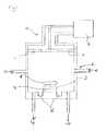
- FIG. 1shows an example of a microwave plasma reactor.
- the microwave plasma reactorcomprises the following basic components: a plasma chamber 2 ; a substrate holder 4 disposed in the plasma chamber for supporting a substrate 5 ; a microwave generator 6 for forming a plasma 8 within the plasma chamber 2 ; a microwave coupling configuration 10 for feeding microwaves from the microwave generator 6 into the plasma chamber 2 via dielectric windows 11 ; and a gas flow system comprising a gas inlet 12 and a gas outlet 14 for feeding process gases into the plasma chamber 2 and removing them therefrom.
- the plasma chamber 2forms a tight microwave cavity with solid metal walls, preferably aluminium.
- the walls of the plasma chambermay be liquid or gas cooled (e.g. water cooled) to enable higher power operation. This aids in removing the requirement for a bell jar to constrain the reactive species, again allowing higher powers while also improving material purity.
- the plasma chamberhas been modified to include an electrically conductive plasma stabilizing annulus 16 in the form of a ring-shaped recess, moat, or channel disposed in an end wall of the plasma chamber around the substrate holder 4 .
- the ring-shaped recess, moat or channelis shown with a substantially square or rectangular cross-sectional shape.
- the cross-sectional shapemay be curved to have, for example, a hemispherical or substantially U-shaped cross-sectional shape.
- the cross-sectional shapemay be asymmetrical and may have, for example, a variable radius of curvature.
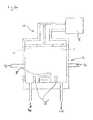
- FIG. 2shows an alternative example in which the ring-shaped recess 16 of FIG. 1 has been replaced with a ring-shaped projection 18 disposed on the end wall of the plasma chamber around the substrate holder.
- the ring-shaped projection 18is oriented in a vertical direction.
- another alternativeis to modify the vertically oriented ring-shaped projection 18 to have a horizontal portion extending inwardly towards a central portion of the chamber.
- the horizontal portionmay have a radial width and inner diameter within the previously prescribed ranges for the annulus.
- FIG. 3shows yet another alternative example in which ring-shaped projection 18 disposed on the end wall of the plasma chamber as illustrated in FIG. 2 as been replaced with a ring-shaped projection 20 disposed on a side wall the plasma chamber around the substrate holder.
- the ring-shaped projection 18is shown with a substantial square or rectangular cross-sectional shape.
- the cross-sectional shapemay be curved.
- the ring-shaped projection 18may have a curved end portion.
- the end portionmay have a constant radius of curvature or it may be asymmetrical and have, for example, a variable radius of curvature.
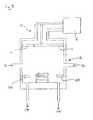
- FIG. 4shows a microwave plasma reactor comprising another example of an electrically conductive plasma stabilizing annulus 22 .
- This arrangementcomprises a side-wall mounted arrangement similar to that shown in FIG. 3 .
- the electrically conductive plasma stabilizing annulus 22has an upper surface 24 which is substantially flat and a curved end portion 26 extending to a lower surface 28 .
- the curved end portion 26has a smaller radius of curvature in an upper portion and a larger radius of curvature in a lower portion of the electrically conductive plasma stabilizing annulus. It has been found that such a profile is particularly good at stabilizing the plasma 8 over the substrate 5 without incurring problematic perturbations to the electric field.
- FIG. 4also illustrates the dimensions discussed previously in this specification to avoid misinterpretation.
- the plasma chamberhas a height h c and a diameter d c .
- the substrate holder 4 and the substrate 5have the same diameter d s .
- the substratehas a growth surface disposed at a height h s above the base of the plasma chamber.
- the electrically conductive plasma stabilizing annulushas a radial width W r , an axial depth d a , and an axial height h a above the base of the chamber.
- Arrangements in which the electrically conductive plasma stabilizing annulus is mounted on a side wall projecting into the plasma chamber at a height approximately adjacent the growth surface of the substrateare particularly useful as, unlike moat-type arrangements which may only give some mode filtering functionality, a side projecting ring also aids in improving thermal management of the plasma and gas flow characteristics within the plasma chamber.
- Embodiments of the present inventionimprove uniformity in a CVD diamond growth process. Improvement in uniformity can be measured by one or more of the following parameters: thickness uniformity of a CVD diamond film (across the deposition area); uniformity of one or more quality parameters of the diamond material (e.g. colour, optical properties, electronic properties, nitrogen uptake, boron uptake, and/or boron activation level); in polycrystalline diamond material, uniformity of texture, surface morphology, grain size, etc . . . ; or in single crystal diamond material where growth takes place on an array of single crystal diamond substrates on a substrate carrier, uniformity of thickness, morphology, edge twinning, lateral growth, etc . . . , between each single crystal.
- the key parameters chosen for assessing uniformitydepend on the synthesis process, the economics of fabricating the final product from the synthesis product, and the requirements of the final product itself.
Landscapes
- Chemical & Material Sciences (AREA)
- Engineering & Computer Science (AREA)
- Organic Chemistry (AREA)
- Metallurgy (AREA)
- Materials Engineering (AREA)
- General Chemical & Material Sciences (AREA)
- Chemical Kinetics & Catalysis (AREA)
- Physics & Mathematics (AREA)
- Plasma & Fusion (AREA)
- Mechanical Engineering (AREA)
- Inorganic Chemistry (AREA)
- Analytical Chemistry (AREA)
- Crystallography & Structural Chemistry (AREA)
- Geology (AREA)
- Life Sciences & Earth Sciences (AREA)
- General Life Sciences & Earth Sciences (AREA)
- Chemical Vapour Deposition (AREA)
- Plasma Technology (AREA)
- Crystals, And After-Treatments Of Crystals (AREA)
Abstract
Description
- a plasma chamber;
- a substrate holder disposed in the plasma chamber and comprising a supporting surface for supporting a substrate on which the diamond film is to be deposited in use;
- a microwave coupling configuration for feeding microwaves from a microwave generator into the plasma chamber; and
- a gas flow system for feeding process gases into the plasma chamber and removing them therefrom;
- wherein the microwave plasma reactor further comprises an electrically conductive plasma stabilizing annulus disposed around the substrate holder within the plasma chamber.
- providing a microwave plasma reactor as described above;
- disposing a substrate over the supporting surface of the substrate holder, the substrate have a growth surface;
- feeding microwaves into the plasma chamber;
- feeding process gases into the plasma chamber; and
- forming synthetic diamond material on said growth surface of the substrate.
- a plasma chamber;
- a substrate holder disposed in the plasma chamber and comprising a supporting surface for supporting a substrate on which the diamond film is to be deposited in use;
- a microwave coupling configuration for feeding microwaves from a microwave generator into the plasma chamber; and
- a gas flow system for feeding process gases into the plasma chamber and removing them therefrom.
- providing a microwave plasma reactor as described;
- disposing a substrate over the supporting surface of the substrate holder, the substrate have a growth surface;
- feeding microwaves from a microwave generator into the plasma chamber;
- feeding process gases into the plasma chamber; and
- forming synthetic diamond material on said growth surface of the substrate.
Claims (19)
Priority Applications (1)
| Application Number | Priority Date | Filing Date | Title |
|---|---|---|---|
| US13/980,452US9410242B2 (en) | 2010-12-23 | 2011-12-14 | Microwave plasma reactor for manufacturing synthetic diamond material |
Applications Claiming Priority (5)
| Application Number | Priority Date | Filing Date | Title |
|---|---|---|---|
| GB1021853.5 | 2010-12-23 | ||
| GBGB1021853.5AGB201021853D0 (en) | 2010-12-23 | 2010-12-23 | A microwave plasma reactor for manufacturing synthetic diamond material |
| US201161439247P | 2011-02-03 | 2011-02-03 | |
| US13/980,452US9410242B2 (en) | 2010-12-23 | 2011-12-14 | Microwave plasma reactor for manufacturing synthetic diamond material |
| PCT/EP2011/072821WO2012084657A1 (en) | 2010-12-23 | 2011-12-14 | A microwave plasma reactor for manufacturing synthetic diamond material |
Publications (2)
| Publication Number | Publication Date |
|---|---|
| US20140048016A1 US20140048016A1 (en) | 2014-02-20 |
| US9410242B2true US9410242B2 (en) | 2016-08-09 |
Family
ID=43598902
Family Applications (1)
| Application Number | Title | Priority Date | Filing Date |
|---|---|---|---|
| US13/980,452Active2032-03-15US9410242B2 (en) | 2010-12-23 | 2011-12-14 | Microwave plasma reactor for manufacturing synthetic diamond material |
Country Status (8)
| Country | Link |
|---|---|
| US (1) | US9410242B2 (en) |
| EP (1) | EP2656371B1 (en) |
| JP (1) | JP5525111B2 (en) |
| KR (1) | KR101507257B1 (en) |
| CN (1) | CN103392218B (en) |
| GB (2) | GB201021853D0 (en) |
| SG (1) | SG191225A1 (en) |
| WO (1) | WO2012084657A1 (en) |
Cited By (2)
| Publication number | Priority date | Publication date | Assignee | Title |
|---|---|---|---|---|
| WO2021173683A1 (en)* | 2020-02-24 | 2021-09-02 | J2 Materials, Llc | Plasma shaping for diamond growth |
| US20210372004A1 (en)* | 2020-06-02 | 2021-12-02 | Chih-shiue Yan | Diamond manufacturing apparatus, diamond manufacturing method using the same and diamond detecting method |
Families Citing this family (24)
| Publication number | Priority date | Publication date | Assignee | Title |
|---|---|---|---|---|
| US10689753B1 (en)* | 2009-04-21 | 2020-06-23 | Goodrich Corporation | System having a cooling element for densifying a substrate |
| GB201121640D0 (en)* | 2011-12-16 | 2012-01-25 | Element Six Ltd | Large area optical synthetic polycrystalline diamond window |
| GB201222395D0 (en)* | 2012-12-12 | 2013-01-23 | Element Six Ltd | Microwave plasma CVD synthetic diamond growth on non-planar and/or non-refractory substrates |
| CN103911596B (en)* | 2014-02-27 | 2016-07-06 | 武汉工程大学 | Device for preparing diamond film and method for preparing diamond film by using device |
| KR102118405B1 (en)* | 2014-03-31 | 2020-06-03 | 에스피피 테크놀로지스 컴퍼니 리미티드 | Plasma processing apparatus and plasma processing method |
| WO2015151148A1 (en)* | 2014-03-31 | 2015-10-08 | Sppテクノロジーズ株式会社 | High-frequency power system and plasma processing apparatus provided therewith |
| GB201410703D0 (en)* | 2014-06-16 | 2014-07-30 | Element Six Technologies Ltd | A microwave plasma reactor for manufacturing synthetic diamond material |
| GB201514998D0 (en) | 2015-08-24 | 2015-10-07 | Element Six Technologies Ltd | Microwave generators and manufacure of synthetic diamond material |
| GB201516814D0 (en) | 2015-09-23 | 2015-11-04 | Element Six Technologies Ltd | Method of fabricating a plurality of single crystal CVD synthetic diamonds |
| GB201522502D0 (en) | 2015-12-21 | 2016-02-03 | Element Six Technologies Ltd | Thick Optical quality synethetic polycrystalline Diamond Material with low bulk absorption and low microfeature density |
| US10280511B2 (en) | 2016-03-07 | 2019-05-07 | Ii-Vi Incorporated | Method of manufacture of free standing microwave plasma CVD polycrystalline diamond films with major dimensions on the order of one wavelength of the utilized microwave |
| EP3276651A1 (en)* | 2016-07-28 | 2018-01-31 | NeoCoat SA | Method for manufacturing an annular thin film of synthetic material and device for carrying out said method |
| ES2882037T3 (en) | 2016-09-06 | 2021-12-01 | Nano Coatings S L | Laser Initiated Microwave Powered Plasma-Assisted Chemical Vapor Deposition Diamond Manufacturing System and Method |
| FR3060024B1 (en)* | 2016-12-09 | 2019-05-31 | Diam Concept | MODULAR REACTOR FOR MICROWAVE PLASMA-ASSISTED DEPOSITION |
| CN106929828B (en)* | 2017-05-12 | 2023-05-23 | 中国工程物理研究院应用电子学研究所 | Substrate table for preparing diamond film by microwave plasma chemical vapor deposition method |
| KR102432857B1 (en) | 2017-09-01 | 2022-08-16 | 삼성전자주식회사 | plasma processing apparatus and manufacturing method of semiconductor device using the same |
| NO345052B1 (en)* | 2018-05-08 | 2020-09-07 | Bergen Teknologioverfoering As | Large area microwave plasma chemical vapour deposition (la mpcvd) reactor apparatus and method for providing same |
| CN110565160B (en)* | 2018-06-05 | 2021-11-09 | 广东众元半导体科技有限公司 | Microwave plasma chemical vapor deposition device |
| CN108624870B (en)* | 2018-07-05 | 2023-07-28 | 成都纽曼和瑞微波技术有限公司 | Tunable round-parabolic cavity type high-power microwave plasma chemical vapor deposition device |
| CN112695382B (en)* | 2020-12-14 | 2022-03-15 | 哈尔滨工业大学 | A method for improving the uniformity of diamond heteroepitaxial nucleation based on grid structure electrode |
| CN113417007A (en)* | 2021-06-23 | 2021-09-21 | 秦皇岛本征晶体科技有限公司 | Method for controlling diamond deposition rate based on airflow system structure |
| WO2023240026A1 (en)* | 2022-06-06 | 2023-12-14 | Plasmability, LLC. | Multiple chamber system for plasma chemical vapor deposition of diamond and related materials |
| CN116926500B (en)* | 2023-07-20 | 2024-03-12 | 北方工业大学 | Annular diamond chemical vapor deposition device with adjustable deposition size |
| GB2639893A (en)* | 2024-03-27 | 2025-10-08 | Element Six Tech Ltd | Microwave plasma reactor and method of operation |
Citations (108)
| Publication number | Priority date | Publication date | Assignee | Title |
|---|---|---|---|---|
| JPS61251158A (en) | 1985-04-30 | 1986-11-08 | Sumitomo Electric Ind Ltd | heat dissipation board |
| JPS62162366A (en) | 1981-09-17 | 1987-07-18 | Semiconductor Energy Lab Co Ltd | Composite having carbon coat |
| JPS62167886A (en) | 1986-11-19 | 1987-07-24 | Semiconductor Energy Lab Co Ltd | Composite body having carbon film |
| JPS62235393A (en) | 1986-04-07 | 1987-10-15 | Nippon Telegr & Teleph Corp <Ntt> | Solid lubricant film having high hardness and formation thereof |
| US4869923A (en) | 1987-02-24 | 1989-09-26 | Semiconductor Energy Laboratory Co., Ltd. | Microwave enhanced CVD method for depositing carbon |
| EP0343602A2 (en) | 1988-05-25 | 1989-11-29 | Canon Kabushiki Kaisha | Microwave plasma treating apparatus |
| EP0390209A2 (en) | 1989-03-30 | 1990-10-03 | Sumitomo Electric Industries, Ltd. | Diamond light-emitting device |
| US4989542A (en) | 1987-07-21 | 1991-02-05 | National Institute For Research In Inorganic Materials | Apparatus for synthesizing diamond |
| EP0447031A1 (en) | 1990-03-05 | 1991-09-18 | Board Of Governors Of Wayne State University | Composite susceptor |
| EP0467043A2 (en) | 1990-06-13 | 1992-01-22 | General Electric Company | Free standing diamond sheet and method and apparatus for making same |
| EP0480581A1 (en) | 1990-09-10 | 1992-04-15 | Applied Science & Technology, Inc. | Recirculating high velocity convective flow reactor system |
| EP0487292A1 (en) | 1990-11-22 | 1992-05-27 | Sumitomo Electric Industries, Limited | Polycrystalline diamond tool and method for producing same |
| JPH04238896A (en) | 1991-01-10 | 1992-08-26 | Nachi Fujikoshi Corp | Production of diamond plate by vapor process |
| JPH0513342A (en) | 1991-06-20 | 1993-01-22 | Kawasaki Steel Corp | Semiconductor diamond |
| EP0526657A1 (en) | 1991-02-26 | 1993-02-10 | Idemitsu Petrochemical Co. Ltd. | Microwave plasma cvd device, and method for synthesizing diamond by device thereof |
| EP0546752A1 (en) | 1991-12-13 | 1993-06-16 | General Electric Company | CVD diamond growth on hydride-forming metal substrates |
| US5258206A (en) | 1989-01-13 | 1993-11-02 | Idemitsu Petrochemical Co., Ltd. | Method and apparatus for producing diamond thin films |
| US5261959A (en) | 1988-05-26 | 1993-11-16 | General Electric Company | Diamond crystal growth apparatus |
| US5273790A (en) | 1987-03-30 | 1993-12-28 | Crystallume | Method for consolidating diamond particles to form high thermal conductivity article |
| US5273731A (en) | 1989-09-14 | 1993-12-28 | General Electric Company | Substantially transparent free standing diamond films |
| EP0582397A2 (en) | 1992-08-05 | 1994-02-09 | Crystallume | CVD diamond material for radiation detector and process for making same |
| US5302226A (en) | 1989-06-15 | 1994-04-12 | Semiconductor Energy Laboratory Co., Ltd. | Apparatus for microwave processing in a magnetic field |
| US5302803A (en) | 1991-12-23 | 1994-04-12 | Consortium For Surface Processing, Inc. | Apparatus and method for uniform microwave plasma processing using TE1101 modes |
| US5311103A (en) | 1992-06-01 | 1994-05-10 | Board Of Trustees Operating Michigan State University | Apparatus for the coating of material on a substrate using a microwave or UHF plasma |
| EP0597445A2 (en) | 1992-11-10 | 1994-05-18 | Norton Company | Method of making synthetic diamond film |
| SE500740C2 (en) | 1993-06-28 | 1994-08-22 | Ladislav Bardos | Microwave appts. for plasma processes partic. for depositing thin films - comprises microwave unit contg. at least one dielectric tube with adjustable length for generating plasma column |
| US5370912A (en)* | 1988-10-31 | 1994-12-06 | Norton Company | Diamond film deposition with a microwave plasma |
| US5397396A (en) | 1993-12-27 | 1995-03-14 | General Electric Company | Apparatus for chemical vapor deposition of diamond including thermal spreader |
| US5432315A (en)* | 1991-05-31 | 1995-07-11 | Hitachi, Ltd. | Plasma process apparatus including ground electrode with protection film |
| EP0695816A1 (en) | 1994-07-05 | 1996-02-07 | Saint-Gobain/Norton Industrial Ceramics Corporation | Method of making synthetic diamond film with reduced bowing |
| US5501740A (en) | 1993-06-04 | 1996-03-26 | Applied Science And Technology, Inc. | Microwave plasma reactor |
| US5520771A (en)* | 1990-09-26 | 1996-05-28 | Hitachi, Ltd. | Microwave plasma processing apparatus |
| JPH08133893A (en) | 1994-11-07 | 1996-05-28 | Sumitomo Electric Ind Ltd | Self-supporting diamond wafer and manufacturing method thereof |
| EP0727507A2 (en) | 1995-02-15 | 1996-08-21 | Saint-Gobain/Norton Industrial Ceramics Corporation | Apparatus and method for making free standing diamond |
| EP0758688A1 (en) | 1995-08-11 | 1997-02-19 | Sumitomo Electric Industries, Ltd. | Apparatuses for deposition or etching |
| US5643365A (en) | 1996-07-25 | 1997-07-01 | Ceram Optec Industries Inc | Method and device for plasma vapor chemical deposition of homogeneous films on large flat surfaces |
| US5683759A (en) | 1994-11-01 | 1997-11-04 | Celestech, Inc. | Method for depositing a substance with temperature control |
| EP0822269A1 (en) | 1996-07-31 | 1998-02-04 | De Beers Industrial Diamond Division (Proprietary) Limited | Diamond |
| US5951887A (en)* | 1996-03-28 | 1999-09-14 | Sumitomo Metal Industries, Ltd. | Plasma processing apparatus and plasma processing method |
| US6106678A (en) | 1996-03-29 | 2000-08-22 | Lam Research Corporation | Method of high density plasma CVD gap-filling |
| US6158383A (en) | 1919-02-20 | 2000-12-12 | Hitachi, Ltd. | Plasma processing method and apparatus |
| JP2001007385A (en) | 1999-06-21 | 2001-01-12 | Japan Science & Technology Corp | Ultraviolet light emitting device and method of manufacturing the same |
| FR2798552A1 (en) | 1999-09-13 | 2001-03-16 | Centre Nat Rech Scient | DEVICE PROVIDING A MICROWAVE POWER DIVISION PREDETERMINED ON A PLURALITY OF CHARGES, IN PARTICULAR FOR THE PRODUCTION OF PLASMA |
| US6245190B1 (en)* | 1997-03-26 | 2001-06-12 | Hitachi, Ltd. | Plasma processing system and plasma processing method |
| US6254683B1 (en) | 1998-05-20 | 2001-07-03 | Matsushita Electric Industrial Co., Ltd. | Substrate temperature control method and device |
| US20010023663A1 (en) | 2000-03-17 | 2001-09-27 | Hideyuki Kazumi | Plasma processing apparatus |
| US20010036465A1 (en) | 1999-11-30 | 2001-11-01 | Nobuo Ishll | Plasma processing apparatus |
| US6319439B1 (en) | 1999-04-30 | 2001-11-20 | Korea Institute Of Science And Technology | Method of synthesizing even diamond film without cracks |
| US6325018B1 (en) | 1999-03-12 | 2001-12-04 | Tokyo Electron Limited | Flat antenna having openings provided with conductive materials accommodated therein and plasma processing apparatus using the flat antenna |
| US20010050059A1 (en)* | 2000-03-24 | 2001-12-13 | Toshiaki Hongo | Plasma processing apparatus with a dielectric plate having a thickness based on a wavelength of a microwave introduced into a process chamber through the dielectric plate |
| JP3281594B2 (en) | 1998-01-12 | 2002-05-13 | マルマテクニカ株式会社 | Vibration type hydraulic cylinder device for construction work machine |
| US6388632B1 (en) | 1999-03-30 | 2002-05-14 | Rohm Co., Ltd. | Slot antenna used for plasma surface processing apparatus |
| US6414338B1 (en) | 1998-11-30 | 2002-07-02 | Sandia National Laboratories | n-Type diamond and method for producing same |
| US20020084034A1 (en)* | 1999-01-19 | 2002-07-04 | Naoyuki Kofuji | Dry etching apparatus and a method of manufacturing a semiconductor device |
| KR20020061768A (en) | 2001-01-17 | 2002-07-25 | 한국과학기술연구원 | A Method for Depositing Diamond Films Without Fracture by a Control of Substrate Temperatures Using Powders |
| US6427621B1 (en) | 1999-04-14 | 2002-08-06 | Hitachi, Ltd. | Plasma processing device and plasma processing method |
| US6433298B1 (en) | 1998-03-20 | 2002-08-13 | Tokyo Electron Limited | Plasma processing apparatus |
| JP2002265296A (en) | 2001-03-09 | 2002-09-18 | Kobe Steel Ltd | Diamond thin film and manufacturing method therefor |
| WO2002077319A1 (en) | 2001-03-27 | 2002-10-03 | Small & Medium Industry Promotion Corporation | Diamond film depositing apparatus using microwaves and plasma |
| US6487986B1 (en) | 1998-09-12 | 2002-12-03 | Unaxis Deutschland Holding Gmbh | Device for the plasma deposition of a polycrystalline diamond |
| JP2003045810A (en) | 2001-07-31 | 2003-02-14 | Canon Inc | Plasma processing equipment |
| WO2003040440A2 (en) | 2001-11-07 | 2003-05-15 | Carnegie Institution Of Washington | Apparatus and method for diamond production |
| JP2003142471A (en) | 2001-11-01 | 2003-05-16 | Canon Inc | Plasma processing apparatus and structure manufacturing method |
| US6565661B1 (en) | 1999-06-04 | 2003-05-20 | Simplus Systems Corporation | High flow conductance and high thermal conductance showerhead system and method |
| US20030107003A1 (en) | 2000-03-15 | 2003-06-12 | Whitehead Andrew John | Diamond radiation detector |
| US20030150846A1 (en) | 1999-06-18 | 2003-08-14 | Tokyo Electron Ltd. | Plasma-assisted processing system and plasma-assisted processing method |
| US20030150561A1 (en) | 2000-04-27 | 2003-08-14 | Tokyo Electron Limited | Plasma processing apparatus |
| US20030200914A1 (en) | 2002-04-25 | 2003-10-30 | Shin-Etsu Chemical Co., Ltd. | Diamond film and method for producing the same |
| US6645343B1 (en) | 1998-01-27 | 2003-11-11 | Fraunhofer-Gesellschaft zur Förderung der angewandten Forschung e.V. | Plasma reactor |
| US20040045674A1 (en) | 2000-08-04 | 2004-03-11 | Nobuo Ishii | Radial antenna and plasma device using it |
| JP2004235434A (en) | 2003-01-30 | 2004-08-19 | Rohm Co Ltd | Plasma processing system |
| JP2004244298A (en) | 2002-12-17 | 2004-09-02 | Kobe Steel Ltd | Substrate holder for vapor-phase diamond synthesis and method of vapor-phase diamond synthesis |
| EP1463849A2 (en) | 2001-12-14 | 2004-10-06 | Element Six Limited | Boron doped diamond |
| US20050005853A1 (en) | 2001-08-07 | 2005-01-13 | Stephan Behle | Device for the coating of objects |
| EP1500718A1 (en) | 2003-07-24 | 2005-01-26 | Shin-Etsu Chemical Company, Ltd. | Method for producing diamond film |
| JP2005044822A (en) | 2003-07-22 | 2005-02-17 | Shibaura Mechatronics Corp | Plasma processing equipment |
| US20050109267A1 (en) | 1998-05-15 | 2005-05-26 | Apollo Diamond, Inc. | Method of growing single crystal diamond in a plasma reactor |
| US20050266606A1 (en) | 2002-06-12 | 2005-12-01 | Centre National De La Recherche Scientifque-Cnrs | Method of producing an n-type diamond with high electrical conductivity |
| WO2006011756A1 (en) | 2004-07-27 | 2006-02-02 | Innovation For Creative Devices Co., Ltd. | Aluminum plasma chamber and method for manufacturing the same |
| EP1643641A2 (en) | 2004-10-01 | 2006-04-05 | Seiko Epson Corporation | High-frequency heating device, semiconductor manufacturing device, and light source device |
| JP2006286269A (en) | 2005-03-31 | 2006-10-19 | Tokyo Electron Ltd | Plasma processing device |
| WO2006117621A1 (en) | 2005-04-29 | 2006-11-09 | Element Six Limited | Diamond transistor and method of manufacture thereof |
| WO2006127611A2 (en) | 2005-05-25 | 2006-11-30 | Carnegie Institution Of Washington | Colorless single-crystal cvd diamond at rapid growth rate |
| US20060266279A1 (en) | 2005-05-26 | 2006-11-30 | National Institute Of Advanced Industrial Science And Technology | Method of producing single crystal |
| JP2007142195A (en) | 2005-11-18 | 2007-06-07 | Idemitsu Kosan Co Ltd | Semiconductor thin film, manufacturing method thereof, thin film transistor, active matrix drive display panel |
| US20070163996A1 (en) | 2006-01-18 | 2007-07-19 | Tokyo Electron Limited | Plasma processing apparatus and plasma processing method |
| WO2007092893A2 (en) | 2006-02-07 | 2007-08-16 | Target Technology Company, Llc | Materials and methods for the manufacture of large crystal diamonds |
| US20070221294A1 (en) | 2006-03-27 | 2007-09-27 | Tokyo Electron Limited | Plasma processing apparatus and plasma processing method |
| JP2007273913A (en) | 2006-03-31 | 2007-10-18 | Shimadzu Corp | Surface wave excitation plasma processing equipment |
| JP2007284773A (en) | 2006-04-20 | 2007-11-01 | Sumitomo Electric Ind Ltd | Diamond synthesis method |
| US20070264441A1 (en)* | 2004-02-16 | 2007-11-15 | Tokyo Electron Limited | Plasma Processing Apparatus and Plasma Processing Method |
| JP2007331955A (en) | 2006-06-12 | 2007-12-27 | National Institute Of Advanced Industrial & Technology | Diamond manufacturing method |
| WO2008025899A1 (en) | 2006-08-30 | 2008-03-06 | Vernet | Thermostatic valve for mounting between a fuel tank and a combustion engine and related fuel circulation circuit |
| WO2008029258A2 (en) | 2006-09-05 | 2008-03-13 | Element Six Limited | Solid electrode |
| WO2008090510A1 (en) | 2007-01-22 | 2008-07-31 | Element Six Limited | High uniformity boron doped diamond material |
| US20080190356A1 (en) | 2007-02-14 | 2008-08-14 | Rajneesh Bhandari | Method and apparatus for producing single crystalline diamonds |
| WO2008123605A1 (en) | 2007-03-29 | 2008-10-16 | Tokyo Electron Limited | Plasma process apparatus |
| US20080303744A1 (en) | 2007-06-11 | 2008-12-11 | Tokyo Electron Limited | Plasma processing system, antenna, and use of plasma processing system |
| CN101385129A (en) | 2006-07-28 | 2009-03-11 | 东京毅力科创株式会社 | Microwave plasma source and plasma processing apparatus |
| EP2108714A1 (en) | 2007-01-29 | 2009-10-14 | Sumitomo Electric Industries, Ltd. | Microwave plasma cvd system |
| JP2009280421A (en) | 2008-05-20 | 2009-12-03 | Sadao Takeuchi | Tool with high strength diamond film |
| WO2010004836A1 (en) | 2008-07-09 | 2010-01-14 | 東京エレクトロン株式会社 | Plasma processing device |
| US20100028556A1 (en) | 2008-05-09 | 2010-02-04 | Apollo Diamond Gemstone Corporation | Chemical vapor deposition colored diamond |
| US20100034984A1 (en) | 2008-06-16 | 2010-02-11 | Board Of Trustees Of Michigan State University | Microwave plasma reactors |
| WO2010021382A1 (en) | 2008-08-22 | 2010-02-25 | 東京エレクトロン株式会社 | Microwave introduction mechanism, microwave plasma source and microwave plasma processing device |
| US20100178234A1 (en) | 2009-01-09 | 2010-07-15 | Shin-Etsu Chemical Co., Ltd. | Multilayer substrate and method for producing the same, diamond film and method for producing the same |
| US20100189924A1 (en) | 2009-01-23 | 2010-07-29 | Lockheed Martin Corporation | Apparatus and method for diamond film growth |
| WO2010084655A1 (en) | 2009-01-21 | 2010-07-29 | 国立大学法人東北大学 | Plasma processing apparatus |
Family Cites Families (4)
| Publication number | Priority date | Publication date | Assignee | Title |
|---|---|---|---|---|
| JPH049471A (en)* | 1990-04-27 | 1992-01-14 | Seiko Instr Inc | Method for synthesizing diamond |
| JP3041844B2 (en)* | 1995-08-11 | 2000-05-15 | 住友電気工業株式会社 | Film forming or etching equipment |
| CN1563480A (en)* | 2004-04-22 | 2005-01-12 | 大连理工大学 | Method for depositing carbon cone of diamond |
| CN2937155Y (en)* | 2006-07-20 | 2007-08-22 | 浙江大学 | Device for depositing diamond-like film on aluminum surface |
- 2010
- 2010-12-23GBGBGB1021853.5Apatent/GB201021853D0/ennot_activeCeased
- 2011
- 2011-12-14WOPCT/EP2011/072821patent/WO2012084657A1/enactiveApplication Filing
- 2011-12-14KRKR1020137018631Apatent/KR101507257B1/enactiveActive
- 2011-12-14GBGB1121505.0Apatent/GB2486783B/enactiveActive
- 2011-12-14CNCN201180068069.2Apatent/CN103392218B/enactiveActive
- 2011-12-14USUS13/980,452patent/US9410242B2/enactiveActive
- 2011-12-14JPJP2013545199Apatent/JP5525111B2/enactiveActive
- 2011-12-14SGSG2013046859Apatent/SG191225A1/enunknown
- 2011-12-14EPEP11794199.7Apatent/EP2656371B1/enactiveActive
Patent Citations (117)
| Publication number | Priority date | Publication date | Assignee | Title |
|---|---|---|---|---|
| US6158383A (en) | 1919-02-20 | 2000-12-12 | Hitachi, Ltd. | Plasma processing method and apparatus |
| JPS62162366A (en) | 1981-09-17 | 1987-07-18 | Semiconductor Energy Lab Co Ltd | Composite having carbon coat |
| JPS61251158A (en) | 1985-04-30 | 1986-11-08 | Sumitomo Electric Ind Ltd | heat dissipation board |
| JPS62235393A (en) | 1986-04-07 | 1987-10-15 | Nippon Telegr & Teleph Corp <Ntt> | Solid lubricant film having high hardness and formation thereof |
| JPS62167886A (en) | 1986-11-19 | 1987-07-24 | Semiconductor Energy Lab Co Ltd | Composite body having carbon film |
| US4869923A (en) | 1987-02-24 | 1989-09-26 | Semiconductor Energy Laboratory Co., Ltd. | Microwave enhanced CVD method for depositing carbon |
| US5273790A (en) | 1987-03-30 | 1993-12-28 | Crystallume | Method for consolidating diamond particles to form high thermal conductivity article |
| US4989542A (en) | 1987-07-21 | 1991-02-05 | National Institute For Research In Inorganic Materials | Apparatus for synthesizing diamond |
| EP0343602A3 (en) | 1988-05-25 | 1991-01-09 | Canon Kabushiki Kaisha | Microwave plasma treating apparatus |
| EP0343602A2 (en) | 1988-05-25 | 1989-11-29 | Canon Kabushiki Kaisha | Microwave plasma treating apparatus |
| US5261959A (en) | 1988-05-26 | 1993-11-16 | General Electric Company | Diamond crystal growth apparatus |
| US5370912A (en)* | 1988-10-31 | 1994-12-06 | Norton Company | Diamond film deposition with a microwave plasma |
| US5258206A (en) | 1989-01-13 | 1993-11-02 | Idemitsu Petrochemical Co., Ltd. | Method and apparatus for producing diamond thin films |
| EP0390209A2 (en) | 1989-03-30 | 1990-10-03 | Sumitomo Electric Industries, Ltd. | Diamond light-emitting device |
| EP0390209A3 (en) | 1989-03-30 | 1991-01-09 | Sumitomo Electric Industries, Ltd. | Diamond light-emitting device |
| US5302226A (en) | 1989-06-15 | 1994-04-12 | Semiconductor Energy Laboratory Co., Ltd. | Apparatus for microwave processing in a magnetic field |
| US5273731A (en) | 1989-09-14 | 1993-12-28 | General Electric Company | Substantially transparent free standing diamond films |
| JPH04228495A (en) | 1990-03-05 | 1992-08-18 | Univ Wayne State | New susceptor for chemical vapor phase deposition apparatus and method for using it |
| US5091208A (en) | 1990-03-05 | 1992-02-25 | Wayne State University | Novel susceptor for use in chemical vapor deposition apparatus and its method of use |
| EP0447031A1 (en) | 1990-03-05 | 1991-09-18 | Board Of Governors Of Wayne State University | Composite susceptor |
| EP0467043A2 (en) | 1990-06-13 | 1992-01-22 | General Electric Company | Free standing diamond sheet and method and apparatus for making same |
| EP0480581A1 (en) | 1990-09-10 | 1992-04-15 | Applied Science & Technology, Inc. | Recirculating high velocity convective flow reactor system |
| US5520771A (en)* | 1990-09-26 | 1996-05-28 | Hitachi, Ltd. | Microwave plasma processing apparatus |
| EP0487292A1 (en) | 1990-11-22 | 1992-05-27 | Sumitomo Electric Industries, Limited | Polycrystalline diamond tool and method for producing same |
| JPH04238896A (en) | 1991-01-10 | 1992-08-26 | Nachi Fujikoshi Corp | Production of diamond plate by vapor process |
| EP0526657A1 (en) | 1991-02-26 | 1993-02-10 | Idemitsu Petrochemical Co. Ltd. | Microwave plasma cvd device, and method for synthesizing diamond by device thereof |
| US5432315A (en)* | 1991-05-31 | 1995-07-11 | Hitachi, Ltd. | Plasma process apparatus including ground electrode with protection film |
| JPH0513342A (en) | 1991-06-20 | 1993-01-22 | Kawasaki Steel Corp | Semiconductor diamond |
| EP0546752A1 (en) | 1991-12-13 | 1993-06-16 | General Electric Company | CVD diamond growth on hydride-forming metal substrates |
| US5302803A (en) | 1991-12-23 | 1994-04-12 | Consortium For Surface Processing, Inc. | Apparatus and method for uniform microwave plasma processing using TE1101 modes |
| US5311103A (en) | 1992-06-01 | 1994-05-10 | Board Of Trustees Operating Michigan State University | Apparatus for the coating of material on a substrate using a microwave or UHF plasma |
| EP0582397A2 (en) | 1992-08-05 | 1994-02-09 | Crystallume | CVD diamond material for radiation detector and process for making same |
| EP0597445A2 (en) | 1992-11-10 | 1994-05-18 | Norton Company | Method of making synthetic diamond film |
| US5501740A (en) | 1993-06-04 | 1996-03-26 | Applied Science And Technology, Inc. | Microwave plasma reactor |
| SE500740C2 (en) | 1993-06-28 | 1994-08-22 | Ladislav Bardos | Microwave appts. for plasma processes partic. for depositing thin films - comprises microwave unit contg. at least one dielectric tube with adjustable length for generating plasma column |
| US5397396A (en) | 1993-12-27 | 1995-03-14 | General Electric Company | Apparatus for chemical vapor deposition of diamond including thermal spreader |
| EP0695816A1 (en) | 1994-07-05 | 1996-02-07 | Saint-Gobain/Norton Industrial Ceramics Corporation | Method of making synthetic diamond film with reduced bowing |
| US5683759A (en) | 1994-11-01 | 1997-11-04 | Celestech, Inc. | Method for depositing a substance with temperature control |
| JPH08133893A (en) | 1994-11-07 | 1996-05-28 | Sumitomo Electric Ind Ltd | Self-supporting diamond wafer and manufacturing method thereof |
| EP0727507A2 (en) | 1995-02-15 | 1996-08-21 | Saint-Gobain/Norton Industrial Ceramics Corporation | Apparatus and method for making free standing diamond |
| US6132550A (en)* | 1995-08-11 | 2000-10-17 | Sumitomo Electric Industries, Ltd. | Apparatuses for desposition or etching |
| EP0758688A1 (en) | 1995-08-11 | 1997-02-19 | Sumitomo Electric Industries, Ltd. | Apparatuses for deposition or etching |
| US5951887A (en)* | 1996-03-28 | 1999-09-14 | Sumitomo Metal Industries, Ltd. | Plasma processing apparatus and plasma processing method |
| US6091045A (en) | 1996-03-28 | 2000-07-18 | Sumitomo Metal Industries, Inc. | Plasma processing apparatus utilizing a microwave window having a thinner inner area |
| US6106678A (en) | 1996-03-29 | 2000-08-22 | Lam Research Corporation | Method of high density plasma CVD gap-filling |
| US5643365A (en) | 1996-07-25 | 1997-07-01 | Ceram Optec Industries Inc | Method and device for plasma vapor chemical deposition of homogeneous films on large flat surfaces |
| US5981057A (en) | 1996-07-31 | 1999-11-09 | Collins; John Lloyd | Diamond |
| EP0822269A1 (en) | 1996-07-31 | 1998-02-04 | De Beers Industrial Diamond Division (Proprietary) Limited | Diamond |
| US6245190B1 (en)* | 1997-03-26 | 2001-06-12 | Hitachi, Ltd. | Plasma processing system and plasma processing method |
| JP3281594B2 (en) | 1998-01-12 | 2002-05-13 | マルマテクニカ株式会社 | Vibration type hydraulic cylinder device for construction work machine |
| US6645343B1 (en) | 1998-01-27 | 2003-11-11 | Fraunhofer-Gesellschaft zur Förderung der angewandten Forschung e.V. | Plasma reactor |
| US6433298B1 (en) | 1998-03-20 | 2002-08-13 | Tokyo Electron Limited | Plasma processing apparatus |
| US20080156256A1 (en) | 1998-05-15 | 2008-07-03 | Apollo Diamond, Inc. | System and method for producing synthetic diamond |
| US20050109267A1 (en) | 1998-05-15 | 2005-05-26 | Apollo Diamond, Inc. | Method of growing single crystal diamond in a plasma reactor |
| US6254683B1 (en) | 1998-05-20 | 2001-07-03 | Matsushita Electric Industrial Co., Ltd. | Substrate temperature control method and device |
| US6487986B1 (en) | 1998-09-12 | 2002-12-03 | Unaxis Deutschland Holding Gmbh | Device for the plasma deposition of a polycrystalline diamond |
| US6414338B1 (en) | 1998-11-30 | 2002-07-02 | Sandia National Laboratories | n-Type diamond and method for producing same |
| US20020084034A1 (en)* | 1999-01-19 | 2002-07-04 | Naoyuki Kofuji | Dry etching apparatus and a method of manufacturing a semiconductor device |
| US6325018B1 (en) | 1999-03-12 | 2001-12-04 | Tokyo Electron Limited | Flat antenna having openings provided with conductive materials accommodated therein and plasma processing apparatus using the flat antenna |
| US6388632B1 (en) | 1999-03-30 | 2002-05-14 | Rohm Co., Ltd. | Slot antenna used for plasma surface processing apparatus |
| US6427621B1 (en) | 1999-04-14 | 2002-08-06 | Hitachi, Ltd. | Plasma processing device and plasma processing method |
| US6319439B1 (en) | 1999-04-30 | 2001-11-20 | Korea Institute Of Science And Technology | Method of synthesizing even diamond film without cracks |
| US6565661B1 (en) | 1999-06-04 | 2003-05-20 | Simplus Systems Corporation | High flow conductance and high thermal conductance showerhead system and method |
| US20030150846A1 (en) | 1999-06-18 | 2003-08-14 | Tokyo Electron Ltd. | Plasma-assisted processing system and plasma-assisted processing method |
| JP2001007385A (en) | 1999-06-21 | 2001-01-12 | Japan Science & Technology Corp | Ultraviolet light emitting device and method of manufacturing the same |
| FR2798552A1 (en) | 1999-09-13 | 2001-03-16 | Centre Nat Rech Scient | DEVICE PROVIDING A MICROWAVE POWER DIVISION PREDETERMINED ON A PLURALITY OF CHARGES, IN PARTICULAR FOR THE PRODUCTION OF PLASMA |
| US20010036465A1 (en) | 1999-11-30 | 2001-11-01 | Nobuo Ishll | Plasma processing apparatus |
| US20030107003A1 (en) | 2000-03-15 | 2003-06-12 | Whitehead Andrew John | Diamond radiation detector |
| US20010023663A1 (en) | 2000-03-17 | 2001-09-27 | Hideyuki Kazumi | Plasma processing apparatus |
| US20010050059A1 (en)* | 2000-03-24 | 2001-12-13 | Toshiaki Hongo | Plasma processing apparatus with a dielectric plate having a thickness based on a wavelength of a microwave introduced into a process chamber through the dielectric plate |
| US20030150561A1 (en) | 2000-04-27 | 2003-08-14 | Tokyo Electron Limited | Plasma processing apparatus |
| US20040045674A1 (en) | 2000-08-04 | 2004-03-11 | Nobuo Ishii | Radial antenna and plasma device using it |
| KR20020061768A (en) | 2001-01-17 | 2002-07-25 | 한국과학기술연구원 | A Method for Depositing Diamond Films Without Fracture by a Control of Substrate Temperatures Using Powders |
| JP2002265296A (en) | 2001-03-09 | 2002-09-18 | Kobe Steel Ltd | Diamond thin film and manufacturing method therefor |
| WO2002077319A1 (en) | 2001-03-27 | 2002-10-03 | Small & Medium Industry Promotion Corporation | Diamond film depositing apparatus using microwaves and plasma |
| JP2003045810A (en) | 2001-07-31 | 2003-02-14 | Canon Inc | Plasma processing equipment |
| US20050005853A1 (en) | 2001-08-07 | 2005-01-13 | Stephan Behle | Device for the coating of objects |
| JP2003142471A (en) | 2001-11-01 | 2003-05-16 | Canon Inc | Plasma processing apparatus and structure manufacturing method |
| WO2003040440A2 (en) | 2001-11-07 | 2003-05-15 | Carnegie Institution Of Washington | Apparatus and method for diamond production |
| EP1463849A2 (en) | 2001-12-14 | 2004-10-06 | Element Six Limited | Boron doped diamond |
| US20030200914A1 (en) | 2002-04-25 | 2003-10-30 | Shin-Etsu Chemical Co., Ltd. | Diamond film and method for producing the same |
| US20050266606A1 (en) | 2002-06-12 | 2005-12-01 | Centre National De La Recherche Scientifque-Cnrs | Method of producing an n-type diamond with high electrical conductivity |
| JP2004244298A (en) | 2002-12-17 | 2004-09-02 | Kobe Steel Ltd | Substrate holder for vapor-phase diamond synthesis and method of vapor-phase diamond synthesis |
| JP2004235434A (en) | 2003-01-30 | 2004-08-19 | Rohm Co Ltd | Plasma processing system |
| JP2005044822A (en) | 2003-07-22 | 2005-02-17 | Shibaura Mechatronics Corp | Plasma processing equipment |
| EP1500718A1 (en) | 2003-07-24 | 2005-01-26 | Shin-Etsu Chemical Company, Ltd. | Method for producing diamond film |
| US20070264441A1 (en)* | 2004-02-16 | 2007-11-15 | Tokyo Electron Limited | Plasma Processing Apparatus and Plasma Processing Method |
| WO2006011756A1 (en) | 2004-07-27 | 2006-02-02 | Innovation For Creative Devices Co., Ltd. | Aluminum plasma chamber and method for manufacturing the same |
| EP1643641A2 (en) | 2004-10-01 | 2006-04-05 | Seiko Epson Corporation | High-frequency heating device, semiconductor manufacturing device, and light source device |
| JP2006286269A (en) | 2005-03-31 | 2006-10-19 | Tokyo Electron Ltd | Plasma processing device |
| US20080099768A1 (en) | 2005-04-29 | 2008-05-01 | Scarsbrook Geoffrey A | Diamond Transistor And Method Of Manufacture Thereof |
| WO2006117621A1 (en) | 2005-04-29 | 2006-11-09 | Element Six Limited | Diamond transistor and method of manufacture thereof |
| WO2006127611A2 (en) | 2005-05-25 | 2006-11-30 | Carnegie Institution Of Washington | Colorless single-crystal cvd diamond at rapid growth rate |
| US20060266279A1 (en) | 2005-05-26 | 2006-11-30 | National Institute Of Advanced Industrial Science And Technology | Method of producing single crystal |
| JP2007142195A (en) | 2005-11-18 | 2007-06-07 | Idemitsu Kosan Co Ltd | Semiconductor thin film, manufacturing method thereof, thin film transistor, active matrix drive display panel |
| US20070163996A1 (en) | 2006-01-18 | 2007-07-19 | Tokyo Electron Limited | Plasma processing apparatus and plasma processing method |
| WO2007092893A2 (en) | 2006-02-07 | 2007-08-16 | Target Technology Company, Llc | Materials and methods for the manufacture of large crystal diamonds |
| US20070221294A1 (en) | 2006-03-27 | 2007-09-27 | Tokyo Electron Limited | Plasma processing apparatus and plasma processing method |
| JP2007273913A (en) | 2006-03-31 | 2007-10-18 | Shimadzu Corp | Surface wave excitation plasma processing equipment |
| JP2007284773A (en) | 2006-04-20 | 2007-11-01 | Sumitomo Electric Ind Ltd | Diamond synthesis method |
| JP2007331955A (en) | 2006-06-12 | 2007-12-27 | National Institute Of Advanced Industrial & Technology | Diamond manufacturing method |
| CN101385129A (en) | 2006-07-28 | 2009-03-11 | 东京毅力科创株式会社 | Microwave plasma source and plasma processing apparatus |
| WO2008025899A1 (en) | 2006-08-30 | 2008-03-06 | Vernet | Thermostatic valve for mounting between a fuel tank and a combustion engine and related fuel circulation circuit |
| WO2008029258A2 (en) | 2006-09-05 | 2008-03-13 | Element Six Limited | Solid electrode |
| WO2008090510A1 (en) | 2007-01-22 | 2008-07-31 | Element Six Limited | High uniformity boron doped diamond material |
| EP2108714A1 (en) | 2007-01-29 | 2009-10-14 | Sumitomo Electric Industries, Ltd. | Microwave plasma cvd system |
| US20080190356A1 (en) | 2007-02-14 | 2008-08-14 | Rajneesh Bhandari | Method and apparatus for producing single crystalline diamonds |
| WO2008123605A1 (en) | 2007-03-29 | 2008-10-16 | Tokyo Electron Limited | Plasma process apparatus |
| US20080303744A1 (en) | 2007-06-11 | 2008-12-11 | Tokyo Electron Limited | Plasma processing system, antenna, and use of plasma processing system |
| US20100028556A1 (en) | 2008-05-09 | 2010-02-04 | Apollo Diamond Gemstone Corporation | Chemical vapor deposition colored diamond |
| JP2009280421A (en) | 2008-05-20 | 2009-12-03 | Sadao Takeuchi | Tool with high strength diamond film |
| US20100034984A1 (en) | 2008-06-16 | 2010-02-11 | Board Of Trustees Of Michigan State University | Microwave plasma reactors |
| WO2010004836A1 (en) | 2008-07-09 | 2010-01-14 | 東京エレクトロン株式会社 | Plasma processing device |
| WO2010021382A1 (en) | 2008-08-22 | 2010-02-25 | 東京エレクトロン株式会社 | Microwave introduction mechanism, microwave plasma source and microwave plasma processing device |
| US20100178234A1 (en) | 2009-01-09 | 2010-07-15 | Shin-Etsu Chemical Co., Ltd. | Multilayer substrate and method for producing the same, diamond film and method for producing the same |
| WO2010084655A1 (en) | 2009-01-21 | 2010-07-29 | 国立大学法人東北大学 | Plasma processing apparatus |
| US20100189924A1 (en) | 2009-01-23 | 2010-07-29 | Lockheed Martin Corporation | Apparatus and method for diamond film growth |
Non-Patent Citations (44)
| Title |
|---|
| Achard, J., et al., Thick boron doped diamond single crystals for high power electronics, Diamond & Related Materials, 20, pp. 145-152, 2010. |
| Alam et al., Adhesion of diamond coatings on tungsten substrates, Journal of Adhesion Science and Technology, vol. 9, No. 6, 1995 Netherlands, 653-679. |
| Asmussen, et al., Multiple substrate microwave plasma-assisted chemical vapor deposition single crystal diamond syntheses, Applied Physics Letters, p. 93, 031502, 2008. |
| Balmer et al., Chemical vapour deposition synthetic diamond: materials, technology and applications, Journal of Physics: Condensed Matter, 21, 2009. |
| Chae, et al., The 8-inch free-standing CVD diamond wafer fabricated by DC-PACVD, Diamond and Related Materials, 19, 2010, pp. 1168-1171. |
| Feng, et al., Surface stress measurement with interference microscopy of thick homoepitaxial single-crystal diamond layers, Diamond & Related Materials 19 (2010) 1453-1456. |
| Funer et al., Numerical simulations of microwave plasma reactor for diamond CVD, Surface and Coatings Technology, 74-75 (1995), pp. 221-226. |
| Funer et al., Simulation and development of optimized microwave plasma reactors for diamond deposition, Surface and Coatings Technology, 1999, 853-862, vol. 116-119. |
| Gray, et al., Free-standing CVD diamond wafers for thermal management by d.c. arc jet technology, Diamond and Related Materials 8, 1999, 903-908. |
| Hassouni et al., Self-consistent microwave field and plasma discharge simulations for a moderate pressure hydrogen discharge reactor, Journal of Applied Physics, 1999, pp. 134-151, 86(1). |
| Hassouni et la., Modelling of diamond deposition microwave cavity generated plasmas, J. Phys. D. Appl. Phys,. 43 (2010) 153001. |
| Hemawan, et a., Improved microwave plasma cavity reactor for diamond synthesis at high-pressure and high power density, Diamond & Related Materials 19 (2010) 1446-1452. |
| http://web.archive.org/web/20501090953/http://en.wikipedia.org/wiki/Aluminum. |
| International Search Report issued on PCT/EP2011/072818, dated Jun. 22, 2012. |
| International Search Report issued on PCT/EP2011/072820, dated Mar. 30, 2012. |
| International Search Report issued on PCT/EP2011/072821, dated Mar. 2, 2012. |
| International Search Report issued on PCT/EP2011/072822, dated May 23, 2012. |
| International Search Report issued on PCT/EP2011/072823, dated Jul. 4, 2012. |
| International Search Report issued on PCT/EP2011/072824, dated May 3, 2012. |
| International Search Report issued on PCT/EP2011/072825 dated Mar. 30, 2012. |
| Kosky et al., Fracture-free release of CVD diamond, Diamond and Related Materials 5 (1996) pp. 1313-1317. |
| Lee, et al., Single-cathode DC PACVD process for large-area CVD diamond wafer fabrication, 203rd Meeting of the Electrochemical Society, Eighth International Symposium on Diamond Materials, 2003. |
| Liao, Samuel Y., Microwave Devices and Circuits, 3d Edition, published by Prentice-Hall, Inc., New Jersey pp. 144-156. |
| Nagatsu et al., "Diagnostics of plasma ball formed in high pressure microwave plasma for diamond film synthesis", Diamond and Related Materials, 2002; pp. 562-566. |
| Search Report issued on GB1021853.5 dated Mar. 30, 2011. |
| Search Report issued on GB1021855.0 dated May 31, 2011. |
| Search Report issued on GB1021860.0 dated Apr. 20, 2011. |
| Search Report issued on GB1021865.9 dated Apr. 20, 2011. |
| Search Report issued on GB1021870.9 dated Apr. 6, 2011. |
| Search Report issued on GB1021913.7, dated Apr. 21, 2011. |
| Search Report issued on GB1121474.9, dated Mar. 27, 2012. |
| Search Report issued on GB1121486.3 dated Apr. 12, 2012. |
| Search Report issued on GB1121492.1 dated Apr. 12, 2012. |
| Search Report issued on GB1121494.7 dated Apr. 7, 2012. |
| Search Report issued on GB1121499.6 dated Jan. 27, 2012. |
| Search Report issued on GB1121505.0 dated Mar. 29, 2012. |
| Search Report issued on GB1121517.5, dated Mar. 27, 2012. |
| Search Report issued on GB1305030.7 dated Apr. 16, 2013. |
| Search Report issued on GB1305041.4 dated Apr. 15, 2013. |
| Search Report issued on GB1305045.5 dated Apr. 16, 2013. |
| Silva et al., Microwave Analysis of PACVD diamond deposition reactor based on electromagnetic materials, Diamond & Related Materials, vol. 19, pp. 397-403, 2010. |
| Silva, F., et al., Microwave engineering of plasma-assisted CVD reactors for diamond deposition, Journal of Physics; Condensed Matter, vol. 21, No. 364202, 2009. |
| Whitfield et al., Nucleation and growth of diamond films on single crystal and polycrystalline tungsten substrates, Diamond and Related Materials, vol. 9, pp. 262-268, 2000. |
| Yamada, Simulation with an improved plasma model utilized to design a new structure of microwave plasma dischage for chemical vapor deposition of diamond crystals, Diamond and Related Materials, 17, Issues 4-5 (2008), pp. 494-497. |
Cited By (2)
| Publication number | Priority date | Publication date | Assignee | Title |
|---|---|---|---|---|
| WO2021173683A1 (en)* | 2020-02-24 | 2021-09-02 | J2 Materials, Llc | Plasma shaping for diamond growth |
| US20210372004A1 (en)* | 2020-06-02 | 2021-12-02 | Chih-shiue Yan | Diamond manufacturing apparatus, diamond manufacturing method using the same and diamond detecting method |
Also Published As
| Publication number | Publication date |
|---|---|
| GB201021853D0 (en) | 2011-02-02 |
| SG191225A1 (en) | 2013-07-31 |
| GB201121505D0 (en) | 2012-01-25 |
| GB2486783A (en) | 2012-06-27 |
| JP5525111B2 (en) | 2014-06-18 |
| GB2486783B (en) | 2014-02-12 |
| US20140048016A1 (en) | 2014-02-20 |
| EP2656371A1 (en) | 2013-10-30 |
| CN103392218A (en) | 2013-11-13 |
| KR101507257B1 (en) | 2015-03-30 |
| JP2014506291A (en) | 2014-03-13 |
| CN103392218B (en) | 2016-05-11 |
| KR20130102639A (en) | 2013-09-17 |
| WO2012084657A1 (en) | 2012-06-28 |
| EP2656371B1 (en) | 2019-08-07 |
Similar Documents
| Publication | Publication Date | Title |
|---|---|---|
| US9410242B2 (en) | Microwave plasma reactor for manufacturing synthetic diamond material | |
| US11488805B2 (en) | Microwave plasma reactor for manufacturing synthetic diamond material | |
| EP2656375B1 (en) | A microwave plasma reactor for manufacturing synthetic diamond material | |
| RU2666135C2 (en) | Microwave plasma reactor for synthetic diamond material |
Legal Events
| Date | Code | Title | Description |
|---|---|---|---|
| AS | Assignment | Owner name:ELEMENT SIX LIMITED, UNITED KINGDOM Free format text:NUNC PRO TUNC ASSIGNMENT;ASSIGNORS:WORT, CHRISTOPHER JOHN HOWARD;COE, STEVEN EDWARD;BRANDON, JOHN ROBERT;AND OTHERS;SIGNING DATES FROM 20110610 TO 20110705;REEL/FRAME:035817/0919 Owner name:ELEMENT SIX LIMITED, ISLE OF MAN Free format text:NUNC PRO TUNC ASSIGNMENT;ASSIGNOR:ELEMENT SIX LIMITED;REEL/FRAME:035818/0015 Effective date:20110621 | |
| FEPP | Fee payment procedure | Free format text:PAYOR NUMBER ASSIGNED (ORIGINAL EVENT CODE: ASPN); ENTITY STATUS OF PATENT OWNER: LARGE ENTITY | |
| AS | Assignment | Owner name:ELEMENT SIX TECHNOLOGIES LIMITED, UNITED KINGDOM Free format text:ASSIGNMENT OF ASSIGNORS INTEREST;ASSIGNOR:ELEMENT SIX LIMITED;REEL/FRAME:038982/0915 Effective date:20150327 Owner name:ELEMENT SIX LIMITED, ISLE OF MAN Free format text:ASSIGNMENT OF ASSIGNORS INTEREST;ASSIGNOR:ELEMENT SIX LIMITED;REEL/FRAME:038982/0876 Effective date:20110621 Owner name:ELEMENT SIX LIMITED, UNITED KINGDOM Free format text:ASSIGNMENT OF ASSIGNORS INTEREST;ASSIGNORS:WORT, CHRISTOPHER JOHN HOWARD;COE, STEVEN EDWARD;BRANDON, JOHN ROBERT;AND OTHERS;SIGNING DATES FROM 20110610 TO 20110705;REEL/FRAME:038982/0865 | |
| STCF | Information on status: patent grant | Free format text:PATENTED CASE | |
| MAFP | Maintenance fee payment | Free format text:PAYMENT OF MAINTENANCE FEE, 4TH YEAR, LARGE ENTITY (ORIGINAL EVENT CODE: M1551); ENTITY STATUS OF PATENT OWNER: LARGE ENTITY Year of fee payment:4 | |
| MAFP | Maintenance fee payment | Free format text:PAYMENT OF MAINTENANCE FEE, 8TH YEAR, LARGE ENTITY (ORIGINAL EVENT CODE: M1552); ENTITY STATUS OF PATENT OWNER: LARGE ENTITY Year of fee payment:8 |