US9407426B2 - Optical network interface, module and engine - Google Patents
Optical network interface, module and engineDownload PDFInfo
- Publication number
- US9407426B2 US9407426B2US12/945,470US94547010AUS9407426B2US 9407426 B2US9407426 B2US 9407426B2US 94547010 AUS94547010 AUS 94547010AUS 9407426 B2US9407426 B2US 9407426B2
- Authority
- US
- United States
- Prior art keywords
- network interface
- optical network
- programmable
- different types
- engine
- Prior art date
- Legal status (The legal status is an assumption and is not a legal conclusion. Google has not performed a legal analysis and makes no representation as to the accuracy of the status listed.)
- Active, expires
Links
Images

Classifications
- H—ELECTRICITY
- H04—ELECTRIC COMMUNICATION TECHNIQUE
- H04L—TRANSMISSION OF DIGITAL INFORMATION, e.g. TELEGRAPHIC COMMUNICATION
- H04L7/00—Arrangements for synchronising receiver with transmitter
- H04L7/0075—Arrangements for synchronising receiver with transmitter with photonic or optical means
- H—ELECTRICITY
- H04—ELECTRIC COMMUNICATION TECHNIQUE
- H04B—TRANSMISSION
- H04B10/00—Transmission systems employing electromagnetic waves other than radio-waves, e.g. infrared, visible or ultraviolet light, or employing corpuscular radiation, e.g. quantum communication
- H04B10/40—Transceivers
- H—ELECTRICITY
- H04—ELECTRIC COMMUNICATION TECHNIQUE
- H04B—TRANSMISSION
- H04B10/00—Transmission systems employing electromagnetic waves other than radio-waves, e.g. infrared, visible or ultraviolet light, or employing corpuscular radiation, e.g. quantum communication
- H04B10/80—Optical aspects relating to the use of optical transmission for specific applications, not provided for in groups H04B10/03 - H04B10/70, e.g. optical power feeding or optical transmission through water
- H04B10/801—Optical aspects relating to the use of optical transmission for specific applications, not provided for in groups H04B10/03 - H04B10/70, e.g. optical power feeding or optical transmission through water using optical interconnects, e.g. light coupled isolators, circuit board interconnections
- H—ELECTRICITY
- H04—ELECTRIC COMMUNICATION TECHNIQUE
- H04L—TRANSMISSION OF DIGITAL INFORMATION, e.g. TELEGRAPHIC COMMUNICATION
- H04L7/00—Arrangements for synchronising receiver with transmitter
- H04L7/02—Speed or phase control by the received code signals, the signals containing no special synchronisation information
- H04L7/027—Speed or phase control by the received code signals, the signals containing no special synchronisation information extracting the synchronising or clock signal from the received signal spectrum, e.g. by using a resonant or bandpass circuit
- H—ELECTRICITY
- H04—ELECTRIC COMMUNICATION TECHNIQUE
- H04B—TRANSMISSION
- H04B10/00—Transmission systems employing electromagnetic waves other than radio-waves, e.g. infrared, visible or ultraviolet light, or employing corpuscular radiation, e.g. quantum communication
- H04B10/07—Arrangements for monitoring or testing transmission systems; Arrangements for fault measurement of transmission systems
- H04B10/075—Arrangements for monitoring or testing transmission systems; Arrangements for fault measurement of transmission systems using an in-service signal
- H04B10/079—Arrangements for monitoring or testing transmission systems; Arrangements for fault measurement of transmission systems using an in-service signal using measurements of the data signal
- H04B10/0793—Network aspects, e.g. central monitoring of transmission parameters
- H—ELECTRICITY
- H04—ELECTRIC COMMUNICATION TECHNIQUE
- H04L—TRANSMISSION OF DIGITAL INFORMATION, e.g. TELEGRAPHIC COMMUNICATION
- H04L65/00—Network arrangements, protocols or services for supporting real-time applications in data packet communication
- H04L65/1066—Session management
- H04L65/1069—Session establishment or de-establishment
- H—ELECTRICITY
- H04—ELECTRIC COMMUNICATION TECHNIQUE
- H04L—TRANSMISSION OF DIGITAL INFORMATION, e.g. TELEGRAPHIC COMMUNICATION
- H04L7/00—Arrangements for synchronising receiver with transmitter
- H04L7/0079—Receiver details
- H04L7/0083—Receiver details taking measures against momentary loss of synchronisation, e.g. inhibiting the synchronisation, using idle words or using redundant clocks
Definitions
- This inventionrelates generally to fiber optic transceivers and transponders, and in particular to the use of an optical network interface engine that is hardware programmable to be used with different application-specific optoelectronic front-ends and/or different host modules and transport protocols.
- transceiversToday's fiber optic based networks use optical transceivers (and transponders) between host electronics and the optical signals that propagate on the optical fiber.
- a transceivercontains the basic elements of an optical transmitter, an optical receiver, and other electronics to perform physical (PHY) layer protocol functions as well as functions to control these components.
- PHYphysical
- transceiversare usually manufactured in a form factor called a pluggable like an XFP or SFP package, or as a board mountable component.
- the performance and design of the transceiver as well as its costis customized for the particular application. For example, if a transceiver is designed for one of today's framed transport protocols (e.g. SONET, SDH, FDDI, Gigabit Ethernet), the clock and data recovery elements in the transceiver will be designed based on continuous data flow rather than burst mode or unframed packet modes of transmission and reception.
- the receivertypically operates at either a fixed standardized bit rate or is selectable over a limited set of standardized bit rates specified by the protocol.
- Electronics and optics in the transceiverare also customized to the transport protocol and application.
- the optical transmitter within a transceiverincludes optics that launches an optical signal onto the fiber.
- This opticsvaries depending on the application.
- ultra low cost lasersoperating at 1310 nm or 830 nm with the capability to transmit over very short distances (typically less than 2 km) are commonly used. These lasers are often driven by the direct drive method where current from an electronic driver circuit is applied directly to the laser.
- more complex optics involving a higher performance laser and possibly an external optical modulator and optical amplifiermay be used, as well as chirp and dispersion compensation techniques.
- Today's WDM transceivers that operate in the 15xxnm and 16xxnm wavebandsuse either fixed channel lasers that adhere to the ITU frequency grid standard for dense WDM (DWDM) or coarse WDM (CWDM).
- DWDMdense WDM
- CWDMcoarse WDM
- transceiversAnother aspect of today's transceivers are the electronics that are used to drive the optics, to convert electronic signals between analog and digital forms, to acquire clock and data, and also microprocessors and I/O channels for controlling the transceivers.
- These circuits todayconsist of multiple dedicated chips to handle these functions. These chip sets and the auxiliary chips to operate between the transceiver and other external subsystems add to the expense for any one application. Since these components are typically customized for an application, the number of spare parts multiplies with the number of applications and transceiver types. There is typically also a mixture of chips used for digital only and digital/analog functions, thus adding to the complexity and cost of the transceiver.
- a different transceiveris required for each transport protocol or finite set of transport protocols such that a sparing card in a multi-service platform (one that supports communications across a wide variety of transport protocols) will require sparing of more than one type of transceiver depending on the services it supports.
- transceiverstypically utilize different components (both optics and electronics) customized for a particular application and/or protocol.
- the transceivermust be changed.
- More advanced transceiversmay include different physical sections designed for different protocols, thus allowing the transceiver to be used with multiple protocols. These sections may be on multiple chips or a custom circuit like an ASIC.
- the set of possible protocolsis fixed once the transceiver is manufactured and the protocol sections in the hardware are dedicated to each protocol. The transceiver typically cannot be programmed later by the user to implement a new or different protocol or interface to new or different optics.
- transceiver architecturesthat can provide more flexibility in supporting different protocols, host electronics and/or optoelectronic front-ends.
- Embodiments of the inventionovercome various limitations of the prior art by providing an optical network interface (ONI) module with two main components: an optoelectronic front-end and a general purpose hardware-programmable optical network interface engine.
- the ONI engineis hardware programmable, allowing the user to configure the overall ONI module with different optoelectronic front-ends and for use with different host modules.
- the ONI modulecan be configured for different applications, protocols, signaling and framing, as well as possibly operation as a burst mode component.
- the interface between the programmable ONI engine and the optoelectronic front-endallows the ONI engine to be used with different types of front-ends, including those that contain communication of both digital and analog signals.
- the programmable ONI enginehas an interface on the host module side that allows the ONI engine to be used with different types of host modules, which typically are digital. In this way, a single hardware programmable optical network interface engine can be used with different front-ends and host modules and to support different transport protocols and applications.
- An ONI enginecan be used in transmitters, receivers, transceivers and/or transponders.
- the programmable optical network interface enginesupports burst mode transmission. This adds flexibility to the types of protocols and applications that can be supported since synchronous transmission is not required.
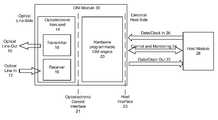
- FIG. 1is an architecture diagram of the present invention.
- FIG. 2is a block diagram of an example ONI module based on the architecture shown in FIG. 1 .
- FIG. 1is an architecture diagram of the present invention.
- the optical network interface module 30includes an optoelectronic front-end 14 and a hardware programmable optical network interface engine 20 .
- the optoelectronic front-end 14includes a transmitter 18 and a receiver 16 .
- the transmitter 18 and receiver 16communicate with the optical data input 12 and optical data output 10 (i.e., the optical line-side).
- the ONI engine 20implements physical (PHY) layer functions and, depending on the design, may also implement higher layer functions.
- the receive data pathis from optical line-in 12 through receiver 16 and ONI engine 20 to electrical data-out 22 .
- the transmit data pathis from electrical data-in 26 through ONI engine 20 and transmitter 18 to optical line-out 10 .
- the ONI engine 20interfaces to the optoelectronic front-end 14 on one side, and to host module 28 on the other side.
- the ONI engine 20typically is implemented as a chip or chip set with associated firmware/software. It can be based on one or more semiconductor substrates, non-semiconductor substrates or photonic integrated circuits where multiple optical, optoelectronic and/or electronic components are integrated on a common semiconductor substrate or other type of common substrate. Other implementations are possible.
- the interface to the optoelectronic front-end 14will be referred to as the optoelectronic control interface 21 .
- the interface to the host module 28will be referred to as the host interface 23 .
- the ONI engine 20connects to the optoelectronic front-end 14 via the optoelectronic control interface 21 , and connects to the host module 28 via the host interface 23 .
- These interfaces and the programmable optical network interface engine 20are designed so that the same ONI engine 20 can be used with different front-ends 14 and host modules 28 .
- the host interface 23is electrical, but it can be optical or a combination of optical and electrical in alternate embodiments.
- the ONI engine 20is hardware programmable, analogous to FPGAs where FPGAs are broadly used in today's electronics applications due to their rapid improvement in performance and speed.
- the ONI enginecontains basic components that can be used for different types of front-ends 14 and host modules 28 .
- itmay contain current drivers for different types of optical modulators, lasers or light sources.
- the ONI engine 20is hardware programmed to connect the corresponding current drivers to the modulator, laser or light source.
- the ONI engine 20may contain an FPGA section. Once the transport protocol for the host module 28 is specified, the FPGA section may be hardware programmed to implement the corresponding functionality for that protocol and possibly also other signaling, management, control plane and other functions used in networking.
- One advantage of this approachis that a single hardware programmable ONI engine 20 can be used to support different transport protocols. By leveraging the larger volume across a broad number of application markets, the cost of the chip/chip set can be reduced. This can be used to enable low cost optical network interface modules that can not only support today's legacy protocols, but also possibly implement new protocols.
- the ONI engine 20includes functionality to support burst mode and unframed transmissions. This capability can help to move today's protocols towards burst mode and asynchronous operation with real time clock and data acquisition without prior constraints of how the data itself is transported.
- This type of implementationprovides a unified optical transponder interface that can be programmed to work in framed or bursty traffic environments and that provides a single interface 21 for sparing applications.
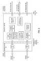
- FIG. 2is a block diagram of an example optical network interface module based on the architecture shown in FIG. 1 .
- the optoelectronic front-end 64includes an E/O converter 62 and an O/E converter 60 .
- the E/O converter 62may include elements such as lasers, modulators, optical amplifiers, dispersion pre-compensation devices, combiners, splitters, frequency selective multiplexers/demultiplexers, optical filters, voltage controlled attenuators, etc.
- the O/E converter 60may include elements such as photodetectors, transimpedance amplifiers, optical amplifiers, dispersion compensation devices, combiners, splitters, frequency selective multiplexers/demultiplexers, optical filters, voltage controlled attenuators, etc.
- Optics to interface with the fiber optic channeltypically will also be part of the optoelectronic front-end 64 .
- the specific choice of components and their designwill depend on the specific transport protocol and application. Examples of different applications include fiber to the home (ONT and OLT), data-center, metro, long haul, ultra long haul, WAN/MAN and very short reach and avionics.
- optical network interface modulesthat can be implemented using this architecture include but are not limited to tunable wavelength transmitters, burst mode transmitters and receivers, low cost short reach transmitters and receivers, fixed wavelength medium, long and ultra long range optical network interface modules, transponders that are used to connect different input and output wavelengths or transmission systems, transponders used for data regeneration, transponders used in add/drop multiplexing systems, and transponders used to convert either optical wavelength or protocol or framing format by interacting with the host module.
- both the ONI engine 66 and the interface 21are designed to have sufficient functionality and flexibility to accommodate the intended range of possible optoelectronic front-ends 64 .
- the ONI engine 66 and the host interface 23are designed to have sufficient functionality and flexibility to accommodate the intended range of possible transport protocols and host modules 28 .
- the programmable optical network interface engine 66is implemented as an ASIC with an embedded FPGA. It includes both analog and digital electronic circuits to burst mode transmit, burst mode receive, monitor and recover clock and data, and communicate with the electrical host module 28 . These circuits may reside on multiple chips or a single chip. Eventually for cost reduction the preferred embodiment is on a single chip, but the invention is not limited to single chip implementation.
- the electrical laser driver and tuning module 68includes different component circuits for driving the supported laser types. There are a wide variety of different laser types, including but not limited to multisection tunable lasers, fixed wavelength lasers, direct drive lasers and externally modulated lasers.
- the modulator driver and tuning module 74includes component circuits for driving the supported modulator types. These may include electro-absorption modulators, Mach-Zehnder modulators and direct modulation of lasers.
- the signals crossing control interface 21 to drive the lasers and modulatorsmay include signals such as a gain drive, mirror drive, phase drive, modulator drive, and control signals for monitoring various optical and electrical properties of the laser.
- driver circuitsare implemented in module 68 to accommodate many different types of lasers. There may be a bank of different driver circuits. Once the laser for E/O 62 is selected, the corresponding driver circuit is connected. For example, hardware programmable interconnects may be used to connect the correct driver circuit to the output pins on control interface 21 and to the rest of the circuitry within chip(s) 66 .
- the transmitter and receiver monitor and control module 76monitors various parameters of the transmitter 62 and receiver 60 . Possible parameters include average power, peak power, burst duty cycle, wavelength, average and peak currents for the lasers, average and peak currents for modulator bias circuits, wavelength and power calibration.
- the post amplifier and signal conditioner module 78includes circuits to receive burst mode data, and the signal conditioner module 70 includes circuits to convert the host-side electrical data and clock into signals used to drive the laser and/or modulator circuits, including as required for burst mode transmission.
- the clock and data recovery (CDR) circuits on the host-side 72 and line-side 80support burst mode transmission, as described in more detail below.
- the host-side electronics 28communicate data 84 to the host-side CDR circuits 72 . Recovered clock and data from line-side CDR circuits 80 are delivered to the host module 28 as received data and clock in the required signal level 88 .
- Control and monitoring of the electronic circuits 66 and the optoelectronic front-end 64 and delivery of control and monitoring signals 86 via the host moduleare handled by control and monitoring module 82 .
- the different modules shown in FIG. 2may include different types of components (referred to as ONI components for convenience) to accommodate different types of applications and protocols.
- ONI componentsreferred to as FPGAs
- the chip(s) 66are hardware programmed accordingly.
- some of the ONI components in chip(s) 66may be hardware programmable components (such as FPGAs) which are then programmed to implement the correct functions for the selected application and protocol.
- Other ONI componentsmay be programmable interconnects, which are then programmed to connect the correct components within ONI engine 66 (and bypassing other components).
- driver circuitsare implemented in module 68 to accommodate many different types of lasers. There may be a bank of different driver circuits. Once the laser for E/O 62 is selected, the corresponding driver circuit is connected. For example, hardware programmable interconnects may be used to connect the correct driver circuit to the output pins on control interface 21 and to the rest of the circuitry within chip(s) 66 .
- ONI engineincluding the selection of ONI components, will depend on the intended end use(s). More types of components will result in increased flexibility, allowing the same ONI engine to be used across more applications, thus increasing volume and driving down cost. However, this must be balanced against the higher complexity and cost of including more types of components.
- the ONI engineis designed to address specific types of applications.
- an ONI enginemay be designed to support data center communications.
- Ethernet, Gigabit Ethernet, ATM, TCP, IP, FDDI, GPON, 10GPON EPON, GBIC, CWDM, WDM PON, DWDM and Fiber Channelare some protocols used in data center communications.
- the components on the ONI enginemay be selected based on the requirements of this set of protocols (or a subset thereof).
- transport protocolsinclude SONET, SDH, Gigabit Ethernet, ATM, TCP, IP, GBIC, SWDM, WDM PON and DWDM.
- Protocols for fiber to the home/premise/curbinclude ATM, TCP, IP, GPON, 10GPON, WDMPON, EPON, Ethernet and Gigabit Ethernet.
- the ONI enginemay also include media access control (MAC) protocols, forward error correction (FEC) and encryption capabilities, either in hardware form, or programmable in hardware and/or software.
- Future communications protocolsmay include pure burst mode communications, including possibly burst switching, generic forms of circuit switching, fast circuit switching, cell based switching, frame based switching and generic forms of packet switching.
- the interfaces 21 and 23will depend on the intended end use(s), and also the division of functionality between the ONI engine 20 and the optoelectronic front-end 14 , or between the ONI engine 20 and the host module 28 .
- the optoelectronic control interface 21typically will carry current or voltage signals.
- Current signalscan be used for the following purposes: tuning the wavelength of tunable lasers, biasing lasers, wavelength locking and sensing, optical amplifier currents, controlling wavelength and frequency selective elements including filters, reflectors and wavelength or frequency multiplexers and demultiplexers, controlling coherent phase and amplitude, and controlling device temperatures.
- Voltage signalscan be used for the following purposes: controlling voltage controlled optical attenuators (VOAs), controlling optical phase shifters/delays, biasing modulators, and biasing photodiodes. Currents and voltages may also be used to control higher level functions. These are primarily examples where the ONI engine 20 provides a current or voltage to control a component in the optoelectronic front-end 14 .
- Current and voltages on the optoelectronic front-end 14can also be sensed, for example to monitor conditions on the optoelectronic front-end 14 .
- More advanced functionsmay include the following: signals to monitor for measuring or estimating of laser, modulator, optical amplifier, detector lifetime and/or aging characteristics, parameters related to burst operation and performance, measurement of bit error and packet or burst error rates, detection of pattern dependent errors, optical performance and channel monitoring including but not limited to optical signal to noise ratio, frequency and phase drift and stability. Additional examples include signals to monitor and control directly laser, modulator and amplifier chirp, laser relative intensity noise and phase noise, and laser mode partition noise. Further examples include signals to measure and estimate receiver, detector, optical amplifier, laser, and modulator performance transient degradation due to burst operation.
- the components included on the ONI enginemay be fairly application-specific: for example a current source for tuning wavelength, another current source for biasing laser, another current source for driving optical amplifiers, etc.
- the ONI engineis then hardware programmed to connect the appropriate current sources.
- the components on the ONI engineare fairly generic with respect to end application, but may represent different operating characteristics: for example, a current source with a low current output but very low noise, a current source with low output and moderate noise but faster response time, and a current source with higher output.
- the current sourcesare then interconnected based on the requirements of the end application.
- a similar approachmay be taken with current and voltage sensors and monitors.
- the programmable ONI engine 20is designed to support burst mode transmission of data.
- suitable transceivers and transpondersare disclosed in co-pending U.S. patent application Ser. No. 12/945,264, “Optical Burst Mode Clock and Data Recovery,” filed on Nov. 12, 2010, which is incorporated by reference herein in its entirety.
- a burst mode receiverpreferably is capable of detecting packets that arrive at the receiver asynchronously, i.e. an incoming packet is not bit aligned compared to the previous packet.
- the burst mode receiverpreferably is also able to adjust in real time to incoming packets with different power levels.
- the inclusion of burst mode capabilityexpands the number of protocols that can be supported by the programmable optical network interface engine 20 , including possibly support for future protocols.
- a protocolmight support variable length, asynchronous packets with small overhead (e.g., short preambles) for clock and data recovery.
- the arrival time and optical power of the packets or burstscan be random and vary per packet or per burst.
- stringent requirementsare imposed onto the receiver electronics, and in particular on the clock and data recovery (CDR), when synchronous protocols such as SONET, SDH and Gigabit Ethernet are used.
- CDRclock and data recovery
- burst mode applicationsmay have short packets which will require locking of the clock in a much shorter time, for example within approximately 32 bits or less.
- a programmable ONI engine 20that supports burst mode can potentially support these new applications, as well as existing protocols.
- the optical network interface moduleaccepts raw data that can be bursty in nature with variable packet length over a wide range of packet or burst sizes and a wide range of inter-packet or inter-burst spacing and can support a large optical input power dynamic range.
- Chip(s) 66serve as a common electronic engine that is used for the supported applications, leading to high volume and low cost electronics with burst mode and continuous/framed, protocol and data transparent operation.
- the electrical host data/clock 84communicates with programmable ONI engine 66 via an electrical line-side burst-mode transmitter and receiver and host-side burst mode receiver.
- the host moduleneed only supply data on the host-side. Integration of the host-side burst mode receiver enables the migration to a low cost interface that eliminates costly custom PHY chip sets.
- the burst mode capabilityallows many protocols to be communicated to the module for transmission or reception and the ONI module does not need to have its transport protocol fixed in hardware. It can be hardware programmable by the user (or hardware and software programmable), thus making this a hardware programmable optical network interface module.
- the inventionis implemented in hardware (including FPGAs and ASICs), firmware, software, and/or combinations thereof.
- moduleis not meant to be limited to a specific physical form.
- modulescan be implemented as hardware, firmware, software, and/or combinations of these.
- the moduleswere largely implemented as dedicated circuitry (e.g., part of an ASIC), in order to take advantage of lower power consumption and higher speed.
- the modulescan be implemented as software, typically running on digital signal processors or even general-purpose processors.
- Various combinationscan also be used.
- different modulescan share common components or even be implemented by the same components. There may or may not be a clear boundary between different modules.
- the “coupling” between modulesmay also take different forms.
- Dedicated circuitrycan be coupled to each other by hardwiring or by accessing a common register or memory location, for example.
- Software “coupling”can occur by any number of ways to pass information between software components (or between software and hardware, if that is the case).
- the term “coupling”is meant to include all of these and is not meant to be limited to a hardwired permanent connection between two components.
Landscapes
- Engineering & Computer Science (AREA)
- Computer Networks & Wireless Communication (AREA)
- Signal Processing (AREA)
- Physics & Mathematics (AREA)
- Electromagnetism (AREA)
- Optics & Photonics (AREA)
- Optical Communication System (AREA)
- Synchronisation In Digital Transmission Systems (AREA)
Abstract
Description
Claims (28)
Priority Applications (1)
| Application Number | Priority Date | Filing Date | Title |
|---|---|---|---|
| US12/945,470US9407426B2 (en) | 2009-11-12 | 2010-11-12 | Optical network interface, module and engine |
Applications Claiming Priority (3)
| Application Number | Priority Date | Filing Date | Title |
|---|---|---|---|
| US28115709P | 2009-11-12 | 2009-11-12 | |
| US28115609P | 2009-11-12 | 2009-11-12 | |
| US12/945,470US9407426B2 (en) | 2009-11-12 | 2010-11-12 | Optical network interface, module and engine |
Publications (2)
| Publication Number | Publication Date |
|---|---|
| US20110116792A1 US20110116792A1 (en) | 2011-05-19 |
| US9407426B2true US9407426B2 (en) | 2016-08-02 |
Family
ID=43992078
Family Applications (3)
| Application Number | Title | Priority Date | Filing Date |
|---|---|---|---|
| US12/945,470Active2032-01-02US9407426B2 (en) | 2009-11-12 | 2010-11-12 | Optical network interface, module and engine |
| US12/945,264Active - Reinstated2031-12-12US8644713B2 (en) | 2009-11-12 | 2010-11-12 | Optical burst mode clock and data recovery |
| US14/171,480Active2031-01-09US9413521B2 (en) | 2009-11-12 | 2014-02-03 | Programmable optical subassemblies and modules |
Family Applications After (2)
| Application Number | Title | Priority Date | Filing Date |
|---|---|---|---|
| US12/945,264Active - Reinstated2031-12-12US8644713B2 (en) | 2009-11-12 | 2010-11-12 | Optical burst mode clock and data recovery |
| US14/171,480Active2031-01-09US9413521B2 (en) | 2009-11-12 | 2014-02-03 | Programmable optical subassemblies and modules |
Country Status (2)
| Country | Link |
|---|---|
| US (3) | US9407426B2 (en) |
| WO (1) | WO2011060325A1 (en) |
Cited By (5)
| Publication number | Priority date | Publication date | Assignee | Title |
|---|---|---|---|---|
| EP3502894A1 (en)* | 2017-12-19 | 2019-06-26 | Solarflare Communications Inc | Network interface device |
| US10686731B2 (en) | 2017-12-19 | 2020-06-16 | Xilinx, Inc. | Network interface device |
| US10686872B2 (en) | 2017-12-19 | 2020-06-16 | Xilinx, Inc. | Network interface device |
| WO2020180349A1 (en)* | 2019-03-05 | 2020-09-10 | Brookhaven Science Associates, Llc | High-bandwidth reconfigurable data acquisition card |
| US12445395B2 (en) | 2022-07-18 | 2025-10-14 | Xilinx, Inc. | Network interface device |
Families Citing this family (23)
| Publication number | Priority date | Publication date | Assignee | Title |
|---|---|---|---|---|
| US8401399B2 (en) | 2009-05-28 | 2013-03-19 | Freedom Photonics, Llc. | Chip-based advanced modulation format transmitter |
| US9344196B1 (en) | 2009-05-28 | 2016-05-17 | Freedom Photonics, Llc. | Integrated interferometric optical transmitter |
| WO2011060325A1 (en)* | 2009-11-12 | 2011-05-19 | Packet Photonics, Inc. | Optical network interface module using a hardware programmable optical network interface engine |
| WO2012170735A2 (en)* | 2011-06-07 | 2012-12-13 | Marvell World Trade Ltd. | Physical layer frame format for long range wlan |
| EP2776881A1 (en)* | 2011-11-09 | 2014-09-17 | Aurora Networks, Inc. | Adaptive equalization of impedance mismatched card-edge connections |
| US9252873B2 (en)* | 2011-12-09 | 2016-02-02 | Source Photonics, Inc. | Methods, apparatuses, and systems for monitoring signal strength in an optical network |
| EP2873175B1 (en)* | 2012-07-15 | 2023-05-17 | OE Solutions America Inc. | Control systems for optical devices and subassemblies |
| US9755753B2 (en) | 2013-01-02 | 2017-09-05 | Oe Solutions America, Inc. | Tunable U-laser transmitter with integrated Mach-Zehnder Modulator |
| US9584884B1 (en)* | 2013-07-11 | 2017-02-28 | Inphi Corporation | Multilane variable bias for an optical modulator |
| JP6476659B2 (en)* | 2014-08-28 | 2019-03-06 | 富士通株式会社 | Signal reproduction circuit and signal reproduction method |
| US9543737B2 (en) | 2014-10-31 | 2017-01-10 | Oe Solutions America, Inc. | Fast calibration and programming optical components |
| WO2016081906A1 (en)* | 2014-11-20 | 2016-05-26 | Oe Solutions America, Inc. | Method and apparatus for controlling, monitoring, and communicating with tunable optical devices and subassemblies |
| US10256914B2 (en)* | 2015-10-13 | 2019-04-09 | Facebook, Inc. | Single source optical transmission |
| US10320152B2 (en) | 2017-03-28 | 2019-06-11 | Freedom Photonics Llc | Tunable laser |
| US10153844B2 (en) | 2017-04-03 | 2018-12-11 | Futurewei Technologies, Inc. | Channel recovery in burst-mode, time-division multiplexing (TDM) passive optical networks (PONs) |
| US10778364B2 (en)* | 2017-04-15 | 2020-09-15 | Futurewei Technologies, Inc. | Reduced power consumption for digital signal processing (DSP)-based reception in time-division multiplexing (TDM) passive optical networks (PONs) |
| CN108880721B (en)* | 2017-05-09 | 2020-07-17 | 扬智科技股份有限公司 | Ethernet physical layer circuit and clock recovery method thereof |
| CN108880902A (en)* | 2018-07-05 | 2018-11-23 | 南京英安特科技实业有限公司 | A kind of Generic Alert device and mobile network's module interface implementation method |
| US10812184B1 (en)* | 2019-04-03 | 2020-10-20 | Board Of Trustees Of The University Of Alabama, For And On Behalf Of The University Of Alabama In Huntsville | Signal analysis systems and methods |
| US10951325B1 (en)* | 2020-03-19 | 2021-03-16 | Dell Products L.P. | Use of siilicon photonics (SiP) for computer network interfaces |
| CN111865464B (en)* | 2020-06-30 | 2022-03-01 | 烽火通信科技股份有限公司 | Automatic mounting method and device for multi-slot communication system clock channel |
| JP2023172092A (en)* | 2022-05-23 | 2023-12-06 | 日本電気株式会社 | Mach-Zehnder optical modulator, optical transceiver and dispersion compensation method |
| US20250192976A1 (en)* | 2023-12-08 | 2025-06-12 | Cortina Access, Inc. | Communication device and interpacket gap adjustment method thereof |
Citations (33)
| Publication number | Priority date | Publication date | Assignee | Title |
|---|---|---|---|---|
| US20010027688A1 (en)* | 2000-04-11 | 2001-10-11 | Hideyuki Yamanaka | System for monitoring the behavior and environmental condition of a high precision electronic apparatus |
| US20010030971A1 (en)* | 2000-01-05 | 2001-10-18 | Moody Francis A. | Parallel interconnect implemented with hardware |
| US20020027689A1 (en)* | 2000-09-05 | 2002-03-07 | Meir Bartur | Fiber optic transceiver employing front end level control |
| US20020027688A1 (en)* | 2000-09-05 | 2002-03-07 | Jim Stephenson | Fiber optic transceiver employing digital dual loop compensation |
| US20030048748A1 (en)* | 2001-09-10 | 2003-03-13 | Ciena Corporation | Providing embedded protection in a network cross-connect device for SONET networks |
| US20030048801A1 (en)* | 2001-08-21 | 2003-03-13 | Dolors Sala | System, method, and computer program product for ethernet passive optical networks |
| US20040091268A1 (en) | 2002-11-01 | 2004-05-13 | Jds Uniphase Corporation | Transmitter optical sub-assembly |
| US20040208514A1 (en) | 2001-12-07 | 2004-10-21 | Ar Card | Auto-setting and optimization of EAM with optical line systems |
| US20060133411A1 (en)* | 2001-05-18 | 2006-06-22 | Denton I C | Multi-protocol networking processor with data traffic support spanning local, regional and wide area networks |
| US7090509B1 (en)* | 1999-06-11 | 2006-08-15 | Stratos International, Inc. | Multi-port pluggable transceiver (MPPT) with multiple LC duplex optical receptacles |
| US20070086479A1 (en)* | 2005-09-30 | 2007-04-19 | Jing Ling | Techniques to buffer traffic in a communications system |
| US20070140288A1 (en)* | 2005-12-19 | 2007-06-21 | Boyd Edward W | Method and apparatus for accommodating TDM traffic in an ethernet passive optical network |
| US20070153823A1 (en)* | 2005-12-30 | 2007-07-05 | Jaroslaw Wojtowicz | Small form factor, pluggable ONU |
| US7373084B2 (en)* | 2003-12-18 | 2008-05-13 | Electronics And Telecommunications Reasearch Institute | Optical network termination device for use in passive optical network based on WDM/SCM scheme |
| US20080187316A1 (en) | 2003-07-28 | 2008-08-07 | Emcore Corporation | Modular optical transceiver |
| US20080292311A1 (en) | 2007-05-24 | 2008-11-27 | Finisar Corporation | Intelligent Transmitter Module |
| US20080292322A1 (en) | 2007-05-24 | 2008-11-27 | Finisar Corporation | Optoelectronic devices with intelligent transmitter modules |
| US20090028548A1 (en)* | 2007-03-14 | 2009-01-29 | Yukihisa Tamura | Operation and construction method of network using multi-rate interface panel |
| CN101365250A (en) | 2008-08-14 | 2009-02-11 | 浙江工业大学 | Hardware platform system of GPON ONU system based on FPGA design |
| US20090060531A1 (en)* | 2007-08-30 | 2009-03-05 | Calix, Inc. | Optical network interface devices and methods |
| US7529485B2 (en) | 2001-07-05 | 2009-05-05 | Enablence Usa Fttx Networks, Inc. | Method and system for supporting multiple services with a subscriber optical interface located outside a subscriber's premises |
| US7664401B2 (en) | 2002-06-25 | 2010-02-16 | Finisar Corporation | Apparatus, system and methods for modifying operating characteristics of optoelectronic devices |
| CN101697601A (en) | 2009-10-26 | 2010-04-21 | 深圳市共进电子有限公司 | Optical network unit capable of remotely upgrading hardware logic and remote upgrade method |
| US20100158525A1 (en) | 2008-12-19 | 2010-06-24 | Edward Walter | Modular network terminals and methods to use the same |
| US7751717B2 (en)* | 2004-12-30 | 2010-07-06 | Finisar Corporation | Host printed circuit board with multiple optical transceivers |
| US7918611B2 (en) | 2007-07-11 | 2011-04-05 | Emcore Corporation | Reconfiguration and protocol adaptation of optoelectronic modules and network components |
| US20110116810A1 (en) | 2009-11-12 | 2011-05-19 | Poulsen Henrik N | Optical Burst Mode Clock and Data Recovery |
| US20110150475A1 (en)* | 2003-07-03 | 2011-06-23 | Soto Alexander I | System and Method for Pluggable Optical Modules for Passive Optical Networks |
| US20110229131A1 (en) | 2010-03-16 | 2011-09-22 | Erez Izenberg | Versatile optical network interface methods and systems |
| US20120027415A1 (en) | 2010-07-29 | 2012-02-02 | Chan Eric Y | Burst mode optical media converter with fast analog conversion |
| US20120301135A1 (en) | 2002-11-18 | 2012-11-29 | At&T Corp. | Router having dual propagation paths for packets |
| US20120308239A1 (en) | 2011-06-03 | 2012-12-06 | Sheth Samir S | Active Tracking for Free-Space Optical Communication Systems |
| US8769082B2 (en)* | 2009-07-24 | 2014-07-01 | Broadcom Corporation | Method and system for PHY initiated wake-up in energy efficient ethernet networks |
Family Cites Families (52)
| Publication number | Priority date | Publication date | Assignee | Title |
|---|---|---|---|---|
| US8107820B2 (en)* | 2006-10-13 | 2012-01-31 | Menara Networks, Inc. | Systems and methods for the integration of framing, OAM&P, and forward error correction in SFP optical transceiver devices |
| US8412051B2 (en)* | 2006-10-13 | 2013-04-02 | Menara Networks, Inc. | 40G/100G optical transceivers with integrated framing and forward error correction |
| US6647010B1 (en)* | 1999-04-07 | 2003-11-11 | Lucent Technologies Inc. | Optoelectronic network interface device |
| US6751717B2 (en)* | 2001-01-23 | 2004-06-15 | Micron Technology, Inc. | Method and apparatus for clock synchronization between a system clock and a burst data clock |
| US7123678B2 (en)* | 2001-02-01 | 2006-10-17 | Vitesse Semiconductor Corporation | RZ recovery |
| FR2824973B1 (en)* | 2001-05-17 | 2003-08-15 | Cit Alcatel | OPTICAL DEVICE FOR RECOVERING THE CLOCK OF AN OPTICAL SIGNAL |
| JP2003005140A (en)* | 2001-06-19 | 2003-01-08 | Kddi Corp | Optical signal reproduction device |
| US6665498B1 (en)* | 2001-07-20 | 2003-12-16 | Wenbin Jiang | High-speed optical data links |
| US7486894B2 (en)* | 2002-06-25 | 2009-02-03 | Finisar Corporation | Transceiver module and integrated circuit with dual eye openers |
| US7437079B1 (en)* | 2002-06-25 | 2008-10-14 | Finisar Corporation | Automatic selection of data rate for optoelectronic devices |
| US7317769B2 (en)* | 2002-07-22 | 2008-01-08 | Broadcom Corporation | Bit stream conditioning circuit having adjustable input sensitivity |
| US7515620B2 (en)* | 2002-10-29 | 2009-04-07 | Finisar Corporation | Method for optimizing laser diode operating current |
| DE20217559U1 (en)* | 2002-11-12 | 2003-01-16 | Heuft Systemtechnik Gmbh | Device for examining filled containers using X-rays |
| US7248802B2 (en)* | 2002-11-27 | 2007-07-24 | Nokia Corporation | Distribution of a synchronization signal in an optical communication system |
| JP2004222252A (en)* | 2002-12-24 | 2004-08-05 | Nec Corp | Optical signal monitoring apparatus and method |
| US20050018271A1 (en)* | 2003-03-26 | 2005-01-27 | Kddi R&D Laboratories Inc. | Apparatus for simultaneous OTDM demultiplexing, electrical clock recovery and optical clock generation, and optical clock recovery |
| KR100554225B1 (en)* | 2003-05-30 | 2006-02-22 | 한국전자통신연구원 | Apparatus and method for clock extraction of optical signal |
| JP4299179B2 (en)* | 2004-03-31 | 2009-07-22 | 富士通株式会社 | Discrimination phase margin monitor circuit, transmission / reception device, and communication system |
| GB2413043B (en)* | 2004-04-06 | 2006-11-15 | Wolfson Ltd | Clock synchroniser and clock and data recovery apparatus and method |
| GB2418084B (en)* | 2004-09-13 | 2010-01-20 | Filtronic Plc | Method and apparatus for measuring the frequency of a received signal |
| US7881616B2 (en)* | 2004-10-29 | 2011-02-01 | Finisar Corporation | Transceiver based loop back initiation |
| TWI319256B (en)* | 2005-06-30 | 2010-01-01 | Delta Electronics Inc | Motor mechanism |
| CN1866803B (en)* | 2005-09-13 | 2012-05-30 | 华为技术有限公司 | Method for solving clock synchronization in total Ethernet |
| US7738229B2 (en)* | 2006-01-10 | 2010-06-15 | Bayco Products, Ltd. | Microprocessor-controlled multifunctioning light with intrinsically safe energy limiting |
| US20070230966A1 (en)* | 2006-04-03 | 2007-10-04 | Walsh Peter J | Single interface with automatic rate detection and selection for multiple optical communication standards |
| US20070264026A1 (en)* | 2006-05-10 | 2007-11-15 | Miguel Joseph D | Method and apparatus for controlling phase of a clock signal |
| KR101088065B1 (en)* | 2006-06-29 | 2011-11-30 | 니폰덴신뎅와 가부시키가이샤 | CDR circuit |
| US7649910B1 (en)* | 2006-07-13 | 2010-01-19 | Atrica Israel Ltd. | Clock synchronization and distribution over a legacy optical Ethernet network |
| US7519750B2 (en)* | 2006-07-18 | 2009-04-14 | Cortina Systems, Inc. | Linear burst mode synchronizer for passive optical networks |
| US9319143B2 (en)* | 2006-10-13 | 2016-04-19 | Menara Networks, Inc. | 40G/100G/200G/400G pluggable optical transceivers with advanced functionality |
| US8243869B2 (en)* | 2006-11-28 | 2012-08-14 | Broadlight Ltd. | Burst mode clock and data recovery circuit and method |
| US7889815B2 (en)* | 2007-02-13 | 2011-02-15 | Optical Communication Products, Inc. | Burst mode receiver for passive optical network |
| US20080304527A1 (en)* | 2007-06-07 | 2008-12-11 | Miaobin Gao | Controlling a bias current for an optical source |
| US8332853B2 (en)* | 2007-08-03 | 2012-12-11 | Finisar Corporation | Task scheduling of fiber-optic transceiver firmware |
| US7929654B2 (en)* | 2007-08-30 | 2011-04-19 | Zenko Technologies, Inc. | Data sampling circuit and method for clock and data recovery |
| EP2071861B1 (en)* | 2007-12-12 | 2014-10-22 | ADVA Optical Networking SE | A method and a network for bidirectional transport of data |
| US8098993B2 (en)* | 2008-05-08 | 2012-01-17 | Alpenio, Inc. | Method and apparatus for transporting computer bus protocols over an optical link |
| US8281126B2 (en)* | 2008-09-30 | 2012-10-02 | Finisar Corporation | Out of band encryption |
| US20100135666A1 (en)* | 2008-11-28 | 2010-06-03 | Electronics And Telecommunications Research Institute | Clock phase aligning apparatus for burst-mode data |
| US8588558B2 (en)* | 2008-12-05 | 2013-11-19 | General Electric Company | Optical link circuit and method of making same |
| WO2010103576A1 (en)* | 2009-03-13 | 2010-09-16 | 富士通株式会社 | Data reception circuit |
| US20100254711A1 (en)* | 2009-04-03 | 2010-10-07 | Avago Technologies Fiber Ip (Singapore) Pte. Ltd. | Method and apparatus for performing direct current (dc) offset cancellation in an optical communications device |
| US20110001530A1 (en)* | 2009-07-01 | 2011-01-06 | Kawasaki Microelectronics Inc. | Method and apparatus for receiving burst data without using external detection signal |
| JP5385718B2 (en)* | 2009-07-28 | 2014-01-08 | ルネサスエレクトロニクス株式会社 | Clock data recovery circuit |
| JP5387254B2 (en)* | 2009-09-11 | 2014-01-15 | 富士通オプティカルコンポーネンツ株式会社 | Communications system |
| US8630605B2 (en)* | 2009-10-23 | 2014-01-14 | Lojack Corporation | Synchronization system and method for achieving low power battery operation of a vehicle locating unit in a stolen vehicle recovery system which receives periodic transmissions |
| KR101310904B1 (en)* | 2009-11-30 | 2013-09-25 | 한국전자통신연구원 | Burst-mode optical receiver and the timing control method |
| US8687964B2 (en)* | 2010-12-13 | 2014-04-01 | Dynamic Method Enterprise Limited | In-band control mechanism |
| US8483344B2 (en)* | 2011-06-13 | 2013-07-09 | Stephen C. Dillinger | Fast lock serializer-deserializer (SERDES) architecture |
| JP2013070254A (en)* | 2011-09-22 | 2013-04-18 | Toshiba Corp | CDR circuit |
| CN102857220A (en)* | 2011-12-27 | 2013-01-02 | 龙迅半导体科技(合肥)有限公司 | Serial clock restoring circuit in universal serial bus (USB) 2.0 high-speed mode |
| JP6268020B2 (en)* | 2014-03-26 | 2018-01-24 | ラピスセミコンダクタ株式会社 | Clock generation method and semiconductor device |
- 2010
- 2010-11-12WOPCT/US2010/056618patent/WO2011060325A1/enactiveApplication Filing
- 2010-11-12USUS12/945,470patent/US9407426B2/enactiveActive
- 2010-11-12USUS12/945,264patent/US8644713B2/enactiveActive - Reinstated
- 2014
- 2014-02-03USUS14/171,480patent/US9413521B2/enactiveActive
Patent Citations (33)
| Publication number | Priority date | Publication date | Assignee | Title |
|---|---|---|---|---|
| US7090509B1 (en)* | 1999-06-11 | 2006-08-15 | Stratos International, Inc. | Multi-port pluggable transceiver (MPPT) with multiple LC duplex optical receptacles |
| US20010030971A1 (en)* | 2000-01-05 | 2001-10-18 | Moody Francis A. | Parallel interconnect implemented with hardware |
| US20010027688A1 (en)* | 2000-04-11 | 2001-10-11 | Hideyuki Yamanaka | System for monitoring the behavior and environmental condition of a high precision electronic apparatus |
| US20020027689A1 (en)* | 2000-09-05 | 2002-03-07 | Meir Bartur | Fiber optic transceiver employing front end level control |
| US20020027688A1 (en)* | 2000-09-05 | 2002-03-07 | Jim Stephenson | Fiber optic transceiver employing digital dual loop compensation |
| US20060133411A1 (en)* | 2001-05-18 | 2006-06-22 | Denton I C | Multi-protocol networking processor with data traffic support spanning local, regional and wide area networks |
| US7529485B2 (en) | 2001-07-05 | 2009-05-05 | Enablence Usa Fttx Networks, Inc. | Method and system for supporting multiple services with a subscriber optical interface located outside a subscriber's premises |
| US20030048801A1 (en)* | 2001-08-21 | 2003-03-13 | Dolors Sala | System, method, and computer program product for ethernet passive optical networks |
| US20030048748A1 (en)* | 2001-09-10 | 2003-03-13 | Ciena Corporation | Providing embedded protection in a network cross-connect device for SONET networks |
| US20040208514A1 (en) | 2001-12-07 | 2004-10-21 | Ar Card | Auto-setting and optimization of EAM with optical line systems |
| US7664401B2 (en) | 2002-06-25 | 2010-02-16 | Finisar Corporation | Apparatus, system and methods for modifying operating characteristics of optoelectronic devices |
| US20040091268A1 (en) | 2002-11-01 | 2004-05-13 | Jds Uniphase Corporation | Transmitter optical sub-assembly |
| US20120301135A1 (en) | 2002-11-18 | 2012-11-29 | At&T Corp. | Router having dual propagation paths for packets |
| US20110150475A1 (en)* | 2003-07-03 | 2011-06-23 | Soto Alexander I | System and Method for Pluggable Optical Modules for Passive Optical Networks |
| US20080187316A1 (en) | 2003-07-28 | 2008-08-07 | Emcore Corporation | Modular optical transceiver |
| US7373084B2 (en)* | 2003-12-18 | 2008-05-13 | Electronics And Telecommunications Reasearch Institute | Optical network termination device for use in passive optical network based on WDM/SCM scheme |
| US7751717B2 (en)* | 2004-12-30 | 2010-07-06 | Finisar Corporation | Host printed circuit board with multiple optical transceivers |
| US20070086479A1 (en)* | 2005-09-30 | 2007-04-19 | Jing Ling | Techniques to buffer traffic in a communications system |
| US20070140288A1 (en)* | 2005-12-19 | 2007-06-21 | Boyd Edward W | Method and apparatus for accommodating TDM traffic in an ethernet passive optical network |
| US20070153823A1 (en)* | 2005-12-30 | 2007-07-05 | Jaroslaw Wojtowicz | Small form factor, pluggable ONU |
| US20090028548A1 (en)* | 2007-03-14 | 2009-01-29 | Yukihisa Tamura | Operation and construction method of network using multi-rate interface panel |
| US20080292322A1 (en) | 2007-05-24 | 2008-11-27 | Finisar Corporation | Optoelectronic devices with intelligent transmitter modules |
| US20080292311A1 (en) | 2007-05-24 | 2008-11-27 | Finisar Corporation | Intelligent Transmitter Module |
| US7918611B2 (en) | 2007-07-11 | 2011-04-05 | Emcore Corporation | Reconfiguration and protocol adaptation of optoelectronic modules and network components |
| US20090060531A1 (en)* | 2007-08-30 | 2009-03-05 | Calix, Inc. | Optical network interface devices and methods |
| CN101365250A (en) | 2008-08-14 | 2009-02-11 | 浙江工业大学 | Hardware platform system of GPON ONU system based on FPGA design |
| US20100158525A1 (en) | 2008-12-19 | 2010-06-24 | Edward Walter | Modular network terminals and methods to use the same |
| US8769082B2 (en)* | 2009-07-24 | 2014-07-01 | Broadcom Corporation | Method and system for PHY initiated wake-up in energy efficient ethernet networks |
| CN101697601A (en) | 2009-10-26 | 2010-04-21 | 深圳市共进电子有限公司 | Optical network unit capable of remotely upgrading hardware logic and remote upgrade method |
| US20110116810A1 (en) | 2009-11-12 | 2011-05-19 | Poulsen Henrik N | Optical Burst Mode Clock and Data Recovery |
| US20110229131A1 (en) | 2010-03-16 | 2011-09-22 | Erez Izenberg | Versatile optical network interface methods and systems |
| US20120027415A1 (en) | 2010-07-29 | 2012-02-02 | Chan Eric Y | Burst mode optical media converter with fast analog conversion |
| US20120308239A1 (en) | 2011-06-03 | 2012-12-06 | Sheth Samir S | Active Tracking for Free-Space Optical Communication Systems |
Cited By (10)
| Publication number | Priority date | Publication date | Assignee | Title |
|---|---|---|---|---|
| EP3502894A1 (en)* | 2017-12-19 | 2019-06-26 | Solarflare Communications Inc | Network interface device |
| US10686731B2 (en) | 2017-12-19 | 2020-06-16 | Xilinx, Inc. | Network interface device |
| US10686872B2 (en) | 2017-12-19 | 2020-06-16 | Xilinx, Inc. | Network interface device |
| US11165720B2 (en) | 2017-12-19 | 2021-11-02 | Xilinx, Inc. | Network interface device |
| US11394768B2 (en) | 2017-12-19 | 2022-07-19 | Xilinx, Inc. | Network interface device |
| US11394664B2 (en) | 2017-12-19 | 2022-07-19 | Xilinx, Inc. | Network interface device |
| US12224954B2 (en) | 2017-12-19 | 2025-02-11 | Xilinx, Inc. | Network interface device |
| WO2020180349A1 (en)* | 2019-03-05 | 2020-09-10 | Brookhaven Science Associates, Llc | High-bandwidth reconfigurable data acquisition card |
| US11816053B2 (en) | 2019-03-05 | 2023-11-14 | Brookhaven Science Associates, Llc | High-bandwidth reconfigurable data acquisition card |
| US12445395B2 (en) | 2022-07-18 | 2025-10-14 | Xilinx, Inc. | Network interface device |
Also Published As
| Publication number | Publication date |
|---|---|
| US8644713B2 (en) | 2014-02-04 |
| US20140147130A1 (en) | 2014-05-29 |
| US20110116810A1 (en) | 2011-05-19 |
| WO2011060325A1 (en) | 2011-05-19 |
| US20110116792A1 (en) | 2011-05-19 |
| US9413521B2 (en) | 2016-08-09 |
Similar Documents
| Publication | Publication Date | Title |
|---|---|---|
| US9407426B2 (en) | Optical network interface, module and engine | |
| US12184400B2 (en) | Multiplex conversion for a passive optical network | |
| US8666257B2 (en) | Optoelectronic devices with intelligent transmitter modules | |
| US7466922B2 (en) | Flexible control and status architecture for optical modules | |
| EP3247056B1 (en) | Optical module and optical line terminal device | |
| US7729617B2 (en) | Flexible, dense line card architecture | |
| US20140241727A1 (en) | Communication between transceivers using in-band subcarrier tones | |
| WO2015154389A1 (en) | Optical transceiving module and configuration method and device for operating parameter thereof | |
| JP2012511185A (en) | Coherent optical system with tunable local oscillator | |
| CN104519419A (en) | Optical signal processing method, optical module and optical line terminal | |
| WO2015078091A1 (en) | Gpon terminal optical transceiver assembly with rssi function | |
| CN105635860A (en) | Triple play optical path structure in EPON/OLT | |
| US8842987B2 (en) | Security in multiwavelength optical networks | |
| EP2584717B1 (en) | Method and system for testing jitter compatibility | |
| CN113346954A (en) | Local side equipment used in passive optical network with power of over 50G | |
| CN114640907B (en) | Optical communication device and optical communication method | |
| Lee et al. | Compact 4× 25 Gb/s optical receiver and transceiver for 100G ethernet interface | |
| JP2003087204A (en) | Optical amplification device and optical transmission device | |
| Kisaka et al. | Fully transparent multiplexing and transport of 10GbE-LANPHY signals in 44.6-Gbit/s-based RZ-DQPSK WDM transmission | |
| Cole | 100-Gb/s and beyond Ethernet optical interfaces | |
| Morkel et al. | Integrated IP-optical networks. Demonstration of DWDM router-to-router IP transport over 574km SMF fiber link using 11.1 Gbit/s OTN pluggable interface with integrated G. 709 and FEC | |
| Whaley et al. | Air Force highly integrated photonics program: Development and demonstration of an optically transparent fiber optic network for avionics applications | |
| US20060133826A1 (en) | Adaptive receiver for APD based modules | |
| Welch | 100 GbE Parallel Transport | |
| Xia et al. | Live Native IP Data Carried End-to-End by 100 GE Router Interfaces and Single Carrier 100 G Transport System Over 1520-km Field Deployed Fiber |
Legal Events
| Date | Code | Title | Description |
|---|---|---|---|
| AS | Assignment | Owner name:PACKET PHOTONICS, INC., NEW HAMPSHIRE Free format text:ASSIGNMENT OF ASSIGNORS INTEREST;ASSIGNORS:BLUMENTHAL, DANIEL J.;POULSEN, HENRIK N.;SIGNING DATES FROM 20101223 TO 20110201;REEL/FRAME:025729/0734 | |
| AS | Assignment | Owner name:OE SOLUTIONS AMERICA, INC., NEW JERSEY Free format text:ASSIGNMENT OF ASSIGNORS INTEREST;ASSIGNOR:PACKET PHOTONICS, INC.;REEL/FRAME:036452/0978 Effective date:20150711 | |
| AS | Assignment | Owner name:OE SOLUTIONS AMERICA, INC, NEW JERSEY Free format text:ASSIGNMENT OF ASSIGNORS INTEREST;ASSIGNOR:PACKET PHOTONICS, INC;REEL/FRAME:037301/0526 Effective date:20150711 | |
| STCF | Information on status: patent grant | Free format text:PATENTED CASE | |
| FEPP | Fee payment procedure | Free format text:SURCHARGE FOR LATE PAYMENT, SMALL ENTITY (ORIGINAL EVENT CODE: M2554); ENTITY STATUS OF PATENT OWNER: SMALL ENTITY | |
| MAFP | Maintenance fee payment | Free format text:PAYMENT OF MAINTENANCE FEE, 4TH YR, SMALL ENTITY (ORIGINAL EVENT CODE: M2551); ENTITY STATUS OF PATENT OWNER: SMALL ENTITY Year of fee payment:4 | |
| FEPP | Fee payment procedure | Free format text:MAINTENANCE FEE REMINDER MAILED (ORIGINAL EVENT CODE: REM.); ENTITY STATUS OF PATENT OWNER: SMALL ENTITY | |
| AS | Assignment | Owner name:OE SOLUTIONS CO., LTD., KOREA, REPUBLIC OF Free format text:ASSIGNMENT OF ASSIGNORS INTEREST;ASSIGNOR:OE SOLUTIONS AMERICA, INC.;REEL/FRAME:067559/0478 Effective date:20240110 | |
| FEPP | Fee payment procedure | Free format text:7.5 YR SURCHARGE - LATE PMT W/IN 6 MO, SMALL ENTITY (ORIGINAL EVENT CODE: M2555); ENTITY STATUS OF PATENT OWNER: SMALL ENTITY | |
| MAFP | Maintenance fee payment | Free format text:PAYMENT OF MAINTENANCE FEE, 8TH YR, SMALL ENTITY (ORIGINAL EVENT CODE: M2552); ENTITY STATUS OF PATENT OWNER: SMALL ENTITY Year of fee payment:8 |