US9406871B2 - Magnetoresistive element and method of manufacturing the same - Google Patents
Magnetoresistive element and method of manufacturing the sameDownload PDFInfo
- Publication number
- US9406871B2 US9406871B2US14/807,267US201514807267AUS9406871B2US 9406871 B2US9406871 B2US 9406871B2US 201514807267 AUS201514807267 AUS 201514807267AUS 9406871 B2US9406871 B2US 9406871B2
- Authority
- US
- United States
- Prior art keywords
- layer
- tunnel barrier
- stacked body
- region
- storage layer
- Prior art date
- Legal status (The legal status is an assumption and is not a legal conclusion. Google has not performed a legal analysis and makes no representation as to the accuracy of the status listed.)
- Active
Links
Images


Classifications
- H—ELECTRICITY
- H10—SEMICONDUCTOR DEVICES; ELECTRIC SOLID-STATE DEVICES NOT OTHERWISE PROVIDED FOR
- H10N—ELECTRIC SOLID-STATE DEVICES NOT OTHERWISE PROVIDED FOR
- H10N50/00—Galvanomagnetic devices
- H10N50/80—Constructional details
- H01L43/02—
- H01L27/222—
- H01L27/224—
- H01L43/08—
- H01L43/10—
- H01L43/12—
- H—ELECTRICITY
- H10—SEMICONDUCTOR DEVICES; ELECTRIC SOLID-STATE DEVICES NOT OTHERWISE PROVIDED FOR
- H10B—ELECTRONIC MEMORY DEVICES
- H10B61/00—Magnetic memory devices, e.g. magnetoresistive RAM [MRAM] devices
- H—ELECTRICITY
- H10—SEMICONDUCTOR DEVICES; ELECTRIC SOLID-STATE DEVICES NOT OTHERWISE PROVIDED FOR
- H10B—ELECTRONIC MEMORY DEVICES
- H10B61/00—Magnetic memory devices, e.g. magnetoresistive RAM [MRAM] devices
- H10B61/10—Magnetic memory devices, e.g. magnetoresistive RAM [MRAM] devices comprising components having two electrodes, e.g. diodes or MIM elements
- H—ELECTRICITY
- H10—SEMICONDUCTOR DEVICES; ELECTRIC SOLID-STATE DEVICES NOT OTHERWISE PROVIDED FOR
- H10N—ELECTRIC SOLID-STATE DEVICES NOT OTHERWISE PROVIDED FOR
- H10N50/00—Galvanomagnetic devices
- H10N50/01—Manufacture or treatment
- H—ELECTRICITY
- H10—SEMICONDUCTOR DEVICES; ELECTRIC SOLID-STATE DEVICES NOT OTHERWISE PROVIDED FOR
- H10N—ELECTRIC SOLID-STATE DEVICES NOT OTHERWISE PROVIDED FOR
- H10N50/00—Galvanomagnetic devices
- H10N50/10—Magnetoresistive devices
- H—ELECTRICITY
- H10—SEMICONDUCTOR DEVICES; ELECTRIC SOLID-STATE DEVICES NOT OTHERWISE PROVIDED FOR
- H10N—ELECTRIC SOLID-STATE DEVICES NOT OTHERWISE PROVIDED FOR
- H10N50/00—Galvanomagnetic devices
- H10N50/80—Constructional details
- H10N50/85—Materials of the active region
- H01L27/226—
- H—ELECTRICITY
- H10—SEMICONDUCTOR DEVICES; ELECTRIC SOLID-STATE DEVICES NOT OTHERWISE PROVIDED FOR
- H10B—ELECTRONIC MEMORY DEVICES
- H10B61/00—Magnetic memory devices, e.g. magnetoresistive RAM [MRAM] devices
- H10B61/20—Magnetic memory devices, e.g. magnetoresistive RAM [MRAM] devices comprising components having three or more electrodes, e.g. transistors
Definitions
- Embodiments described hereinrelate generally to a magnetoresistive element and a method of manufacturing the same.
- the MRAMis a device which performs a memory operation by storing “1” or “0” information in a memory cell by using a magnetoresistive effect, and has features of nonvolatility, high-speed operation, high integration and high reliability.
- One of magnetoresistive effect elementsis a magnetic tunnel junction (MTJ) element including a three-layer multilayer structure of a storage layer having a variable magnetization direction, an insulation film as a tunnel barrier, and a reference layer which maintains a predetermined magnetization direction.
- MTJmagnetic tunnel junction
- the resistance of the MTJ elementvaries depending on the magnetization directions of the storage layer and the reference layer, it takes a minimum value when the magnetization directions are parallel, and takes a maximum value when the magnetization directions are antiparallel, and information is stored by associating the parallel state and antiparallel state with binary information “0” and binary information “1”, respectively.
- Writing of information into the MTJ elementinvolves a magnetic-field write scheme in which only the magnetization direction in the storage layer is reversed by a current magnetic field that is generated when a current flowing is flowed through a write line, and a write (spin injection write) scheme using spin angular momentum movement in which the magnetization direction in the storage layer is reversed by passing a spin polarization current through the MTJ element itself.
- spin injection write schemespin polarized electron to be injected into the MTJ element decreases with the decrease of the volume of the magnetic layer constituting the storage layer, so that it is expected that both the miniaturization and low electric current may be easily achieved.
- FIG. 1is a sectional view for explaining a manufacturing method of a magnetic memory according to a first embodiment.
- FIG. 2is a sectional view for explaining the manufacturing method of the magnetic memory according to the first embodiment following FIG. 1 .
- FIG. 3is a sectional view for explaining the manufacturing method of the magnetic memory according to the first embodiment following FIG. 2 .
- FIG. 4is a sectional view for explaining the manufacturing method of the magnetic memory according to the first embodiment following FIG. 3 .
- FIG. 5is a sectional view for explaining the manufacturing method according to the first embodiment following FIG. 4 .
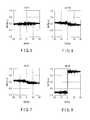
- FIG. 6is a diagram showing a magnetization curve (As I/I) of an MTJ element according to an embodiment.
- FIG. 7is a diagram showing a magnetization curve (Ge I/I) of an MTJ element according to an embodiment.
- FIG. 8is a diagram showing a magnetization curve (As P/D) of an MTJ element according to an embodiment.
- FIG. 9is a diagram showing a magnetization curve (No I/I) of an MTJ element according to a comparative example.
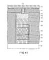
- FIG. 10is a sectional view showing a magnetic memory according to a second embodiment.
- FIG. 11is a sectional view showing a magnetoresistive memory according to a third embodiment.
- FIG. 12is a sectional view showing a manufacturing method of the magnetoresistive memory according to the third embodiment.
- FIG. 13is a sectional view for explaining the manufacturing method of the magnetoresistive memory according to the third embodiment following FIG. 12 .
- FIG. 14is a plan view schematically showing the magnetoresistive memory according to the third embodiment following FIG. 13 .
- FIG. 15is a plan view schematically showing the magnetoresistive memory according to the third embodiment following FIG. 14 .
- FIG. 16is a plan view schematically showing the magnetoresistive memory according to the third embodiment following FIG. 15 .
- FIG. 17is a plan view schematically showing the magnetoresistive memory according to the third embodiment following FIG. 16 .
- a magnetoresistive elementin general, according to one embodiment, includes a reference layer, a tunnel barrier layer, a storage layer.
- the storage layerincludes a first region and a second region provided outside the first region to surround the first region, the second region including element included in the first region and another element being different from the element.
- the magnetoresistive elementfurther includes a cap layer including a third region and a fourth region provided outside the third region to surround the third region, the fourth region including an element included in the third region and the another element.
- a method of manufacturing a magnetoresistive elementincludes forming a stacked body including a reference layer, a tunnel barrier layer and a storage layer; processing the stacked body by process including RIE (reactive ion etching) process.
- the methodfurther includes implanting another element being different from element included in the storage layer into a surface of the storage layer exposed by processing the stacked body.
- FIGS. 1 to 5are sectional views for explaining a method of manufacturing a magnetic memory.
- the magnetic memoryis a magnetic random access memory (MRAM)
- MRAMmagnetic random access memory
- FIG. 1[ FIG. 1 ]
- a lower electrode 101 , a reference layer 102 , a tunnel barrier layer 103 , a storage layer 104 , a cap layer 105 and an upper electrode 106are successively formed on a base 100 including a substrate not shown.
- a selection transistor and the likeare formed on a surface of the substrate. This selection transistor is an element for selecting an MTJ element.
- the tunnel barrier layer 103is, for example, magnesium oxide (MgO).
- the cap layer 105comprises a material having conductivity such as Ta and Ru.
- FIG. 2[ FIG. 2 ]
- a hard mask 120is formed on the upper electrode 106 , thereafter the upper electrode 106 is etched by RIE (reactive ion etching) process using the hard mask 120 as a mask to process the upper electrode 106 to be in a predetermined shape.
- RIEreactive ion etching
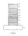
- FIG. 3[ FIG. 3 ]
- the cap layer 105 , the storage layer 104 , the tunnel barrier layer 103 , the reference layer 102 and the lower electrode 101are etched by RIE process. As a result, the MTJ element in the predetermined shape is obtained.
- a damage layer 107is generated on a surface of the stacked body 101 to 106 (MTJ element).
- RIE processbrings about chemical action between etching gas and the stacked body 101 to 106 .
- the storage layer 104has magnetic anisotropy.
- the storage layer 104has the magnetic anisotropy in a direction vertical to its film surface.
- the damage layer 107 generated on the surface of the storage layer 104also has the magnetic anisotropy.
- the damage layer 107has the magnetic anisotropy in a direction different from the storage layer 104 . Since the damage layer 107 having such disordered magnetic anisotropy deteriorates the magnetic anisotropy, spin implantation efficiency and an MR ratio, the property of the MTJ element is degraded.
- a plurality of MTJ elementsare used for the MRAM.
- the same level of influence of the damage layer 107is not caused in all the MTJ elements.
- variations in characteristics of the plurality of MTJ elements used for the MRAMoccur. Such variations in characteristics prevent the performance of the MRAM from being improved.
- the damage layeris demagnetized by implanting ions 108 into the stacked body 101 to 106 .
- the damage layeris not only magnetically deactivated, but its electric resistance may increase.
- Reference numeral 109denotes a region including the damage layer into which ions are implanted (implantation region [second region]).
- the ions 108are implanted using an oblique ion implantation method.
- the implantation of ionsare performed with the implantation angle of the ions is inclined from a direction vertical to a substrate surface.
- the ions 108can be implanted in the damage layer generated on a side face of the storage layer 104 .
- methods of obliquely implanting the ions(1) a method of implanting the ions a plurality of times by changing the implantation angle, (2) a method of implanting the ions by rotating a wafer, and a method obtained by combining (1) and (2) are available.
- the condition of the ion implantationis, for example, as follows.
- the ion implantation energyis in a range of 1 to 10 keV.
- the dose amountis 1 ⁇ 10 15 to 5 ⁇ 10 16 /cm 2 .
- the ion implantationmay be performed in a state where the MTJ element is cooled.
- the ion implantationmay be performed, for example, in a state where a substrate in which the MTJ element is formed is cooled.
- the substrateis cooled by cooling a stage on which the substrate is placed.
- the cooling temperature of the substrateis, for example, from ⁇ 100 to ⁇ 50° C. Implanting the ions at a low temperature allows damage of an object into which the ions are implanted to be reduced.
- An element used as the ions 108is, for example, at least one of As, Ge, Ga, Sb, In, N, Ar, He, F, Cl, Br, I, O, Si, B, C, Zr, Tb, S, Se, P and Ti.
- the ions 108are implanted not only into the damage layer generated on the storage layer 104 but into the damage layers generated on the lower electrode 101 , the reference layer 102 , the tunnel barrier layer 103 , the cap layer 105 and the upper electrode 106 .
- implantation regions 109are formed also on the surfaces of the lower electrode 101 , the reference layer 102 , the tunnel barrier layer 103 , the cap layer 105 and the upper electrode 106 .
- a member having magnetism other than the storage layer 104may be demagnetized, or need not be demagnetized.
- Elements corresponding to the ions 108 included in a central portion of the storage layer 104are smaller in amount than elements corresponding to the ions 108 included in the damage layer (a portion outside the central portion of the storage layer 104 ).
- the implantation region 109may be formed using a plasma doping method instead of the ion implantation method.
- Doping gasis, for example, AsH 3 , PH 3 , BF 3 and B 2 H 6 .
- the implantation region 109 including at least one of As, Ge, Ga, Sb, In, N, Ar, He, F, Cl, Br, I, O, Si, B, C, Zr, Tb, S, Se, P and Tican be formed by selecting appropriate doping gas.
- the plasma doping methodhas high productivity in comparison with the ion implantation method.
- the plasma dopingmay be performed in a state where the substrate is cooled, as well as the case of the ion implantation.
- FIG. 5[ FIG. 5 ]
- a well-known MRAM processcontinues after the implantation region 109 is formed.
- an insulating film 110is formed on an entire surface to cover the MTJ element, a surface is planarized by CMP (chemical mechanical polishing) process, an insulating film 111 is formed on the planarized surface, a plug 112 electrically connected to the upper electrode 106 is formed in the insulating film 111 , and a bit line 113 electrically connected to the plug 112 is formed.
- CMPchemical mechanical polishing
- FIGS. 6 to 8show a magnetization curve of the MTJ element according to the embodiment.
- the vertical axisis magnetization and the horizontal axis is an external magnetic field.
- FIGS. 6 to 8show the magnetization curves when As ion implantation, Ge ion implantation and As plasma doping are performed on the damage layer, respectively.
- FIG. 9shows a magnetization curve of the MTJ element (comparative example) in which neither the ion implantation nor the plasma doping is performed on the damage layer.
- the damage layerare effectively demagnetized by performing the ion implantation or the plasma doping on the damage layer.
- FIG. 10is a sectional view showing an MRAM of the present embodiment.
- the present embodimentis different from the first embodiment in a positional relationship between a reference layer 102 and a storage layer 104 , and in that the reference layer 102 is arranged on the storage layer 104 .
- the MRAM according of the present embodimentcan be obtained in accordance with the manufacturing method of the first embodiment, and has an advantage similar to that of the first embodiment.
- FIG. 11is a sectional view showing an MRAM according to the present embodiment.
- the present embodimentcan be applied to the MTJ structure in which the storage layer is arranged above the reference layer.
- the present embodimentis different from the second embodiment in that a width of stacked body of the lower electrode 101 , the storage layer 104 and the tunnel barrier layer 103 is greater than a width of stacked body of the reference layer 102 , the cap layer 105 and the upper electrode 106 .
- Such a structurecan be obtained by separating a step of processing the stacked body of the lower electrode 101 , the storage layer 104 and the tunnel barrier layer 103 from a step of processing the stacked body of the reference layer 102 , the cap layer 105 and the upper electrode 106 .
- FIGS. 12 to 17are sectional views for explaining a method for manufacturing the MRAM of the embodiment.
- the lower electrode 101 , the storage layer 104 , the tunnel barrier layer 103 , the reference layer 102 , the cap layer 105 and the upper electrode 106are successively formed on the base 100 including the substrate not shown.
- the upper electrode 106 , the cap layer 105 and the reference layer 102are processed to be in a predetermined shape by RIE process.
- the processconforms to the steps of FIGS. 2 and 3 of the first embodiment.
- a damage layer 107 due to the RIE processis generated on surfaces of the upper electrode 106 , the cap layer 105 and the reference layer 102 .
- the implantation region 109is formed and the damage layer is demagnetized.
- the implantation region 109may be formed using the plasma doping method instead of the ion implantation method.
- FIG. 15[ FIG. 15 ]
- An insulating film 110 a covering the stacked body of the reference layer 102 , the cap layer 105 and the upper electrode 106is formed by depositing an insulating film and processing the insulating film using a lithography process and an etching process.
- FIG. 16[ FIG. 16 ]
- the stacked body of the lower electrode 101 , the storage layer 104 and the tunnel barrier layer 103is etched by ion beam etching (IBE) process using the insulating film 110 a as a mask.
- IBEion beam etching
- IBEis physical etching mainly using kinetic energy of ions.
- the damage layer due to chemical reactionis hardly caused in the IBE process, unlike in the RIE process.
- throughput in the IBE processis higher than that in the RIE process, the manufacturing method according to the present embodiment may be advantageous in productivity.
- An insulating film 110 bis formed on an entire surface to cover the MTJ element, and a surface of the insulating film 110 including the insulating films 110 a and 110 b is planarized by CMP process.
- the insulating film 111is formed on the planarized surface, the plug 112 electrically connected to the upper electrode 106 is formed in the insulating film 111 , and the bit line 113 electrically connected to the plug 112 is formed, as in FIG. 5 of the first embodiment.
- the MRAM shown in FIG. 11can be obtained in this manner.
- the manufacturing method of the present embodimentcan be applied to the MTJ element including a shift adjustment layer on the reference layer 102 .
- the manufacturing method of the present embodimentcan be applied generally to a method of manufacturing an MTJ element including processing the storage layer using the RIE process.
- Each of above described MTJ structurescan be introduced as MTJ elements of memory cells.
- Memory cells, memory cell arrays and memory devicesare disclosed in U.S. patent application Ser. No. 13/420,106, Asao, the entire contents of which are incorporated by reference herein.
Landscapes
- Engineering & Computer Science (AREA)
- Manufacturing & Machinery (AREA)
- Hall/Mr Elements (AREA)
- Mram Or Spin Memory Techniques (AREA)
Abstract
Description
Claims (12)
Priority Applications (1)
| Application Number | Priority Date | Filing Date | Title |
|---|---|---|---|
| US14/807,267US9406871B2 (en) | 2013-09-09 | 2015-07-23 | Magnetoresistive element and method of manufacturing the same |
Applications Claiming Priority (3)
| Application Number | Priority Date | Filing Date | Title |
|---|---|---|---|
| US201361875577P | 2013-09-09 | 2013-09-09 | |
| US14/202,802US9123879B2 (en) | 2013-09-09 | 2014-03-10 | Magnetoresistive element and method of manufacturing the same |
| US14/807,267US9406871B2 (en) | 2013-09-09 | 2015-07-23 | Magnetoresistive element and method of manufacturing the same |
Related Parent Applications (1)
| Application Number | Title | Priority Date | Filing Date |
|---|---|---|---|
| US14/202,802DivisionUS9123879B2 (en) | 2013-09-09 | 2014-03-10 | Magnetoresistive element and method of manufacturing the same |
Publications (2)
| Publication Number | Publication Date |
|---|---|
| US20150325785A1 US20150325785A1 (en) | 2015-11-12 |
| US9406871B2true US9406871B2 (en) | 2016-08-02 |
Family
ID=52624779
Family Applications (2)
| Application Number | Title | Priority Date | Filing Date |
|---|---|---|---|
| US14/202,802ActiveUS9123879B2 (en) | 2013-09-09 | 2014-03-10 | Magnetoresistive element and method of manufacturing the same |
| US14/807,267ActiveUS9406871B2 (en) | 2013-09-09 | 2015-07-23 | Magnetoresistive element and method of manufacturing the same |
Family Applications Before (1)
| Application Number | Title | Priority Date | Filing Date |
|---|---|---|---|
| US14/202,802ActiveUS9123879B2 (en) | 2013-09-09 | 2014-03-10 | Magnetoresistive element and method of manufacturing the same |
Country Status (3)
| Country | Link |
|---|---|
| US (2) | US9123879B2 (en) |
| TW (1) | TWI562414B (en) |
| WO (1) | WO2015033858A1 (en) |
Cited By (1)
| Publication number | Priority date | Publication date | Assignee | Title |
|---|---|---|---|---|
| US12075629B2 (en) | 2019-03-20 | 2024-08-27 | Kioxia Corporation | Magnetic memory device with nonmagnetic layer having two additive elements |
Families Citing this family (2)
| Publication number | Priority date | Publication date | Assignee | Title |
|---|---|---|---|---|
| KR20170031826A (en)* | 2015-09-11 | 2017-03-22 | 삼성전자주식회사 | Semiconductor device and method of fabricating the same |
| TWI812762B (en)* | 2018-07-30 | 2023-08-21 | 日商東京威力科創股份有限公司 | Method, device and system for processing object |
Citations (96)
| Publication number | Priority date | Publication date | Assignee | Title |
|---|---|---|---|---|
| JPH04241481A (en) | 1991-01-14 | 1992-08-28 | Toshiba Corp | Heteroepitaxial junction device and its manufacturing method |
| JPH0941138A (en) | 1995-07-31 | 1997-02-10 | Res Dev Corp Of Japan | Ion implantation method using gas cluster ion beam |
| JP2000156531A (en) | 1998-09-14 | 2000-06-06 | Toshiba Corp | Magnetic element, magnetic memory device, magnetoresistive head, magnetic head gimbal assembly, and magnetic recording system |
| US6165803A (en) | 1999-05-17 | 2000-12-26 | Motorola, Inc. | Magnetic random access memory and fabricating method thereof |
| JP2001052316A (en) | 1999-05-31 | 2001-02-23 | Nec Corp | Magnetoresistance effect head, its manufacture effect head, and magnetic recording apparatus using the magnetoresistance |
| US20010022742A1 (en) | 2000-02-29 | 2001-09-20 | Manoj Bhattacharyya | Reference layer structure in a magnetic storage cell |
| US20010024347A1 (en) | 2000-01-12 | 2001-09-27 | Koji Shimazawa | Tunnel magnetoresistive element, thin-film magnetic head and memory element, and methods of manufacturing same |
| US6365286B1 (en) | 1998-09-11 | 2002-04-02 | Kabushiki Kaisha Toshiba | Magnetic element, magnetic memory device, magnetoresistance effect head, and magnetic storage system |
| US6391430B1 (en) | 2000-06-21 | 2002-05-21 | International Business Machines Corporation | Patterned magnetic recording media with discrete magnetic regions separated by regions of antiferromagnetically coupled films |
| US20020070361A1 (en) | 2000-07-14 | 2002-06-13 | Epion Corporation | Gas cluster ion beam size diagnostics and workpiece processing |
| JP2002176211A (en) | 2000-09-06 | 2002-06-21 | Matsushita Electric Ind Co Ltd | Magnetoresistive element, method of manufacturing the same, and magnetic device using the same |
| JP2002280640A (en) | 2001-03-19 | 2002-09-27 | Canon Inc | Magnetoresistive element, memory element using the magnetoresistive element, and recording / reproducing method of the memory element |
| US20020146851A1 (en) | 2001-04-06 | 2002-10-10 | Takeshi Okazawa | Method of forming magnetic memory |
| JP2002299727A (en) | 2001-04-02 | 2002-10-11 | Canon Inc | Magnetic element, tunnel magnetoresistive element and method for manufacturing the same |
| JP2002299726A (en) | 2001-03-30 | 2002-10-11 | Toshiba Corp | Magnetoresistive element, magnetic head, magnetic reproducing device and magnetic storage device |
| US20020167059A1 (en) | 2001-03-19 | 2002-11-14 | Naoki Nishimura | Magnetoresistive element, memory element using the magnetoresistive element, and recording/reproduction method for the memory element |
| US6483675B1 (en) | 1999-07-23 | 2002-11-19 | Tdk Corporation | Tunnel magnetoresistance effect element |
| US20020182442A1 (en) | 2001-04-02 | 2002-12-05 | Takashi Ikeda | Magnetoresistive element, memory element having the magnetoresistive element, and memory using the memory element |
| US20030067800A1 (en) | 2001-10-02 | 2003-04-10 | Akio Koganei | Magnetoresistive element and nonvolatile solid-state memory using the same |
| JP2004006589A (en) | 2002-03-28 | 2004-01-08 | Toshiba Corp | Magnetoresistive element, magnetic head, and magnetic reproducing device |
| JP2004500483A (en) | 1999-12-06 | 2004-01-08 | エピオン コーポレイション | Method and apparatus for smoothing a thin conductive film with a gas cluster ion beam |
| US20040080876A1 (en) | 2002-04-22 | 2004-04-29 | Matsushita Electric Industrial Co. | Magnetoresistive element, magnetic head, magnetic memory and magnetic recording apparatus using the same |
| US20040135184A1 (en)* | 2003-01-06 | 2004-07-15 | Sony Corporation | Nonvolatile magnetic memory device and manufacturing method thereof |
| US20040188732A1 (en) | 2003-03-24 | 2004-09-30 | Yoshiaki Fukuzumi | Semiconductor memory device comprising magneto resistive element and its manufacturing method |
| US20050020076A1 (en) | 2003-07-21 | 2005-01-27 | Hynix Semiconductor Inc. | Method for manufacturing MTJ cell of magnetic random access memory |
| US20050048675A1 (en) | 2003-08-29 | 2005-03-03 | Canon Kabushiki Kaisha | Method of etching magnetic material, magnetoresistive film and magnetic random access memory |
| JP2005209951A (en) | 2004-01-23 | 2005-08-04 | Sony Corp | Magnetic memory device and magnetic storage device |
| US20050174876A1 (en) | 2002-05-13 | 2005-08-11 | Nec Corporation | Semiconductor storage device and production method therefor |
| WO2005088745A1 (en) | 2004-03-12 | 2005-09-22 | Japan Science And Technology Agency | Magnetoresistive element and its manufacturing method |
| US6965138B2 (en) | 2003-07-23 | 2005-11-15 | Kabushiki Kaisha Toshiba | Magnetic memory device and method of manufacturing the same |
| US20050274997A1 (en) | 2004-06-15 | 2005-12-15 | International Business Machines Corporation | Method for fabricating magnetic field concentrators as liners around conductive wires in microelectronic devices |
| US20060043317A1 (en) | 2004-08-24 | 2006-03-02 | Shigeru Ono | Cluster-ion beam irradiation apparatus and method for manufacturing magnetic head element using the same |
| JP2006510196A (en) | 2002-12-12 | 2006-03-23 | エピオン コーポレーション | Recrystallization of semiconductor surface film by high energy cluster irradiation and semiconductor doping method |
| US20060105570A1 (en) | 2004-11-08 | 2006-05-18 | Epion Corporation | Copper interconnect wiring and method of forming thereof |
| JP2006165031A (en) | 2004-12-02 | 2006-06-22 | Ulvac Japan Ltd | Tunnel junction element manufacturing method and manufacturing apparatus thereof |
| JP2007053315A (en) | 2005-08-19 | 2007-03-01 | Fujitsu Ltd | Magnetic memory device and manufacturing method thereof |
| US20070076328A1 (en)* | 2005-09-30 | 2007-04-05 | Hitachi Global Storage Technologies Netherlands, B.V. | Magnetic recording head with ESD shunt trace |
| US7220601B2 (en) | 2004-01-16 | 2007-05-22 | Samsung Electronics Co., Ltd. | Method of forming nano-sized MTJ cell without contact hole |
| JP2007234897A (en) | 2006-03-01 | 2007-09-13 | Toyota Motor Corp | Semiconductor device and its manufacturing method |
| JP2007305610A (en) | 2006-05-08 | 2007-11-22 | Tohoku Univ | Tunnel magnetoresistive element, nonvolatile magnetic memory, light emitting element, and three-terminal element |
| JP2008066612A (en) | 2006-09-11 | 2008-03-21 | Fujitsu Ltd | Tunnel magnetoresistive element and manufacturing method thereof. |
| US20080073641A1 (en)* | 2006-09-27 | 2008-03-27 | Amberwave Systems Corporation | Quantum tunneling devices and circuits with lattice-mismatched semiconductor structures |
| US20080122005A1 (en) | 2006-11-06 | 2008-05-29 | Horsky Thomas N | Ion Implantation Device and a Method of Semiconductor Manufacturing by the Implantation of Molecular Ions Containing Phosphorus and Arsenic |
| JP2008522429A (en) | 2004-12-03 | 2008-06-26 | エピオン コーポレーション | Formation of ultra-shallow junction by gas cluster ion irradiation |
| JP2008153527A (en) | 2006-12-19 | 2008-07-03 | Sony Corp | Storage element and memory |
| JP2008171882A (en) | 2007-01-09 | 2008-07-24 | Sony Corp | Storage element and memory |
| JP2008282940A (en) | 2007-05-10 | 2008-11-20 | Sony Corp | Method for manufacturing magnetic storage device |
| JP2009054715A (en) | 2007-08-24 | 2009-03-12 | Nec Corp | Magnetic wall random access memory |
| US20090080238A1 (en) | 2007-09-25 | 2009-03-26 | Kabushiki Kaisha Toshiba | Magnetoresistive element and magnetoresistive random access memory including the same |
| US20090191696A1 (en) | 2008-01-25 | 2009-07-30 | Tel Epion Inc. | Method for increasing the penetration depth of material infusion in a substrate using a gas cluster ion beam |
| US7586781B2 (en) | 2004-10-27 | 2009-09-08 | Keio University | Magneto-resistance effect element and magnetic memory device |
| US20090243008A1 (en) | 2008-03-27 | 2009-10-01 | Eiji Kitagawa | Magnetoresistive element and magnetic memory |
| US7619431B2 (en) | 2003-12-23 | 2009-11-17 | Nxp B.V. | High sensitivity magnetic built-in current sensor |
| JP2010003342A (en) | 2008-06-19 | 2010-01-07 | Hitachi Ltd | Magnetic head and magnetic storage |
| US20100097846A1 (en) | 2008-10-22 | 2010-04-22 | Kabushiki Kaisha Toshiba | Magnetoresistive element and magnetic memory |
| JP2010113782A (en) | 2008-11-10 | 2010-05-20 | Hitachi Global Storage Technologies Netherlands Bv | Output balanced differential type reproducing magnetic head and method for manufacturing the same |
| US20100135068A1 (en) | 2008-12-03 | 2010-06-03 | Sony Corporation | Resistance-change memory device |
| US7746603B2 (en) | 2006-12-19 | 2010-06-29 | Hitachi Global Storage Technologies Netherlands B.V. | CPP Magnetoresistive head with different thickness free layers for improved signal to noise ratio |
| US20100183902A1 (en) | 2009-01-20 | 2010-07-22 | Woojin Kim | Magnetic memory devices and methods of manufacturing such magnetic memory devices |
| US20110037108A1 (en) | 2009-08-11 | 2011-02-17 | Kabushiki Kaisha Toshiba | Magnetoresistive memory and manufacturing method thereof |
| US20110059557A1 (en) | 2009-09-04 | 2011-03-10 | Sony Corporation | Method of manufacturing nonvolatile memory device |
| US7916430B2 (en) | 2007-08-09 | 2011-03-29 | Tdk Corporation | Thin-film magnetic head and manufacturing method thereof |
| US20110174770A1 (en) | 2010-01-15 | 2011-07-21 | Tel Epion Inc. | Method for modifying an etch rate of a material layer using energetic charged particles |
| US20110233697A1 (en) | 2010-03-24 | 2011-09-29 | Kabushiki Kaisha Toshiba | Magnetic memory |
| US20120032288A1 (en) | 2010-08-04 | 2012-02-09 | Kabushiki Kaisha Toshiba | Magnetoresistive element and method of manufacturing the same |
| US8119018B2 (en) | 2006-09-13 | 2012-02-21 | Canon Anelva Corporation | Magnetoresistive effect element manufacturing method and multi-chamber apparatus for manufacturing magnetoresistive effect element |
| US8130474B2 (en) | 2005-07-18 | 2012-03-06 | Hitachi Global Storage Technologies Netherlands B.V. | CPP-TMR sensor with non-orthogonal free and reference layer magnetization orientation |
| US20120056253A1 (en) | 2010-09-07 | 2012-03-08 | Kabushiki Kaisha Toshiba | Semiconductor memory device and manufacturing method thereof |
| US20120074511A1 (en) | 2010-09-17 | 2012-03-29 | Kabushiki Kaisha Toshiba | Magnetic memory and method of manufacturing the same |
| US20120135543A1 (en) | 2010-11-29 | 2012-05-31 | Samsung Electronics Co., Ltd. | Method For Forming Magnetic Tunnel Junction Structure And Method For Forming Magnetic Random Access Memory Using The Same |
| US20120139019A1 (en) | 2010-12-02 | 2012-06-07 | Fujitsu Semiconductor Limited | Magnetoresistive effect element and method of manufacturing magnetoresistive effect element |
| US8223533B2 (en) | 2008-09-26 | 2012-07-17 | Kabushiki Kaisha Toshiba | Magnetoresistive effect device and magnetic memory |
| US8270125B2 (en) | 2007-12-18 | 2012-09-18 | Hitachi Global Storage Technologies Netherlands B.V. | Tunnel junction magnetoresistive sensor having a near zero magnetostriction free layer |
| US20120244639A1 (en) | 2011-03-22 | 2012-09-27 | Yuichi Ohsawa | Method of manufacturing magnetic memory |
| US20120244640A1 (en) | 2011-03-22 | 2012-09-27 | Yuichi Ohsawa | Method of manufacturing multilayer film |
| JP2012244051A (en) | 2011-05-23 | 2012-12-10 | Fujitsu Ltd | Magnetoresistive element and magnetic storage device |
| US8339841B2 (en) | 2009-02-12 | 2012-12-25 | Kabushiki Kaisha Toshiba | Magnetoresistive element including upper electrode having hexagonal cross-section shape and method of manufacturing the same |
| US20130001716A1 (en)* | 2011-06-30 | 2013-01-03 | Kabushiki Kaisha Toshiba | Magnetoresistive element and manufacturing method of the same |
| US20130008867A1 (en)* | 2011-07-07 | 2013-01-10 | Ken Tokashiki | Methods for manufacturing magnetic tunnel junction structure |
| US20130017626A1 (en) | 2011-07-11 | 2013-01-17 | Kazuhiro Tomioka | Etching apparatus and method of manufacturing semiconductor device |
| US20130029431A1 (en)* | 2011-06-28 | 2013-01-31 | Kabushiki Kaisha Toshiba | Method for manufacturing nonvolatile memory device |
| US20130069182A1 (en)* | 2011-09-21 | 2013-03-21 | Yuichi Ohsawa | Magnetoresistive effect element, magnetic memory, and magnetoresistive effect element manufacturing method |
| US20130069186A1 (en) | 2011-09-20 | 2013-03-21 | Kabushiki Kaisha Toshiba | Magnetoresistive element and method of manufacturing the same |
| US20130099338A1 (en) | 2011-10-24 | 2013-04-25 | Kabushiki Kaisha Toshiba | Magnetic memory element and magnetic memory |
| US8475672B2 (en) | 2009-02-06 | 2013-07-02 | Canon Anelva Corporation | Plasma processing device, plasma processing method and method of manufacturing element including substrate to be processed |
| US20130181305A1 (en) | 2010-09-17 | 2013-07-18 | Kabushiki Kaisha Toshiba | Magnetoresistive element and magnetic random access memory |
| JP2013153232A (en) | 2013-05-15 | 2013-08-08 | Fujitsu Ltd | Semiconductor memory device |
| US20140087483A1 (en)* | 2012-09-25 | 2014-03-27 | Kabushiki Kaisha Toshiba | Manufacturing method of magnetoresistive effect element and manufacturing apparatus of magnetoresistive effect element |
| US20140319590A1 (en)* | 2013-04-25 | 2014-10-30 | Keisuke Nakatsuka | Semiconductor memory device |
| US20140327096A1 (en) | 2013-05-02 | 2014-11-06 | T3Memory, Inc. | Perpendicular stt-mram having logical magnetic shielding |
| US20140356979A1 (en) | 2013-06-04 | 2014-12-04 | International Business Machines Corporation | Thermally assisted mram with a multilayer encapsulant for low thermal conductivity |
| US8928055B2 (en) | 2012-03-20 | 2015-01-06 | Kabushiki Kaisha Toshiba | Magnetic memory element |
| US8963264B2 (en) | 2012-06-29 | 2015-02-24 | Seagate Technology Llc | Magnetic stack with orthogonal biasing layer |
| US20150069542A1 (en) | 2013-09-06 | 2015-03-12 | Makoto Nagamine | Magneto-resistive element and method of manufacturing the same |
| US20150069561A1 (en)* | 2013-09-12 | 2015-03-12 | Globalfoundries Singapore Pte. Ltd. | Logic compatible memory |
| US20160087004A1 (en)* | 2014-09-18 | 2016-03-24 | Yasuyuki Sonoda | Magnetic memory and method of manufacturing the same |
Family Cites Families (1)
| Publication number | Priority date | Publication date | Assignee | Title |
|---|---|---|---|---|
| US20070246787A1 (en)* | 2006-03-29 | 2007-10-25 | Lien-Chang Wang | On-plug magnetic tunnel junction devices based on spin torque transfer switching |
- 2014
- 2014-03-10USUS14/202,802patent/US9123879B2/enactiveActive
- 2014-08-22WOPCT/JP2014/072663patent/WO2015033858A1/enactiveApplication Filing
- 2014-09-09TWTW103131027Apatent/TWI562414B/enactive
- 2015
- 2015-07-23USUS14/807,267patent/US9406871B2/enactiveActive
Patent Citations (126)
| Publication number | Priority date | Publication date | Assignee | Title |
|---|---|---|---|---|
| JPH04241481A (en) | 1991-01-14 | 1992-08-28 | Toshiba Corp | Heteroepitaxial junction device and its manufacturing method |
| JPH0941138A (en) | 1995-07-31 | 1997-02-10 | Res Dev Corp Of Japan | Ion implantation method using gas cluster ion beam |
| US6365286B1 (en) | 1998-09-11 | 2002-04-02 | Kabushiki Kaisha Toshiba | Magnetic element, magnetic memory device, magnetoresistance effect head, and magnetic storage system |
| JP2000156531A (en) | 1998-09-14 | 2000-06-06 | Toshiba Corp | Magnetic element, magnetic memory device, magnetoresistive head, magnetic head gimbal assembly, and magnetic recording system |
| US6165803A (en) | 1999-05-17 | 2000-12-26 | Motorola, Inc. | Magnetic random access memory and fabricating method thereof |
| JP2001052316A (en) | 1999-05-31 | 2001-02-23 | Nec Corp | Magnetoresistance effect head, its manufacture effect head, and magnetic recording apparatus using the magnetoresistance |
| US6483675B1 (en) | 1999-07-23 | 2002-11-19 | Tdk Corporation | Tunnel magnetoresistance effect element |
| JP2004500483A (en) | 1999-12-06 | 2004-01-08 | エピオン コーポレイション | Method and apparatus for smoothing a thin conductive film with a gas cluster ion beam |
| US20010024347A1 (en) | 2000-01-12 | 2001-09-27 | Koji Shimazawa | Tunnel magnetoresistive element, thin-film magnetic head and memory element, and methods of manufacturing same |
| US6895658B2 (en) | 2000-01-12 | 2005-05-24 | Tdk Corporation | Methods of manufacturing a tunnel magnetoresistive element, thin-film magnetic head and memory element |
| US20010022742A1 (en) | 2000-02-29 | 2001-09-20 | Manoj Bhattacharyya | Reference layer structure in a magnetic storage cell |
| US6297983B1 (en) | 2000-02-29 | 2001-10-02 | Hewlett-Packard Company | Reference layer structure in a magnetic storage cell |
| JP2001308292A (en) | 2000-02-29 | 2001-11-02 | Hewlett Packard Co <Hp> | Magnetic storage cell |
| JP2008193103A (en) | 2000-02-29 | 2008-08-21 | Samsung Electronics Co Ltd | Method for manufacturing magnetic memory cell |
| US6479353B2 (en) | 2000-02-29 | 2002-11-12 | Hewlett-Packard Company | Reference layer structure in a magnetic storage cell |
| US6391430B1 (en) | 2000-06-21 | 2002-05-21 | International Business Machines Corporation | Patterned magnetic recording media with discrete magnetic regions separated by regions of antiferromagnetically coupled films |
| JP2003536199A (en) | 2000-06-21 | 2003-12-02 | インターナショナル・ビジネス・マシーンズ・コーポレーション | Magnetic recording medium and method for manufacturing the same |
| US20020070361A1 (en) | 2000-07-14 | 2002-06-13 | Epion Corporation | Gas cluster ion beam size diagnostics and workpiece processing |
| JP2002176211A (en) | 2000-09-06 | 2002-06-21 | Matsushita Electric Ind Co Ltd | Magnetoresistive element, method of manufacturing the same, and magnetic device using the same |
| US20020167059A1 (en) | 2001-03-19 | 2002-11-14 | Naoki Nishimura | Magnetoresistive element, memory element using the magnetoresistive element, and recording/reproduction method for the memory element |
| JP2002280640A (en) | 2001-03-19 | 2002-09-27 | Canon Inc | Magnetoresistive element, memory element using the magnetoresistive element, and recording / reproducing method of the memory element |
| US6713830B2 (en) | 2001-03-19 | 2004-03-30 | Canon Kabushiki Kaisha | Magnetoresistive element, memory element using the magnetoresistive element, and recording/reproduction method for the memory element |
| JP2002299726A (en) | 2001-03-30 | 2002-10-11 | Toshiba Corp | Magnetoresistive element, magnetic head, magnetic reproducing device and magnetic storage device |
| US6829121B2 (en) | 2001-04-02 | 2004-12-07 | Canon Kabushiki Kaisha | Magnetoresistive element, memory element having the magnetoresistive element, and memory using the memory element |
| JP2002299727A (en) | 2001-04-02 | 2002-10-11 | Canon Inc | Magnetic element, tunnel magnetoresistive element and method for manufacturing the same |
| US20020182442A1 (en) | 2001-04-02 | 2002-12-05 | Takashi Ikeda | Magnetoresistive element, memory element having the magnetoresistive element, and memory using the memory element |
| JP2002305290A (en) | 2001-04-06 | 2002-10-18 | Nec Corp | Magnetic memory and method of manufacturing the same |
| US20020146851A1 (en) | 2001-04-06 | 2002-10-10 | Takeshi Okazawa | Method of forming magnetic memory |
| US20030067800A1 (en) | 2001-10-02 | 2003-04-10 | Akio Koganei | Magnetoresistive element and nonvolatile solid-state memory using the same |
| JP2003110162A (en) | 2001-10-02 | 2003-04-11 | Canon Inc | Magnetoresistive element, nonvolatile solid-state memory using the element, and recording / reproducing method thereof |
| US6987652B2 (en) | 2001-10-02 | 2006-01-17 | Canon Kabushiki Kaisha | Tapered angle magnetoresistive element and nonvolatile solid-state memory using the same |
| JP2004006589A (en) | 2002-03-28 | 2004-01-08 | Toshiba Corp | Magnetoresistive element, magnetic head, and magnetic reproducing device |
| US20040080876A1 (en) | 2002-04-22 | 2004-04-29 | Matsushita Electric Industrial Co. | Magnetoresistive element, magnetic head, magnetic memory and magnetic recording apparatus using the same |
| US20050174876A1 (en) | 2002-05-13 | 2005-08-11 | Nec Corporation | Semiconductor storage device and production method therefor |
| JP2006510196A (en) | 2002-12-12 | 2006-03-23 | エピオン コーポレーション | Recrystallization of semiconductor surface film by high energy cluster irradiation and semiconductor doping method |
| US20040135184A1 (en)* | 2003-01-06 | 2004-07-15 | Sony Corporation | Nonvolatile magnetic memory device and manufacturing method thereof |
| US20040188732A1 (en) | 2003-03-24 | 2004-09-30 | Yoshiaki Fukuzumi | Semiconductor memory device comprising magneto resistive element and its manufacturing method |
| US20050020076A1 (en) | 2003-07-21 | 2005-01-27 | Hynix Semiconductor Inc. | Method for manufacturing MTJ cell of magnetic random access memory |
| US6965138B2 (en) | 2003-07-23 | 2005-11-15 | Kabushiki Kaisha Toshiba | Magnetic memory device and method of manufacturing the same |
| US20050254289A1 (en) | 2003-07-23 | 2005-11-17 | Kabushiki Kaisha Toshiba | Magnetic memory device and method of manufacturing the same |
| US20050048675A1 (en) | 2003-08-29 | 2005-03-03 | Canon Kabushiki Kaisha | Method of etching magnetic material, magnetoresistive film and magnetic random access memory |
| US7619431B2 (en) | 2003-12-23 | 2009-11-17 | Nxp B.V. | High sensitivity magnetic built-in current sensor |
| US7220601B2 (en) | 2004-01-16 | 2007-05-22 | Samsung Electronics Co., Ltd. | Method of forming nano-sized MTJ cell without contact hole |
| US20070164338A1 (en) | 2004-01-16 | 2007-07-19 | Samsung Electronics Co., Ltd. | Method of forming nano-sized MTJ cell without contact hole |
| JP2005209951A (en) | 2004-01-23 | 2005-08-04 | Sony Corp | Magnetic memory device and magnetic storage device |
| WO2005088745A1 (en) | 2004-03-12 | 2005-09-22 | Japan Science And Technology Agency | Magnetoresistive element and its manufacturing method |
| JP2006005342A (en) | 2004-06-15 | 2006-01-05 | Internatl Business Mach Corp <Ibm> | Method of manufacturing a magnetic field concentrator as a liner around a conductive wire in a microelectronic device |
| US20050274997A1 (en) | 2004-06-15 | 2005-12-15 | International Business Machines Corporation | Method for fabricating magnetic field concentrators as liners around conductive wires in microelectronic devices |
| US20060043317A1 (en) | 2004-08-24 | 2006-03-02 | Shigeru Ono | Cluster-ion beam irradiation apparatus and method for manufacturing magnetic head element using the same |
| US7586781B2 (en) | 2004-10-27 | 2009-09-08 | Keio University | Magneto-resistance effect element and magnetic memory device |
| US20090285013A1 (en) | 2004-10-27 | 2009-11-19 | Keio University | Magneto-resistance effect element and magnetic memory device |
| US20060105570A1 (en) | 2004-11-08 | 2006-05-18 | Epion Corporation | Copper interconnect wiring and method of forming thereof |
| JP2006165031A (en) | 2004-12-02 | 2006-06-22 | Ulvac Japan Ltd | Tunnel junction element manufacturing method and manufacturing apparatus thereof |
| JP2008522429A (en) | 2004-12-03 | 2008-06-26 | エピオン コーポレーション | Formation of ultra-shallow junction by gas cluster ion irradiation |
| US8130474B2 (en) | 2005-07-18 | 2012-03-06 | Hitachi Global Storage Technologies Netherlands B.V. | CPP-TMR sensor with non-orthogonal free and reference layer magnetization orientation |
| JP2007053315A (en) | 2005-08-19 | 2007-03-01 | Fujitsu Ltd | Magnetic memory device and manufacturing method thereof |
| US20070076328A1 (en)* | 2005-09-30 | 2007-04-05 | Hitachi Global Storage Technologies Netherlands, B.V. | Magnetic recording head with ESD shunt trace |
| JP2007234897A (en) | 2006-03-01 | 2007-09-13 | Toyota Motor Corp | Semiconductor device and its manufacturing method |
| JP2007305610A (en) | 2006-05-08 | 2007-11-22 | Tohoku Univ | Tunnel magnetoresistive element, nonvolatile magnetic memory, light emitting element, and three-terminal element |
| JP2008066612A (en) | 2006-09-11 | 2008-03-21 | Fujitsu Ltd | Tunnel magnetoresistive element and manufacturing method thereof. |
| US8119018B2 (en) | 2006-09-13 | 2012-02-21 | Canon Anelva Corporation | Magnetoresistive effect element manufacturing method and multi-chamber apparatus for manufacturing magnetoresistive effect element |
| US20080073641A1 (en)* | 2006-09-27 | 2008-03-27 | Amberwave Systems Corporation | Quantum tunneling devices and circuits with lattice-mismatched semiconductor structures |
| US20080122005A1 (en) | 2006-11-06 | 2008-05-29 | Horsky Thomas N | Ion Implantation Device and a Method of Semiconductor Manufacturing by the Implantation of Molecular Ions Containing Phosphorus and Arsenic |
| JP2008153527A (en) | 2006-12-19 | 2008-07-03 | Sony Corp | Storage element and memory |
| US7746603B2 (en) | 2006-12-19 | 2010-06-29 | Hitachi Global Storage Technologies Netherlands B.V. | CPP Magnetoresistive head with different thickness free layers for improved signal to noise ratio |
| JP2008171882A (en) | 2007-01-09 | 2008-07-24 | Sony Corp | Storage element and memory |
| JP2008282940A (en) | 2007-05-10 | 2008-11-20 | Sony Corp | Method for manufacturing magnetic storage device |
| US7916430B2 (en) | 2007-08-09 | 2011-03-29 | Tdk Corporation | Thin-film magnetic head and manufacturing method thereof |
| JP2009054715A (en) | 2007-08-24 | 2009-03-12 | Nec Corp | Magnetic wall random access memory |
| US20090080238A1 (en) | 2007-09-25 | 2009-03-26 | Kabushiki Kaisha Toshiba | Magnetoresistive element and magnetoresistive random access memory including the same |
| US7957184B2 (en) | 2007-09-25 | 2011-06-07 | Kabushiki Kaisha Toshiba | Magnetoresistive element and magnetoresistive random access memory including the same |
| US8154915B2 (en) | 2007-09-25 | 2012-04-10 | Kabushiki Kaisha Toshiba | Magnetoresistive element and magnetoresistive random access memory including the same |
| US8139405B2 (en) | 2007-09-25 | 2012-03-20 | Kabushiki Kaisha Toshiba | Magnetoresistive element and magnetoresistive random access memory including the same |
| JP2009081216A (en) | 2007-09-25 | 2009-04-16 | Toshiba Corp | Magnetoresistive element and magnetic random access memory using the same |
| US7768824B2 (en) | 2007-09-25 | 2010-08-03 | Kabushiki Kaisha Toshiba | Magnetoresistive element and magnetoresistive random access memory including the same |
| US20100230770A1 (en) | 2007-09-25 | 2010-09-16 | Kabushiki Kaisha Toshiba | Magnetoresistive element and magnetoresistive random access memory including the same |
| US20110222335A1 (en) | 2007-09-25 | 2011-09-15 | Kabushiki Kaisha Toshiba | Magnetoresistive element and magnetoresistive random access memory including the same |
| US20110211389A1 (en) | 2007-09-25 | 2011-09-01 | Kabushiki Kaisha Toshiba | Magnetoresistive element and magnetoresistive random access memory including the same |
| US8270125B2 (en) | 2007-12-18 | 2012-09-18 | Hitachi Global Storage Technologies Netherlands B.V. | Tunnel junction magnetoresistive sensor having a near zero magnetostriction free layer |
| US20090191696A1 (en) | 2008-01-25 | 2009-07-30 | Tel Epion Inc. | Method for increasing the penetration depth of material infusion in a substrate using a gas cluster ion beam |
| US8218355B2 (en) | 2008-03-27 | 2012-07-10 | Kabushiki Kaisha Toshiba | Magnetoresistive element and magnetic memory |
| US20090243008A1 (en) | 2008-03-27 | 2009-10-01 | Eiji Kitagawa | Magnetoresistive element and magnetic memory |
| JP2009239120A (en) | 2008-03-27 | 2009-10-15 | Toshiba Corp | Magnetoresistive element, and magnetic memory |
| JP2010003342A (en) | 2008-06-19 | 2010-01-07 | Hitachi Ltd | Magnetic head and magnetic storage |
| US8223533B2 (en) | 2008-09-26 | 2012-07-17 | Kabushiki Kaisha Toshiba | Magnetoresistive effect device and magnetic memory |
| US20100097846A1 (en) | 2008-10-22 | 2010-04-22 | Kabushiki Kaisha Toshiba | Magnetoresistive element and magnetic memory |
| JP2010113782A (en) | 2008-11-10 | 2010-05-20 | Hitachi Global Storage Technologies Netherlands Bv | Output balanced differential type reproducing magnetic head and method for manufacturing the same |
| US20100135068A1 (en) | 2008-12-03 | 2010-06-03 | Sony Corporation | Resistance-change memory device |
| US20100183902A1 (en) | 2009-01-20 | 2010-07-22 | Woojin Kim | Magnetic memory devices and methods of manufacturing such magnetic memory devices |
| US8475672B2 (en) | 2009-02-06 | 2013-07-02 | Canon Anelva Corporation | Plasma processing device, plasma processing method and method of manufacturing element including substrate to be processed |
| US8339841B2 (en) | 2009-02-12 | 2012-12-25 | Kabushiki Kaisha Toshiba | Magnetoresistive element including upper electrode having hexagonal cross-section shape and method of manufacturing the same |
| JP2011040580A (en) | 2009-08-11 | 2011-02-24 | Toshiba Corp | Magnetoresistive memory and method for manufacturing the same |
| US20110037108A1 (en) | 2009-08-11 | 2011-02-17 | Kabushiki Kaisha Toshiba | Magnetoresistive memory and manufacturing method thereof |
| JP2011054873A (en) | 2009-09-04 | 2011-03-17 | Sony Corp | Method of manufacturing nonvolatile memory element |
| US8268713B2 (en) | 2009-09-04 | 2012-09-18 | Sony Corporation | Method of manufacturing nonvolatile memory device |
| US20110059557A1 (en) | 2009-09-04 | 2011-03-10 | Sony Corporation | Method of manufacturing nonvolatile memory device |
| US20110174770A1 (en) | 2010-01-15 | 2011-07-21 | Tel Epion Inc. | Method for modifying an etch rate of a material layer using energetic charged particles |
| US20110233697A1 (en) | 2010-03-24 | 2011-09-29 | Kabushiki Kaisha Toshiba | Magnetic memory |
| US20120032288A1 (en) | 2010-08-04 | 2012-02-09 | Kabushiki Kaisha Toshiba | Magnetoresistive element and method of manufacturing the same |
| US20120056253A1 (en) | 2010-09-07 | 2012-03-08 | Kabushiki Kaisha Toshiba | Semiconductor memory device and manufacturing method thereof |
| US20120074511A1 (en) | 2010-09-17 | 2012-03-29 | Kabushiki Kaisha Toshiba | Magnetic memory and method of manufacturing the same |
| US8710605B2 (en) | 2010-09-17 | 2014-04-29 | Kabushiki Kaisha Toshiba | Magnetic memory and method of manufacturing the same |
| US20130181305A1 (en) | 2010-09-17 | 2013-07-18 | Kabushiki Kaisha Toshiba | Magnetoresistive element and magnetic random access memory |
| US20120135543A1 (en) | 2010-11-29 | 2012-05-31 | Samsung Electronics Co., Ltd. | Method For Forming Magnetic Tunnel Junction Structure And Method For Forming Magnetic Random Access Memory Using The Same |
| US20120139019A1 (en) | 2010-12-02 | 2012-06-07 | Fujitsu Semiconductor Limited | Magnetoresistive effect element and method of manufacturing magnetoresistive effect element |
| US20120244639A1 (en) | 2011-03-22 | 2012-09-27 | Yuichi Ohsawa | Method of manufacturing magnetic memory |
| US20120244640A1 (en) | 2011-03-22 | 2012-09-27 | Yuichi Ohsawa | Method of manufacturing multilayer film |
| US8716034B2 (en) | 2011-03-22 | 2014-05-06 | Kabushiki Kaisha Toshiba | Method of manufacturing magnetic memory |
| JP2012244051A (en) | 2011-05-23 | 2012-12-10 | Fujitsu Ltd | Magnetoresistive element and magnetic storage device |
| US20130029431A1 (en)* | 2011-06-28 | 2013-01-31 | Kabushiki Kaisha Toshiba | Method for manufacturing nonvolatile memory device |
| US20130001716A1 (en)* | 2011-06-30 | 2013-01-03 | Kabushiki Kaisha Toshiba | Magnetoresistive element and manufacturing method of the same |
| US20130008867A1 (en)* | 2011-07-07 | 2013-01-10 | Ken Tokashiki | Methods for manufacturing magnetic tunnel junction structure |
| US20130017626A1 (en) | 2011-07-11 | 2013-01-17 | Kazuhiro Tomioka | Etching apparatus and method of manufacturing semiconductor device |
| US20130069186A1 (en) | 2011-09-20 | 2013-03-21 | Kabushiki Kaisha Toshiba | Magnetoresistive element and method of manufacturing the same |
| US20130069182A1 (en)* | 2011-09-21 | 2013-03-21 | Yuichi Ohsawa | Magnetoresistive effect element, magnetic memory, and magnetoresistive effect element manufacturing method |
| US20130099338A1 (en) | 2011-10-24 | 2013-04-25 | Kabushiki Kaisha Toshiba | Magnetic memory element and magnetic memory |
| US8928055B2 (en) | 2012-03-20 | 2015-01-06 | Kabushiki Kaisha Toshiba | Magnetic memory element |
| US8963264B2 (en) | 2012-06-29 | 2015-02-24 | Seagate Technology Llc | Magnetic stack with orthogonal biasing layer |
| US20140087483A1 (en)* | 2012-09-25 | 2014-03-27 | Kabushiki Kaisha Toshiba | Manufacturing method of magnetoresistive effect element and manufacturing apparatus of magnetoresistive effect element |
| US20140319590A1 (en)* | 2013-04-25 | 2014-10-30 | Keisuke Nakatsuka | Semiconductor memory device |
| US20140327096A1 (en) | 2013-05-02 | 2014-11-06 | T3Memory, Inc. | Perpendicular stt-mram having logical magnetic shielding |
| JP2013153232A (en) | 2013-05-15 | 2013-08-08 | Fujitsu Ltd | Semiconductor memory device |
| US20140356979A1 (en) | 2013-06-04 | 2014-12-04 | International Business Machines Corporation | Thermally assisted mram with a multilayer encapsulant for low thermal conductivity |
| US20150069542A1 (en) | 2013-09-06 | 2015-03-12 | Makoto Nagamine | Magneto-resistive element and method of manufacturing the same |
| US20150069561A1 (en)* | 2013-09-12 | 2015-03-12 | Globalfoundries Singapore Pte. Ltd. | Logic compatible memory |
| US20160087004A1 (en)* | 2014-09-18 | 2016-03-24 | Yasuyuki Sonoda | Magnetic memory and method of manufacturing the same |
Non-Patent Citations (10)
| Title |
|---|
| Albert, et al., "Spin-polarized current switching of a Co thin film nanomagnet", Applied Physics Letters, vol. 77, No. 23, Oct. 7, 2000, 3809-3811. |
| International Search Report including Written Opinion dated Sep. 22, 2014, issued in parent International Application No. PCT/JP2014/072663. |
| Otani, et al., "Microfabrication of Magnetic Tunnel Junctions Using CH3OH Etching", IEEE Transactions on Magnetics, vol. 43, No. 6, Jun. 6, 2007, 2776-2778. |
| Related U.S. Appl. No. 13/226,868; First Named Inventor: Yuichi Ohsawa; Title: "Method of Manufacturing Magnetic Memory"; filed Sep. 7, 2011. |
| Related U.S. Appl. No. 13/226,960; First Named Inventor: Yuichi Ohsawa; Title: "Method of Manufacturing Multilayer Film"; filed Sep. 7, 2011. |
| Related U.S. Appl. No. 13/231,894; First Named Inventor: Shigeki Takahashi; Title: "Magnetic Memory and Method of Manufacturing the Same"; filed Sep. 13, 2011. |
| Related U.S. Appl. No. 13/604,537; First Named Inventor: Masahiko Nakayama; Title: "Magnetic Memory Element and Magnetic Memory"; filed Sep. 5, 2012. |
| Related U.S. Appl. No. 14/200,670; First Named Inventor: Kuniaki Sugiura; Title: "Magnetoresistive Element and Method of Manufacturing the Same"; filed Mar. 7, 2014. |
| Related U.S. Appl. No. 14/200,742; First Named Inventor: Masaru Toko; Title: "Magnetoresistive Element and Method for Manufacturing the Same"; filed Mar. 7, 2014. |
| Related U.S. Appl. No. 14/203,249; First Named Inventor: Masahiko Nakayama; Title: "Magnetic Memory and Method of Manufacturing the Same"; filed Mar. 10, 2014. |
Cited By (1)
| Publication number | Priority date | Publication date | Assignee | Title |
|---|---|---|---|---|
| US12075629B2 (en) | 2019-03-20 | 2024-08-27 | Kioxia Corporation | Magnetic memory device with nonmagnetic layer having two additive elements |
Also Published As
| Publication number | Publication date |
|---|---|
| US9123879B2 (en) | 2015-09-01 |
| WO2015033858A1 (en) | 2015-03-12 |
| TWI562414B (en) | 2016-12-11 |
| US20150069557A1 (en) | 2015-03-12 |
| TW201523944A (en) | 2015-06-16 |
| US20150325785A1 (en) | 2015-11-12 |
Similar Documents
| Publication | Publication Date | Title |
|---|---|---|
| US8716819B2 (en) | Magnetic random access memory | |
| US9362490B1 (en) | Method of patterning MTJ cell without sidewall damage | |
| US9741928B2 (en) | Magnetoresistive element and magnetic random access memory | |
| JP2019114816A (en) | Manufacturing method of magnetic resistance random access memory | |
| US8987846B2 (en) | Magnetic memory and manufacturing method thereof | |
| US9385304B2 (en) | Magnetic memory and method of manufacturing the same | |
| US9647203B2 (en) | Magnetoresistive element having a magnetic layer including O | |
| US8884389B2 (en) | Magnetoresistive element and method of manufacturing the same | |
| JP6043478B2 (en) | Storage node including free magnetic layer of magnetic anisotropic material, magnetic memory device including the same, and manufacturing method thereof | |
| US20150069554A1 (en) | Magnetic memory and method of manufacturing the same | |
| US9620565B2 (en) | Semiconductor memory device | |
| JP2016225633A (en) | Voltage controlled magnetic anisotropy switching device using external ferromagnetic bias film | |
| CN106104830A (en) | The replacement conductive hard mask etched for multi-step MTJ (MTJ) | |
| US20160163974A1 (en) | Electric field assisted perpendicular stt-mram | |
| US9755141B2 (en) | Method for fabricating MRAM bits on a tight pitch | |
| US9306152B2 (en) | Magnetic memory and method for manufacturing the same | |
| US9368717B2 (en) | Magnetoresistive element and method for manufacturing the same | |
| US9231196B2 (en) | Magnetoresistive element and method of manufacturing the same | |
| US9406871B2 (en) | Magnetoresistive element and method of manufacturing the same | |
| KR101774937B1 (en) | Storage node comprising free magnetic layer of in-plane magnetic anisotropy material, magnetic memory device comprising the same and method of manufacturing the same | |
| US20160064651A1 (en) | Method to make three-terminal mram | |
| JP2014063804A (en) | Magnetic memory |
Legal Events
| Date | Code | Title | Description |
|---|---|---|---|
| AS | Assignment | Owner name:SK HYNIX INC., KOREA, REPUBLIC OF Free format text:ASSIGNMENT OF ASSIGNORS INTEREST;ASSIGNORS:NAKAYAMA, MASAHIKO;YOSHIKAWA, MASATOSHI;KAI, TADASHI;AND OTHERS;SIGNING DATES FROM 20140225 TO 20140523;REEL/FRAME:037924/0981 Owner name:KABUSHIKI KAISHA TOSHIBA, JAPAN Free format text:ASSIGNMENT OF ASSIGNORS INTEREST;ASSIGNORS:NAKAYAMA, MASAHIKO;YOSHIKAWA, MASATOSHI;KAI, TADASHI;AND OTHERS;SIGNING DATES FROM 20140225 TO 20140523;REEL/FRAME:037924/0981 | |
| AS | Assignment | Owner name:SK HYNIX INC., KOREA, REPUBLIC OF Free format text:CORRECTIVE ASSIGNMENT TO CORRECT THE ADDRESS OF THE SECOND ASSIGNEE PREVIOUSLY RECORDED AT REEL: 037924 FRAME: 0981. ASSIGNOR(S) HEREBY CONFIRMS THE ASSIGNMENT;ASSIGNORS:NAKAYAMA, MASAHIKO;YOSHIKAWA, MASATOSHI;KAI, TADASHI;AND OTHERS;SIGNING DATES FROM 20140225 TO 20140523;REEL/FRAME:038188/0620 Owner name:KABUSHIKI KAISHA TOSHIBA, JAPAN Free format text:CORRECTIVE ASSIGNMENT TO CORRECT THE ADDRESS OF THE SECOND ASSIGNEE PREVIOUSLY RECORDED AT REEL: 037924 FRAME: 0981. ASSIGNOR(S) HEREBY CONFIRMS THE ASSIGNMENT;ASSIGNORS:NAKAYAMA, MASAHIKO;YOSHIKAWA, MASATOSHI;KAI, TADASHI;AND OTHERS;SIGNING DATES FROM 20140225 TO 20140523;REEL/FRAME:038188/0620 | |
| STCF | Information on status: patent grant | Free format text:PATENTED CASE | |
| FEPP | Fee payment procedure | Free format text:PAYOR NUMBER ASSIGNED (ORIGINAL EVENT CODE: ASPN); ENTITY STATUS OF PATENT OWNER: LARGE ENTITY | |
| AS | Assignment | Owner name:SK HYNIX, INC., KOREA, REPUBLIC OF Free format text:ASSIGNMENT OF ASSIGNORS INTEREST;ASSIGNOR:KABUSHIKI KAISHA TOSHIBA;REEL/FRAME:043559/0459 Effective date:20170905 Owner name:TOSHIBA MEMORY CORPORATION, JAPAN Free format text:ASSIGNMENT OF ASSIGNORS INTEREST;ASSIGNOR:KABUSHIKI KAISHA TOSHIBA;REEL/FRAME:043559/0459 Effective date:20170905 | |
| MAFP | Maintenance fee payment | Free format text:PAYMENT OF MAINTENANCE FEE, 4TH YEAR, LARGE ENTITY (ORIGINAL EVENT CODE: M1551); ENTITY STATUS OF PATENT OWNER: LARGE ENTITY Year of fee payment:4 | |
| AS | Assignment | Owner name:K.K. PANGEA, JAPAN Free format text:MERGER AND CHANGE OF NAME;ASSIGNORS:TOSHIBA MEMORY CORPORATION;K.K. PANGEA;REEL/FRAME:058786/0085 Effective date:20180801 Owner name:TOSHIBA MEMORY CORPORATION, JAPAN Free format text:CHANGE OF NAME;ASSIGNOR:K.K. PANGEA;REEL/FRAME:058711/0088 Effective date:20180801 | |
| AS | Assignment | Owner name:KIOXIA CORPORATION, JAPAN Free format text:CHANGE OF NAME;ASSIGNOR:TOSHIBA MEMORY CORPORATION;REEL/FRAME:059110/0850 Effective date:20191001 | |
| MAFP | Maintenance fee payment | Free format text:PAYMENT OF MAINTENANCE FEE, 8TH YEAR, LARGE ENTITY (ORIGINAL EVENT CODE: M1552); ENTITY STATUS OF PATENT OWNER: LARGE ENTITY Year of fee payment:8 |