US9406658B2 - Embedded component device and manufacturing methods thereof - Google Patents
Embedded component device and manufacturing methods thereofDownload PDFInfo
- Publication number
- US9406658B2 US9406658B2US12/972,046US97204610AUS9406658B2US 9406658 B2US9406658 B2US 9406658B2US 97204610 AUS97204610 AUS 97204610AUS 9406658 B2US9406658 B2US 9406658B2
- Authority
- US
- United States
- Prior art keywords
- layer
- conductive
- patterned conductive
- dielectric layer
- conductive layer
- Prior art date
- Legal status (The legal status is an assumption and is not a legal conclusion. Google has not performed a legal analysis and makes no representation as to the accuracy of the status listed.)
- Active, expires
Links
- 238000004519manufacturing processMethods0.000titledescription36
- 229920005989resinPolymers0.000claimsdescription29
- 239000011347resinSubstances0.000claimsdescription29
- 239000000835fiberSubstances0.000claimsdescription13
- 239000004593EpoxySubstances0.000claimsdescription6
- 239000010410layerSubstances0.000description534
- 239000004065semiconductorSubstances0.000description116
- 229920002120photoresistant polymerPolymers0.000description51
- 238000000034methodMethods0.000description48
- 239000000758substrateSubstances0.000description42
- 239000000463materialSubstances0.000description32
- 239000004020conductorSubstances0.000description24
- RYGMFSIKBFXOCR-UHFFFAOYSA-NCopperChemical compound[Cu]RYGMFSIKBFXOCR-UHFFFAOYSA-N0.000description18
- 239000012790adhesive layerSubstances0.000description18
- 229910052802copperInorganic materials0.000description16
- 239000010949copperSubstances0.000description16
- 229910052751metalInorganic materials0.000description14
- 239000002184metalSubstances0.000description14
- 238000005553drillingMethods0.000description12
- 238000005530etchingMethods0.000description9
- 229910000679solderInorganic materials0.000description8
- 229910045601alloyInorganic materials0.000description7
- 239000000956alloySubstances0.000description7
- 238000013459approachMethods0.000description7
- 238000003486chemical etchingMethods0.000description7
- PXHVJJICTQNCMI-UHFFFAOYSA-NNickelChemical compound[Ni]PXHVJJICTQNCMI-UHFFFAOYSA-N0.000description6
- 238000007772electroless platingMethods0.000description6
- 239000011888foilSubstances0.000description6
- 229910001092metal group alloyInorganic materials0.000description6
- 239000011248coating agentSubstances0.000description5
- 238000000576coating methodMethods0.000description5
- 238000003475laminationMethods0.000description5
- 229920000271Kevlar®Polymers0.000description4
- 239000003989dielectric materialSubstances0.000description4
- 239000003365glass fiberSubstances0.000description4
- 239000004761kevlarSubstances0.000description4
- 238000004544sputter depositionMethods0.000description4
- 229920000106Liquid crystal polymerPolymers0.000description3
- 239000004977Liquid-crystal polymers (LCPs)Substances0.000description3
- 239000000654additiveSubstances0.000description3
- 238000009713electroplatingMethods0.000description3
- 230000007613environmental effectEffects0.000description3
- PCHJSUWPFVWCPO-UHFFFAOYSA-NgoldChemical compound[Au]PCHJSUWPFVWCPO-UHFFFAOYSA-N0.000description3
- 229910052737goldInorganic materials0.000description3
- 239000010931goldSubstances0.000description3
- 239000011159matrix materialSubstances0.000description3
- 238000000465mouldingMethods0.000description3
- 229910052759nickelInorganic materials0.000description3
- 230000003647oxidationEffects0.000description3
- 238000007254oxidation reactionMethods0.000description3
- 238000007639printingMethods0.000description3
- 239000004642PolyimideSubstances0.000description2
- ATJFFYVFTNAWJD-UHFFFAOYSA-NTinChemical compound[Sn]ATJFFYVFTNAWJD-UHFFFAOYSA-N0.000description2
- 150000001875compoundsChemical class0.000description2
- 239000011889copper foilSubstances0.000description2
- 239000012792core layerSubstances0.000description2
- 230000003247decreasing effectEffects0.000description2
- 239000008393encapsulating agentSubstances0.000description2
- 238000012986modificationMethods0.000description2
- 230000004048modificationEffects0.000description2
- 239000012778molding materialSubstances0.000description2
- 238000004806packaging method and processMethods0.000description2
- 229920001721polyimidePolymers0.000description2
- 239000002356single layerSubstances0.000description2
- 238000009987spinningMethods0.000description2
- 238000005507sprayingMethods0.000description2
- 229910052718tinInorganic materials0.000description2
- JYEUMXHLPRZUAT-UHFFFAOYSA-N1,2,3-triazineChemical compoundC1=CN=NN=C1JYEUMXHLPRZUAT-UHFFFAOYSA-N0.000description1
- XQUPVDVFXZDTLT-UHFFFAOYSA-N1-[4-[[4-(2,5-dioxopyrrol-1-yl)phenyl]methyl]phenyl]pyrrole-2,5-dioneChemical compoundO=C1C=CC(=O)N1C(C=C1)=CC=C1CC1=CC=C(N2C(C=CC2=O)=O)C=C1XQUPVDVFXZDTLT-UHFFFAOYSA-N0.000description1
- RTAQQCXQSZGOHL-UHFFFAOYSA-NTitaniumChemical compound[Ti]RTAQQCXQSZGOHL-UHFFFAOYSA-N0.000description1
- 239000002390adhesive tapeSubstances0.000description1
- 229910052782aluminiumInorganic materials0.000description1
- XAGFODPZIPBFFR-UHFFFAOYSA-NaluminiumChemical compound[Al]XAGFODPZIPBFFR-UHFFFAOYSA-N0.000description1
- 239000004760aramidSubstances0.000description1
- 229920006231aramid fiberPolymers0.000description1
- 230000015572biosynthetic processEffects0.000description1
- 238000005229chemical vapour depositionMethods0.000description1
- 239000011247coating layerSubstances0.000description1
- 238000000151depositionMethods0.000description1
- 229920006336epoxy molding compoundPolymers0.000description1
- 238000001746injection mouldingMethods0.000description1
- 239000007788liquidSubstances0.000description1
- 230000008018meltingEffects0.000description1
- 238000002844meltingMethods0.000description1
- 239000000203mixtureSubstances0.000description1
- 238000000059patterningMethods0.000description1
- 229920003192poly(bis maleimide)Polymers0.000description1
- 239000011135tinSubstances0.000description1
- 229910052719titaniumInorganic materials0.000description1
- 239000010936titaniumSubstances0.000description1
- 238000001771vacuum depositionMethods0.000description1
Images


Classifications
- H—ELECTRICITY
- H01—ELECTRIC ELEMENTS
- H01L—SEMICONDUCTOR DEVICES NOT COVERED BY CLASS H10
- H01L25/00—Assemblies consisting of a plurality of semiconductor or other solid state devices
- H01L25/16—Assemblies consisting of a plurality of semiconductor or other solid state devices the devices being of types provided for in two or more different subclasses of H10B, H10D, H10F, H10H, H10K or H10N, e.g. forming hybrid circuits
- H—ELECTRICITY
- H01—ELECTRIC ELEMENTS
- H01L—SEMICONDUCTOR DEVICES NOT COVERED BY CLASS H10
- H01L23/00—Details of semiconductor or other solid state devices
- H01L23/52—Arrangements for conducting electric current within the device in operation from one component to another, i.e. interconnections, e.g. wires, lead frames
- H01L23/538—Arrangements for conducting electric current within the device in operation from one component to another, i.e. interconnections, e.g. wires, lead frames the interconnection structure between a plurality of semiconductor chips being formed on, or in, insulating substrates
- H01L23/5389—Arrangements for conducting electric current within the device in operation from one component to another, i.e. interconnections, e.g. wires, lead frames the interconnection structure between a plurality of semiconductor chips being formed on, or in, insulating substrates the chips being integrally enclosed by the interconnect and support structures
- H—ELECTRICITY
- H01—ELECTRIC ELEMENTS
- H01L—SEMICONDUCTOR DEVICES NOT COVERED BY CLASS H10
- H01L24/00—Arrangements for connecting or disconnecting semiconductor or solid-state bodies; Methods or apparatus related thereto
- H01L24/01—Means for bonding being attached to, or being formed on, the surface to be connected, e.g. chip-to-package, die-attach, "first-level" interconnects; Manufacturing methods related thereto
- H01L24/18—High density interconnect [HDI] connectors; Manufacturing methods related thereto
- H01L24/23—Structure, shape, material or disposition of the high density interconnect connectors after the connecting process
- H01L24/24—Structure, shape, material or disposition of the high density interconnect connectors after the connecting process of an individual high density interconnect connector
- H—ELECTRICITY
- H01—ELECTRIC ELEMENTS
- H01L—SEMICONDUCTOR DEVICES NOT COVERED BY CLASS H10
- H01L24/00—Arrangements for connecting or disconnecting semiconductor or solid-state bodies; Methods or apparatus related thereto
- H01L24/80—Methods for connecting semiconductor or other solid state bodies using means for bonding being attached to, or being formed on, the surface to be connected
- H01L24/82—Methods for connecting semiconductor or other solid state bodies using means for bonding being attached to, or being formed on, the surface to be connected by forming build-up interconnects at chip-level, e.g. for high density interconnects [HDI]
- H—ELECTRICITY
- H01—ELECTRIC ELEMENTS
- H01L—SEMICONDUCTOR DEVICES NOT COVERED BY CLASS H10
- H01L2224/00—Indexing scheme for arrangements for connecting or disconnecting semiconductor or solid-state bodies and methods related thereto as covered by H01L24/00
- H01L2224/01—Means for bonding being attached to, or being formed on, the surface to be connected, e.g. chip-to-package, die-attach, "first-level" interconnects; Manufacturing methods related thereto
- H01L2224/02—Bonding areas; Manufacturing methods related thereto
- H01L2224/04—Structure, shape, material or disposition of the bonding areas prior to the connecting process
- H01L2224/04105—Bonding areas formed on an encapsulation of the semiconductor or solid-state body, e.g. bonding areas on chip-scale packages
- H—ELECTRICITY
- H01—ELECTRIC ELEMENTS
- H01L—SEMICONDUCTOR DEVICES NOT COVERED BY CLASS H10
- H01L2224/00—Indexing scheme for arrangements for connecting or disconnecting semiconductor or solid-state bodies and methods related thereto as covered by H01L24/00
- H01L2224/01—Means for bonding being attached to, or being formed on, the surface to be connected, e.g. chip-to-package, die-attach, "first-level" interconnects; Manufacturing methods related thereto
- H01L2224/10—Bump connectors; Manufacturing methods related thereto
- H01L2224/15—Structure, shape, material or disposition of the bump connectors after the connecting process
- H01L2224/16—Structure, shape, material or disposition of the bump connectors after the connecting process of an individual bump connector
- H01L2224/161—Disposition
- H01L2224/16151—Disposition the bump connector connecting between a semiconductor or solid-state body and an item not being a semiconductor or solid-state body, e.g. chip-to-substrate, chip-to-passive
- H01L2224/16221—Disposition the bump connector connecting between a semiconductor or solid-state body and an item not being a semiconductor or solid-state body, e.g. chip-to-substrate, chip-to-passive the body and the item being stacked
- H01L2224/16225—Disposition the bump connector connecting between a semiconductor or solid-state body and an item not being a semiconductor or solid-state body, e.g. chip-to-substrate, chip-to-passive the body and the item being stacked the item being non-metallic, e.g. insulating substrate with or without metallisation
- H—ELECTRICITY
- H01—ELECTRIC ELEMENTS
- H01L—SEMICONDUCTOR DEVICES NOT COVERED BY CLASS H10
- H01L2224/00—Indexing scheme for arrangements for connecting or disconnecting semiconductor or solid-state bodies and methods related thereto as covered by H01L24/00
- H01L2224/01—Means for bonding being attached to, or being formed on, the surface to be connected, e.g. chip-to-package, die-attach, "first-level" interconnects; Manufacturing methods related thereto
- H01L2224/18—High density interconnect [HDI] connectors; Manufacturing methods related thereto
- H01L2224/23—Structure, shape, material or disposition of the high density interconnect connectors after the connecting process
- H01L2224/24—Structure, shape, material or disposition of the high density interconnect connectors after the connecting process of an individual high density interconnect connector
- H01L2224/241—Disposition
- H01L2224/24151—Connecting between a semiconductor or solid-state body and an item not being a semiconductor or solid-state body, e.g. chip-to-substrate, chip-to-passive
- H01L2224/24153—Connecting between a semiconductor or solid-state body and an item not being a semiconductor or solid-state body, e.g. chip-to-substrate, chip-to-passive the body and the item being arranged next to each other, e.g. on a common substrate
- H01L2224/24195—Connecting between a semiconductor or solid-state body and an item not being a semiconductor or solid-state body, e.g. chip-to-substrate, chip-to-passive the body and the item being arranged next to each other, e.g. on a common substrate the item being a discrete passive component
- H—ELECTRICITY
- H01—ELECTRIC ELEMENTS
- H01L—SEMICONDUCTOR DEVICES NOT COVERED BY CLASS H10
- H01L2224/00—Indexing scheme for arrangements for connecting or disconnecting semiconductor or solid-state bodies and methods related thereto as covered by H01L24/00
- H01L2224/01—Means for bonding being attached to, or being formed on, the surface to be connected, e.g. chip-to-package, die-attach, "first-level" interconnects; Manufacturing methods related thereto
- H01L2224/18—High density interconnect [HDI] connectors; Manufacturing methods related thereto
- H01L2224/23—Structure, shape, material or disposition of the high density interconnect connectors after the connecting process
- H01L2224/24—Structure, shape, material or disposition of the high density interconnect connectors after the connecting process of an individual high density interconnect connector
- H01L2224/241—Disposition
- H01L2224/24151—Connecting between a semiconductor or solid-state body and an item not being a semiconductor or solid-state body, e.g. chip-to-substrate, chip-to-passive
- H01L2224/24221—Connecting between a semiconductor or solid-state body and an item not being a semiconductor or solid-state body, e.g. chip-to-substrate, chip-to-passive the body and the item being stacked
- H01L2224/24225—Connecting between a semiconductor or solid-state body and an item not being a semiconductor or solid-state body, e.g. chip-to-substrate, chip-to-passive the body and the item being stacked the item being non-metallic, e.g. insulating substrate with or without metallisation
- H01L2224/24227—Connecting between a semiconductor or solid-state body and an item not being a semiconductor or solid-state body, e.g. chip-to-substrate, chip-to-passive the body and the item being stacked the item being non-metallic, e.g. insulating substrate with or without metallisation the HDI interconnect not connecting to the same level of the item at which the semiconductor or solid-state body is mounted, e.g. the semiconductor or solid-state body being mounted in a cavity or on a protrusion of the item
- H—ELECTRICITY
- H01—ELECTRIC ELEMENTS
- H01L—SEMICONDUCTOR DEVICES NOT COVERED BY CLASS H10
- H01L2224/00—Indexing scheme for arrangements for connecting or disconnecting semiconductor or solid-state bodies and methods related thereto as covered by H01L24/00
- H01L2224/01—Means for bonding being attached to, or being formed on, the surface to be connected, e.g. chip-to-package, die-attach, "first-level" interconnects; Manufacturing methods related thereto
- H01L2224/26—Layer connectors, e.g. plate connectors, solder or adhesive layers; Manufacturing methods related thereto
- H01L2224/31—Structure, shape, material or disposition of the layer connectors after the connecting process
- H01L2224/32—Structure, shape, material or disposition of the layer connectors after the connecting process of an individual layer connector
- H01L2224/321—Disposition
- H01L2224/32151—Disposition the layer connector connecting between a semiconductor or solid-state body and an item not being a semiconductor or solid-state body, e.g. chip-to-substrate, chip-to-passive
- H01L2224/32221—Disposition the layer connector connecting between a semiconductor or solid-state body and an item not being a semiconductor or solid-state body, e.g. chip-to-substrate, chip-to-passive the body and the item being stacked
- H01L2224/32225—Disposition the layer connector connecting between a semiconductor or solid-state body and an item not being a semiconductor or solid-state body, e.g. chip-to-substrate, chip-to-passive the body and the item being stacked the item being non-metallic, e.g. insulating substrate with or without metallisation
- H—ELECTRICITY
- H01—ELECTRIC ELEMENTS
- H01L—SEMICONDUCTOR DEVICES NOT COVERED BY CLASS H10
- H01L2224/00—Indexing scheme for arrangements for connecting or disconnecting semiconductor or solid-state bodies and methods related thereto as covered by H01L24/00
- H01L2224/01—Means for bonding being attached to, or being formed on, the surface to be connected, e.g. chip-to-package, die-attach, "first-level" interconnects; Manufacturing methods related thereto
- H01L2224/42—Wire connectors; Manufacturing methods related thereto
- H01L2224/44—Structure, shape, material or disposition of the wire connectors prior to the connecting process
- H01L2224/45—Structure, shape, material or disposition of the wire connectors prior to the connecting process of an individual wire connector
- H01L2224/45001—Core members of the connector
- H01L2224/45099—Material
- H—ELECTRICITY
- H01—ELECTRIC ELEMENTS
- H01L—SEMICONDUCTOR DEVICES NOT COVERED BY CLASS H10
- H01L2224/00—Indexing scheme for arrangements for connecting or disconnecting semiconductor or solid-state bodies and methods related thereto as covered by H01L24/00
- H01L2224/01—Means for bonding being attached to, or being formed on, the surface to be connected, e.g. chip-to-package, die-attach, "first-level" interconnects; Manufacturing methods related thereto
- H01L2224/42—Wire connectors; Manufacturing methods related thereto
- H01L2224/47—Structure, shape, material or disposition of the wire connectors after the connecting process
- H01L2224/48—Structure, shape, material or disposition of the wire connectors after the connecting process of an individual wire connector
- H01L2224/4805—Shape
- H01L2224/4809—Loop shape
- H01L2224/48091—Arched
- H—ELECTRICITY
- H01—ELECTRIC ELEMENTS
- H01L—SEMICONDUCTOR DEVICES NOT COVERED BY CLASS H10
- H01L2224/00—Indexing scheme for arrangements for connecting or disconnecting semiconductor or solid-state bodies and methods related thereto as covered by H01L24/00
- H01L2224/01—Means for bonding being attached to, or being formed on, the surface to be connected, e.g. chip-to-package, die-attach, "first-level" interconnects; Manufacturing methods related thereto
- H01L2224/42—Wire connectors; Manufacturing methods related thereto
- H01L2224/47—Structure, shape, material or disposition of the wire connectors after the connecting process
- H01L2224/48—Structure, shape, material or disposition of the wire connectors after the connecting process of an individual wire connector
- H01L2224/481—Disposition
- H01L2224/48151—Connecting between a semiconductor or solid-state body and an item not being a semiconductor or solid-state body, e.g. chip-to-substrate, chip-to-passive
- H01L2224/48221—Connecting between a semiconductor or solid-state body and an item not being a semiconductor or solid-state body, e.g. chip-to-substrate, chip-to-passive the body and the item being stacked
- H01L2224/48225—Connecting between a semiconductor or solid-state body and an item not being a semiconductor or solid-state body, e.g. chip-to-substrate, chip-to-passive the body and the item being stacked the item being non-metallic, e.g. insulating substrate with or without metallisation
- H01L2224/48227—Connecting between a semiconductor or solid-state body and an item not being a semiconductor or solid-state body, e.g. chip-to-substrate, chip-to-passive the body and the item being stacked the item being non-metallic, e.g. insulating substrate with or without metallisation connecting the wire to a bond pad of the item
- H—ELECTRICITY
- H01—ELECTRIC ELEMENTS
- H01L—SEMICONDUCTOR DEVICES NOT COVERED BY CLASS H10
- H01L2224/00—Indexing scheme for arrangements for connecting or disconnecting semiconductor or solid-state bodies and methods related thereto as covered by H01L24/00
- H01L2224/73—Means for bonding being of different types provided for in two or more of groups H01L2224/10, H01L2224/18, H01L2224/26, H01L2224/34, H01L2224/42, H01L2224/50, H01L2224/63, H01L2224/71
- H01L2224/732—Location after the connecting process
- H01L2224/73251—Location after the connecting process on different surfaces
- H01L2224/73265—Layer and wire connectors
- H—ELECTRICITY
- H01—ELECTRIC ELEMENTS
- H01L—SEMICONDUCTOR DEVICES NOT COVERED BY CLASS H10
- H01L2224/00—Indexing scheme for arrangements for connecting or disconnecting semiconductor or solid-state bodies and methods related thereto as covered by H01L24/00
- H01L2224/73—Means for bonding being of different types provided for in two or more of groups H01L2224/10, H01L2224/18, H01L2224/26, H01L2224/34, H01L2224/42, H01L2224/50, H01L2224/63, H01L2224/71
- H01L2224/732—Location after the connecting process
- H01L2224/73251—Location after the connecting process on different surfaces
- H01L2224/73267—Layer and HDI connectors
- H—ELECTRICITY
- H01—ELECTRIC ELEMENTS
- H01L—SEMICONDUCTOR DEVICES NOT COVERED BY CLASS H10
- H01L24/00—Arrangements for connecting or disconnecting semiconductor or solid-state bodies; Methods or apparatus related thereto
- H01L24/01—Means for bonding being attached to, or being formed on, the surface to be connected, e.g. chip-to-package, die-attach, "first-level" interconnects; Manufacturing methods related thereto
- H01L24/10—Bump connectors ; Manufacturing methods related thereto
- H01L24/15—Structure, shape, material or disposition of the bump connectors after the connecting process
- H01L24/16—Structure, shape, material or disposition of the bump connectors after the connecting process of an individual bump connector
- H—ELECTRICITY
- H01—ELECTRIC ELEMENTS
- H01L—SEMICONDUCTOR DEVICES NOT COVERED BY CLASS H10
- H01L24/00—Arrangements for connecting or disconnecting semiconductor or solid-state bodies; Methods or apparatus related thereto
- H01L24/01—Means for bonding being attached to, or being formed on, the surface to be connected, e.g. chip-to-package, die-attach, "first-level" interconnects; Manufacturing methods related thereto
- H01L24/26—Layer connectors, e.g. plate connectors, solder or adhesive layers; Manufacturing methods related thereto
- H01L24/31—Structure, shape, material or disposition of the layer connectors after the connecting process
- H01L24/32—Structure, shape, material or disposition of the layer connectors after the connecting process of an individual layer connector
- H—ELECTRICITY
- H01—ELECTRIC ELEMENTS
- H01L—SEMICONDUCTOR DEVICES NOT COVERED BY CLASS H10
- H01L24/00—Arrangements for connecting or disconnecting semiconductor or solid-state bodies; Methods or apparatus related thereto
- H01L24/01—Means for bonding being attached to, or being formed on, the surface to be connected, e.g. chip-to-package, die-attach, "first-level" interconnects; Manufacturing methods related thereto
- H01L24/42—Wire connectors; Manufacturing methods related thereto
- H01L24/47—Structure, shape, material or disposition of the wire connectors after the connecting process
- H01L24/48—Structure, shape, material or disposition of the wire connectors after the connecting process of an individual wire connector
- H—ELECTRICITY
- H01—ELECTRIC ELEMENTS
- H01L—SEMICONDUCTOR DEVICES NOT COVERED BY CLASS H10
- H01L24/00—Arrangements for connecting or disconnecting semiconductor or solid-state bodies; Methods or apparatus related thereto
- H01L24/73—Means for bonding being of different types provided for in two or more of groups H01L24/10, H01L24/18, H01L24/26, H01L24/34, H01L24/42, H01L24/50, H01L24/63, H01L24/71
- H—ELECTRICITY
- H01—ELECTRIC ELEMENTS
- H01L—SEMICONDUCTOR DEVICES NOT COVERED BY CLASS H10
- H01L2924/00—Indexing scheme for arrangements or methods for connecting or disconnecting semiconductor or solid-state bodies as covered by H01L24/00
- H—ELECTRICITY
- H01—ELECTRIC ELEMENTS
- H01L—SEMICONDUCTOR DEVICES NOT COVERED BY CLASS H10
- H01L2924/00—Indexing scheme for arrangements or methods for connecting or disconnecting semiconductor or solid-state bodies as covered by H01L24/00
- H01L2924/0001—Technical content checked by a classifier
- H01L2924/00012—Relevant to the scope of the group, the symbol of which is combined with the symbol of this group
- H—ELECTRICITY
- H01—ELECTRIC ELEMENTS
- H01L—SEMICONDUCTOR DEVICES NOT COVERED BY CLASS H10
- H01L2924/00—Indexing scheme for arrangements or methods for connecting or disconnecting semiconductor or solid-state bodies as covered by H01L24/00
- H01L2924/0001—Technical content checked by a classifier
- H01L2924/00014—Technical content checked by a classifier the subject-matter covered by the group, the symbol of which is combined with the symbol of this group, being disclosed without further technical details
- H—ELECTRICITY
- H01—ELECTRIC ELEMENTS
- H01L—SEMICONDUCTOR DEVICES NOT COVERED BY CLASS H10
- H01L2924/00—Indexing scheme for arrangements or methods for connecting or disconnecting semiconductor or solid-state bodies as covered by H01L24/00
- H01L2924/01—Chemical elements
- H01L2924/01029—Copper [Cu]
- H—ELECTRICITY
- H01—ELECTRIC ELEMENTS
- H01L—SEMICONDUCTOR DEVICES NOT COVERED BY CLASS H10
- H01L2924/00—Indexing scheme for arrangements or methods for connecting or disconnecting semiconductor or solid-state bodies as covered by H01L24/00
- H01L2924/15—Details of package parts other than the semiconductor or other solid state devices to be connected
- H01L2924/151—Die mounting substrate
- H01L2924/1515—Shape
- H01L2924/15153—Shape the die mounting substrate comprising a recess for hosting the device
- H—ELECTRICITY
- H01—ELECTRIC ELEMENTS
- H01L—SEMICONDUCTOR DEVICES NOT COVERED BY CLASS H10
- H01L2924/00—Indexing scheme for arrangements or methods for connecting or disconnecting semiconductor or solid-state bodies as covered by H01L24/00
- H01L2924/15—Details of package parts other than the semiconductor or other solid state devices to be connected
- H01L2924/181—Encapsulation
- H—ELECTRICITY
- H01—ELECTRIC ELEMENTS
- H01L—SEMICONDUCTOR DEVICES NOT COVERED BY CLASS H10
- H01L2924/00—Indexing scheme for arrangements or methods for connecting or disconnecting semiconductor or solid-state bodies as covered by H01L24/00
- H01L2924/30—Technical effects
- H01L2924/301—Electrical effects
- H01L2924/3025—Electromagnetic shielding
Definitions
- the inventionrelates generally to substrates including electrical circuitry and manufacturing methods thereof. More particularly, the invention relates to an embedded component device and manufacturing methods thereof.
- Semiconductor deviceshave become progressively more complex, driven at least in part by the demand for smaller sizes and enhanced processing speeds. At the same time, there is a demand to further miniaturize many electronic products including these semiconductor devices. Semiconductor devices are typically packaged, and then may be installed on a substrate including electrical circuitry, such as a circuit board. This results in space being occupied by both the semiconductor device package and the substrate, and in surface area on the substrate being occupied by the semiconductor device package. In addition, additional cost may be incurred by performing packaging, circuit board manufacturing, and assembly as separate processes. It would be desirable to reduce the space occupied by the semiconductor device on the substrate, and to simplify and combine the packaging, circuit board manufacturing, and assembly processes as applied to the semiconductor device and the substrate.
- the embedded component deviceincludes an electronic component including an electrical contact, an upper patterned conductive layer, a dielectric layer between the upper patterned conductive layer and the electronic component, a first electrical interconnect, a lower patterned conductive layer, a conductive via, and a second electrical interconnect.
- the dielectric layerhas a first opening exposing the electrical contact, and a second opening extending from the lower patterned conductive layer to the upper patterned conductive layer.
- the first electrical interconnectextends from the electrical contact to the upper patterned conductive layer, and fills the first opening.
- the second openinghas an upper portion exposing the upper patterned conductive layer and a lower portion exposing the lower patterned conductive layer.
- the conductive viais located at the lower portion of the second opening. The second electrical interconnect fills the upper portion of the second opening.
- the methodincludes: (1) providing a first patterned conductive layer and an electronic component; (2) forming a conductive via extending vertically from the first patterned conductive layer, the conductive via having an upper surface; (3) disposing a dielectric layer and a conductive sheet covering the electronic component and the conductive via, where the conductive sheet is adjacent to an upper surface of the dielectric layer, the dielectric layer separating the conductive sheet from the electronic component and from the conductive via; (4) forming a first opening extending through the conductive sheet and the dielectric layer to expose the upper surface of the conductive via; (5) forming a first electrical interconnect connecting the conductive via to the conductive sheet, where the first electrical interconnect fills the first opening; and (6) forming a second patterned conductive layer from the conductive sheet.
- the methodincludes: (1) providing an electronic component and a first conductive sheet having a lower surface; (2) forming a conductive block adjacent to the lower surface of the first conductive sheet; (3) disposing a dielectric layer adjacent to the lower surface of the first conductive sheet and covering a lateral surface of the conductive block; (4) disposing a lower dielectric layer adjacent to the dielectric layer and the conductive block, the lower dielectric layer covering a lower surface of the conductive block; (5) forming a first patterned conductive layer from the first conductive sheet, the first patterned conductive layer having a lower surface adjacent to the lower dielectric layer and an upper surface; (6) forming a conductive via extending vertically from the upper surface of the first patterned conductive layer; (7) after forming the conductive via, removing the conductive block to form a first opening extending through the dielectric layer and exposing a portion of the lower dielectric layer; and (8) disposing the electronic component at least
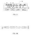
- FIG. 1illustrates a perspective view of an embedded component device, according to an embodiment of the invention
- FIG. 2illustrates a cross section view of an embedded component device, according to an embodiment of the invention
- FIG. 3illustrates a cross section view of an embedded component device, according to an embodiment of the invention
- FIG. 4illustrates a cross section view of an embedded component device, according to an embodiment of the invention
- FIG. 5illustrates a cross section view of an embedded component device, according to an embodiment of the invention
- FIG. 6A through FIG. 6Rillustrate a method of manufacturing an embedded component device, according to an embodiment of the invention
- FIG. 7illustrates a cross section view of an embedded component device, according to an embodiment of the invention.
- FIG. 8illustrates a cross section view of an embedded component device, according to an embodiment of the invention.
- FIG. 9illustrates a cross section view of an embedded component device, according to an embodiment of the invention.
- FIG. 10illustrates a cross section view of an embedded component device, according to an embodiment of the invention.
- FIG. 11A through FIG. 11Sillustrate a method of manufacturing an embedded component device, according to an embodiment of the invention
- FIG. 12A through FIG. 12Eillustrate a method of manufacturing an embedded component device, according to an embodiment of the invention
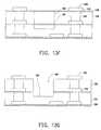
- FIG. 13A through FIG. 13Hillustrate a method of manufacturing an embedded component device, according to an embodiment of the invention.
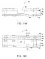
- FIG. 14A through FIG. 14Cillustrate a method of manufacturing an embedded component device, according to an embodiment of the invention.
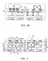
- FIG. 1illustrates a perspective view of an embedded component device 100 implemented in accordance with an embodiment of the invention.
- the embedded component device 100may include an embedded package, substrate, and/or module, and may include active components, passive components, or both active and passive components.
- sides of the embedded component device 100are substantially planar and have a substantially orthogonal orientation so as to define a lateral profile that extends around substantially an entire periphery of the embedded component device 100 .
- This orthogonal lateral profileallows a reduced overall size by reducing or minimizing an area of the embedded component device 100 . This reduction in area may be advantageous, for example, because the area may correspond to a footprint area of the embedded component device 100 when stacked on another substrate.
- the lateral profile of the embedded component device 100in general, can be any of a number of shapes, such as curved, inclined, stepped, or roughly textured. Some embodiments of the internal structure of the embedded component device 100 are illustrated in FIG. 2 through FIG. 5 .
- FIG. 2illustrates a cross-sectional view of an embedded component device 200 , in accordance with one embodiment of the present invention.
- the cross-sectional viewis taken along line A-A of FIG. 1 , where the embedded component device 200 is one embodiment of the embedded component device 100 .
- the embedded component device 200includes an electronic component such as a semiconductor device 202 , which includes a lower surface 204 , an upper surface 206 , and lateral surfaces 208 and 210 disposed adjacent to a periphery of the semiconductor device 202 and extending between the lower surface 204 and the upper surface 206 .
- each of the surfaces 204 , 206 , 208 , and 210is substantially planar, with the lateral surfaces 208 and 210 having a substantially orthogonal orientation with respect to the lower surface 204 or the upper surface 206 , although it is contemplated that the shapes and orientations of the surfaces 204 , 206 , 208 , and 210 can vary for other implementations.
- the lower surface 204is a back surface of the semiconductor device 202
- the upper surface 206is an active surface of the semiconductor device 202 .
- electrical contacts 212 a and 212 bare disposed adjacent to the upper surface 206 .
- These contacts 212provide input and output electrical connections for the semiconductor device 202 to conductive structures included in the embedded component device 200 , such as a patterned conductive layer 240 (described below).
- the lower surface 204may be disposed adjacent to a patterned conductive layer 230 (described below).
- an adhesive layer 213may optionally be added between the lower surface 204 and the patterned conductive layer 230 .
- the adhesive layer 213may include epoxy, resin, or other suitable materials, and may be a paste.
- the semiconductor device 202is a semiconductor chip, although it is contemplated that the semiconductor device 202 , in general, can be any active device such as an active electronic component, any passive device, or a combination thereof.
- the semiconductor device 202may be, for example, a wafer-level package.
- FIG. 2also illustrates a passive electronic component 203 that has electrical contacts 205 a and 205 b .
- the passive electronic component 203may be optionally included in the embedded component device 200 .
- the contacts 205provide electrical connections for the passive electronic component 203 to, for example, the patterned conductive layers 230 and 240 .
- an adhesive layer 207may optionally be added between the passive electronic component 203 and a patterned conductive layer 230 .
- the adhesive layer 207may include epoxy, resin, or other suitable materials, and may be a paste. It is contemplated that additional semiconductor devices, active devices, and/or passive devices can be included for other implementations.
- the embedded component device 200also includes a dielectric layer 214 that is disposed adjacent to the semiconductor device 202 and the passive electronic component 203 .
- the dielectric layer 214has a lower surface 216 and an upper surface 218 .
- the dielectric layer 214substantially covers or encapsulates the semiconductor device 202 , the passive electronic component 203 , the adhesive layer 213 , the adhesive layer 207 , and the patterned conductive layer 230 to provide mechanical stability as well as protection against oxidation, humidity, and other environmental conditions.
- the dielectric layer 214substantially covers the upper surface 206 and the lateral surfaces 208 and 210 of the semiconductor device 202 .
- the patterned conductive layer 240is disposed adjacent to the upper surface 218
- the patterned conductive layer 230is disposed adjacent to the lower surface 216 . While one dielectric layer 214 encapsulating a semiconductor device is illustrated in FIG. 2 as part of the embedded component device 200 , it is contemplated that more or less dielectric layers that encapsulate semiconductor devices can be included in an embedded component device in other embodiments.
- an upper dielectric layer 250may be disposed adjacent to the patterned conductive layer 240 and the upper surface 218 of the dielectric layer 214 , and an additional dielectric coating layer 251 may be disposed adjacent to the upper dielectric layer 250 .
- a lower dielectric layer 260may be disposed adjacent to the patterned conductive layer 230 and the lower surface 216 of the dielectric layer 214 .
- an additional dielectric layer 270may be disposed adjacent to the lower dielectric layer 260 . It is contemplated that more or less dielectric layers can be included above and/or below the dielectric layer 214 in other embodiments.
- each of the dielectric layers 214 , 250 , 260 , and 270can be formed from a dielectric material that is polymeric or non-polymeric.
- a dielectric materialthat is polymeric or non-polymeric.
- at least one of the dielectric layers 214 , 250 , 260 , and 270may be formed from, but is not limited to, at least one of liquid crystal polymer (LCP), bismaleimide triazine (BT), prepreg (PP), Ajinomoto Build-up Film (ABF), epoxy, and polyimide.
- LCPliquid crystal polymer
- BTbismaleimide triazine
- PPprepreg
- ABSFAjinomoto Build-up Film
- epoxyepoxy
- polyimidepolyimide
- the dielectric layers 214 , 250 , 260 , and 270can be formed from a dielectric material that is photoimageable or photoactive.
- the dielectric layer 214may be a resin material reinforced with fibers, such as glass fibers or Kevlar fibers (aramid fibers), to strengthen the dielectric layer 214 .
- resin materials that may be reinforced by fibers for use in the dielectric layer 214include ABF, BT, prepreg, polyimide, LCP, epoxy, and other resin materials.
- the fibers 290are initially oriented along a generally horizontal plane within a dielectric layer 614 prior to lamination to form the dielectric layer 214 . As shown in FIG.
- the fibers 290 subsequent to lamination of the dielectric layer 214are re-oriented, with portions adjacent to the conductive via 224 , the semiconductor device 202 , and the passive electronic component 203 being pushed along a vertically extending direction of the conductive via 224 , the semiconductor device 202 , and the passive electronic component 203 , and away from the patterned conductive layer 230 .
- the dielectric layer 214is formed so as to define openings 220 , 221 , 222 , and 223 .
- the openings 220may expose the patterned conductive layer 230 .
- Each opening 220may also be substantially aligned with a corresponding opening 221 that exposes the patterned conductive layer 240 .
- the openings 222may expose electrical contacts 212 of the semiconductor device 202 .
- the openings 223may expose electrical contacts 205 of the passive electronic component 203 .
- a conductive via 224may substantially fill each opening 220
- an electrical interconnect 225may substantially fill each opening 221 .
- the conductive via 224may be located in each opening 220 .
- the conductive via 224may be a plated conductive post. Although two conductive vias 224 are shown in FIG. 2 , it is contemplated that the embedded component device 200 may contain fewer than two or more than two conductive vias 224 .
- the conductive via 224has an upper surface 233 and a lower surface 234 .
- the upper surface 233may be substantially coplanar with the active surface 206 of the semiconductor device 202 .
- the upper surface 233may be substantially coplanar with the back surface 204 of the semiconductor device 202 .
- the conductive via 224may extend from the patterned conductive layer 230 to the electrical interconnect 225 , and the electrical interconnect 225 may extend from the conductive via 224 to the patterned conductive layer 240 .
- An electrical interconnect 226may substantially fill each opening 222 , and an electrical interconnect 227 may substantially fill each opening 223 .
- the electrical interconnect 226may extend from the electrical contact 212 to the patterned conductive layer 240 to electrically connect the semiconductor device 202 to portions of the patterned conductive layer 230 .
- the electrical interconnect 227may extend from the electrical contact 205 to the patterned conductive layer 240 to electrically connect the passive electronic component 203 to portions of the patterned conductive layer 240 .
- each of the electrical interconnects 225 , 226 , and 227has a height in the range from about 30 ⁇ m to about 150 ⁇ m, such as from about 30 ⁇ m to about 50 ⁇ m, from about 30 ⁇ m to about 100 ⁇ m, from about 50 ⁇ m to about 100 ⁇ m, and from about 100 ⁇ m to 150 ⁇ m.
- Each of the electrical interconnects 225 , 226 , and 227may be in the range from about 150 ⁇ m to 250 ⁇ m in diameter, such as about 200 ⁇ m in diameter.
- each of the conductive interconnects 224may have a height in the range from about 100 ⁇ m to about 500 ⁇ m, such as from about 100 ⁇ m to about 300 ⁇ m, from about 100 ⁇ m to about 200 ⁇ m, and from about 140 ⁇ m to about 160 ⁇ m.
- each of the electrical interconnects 225has an upper surface 231 having a first area and a lower surface 232 having a second area.
- each of the electrical interconnects 226may have an upper surface 235 having a first area and a lower surface 236 having a second area
- each of the electrical interconnects 227may have an upper surface 237 having a first area and a lower surface 238 having a second area.
- the first areais larger than the second area.
- the upper surface 233 of each of the conductive vias 224has a third area. The diameter of the conductive vias 224 may range from about 150 ⁇ m to upwards of about 300 ⁇ m.
- the third areais larger than the second area of the lower surface 232 .
- the third areamay be smaller than or equal to the second area of the lower surface 232 .
- the surfaces 231 through 238may have a shape including but not limited to a substantially circular shape, a substantially elliptical shape, a substantially square shape, and a substantially rectangular shape.
- a first distance 280 from the upper surface 233 of the conductive via 224 to the patterned conductive layer 240is less than a second distance 281 from the upper surface 206 of the semiconductor device 202 to the patterned conductive layer 240 .
- the first distance 280may be greater than or equal to the second distance 281 .
- the electrical interconnects 225 , 226 and 227allow the conductive via 224 , the semiconductor device 202 , and the passive electronic component 203 to be recessed from the upper surface 218 of the dielectric layer 214 . This can facilitate embedding the semiconductor device 202 and the passive electronic component 203 in the dielectric layer 214 to reduce the thickness of the embedded component device 200 .
- the conductive vias 224 and the electrical interconnects 225 , 226 , and 227may enable enhanced electrical connectivity characteristics.
- the electrical interconnects 225 , 226 , and 227provide electrical connectivity without the need for vias, such as plated through holes. This can significantly reduce the cost of the embedded component device 200 .
- the upper dielectric layer 250may define openings 252 that expose the patterned conductive layer 240 .
- An electrical interconnect 253may substantially fill each opening 252 .
- the electrical interconnect 253may have similar characteristics to the conductive via 224 , or alternatively may have similar characteristics to the electrical interconnect 225 .
- An additional dielectric layer 251may be disposed adjacent to the upper dielectric layer 250 .
- the electrical interconnect 253may extend from the patterned conductive layer 240 to contact pads 254 exposed by openings in the additional dielectric layer 251 .
- the contact pads 254may be for electrical connection externally to the embedded component device 200 .
- a surface finish layer 255may be disposed adjacent to each of the contact pads 254 .
- a semiconductor device(see semiconductor device 690 in FIG. 6R ) electrically connected to the contact pads 254 may also be electrically connected to the semiconductor device 202 on a conductive path including the electrical interconnect 253 and the electrical interconnect 226 .
- the conductive pathmay also include portions of the patterned conductive layer 240 .
- the lower dielectric layer 260may define openings 262 that expose the patterned conductive layer 230 .
- An electrical interconnect 263may substantially fill each opening 262 .
- the electrical interconnect 263may have similar characteristics to the conductive via 224 , or alternatively may have similar characteristics to the electrical interconnect 225 .
- An additional dielectric layer 271may be disposed adjacent to the lower dielectric layer 260 .
- the dielectric layer 270may be disposed between the lower dielectric layer 260 and the additional dielectric layer 271 .
- Contact pads 274may be exposed by openings in the additional dielectric layer 271 .
- the contact pads 274may be for electrical connection externally to the embedded component device 200 .
- a surface finish layer 275may be disposed adjacent to each of the contact pads 274 .
- the semiconductor device 202may be electrically connected to the contact pads 274 on a conductive path including the electrical interconnect 263 .
- the conductive pathmay also include one or more of the conductive via 224 , the electrical interconnect 225 , and the electrical interconnect 226 .
- the conductive pathmay also include portions of the patterned conductive layer 230 .
- each of the patterned conductive layers, electrical interconnects, and conductive vias shown in FIG. 2can be formed from a metal, a metal alloy, a matrix with a metal or a metal alloy dispersed therein, or another suitable electrically conductive material.
- each of the patterned conductive layers, electrical interconnects, and conductive vias shown in FIG. 2can be formed from aluminum, copper, titanium, or a combination thereof.
- the patterned conductive layers, electrical interconnects, and conductive vias shown in FIG. 2can be formed from the same electrically conductive material or different electrically conductive materials.
- the surface finish layers 255 and 275can be formed similarly to the patterned conductive layers, electrical interconnects, and conductive vias shown in FIG. 2 , as described previously.
- the surface finish layers 255 and 275may be formed differently.
- the surface finish layers 255 and 275may be formed from at least one of tin, nickel, and gold, or an alloy including tin or including nickel and gold.
- the surface finish layers 255 and 275can be formed from the same electrically conductive material or different electrically conductive materials.
- the additional dielectric layers 251 and 271can be formed similarly to the dielectric layers 214 , 250 , 260 , and 270 , as described previously.
- the additional dielectric layers 251 and 271may be formed using solder mask (solder resist), such as dry film imageable solder mask, or another type of patternable layer or dielectric layer.
- solder masksolder resist
- the openings in the additional dielectric layers 251 and 271 that expose the electrical contacts 274 and 275 , respectively,can have any of a number of shapes. These shapes include a cylindrical shape, such as a circular cylindrical shape, an elliptic cylindrical shape, a square cylindrical shape, or a rectangular cylindrical shape, or a non-cylindrical shape, such as a cone, a funnel, or another tapered shape. It is also contemplated that lateral boundaries of these openings can be curved or roughly textured.
- the lower dielectric layer 260may be a base substrate 264 , such that the base substrate 264 has a single layer.
- the base substrate 264may include two or more layers, such as the lower dielectric layer 260 and the additional dielectric layer 270 .
- the base substrate 264may be coreless.
- the base substrate 264may define a cavity (see FIG. 5 ). Electrical connections through the base substrate 264 may be electrical interconnects such as the electrical interconnect 263 . Alternatively or in addition, electrical connections through the base substrate 264 may be plated through vias or other types of electrical connections known in the art.
- FIG. 3illustrates a cross section view of an embedded component device 300 , according to an embodiment of the invention.
- the embedded component device 300is similar to the embedded component device 200 described with reference to FIG. 2 , except that the semiconductor device 302 is flip-chip bonded. Portions of the patterned conductive layer 230 under the semiconductor device 302 may be electrically connected to the die 302 via an fused conductive bump 304 , which may be made of a conductive material such as solder.
- a semiconductor device(not shown) electrically connected to the contact pads 254 may be electrically connected to the semiconductor device 302 on a conductive path including the electrical interconnect 253 , the electrical interconnect 225 , and the conductive via 224 .
- the conductive pathmay also include portions of the patterned conductive layers 230 and 240 (some portions not shown).
- the semiconductor device 302may be electrically connected to the contact pads 274 on a conductive path including the electrical interconnect 263 .
- the conductive pathmay also include portions of the patterned conductive layer 230 (some portions not shown).
- FIG. 4illustrates a cross section view of an embedded component device 400 , according to an embodiment of the invention.
- the embedded component device 400is similar to the embedded component device 200 described with reference to FIG. 2 , except that the semiconductor device 402 is wire bonded. Portions of the patterned conductive layer 230 under the semiconductor device 402 may be electrically connected to the die 402 via bonding wires 404 .
- a semiconductor device(not shown) electrically connected to the contact pads 254 may be electrically connected to the semiconductor device 402 on a conductive path including the electrical interconnect 253 , the electrical interconnect 225 , and the conductive via 224 .
- the conductive pathmay also include portions of the patterned conductive layers 230 and 240 (some portions not shown).
- the semiconductor device 402may be electrically connected to the contact pads 274 on a conductive path including the electrical interconnect 263 .
- the conductive pathmay also include portions of the patterned conductive layer 230 (some portions not shown).
- FIG. 5illustrates a cross section view of an embedded component device 500 , according to an embodiment of the invention.
- the embedded component device 500is similar to the embedded component device 200 described with reference to FIG. 2 , except that the semiconductor device 502 is at least partially disposed in a cavity 504 defined by the dielectric layer 260 .
- the adhesive layer 213is disposed in the cavity 504 .
- the semiconductor device 502By disposing the semiconductor device 502 in the cavity 504 , a taller semiconductor device 502 can be supported in the embedded component device 500 without increasing the overall height of the embedded component device 500 relative to the embedded component device 200 .
- the semiconductor device 502has a height 506 that is greater than the sum of a height 508 of the conductive via 224 and a thickness 509 of the patterned conductive layer 230 .
- the semiconductor device 502may be at least partially disposed in the cavity 504 .
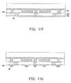
- FIG. 7illustrates a cross section view of an embedded component device 700 , according to an embodiment of the invention.
- the embedded component device 700is similar to the embedded component device 200 described with reference to FIG. 2 , except that the semiconductor device 202 is at least partially disposed in an opening 704 extending through a dielectric layer 715 .
- the passive electronic component 203is at least partially disposed in an opening 705 extending through the dielectric layer 715 and exposing the dielectric layer 260 .
- a “semiconductor device”can be any active device, any passive device, or a combination thereof.
- the semiconductor device 202is disposed adjacent to the dielectric layer 260 .
- the adhesive layer 213may be disposed between the semiconductor device 202 and the dielectric layer 260 .
- the passive electronic component 203is disposed adjacent to the dielectric layer 260 .
- the adhesive layer 207is disposed between the passive electronic component 203 and the dielectric layer 260 .
- the dielectric layer 715otherwise has similar characteristics to those previously described for the dielectric layer 260 .
- a single dielectric layercan include multiple dielectric layers formed during manufacturing.
- a dielectric layer 701includes the dielectric layers 715 and 260 .
- the opening 704 in the dielectric layer 715can also be referred to as a cavity 706 in the dielectric layer 701 , the cavity 706 having a cavity bottom 716 .
- the opening 705 in the dielectric layer 715can also be referred to as a cavity 707 in the dielectric layer 701 , the cavity 707 having a cavity bottom 717 .
- the semiconductor device 202is disposed adjacent to the cavity bottom 716
- the passive electronic component 203is disposed adjacent to the cavity bottom 717 .
- the cavity bottom 716 and the cavity bottom 717may each include at least a portion of a surface of the dielectric layer 260 .
- a taller semiconductor device 202can be supported in the embedded component device 700 without increasing the overall height of the embedded component device 700 relative to the embedded component device 200 . In one example, this is achieved by partially disposing the semiconductor device 202 in the cavity 706 .
- the semiconductor device 202may have a height 720 that is greater than a height 721 of the cavity 706 , but that is less than the sum of the height 721 and a thickness 722 (above the cavity 706 ) of the dielectric layer 214 .
- the cavity 706is positioned such that none of the surfaces of the semiconductor device 202 are exposed at an external surface of the embedded component device 700 .
- the semiconductor device 202is covered by the dielectric layer 214 . This can provide mechanical stability as well as protect the semiconductor device 202 against oxidation, humidity, and other environmental conditions.
- at least a portion of the upper (active) surface 206 of the semiconductor device 202may be substantially covered by the dielectric layer 214 .
- the dielectric layer 214may also cover the lateral surfaces 208 and 210 of the semiconductor device 202 .
- the lower (back) surface 204 of the semiconductor device 202may be disposed adjacent to the cavity bottom 716 and/or the dielectric layer 260 .
- the embedded component device 700also includes a conductive via 741 extending through the dielectric layer 715 and connecting the patterned conductive layer 230 to a patterned conductive layer 740 .
- the patterned conductive layerhas a lower surface 741 .
- the lower surface 204 of the semiconductor device 202is lower than the lower surface 741 of the patterned conductive layer 230 .
- the patterned conductive layer 740is between the dielectric layer 715 and the dielectric layer 260 .
- a conductive via 742extends through the dielectric layer 260 and connects the patterned conductive layer 740 to a patterned conductive layer 750 .
- the patterned conductive layer 750is between the dielectric layer 260 and the dielectric layer 270 . The remaining elements marked in FIG. 7 are described with reference to FIG. 2 .
- the thickness 722 of the dielectric layer 214is in the range from about 10 ⁇ m to about 150 ⁇ m, such as from about 10 ⁇ m to about 120 ⁇ m, from about 10 ⁇ m to about 100 ⁇ m, from about 30 ⁇ m to about 100 ⁇ m, and from about 50 ⁇ m to about 100 ⁇ m.
- a distance 738 from a lateral surface 736 of the cavity 716 to the nearest lateral surface 208 of the semiconductor device 202is in the range from about 10 ⁇ m to about 100 ⁇ m, such as from about 10 ⁇ m to about 50 ⁇ m, from about 30 ⁇ m to about 50 ⁇ m, and from about 50 ⁇ m to about 100 ⁇ m.
- the advantage of reducing the distance 738is that this can reduce the amount of encapsulant needed to fill the space in the cavity 716 between the semiconductor device 202 and the lateral surface 736 .
- the distance 738should be greater than some minimum tolerance related to the precision with which the cavity 716 and the semiconductor device 202 can be positioned during manufacturing. In another embodiment, the distance 738 may be greater than 100 ⁇ m.
- FIG. 8illustrates a cross section view of an embedded component device 800 , according to an embodiment of the invention.
- the embedded component device 800is similar to the embedded component device 700 described with reference to FIG. 7 , except that the semiconductor device 302 is flip-chip bonded.
- a portion 840 of a patterned conductive layer 830may be exposed by the opening 704 , and may be exposed at the cavity bottom 716 of the cavity 706 .
- the patterned conductive layer 830otherwise has similar characteristics to those previously described for the patterned conductive layer 230 .
- the electrical contact 304 of the semiconductor device 302may be disposed adjacent to the portion 840 .
- the portion 840may be electrically connected to the semiconductor device 302 via a fused conductive bump 304 , which may be made of a conductive material such as solder.
- FIG. 9illustrates a cross section view of an embedded component device 900 , according to an embodiment of the invention.
- the embedded component device 900is similar to the embedded component device 700 described with reference to FIG. 7 , except that the semiconductor device 402 is wire bonded. Portions of the patterned conductive layer 230 may be electrically connected to the semiconductor device 402 via the bonding wires 404 .
- FIG. 10illustrates a cross section view of an embedded component device 1000 , according to an embodiment of the invention.
- the embedded component device 1000is similar to the embedded component device 700 described with reference to FIG. 7 , except that a semiconductor device 1002 is at least partially disposed in a two-layer cavity 1006 .
- a passive electronic component 1003is at least partially disposed in a two-layer cavity 1007 .
- the semiconductor device 1002has similar characteristics to the semiconductor device 202 , respectively, except that a height 1010 of the semiconductor device 1002 is greater than the height 210 of the semiconductor device 202 .
- the two-layer cavity 1006has similar characteristics to the two-layer cavity 1007 , so only the two-layer cavity 1006 is further described here.
- the two-layer cavity 1006has an upper portion 1006 a defined by the dielectric layer 715 , and a lower portion 1006 b defined by a dielectric layer 1060 .
- the dielectric layer 1060otherwise has similar characteristics to those previously described for the dielectric layer 260 .
- the upper portion 1006 aextends through the dielectric layer 715
- the lower portion 1006 bextends through the dielectric layer 1060 , so the two-layer cavity 1006 extends through two dielectric layers.
- a height 1021 of the two-layer cavity 1006can be greater than the height 721 of the single-layer cavity 706 .
- the semiconductor device 1002By disposing the semiconductor device 1002 in the two-layer cavity 1006 , it is possible to support the semiconductor device 1002 without increasing (or even when decreasing) the overall height of the embedded component device 1000 relative to the embedded component device 700 .
- the cavitymay extend through more than two dielectric layers.
- a width 1008 of the upper portion 1006 ais greater than a width 1012 of the upper portion 1006 b by an amount less than or equal to about 50 ⁇ m, such as from about 10 ⁇ m to about 20 ⁇ m, from about 10 ⁇ m to about 30 ⁇ m, and from about 10 ⁇ m to about 50 ⁇ m.
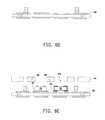
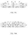
- FIGS. 6A through 6Rillustrate a method of manufacturing an embedded component device, according to an embodiment of the invention.
- the manufacturing operationsare described with reference to the embedded component device 200 of FIG. 2 .
- the manufacturing operationscan be similarly carried out to form other embedded component devices that may have different internal structure from the embedded component device 200 , such as the embedded component devices illustrated in FIGS. 3-5 .
- the manufacturing operationscan be carried out to form a substrate strip including an array of connected embedded component devices, each of which may correspond to an embedded component device such as those illustrated in FIGS. 1-5 .
- the array of connected embedded component devicesmay be singulated into individual embedded component devices such as those illustrated in FIGS. 1-5 .
- a base substrate strip 600is provided, the portion shown in FIG. 6A corresponding to the base substrate 264 of FIG. 2 .
- Patterned conductive layers 602 and 604are disposed adjacent to the base substrate 600 .
- the portion of the patterned conductive layer 602 shown in FIG. 6Acorresponds to the patterned conductive layer 230 of FIG. 2 .
- the base substrate strip 600defines the openings 262 .
- the conductive interconnects 263extend between the patterned conductive layers 602 and 604 , and substantially fill the openings 262 .
- Each of the patterned conductive layers 602 and 604may have a thickness in the range from about 10 ⁇ m to about 30 ⁇ m, such as in the range from about 15 ⁇ m to about 25 ⁇ m.
- a photoresist materialmay be formed adjacent to the patterned conductive layer 602 .
- the photoresist materialmay be a dry film photoresist, or another type of patternable layer or dielectric layer.
- the photoresist layer 606may be formed by coating, printing, or any other suitable technique. Predetermined or selected portions of the photoresist layer 606 may be photoimaged and developed so as to create openings 607 exposing the patterned conductive layer 602 .
- the photoresist layer 606may be photochemically defined using a photomask (not shown). Photoimaging and developing may have advantages of lower cost and decreased process time as compared to other approaches for creating openings in the photoresist layer 606 .
- the resulting openingscan have any of a number of shapes, including a cylindrical shape, such as a circular cylindrical shape, an elliptic cylindrical shape, a square cylindrical shape, or a rectangular cylindrical shape, or a non-cylindrical shape, such as a cone, a funnel, or another tapered shape. It is also contemplated that lateral boundaries of the resulting openings can be curved or roughly textured.
- an electrically conductive materialis applied into the openings 607 defined by the photoresist layer 606 to form the conductive vias 224 extending vertically from the patterned conductive layer 602 .
- the conductive vias 224may be formed using any of a number of coating techniques, such as chemical vapor deposition, electroless plating, electrolytic plating, printing, spinning, spraying, sputtering, or vacuum deposition.
- the photoresist layer 606is stripped to expose the patterned conductive layer 602 .
- the semiconductor device 202is disposed adjacent to the patterned conductive layer 602 .
- the adhesive layer 213may be disposed between the semiconductor device 202 and the patterned conductive layer 602 .
- the passive electronic component 203is disposed adjacent to the patterned conductive layer 602 .
- the adhesive layer 207may be disposed between the passive electronic component 203 and the patterned conductive layer 602 .
- the cavity 504may be formed in the base substrate strip 600 .
- the semiconductor device 502may be at least partially disposed in the cavity 504 .
- the adhesive layer 213is disposed in the cavity 504 .
- a dielectric layer 614is provided, wherein the dielectric layer 614 is pre-formed with a set of first openings 614 a , and positions of the first openings 614 a respectively correspond to positions of the conductive via 224 , the semiconductor device 202 , and the passive electronic component 203 .
- the dielectric layer 614includes a fiber-reinforced resin material, such as a prepreg material, including the fibers 290 to strengthen the dielectric layer 614 .
- the fibers 290are initially oriented along a generally horizontal plane within the dielectric layer 614 . While the openings 614 a are shown in FIG. 6E as fully extending through the dielectric layer 614 , it is contemplated that the openings 614 a also can partially extend through the dielectric layer 614 .
- the dielectric layer 614is disposed adjacent to the base substrate strip 600 , and covering the semiconductor device 202 , the passive electronic component 203 , and the conductive vias 224 .
- the dielectric layer 614may also cover the patterned conductive layer 602 .
- the dielectric layer 614may separate a conductive sheet 616 from the semiconductor device 202 , the passive electronic component 203 , and the conductive vias 224 .
- the portion of the dielectric layer 614 shown in FIG. 6Gcorresponds to the dielectric layer 214 of FIG. 2 .
- the fibers 290 subsequent to lamination of the dielectric layer 614are re-oriented, with portions adjacent to the conductive via 224 , the semiconductor device 202 , and the passive electronic component 203 being pushed along a vertically extending direction of the conductive via 224 , the semiconductor device 202 , and the passive electronic component 203 , and away from the patterned conductive layer 230 .
- a conductive sheet 616such as a copper foil, may be disposed adjacent to the dielectric layer 614 to form, for example, a resin-coated copper layer that covers the semiconductor device 202 , the passive electronic component 203 , and the conductive vias 224 .
- the dielectric layer 614may have a single resin layer, or may include a first sublayer made of resin and a second sublayer made of reinforced resin, such as resin reinforced with glass fibers and/or Kevlar fibers.
- the dielectric layer 614may be formed from a prepreg material, and the conductive sheet 616 may be disposed adjacent to the dielectric layer 614 .
- the prepreg materialmay be disposed adjacent to the base substrate strip 600 , and may be pre-formed to define openings at the locations of the semiconductor device 202 , the passive electronic component 203 , and the conductive vias 224 .
- the prepreg materialmay cover the semiconductor device 202 , the passive electronic component 203 , and the conductive vias 224 .
- the prepreg materialmay be formed of one prepreg layer, or of two or more prepreg layers.
- the dielectric layer 614may include a combination of a prepreg sublayer and a resin sublayer, and the conductive sheet 616 may be disposed adjacent to the dielectric layer 614 .
- the prepreg sublayermay be disposed adjacent to the base substrate strip 600 , and may be pre-formed to define openings at the locations of the semiconductor device 202 , the passive electronic component 203 , and the conductive vias 224 .
- the resin sublayermay be disposed adjacent to the prepreg sublayer, and may also be disposed adjacent to the base substrate strip 600 within the openings defined by the prepreg sublayer.
- the dielectric layermay be formed from an epoxy molding compound, such as an encapsulant material, and the conductive sheet 616 may be disposed adjacent to the dielectric layer 614 .
- the dielectric layer 614may be laminated on the base substrate strip 600 .
- the dielectric layer 614can be formed using any of a number of molding techniques, such as injection molding. Once applied, the molding material is hardened or solidified, such as by lowering the temperature to below a melting point of the molding material, thereby forming the dielectric layer 614 .
- the dielectric layer 614can be formed using any of a number of coating techniques, such as printing, spinning, or spraying.
- the conductive sheet 616may be attached to the dielectric layer 614 prior to disposing the dielectric layer 614 adjacent to the base substrate strip 600 .
- the dielectric layer 614with the conductive sheet 616 already attached, may be disposed adjacent to the base substrate strip 600 .
- openings including the openings 221 , 222 , and 223are formed.
- the openings 221extend through the conductive sheet 616 and the dielectric layer 614 to expose the upper surface 233 of each of the conductive vias 224 .
- the openings 222extend through the conductive sheet 616 and the dielectric layer 614 to expose the electrical contacts 212 of the semiconductor device 202 .
- the openings 223extend through the conductive sheet 616 and the dielectric layer 614 to expose the electrical contacts 205 of the passive electronic component 203 .
- the openings 221 , 222 , and 223may be formed by laser drilling, or other suitable approaches known in the art.
- the openings 221 , 222 , and 223are filled with a conductive material to form conductive vias, such as the electrical interconnects 225 , 226 , and 227 of FIG. 2 .
- the electrical interconnects 225 , 226 , and 227may be formed using any of a number of coating techniques, such as electroless plating and/or electrolytic plating.
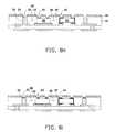
- FIGS. 6J through 6La subtractive process for forming a patterned conductive layer including the patterned conductive layer 240 of FIG. 2 is illustrated in FIGS. 6J through 6L .
- additional conductive materialis disposed adjacent to the electrical interconnects 225 , 226 , and 227 , and adjacent to the conductive sheet 616 .
- This additional conductive materialforms a conductive layer 618 that is electrically connected to the electrical interconnects 225 , 226 , and 227 .
- a photoresist layer 620is formed adjacent to the conductive layer 618 . Predetermined or selected portions of the photoresist layer 620 may be photoimaged and developed so as to create openings 622 . The openings 622 expose the conductive layer 618 .
- the photoresist layer 620 (and the openings 622 )have similar characteristics and are formed similarly to the photoresist layer 606 (and the openings 607 ) described with reference to FIG. 6B .
- openings 624 exposing the dielectric layer 614are formed in the conductive layer 618 to form a patterned conductive layer 640 .
- the portion of the patterned conductive layer 640 shown in FIG. 6Lcorresponds to the patterned conductive layer 240 of FIG. 2 .
- Patterning to form the patterned conductive layer 640can be carried out in any of a number of ways, such as chemical etching, laser drilling, or mechanical drilling, and the resulting openings can have any of a number of shapes, such as a cylindrical shape, such as a circular cylindrical shape, an elliptic cylindrical shape, a square cylindrical shape, or a rectangular cylindrical shape, or a non-cylindrical shape, such as a cone, a funnel, or another tapered shape. It is also contemplated that lateral boundaries of the resulting openings can be curved or roughly textured.
- FIGS. 6M through 6Oa modified semi-additive process (MSAP) for forming a patterned conductive layer including the patterned conductive layer 240 of FIG. 2 is illustrated in FIGS. 6M through 6O .
- the MSAPis used to form a patterned conductive layer with finer pitch, narrower traces than the subtractive process.
- a photoresist layer 630is formed adjacent to the conductive sheet 616 . Predetermined or selected portions of the photoresist layer 630 may be photoimaged and developed so as to create openings 632 .
- the openings 632expose the conductive sheet 616 .
- the photoresist layer 630 (and the openings 632 )have similar characteristics and are formed similarly to the photoresist layer 606 (and the openings 607 ) described with reference to FIG. 6B .
- additional conductive materialis disposed adjacent to the electrical interconnects 225 , 226 , and 227 , and adjacent to the conductive sheet 616 .
- This additional conductive materialforms a conductive layer 634 that is electrically connected to the electrical interconnects 225 , 226 , and 227 .
- the combination of the conductive sheet 616 and the conductive layer 634has a thickness 635 .
- the patterned photoresist layer 630is removed. Then, a portion of the conductive layer 634 is removed, such as by flash etching, to form the patterned conductive layer 640 . As a result of the flash etching, a thickness 641 of the patterned conductive layer 640 may be reduced from the thickness 635 illustrated in FIG. 6N .
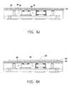
- a dielectric layer 650is disposed adjacent to the dielectric layer 614
- a dielectric layer 670is disposed adjacent to the base substrate strip 600 .
- the portions of the dielectric layers 650 and 670 shown in FIG. 6Pcorrespond to the dielectric layers 250 and 270 of FIG. 2 , respectively.
- the dielectric layers 650 and 670may be formed in a manner similar to that described previously for the dielectric layer 614 with reference to FIG. 6G .
- the electrical interconnects extending through the dielectric layers 650 and 670such as the electrical interconnects 253 , may be formed in a manner similar to that described previously for the conductive vias 224 with reference to FIG. 6C .
- the electrical contacts 254 and 274may be formed in a manner similar to that described previously for the patterned conductive layer 640 with reference to FIGS. 6K and 6L .
- a dielectric layer 651is disposed adjacent to the dielectric layer 650
- a dielectric layer 671is disposed adjacent to the dielectric layer 670 .
- the portions of the dielectric layers 651 and 671 shown in FIG. 6Pcorrespond to the dielectric layers 251 and 271 of FIG. 2 , respectively.
- the dielectric layers 651 and 671may be formed in a manner similar to that described previously for the dielectric layer 614 with reference to FIG. 6G .
- the surface finish layers 255 and 275may be formed in a manner similar to that described previously for the conductive vias 224 with reference to FIG. 6C . Singulation may then be performed along the dashed lines 680 and 681 to obtain individual embedded component devices, such as the embedded component device 200 of FIG. 2 .
- a second semiconductor device 690 and a passive electronic component 692may be electrically connected to the electrical contacts 254 .
- FIGS. 11A through 11Sillustrate a method of manufacturing an embedded component device, according to an embodiment of the invention.
- the following manufacturing operationsare described with reference to the embedded component device 700 of FIG. 7 , which includes aspects of the embedded component device 200 of FIG. 2 .
- the manufacturing operationscan be similarly carried out to form other embedded component devices that may have different internal structure from the embedded component device 700 , such as the embedded component devices illustrated in FIGS. 8-10 .
- the manufacturing operationscan be carried out to form a substrate strip including an array of connected embedded component devices, each of which may correspond to an embedded component device such as those illustrated in FIGS. 8-10 .
- the array of connected embedded component devicesmay be singulated into individual embedded component devices such as those illustrated in FIGS. 8-10 .
- the carrier 1100includes a core layer (not shown) between two carrier conductive layers (not shown) attached to the core layer.
- Each carrier conductive layermay be formed from a metal, a metal alloy, a matrix with a metal or a metal alloy dispersed therein, or another suitable electrically conductive material.
- each carrier conductive layermay include a metal foil formed from copper or an alloy including copper. The metal foil may have a thickness in the range from about 10 ⁇ m to about 30 ⁇ m, such as in the range from about 15 ⁇ m to about 25 ⁇ m.
- the carrier 1100has an upper surface 1102 and a lower surface 1104 .
- a conductive layer 1105(conductive sheet 1105 ) is disposed adjacent to the lower surface 1104 .
- FIGS. 11A to 11Hillustrate processing on a single side of the carrier 1100 corresponding to the lower surface 1104 . It is contemplated that similar processing may occur on both sides of the carrier 1100 , including the side of the carrier 1100 corresponding to the upper surface 1102 .
- a conductive layer(not shown) having similar characteristics to the conductive sheet 1105 can be disposed adjacent to the upper surface 1102 .
- the conductive sheet 1105may be formed from a metal, a metal alloy, a matrix with a metal or a metal alloy dispersed therein, or another suitable electrically conductive material.
- the conductive sheet 1105may include a releasable metal foil formed from copper or an alloy including copper.
- the conductive sheet 1105may be attached to the carrier 1100 by a release layer (not shown).
- the release layeris an adhesive layer that may be organic or inorganic, such as tape.
- the tapewhich can be implemented as a single-sided or double-sided adhesive tape, secures components at an appropriate spacing with respect to one another, and allows subsequent manufacturing operations to be carried out with those components disposed adjacent to the carrier 1100 .
- the conductive sheet 1105may have a thickness in the range from about 2 ⁇ m to about 10 ⁇ m, such as in the range from about 3 ⁇ m to about 5 ⁇ m.
- conductive blocks 1106 and the conductive vias 741are formed adjacent to a lower surface 1107 of the conductive sheet 1105 .
- the process by which the conductive blocks 1106 and the conductive vias 741 are formedis similar to the process previously described with reference to FIGS. 6B through 6D .
- a photoresist materialis formed adjacent to the lower surface 1107 . Openings in the photoresist are created, such as by photoimaging and developing, that correspond to the locations of the conductive blocks 1106 and the conductive vias 741 .
- An electrically conductive materialis applied into the openings to form the conductive blocks 1106 and the conductive vias 741 .
- the conductive blocks 1106 and the conductive vias 741may be buffed.
- the photoresist layeris then stripped to expose the conductive sheet 1105 .
- a dielectric layer 1115is disposed adjacent to the lower surface 1107 of the conductive sheet 1105 .
- the portion of the dielectric layer 1115 shown in FIG. 11Ccorresponds to the dielectric layer 715 of FIG. 7 .
- the dielectric layer 1115may cover a lateral surface 1108 of the conductive blocks 1106 .
- a conductive layer 1110(conductive sheet 1110 ) may be disposed adjacent to the dielectric layer 1115 , the conductive blocks 1106 , and the conductive vias 741 .
- the dielectric layer 1115may be formed of a resin material.
- the conductive sheet 1110such as a copper foil, may be disposed adjacent to the dielectric layer 1115 to form, for example, a resin-coated copper layer.
- the conductive sheet 1110may be a metal such as copper or an alloy including copper.
- the conductive sheet 1110may be formed by electroless plating, sputtering, or another suitable method known in the art.
- the dielectric layer 1115may have a single resin layer, or may include a first sublayer made of resin and a second sublayer made of reinforced resin, such as resin reinforced with glass fibers and/or Kevlar fibers.
- the dielectric layer 1115may be formed from a prepreg material, and the conductive sheet 1110 may be disposed adjacent to the dielectric layer 1115 .
- the prepreg materialmay be disposed adjacent to the conductive sheet 1105 , and may be pre-formed to define openings at the locations of the conductive blocks 1106 and the conductive vias 741 .
- the prepreg materialmay be formed of one prepreg layer, or of two or more prepreg layers.
- the dielectric layer 1115may include a combination of a prepreg sublayer and a resin sublayer, and the conductive sheet 1110 may be disposed adjacent to the dielectric layer 1115 .
- the prepreg sublayermay be disposed adjacent to the conductive sheet 1105 , and may be pre-formed to define openings at the locations of the conductive blocks 1106 and the conductive vias 741 .
- the resin sublayermay be disposed adjacent to the prepreg sublayer, and may also be disposed adjacent to the conductive sheet 1105 within the openings defined by the prepreg sublayer.
- a patterned conductive layer 1140is formed from the conductive sheet 1110 , and the conductive vias 742 are formed adjacent to the patterned conductive layer 1140 .
- the portion of the patterned conductive layer 1140 shown in FIG. 11Dcorresponds to the patterned conductive layer 740 of FIG. 7 .
- the process by which the patterned conductive layer 1140 and the conductive vias 742 are formedhas aspects that are similar to the process previously described with reference to FIGS. 6B through 6D .
- a photoresist materialis formed adjacent to the conductive sheet 1110 , such as by dry film lamination. Openings in the photoresist are created, such as by photoimaging and developing, that correspond to the patterned conductive layer 1140 .
- An electrically conductive materialis applied into the openings to form a conductive layer corresponding to the patterned conductive layer 1140 .
- the photoresist layeris then stripped.
- a photoresist materialis again formed adjacent to the conductive sheet 1110 . Openings in the photoresist are created, such as by photoimaging and developing, that correspond to the conductive vias 742 .
- An electrically conductive materialis applied into the openings to form the conductive vias 742 .
- the conductive vias 742may be buffed.
- the photoresist layeris then stripped. Flash etching is then performed to remove residual portions of the conductive sheet 1110 , and to form the patterned conductive layer 1140 .
- FIG. 11Eillustrates an embodiment in which a conductive block 1112 corresponding to the two-layer cavity 1006 of FIG. 10 is formed.
- the conductive block 1112includes a first conductive portion 1112 a , and a second conductive portion 1112 b .
- the second conductive portion 1112 bis formed similarly to how the conductive vias 742 are formed (see description associated with FIG. 11D ).
- the first conductive portion 1112 ahas a width 1111 that is greater than a width 1117 of the second conductive portion 1112 b .
- a lateral surface 1113 of the first conductive portion 1112 ais covered by the dielectric layer 1115 .
- a lateral surface 1116 of the second conductive portion 1112 bis then covered by a dielectric layer (not shown) corresponding to the dielectric layer 260 of FIGS. 2 and 7 .
- a dielectric layer 1160is disposed adjacent to the dielectric layer 1115 and covering the patterned conductive layer 1140 and the conductive vias 742 .
- the portion of the dielectric layer 1160 shown in FIG. 11Fcorresponds to the dielectric layer 260 of FIGS. 2 and 7 .
- a conductive layer 1118(conductive sheet 1118 ) may be disposed adjacent to the dielectric layer 1160 and the conductive vias 742 .
- the dielectric layer 1160 and the conductive sheet 1118have similar characteristics to and are formed in a similar manner to the dielectric layer 1115 and the conductive sheet 1110 , respectively, and are not described further here (see description associated with FIG. 11C ).
- a patterned conductive layer 1150is formed from the conductive sheet 1118 , and the conductive vias 744 are formed adjacent to the patterned conductive layer 1150 .
- the portion of the patterned conductive layer 1150 shown in FIG. 11Gcorresponds to the patterned conductive layer 750 of FIG. 7 .
- the patterned conductive layer 1150 and the conductive vias 744have similar characteristics to and are formed in a similar manner to the patterned conductive layer 1142 and the conductive vias 742 , respectively, and are not described further here (see description associated with FIG. 11D ).
- a dielectric layer 1170is disposed adjacent to the dielectric layer 1160 and covering the patterned conductive layer 1150 and the conductive vias 744 .
- the portion of the dielectric layer 1170 shown in FIG. 11Hcorresponds to the dielectric layer 270 of FIGS. 2 and 7 .
- a conductive layer 1119(conductive sheet 1119 ) may be disposed adjacent to the dielectric layer 1170 and the conductive vias 744 .
- the dielectric layer 1170 and the conductive sheet 1119have similar characteristics to and are formed in a similar manner to the dielectric layer 1115 and the conductive sheet 1110 , respectively, and are not described further here (see description associated with FIG. 11C ).
- the carrier 1100is removed to expose the conductive sheet 1105 .
- a patterned conductive layer 1130is formed from the conductive sheet 1105 , and the conductive vias 224 are formed adjacent to the patterned conductive layer 1130 .
- the portion of the patterned conductive layer 1130 shown in FIG. 11Jcorresponds to the patterned conductive layer 230 of FIGS. 2 and 7 .
- the patterned conductive layer 1130 and the conductive vias 224have similar characteristics to and are formed in a similar manner to the patterned conductive layer 1142 and the conductive vias 742 , respectively, and are not described further here (see description associated with FIG. 11D ).
- a photoresist materialis formed adjacent to the dielectric layer 1115 , and openings are formed in the photoresist, by a process similar to that previously described with reference to FIG. 6B . Openings in the photoresist are created, such as by photoimaging and developing, that expose the conductive blocks 1106 .
- the conductive blocks 1106are removed to form the openings 704 and 705 extending through the dielectric layer 1115 .
- the openings 704 and 705each expose the dielectric layer 1160 .
- the opening 704can also be referred to as the cavity 706 having the cavity bottom 716 .
- the opening 705can also be referred to as the cavity 707 having the cavity bottom 717 .
- the conductive blocks 1106may be removed by chemical etching. An advantage of chemical etching is that many conductive blocks 1106 can be removed simultaneously by the same process step.
- the cavity 706may be formed by laser drilling and/or mechanical drilling through the dielectric layer 1115 . These drilling approaches may be more time-consuming that chemical etching, in that cavities are typically formed one at a time using these approaches.
- the semiconductor device 202is disposed adjacent to the dielectric layer 1160 (also adjacent to the cavity bottom 716 ).
- the adhesive layer 213may be disposed between the semiconductor device 202 and the cavity bottom 716 .
- the passive electronic component 203is disposed adjacent to the dielectric layer 1160 (also adjacent to the cavity bottom 717 ).
- the adhesive layer 207may be disposed between the passive electronic component 203 and the cavity bottom 717 .
- a dielectric layer 1114is disposed adjacent to the dielectric layer 1115 , and covering the semiconductor device 202 , the passive electronic component 203 , and the conductive vias 224 .
- the dielectric layer 1114may separate a conductive sheet 1120 from the semiconductor device 202 , the passive electronic component 203 , and the conductive vias 224 .
- the portion of the dielectric layer 1114 shown in FIG. 6Gcorresponds to the dielectric layer 214 of FIGS. 2 and 7 .
- the dielectric layer 1114 and the conductive sheet 1120have similar characteristics to and are formed in a similar manner to the dielectric layer 614 and the conductive sheet 616 , respectively, and are not described further here (see description associated with FIG. 6G ).
- openings including the openings 221 , 222 , and 223are formed.
- the openings 221extend through the conductive sheet 1120 and the dielectric layer 1114 to expose the upper surface 233 of each of the conductive vias 224 .
- the openings 222extend through the conductive sheet 1120 and the dielectric layer 1114 to expose the electrical contacts 212 of the semiconductor device 202 .
- the openings 223extend through the conductive sheet 1120 and the dielectric layer 1114 to expose the electrical contacts 205 of the passive electronic component 203 .
- the openings 221 , 222 , and 223may be formed by laser drilling, or other suitable approaches known in the art.
- the openings 221 , 222 , and 223are filled with a conductive material to form conductive vias, such as the electrical interconnects 225 , 226 , and 227 of FIGS. 2 and 7 .
- the electrical interconnects 225 , 226 , and 227may be formed using any of a number of coating techniques, such as electroless plating and/or electrolytic plating.
- a subtractive processis then performed to form a patterned conductive layer 1140 . The subtractive process is similar to that described with reference to FIGS. 6J to 6L , and is not further described here.
- a modified semi-additive processfor forming a patterned conductive layer 1140 including the patterned conductive layer 240 of FIGS. 2 and 7 .
- the MSAPis similar to that described with reference to FIGS. 6M through 6O , and is not further described here.
- the portion of the patterned conductive layer 1140 shown in FIG. 11Pcorresponds to the patterned conductive layer 240 of FIGS. 2 and 7 .
- a dielectric layer 1150is disposed adjacent to the dielectric layer 1114
- a dielectric layer 1170is disposed adjacent to the dielectric layer 1160 .
- the portions of the dielectric layers 1150 and 1170 shown in FIG. 11Qcorrespond to the dielectric layers 250 and 270 of FIGS. 2 and 7 , respectively.
- the dielectric layers 1150 and 1170may be formed in a manner similar to that described previously for the dielectric layer 614 with reference to FIG. 6G .
- the electrical interconnects extending through the dielectric layers 1150 and 1170such as the electrical interconnects 253 , may be formed in a manner similar to that described previously for the conductive vias 742 with reference to FIG. 11D .
- the electrical contacts 254 and 274may be formed in a manner similar to that described previously for the patterned conductive layer 1140 with reference to FIG. 11P .
- a dielectric layer 1151is disposed adjacent to the dielectric layer 1150
- a dielectric layer 1171is disposed adjacent to the dielectric layer 1170 .
- the portions of the dielectric layers 1151 and 1171 shown in FIG. 11Rcorrespond to the dielectric layers 251 and 271 , respectively, of FIGS. 2 and 7 .
- the dielectric layers 1151 and 1171may be formed in a manner similar to that described previously for the dielectric layer 614 with reference to FIG. 6G .
- the surface finish layers 255 and 275may be formed in a manner similar to that described previously for the conductive vias 224 with reference to FIG. 6C . Singulation may then be performed along the dashed lines 1180 and 1181 to obtain individual embedded component devices, such as the embedded component device 700 of FIG. 7 .
- a second semiconductor device 1190 and a passive electronic component 1192may be electrically connected to the electrical contacts 254 .
- dielectric layers and conductive elementsare formed both above and below the semiconductor device 202 .
- none of the surfaces of the semiconductor device 202are exposed at an external surface of the embedded component device 700 .
- the semiconductor device 202is covered by the dielectric layer 214 . This can provide mechanical stability as well as protect the semiconductor device 202 against oxidation, humidity, and other environmental conditions.
- FIG. 12A through FIG. 12Eillustrate a method of manufacturing an embedded component device 1280 (see FIG. 12E ), according to an embodiment of the invention.
- the manufacturing operationsare described with reference to the method of FIGS. 6A through 6R , with differences noted below.
- the manufacturing operationscan be similarly carried out to form other embedded component devices that may have different internal structure from the embedded component device 1280 .
- the manufacturing operationscan be carried out to form a substrate strip including an array of connected embedded component devices.
- a substrate strip 1200such as a printed circuit board is provided.
- the substrate strip 1200includes conductive elements 1201 internal to the substrate 1200 , and conductive elements 1202 on the surface of the substrate strip 1200 .
- Conductive vias 1224extend vertically from the conductive elements 1202 .
- the conductive vias 1224have similar characteristics and are formed similarly to the conductive vias 224 , as described with reference to FIGS. 6B through 6D .
- a dielectric layer 1214is disposed adjacent to the substrate strip 1200 .
- the dielectric layer 1214has similar characteristics to the dielectric layer 614 , as described with reference to FIG. 6E .
- the dielectric layer 1214is also placed similarly to the dielectric layer 614 , as described with reference to FIG. 6G , except that the dielectric layer 1214 is placed on the substrate strip 1200 prior to the placement of a semiconductor device 1202 (see FIG. 12D ).
- the dielectric layer 1214has a cavity 1225 into which the semiconductor device 1202 is placed (see FIG. 12D ).
- the dielectric layer 1214may be ground and/or laser drilled to expose the conductive vias 1224 .
- a photoresist layer 1220such as photo-imageable solder resist, is formed adjacent to the dielectric layer 1214 . Predetermined or selected portions of the photoresist layer 1220 may be photoimaged and developed so as to create openings 1222 . The openings 1222 expose the conductive vias 1224 . The photoresist layer 1220 (and the openings 1222 ) have similar characteristics and are formed similarly to the photoresist layer 606 (and the openings 607 ) described with reference to FIG. 6B .
- electrical contactssuch as solder balls can be disposed in the openings 1222 and electrically connected to the conductive vias 1224 . These electrical contacts may provide electrical connectivity to, for example, a patterned conductive layer and/or another package positioned above the photoresist layer 1220 .
- the semiconductor device 1202is placed into the cavity 1225 in the dielectric layer 1214 .
- the cavity 1225is then filled with a dielectric layer 1234 .
- the dielectric layer 1234may be epoxy, a molding compound, a liquid molding compound, or another suitable material different from prepreg.
- the semiconductor device 1202may be flip-chip bonded to one or more of the conductive elements 1202 .
- a semiconductor device similar to the semiconductor device 202may be disposed adjacent to the substrate strip 1200 .
- the electrical contacts 212 of the semiconductor device 202may be exposed as described with reference to FIG. 6H .
- a cavitymay be formed in the substrate strip 1200 by mechanical drilling, as described with reference to FIG. 6F .
- the semiconductor device 1202may then be at least partially placed in the cavity in the substrate strip 1200 .
- an adhesive layer similar to the adhesive layer 213may also be disposed in the cavity.
- FIG. 13A through FIG. 13Hillustrate a method of manufacturing an embedded component device 1390 (see FIG. 13H ), according to an embodiment of the invention.
- the manufacturing operationsare described with reference to portions of the method of FIGS. 6A to 6R and the method of FIGS. 11A to 11S , with differences noted below.
- the manufacturing operationscan be similarly carried out to form other embedded component devices that may have different internal structure from the embedded component device 1390 .
- the manufacturing operationscan be carried out to form a substrate strip including an array of connected embedded component devices.
- the conductive layer 1105(conductive sheet 1105 ) may include a releasable metal foil formed from copper or an alloy including copper.
- the metal foilmay have a thickness in the range from about 10 ⁇ m to about 30 ⁇ m, such as in the range from about 15 ⁇ m to about 25 ⁇ m.
- the conductive sheet 1105may be disposed adjacent to a carrier (not shown) such as the carrier 1100 illustrated in FIG. 11A .
- the conductive sheet 1105may be attached to the carrier 1100 by a release layer (not shown).
- the release layeris an adhesive layer that may be organic or inorganic, such as tape.
- a patterned conductive layer 1300may be disposed adjacent to the conductive sheet 1105 , and conductive vias 1302 may extend vertically from the patterned conductive layer 1300 .
- the patterned conductive layer 1300may have similar characteristics to the patterned conductive layer 1140 previously described with reference to FIG. 11D .
- the conductive vias 1302may have similar characteristics to the patterned conductive layer 742 , also previously described with reference to FIG. 11D .
- the process by which the patterned conductive layer 1300 and the conductive vias 1302 are formedhas aspects that are similar to the process previously described with reference to FIG. 11D .
- a photoresist materialis formed adjacent to the conductive sheet 1105 , such as by dry film lamination.
- Openings in the photoresistare created, such as by photoimaging and developing, that correspond to the patterned conductive layer 1300 .
- An electrically conductive materialis applied into the openings to form a conductive layer corresponding to the patterned conductive layer 1300 .
- the photoresist layeris then stripped.
- a photoresist materialis again formed adjacent to the conductive sheet 1105 .
- Openings in the photoresistare created, such as by photoimaging and developing, that correspond to the conductive vias 1302 .
- An electrically conductive materialis applied into the openings to form the conductive vias 1302 .
- the conductive vias 1302may be buffed.
- the photoresist layeris then stripped.
- a dielectric sublayer 1304is disposed adjacent to the conductive sheet 1105 .
- the dielectric sublayer 1304has similar characteristics to the dielectric layer 1115 previously described with reference to FIG. 11C .
- the dielectric sublayer 1304may be formed of a resin material.
- the conductive sheet 1105may be disposed adjacent to the dielectric sublayer 1304 to form, for example, a resin-coated copper layer.
- the dielectric sublayer 1304may have a single resin layer, or may include a first sublayer made of resin and a second sublayer made of reinforced resin, such as resin reinforced with glass fibers and/or Kevlar fibers.
- the dielectric sublayer 1304may be formed from a prepreg material.
- the prepreg materialmay be pre-formed to define openings at the locations of the conductive vias 1302 .
- the dielectric sublayer 1304may also include a combination of a prepreg sublayer and a resin sublayer.
- a conductive sheet 1306is formed adjacent to the dielectric sublayer 1304 .
- the conductive sheet 1306has similar characteristics to and is formed similarly to the conductive sheet 1110 previously described with reference to FIG. 11C .
- the conductive sheet 1306may be a metal such as copper or an alloy including copper.
- the conductive sheet 1306may be formed by electroless plating, sputtering, or another suitable method known in the art.
- the conductive sheet 1306may be attached to the dielectric sublayer 1304 prior to disposing the dielectric sublayer 1304 adjacent to the conductive sheet 1105 .
- the dielectric sublayer 1304with the conductive sheet 1306 already attached, may be disposed adjacent to the conductive sheet 1105 . This may occur simultaneously with the conductive sheet 1306 being disposed adjacent to the conductive vias 1302 .
- conductive vias 1308 and conductive block 1310are formed adjacent to the conductive sheet 1306 .
- the conductive vias 1308extend the conductive vias 1302 (see FIG. 13A ) to form conductive vias 1312 .
- the conductive vias 1312 and the conductive block 1310have similar characteristics to and are formed similarly to the conductive vias 741 and the conductive blocks 1106 previously described with reference to FIG. 11B .
- a photoresist materialis formed adjacent to the conductive sheet 1306 . Openings in the photoresist are created, such as by photoimaging and developing, that correspond to the locations of the conductive block 1310 and the conductive vias 1312 .
- An electrically conductive materialis applied into the openings to form the conductive block 1310 and the conductive vias 1312 .
- the conductive block 1310 and the conductive vias 1312may be buffed.
- the photoresist layeris then stripped to expose the conductive sheet 1306 .
- the conductive sheet 1306is then removed by flash etching.
- An additional dielectric sublayer having similar characteristics to the dielectric layer 1115 previously described with reference to FIG. 11Cis disposed adjacent to the dielectric sublayer 1304 (see FIG. 13A ) to form the dielectric layer 1314 .
- the conductive block 1310 and the conductive vias 1312may be buffed and de-smeared.
- a conductive sheet 1316may then be formed adjacent to the dielectric layer 1314 .
- the conductive sheet 1316has similar characteristics to and is formed similarly to the conductive sheet 1306 previously described with reference to FIG. 13A .
- the conductive sheet 1316may be attached to the additional dielectric sublayer prior to disposing the additional dielectric sublayer adjacent to the dielectric sublayer 1304 to form the dielectric layer 1314 .
- the additional dielectric sublayer, with the conductive sheet 1316 already attachedmay be disposed adjacent to the dielectric layer 1304 to form the dielectric layer 1314 . This may occur simultaneously with the conductive sheet 1316 being disposed adjacent to the conductive vias 1312 .
- a patterned conductive layer 1318is then disposed adjacent to the conductive sheet 1316 .
- the patterned conductive layer 1318may have similar characteristics to and be formed in a similar manner to the patterned conductive layer 1300 previously described with reference to FIG. 13A .
- conductive vias 1322are formed adjacent to the patterned conductive layer 1318
- conductive block 1320is formed adjacent to the conductive sheet 1316 .
- the conductive block 1320extends the conductive block 1310 (see FIG. 13C ) to form conductive block 1321 .
- the conductive vias 1322 and the conductive block 1321have similar characteristics to and are formed similarly to the conductive vias 1312 and the conductive blocks 1310 previously described with reference to FIG. 13B .
- the conductive sheet 1316is then removed by flash etching.
- An additional dielectric sublayer 1324having similar characteristics to the dielectric layer 1115 previously described with reference to FIG. 11C is disposed adjacent to the dielectric layer 1314 .
- the conductive block 1321 and the conductive vias 1312may be buffed and de-smeared.
- a conductive sheet 1326may then be formed adjacent to the dielectric sublayer 1324 .
- the conductive sheet 1326has similar characteristics to and is formed similarly to the conductive sheet 1306 previously described with reference to FIG. 13A .
- the conductive sheet 1326may be attached to the dielectric sublayer 1324 prior to disposing the dielectric sublayer 1324 adjacent to the dielectric layer 1314 .
- the dielectric sublayer 1324with the conductive sheet 1326 already attached, may be disposed adjacent to the dielectric layer 1314 . This may occur simultaneously with the conductive sheet 1326 being disposed adjacent to the conductive vias 1322 .
- conductive vias 1332are formed adjacent to the conductive sheet 1326
- conductive block 1330is formed adjacent to the conductive sheet 1326 .
- the conductive vias 1332extend the conductive vias 1322 (see FIG. 13E ) to from the conductive vias 1333 .
- the conductive block 1330extends the conductive block 1321 (see FIG. 13E ) to form conductive block 1331 .
- the conductive vias 1333 and the conductive block 1331have similar characteristics to and are formed similarly to the conductive vias 1312 and the conductive blocks 1310 previously described with reference to FIG. 13B .
- the conductive sheet 1326is then removed by flash etching.
- An additional dielectric layer having similar characteristics to the dielectric layer 1115 previously described with reference to FIG. 11Cis disposed adjacent to the dielectric sublayer 1324 (see FIG. 13E ) to form the dielectric layer 1334 .
- the conductive block 1331 and the conductive vias 1333may be buffed and de-smeared.
- a conductive sheet 1336may then be formed adjacent to the dielectric layer 1334 .
- the conductive sheet 1336has similar characteristics to and is formed similarly to the conductive sheet 1306 previously described with reference to FIG. 13A .
- the conductive sheet 1336may be attached to the additional dielectric sublayer prior to disposing the additional dielectric sublayer adjacent to the dielectric sublayer 1324 to form the dielectric layer 1334 .
- the additional dielectric sublayerwith the conductive sheet 1336 already attached, may be disposed adjacent to the dielectric layer 1324 to form the dielectric layer 1334 . This may occur simultaneously with the conductive sheet 1336 being disposed adjacent to the conductive vias 1332 .
- a patterned conductive layer 1338is then disposed adjacent to the conductive sheet 1336 .
- the patterned conductive layer 1338may have similar characteristics to and be formed in a similar manner to the patterned conductive layer 1300 previously described with reference to FIG. 13A .
- the conductive sheet 1336may be removed by flash etching.
- a photoresist materialis then formed adjacent to the dielectric layer 1334 , and openings are formed in the photoresist, by a process similar to that previously described with reference to FIG. 11K . Openings in the photoresist are created, such as by photoimaging and developing, that expose the conductive blocks 1331 (see FIG. 13F ).
- the conductive blocks 1331are removed to form the opening 1340 extending through the dielectric layer 1334 into the dielectric layer 1314 .
- the opening 1340can also be referred to as the cavity 1340 having cavity bottom 1342 .
- the conductive blocks 1331may be removed by chemical etching.
- an advantage of chemical etchingis that many conductive blocks 1331 can be removed simultaneously by the same process step.
- the cavity 1340may be formed by laser drilling and/or mechanical drilling through the dielectric layer 1331 . These drilling approaches may be more time-consuming that chemical etching, in that cavities are typically formed one at a time using these approaches.
- FIG. 13Hillustrates the embedded component device 1390 .
- the die 202is disposed in the cavity 1340 .
- a dielectric layer 1344is formed adjacent to the dielectric layer 1334 .
- the dielectric layer 1344has similar characteristics to the dielectric layer 1115 previously described with reference to FIG. 11C .
- the patterned conductive layer 1346may be formed in a similar manner to that previously described with references to FIGS. 11N through 11P .
- a subtractive process similar to that described with reference to FIGS. 6J to 6Lmay be used, and is not further described here.
- a modified semi-additive process (MSAP)similar to that described with reference to FIGS. 6M through 6O may be used, and is not further described here.
- the patterned conductive layer 1346may be formed by first forming openings 1347 in the dielectric layer 1344 , then by disposing a layer of conductive material in the openings 1347 .
- the openings 1347may be formed by mechanical drilling, or another suitable method known in the art.
- the conductive layermay be disposed in the openings 1347 by sputtering, electroless plating, or another suitable method known in the art.
- the conductive layermay then be patterned to form the patterned conductive layer 1346 .
- the patterned conductive layer 1346may have similar characteristics to and be formed in a similar manner to the patterned conductive layer 1300 previously described with reference to FIG. 13A .
- Dielectric layers 1350 and 1352may then be disposed adjacent to the patterned conductive layers 1346 and 1300 , respectively.
- the dielectric layers 1350 and 1352may be made of solder mask. Portions of the patterned conductive layers 1346 and 1300 may be exposed by the dielectric layers 1350 and 1352 to form electrical contacts 1354 and 1356 on an external periphery of the embedded component device 1390 .
- the electrical contacts 1354 and 1356may have surface finish layers 1358 and 1360 , respectively, that may include one or more sublayers of nickel and gold.
- FIG. 13A through FIG. 13Hshow a method of forming a cavity that extends across more than one patterned conductive layer in an embedded component device.
- the cavity 1340extends from the patterned conductive layer 1338 past the conductive layer 1318 .
- the cavity bottom 1342may be positioned between the patterned conductive layer 1318 and the patterned conductive layer 1300 in the dielectric layer 1314 .
- the cavity bottom 1342can be positioned between the patterned conductive layer 1300 and the patterned conductive layer 1318 by depositing the conductive block 1310 and the conductive vias 1308 adjacent to the conductive sheet 1306 without also forming a separate patterned conductive layer adjacent to the conductive sheet 1306 .
- the cavity bottom 1342could be positioned at the depth of a patterned conductive layer by, for example, also forming a separate patterned conductive layer adjacent to the conductive sheet 1306 .
- the cavity 1340can extend past the patterned conductive layer 1318 by forming the conductive block 1321 as shown in FIGS. 13 D and 13 E.
- the cavity 1340can be formed to have a depth corresponding to the die 202 (see FIG. 13H ) disposed in the cavity 1340 based on the positioning of the conductive sheet 1306 (see FIG. 13B ) and the conductive sheet 1336 (see FIG. 13F ). In the illustrated example, the depth of the cavity 1340 is greater than a thickness of the dielectric layer 1334 .
- FIG. 14A through FIG. 14Cillustrate a method of manufacturing an embedded component device 1490 (see FIG. 14C ), according to an embodiment of the invention.
- the manufacturing operationsare described with reference to portions of the method of FIGS. 11A to 11S and the method of FIGS. 13A to 13H , with differences noted below.
- the manufacturing operationscan be similarly carried out to form other embedded component devices that may have different internal structure from the embedded component device 1490 .
- the manufacturing operationscan be carried out to form a substrate strip including an array of connected embedded component devices.
- a conductive layer 1105(previously described with reference to FIG. 11A ) is provided.
- the conductive layer 1105may include a releasable metal foil formed from copper or an alloy including copper.
- the conductive sheet 1105may be disposed adjacent to a carrier (not shown) such as the carrier 1100 illustrated in FIG. 11A .
- the conductive sheet 1105may be attached to the carrier 1100 by a release layer (not shown).
- Conductive vias 1406 and conductive block 1404are formed adjacent to the conductive sheet 1105 .
- the conductive vias 1406 and the conductive block 1404have similar characteristics to and are formed similarly to the conductive vias 741 and the conductive blocks 1106 previously described with reference to FIG. 11B .
- a photoresist materialis formed adjacent to the conductive sheet 1105 . Openings in the photoresist are created, such as by photoimaging and developing, that correspond to the locations of the conductive block 1404 and the conductive vias 1406 .
- An electrically conductive materialis applied into the openings to form the conductive block 1404 and the conductive vias 1406 .
- the conductive block 1404 and the conductive vias 1406may be buffed.
- the photoresist layeris then stripped to expose the conductive sheet 1105 .
- a dielectric layer 1402 having similar characteristics to the dielectric layer 1115 previously described with reference to FIG. 11Cis then disposed adjacent to the conductive sheet 1105 .
- the conductive block 1404 and the conductive vias 1406may then be buffed and de-smeared.
- a conductive sheet 1400may then be formed adjacent to the dielectric layer 1402 .
- the conductive sheet 1400has similar characteristics to and is formed similarly to the conductive sheet 1105 .
- a patterned conductive layer 1410may then be disposed adjacent to the conductive sheet 1400 .
- the patterned conductive layer 1410may have similar characteristics to the patterned conductive layer 1140 previously described with reference to FIG. 11D .
- the process by which the patterned conductive layer 1410 is formedis similar to the process previously described for forming the patterned conductive layer 1300 with reference to FIG. 13A .
- the conductive sheet 1105may then be detached from the carrier and flipped over so that the patterned conductive layer 1410 may be placed on the carrier.
- a patterned conductive layer 1408may then be disposed adjacent to the conductive sheet 1105 .
- the patterned conductive layermay have similar characteristics and may be formed similarly to the patterned conductive layer 1410 .
- additional processingmay be performed before the conductive sheet 1105 is detached from the carrier.
- the dielectric layer 1417 , the conductive vias 1422 , and the patterned conductive layer 1414may be formed adjacent to and/or above the patterned conductive layer 1410 , similar to processing shown in FIGS. 11D, 11F, and 11G .
- the structure 1430may include a cavity 1420 that extends through dielectric layers 1416 and 1402 and that exposes dielectric layer 1417 .
- the cavity 1420may also extend from patterned conductive layer 1412 past patterned conductive layer 1408 to the patterned conductive layer 1410 .
- FIG. 14Cadditional processing similar to that shown in FIGS. 11M through 11R may be performed to obtain the embedded component device 1490 .
- This processingresults in the semiconductor device 202 being disposed internally to the embedded component device 1490 such that the semiconductor device 202 is positioned between two internal patterned conductive layers: the patterned conductive layer 1412 and the patterned conductive layer 1410 .
- at least the dielectric layer 1417separates the patterned conductive layer 1410 from a patterned conductive layer 1414 adjacent to an external periphery 1440 of the embedded component device 1490 .
- At least a dielectric layer 1430 , a patterned conductive layer 1431 , and a dielectric layer 1432separates the patterned conductive layer 1412 from a patterned conductive layer 1433 adjacent to an external periphery 1441 of the embedded component device 1490 .
- the semiconductor deviceis electrically connected to the patterned conductive layer 1431 through electrical interconnects 1435 .
Landscapes
- Engineering & Computer Science (AREA)
- Microelectronics & Electronic Packaging (AREA)
- Computer Hardware Design (AREA)
- Power Engineering (AREA)
- Physics & Mathematics (AREA)
- Condensed Matter Physics & Semiconductors (AREA)
- General Physics & Mathematics (AREA)
- Production Of Multi-Layered Print Wiring Board (AREA)
Abstract
Description
1. Field of the Invention
The invention relates generally to substrates including electrical circuitry and manufacturing methods thereof. More particularly, the invention relates to an embedded component device and manufacturing methods thereof.
2. Description of Related Art
Semiconductor devices have become progressively more complex, driven at least in part by the demand for smaller sizes and enhanced processing speeds. At the same time, there is a demand to further miniaturize many electronic products including these semiconductor devices. Semiconductor devices are typically packaged, and then may be installed on a substrate including electrical circuitry, such as a circuit board. This results in space being occupied by both the semiconductor device package and the substrate, and in surface area on the substrate being occupied by the semiconductor device package. In addition, additional cost may be incurred by performing packaging, circuit board manufacturing, and assembly as separate processes. It would be desirable to reduce the space occupied by the semiconductor device on the substrate, and to simplify and combine the packaging, circuit board manufacturing, and assembly processes as applied to the semiconductor device and the substrate.
It is against this background that a need arose to develop the embedded component device and related methods described herein.
One aspect of the invention relates to an embedded component device. In one embodiment, the embedded component device includes an electronic component including an electrical contact, an upper patterned conductive layer, a dielectric layer between the upper patterned conductive layer and the electronic component, a first electrical interconnect, a lower patterned conductive layer, a conductive via, and a second electrical interconnect. The dielectric layer has a first opening exposing the electrical contact, and a second opening extending from the lower patterned conductive layer to the upper patterned conductive layer. The first electrical interconnect extends from the electrical contact to the upper patterned conductive layer, and fills the first opening. The second opening has an upper portion exposing the upper patterned conductive layer and a lower portion exposing the lower patterned conductive layer. The conductive via is located at the lower portion of the second opening. The second electrical interconnect fills the upper portion of the second opening.
Another aspect of the invention relates to a method of manufacturing an embedded component device. In one embodiment, the method includes: (1) providing a first patterned conductive layer and an electronic component; (2) forming a conductive via extending vertically from the first patterned conductive layer, the conductive via having an upper surface; (3) disposing a dielectric layer and a conductive sheet covering the electronic component and the conductive via, where the conductive sheet is adjacent to an upper surface of the dielectric layer, the dielectric layer separating the conductive sheet from the electronic component and from the conductive via; (4) forming a first opening extending through the conductive sheet and the dielectric layer to expose the upper surface of the conductive via; (5) forming a first electrical interconnect connecting the conductive via to the conductive sheet, where the first electrical interconnect fills the first opening; and (6) forming a second patterned conductive layer from the conductive sheet.
Another aspect of the invention relates to a method of manufacturing an embedded component device. In one embodiment, the method includes: (1) providing an electronic component and a first conductive sheet having a lower surface; (2) forming a conductive block adjacent to the lower surface of the first conductive sheet; (3) disposing a dielectric layer adjacent to the lower surface of the first conductive sheet and covering a lateral surface of the conductive block; (4) disposing a lower dielectric layer adjacent to the dielectric layer and the conductive block, the lower dielectric layer covering a lower surface of the conductive block; (5) forming a first patterned conductive layer from the first conductive sheet, the first patterned conductive layer having a lower surface adjacent to the lower dielectric layer and an upper surface; (6) forming a conductive via extending vertically from the upper surface of the first patterned conductive layer; (7) after forming the conductive via, removing the conductive block to form a first opening extending through the dielectric layer and exposing a portion of the lower dielectric layer; and (8) disposing the electronic component at least partially in the first opening and adjacent to the portion of the lower dielectric layer.
Other aspects and embodiments of the invention are also contemplated. The foregoing summary and the following detailed description are not meant to restrict the invention to any particular embodiment but are merely meant to describe some embodiments of the invention.
The drawings illustrate embodiments of the invention and, together with the description, serve to explain the principles of some embodiments of the invention. Reference will now be made in detail to some embodiments of the invention, examples of which are illustrated in the accompanying drawings. Wherever possible, the same reference numbers are used in the drawings and the descriptions to refer to the same or like features.
Attention first turns toFIG. 1 , which illustrates a perspective view of an embeddedcomponent device 100 implemented in accordance with an embodiment of the invention. The embeddedcomponent device 100 may include an embedded package, substrate, and/or module, and may include active components, passive components, or both active and passive components. In the illustrated embodiment, sides of the embeddedcomponent device 100 are substantially planar and have a substantially orthogonal orientation so as to define a lateral profile that extends around substantially an entire periphery of the embeddedcomponent device 100. This orthogonal lateral profile allows a reduced overall size by reducing or minimizing an area of the embeddedcomponent device 100. This reduction in area may be advantageous, for example, because the area may correspond to a footprint area of the embeddedcomponent device 100 when stacked on another substrate. However, it is contemplated that the lateral profile of the embeddedcomponent device 100, in general, can be any of a number of shapes, such as curved, inclined, stepped, or roughly textured. Some embodiments of the internal structure of the embeddedcomponent device 100 are illustrated inFIG. 2 throughFIG. 5 .
As illustrated inFIG. 2 , the embeddedcomponent device 200 also includes adielectric layer 214 that is disposed adjacent to thesemiconductor device 202 and the passiveelectronic component 203. Thedielectric layer 214 has alower surface 216 and anupper surface 218. In the illustrated embodiment, thedielectric layer 214 substantially covers or encapsulates thesemiconductor device 202, the passiveelectronic component 203, theadhesive layer 213, theadhesive layer 207, and the patternedconductive layer 230 to provide mechanical stability as well as protection against oxidation, humidity, and other environmental conditions. In this embodiment, thedielectric layer 214 substantially covers theupper surface 206 and thelateral surfaces semiconductor device 202. The patternedconductive layer 240 is disposed adjacent to theupper surface 218, and the patternedconductive layer 230 is disposed adjacent to thelower surface 216. While onedielectric layer 214 encapsulating a semiconductor device is illustrated inFIG. 2 as part of the embeddedcomponent device 200, it is contemplated that more or less dielectric layers that encapsulate semiconductor devices can be included in an embedded component device in other embodiments.
In one embodiment, anupper dielectric layer 250 may be disposed adjacent to the patternedconductive layer 240 and theupper surface 218 of thedielectric layer 214, and an additionaldielectric coating layer 251 may be disposed adjacent to theupper dielectric layer 250. Alternatively or in addition, a lowerdielectric layer 260 may be disposed adjacent to the patternedconductive layer 230 and thelower surface 216 of thedielectric layer 214. In one embodiment, an additionaldielectric layer 270 may be disposed adjacent to the lowerdielectric layer 260. It is contemplated that more or less dielectric layers can be included above and/or below thedielectric layer 214 in other embodiments.
In one embodiment, each of thedielectric layers dielectric layers dielectric layers dielectric layers dielectric layer 214 may be a resin material reinforced with fibers, such as glass fibers or Kevlar fibers (aramid fibers), to strengthen thedielectric layer 214. Examples of resin materials that may be reinforced by fibers for use in thedielectric layer 214 include ABF, BT, prepreg, polyimide, LCP, epoxy, and other resin materials. As shown inFIG. 6E below, thefibers 290 are initially oriented along a generally horizontal plane within adielectric layer 614 prior to lamination to form thedielectric layer 214. As shown inFIG. 2 , thefibers 290 subsequent to lamination of thedielectric layer 214 are re-oriented, with portions adjacent to the conductive via224, thesemiconductor device 202, and the passiveelectronic component 203 being pushed along a vertically extending direction of the conductive via224, thesemiconductor device 202, and the passiveelectronic component 203, and away from the patternedconductive layer 230.
As illustrated inFIG. 2 , thedielectric layer 214 is formed so as to defineopenings openings 220 may expose the patternedconductive layer 230. Eachopening 220 may also be substantially aligned with acorresponding opening 221 that exposes the patternedconductive layer 240. Theopenings 222 may exposeelectrical contacts 212 of thesemiconductor device 202. Theopenings 223 may exposeelectrical contacts 205 of the passiveelectronic component 203. A conductive via224 may substantially fill eachopening 220, and anelectrical interconnect 225 may substantially fill eachopening 221. Alternatively, the conductive via224 may be located in eachopening 220. For example, the conductive via224 may be a plated conductive post. Although twoconductive vias 224 are shown inFIG. 2 , it is contemplated that the embeddedcomponent device 200 may contain fewer than two or more than twoconductive vias 224. The conductive via224 has anupper surface 233 and alower surface 234. In one embodiment, theupper surface 233 may be substantially coplanar with theactive surface 206 of thesemiconductor device 202. Alternatively, if theactive surface 206 is facing the patternedconductive layer 230 instead of the patternedconductive layer 240, theupper surface 233 may be substantially coplanar with theback surface 204 of thesemiconductor device 202. The conductive via224 may extend from the patternedconductive layer 230 to theelectrical interconnect 225, and theelectrical interconnect 225 may extend from the conductive via224 to the patternedconductive layer 240. This electrically connects (forms a conductive path for current flow between) portions of the patternedconductive layers electrical interconnect 226 may substantially fill eachopening 222, and anelectrical interconnect 227 may substantially fill eachopening 223. Theelectrical interconnect 226 may extend from theelectrical contact 212 to the patternedconductive layer 240 to electrically connect thesemiconductor device 202 to portions of the patternedconductive layer 230. Theelectrical interconnect 227 may extend from theelectrical contact 205 to the patternedconductive layer 240 to electrically connect the passiveelectronic component 203 to portions of the patternedconductive layer 240.
In one embodiment, each of theelectrical interconnects electrical interconnects conductive interconnects 224 may have a height in the range from about 100 μm to about 500 μm, such as from about 100 μm to about 300 μm, from about 100 μm to about 200 μm, and from about 140 μm to about 160 μm.
In one embodiment, each of theelectrical interconnects 225 has an upper surface231 having a first area and alower surface 232 having a second area. Similarly, each of theelectrical interconnects 226 may have an upper surface235 having a first area and a lower surface236 having a second area, and each of theelectrical interconnects 227 may have an upper surface237 having a first area and a lower surface238 having a second area. In one embodiment, the first area is larger than the second area. In addition, theupper surface 233 of each of theconductive vias 224 has a third area. The diameter of theconductive vias 224 may range from about 150 μm to upwards of about 300 μm. Therefore, in one embodiment, the third area is larger than the second area of thelower surface 232. Alternatively, the third area may be smaller than or equal to the second area of thelower surface 232. In one embodiment, the surfaces231 through238 may have a shape including but not limited to a substantially circular shape, a substantially elliptical shape, a substantially square shape, and a substantially rectangular shape.
In one embodiment, afirst distance 280 from theupper surface 233 of the conductive via224 to the patternedconductive layer 240 is less than asecond distance 281 from theupper surface 206 of thesemiconductor device 202 to the patternedconductive layer 240. Alternatively, thefirst distance 280 may be greater than or equal to thesecond distance 281.
By providing electrical connectivity to the patternedconductive layer 240, theelectrical interconnects semiconductor device 202, and the passiveelectronic component 203 to be recessed from theupper surface 218 of thedielectric layer 214. This can facilitate embedding thesemiconductor device 202 and the passiveelectronic component 203 in thedielectric layer 214 to reduce the thickness of the embeddedcomponent device 200. In addition, by substantially filling theopenings conductive vias 224 and theelectrical interconnects electrical interconnects component device 200.
In one embodiment, theupper dielectric layer 250 may define openings252 that expose the patternedconductive layer 240. Anelectrical interconnect 253 may substantially fill each opening252. Theelectrical interconnect 253 may have similar characteristics to the conductive via224, or alternatively may have similar characteristics to theelectrical interconnect 225. An additionaldielectric layer 251 may be disposed adjacent to theupper dielectric layer 250. Theelectrical interconnect 253 may extend from the patternedconductive layer 240 to contactpads 254 exposed by openings in the additionaldielectric layer 251. Thecontact pads 254 may be for electrical connection externally to the embeddedcomponent device 200. Asurface finish layer 255 may be disposed adjacent to each of thecontact pads 254.
In one embodiment, a semiconductor device (seesemiconductor device 690 inFIG. 6R ) electrically connected to thecontact pads 254 may also be electrically connected to thesemiconductor device 202 on a conductive path including theelectrical interconnect 253 and theelectrical interconnect 226. The conductive path may also include portions of the patternedconductive layer 240.
In one embodiment, the lowerdielectric layer 260 may defineopenings 262 that expose the patternedconductive layer 230. Anelectrical interconnect 263 may substantially fill eachopening 262. Theelectrical interconnect 263 may have similar characteristics to the conductive via224, or alternatively may have similar characteristics to theelectrical interconnect 225. An additionaldielectric layer 271 may be disposed adjacent to the lowerdielectric layer 260. Alternatively, thedielectric layer 270 may be disposed between the lowerdielectric layer 260 and the additionaldielectric layer 271. Contactpads 274 may be exposed by openings in the additionaldielectric layer 271. Thecontact pads 274 may be for electrical connection externally to the embeddedcomponent device 200. Asurface finish layer 275 may be disposed adjacent to each of thecontact pads 274.
In one embodiment, thesemiconductor device 202 may be electrically connected to thecontact pads 274 on a conductive path including theelectrical interconnect 263. The conductive path may also include one or more of the conductive via224, theelectrical interconnect 225, and theelectrical interconnect 226. The conductive path may also include portions of the patternedconductive layer 230.
In one embodiment, each of the patterned conductive layers, electrical interconnects, and conductive vias shown inFIG. 2 can be formed from a metal, a metal alloy, a matrix with a metal or a metal alloy dispersed therein, or another suitable electrically conductive material. For example, each of the patterned conductive layers, electrical interconnects, and conductive vias shown inFIG. 2 can be formed from aluminum, copper, titanium, or a combination thereof. The patterned conductive layers, electrical interconnects, and conductive vias shown inFIG. 2 can be formed from the same electrically conductive material or different electrically conductive materials.
In one embodiment, the surface finish layers255 and275 can be formed similarly to the patterned conductive layers, electrical interconnects, and conductive vias shown inFIG. 2 , as described previously. Alternatively, the surface finish layers255 and275 may be formed differently. For example, the surface finish layers255 and275 may be formed from at least one of tin, nickel, and gold, or an alloy including tin or including nickel and gold. The surface finish layers255 and275 can be formed from the same electrically conductive material or different electrically conductive materials.
In one embodiment, the additionaldielectric layers dielectric layers dielectric layers dielectric layers electrical contacts
In one embodiment, the lowerdielectric layer 260 may be abase substrate 264, such that thebase substrate 264 has a single layer. Alternatively, thebase substrate 264 may include two or more layers, such as the lowerdielectric layer 260 and the additionaldielectric layer 270. Thebase substrate 264 may be coreless. Thebase substrate 264 may define a cavity (seeFIG. 5 ). Electrical connections through thebase substrate 264 may be electrical interconnects such as theelectrical interconnect 263. Alternatively or in addition, electrical connections through thebase substrate 264 may be plated through vias or other types of electrical connections known in the art.
In one embodiment, a semiconductor device (not shown) electrically connected to thecontact pads 254 may be electrically connected to thesemiconductor device 302 on a conductive path including theelectrical interconnect 253, theelectrical interconnect 225, and the conductive via224. The conductive path may also include portions of the patternedconductive layers 230 and240 (some portions not shown).
In one embodiment, thesemiconductor device 302 may be electrically connected to thecontact pads 274 on a conductive path including theelectrical interconnect 263. The conductive path may also include portions of the patterned conductive layer230 (some portions not shown).
In one embodiment, a semiconductor device (not shown) electrically connected to thecontact pads 254 may be electrically connected to thesemiconductor device 402 on a conductive path including theelectrical interconnect 253, theelectrical interconnect 225, and the conductive via224. The conductive path may also include portions of the patternedconductive layers 230 and240 (some portions not shown).
In one embodiment, thesemiconductor device 402 may be electrically connected to thecontact pads 274 on a conductive path including theelectrical interconnect 263. The conductive path may also include portions of the patterned conductive layer230 (some portions not shown).
By disposing thesemiconductor device 502 in thecavity 504, ataller semiconductor device 502 can be supported in the embeddedcomponent device 500 without increasing the overall height of the embeddedcomponent device 500 relative to the embeddedcomponent device 200. In one example, thesemiconductor device 502 has aheight 506 that is greater than the sum of aheight 508 of the conductive via224 and athickness 509 of the patternedconductive layer 230. To avoid increasing theheight 508 of the conductive via224, thesemiconductor device 502 may be at least partially disposed in thecavity 504.
As used in this specification, a single dielectric layer can include multiple dielectric layers formed during manufacturing. For example, adielectric layer 701 includes thedielectric layers opening 704 in thedielectric layer 715 can also be referred to as acavity 706 in thedielectric layer 701, thecavity 706 having acavity bottom 716. Theopening 705 in thedielectric layer 715 can also be referred to as acavity 707 in thedielectric layer 701, thecavity 707 having acavity bottom 717. Thesemiconductor device 202 is disposed adjacent to thecavity bottom 716, and the passiveelectronic component 203 is disposed adjacent to thecavity bottom 717. Thecavity bottom 716 and thecavity bottom 717 may each include at least a portion of a surface of thedielectric layer 260.
By disposing thesemiconductor device 202 in thecavity 706, ataller semiconductor device 202 can be supported in the embeddedcomponent device 700 without increasing the overall height of the embeddedcomponent device 700 relative to the embeddedcomponent device 200. In one example, this is achieved by partially disposing thesemiconductor device 202 in thecavity 706. For example, thesemiconductor device 202 may have aheight 720 that is greater than aheight 721 of thecavity 706, but that is less than the sum of theheight 721 and a thickness722 (above the cavity706) of thedielectric layer 214.
Also, thecavity 706 is positioned such that none of the surfaces of thesemiconductor device 202 are exposed at an external surface of the embeddedcomponent device 700. In one embodiment, thesemiconductor device 202 is covered by thedielectric layer 214. This can provide mechanical stability as well as protect thesemiconductor device 202 against oxidation, humidity, and other environmental conditions. Specifically, at least a portion of the upper (active)surface 206 of thesemiconductor device 202 may be substantially covered by thedielectric layer 214. Thedielectric layer 214 may also cover the lateral surfaces208 and210 of thesemiconductor device 202. The lower (back)surface 204 of thesemiconductor device 202 may be disposed adjacent to thecavity bottom 716 and/or thedielectric layer 260.
The embeddedcomponent device 700 also includes a conductive via741 extending through thedielectric layer 715 and connecting the patternedconductive layer 230 to a patternedconductive layer 740. The patterned conductive layer has alower surface 741. In one embodiment, thelower surface 204 of thesemiconductor device 202 is lower than thelower surface 741 of the patternedconductive layer 230. The patternedconductive layer 740 is between thedielectric layer 715 and thedielectric layer 260. A conductive via742 extends through thedielectric layer 260 and connects the patternedconductive layer 740 to a patternedconductive layer 750. The patternedconductive layer 750 is between thedielectric layer 260 and thedielectric layer 270. The remaining elements marked inFIG. 7 are described with reference toFIG. 2 .
In one embodiment, thethickness 722 of thedielectric layer 214 is in the range from about 10 μm to about 150 μm, such as from about 10 μm to about 120 μm, from about 10 μm to about 100 μm, from about 30 μm to about 100 μm, and from about 50 μm to about 100 μm.
In one embodiment, adistance 738 from alateral surface 736 of thecavity 716 to the nearestlateral surface 208 of thesemiconductor device 202 is in the range from about 10 μm to about 100 μm, such as from about 10 μm to about 50 μm, from about 30 μm to about 50 μm, and from about 50 μm to about 100 μm. The advantage of reducing thedistance 738 is that this can reduce the amount of encapsulant needed to fill the space in thecavity 716 between thesemiconductor device 202 and thelateral surface 736. On the other hand, thedistance 738 should be greater than some minimum tolerance related to the precision with which thecavity 716 and thesemiconductor device 202 can be positioned during manufacturing. In another embodiment, thedistance 738 may be greater than 100 μm.
Aheight 1021 of the two-layer cavity1006 can be greater than theheight 721 of the single-layer cavity 706. By disposing thesemiconductor device 1002 in the two-layer cavity1006, it is possible to support thesemiconductor device 1002 without increasing (or even when decreasing) the overall height of the embeddedcomponent device 1000 relative to the embeddedcomponent device 700. In other embodiments, it is contemplated that the cavity may extend through more than two dielectric layers.
In one embodiment, awidth 1008 of theupper portion 1006ais greater than awidth 1012 of theupper portion 1006bby an amount less than or equal to about 50 μm, such as from about 10 μm to about 20 μm, from about 10 μm to about 30 μm, and from about 10 μm to about 50 μm.
Referring first toFIG. 6A , abase substrate strip 600 is provided, the portion shown inFIG. 6A corresponding to thebase substrate 264 ofFIG. 2 . Patternedconductive layers base substrate 600. The portion of the patternedconductive layer 602 shown inFIG. 6A corresponds to the patternedconductive layer 230 ofFIG. 2 . Thebase substrate strip 600 defines theopenings 262. Theconductive interconnects 263 extend between the patternedconductive layers openings 262. Each of the patternedconductive layers
Next, as illustrated inFIG. 6B , a photoresist material may be formed adjacent to the patternedconductive layer 602. The photoresist material may be a dry film photoresist, or another type of patternable layer or dielectric layer. Thephotoresist layer 606 may be formed by coating, printing, or any other suitable technique. Predetermined or selected portions of thephotoresist layer 606 may be photoimaged and developed so as to createopenings 607 exposing the patternedconductive layer 602. Thephotoresist layer 606 may be photochemically defined using a photomask (not shown). Photoimaging and developing may have advantages of lower cost and decreased process time as compared to other approaches for creating openings in thephotoresist layer 606. The resulting openings can have any of a number of shapes, including a cylindrical shape, such as a circular cylindrical shape, an elliptic cylindrical shape, a square cylindrical shape, or a rectangular cylindrical shape, or a non-cylindrical shape, such as a cone, a funnel, or another tapered shape. It is also contemplated that lateral boundaries of the resulting openings can be curved or roughly textured.
Next, as illustrated inFIG. 6C , an electrically conductive material is applied into theopenings 607 defined by thephotoresist layer 606 to form theconductive vias 224 extending vertically from the patternedconductive layer 602. Theconductive vias 224 may be formed using any of a number of coating techniques, such as chemical vapor deposition, electroless plating, electrolytic plating, printing, spinning, spraying, sputtering, or vacuum deposition.
Next, as illustrated inFIG. 6D , thephotoresist layer 606 is stripped to expose the patternedconductive layer 602.
Next, as illustrated inFIG. 6E , thesemiconductor device 202 is disposed adjacent to the patternedconductive layer 602. Theadhesive layer 213 may be disposed between thesemiconductor device 202 and the patternedconductive layer 602. The passiveelectronic component 203 is disposed adjacent to the patternedconductive layer 602. Theadhesive layer 207 may be disposed between the passiveelectronic component 203 and the patternedconductive layer 602.
Alternatively, as illustrated inFIG. 6F , thecavity 504 may be formed in thebase substrate strip 600. Thesemiconductor device 502 may be at least partially disposed in thecavity 504. In one embodiment, theadhesive layer 213 is disposed in thecavity 504.
Referring toFIG. 6E , adielectric layer 614 is provided, wherein thedielectric layer 614 is pre-formed with a set offirst openings 614a, and positions of thefirst openings 614arespectively correspond to positions of the conductive via224, thesemiconductor device 202, and the passiveelectronic component 203. In one embodiment, thedielectric layer 614 includes a fiber-reinforced resin material, such as a prepreg material, including thefibers 290 to strengthen thedielectric layer 614. As shown inFIG. 6E , thefibers 290 are initially oriented along a generally horizontal plane within thedielectric layer 614. While theopenings 614aare shown inFIG. 6E as fully extending through thedielectric layer 614, it is contemplated that theopenings 614aalso can partially extend through thedielectric layer 614.
Next, as illustrated inFIG. 6G , thedielectric layer 614 is disposed adjacent to thebase substrate strip 600, and covering thesemiconductor device 202, the passiveelectronic component 203, and theconductive vias 224. Thedielectric layer 614 may also cover the patternedconductive layer 602. Thedielectric layer 614 may separate aconductive sheet 616 from thesemiconductor device 202, the passiveelectronic component 203, and theconductive vias 224. The portion of thedielectric layer 614 shown inFIG. 6G corresponds to thedielectric layer 214 ofFIG. 2 . In one embodiment, thefibers 290 subsequent to lamination of thedielectric layer 614 are re-oriented, with portions adjacent to the conductive via224, thesemiconductor device 202, and the passiveelectronic component 203 being pushed along a vertically extending direction of the conductive via224, thesemiconductor device 202, and the passiveelectronic component 203, and away from the patternedconductive layer 230. Aconductive sheet 616, such as a copper foil, may be disposed adjacent to thedielectric layer 614 to form, for example, a resin-coated copper layer that covers thesemiconductor device 202, the passiveelectronic component 203, and theconductive vias 224. Thedielectric layer 614 may have a single resin layer, or may include a first sublayer made of resin and a second sublayer made of reinforced resin, such as resin reinforced with glass fibers and/or Kevlar fibers.
In another embodiment, thedielectric layer 614 may be formed from a prepreg material, and theconductive sheet 616 may be disposed adjacent to thedielectric layer 614. The prepreg material may be disposed adjacent to thebase substrate strip 600, and may be pre-formed to define openings at the locations of thesemiconductor device 202, the passiveelectronic component 203, and theconductive vias 224. In addition, the prepreg material may cover thesemiconductor device 202, the passiveelectronic component 203, and theconductive vias 224. The prepreg material may be formed of one prepreg layer, or of two or more prepreg layers. Alternatively, thedielectric layer 614 may include a combination of a prepreg sublayer and a resin sublayer, and theconductive sheet 616 may be disposed adjacent to thedielectric layer 614. The prepreg sublayer may be disposed adjacent to thebase substrate strip 600, and may be pre-formed to define openings at the locations of thesemiconductor device 202, the passiveelectronic component 203, and theconductive vias 224. The resin sublayer may be disposed adjacent to the prepreg sublayer, and may also be disposed adjacent to thebase substrate strip 600 within the openings defined by the prepreg sublayer.
In another embodiment, the dielectric layer may be formed from an epoxy molding compound, such as an encapsulant material, and theconductive sheet 616 may be disposed adjacent to thedielectric layer 614.
In one embodiment, thedielectric layer 614 may be laminated on thebase substrate strip 600. Alternatively, thedielectric layer 614 can be formed using any of a number of molding techniques, such as injection molding. Once applied, the molding material is hardened or solidified, such as by lowering the temperature to below a melting point of the molding material, thereby forming thedielectric layer 614. Alternatively, thedielectric layer 614 can be formed using any of a number of coating techniques, such as printing, spinning, or spraying.
In one embodiment, theconductive sheet 616 may be attached to thedielectric layer 614 prior to disposing thedielectric layer 614 adjacent to thebase substrate strip 600. In one embodiment, thedielectric layer 614, with theconductive sheet 616 already attached, may be disposed adjacent to thebase substrate strip 600.
Next, as illustrated inFIG. 6H , openings including theopenings openings 221 extend through theconductive sheet 616 and thedielectric layer 614 to expose theupper surface 233 of each of theconductive vias 224. Theopenings 222 extend through theconductive sheet 616 and thedielectric layer 614 to expose theelectrical contacts 212 of thesemiconductor device 202. Theopenings 223 extend through theconductive sheet 616 and thedielectric layer 614 to expose theelectrical contacts 205 of the passiveelectronic component 203. Theopenings
Next, as illustrated inFIG. 6I , theopenings electrical interconnects FIG. 2 . Theelectrical interconnects
Next, a subtractive process for forming a patterned conductive layer including the patternedconductive layer 240 ofFIG. 2 is illustrated inFIGS. 6J through 6L . InFIG. 6J , additional conductive material is disposed adjacent to theelectrical interconnects conductive sheet 616. This additional conductive material forms aconductive layer 618 that is electrically connected to theelectrical interconnects
InFIG. 6K , aphotoresist layer 620 is formed adjacent to theconductive layer 618. Predetermined or selected portions of thephotoresist layer 620 may be photoimaged and developed so as to createopenings 622. Theopenings 622 expose theconductive layer 618. The photoresist layer620 (and the openings622) have similar characteristics and are formed similarly to the photoresist layer606 (and the openings607) described with reference toFIG. 6B .
InFIG. 6L ,openings 624 exposing thedielectric layer 614 are formed in theconductive layer 618 to form a patternedconductive layer 640. The portion of the patternedconductive layer 640 shown inFIG. 6L corresponds to the patternedconductive layer 240 ofFIG. 2 . Patterning to form the patternedconductive layer 640 can be carried out in any of a number of ways, such as chemical etching, laser drilling, or mechanical drilling, and the resulting openings can have any of a number of shapes, such as a cylindrical shape, such as a circular cylindrical shape, an elliptic cylindrical shape, a square cylindrical shape, or a rectangular cylindrical shape, or a non-cylindrical shape, such as a cone, a funnel, or another tapered shape. It is also contemplated that lateral boundaries of the resulting openings can be curved or roughly textured.
As an alternative to the subtractive process illustrated inFIGS. 6J through 6L , a modified semi-additive process (MSAP) for forming a patterned conductive layer including the patternedconductive layer 240 ofFIG. 2 is illustrated inFIGS. 6M through 6O . The MSAP is used to form a patterned conductive layer with finer pitch, narrower traces than the subtractive process. InFIG. 6M , a photoresist layer630 is formed adjacent to theconductive sheet 616. Predetermined or selected portions of the photoresist layer630 may be photoimaged and developed so as to createopenings 632. Theopenings 632 expose theconductive sheet 616. The photoresist layer630 (and the openings632) have similar characteristics and are formed similarly to the photoresist layer606 (and the openings607) described with reference toFIG. 6B .
InFIG. 6N , additional conductive material is disposed adjacent to theelectrical interconnects conductive sheet 616. This additional conductive material forms aconductive layer 634 that is electrically connected to theelectrical interconnects conductive sheet 616 and theconductive layer 634 has a thickness635.
InFIG. 6O , the patterned photoresist layer630 is removed. Then, a portion of theconductive layer 634 is removed, such as by flash etching, to form the patternedconductive layer 640. As a result of the flash etching, athickness 641 of the patternedconductive layer 640 may be reduced from the thickness635 illustrated inFIG. 6N .
Next, as illustrated inFIG. 6P , adielectric layer 650 is disposed adjacent to thedielectric layer 614, and adielectric layer 670 is disposed adjacent to thebase substrate strip 600. The portions of thedielectric layers FIG. 6P correspond to thedielectric layers FIG. 2 , respectively. Thedielectric layers dielectric layer 614 with reference toFIG. 6G . The electrical interconnects extending through thedielectric layers electrical interconnects 253, may be formed in a manner similar to that described previously for theconductive vias 224 with reference toFIG. 6C . Theelectrical contacts conductive layer 640 with reference toFIGS. 6K and 6L .
Next, as illustrated inFIG. 6Q , adielectric layer 651 is disposed adjacent to thedielectric layer 650, and adielectric layer 671 is disposed adjacent to thedielectric layer 670. The portions of thedielectric layers FIG. 6P correspond to thedielectric layers FIG. 2 , respectively. Thedielectric layers dielectric layer 614 with reference toFIG. 6G . The surface finish layers255 and275 may be formed in a manner similar to that described previously for theconductive vias 224 with reference toFIG. 6C . Singulation may then be performed along the dashedlines component device 200 ofFIG. 2 .
Next, as illustrated inFIG. 6R , asecond semiconductor device 690 and a passiveelectronic component 692 may be electrically connected to theelectrical contacts 254.
Referring first toFIG. 11A , acarrier 1100 is provided. In one embodiment, thecarrier 1100 includes a core layer (not shown) between two carrier conductive layers (not shown) attached to the core layer. Each carrier conductive layer may be formed from a metal, a metal alloy, a matrix with a metal or a metal alloy dispersed therein, or another suitable electrically conductive material. For example, each carrier conductive layer may include a metal foil formed from copper or an alloy including copper. The metal foil may have a thickness in the range from about 10 μm to about 30 μm, such as in the range from about 15 μm to about 25 μm.
Thecarrier 1100 has anupper surface 1102 and alower surface 1104. A conductive layer1105 (conductive sheet1105) is disposed adjacent to thelower surface 1104.FIGS. 11A to 11H illustrate processing on a single side of thecarrier 1100 corresponding to thelower surface 1104. It is contemplated that similar processing may occur on both sides of thecarrier 1100, including the side of thecarrier 1100 corresponding to theupper surface 1102. For double-sided processing, a conductive layer (not shown) having similar characteristics to theconductive sheet 1105 can be disposed adjacent to theupper surface 1102.
Theconductive sheet 1105 may be formed from a metal, a metal alloy, a matrix with a metal or a metal alloy dispersed therein, or another suitable electrically conductive material. For example, theconductive sheet 1105 may include a releasable metal foil formed from copper or an alloy including copper. Theconductive sheet 1105 may be attached to thecarrier 1100 by a release layer (not shown). In one embodiment, the release layer is an adhesive layer that may be organic or inorganic, such as tape. The tape, which can be implemented as a single-sided or double-sided adhesive tape, secures components at an appropriate spacing with respect to one another, and allows subsequent manufacturing operations to be carried out with those components disposed adjacent to thecarrier 1100. Theconductive sheet 1105 may have a thickness in the range from about 2 μm to about 10 μm, such as in the range from about 3 μm to about 5 μm.
Next, as illustrated inFIG. 11B ,conductive blocks 1106 and theconductive vias 741 are formed adjacent to alower surface 1107 of theconductive sheet 1105. The process by which theconductive blocks 1106 and theconductive vias 741 are formed is similar to the process previously described with reference toFIGS. 6B through 6D . A photoresist material is formed adjacent to thelower surface 1107. Openings in the photoresist are created, such as by photoimaging and developing, that correspond to the locations of theconductive blocks 1106 and theconductive vias 741. An electrically conductive material is applied into the openings to form theconductive blocks 1106 and theconductive vias 741. Theconductive blocks 1106 and theconductive vias 741 may be buffed. The photoresist layer is then stripped to expose theconductive sheet 1105.
Next, as illustrated inFIG. 11C , adielectric layer 1115 is disposed adjacent to thelower surface 1107 of theconductive sheet 1105. The portion of thedielectric layer 1115 shown inFIG. 11C corresponds to thedielectric layer 715 ofFIG. 7 . Thedielectric layer 1115 may cover alateral surface 1108 of the conductive blocks1106. A conductive layer1110 (conductive sheet1110) may be disposed adjacent to thedielectric layer 1115, theconductive blocks 1106, and theconductive vias 741. In one embodiment, thedielectric layer 1115 may be formed of a resin material. Theconductive sheet 1110, such as a copper foil, may be disposed adjacent to thedielectric layer 1115 to form, for example, a resin-coated copper layer. Theconductive sheet 1110 may be a metal such as copper or an alloy including copper. Theconductive sheet 1110 may be formed by electroless plating, sputtering, or another suitable method known in the art. Thedielectric layer 1115 may have a single resin layer, or may include a first sublayer made of resin and a second sublayer made of reinforced resin, such as resin reinforced with glass fibers and/or Kevlar fibers.
In another embodiment, thedielectric layer 1115 may be formed from a prepreg material, and theconductive sheet 1110 may be disposed adjacent to thedielectric layer 1115. The prepreg material may be disposed adjacent to theconductive sheet 1105, and may be pre-formed to define openings at the locations of theconductive blocks 1106 and theconductive vias 741. The prepreg material may be formed of one prepreg layer, or of two or more prepreg layers. Alternatively, thedielectric layer 1115 may include a combination of a prepreg sublayer and a resin sublayer, and theconductive sheet 1110 may be disposed adjacent to thedielectric layer 1115. The prepreg sublayer may be disposed adjacent to theconductive sheet 1105, and may be pre-formed to define openings at the locations of theconductive blocks 1106 and theconductive vias 741. The resin sublayer may be disposed adjacent to the prepreg sublayer, and may also be disposed adjacent to theconductive sheet 1105 within the openings defined by the prepreg sublayer.
Next, as illustrated inFIG. 11D , a patternedconductive layer 1140 is formed from theconductive sheet 1110, and theconductive vias 742 are formed adjacent to the patternedconductive layer 1140. The portion of the patternedconductive layer 1140 shown inFIG. 11D corresponds to the patternedconductive layer 740 ofFIG. 7 . The process by which the patternedconductive layer 1140 and theconductive vias 742 are formed has aspects that are similar to the process previously described with reference toFIGS. 6B through 6D . A photoresist material is formed adjacent to theconductive sheet 1110, such as by dry film lamination. Openings in the photoresist are created, such as by photoimaging and developing, that correspond to the patternedconductive layer 1140. An electrically conductive material is applied into the openings to form a conductive layer corresponding to the patternedconductive layer 1140. The photoresist layer is then stripped. Then, a photoresist material is again formed adjacent to theconductive sheet 1110. Openings in the photoresist are created, such as by photoimaging and developing, that correspond to theconductive vias 742. An electrically conductive material is applied into the openings to form theconductive vias 742. Theconductive vias 742 may be buffed. The photoresist layer is then stripped. Flash etching is then performed to remove residual portions of theconductive sheet 1110, and to form the patternedconductive layer 1140.
Next, as illustrated inFIG. 11F , adielectric layer 1160 is disposed adjacent to thedielectric layer 1115 and covering the patternedconductive layer 1140 and theconductive vias 742. The portion of thedielectric layer 1160 shown inFIG. 11F corresponds to thedielectric layer 260 ofFIGS. 2 and 7 . A conductive layer1118 (conductive sheet1118) may be disposed adjacent to thedielectric layer 1160 and theconductive vias 742. Thedielectric layer 1160 and theconductive sheet 1118 have similar characteristics to and are formed in a similar manner to thedielectric layer 1115 and theconductive sheet 1110, respectively, and are not described further here (see description associated withFIG. 11C ).
Next, as illustrated inFIG. 11G , a patternedconductive layer 1150 is formed from theconductive sheet 1118, and theconductive vias 744 are formed adjacent to the patternedconductive layer 1150. The portion of the patternedconductive layer 1150 shown inFIG. 11G corresponds to the patternedconductive layer 750 ofFIG. 7 . The patternedconductive layer 1150 and theconductive vias 744 have similar characteristics to and are formed in a similar manner to the patterned conductive layer1142 and theconductive vias 742, respectively, and are not described further here (see description associated withFIG. 11D ).
Next, as illustrated inFIG. 11H , adielectric layer 1170 is disposed adjacent to thedielectric layer 1160 and covering the patternedconductive layer 1150 and theconductive vias 744. The portion of thedielectric layer 1170 shown inFIG. 11H corresponds to thedielectric layer 270 ofFIGS. 2 and 7 . A conductive layer1119 (conductive sheet1119) may be disposed adjacent to thedielectric layer 1170 and theconductive vias 744. Thedielectric layer 1170 and the conductive sheet1119 have similar characteristics to and are formed in a similar manner to thedielectric layer 1115 and theconductive sheet 1110, respectively, and are not described further here (see description associated withFIG. 11C ).
Next, as illustrated inFIG. 11I , thecarrier 1100 is removed to expose theconductive sheet 1105.
Next, as illustrated inFIG. 11J , a patternedconductive layer 1130 is formed from theconductive sheet 1105, and theconductive vias 224 are formed adjacent to the patternedconductive layer 1130. The portion of the patternedconductive layer 1130 shown inFIG. 11J corresponds to the patternedconductive layer 230 ofFIGS. 2 and 7 . The patternedconductive layer 1130 and theconductive vias 224 have similar characteristics to and are formed in a similar manner to the patterned conductive layer1142 and theconductive vias 742, respectively, and are not described further here (see description associated withFIG. 11D ).
Next, as illustrated inFIG. 11K , a photoresist material is formed adjacent to thedielectric layer 1115, and openings are formed in the photoresist, by a process similar to that previously described with reference toFIG. 6B . Openings in the photoresist are created, such as by photoimaging and developing, that expose the conductive blocks1106.
Next, as illustrated inFIG. 11L , theconductive blocks 1106 are removed to form theopenings dielectric layer 1115. Theopenings dielectric layer 1160. Theopening 704 can also be referred to as thecavity 706 having thecavity bottom 716. Theopening 705 can also be referred to as thecavity 707 having thecavity bottom 717. In one embodiment, theconductive blocks 1106 may be removed by chemical etching. An advantage of chemical etching is that manyconductive blocks 1106 can be removed simultaneously by the same process step. In another embodiment, instead of etching away theconductive block 1106, thecavity 706 may be formed by laser drilling and/or mechanical drilling through thedielectric layer 1115. These drilling approaches may be more time-consuming that chemical etching, in that cavities are typically formed one at a time using these approaches.
Next, as illustrated inFIG. 11M , thesemiconductor device 202 is disposed adjacent to the dielectric layer1160 (also adjacent to the cavity bottom716). Theadhesive layer 213 may be disposed between thesemiconductor device 202 and thecavity bottom 716. The passiveelectronic component 203 is disposed adjacent to the dielectric layer1160 (also adjacent to the cavity bottom717). Theadhesive layer 207 may be disposed between the passiveelectronic component 203 and thecavity bottom 717.
Next, as illustrated inFIG. 11N , adielectric layer 1114 is disposed adjacent to thedielectric layer 1115, and covering thesemiconductor device 202, the passiveelectronic component 203, and theconductive vias 224. Thedielectric layer 1114 may separate aconductive sheet 1120 from thesemiconductor device 202, the passiveelectronic component 203, and theconductive vias 224. The portion of thedielectric layer 1114 shown inFIG. 6G corresponds to thedielectric layer 214 ofFIGS. 2 and 7 . Thedielectric layer 1114 and theconductive sheet 1120 have similar characteristics to and are formed in a similar manner to thedielectric layer 614 and theconductive sheet 616, respectively, and are not described further here (see description associated withFIG. 6G ).
Next, as illustrated inFIG. 11O , openings including theopenings openings 221 extend through theconductive sheet 1120 and thedielectric layer 1114 to expose theupper surface 233 of each of theconductive vias 224. Theopenings 222 extend through theconductive sheet 1120 and thedielectric layer 1114 to expose theelectrical contacts 212 of thesemiconductor device 202. Theopenings 223 extend through theconductive sheet 1120 and thedielectric layer 1114 to expose theelectrical contacts 205 of the passiveelectronic component 203. Theopenings
Next, as illustrated inFIG. 11P , theopenings electrical interconnects FIGS. 2 and 7 . Theelectrical interconnects conductive layer 1140. The subtractive process is similar to that described with reference toFIGS. 6J to 6L , and is not further described here. In another embodiment, a modified semi-additive process (MSAP) for forming a patternedconductive layer 1140 including the patternedconductive layer 240 ofFIGS. 2 and 7 . The MSAP is similar to that described with reference toFIGS. 6M through 6O , and is not further described here. The portion of the patternedconductive layer 1140 shown inFIG. 11P corresponds to the patternedconductive layer 240 ofFIGS. 2 and 7 .
Next, as illustrated inFIG. 11Q , adielectric layer 1150 is disposed adjacent to thedielectric layer 1114, and adielectric layer 1170 is disposed adjacent to thedielectric layer 1160. The portions of thedielectric layers FIG. 11Q correspond to thedielectric layers FIGS. 2 and 7 , respectively. Thedielectric layers dielectric layer 614 with reference toFIG. 6G . The electrical interconnects extending through thedielectric layers electrical interconnects 253, may be formed in a manner similar to that described previously for theconductive vias 742 with reference toFIG. 11D . Theelectrical contacts conductive layer 1140 with reference toFIG. 11P .
Next, as illustrated inFIG. 11R , adielectric layer 1151 is disposed adjacent to thedielectric layer 1150, and adielectric layer 1171 is disposed adjacent to thedielectric layer 1170. The portions of thedielectric layers FIG. 11R correspond to thedielectric layers FIGS. 2 and 7 . Thedielectric layers dielectric layer 614 with reference toFIG. 6G . The surface finish layers255 and275 may be formed in a manner similar to that described previously for theconductive vias 224 with reference toFIG. 6C . Singulation may then be performed along the dashedlines component device 700 ofFIG. 7 .
Next, as illustrated inFIG. 11S , asecond semiconductor device 1190 and a passiveelectronic component 1192 may be electrically connected to theelectrical contacts 254.
In the method illustrated inFIGS. 11A through 11S , dielectric layers and conductive elements are formed both above and below thesemiconductor device 202. As a result, none of the surfaces of thesemiconductor device 202 are exposed at an external surface of the embeddedcomponent device 700. In one embodiment, thesemiconductor device 202 is covered by thedielectric layer 214. This can provide mechanical stability as well as protect thesemiconductor device 202 against oxidation, humidity, and other environmental conditions.
Referring toFIG. 12A , asubstrate strip 1200 such as a printed circuit board is provided. Thesubstrate strip 1200 includesconductive elements 1201 internal to thesubstrate 1200, andconductive elements 1202 on the surface of thesubstrate strip 1200.Conductive vias 1224 extend vertically from theconductive elements 1202. In one embodiment, theconductive vias 1224 have similar characteristics and are formed similarly to theconductive vias 224, as described with reference toFIGS. 6B through 6D .
As illustrated inFIG. 12B , adielectric layer 1214 is disposed adjacent to thesubstrate strip 1200. Thedielectric layer 1214 has similar characteristics to thedielectric layer 614, as described with reference toFIG. 6E . Thedielectric layer 1214 is also placed similarly to thedielectric layer 614, as described with reference toFIG. 6G , except that thedielectric layer 1214 is placed on thesubstrate strip 1200 prior to the placement of a semiconductor device1202 (seeFIG. 12D ). Thedielectric layer 1214 has acavity 1225 into which thesemiconductor device 1202 is placed (seeFIG. 12D ). In one embodiment, thedielectric layer 1214 may be ground and/or laser drilled to expose theconductive vias 1224.
Referring toFIG. 12C , aphotoresist layer 1220, such as photo-imageable solder resist, is formed adjacent to thedielectric layer 1214. Predetermined or selected portions of thephotoresist layer 1220 may be photoimaged and developed so as to createopenings 1222. Theopenings 1222 expose theconductive vias 1224. The photoresist layer1220 (and the openings1222) have similar characteristics and are formed similarly to the photoresist layer606 (and the openings607) described with reference toFIG. 6B . In one embodiment, electrical contacts such as solder balls can be disposed in theopenings 1222 and electrically connected to theconductive vias 1224. These electrical contacts may provide electrical connectivity to, for example, a patterned conductive layer and/or another package positioned above thephotoresist layer 1220.
Referring toFIGS. 12D and 12E , thesemiconductor device 1202 is placed into thecavity 1225 in thedielectric layer 1214. Thecavity 1225 is then filled with adielectric layer 1234. Thedielectric layer 1234 may be epoxy, a molding compound, a liquid molding compound, or another suitable material different from prepreg. In one embodiment, thesemiconductor device 1202 may be flip-chip bonded to one or more of theconductive elements 1202. Alternatively, a semiconductor device similar to the semiconductor device202 (seeFIG. 6E ) may be disposed adjacent to thesubstrate strip 1200. In this embodiment, theelectrical contacts 212 of thesemiconductor device 202 may be exposed as described with reference toFIG. 6H . Also in this embodiment, it is contemplated that the formation of the conductive sheet616 (seeFIG. 6G ) and the operations described with reference toFIGS. 6H to 6R may follow the operations associated withFIG. 12E .
In one embodiment, a cavity may be formed in thesubstrate strip 1200 by mechanical drilling, as described with reference toFIG. 6F . Thesemiconductor device 1202 may then be at least partially placed in the cavity in thesubstrate strip 1200. In one embodiment, an adhesive layer similar to theadhesive layer 213 may also be disposed in the cavity.
Referring toFIG. 13A , a conductive layer1105 (previously described with reference toFIG. 11A ) is provided. In one embodiment, the conductive layer1105 (conductive sheet1105) may include a releasable metal foil formed from copper or an alloy including copper. The metal foil may have a thickness in the range from about 10 μm to about 30 μm, such as in the range from about 15 μm to about 25 μm. Theconductive sheet 1105 may be disposed adjacent to a carrier (not shown) such as thecarrier 1100 illustrated inFIG. 11A . Theconductive sheet 1105 may be attached to thecarrier 1100 by a release layer (not shown). In one embodiment, the release layer is an adhesive layer that may be organic or inorganic, such as tape.
A patternedconductive layer 1300 may be disposed adjacent to theconductive sheet 1105, andconductive vias 1302 may extend vertically from the patternedconductive layer 1300. The patternedconductive layer 1300 may have similar characteristics to the patternedconductive layer 1140 previously described with reference toFIG. 11D . Theconductive vias 1302 may have similar characteristics to the patternedconductive layer 742, also previously described with reference toFIG. 11D . The process by which the patternedconductive layer 1300 and theconductive vias 1302 are formed has aspects that are similar to the process previously described with reference toFIG. 11D . A photoresist material is formed adjacent to theconductive sheet 1105, such as by dry film lamination. Openings in the photoresist are created, such as by photoimaging and developing, that correspond to the patternedconductive layer 1300. An electrically conductive material is applied into the openings to form a conductive layer corresponding to the patternedconductive layer 1300. The photoresist layer is then stripped. Then, a photoresist material is again formed adjacent to theconductive sheet 1105. Openings in the photoresist are created, such as by photoimaging and developing, that correspond to theconductive vias 1302. An electrically conductive material is applied into the openings to form theconductive vias 1302. Theconductive vias 1302 may be buffed. The photoresist layer is then stripped.
In one embodiment, after stripping of the photoresist layer, adielectric sublayer 1304 is disposed adjacent to theconductive sheet 1105. Thedielectric sublayer 1304 has similar characteristics to thedielectric layer 1115 previously described with reference toFIG. 11C . In one embodiment, thedielectric sublayer 1304 may be formed of a resin material. Theconductive sheet 1105 may be disposed adjacent to thedielectric sublayer 1304 to form, for example, a resin-coated copper layer. Thedielectric sublayer 1304 may have a single resin layer, or may include a first sublayer made of resin and a second sublayer made of reinforced resin, such as resin reinforced with glass fibers and/or Kevlar fibers. Alternatively, thedielectric sublayer 1304 may be formed from a prepreg material. The prepreg material may be pre-formed to define openings at the locations of theconductive vias 1302. Thedielectric sublayer 1304 may also include a combination of a prepreg sublayer and a resin sublayer. In this embodiment, after forming thedielectric sublayer 1304 adjacent to theconductive sheet 1105, aconductive sheet 1306 is formed adjacent to thedielectric sublayer 1304. Theconductive sheet 1306 has similar characteristics to and is formed similarly to theconductive sheet 1110 previously described with reference toFIG. 11C . Theconductive sheet 1306 may be a metal such as copper or an alloy including copper. Theconductive sheet 1306 may be formed by electroless plating, sputtering, or another suitable method known in the art.
Alternatively, theconductive sheet 1306 may be attached to thedielectric sublayer 1304 prior to disposing thedielectric sublayer 1304 adjacent to theconductive sheet 1105. In one embodiment, thedielectric sublayer 1304, with theconductive sheet 1306 already attached, may be disposed adjacent to theconductive sheet 1105. This may occur simultaneously with theconductive sheet 1306 being disposed adjacent to theconductive vias 1302.
As illustrated inFIG. 13B ,conductive vias 1308 andconductive block 1310 are formed adjacent to theconductive sheet 1306. Theconductive vias 1308 extend the conductive vias1302 (seeFIG. 13A ) to formconductive vias 1312. Theconductive vias 1312 and theconductive block 1310 have similar characteristics to and are formed similarly to theconductive vias 741 and theconductive blocks 1106 previously described with reference toFIG. 11B . A photoresist material is formed adjacent to theconductive sheet 1306. Openings in the photoresist are created, such as by photoimaging and developing, that correspond to the locations of theconductive block 1310 and theconductive vias 1312. An electrically conductive material is applied into the openings to form theconductive block 1310 and theconductive vias 1312. Theconductive block 1310 and theconductive vias 1312 may be buffed. The photoresist layer is then stripped to expose theconductive sheet 1306.
As illustrated inFIG. 13C , theconductive sheet 1306 is then removed by flash etching. An additional dielectric sublayer having similar characteristics to thedielectric layer 1115 previously described with reference toFIG. 11C is disposed adjacent to the dielectric sublayer1304 (seeFIG. 13A ) to form thedielectric layer 1314. Theconductive block 1310 and theconductive vias 1312 may be buffed and de-smeared. Aconductive sheet 1316 may then be formed adjacent to thedielectric layer 1314. Theconductive sheet 1316 has similar characteristics to and is formed similarly to theconductive sheet 1306 previously described with reference toFIG. 13A . Alternatively, theconductive sheet 1316 may be attached to the additional dielectric sublayer prior to disposing the additional dielectric sublayer adjacent to thedielectric sublayer 1304 to form thedielectric layer 1314. In one embodiment, the additional dielectric sublayer, with theconductive sheet 1316 already attached, may be disposed adjacent to thedielectric layer 1304 to form thedielectric layer 1314. This may occur simultaneously with theconductive sheet 1316 being disposed adjacent to theconductive vias 1312.
As illustrated inFIG. 13D , a patternedconductive layer 1318 is then disposed adjacent to theconductive sheet 1316. The patternedconductive layer 1318 may have similar characteristics to and be formed in a similar manner to the patternedconductive layer 1300 previously described with reference toFIG. 13A .
As illustrated inFIG. 13E ,conductive vias 1322 are formed adjacent to the patternedconductive layer 1318, andconductive block 1320 is formed adjacent to theconductive sheet 1316. Theconductive block 1320 extends the conductive block1310 (seeFIG. 13C ) to formconductive block 1321. Theconductive vias 1322 and theconductive block 1321 have similar characteristics to and are formed similarly to theconductive vias 1312 and theconductive blocks 1310 previously described with reference toFIG. 13B . Theconductive sheet 1316 is then removed by flash etching. Anadditional dielectric sublayer 1324 having similar characteristics to thedielectric layer 1115 previously described with reference toFIG. 11C is disposed adjacent to thedielectric layer 1314. Theconductive block 1321 and theconductive vias 1312 may be buffed and de-smeared. Aconductive sheet 1326 may then be formed adjacent to thedielectric sublayer 1324. Theconductive sheet 1326 has similar characteristics to and is formed similarly to theconductive sheet 1306 previously described with reference toFIG. 13A . Alternatively, theconductive sheet 1326 may be attached to thedielectric sublayer 1324 prior to disposing thedielectric sublayer 1324 adjacent to thedielectric layer 1314. In one embodiment, thedielectric sublayer 1324, with theconductive sheet 1326 already attached, may be disposed adjacent to thedielectric layer 1314. This may occur simultaneously with theconductive sheet 1326 being disposed adjacent to theconductive vias 1322.
As illustrated inFIG. 13F ,conductive vias 1332 are formed adjacent to theconductive sheet 1326, and conductive block1330 is formed adjacent to theconductive sheet 1326. Theconductive vias 1332 extend the conductive vias1322 (seeFIG. 13E ) to from theconductive vias 1333. The conductive block1330 extends the conductive block1321 (seeFIG. 13E ) to formconductive block 1331. Theconductive vias 1333 and theconductive block 1331 have similar characteristics to and are formed similarly to theconductive vias 1312 and theconductive blocks 1310 previously described with reference toFIG. 13B . Theconductive sheet 1326 is then removed by flash etching. An additional dielectric layer having similar characteristics to thedielectric layer 1115 previously described with reference toFIG. 11C is disposed adjacent to the dielectric sublayer1324 (seeFIG. 13E ) to form thedielectric layer 1334. Theconductive block 1331 and theconductive vias 1333 may be buffed and de-smeared. Aconductive sheet 1336 may then be formed adjacent to thedielectric layer 1334. Theconductive sheet 1336 has similar characteristics to and is formed similarly to theconductive sheet 1306 previously described with reference toFIG. 13A . Alternatively, theconductive sheet 1336 may be attached to the additional dielectric sublayer prior to disposing the additional dielectric sublayer adjacent to thedielectric sublayer 1324 to form thedielectric layer 1334. In one embodiment, the additional dielectric sublayer, with theconductive sheet 1336 already attached, may be disposed adjacent to thedielectric layer 1324 to form thedielectric layer 1334. This may occur simultaneously with theconductive sheet 1336 being disposed adjacent to theconductive vias 1332.
A patternedconductive layer 1338 is then disposed adjacent to theconductive sheet 1336. The patternedconductive layer 1338 may have similar characteristics to and be formed in a similar manner to the patternedconductive layer 1300 previously described with reference toFIG. 13A .
As illustrated inFIG. 13G , theconductive sheet 1336 may be removed by flash etching. A photoresist material is then formed adjacent to thedielectric layer 1334, and openings are formed in the photoresist, by a process similar to that previously described with reference toFIG. 11K . Openings in the photoresist are created, such as by photoimaging and developing, that expose the conductive blocks1331 (seeFIG. 13F ). Theconductive blocks 1331 are removed to form theopening 1340 extending through thedielectric layer 1334 into thedielectric layer 1314. Theopening 1340 can also be referred to as thecavity 1340 havingcavity bottom 1342. In one embodiment, theconductive blocks 1331 may be removed by chemical etching. An advantage of chemical etching is that manyconductive blocks 1331 can be removed simultaneously by the same process step. In another embodiment, instead of etching away theconductive block 1331, thecavity 1340 may be formed by laser drilling and/or mechanical drilling through thedielectric layer 1331. These drilling approaches may be more time-consuming that chemical etching, in that cavities are typically formed one at a time using these approaches.
Alternatively, the patternedconductive layer 1346 may be formed by first formingopenings 1347 in thedielectric layer 1344, then by disposing a layer of conductive material in theopenings 1347. Theopenings 1347 may be formed by mechanical drilling, or another suitable method known in the art. The conductive layer may be disposed in theopenings 1347 by sputtering, electroless plating, or another suitable method known in the art. The conductive layer may then be patterned to form the patternedconductive layer 1346. The patternedconductive layer 1346 may have similar characteristics to and be formed in a similar manner to the patternedconductive layer 1300 previously described with reference toFIG. 13A .
Referring toFIG. 14A , a conductive layer1105 (previously described with reference toFIG. 11A ) is provided. In one embodiment, the conductive layer1105 (conductive sheet1105) may include a releasable metal foil formed from copper or an alloy including copper. Theconductive sheet 1105 may be disposed adjacent to a carrier (not shown) such as thecarrier 1100 illustrated inFIG. 11A . Theconductive sheet 1105 may be attached to thecarrier 1100 by a release layer (not shown).
Adielectric layer 1402 having similar characteristics to thedielectric layer 1115 previously described with reference toFIG. 11C is then disposed adjacent to theconductive sheet 1105. Theconductive block 1404 and theconductive vias 1406 may then be buffed and de-smeared. Aconductive sheet 1400 may then be formed adjacent to thedielectric layer 1402. Theconductive sheet 1400 has similar characteristics to and is formed similarly to theconductive sheet 1105.
A patternedconductive layer 1410 may then be disposed adjacent to theconductive sheet 1400. The patternedconductive layer 1410 may have similar characteristics to the patternedconductive layer 1140 previously described with reference toFIG. 11D . The process by which the patternedconductive layer 1410 is formed is similar to the process previously described for forming the patternedconductive layer 1300 with reference toFIG. 13A .
In one embodiment, theconductive sheet 1105 may then be detached from the carrier and flipped over so that the patternedconductive layer 1410 may be placed on the carrier. A patternedconductive layer 1408 may then be disposed adjacent to theconductive sheet 1105. The patterned conductive layer may have similar characteristics and may be formed similarly to the patternedconductive layer 1410.
Alternatively, additional processing may be performed before theconductive sheet 1105 is detached from the carrier. For example, thedielectric layer 1417, theconductive vias 1422, and the patterned conductive layer1414 (seeFIG. 14B ) may be formed adjacent to and/or above the patternedconductive layer 1410, similar to processing shown inFIGS. 11D, 11F, and 11G .
As illustrated inFIG. 14B , after theconductive sheet 1105 is detached from the carrier and flipped over, processing similar to that shown inFIGS. 13E, 13F, and 13G may be performed to obtain thestructure 1430. Thestructure 1430 may include acavity 1420 that extends throughdielectric layers dielectric layer 1417. Thecavity 1420 may also extend from patternedconductive layer 1412 past patternedconductive layer 1408 to the patternedconductive layer 1410.
As illustrated inFIG. 14C , additional processing similar to that shown inFIGS. 11M through 11R may be performed to obtain the embeddedcomponent device 1490. This processing results in thesemiconductor device 202 being disposed internally to the embeddedcomponent device 1490 such that thesemiconductor device 202 is positioned between two internal patterned conductive layers: the patternedconductive layer 1412 and the patternedconductive layer 1410. In one embodiment, at least thedielectric layer 1417 separates the patternedconductive layer 1410 from a patternedconductive layer 1414 adjacent to anexternal periphery 1440 of the embeddedcomponent device 1490. In one embodiment, at least adielectric layer 1430, a patternedconductive layer 1431, and adielectric layer 1432 separates the patternedconductive layer 1412 from a patternedconductive layer 1433 adjacent to anexternal periphery 1441 of the embeddedcomponent device 1490. The semiconductor device is electrically connected to the patternedconductive layer 1431 throughelectrical interconnects 1435.
While the invention has been described and illustrated with reference to specific embodiments thereof, these descriptions and illustrations do not limit the invention. It should be understood by those skilled in the art that various changes may be made and equivalents may be substituted without departing from the true spirit and scope of the invention as defined by the appended claims. The illustrations may not be necessarily be drawn to scale, and manufacturing tolerances may result in departure from the artistic renditions herein. There may be other embodiments of the present invention which are not specifically illustrated. Thus, the specification and the drawings are to be regarded as illustrative rather than restrictive. Additionally, the drawings illustrating the embodiments of the present invention may focus on certain major characteristic features for clarity. Furthermore, modifications may be made to adapt a particular situation, material, composition of matter, method, or process to the objective, spirit and scope of the invention. All such modifications are intended to be within the scope of the claims appended hereto. In particular, while the methods disclosed herein have been described with reference to particular operations performed in a particular order, it will be understood that these operations may be combined, sub-divided, or re-ordered to form an equivalent method without departing from the teachings of the invention. Accordingly, unless specifically indicated herein, the order and grouping of the operations are not limitations of the invention.
Claims (16)
1. An embedded component device, comprising:
an electronic component including an electrical contact;
an upper patterned conductive layer;
a single dielectric layer between the upper patterned conductive layer and the electronic component, the dielectric layer having a first opening exposing the electrical contact;
a first electrical interconnect extending from the electrical contact to the upper patterned conductive layer, wherein the first electrical interconnect fills the first opening;
a lower patterned conductive layer embedded in the dielectric layer, the dielectric layer having a second opening extending from the lower patterned conductive layer to the upper patterned conductive layer, the second opening having an upper portion exposing the upper patterned conductive layer and a lower portion exposing the lower patterned conductive layer;
a conductive via located at the lower portion of the second opening; and
a second electrical interconnect filling the upper portion of the second opening;
wherein the second electrical interconnect includes a top surface having a first area, and includes a bottom surface having a second area, and the first area is different from the second area; and
wherein the conductive via includes an upper surface having a third area substantially parallel to the second area, and the third area is larger than the second area.
2. The embedded component device ofclaim 1 , wherein the upper patterned conductive layer is electrically connected to the lower patterned conductive layer on a conductive path including the conductive via and the second electrical interconnect.
3. The embedded component device ofclaim 1 , wherein the conductive via is a plated conductive post.
4. The embedded component device ofclaim 1 , wherein a first distance from the upper surface of the conductive via to the upper patterned conductive layer is less than a second distance from an upper surface of the electronic component to the upper patterned conductive layer.
5. The embedded component device ofclaim 1 , wherein the electronic component is at least one of an active component and a passive component.
6. The embedded component device ofclaim 1 , wherein the dielectric layer includes at least one of a prepreg layer, a resin layer, and an epoxy layer.
7. The embedded component device ofclaim 6 , wherein the dielectric layer includes fiber, and portions of the fiber are oriented away from the lower patterned conductive layer.
8. The embedded component device ofclaim 1 , wherein the electronic component has a back surface, the back surface being disposed adjacent to the lower patterned conductive layer.
9. The embedded component device ofclaim 1 , wherein the upper surface of the conductive via is substantially coplanar with an active surface of the electronic component.
10. An embedded component device, comprising:
an upper patterned conductive layer;
a lower patterned conductive layer;
an electronic component electrically connected to at least one of the upper patterned conductive layer and the lower patterned conductive layer;
a single dielectric layer between the upper patterned conductive layer and the lower patterned conductive layer and encapsulating the electronic component, the dielectric layer defining an opening extending from the lower patterned conductive layer to the upper patterned conductive layer, the lower patterned conductive layer embedded in the single dielectric layer;
a conductive via located at a lower portion of the opening and electrically connected to the lower patterned conductive layer; and
an electrical interconnect located at an upper portion of the opening and electrically connected to the upper patterned conductive layer;
wherein the electrical interconnect includes a top surface having a first area, and includes a bottom surface having a second area, and the first area is different from the second area; and
wherein the conductive via includes an upper surface having a third area substantially parallel to the second area, and the third area is larger than the second area.
11. The embedded component device ofclaim 10 , wherein the upper patterned conductive layer is electrically connected to the lower patterned conductive layer on a conductive path including the conductive via and the electrical interconnect.
12. The embedded component device ofclaim 10 , wherein the conductive via is a conductive post.
13. The embedded component device ofclaim 10 , wherein the first area is larger than the second area.
14. An embedded component device, comprising:
a first dielectric layer defining a cavity;
a lower patterned conductive layer disposed over the first dielectric layer;
an electronic component disposed in the cavity defined by the first dielectric layer;
a second dielectric layer encapsulating the electronic component, the second dielectric layer defining an opening extending through the second dielectric layer, the lower patterned conductive layer embedded in the second dielectric layer;
an upper patterned conductive layer disposed over the second dielectric layer;
a conductive via located at a lower portion of the opening and electrically connected to the lower patterned conductive layer; and
an electrical interconnect located at an upper portion of the opening and electrically connected to the upper patterned conductive layer;
wherein the electrical interconnect includes a top surface having a first area, and includes a bottom surface having a second area, and the first area is different from the second area; and
wherein the conductive via includes an upper surface having a third area substantially parallel to the second area, and the third area is larger than the second area.
15. The embedded component device ofclaim 14 , wherein an upper surface of the electronic component is recessed below an upper surface of the second dielectric layer.
16. The embedded component device ofclaim 14 , wherein an active surface of the electronic component faces the upper patterned conductive layer.
Priority Applications (4)
| Application Number | Priority Date | Filing Date | Title |
|---|---|---|---|
| US12/972,046US9406658B2 (en) | 2010-12-17 | 2010-12-17 | Embedded component device and manufacturing methods thereof |
| TW100114923ATWI557859B (en) | 2010-12-17 | 2011-04-28 | Embedded semiconductor package component and manufacturing methods thereof |
| CN201410409688.9ACN104332417B (en) | 2010-12-17 | 2011-05-27 | Manufacturing method of embedded semiconductor packaging part |
| CN201110139369.7ACN102214626B (en) | 2010-12-17 | 2011-05-27 | Embedded semiconductor package and manufacturing method thereof |
Applications Claiming Priority (1)
| Application Number | Priority Date | Filing Date | Title |
|---|---|---|---|
| US12/972,046US9406658B2 (en) | 2010-12-17 | 2010-12-17 | Embedded component device and manufacturing methods thereof |
Publications (2)
| Publication Number | Publication Date |
|---|---|
| US20120153493A1 US20120153493A1 (en) | 2012-06-21 |
| US9406658B2true US9406658B2 (en) | 2016-08-02 |
Family
ID=44745873
Family Applications (1)
| Application Number | Title | Priority Date | Filing Date |
|---|---|---|---|
| US12/972,046Active2034-06-11US9406658B2 (en) | 2010-12-17 | 2010-12-17 | Embedded component device and manufacturing methods thereof |
Country Status (3)
| Country | Link |
|---|---|
| US (1) | US9406658B2 (en) |
| CN (2) | CN102214626B (en) |
| TW (1) | TWI557859B (en) |
Cited By (48)
| Publication number | Priority date | Publication date | Assignee | Title |
|---|---|---|---|---|
| US20160071820A1 (en)* | 2014-09-05 | 2016-03-10 | Taiwan Semiconductor Manufacturing Company, Ltd. | Package structures and methods of forming |
| US20160113117A1 (en)* | 2014-10-16 | 2016-04-21 | Cyntec Co., Ltd. | Electronic module and the fabrication method thereof |
| US20160336299A1 (en)* | 2012-09-14 | 2016-11-17 | STATS ChipPAC Pte. Ltd. | Semiconductor Device and Method of Forming Wire Studs as Vertical Interconnect in FO-WLP |
| US9520385B1 (en)* | 2015-06-29 | 2016-12-13 | Taiwan Semiconductor Manufacturing Company, Ltd. | Package structure and method for forming same |
| US20170213799A1 (en)* | 2016-01-21 | 2017-07-27 | Ibiden Co., Ltd. | Printed wiring board |
| US20170263470A1 (en)* | 2013-03-08 | 2017-09-14 | STATS ChipPAC Pte. Ltd. | Semiconductor Device and Method of Forming Embedded Conductive Layer for Power/Ground Planes in FO-EWLB |
| US20170323872A1 (en)* | 2014-11-04 | 2017-11-09 | Osram Opto Semiconductors Gmbh | Optoelectronic component and method of producing same |
| US9941229B2 (en) | 2013-10-31 | 2018-04-10 | Infineon Technologies Ag | Device including semiconductor chips and method for producing such device |
| US10002825B2 (en)* | 2014-09-12 | 2018-06-19 | Siliconware Precision Industries Co., Ltd. | Method of fabricating package structure with an embedded electronic component |
| US20180247897A1 (en)* | 2017-02-24 | 2018-08-30 | SK Hynix Inc. | Semiconductor package having an electro-magnetic interference shielding or electro-magnetic wave scattering structure |
| US20190181116A1 (en)* | 2017-12-11 | 2019-06-13 | Semiconductor Components Industries, Llc | Fan-out structure for semiconductor packages and related methods |
| US10340153B2 (en)* | 2016-03-14 | 2019-07-02 | Samsung Electro-Mechanics Co., Ltd. | Fan-out semiconductor package and method of manufacturing same |
| US10504827B2 (en)* | 2016-06-03 | 2019-12-10 | Amkor Technology, Inc. | Semiconductor device and manufacturing method thereof |
| US20200120804A1 (en)* | 2018-10-12 | 2020-04-16 | ASE Embedded Electronics Inc. | Embedded component package structure and manufacturing method thereof |
| US10665662B2 (en)* | 2015-05-27 | 2020-05-26 | STATS ChipPAC Pte. Ltd. | Semiconductor device and method of forming substrate including embedded component with symmetrical structure |
| US10886924B2 (en) | 2018-02-14 | 2021-01-05 | iCometrue Company Ltd. | Logic drive using standard commodity programmable logic IC chips |
| US10957679B2 (en) | 2017-08-08 | 2021-03-23 | iCometrue Company Ltd. | Logic drive based on standardized commodity programmable logic semiconductor IC chips |
| US10985154B2 (en) | 2019-07-02 | 2021-04-20 | iCometrue Company Ltd. | Logic drive based on multichip package comprising standard commodity FPGA IC chip with cryptography circuits |
| US10985760B2 (en) | 2017-07-11 | 2021-04-20 | iCometrue Company Ltd. | Logic drive based on standard commodity FPGA IC chips using non-volatile memory cells |
| US10998656B2 (en)* | 2017-07-26 | 2021-05-04 | Robert Bosch Gmbh | Electrical assembly |
| US11081448B2 (en)* | 2017-03-29 | 2021-08-03 | Intel Corporation | Embedded die microelectronic device with molded component |
| US11093677B2 (en) | 2016-12-14 | 2021-08-17 | iCometrue Company Ltd. | Logic drive based on standard commodity FPGA IC chips |
| US11101801B2 (en) | 2018-05-24 | 2021-08-24 | iCometrue Company Ltd. | Logic drive using standard commodity programmable logic IC chips |
| US11107768B2 (en) | 2012-09-26 | 2021-08-31 | Ping-Jung Yang | Chip package |
| US11133423B2 (en)* | 2019-07-03 | 2021-09-28 | Advanced Semiconductor Engineering, Inc. | Optical device and method of manufacturing the same |
| US11159166B2 (en) | 2018-02-01 | 2021-10-26 | iCometrue Company Ltd. | Logic drive using standard commodity programmable logic IC chips comprising non-volatile random access memory cells |
| US20210351093A1 (en)* | 2019-01-24 | 2021-11-11 | Murata Manufacturing Co., Ltd. | Module |
| US20210391271A1 (en)* | 2020-06-11 | 2021-12-16 | Advanced Semiconductor Engineering, Inc. | Substrate structures, and methods for forming the same and semiconductor package structures |
| US11227838B2 (en) | 2019-07-02 | 2022-01-18 | iCometrue Company Ltd. | Logic drive based on multichip package comprising standard commodity FPGA IC chip with cooperating or supporting circuits |
| US11272618B2 (en) | 2016-04-26 | 2022-03-08 | Analog Devices International Unlimited Company | Mechanically-compliant and electrically and thermally conductive leadframes for component-on-package circuits |
| US11277917B2 (en) | 2019-03-12 | 2022-03-15 | Advanced Semiconductor Engineering, Inc. | Embedded component package structure, embedded type panel substrate and manufacturing method thereof |
| US11309334B2 (en) | 2018-09-11 | 2022-04-19 | iCometrue Company Ltd. | Logic drive using standard commodity programmable logic IC chips comprising non-volatile random access memory cells |
| US11368157B2 (en) | 2017-09-12 | 2022-06-21 | iCometrue Company Ltd. | Logic drive with brain-like elasticity and integrality based on standard commodity FPGA IC chips using non-volatile memory cells |
| US11410977B2 (en) | 2018-11-13 | 2022-08-09 | Analog Devices International Unlimited Company | Electronic module for high power applications |
| US20230052065A1 (en)* | 2021-08-10 | 2023-02-16 | Zhuhai Access Semiconductor Co., Ltd. | Hybrid embedded packaging structure and manufacturing method thereof |
| US11600526B2 (en) | 2020-01-22 | 2023-03-07 | iCometrue Company Ltd. | Chip package based on through-silicon-via connector and silicon interconnection bridge |
| US11625523B2 (en) | 2016-12-14 | 2023-04-11 | iCometrue Company Ltd. | Logic drive based on standard commodity FPGA IC chips |
| US11637056B2 (en) | 2019-09-20 | 2023-04-25 | iCometrue Company Ltd. | 3D chip package based on through-silicon-via interconnection elevator |
| US20230213715A1 (en)* | 2022-01-03 | 2023-07-06 | Apple Inc. | Technologies for Increased Volumetric and Functional Efficiencies of Optical Packages |
| US20230223312A1 (en)* | 2022-01-11 | 2023-07-13 | Infineon Technologies Ag | Semiconductor package having a thermally and electrically conductive spacer |
| US11749610B2 (en) | 2018-11-18 | 2023-09-05 | iCometrue Company Ltd. | Logic drive based on chip scale package comprising standardized commodity programmable logic IC chip and memory IC chip |
| US11749576B2 (en) | 2018-03-27 | 2023-09-05 | Analog Devices International Unlimited Company | Stacked circuit package with molded base having laser drilled openings for upper package |
| US11844178B2 (en) | 2020-06-02 | 2023-12-12 | Analog Devices International Unlimited Company | Electronic component |
| US11887930B2 (en) | 2019-08-05 | 2024-01-30 | iCometrue Company Ltd. | Vertical interconnect elevator based on through silicon vias |
| US12027491B2 (en) | 2018-10-04 | 2024-07-02 | iCometrue Company Ltd. | Logic drive based on multichip package using interconnection bridge |
| US12176278B2 (en) | 2021-05-30 | 2024-12-24 | iCometrue Company Ltd. | 3D chip package based on vertical-through-via connector |
| US12268012B2 (en) | 2021-09-24 | 2025-04-01 | iCometrue Company Ltd. | Multi-output look-up table (LUT) for use in coarse-grained field-programmable-gate-array (FPGA) integrated-circuit (IC) chip |
| US12327816B2 (en) | 2018-11-02 | 2025-06-10 | iCometrue Company Ltd. | Logic drive based on chip scale package comprising standardized commodity programmable logic IC chip and memory IC chip |
Families Citing this family (94)
| Publication number | Priority date | Publication date | Assignee | Title |
|---|---|---|---|---|
| TWI405306B (en) | 2009-07-23 | 2013-08-11 | Advanced Semiconductor Eng | Semiconductor package, manufacturing method thereof and chip-redistribution encapsulant |
| US20110084372A1 (en) | 2009-10-14 | 2011-04-14 | Advanced Semiconductor Engineering, Inc. | Package carrier, semiconductor package, and process for fabricating same |
| US8569894B2 (en) | 2010-01-13 | 2013-10-29 | Advanced Semiconductor Engineering, Inc. | Semiconductor package with single sided substrate design and manufacturing methods thereof |
| US8372689B2 (en)* | 2010-01-21 | 2013-02-12 | Advanced Semiconductor Engineering, Inc. | Wafer-level semiconductor device packages with three-dimensional fan-out and manufacturing methods thereof |
| US8320134B2 (en) | 2010-02-05 | 2012-11-27 | Advanced Semiconductor Engineering, Inc. | Embedded component substrate and manufacturing methods thereof |
| TWI411075B (en)* | 2010-03-22 | 2013-10-01 | Advanced Semiconductor Eng | Semiconductor package and manufacturing method thereof |
| US8624374B2 (en) | 2010-04-02 | 2014-01-07 | Advanced Semiconductor Engineering, Inc. | Semiconductor device packages with fan-out and with connecting elements for stacking and manufacturing methods thereof |
| US20110316140A1 (en)* | 2010-06-29 | 2011-12-29 | Nalla Ravi K | Microelectronic package and method of manufacturing same |
| US8941222B2 (en) | 2010-11-11 | 2015-01-27 | Advanced Semiconductor Engineering Inc. | Wafer level semiconductor package and manufacturing methods thereof |
| US8844125B2 (en) | 2011-01-14 | 2014-09-30 | Harris Corporation | Method of making an electronic device having a liquid crystal polymer solder mask and related devices |
| US8923008B2 (en)* | 2011-03-08 | 2014-12-30 | Ibiden Co., Ltd. | Circuit board and method for manufacturing circuit board |
| US8487426B2 (en) | 2011-03-15 | 2013-07-16 | Advanced Semiconductor Engineering, Inc. | Semiconductor package with embedded die and manufacturing methods thereof |
| US9888568B2 (en) | 2012-02-08 | 2018-02-06 | Crane Electronics, Inc. | Multilayer electronics assembly and method for embedding electrical circuit components within a three dimensional module |
| CN104094679B (en)* | 2012-02-17 | 2017-08-29 | 株式会社村田制作所 | Substrate with built-in components |
| US9113565B2 (en)* | 2012-06-19 | 2015-08-18 | Shennan Circuits Co., Ltd | Method for processing printed circuit board, printed circuit board and electronic apparatus |
| US10373930B2 (en)* | 2012-08-10 | 2019-08-06 | Cyntec Co., Ltd | Package structure and the method to fabricate thereof |
| US8998622B2 (en) | 2012-08-31 | 2015-04-07 | Apple Inc. | Electrical connectors with applicators for electronic devices |
| US9059107B2 (en)* | 2012-09-12 | 2015-06-16 | Taiwan Semiconductor Manufacturing Company, Ltd. | Packaging methods and packaged devices |
| US8997342B2 (en)* | 2012-10-15 | 2015-04-07 | Zhuhai Advanced Chip Carriers & Electronic Substrate Solutions Technologies Co. Ltd. | Method of fabrication, a multilayer electronic structure and structures in accordance with the method |
| CN102915995B (en)* | 2012-11-02 | 2015-12-16 | 日月光半导体制造股份有限公司 | Semiconductor package, substrate and manufacturing method thereof |
| CN103050450B (en)* | 2012-11-14 | 2015-10-28 | 日月光半导体制造股份有限公司 | Chip package structure and manufacturing method thereof |
| TW201436164A (en)* | 2013-01-21 | 2014-09-16 | Pbt Pte Ltd | Substrate for semiconductor packaging and method of forming same |
| JP6200178B2 (en)* | 2013-03-28 | 2017-09-20 | 新光電気工業株式会社 | Electronic component built-in substrate and manufacturing method thereof |
| US10219384B2 (en) | 2013-11-27 | 2019-02-26 | At&S Austria Technologie & Systemtechnik Aktiengesellschaft | Circuit board structure |
| AT515101B1 (en) | 2013-12-12 | 2015-06-15 | Austria Tech & System Tech | Method for embedding a component in a printed circuit board |
| US9171795B2 (en)* | 2013-12-16 | 2015-10-27 | Stats Chippac Ltd. | Integrated circuit packaging system with embedded component and method of manufacture thereof |
| US11523520B2 (en)* | 2014-02-27 | 2022-12-06 | At&S Austria Technologie & Systemtechnik Aktiengesellschaft | Method for making contact with a component embedded in a printed circuit board |
| SG10201400396WA (en)* | 2014-03-05 | 2015-10-29 | Delta Electronics Int’L Singapore Pte Ltd | Package structure and stacked package module with the same |
| CN104952839B (en)* | 2014-03-28 | 2018-05-04 | 恒劲科技股份有限公司 | Packaging device and manufacturing method thereof |
| CN105140198B (en)* | 2014-05-29 | 2017-11-28 | 日月光半导体制造股份有限公司 | Semiconductor substrate, semiconductor packaging structure and manufacturing method thereof |
| CN105280574B (en)* | 2014-07-16 | 2018-12-04 | 日月光半导体制造股份有限公司 | Element embedded type packaging structure and manufacturing method thereof |
| KR102211741B1 (en)* | 2014-07-21 | 2021-02-03 | 삼성전기주식회사 | Printed circuit board and method of manufacturing the same |
| CN104241219B (en) | 2014-08-26 | 2019-06-21 | 日月光半导体制造股份有限公司 | Element embedded packaging structure and manufacturing method thereof |
| TWI571187B (en)* | 2014-09-04 | 2017-02-11 | Buried element double layer board and its making method | |
| CN105470144B (en)* | 2014-09-09 | 2018-01-02 | 欣兴电子股份有限公司 | Coreless layer packaging substrate and manufacturing method thereof |
| US10211158B2 (en)* | 2014-10-31 | 2019-02-19 | Infineon Technologies Ag | Power semiconductor module having a direct copper bonded substrate and an integrated passive component, and an integrated power module |
| TWI553792B (en) | 2014-12-02 | 2016-10-11 | 旭德科技股份有限公司 | Package structure and manufacturing method thereof |
| TWI517321B (en) | 2014-12-08 | 2016-01-11 | 旭德科技股份有限公司 | Package structure and manufacturing method thereof |
| JP6537815B2 (en)* | 2014-12-11 | 2019-07-03 | 株式会社ジェイデバイス | Semiconductor package and method of manufacturing the same |
| CN105810659A (en)* | 2014-12-30 | 2016-07-27 | 恒劲科技股份有限公司 | Packaging device and manufacturing method thereof |
| US9627311B2 (en)* | 2015-01-22 | 2017-04-18 | Mediatek Inc. | Chip package, package substrate and manufacturing method thereof |
| US9230726B1 (en) | 2015-02-20 | 2016-01-05 | Crane Electronics, Inc. | Transformer-based power converters with 3D printed microchannel heat sink |
| US10090241B2 (en)* | 2015-05-29 | 2018-10-02 | Taiwan Semiconductor Manufacturing Co., Ltd. | Device, package structure and method of forming the same |
| US9748227B2 (en)* | 2015-07-15 | 2017-08-29 | Apple Inc. | Dual-sided silicon integrated passive devices |
| US9913385B2 (en)* | 2015-07-28 | 2018-03-06 | Bridge Semiconductor Corporation | Methods of making stackable wiring board having electronic component in dielectric recess |
| US10177090B2 (en) | 2015-07-28 | 2019-01-08 | Bridge Semiconductor Corporation | Package-on-package semiconductor assembly having bottom device confined by dielectric recess |
| US10096573B2 (en) | 2015-07-28 | 2018-10-09 | Bridge Semiconductor Corporation | Face-to-face semiconductor assembly having semiconductor device in dielectric recess |
| TWI550745B (en)* | 2015-07-29 | 2016-09-21 | 恆勁科技股份有限公司 | Packaging substrate and manufacturing method thereof |
| TWI582933B (en)* | 2015-08-05 | 2017-05-11 | 恆勁科技股份有限公司 | Fabrication process for making embedded package structure |
| CN106449420B (en)* | 2015-08-05 | 2019-06-21 | 凤凰先驱股份有限公司 | It is embedded into formula encapsulating structure and its manufacturing method |
| US20170047276A1 (en)* | 2015-08-13 | 2017-02-16 | Advanced Semiconductor Engineering, Inc. | Semiconductor device package and method of manufacturing the same |
| US10325855B2 (en) | 2016-03-18 | 2019-06-18 | Qualcomm Incorporated | Backside drill embedded die substrate |
| US9832865B2 (en)* | 2016-04-26 | 2017-11-28 | Avago Technologies General Ip (Singapore) Pte. Ltd. | Methods and devices for providing increased routing flexibility in multi-layer printed circuit boards |
| CN107527824B (en)* | 2016-06-21 | 2019-11-12 | 碁鼎科技秦皇岛有限公司 | Has gelled encapsulating carrier plate and preparation method thereof |
| US10340206B2 (en)* | 2016-08-05 | 2019-07-02 | Taiwan Semiconductor Manufacturing Company, Ltd. | Dense redistribution layers in semiconductor packages and methods of forming the same |
| JP2018022823A (en)* | 2016-08-05 | 2018-02-08 | イビデン株式会社 | Printed Wiring Board |
| TWI643275B (en)* | 2016-08-29 | 2018-12-01 | 上海兆芯集成電路有限公司 | Electronic structure process |
| US11227848B2 (en)* | 2016-08-29 | 2022-01-18 | Via Alliance Semiconductor Co., Ltd. | Chip package array, and chip package |
| CN107785326B (en)* | 2016-08-31 | 2020-07-03 | 矽品精密工业股份有限公司 | Carrier plate for semiconductor packaging, semiconductor packaging assembly and semiconductor packaging method |
| KR101952864B1 (en) | 2016-09-30 | 2019-02-27 | 삼성전기주식회사 | Fan-out semiconductor package |
| US10381300B2 (en)* | 2016-11-28 | 2019-08-13 | Advanced Semiconductor Engineering, Inc. | Semiconductor device package including filling mold via |
| TWI629764B (en)* | 2017-04-12 | 2018-07-11 | 力成科技股份有限公司 | Package structure and manufacturing method thereof |
| TWI645519B (en)* | 2017-06-02 | 2018-12-21 | 旭德科技股份有限公司 | Component embedded package carrier and manufacturing method thereof |
| US10181449B1 (en)* | 2017-09-28 | 2019-01-15 | Taiwan Semiconductor Manufacturing Co., Ltd. | Semiconductor structure |
| US10615105B2 (en)* | 2017-10-20 | 2020-04-07 | Advanced Semiconductor Engineering, Inc. | Semiconductor device package and method of manufacturing the same |
| KR101901713B1 (en)* | 2017-10-27 | 2018-09-27 | 삼성전기 주식회사 | Fan-out semiconductor package |
| US10418314B2 (en)* | 2017-11-01 | 2019-09-17 | Advanced Semiconductor Engineering, Inc. | External connection pad for semiconductor device package |
| US10903136B2 (en)* | 2017-11-07 | 2021-01-26 | Tdk Taiwan Corp. | Package structure having a plurality of insulating layers |
| JP6472931B1 (en)* | 2017-11-10 | 2019-02-20 | 新電元工業株式会社 | Electronic module |
| US10381309B2 (en)* | 2017-11-21 | 2019-08-13 | Taiwan Semiconductor Manufacturing Co., Ltd. | Package structure having connecting module |
| WO2019191615A1 (en)* | 2018-03-29 | 2019-10-03 | Wispry, Inc. | Systems and methods for wafer-level manufacturing of devices having land grid array interfaces |
| US10854527B2 (en) | 2018-05-25 | 2020-12-01 | Advanced Semiconductor Engineering, Inc. | Semiconductor device package and method of manufacturing the same |
| KR102163059B1 (en)* | 2018-09-07 | 2020-10-08 | 삼성전기주식회사 | Printed circuit board with embedded interconnect structure |
| JP6921794B2 (en)* | 2018-09-14 | 2021-08-18 | 株式会社東芝 | Semiconductor device |
| US11031382B2 (en)* | 2018-10-03 | 2021-06-08 | Advanced Semiconductor Engineering, Inc. | Passive element, electronic device and method for manufacturing the same |
| US11581289B2 (en)* | 2019-07-30 | 2023-02-14 | Stmicroelectronics Pte Ltd | Multi-chip package |
| US11239168B2 (en) | 2019-07-30 | 2022-02-01 | Industrial Technology Research Institute | Chip package structure |
| TWI753337B (en)* | 2019-07-30 | 2022-01-21 | 財團法人工業技術研究院 | Chip package structure |
| US11120988B2 (en)* | 2019-08-01 | 2021-09-14 | Advanced Semiconductor Engineering, Inc. | Semiconductor device packages and methods of manufacturing the same |
| US11158580B2 (en)* | 2019-10-18 | 2021-10-26 | Taiwan Semiconductor Manufacturing Co., Ltd. | Semiconductor devices with backside power distribution network and frontside through silicon via |
| KR102762886B1 (en)* | 2019-12-11 | 2025-02-07 | 삼성전기주식회사 | Substrate with electronic component embedded therein |
| US11342282B2 (en)* | 2020-02-21 | 2022-05-24 | Advanced Semiconductor Engineering, Inc. | Semiconductor device package including a reinforcement structure on an electronic component and method of manufacturing the same |
| US11824031B2 (en)* | 2020-06-10 | 2023-11-21 | Advanced Semiconductor Engineering, Inc. | Semiconductor package structure with dielectric structure covering upper surface of chip |
| CN113950190B (en)* | 2020-07-15 | 2025-01-24 | 欣兴电子股份有限公司 | Embedded component structure and manufacturing method thereof |
| CN112701055B (en)* | 2020-12-22 | 2022-04-22 | 杰群电子科技(东莞)有限公司 | Packaging method and packaging structure of embedded element |
| CN112820694B (en)* | 2021-01-15 | 2022-05-27 | 上海航天电子通讯设备研究所 | Chip shielding and airtight packaging method and packaging structure |
| US12136613B2 (en)* | 2022-02-10 | 2024-11-05 | Xilinx, Inc. | Chip package with near-die integrated passive device |
| US12170261B2 (en) | 2022-05-31 | 2024-12-17 | Deca Technologies Usa, Inc. | Molded direct contact interconnect structure without capture pads and method for the same |
| CN117316774A (en)* | 2022-06-20 | 2023-12-29 | 宏启胜精密电子(秦皇岛)有限公司 | Packaging structure, manufacturing method thereof and display assembly |
| US20240030174A1 (en)* | 2022-07-21 | 2024-01-25 | Deca Technologies Usa, Inc. | Quad flat no-lead (qfn) package with backside conductive material and direct contact interconnect build-up structure and method for making the same |
| IL318660A (en)* | 2022-09-15 | 2025-03-01 | Fuji Corp | Resin laminate formation device and resin laminate formation method |
| US12424450B2 (en) | 2023-11-22 | 2025-09-23 | Deca Technologies Usa, Inc. | Embedded component interposer or substrate comprising displacement compensation traces (DCTs) and method of making the same |
| TWI883713B (en)* | 2023-12-18 | 2025-05-11 | 矽品精密工業股份有限公司 | Electronic package and manufacturing method thereof |
| US20250210268A1 (en)* | 2023-12-26 | 2025-06-26 | Intel Corporation | Pre-fabricated component-hybrids for embedding in a core |
Citations (573)
| Publication number | Priority date | Publication date | Assignee | Title |
|---|---|---|---|---|
| US3390226A (en) | 1964-10-19 | 1968-06-25 | Siemens Ag | Encapsulated semiconductor element |
| US3903590A (en) | 1973-03-10 | 1975-09-09 | Tokyo Shibaura Electric Co | Multiple chip integrated circuits and method of manufacturing the same |
| US3959874A (en) | 1974-12-20 | 1976-06-01 | Western Electric Company, Inc. | Method of forming an integrated circuit assembly |
| JPS5544737Y2 (en) | 1975-05-07 | 1980-10-21 | ||
| US4246595A (en) | 1977-03-08 | 1981-01-20 | Matsushita Electric Industrial Co., Ltd. | Electronics circuit device and method of making the same |
| JPS58122759U (en) | 1982-02-13 | 1983-08-20 | ヤンマーディーゼル株式会社 | Air-fuel ratio variable device for spark ignition gas engines |
| JPS5951555U (en) | 1982-09-29 | 1984-04-05 | 三洋電機株式会社 | Floor suction device |
| GB2130794A (en) | 1982-11-27 | 1984-06-06 | Prutec Ltd | Electrical circuit assembly |
| US4569786A (en) | 1983-04-12 | 1986-02-11 | Ube Industries, Ltd. | Electrically conductive thermoplastic resin composition containing metal and carbon fibers |
| US4630096A (en) | 1984-05-30 | 1986-12-16 | Motorola, Inc. | High density IC module assembly |
| FR2572849B1 (en) | 1984-11-06 | 1987-06-19 | Thomson Csf | HIGH DENSITY MONOLITHIC MODULE COMPRISING INTERCONNECTED ELECTRONIC COMPONENTS AND MANUFACTURING METHOD THEREOF |
| US4717948A (en) | 1983-03-18 | 1988-01-05 | Mitsubishi Denki Kabushiki Kaisha | Semiconductor device |
| JPS63262860A (en) | 1987-04-21 | 1988-10-31 | Nec Corp | Hybrid integrated circuit device |
| US4783695A (en) | 1986-09-26 | 1988-11-08 | General Electric Company | Multichip integrated circuit packaging configuration and method |
| US4814205A (en) | 1983-12-02 | 1989-03-21 | Omi International Corporation | Process for rejuvenation electroless nickel solution |
| US4821007A (en) | 1987-02-06 | 1989-04-11 | Tektronix, Inc. | Strip line circuit component and method of manufacture |
| US4827328A (en) | 1986-03-17 | 1989-05-02 | Fujitsu Limited | Hybrid IC device |
| US4860166A (en) | 1983-09-06 | 1989-08-22 | Raytheon Company | Integrated circuit termination device |
| US4866501A (en) | 1985-12-16 | 1989-09-12 | American Telephone And Telegraph Company At&T Bell Laboratories | Wafer scale integration |
| US4897708A (en) | 1986-07-17 | 1990-01-30 | Laser Dynamics, Inc. | Semiconductor wafer array |
| US4907062A (en) | 1985-10-05 | 1990-03-06 | Fujitsu Limited | Semiconductor wafer-scale integrated device composed of interconnected multiple chips each having an integration circuit chip formed thereon |
| JPH0278299U (en) | 1988-11-30 | 1990-06-15 | ||
| US4939568A (en) | 1986-03-20 | 1990-07-03 | Fujitsu Limited | Three-dimensional integrated circuit and manufacturing method thereof |
| JPH0323654Y2 (en) | 1985-03-08 | 1991-05-23 | ||
| US5019535A (en) | 1989-03-28 | 1991-05-28 | General Electric Company | Die attachment method using nonconductive adhesive for use in high density interconnected assemblies |
| JPH03171652A (en) | 1989-11-29 | 1991-07-25 | Seiko Epson Corp | Semiconductor device |
| US5049980A (en) | 1987-04-15 | 1991-09-17 | Kabushiki Kaisha Toshiba | Electronic circuit device and method of manufacturing same |
| US5091769A (en) | 1991-03-27 | 1992-02-25 | Eichelberger Charles W | Configuration for testing and burn-in of integrated circuit chips |
| US5111278A (en) | 1991-03-27 | 1992-05-05 | Eichelberger Charles W | Three-dimensional multichip module systems |
| JPH04147652A (en) | 1990-10-09 | 1992-05-21 | Nec Ic Microcomput Syst Ltd | Package for semiconductor device |
| US5120678A (en) | 1990-11-05 | 1992-06-09 | Motorola Inc. | Electrical component package comprising polymer-reinforced solder bump interconnection |
| JPH04206858A (en) | 1990-11-30 | 1992-07-28 | Mitsubishi Electric Corp | semiconductor package |
| US5140745A (en) | 1990-07-23 | 1992-08-25 | Mckenzie Jr Joseph A | Method for forming traces on side edges of printed circuit boards and devices formed thereby |
| US5149662A (en) | 1991-03-27 | 1992-09-22 | Integrated System Assemblies Corporation | Methods for testing and burn-in of integrated circuit chips |
| US5151776A (en) | 1989-03-28 | 1992-09-29 | General Electric Company | Die attachment method for use in high density interconnected assemblies |
| US5151770A (en) | 1989-11-24 | 1992-09-29 | Mitsubishi Denki Kabushiki Kaisha | Shielded semiconductor device |
| US5157589A (en) | 1990-07-02 | 1992-10-20 | General Electric Company | Mutliple lamination high density interconnect process and structure employing thermoplastic adhesives having sequentially decreasing TG 's |
| US5166772A (en) | 1991-02-22 | 1992-11-24 | Motorola, Inc. | Transfer molded semiconductor device package with integral shield |
| US5172077A (en) | 1991-04-27 | 1992-12-15 | Murata Manufacturing Co., Ltd. | Oscillator and method of manufacturing the same |
| JPH05129476A (en) | 1991-11-05 | 1993-05-25 | Matsushita Electron Corp | Semiconductor device and manufacture thereof |
| US5225023A (en) | 1989-02-21 | 1993-07-06 | General Electric Company | High density interconnect thermoplastic die attach material and solvent die attach processing |
| US5241456A (en) | 1990-07-02 | 1993-08-31 | General Electric Company | Compact high density interconnect structure |
| US5250843A (en) | 1991-03-27 | 1993-10-05 | Integrated System Assemblies Corp. | Multichip integrated circuit modules |
| US5315486A (en) | 1991-12-16 | 1994-05-24 | General Electric Company | Hermetically packaged HDI electronic system |
| US5324687A (en) | 1992-10-16 | 1994-06-28 | General Electric Company | Method for thinning of integrated circuit chips for lightweight packaged electronic systems |
| US5353195A (en) | 1993-07-09 | 1994-10-04 | General Electric Company | Integral power and ground structure for multi-chip modules |
| US5355016A (en) | 1993-05-03 | 1994-10-11 | Motorola, Inc. | Shielded EPROM package |
| US5353498A (en) | 1993-02-08 | 1994-10-11 | General Electric Company | Method for fabricating an integrated circuit module |
| US5422513A (en) | 1992-10-16 | 1995-06-06 | Martin Marietta Corporation | Integrated circuit chip placement in a high density interconnect structure |
| US5432677A (en) | 1993-02-09 | 1995-07-11 | Texas Instruments Incorporated | Multi-chip integrated circuit module |
| JPH07335783A (en) | 1994-06-13 | 1995-12-22 | Fujitsu Ltd | Semiconductor device and semiconductor device unit |
| US5519936A (en) | 1994-01-28 | 1996-05-28 | International Business Machines Corporation | Method of making an electronic package with a thermally conductive support member having a thin circuitized substrate and semiconductor device bonded thereto |
| US5527741A (en) | 1994-10-11 | 1996-06-18 | Martin Marietta Corporation | Fabrication and structures of circuit modules with flexible interconnect layers |
| US5546654A (en) | 1994-08-29 | 1996-08-20 | General Electric Company | Vacuum fixture and method for fabricating electronic assemblies |
| US5554887A (en) | 1993-06-01 | 1996-09-10 | Mitsubishi Denki Kabushiki Kaisha | Plastic molded semiconductor package |
| US5557142A (en) | 1991-02-04 | 1996-09-17 | Motorola, Inc. | Shielded semiconductor device package |
| US5565706A (en) | 1994-03-18 | 1996-10-15 | Hitachi, Ltd. | LSI package board |
| US5567656A (en) | 1993-12-27 | 1996-10-22 | Goldstar Electron Co., Ltd. | Process for packaging semiconductor device |
| JPH08288686A (en) | 1995-04-20 | 1996-11-01 | Nec Corp | Semiconductor device |
| US5592025A (en) | 1992-08-06 | 1997-01-07 | Motorola, Inc. | Pad array semiconductor device |
| US5600181A (en) | 1995-05-24 | 1997-02-04 | Lockheed Martin Corporation | Hermetically sealed high density multi-chip package |
| US5639989A (en) | 1994-04-19 | 1997-06-17 | Motorola Inc. | Shielded electronic component assembly and method for making the same |
| US5677511A (en) | 1995-03-20 | 1997-10-14 | National Semiconductor Corporation | Overmolded PC board with ESD protection and EMI suppression |
| US5694300A (en) | 1996-04-01 | 1997-12-02 | Northrop Grumman Corporation | Electromagnetically channelized microwave integrated circuit |
| US5703400A (en) | 1995-12-04 | 1997-12-30 | General Electric Company | Fabrication and structures of two-sided molded circuit modules with flexible interconnect layers |
| US5703761A (en) | 1995-09-07 | 1997-12-30 | Siemens Aktiengesellschaft | Shielding for flat modules |
| US5726612A (en) | 1992-12-01 | 1998-03-10 | Murata Manufacturing Co., Ltd. | Chip-type electronic component |
| US5729437A (en) | 1994-06-22 | 1998-03-17 | Seiko Epson Corporation | Electronic part including a thin body of molding resin |
| US5745984A (en) | 1995-07-10 | 1998-05-05 | Martin Marietta Corporation | Method for making an electronic module |
| JPH10125819A (en) | 1996-10-16 | 1998-05-15 | Toppan Printing Co Ltd | Substrate for semiconductor device, semiconductor device, and manufacturing method thereof |
| US5776798A (en) | 1996-09-04 | 1998-07-07 | Motorola, Inc. | Semiconductor package and method thereof |
| US5841190A (en) | 1995-05-19 | 1998-11-24 | Ibiden Co., Ltd. | High density multi-layered printed wiring board, multi-chip carrier and semiconductor package |
| US5841193A (en) | 1996-05-20 | 1998-11-24 | Epic Technologies, Inc. | Single chip modules, repairable multichip modules, and methods of fabrication thereof |
| US5847930A (en) | 1995-10-13 | 1998-12-08 | Hei, Inc. | Edge terminals for electronic circuit modules |
| US5856705A (en) | 1993-01-25 | 1999-01-05 | Intel Corporation | Sealed semiconductor chip and process for fabricating sealed semiconductor chip |
| US5864088A (en) | 1994-01-20 | 1999-01-26 | Tokin Corporation | Electronic device having the electromagnetic interference suppressing body |
| US5866952A (en) | 1995-11-30 | 1999-02-02 | Lockheed Martin Corporation | High density interconnected circuit module with a compliant layer as part of a stress-reducing molded substrate |
| US5886876A (en) | 1995-12-13 | 1999-03-23 | Oki Electric Industry Co., Ltd. | Surface-mounted semiconductor package and its manufacturing method |
| US5895229A (en) | 1997-05-19 | 1999-04-20 | Motorola, Inc. | Microelectronic package including a polymer encapsulated die, and method for forming same |
| US5898344A (en) | 1996-03-14 | 1999-04-27 | Tdk Corporation | High-frequency module |
| US5945741A (en) | 1995-11-21 | 1999-08-31 | Sony Corporation | Semiconductor chip housing having a reinforcing plate |
| US5966052A (en) | 1997-04-09 | 1999-10-12 | Murata Manufacturing Co., Ltd. | Voltage-controlled oscillator with input and output on opposite corners of substrate |
| US5977626A (en) | 1998-08-12 | 1999-11-02 | Industrial Technology Research Institute | Thermally and electrically enhanced PBGA package |
| US5990546A (en) | 1994-12-29 | 1999-11-23 | Nitto Denko Corporation | Chip scale package type of semiconductor device |
| US5994773A (en) | 1996-03-06 | 1999-11-30 | Hirakawa; Tadashi | Ball grid array semiconductor package |
| US5998867A (en) | 1996-02-23 | 1999-12-07 | Honeywell Inc. | Radiation enhanced chip encapsulant |
| US6013953A (en) | 1997-01-16 | 2000-01-11 | Nec Corporation | Semiconductor device with improved connection reliability |
| US6025995A (en) | 1997-11-05 | 2000-02-15 | Ericsson Inc. | Integrated circuit module and method |
| US6028358A (en) | 1996-05-30 | 2000-02-22 | Nec Corporation | Package for a semiconductor device and a semiconductor device |
| US6060775A (en) | 1996-07-30 | 2000-05-09 | Texas Instruments Incorporated | Semiconductor device |
| US6079099A (en) | 1996-06-24 | 2000-06-27 | Sumitomo Metal Industries Limited | Electronic component manufacturing method |
| US6080932A (en) | 1998-04-14 | 2000-06-27 | Tessera, Inc. | Semiconductor package assemblies with moisture vents |
| US6087717A (en) | 1997-03-24 | 2000-07-11 | Texas Instruments Incorporated | Semiconductor device and manufacturing method |
| US6110608A (en) | 1996-12-10 | 2000-08-29 | The Furukawa Electric Co., Ltd. | Lead material for electronic part, lead and semiconductor device using the same |
| US6117704A (en) | 1999-03-31 | 2000-09-12 | Irvine Sensors Corporation | Stackable layers containing encapsulated chips |
| US6150193A (en) | 1996-10-31 | 2000-11-21 | Amkor Technology, Inc. | RF shielded device |
| US6154366A (en) | 1999-11-23 | 2000-11-28 | Intel Corporation | Structures and processes for fabricating moisture resistant chip-on-flex packages |
| US6225694B1 (en) | 1997-09-02 | 2001-05-01 | Oki Electric Industry Co, Ltd. | Semiconductor device |
| US6232151B1 (en) | 1999-11-01 | 2001-05-15 | General Electric Company | Power electronic module packaging |
| US6232661B1 (en) | 1998-07-14 | 2001-05-15 | Texas Instruments Incorporated | Semiconductor device in BGA package and manufacturing method thereof |
| US6239482B1 (en) | 1999-06-21 | 2001-05-29 | General Electric Company | Integrated circuit package including window frame |
| US6255143B1 (en) | 1999-08-04 | 2001-07-03 | St. Assembly Test Services Pte Ltd. | Flip chip thermally enhanced ball grid array |
| US6261680B1 (en) | 1999-12-07 | 2001-07-17 | Hughes Electronics Corporation | Electronic assembly with charge-dissipating transparent conformal coating |
| US6265783B1 (en) | 1999-01-27 | 2001-07-24 | Sharp Kabushiki Kaisha | Resin overmolded type semiconductor device |
| US6265765B1 (en) | 1994-07-07 | 2001-07-24 | Tessera, Inc. | Fan-out semiconductor chip assembly |
| US6271469B1 (en) | 1999-11-12 | 2001-08-07 | Intel Corporation | Direct build-up layer on an encapsulated die package |
| US6278181B1 (en) | 1999-06-28 | 2001-08-21 | Advanced Micro Devices, Inc. | Stacked multi-chip modules using C4 interconnect technology having improved thermal management |
| US6294406B1 (en) | 1998-06-26 | 2001-09-25 | International Business Machines Corporation | Highly integrated chip-on-chip packaging |
| US6306680B1 (en) | 1999-02-22 | 2001-10-23 | General Electric Company | Power overlay chip scale packages for discrete power devices |
| US6323045B1 (en) | 1999-12-08 | 2001-11-27 | International Business Machines Corporation | Method and structure for top-to-bottom I/O nets repair in a thin film transfer and join process |
| US6331451B1 (en) | 1999-11-05 | 2001-12-18 | Amkor Technology, Inc. | Methods of making thin integrated circuit device packages with improved thermal performance and substrates for making the packages |
| US6369335B1 (en) | 1999-04-02 | 2002-04-09 | Murata Manufacturing Co., Ltd | Mother substrate, substrate element and method for manufacturing the same |
| US6376769B1 (en) | 1999-05-18 | 2002-04-23 | Amerasia International Technology, Inc. | High-density electronic package, and method for making same |
| US20020053724A1 (en) | 2000-09-13 | 2002-05-09 | Siliconware Precision Industries Co., Ltd. | Semiconductor package |
| US20020056192A1 (en) | 2000-09-27 | 2002-05-16 | Tokihito Suwa | Method of producing multilayer printed wiring board and multilayer printed wiring board |
| US6396148B1 (en) | 2000-02-10 | 2002-05-28 | Epic Technologies, Inc. | Electroless metal connection structures and methods |
| US6400573B1 (en) | 1993-02-09 | 2002-06-04 | Texas Instruments Incorporated | Multi-chip integrated circuit module |
| US20020093108A1 (en) | 2001-01-15 | 2002-07-18 | Grigorov Ilya L. | Flip chip packaged semiconductor device having double stud bumps and method of forming same |
| US6423570B1 (en) | 2000-10-18 | 2002-07-23 | Intel Corporation | Method to protect an encapsulated die package during back grinding with a solder metallization layer and devices formed thereby |
| US6423566B1 (en) | 1998-07-24 | 2002-07-23 | International Business Machines Corporation | Moisture and ion barrier for protection of devices and interconnect structures |
| US6426545B1 (en) | 2000-02-10 | 2002-07-30 | Epic Technologies, Inc. | Integrated circuit structures and methods employing a low modulus high elongation photodielectric |
| US6448174B1 (en) | 1998-03-26 | 2002-09-10 | Fraunhofer-Gesellschaft Zur Forderung Der Angewandten Forschung E. V. | Wiring method for producing a vertical, integrated circuit structure and vertical, integrated circuit structure |
| US6448632B1 (en) | 2000-08-28 | 2002-09-10 | National Semiconductor Corporation | Metal coated markings on integrated circuit devices |
| US6452258B1 (en) | 2000-11-06 | 2002-09-17 | Lucent Technologies Inc. | Ultra-thin composite surface finish for electronic packaging |
| US6455864B1 (en) | 1994-04-01 | 2002-09-24 | Maxwell Electronic Components Group, Inc. | Methods and compositions for ionizing radiation shielding |
| US6472743B2 (en) | 2001-02-22 | 2002-10-29 | Siliconware Precision Industries, Co., Ltd. | Semiconductor package with heat dissipating structure |
| US6472598B1 (en) | 1998-08-28 | 2002-10-29 | Amkor Technology, Inc. | Electromagnetic interference shield device with conductive encapsulant and dam |
| US20020158334A1 (en) | 2001-04-30 | 2002-10-31 | Intel Corporation | Microelectronic device having signal distribution functionality on an interfacial layer thereof |
| US6485595B1 (en) | 1998-05-01 | 2002-11-26 | 3M Innovative Properties Company | EMI shielding enclosures |
| US6486545B1 (en) | 2001-07-26 | 2002-11-26 | Amkor Technology, Inc. | Pre-drilled ball grid array package |
| US6486006B2 (en) | 1997-10-02 | 2002-11-26 | Matsushita Electric Industrial Co., Ltd. | Semiconductor chip bonded to a thermal conductive sheet having a filled through hole for electrical connection |
| US6486005B1 (en) | 2000-04-03 | 2002-11-26 | Hynix Semiconductor Inc. | Semiconductor package and method for fabricating the same |
| US6492194B1 (en) | 1999-10-15 | 2002-12-10 | Thomson-Csf | Method for the packaging of electronic components |
| US6495914B1 (en) | 1997-08-19 | 2002-12-17 | Hitachi, Ltd. | Multi-chip module structure having conductive blocks to provide electrical connection between conductors on first and second sides of a conductive base substrate |
| US6521978B2 (en) | 2000-01-24 | 2003-02-18 | Infineon Technologies Ag | Shielding device and electrical structural part having a shielding device |
| US6552430B1 (en) | 2002-01-30 | 2003-04-22 | Texas Instruments Incorporated | Ball grid array substrate with improved traces formed from copper based metal |
| US20030077871A1 (en) | 2000-10-24 | 2003-04-24 | Intel Corporation | Fabrication of on-package and on-chip structure using build-up layer process |
| US6555906B2 (en) | 2000-12-15 | 2003-04-29 | Intel Corporation | Microelectronic package having a bumpless laminated interconnection layer |
| US6555908B1 (en) | 2000-02-10 | 2003-04-29 | Epic Technologies, Inc. | Compliant, solderable input/output bump structures |
| US6560109B2 (en) | 2001-09-07 | 2003-05-06 | Irvine Sensors Corporation | Stack of multilayer modules with heat-focusing metal layer |
| US20030090883A1 (en) | 2001-10-18 | 2003-05-15 | Matsushita Electric Industrial Co., Ltd. | Component built-in module and method for producing the same |
| US6566596B1 (en) | 1997-12-29 | 2003-05-20 | Intel Corporation | Magnetic and electric shielding of on-board devices |
| US6580159B1 (en) | 1999-11-05 | 2003-06-17 | Amkor Technology, Inc. | Integrated circuit device packages and substrates for making the packages |
| US6586822B1 (en) | 2000-09-08 | 2003-07-01 | Intel Corporation | Integrated core microelectronic package |
| US6586276B2 (en) | 2001-07-11 | 2003-07-01 | Intel Corporation | Method for fabricating a microelectronic device using wafer-level adhesion layer deposition |
| US6590291B2 (en) | 2000-01-31 | 2003-07-08 | Shinko Electric Industries Co., Ltd. | Semiconductor device and manufacturing method therefor |
| US6590295B1 (en) | 2002-06-11 | 2003-07-08 | Taiwan Semiconductor Manufacturing Co., Ltd. | Microelectronic device with a spacer redistribution layer via and method of making the same |
| US6602737B2 (en) | 2001-04-18 | 2003-08-05 | Siliconware Precision Industries Co., Ltd. | Semiconductor package with heat-dissipating structure and method of making the same |
| WO2002033751A3 (en) | 2000-10-19 | 2003-08-14 | Intel Corp | Microelectronic substrate with integrated devices |
| US6614102B1 (en) | 2001-05-04 | 2003-09-02 | Amkor Technology, Inc. | Shielded semiconductor leadframe package |
| CN1442033A (en) | 2000-04-21 | 2003-09-10 | 电子设备屏蔽公司 | EMI and RFI shielding for printed circuit boards |
| US6624523B2 (en) | 2000-11-08 | 2003-09-23 | Advanced Semiconductor Engineering, Inc. | Structure and package of a heat spreader substrate |
| JP2003273571A (en) | 2002-03-18 | 2003-09-26 | Fujitsu Ltd | Inter-element interference radio wave shield type high frequency module |
| US6635953B2 (en) | 2001-01-09 | 2003-10-21 | Taiwan Electronic Packaging Co., Ltd. | IC chip package |
| US6639324B1 (en) | 2002-07-09 | 2003-10-28 | Via Technologies, Inc. | Flip chip package module and method of forming the same |
| US6646354B2 (en) | 1997-08-22 | 2003-11-11 | Micron Technology, Inc. | Adhesive composition and methods for use in packaging applications |
| US6656827B1 (en) | 2002-10-17 | 2003-12-02 | Taiwan Semiconductor Manufacturing Co., Ltd. | Electrical performance enhanced wafer level chip scale package with ground |
| US6663943B2 (en) | 2000-06-27 | 2003-12-16 | Murata Manufacturing Co., Ltd. | Surface acoustic wave device and method for making the same |
| JP2004007006A (en) | 2003-09-16 | 2004-01-08 | Kyocera Corp | Multilayer wiring board |
| US6680529B2 (en) | 2002-02-15 | 2004-01-20 | Advanced Semiconductor Engineering, Inc. | Semiconductor build-up package |
| US20040012099A1 (en) | 2002-02-26 | 2004-01-22 | Toshinori Nakayama | Semiconductor device and manufacturing method for the same, circuit board, and electronic device |
| US6686649B1 (en) | 2001-05-14 | 2004-02-03 | Amkor Technology, Inc. | Multi-chip semiconductor package with integral shield and antenna |
| US20040020673A1 (en) | 2001-03-19 | 2004-02-05 | Mazurkiewicz Paul H. | Board-level conformal EMI shield having an electrically-conductive polymer coating over a thermally-conductive dielectric coating |
| US6695985B2 (en) | 2001-06-12 | 2004-02-24 | Nitto Denko Corporation | Electromagnetic wave suppressor sheet |
| US6701614B2 (en) | 2002-02-15 | 2004-03-09 | Advanced Semiconductor Engineering Inc. | Method for making a build-up package of a semiconductor |
| US6706554B2 (en) | 2000-10-26 | 2004-03-16 | Oki Electric Industry Co., Ltd. | Conductor posts, construction for and method of fabricating semiconductor integrated circuit chips using the conductor post, and method of probing semiconductor integrated circuit chips |
| US6709898B1 (en) | 2000-10-04 | 2004-03-23 | Intel Corporation | Die-in-heat spreader microelectronic package |
| US6713859B1 (en) | 2000-09-13 | 2004-03-30 | Intel Corporation | Direct build-up layer on an encapsulated die package having a moisture barrier structure |
| US20040063242A1 (en) | 2002-09-17 | 2004-04-01 | Chippac, Inc. | Semiconductor multi-package module having package stacked over ball grid array package and having wire bond interconnect between stacked packages |
| US6717061B2 (en) | 2001-09-07 | 2004-04-06 | Irvine Sensors Corporation | Stacking of multilayer modules |
| US6724061B2 (en) | 2000-11-10 | 2004-04-20 | Seiko Epson Corporation | Optical device and method of manufacture thereof, and electronic instrument |
| US6724638B1 (en) | 1999-09-02 | 2004-04-20 | Ibiden Co., Ltd. | Printed wiring board and method of producing the same |
| US6734696B2 (en) | 2001-11-01 | 2004-05-11 | Kla-Tencor Technologies Corp. | Non-contact hysteresis measurements of insulating films |
| US6734542B2 (en) | 2000-12-27 | 2004-05-11 | Matsushita Electric Industrial Co., Ltd. | Component built-in module and method for producing the same |
| US6734370B2 (en) | 2001-09-07 | 2004-05-11 | Irvine Sensors Corporation | Multilayer modules with flexible substrates |
| US6740959B2 (en) | 2001-08-01 | 2004-05-25 | International Business Machines Corporation | EMI shielding for semiconductor chip carriers |
| US6740546B2 (en) | 2002-08-21 | 2004-05-25 | Micron Technology, Inc. | Packaged microelectronic devices and methods for assembling microelectronic devices |
| US6747348B2 (en) | 2001-10-16 | 2004-06-08 | Micron Technology, Inc. | Apparatus and method for leadless packaging of semiconductor devices |
| US6750547B2 (en) | 2001-12-26 | 2004-06-15 | Micron Technology, Inc. | Multi-substrate microelectronic packages and methods for manufacture |
| US6756671B2 (en) | 2002-07-05 | 2004-06-29 | Taiwan Semiconductor Manufacturing Co., Ltd | Microelectronic device with a redistribution layer having a step shaped portion and method of making the same |
| US6757181B1 (en) | 2000-08-22 | 2004-06-29 | Skyworks Solutions, Inc. | Molded shield structures and method for their fabrication |
| US6759268B2 (en) | 2000-01-13 | 2004-07-06 | Shinko Electric Industries Co., Ltd. | Semiconductor device and manufacturing method therefor |
| WO2004060034A1 (en) | 2002-12-24 | 2004-07-15 | Matsushita Electric Industrial Co., Ltd. | Electronic component-built-in module |
| US20040150097A1 (en) | 2003-01-30 | 2004-08-05 | International Business Machines Corporation | Optimized conductive lid mounting for integrated circuit chip carriers |
| US20040155354A1 (en) | 2000-06-02 | 2004-08-12 | Seiko Epson Corporation | Semiconductor device, method of fabricating the same, stack-type semiconductor device, circuit board and electronic instrument |
| US6781231B2 (en) | 2002-09-10 | 2004-08-24 | Knowles Electronics Llc | Microelectromechanical system package with environmental and interference shield |
| US20040178500A1 (en) | 2003-03-13 | 2004-09-16 | Sanyo Electric Co., Ltd. | Semiconductor device and method for manufacturing same |
| US6800804B2 (en) | 2001-06-12 | 2004-10-05 | Nitto Denko Corporation | Epoxy resin composition used for encapsulating semiconductor and semiconductor device using the composition |
| JP2004327855A (en) | 2003-04-25 | 2004-11-18 | Nec Electronics Corp | Semiconductor device and its manufacturing method |
| US20040231872A1 (en) | 2003-04-15 | 2004-11-25 | Wavezero, Inc. | EMI shielding for electronic component packaging |
| US20040252475A1 (en) | 2002-08-29 | 2004-12-16 | Michiaki Tsuneoka | Module part |
| US6838776B2 (en) | 2003-04-18 | 2005-01-04 | Freescale Semiconductor, Inc. | Circuit device with at least partial packaging and method for forming |
| US6845554B2 (en) | 2001-11-22 | 2005-01-25 | Infineon Technologies Ag | Method for connection of circuit units |
| US6849945B2 (en) | 2000-06-21 | 2005-02-01 | Shinko Electric Industries Co., Ltd | Multi-layered semiconductor device and method for producing the same |
| US20050029673A1 (en) | 2001-04-06 | 2005-02-10 | Hitachi, Ltd. | Multi-chip semiconductor device with specific chip arrangement |
| US6856007B2 (en) | 2001-08-28 | 2005-02-15 | Tessera, Inc. | High-frequency chip packages |
| US20050039946A1 (en) | 2003-08-20 | 2005-02-24 | Alps Electric Co., Ltd. | Electronic circuit unit and method of manufacturing same |
| US20050045358A1 (en) | 2003-06-19 | 2005-03-03 | Wavezero, Inc. | EMI absorbing shielding for a printed circuit board |
| US6865089B2 (en) | 2002-06-27 | 2005-03-08 | Via Technologies, Inc. | Module board having embedded chips and components and method of forming the same |
| US6865084B2 (en) | 2003-02-07 | 2005-03-08 | Siliconware Precision Industries Co., Ltd. | Thermally enhanced semiconductor package with EMI shielding |
| US6867480B2 (en) | 2003-06-10 | 2005-03-15 | Lsi Logic Corporation | Electromagnetic interference package protection |
| US20050062173A1 (en) | 2000-08-16 | 2005-03-24 | Intel Corporation | Microelectronic substrates with integrated devices |
| US6872893B2 (en) | 2001-06-05 | 2005-03-29 | Dai Nippon Printing Co., Ltd. | Wiring board provided with passive element and cone shaped bumps |
| US6876544B2 (en) | 2003-07-16 | 2005-04-05 | Kingpak Technology Inc. | Image sensor module and method for manufacturing the same |
| US6881896B2 (en) | 2003-05-20 | 2005-04-19 | Nec Compound Semiconductor, Ltd. | Semiconductor device package |
| US20050112798A1 (en) | 2002-06-19 | 2005-05-26 | Sten Bjorbell | Electronics circuit manufacture |
| US20050110163A1 (en) | 2003-11-25 | 2005-05-26 | Koo Ja U. | Flip chip bonding method for enhancing adhesion force in flip chip packaging process and metal layer-built structure of substrate for the same |
| US6905914B1 (en) | 2002-11-08 | 2005-06-14 | Amkor Technology, Inc. | Wafer level package and fabrication method |
| TWI236323B (en) | 2004-02-16 | 2005-07-11 | Subtron Technology Co Ltd | Fabricating process of circuit board with embedded passive component |
| US6919508B2 (en) | 2002-11-08 | 2005-07-19 | Flipchip International, Llc | Build-up structures with multi-angle vias for chip to chip interconnects and optical bussing |
| US6921683B2 (en) | 2002-02-25 | 2005-07-26 | Seiko Epson Corporation | Semiconductor device and manufacturing method for the same, circuit board, and electronic device |
| US6921975B2 (en) | 2003-04-18 | 2005-07-26 | Freescale Semiconductor, Inc. | Circuit device with at least partial packaging, exposed active surface and a voltage reference plane |
| US6930256B1 (en) | 2002-05-01 | 2005-08-16 | Amkor Technology, Inc. | Integrated circuit substrate having laser-embedded conductive patterns and method therefor |
| US6928719B2 (en) | 2001-12-07 | 2005-08-16 | Samsung Electro-Mechanics Co., Ltd. | Method for fabricating surface acoustic wave filter package |
| US20050208702A1 (en) | 2003-10-01 | 2005-09-22 | Deok-Hoon Kim | Electronic package of photo-image sensors in cellular phone camera modules, and the fabrication and assembly thereof |
| US6948944B2 (en) | 2001-11-05 | 2005-09-27 | Sharp Kabushiki Kaisha | Wiring board with built-in electronic component and method for producing the same |
| US20050212110A1 (en) | 2004-03-26 | 2005-09-29 | Atsushi Kato | Circuit device |
| US6953708B2 (en) | 2002-08-29 | 2005-10-11 | Infineon Technologies Ag | Method of producing a semiconductor component having a compliant buffer layer |
| US6962869B1 (en) | 2002-10-15 | 2005-11-08 | Taiwan Semiconductor Manufacturing Company, Ltd. | SiOCH low k surface protection layer formation by CxHy gas plasma treatment |
| US20050253244A1 (en) | 2004-05-11 | 2005-11-17 | Wen-Yuan Chang | Chip embedded package structure |
| US20050253223A1 (en) | 2004-05-13 | 2005-11-17 | Silicon Laboratories, Inc. | Semiconductor integrated circuit including metal mesh structure |
| US6967403B2 (en) | 2003-06-18 | 2005-11-22 | Advanced Semiconductor Engineering, Inc. | Package structure with a heat spreader and manufacturing method thereof |
| US6969916B2 (en) | 2003-09-26 | 2005-11-29 | Oki Electric Industrial Co., Ltd. | Substrate having built-in semiconductor apparatus and manufacturing method thereof |
| US20050285147A1 (en)* | 2004-06-29 | 2005-12-29 | Sanyo Electric Co., Ltd. | Circuit apparatus and method of manufacturing the same |
| US6992400B2 (en) | 2004-01-30 | 2006-01-31 | Nokia Corporation | Encapsulated electronics device with improved heat dissipation |
| US6991966B2 (en) | 2002-01-31 | 2006-01-31 | Imbera Electronics Oy | Method for embedding a component in a base and forming a contact |
| US7002245B2 (en) | 2003-06-09 | 2006-02-21 | Siliconware Precicion Industries Co., Ltd. | Semiconductor package having conductive bumps on chip and method for fabricating the same |
| US7015075B2 (en) | 2004-02-09 | 2006-03-21 | Freescale Semiconuctor, Inc. | Die encapsulation using a porous carrier |
| US7019406B2 (en) | 2003-05-28 | 2006-03-28 | Siliconware Precision Industries Co., Ltd. | Thermally enhanced semiconductor package |
| US20060065387A1 (en) | 2004-09-28 | 2006-03-30 | General Electric Company | Electronic assemblies and methods of making the same |
| US20060071315A1 (en) | 2001-03-09 | 2006-04-06 | Oh Kwang S | Method of forming a stacked semiconductor package |
| US7030469B2 (en) | 2003-09-25 | 2006-04-18 | Freescale Semiconductor, Inc. | Method of forming a semiconductor package and structure thereof |
| US7045908B2 (en) | 2003-04-14 | 2006-05-16 | Oki Electric Industry Co., Ltd. | Semiconductor device and method for manufacturing the same |
| US7045385B2 (en) | 2003-08-20 | 2006-05-16 | Samsung Electro-Mechanics Co., Ltd. | Method for fabricating surface acoustic wave filter packages and package sheet used therein |
| US7048450B2 (en) | 2003-07-14 | 2006-05-23 | Infineon Technologies, Ag | Optoelectronic module with transmitter chip and connecting piece for the module with respect to an optical fiber and with respect to a circuit board, and methods for producing the same |
| US7071024B2 (en) | 2001-05-21 | 2006-07-04 | Intel Corporation | Method for packaging a microelectronic device using on-die bond pad expansion |
| US20060148317A1 (en) | 2005-01-05 | 2006-07-06 | Sadakazu Akaike | Semiconductor device |
| US20060145361A1 (en) | 2005-01-05 | 2006-07-06 | Yang Jun Y | Semiconductor device package and manufacturing method thereof |
| US20060160261A1 (en) | 2005-01-20 | 2006-07-20 | Nanosolar, Inc. | Series interconnected optoelectronic device module assembly |
| WO2006076613A2 (en) | 2005-01-14 | 2006-07-20 | Cabot Corporation | Metal nanoparticle compositions |
| US7081661B2 (en) | 2001-03-16 | 2006-07-25 | Matsushita Electric Industrial Co., Ltd. | High-frequency module and method for manufacturing the same |
| US7087991B2 (en) | 2002-01-16 | 2006-08-08 | Via Technologies, Inc. | Integrated circuit package and method of manufacture |
| US7091595B2 (en) | 2003-11-11 | 2006-08-15 | Infineon Technologies, Ag | Semiconductor device with semiconductor chip and rewiring layer and method for producing the same |
| US7102807B2 (en) | 2004-10-19 | 2006-09-05 | National Central University | High-speed electro-absorption modulator with low drive voltage |
| US7122901B2 (en) | 2004-04-20 | 2006-10-17 | Shinko Electric Industries Co., Ltd. | Semiconductor device |
| US20060231944A1 (en) | 2005-04-15 | 2006-10-19 | Siliconware Precision Industries Co., Ltd. | Thermally enhanced semiconductor package and fabrication method thereof |
| US7126218B1 (en) | 2001-08-07 | 2006-10-24 | Amkor Technology, Inc. | Embedded heat spreader ball grid array |
| US7141884B2 (en) | 2003-07-03 | 2006-11-28 | Matsushita Electric Industrial Co., Ltd. | Module with a built-in semiconductor and method for producing the same |
| US20060266547A1 (en) | 2005-05-25 | 2006-11-30 | Alps Electric Co., Ltd. | Shielded electronic circuit unit and method of manufacturing the same |
| US7145228B2 (en) | 2003-03-14 | 2006-12-05 | Micron Technology, Inc. | Microelectronic devices |
| CN1873935A (en) | 2005-05-31 | 2006-12-06 | 新光电气工业株式会社 | Method of fabricating wiring board and method of fabricating semiconductor device |
| US20060284300A1 (en) | 2004-02-09 | 2006-12-21 | Murata Manufacturing Co., Ltd. | Module with built-in component and method for manufacturing module |
| US20060292753A1 (en) | 2005-06-27 | 2006-12-28 | Yoshimi Takahashi | Semiconductor Device and Method of Manufacturing a Semiconductor Device |
| US7161252B2 (en) | 2002-07-19 | 2007-01-09 | Matsushita Electric Industrial Co., Ltd. | Module component |
| US7163843B2 (en) | 2003-07-24 | 2007-01-16 | Infineon Technologies Ag | Semiconductor component of semiconductor chip size with flip-chip-like external contacts, and method of producing the same |
| US7170152B2 (en) | 2004-03-11 | 2007-01-30 | Siliconware Precision Industries Co., Ltd. | Wafer level semiconductor package with build-up layer and method for fabricating the same |
| US20070025092A1 (en) | 2005-08-01 | 2007-02-01 | Baik-Woo Lee | Embedded actives and discrete passives in a cavity within build-up layers |
| US7173330B2 (en) | 2002-08-27 | 2007-02-06 | Micron Technology, Inc. | Multiple chip semiconductor package |
| US20070030661A1 (en) | 2005-08-08 | 2007-02-08 | Rf Micro Devices, Inc. | Conformal electromagnetic interference shield |
| US7176567B2 (en) | 2005-07-06 | 2007-02-13 | Advanced Chip Engineering Technology Inc. | Semiconductor device protective structure and method for fabricating the same |
| US7183498B2 (en) | 2004-10-05 | 2007-02-27 | Matsushita Electric Industrial Co., Ltd. | High-frequency module and electronic device using the module |
| US7187070B2 (en) | 2003-09-08 | 2007-03-06 | Advanced Semiconductor Engineering, Inc. | Stacked package module |
| US7186928B2 (en) | 2002-08-01 | 2007-03-06 | Nec Corporation | Electronic device including chip parts and a method for manufacturing the same |
| US20070059866A1 (en) | 2003-12-03 | 2007-03-15 | Advanced Chip Engineering Technology Inc. | Fan out type wafer level package structure and method of the same |
| US20070069389A1 (en) | 2005-09-15 | 2007-03-29 | Alexander Wollanke | Stackable device, device stack and method for fabricating the same |
| US7205674B2 (en) | 2003-05-14 | 2007-04-17 | Siliconware Precision Industries Co., Ltd | Semiconductor package with build-up layers formed on chip and fabrication method of the semiconductor package |
| US20070096311A1 (en) | 2003-09-26 | 2007-05-03 | Tessera, Inc. | Structure and method of making capped chips having vertical interconnects |
| US20070108580A1 (en) | 2003-05-07 | 2007-05-17 | Infineon Technologies Ag | Semiconductor wafer, panel and electronic component with stacked semiconductor chips, and also method for producing same |
| US7224061B2 (en) | 2004-08-16 | 2007-05-29 | Advanced Chip Engineering Technology Inc. | Package structure |
| US20070131349A1 (en) | 2003-08-26 | 2007-06-14 | Imbera Electronics Oy | Method for manufacturing an electronic module, and an electronic module |
| US20070145541A1 (en) | 2005-05-06 | 2007-06-28 | Samsung Electro-Mechanics Co., Ltd. | Stack type surface acoustic wave package, and method for manufacturing the same |
| US20070145539A1 (en) | 2005-12-22 | 2007-06-28 | Ken Lam | Method and system for providing an integral radio frequency shield in a molded array package |
| US7238602B2 (en) | 2004-10-26 | 2007-07-03 | Advanced Chip Engineering Technology Inc. | Chip-size package structure and method of the same |
| US20070170582A1 (en) | 2005-12-22 | 2007-07-26 | Murata Manufacturing Co., Ltd. | Component-containing module and method for producing the same |
| US20070170595A1 (en) | 2003-09-23 | 2007-07-26 | Nishant Sinha | Semiconductor device components with conductive vias and systems including the components |
| US20070176281A1 (en) | 2006-01-27 | 2007-08-02 | Advanced Semiconductor Engineering, Inc. | Semiconductor package |
| US20070190690A1 (en) | 2006-02-14 | 2007-08-16 | Stats Chippac Ltd. | Integrated circuit package system with exposed interconnects |
| US7262497B2 (en) | 2003-03-25 | 2007-08-28 | Advanced Semiconductor Engineering, Inc. | Bumpless assembly package |
| US20070221399A1 (en) | 2004-12-02 | 2007-09-27 | Murata Manufacturing Co., Ltd. | Electronic component and its manufacturing method |
| US20070222054A1 (en) | 2005-04-08 | 2007-09-27 | Hembree David R | Semiconductor components with through wire interconnects |
| US7276783B2 (en) | 2001-07-31 | 2007-10-02 | Infineon Technologies Ag | Electronic component with a plastic package and method for production |
| US20070227761A1 (en) | 2004-04-27 | 2007-10-04 | Imbera Electronics Oy | Heat Conduction From an Embedded Component |
| US20070234563A1 (en) | 2006-04-11 | 2007-10-11 | Shinko Electric Industries Co., Ltd. | Method of forming solder connection portions, method of forming wiring substrate and method of producing semiconductor device |
| US20070241437A1 (en) | 2006-04-17 | 2007-10-18 | Elpida Memory, Inc. | Stacked semiconductor device and fabrication method for same |
| US20070246806A1 (en) | 2006-04-19 | 2007-10-25 | Stats Chippac Ltd. | Embedded integrated circuit package system |
| US20070246252A1 (en) | 2006-04-18 | 2007-10-25 | International Business Machines Corporation | Manufacture of printed circuit boards with stubless plated through-holes |
| US20070252481A1 (en) | 2005-06-16 | 2007-11-01 | Murata Manufacturing Co., Ltd. | Piezoelectric device and method for producing same |
| US7294529B2 (en) | 2002-01-31 | 2007-11-13 | Imbera Electronics Oy | Method for embedding a component in a base |
| US7294922B2 (en) | 2002-08-09 | 2007-11-13 | Casio Computer Co., Ltd. | Semiconductor device and method of manufacturing the same |
| US7294791B2 (en) | 2004-09-29 | 2007-11-13 | Endicott Interconnect Technologies, Inc. | Circuitized substrate with improved impedance control circuitry, method of making same, electrical assembly and information handling system utilizing same |
| US7294920B2 (en) | 2004-07-23 | 2007-11-13 | Industrial Technology Research Institute | Wafer-leveled chip packaging structure and method thereof |
| US20070262422A1 (en) | 2006-05-12 | 2007-11-15 | Infineon Technologies Ag | Shielding device |
| US7299546B2 (en) | 2003-02-26 | 2007-11-27 | Imbera Electronics Oy | Method for manufacturing an electronic module |
| US20070273008A1 (en) | 2004-06-28 | 2007-11-29 | Mitsubishi Electric Corporation | Multilayer Dielectric Substrate and Semiconductor Package |
| US20070281471A1 (en)* | 2006-06-01 | 2007-12-06 | Dror Hurwitz | Advanced Multilayered Coreless Support Structures and their Fabrication |
| US20070296065A1 (en) | 2006-06-27 | 2007-12-27 | Advanced Chip Engineering Technology Inc. | 3D electronic packaging structure having a conductive support substrate |
| US7319049B2 (en) | 2004-05-10 | 2008-01-15 | Shinko Electric Industries Co., Ltd. | Method of manufacturing an electronic parts packaging structure |
| US7327015B2 (en) | 2004-09-20 | 2008-02-05 | Advanced Semiconductor Engineering, Inc. | Semiconductor device package |
| US20080042301A1 (en) | 2005-01-05 | 2008-02-21 | Integrated System Solution Advanced Semiconductor | Semiconductor device package and manufacturing method |
| US7338884B2 (en) | 2001-09-03 | 2008-03-04 | Nec Corporation | Interconnecting substrate for carrying semiconductor device, method of producing thereof and package of semiconductor device |
| US7338892B2 (en) | 2006-06-09 | 2008-03-04 | Advanced Semiconductor Engineering, Inc. | Circuit carrier and manufacturing process thereof |
| US7342303B1 (en) | 2006-02-28 | 2008-03-11 | Amkor Technology, Inc. | Semiconductor device having RF shielding and method therefor |
| US7342296B2 (en) | 2005-12-05 | 2008-03-11 | Advanced Chip Engineering Technology Inc. | Wafer street buffer layer |
| US7344917B2 (en) | 2005-11-30 | 2008-03-18 | Freescale Semiconductor, Inc. | Method for packaging a semiconductor device |
| US7352054B2 (en) | 2004-01-27 | 2008-04-01 | Casio Computer Co., Ltd. | Semiconductor device having conducting portion of upper and lower conductive layers |
| US20080085572A1 (en) | 2006-10-05 | 2008-04-10 | Advanced Chip Engineering Technology Inc. | Semiconductor packaging method by using large panel size |
| US20080087988A1 (en) | 2006-10-11 | 2008-04-17 | Hee-Seok Lee | Semiconductor package preventing generation of static electricity therein |
| US20080089048A1 (en) | 2006-10-11 | 2008-04-17 | Shinko Electric Industries Co., Ltd. | Substrate with built-in electronic component and method for manufacturing the same |
| US7361533B1 (en) | 2002-11-08 | 2008-04-22 | Amkor Technology, Inc. | Stacked embedded leadframe |
| US20080094805A1 (en) | 2004-11-26 | 2008-04-24 | Imbera Electroics Oy | Electronics Module and Method for Manufacturing the Same |
| US7372151B1 (en) | 2003-09-12 | 2008-05-13 | Asat Ltd. | Ball grid array package and process for manufacturing same |
| US7371617B2 (en) | 2004-10-27 | 2008-05-13 | Siliconware Precision Industries Co., Ltd. | Method for fabricating semiconductor package with heat sink |
| US20080116564A1 (en)* | 2006-11-21 | 2008-05-22 | Advanced Chip Engineering Technology Inc. | Wafer level package with die receiving cavity and method of the same |
| US20080128890A1 (en) | 2006-11-30 | 2008-06-05 | Advanced Semiconductor Engineering, Inc. | Chip package and fabricating process thereof |
| US20080137314A1 (en) | 2006-12-11 | 2008-06-12 | Islam Salama | Microelectronic substrate including embedded components and spacer layer and method of forming same |
| US20080136041A1 (en) | 2006-01-24 | 2008-06-12 | Tessera Interconnect Materials, Inc. | Structure and method of making interconnect element having metal traces embedded in surface of dielectric |
| US20080136033A1 (en) | 2006-11-08 | 2008-06-12 | Sanyo Electric Co., Ltd. | Packaging board and manufacturing method therefor, semiconductor module and mobile apparatus |
| US20080136002A1 (en) | 2006-12-07 | 2008-06-12 | Advanced Chip Engineering Technology Inc. | Multi-chips package and method of forming the same |
| US20080136004A1 (en) | 2006-12-08 | 2008-06-12 | Advanced Chip Engineering Technology Inc. | Multi-chip package structure and method of forming the same |
| US20080153209A1 (en) | 2002-01-07 | 2008-06-26 | Intel Corporation | Thinned die integrated circuit package |
| US20080153245A1 (en) | 2006-12-21 | 2008-06-26 | Stats Chippac, Ltd. | Semiconductor Device and Method of Forming Passive Devices |
| TW200828540A (en) | 2006-12-20 | 2008-07-01 | Phoenix Prec Technology Corp | Carrier structure embedded with a chip and method for manufacturing the same |
| US20080157316A1 (en) | 2007-01-03 | 2008-07-03 | Advanced Chip Engineering Technology Inc. | Multi-chips package and method of forming the same |
| US20080157327A1 (en) | 2007-01-03 | 2008-07-03 | Advanced Chip Engineering Technology Inc. | Package on package structure for semiconductor devices and method of the same |
| US20080157336A1 (en) | 2007-01-03 | 2008-07-03 | Advanced Chip Engineering Technology Inc. | Wafer level package with die receiving through-hole and method of the same |
| US20080157402A1 (en) | 2006-12-30 | 2008-07-03 | Kambhampati Ramakrishna | Dual molded multi-chip package system |
| US20080157396A1 (en) | 2007-01-03 | 2008-07-03 | Advanced Chip Engineering Technology Inc. | Wafer level package with die receiving through-hole and method of the same |
| US20080174008A1 (en) | 2007-01-18 | 2008-07-24 | Wen-Kun Yang | Structure of Memory Card and the Method of the Same |
| US7411306B2 (en) | 2004-08-03 | 2008-08-12 | Industrial Technology Research Institute | Packaging structure and method of an image sensor module |
| US20080191343A1 (en) | 2007-02-13 | 2008-08-14 | Xintec Inc. | Integrated circuit package having large conductive area and method for fabricating the same |
| US20080197479A1 (en) | 2007-02-21 | 2008-08-21 | Samsung Electronics Co., Ltd. | Semiconductor package, integrated circuit cards incorporating the semiconductor package, and method of manufacturing the same |
| US20080197473A1 (en) | 2007-02-16 | 2008-08-21 | Taiwan Semiconductor Manufacturing Co., Ltd. | Chip holder with wafer level redistribution layer |
| US20080197469A1 (en) | 2007-02-21 | 2008-08-21 | Advanced Chip Engineering Technology Inc. | Multi-chips package with reduced structure and method for forming the same |
| US20080210462A1 (en) | 2005-11-28 | 2008-09-04 | Murata Manufacturing Co., Ltd. | Method for manufacturing circuit modules and circuit module |
| US7425464B2 (en) | 2006-03-10 | 2008-09-16 | Freescale Semiconductor, Inc. | Semiconductor device packaging |
| US20080230887A1 (en) | 2007-03-23 | 2008-09-25 | Advanced Semiconductor Engineering, Inc. | Semiconductor package and the method of making the same |
| US20080230860A1 (en) | 2007-03-19 | 2008-09-25 | Xintec Inc. | Integrated cirucit package and method for fabrication thereof |
| US20080237879A1 (en) | 2007-03-30 | 2008-10-02 | Wen-Kun Yang | Semiconductor device package with die receiving through-hole and dual build-up layers over both side-surfaces for wlp and method of the same |
| US20080246126A1 (en) | 2007-04-04 | 2008-10-09 | Freescale Semiconductor, Inc. | Stacked and shielded die packages with interconnects |
| US20080251908A1 (en) | 2007-04-11 | 2008-10-16 | Advanced Chip Engineering Technology Inc. | Semiconductor device package having multi-chips with side-by-side configuration and method of the same |
| US20080258293A1 (en) | 2007-04-17 | 2008-10-23 | Advanced Chip Engineering Technology Inc. | Semiconductor device package to improve functions of heat sink and ground shield |
| US20080265421A1 (en) | 2007-04-30 | 2008-10-30 | Infineon Technologies Ag | Structure for Electrostatic Discharge in Embedded Wafer Level Packages |
| US7445968B2 (en) | 2005-12-16 | 2008-11-04 | Sige Semiconductor (U.S.), Corp. | Methods for integrated circuit module packaging and integrated circuit module packages |
| US7446265B2 (en) | 2005-04-15 | 2008-11-04 | Parker Hannifin Corporation | Board level shielding module |
| US20080274593A1 (en) | 2007-02-16 | 2008-11-06 | Advanced Chip Engineering Technology Inc. | Semiconductor device package with multi-chips and method of the same |
| US20080272499A1 (en) | 2007-05-03 | 2008-11-06 | Teledyne Licensing, Llc | Through-wafer vias |
| US7453148B2 (en) | 2006-12-20 | 2008-11-18 | Advanced Chip Engineering Technology Inc. | Structure of dielectric layers in built-up layers of wafer level package |
| US20080284035A1 (en) | 2007-05-16 | 2008-11-20 | Infineon Technologies Ag | Semiconductor device |
| US20080296697A1 (en) | 2007-05-29 | 2008-12-04 | Chao-Shun Hsu | Programmable semiconductor interposer for electronic package and method of forming |
| US20080303110A1 (en) | 2007-06-11 | 2008-12-11 | Xintec Inc. | Integrated circuit package and method for operating and fabricating thereof |
| TW200849503A (en) | 2007-06-08 | 2008-12-16 | Advanced Semiconductor Eng | Package-on-package structure and method for making the same |
| US20080315377A1 (en) | 2007-06-25 | 2008-12-25 | Epic Technologies, Inc. | Packaged electronic modules and fabrication methods thereof implementing a cell phone or other electronic system |
| US20090000114A1 (en) | 2007-06-27 | 2009-01-01 | Rf Micro Devices, Inc. | Heat sink formed with conformal shield |
| US7476563B2 (en) | 2006-11-17 | 2009-01-13 | Freescale Semiconductor, Inc. | Method of packaging a device using a dielectric layer |
| US20090014872A1 (en) | 2005-06-16 | 2009-01-15 | Imbera Electronics Oy | Method for manufacturing a circuit board structure, and a circuit board structure |
| US20090014826A1 (en) | 2007-07-13 | 2009-01-15 | Xintec Inc. | Image sensor package and fabrication method thereof |
| US7482198B2 (en) | 2004-04-26 | 2009-01-27 | Infineon Technologies Ag | Method for producing through-contacts and a semiconductor component with through-contacts |
| US20090027863A1 (en) | 2003-04-04 | 2009-01-29 | Marcos Karnezos | Method for making a semiconductor multipackage module including a processor and memory package assemblies |
| US20090035895A1 (en) | 2007-07-30 | 2009-02-05 | Advanced Semiconductor Engineering, Inc. | Chip package and chip packaging process thereof |
| US20090039455A1 (en) | 2007-08-08 | 2009-02-12 | Xintec Inc. | Image sensor package with trench insulator and fabrication method thereof |
| US20090050996A1 (en) | 2007-08-24 | 2009-02-26 | Xintec Inc. | Electronic device wafer level scale packages and fabrication methods thereof |
| US20090050995A1 (en) | 2007-08-24 | 2009-02-26 | Xintec Inc. | Electronic device wafer level scale packges and fabrication methods thereof |
| US7501696B2 (en) | 2004-07-30 | 2009-03-10 | Shinko Electric Industries Co., Ltd. | Semiconductor chip-embedded substrate and method of manufacturing same |
| US7501310B2 (en) | 2004-04-28 | 2009-03-10 | Advanced Chip Engineering Technology Inc. | Structure of image sensor module and method for manufacturing of wafer level package |
| JP2009054686A (en) | 2007-08-24 | 2009-03-12 | Shinko Electric Ind Co Ltd | Wiring substrate and its manufacturing method, and semiconductor device |
| US20090075428A1 (en)* | 2007-09-13 | 2009-03-19 | Freescale Semiconductor, Inc. | Electromagnetic shield formation for integrated circuit die package |
| US7511356B2 (en) | 2005-08-31 | 2009-03-31 | Micron Technology, Inc. | Voltage-controlled semiconductor inductor and method |
| US7511365B2 (en) | 2005-04-21 | 2009-03-31 | Industrial Technology Research Institute | Thermal enhanced low profile package structure |
| US7514767B2 (en) | 2003-12-03 | 2009-04-07 | Advanced Chip Engineering Technology Inc. | Fan out type wafer level package structure and method of the same |
| US20090096098A1 (en) | 2007-10-15 | 2009-04-16 | Advanced Chip Engineering Technology Inc. | Inter-connecting structure for semiconductor package and method of the same |
| US20090096093A1 (en) | 2007-10-15 | 2009-04-16 | Advanced Chip Engineering Technology Inc. | Inter-connecting structure for semiconductor package and method of the same |
| US20090102003A1 (en) | 2006-04-25 | 2009-04-23 | Fraunhofer-Gesellschaft Zur Foerderung Der Angewandten Forschung E.V. | Package comprising an electrical circuit |
| US20090101400A1 (en)* | 2007-06-19 | 2009-04-23 | Murata Manufacturing Co., Ltd. | Method for manufacturing component-embedded substrate and component-embedded substrate |
| US20090102066A1 (en) | 2007-10-22 | 2009-04-23 | Advanced Semiconductor Engineering, Inc. | Chip package structure and method of manufacturing the same |
| US7525185B2 (en) | 2007-03-19 | 2009-04-28 | Advanced Chip Engineering Technology, Inc. | Semiconductor device package having multi-chips with side-by-side configuration and method of the same |
| US7523551B2 (en) | 2004-09-21 | 2009-04-28 | Advanced Semiconductor Engineering, Inc. | Manufacturing method of a multi-layer circuit board embedded with a passive component |
| US20090108460A1 (en) | 2007-10-26 | 2009-04-30 | Infineon Technologies Ag | Device including a semiconductor chip having a plurality of electrodes |
| US20090129037A1 (en) | 2006-01-13 | 2009-05-21 | Yutaka Yoshino | Printed wiring board with built-in semiconductor element, and process for producing the same |
| US20090127686A1 (en) | 2007-11-21 | 2009-05-21 | Advanced Chip Engineering Technology Inc. | Stacking die package structure for semiconductor devices and method of the same |
| US20090127680A1 (en) | 2007-11-16 | 2009-05-21 | Byung Tai Do | Integrated circuit package-in-package system with wire-in-film encapsulant |
| US20090133251A1 (en) | 2005-06-06 | 2009-05-28 | Imbera Electroincs Oy | Manufacture of a circuit board and circuit board containing a component |
| US20090140394A1 (en) | 2007-11-29 | 2009-06-04 | Stats Chippac, Ltd. | Semiconductor Device and Method of Forming Through Hole Vias in Die Extension Region Around Periphery of Die |
| US20090140441A1 (en) | 2007-12-03 | 2009-06-04 | Stats Chippac, Ltd. | Wafer Level Die Integration and Method |
| US20090140436A1 (en) | 2007-12-04 | 2009-06-04 | Advanced Semiconductor Engineering, Inc. | Method for forming a via in a substrate and substrate with a via |
| US20090140442A1 (en) | 2007-12-03 | 2009-06-04 | Stats Chippac, Ltd. | Wafer Level Package Integration and Method |
| US20090146297A1 (en) | 2007-12-06 | 2009-06-11 | Stats Chippac, Ltd. | Semiconductor Device and Method of Forming Wafer Level Ground Plane and Power Ring |
| US20090152688A1 (en) | 2007-12-13 | 2009-06-18 | Byung Tai Do | Integrated circuit package system for shielding electromagnetic interference |
| US20090155959A1 (en) | 2007-12-18 | 2009-06-18 | Stats Chippac, Ltd. | Semiconductor Device and Method of Forming Integrated Passive Device Module |
| US7550843B2 (en) | 2004-01-27 | 2009-06-23 | Casio Computer Co., Ltd. | Semiconductor device including a base member and a semiconductor constructing body directly fixed to thermosetting resin of the base member |
| US7550320B2 (en) | 2006-02-13 | 2009-06-23 | Advanced Semiconductor Engineering Inc. | Method of fabricating substrate with embedded component therein |
| US20090160053A1 (en) | 2007-12-19 | 2009-06-25 | Infineon Technologies Ag | Method of manufacturing a semiconducotor device |
| US20090160046A1 (en) | 2007-12-21 | 2009-06-25 | Infineon Technologies Ag | Electronic device and method |
| US20090170242A1 (en) | 2007-12-26 | 2009-07-02 | Stats Chippac, Ltd. | System-in-Package Having Integrated Passive Devices and Method Therefor |
| US20090170241A1 (en) | 2007-12-26 | 2009-07-02 | Stats Chippac, Ltd. | Semiconductor Device and Method of Forming the Device Using Sacrificial Carrier |
| US20090166873A1 (en) | 2007-12-27 | 2009-07-02 | Advanced Chip Engineering Technology Inc. | Inter-connecting structure for semiconductor device package and method of the same |
| US20090166785A1 (en) | 2007-12-27 | 2009-07-02 | Stats Chippac, Ltd. | Semiconductor Device with Optical Sensor and Method of Forming Interconnect Structure on Front and Backside of the Device |
| US20090176348A1 (en) | 2008-01-04 | 2009-07-09 | Freescale Semiconductor, Inc. | Removable layer manufacturing method |
| US7564121B2 (en) | 2005-09-27 | 2009-07-21 | Casio Computer Co., Ltd. | Semiconductor device having shield structure |
| US7566969B2 (en) | 2005-01-05 | 2009-07-28 | Renesas Technology Corp. | Semiconductor device with improved arrangement of a through-hole in a wiring substrate |
| US20090194851A1 (en) | 2008-02-05 | 2009-08-06 | Chi-Tsung Chiu | Semiconductor device packages with electromagnetic interference shielding |
| US20090194852A1 (en) | 2008-02-05 | 2009-08-06 | Chi-Tsung Chiu | Semiconductor device packages with electromagnetic interference shielding |
| US7572681B1 (en) | 2005-12-08 | 2009-08-11 | Amkor Technology, Inc. | Embedded electronic component package |
| US20090200648A1 (en) | 2008-02-08 | 2009-08-13 | Apple Inc. | Embedded die system and method |
| US7576425B2 (en) | 2007-01-25 | 2009-08-18 | Xintec, Inc. | Conducting layer in chip package module |
| US7576415B2 (en) | 2007-06-15 | 2009-08-18 | Advanced Semiconductor Engineering, Inc. | EMI shielded semiconductor package |
| US7575173B2 (en) | 2003-07-28 | 2009-08-18 | Infineon Technologies, Ag | Smart card, smart card module, and a method for production of a smart card module |
| US20090221114A1 (en) | 2008-02-29 | 2009-09-03 | Freescale Semiconductor, Inc. | Packaging an integrated circuit die using compression molding |
| US20090224391A1 (en) | 2008-03-04 | 2009-09-10 | Stats Chippac, Ltd. | Wafer Level Die Integration and Method Therefor |
| US7588951B2 (en) | 2006-11-17 | 2009-09-15 | Freescale Semiconductor, Inc. | Method of packaging a semiconductor device and a prefabricated connector |
| US20090230487A1 (en) | 2005-03-16 | 2009-09-17 | Yamaha Corporation | Semiconductor device, semiconductor device manufacturing method and lid frame |
| US20090230526A1 (en) | 2008-03-14 | 2009-09-17 | Chien-Wen Chen | Advanced quad flat no lead chip package having a protective layer to enhance surface mounting and manufacturing methods thereof |
| US20090230542A1 (en) | 2008-03-13 | 2009-09-17 | Stats Chippac, Ltd. | Semiconductor Device With Integrated Passive Circuit and Method of Making the Same Using Sacrificial Substrate |
| US7591067B2 (en) | 2005-12-30 | 2009-09-22 | Advanced Semiconductor Engineering Inc. | Thermally enhanced coreless thin substrate with embedded chip and method for manufacturing the same |
| US20090236686A1 (en) | 2006-04-19 | 2009-09-24 | Stats Chippac, Ltd. | Semiconductor Device and Method of Forming UBM Fixed Relative to Interconnect Structure for Alignment of Semiconductor Die |
| US20090236700A1 (en) | 2007-01-31 | 2009-09-24 | Fujitsu Microelectronics Limited | Semiconductor device and manufacturing method of the same |
| US20090236749A1 (en) | 2008-03-18 | 2009-09-24 | Infineon Technologies Ag | Electronic device and manufacturing thereof |
| WO2009115449A1 (en) | 2008-03-19 | 2009-09-24 | Interuniversitair Microelektronica Centrum Vzw (Imec) | Method for fabricating through-substrate vias |
| US7595226B2 (en) | 2007-08-29 | 2009-09-29 | Freescale Semiconductor, Inc. | Method of packaging an integrated circuit die |
| TW200941637A (en) | 2008-03-19 | 2009-10-01 | Phoenix Prec Technology Corp | Substrate structure and manufacturing method thereof |
| US7598607B2 (en) | 2007-05-22 | 2009-10-06 | Samsung Electronics Co., Ltd. | Semiconductor packages with enhanced joint reliability and methods of fabricating the same |
| US20090256247A1 (en) | 2008-04-14 | 2009-10-15 | Infineon Technologies Ag | Semiconductor device and method including first and second carriers |
| US20090256244A1 (en) | 2008-02-05 | 2009-10-15 | Kuo-Hsien Liao | Semiconductor device packages with electromagnetic interference shielding |
| US20090261466A1 (en) | 2006-11-10 | 2009-10-22 | Stats Chippac, Ltd. | Semiconductor Device and Method of Forming Vertical Interconnect Structure Using Stud Bumps |
| US20090273075A1 (en) | 2008-05-05 | 2009-11-05 | Infineon Technologies Ag | Semiconductor device and manufacturing of the semiconductor device |
| US20090278238A1 (en) | 2008-05-12 | 2009-11-12 | Texas Instruments Inc | Tsvs having chemically exposed tsv tips for integrated circuit devices |
| TW200947607A (en) | 2008-05-13 | 2009-11-16 | Nan Ya Printed Circuit Board | Chip embedded package structure and method for fabricating the same |
| US7618846B1 (en) | 2008-06-16 | 2009-11-17 | Stats Chippac, Ltd. | Semiconductor device and method of forming shielding along a profile disposed in peripheral region around the device |
| US7619304B2 (en) | 2005-06-01 | 2009-11-17 | Infineon Technologies Ag | Panel and semiconductor component having a composite board with semiconductor chips and plastic package molding compound and method for the production thereof |
| US7622733B2 (en) | 2003-07-28 | 2009-11-24 | Infineon Technologies Ag | Semiconductor structure with a plastic housing and separable carrier plate |
| US7625818B2 (en) | 2007-08-02 | 2009-12-01 | Advanced Semiconductor Engineering, Inc. | Method for forming vias in a substrate |
| US20090294928A1 (en) | 2008-05-28 | 2009-12-03 | Stats Chippac, Ltd. | Semiconductor Device and Method of Forming Holes In Substrate to Interconnect Top Shield and Ground Shield |
| US20090294899A1 (en) | 2008-05-27 | 2009-12-03 | Stats Chippac, Ltd. | Semiconductor device and method of forming embedded passive circuit elements interconnected to through hole vias |
| US20090294911A1 (en) | 2008-05-27 | 2009-12-03 | Stats Chippac, Ltd. | Semiconductor Device and Method of Forming Double-Sided Through Vias in Saw Streets |
| US7629186B2 (en) | 2005-03-29 | 2009-12-08 | Stmicroelectronics Sa | System and method for identification of a reference integrated circuit for a pick-and-place equipment |
| US7629674B1 (en) | 2004-11-17 | 2009-12-08 | Amkor Technology, Inc. | Shielded package having shield fence |
| US20090302435A1 (en) | 2008-06-04 | 2009-12-10 | Stats Chippac, Ltd. | Semiconductor Device and Method of Shielding Semiconductor Die from Inter-Device Interference |
| US20090302439A1 (en) | 2008-06-04 | 2009-12-10 | Stats Chippac, Ltd. | Semiconductor Device Having Electrical Devices Mounted to IPD Structure and Method of Shielding Electromagnetic Interference |
| US20090302446A1 (en) | 2007-12-28 | 2009-12-10 | Kuo-Yuan Lee | Semiconductor package fabricated by cutting and molding in small windows |
| US7633765B1 (en)* | 2004-03-23 | 2009-12-15 | Amkor Technology, Inc. | Semiconductor package including a top-surface metal layer for implementing circuit features |
| US20090309212A1 (en) | 2008-06-11 | 2009-12-17 | Stats Chippac, Ltd. | Semiconductor Device and Method of Forming Stress Relief Layer Between Die and Interconnect Structure |
| US20090315156A1 (en) | 2008-06-20 | 2009-12-24 | Harper Peter R | Packaged integrated circuit having conformal electromagnetic shields and methods to form the same |
| US7639473B2 (en) | 2006-12-22 | 2009-12-29 | Phoenix Precision Technology Corporation | Circuit board structure with embedded electronic components |
| US7643311B2 (en) | 2005-04-21 | 2010-01-05 | Stmicroelectronics Sa | Electronic circuit protection device |
| US7642128B1 (en) | 2008-12-12 | 2010-01-05 | Stats Chippac, Ltd. | Semiconductor device and method of forming a vertical interconnect structure for 3-D FO-WLCSP |
| US20100001396A1 (en) | 2008-07-07 | 2010-01-07 | Infineon Technologies Ag | Repairable semiconductor device and method |
| US20100006994A1 (en) | 2008-07-14 | 2010-01-14 | Stats Chippac, Ltd. | Embedded Semiconductor Die Package and Method of Making the Same Using Metal Frame Carrier |
| US20100007029A1 (en) | 2008-07-14 | 2010-01-14 | Stats Chippac, Ltd. | Semiconductor device and method of forming stepped-down rdl and recessed thv in peripheral region of the device |
| US20100006987A1 (en) | 2008-07-09 | 2010-01-14 | Rajen Murugan | Integrated circuit package with emi shield |
| US20100006330A1 (en)* | 2008-07-11 | 2010-01-14 | Advanced Semiconductor Engineering, Inc. | Structure and process of embedded chip package |
| US20100013081A1 (en) | 2008-07-18 | 2010-01-21 | United Test And Assembly Center Ltd. | Packaging structural member |
| US20100013102A1 (en) | 2008-07-15 | 2010-01-21 | Stats Chippac, Ltd. | Semiconductor Device and Method of Providing a Thermal Dissipation Path Through RDL and Conductive Via |
| US20100013065A1 (en) | 2005-12-16 | 2010-01-21 | Freescale Semiconductor, Inc. | Stackable molded packages and methods of making the same |
| US20100013064A1 (en) | 2008-07-21 | 2010-01-21 | Chain-Hau Hsu | Semiconductor device packages with electromagnetic interference shielding |
| US20100019381A1 (en) | 2008-07-25 | 2010-01-28 | Infineon Technologies Ag | Semiconductor device and method of manufacturing a semiconductor device |
| US20100019370A1 (en) | 2008-07-24 | 2010-01-28 | Infineon Technologies Ag | Semiconductor device and manufacturing method |
| US7655501B2 (en) | 2006-12-13 | 2010-02-02 | Advanced Chip Engineering Technology Inc. | Wafer level package with good CTE performance |
| US20100032764A1 (en) | 2008-08-08 | 2010-02-11 | Paul Stephen Andry | Through silicon via and method of fabricating same |
| US20100032818A1 (en) | 2008-08-05 | 2010-02-11 | Pilling David J | Lead frame package |
| US20100032815A1 (en) | 2008-08-08 | 2010-02-11 | An Jaeseon | Semiconductor device packages with electromagnetic interference shielding |
| US7662667B2 (en) | 2007-12-20 | 2010-02-16 | Chipmos Technologies Inc | Die rearrangement package structure using layout process to form a compliant configuration |
| US7671466B2 (en) | 2006-02-27 | 2010-03-02 | Siliconware Precision Industries Co., Ltd. | Semiconductor package having heat dissipating device with cooling fluid |
| US7669320B2 (en) | 2006-04-20 | 2010-03-02 | Amitec-Advanced Multilayer Interconnect Technologies Ltd. | Coreless cavity substrates for chip packaging and their fabrication |
| US7675170B2 (en) | 2006-08-03 | 2010-03-09 | Stmicroelectronics Ltd | Removable wafer expander for die bonding equipment |
| US7675157B2 (en) | 2006-01-30 | 2010-03-09 | Marvell World Trade Ltd. | Thermal enhanced package |
| US20100059853A1 (en) | 2008-09-05 | 2010-03-11 | Stats Chippac, Ltd. | Semiconductor Device and Method of Forming Shielding Layer over Integrated Passive Device Using Conductive Channels |
| US20100059854A1 (en) | 2008-09-05 | 2010-03-11 | Stats Chippac, Ltd. | Semiconductor Device and Method of Forming an IPD over a High-Resistivity Encapsulant Separated from other IPDS and Baseband Circuit |
| US20100059898A1 (en) | 2008-09-11 | 2010-03-11 | Micron Technology, Inc. | Signal delivery in stacked device |
| US20100072618A1 (en) | 2008-09-22 | 2010-03-25 | Stats Chippac, Ltd. | Semiconductor Device and Method of Forming a Wafer Level Package with Bump Interconnection |
| US20100072599A1 (en) | 2008-09-22 | 2010-03-25 | Stats Chippac, Ltd. | Semiconductor Device and Method of Forming a Wafer Level Package with Top and Bottom Solder Bump Interconnection |
| US7687823B2 (en) | 2006-12-26 | 2010-03-30 | Nichia Corporation | Light-emitting apparatus and method of producing the same |
| US20100078777A1 (en) | 2008-09-30 | 2010-04-01 | Hans-Joachim Barth | On-Chip Radio Frequency Shield with Interconnect Metallization |
| WO2010035866A1 (en) | 2008-09-29 | 2010-04-01 | 日立化成工業株式会社 | Package substrate for mounting semiconductor element and method for manufacturing the package substrate |
| US20100078776A1 (en) | 2008-09-30 | 2010-04-01 | Hans-Joachim Barth | On-Chip RF Shields with Backside Redistribution Lines |
| US20100078779A1 (en) | 2008-09-30 | 2010-04-01 | Hans-Joachim Barth | System on a Chip with On-Chip RF Shield |
| US20100096739A1 (en) | 2005-10-27 | 2010-04-22 | Panasonic Corporation | Stacked semiconductor module |
| US20100109132A1 (en) | 2008-10-31 | 2010-05-06 | Advanced Semiconductor Engineering, Inc. | Chip package and manufacturing method thereof |
| US7724431B2 (en) | 2006-09-29 | 2010-05-25 | Hewlett-Packard Development Company, L.P. | Active layer |
| US7727818B2 (en) | 2007-03-09 | 2010-06-01 | Advanced Semiconductor Engineering, Inc. | Substrate process for an embedded component |
| US7727803B2 (en) | 2003-06-13 | 2010-06-01 | Sony Corporation | Semiconductor device, package structure thereof, and method for manufacturing the semiconductor device |
| US20100133704A1 (en) | 2008-12-01 | 2010-06-03 | Stats Chippac, Ltd. | Semiconductor Device and Method of Forming an Interposer Package with Through Silicon Vias |
| US7732242B2 (en) | 2006-03-01 | 2010-06-08 | Infineon Technologies Ag | Composite board with semiconductor chips and plastic housing composition and method |
| US20100140736A1 (en) | 2008-12-10 | 2010-06-10 | Stats Chippac, Ltd. | Semiconductor Device and Method of Embedding Integrated Passive Devices into the Package Electrically Interconnected Using Conductive Pillars |
| US20100140779A1 (en) | 2008-12-08 | 2010-06-10 | Stats Chippac, Ltd. | Semiconductor Package with Semiconductor Core Structure and Method of Forming Same |
| US20100140771A1 (en) | 2008-12-05 | 2010-06-10 | Stats Chippac, Ltd. | Semiconductor Package and Method of Forming Z-Direction Conductive Posts Embedded in Structurally Protective Encapsulant |
| US20100140759A1 (en) | 2008-12-10 | 2010-06-10 | Stats Chippac, Ltd. | Semiconductor Device and Method of Forming a Shielding Layer over a Semiconductor Die after Forming a Build-Up Interconnect Structure |
| US20100148357A1 (en) | 2008-12-16 | 2010-06-17 | Freescale Semiconductor, Inc. | Method of packaging integrated circuit dies with thermal dissipation capability |
| US7741156B2 (en) | 2008-05-27 | 2010-06-22 | Stats Chippac, Ltd. | Semiconductor device and method of forming through vias with reflowed conductive material |
| US7741151B2 (en) | 2008-11-06 | 2010-06-22 | Freescale Semiconductor, Inc. | Integrated circuit package formation |
| US7745910B1 (en) | 2007-07-10 | 2010-06-29 | Amkor Technology, Inc. | Semiconductor device having RF shielding and method therefor |
| US20100163295A1 (en) | 2008-12-31 | 2010-07-01 | Mihir Roy | Coaxial plated through holes (pth) for robust electrical performance |
| US7750467B2 (en) | 2006-12-12 | 2010-07-06 | Siliconware Precision Industries Co., Ltd. | Chip scale package structure with metal pads exposed from an encapsulant |
| US7759163B2 (en) | 2008-04-18 | 2010-07-20 | Infineon Technologies Ag | Semiconductor module |
| US7763976B2 (en) | 2008-09-30 | 2010-07-27 | Freescale Semiconductor, Inc. | Integrated circuit module with integrated passive device |
| US7767495B2 (en) | 2008-08-25 | 2010-08-03 | Infineon Technologies Ag | Method for the fabrication of semiconductor devices including attaching chips to each other with a dielectric material |
| US20100200951A1 (en) | 2007-03-21 | 2010-08-12 | Stats Chippac, Ltd. | Method of Forming Top Electrode for Capacitor and Interconnection in Integrated Passive Device (IPD) |
| US20100207258A1 (en) | 2009-02-19 | 2010-08-19 | Advanced Semiconductor Engineering, Inc. | Chip package and manufacturing method thereof |
| US20100207259A1 (en) | 2008-02-05 | 2010-08-19 | Advanced Semiconductor Engineering, Inc. | Semiconductor device packages with electromagnetic interference shielding |
| US20100207257A1 (en) | 2009-02-17 | 2010-08-19 | Advanced Semiconductor Engineering, Inc. | Semiconductor package and manufacturing method thereof |
| US20100214780A1 (en) | 2006-09-12 | 2010-08-26 | Cree, Inc. | Led lighting fixture |
| US20100221873A1 (en) | 2008-12-10 | 2010-09-02 | Stats Chippac, Ltd. | Semiconductor Device and Method of Forming an Interconnect Structure for 3-D Devices Using Encapsulant for Structural Support |
| US20100219514A1 (en) | 2009-03-02 | 2010-09-02 | Kabushiki Kaisha Toshiba | Semiconductor device |
| US20100224983A1 (en) | 2009-03-03 | 2010-09-09 | Min-Lung Huang | Semiconductor package structure and manufacturing method thereof |
| US20100233831A1 (en) | 2009-03-10 | 2010-09-16 | Infineon Technologies Ag | Reconfigured wafer alignment |
| US20100230795A1 (en) | 2009-03-13 | 2010-09-16 | Tessera Technologies Hungary Kft. | Stacked microelectronic assemblies having vias extending through bond pads |
| US20100237477A1 (en) | 2009-03-23 | 2010-09-23 | Stats Chippac, Ltd. | Semiconductor Device and Method of Mounting Pre-Fabricated Shielding Frame over Semiconductor Die |
| US20100244208A1 (en) | 2009-03-25 | 2010-09-30 | Stats Chippac, Ltd. | Semiconductor Device and Method of Forming a Shielding Layer Between Stacked Semiconductor Die |
| US7807512B2 (en) | 2008-03-21 | 2010-10-05 | Samsung Electronics Co., Ltd. | Semiconductor packages and methods of fabricating the same |
| US20100276792A1 (en) | 2009-05-01 | 2010-11-04 | Stats Chippac, Ltd. | Semiconductor Device and Method of Forming Shielding Layer After Encapsulation and Grounded Through Interconnect Structure |
| US7830004B2 (en) | 2006-10-27 | 2010-11-09 | Taiwan Semiconductor Manufacturing Company, Ltd. | Packaging with base layers comprising alloy 42 |
| US7834464B2 (en) | 2007-10-09 | 2010-11-16 | Infineon Technologies Ag | Semiconductor chip package, semiconductor chip assembly, and method for fabricating a device |
| US20100289126A1 (en)* | 2009-05-18 | 2010-11-18 | Stats Chippac, Ltd. | Semiconductor Device and Method of Forming a 3D Inductor from Prefabricated Pillar Frame |
| US7842541B1 (en) | 2008-09-24 | 2010-11-30 | Amkor Technology, Inc. | Ultra thin package and fabrication method |
| US20100308449A1 (en) | 2009-06-03 | 2010-12-09 | Hung-Jen Yang | Semiconductor packages and manufacturing method thereof |
| US20100314746A1 (en) | 2009-06-11 | 2010-12-16 | Chueh-An Hsieh | Semiconductor package and manufacturing method thereof |
| US20100314726A1 (en) | 2009-06-10 | 2010-12-16 | Medtronic, Inc. | Faraday cage for circuitry using substrates |
| US20100320585A1 (en) | 2007-08-07 | 2010-12-23 | Micron Technology, Inc. | Packaged integrated circuit devices with through-body conductive vias, and methods of making same |
| US20100320593A1 (en) | 2009-06-19 | 2010-12-23 | Advanced Semiconductor Engineering, Inc. | Chip Package Structure and Manufacturing Methods Thereof |
| US20100326707A1 (en) | 2007-07-31 | 2010-12-30 | Wavenics Inc. | Methal-based package substrate, three-dimensional multi-layered package module using the same, and manufacturing method thereof |
| US20110010509A1 (en) | 2009-07-07 | 2011-01-13 | L3 Communications Integrated Systems,L.P. | System and method of sorting and calculating statistics on large data sets with a known value range |
| US20110006408A1 (en) | 2009-07-13 | 2011-01-13 | Advanced Semiconductor Engineering, Inc. | Chip package and manufacturing method thereof |
| US20110018118A1 (en) | 2009-07-21 | 2011-01-27 | Advanced Semiconductor Engineering, Inc. | Semiconductor Device Packages, Redistribution Structures, and Manufacturing Methods Thereof |
| US20110018124A1 (en) | 2009-07-23 | 2011-01-27 | Advanced Semiconductor Engineering, Inc. | Semiconductor Device Packages, Redistribution Structures, and Manufacturing Methods Thereof |
| US7880091B2 (en) | 2006-05-22 | 2011-02-01 | Hitachi Cable, Ltd. | Electronic device substrate, electronic device and methods for making same |
| US20110037169A1 (en) | 2009-08-12 | 2011-02-17 | Stats Chippac, Ltd. | Semiconductor Device and Method of Dual-Molding Die Formed on Opposite Sides of Build-Up Interconnect Structures |
| US20110068453A1 (en) | 2009-09-21 | 2011-03-24 | Cho Namju | Integrated circuit packaging system with encapsulated via and method of manufacture thereof |
| US20110068459A1 (en) | 2009-09-23 | 2011-03-24 | Stats Chippac, Ltd. | Semiconductor Device and Method of Forming Interposer with Opening to Contain Semiconductor Die |
| US20110068433A1 (en) | 2009-09-24 | 2011-03-24 | Qualcomm Incorporated | Forming radio frequency integrated circuits |
| US20110074008A1 (en) | 2009-09-25 | 2011-03-31 | Tung-Hsien Hsieh | Semiconductor flip chip package |
| US7936050B2 (en) | 2006-12-28 | 2011-05-03 | Dongbu Hitek Co., Ltd. | Semiconductor device and method of fabricating semiconductor device |
| US20110101509A1 (en) | 2008-03-25 | 2011-05-05 | Stats Chippac, Ltd. | Wafer Integrated With Permanent Carrier and Method Therefor |
| US7939935B2 (en) | 2006-05-22 | 2011-05-10 | Hitachi Cable Ltd. | Electronic device substrate, electronic device and methods for fabricating the same |
| US20110115082A1 (en) | 2009-11-16 | 2011-05-19 | International Business Machines Corporation | Configurable interposer |
| US20110115066A1 (en) | 2009-11-19 | 2011-05-19 | Seokbong Kim | Semiconductor device packages with electromagnetic interference shielding |
| US20110115060A1 (en) | 2009-11-19 | 2011-05-19 | Advanced Semiconductor Engineering, Inc. | Wafer-Level Semiconductor Device Packages with Electromagnetic Interference Shielding |
| US20110115059A1 (en) | 2009-11-19 | 2011-05-19 | Yuyong Lee | Semiconductor Device Packages with Electromagnetic Interference Shielding |
| US7948090B2 (en) | 2006-12-20 | 2011-05-24 | Intel Corporation | Capillary-flow underfill compositions, packages containing same, and systems containing same |
| US20110127654A1 (en) | 2009-11-27 | 2011-06-02 | Advanced Semiconductor Engineering, Inc.., | Semiconductor Package and Manufacturing Methods Thereof |
| US20110140364A1 (en) | 2009-12-10 | 2011-06-16 | Artificial Lift Company Limited | Seal, assembly and method, particularly for downhole electric cable terminations |
| US7964957B2 (en) | 2007-12-26 | 2011-06-21 | Sanyo Electric Co., Ltd. | Circuit substrate, circuit device and manufacturing process thereof |
| US20110169150A1 (en) | 2010-01-13 | 2011-07-14 | Advanced Semiconductor Engineering, Inc. | Semiconductor Package with Single Sided Substrate Design and Manufacturing Methods Thereof |
| US20110177654A1 (en) | 2010-01-21 | 2011-07-21 | Advanced Semiconductor Engineering, Inc. | Wafer-Level Semiconductor Device Packages with Three-Dimensional Fan-Out and Manufacturing Methods Thereof |
| US20110194265A1 (en) | 2010-02-05 | 2011-08-11 | Advanced Semiconductor Engineering, Inc. | Embedded Component Substrate and Manufacturing Methods Thereof |
| CN102157476A (en) | 2010-03-04 | 2011-08-17 | 日月光半导体制造股份有限公司 | Semiconductor package with single-sided substrate design and manufacturing method thereof |
| US8015700B2 (en) | 2005-05-31 | 2011-09-13 | Shinko Electric Industries Co., Ltd. | Method of fabricating wiring board and method of fabricating semiconductor device |
| US8017515B2 (en) | 2008-12-10 | 2011-09-13 | Stats Chippac, Ltd. | Semiconductor device and method of forming compliant polymer layer between UBM and conformal dielectric layer/RDL for stress relief |
| US8018040B2 (en) | 2006-12-22 | 2011-09-13 | Stats Chippac Ltd. | Shielded stacked integrated circuit packaging system and method of manufacture thereof |
| US20110227220A1 (en) | 2010-03-22 | 2011-09-22 | Chia-Ching Chen | Stackable semiconductor package and manufacturing method thereof |
| US20110227219A1 (en) | 2010-03-17 | 2011-09-22 | Maxim Integrated Products, Inc. | Enhanced wlp for superior temp cycling, drop test and high current applications |
| US20110241194A1 (en) | 2010-04-02 | 2011-10-06 | Advanced Semiconductor Engineering, Inc. | Stacked Semiconductor Device Package Assemblies with Reduced Wire Sweep and Manufacturing Methods Thereof |
| US20110241192A1 (en) | 2010-04-02 | 2011-10-06 | Advanced Semiconductor Engineering, Inc. | Wafer-Level Semiconductor Device Packages with Stacking Functionality |
| US20110241193A1 (en) | 2010-04-02 | 2011-10-06 | Advanced Semiconductor Engineering, Inc. | Semiconductor Device Packages with Fan-Out and with Connecting Elements for Stacking and Manufacturing Methods Thereof |
| US20110278741A1 (en) | 2010-05-14 | 2011-11-17 | Stats Chippac, Ltd. | Semiconductor Device and Method of Forming Interconnect Structure and Mounting Semiconductor Die in Recessed Encapsulant |
| US20110278703A1 (en) | 2010-05-14 | 2011-11-17 | Stats Chippac, Ltd. | Semiconductor Device and Method of Forming Discontinuous ESD Protection Layers Between Semiconductor Die |
| US20110298109A1 (en) | 2010-06-02 | 2011-12-08 | Stats Chippac, Ltd. | Semiconductor device and method of forming prefabricated emi shielding frame with cavities containing penetrable material over semiconductor die |
| US20110309488A1 (en) | 2009-08-12 | 2011-12-22 | Stats Chippac, Ltd. | Semiconductor Device and Method of Forming Dam Material Around Periphery of Die to Reduce Warpage |
| US8101864B2 (en) | 2005-03-17 | 2012-01-24 | Hitachi Cable, Ltd. | Electronic device substrate and its fabrication method, and electronic device and its fabrication method |
| US20120038053A1 (en) | 2010-08-16 | 2012-02-16 | Stats Chippac, Ltd. | Semiconductor Device and Method of Forming FO-WLCSP Having Conductive Layers and Conductive Vias Separated by Polymer Layers |
| US20120056321A1 (en) | 2010-09-07 | 2012-03-08 | Stats Chippac, Ltd. | Semiconductor Device and Method of Forming WLP With Semiconductor Die Embedded Within Penetrable Encapsulant Between TSV Interposers |
| US20120074538A1 (en) | 2010-09-23 | 2012-03-29 | Siliconware Precision Industries Co., Ltd. | Package structure with esd and emi preventing functions |
| US20120077311A1 (en) | 2007-08-10 | 2012-03-29 | Pyoung-Wan Kim | Semiconductor package having buried post in encapsulant and method of manufacturing the same |
| US20120104570A1 (en) | 2010-11-01 | 2012-05-03 | Samsung Electro-Mechanics Co., Ltd. | Semiconductor package module |
| US20120104572A1 (en) | 2010-11-01 | 2012-05-03 | Samsung Electro-Mechanics Co., Ltd. | Semiconductor package module |
| US20120104571A1 (en) | 2010-10-27 | 2012-05-03 | Samsung Electro-Mechanics Co., Ltd. | Semiconductor package and manufacturing method thereof |
| US20120119373A1 (en) | 2010-11-11 | 2012-05-17 | Advanced Semiconductor Engineering Inc. | Wafer level semiconductor package and manufacturing methods thereof |
| US20120153472A1 (en) | 2009-03-17 | 2012-06-21 | Stats Chippac, Ltd. | Semiconductor Device and Method of Providing Z-Interconnect Conductive Pillars with Inner Polymer Core |
| US8222976B2 (en) | 2008-03-17 | 2012-07-17 | Mitsubishi Electric Corporation | Multilayer dielectric substrate and semiconductor package |
| US20120199958A1 (en) | 2011-02-09 | 2012-08-09 | Murata Manufacturing Co., Ltd. | Method of manufacturing high frequency module and high frequency module |
| US20120235309A1 (en) | 2011-03-15 | 2012-09-20 | Advanced Semiconductor Engineering, Inc. | Semiconductor Package with Embedded Die and Manufacturing Methods Thereof |
| US20120247275A1 (en) | 2011-03-31 | 2012-10-04 | The Hong Kong University Of Science And Technology | Method of producing silver nanowires in large quantities |
| US20120306063A1 (en) | 2010-02-19 | 2012-12-06 | Panasonic Corporation | High-frequency module manufacturing method |
| US8432022B1 (en) | 2009-09-29 | 2013-04-30 | Amkor Technology, Inc. | Shielded embedded electronic component substrate fabrication method and structure |
| US8450836B2 (en) | 2010-01-15 | 2013-05-28 | Panasonic Corporation | Semiconductor device |
| US8471215B1 (en) | 2009-02-05 | 2013-06-25 | Marvell Israel (M.I.S.L) Ltd. | Integrated circuit sample preparation for alpha emission measurements |
Family Cites Families (11)
| Publication number | Priority date | Publication date | Assignee | Title |
|---|---|---|---|---|
| CN1577819A (en)* | 2003-07-09 | 2005-02-09 | 松下电器产业株式会社 | Circuit board with in-built electronic component and method for manufacturing the same |
| CN100372084C (en)* | 2003-09-04 | 2008-02-27 | 美龙翔微电子科技(深圳)有限公司 | Method for mfg. heat reinforced ball grid array IC packaging substrate and packaging substrate |
| WO2006042029A2 (en)* | 2004-10-06 | 2006-04-20 | Tessera Interconnect Materials, Inc. | Structure and method of making interconnect element having metal traces embedded in surface of dielectric |
| CN100388447C (en)* | 2004-12-20 | 2008-05-14 | 全懋精密科技股份有限公司 | Chip embedded substrate structure of semiconductor package and manufacturing method thereof |
| WO2008001915A1 (en)* | 2006-06-30 | 2008-01-03 | Nec Corporation | Wiring board, semiconductor device using wiring board and their manufacturing methods |
| CN100584155C (en)* | 2007-04-10 | 2010-01-20 | 日月光半导体制造股份有限公司 | Substrate process for embedded components |
| CN100579339C (en)* | 2008-04-28 | 2010-01-06 | 日月光半导体制造股份有限公司 | Method for manufacturing circuit board and method for reducing thickness of electrode contact of embedded element in circuit board |
| TWI443789B (en)* | 2008-07-04 | 2014-07-01 | Unimicron Technology Corp | Circuit board embedded with semiconductor wafer and method of manufacturing same |
| CN101789380B (en)* | 2009-01-23 | 2012-02-15 | 日月光半导体制造股份有限公司 | Structure and Technology of Embedded Chip Packaging |
| CN101853818B (en)* | 2009-04-02 | 2013-09-11 | 欣兴电子股份有限公司 | Package substrate structure with cavity and manufacturing method thereof |
| CN101894809A (en)* | 2009-05-19 | 2010-11-24 | 日月光半导体制造股份有限公司 | Stackable packaging structure with embedded connecting substrate and manufacturing method thereof |
- 2010
- 2010-12-17USUS12/972,046patent/US9406658B2/enactiveActive
- 2011
- 2011-04-28TWTW100114923Apatent/TWI557859B/enactive
- 2011-05-27CNCN201110139369.7Apatent/CN102214626B/enactiveActive
- 2011-05-27CNCN201410409688.9Apatent/CN104332417B/enactiveActive
Patent Citations (724)
| Publication number | Priority date | Publication date | Assignee | Title |
|---|---|---|---|---|
| US3390226A (en) | 1964-10-19 | 1968-06-25 | Siemens Ag | Encapsulated semiconductor element |
| US3903590A (en) | 1973-03-10 | 1975-09-09 | Tokyo Shibaura Electric Co | Multiple chip integrated circuits and method of manufacturing the same |
| US3959874A (en) | 1974-12-20 | 1976-06-01 | Western Electric Company, Inc. | Method of forming an integrated circuit assembly |
| JPS5544737Y2 (en) | 1975-05-07 | 1980-10-21 | ||
| US4246595A (en) | 1977-03-08 | 1981-01-20 | Matsushita Electric Industrial Co., Ltd. | Electronics circuit device and method of making the same |
| JPS58122759U (en) | 1982-02-13 | 1983-08-20 | ヤンマーディーゼル株式会社 | Air-fuel ratio variable device for spark ignition gas engines |
| JPS5951555U (en) | 1982-09-29 | 1984-04-05 | 三洋電機株式会社 | Floor suction device |
| GB2130794A (en) | 1982-11-27 | 1984-06-06 | Prutec Ltd | Electrical circuit assembly |
| US4717948A (en) | 1983-03-18 | 1988-01-05 | Mitsubishi Denki Kabushiki Kaisha | Semiconductor device |
| US4569786A (en) | 1983-04-12 | 1986-02-11 | Ube Industries, Ltd. | Electrically conductive thermoplastic resin composition containing metal and carbon fibers |
| US4860166A (en) | 1983-09-06 | 1989-08-22 | Raytheon Company | Integrated circuit termination device |
| US4814205A (en) | 1983-12-02 | 1989-03-21 | Omi International Corporation | Process for rejuvenation electroless nickel solution |
| US4630096A (en) | 1984-05-30 | 1986-12-16 | Motorola, Inc. | High density IC module assembly |
| FR2572849B1 (en) | 1984-11-06 | 1987-06-19 | Thomson Csf | HIGH DENSITY MONOLITHIC MODULE COMPRISING INTERCONNECTED ELECTRONIC COMPONENTS AND MANUFACTURING METHOD THEREOF |
| JPH0323654Y2 (en) | 1985-03-08 | 1991-05-23 | ||
| US4907062A (en) | 1985-10-05 | 1990-03-06 | Fujitsu Limited | Semiconductor wafer-scale integrated device composed of interconnected multiple chips each having an integration circuit chip formed thereon |
| US4866501A (en) | 1985-12-16 | 1989-09-12 | American Telephone And Telegraph Company At&T Bell Laboratories | Wafer scale integration |
| US4827328A (en) | 1986-03-17 | 1989-05-02 | Fujitsu Limited | Hybrid IC device |
| US4939568A (en) | 1986-03-20 | 1990-07-03 | Fujitsu Limited | Three-dimensional integrated circuit and manufacturing method thereof |
| US4897708A (en) | 1986-07-17 | 1990-01-30 | Laser Dynamics, Inc. | Semiconductor wafer array |
| US4783695A (en) | 1986-09-26 | 1988-11-08 | General Electric Company | Multichip integrated circuit packaging configuration and method |
| US4821007A (en) | 1987-02-06 | 1989-04-11 | Tektronix, Inc. | Strip line circuit component and method of manufacture |
| US5049980A (en) | 1987-04-15 | 1991-09-17 | Kabushiki Kaisha Toshiba | Electronic circuit device and method of manufacturing same |
| JPS63262860A (en) | 1987-04-21 | 1988-10-31 | Nec Corp | Hybrid integrated circuit device |
| JPH0278299U (en) | 1988-11-30 | 1990-06-15 | ||
| US5225023A (en) | 1989-02-21 | 1993-07-06 | General Electric Company | High density interconnect thermoplastic die attach material and solvent die attach processing |
| US5151776A (en) | 1989-03-28 | 1992-09-29 | General Electric Company | Die attachment method for use in high density interconnected assemblies |
| US5019535A (en) | 1989-03-28 | 1991-05-28 | General Electric Company | Die attachment method using nonconductive adhesive for use in high density interconnected assemblies |
| US5151770A (en) | 1989-11-24 | 1992-09-29 | Mitsubishi Denki Kabushiki Kaisha | Shielded semiconductor device |
| JPH03171652A (en) | 1989-11-29 | 1991-07-25 | Seiko Epson Corp | Semiconductor device |
| US5241456A (en) | 1990-07-02 | 1993-08-31 | General Electric Company | Compact high density interconnect structure |
| US5157589A (en) | 1990-07-02 | 1992-10-20 | General Electric Company | Mutliple lamination high density interconnect process and structure employing thermoplastic adhesives having sequentially decreasing TG 's |
| US5140745A (en) | 1990-07-23 | 1992-08-25 | Mckenzie Jr Joseph A | Method for forming traces on side edges of printed circuit boards and devices formed thereby |
| JPH04147652A (en) | 1990-10-09 | 1992-05-21 | Nec Ic Microcomput Syst Ltd | Package for semiconductor device |
| US5120678A (en) | 1990-11-05 | 1992-06-09 | Motorola Inc. | Electrical component package comprising polymer-reinforced solder bump interconnection |
| JPH04206858A (en) | 1990-11-30 | 1992-07-28 | Mitsubishi Electric Corp | semiconductor package |
| US5557142A (en) | 1991-02-04 | 1996-09-17 | Motorola, Inc. | Shielded semiconductor device package |
| US5166772A (en) | 1991-02-22 | 1992-11-24 | Motorola, Inc. | Transfer molded semiconductor device package with integral shield |
| US5250843A (en) | 1991-03-27 | 1993-10-05 | Integrated System Assemblies Corp. | Multichip integrated circuit modules |
| US5091769A (en) | 1991-03-27 | 1992-02-25 | Eichelberger Charles W | Configuration for testing and burn-in of integrated circuit chips |
| US5111278A (en) | 1991-03-27 | 1992-05-05 | Eichelberger Charles W | Three-dimensional multichip module systems |
| US5149662A (en) | 1991-03-27 | 1992-09-22 | Integrated System Assemblies Corporation | Methods for testing and burn-in of integrated circuit chips |
| US5172077A (en) | 1991-04-27 | 1992-12-15 | Murata Manufacturing Co., Ltd. | Oscillator and method of manufacturing the same |
| JPH05129476A (en) | 1991-11-05 | 1993-05-25 | Matsushita Electron Corp | Semiconductor device and manufacture thereof |
| US5315486A (en) | 1991-12-16 | 1994-05-24 | General Electric Company | Hermetically packaged HDI electronic system |
| US5592025A (en) | 1992-08-06 | 1997-01-07 | Motorola, Inc. | Pad array semiconductor device |
| US5422513A (en) | 1992-10-16 | 1995-06-06 | Martin Marietta Corporation | Integrated circuit chip placement in a high density interconnect structure |
| US5324687A (en) | 1992-10-16 | 1994-06-28 | General Electric Company | Method for thinning of integrated circuit chips for lightweight packaged electronic systems |
| US5726612A (en) | 1992-12-01 | 1998-03-10 | Murata Manufacturing Co., Ltd. | Chip-type electronic component |
| US5856705A (en) | 1993-01-25 | 1999-01-05 | Intel Corporation | Sealed semiconductor chip and process for fabricating sealed semiconductor chip |
| US5353498A (en) | 1993-02-08 | 1994-10-11 | General Electric Company | Method for fabricating an integrated circuit module |
| US5497033A (en) | 1993-02-08 | 1996-03-05 | Martin Marietta Corporation | Embedded substrate for integrated circuit modules |
| US5432677A (en) | 1993-02-09 | 1995-07-11 | Texas Instruments Incorporated | Multi-chip integrated circuit module |
| US6400573B1 (en) | 1993-02-09 | 2002-06-04 | Texas Instruments Incorporated | Multi-chip integrated circuit module |
| US5355016A (en) | 1993-05-03 | 1994-10-11 | Motorola, Inc. | Shielded EPROM package |
| US5710062A (en) | 1993-06-01 | 1998-01-20 | Mitsubishi Denki Kabushiki Kaisha | Plastic molded semiconductor package and method of manufacturing the same |
| US5554887A (en) | 1993-06-01 | 1996-09-10 | Mitsubishi Denki Kabushiki Kaisha | Plastic molded semiconductor package |
| US6046071A (en) | 1993-06-01 | 2000-04-04 | Mitsubishi Denki Kabushiki Kaisha | Plastic molded semiconductor package and method of manufacturing the same |
| US5834340A (en) | 1993-06-01 | 1998-11-10 | Mitsubishi Denki Kabushiki Kaisha | Plastic molded semiconductor package and method of manufacturing the same |
| US5353195A (en) | 1993-07-09 | 1994-10-04 | General Electric Company | Integral power and ground structure for multi-chip modules |
| US5567656A (en) | 1993-12-27 | 1996-10-22 | Goldstar Electron Co., Ltd. | Process for packaging semiconductor device |
| US5864088A (en) | 1994-01-20 | 1999-01-26 | Tokin Corporation | Electronic device having the electromagnetic interference suppressing body |
| US5519936A (en) | 1994-01-28 | 1996-05-28 | International Business Machines Corporation | Method of making an electronic package with a thermally conductive support member having a thin circuitized substrate and semiconductor device bonded thereto |
| US5565706A (en) | 1994-03-18 | 1996-10-15 | Hitachi, Ltd. | LSI package board |
| US6455864B1 (en) | 1994-04-01 | 2002-09-24 | Maxwell Electronic Components Group, Inc. | Methods and compositions for ionizing radiation shielding |
| US5639989A (en) | 1994-04-19 | 1997-06-17 | Motorola Inc. | Shielded electronic component assembly and method for making the same |
| JPH07335783A (en) | 1994-06-13 | 1995-12-22 | Fujitsu Ltd | Semiconductor device and semiconductor device unit |
| US5729437A (en) | 1994-06-22 | 1998-03-17 | Seiko Epson Corporation | Electronic part including a thin body of molding resin |
| US6265765B1 (en) | 1994-07-07 | 2001-07-24 | Tessera, Inc. | Fan-out semiconductor chip assembly |
| US5546654A (en) | 1994-08-29 | 1996-08-20 | General Electric Company | Vacuum fixture and method for fabricating electronic assemblies |
| US5527741A (en) | 1994-10-11 | 1996-06-18 | Martin Marietta Corporation | Fabrication and structures of circuit modules with flexible interconnect layers |
| US5990546A (en) | 1994-12-29 | 1999-11-23 | Nitto Denko Corporation | Chip scale package type of semiconductor device |
| US5677511A (en) | 1995-03-20 | 1997-10-14 | National Semiconductor Corporation | Overmolded PC board with ESD protection and EMI suppression |
| JPH08288686A (en) | 1995-04-20 | 1996-11-01 | Nec Corp | Semiconductor device |
| US5841190A (en) | 1995-05-19 | 1998-11-24 | Ibiden Co., Ltd. | High density multi-layered printed wiring board, multi-chip carrier and semiconductor package |
| US5600181A (en) | 1995-05-24 | 1997-02-04 | Lockheed Martin Corporation | Hermetically sealed high density multi-chip package |
| US6294741B1 (en) | 1995-07-10 | 2001-09-25 | Lockheed Martin Corporation | Electronics module having high density interconnect structures incorporating an improved dielectric lamination adhesive |
| US5745984A (en) | 1995-07-10 | 1998-05-05 | Martin Marietta Corporation | Method for making an electronic module |
| US5703761A (en) | 1995-09-07 | 1997-12-30 | Siemens Aktiengesellschaft | Shielding for flat modules |
| US5847930A (en) | 1995-10-13 | 1998-12-08 | Hei, Inc. | Edge terminals for electronic circuit modules |
| US5945741A (en) | 1995-11-21 | 1999-08-31 | Sony Corporation | Semiconductor chip housing having a reinforcing plate |
| US5866952A (en) | 1995-11-30 | 1999-02-02 | Lockheed Martin Corporation | High density interconnected circuit module with a compliant layer as part of a stress-reducing molded substrate |
| US5703400A (en) | 1995-12-04 | 1997-12-30 | General Electric Company | Fabrication and structures of two-sided molded circuit modules with flexible interconnect layers |
| US5886876A (en) | 1995-12-13 | 1999-03-23 | Oki Electric Industry Co., Ltd. | Surface-mounted semiconductor package and its manufacturing method |
| US5998867A (en) | 1996-02-23 | 1999-12-07 | Honeywell Inc. | Radiation enhanced chip encapsulant |
| US5994773A (en) | 1996-03-06 | 1999-11-30 | Hirakawa; Tadashi | Ball grid array semiconductor package |
| US5898344A (en) | 1996-03-14 | 1999-04-27 | Tdk Corporation | High-frequency module |
| US5694300A (en) | 1996-04-01 | 1997-12-02 | Northrop Grumman Corporation | Electromagnetically channelized microwave integrated circuit |
| US5841193A (en) | 1996-05-20 | 1998-11-24 | Epic Technologies, Inc. | Single chip modules, repairable multichip modules, and methods of fabrication thereof |
| US6159767A (en) | 1996-05-20 | 2000-12-12 | Epic Technologies, Inc. | Single chip modules, repairable multichip modules, and methods of fabrication thereof |
| US6028358A (en) | 1996-05-30 | 2000-02-22 | Nec Corporation | Package for a semiconductor device and a semiconductor device |
| US6079099A (en) | 1996-06-24 | 2000-06-27 | Sumitomo Metal Industries Limited | Electronic component manufacturing method |
| US6060775A (en) | 1996-07-30 | 2000-05-09 | Texas Instruments Incorporated | Semiconductor device |
| US5776798A (en) | 1996-09-04 | 1998-07-07 | Motorola, Inc. | Semiconductor package and method thereof |
| JPH10125819A (en) | 1996-10-16 | 1998-05-15 | Toppan Printing Co Ltd | Substrate for semiconductor device, semiconductor device, and manufacturing method thereof |
| US6150193A (en) | 1996-10-31 | 2000-11-21 | Amkor Technology, Inc. | RF shielded device |
| US6110608A (en) | 1996-12-10 | 2000-08-29 | The Furukawa Electric Co., Ltd. | Lead material for electronic part, lead and semiconductor device using the same |
| US6013953A (en) | 1997-01-16 | 2000-01-11 | Nec Corporation | Semiconductor device with improved connection reliability |
| US6087717A (en) | 1997-03-24 | 2000-07-11 | Texas Instruments Incorporated | Semiconductor device and manufacturing method |
| US5966052A (en) | 1997-04-09 | 1999-10-12 | Murata Manufacturing Co., Ltd. | Voltage-controlled oscillator with input and output on opposite corners of substrate |
| US6093972A (en) | 1997-05-19 | 2000-07-25 | Motorola, Inc. | Microelectronic package including a polymer encapsulated die |
| US5895229A (en) | 1997-05-19 | 1999-04-20 | Motorola, Inc. | Microelectronic package including a polymer encapsulated die, and method for forming same |
| US6495914B1 (en) | 1997-08-19 | 2002-12-17 | Hitachi, Ltd. | Multi-chip module structure having conductive blocks to provide electrical connection between conductors on first and second sides of a conductive base substrate |
| US6646354B2 (en) | 1997-08-22 | 2003-11-11 | Micron Technology, Inc. | Adhesive composition and methods for use in packaging applications |
| US6709896B1 (en) | 1997-08-22 | 2004-03-23 | Micron Technology, Inc. | Methods for use in packaging applications using an adhesive composition |
| US6225694B1 (en) | 1997-09-02 | 2001-05-01 | Oki Electric Industry Co, Ltd. | Semiconductor device |
| US20010008301A1 (en) | 1997-09-02 | 2001-07-19 | Makoto Terui | Semiconductor device |
| US6486006B2 (en) | 1997-10-02 | 2002-11-26 | Matsushita Electric Industrial Co., Ltd. | Semiconductor chip bonded to a thermal conductive sheet having a filled through hole for electrical connection |
| US6025995A (en) | 1997-11-05 | 2000-02-15 | Ericsson Inc. | Integrated circuit module and method |
| US6566596B1 (en) | 1997-12-29 | 2003-05-20 | Intel Corporation | Magnetic and electric shielding of on-board devices |
| US6448174B1 (en) | 1998-03-26 | 2002-09-10 | Fraunhofer-Gesellschaft Zur Forderung Der Angewandten Forschung E. V. | Wiring method for producing a vertical, integrated circuit structure and vertical, integrated circuit structure |
| US6080932A (en) | 1998-04-14 | 2000-06-27 | Tessera, Inc. | Semiconductor package assemblies with moisture vents |
| US6358780B1 (en) | 1998-04-14 | 2002-03-19 | Tessera, Inc. | Semiconductor package assemblies with moisture vents and methods of making same |
| US6485595B1 (en) | 1998-05-01 | 2002-11-26 | 3M Innovative Properties Company | EMI shielding enclosures |
| US6294406B1 (en) | 1998-06-26 | 2001-09-25 | International Business Machines Corporation | Highly integrated chip-on-chip packaging |
| US6232661B1 (en) | 1998-07-14 | 2001-05-15 | Texas Instruments Incorporated | Semiconductor device in BGA package and manufacturing method thereof |
| US6423566B1 (en) | 1998-07-24 | 2002-07-23 | International Business Machines Corporation | Moisture and ion barrier for protection of devices and interconnect structures |
| US5977626A (en) | 1998-08-12 | 1999-11-02 | Industrial Technology Research Institute | Thermally and electrically enhanced PBGA package |
| US6472598B1 (en) | 1998-08-28 | 2002-10-29 | Amkor Technology, Inc. | Electromagnetic interference shield device with conductive encapsulant and dam |
| US6265783B1 (en) | 1999-01-27 | 2001-07-24 | Sharp Kabushiki Kaisha | Resin overmolded type semiconductor device |
| US6306680B1 (en) | 1999-02-22 | 2001-10-23 | General Electric Company | Power overlay chip scale packages for discrete power devices |
| US6117704A (en) | 1999-03-31 | 2000-09-12 | Irvine Sensors Corporation | Stackable layers containing encapsulated chips |
| US6369335B1 (en) | 1999-04-02 | 2002-04-09 | Murata Manufacturing Co., Ltd | Mother substrate, substrate element and method for manufacturing the same |
| US6376769B1 (en) | 1999-05-18 | 2002-04-23 | Amerasia International Technology, Inc. | High-density electronic package, and method for making same |
| US6239482B1 (en) | 1999-06-21 | 2001-05-29 | General Electric Company | Integrated circuit package including window frame |
| US6278181B1 (en) | 1999-06-28 | 2001-08-21 | Advanced Micro Devices, Inc. | Stacked multi-chip modules using C4 interconnect technology having improved thermal management |
| US6479903B2 (en) | 1999-08-04 | 2002-11-12 | St Assembly Test Services Ltd. | Flip chip thermally enhanced ball grid array |
| US6255143B1 (en) | 1999-08-04 | 2001-07-03 | St. Assembly Test Services Pte Ltd. | Flip chip thermally enhanced ball grid array |
| US7342803B2 (en) | 1999-09-02 | 2008-03-11 | Ibiden Co., Ltd. | Printed circuit board and method of manufacturing printed circuit board |
| US6724638B1 (en) | 1999-09-02 | 2004-04-20 | Ibiden Co., Ltd. | Printed wiring board and method of producing the same |
| US6492194B1 (en) | 1999-10-15 | 2002-12-10 | Thomson-Csf | Method for the packaging of electronic components |
| US6377461B1 (en) | 1999-11-01 | 2002-04-23 | General Electric Company | Power electronic module packaging |
| US6232151B1 (en) | 1999-11-01 | 2001-05-15 | General Electric Company | Power electronic module packaging |
| US6331451B1 (en) | 1999-11-05 | 2001-12-18 | Amkor Technology, Inc. | Methods of making thin integrated circuit device packages with improved thermal performance and substrates for making the packages |
| US6580159B1 (en) | 1999-11-05 | 2003-06-17 | Amkor Technology, Inc. | Integrated circuit device packages and substrates for making the packages |
| US6271469B1 (en) | 1999-11-12 | 2001-08-07 | Intel Corporation | Direct build-up layer on an encapsulated die package |
| US6154366A (en) | 1999-11-23 | 2000-11-28 | Intel Corporation | Structures and processes for fabricating moisture resistant chip-on-flex packages |
| US6261680B1 (en) | 1999-12-07 | 2001-07-17 | Hughes Electronics Corporation | Electronic assembly with charge-dissipating transparent conformal coating |
| US6323045B1 (en) | 1999-12-08 | 2001-11-27 | International Business Machines Corporation | Method and structure for top-to-bottom I/O nets repair in a thin film transfer and join process |
| US6759268B2 (en) | 2000-01-13 | 2004-07-06 | Shinko Electric Industries Co., Ltd. | Semiconductor device and manufacturing method therefor |
| US7053475B2 (en) | 2000-01-13 | 2006-05-30 | Shinko Electric Industries Co., Ltd. | Semiconductor device and manufacturing method therefor |
| US6521978B2 (en) | 2000-01-24 | 2003-02-18 | Infineon Technologies Ag | Shielding device and electrical structural part having a shielding device |
| US6590291B2 (en) | 2000-01-31 | 2003-07-08 | Shinko Electric Industries Co., Ltd. | Semiconductor device and manufacturing method therefor |
| US6964887B2 (en) | 2000-01-31 | 2005-11-15 | Shinko Electronic Industries Co., Ltd. | Method for manufacturing semiconductor device |
| US7112467B2 (en) | 2000-02-10 | 2006-09-26 | Epic Technologies, Inc. | Structure and method for temporarily holding integrated circuit chips in accurate alignment |
| US6555908B1 (en) | 2000-02-10 | 2003-04-29 | Epic Technologies, Inc. | Compliant, solderable input/output bump structures |
| US6818544B2 (en) | 2000-02-10 | 2004-11-16 | Epic Technologies, Inc. | Compliant, solderable input/output bump structures |
| US6426545B1 (en) | 2000-02-10 | 2002-07-30 | Epic Technologies, Inc. | Integrated circuit structures and methods employing a low modulus high elongation photodielectric |
| US6396148B1 (en) | 2000-02-10 | 2002-05-28 | Epic Technologies, Inc. | Electroless metal connection structures and methods |
| US6707137B2 (en) | 2000-04-03 | 2004-03-16 | Hynix Semiconductor, Inc. | Semiconductor package and method for fabricating the same |
| US6486005B1 (en) | 2000-04-03 | 2002-11-26 | Hynix Semiconductor Inc. | Semiconductor package and method for fabricating the same |
| CN1442033A (en) | 2000-04-21 | 2003-09-10 | 电子设备屏蔽公司 | EMI and RFI shielding for printed circuit boards |
| US20040155354A1 (en) | 2000-06-02 | 2004-08-12 | Seiko Epson Corporation | Semiconductor device, method of fabricating the same, stack-type semiconductor device, circuit board and electronic instrument |
| US6849945B2 (en) | 2000-06-21 | 2005-02-01 | Shinko Electric Industries Co., Ltd | Multi-layered semiconductor device and method for producing the same |
| US6663943B2 (en) | 2000-06-27 | 2003-12-16 | Murata Manufacturing Co., Ltd. | Surface acoustic wave device and method for making the same |
| US6734534B1 (en) | 2000-08-16 | 2004-05-11 | Intel Corporation | Microelectronic substrate with integrated devices |
| US20050062173A1 (en) | 2000-08-16 | 2005-03-24 | Intel Corporation | Microelectronic substrates with integrated devices |
| US7078788B2 (en) | 2000-08-16 | 2006-07-18 | Intel Corporation | Microelectronic substrates with integrated devices |
| US6757181B1 (en) | 2000-08-22 | 2004-06-29 | Skyworks Solutions, Inc. | Molded shield structures and method for their fabrication |
| US6448632B1 (en) | 2000-08-28 | 2002-09-10 | National Semiconductor Corporation | Metal coated markings on integrated circuit devices |
| US6586822B1 (en) | 2000-09-08 | 2003-07-01 | Intel Corporation | Integrated core microelectronic package |
| US20020053724A1 (en) | 2000-09-13 | 2002-05-09 | Siliconware Precision Industries Co., Ltd. | Semiconductor package |
| US6713859B1 (en) | 2000-09-13 | 2004-03-30 | Intel Corporation | Direct build-up layer on an encapsulated die package having a moisture barrier structure |
| US7416918B2 (en) | 2000-09-13 | 2008-08-26 | Intel Corporation | Direct build-up layer on an encapsulated die package having a moisture barrier structure |
| US20040155352A1 (en) | 2000-09-13 | 2004-08-12 | Intel Corporation | Direct build-up layer on an encapsulated die package having a moisture barrier structure |
| US20020056192A1 (en) | 2000-09-27 | 2002-05-16 | Tokihito Suwa | Method of producing multilayer printed wiring board and multilayer printed wiring board |
| US6709898B1 (en) | 2000-10-04 | 2004-03-23 | Intel Corporation | Die-in-heat spreader microelectronic package |
| US6964889B2 (en) | 2000-10-18 | 2005-11-15 | Intel Corporation | Method to protect an encapsulated die package during back grinding with a solder metallization layer and devices formed thereby |
| US6902950B2 (en) | 2000-10-18 | 2005-06-07 | Intel Corporation | Method to protect an encapsulated die package during back grinding with a solder metallization layer and devices formed thereby |
| US6423570B1 (en) | 2000-10-18 | 2002-07-23 | Intel Corporation | Method to protect an encapsulated die package during back grinding with a solder metallization layer and devices formed thereby |
| US20020127780A1 (en) | 2000-10-18 | 2002-09-12 | Qing Ma | Method to protect an encapsulated die package during back grinding with a solder metallization layer and devices formed thereby |
| WO2002033751A3 (en) | 2000-10-19 | 2003-08-14 | Intel Corp | Microelectronic substrate with integrated devices |
| CN1524293A (en) | 2000-10-19 | 2004-08-25 | ض� | Microelectronic substrate with integrated devices |
| US20030077871A1 (en) | 2000-10-24 | 2003-04-24 | Intel Corporation | Fabrication of on-package and on-chip structure using build-up layer process |
| US6706554B2 (en) | 2000-10-26 | 2004-03-16 | Oki Electric Industry Co., Ltd. | Conductor posts, construction for and method of fabricating semiconductor integrated circuit chips using the conductor post, and method of probing semiconductor integrated circuit chips |
| US6452258B1 (en) | 2000-11-06 | 2002-09-17 | Lucent Technologies Inc. | Ultra-thin composite surface finish for electronic packaging |
| US6624523B2 (en) | 2000-11-08 | 2003-09-23 | Advanced Semiconductor Engineering, Inc. | Structure and package of a heat spreader substrate |
| US6724061B2 (en) | 2000-11-10 | 2004-04-20 | Seiko Epson Corporation | Optical device and method of manufacture thereof, and electronic instrument |
| US6555906B2 (en) | 2000-12-15 | 2003-04-29 | Intel Corporation | Microelectronic package having a bumpless laminated interconnection layer |
| US7067356B2 (en) | 2000-12-15 | 2006-06-27 | Intel Corporation | Method of fabricating microelectronic package having a bumpless laminated interconnection layer |
| US6939738B2 (en) | 2000-12-27 | 2005-09-06 | Matsushita Electric Industrial Co., Ltd. | Component built-in module and method for producing the same |
| US6734542B2 (en) | 2000-12-27 | 2004-05-11 | Matsushita Electric Industrial Co., Ltd. | Component built-in module and method for producing the same |
| US6635953B2 (en) | 2001-01-09 | 2003-10-21 | Taiwan Electronic Packaging Co., Ltd. | IC chip package |
| US20020093108A1 (en) | 2001-01-15 | 2002-07-18 | Grigorov Ilya L. | Flip chip packaged semiconductor device having double stud bumps and method of forming same |
| US6472743B2 (en) | 2001-02-22 | 2002-10-29 | Siliconware Precision Industries, Co., Ltd. | Semiconductor package with heat dissipating structure |
| US20060071315A1 (en) | 2001-03-09 | 2006-04-06 | Oh Kwang S | Method of forming a stacked semiconductor package |
| US7081661B2 (en) | 2001-03-16 | 2006-07-25 | Matsushita Electric Industrial Co., Ltd. | High-frequency module and method for manufacturing the same |
| US7125744B2 (en) | 2001-03-16 | 2006-10-24 | Matsushita Electric Industrial Co., Ltd. | High-frequency module and method for manufacturing the same |
| US6900383B2 (en) | 2001-03-19 | 2005-05-31 | Hewlett-Packard Development Company, L.P. | Board-level EMI shield that adheres to and conforms with printed circuit board component and board surfaces |
| US20040020673A1 (en) | 2001-03-19 | 2004-02-05 | Mazurkiewicz Paul H. | Board-level conformal EMI shield having an electrically-conductive polymer coating over a thermally-conductive dielectric coating |
| US20050029673A1 (en) | 2001-04-06 | 2005-02-10 | Hitachi, Ltd. | Multi-chip semiconductor device with specific chip arrangement |
| US6602737B2 (en) | 2001-04-18 | 2003-08-05 | Siliconware Precision Industries Co., Ltd. | Semiconductor package with heat-dissipating structure and method of making the same |
| US6894399B2 (en) | 2001-04-30 | 2005-05-17 | Intel Corporation | Microelectronic device having signal distribution functionality on an interfacial layer thereof |
| US20020158334A1 (en) | 2001-04-30 | 2002-10-31 | Intel Corporation | Microelectronic device having signal distribution functionality on an interfacial layer thereof |
| US6614102B1 (en) | 2001-05-04 | 2003-09-02 | Amkor Technology, Inc. | Shielded semiconductor leadframe package |
| US6686649B1 (en) | 2001-05-14 | 2004-02-03 | Amkor Technology, Inc. | Multi-chip semiconductor package with integral shield and antenna |
| US7049682B1 (en) | 2001-05-14 | 2006-05-23 | Amkor Technology, Inc. | Multi-chip semiconductor package with integral shield and antenna |
| US7071024B2 (en) | 2001-05-21 | 2006-07-04 | Intel Corporation | Method for packaging a microelectronic device using on-die bond pad expansion |
| US6872893B2 (en) | 2001-06-05 | 2005-03-29 | Dai Nippon Printing Co., Ltd. | Wiring board provided with passive element and cone shaped bumps |
| US6800804B2 (en) | 2001-06-12 | 2004-10-05 | Nitto Denko Corporation | Epoxy resin composition used for encapsulating semiconductor and semiconductor device using the composition |
| US6695985B2 (en) | 2001-06-12 | 2004-02-24 | Nitto Denko Corporation | Electromagnetic wave suppressor sheet |
| US6586276B2 (en) | 2001-07-11 | 2003-07-01 | Intel Corporation | Method for fabricating a microelectronic device using wafer-level adhesion layer deposition |
| US6486545B1 (en) | 2001-07-26 | 2002-11-26 | Amkor Technology, Inc. | Pre-drilled ball grid array package |
| US7276783B2 (en) | 2001-07-31 | 2007-10-02 | Infineon Technologies Ag | Electronic component with a plastic package and method for production |
| US6740959B2 (en) | 2001-08-01 | 2004-05-25 | International Business Machines Corporation | EMI shielding for semiconductor chip carriers |
| US7126218B1 (en) | 2001-08-07 | 2006-10-24 | Amkor Technology, Inc. | Embedded heat spreader ball grid array |
| US7012323B2 (en) | 2001-08-28 | 2006-03-14 | Tessera, Inc. | Microelectronic assemblies incorporating inductors |
| US6856007B2 (en) | 2001-08-28 | 2005-02-15 | Tessera, Inc. | High-frequency chip packages |
| US7566955B2 (en) | 2001-08-28 | 2009-07-28 | Tessera, Inc. | High-frequency chip packages |
| US20050046001A1 (en) | 2001-08-28 | 2005-03-03 | Tessera, Inc | High-frequency chip packages |
| US7338884B2 (en) | 2001-09-03 | 2008-03-04 | Nec Corporation | Interconnecting substrate for carrying semiconductor device, method of producing thereof and package of semiconductor device |
| US6560109B2 (en) | 2001-09-07 | 2003-05-06 | Irvine Sensors Corporation | Stack of multilayer modules with heat-focusing metal layer |
| US6717061B2 (en) | 2001-09-07 | 2004-04-06 | Irvine Sensors Corporation | Stacking of multilayer modules |
| US6734370B2 (en) | 2001-09-07 | 2004-05-11 | Irvine Sensors Corporation | Multilayer modules with flexible substrates |
| US6790706B2 (en) | 2001-10-16 | 2004-09-14 | Micron Technology, Inc. | Apparatus and method for leadless packaging of semiconductor devices |
| US6787894B2 (en) | 2001-10-16 | 2004-09-07 | Micron Technology, Inc. | Apparatus and method for leadless packaging of semiconductor devices |
| US6747348B2 (en) | 2001-10-16 | 2004-06-08 | Micron Technology, Inc. | Apparatus and method for leadless packaging of semiconductor devices |
| US7294587B2 (en) | 2001-10-18 | 2007-11-13 | Matsushita Electric Industrial Co., Ltd. | Component built-in module and method for producing the same |
| US6975516B2 (en) | 2001-10-18 | 2005-12-13 | Matsushita Electric Industrial Co., Ltd. | Component built-in module and method for producing the same |
| US20030090883A1 (en) | 2001-10-18 | 2003-05-15 | Matsushita Electric Industrial Co., Ltd. | Component built-in module and method for producing the same |
| US6734696B2 (en) | 2001-11-01 | 2004-05-11 | Kla-Tencor Technologies Corp. | Non-contact hysteresis measurements of insulating films |
| US6948944B2 (en) | 2001-11-05 | 2005-09-27 | Sharp Kabushiki Kaisha | Wiring board with built-in electronic component and method for producing the same |
| US6845554B2 (en) | 2001-11-22 | 2005-01-25 | Infineon Technologies Ag | Method for connection of circuit units |
| US6928719B2 (en) | 2001-12-07 | 2005-08-16 | Samsung Electro-Mechanics Co., Ltd. | Method for fabricating surface acoustic wave filter package |
| US6750547B2 (en) | 2001-12-26 | 2004-06-15 | Micron Technology, Inc. | Multi-substrate microelectronic packages and methods for manufacture |
| US7420273B2 (en) | 2002-01-07 | 2008-09-02 | Intel Corporation | Thinned die integrated circuit package |
| US20080153209A1 (en) | 2002-01-07 | 2008-06-26 | Intel Corporation | Thinned die integrated circuit package |
| US7087991B2 (en) | 2002-01-16 | 2006-08-08 | Via Technologies, Inc. | Integrated circuit package and method of manufacture |
| US6552430B1 (en) | 2002-01-30 | 2003-04-22 | Texas Instruments Incorporated | Ball grid array substrate with improved traces formed from copper based metal |
| US6991966B2 (en) | 2002-01-31 | 2006-01-31 | Imbera Electronics Oy | Method for embedding a component in a base and forming a contact |
| US7294529B2 (en) | 2002-01-31 | 2007-11-13 | Imbera Electronics Oy | Method for embedding a component in a base |
| US6680529B2 (en) | 2002-02-15 | 2004-01-20 | Advanced Semiconductor Engineering, Inc. | Semiconductor build-up package |
| US6701614B2 (en) | 2002-02-15 | 2004-03-09 | Advanced Semiconductor Engineering Inc. | Method for making a build-up package of a semiconductor |
| US6921683B2 (en) | 2002-02-25 | 2005-07-26 | Seiko Epson Corporation | Semiconductor device and manufacturing method for the same, circuit board, and electronic device |
| US20040012099A1 (en) | 2002-02-26 | 2004-01-22 | Toshinori Nakayama | Semiconductor device and manufacturing method for the same, circuit board, and electronic device |
| JP2003273571A (en) | 2002-03-18 | 2003-09-26 | Fujitsu Ltd | Inter-element interference radio wave shield type high frequency module |
| US7312103B1 (en) | 2002-05-01 | 2007-12-25 | Amkor Technology, Inc. | Method for making an integrated circuit substrate having laser-embedded conductive patterns |
| US7185426B1 (en) | 2002-05-01 | 2007-03-06 | Amkor Technology, Inc. | Method of manufacturing a semiconductor package |
| US6930256B1 (en) | 2002-05-01 | 2005-08-16 | Amkor Technology, Inc. | Integrated circuit substrate having laser-embedded conductive patterns and method therefor |
| US6590295B1 (en) | 2002-06-11 | 2003-07-08 | Taiwan Semiconductor Manufacturing Co., Ltd. | Microelectronic device with a spacer redistribution layer via and method of making the same |
| US20050112798A1 (en) | 2002-06-19 | 2005-05-26 | Sten Bjorbell | Electronics circuit manufacture |
| US6865089B2 (en) | 2002-06-27 | 2005-03-08 | Via Technologies, Inc. | Module board having embedded chips and components and method of forming the same |
| US6756671B2 (en) | 2002-07-05 | 2004-06-29 | Taiwan Semiconductor Manufacturing Co., Ltd | Microelectronic device with a redistribution layer having a step shaped portion and method of making the same |
| US6639324B1 (en) | 2002-07-09 | 2003-10-28 | Via Technologies, Inc. | Flip chip package module and method of forming the same |
| US7161252B2 (en) | 2002-07-19 | 2007-01-09 | Matsushita Electric Industrial Co., Ltd. | Module component |
| US7186928B2 (en) | 2002-08-01 | 2007-03-06 | Nec Corporation | Electronic device including chip parts and a method for manufacturing the same |
| US7547967B2 (en) | 2002-08-09 | 2009-06-16 | Casio Computer Co., Ltd. | Semiconductor device and method of manufacturing the same |
| US7294922B2 (en) | 2002-08-09 | 2007-11-13 | Casio Computer Co., Ltd. | Semiconductor device and method of manufacturing the same |
| US6740546B2 (en) | 2002-08-21 | 2004-05-25 | Micron Technology, Inc. | Packaged microelectronic devices and methods for assembling microelectronic devices |
| US7173330B2 (en) | 2002-08-27 | 2007-02-06 | Micron Technology, Inc. | Multiple chip semiconductor package |
| US20040252475A1 (en) | 2002-08-29 | 2004-12-16 | Michiaki Tsuneoka | Module part |
| US6953708B2 (en) | 2002-08-29 | 2005-10-11 | Infineon Technologies Ag | Method of producing a semiconductor component having a compliant buffer layer |
| US7180012B2 (en) | 2002-08-29 | 2007-02-20 | Mitsushita Electric Industrial Co., Ltd. | Module part |
| US6781231B2 (en) | 2002-09-10 | 2004-08-24 | Knowles Electronics Llc | Microelectromechanical system package with environmental and interference shield |
| US20040063242A1 (en) | 2002-09-17 | 2004-04-01 | Chippac, Inc. | Semiconductor multi-package module having package stacked over ball grid array package and having wire bond interconnect between stacked packages |
| US6962869B1 (en) | 2002-10-15 | 2005-11-08 | Taiwan Semiconductor Manufacturing Company, Ltd. | SiOCH low k surface protection layer formation by CxHy gas plasma treatment |
| US6656827B1 (en) | 2002-10-17 | 2003-12-02 | Taiwan Semiconductor Manufacturing Co., Ltd. | Electrical performance enhanced wafer level chip scale package with ground |
| US6919508B2 (en) | 2002-11-08 | 2005-07-19 | Flipchip International, Llc | Build-up structures with multi-angle vias for chip to chip interconnects and optical bussing |
| US6905914B1 (en) | 2002-11-08 | 2005-06-14 | Amkor Technology, Inc. | Wafer level package and fabrication method |
| US7361533B1 (en) | 2002-11-08 | 2008-04-22 | Amkor Technology, Inc. | Stacked embedded leadframe |
| US7420272B1 (en) | 2002-11-08 | 2008-09-02 | Amkor Technology, Inc. | Two-sided wafer escape package |
| US7192807B1 (en) | 2002-11-08 | 2007-03-20 | Amkor Technology, Inc. | Wafer level package and fabrication method |
| US7714431B1 (en) | 2002-11-08 | 2010-05-11 | Amkor Technology, Inc. | Electronic component package comprising fan-out and fan-in traces |
| US7247523B1 (en) | 2002-11-08 | 2007-07-24 | Amkor Technology, Inc. | Two-sided wafer escape package |
| US7692286B1 (en) | 2002-11-08 | 2010-04-06 | Amkor Technology, Inc. | Two-sided fan-out wafer escape package |
| US6998532B2 (en) | 2002-12-24 | 2006-02-14 | Matsushita Electric Industrial Co., Ltd. | Electronic component-built-in module |
| WO2004060034A1 (en) | 2002-12-24 | 2004-07-15 | Matsushita Electric Industrial Co., Ltd. | Electronic component-built-in module |
| US20050013082A1 (en) | 2002-12-24 | 2005-01-20 | Eiji Kawamoto | Electronic component-built-in module |
| US20040150097A1 (en) | 2003-01-30 | 2004-08-05 | International Business Machines Corporation | Optimized conductive lid mounting for integrated circuit chip carriers |
| US6865084B2 (en) | 2003-02-07 | 2005-03-08 | Siliconware Precision Industries Co., Ltd. | Thermally enhanced semiconductor package with EMI shielding |
| US7609527B2 (en) | 2003-02-26 | 2009-10-27 | Imbera Electronics Oy | Electronic module |
| US7299546B2 (en) | 2003-02-26 | 2007-11-27 | Imbera Electronics Oy | Method for manufacturing an electronic module |
| US20040178500A1 (en) | 2003-03-13 | 2004-09-16 | Sanyo Electric Co., Ltd. | Semiconductor device and method for manufacturing same |
| US7187060B2 (en) | 2003-03-13 | 2007-03-06 | Sanyo Electric Co., Ltd. | Semiconductor device with shield |
| US7145228B2 (en) | 2003-03-14 | 2006-12-05 | Micron Technology, Inc. | Microelectronic devices |
| US7262497B2 (en) | 2003-03-25 | 2007-08-28 | Advanced Semiconductor Engineering, Inc. | Bumpless assembly package |
| US20090027863A1 (en) | 2003-04-04 | 2009-01-29 | Marcos Karnezos | Method for making a semiconductor multipackage module including a processor and memory package assemblies |
| US7045908B2 (en) | 2003-04-14 | 2006-05-16 | Oki Electric Industry Co., Ltd. | Semiconductor device and method for manufacturing the same |
| CN1774804A (en) | 2003-04-15 | 2006-05-17 | 波零公司 | EMI shielding for electronic component packaging |
| US20040231872A1 (en) | 2003-04-15 | 2004-11-25 | Wavezero, Inc. | EMI shielding for electronic component packaging |
| US20080142960A1 (en) | 2003-04-18 | 2008-06-19 | Freescale Semiconductor, Inc. | Circuit device with at least partial packaging and method for forming |
| US7361987B2 (en) | 2003-04-18 | 2008-04-22 | Freescale Semiconductor, Inc. | Circuit device with at least partial packaging and method for forming |
| US6838776B2 (en) | 2003-04-18 | 2005-01-04 | Freescale Semiconductor, Inc. | Circuit device with at least partial packaging and method for forming |
| US6921975B2 (en) | 2003-04-18 | 2005-07-26 | Freescale Semiconductor, Inc. | Circuit device with at least partial packaging, exposed active surface and a voltage reference plane |
| JP2004327855A (en) | 2003-04-25 | 2004-11-18 | Nec Electronics Corp | Semiconductor device and its manufacturing method |
| US20070108580A1 (en) | 2003-05-07 | 2007-05-17 | Infineon Technologies Ag | Semiconductor wafer, panel and electronic component with stacked semiconductor chips, and also method for producing same |
| US7629199B2 (en) | 2003-05-14 | 2009-12-08 | Siliconware Precision Industries Co., Ltd. | Method for fabricating semiconductor package with build-up layers formed on chip |
| US7205674B2 (en) | 2003-05-14 | 2007-04-17 | Siliconware Precision Industries Co., Ltd | Semiconductor package with build-up layers formed on chip and fabrication method of the semiconductor package |
| US6881896B2 (en) | 2003-05-20 | 2005-04-19 | Nec Compound Semiconductor, Ltd. | Semiconductor device package |
| US7364944B2 (en) | 2003-05-28 | 2008-04-29 | Siliconware Precision Industries Co., Ltd. | Method for fabricating thermally enhanced semiconductor package |
| US7019406B2 (en) | 2003-05-28 | 2006-03-28 | Siliconware Precision Industries Co., Ltd. | Thermally enhanced semiconductor package |
| US7132312B2 (en) | 2003-06-09 | 2006-11-07 | Siliconware Precision Industrial Co., Ltd. | Method for fabricating semiconductor package having conductive bumps on chip |
| US7002245B2 (en) | 2003-06-09 | 2006-02-21 | Siliconware Precicion Industries Co., Ltd. | Semiconductor package having conductive bumps on chip and method for fabricating the same |
| US6867480B2 (en) | 2003-06-10 | 2005-03-15 | Lsi Logic Corporation | Electromagnetic interference package protection |
| US7727803B2 (en) | 2003-06-13 | 2010-06-01 | Sony Corporation | Semiconductor device, package structure thereof, and method for manufacturing the semiconductor device |
| US6967403B2 (en) | 2003-06-18 | 2005-11-22 | Advanced Semiconductor Engineering, Inc. | Package structure with a heat spreader and manufacturing method thereof |
| US20050045358A1 (en) | 2003-06-19 | 2005-03-03 | Wavezero, Inc. | EMI absorbing shielding for a printed circuit board |
| US7141884B2 (en) | 2003-07-03 | 2006-11-28 | Matsushita Electric Industrial Co., Ltd. | Module with a built-in semiconductor and method for producing the same |
| US7048450B2 (en) | 2003-07-14 | 2006-05-23 | Infineon Technologies, Ag | Optoelectronic module with transmitter chip and connecting piece for the module with respect to an optical fiber and with respect to a circuit board, and methods for producing the same |
| US6876544B2 (en) | 2003-07-16 | 2005-04-05 | Kingpak Technology Inc. | Image sensor module and method for manufacturing the same |
| US7932599B2 (en) | 2003-07-24 | 2011-04-26 | Sony Corporation | Semiconductor component of semiconductor chip size with flip-chip-like external contacts |
| US7163843B2 (en) | 2003-07-24 | 2007-01-16 | Infineon Technologies Ag | Semiconductor component of semiconductor chip size with flip-chip-like external contacts, and method of producing the same |
| US7622733B2 (en) | 2003-07-28 | 2009-11-24 | Infineon Technologies Ag | Semiconductor structure with a plastic housing and separable carrier plate |
| US7575173B2 (en) | 2003-07-28 | 2009-08-18 | Infineon Technologies, Ag | Smart card, smart card module, and a method for production of a smart card module |
| US20050039946A1 (en) | 2003-08-20 | 2005-02-24 | Alps Electric Co., Ltd. | Electronic circuit unit and method of manufacturing same |
| US7045385B2 (en) | 2003-08-20 | 2006-05-16 | Samsung Electro-Mechanics Co., Ltd. | Method for fabricating surface acoustic wave filter packages and package sheet used therein |
| US20070131349A1 (en) | 2003-08-26 | 2007-06-14 | Imbera Electronics Oy | Method for manufacturing an electronic module, and an electronic module |
| US7187070B2 (en) | 2003-09-08 | 2007-03-06 | Advanced Semiconductor Engineering, Inc. | Stacked package module |
| US7372151B1 (en) | 2003-09-12 | 2008-05-13 | Asat Ltd. | Ball grid array package and process for manufacturing same |
| JP2004007006A (en) | 2003-09-16 | 2004-01-08 | Kyocera Corp | Multilayer wiring board |
| US20070170595A1 (en) | 2003-09-23 | 2007-07-26 | Nishant Sinha | Semiconductor device components with conductive vias and systems including the components |
| US7030469B2 (en) | 2003-09-25 | 2006-04-18 | Freescale Semiconductor, Inc. | Method of forming a semiconductor package and structure thereof |
| US20070096311A1 (en) | 2003-09-26 | 2007-05-03 | Tessera, Inc. | Structure and method of making capped chips having vertical interconnects |
| US6969916B2 (en) | 2003-09-26 | 2005-11-29 | Oki Electric Industrial Co., Ltd. | Substrate having built-in semiconductor apparatus and manufacturing method thereof |
| US20050208702A1 (en) | 2003-10-01 | 2005-09-22 | Deok-Hoon Kim | Electronic package of photo-image sensors in cellular phone camera modules, and the fabrication and assembly thereof |
| US7091595B2 (en) | 2003-11-11 | 2006-08-15 | Infineon Technologies, Ag | Semiconductor device with semiconductor chip and rewiring layer and method for producing the same |
| US20050110163A1 (en) | 2003-11-25 | 2005-05-26 | Koo Ja U. | Flip chip bonding method for enhancing adhesion force in flip chip packaging process and metal layer-built structure of substrate for the same |
| US20080105967A1 (en) | 2003-12-03 | 2008-05-08 | Advanced Chip Engineering Technology Inc. | Fan out type wafer level package structure and method of the same |
| US7667318B2 (en) | 2003-12-03 | 2010-02-23 | Advanced Chip Engineering Technology Inc. | Fan out type wafer level package structure and method of the same |
| US20090051025A1 (en) | 2003-12-03 | 2009-02-26 | Advanced Chip Engineering Technology Inc. | Fan out type wafer level package structure and method of the same |
| US20070059866A1 (en) | 2003-12-03 | 2007-03-15 | Advanced Chip Engineering Technology Inc. | Fan out type wafer level package structure and method of the same |
| US7196408B2 (en) | 2003-12-03 | 2007-03-27 | Wen-Kun Yang | Fan out type wafer level package structure and method of the same |
| US7557437B2 (en) | 2003-12-03 | 2009-07-07 | Advanced Chip Engineering Technology Inc. | Fan out type wafer level package structure and method of the same |
| US7262081B2 (en) | 2003-12-03 | 2007-08-28 | Wen-Kun Yang | Fan out type wafer level package structure and method of the same |
| US7514767B2 (en) | 2003-12-03 | 2009-04-07 | Advanced Chip Engineering Technology Inc. | Fan out type wafer level package structure and method of the same |
| US7459781B2 (en) | 2003-12-03 | 2008-12-02 | Wen-Kun Yang | Fan out type wafer level package structure and method of the same |
| US7550843B2 (en) | 2004-01-27 | 2009-06-23 | Casio Computer Co., Ltd. | Semiconductor device including a base member and a semiconductor constructing body directly fixed to thermosetting resin of the base member |
| US7352054B2 (en) | 2004-01-27 | 2008-04-01 | Casio Computer Co., Ltd. | Semiconductor device having conducting portion of upper and lower conductive layers |
| US6992400B2 (en) | 2004-01-30 | 2006-01-31 | Nokia Corporation | Encapsulated electronics device with improved heat dissipation |
| US7015075B2 (en) | 2004-02-09 | 2006-03-21 | Freescale Semiconuctor, Inc. | Die encapsulation using a porous carrier |
| US20060284300A1 (en) | 2004-02-09 | 2006-12-21 | Murata Manufacturing Co., Ltd. | Module with built-in component and method for manufacturing module |
| TWI236323B (en) | 2004-02-16 | 2005-07-11 | Subtron Technology Co Ltd | Fabricating process of circuit board with embedded passive component |
| US7170152B2 (en) | 2004-03-11 | 2007-01-30 | Siliconware Precision Industries Co., Ltd. | Wafer level semiconductor package with build-up layer and method for fabricating the same |
| US7445957B2 (en) | 2004-03-11 | 2008-11-04 | Siliconware Precision Industries Co., Ltd. | Method for fabricating wafer level semiconductor package with build-up layer |
| US7633765B1 (en)* | 2004-03-23 | 2009-12-15 | Amkor Technology, Inc. | Semiconductor package including a top-surface metal layer for implementing circuit features |
| CN100536127C (en) | 2004-03-26 | 2009-09-02 | 三洋电机株式会社 | Circuit device |
| US20050212110A1 (en) | 2004-03-26 | 2005-09-29 | Atsushi Kato | Circuit device |
| US7122901B2 (en) | 2004-04-20 | 2006-10-17 | Shinko Electric Industries Co., Ltd. | Semiconductor device |
| US7482198B2 (en) | 2004-04-26 | 2009-01-27 | Infineon Technologies Ag | Method for producing through-contacts and a semiconductor component with through-contacts |
| US20070227761A1 (en) | 2004-04-27 | 2007-10-04 | Imbera Electronics Oy | Heat Conduction From an Embedded Component |
| US7501310B2 (en) | 2004-04-28 | 2009-03-10 | Advanced Chip Engineering Technology Inc. | Structure of image sensor module and method for manufacturing of wafer level package |
| US7319049B2 (en) | 2004-05-10 | 2008-01-15 | Shinko Electric Industries Co., Ltd. | Method of manufacturing an electronic parts packaging structure |
| US20050253244A1 (en) | 2004-05-11 | 2005-11-17 | Wen-Yuan Chang | Chip embedded package structure |
| US20050253223A1 (en) | 2004-05-13 | 2005-11-17 | Silicon Laboratories, Inc. | Semiconductor integrated circuit including metal mesh structure |
| US20070273008A1 (en) | 2004-06-28 | 2007-11-29 | Mitsubishi Electric Corporation | Multilayer Dielectric Substrate and Semiconductor Package |
| US20050285147A1 (en)* | 2004-06-29 | 2005-12-29 | Sanyo Electric Co., Ltd. | Circuit apparatus and method of manufacturing the same |
| US7294920B2 (en) | 2004-07-23 | 2007-11-13 | Industrial Technology Research Institute | Wafer-leveled chip packaging structure and method thereof |
| US7528009B2 (en) | 2004-07-23 | 2009-05-05 | Industrial Technology Research Institute | Wafer-leveled chip packaging structure and method thereof |
| US7501696B2 (en) | 2004-07-30 | 2009-03-10 | Shinko Electric Industries Co., Ltd. | Semiconductor chip-embedded substrate and method of manufacturing same |
| US7572676B2 (en) | 2004-08-03 | 2009-08-11 | Industrial Technology Research Institute | Packaging structure and method of an image sensor module |
| US7411306B2 (en) | 2004-08-03 | 2008-08-12 | Industrial Technology Research Institute | Packaging structure and method of an image sensor module |
| US7224061B2 (en) | 2004-08-16 | 2007-05-29 | Advanced Chip Engineering Technology Inc. | Package structure |
| US7327015B2 (en) | 2004-09-20 | 2008-02-05 | Advanced Semiconductor Engineering, Inc. | Semiconductor device package |
| US7523551B2 (en) | 2004-09-21 | 2009-04-28 | Advanced Semiconductor Engineering, Inc. | Manufacturing method of a multi-layer circuit board embedded with a passive component |
| US20060065387A1 (en) | 2004-09-28 | 2006-03-30 | General Electric Company | Electronic assemblies and methods of making the same |
| US7294791B2 (en) | 2004-09-29 | 2007-11-13 | Endicott Interconnect Technologies, Inc. | Circuitized substrate with improved impedance control circuitry, method of making same, electrical assembly and information handling system utilizing same |
| US7183498B2 (en) | 2004-10-05 | 2007-02-27 | Matsushita Electric Industrial Co., Ltd. | High-frequency module and electronic device using the module |
| US7102807B2 (en) | 2004-10-19 | 2006-09-05 | National Central University | High-speed electro-absorption modulator with low drive voltage |
| US7339279B2 (en) | 2004-10-26 | 2008-03-04 | Advanced Chip Engineering Technology Inc. | Chip-size package structure and method of the same |
| US7238602B2 (en) | 2004-10-26 | 2007-07-03 | Advanced Chip Engineering Technology Inc. | Chip-size package structure and method of the same |
| US7371617B2 (en) | 2004-10-27 | 2008-05-13 | Siliconware Precision Industries Co., Ltd. | Method for fabricating semiconductor package with heat sink |
| US7629674B1 (en) | 2004-11-17 | 2009-12-08 | Amkor Technology, Inc. | Shielded package having shield fence |
| US8362597B1 (en) | 2004-11-17 | 2013-01-29 | Amkor Technology, Inc. | Shielded package having shield lid |
| US20080094805A1 (en) | 2004-11-26 | 2008-04-24 | Imbera Electroics Oy | Electronics Module and Method for Manufacturing the Same |
| US20070221399A1 (en) | 2004-12-02 | 2007-09-27 | Murata Manufacturing Co., Ltd. | Electronic component and its manufacturing method |
| US7557307B2 (en) | 2004-12-02 | 2009-07-07 | Murata Manufacturing Co., Ltd. | Electronic component and its manufacturing method |
| US7633170B2 (en) | 2005-01-05 | 2009-12-15 | Advanced Semiconductor Engineering, Inc. | Semiconductor device package and manufacturing method thereof |
| US7656047B2 (en) | 2005-01-05 | 2010-02-02 | Advanced Semiconductor Engineering, Inc. | Semiconductor device package and manufacturing method |
| US20080061407A1 (en) | 2005-01-05 | 2008-03-13 | Integrated System Solution Advanced Semiconductor Engineering, Inc. | Semiconductor device package and manufacturing method |
| US20080174013A1 (en) | 2005-01-05 | 2008-07-24 | Jun Young Yang | Semiconductor device package and manufacturing method thereof |
| US20080042301A1 (en) | 2005-01-05 | 2008-02-21 | Integrated System Solution Advanced Semiconductor | Semiconductor device package and manufacturing method |
| US20060145361A1 (en) | 2005-01-05 | 2006-07-06 | Yang Jun Y | Semiconductor device package and manufacturing method thereof |
| US7566969B2 (en) | 2005-01-05 | 2009-07-28 | Renesas Technology Corp. | Semiconductor device with improved arrangement of a through-hole in a wiring substrate |
| US20060148317A1 (en) | 2005-01-05 | 2006-07-06 | Sadakazu Akaike | Semiconductor device |
| US7700411B2 (en) | 2005-01-05 | 2010-04-20 | Advanced Semiconductor Engineering, Inc. | Semiconductor device package and manufacturing method |
| WO2006076613A2 (en) | 2005-01-14 | 2006-07-20 | Cabot Corporation | Metal nanoparticle compositions |
| US20060160261A1 (en) | 2005-01-20 | 2006-07-20 | Nanosolar, Inc. | Series interconnected optoelectronic device module assembly |
| US20090230487A1 (en) | 2005-03-16 | 2009-09-17 | Yamaha Corporation | Semiconductor device, semiconductor device manufacturing method and lid frame |
| US8101864B2 (en) | 2005-03-17 | 2012-01-24 | Hitachi Cable, Ltd. | Electronic device substrate and its fabrication method, and electronic device and its fabrication method |
| US8230591B2 (en) | 2005-03-17 | 2012-07-31 | Hitachi Cable, Ltd. | Method for fabricating an electronic device substrate |
| US7629186B2 (en) | 2005-03-29 | 2009-12-08 | Stmicroelectronics Sa | System and method for identification of a reference integrated circuit for a pick-and-place equipment |
| US20070222054A1 (en) | 2005-04-08 | 2007-09-27 | Hembree David R | Semiconductor components with through wire interconnects |
| US7446265B2 (en) | 2005-04-15 | 2008-11-04 | Parker Hannifin Corporation | Board level shielding module |
| US20060231944A1 (en) | 2005-04-15 | 2006-10-19 | Siliconware Precision Industries Co., Ltd. | Thermally enhanced semiconductor package and fabrication method thereof |
| US7511365B2 (en) | 2005-04-21 | 2009-03-31 | Industrial Technology Research Institute | Thermal enhanced low profile package structure |
| US7643311B2 (en) | 2005-04-21 | 2010-01-05 | Stmicroelectronics Sa | Electronic circuit protection device |
| US20070145541A1 (en) | 2005-05-06 | 2007-06-28 | Samsung Electro-Mechanics Co., Ltd. | Stack type surface acoustic wave package, and method for manufacturing the same |
| US7478474B2 (en) | 2005-05-25 | 2009-01-20 | Alps Electric Co., Ltd. | Method of manufacturing shielded electronic circuit units |
| US20060266547A1 (en) | 2005-05-25 | 2006-11-30 | Alps Electric Co., Ltd. | Shielded electronic circuit unit and method of manufacturing the same |
| US8015700B2 (en) | 2005-05-31 | 2011-09-13 | Shinko Electric Industries Co., Ltd. | Method of fabricating wiring board and method of fabricating semiconductor device |
| CN1873935A (en) | 2005-05-31 | 2006-12-06 | 新光电气工业株式会社 | Method of fabricating wiring board and method of fabricating semiconductor device |
| US7619304B2 (en) | 2005-06-01 | 2009-11-17 | Infineon Technologies Ag | Panel and semiconductor component having a composite board with semiconductor chips and plastic package molding compound and method for the production thereof |
| US20090133251A1 (en) | 2005-06-06 | 2009-05-28 | Imbera Electroincs Oy | Manufacture of a circuit board and circuit board containing a component |
| US20090014872A1 (en) | 2005-06-16 | 2009-01-15 | Imbera Electronics Oy | Method for manufacturing a circuit board structure, and a circuit board structure |
| US20070252481A1 (en) | 2005-06-16 | 2007-11-01 | Murata Manufacturing Co., Ltd. | Piezoelectric device and method for producing same |
| US20060292753A1 (en) | 2005-06-27 | 2006-12-28 | Yoshimi Takahashi | Semiconductor Device and Method of Manufacturing a Semiconductor Device |
| US7416920B2 (en) | 2005-07-06 | 2008-08-26 | Advanced Chip Engineering Technology Inc. | Semiconductor device protective structure and method for fabricating the same |
| US7176567B2 (en) | 2005-07-06 | 2007-02-13 | Advanced Chip Engineering Technology Inc. | Semiconductor device protective structure and method for fabricating the same |
| US20070025092A1 (en) | 2005-08-01 | 2007-02-01 | Baik-Woo Lee | Embedded actives and discrete passives in a cavity within build-up layers |
| US7451539B2 (en) | 2005-08-08 | 2008-11-18 | Rf Micro Devices, Inc. | Method of making a conformal electromagnetic interference shield |
| US20070030661A1 (en) | 2005-08-08 | 2007-02-08 | Rf Micro Devices, Inc. | Conformal electromagnetic interference shield |
| US7511356B2 (en) | 2005-08-31 | 2009-03-31 | Micron Technology, Inc. | Voltage-controlled semiconductor inductor and method |
| US20070069389A1 (en) | 2005-09-15 | 2007-03-29 | Alexander Wollanke | Stackable device, device stack and method for fabricating the same |
| US7564121B2 (en) | 2005-09-27 | 2009-07-21 | Casio Computer Co., Ltd. | Semiconductor device having shield structure |
| US20100096739A1 (en) | 2005-10-27 | 2010-04-22 | Panasonic Corporation | Stacked semiconductor module |
| US20080210462A1 (en) | 2005-11-28 | 2008-09-04 | Murata Manufacturing Co., Ltd. | Method for manufacturing circuit modules and circuit module |
| US7488903B2 (en) | 2005-11-28 | 2009-02-10 | Murata Manufacturing Co., Ltd. | Method for manufacturing circuit modules and circuit module |
| US7344917B2 (en) | 2005-11-30 | 2008-03-18 | Freescale Semiconductor, Inc. | Method for packaging a semiconductor device |
| US7342296B2 (en) | 2005-12-05 | 2008-03-11 | Advanced Chip Engineering Technology Inc. | Wafer street buffer layer |
| US7572681B1 (en) | 2005-12-08 | 2009-08-11 | Amkor Technology, Inc. | Embedded electronic component package |
| US7445968B2 (en) | 2005-12-16 | 2008-11-04 | Sige Semiconductor (U.S.), Corp. | Methods for integrated circuit module packaging and integrated circuit module packages |
| US20100013065A1 (en) | 2005-12-16 | 2010-01-21 | Freescale Semiconductor, Inc. | Stackable molded packages and methods of making the same |
| US20070145539A1 (en) | 2005-12-22 | 2007-06-28 | Ken Lam | Method and system for providing an integral radio frequency shield in a molded array package |
| US20070170582A1 (en) | 2005-12-22 | 2007-07-26 | Murata Manufacturing Co., Ltd. | Component-containing module and method for producing the same |
| US7591067B2 (en) | 2005-12-30 | 2009-09-22 | Advanced Semiconductor Engineering Inc. | Thermally enhanced coreless thin substrate with embedded chip and method for manufacturing the same |
| US20090129037A1 (en) | 2006-01-13 | 2009-05-21 | Yutaka Yoshino | Printed wiring board with built-in semiconductor element, and process for producing the same |
| US20080136041A1 (en) | 2006-01-24 | 2008-06-12 | Tessera Interconnect Materials, Inc. | Structure and method of making interconnect element having metal traces embedded in surface of dielectric |
| US20070176281A1 (en) | 2006-01-27 | 2007-08-02 | Advanced Semiconductor Engineering, Inc. | Semiconductor package |
| US7675157B2 (en) | 2006-01-30 | 2010-03-09 | Marvell World Trade Ltd. | Thermal enhanced package |
| US7550320B2 (en) | 2006-02-13 | 2009-06-23 | Advanced Semiconductor Engineering Inc. | Method of fabricating substrate with embedded component therein |
| US20070190690A1 (en) | 2006-02-14 | 2007-08-16 | Stats Chippac Ltd. | Integrated circuit package system with exposed interconnects |
| US7671466B2 (en) | 2006-02-27 | 2010-03-02 | Siliconware Precision Industries Co., Ltd. | Semiconductor package having heat dissipating device with cooling fluid |
| US7342303B1 (en) | 2006-02-28 | 2008-03-11 | Amkor Technology, Inc. | Semiconductor device having RF shielding and method therefor |
| US7732242B2 (en) | 2006-03-01 | 2010-06-08 | Infineon Technologies Ag | Composite board with semiconductor chips and plastic housing composition and method |
| US7425464B2 (en) | 2006-03-10 | 2008-09-16 | Freescale Semiconductor, Inc. | Semiconductor device packaging |
| US20070234563A1 (en) | 2006-04-11 | 2007-10-11 | Shinko Electric Industries Co., Ltd. | Method of forming solder connection portions, method of forming wiring substrate and method of producing semiconductor device |
| US20070241437A1 (en) | 2006-04-17 | 2007-10-18 | Elpida Memory, Inc. | Stacked semiconductor device and fabrication method for same |
| US20070246252A1 (en) | 2006-04-18 | 2007-10-25 | International Business Machines Corporation | Manufacture of printed circuit boards with stubless plated through-holes |
| US20070246806A1 (en) | 2006-04-19 | 2007-10-25 | Stats Chippac Ltd. | Embedded integrated circuit package system |
| US20090236686A1 (en) | 2006-04-19 | 2009-09-24 | Stats Chippac, Ltd. | Semiconductor Device and Method of Forming UBM Fixed Relative to Interconnect Structure for Alignment of Semiconductor Die |
| US7669320B2 (en) | 2006-04-20 | 2010-03-02 | Amitec-Advanced Multilayer Interconnect Technologies Ltd. | Coreless cavity substrates for chip packaging and their fabrication |
| US20090102003A1 (en) | 2006-04-25 | 2009-04-23 | Fraunhofer-Gesellschaft Zur Foerderung Der Angewandten Forschung E.V. | Package comprising an electrical circuit |
| US20070262422A1 (en) | 2006-05-12 | 2007-11-15 | Infineon Technologies Ag | Shielding device |
| US20110260302A1 (en) | 2006-05-12 | 2011-10-27 | Infineon Technologies Ag | Shielding device |
| US7939935B2 (en) | 2006-05-22 | 2011-05-10 | Hitachi Cable Ltd. | Electronic device substrate, electronic device and methods for fabricating the same |
| US7880091B2 (en) | 2006-05-22 | 2011-02-01 | Hitachi Cable, Ltd. | Electronic device substrate, electronic device and methods for making same |
| US20070281471A1 (en)* | 2006-06-01 | 2007-12-06 | Dror Hurwitz | Advanced Multilayered Coreless Support Structures and their Fabrication |
| US7338892B2 (en) | 2006-06-09 | 2008-03-04 | Advanced Semiconductor Engineering, Inc. | Circuit carrier and manufacturing process thereof |
| US20070296065A1 (en) | 2006-06-27 | 2007-12-27 | Advanced Chip Engineering Technology Inc. | 3D electronic packaging structure having a conductive support substrate |
| US7675170B2 (en) | 2006-08-03 | 2010-03-09 | Stmicroelectronics Ltd | Removable wafer expander for die bonding equipment |
| US20100214780A1 (en) | 2006-09-12 | 2010-08-26 | Cree, Inc. | Led lighting fixture |
| US7724431B2 (en) | 2006-09-29 | 2010-05-25 | Hewlett-Packard Development Company, L.P. | Active layer |
| US20080085572A1 (en) | 2006-10-05 | 2008-04-10 | Advanced Chip Engineering Technology Inc. | Semiconductor packaging method by using large panel size |
| US20080087988A1 (en) | 2006-10-11 | 2008-04-17 | Hee-Seok Lee | Semiconductor package preventing generation of static electricity therein |
| US20080089048A1 (en) | 2006-10-11 | 2008-04-17 | Shinko Electric Industries Co., Ltd. | Substrate with built-in electronic component and method for manufacturing the same |
| US7830004B2 (en) | 2006-10-27 | 2010-11-09 | Taiwan Semiconductor Manufacturing Company, Ltd. | Packaging with base layers comprising alloy 42 |
| US7595553B2 (en) | 2006-11-08 | 2009-09-29 | Sanyo Electric Co., Ltd. | Packaging board and manufacturing method therefor, semiconductor module and mobile apparatus |
| US20080136033A1 (en) | 2006-11-08 | 2008-06-12 | Sanyo Electric Co., Ltd. | Packaging board and manufacturing method therefor, semiconductor module and mobile apparatus |
| US20090261466A1 (en) | 2006-11-10 | 2009-10-22 | Stats Chippac, Ltd. | Semiconductor Device and Method of Forming Vertical Interconnect Structure Using Stud Bumps |
| US20120199972A1 (en) | 2006-11-10 | 2012-08-09 | Stats Chippac, Ltd. | Semiconductor Device and Method of Forming Vertical Interconnect Structure Using Stud Bumps |
| US7476563B2 (en) | 2006-11-17 | 2009-01-13 | Freescale Semiconductor, Inc. | Method of packaging a device using a dielectric layer |
| US7588951B2 (en) | 2006-11-17 | 2009-09-15 | Freescale Semiconductor, Inc. | Method of packaging a semiconductor device and a prefabricated connector |
| US20080116564A1 (en)* | 2006-11-21 | 2008-05-22 | Advanced Chip Engineering Technology Inc. | Wafer level package with die receiving cavity and method of the same |
| US20080128890A1 (en) | 2006-11-30 | 2008-06-05 | Advanced Semiconductor Engineering, Inc. | Chip package and fabricating process thereof |
| US20090261470A1 (en) | 2006-11-30 | 2009-10-22 | Advanced Semiconductor Engineering, Inc. | Chip package |
| US20080136002A1 (en) | 2006-12-07 | 2008-06-12 | Advanced Chip Engineering Technology Inc. | Multi-chips package and method of forming the same |
| US20080136004A1 (en) | 2006-12-08 | 2008-06-12 | Advanced Chip Engineering Technology Inc. | Multi-chip package structure and method of forming the same |
| US20080137314A1 (en) | 2006-12-11 | 2008-06-12 | Islam Salama | Microelectronic substrate including embedded components and spacer layer and method of forming same |
| US7750467B2 (en) | 2006-12-12 | 2010-07-06 | Siliconware Precision Industries Co., Ltd. | Chip scale package structure with metal pads exposed from an encapsulant |
| US7655501B2 (en) | 2006-12-13 | 2010-02-02 | Advanced Chip Engineering Technology Inc. | Wafer level package with good CTE performance |
| TW200828540A (en) | 2006-12-20 | 2008-07-01 | Phoenix Prec Technology Corp | Carrier structure embedded with a chip and method for manufacturing the same |
| US7948090B2 (en) | 2006-12-20 | 2011-05-24 | Intel Corporation | Capillary-flow underfill compositions, packages containing same, and systems containing same |
| US7453148B2 (en) | 2006-12-20 | 2008-11-18 | Advanced Chip Engineering Technology Inc. | Structure of dielectric layers in built-up layers of wafer level package |
| US7829987B2 (en) | 2006-12-20 | 2010-11-09 | Unimicron Technology Corp. | Carrier structure embedded with semiconductor chips and method for manufacturing the same |
| US20080153245A1 (en) | 2006-12-21 | 2008-06-26 | Stats Chippac, Ltd. | Semiconductor Device and Method of Forming Passive Devices |
| US8018040B2 (en) | 2006-12-22 | 2011-09-13 | Stats Chippac Ltd. | Shielded stacked integrated circuit packaging system and method of manufacture thereof |
| US7639473B2 (en) | 2006-12-22 | 2009-12-29 | Phoenix Precision Technology Corporation | Circuit board structure with embedded electronic components |
| US7687823B2 (en) | 2006-12-26 | 2010-03-30 | Nichia Corporation | Light-emitting apparatus and method of producing the same |
| US7936050B2 (en) | 2006-12-28 | 2011-05-03 | Dongbu Hitek Co., Ltd. | Semiconductor device and method of fabricating semiconductor device |
| US20080157402A1 (en) | 2006-12-30 | 2008-07-03 | Kambhampati Ramakrishna | Dual molded multi-chip package system |
| US20080157316A1 (en) | 2007-01-03 | 2008-07-03 | Advanced Chip Engineering Technology Inc. | Multi-chips package and method of forming the same |
| US20080157396A1 (en) | 2007-01-03 | 2008-07-03 | Advanced Chip Engineering Technology Inc. | Wafer level package with die receiving through-hole and method of the same |
| US20080157336A1 (en) | 2007-01-03 | 2008-07-03 | Advanced Chip Engineering Technology Inc. | Wafer level package with die receiving through-hole and method of the same |
| US20080157327A1 (en) | 2007-01-03 | 2008-07-03 | Advanced Chip Engineering Technology Inc. | Package on package structure for semiconductor devices and method of the same |
| US7812434B2 (en) | 2007-01-03 | 2010-10-12 | Advanced Chip Engineering Technology Inc | Wafer level package with die receiving through-hole and method of the same |
| US20080174008A1 (en) | 2007-01-18 | 2008-07-24 | Wen-Kun Yang | Structure of Memory Card and the Method of the Same |
| US7576425B2 (en) | 2007-01-25 | 2009-08-18 | Xintec, Inc. | Conducting layer in chip package module |
| US20090236700A1 (en) | 2007-01-31 | 2009-09-24 | Fujitsu Microelectronics Limited | Semiconductor device and manufacturing method of the same |
| US20080191343A1 (en) | 2007-02-13 | 2008-08-14 | Xintec Inc. | Integrated circuit package having large conductive area and method for fabricating the same |
| US20080197473A1 (en) | 2007-02-16 | 2008-08-21 | Taiwan Semiconductor Manufacturing Co., Ltd. | Chip holder with wafer level redistribution layer |
| US20080274593A1 (en) | 2007-02-16 | 2008-11-06 | Advanced Chip Engineering Technology Inc. | Semiconductor device package with multi-chips and method of the same |
| US20080197479A1 (en) | 2007-02-21 | 2008-08-21 | Samsung Electronics Co., Ltd. | Semiconductor package, integrated circuit cards incorporating the semiconductor package, and method of manufacturing the same |
| US20080197469A1 (en) | 2007-02-21 | 2008-08-21 | Advanced Chip Engineering Technology Inc. | Multi-chips package with reduced structure and method for forming the same |
| US7727818B2 (en) | 2007-03-09 | 2010-06-01 | Advanced Semiconductor Engineering, Inc. | Substrate process for an embedded component |
| US7525185B2 (en) | 2007-03-19 | 2009-04-28 | Advanced Chip Engineering Technology, Inc. | Semiconductor device package having multi-chips with side-by-side configuration and method of the same |
| US20080230860A1 (en) | 2007-03-19 | 2008-09-25 | Xintec Inc. | Integrated cirucit package and method for fabrication thereof |
| US20100200951A1 (en) | 2007-03-21 | 2010-08-12 | Stats Chippac, Ltd. | Method of Forming Top Electrode for Capacitor and Interconnection in Integrated Passive Device (IPD) |
| US20080230887A1 (en) | 2007-03-23 | 2008-09-25 | Advanced Semiconductor Engineering, Inc. | Semiconductor package and the method of making the same |
| US20080237879A1 (en) | 2007-03-30 | 2008-10-02 | Wen-Kun Yang | Semiconductor device package with die receiving through-hole and dual build-up layers over both side-surfaces for wlp and method of the same |
| US20080246126A1 (en) | 2007-04-04 | 2008-10-09 | Freescale Semiconductor, Inc. | Stacked and shielded die packages with interconnects |
| US20080251908A1 (en) | 2007-04-11 | 2008-10-16 | Advanced Chip Engineering Technology Inc. | Semiconductor device package having multi-chips with side-by-side configuration and method of the same |
| US20080258293A1 (en) | 2007-04-17 | 2008-10-23 | Advanced Chip Engineering Technology Inc. | Semiconductor device package to improve functions of heat sink and ground shield |
| US20130228904A1 (en) | 2007-04-30 | 2013-09-05 | Intel Mobile Communications GmbH | Workpiece with Semiconductor Chips, Semiconductor Device and Method for Producing a Workpiece with Semiconductor Chips |
| US20080265421A1 (en) | 2007-04-30 | 2008-10-30 | Infineon Technologies Ag | Structure for Electrostatic Discharge in Embedded Wafer Level Packages |
| US20080272499A1 (en) | 2007-05-03 | 2008-11-06 | Teledyne Licensing, Llc | Through-wafer vias |
| US20080284035A1 (en) | 2007-05-16 | 2008-11-20 | Infineon Technologies Ag | Semiconductor device |
| US7598607B2 (en) | 2007-05-22 | 2009-10-06 | Samsung Electronics Co., Ltd. | Semiconductor packages with enhanced joint reliability and methods of fabricating the same |
| US20080296697A1 (en) | 2007-05-29 | 2008-12-04 | Chao-Shun Hsu | Programmable semiconductor interposer for electronic package and method of forming |
| TW200849503A (en) | 2007-06-08 | 2008-12-16 | Advanced Semiconductor Eng | Package-on-package structure and method for making the same |
| US20080303110A1 (en) | 2007-06-11 | 2008-12-11 | Xintec Inc. | Integrated circuit package and method for operating and fabricating thereof |
| US7576415B2 (en) | 2007-06-15 | 2009-08-18 | Advanced Semiconductor Engineering, Inc. | EMI shielded semiconductor package |
| US20090101400A1 (en)* | 2007-06-19 | 2009-04-23 | Murata Manufacturing Co., Ltd. | Method for manufacturing component-embedded substrate and component-embedded substrate |
| US7619901B2 (en) | 2007-06-25 | 2009-11-17 | Epic Technologies, Inc. | Integrated structures and fabrication methods thereof implementing a cell phone or other electronic system |
| US20100035384A1 (en) | 2007-06-25 | 2010-02-11 | Epic Technologies, Inc. | Methods of fabricating a circuit structure with a strengthening structure over the back surface of a chip layer |
| US20100031500A1 (en) | 2007-06-25 | 2010-02-11 | Epic Technologies, Inc. | Method of fabricating a base layer circuit structure |
| US20080315391A1 (en) | 2007-06-25 | 2008-12-25 | Epic Technologies, Inc. | Integrated structures and methods of fabrication thereof with fan-out metallization on a chips-first chip layer |
| US20100032091A1 (en) | 2007-06-25 | 2010-02-11 | Epic Technologies, Inc. | Method of bonding two structures together with an adhesive line of controlled thickness |
| US20100044855A1 (en) | 2007-06-25 | 2010-02-25 | Epic Technologies, Inc. | Integrated thermal structures and fabrication methods thereof facilitating implementing a cell phone or other electronic system |
| US20080315404A1 (en) | 2007-06-25 | 2008-12-25 | Epic Technologies, Inc. | Integrated thermal structures and fabrication methods thereof facilitating implementing a cell phone or other electronic system |
| US20100047970A1 (en) | 2007-06-25 | 2010-02-25 | Epic Technologies, Inc. | Integrated conductive structures and fabrication methods thereof facilitating implementing a cell phone or other electronic system |
| US20080315377A1 (en) | 2007-06-25 | 2008-12-25 | Epic Technologies, Inc. | Packaged electronic modules and fabrication methods thereof implementing a cell phone or other electronic system |
| US20080315375A1 (en) | 2007-06-25 | 2008-12-25 | Epic Technologies, Inc. | Integrated conductive structures and fabrication methods thereof facilitating implementing a cell phone or other electronic system |
| US20090002972A1 (en) | 2007-06-27 | 2009-01-01 | Rf Micro Devices, Inc. | Backside seal for conformal shielding process |
| US20090002970A1 (en) | 2007-06-27 | 2009-01-01 | Rf Micro Devices, Inc. | Conformal shielding process using process gases |
| US20090000815A1 (en) | 2007-06-27 | 2009-01-01 | Rf Micro Devices, Inc. | Conformal shielding employing segment buildup |
| US20090002969A1 (en) | 2007-06-27 | 2009-01-01 | Rf Micro Devices, Inc. | Field barrier structures within a conformal shield |
| US20090025211A1 (en) | 2007-06-27 | 2009-01-29 | Rf Micro Devices, Inc. | Isolated conformal shielding |
| US20090000816A1 (en) | 2007-06-27 | 2009-01-01 | Rf Micro Devices, Inc. | Conformal shielding process using flush structures |
| US8220145B2 (en) | 2007-06-27 | 2012-07-17 | Rf Micro Devices, Inc. | Isolated conformal shielding |
| US20090000114A1 (en) | 2007-06-27 | 2009-01-01 | Rf Micro Devices, Inc. | Heat sink formed with conformal shield |
| US20090002971A1 (en) | 2007-06-27 | 2009-01-01 | Rf Micro Devices, Inc. | Bottom side support structure for conformal shielding process |
| US7745910B1 (en) | 2007-07-10 | 2010-06-29 | Amkor Technology, Inc. | Semiconductor device having RF shielding and method therefor |
| US20090014826A1 (en) | 2007-07-13 | 2009-01-15 | Xintec Inc. | Image sensor package and fabrication method thereof |
| US20090035895A1 (en) | 2007-07-30 | 2009-02-05 | Advanced Semiconductor Engineering, Inc. | Chip package and chip packaging process thereof |
| US20100326707A1 (en) | 2007-07-31 | 2010-12-30 | Wavenics Inc. | Methal-based package substrate, three-dimensional multi-layered package module using the same, and manufacturing method thereof |
| US7625818B2 (en) | 2007-08-02 | 2009-12-01 | Advanced Semiconductor Engineering, Inc. | Method for forming vias in a substrate |
| US20100320585A1 (en) | 2007-08-07 | 2010-12-23 | Micron Technology, Inc. | Packaged integrated circuit devices with through-body conductive vias, and methods of making same |
| US20090039455A1 (en) | 2007-08-08 | 2009-02-12 | Xintec Inc. | Image sensor package with trench insulator and fabrication method thereof |
| US20120077311A1 (en) | 2007-08-10 | 2012-03-29 | Pyoung-Wan Kim | Semiconductor package having buried post in encapsulant and method of manufacturing the same |
| JP2009054686A (en) | 2007-08-24 | 2009-03-12 | Shinko Electric Ind Co Ltd | Wiring substrate and its manufacturing method, and semiconductor device |
| US20090050995A1 (en) | 2007-08-24 | 2009-02-26 | Xintec Inc. | Electronic device wafer level scale packges and fabrication methods thereof |
| US20090050996A1 (en) | 2007-08-24 | 2009-02-26 | Xintec Inc. | Electronic device wafer level scale packages and fabrication methods thereof |
| US7595226B2 (en) | 2007-08-29 | 2009-09-29 | Freescale Semiconductor, Inc. | Method of packaging an integrated circuit die |
| US20090075428A1 (en)* | 2007-09-13 | 2009-03-19 | Freescale Semiconductor, Inc. | Electromagnetic shield formation for integrated circuit die package |
| US7834464B2 (en) | 2007-10-09 | 2010-11-16 | Infineon Technologies Ag | Semiconductor chip package, semiconductor chip assembly, and method for fabricating a device |
| US20090096098A1 (en) | 2007-10-15 | 2009-04-16 | Advanced Chip Engineering Technology Inc. | Inter-connecting structure for semiconductor package and method of the same |
| US20090096093A1 (en) | 2007-10-15 | 2009-04-16 | Advanced Chip Engineering Technology Inc. | Inter-connecting structure for semiconductor package and method of the same |
| US20090102066A1 (en) | 2007-10-22 | 2009-04-23 | Advanced Semiconductor Engineering, Inc. | Chip package structure and method of manufacturing the same |
| US8035213B2 (en) | 2007-10-22 | 2011-10-11 | Advanced Semiconductor Engineering, Inc. | Chip package structure and method of manufacturing the same |
| US20090108460A1 (en) | 2007-10-26 | 2009-04-30 | Infineon Technologies Ag | Device including a semiconductor chip having a plurality of electrodes |
| US20090127680A1 (en) | 2007-11-16 | 2009-05-21 | Byung Tai Do | Integrated circuit package-in-package system with wire-in-film encapsulant |
| US20090127686A1 (en) | 2007-11-21 | 2009-05-21 | Advanced Chip Engineering Technology Inc. | Stacking die package structure for semiconductor devices and method of the same |
| US20090140394A1 (en) | 2007-11-29 | 2009-06-04 | Stats Chippac, Ltd. | Semiconductor Device and Method of Forming Through Hole Vias in Die Extension Region Around Periphery of Die |
| US20090140442A1 (en) | 2007-12-03 | 2009-06-04 | Stats Chippac, Ltd. | Wafer Level Package Integration and Method |
| US20090140441A1 (en) | 2007-12-03 | 2009-06-04 | Stats Chippac, Ltd. | Wafer Level Die Integration and Method |
| US20090140436A1 (en) | 2007-12-04 | 2009-06-04 | Advanced Semiconductor Engineering, Inc. | Method for forming a via in a substrate and substrate with a via |
| US20090146297A1 (en) | 2007-12-06 | 2009-06-11 | Stats Chippac, Ltd. | Semiconductor Device and Method of Forming Wafer Level Ground Plane and Power Ring |
| US20090152688A1 (en) | 2007-12-13 | 2009-06-18 | Byung Tai Do | Integrated circuit package system for shielding electromagnetic interference |
| US20090155959A1 (en) | 2007-12-18 | 2009-06-18 | Stats Chippac, Ltd. | Semiconductor Device and Method of Forming Integrated Passive Device Module |
| US20090160053A1 (en) | 2007-12-19 | 2009-06-25 | Infineon Technologies Ag | Method of manufacturing a semiconducotor device |
| US20100084759A1 (en) | 2007-12-20 | 2010-04-08 | Geng-Shin Shen | Die Rearrangement Package Structure Using Layout Process to Form a Compliant Configuration |
| US7662667B2 (en) | 2007-12-20 | 2010-02-16 | Chipmos Technologies Inc | Die rearrangement package structure using layout process to form a compliant configuration |
| US20090160046A1 (en) | 2007-12-21 | 2009-06-25 | Infineon Technologies Ag | Electronic device and method |
| US20090170241A1 (en) | 2007-12-26 | 2009-07-02 | Stats Chippac, Ltd. | Semiconductor Device and Method of Forming the Device Using Sacrificial Carrier |
| US20090170242A1 (en) | 2007-12-26 | 2009-07-02 | Stats Chippac, Ltd. | System-in-Package Having Integrated Passive Devices and Method Therefor |
| US7964957B2 (en) | 2007-12-26 | 2011-06-21 | Sanyo Electric Co., Ltd. | Circuit substrate, circuit device and manufacturing process thereof |
| US20100052135A1 (en) | 2007-12-26 | 2010-03-04 | Stats Chippac, Ltd. | Semiconductor Device and Method of Forming the Device Using Sacrificial Carrier |
| US20090166873A1 (en) | 2007-12-27 | 2009-07-02 | Advanced Chip Engineering Technology Inc. | Inter-connecting structure for semiconductor device package and method of the same |
| US20090166785A1 (en) | 2007-12-27 | 2009-07-02 | Stats Chippac, Ltd. | Semiconductor Device with Optical Sensor and Method of Forming Interconnect Structure on Front and Backside of the Device |
| US20090302446A1 (en) | 2007-12-28 | 2009-12-10 | Kuo-Yuan Lee | Semiconductor package fabricated by cutting and molding in small windows |
| US20090176348A1 (en) | 2008-01-04 | 2009-07-09 | Freescale Semiconductor, Inc. | Removable layer manufacturing method |
| US8212339B2 (en) | 2008-02-05 | 2012-07-03 | Advanced Semiconductor Engineering, Inc. | Semiconductor device packages with electromagnetic interference shielding |
| US20090256244A1 (en) | 2008-02-05 | 2009-10-15 | Kuo-Hsien Liao | Semiconductor device packages with electromagnetic interference shielding |
| US20100207259A1 (en) | 2008-02-05 | 2010-08-19 | Advanced Semiconductor Engineering, Inc. | Semiconductor device packages with electromagnetic interference shielding |
| US20090194852A1 (en) | 2008-02-05 | 2009-08-06 | Chi-Tsung Chiu | Semiconductor device packages with electromagnetic interference shielding |
| US7989928B2 (en) | 2008-02-05 | 2011-08-02 | Advanced Semiconductor Engineering Inc. | Semiconductor device packages with electromagnetic interference shielding |
| US8022511B2 (en) | 2008-02-05 | 2011-09-20 | Advanced Semiconductor Engineering, Inc. | Semiconductor device packages with electromagnetic interference shielding |
| US20090194851A1 (en) | 2008-02-05 | 2009-08-06 | Chi-Tsung Chiu | Semiconductor device packages with electromagnetic interference shielding |
| US20090200648A1 (en) | 2008-02-08 | 2009-08-13 | Apple Inc. | Embedded die system and method |
| US20090221114A1 (en) | 2008-02-29 | 2009-09-03 | Freescale Semiconductor, Inc. | Packaging an integrated circuit die using compression molding |
| US20090224391A1 (en) | 2008-03-04 | 2009-09-10 | Stats Chippac, Ltd. | Wafer Level Die Integration and Method Therefor |
| US20090230542A1 (en) | 2008-03-13 | 2009-09-17 | Stats Chippac, Ltd. | Semiconductor Device With Integrated Passive Circuit and Method of Making the Same Using Sacrificial Substrate |
| US20090230523A1 (en) | 2008-03-14 | 2009-09-17 | Pao-Huei Chang Chien | Advanced quad flat no lead chip package having a cavity structure and manufacturing methods thereof |
| US20090230526A1 (en) | 2008-03-14 | 2009-09-17 | Chien-Wen Chen | Advanced quad flat no lead chip package having a protective layer to enhance surface mounting and manufacturing methods thereof |
| US20090230525A1 (en) | 2008-03-14 | 2009-09-17 | Pao-Huei Chang Chien | Advanced quad flat no lead chip package having marking and corner lead features and manufacturing methods thereof |
| US20090230524A1 (en) | 2008-03-14 | 2009-09-17 | Pao-Huei Chang Chien | Semiconductor chip package having ground and power regions and manufacturing methods thereof |
| US8222976B2 (en) | 2008-03-17 | 2012-07-17 | Mitsubishi Electric Corporation | Multilayer dielectric substrate and semiconductor package |
| US20090236749A1 (en) | 2008-03-18 | 2009-09-24 | Infineon Technologies Ag | Electronic device and manufacturing thereof |
| WO2009115449A1 (en) | 2008-03-19 | 2009-09-24 | Interuniversitair Microelektronica Centrum Vzw (Imec) | Method for fabricating through-substrate vias |
| TW200941637A (en) | 2008-03-19 | 2009-10-01 | Phoenix Prec Technology Corp | Substrate structure and manufacturing method thereof |
| US7807512B2 (en) | 2008-03-21 | 2010-10-05 | Samsung Electronics Co., Ltd. | Semiconductor packages and methods of fabricating the same |
| US20110101509A1 (en) | 2008-03-25 | 2011-05-05 | Stats Chippac, Ltd. | Wafer Integrated With Permanent Carrier and Method Therefor |
| US20090256247A1 (en) | 2008-04-14 | 2009-10-15 | Infineon Technologies Ag | Semiconductor device and method including first and second carriers |
| US7759163B2 (en) | 2008-04-18 | 2010-07-20 | Infineon Technologies Ag | Semiconductor module |
| US20090273075A1 (en) | 2008-05-05 | 2009-11-05 | Infineon Technologies Ag | Semiconductor device and manufacturing of the semiconductor device |
| US20090278238A1 (en) | 2008-05-12 | 2009-11-12 | Texas Instruments Inc | Tsvs having chemically exposed tsv tips for integrated circuit devices |
| TW200947607A (en) | 2008-05-13 | 2009-11-16 | Nan Ya Printed Circuit Board | Chip embedded package structure and method for fabricating the same |
| US20090294911A1 (en) | 2008-05-27 | 2009-12-03 | Stats Chippac, Ltd. | Semiconductor Device and Method of Forming Double-Sided Through Vias in Saw Streets |
| US20090294899A1 (en) | 2008-05-27 | 2009-12-03 | Stats Chippac, Ltd. | Semiconductor device and method of forming embedded passive circuit elements interconnected to through hole vias |
| US7741156B2 (en) | 2008-05-27 | 2010-06-22 | Stats Chippac, Ltd. | Semiconductor device and method of forming through vias with reflowed conductive material |
| US20090294928A1 (en) | 2008-05-28 | 2009-12-03 | Stats Chippac, Ltd. | Semiconductor Device and Method of Forming Holes In Substrate to Interconnect Top Shield and Ground Shield |
| US20100270661A1 (en) | 2008-06-04 | 2010-10-28 | Stats Chippac, Ltd. | Semiconductor Device Having Electrical Devices Mounted to IPD Structure and Method of Shielding Electromagnetic Interference |
| US7772046B2 (en) | 2008-06-04 | 2010-08-10 | Stats Chippac, Ltd. | Semiconductor device having electrical devices mounted to IPD structure and method for shielding electromagnetic interference |
| US20120104573A1 (en) | 2008-06-04 | 2012-05-03 | Stats Chippac, Ltd. | Semiconductor Device and Method of Shielding Semiconductor Die from Inter-Device Interference |
| US8076757B2 (en) | 2008-06-04 | 2011-12-13 | Stats Chippac, Ltd. | Semiconductor device having electrical devices mounted to IPD structure and method of shielding electromagnetic interference |
| US20090302435A1 (en) | 2008-06-04 | 2009-12-10 | Stats Chippac, Ltd. | Semiconductor Device and Method of Shielding Semiconductor Die from Inter-Device Interference |
| US20090302439A1 (en) | 2008-06-04 | 2009-12-10 | Stats Chippac, Ltd. | Semiconductor Device Having Electrical Devices Mounted to IPD Structure and Method of Shielding Electromagnetic Interference |
| US8039303B2 (en) | 2008-06-11 | 2011-10-18 | Stats Chippac, Ltd. | Method of forming stress relief layer between die and interconnect structure |
| US20090309212A1 (en) | 2008-06-11 | 2009-12-17 | Stats Chippac, Ltd. | Semiconductor Device and Method of Forming Stress Relief Layer Between Die and Interconnect Structure |
| US20100019359A1 (en) | 2008-06-16 | 2010-01-28 | Stats Chippac, Ltd. | Semiconductor Device and Method of Forming Shielding Along a Profile Disposed in Peripheral Region Around the Device |
| US7618846B1 (en) | 2008-06-16 | 2009-11-17 | Stats Chippac, Ltd. | Semiconductor device and method of forming shielding along a profile disposed in peripheral region around the device |
| US20090315156A1 (en) | 2008-06-20 | 2009-12-24 | Harper Peter R | Packaged integrated circuit having conformal electromagnetic shields and methods to form the same |
| US20100001396A1 (en) | 2008-07-07 | 2010-01-07 | Infineon Technologies Ag | Repairable semiconductor device and method |
| US20100006987A1 (en) | 2008-07-09 | 2010-01-14 | Rajen Murugan | Integrated circuit package with emi shield |
| US20100006330A1 (en)* | 2008-07-11 | 2010-01-14 | Advanced Semiconductor Engineering, Inc. | Structure and process of embedded chip package |
| US20100007029A1 (en) | 2008-07-14 | 2010-01-14 | Stats Chippac, Ltd. | Semiconductor device and method of forming stepped-down rdl and recessed thv in peripheral region of the device |
| US20100006994A1 (en) | 2008-07-14 | 2010-01-14 | Stats Chippac, Ltd. | Embedded Semiconductor Die Package and Method of Making the Same Using Metal Frame Carrier |
| US20100013102A1 (en) | 2008-07-15 | 2010-01-21 | Stats Chippac, Ltd. | Semiconductor Device and Method of Providing a Thermal Dissipation Path Through RDL and Conductive Via |
| US20100013081A1 (en) | 2008-07-18 | 2010-01-21 | United Test And Assembly Center Ltd. | Packaging structural member |
| US7829981B2 (en) | 2008-07-21 | 2010-11-09 | Advanced Semiconductor Engineering, Inc. | Semiconductor device packages with electromagnetic interference shielding |
| US20100013064A1 (en) | 2008-07-21 | 2010-01-21 | Chain-Hau Hsu | Semiconductor device packages with electromagnetic interference shielding |
| US20100019370A1 (en) | 2008-07-24 | 2010-01-28 | Infineon Technologies Ag | Semiconductor device and manufacturing method |
| US20100019381A1 (en) | 2008-07-25 | 2010-01-28 | Infineon Technologies Ag | Semiconductor device and method of manufacturing a semiconductor device |
| US20100032818A1 (en) | 2008-08-05 | 2010-02-11 | Pilling David J | Lead frame package |
| US20100032764A1 (en) | 2008-08-08 | 2010-02-11 | Paul Stephen Andry | Through silicon via and method of fabricating same |
| US20100032815A1 (en) | 2008-08-08 | 2010-02-11 | An Jaeseon | Semiconductor device packages with electromagnetic interference shielding |
| US8410584B2 (en) | 2008-08-08 | 2013-04-02 | Advanced Semiconductor Engineering, Inc. | Semiconductor device packages with electromagnetic interference shielding |
| US7767495B2 (en) | 2008-08-25 | 2010-08-03 | Infineon Technologies Ag | Method for the fabrication of semiconductor devices including attaching chips to each other with a dielectric material |
| US20100059854A1 (en) | 2008-09-05 | 2010-03-11 | Stats Chippac, Ltd. | Semiconductor Device and Method of Forming an IPD over a High-Resistivity Encapsulant Separated from other IPDS and Baseband Circuit |
| US20100059853A1 (en) | 2008-09-05 | 2010-03-11 | Stats Chippac, Ltd. | Semiconductor Device and Method of Forming Shielding Layer over Integrated Passive Device Using Conductive Channels |
| US20100059898A1 (en) | 2008-09-11 | 2010-03-11 | Micron Technology, Inc. | Signal delivery in stacked device |
| US20100072599A1 (en) | 2008-09-22 | 2010-03-25 | Stats Chippac, Ltd. | Semiconductor Device and Method of Forming a Wafer Level Package with Top and Bottom Solder Bump Interconnection |
| US20100072618A1 (en) | 2008-09-22 | 2010-03-25 | Stats Chippac, Ltd. | Semiconductor Device and Method of Forming a Wafer Level Package with Bump Interconnection |
| US7842541B1 (en) | 2008-09-24 | 2010-11-30 | Amkor Technology, Inc. | Ultra thin package and fabrication method |
| WO2010035866A1 (en) | 2008-09-29 | 2010-04-01 | 日立化成工業株式会社 | Package substrate for mounting semiconductor element and method for manufacturing the package substrate |
| US20100078779A1 (en) | 2008-09-30 | 2010-04-01 | Hans-Joachim Barth | System on a Chip with On-Chip RF Shield |
| US7763976B2 (en) | 2008-09-30 | 2010-07-27 | Freescale Semiconductor, Inc. | Integrated circuit module with integrated passive device |
| US20100078777A1 (en) | 2008-09-30 | 2010-04-01 | Hans-Joachim Barth | On-Chip Radio Frequency Shield with Interconnect Metallization |
| US20100078776A1 (en) | 2008-09-30 | 2010-04-01 | Hans-Joachim Barth | On-Chip RF Shields with Backside Redistribution Lines |
| US8093690B2 (en) | 2008-10-31 | 2012-01-10 | Advanced Semiconductor Engineering, Inc. | Chip package and manufacturing method thereof |
| US20100109132A1 (en) | 2008-10-31 | 2010-05-06 | Advanced Semiconductor Engineering, Inc. | Chip package and manufacturing method thereof |
| US20120098109A1 (en) | 2008-10-31 | 2012-04-26 | Dongkyun Ko | Chip package and manufacturing method thereof |
| US20100110656A1 (en) | 2008-10-31 | 2010-05-06 | Advanced Semiconductor Engineering, Inc. | Chip package and manufacturing method thereof |
| US7741151B2 (en) | 2008-11-06 | 2010-06-22 | Freescale Semiconductor, Inc. | Integrated circuit package formation |
| US20100133704A1 (en) | 2008-12-01 | 2010-06-03 | Stats Chippac, Ltd. | Semiconductor Device and Method of Forming an Interposer Package with Through Silicon Vias |
| US20100140771A1 (en) | 2008-12-05 | 2010-06-10 | Stats Chippac, Ltd. | Semiconductor Package and Method of Forming Z-Direction Conductive Posts Embedded in Structurally Protective Encapsulant |
| US20100140779A1 (en) | 2008-12-08 | 2010-06-10 | Stats Chippac, Ltd. | Semiconductor Package with Semiconductor Core Structure and Method of Forming Same |
| US20120175732A1 (en) | 2008-12-08 | 2012-07-12 | Stats Chippac, Ltd. | Semiconductor Package with Semiconductor Core Structure and Method of Forming Same |
| US8017515B2 (en) | 2008-12-10 | 2011-09-13 | Stats Chippac, Ltd. | Semiconductor device and method of forming compliant polymer layer between UBM and conformal dielectric layer/RDL for stress relief |
| US20100140759A1 (en) | 2008-12-10 | 2010-06-10 | Stats Chippac, Ltd. | Semiconductor Device and Method of Forming a Shielding Layer over a Semiconductor Die after Forming a Build-Up Interconnect Structure |
| US20100140736A1 (en) | 2008-12-10 | 2010-06-10 | Stats Chippac, Ltd. | Semiconductor Device and Method of Embedding Integrated Passive Devices into the Package Electrically Interconnected Using Conductive Pillars |
| US7799602B2 (en) | 2008-12-10 | 2010-09-21 | Stats Chippac, Ltd. | Semiconductor device and method of forming a shielding layer over a semiconductor die after forming a build-up interconnect structure |
| US20100221873A1 (en) | 2008-12-10 | 2010-09-02 | Stats Chippac, Ltd. | Semiconductor Device and Method of Forming an Interconnect Structure for 3-D Devices Using Encapsulant for Structural Support |
| US7642128B1 (en) | 2008-12-12 | 2010-01-05 | Stats Chippac, Ltd. | Semiconductor device and method of forming a vertical interconnect structure for 3-D FO-WLCSP |
| US20100148357A1 (en) | 2008-12-16 | 2010-06-17 | Freescale Semiconductor, Inc. | Method of packaging integrated circuit dies with thermal dissipation capability |
| US20100163295A1 (en) | 2008-12-31 | 2010-07-01 | Mihir Roy | Coaxial plated through holes (pth) for robust electrical performance |
| US8227706B2 (en) | 2008-12-31 | 2012-07-24 | Intel Corporation | Coaxial plated through holes (PTH) for robust electrical performance |
| US8471215B1 (en) | 2009-02-05 | 2013-06-25 | Marvell Israel (M.I.S.L) Ltd. | Integrated circuit sample preparation for alpha emission measurements |
| US20100207257A1 (en) | 2009-02-17 | 2010-08-19 | Advanced Semiconductor Engineering, Inc. | Semiconductor package and manufacturing method thereof |
| US20100207258A1 (en) | 2009-02-19 | 2010-08-19 | Advanced Semiconductor Engineering, Inc. | Chip package and manufacturing method thereof |
| US8110902B2 (en) | 2009-02-19 | 2012-02-07 | Advanced Semiconductor Engineering, Inc. | Chip package and manufacturing method thereof |
| US20100219514A1 (en) | 2009-03-02 | 2010-09-02 | Kabushiki Kaisha Toshiba | Semiconductor device |
| US20100224983A1 (en) | 2009-03-03 | 2010-09-09 | Min-Lung Huang | Semiconductor package structure and manufacturing method thereof |
| US20100233831A1 (en) | 2009-03-10 | 2010-09-16 | Infineon Technologies Ag | Reconfigured wafer alignment |
| US20100230795A1 (en) | 2009-03-13 | 2010-09-16 | Tessera Technologies Hungary Kft. | Stacked microelectronic assemblies having vias extending through bond pads |
| US20120153472A1 (en) | 2009-03-17 | 2012-06-21 | Stats Chippac, Ltd. | Semiconductor Device and Method of Providing Z-Interconnect Conductive Pillars with Inner Polymer Core |
| US20100237477A1 (en) | 2009-03-23 | 2010-09-23 | Stats Chippac, Ltd. | Semiconductor Device and Method of Mounting Pre-Fabricated Shielding Frame over Semiconductor Die |
| US20100244208A1 (en) | 2009-03-25 | 2010-09-30 | Stats Chippac, Ltd. | Semiconductor Device and Method of Forming a Shielding Layer Between Stacked Semiconductor Die |
| US20100276792A1 (en) | 2009-05-01 | 2010-11-04 | Stats Chippac, Ltd. | Semiconductor Device and Method of Forming Shielding Layer After Encapsulation and Grounded Through Interconnect Structure |
| US20100289126A1 (en)* | 2009-05-18 | 2010-11-18 | Stats Chippac, Ltd. | Semiconductor Device and Method of Forming a 3D Inductor from Prefabricated Pillar Frame |
| US20100308449A1 (en) | 2009-06-03 | 2010-12-09 | Hung-Jen Yang | Semiconductor packages and manufacturing method thereof |
| US20100314726A1 (en) | 2009-06-10 | 2010-12-16 | Medtronic, Inc. | Faraday cage for circuitry using substrates |
| US20100314746A1 (en) | 2009-06-11 | 2010-12-16 | Chueh-An Hsieh | Semiconductor package and manufacturing method thereof |
| US20100320593A1 (en) | 2009-06-19 | 2010-12-23 | Advanced Semiconductor Engineering, Inc. | Chip Package Structure and Manufacturing Methods Thereof |
| US8110916B2 (en) | 2009-06-19 | 2012-02-07 | Advanced Semiconductor Engineering, Inc. | Chip package structure and manufacturing methods thereof |
| US20110010509A1 (en) | 2009-07-07 | 2011-01-13 | L3 Communications Integrated Systems,L.P. | System and method of sorting and calculating statistics on large data sets with a known value range |
| US20110006408A1 (en) | 2009-07-13 | 2011-01-13 | Advanced Semiconductor Engineering, Inc. | Chip package and manufacturing method thereof |
| US8212340B2 (en) | 2009-07-13 | 2012-07-03 | Advanced Semiconductor Engineering, Inc. | Chip package and manufacturing method thereof |
| US20110018118A1 (en) | 2009-07-21 | 2011-01-27 | Advanced Semiconductor Engineering, Inc. | Semiconductor Device Packages, Redistribution Structures, and Manufacturing Methods Thereof |
| US8193647B2 (en) | 2009-07-21 | 2012-06-05 | Advanced Semiconductor Engineering, Inc. | Semiconductor device package with an alignment mark |
| US8358001B2 (en) | 2009-07-23 | 2013-01-22 | Advanced Semiconductor Engineering, Inc. | Semiconductor device packages, redistribution structures, and manufacturing methods thereof |
| US20110018124A1 (en) | 2009-07-23 | 2011-01-27 | Advanced Semiconductor Engineering, Inc. | Semiconductor Device Packages, Redistribution Structures, and Manufacturing Methods Thereof |
| US8039304B2 (en) | 2009-08-12 | 2011-10-18 | Stats Chippac, Ltd. | Semiconductor device and method of dual-molding die formed on opposite sides of build-up interconnect structures |
| US20110309488A1 (en) | 2009-08-12 | 2011-12-22 | Stats Chippac, Ltd. | Semiconductor Device and Method of Forming Dam Material Around Periphery of Die to Reduce Warpage |
| US20110037169A1 (en) | 2009-08-12 | 2011-02-17 | Stats Chippac, Ltd. | Semiconductor Device and Method of Dual-Molding Die Formed on Opposite Sides of Build-Up Interconnect Structures |
| US20110068453A1 (en) | 2009-09-21 | 2011-03-24 | Cho Namju | Integrated circuit packaging system with encapsulated via and method of manufacture thereof |
| US20110068459A1 (en) | 2009-09-23 | 2011-03-24 | Stats Chippac, Ltd. | Semiconductor Device and Method of Forming Interposer with Opening to Contain Semiconductor Die |
| US20110068433A1 (en) | 2009-09-24 | 2011-03-24 | Qualcomm Incorporated | Forming radio frequency integrated circuits |
| US20110074008A1 (en) | 2009-09-25 | 2011-03-31 | Tung-Hsien Hsieh | Semiconductor flip chip package |
| US8432022B1 (en) | 2009-09-29 | 2013-04-30 | Amkor Technology, Inc. | Shielded embedded electronic component substrate fabrication method and structure |
| US20110115082A1 (en) | 2009-11-16 | 2011-05-19 | International Business Machines Corporation | Configurable interposer |
| US8378466B2 (en) | 2009-11-19 | 2013-02-19 | Advanced Semiconductor Engineering, Inc. | Wafer-level semiconductor device packages with electromagnetic interference shielding |
| US20110115066A1 (en) | 2009-11-19 | 2011-05-19 | Seokbong Kim | Semiconductor device packages with electromagnetic interference shielding |
| US8030750B2 (en) | 2009-11-19 | 2011-10-04 | Advanced Semiconductor Engineering, Inc. | Semiconductor device packages with electromagnetic interference shielding |
| US20110115059A1 (en) | 2009-11-19 | 2011-05-19 | Yuyong Lee | Semiconductor Device Packages with Electromagnetic Interference Shielding |
| US8368185B2 (en) | 2009-11-19 | 2013-02-05 | Advanced Semiconductor Engineering, Inc. | Semiconductor device packages with electromagnetic interference shielding |
| US20110115060A1 (en) | 2009-11-19 | 2011-05-19 | Advanced Semiconductor Engineering, Inc. | Wafer-Level Semiconductor Device Packages with Electromagnetic Interference Shielding |
| US20110127654A1 (en) | 2009-11-27 | 2011-06-02 | Advanced Semiconductor Engineering, Inc.., | Semiconductor Package and Manufacturing Methods Thereof |
| US20110140364A1 (en) | 2009-12-10 | 2011-06-16 | Artificial Lift Company Limited | Seal, assembly and method, particularly for downhole electric cable terminations |
| US8569894B2 (en) | 2010-01-13 | 2013-10-29 | Advanced Semiconductor Engineering, Inc. | Semiconductor package with single sided substrate design and manufacturing methods thereof |
| US20110169150A1 (en) | 2010-01-13 | 2011-07-14 | Advanced Semiconductor Engineering, Inc. | Semiconductor Package with Single Sided Substrate Design and Manufacturing Methods Thereof |
| US8884424B2 (en) | 2010-01-13 | 2014-11-11 | Advanced Semiconductor Engineering, Inc. | Semiconductor package with single sided substrate design and manufacturing methods thereof |
| US8450836B2 (en) | 2010-01-15 | 2013-05-28 | Panasonic Corporation | Semiconductor device |
| US8372689B2 (en) | 2010-01-21 | 2013-02-12 | Advanced Semiconductor Engineering, Inc. | Wafer-level semiconductor device packages with three-dimensional fan-out and manufacturing methods thereof |
| US20110177654A1 (en) | 2010-01-21 | 2011-07-21 | Advanced Semiconductor Engineering, Inc. | Wafer-Level Semiconductor Device Packages with Three-Dimensional Fan-Out and Manufacturing Methods Thereof |
| US8320134B2 (en) | 2010-02-05 | 2012-11-27 | Advanced Semiconductor Engineering, Inc. | Embedded component substrate and manufacturing methods thereof |
| US20110194265A1 (en) | 2010-02-05 | 2011-08-11 | Advanced Semiconductor Engineering, Inc. | Embedded Component Substrate and Manufacturing Methods Thereof |
| US20120306063A1 (en) | 2010-02-19 | 2012-12-06 | Panasonic Corporation | High-frequency module manufacturing method |
| CN102157476A (en) | 2010-03-04 | 2011-08-17 | 日月光半导体制造股份有限公司 | Semiconductor package with single-sided substrate design and manufacturing method thereof |
| US20110227219A1 (en) | 2010-03-17 | 2011-09-22 | Maxim Integrated Products, Inc. | Enhanced wlp for superior temp cycling, drop test and high current applications |
| US8405213B2 (en) | 2010-03-22 | 2013-03-26 | Advanced Semiconductor Engineering, Inc. | Semiconductor package including a stacking element |
| US20110227220A1 (en) | 2010-03-22 | 2011-09-22 | Chia-Ching Chen | Stackable semiconductor package and manufacturing method thereof |
| US20110241193A1 (en) | 2010-04-02 | 2011-10-06 | Advanced Semiconductor Engineering, Inc. | Semiconductor Device Packages with Fan-Out and with Connecting Elements for Stacking and Manufacturing Methods Thereof |
| US20110241192A1 (en) | 2010-04-02 | 2011-10-06 | Advanced Semiconductor Engineering, Inc. | Wafer-Level Semiconductor Device Packages with Stacking Functionality |
| US20110241194A1 (en) | 2010-04-02 | 2011-10-06 | Advanced Semiconductor Engineering, Inc. | Stacked Semiconductor Device Package Assemblies with Reduced Wire Sweep and Manufacturing Methods Thereof |
| US8278746B2 (en) | 2010-04-02 | 2012-10-02 | Advanced Semiconductor Engineering, Inc. | Semiconductor device packages including connecting elements |
| US8624374B2 (en) | 2010-04-02 | 2014-01-07 | Advanced Semiconductor Engineering, Inc. | Semiconductor device packages with fan-out and with connecting elements for stacking and manufacturing methods thereof |
| US20120292749A1 (en) | 2010-05-14 | 2012-11-22 | Stats Chippac, Ltd. | Semiconductor Device and Method of Forming Discontinuous ESD Protection Layers Between Semiconductor Die |
| US20110278703A1 (en) | 2010-05-14 | 2011-11-17 | Stats Chippac, Ltd. | Semiconductor Device and Method of Forming Discontinuous ESD Protection Layers Between Semiconductor Die |
| US20110278741A1 (en) | 2010-05-14 | 2011-11-17 | Stats Chippac, Ltd. | Semiconductor Device and Method of Forming Interconnect Structure and Mounting Semiconductor Die in Recessed Encapsulant |
| US20110298109A1 (en) | 2010-06-02 | 2011-12-08 | Stats Chippac, Ltd. | Semiconductor device and method of forming prefabricated emi shielding frame with cavities containing penetrable material over semiconductor die |
| US20120112326A1 (en) | 2010-06-02 | 2012-05-10 | Stats Chippac, Ltd. | Semiconductor Device and Method of Forming Prefabricated EMI Shielding Frame with Cavities Containing Penetrable Material Over Semiconductor Die |
| US8105872B2 (en) | 2010-06-02 | 2012-01-31 | Stats Chippac, Ltd. | Semiconductor device and method of forming prefabricated EMI shielding frame with cavities containing penetrable material over semiconductor die |
| US20120038053A1 (en) | 2010-08-16 | 2012-02-16 | Stats Chippac, Ltd. | Semiconductor Device and Method of Forming FO-WLCSP Having Conductive Layers and Conductive Vias Separated by Polymer Layers |
| US20120056321A1 (en) | 2010-09-07 | 2012-03-08 | Stats Chippac, Ltd. | Semiconductor Device and Method of Forming WLP With Semiconductor Die Embedded Within Penetrable Encapsulant Between TSV Interposers |
| US20120074538A1 (en) | 2010-09-23 | 2012-03-29 | Siliconware Precision Industries Co., Ltd. | Package structure with esd and emi preventing functions |
| US20120104571A1 (en) | 2010-10-27 | 2012-05-03 | Samsung Electro-Mechanics Co., Ltd. | Semiconductor package and manufacturing method thereof |
| US20120104572A1 (en) | 2010-11-01 | 2012-05-03 | Samsung Electro-Mechanics Co., Ltd. | Semiconductor package module |
| US20120104570A1 (en) | 2010-11-01 | 2012-05-03 | Samsung Electro-Mechanics Co., Ltd. | Semiconductor package module |
| US20120119373A1 (en) | 2010-11-11 | 2012-05-17 | Advanced Semiconductor Engineering Inc. | Wafer level semiconductor package and manufacturing methods thereof |
| US8941222B2 (en) | 2010-11-11 | 2015-01-27 | Advanced Semiconductor Engineering Inc. | Wafer level semiconductor package and manufacturing methods thereof |
| US20120199958A1 (en) | 2011-02-09 | 2012-08-09 | Murata Manufacturing Co., Ltd. | Method of manufacturing high frequency module and high frequency module |
| US20120235309A1 (en) | 2011-03-15 | 2012-09-20 | Advanced Semiconductor Engineering, Inc. | Semiconductor Package with Embedded Die and Manufacturing Methods Thereof |
| US20120247275A1 (en) | 2011-03-31 | 2012-10-04 | The Hong Kong University Of Science And Technology | Method of producing silver nanowires in large quantities |
Non-Patent Citations (12)
| Title |
|---|
| Chen et al., U.S. Appl. No. 12/753,843, filed Apr. 2, 2010 for "Stacked Semiconductor Device Package Assemblies with Reduced Wire Sweep and Manufacturing Methods Thereof." |
| Chen et al., U.S. Appl. No. 12/874,14, filed Sep. 1, 2010 for "Stackable Semiconductor Package and Manufacturing Method Thereof." |
| CitiBus Hybrid Electric StarTrans, CitiBus HD Senator, http://www.azuredynamics.com/products/citibus-hybrid-electric.htm; retrieved on Sep. 17, 2008, 2 pages. |
| Ding et al., U.S. Appl. No. 12/753,837, filed Apr. 2, 2010 for "Wafer-Level Semiconductor Device Packages with Stacking Functionality." |
| Ding et al., U.S. Appl. No. 12/753,840, filed Apr. 2, 2010 for "Semiconductor Device Packages with Fan-Out and with Connecting Elements for Stacking and Manufacturing Methods Thereof". |
| Hunt et al., U.S. Appl. No. 12/944,697, filed Nov. 11, 2010 for "Wafer Level Semiconductor Package and Manufacturing Methods Thereof." |
| Imbera, "IMB Technology". available at http://www.imberacorp.com/imb-technology (brief printable download). Imbera Corporation, Melbourne, FL. |
| Office action and Search Report for Taiwan Patent Application No. 099146979 dated Feb. 5, 2015. |
| Samsung "Overview Buildup CSP." (downloaded Dec. 17, 2010) (See https://sem.samsung.co.kr/en/product/prd-content.jsp?prd-id=A050&menu-id= A050002&NavNum2=2&CateNum1=1&CateNum2=3&CateNum3=1&CateNum4=4). |
| Search Report for Taiwan Application No. TW 100106679 dated Mar. 7, 2014 (English machine translation) 1 page. |
| TW200739875 English Abstract Only. |
| Weng et al. U.S. Appl. No. 12/648,270, filed Dec. 28, 2009 entitled "Chip Package Structure and Manufacturing Methods Thereof." |
Cited By (100)
| Publication number | Priority date | Publication date | Assignee | Title |
|---|---|---|---|---|
| US20160336299A1 (en)* | 2012-09-14 | 2016-11-17 | STATS ChipPAC Pte. Ltd. | Semiconductor Device and Method of Forming Wire Studs as Vertical Interconnect in FO-WLP |
| US10446523B2 (en)* | 2012-09-14 | 2019-10-15 | STATS ChipPAC Pte. Ltd. | Semiconductor device and method of forming wire studs as vertical interconnect in FO-WLP |
| US11538763B2 (en) | 2012-09-26 | 2022-12-27 | Ping-Jung Yang | Chip package |
| US11894306B2 (en) | 2012-09-26 | 2024-02-06 | Ping-Jung Yang | Chip package |
| US12062618B2 (en) | 2012-09-26 | 2024-08-13 | Ping-Jung Yang | Chip package |
| US11107768B2 (en) | 2012-09-26 | 2021-08-31 | Ping-Jung Yang | Chip package |
| US20170263470A1 (en)* | 2013-03-08 | 2017-09-14 | STATS ChipPAC Pte. Ltd. | Semiconductor Device and Method of Forming Embedded Conductive Layer for Power/Ground Planes in FO-EWLB |
| US10741416B2 (en)* | 2013-03-08 | 2020-08-11 | STATS ChipPAC Pte. Ltd. | Semiconductor device and method of forming embedded conductive layer for power/ground planes in Fo-eWLB |
| US11488838B2 (en)* | 2013-03-08 | 2022-11-01 | STATS ChipPAC Pte. Ltd. | Semiconductor device having an embedded conductive layer for power/ground planes in Fo-eWLB |
| US12027481B2 (en) | 2013-10-31 | 2024-07-02 | Infineon Technologies Ag | Device including semiconductor chips and method for producing such device |
| US9941229B2 (en) | 2013-10-31 | 2018-04-10 | Infineon Technologies Ag | Device including semiconductor chips and method for producing such device |
| US11569186B2 (en) | 2013-10-31 | 2023-01-31 | Infineon Technologies Ag | Device including semiconductor chips and method for producing such device |
| US10903180B2 (en) | 2013-10-31 | 2021-01-26 | Infineon Technologies Ag | Device including semiconductor chips and method for producing such device |
| US12431450B2 (en) | 2013-10-31 | 2025-09-30 | Infineon Technologies Ag | Device including semiconductor chips and method for producing such device |
| US10672738B2 (en) | 2014-09-05 | 2020-06-02 | Taiwan Semiconductor Manufacturing Company, Ltd. | Package structures and methods of forming |
| US10177115B2 (en)* | 2014-09-05 | 2019-01-08 | Taiwan Semiconductor Manufacturing Company, Ltd. | Package structures and methods of forming |
| US11444057B2 (en) | 2014-09-05 | 2022-09-13 | Taiwan Semiconductor Manufacturing Company Ltd | Package structures and methods of forming |
| US20160071820A1 (en)* | 2014-09-05 | 2016-03-10 | Taiwan Semiconductor Manufacturing Company, Ltd. | Package structures and methods of forming |
| US10002825B2 (en)* | 2014-09-12 | 2018-06-19 | Siliconware Precision Industries Co., Ltd. | Method of fabricating package structure with an embedded electronic component |
| US10433424B2 (en)* | 2014-10-16 | 2019-10-01 | Cyntec Co., Ltd | Electronic module and the fabrication method thereof |
| US20160113117A1 (en)* | 2014-10-16 | 2016-04-21 | Cyntec Co., Ltd. | Electronic module and the fabrication method thereof |
| US20170323872A1 (en)* | 2014-11-04 | 2017-11-09 | Osram Opto Semiconductors Gmbh | Optoelectronic component and method of producing same |
| US10665662B2 (en)* | 2015-05-27 | 2020-05-26 | STATS ChipPAC Pte. Ltd. | Semiconductor device and method of forming substrate including embedded component with symmetrical structure |
| US10163862B2 (en) | 2015-06-29 | 2018-12-25 | Taiwan Semiconductor Manufacturing Company, Ltd. | Package structure and method for forming same |
| US9520385B1 (en)* | 2015-06-29 | 2016-12-13 | Taiwan Semiconductor Manufacturing Company, Ltd. | Package structure and method for forming same |
| US10134693B2 (en)* | 2016-01-21 | 2018-11-20 | Ibiden Co., Ltd. | Printed wiring board |
| US20170213799A1 (en)* | 2016-01-21 | 2017-07-27 | Ibiden Co., Ltd. | Printed wiring board |
| US10340153B2 (en)* | 2016-03-14 | 2019-07-02 | Samsung Electro-Mechanics Co., Ltd. | Fan-out semiconductor package and method of manufacturing same |
| US11272618B2 (en) | 2016-04-26 | 2022-03-08 | Analog Devices International Unlimited Company | Mechanically-compliant and electrically and thermally conductive leadframes for component-on-package circuits |
| US11444013B2 (en) | 2016-06-03 | 2022-09-13 | Amkor Technology Singapore Holding Pte. Ltd. | Semiconductor device and manufacturing method thereof |
| US10504827B2 (en)* | 2016-06-03 | 2019-12-10 | Amkor Technology, Inc. | Semiconductor device and manufacturing method thereof |
| US11625523B2 (en) | 2016-12-14 | 2023-04-11 | iCometrue Company Ltd. | Logic drive based on standard commodity FPGA IC chips |
| US11093677B2 (en) | 2016-12-14 | 2021-08-17 | iCometrue Company Ltd. | Logic drive based on standard commodity FPGA IC chips |
| US12153865B2 (en) | 2016-12-14 | 2024-11-26 | iCometrue Company Ltd. | Logic drive based on standard commodity FPGA IC chips |
| US11651132B2 (en) | 2016-12-14 | 2023-05-16 | iCometrue Company Ltd. | Logic drive based on standard commodity FPGA IC chips |
| US10615129B2 (en)* | 2017-02-24 | 2020-04-07 | SK Hynix Inc. | Semiconductor package having an electro-magnetic interference shielding or electro-magnetic wave scattering structure |
| US20180247897A1 (en)* | 2017-02-24 | 2018-08-30 | SK Hynix Inc. | Semiconductor package having an electro-magnetic interference shielding or electro-magnetic wave scattering structure |
| US10157858B2 (en)* | 2017-02-24 | 2018-12-18 | SK Hynix Inc. | Semiconductor package having an electro-magnetic interference shielding or electro-magnetic wave scattering structure |
| US12087700B2 (en)* | 2017-03-29 | 2024-09-10 | Intel Corporation | Embedded die microelectronic device with molded component |
| US11081448B2 (en)* | 2017-03-29 | 2021-08-03 | Intel Corporation | Embedded die microelectronic device with molded component |
| US20210366835A1 (en)* | 2017-03-29 | 2021-11-25 | Intel Corporation | Embedded die microelectronic device with molded component |
| US12176901B2 (en) | 2017-07-11 | 2024-12-24 | iCometrue Company Ltd. | Logic drive based on standard commodity FPGA IC Chips using non-volatile memory cells |
| US12368438B2 (en) | 2017-07-11 | 2025-07-22 | iCometrue Company Ltd. | Logic drive based on standard commodity FPGA IC chips using non-volatile memory cells |
| US11264992B2 (en) | 2017-07-11 | 2022-03-01 | iCometrue Company Ltd. | Logic drive based on standard commodity FPGA IC chips using non-volatile memory cells |
| US10985760B2 (en) | 2017-07-11 | 2021-04-20 | iCometrue Company Ltd. | Logic drive based on standard commodity FPGA IC chips using non-volatile memory cells |
| US10998656B2 (en)* | 2017-07-26 | 2021-05-04 | Robert Bosch Gmbh | Electrical assembly |
| US10957679B2 (en) | 2017-08-08 | 2021-03-23 | iCometrue Company Ltd. | Logic drive based on standardized commodity programmable logic semiconductor IC chips |
| US12255195B2 (en) | 2017-08-08 | 2025-03-18 | iCometrue Company Ltd. | Logic drive based on standardized commodity programmable logic semiconductor IC chips |
| US11545477B2 (en) | 2017-08-08 | 2023-01-03 | iCometrue Company Ltd. | Logic drive based on standardized commodity programmable logic semiconductor IC chips |
| US11368157B2 (en) | 2017-09-12 | 2022-06-21 | iCometrue Company Ltd. | Logic drive with brain-like elasticity and integrality based on standard commodity FPGA IC chips using non-volatile memory cells |
| US12176902B2 (en) | 2017-09-12 | 2024-12-24 | iCometrue Company Ltd. | Logic drive with brain-like elasticity and integrality based on standard commodity FPGA IC chips using non-volatile memory cells |
| US20190181116A1 (en)* | 2017-12-11 | 2019-06-13 | Semiconductor Components Industries, Llc | Fan-out structure for semiconductor packages and related methods |
| US11711082B2 (en) | 2018-02-01 | 2023-07-25 | iCometrue Company Ltd. | Logic drive using standard commodity programmable logic IC chips comprising non-volatile random access memory cells |
| US12057837B2 (en) | 2018-02-01 | 2024-08-06 | iCometrue Company Ltd. | Logic drive using standard commodity programmable logic IC chips comprising non-volatile random access memory cells |
| US11159165B2 (en) | 2018-02-01 | 2021-10-26 | iCometrue Company Ltd. | Logic drive using standard commodity programmable logic IC chips comprising non-volatile random access memory cells |
| US11159166B2 (en) | 2018-02-01 | 2021-10-26 | iCometrue Company Ltd. | Logic drive using standard commodity programmable logic IC chips comprising non-volatile random access memory cells |
| US11394386B2 (en) | 2018-02-14 | 2022-07-19 | iCometrue Company Ltd. | Logic drive using standard commodity programmable logic IC chips |
| US10886924B2 (en) | 2018-02-14 | 2021-01-05 | iCometrue Company Ltd. | Logic drive using standard commodity programmable logic IC chips |
| US11749576B2 (en) | 2018-03-27 | 2023-09-05 | Analog Devices International Unlimited Company | Stacked circuit package with molded base having laser drilled openings for upper package |
| US11101801B2 (en) | 2018-05-24 | 2021-08-24 | iCometrue Company Ltd. | Logic drive using standard commodity programmable logic IC chips |
| US11683037B2 (en) | 2018-05-24 | 2023-06-20 | iCometrue Company Ltd. | Logic drive using standard commodity programmable logic IC chips |
| US11881483B2 (en) | 2018-09-11 | 2024-01-23 | iCometrue Company Ltd. | Logic drive using standard commodity programmable logic IC chips comprising non-volatile random access memory cells |
| US11309334B2 (en) | 2018-09-11 | 2022-04-19 | iCometrue Company Ltd. | Logic drive using standard commodity programmable logic IC chips comprising non-volatile random access memory cells |
| US12327813B2 (en) | 2018-10-04 | 2025-06-10 | iCometrue Company | Logic drive based on multichip package using interconnection bridge |
| US12027491B2 (en) | 2018-10-04 | 2024-07-02 | iCometrue Company Ltd. | Logic drive based on multichip package using interconnection bridge |
| US10757813B2 (en)* | 2018-10-12 | 2020-08-25 | Advanced Semiconductor Engineering, Inc. | Embedded component package structure and manufacturing method thereof |
| US12267961B2 (en) | 2018-10-12 | 2025-04-01 | Advanced Semiconductor Engineering, Inc. | Embedded component package structure and manufacturing method thereof |
| US11882660B2 (en) | 2018-10-12 | 2024-01-23 | Advanced Semiconductor Engineering, Inc. | Embedded component package structure and manufacturing method thereof |
| US11032911B2 (en) | 2018-10-12 | 2021-06-08 | Advanced Semiconductor Engineering, Inc. | Embedded component package structure and manufacturing method thereof |
| US20200120804A1 (en)* | 2018-10-12 | 2020-04-16 | ASE Embedded Electronics Inc. | Embedded component package structure and manufacturing method thereof |
| US11553596B2 (en) | 2018-10-12 | 2023-01-10 | Advanced Semiconductor Engineering, Inc. | Embedded component package structure and manufacturing method thereof |
| US12327816B2 (en) | 2018-11-02 | 2025-06-10 | iCometrue Company Ltd. | Logic drive based on chip scale package comprising standardized commodity programmable logic IC chip and memory IC chip |
| US11410977B2 (en) | 2018-11-13 | 2022-08-09 | Analog Devices International Unlimited Company | Electronic module for high power applications |
| US11749610B2 (en) | 2018-11-18 | 2023-09-05 | iCometrue Company Ltd. | Logic drive based on chip scale package comprising standardized commodity programmable logic IC chip and memory IC chip |
| US12354966B2 (en) | 2018-11-18 | 2025-07-08 | iCometrue Company Ltd. | Logic drive based on chip scale package comprising standardized commodity programmable logic IC chip and memory IC chip |
| US20210351093A1 (en)* | 2019-01-24 | 2021-11-11 | Murata Manufacturing Co., Ltd. | Module |
| US12040243B2 (en)* | 2019-01-24 | 2024-07-16 | Murata Manufacturing Co., Ltd. | Module |
| US11277917B2 (en) | 2019-03-12 | 2022-03-15 | Advanced Semiconductor Engineering, Inc. | Embedded component package structure, embedded type panel substrate and manufacturing method thereof |
| US11227838B2 (en) | 2019-07-02 | 2022-01-18 | iCometrue Company Ltd. | Logic drive based on multichip package comprising standard commodity FPGA IC chip with cooperating or supporting circuits |
| US11869847B2 (en) | 2019-07-02 | 2024-01-09 | iCometrue Company Ltd. | Logic drive based on multichip package comprising standard commodity FPGA IC chip with cooperating or supporting circuits |
| US12278192B2 (en) | 2019-07-02 | 2025-04-15 | iCometrue Company Ltd. | Logic drive based on multichip package comprising standard commodity FPGA IC chip with cooperating or supporting circuits |
| US10985154B2 (en) | 2019-07-02 | 2021-04-20 | iCometrue Company Ltd. | Logic drive based on multichip package comprising standard commodity FPGA IC chip with cryptography circuits |
| US11764311B2 (en)* | 2019-07-03 | 2023-09-19 | Advanced Semiconductor Engineering, Inc. | Optical device and electronic device |
| US11133423B2 (en)* | 2019-07-03 | 2021-09-28 | Advanced Semiconductor Engineering, Inc. | Optical device and method of manufacturing the same |
| US20220020885A1 (en)* | 2019-07-03 | 2022-01-20 | Advanced Semiconductor Engineering, Inc. | Optical device and method of manufacturing the same |
| US11887930B2 (en) | 2019-08-05 | 2024-01-30 | iCometrue Company Ltd. | Vertical interconnect elevator based on through silicon vias |
| US12327790B2 (en) | 2019-08-05 | 2025-06-10 | iCometrue Company Ltd. | Vertical interconnect elevator based on through silicon vias |
| US11637056B2 (en) | 2019-09-20 | 2023-04-25 | iCometrue Company Ltd. | 3D chip package based on through-silicon-via interconnection elevator |
| US11600526B2 (en) | 2020-01-22 | 2023-03-07 | iCometrue Company Ltd. | Chip package based on through-silicon-via connector and silicon interconnection bridge |
| US11844178B2 (en) | 2020-06-02 | 2023-12-12 | Analog Devices International Unlimited Company | Electronic component |
| US20210391271A1 (en)* | 2020-06-11 | 2021-12-16 | Advanced Semiconductor Engineering, Inc. | Substrate structures, and methods for forming the same and semiconductor package structures |
| US11342272B2 (en)* | 2020-06-11 | 2022-05-24 | Advanced Semiconductor Engineering, Inc. | Substrate structures, and methods for forming the same and semiconductor package structures |
| US12176278B2 (en) | 2021-05-30 | 2024-12-24 | iCometrue Company Ltd. | 3D chip package based on vertical-through-via connector |
| US12278227B2 (en)* | 2021-08-10 | 2025-04-15 | Zhuhai Access Semiconductor Co., Ltd. | Hybrid embedded packaging structure and manufacturing method thereof |
| US20230052065A1 (en)* | 2021-08-10 | 2023-02-16 | Zhuhai Access Semiconductor Co., Ltd. | Hybrid embedded packaging structure and manufacturing method thereof |
| US12268012B2 (en) | 2021-09-24 | 2025-04-01 | iCometrue Company Ltd. | Multi-output look-up table (LUT) for use in coarse-grained field-programmable-gate-array (FPGA) integrated-circuit (IC) chip |
| US20230213715A1 (en)* | 2022-01-03 | 2023-07-06 | Apple Inc. | Technologies for Increased Volumetric and Functional Efficiencies of Optical Packages |
| US12153268B2 (en)* | 2022-01-03 | 2024-11-26 | Apple Inc. | Technologies for increased volumetric and functional efficiencies of optical packages |
| US20230223312A1 (en)* | 2022-01-11 | 2023-07-13 | Infineon Technologies Ag | Semiconductor package having a thermally and electrically conductive spacer |
| US12224222B2 (en)* | 2022-01-11 | 2025-02-11 | Infineon Technologies Ag | Semiconductor package having a thermally and electrically conductive spacer |
Also Published As
| Publication number | Publication date |
|---|---|
| US20120153493A1 (en) | 2012-06-21 |
| CN104332417A (en) | 2015-02-04 |
| TWI557859B (en) | 2016-11-11 |
| TW201227884A (en) | 2012-07-01 |
| CN102214626A (en) | 2011-10-12 |
| CN104332417B (en) | 2017-08-15 |
| CN102214626B (en) | 2014-09-17 |
Similar Documents
| Publication | Publication Date | Title |
|---|---|---|
| US9406658B2 (en) | Embedded component device and manufacturing methods thereof | |
| US9196597B2 (en) | Semiconductor package with single sided substrate design and manufacturing methods thereof | |
| US10957654B2 (en) | Semiconductor package and method of manufacturing the same | |
| TWI538137B (en) | Semiconductor package with single sided substrate design and manufacturing methods thereof | |
| US8487426B2 (en) | Semiconductor package with embedded die and manufacturing methods thereof | |
| US7416918B2 (en) | Direct build-up layer on an encapsulated die package having a moisture barrier structure | |
| US8288869B2 (en) | Semiconductor package with substrate having single metal layer and manufacturing methods thereof | |
| KR102333092B1 (en) | Circuit board and manufacturing method of the same | |
| KR102643331B1 (en) | Embedded packaging structure and manufacturing method thereof | |
| KR102194722B1 (en) | Package board, method for manufacturing the same and package on package having the thereof | |
| US12356558B2 (en) | Electronic assembly having circuit carrier | |
| KR102019350B1 (en) | Electronic component package and manufacturing method for the same | |
| KR20150135048A (en) | Printed circuit board, method for manufacturing the same and package on packaage having the thereof | |
| KR20150043135A (en) | printed circuit board which includes metal layer and semiconductor package including the same | |
| TWI463622B (en) | Semiconductor package with single sided substrate design and manufacturing methods thereof | |
| JP7283027B2 (en) | printed circuit board | |
| KR102642917B1 (en) | Circuit board and method of manufacturing the same | |
| US20240371825A1 (en) | Semiconductor package and method for making the same | |
| KR101340349B1 (en) | Package substrate and method of manufacturing the same |
Legal Events
| Date | Code | Title | Description |
|---|---|---|---|
| AS | Assignment | Owner name:ADVANCED SEMICONDUCTOR ENGINEERING, INC., TAIWAN Free format text:ASSIGNMENT OF ASSIGNORS INTEREST;ASSIGNORS:LEE, CHUN-CHE;SU, YUAN-CHANG;LEE, MING CHIANG;AND OTHERS;REEL/FRAME:025520/0340 Effective date:20101217 | |
| STCF | Information on status: patent grant | Free format text:PATENTED CASE | |
| MAFP | Maintenance fee payment | Free format text:PAYMENT OF MAINTENANCE FEE, 4TH YEAR, LARGE ENTITY (ORIGINAL EVENT CODE: M1551); ENTITY STATUS OF PATENT OWNER: LARGE ENTITY Year of fee payment:4 | |
| MAFP | Maintenance fee payment | Free format text:PAYMENT OF MAINTENANCE FEE, 8TH YEAR, LARGE ENTITY (ORIGINAL EVENT CODE: M1552); ENTITY STATUS OF PATENT OWNER: LARGE ENTITY Year of fee payment:8 |