US9406645B1 - Wafer level package and fabrication method - Google Patents
Wafer level package and fabrication methodDownload PDFInfo
- Publication number
- US9406645B1 US9406645B1US14/734,192US201514734192AUS9406645B1US 9406645 B1US9406645 B1US 9406645B1US 201514734192 AUS201514734192 AUS 201514734192AUS 9406645 B1US9406645 B1US 9406645B1
- Authority
- US
- United States
- Prior art keywords
- vias
- traces
- dielectric strip
- dielectric layer
- electronic component
- Prior art date
- Legal status (The legal status is an assumption and is not a legal conclusion. Google has not performed a legal analysis and makes no representation as to the accuracy of the status listed.)
- Expired - Fee Related
Links
Images


Classifications
- H—ELECTRICITY
- H01—ELECTRIC ELEMENTS
- H01L—SEMICONDUCTOR DEVICES NOT COVERED BY CLASS H10
- H01L21/00—Processes or apparatus adapted for the manufacture or treatment of semiconductor or solid state devices or of parts thereof
- H01L21/67—Apparatus specially adapted for handling semiconductor or electric solid state devices during manufacture or treatment thereof; Apparatus specially adapted for handling wafers during manufacture or treatment of semiconductor or electric solid state devices or components ; Apparatus not specifically provided for elsewhere
- H01L21/683—Apparatus specially adapted for handling semiconductor or electric solid state devices during manufacture or treatment thereof; Apparatus specially adapted for handling wafers during manufacture or treatment of semiconductor or electric solid state devices or components ; Apparatus not specifically provided for elsewhere for supporting or gripping
- H01L21/6835—Apparatus specially adapted for handling semiconductor or electric solid state devices during manufacture or treatment thereof; Apparatus specially adapted for handling wafers during manufacture or treatment of semiconductor or electric solid state devices or components ; Apparatus not specifically provided for elsewhere for supporting or gripping using temporarily an auxiliary support
- H—ELECTRICITY
- H01—ELECTRIC ELEMENTS
- H01L—SEMICONDUCTOR DEVICES NOT COVERED BY CLASS H10
- H01L24/00—Arrangements for connecting or disconnecting semiconductor or solid-state bodies; Methods or apparatus related thereto
- H01L24/93—Batch processes
- H01L24/95—Batch processes at chip-level, i.e. with connecting carried out on a plurality of singulated devices, i.e. on diced chips
- H01L24/96—Batch processes at chip-level, i.e. with connecting carried out on a plurality of singulated devices, i.e. on diced chips the devices being encapsulated in a common layer, e.g. neo-wafer or pseudo-wafer, said common layer being separable into individual assemblies after connecting
- H—ELECTRICITY
- H01—ELECTRIC ELEMENTS
- H01L—SEMICONDUCTOR DEVICES NOT COVERED BY CLASS H10
- H01L21/00—Processes or apparatus adapted for the manufacture or treatment of semiconductor or solid state devices or of parts thereof
- H01L21/02—Manufacture or treatment of semiconductor devices or of parts thereof
- H01L21/04—Manufacture or treatment of semiconductor devices or of parts thereof the devices having potential barriers, e.g. a PN junction, depletion layer or carrier concentration layer
- H01L21/50—Assembly of semiconductor devices using processes or apparatus not provided for in a single one of the groups H01L21/18 - H01L21/326 or H10D48/04 - H10D48/07 e.g. sealing of a cap to a base of a container
- H01L21/56—Encapsulations, e.g. encapsulation layers, coatings
- H01L21/561—Batch processing
- H—ELECTRICITY
- H01—ELECTRIC ELEMENTS
- H01L—SEMICONDUCTOR DEVICES NOT COVERED BY CLASS H10
- H01L21/00—Processes or apparatus adapted for the manufacture or treatment of semiconductor or solid state devices or of parts thereof
- H01L21/02—Manufacture or treatment of semiconductor devices or of parts thereof
- H01L21/04—Manufacture or treatment of semiconductor devices or of parts thereof the devices having potential barriers, e.g. a PN junction, depletion layer or carrier concentration layer
- H01L21/50—Assembly of semiconductor devices using processes or apparatus not provided for in a single one of the groups H01L21/18 - H01L21/326 or H10D48/04 - H10D48/07 e.g. sealing of a cap to a base of a container
- H01L21/56—Encapsulations, e.g. encapsulation layers, coatings
- H01L21/568—Temporary substrate used as encapsulation process aid
- H—ELECTRICITY
- H01—ELECTRIC ELEMENTS
- H01L—SEMICONDUCTOR DEVICES NOT COVERED BY CLASS H10
- H01L21/00—Processes or apparatus adapted for the manufacture or treatment of semiconductor or solid state devices or of parts thereof
- H01L21/70—Manufacture or treatment of devices consisting of a plurality of solid state components formed in or on a common substrate or of parts thereof; Manufacture of integrated circuit devices or of parts thereof
- H01L21/71—Manufacture of specific parts of devices defined in group H01L21/70
- H01L21/768—Applying interconnections to be used for carrying current between separate components within a device comprising conductors and dielectrics
- H01L21/76801—Applying interconnections to be used for carrying current between separate components within a device comprising conductors and dielectrics characterised by the formation and the after-treatment of the dielectrics, e.g. smoothing
- H01L21/76802—Applying interconnections to be used for carrying current between separate components within a device comprising conductors and dielectrics characterised by the formation and the after-treatment of the dielectrics, e.g. smoothing by forming openings in dielectrics
- H—ELECTRICITY
- H01—ELECTRIC ELEMENTS
- H01L—SEMICONDUCTOR DEVICES NOT COVERED BY CLASS H10
- H01L21/00—Processes or apparatus adapted for the manufacture or treatment of semiconductor or solid state devices or of parts thereof
- H01L21/70—Manufacture or treatment of devices consisting of a plurality of solid state components formed in or on a common substrate or of parts thereof; Manufacture of integrated circuit devices or of parts thereof
- H01L21/71—Manufacture of specific parts of devices defined in group H01L21/70
- H01L21/768—Applying interconnections to be used for carrying current between separate components within a device comprising conductors and dielectrics
- H01L21/76838—Applying interconnections to be used for carrying current between separate components within a device comprising conductors and dielectrics characterised by the formation and the after-treatment of the conductors
- H01L21/76877—Filling of holes, grooves or trenches, e.g. vias, with conductive material
- H—ELECTRICITY
- H01—ELECTRIC ELEMENTS
- H01L—SEMICONDUCTOR DEVICES NOT COVERED BY CLASS H10
- H01L21/00—Processes or apparatus adapted for the manufacture or treatment of semiconductor or solid state devices or of parts thereof
- H01L21/70—Manufacture or treatment of devices consisting of a plurality of solid state components formed in or on a common substrate or of parts thereof; Manufacture of integrated circuit devices or of parts thereof
- H01L21/77—Manufacture or treatment of devices consisting of a plurality of solid state components or integrated circuits formed in, or on, a common substrate
- H01L21/78—Manufacture or treatment of devices consisting of a plurality of solid state components or integrated circuits formed in, or on, a common substrate with subsequent division of the substrate into plural individual devices
- H—ELECTRICITY
- H01—ELECTRIC ELEMENTS
- H01L—SEMICONDUCTOR DEVICES NOT COVERED BY CLASS H10
- H01L23/00—Details of semiconductor or other solid state devices
- H01L23/28—Encapsulations, e.g. encapsulating layers, coatings, e.g. for protection
- H01L23/31—Encapsulations, e.g. encapsulating layers, coatings, e.g. for protection characterised by the arrangement or shape
- H01L23/3157—Partial encapsulation or coating
- H—ELECTRICITY
- H01—ELECTRIC ELEMENTS
- H01L—SEMICONDUCTOR DEVICES NOT COVERED BY CLASS H10
- H01L23/00—Details of semiconductor or other solid state devices
- H01L23/48—Arrangements for conducting electric current to or from the solid state body in operation, e.g. leads, terminal arrangements ; Selection of materials therefor
- H01L23/481—Internal lead connections, e.g. via connections, feedthrough structures
- H—ELECTRICITY
- H01—ELECTRIC ELEMENTS
- H01L—SEMICONDUCTOR DEVICES NOT COVERED BY CLASS H10
- H01L23/00—Details of semiconductor or other solid state devices
- H01L23/52—Arrangements for conducting electric current within the device in operation from one component to another, i.e. interconnections, e.g. wires, lead frames
- H01L23/538—Arrangements for conducting electric current within the device in operation from one component to another, i.e. interconnections, e.g. wires, lead frames the interconnection structure between a plurality of semiconductor chips being formed on, or in, insulating substrates
- H01L23/5389—Arrangements for conducting electric current within the device in operation from one component to another, i.e. interconnections, e.g. wires, lead frames the interconnection structure between a plurality of semiconductor chips being formed on, or in, insulating substrates the chips being integrally enclosed by the interconnect and support structures
- H—ELECTRICITY
- H01—ELECTRIC ELEMENTS
- H01L—SEMICONDUCTOR DEVICES NOT COVERED BY CLASS H10
- H01L24/00—Arrangements for connecting or disconnecting semiconductor or solid-state bodies; Methods or apparatus related thereto
- H01L24/01—Means for bonding being attached to, or being formed on, the surface to be connected, e.g. chip-to-package, die-attach, "first-level" interconnects; Manufacturing methods related thereto
- H01L24/18—High density interconnect [HDI] connectors; Manufacturing methods related thereto
- H01L24/19—Manufacturing methods of high density interconnect preforms
- H—ELECTRICITY
- H01—ELECTRIC ELEMENTS
- H01L—SEMICONDUCTOR DEVICES NOT COVERED BY CLASS H10
- H01L24/00—Arrangements for connecting or disconnecting semiconductor or solid-state bodies; Methods or apparatus related thereto
- H01L24/93—Batch processes
- H01L24/95—Batch processes at chip-level, i.e. with connecting carried out on a plurality of singulated devices, i.e. on diced chips
- H01L24/97—Batch processes at chip-level, i.e. with connecting carried out on a plurality of singulated devices, i.e. on diced chips the devices being connected to a common substrate, e.g. interposer, said common substrate being separable into individual assemblies after connecting
- H—ELECTRICITY
- H10—SEMICONDUCTOR DEVICES; ELECTRIC SOLID-STATE DEVICES NOT OTHERWISE PROVIDED FOR
- H10D—INORGANIC ELECTRIC SEMICONDUCTOR DEVICES
- H10D84/00—Integrated devices formed in or on semiconductor substrates that comprise only semiconducting layers, e.g. on Si wafers or on GaAs-on-Si wafers
- H10D84/01—Manufacture or treatment
- H—ELECTRICITY
- H01—ELECTRIC ELEMENTS
- H01L—SEMICONDUCTOR DEVICES NOT COVERED BY CLASS H10
- H01L2221/00—Processes or apparatus adapted for the manufacture or treatment of semiconductor or solid state devices or of parts thereof covered by H01L21/00
- H01L2221/67—Apparatus for handling semiconductor or electric solid state devices during manufacture or treatment thereof; Apparatus for handling wafers during manufacture or treatment of semiconductor or electric solid state devices or components; Apparatus not specifically provided for elsewhere
- H01L2221/683—Apparatus for handling semiconductor or electric solid state devices during manufacture or treatment thereof; Apparatus for handling wafers during manufacture or treatment of semiconductor or electric solid state devices or components; Apparatus not specifically provided for elsewhere for supporting or gripping
- H01L2221/68304—Apparatus for handling semiconductor or electric solid state devices during manufacture or treatment thereof; Apparatus for handling wafers during manufacture or treatment of semiconductor or electric solid state devices or components; Apparatus not specifically provided for elsewhere for supporting or gripping using temporarily an auxiliary support
- H01L2221/68345—Apparatus for handling semiconductor or electric solid state devices during manufacture or treatment thereof; Apparatus for handling wafers during manufacture or treatment of semiconductor or electric solid state devices or components; Apparatus not specifically provided for elsewhere for supporting or gripping using temporarily an auxiliary support used as a support during the manufacture of self supporting substrates
- H—ELECTRICITY
- H01—ELECTRIC ELEMENTS
- H01L—SEMICONDUCTOR DEVICES NOT COVERED BY CLASS H10
- H01L2224/00—Indexing scheme for arrangements for connecting or disconnecting semiconductor or solid-state bodies and methods related thereto as covered by H01L24/00
- H01L2224/01—Means for bonding being attached to, or being formed on, the surface to be connected, e.g. chip-to-package, die-attach, "first-level" interconnects; Manufacturing methods related thereto
- H01L2224/02—Bonding areas; Manufacturing methods related thereto
- H01L2224/04—Structure, shape, material or disposition of the bonding areas prior to the connecting process
- H01L2224/04105—Bonding areas formed on an encapsulation of the semiconductor or solid-state body, e.g. bonding areas on chip-scale packages
- H—ELECTRICITY
- H01—ELECTRIC ELEMENTS
- H01L—SEMICONDUCTOR DEVICES NOT COVERED BY CLASS H10
- H01L2224/00—Indexing scheme for arrangements for connecting or disconnecting semiconductor or solid-state bodies and methods related thereto as covered by H01L24/00
- H01L2224/01—Means for bonding being attached to, or being formed on, the surface to be connected, e.g. chip-to-package, die-attach, "first-level" interconnects; Manufacturing methods related thereto
- H01L2224/10—Bump connectors; Manufacturing methods related thereto
- H01L2224/12—Structure, shape, material or disposition of the bump connectors prior to the connecting process
- H01L2224/12105—Bump connectors formed on an encapsulation of the semiconductor or solid-state body, e.g. bumps on chip-scale packages
- H—ELECTRICITY
- H01—ELECTRIC ELEMENTS
- H01L—SEMICONDUCTOR DEVICES NOT COVERED BY CLASS H10
- H01L2224/00—Indexing scheme for arrangements for connecting or disconnecting semiconductor or solid-state bodies and methods related thereto as covered by H01L24/00
- H01L2224/01—Means for bonding being attached to, or being formed on, the surface to be connected, e.g. chip-to-package, die-attach, "first-level" interconnects; Manufacturing methods related thereto
- H01L2224/18—High density interconnect [HDI] connectors; Manufacturing methods related thereto
- H01L2224/20—Structure, shape, material or disposition of high density interconnect preforms
- H—ELECTRICITY
- H01—ELECTRIC ELEMENTS
- H01L—SEMICONDUCTOR DEVICES NOT COVERED BY CLASS H10
- H01L2224/00—Indexing scheme for arrangements for connecting or disconnecting semiconductor or solid-state bodies and methods related thereto as covered by H01L24/00
- H01L2224/80—Methods for connecting semiconductor or other solid state bodies using means for bonding being attached to, or being formed on, the surface to be connected
- H01L2224/83—Methods for connecting semiconductor or other solid state bodies using means for bonding being attached to, or being formed on, the surface to be connected using a layer connector
- H01L2224/8312—Aligning
- H01L2224/83121—Active alignment, i.e. by apparatus steering, e.g. optical alignment using marks or sensors
- H01L2224/83132—Active alignment, i.e. by apparatus steering, e.g. optical alignment using marks or sensors using marks formed outside the semiconductor or solid-state body, i.e. "off-chip"
- H—ELECTRICITY
- H01—ELECTRIC ELEMENTS
- H01L—SEMICONDUCTOR DEVICES NOT COVERED BY CLASS H10
- H01L2224/00—Indexing scheme for arrangements for connecting or disconnecting semiconductor or solid-state bodies and methods related thereto as covered by H01L24/00
- H01L2224/80—Methods for connecting semiconductor or other solid state bodies using means for bonding being attached to, or being formed on, the surface to be connected
- H01L2224/83—Methods for connecting semiconductor or other solid state bodies using means for bonding being attached to, or being formed on, the surface to be connected using a layer connector
- H01L2224/8312—Aligning
- H01L2224/83136—Aligning involving guiding structures, e.g. spacers or supporting members
- H01L2224/83138—Aligning involving guiding structures, e.g. spacers or supporting members the guiding structures being at least partially left in the finished device
- H01L2224/8314—Guiding structures outside the body
- H—ELECTRICITY
- H01—ELECTRIC ELEMENTS
- H01L—SEMICONDUCTOR DEVICES NOT COVERED BY CLASS H10
- H01L2224/00—Indexing scheme for arrangements for connecting or disconnecting semiconductor or solid-state bodies and methods related thereto as covered by H01L24/00
- H01L2224/80—Methods for connecting semiconductor or other solid state bodies using means for bonding being attached to, or being formed on, the surface to be connected
- H01L2224/83—Methods for connecting semiconductor or other solid state bodies using means for bonding being attached to, or being formed on, the surface to be connected using a layer connector
- H01L2224/8319—Arrangement of the layer connectors prior to mounting
- H01L2224/83192—Arrangement of the layer connectors prior to mounting wherein the layer connectors are disposed only on another item or body to be connected to the semiconductor or solid-state body
- H—ELECTRICITY
- H01—ELECTRIC ELEMENTS
- H01L—SEMICONDUCTOR DEVICES NOT COVERED BY CLASS H10
- H01L2224/00—Indexing scheme for arrangements for connecting or disconnecting semiconductor or solid-state bodies and methods related thereto as covered by H01L24/00
- H01L2224/91—Methods for connecting semiconductor or solid state bodies including different methods provided for in two or more of groups H01L2224/80 - H01L2224/90
- H01L2224/92—Specific sequence of method steps
- H01L2224/921—Connecting a surface with connectors of different types
- H01L2224/9212—Sequential connecting processes
- H01L2224/92142—Sequential connecting processes the first connecting process involving a layer connector
- H01L2224/92144—Sequential connecting processes the first connecting process involving a layer connector the second connecting process involving a build-up interconnect
- H—ELECTRICITY
- H01—ELECTRIC ELEMENTS
- H01L—SEMICONDUCTOR DEVICES NOT COVERED BY CLASS H10
- H01L2224/00—Indexing scheme for arrangements for connecting or disconnecting semiconductor or solid-state bodies and methods related thereto as covered by H01L24/00
- H01L2224/93—Batch processes
- H01L2224/95—Batch processes at chip-level, i.e. with connecting carried out on a plurality of singulated devices, i.e. on diced chips
- H01L2224/97—Batch processes at chip-level, i.e. with connecting carried out on a plurality of singulated devices, i.e. on diced chips the devices being connected to a common substrate, e.g. interposer, said common substrate being separable into individual assemblies after connecting
- H—ELECTRICITY
- H01—ELECTRIC ELEMENTS
- H01L—SEMICONDUCTOR DEVICES NOT COVERED BY CLASS H10
- H01L2924/00—Indexing scheme for arrangements or methods for connecting or disconnecting semiconductor or solid-state bodies as covered by H01L24/00
- H01L2924/01—Chemical elements
- H01L2924/01006—Carbon [C]
- H—ELECTRICITY
- H01—ELECTRIC ELEMENTS
- H01L—SEMICONDUCTOR DEVICES NOT COVERED BY CLASS H10
- H01L2924/00—Indexing scheme for arrangements or methods for connecting or disconnecting semiconductor or solid-state bodies as covered by H01L24/00
- H01L2924/01—Chemical elements
- H01L2924/01013—Aluminum [Al]
- H—ELECTRICITY
- H01—ELECTRIC ELEMENTS
- H01L—SEMICONDUCTOR DEVICES NOT COVERED BY CLASS H10
- H01L2924/00—Indexing scheme for arrangements or methods for connecting or disconnecting semiconductor or solid-state bodies as covered by H01L24/00
- H01L2924/01—Chemical elements
- H01L2924/01019—Potassium [K]
- H—ELECTRICITY
- H01—ELECTRIC ELEMENTS
- H01L—SEMICONDUCTOR DEVICES NOT COVERED BY CLASS H10
- H01L2924/00—Indexing scheme for arrangements or methods for connecting or disconnecting semiconductor or solid-state bodies as covered by H01L24/00
- H01L2924/01—Chemical elements
- H01L2924/01023—Vanadium [V]
- H—ELECTRICITY
- H01—ELECTRIC ELEMENTS
- H01L—SEMICONDUCTOR DEVICES NOT COVERED BY CLASS H10
- H01L2924/00—Indexing scheme for arrangements or methods for connecting or disconnecting semiconductor or solid-state bodies as covered by H01L24/00
- H01L2924/01—Chemical elements
- H01L2924/01029—Copper [Cu]
- H—ELECTRICITY
- H01—ELECTRIC ELEMENTS
- H01L—SEMICONDUCTOR DEVICES NOT COVERED BY CLASS H10
- H01L2924/00—Indexing scheme for arrangements or methods for connecting or disconnecting semiconductor or solid-state bodies as covered by H01L24/00
- H01L2924/01—Chemical elements
- H01L2924/01033—Arsenic [As]
- H—ELECTRICITY
- H01—ELECTRIC ELEMENTS
- H01L—SEMICONDUCTOR DEVICES NOT COVERED BY CLASS H10
- H01L2924/00—Indexing scheme for arrangements or methods for connecting or disconnecting semiconductor or solid-state bodies as covered by H01L24/00
- H01L2924/01—Chemical elements
- H01L2924/01047—Silver [Ag]
- H—ELECTRICITY
- H01—ELECTRIC ELEMENTS
- H01L—SEMICONDUCTOR DEVICES NOT COVERED BY CLASS H10
- H01L2924/00—Indexing scheme for arrangements or methods for connecting or disconnecting semiconductor or solid-state bodies as covered by H01L24/00
- H01L2924/01—Chemical elements
- H01L2924/01075—Rhenium [Re]
- H—ELECTRICITY
- H01—ELECTRIC ELEMENTS
- H01L—SEMICONDUCTOR DEVICES NOT COVERED BY CLASS H10
- H01L2924/00—Indexing scheme for arrangements or methods for connecting or disconnecting semiconductor or solid-state bodies as covered by H01L24/00
- H01L2924/01—Chemical elements
- H01L2924/01078—Platinum [Pt]
- H—ELECTRICITY
- H01—ELECTRIC ELEMENTS
- H01L—SEMICONDUCTOR DEVICES NOT COVERED BY CLASS H10
- H01L2924/00—Indexing scheme for arrangements or methods for connecting or disconnecting semiconductor or solid-state bodies as covered by H01L24/00
- H01L2924/01—Chemical elements
- H01L2924/01079—Gold [Au]
- H—ELECTRICITY
- H01—ELECTRIC ELEMENTS
- H01L—SEMICONDUCTOR DEVICES NOT COVERED BY CLASS H10
- H01L2924/00—Indexing scheme for arrangements or methods for connecting or disconnecting semiconductor or solid-state bodies as covered by H01L24/00
- H01L2924/01—Chemical elements
- H01L2924/01082—Lead [Pb]
- H—ELECTRICITY
- H01—ELECTRIC ELEMENTS
- H01L—SEMICONDUCTOR DEVICES NOT COVERED BY CLASS H10
- H01L2924/00—Indexing scheme for arrangements or methods for connecting or disconnecting semiconductor or solid-state bodies as covered by H01L24/00
- H01L2924/013—Alloys
- H01L2924/0132—Binary Alloys
- H01L2924/01322—Eutectic Alloys, i.e. obtained by a liquid transforming into two solid phases
- H—ELECTRICITY
- H01—ELECTRIC ELEMENTS
- H01L—SEMICONDUCTOR DEVICES NOT COVERED BY CLASS H10
- H01L2924/00—Indexing scheme for arrangements or methods for connecting or disconnecting semiconductor or solid-state bodies as covered by H01L24/00
- H01L2924/013—Alloys
- H01L2924/014—Solder alloys
- H—ELECTRICITY
- H01—ELECTRIC ELEMENTS
- H01L—SEMICONDUCTOR DEVICES NOT COVERED BY CLASS H10
- H01L2924/00—Indexing scheme for arrangements or methods for connecting or disconnecting semiconductor or solid-state bodies as covered by H01L24/00
- H01L2924/10—Details of semiconductor or other solid state devices to be connected
- H01L2924/11—Device type
- H01L2924/14—Integrated circuits
- H—ELECTRICITY
- H01—ELECTRIC ELEMENTS
- H01L—SEMICONDUCTOR DEVICES NOT COVERED BY CLASS H10
- H01L2924/00—Indexing scheme for arrangements or methods for connecting or disconnecting semiconductor or solid-state bodies as covered by H01L24/00
- H01L2924/15—Details of package parts other than the semiconductor or other solid state devices to be connected
- H01L2924/151—Die mounting substrate
- H01L2924/153—Connection portion
- H01L2924/1531—Connection portion the connection portion being formed only on the surface of the substrate opposite to the die mounting surface
- H01L2924/15311—Connection portion the connection portion being formed only on the surface of the substrate opposite to the die mounting surface being a ball array, e.g. BGA
- H—ELECTRICITY
- H01—ELECTRIC ELEMENTS
- H01L—SEMICONDUCTOR DEVICES NOT COVERED BY CLASS H10
- H01L2924/00—Indexing scheme for arrangements or methods for connecting or disconnecting semiconductor or solid-state bodies as covered by H01L24/00
- H01L2924/30—Technical effects
- H01L2924/301—Electrical effects
- H01L2924/3011—Impedance
Definitions
- the present inventionrelates generally to the packaging of electronic components. More particularly, the present invention relates to a wafer level package and method of fabricating the same.
- an electronic component packageincluded an electronic component such as an integrated circuit chip mounted to a substrate.
- an electronic componentsuch as an integrated circuit chip mounted to a substrate.
- the rear surface of the integrated circuit chipwas mounted to the substrate, e.g., with an adhesive.
- Bond wireswere used to form the electrical interconnections between the bond pads on the front surface of the integrated circuit chip and the electrically conductive traces on the substrate.
- a flip chip configurationwas used instead of a wirebond configuration.
- the bond pads on the front surface of the integrated circuit chipwere directly connected to the traces on the substrate with flip chip bumps, e.g., solder. This avoided the need to fan out the traces around the integrated circuit chip resulting in a minimum package size. Further, the use of flip chip bumps between the bond pads and the traces on the substrate minimized impedance.
- the flip chip bumps between the bond pads of the integrated circuit chip and the traces on the substratewere subject to significant stress, e.g., due to differential thermal expansion between the integrated circuit chip and the substrate.
- failure of the flip chip bumpsoften occurred which decreased yield and thus increased the cost of the electronic component package.
- an underfill materialwas often applied between the integrated circuit chip and the substrate and around the flip chip bumps.
- the application of the underfill materialrequired an additional manufacturing step, which increased the cost of the electronic component package.
- a method of forming an electronic component packageincludes coupling a first surface of an electronic component to a first surface of a first dielectric strip, the electronic component comprising bond pads on the first surface; forming first via apertures through the first dielectric strip to expose the bond pads; and filling the first via apertures with an electrically conductive material to form first vias electrically coupled to the bond pads.
- the bond padsare directly connected to the corresponding first vias.
- the bond padsare electrically connected to the corresponding first vias without the use of a solder, e.g., without the use of flip chip bumps, and without the need to form a solder wetting layer, e.g., a nickel/gold layer, on the bond pads. This maximizes the reliability of the electrical connection between the first vias and the bond pads, while at the same time minimizes impedance.
- the dielectric stripis directly attached to the electronic component and the bond pads are directly connected to the corresponding first vias, the use of an underfill material is obviated. This simplifies manufacturing, enhances reliability, and thus reduces cost.
- FIG. 1Ais a cross-sectional view of an assembly during the fabrication of a plurality of wafer level electronic component packages in accordance with one embodiment of the present invention
- FIG. 1Bis a cross-sectional view of an assembly during the fabrication of a plurality of wafer level electronic component packages in accordance with another embodiment of the present invention
- FIGS. 2, 3, 4, 5, 6, 7, 8, 9, 10 and 11are cross-sectional views of the assembly of FIG. 1B at further stages during the fabrication of a plurality of wafer level electronic component packages in accordance with various embodiments of the present invention
- FIG. 12is a cross-sectional view of an assembly during the fabrication of a plurality of wafer level electronic component packages in accordance with another embodiment of the present invention.
- FIG. 13is a cross-sectional view of the assembly of FIG. 12 at a further stage during the fabrication of a plurality of wafer level electronic component packages in accordance with one embodiment of the present invention.
- a method of forming an electronic component packageincludes coupling first surfaces 106 F of electronic components 106 to a first surface 108 U of a dielectric strip 108 with adhesives 110 or 120 ( FIGS. 1A and 1B ), electronic components 106 having bond pads 112 on first surfaces 106 F; forming via apertures 522 through dielectric strip 108 to expose bond pads 112 ( FIG. 5 ); and filling via apertures 522 with an electrically conductive material to form vias 624 electrically coupled to bond pads 112 ( FIG. 6 ).
- bond pads 112are directly connected to corresponding vies 624 .
- bond pads 112are electrically connected to corresponding vies 624 without the use of a solder, e.g., without the use of flip chip bumps, and without the need to form a solder wetting layer, e.g., a nickel/gold layer, on bond pads 112 .
- a soldere.g., without the use of flip chip bumps
- a solder wetting layere.g., a nickel/gold layer
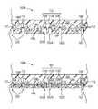
- FIG. 1Ais a cross-sectional view of an assembly 100 A during the fabrication of a plurality of wafer level electronic component packages in accordance with one embodiment of the present invention.
- assembly 100 Aincludes a rigid support strip 102 , e.g., an aluminum, copper or stainless steel plate.
- Support strip 102includes fiducials 104 on an upper, e.g., first, surface 102 U of support strip 102 .
- Fiducials 104are used for alignment and mounting of electronic components 106 , e.g., integrated circuit chips, as discussed further below.
- a dielectric strip 108is mounted to support strip 102 .
- Electronic components 106are mounted to dielectric strip 108 with adhesives 110 , e.g., liquid adhesives or double-sided sticky tapes, although other adhesives are used in other embodiments.
- adhesives 110e.g., liquid adhesives or double-sided sticky tapes, although other adhesives are used in other embodiments.
- a first electronic component 106 A of the plurality of electronic components 106is mounted to dielectric strip 108 with a first adhesive 110 A of the plurality of adhesives 110 .
- Dielectric strip 108sometimes called a first dielectric strip
- adhesives 110are electrical insulators, i.e., dielectrics.
- front, e.g., first, surfaces 106 F of electronic components 106are mounted to an upper, e.g., first, surface 108 U of dielectric strip 108 with adhesives 110 .
- a lower, e.g., second, surface 108 L of dielectric strip 108is mounted to upper surface 102 U of support strip 102 .
- dielectric strip 108is tacky, sometimes called sticky, and is simply pressed against support strip 102 to mount dielectric strip 108 to support strip 102 .
- adhesives 110are applied to front surfaces 106 F of electronic components 106 while electronic components 106 are still in wafer form, i.e., before they are singulated.
- dielectric strip 108is transparent such that fiducials 104 are visible through dielectric strip 108 .
- Electronic components 106are aligned to fiducials 104 and mounted to dielectric strip 108 with adhesives 110 , e.g., using an optical alignment system.
- Adhesives 110are cured, if necessary.
- electronic components 106are mounted in a single row on dielectric strip 108 .
- electronic components 106are mounted in an array on dielectric strip 108 .
- electronic components 106are mounted in a 2 ⁇ 2, 3 ⁇ 3, . . . , or n ⁇ m array.
- only a single electronic component 106is mounted to dielectric strip 108 , i.e., the wafer level electronic component package is fabricated as an individual unit instead of as one of a plurality of units fabricated simultaneously.
- band pads 112Formed on front surface 106 F of electronic components 106 are band pads 112 , e.g., formed of aluminum. Bond pads 112 are connected to the internal circuitry of electronic components 106 .
- bond pads 112are distributed in an array on front surface 106 F. In another embodiment, bond pads 112 are formed on front surface 106 F directly adjacent sides S of electronic components 106 in a typical wirebond configuration pattern.
- FIG. 1Bis a cross-sectional view of an assembly 100 B during the fabrication of a plurality of wafer level electronic component packages in accordance with another embodiment of the present invention.
- Assembly 100 B of FIG. 1Bis similar to assembly 100 A of FIG. 1A and only the significant differences are discussed below.
- an adhesive strip 120( FIG. 1B ) is used to mount electronic components 106 .
- Adhesive strip 120is an electrical insulator.
- adhesive strip 120is a liquid adhesive, for example, applied by spin coating.
- adhesive strip 120is a double-sided sticky tape although other adhesives are used in other embodiments.
- a lower, e.g., first, surface 120 L of adhesive strip 120is mounted to upper surface 108 U of dielectric strip 108 .
- Front surfaces 106 F of electronic components 106are mounted to an upper, e.g., second, surface 120 U of adhesive strip 120 .
- adhesive strip 120is illustrated in the figures which follow and discussed below for purposes of simplicity, it is to be understood that adhesives 110 ( FIG. 1A ) are used instead of adhesive strip 120 in an alternative embodiment.
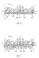
- FIG. 2is a cross-sectional view of assembly 100 B of FIG. 1B at a further stage during the fabrication of a plurality of wafer level electronic component packages in accordance with one embodiment of the present invention.
- heat sinks 214e.g., copper slugs, are mounted to rear, e.g., second, surfaces 106 R of electronic components 106 .
- heat sinks 214enhance heat dissipation from electronic components 106 to the ambient environment.
- a first heat sink 214 A of the plurality of heat sinks 214is mounted to rear surface 106 R of electronic component 106 A.
- legs 216 of heat sinks 214adhere to adhesive strip 120 to hold heat sinks 214 in place.
- a thermal pad or greaseis used between heat sinks 214 and rear surfaces 106 R of electronic components 106 to enhance heat transfer from electronic components 106 to heat sinks 214 .
- adhesives 218mount heat sinks 214 to rear surface 106 R of electronic components 106 .
- heat sink 214 Ais mounted to rear surface 106 R of electronic component 106 A with a first adhesive 218 A of the plurality of adhesives 218 .
- heat sinks 214are not illustrated in the figures which follow or discussed further below for purposes of simplicity, it is to be understood that the assembly is fabricated to include heat sinks 214 in an alternative embodiment.
- FIG. 3is a cross-sectional view of assembly 100 B of FIG. 1B at a further stage during the fabrication of a plurality of wafer level electronic component packages in accordance with one embodiment of the present invention.
- electronic components 106are encapsulated, sometimes called overmolded, in an encapsulant 320 .
- Encapsulant 320protects electronic components 106 from the ambient environment.
- a liquid encapsulantis applied and cured to form encapsulant 320 .
- a plastic encapsulantis applied, e.g., using a transfer or injection mold process, to form encapsulant 320 .
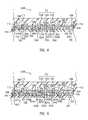
- FIG. 4is a cross-sectional view of assembly 100 B of FIG. 3 at a further stage during the fabrication of a plurality of wafer level electronic component packages in accordance with one embodiment of the present invention.
- support strip 102is removed from dielectric strip 108 .
- upper surface 102 U of support strip 102is pretreated, e.g., a release agent is applied, to facilitate easy removal of support strip 102 .
- support strip 102is reusable and thus reused to fabricate another assembly 100 B as illustrated in FIG. 1B after removal from dielectric strip 108 thus minimizing the cost of fabricating assembly 100 B.
- encapsulant 320provides rigidity and support for assembly 100 B. Further, removal of support strip 102 exposes lower surface 108 L of dielectric strip 108 for further processing as discussed further below.
- FIG. 5is a cross-sectional view of assembly 100 B of FIG. 4 at a further stage during the fabrication of a plurality of wafer level electronic component packages in accordance with one embodiment of the present invention.
- a plurality of via apertures 522are formed using a laser, i.e., using laser ablation. Via apertures 522 are sometimes called first via apertures.
- Via apertures 522extend through dielectric strip 108 and through adhesive strip 120 to bond pads 112 of electronic components 106 .
- via apertures 522are cylindrical in shape. Bond pads 112 are exposed through via apertures 522 .
- the laser intensityis set to be sufficient to remove dielectric strip 108 and adhesive strip 120 .
- the laser intensityis set to be insufficient to remove bond pads 112 . Accordingly, pulsing of the laser forms a single via aperture 522 extending through dielectric strip 108 and through adhesive strip 120 to a bond pad 112 of electronic components 106 . The laser is then stepped to the next location to form the next via aperture 522 .
- electronic component 106 Aincludes bond pads 112 A, 112 B, 112 C on front surface 106 F of electronic component 106 A.
- Via apertures 522 A, 522 B, 522 C of the plurality of via apertures 522extend through dielectric strip 108 and through adhesive strip 120 to bond pads 112 A, 112 B, 112 C, respectively.
- the laseris pulsed to form via aperture 522 A.
- the laseris then stepped and pulsed again to form via aperture 522 B.
- the laseris then stepped and pulsed again to form via aperture 522 C.
- the laseris stepped and pulsed repeatedly until all of via apertures 522 are formed.
- a plurality of lasersare simultaneous pulsed to form some or all of via apertures 522 simultaneously.
- via apertures 522are formed using selective etching, mechanical drilling, or other techniques.
- FIG. 6is a cross-sectional view of assembly 100 B of FIG. 5 at a further stage during the fabrication of a plurality of wafer level electronic component packages in accordance with one embodiment of the present invention.
- via apertures 522are filled with an electrically conductive material, e.g., a metal or metal containing material, an electrically conductive adhesive such as a silver filled adhesive or polymer, or solder paste, to form electrically conductive vias 624 .
- Vias 624are sometimes called first vies.
- via apertures 522are filled with an electrically conductive adhesive, which is then cured if necessary, to form vias 624 .
- via apertures 522are filled with a solder paste. Assembly 100 B is then heated to reflow the solder paste to form vias 624 .
- any excess electrically conductive material formed on lower surface 108 L of dielectric strip 108is removed. Illustratively, an etch or physical grinding process is used.
- an over-etch processis used to slightly over-etch vias 624 .
- vias 624remain recessed within via apertures 522 . This ensures that shorting between vias 624 from excess electrically conductive material is avoided.
- Vias 624are electrically connected to corresponding bond pads 112 .
- vias 624 A, 624 B, 624 C of the plurality of vias 624are electrically connected to bond pads 112 A, 112 B, 112 C, respectively.
- Vias 624extend from bond pads 112 , through adhesive strip 120 and through dielectric strip 108 to be adjacent or slightly recessed from (above in the view of FIG. 6 ) lower surface 108 L of dielectric strip 108 .
- Bond pads 112are directly connected to corresponding vias 624 . Stated another way, bond pads 112 are electrically connected to corresponding vias 624 without the use of a solder, e.g., without the use of flip chip bumps, and without the need to form a solder wetting layer, e.g., a nickel/gold layer, on bond pads 112 . This maximizes the reliability of the electrical connection between vies 624 and bond pads 112 , while at the same time minimizes impedance.
- dielectric strip 108is directly attached to electronic components 106 by adhesive strip 120 and bond pads 112 are directly connected to corresponding vies 624 , the use of an underfill material is obviated. This simplifies manufacturing, enhances reliability, and thus reduces cost.
- assembly 100 Bis inspected, e.g., optically using an automatic inspection system, to insure that all via apertures 522 are properly filled with electrically conductive material, i.e., to inspect the integrity of vias 624 .
- any defective or unformed vias 624 detected during the inspectionare corrected, e.g., by etch removal of vias 624 , reapplication of the electrically conductive material to reform vias 624 , e.g., re-plating, and removal of any excess electrically conductive material on lower surface 108 L of dielectric strip 108 .
- the wafer level electronic component packagesare fabricated with a maximum yield, e.g., essentially a 100 percent yield. This further minimizes the fabrication cost of the wafer level electronic component packages.
- FIG. 7is a cross-sectional view of assembly 100 B of FIG. 6 at a further stage during the fabrication of a plurality of wafer level electronic component packages in accordance with one embodiment of the present invention.
- a second dielectric strip 708is mounted to dielectric strip 108 . More particularly, an upper, e.g., first, surface 708 U of dielectric strip 708 is mounted to lower surface 108 L of dielectric strip 108 .
- dielectric strip 708is mounted to dielectric strip 108 using a tack cure. More particularly, dielectric strip 708 is pressed on to dielectric strip 108 . Assembly 100 B is heated to fuse together and bond dielectric strip 708 to dielectric strip 108 .
- dielectric strip 108 and dielectric strip 708are polytetrafluoroethylene (PTFE), liquid crystal polymer (LCP) or a non woven arimid although other low-K dielectric materials are used in other embodiments.
- PTFEpolytetrafluoroethylene
- LCPliquid crystal polymer
- non woven arimidalthough other low-K dielectric materials are used in other embodiments.
- a plurality of via apertures 722 and trace channels 726are formed using a laser, i.e., using laser ablation. Via apertures 722 and trace channels 726 extend through dielectric strip 708 and to vias 624 . Via apertures 722 are sometimes called second via apertures.
- via apertures 722are cylindrical in shape and extend vertically, i.e., in a first direction perpendicular to front surface 106 F of electronic components 106 , through dielectric strip 708 to vias 624 .
- Trace channels 726are trenches extending horizontally, i.e., in a second direction perpendicular to the first direction and parallel to front surface 106 F of electronic components 106 , from vias 624 .
- Vias 624are exposed through via apertures 722 and trace channels 726 .
- a first via aperture 722 A of the plurality of via apertures 722extends through dielectric strip 708 to via 624 A.
- a first trace channel 726 A of the plurality of trace channels 726extends through dielectric strip 708 to via 624 B. More particularly, via 624 B is exposed at a first end 728 of trace channel 726 A. Trace channel 726 A extends horizontally outwards from a center C of electronic component 106 A and outwards from via 624 D to a second end 730 of trace channel 726 A in a fan-out configuration.
- a second trace channel 726 B of the plurality of trace channels 726extends through dielectric strip 708 to via 624 C. More particularly, via 624 C is exposed at a first end 728 of trace channel 726 B. Trace channel 726 B extends horizontally inwards toward center C from via 624 C to a second end 730 of trace channel 726 B in a fan-in configuration.
- a laseris stepped and pulsed repeatedly to form via apertures 722 and trace channels 726 .
- a plurality of lasersare simultaneous pulsed to form some or all of via apertures 722 and trace channels 726 simultaneously.
- the laseris moved during pulsing to form the horizontal trenches of trace channels 726 .
- via apertures 722 and trace channels 726are all formed to have the same depth, this depth being equal to the thickness of dielectric strip 708 . This simplifies and enhances reliability of filling, e.g., plating, of via apertures 722 and trace channels 726 with an electrically conductive material as discussed below.
- FIG. 8is a cross-sectional view of assembly 1003 of FIG. 7 at a further stage during the fabrication of a plurality of wafer level electronic component packages in accordance with one embodiment of the present invention.
- via apertures 722 and trace channels 726are filled with an electrically conductive material, e.g., a metal or metal containing material, an electrically conductive adhesive, or solder paste, to form electrically conductive vias 824 and electrically conductive traces 832 , respectively.
- Vias 824are sometimes called second vias.
- via apertures 722 and trace channels 726are filled with an electrically conductive adhesive, which is then cured if necessary, to form vias 824 and traces 832 , respectively.
- via apertures 722 and trace channels 726are filled with a solder paste. Assembly 100 B is then heated to reflow the solder paste to form vias 824 and traces 832 , respectively.
- Vias 824form vertical electrical connectors, i.e., form electrical connectors extending vertically.
- Traces 832form horizontal electrical connectors, i.e., form electrical connectors extending horizontally.
- any excess electrically conductive material formed on a lower, e.g., second, surface 708 L of dielectric strip 708is removed.
- an etch or physical grinding processis used.
- an over-etch processis used to slightly over-etch vias 824 and traces 832 . This ensures that shorting between vias 824 and/or traces 832 from excess electrically conductive material is avoided.
- Vias 824 and traces 832are electrically connected to corresponding vias 624 .
- a first via 824 A of the plurality of vise 824is electrically connected to via 624 A.
- Vise 824extend from vise 624 , through dielectric strip 708 to be adjacent or recessed from lower surface 708 L of dielectric strip 708 .
- a first trace 832 A of the plurality of traces 832is electrically connected to via 624 B. More particularly, a first end 834 of trace 832 A is electrically connected to via 624 B. Trace 832 A extends horizontally outwards from a center C of electronic component 106 A and outwards from via 624 B to a second end 836 of trace 832 A in a fan-out configuration.
- a second trace 832 B of the plurality of traces 832is electrically connected to via 624 C. More particularly, a first end 834 of trace 832 B is electrically connected to via 624 C. Trace 832 B extends horizontally inwards toward center C from via 624 C to a second end 836 of trace 832 B in a fan-in configuration.
- a fan-out trace and a fan-in tracei.e., traces 832 A, 832 B, respectively, are illustrated and discussed, in other embodiments, only fan-in traces or fan-out traces are formed.
- assembly 100 Bis inspected to insure that all via apertures 722 and trace channels 726 are properly filled with electrically conductive material, i.e., to inspect the integrity of vias 824 and traces 832 .
- any defective or unformed vies 824 and traces 832 detected during the inspectionare corrected, e.g., by etch removal of vise 824 and traces 832 , reapplication of the electrically conductive material to reform vias 824 and traces 832 , and removal of any excess electrically conductive material on lower surface 708 L of dielectric strip 708 .
- the wafer level electronic component packagesare fabricated with a maximum yield.
- FIG. 9is a cross-sectional view of assembly 100 B of FIG. 8 at a further stage during the fabrication of a plurality of wafer level electronic component packages in accordance with one embodiment of the present invention.
- a third dielectric strip 908is mounted to dielectric strip 708 . More particularly, an upper, e.g., first, surface 908 U of dielectric strip 908 is mounted to lower surface 708 L of dielectric strip 708 .
- Dielectric strip 908is similar to dielectric strip 708 and mounted in a manner similar to that discussed above with regards to mounting of dielectric strip 708 to dielectric strip 108 .
- a plurality of via apertures 922are formed using a laser, i.e., using laser ablation. Via apertures 922 extend through dielectric strip 908 to vias 824 and traces 832 . In one embodiment, via apertures 922 are cylindrical in shape. Via apertures 922 are sometimes called third via apertures.
- Vias 824 and second ends 836 of traces 832are exposed through via apertures 922 .
- via apertures 922 A, 922 B, 922 C of the plurality of via apertures 922extend through dielectric strip 908 to via 824 A and second ends 836 of traces 832 A, 832 B, respectively.
- Via apertures 922are formed in a manner similar to via apertures 522 of FIG. 5 so formation of via apertures 922 is not discussed in detail to avoid detracting from the principals of the invention.
- Via apertures 922are filled with an electrically conductive material, e.g., a metal or metal containing material, an electrically conductive adhesive, or solder paste, to form electrically conductive vias 924 .
- Via apertures 922are filled to form vias 924 in a manner similar to that discussed with regards to vias 624 of FIG. 6 so formation of vias 924 is not discussed in detail to avoid detracting from the principals of the invention. Vias 924 are sometimes called third vias.
- any excess electrically conductive material formed on a lower, e.g., second, surface 908 U of dielectric strip 908is removed.
- an etch or physical grinding processis used.
- an over-etch processis used to slightly over-etch vias 924 .
- vias 924remain recessed within via apertures 922 . This ensures that shorting between vias 924 from excess electrically conductive material is avoided.
- Vias 924are electrically connected to corresponding vias 824 and second ends 836 of traces 832 .
- vias 924 A, 924 B, 924 C of the plurality of vias 924are electrically connected to via 824 A and second ends 836 of traces 832 A, 832 , respectively.
- Vias 924extend from vise 824 and second ends 836 of traces 832 through dielectric strip 908 to be adjacent or slightly recessed from lower surface 908 L of dielectric strip 908 .
- vise 924are formed to have a larger diameter than the width of traces 832 and/or the diameter of vias 824 .
- vias 924are formed with the appropriate diameter, tolerance in the positioning of vias 924 is accommodated. Stated another way, by forming vias 924 with a sufficiently large diameter, electrical contact between vias 924 and vias 824 /traces 832 is assured.
- assembly 100 Bis inspected to insure that all via apertures 922 are properly filled with electrically conductive material, i.e., to inspect the integrity of vias 924 .
- any defective or unformed vias 924 detected during the inspectionare corrected, e.g., by etch removal of vise 924 , reapplication of the electrically conductive material to reform vias 924 , and removal of any excess electrically conductive material on lower surface 908 L of dielectric strip 908 .
- the wafer level electronic component packagesare fabricated with a maximum yield.
- FIG. 10is a cross-sectional view of assembly 100 B of FIG. 9 at a further stage during the fabrication of a plurality of wafer level electronic component packages in accordance with one embodiment of the present invention.
- a fourth dielectric strip 1008is mounted to dielectric strip 908 . More particularly, an upper, e.g., first, surface 1008 U of dielectric strip 1008 is mounted to lower surface 908 L of dielectric strip 908 .
- Dielectric strip 1008is similar to dielectric strip 708 and mounted in a manner similar to that discussed above with regards to mounting of dielectric strip 708 to dielectric strip 108 .
- a plurality of land apertures 1040are formed using a laser, i.e., using laser ablation. Land apertures 1040 extend through dielectric strip 1008 to vias 924 . In one embodiment, land apertures 1040 are cylindrical in shape but can be patterned in a variety of shapes depending upon the particular interconnection structure used, e.g., interconnection balls or lands.
- Vias 924are exposed through land apertures 1040 .
- land apertures 1040 A, 1040 B, 1040 C of the plurality of land apertures 1040extend through dielectric strip 1008 to vias 924 A, 924 B, 924 C, respectively.
- Land apertures 1040are formed in a manner similar to via apertures 522 of FIG. 5 so formation of land apertures 1040 is not discussed in detail to avoid detracting from the principals of the invention.
- Land apertures 1040are filled with an electrically conductive material, e.g., a metal or metal containing material, an electrically conductive adhesive, or solder paste, to form electrically conductive lands 1044 .
- Land apertures 1040are filled to form lands 1044 in a manner similar to that discussed with regards to vies 624 of FIG. 6 so formation of lands 1044 is not discussed in detail to avoid detracting from the principals of the invention.
- any excess electrically conductive material formed on a lower, e.g., second, surface 1008 L of dielectric strip 1008is removed.
- an etch or physical grinding processis used.
- an over-etch processis used to slightly over-etch lands 1044 .
- lands 1044remain recessed within land apertures 1040 . This ensures that shorting between lands 1044 from excess electrically conductive material is avoided.
- Lands 1044are electrically connected to corresponding vies 924 .
- lands 1044 A, 1044 B, 1044 C of the plurality of lands 1044are electrically connected to vies 924 A, 924 B, 924 C, respectively.
- Lands 1044extend from vias 924 through dielectric strip 1008 to be adjacent or slightly recessed from lower surface 1008 L of dielectric strip 1008 .
- assembly 100 Bis inspected to insure that all land apertures 1040 are properly filled with electrically conductive material, i.e., to inspect the integrity of lands 1044 .
- any defective or unformed lands 1044 detected during the inspectionare corrected, e.g., by etch removal of lands 1044 , reapplication of the electrically conductive material to reform lands 1044 , and removal of any excess electrically conductive material on lower surface 1008 L of dielectric strip 1008 . In this manner, the wafer level electronic component packages are fabricated with a maximum yield.
- solder on pasteis applied to lands 1044 .
- This solder on pasteis reflowed, i.e., heated to a melt and cooled to resolidify, to form solder lands, which are represented as item 1046 in FIG. 10 in accordance with this embodiment.
- the resulting wafer level electronic component packageis a land grid array package.
- the solder landsare used to electrically connect the wafer level electronic component package to the larger substrate, e.g., a mother or daughter board, for example, using a high lead solder such as a 90/10 lead/tin solder.
- a ball grid array packageis formed. More particular, after formation of lands 1044 , an organic solderability protectant (OSP), sometimes called an organic solderability preservative, is applied to lands 1044 .
- the organic solderability protectantwhich is represented as item 1046 in FIG. 10 in accordance with this embodiment, enhances the solder wet-ability of lands 1044 .
- the organic solderability protectantis hereinafter referred to as OSP 1046 .
- OSP 1046is not used.
- FIG. 11is a cross-sectional view of assembly 100 B of FIG. 10 at a further stage during the fabrication of a plurality of wafer level electronic component packages 1148 in accordance with one embodiment of the present invention.
- electrically conductive interconnection balls 1150e.g., eutectic lead/tin solder, are formed on lands 1044 .
- Interconnection balls 1150are formed in a conventional manner. During formation of interconnection balls 1150 , OSP 1046 is consumed.
- Interconnection balls 1150are used to electrically connect wafer level electronic component packages 1148 to the larger substrate, e.g., a mother or daughter board. Assembly 100 B is then singulated, e.g., using a mechanical saw or laser, to form the plurality of wafer level electronic component packages 1148 .
- Each interconnection ball 1150is electrically connected to a corresponding bond pad 112 as discussed above. In this manner, the pattern of bond pads 112 is redistributed to the pattern of interconnection balls 1150 .
- bond pads 112are formed on front surface 106 F directly adjacent sides S of electronic components 106 in a typical wirebond configuration pattern.
- interconnection balls 1150are distributed in an array pattern.
- the wirebond configuration pattern of bond pads 112is redistributed to an array pattern of interconnection balls 1150 .
- an array pattern of interconnection balls 1150is discussed above, interconnection balls 1150 are distributed in any one of a number of desired patterns in other embodiments.
- interconnection balls 1150are connected to bond pads 112 using a minimum path length.
- bond pad 112 Ais coupled to a first interconnection ball 1150 A of the plurality of interconnection balls 1150 by vies 624 A, 824 A, 924 A, land 1044 A, which are directly aligned with one another.
- heat transfer between bond pads 112 and more generally between electronic components 106 and interconnection balls 1150is maximized thus improving the thermal performance of wafer level electronic component packages 1148 .
- impedance between bond pads 112 and interconnection balls 1150is minimized
- a dielectric stripis applied; (2) the dielectric strip is laser patterned to form via apertures and/or trace channels; (3) the via apertures and/or trace channels are filled with electrically conductive material to form vias and/or traces; (4) excess electrically conductive material is removed from the lower surface of the dielectric strip; and (5) the formed vies and/or traces are inspected and corrected, if necessary. This process is repeated any number of desired times until the desired redistribution is achieved.
- any changes in the design layout of the via apertures 522 , 722 , 922 and/or trace channels 726are relatively simple to execute. More particularly, these design layout changes are made in the computer software, e.g., the CAD software, which drives the laser. Accordingly, the design layout changes are made with some relatively simple programming and executed immediately.
- dielectric strips 108 , 708 , 908 , 1008are illustrated and discussed above, more or less than four dielectric strips are used in other embodiments. Generally, at least one dielectric strip, e.g., dielectric strip 108 , is used.
- vias 624 , 824 , 924 , traces 832 , and lands 1044are discussed above as being formed in various dielectric strips 108 , 708 , 908 , and 1008 for purposes of discussion, in light of this disclosure, those of skill in the art will understand that vias, traces, lands and/or combinations thereof can be formed in any single dielectric strip 108 , 708 , 908 , or 1008 .
- vias 624 , 824 , 924 , traces 832 , and lands 1044are discussed as distinct types of structures for purposes of discussion, in light of this disclosure, those of skill in the art will understand that vias 624 , 824 , 924 , traces 832 , and lands 1044 can be similar in structure. For example, a via or trace can form a land.
- trace channels 726 and land apertures 1040are filled immediately after formation, i.e., before application of the next dielectric strip, with an electrically conductive material to form the vies 624 , 824 , 924 , traces 832 and lands 1044 , respectively, in the discussion above.
- trace channels 726 and land apertures 1040are formed in some or all of dielectric strips 108 , 708 , 908 , 1008 .
- via apertures 522 , 722 , 922 , trace channels 726 and land apertures 1040are filled at the same time, e.g., in a single plating operation, with an electrically conductive material to form vias 624 , 824 , 924 , traces 832 and lands 1044 , respectively.
- FIG. 12is a cross-sectional view of an assembly 1200 during the fabrication of a plurality of wafer level electronic component packages in accordance with one embodiment of the present invention.
- assembly 1200includes an electronic component substrate 1252 such as a silicon wafer.
- Electronic component substrate 1252includes a plurality of electronic components 106 - 1 integrally connected together.
- Electronic components 106 - 1include bond pads 112 on front surfaces 106 F of electronic components 106 - 1 , and more generally on a lower, e.g., first, surface 1252 L of electronic component substrate 1252 .
- Electronic components 106 - 1are integrally connected together in an array, e.g., a 2 ⁇ 2, 3 ⁇ 3 . . . or n ⁇ m array. Each of electronic components 106 - 1 is delineated by a singulation street 1254 , which is located between adjacent electronic components 106 - 1 .
- a first singulation street 1254 A of the plurality of singulation streets 1254delineates a first electronic component 106 -IA from a second electronic component 106 - 1 B of the plurality of electronic components 106 - 1 .
- the other electronic components 106 - 1are similarly delineated from adjacent electronic components 106 - 1 by corresponding singulation streets 1254 .
- Upper surface 108 U of dielectric strip 108is mounted to front surfaces 106 F of electronic components 106 - 1 , and more generally to lower surface 1252 L of electronic component substrate 1252 with adhesive strip 120 .
- Electronic component substrate 1252provides rigidity and support for assembly 1200 .
- FIG. 13is a cross-sectional view of assembly 1200 of FIG. 12 at a further stage during the fabrication of a plurality of wafer level electronic component packages in accordance with one embodiment of the present invention.
- vias 624 , 824 , 924 , traces 832 , and lands 1044are formed in dielectric strips 108 , 708 , 908 , and 1008 as discussed above in reference to FIGS. 5-11 , the discussion of which is incorporated herein by reference in its entirety.
- interconnection balls 1150are formed on lands 1044 to form a ball grid array (BGA) package.
- BGAball grid array
- Each interconnection ball 1150is coupled to a corresponding bond pad 112 .
- LGAland grid array
- Assembly 1200is a true wafer scale process. After formation of vias 624 , 824 , 924 , traces 832 , lands 1044 in dielectric strips 108 , 708 , 908 , 1008 , assembly 1200 is singulated along singulation streets 1254 ( FIG. 12 ) resulting in the fabrication of wafer level electronic component packages 1348 . Singulation is performed before or after fabrication of interconnection balls 1150 .
Landscapes
- Engineering & Computer Science (AREA)
- Computer Hardware Design (AREA)
- Microelectronics & Electronic Packaging (AREA)
- Power Engineering (AREA)
- Physics & Mathematics (AREA)
- Condensed Matter Physics & Semiconductors (AREA)
- General Physics & Mathematics (AREA)
- Manufacturing & Machinery (AREA)
- Production Of Multi-Layered Print Wiring Board (AREA)
- Internal Circuitry In Semiconductor Integrated Circuit Devices (AREA)
Abstract
Description
Claims (14)
Priority Applications (3)
| Application Number | Priority Date | Filing Date | Title |
|---|---|---|---|
| US14/734,192US9406645B1 (en) | 2002-11-08 | 2015-06-09 | Wafer level package and fabrication method |
| US15/225,284US9871015B1 (en) | 2002-11-08 | 2016-08-01 | Wafer level package and fabrication method |
| US15/872,397US10665567B1 (en) | 2002-11-08 | 2018-01-16 | Wafer level package and fabrication method |
Applications Claiming Priority (12)
| Application Number | Priority Date | Filing Date | Title |
|---|---|---|---|
| US10/291,050US6905914B1 (en) | 2002-11-08 | 2002-11-08 | Wafer level package and fabrication method |
| US11/123,605US7192807B1 (en) | 2002-11-08 | 2005-05-05 | Wafer level package and fabrication method |
| US11/605,740US7714431B1 (en) | 2002-11-08 | 2006-11-28 | Electronic component package comprising fan-out and fan-in traces |
| US12/661,604US7932595B1 (en) | 2002-11-08 | 2010-03-19 | Electronic component package comprising fan-out traces |
| US13/065,296US8119455B1 (en) | 2002-11-08 | 2011-03-18 | Wafer level package fabrication method |
| US13/358,947US8298866B1 (en) | 2002-11-08 | 2012-01-26 | Wafer level package and fabrication method |
| US13/627,815US8486764B1 (en) | 2002-11-08 | 2012-09-26 | Wafer level package and fabrication method |
| US13/918,307US8691632B1 (en) | 2002-11-08 | 2013-06-14 | Wafer level package and fabrication method |
| US14/019,136US8710649B1 (en) | 2002-11-08 | 2013-09-05 | Wafer level package and fabrication method |
| US14/264,970US8952522B1 (en) | 2002-11-08 | 2014-04-29 | Wafer level package and fabrication method |
| US14/586,263US9054117B1 (en) | 2002-11-08 | 2014-12-30 | Wafer level package and fabrication method |
| US14/734,192US9406645B1 (en) | 2002-11-08 | 2015-06-09 | Wafer level package and fabrication method |
Related Parent Applications (1)
| Application Number | Title | Priority Date | Filing Date |
|---|---|---|---|
| US14/586,263ContinuationUS9054117B1 (en) | 2002-11-08 | 2014-12-30 | Wafer level package and fabrication method |
Related Child Applications (1)
| Application Number | Title | Priority Date | Filing Date |
|---|---|---|---|
| US15/225,284ContinuationUS9871015B1 (en) | 2002-11-08 | 2016-08-01 | Wafer level package and fabrication method |
Publications (1)
| Publication Number | Publication Date |
|---|---|
| US9406645B1true US9406645B1 (en) | 2016-08-02 |
Family
ID=34632671
Family Applications (18)
| Application Number | Title | Priority Date | Filing Date |
|---|---|---|---|
| US10/291,050Expired - LifetimeUS6905914B1 (en) | 2002-11-08 | 2002-11-08 | Wafer level package and fabrication method |
| US11/047,848Expired - LifetimeUS7247523B1 (en) | 2002-11-08 | 2005-01-31 | Two-sided wafer escape package |
| US11/123,605Expired - LifetimeUS7192807B1 (en) | 2002-11-08 | 2005-05-05 | Wafer level package and fabrication method |
| US11/605,740Expired - LifetimeUS7714431B1 (en) | 2002-11-08 | 2006-11-28 | Electronic component package comprising fan-out and fan-in traces |
| US11/784,979Expired - LifetimeUS7420272B1 (en) | 2002-11-08 | 2007-04-09 | Two-sided wafer escape package |
| US12/221,797Expired - LifetimeUS7692286B1 (en) | 2002-11-08 | 2008-08-05 | Two-sided fan-out wafer escape package |
| US12/661,604Expired - Fee RelatedUS7932595B1 (en) | 2002-11-08 | 2010-03-19 | Electronic component package comprising fan-out traces |
| US13/065,296Expired - Fee RelatedUS8119455B1 (en) | 2002-11-08 | 2011-03-18 | Wafer level package fabrication method |
| US13/358,947Expired - Fee RelatedUS8298866B1 (en) | 2002-11-08 | 2012-01-26 | Wafer level package and fabrication method |
| US13/472,961ActiveUS8501543B1 (en) | 2002-11-08 | 2012-05-16 | Direct-write wafer level chip scale package |
| US13/627,815Expired - Fee RelatedUS8486764B1 (en) | 2002-11-08 | 2012-09-26 | Wafer level package and fabrication method |
| US13/918,307Expired - LifetimeUS8691632B1 (en) | 2002-11-08 | 2013-06-14 | Wafer level package and fabrication method |
| US14/019,136Expired - LifetimeUS8710649B1 (en) | 2002-11-08 | 2013-09-05 | Wafer level package and fabrication method |
| US14/264,970Expired - LifetimeUS8952522B1 (en) | 2002-11-08 | 2014-04-29 | Wafer level package and fabrication method |
| US14/586,263Expired - Fee RelatedUS9054117B1 (en) | 2002-11-08 | 2014-12-30 | Wafer level package and fabrication method |
| US14/734,192Expired - Fee RelatedUS9406645B1 (en) | 2002-11-08 | 2015-06-09 | Wafer level package and fabrication method |
| US15/225,284Expired - LifetimeUS9871015B1 (en) | 2002-11-08 | 2016-08-01 | Wafer level package and fabrication method |
| US15/872,397Expired - Fee RelatedUS10665567B1 (en) | 2002-11-08 | 2018-01-16 | Wafer level package and fabrication method |
Family Applications Before (15)
| Application Number | Title | Priority Date | Filing Date |
|---|---|---|---|
| US10/291,050Expired - LifetimeUS6905914B1 (en) | 2002-11-08 | 2002-11-08 | Wafer level package and fabrication method |
| US11/047,848Expired - LifetimeUS7247523B1 (en) | 2002-11-08 | 2005-01-31 | Two-sided wafer escape package |
| US11/123,605Expired - LifetimeUS7192807B1 (en) | 2002-11-08 | 2005-05-05 | Wafer level package and fabrication method |
| US11/605,740Expired - LifetimeUS7714431B1 (en) | 2002-11-08 | 2006-11-28 | Electronic component package comprising fan-out and fan-in traces |
| US11/784,979Expired - LifetimeUS7420272B1 (en) | 2002-11-08 | 2007-04-09 | Two-sided wafer escape package |
| US12/221,797Expired - LifetimeUS7692286B1 (en) | 2002-11-08 | 2008-08-05 | Two-sided fan-out wafer escape package |
| US12/661,604Expired - Fee RelatedUS7932595B1 (en) | 2002-11-08 | 2010-03-19 | Electronic component package comprising fan-out traces |
| US13/065,296Expired - Fee RelatedUS8119455B1 (en) | 2002-11-08 | 2011-03-18 | Wafer level package fabrication method |
| US13/358,947Expired - Fee RelatedUS8298866B1 (en) | 2002-11-08 | 2012-01-26 | Wafer level package and fabrication method |
| US13/472,961ActiveUS8501543B1 (en) | 2002-11-08 | 2012-05-16 | Direct-write wafer level chip scale package |
| US13/627,815Expired - Fee RelatedUS8486764B1 (en) | 2002-11-08 | 2012-09-26 | Wafer level package and fabrication method |
| US13/918,307Expired - LifetimeUS8691632B1 (en) | 2002-11-08 | 2013-06-14 | Wafer level package and fabrication method |
| US14/019,136Expired - LifetimeUS8710649B1 (en) | 2002-11-08 | 2013-09-05 | Wafer level package and fabrication method |
| US14/264,970Expired - LifetimeUS8952522B1 (en) | 2002-11-08 | 2014-04-29 | Wafer level package and fabrication method |
| US14/586,263Expired - Fee RelatedUS9054117B1 (en) | 2002-11-08 | 2014-12-30 | Wafer level package and fabrication method |
Family Applications After (2)
| Application Number | Title | Priority Date | Filing Date |
|---|---|---|---|
| US15/225,284Expired - LifetimeUS9871015B1 (en) | 2002-11-08 | 2016-08-01 | Wafer level package and fabrication method |
| US15/872,397Expired - Fee RelatedUS10665567B1 (en) | 2002-11-08 | 2018-01-16 | Wafer level package and fabrication method |
Country Status (1)
| Country | Link |
|---|---|
| US (18) | US6905914B1 (en) |
Cited By (16)
| Publication number | Priority date | Publication date | Assignee | Title |
|---|---|---|---|---|
| US20150364402A1 (en)* | 2012-06-22 | 2015-12-17 | Infineon Technologies Ag | Monitor Structures and Methods of Formation Thereof |
| US10665567B1 (en) | 2002-11-08 | 2020-05-26 | Amkor Technology, Inc. | Wafer level package and fabrication method |
| US10886232B2 (en) | 2019-05-10 | 2021-01-05 | Applied Materials, Inc. | Package structure and fabrication methods |
| US10937726B1 (en) | 2019-11-27 | 2021-03-02 | Applied Materials, Inc. | Package structure with embedded core |
| US11063169B2 (en) | 2019-05-10 | 2021-07-13 | Applied Materials, Inc. | Substrate structuring methods |
| US11232951B1 (en) | 2020-07-14 | 2022-01-25 | Applied Materials, Inc. | Method and apparatus for laser drilling blind vias |
| US11257790B2 (en) | 2020-03-10 | 2022-02-22 | Applied Materials, Inc. | High connectivity device stacking |
| US11342256B2 (en) | 2019-01-24 | 2022-05-24 | Applied Materials, Inc. | Method of fine redistribution interconnect formation for advanced packaging applications |
| US11400545B2 (en) | 2020-05-11 | 2022-08-02 | Applied Materials, Inc. | Laser ablation for package fabrication |
| US11404318B2 (en) | 2020-11-20 | 2022-08-02 | Applied Materials, Inc. | Methods of forming through-silicon vias in substrates for advanced packaging |
| US11454884B2 (en) | 2020-04-15 | 2022-09-27 | Applied Materials, Inc. | Fluoropolymer stamp fabrication method |
| US11521937B2 (en) | 2020-11-16 | 2022-12-06 | Applied Materials, Inc. | Package structures with built-in EMI shielding |
| US11676832B2 (en) | 2020-07-24 | 2023-06-13 | Applied Materials, Inc. | Laser ablation system for package fabrication |
| US11705365B2 (en) | 2021-05-18 | 2023-07-18 | Applied Materials, Inc. | Methods of micro-via formation for advanced packaging |
| US11931855B2 (en) | 2019-06-17 | 2024-03-19 | Applied Materials, Inc. | Planarization methods for packaging substrates |
| US12183684B2 (en) | 2021-10-26 | 2024-12-31 | Applied Materials, Inc. | Semiconductor device packaging methods |
Families Citing this family (83)
| Publication number | Priority date | Publication date | Assignee | Title |
|---|---|---|---|---|
| US7723210B2 (en) | 2002-11-08 | 2010-05-25 | Amkor Technology, Inc. | Direct-write wafer level chip scale package |
| US7361533B1 (en) | 2002-11-08 | 2008-04-22 | Amkor Technology, Inc. | Stacked embedded leadframe |
| US7326629B2 (en)* | 2004-09-10 | 2008-02-05 | Agency For Science, Technology And Research | Method of stacking thin substrates by transfer bonding |
| TWI250629B (en)* | 2005-01-12 | 2006-03-01 | Ind Tech Res Inst | Electronic package and fabricating method thereof |
| US7572681B1 (en) | 2005-12-08 | 2009-08-11 | Amkor Technology, Inc. | Embedded electronic component package |
| US7902660B1 (en) | 2006-05-24 | 2011-03-08 | Amkor Technology, Inc. | Substrate for semiconductor device and manufacturing method thereof |
| WO2008014633A1 (en)* | 2006-06-29 | 2008-02-07 | Intel Corporation | Apparatus, system, and method for wireless connection in integrated circuit packages |
| US20080001297A1 (en)* | 2006-06-30 | 2008-01-03 | Stefanie Lotz | Laser patterning and conductive interconnect/materials forming techniques for fine line and space features |
| US8237259B2 (en)* | 2007-06-13 | 2012-08-07 | Infineon Technologies Ag | Embedded chip package |
| US8759964B2 (en) | 2007-07-17 | 2014-06-24 | Taiwan Semiconductor Manufacturing Company, Ltd. | Wafer level package structure and fabrication methods |
| TWI360207B (en) | 2007-10-22 | 2012-03-11 | Advanced Semiconductor Eng | Chip package structure and method of manufacturing |
| FR2923081B1 (en)* | 2007-10-26 | 2009-12-11 | 3D Plus | PROCESS FOR VERTICAL INTERCONNECTION OF 3D ELECTRONIC MODULES BY VIAS. |
| US8456002B2 (en) | 2007-12-14 | 2013-06-04 | Stats Chippac Ltd. | Semiconductor device and method of forming insulating layer disposed over the semiconductor die for stress relief |
| US8183095B2 (en) | 2010-03-12 | 2012-05-22 | Stats Chippac, Ltd. | Semiconductor device and method of forming sacrificial protective layer to protect semiconductor die edge during singulation |
| US8343809B2 (en) | 2010-03-15 | 2013-01-01 | Stats Chippac, Ltd. | Semiconductor device and method of forming repassivation layer with reduced opening to contact pad of semiconductor die |
| US9318441B2 (en) | 2007-12-14 | 2016-04-19 | Stats Chippac, Ltd. | Semiconductor device and method of forming sacrificial adhesive over contact pads of semiconductor die |
| US7767496B2 (en) | 2007-12-14 | 2010-08-03 | Stats Chippac, Ltd. | Semiconductor device and method of forming interconnect structure for encapsulated die having pre-applied protective layer |
| US8039303B2 (en) | 2008-06-11 | 2011-10-18 | Stats Chippac, Ltd. | Method of forming stress relief layer between die and interconnect structure |
| CN101364760B (en)* | 2008-07-31 | 2010-11-10 | 卢旻 | Electricity generator, motor and electric automobile, electric boat |
| WO2010045594A2 (en)* | 2008-10-17 | 2010-04-22 | Occam Portfolio Llc | Flexible circuit assemblies without solder and methods for their manufacture |
| TWI456715B (en)* | 2009-06-19 | 2014-10-11 | Advanced Semiconductor Eng | Chip package structure and manufacturing method thereof |
| TWI466259B (en) | 2009-07-21 | 2014-12-21 | Advanced Semiconductor Eng | Semiconductor package, manufacturing method thereof and manufacturing method for chip-redistribution encapsulant |
| TWI405306B (en)* | 2009-07-23 | 2013-08-11 | Advanced Semiconductor Eng | Semiconductor package, manufacturing method thereof and chip-redistribution encapsulant |
| US8796561B1 (en) | 2009-10-05 | 2014-08-05 | Amkor Technology, Inc. | Fan out build up substrate stackable package and method |
| US20110084372A1 (en) | 2009-10-14 | 2011-04-14 | Advanced Semiconductor Engineering, Inc. | Package carrier, semiconductor package, and process for fabricating same |
| US8334202B2 (en)* | 2009-11-03 | 2012-12-18 | Infineon Technologies Ag | Device fabricated using an electroplating process |
| US8378466B2 (en) | 2009-11-19 | 2013-02-19 | Advanced Semiconductor Engineering, Inc. | Wafer-level semiconductor device packages with electromagnetic interference shielding |
| US8327532B2 (en)* | 2009-11-23 | 2012-12-11 | Freescale Semiconductor, Inc. | Method for releasing a microelectronic assembly from a carrier substrate |
| TWI497679B (en)* | 2009-11-27 | 2015-08-21 | Advanced Semiconductor Eng | Semiconductor package and manufacturing method thereof |
| US8937381B1 (en) | 2009-12-03 | 2015-01-20 | Amkor Technology, Inc. | Thin stackable package and method |
| US9691734B1 (en) | 2009-12-07 | 2017-06-27 | Amkor Technology, Inc. | Method of forming a plurality of electronic component packages |
| US8569894B2 (en) | 2010-01-13 | 2013-10-29 | Advanced Semiconductor Engineering, Inc. | Semiconductor package with single sided substrate design and manufacturing methods thereof |
| US8372689B2 (en)* | 2010-01-21 | 2013-02-12 | Advanced Semiconductor Engineering, Inc. | Wafer-level semiconductor device packages with three-dimensional fan-out and manufacturing methods thereof |
| US8320134B2 (en)* | 2010-02-05 | 2012-11-27 | Advanced Semiconductor Engineering, Inc. | Embedded component substrate and manufacturing methods thereof |
| US10373870B2 (en) | 2010-02-16 | 2019-08-06 | Deca Technologies Inc. | Semiconductor device and method of packaging |
| US9754835B2 (en) | 2010-02-16 | 2017-09-05 | Deca Technologies Inc. | Semiconductor device and method comprising redistribution layers |
| US20110198762A1 (en)* | 2010-02-16 | 2011-08-18 | Deca Technologies Inc. | Panelized packaging with transferred dielectric |
| US8421226B2 (en)* | 2010-02-25 | 2013-04-16 | Infineon Technologies Ag | Device including an encapsulated semiconductor chip and manufacturing method thereof |
| US9548240B2 (en) | 2010-03-15 | 2017-01-17 | STATS ChipPAC Pte. Ltd. | Semiconductor device and method of forming repassivation layer for robust low cost fan-out semiconductor package |
| TWI411075B (en)* | 2010-03-22 | 2013-10-01 | Advanced Semiconductor Eng | Semiconductor package and manufacturing method thereof |
| US8278746B2 (en) | 2010-04-02 | 2012-10-02 | Advanced Semiconductor Engineering, Inc. | Semiconductor device packages including connecting elements |
| US8624374B2 (en) | 2010-04-02 | 2014-01-07 | Advanced Semiconductor Engineering, Inc. | Semiconductor device packages with fan-out and with connecting elements for stacking and manufacturing methods thereof |
| US8324511B1 (en) | 2010-04-06 | 2012-12-04 | Amkor Technology, Inc. | Through via nub reveal method and structure |
| US8294276B1 (en) | 2010-05-27 | 2012-10-23 | Amkor Technology, Inc. | Semiconductor device and fabricating method thereof |
| US20110316140A1 (en)* | 2010-06-29 | 2011-12-29 | Nalla Ravi K | Microelectronic package and method of manufacturing same |
| US8440554B1 (en) | 2010-08-02 | 2013-05-14 | Amkor Technology, Inc. | Through via connected backside embedded circuit features structure and method |
| US8487445B1 (en) | 2010-10-05 | 2013-07-16 | Amkor Technology, Inc. | Semiconductor device having through electrodes protruding from dielectric layer |
| US8941222B2 (en) | 2010-11-11 | 2015-01-27 | Advanced Semiconductor Engineering Inc. | Wafer level semiconductor package and manufacturing methods thereof |
| US8791501B1 (en) | 2010-12-03 | 2014-07-29 | Amkor Technology, Inc. | Integrated passive device structure and method |
| US8535961B1 (en)* | 2010-12-09 | 2013-09-17 | Amkor Technology, Inc. | Light emitting diode (LED) package and method |
| US9406658B2 (en) | 2010-12-17 | 2016-08-02 | Advanced Semiconductor Engineering, Inc. | Embedded component device and manufacturing methods thereof |
| US8390130B1 (en) | 2011-01-06 | 2013-03-05 | Amkor Technology, Inc. | Through via recessed reveal structure and method |
| US10204879B2 (en) | 2011-01-21 | 2019-02-12 | STATS ChipPAC Pte. Ltd. | Semiconductor device and method of forming wafer-level interconnect structures with advanced dielectric characteristics |
| US8492203B2 (en) | 2011-01-21 | 2013-07-23 | Stats Chippac, Ltd. | Semiconductor device and method for forming semiconductor package having build-up interconnect structure over semiconductor die with different CTE insulating layers |
| US9721872B1 (en) | 2011-02-18 | 2017-08-01 | Amkor Technology, Inc. | Methods and structures for increasing the allowable die size in TMV packages |
| US8828802B1 (en) | 2011-11-01 | 2014-09-09 | Amkor Technology, Inc. | Wafer level chip scale package and method of fabricating wafer level chip scale package |
| US8552548B1 (en) | 2011-11-29 | 2013-10-08 | Amkor Technology, Inc. | Conductive pad on protruding through electrode semiconductor device |
| US20130154106A1 (en)* | 2011-12-14 | 2013-06-20 | Broadcom Corporation | Stacked Packaging Using Reconstituted Wafers |
| US9129943B1 (en) | 2012-03-29 | 2015-09-08 | Amkor Technology, Inc. | Embedded component package and fabrication method |
| US9048298B1 (en) | 2012-03-29 | 2015-06-02 | Amkor Technology, Inc. | Backside warpage control structure and fabrication method |
| KR101429344B1 (en) | 2012-08-08 | 2014-08-12 | 앰코 테크놀로지 코리아 주식회사 | Semiconductor Package and Manufacturing Methode thereof |
| US9162872B2 (en) | 2012-09-10 | 2015-10-20 | Invensense, Inc. | Pre-molded MEMS device package having conductive column coupled to leadframe and cover |
| KR20140038116A (en) | 2012-09-20 | 2014-03-28 | 제이앤제이 패밀리 주식회사 | Led lamp |
| US9735087B2 (en)* | 2012-09-20 | 2017-08-15 | Taiwan Semiconductor Manufacturing Company, Ltd. | Wafer level embedded heat spreader |
| KR101438915B1 (en)* | 2012-11-02 | 2014-09-11 | 엘지이노텍 주식회사 | The printed circuit board and the method for manufacturing the same |
| KR101366461B1 (en) | 2012-11-20 | 2014-02-26 | 앰코 테크놀로지 코리아 주식회사 | Semiconductor device and manufacturing method thereof |
| US9799592B2 (en) | 2013-11-19 | 2017-10-24 | Amkor Technology, Inc. | Semicondutor device with through-silicon via-less deep wells |
| US8802504B1 (en)* | 2013-03-14 | 2014-08-12 | Taiwan Semiconductor Manufacturing Company, Ltd. | 3D packages and methods for forming the same |
| US9299649B2 (en) | 2013-02-08 | 2016-03-29 | Taiwan Semiconductor Manufacturing Company, Ltd. | 3D packages and methods for forming the same |
| KR101488590B1 (en) | 2013-03-29 | 2015-01-30 | 앰코 테크놀로지 코리아 주식회사 | Semiconductor device and manufacturing method thereof |
| KR101607981B1 (en) | 2013-11-04 | 2016-03-31 | 앰코 테크놀로지 코리아 주식회사 | Interposer and method for manufacturing the same, and semiconductor package using the same |
| JP2017073472A (en)* | 2015-10-07 | 2017-04-13 | 株式会社ディスコ | Manufacturing method of semiconductor device |
| US10055631B1 (en) | 2015-11-03 | 2018-08-21 | Synaptics Incorporated | Semiconductor package for sensor applications |
| US9659911B1 (en)* | 2016-04-20 | 2017-05-23 | Powertech Technology Inc. | Package structure and manufacturing method thereof |
| US9960328B2 (en) | 2016-09-06 | 2018-05-01 | Amkor Technology, Inc. | Semiconductor device and manufacturing method thereof |
| DE102018109028B4 (en) | 2017-06-30 | 2023-09-07 | Taiwan Semiconductor Manufacturing Co., Ltd. | Semiconductor device having a shield structure for reducing crosstalk and method of manufacturing the same |
| US10269728B2 (en)* | 2017-06-30 | 2019-04-23 | Taiwan Semiconductor Manufacturing Company, Ltd. | Semiconductor device with shielding structure for cross-talk reduction |
| US11164804B2 (en) | 2019-07-23 | 2021-11-02 | International Business Machines Corporation | Integrated circuit (IC) device package lid attach utilizing nano particle metallic paste |
| KR102543996B1 (en)* | 2019-09-20 | 2023-06-16 | 주식회사 네패스 | Semiconductor package and manufacturing method thereof |
| US11064615B2 (en) | 2019-09-30 | 2021-07-13 | Texas Instruments Incorporated | Wafer level bump stack for chip scale package |
| KR20220090661A (en) | 2020-12-22 | 2022-06-30 | 삼성전자주식회사 | Semiconductor package |
| CN114649286B (en)* | 2022-05-19 | 2022-09-27 | 甬矽电子(宁波)股份有限公司 | Fan-out type packaging structure and fan-out type packaging method |
| US12431422B2 (en) | 2023-01-05 | 2025-09-30 | STATS ChipPAC Pte. Ltd. | Semiconductor device and method of forming RDL with graphene-coated core |
Citations (444)
| Publication number | Priority date | Publication date | Assignee | Title |
|---|---|---|---|---|
| US2596993A (en) | 1949-01-13 | 1952-05-20 | United Shoe Machinery Corp | Method and mold for covering of eyelets by plastic injection |
| US3435815A (en) | 1966-07-15 | 1969-04-01 | Micro Tech Mfg Inc | Wafer dicer |
| US3734660A (en) | 1970-01-09 | 1973-05-22 | Tuthill Pump Co | Apparatus for fabricating a bearing device |
| US3781596A (en) | 1972-07-07 | 1973-12-25 | R Galli | Semiconductor chip carriers and strips thereof |
| US3838984A (en) | 1973-04-16 | 1974-10-01 | Sperry Rand Corp | Flexible carrier and interconnect for uncased ic chips |
| US4054238A (en) | 1976-03-23 | 1977-10-18 | Western Electric Company, Inc. | Method, apparatus and lead frame for assembling leads with terminals on a substrate |
| US4189342A (en) | 1971-10-07 | 1980-02-19 | U.S. Philips Corporation | Semiconductor device comprising projecting contact layers |
| JPS55163868U (en) | 1979-05-11 | 1980-11-25 | ||
| US4258381A (en) | 1977-12-07 | 1981-03-24 | Steag, Kernergie Gmbh | Lead frame for a semiconductor device suitable for mass production |
| US4289922A (en) | 1979-09-04 | 1981-09-15 | Plessey Incorporated | Integrated circuit package and lead frame |
| US4301464A (en) | 1978-08-02 | 1981-11-17 | Hitachi, Ltd. | Lead frame and semiconductor device employing the same with improved arrangement of supporting leads for securing the semiconductor supporting member |
| US4332537A (en) | 1978-07-17 | 1982-06-01 | Dusan Slepcevic | Encapsulation mold with removable cavity plates |
| JPS5745959Y2 (en) | 1980-04-25 | 1982-10-09 | ||
| US4417266A (en) | 1981-08-14 | 1983-11-22 | Amp Incorporated | Power and ground plane structure for chip carrier |
| US4451224A (en) | 1982-03-25 | 1984-05-29 | General Electric Company | Mold device for making plastic articles from resin |
| JPS59208756A (en) | 1983-05-12 | 1984-11-27 | Sony Corp | Manufacture of semiconductor device package |
| JPS59227143A (en) | 1983-06-07 | 1984-12-20 | Dainippon Printing Co Ltd | Package of integrated circuit |
| JPS6010756Y2 (en) | 1979-06-13 | 1985-04-11 | アイダエンジニアリング株式会社 | Roll feed device |
| US4530152A (en) | 1982-04-01 | 1985-07-23 | Compagnie Industrielle Des Telecommunications Cit-Alcatel | Method for encapsulating semiconductor components using temporary substrates |
| JPS60116239U (en) | 1984-01-12 | 1985-08-06 | 日産自動車株式会社 | Power MOSFET mounting structure |
| US4541003A (en) | 1978-12-27 | 1985-09-10 | Hitachi, Ltd. | Semiconductor device including an alpha-particle shield |
| JPS60231349A (en) | 1984-05-01 | 1985-11-16 | Toshiba Corp | lead frame |
| JPS60195957U (en) | 1984-06-06 | 1985-12-27 | スズキ株式会社 | Engine intake air temperature automatic adjustment device |
| US4646710A (en) | 1982-09-22 | 1987-03-03 | Crystal Systems, Inc. | Multi-wafer slicing with a fixed abrasive |
| JPS629639Y2 (en) | 1979-12-21 | 1987-03-06 | ||
| US4707724A (en) | 1984-06-04 | 1987-11-17 | Hitachi, Ltd. | Semiconductor device and method of manufacturing thereof |
| US4727633A (en) | 1985-08-08 | 1988-03-01 | Tektronix, Inc. | Method of securing metallic members together |
| US4729061A (en) | 1985-04-29 | 1988-03-01 | Advanced Micro Devices, Inc. | Chip on board package for integrated circuit devices using printed circuit boards and means for conveying the heat to the opposite side of the package from the chip mounting side to permit the heat to dissipate therefrom |
| US4737839A (en) | 1984-03-19 | 1988-04-12 | Trilogy Computer Development Partners, Ltd. | Semiconductor chip mounting system |
| JPS6367762U (en) | 1986-10-23 | 1988-05-07 | ||
| US4756080A (en) | 1986-01-27 | 1988-07-12 | American Microsystems, Inc. | Metal foil semiconductor interconnection method |
| JPS63205935A (en) | 1987-02-23 | 1988-08-25 | Toshiba Corp | Resin-encapsulated semiconductor device with heat sink |
| JPS6333854Y2 (en) | 1979-12-26 | 1988-09-08 | ||
| JPS63233555A (en) | 1987-03-23 | 1988-09-29 | Toshiba Corp | Resin-encapsulated semiconductor device |
| JPS63249345A (en) | 1987-04-06 | 1988-10-17 | Olympus Optical Co Ltd | Flexible mounting substrate |
| JPS63289951A (en) | 1987-05-22 | 1988-11-28 | Dainippon Printing Co Ltd | Lead frame |
| JPS63188964U (en) | 1987-05-28 | 1988-12-05 | ||
| JPS63316470A (en) | 1987-06-19 | 1988-12-23 | Alps Electric Co Ltd | Manufacture of thin film transistor |
| US4812896A (en) | 1986-11-13 | 1989-03-14 | Olin Corporation | Metal electronic package sealed with thermoplastic having a grafted metal deactivator and antioxidant |
| JPS6454749U (en) | 1987-09-30 | 1989-04-04 | ||
| JPH01175250A (en) | 1987-12-28 | 1989-07-11 | Sony Corp | Lead frame and semiconductor device using it |
| JPH01106456U (en) | 1988-01-08 | 1989-07-18 | ||
| JPH01205544A (en) | 1988-02-12 | 1989-08-17 | Seiko Epson Corp | Integrated circuit device assembly tape |
| US4862245A (en) | 1985-04-18 | 1989-08-29 | International Business Machines Corporation | Package semiconductor chip |
| US4862246A (en) | 1984-09-26 | 1989-08-29 | Hitachi, Ltd. | Semiconductor device lead frame with etched through holes |
| JPH01251747A (en) | 1988-03-31 | 1989-10-06 | Toshiba Corp | Semiconductor device and its manufacturing method |
| US4907067A (en) | 1988-05-11 | 1990-03-06 | Texas Instruments Incorporated | Thermally efficient power device package |
| US4920074A (en) | 1987-02-25 | 1990-04-24 | Hitachi, Ltd. | Surface mount plastic package semiconductor integrated circuit, manufacturing method thereof, as well as mounting method and mounted structure thereof |
| JPH02129948A (en) | 1988-11-09 | 1990-05-18 | Dainippon Printing Co Ltd | Pre-molded semiconductor device |
| US4935803A (en) | 1988-09-09 | 1990-06-19 | Motorola, Inc. | Self-centering electrode for power devices |
| US4942454A (en) | 1987-08-05 | 1990-07-17 | Mitsubishi Denki Kabushiki Kaisha | Resin sealed semiconductor device |
| US4987475A (en) | 1988-02-29 | 1991-01-22 | Digital Equipment Corporation | Alignment of leads for ceramic integrated circuit packages |
| US5018003A (en) | 1988-10-20 | 1991-05-21 | Mitsubishi Denki Kabushiki Kaisha | Lead frame and semiconductor device |
| JPH0369248U (en) | 1989-11-10 | 1991-07-09 | ||
| US5029386A (en) | 1990-09-17 | 1991-07-09 | Hewlett-Packard Company | Hierarchical tape automated bonding method |
| JPH03177060A (en) | 1989-12-05 | 1991-08-01 | Mitsubishi Electric Corp | Lead frame for semiconductor device |
| US5041902A (en) | 1989-12-14 | 1991-08-20 | Motorola, Inc. | Molded electronic package with compression structures |
| US5057900A (en) | 1988-10-17 | 1991-10-15 | Semiconductor Energy Laboratory Co., Ltd. | Electronic device and a manufacturing method for the same |
| US5059379A (en) | 1987-07-20 | 1991-10-22 | Mitsubishi Denki Kabushiki Kaisha | Method of resin sealing semiconductor devices |
| US5065223A (en) | 1989-05-31 | 1991-11-12 | Fujitsu Vlsi Limited | Packaged semiconductor device |
| US5070039A (en) | 1989-04-13 | 1991-12-03 | Texas Instruments Incorporated | Method of making an integrated circuit using a pre-served dam bar to reduce mold flash and to facilitate flash removal |
| US5087961A (en) | 1987-01-28 | 1992-02-11 | Lsi Logic Corporation | Semiconductor device package |
| US5091341A (en) | 1989-05-22 | 1992-02-25 | Kabushiki Kaisha Toshiba | Method of sealing semiconductor device with resin by pressing a lead frame to a heat sink using an upper mold pressure member |
| US5096852A (en) | 1988-06-02 | 1992-03-17 | Burr-Brown Corporation | Method of making plastic encapsulated multichip hybrid integrated circuits |
| US5118298A (en) | 1991-04-04 | 1992-06-02 | Advanced Interconnections Corporation | Through hole mounting of integrated circuit adapter leads |
| US5122860A (en) | 1987-08-26 | 1992-06-16 | Matsushita Electric Industrial Co., Ltd. | Integrated circuit device and manufacturing method thereof |
| US5134773A (en) | 1989-05-26 | 1992-08-04 | Gerard Lemaire | Method for making a credit card containing a microprocessor chip |
| JPH0498864U (en) | 1991-01-31 | 1992-08-26 | ||
| US5151039A (en) | 1990-04-06 | 1992-09-29 | Advanced Interconnections Corporation | Integrated circuit adapter having gullwing-shaped leads |
| US5157480A (en) | 1991-02-06 | 1992-10-20 | Motorola, Inc. | Semiconductor device having dual electrical contact sites |
| US5157475A (en) | 1988-07-08 | 1992-10-20 | Oki Electric Industry Co., Ltd. | Semiconductor device having a particular conductive lead structure |
| US5168368A (en) | 1991-05-09 | 1992-12-01 | International Business Machines Corporation | Lead frame-chip package with improved configuration |
| US5172213A (en) | 1991-05-23 | 1992-12-15 | At&T Bell Laboratories | Molded circuit package having heat dissipating post |
| US5172214A (en) | 1991-02-06 | 1992-12-15 | Motorola, Inc. | Leadless semiconductor device and method for making the same |
| US5175060A (en) | 1989-07-01 | 1992-12-29 | Ibiden Co., Ltd. | Leadframe semiconductor-mounting substrate having a roughened adhesive conductor circuit substrate and method of producing the same |
| US5200809A (en) | 1991-09-27 | 1993-04-06 | Vlsi Technology, Inc. | Exposed die-attach heatsink package |
| US5200362A (en) | 1989-09-06 | 1993-04-06 | Motorola, Inc. | Method of attaching conductive traces to an encapsulated semiconductor die using a removable transfer film |
| JPH05129473A (en) | 1991-11-06 | 1993-05-25 | Sony Corp | Resin-sealed surface-mounting semiconductor device |
| US5214845A (en) | 1992-05-11 | 1993-06-01 | Micron Technology, Inc. | Method for producing high speed integrated circuits |
| US5216278A (en) | 1990-12-04 | 1993-06-01 | Motorola, Inc. | Semiconductor device having a pad array carrier package |
| US5218231A (en) | 1989-08-30 | 1993-06-08 | Kabushiki Kaisha Toshiba | Mold-type semiconductor device |
| US5221642A (en) | 1991-08-15 | 1993-06-22 | Staktek Corporation | Lead-on-chip integrated circuit fabrication method |
| JPH05166992A (en) | 1991-12-13 | 1993-07-02 | Fujitsu Ltd | Semiconductor device |
| US5250843A (en) | 1991-03-27 | 1993-10-05 | Integrated System Assemblies Corp. | Multichip integrated circuit modules |
| US5250841A (en) | 1992-04-06 | 1993-10-05 | Motorola, Inc. | Semiconductor device with test-only leads |
| US5252853A (en) | 1991-09-19 | 1993-10-12 | Mitsubishi Denki Kabushiki Kaisha | Packaged semiconductor device having tab tape and particular power distribution lead structure |
| JPH05283460A (en) | 1992-04-02 | 1993-10-29 | Shinko Electric Ind Co Ltd | Semiconductor device |
| US5258094A (en) | 1991-09-18 | 1993-11-02 | Nec Corporation | Method for producing multilayer printed wiring boards |
| US5266834A (en) | 1989-03-13 | 1993-11-30 | Hitachi Ltd. | Semiconductor device and an electronic device with the semiconductor devices mounted thereon |
| US5268310A (en) | 1992-11-25 | 1993-12-07 | M/A-Com, Inc. | Method for making a mesa type PIN diode |
| US5278446A (en) | 1992-07-06 | 1994-01-11 | Motorola, Inc. | Reduced stress plastic package |
| US5277972A (en) | 1988-09-29 | 1994-01-11 | Tomoegawa Paper Co., Ltd. | Adhesive tapes |
| US5279029A (en) | 1990-08-01 | 1994-01-18 | Staktek Corporation | Ultra high density integrated circuit packages method |
| US5281849A (en) | 1991-05-07 | 1994-01-25 | Singh Deo Narendra N | Semiconductor package with segmented lead frame |
| US5294897A (en) | 1992-07-20 | 1994-03-15 | Mitsubishi Denki Kabushiki Kaisha | Microwave IC package |
| JPH0692076A (en) | 1992-09-16 | 1994-04-05 | Oki Electric Ind Co Ltd | Lead frame form for ic card module |
| JPH06140563A (en) | 1992-10-23 | 1994-05-20 | Rohm Co Ltd | Semiconductor device |
| US5327008A (en) | 1993-03-22 | 1994-07-05 | Motorola Inc. | Semiconductor device having universal low-stress die support and method for making the same |
| US5332864A (en) | 1991-12-27 | 1994-07-26 | Vlsi Technology, Inc. | Integrated circuit package having an interposer |
| US5336931A (en) | 1993-09-03 | 1994-08-09 | Motorola, Inc. | Anchoring method for flow formed integrated circuit covers |
| US5335771A (en) | 1990-09-25 | 1994-08-09 | R. H. Murphy Company, Inc. | Spacer trays for stacking storage trays with integrated circuits |
| US5343076A (en) | 1990-07-21 | 1994-08-30 | Mitsui Petrochemical Industries, Ltd. | Semiconductor device with an airtight space formed internally within a hollow package |
| JPH06260532A (en) | 1993-03-05 | 1994-09-16 | Sony Corp | Connection structure of flip chip |
| US5353498A (en) | 1993-02-08 | 1994-10-11 | General Electric Company | Method for fabricating an integrated circuit module |
| US5358905A (en) | 1993-04-02 | 1994-10-25 | Texas Instruments Incorporated | Semiconductor device having die pad locking to substantially reduce package cracking |
| US5365106A (en) | 1992-10-27 | 1994-11-15 | Kabushiki Kaisha Toshiba | Resin mold semiconductor device |
| US5381042A (en) | 1992-03-31 | 1995-01-10 | Amkor Electronics, Inc. | Packaged integrated circuit including heat slug having an exposed surface |
| EP0393997B1 (en) | 1989-04-20 | 1995-02-01 | Honeywell Inc. | Method of providing a variable-pitch leadframe assembly |
| US5391439A (en) | 1990-09-27 | 1995-02-21 | Dai Nippon Printing Co., Ltd. | Leadframe adapted to support semiconductor elements |
| US5394303A (en) | 1992-09-11 | 1995-02-28 | Kabushiki Kaisha Toshiba | Semiconductor device |
| US5406124A (en) | 1992-12-04 | 1995-04-11 | Mitsui Toatsu Chemicals, Inc. | Insulating adhesive tape, and lead frame and semiconductor device employing the tape |
| US5410180A (en) | 1992-07-28 | 1995-04-25 | Shinko Electric Industries Co., Ltd. | Metal plane support for multi-layer lead frames and a process for manufacturing such frames |
| US5414299A (en) | 1993-09-24 | 1995-05-09 | Vlsi Technology, Inc. | Semi-conductor device interconnect package assembly for improved package performance |
| US5417905A (en) | 1989-05-26 | 1995-05-23 | Esec (Far East) Limited | Method of making a card having decorations on both faces |
| US5428248A (en) | 1992-08-21 | 1995-06-27 | Goldstar Electron Co., Ltd. | Resin molded semiconductor package |
| US5432677A (en) | 1993-02-09 | 1995-07-11 | Texas Instruments Incorporated | Multi-chip integrated circuit module |
| US5435057A (en) | 1990-10-30 | 1995-07-25 | International Business Machines Corporation | Interconnection method and structure for organic circuit boards |
| US5444301A (en) | 1993-06-23 | 1995-08-22 | Goldstar Electron Co. Ltd. | Semiconductor package and method for manufacturing the same |
| US5452511A (en) | 1993-11-04 | 1995-09-26 | Chang; Alexander H. C. | Composite lead frame manufacturing method |
| US5454905A (en) | 1994-08-09 | 1995-10-03 | National Semiconductor Corporation | Method for manufacturing fine pitch lead frame |
| US5454904A (en) | 1993-01-04 | 1995-10-03 | General Electric Company | Micromachining methods for making micromechanical moving structures including multiple contact switching system |
| JPH07297344A (en) | 1994-04-25 | 1995-11-10 | Toshiba Corp | Lead frame |
| JPH07312405A (en) | 1994-05-17 | 1995-11-28 | Hitachi Ltd | Semiconductor device |
| US5474958A (en) | 1993-05-04 | 1995-12-12 | Motorola, Inc. | Method for making semiconductor device having no die supporting surface |
| US5484274A (en) | 1992-11-24 | 1996-01-16 | Neu Dynamics Corp. | Encapsulation molding equipment |
| US5493151A (en) | 1993-07-15 | 1996-02-20 | Kabushiki Kaisha Toshiba | Semiconductor device, lead frame and method for manufacturing semiconductor devices |
| JPH0864634A (en) | 1994-08-23 | 1996-03-08 | Hitachi Ltd | Semiconductor device and manufacturing method thereof |
| JPH0883877A (en) | 1994-07-12 | 1996-03-26 | Sony Corp | Lead frame |
| US5508556A (en) | 1994-09-02 | 1996-04-16 | Motorola, Inc. | Leaded semiconductor device having accessible power supply pad terminals |
| US5517056A (en) | 1993-09-30 | 1996-05-14 | Motorola, Inc. | Molded carrier ring leadframe having a particular resin injecting area design for gate removal and semiconductor device employing the same |
| JPH08125066A (en) | 1994-10-26 | 1996-05-17 | Dainippon Printing Co Ltd | Resin-sealed semiconductor device, lead frame used therefor, and method of manufacturing resin-sealed semiconductor device |
| US5521429A (en) | 1993-11-25 | 1996-05-28 | Sanyo Electric Co., Ltd. | Surface-mount flat package semiconductor device |
| US5528076A (en) | 1995-02-01 | 1996-06-18 | Motorola, Inc. | Leadframe having metal impregnated silicon carbide mounting area |
| US5534467A (en) | 1993-03-18 | 1996-07-09 | Lsi Logic Corporation | Semiconductor packages for high I/O semiconductor dies |
| US5539251A (en) | 1992-05-11 | 1996-07-23 | Micron Technology, Inc. | Tie bar over chip lead frame design |
| US5543657A (en) | 1994-10-07 | 1996-08-06 | International Business Machines Corporation | Single layer leadframe design with groundplane capability |
| US5544412A (en) | 1994-05-24 | 1996-08-13 | Motorola, Inc. | Method for coupling a power lead to a bond pad in an electronic module |
| US5545923A (en) | 1993-10-22 | 1996-08-13 | Lsi Logic Corporation | Semiconductor device assembly with minimized bond finger connections |
| JPH08222682A (en) | 1995-02-14 | 1996-08-30 | Dainippon Printing Co Ltd | Lead frame and manufacturing method thereof |
| US5576517A (en) | 1994-05-23 | 1996-11-19 | General Electric Company | Low Dielectric constant materials for high speed electronics |
| JPH08306853A (en) | 1995-05-09 | 1996-11-22 | Fujitsu Ltd | Semiconductor device, method of manufacturing the same, and method of manufacturing lead frame |
| US5578525A (en) | 1993-12-13 | 1996-11-26 | Fujitsu Limited | Semiconductor device and a fabrication process thereof |
| US5581122A (en) | 1994-10-25 | 1996-12-03 | Industrial Technology Research Institute | Packaging assembly with consolidated common voltage connections for integrated circuits |
| US5592025A (en) | 1992-08-06 | 1997-01-07 | Motorola, Inc. | Pad array semiconductor device |
| US5592019A (en) | 1994-04-19 | 1997-01-07 | Mitsubishi Denki Kabushiki Kaisha | Semiconductor device and module |
| JPH098206A (en) | 1995-06-19 | 1997-01-10 | Dainippon Printing Co Ltd | Lead frame and bga resin sealed semiconductor device |
| JPH098205A (en) | 1995-06-14 | 1997-01-10 | Dainippon Printing Co Ltd | Resin-sealed semiconductor device |
| JPH098207A (en) | 1995-06-21 | 1997-01-10 | Dainippon Printing Co Ltd | Resin-sealed semiconductor device |
| US5594274A (en) | 1993-07-01 | 1997-01-14 | Nec Corporation | Lead frame for use in a semiconductor device and method of manufacturing the semiconductor device using the same |
| US5595934A (en) | 1995-05-17 | 1997-01-21 | Samsung Electronics Co., Ltd. | Method for forming oxide protective film on bonding pads of semiconductor chips by UV/O3 treatment |
| US5604376A (en) | 1994-06-30 | 1997-02-18 | Digital Equipment Corporation | Paddleless molded plastic semiconductor chip package |
| US5608267A (en) | 1992-09-17 | 1997-03-04 | Olin Corporation | Molded plastic semiconductor package including heat spreader |
| US5608265A (en) | 1993-03-17 | 1997-03-04 | Hitachi, Ltd. | Encapsulated semiconductor device package having holes for electrically conductive material |
| JPH0992775A (en) | 1995-09-22 | 1997-04-04 | Hitachi Cable Ltd | Semiconductor device |
| US5619068A (en) | 1995-04-28 | 1997-04-08 | Lucent Technologies Inc. | Externally bondable overmolded package arrangements |
| US5625222A (en) | 1993-11-18 | 1997-04-29 | Fujitsu Limited | Semiconductor device in a resin package housed in a frame having high thermal conductivity |
| US5633528A (en) | 1994-05-25 | 1997-05-27 | Texas Instruments Incorporated | Lead frame structure for IC devices with strengthened encapsulation adhesion |
| US5639990A (en) | 1992-06-05 | 1997-06-17 | Mitsui Toatsu Chemicals, Inc. | Solid printed substrate and electronic circuit package using the same |
| US5640047A (en) | 1995-09-25 | 1997-06-17 | Mitsui High-Tec, Inc. | Ball grid assembly type semiconductor device having a heat diffusion function and an electric and magnetic shielding function |
| US5641997A (en) | 1993-09-14 | 1997-06-24 | Kabushiki Kaisha Toshiba | Plastic-encapsulated semiconductor device |
| US5643433A (en) | 1992-12-23 | 1997-07-01 | Shinko Electric Industries Co., Ltd. | Lead frame and method for manufacturing same |
| US5644169A (en) | 1993-03-04 | 1997-07-01 | Goldstar Electron Co., Ltd. | Mold and method for manufacturing a package for a semiconductor chip and the package manufactured thereby |
| US5646831A (en) | 1995-12-28 | 1997-07-08 | Vlsi Technology, Inc. | Electrically enhanced power quad flat pack arrangement |
| US5650663A (en) | 1995-07-03 | 1997-07-22 | Olin Corporation | Electronic package with improved thermal properties |
| US5661088A (en) | 1996-01-11 | 1997-08-26 | Motorola, Inc. | Electronic component and method of packaging |
| US5665996A (en) | 1994-12-30 | 1997-09-09 | Siliconix Incorporated | Vertical power mosfet having thick metal layer to reduce distributed resistance |
| EP0794572A2 (en) | 1996-03-07 | 1997-09-10 | Matsushita Electronics Corporation | Electronic component, method for making the same, and lead frame and mold assembly for use therein |
| US5673479A (en) | 1993-12-20 | 1997-10-07 | Lsi Logic Corporation | Method for mounting a microelectronic circuit peripherally-leaded package including integral support member with spacer |
| US5683806A (en) | 1988-09-29 | 1997-11-04 | Tomoegawa Paper Co., Ltd. | Adhesive tapes |
| JPH09293822A (en) | 1996-04-25 | 1997-11-11 | Seiko Epson Corp | Semiconductor device with lead frame for power supply |
| US5689135A (en) | 1995-12-19 | 1997-11-18 | Micron Technology, Inc. | Multi-chip device and method of fabrication employing leads over and under processes |
| US5696666A (en) | 1995-10-11 | 1997-12-09 | Motorola, Inc. | Low profile exposed die chip carrier package |
| US5701034A (en) | 1994-05-03 | 1997-12-23 | Amkor Electronics, Inc. | Packaged semiconductor die including heat sink with locking feature |
| US5703407A (en) | 1995-02-14 | 1997-12-30 | Kabushiki Kaisha Toshiba | Resin-sealed type semiconductor device |
| US5710064A (en) | 1994-08-16 | 1998-01-20 | Samsung Electronics Co., Ltd. | Method for manufacturing a semiconductor package |
| JPH1022447A (en) | 1996-06-28 | 1998-01-23 | Goto Seisakusho:Kk | Resin-sealed semiconductor device and method of manufacturing the same |
| US5724233A (en) | 1993-07-09 | 1998-03-03 | Fujitsu Limited | Semiconductor device having first and second semiconductor chips with a gap therebetween, a die stage in the gap and associated lead frames disposed in a package, the lead frames providing electrical connections from the chips to an exterior of the packag |
| US5723899A (en) | 1994-08-30 | 1998-03-03 | Amkor Electronics, Inc. | Semiconductor lead frame having connection bar and guide rings |
| US5726493A (en) | 1994-06-13 | 1998-03-10 | Fujitsu Limited | Semiconductor device and semiconductor device unit having ball-grid-array type package structure |
| US5736448A (en) | 1995-12-04 | 1998-04-07 | General Electric Company | Fabrication method for thin film capacitors |
| US5736432A (en) | 1996-09-20 | 1998-04-07 | National Semiconductor Corporation | Lead frame with lead finger locking feature and method for making same |
| US5745984A (en) | 1995-07-10 | 1998-05-05 | Martin Marietta Corporation | Method for making an electronic module |
| US5753532A (en) | 1995-08-30 | 1998-05-19 | Samsung Electronics Co., Ltd. | Method of manufacturing semiconductor chip package |
| US5753977A (en) | 1996-03-22 | 1998-05-19 | Mitsubishi Denki Kabushiki Kaisha | Semiconductor device and lead frame therefor |
| US5766972A (en) | 1994-06-02 | 1998-06-16 | Mitsubishi Denki Kabushiki Kaisha | Method of making resin encapsulated semiconductor device with bump electrodes |
| JPH10163401A (en) | 1996-12-04 | 1998-06-19 | Sony Corp | Lead frame, semiconductor package, and manufacture of semiconductor package |
| US5769989A (en) | 1995-09-19 | 1998-06-23 | International Business Machines Corporation | Method and system for reworkable direct chip attach (DCA) structure with thermal enhancement |
| US5770888A (en) | 1995-12-29 | 1998-06-23 | Lg Semicon Co., Ltd. | Integrated chip package with reduced dimensions and leads exposed from the top and bottom of the package |
| US5776798A (en) | 1996-09-04 | 1998-07-07 | Motorola, Inc. | Semiconductor package and method thereof |
| US5783861A (en) | 1994-03-29 | 1998-07-21 | Lg Semicon Co., Ltd. | Semiconductor package and lead frame |
| US5786238A (en) | 1997-02-13 | 1998-07-28 | Generyal Dynamics Information Systems, Inc. | Laminated multilayer substrates |
| JPH10199934A (en) | 1997-01-13 | 1998-07-31 | Hitachi Ltd | Semiconductor element mounting structure and semiconductor element mounting method |
| US5801440A (en) | 1995-10-10 | 1998-09-01 | Acc Microelectronics Corporation | Chip package board having utility rings |
| JPH10256240A (en) | 1997-01-10 | 1998-09-25 | Sony Corp | Manufacture of semiconductor device |
| US5814881A (en) | 1996-12-20 | 1998-09-29 | Lsi Logic Corporation | Stacked integrated chip package and method of making same |
| US5814884A (en) | 1996-10-24 | 1998-09-29 | International Rectifier Corporation | Commonly housed diverse semiconductor die |
| US5814883A (en) | 1995-10-04 | 1998-09-29 | Mitsubishi Denki Kabushiki Kaisha | Packaged semiconductor chip |
| US5818105A (en) | 1994-07-22 | 1998-10-06 | Nec Corporation | Semiconductor device with plastic material covering a semiconductor chip mounted on a substrate of the device |
| US5817540A (en) | 1996-09-20 | 1998-10-06 | Micron Technology, Inc. | Method of fabricating flip-chip on leads devices and resulting assemblies |
| US5821457A (en) | 1994-03-11 | 1998-10-13 | The Panda Project | Semiconductor die carrier having a dielectric epoxy between adjacent leads |
| US5821615A (en) | 1995-12-06 | 1998-10-13 | Lg Semicon Co., Ltd. | Semiconductor chip package having clip-type outlead and fabrication method of same |
| US5834830A (en) | 1995-12-18 | 1998-11-10 | Lg Semicon Co., Ltd. | LOC (lead on chip) package and fabricating method thereof |
| US5835988A (en) | 1996-03-27 | 1998-11-10 | Mitsubishi Denki Kabushiki Kaisha | Packed semiconductor device with wrap around external leads |
| US5841193A (en) | 1996-05-20 | 1998-11-24 | Epic Technologies, Inc. | Single chip modules, repairable multichip modules, and methods of fabrication thereof |
| US5844306A (en) | 1995-09-28 | 1998-12-01 | Mitsubishi Denki Kabushiki Kaisha | Die pad structure for solder bonding |
| US5856911A (en) | 1996-11-12 | 1999-01-05 | National Semiconductor Corporation | Attachment assembly for integrated circuits |
| US5859471A (en) | 1992-11-17 | 1999-01-12 | Shinko Electric Industries Co., Ltd. | Semiconductor device having tab tape lead frame with reinforced outer leads |
| US5859475A (en) | 1996-04-24 | 1999-01-12 | Amkor Technology, Inc. | Carrier strip and molded flex circuit ball grid array |
| US5866939A (en) | 1996-01-21 | 1999-02-02 | Anam Semiconductor Inc. | Lead end grid array semiconductor package |
| US5871782A (en) | 1995-12-30 | 1999-02-16 | Lg Semicon Co. Ltd. | Transfer molding apparatus having laminated chase block |
| US5874770A (en) | 1996-10-10 | 1999-02-23 | General Electric Company | Flexible interconnect film including resistor and capacitor layers |
| US5874784A (en) | 1995-10-25 | 1999-02-23 | Sharp Kabushiki Kaisha | Semiconductor device having external connection terminals provided on an interconnection plate and fabrication process therefor |
| US5877043A (en) | 1996-02-01 | 1999-03-02 | International Business Machines Corporation | Electronic package with strain relief means and method of making |
| US5886398A (en) | 1997-09-26 | 1999-03-23 | Lsi Logic Corporation | Molded laminate package with integral mold gate |
| US5886397A (en) | 1996-09-05 | 1999-03-23 | International Rectifier Corporation | Crushable bead on lead finger side surface to improve moldability |
| US5894108A (en) | 1997-02-11 | 1999-04-13 | National Semiconductor Corporation | Plastic package with exposed die |
| US5897339A (en) | 1996-09-11 | 1999-04-27 | Samsung Electronics Co., Ltd. | Lead-on-chip semiconductor device package having an adhesive layer formed from liquid adhesive and method for manufacturing the same |
| US5900676A (en) | 1996-08-19 | 1999-05-04 | Samsung Electronics Co., Ltd. | Semiconductor device package structure having column leads and a method for production thereof |
| US5903050A (en) | 1998-04-30 | 1999-05-11 | Lsi Logic Corporation | Semiconductor package having capacitive extension spokes and method for making the same |
| US5903049A (en) | 1997-10-29 | 1999-05-11 | Mitsubishi Denki Kabushiki Kaisha | Semiconductor module comprising semiconductor packages |
| US5915998A (en) | 1996-06-19 | 1999-06-29 | Erico International Corporation | Electrical connector and method of making |
| US5917242A (en) | 1996-05-20 | 1999-06-29 | Micron Technology, Inc. | Combination of semiconductor interconnect |
| US5937324A (en) | 1996-08-26 | 1999-08-10 | Motorola, Inc. | Method for forming a line-on-line multi-level metal interconnect structure for use in integrated circuits |
| US5939779A (en) | 1996-05-17 | 1999-08-17 | Lg Semicon Co., Ltd. | Bottom lead semiconductor chip stack package |
| US5942794A (en) | 1996-10-22 | 1999-08-24 | Matsushita Electronics Corporation | Plastic encapsulated semiconductor device and method of manufacturing the same |
| KR100220154B1 (en) | 1996-04-01 | 1999-09-01 | 김규현 | Method manufacture of semiconductor package |
| US5951305A (en) | 1998-07-09 | 1999-09-14 | Tessera, Inc. | Lidless socket and method of making same |
| US5959356A (en) | 1995-11-25 | 1999-09-28 | Samsung Electronics Co., Ltd. | Solder ball grid array carrier package with heat sink |
| US5969426A (en) | 1994-12-14 | 1999-10-19 | Mitsubishi Denki Kabushiki Kaisha | Substrateless resin encapsulated semiconductor device |
| US5973388A (en) | 1998-01-26 | 1999-10-26 | Motorola, Inc. | Leadframe, method of manufacturing a leadframe, and method of packaging an electronic component utilizing the leadframe |
| EP0844665A3 (en) | 1996-11-21 | 1999-10-27 | Texas Instruments Incorporated | Wafer level packaging |
| US5977630A (en) | 1997-08-15 | 1999-11-02 | International Rectifier Corp. | Plural semiconductor die housed in common package with split heat sink |
| US5976912A (en) | 1994-03-18 | 1999-11-02 | Hitachi Chemical Company, Ltd. | Fabrication process of semiconductor package and semiconductor package |
| US5977615A (en) | 1996-12-24 | 1999-11-02 | Matsushita Electronics Corporation | Lead frame, method of manufacturing lead frame, semiconductor device and method of manufacturing semiconductor device |
| WO1999056316A1 (en) | 1998-04-28 | 1999-11-04 | Tessera, Inc. | Encapsulation of microelectronic assemblies |
| US5982632A (en) | 1995-01-24 | 1999-11-09 | Intel Corporation | Short power signal path integrated circuit package |
| US5981314A (en) | 1996-10-31 | 1999-11-09 | Amkor Technology, Inc. | Near chip size integrated circuit package |
| US5986885A (en) | 1997-04-08 | 1999-11-16 | Integrated Device Technology, Inc. | Semiconductor package with internal heatsink and assembly method |
| US5986333A (en) | 1997-02-27 | 1999-11-16 | Oki Electric Industry Co., Ltd. | Semiconductor apparatus and method for fabricating the same |
| US6001671A (en) | 1996-04-18 | 1999-12-14 | Tessera, Inc. | Methods for manufacturing a semiconductor package having a sacrificial layer |
| WO1999067821A1 (en) | 1998-06-24 | 1999-12-29 | Amkor Technology, Inc. | Plastic integrated circuit package and method and leadframe for making the package |
| US6013947A (en) | 1997-06-27 | 2000-01-11 | Trimecs Co., Ltd. | Substrate having gate recesses or slots and molding device and molding method thereof |
| US6018189A (en) | 1997-03-31 | 2000-01-25 | Nec Corporation | Lead frame for face-down bonding |
| US6020625A (en) | 1998-03-27 | 2000-02-01 | Mitsubishi Denki Kabushiki Kaisha | Lead frame including hanging leads and hanging lead reinforcement in a semiconductor device including the lead frame |
| US6025640A (en) | 1997-07-16 | 2000-02-15 | Dai Nippon Insatsu Kabushiki Kaisha | Resin-sealed semiconductor device, circuit member for use therein and method of manufacturing resin-sealed semiconductor device |
| US6031279A (en) | 1996-09-02 | 2000-02-29 | Siemens Aktiengesellschaft | Power semiconductor component |
| US6034423A (en) | 1998-04-02 | 2000-03-07 | National Semiconductor Corporation | Lead frame design for increased chip pinout |
| USRE36613E (en) | 1993-04-06 | 2000-03-14 | Micron Technology, Inc. | Multi-chip stacked devices |
| US6040626A (en) | 1998-09-25 | 2000-03-21 | International Rectifier Corp. | Semiconductor package |
| US6043430A (en) | 1997-03-14 | 2000-03-28 | Lg Semicon Co., Ltd. | Bottom lead semiconductor chip package |
| JP2000150765A (en) | 1998-10-21 | 2000-05-30 | Amkor Technology Inc | Semiconductor integrated circuit plastic package, ultra- compact lead frame for manufacture thereof, and its manufacture |
| US6072228A (en) | 1996-10-25 | 2000-06-06 | Micron Technology, Inc. | Multi-part lead frame with dissimilar materials and method of manufacturing |
| US6075284A (en) | 1998-06-30 | 2000-06-13 | Hyundai Electronics Industries Co., Ltd. | Stack package |
| US6081029A (en) | 1998-03-12 | 2000-06-27 | Matsushita Electronics Corporation | Resin encapsulated semiconductor device having a reduced thickness and improved reliability |
| US6084310A (en) | 1997-04-21 | 2000-07-04 | Nec Corporation | Semiconductor device, lead frame, and lead bonding |
| US6087715A (en) | 1997-04-22 | 2000-07-11 | Kabushiki Kaisha Toshiba | Semiconductor device, and manufacturing method of the same |
| US6087722A (en) | 1998-05-28 | 2000-07-11 | Samsung Electronics Co., Ltd. | Multi-chip package |
| US6097089A (en) | 1998-01-28 | 2000-08-01 | Mitsubishi Gas Chemical Company, Inc. | Semiconductor plastic package, metal plate for said package, and method of producing copper-clad board for said package |
| US6100594A (en) | 1998-01-14 | 2000-08-08 | Sharp Kabushiki Kaisha | Semiconductor device and method of manufacturing the same |
| US6113474A (en) | 1997-10-01 | 2000-09-05 | Cummins Engine Company, Inc. | Constant force truing and dressing apparatus and method |
| US6114752A (en) | 1998-11-10 | 2000-09-05 | Siliconware Precision Industries Co., Ltd. | Semiconductor package having lead frame with an exposed base pad |
| US6118184A (en) | 1997-07-18 | 2000-09-12 | Sharp Kabushiki Kaisha | Semiconductor device sealed with a sealing resin and including structure to balance sealing resin flow |
| US6118174A (en) | 1996-12-28 | 2000-09-12 | Lg Semicon Co., Ltd. | Bottom lead frame and bottom lead semiconductor package using the same |
| US6127633A (en) | 1995-04-28 | 2000-10-03 | Victor Company Of Japan, Ltd. | Multilayer print circuit board having a blind hole in an insulation layer with a roughened surface formed by application of an oxidizing agent and method of production |
| USRE36907E (en) | 1992-12-07 | 2000-10-10 | Integrated Device Technology, Inc. | Leadframe with power and ground planes |
| US6130473A (en) | 1998-04-02 | 2000-10-10 | National Semiconductor Corporation | Lead frame chip scale package |
| US6133623A (en) | 1996-07-03 | 2000-10-17 | Seiko Epson Corporation | Resin sealing type semiconductor device that includes a plurality of leads and method of making the same |
| US6154366A (en) | 1999-11-23 | 2000-11-28 | Intel Corporation | Structures and processes for fabricating moisture resistant chip-on-flex packages |
| US6169329B1 (en) | 1996-04-02 | 2001-01-02 | Micron Technology, Inc. | Semiconductor devices having interconnections using standardized bonding locations and methods of designing |
| US6177718B1 (en) | 1998-04-28 | 2001-01-23 | Kabushiki Kaisha Toshiba | Resin-sealed semiconductor device |
| US6181002B1 (en) | 1998-12-22 | 2001-01-30 | Sharp Kabushiki Kaisha | Semiconductor device having a plurality of semiconductor chips |
| US6184465B1 (en) | 1998-11-12 | 2001-02-06 | Micron Technology, Inc. | Semiconductor package |
| US6184573B1 (en) | 1999-05-13 | 2001-02-06 | Siliconware Precision Industries Co., Ltd. | Chip packaging |
| US6194777B1 (en) | 1998-06-27 | 2001-02-27 | Texas Instruments Incorporated | Leadframes with selective palladium plating |
| US6194250B1 (en) | 1998-09-14 | 2001-02-27 | Motorola, Inc. | Low-profile microelectronic package |
| US6197615B1 (en) | 1997-04-04 | 2001-03-06 | Samsung Electronics Co., Ltd. | Method of producing lead frame having uneven surfaces |
| JP2001060648A (en) | 1999-08-23 | 2001-03-06 | Dainippon Printing Co Ltd | Lead frame, method of manufacturing the same, and semiconductor device |
| US6198171B1 (en) | 1999-12-30 | 2001-03-06 | Siliconware Precision Industries Co., Ltd. | Thermally enhanced quad flat non-lead package of semiconductor |
| US6201292B1 (en) | 1997-04-02 | 2001-03-13 | Dai Nippon Insatsu Kabushiki Kaisha | Resin-sealed semiconductor device, circuit member used therefor |
| US6201186B1 (en) | 1998-06-29 | 2001-03-13 | Motorola, Inc. | Electronic component assembly and method of making the same |
| US6204554B1 (en) | 1996-09-05 | 2001-03-20 | International Rectifier Corporation | Surface mount semiconductor package |
| US6208020B1 (en) | 1999-02-24 | 2001-03-27 | Matsushita Electronics Corporation | Leadframe for use in manufacturing a resin-molded semiconductor device |
| US6208023B1 (en) | 1997-07-31 | 2001-03-27 | Matsushita Electronics Corporation | Lead frame for use with an RF powered semiconductor |
| US6208021B1 (en) | 1996-03-27 | 2001-03-27 | Oki Electric Industry Co., Ltd. | Semiconductor device, manufacturing method thereof and aggregate type semiconductor device |
| US6211462B1 (en) | 1998-11-05 | 2001-04-03 | Texas Instruments Incorporated | Low inductance power package for integrated circuits |
| US6214525B1 (en) | 1996-09-06 | 2001-04-10 | International Business Machines Corp. | Printed circuit board with circuitized cavity and methods of producing same |
| US6217987B1 (en) | 1996-11-20 | 2001-04-17 | Ibiden Co. Ltd. | Solder resist composition and printed circuit boards |
| US6218731B1 (en) | 1999-05-21 | 2001-04-17 | Siliconware Precision Industries Co., Ltd. | Tiny ball grid array package |
| US6222259B1 (en) | 1998-09-15 | 2001-04-24 | Hyundai Electronics Industries Co., Ltd. | Stack package and method of fabricating the same |
| US6222258B1 (en) | 1996-11-11 | 2001-04-24 | Fujitsu Limited | Semiconductor device and method for producing a semiconductor device |
| US6221754B1 (en) | 1998-08-21 | 2001-04-24 | United Microelectronics Corp. | Method of fabricating a plug |
| JP2001118947A (en) | 1999-10-19 | 2001-04-27 | Nec Corp | Semiconductor device and method of manufacturing package therefor |
| US6229205B1 (en) | 1997-06-30 | 2001-05-08 | Samsung Electronics Co., Ltd. | Semiconductor device package having twice-bent tie bar and small die pad |
| US6229200B1 (en) | 1998-06-10 | 2001-05-08 | Asat Limited | Saw-singulated leadless plastic chip carrier |
| US6239384B1 (en) | 1995-09-18 | 2001-05-29 | Tessera, Inc. | Microelectric lead structures with plural conductors |
| US6239367B1 (en) | 1999-01-29 | 2001-05-29 | United Microelectronics Corp. | Multi-chip chip scale package |
| US6256200B1 (en) | 1999-05-27 | 2001-07-03 | Allen K. Lam | Symmetrical package for semiconductor die |
| US6258629B1 (en) | 1999-08-09 | 2001-07-10 | Amkor Technology, Inc. | Electronic device package and leadframe and method for making the package |
| US6258192B1 (en) | 1999-02-10 | 2001-07-10 | International Business Machines Corporation | Multi-thickness, multi-layer green sheet processing |
| US6261918B1 (en) | 1999-10-04 | 2001-07-17 | Conexant Systems, Inc. | Method for creating and preserving alignment marks for aligning mask layers in integrated circuit manufacture |
| US20010008305A1 (en) | 1998-06-10 | 2001-07-19 | Asat Ltd. | Leadless plastic chip carrier with etch back pad singulation |
| US20010011654A1 (en) | 1998-07-16 | 2001-08-09 | The University Of Texas System | Method for rapid drying of coated materials with close capture of vapors |
| US20010012704A1 (en) | 1998-07-13 | 2001-08-09 | Benjamin N. Eldridge | Interconnect assemblies and methods |
| US20010014538A1 (en) | 1998-06-10 | 2001-08-16 | Asat Ltd. | Leadless plastic chip carrier with etch back pad singulation and die attach pad array |
| EP0459493B1 (en) | 1990-06-01 | 2001-08-16 | Kabushiki Kaisha Toshiba | A semiconductor device comprising a TAB tape and its manufacturing method |
| US6281566B1 (en) | 1996-09-30 | 2001-08-28 | Sgs-Thomson Microelectronics S.R.L. | Plastic package for electronic devices |
| US6282095B1 (en) | 1999-02-02 | 2001-08-28 | Compaq Computer Corporation | Method and system for controlling radio frequency radiation in microelectronic packages using heat dissipation structures |
| US6285075B1 (en) | 1998-11-02 | 2001-09-04 | Asat, Limited | Integrated circuit package with bonding planes on a ceramic ring using an adhesive assembly |
| US6291273B1 (en) | 1996-12-26 | 2001-09-18 | Hitachi, Ltd. | Plastic molded type semiconductor device and fabrication process thereof |
| US6291271B1 (en) | 1999-09-14 | 2001-09-18 | Advanced Semiconductor Engineering, Inc. | Method of making semiconductor chip package |
| US20010022396A1 (en) | 1994-07-07 | 2001-09-20 | Distefano Thomas H. | Fan-out semiconductor chip assembly |
| US6294100B1 (en) | 1998-06-10 | 2001-09-25 | Asat Ltd | Exposed die leadless plastic chip carrier |
| US6297548B1 (en) | 1998-06-30 | 2001-10-02 | Micron Technology, Inc. | Stackable ceramic FBGA for high thermal applications |
| US6295977B1 (en) | 1998-11-05 | 2001-10-02 | Wacker Chemie Gmbh | Method and device for simultaneously cutting off a multiplicity of wafers from a workpiece |
| US6303984B1 (en) | 1997-08-12 | 2001-10-16 | Micron Technology, Inc. | Lead frame including angle iron tie bar |
| US6303997B1 (en) | 1998-04-08 | 2001-10-16 | Anam Semiconductor, Inc. | Thin, stackable semiconductor packages |
| US6307272B1 (en) | 1998-05-27 | 2001-10-23 | Hitachi, Ltd. | Semiconductor device and method for manufacturing the same |
| US20010032738A1 (en) | 1999-07-15 | 2001-10-25 | Dibene Joseph Ted | Method and apparatus for providing power to a microprocessor with integrated thermal and EMI management |
| US6309909B1 (en) | 1998-07-02 | 2001-10-30 | Mitsubishi Denki Kabushiki Kaisha | Semiconductor device and method of manufacturing the same |
| US6316822B1 (en) | 1998-09-16 | 2001-11-13 | Texas Instruments Incorporated | Multichip assembly semiconductor |
| US6316838B1 (en) | 1999-10-29 | 2001-11-13 | Fujitsu Limited | Semiconductor device |
| US6323550B1 (en) | 1995-06-06 | 2001-11-27 | Analog Devices, Inc. | Package for sealing an integrated circuit die |
| US6326243B1 (en) | 1995-08-15 | 2001-12-04 | Kabushiki Kaisha Toshiba | Resin sealed semiconductor device including a die pad uniformly having heat conducting paths and circulating holes for fluid resin |
| US6326244B1 (en) | 1998-09-03 | 2001-12-04 | Micron Technology, Inc. | Method of making a cavity ball grid array apparatus |
| US6326678B1 (en) | 1993-09-03 | 2001-12-04 | Asat, Limited | Molded plastic package with heat sink and enhanced electrical performance |
| US6335564B1 (en) | 1998-05-06 | 2002-01-01 | Conexant Systems, Inc. | Single Paddle having a semiconductor device and a passive electronic component |
| US6337510B1 (en) | 2000-11-17 | 2002-01-08 | Walsin Advanced Electronics Ltd | Stackable QFN semiconductor package |
| US6339255B1 (en) | 1998-10-24 | 2002-01-15 | Hyundai Electronics Industries Co., Ltd. | Stacked semiconductor chips in a single semiconductor package |
| JP2002043497A (en) | 2000-07-27 | 2002-02-08 | Mitsubishi Electric Corp | Semiconductor device |
| US6348726B1 (en) | 2001-01-18 | 2002-02-19 | National Semiconductor Corporation | Multi row leadless leadframe package |
| US20020024122A1 (en) | 2000-08-25 | 2002-02-28 | Samsung Electronics Co., Ltd. | Lead frame having a side ring pad and semiconductor chip package including the same |
| US20020027297A1 (en) | 2000-09-04 | 2002-03-07 | Chikao Ikenaga | Semiconductor package |
| US6355502B1 (en) | 2000-04-25 | 2002-03-12 | National Science Council | Semiconductor package and method for making the same |
| US6365974B1 (en) | 1999-03-23 | 2002-04-02 | Texas Instruments Incorporated | Flex circuit substrate for an integrated circuit package |
| US6369447B2 (en) | 1998-04-20 | 2002-04-09 | Mitsubishi Denki Kabushiki Kaisha | Plastic-packaged semiconductor device including a plurality of chips |
| US6369454B1 (en) | 1998-12-31 | 2002-04-09 | Amkor Technology, Inc. | Semiconductor package and method for fabricating the same |
| US6373127B1 (en) | 1998-09-29 | 2002-04-16 | Texas Instruments Incorporated | Integrated capacitor on the back of a chip |
| US6380048B1 (en) | 2001-08-02 | 2002-04-30 | St Assembly Test Services Pte Ltd | Die paddle enhancement for exposed pad in semiconductor packaging |
| US6384472B1 (en) | 2000-03-24 | 2002-05-07 | Siliconware Precision Industries Co., Ltd | Leadless image sensor package structure and method for making the same |
| US6388336B1 (en) | 1999-09-15 | 2002-05-14 | Texas Instruments Incorporated | Multichip semiconductor assembly |
| US20020061642A1 (en)* | 1999-09-02 | 2002-05-23 | Matsushita Electric Industrial Co., Ltd. | Semiconductor device and method of manufacturing the same |
| US6396153B2 (en) | 1999-10-04 | 2002-05-28 | General Electric Company | Circuit chip package and fabrication method |
| US6396148B1 (en) | 2000-02-10 | 2002-05-28 | Epic Technologies, Inc. | Electroless metal connection structures and methods |
| US6395578B1 (en) | 1999-05-20 | 2002-05-28 | Amkor Technology, Inc. | Semiconductor package and method for fabricating the same |
| US6400004B1 (en) | 2000-08-17 | 2002-06-04 | Advanced Semiconductor Engineering, Inc. | Leadless semiconductor package |
| US6410979B2 (en) | 1998-12-21 | 2002-06-25 | Nec Corporation | Ball-grid-array semiconductor device with protruding terminals |
| KR20020049944A (en) | 2000-12-20 | 2002-06-26 | 박종섭 | semiconductor package and method for fabricating the same |
| US6414385B1 (en) | 1999-11-08 | 2002-07-02 | Siliconware Precisionindustries Co., Ltd. | Quad flat non-lead package of semiconductor |
| US6418615B1 (en) | 1999-03-11 | 2002-07-16 | Shinko Electronics Industries, Co., Ltd. | Method of making multilayered substrate for semiconductor device |
| US6420779B1 (en) | 1999-09-14 | 2002-07-16 | St Assembly Test Services Ltd. | Leadframe based chip scale package and method of producing the same |
| US6429508B1 (en) | 2000-08-09 | 2002-08-06 | Kostat Semiconductor Co., Ltd. | Semiconductor package having implantable conductive lands and method for manufacturing the same |
| US20020105092A1 (en)* | 2001-02-02 | 2002-08-08 | Coyle Anthony L. | Flip chip semiconductor device in a molded chip scale package (CSP) and method of assembly |
| US6437429B1 (en) | 2001-05-11 | 2002-08-20 | Walsin Advanced Electronics Ltd | Semiconductor package with metal pads |
| US6444499B1 (en) | 2000-03-30 | 2002-09-03 | Amkor Technology, Inc. | Method for fabricating a snapable multi-package array substrate, snapable multi-package array and snapable packaged electronic components |
| US6448633B1 (en) | 1998-11-20 | 2002-09-10 | Amkor Technology, Inc. | Semiconductor package and method of making using leadframe having lead locks to secure leads to encapsulant |
| US6452279B2 (en) | 2000-07-14 | 2002-09-17 | Mitsubishi Denki Kabushiki Kaisha | Semiconductor device |
| US6455355B1 (en) | 2001-04-10 | 2002-09-24 | Siliconware Precision Industries, Co., Ltd. | Method of mounting an exposed-pad type of semiconductor device over a printed circuit board |
| US6459148B1 (en) | 2000-11-13 | 2002-10-01 | Walsin Advanced Electronics Ltd | QFN semiconductor package |
| US20020140061A1 (en) | 2001-03-27 | 2002-10-03 | Lee Hyung Ju | Lead frame for semiconductor package |
| US20020140068A1 (en) | 2001-03-28 | 2002-10-03 | Ming-Hsun Lee | Leadframe-based semiconductor package for multi-media card |
| US6464121B2 (en) | 2000-12-21 | 2002-10-15 | Xerox Corporation | Specialized tool adapted for a process for manufacture and interconnection between adjoining printed wiring boards |
| US6476474B1 (en) | 2000-10-10 | 2002-11-05 | Siliconware Precision Industries Co., Ltd. | Dual-die package structure and method for fabricating the same |
| US6476469B2 (en) | 2000-11-23 | 2002-11-05 | Siliconware Precision Industries Co., Ltd. | Quad flat non-leaded package structure for housing CMOS sensor |
| US20020163015A1 (en) | 2001-02-27 | 2002-11-07 | Chippac, Inc. | Plastic semiconductor package |
| US6482680B1 (en) | 2001-07-20 | 2002-11-19 | Carsem Semiconductor Sdn, Bhd. | Flip-chip on lead frame |
| US6486005B1 (en) | 2000-04-03 | 2002-11-26 | Hynix Semiconductor Inc. | Semiconductor package and method for fabricating the same |
| US6498392B2 (en) | 2000-01-24 | 2002-12-24 | Nec Corporation | Semiconductor devices having different package sizes made by using common parts |
| US6498099B1 (en) | 1998-06-10 | 2002-12-24 | Asat Ltd. | Leadless plastic chip carrier with etch back pad singulation |
| US6507096B2 (en) | 2000-08-09 | 2003-01-14 | Kostat Semiconductor Co., Ltd. | Tape having implantable conductive lands for semiconductor packaging process and method for manufacturing the same |
| US6507120B2 (en) | 2000-12-22 | 2003-01-14 | Siliconware Precision Industries Co., Ltd. | Flip chip type quad flat non-leaded package |
| US20030013232A1 (en) | 2001-07-11 | 2003-01-16 | Intel Corporation | Method for fabricating a microelectronic device using wafer-level adhesion layer deposition |
| US20030030131A1 (en) | 2000-09-15 | 2003-02-13 | Samsung Techwin Co., Ltd., | Semiconductor package apparatus and method |
| US6521530B2 (en) | 1998-11-13 | 2003-02-18 | Fujitsu Limited | Composite interposer and method for producing a composite interposer |
| US6524885B2 (en) | 2000-12-15 | 2003-02-25 | Eaglestone Partners I, Llc | Method, apparatus and system for building an interposer onto a semiconductor wafer using laser techniques |
| US20030064548A1 (en) | 2000-06-21 | 2003-04-03 | Isaak Harlan R. | Panel stacking of BGA devices to form three-dimensional modules |
| US6545332B2 (en) | 2001-01-17 | 2003-04-08 | Siliconware Precision Industries Co., Ltd. | Image sensor of a quad flat package |
| US6545345B1 (en) | 2001-03-20 | 2003-04-08 | Amkor Technology, Inc. | Mounting for a package containing a chip |
| US6548898B2 (en) | 2000-12-28 | 2003-04-15 | Fujitsu Limited | External connection terminal and semiconductor device |
| US6549891B1 (en) | 1996-03-26 | 2003-04-15 | Recovery Management Corporation | Method for managing inventory |
| US20030073265A1 (en) | 2001-10-12 | 2003-04-17 | Tom Hu | Semiconductor package with singulation crease |
| US6559525B2 (en) | 2000-01-13 | 2003-05-06 | Siliconware Precision Industries Co., Ltd. | Semiconductor package having heat sink at the outer surface |
| EP0936671B1 (en) | 1998-02-12 | 2003-05-07 | Hitachi, Ltd. | Resin-moulded semiconductor hybrid module and manufacturing method thereof |
| US6583503B2 (en) | 1997-03-10 | 2003-06-24 | Micron Technology, Inc. | Semiconductor package with stacked substrates and multiple semiconductor dice |
| US6593645B2 (en) | 1999-09-24 | 2003-07-15 | United Microelectronics Corp. | Three-dimensional system-on-chip structure |
| US20030134455A1 (en) | 2002-01-15 | 2003-07-17 | Jao-Chin Cheng | Method of forming IC package having upward-facing chip cavity |
| US6624005B1 (en) | 2000-09-06 | 2003-09-23 | Amkor Technology, Inc. | Semiconductor memory cards and method of making same |
| US6667546B2 (en) | 2001-11-15 | 2003-12-23 | Siliconware Precision Industries Co., Ltd. | Ball grid array semiconductor package and substrate without power ring or ground ring |
| US6671398B2 (en) | 1998-09-09 | 2003-12-30 | Applied Materials, Inc. | Method and apparatus for inspection of patterned semiconductor wafers |
| US20040004293A1 (en) | 2001-04-27 | 2004-01-08 | Shinko Electric Industries Co., Ltd | Semiconductor package |
| US6680529B2 (en) | 2002-02-15 | 2004-01-20 | Advanced Semiconductor Engineering, Inc. | Semiconductor build-up package |
| KR20040012028A (en) | 2002-07-31 | 2004-02-11 | 앰코 테크놀로지 코리아 주식회사 | chip size package |
| US20040026781A1 (en) | 2001-09-28 | 2004-02-12 | Toru Nakai | Printed wiring board and production method for printed wiring board |
| US20040046244A1 (en) | 2001-10-31 | 2004-03-11 | Shinko Electric Industries Co., Ltd. | Multilayered substrate for semiconductor device |
| US20040056277A1 (en) | 2002-09-17 | 2004-03-25 | Chippac, Inc. | Semiconductor multi-package module including stacked-die package and having wire bond interconnect between stacked packages |
| US20040063246A1 (en) | 2002-09-17 | 2004-04-01 | Chippac, Inc. | Semiconductor multi-package module having package stacked over die-down flip chip ball grid array package and having wire bond interconnect between stacked packages |
| US20040061213A1 (en) | 2002-09-17 | 2004-04-01 | Chippac, Inc. | Semiconductor multi-package module having package stacked over die-up flip chip ball grid array package and having wire bond interconnect between stacked packages |
| US20040063242A1 (en) | 2002-09-17 | 2004-04-01 | Chippac, Inc. | Semiconductor multi-package module having package stacked over ball grid array package and having wire bond interconnect between stacked packages |
| US20040061212A1 (en) | 2002-09-17 | 2004-04-01 | Chippac, Inc. | Semiconductor multi-package module having wire bond interconnect between stacked packages |
| US6727576B2 (en) | 2001-10-31 | 2004-04-27 | Infineon Technologies Ag | Transfer wafer level packaging |
| US6730857B2 (en) | 2001-03-13 | 2004-05-04 | International Business Machines Corporation | Structure having laser ablated features and method of fabricating |
| US6740964B2 (en) | 2000-11-17 | 2004-05-25 | Oki Electric Industry Co., Ltd. | Semiconductor package for three-dimensional mounting, fabrication method thereof, and semiconductor device |
| US20040113260A1 (en) | 2002-11-26 | 2004-06-17 | Shinko Electric Industries Co., Ltd. | Electronic parts packaging structure and method of manufacturing the same |
| DE19734794B4 (en) | 1997-01-09 | 2004-09-23 | Mitsubishi Denki K.K. | A lead frame with a plurality of wiring parts for use in a semiconductor device |
| EP0720225B1 (en) | 1994-12-30 | 2004-10-27 | SILICONIX Incorporated | Lateral power MOSFET having metal strap layer to reduce distributed resistance and method of fabricating the same |
| US6831371B1 (en) | 2002-03-16 | 2004-12-14 | Amkor Technology, Inc. | Integrated circuit substrate having embedded wire conductors and method therefor |
| US6838776B2 (en) | 2003-04-18 | 2005-01-04 | Freescale Semiconductor, Inc. | Circuit device with at least partial packaging and method for forming |
| US20050001309A1 (en) | 2003-06-20 | 2005-01-06 | Akinori Tanaka | Printed wiring board for mounting semiconductor |
| US6845554B2 (en) | 2001-11-22 | 2005-01-25 | Infineon Technologies Ag | Method for connection of circuit units |
| US6853060B1 (en) | 2003-04-22 | 2005-02-08 | Amkor Technology, Inc. | Semiconductor package using a printed circuit board and a method of manufacturing the same |
| US20050124093A1 (en) | 2003-12-03 | 2005-06-09 | Wen-Kun Yang | Fan out type wafer level package structure and method of the same |
| US6905914B1 (en) | 2002-11-08 | 2005-06-14 | Amkor Technology, Inc. | Wafer level package and fabrication method |
| US6921975B2 (en) | 2003-04-18 | 2005-07-26 | Freescale Semiconductor, Inc. | Circuit device with at least partial packaging, exposed active surface and a voltage reference plane |
| US6930256B1 (en) | 2002-05-01 | 2005-08-16 | Amkor Technology, Inc. | Integrated circuit substrate having laser-embedded conductive patterns and method therefor |
| US20050242425A1 (en) | 2004-04-30 | 2005-11-03 | Leal George R | Semiconductor device with a protected active die region and method therefor |
| US20050266608A1 (en) | 2004-05-28 | 2005-12-01 | Via Technologies, Inc. | Packaging substrate without plating bar and a method of forming the same |
| US20050282314A1 (en) | 2004-06-17 | 2005-12-22 | Advanced Semiconductor Engineering Inc. | Printed circuit boards and methods for fabricating the same |
| US7015075B2 (en) | 2004-02-09 | 2006-03-21 | Freescale Semiconuctor, Inc. | Die encapsulation using a porous carrier |
| US7041534B2 (en) | 2003-08-28 | 2006-05-09 | Advanced Semiconductor Engineering, Inc. | Semiconductor chip package and method for making the same |
| US20060145343A1 (en) | 2004-12-30 | 2006-07-06 | Samsung Electro-Mechanics Co., Ltd. | BGA package having half-etched bonding pad and cut plating line and method of fabricating same |
| US20060209497A1 (en) | 2003-10-03 | 2006-09-21 | Kazuhiko Ooi | Pad structure of wiring board and wiring board |
| US20060225918A1 (en) | 2005-03-17 | 2006-10-12 | Hitachi Cable, Ltd. | Electronic device substrate and its fabrication method, and electronic device and its fabrication method |
| US20060231958A1 (en) | 2003-12-03 | 2006-10-19 | Advanced Chip Engineering Technology, Inc. | Fan out type wafer level package structure and method of the same |
| US20060243478A1 (en) | 2004-02-04 | 2006-11-02 | Ibiden Co., Ltd | Multilayer printed wiring board |
| US20060284309A1 (en) | 2005-06-16 | 2006-12-21 | Samsung Electronics Co., Ltd. | Integrated circuit package and integrated circuit module |
| US7190062B1 (en) | 2004-06-15 | 2007-03-13 | Amkor Technology, Inc. | Embedded leadframe semiconductor package |
| US7202107B2 (en) | 2003-07-28 | 2007-04-10 | Infineon Technologies Ag | Method for producing a semiconductor component with a plastic housing and carrier plate for performing the method |
| US7238602B2 (en) | 2004-10-26 | 2007-07-03 | Advanced Chip Engineering Technology Inc. | Chip-size package structure and method of the same |
| US7242081B1 (en) | 2006-04-24 | 2007-07-10 | Advanced Semiconductor Engineering Inc. | Stacked package structure |
| US7272444B2 (en) | 2003-05-07 | 2007-09-18 | Cardiac Pacemakers, Inc. | Medical device interface system with automatic rate threshold adjustment |
| US20070273049A1 (en) | 2006-05-12 | 2007-11-29 | Broadcom Corporation | Interconnect structure and formation for package stacking of molded plastic area array package |
| US20070290376A1 (en) | 2006-06-20 | 2007-12-20 | Broadcom Corporation | Integrated circuit (IC) package stacking and IC packages formed by same |
| US7326592B2 (en) | 2005-04-04 | 2008-02-05 | Infineon Technologies Ag | Stacked die package |
| US7345361B2 (en) | 2003-12-04 | 2008-03-18 | Intel Corporation | Stackable integrated circuit packaging |
| US7361533B1 (en) | 2002-11-08 | 2008-04-22 | Amkor Technology, Inc. | Stacked embedded leadframe |
| US7372151B1 (en) | 2003-09-12 | 2008-05-13 | Asat Ltd. | Ball grid array package and process for manufacturing same |
| US7405484B2 (en) | 2003-09-30 | 2008-07-29 | Sanyo Electric Co., Ltd. | Semiconductor device containing stacked semiconductor chips and manufacturing method thereof |
| US7405102B2 (en) | 2006-06-09 | 2008-07-29 | Freescale Semiconductor, Inc. | Methods and apparatus for thermal management in a multi-layer embedded chip structure |
| US20080182363A1 (en) | 2007-01-31 | 2008-07-31 | Freescale Semiconductor, Inc. | Method for forming a microelectronic assembly including encapsulating a die using a sacrificial layer |
| US7408261B2 (en) | 2004-07-26 | 2008-08-05 | Samsung Electro-Mechanics Co., Ltd. | BGA package board and method for manufacturing the same |
| US20080230887A1 (en) | 2007-03-23 | 2008-09-25 | Advanced Semiconductor Engineering, Inc. | Semiconductor package and the method of making the same |
| US7572681B1 (en) | 2005-12-08 | 2009-08-11 | Amkor Technology, Inc. | Embedded electronic component package |
| US7723210B2 (en) | 2002-11-08 | 2010-05-25 | Amkor Technology, Inc. | Direct-write wafer level chip scale package |
| US7777351B1 (en) | 2007-10-01 | 2010-08-17 | Amkor Technology, Inc. | Thin stacked interposer package |
| US7902660B1 (en) | 2006-05-24 | 2011-03-08 | Amkor Technology, Inc. | Substrate for semiconductor device and manufacturing method thereof |
Family Cites Families (28)
| Publication number | Priority date | Publication date | Assignee | Title |
|---|---|---|---|---|
| JPS55163868A (en) | 1979-06-08 | 1980-12-20 | Fujitsu Ltd | Lead frame and semiconductor device using the same |
| JPS56105199A (en) | 1980-01-21 | 1981-08-21 | Kawasaki Heavy Ind Ltd | Antifreezing structure for low temperature underground tank bottom |
| JPS5717629A (en) | 1980-07-08 | 1982-01-29 | Tokyo Electric Co Ltd | Electric cleaner |
| JPS5745959A (en) | 1980-09-02 | 1982-03-16 | Nec Corp | Resin-sealed semiconductor device |
| JPS6139555Y2 (en) | 1980-10-30 | 1986-11-13 | ||
| JPS6010756B2 (en) | 1981-05-15 | 1985-03-19 | アイシン精機株式会社 | sewing machine |
| JPS5817705A (en) | 1981-07-23 | 1983-02-02 | Mazda Motor Corp | Antenna in common use for conductor for heating window glass of car |
| JPS5819384A (en) | 1981-07-27 | 1983-02-04 | Osaka Gas Co Ltd | Heating of coke oven |
| JPS5868570A (en) | 1981-10-19 | 1983-04-23 | Matsushita Electric Ind Co Ltd | Proportional control valve |
| JPS6010756A (en) | 1983-06-30 | 1985-01-19 | Nec Corp | Manufacture of beam-lead type semiconductor device |
| JPS60116239A (en) | 1983-11-28 | 1985-06-22 | Nec Corp | Radio communication equipment |
| JPS60195957A (en) | 1984-03-19 | 1985-10-04 | Hitachi Ltd | lead frame |
| JPS6139555A (en) | 1984-07-31 | 1986-02-25 | Toshiba Corp | Resin sealed type semiconductor device with heat sink |
| JPS62208213A (en) | 1986-03-07 | 1987-09-12 | 株式会社新宮商行 | Cord delivery apparatus of reaper |
| JPS629639A (en) | 1985-07-05 | 1987-01-17 | Nec Yamagata Ltd | Manufacture of semiconductor device |
| JPS6333854A (en) | 1986-07-28 | 1988-02-13 | Dainippon Printing Co Ltd | Integrated circuit package |
| JPS6367762A (en) | 1986-09-09 | 1988-03-26 | Fujitsu Ltd | Lead frame for resin sealed semiconductor device |
| JPS63188964A (en) | 1987-01-31 | 1988-08-04 | Dainippon Printing Co Ltd | integrated circuit package |
| JPS6454749A (en) | 1987-08-26 | 1989-03-02 | Matsushita Electric Industrial Co Ltd | Semiconductor device and manufacture thereof |
| JPH01106456A (en) | 1987-10-19 | 1989-04-24 | Matsushita Electric Ind Co Ltd | Semiconductor integrated circuit device |
| JPH0369248A (en) | 1989-08-08 | 1991-03-25 | Nec Off Syst Ltd | Telephone set |
| JPH0732208B2 (en) | 1989-10-31 | 1995-04-10 | 三菱電機株式会社 | Semiconductor device |
| JPH0692076B2 (en) | 1989-11-22 | 1994-11-16 | 工業技術院長 | Walking leg motion control device |
| JPH0498864A (en) | 1990-08-16 | 1992-03-31 | Nec Kyushu Ltd | Resin sealed type semiconductor device |
| GB9216079D0 (en) | 1992-07-28 | 1992-09-09 | Foseco Int | Lining of molten metal handling vessel |
| JP3487774B2 (en) | 1998-11-19 | 2004-01-19 | 沖電気工業株式会社 | Transport method in semiconductor device manufacturing process |
| TW557521B (en)* | 2002-01-16 | 2003-10-11 | Via Tech Inc | Integrated circuit package and its manufacturing process |
| JP5005603B2 (en)* | 2008-04-03 | 2012-08-22 | 新光電気工業株式会社 | Semiconductor device and manufacturing method thereof |
- 2002
- 2002-11-08USUS10/291,050patent/US6905914B1/ennot_activeExpired - Lifetime
- 2005
- 2005-01-31USUS11/047,848patent/US7247523B1/ennot_activeExpired - Lifetime
- 2005-05-05USUS11/123,605patent/US7192807B1/ennot_activeExpired - Lifetime
- 2006
- 2006-11-28USUS11/605,740patent/US7714431B1/ennot_activeExpired - Lifetime
- 2007
- 2007-04-09USUS11/784,979patent/US7420272B1/ennot_activeExpired - Lifetime
- 2008
- 2008-08-05USUS12/221,797patent/US7692286B1/ennot_activeExpired - Lifetime
- 2010
- 2010-03-19USUS12/661,604patent/US7932595B1/ennot_activeExpired - Fee Related
- 2011
- 2011-03-18USUS13/065,296patent/US8119455B1/ennot_activeExpired - Fee Related
- 2012
- 2012-01-26USUS13/358,947patent/US8298866B1/ennot_activeExpired - Fee Related
- 2012-05-16USUS13/472,961patent/US8501543B1/enactiveActive
- 2012-09-26USUS13/627,815patent/US8486764B1/ennot_activeExpired - Fee Related
- 2013
- 2013-06-14USUS13/918,307patent/US8691632B1/ennot_activeExpired - Lifetime
- 2013-09-05USUS14/019,136patent/US8710649B1/ennot_activeExpired - Lifetime
- 2014
- 2014-04-29USUS14/264,970patent/US8952522B1/ennot_activeExpired - Lifetime
- 2014-12-30USUS14/586,263patent/US9054117B1/ennot_activeExpired - Fee Related
- 2015
- 2015-06-09USUS14/734,192patent/US9406645B1/ennot_activeExpired - Fee Related
- 2016
- 2016-08-01USUS15/225,284patent/US9871015B1/ennot_activeExpired - Lifetime
- 2018
- 2018-01-16USUS15/872,397patent/US10665567B1/ennot_activeExpired - Fee Related
Patent Citations (496)
| Publication number | Priority date | Publication date | Assignee | Title |
|---|---|---|---|---|
| US2596993A (en) | 1949-01-13 | 1952-05-20 | United Shoe Machinery Corp | Method and mold for covering of eyelets by plastic injection |
| US3435815A (en) | 1966-07-15 | 1969-04-01 | Micro Tech Mfg Inc | Wafer dicer |
| US3734660A (en) | 1970-01-09 | 1973-05-22 | Tuthill Pump Co | Apparatus for fabricating a bearing device |
| US4189342A (en) | 1971-10-07 | 1980-02-19 | U.S. Philips Corporation | Semiconductor device comprising projecting contact layers |
| US3781596A (en) | 1972-07-07 | 1973-12-25 | R Galli | Semiconductor chip carriers and strips thereof |
| US3838984A (en) | 1973-04-16 | 1974-10-01 | Sperry Rand Corp | Flexible carrier and interconnect for uncased ic chips |
| US4054238A (en) | 1976-03-23 | 1977-10-18 | Western Electric Company, Inc. | Method, apparatus and lead frame for assembling leads with terminals on a substrate |
| US4258381A (en) | 1977-12-07 | 1981-03-24 | Steag, Kernergie Gmbh | Lead frame for a semiconductor device suitable for mass production |
| US4332537A (en) | 1978-07-17 | 1982-06-01 | Dusan Slepcevic | Encapsulation mold with removable cavity plates |
| US4301464A (en) | 1978-08-02 | 1981-11-17 | Hitachi, Ltd. | Lead frame and semiconductor device employing the same with improved arrangement of supporting leads for securing the semiconductor supporting member |
| US4541003A (en) | 1978-12-27 | 1985-09-10 | Hitachi, Ltd. | Semiconductor device including an alpha-particle shield |
| JPS55163868U (en) | 1979-05-11 | 1980-11-25 | ||
| JPS6010756Y2 (en) | 1979-06-13 | 1985-04-11 | アイダエンジニアリング株式会社 | Roll feed device |
| US4289922A (en) | 1979-09-04 | 1981-09-15 | Plessey Incorporated | Integrated circuit package and lead frame |
| JPS629639Y2 (en) | 1979-12-21 | 1987-03-06 | ||
| JPS6333854Y2 (en) | 1979-12-26 | 1988-09-08 | ||
| JPS5745959Y2 (en) | 1980-04-25 | 1982-10-09 | ||
| US4417266A (en) | 1981-08-14 | 1983-11-22 | Amp Incorporated | Power and ground plane structure for chip carrier |
| US4451224A (en) | 1982-03-25 | 1984-05-29 | General Electric Company | Mold device for making plastic articles from resin |
| US4530152A (en) | 1982-04-01 | 1985-07-23 | Compagnie Industrielle Des Telecommunications Cit-Alcatel | Method for encapsulating semiconductor components using temporary substrates |
| US4646710A (en) | 1982-09-22 | 1987-03-03 | Crystal Systems, Inc. | Multi-wafer slicing with a fixed abrasive |
| JPS59208756A (en) | 1983-05-12 | 1984-11-27 | Sony Corp | Manufacture of semiconductor device package |
| JPS59227143A (en) | 1983-06-07 | 1984-12-20 | Dainippon Printing Co Ltd | Package of integrated circuit |
| JPS60116239U (en) | 1984-01-12 | 1985-08-06 | 日産自動車株式会社 | Power MOSFET mounting structure |
| US4737839A (en) | 1984-03-19 | 1988-04-12 | Trilogy Computer Development Partners, Ltd. | Semiconductor chip mounting system |
| JPS60231349A (en) | 1984-05-01 | 1985-11-16 | Toshiba Corp | lead frame |
| US4707724A (en) | 1984-06-04 | 1987-11-17 | Hitachi, Ltd. | Semiconductor device and method of manufacturing thereof |
| JPS60195957U (en) | 1984-06-06 | 1985-12-27 | スズキ株式会社 | Engine intake air temperature automatic adjustment device |
| US4862246A (en) | 1984-09-26 | 1989-08-29 | Hitachi, Ltd. | Semiconductor device lead frame with etched through holes |
| US4862245A (en) | 1985-04-18 | 1989-08-29 | International Business Machines Corporation | Package semiconductor chip |
| US4729061A (en) | 1985-04-29 | 1988-03-01 | Advanced Micro Devices, Inc. | Chip on board package for integrated circuit devices using printed circuit boards and means for conveying the heat to the opposite side of the package from the chip mounting side to permit the heat to dissipate therefrom |
| US4727633A (en) | 1985-08-08 | 1988-03-01 | Tektronix, Inc. | Method of securing metallic members together |
| US4756080A (en) | 1986-01-27 | 1988-07-12 | American Microsystems, Inc. | Metal foil semiconductor interconnection method |
| JPS6367762U (en) | 1986-10-23 | 1988-05-07 | ||
| US4812896A (en) | 1986-11-13 | 1989-03-14 | Olin Corporation | Metal electronic package sealed with thermoplastic having a grafted metal deactivator and antioxidant |
| US5087961A (en) | 1987-01-28 | 1992-02-11 | Lsi Logic Corporation | Semiconductor device package |
| JPS63205935A (en) | 1987-02-23 | 1988-08-25 | Toshiba Corp | Resin-encapsulated semiconductor device with heat sink |
| US4920074A (en) | 1987-02-25 | 1990-04-24 | Hitachi, Ltd. | Surface mount plastic package semiconductor integrated circuit, manufacturing method thereof, as well as mounting method and mounted structure thereof |
| JPS63233555A (en) | 1987-03-23 | 1988-09-29 | Toshiba Corp | Resin-encapsulated semiconductor device |
| JPS63249345A (en) | 1987-04-06 | 1988-10-17 | Olympus Optical Co Ltd | Flexible mounting substrate |
| JPS63289951A (en) | 1987-05-22 | 1988-11-28 | Dainippon Printing Co Ltd | Lead frame |
| JPS63188964U (en) | 1987-05-28 | 1988-12-05 | ||
| JPS63316470A (en) | 1987-06-19 | 1988-12-23 | Alps Electric Co Ltd | Manufacture of thin film transistor |
| US5059379A (en) | 1987-07-20 | 1991-10-22 | Mitsubishi Denki Kabushiki Kaisha | Method of resin sealing semiconductor devices |
| US4942454A (en) | 1987-08-05 | 1990-07-17 | Mitsubishi Denki Kabushiki Kaisha | Resin sealed semiconductor device |
| US5122860A (en) | 1987-08-26 | 1992-06-16 | Matsushita Electric Industrial Co., Ltd. | Integrated circuit device and manufacturing method thereof |
| JPS6454749U (en) | 1987-09-30 | 1989-04-04 | ||
| JPH01175250A (en) | 1987-12-28 | 1989-07-11 | Sony Corp | Lead frame and semiconductor device using it |
| JPH01106456U (en) | 1988-01-08 | 1989-07-18 | ||
| JPH01205544A (en) | 1988-02-12 | 1989-08-17 | Seiko Epson Corp | Integrated circuit device assembly tape |
| US4987475A (en) | 1988-02-29 | 1991-01-22 | Digital Equipment Corporation | Alignment of leads for ceramic integrated circuit packages |
| JPH01251747A (en) | 1988-03-31 | 1989-10-06 | Toshiba Corp | Semiconductor device and its manufacturing method |
| US4907067A (en) | 1988-05-11 | 1990-03-06 | Texas Instruments Incorporated | Thermally efficient power device package |
| US5096852A (en) | 1988-06-02 | 1992-03-17 | Burr-Brown Corporation | Method of making plastic encapsulated multichip hybrid integrated circuits |
| US5157475A (en) | 1988-07-08 | 1992-10-20 | Oki Electric Industry Co., Ltd. | Semiconductor device having a particular conductive lead structure |
| US4935803A (en) | 1988-09-09 | 1990-06-19 | Motorola, Inc. | Self-centering electrode for power devices |
| US5683806A (en) | 1988-09-29 | 1997-11-04 | Tomoegawa Paper Co., Ltd. | Adhesive tapes |
| US5277972A (en) | 1988-09-29 | 1994-01-11 | Tomoegawa Paper Co., Ltd. | Adhesive tapes |
| US5277972B1 (en) | 1988-09-29 | 1996-11-05 | Tomoegawa Paper Co Ltd | Adhesive tapes |
| US5057900A (en) | 1988-10-17 | 1991-10-15 | Semiconductor Energy Laboratory Co., Ltd. | Electronic device and a manufacturing method for the same |
| US5018003A (en) | 1988-10-20 | 1991-05-21 | Mitsubishi Denki Kabushiki Kaisha | Lead frame and semiconductor device |
| JPH02129948A (en) | 1988-11-09 | 1990-05-18 | Dainippon Printing Co Ltd | Pre-molded semiconductor device |
| US5266834A (en) | 1989-03-13 | 1993-11-30 | Hitachi Ltd. | Semiconductor device and an electronic device with the semiconductor devices mounted thereon |
| US5070039A (en) | 1989-04-13 | 1991-12-03 | Texas Instruments Incorporated | Method of making an integrated circuit using a pre-served dam bar to reduce mold flash and to facilitate flash removal |
| EP0393997B1 (en) | 1989-04-20 | 1995-02-01 | Honeywell Inc. | Method of providing a variable-pitch leadframe assembly |
| US5091341A (en) | 1989-05-22 | 1992-02-25 | Kabushiki Kaisha Toshiba | Method of sealing semiconductor device with resin by pressing a lead frame to a heat sink using an upper mold pressure member |
| US5134773A (en) | 1989-05-26 | 1992-08-04 | Gerard Lemaire | Method for making a credit card containing a microprocessor chip |
| US5417905A (en) | 1989-05-26 | 1995-05-23 | Esec (Far East) Limited | Method of making a card having decorations on both faces |
| US5065223A (en) | 1989-05-31 | 1991-11-12 | Fujitsu Vlsi Limited | Packaged semiconductor device |
| US5175060A (en) | 1989-07-01 | 1992-12-29 | Ibiden Co., Ltd. | Leadframe semiconductor-mounting substrate having a roughened adhesive conductor circuit substrate and method of producing the same |
| US5218231A (en) | 1989-08-30 | 1993-06-08 | Kabushiki Kaisha Toshiba | Mold-type semiconductor device |
| US5200362A (en) | 1989-09-06 | 1993-04-06 | Motorola, Inc. | Method of attaching conductive traces to an encapsulated semiconductor die using a removable transfer film |
| US5273938A (en) | 1989-09-06 | 1993-12-28 | Motorola, Inc. | Method for attaching conductive traces to plural, stacked, encapsulated semiconductor die using a removable transfer film |
| JPH0369248U (en) | 1989-11-10 | 1991-07-09 | ||
| JPH03177060A (en) | 1989-12-05 | 1991-08-01 | Mitsubishi Electric Corp | Lead frame for semiconductor device |
| US5041902A (en) | 1989-12-14 | 1991-08-20 | Motorola, Inc. | Molded electronic package with compression structures |
| US5151039A (en) | 1990-04-06 | 1992-09-29 | Advanced Interconnections Corporation | Integrated circuit adapter having gullwing-shaped leads |
| EP0459493B1 (en) | 1990-06-01 | 2001-08-16 | Kabushiki Kaisha Toshiba | A semiconductor device comprising a TAB tape and its manufacturing method |
| US5343076A (en) | 1990-07-21 | 1994-08-30 | Mitsui Petrochemical Industries, Ltd. | Semiconductor device with an airtight space formed internally within a hollow package |
| US5279029A (en) | 1990-08-01 | 1994-01-18 | Staktek Corporation | Ultra high density integrated circuit packages method |
| US5029386A (en) | 1990-09-17 | 1991-07-09 | Hewlett-Packard Company | Hierarchical tape automated bonding method |
| US5335771A (en) | 1990-09-25 | 1994-08-09 | R. H. Murphy Company, Inc. | Spacer trays for stacking storage trays with integrated circuits |
| US5391439A (en) | 1990-09-27 | 1995-02-21 | Dai Nippon Printing Co., Ltd. | Leadframe adapted to support semiconductor elements |
| US5435057A (en) | 1990-10-30 | 1995-07-25 | International Business Machines Corporation | Interconnection method and structure for organic circuit boards |
| US5216278A (en) | 1990-12-04 | 1993-06-01 | Motorola, Inc. | Semiconductor device having a pad array carrier package |
| JPH0498864U (en) | 1991-01-31 | 1992-08-26 | ||
| US5157480A (en) | 1991-02-06 | 1992-10-20 | Motorola, Inc. | Semiconductor device having dual electrical contact sites |
| US5172214A (en) | 1991-02-06 | 1992-12-15 | Motorola, Inc. | Leadless semiconductor device and method for making the same |
| US5250843A (en) | 1991-03-27 | 1993-10-05 | Integrated System Assemblies Corp. | Multichip integrated circuit modules |
| US5118298A (en) | 1991-04-04 | 1992-06-02 | Advanced Interconnections Corporation | Through hole mounting of integrated circuit adapter leads |
| US5281849A (en) | 1991-05-07 | 1994-01-25 | Singh Deo Narendra N | Semiconductor package with segmented lead frame |
| US5168368A (en) | 1991-05-09 | 1992-12-01 | International Business Machines Corporation | Lead frame-chip package with improved configuration |
| US5172213A (en) | 1991-05-23 | 1992-12-15 | At&T Bell Laboratories | Molded circuit package having heat dissipating post |
| US5221642A (en) | 1991-08-15 | 1993-06-22 | Staktek Corporation | Lead-on-chip integrated circuit fabrication method |
| US5258094A (en) | 1991-09-18 | 1993-11-02 | Nec Corporation | Method for producing multilayer printed wiring boards |
| US5252853A (en) | 1991-09-19 | 1993-10-12 | Mitsubishi Denki Kabushiki Kaisha | Packaged semiconductor device having tab tape and particular power distribution lead structure |
| US5200809A (en) | 1991-09-27 | 1993-04-06 | Vlsi Technology, Inc. | Exposed die-attach heatsink package |
| JPH05129473A (en) | 1991-11-06 | 1993-05-25 | Sony Corp | Resin-sealed surface-mounting semiconductor device |
| JPH05166992A (en) | 1991-12-13 | 1993-07-02 | Fujitsu Ltd | Semiconductor device |
| US5332864A (en) | 1991-12-27 | 1994-07-26 | Vlsi Technology, Inc. | Integrated circuit package having an interposer |
| US5381042A (en) | 1992-03-31 | 1995-01-10 | Amkor Electronics, Inc. | Packaged integrated circuit including heat slug having an exposed surface |
| JPH05283460A (en) | 1992-04-02 | 1993-10-29 | Shinko Electric Ind Co Ltd | Semiconductor device |
| US5250841A (en) | 1992-04-06 | 1993-10-05 | Motorola, Inc. | Semiconductor device with test-only leads |
| US5539251A (en) | 1992-05-11 | 1996-07-23 | Micron Technology, Inc. | Tie bar over chip lead frame design |
| US5214845A (en) | 1992-05-11 | 1993-06-01 | Micron Technology, Inc. | Method for producing high speed integrated circuits |
| US5639990A (en) | 1992-06-05 | 1997-06-17 | Mitsui Toatsu Chemicals, Inc. | Solid printed substrate and electronic circuit package using the same |
| US5278446A (en) | 1992-07-06 | 1994-01-11 | Motorola, Inc. | Reduced stress plastic package |
| US5294897A (en) | 1992-07-20 | 1994-03-15 | Mitsubishi Denki Kabushiki Kaisha | Microwave IC package |
| US5410180A (en) | 1992-07-28 | 1995-04-25 | Shinko Electric Industries Co., Ltd. | Metal plane support for multi-layer lead frames and a process for manufacturing such frames |
| US5592025A (en) | 1992-08-06 | 1997-01-07 | Motorola, Inc. | Pad array semiconductor device |
| US5428248A (en) | 1992-08-21 | 1995-06-27 | Goldstar Electron Co., Ltd. | Resin molded semiconductor package |
| US5394303A (en) | 1992-09-11 | 1995-02-28 | Kabushiki Kaisha Toshiba | Semiconductor device |
| JPH0692076A (en) | 1992-09-16 | 1994-04-05 | Oki Electric Ind Co Ltd | Lead frame form for ic card module |
| US5608267A (en) | 1992-09-17 | 1997-03-04 | Olin Corporation | Molded plastic semiconductor package including heat spreader |
| JPH06140563A (en) | 1992-10-23 | 1994-05-20 | Rohm Co Ltd | Semiconductor device |
| US5365106A (en) | 1992-10-27 | 1994-11-15 | Kabushiki Kaisha Toshiba | Resin mold semiconductor device |
| US5859471A (en) | 1992-11-17 | 1999-01-12 | Shinko Electric Industries Co., Ltd. | Semiconductor device having tab tape lead frame with reinforced outer leads |
| US5484274A (en) | 1992-11-24 | 1996-01-16 | Neu Dynamics Corp. | Encapsulation molding equipment |
| US5268310A (en) | 1992-11-25 | 1993-12-07 | M/A-Com, Inc. | Method for making a mesa type PIN diode |
| US5406124A (en) | 1992-12-04 | 1995-04-11 | Mitsui Toatsu Chemicals, Inc. | Insulating adhesive tape, and lead frame and semiconductor device employing the tape |
| USRE36907E (en) | 1992-12-07 | 2000-10-10 | Integrated Device Technology, Inc. | Leadframe with power and ground planes |
| US5909053A (en) | 1992-12-23 | 1999-06-01 | Shinko Electric Industries Co. Ltd. | Lead frame and method for manufacturing same |
| US5643433A (en) | 1992-12-23 | 1997-07-01 | Shinko Electric Industries Co., Ltd. | Lead frame and method for manufacturing same |
| US5454904A (en) | 1993-01-04 | 1995-10-03 | General Electric Company | Micromachining methods for making micromechanical moving structures including multiple contact switching system |
| US5497033A (en) | 1993-02-08 | 1996-03-05 | Martin Marietta Corporation | Embedded substrate for integrated circuit modules |
| US5353498A (en) | 1993-02-08 | 1994-10-11 | General Electric Company | Method for fabricating an integrated circuit module |
| US5432677A (en) | 1993-02-09 | 1995-07-11 | Texas Instruments Incorporated | Multi-chip integrated circuit module |
| US5644169A (en) | 1993-03-04 | 1997-07-01 | Goldstar Electron Co., Ltd. | Mold and method for manufacturing a package for a semiconductor chip and the package manufactured thereby |
| JPH06260532A (en) | 1993-03-05 | 1994-09-16 | Sony Corp | Connection structure of flip chip |
| US5608265A (en) | 1993-03-17 | 1997-03-04 | Hitachi, Ltd. | Encapsulated semiconductor device package having holes for electrically conductive material |
| US5534467A (en) | 1993-03-18 | 1996-07-09 | Lsi Logic Corporation | Semiconductor packages for high I/O semiconductor dies |
| US5327008A (en) | 1993-03-22 | 1994-07-05 | Motorola Inc. | Semiconductor device having universal low-stress die support and method for making the same |
| US5424576A (en) | 1993-03-22 | 1995-06-13 | Motorola, Inc. | Semiconductor device having x-shaped die support member and method for making the same |
| US5358905A (en) | 1993-04-02 | 1994-10-25 | Texas Instruments Incorporated | Semiconductor device having die pad locking to substantially reduce package cracking |
| USRE36613E (en) | 1993-04-06 | 2000-03-14 | Micron Technology, Inc. | Multi-chip stacked devices |
| US5474958A (en) | 1993-05-04 | 1995-12-12 | Motorola, Inc. | Method for making semiconductor device having no die supporting surface |
| US5444301A (en) | 1993-06-23 | 1995-08-22 | Goldstar Electron Co. Ltd. | Semiconductor package and method for manufacturing the same |
| US5594274A (en) | 1993-07-01 | 1997-01-14 | Nec Corporation | Lead frame for use in a semiconductor device and method of manufacturing the semiconductor device using the same |
| US5724233A (en) | 1993-07-09 | 1998-03-03 | Fujitsu Limited | Semiconductor device having first and second semiconductor chips with a gap therebetween, a die stage in the gap and associated lead frames disposed in a package, the lead frames providing electrical connections from the chips to an exterior of the packag |
| US5493151A (en) | 1993-07-15 | 1996-02-20 | Kabushiki Kaisha Toshiba | Semiconductor device, lead frame and method for manufacturing semiconductor devices |
| US6326678B1 (en) | 1993-09-03 | 2001-12-04 | Asat, Limited | Molded plastic package with heat sink and enhanced electrical performance |
| US5336931A (en) | 1993-09-03 | 1994-08-09 | Motorola, Inc. | Anchoring method for flow formed integrated circuit covers |
| US5641997A (en) | 1993-09-14 | 1997-06-24 | Kabushiki Kaisha Toshiba | Plastic-encapsulated semiconductor device |
| US5414299A (en) | 1993-09-24 | 1995-05-09 | Vlsi Technology, Inc. | Semi-conductor device interconnect package assembly for improved package performance |
| US5517056A (en) | 1993-09-30 | 1996-05-14 | Motorola, Inc. | Molded carrier ring leadframe having a particular resin injecting area design for gate removal and semiconductor device employing the same |
| US5545923A (en) | 1993-10-22 | 1996-08-13 | Lsi Logic Corporation | Semiconductor device assembly with minimized bond finger connections |
| US5452511A (en) | 1993-11-04 | 1995-09-26 | Chang; Alexander H. C. | Composite lead frame manufacturing method |
| US5625222A (en) | 1993-11-18 | 1997-04-29 | Fujitsu Limited | Semiconductor device in a resin package housed in a frame having high thermal conductivity |
| US5521429A (en) | 1993-11-25 | 1996-05-28 | Sanyo Electric Co., Ltd. | Surface-mount flat package semiconductor device |
| US5578525A (en) | 1993-12-13 | 1996-11-26 | Fujitsu Limited | Semiconductor device and a fabrication process thereof |
| US5673479A (en) | 1993-12-20 | 1997-10-07 | Lsi Logic Corporation | Method for mounting a microelectronic circuit peripherally-leaded package including integral support member with spacer |
| US5821457A (en) | 1994-03-11 | 1998-10-13 | The Panda Project | Semiconductor die carrier having a dielectric epoxy between adjacent leads |
| US5976912A (en) | 1994-03-18 | 1999-11-02 | Hitachi Chemical Company, Ltd. | Fabrication process of semiconductor package and semiconductor package |
| US5783861A (en) | 1994-03-29 | 1998-07-21 | Lg Semicon Co., Ltd. | Semiconductor package and lead frame |
| US5592019A (en) | 1994-04-19 | 1997-01-07 | Mitsubishi Denki Kabushiki Kaisha | Semiconductor device and module |
| JPH07297344A (en) | 1994-04-25 | 1995-11-10 | Toshiba Corp | Lead frame |
| US5701034A (en) | 1994-05-03 | 1997-12-23 | Amkor Electronics, Inc. | Packaged semiconductor die including heat sink with locking feature |
| JPH07312405A (en) | 1994-05-17 | 1995-11-28 | Hitachi Ltd | Semiconductor device |
| US5576517A (en) | 1994-05-23 | 1996-11-19 | General Electric Company | Low Dielectric constant materials for high speed electronics |
| US5544412A (en) | 1994-05-24 | 1996-08-13 | Motorola, Inc. | Method for coupling a power lead to a bond pad in an electronic module |
| US5633528A (en) | 1994-05-25 | 1997-05-27 | Texas Instruments Incorporated | Lead frame structure for IC devices with strengthened encapsulation adhesion |
| US5766972A (en) | 1994-06-02 | 1998-06-16 | Mitsubishi Denki Kabushiki Kaisha | Method of making resin encapsulated semiconductor device with bump electrodes |
| US5726493A (en) | 1994-06-13 | 1998-03-10 | Fujitsu Limited | Semiconductor device and semiconductor device unit having ball-grid-array type package structure |
| US5604376A (en) | 1994-06-30 | 1997-02-18 | Digital Equipment Corporation | Paddleless molded plastic semiconductor chip package |
| US20010022396A1 (en) | 1994-07-07 | 2001-09-20 | Distefano Thomas H. | Fan-out semiconductor chip assembly |
| JPH0883877A (en) | 1994-07-12 | 1996-03-26 | Sony Corp | Lead frame |
| US5818105A (en) | 1994-07-22 | 1998-10-06 | Nec Corporation | Semiconductor device with plastic material covering a semiconductor chip mounted on a substrate of the device |
| US5454905A (en) | 1994-08-09 | 1995-10-03 | National Semiconductor Corporation | Method for manufacturing fine pitch lead frame |
| US5710064A (en) | 1994-08-16 | 1998-01-20 | Samsung Electronics Co., Ltd. | Method for manufacturing a semiconductor package |
| JPH0864634A (en) | 1994-08-23 | 1996-03-08 | Hitachi Ltd | Semiconductor device and manufacturing method thereof |
| US5723899A (en) | 1994-08-30 | 1998-03-03 | Amkor Electronics, Inc. | Semiconductor lead frame having connection bar and guide rings |
| US5508556A (en) | 1994-09-02 | 1996-04-16 | Motorola, Inc. | Leaded semiconductor device having accessible power supply pad terminals |
| US5543657A (en) | 1994-10-07 | 1996-08-06 | International Business Machines Corporation | Single layer leadframe design with groundplane capability |
| US5814877A (en) | 1994-10-07 | 1998-09-29 | International Business Machines Corporation | Single layer leadframe design with groundplane capability |
| US5581122A (en) | 1994-10-25 | 1996-12-03 | Industrial Technology Research Institute | Packaging assembly with consolidated common voltage connections for integrated circuits |
| JPH08125066A (en) | 1994-10-26 | 1996-05-17 | Dainippon Printing Co Ltd | Resin-sealed semiconductor device, lead frame used therefor, and method of manufacturing resin-sealed semiconductor device |
| US5969426A (en) | 1994-12-14 | 1999-10-19 | Mitsubishi Denki Kabushiki Kaisha | Substrateless resin encapsulated semiconductor device |
| US5665996A (en) | 1994-12-30 | 1997-09-09 | Siliconix Incorporated | Vertical power mosfet having thick metal layer to reduce distributed resistance |
| EP0720225B1 (en) | 1994-12-30 | 2004-10-27 | SILICONIX Incorporated | Lateral power MOSFET having metal strap layer to reduce distributed resistance and method of fabricating the same |
| EP0720234B1 (en) | 1994-12-30 | 2006-03-08 | SILICONIX Incorporated | Vertical power MOSFET having thick metal layer to reduce distributed resistance and method of fabricating the same |
| US5982632A (en) | 1995-01-24 | 1999-11-09 | Intel Corporation | Short power signal path integrated circuit package |
| US5528076A (en) | 1995-02-01 | 1996-06-18 | Motorola, Inc. | Leadframe having metal impregnated silicon carbide mounting area |
| US5703407A (en) | 1995-02-14 | 1997-12-30 | Kabushiki Kaisha Toshiba | Resin-sealed type semiconductor device |
| JPH08222682A (en) | 1995-02-14 | 1996-08-30 | Dainippon Printing Co Ltd | Lead frame and manufacturing method thereof |
| US6127633A (en) | 1995-04-28 | 2000-10-03 | Victor Company Of Japan, Ltd. | Multilayer print circuit board having a blind hole in an insulation layer with a roughened surface formed by application of an oxidizing agent and method of production |
| US5619068A (en) | 1995-04-28 | 1997-04-08 | Lucent Technologies Inc. | Externally bondable overmolded package arrangements |
| US6060768A (en) | 1995-05-09 | 2000-05-09 | Fujitsu Limited | Semiconductor device, method of manufacturing the semiconductor device, and method of manufacturing lead frame |
| JPH08306853A (en) | 1995-05-09 | 1996-11-22 | Fujitsu Ltd | Semiconductor device, method of manufacturing the same, and method of manufacturing lead frame |
| US5595934A (en) | 1995-05-17 | 1997-01-21 | Samsung Electronics Co., Ltd. | Method for forming oxide protective film on bonding pads of semiconductor chips by UV/O3 treatment |
| US6323550B1 (en) | 1995-06-06 | 2001-11-27 | Analog Devices, Inc. | Package for sealing an integrated circuit die |
| JPH098205A (en) | 1995-06-14 | 1997-01-10 | Dainippon Printing Co Ltd | Resin-sealed semiconductor device |
| JPH098206A (en) | 1995-06-19 | 1997-01-10 | Dainippon Printing Co Ltd | Lead frame and bga resin sealed semiconductor device |
| JPH098207A (en) | 1995-06-21 | 1997-01-10 | Dainippon Printing Co Ltd | Resin-sealed semiconductor device |
| US5650663A (en) | 1995-07-03 | 1997-07-22 | Olin Corporation | Electronic package with improved thermal properties |
| US5745984A (en) | 1995-07-10 | 1998-05-05 | Martin Marietta Corporation | Method for making an electronic module |
| US6326243B1 (en) | 1995-08-15 | 2001-12-04 | Kabushiki Kaisha Toshiba | Resin sealed semiconductor device including a die pad uniformly having heat conducting paths and circulating holes for fluid resin |
| US5753532A (en) | 1995-08-30 | 1998-05-19 | Samsung Electronics Co., Ltd. | Method of manufacturing semiconductor chip package |
| US6239384B1 (en) | 1995-09-18 | 2001-05-29 | Tessera, Inc. | Microelectric lead structures with plural conductors |
| US5769989A (en) | 1995-09-19 | 1998-06-23 | International Business Machines Corporation | Method and system for reworkable direct chip attach (DCA) structure with thermal enhancement |
| JPH0992775A (en) | 1995-09-22 | 1997-04-04 | Hitachi Cable Ltd | Semiconductor device |
| US5640047A (en) | 1995-09-25 | 1997-06-17 | Mitsui High-Tec, Inc. | Ball grid assembly type semiconductor device having a heat diffusion function and an electric and magnetic shielding function |
| US5844306A (en) | 1995-09-28 | 1998-12-01 | Mitsubishi Denki Kabushiki Kaisha | Die pad structure for solder bonding |
| US5814883A (en) | 1995-10-04 | 1998-09-29 | Mitsubishi Denki Kabushiki Kaisha | Packaged semiconductor chip |
| US5801440A (en) | 1995-10-10 | 1998-09-01 | Acc Microelectronics Corporation | Chip package board having utility rings |
| US5696666A (en) | 1995-10-11 | 1997-12-09 | Motorola, Inc. | Low profile exposed die chip carrier package |
| US5874784A (en) | 1995-10-25 | 1999-02-23 | Sharp Kabushiki Kaisha | Semiconductor device having external connection terminals provided on an interconnection plate and fabrication process therefor |
| US5959356A (en) | 1995-11-25 | 1999-09-28 | Samsung Electronics Co., Ltd. | Solder ball grid array carrier package with heat sink |
| US5736448A (en) | 1995-12-04 | 1998-04-07 | General Electric Company | Fabrication method for thin film capacitors |
| US5821615A (en) | 1995-12-06 | 1998-10-13 | Lg Semicon Co., Ltd. | Semiconductor chip package having clip-type outlead and fabrication method of same |
| US5834830A (en) | 1995-12-18 | 1998-11-10 | Lg Semicon Co., Ltd. | LOC (lead on chip) package and fabricating method thereof |
| US5689135A (en) | 1995-12-19 | 1997-11-18 | Micron Technology, Inc. | Multi-chip device and method of fabrication employing leads over and under processes |
| US5646831A (en) | 1995-12-28 | 1997-07-08 | Vlsi Technology, Inc. | Electrically enhanced power quad flat pack arrangement |
| US5770888A (en) | 1995-12-29 | 1998-06-23 | Lg Semicon Co., Ltd. | Integrated chip package with reduced dimensions and leads exposed from the top and bottom of the package |
| US5871782A (en) | 1995-12-30 | 1999-02-16 | Lg Semicon Co. Ltd. | Transfer molding apparatus having laminated chase block |
| US5661088A (en) | 1996-01-11 | 1997-08-26 | Motorola, Inc. | Electronic component and method of packaging |
| US5866939A (en) | 1996-01-21 | 1999-02-02 | Anam Semiconductor Inc. | Lead end grid array semiconductor package |
| US5877043A (en) | 1996-02-01 | 1999-03-02 | International Business Machines Corporation | Electronic package with strain relief means and method of making |
| EP0794572A2 (en) | 1996-03-07 | 1997-09-10 | Matsushita Electronics Corporation | Electronic component, method for making the same, and lead frame and mold assembly for use therein |
| US5977613A (en) | 1996-03-07 | 1999-11-02 | Matsushita Electronics Corporation | Electronic component, method for making the same, and lead frame and mold assembly for use therein |
| US5753977A (en) | 1996-03-22 | 1998-05-19 | Mitsubishi Denki Kabushiki Kaisha | Semiconductor device and lead frame therefor |
| US6549891B1 (en) | 1996-03-26 | 2003-04-15 | Recovery Management Corporation | Method for managing inventory |
| US5835988A (en) | 1996-03-27 | 1998-11-10 | Mitsubishi Denki Kabushiki Kaisha | Packed semiconductor device with wrap around external leads |
| US6208021B1 (en) | 1996-03-27 | 2001-03-27 | Oki Electric Industry Co., Ltd. | Semiconductor device, manufacturing method thereof and aggregate type semiconductor device |
| KR100220154B1 (en) | 1996-04-01 | 1999-09-01 | 김규현 | Method manufacture of semiconductor package |
| US6169329B1 (en) | 1996-04-02 | 2001-01-02 | Micron Technology, Inc. | Semiconductor devices having interconnections using standardized bonding locations and methods of designing |
| US6294830B1 (en) | 1996-04-18 | 2001-09-25 | Tessera, Inc. | Microelectronic assembly with conductive terminals having an exposed surface through a dielectric layer |
| US6001671A (en) | 1996-04-18 | 1999-12-14 | Tessera, Inc. | Methods for manufacturing a semiconductor package having a sacrificial layer |
| US5859475A (en) | 1996-04-24 | 1999-01-12 | Amkor Technology, Inc. | Carrier strip and molded flex circuit ball grid array |
| JPH09293822A (en) | 1996-04-25 | 1997-11-11 | Seiko Epson Corp | Semiconductor device with lead frame for power supply |
| US5939779A (en) | 1996-05-17 | 1999-08-17 | Lg Semicon Co., Ltd. | Bottom lead semiconductor chip stack package |
| US5841193A (en) | 1996-05-20 | 1998-11-24 | Epic Technologies, Inc. | Single chip modules, repairable multichip modules, and methods of fabrication thereof |
| US5917242A (en) | 1996-05-20 | 1999-06-29 | Micron Technology, Inc. | Combination of semiconductor interconnect |
| US6159767A (en) | 1996-05-20 | 2000-12-12 | Epic Technologies, Inc. | Single chip modules, repairable multichip modules, and methods of fabrication thereof |
| US5915998A (en) | 1996-06-19 | 1999-06-29 | Erico International Corporation | Electrical connector and method of making |
| JPH1022447A (en) | 1996-06-28 | 1998-01-23 | Goto Seisakusho:Kk | Resin-sealed semiconductor device and method of manufacturing the same |
| US6133623A (en) | 1996-07-03 | 2000-10-17 | Seiko Epson Corporation | Resin sealing type semiconductor device that includes a plurality of leads and method of making the same |
| US5900676A (en) | 1996-08-19 | 1999-05-04 | Samsung Electronics Co., Ltd. | Semiconductor device package structure having column leads and a method for production thereof |
| US5937324A (en) | 1996-08-26 | 1999-08-10 | Motorola, Inc. | Method for forming a line-on-line multi-level metal interconnect structure for use in integrated circuits |
| US6031279A (en) | 1996-09-02 | 2000-02-29 | Siemens Aktiengesellschaft | Power semiconductor component |
| US5776798A (en) | 1996-09-04 | 1998-07-07 | Motorola, Inc. | Semiconductor package and method thereof |
| US6204554B1 (en) | 1996-09-05 | 2001-03-20 | International Rectifier Corporation | Surface mount semiconductor package |
| US5886397A (en) | 1996-09-05 | 1999-03-23 | International Rectifier Corporation | Crushable bead on lead finger side surface to improve moldability |
| US6214525B1 (en) | 1996-09-06 | 2001-04-10 | International Business Machines Corp. | Printed circuit board with circuitized cavity and methods of producing same |
| US5897339A (en) | 1996-09-11 | 1999-04-27 | Samsung Electronics Co., Ltd. | Lead-on-chip semiconductor device package having an adhesive layer formed from liquid adhesive and method for manufacturing the same |
| US5736432A (en) | 1996-09-20 | 1998-04-07 | National Semiconductor Corporation | Lead frame with lead finger locking feature and method for making same |
| US6060769A (en) | 1996-09-20 | 2000-05-09 | Micron Technology, Inc. | Flip-chip on leads devices |
| US5817540A (en) | 1996-09-20 | 1998-10-06 | Micron Technology, Inc. | Method of fabricating flip-chip on leads devices and resulting assemblies |
| US6281566B1 (en) | 1996-09-30 | 2001-08-28 | Sgs-Thomson Microelectronics S.R.L. | Plastic package for electronic devices |
| US5874770A (en) | 1996-10-10 | 1999-02-23 | General Electric Company | Flexible interconnect film including resistor and capacitor layers |
| US6130115A (en) | 1996-10-22 | 2000-10-10 | Matsushita Electronics Corporation | Plastic encapsulated semiconductor device and method of manufacturing the same |
| US5942794A (en) | 1996-10-22 | 1999-08-24 | Matsushita Electronics Corporation | Plastic encapsulated semiconductor device and method of manufacturing the same |
| US5814884A (en) | 1996-10-24 | 1998-09-29 | International Rectifier Corporation | Commonly housed diverse semiconductor die |
| US5814884C1 (en) | 1996-10-24 | 2002-01-29 | Int Rectifier Corp | Commonly housed diverse semiconductor die |
| US6072228A (en) | 1996-10-25 | 2000-06-06 | Micron Technology, Inc. | Multi-part lead frame with dissimilar materials and method of manufacturing |
| US6140154A (en) | 1996-10-25 | 2000-10-31 | Micron Technology, Inc. | Multi-part lead frame with dissimilar materials and method of manufacturing |
| US5981314A (en) | 1996-10-31 | 1999-11-09 | Amkor Technology, Inc. | Near chip size integrated circuit package |
| US6222258B1 (en) | 1996-11-11 | 2001-04-24 | Fujitsu Limited | Semiconductor device and method for producing a semiconductor device |
| US5856911A (en) | 1996-11-12 | 1999-01-05 | National Semiconductor Corporation | Attachment assembly for integrated circuits |
| US6217987B1 (en) | 1996-11-20 | 2001-04-17 | Ibiden Co. Ltd. | Solder resist composition and printed circuit boards |
| EP0844665A3 (en) | 1996-11-21 | 1999-10-27 | Texas Instruments Incorporated | Wafer level packaging |
| JPH10163401A (en) | 1996-12-04 | 1998-06-19 | Sony Corp | Lead frame, semiconductor package, and manufacture of semiconductor package |
| US5814881A (en) | 1996-12-20 | 1998-09-29 | Lsi Logic Corporation | Stacked integrated chip package and method of making same |
| US5977615A (en) | 1996-12-24 | 1999-11-02 | Matsushita Electronics Corporation | Lead frame, method of manufacturing lead frame, semiconductor device and method of manufacturing semiconductor device |
| US6225146B1 (en) | 1996-12-24 | 2001-05-01 | Matsushita Electronics Corporation | Lead frame, method of manufacturing lead frame, semiconductor device and method of manufacturing semiconductor device |
| US6291273B1 (en) | 1996-12-26 | 2001-09-18 | Hitachi, Ltd. | Plastic molded type semiconductor device and fabrication process thereof |
| US6118174A (en) | 1996-12-28 | 2000-09-12 | Lg Semicon Co., Ltd. | Bottom lead frame and bottom lead semiconductor package using the same |
| DE19734794B4 (en) | 1997-01-09 | 2004-09-23 | Mitsubishi Denki K.K. | A lead frame with a plurality of wiring parts for use in a semiconductor device |
| JPH10256240A (en) | 1997-01-10 | 1998-09-25 | Sony Corp | Manufacture of semiconductor device |
| JPH10199934A (en) | 1997-01-13 | 1998-07-31 | Hitachi Ltd | Semiconductor element mounting structure and semiconductor element mounting method |
| US5894108A (en) | 1997-02-11 | 1999-04-13 | National Semiconductor Corporation | Plastic package with exposed die |
| US5786238A (en) | 1997-02-13 | 1998-07-28 | Generyal Dynamics Information Systems, Inc. | Laminated multilayer substrates |
| US5986333A (en) | 1997-02-27 | 1999-11-16 | Oki Electric Industry Co., Ltd. | Semiconductor apparatus and method for fabricating the same |
| US6583503B2 (en) | 1997-03-10 | 2003-06-24 | Micron Technology, Inc. | Semiconductor package with stacked substrates and multiple semiconductor dice |
| US6043430A (en) | 1997-03-14 | 2000-03-28 | Lg Semicon Co., Ltd. | Bottom lead semiconductor chip package |
| US6018189A (en) | 1997-03-31 | 2000-01-25 | Nec Corporation | Lead frame for face-down bonding |
| US6201292B1 (en) | 1997-04-02 | 2001-03-13 | Dai Nippon Insatsu Kabushiki Kaisha | Resin-sealed semiconductor device, circuit member used therefor |
| US6197615B1 (en) | 1997-04-04 | 2001-03-06 | Samsung Electronics Co., Ltd. | Method of producing lead frame having uneven surfaces |
| US5986885A (en) | 1997-04-08 | 1999-11-16 | Integrated Device Technology, Inc. | Semiconductor package with internal heatsink and assembly method |
| US6084310A (en) | 1997-04-21 | 2000-07-04 | Nec Corporation | Semiconductor device, lead frame, and lead bonding |
| US6087715A (en) | 1997-04-22 | 2000-07-11 | Kabushiki Kaisha Toshiba | Semiconductor device, and manufacturing method of the same |
| US6013947A (en) | 1997-06-27 | 2000-01-11 | Trimecs Co., Ltd. | Substrate having gate recesses or slots and molding device and molding method thereof |
| US6229205B1 (en) | 1997-06-30 | 2001-05-08 | Samsung Electronics Co., Ltd. | Semiconductor device package having twice-bent tie bar and small die pad |
| US6025640A (en) | 1997-07-16 | 2000-02-15 | Dai Nippon Insatsu Kabushiki Kaisha | Resin-sealed semiconductor device, circuit member for use therein and method of manufacturing resin-sealed semiconductor device |
| US6118184A (en) | 1997-07-18 | 2000-09-12 | Sharp Kabushiki Kaisha | Semiconductor device sealed with a sealing resin and including structure to balance sealing resin flow |
| US6208023B1 (en) | 1997-07-31 | 2001-03-27 | Matsushita Electronics Corporation | Lead frame for use with an RF powered semiconductor |
| US6303984B1 (en) | 1997-08-12 | 2001-10-16 | Micron Technology, Inc. | Lead frame including angle iron tie bar |
| US5977630A (en) | 1997-08-15 | 1999-11-02 | International Rectifier Corp. | Plural semiconductor die housed in common package with split heat sink |
| US5886398A (en) | 1997-09-26 | 1999-03-23 | Lsi Logic Corporation | Molded laminate package with integral mold gate |
| US6113474A (en) | 1997-10-01 | 2000-09-05 | Cummins Engine Company, Inc. | Constant force truing and dressing apparatus and method |
| US5903049A (en) | 1997-10-29 | 1999-05-11 | Mitsubishi Denki Kabushiki Kaisha | Semiconductor module comprising semiconductor packages |
| US6100594A (en) | 1998-01-14 | 2000-08-08 | Sharp Kabushiki Kaisha | Semiconductor device and method of manufacturing the same |
| US5973388A (en) | 1998-01-26 | 1999-10-26 | Motorola, Inc. | Leadframe, method of manufacturing a leadframe, and method of packaging an electronic component utilizing the leadframe |
| US6097089A (en) | 1998-01-28 | 2000-08-01 | Mitsubishi Gas Chemical Company, Inc. | Semiconductor plastic package, metal plate for said package, and method of producing copper-clad board for said package |
| EP0936671B1 (en) | 1998-02-12 | 2003-05-07 | Hitachi, Ltd. | Resin-moulded semiconductor hybrid module and manufacturing method thereof |
| US6081029A (en) | 1998-03-12 | 2000-06-27 | Matsushita Electronics Corporation | Resin encapsulated semiconductor device having a reduced thickness and improved reliability |
| US6020625A (en) | 1998-03-27 | 2000-02-01 | Mitsubishi Denki Kabushiki Kaisha | Lead frame including hanging leads and hanging lead reinforcement in a semiconductor device including the lead frame |
| US6130473A (en) | 1998-04-02 | 2000-10-10 | National Semiconductor Corporation | Lead frame chip scale package |
| US6034423A (en) | 1998-04-02 | 2000-03-07 | National Semiconductor Corporation | Lead frame design for increased chip pinout |
| US6303997B1 (en) | 1998-04-08 | 2001-10-16 | Anam Semiconductor, Inc. | Thin, stackable semiconductor packages |
| US6369447B2 (en) | 1998-04-20 | 2002-04-09 | Mitsubishi Denki Kabushiki Kaisha | Plastic-packaged semiconductor device including a plurality of chips |
| US6177718B1 (en) | 1998-04-28 | 2001-01-23 | Kabushiki Kaisha Toshiba | Resin-sealed semiconductor device |
| WO1999056316A1 (en) | 1998-04-28 | 1999-11-04 | Tessera, Inc. | Encapsulation of microelectronic assemblies |
| US5903050A (en) | 1998-04-30 | 1999-05-11 | Lsi Logic Corporation | Semiconductor package having capacitive extension spokes and method for making the same |
| US6335564B1 (en) | 1998-05-06 | 2002-01-01 | Conexant Systems, Inc. | Single Paddle having a semiconductor device and a passive electronic component |
| US6307272B1 (en) | 1998-05-27 | 2001-10-23 | Hitachi, Ltd. | Semiconductor device and method for manufacturing the same |
| US6087722A (en) | 1998-05-28 | 2000-07-11 | Samsung Electronics Co., Ltd. | Multi-chip package |
| US6498099B1 (en) | 1998-06-10 | 2002-12-24 | Asat Ltd. | Leadless plastic chip carrier with etch back pad singulation |
| US20010014538A1 (en) | 1998-06-10 | 2001-08-16 | Asat Ltd. | Leadless plastic chip carrier with etch back pad singulation and die attach pad array |
| US6229200B1 (en) | 1998-06-10 | 2001-05-08 | Asat Limited | Saw-singulated leadless plastic chip carrier |
| US6242281B1 (en) | 1998-06-10 | 2001-06-05 | Asat, Limited | Saw-singulated leadless plastic chip carrier |
| US6294100B1 (en) | 1998-06-10 | 2001-09-25 | Asat Ltd | Exposed die leadless plastic chip carrier |
| US20010008305A1 (en) | 1998-06-10 | 2001-07-19 | Asat Ltd. | Leadless plastic chip carrier with etch back pad singulation |
| US6143981A (en) | 1998-06-24 | 2000-11-07 | Amkor Technology, Inc. | Plastic integrated circuit package and method and leadframe for making the package |
| WO1999067821A1 (en) | 1998-06-24 | 1999-12-29 | Amkor Technology, Inc. | Plastic integrated circuit package and method and leadframe for making the package |
| US6194777B1 (en) | 1998-06-27 | 2001-02-27 | Texas Instruments Incorporated | Leadframes with selective palladium plating |
| US6201186B1 (en) | 1998-06-29 | 2001-03-13 | Motorola, Inc. | Electronic component assembly and method of making the same |
| US6297548B1 (en) | 1998-06-30 | 2001-10-02 | Micron Technology, Inc. | Stackable ceramic FBGA for high thermal applications |
| US6075284A (en) | 1998-06-30 | 2000-06-13 | Hyundai Electronics Industries Co., Ltd. | Stack package |
| US6309909B1 (en) | 1998-07-02 | 2001-10-30 | Mitsubishi Denki Kabushiki Kaisha | Semiconductor device and method of manufacturing the same |
| US5951305A (en) | 1998-07-09 | 1999-09-14 | Tessera, Inc. | Lidless socket and method of making same |
| US20010012704A1 (en) | 1998-07-13 | 2001-08-09 | Benjamin N. Eldridge | Interconnect assemblies and methods |
| US20010011654A1 (en) | 1998-07-16 | 2001-08-09 | The University Of Texas System | Method for rapid drying of coated materials with close capture of vapors |
| US6221754B1 (en) | 1998-08-21 | 2001-04-24 | United Microelectronics Corp. | Method of fabricating a plug |
| US6326244B1 (en) | 1998-09-03 | 2001-12-04 | Micron Technology, Inc. | Method of making a cavity ball grid array apparatus |
| US6671398B2 (en) | 1998-09-09 | 2003-12-30 | Applied Materials, Inc. | Method and apparatus for inspection of patterned semiconductor wafers |
| US6194250B1 (en) | 1998-09-14 | 2001-02-27 | Motorola, Inc. | Low-profile microelectronic package |
| US6222259B1 (en) | 1998-09-15 | 2001-04-24 | Hyundai Electronics Industries Co., Ltd. | Stack package and method of fabricating the same |
| US6316822B1 (en) | 1998-09-16 | 2001-11-13 | Texas Instruments Incorporated | Multichip assembly semiconductor |
| EP0989608A3 (en) | 1998-09-21 | 2001-01-10 | Amkor Technology Inc. | Plastic integrated circuit device package and method of making the same |
| US6040626A (en) | 1998-09-25 | 2000-03-21 | International Rectifier Corp. | Semiconductor package |
| US6373127B1 (en) | 1998-09-29 | 2002-04-16 | Texas Instruments Incorporated | Integrated capacitor on the back of a chip |
| JP2000150765A (en) | 1998-10-21 | 2000-05-30 | Amkor Technology Inc | Semiconductor integrated circuit plastic package, ultra- compact lead frame for manufacture thereof, and its manufacture |
| US6281568B1 (en) | 1998-10-21 | 2001-08-28 | Amkor Technology, Inc. | Plastic integrated circuit device package and leadframe having partially undercut leads and die pad |
| US6339255B1 (en) | 1998-10-24 | 2002-01-15 | Hyundai Electronics Industries Co., Ltd. | Stacked semiconductor chips in a single semiconductor package |
| US6285075B1 (en) | 1998-11-02 | 2001-09-04 | Asat, Limited | Integrated circuit package with bonding planes on a ceramic ring using an adhesive assembly |
| US6295977B1 (en) | 1998-11-05 | 2001-10-02 | Wacker Chemie Gmbh | Method and device for simultaneously cutting off a multiplicity of wafers from a workpiece |
| US6211462B1 (en) | 1998-11-05 | 2001-04-03 | Texas Instruments Incorporated | Low inductance power package for integrated circuits |
| US6114752A (en) | 1998-11-10 | 2000-09-05 | Siliconware Precision Industries Co., Ltd. | Semiconductor package having lead frame with an exposed base pad |
| US6184465B1 (en) | 1998-11-12 | 2001-02-06 | Micron Technology, Inc. | Semiconductor package |
| US6521530B2 (en) | 1998-11-13 | 2003-02-18 | Fujitsu Limited | Composite interposer and method for producing a composite interposer |
| US6448633B1 (en) | 1998-11-20 | 2002-09-10 | Amkor Technology, Inc. | Semiconductor package and method of making using leadframe having lead locks to secure leads to encapsulant |
| US6410979B2 (en) | 1998-12-21 | 2002-06-25 | Nec Corporation | Ball-grid-array semiconductor device with protruding terminals |
| US6181002B1 (en) | 1998-12-22 | 2001-01-30 | Sharp Kabushiki Kaisha | Semiconductor device having a plurality of semiconductor chips |
| US6369454B1 (en) | 1998-12-31 | 2002-04-09 | Amkor Technology, Inc. | Semiconductor package and method for fabricating the same |
| US6239367B1 (en) | 1999-01-29 | 2001-05-29 | United Microelectronics Corp. | Multi-chip chip scale package |
| US6282095B1 (en) | 1999-02-02 | 2001-08-28 | Compaq Computer Corporation | Method and system for controlling radio frequency radiation in microelectronic packages using heat dissipation structures |
| US6258192B1 (en) | 1999-02-10 | 2001-07-10 | International Business Machines Corporation | Multi-thickness, multi-layer green sheet processing |
| US6208020B1 (en) | 1999-02-24 | 2001-03-27 | Matsushita Electronics Corporation | Leadframe for use in manufacturing a resin-molded semiconductor device |
| EP1032037B1 (en) | 1999-02-24 | 2004-06-09 | Matsushita Electric Industrial Co., Ltd. | Resin-moulded semiconductor device, method for manufacturing the same, and leadframe |
| US6418615B1 (en) | 1999-03-11 | 2002-07-16 | Shinko Electronics Industries, Co., Ltd. | Method of making multilayered substrate for semiconductor device |
| US6365974B1 (en) | 1999-03-23 | 2002-04-02 | Texas Instruments Incorporated | Flex circuit substrate for an integrated circuit package |
| US6184573B1 (en) | 1999-05-13 | 2001-02-06 | Siliconware Precision Industries Co., Ltd. | Chip packaging |
| US6395578B1 (en) | 1999-05-20 | 2002-05-28 | Amkor Technology, Inc. | Semiconductor package and method for fabricating the same |
| US6218731B1 (en) | 1999-05-21 | 2001-04-17 | Siliconware Precision Industries Co., Ltd. | Tiny ball grid array package |
| US6256200B1 (en) | 1999-05-27 | 2001-07-03 | Allen K. Lam | Symmetrical package for semiconductor die |
| US20010032738A1 (en) | 1999-07-15 | 2001-10-25 | Dibene Joseph Ted | Method and apparatus for providing power to a microprocessor with integrated thermal and EMI management |
| US6258629B1 (en) | 1999-08-09 | 2001-07-10 | Amkor Technology, Inc. | Electronic device package and leadframe and method for making the package |
| JP2001060648A (en) | 1999-08-23 | 2001-03-06 | Dainippon Printing Co Ltd | Lead frame, method of manufacturing the same, and semiconductor device |
| US20020061642A1 (en)* | 1999-09-02 | 2002-05-23 | Matsushita Electric Industrial Co., Ltd. | Semiconductor device and method of manufacturing the same |
| US6291271B1 (en) | 1999-09-14 | 2001-09-18 | Advanced Semiconductor Engineering, Inc. | Method of making semiconductor chip package |
| US6420779B1 (en) | 1999-09-14 | 2002-07-16 | St Assembly Test Services Ltd. | Leadframe based chip scale package and method of producing the same |
| US6388336B1 (en) | 1999-09-15 | 2002-05-14 | Texas Instruments Incorporated | Multichip semiconductor assembly |
| US6593645B2 (en) | 1999-09-24 | 2003-07-15 | United Microelectronics Corp. | Three-dimensional system-on-chip structure |
| US6261918B1 (en) | 1999-10-04 | 2001-07-17 | Conexant Systems, Inc. | Method for creating and preserving alignment marks for aligning mask layers in integrated circuit manufacture |
| US6396153B2 (en) | 1999-10-04 | 2002-05-28 | General Electric Company | Circuit chip package and fabrication method |
| JP2001118947A (en) | 1999-10-19 | 2001-04-27 | Nec Corp | Semiconductor device and method of manufacturing package therefor |
| US6316838B1 (en) | 1999-10-29 | 2001-11-13 | Fujitsu Limited | Semiconductor device |
| US6414385B1 (en) | 1999-11-08 | 2002-07-02 | Siliconware Precisionindustries Co., Ltd. | Quad flat non-lead package of semiconductor |
| US6154366A (en) | 1999-11-23 | 2000-11-28 | Intel Corporation | Structures and processes for fabricating moisture resistant chip-on-flex packages |
| US6198171B1 (en) | 1999-12-30 | 2001-03-06 | Siliconware Precision Industries Co., Ltd. | Thermally enhanced quad flat non-lead package of semiconductor |
| US6559525B2 (en) | 2000-01-13 | 2003-05-06 | Siliconware Precision Industries Co., Ltd. | Semiconductor package having heat sink at the outer surface |
| US6498392B2 (en) | 2000-01-24 | 2002-12-24 | Nec Corporation | Semiconductor devices having different package sizes made by using common parts |
| US6396148B1 (en) | 2000-02-10 | 2002-05-28 | Epic Technologies, Inc. | Electroless metal connection structures and methods |
| US6384472B1 (en) | 2000-03-24 | 2002-05-07 | Siliconware Precision Industries Co., Ltd | Leadless image sensor package structure and method for making the same |
| US6444499B1 (en) | 2000-03-30 | 2002-09-03 | Amkor Technology, Inc. | Method for fabricating a snapable multi-package array substrate, snapable multi-package array and snapable packaged electronic components |
| US6486005B1 (en) | 2000-04-03 | 2002-11-26 | Hynix Semiconductor Inc. | Semiconductor package and method for fabricating the same |
| US6355502B1 (en) | 2000-04-25 | 2002-03-12 | National Science Council | Semiconductor package and method for making the same |
| US20030064548A1 (en) | 2000-06-21 | 2003-04-03 | Isaak Harlan R. | Panel stacking of BGA devices to form three-dimensional modules |
| US6452279B2 (en) | 2000-07-14 | 2002-09-17 | Mitsubishi Denki Kabushiki Kaisha | Semiconductor device |
| JP2002043497A (en) | 2000-07-27 | 2002-02-08 | Mitsubishi Electric Corp | Semiconductor device |
| US6507096B2 (en) | 2000-08-09 | 2003-01-14 | Kostat Semiconductor Co., Ltd. | Tape having implantable conductive lands for semiconductor packaging process and method for manufacturing the same |
| US6566168B2 (en) | 2000-08-09 | 2003-05-20 | Kostat Semiconductor Co., Inc. | Semiconductor package having implantable conductive lands and method for manufacturing the same |
| US6534849B1 (en) | 2000-08-09 | 2003-03-18 | Kostat Semiconductor Co., Ltd. | Tape having implantable conductive lands for semiconductor packaging process and method for manufacturing the same |
| US6429508B1 (en) | 2000-08-09 | 2002-08-06 | Kostat Semiconductor Co., Ltd. | Semiconductor package having implantable conductive lands and method for manufacturing the same |
| US6400004B1 (en) | 2000-08-17 | 2002-06-04 | Advanced Semiconductor Engineering, Inc. | Leadless semiconductor package |
| US20020024122A1 (en) | 2000-08-25 | 2002-02-28 | Samsung Electronics Co., Ltd. | Lead frame having a side ring pad and semiconductor chip package including the same |
| US20020027297A1 (en) | 2000-09-04 | 2002-03-07 | Chikao Ikenaga | Semiconductor package |
| US6624005B1 (en) | 2000-09-06 | 2003-09-23 | Amkor Technology, Inc. | Semiconductor memory cards and method of making same |
| US20030030131A1 (en) | 2000-09-15 | 2003-02-13 | Samsung Techwin Co., Ltd., | Semiconductor package apparatus and method |
| US6476474B1 (en) | 2000-10-10 | 2002-11-05 | Siliconware Precision Industries Co., Ltd. | Dual-die package structure and method for fabricating the same |
| US6459148B1 (en) | 2000-11-13 | 2002-10-01 | Walsin Advanced Electronics Ltd | QFN semiconductor package |
| US6740964B2 (en) | 2000-11-17 | 2004-05-25 | Oki Electric Industry Co., Ltd. | Semiconductor package for three-dimensional mounting, fabrication method thereof, and semiconductor device |
| US6337510B1 (en) | 2000-11-17 | 2002-01-08 | Walsin Advanced Electronics Ltd | Stackable QFN semiconductor package |
| US6476469B2 (en) | 2000-11-23 | 2002-11-05 | Siliconware Precision Industries Co., Ltd. | Quad flat non-leaded package structure for housing CMOS sensor |
| US6524885B2 (en) | 2000-12-15 | 2003-02-25 | Eaglestone Partners I, Llc | Method, apparatus and system for building an interposer onto a semiconductor wafer using laser techniques |
| KR20020049944A (en) | 2000-12-20 | 2002-06-26 | 박종섭 | semiconductor package and method for fabricating the same |
| US6464121B2 (en) | 2000-12-21 | 2002-10-15 | Xerox Corporation | Specialized tool adapted for a process for manufacture and interconnection between adjoining printed wiring boards |
| US6507120B2 (en) | 2000-12-22 | 2003-01-14 | Siliconware Precision Industries Co., Ltd. | Flip chip type quad flat non-leaded package |
| US6548898B2 (en) | 2000-12-28 | 2003-04-15 | Fujitsu Limited | External connection terminal and semiconductor device |
| US6545332B2 (en) | 2001-01-17 | 2003-04-08 | Siliconware Precision Industries Co., Ltd. | Image sensor of a quad flat package |
| US6348726B1 (en) | 2001-01-18 | 2002-02-19 | National Semiconductor Corporation | Multi row leadless leadframe package |
| US20020105092A1 (en)* | 2001-02-02 | 2002-08-08 | Coyle Anthony L. | Flip chip semiconductor device in a molded chip scale package (CSP) and method of assembly |
| US20020163015A1 (en) | 2001-02-27 | 2002-11-07 | Chippac, Inc. | Plastic semiconductor package |
| US6730857B2 (en) | 2001-03-13 | 2004-05-04 | International Business Machines Corporation | Structure having laser ablated features and method of fabricating |
| US6919514B2 (en) | 2001-03-13 | 2005-07-19 | International Business Machines Corporation | Structure having laser ablated features and method of fabricating |
| US6545345B1 (en) | 2001-03-20 | 2003-04-08 | Amkor Technology, Inc. | Mounting for a package containing a chip |
| US20020140061A1 (en) | 2001-03-27 | 2002-10-03 | Lee Hyung Ju | Lead frame for semiconductor package |
| US20020140068A1 (en) | 2001-03-28 | 2002-10-03 | Ming-Hsun Lee | Leadframe-based semiconductor package for multi-media card |
| US6603196B2 (en) | 2001-03-28 | 2003-08-05 | Siliconware Precision Industries Co., Ltd. | Leadframe-based semiconductor package for multi-media card |
| US6455355B1 (en) | 2001-04-10 | 2002-09-24 | Siliconware Precision Industries, Co., Ltd. | Method of mounting an exposed-pad type of semiconductor device over a printed circuit board |
| US20040004293A1 (en) | 2001-04-27 | 2004-01-08 | Shinko Electric Industries Co., Ltd | Semiconductor package |
| US6437429B1 (en) | 2001-05-11 | 2002-08-20 | Walsin Advanced Electronics Ltd | Semiconductor package with metal pads |
| US20030013232A1 (en) | 2001-07-11 | 2003-01-16 | Intel Corporation | Method for fabricating a microelectronic device using wafer-level adhesion layer deposition |
| US6482680B1 (en) | 2001-07-20 | 2002-11-19 | Carsem Semiconductor Sdn, Bhd. | Flip-chip on lead frame |
| US6380048B1 (en) | 2001-08-02 | 2002-04-30 | St Assembly Test Services Pte Ltd | Die paddle enhancement for exposed pad in semiconductor packaging |
| US20040026781A1 (en) | 2001-09-28 | 2004-02-12 | Toru Nakai | Printed wiring board and production method for printed wiring board |
| US7129158B2 (en) | 2001-09-28 | 2006-10-31 | Ibiden Co., Ltd. | Printed wiring board and production method for printed wiring board |
| US20030073265A1 (en) | 2001-10-12 | 2003-04-17 | Tom Hu | Semiconductor package with singulation crease |
| US20040046244A1 (en) | 2001-10-31 | 2004-03-11 | Shinko Electric Industries Co., Ltd. | Multilayered substrate for semiconductor device |
| US6727576B2 (en) | 2001-10-31 | 2004-04-27 | Infineon Technologies Ag | Transfer wafer level packaging |
| US6667546B2 (en) | 2001-11-15 | 2003-12-23 | Siliconware Precision Industries Co., Ltd. | Ball grid array semiconductor package and substrate without power ring or ground ring |
| US6845554B2 (en) | 2001-11-22 | 2005-01-25 | Infineon Technologies Ag | Method for connection of circuit units |
| US20030134455A1 (en) | 2002-01-15 | 2003-07-17 | Jao-Chin Cheng | Method of forming IC package having upward-facing chip cavity |
| US6680529B2 (en) | 2002-02-15 | 2004-01-20 | Advanced Semiconductor Engineering, Inc. | Semiconductor build-up package |
| US6831371B1 (en) | 2002-03-16 | 2004-12-14 | Amkor Technology, Inc. | Integrated circuit substrate having embedded wire conductors and method therefor |
| US6930256B1 (en) | 2002-05-01 | 2005-08-16 | Amkor Technology, Inc. | Integrated circuit substrate having laser-embedded conductive patterns and method therefor |
| KR20040012028A (en) | 2002-07-31 | 2004-02-11 | 앰코 테크놀로지 코리아 주식회사 | chip size package |
| US20040063242A1 (en) | 2002-09-17 | 2004-04-01 | Chippac, Inc. | Semiconductor multi-package module having package stacked over ball grid array package and having wire bond interconnect between stacked packages |
| US20040061212A1 (en) | 2002-09-17 | 2004-04-01 | Chippac, Inc. | Semiconductor multi-package module having wire bond interconnect between stacked packages |
| US20040056277A1 (en) | 2002-09-17 | 2004-03-25 | Chippac, Inc. | Semiconductor multi-package module including stacked-die package and having wire bond interconnect between stacked packages |
| US20040063246A1 (en) | 2002-09-17 | 2004-04-01 | Chippac, Inc. | Semiconductor multi-package module having package stacked over die-down flip chip ball grid array package and having wire bond interconnect between stacked packages |
| US20040061213A1 (en) | 2002-09-17 | 2004-04-01 | Chippac, Inc. | Semiconductor multi-package module having package stacked over die-up flip chip ball grid array package and having wire bond interconnect between stacked packages |
| US8710649B1 (en) | 2002-11-08 | 2014-04-29 | Amkor Technology, Inc. | Wafer level package and fabrication method |
| US7361533B1 (en) | 2002-11-08 | 2008-04-22 | Amkor Technology, Inc. | Stacked embedded leadframe |
| US8119455B1 (en) | 2002-11-08 | 2012-02-21 | Amkor Technology, Inc. | Wafer level package fabrication method |
| US7692286B1 (en) | 2002-11-08 | 2010-04-06 | Amkor Technology, Inc. | Two-sided fan-out wafer escape package |
| US7192807B1 (en) | 2002-11-08 | 2007-03-20 | Amkor Technology, Inc. | Wafer level package and fabrication method |
| US9054117B1 (en)* | 2002-11-08 | 2015-06-09 | Amkor Technology, Inc. | Wafer level package and fabrication method |
| US7714431B1 (en) | 2002-11-08 | 2010-05-11 | Amkor Technology, Inc. | Electronic component package comprising fan-out and fan-in traces |
| US8691632B1 (en) | 2002-11-08 | 2014-04-08 | Amkor Technology, Inc. | Wafer level package and fabrication method |
| US8501543B1 (en) | 2002-11-08 | 2013-08-06 | Amkor Technology, Inc. | Direct-write wafer level chip scale package |
| US6905914B1 (en) | 2002-11-08 | 2005-06-14 | Amkor Technology, Inc. | Wafer level package and fabrication method |
| US7420272B1 (en) | 2002-11-08 | 2008-09-02 | Amkor Technology, Inc. | Two-sided wafer escape package |
| US8486764B1 (en) | 2002-11-08 | 2013-07-16 | Amkor Technology, Inc. | Wafer level package and fabrication method |
| US8298866B1 (en) | 2002-11-08 | 2012-10-30 | Amkor Technology, Inc. | Wafer level package and fabrication method |
| US7932595B1 (en) | 2002-11-08 | 2011-04-26 | Amkor Technology, Inc. | Electronic component package comprising fan-out traces |
| US8188584B1 (en) | 2002-11-08 | 2012-05-29 | Amkor Technology, Inc. | Direct-write wafer level chip scale package |
| US7247523B1 (en) | 2002-11-08 | 2007-07-24 | Amkor Technology, Inc. | Two-sided wafer escape package |
| US7723210B2 (en) | 2002-11-08 | 2010-05-25 | Amkor Technology, Inc. | Direct-write wafer level chip scale package |
| US20040113260A1 (en) | 2002-11-26 | 2004-06-17 | Shinko Electric Industries Co., Ltd. | Electronic parts packaging structure and method of manufacturing the same |
| US6838776B2 (en) | 2003-04-18 | 2005-01-04 | Freescale Semiconductor, Inc. | Circuit device with at least partial packaging and method for forming |
| US20080142960A1 (en) | 2003-04-18 | 2008-06-19 | Freescale Semiconductor, Inc. | Circuit device with at least partial packaging and method for forming |
| US7361987B2 (en) | 2003-04-18 | 2008-04-22 | Freescale Semiconductor, Inc. | Circuit device with at least partial packaging and method for forming |
| US6921975B2 (en) | 2003-04-18 | 2005-07-26 | Freescale Semiconductor, Inc. | Circuit device with at least partial packaging, exposed active surface and a voltage reference plane |
| US6853060B1 (en) | 2003-04-22 | 2005-02-08 | Amkor Technology, Inc. | Semiconductor package using a printed circuit board and a method of manufacturing the same |
| US7272444B2 (en) | 2003-05-07 | 2007-09-18 | Cardiac Pacemakers, Inc. | Medical device interface system with automatic rate threshold adjustment |
| US20050001309A1 (en) | 2003-06-20 | 2005-01-06 | Akinori Tanaka | Printed wiring board for mounting semiconductor |
| US7202107B2 (en) | 2003-07-28 | 2007-04-10 | Infineon Technologies Ag | Method for producing a semiconductor component with a plastic housing and carrier plate for performing the method |
| US7041534B2 (en) | 2003-08-28 | 2006-05-09 | Advanced Semiconductor Engineering, Inc. | Semiconductor chip package and method for making the same |
| US7372151B1 (en) | 2003-09-12 | 2008-05-13 | Asat Ltd. | Ball grid array package and process for manufacturing same |
| US7405484B2 (en) | 2003-09-30 | 2008-07-29 | Sanyo Electric Co., Ltd. | Semiconductor device containing stacked semiconductor chips and manufacturing method thereof |
| US20060209497A1 (en) | 2003-10-03 | 2006-09-21 | Kazuhiko Ooi | Pad structure of wiring board and wiring board |
| US7262081B2 (en) | 2003-12-03 | 2007-08-28 | Wen-Kun Yang | Fan out type wafer level package structure and method of the same |
| US7459781B2 (en) | 2003-12-03 | 2008-12-02 | Wen-Kun Yang | Fan out type wafer level package structure and method of the same |
| US20090051025A1 (en) | 2003-12-03 | 2009-02-26 | Advanced Chip Engineering Technology Inc. | Fan out type wafer level package structure and method of the same |
| US20060231958A1 (en) | 2003-12-03 | 2006-10-19 | Advanced Chip Engineering Technology, Inc. | Fan out type wafer level package structure and method of the same |
| US20070059866A1 (en) | 2003-12-03 | 2007-03-15 | Advanced Chip Engineering Technology Inc. | Fan out type wafer level package structure and method of the same |
| US20050124093A1 (en) | 2003-12-03 | 2005-06-09 | Wen-Kun Yang | Fan out type wafer level package structure and method of the same |
| US20080105967A1 (en) | 2003-12-03 | 2008-05-08 | Advanced Chip Engineering Technology Inc. | Fan out type wafer level package structure and method of the same |
| US7196408B2 (en) | 2003-12-03 | 2007-03-27 | Wen-Kun Yang | Fan out type wafer level package structure and method of the same |
| US7345361B2 (en) | 2003-12-04 | 2008-03-18 | Intel Corporation | Stackable integrated circuit packaging |
| US20060243478A1 (en) | 2004-02-04 | 2006-11-02 | Ibiden Co., Ltd | Multilayer printed wiring board |
| US7015075B2 (en) | 2004-02-09 | 2006-03-21 | Freescale Semiconuctor, Inc. | Die encapsulation using a porous carrier |
| US20050242425A1 (en) | 2004-04-30 | 2005-11-03 | Leal George R | Semiconductor device with a protected active die region and method therefor |
| US20060192301A1 (en) | 2004-04-30 | 2006-08-31 | Leal George R | Semiconductor device with a protected active die region and method therefor |
| US20050266608A1 (en) | 2004-05-28 | 2005-12-01 | Via Technologies, Inc. | Packaging substrate without plating bar and a method of forming the same |
| US7190062B1 (en) | 2004-06-15 | 2007-03-13 | Amkor Technology, Inc. | Embedded leadframe semiconductor package |
| US20050282314A1 (en) | 2004-06-17 | 2005-12-22 | Advanced Semiconductor Engineering Inc. | Printed circuit boards and methods for fabricating the same |
| US7408261B2 (en) | 2004-07-26 | 2008-08-05 | Samsung Electro-Mechanics Co., Ltd. | BGA package board and method for manufacturing the same |
| US7238602B2 (en) | 2004-10-26 | 2007-07-03 | Advanced Chip Engineering Technology Inc. | Chip-size package structure and method of the same |
| US7339279B2 (en) | 2004-10-26 | 2008-03-04 | Advanced Chip Engineering Technology Inc. | Chip-size package structure and method of the same |
| US20060145343A1 (en) | 2004-12-30 | 2006-07-06 | Samsung Electro-Mechanics Co., Ltd. | BGA package having half-etched bonding pad and cut plating line and method of fabricating same |
| US20060225918A1 (en) | 2005-03-17 | 2006-10-12 | Hitachi Cable, Ltd. | Electronic device substrate and its fabrication method, and electronic device and its fabrication method |
| US20080128884A1 (en) | 2005-04-04 | 2008-06-05 | Torsten Meyer | Stacked Die Package |
| US7326592B2 (en) | 2005-04-04 | 2008-02-05 | Infineon Technologies Ag | Stacked die package |
| US20060284309A1 (en) | 2005-06-16 | 2006-12-21 | Samsung Electronics Co., Ltd. | Integrated circuit package and integrated circuit module |
| US7977163B1 (en) | 2005-12-08 | 2011-07-12 | Amkor Technology, Inc. | Embedded electronic component package fabrication method |
| US7572681B1 (en) | 2005-12-08 | 2009-08-11 | Amkor Technology, Inc. | Embedded electronic component package |
| US7242081B1 (en) | 2006-04-24 | 2007-07-10 | Advanced Semiconductor Engineering Inc. | Stacked package structure |
| US20070273049A1 (en) | 2006-05-12 | 2007-11-29 | Broadcom Corporation | Interconnect structure and formation for package stacking of molded plastic area array package |
| US7902660B1 (en) | 2006-05-24 | 2011-03-08 | Amkor Technology, Inc. | Substrate for semiconductor device and manufacturing method thereof |
| US7405102B2 (en) | 2006-06-09 | 2008-07-29 | Freescale Semiconductor, Inc. | Methods and apparatus for thermal management in a multi-layer embedded chip structure |
| US20070290376A1 (en) | 2006-06-20 | 2007-12-20 | Broadcom Corporation | Integrated circuit (IC) package stacking and IC packages formed by same |
| US20080182363A1 (en) | 2007-01-31 | 2008-07-31 | Freescale Semiconductor, Inc. | Method for forming a microelectronic assembly including encapsulating a die using a sacrificial layer |
| US20080230887A1 (en) | 2007-03-23 | 2008-09-25 | Advanced Semiconductor Engineering, Inc. | Semiconductor package and the method of making the same |
| US7777351B1 (en) | 2007-10-01 | 2010-08-17 | Amkor Technology, Inc. | Thin stacked interposer package |
Non-Patent Citations (4)
| Title |
|---|
| Berry et al., "Direct-Write Wafer Level Chip Scale Package", U.S. Appl. No. 11/289,826, filed Nov. 29,2005. |
| Huemoeller et al., "Integrated Circuit Film Substrate Having Embedded Conductive Patterns and Vias", U.S. Appl. No. 10/261,868, filed Oct. 1,2002. |
| Kim et al., "Application of Through Mold Via (TMV) as PoP base package", 58th ECTC Proceedings, May 2008, Lake Buena Vista, FL, 6 pages, IEEE. |
| Scanlan, "Package-on-package (PoP) with Through-mold Vias", Advanced Packaging, Jan. 2008, 3 pages, vol. 17, Issue 1, PennWell Corporation. |
Cited By (39)
| Publication number | Priority date | Publication date | Assignee | Title |
|---|---|---|---|---|
| US10665567B1 (en) | 2002-11-08 | 2020-05-26 | Amkor Technology, Inc. | Wafer level package and fabrication method |
| US20150364402A1 (en)* | 2012-06-22 | 2015-12-17 | Infineon Technologies Ag | Monitor Structures and Methods of Formation Thereof |
| US9530720B2 (en)* | 2012-06-22 | 2016-12-27 | Infineon Technologies Ag | Monitor structures and methods of formation thereof |
| US20170069554A1 (en)* | 2012-06-22 | 2017-03-09 | Infineon Technologies Ag | Monitor Structures and Methods of Formation Thereof |
| US10014230B2 (en)* | 2012-06-22 | 2018-07-03 | Infineon Technologies Ag | Monitor structures and methods of formation thereof |
| US11342256B2 (en) | 2019-01-24 | 2022-05-24 | Applied Materials, Inc. | Method of fine redistribution interconnect formation for advanced packaging applications |
| US12051653B2 (en) | 2019-05-10 | 2024-07-30 | Applied Materials, Inc. | Reconstituted substrate for radio frequency applications |
| US12354968B2 (en) | 2019-05-10 | 2025-07-08 | Applied Materials, Inc. | Reconstituted substrate structure and fabrication methods for heterogeneous packaging integration |
| US11715700B2 (en) | 2019-05-10 | 2023-08-01 | Applied Materials, Inc. | Reconstituted substrate structure and fabrication methods for heterogeneous packaging integration |
| US11887934B2 (en) | 2019-05-10 | 2024-01-30 | Applied Materials, Inc. | Package structure and fabrication methods |
| US11264333B2 (en) | 2019-05-10 | 2022-03-01 | Applied Materials, Inc. | Reconstituted substrate structure and fabrication methods for heterogeneous packaging integration |
| US11264331B2 (en) | 2019-05-10 | 2022-03-01 | Applied Materials, Inc. | Package structure and fabrication methods |
| US10886232B2 (en) | 2019-05-10 | 2021-01-05 | Applied Materials, Inc. | Package structure and fabrication methods |
| US11362235B2 (en) | 2019-05-10 | 2022-06-14 | Applied Materials, Inc. | Substrate structuring methods |
| US11398433B2 (en) | 2019-05-10 | 2022-07-26 | Applied Materials, Inc. | Reconstituted substrate structure and fabrication methods for heterogeneous packaging integration |
| US11063169B2 (en) | 2019-05-10 | 2021-07-13 | Applied Materials, Inc. | Substrate structuring methods |
| US11521935B2 (en) | 2019-05-10 | 2022-12-06 | Applied Materials, Inc. | Package structure and fabrication methods |
| US11417605B2 (en) | 2019-05-10 | 2022-08-16 | Applied Materials, Inc. | Reconstituted substrate for radio frequency applications |
| US11476202B2 (en) | 2019-05-10 | 2022-10-18 | Applied Materials, Inc. | Reconstituted substrate structure and fabrication methods for heterogeneous packaging integration |
| US11931855B2 (en) | 2019-06-17 | 2024-03-19 | Applied Materials, Inc. | Planarization methods for packaging substrates |
| US11862546B2 (en) | 2019-11-27 | 2024-01-02 | Applied Materials, Inc. | Package core assembly and fabrication methods |
| US12087679B2 (en) | 2019-11-27 | 2024-09-10 | Applied Materials, Inc. | Package core assembly and fabrication methods |
| US10937726B1 (en) | 2019-11-27 | 2021-03-02 | Applied Materials, Inc. | Package structure with embedded core |
| US11881447B2 (en) | 2019-11-27 | 2024-01-23 | Applied Materials, Inc. | Package core assembly and fabrication methods |
| US12374611B2 (en) | 2019-11-27 | 2025-07-29 | Applied Materials, Inc. | Package core assembly and fabrication methods |
| US11257790B2 (en) | 2020-03-10 | 2022-02-22 | Applied Materials, Inc. | High connectivity device stacking |
| US12388049B2 (en) | 2020-03-10 | 2025-08-12 | Applied Materials, Inc. | High connectivity device stacking |
| US11742330B2 (en) | 2020-03-10 | 2023-08-29 | Applied Materials, Inc. | High connectivity device stacking |
| US11454884B2 (en) | 2020-04-15 | 2022-09-27 | Applied Materials, Inc. | Fluoropolymer stamp fabrication method |
| US11927885B2 (en) | 2020-04-15 | 2024-03-12 | Applied Materials, Inc. | Fluoropolymer stamp fabrication method |
| US11400545B2 (en) | 2020-05-11 | 2022-08-02 | Applied Materials, Inc. | Laser ablation for package fabrication |
| US12358073B2 (en) | 2020-07-14 | 2025-07-15 | Applied Materials, Inc. | Method and apparatus for laser drilling blind vias |
| US11232951B1 (en) | 2020-07-14 | 2022-01-25 | Applied Materials, Inc. | Method and apparatus for laser drilling blind vias |
| US11676832B2 (en) | 2020-07-24 | 2023-06-13 | Applied Materials, Inc. | Laser ablation system for package fabrication |
| US11521937B2 (en) | 2020-11-16 | 2022-12-06 | Applied Materials, Inc. | Package structures with built-in EMI shielding |
| US11404318B2 (en) | 2020-11-20 | 2022-08-02 | Applied Materials, Inc. | Methods of forming through-silicon vias in substrates for advanced packaging |
| US12374586B2 (en) | 2020-11-20 | 2025-07-29 | Applied Materials, Inc. | Methods of TSV formation for advanced packaging |
| US11705365B2 (en) | 2021-05-18 | 2023-07-18 | Applied Materials, Inc. | Methods of micro-via formation for advanced packaging |
| US12183684B2 (en) | 2021-10-26 | 2024-12-31 | Applied Materials, Inc. | Semiconductor device packaging methods |
Also Published As
| Publication number | Publication date |
|---|---|
| US9871015B1 (en) | 2018-01-16 |
| US10665567B1 (en) | 2020-05-26 |
| US8298866B1 (en) | 2012-10-30 |
| US8486764B1 (en) | 2013-07-16 |
| US7932595B1 (en) | 2011-04-26 |
| US7247523B1 (en) | 2007-07-24 |
| US7714431B1 (en) | 2010-05-11 |
| US8952522B1 (en) | 2015-02-10 |
| US9054117B1 (en) | 2015-06-09 |
| US7192807B1 (en) | 2007-03-20 |
| US8691632B1 (en) | 2014-04-08 |
| US8710649B1 (en) | 2014-04-29 |
| US7692286B1 (en) | 2010-04-06 |
| US8501543B1 (en) | 2013-08-06 |
| US6905914B1 (en) | 2005-06-14 |
| US8119455B1 (en) | 2012-02-21 |
| US7420272B1 (en) | 2008-09-02 |
Similar Documents
| Publication | Publication Date | Title |
|---|---|---|
| US10665567B1 (en) | Wafer level package and fabrication method | |
| US7361533B1 (en) | Stacked embedded leadframe | |
| US7977163B1 (en) | Embedded electronic component package fabrication method | |
| US6753616B2 (en) | Flip chip semiconductor device in a molded chip scale package | |
| US7915718B2 (en) | Apparatus for flip-chip packaging providing testing capability | |
| US6744126B1 (en) | Multichip semiconductor package device | |
| US6987058B2 (en) | Methods for underfilling and encapsulating semiconductor device assemblies with a single dielectric material | |
| US9806061B2 (en) | Bumpless wafer level fan-out package | |
| US6927095B2 (en) | Low cost and compliant microelectronic packages for high I/O and fine pitch | |
| US20180151461A1 (en) | Stiffener for fan-out wafer level packaging and method of manufacturing | |
| US20090258459A1 (en) | Packaged System of Semiconductor Chips Having a Semiconductor Interposer | |
| US20210202337A1 (en) | Semiconductor device | |
| US9627325B2 (en) | Package alignment structure and method of forming same | |
| KR100444175B1 (en) | ball grid array of stack chip package | |
| CN119447044A (en) | Semiconductor package and method of manufacturing the same | |
| KR20040091985A (en) | Ball Grid Array Package |
Legal Events
| Date | Code | Title | Description |
|---|---|---|---|
| AS | Assignment | Owner name:AMKOR TECHNOLOGY, INC., ARIZONA Free format text:ASSIGNMENT OF ASSIGNORS INTEREST;ASSIGNORS:HUEMOELLER, RONALD PATRICK;RUSLI, SUKIANTO;RAZU, DAVID;SIGNING DATES FROM 20021107 TO 20021108;REEL/FRAME:035808/0385 | |
| STCF | Information on status: patent grant | Free format text:PATENTED CASE | |
| AS | Assignment | Owner name:BANK OF AMERICA, N.A., AS AGENT, CALIFORNIA Free format text:SECURITY INTEREST;ASSIGNOR:AMKOR TECHNOLOGY, INC.;REEL/FRAME:046683/0139 Effective date:20180713 | |
| MAFP | Maintenance fee payment | Free format text:PAYMENT OF MAINTENANCE FEE, 4TH YEAR, LARGE ENTITY (ORIGINAL EVENT CODE: M1551); ENTITY STATUS OF PATENT OWNER: LARGE ENTITY Year of fee payment:4 | |
| AS | Assignment | Owner name:AMKOR TECHNOLOGY SINGAPORE HOLDING PTE.LTD., SINGAPORE Free format text:ASSIGNMENT OF ASSIGNORS INTEREST;ASSIGNOR:AMKOR TECHNOLOGY, INC.;REEL/FRAME:054046/0673 Effective date:20191119 | |
| FEPP | Fee payment procedure | Free format text:MAINTENANCE FEE REMINDER MAILED (ORIGINAL EVENT CODE: REM.); ENTITY STATUS OF PATENT OWNER: LARGE ENTITY | |
| LAPS | Lapse for failure to pay maintenance fees | Free format text:PATENT EXPIRED FOR FAILURE TO PAY MAINTENANCE FEES (ORIGINAL EVENT CODE: EXP.); ENTITY STATUS OF PATENT OWNER: LARGE ENTITY | |
| STCH | Information on status: patent discontinuation | Free format text:PATENT EXPIRED DUE TO NONPAYMENT OF MAINTENANCE FEES UNDER 37 CFR 1.362 | |
| FP | Lapsed due to failure to pay maintenance fee | Effective date:20240802 |