US9406444B2 - Thin film capacitors - Google Patents
Thin film capacitorsDownload PDFInfo
- Publication number
- US9406444B2 US9406444B2US13/289,194US201113289194AUS9406444B2US 9406444 B2US9406444 B2US 9406444B2US 201113289194 AUS201113289194 AUS 201113289194AUS 9406444 B2US9406444 B2US 9406444B2
- Authority
- US
- United States
- Prior art keywords
- subsections
- group
- electrode
- capacitors
- capacitor
- Prior art date
- Legal status (The legal status is an assumption and is not a legal conclusion. Google has not performed a legal analysis and makes no representation as to the accuracy of the status listed.)
- Active - Reinstated, expires
Links
- 239000003990capacitorSubstances0.000titleclaimsdescription150
- 239000010409thin filmSubstances0.000titledescription14
- 239000007787solidSubstances0.000claimsabstractdescription27
- 229910052751metalInorganic materials0.000claimsdescription18
- 239000002184metalSubstances0.000claimsdescription18
- 229910003460diamondInorganic materials0.000claimsdescription8
- 239000010432diamondSubstances0.000claimsdescription8
- 229910052454barium strontium titanateInorganic materials0.000claimsdescription2
- 239000000463materialSubstances0.000description18
- 239000003989dielectric materialSubstances0.000description16
- 229910015846BaxSr1-xTiO3Inorganic materials0.000description14
- 238000000034methodMethods0.000description10
- 230000035882stressEffects0.000description10
- 239000000758substrateSubstances0.000description9
- 239000010408filmSubstances0.000description7
- BASFCYQUMIYNBI-UHFFFAOYSA-NplatinumChemical compound[Pt]BASFCYQUMIYNBI-UHFFFAOYSA-N0.000description7
- 239000010410layerSubstances0.000description6
- 150000002739metalsChemical class0.000description5
- 239000003985ceramic capacitorSubstances0.000description4
- 230000009467reductionEffects0.000description4
- 230000008901benefitEffects0.000description3
- 230000015556catabolic processEffects0.000description3
- 230000008859changeEffects0.000description3
- 239000002131composite materialSubstances0.000description3
- 238000000151depositionMethods0.000description3
- 239000010931goldSubstances0.000description3
- 230000000694effectsEffects0.000description2
- 230000005684electric fieldEffects0.000description2
- 230000006870functionEffects0.000description2
- PCHJSUWPFVWCPO-UHFFFAOYSA-NgoldChemical compound[Au]PCHJSUWPFVWCPO-UHFFFAOYSA-N0.000description2
- 229910052737goldInorganic materials0.000description2
- 229910052697platinumInorganic materials0.000description2
- 230000002028prematureEffects0.000description2
- 238000001228spectrumMethods0.000description2
- WFKWXMTUELFFGS-UHFFFAOYSA-NtungstenChemical compound[W]WFKWXMTUELFFGS-UHFFFAOYSA-N0.000description2
- 229910052721tungstenInorganic materials0.000description2
- 239000010937tungstenSubstances0.000description2
- VYZAMTAEIAYCRO-UHFFFAOYSA-NChromiumChemical compound[Cr]VYZAMTAEIAYCRO-UHFFFAOYSA-N0.000description1
- BQCADISMDOOEFD-UHFFFAOYSA-NSilverChemical compound[Ag]BQCADISMDOOEFD-UHFFFAOYSA-N0.000description1
- RTAQQCXQSZGOHL-UHFFFAOYSA-NTitaniumChemical compound[Ti]RTAQQCXQSZGOHL-UHFFFAOYSA-N0.000description1
- 230000006978adaptationEffects0.000description1
- 229910052782aluminiumInorganic materials0.000description1
- XAGFODPZIPBFFR-UHFFFAOYSA-NaluminiumChemical compound[Al]XAGFODPZIPBFFR-UHFFFAOYSA-N0.000description1
- 230000004888barrier functionEffects0.000description1
- 238000010276constructionMethods0.000description1
- 230000001419dependent effectEffects0.000description1
- 230000008021depositionEffects0.000description1
- 238000010586diagramMethods0.000description1
- 239000002355dual-layerSubstances0.000description1
- 238000005538encapsulationMethods0.000description1
- 238000005516engineering processMethods0.000description1
- 230000007613environmental effectEffects0.000description1
- 238000009501film coatingMethods0.000description1
- 230000007774longtermEffects0.000description1
- 238000001465metallisationMethods0.000description1
- 238000001000micrographMethods0.000description1
- 238000002044microwave spectrumMethods0.000description1
- 150000002815nickelChemical class0.000description1
- 230000010287polarizationEffects0.000description1
- 229920000642polymerPolymers0.000description1
- 230000008569processEffects0.000description1
- 230000004044responseEffects0.000description1
- 229910052703rhodiumInorganic materials0.000description1
- 239000010948rhodiumSubstances0.000description1
- MHOVAHRLVXNVSD-UHFFFAOYSA-Nrhodium atomChemical compound[Rh]MHOVAHRLVXNVSD-UHFFFAOYSA-N0.000description1
- 239000004065semiconductorSubstances0.000description1
- 238000000926separation methodMethods0.000description1
- 238000004904shorteningMethods0.000description1
- 229910052709silverInorganic materials0.000description1
- 239000004332silverSubstances0.000description1
- 239000002356single layerSubstances0.000description1
- 230000002269spontaneous effectEffects0.000description1
- 238000006467substitution reactionMethods0.000description1
- 230000008646thermal stressEffects0.000description1
- 239000010936titaniumSubstances0.000description1
- 229910052719titaniumInorganic materials0.000description1
- 230000001052transient effectEffects0.000description1
- 238000009827uniform distributionMethods0.000description1
Images


Classifications
- H—ELECTRICITY
- H01—ELECTRIC ELEMENTS
- H01G—CAPACITORS; CAPACITORS, RECTIFIERS, DETECTORS, SWITCHING DEVICES, LIGHT-SENSITIVE OR TEMPERATURE-SENSITIVE DEVICES OF THE ELECTROLYTIC TYPE
- H01G7/00—Capacitors in which the capacitance is varied by non-mechanical means; Processes of their manufacture
- H01G7/06—Capacitors in which the capacitance is varied by non-mechanical means; Processes of their manufacture having a dielectric selected for the variation of its permittivity with applied voltage, i.e. ferroelectric capacitors
- H—ELECTRICITY
- H01—ELECTRIC ELEMENTS
- H01G—CAPACITORS; CAPACITORS, RECTIFIERS, DETECTORS, SWITCHING DEVICES, LIGHT-SENSITIVE OR TEMPERATURE-SENSITIVE DEVICES OF THE ELECTROLYTIC TYPE
- H01G4/00—Fixed capacitors; Processes of their manufacture
- H01G4/33—Thin- or thick-film capacitors (thin- or thick-film circuits; capacitors without a potential-jump or surface barrier specially adapted for integrated circuits, details thereof, multistep manufacturing processes therefor)
- H—ELECTRICITY
- H01—ELECTRIC ELEMENTS
- H01G—CAPACITORS; CAPACITORS, RECTIFIERS, DETECTORS, SWITCHING DEVICES, LIGHT-SENSITIVE OR TEMPERATURE-SENSITIVE DEVICES OF THE ELECTROLYTIC TYPE
- H01G4/00—Fixed capacitors; Processes of their manufacture
- H01G4/38—Multiple capacitors, i.e. structural combinations of fixed capacitors
- H—ELECTRICITY
- H04—ELECTRIC COMMUNICATION TECHNIQUE
- H04B—TRANSMISSION
- H04B1/00—Details of transmission systems, not covered by a single one of groups H04B3/00 - H04B13/00; Details of transmission systems not characterised by the medium used for transmission
- H04B1/02—Transmitters
- H04B1/04—Circuits
- H04B1/0458—Arrangements for matching and coupling between power amplifier and antenna or between amplifying stages
- H—ELECTRICITY
- H03—ELECTRONIC CIRCUITRY
- H03H—IMPEDANCE NETWORKS, e.g. RESONANT CIRCUITS; RESONATORS
- H03H1/00—Constructional details of impedance networks whose electrical mode of operation is not specified or applicable to more than one type of network
- H03H2001/0014—Capacitor filters, i.e. capacitors whose parasitic inductance is of relevance to consider it as filter
Definitions
- the present disclosurerelates generally to electrical components and more particularly to capacitors.
- Some capacitorsare made with dielectric material sandwiched between a top and a bottom electrode in an integrated parallel-plate overlay capacitor structure.
- the bottom electrode thicknesscan be constrained by the dielectric thickness.
- the losses in the thin bottom electrodescan limit the overall high frequency quality factor of such capacitors.
- the higher electrical field between the top and bottom electrodes at the edge of the crossovercan create premature breakdown under the application of high bias voltages or large AC signals to the capacitor.
- electromagnetic wavestravel towards the surface of the circuits, making the surface properties, deposition techniques and design critical. As the surface wave velocity propagates throughout the surface of the capacitor, the waves can be slowed due to the field shortening effect. The degree of the effect is typically dependent on the geometry and pattern of the top metallization.
- the size of active area of the capacitoris just 150 micrometers square.
- An 0201 surface mount packagewould be 250 micrometers by 500 micrometers and a wire bonded package using this technology would be as small as 60 micrometers by 60 micrometers.
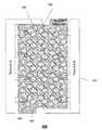
- FIG. 1depicts an exemplary embodiment of a stack of a thin film diamond shaped deposited electrode terminals and tunable dielectric materials on a substrate.
- FIG. 2depicts a micro-image of the top of two series capacitors as described in FIG. 1 .
- FIG. 3depicts another exemplary embodiment of a stack of a thin film diamond shaped deposited electrode terminals and tunable dielectric materials on a substrate.
- FIG. 4depicts a circuit representative of the exemplary embodiment of FIG. 3 .
- FIG. 5depicts a top view of an exemplary embodiment of thin film diamond ring shaped electrode terminal with internal islands deposited terminals on tunable dielectric materials and a substrate.
- FIG. 6depicts a top view of an exemplary embodiment of thin film terminals deposited to form a zigzag space on top of dielectric materials and a substrate.
- FIG. 7depicts an exemplary embodiment of a segmented array capacitor.
- FIG. 8depicts a circuit representative of the exemplary embodiment of FIG. 7 .
- FIG. 9depicts an exemplary embodiment of an array capacitor utilizing non-rectangular top electrodes.
- FIG. 10depicts an exemplary embodiment of a capacitor utilizing comb-shaped top electrodes.
- FIG. 11depicts an exemplary embodiment of a nested ring capacitor.
- FIG. 12depicts a cross-sectional view of the capacitor of FIG. 11 taken along line A-A of FIG. 11 .
- FIG. 13depicts a circuit representative of the exemplary embodiment of FIG. 10 .
- FIGS. 14A-Ddepict other exemplary embodiments of nested ring capacitors.
- FIG. 15depicts a system 1500 that can utilize one or more of the exemplary embodiments of the capacitors of FIGS. 1-14 .
- the present disclosuredescribes, among other things, illustrative embodiments of systems and methods for providing tunable capacitors, such as BST thin film capacitors, where there is reduced contact with the bottom electrodes and which creates an improved periphery with an improved quality (Q) factor and a desired aspect ratio range.
- tunable capacitorssuch as BST thin film capacitors
- One embodiment of the present disclosurecan include an apparatus having a first solid electrode, a second electrode separated into subsections, and a dielectric medium separating the subsections from the first solid electrode.
- the subsections of the second electrodecan include a first group of subsections and a second group of subsections.
- the first group of subsections and the first solid electrodecan form a first group of capacitors.
- the second group of subsections and the first solid electrodecan form a second group of capacitors.
- Each capacitor of the first group of capacitorscan be in parallel.
- Each capacitor of the second group of capacitorscan be in parallel.
- the first group of capacitorscan be in series with the second group of capacitors.
- the first group of subsectionscan be connectable with a first terminal for receiving an input signal.
- the second group of subsectionscan be connectable with a second terminal for providing an output signal.
- One embodiment of the present disclosurecan include an apparatus having a first solid electrode, a second electrode separated into subsections, and a dielectric medium separating the subsections from the first solid electrode.
- the subsections of the second electrodecan include a first group of subsections and a second group of subsections.
- the first group of subsectionscan be connectable with a first terminal for receiving an input signal.
- the second group of subsectionscan be connectable with a second terminal for providing an output signal.
- One embodiment of the present disclosurecan include an apparatus having a first structure and a second structure.
- the first structurecan include a plurality of first top electrodes, a plurality of first middle electrodes, a plurality of first bottom electrodes and a tunable dielectric medium.
- the tunable dielectric mediumcan separate the plurality of first top electrodes from the plurality of first middle electrodes to form first upper capacitors.
- the tunable dielectric mediumcan separate the plurality of first bottom electrodes from the plurality of first middle electrodes to form first lower capacitors.
- the first upper and lower capacitorscan form a first stacked capacitor structure.
- the second structurecan include a plurality of second top electrodes, a plurality of second middle electrodes, a plurality of second bottom electrodes and the tunable dielectric medium.
- the tunable dielectric mediumcan separate the plurality of second top electrodes from the plurality of second middle electrodes to form second upper capacitors.
- the tunable dielectric mediumcan separate the plurality of second bottom electrodes from the plurality of second middle electrodes to form second lower capacitors.
- the second upper and lower capacitorscan form a second stacked capacitor structure.
- the first and second structurescan share at least one electrode to provide electrical contact between the first and second structures.
- the plurality of first middle electrodes of the first structurecan be connectable with a first bias terminal for receiving a first bias signal.
- the plurality of second middle electrodes of the second structurecan be connectable with a second bias terminal for receiving a second bias signal.
- a capacitorin one or more exemplary embodiments, comprises a substrate, a first solid electrode disposed on the substrate, and a second electrode broken into subsections.
- the subsectionscan be connected by a bus line and separated from the first electrode by a dielectric medium.
- the second electrode broken into subsectionsmay have a lower resistance than the first solid electrode. By changing the width and length of the sides of the subsections, the resistance of the first electrode is modifiable.
- a BST thin film design structurethat optimizes electrode structure to enable very high “Q” (low resistance) capacitors through use of a process that varies the width/length aspect ratio of the electrode(s).
- One of the exemplary embodimentscan utilize various capacitor materials where one electrode(s) is made from a higher resistance metal(s) than the opposite electrode(s).
- one electrodemay be thinner than the other electrode, and can exhibit a higher resistance.
- capacitors with such material propertiescan be used in planar integrated capacitors, as well as discrete ceramic capacitors.
- One or more of the exemplary embodimentscan reduce the mechanical stresses generated in the metals and/or dielectric films of the capacitor.
- high frequencyrefers to the radio spectrum between 3 MHZ to 30 GHz, which includes both the “RF” spectrum and the “microwave spectrum”.
- a “device”can include multiple “components”, which can be “passive components” and/or “active components” and a “3D” device may comprise multiple layers stacked, such as vertically.
- Creepis the term given to the material deformation that occurs as a result of long term exposure to levels of stress that are below the yield or ultimate strength. The rate of this damage is a function of the material properties, the exposure time, exposure temperature and the applied load (stress). Creep is usually experienced when the device is heated and cooled as a function of use or environmental temperature fluctuations. Such failures may be caused either by direct thermal loads or by electrical resistive loads, which in turn generate excessive localized thermal stresses. Depending on the magnitude of the applied stress and its duration, the deformation may become so large that it will experience brittle and/or ductile fracture, interfacial separation and creep rupture.
- One or more of the exemplary embodimentscan include at least one electrode structure that allows for the creation of very high “Q” (low resistance) capacitors which is well suited to common capacitor material structures where at least one electrode is made from a higher resistance metal or a thinner metal layer than the opposite electrode.
- High resistance electrodescan include but are not limited to Tungsten, Platinum, Rhodium, Chrome, Titanium/Tungsten, Nickel composites, and combinations thereof. Exemplary capacitors with such material properties can be utilized in planar integrated capacitors, as well as discrete ceramic capacitors.
- One or more of the exemplary embodimentscan reduce the mechanical stresses, creep and/or other thermal generated stresses in the metals and dielectric films of the capacitor.
- the broken electrodeIn a broken or segmented electrode configuration of the exemplary embodiments, the broken electrode usually carries the lower resistance of the two.
- the broken electrodecan distribute the signal across the capacitor area and, through proper arrangement, increase the effective width of the signal path through the higher resistance solid electrode.
- the signal bussese.g., electrical metal connections
- One or more of the exemplary embodimentscan include at least a broken electrode and bussing, where the broken electrode can be used in various types of capacitors, and may find applicability in other components, such as transistor structures.
- One or more of the exemplary embodimentscan realize these benefits by breaking at least two of the electrodes of a pair of series capacitors into subsections.
- a capacitoris shown having diamond-like shaped top electrode subsections 201 and a bottom electrode 204 with a substrate 205 .
- Dielectric material 203e.g., a tunable dielectric such as BST material
- WWidth
- LLength
- the subsections of the top electrode 201can be arranged to increase the effective Width 207 of the signal path in the higher resistance electrode 204 . These subsections can then be electrically connected through a bus 501 as seen in the micrograph image of FIG.
- the critical dimensions 206 , 207can be maximized or otherwise improved in order to increase the active area of the capacitor.
- the length (L) 206 dimensioncan be fixed due to lithographic constraints, therefore by modifying the (W) 207 dimension and duplicating the structure as seen in FIG. 1 , the active area can be significantly increased and the change in capacitance can be increased, such as to a 5 to 1 ratio.
- a wide frequency of tuningcan be enabled, and some of the applications of the embodiments can include but are not limited to low loss phase shifters for high electronically scanning antennas.
- Shear Stresscan be defined as the shear force per unit area applied to a subsection of the top electrode 201 .
- the smaller the area of shearthe smaller the stress applied to the device.
- FIG. 1the “diamond” configuration depicts one embodiment of the invention in which the reduction of the original breaking of the electrode 201 increases the width to 4.25 times that of conventional capacitors.
- the reduction in resistance, leading to an increase in Q,can occur due to the length 206 of the signal path staying the same while the effective width 207 increases.
- the bus 501is not shown in FIG. 1 for clarity purposes.
- FIG. 1depicts at least one apparatus and method of an exemplary embodiment of a capacitor 3D stack.
- a multilayer BST compositecan be formed by sputter blanket PARASCAN® from Paratek Inc. (35 target) on top of a Gennum Inc. 0.2 um Pt substrate.
- a Gold (Au) top electrodecan be patterned using conventional semiconductor lithographic techniques and sputtered on top in order to create the interconnections between the top and bottom electrodes.
- the embodimentmay also include at least one buffer layer. The wafer can be diced into approximate 4 of 1 ⁇ 2 by 1 ⁇ 2 after the PARASCAN® deposition.
- Capacitor 300can include diamond-shaped top electrode subsections. Terminal A and Terminal B can be connected to select top electrode subsections, such as in alternating rows. This exemplary embodiment can increase the zero bias Q of the capacitor, which can be a voltage tunable capacitor. In this exemplary embodiment, capacitor 300 can reduce the series resistance of the bottom electrode by increasing the periphery length around each diamond-shaped top electrode. This is done by utilizing a nested array of diamond shapes for each of the subsections of the two connected top electrodes (e.g., first top electrode connected to terminal A and second top electrode connected to terminal B).
- a first group of top electrodescan be connected to the RF terminal A.
- a second group of the top electrode subsectionscan be connected by interconnect metal to the RF terminal B.
- a bottom electrodecan be utilized for the connection between the first and second groups of top electrodes.
- the circular areas illustrated in FIG. 3are vias 350 used to contact the top electrodes. It should be understood that the exemplary embodiments can also include other numbers of groups of top electrodes subsections.
- the terminals A, Bcan communicate input and/or output signals to the individual capacitors formed by the top and bottom electrodes.
- the terminals A, Bcan have a comb shape with a terminal body 380 and a plurality of terminal fingers or connectors 385 extending therefrom, such as orthogonal from the terminal body.
- Circuit 400 representative of capacitor 300is illustrated in FIG. 4 showing the configuration of the series and parallel connections of the individual capacitors formed through use of the first and second groups of top electrodes with the bottom electrode.
- FIG. 5 and FIG. 6depict capacitors without the interconnection bus 501 for clarity.
- the bus 501may be patterned and deposited by one skilled in the art in order to create parallel and/or series capacitors.
- Two embodimentsare shown in FIG. 5 and FIG. 6 . These embodiments include at least a solid bottom electrode, where the electrodes broken into subsections in FIG. 5 can include a “diamond ring” 601 with internal “islands” 602 , which can maximize or otherwise increase the (W) 207 on both sides of the top electrode.
- signal bus lines 501 to connect the subsectionsare not depicted but would connect the islands and rings to the outside circuitry, for example through gold wire bonds or studs.
- Capacitor 700can reduce the series resistance of the bottom electrode by increasing the periphery length around each top or upper electrode.
- One means of increasing this peripheryis to segment a very wide (e.g., in the transverse direction) capacitor and place the segments next to each other as shown to make an array of top electrodes that alternate in their connection to the RF terminals A and B.
- the exemplary embodimentscan also include the capacitors be segmented in the horizontal direction or both at once.
- surface currents in the bottom electrodecan flow left and right from a given capacitor formed by way of dielectric material sandwiched with one of the rectangular top electrodes 750 , thus reducing the effective resistance of this electrode by a factor of two.
- a first group of the top electrodes 725can be connected to the RF terminal A.
- a second group of the top electrodes 725 ′can be connected by interconnect metal to the RF terminal B.
- the first and second groups of top electrodesare formed in an alternating pattern, but the exemplary embodiment can include other patterns being utilized to group the top electrodes.
- the bottom electrodecan provide the connection between the capacitors formed by the first group of top electrodes and the capacitors formed by the second group of top electrodes.
- the circular areas illustrated in FIG. 7are vias 750 used to contact the top electrodes.
- the terminals A, Bcan communicate input and/or output signals to the individual capacitors formed by the top and bottom electrodes.
- the terminals A, Bcan have a comb shape with a terminal body 780 and a plurality of terminal fingers or connectors 785 extending therefrom, such as orthogonal from the terminal body. It should be understood that the exemplary embodiments can also include other numbers of groups of top electrodes subsections. Circuit 800 representative of capacitor 700 is illustrated in FIG. 8 showing the configuration of the series and parallel connections of the individual capacitors formed through use of the first and second groups of top electrodes with the bottom electrode.
- Capacitor 900can reduce the series resistance of the bottom electrode by increasing the periphery length around each top or upper electrode.
- One means of increasing this peripheryis use a nested array of crosses for the two top electrodes (e.g., a first group of cross-shaped electrodes 925 connected to terminal A and a second group of cross-shaped electrodes 925 ′ connected to terminal B).
- the first and second groups of top electrodesare formed in an alternating pattern, but the exemplary embodiment can include other patterns being utilized to group the top electrodes.
- the bottom electrodecan provide the connection between the capacitors formed by the first group of top electrodes and the capacitors formed by the second group of top electrodes.
- Capacitor 900can provide for series and parallel connections of the individual capacitors formed through use of the first and second groups of top electrodes with the bottom electrode.
- the terminals A, Bcan communicate input and/or output signals to the individual capacitors formed by the top and bottom electrodes.
- the terminals A, Bcan have a terminal body 980 and a plurality of terminal fingers or connectors 985 extending therefrom.
- a portion of one or more of the terminal connectors 985can be orthogonal to the terminal body 980 .
- all or a portion of the terminal connectors 985can be non-orthogonal to the terminal body 980 to facilitate connecting each of the first and second groups of top electrodes 925 , 925 ′ with terminals A, B, respectively.
- Capacitor 900can utilize the cross-shaped top electrodes 925 , 925 ′ so as to maintain a consistent gap between each of the adjacent electrodes and/or maintain symmetry of the electrode subsection pattern.
- Other shapescan also be utilized for the crosses 925 , 925 ′ including other non-rectangular shapes.
- a combination of shapescan be utilizes such as the crosses and half-crosses depicted in FIG. 9 .
- the non-rectangular shapes used for the top electrode subsectionscan provide for an electrode subsections having at least one edge that is parallel with another edge of an adjacent top electrode subsection.
- Capacitor 1000can increase the zero bias Q.
- Capacitor 1000can reduce the series resistance of the bottom electrode by increasing the periphery length around each top or upper electrode.
- One means of increasing this peripheryis to use a comb-shaped upper electrode pattern comprising a first comb-shaped electrode 1025 and a second-comb shaped electrode 1025 ′.
- the bottom electrodecan provide the connection between the capacitors formed from the first and second comb-shaped top electrodes 1025 , 1025 ′.
- the comb-shaped electrodes 1025 , 1025 ′can include an electrode body 1080 and a plurality of electrode fingers or connectors 1085 extending therefrom, such as orthogonal from the electrode body.
- the terminals A, Bcan communicate input and/or output signals to the individual capacitors formed by the top and bottom electrodes.
- the terminals A, Bcan be connected with the electrodes 1025 , 1025 ′′ along or in proximity to the corresponding electrode bodies 1080 .
- the exemplary embodimentscan also include other numbers of groups of top electrodes subsections.
- capacitor 1000can utilize the first and second comb-shaped electrodes 1025 , 1025 ′ including the orthogonal electrode fingers or connectors 1085 so as to maintain a consistent gap between each of the two top electrodes.
- Capacitor 1100can include a first capacitor portion or structure 1105 and a second capacitor portion or structure 1110 .
- the first and second capacitors portionscan be symmetrical.
- First capacitor portion 1105can include top electrodes 1125 , middle electrodes 1135 , bottom electrodes 1145 , and biasing terminal 1155 .
- a dielectric medium(s) 1165e.g., a tunable dielectric such as a BST material
- Second capacitor portion 1110can include top electrodes 1125 ′, middle electrodes 1135 ′, bottom electrodes 1145 ′, and biasing terminal 1155 ′.
- a dielectric medium(s)e.g., a tunable dielectric such as a BST material
- BST materialcan be used to separate the top, middle and bottom electrodes 1125 ′, 1135 ′, 1145 ′ of the second capacitor portion 111 .
- Capacitor 1100can increase the perimeter length of middle electrodes 1135 , 1135 ′ without increasing the area of the electrodes.
- the broken concentric ring-like structure of capacitor 1100can be used to enable a graded value of capacitance where the outer rings are higher capacitance values and the inner rings have lower capacitance values. With the appropriate resistive bias network, this arrangement of capacitors can permit lower time constants compared to a uniform distribution of capacitor values.
- Capacitor 1100is illustrated as a dual layer capacitor, meaning that two capacitors are stacked vertically to make each ring. However, the exemplary embodiments can include single layer or multiple layers with more than two stacked layers that utilize all or a portion of the features of capacitor 1100 .
- Cross section A-Aillustrates the construction of the capacitors as stacked capacitors using three metal layers.
- each metal layer shown heremay be a combination of metals.
- Ptmay be used to contact the tunable dielectric layers (e.g., PARASCAN®) and/or TiW may be used next to the Pt for adhesion purposes.
- Other metals with higher electrical or thermal conductivitymay be employed to lower the electrical and/or thermal resistance of each electrode.
- Capacitor 1100can provide a symmetrical biasing network. Capacitor 1100 can achieve low charging times or low time constants for all capacitors in the string. Capacitor 1100 is in essence a splitting of the bias network into two halves, which may be symmetric as shown (or in one or more embodiments may be asymmetrical), to enable charging current to be injected equally along both sides of the capacitor string. To facilitate equalizing the charging times so as to achieve the shortest overall transient response, the capacitor values can be graded in the following manner such that the largest capacitors are found near the ends of the string:
- the bias resistors R mmay be graded so as to have the largest resistor near the bias terminals:
- This bias resistor gradingcan also be done to facilitate equalizing the charging times across capacitors in the string.
- Circuit 1300 representative of capacitor 1100is illustrated in FIG. 13 .
- any number of bias terminalscan be utilized such as a single bias terminal or three or more bias terminals. The nested configuration can be adjusted based on the number of biasing terminals.
- any number of capacitor portionscan be utilized, including using four portions with four bias terminals, where the four portions can share a center top electrode.
- One or more exemplary embodimentscan utilize the nested ring capacitor configuration of FIG. 11 , but with different shapes for the electrodes.
- the four capacitor designsrepresent top electrode metal patterns built as nested rings.
- the exemplary embodimentscan include other polygonal shapes which may or may not provide a symmetrical configuration.
- Bias resistorsare omitted for clarity in FIGS. 14A-14D , but they can be located in the vicinity of the gaps in the outer rings.
- FIG. 15is a block diagram of a system 1500 having a matching network 1510 that can utilize one or more of the exemplary capacitors or other components described herein.
- the matching network 1510can be coupled to a tunable microwave device 1532 .
- the tunable microwave device 1532could be one of many devices which have varying input/output characteristic impedances such as tunable phase shifters, delay lines, filters, etc.
- the adjustable external DC voltage source 1534can be used to supply bias voltage to the matching network 1510 and the tunable microwave device 1532 in tandem. As the voltage supplied by the external DC voltage source 1534 changes, the characteristic input/output impedance of the tunable dielectric device may also change.
- the impedance characteristics of the matching network 1510can change to maximize, improve or otherwise adjust power transfer from/to the microwave source/load 1536 to/from the tunable microwave device 1532 .
- the tunable microwave device 1532 and the matching network 1510can be controlled by two different external DC voltage sources.
- the exemplary embodimentscan be utilized in other circuits that may or may not include matching networks.
- an electrodecan be broken into subsections with signal bus lines connecting the subsections and a solid electrode to improve Q.
- the methodmay further comprise distributing the signal across the capacitor area by the broken electrode and thereby increasing the effective width of a signal path through the solid electrode.
- the capacitormay be of various forms including a planar integrated capacitor or a discrete ceramic capacitor.
- the methodmay still further comprise adapting the solid electrode and the broken electrode to reduce the mechanical stresses generated in the metals and dielectric films of the capacitor.
- the capacitorcan be utilized in a pair of series capacitors where the subsections are arranged in such a manner that it increases the effective width of the signal path in the solid electrode.
- a series network of voltage tunable dielectric capacitorscan be provided, such as according to the steps and structures described herein, which are all, or a portion thereof, tuned using a common tuning voltage.
- a capacitor electrode structureallows for the creation of very high “Q” (e.g., low resistance) capacitors.
- one electrodecan be made from a higher resistance metal than the opposite electrode, such as in planar integrated capacitors, as well as discrete ceramic capacitors.
- the electrodescan be broken into subsections, with signal bus lines connected to the subsections and/or to a solid electrode.
- the broken electrodepreferably has the lower resistance material of the two.
- the broken electrodemay distribute the signal across the capacitor area and, through proper arrangement, increase the effective width of the signal path through the higher resistance solid electrode.
- the signal bussesmay bring in and take out the signal. Voltage tunable dielectric material can be utilized between the electrodes.
- One or more of the exemplary embodimentscan include a first or bottom electrode(s), such as platinum, patterned and deposited into a substrate.
- a dielectric material, such as a thin film coating of a BST type materialcan be deposited on top of the bottom electrode, such as according to one or more of the exemplary configurations described above.
- a top or second electrode(s)can be deposited on top of the BST film.
- Interconnects, vias and the likecan be utilized with the exemplary embodiments, including being deposited over a portion of the thin film structure, to provide attachment to other components, such as a microwave circuit and/or to provide an electrical path to at least one of the electrodes.
- Various materials including gold, aluminum and silvercan be provided using various techniques including sputter and depositing to form some of the components of one or more of the exemplary embodiments, such as the electrode(s), the bus and so forth.
- a polymer encapsulationcan be deposited to provide protection from ambient conditions and/or as a humidity barrier.
- multiple layers of dielectric materials (e.g., BST thin films) and/or electrodescan be deposited or otherwise formed to create an elaborate 3D structure of a multiple layer capacitor stack.
- One or more of the exemplary embodiments of the capacitor configurationscan be utilized in various systems.
- wireless communicationsis a rapidly growing segment of the communications industry, with the potential to provide high-speed high-quality information exchange between portable devices located anywhere in the world.
- Potential applications enabled by one or more of the exemplary embodimentsinclude multimedia internet-enabled cell phones, smart homes, appliances, automated highway systems, distance learning, and autonomous sensor networks, just to name a few.
- One or more of the exemplary embodimentscan be used to enable low loss devices that can be used at higher frequency ranges.
- One or more of the exemplary embodimentscan utilize relatively low capacitance varactors that can operate at temperatures above those necessary for superconduction and at bias voltages less than those required for existing planar varactor structures, while maintaining high tunability and high Q factors. Even though these materials may work in their paraelectric phase above the Curie temperature, they are conveniently called “ferroelectric” because they exhibit spontaneous polarization at temperatures below the Curie temperature.
- Tunable ferroelectric materials including barium-strontium titanate Ba x Sr 1-x TiO 3 (BST) or BST compositeshave been the subject of several patents. Dielectric materials including BST are disclosed by Sengupta, et al.
- the dielectric constant of these materialscan be varied by varying the strength of an electric field to which the materials are subjected. These materials allow for thin-film ferroelectric composites of low overall dielectric constant that takes advantage of the high tunability and at the same time having high dielectric constants. BST thin films can be used with one or more of the exemplary embodiments due to their high dielectric constant, high tunability, low loss, and fast switching speed.
- One or more of the exemplary embodimentscan include the use of non-tunable dielectric material alone or in combination with other capacitors that utilize tunable dielectric material.
- the configuration of tunable and non-tunable capacitors formed by the exemplary embodimentscan vary.
- the exemplary embodimentscan also include the use of different dielectric materials by different individual capacitors formed by the segmented electrodes and the solid electrode, including a plurality of different tunable dielectric materials and/or a plurality of non-tunable dielectric materials forming individual capacitors that are in parallel and/or series and with each other.
- Quality factor, resonance frequency and breakdown voltageare can be important factors for determining when thin film capacitor can be utilized.
- High-frequency device lossesconsist of material-related losses in the film and at the electrode-film interface, as well as the resistive losses in the electrodes.
- Thermal straincan occur on the interface between the ferroelectric thin film and the metal electrode due to the creation of oxide films and crystalline microstructure. This interface is generally the cause of losses at high frequencies and premature breakdown at low voltages.
- the designs on current devicesare limited by traditional design guidelines that create resistive losses due to design constraints.
Landscapes
- Engineering & Computer Science (AREA)
- Power Engineering (AREA)
- Microelectronics & Electronic Packaging (AREA)
- Manufacturing & Machinery (AREA)
- Computer Networks & Wireless Communication (AREA)
- Signal Processing (AREA)
- Semiconductor Integrated Circuits (AREA)
Abstract
Description
- C1≅C2>C3≅C4>C5≅C6>C7≅C8C9≅C10<C11≅C12<C13≅C14<C15≅C16
- Rm1>Rm2>Rm3>Rm4
Claims (14)
Priority Applications (4)
| Application Number | Priority Date | Filing Date | Title |
|---|---|---|---|
| US13/289,194US9406444B2 (en) | 2005-11-14 | 2011-11-04 | Thin film capacitors |
| CA2794262ACA2794262C (en) | 2011-11-04 | 2012-11-05 | Thin film capacitors |
| EP12191338.8AEP2590190B1 (en) | 2011-11-04 | 2012-11-05 | Thin film capacitors |
| US15/207,171US10163574B2 (en) | 2005-11-14 | 2016-07-11 | Thin films capacitors |
Applications Claiming Priority (5)
| Application Number | Priority Date | Filing Date | Title |
|---|---|---|---|
| US73636605P | 2005-11-14 | 2005-11-14 | |
| US11/598,354US7869186B2 (en) | 2005-11-14 | 2006-11-13 | High Q and low stress capacitor electrode array |
| US11/602,114US8064188B2 (en) | 2000-07-20 | 2006-11-20 | Optimized thin film capacitors |
| US12/321,897US8627556B2 (en) | 2005-11-14 | 2009-01-27 | High Q and low stress capacitor electrode array |
| US13/289,194US9406444B2 (en) | 2005-11-14 | 2011-11-04 | Thin film capacitors |
Related Parent Applications (1)
| Application Number | Title | Priority Date | Filing Date |
|---|---|---|---|
| US11/602,114Continuation-In-PartUS8064188B2 (en) | 2000-07-20 | 2006-11-20 | Optimized thin film capacitors |
Related Child Applications (1)
| Application Number | Title | Priority Date | Filing Date |
|---|---|---|---|
| US15/207,171ContinuationUS10163574B2 (en) | 2005-11-14 | 2016-07-11 | Thin films capacitors |
Publications (2)
| Publication Number | Publication Date |
|---|---|
| US20120154975A1 US20120154975A1 (en) | 2012-06-21 |
| US9406444B2true US9406444B2 (en) | 2016-08-02 |
Family
ID=46234103
Family Applications (2)
| Application Number | Title | Priority Date | Filing Date |
|---|---|---|---|
| US13/289,194Active - Reinstated2028-04-20US9406444B2 (en) | 2005-11-14 | 2011-11-04 | Thin film capacitors |
| US15/207,171Active2027-04-26US10163574B2 (en) | 2005-11-14 | 2016-07-11 | Thin films capacitors |
Family Applications After (1)
| Application Number | Title | Priority Date | Filing Date |
|---|---|---|---|
| US15/207,171Active2027-04-26US10163574B2 (en) | 2005-11-14 | 2016-07-11 | Thin films capacitors |
Country Status (1)
| Country | Link |
|---|---|
| US (2) | US9406444B2 (en) |
Cited By (6)
| Publication number | Priority date | Publication date | Assignee | Title |
|---|---|---|---|---|
| US20170011858A1 (en)* | 2005-11-14 | 2017-01-12 | Blackberry Limited | Thin film capacitors |
| US10615769B2 (en) | 2010-03-22 | 2020-04-07 | Blackberry Limited | Method and apparatus for adapting a variable impedance network |
| US10700719B2 (en) | 2012-12-21 | 2020-06-30 | Nxp Usa, Inc. | Method and apparatus for adjusting the timing of radio antenna tuning |
| WO2020226741A1 (en)* | 2019-05-07 | 2020-11-12 | Massachusetts Institute Of Technology | Optical modulator rf electrodes |
| USRE48435E1 (en) | 2007-11-14 | 2021-02-09 | Nxp Usa, Inc. | Tuning matching circuits for transmitter and receiver bands as a function of the transmitter metrics |
| US10979095B2 (en) | 2011-02-18 | 2021-04-13 | Nxp Usa, Inc. | Method and apparatus for radio antenna frequency tuning |
Families Citing this family (21)
| Publication number | Priority date | Publication date | Assignee | Title |
|---|---|---|---|---|
| US8744384B2 (en) | 2000-07-20 | 2014-06-03 | Blackberry Limited | Tunable microwave devices with auto-adjusting matching circuit |
| US7711337B2 (en) | 2006-01-14 | 2010-05-04 | Paratek Microwave, Inc. | Adaptive impedance matching module (AIMM) control architectures |
| US7714676B2 (en) | 2006-11-08 | 2010-05-11 | Paratek Microwave, Inc. | Adaptive impedance matching apparatus, system and method |
| US7535312B2 (en) | 2006-11-08 | 2009-05-19 | Paratek Microwave, Inc. | Adaptive impedance matching apparatus, system and method with improved dynamic range |
| US7917104B2 (en) | 2007-04-23 | 2011-03-29 | Paratek Microwave, Inc. | Techniques for improved adaptive impedance matching |
| US8213886B2 (en) | 2007-05-07 | 2012-07-03 | Paratek Microwave, Inc. | Hybrid techniques for antenna retuning utilizing transmit and receive power information |
| US8072285B2 (en) | 2008-09-24 | 2011-12-06 | Paratek Microwave, Inc. | Methods for tuning an adaptive impedance matching network with a look-up table |
| US8472888B2 (en) | 2009-08-25 | 2013-06-25 | Research In Motion Rf, Inc. | Method and apparatus for calibrating a communication device |
| US9026062B2 (en) | 2009-10-10 | 2015-05-05 | Blackberry Limited | Method and apparatus for managing operations of a communication device |
| SG184929A1 (en) | 2010-04-20 | 2012-11-29 | Paratek Microwave Inc | Method and apparatus for managing interference in a communication device |
| US9379454B2 (en) | 2010-11-08 | 2016-06-28 | Blackberry Limited | Method and apparatus for tuning antennas in a communication device |
| US8655286B2 (en) | 2011-02-25 | 2014-02-18 | Blackberry Limited | Method and apparatus for tuning a communication device |
| US8594584B2 (en) | 2011-05-16 | 2013-11-26 | Blackberry Limited | Method and apparatus for tuning a communication device |
| US9769826B2 (en) | 2011-08-05 | 2017-09-19 | Blackberry Limited | Method and apparatus for band tuning in a communication device |
| US8948889B2 (en) | 2012-06-01 | 2015-02-03 | Blackberry Limited | Methods and apparatus for tuning circuit components of a communication device |
| US9350405B2 (en) | 2012-07-19 | 2016-05-24 | Blackberry Limited | Method and apparatus for antenna tuning and power consumption management in a communication device |
| US9374113B2 (en) | 2012-12-21 | 2016-06-21 | Blackberry Limited | Method and apparatus for adjusting the timing of radio antenna tuning |
| US9520904B2 (en)* | 2013-11-13 | 2016-12-13 | Blackberry Limited | Apparatus and method for high linearity tuning |
| US9438319B2 (en) | 2014-12-16 | 2016-09-06 | Blackberry Limited | Method and apparatus for antenna selection |
| EP3549232A1 (en) | 2016-12-02 | 2019-10-09 | Carver Scientific, Inc. | Memory device and capacitive energy storage device |
| US10957807B2 (en)* | 2017-04-19 | 2021-03-23 | The Board Of Trustees Of The University Of Alabama | PLZT thin film capacitors apparatus with enhanced photocurrent and power conversion efficiency and method thereof |
Citations (213)
| Publication number | Priority date | Publication date | Assignee | Title |
|---|---|---|---|---|
| US2745067A (en) | 1951-06-28 | 1956-05-08 | True Virgil | Automatic impedance matching apparatus |
| US3117279A (en) | 1962-06-04 | 1964-01-07 | Collins Radio Co | Automatically controlled antenna tuning and loading system |
| US3160832A (en) | 1961-12-22 | 1964-12-08 | Collins Radio Co | Automatic coupling and impedance matching network |
| US3390337A (en) | 1966-03-15 | 1968-06-25 | Avco Corp | Band changing and automatic tuning apparatus for transmitter tau-pad output filter |
| US3443231A (en) | 1966-04-27 | 1969-05-06 | Gulf General Atomic Inc | Impedance matching system |
| US3509500A (en) | 1966-12-05 | 1970-04-28 | Avco Corp | Automatic digital tuning apparatus |
| US3571716A (en) | 1968-04-16 | 1971-03-23 | Motorola Inc | Electronically tuned antenna system |
| US3590385A (en) | 1969-07-25 | 1971-06-29 | Avco Corp | Semi-automatic tuning circuit for an antenna coupler |
| US3601717A (en) | 1969-11-20 | 1971-08-24 | Gen Dynamics Corp | System for automatically matching a radio frequency power output circuit to a load |
| US3742279A (en) | 1971-02-10 | 1973-06-26 | Burroughs Corp | Segmented electrode display panel having closed structure |
| US3794941A (en) | 1972-05-08 | 1974-02-26 | Hughes Aircraft Co | Automatic antenna impedance tuner including digital control circuits |
| US3919644A (en) | 1970-02-02 | 1975-11-11 | Gen Dynamics Corp | Automatic antenna coupler utilizing system for measuring the real part of the complex impedance or admittance presented by an antenna or other network |
| US3990024A (en) | 1975-01-06 | 1976-11-02 | Xerox Corporation | Microstrip/stripline impedance transformer |
| US3995237A (en) | 1974-10-15 | 1976-11-30 | Cincinnati Electronics Corporation | Automatic matching method and apparatus |
| US4186359A (en) | 1977-08-22 | 1980-01-29 | Tx Rx Systems Inc. | Notch filter network |
| US4201960A (en) | 1978-05-24 | 1980-05-06 | Motorola, Inc. | Method for automatically matching a radio frequency transmitter to an antenna |
| US4227256A (en) | 1978-01-06 | 1980-10-07 | Quadracast Systems, Inc. | AM Broadcast tuner with automatic gain control |
| US4383441A (en) | 1981-07-20 | 1983-05-17 | Ford Motor Company | Method for generating a table of engine calibration control values |
| US4476578A (en) | 1981-11-27 | 1984-10-09 | Thomson-Csf | Device for detecting the optimum anode load impedance of a tube transmitter in a high frequency transmission chain |
| US4493112A (en) | 1981-11-19 | 1985-01-08 | Rockwell International Corporation | Antenna tuner discriminator |
| US4777490A (en) | 1986-04-22 | 1988-10-11 | General Electric Company | Monolithic antenna with integral pin diode tuning |
| US4799066A (en) | 1985-07-26 | 1989-01-17 | The Marconi Company Limited | Impedance matching arrangement |
| US4965607A (en) | 1987-04-30 | 1990-10-23 | Br Communications, Inc. | Antenna coupler |
| US5032805A (en) | 1989-10-23 | 1991-07-16 | The United States Of America As Represented By The Secretary Of The Army | RF phase shifter |
| JPH03276901A (en) | 1990-03-27 | 1991-12-09 | Mitsubishi Electric Corp | Hybrid integrated circuit device |
| US5136478A (en) | 1990-08-03 | 1992-08-04 | Quadri Electronics Corporation | Solid electrolyte capacitor and method of making |
| US5142255A (en) | 1990-05-07 | 1992-08-25 | The Texas A&M University System | Planar active endfire radiating elements and coplanar waveguide filters with wide electronic tuning bandwidth |
| US5177670A (en) | 1991-02-08 | 1993-01-05 | Hitachi, Ltd. | Capacitor-carrying semiconductor module |
| US5195045A (en) | 1991-02-27 | 1993-03-16 | Astec America, Inc. | Automatic impedance matching apparatus and method |
| US5200826A (en) | 1990-06-21 | 1993-04-06 | Samsung Electronics Co., Ltd. | TV signal receiving double conversion television tuner system having automatic gain control provisions |
| US5212463A (en) | 1992-07-22 | 1993-05-18 | The United States Of America As Represented By The Secretary Of The Army | Planar ferro-electric phase shifter |
| US5243358A (en) | 1991-07-15 | 1993-09-07 | Ball Corporation | Directional scanning circular phased array antenna |
| US5258728A (en) | 1987-09-30 | 1993-11-02 | Fujitsu Ten Limited | Antenna circuit for a multi-band antenna |
| US5276912A (en) | 1990-02-06 | 1994-01-04 | Motorola, Inc. | Radio frequency power amplifier having variable output power |
| US5301358A (en) | 1988-12-05 | 1994-04-05 | Seiko Corp. | Automatic antenna tuning method and apparatus |
| US5307033A (en) | 1993-01-19 | 1994-04-26 | The United States Of America As Represented By The Secretary Of The Army | Planar digital ferroelectric phase shifter |
| US5310358A (en) | 1992-12-22 | 1994-05-10 | The Whitaker Corporation | Computer docking system |
| US5312790A (en) | 1993-06-09 | 1994-05-17 | The United States Of America As Represented By The Secretary Of The Army | Ceramic ferroelectric material |
| US5334958A (en) | 1993-07-06 | 1994-08-02 | The United States Of America As Represented By The Secretary Of The Army | Microwave ferroelectric phase shifters and methods for fabricating the same |
| US5371473A (en) | 1993-09-10 | 1994-12-06 | Hughes Aircraft Company | Thermally stable ALC for pulsed output amplifier |
| US5409889A (en) | 1993-05-03 | 1995-04-25 | Das; Satyendranath | Ferroelectric high Tc superconductor RF phase shifter |
| US5430417A (en) | 1991-07-05 | 1995-07-04 | Aft Advanced Ferrite Technology Gmbh | Tunable matching network |
| US5446447A (en) | 1994-02-16 | 1995-08-29 | Motorola, Inc. | RF tagging system including RF tags with variable frequency resonant circuits |
| US5448252A (en) | 1994-03-15 | 1995-09-05 | The United States Of America As Represented By The Secretary Of The Air Force | Wide bandwidth microstrip patch antenna |
| US5451914A (en) | 1994-07-05 | 1995-09-19 | Motorola, Inc. | Multi-layer radio frequency transformer |
| US5451567A (en) | 1994-03-30 | 1995-09-19 | Das; Satyendranath | High power ferroelectric RF phase shifter |
| US5457394A (en) | 1993-04-12 | 1995-10-10 | The Regents Of The University Of California | Impulse radar studfinder |
| US5472935A (en) | 1992-12-01 | 1995-12-05 | Yandrofski; Robert M. | Tuneable microwave devices incorporating high temperature superconducting and ferroelectric films |
| US5479139A (en) | 1995-04-19 | 1995-12-26 | The United States Of America As Represented By The Secretary Of The Army | System and method for calibrating a ferroelectric phase shifter |
| US5496795A (en) | 1994-08-16 | 1996-03-05 | Das; Satyendranath | High TC superconducting monolithic ferroelectric junable b and pass filter |
| US5502372A (en) | 1994-10-07 | 1996-03-26 | Hughes Aircraft Company | Microstrip diagnostic probe for thick metal flared notch and ridged waveguide radiators |
| US5524281A (en) | 1988-03-31 | 1996-06-04 | Wiltron Company | Apparatus and method for measuring the phase and magnitude of microwave signals |
| US5561407A (en) | 1995-01-31 | 1996-10-01 | The United States Of America As Represented By The Secretary Of The Army | Single substrate planar digital ferroelectric phase shifter |
| US5564086A (en) | 1993-11-29 | 1996-10-08 | Motorola, Inc. | Method and apparatus for enhancing an operating characteristic of a radio transmitter |
| US5583359A (en)* | 1995-03-03 | 1996-12-10 | Northern Telecom Limited | Capacitor structure for an integrated circuit |
| US5593495A (en) | 1994-06-16 | 1997-01-14 | Sharp Kabushiki Kaisha | Method for manufacturing thin film of composite metal-oxide dielectric |
| US5635434A (en) | 1995-09-11 | 1997-06-03 | The United States Of America As Represented By The Secretary Of The Army | Ceramic ferroelectric composite material-BSTO-magnesium based compound |
| US5635433A (en) | 1995-09-11 | 1997-06-03 | The United States Of America As Represented By The Secretary Of The Army | Ceramic ferroelectric composite material-BSTO-ZnO |
| US5640042A (en) | 1995-12-14 | 1997-06-17 | The United States Of America As Represented By The Secretary Of The Army | Thin film ferroelectric varactor |
| US5679624A (en) | 1995-02-24 | 1997-10-21 | Das; Satyendranath | High Tc superconductive KTN ferroelectric time delay device |
| US5689219A (en) | 1994-06-30 | 1997-11-18 | Nokia Telecommunications Oy | Summing network |
| US5693429A (en) | 1995-01-20 | 1997-12-02 | The United States Of America As Represented By The Secretary Of The Army | Electronically graded multilayer ferroelectric composites |
| US5694134A (en) | 1992-12-01 | 1997-12-02 | Superconducting Core Technologies, Inc. | Phased array antenna system including a coplanar waveguide feed arrangement |
| US5699071A (en) | 1991-03-26 | 1997-12-16 | Sumitomo Chemical Company, Limited | Glass antenna system for automobile |
| US5766697A (en) | 1995-12-08 | 1998-06-16 | The United States Of America As Represented By The Secretary Of The Army | Method of making ferrolectric thin film composites |
| US5778308A (en) | 1994-05-25 | 1998-07-07 | Nokia Mobile Phones Limited | Adaptive antenna matching |
| US5777581A (en) | 1995-12-07 | 1998-07-07 | Atlantic Aerospace Electronics Corporation | Tunable microstrip patch antennas |
| US5786727A (en) | 1996-10-15 | 1998-07-28 | Motorola, Inc. | Multi-stage high efficiency linear power amplifier and method therefor |
| JPH10209722A (en) | 1997-01-20 | 1998-08-07 | Seiko Epson Corp | High frequency circuit and method of manufacturing the same |
| US5812943A (en) | 1995-09-01 | 1998-09-22 | Nec Corporation | High frequency band high temperature superconductor mixer antenna which allows a superconductor feed line to be used in a low frequency region |
| US5830591A (en) | 1996-04-29 | 1998-11-03 | Sengupta; Louise | Multilayered ferroelectric composite waveguides |
| US5846893A (en) | 1995-12-08 | 1998-12-08 | Sengupta; Somnath | Thin film ferroelectric composites and method of making |
| US5874926A (en) | 1996-03-11 | 1999-02-23 | Murata Mfg Co. Ltd | Matching circuit and antenna apparatus |
| US5880635A (en) | 1997-04-16 | 1999-03-09 | Sony Corporation | Apparatus for optimizing the performance of a power amplifier |
| US5886867A (en) | 1995-03-21 | 1999-03-23 | Northern Telecom Limited | Ferroelectric dielectric for integrated circuit applications at microwave frequencies |
| EP0909024A2 (en) | 1997-10-07 | 1999-04-14 | Sharp Kabushiki Kaisha | Impedance matching device |
| US5929717A (en) | 1998-01-09 | 1999-07-27 | Lam Research Corporation | Method of and apparatus for minimizing plasma instability in an RF processor |
| US5963871A (en) | 1996-10-04 | 1999-10-05 | Telefonaktiebolaget Lm Ericsson | Retractable multi-band antennas |
| US5969582A (en) | 1997-07-03 | 1999-10-19 | Ericsson Inc. | Impedance matching circuit for power amplifier |
| US5982099A (en) | 1996-03-29 | 1999-11-09 | Lam Research Corporation | Method of and apparatus for igniting a plasma in an r.f. plasma processor |
| US5990766A (en) | 1996-06-28 | 1999-11-23 | Superconducting Core Technologies, Inc. | Electrically tunable microwave filters |
| US6009124A (en) | 1997-09-22 | 1999-12-28 | Intel Corporation | High data rate communications network employing an adaptive sectored antenna |
| US6020787A (en) | 1995-06-07 | 2000-02-01 | Motorola, Inc. | Method and apparatus for amplifying a signal |
| US6029075A (en) | 1997-04-17 | 2000-02-22 | Manoj K. Bhattacharygia | High Tc superconducting ferroelectric variable time delay devices of the coplanar type |
| US6045932A (en) | 1998-08-28 | 2000-04-04 | The Regents Of The Universitiy Of California | Formation of nonlinear dielectric films for electrically tunable microwave devices |
| JP2000124066A (en) | 1998-10-13 | 2000-04-28 | Oki Electric Ind Co Ltd | Microchip capacitor and method of mounting thereof |
| US6061025A (en) | 1995-12-07 | 2000-05-09 | Atlantic Aerospace Electronics Corporation | Tunable microstrip patch antenna and control system therefor |
| US6074971A (en) | 1998-11-13 | 2000-06-13 | The United States Of America As Represented By The Secretary Of The Army | Ceramic ferroelectric composite materials with enhanced electronic properties BSTO-Mg based compound-rare earth oxide |
| US6096127A (en) | 1997-02-28 | 2000-08-01 | Superconducting Core Technologies, Inc. | Tuneable dielectric films having low electrical losses |
| US6101102A (en) | 1999-04-28 | 2000-08-08 | Raytheon Company | Fixed frequency regulation circuit employing a voltage variable dielectric capacitor |
| US6100733A (en) | 1998-06-09 | 2000-08-08 | Siemens Aktiengesellschaft | Clock latency compensation circuit for DDR timing |
| US6133883A (en) | 1998-11-17 | 2000-10-17 | Xertex Technologies, Inc. | Wide band antenna having unitary radiator/ground plane |
| US6172385B1 (en) | 1998-10-30 | 2001-01-09 | International Business Machines Corporation | Multilayer ferroelectric capacitor structure |
| US6215644B1 (en) | 1999-09-09 | 2001-04-10 | Jds Uniphase Inc. | High frequency tunable capacitors |
| US6281847B1 (en) | 1998-12-17 | 2001-08-28 | Southern Methodist University | Electronically steerable and direction finding microstrip array antenna |
| US6309895B1 (en) | 1998-10-27 | 2001-10-30 | Precision Instrument Development Center, National Science Council | Method for fabricating capacitor containing amorphous and polycrystalline ferroelectric films and method for forming amorphous ferroelectric film |
| US6343208B1 (en) | 1998-12-16 | 2002-01-29 | Telefonaktiebolaget Lm Ericsson (Publ) | Printed multi-band patch antenna |
| US6377440B1 (en) | 2000-09-12 | 2002-04-23 | Paratek Microwave, Inc. | Dielectric varactors with offset two-layer electrodes |
| US6377142B1 (en) | 1998-10-16 | 2002-04-23 | Paratek Microwave, Inc. | Voltage tunable laminated dielectric materials for microwave applications |
| US6377217B1 (en) | 1999-09-14 | 2002-04-23 | Paratek Microwave, Inc. | Serially-fed phased array antennas with dielectric phase shifters |
| US20020047154A1 (en)* | 2000-04-07 | 2002-04-25 | Tirdad Sowlati | Interdigitated multilayer capacitor structure for deep sub-micron CMOS |
| US6384785B1 (en) | 1995-05-29 | 2002-05-07 | Nippon Telegraph And Telephone Corporation | Heterogeneous multi-lamination microstrip antenna |
| US6404614B1 (en) | 2000-05-02 | 2002-06-11 | Paratek Microwave, Inc. | Voltage tuned dielectric varactors with bottom electrodes |
| US6408190B1 (en) | 1999-09-01 | 2002-06-18 | Telefonaktiebolaget Lm Ericsson (Publ) | Semi built-in multi-band printed antenna |
| US6414562B1 (en) | 1997-05-27 | 2002-07-02 | Motorola, Inc. | Circuit and method for impedance matching |
| KR20020052476A (en)* | 2000-12-26 | 2002-07-04 | 박종섭 | A exposure mask |
| US6415562B1 (en) | 1998-11-09 | 2002-07-09 | Benchmark Outdoor Products, Inc. | Artificial board |
| US6452776B1 (en) | 2000-04-06 | 2002-09-17 | Intel Corporation | Capacitor with defect isolation and bypass |
| US6461930B2 (en) | 1998-06-19 | 2002-10-08 | Micron Technology, Inc. | Capacitor and method for forming the same |
| US6466774B1 (en) | 1998-07-21 | 2002-10-15 | Hitachi, Ltd. | Wireless handset |
| US6492883B2 (en) | 2000-11-03 | 2002-12-10 | Paratek Microwave, Inc. | Method of channel frequency allocation for RF and microwave duplexers |
| US20020193088A1 (en) | 2001-06-19 | 2002-12-19 | Lg Electronics Inc. | Frequency matching method and apparatus for mobile systems |
| US20020191703A1 (en) | 2001-03-23 | 2002-12-19 | Fuyun Ling | Method and apparatus for utilizing channel state information in a wireless communication system |
| US6514895B1 (en) | 2000-06-15 | 2003-02-04 | Paratek Microwave, Inc. | Electronically tunable ceramic materials including tunable dielectric and metal silicate phases |
| US6525630B1 (en) | 1999-11-04 | 2003-02-25 | Paratek Microwave, Inc. | Microstrip tunable filters tuned by dielectric varactors |
| US6531936B1 (en) | 1998-10-16 | 2003-03-11 | Paratek Microwave, Inc. | Voltage tunable varactors and tunable devices including such varactors |
| US6535722B1 (en) | 1998-07-09 | 2003-03-18 | Sarnoff Corporation | Television tuner employing micro-electro-mechanically-switched tuning matrix |
| US6535076B2 (en) | 2001-05-15 | 2003-03-18 | Silicon Valley Bank | Switched charge voltage driver and method for applying voltage to tunable dielectric devices |
| US6538603B1 (en) | 2000-07-21 | 2003-03-25 | Paratek Microwave, Inc. | Phased array antennas incorporating voltage-tunable phase shifters |
| US20030060227A1 (en) | 2001-09-27 | 2003-03-27 | Sekine Shu-Ichi | Portable type radio equipment |
| US20030071300A1 (en) | 2001-03-30 | 2003-04-17 | Yukihiko Yashima | Tunable thin film capacitor |
| US6556102B1 (en) | 1999-11-18 | 2003-04-29 | Paratek Microwave, Inc. | RF/microwave tunable delay line |
| US6570462B2 (en) | 2000-11-08 | 2003-05-27 | Research In Motion Limited | Adaptive tuning device and method utilizing a surface acoustic wave device for tuning a wireless communication device |
| US20030114124A1 (en) | 2001-12-13 | 2003-06-19 | Mitsubishi Denki Kabushiki Kaisha | Transmission output power control device for use in a burst transmitter and control method |
| US6590468B2 (en) | 2000-07-20 | 2003-07-08 | Paratek Microwave, Inc. | Tunable microwave devices with auto-adjusting matching circuit |
| US6590541B1 (en) | 1998-12-11 | 2003-07-08 | Robert Bosch Gmbh | Half-loop antenna |
| US6597265B2 (en) | 2000-11-14 | 2003-07-22 | Paratek Microwave, Inc. | Hybrid resonator microstrip line filters |
| US6608603B2 (en) | 2001-08-24 | 2003-08-19 | Broadcom Corporation | Active impedance matching in communications systems |
| US6624786B2 (en) | 2000-06-01 | 2003-09-23 | Koninklijke Philips Electronics N.V. | Dual band patch antenna |
| US20030193997A1 (en) | 2001-01-26 | 2003-10-16 | Dent Paul W. | System and method for adaptive antenna impedance matching |
| US6657595B1 (en) | 2002-05-09 | 2003-12-02 | Motorola, Inc. | Sensor-driven adaptive counterpoise antenna system |
| US6661638B2 (en) | 2001-12-07 | 2003-12-09 | Avaya Technology Corp. | Capacitor employing both fringe and plate capacitance and method of manufacture thereof |
| US20030232607A1 (en) | 2002-03-25 | 2003-12-18 | Canon Kabushiki Kaisha | Wireless transmitter with reduced power consumption |
| US6670256B2 (en) | 2000-01-18 | 2003-12-30 | Micron Technology, Inc. | Metal oxynitride capacitor barrier layer |
| US20040009754A1 (en) | 2002-07-12 | 2004-01-15 | Smith Edward Lee | Apparatus and methods for tuning antenna impedance using transmitter and receiver parameters |
| US6710651B2 (en) | 2001-10-22 | 2004-03-23 | Kyocera Wireless Corp. | Systems and methods for controlling output power in a communication device |
| US6724611B1 (en) | 2000-03-29 | 2004-04-20 | Intel Corporation | Multi-layer chip capacitor |
| US6724890B1 (en) | 1998-11-24 | 2004-04-20 | Premisenet Incorporated | Adaptive transmission line impedance matching device and method |
| US6737179B2 (en) | 2000-06-16 | 2004-05-18 | Paratek Microwave, Inc. | Electronically tunable dielectric composite thick films and methods of making same |
| US20040137950A1 (en) | 2001-03-23 | 2004-07-15 | Thomas Bolin | Built-in, multi band, multi antenna system |
| US6765540B2 (en) | 2001-04-11 | 2004-07-20 | Kyocera Wireless Corp. | Tunable antenna matching circuit |
| US6774077B2 (en) | 2001-01-24 | 2004-08-10 | Paratek Microwave, Inc. | Electronically tunable, low-loss ceramic materials including a tunable dielectric phase and multiple metal oxide phases |
| US6795712B1 (en) | 2000-09-20 | 2004-09-21 | Skyworks Solutions, Inc. | System for allowing a TDMA/CDMA portable transceiver to operate with closed loop power control |
| US20040202399A1 (en) | 2001-10-26 | 2004-10-14 | Lake Shore Cryotronics, Inc. | System and method for measuring physical, chemical and biological stimuli using vertical cavity surface emitting lasers with integrated tuner |
| US20040257293A1 (en) | 2003-05-28 | 2004-12-23 | Ulrich Friedrich | Circuit arrangement with simplified input circuit for phase modulation in a backscattering transponder |
| US6839028B2 (en) | 2001-08-10 | 2005-01-04 | Southern Methodist University | Microstrip antenna employing width discontinuities |
| US20050032488A1 (en) | 2001-03-21 | 2005-02-10 | Pehlke David R. | System and method for current-mode amplitude modulation |
| US20050042994A1 (en) | 1997-03-14 | 2005-02-24 | Kabushiki Kaisha Toshiba | Radio apparatus |
| US6862432B1 (en) | 1999-07-27 | 2005-03-01 | Lg Electronics Inc. | Antenna impedance matching device and method for a portable radio telephone |
| US6868260B2 (en) | 2000-03-18 | 2005-03-15 | Siemens Aktiengesellschaft | Radio station with optimized impedance |
| US20050059362A1 (en) | 2003-08-29 | 2005-03-17 | Nokia Corporation | Method and apparatus providing integrated load matching using adaptive power amplifier compensation |
| US6875655B2 (en) | 2003-03-17 | 2005-04-05 | Taiwan Semiconductor Manufacturing Company, Ltd. | Method of forming DRAM capacitors with protected outside crown surface for more robust structures |
| US6888714B2 (en) | 1999-11-01 | 2005-05-03 | International Business Machines Corporation | Tuneable ferroelectric decoupling capacitor |
| US20050093624A1 (en) | 2001-10-22 | 2005-05-05 | Tim Forrester | Systems and methods for controlling output power in a communication device |
| US6905989B2 (en) | 2001-06-01 | 2005-06-14 | Paratek Microwave, Inc. | Tunable dielectric compositions including low loss glass |
| US6907234B2 (en) | 2001-10-26 | 2005-06-14 | Microsoft Corporation | System and method for automatically tuning an antenna |
| US20050130608A1 (en) | 2003-08-05 | 2005-06-16 | Forse Roger J. | Self-tuning variable impedance circuit for impedance matching of power amplifiers |
| US20050145987A1 (en)* | 2004-01-06 | 2005-07-07 | Renesas Technology Corp. | Semiconductor device |
| US6920315B1 (en) | 2000-03-22 | 2005-07-19 | Ericsson Inc. | Multiple antenna impedance optimization |
| US6922330B2 (en) | 2002-04-18 | 2005-07-26 | Medtronic, Inc. | Implantable medical device having flat electrolytic capacitor fabricated with laser welded anode sheets |
| US6943078B1 (en) | 2000-08-31 | 2005-09-13 | Micron Technology, Inc. | Method and structure for reducing leakage current in capacitors |
| US6946847B2 (en) | 2002-02-08 | 2005-09-20 | Daihen Corporation | Impedance matching device provided with reactance-impedance table |
| US6949442B2 (en) | 2003-05-05 | 2005-09-27 | Infineon Technologies Ag | Methods of forming MIM capacitors |
| US20050215204A1 (en) | 2004-03-29 | 2005-09-29 | Wallace Raymond C | Adaptive interference filtering |
| US6961368B2 (en) | 2001-01-26 | 2005-11-01 | Ericsson Inc. | Adaptive antenna optimization network |
| US6965837B2 (en) | 2002-10-18 | 2005-11-15 | Nokia Corporation | Method and arrangement for detecting load mismatch, and a radio device utilizing the same |
| US6964296B2 (en) | 2001-02-07 | 2005-11-15 | Modine Manufacturing Company | Heat exchanger |
| US20050282503A1 (en) | 2004-06-21 | 2005-12-22 | M/A-Com, Inc. | Combined matching and filter circuit |
| US20060003537A1 (en) | 2002-04-25 | 2006-01-05 | Nishant Sinha | Methods for forming capacitor structures |
| US20060009165A1 (en) | 2004-07-09 | 2006-01-12 | Atmel Germany Gmbh | High frequency circuit |
| US6999297B1 (en) | 1999-01-20 | 2006-02-14 | U.S. Philips Corporation | Breakdown-resistant thin film capacitor with interdigitated structure |
| US20060160501A1 (en) | 2000-07-20 | 2006-07-20 | Greg Mendolia | Tunable microwave devices with auto-adjusting matching circuit |
| US20060183442A1 (en) | 2005-02-17 | 2006-08-17 | Henry Chang | Mobile station acquisition state antenna tuning systems and methods |
| US20060183433A1 (en) | 2005-02-15 | 2006-08-17 | Sony Corporation | Wireless communication apparatus |
| US7107033B2 (en) | 2002-04-17 | 2006-09-12 | Paratek Microwave, Inc. | Smart radio incorporating Parascan® varactors embodied within an intelligent adaptive RF front end |
| US7113614B2 (en) | 1993-11-18 | 2006-09-26 | Digimarc Corporation | Embedding auxiliary signals with multiple components into media signals |
| US20060281423A1 (en) | 2004-10-15 | 2006-12-14 | Caimi Frank M | Methods and Apparatuses for Adaptively Controlling Antenna Parameters to Enhance Efficiency and Maintain Antenna Size Compactness |
| US7151411B2 (en) | 2004-03-17 | 2006-12-19 | Paratek Microwave, Inc. | Amplifier system and method |
| US20070013483A1 (en) | 2005-07-15 | 2007-01-18 | Allflex U.S.A. Inc. | Passive dynamic antenna tuning circuit for a radio frequency identification reader |
| US7176845B2 (en) | 2002-02-12 | 2007-02-13 | Kyocera Wireless Corp. | System and method for impedance matching an antenna to sub-bands in a communication band |
| US7176634B2 (en) | 2002-05-31 | 2007-02-13 | Tokyo Electron Limited | Coaxial type impedance matching device and impedance detecting method for plasma generation |
| US7180467B2 (en) | 2002-02-12 | 2007-02-20 | Kyocera Wireless Corp. | System and method for dual-band antenna matching |
| US20070042734A1 (en) | 2005-08-17 | 2007-02-22 | Samsung Electronics Co., Ltd. | Tuner and broadcasting signal receiver including the same |
| DE19614655B4 (en) | 1996-04-13 | 2007-03-01 | Telefunken Radio Communication Systems Gmbh & Co. Kg | Antenna tuner |
| US20070080888A1 (en) | 2005-05-31 | 2007-04-12 | Farrokh Mohamadi | Control of an Integrated Beamforming Array Using Near-Field-Coupled or Far-Field-Coupled Commands |
| US20070085609A1 (en) | 2005-09-30 | 2007-04-19 | Grigory Itkin | Transmitting arrangement and method for impedance matching |
| US20070109716A1 (en) | 2005-11-14 | 2007-05-17 | James Martin | High Q and low stress capacitor electrode array |
| US20070142014A1 (en) | 2005-12-19 | 2007-06-21 | Sony Ericsson Mobile Communications Ab | Devices, methods, and computer program products for controlling power transfer to an antenna in a wireless mobile terminal |
| US20070149146A1 (en) | 2005-12-14 | 2007-06-28 | Samsung Electronics Co., Ltd. | Apparatus for automatically matching frequency of antenna in wireless terminal and method of using the same |
| US20070197180A1 (en) | 2006-01-14 | 2007-08-23 | Mckinzie William E Iii | Adaptive impedance matching module (AIMM) control architectures |
| US20070200766A1 (en) | 2006-01-14 | 2007-08-30 | Mckinzie William E Iii | Adaptively tunable antennas and method of operation therefore |
| US20070285326A1 (en) | 2006-01-14 | 2007-12-13 | Mckinzie William E | Adaptively tunable antennas incorporating an external probe to monitor radiated power |
| US7312118B2 (en) | 2002-11-27 | 2007-12-25 | Kabushiki Kaisha Toshiba | Semiconductor device and method of manufacturing the same |
| US7332980B2 (en) | 2005-09-22 | 2008-02-19 | Samsung Electronics Co., Ltd. | System and method for a digitally tunable impedance matching network |
| US7332981B2 (en) | 2004-11-09 | 2008-02-19 | Daihen Corporation | Impedance matching apparatus for a plasma chamber comprising two separate storage units and three separate calculators |
| US7339527B2 (en) | 2002-11-20 | 2008-03-04 | Nokia Corporation | Controllable antenna arrangement |
| US20080055016A1 (en) | 2006-03-08 | 2008-03-06 | Wispry Inc. | Tunable impedance matching networks and tunable diplexer matching systems |
| US20080122723A1 (en) | 2006-09-22 | 2008-05-29 | Broadcom Corporation, A California Coporation | Programmable antenna with programmable impedance matching and methods for use therewith |
| US20080122553A1 (en) | 2006-11-08 | 2008-05-29 | Mckinzie William E | Adaptive impedance matching module |
| US20080158076A1 (en) | 2006-12-28 | 2008-07-03 | Broadcom Corporation | Dynamically adjustable narrow bandwidth antenna for wide band systems |
| US7426373B2 (en) | 2005-01-11 | 2008-09-16 | The Boeing Company | Electrically tuned resonance circuit using piezo and magnetostrictive materials |
| US7468638B1 (en) | 2006-06-20 | 2008-12-23 | Marvell International Ltd. | Transmit/receive switch device |
| US20090109880A1 (en) | 2007-10-31 | 2009-04-30 | Hong Teuk Kim | Impedance control apparatus and method for portable mobile communication terminal |
| US7531011B2 (en) | 2003-12-25 | 2009-05-12 | Shinko Electric Industries Co., Ltd. | Method of manufacturing capacitor device |
| US7535312B2 (en) | 2006-11-08 | 2009-05-19 | Paratek Microwave, Inc. | Adaptive impedance matching apparatus, system and method with improved dynamic range |
| US7539527B2 (en) | 2004-12-27 | 2009-05-26 | Lg Electronics Inc. | Apparatus and method for matching antenna of mobile communication terminal |
| US20090149136A1 (en) | 2007-12-05 | 2009-06-11 | Broadcom Corporation | Terminal with Programmable Antenna and Methods for use Therewith |
| US7557507B2 (en) | 2004-01-05 | 2009-07-07 | Au Optronics Corporation | Electrode and method of manufacture |
| US7596357B2 (en) | 2004-02-27 | 2009-09-29 | Kyocera Corporation | High-frequency switching circuit, high-frequency module, and wireless communications device |
| US7655530B2 (en) | 2005-08-05 | 2010-02-02 | Sb Electronics, Inc. | Segmented end electrode capacitor and method of segmenting an end electrode of a capacitor |
| US7667663B2 (en) | 2007-02-15 | 2010-02-23 | Advanced Connectek, Inc. | Coupling antenna |
| US20120154975A1 (en) | 2005-11-14 | 2012-06-21 | Paratek Microwave, Inc. | Thin film capacitors |
| US8213886B2 (en) | 2007-05-07 | 2012-07-03 | Paratek Microwave, Inc. | Hybrid techniques for antenna retuning utilizing transmit and receive power information |
Family Cites Families (219)
| Publication number | Priority date | Publication date | Assignee | Title |
|---|---|---|---|---|
| US3749491A (en) | 1972-02-07 | 1973-07-31 | Stromberg Datagraphix Inc | Microfiche duplicator |
| US4509019A (en) | 1983-01-27 | 1985-04-02 | At&T Bell Laboratories | Tunable active filter |
| JPH0277580A (en) | 1988-09-12 | 1990-03-16 | Sekisui Chem Co Ltd | Production of ceramic coated body |
| US4970478A (en) | 1989-06-14 | 1990-11-13 | Honeywell, Inc. | Matched microwave variable attenuator |
| FI83717C (en) | 1989-09-25 | 1991-08-12 | Nokia Mobile Phones Ltd | Procedure for tuning and compensating power levels in a radiophone |
| US4980656A (en) | 1989-12-01 | 1990-12-25 | Motorola, Inc. | Active input impedance tuner for compensating for power loss |
| JP3086512B2 (en) | 1990-11-14 | 2000-09-11 | エリクソン−ジーイー モービル コミュニケーションズ ホールディング インコーポレイテッド | Transmitter and its power amplifier circuit |
| US5215463A (en) | 1991-11-05 | 1993-06-01 | Marshall Albert H | Disappearing target |
| US5561086A (en) | 1993-06-18 | 1996-10-01 | Lsi Logic Corporation | Techniques for mounting semiconductor dies in die-receiving areas having support structure having notches |
| US5548837A (en) | 1994-03-28 | 1996-08-20 | Hess; Garry C. | Method and apparatus for producing diversity gain of a received signal |
| US5589844A (en) | 1995-06-06 | 1996-12-31 | Flash Comm, Inc. | Automatic antenna tuner for low-cost mobile radio |
| JPH09321526A (en) | 1996-05-27 | 1997-12-12 | Kokusai Electric Co Ltd | Adaptive array antenna |
| US5812572A (en) | 1996-07-01 | 1998-09-22 | Pacific Fiberoptics, Inc. | Intelligent fiberoptic transmitters and methods of operating and manufacturing the same |
| US5768691A (en) | 1996-08-07 | 1998-06-16 | Nokia Mobile Phones Limited | Antenna switching circuits for radio telephones |
| US5892482A (en) | 1996-12-06 | 1999-04-06 | Raytheon Company | Antenna mutual coupling neutralizer |
| US5926751A (en) | 1997-02-19 | 1999-07-20 | Motorola, Inc. | Method and apparatus for receiving communication signals |
| KR100247005B1 (en) | 1997-05-19 | 2000-04-01 | 윤종용 | Impedance matching apparatus which is controled by electric signal in rf amplifier |
| US6127908A (en) | 1997-11-17 | 2000-10-03 | Massachusetts Institute Of Technology | Microelectro-mechanical system actuator device and reconfigurable circuits utilizing same |
| US6125266A (en) | 1997-12-31 | 2000-09-26 | Nokia Mobile Phones Limited | Dual band architectures for mobile stations having transmitter linearization feedback |
| US5940030A (en) | 1998-03-18 | 1999-08-17 | Lucent Technologies, Inc. | Steerable phased-array antenna having series feed network |
| US5973568A (en) | 1998-06-01 | 1999-10-26 | Motorola Inc. | Power amplifier output module for dual-mode digital systems |
| US6242989B1 (en) | 1998-09-12 | 2001-06-05 | Agere Systems Guardian Corp. | Article comprising a multi-port variable capacitor |
| US6600456B2 (en) | 1998-09-21 | 2003-07-29 | Tantivy Communications, Inc. | Adaptive antenna for use in wireless communication systems |
| US6337664B1 (en) | 1998-10-21 | 2002-01-08 | Paul E. Mayes | Tuning circuit for edge-loaded nested resonant radiators that provides switching among several wide frequency bands |
| US6266528B1 (en) | 1998-12-23 | 2001-07-24 | Arraycomm, Inc. | Performance monitor for antenna arrays |
| US6064865A (en) | 1999-03-01 | 2000-05-16 | Ford Motor Company | Proportional diversity radio receiver system with dynamic noise-controlled antenna phasers |
| US6978126B1 (en) | 1999-06-07 | 2005-12-20 | Johnson Controls Technology Company | Transceiver with closed loop control of antenna tuning and power level |
| US6556814B1 (en) | 1999-07-22 | 2003-04-29 | Motorola, Inc. | Memory-based amplifier load adjust system |
| EP1079296A2 (en) | 1999-08-06 | 2001-02-28 | Lucent Technologies Inc. | Electronically steerable embedded laptop computer antenna array |
| US6640085B1 (en) | 1999-09-01 | 2003-10-28 | Xm Satellite Radio Inc. | Electronically steerable antenna array using user-specified location data for maximum signal reception based on elevation angle |
| CA2358877A1 (en) | 1999-12-15 | 2001-06-21 | Mitsubishi Denki Kabushiki Kaisha | Impedance matching circuit and antenna using impedance matching circuit |
| US6281748B1 (en) | 2000-01-14 | 2001-08-28 | Motorola, Inc. | Method of and apparatus for modulation dependent signal amplification |
| US8744384B2 (en) | 2000-07-20 | 2014-06-03 | Blackberry Limited | Tunable microwave devices with auto-adjusting matching circuit |
| EP1182778A1 (en) | 2000-07-21 | 2002-02-27 | Semiconductor Ideas to The Market (ItoM) BV | Receiver comprising a digitally controlled capacitor bank |
| US6906653B2 (en) | 2000-10-18 | 2005-06-14 | Linear Cell Design Co., Ltd. | Digital to analog converter with a weighted capacitive circuit |
| US6529088B2 (en) | 2000-12-26 | 2003-03-04 | Vistar Telecommunications Inc. | Closed loop antenna tuning system |
| WO2002065380A2 (en) | 2001-02-12 | 2002-08-22 | Matrics, Inc. | Radio frequency identification architecture |
| US7142811B2 (en) | 2001-03-16 | 2006-11-28 | Aura Communications Technology, Inc. | Wireless communication over a transducer device |
| US20020167963A1 (en) | 2001-03-27 | 2002-11-14 | Mario Joa-Ng | Method and apparatus for spread spectrum medium access protocol with collision avoidance using controlled time of arrival |
| US6829481B2 (en) | 2001-05-15 | 2004-12-07 | Novatel Wireless, Inc. | Systems and methods for intelligent inter-system handoff |
| WO2002095982A1 (en) | 2001-05-21 | 2002-11-28 | Nokia Corporation | Communication system and method using transmit diversity |
| US20020183013A1 (en) | 2001-05-25 | 2002-12-05 | Auckland David T. | Programmable radio frequency sub-system with integrated antennas and filters and wireless communication device using same |
| US6833812B2 (en) | 2001-08-31 | 2004-12-21 | The Trustees Of Columbia University In The City Of New York | Systems and methods for providing optimized patch antenna excitation for mutually coupled patches |
| US7106715B1 (en) | 2001-11-16 | 2006-09-12 | Vixs Systems, Inc. | System for providing data to multiple devices and method thereof |
| US6683341B1 (en) | 2001-12-05 | 2004-01-27 | Agile Materials & Technologies, Inc. | Voltage-variable capacitor with increased current conducting perimeter |
| US6650295B2 (en) | 2002-01-28 | 2003-11-18 | Nokia Corporation | Tunable antenna for wireless communication terminals |
| US7184727B2 (en) | 2002-02-12 | 2007-02-27 | Kyocera Wireless Corp. | Full-duplex antenna system and method |
| US6987493B2 (en) | 2002-04-15 | 2006-01-17 | Paratek Microwave, Inc. | Electronically steerable passive array antenna |
| US6747522B2 (en) | 2002-05-03 | 2004-06-08 | Silicon Laboratories, Inc. | Digitally controlled crystal oscillator with integrated coarse and fine control |
| US6765536B2 (en) | 2002-05-09 | 2004-07-20 | Motorola, Inc. | Antenna with variably tuned parasitic element |
| JP4096294B2 (en) | 2002-05-14 | 2008-06-04 | 日本電気株式会社 | Mobile phone equipment |
| US6882245B2 (en) | 2002-06-05 | 2005-04-19 | Rf Stream Corporation | Frequency discrete LC filter bank |
| US20040232982A1 (en) | 2002-07-19 | 2004-11-25 | Ikuroh Ichitsubo | RF front-end module for wireless communication devices |
| US6762723B2 (en) | 2002-11-08 | 2004-07-13 | Motorola, Inc. | Wireless communication device having multiband antenna |
| US6992543B2 (en) | 2002-11-22 | 2006-01-31 | Raytheon Company | Mems-tuned high power, high efficiency, wide bandwidth power amplifier |
| US7212789B2 (en) | 2002-12-30 | 2007-05-01 | Motorola, Inc. | Tunable duplexer |
| US7369828B2 (en) | 2003-02-05 | 2008-05-06 | Paratek Microwave, Inc. | Electronically tunable quad-band antennas for handset applications |
| US7280856B2 (en) | 2003-05-24 | 2007-10-09 | Samsung Electronics Co., Ltd. | Portable terminal having tuner for changing radiation pattern |
| TWI234973B (en) | 2003-07-01 | 2005-06-21 | Benq Corp | A data throughput adjusting method |
| JP2005130441A (en) | 2003-09-29 | 2005-05-19 | Mitsubishi Materials Corp | Wireless interface apparatus |
| US7039370B2 (en) | 2003-10-16 | 2006-05-02 | Flarion Technologies, Inc. | Methods and apparatus of providing transmit and/or receive diversity with multiple antennas in wireless communication systems |
| KR100877304B1 (en) | 2003-11-27 | 2009-01-09 | 가부시키가이샤 다이헨 | High frequency power supply system |
| GB2409582B (en) | 2003-12-24 | 2007-04-18 | Nokia Corp | Antenna for mobile communication terminals |
| BRPI0417047A (en) | 2004-01-29 | 2007-02-06 | Bozidar Konjevic Lisac | method and device for feeding charge with recovery of electricity |
| TWI373925B (en) | 2004-02-10 | 2012-10-01 | Tridev Res L L C | Tunable resonant circuit, tunable voltage controlled oscillator circuit, tunable low noise amplifier circuit and method of tuning a resonant circuit |
| GB2411078B (en) | 2004-02-10 | 2009-02-04 | Samsung Electronics Co Ltd | Mobile communications |
| US7508898B2 (en) | 2004-02-10 | 2009-03-24 | Bitwave Semiconductor, Inc. | Programmable radio transceiver |
| US7747226B2 (en) | 2004-04-13 | 2010-06-29 | Sony Ericsson Mobile Communications Ab | Portable electronic devices including multi-mode matching circuits and methods of operating the same |
| JP2005311762A (en) | 2004-04-22 | 2005-11-04 | Matsushita Electric Ind Co Ltd | Variable matching circuit |
| US7109924B2 (en) | 2004-05-18 | 2006-09-19 | Sony Ericsson Mobile Communications Ab | Multi-band antenna systems including a plurality of separate low-band frequency antennas, wireless terminals and radiotelephones incorporating the same |
| US8385910B2 (en) | 2004-05-20 | 2013-02-26 | Qualcomm Incorporated | Systems and methods for testing signal processing control |
| US20050264455A1 (en) | 2004-05-26 | 2005-12-01 | Nokia Corporation | Actively tunable planar antenna |
| JP4199697B2 (en) | 2004-05-31 | 2008-12-17 | パナソニック株式会社 | Portable radio |
| US7202821B2 (en) | 2004-06-18 | 2007-04-10 | Matsushita Electric Industrial Co., Ltd. | Antenna |
| ATE470271T1 (en) | 2004-09-09 | 2010-06-15 | Epcos Ag | IMPROVEMENTS IN OR RELATING TO ANTENNA MATCHING IN VIDEO RECEIVER |
| SE528088C2 (en) | 2004-09-13 | 2006-08-29 | Amc Centurion Ab | Antenna device and portable radio communication device including such antenna device |
| US7362266B2 (en) | 2004-12-07 | 2008-04-22 | Lockheed Martin Corporation | Mutual coupling method for calibrating a phased array |
| JPWO2006080304A1 (en) | 2005-01-31 | 2008-06-19 | 松下電器産業株式会社 | Portable wireless device capable of adaptive matching of impedance |
| US8396431B2 (en) | 2005-02-17 | 2013-03-12 | Kyocera Corporation | Mobile station traffic state antenna tuning systems and methods |
| US7392092B2 (en) | 2005-02-28 | 2008-06-24 | Cardiac Pacemakers, Inc. | Method and apparatus for operating a diversity antenna system for communicating with implantable medical device |
| US20060205368A1 (en) | 2005-03-14 | 2006-09-14 | Motorola, Inc. | Selecting an optimal antenna according to an operating state of a device |
| JP2006295375A (en) | 2005-04-07 | 2006-10-26 | Hitachi Metals Ltd | High frequency circuit and communication system using the same |
| JP4651441B2 (en) | 2005-04-11 | 2011-03-16 | 株式会社エヌ・ティ・ティ・ドコモ | Mobile communication system and mobile device |
| WO2007000578A2 (en) | 2005-06-25 | 2007-01-04 | Omni-Id Limited | Electromagnetic radiation decoupler |
| US7535080B2 (en) | 2005-06-30 | 2009-05-19 | Intel Corporation | Reducing parasitic mutual capacitances |
| JP4345719B2 (en) | 2005-06-30 | 2009-10-14 | ソニー株式会社 | ANTENNA DEVICE AND WIRELESS COMMUNICATION DEVICE |
| JP4707495B2 (en) | 2005-08-09 | 2011-06-22 | 株式会社東芝 | Antenna device and radio device |
| US7640040B2 (en) | 2005-08-22 | 2009-12-29 | Kyocera Corporation | Systems and methods for tuning an antenna configuration in a mobile communication device |
| US7515575B1 (en) | 2005-08-26 | 2009-04-07 | Kineto Wireless, Inc. | Intelligent access point scanning with self-learning capability |
| US20080094149A1 (en) | 2005-09-22 | 2008-04-24 | Sungsung Electronics Co., Ltd. | Power amplifier matching circuit and method using tunable mems devices |
| US7592961B2 (en) | 2005-10-21 | 2009-09-22 | Sanimina-Sci Corporation | Self-tuning radio frequency identification antenna system |
| US20070111681A1 (en) | 2005-11-14 | 2007-05-17 | Alberth William P Jr | Transmit power allocation in wireless communication devices |
| US7427949B2 (en) | 2005-12-05 | 2008-09-23 | M/A-Com, Inc. | System and method of using absorber-walls for mutual coupling reduction between microstrip antennas or brick wall antennas |
| WO2007070508A2 (en) | 2005-12-13 | 2007-06-21 | Marcio Marc Abreu | Biologically fit wearable electronics apparatus and methods |
| US7697913B2 (en) | 2005-12-19 | 2010-04-13 | Delphi Technologies, Inc. | Dual tuner diversity for background processing and to reduce multipath distortion |
| KR100645526B1 (en) | 2005-12-21 | 2006-11-15 | 주식회사 팬택 | Method for outputting signal using a plurality of antennas in mobile communication terminal and mobile communication terminal employing the method |
| KR100842633B1 (en) | 2006-01-09 | 2008-06-30 | 삼성전자주식회사 | Method for selecting a visited network to be used by a terminal in a wireless communication system and system therefor |
| EP1976131A4 (en) | 2006-01-20 | 2011-08-03 | Panasonic Corp | MOBILE TERMINAL DEVICE |
| US8199731B2 (en) | 2006-01-25 | 2012-06-12 | Motorola Mobility, Inc. | Method and apparatus for facilitating switched packet data services on multiple networks |
| US20070182636A1 (en) | 2006-02-06 | 2007-08-09 | Nokia Corporation | Dual band trace antenna for WLAN frequencies in a mobile phone |
| US7671693B2 (en) | 2006-02-17 | 2010-03-02 | Samsung Electronics Co., Ltd. | System and method for a tunable impedance matching network |
| US7548208B2 (en) | 2006-02-24 | 2009-06-16 | Palm, Inc. | Internal diversity antenna architecture |
| US7856228B2 (en) | 2006-02-28 | 2010-12-21 | At&T Mobility Ii Llc | Measurement, collection, distribution and reporting of atmospheric data |
| WO2007124766A1 (en) | 2006-04-28 | 2007-11-08 | Telefonaktiebolaget Lm Ericsson (Publ) | Method and device for coupling cancellation of closely spaced antennas |
| US7603092B2 (en) | 2006-06-19 | 2009-10-13 | Motorola, Inc. | Estimation of CINR and RSSI in a wireless communication system |
| KR100742343B1 (en) | 2006-07-04 | 2007-07-25 | 삼성전자주식회사 | Uncoupled Multiband Antenna |
| US7936307B2 (en) | 2006-07-24 | 2011-05-03 | Nokia Corporation | Cover antennas |
| US7760699B1 (en) | 2006-08-05 | 2010-07-20 | Sandeep Malik | System and method for efficient transmission of electronic information |
| JP5002651B2 (en) | 2006-09-05 | 2012-08-15 | ソニーモバイルコミュニケーションズ, エービー | Antenna system and method for operating antenna system |
| US7792548B2 (en) | 2006-09-28 | 2010-09-07 | Broadcom Corporation | Multiple frequency antenna array for use with an RF transmitter or transceiver |
| US8280323B2 (en) | 2006-10-11 | 2012-10-02 | Bae Systems Information And Electronic Systems Integration Inc. | Fuzzy logic control of an RF power amplifier for automatic self-tuning |
| JP2010507295A (en) | 2006-10-17 | 2010-03-04 | アベガ システムズ ピーティーワイ リミテッド | Media wireless network setup and connection |
| KR20090074812A (en) | 2006-10-26 | 2009-07-07 | 퀄컴 인코포레이티드 | Repeater technology for multiple input multiple output using beam former |
| US7714676B2 (en) | 2006-11-08 | 2010-05-11 | Paratek Microwave, Inc. | Adaptive impedance matching apparatus, system and method |
| FI119404B (en) | 2006-11-15 | 2008-10-31 | Pulse Finland Oy | Built-in multi-band antenna |
| KR100740177B1 (en) | 2006-11-27 | 2007-07-16 | (주)카이로넷 | Method and apparatus for compensating mismatch of transmitter using nonlinear envelope detector |
| JP4571988B2 (en) | 2007-01-19 | 2010-10-27 | パナソニック株式会社 | Array antenna device and wireless communication device |
| WO2008094383A1 (en) | 2007-01-29 | 2008-08-07 | Fred Bassali | Advanced vehicular universal transmitter using time domain with vehicle location logging system |
| US7409245B1 (en) | 2007-01-30 | 2008-08-05 | Cardiac Pacemakers, Inc. | Variable antenna matching network for an implantable antenna |
| US7764932B2 (en) | 2007-03-14 | 2010-07-27 | Broadcom Corporation | Antenna system for use within a wireless communication device |
| US20080233869A1 (en) | 2007-03-19 | 2008-09-25 | Thomas Baker | Method and system for a single-chip fm tuning system for transmit and receive antennas |
| US7917104B2 (en) | 2007-04-23 | 2011-03-29 | Paratek Microwave, Inc. | Techniques for improved adaptive impedance matching |
| US20080274706A1 (en) | 2007-05-01 | 2008-11-06 | Guillaume Blin | Techniques for antenna retuning utilizing transmit power information |
| US20080285729A1 (en) | 2007-05-16 | 2008-11-20 | Jay Glasgow | Communication Modalities Management |
| JP2008287674A (en) | 2007-05-21 | 2008-11-27 | Olympus Corp | Information processor, client device, information processing system and service connection method |
| US8224400B2 (en) | 2007-05-31 | 2012-07-17 | Hewlett-Packard Development Company, L.P. | Systems and techniques for reducing power consumption in a mobile computing device |
| US8126410B2 (en) | 2007-06-07 | 2012-02-28 | Vishay Intertechnology, Inc. | Miniature sub-resonant multi-band VHF-UHF antenna |
| US8583065B2 (en) | 2007-06-07 | 2013-11-12 | Vishay Intertechnology, Inc. | Digitally controlled antenna tuning circuit for radio frequency receivers |
| US8711102B2 (en) | 2007-06-15 | 2014-04-29 | Microsoft Corporation | Graphical communication user interface with graphical position user input mechanism for selecting a display image |
| US7567129B2 (en) | 2007-06-29 | 2009-07-28 | Intel Corporation | Monolithic flexible power amplifier using integrated tunable matching networks |
| JP4966125B2 (en) | 2007-07-27 | 2012-07-04 | 株式会社東芝 | Antenna device and radio |
| US7830320B2 (en) | 2007-08-20 | 2010-11-09 | Ethertronics, Inc. | Antenna with active elements |
| FI120427B (en) | 2007-08-30 | 2009-10-15 | Pulse Finland Oy | Adjustable multiband antenna |
| US7786819B2 (en) | 2007-08-31 | 2010-08-31 | Nokia Corporation | Apparatus comprising an antenna element, which efficiently performs at both a first resonant frequency band and a second resonant frequency band, method and computer program therefore |
| US8073500B2 (en) | 2007-09-21 | 2011-12-06 | Kyocera Corporation | Detecting the presence of multiple communication access technologies |
| US7991363B2 (en) | 2007-11-14 | 2011-08-02 | Paratek Microwave, Inc. | Tuning matching circuits for transmitter and receiver bands as a function of transmitter metrics |
| JP4358886B2 (en) | 2008-01-10 | 2009-11-04 | パナソニック株式会社 | Wireless communication device |
| US20090180403A1 (en) | 2008-01-11 | 2009-07-16 | Bogdan Tudosoiu | Multi-band and multi-mode radio frequency front-end module architecture |
| EP2760136B1 (en) | 2008-02-28 | 2018-05-09 | Peregrine Semiconductor Corporation | Method and apparatus for use in digitally tuning a capacitor in an integrated circuit device |
| US8614646B2 (en) | 2008-03-14 | 2013-12-24 | Qualcomm Incorporated | Adaptive tunable antennas for wireless devices |
| US8351874B2 (en) | 2008-04-08 | 2013-01-08 | Telefonaktiebolaget Lm Ericsson (Publ) | System and method for adaptive antenna impedance matching |
| US8112043B2 (en) | 2008-04-11 | 2012-02-07 | Infineon Technologies Ag | Radio frequency communication devices and methods |
| KR20090110669A (en) | 2008-04-18 | 2009-10-22 | 주식회사 에이디알에프코리아 | Variable gain flatness compensation circuit for repeaters, variable gain flatness compensation device for repeaters and method thereof |
| US7911345B2 (en) | 2008-05-12 | 2011-03-22 | General Electric Company | Methods and systems for calibration of RFID sensors |
| ES2572889T3 (en) | 2008-06-23 | 2016-06-02 | Nokia Technologies Oy | Tunable antenna set |
| US8773324B2 (en) | 2008-06-26 | 2014-07-08 | Nokia Corporation | Apparatus, method and computer program for wireless communication |
| US8350763B2 (en) | 2008-08-14 | 2013-01-08 | Rappaport Theodore S | Active antennas for multiple bands in wireless portable devices |
| US8068798B2 (en) | 2008-08-15 | 2011-11-29 | Sony Ericsson Mobile Communications Ab | Full closed loop auto antenna tuning for wireless communications |
| CN101821902B (en) | 2008-09-11 | 2012-12-19 | 香港应用科技研究院有限公司 | System and method for improving antenna isolation using coupling elements |
| US8072285B2 (en) | 2008-09-24 | 2011-12-06 | Paratek Microwave, Inc. | Methods for tuning an adaptive impedance matching network with a look-up table |
| KR20110071105A (en) | 2008-09-30 | 2011-06-28 | 스파이더클라우드 와이어리스, 인크. | Dynamic Topology Adaptation |
| DE102008050743B4 (en) | 2008-10-08 | 2016-11-17 | Qualcomm Technologies, Inc. (N.D.Ges.D. Staates Delaware) | Impedance matching circuit for adapting planar antennas |
| US20100107067A1 (en) | 2008-10-27 | 2010-04-29 | Nokia Corporation | Input on touch based user interfaces |
| US8447255B2 (en) | 2008-10-28 | 2013-05-21 | Sony Ericsson Mobile Communications Ab | Variable impedance matching network and method for the same |
| US8174341B2 (en) | 2008-12-01 | 2012-05-08 | Toyota Motor Engineering & Manufacturing North America, Inc. | Thin film based split resonator tunable metamaterial |
| JP4670970B2 (en) | 2009-01-28 | 2011-04-13 | ソニー株式会社 | Display input device |
| JP5412871B2 (en) | 2009-02-24 | 2014-02-12 | 富士通株式会社 | Antenna, radiation pattern switching method thereof, and wireless communication apparatus |
| US8320850B1 (en) | 2009-03-18 | 2012-11-27 | Rf Micro Devices, Inc. | Power control loop using a tunable antenna matching circuit |
| US8803474B2 (en) | 2009-03-25 | 2014-08-12 | Qualcomm Incorporated | Optimization of wireless power devices |
| US8086174B2 (en) | 2009-04-10 | 2011-12-27 | Nextivity, Inc. | Short-range cellular booster |
| DE102009018648B4 (en) | 2009-04-23 | 2018-11-29 | Snaptrack, Inc. | Front end module with antenna tuner |
| US8232925B2 (en) | 2009-05-29 | 2012-07-31 | Intel Mobile Communications GmbH | Impedance tuning of transmitting and receiving antennas |
| US8170510B2 (en) | 2009-05-29 | 2012-05-01 | Intel Mobile Communications GmbH | Minimizing mutual coupling |
| CN101640949B (en) | 2009-06-29 | 2012-07-25 | 惠州Tcl移动通信有限公司 | Multi-antenna wireless transceiving device |
| US20110014879A1 (en) | 2009-07-17 | 2011-01-20 | Motorola, Inc. | Customized antenna arrangement |
| CA2709616C (en) | 2009-07-17 | 2013-08-27 | Research In Motion Limited | Multi-slot antenna and mobile device |
| US7996035B2 (en) | 2009-08-17 | 2011-08-09 | Sony Corporation | Matching circuit for adaptive impedance matching in radio |
| US8472888B2 (en) | 2009-08-25 | 2013-06-25 | Research In Motion Rf, Inc. | Method and apparatus for calibrating a communication device |
| WO2011024280A1 (en) | 2009-08-27 | 2011-03-03 | 株式会社 東芝 | Antenna device and communication device |
| US8442457B2 (en) | 2009-09-08 | 2013-05-14 | Google Inc. | System and method for adaptive beamforming for specific absorption rate control |
| US8131232B2 (en) | 2009-10-09 | 2012-03-06 | Texas Instruments Incorporated | Method and apparatus for antenna tuning |
| US9026062B2 (en) | 2009-10-10 | 2015-05-05 | Blackberry Limited | Method and apparatus for managing operations of a communication device |
| US8190109B2 (en) | 2009-10-14 | 2012-05-29 | Research In Motion Limited | Dynamic real-time calibration for antenna matching in a radio frequency transmitter system |
| US8204446B2 (en) | 2009-10-29 | 2012-06-19 | Motorola Mobility, Inc. | Adaptive antenna tuning systems and methods |
| EP2522074A1 (en) | 2009-11-09 | 2012-11-14 | Epcos AG | Impedance circuit and method for signal transformation |
| US8483632B2 (en) | 2009-11-13 | 2013-07-09 | Motorola Mobility Llc | Radiated power control systems and methods in wireless communication devices |
| US8774067B2 (en) | 2009-11-17 | 2014-07-08 | Nokia Corporation | Antenna impedance stabilization with stabilization load in second antenna circuitry |
| US8706053B2 (en) | 2009-11-19 | 2014-04-22 | Sony Corporation | Communications circuitry for an electronic device |
| JP5532847B2 (en) | 2009-11-20 | 2014-06-25 | 船井電機株式会社 | Multi-antenna device and portable device |
| JP5531582B2 (en) | 2009-11-27 | 2014-06-25 | 富士通株式会社 | Antenna and wireless communication device |
| US20110249760A1 (en) | 2009-12-21 | 2011-10-13 | Qualcomm Incorporated | Antenna selection based on measurements in a wireless device |
| US20110195679A1 (en) | 2010-02-11 | 2011-08-11 | Qualcomm Incorporated | Ic component benchmarking without external references |
| WO2011102143A1 (en) | 2010-02-19 | 2011-08-25 | パナソニック株式会社 | Antenna device and portable wireless terminal equipped with same |
| GB201003456D0 (en) | 2010-03-02 | 2010-04-14 | Trw Ltd | Current sensor error compensation |
| US8803631B2 (en) | 2010-03-22 | 2014-08-12 | Blackberry Limited | Method and apparatus for adapting a variable impedance network |
| US9112277B2 (en) | 2010-03-23 | 2015-08-18 | Rf Micro Devices, Inc. | Adaptive antenna neutralization network |
| US20110256857A1 (en) | 2010-04-20 | 2011-10-20 | Intersil Americas Inc. | Systems and Methods for Improving Antenna Isolation Using Signal Cancellation |
| SG184929A1 (en) | 2010-04-20 | 2012-11-29 | Paratek Microwave Inc | Method and apparatus for managing interference in a communication device |
| US8644779B2 (en) | 2010-05-12 | 2014-02-04 | Samsung Electronics Co., Ltd. | Apparatus and method for antenna matching in mobile device |
| US8294632B2 (en) | 2010-05-18 | 2012-10-23 | Sony Ericsson Mobile Communications Ab | Antenna interface circuits including tunable impedance matching networks, electronic devices incorporating the same, and methods of tuning antenna interface circuits |
| WO2011148225A1 (en) | 2010-05-24 | 2011-12-01 | Nokia Corporation | Apparatus, methods, computer programs and computer readable storage mediums for wireless communication |
| US8923168B2 (en) | 2010-06-03 | 2014-12-30 | Broadcom Corporation | Front end module with an antenna tuning unit |
| US8446318B2 (en) | 2010-06-22 | 2013-05-21 | Shirook Ali | Controlling a beamforming antenna using reconfigurable parasitic elements |
| CN201765685U (en) | 2010-08-19 | 2011-03-16 | 西北工业大学 | A Sensing Node Circuit Adapting to Multiple Types of Sensors |
| TWI407691B (en) | 2010-08-24 | 2013-09-01 | Htc Corp | Antenna module and impedance matching method thereof |
| US8712348B2 (en) | 2010-09-01 | 2014-04-29 | Samsung Electronics Co., Ltd. | Apparatus and method for controlling a tunable matching network in a wireless network |
| TWI452850B (en) | 2010-09-29 | 2014-09-11 | Asustek Comp Inc | Antenna matching circuit control device |
| US20120084537A1 (en) | 2010-09-30 | 2012-04-05 | International Business Machines Corporation | System and method for execution based filtering of instructions of a processor to manage dynamic code optimization |
| KR101682384B1 (en) | 2010-10-13 | 2016-12-05 | 삼성전자 주식회사 | Method and apparatus for optimizing radio frequency transmission performance according to network |
| US9379454B2 (en) | 2010-11-08 | 2016-06-28 | Blackberry Limited | Method and apparatus for tuning antennas in a communication device |
| EP2641333B1 (en) | 2010-11-19 | 2018-08-22 | BlackBerry Limited | Dynamic real-time calibration for antenna matching in a radio frequency receiver system |
| WO2012085932A2 (en) | 2010-12-20 | 2012-06-28 | Muthukumar Prasad | Smart rf signal quality enhancement system for mobile device with active dynamic radiation pattern achieved by sensing device proximity environment with property, position, orientation, signal quality and operating modes |
| US8712340B2 (en) | 2011-02-18 | 2014-04-29 | Blackberry Limited | Method and apparatus for radio antenna frequency tuning |
| US8655286B2 (en) | 2011-02-25 | 2014-02-18 | Blackberry Limited | Method and apparatus for tuning a communication device |
| US8938026B2 (en) | 2011-03-22 | 2015-01-20 | Intel IP Corporation | System and method for tuning an antenna in a wireless communication device |
| US9722324B2 (en) | 2011-03-15 | 2017-08-01 | Blackberry Limited | Method and apparatus to control mutual coupling and correlation for multi-antenna applications |
| US8626083B2 (en) | 2011-05-16 | 2014-01-07 | Blackberry Limited | Method and apparatus for tuning a communication device |
| US8594584B2 (en) | 2011-05-16 | 2013-11-26 | Blackberry Limited | Method and apparatus for tuning a communication device |
| TWI423601B (en) | 2011-05-30 | 2014-01-11 | Ralink Technology Corp | Rf processing circuit and wireless communication device using the same |
| US8929838B2 (en) | 2011-06-30 | 2015-01-06 | Motorola Mobility Llc | System and methods for adaptive antenna optimization |
| US8712355B2 (en) | 2011-08-30 | 2014-04-29 | Motorola Mobility Llc | Antenna tuning on an impedance trajectory |
| US8502329B2 (en) | 2011-09-01 | 2013-08-06 | Solid State System Co., Ltd. | Micro-electro-mechanical systems (MEMS) device and method for fabricating the same |
| US9583824B2 (en) | 2011-09-28 | 2017-02-28 | Sony Corporation | Multi-band wireless terminals with a hybrid antenna along an end portion, and related multi-band antenna systems |
| US9673520B2 (en) | 2011-09-28 | 2017-06-06 | Sony Corporation | Multi-band wireless terminals with multiple antennas along an end portion, and related multi-band antenna systems |
| US8995936B2 (en) | 2011-11-14 | 2015-03-31 | Ethertronics, Inc. | Communication system with band, mode, impedance and linearization self-adjustment |
| US9041617B2 (en) | 2011-12-20 | 2015-05-26 | Apple Inc. | Methods and apparatus for controlling tunable antenna systems |
| US9307489B2 (en) | 2012-02-20 | 2016-04-05 | Apple Inc. | Methods and apparatus for preferred data traffic (application) mode |
| US9281849B2 (en) | 2012-03-26 | 2016-03-08 | Google Technology Holdings LLC | Method and apparatus for compensating for phase shift in a communication device |
| US9203139B2 (en) | 2012-05-04 | 2015-12-01 | Apple Inc. | Antenna structures having slot-based parasitic elements |
- 2011
- 2011-11-04USUS13/289,194patent/US9406444B2/enactiveActive - Reinstated
- 2016
- 2016-07-11USUS15/207,171patent/US10163574B2/enactiveActive
Patent Citations (239)
| Publication number | Priority date | Publication date | Assignee | Title |
|---|---|---|---|---|
| US2745067A (en) | 1951-06-28 | 1956-05-08 | True Virgil | Automatic impedance matching apparatus |
| US3160832A (en) | 1961-12-22 | 1964-12-08 | Collins Radio Co | Automatic coupling and impedance matching network |
| US3117279A (en) | 1962-06-04 | 1964-01-07 | Collins Radio Co | Automatically controlled antenna tuning and loading system |
| US3390337A (en) | 1966-03-15 | 1968-06-25 | Avco Corp | Band changing and automatic tuning apparatus for transmitter tau-pad output filter |
| US3443231A (en) | 1966-04-27 | 1969-05-06 | Gulf General Atomic Inc | Impedance matching system |
| US3509500A (en) | 1966-12-05 | 1970-04-28 | Avco Corp | Automatic digital tuning apparatus |
| US3571716A (en) | 1968-04-16 | 1971-03-23 | Motorola Inc | Electronically tuned antenna system |
| US3590385A (en) | 1969-07-25 | 1971-06-29 | Avco Corp | Semi-automatic tuning circuit for an antenna coupler |
| US3601717A (en) | 1969-11-20 | 1971-08-24 | Gen Dynamics Corp | System for automatically matching a radio frequency power output circuit to a load |
| US3919644A (en) | 1970-02-02 | 1975-11-11 | Gen Dynamics Corp | Automatic antenna coupler utilizing system for measuring the real part of the complex impedance or admittance presented by an antenna or other network |
| US3742279A (en) | 1971-02-10 | 1973-06-26 | Burroughs Corp | Segmented electrode display panel having closed structure |
| US3794941A (en) | 1972-05-08 | 1974-02-26 | Hughes Aircraft Co | Automatic antenna impedance tuner including digital control circuits |
| US3995237A (en) | 1974-10-15 | 1976-11-30 | Cincinnati Electronics Corporation | Automatic matching method and apparatus |
| US3990024A (en) | 1975-01-06 | 1976-11-02 | Xerox Corporation | Microstrip/stripline impedance transformer |
| US4186359A (en) | 1977-08-22 | 1980-01-29 | Tx Rx Systems Inc. | Notch filter network |
| US4227256A (en) | 1978-01-06 | 1980-10-07 | Quadracast Systems, Inc. | AM Broadcast tuner with automatic gain control |
| US4201960A (en) | 1978-05-24 | 1980-05-06 | Motorola, Inc. | Method for automatically matching a radio frequency transmitter to an antenna |
| US4383441A (en) | 1981-07-20 | 1983-05-17 | Ford Motor Company | Method for generating a table of engine calibration control values |
| US4493112A (en) | 1981-11-19 | 1985-01-08 | Rockwell International Corporation | Antenna tuner discriminator |
| US4476578A (en) | 1981-11-27 | 1984-10-09 | Thomson-Csf | Device for detecting the optimum anode load impedance of a tube transmitter in a high frequency transmission chain |
| US4799066A (en) | 1985-07-26 | 1989-01-17 | The Marconi Company Limited | Impedance matching arrangement |
| US4777490A (en) | 1986-04-22 | 1988-10-11 | General Electric Company | Monolithic antenna with integral pin diode tuning |
| US4965607A (en) | 1987-04-30 | 1990-10-23 | Br Communications, Inc. | Antenna coupler |
| US5258728A (en) | 1987-09-30 | 1993-11-02 | Fujitsu Ten Limited | Antenna circuit for a multi-band antenna |
| US5524281A (en) | 1988-03-31 | 1996-06-04 | Wiltron Company | Apparatus and method for measuring the phase and magnitude of microwave signals |
| US5301358A (en) | 1988-12-05 | 1994-04-05 | Seiko Corp. | Automatic antenna tuning method and apparatus |
| US5032805A (en) | 1989-10-23 | 1991-07-16 | The United States Of America As Represented By The Secretary Of The Army | RF phase shifter |
| US5276912A (en) | 1990-02-06 | 1994-01-04 | Motorola, Inc. | Radio frequency power amplifier having variable output power |
| JPH03276901A (en) | 1990-03-27 | 1991-12-09 | Mitsubishi Electric Corp | Hybrid integrated circuit device |
| US5142255A (en) | 1990-05-07 | 1992-08-25 | The Texas A&M University System | Planar active endfire radiating elements and coplanar waveguide filters with wide electronic tuning bandwidth |
| US5200826A (en) | 1990-06-21 | 1993-04-06 | Samsung Electronics Co., Ltd. | TV signal receiving double conversion television tuner system having automatic gain control provisions |
| US5136478A (en) | 1990-08-03 | 1992-08-04 | Quadri Electronics Corporation | Solid electrolyte capacitor and method of making |
| US5177670A (en) | 1991-02-08 | 1993-01-05 | Hitachi, Ltd. | Capacitor-carrying semiconductor module |
| US5195045A (en) | 1991-02-27 | 1993-03-16 | Astec America, Inc. | Automatic impedance matching apparatus and method |
| US5699071A (en) | 1991-03-26 | 1997-12-16 | Sumitomo Chemical Company, Limited | Glass antenna system for automobile |
| US5430417A (en) | 1991-07-05 | 1995-07-04 | Aft Advanced Ferrite Technology Gmbh | Tunable matching network |
| US5243358A (en) | 1991-07-15 | 1993-09-07 | Ball Corporation | Directional scanning circular phased array antenna |
| US5212463A (en) | 1992-07-22 | 1993-05-18 | The United States Of America As Represented By The Secretary Of The Army | Planar ferro-electric phase shifter |
| US5472935A (en) | 1992-12-01 | 1995-12-05 | Yandrofski; Robert M. | Tuneable microwave devices incorporating high temperature superconducting and ferroelectric films |
| US5694134A (en) | 1992-12-01 | 1997-12-02 | Superconducting Core Technologies, Inc. | Phased array antenna system including a coplanar waveguide feed arrangement |
| US5721194A (en) | 1992-12-01 | 1998-02-24 | Superconducting Core Technologies, Inc. | Tuneable microwave devices including fringe effect capacitor incorporating ferroelectric films |
| US5310358A (en) | 1992-12-22 | 1994-05-10 | The Whitaker Corporation | Computer docking system |
| US5307033A (en) | 1993-01-19 | 1994-04-26 | The United States Of America As Represented By The Secretary Of The Army | Planar digital ferroelectric phase shifter |
| US5457394A (en) | 1993-04-12 | 1995-10-10 | The Regents Of The University Of California | Impulse radar studfinder |
| US5409889A (en) | 1993-05-03 | 1995-04-25 | Das; Satyendranath | Ferroelectric high Tc superconductor RF phase shifter |
| US5486491A (en) | 1993-06-09 | 1996-01-23 | The United States Of America As Represented By The Secretary Of The Army | Ceramic ferroelectric composite material - BSTO-ZrO2 |
| US5312790A (en) | 1993-06-09 | 1994-05-17 | The United States Of America As Represented By The Secretary Of The Army | Ceramic ferroelectric material |
| US5427988A (en) | 1993-06-09 | 1995-06-27 | The United States Of America As Represented By The Secretary Of The Army | Ceramic ferroelectric composite material - BSTO-MgO |
| US5334958A (en) | 1993-07-06 | 1994-08-02 | The United States Of America As Represented By The Secretary Of The Army | Microwave ferroelectric phase shifters and methods for fabricating the same |
| US5371473A (en) | 1993-09-10 | 1994-12-06 | Hughes Aircraft Company | Thermally stable ALC for pulsed output amplifier |
| US7113614B2 (en) | 1993-11-18 | 2006-09-26 | Digimarc Corporation | Embedding auxiliary signals with multiple components into media signals |
| US5564086A (en) | 1993-11-29 | 1996-10-08 | Motorola, Inc. | Method and apparatus for enhancing an operating characteristic of a radio transmitter |
| US5446447A (en) | 1994-02-16 | 1995-08-29 | Motorola, Inc. | RF tagging system including RF tags with variable frequency resonant circuits |
| US5448252A (en) | 1994-03-15 | 1995-09-05 | The United States Of America As Represented By The Secretary Of The Air Force | Wide bandwidth microstrip patch antenna |
| US5451567A (en) | 1994-03-30 | 1995-09-19 | Das; Satyendranath | High power ferroelectric RF phase shifter |
| EP0685936B1 (en) | 1994-05-25 | 2003-09-24 | Nokia Corporation | Adaptive antenna matching |
| US5778308A (en) | 1994-05-25 | 1998-07-07 | Nokia Mobile Phones Limited | Adaptive antenna matching |
| US5593495A (en) | 1994-06-16 | 1997-01-14 | Sharp Kabushiki Kaisha | Method for manufacturing thin film of composite metal-oxide dielectric |
| US5689219A (en) | 1994-06-30 | 1997-11-18 | Nokia Telecommunications Oy | Summing network |
| US5451914A (en) | 1994-07-05 | 1995-09-19 | Motorola, Inc. | Multi-layer radio frequency transformer |
| US5496795A (en) | 1994-08-16 | 1996-03-05 | Das; Satyendranath | High TC superconducting monolithic ferroelectric junable b and pass filter |
| US5502372A (en) | 1994-10-07 | 1996-03-26 | Hughes Aircraft Company | Microstrip diagnostic probe for thick metal flared notch and ridged waveguide radiators |
| US5693429A (en) | 1995-01-20 | 1997-12-02 | The United States Of America As Represented By The Secretary Of The Army | Electronically graded multilayer ferroelectric composites |
| US5561407A (en) | 1995-01-31 | 1996-10-01 | The United States Of America As Represented By The Secretary Of The Army | Single substrate planar digital ferroelectric phase shifter |
| US5679624A (en) | 1995-02-24 | 1997-10-21 | Das; Satyendranath | High Tc superconductive KTN ferroelectric time delay device |
| US5583359A (en)* | 1995-03-03 | 1996-12-10 | Northern Telecom Limited | Capacitor structure for an integrated circuit |
| US5886867A (en) | 1995-03-21 | 1999-03-23 | Northern Telecom Limited | Ferroelectric dielectric for integrated circuit applications at microwave frequencies |
| US5479139A (en) | 1995-04-19 | 1995-12-26 | The United States Of America As Represented By The Secretary Of The Army | System and method for calibrating a ferroelectric phase shifter |
| US6384785B1 (en) | 1995-05-29 | 2002-05-07 | Nippon Telegraph And Telephone Corporation | Heterogeneous multi-lamination microstrip antenna |
| US6020787A (en) | 1995-06-07 | 2000-02-01 | Motorola, Inc. | Method and apparatus for amplifying a signal |
| US5812943A (en) | 1995-09-01 | 1998-09-22 | Nec Corporation | High frequency band high temperature superconductor mixer antenna which allows a superconductor feed line to be used in a low frequency region |
| US5635433A (en) | 1995-09-11 | 1997-06-03 | The United States Of America As Represented By The Secretary Of The Army | Ceramic ferroelectric composite material-BSTO-ZnO |
| US5635434A (en) | 1995-09-11 | 1997-06-03 | The United States Of America As Represented By The Secretary Of The Army | Ceramic ferroelectric composite material-BSTO-magnesium based compound |
| US5777581A (en) | 1995-12-07 | 1998-07-07 | Atlantic Aerospace Electronics Corporation | Tunable microstrip patch antennas |
| US6061025A (en) | 1995-12-07 | 2000-05-09 | Atlantic Aerospace Electronics Corporation | Tunable microstrip patch antenna and control system therefor |
| US5766697A (en) | 1995-12-08 | 1998-06-16 | The United States Of America As Represented By The Secretary Of The Army | Method of making ferrolectric thin film composites |
| US5846893A (en) | 1995-12-08 | 1998-12-08 | Sengupta; Somnath | Thin film ferroelectric composites and method of making |
| US5640042A (en) | 1995-12-14 | 1997-06-17 | The United States Of America As Represented By The Secretary Of The Army | Thin film ferroelectric varactor |
| US5874926A (en) | 1996-03-11 | 1999-02-23 | Murata Mfg Co. Ltd | Matching circuit and antenna apparatus |
| US5982099A (en) | 1996-03-29 | 1999-11-09 | Lam Research Corporation | Method of and apparatus for igniting a plasma in an r.f. plasma processor |
| DE19614655B4 (en) | 1996-04-13 | 2007-03-01 | Telefunken Radio Communication Systems Gmbh & Co. Kg | Antenna tuner |
| US5830591A (en) | 1996-04-29 | 1998-11-03 | Sengupta; Louise | Multilayered ferroelectric composite waveguides |
| US5990766A (en) | 1996-06-28 | 1999-11-23 | Superconducting Core Technologies, Inc. | Electrically tunable microwave filters |
| US5963871A (en) | 1996-10-04 | 1999-10-05 | Telefonaktiebolaget Lm Ericsson | Retractable multi-band antennas |
| US5786727A (en) | 1996-10-15 | 1998-07-28 | Motorola, Inc. | Multi-stage high efficiency linear power amplifier and method therefor |
| JPH10209722A (en) | 1997-01-20 | 1998-08-07 | Seiko Epson Corp | High frequency circuit and method of manufacturing the same |
| US6096127A (en) | 1997-02-28 | 2000-08-01 | Superconducting Core Technologies, Inc. | Tuneable dielectric films having low electrical losses |
| US20050042994A1 (en) | 1997-03-14 | 2005-02-24 | Kabushiki Kaisha Toshiba | Radio apparatus |
| US5880635A (en) | 1997-04-16 | 1999-03-09 | Sony Corporation | Apparatus for optimizing the performance of a power amplifier |
| US6029075A (en) | 1997-04-17 | 2000-02-22 | Manoj K. Bhattacharygia | High Tc superconducting ferroelectric variable time delay devices of the coplanar type |
| US6414562B1 (en) | 1997-05-27 | 2002-07-02 | Motorola, Inc. | Circuit and method for impedance matching |
| US5969582A (en) | 1997-07-03 | 1999-10-19 | Ericsson Inc. | Impedance matching circuit for power amplifier |
| US6009124A (en) | 1997-09-22 | 1999-12-28 | Intel Corporation | High data rate communications network employing an adaptive sectored antenna |
| EP0909024A2 (en) | 1997-10-07 | 1999-04-14 | Sharp Kabushiki Kaisha | Impedance matching device |
| US5929717A (en) | 1998-01-09 | 1999-07-27 | Lam Research Corporation | Method of and apparatus for minimizing plasma instability in an RF processor |
| US6100733A (en) | 1998-06-09 | 2000-08-08 | Siemens Aktiengesellschaft | Clock latency compensation circuit for DDR timing |
| US6461930B2 (en) | 1998-06-19 | 2002-10-08 | Micron Technology, Inc. | Capacitor and method for forming the same |
| US6535722B1 (en) | 1998-07-09 | 2003-03-18 | Sarnoff Corporation | Television tuner employing micro-electro-mechanically-switched tuning matrix |
| US6466774B1 (en) | 1998-07-21 | 2002-10-15 | Hitachi, Ltd. | Wireless handset |
| US6045932A (en) | 1998-08-28 | 2000-04-04 | The Regents Of The Universitiy Of California | Formation of nonlinear dielectric films for electrically tunable microwave devices |
| JP2000124066A (en) | 1998-10-13 | 2000-04-28 | Oki Electric Ind Co Ltd | Microchip capacitor and method of mounting thereof |
| US6531936B1 (en) | 1998-10-16 | 2003-03-11 | Paratek Microwave, Inc. | Voltage tunable varactors and tunable devices including such varactors |
| US6377142B1 (en) | 1998-10-16 | 2002-04-23 | Paratek Microwave, Inc. | Voltage tunable laminated dielectric materials for microwave applications |
| US6309895B1 (en) | 1998-10-27 | 2001-10-30 | Precision Instrument Development Center, National Science Council | Method for fabricating capacitor containing amorphous and polycrystalline ferroelectric films and method for forming amorphous ferroelectric film |
| US6172385B1 (en) | 1998-10-30 | 2001-01-09 | International Business Machines Corporation | Multilayer ferroelectric capacitor structure |
| US6415562B1 (en) | 1998-11-09 | 2002-07-09 | Benchmark Outdoor Products, Inc. | Artificial board |
| US6074971A (en) | 1998-11-13 | 2000-06-13 | The United States Of America As Represented By The Secretary Of The Army | Ceramic ferroelectric composite materials with enhanced electronic properties BSTO-Mg based compound-rare earth oxide |
| US6133883A (en) | 1998-11-17 | 2000-10-17 | Xertex Technologies, Inc. | Wide band antenna having unitary radiator/ground plane |
| US6724890B1 (en) | 1998-11-24 | 2004-04-20 | Premisenet Incorporated | Adaptive transmission line impedance matching device and method |
| US6590541B1 (en) | 1998-12-11 | 2003-07-08 | Robert Bosch Gmbh | Half-loop antenna |
| US6343208B1 (en) | 1998-12-16 | 2002-01-29 | Telefonaktiebolaget Lm Ericsson (Publ) | Printed multi-band patch antenna |
| US6281847B1 (en) | 1998-12-17 | 2001-08-28 | Southern Methodist University | Electronically steerable and direction finding microstrip array antenna |
| US6999297B1 (en) | 1999-01-20 | 2006-02-14 | U.S. Philips Corporation | Breakdown-resistant thin film capacitor with interdigitated structure |
| US6101102A (en) | 1999-04-28 | 2000-08-08 | Raytheon Company | Fixed frequency regulation circuit employing a voltage variable dielectric capacitor |
| US6862432B1 (en) | 1999-07-27 | 2005-03-01 | Lg Electronics Inc. | Antenna impedance matching device and method for a portable radio telephone |
| US6408190B1 (en) | 1999-09-01 | 2002-06-18 | Telefonaktiebolaget Lm Ericsson (Publ) | Semi built-in multi-band printed antenna |
| US6215644B1 (en) | 1999-09-09 | 2001-04-10 | Jds Uniphase Inc. | High frequency tunable capacitors |
| US6377217B1 (en) | 1999-09-14 | 2002-04-23 | Paratek Microwave, Inc. | Serially-fed phased array antennas with dielectric phase shifters |
| US6888714B2 (en) | 1999-11-01 | 2005-05-03 | International Business Machines Corporation | Tuneable ferroelectric decoupling capacitor |
| US6525630B1 (en) | 1999-11-04 | 2003-02-25 | Paratek Microwave, Inc. | Microstrip tunable filters tuned by dielectric varactors |
| US6556102B1 (en) | 1999-11-18 | 2003-04-29 | Paratek Microwave, Inc. | RF/microwave tunable delay line |
| US6670256B2 (en) | 2000-01-18 | 2003-12-30 | Micron Technology, Inc. | Metal oxynitride capacitor barrier layer |
| US6868260B2 (en) | 2000-03-18 | 2005-03-15 | Siemens Aktiengesellschaft | Radio station with optimized impedance |
| EP1137192B1 (en) | 2000-03-18 | 2005-11-23 | Siemens Aktiengesellschaft | Radio station for transmitting signals |
| US6920315B1 (en) | 2000-03-22 | 2005-07-19 | Ericsson Inc. | Multiple antenna impedance optimization |
| US6724611B1 (en) | 2000-03-29 | 2004-04-20 | Intel Corporation | Multi-layer chip capacitor |
| US6452776B1 (en) | 2000-04-06 | 2002-09-17 | Intel Corporation | Capacitor with defect isolation and bypass |
| US20020047154A1 (en)* | 2000-04-07 | 2002-04-25 | Tirdad Sowlati | Interdigitated multilayer capacitor structure for deep sub-micron CMOS |
| US6404614B1 (en) | 2000-05-02 | 2002-06-11 | Paratek Microwave, Inc. | Voltage tuned dielectric varactors with bottom electrodes |
| US6624786B2 (en) | 2000-06-01 | 2003-09-23 | Koninklijke Philips Electronics N.V. | Dual band patch antenna |
| US6514895B1 (en) | 2000-06-15 | 2003-02-04 | Paratek Microwave, Inc. | Electronically tunable ceramic materials including tunable dielectric and metal silicate phases |
| US6737179B2 (en) | 2000-06-16 | 2004-05-18 | Paratek Microwave, Inc. | Electronically tunable dielectric composite thick films and methods of making same |
| US7728693B2 (en) | 2000-07-20 | 2010-06-01 | Paratek Microwave, Inc. | Tunable microwave devices with auto-adjusting matching circuit |
| US7714678B2 (en) | 2000-07-20 | 2010-05-11 | Paratek Microwave, Inc. | Tunable microwave devices with auto-adjusting matching circuit |
| US7865154B2 (en) | 2000-07-20 | 2011-01-04 | Paratek Microwave, Inc. | Tunable microwave devices with auto-adjusting matching circuit |
| US20060160501A1 (en) | 2000-07-20 | 2006-07-20 | Greg Mendolia | Tunable microwave devices with auto-adjusting matching circuit |
| US7795990B2 (en) | 2000-07-20 | 2010-09-14 | Paratek Microwave, Inc. | Tunable microwave devices with auto-adjusting matching circuit |
| US6759918B2 (en) | 2000-07-20 | 2004-07-06 | Paratek Microwave, Inc. | Tunable microwave devices with auto-adjusting matching circuit |
| US6864757B2 (en) | 2000-07-20 | 2005-03-08 | Paratek Microwave, Inc. | Tunable microwave devices with auto-adjusting matching circuit |
| US7969257B2 (en) | 2000-07-20 | 2011-06-28 | Paratek Microwave, Inc. | Tunable microwave devices with auto-adjusting matching circuit |
| US6590468B2 (en) | 2000-07-20 | 2003-07-08 | Paratek Microwave, Inc. | Tunable microwave devices with auto-adjusting matching circuit |
| US6538603B1 (en) | 2000-07-21 | 2003-03-25 | Paratek Microwave, Inc. | Phased array antennas incorporating voltage-tunable phase shifters |
| US6943078B1 (en) | 2000-08-31 | 2005-09-13 | Micron Technology, Inc. | Method and structure for reducing leakage current in capacitors |
| US6377440B1 (en) | 2000-09-12 | 2002-04-23 | Paratek Microwave, Inc. | Dielectric varactors with offset two-layer electrodes |
| US6795712B1 (en) | 2000-09-20 | 2004-09-21 | Skyworks Solutions, Inc. | System for allowing a TDMA/CDMA portable transceiver to operate with closed loop power control |
| US6492883B2 (en) | 2000-11-03 | 2002-12-10 | Paratek Microwave, Inc. | Method of channel frequency allocation for RF and microwave duplexers |
| US6570462B2 (en) | 2000-11-08 | 2003-05-27 | Research In Motion Limited | Adaptive tuning device and method utilizing a surface acoustic wave device for tuning a wireless communication device |
| US6597265B2 (en) | 2000-11-14 | 2003-07-22 | Paratek Microwave, Inc. | Hybrid resonator microstrip line filters |
| KR20020052476A (en)* | 2000-12-26 | 2002-07-04 | 박종섭 | A exposure mask |
| US6774077B2 (en) | 2001-01-24 | 2004-08-10 | Paratek Microwave, Inc. | Electronically tunable, low-loss ceramic materials including a tunable dielectric phase and multiple metal oxide phases |
| US6961368B2 (en) | 2001-01-26 | 2005-11-01 | Ericsson Inc. | Adaptive antenna optimization network |
| US6845126B2 (en) | 2001-01-26 | 2005-01-18 | Telefonaktiebolaget L.M. Ericsson (Publ) | System and method for adaptive antenna impedance matching |
| US20030193997A1 (en) | 2001-01-26 | 2003-10-16 | Dent Paul W. | System and method for adaptive antenna impedance matching |
| US6964296B2 (en) | 2001-02-07 | 2005-11-15 | Modine Manufacturing Company | Heat exchanger |
| US20050032488A1 (en) | 2001-03-21 | 2005-02-10 | Pehlke David R. | System and method for current-mode amplitude modulation |
| US20040137950A1 (en) | 2001-03-23 | 2004-07-15 | Thomas Bolin | Built-in, multi band, multi antenna system |
| US20020191703A1 (en) | 2001-03-23 | 2002-12-19 | Fuyun Ling | Method and apparatus for utilizing channel state information in a wireless communication system |
| US20030071300A1 (en) | 2001-03-30 | 2003-04-17 | Yukihiko Yashima | Tunable thin film capacitor |
| US20050082636A1 (en) | 2001-03-30 | 2005-04-21 | Kyocera Corporation | Tunable thin film capacitor |
| US6859104B2 (en) | 2001-04-11 | 2005-02-22 | Kyocera Wireless Corp. | Tunable power amplifier matching circuit |
| US7009455B2 (en) | 2001-04-11 | 2006-03-07 | Kyocera Wireless Corp. | Tunable power amplifier matching circuit |
| US7221327B2 (en) | 2001-04-11 | 2007-05-22 | Kyocera Wireless Corp. | Tunable matching circuit |
| US6825818B2 (en) | 2001-04-11 | 2004-11-30 | Kyocera Wireless Corp. | Tunable matching circuit |
| US6765540B2 (en) | 2001-04-11 | 2004-07-20 | Kyocera Wireless Corp. | Tunable antenna matching circuit |
| US6535076B2 (en) | 2001-05-15 | 2003-03-18 | Silicon Valley Bank | Switched charge voltage driver and method for applying voltage to tunable dielectric devices |
| US6905989B2 (en) | 2001-06-01 | 2005-06-14 | Paratek Microwave, Inc. | Tunable dielectric compositions including low loss glass |
| US20020193088A1 (en) | 2001-06-19 | 2002-12-19 | Lg Electronics Inc. | Frequency matching method and apparatus for mobile systems |
| US6839028B2 (en) | 2001-08-10 | 2005-01-04 | Southern Methodist University | Microstrip antenna employing width discontinuities |
| US6608603B2 (en) | 2001-08-24 | 2003-08-19 | Broadcom Corporation | Active impedance matching in communications systems |
| US6768472B2 (en) | 2001-08-24 | 2004-07-27 | Broadcom Corporation | Active impedance matching in communications systems |
| US20030060227A1 (en) | 2001-09-27 | 2003-03-27 | Sekine Shu-Ichi | Portable type radio equipment |
| EP1298810B8 (en) | 2001-09-27 | 2007-12-12 | Kabushiki Kaisha Toshiba | Portable type radio equipment |
| US20050093624A1 (en) | 2001-10-22 | 2005-05-05 | Tim Forrester | Systems and methods for controlling output power in a communication device |
| US7071776B2 (en) | 2001-10-22 | 2006-07-04 | Kyocera Wireless Corp. | Systems and methods for controlling output power in a communication device |
| US6710651B2 (en) | 2001-10-22 | 2004-03-23 | Kyocera Wireless Corp. | Systems and methods for controlling output power in a communication device |
| US20040202399A1 (en) | 2001-10-26 | 2004-10-14 | Lake Shore Cryotronics, Inc. | System and method for measuring physical, chemical and biological stimuli using vertical cavity surface emitting lasers with integrated tuner |
| US6907234B2 (en) | 2001-10-26 | 2005-06-14 | Microsoft Corporation | System and method for automatically tuning an antenna |
| US6661638B2 (en) | 2001-12-07 | 2003-12-09 | Avaya Technology Corp. | Capacitor employing both fringe and plate capacitance and method of manufacture thereof |
| US20030114124A1 (en) | 2001-12-13 | 2003-06-19 | Mitsubishi Denki Kabushiki Kaisha | Transmission output power control device for use in a burst transmitter and control method |
| US6946847B2 (en) | 2002-02-08 | 2005-09-20 | Daihen Corporation | Impedance matching device provided with reactance-impedance table |
| US7176845B2 (en) | 2002-02-12 | 2007-02-13 | Kyocera Wireless Corp. | System and method for impedance matching an antenna to sub-bands in a communication band |
| US7180467B2 (en) | 2002-02-12 | 2007-02-20 | Kyocera Wireless Corp. | System and method for dual-band antenna matching |
| US20030232607A1 (en) | 2002-03-25 | 2003-12-18 | Canon Kabushiki Kaisha | Wireless transmitter with reduced power consumption |
| US7107033B2 (en) | 2002-04-17 | 2006-09-12 | Paratek Microwave, Inc. | Smart radio incorporating Parascan® varactors embodied within an intelligent adaptive RF front end |
| US6922330B2 (en) | 2002-04-18 | 2005-07-26 | Medtronic, Inc. | Implantable medical device having flat electrolytic capacitor fabricated with laser welded anode sheets |
| US20060003537A1 (en) | 2002-04-25 | 2006-01-05 | Nishant Sinha | Methods for forming capacitor structures |
| US6657595B1 (en) | 2002-05-09 | 2003-12-02 | Motorola, Inc. | Sensor-driven adaptive counterpoise antenna system |
| US7176634B2 (en) | 2002-05-31 | 2007-02-13 | Tokyo Electron Limited | Coaxial type impedance matching device and impedance detecting method for plasma generation |
| US6993297B2 (en) | 2002-07-12 | 2006-01-31 | Sony Ericsson Mobile Communications Ab | Apparatus and methods for tuning antenna impedance using transmitter and receiver parameters |
| US20040009754A1 (en) | 2002-07-12 | 2004-01-15 | Smith Edward Lee | Apparatus and methods for tuning antenna impedance using transmitter and receiver parameters |
| US6965837B2 (en) | 2002-10-18 | 2005-11-15 | Nokia Corporation | Method and arrangement for detecting load mismatch, and a radio device utilizing the same |
| US7339527B2 (en) | 2002-11-20 | 2008-03-04 | Nokia Corporation | Controllable antenna arrangement |
| US7312118B2 (en) | 2002-11-27 | 2007-12-25 | Kabushiki Kaisha Toshiba | Semiconductor device and method of manufacturing the same |
| US6875655B2 (en) | 2003-03-17 | 2005-04-05 | Taiwan Semiconductor Manufacturing Company, Ltd. | Method of forming DRAM capacitors with protected outside crown surface for more robust structures |
| US6949442B2 (en) | 2003-05-05 | 2005-09-27 | Infineon Technologies Ag | Methods of forming MIM capacitors |
| US20040257293A1 (en) | 2003-05-28 | 2004-12-23 | Ulrich Friedrich | Circuit arrangement with simplified input circuit for phase modulation in a backscattering transponder |
| US20050130608A1 (en) | 2003-08-05 | 2005-06-16 | Forse Roger J. | Self-tuning variable impedance circuit for impedance matching of power amplifiers |
| US20050059362A1 (en) | 2003-08-29 | 2005-03-17 | Nokia Corporation | Method and apparatus providing integrated load matching using adaptive power amplifier compensation |
| US7531011B2 (en) | 2003-12-25 | 2009-05-12 | Shinko Electric Industries Co., Ltd. | Method of manufacturing capacitor device |
| US7557507B2 (en) | 2004-01-05 | 2009-07-07 | Au Optronics Corporation | Electrode and method of manufacture |
| US20050145987A1 (en)* | 2004-01-06 | 2005-07-07 | Renesas Technology Corp. | Semiconductor device |
| US7596357B2 (en) | 2004-02-27 | 2009-09-29 | Kyocera Corporation | High-frequency switching circuit, high-frequency module, and wireless communications device |
| US7151411B2 (en) | 2004-03-17 | 2006-12-19 | Paratek Microwave, Inc. | Amplifier system and method |
| US20050215204A1 (en) | 2004-03-29 | 2005-09-29 | Wallace Raymond C | Adaptive interference filtering |
| US20050282503A1 (en) | 2004-06-21 | 2005-12-22 | M/A-Com, Inc. | Combined matching and filter circuit |
| US20060009165A1 (en) | 2004-07-09 | 2006-01-12 | Atmel Germany Gmbh | High frequency circuit |
| US20060281423A1 (en) | 2004-10-15 | 2006-12-14 | Caimi Frank M | Methods and Apparatuses for Adaptively Controlling Antenna Parameters to Enhance Efficiency and Maintain Antenna Size Compactness |
| US7332981B2 (en) | 2004-11-09 | 2008-02-19 | Daihen Corporation | Impedance matching apparatus for a plasma chamber comprising two separate storage units and three separate calculators |
| US7539527B2 (en) | 2004-12-27 | 2009-05-26 | Lg Electronics Inc. | Apparatus and method for matching antenna of mobile communication terminal |
| US7426373B2 (en) | 2005-01-11 | 2008-09-16 | The Boeing Company | Electrically tuned resonance circuit using piezo and magnetostrictive materials |
| US20060183433A1 (en) | 2005-02-15 | 2006-08-17 | Sony Corporation | Wireless communication apparatus |
| US20060183442A1 (en) | 2005-02-17 | 2006-08-17 | Henry Chang | Mobile station acquisition state antenna tuning systems and methods |
| US20070080888A1 (en) | 2005-05-31 | 2007-04-12 | Farrokh Mohamadi | Control of an Integrated Beamforming Array Using Near-Field-Coupled or Far-Field-Coupled Commands |
| US20070013483A1 (en) | 2005-07-15 | 2007-01-18 | Allflex U.S.A. Inc. | Passive dynamic antenna tuning circuit for a radio frequency identification reader |
| US7655530B2 (en) | 2005-08-05 | 2010-02-02 | Sb Electronics, Inc. | Segmented end electrode capacitor and method of segmenting an end electrode of a capacitor |
| US20070042734A1 (en) | 2005-08-17 | 2007-02-22 | Samsung Electronics Co., Ltd. | Tuner and broadcasting signal receiver including the same |
| US7332980B2 (en) | 2005-09-22 | 2008-02-19 | Samsung Electronics Co., Ltd. | System and method for a digitally tunable impedance matching network |
| US20070085609A1 (en) | 2005-09-30 | 2007-04-19 | Grigory Itkin | Transmitting arrangement and method for impedance matching |
| US20070109716A1 (en) | 2005-11-14 | 2007-05-17 | James Martin | High Q and low stress capacitor electrode array |
| US20120154975A1 (en) | 2005-11-14 | 2012-06-21 | Paratek Microwave, Inc. | Thin film capacitors |
| US20070149146A1 (en) | 2005-12-14 | 2007-06-28 | Samsung Electronics Co., Ltd. | Apparatus for automatically matching frequency of antenna in wireless terminal and method of using the same |
| US20070142014A1 (en) | 2005-12-19 | 2007-06-21 | Sony Ericsson Mobile Communications Ab | Devices, methods, and computer program products for controlling power transfer to an antenna in a wireless mobile terminal |
| US20070197180A1 (en) | 2006-01-14 | 2007-08-23 | Mckinzie William E Iii | Adaptive impedance matching module (AIMM) control architectures |
| US20070200766A1 (en) | 2006-01-14 | 2007-08-30 | Mckinzie William E Iii | Adaptively tunable antennas and method of operation therefore |
| US20100156552A1 (en) | 2006-01-14 | 2010-06-24 | Paratek Microwave, Inc. | Adaptive matching network |
| US20100085260A1 (en) | 2006-01-14 | 2010-04-08 | Mckinzie William E | Adaptively tunable antennas and method of operation therefore |
| US7711337B2 (en) | 2006-01-14 | 2010-05-04 | Paratek Microwave, Inc. | Adaptive impedance matching module (AIMM) control architectures |
| US20070285326A1 (en) | 2006-01-14 | 2007-12-13 | Mckinzie William E | Adaptively tunable antennas incorporating an external probe to monitor radiated power |
| US20080055016A1 (en) | 2006-03-08 | 2008-03-06 | Wispry Inc. | Tunable impedance matching networks and tunable diplexer matching systems |
| US7468638B1 (en) | 2006-06-20 | 2008-12-23 | Marvell International Ltd. | Transmit/receive switch device |
| US20080122723A1 (en) | 2006-09-22 | 2008-05-29 | Broadcom Corporation, A California Coporation | Programmable antenna with programmable impedance matching and methods for use therewith |
| US7852170B2 (en) | 2006-11-08 | 2010-12-14 | Paratek Microwave, Inc. | Adaptive impedance matching apparatus, system and method with improved dynamic range |
| US20080122553A1 (en) | 2006-11-08 | 2008-05-29 | Mckinzie William E | Adaptive impedance matching module |
| US7535312B2 (en) | 2006-11-08 | 2009-05-19 | Paratek Microwave, Inc. | Adaptive impedance matching apparatus, system and method with improved dynamic range |
| US20080158076A1 (en) | 2006-12-28 | 2008-07-03 | Broadcom Corporation | Dynamically adjustable narrow bandwidth antenna for wide band systems |
| US7667663B2 (en) | 2007-02-15 | 2010-02-23 | Advanced Connectek, Inc. | Coupling antenna |
| US8213886B2 (en) | 2007-05-07 | 2012-07-03 | Paratek Microwave, Inc. | Hybrid techniques for antenna retuning utilizing transmit and receive power information |
| US20090109880A1 (en) | 2007-10-31 | 2009-04-30 | Hong Teuk Kim | Impedance control apparatus and method for portable mobile communication terminal |
| US20090149136A1 (en) | 2007-12-05 | 2009-06-11 | Broadcom Corporation | Terminal with Programmable Antenna and Methods for use Therewith |
Non-Patent Citations (12)
| Title |
|---|
| Hyun, S., "Effects of strain on the dielectric properties of tunable dielectric SrTi03 thin films", Applied Physics Letters, 2004 American Institute of Physics. |
| Ida, I. et al., "An Adaptive Impedence Matching System and Its Application to Mobile Antennas", TENCON 2004, IEEE Region 10 Conference, See Abstract ad p. 544, Nov. 21-24, 2004, 543-547. |
| Patent Cooperation Treaty, "International Search Report and Written Opinion", International Application No. PCT/US2010/046241, Mar. 2, 2011. |
| Patent Cooperation Treaty, "International Search Report and Written Opinion", International Application No. PCT/US2010/056413, Jul. 27, 2011. |
| Patent Cooperation Treaty, "International Search Report and Written Opinion", PCT Application No. PCT/US08/005085, Jul. 2, 2008. |
| Pervez, N.K., "High Tunability barium strontium titanate thin films for RF circuit applications", Applied Physics Letters, 2004 American Institute of Physics. |
| Qiao, et al., "Antenna Impedance Mismatch Measurement and Correction for Adaptive COMA Transceivers", IEEE, 2005. |
| Qiao, et al., "Measurement of Antenna Load Impedance for Power Amplifiers", The Department of Electrical and Computer Engineering, University of California, San Diego, Sep. 13, 2004. |
| Stemmer, Susanne , "Low-loss tunable capacitors fabricated directly on gold bottom electrodes", University of California Postprints 2006. |
| Taylor, T.R., "Impact of thermal strain on the dielectric constant of sputtered barium strontium titanate thin films", Applied Physics Letters, 2002 American Institute of Physics. |
| Tombak, Ali, "Tunable Barium Strontium Titanate Thin Film Capacitors for RF and Microwave Applications", IEEE Microwave and Wireles Components Letters, vol. Jan. 12, 2002, p. 3. |
| Xu, Hongtao, "Tunable Microwave Integrated Circuits using BST Thin Film Capacitors with Device", Integrated Ferroelectrics, Department of Electrical Engineering and Computer Engineering, University of California, 2005. |
Cited By (8)
| Publication number | Priority date | Publication date | Assignee | Title |
|---|---|---|---|---|
| US20170011858A1 (en)* | 2005-11-14 | 2017-01-12 | Blackberry Limited | Thin film capacitors |
| US10163574B2 (en)* | 2005-11-14 | 2018-12-25 | Blackberry Limited | Thin films capacitors |
| USRE48435E1 (en) | 2007-11-14 | 2021-02-09 | Nxp Usa, Inc. | Tuning matching circuits for transmitter and receiver bands as a function of the transmitter metrics |
| US10615769B2 (en) | 2010-03-22 | 2020-04-07 | Blackberry Limited | Method and apparatus for adapting a variable impedance network |
| US10979095B2 (en) | 2011-02-18 | 2021-04-13 | Nxp Usa, Inc. | Method and apparatus for radio antenna frequency tuning |
| US10700719B2 (en) | 2012-12-21 | 2020-06-30 | Nxp Usa, Inc. | Method and apparatus for adjusting the timing of radio antenna tuning |
| WO2020226741A1 (en)* | 2019-05-07 | 2020-11-12 | Massachusetts Institute Of Technology | Optical modulator rf electrodes |
| US11016360B1 (en) | 2019-05-07 | 2021-05-25 | Massachusetts Institute Of Technology | Optical modulator RF electrodes |
Also Published As
| Publication number | Publication date |
|---|---|
| US10163574B2 (en) | 2018-12-25 |
| US20170011858A1 (en) | 2017-01-12 |
| US20120154975A1 (en) | 2012-06-21 |
Similar Documents
| Publication | Publication Date | Title |
|---|---|---|
| US10163574B2 (en) | Thin films capacitors | |
| USRE44998E1 (en) | Optimized thin film capacitors | |
| Yoon et al. | A reduced intermodulation distortion tunable ferroelectric capacitor-architecture and demonstration | |
| US6816356B2 (en) | Integrated broadband ceramic capacitor array | |
| KR101813374B1 (en) | Thin film capacitor and manufacturing method of the same | |
| US10825612B2 (en) | Tunable coplanar capacitor with vertical tuning and lateral RF path and methods for manufacturing thereof | |
| EP3067947A1 (en) | A thin film dielectric stack | |
| WO2003050873A1 (en) | Voltage-variable capacitor with increased current conducting perimeter | |
| TW200901549A (en) | Variable filter element, variable filter module and fabrication method thereof | |
| Ji et al. | Ku-band antenna array feed distribution network with ferroelectric phase shifters on silicon | |
| WO2009136320A1 (en) | Tunable capacitor | |
| US7307829B1 (en) | Integrated broadband ceramic capacitor array | |
| CA2794262C (en) | Thin film capacitors | |
| US3737743A (en) | High power microwave field effect transistor | |
| US10491159B2 (en) | Self-tuning microelectromechanical impedance matching circuits and methods of fabrication | |
| US9000866B2 (en) | Varactor shunt switches with parallel capacitor architecture | |
| AU2002305531B2 (en) | Capacitor having improved electrodes | |
| EP2697861B1 (en) | Wide-band microwave hybrid coupler with arbitrary phase shifts and power splits | |
| US7075776B1 (en) | Integrated broadband ceramic capacitor array | |
| US20230343531A1 (en) | Phase change material switch device and related methods | |
| TWI742738B (en) | A capacitor structure and a chip antenna | |
| US20060125052A1 (en) | Lateral tunable capacitor and high frequency tunable device having the same | |
| JP6416102B2 (en) | Variable capacity device and communication apparatus | |
| US20240431220A1 (en) | Electronic device copmprising a layer of 2d material | |
| JP2006093323A (en) | Variable capacitor |
Legal Events
| Date | Code | Title | Description |
|---|---|---|---|
| AS | Assignment | Owner name:PARATEK MICROWAVE, INC., NEW HAMPSHIRE Free format text:ASSIGNMENT OF ASSIGNORS INTEREST;ASSIGNORS:OAKES, JAMES;MARTIN, JAMES;HORNE, EDWARD PROVO WALLIS;AND OTHERS;SIGNING DATES FROM 20111110 TO 20111205;REEL/FRAME:027833/0475 | |
| AS | Assignment | Owner name:RESEARCH IN MOTION RF, INC., DELAWARE Free format text:CHANGE OF NAME;ASSIGNOR:PARATEK MICROWAVE, INC.;REEL/FRAME:028686/0432 Effective date:20120608 | |
| AS | Assignment | Owner name:RESEARCH IN MOTION CORPORATION, DELAWARE Free format text:ASSIGNMENT OF ASSIGNORS INTEREST;ASSIGNOR:RESEARCH IN MOTION RF, INC.;REEL/FRAME:030909/0908 Effective date:20130709 Owner name:BLACKBERRY LIMITED, ONTARIO Free format text:ASSIGNMENT OF ASSIGNORS INTEREST;ASSIGNOR:RESEARCH IN MOTION CORPORATION;REEL/FRAME:030909/0933 Effective date:20130710 | |
| ZAAA | Notice of allowance and fees due | Free format text:ORIGINAL CODE: NOA | |
| ZAAB | Notice of allowance mailed | Free format text:ORIGINAL CODE: MN/=. | |
| STCF | Information on status: patent grant | Free format text:PATENTED CASE | |
| MAFP | Maintenance fee payment | Free format text:PAYMENT OF MAINTENANCE FEE, 4TH YEAR, LARGE ENTITY (ORIGINAL EVENT CODE: M1551); ENTITY STATUS OF PATENT OWNER: LARGE ENTITY Year of fee payment:4 | |
| AS | Assignment | Owner name:NXP USA, INC., TEXAS Free format text:ASSIGNMENT OF ASSIGNORS INTEREST;ASSIGNOR:BLACKBERRY LIMITED;REEL/FRAME:052095/0443 Effective date:20200228 | |
| FEPP | Fee payment procedure | Free format text:MAINTENANCE FEE REMINDER MAILED (ORIGINAL EVENT CODE: REM.); ENTITY STATUS OF PATENT OWNER: LARGE ENTITY | |
| LAPS | Lapse for failure to pay maintenance fees | Free format text:PATENT EXPIRED FOR FAILURE TO PAY MAINTENANCE FEES (ORIGINAL EVENT CODE: EXP.); ENTITY STATUS OF PATENT OWNER: LARGE ENTITY | |
| STCH | Information on status: patent discontinuation | Free format text:PATENT EXPIRED DUE TO NONPAYMENT OF MAINTENANCE FEES UNDER 37 CFR 1.362 | |
| FP | Lapsed due to failure to pay maintenance fee | Effective date:20240802 | |
| PRDP | Patent reinstated due to the acceptance of a late maintenance fee | Effective date:20241017 | |
| FEPP | Fee payment procedure | Free format text:PETITION RELATED TO MAINTENANCE FEES FILED (ORIGINAL EVENT CODE: PMFP); ENTITY STATUS OF PATENT OWNER: LARGE ENTITY Free format text:PETITION RELATED TO MAINTENANCE FEES GRANTED (ORIGINAL EVENT CODE: PMFG); ENTITY STATUS OF PATENT OWNER: LARGE ENTITY Free format text:SURCHARGE, PETITION TO ACCEPT PYMT AFTER EXP, UNINTENTIONAL (ORIGINAL EVENT CODE: M1558); ENTITY STATUS OF PATENT OWNER: LARGE ENTITY | |
| MAFP | Maintenance fee payment | Free format text:PAYMENT OF MAINTENANCE FEE, 8TH YEAR, LARGE ENTITY (ORIGINAL EVENT CODE: M1552); ENTITY STATUS OF PATENT OWNER: LARGE ENTITY Year of fee payment:8 | |
| STCF | Information on status: patent grant | Free format text:PATENTED CASE | |
| AS | Assignment | Owner name:VELOCITY COMMUNICATION TECHNOLOGIES, LLC, MINNESOTA Free format text:ASSIGNMENT OF ASSIGNORS INTEREST;ASSIGNORS:NXP B.V.;NXP USA, INC.;SIGNING DATES FROM 20240321 TO 20240322;REEL/FRAME:070169/0257 |