US9405668B1 - Data storage device initialization information accessed by searching for pointer information - Google Patents
Data storage device initialization information accessed by searching for pointer informationDownload PDFInfo
- Publication number
- US9405668B1 US9405668B1US13/027,432US201113027432AUS9405668B1US 9405668 B1US9405668 B1US 9405668B1US 201113027432 AUS201113027432 AUS 201113027432AUS 9405668 B1US9405668 B1US 9405668B1
- Authority
- US
- United States
- Prior art keywords
- initialization
- pointer
- program code
- storage device
- data
- Prior art date
- Legal status (The legal status is an assumption and is not a legal conclusion. Google has not performed a legal analysis and makes no representation as to the accuracy of the status listed.)
- Expired - Fee Related, expires
Links
Images


Classifications
- G—PHYSICS
- G06—COMPUTING OR CALCULATING; COUNTING
- G06F—ELECTRIC DIGITAL DATA PROCESSING
- G06F12/00—Accessing, addressing or allocating within memory systems or architectures
- G—PHYSICS
- G06—COMPUTING OR CALCULATING; COUNTING
- G06F—ELECTRIC DIGITAL DATA PROCESSING
- G06F9/00—Arrangements for program control, e.g. control units
- G06F9/06—Arrangements for program control, e.g. control units using stored programs, i.e. using an internal store of processing equipment to receive or retain programs
- G06F9/44—Arrangements for executing specific programs
- G06F9/4401—Bootstrapping
Definitions
- Data storage devicesare ubiquitous in everyday life. For example, nearly all computers have hard disk drives (HDD) or solid state memory for non-volatile storage. There may be multiple types of storage medium, including removable media such as Compact Disk (CD), Digital Versatile Disk (DVD) or Universal Serial Bus (USB) devices for information storage. It is not uncommon for a system to employ multiple types of storage medium.
- HDDhard disk drives
- SSDsolid state memory
- USBUniversal Serial Bus
- a small resident programmay be used at initialization time to read the initialization information for the data storage device to become fully operational.
- Some systemsmay use a boot block that is stored in a permanent fixed location that can be accessed to get the needed information to locate the initialization information.
- the present inventionovercomes the limitations of the prior art and provides a method of initializing a data storage device robustly.
- FIG. 1illustrates a data storage device according to one embodiment.
- FIG. 2illustrates initialization information areas, pointer areas, and initialization pointers according to one embodiment.
- FIG. 3is a flow chart illustrating a process for initialization of a data storage device according to one embodiment of the invention.
- FIG. 4is a flow chart illustrating a process for updating initialization information according to one embodiment of the invention.
- FIG. 5illustrates a conceptual overview of a solid state storage device according to one embodiment.
- FIG. 6illustrates a solid state drive according to one embodiment.
- FIG. 7illustrates a disk drive according to one embodiment.
- FIG. 8illustrates a shingle formatted HDD according to one embodiment.
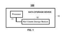
- FIG. 1illustrates a data storage device 10 according to one embodiment of the invention.
- the data storage device 10may be any device containing a processor 11 and a non-volatile storage medium 12 .
- the non-volatile storage medium 12may be incorporated as part of the device 10 , for example as memory chips, magnetic disks, NAND memory, or as peripherals contained on a system bus.
- FIG. 2illustrates a non-volatile memory 200 of a data storage device according to one embodiment of the invention.
- the non-volatile memory 200may comprise an HDD 12 and/or SSD 13 —or any other appropriate non-volatile memory medium—in the data storage device 100 shown in FIG. 1 .
- the non-volatile memory 200comprises first initialization information area (INA) 230 and an optional INA 240 .
- First INA 230includes first initialization information (INI) 235 and, in one embodiment, first INA 230 may have additional space 236 to store multiple INIs.
- the optional INA 240includes second INI 245 and additional space 246 . Although shown as being smaller for ease of depiction, additional spaces 236 and 246 may be, and generally will be, physically larger than first and second INIs 235 and 245 , respectively.
- INA 230 and 240may comprise numerous instances of initialization information as various versions of initialization information are written to INA 230 and 240 .
- Initialization pointersfirst INP 210 and second INP 210 ′ are stored in a pointer area (PA) 220 .
- the PA 220may comprise multiple INPs as illustrated by blocks 221 - 229 .
- Non-volatile memory 200will typically also have memory 290 for system and user data.
- INImay comprise information used by the data storage device for a variety of purposes, including for example system program code, system data, system hardware configuration information such as servo or channel settings, user hardware or firmware settings or preferences, file information, system resource allocation, permissions, factory information, logical-to-physical mapping information, defect information, lookup tables, error information, wear leveling information or other information that may be needed to bring the data storage device to a fully operational condition.
- Information in the INImay be changed at any time due to normal operation or changes in system or user requirements.
- non-volatile memory 200comprises data that is addressed by the processor 11 according to physical block address (PBA).
- PBAsmay be mapped to logical block addresses (LBAs) that may be used for addressing by a host connected to the data storage device 100 .
- LBAsmay be consecutively numbered, but mapped to non-consecutive physical locations with non-consecutive PBAs.
- LBAsmay be consecutively numbered, but mapped to non-consecutive physical locations with non-consecutive PBAs.
- Such mapping schemesare advantageous for HDD and SSD storage devices according to some embodiments. It will be apparent to one of skill in the art that any such mapping schemes may be used without departing from the spirit of the invention.
- the expression PBAmay therefore include embodiments with LBA address mapping.
- First INP 210 shown in block 221 of PA 220comprises first PBA pointer 211 , first sequence identifier 212 , and first metadata 213 .
- Second INP 210 ′ shown in block 226 of PA 220comprises second PBA pointer 211 ′, second sequence identifier 212 ′, and second metadata 213 ′.
- INPs stored in PA 220may be in any order. For example, in one embodiment, block 221 is written with a first INP and then block 222 is written with the next INP and so forth. When all of the blocks 221 - 229 are full, the next INP may be written to the least-recently used block (i.e., block 221 ) and the process continues as before.
- PA 220may comprise one or more tracks of an HDD or, in another embodiment, PA 220 may comprise one or more blocks of non-volatile semiconductor memory.
- First PBA pointer 211comprises the PBA of first PBA starting location 231 .
- First PBA location 231is the starting address where first INI 235 is stored within INA 230 .
- first PBA pointer 211may comprise more than one PBA.
- first PBA pointer 211may point to two or more different types of INIs that are located at different PBAs. When any of the different types of INIs are updated, a new PBA pointer may be written to point to all of the current INI locations.
- First sequence identifier 212comprises information related to the order that first INP 210 was written into PA 220 .
- Sequence identifiersmay be any data that can be used to determine that an INP has been written after other INPs in the PA or signify a version or revision of an INP.
- Sequence identifiersmay comprise for example: a revision number, a sequence string, a sequence number, a time stamp, and/or a validation code.
- First INP 210may optionally comprise first metadata 213 .
- Metadatamay be for example: additional pointers, code, parameters, or initialization information.
- Embodiments of the inventionmay find the optional metadata space useful for initialization and the invention is not limited by the contents or absence of metadata.
- PA 220may comprise more than one INP, and in one embodiment of the invention, updating INI may be performed by writing second INI 245 and second INP 210 ′.
- the contents of second INP 210 ′follow the same description as first INP 210 , however, second INP 210 ′ comprises more recent information.
- Second PBA pointer 211 ′comprises a pointer that now points to second PBA starting location 241 for second INI 245 .
- Second sequence identifier 212 ′comprises contents that can be recognized as more recent than all other sequence identifiers contained in PA 220 .
- Optional second metadata 213 ′may comprise updated metadata.
- second INI 245may be in first INA 230 or in a separated location, such as a separate physical medium. The separate physical medium may be a different volume, a different disk surface, or a different semiconductor memory, for example.
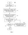
- FIG. 3is a flow chart of a process 300 for initializing of a data storage device according to one embodiment of the invention.
- a processorwill read the INPs contained in the PA.
- the processorwill examine the sequence identifiers contained in each INP to determine which is the most recent.
- the processoruses the PBA pointer from the most recent INP as an index to the PBA starting location of most recent INI.
- the processorreads the data beginning at the PBA starting location and performs initialization. Once initialization has completed or become interrupted, the process checks to see if the initialization process was successful in block 350 . If the initialization was successful, the operation is completed.
- the processbegins recovery in block 360 .
- the processwill use a less recent—typically the next most recent—INP and PBA pointer, and return to block 340 to index to the previous INI and perform initialization using the selected INI.
- additional prior INPsmay be used to access older INIs by repeating blocks 340 , 350 , and 360 until a successful initialization is achieved.
- the processmay stop and/or an error message may be provided to the user or host after a certain number of unsuccessful initialization attempts.
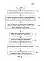
- FIG. 4is a flow chart of a process 400 for updating initialization information according to one embodiment of the invention.
- new initialization informationmay be stored in the first INA 230 when an updated mapping table of LBAs to PBAs is flushed to the non-volatile storage due to recent user data writes.
- a processorwill read the INPs contained in the PA.
- the processorwill examine the sequence identifiers contained in each INP to determine which is the most recent.
- the processoruses the PBA pointer from the most recent INP as an index to determine the PBA starting location of most recent INI.
- the processoruses the PBA starting location to select a location to put the new INI.
- the new INI locationmay be in optional PA 240 or a different medium, page or erase block.
- the processorwrites the new INI to the selected location.
- the processorcreates a new most recent PBA pointer, which includes a most recent sequence identifier.
- the processorwrites a new INP into any available location in the PA. For example, in one embodiment, the new INP may be written to the next available location in PA 220 of FIG. 2 or may overwrite the least-recently used location in PA 220 if all of the locations have been used.
- the processormay store the location of the most recent initialization information and/or the most recent initialization pointer in volatile memory after determining that initialization was successful in block 350 of FIG. 3 . This information can then be quickly accessed for use in block 440 . In this embodiment, each time new initialization information and/or a new initialization pointer is written to non-volatile memory, the new locations would be stored on volatile memory for later use in block 440 of FIG. 4 .
- FIG. 5illustrates a conceptual overview of solid state memory 500 according to one embodiment, which may be in SSD 62 shown in data storage device 60 in FIG. 6 .
- Solid state memory 500may comprise multiple physical memory devices mapped to PBAs of data storage device 100 .
- Semiconductor memories 505 , 505 ′ and 505 ′′ in solid state memory 500are shown as an example, and more or less such devices may be found in data storage device 60 .
- Semiconductor memory 505may comprise any non-volatile semiconductor memory, for example, NAND flash memory.
- semiconductor memory 505may be divided into erase blocks 510 , 520 , 530 , 540 , and extending to ending erase block 599 .
- an erase blockis a portion of the semiconductor memory 505 that can be written (sometimes referred to as programming) and erased independently from all other erase blocks.
- one or more erase blocksmay be divided into pages.
- Erase block 510is shown divided into page 1 , page 2 , page n, and up to page m shown as 511 , 512 , 513 , and 514 respectively.
- Erase block 520is similarly divided into page 1 , page 2 , page n and up to page m shown as 521 , 522 , 523 , and 524 respectively. All the erase blocks in semiconductor memory 505 may be similarly divided into pages.
- a pagemay be a portion of an erase block that can be accessed by one or more PBAs and can be written as a unit. In order to rewrite a page that has been previously written, the entire erase block must typically be erased first. If a hazardous event such as power loss occurs during writing or erasing of an NAND memory, loss of data may occur. If the writing or erasing was part of updating INI or INP, the data loss can be catastrophic if not handled properly.
- Some embodiments of the inventionmay prevent such catastrophic loss by writing updated INI and INP into different erase blocks rather than overwriting prior INI and INP.
- each updatemay be written alternately to two erase blocks.
- each updatemay be written to different pages of an erase block, and in yet another embodiment, updates may be written to different pages of alternating erase blocks.
- the advantage of maintaining older versions of INI and INPis that they may be used for restore operations in the event that an erase block or page becomes corrupted or the new update is inoperable.
- FIG. 7illustrates a data storage device 70 according to one embodiment of the invention.
- Data storage device 70includes a processor 71 , and a disk drive 72 .
- the disk drive 72may comprise one or more magnetic disks for storing data and one or more heads for accessing the data on the disk surface.
- Disk drive 72may also comprise non-volatile semiconductor memory, sometimes referred to as a hybrid drive.
- the processor 71may be tightly coupled with the disk drive 72 by being included on a PCBA of the disk drive 72 or the processor may communicate remotely with the disk drive 72 over an interface.
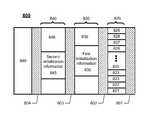
- FIG. 8illustrates a non-volatile memory 800 similar to the non-volatile memory 200 illustrated in FIG. 2 according to one embodiment.
- the non-volatile memory 200may be embodied in a disk drive 62 that is written in a shingle format, which is a method of writing adjacent concentric tracks of data with wide tracks using a write transducer that has a writer width greater than the final track width.
- a first trackis written as a wide track, and when an adjacent second track is written, it partially overwrites a fraction of the first track leaving a narrow first track and a wide second track. Subsequent writes to adjacent tracks similarly overwrite a fraction of the previous track, leaving behind multiple narrow tracks.
- the resulting formathas higher track density, but has disadvantages for non-sequential or random writing.
- multiple tracksmay be written in order from an inner diameter (ID) to an outer diameter (OD) direction of a recording disk, or vice versa.
- IDinner diameter
- ODouter diameter
- Some methodsincorporate indirect addressing to break the fixed connection between physical and logical addresses by using address mapping tables. Shingle format and indirect addressing may increase the frequency of updates to mapping tables due to the need to consolidate shingled tracks and recover storage using methods commonly referred to as garbage collection.
- garbage collectionsince the initialization information itself may employ shingle format, the frequency and duration of risk due to failure or power loss increases substantially.
- the non-volatile memory 800 in FIG. 8comprises PA 820 and INPs 821 through 829 , however, the number of INPs and/or initialization information areas are not limited.
- First INA 830comprises first INI 835 and additional space 836 .
- Optional second INA 840comprises second INI 845 and additional space 846 .
- System and user storageis shown in block 890 .
- Guard bands 801 , 802 , 803 , and 804are provided between the PA 830 , first INA 830 , optional INA 840 , and system and user storage 890 .
- guard bands 801 , 802 , 803 , and 804are at least as wide as the write transducer writer width.
- guard bands 801 , 802 , 803 , and/or 804may be wide enough to prevent adjacent track interference or erasure due to stray magnetic flux lines that occur when writing tracks near the area to be protected.
- PA 820comprises a single track of data.
- PA 820may be located near the ID of at least one of the disk surfaces.
- Guard bands 801 and 802are provided to prevent overwriting of INPs when adjacent tracks are written in shingle format. For example, without guard band 802 , if the first INI 835 or any of first INA 830 is written, a wide shingle write transducer may overwrite part of PA 820 . Similarly, if PA 820 were written, part of first INA 830 may be overwritten.
- Guard bands 801 , 802 , 803 , and 804provide enough space for writing any of PA 820 , first INA 830 , optional INA 840 , and system and user storage 890 without overwriting adjacent areas.
- PA 820can operate in a conventional non-shingle format that provides non-sequential and random writing performance.
- Some embodiments of the present inventionmay provide for robust initialization of a data storage device and updating of initialization of INI.
- some embodiments of the inventionallow for updating a system while protecting old initialization information without the need to update or preserve any fixed storage location.
- replacing a fixed boot pointer with a pointer search areapermits updating INI and pointers with code that can be protected during updates and allow recovery to a prior initialization pointer and initialization information.
- a processormay include many alternatives, such as a microprocessor, microcontroller, sequencer, or state machine. Processors may also be local in the data storage device or remotely, such as in a host computer. Alternatives to embody the invention in combinations of hardware, firmware, and/or software running on a processor, or as a hardware implementation that is reconfigurable to operate in multiple modes would be design choices apparent to those of ordinary skill in the art.
- system and method of the present inventionmay be embodied as software which provides such programming, such as a set of instructions and/or metadata embodied within a computer readable medium.
- the described embodimentshave been presented by way of example only and are not intended to limit the scope of the disclosure. Indeed, the novel methods and systems described herein may be embodied in a variety of other forms without departing from the spirit thereof. Thus, the invention is not limited by any preferred embodiments, but is defined by reference to the appended claims.
Landscapes
- Engineering & Computer Science (AREA)
- Theoretical Computer Science (AREA)
- Software Systems (AREA)
- Physics & Mathematics (AREA)
- General Engineering & Computer Science (AREA)
- General Physics & Mathematics (AREA)
- Computer Security & Cryptography (AREA)
- Signal Processing For Digital Recording And Reproducing (AREA)
Abstract
Description
Claims (11)
Priority Applications (1)
| Application Number | Priority Date | Filing Date | Title |
|---|---|---|---|
| US13/027,432US9405668B1 (en) | 2011-02-15 | 2011-02-15 | Data storage device initialization information accessed by searching for pointer information |
Applications Claiming Priority (1)
| Application Number | Priority Date | Filing Date | Title |
|---|---|---|---|
| US13/027,432US9405668B1 (en) | 2011-02-15 | 2011-02-15 | Data storage device initialization information accessed by searching for pointer information |
Publications (1)
| Publication Number | Publication Date |
|---|---|
| US9405668B1true US9405668B1 (en) | 2016-08-02 |
Family
ID=56506860
Family Applications (1)
| Application Number | Title | Priority Date | Filing Date |
|---|---|---|---|
| US13/027,432Expired - Fee RelatedUS9405668B1 (en) | 2011-02-15 | 2011-02-15 | Data storage device initialization information accessed by searching for pointer information |
Country Status (1)
| Country | Link |
|---|---|
| US (1) | US9405668B1 (en) |
Cited By (4)
| Publication number | Priority date | Publication date | Assignee | Title |
|---|---|---|---|---|
| US20170277688A1 (en)* | 2016-03-28 | 2017-09-28 | Silicon Motion, Inc. | Image file generating method for data storage device |
| US10394479B2 (en)* | 2015-08-20 | 2019-08-27 | Micron Technology, Inc. | Solid state storage device with quick boot from NAND media |
| US20220100408A1 (en)* | 2020-09-28 | 2022-03-31 | Raymx Microelectronics Corp. | Storage device and accessing method for operation log thereof |
| US20240304218A1 (en)* | 2023-03-06 | 2024-09-12 | Kabushiki Kaisha Toshiba | Magnetic disk device and method |
Citations (33)
| Publication number | Priority date | Publication date | Assignee | Title |
|---|---|---|---|---|
| US4086636A (en)* | 1977-02-28 | 1978-04-25 | Xerox Corporation | Restore method and apparatus for disk drive |
| US4827462A (en)* | 1987-03-26 | 1989-05-02 | International Business Machines Corporation | Modular data storage directories for large-capacity data storage units |
| US4945427A (en)* | 1988-06-13 | 1990-07-31 | International Business Machines Corporation | Magnetic disk recording with variable track width and variable track density |
| US5535355A (en)* | 1989-04-06 | 1996-07-09 | Kabushiki Kaisha Toshiba | Controller for a storage device which allows either prestored or user defined firmware to be executed |
| US6073232A (en) | 1997-02-25 | 2000-06-06 | International Business Machines Corporation | Method for minimizing a computer's initial program load time after a system reset or a power-on using non-volatile storage |
| US6098158A (en) | 1997-12-18 | 2000-08-01 | International Business Machines Corporation | Software-enabled fast boot |
| US6185063B1 (en) | 1997-02-13 | 2001-02-06 | Seagate Technology Llc | Methods and apparatus for overlapping data tracks on a storage medium |
| US6539456B2 (en) | 1999-10-13 | 2003-03-25 | Intel Corporation | Hardware acceleration of boot-up utilizing a non-volatile disk cache |
| US20030095648A1 (en)* | 1999-10-05 | 2003-05-22 | Lifecor, Inc. | Fault-tolerant remote reprogramming for a patient-worn medical device |
| US20030135729A1 (en) | 2001-12-14 | 2003-07-17 | I/O Integrity, Inc. | Apparatus and meta data caching method for optimizing server startup performance |
| US20030142561A1 (en) | 2001-12-14 | 2003-07-31 | I/O Integrity, Inc. | Apparatus and caching method for optimizing server startup performance |
| US20040025002A1 (en)* | 2002-08-01 | 2004-02-05 | Cepulis Darren J. | System firmware back-up using a BIOS-accessible pre-boot partition |
| US20040064647A1 (en) | 2002-06-27 | 2004-04-01 | Microsoft Corporation | Method and apparatus to reduce power consumption and improve read/write performance of hard disk drives using non-volatile memory |
| US20050071537A1 (en) | 2003-09-26 | 2005-03-31 | Hitachi Global Storage Technologies | Log-structured file system for disk drives with shingled writing |
| US6904496B2 (en) | 2002-03-25 | 2005-06-07 | Dell Products L.P. | Computer system with improved write cache and method therefor |
| US6963951B2 (en) | 2000-07-12 | 2005-11-08 | Seagate Technology Llc | Partition recovery method |
| US20050251617A1 (en)* | 2004-05-07 | 2005-11-10 | Sinclair Alan W | Hybrid non-volatile memory system |
| US6968450B1 (en) | 2002-06-01 | 2005-11-22 | Western Digital Technologies, Inc. | Disk drive caching initial host requested data in non-volatile semiconductor memory to reduce start-up time of a host computer |
| US6967810B2 (en) | 2003-09-29 | 2005-11-22 | Hitachi Global Storage Technologies Netherlands B.V. | System and method for writing HDD depending on direction of head skew |
| US7082007B2 (en) | 2000-09-27 | 2006-07-25 | Seagate Technology Llc | Method to achieve higher track density by allowing only one-sided track encroachment |
| US7130962B2 (en) | 2003-12-18 | 2006-10-31 | Intel Corporation | Writing cache lines on a disk drive |
| US20060294352A1 (en) | 2005-06-23 | 2006-12-28 | Morrison John A | Speedy boot for computer systems |
| US20070005883A1 (en) | 2005-06-30 | 2007-01-04 | Trika Sanjeev N | Method to keep volatile disk caches warm across reboots |
| US7181608B2 (en) | 2000-02-03 | 2007-02-20 | Realtime Data Llc | Systems and methods for accelerated loading of operating systems and application programs |
| US20070083743A1 (en) | 2005-10-06 | 2007-04-12 | Microsoft Corporation | Fast booting an operating system from an off state |
| US7305539B2 (en) | 2004-10-14 | 2007-12-04 | Sandisk Il Ltd. | Adaptive booting from mass storage device |
| US7408731B2 (en) | 2006-01-04 | 2008-08-05 | Hitachi Global Storage Technologies Netherlands B.V. | Track allocation method of disk drive |
| US7417813B2 (en) | 2004-05-26 | 2008-08-26 | Seagate Technology Llc | Overlapping data track access |
| US7443625B2 (en) | 1998-03-04 | 2008-10-28 | Hitachi Global Storage Technologies Japan Ltd. | Magnetic disk drive |
| US7490212B2 (en) | 2003-09-29 | 2009-02-10 | Hitachi Global Storage Technologies Netherlands B.V. | System and method for writing data to dedicated bands of a hard disk drive |
| US20100088482A1 (en)* | 2008-10-02 | 2010-04-08 | Torsten Hinz | Process and Method for Erase Strategy in Solid State Disks |
| US20110320685A1 (en)* | 2010-06-23 | 2011-12-29 | Sergey Anatolicvich Gorobets | Use of Guard Bands and Phased Maintenance Operations to Avoid Exceeding Maximum Latency Requirements in Non-Volatile Memory Systems |
| US20120072734A1 (en)* | 2010-09-22 | 2012-03-22 | Wishman Allen R | Platform firmware armoring technology |
- 2011
- 2011-02-15USUS13/027,432patent/US9405668B1/ennot_activeExpired - Fee Related
Patent Citations (34)
| Publication number | Priority date | Publication date | Assignee | Title |
|---|---|---|---|---|
| US4086636A (en)* | 1977-02-28 | 1978-04-25 | Xerox Corporation | Restore method and apparatus for disk drive |
| US4827462A (en)* | 1987-03-26 | 1989-05-02 | International Business Machines Corporation | Modular data storage directories for large-capacity data storage units |
| US4945427A (en)* | 1988-06-13 | 1990-07-31 | International Business Machines Corporation | Magnetic disk recording with variable track width and variable track density |
| US5535355A (en)* | 1989-04-06 | 1996-07-09 | Kabushiki Kaisha Toshiba | Controller for a storage device which allows either prestored or user defined firmware to be executed |
| US6185063B1 (en) | 1997-02-13 | 2001-02-06 | Seagate Technology Llc | Methods and apparatus for overlapping data tracks on a storage medium |
| US6073232A (en) | 1997-02-25 | 2000-06-06 | International Business Machines Corporation | Method for minimizing a computer's initial program load time after a system reset or a power-on using non-volatile storage |
| US6098158A (en) | 1997-12-18 | 2000-08-01 | International Business Machines Corporation | Software-enabled fast boot |
| US7443625B2 (en) | 1998-03-04 | 2008-10-28 | Hitachi Global Storage Technologies Japan Ltd. | Magnetic disk drive |
| US20030095648A1 (en)* | 1999-10-05 | 2003-05-22 | Lifecor, Inc. | Fault-tolerant remote reprogramming for a patient-worn medical device |
| US6662267B2 (en) | 1999-10-13 | 2003-12-09 | Intel Corporation | Hardware acceleration of boot-up utilizing a non-volatile disk cache |
| US6539456B2 (en) | 1999-10-13 | 2003-03-25 | Intel Corporation | Hardware acceleration of boot-up utilizing a non-volatile disk cache |
| US7181608B2 (en) | 2000-02-03 | 2007-02-20 | Realtime Data Llc | Systems and methods for accelerated loading of operating systems and application programs |
| US6963951B2 (en) | 2000-07-12 | 2005-11-08 | Seagate Technology Llc | Partition recovery method |
| US7082007B2 (en) | 2000-09-27 | 2006-07-25 | Seagate Technology Llc | Method to achieve higher track density by allowing only one-sided track encroachment |
| US20030135729A1 (en) | 2001-12-14 | 2003-07-17 | I/O Integrity, Inc. | Apparatus and meta data caching method for optimizing server startup performance |
| US20030142561A1 (en) | 2001-12-14 | 2003-07-31 | I/O Integrity, Inc. | Apparatus and caching method for optimizing server startup performance |
| US6904496B2 (en) | 2002-03-25 | 2005-06-07 | Dell Products L.P. | Computer system with improved write cache and method therefor |
| US6968450B1 (en) | 2002-06-01 | 2005-11-22 | Western Digital Technologies, Inc. | Disk drive caching initial host requested data in non-volatile semiconductor memory to reduce start-up time of a host computer |
| US20040064647A1 (en) | 2002-06-27 | 2004-04-01 | Microsoft Corporation | Method and apparatus to reduce power consumption and improve read/write performance of hard disk drives using non-volatile memory |
| US20040025002A1 (en)* | 2002-08-01 | 2004-02-05 | Cepulis Darren J. | System firmware back-up using a BIOS-accessible pre-boot partition |
| US20050071537A1 (en) | 2003-09-26 | 2005-03-31 | Hitachi Global Storage Technologies | Log-structured file system for disk drives with shingled writing |
| US6967810B2 (en) | 2003-09-29 | 2005-11-22 | Hitachi Global Storage Technologies Netherlands B.V. | System and method for writing HDD depending on direction of head skew |
| US7490212B2 (en) | 2003-09-29 | 2009-02-10 | Hitachi Global Storage Technologies Netherlands B.V. | System and method for writing data to dedicated bands of a hard disk drive |
| US7130962B2 (en) | 2003-12-18 | 2006-10-31 | Intel Corporation | Writing cache lines on a disk drive |
| US20050251617A1 (en)* | 2004-05-07 | 2005-11-10 | Sinclair Alan W | Hybrid non-volatile memory system |
| US7417813B2 (en) | 2004-05-26 | 2008-08-26 | Seagate Technology Llc | Overlapping data track access |
| US7305539B2 (en) | 2004-10-14 | 2007-12-04 | Sandisk Il Ltd. | Adaptive booting from mass storage device |
| US20060294352A1 (en) | 2005-06-23 | 2006-12-28 | Morrison John A | Speedy boot for computer systems |
| US20070005883A1 (en) | 2005-06-30 | 2007-01-04 | Trika Sanjeev N | Method to keep volatile disk caches warm across reboots |
| US20070083743A1 (en) | 2005-10-06 | 2007-04-12 | Microsoft Corporation | Fast booting an operating system from an off state |
| US7408731B2 (en) | 2006-01-04 | 2008-08-05 | Hitachi Global Storage Technologies Netherlands B.V. | Track allocation method of disk drive |
| US20100088482A1 (en)* | 2008-10-02 | 2010-04-08 | Torsten Hinz | Process and Method for Erase Strategy in Solid State Disks |
| US20110320685A1 (en)* | 2010-06-23 | 2011-12-29 | Sergey Anatolicvich Gorobets | Use of Guard Bands and Phased Maintenance Operations to Avoid Exceeding Maximum Latency Requirements in Non-Volatile Memory Systems |
| US20120072734A1 (en)* | 2010-09-22 | 2012-03-22 | Wishman Allen R | Platform firmware armoring technology |
Cited By (8)
| Publication number | Priority date | Publication date | Assignee | Title |
|---|---|---|---|---|
| US10394479B2 (en)* | 2015-08-20 | 2019-08-27 | Micron Technology, Inc. | Solid state storage device with quick boot from NAND media |
| US10956065B2 (en) | 2015-08-20 | 2021-03-23 | Micron Technology, Inc. | Solid state storage device with quick boot from NAND media |
| US11287990B2 (en) | 2015-08-20 | 2022-03-29 | Micron Technology, Inc. | Solid state storage device with quick boot from NAND media |
| US20170277688A1 (en)* | 2016-03-28 | 2017-09-28 | Silicon Motion, Inc. | Image file generating method for data storage device |
| US20220100408A1 (en)* | 2020-09-28 | 2022-03-31 | Raymx Microelectronics Corp. | Storage device and accessing method for operation log thereof |
| US11494112B2 (en)* | 2020-09-28 | 2022-11-08 | Raymx Microelectronics Corp. | Storage device and accessing method for operation log thereof |
| US20240304218A1 (en)* | 2023-03-06 | 2024-09-12 | Kabushiki Kaisha Toshiba | Magnetic disk device and method |
| US12236978B2 (en)* | 2023-03-06 | 2025-02-25 | Kabushiki Kaisha Toshiba | Magnetic disk device and method |
Similar Documents
| Publication | Publication Date | Title |
|---|---|---|
| US9665301B2 (en) | Methods and devices for storing user data along with addresses corresponding to physical pages storing valid data | |
| US8041991B2 (en) | System and method for recovering solid state drive data | |
| EP2329380B1 (en) | Embedded mapping information for memory devices | |
| US9842030B2 (en) | Data storage device and flash memory control method | |
| US8312554B2 (en) | Method of hiding file at data protecting mode for non-volatile memory module, memory controller and portable memory storage apparatus | |
| US10381040B1 (en) | Dynamic hybrid shingled magnetic recording device | |
| EP3100165B1 (en) | Garbage collection and data relocation for data storage system | |
| KR100644602B1 (en) | Reimaging Control Method for Flash Memory and Its Structure | |
| JP4164118B1 (en) | Storage device using flash memory | |
| US8285965B2 (en) | Aligning data storage device partition to boundary of physical data sector | |
| US8190811B2 (en) | Defragmentation of solid state memory | |
| US8291155B2 (en) | Data access method, memory controller and memory storage system | |
| US7752412B2 (en) | Methods of managing file allocation table information | |
| US7681008B2 (en) | Systems for managing file allocation table information | |
| US20120246393A1 (en) | Memory system and control method of the memory system | |
| US20100191897A1 (en) | System and method for wear leveling in a data storage device | |
| US7702845B2 (en) | Method and apparatus for managing blocks according to update type of data in block-type memory | |
| WO2005059966A2 (en) | Rotational use of memory to minimize write cycles | |
| US9405668B1 (en) | Data storage device initialization information accessed by searching for pointer information | |
| JP4130808B2 (en) | Formatting method | |
| WO2008042594A1 (en) | Managing file allocation table information | |
| KR20060089486A (en) | How to Repair Errors in Flash File System |
Legal Events
| Date | Code | Title | Description |
|---|---|---|---|
| AS | Assignment | Owner name:WESTERN DIGITAL TECHNOLOGIES, INC., CALIFORNIA Free format text:ASSIGNMENT OF ASSIGNORS INTEREST;ASSIGNORS:FALLONE, ROBERT M.;HAMILTON, DAVID M.;REEL/FRAME:025809/0174 Effective date:20110215 | |
| ZAAA | Notice of allowance and fees due | Free format text:ORIGINAL CODE: NOA | |
| ZAAB | Notice of allowance mailed | Free format text:ORIGINAL CODE: MN/=. | |
| AS | Assignment | Owner name:U.S. BANK NATIONAL ASSOCIATION, AS COLLATERAL AGENT, CALIFORNIA Free format text:SECURITY AGREEMENT;ASSIGNOR:WESTERN DIGITAL TECHNOLOGIES, INC.;REEL/FRAME:038744/0281 Effective date:20160512 Owner name:JPMORGAN CHASE BANK, N.A., AS COLLATERAL AGENT, ILLINOIS Free format text:SECURITY AGREEMENT;ASSIGNOR:WESTERN DIGITAL TECHNOLOGIES, INC.;REEL/FRAME:038722/0229 Effective date:20160512 Owner name:JPMORGAN CHASE BANK, N.A., AS COLLATERAL AGENT, ILLINOIS Free format text:SECURITY AGREEMENT;ASSIGNOR:WESTERN DIGITAL TECHNOLOGIES, INC.;REEL/FRAME:038744/0481 Effective date:20160512 Owner name:JPMORGAN CHASE BANK, N.A., AS COLLATERAL AGENT, IL Free format text:SECURITY AGREEMENT;ASSIGNOR:WESTERN DIGITAL TECHNOLOGIES, INC.;REEL/FRAME:038722/0229 Effective date:20160512 Owner name:JPMORGAN CHASE BANK, N.A., AS COLLATERAL AGENT, IL Free format text:SECURITY AGREEMENT;ASSIGNOR:WESTERN DIGITAL TECHNOLOGIES, INC.;REEL/FRAME:038744/0481 Effective date:20160512 Owner name:U.S. BANK NATIONAL ASSOCIATION, AS COLLATERAL AGEN Free format text:SECURITY AGREEMENT;ASSIGNOR:WESTERN DIGITAL TECHNOLOGIES, INC.;REEL/FRAME:038744/0281 Effective date:20160512 | |
| STCF | Information on status: patent grant | Free format text:PATENTED CASE | |
| AS | Assignment | Owner name:WESTERN DIGITAL TECHNOLOGIES, INC., CALIFORNIA Free format text:RELEASE BY SECURED PARTY;ASSIGNOR:U.S. BANK NATIONAL ASSOCIATION, AS COLLATERAL AGENT;REEL/FRAME:045501/0714 Effective date:20180227 | |
| MAFP | Maintenance fee payment | Free format text:PAYMENT OF MAINTENANCE FEE, 4TH YEAR, LARGE ENTITY (ORIGINAL EVENT CODE: M1551); ENTITY STATUS OF PATENT OWNER: LARGE ENTITY Year of fee payment:4 | |
| AS | Assignment | Owner name:WESTERN DIGITAL TECHNOLOGIES, INC., CALIFORNIA Free format text:RELEASE OF SECURITY INTEREST AT REEL 038744 FRAME 0481;ASSIGNOR:JPMORGAN CHASE BANK, N.A.;REEL/FRAME:058982/0556 Effective date:20220203 | |
| AS | Assignment | Owner name:JPMORGAN CHASE BANK, N.A., ILLINOIS Free format text:PATENT COLLATERAL AGREEMENT - A&R LOAN AGREEMENT;ASSIGNOR:WESTERN DIGITAL TECHNOLOGIES, INC.;REEL/FRAME:064715/0001 Effective date:20230818 Owner name:JPMORGAN CHASE BANK, N.A., ILLINOIS Free format text:PATENT COLLATERAL AGREEMENT - DDTL LOAN AGREEMENT;ASSIGNOR:WESTERN DIGITAL TECHNOLOGIES, INC.;REEL/FRAME:067045/0156 Effective date:20230818 | |
| FEPP | Fee payment procedure | Free format text:MAINTENANCE FEE REMINDER MAILED (ORIGINAL EVENT CODE: REM.); ENTITY STATUS OF PATENT OWNER: LARGE ENTITY | |
| LAPS | Lapse for failure to pay maintenance fees | Free format text:PATENT EXPIRED FOR FAILURE TO PAY MAINTENANCE FEES (ORIGINAL EVENT CODE: EXP.); ENTITY STATUS OF PATENT OWNER: LARGE ENTITY | |
| STCH | Information on status: patent discontinuation | Free format text:PATENT EXPIRED DUE TO NONPAYMENT OF MAINTENANCE FEES UNDER 37 CFR 1.362 | |
| FP | Lapsed due to failure to pay maintenance fee | Effective date:20240802 |