US9405408B2 - Trace pattern for touch-sensing application - Google Patents
Trace pattern for touch-sensing applicationDownload PDFInfo
- Publication number
- US9405408B2 US9405408B2US13/008,014US201113008014AUS9405408B2US 9405408 B2US9405408 B2US 9405408B2US 201113008014 AUS201113008014 AUS 201113008014AUS 9405408 B2US9405408 B2US 9405408B2
- Authority
- US
- United States
- Prior art keywords
- sensor element
- row
- column
- unit cell
- sensor
- Prior art date
- Legal status (The legal status is an assumption and is not a legal conclusion. Google has not performed a legal analysis and makes no representation as to the accuracy of the status listed.)
- Active, expires
Links
Images


Classifications
- G—PHYSICS
- G06—COMPUTING OR CALCULATING; COUNTING
- G06F—ELECTRIC DIGITAL DATA PROCESSING
- G06F3/00—Input arrangements for transferring data to be processed into a form capable of being handled by the computer; Output arrangements for transferring data from processing unit to output unit, e.g. interface arrangements
- G06F3/01—Input arrangements or combined input and output arrangements for interaction between user and computer
- G06F3/03—Arrangements for converting the position or the displacement of a member into a coded form
- G06F3/041—Digitisers, e.g. for touch screens or touch pads, characterised by the transducing means
- G06F3/044—Digitisers, e.g. for touch screens or touch pads, characterised by the transducing means by capacitive means
- G06F3/0446—Digitisers, e.g. for touch screens or touch pads, characterised by the transducing means by capacitive means using a grid-like structure of electrodes in at least two directions, e.g. using row and column electrodes
- G—PHYSICS
- G06—COMPUTING OR CALCULATING; COUNTING
- G06F—ELECTRIC DIGITAL DATA PROCESSING
- G06F3/00—Input arrangements for transferring data to be processed into a form capable of being handled by the computer; Output arrangements for transferring data from processing unit to output unit, e.g. interface arrangements
- G06F3/01—Input arrangements or combined input and output arrangements for interaction between user and computer
- G06F3/03—Arrangements for converting the position or the displacement of a member into a coded form
- G06F3/041—Digitisers, e.g. for touch screens or touch pads, characterised by the transducing means
- G06F3/044—Digitisers, e.g. for touch screens or touch pads, characterised by the transducing means by capacitive means
- G06F3/0443—Digitisers, e.g. for touch screens or touch pads, characterised by the transducing means by capacitive means using a single layer of sensing electrodes
- G—PHYSICS
- G06—COMPUTING OR CALCULATING; COUNTING
- G06F—ELECTRIC DIGITAL DATA PROCESSING
- G06F3/00—Input arrangements for transferring data to be processed into a form capable of being handled by the computer; Output arrangements for transferring data from processing unit to output unit, e.g. interface arrangements
- G06F3/01—Input arrangements or combined input and output arrangements for interaction between user and computer
- G06F3/03—Arrangements for converting the position or the displacement of a member into a coded form
- G06F3/041—Digitisers, e.g. for touch screens or touch pads, characterised by the transducing means
- G06F3/044—Digitisers, e.g. for touch screens or touch pads, characterised by the transducing means by capacitive means
- G06F3/0445—Digitisers, e.g. for touch screens or touch pads, characterised by the transducing means by capacitive means using two or more layers of sensing electrodes, e.g. using two layers of electrodes separated by a dielectric layer
- G—PHYSICS
- G06—COMPUTING OR CALCULATING; COUNTING
- G06F—ELECTRIC DIGITAL DATA PROCESSING
- G06F2203/00—Indexing scheme relating to G06F3/00 - G06F3/048
- G06F2203/041—Indexing scheme relating to G06F3/041 - G06F3/045
- G06F2203/04111—Cross over in capacitive digitiser, i.e. details of structures for connecting electrodes of the sensing pattern where the connections cross each other, e.g. bridge structures comprising an insulating layer, or vias through substrate
Definitions
- This disclosurerelates to the field of touch-sensors and, in particular, to trace patterns of elements in capacitive touch-sensor arrays.
- Computing devicessuch as notebook computers, personal data assistants (PDAs), kiosks, and mobile handsets, have user interface devices, which are also known as human interface devices (HID).
- user interface deviceswhich are also known as human interface devices (HID).
- One user interface device that has become more commonis a touch-sensor pad (also commonly referred to as a touchpad).
- a basic notebook computer touch-sensor pademulates the function of a personal computer (PC) mouse.
- a touch-sensor padis typically embedded into a PC notebook for built-in portability.
- a touch-sensor padreplicates mouse X/Y movement by using two defined axes which contain a collection of sensor elements that detect the position of one or more conductive objects, such as a finger.
- Mouse right/left button clickscan be replicated by two mechanical buttons, located in the vicinity of the touchpad, or by tapping commands on the touch-sensor pad itself.
- the touch-sensor padprovides a user interface device for performing such functions as positioning a pointer, or selecting an item on a display.
- These touch-sensor padsmay include multi-dimensional sensor arrays for detecting movement in multiple axes.
- the sensor arraymay include a one-dimensional sensor array, detecting movement in one axis.
- the sensor arraymay also be two dimensional, detecting movements in two axes.
- Touch screensalso known as touchscreens, touch windows, touch panels, or touchscreen panels
- transparent display overlayswhich are typically either pressure-sensitive (resistive or piezoelectric), electrically-sensitive (capacitive), acoustically-sensitive (surface acoustic wave (SAW)) or photo-sensitive (infra-red).
- SAWsurface acoustic wave
- the effect of such overlaysallows a display to be used as an input device, removing the keyboard and/or the mouse as the primary input device for interacting with the display's content.
- Such displayscan be attached to computers or, as terminals, to networks.
- Touch screenshave become familiar in retail settings, on point-of-sale systems, on ATMs, on mobile handsets, on kiosks, on game consoles, and on PDAs where a stylus is sometimes used to manipulate the graphical user interface (GUI) and to enter data.
- GUIgraphical user interface
- a usercan touch a touch screen or a touch-sensor pad to manipulate data. For example, a user can apply a single touch, by using a finger to touch the surface of a touch screen, to select an item from a menu.
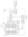
- FIG. 1is a block diagram illustrating an embodiment of an electronic system that processes touch sensor data.
- FIG. 2is a block diagram illustrating an embodiment of an electronic system that processes touch sensor data.
- FIG. 3Aillustrates an embodiment of a capacitive sensor array having a hollow diamond pattern.
- FIG. 3Billustrates an embodiment of a capacitive sensor array having a hollow diamond pattern.
- FIG. 3Cillustrates an embodiment of a capacitive sensor array having a hollow diamond pattern.
- FIG. 4Aillustrates an embodiment of a capacitive sensor array having a dual hollow Manhattan (DHM) pattern.
- DLMdual hollow Manhattan
- FIG. 4Billustrates an embodiment of a capacitive sensor array having a dual hollow Manhattan (DHM) pattern.
- DLMdual hollow Manhattan
- FIG. 4Cillustrates a cross-section view of an embodiment of a capacitive sensor array having a dual hollow Manhattan (DHM) pattern.
- DLMdual hollow Manhattan
- FIG. 4Dillustrates a cross-section view of an embodiment of a capacitive sensor array having a dual hollow Manhattan (DHM) pattern.
- DLMdual hollow Manhattan
- FIG. 4Eillustrates an embodiment of a capacitive sensor array having a dual hollow Manhattan (DHM) pattern and ground planes.
- DLMdual hollow Manhattan
- FIG. 4Fillustrates an embodiment of a capacitive sensor array having a dual hollow Manhattan (DHM) pattern and additional traces.
- DLMdual hollow Manhattan
- FIG. 5illustrates an embodiment of a capacitive sensor array having a quad nested spiral pattern.
- FIG. 6illustrates an embodiment of a capacitive sensor array having a interleaved trace pattern.
- a capacitive sensing systemmay be used to perform mutual capacitance measurements between sensor elements in the capacitive sensor array.
- An embodiment of a capacitive sensor array having a greater mutual capacitance between sensor elements and smaller self capacitance for each of the individual sensor elements than a conventional capacitive sensor arraymay be used to decrease signal disparity in the resulting signal.
- a mutual capacitance between two sensor elementsmay be increased by maximizing a boundary length between the adjacent edges of the sensor elements. Additionally, the self capacitance of each individual sensor element may be decreased by minimizing the area of the sensor element.
- FIG. 1illustrates a block diagram of one embodiment of an electronic system 100 including a processing device 110 that may be configured to measure capacitances from a touch sensing surface 116 .
- the electronic system 100includes a touch-sensing surface 116 (e.g., a touchscreen, or a touch pad) coupled to the processing device 110 and a host 150 .
- the touch-sensing surface 116is a two-dimensional user interface that uses a sensor array 121 to detect touches on the surface 116 .
- the sensor array 121includes sensor elements 121 ( 1 )- 121 (N) (where N is a positive integer) that are disposed as a two-dimensional matrix (also referred to as an XY matrix).
- the sensor array 121is coupled to pins 113 ( 1 )- 113 (N) of the processing device 110 via one or more analog buses 115 transporting multiple signals.
- each sensor element 121 ( 1 )- 121 (N)is represented as a capacitor.
- the capacitance sensor 101may include a relaxation oscillator or other means to convert a capacitance into a measured value.
- the capacitance sensor 101may also include a counter or timer to measure the oscillator output.
- the capacitance sensor 101may further include software components to convert the count value (e.g., capacitance value) into a sensor element detection decision (also referred to as switch detection decision) or relative magnitude.
- a sensor element detection decisionalso referred to as switch detection decision
- switch detection decisione.g., switch detection decision
- the capacitance sensor 101may be evaluating other measurements to determine the user interaction. For example, in the capacitance sensor 101 having a sigma-delta modulator, the capacitance sensor 101 is evaluating the ratio of pulse widths of the output, instead of the raw counts being over or under a certain threshold.
- the processing device 110further includes processing logic 102 .
- Operations of the processing logic 102may be implemented in firmware; alternatively, it may be implemented in hardware or software.
- the processing logic 102may receive signals from the capacitance sensor 101 , and determine the state of the sensor array 121 , such as whether an object (e.g., a finger) is detected on or in proximity to the sensor array 121 (e.g., determining the presence of the object), where the object is detected on the sensor array (e.g., determining the location of the object); tracking the motion of the object, or other information related to an object detected at the touch sensor.
- an objecte.g., a finger
- the processing logic 102may receive signals from the capacitance sensor 101 , and determine the state of the sensor array 121 , such as whether an object (e.g., a finger) is detected on or in proximity to the sensor array 121 (e.g., determining the presence of the object), where the object is detected on the sensor array (e.g.,
- the processing device 110may send the raw data or partially-processed data to the host 150 .
- the host 150may include decision logic 151 that performs some or all of the operations of the processing logic 102 .
- Operations of the decision logic 151may be implemented in firmware, hardware, software, or a combination thereof.
- the host 150may include a high-level Application Programming Interface (API) in applications 152 that perform routines on the received data, such as compensating for sensitivity differences, other compensation algorithms, baseline update routines, start-up and/or initialization routines, interpolation operations, or scaling operations.
- APIApplication Programming Interface
- the operations described with respect to the processing logic 102may be implemented in the decision logic 151 , the applications 152 , or in other hardware, software, and/or firmware external to the processing device 110 .
- the processing device 110is the host 150 .
- the processing device 110may also include a non-sensing actions block 103 .
- This block 103may be used to process and/or receive/transmit data to and from the host 150 .
- additional componentsmay be implemented to operate with the processing device 110 along with the sensor array 121 (e.g., keyboard, keypad, mouse, trackball, LEDs, displays, or other peripheral devices).
- the processing device 110may reside on a common carrier substrate such as, for example, an integrated circuit (IC) die substrate, or a multi-chip module substrate.
- the components of the processing device 110may be one or more separate integrated circuits and/or discrete components.
- the processing device 110may be the Programmable System on a Chip (PSoCTM) processing device, developed by Cypress Semiconductor Corporation, San Jose, Calif.
- the processing device 110may be one or more other processing devices known by those of ordinary skill in the art, such as a microprocessor or central processing unit, a controller, special-purpose processor, digital signal processor (DSP), an application specific integrated circuit (ASIC), a field programmable gate array (FPGA), or other programmable device.
- the processing device 110may be a network processor having multiple processors including a core unit and multiple micro-engines.
- the processing device 110may include any combination of general-purpose processing device(s) and special-purpose processing device(s).
- the electronic system 100is implemented in a device that includes the touch-sensing surface 116 as the user interface, such as handheld electronics, portable telephones, cellular telephones, notebook computers, personal computers, personal data assistants (PDAs), kiosks, keyboards, televisions, remote controls, monitors, handheld multi-media devices, handheld video players, gaming devices, control panels of a household or industrial appliances, or other computer peripheral or input devices.
- the electronic system 100may be used in other types of devices.
- the components of electronic system 100may include all the components described above.
- electronic system 100may include only some of the components described above, or include additional components not listed herein.
- FIG. 2is a block diagram illustrating one embodiment of a capacitive touch sensor array 121 and a capacitance sensor 101 that converts measured capacitances to coordinates. The coordinates are calculated based on measured capacitances.
- sensor array 121 and capacitance sensor 101are implemented in a system such as electronic system 100 .
- Sensor array 220includes a matrix 225 of N ⁇ M electrodes (N receive electrodes and M transmit electrodes), which further includes transmit (TX) electrode 222 and receive (RX) electrode 223 . Each of the electrodes in matrix 225 is connected with capacitance sensing circuit 201 through demultiplexer 212 and multiplexer 213 .
- Capacitance sensor 101includes multiplexer control 211 , demultiplexer 212 and multiplexer 213 , clock generator 214 , signal generator 215 , demodulation circuit 216 , and analog to digital converter (ADC) 217 .
- ADC 217is further coupled with touch coordinate converter 218 .
- Touch coordinate converter 218outputs a signal to the processing logic 102 .
- the transmit and receive electrodes in the electrode matrix 225may be arranged so that each of the transmit electrodes overlap and cross each of the receive electrodes such as to form an array of intersections, while maintaining galvanic isolation from each other.
- each transmit electrodemay be capacitively coupled with each of the receive electrodes.
- transmit electrode 222is capacitively coupled with receive electrode 223 at the point where transmit electrode 222 and receive electrode 223 overlap.
- Clock generator 214supplies a clock signal to signal generator 215 , which produces a TX signal 224 to be supplied to the transmit electrodes of touch sensor 121 .
- the signal generator 215includes a set of switches that operate according to the clock signal from clock generator 214 . The switches may generate a TX signal 224 by periodically connecting the output of signal generator 215 to a first voltage and then to a second voltage, wherein said first and second voltages are different.
- the output of signal generator 215is connected with demultiplexer 212 , which allows the TX signal 224 to be applied to any of the M transmit electrodes of touch sensor 121 .
- multiplexer control 211controls demultiplexer 212 so that the TX signal 224 is applied to each transmit electrode 222 in a controlled sequence.
- Demultiplexer 212may also be used to ground, float, or connect an alternate signal to the other transmit electrodes to which the TX signal 224 is not currently being applied.
- the TX signal 224 applied to each transmit electrodeinduces a current within each of the receive electrodes. For instance, when the TX signal 224 is applied to transmit electrode 222 through demultiplexer 212 , the TX signal 224 induces an RX signal 227 on the receive electrodes in matrix 225 . The RX signal 227 on each of the receive electrodes can then be measured in sequence by using multiplexer 213 to connect each of the N receive electrodes to demodulation circuit 216 in sequence.
- the mutual capacitance associated with each intersection between a TX electrode and an RX electrodecan be sensed by selecting every available combination of TX electrode and an RX electrode using demultiplexer 212 and multiplexer 213 .
- multiplexer 213may also be segmented to allow more than one of the receive electrodes in matrix 225 to be routed to additional demodulation circuits 216 . In an optimized configuration, wherein there is a 1-to-1 correspondence of instances of demodulation circuit 216 with receive electrodes, multiplexer 213 may not be present in the system.
- the objectWhen an object, such as a finger, approaches the electrode matrix 225 , the object causes a decrease in the mutual capacitance between only some of the electrodes. For example, if a finger is placed near the intersection of transmit electrode 222 and receive electrode 223 , the presence of the finger will decrease the mutual capacitance between electrodes 222 and 223 .
- the location of the finger on the touchpadcan be determined by identifying the one or more receive electrodes having a decreased mutual capacitance in addition to identifying the transmit electrode to which the TX signal 224 was applied at the time the decreased mutual capacitance was measured on the one or more receive electrodes.
- the locations of one or more touch contactsmay be determined. The determination may be sequential, in parallel, or may occur more frequently at commonly used electrodes.
- a finger or conductive objectmay be used where the finger or conductive object causes an increase in capacitance at one or more electrodes, which may be arranged in a grid or other pattern.
- a finger placed near an electrode of a capacitive sensormay introduce an additional capacitance to ground that increases the total capacitance between the electrode and ground.
- the location of the fingercan be determined from the locations of one or more electrodes at which an increased capacitance is detected.
- the induced current signal 227is rectified by demodulation circuit 216 .
- the rectified current output by demodulation circuit 216can then be filtered and converted to a digital code by ADC 217 .
- the digital codeis converted to touch coordinates indicating a position of an input on touch sensor array 121 by touch coordinate converter 218 .
- the touch coordinatesare transmitted as an input signal to the processing logic 102 .
- the input signalis received at an input to the processing logic 102 .
- the inputmay be configured to receive capacitance measurements indicating a plurality of row coordinates and a plurality of column coordinates. Alternatively, the input may be configured to receive row coordinates and column coordinates.
- the sensor array 121can be configured to detect multiple touches.
- One technique for multi-touch detectionuses a two-axis implementation: one axis to support rows and another axis to support columns. Additional axes, such as a diagonal axis, implemented on the surface using additional layers, can allow resolution of additional touches.
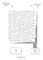
- FIG. 3Aillustrates an embodiment of a capacitive touch sensing system 300 that includes a capacitive sensor array 320 .
- Capacitive sensor array 320includes a plurality of row sensor elements 331 - 340 and a plurality of column sensor elements 341 - 348 .
- the row and column sensor elements 331 - 348are connected to a processing device 310 , which may include the functionality of capacitance sensor 101 , as illustrated in FIG. 2 .
- the processing device 370may perform TX-RX scans of the capacitive sensor array 320 to measure a mutual capacitance value associated with each of the intersections between a row sensor element and a column sensor element in the sensor array 320 .
- the measured capacitancesmay be further processed to determine centroid locations of one or more contacts at the capacitive sensor array 320 .
- the processing device 310is connected to a host 150 which may receive the measured capacitances or calculated centroid locations from the processing device 310 .
- FIG. 3Billustrates a closer view of capacitive sensor array 320 .
- the capacitive sensor array 320has a hollow diamond pattern.
- Each of the sensor elements 331 - 348 in the sensor array 320includes a number of sub-elements, and each of these sub-elements has a shape similar to a diamond, or a rotated square shape.
- Column sensor element 345for example, includes a number of sub-elements such as sub-element 356 .
- Each of the sub-elementsalso includes a cutout area to reduce the self capacitance of each of the sensor elements 331 - 348 , as compared to a diamond patterned sensor element without cutout areas.
- sub-element 356includes a cutout area 354 , which is an area of the sub-element 356 that lacks conductive material.
- the cutout areasmay be filled with conductive material or other material that is not electrically connected to their respective sensor elements.
- FIG. 3Bfurther illustrates an intersection 350 between column sensor element 344 and row sensor element 335 .
- unit cells of the capacitive sensor array 320may designate areas of the capacitive sensor array 320 associated with a single intersection between a row sensor element and a column sensor element.
- the unit cell 352corresponds to intersection 350 between sensor elements 344 and 335 .
- the trace pattern formed by the sensor elements within a unit cellis substantially similar to a trace pattern formed by sensor elements in each of the other unit cells.
- the width of a unit cellmay be approximately equal to the distance between corresponding features of adjacent unit cells.
- the width of unit cell 352may be approximately equal to the distance between intersection 350 and an adjacent intersection, such as the intersection between sensor element 345 and 335 .
- each unit cellis bounded by adjacent unit cells, such that there are no gaps between unit cells.
- each unit cellmay share its boundaries with unit cells associated with adjacent intersections.
- FIG. 3Cillustrates a detail view of unit cell 352 , including the perimeter of unit cell 352 and boundary lengths between the row sensor element 335 and the column sensor element 344 , according to an embodiment.
- the boundary length between a first sensor element and a second sensor elementmay include the set of points within a unit cell and on an edge of the first sensor element from which a straight line can be drawn to reach an edge of the second sensor element without first crossing over any portion of the first sensor element.
- the boundary length between row sensor element 335 and column sensor element 344includes the lengths of segments 372 , 374 , 376 , and 378 .
- Segments 372 , 374 , 376 , and 378mark the lengths of the edges of sensor element 335 from which a straight line can be drawn to an edge of sensor element 344 within unit cell 352 without first crossing sensor element 335 .
- An alternative way to measure boundary length between a row sensor element and a column sensor elementis to include all edge points of one sensor element that are within the unit cell and are also within a threshold distance from an edge of the other sensor element. For example, if the threshold distance is a radius R, the boundary length between row sensor element 335 and column sensor element 344 includes all the points on the edge of element 335 and within unit cell 352 that are less than the distance R from an edge of element 344 .
- the boundary length between sensor elements 335 and 344includes the lengths of segments 372 , 374 , 376 , and 378 , since every point on the edges of sensor element 335 corresponding to these segments is within the distance R from an edge of sensor element 344 .
- Rmay be chosen so that the edges of the cutout areas such as cutout area 354 are not included in the boundary length.
- a ratiomay be calculated between 1) the boundary length between the row sensor element 335 and the column sensor element 344 and 2) the perimeter of the unit cell 352 .
- the perimeter of the unit cell 352may be calculated by summing the lengths of segments 362 , 364 , 366 , and 368 , while the boundary lengths may be calculated by summing the segments 372 , 374 , 376 , and 378 .
- each of the segments 362 , 364 , 366 , and 368measures 1 unit in length, such that each of the segments 372 , 374 , 376 , and 378 , measures less than ⁇ square root over (2) ⁇ /2 units in length.
- the total boundary length between the sensor elements 335 and 344 within unit cell 352is therefore less than 4 ⁇ square root over (2) ⁇ /2, or 2 ⁇ square root over (2) ⁇ units in length. Since the perimeter of unit cell 352 is equal to 4 units, the ratio of the boundary length to the perimeter is less than 2 ⁇ square root over (2) ⁇ /4, or 2 ⁇ square root over (2) ⁇ /2. Thus, the ratio of the boundary length to the unit cell perimeter for a hollow diamond pattern as illustrated in FIGS. 3A-3C is less than ⁇ square root over (2) ⁇ /2 .
- a “dual hollow Manhattan” (DHM) rectangular pattern with subtraces and cutout areasmay be used to increase the boundary length between the row and column sensor elements, to achieve a ratio of boundary length to unit cell perimeter that is greater than ⁇ square root over (2) ⁇ /2. In one embodiment, this may result in a decrease of 20% or more in the signal disparity ratio.
- DLMdual hollow Manhattan
- FIG. 4Aillustrates a capacitive sensor array 400 having a DHM pattern.
- the unit cell 450is associated with at least one intersection (such as intersections 452 ) between the row sensor element 430 and the column sensor element 440 .
- unit cell 450may be defined as the largest contiguous area of the capacitive sensor array 400 that contains both the row sensor element 430 and the column sensor element 440 while excluding other sensor elements of the sensor array 400 .
- the size of unit cell 450may be less than the largest such contiguous area so that the unit cell 450 may share its boundaries with adjacent unit cells. In one embodiment, such adjacent unit cells do not overlap.
- the DHM patternalso includes a number of cutout areas (such as cutout area 454 ) within each unit cell to minimize self capacitance of each sensor element.
- each of the cutout areas of a row sensor elementcorresponds to a cutout area of a column sensor element.
- such corresponding cutout areasmay be concentric, so their boundaries are parallel.
- the DHM patternhas an increased boundary ratio as compared to the hollow diamond pattern because the DHM pattern includes more edges of the row sensor element that are adjacent to edges of the column sensor element.
- the trace pattern within unit cell 450for example, includes traces within the interior of the unit cell 450 , as well as near the edges of the unit cell 450 .
- Each of the edges of the row sensor element 430 within the unit cell 450contributes to the total boundary length, except for the edges of the four larger cutout areas.
- the ratio of boundary length to unit cell perimeteris greater than ⁇ square root over (2) ⁇ /2 since (assuming a similarly sized unit cell) the sum of these lengths is greater than the sum of the segments 372 , 374 , 376 , and 378 illustrated in FIG. 3C .
- Equation 1The relationship between boundary length and area of the unit cell for a DHM pattern can also be described by the following Equation 1:
- L BA CELL > 2 ⁇ 2 ⁇ ⁇ units - 1 ( Equation ⁇ ⁇ 1 )
- L Brepresents the boundary length in units
- a CELLrepresents an area of the unit cell in square units. Referring back to the hollow diamond pattern in FIG. 3C , if the length of each side of unit cell 352 is 1 unit, then the area A CELL of unit cell 352 is 1 square unit. Since boundary length L B is less than 2 ⁇ square root over (2) ⁇ units in length, the value of L B /A CELL is less than 2 ⁇ square root over (2) ⁇ units ⁇ 1 for the hollow diamond pattern. In contrast, the value of L B /A CELL for a DHM pattern is greater than 2 ⁇ square root over (2) ⁇ units ⁇ 1 because of the additional boundary length between the row sensor element 430 and column sensor element 440 .
- FIG. 4Billustrates a portion of a capacitive sensor array 401 having a DHM pattern formed by multiple layers of conductive material on a substrate, according to one embodiment.
- the row sensor element 431 and pieces of the column sensor element 441are situated in the same plane, while the connecting wires of the column sensor element 441 such as wires 455 , which connect the other pieces of column sensor element 441 , are situated in a different plane than the row sensor element 431 and the pieces of column sensor element 441 which they connect.
- Conductive elements in different planesmay be connected by vias such as vias 451 .
- FIG. 4Cillustrates a cross-sectional view of capacitive sensor array 401 along the cross-section line 451 , according to one embodiment.
- row sensor element 431 and parts of column sensor element 441are situated in the same plane, on one side of a dielectric material 457 , while the connecting wire 456 of the column sensor element 441 , which connects the other pieces of sensor element 441 , resides on a different side of the dielectric 457 .
- Vias 458are used to connect the row sensor element 431 on one side of the dielectric 457 to the connecting wire 456 on the other side of the dielectric 457 .
- the dielectricis a substrate, such as a printed circuit board (PCB) substrate.
- PCBprinted circuit board
- FIG. 4Dillustrates a cross-sectional view of an embodiment of a capacitive sensor array.
- the column sensor element 442may be a single printed trace that is situated over the dielectric material 459 , which is in turn situated over the top of the row sensor element 432 .
- the dielectric 459may be a printed dielectric, which is printed or otherwise deposited on top of the row sensor element 432 after sensor element 432 has been printed or deposited on the substrate 414 .
- the column sensor element 442may be printed or deposited on top of the dielectric 459 in one or more subsequent steps.
- FIG. 4Eillustrates an embodiment of a capacitive sensor array 404 having a filled DHM pattern.
- the cutout areas in the DHM pattern of sensor array 404may be substantially filled with conductive material that is connected to ground, such as ground plane 410 .
- the ground plane 410 and other ground planes in the sensor array 404may be connected to ground through one or more connecting wires 460 .
- These connecting wires 460may be situated on a different plane than the ground planes and the sensor elements, and may be connected to the ground planes through vias.
- FIG. 4Fillustrates one embodiment of a capacitive sensor array 405 having a DHM pattern.
- capacitive sensor array 405may have additional circuitry on a lower side of its substrate, which may include conductive traces or wires such as traces 412 and 413 .
- the traces 412 and 413may cross each other using an overpass segment 411 in a different plane than the traces 412 and 413 .
- the overpass segment 411may be, for example, in the same plane as the row and column sensor elements on the upper side of the substrate.
- the overpass segmentis connected to pieces of the trace 412 by one or more vias.
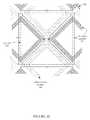
- FIG. 5illustrates a capacitive sensor array 500 having a quad spiral trace pattern, according to an embodiment.
- the quad spiral trace patternhas a longer boundary length between row and column sensor elements than the hollow diamond pattern.
- a row sensor element 560may intersect with a column sensor element 550 at intersection 530 , which is within the boundaries of unit cell 540 .
- row sensor element 560includes a main trace 510 which extends for the full length of row sensor element 560 .
- a number of traces, such as subtrace 520may extend from the main trace 510 .
- each of the subtraces of row sensor element 560 branching from the main trace 510are followed by a corresponding subtrace of the column sensor element 550 .
- the subtraces of the column sensor element 550may similarly branch from a main trace of the column sensor element 550 .
- the subtrace 520 branching from main trace 510 of the row sensor element 560corresponds to the subtrace 522 branching from the main trace 512 of column sensor element 550 .
- the subtraces 520 and 522form an interlocking spiral, thus increasing the boundary length between the subtraces 520 and 522 .
- Additional subtraces within the unit cell 540may be similarly patterned to further increase the boundary length between the row sensor element 560 and column sensor element 550 .
- the quad spiral patternincreases the boundary length between the row and column sensor elements such that the ratio of 1) the boundary length within a unit cell to 2) the perimeter of the unit cell is greater than the same ratio for a hollow diamond pattern.
- the ratio for the quad spiral patternis greater than ⁇ square root over (2) ⁇ /2.
- the ratio L B /A CELLis greater than 2 ⁇ square root over (2) ⁇ units ⁇ 1 .
- FIG. 6illustrates a capacitive sensor array 600 having interleaved traces, according to an embodiment.
- a unit cell 640is associated with an intersection 630 between the row sensor element 660 and column sensor element 650 .
- Row sensor element 660includes a main trace 610 and a number of subtraces such as subtraces 620 branching from the main trace 610 .
- Column sensor element 650includes a main trace 612 and a number of subtraces 622 branching from the main trace 612 .
- the subtraces 620 of the row sensor element 660are interleaved with the subtraces 612 of the column sensor element 650 .
- the interleaved patternincreases the boundary length between the row and column sensor elements such that the ratio of 1) the boundary length within a unit cell to 2) the perimeter of the unit cell is greater than the same ratio for a hollow diamond pattern.
- the ratio for the interleaved patternis greater than ⁇ square root over (2) ⁇ /2.
- the ratio L B /A CELLis greater than 2 ⁇ square root over (2) ⁇ units ⁇ 1 .
- trace patternsmay include features similar to those illustrated in FIGS. 4-6 , such as row and column sensor elements with cutout areas, corresponding parallel subtraces, and thin traces filling the majority of each unit cell.
- Embodiments of the present inventioninclude various operations. These operations may be performed by hardware components, software, firmware, or a combination thereof.
- the term “coupled to”may mean coupled directly or indirectly through one or more intervening components. Any of the signals provided over various buses described herein may be time multiplexed with other signals and provided over one or more common buses. Additionally, the interconnection between circuit components or blocks may be shown as buses or as single signal lines. Each of the buses may alternatively be one or more single signal lines and each of the single signal lines may alternatively be buses.
- Certain embodimentsmay be implemented as a computer program product that may include instructions stored on a computer-readable medium. These instructions may be used to program a general-purpose or special-purpose processor to perform the described operations.
- a computer-readable mediumincludes any mechanism for storing or transmitting information in a form (e.g., software, processing application) readable by a machine (e.g., a computer).
- the computer-readable storage mediummay include, but is not limited to, magnetic storage medium (e.g., floppy diskette); optical storage medium (e.g., CD-ROM); magneto-optical storage medium; read-only memory (ROM); random-access memory (RAM); erasable programmable memory (e.g., EPROM and EEPROM); flash memory, or another type of medium suitable for storing electronic instructions.
- magnetic storage mediume.g., floppy diskette
- optical storage mediume.g., CD-ROM
- magneto-optical storage mediume.g., magneto-optical storage medium
- ROMread-only memory
- RAMrandom-access memory
- EPROM and EEPROMerasable programmable memory
- flash memoryor another type of medium suitable for storing electronic instructions.
- some embodimentsmay be practiced in distributed computing environments where the computer-readable medium is stored on and/or executed by more than one computer system.
- the information transferred between computer systemsmay either be pulled or pushed across the transmission medium connecting the computer systems.
Landscapes
- Engineering & Computer Science (AREA)
- General Engineering & Computer Science (AREA)
- Theoretical Computer Science (AREA)
- Human Computer Interaction (AREA)
- Physics & Mathematics (AREA)
- General Physics & Mathematics (AREA)
- Position Input By Displaying (AREA)
- Measurement Of Length, Angles, Or The Like Using Electric Or Magnetic Means (AREA)
Abstract
Description
In
Claims (20)
Priority Applications (7)
| Application Number | Priority Date | Filing Date | Title |
|---|---|---|---|
| US13/008,014US9405408B2 (en) | 2010-01-15 | 2011-01-18 | Trace pattern for touch-sensing application |
| US13/198,717US8901944B2 (en) | 2010-01-15 | 2011-08-05 | Lattice structure for capacitance sensing electrodes |
| PCT/US2011/047094WO2012021524A2 (en) | 2010-08-09 | 2011-08-09 | Lattice structure for capacitance sensing electrodes |
| CN201180002808.8ACN102667693B (en) | 2010-08-09 | 2011-08-09 | Mesh structure for applications related to capacitive sensing electrodes |
| US13/247,922US9705495B2 (en) | 2010-01-15 | 2011-09-28 | Asymmetric sensor pattern |
| US14/557,254US9513755B2 (en) | 2010-01-15 | 2014-12-01 | Lattice structure for capacitance sensing electrodes |
| US15/014,277US9529485B2 (en) | 2010-01-15 | 2016-02-03 | Trace pattern for touch-sensing application |
Applications Claiming Priority (2)
| Application Number | Priority Date | Filing Date | Title |
|---|---|---|---|
| US29559910P | 2010-01-15 | 2010-01-15 | |
| US13/008,014US9405408B2 (en) | 2010-01-15 | 2011-01-18 | Trace pattern for touch-sensing application |
Related Child Applications (2)
| Application Number | Title | Priority Date | Filing Date |
|---|---|---|---|
| US13/198,717Continuation-In-PartUS8901944B2 (en) | 2010-01-15 | 2011-08-05 | Lattice structure for capacitance sensing electrodes |
| US15/014,277ContinuationUS9529485B2 (en) | 2010-01-15 | 2016-02-03 | Trace pattern for touch-sensing application |
Publications (2)
| Publication Number | Publication Date |
|---|---|
| US20120044193A1 US20120044193A1 (en) | 2012-02-23 |
| US9405408B2true US9405408B2 (en) | 2016-08-02 |
Family
ID=45593662
Family Applications (2)
| Application Number | Title | Priority Date | Filing Date |
|---|---|---|---|
| US13/008,014Active2034-01-17US9405408B2 (en) | 2010-01-15 | 2011-01-18 | Trace pattern for touch-sensing application |
| US15/014,277ActiveUS9529485B2 (en) | 2010-01-15 | 2016-02-03 | Trace pattern for touch-sensing application |
Family Applications After (1)
| Application Number | Title | Priority Date | Filing Date |
|---|---|---|---|
| US15/014,277ActiveUS9529485B2 (en) | 2010-01-15 | 2016-02-03 | Trace pattern for touch-sensing application |
Country Status (1)
| Country | Link |
|---|---|
| US (2) | US9405408B2 (en) |
Cited By (4)
| Publication number | Priority date | Publication date | Assignee | Title |
|---|---|---|---|---|
| US20170228572A1 (en)* | 2016-02-04 | 2017-08-10 | Superc-Touch Corporation | High-efficiency fingerprint identification device |
| US9829523B1 (en)* | 2012-12-27 | 2017-11-28 | Cypress Semiconductor Corporation | Offset sensor pattern |
| US10175838B2 (en)* | 2017-01-10 | 2019-01-08 | Semiconductor Components Industries, Llc | Methods and apparatus for a touch sensor |
| US10817111B1 (en)* | 2019-04-10 | 2020-10-27 | Semiconductor Components Industries, Llc | Methods and apparatus for a capacitive touch sensor |
Families Citing this family (32)
| Publication number | Priority date | Publication date | Assignee | Title |
|---|---|---|---|---|
| US9705495B2 (en) | 2010-01-15 | 2017-07-11 | Creator Technology B.V. | Asymmetric sensor pattern |
| US8901944B2 (en) | 2010-01-15 | 2014-12-02 | Cypress Semiconductor Corporation | Lattice structure for capacitance sensing electrodes |
| US9405408B2 (en) | 2010-01-15 | 2016-08-02 | Creator Technology B.V. | Trace pattern for touch-sensing application |
| US8482546B2 (en) | 2010-06-30 | 2013-07-09 | Cypress Semiconductor Corporation | Self shielding capacitance sensing panel |
| JP5806684B2 (en)* | 2011-01-11 | 2015-11-10 | アルプス電気株式会社 | Coordinate input device |
| JP5432193B2 (en)* | 2011-01-18 | 2014-03-05 | 株式会社ジャパンディスプレイ | Display device |
| US8638316B2 (en)* | 2011-03-11 | 2014-01-28 | Cypress Semiconductor Corporation | Two prong capacitive sensor pattern |
| TWI463626B (en)* | 2011-06-07 | 2014-12-01 | Novatek Microelectronics Corp | Touch panel and displaying apparatus |
| US9612265B1 (en) | 2011-09-23 | 2017-04-04 | Cypress Semiconductor Corporation | Methods and apparatus to detect a conductive object |
| CN103164093A (en)* | 2011-12-19 | 2013-06-19 | 禾瑞亚科技股份有限公司 | Capacitive touch screen |
| US8436627B1 (en) | 2012-03-16 | 2013-05-07 | Cypress Semiconductor Corporation | Serpentine touch sensor pattern |
| CN103576950B (en)* | 2012-07-24 | 2016-08-24 | 宸鸿科技(厦门)有限公司 | Contact panel and preparation method thereof |
| DE102012212931A1 (en)* | 2012-07-24 | 2014-01-30 | BSH Bosch und Siemens Hausgeräte GmbH | Touchpad for electrically detecting a touch |
| CN103268177B (en)* | 2012-12-19 | 2016-09-07 | 上海天马微电子有限公司 | Capacitive touch module and touch display device |
| EP2772837A1 (en)* | 2013-02-28 | 2014-09-03 | Nxp B.V. | Touch sensor for smartcard |
| US8872526B1 (en)* | 2013-09-10 | 2014-10-28 | Cypress Semiconductor Corporation | Interleaving sense elements of a capacitive-sense array |
| US20150091842A1 (en) | 2013-09-30 | 2015-04-02 | Synaptics Incorporated | Matrix sensor for image touch sensing |
| US10042489B2 (en)* | 2013-09-30 | 2018-08-07 | Synaptics Incorporated | Matrix sensor for image touch sensing |
| EP2958000B1 (en)* | 2014-05-30 | 2018-04-11 | Marvell World Trade Ltd. | Touch panel and touch detection circuit |
| CN105589586B (en)* | 2014-10-21 | 2019-06-14 | 宸鸿光电科技股份有限公司 | touch panel |
| US9310953B1 (en) | 2014-11-25 | 2016-04-12 | Cypress Semiconductor Corporation | Full-wave synchronous rectification for self-capacitance sensing |
| US20170240418A1 (en)* | 2016-02-18 | 2017-08-24 | Knowles Electronics, Llc | Low-cost miniature mems vibration sensor |
| US10969902B2 (en)* | 2016-07-19 | 2021-04-06 | Elo Touch Solutions, Inc. | Projected-capacitive (PCAP) touchscreen |
| US10802649B2 (en) | 2016-07-19 | 2020-10-13 | Elo Touch Solutions, Inc. | Projected-capacitive (PCAP) touchscreen |
| US20180088728A1 (en)* | 2016-09-23 | 2018-03-29 | Apple Inc. | Integrated force-sensitive touch screen |
| US9996194B1 (en)* | 2016-11-28 | 2018-06-12 | Stmicroelectronics Asia Pacific Pte Ltd | Touch screen self-capacitance foreign matter detection |
| GB2559572A (en)* | 2017-02-09 | 2018-08-15 | Solomon Systech Ltd | Touch sensor |
| GB2559571A (en)* | 2017-02-09 | 2018-08-15 | Solomon Systech Ltd | Touch sensor |
| CN108803910B (en) | 2017-04-28 | 2021-08-06 | 京东方科技集团股份有限公司 | Touch substrate and manufacturing method thereof, and touch display device |
| TWI655571B (en)* | 2018-01-18 | 2019-04-01 | 奕力科技股份有限公司 | Mutual touch panel |
| CN108803945B (en)* | 2018-09-05 | 2024-04-12 | 京东方科技集团股份有限公司 | Touch screen and display device |
| US11740706B2 (en)* | 2020-05-11 | 2023-08-29 | Darfon Electronics Corp. | Keyboard touch electrode module and touch keyboard therewith |
Citations (79)
| Publication number | Priority date | Publication date | Assignee | Title |
|---|---|---|---|---|
| US5099386A (en) | 1990-09-20 | 1992-03-24 | General Scanning, Inc. | Variable-capacitance position transducing |
| US6188391B1 (en) | 1998-07-09 | 2001-02-13 | Synaptics, Inc. | Two-layer capacitive touchpad and method of making same |
| US20020015024A1 (en) | 1998-01-26 | 2002-02-07 | University Of Delaware | Method and apparatus for integrating manual input |
| US20020098119A1 (en) | 1998-04-09 | 2002-07-25 | California Institute Of Technology | Electronic techniques for analyte detection |
| US6642857B1 (en) | 2000-01-19 | 2003-11-04 | Synaptics Incorporated | Capacitive pointing stick |
| US20040119701A1 (en) | 2002-12-19 | 2004-06-24 | Mulligan Roger C. | Lattice touch-sensing system |
| US20040130336A1 (en) | 2002-09-23 | 2004-07-08 | Stimicroelectronics Sa | Method of determining an electrical capacitance of a circuit component and method of defining a dimension of such a component |
| US20040252109A1 (en) | 2002-04-11 | 2004-12-16 | Synaptics, Inc. | Closed-loop sensor on a solid-state object position detector |
| US6925611B2 (en) | 2001-01-31 | 2005-08-02 | Microsoft Corporation | Navigational interface for mobile and wearable computers |
| US20060017710A1 (en) | 2004-07-26 | 2006-01-26 | Lee Joo-Hyung | Liquid crystal display device including sensing element |
| US7030860B1 (en) | 1999-10-08 | 2006-04-18 | Synaptics Incorporated | Flexible transparent touch sensing system for electronic devices |
| US20060097991A1 (en) | 2004-05-06 | 2006-05-11 | Apple Computer, Inc. | Multipoint touchscreen |
| US7129935B2 (en) | 2003-06-02 | 2006-10-31 | Synaptics Incorporated | Sensor patterns for a capacitive sensing apparatus |
| US20070008299A1 (en) | 2005-07-08 | 2007-01-11 | Harald Philipp | Two-Dimensional Position Sensor |
| US20070057167A1 (en) | 2005-09-09 | 2007-03-15 | Mackey Bob L | Polar sensor patterns |
| US20070074914A1 (en) | 2005-10-05 | 2007-04-05 | Geaghan Bernard O | Interleaved electrodes for touch sensing |
| US7202859B1 (en)* | 2002-08-09 | 2007-04-10 | Synaptics, Inc. | Capacitive sensing pattern |
| US20070176608A1 (en) | 2006-01-30 | 2007-08-02 | Mackey Bob L | Capacitive sensing apparatus designs |
| US20070229470A1 (en) | 2006-03-31 | 2007-10-04 | Warren Snyder | Capacitive touch sense device having polygonal shaped sensor elements |
| US20080007534A1 (en)* | 2006-07-10 | 2008-01-10 | Cypress Semiconductor Corporation | Touch-sensor with shared capacitive sensors |
| US20080006453A1 (en) | 2006-07-06 | 2008-01-10 | Apple Computer, Inc., A California Corporation | Mutual capacitance touch sensing device |
| US20080048997A1 (en)* | 1992-06-08 | 2008-02-28 | Synaptics Incorporated | Object position detector with edge motion feature and gesture recognition |
| US20080062139A1 (en) | 2006-06-09 | 2008-03-13 | Apple Inc. | Touch screen liquid crystal display |
| US20080111795A1 (en) | 2006-11-13 | 2008-05-15 | Apple Inc. | Method of capacitively sensing finger position |
| US20080165139A1 (en) | 2007-01-05 | 2008-07-10 | Apple Inc. | Touch screen stack-up processing |
| US20080165158A1 (en) | 2007-01-05 | 2008-07-10 | Apple Inc. | Touch screen stack-ups |
| US20080225015A1 (en) | 2007-03-13 | 2008-09-18 | Junji Hashida | Input device |
| US20080246496A1 (en) | 2007-04-05 | 2008-10-09 | Luben Hristov | Two-Dimensional Position Sensor |
| US20080264699A1 (en)* | 2007-04-27 | 2008-10-30 | Trendon Touch Technology Corp. | Conductor pattern structure of capacitive touch panel |
| US20080278178A1 (en)* | 2007-05-07 | 2008-11-13 | Harald Philipp | Capacative Position Sensor |
| US7453270B2 (en) | 2005-06-03 | 2008-11-18 | Synaptics Incorporated | Methods and systems for detecting a capacitance using sigma-delta measurement techniques |
| US7463246B2 (en) | 2002-06-25 | 2008-12-09 | Synaptics Incorporated | Capacitive sensing device |
| US20080309633A1 (en) | 2007-06-13 | 2008-12-18 | Apple Inc. | Touch-sensitive display |
| US20090051863A1 (en) | 2007-02-07 | 2009-02-26 | Green Cloak Llc | Displays including addressible trace structures |
| US20090159344A1 (en) | 2007-12-21 | 2009-06-25 | Apple Inc. | Touch pad electrode design |
| US20090262092A1 (en) | 2003-07-03 | 2009-10-22 | Donnelly Corporation | Capacitive touch screen suitable for use in an interactive information display |
| US20090273570A1 (en) | 2008-04-30 | 2009-11-05 | Apple Inc. | Multi-touch sensor patterns and stack-ups |
| US20090309616A1 (en) | 2008-06-13 | 2009-12-17 | Sony Ericsson Mobile Communications Ab | Touch and force sensing for input devices |
| JP2010002958A (en) | 2008-06-18 | 2010-01-07 | Epson Imaging Devices Corp | Capacitance input device, and display device with input function |
| US20100020032A1 (en) | 2008-07-25 | 2010-01-28 | Hitachi Displays, Ltd. | Display Device |
| US20100026655A1 (en) | 2008-07-31 | 2010-02-04 | Avago Technologies Ecbu Ip (Singapore) Pte. Ltd. | Capacitive Touchscreen or Touchpad for Finger or Stylus |
| US20100045632A1 (en) | 2008-04-10 | 2010-02-25 | Atmel Corporation | Capacitive Position Sensor |
| US20100059294A1 (en) | 2008-09-08 | 2010-03-11 | Apple Inc. | Bandwidth enhancement for a touch sensor panel |
| US20100060300A1 (en) | 2004-12-23 | 2010-03-11 | Fraunhofer-Gesellschaft Zur Forderung Der Angewandten Forschung E.V | Sensor system and methods for the capacitive measurement of electromagnetic signals having a biological origin |
| KR20100031242A (en) | 2008-09-12 | 2010-03-22 | 엘지디스플레이 주식회사 | Liquid crystal display device embedded touch panel therein |
| US20100079384A1 (en) | 2008-09-26 | 2010-04-01 | Cypress Semiconductor Corporation | Capacitance touch screen |
| US20100110038A1 (en) | 2008-10-31 | 2010-05-06 | Michael Mo | Mutual capacitance touch screen and combined mutual capacitance touch screen |
| US20100128002A1 (en) | 2008-11-26 | 2010-05-27 | William Stacy | Touch-sensitive display method and apparatus |
| US20100149108A1 (en) | 2008-12-11 | 2010-06-17 | Steve Porter Hotelling | Single layer touch panel with segmented drive and sense electrodes |
| US7741896B2 (en) | 2008-02-15 | 2010-06-22 | Avago Technologies Ecbu Ip (Singapore) Pte. Ltd. | High voltage drive circuit employing capacitive signal coupling and associated devices and methods |
| US20100156811A1 (en) | 2008-12-22 | 2010-06-24 | Ding Hua Long | New pattern design for a capacitive touch screen |
| KR20100070964A (en) | 2008-12-18 | 2010-06-28 | (주)에릭소코퍼레이션 | Pattern structure of the touch panel using electrostatic capacitive type |
| US20100164881A1 (en) | 2008-12-25 | 2010-07-01 | Au Optronics Corp. | Touch Panel Structure |
| US20100164889A1 (en) | 2008-12-26 | 2010-07-01 | Luben Hristov | Multiple electrode touch sensitive device |
| US20100182275A1 (en) | 2009-01-20 | 2010-07-22 | Hitachi Displays, Ltd. | Display device |
| US20100201633A1 (en) | 2009-02-09 | 2010-08-12 | Ocular Lcd Inc. | Touch screen with improved optical performace |
| US20100224424A1 (en) | 2009-01-07 | 2010-09-09 | Rohm Co., Ltd. | Input device |
| US20100231555A1 (en) | 2004-08-19 | 2010-09-16 | Bob Lee Mackey | Capacitive sensing apparatus |
| US20100292945A1 (en) | 2009-05-13 | 2010-11-18 | Joseph Kurth Reynolds | Capacitive sensor device |
| US20100302206A1 (en) | 2009-06-01 | 2010-12-02 | Ming-Chang Yu | Touch sensing display and touch panel thereof |
| US20100302201A1 (en) | 2009-06-02 | 2010-12-02 | Avago Technologies Ecbu (Singapore) Pte. Ltd. | Sensor Patterns for Mutual Capacitance Touchscreens |
| US7859521B2 (en) | 2009-02-02 | 2010-12-28 | Apple Inc. | Integrated touch screen |
| US20100328255A1 (en) | 2009-06-30 | 2010-12-30 | Sony Corporation | Touch detection device and display device having touch sensor function |
| US20110001723A1 (en) | 2009-07-01 | 2011-01-06 | Hsiang-Pin Fan | Touch panel and sensing method thereof |
| US20110012842A1 (en) | 2008-09-26 | 2011-01-20 | Tovis Co., Ltd. | Touch panel using tempered glass |
| US7920129B2 (en) | 2007-01-03 | 2011-04-05 | Apple Inc. | Double-sided touch-sensitive panel with shield and drive combined layer |
| US7932898B2 (en) | 2005-09-20 | 2011-04-26 | Atmel Corporation | Touch sensitive screen |
| US20110134073A1 (en) | 2008-07-04 | 2011-06-09 | Young Soo Ahn | Touch panel device of digital capacitive coupling type with high sensitivity |
| US7965281B2 (en) | 2006-10-03 | 2011-06-21 | Synaptics, Inc. | Unambiguous capacitance sensing using shared inputs |
| US20110261003A1 (en) | 2010-04-21 | 2011-10-27 | Samsung Electro-Mechanics Co., Ltd. | Display device having capacitive touch screen |
| US20110316567A1 (en) | 2010-01-15 | 2011-12-29 | Cypress Semiconductor Corporation | Lattice Structure for Capacitance Sensing Electrodes |
| US20120044193A1 (en) | 2010-01-15 | 2012-02-23 | Cypress Semiconductor Corporation | Trace pattern for touch-sensing application |
| US20120044198A1 (en) | 2010-06-30 | 2012-02-23 | Cypress Semiconductor Corporation | Self shielding capacitance sensing panel |
| US20120133611A1 (en) | 2010-01-15 | 2012-05-31 | Cypress Semiconductor Corporation | Asymmetric Sensor Pattern |
| US8217916B2 (en) | 2008-06-30 | 2012-07-10 | Hitachi Displays, Ltd. | Display device with touch panel |
| US20120229417A1 (en) | 2011-03-11 | 2012-09-13 | Cypress Semiconductor Corporation | Two Prong Capacitive Sensor Pattern |
| US8410795B1 (en) | 2012-03-16 | 2013-04-02 | Cypress Semiconductor Corporation | Serpentine touch sensor pattern |
| US20130169582A1 (en) | 2012-01-01 | 2013-07-04 | Cypress Semiconductor Corporation | Contact identification and tracking on a capacitance sensing array |
| US8525799B1 (en)* | 2007-04-24 | 2013-09-03 | Cypress Semiconductor Conductor | Detecting multiple simultaneous touches on a touch-sensor device |
Family Cites Families (1)
| Publication number | Priority date | Publication date | Assignee | Title |
|---|---|---|---|---|
| US8269744B2 (en)* | 2008-09-05 | 2012-09-18 | Mitsubishi Electric Corporation | Touch screen, touch panel and display device |
- 2011
- 2011-01-18USUS13/008,014patent/US9405408B2/enactiveActive
- 2016
- 2016-02-03USUS15/014,277patent/US9529485B2/enactiveActive
Patent Citations (85)
| Publication number | Priority date | Publication date | Assignee | Title |
|---|---|---|---|---|
| US5099386A (en) | 1990-09-20 | 1992-03-24 | General Scanning, Inc. | Variable-capacitance position transducing |
| US20080048997A1 (en)* | 1992-06-08 | 2008-02-28 | Synaptics Incorporated | Object position detector with edge motion feature and gesture recognition |
| US20070139395A1 (en) | 1998-01-26 | 2007-06-21 | Fingerworks, Inc. | Ellipse Fitting for Multi-Touch Surfaces |
| US20020015024A1 (en) | 1998-01-26 | 2002-02-07 | University Of Delaware | Method and apparatus for integrating manual input |
| US20020098119A1 (en) | 1998-04-09 | 2002-07-25 | California Institute Of Technology | Electronic techniques for analyte detection |
| US6627154B1 (en) | 1998-04-09 | 2003-09-30 | Cyrano Sciences Inc. | Electronic techniques for analyte detection |
| US6188391B1 (en) | 1998-07-09 | 2001-02-13 | Synaptics, Inc. | Two-layer capacitive touchpad and method of making same |
| US7030860B1 (en) | 1999-10-08 | 2006-04-18 | Synaptics Incorporated | Flexible transparent touch sensing system for electronic devices |
| US6642857B1 (en) | 2000-01-19 | 2003-11-04 | Synaptics Incorporated | Capacitive pointing stick |
| US6925611B2 (en) | 2001-01-31 | 2005-08-02 | Microsoft Corporation | Navigational interface for mobile and wearable computers |
| US20040252109A1 (en) | 2002-04-11 | 2004-12-16 | Synaptics, Inc. | Closed-loop sensor on a solid-state object position detector |
| US7463246B2 (en) | 2002-06-25 | 2008-12-09 | Synaptics Incorporated | Capacitive sensing device |
| US7202859B1 (en)* | 2002-08-09 | 2007-04-10 | Synaptics, Inc. | Capacitive sensing pattern |
| US20040130336A1 (en) | 2002-09-23 | 2004-07-08 | Stimicroelectronics Sa | Method of determining an electrical capacitance of a circuit component and method of defining a dimension of such a component |
| US20040119701A1 (en) | 2002-12-19 | 2004-06-24 | Mulligan Roger C. | Lattice touch-sensing system |
| US7129935B2 (en) | 2003-06-02 | 2006-10-31 | Synaptics Incorporated | Sensor patterns for a capacitive sensing apparatus |
| US20090262092A1 (en) | 2003-07-03 | 2009-10-22 | Donnelly Corporation | Capacitive touch screen suitable for use in an interactive information display |
| US20060097991A1 (en) | 2004-05-06 | 2006-05-11 | Apple Computer, Inc. | Multipoint touchscreen |
| US7663607B2 (en) | 2004-05-06 | 2010-02-16 | Apple Inc. | Multipoint touchscreen |
| US20060017710A1 (en) | 2004-07-26 | 2006-01-26 | Lee Joo-Hyung | Liquid crystal display device including sensing element |
| US20100231555A1 (en) | 2004-08-19 | 2010-09-16 | Bob Lee Mackey | Capacitive sensing apparatus |
| US20100060300A1 (en) | 2004-12-23 | 2010-03-11 | Fraunhofer-Gesellschaft Zur Forderung Der Angewandten Forschung E.V | Sensor system and methods for the capacitive measurement of electromagnetic signals having a biological origin |
| US7453270B2 (en) | 2005-06-03 | 2008-11-18 | Synaptics Incorporated | Methods and systems for detecting a capacitance using sigma-delta measurement techniques |
| US20070008299A1 (en) | 2005-07-08 | 2007-01-11 | Harald Philipp | Two-Dimensional Position Sensor |
| US20070057167A1 (en) | 2005-09-09 | 2007-03-15 | Mackey Bob L | Polar sensor patterns |
| US7932898B2 (en) | 2005-09-20 | 2011-04-26 | Atmel Corporation | Touch sensitive screen |
| US20070074914A1 (en) | 2005-10-05 | 2007-04-05 | Geaghan Bernard O | Interleaved electrodes for touch sensing |
| US20070176608A1 (en) | 2006-01-30 | 2007-08-02 | Mackey Bob L | Capacitive sensing apparatus designs |
| US20070229470A1 (en) | 2006-03-31 | 2007-10-04 | Warren Snyder | Capacitive touch sense device having polygonal shaped sensor elements |
| US20080062139A1 (en) | 2006-06-09 | 2008-03-13 | Apple Inc. | Touch screen liquid crystal display |
| US20080006453A1 (en) | 2006-07-06 | 2008-01-10 | Apple Computer, Inc., A California Corporation | Mutual capacitance touch sensing device |
| US20080007534A1 (en)* | 2006-07-10 | 2008-01-10 | Cypress Semiconductor Corporation | Touch-sensor with shared capacitive sensors |
| US7965281B2 (en) | 2006-10-03 | 2011-06-21 | Synaptics, Inc. | Unambiguous capacitance sensing using shared inputs |
| US20080111795A1 (en) | 2006-11-13 | 2008-05-15 | Apple Inc. | Method of capacitively sensing finger position |
| US7920129B2 (en) | 2007-01-03 | 2011-04-05 | Apple Inc. | Double-sided touch-sensitive panel with shield and drive combined layer |
| US20080165139A1 (en) | 2007-01-05 | 2008-07-10 | Apple Inc. | Touch screen stack-up processing |
| US20080165158A1 (en) | 2007-01-05 | 2008-07-10 | Apple Inc. | Touch screen stack-ups |
| US20090051863A1 (en) | 2007-02-07 | 2009-02-26 | Green Cloak Llc | Displays including addressible trace structures |
| US20080225015A1 (en) | 2007-03-13 | 2008-09-18 | Junji Hashida | Input device |
| US7940251B2 (en) | 2007-03-13 | 2011-05-10 | Alps Electric Co., Ltd. | Input device |
| US20080246496A1 (en) | 2007-04-05 | 2008-10-09 | Luben Hristov | Two-Dimensional Position Sensor |
| US7808255B2 (en) | 2007-04-05 | 2010-10-05 | Atmel Corporation | Two-dimensional position sensor |
| US8525799B1 (en)* | 2007-04-24 | 2013-09-03 | Cypress Semiconductor Conductor | Detecting multiple simultaneous touches on a touch-sensor device |
| US20080264699A1 (en)* | 2007-04-27 | 2008-10-30 | Trendon Touch Technology Corp. | Conductor pattern structure of capacitive touch panel |
| US20080278178A1 (en)* | 2007-05-07 | 2008-11-13 | Harald Philipp | Capacative Position Sensor |
| US20080309633A1 (en) | 2007-06-13 | 2008-12-18 | Apple Inc. | Touch-sensitive display |
| US20090159344A1 (en) | 2007-12-21 | 2009-06-25 | Apple Inc. | Touch pad electrode design |
| US7741896B2 (en) | 2008-02-15 | 2010-06-22 | Avago Technologies Ecbu Ip (Singapore) Pte. Ltd. | High voltage drive circuit employing capacitive signal coupling and associated devices and methods |
| US20100045632A1 (en) | 2008-04-10 | 2010-02-25 | Atmel Corporation | Capacitive Position Sensor |
| US20100044122A1 (en) | 2008-04-10 | 2010-02-25 | Atmel Corporation | Capacitive Touch Screen with Noise Suppression |
| US20090273570A1 (en) | 2008-04-30 | 2009-11-05 | Apple Inc. | Multi-touch sensor patterns and stack-ups |
| US20090309616A1 (en) | 2008-06-13 | 2009-12-17 | Sony Ericsson Mobile Communications Ab | Touch and force sensing for input devices |
| JP2010002958A (en) | 2008-06-18 | 2010-01-07 | Epson Imaging Devices Corp | Capacitance input device, and display device with input function |
| US8217916B2 (en) | 2008-06-30 | 2012-07-10 | Hitachi Displays, Ltd. | Display device with touch panel |
| US20110134073A1 (en) | 2008-07-04 | 2011-06-09 | Young Soo Ahn | Touch panel device of digital capacitive coupling type with high sensitivity |
| US20100020032A1 (en) | 2008-07-25 | 2010-01-28 | Hitachi Displays, Ltd. | Display Device |
| US20100026655A1 (en) | 2008-07-31 | 2010-02-04 | Avago Technologies Ecbu Ip (Singapore) Pte. Ltd. | Capacitive Touchscreen or Touchpad for Finger or Stylus |
| US20100059294A1 (en) | 2008-09-08 | 2010-03-11 | Apple Inc. | Bandwidth enhancement for a touch sensor panel |
| KR20100031242A (en) | 2008-09-12 | 2010-03-22 | 엘지디스플레이 주식회사 | Liquid crystal display device embedded touch panel therein |
| US20100079384A1 (en) | 2008-09-26 | 2010-04-01 | Cypress Semiconductor Corporation | Capacitance touch screen |
| US20110012842A1 (en) | 2008-09-26 | 2011-01-20 | Tovis Co., Ltd. | Touch panel using tempered glass |
| US20100110038A1 (en) | 2008-10-31 | 2010-05-06 | Michael Mo | Mutual capacitance touch screen and combined mutual capacitance touch screen |
| US20100128002A1 (en) | 2008-11-26 | 2010-05-27 | William Stacy | Touch-sensitive display method and apparatus |
| US20100149108A1 (en) | 2008-12-11 | 2010-06-17 | Steve Porter Hotelling | Single layer touch panel with segmented drive and sense electrodes |
| KR20100070964A (en) | 2008-12-18 | 2010-06-28 | (주)에릭소코퍼레이션 | Pattern structure of the touch panel using electrostatic capacitive type |
| US20100156811A1 (en) | 2008-12-22 | 2010-06-24 | Ding Hua Long | New pattern design for a capacitive touch screen |
| US20100164881A1 (en) | 2008-12-25 | 2010-07-01 | Au Optronics Corp. | Touch Panel Structure |
| US20100164889A1 (en) | 2008-12-26 | 2010-07-01 | Luben Hristov | Multiple electrode touch sensitive device |
| US20100224424A1 (en) | 2009-01-07 | 2010-09-09 | Rohm Co., Ltd. | Input device |
| US20100182275A1 (en) | 2009-01-20 | 2010-07-22 | Hitachi Displays, Ltd. | Display device |
| US7859521B2 (en) | 2009-02-02 | 2010-12-28 | Apple Inc. | Integrated touch screen |
| US20100201633A1 (en) | 2009-02-09 | 2010-08-12 | Ocular Lcd Inc. | Touch screen with improved optical performace |
| US20100292945A1 (en) | 2009-05-13 | 2010-11-18 | Joseph Kurth Reynolds | Capacitive sensor device |
| US20100302206A1 (en) | 2009-06-01 | 2010-12-02 | Ming-Chang Yu | Touch sensing display and touch panel thereof |
| US20100302201A1 (en) | 2009-06-02 | 2010-12-02 | Avago Technologies Ecbu (Singapore) Pte. Ltd. | Sensor Patterns for Mutual Capacitance Touchscreens |
| US20100328255A1 (en) | 2009-06-30 | 2010-12-30 | Sony Corporation | Touch detection device and display device having touch sensor function |
| US20110001723A1 (en) | 2009-07-01 | 2011-01-06 | Hsiang-Pin Fan | Touch panel and sensing method thereof |
| US20110316567A1 (en) | 2010-01-15 | 2011-12-29 | Cypress Semiconductor Corporation | Lattice Structure for Capacitance Sensing Electrodes |
| US20120044193A1 (en) | 2010-01-15 | 2012-02-23 | Cypress Semiconductor Corporation | Trace pattern for touch-sensing application |
| US20120133611A1 (en) | 2010-01-15 | 2012-05-31 | Cypress Semiconductor Corporation | Asymmetric Sensor Pattern |
| US20110261003A1 (en) | 2010-04-21 | 2011-10-27 | Samsung Electro-Mechanics Co., Ltd. | Display device having capacitive touch screen |
| US20120044198A1 (en) | 2010-06-30 | 2012-02-23 | Cypress Semiconductor Corporation | Self shielding capacitance sensing panel |
| US20120229417A1 (en) | 2011-03-11 | 2012-09-13 | Cypress Semiconductor Corporation | Two Prong Capacitive Sensor Pattern |
| US20130169582A1 (en) | 2012-01-01 | 2013-07-04 | Cypress Semiconductor Corporation | Contact identification and tracking on a capacitance sensing array |
| US8410795B1 (en) | 2012-03-16 | 2013-04-02 | Cypress Semiconductor Corporation | Serpentine touch sensor pattern |
Non-Patent Citations (35)
| Title |
|---|
| Barrett, G. Projected-Capacitive Touch Technology. Information Display [online]. Mar. 2010,vol. 26 No. 3, p. 16-21 [retrieved on Aug. 4, 2011]. Retrieved from the Intemet. |
| Barrett, G. Projected-Capacitive Touch Technology. Information Display [online]. Mar. 2010,vol. 26 No. 3, p. 16-21 [retrieved on Aug. 4, 2011]. Retrieved from the Intemet<URL:http://walkermobile.com/March-2010-Information-Display-Magazine.pdf>. |
| Gary Barrett and Ryomei Omote, Projected-Capacitive Touch Technology, Frontline Technology, Information Display 26, No. 3, Mar. 2010. |
| International Search Report and Written Opinion of the International Searching Authority for International Application No. PCT/US11/47094 dated Feb. 23, 2012; 6 pages. |
| International Search Report for International Application No. PCT/US11/66509 dated Apr. 19, 2012; 2 pages. |
| Jing Wu, et al., "A High Sensitivity Capacitive Fingerprint Sensor with Double Sensing Plates", IEEE Xplore, Oct. 2004; accessed from http://ieeexplore.ieee.org/xpl/freeabs-all.jsp?reload=true&arnumber=1436920; 4 pages. |
| Lee, M. The Art of Capacitive Touch Sensing. EE Times, Design Article [online]. Mar. 1, 2006 [retrieved on Aug. 4, 2011]. Retrieved from the Internet. |
| Lee, M. The Art of Capacitive Touch Sensing. EE Times, Design Article [online]. Mar. 1, 2006 [retrieved on Aug. 4, 2011]. Retrieved from the Internet<URL:http://www.etimes.com/design/analog-design/4009622/The-art-of-capacitive-touch-sensing>. |
| Otmar Hilliges, Bringing the Physical to the Digital: A New Model for Tabletop Interaction, LMU, Munchen 2009. |
| Paul Dietz and Darren Leigh, DiamondTouch: a multi-user touch technology, UIST '01 Proceedings of the 14th annual ACM symposium on User interface software and technology, pp. 219-226, New York, NY, USA 2001. |
| SIPO Office Action for Application No. 201180002808.8 dated May 5, 2015; 3 pages. |
| SIPO Office Action for Application No. 201180002808.8 dated Nov. 13, 2015; 4 pages. |
| SIPO Office Action for Chinese Application No. 201180070734.1 dated Aug. 26, 2014; 7 pages. |
| SIPO Office Action for Chinese Application No. 201180070734.1 dated Jun. 9, 2015; 7 pages. |
| Timothy Hoye, et al., "Touch Screens: A Pressing Technology", University of Pittsburgh Tenth Annual Freshman Conference, dated Apr. 10, 2010; 6 pages. |
| Tsz-Kin Ho et al., "Simple Single-Layer Multi-Touch Projected Capacitive Touch Panel", Center for Display Research, Department of Electronic and Computer Engineering Hong Kong University of Science and Technology; Clear Water Bay, Hong Kong; 4 pages. |
| USPTO Advisory Action for U.S. Appl. No. 13/198,2014 dated Jul. 21, 2014; 5 pages. |
| USPTO Advisory Action for U.S. Appl. No. 13/247,922 dated Feb. 13, 2015; 3 pages. |
| USPTO Advisory Action for U.S. Appl. No. 13/247,922 dated May 16, 2014; 3 pages. |
| USPTO Final Rejection for U.S. Appl. No. 13/198,717 dated Apr. 10, 2014; 28 pages. |
| USPTO Final Rejection for U.S. Appl. No. 13/247,922 dated Mar. 12, 2014; 20 pages. |
| USPTO Final Rejection for U.S. Appl. No. 13/247,922 dated Nov. 26, 2014; 23 pages. |
| USPTO Non Final Rejection for U.S. Appl. No. 13/247,922 dated Oct. 3, 2013; 20 pages. |
| USPTO Non-Final Rejection for U.S. Appl. No. 13/198,2014 dated Jan. 22, 2014; 27 pages. |
| USPTO Non-Final Rejection for U.S. Appl. No. 13/247,922 dated Aug. 15, 2014; 21 pages. |
| USPTO Non-Final Rejection for U.S. Appl. No. 13/247,922 dated Dec. 4, 2015; 22 pages. |
| USPTO Non-Final Rejection for U.S. Appl. No. 13/923,037 dated Apr. 17, 2015; 12 pages. |
| USPTO Notice of Allowance for U.S. Appl. No. 13/172,749 dated Mar. 19, 2013; 10 pages. |
| USPTO Notice of Allowance for U.S. Appl. No. 13/172,749 dated May 9, 2013; 6 pages. |
| USPTO Notice of Allowance for U.S. Appl. No. 13/198,2014 dated Sep. 18, 2014; 8 pages. |
| USPTO Notice of Allowance for U.S. Appl. No. 13/247,867 dated Dec. 6, 2013; 10 pages. |
| USPTO Notice of Allowance for U.S. Appl. No. 13/247,867 dated Oct. 21, 2013; 10 pages. |
| USPTO Notice of Allowance for U.S. Appl. No. 13/923,037 dated Jun. 25, 2015; 5 pages. |
| USPTO Notice of Allowance for U.S. Appl. No. 3/198,2014 dated Aug. 19, 2014; 8 pages. |
| Written Opinion of the International Searching Authority for International Application No. PCT/US11/66509 mailed Apr. 19, 2012; 6 pages. |
Cited By (5)
| Publication number | Priority date | Publication date | Assignee | Title |
|---|---|---|---|---|
| US9829523B1 (en)* | 2012-12-27 | 2017-11-28 | Cypress Semiconductor Corporation | Offset sensor pattern |
| US20170228572A1 (en)* | 2016-02-04 | 2017-08-10 | Superc-Touch Corporation | High-efficiency fingerprint identification device |
| US10192092B2 (en)* | 2016-02-04 | 2019-01-29 | Superc-Touch Corporation | High-efficiency fingerprint identification device |
| US10175838B2 (en)* | 2017-01-10 | 2019-01-08 | Semiconductor Components Industries, Llc | Methods and apparatus for a touch sensor |
| US10817111B1 (en)* | 2019-04-10 | 2020-10-27 | Semiconductor Components Industries, Llc | Methods and apparatus for a capacitive touch sensor |
Also Published As
| Publication number | Publication date |
|---|---|
| US20160291728A1 (en) | 2016-10-06 |
| US9529485B2 (en) | 2016-12-27 |
| US20120044193A1 (en) | 2012-02-23 |
Similar Documents
| Publication | Publication Date | Title |
|---|---|---|
| US9529485B2 (en) | Trace pattern for touch-sensing application | |
| US10402022B2 (en) | Sensor array with edge pattern | |
| US9513755B2 (en) | Lattice structure for capacitance sensing electrodes | |
| US8436627B1 (en) | Serpentine touch sensor pattern | |
| US9547031B2 (en) | Flipped cell sensor pattern | |
| US9292138B2 (en) | Single layer sensor pattern | |
| US10073563B2 (en) | Touch sensor pattern | |
| US9201106B1 (en) | Self shielding capacitance sensing panel | |
| US9658726B2 (en) | Single layer sensor pattern | |
| US8638316B2 (en) | Two prong capacitive sensor pattern | |
| US9454268B2 (en) | Force sensing capacitive hybrid touch sensor | |
| US9454274B1 (en) | All points addressable touch sensing surface | |
| US8723825B2 (en) | Predictive touch surface scanning | |
| US9829523B1 (en) | Offset sensor pattern | |
| US9705495B2 (en) | Asymmetric sensor pattern | |
| US20140285469A1 (en) | Predictive Touch Surface Scanning | |
| WO2012021524A2 (en) | Lattice structure for capacitance sensing electrodes | |
| US9495050B1 (en) | Sensor pattern with signal-spreading electrodes |
Legal Events
| Date | Code | Title | Description |
|---|---|---|---|
| AS | Assignment | Owner name:CYPRESS SEMICONDUCTOR CORPORATION, CALIFORNIA Free format text:ASSIGNMENT OF ASSIGNORS INTEREST;ASSIGNORS:PENG, TAO;WENG, XIAOPING;SHAO, DANGDANG;AND OTHERS;REEL/FRAME:026286/0899 Effective date:20110121 | |
| AS | Assignment | Owner name:MORGAN STANLEY SENIOR FUNDING, INC., NEW YORK Free format text:PATENT SECURITY AGREEMENT;ASSIGNOR:CYPRESS SEMICONDUCTOR CORPORATION;REEL/FRAME:028863/0870 Effective date:20120822 | |
| AS | Assignment | Owner name:MORGAN STANLEY SENIOR FUNDING, INC., NEW YORK Free format text:SECURITY INTEREST;ASSIGNORS:CYPRESS SEMICONDUCTOR CORPORATION;SPANSION LLC;REEL/FRAME:035240/0429 Effective date:20150312 | |
| AS | Assignment | Owner name:CREATOR TECHNOLOGY B.V., NETHERLANDS Free format text:ASSIGNMENT OF ASSIGNORS INTEREST;ASSIGNOR:CYPRESS SEMICONDUCTOR CORPORATION;REEL/FRAME:038259/0864 Effective date:20160226 | |
| STCF | Information on status: patent grant | Free format text:PATENTED CASE | |
| MAFP | Maintenance fee payment | Free format text:PAYMENT OF MAINTENANCE FEE, 4TH YR, SMALL ENTITY (ORIGINAL EVENT CODE: M2551); ENTITY STATUS OF PATENT OWNER: SMALL ENTITY Year of fee payment:4 | |
| AS | Assignment | Owner name:MORGAN STANLEY SENIOR FUNDING, INC., NEW YORK Free format text:CORRECTIVE ASSIGNMENT TO CORRECT THE 8647899 PREVIOUSLY RECORDED ON REEL 035240 FRAME 0429. ASSIGNOR(S) HEREBY CONFIRMS THE SECURITY INTERST;ASSIGNORS:CYPRESS SEMICONDUCTOR CORPORATION;SPANSION LLC;REEL/FRAME:058002/0470 Effective date:20150312 | |
| AS | Assignment | Owner name:WISTRON CORPORATION, TAIWAN Free format text:ASSIGNMENT OF ASSIGNORS INTEREST;ASSIGNOR:CREATOR TECHNOLOGY B.V.;REEL/FRAME:055829/0838 Effective date:20210331 | |
| FEPP | Fee payment procedure | Free format text:ENTITY STATUS SET TO UNDISCOUNTED (ORIGINAL EVENT CODE: BIG.); ENTITY STATUS OF PATENT OWNER: LARGE ENTITY | |
| AS | Assignment | Owner name:SPANSION LLC, CALIFORNIA Free format text:RELEASE BY SECURED PARTY;ASSIGNOR:MUFG UNION BANK, N.A.;REEL/FRAME:059410/0438 Effective date:20200416 Owner name:CYPRESS SEMICONDUCTOR CORPORATION, CALIFORNIA Free format text:RELEASE BY SECURED PARTY;ASSIGNOR:MUFG UNION BANK, N.A.;REEL/FRAME:059410/0438 Effective date:20200416 | |
| MAFP | Maintenance fee payment | Free format text:PAYMENT OF MAINTENANCE FEE, 8TH YEAR, LARGE ENTITY (ORIGINAL EVENT CODE: M1552); ENTITY STATUS OF PATENT OWNER: LARGE ENTITY Year of fee payment:8 |