US9405388B2 - Full perimeter chemical strengthening of substrates - Google Patents
Full perimeter chemical strengthening of substratesDownload PDFInfo
- Publication number
- US9405388B2 US9405388B2US12/885,376US88537610AUS9405388B2US 9405388 B2US9405388 B2US 9405388B2US 88537610 AUS88537610 AUS 88537610AUS 9405388 B2US9405388 B2US 9405388B2
- Authority
- US
- United States
- Prior art keywords
- glass substrate
- sealant
- conductive traces
- substrate
- separation
- Prior art date
- Legal status (The legal status is an assumption and is not a legal conclusion. Google has not performed a legal analysis and makes no representation as to the accuracy of the status listed.)
- Active, expires
Links
Images


Classifications
- G—PHYSICS
- G06—COMPUTING OR CALCULATING; COUNTING
- G06F—ELECTRIC DIGITAL DATA PROCESSING
- G06F3/00—Input arrangements for transferring data to be processed into a form capable of being handled by the computer; Output arrangements for transferring data from processing unit to output unit, e.g. interface arrangements
- G06F3/01—Input arrangements or combined input and output arrangements for interaction between user and computer
- G06F3/03—Arrangements for converting the position or the displacement of a member into a coded form
- G06F3/041—Digitisers, e.g. for touch screens or touch pads, characterised by the transducing means
- C—CHEMISTRY; METALLURGY
- C03—GLASS; MINERAL OR SLAG WOOL
- C03C—CHEMICAL COMPOSITION OF GLASSES, GLAZES OR VITREOUS ENAMELS; SURFACE TREATMENT OF GLASS; SURFACE TREATMENT OF FIBRES OR FILAMENTS MADE FROM GLASS, MINERALS OR SLAGS; JOINING GLASS TO GLASS OR OTHER MATERIALS
- C03C15/00—Surface treatment of glass, not in the form of fibres or filaments, by etching
- C—CHEMISTRY; METALLURGY
- C03—GLASS; MINERAL OR SLAG WOOL
- C03C—CHEMICAL COMPOSITION OF GLASSES, GLAZES OR VITREOUS ENAMELS; SURFACE TREATMENT OF GLASS; SURFACE TREATMENT OF FIBRES OR FILAMENTS MADE FROM GLASS, MINERALS OR SLAGS; JOINING GLASS TO GLASS OR OTHER MATERIALS
- C03C21/00—Treatment of glass, not in the form of fibres or filaments, by diffusing ions or metals in the surface
- C03C21/001—Treatment of glass, not in the form of fibres or filaments, by diffusing ions or metals in the surface in liquid phase, e.g. molten salts, solutions
- C03C21/002—Treatment of glass, not in the form of fibres or filaments, by diffusing ions or metals in the surface in liquid phase, e.g. molten salts, solutions to perform ion-exchange between alkali ions
- G—PHYSICS
- G06—COMPUTING OR CALCULATING; COUNTING
- G06F—ELECTRIC DIGITAL DATA PROCESSING
- G06F3/00—Input arrangements for transferring data to be processed into a form capable of being handled by the computer; Output arrangements for transferring data from processing unit to output unit, e.g. interface arrangements
- G06F3/01—Input arrangements or combined input and output arrangements for interaction between user and computer
- G06F3/03—Arrangements for converting the position or the displacement of a member into a coded form
- G06F3/041—Digitisers, e.g. for touch screens or touch pads, characterised by the transducing means
- G06F3/044—Digitisers, e.g. for touch screens or touch pads, characterised by the transducing means by capacitive means
- G06F3/0445—Digitisers, e.g. for touch screens or touch pads, characterised by the transducing means by capacitive means using two or more layers of sensing electrodes, e.g. using two layers of electrodes separated by a dielectric layer
- Y—GENERAL TAGGING OF NEW TECHNOLOGICAL DEVELOPMENTS; GENERAL TAGGING OF CROSS-SECTIONAL TECHNOLOGIES SPANNING OVER SEVERAL SECTIONS OF THE IPC; TECHNICAL SUBJECTS COVERED BY FORMER USPC CROSS-REFERENCE ART COLLECTIONS [XRACs] AND DIGESTS
- Y10—TECHNICAL SUBJECTS COVERED BY FORMER USPC
- Y10T—TECHNICAL SUBJECTS COVERED BY FORMER US CLASSIFICATION
- Y10T156/00—Adhesive bonding and miscellaneous chemical manufacture
- Y10T156/10—Methods of surface bonding and/or assembly therefor
- Y—GENERAL TAGGING OF NEW TECHNOLOGICAL DEVELOPMENTS; GENERAL TAGGING OF CROSS-SECTIONAL TECHNOLOGIES SPANNING OVER SEVERAL SECTIONS OF THE IPC; TECHNICAL SUBJECTS COVERED BY FORMER USPC CROSS-REFERENCE ART COLLECTIONS [XRACs] AND DIGESTS
- Y10—TECHNICAL SUBJECTS COVERED BY FORMER USPC
- Y10T—TECHNICAL SUBJECTS COVERED BY FORMER US CLASSIFICATION
- Y10T428/00—Stock material or miscellaneous articles
- Y10T428/24—Structurally defined web or sheet [e.g., overall dimension, etc.]
- Y10T428/24802—Discontinuous or differential coating, impregnation or bond [e.g., artwork, printing, retouched photograph, etc.]
Definitions
- the present inventionrelates generally to substrate strengthening. More particularly, the present invention is directed in one exemplary aspect to chemically strengthening the edges of substrates comprising thin film deposits.
- Touch sensor panelsare typically fabricated as one or more thin films deposited and patterned into conductive traces upon one or both sides of a chemically strengthened sheet of glass.
- standard thin film equipmentdoes not allow for thin film deposition on custom-sized or shaped sheets of glass. Instead, thin film deposition occurs on large, rectangular sheets of glass (called mother sheets) which are subsequently separated and shaped into a plurality of individual glass sheets. The individual sheets are typically used in separate electronic devices.
- Various embodiments of the present inventionrelate to chemically strengthening the edges of glass sheets having thin films deposited on at least one surface. Thin films are typically deposited and patterned upon discrete regions of a chemically strengthened sheet of glass. This sheet of glass is called a mother sheet. The mother sheet is typically cut into separate sheets, where each sheet is adapted to service a separate electronic component or device.
- edgesWhen the mother sheet is separated, a new set of edges are formed at the path of separation. These edges have not been chemically strengthened and are therefore sensitive to forces exerted upon them. While applying a chemical strengthener to the edges of the sheets would protect the sheets from cracking, this tends to damage exposed regions of the thin film. Moreover, since standard thin film equipment lacks the capability to apply thin film processes to glass in different and/or smaller sizes than a mother sheet, in many cases, the thin film deposition process must precede the separation process.
- Various embodiments of the present inventionaddress these concerns by protecting the thin films during the chemical and/or thermal edge strengthening treatment.
- a portion of each individual sheetis laminated. Pairs of sheets are then sealed together such that the thin film sides face inward to form a thin film sandwich.
- the sandwichin then immersed in a chemical strengthener.
- a localized treatmentis applied to the unstrengthened edges.
- FIG. 1Ais a block diagram of an exemplary thin-film deposition process according to embodiments of the present invention.
- FIG. 1Bis a block diagram of an exemplary separation process according to embodiments of the present invention.
- FIG. 1Cis a block diagram of an exemplary sealing process according to embodiments of the present invention.
- FIG. 1Dis a block diagram of an exemplary pair of sealed sheets after a strengthening process has commenced according to embodiments of the present invention.
- FIG. 1Eis a block diagram of exemplary sheets after separation from the seal according to embodiments of the present invention.
- FIG. 2Ais a block diagram illustrating an exemplary glass shape comprising unstrengthened edges which do not extend to the region situated directly behind the thin film according to embodiments of the present invention.
- FIG. 2Bis a block diagram illustrating an exemplary glass shape comprising unstrengthened edges which extend to the region situated directly behind the thin film on one side according to embodiments of the present invention.
- FIG. 2Cis a block diagram illustrating an exemplary glass shape comprising unstrengthened edges which extend to the region situated directly behind the thin film on one side according to embodiments of the present invention.
- FIG. 2Dis a block diagram illustrating an exemplary glass shape comprising a single contiguous unstrengthened surface according to embodiments of the present invention.
- FIG. 3Ais a block diagram illustrating an exemplary sealing process according to embodiments of the present invention.
- FIG. 3Bis a block diagram illustrating an exemplary sealing process according to embodiments of the present invention.
- FIG. 4is a high-level flow diagram illustrating an exemplary method of strengthening a substrate according to embodiments of the present invention.
- FIG. 5is a block diagram illustrating an exemplary computing system including a touch sensor panel utilizing a strengthened glass substrate according to embodiments of the invention.
- FIG. 6Ais a block diagram illustrating an exemplary mobile telephone having a touch sensor panel formed upon a strengthened glass substrate according to embodiments of the invention.
- FIG. 6Bis a block diagram illustrating an exemplary digital media player having a touch sensor panel formed upon a strengthened glass substrate according to embodiments of the invention.
- FIG. 6Cis a block diagram illustrating an exemplary personal computer having a touch sensor panel (trackpad) and/or display each formed upon a strengthened glass substrate according to embodiments of the invention.
- Various embodiments of the present inventionrelate to chemically strengthening the edges of glass sheets having thin films deposited on at least one surface. Thin films are typically deposited and patterned upon discrete regions of a chemically strengthened sheet of glass. This sheet of glass is called a mother sheet. The mother sheet is typically cut into separate sheets, where each sheet is adapted to service a separate electronic component or device.
- edgesWhen the mother sheet is separated, a new set of edges are formed at the path of separation. These edges have not been chemically strengthened and are therefore sensitive to forces exerted upon them. While applying a chemical strengthener to the edges of the sheets would protect the sheets from cracking, this tends to damage exposed regions of the thin film. Moreover, since standard thin film equipment lacks the capability to apply thin film processes to glass in different and/or smaller sizes than a mother sheet, in many cases, the thin film deposition process must precede the separation process.
- Various embodiments of the present inventionaddress these concerns by protecting the thin films during the chemical and/or thermal edge strengthening treatment.
- a portion of each individual sheetis laminated. Pairs of sheets are then sealed together such that the thin film sides face inward to form a thin film sandwich.
- the sandwichin then immersed in a chemical strengthener.
- a localized treatmentis applied to the unstrengthened edges.
- embodiments of the inventionmay be described and illustrated herein in terms of touch sensor panels, it should be understood that embodiments of this invention are not so limited, but are additionally applicable to any circuit or communication path formed on a glass substrate or other substrate prone to weakness at an unstrengthened edge.
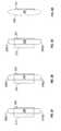
- FIGS. 1A-1Eare block diagrams illustrating an exemplary method of strengthening glass according to embodiments of the present invention. Each figure in the sequence depicts a step in the described method.
- FIG. 1Ais a block diagram of an exemplary thin-film deposition process according to embodiments of the present invention.
- a mother sheet 100is adapted to receive at least one thin film deposit upon at least one target surface 102 .
- the mother sheetis often a large, rectangular sheet of glass, but may be any size or shape according to embodiments of the present invention.
- the surfaces of the mother sheet 100have already been chemically strengthened (for example, by immersion into a chemical substance for a certain period and at a certain temperature).
- the mother sheethas not been chemically treated or strengthened.
- One or more thin films 104 ( 1 ) and 104 ( 2 )are then deposited upon discrete regions of the target surface 102 and patterned. Note that even though FIG. 1A depicts two thin films 104 ( 1 ) and 104 ( 2 ) deposited upon the target surface 102 , the target surface 102 can comprise any number of thin films 104 according to embodiments of the present invention. Additionally, the thin films 104 can be situated in any position along both axes of the surface 102 .
- the thin films 104 ( 1 ) and 104 ( 2 )is indium tin oxide (ITO).
- ITOindium tin oxide
- other materialsare utilized in addition to, or instead of, ITO. These materials include, without limitation, amorphous silicon, copper indium diselenide, cadmium telluride and film crystalline silicon.
- the thin films 104 ( 1 ) and 104 ( 2 )can be protected by one or more passivation layers (organic and/or inorganic). Passivation layers are compositions formed over conductive material and other layers which protect those materials from corrosion and other environmental effects.
- passivation layerscomprising silicon dioxide (SiO 2 ) and/or silicon nitride (SiNx).
- FIG. 1Bis a block diagram of a separation process according to embodiments of the present invention.
- the mother sheet 100has been separated into a plurality of individual sheets 106 ( 1 ) and 106 ( 2 ).
- FIG. 1Bdepicts two sheets 106 ( 1 ) and 106 ( 2 ) being formed from the mother sheet 100
- any number of individual sheets 106may be formed from the mother sheet.
- the individual sheets 106are shaped (e.g., cut into a specific geometry) upon separation from the mother sheet 100 . In other embodiments, one or more shaping processes are employed subsequent to separation.
- any number of means or mechanismscan be used in order to accomplish separation from the mother sheet 100 . This includes, without limitation, etching, laser scribing, mechanical scribing, and/or grinding and polishing.
- the edges of the separated sheets 106 ( 1 ) and 106 ( 2 )include at least one curved portion (e.g., as depicted by the unstrengthened edges 108 ( 1 ) and 108 ( 2 )).
- the glass sheetsmay be separated and/or shaped using any pattern or geometry according to embodiments of the present invention. This includes glass shapes having flat edges, cylindrical edges, uneven edges, and edges including extended regions.
- one or more unstrengthened edges 108 ( 1 ) and 108 ( 2 )are formed along the paths of separation (or alternatively, upon the specific surfaces that have been shaped).
- the unstrengthened edges 108adjoin one or more surfaces that have already been chemically strengthened (for example, by a strengthening process applied to the mother sheet 100 ).
- the unstrengthened edges 108are part of a larger set of unstrengthened regions.
- FIG. 1Bdepicts the unstrengthened edges 108 ( 1 ) and 108 ( 2 ) as each adjoining a strengthened region situated directly behind the thin films 104 ( 1 ) and 104 ( 2 ), respectively, this is not necessary according to some embodiments of the present invention.
- FIG. 2Ais a block diagram illustrating an exemplary glass shape including unstrengthened edges 208 ( 1 ) and 208 ( 2 ) which do not extend to the region 210 situated directly behind the thin film 204 according to embodiments of the present invention.
- FIGS. 2Care block diagrams illustrating exemplary glass shapes including unstrengthened edges 208 ( 1 ) and 208 ( 2 ) which extend to the region 210 situated directly behind the thin film 204 on one side of the individual sheet 206 according to other embodiments of the present invention.
- FIG. 2Dis a block diagram illustrating an exemplary glass shape including a single contiguous unstrengthened surface 208 according to still other embodiments of the present invention.
- Other combinations of strengthened and/or unstrengthened edgesare also possible according to embodiments of the present invention.
- FIG. 1Cis a block diagram of an exemplary sealing process according to embodiments of the present invention.
- the individual sheets 106 ( 1 ) and 106 ( 2 )are positioned such that the thin films 104 ( 1 ) and 104 ( 2 ) face inward.
- an initial laminate, coating, or other protective sheetis applied to at least the regions including the thin films 104 ( 1 ) and 104 ( 2 ) before the sealing process commences.
- FIG. 3Ais a block diagram illustrating a sealing process according to one embodiment of the present invention.
- Sealants or adhesivesare applied to one or more regions of the individual sheets 106 ( 1 ) and 106 ( 2 ).
- the sealants 110 ( 1 ) and 110 ( 2 )may be applied to regions separating the unstrengthened edges 108 ( 1 ) and 108 ( 2 ) from the thin films 104 ( 1 ) and 104 ( 2 ) (as shown in FIG. 1C ).
- the sealants 110 ( 1 ) and 110 ( 2 )may be applied to the entire perimeter of the thin films 104 ( 1 ) and 104 ( 2 ) (as shown in FIG. 3A ).
- thermo and chemical resistances of the sealantare selected so as to withstand the thermal and chemical environment of the strengthening process.
- the sealing processincludes sealing the individual sheets 106 ( 1 ) and 106 ( 2 ) with an O-ring or other looped elastomer. This includes, without limitation, clamping two individual sheets 106 ( 1 ) and 106 ( 2 ) together with a Viton® or Kalrez® O-ring.
- FIG. 3Bis a block diagram illustrating two individual sheets 106 ( 1 ) and 106 ( 2 ) fastened by an O-ring 302 .
- sealingincludes, for example, ties, fasteners, and mechanical clamping devices. Note also that combinations of sealing techniques may also be employed in accordance with embodiments of the present invention (e.g., utilizing an O-ring in addition to a full-face adhesive covering).
- FIG. 1Dis a block diagram of an exemplary pair of sealed sheets 106 ( 1 ) and 106 ( 2 ) after a strengthening process has occurred according to embodiments of the present invention.
- the strengthening processincludes applying a localized treatment to unstrengthened regions of the glass sheets 106 . This may be accomplished, for example, by treating only the unstrengthened edges 108 ( 1 ) and 108 ( 2 ) of the individual sheets 106 ( 1 ) and 106 ( 2 ).
- the mother glass 100has already been chemically strengthened (for example, by prior immersion in chemical strengthener)
- application of the localized treatment to the unstrengthened regionsresults in glass sheets 106 with strengthened surfaces at all sides. In this manner, full perimeter glass strengthening may be accomplished.
- the substances used to strengthen the unstrengthened regions of the glass sheets 106may be the same or may be different than the substances used to strengthen the mother sheet 100 according to some embodiments of the present invention.
- the localized treatmentmay include, without limitation, one or more of the following: edge polishes (e.g., as via cerium oxide or other similar compounds), acid polishes, chemical etches (e.g., as via hydrogen fluoride or hydrogen chloride), localized heat treatment (e.g., bringing the glass to its glass transition temperature in the range of 500° C.-620° C.) and/or chemical treatments.
- the chemical treatmentincludes filling flaws in the surface of the glass 106 with an adhesive or other similar substance.
- potassium nitrate (KNO 3 )is applied to the unstrengthened regions at 350° C.
- KNO 3potassium nitrate
- a non-localized treatmentis used for strengthening.
- a non-localized treatmentat least a portion of the sealed sheets 106 ( 1 ) and 106 ( 2 ) are immersed in one or more chemical substances and treated at a certain temperature.
- the chemical substancecomprises potassium nitrate (KNO 3 ) applied to the sheets at approximately 350° C.
- the thin film 104may comprise any combination of indium tin oxide, metal and/or silicon oxide (SiO 2 ), but without organic passivation layers, which react adversely to the high temperature.
- the temperature settingsare adjusted accordingly (for example, in one embodiment, the applied temperature is regulated such that it does not exceed 300° C.).
- the edges 112 ( 1 ) and 112 ( 2 ) of glass sheets 106 ( 1 ) and 106 ( 2 )have been strengthened.
- the sealant, adhesive, or other binding mechanism used in the sealing processis then removed and the sealed sheets 106 ( 1 ) and 106 ( 2 ) are separated.
- the adhesive used to seal the glass sheets 106 ( 1 ) and 106 ( 2 )is chemically resistive to the strengthening agents but mechanically soft (e.g., 3M® reworkable pressure sensitive adhesives). This property enables the adhesive to be pulled out.
- FIG. 1Edepicts strengthened surfaces of the individual sheets 106 ( 1 ) and 106 ( 2 ) at all sides.
- FIG. 4is a high-level flow diagram illustrating an exemplary method of strengthening a substrate according to embodiments of the present invention.
- a mother sheetis separated and/or shaped into multiple smaller sheets.
- Many methodsmay be used to accomplish separation and shaping according to embodiments of the present invention. This includes, without limitation, etching, laser scribing, mechanical scribing, and/or grinding and polishing.
- the individual sheets in each pairare positioned such that the surface of each sheet including a sensitive region faces each other, and the sandwich is then sealed.
- a sensitive regionincludes materials or components which could be damaged or otherwise adversely affected during chemical and/or thermal treatment (e.g., thin film).
- this sealing processcomprises applying a sealant or adhesive around the perimeter of the sensitive regions.
- the sealing processincludes applying an adhesive over all portions of the thin film and then sealing the sheets together.
- the sealing processincludes sealing the sheets together with an O-ring, elastomer, or other flexible substance protecting the thin film.
- each pair of sealed sheetsis then chemically strengthened.
- this chemical strengthening processincludes subjecting each sandwich to an edge polishing procedure, a chemical etch or acid polish procedure, or a localized heat or chemical treatment.
- the chemical strengthening processincludes immersing the sandwich into a chemical substance at specific temperature settings (e.g., potassium nitrate (KNO 3 ) at 350° C.).
- the sandwichis then separated.
- the adhesive used to seal the glass sheets 106 ( 1 ) and 106 ( 2 )is chemically resistive to the strengthening agents but mechanically soft, which enables the adhesive to be pulled out.
- FIG. 5illustrates exemplary computing system 500 that can include a touch sensor panel 524 situated on a glass substrate that has been strengthened by one or more of the embodiments of the invention described above.
- Computing system 500can include one or more panel processors 502 and peripherals 504 , and panel subsystem 506 .
- Peripherals 504can include, but are not limited to, random access memory (RAM) or other types of memory or storage, watchdog timers and the like.
- Panel subsystem 506can include, but is not limited to, one or more sense channels 508 , channel scan logic 510 and driver logic 514 .
- Channel scan logic 510can access RAM 512 , autonomously read data from the sense channels and provide control for the sense channels.
- channel scan logic 510can control driver logic 514 to generate stimulation signals 516 at various frequencies and phases that can be selectively applied to drive lines of touch sensor panel 524 .
- panel subsystem 506 , panel processor 502 and peripherals 504can be integrated into a single application specific integrated circuit (ASIC).
- ASICapplication specific integrated circuit
- Touch sensor panel 524can include a capacitive sensing medium having a plurality of drive lines and a plurality of sense lines, although other sensing media can also be used. Each intersection of drive and sense lines can represent a capacitive sensing node and can be viewed as picture element (pixel) 526 , which can be particularly useful when touch sensor panel 524 is viewed as capturing an “image” of touch. (In other words, after panel subsystem 506 has determined whether a touch event has been detected at each touch sensor in the touch sensor panel, the pattern of touch sensors in the multi-touch panel at which a touch event occurred can be viewed as an “image” of touch (e.g. a pattern of fingers touching the panel).) Each sense line of touch sensor panel 524 can drive sense channel 508 (also referred to herein as an event detection and demodulation circuit) in panel subsystem 506 .
- sense channel 508also referred to herein as an event detection and demodulation circuit
- Computing system 500can also include host processor 528 for receiving outputs from panel processor 502 and performing actions based on the outputs that can include, but are not limited to, moving an object such as a cursor or pointer, scrolling or panning, adjusting control settings, opening a file or document, viewing a menu, making a selection, executing instructions, operating a peripheral device coupled to the host device, answering a telephone call, placing a telephone call, terminating a telephone call, changing the volume or audio settings, storing information related to telephone communications such as addresses, frequently dialed numbers, received calls, missed calls, logging onto a computer or a computer network, permitting authorized individuals access to restricted areas of the computer or computer network, loading a user profile associated with a user's preferred arrangement of the computer desktop, permitting access to web content, launching a particular program, encrypting or decoding a message, and/or the like.
- host processor 528for receiving outputs from panel processor 502 and performing actions based on the outputs that can include, but are not limited to, moving an
- Host processor 528can also perform additional functions that may not be related to panel processing, and can be coupled to program storage 532 and display device 530 such as an LCD display for providing a UI to a user of the device.
- Display device 530 together with touch sensor panel 524when located partially or entirely under the touch sensor panel, can form touch screen 518 .
- firmwarestored in memory (e.g. one of the peripherals 504 in FIG. 5 ) and executed by panel processor 502 , or stored in program storage 532 and executed by host processor 528 .
- the firmwarecan also be stored and/or transported within any computer-readable medium for use by or in connection with an instruction execution system, apparatus, or device, such as a computer-based system, processor-containing system, or other system that can fetch the instructions from the instruction execution system, apparatus, or device and execute the instructions.
- a “computer-readable medium”can be any medium that can contain or store the program for use by or in connection with the instruction execution system, apparatus, or device.
- the computer readable mediumcan include, but is not limited to, an electronic, magnetic, optical, electromagnetic, infrared, or semiconductor system, apparatus or device, a portable computer diskette (magnetic), a random access memory (RAM) (magnetic), a read-only memory (ROM) (magnetic), an erasable programmable read-only memory (EPROM) (magnetic), a portable optical disc such a CD, CD-R, CD-RW, DVD, DVD-R, or DVD-RW, or flash memory such as compact flash cards, secured digital cards, USB memory devices, memory sticks, and the like.
- FIG. 6Aillustrates exemplary mobile telephone 636 that can include touch sensor panel 624 and display device 630 , the touch sensor panel formed upon a glass substrate that has been strengthened according to embodiments of the invention.
- FIG. 6Billustrates exemplary digital media player 640 that can include touch sensor panel 624 and display device 630 , the touch sensor panel formed upon a glass substrate that has been strengthened according to embodiments of the invention.
- FIG. 6Cillustrates exemplary personal computer 644 that can include touch sensor panel (trackpad) 624 and display 630 , the touch sensor panel and/or display of the personal computer (in embodiments where the display is part of a touch screen) including a glass substrate that has been strengthened according to embodiments of the invention.
- the mobile telephone, media player and personal computer of FIGS. 6A, 6B and 6Ccan achieve improved overall durability by utilizing the strengthened glass substrate according to embodiments of the invention.
Landscapes
- Engineering & Computer Science (AREA)
- Chemical & Material Sciences (AREA)
- Materials Engineering (AREA)
- Chemical Kinetics & Catalysis (AREA)
- General Chemical & Material Sciences (AREA)
- Geochemistry & Mineralogy (AREA)
- Life Sciences & Earth Sciences (AREA)
- Organic Chemistry (AREA)
- General Engineering & Computer Science (AREA)
- Theoretical Computer Science (AREA)
- Human Computer Interaction (AREA)
- Physics & Mathematics (AREA)
- General Physics & Mathematics (AREA)
- Surface Treatment Of Glass (AREA)
Abstract
Description
This application is a divisional of U.S. patent application Ser. No. 12/165,336, filed Jun. 30, 2008, the entire disclosure of which is incorporated herein by reference in its entirety.
The present invention relates generally to substrate strengthening. More particularly, the present invention is directed in one exemplary aspect to chemically strengthening the edges of substrates comprising thin film deposits.
Touch sensor panels are typically fabricated as one or more thin films deposited and patterned into conductive traces upon one or both sides of a chemically strengthened sheet of glass. However, standard thin film equipment does not allow for thin film deposition on custom-sized or shaped sheets of glass. Instead, thin film deposition occurs on large, rectangular sheets of glass (called mother sheets) which are subsequently separated and shaped into a plurality of individual glass sheets. The individual sheets are typically used in separate electronic devices.
When the mother sheet is separated into individual sheets, however, a new set of edges is formed along each path of separation. Since the new set of edges has not been chemically treated, the individual sheets are susceptible to cracking.
Conventional techniques for chemically strengthening glass require immersion of the sheet into a chemical treatment for a certain period of time and at a certain temperature. In many cases, chemically strengthening the edges is infeasible since the exposed film would be damaged by the chemicals and/or the temperature required for the treatment.
Various embodiments of the present invention relate to chemically strengthening the edges of glass sheets having thin films deposited on at least one surface. Thin films are typically deposited and patterned upon discrete regions of a chemically strengthened sheet of glass. This sheet of glass is called a mother sheet. The mother sheet is typically cut into separate sheets, where each sheet is adapted to service a separate electronic component or device.
When the mother sheet is separated, a new set of edges are formed at the path of separation. These edges have not been chemically strengthened and are therefore sensitive to forces exerted upon them. While applying a chemical strengthener to the edges of the sheets would protect the sheets from cracking, this tends to damage exposed regions of the thin film. Moreover, since standard thin film equipment lacks the capability to apply thin film processes to glass in different and/or smaller sizes than a mother sheet, in many cases, the thin film deposition process must precede the separation process.
Various embodiments of the present invention address these concerns by protecting the thin films during the chemical and/or thermal edge strengthening treatment. In one embodiment, a portion of each individual sheet is laminated. Pairs of sheets are then sealed together such that the thin film sides face inward to form a thin film sandwich. In some embodiments, the sandwich in then immersed in a chemical strengthener. In other embodiments, a localized treatment is applied to the unstrengthened edges.
In the following description of preferred embodiments, reference is made to the accompanying drawings in which it is shown by way of illustration specific embodiments in which the invention can be practiced. It is to be understood that other embodiments can be used and structural changes can be made without departing from the scope of the embodiments of this invention.
Various embodiments of the present invention relate to chemically strengthening the edges of glass sheets having thin films deposited on at least one surface. Thin films are typically deposited and patterned upon discrete regions of a chemically strengthened sheet of glass. This sheet of glass is called a mother sheet. The mother sheet is typically cut into separate sheets, where each sheet is adapted to service a separate electronic component or device.
When the mother sheet is separated, a new set of edges are formed at the path of separation. These edges have not been chemically strengthened and are therefore sensitive to forces exerted upon them. While applying a chemical strengthener to the edges of the sheets would protect the sheets from cracking, this tends to damage exposed regions of the thin film. Moreover, since standard thin film equipment lacks the capability to apply thin film processes to glass in different and/or smaller sizes than a mother sheet, in many cases, the thin film deposition process must precede the separation process.
Various embodiments of the present invention address these concerns by protecting the thin films during the chemical and/or thermal edge strengthening treatment. In one embodiment, a portion of each individual sheet is laminated. Pairs of sheets are then sealed together such that the thin film sides face inward to form a thin film sandwich. In some embodiments, the sandwich in then immersed in a chemical strengthener. In other embodiments, a localized treatment is applied to the unstrengthened edges.
Although embodiments of the invention may be described and illustrated herein in terms of touch sensor panels, it should be understood that embodiments of this invention are not so limited, but are additionally applicable to any circuit or communication path formed on a glass substrate or other substrate prone to weakness at an unstrengthened edge.
One or more thin films104(1) and104(2) are then deposited upon discrete regions of thetarget surface 102 and patterned. Note that even thoughFIG. 1A depicts two thin films104(1) and104(2) deposited upon thetarget surface 102, thetarget surface 102 can comprise any number ofthin films 104 according to embodiments of the present invention. Additionally, thethin films 104 can be situated in any position along both axes of thesurface 102.
In some embodiments, at least one of the thin films104(1) and104(2) is indium tin oxide (ITO). In some embodiments, other materials are utilized in addition to, or instead of, ITO. These materials include, without limitation, amorphous silicon, copper indium diselenide, cadmium telluride and film crystalline silicon. Optionally, the thin films104(1) and104(2) can be protected by one or more passivation layers (organic and/or inorganic). Passivation layers are compositions formed over conductive material and other layers which protect those materials from corrosion and other environmental effects. Various types of passivation can be employed according to embodiments of the present invention. These include, without limitation, passivation layers comprising silicon dioxide (SiO2) and/or silicon nitride (SiNx).
Additionally, any number of means or mechanisms can be used in order to accomplish separation from themother sheet 100. This includes, without limitation, etching, laser scribing, mechanical scribing, and/or grinding and polishing. In some embodiments, the edges of the separated sheets106(1) and106(2) include at least one curved portion (e.g., as depicted by the unstrengthened edges108(1) and108(2)). However, the glass sheets may be separated and/or shaped using any pattern or geometry according to embodiments of the present invention. This includes glass shapes having flat edges, cylindrical edges, uneven edges, and edges including extended regions.
Once the individual sheets have been separated, one or more unstrengthened edges108(1) and108(2) are formed along the paths of separation (or alternatively, upon the specific surfaces that have been shaped). In several embodiments, such as the one illustrated inFIG. 1B , theunstrengthened edges 108 adjoin one or more surfaces that have already been chemically strengthened (for example, by a strengthening process applied to the mother sheet100). In some embodiments, theunstrengthened edges 108 are part of a larger set of unstrengthened regions.
Even thoughFIG. 1B depicts the unstrengthened edges108(1) and108(2) as each adjoining a strengthened region situated directly behind the thin films104(1) and104(2), respectively, this is not necessary according to some embodiments of the present invention. For example,FIG. 2A is a block diagram illustrating an exemplary glass shape including unstrengthened edges208(1) and208(2) which do not extend to theregion 210 situated directly behind thethin film 204 according to embodiments of the present invention.FIG. 2B andFIG. 2C are block diagrams illustrating exemplary glass shapes including unstrengthened edges208(1) and208(2) which extend to theregion 210 situated directly behind thethin film 204 on one side of the individual sheet206 according to other embodiments of the present invention.FIG. 2D is a block diagram illustrating an exemplary glass shape including a single contiguousunstrengthened surface 208 according to still other embodiments of the present invention. Other combinations of strengthened and/or unstrengthened edges are also possible according to embodiments of the present invention.
In other embodiments, the sealing process includes sealing the individual sheets106(1) and106(2) with an O-ring or other looped elastomer. This includes, without limitation, clamping two individual sheets106(1) and106(2) together with a Viton® or Kalrez® O-ring.FIG. 3B is a block diagram illustrating two individual sheets106(1) and106(2) fastened by an O-ring 302.
Other forms of sealing are also possible according to embodiments of the present invention. This includes, for example, ties, fasteners, and mechanical clamping devices. Note also that combinations of sealing techniques may also be employed in accordance with embodiments of the present invention (e.g., utilizing an O-ring in addition to a full-face adhesive covering).
Additionally, the localized treatment may include, without limitation, one or more of the following: edge polishes (e.g., as via cerium oxide or other similar compounds), acid polishes, chemical etches (e.g., as via hydrogen fluoride or hydrogen chloride), localized heat treatment (e.g., bringing the glass to its glass transition temperature in the range of 500° C.-620° C.) and/or chemical treatments. In many embodiments, the chemical treatment includes filling flaws in the surface of theglass 106 with an adhesive or other similar substance. In one embodiment, for example, potassium nitrate (KNO3) is applied to the unstrengthened regions at 350° C. The selection of chemical substances and thermal settings depends in part upon the type of thin films and/or conductive materials used.
In other embodiments, a non-localized treatment is used for strengthening. In a non-localized treatment, at least a portion of the sealed sheets106(1) and106(2) are immersed in one or more chemical substances and treated at a certain temperature. For example, in one embodiment, the chemical substance comprises potassium nitrate (KNO3) applied to the sheets at approximately 350° C. Note that in the above embodiment, thethin film 104 may comprise any combination of indium tin oxide, metal and/or silicon oxide (SiO2), but without organic passivation layers, which react adversely to the high temperature. In certain embodiments where organic passivation layers are utilized, the temperature settings are adjusted accordingly (for example, in one embodiment, the applied temperature is regulated such that it does not exceed 300° C.).
Once the treatment process has completed, the edges112(1) and112(2) of glass sheets106(1) and106(2) have been strengthened. In many embodiments, the sealant, adhesive, or other binding mechanism used in the sealing process is then removed and the sealed sheets106(1) and106(2) are separated. In some embodiments, for example, the adhesive used to seal the glass sheets106(1) and106(2) is chemically resistive to the strengthening agents but mechanically soft (e.g., 3M® reworkable pressure sensitive adhesives). This property enables the adhesive to be pulled out. The result of the strengthening process is shown inFIG. 1E , which depicts strengthened surfaces of the individual sheets106(1) and106(2) at all sides.
Atblock 404, the individual sheets in each pair are positioned such that the surface of each sheet including a sensitive region faces each other, and the sandwich is then sealed. A sensitive region includes materials or components which could be damaged or otherwise adversely affected during chemical and/or thermal treatment (e.g., thin film).
In some embodiments, this sealing process comprises applying a sealant or adhesive around the perimeter of the sensitive regions. In other embodiments, the sealing process includes applying an adhesive over all portions of the thin film and then sealing the sheets together. In still other embodiments, the sealing process includes sealing the sheets together with an O-ring, elastomer, or other flexible substance protecting the thin film.
Atblock 406, each pair of sealed sheets is then chemically strengthened. In some embodiments, this chemical strengthening process includes subjecting each sandwich to an edge polishing procedure, a chemical etch or acid polish procedure, or a localized heat or chemical treatment. In other embodiments, the chemical strengthening process includes immersing the sandwich into a chemical substance at specific temperature settings (e.g., potassium nitrate (KNO3) at 350° C.).
Atblock 408, the sandwich is then separated. In some embodiments, for example, the adhesive used to seal the glass sheets106(1) and106(2) is chemically resistive to the strengthening agents but mechanically soft, which enables the adhesive to be pulled out.
Note that one or more of the functions described above can be performed by firmware stored in memory (e.g. one of theperipherals 504 inFIG. 5 ) and executed bypanel processor 502, or stored inprogram storage 532 and executed byhost processor 528. The firmware can also be stored and/or transported within any computer-readable medium for use by or in connection with an instruction execution system, apparatus, or device, such as a computer-based system, processor-containing system, or other system that can fetch the instructions from the instruction execution system, apparatus, or device and execute the instructions. In the context of this document, a “computer-readable medium” can be any medium that can contain or store the program for use by or in connection with the instruction execution system, apparatus, or device. The computer readable medium can include, but is not limited to, an electronic, magnetic, optical, electromagnetic, infrared, or semiconductor system, apparatus or device, a portable computer diskette (magnetic), a random access memory (RAM) (magnetic), a read-only memory (ROM) (magnetic), an erasable programmable read-only memory (EPROM) (magnetic), a portable optical disc such a CD, CD-R, CD-RW, DVD, DVD-R, or DVD-RW, or flash memory such as compact flash cards, secured digital cards, USB memory devices, memory sticks, and the like.
Although embodiments of this invention have been fully described with reference to the accompanying drawings, it is to be noted that various changes and modifications will become apparent to those skilled in the art. Such changes and modifications are to be understood as being included within the scope of embodiments of this invention as defined by the appended claims.
Claims (18)
1. An apparatus comprising:
a first glass substrate having a first surface and a second surface, the second surface created by the separation of the substrate from a larger glass sheet, the first surface previously strengthened with a chemical treatment and the second surface not strengthened with a chemical treatment;
a second glass substrate having a third surface and a fourth surface, the fourth surface created by the separation of the substrate from the larger glass sheet, the third surface previously strengthened with a chemical treatment and the fourth surface not strengthened with a chemical treatment;
a first thin film including one or more conductive traces formed on the first surface of the first glass substrate prior to the separation of the first substrate from the larger sheet;
a second thin film including one or more conductive traces formed on the third surface of the second glass substrate prior to the separation of the second substrate from the larger sheet;
a first sealant applied to a perimeter area of the first surface and not applied on the conductive traces on the first surface; and
a second sealant applied to a perimeter area of the third surface and not applied on the conductive traces on the third surface,
wherein the first sealant is mated with the second sealant to removably seal the first surface with the third surface, and
wherein the first surface and the third surface are temporarily removably sealed when the first sealant on the first surface mates with the second sealant on the third surface such that the first sealant, the second sealant and the conductive traces occupy substantially all space between the first glass substrate and the second glass substrate.
2. The apparatus ofclaim 1 , wherein the chemical treatment comprises an acid polish.
3. The apparatus ofclaim 1 , wherein the chemical treatment comprises cerium oxide.
4. The apparatus ofclaim 1 , wherein the chemical treatment comprises potassium nitrate.
5. The apparatus ofclaim 1 , wherein the conductive traces include a thin film on conductor.
6. The apparatus ofclaim 5 , wherein the thin film conductor includes one of indium tin oxide, amorphous silicon, copper indium diselenide, cadmium telluride, and film crystalline silicon.
7. The apparatus ofclaim 1 , wherein the chemical treatment includes heating the first and third surface.
8. The apparatus ofclaim 1 , wherein a passivation layer including one of silicon dioxide (SiO2) and silicon nitride (SiNx) is formed over the one or more conductive traces prior to separation.
9. The apparatus ofclaim 1 , wherein the glass substrate is separated from larger glass sheet by a separating mechanism including one of etching, laser scribing, mechanical scribing, and grinding and polishing, the second surface including a surface created by the separating mechanism.
10. The apparatus ofclaim 1 , wherein the second surface includes one of a flat surface, a cylindrical surface, an uneven surface, and a surface including extended regions.
11. The apparatus ofclaim 1 , wherein the sealant includes one of polymer film, polyimide, SU-8, photoresist, reworkable pressure sensitive adhesive, and silicone based adhesive.
12. An apparatus comprising:
a first glass substrate having a first surface and a second surface, the second surface created by the separation of the substrate from a larger glass sheet, the first surface previously strengthened with a chemical treatment;
a second glass substrate having a third surface and a fourth surface, the fourth surface created by the separation of the substrate from the larger glass sheet, the third surface previously strengthened with a chemical treatment;
a thin film including one or more conductive traces formed on the first surface of the first glass substrate and the third surface of the second glass substrate prior to the separation of the substrate from the larger sheet; and
a temporary removable sealant applied to a perimeter of the first surface and a perimeter of the third surface, wherein the first surface and the third surface are removably sealed when the temporary removable sealant on the first surface mates with the temporary removable sealant on the third surface such that the temporary removable sealant and the conductive traces occupy substantially all space between the first glass substrate and the second glass substrate.
13. The apparatus ofclaim 12 , wherein the temporary removable sealant includes one of polymer film, polyimide, SU-8 photoresist, reworkable pressure sensitive adhesive, and silicone based adhesive.
14. The apparatus ofclaim 12 , wherein the conductive traces include a thin film of conductor.
15. The apparatus ofclaim 12 , wherein the temporary removable sealant is applied to entire perimeter areas of the first surface and the third surface surrounding the conductive traces.
16. An apparatus comprising:
a first glass substrate having a first surface and a second surface, the second surface created by the separation of the substrate from a larger glass sheet, the first surface previously strengthened with a chemical treatment;
a second glass substrate having a third surface and a fourth surface, the fourth surface created by the separation of the substrate from the larger glass sheet, the first surface previously strengthened with a chemical treatment;
a thin film including one or more conductive traces formed on the first surface of the first glass substrate and the third surface of the second glass substrate prior to the separation of the substrate from the larger sheet;
a temporary removable sealant applied to a perimeter of the first surface and a perimeter of the third surface, wherein the first surface and the third surface are removably sealed when the temporary removable sealant on the first surface mates with the temporary removable sealant on the third surface such that the temporary removable sealant and the conductive traces occupy substantially all space between the first glass substrate and the second glass substrate.
17. The apparatus ofclaim 16 , wherein the temporary removable sealant includes one of polymer film, polymide, SU-8 photoresist, reworkable pressure sensitive adhesive, and silicone based adhesive.
18. The apparatus ofclaim 16 , wherein the temporary removable sealant is applied to entire perimeter areas of the first surface and the third surface surrounding the conductive traces.
Priority Applications (1)
| Application Number | Priority Date | Filing Date | Title |
|---|---|---|---|
| US12/885,376US9405388B2 (en) | 2008-06-30 | 2010-09-17 | Full perimeter chemical strengthening of substrates |
Applications Claiming Priority (2)
| Application Number | Priority Date | Filing Date | Title |
|---|---|---|---|
| US12/165,336US7810355B2 (en) | 2008-06-30 | 2008-06-30 | Full perimeter chemical strengthening of substrates |
| US12/885,376US9405388B2 (en) | 2008-06-30 | 2010-09-17 | Full perimeter chemical strengthening of substrates |
Related Parent Applications (1)
| Application Number | Title | Priority Date | Filing Date |
|---|---|---|---|
| US12/165,336DivisionUS7810355B2 (en) | 2008-06-30 | 2008-06-30 | Full perimeter chemical strengthening of substrates |
Publications (2)
| Publication Number | Publication Date |
|---|---|
| US20110005820A1 US20110005820A1 (en) | 2011-01-13 |
| US9405388B2true US9405388B2 (en) | 2016-08-02 |
Family
ID=41447808
Family Applications (2)
| Application Number | Title | Priority Date | Filing Date |
|---|---|---|---|
| US12/165,336Expired - Fee RelatedUS7810355B2 (en) | 2008-06-30 | 2008-06-30 | Full perimeter chemical strengthening of substrates |
| US12/885,376Active2029-08-22US9405388B2 (en) | 2008-06-30 | 2010-09-17 | Full perimeter chemical strengthening of substrates |
Family Applications Before (1)
| Application Number | Title | Priority Date | Filing Date |
|---|---|---|---|
| US12/165,336Expired - Fee RelatedUS7810355B2 (en) | 2008-06-30 | 2008-06-30 | Full perimeter chemical strengthening of substrates |
Country Status (1)
| Country | Link |
|---|---|
| US (2) | US7810355B2 (en) |
Families Citing this family (81)
| Publication number | Priority date | Publication date | Assignee | Title |
|---|---|---|---|---|
| US8169587B2 (en)* | 2007-08-16 | 2012-05-01 | Apple Inc. | Methods and systems for strengthening LCD modules |
| US8673163B2 (en) | 2008-06-27 | 2014-03-18 | Apple Inc. | Method for fabricating thin sheets of glass |
| US7810355B2 (en)* | 2008-06-30 | 2010-10-12 | Apple Inc. | Full perimeter chemical strengthening of substrates |
| KR101040789B1 (en)* | 2009-01-16 | 2011-06-13 | 삼성모바일디스플레이주식회사 | Touch screen panel and its manufacturing method |
| CN102388003B (en) | 2009-03-02 | 2014-11-19 | 苹果公司 | Technology for Strengthening Glass Covers for Portable Electronic Devices |
| US8549882B2 (en)* | 2009-09-30 | 2013-10-08 | Apple Inc. | Pre-processing techniques to produce complex edges using a glass slumping process |
| US9778685B2 (en) | 2011-05-04 | 2017-10-03 | Apple Inc. | Housing for portable electronic device with reduced border region |
| KR101661160B1 (en)* | 2010-03-31 | 2016-09-29 | 삼성전자주식회사 | Touch screen pannel |
| US9213451B2 (en) | 2010-06-04 | 2015-12-15 | Apple Inc. | Thin glass for touch panel sensors and methods therefor |
| US9207528B2 (en) | 2010-06-04 | 2015-12-08 | Apple Inc. | Thin sheet glass processing |
| US8974268B2 (en)* | 2010-06-25 | 2015-03-10 | Corning Incorporated | Method of preparing an edge-strengthened article |
| US8923693B2 (en)* | 2010-07-30 | 2014-12-30 | Apple Inc. | Electronic device having selectively strengthened cover glass |
| US10189743B2 (en)* | 2010-08-18 | 2019-01-29 | Apple Inc. | Enhanced strengthening of glass |
| WO2012023360A1 (en)* | 2010-08-20 | 2012-02-23 | シャープ株式会社 | Method for manufacturing position input devices and device for manufacturing position input devices |
| US20120052302A1 (en)* | 2010-08-24 | 2012-03-01 | Matusick Joseph M | Method of strengthening edge of glass article |
| US8873028B2 (en) | 2010-08-26 | 2014-10-28 | Apple Inc. | Non-destructive stress profile determination in chemically tempered glass |
| US8393175B2 (en)* | 2010-08-26 | 2013-03-12 | Corning Incorporated | Methods for extracting strengthened glass substrates from glass sheets |
| US8824140B2 (en) | 2010-09-17 | 2014-09-02 | Apple Inc. | Glass enclosure |
| JP5649592B2 (en)* | 2011-02-17 | 2015-01-07 | Hoya株式会社 | Manufacturing method of glass substrate of cover glass for portable electronic device, glass substrate of cover glass for portable electronic device, and portable electronic device |
| US8776547B2 (en)* | 2011-02-28 | 2014-07-15 | Corning Incorporated | Local strengthening of glass by ion exchange |
| US10781135B2 (en) | 2011-03-16 | 2020-09-22 | Apple Inc. | Strengthening variable thickness glass |
| US9725359B2 (en) | 2011-03-16 | 2017-08-08 | Apple Inc. | Electronic device having selectively strengthened glass |
| US9128666B2 (en) | 2011-05-04 | 2015-09-08 | Apple Inc. | Housing for portable electronic device with reduced border region |
| JP2013043795A (en)* | 2011-08-23 | 2013-03-04 | Nippon Electric Glass Co Ltd | Tempered glass and method of manufacturing the same |
| CN102968200B (en)* | 2011-09-01 | 2016-08-03 | 宸美(厦门)光电有限公司 | Eyeglass contactor control device and manufacturing method thereof thereof |
| US9944554B2 (en) | 2011-09-15 | 2018-04-17 | Apple Inc. | Perforated mother sheet for partial edge chemical strengthening and method therefor |
| US9516149B2 (en) | 2011-09-29 | 2016-12-06 | Apple Inc. | Multi-layer transparent structures for electronic device housings |
| US10144669B2 (en) | 2011-11-21 | 2018-12-04 | Apple Inc. | Self-optimizing chemical strengthening bath for glass |
| KR20130070165A (en)* | 2011-12-19 | 2013-06-27 | 삼성전기주식회사 | Touch sensor and the manufacturing method |
| US10133156B2 (en) | 2012-01-10 | 2018-11-20 | Apple Inc. | Fused opaque and clear glass for camera or display window |
| US8684613B2 (en) | 2012-01-10 | 2014-04-01 | Apple Inc. | Integrated camera window |
| GB201200890D0 (en)* | 2012-01-19 | 2012-02-29 | Univ Dundee | An ion exchange substrate and metalized product and apparatus and method for production thereof |
| US8773848B2 (en) | 2012-01-25 | 2014-07-08 | Apple Inc. | Fused glass device housings |
| US20150218045A1 (en)* | 2012-08-31 | 2015-08-06 | Corning Incorporated | Edge treating a cut edge of a glass piece |
| US9236202B2 (en) | 2012-09-10 | 2016-01-12 | Apple Inc. | Corrosion mitigation for metal traces |
| US9946302B2 (en) | 2012-09-19 | 2018-04-17 | Apple Inc. | Exposed glass article with inner recessed area for portable electronic device housing |
| WO2014079478A1 (en) | 2012-11-20 | 2014-05-30 | Light In Light Srl | High speed laser processing of transparent materials |
| EP2754524B1 (en) | 2013-01-15 | 2015-11-25 | Corning Laser Technologies GmbH | Method of and apparatus for laser based processing of flat substrates being wafer or glass element using a laser beam line |
| WO2014144322A1 (en)* | 2013-03-15 | 2014-09-18 | Kinestral Technologies, Inc. | Laser cutting strengthened glass |
| EP2781296B1 (en) | 2013-03-21 | 2020-10-21 | Corning Laser Technologies GmbH | Device and method for cutting out contours from flat substrates using a laser |
| JP2014208570A (en)* | 2013-03-25 | 2014-11-06 | 日本電気硝子株式会社 | Tempered glass substrate and method of manufacturing the same |
| US9459661B2 (en) | 2013-06-19 | 2016-10-04 | Apple Inc. | Camouflaged openings in electronic device housings |
| US9850160B2 (en) | 2013-12-17 | 2017-12-26 | Corning Incorporated | Laser cutting of display glass compositions |
| US10293436B2 (en) | 2013-12-17 | 2019-05-21 | Corning Incorporated | Method for rapid laser drilling of holes in glass and products made therefrom |
| US11556039B2 (en) | 2013-12-17 | 2023-01-17 | Corning Incorporated | Electrochromic coated glass articles and methods for laser processing the same |
| US9676167B2 (en) | 2013-12-17 | 2017-06-13 | Corning Incorporated | Laser processing of sapphire substrate and related applications |
| US20150166393A1 (en)* | 2013-12-17 | 2015-06-18 | Corning Incorporated | Laser cutting of ion-exchangeable glass substrates |
| US9701563B2 (en) | 2013-12-17 | 2017-07-11 | Corning Incorporated | Laser cut composite glass article and method of cutting |
| US9815730B2 (en) | 2013-12-17 | 2017-11-14 | Corning Incorporated | Processing 3D shaped transparent brittle substrate |
| US20150165560A1 (en) | 2013-12-17 | 2015-06-18 | Corning Incorporated | Laser processing of slots and holes |
| US10442719B2 (en) | 2013-12-17 | 2019-10-15 | Corning Incorporated | Edge chamfering methods |
| US9886062B2 (en) | 2014-02-28 | 2018-02-06 | Apple Inc. | Exposed glass article with enhanced stiffness for portable electronic device housing |
| CN106687419A (en) | 2014-07-08 | 2017-05-17 | 康宁股份有限公司 | Methods and apparatuses for laser processing materials |
| CN208586209U (en) | 2014-07-14 | 2019-03-08 | 康宁股份有限公司 | A system for forming contoured multiple defects in a workpiece |
| KR20170028943A (en)* | 2014-07-14 | 2017-03-14 | 코닝 인코포레이티드 | System for and method of processing transparent materials using laser beam focal lines adjustable in length and diameter |
| EP3169479B1 (en) | 2014-07-14 | 2019-10-02 | Corning Incorporated | Method of and system for arresting incident crack propagation in a transparent material |
| JP6788571B2 (en) | 2014-07-14 | 2020-11-25 | コーニング インコーポレイテッド | Interface blocks, systems and methods for cutting transparent substrates within a wavelength range using such interface blocks. |
| US10047001B2 (en) | 2014-12-04 | 2018-08-14 | Corning Incorporated | Glass cutting systems and methods using non-diffracting laser beams |
| CN107406293A (en) | 2015-01-12 | 2017-11-28 | 康宁股份有限公司 | The substrate through heat tempering is cut by laser using Multiphoton Absorbtion method |
| HUE055461T2 (en) | 2015-03-24 | 2021-11-29 | Corning Inc | Laser cutting and processing of display glass compositions |
| JP2018516215A (en) | 2015-03-27 | 2018-06-21 | コーニング インコーポレイテッド | Gas permeable window and manufacturing method thereof |
| JP6531940B2 (en)* | 2015-05-25 | 2019-06-19 | 日本電気硝子株式会社 | Surface roughness evaluation method, surface roughness evaluation device and glass substrate |
| JP7082042B2 (en) | 2015-07-10 | 2022-06-07 | コーニング インコーポレイテッド | A method for continuously forming holes in a flexible substrate sheet and related products. |
| SG11201809797PA (en) | 2016-05-06 | 2018-12-28 | Corning Inc | Laser cutting and removal of contoured shapes from transparent substrates |
| US10410883B2 (en) | 2016-06-01 | 2019-09-10 | Corning Incorporated | Articles and methods of forming vias in substrates |
| US10794679B2 (en) | 2016-06-29 | 2020-10-06 | Corning Incorporated | Method and system for measuring geometric parameters of through holes |
| KR20190035805A (en) | 2016-07-29 | 2019-04-03 | 코닝 인코포레이티드 | Apparatus and method for laser processing |
| CN106242307A (en)* | 2016-08-11 | 2016-12-21 | 京东方科技集团股份有限公司 | For strengthening the method at the edge of goods, glass and display device |
| EP3507057A1 (en) | 2016-08-30 | 2019-07-10 | Corning Incorporated | Laser processing of transparent materials |
| US10730783B2 (en) | 2016-09-30 | 2020-08-04 | Corning Incorporated | Apparatuses and methods for laser processing transparent workpieces using non-axisymmetric beam spots |
| EP3529214B1 (en) | 2016-10-24 | 2020-12-23 | Corning Incorporated | Substrate processing station for laser-based machining of sheet-like glass substrates |
| US10752534B2 (en) | 2016-11-01 | 2020-08-25 | Corning Incorporated | Apparatuses and methods for laser processing laminate workpiece stacks |
| US11795116B2 (en) | 2016-12-21 | 2023-10-24 | Corning Incorporated | Ceramic assembly and method of forming the same |
| US10688599B2 (en) | 2017-02-09 | 2020-06-23 | Corning Incorporated | Apparatus and methods for laser processing transparent workpieces using phase shifted focal lines |
| US10580725B2 (en) | 2017-05-25 | 2020-03-03 | Corning Incorporated | Articles having vias with geometry attributes and methods for fabricating the same |
| US11078112B2 (en) | 2017-05-25 | 2021-08-03 | Corning Incorporated | Silica-containing substrates with vias having an axially variable sidewall taper and methods for forming the same |
| US10626040B2 (en) | 2017-06-15 | 2020-04-21 | Corning Incorporated | Articles capable of individual singulation |
| US12180108B2 (en) | 2017-12-19 | 2024-12-31 | Corning Incorporated | Methods for etching vias in glass-based articles employing positive charge organic molecules |
| US11554984B2 (en) | 2018-02-22 | 2023-01-17 | Corning Incorporated | Alkali-free borosilicate glasses with low post-HF etch roughness |
| CN113307503A (en)* | 2021-06-24 | 2021-08-27 | 芜湖长信新型显示器件有限公司 | Vehicle-mounted curved surface Sensor glass thinning process method |
| WO2024137355A1 (en)* | 2022-12-22 | 2024-06-27 | Corning Incorporated | Methods and systems for single-side etching glass-based substrates |
Citations (263)
| Publication number | Priority date | Publication date | Assignee | Title |
|---|---|---|---|---|
| US3415637A (en) | 1967-06-14 | 1968-12-10 | Saint Gobain Corp | Strengthening glass sheets by ion exchange |
| US3467508A (en) | 1965-07-09 | 1969-09-16 | Pilkington Brothers Ltd | Float glass surface modification process |
| US3498773A (en) | 1966-02-23 | 1970-03-03 | Owens Illinois Inc | Method of strengthening glass by ion exchange |
| AT283630B (en) | 1967-04-28 | 1970-08-10 | Glaverbel | Method and device for the production of bent and toughened glass sheets |
| US3558415A (en) | 1969-01-13 | 1971-01-26 | Ppg Industries Inc | Glass window having a compressively stressed outer glass sheet |
| US3607172A (en) | 1968-11-01 | 1971-09-21 | Brockway Glass Co Inc | Tripotassium phosphate treatment for strengthening glass |
| US3619240A (en) | 1967-04-25 | 1971-11-09 | Glaverbel | Mechanically strengthening articles made of vitreous or ceramic materials |
| US3626723A (en) | 1967-04-28 | 1971-12-14 | Glaverbel | Production of chemically strengthened curved glass bodies |
| DE1771268A1 (en) | 1967-04-28 | 1971-12-23 | Glaverbel | Method and device for bending glass |
| US3652244A (en) | 1967-04-27 | 1972-03-28 | Glaverbel | Chemical treatments for modifying physical properties of various materials |
| JPS486925Y1 (en) | 1970-08-18 | 1973-02-22 | ||
| US3753840A (en) | 1970-01-19 | 1973-08-21 | Glaverbel | Fabrication of curved glass sheets |
| GB1346747A (en) | 1971-07-28 | 1974-02-13 | Saint Gobain | Method for strengthening glass by ion exchange |
| US3798013A (en) | 1971-04-26 | 1974-03-19 | Nippon Sheet Glass Co Ltd | Double ion exchange method for strengthening glass articles |
| US3843472A (en) | 1971-05-21 | 1974-10-22 | Glaverbel | Method of strengthening an edge of a glass article and article with strengthened edge |
| US3857689A (en) | 1971-12-28 | 1974-12-31 | Nippon Selfoc Co Ltd | Ion exchange process for manufacturing integrated optical circuits |
| US3951707A (en) | 1973-04-02 | 1976-04-20 | Kulite Semiconductor Products, Inc. | Method for fabricating glass-backed transducers and glass-backed structures |
| US4015045A (en) | 1974-01-09 | 1977-03-29 | Ppg Industries, Inc. | Chemical strengthening of glass |
| JPS5231757Y2 (en) | 1972-01-26 | 1977-07-19 | ||
| US4119760A (en) | 1975-08-15 | 1978-10-10 | Ppg Industries, Inc. | Chemical strengthening of glass |
| US4156755A (en) | 1978-04-19 | 1979-05-29 | Ppg Industries, Inc. | Lithium containing ion exchange strengthened glass |
| US4165228A (en) | 1977-05-26 | 1979-08-21 | Agency Of Industrial Science And Technology | Process and apparatus for heat treating edge of plate glass |
| US4178082A (en) | 1976-12-18 | 1979-12-11 | Carl Zeiss-Stiftung | Hardened circular spectacle-lens element and method of making the same |
| JPS5567529U (en) | 1978-11-02 | 1980-05-09 | ||
| JPS5595645U (en) | 1978-12-22 | 1980-07-02 | ||
| US4212919A (en) | 1979-06-28 | 1980-07-15 | Corning Glass Works | Strengthened polychromatic glasses |
| JPS5531944Y2 (en) | 1975-07-23 | 1980-07-30 | ||
| JPS55144450U (en) | 1979-04-03 | 1980-10-16 | ||
| US4346601A (en) | 1980-08-18 | 1982-08-31 | The Post Office | Testing glass fibres |
| US4353649A (en) | 1979-07-06 | 1982-10-12 | Tokyo Shibaura Denki Kabushiki Kaisha | Apparatus for surface stress measurement of glass coating and transparent plastic product |
| DE3212612A1 (en) | 1982-04-05 | 1983-10-13 | Schott Glaswerke, 6500 Mainz | Chemically curable watch glass of high Knoop hardness |
| US4425810A (en) | 1981-11-05 | 1984-01-17 | Chevron Research Company | Apparatus for physical properties measurements at high temperatures and pressures |
| JPS60108864U (en) | 1983-12-28 | 1985-07-24 | エヌオーケー株式会社 | breather seal |
| JPS61228561A (en) | 1985-04-01 | 1986-10-11 | Ricoh Co Ltd | Document producing and editing device |
| US4646722A (en) | 1984-12-10 | 1987-03-03 | Opielab, Inc. | Protective endoscope sheath and method of installing same |
| US4733973A (en) | 1986-05-12 | 1988-03-29 | American Glass Research, Inc. | Method and apparatus for testing glassware |
| JPS63222234A (en) | 1987-03-11 | 1988-09-16 | Mitsubishi Heavy Ind Ltd | Strain/stress measuring film |
| JPS6360129B2 (en) | 1979-10-01 | 1988-11-22 | ||
| US4842629A (en) | 1986-12-01 | 1989-06-27 | Siemens Aktiengesellschaft | Method for producing buried regions of raised refractive index in a glass member by ion exchange |
| US4844724A (en) | 1984-11-29 | 1989-07-04 | Hoya Corporation | Method of adjusting refractive index distribution lenses |
| US4846868A (en) | 1986-09-05 | 1989-07-11 | Central Glass Company, Limited | Chemically strengthened glass article and method of producing same |
| US4849002A (en) | 1987-10-27 | 1989-07-18 | Kigre, Inc. | Ion-exchangeable germanate method for strengthened germanate glass articles |
| US4872896A (en) | 1988-05-27 | 1989-10-10 | Alfred University | Process for strengthening glass |
| US4911743A (en) | 1986-05-29 | 1990-03-27 | Hughes Aircraft Company | Glass structure strengthening by etching |
| US4937129A (en) | 1988-01-06 | 1990-06-26 | Semiconductor Energy Laboratory Co., Ltd. | Thin film pattern structure formed on a glass substrate |
| US4957364A (en) | 1989-04-18 | 1990-09-18 | Hughes Aircraft Company | Helical bend proof testing of optical fibers |
| US4959548A (en) | 1989-05-02 | 1990-09-25 | The United States Of America As Represented By The United States Department Of Energy | Neutron apparatus for measuring strain in composites |
| US4983197A (en) | 1988-08-09 | 1991-01-08 | Froning Edilbert A K | Method for producing waveguides in a glass substrate by ion exchange |
| US4986130A (en) | 1989-10-19 | 1991-01-22 | Engelhaupt Darell E | Apparatus and method for monitoring stress as a coating is applied |
| US5041173A (en) | 1985-03-25 | 1991-08-20 | Kabushiki Kaisha Toshiba | Lapping tools |
| US5104435A (en) | 1985-03-05 | 1992-04-14 | Nippon Sheet Glass Co., Ltd. | Method of making a plate microlens |
| US5129934A (en) | 1990-12-24 | 1992-07-14 | Ford Motor Company | Method and apparatus for bending glass sheets |
| US5157746A (en) | 1990-06-08 | 1992-10-20 | Brother Kogyo Kabushiki Kaisha | Optical waveguide array including two-dimensional lens and its manufacturing method |
| US5160523A (en) | 1990-07-10 | 1992-11-03 | Oy Nokia Ab | Method of producing optical waveguides by an ion exchange technique on a glass substrate |
| JPH0532431Y2 (en) | 1987-08-25 | 1993-08-19 | ||
| JPH05249422A (en) | 1992-03-06 | 1993-09-28 | Casio Comput Co Ltd | Liquid crystal display device manufacturing method |
| US5254149A (en) | 1992-04-06 | 1993-10-19 | Ford Motor Company | Process for determining the quality of temper of a glass sheet using a laser beam |
| US5269888A (en) | 1990-04-19 | 1993-12-14 | Cselt - Centro Studi E Laboratori Telecomunicazioni S.P.A. | Method of fabricating integrated optical devices by means of field-assisted ion exchange |
| US5281303A (en) | 1991-09-27 | 1994-01-25 | Corning Incorporated | Process for manufacturing integrated optical components using silicon mask |
| US5369267A (en) | 1993-05-18 | 1994-11-29 | Intevac, Inc. | Microchannel image intensifier tube with novel sealing feature |
| US5411563A (en) | 1993-06-25 | 1995-05-02 | Industrial Technology Research Institute | Strengthening of multilayer ceramic/glass articles |
| US5437193A (en) | 1994-03-22 | 1995-08-01 | The United States Of America As Represented By The United States Department Of Energy | Method and apparatus for testing microfilaments |
| US5445871A (en) | 1990-10-30 | 1995-08-29 | Kansai Paint Co., Ltd. | Surface-modified plastic plate |
| US5483261A (en) | 1992-02-14 | 1996-01-09 | Itu Research, Inc. | Graphical input controller and method with rear screen image detection |
| US5488204A (en) | 1992-06-08 | 1996-01-30 | Synaptics, Incorporated | Paintbrush stylus for capacitive touch sensor pad |
| US5525138A (en) | 1994-05-26 | 1996-06-11 | Ford Motor Company | Determination of tensile membrane stress and compressive layer thickness in tempered glass using a CO2 laser beam |
| US5625154A (en) | 1993-12-24 | 1997-04-29 | Ngk Ceramics Europe S.A. | Method and apparatus for testing ceramic specimens by simultaneous application of mechanical and thermal stresses |
| US5654057A (en) | 1994-12-28 | 1997-08-05 | Hoya Corporation | Sheet glass flattening method, method of manufacturing glass substrate for an information recording disk using flattened glass, method of manufacturing a magnetic recording disk using glass substrate, and magnetic recording medium |
| JPH09312245A (en) | 1996-05-21 | 1997-12-02 | Hoya Corp | Thin-film-deposited substrate and manufacture thereof |
| US5733622A (en) | 1995-06-07 | 1998-03-31 | International Business Machines Corporation | Edge strengthened substrate of a data storage disk and method for fabricating same |
| US5766493A (en) | 1995-07-06 | 1998-06-16 | Lg Electronics Inc. | Method of fabricating a liquid crystal display substrate |
| US5780371A (en) | 1994-10-13 | 1998-07-14 | Saint-Gobain Vitrage S.A. | Reinforced glass substrate |
| US5816225A (en) | 1996-05-14 | 1998-10-06 | I.A.T. Technologies Limited | Device for the treatment of engine and heating fuels obtained from mineral oil or from plants |
| US5825352A (en) | 1996-01-04 | 1998-10-20 | Logitech, Inc. | Multiple fingers contact sensing method for emulating mouse buttons and mouse operations on a touch sensor pad |
| US5826601A (en) | 1995-03-30 | 1998-10-27 | Dainippon Screen Mfg., Co. | Treating liquid replacing method, substrate treating method and substrate treating apparatus |
| US5835079A (en) | 1996-06-13 | 1998-11-10 | International Business Machines Corporation | Virtual pointing device for touchscreens |
| US5880411A (en) | 1992-06-08 | 1999-03-09 | Synaptics, Incorporated | Object position detector with edge motion feature and gesture recognition |
| US5880441A (en) | 1997-11-12 | 1999-03-09 | National Presto Industries, Inc. | Microwave beverage maker apparatus and method |
| US5930047A (en) | 1995-04-21 | 1999-07-27 | Xelux Holding Ag | Anti-glare device |
| US5953094A (en) | 1997-04-04 | 1999-09-14 | Sanyo Electric Co., Ltd. | Liquid crystal display device |
| US5985014A (en) | 1996-10-01 | 1999-11-16 | Minolta Co., Ltd. | Ink for ink-jet recording containing specified glycol derivatives |
| US6050870A (en) | 1994-12-09 | 2000-04-18 | Seiko Instruments, Inc. | Display device and method of manufacturing the same |
| JP2000163031A (en) | 1998-11-25 | 2000-06-16 | Seiko Epson Corp | Portable information devices and information storage media |
| US6114039A (en) | 1996-02-07 | 2000-09-05 | Saint Gobain Vitrage | Process for treating glass substrates |
| US6120908A (en) | 1997-09-08 | 2000-09-19 | Elf Atochem North America, Inc. | Strengthening flat glass by edge coating |
| CN1277090A (en) | 1999-06-14 | 2000-12-20 | 康宁股份有限公司 | Method for finishing glass plate edge |
| US6166915A (en) | 1996-01-11 | 2000-12-26 | Micron Technology, Inc. | Electronic circuits and circuit boards |
| US6188391B1 (en) | 1998-07-09 | 2001-02-13 | Synaptics, Inc. | Two-layer capacitive touchpad and method of making same |
| US6245313B1 (en) | 1998-05-19 | 2001-06-12 | Toshiba Machine Co., Ltd. | Process for manufacturing a product of glassy carbon |
| US6307590B1 (en) | 1997-01-30 | 2001-10-23 | Fuji Photo Film Co., Ltd. | Cooled CCD camera |
| US6310610B1 (en) | 1997-12-04 | 2001-10-30 | Nortel Networks Limited | Intelligent touch display |
| CN1322339A (en) | 1999-09-27 | 2001-11-14 | 时至准钟表股份有限公司 | Method for driving color liquid crystal display panel and method for control of display of time piece |
| US6323846B1 (en) | 1998-01-26 | 2001-11-27 | University Of Delaware | Method and apparatus for integrating manual input |
| US6327011B2 (en) | 1997-10-20 | 2001-12-04 | Lg Electronics, Inc. | Liquid crystal display device having thin glass substrate on which protective layer formed and method of making the same |
| JP2002003895A (en) | 2000-06-26 | 2002-01-09 | Lion Hygiene Kk | Solid detergent and its manufacturing method |
| US6350664B1 (en) | 1999-09-02 | 2002-02-26 | Matsushita Electric Industrial Co., Ltd. | Semiconductor device and method of manufacturing the same |
| US6393180B1 (en) | 1997-10-07 | 2002-05-21 | Jds Fitel Inc. | Providing a refractive index change in an ion diffused material |
| WO2002042838A1 (en) | 2000-11-27 | 2002-05-30 | Seamless Display Limited | Visual display screen arrangement |
| US6437867B2 (en) | 1996-12-04 | 2002-08-20 | The Research Foundation Of The City University Of New York | Performing selected optical measurements with optical coherence domain reflectometry |
| CN1369449A (en) | 2002-03-26 | 2002-09-18 | 中国建筑材料科学研究院 | Process for over-all strengthening of glass |
| US20020155302A1 (en) | 2001-04-19 | 2002-10-24 | Smith Novis W. | Method for preparing laminated safety glass |
| US20020157199A1 (en) | 2000-05-19 | 2002-10-31 | International Business Machines Corporation | Lanthanide oxide dissolution from glass surface |
| JP2002342033A (en) | 2001-05-21 | 2002-11-29 | Sony Corp | Non-contact type user input device |
| US20030024274A1 (en) | 2001-08-06 | 2003-02-06 | Cho Doo Hee | Method of manufacturing a planar waveguide using ion exchange method |
| US6516634B1 (en) | 1999-02-12 | 2003-02-11 | The Penn State Research Foundation | Strengthening, crack arrest and multiple cracking in brittle materials using residual stresses |
| US6521862B1 (en) | 2001-10-09 | 2003-02-18 | International Business Machines Corporation | Apparatus and method for improving chamfer quality of disk edge surfaces with laser treatment |
| US20030057183A1 (en) | 2001-09-21 | 2003-03-27 | Cho Gyu Sn | Method of fabricating thin liquid crystal display device |
| US6621542B1 (en) | 1999-10-29 | 2003-09-16 | Seiko Epson Corporation | Electro-optic panel, device, and apparatus having a mark on a planarized layer on an irregular surface |
| US20030234771A1 (en) | 2002-06-21 | 2003-12-25 | Mulligan Roger C. | Capacitive touch sensor architecture with unique sensor bar addressing |
| US6690387B2 (en) | 2001-12-28 | 2004-02-10 | Koninklijke Philips Electronics N.V. | Touch-screen image scrolling system and method |
| US6718612B2 (en) | 1999-08-04 | 2004-04-13 | Asahi Glass Company, Ltd. | Method for manufacturing a magnetic disk comprising a glass substrate using a protective layer over a glass workpiece |
| US20040119701A1 (en) | 2002-12-19 | 2004-06-24 | Mulligan Roger C. | Lattice touch-sensing system |
| US20040137828A1 (en) | 2002-07-17 | 2004-07-15 | Hoya Corporation | Glass substrate for a mask blank, method of producing a glass substrate for a mask blank, mask blank, method of producing the mask blank, transfer mask, and method of producing a transfer mask |
| US20040142118A1 (en) | 2003-01-10 | 2004-07-22 | Nec Corporation | Flexible electronic device and production method of the same |
| WO2004061806A1 (en) | 2002-12-27 | 2004-07-22 | Semiconductor Energy Laboratory Co., Ltd. | Display and electronic device |
| US20040163414A1 (en) | 2003-02-20 | 2004-08-26 | Hoya Corporation | Method of processing a glass substrate for a magnetic disk and method of manufacturing the glass substrate |
| US6810688B1 (en) | 1999-11-22 | 2004-11-02 | Saint-Gobain Glass France | Method for treating glass substrates and glass substrates for the producing of display screens |
| DE10322350A1 (en) | 2003-05-17 | 2004-12-09 | Schott Ag | Production of optical device comprises coating first region of substrate with coating having first layer with exchange atoms, removing substrate material from second region, and exchanging substrate ions with exchange ions |
| US20050105071A1 (en)* | 2003-06-03 | 2005-05-19 | Fusao Ishii | Methods for patterning substrates having arbitrary and unexpected dimensional changes |
| JP2005165249A (en) | 2003-11-10 | 2005-06-23 | Olympus Corp | Antireflection film, optical lens equipped therewith and optical lens unit |
| US20050135724A1 (en) | 2003-12-19 | 2005-06-23 | Henry Helvajian | Integrated glass ceramic systems |
| US6936741B2 (en) | 2003-06-30 | 2005-08-30 | Bayer Materialscience Ag | Process for working up the waste water obtained in the preparation of dinitrotoluene |
| US20050193772A1 (en) | 2004-03-05 | 2005-09-08 | Davidson Ronald A. | Closed cassette and method for heat treating glass sheets |
| US6955971B2 (en) | 2002-11-12 | 2005-10-18 | S.O.I.Tec Silicon On Insulator Technologies S.A. | Semiconductor structure and methods for fabricating same |
| EP1592073A1 (en) | 2004-04-30 | 2005-11-02 | Kabushiki Kaisha Toyota Jidoshokki | Method for thinning substrates of EL devices |
| US20050285991A1 (en) | 2004-06-28 | 2005-12-29 | Kabushiki Kaisha Toshiba | Liquid crystal display device protection structure for electronic equipment |
| US20060026521A1 (en) | 2004-07-30 | 2006-02-02 | Apple Computer, Inc. | Gestures for touch sensitive input devices |
| US6996324B2 (en) | 2001-09-19 | 2006-02-07 | Matsushita Electric Industrial Co., Ltd. | Optical waveguide and method for fabricating the same |
| US7012700B2 (en) | 2002-06-17 | 2006-03-14 | Zygo Corporation | Interferometric optical systems having simultaneously scanned optical path length and focus |
| US20060055936A1 (en) | 2004-09-10 | 2006-03-16 | The General Hospital Corporation | System and method for optical coherence imaging |
| US7015894B2 (en) | 2001-09-28 | 2006-03-21 | Ricoh Company, Ltd. | Information input and output system, method, storage medium, and carrier wave |
| US7013709B2 (en) | 2002-01-31 | 2006-03-21 | Symyx Technologies, Inc. | High throughput preparation and analysis of plastically shaped material samples |
| US20060063351A1 (en) | 2004-09-10 | 2006-03-23 | Versatilis Llc | Method of making a microelectronic and/or optoelectronic circuitry sheet |
| US20060070694A1 (en) | 2000-05-03 | 2006-04-06 | Saint-Gobain Glass France | Laminated glazing material |
| US20060097991A1 (en) | 2004-05-06 | 2006-05-11 | Apple Computer, Inc. | Multipoint touchscreen |
| US7070837B2 (en) | 2001-08-08 | 2006-07-04 | Mark Ross | Screen protector |
| US20060197753A1 (en) | 2005-03-04 | 2006-09-07 | Hotelling Steven P | Multi-functional hand-held device |
| US20060227331A1 (en) | 2005-04-06 | 2006-10-12 | Frank Vollmer | Method and apparatus for measuring and monitoring optical properties based on a ring-resonator |
| US20060238695A1 (en) | 2005-04-26 | 2006-10-26 | Sharp Kabushiki Kaisha | Display device and method for manufacturing the same |
| US20060250559A1 (en) | 2003-07-03 | 2006-11-09 | Bocko Peter L | Glass product for use in ultra-thin glass display applications |
| US20060268528A1 (en) | 2004-07-02 | 2006-11-30 | Apple Computer, Inc. | Handheld computing device |
| US20060292822A1 (en) | 2005-06-27 | 2006-12-28 | Ya-Hong Xie | Method for producing dislocation-free strained crystalline films |
| US20070003796A1 (en) | 2005-06-03 | 2007-01-04 | Hoya Corporation | Method for manufacturing magnetic disk glass substrate and method for manufacturing magnetic disk |
| US20070013822A1 (en) | 2005-07-15 | 2007-01-18 | Toshiba Matsushita Display Technology Co., Ltd | Display device and method of manufacturing the same |
| US7166531B1 (en) | 2005-01-31 | 2007-01-23 | Novellus Systems, Inc. | VLSI fabrication processes for introducing pores into dielectric materials |
| US20070029519A1 (en) | 2001-08-24 | 2007-02-08 | Hirohisa Kikuyama | Surface treating solution for fine processing of glass base plate having a plurality of components |
| US20070030436A1 (en) | 2005-08-05 | 2007-02-08 | Seiko Epson Corporation | Liquid crystal device, electro-optical device, projector, and micro-device |
| US20070039353A1 (en)* | 2003-09-29 | 2007-02-22 | Naohiro Kamiya | Chemical strengthening treatment method of magnetic disk glass substrate |
| US20070046200A1 (en) | 2005-08-31 | 2007-03-01 | Chung-Lin Fu | Plasma display panel and manufacturing method of barrier ribs thereof |
| US20070063876A1 (en) | 2005-08-24 | 2007-03-22 | Wong Alex K | Multiple sensing element touch sensor |
| JP2007099557A (en) | 2005-10-04 | 2007-04-19 | Nippon Electric Glass Co Ltd | Tempered glass article and method for producing the same |
| US20070089827A1 (en)* | 2004-06-01 | 2007-04-26 | Asahi Glass Co., Ltd. | Method for producing an optical element |
| US20070122542A1 (en) | 2003-07-03 | 2007-05-31 | Donnelly Corporation | Method of manufacturing a touch screen |
| US20070132737A1 (en) | 2005-12-09 | 2007-06-14 | Mulligan Roger C | Systems and methods for determining touch location |
| US20070196578A1 (en) | 2006-10-10 | 2007-08-23 | Michael Karp | Method and system for coating |
| US20070236618A1 (en) | 2006-03-31 | 2007-10-11 | 3M Innovative Properties Company | Touch Screen Having Reduced Visibility Transparent Conductor Pattern |
| JP2008001590A (en) | 2006-05-25 | 2008-01-10 | Nippon Electric Glass Co Ltd | Tempered glass and method for producing the same |
| JP2008007360A (en)* | 2006-06-28 | 2008-01-17 | Optrex Corp | Mother glass substrate, glass substrate and method for manufacturing the glass substrate |
| US20080026260A1 (en) | 2006-07-03 | 2008-01-31 | Hideki Kawai | Method for fabricating a glass substrate, magnetic disk, and method for fabricating the same |
| JP2008066126A (en) | 2006-09-07 | 2008-03-21 | Pentax Corp | Sealing member and organic electroluminescence element |
| US20080074028A1 (en) | 2002-09-03 | 2008-03-27 | Helmars Ozolins | Bezel-less electronic display |
| US20080094716A1 (en) | 2004-09-10 | 2008-04-24 | Toshihiko Ushiro | Transmission-Type Display Panel and Method of Manufacturing the Same |
| US20080135157A1 (en) | 2004-04-30 | 2008-06-12 | William James Donnelly | Manufacture of Reinforced Tubular Products of Predetermined Length |
| CN101206314A (en) | 2006-12-19 | 2008-06-25 | 蔡孟廷 | Touch panel display device, touch panel unit manufacturing method, and glass grinder for manufacturing touch panel unit |
| US20080158181A1 (en) | 2007-01-03 | 2008-07-03 | Apple Computer, Inc. | Double-sided touch sensitive panel and flex circuit bonding |
| US20080202167A1 (en) | 2007-02-23 | 2008-08-28 | Nicholas Dominic Cavallaro | Thermal edge finishing |
| US20080243321A1 (en) | 2005-02-11 | 2008-10-02 | Econtrols, Inc. | Event sensor |
| US20080261057A1 (en) | 2007-04-20 | 2008-10-23 | White Electronic Designs Corp. | Bezelless display system |
| US20080264176A1 (en) | 2007-04-30 | 2008-10-30 | Snecma | Method of making an alumina deposit on a substrate covered in sic |
| US20080286548A1 (en) | 2007-05-18 | 2008-11-20 | Adam James Ellison | Down-drawable, chemically strengthened glass for cover plate |
| US7461564B2 (en) | 2006-10-04 | 2008-12-09 | Corning Incorporated | Method and apparatus for proof testing a sheet of brittle material |
| WO2009003029A2 (en) | 2007-06-25 | 2008-12-31 | Brewer Science Inc. | High-temperature spin-on temporary bonding compositions |
| EP2025556A2 (en) | 2007-08-07 | 2009-02-18 | Murakami Corporation | Image pickup device-equipped rear view mirror |
| US20090046240A1 (en) | 2007-08-16 | 2009-02-19 | Brian Bolton | Methods and Systems for Strengthening LCD Modules |
| US20090067141A1 (en) | 2007-09-04 | 2009-03-12 | Apple Inc. | Assembly of a handheld electronic device |
| EP2036867A1 (en) | 2006-06-08 | 2009-03-18 | Hoya Corporation | Glass for use as substrate for information recording medium, substrate for information recording medium, information recording medium, and their production methods |
| US20090091551A1 (en) | 2007-10-04 | 2009-04-09 | Apple Inc. | Single-layer touch-sensitive display |
| US20090096937A1 (en) | 2007-08-16 | 2009-04-16 | Bauer Frederick T | Vehicle Rearview Assembly Including a Display for Displaying Video Captured by a Camera and User Instructions |
| US20090153729A1 (en) | 2007-12-17 | 2009-06-18 | Jari Hiltunen | Reflowable Camera Module With Integrated Flash |
| US20090162703A1 (en) | 2006-10-16 | 2009-06-25 | Konica Minolta | Glass Substrate for Information Recording Medium, and Method of Manufacturing Glass Substrate for Magnetic Recording Medium and Information Recording Medium |
| EP2075237A1 (en) | 2006-10-10 | 2009-07-01 | Nippon Electric Glass Co., Ltd. | Reinforced glass substrate |
| US7558054B1 (en) | 2008-01-03 | 2009-07-07 | Apple Inc. | Display window securing system |
| US20090197048A1 (en) | 2008-02-05 | 2009-08-06 | Jaymin Amin | Damage resistant glass article for use as a cover plate in electronic devices |
| US20090202808A1 (en) | 2008-02-08 | 2009-08-13 | Gregory Scott Glaesemann | Damage resistant chemically-toughened protective cover glass |
| WO2009102326A1 (en) | 2008-02-13 | 2009-08-20 | Hewlett-Packard Development Company, L.P. | Reinforced display devices |
| US20090220761A1 (en) | 2008-02-29 | 2009-09-03 | Matthew John Dejneka | Ion exchanged, fast cooled glasses |
| WO2009125133A2 (en) | 2008-03-27 | 2009-10-15 | Saint-Gobain Glass France | Method of manufacturing flat optical elements, and elements obtained |
| US20090257189A1 (en) | 2008-04-11 | 2009-10-15 | Wang Erik L | Portable electronic device housing structures |
| US7626807B2 (en) | 2007-01-17 | 2009-12-01 | Askey Computer Corp. | Display device capable of protecting a display panel |
| US20090294420A1 (en) | 2008-05-30 | 2009-12-03 | Anatoli Anatolyevich Abramov | Laser Cutting of Glass Along A Predetermined Line |
| US20090324899A1 (en) | 2008-06-30 | 2009-12-31 | Feinstein Casey J | Full perimeter chemical strengthening of substrates |
| US20090324939A1 (en) | 2008-06-27 | 2009-12-31 | Feinstein Casey J | Method for Fabricating Thin Sheets of Glass |
| US20100009154A1 (en) | 2008-07-11 | 2010-01-14 | Douglas Clippinger Allan | Glass with compressive surface for consumer applications |
| WO2010014163A1 (en) | 2008-07-29 | 2010-02-04 | Corning Incorporated | Dual stage ion exchange for chemical strengthening of glass |
| US20100035038A1 (en) | 2008-08-08 | 2010-02-11 | Barefoot Kristen L | Strengthened glass articles and methods of making |
| TW201007521A (en) | 2008-08-12 | 2010-02-16 | Cando Corp | Cover lens with touch-sensing function and method for fabricating the same |
| WO2010019829A1 (en) | 2008-08-13 | 2010-02-18 | Robert Stancel | Impact resistant thin-glass solar modules |
| US20100053632A1 (en) | 2004-11-12 | 2010-03-04 | Medeikon Corporation | Single Trace Multi-Channel Low Coherence Interferometric Sensor |
| US20100062284A1 (en) | 2006-12-04 | 2010-03-11 | Toru Watanabe | Method of manufacturing glass substrate for recording medium, glass substrate for recording medium, recording medium and holding jig |
| JP2010064943A (en) | 2008-09-12 | 2010-03-25 | Olympus Corp | Method for producing glass substrate and apparatus for reinforcing glass substrate |
| US20100119846A1 (en) | 2007-03-02 | 2010-05-13 | Masahiro Sawada | Reinforced plate glass and method for manufacturing the same |
| US20100137031A1 (en) | 2008-12-01 | 2010-06-03 | Research In Motion Limited | Portable electronic device and method of controlling same |
| EP2196870A1 (en) | 2007-09-26 | 2010-06-16 | Citizen Holdings Co., Ltd. | Cover glass for watch |
| US20100154992A1 (en) | 2008-12-22 | 2010-06-24 | Feinstein Casey J | Layer-Specific Energy Distribution Delamination |
| US20100167059A1 (en) | 2008-12-26 | 2010-07-01 | Kazuaki Hashimoto | Glass substrate and method for manufacturing the same |
| US20100171920A1 (en) | 2007-06-22 | 2010-07-08 | Tomohiro Nishiyama | Display device and method for producing the same |
| US20100179044A1 (en) | 2007-09-03 | 2010-07-15 | Saint- Gobain Glass France | Glass substrate with refractive index gradient and manufacturing process of same |
| WO2010080988A2 (en) | 2009-01-09 | 2010-07-15 | Apple Inc. | A method for fabricating thin touch sensor panels |
| US20100206008A1 (en) | 2009-02-19 | 2010-08-19 | Harvey Daniel R | Method of separating strengthened glass |
| US20100215862A1 (en) | 2009-02-26 | 2010-08-26 | Sinue Gomez | Method for forming an opal glass |
| US20100216514A1 (en) | 2009-02-25 | 2010-08-26 | Embarq Holdings Company, Llc | Multi-directional display communication devices, systems, and methods |
| JP2010195600A (en) | 2009-02-23 | 2010-09-09 | Nishiyama Stainless Chemical Kk | Methods for manufacturing glass substrate for electronic device and electronic device |
| US20100224767A1 (en) | 2009-03-04 | 2010-09-09 | Tdk Corporation | Photodetector, method for manufacturing the same, and photodetection system |
| US20100265188A1 (en) | 2009-04-20 | 2010-10-21 | Shih Chang Chang | Touch actuated sensor configuration integrated with an oled structure |
| US20100279067A1 (en) | 2009-04-30 | 2010-11-04 | Robert Sabia | Glass sheet having enhanced edge strength |
| US20100285275A1 (en) | 2009-05-06 | 2010-11-11 | Adra Smith Baca | Fingerprint-resistant glass substrates |
| US20100296027A1 (en) | 2006-10-17 | 2010-11-25 | Tsutomu Matsuhira | Display device |
| US20100315570A1 (en) | 2009-06-11 | 2010-12-16 | Mathew Dinesh C | Portable computer display structures |
| US20100321305A1 (en) | 2009-06-18 | 2010-12-23 | Shih Chang Chang | Driving an oled display structure integrated with a touch sensor configuration |
| US20110003619A1 (en) | 2007-12-18 | 2011-01-06 | Hoya Corporation | Cover glass for mobile terminals, manufacturing method of the same and mobile terminal device |
| US7872644B2 (en) | 2005-12-01 | 2011-01-18 | Lg Display Co., Ltd. | Aging pad and flat panel display device having the same |
| WO2010101961A3 (en) | 2009-03-02 | 2011-01-20 | Apple Inc. | Techniques for strengthening glass covers for portable electronic devices |
| US20110012873A1 (en) | 2009-07-15 | 2011-01-20 | Prest Christopher D | Display modules |
| US20110019354A1 (en) | 2009-03-02 | 2011-01-27 | Christopher Prest | Techniques for Strengthening Glass Covers for Portable Electronic Devices |
| JP2011032124A (en) | 2009-07-31 | 2011-02-17 | Bridgestone Plant Engineering Co Ltd | Processing apparatus for thin sheet glass |
| US20110063550A1 (en) | 2009-09-11 | 2011-03-17 | Gettemy Shawn R | Electronic device display structures with alignment features |
| US20110067447A1 (en) | 2010-08-18 | 2011-03-24 | Stephen Paul Zadesky | Enhanced Strengthening of Glass |
| US20110072856A1 (en) | 2009-09-30 | 2011-03-31 | Andrew Davidson | Pre-Processing Techniques to Produce Complex Edges Using a Glass Slumping Process |
| WO2011041484A1 (en) | 2009-09-30 | 2011-04-07 | Apple Inc. | Techniques for strengthening glass covers for portable electronic devices |
| US20110102346A1 (en) | 2009-10-30 | 2011-05-05 | Orsley Timothy J | Methods and apparatus for providing touch sensitive displays |
| CN101465892B (en) | 2007-12-19 | 2011-06-08 | 深圳富泰宏精密工业有限公司 | Pick-up head protective cover structure |
| US20110159321A1 (en) | 2009-12-29 | 2011-06-30 | Hoya Corporation | Glass substrate for magnetic disk and manufacturing method thereof |
| US20110164372A1 (en) | 2010-01-06 | 2011-07-07 | Apple Inc. | Display module |
| US20110186345A1 (en) | 2010-02-02 | 2011-08-04 | David Pakula | Offset Control for Assemblying an Electronic Device Housing |
| US20110248152A1 (en) | 2010-04-13 | 2011-10-13 | Silicon Laboratories, Inc. | Apparatus and Circuit with a Multi-Directional Arrangement of Optical Elements |
| US20110255250A1 (en) | 2010-04-19 | 2011-10-20 | Richard Hung Minh Dinh | Printed circuit board components for electronic devices |
| US20110255000A1 (en) | 2010-04-19 | 2011-10-20 | Trent Weber | Camera alignment and mounting structures |
| US20110267833A1 (en) | 2008-10-27 | 2011-11-03 | Saint-Gobain Glass France | Light-emitting diode module for a vehicle, and productions |
| US20110279383A1 (en) | 2010-05-14 | 2011-11-17 | Wilson Stephen S | Touch Screen Shield |
| US20110300908A1 (en) | 2010-06-04 | 2011-12-08 | Silvio Grespan | Thin Glass for Touch Panel Sensors and Methods Therefor |
| US20120018323A1 (en) | 2010-07-20 | 2012-01-26 | Otter Products, Llc | Flash Isolation for Device Covers |
| WO2012015960A2 (en) | 2010-07-30 | 2012-02-02 | Apple Inc. | Electronic device having selectively strengthened cover glass |
| US8110268B2 (en) | 2006-11-03 | 2012-02-07 | Skinit, Inc. | Adhesive cover for consumer devices |
| US8111248B2 (en) | 2008-09-12 | 2012-02-07 | Lg Display Co., Ltd. | Liquid crystal display device and method of manufacturing thereof |
| US20120099113A1 (en) | 2008-11-05 | 2012-04-26 | The General Hospital Corporation | System and method for providing full jones matrix-based analysis to determine non-depolarizing polarization parameters using optical frequency domain imaging |
| US20120105400A1 (en) | 2010-10-29 | 2012-05-03 | Mathew Dinesh C | Camera lens structures and display structures for electronic devices |
| US20120118628A1 (en) | 2010-11-11 | 2012-05-17 | David Pakula | Insert Molding Around Glass Members for Portable Electronic Devices |
| US20120136259A1 (en) | 2006-06-05 | 2012-05-31 | Volcano Corporation | Polarization-sensitive spectral interferometry |
| US20120135195A1 (en) | 2010-11-30 | 2012-05-31 | Gregory Scott Glaesemann | Methods for separating glass articles from strengthened glass substrate sheets |
| US20120151760A1 (en) | 2010-12-15 | 2012-06-21 | Sony Ericsson Mobile Communications Ab | Non-planar display glass for mobile device |
| US20120188743A1 (en) | 2010-05-14 | 2012-07-26 | Wilson Stephen S | Touch screen shield |
| US20120196071A1 (en) | 2011-02-01 | 2012-08-02 | Cornejo Ivan A | Strengthened glass substrate sheets and methods for fabricating glass panels from glass substrate sheets |
| US20120236526A1 (en) | 2011-03-16 | 2012-09-20 | Weber Douglas J | Strengthening variable thickness glass |
| US20120236477A1 (en) | 2011-03-16 | 2012-09-20 | Weber Douglas J | Electronic device having selectively strengthened glass |
| US20120281381A1 (en) | 2011-05-04 | 2012-11-08 | Sanford Emery A | Housing for Portable Electronic Device with Reduced Border Region |
| US8312743B2 (en) | 2005-05-18 | 2012-11-20 | City University Of Hong Kong | Method for fabricating buried ion-exchanged waveguides using field-assisted annealing |
| US20120328843A1 (en) | 2011-06-24 | 2012-12-27 | Cleary Thomas M | Light-weight hybrid glass laminates |
| US8393175B2 (en) | 2010-08-26 | 2013-03-12 | Corning Incorporated | Methods for extracting strengthened glass substrates from glass sheets |
| US20130071601A1 (en) | 2011-09-16 | 2013-03-21 | Amazon Technologies, Inc. | Cover glass for electronic devices |
| US20130083506A1 (en) | 2011-09-29 | 2013-04-04 | Derek W. Wright | Multi-layer transparent structures for electronic device housings |
| WO2013106242A2 (en) | 2012-01-10 | 2013-07-18 | Apple Inc. | Integrated camera window |
| US20130182259A1 (en) | 2009-12-01 | 2013-07-18 | Mark Brezinski | System and method for calibrated spectral domain optical coherence tomography and low coherence interferometry |
| CN102131357B (en) | 2010-02-02 | 2015-03-18 | 苹果公司 | Handheld Device Housing |
- 2008
- 2008-06-30USUS12/165,336patent/US7810355B2/ennot_activeExpired - Fee Related
- 2010
- 2010-09-17USUS12/885,376patent/US9405388B2/enactiveActive
Patent Citations (294)
| Publication number | Priority date | Publication date | Assignee | Title |
|---|---|---|---|---|
| US3467508A (en) | 1965-07-09 | 1969-09-16 | Pilkington Brothers Ltd | Float glass surface modification process |
| US3498773A (en) | 1966-02-23 | 1970-03-03 | Owens Illinois Inc | Method of strengthening glass by ion exchange |
| US3619240A (en) | 1967-04-25 | 1971-11-09 | Glaverbel | Mechanically strengthening articles made of vitreous or ceramic materials |
| US3652244A (en) | 1967-04-27 | 1972-03-28 | Glaverbel | Chemical treatments for modifying physical properties of various materials |
| AT283630B (en) | 1967-04-28 | 1970-08-10 | Glaverbel | Method and device for the production of bent and toughened glass sheets |
| US3626723A (en) | 1967-04-28 | 1971-12-14 | Glaverbel | Production of chemically strengthened curved glass bodies |
| DE1771268A1 (en) | 1967-04-28 | 1971-12-23 | Glaverbel | Method and device for bending glass |
| US3415637A (en) | 1967-06-14 | 1968-12-10 | Saint Gobain Corp | Strengthening glass sheets by ion exchange |
| US3607172A (en) | 1968-11-01 | 1971-09-21 | Brockway Glass Co Inc | Tripotassium phosphate treatment for strengthening glass |
| US3558415A (en) | 1969-01-13 | 1971-01-26 | Ppg Industries Inc | Glass window having a compressively stressed outer glass sheet |
| US3753840A (en) | 1970-01-19 | 1973-08-21 | Glaverbel | Fabrication of curved glass sheets |
| JPS486925Y1 (en) | 1970-08-18 | 1973-02-22 | ||
| US3798013A (en) | 1971-04-26 | 1974-03-19 | Nippon Sheet Glass Co Ltd | Double ion exchange method for strengthening glass articles |
| US3843472A (en) | 1971-05-21 | 1974-10-22 | Glaverbel | Method of strengthening an edge of a glass article and article with strengthened edge |
| GB1346747A (en) | 1971-07-28 | 1974-02-13 | Saint Gobain | Method for strengthening glass by ion exchange |
| US3857689A (en) | 1971-12-28 | 1974-12-31 | Nippon Selfoc Co Ltd | Ion exchange process for manufacturing integrated optical circuits |
| JPS5231757Y2 (en) | 1972-01-26 | 1977-07-19 | ||
| US3951707A (en) | 1973-04-02 | 1976-04-20 | Kulite Semiconductor Products, Inc. | Method for fabricating glass-backed transducers and glass-backed structures |
| US4015045A (en) | 1974-01-09 | 1977-03-29 | Ppg Industries, Inc. | Chemical strengthening of glass |
| JPS5531944Y2 (en) | 1975-07-23 | 1980-07-30 | ||
| US4119760A (en) | 1975-08-15 | 1978-10-10 | Ppg Industries, Inc. | Chemical strengthening of glass |
| US4178082A (en) | 1976-12-18 | 1979-12-11 | Carl Zeiss-Stiftung | Hardened circular spectacle-lens element and method of making the same |
| US4165228A (en) | 1977-05-26 | 1979-08-21 | Agency Of Industrial Science And Technology | Process and apparatus for heat treating edge of plate glass |
| US4156755A (en) | 1978-04-19 | 1979-05-29 | Ppg Industries, Inc. | Lithium containing ion exchange strengthened glass |
| JPS5567529U (en) | 1978-11-02 | 1980-05-09 | ||
| JPS5595645U (en) | 1978-12-22 | 1980-07-02 | ||
| JPS55144450U (en) | 1979-04-03 | 1980-10-16 | ||
| US4212919A (en) | 1979-06-28 | 1980-07-15 | Corning Glass Works | Strengthened polychromatic glasses |
| US4353649A (en) | 1979-07-06 | 1982-10-12 | Tokyo Shibaura Denki Kabushiki Kaisha | Apparatus for surface stress measurement of glass coating and transparent plastic product |
| JPS6360129B2 (en) | 1979-10-01 | 1988-11-22 | ||
| US4346601A (en) | 1980-08-18 | 1982-08-31 | The Post Office | Testing glass fibres |
| US4425810A (en) | 1981-11-05 | 1984-01-17 | Chevron Research Company | Apparatus for physical properties measurements at high temperatures and pressures |
| DE3212612A1 (en) | 1982-04-05 | 1983-10-13 | Schott Glaswerke, 6500 Mainz | Chemically curable watch glass of high Knoop hardness |
| JPS60108864U (en) | 1983-12-28 | 1985-07-24 | エヌオーケー株式会社 | breather seal |
| US4844724A (en) | 1984-11-29 | 1989-07-04 | Hoya Corporation | Method of adjusting refractive index distribution lenses |
| US4646722A (en) | 1984-12-10 | 1987-03-03 | Opielab, Inc. | Protective endoscope sheath and method of installing same |
| US5104435A (en) | 1985-03-05 | 1992-04-14 | Nippon Sheet Glass Co., Ltd. | Method of making a plate microlens |
| US5041173A (en) | 1985-03-25 | 1991-08-20 | Kabushiki Kaisha Toshiba | Lapping tools |
| JPS61228561A (en) | 1985-04-01 | 1986-10-11 | Ricoh Co Ltd | Document producing and editing device |
| US4733973A (en) | 1986-05-12 | 1988-03-29 | American Glass Research, Inc. | Method and apparatus for testing glassware |
| US4911743A (en) | 1986-05-29 | 1990-03-27 | Hughes Aircraft Company | Glass structure strengthening by etching |
| US4846868A (en) | 1986-09-05 | 1989-07-11 | Central Glass Company, Limited | Chemically strengthened glass article and method of producing same |
| US4842629A (en) | 1986-12-01 | 1989-06-27 | Siemens Aktiengesellschaft | Method for producing buried regions of raised refractive index in a glass member by ion exchange |
| JPS63222234A (en) | 1987-03-11 | 1988-09-16 | Mitsubishi Heavy Ind Ltd | Strain/stress measuring film |
| JPH0532431Y2 (en) | 1987-08-25 | 1993-08-19 | ||
| US4849002A (en) | 1987-10-27 | 1989-07-18 | Kigre, Inc. | Ion-exchangeable germanate method for strengthened germanate glass articles |
| US4937129A (en) | 1988-01-06 | 1990-06-26 | Semiconductor Energy Laboratory Co., Ltd. | Thin film pattern structure formed on a glass substrate |
| US4872896A (en) | 1988-05-27 | 1989-10-10 | Alfred University | Process for strengthening glass |
| US4983197A (en) | 1988-08-09 | 1991-01-08 | Froning Edilbert A K | Method for producing waveguides in a glass substrate by ion exchange |
| US4957364A (en) | 1989-04-18 | 1990-09-18 | Hughes Aircraft Company | Helical bend proof testing of optical fibers |
| US4959548A (en) | 1989-05-02 | 1990-09-25 | The United States Of America As Represented By The United States Department Of Energy | Neutron apparatus for measuring strain in composites |
| US4986130A (en) | 1989-10-19 | 1991-01-22 | Engelhaupt Darell E | Apparatus and method for monitoring stress as a coating is applied |
| US5269888A (en) | 1990-04-19 | 1993-12-14 | Cselt - Centro Studi E Laboratori Telecomunicazioni S.P.A. | Method of fabricating integrated optical devices by means of field-assisted ion exchange |
| US5157746A (en) | 1990-06-08 | 1992-10-20 | Brother Kogyo Kabushiki Kaisha | Optical waveguide array including two-dimensional lens and its manufacturing method |
| US5160523A (en) | 1990-07-10 | 1992-11-03 | Oy Nokia Ab | Method of producing optical waveguides by an ion exchange technique on a glass substrate |
| US5445871A (en) | 1990-10-30 | 1995-08-29 | Kansai Paint Co., Ltd. | Surface-modified plastic plate |
| US5129934A (en) | 1990-12-24 | 1992-07-14 | Ford Motor Company | Method and apparatus for bending glass sheets |
| US5281303A (en) | 1991-09-27 | 1994-01-25 | Corning Incorporated | Process for manufacturing integrated optical components using silicon mask |
| US5483261A (en) | 1992-02-14 | 1996-01-09 | Itu Research, Inc. | Graphical input controller and method with rear screen image detection |
| JPH05249422A (en) | 1992-03-06 | 1993-09-28 | Casio Comput Co Ltd | Liquid crystal display device manufacturing method |
| US5254149A (en) | 1992-04-06 | 1993-10-19 | Ford Motor Company | Process for determining the quality of temper of a glass sheet using a laser beam |
| US5880411A (en) | 1992-06-08 | 1999-03-09 | Synaptics, Incorporated | Object position detector with edge motion feature and gesture recognition |
| US5488204A (en) | 1992-06-08 | 1996-01-30 | Synaptics, Incorporated | Paintbrush stylus for capacitive touch sensor pad |
| US5369267A (en) | 1993-05-18 | 1994-11-29 | Intevac, Inc. | Microchannel image intensifier tube with novel sealing feature |
| US5411563A (en) | 1993-06-25 | 1995-05-02 | Industrial Technology Research Institute | Strengthening of multilayer ceramic/glass articles |
| US5625154A (en) | 1993-12-24 | 1997-04-29 | Ngk Ceramics Europe S.A. | Method and apparatus for testing ceramic specimens by simultaneous application of mechanical and thermal stresses |
| US5437193A (en) | 1994-03-22 | 1995-08-01 | The United States Of America As Represented By The United States Department Of Energy | Method and apparatus for testing microfilaments |
| US5525138A (en) | 1994-05-26 | 1996-06-11 | Ford Motor Company | Determination of tensile membrane stress and compressive layer thickness in tempered glass using a CO2 laser beam |
| US5780371A (en) | 1994-10-13 | 1998-07-14 | Saint-Gobain Vitrage S.A. | Reinforced glass substrate |
| US6050870A (en) | 1994-12-09 | 2000-04-18 | Seiko Instruments, Inc. | Display device and method of manufacturing the same |
| US5654057A (en) | 1994-12-28 | 1997-08-05 | Hoya Corporation | Sheet glass flattening method, method of manufacturing glass substrate for an information recording disk using flattened glass, method of manufacturing a magnetic recording disk using glass substrate, and magnetic recording medium |
| US5725625A (en) | 1994-12-28 | 1998-03-10 | Hoya Corporation | Method of manufacturing a magnetic recording disk using glass substrate |
| US5826601A (en) | 1995-03-30 | 1998-10-27 | Dainippon Screen Mfg., Co. | Treating liquid replacing method, substrate treating method and substrate treating apparatus |
| US5930047A (en) | 1995-04-21 | 1999-07-27 | Xelux Holding Ag | Anti-glare device |
| US5733622A (en) | 1995-06-07 | 1998-03-31 | International Business Machines Corporation | Edge strengthened substrate of a data storage disk and method for fabricating same |
| US5766493A (en) | 1995-07-06 | 1998-06-16 | Lg Electronics Inc. | Method of fabricating a liquid crystal display substrate |
| US5825352A (en) | 1996-01-04 | 1998-10-20 | Logitech, Inc. | Multiple fingers contact sensing method for emulating mouse buttons and mouse operations on a touch sensor pad |
| US6166915A (en) | 1996-01-11 | 2000-12-26 | Micron Technology, Inc. | Electronic circuits and circuit boards |
| US6114039A (en) | 1996-02-07 | 2000-09-05 | Saint Gobain Vitrage | Process for treating glass substrates |
| US5816225A (en) | 1996-05-14 | 1998-10-06 | I.A.T. Technologies Limited | Device for the treatment of engine and heating fuels obtained from mineral oil or from plants |
| JPH09312245A (en) | 1996-05-21 | 1997-12-02 | Hoya Corp | Thin-film-deposited substrate and manufacture thereof |
| US5835079A (en) | 1996-06-13 | 1998-11-10 | International Business Machines Corporation | Virtual pointing device for touchscreens |
| US5985014A (en) | 1996-10-01 | 1999-11-16 | Minolta Co., Ltd. | Ink for ink-jet recording containing specified glycol derivatives |
| US6437867B2 (en) | 1996-12-04 | 2002-08-20 | The Research Foundation Of The City University Of New York | Performing selected optical measurements with optical coherence domain reflectometry |
| US6307590B1 (en) | 1997-01-30 | 2001-10-23 | Fuji Photo Film Co., Ltd. | Cooled CCD camera |
| US5953094A (en) | 1997-04-04 | 1999-09-14 | Sanyo Electric Co., Ltd. | Liquid crystal display device |
| US6120908A (en) | 1997-09-08 | 2000-09-19 | Elf Atochem North America, Inc. | Strengthening flat glass by edge coating |
| US6393180B1 (en) | 1997-10-07 | 2002-05-21 | Jds Fitel Inc. | Providing a refractive index change in an ion diffused material |
| US6327011B2 (en) | 1997-10-20 | 2001-12-04 | Lg Electronics, Inc. | Liquid crystal display device having thin glass substrate on which protective layer formed and method of making the same |
| US5880441A (en) | 1997-11-12 | 1999-03-09 | National Presto Industries, Inc. | Microwave beverage maker apparatus and method |
| US6310610B1 (en) | 1997-12-04 | 2001-10-30 | Nortel Networks Limited | Intelligent touch display |
| US6323846B1 (en) | 1998-01-26 | 2001-11-27 | University Of Delaware | Method and apparatus for integrating manual input |
| US6245313B1 (en) | 1998-05-19 | 2001-06-12 | Toshiba Machine Co., Ltd. | Process for manufacturing a product of glassy carbon |
| US6188391B1 (en) | 1998-07-09 | 2001-02-13 | Synaptics, Inc. | Two-layer capacitive touchpad and method of making same |
| JP2000163031A (en) | 1998-11-25 | 2000-06-16 | Seiko Epson Corp | Portable information devices and information storage media |
| US6516634B1 (en) | 1999-02-12 | 2003-02-11 | The Penn State Research Foundation | Strengthening, crack arrest and multiple cracking in brittle materials using residual stresses |
| US6325704B1 (en) | 1999-06-14 | 2001-12-04 | Corning Incorporated | Method for finishing edges of glass sheets |
| CN1277090A (en) | 1999-06-14 | 2000-12-20 | 康宁股份有限公司 | Method for finishing glass plate edge |
| US20020035853A1 (en) | 1999-06-14 | 2002-03-28 | Corning Incorporated | Method for finishing edges of glass sheets |
| US6718612B2 (en) | 1999-08-04 | 2004-04-13 | Asahi Glass Company, Ltd. | Method for manufacturing a magnetic disk comprising a glass substrate using a protective layer over a glass workpiece |
| US6350664B1 (en) | 1999-09-02 | 2002-02-26 | Matsushita Electric Industrial Co., Ltd. | Semiconductor device and method of manufacturing the same |
| US6429840B1 (en) | 1999-09-27 | 2002-08-06 | Citizen Watch Co., Ltd. | Method of driving color liquid crystal display panel and method of controlling display of timepiece |
| CN1322339A (en) | 1999-09-27 | 2001-11-14 | 时至准钟表股份有限公司 | Method for driving color liquid crystal display panel and method for control of display of time piece |
| US6621542B1 (en) | 1999-10-29 | 2003-09-16 | Seiko Epson Corporation | Electro-optic panel, device, and apparatus having a mark on a planarized layer on an irregular surface |
| US6810688B1 (en) | 1999-11-22 | 2004-11-02 | Saint-Gobain Glass France | Method for treating glass substrates and glass substrates for the producing of display screens |
| US20060070694A1 (en) | 2000-05-03 | 2006-04-06 | Saint-Gobain Glass France | Laminated glazing material |
| US20020157199A1 (en) | 2000-05-19 | 2002-10-31 | International Business Machines Corporation | Lanthanide oxide dissolution from glass surface |
| JP2002003895A (en) | 2000-06-26 | 2002-01-09 | Lion Hygiene Kk | Solid detergent and its manufacturing method |
| WO2002042838A1 (en) | 2000-11-27 | 2002-05-30 | Seamless Display Limited | Visual display screen arrangement |
| US20040051944A1 (en) | 2000-11-27 | 2004-03-18 | Stark Bernard Harry | Visual display screen arrangement |
| US20020155302A1 (en) | 2001-04-19 | 2002-10-24 | Smith Novis W. | Method for preparing laminated safety glass |
| JP2002342033A (en) | 2001-05-21 | 2002-11-29 | Sony Corp | Non-contact type user input device |
| US6769274B2 (en) | 2001-08-06 | 2004-08-03 | Electronics And Telecommunications Research Institute | Method of manufacturing a planar waveguide using ion exchange method |
| US20030024274A1 (en) | 2001-08-06 | 2003-02-06 | Cho Doo Hee | Method of manufacturing a planar waveguide using ion exchange method |
| US7070837B2 (en) | 2001-08-08 | 2006-07-04 | Mark Ross | Screen protector |
| US20070029519A1 (en) | 2001-08-24 | 2007-02-08 | Hirohisa Kikuyama | Surface treating solution for fine processing of glass base plate having a plurality of components |
| US6996324B2 (en) | 2001-09-19 | 2006-02-07 | Matsushita Electric Industrial Co., Ltd. | Optical waveguide and method for fabricating the same |
| US20030057183A1 (en) | 2001-09-21 | 2003-03-27 | Cho Gyu Sn | Method of fabricating thin liquid crystal display device |
| US7015894B2 (en) | 2001-09-28 | 2006-03-21 | Ricoh Company, Ltd. | Information input and output system, method, storage medium, and carrier wave |
| US6521862B1 (en) | 2001-10-09 | 2003-02-18 | International Business Machines Corporation | Apparatus and method for improving chamfer quality of disk edge surfaces with laser treatment |
| US7184064B2 (en) | 2001-12-28 | 2007-02-27 | Koninklijke Philips Electronics N.V. | Touch-screen image scrolling system and method |
| US6690387B2 (en) | 2001-12-28 | 2004-02-10 | Koninklijke Philips Electronics N.V. | Touch-screen image scrolling system and method |
| US7013709B2 (en) | 2002-01-31 | 2006-03-21 | Symyx Technologies, Inc. | High throughput preparation and analysis of plastically shaped material samples |
| CN1369449A (en) | 2002-03-26 | 2002-09-18 | 中国建筑材料科学研究院 | Process for over-all strengthening of glass |
| US7012700B2 (en) | 2002-06-17 | 2006-03-14 | Zygo Corporation | Interferometric optical systems having simultaneously scanned optical path length and focus |
| US20030234771A1 (en) | 2002-06-21 | 2003-12-25 | Mulligan Roger C. | Capacitive touch sensor architecture with unique sensor bar addressing |
| US20040137828A1 (en) | 2002-07-17 | 2004-07-15 | Hoya Corporation | Glass substrate for a mask blank, method of producing a glass substrate for a mask blank, mask blank, method of producing the mask blank, transfer mask, and method of producing a transfer mask |
| US20080074028A1 (en) | 2002-09-03 | 2008-03-27 | Helmars Ozolins | Bezel-less electronic display |
| US6955971B2 (en) | 2002-11-12 | 2005-10-18 | S.O.I.Tec Silicon On Insulator Technologies S.A. | Semiconductor structure and methods for fabricating same |
| US20040119701A1 (en) | 2002-12-19 | 2004-06-24 | Mulligan Roger C. | Lattice touch-sensing system |
| WO2004061806A1 (en) | 2002-12-27 | 2004-07-22 | Semiconductor Energy Laboratory Co., Ltd. | Display and electronic device |
| US20040142118A1 (en) | 2003-01-10 | 2004-07-22 | Nec Corporation | Flexible electronic device and production method of the same |
| CN101025502A (en) | 2003-01-10 | 2007-08-29 | 日本电气株式会社 | Production method of flexible electronic device |
| US20040163414A1 (en) | 2003-02-20 | 2004-08-26 | Hoya Corporation | Method of processing a glass substrate for a magnetic disk and method of manufacturing the glass substrate |
| US20050058423A1 (en) | 2003-05-17 | 2005-03-17 | Schott Glas | Optical device, and process for producing it |
| DE10322350A1 (en) | 2003-05-17 | 2004-12-09 | Schott Ag | Production of optical device comprises coating first region of substrate with coating having first layer with exchange atoms, removing substrate material from second region, and exchanging substrate ions with exchange ions |
| US20050105071A1 (en)* | 2003-06-03 | 2005-05-19 | Fusao Ishii | Methods for patterning substrates having arbitrary and unexpected dimensional changes |
| US6936741B2 (en) | 2003-06-30 | 2005-08-30 | Bayer Materialscience Ag | Process for working up the waste water obtained in the preparation of dinitrotoluene |
| US20060250559A1 (en) | 2003-07-03 | 2006-11-09 | Bocko Peter L | Glass product for use in ultra-thin glass display applications |
| US20070122542A1 (en) | 2003-07-03 | 2007-05-31 | Donnelly Corporation | Method of manufacturing a touch screen |
| US20070039353A1 (en)* | 2003-09-29 | 2007-02-22 | Naohiro Kamiya | Chemical strengthening treatment method of magnetic disk glass substrate |
| JP2005165249A (en) | 2003-11-10 | 2005-06-23 | Olympus Corp | Antireflection film, optical lens equipped therewith and optical lens unit |
| US20050135724A1 (en) | 2003-12-19 | 2005-06-23 | Henry Helvajian | Integrated glass ceramic systems |
| US20050193772A1 (en) | 2004-03-05 | 2005-09-08 | Davidson Ronald A. | Closed cassette and method for heat treating glass sheets |
| CN1694589A (en) | 2004-04-30 | 2005-11-09 | 株式会社丰田自动织机 | Method for thinning substrate of EL device |
| US20050245165A1 (en) | 2004-04-30 | 2005-11-03 | Masayuki Harada | Method for thinning substrate of EL device |
| US20080135157A1 (en) | 2004-04-30 | 2008-06-12 | William James Donnelly | Manufacture of Reinforced Tubular Products of Predetermined Length |
| EP1592073A1 (en) | 2004-04-30 | 2005-11-02 | Kabushiki Kaisha Toyota Jidoshokki | Method for thinning substrates of EL devices |
| US20060097991A1 (en) | 2004-05-06 | 2006-05-11 | Apple Computer, Inc. | Multipoint touchscreen |
| US7663607B2 (en) | 2004-05-06 | 2010-02-16 | Apple Inc. | Multipoint touchscreen |
| US20070089827A1 (en)* | 2004-06-01 | 2007-04-26 | Asahi Glass Co., Ltd. | Method for producing an optical element |
| US20050285991A1 (en) | 2004-06-28 | 2005-12-29 | Kabushiki Kaisha Toshiba | Liquid crystal display device protection structure for electronic equipment |
| US20060268528A1 (en) | 2004-07-02 | 2006-11-30 | Apple Computer, Inc. | Handheld computing device |
| US20060026521A1 (en) | 2004-07-30 | 2006-02-02 | Apple Computer, Inc. | Gestures for touch sensitive input devices |
| US20080094716A1 (en) | 2004-09-10 | 2008-04-24 | Toshihiko Ushiro | Transmission-Type Display Panel and Method of Manufacturing the Same |
| US20060063351A1 (en) | 2004-09-10 | 2006-03-23 | Versatilis Llc | Method of making a microelectronic and/or optoelectronic circuitry sheet |
| US20060055936A1 (en) | 2004-09-10 | 2006-03-16 | The General Hospital Corporation | System and method for optical coherence imaging |
| US20100053632A1 (en) | 2004-11-12 | 2010-03-04 | Medeikon Corporation | Single Trace Multi-Channel Low Coherence Interferometric Sensor |
| US7166531B1 (en) | 2005-01-31 | 2007-01-23 | Novellus Systems, Inc. | VLSI fabrication processes for introducing pores into dielectric materials |
| US20080243321A1 (en) | 2005-02-11 | 2008-10-02 | Econtrols, Inc. | Event sensor |
| US20060197753A1 (en) | 2005-03-04 | 2006-09-07 | Hotelling Steven P | Multi-functional hand-held device |
| US20060227331A1 (en) | 2005-04-06 | 2006-10-12 | Frank Vollmer | Method and apparatus for measuring and monitoring optical properties based on a ring-resonator |
| US20060238695A1 (en) | 2005-04-26 | 2006-10-26 | Sharp Kabushiki Kaisha | Display device and method for manufacturing the same |
| US8312743B2 (en) | 2005-05-18 | 2012-11-20 | City University Of Hong Kong | Method for fabricating buried ion-exchanged waveguides using field-assisted annealing |
| US20070003796A1 (en) | 2005-06-03 | 2007-01-04 | Hoya Corporation | Method for manufacturing magnetic disk glass substrate and method for manufacturing magnetic disk |
| US20060292822A1 (en) | 2005-06-27 | 2006-12-28 | Ya-Hong Xie | Method for producing dislocation-free strained crystalline films |
| US20070013822A1 (en) | 2005-07-15 | 2007-01-18 | Toshiba Matsushita Display Technology Co., Ltd | Display device and method of manufacturing the same |
| US20070030436A1 (en) | 2005-08-05 | 2007-02-08 | Seiko Epson Corporation | Liquid crystal device, electro-optical device, projector, and micro-device |
| US20070063876A1 (en) | 2005-08-24 | 2007-03-22 | Wong Alex K | Multiple sensing element touch sensor |
| US20070046200A1 (en) | 2005-08-31 | 2007-03-01 | Chung-Lin Fu | Plasma display panel and manufacturing method of barrier ribs thereof |
| JP2007099557A (en) | 2005-10-04 | 2007-04-19 | Nippon Electric Glass Co Ltd | Tempered glass article and method for producing the same |
| US7872644B2 (en) | 2005-12-01 | 2011-01-18 | Lg Display Co., Ltd. | Aging pad and flat panel display device having the same |
| US20070132737A1 (en) | 2005-12-09 | 2007-06-14 | Mulligan Roger C | Systems and methods for determining touch location |
| US20070236618A1 (en) | 2006-03-31 | 2007-10-11 | 3M Innovative Properties Company | Touch Screen Having Reduced Visibility Transparent Conductor Pattern |
| JP2008001590A (en) | 2006-05-25 | 2008-01-10 | Nippon Electric Glass Co Ltd | Tempered glass and method for producing the same |
| US20120136259A1 (en) | 2006-06-05 | 2012-05-31 | Volcano Corporation | Polarization-sensitive spectral interferometry |
| EP2036867A1 (en) | 2006-06-08 | 2009-03-18 | Hoya Corporation | Glass for use as substrate for information recording medium, substrate for information recording medium, information recording medium, and their production methods |
| JP2008007360A (en)* | 2006-06-28 | 2008-01-17 | Optrex Corp | Mother glass substrate, glass substrate and method for manufacturing the glass substrate |
| US20080026260A1 (en) | 2006-07-03 | 2008-01-31 | Hideki Kawai | Method for fabricating a glass substrate, magnetic disk, and method for fabricating the same |
| JP2008066126A (en) | 2006-09-07 | 2008-03-21 | Pentax Corp | Sealing member and organic electroluminescence element |
| US7461564B2 (en) | 2006-10-04 | 2008-12-09 | Corning Incorporated | Method and apparatus for proof testing a sheet of brittle material |
| US20070196578A1 (en) | 2006-10-10 | 2007-08-23 | Michael Karp | Method and system for coating |
| EP2075237A1 (en) | 2006-10-10 | 2009-07-01 | Nippon Electric Glass Co., Ltd. | Reinforced glass substrate |
| US20090162703A1 (en) | 2006-10-16 | 2009-06-25 | Konica Minolta | Glass Substrate for Information Recording Medium, and Method of Manufacturing Glass Substrate for Magnetic Recording Medium and Information Recording Medium |
| CN101523275B (en) | 2006-10-17 | 2011-03-09 | 精工电子有限公司 | Display device |
| US20100296027A1 (en) | 2006-10-17 | 2010-11-25 | Tsutomu Matsuhira | Display device |
| US8110268B2 (en) | 2006-11-03 | 2012-02-07 | Skinit, Inc. | Adhesive cover for consumer devices |
| US20100062284A1 (en) | 2006-12-04 | 2010-03-11 | Toru Watanabe | Method of manufacturing glass substrate for recording medium, glass substrate for recording medium, recording medium and holding jig |
| CN101206314A (en) | 2006-12-19 | 2008-06-25 | 蔡孟廷 | Touch panel display device, touch panel unit manufacturing method, and glass grinder for manufacturing touch panel unit |
| US20080158181A1 (en) | 2007-01-03 | 2008-07-03 | Apple Computer, Inc. | Double-sided touch sensitive panel and flex circuit bonding |
| US7626807B2 (en) | 2007-01-17 | 2009-12-01 | Askey Computer Corp. | Display device capable of protecting a display panel |
| US20080202167A1 (en) | 2007-02-23 | 2008-08-28 | Nicholas Dominic Cavallaro | Thermal edge finishing |
| US20100119846A1 (en) | 2007-03-02 | 2010-05-13 | Masahiro Sawada | Reinforced plate glass and method for manufacturing the same |
| US20080261057A1 (en) | 2007-04-20 | 2008-10-23 | White Electronic Designs Corp. | Bezelless display system |
| US20080264176A1 (en) | 2007-04-30 | 2008-10-30 | Snecma | Method of making an alumina deposit on a substrate covered in sic |
| US20080286548A1 (en) | 2007-05-18 | 2008-11-20 | Adam James Ellison | Down-drawable, chemically strengthened glass for cover plate |
| WO2008143999A1 (en) | 2007-05-18 | 2008-11-27 | Corning Incorporated | Down-drawable, chemically strengthened glass for cover plate |
| US20100171920A1 (en) | 2007-06-22 | 2010-07-08 | Tomohiro Nishiyama | Display device and method for producing the same |
| WO2009003029A2 (en) | 2007-06-25 | 2008-12-31 | Brewer Science Inc. | High-temperature spin-on temporary bonding compositions |
| EP2025556A2 (en) | 2007-08-07 | 2009-02-18 | Murakami Corporation | Image pickup device-equipped rear view mirror |
| US20090046240A1 (en) | 2007-08-16 | 2009-02-19 | Brian Bolton | Methods and Systems for Strengthening LCD Modules |
| US20090096937A1 (en) | 2007-08-16 | 2009-04-16 | Bauer Frederick T | Vehicle Rearview Assembly Including a Display for Displaying Video Captured by a Camera and User Instructions |
| US20100179044A1 (en) | 2007-09-03 | 2010-07-15 | Saint- Gobain Glass France | Glass substrate with refractive index gradient and manufacturing process of same |
| US20090067141A1 (en) | 2007-09-04 | 2009-03-12 | Apple Inc. | Assembly of a handheld electronic device |
| EP2196870A1 (en) | 2007-09-26 | 2010-06-16 | Citizen Holdings Co., Ltd. | Cover glass for watch |
| US20090091551A1 (en) | 2007-10-04 | 2009-04-09 | Apple Inc. | Single-layer touch-sensitive display |
| US20090153729A1 (en) | 2007-12-17 | 2009-06-18 | Jari Hiltunen | Reflowable Camera Module With Integrated Flash |
| US20110003619A1 (en) | 2007-12-18 | 2011-01-06 | Hoya Corporation | Cover glass for mobile terminals, manufacturing method of the same and mobile terminal device |
| CN101465892B (en) | 2007-12-19 | 2011-06-08 | 深圳富泰宏精密工业有限公司 | Pick-up head protective cover structure |
| US7558054B1 (en) | 2008-01-03 | 2009-07-07 | Apple Inc. | Display window securing system |
| US20090197048A1 (en) | 2008-02-05 | 2009-08-06 | Jaymin Amin | Damage resistant glass article for use as a cover plate in electronic devices |
| WO2009099615A1 (en) | 2008-02-05 | 2009-08-13 | Corning Incorporated | Damage resistant glass article for use as a cover plate in electronic devices |
| US20090202808A1 (en) | 2008-02-08 | 2009-08-13 | Gregory Scott Glaesemann | Damage resistant chemically-toughened protective cover glass |
| WO2009102326A1 (en) | 2008-02-13 | 2009-08-20 | Hewlett-Packard Development Company, L.P. | Reinforced display devices |
| US20090220761A1 (en) | 2008-02-29 | 2009-09-03 | Matthew John Dejneka | Ion exchanged, fast cooled glasses |
| US20110199687A1 (en) | 2008-03-27 | 2011-08-18 | Saint-Gobain Glass France | Process for the manufacture of flat optical elements and elements thus obtained |
| WO2009125133A2 (en) | 2008-03-27 | 2009-10-15 | Saint-Gobain Glass France | Method of manufacturing flat optical elements, and elements obtained |
| US20090257189A1 (en) | 2008-04-11 | 2009-10-15 | Wang Erik L | Portable electronic device housing structures |
| US20090294420A1 (en) | 2008-05-30 | 2009-12-03 | Anatoli Anatolyevich Abramov | Laser Cutting of Glass Along A Predetermined Line |
| US20090324939A1 (en) | 2008-06-27 | 2009-12-31 | Feinstein Casey J | Method for Fabricating Thin Sheets of Glass |
| US8673163B2 (en) | 2008-06-27 | 2014-03-18 | Apple Inc. | Method for fabricating thin sheets of glass |
| US20090324899A1 (en) | 2008-06-30 | 2009-12-31 | Feinstein Casey J | Full perimeter chemical strengthening of substrates |
| US7810355B2 (en) | 2008-06-30 | 2010-10-12 | Apple Inc. | Full perimeter chemical strengthening of substrates |
| US20100009154A1 (en) | 2008-07-11 | 2010-01-14 | Douglas Clippinger Allan | Glass with compressive surface for consumer applications |
| WO2010005578A1 (en) | 2008-07-11 | 2010-01-14 | Corning Incorporated | Glass with compressive surface for consumer applications |
| JP2011527661A (en) | 2008-07-11 | 2011-11-04 | コーニング インコーポレイテッド | Glass with compression surface for consumer use |
| WO2010014163A1 (en) | 2008-07-29 | 2010-02-04 | Corning Incorporated | Dual stage ion exchange for chemical strengthening of glass |
| US20100028607A1 (en) | 2008-07-29 | 2010-02-04 | Christopher Morton Lee | Dual stage ion exchange for chemical strengthening of glass |
| US20100035038A1 (en) | 2008-08-08 | 2010-02-11 | Barefoot Kristen L | Strengthened glass articles and methods of making |
| US20120202040A1 (en) | 2008-08-08 | 2012-08-09 | Barefoot Kristen L | Strengthened glass articles and methods of making |
| TW201007521A (en) | 2008-08-12 | 2010-02-16 | Cando Corp | Cover lens with touch-sensing function and method for fabricating the same |
| WO2010019829A1 (en) | 2008-08-13 | 2010-02-18 | Robert Stancel | Impact resistant thin-glass solar modules |
| US8111248B2 (en) | 2008-09-12 | 2012-02-07 | Lg Display Co., Ltd. | Liquid crystal display device and method of manufacturing thereof |
| JP2010064943A (en) | 2008-09-12 | 2010-03-25 | Olympus Corp | Method for producing glass substrate and apparatus for reinforcing glass substrate |
| US20110267833A1 (en) | 2008-10-27 | 2011-11-03 | Saint-Gobain Glass France | Light-emitting diode module for a vehicle, and productions |
| US20120099113A1 (en) | 2008-11-05 | 2012-04-26 | The General Hospital Corporation | System and method for providing full jones matrix-based analysis to determine non-depolarizing polarization parameters using optical frequency domain imaging |
| US20100137031A1 (en) | 2008-12-01 | 2010-06-03 | Research In Motion Limited | Portable electronic device and method of controlling same |
| US20100154992A1 (en) | 2008-12-22 | 2010-06-24 | Feinstein Casey J | Layer-Specific Energy Distribution Delamination |
| US20100167059A1 (en) | 2008-12-26 | 2010-07-01 | Kazuaki Hashimoto | Glass substrate and method for manufacturing the same |
| WO2010080988A2 (en) | 2009-01-09 | 2010-07-15 | Apple Inc. | A method for fabricating thin touch sensor panels |
| US7918019B2 (en) | 2009-01-09 | 2011-04-05 | Apple Inc. | Method for fabricating thin touch sensor panels |
| US20110030209A1 (en) | 2009-01-09 | 2011-02-10 | Shih Chang Chang | Method for fabricating thin touch sensor panels |
| US20100206008A1 (en) | 2009-02-19 | 2010-08-19 | Harvey Daniel R | Method of separating strengthened glass |
| JP2010195600A (en) | 2009-02-23 | 2010-09-09 | Nishiyama Stainless Chemical Kk | Methods for manufacturing glass substrate for electronic device and electronic device |
| US20100216514A1 (en) | 2009-02-25 | 2010-08-26 | Embarq Holdings Company, Llc | Multi-directional display communication devices, systems, and methods |
| US20100215862A1 (en) | 2009-02-26 | 2010-08-26 | Sinue Gomez | Method for forming an opal glass |
| US20110019123A1 (en) | 2009-03-02 | 2011-01-27 | Christopher Prest | Techniques for Strengthening Glass Covers for Portable Electronic Devices |
| US20110019354A1 (en) | 2009-03-02 | 2011-01-27 | Christopher Prest | Techniques for Strengthening Glass Covers for Portable Electronic Devices |
| WO2010101961A3 (en) | 2009-03-02 | 2011-01-20 | Apple Inc. | Techniques for strengthening glass covers for portable electronic devices |
| US20100224767A1 (en) | 2009-03-04 | 2010-09-09 | Tdk Corporation | Photodetector, method for manufacturing the same, and photodetection system |
| US20100265188A1 (en) | 2009-04-20 | 2010-10-21 | Shih Chang Chang | Touch actuated sensor configuration integrated with an oled structure |
| US20100279067A1 (en) | 2009-04-30 | 2010-11-04 | Robert Sabia | Glass sheet having enhanced edge strength |
| US20100285275A1 (en) | 2009-05-06 | 2010-11-11 | Adra Smith Baca | Fingerprint-resistant glass substrates |
| US20100315570A1 (en) | 2009-06-11 | 2010-12-16 | Mathew Dinesh C | Portable computer display structures |
| US20100321305A1 (en) | 2009-06-18 | 2010-12-23 | Shih Chang Chang | Driving an oled display structure integrated with a touch sensor configuration |
| US20110012873A1 (en) | 2009-07-15 | 2011-01-20 | Prest Christopher D | Display modules |
| JP2011032124A (en) | 2009-07-31 | 2011-02-17 | Bridgestone Plant Engineering Co Ltd | Processing apparatus for thin sheet glass |
| US20110063550A1 (en) | 2009-09-11 | 2011-03-17 | Gettemy Shawn R | Electronic device display structures with alignment features |
| WO2011041484A1 (en) | 2009-09-30 | 2011-04-07 | Apple Inc. | Techniques for strengthening glass covers for portable electronic devices |
| EP2483216A1 (en) | 2009-09-30 | 2012-08-08 | Apple Inc. | Techniques for strengthening glass covers for portable electronic devices |
| US20110072856A1 (en) | 2009-09-30 | 2011-03-31 | Andrew Davidson | Pre-Processing Techniques to Produce Complex Edges Using a Glass Slumping Process |
| US20110102346A1 (en) | 2009-10-30 | 2011-05-05 | Orsley Timothy J | Methods and apparatus for providing touch sensitive displays |
| US20130182259A1 (en) | 2009-12-01 | 2013-07-18 | Mark Brezinski | System and method for calibrated spectral domain optical coherence tomography and low coherence interferometry |
| US20110159321A1 (en) | 2009-12-29 | 2011-06-30 | Hoya Corporation | Glass substrate for magnetic disk and manufacturing method thereof |
| US20110164372A1 (en) | 2010-01-06 | 2011-07-07 | Apple Inc. | Display module |
| US20110186345A1 (en) | 2010-02-02 | 2011-08-04 | David Pakula | Offset Control for Assemblying an Electronic Device Housing |
| US8551283B2 (en) | 2010-02-02 | 2013-10-08 | Apple Inc. | Offset control for assembling an electronic device housing |
| CN102131357B (en) | 2010-02-02 | 2015-03-18 | 苹果公司 | Handheld Device Housing |
| US20110248152A1 (en) | 2010-04-13 | 2011-10-13 | Silicon Laboratories, Inc. | Apparatus and Circuit with a Multi-Directional Arrangement of Optical Elements |
| US20110255000A1 (en) | 2010-04-19 | 2011-10-20 | Trent Weber | Camera alignment and mounting structures |
| US20110255250A1 (en) | 2010-04-19 | 2011-10-20 | Richard Hung Minh Dinh | Printed circuit board components for electronic devices |
| US20110279383A1 (en) | 2010-05-14 | 2011-11-17 | Wilson Stephen S | Touch Screen Shield |
| US20120188743A1 (en) | 2010-05-14 | 2012-07-26 | Wilson Stephen S | Touch screen shield |
| US20110300908A1 (en) | 2010-06-04 | 2011-12-08 | Silvio Grespan | Thin Glass for Touch Panel Sensors and Methods Therefor |
| US20120018323A1 (en) | 2010-07-20 | 2012-01-26 | Otter Products, Llc | Flash Isolation for Device Covers |
| US20120027399A1 (en) | 2010-07-30 | 2012-02-02 | Yeates Kyle H | Electronic Device Having Selectively Strengthening Glass Cover Glass |
| WO2012015960A2 (en) | 2010-07-30 | 2012-02-02 | Apple Inc. | Electronic device having selectively strengthened cover glass |
| US20110067447A1 (en) | 2010-08-18 | 2011-03-24 | Stephen Paul Zadesky | Enhanced Strengthening of Glass |
| US8393175B2 (en) | 2010-08-26 | 2013-03-12 | Corning Incorporated | Methods for extracting strengthened glass substrates from glass sheets |
| US20120105400A1 (en) | 2010-10-29 | 2012-05-03 | Mathew Dinesh C | Camera lens structures and display structures for electronic devices |
| US20120118628A1 (en) | 2010-11-11 | 2012-05-17 | David Pakula | Insert Molding Around Glass Members for Portable Electronic Devices |
| US20120135195A1 (en) | 2010-11-30 | 2012-05-31 | Gregory Scott Glaesemann | Methods for separating glass articles from strengthened glass substrate sheets |
| US20120151760A1 (en) | 2010-12-15 | 2012-06-21 | Sony Ericsson Mobile Communications Ab | Non-planar display glass for mobile device |
| WO2012106280A1 (en) | 2011-02-01 | 2012-08-09 | Corning Incorporated | Strengthened glass substrate sheets and methods for fabricating glass panels from glass substrate sheets |
| US20120196071A1 (en) | 2011-02-01 | 2012-08-02 | Cornejo Ivan A | Strengthened glass substrate sheets and methods for fabricating glass panels from glass substrate sheets |
| US20120236477A1 (en) | 2011-03-16 | 2012-09-20 | Weber Douglas J | Electronic device having selectively strengthened glass |
| US20120236526A1 (en) | 2011-03-16 | 2012-09-20 | Weber Douglas J | Strengthening variable thickness glass |
| US20120281381A1 (en) | 2011-05-04 | 2012-11-08 | Sanford Emery A | Housing for Portable Electronic Device with Reduced Border Region |
| US20120328843A1 (en) | 2011-06-24 | 2012-12-27 | Cleary Thomas M | Light-weight hybrid glass laminates |
| US20130071601A1 (en) | 2011-09-16 | 2013-03-21 | Amazon Technologies, Inc. | Cover glass for electronic devices |
| US20130083506A1 (en) | 2011-09-29 | 2013-04-04 | Derek W. Wright | Multi-layer transparent structures for electronic device housings |
| WO2013106242A2 (en) | 2012-01-10 | 2013-07-18 | Apple Inc. | Integrated camera window |
| US8684613B2 (en) | 2012-01-10 | 2014-04-01 | Apple Inc. | Integrated camera window |
| US20140176779A1 (en) | 2012-01-10 | 2014-06-26 | Apple Inc. | Integrated camera window |
Non-Patent Citations (21)
| Title |
|---|
| "iPhone 4", Wikipedia, Jan. 4, 2012, 17 pgs. |
| "Toward Making Smart Phone Touch-Screens More Glare and Smudge Resistant", e!Science News, http://eciencenews.com/articles/2009/08/19toward.making.smart.phone.touch.screens.more.glare.and.smudge.resistant, Aug. 19, 2009, 1 pg. |
| Aben "Laboratory of Photoelasticity", Institute of Cybernetics at TTU, www.ioc.ee/res/photo.html, Oct. 5, 2000. |
| Chemically Strengthened Glass, Wikipedia, Apr. 19, 2009, http://en/wikipedia.org/w/index.php?title=Chemically-strengthened-glass&oldid=28 4794988. |
| Final Office Action mailed Apr. 12, 2010, for U.S. Appl. No. 12/165,336, filed Jun. 30, 2008, 13 pages. |
| Forooghian et al., Investigative Ophthalmology & Visual Science; Oct. 2008, vol. 49, No. 10. |
| JP 2008-007360 A (Ihara et al) Jan. 17, 2008 (English language machine translation). [online] [retrieved Nov. 21, 2011]. Retrieved from: Advanced Industrial Property Network Japan Patent Office.* |
| Karlsson et al., "The Technology of Chemical Glass Strengthening-a review", Apr. 2010, Glass Technology, European Journal of Glass Science and Technology A., vol. 51, No. 2, pp. 41-54. |
| Lee et al., "A Multi-Touch Three Dimensional Touch-Sensitive Tablet", Proceedings of CHI: ACM Conference on Human Factors in Computing Systems, Apr. 1985, pp. 21-25. |
| Lee, S.K. et al. (Apr. 1985). "A Multi-Touch Three Dimensional Touch-Sensitive Tablet," Proceedings of CHI: ACM Conference on Human Factors in Computing Systems, pp. 21-25. |
| Mehrl et al., "Designer's Noticebook: Proximity Detection IR LED and Optical Crosstalk", http://ams.com/eng/content/view/download/145137, Aug. 1, 2011, 5 pages. |
| Non-Final Office Action mailed Sep. 29, 2009, for U.S. Appl. No. 12/165,336, filed Jun. 30, 2008, 15 pages. |
| Notice of Allowance mailed Jun. 24, 2010, for U.S. Appl. No. 12/165,336, filed Jun. 30, 2008, six pages. |
| Ohkuma, "Development of a Manufacturing Process of a Thin, Lightweight LCD Cell", Department of Cell Process Development, IBM, Japan, Section 13.4. |
| Rubine, "Combining Gestures and Direct Manipulation", CHI'92, May 1992, pp. 659-660. |
| Rubine, "The Automatic Recognition of Gestures", CMU-CS-91-202, Submitted in Partial Fulfillment of the Requirements of the Degree of Doctor of Philosophy in Computer Science at Carnegie Mellon University, Dec. 1991, 285 pages. |
| Rubine, D.H. (Dec. 1991). "The Automatic Recognition of Gestures," CMU-CS-91-202, Submitted in Partial Fulfillment of the Requirements of the Degree of Doctor of Philosophy in Computer Science at Carnegie Mellon University, 285 pages. |
| Rubine, D.H. (May 1992). "Combining Gestures and Direct Manipulation," CHI '92, pp. 659-660. |
| Westerman, "Hand Tracking, Finger Identification and Chordic Manipulation of a Multi-Touch Surface", A Dissertation Submitted to the Faculty of the University of Delaware in Partial Fulfillment of the Requirements for the degree of Doctor of Philosophy in Electrical Engineering, Spring 1999, 364 pages. |
| Westerman, W. (Spring 1999). "Hand Tracking, Finger Identification, and Chordic Manipulation on a Multi-Touch Surface," A Dissertation Submitted to the Faculty of the University of Delaware in Partial Fulfillment of the Requirements for the Degree of Doctor of Philosophy in Electrical Engineering, 364 pages. |
| Wikipedia: "Iphone 4", www.wikipedia.org, retrieved Oct. 31, 2011, 15 pgs. |
Also Published As
| Publication number | Publication date |
|---|---|
| US7810355B2 (en) | 2010-10-12 |
| US20110005820A1 (en) | 2011-01-13 |
| US20090324899A1 (en) | 2009-12-31 |
Similar Documents
| Publication | Publication Date | Title |
|---|---|---|
| US9405388B2 (en) | Full perimeter chemical strengthening of substrates | |
| US9944554B2 (en) | Perforated mother sheet for partial edge chemical strengthening and method therefor | |
| US9615448B2 (en) | Method for fabricating thin sheets of glass | |
| US9063605B2 (en) | Thin glass processing using a carrier | |
| US8970504B2 (en) | Reliability metal traces | |
| TWI418462B (en) | Method for transferring thin film to substrate | |
| US8388852B2 (en) | Method for fabricating touch sensor panels | |
| CN102318054B (en) | Method for manufacturing thin touch sensor panel | |
| US8475872B2 (en) | Patterning of thin film layers | |
| WO2011005887A2 (en) | Patterning of thin film conductive and passivation layers | |
| TWM406220U (en) | A laminate for fabricating a plurality of touch sensor panels | |
| CN102621736A (en) | Method for patterning black matrix in touch panel | |
| US20160064419A1 (en) | Array substrate, method of manufacturing the same and display device | |
| HK1141102A (en) | Method for transferring thin film to substrate |
Legal Events
| Date | Code | Title | Description |
|---|---|---|---|
| FEPP | Fee payment procedure | Free format text:PAYOR NUMBER ASSIGNED (ORIGINAL EVENT CODE: ASPN); ENTITY STATUS OF PATENT OWNER: LARGE ENTITY | |
| STCF | Information on status: patent grant | Free format text:PATENTED CASE | |
| MAFP | Maintenance fee payment | Free format text:PAYMENT OF MAINTENANCE FEE, 4TH YEAR, LARGE ENTITY (ORIGINAL EVENT CODE: M1551); ENTITY STATUS OF PATENT OWNER: LARGE ENTITY Year of fee payment:4 | |
| MAFP | Maintenance fee payment | Free format text:PAYMENT OF MAINTENANCE FEE, 8TH YEAR, LARGE ENTITY (ORIGINAL EVENT CODE: M1552); ENTITY STATUS OF PATENT OWNER: LARGE ENTITY Year of fee payment:8 |