US9401475B1 - Method for silver deposition for a non-volatile memory device - Google Patents
Method for silver deposition for a non-volatile memory deviceDownload PDFInfo
- Publication number
- US9401475B1 US9401475B1US14/546,926US201414546926AUS9401475B1US 9401475 B1US9401475 B1US 9401475B1US 201414546926 AUS201414546926 AUS 201414546926AUS 9401475 B1US9401475 B1US 9401475B1
- Authority
- US
- United States
- Prior art keywords
- layer
- silver
- forming
- overlying
- resistive switching
- Prior art date
- Legal status (The legal status is an assumption and is not a legal conclusion. Google has not performed a legal analysis and makes no representation as to the accuracy of the status listed.)
- Active
Links
- 238000000034methodMethods0.000titleclaimsabstractdescription99
- BQCADISMDOOEFD-UHFFFAOYSA-NSilverChemical compound[Ag]BQCADISMDOOEFD-UHFFFAOYSA-N0.000titleclaimsabstractdescription75
- 229910052709silverInorganic materials0.000titleclaimsabstractdescription69
- 239000004332silverSubstances0.000titleclaimsabstractdescription69
- 230000008021depositionEffects0.000titledescription15
- 239000000463materialSubstances0.000claimsabstractdescription117
- 238000000151depositionMethods0.000claimsabstractdescription30
- 230000015654memoryEffects0.000claimsabstractdescription28
- 239000007769metal materialSubstances0.000claimsabstractdescription27
- XUIMIQQOPSSXEZ-UHFFFAOYSA-NSiliconChemical compound[Si]XUIMIQQOPSSXEZ-UHFFFAOYSA-N0.000claimsabstractdescription23
- 229910052710siliconInorganic materials0.000claimsabstractdescription23
- 239000010703siliconSubstances0.000claimsabstractdescription23
- WFKWXMTUELFFGS-UHFFFAOYSA-NtungstenChemical compound[W]WFKWXMTUELFFGS-UHFFFAOYSA-N0.000claimsabstractdescription21
- 229910052721tungstenInorganic materials0.000claimsabstractdescription21
- 239000010937tungstenSubstances0.000claimsabstractdescription21
- 229910052751metalInorganic materials0.000claimsabstractdescription19
- 239000002184metalSubstances0.000claimsabstractdescription19
- 230000008569processEffects0.000claimsdescription41
- 239000002210silicon-based materialSubstances0.000claimsdescription28
- 239000003989dielectric materialSubstances0.000claimsdescription27
- NDVLTYZPCACLMA-UHFFFAOYSA-Nsilver oxideChemical compound[O-2].[Ag+].[Ag+]NDVLTYZPCACLMA-UHFFFAOYSA-N0.000claimsdescription20
- 229910021417amorphous siliconInorganic materials0.000claimsdescription19
- 239000004065semiconductorSubstances0.000claimsdescription15
- KWYUFKZDYYNOTN-UHFFFAOYSA-MPotassium hydroxideChemical compound[OH-].[K+]KWYUFKZDYYNOTN-UHFFFAOYSA-M0.000claimsdescription14
- 238000006243chemical reactionMethods0.000claimsdescription14
- 229910021420polycrystalline siliconInorganic materials0.000claimsdescription13
- 239000000758substrateSubstances0.000claimsdescription12
- 238000005137deposition processMethods0.000claimsdescription10
- 229910001923silver oxideInorganic materials0.000claimsdescription10
- 238000005229chemical vapour depositionMethods0.000claimsdescription9
- 238000005240physical vapour depositionMethods0.000claimsdescription9
- LEVVHYCKPQWKOP-UHFFFAOYSA-N[Si].[Ge]Chemical compound[Si].[Ge]LEVVHYCKPQWKOP-UHFFFAOYSA-N0.000claimsdescription8
- RTAQQCXQSZGOHL-UHFFFAOYSA-NTitaniumChemical compound[Ti]RTAQQCXQSZGOHL-UHFFFAOYSA-N0.000claimsdescription6
- 238000005530etchingMethods0.000claimsdescription6
- 238000000059patterningMethods0.000claimsdescription6
- 239000010936titaniumSubstances0.000claimsdescription6
- 229910052719titaniumInorganic materials0.000claimsdescription6
- QVGXLLKOCUKJST-UHFFFAOYSA-Natomic oxygenChemical compound[O]QVGXLLKOCUKJST-UHFFFAOYSA-N0.000claimsdescription5
- 229910052760oxygenInorganic materials0.000claimsdescription5
- 239000001301oxygenSubstances0.000claimsdescription5
- XLYOFNOQVPJJNP-UHFFFAOYSA-NwaterSubstancesOXLYOFNOQVPJJNP-UHFFFAOYSA-N0.000claimsdescription5
- 238000004070electrodepositionMethods0.000claimsdescription2
- 229910052732germaniumInorganic materials0.000claims2
- GNPVGFCGXDBREM-UHFFFAOYSA-Ngermanium atomChemical compound[Ge]GNPVGFCGXDBREM-UHFFFAOYSA-N0.000claims2
- 229910001868waterInorganic materials0.000claims2
- 239000004020conductorSubstances0.000description16
- 238000004519manufacturing processMethods0.000description16
- 238000010586diagramMethods0.000description13
- 241000894007speciesSpecies0.000description13
- VYPSYNLAJGMNEJ-UHFFFAOYSA-NSilicium dioxideChemical compoundO=[Si]=OVYPSYNLAJGMNEJ-UHFFFAOYSA-N0.000description7
- 229910052814silicon oxideInorganic materials0.000description7
- 229910052581Si3N4Inorganic materials0.000description6
- 230000005684electric fieldEffects0.000description6
- HQVNEWCFYHHQES-UHFFFAOYSA-Nsilicon nitrideChemical compoundN12[Si]34N5[Si]62N3[Si]51N64HQVNEWCFYHHQES-UHFFFAOYSA-N0.000description6
- 229910000577Silicon-germaniumInorganic materials0.000description5
- 238000009792diffusion processMethods0.000description5
- 239000012535impuritySubstances0.000description5
- 238000004518low pressure chemical vapour depositionMethods0.000description5
- KDLHZDBZIXYQEI-UHFFFAOYSA-NPalladiumChemical compound[Pd]KDLHZDBZIXYQEI-UHFFFAOYSA-N0.000description4
- BLRPTPMANUNPDV-UHFFFAOYSA-NSilaneChemical compound[SiH4]BLRPTPMANUNPDV-UHFFFAOYSA-N0.000description4
- 238000000623plasma-assisted chemical vapour depositionMethods0.000description4
- BASFCYQUMIYNBI-UHFFFAOYSA-NplatinumChemical compound[Pt]BASFCYQUMIYNBI-UHFFFAOYSA-N0.000description4
- 229910000077silaneInorganic materials0.000description4
- RYGMFSIKBFXOCR-UHFFFAOYSA-NCopperChemical compound[Cu]RYGMFSIKBFXOCR-UHFFFAOYSA-N0.000description3
- 229910052782aluminiumInorganic materials0.000description3
- XAGFODPZIPBFFR-UHFFFAOYSA-NaluminiumChemical compound[Al]XAGFODPZIPBFFR-UHFFFAOYSA-N0.000description3
- 230000008901benefitEffects0.000description3
- 230000008859changeEffects0.000description3
- 229910052802copperInorganic materials0.000description3
- 239000010949copperSubstances0.000description3
- 239000008367deionised waterSubstances0.000description3
- 229910021641deionized waterInorganic materials0.000description3
- PZPGRFITIJYNEJ-UHFFFAOYSA-NdisilaneChemical compound[SiH3][SiH3]PZPGRFITIJYNEJ-UHFFFAOYSA-N0.000description3
- 230000000694effectsEffects0.000description3
- 238000009713electroplatingMethods0.000description3
- 239000012212insulatorSubstances0.000description3
- 238000012986modificationMethods0.000description3
- 230000004048modificationEffects0.000description3
- 229920005591polysiliconPolymers0.000description3
- 238000012545processingMethods0.000description3
- 239000000126substanceSubstances0.000description3
- XKRFYHLGVUSROY-UHFFFAOYSA-NArgonChemical compound[Ar]XKRFYHLGVUSROY-UHFFFAOYSA-N0.000description2
- 241000220010RhodeSpecies0.000description2
- 238000000231atomic layer depositionMethods0.000description2
- 230000004888barrier functionEffects0.000description2
- 230000015556catabolic processEffects0.000description2
- 230000003197catalytic effectEffects0.000description2
- 229910021419crystalline siliconInorganic materials0.000description2
- PCHJSUWPFVWCPO-UHFFFAOYSA-NgoldChemical compound[Au]PCHJSUWPFVWCPO-UHFFFAOYSA-N0.000description2
- 229910052737goldInorganic materials0.000description2
- 239000010931goldSubstances0.000description2
- 239000001307heliumSubstances0.000description2
- 229910052734heliumInorganic materials0.000description2
- SWQJXJOGLNCZEY-UHFFFAOYSA-Nhelium atomChemical compound[He]SWQJXJOGLNCZEY-UHFFFAOYSA-N0.000description2
- 239000000203mixtureSubstances0.000description2
- 229910021423nanocrystalline siliconInorganic materials0.000description2
- 229910000510noble metalInorganic materials0.000description2
- 229910052763palladiumInorganic materials0.000description2
- 238000001020plasma etchingMethods0.000description2
- 229910052697platinumInorganic materials0.000description2
- 238000007517polishing processMethods0.000description2
- 239000005046ChlorosilaneSubstances0.000description1
- PIICEJLVQHRZGT-UHFFFAOYSA-NEthylenediamineChemical compoundNCCNPIICEJLVQHRZGT-UHFFFAOYSA-N0.000description1
- ZLMJMSJWJFRBEC-UHFFFAOYSA-NPotassiumChemical compound[K]ZLMJMSJWJFRBEC-UHFFFAOYSA-N0.000description1
- KJTLSVCANCCWHF-UHFFFAOYSA-NRutheniumChemical compound[Ru]KJTLSVCANCCWHF-UHFFFAOYSA-N0.000description1
- GWEVSGVZZGPLCZ-UHFFFAOYSA-NTitan oxideChemical compoundO=[Ti]=OGWEVSGVZZGPLCZ-UHFFFAOYSA-N0.000description1
- 239000000956alloySubstances0.000description1
- 238000013459approachMethods0.000description1
- 229910052786argonInorganic materials0.000description1
- 230000015572biosynthetic processEffects0.000description1
- KOPOQZFJUQMUML-UHFFFAOYSA-NchlorosilaneChemical compoundCl[SiH3]KOPOQZFJUQMUML-UHFFFAOYSA-N0.000description1
- 229910017052cobaltInorganic materials0.000description1
- 239000010941cobaltSubstances0.000description1
- GUTLYIVDDKVIGB-UHFFFAOYSA-Ncobalt atomChemical compound[Co]GUTLYIVDDKVIGB-UHFFFAOYSA-N0.000description1
- 238000011109contaminationMethods0.000description1
- 238000007796conventional methodMethods0.000description1
- 238000006731degradation reactionMethods0.000description1
- 230000001419dependent effectEffects0.000description1
- 239000002019doping agentSubstances0.000description1
- 238000004453electron probe microanalysisMethods0.000description1
- 238000005516engineering processMethods0.000description1
- UYMKPFRHYYNDTL-UHFFFAOYSA-NethenamineChemical compoundNC=CUYMKPFRHYYNDTL-UHFFFAOYSA-N0.000description1
- 238000002474experimental methodMethods0.000description1
- 230000005669field effectEffects0.000description1
- -1gassesSubstances0.000description1
- 238000010438heat treatmentMethods0.000description1
- 229910021424microcrystalline siliconInorganic materials0.000description1
- 229910021421monocrystalline siliconInorganic materials0.000description1
- 239000012811non-conductive materialSubstances0.000description1
- 238000002161passivationMethods0.000description1
- 238000005498polishingMethods0.000description1
- 229910052700potassiumInorganic materials0.000description1
- 239000011591potassiumSubstances0.000description1
- 229910052707rutheniumInorganic materials0.000description1
- 239000012686silicon precursorSubstances0.000description1
- 239000002904solventSubstances0.000description1
- 238000000992sputter etchingMethods0.000description1
- 239000013077target materialSubstances0.000description1
- OGIDPMRJRNCKJF-UHFFFAOYSA-Ntitanium oxideInorganic materials[Ti]=OOGIDPMRJRNCKJF-UHFFFAOYSA-N0.000description1
- 238000012546transferMethods0.000description1
Images


Classifications
- H01L45/1608—
- H—ELECTRICITY
- H10—SEMICONDUCTOR DEVICES; ELECTRIC SOLID-STATE DEVICES NOT OTHERWISE PROVIDED FOR
- H10N—ELECTRIC SOLID-STATE DEVICES NOT OTHERWISE PROVIDED FOR
- H10N70/00—Solid-state devices having no potential barriers, and specially adapted for rectifying, amplifying, oscillating or switching
- H10N70/011—Manufacture or treatment of multistable switching devices
- H10N70/021—Formation of switching materials, e.g. deposition of layers
- H01L27/2436—
- H01L27/2463—
- H01L45/1253—
- H01L45/1675—
- H—ELECTRICITY
- H10—SEMICONDUCTOR DEVICES; ELECTRIC SOLID-STATE DEVICES NOT OTHERWISE PROVIDED FOR
- H10B—ELECTRONIC MEMORY DEVICES
- H10B63/00—Resistance change memory devices, e.g. resistive RAM [ReRAM] devices
- H10B63/30—Resistance change memory devices, e.g. resistive RAM [ReRAM] devices comprising selection components having three or more electrodes, e.g. transistors
- H—ELECTRICITY
- H10—SEMICONDUCTOR DEVICES; ELECTRIC SOLID-STATE DEVICES NOT OTHERWISE PROVIDED FOR
- H10B—ELECTRONIC MEMORY DEVICES
- H10B63/00—Resistance change memory devices, e.g. resistive RAM [ReRAM] devices
- H10B63/80—Arrangements comprising multiple bistable or multi-stable switching components of the same type on a plane parallel to the substrate, e.g. cross-point arrays
- H—ELECTRICITY
- H10—SEMICONDUCTOR DEVICES; ELECTRIC SOLID-STATE DEVICES NOT OTHERWISE PROVIDED FOR
- H10N—ELECTRIC SOLID-STATE DEVICES NOT OTHERWISE PROVIDED FOR
- H10N70/00—Solid-state devices having no potential barriers, and specially adapted for rectifying, amplifying, oscillating or switching
- H10N70/011—Manufacture or treatment of multistable switching devices
- H10N70/021—Formation of switching materials, e.g. deposition of layers
- H10N70/023—Formation of switching materials, e.g. deposition of layers by chemical vapor deposition, e.g. MOCVD, ALD
- H—ELECTRICITY
- H10—SEMICONDUCTOR DEVICES; ELECTRIC SOLID-STATE DEVICES NOT OTHERWISE PROVIDED FOR
- H10N—ELECTRIC SOLID-STATE DEVICES NOT OTHERWISE PROVIDED FOR
- H10N70/00—Solid-state devices having no potential barriers, and specially adapted for rectifying, amplifying, oscillating or switching
- H10N70/011—Manufacture or treatment of multistable switching devices
- H10N70/061—Shaping switching materials
- H10N70/063—Shaping switching materials by etching of pre-deposited switching material layers, e.g. lithography
- H—ELECTRICITY
- H10—SEMICONDUCTOR DEVICES; ELECTRIC SOLID-STATE DEVICES NOT OTHERWISE PROVIDED FOR
- H10N—ELECTRIC SOLID-STATE DEVICES NOT OTHERWISE PROVIDED FOR
- H10N70/00—Solid-state devices having no potential barriers, and specially adapted for rectifying, amplifying, oscillating or switching
- H10N70/20—Multistable switching devices, e.g. memristors
- H10N70/24—Multistable switching devices, e.g. memristors based on migration or redistribution of ionic species, e.g. anions, vacancies
- H10N70/245—Multistable switching devices, e.g. memristors based on migration or redistribution of ionic species, e.g. anions, vacancies the species being metal cations, e.g. programmable metallization cells
- H—ELECTRICITY
- H10—SEMICONDUCTOR DEVICES; ELECTRIC SOLID-STATE DEVICES NOT OTHERWISE PROVIDED FOR
- H10N—ELECTRIC SOLID-STATE DEVICES NOT OTHERWISE PROVIDED FOR
- H10N70/00—Solid-state devices having no potential barriers, and specially adapted for rectifying, amplifying, oscillating or switching
- H10N70/801—Constructional details of multistable switching devices
- H10N70/821—Device geometry
- H10N70/826—Device geometry adapted for essentially vertical current flow, e.g. sandwich or pillar type devices
- H—ELECTRICITY
- H10—SEMICONDUCTOR DEVICES; ELECTRIC SOLID-STATE DEVICES NOT OTHERWISE PROVIDED FOR
- H10N—ELECTRIC SOLID-STATE DEVICES NOT OTHERWISE PROVIDED FOR
- H10N70/00—Solid-state devices having no potential barriers, and specially adapted for rectifying, amplifying, oscillating or switching
- H10N70/801—Constructional details of multistable switching devices
- H10N70/841—Electrodes
- H10N70/8416—Electrodes adapted for supplying ionic species
- H—ELECTRICITY
- H10—SEMICONDUCTOR DEVICES; ELECTRIC SOLID-STATE DEVICES NOT OTHERWISE PROVIDED FOR
- H10N—ELECTRIC SOLID-STATE DEVICES NOT OTHERWISE PROVIDED FOR
- H10N70/00—Solid-state devices having no potential barriers, and specially adapted for rectifying, amplifying, oscillating or switching
- H10N70/801—Constructional details of multistable switching devices
- H10N70/881—Switching materials
- H10N70/884—Switching materials based on at least one element of group IIIA, IVA or VA, e.g. elemental or compound semiconductors
Definitions
- the inventor of the present inventionhas recognized the success of semiconductor devices has been mainly driven by an intensive transistor down-scaling process.
- FETsfield effect transistors
- physical problemssuch as short channel effect begin to hinder proper device operation.
- FETsfield effect transistors
- Flash memoriesother performance degradations or problems may occur as device sizes shrink.
- a high voltageis usually required for programming of such memories, however, as device sizes shrink, the high programming voltage can result in dielectric breakdown and other problems. Similar problems can occur with other types of non-volatile memory devices other than Flash memories.
- RAMnon-volatile random access memory
- Fe RAMferroelectric RAM
- MRAMmagneto-resistive RAM
- ORAMorganic RAM
- PCRAMphase change RAM
- a common drawback with these memory devicesinclude that they often require new materials that are incompatible with typical CMOS manufacturing.
- Organic RAM or ORAMrequires organic chemicals that are currently incompatible with large volume silicon-based fabrication techniques and foundries.
- Fe-RAM and MRAM devicestypically require materials using a high temperature anneal step, and thus such devices cannot be normally be incorporated with large volume silicon-based fabrication techniques.
- Additional drawbacks with these devicesinclude that such memory cells often lack one or more key attributes required of non-volatile memories.
- Fe-RAM and MRAM devicestypically have fast switching (e.g. “0” to “1”) characteristics and good programming endurance, however, such memory cells are difficult to scale to small sizes.
- switching of PCRAM devicestypically includes Joules heating and undesirably require high power consumption.
- the present inventionis directed to resistive switching device. More particularly, embodiments according to the present invention provide a device structure and a method to form a resistive switching device.
- the resistive switching devicehas been applied in non-volatile memory device. But it should be recognized that embodiment according to the present invention can have a much broader range of applicability
- a method for forming a resistive switching device for a non-volatile memory deviceincludes providing a substrate having a surface region. A first dielectric material is deposited overlying the surface region and a first wiring structure is formed overlying the first dielectric material. The method includes forming a junction material overlying the first wiring structure. In a specific embodiment, the method includes forming a resistive switching material overlying the junction material.
- the resistive switching materialcan be a silicon material having an intrinsic semiconductor characteristic in a specific embodiment. The method then subjects a stack material comprising at least the junction material and the resistive switching material to a first patterning and etching process to form a first structure.
- the first structureincludes at least the junction material and the resistive switching material in a specific embodiment.
- the first structurefurther includes a surface region comprising a surface region of the resistive switching material.
- a second dielectric materialis formed overlying the first structure and a thickness of second dielectric material overlying the first structure.
- the methodforms an opening structure in portions of the second dielectric material to expose a portion of the surface region of the resistive switching material.
- the methodincludes forming a catalytic material overlying at least the resistive material in a first portion of the opening structure and forming a silver material conformally overlying the resistive switching material in the opening structure from a solution.
- the solutionincludes at least a silver species in a reaction bath and characterized by an alkaline pH to cause the catalytic material to solubilize while forming the silver material.
- the methodforms a second wiring structure overlying the silver material and exposed surface of the second dielectric material.
- embodiments according to the present inventionprovide a method to form an active conductive material for a resistive switching device.
- the active conductive materialcan include noble metal such as silver, gold, palladium, platinum, and others which has a suitable diffusion characteristic in the resistive switching material caused by a presence of a suitable electric field.
- the present method of forming the active conductive material structureis free from a dry etch process (for example, reactive ion etching, or RIE), which is challenging, as the noble metals do not form a volatile species.
- RIEreactive ion etching
- the present methodcan e realized using conventional processing equipments without modification. Depending on the embodiment, one or more of these benefits may be achieved.
- One skilled in the artwould recognized other modifications, variations, and alternatives.
- a method for forming a non-volatile memory deviceincludes depositing a first dielectric layer overlying a surface region of a substrate, forming a first wiring structure overlying the first dielectric material, forming a junction layer overlying the first wiring structure, and forming a resistive switching layer overlying the junction layer.
- One processincludes subjecting a stack layer comprising at least the junction layer, the resistive switching layer to a first patterning and etching process to form a first structure comprising at least the junction layer and the resistive switching layer, the first structure comprising a surface region comprising a surface region of the resistive switching layer, forming a second dielectric layer overlying the first structure and forming a second dielectric layer overlying the first structure, wherein the second dielectric layer comprises a controlled thickness above the surface region, and forming an opening structure in portions of the second dielectric layer to expose a portion of the surface region of the resistive switching layer.
- One methodincludes forming a first metal layer comprising first metal material overlying at least the portion of the surface region of the resistive switching layer within a portion of the opening structure, forming a silver layer overlying at least the portion of the surface region of the resistive switching layer in the opening structure, wherein the silver layer is derived from a solution comprising at least a silver species in a reaction bath, wherein the solution comprises an alkaline pH to cause silver species of the solution to be reduced by the first metal material, and wherein the first metal layer is solubilized while forming the silver material, and forming a second wiring structure overlying the silver layer and an exposed surface of the second dielectric layer.
- a method of depositing a silver material layerincludes forming a plurality of openings in a dielectric layer to expose a top surface of a structure comprising a resistive memory layer on top of a p-doped silicon-containing layer on top of a conductive structure, and depositing a first metal layer comprising a tungsten layer overlying the top surface of the structure, wherein a first metal material of the first metal layer contacts a resistive memory material of the resistive memory layer.
- One techniqueincludes exposing the first metal layer in a bath comprising a solution of silver species having an alkaline pH for a predetermined time to form a silver metal layer from the silver species from the solution overlying the resistive memory material, wherein the silver species is reduced by the first metal material, and wherein the first metal material is solubilized while forming the silver metal layer.
- FIG. 1is a simplified diagram illustrating a fabrication step according to various embodiments of the present invention
- FIG. 2is a simplified diagram illustrating a fabrication step according to various embodiments of the present invention.
- FIG. 3is a simplified diagram illustrating a fabrication step according to various embodiments of the present invention.
- FIG. 4is a simplified diagram illustrating a fabrication step according to various embodiments of the present invention.
- FIG. 5is a simplified diagram illustrating a fabrication step according to various embodiments of the present invention.
- FIG. 6is a simplified diagram illustrating a fabrication step according to various embodiments of the present invention.
- FIG. 7is a simplified diagram illustrating a fabrication step according to various embodiments of the present invention.
- FIG. 8is a simplified diagram illustrating a fabrication step according to various embodiments of the present invention.
- FIG. 9is a simplified diagram illustrating a fabrication step according to various embodiments of the present invention.
- FIG. 10is a simplified diagram illustrating a fabrication step according to various embodiments of the present invention.
- FIG. 11is a simplified diagram illustrating a fabrication step according to various embodiments of the present invention.
- FIG. 12is a simplified diagram illustrating a fabrication step according to various embodiments of the present invention.
- FIG. 13is a simplified diagram illustrating a fabrication step according to various embodiments of the present invention.
- Embodiments according to the present inventionare direct to resistive switching devices. More particularly, embodiments according to the present invention provide a method and a device structure for fabricating a resistive switching device.
- the resistive switching devicehas been used in a non-volatile memory device, but it should be recognized that embodiments according to the present invention can have a much broader range of applicability.
- Resistive switching deviceexploits a unique property of electrical resistance change upon application of an electric field of certain non-conductive materials.
- a resistive switching device using a silicon material as the resistive switching materialhas an advantage of complete compatibility with current CMOS processing techniques.
- a conductive materialis provided in direct contact with the resistive switching material.
- the conductive materialis characterized by a suitable diffusivity in the resistive switching material upon application of an appropriate electric field. Diffusion due to thermal effect or mass transfer should be insignificant compared to diffusion due to the electrical effect.
- the electric filedcan be provided by applying a voltage or a current to the resistive switching device.
- metal materialsuch as silver, gold, palladium, platinum, aluminum, and others may be used.
- Silver materialhas the desirable diffusivity characteristic in amorphous silicon resistive switching material in presence of an electric field. Due to high mobility and surface characteristic of silver, deposition of silver onto a semiconductor surface and to fill a small area of opening can be challenging. Additionally, resistive ion etching of silver may not be possible due to lack of volatile species derived from silver. Accordingly, embodiments of the present invention provide a method and a device structure for a resistive switching device using amorphous silicon material as the resistive switching material and a silver material as an active conductive material.
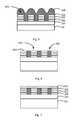
- a semiconductor substrate 102 having a surface region 104is provided.
- Semiconductor substrate 102can be a single crystal silicon wafer, a silicon germanium material, a silicon on insulator (commonly called SOI) depending on the embodiment.
- semiconductor substrate 102can have one or more MOS devices formed thereon or therein. The one or more MOS devices can be controlling circuitry for the resistive switching device, or the like in some embodiments.
- a processor, or the likemay include resistive memory memories as described herein. Because the resistive state-change memories are relatively non-volatile, the states of devices, such as processors, or the like may be maintained while power is not supplied to the processors. To a user, such capability would greatly enhance the power-on power-off performance of devices including such processors. Additionally, such capability would greatly reduce the power consumption of devices including such processors. In particular, because such resistive memories are non-volatile, the processor need not draw power to refresh the memory states, as is common with CMOS type memories. Accordingly, embodiments of the present invention are directed towards processors or other logic incorporating these memory devices, as described herein, devices (e.g. smart phones, network devices) incorporating such memory devices, and the like.
- devicese.g. smart phones, network devices
- first dielectric material 202can be silicon oxide, silicon nitride, a dielectric stack of alternating layers of silicon oxide and silicon nitride (for example, an ONO stack), a low K dielectric, a high K dielectric, or a combination, and others, depending on the application.
- First dielectric material 202can be deposited using techniques such as chemical vapor deposition, including low pressure chemical vapor deposition, plasma enhanced chemical vapor deposition, high density plasma chemical vapor deposition, atomic layer deposition (ALD), physical vapor deposition, including any combination of these, and others.
- first wiring material 302can be a suitable metal material including alloy materials, or a semiconductor material having a suitable conductivity characteristic.
- the metal materialcan be tungsten, aluminum, copper or silver, and others.
- the first wiring materialmay be a combination of conductive materials.
- these metal materialsmay be deposited using a physical vapor deposition process, chemical vapor deposition process, electroplating, or electrodeless deposition process, a combinations of these, and others.
- the semiconductor materialcan be, for example, a p-type doped silicon material, a conductive polysilicon, or the like.
- a first adhesion material 304is first formed overlying the first dielectric material 302 before deposition of the first wiring material 302 to promote adhesion of the first wiring material 302 to the first dielectric material 202 .
- a diffusion barrier material 306may also be formed overlying the first wiring material 302 to prevent, for example, the conductive material, the metal material, gasses, oxygen, or the like to contaminate other portions of the device in a specific embodiment.
- an embodiment of the methodsubjects the first wiring material ( 302 , 304 and 306 ) to a first pattern and etching process to form a first wiring structure 402 in a specific embodiment.
- the first wiring structure 402includes a plurality of first elongated structures configured to extend in a first direction 404 (into and out of the page) in a specific embodiment.
- the methoddeposits a second dielectric material 406 overlying the first wiring structure, as illustrated in FIG. 5 .
- the second dielectric material 406can be silicon oxide, silicon nitride, a dielectric stack of alternating layers of silicon oxide and silicon nitride (for example, an ONO stack), a low K dielectric, a high K dielectric, or a combination, and others, depending on the application.
- second dielectric material 406can be subjected to a planarizing process to isolate the first wiring structures 402 in a specific embodiment.
- the planarizing processcan be a chemical mechanical polishing process or an etch back process, a combination thereof, and others depending on the application.
- a surface region 504 of the diffusion barrier materialis exposed, and second dielectric material 406 remains in the spaces 502 between first wiring structure 402 .
- junction material 602includes a step of depositing a junction material 602 overlying the first wiring structure 402 and exposed surface region 504 of the second dielectric material 306 .
- junction material 602can be a conductive p-doped silicon containing material, polycrystalline silicon material having a p+ impurity characteristic or a polycrystalline silicon germanium material having a p+ impurity characteristic, or a combination thereof.
- Junction material 602can be deposited using techniques such as a chemical vapor deposition process including low pressure chemical vapor deposition process, plasma-enhanced chemical vapor deposition process, using silicon precursor such as silane (SiH 4 ), disilane (Si 2 H 6 ), or a chlorosilane in a suitable reducing environment depending on the embodiment. Deposition temperature ranges from about 380 Degree Celsius to about 450 Degree Celsius and not greater than about 440 Degree Celsius depending on the application. Alternatively, junction material 602 can be deposited using a physical vapor deposition process from a suitable silicon target.
- a chemical vapor deposition processincluding low pressure chemical vapor deposition process, plasma-enhanced chemical vapor deposition process, using silicon precursor such as silane (SiH 4 ), disilane (Si 2 H 6 ), or a chlorosilane in a suitable reducing environment depending on the embodiment. Deposition temperature ranges from about 380 Degree Celsius to about 450 Degree Celsius and not greater than about 440 Degree Celsius depending on the application
- junction material 602can be deposited using a low pressure chemical vapor deposition process using disilane at a deposition temperature ranging from about 400 Degree Celsius to about 460 Degree Celsius. In some embodiments, junction material 602 is configured to have the polycrystalline characteristic as deposited free from an anneal process.
- the methoddeposits a resistive switching material 702 overlying junction material 602 (for example, the polycrystalline silicon having the p+ impurity characteristic).
- the resistive switching material 702can include a suitable insulator material having a resistance that can be altered upon application of an electric field to the insulator material.
- the resistive switching material 702can include a silicon material.
- the silicon materialcan be an amorphous silicon material, a microcrystalline silicon material, a macro crystalline silicon material, a silicon germanium material, a silicon oxide, and including any combination of these.
- the silicon materialincludes an amorphous silicon material.
- the resistive switching material 702is characterized by a state, for example, a resistance state dependent on an electric field in the switching material.
- the switching material 702is an amorphous silicon material.
- the amorphous silicon materialhas essentially intrinsic semiconductor characteristic and is not intentionally doped in a specific embodiment.
- the amorphous siliconis also referred to as non-crystalline silicon (nc-Si).
- nc-Si non-volatile resistive switching devicesmay be fabricated using existing CMOS technologies.
- Portions of poly-silicon grainsmay form during the LPCVD process and result in an amorphous-poly silicon film.
- no p-type, n-type, or metallic impuritiesare intentionally added to the deposition chamber while forming the amorphous silicon material. Accordingly, when deposited, the amorphous silicon material is substantially free of any p-type, n-type or metallic dopants, i.e. the amorphous silicon material is undoped.
- the resistive switching material/amorphous silicon material 702may be formed from an upper region of a p+ polycrystalline silicon or p+ silicon germanium bearing layer (e.g. 602 ) using an Argon, Silicon, Oxygen plasma etch, or the like.
- a plasma etchmay use a bias power within a range of approximately 30 watts to approximately 120 watts to convert an upper region of the polysilicon or silicon germanium material 602 into a non-conductive amorphous silicon 702 having p-type impurities (from the original polycrystalline silicon or silicon germanium bearing layer 602 ).
- resistive e switching material 702may be on the order of about 2 nm to about 5 nm.
- resistive switching material 702 and junction material 602are subjected to a patterning and etching process to form one or more first structures 802 substantially free from side wall contamination (e.g. silver).
- each of the one or more first structurescomprises 802 includes at least resistive switching material 702 and junction material 602 .
- each of the one or more first structures 802are configured to be in physical and electrical contact with first wiring structures 402 .
- a third dielectric material 902is formed overlying the first structures 802 to fill a gap 906 between each of the first structures 802 .
- Third dielectric material 902can include silicon oxide, silicon nitride, a dielectric stack of alternating layers of silicon oxide and silicon nitride (for example, an ONO stack), a low K dielectric, a high K dielectric, or a combination, and others, depending on the application.
- Third dielectric material 902further forms a layer 904 having a controlled thickness overlying each of the first structures 802 , as shown.
- the methodinclude subjecting third dielectric material 902 to a patterning and etch process to form an opening structure 1002 .
- opening structure 1002 in layer 904 of third dielectric material 902overlies first structures 802 .
- opening structure 1002exposes a top surface region of first structure 802 , more specifically, a top surface region of resistive switching material 702 , as shown.
- the top surface region of the resistive switching material 702may first be provided with a thin layer of titanium, or the like, that protects resistive switching material 702 during the following steps.
- the methodincludes depositing an active conductive material 1102 at least in the opening structure 1002 overlying the resistive switching material 702 as shown in FIG. 11 .
- the active conductive material 1102may be deposited using a physical vapor deposition process, a chemical vapor deposition process, an electrochemical (for example electroplating), and an electroless deposition process and others, depending on the application.
- active conductive material 1102can be deposited overlying the resistive switching material 702 using an electroless deposition process.
- the electroless deposition processincludes first forming a first metal material to promote formation of the active conductive material overlying the resistive switching material 702 .
- the first metal materialcan be cobalt, copper, tungsten, ruthenium, and others. These metal materials can be deposited using techniques such as a physical vapor deposition process, a chemical vapor deposition process, an electrochemical deposition process, and others.
- the first metal materialcan be tungsten.
- Tungstenhas an additional advantage of having complete compatibility with conventional silicon processing.
- tungstencan be deposited using techniques such as physical vapor deposition process, chemical vapor deposition process, or a combination, and others.
- the deposited tungstenis characterized by a thickness ranging from about 30 Angstroms to about 100 Angstroms and has a good fill in the opening structures 1002 .
- the deposited tungstencan have a thickness of about 40 Angstroms to about 70 Angstroms.
- the methodincludes subjecting the first metal material, for example, the tungsten material, to a solution comprising an active metal species (e.g. silver) to form an active metal material (e.g. silver) overlying the resistive switching material 702 .
- the active metal species (e.g. silver) in the solutionis reduced by the first metal material (e.g. tungsten) in an electroless deposition process.
- the electroless deposition processincludes providing a silver species in a solution in a reaction bath.
- the silver speciescomprises a silver oxide material in a solution.
- a solution including a silver speciesis provided by TechniSol® SilvermerseTM by Technic Inc., of Rhode Island, USA.
- the solutionis characterized by a pH greater than about 7, that is, an alkaline pH, in a specific embodiment.
- the pHcan range from about 7.5 to about 11.
- the pH of the solutioncan range from about 8 to about 9.8.
- the alkaline pHmay be provided using a potassium hydroxide solution, or others, depending on the application.
- thermal energycan be applied to the reaction bath including the solution comprising the silver species to provide for a deposition temperature ranging from about 35 Degree Celsius to about 70 Degree Celsius or about 40 Degree Celsius to about 60 Degree Celsius, or the like depending on the application.
- the silver oxide concentrationcan range from about 3 percent to about 4 percent, or the like.
- the silver concentration in the reaction bathcan be adjusted using deionized water.
- the silver concentration in the reaction bathcan be adjusted using an ethylenediamine solution, also supplied by Technic Inc., of Rhode Island, USA.
- the solutionis further characterized by a suitable surface tension to allow for deposition in an opening structure having small areas.
- the deposited silvercan have a silver thickness depending substantially on a deposition time, silver oxide concentration, temperature, pH, or the like.
- the as-deposited silveris then subjected to a rinsing step using deionized water or other suitable solvent to remove residual reaction species, for example, silver oxide, potassium hydroxide, or ethyleneamine, and others.
- a rinsing stepusing deionized water or other suitable solvent to remove residual reaction species, for example, silver oxide, potassium hydroxide, or ethyleneamine, and others.
- silver material deposited on a top surface of the third dielectric material 902can be removed using a chemical mechanical polishing process, a polishing step, or the like, while the silver material remains isolated in the opening structure 1002 and in electrical and physical contact with the resistive switching material 702 in a specific embodiment.
- the first metal materiale.g. tungsten
- active conductor materiale.g. silver
- the tungsten materialis consumed and a substantially pure silver material is formed.
- the silver materialwas deposited on a silicon material, using TechniSol® SilvermerseTM and tungsten (about 50 Angstrom) was used as the reducing material. Deposition parameters were as follows:
- a solutioncomprising a silver oxide material and a potassium hydroxide in a reaction bath, the silver oxide material has a concentration of about 3-4% of silver oxide material, and the solution has a pH ranging from about 8-11.
- Immerse the silicon substrate including the tungsten material to the reaction bathcomprises silver oxide material and potassium hydroxide solution for about 1 minute to about 15 minutes,
- a second wiring material 1202is formed overlying the third dielectric material 902 and contacting the silver in the opening structures 1002 .
- the second wiring materialcan be tungsten, copper, aluminum, titanium, titanium oxide, or other suitable conductive material, depending on the application.
- the second wiringmay be formed using a physical vapor deposition process, a chemical vapor deposition process, an electroplating process, an electroless deposition process, or a combination of theses, and others.
- the second wiring material 1202is subjected to a patterning an etching process to form one or more second wiring structures.
- the second wiring structureextends in direction 110 , typically orthogonal to direction 440 . Additionally, second wiring structure maintains a direct physical and electrical contact with the silver material in the opening structures, as shown.
- the methodcontinues to complete the device by forming isolating dielectric material and other passivation steps and others as would be recognized by one skilled in the art.
- silver material deposited on a silicon substratecomprises about 97% silver and trace amount of oxygen, tungsten, and potassium.
Landscapes
- Engineering & Computer Science (AREA)
- Manufacturing & Machinery (AREA)
- Semiconductor Memories (AREA)
Abstract
Description
Claims (20)
Priority Applications (1)
| Application Number | Priority Date | Filing Date | Title |
|---|---|---|---|
| US14/546,926US9401475B1 (en) | 2010-08-23 | 2014-11-18 | Method for silver deposition for a non-volatile memory device |
Applications Claiming Priority (8)
| Application Number | Priority Date | Filing Date | Title |
|---|---|---|---|
| US12/861,666US8404553B2 (en) | 2010-08-23 | 2010-08-23 | Disturb-resistant non-volatile memory device and method |
| US38796310P | 2010-09-29 | 2010-09-29 | |
| US13/249,115US8841196B1 (en) | 2010-09-29 | 2011-09-29 | Selective deposition of silver for non-volatile memory device fabrication |
| US13/620,012US8889521B1 (en) | 2012-09-14 | 2012-09-14 | Method for silver deposition for a non-volatile memory device |
| US13/733,828US8659003B2 (en) | 2010-08-23 | 2013-01-03 | Disturb-resistant non-volatile memory device and method |
| US14/109,415US20140264242A1 (en) | 2010-08-23 | 2013-12-17 | Disturb-resistant non-volatile memory device and method |
| US14/455,822US20140346427A1 (en) | 2010-09-29 | 2014-08-08 | Selective deposition of silver for non-volatile memory device fabrication |
| US14/546,926US9401475B1 (en) | 2010-08-23 | 2014-11-18 | Method for silver deposition for a non-volatile memory device |
Related Parent Applications (2)
| Application Number | Title | Priority Date | Filing Date |
|---|---|---|---|
| US13/620,012Continuation-In-PartUS8889521B1 (en) | 2010-08-23 | 2012-09-14 | Method for silver deposition for a non-volatile memory device |
| US14/455,822Continuation-In-PartUS20140346427A1 (en) | 2010-08-23 | 2014-08-08 | Selective deposition of silver for non-volatile memory device fabrication |
Related Child Applications (1)
| Application Number | Title | Priority Date | Filing Date |
|---|---|---|---|
| US13/733,828DivisionUS8659003B2 (en) | 2010-08-23 | 2013-01-03 | Disturb-resistant non-volatile memory device and method |
Publications (1)
| Publication Number | Publication Date |
|---|---|
| US9401475B1true US9401475B1 (en) | 2016-07-26 |
Family
ID=56411331
Family Applications (1)
| Application Number | Title | Priority Date | Filing Date |
|---|---|---|---|
| US14/546,926ActiveUS9401475B1 (en) | 2010-08-23 | 2014-11-18 | Method for silver deposition for a non-volatile memory device |
Country Status (1)
| Country | Link |
|---|---|
| US (1) | US9401475B1 (en) |
Citations (247)
| Publication number | Priority date | Publication date | Assignee | Title |
|---|---|---|---|---|
| US680652A (en) | 1897-11-08 | 1901-08-13 | Leonard L Elden | Circuit-breaker. |
| US4433468A (en) | 1980-03-26 | 1984-02-28 | Nippon Electric Co., Ltd. | Method for making semiconductor device having improved thermal stress characteristics |
| US4684972A (en) | 1981-08-07 | 1987-08-04 | The British Petroleum Company, P.L.C. | Non-volatile amorphous semiconductor memory device utilizing a forming voltage |
| US4741601A (en) | 1984-10-08 | 1988-05-03 | Nec Corporation | Non-linear device for driving liquid crystal display |
| US5139911A (en) | 1989-01-04 | 1992-08-18 | Fuji Xerox Co., Ltd. | Electrophotographic photoreceptor with two part surface layer |
| US5242855A (en) | 1991-09-30 | 1993-09-07 | Nec Corporation | Method of fabricating a polycrystalline silicon film having a reduced resistivity |
| US5278085A (en) | 1992-08-11 | 1994-01-11 | Micron Semiconductor, Inc. | Single mask process for forming both n-type and p-type gates in a polycrystalline silicon layer during the formation of a semiconductor device |
| US5315131A (en) | 1990-11-22 | 1994-05-24 | Matsushita Electric Industrial Co., Ltd. | Electrically reprogrammable nonvolatile memory device |
| US5335219A (en) | 1991-01-18 | 1994-08-02 | Ovshinsky Stanford R | Homogeneous composition of microcrystalline semiconductor material, semiconductor devices and directly overwritable memory elements fabricated therefrom, and arrays fabricated from the memory elements |
| US5360981A (en) | 1989-05-11 | 1994-11-01 | British Telecommunications Public Limited Company | Amorphous silicon memory |
| US5457649A (en) | 1994-08-26 | 1995-10-10 | Microchip Technology, Inc. | Semiconductor memory device and write-once, read-only semiconductor memory array using amorphous-silicon and method therefor |
| US5538564A (en) | 1994-03-18 | 1996-07-23 | Regents Of The University Of California | Three dimensional amorphous silicon/microcrystalline silicon solar cells |
| US5541869A (en) | 1991-10-22 | 1996-07-30 | British Telecommunications, Plc | Resistive memory element |
| US5594363A (en) | 1995-04-07 | 1997-01-14 | Zycad Corporation | Logic cell and routing architecture in a field programmable gate array |
| US5614756A (en) | 1990-04-12 | 1997-03-25 | Actel Corporation | Metal-to-metal antifuse with conductive |
| US5645628A (en)* | 1994-07-14 | 1997-07-08 | Matsushita Electric Industrial Co., Ltd. | Electroless plating bath used for forming a wiring of a semiconductor device, and method of forming a wiring of a semiconductor device |
| US5707487A (en) | 1991-01-22 | 1998-01-13 | Kabushiki Kaisha Toshiba | Method of manufacturing semiconductor device |
| US5751012A (en) | 1995-06-07 | 1998-05-12 | Micron Technology, Inc. | Polysilicon pillar diode for use in a non-volatile memory cell |
| US5840608A (en) | 1996-11-22 | 1998-11-24 | United Microelectronics Corporation | High density ROM and a method of making the same |
| US5970332A (en) | 1995-03-28 | 1999-10-19 | U.S. Philips Corporation | Method of manufacturing a semiconductor device with a BiCMOS circuit |
| US5998244A (en) | 1996-08-22 | 1999-12-07 | Micron Technology, Inc. | Memory cell incorporating a chalcogenide element and method of making same |
| US6122318A (en) | 1996-10-31 | 2000-09-19 | Kabushiki Kaisha Toshiba | Video encoding apparatus and video decoding apparatus |
| US6128214A (en) | 1999-03-29 | 2000-10-03 | Hewlett-Packard | Molecular wire crossbar memory |
| US6143642A (en) | 1997-12-22 | 2000-11-07 | Vlsi Technology, Inc. | Programmable semiconductor structures and methods for making the same |
| US6180998B1 (en) | 1998-03-30 | 2001-01-30 | Lsi Logic Corporation | DRAM with built-in noise protection |
| US6259116B1 (en) | 1997-10-22 | 2001-07-10 | U.S. Philips Corporation | Multiple memory element semiconductor memory devices |
| US6291836B1 (en) | 1996-06-05 | 2001-09-18 | U. S. Philips Corporation | Method of operating a programmable, non-volatile memory device |
| US6436818B1 (en) | 1997-02-19 | 2002-08-20 | Micron Technology, Inc. | Semiconductor structure having a doped conductive layer |
| US6436765B1 (en) | 2001-02-09 | 2002-08-20 | United Microelectronics Corp. | Method of fabricating a trenched flash memory cell |
| US6492694B2 (en) | 1998-02-27 | 2002-12-10 | Micron Technology, Inc. | Highly conductive composite polysilicon gate for CMOS integrated circuits |
| US20030052330A1 (en) | 2001-09-20 | 2003-03-20 | Klein Rita J. | Electro-and electroless plating of metal in the manufacture of PCRAM devices |
| WO2003034498A1 (en) | 2001-10-16 | 2003-04-24 | Midwest Research Institute | Stacked switchable element and diode combination |
| US20030141565A1 (en) | 2002-01-28 | 2003-07-31 | Fumihiko Hirose | Diode |
| US20030174574A1 (en) | 2002-03-12 | 2003-09-18 | Perner Frederick A. | Write pulse circuit for a magnetic memory |
| US6627530B2 (en) | 2000-12-22 | 2003-09-30 | Matrix Semiconductor, Inc. | Patterning three dimensional structures |
| US20030206659A1 (en) | 1998-09-08 | 2003-11-06 | Canon Kabushiki Kaisha | Image processing apparatus including an image data encoder having at least two scalability modes and method therefor |
| US20040026682A1 (en) | 2002-06-17 | 2004-02-12 | Hai Jiang | Nano-dot memory and fabricating same |
| US6762474B1 (en) | 1998-06-10 | 2004-07-13 | Agere Systems Inc. | Method and apparatus for temperature compensation of read-only memory |
| US6768157B2 (en) | 2001-08-13 | 2004-07-27 | Advanced Micro Devices, Inc. | Memory device |
| US20040170040A1 (en) | 2002-08-02 | 2004-09-02 | Unity Semiconductor Corporation | Rewritable memory with non-linear memory element |
| US20040192006A1 (en) | 2002-02-20 | 2004-09-30 | Campbell Kristy A. | Layered resistance variable memory device and method of fabrication |
| US20040194340A1 (en) | 1998-10-14 | 2004-10-07 | Tokyo Electron Limited | Method and apparatus for surface treatment |
| US20040202041A1 (en) | 2003-04-11 | 2004-10-14 | Sharp Kabushiki Kaisha | Memory cell, memory device and manufacturing method of memory cell |
| US6815286B2 (en) | 2001-08-13 | 2004-11-09 | Advanced Micro Devices, Inc. | Memory device |
| US6838720B2 (en) | 2001-08-13 | 2005-01-04 | Advanced Micro Devices, Inc. | Memory device with active passive layers |
| US6848012B2 (en) | 2002-09-27 | 2005-01-25 | Broadcom Corporation | Method and system for an adaptive multimode media queue |
| US20050020510A1 (en) | 2002-08-29 | 2005-01-27 | Benedict Dale L. | D-mannose contraceptives |
| US20050029587A1 (en) | 1995-06-07 | 2005-02-10 | Harshfield Steven T. | Method and apparatus for forming an integrated circuit electrode having a reduced contact area |
| US6858482B2 (en) | 2002-04-10 | 2005-02-22 | Micron Technology, Inc. | Method of manufacture of programmable switching circuits and memory cells employing a glass layer |
| US6858481B2 (en) | 2001-08-13 | 2005-02-22 | Advanced Micro Devices, Inc. | Memory device with active and passive layers |
| US20050041498A1 (en) | 2003-06-16 | 2005-02-24 | Claudio Resta | Writing circuit for a phase change memory device |
| US6864127B2 (en) | 1997-04-25 | 2005-03-08 | Semiconductor Energy Laboratory Co., Ltd. | Semiconductor device and method of fabricating the same |
| US20050052915A1 (en) | 2002-12-19 | 2005-03-10 | Matrix Semiconductor, Inc. | Nonvolatile memory cell without a dielectric antifuse having high- and low-impedance states |
| US20050062045A1 (en) | 2002-10-02 | 2005-03-24 | Arup Bhattacharyya | Processes of forming stacked resistor constructions |
| US20050073881A1 (en) | 2003-10-06 | 2005-04-07 | Tran Lung The | Magnetic memory device including groups of series-connected memory elements |
| US6881994B2 (en) | 2000-08-14 | 2005-04-19 | Matrix Semiconductor, Inc. | Monolithic three dimensional array of charge storage devices containing a planarized surface |
| US6927430B2 (en) | 2001-06-28 | 2005-08-09 | Sharp Laboratories Of America, Inc. | Shared bit line cross-point memory array incorporating P/N junctions |
| US20050175099A1 (en) | 2004-02-06 | 2005-08-11 | Nokia Corporation | Transcoder and associated system, method and computer program product for low-complexity reduced resolution transcoding |
| US6939787B2 (en) | 1999-12-28 | 2005-09-06 | Fujitsu Limited | Method for fabricating semiconductor device having gate electrode with polymetal structure of polycrystalline silicon film and metal film |
| US6946719B2 (en) | 2003-12-03 | 2005-09-20 | Matrix Semiconductor, Inc | Semiconductor device including junction diode contacting contact-antifuse unit comprising silicide |
| US20060017488A1 (en) | 2004-07-21 | 2006-01-26 | Sharp Laboratories Of America, Inc. | Mono-polarity switchable PCMO resistor trimmer |
| US7020006B2 (en) | 2002-08-02 | 2006-03-28 | Unity Semiconductor Corporation | Discharge of conductive array lines in fast memory |
| US7023093B2 (en) | 2002-10-24 | 2006-04-04 | International Business Machines Corporation | Very low effective dielectric constant interconnect Structures and methods for fabricating the same |
| US20060134837A1 (en) | 1998-11-16 | 2006-06-22 | Vivek Subramanian | Vertically stacked field programmable nonvolatile memory and method of fabrication |
| US7102150B2 (en) | 2001-05-11 | 2006-09-05 | Harshfield Steven T | PCRAM memory cell and method of making same |
| US7122853B1 (en) | 2004-08-17 | 2006-10-17 | Fasl, Inc. | Method to improve yield and simplify operation of polymer memory cells |
| US20060246606A1 (en) | 2005-05-02 | 2006-11-02 | Sharp Laboratories Of America, Inc. | Self-aligned cross point resistor memory array |
| US20060281244A1 (en) | 2005-06-08 | 2006-12-14 | Masayuki Ichige | Nonvolatile semiconductor memory device and method of manufacturing the same |
| US20070008773A1 (en) | 2005-07-11 | 2007-01-11 | Matrix Semiconductor, Inc. | Nonvolatile memory cell comprising switchable resistor and transistor |
| US20070015348A1 (en) | 2005-07-18 | 2007-01-18 | Sharp Laboratories Of America, Inc. | Crosspoint resistor memory device with back-to-back Schottky diodes |
| US20070045615A1 (en) | 2005-08-31 | 2007-03-01 | Samsung Electronics Co., Ltd. | Non-volatile organic resistance random access memory device and method of manufacturing the same |
| US7187577B1 (en) | 2005-11-23 | 2007-03-06 | Grandis, Inc. | Method and system for providing current balanced writing for memory cells and magnetic devices |
| US20070087508A1 (en) | 2003-12-03 | 2007-04-19 | Herner S B | Method for making a p-i-n diode crystallized adjacent to a silicide in series with a dielectric antifuse |
| US20070091685A1 (en) | 2004-01-27 | 2007-04-26 | Guterman Daniel C | Efficient verification for coarse/fine programming of non-volatile memory |
| US20070090425A1 (en) | 2005-09-28 | 2007-04-26 | Matrix Semiconductor, Inc. | Memory cell comprising switchable semiconductor memory element with trimmable resistance |
| US20070105284A1 (en) | 2003-12-03 | 2007-05-10 | Herner S B | Method for forming a memory cell comprising a semiconductor junction diode crystallized adjacent to a silicide |
| US20070105390A1 (en) | 2005-11-09 | 2007-05-10 | Oh Travis B | Oxygen depleted etching process |
| US7221599B1 (en) | 2004-11-01 | 2007-05-22 | Spansion, Llc | Polymer memory cell operation |
| US7238607B2 (en) | 2002-12-19 | 2007-07-03 | Sandisk 3D Llc | Method to minimize formation of recess at surface planarized by chemical mechanical planarization |
| US20070205510A1 (en) | 2006-03-03 | 2007-09-06 | Lavoie Adrien R | Noble metal barrier layers |
| US20070228414A1 (en) | 2006-03-31 | 2007-10-04 | Sandisk 3D, Llc | Heterojunction device comprising a semiconductor and a resistivity-switching oxide or nitride |
| JP2007281208A (en) | 2006-04-07 | 2007-10-25 | Matsushita Electric Ind Co Ltd | Multilayer variable resistance element array, variable resistance device, multilayer nonvolatile memory element array, and nonvolatile memory device |
| US7289353B2 (en) | 2004-08-17 | 2007-10-30 | Spansion, Llc | Systems and methods for adjusting programming thresholds of polymer memory cells |
| US20070284575A1 (en) | 2005-07-18 | 2007-12-13 | Sharp Laboratories Of America, Inc. | Metal/semiconductor/metal current limiter |
| JP2007328857A (en) | 2006-06-07 | 2007-12-20 | Sony Corp | Storage device |
| US20070290186A1 (en) | 2006-05-04 | 2007-12-20 | El Mostafa Bourim | Non-volatile variable resistance memory device and method of fabricating the same |
| US20070295950A1 (en) | 2006-06-27 | 2007-12-27 | Samsung Electronics Co., Ltd. | Variable resistance random access memory device and a method of fabricating the same |
| US20070297501A1 (en) | 2006-06-08 | 2007-12-27 | Via Technologies, Inc. | Decoding Systems and Methods in Computational Core of Programmable Graphics Processing Unit |
| US20080002481A1 (en) | 2002-12-20 | 2008-01-03 | Dietmar Gogl | Integrated Circuit, Method of Operating an Integrated Circuit, Method of Manufacturing an Integrated Circuit, Memory Module, Stackable Memory Module |
| US20080006907A1 (en) | 2006-07-06 | 2008-01-10 | Samsung Electronics Co., Ltd | Non-volatile memory device including a variable resistance material |
| US7324363B2 (en) | 2005-12-12 | 2008-01-29 | Synopsys, Inc. | SPICE optimized for arrays |
| US20080048164A1 (en) | 2006-07-11 | 2008-02-28 | Matsushita Electric Industrial Co., Ltd. | Electro-resistance element, method of manufacturing the same and electro-resistance memory using the same |
| US20080090337A1 (en) | 2006-10-03 | 2008-04-17 | Williams R Stanley | Electrically actuated switch |
| US20080089110A1 (en) | 2006-10-16 | 2008-04-17 | Warren Robinett | Crossbar-memory systems and methods for writing to and reading from crossbar memory junctions of crossbar-memory systems |
| US7365411B2 (en) | 2004-08-12 | 2008-04-29 | Micron Technology, Inc. | Resistance variable memory with temperature tolerant materials |
| US20080106925A1 (en) | 2006-11-08 | 2008-05-08 | Symetrix Corporation | Correlated electron memory |
| US20080106926A1 (en) | 2006-11-08 | 2008-05-08 | Symetrix Corporation | Non-volatile resistance switching memories and methods of making same |
| US7405418B2 (en) | 2004-02-17 | 2008-07-29 | Infineon Technologies Ag | Memory device electrode with a surface structure |
| US20080185567A1 (en) | 2007-02-05 | 2008-08-07 | Nitin Kumar | Methods for forming resistive switching memory elements |
| US20080198934A1 (en) | 2007-02-20 | 2008-08-21 | Edward Hong | Motion refinement engine for use in video encoding in accordance with a plurality of sub-pixel resolutions and methods for use therewith |
| US20080206931A1 (en) | 2002-07-26 | 2008-08-28 | Laurent Breuil | Nonvolatile memory element and production method thereof and storage memory arrangement |
| US20080205179A1 (en) | 2007-02-28 | 2008-08-28 | Qimonda Ag | Integrated circuit having a memory array |
| US20080220601A1 (en) | 2007-03-05 | 2008-09-11 | Nitin Kumar | Methods for forming nonvolatile memory elements with resistive-switching metal oxides |
| US20080232160A1 (en) | 2007-02-27 | 2008-09-25 | International Business Machines Corporation | Rectifying element for a crosspoint based memory array architecture |
| US20080242051A1 (en) | 2007-03-26 | 2008-10-02 | Semiconductor Energy Laboratory Co., Ltd. | Method for manufacturing semiconductor device |
| US20080278990A1 (en) | 2007-05-09 | 2008-11-13 | Pragati Kumar | Resistive-switching nonvolatile memory elements |
| US20080304312A1 (en) | 2007-06-11 | 2008-12-11 | Macronix International Co., Ltd. | Resistance memory with tungsten compound and manufacturing |
| US20080311722A1 (en) | 2007-06-15 | 2008-12-18 | Sandisk 3D Llc | Method for forming polycrystalline thin film bipolar transistors |
| US20090001345A1 (en) | 2007-06-29 | 2009-01-01 | April Schricker | Memory cell that employs a selectively deposited reversible resistance-switching element and methods of forming the same |
| US20090003717A1 (en) | 2007-06-28 | 2009-01-01 | Mitsubishi Electric Corporation | Image encoding device, image decoding device, image encoding method and image decoding method |
| US7474000B2 (en) | 2003-12-05 | 2009-01-06 | Sandisk 3D Llc | High density contact to relaxed geometry layers |
| WO2009005699A1 (en) | 2007-06-29 | 2009-01-08 | Sandisk 3D, Llc | Memory cell that employs a selectively grown reversible resistance-switching element and methods of forming the same |
| US20090014707A1 (en) | 2006-10-20 | 2009-01-15 | Wei Lu | Non-volatile solid state resistive switching devices |
| US20090052226A1 (en) | 2007-08-24 | 2009-02-26 | Samsung Electronics Co., Ltd | Resistive random access memory device |
| US7499355B2 (en) | 2006-07-31 | 2009-03-03 | Sandisk 3D Llc | High bandwidth one time field-programmable memory |
| US20090095951A1 (en) | 2007-10-12 | 2009-04-16 | Ovonyx, Inc. | Memory Device With Low Reset Current |
| US7521705B2 (en) | 2005-08-15 | 2009-04-21 | Micron Technology, Inc. | Reproducible resistance variable insulating memory devices having a shaped bottom electrode |
| US7534625B2 (en) | 2004-09-24 | 2009-05-19 | Karpov Ilya V | Phase change memory with damascene memory element |
| US20090134432A1 (en) | 2007-11-22 | 2009-05-28 | Kabushiki Kaisha Toshiba | Nonvolatile semiconductor memory device and method of manufacturing the same |
| US7541252B2 (en) | 2006-11-09 | 2009-06-02 | Samsung Electronics Co., Ltd. | Methods of fabricating a semiconductor device including a self-aligned cell diode |
| US20090152737A1 (en) | 2000-07-14 | 2009-06-18 | Micron Technology, Inc. | Memory devices having contact features |
| US7550380B2 (en) | 2004-11-03 | 2009-06-23 | Micron Technology, Inc. | Electroless plating of metal caps for chalcogenide-based memory devices |
| US20090168486A1 (en) | 2007-12-27 | 2009-07-02 | Sandisk 3D Llc | Large capacity one-time programmable memory cell using metal oxides |
| US7566643B2 (en)* | 2007-07-23 | 2009-07-28 | Ovonyx, Inc. | Liquid phase deposition of contacts in programmable resistance and switching devices |
| US20090231910A1 (en) | 2008-03-11 | 2009-09-17 | Micron Technology, Inc. | Non-volatile memory with resistive access component |
| US20090250787A1 (en) | 2008-04-07 | 2009-10-08 | Toshie Kutsunai | Semiconductor storage device and manufacturing method of the same |
| US20090257265A1 (en) | 2008-04-11 | 2009-10-15 | Sandisk 3D Llc | Multilevel nonvolatile memory device containing a carbon storage material and methods of making and using same |
| US20090256130A1 (en) | 2008-04-11 | 2009-10-15 | Sandisk 3D Llc | Memory cell that employs a selectively fabricated carbon nano-tube reversible resistance-switching element, and methods of forming the same |
| US7606059B2 (en) | 2003-03-18 | 2009-10-20 | Kabushiki Kaisha Toshiba | Three-dimensional programmable resistance memory device with a read/write circuit stacked under a memory cell array |
| US20090267047A1 (en) | 2008-04-28 | 2009-10-29 | Hitachi, Ltd. | Semiconductor memory device and manufacturing method thereof |
| US7615439B1 (en) | 2008-09-29 | 2009-11-10 | Sandisk Corporation | Damascene process for carbon memory element with MIIM diode |
| US20090298224A1 (en) | 2002-12-13 | 2009-12-03 | Lowrey Tyler A | Memory and Access Device and Method Therefor |
| US20090321789A1 (en) | 2008-06-30 | 2009-12-31 | Sandisk 3D Llc | Triangle two dimensional complementary patterning of pillars |
| US20100007937A1 (en) | 2006-11-09 | 2010-01-14 | Sage Electrochromics, Inc. | Method of making an ion-switching device without a separate lithiation step |
| US20100012914A1 (en) | 2008-07-18 | 2010-01-21 | Sandisk 3D Llc | Carbon-based resistivity-switching materials and methods of forming the same |
| US20100019221A1 (en) | 2008-07-22 | 2010-01-28 | Macronix International Co., Ltd. | Fully self-aligned pore-type memory cell having diode access device |
| US20100019310A1 (en) | 2008-07-25 | 2010-01-28 | Kabushiki Kaisha Toshiba | Semiconductor memory device |
| US20100032637A1 (en) | 2008-08-06 | 2010-02-11 | Hitachi, Ltd. | Nonvolatile memory device and method of manufacturing the same |
| US20100034518A1 (en) | 2003-11-10 | 2010-02-11 | Panasonic Corporation | Integrated circuit for use in a playback apparatus |
| US20100032638A1 (en) | 2008-08-07 | 2010-02-11 | Sandisk 3D Llc | Memory cell that includes a carbon-based memory element and methods of forming the same |
| US20100046622A1 (en) | 2006-12-14 | 2010-02-25 | Thomson Licensing | Method and apparatus for encoding and/or decoding bit depth scalable video data using adaptive enhancement layer residual prediction |
| US20100044708A1 (en) | 2008-08-19 | 2010-02-25 | Chunghwa Picture Tubes, Ltd. | Thin film transistor, pixel structure and fabrication methods thereof |
| US20100085798A1 (en) | 2008-10-08 | 2010-04-08 | The Regents Of The University Of Michigan | Silicon-based nanoscale resistive device with adjustable resistance |
| US20100084625A1 (en) | 2008-10-02 | 2010-04-08 | Guy Wicker | Memory Device |
| US20100090192A1 (en) | 2006-08-31 | 2010-04-15 | Nxp, B.V. | Method for controlled formation of the resistive switching material in a resistive switching device and device obtained thereof |
| US20100101290A1 (en) | 2008-10-24 | 2010-04-29 | Antonio Bertolotto | Method for the production of an agent for treatment of agricultural soils |
| US20100102290A1 (en) | 2008-10-20 | 2010-04-29 | The Regents Of The University Of Michigan | Silicon based nanoscale crossbar memory |
| US7719001B2 (en) | 2006-06-28 | 2010-05-18 | Semiconductor Energy Laboratory Co., Ltd | Semiconductor device with metal oxides and an organic compound |
| US7729158B2 (en) | 2003-04-03 | 2010-06-01 | Kabushiki Kaisha Toshiba | Resistance change memory device |
| US7728318B2 (en) | 2006-11-16 | 2010-06-01 | Sandisk Corporation | Nonvolatile phase change memory cell having a reduced contact area |
| US20100157651A1 (en) | 2008-12-18 | 2010-06-24 | Sandisk 3D Llc | Method of programming a nonvolatile memory device containing a carbon storage material |
| US20100157710A1 (en) | 2008-12-19 | 2010-06-24 | Unity Semiconductor Corporation | Array Operation Using A Schottky Diode As a Non-Ohmic Isolation Device |
| US20100163828A1 (en) | 2008-12-30 | 2010-07-01 | Industrial Technology Research Institute | Phase change memory devices and methods for fabricating the same |
| US7749805B2 (en) | 2005-03-10 | 2010-07-06 | Qimonda Ag | Method for manufacturing an integrated circuit including an electrolyte material layer |
| US20100176368A1 (en) | 2009-01-14 | 2010-07-15 | Ko Nikka | Method of manufacturing semiconductor memory device, and semiconductor memory device |
| US7772581B2 (en) | 2006-09-11 | 2010-08-10 | Macronix International Co., Ltd. | Memory device having wide area phase change element and small electrode contact area |
| US7786464B2 (en) | 2007-11-20 | 2010-08-31 | Infineon Technologies Ag | Integrated circuit having dielectric layer including nanocrystals |
| US7786589B2 (en) | 2006-12-06 | 2010-08-31 | Kabushiki Kaisha Toshiba | Semiconductor device and method for manufacturing semiconductor device |
| US20100221868A1 (en) | 2007-12-04 | 2010-09-02 | Regino Sandoval | Active Material Devices with Containment Layer |
| US20100219510A1 (en) | 2008-06-30 | 2010-09-02 | Sandisk 3D Llc | Method for fabricating high density pillar structures by double patterning using positive photoresist |
| US7824956B2 (en) | 2007-06-29 | 2010-11-02 | Sandisk 3D Llc | Memory cell that employs a selectively grown reversible resistance-switching element and methods of forming the same |
| US7829875B2 (en) | 2006-03-31 | 2010-11-09 | Sandisk 3D Llc | Nonvolatile rewritable memory cell comprising a resistivity-switching oxide or nitride and an antifuse |
| US7835170B2 (en) | 2005-05-09 | 2010-11-16 | Nantero, Inc. | Memory elements and cross point switches and arrays of same using nonvolatile nanotube blocks |
| US20100321095A1 (en) | 2008-06-10 | 2010-12-23 | Takumi Mikawa | Semiconductor device, manufacturing method of semiconductor device, semiconductor chip and system |
| US7859884B2 (en) | 2005-01-19 | 2010-12-28 | Sandisk 3D Llc | Structure and method for biasing phase change memory array for reliable writing |
| US7858468B2 (en) | 2008-10-30 | 2010-12-28 | Micron Technology, Inc. | Memory devices and formation methods |
| US20110006275A1 (en) | 2009-07-13 | 2011-01-13 | Seagate Technology Llc | Non-volatile resistive sense memory |
| US7881097B2 (en) | 2006-12-26 | 2011-02-01 | Sony Corporation | Storage element and memory |
| KR20110014248A (en) | 2010-11-28 | 2011-02-10 | 오세영 | Night light emitting panel device for solar energy supply |
| US7897953B2 (en) | 2008-01-16 | 2011-03-01 | Micron Technology, Inc. | Multi-level programmable PCRAM memory |
| US7898838B2 (en) | 2008-10-31 | 2011-03-01 | Seagate Technology Llc | Resistive sense memory calibration for self-reference read method |
| US20110068373A1 (en) | 2009-09-24 | 2011-03-24 | Kabushiki Kaisha Toshiba | Semiconductor memory device |
| US7920412B2 (en) | 2006-09-29 | 2011-04-05 | Kabushiki Kaisha Toshiba | Magnetic random access memory and method of manufacturing the same |
| US7924138B2 (en) | 2007-03-01 | 2011-04-12 | Fujitsu Limited | Semiconductor device and manufacturing method of the same |
| US20110089391A1 (en) | 2009-10-20 | 2011-04-21 | Andrei Mihnea | Punch-through diode steering element |
| US20110128779A1 (en) | 2009-11-30 | 2011-06-02 | Andrea Redaelli | Memory including a selector switch on a variable resistance memory cell |
| US20110133149A1 (en) | 2009-12-04 | 2011-06-09 | Sonehara Takeshi | Resistance change memory and manufacturing method thereof |
| US20110136327A1 (en) | 2009-12-03 | 2011-06-09 | Applied Materials, Inc. | High mobility monolithic p-i-n diodes |
| US7968419B2 (en) | 2005-07-18 | 2011-06-28 | Sharp Laboratories Of America, Inc. | Back-to-back metal/semiconductor/metal (MSM) Schottky diode |
| US20110155991A1 (en) | 2009-12-29 | 2011-06-30 | Industrial Technology Research Institute | Resistive memory device and fabricating method thereof |
| US7984776B2 (en) | 2007-03-30 | 2011-07-26 | The Regents Of The University Of Michigan | Energy storage and control system for a vehicle electrified drivetrain |
| US20110194329A1 (en) | 2010-02-09 | 2011-08-11 | Sony Corporation | Memory component, memory device, and method of operating memory device |
| US20110198557A1 (en) | 2008-02-07 | 2011-08-18 | International Business Machines Corporation | Method for fabrication of crystalline diodes for resistive memories |
| US8004882B2 (en) | 2004-06-04 | 2011-08-23 | Micron Technology, Inc. | Spintronic devices with integrated transistors |
| US20110204312A1 (en) | 2008-05-10 | 2011-08-25 | Intermolecular, Inc. | Confinement techniques for non-volatile resistive-switching memories |
| US20110205782A1 (en) | 2010-02-23 | 2011-08-25 | Xiying Chen Costa | Step soft program for reversible resistivity-switching elements |
| US20110212616A1 (en) | 2010-02-26 | 2011-09-01 | Robert Seidel | Metallization system of a semiconductor device comprising rounded interconnects formed by hard mask rounding |
| US8018760B2 (en) | 2006-12-28 | 2011-09-13 | Panasonic Corporation | Resistance variable element and resistance variable memory apparatus |
| US8021897B2 (en) | 2009-02-19 | 2011-09-20 | Micron Technology, Inc. | Methods of fabricating a cross point memory array |
| US20110227028A1 (en) | 2010-03-16 | 2011-09-22 | Deepak Chandra Sekar | Bottom electrodes for use with metal oxide resistivity switching layers |
| US8045364B2 (en) | 2009-12-18 | 2011-10-25 | Unity Semiconductor Corporation | Non-volatile memory device ion barrier |
| US8054674B2 (en) | 2007-05-10 | 2011-11-08 | Sharp Kabushiki Kaisha | Variable resistive element, manufacturing method for same, and non-volatile semiconductor memory device |
| US20110284814A1 (en) | 2010-05-24 | 2011-11-24 | Guobiao Zhang | Large Bit-Per-Cell Three-Dimensional Mask-Programmable Read-Only Memory |
| US8067815B2 (en) | 2008-12-11 | 2011-11-29 | Macronix International Co., Lt.d. | Aluminum copper oxide based memory devices and methods for manufacture |
| US20110299324A1 (en) | 2008-10-31 | 2011-12-08 | Seagate Technology Llc | Write current compensation using word line boosting circuitry |
| US20110305064A1 (en)* | 2010-06-11 | 2011-12-15 | Crossbar, Inc. | Interface control for improved switching in rram |
| US20110312151A1 (en)* | 2010-06-11 | 2011-12-22 | Crossbar Inc. | Pillar structure for memory device and method |
| US8084830B2 (en) | 2009-02-24 | 2011-12-27 | Kabushiki Kaisha Toshiba | Nonvolatile semiconductor memory device |
| US20110317470A1 (en) | 2010-06-24 | 2011-12-29 | The Regents Of The University Of Michigan | Rectification element and method for resistive switching for non volatile memory device |
| US8088688B1 (en) | 2010-11-05 | 2012-01-03 | Crossbar, Inc. | p+ polysilicon material on aluminum for non-volatile memory device and method |
| US20120001145A1 (en) | 2008-12-31 | 2012-01-05 | Michele Magistretti | Avoiding degradation of chalcogenide material during definition of multilayer stack structure |
| US20120001146A1 (en)* | 2010-06-24 | 2012-01-05 | The Regents Of The University Of Michigan | Nanoscale metal oxide resistive switching element |
| EP2405441A1 (en) | 2010-07-09 | 2012-01-11 | Crossbar, Inc. | Resistive memory using SiGe material |
| US20120007035A1 (en) | 2010-07-12 | 2012-01-12 | Crossbar, Inc. | Intrinsic Programming Current Control for a RRAM |
| US8097874B2 (en) | 2008-10-30 | 2012-01-17 | Seagate Technology Llc | Programmable resistive memory cell with sacrificial metal |
| EP2408035A2 (en) | 2010-07-13 | 2012-01-18 | Crossbar, Inc. | Two terminal resistive switching device structure and method of fabricating |
| US20120012808A1 (en) | 2004-09-29 | 2012-01-19 | Herner S Brad | Deposited semiconductor structure to minimize n-type dopant diffusion and method of making |
| US20120012806A1 (en) | 2010-07-13 | 2012-01-19 | Crossbar, Inc. | Improved on/off ratio for non-volatile memory device and method |
| US20120025161A1 (en) | 2008-02-27 | 2012-02-02 | Manuj Rathor | Diode and resistive memory device structures |
| US20120033479A1 (en) | 2010-08-06 | 2012-02-09 | Lsi Corporation | Modification of logic by morphological manipulation of a semiconductor resistive element |
| US20120043654A1 (en) | 2010-08-19 | 2012-02-23 | Taiwan Semiconductor Manufacturing Company, Ltd. | Mechanisms for forming copper pillar bumps using patterned anodes |
| US20120043621A1 (en) | 2010-08-23 | 2012-02-23 | Crossbar, Inc. | Stackable non-volatile resistive switching memory device and method |
| US20120043520A1 (en)* | 2010-08-23 | 2012-02-23 | Crossbar, Inc. | Disturb-resistant non-volatile memory device and method |
| US20120043519A1 (en) | 2010-08-23 | 2012-02-23 | Crossbar, Inc. | Device switching using layered device structure |
| US8143092B2 (en) | 2008-03-10 | 2012-03-27 | Pragati Kumar | Methods for forming resistive switching memory elements by heating deposited layers |
| US20120076203A1 (en) | 2009-05-29 | 2012-03-29 | Mitsubishi Electric Corporation | Video encoding device, video decoding device, video encoding method, and video decoding method |
| US20120074507A1 (en) | 2010-09-29 | 2012-03-29 | Crossbar, Inc. | Integration of an amorphous silicon resistive switching device |
| US20120074374A1 (en) | 2010-09-29 | 2012-03-29 | Crossbar, Inc. | Conductive path in switching material in a resistive random access memory device and control |
| US20120104351A1 (en) | 2010-07-01 | 2012-05-03 | Zhiqiang Wei | Non-volatile memory cell, non-volatile memory cell array, and method of manufacturing the same |
| US20120108030A1 (en) | 2010-10-27 | 2012-05-03 | Crossbar, Inc. | Method for obtaining smooth, continuous silver film |
| US8183553B2 (en) | 2009-04-10 | 2012-05-22 | Intermolecular, Inc. | Resistive switching memory element including doped silicon electrode |
| US20120140816A1 (en) | 2010-12-01 | 2012-06-07 | Jean-Francois Franche | Method and system for parallel encoding of a video |
| US20120145984A1 (en) | 2010-12-13 | 2012-06-14 | Peter Rabkin | Punch-through diode |
| US20120155146A1 (en) | 2010-12-20 | 2012-06-21 | Yoshihiro Ueda | Resistance-change memory |
| US8207064B2 (en) | 2009-09-17 | 2012-06-26 | Sandisk 3D Llc | 3D polysilicon diode with low contact resistance and method for forming same |
| US8231998B2 (en) | 2007-03-30 | 2012-07-31 | The Regents Of The University Of Michigan | Deposited microarchitectured battery and manufacturing method |
| US8233308B2 (en) | 2007-06-29 | 2012-07-31 | Sandisk 3D Llc | Memory cell that employs a selectively deposited reversible resistance-switching element and methods of forming the same |
| US8237146B2 (en) | 2010-02-24 | 2012-08-07 | Sandisk 3D Llc | Memory cell with silicon-containing carbon switching layer and methods for forming the same |
| US20120205606A1 (en) | 2011-02-14 | 2012-08-16 | Dongguk University Industry-Academic Cooperation Foundation | Nonvolatile Memory Device Using The Resistive Switching of Graphene Oxide And The Fabrication Method Thereof |
| US8258020B2 (en) | 2010-11-04 | 2012-09-04 | Crossbar Inc. | Interconnects for stacked non-volatile memory device and method |
| US20120236625A1 (en)* | 2011-03-18 | 2012-09-20 | Sony Corporation | Memory element and memory device |
| US20120235112A1 (en) | 2010-11-30 | 2012-09-20 | Huo Zongliang | Resistive switching memory and method for manufacturing the same |
| US8274812B2 (en) | 2010-06-14 | 2012-09-25 | Crossbar, Inc. | Write and erase scheme for resistive memory device |
| US20120250183A1 (en) | 2011-03-31 | 2012-10-04 | Nidec Corporation | Motor and storage disk drive |
| US20120269275A1 (en) | 2010-10-20 | 2012-10-25 | Nokia Corporation | Method and device for video coding and decoding |
| US8315079B2 (en) | 2010-10-07 | 2012-11-20 | Crossbar, Inc. | Circuit for concurrent read operation and method therefor |
| US8320160B2 (en) | 2011-03-18 | 2012-11-27 | Crossbar, Inc. | NAND architecture having a resistive memory cell connected to a control gate of a field-effect transistor |
| US20120305874A1 (en) | 2011-05-31 | 2012-12-06 | Crossbar, Inc. | Vertical Diodes for Non-Volatile Memory Device |
| US20120326265A1 (en) | 2011-06-24 | 2012-12-27 | International Business Machines Corporation | Method of forming memory cell access device |
| US20130009128A1 (en) | 2010-03-31 | 2013-01-10 | Gilberto Ribeiro | Nanoscale switching device |
| US20130020548A1 (en) | 2011-07-22 | 2013-01-24 | Crossbar, Inc. | Seed layer for a p+ silicon germanium material for a non-volatile memory device and method |
| US8385100B2 (en) | 2009-12-08 | 2013-02-26 | Intel Corporation | Energy-efficient set write of phase change memory with switch |
| US8389971B2 (en) | 2010-10-14 | 2013-03-05 | Sandisk 3D Llc | Memory cells having storage elements that share material layers with steering elements and methods of forming the same |
| US8467227B1 (en) | 2010-11-04 | 2013-06-18 | Crossbar, Inc. | Hetero resistive switching material layer in RRAM device and method |
| US8587989B2 (en) | 2008-06-20 | 2013-11-19 | Nantero Inc. | NRAM arrays with nanotube blocks, nanotube traces, and nanotube planes and methods of making same |
| US8658476B1 (en) | 2012-04-20 | 2014-02-25 | Crossbar, Inc. | Low temperature P+ polycrystalline silicon material for non-volatile memory device |
| US8716098B1 (en) | 2012-03-09 | 2014-05-06 | Crossbar, Inc. | Selective removal method and structure of silver in resistive switching device for a non-volatile memory device |
- 2014
- 2014-11-18USUS14/546,926patent/US9401475B1/enactiveActive
Patent Citations (285)
| Publication number | Priority date | Publication date | Assignee | Title |
|---|---|---|---|---|
| US680652A (en) | 1897-11-08 | 1901-08-13 | Leonard L Elden | Circuit-breaker. |
| US4433468A (en) | 1980-03-26 | 1984-02-28 | Nippon Electric Co., Ltd. | Method for making semiconductor device having improved thermal stress characteristics |
| US4684972A (en) | 1981-08-07 | 1987-08-04 | The British Petroleum Company, P.L.C. | Non-volatile amorphous semiconductor memory device utilizing a forming voltage |
| US4741601A (en) | 1984-10-08 | 1988-05-03 | Nec Corporation | Non-linear device for driving liquid crystal display |
| US5139911A (en) | 1989-01-04 | 1992-08-18 | Fuji Xerox Co., Ltd. | Electrophotographic photoreceptor with two part surface layer |
| US5360981A (en) | 1989-05-11 | 1994-11-01 | British Telecommunications Public Limited Company | Amorphous silicon memory |
| US5614756A (en) | 1990-04-12 | 1997-03-25 | Actel Corporation | Metal-to-metal antifuse with conductive |
| US5315131A (en) | 1990-11-22 | 1994-05-24 | Matsushita Electric Industrial Co., Ltd. | Electrically reprogrammable nonvolatile memory device |
| US5335219A (en) | 1991-01-18 | 1994-08-02 | Ovshinsky Stanford R | Homogeneous composition of microcrystalline semiconductor material, semiconductor devices and directly overwritable memory elements fabricated therefrom, and arrays fabricated from the memory elements |
| US5707487A (en) | 1991-01-22 | 1998-01-13 | Kabushiki Kaisha Toshiba | Method of manufacturing semiconductor device |
| US5242855A (en) | 1991-09-30 | 1993-09-07 | Nec Corporation | Method of fabricating a polycrystalline silicon film having a reduced resistivity |
| US5541869A (en) | 1991-10-22 | 1996-07-30 | British Telecommunications, Plc | Resistive memory element |
| US5278085A (en) | 1992-08-11 | 1994-01-11 | Micron Semiconductor, Inc. | Single mask process for forming both n-type and p-type gates in a polycrystalline silicon layer during the formation of a semiconductor device |
| US5538564A (en) | 1994-03-18 | 1996-07-23 | Regents Of The University Of California | Three dimensional amorphous silicon/microcrystalline silicon solar cells |
| US5645628A (en)* | 1994-07-14 | 1997-07-08 | Matsushita Electric Industrial Co., Ltd. | Electroless plating bath used for forming a wiring of a semiconductor device, and method of forming a wiring of a semiconductor device |
| US5457649A (en) | 1994-08-26 | 1995-10-10 | Microchip Technology, Inc. | Semiconductor memory device and write-once, read-only semiconductor memory array using amorphous-silicon and method therefor |
| US5714416A (en) | 1994-08-26 | 1998-02-03 | Microchip Technology Incorporated | Semiconductor memory device and write-once, read-only semiconductor memory array using amorphous-silicon and method therefor |
| US5970332A (en) | 1995-03-28 | 1999-10-19 | U.S. Philips Corporation | Method of manufacturing a semiconductor device with a BiCMOS circuit |
| US5594363A (en) | 1995-04-07 | 1997-01-14 | Zycad Corporation | Logic cell and routing architecture in a field programmable gate array |
| US20050029587A1 (en) | 1995-06-07 | 2005-02-10 | Harshfield Steven T. | Method and apparatus for forming an integrated circuit electrode having a reduced contact area |
| US5751012A (en) | 1995-06-07 | 1998-05-12 | Micron Technology, Inc. | Polysilicon pillar diode for use in a non-volatile memory cell |
| US6291836B1 (en) | 1996-06-05 | 2001-09-18 | U. S. Philips Corporation | Method of operating a programmable, non-volatile memory device |
| US5998244A (en) | 1996-08-22 | 1999-12-07 | Micron Technology, Inc. | Memory cell incorporating a chalcogenide element and method of making same |
| US6122318A (en) | 1996-10-31 | 2000-09-19 | Kabushiki Kaisha Toshiba | Video encoding apparatus and video decoding apparatus |
| US5840608A (en) | 1996-11-22 | 1998-11-24 | United Microelectronics Corporation | High density ROM and a method of making the same |
| US6436818B1 (en) | 1997-02-19 | 2002-08-20 | Micron Technology, Inc. | Semiconductor structure having a doped conductive layer |
| US6864127B2 (en) | 1997-04-25 | 2005-03-08 | Semiconductor Energy Laboratory Co., Ltd. | Semiconductor device and method of fabricating the same |
| US6259116B1 (en) | 1997-10-22 | 2001-07-10 | U.S. Philips Corporation | Multiple memory element semiconductor memory devices |
| US6143642A (en) | 1997-12-22 | 2000-11-07 | Vlsi Technology, Inc. | Programmable semiconductor structures and methods for making the same |
| US6492694B2 (en) | 1998-02-27 | 2002-12-10 | Micron Technology, Inc. | Highly conductive composite polysilicon gate for CMOS integrated circuits |
| US6180998B1 (en) | 1998-03-30 | 2001-01-30 | Lsi Logic Corporation | DRAM with built-in noise protection |
| US6762474B1 (en) | 1998-06-10 | 2004-07-13 | Agere Systems Inc. | Method and apparatus for temperature compensation of read-only memory |
| US20030206659A1 (en) | 1998-09-08 | 2003-11-06 | Canon Kabushiki Kaisha | Image processing apparatus including an image data encoder having at least two scalability modes and method therefor |
| US20040194340A1 (en) | 1998-10-14 | 2004-10-07 | Tokyo Electron Limited | Method and apparatus for surface treatment |
| US20060134837A1 (en) | 1998-11-16 | 2006-06-22 | Vivek Subramanian | Vertically stacked field programmable nonvolatile memory and method of fabrication |
| US6128214A (en) | 1999-03-29 | 2000-10-03 | Hewlett-Packard | Molecular wire crossbar memory |
| US6939787B2 (en) | 1999-12-28 | 2005-09-06 | Fujitsu Limited | Method for fabricating semiconductor device having gate electrode with polymetal structure of polycrystalline silicon film and metal film |
| US20120080798A1 (en) | 2000-07-14 | 2012-04-05 | Round Rock Research, Llc | Memory devices having contact features |
| US20090152737A1 (en) | 2000-07-14 | 2009-06-18 | Micron Technology, Inc. | Memory devices having contact features |
| US6881994B2 (en) | 2000-08-14 | 2005-04-19 | Matrix Semiconductor, Inc. | Monolithic three dimensional array of charge storage devices containing a planarized surface |
| US6627530B2 (en) | 2000-12-22 | 2003-09-30 | Matrix Semiconductor, Inc. | Patterning three dimensional structures |
| US6436765B1 (en) | 2001-02-09 | 2002-08-20 | United Microelectronics Corp. | Method of fabricating a trenched flash memory cell |
| US7102150B2 (en) | 2001-05-11 | 2006-09-05 | Harshfield Steven T | PCRAM memory cell and method of making same |
| US6927430B2 (en) | 2001-06-28 | 2005-08-09 | Sharp Laboratories Of America, Inc. | Shared bit line cross-point memory array incorporating P/N junctions |
| US6858481B2 (en) | 2001-08-13 | 2005-02-22 | Advanced Micro Devices, Inc. | Memory device with active and passive layers |
| US6838720B2 (en) | 2001-08-13 | 2005-01-04 | Advanced Micro Devices, Inc. | Memory device with active passive layers |
| US6815286B2 (en) | 2001-08-13 | 2004-11-09 | Advanced Micro Devices, Inc. | Memory device |
| US7026702B2 (en) | 2001-08-13 | 2006-04-11 | Advanced Micro Devices, Inc. | Memory device |
| US7254053B2 (en) | 2001-08-13 | 2007-08-07 | Advanced Micro Devices, Inc. | Active programming and operation of a memory device |
| US6768157B2 (en) | 2001-08-13 | 2004-07-27 | Advanced Micro Devices, Inc. | Memory device |
| US6864522B2 (en) | 2001-08-13 | 2005-03-08 | Advanced Micro Devices, Inc. | Memory device |
| US20030052330A1 (en) | 2001-09-20 | 2003-03-20 | Klein Rita J. | Electro-and electroless plating of metal in the manufacture of PCRAM devices |
| WO2003034498A1 (en) | 2001-10-16 | 2003-04-24 | Midwest Research Institute | Stacked switchable element and diode combination |
| JP2005506703A (en) | 2001-10-16 | 2005-03-03 | ミッドウエスト リサーチ インスティチュート | Stacked switchable elements and diode combinations |
| US20030141565A1 (en) | 2002-01-28 | 2003-07-31 | Fumihiko Hirose | Diode |
| US20040192006A1 (en) | 2002-02-20 | 2004-09-30 | Campbell Kristy A. | Layered resistance variable memory device and method of fabrication |
| US20030174574A1 (en) | 2002-03-12 | 2003-09-18 | Perner Frederick A. | Write pulse circuit for a magnetic memory |
| US6858482B2 (en) | 2002-04-10 | 2005-02-22 | Micron Technology, Inc. | Method of manufacture of programmable switching circuits and memory cells employing a glass layer |
| US7479650B2 (en) | 2002-04-10 | 2009-01-20 | Micron Technology, Inc. | Method of manufacture of programmable conductor memory |
| US20040026682A1 (en) | 2002-06-17 | 2004-02-12 | Hai Jiang | Nano-dot memory and fabricating same |
| US20080206931A1 (en) | 2002-07-26 | 2008-08-28 | Laurent Breuil | Nonvolatile memory element and production method thereof and storage memory arrangement |
| US20040170040A1 (en) | 2002-08-02 | 2004-09-02 | Unity Semiconductor Corporation | Rewritable memory with non-linear memory element |
| US7020006B2 (en) | 2002-08-02 | 2006-03-28 | Unity Semiconductor Corporation | Discharge of conductive array lines in fast memory |
| US20050020510A1 (en) | 2002-08-29 | 2005-01-27 | Benedict Dale L. | D-mannose contraceptives |
| US6848012B2 (en) | 2002-09-27 | 2005-01-25 | Broadcom Corporation | Method and system for an adaptive multimode media queue |
| US20050062045A1 (en) | 2002-10-02 | 2005-03-24 | Arup Bhattacharyya | Processes of forming stacked resistor constructions |
| US7023093B2 (en) | 2002-10-24 | 2006-04-04 | International Business Machines Corporation | Very low effective dielectric constant interconnect Structures and methods for fabricating the same |
| US20090298224A1 (en) | 2002-12-13 | 2009-12-03 | Lowrey Tyler A | Memory and Access Device and Method Therefor |
| US20050052915A1 (en) | 2002-12-19 | 2005-03-10 | Matrix Semiconductor, Inc. | Nonvolatile memory cell without a dielectric antifuse having high- and low-impedance states |
| US7238607B2 (en) | 2002-12-19 | 2007-07-03 | Sandisk 3D Llc | Method to minimize formation of recess at surface planarized by chemical mechanical planarization |
| US7433253B2 (en) | 2002-12-20 | 2008-10-07 | Qimonda Ag | Integrated circuit, method of operating an integrated circuit, method of manufacturing an integrated circuit, memory module, stackable memory module |
| US20080002481A1 (en) | 2002-12-20 | 2008-01-03 | Dietmar Gogl | Integrated Circuit, Method of Operating an Integrated Circuit, Method of Manufacturing an Integrated Circuit, Memory Module, Stackable Memory Module |
| US7606059B2 (en) | 2003-03-18 | 2009-10-20 | Kabushiki Kaisha Toshiba | Three-dimensional programmable resistance memory device with a read/write circuit stacked under a memory cell array |
| US7729158B2 (en) | 2003-04-03 | 2010-06-01 | Kabushiki Kaisha Toshiba | Resistance change memory device |
| US20040202041A1 (en) | 2003-04-11 | 2004-10-14 | Sharp Kabushiki Kaisha | Memory cell, memory device and manufacturing method of memory cell |
| US20050041498A1 (en) | 2003-06-16 | 2005-02-24 | Claudio Resta | Writing circuit for a phase change memory device |
| US20050073881A1 (en) | 2003-10-06 | 2005-04-07 | Tran Lung The | Magnetic memory device including groups of series-connected memory elements |
| US20100034518A1 (en) | 2003-11-10 | 2010-02-11 | Panasonic Corporation | Integrated circuit for use in a playback apparatus |
| US20070087508A1 (en) | 2003-12-03 | 2007-04-19 | Herner S B | Method for making a p-i-n diode crystallized adjacent to a silicide in series with a dielectric antifuse |
| US20070105284A1 (en) | 2003-12-03 | 2007-05-10 | Herner S B | Method for forming a memory cell comprising a semiconductor junction diode crystallized adjacent to a silicide |
| US6946719B2 (en) | 2003-12-03 | 2005-09-20 | Matrix Semiconductor, Inc | Semiconductor device including junction diode contacting contact-antifuse unit comprising silicide |
| US7474000B2 (en) | 2003-12-05 | 2009-01-06 | Sandisk 3D Llc | High density contact to relaxed geometry layers |
| US20070091685A1 (en) | 2004-01-27 | 2007-04-26 | Guterman Daniel C | Efficient verification for coarse/fine programming of non-volatile memory |
| US20050175099A1 (en) | 2004-02-06 | 2005-08-11 | Nokia Corporation | Transcoder and associated system, method and computer program product for low-complexity reduced resolution transcoding |
| US7405418B2 (en) | 2004-02-17 | 2008-07-29 | Infineon Technologies Ag | Memory device electrode with a surface structure |
| US8164948B2 (en) | 2004-06-04 | 2012-04-24 | Micron Technology, Inc. | Spintronic devices with integrated transistors |
| US8004882B2 (en) | 2004-06-04 | 2011-08-23 | Micron Technology, Inc. | Spintronic devices with integrated transistors |
| JP2006032951A (en) | 2004-07-21 | 2006-02-02 | Sharp Corp | Unipolar resistance variable PCMO register adjustment circuit |
| US20060017488A1 (en) | 2004-07-21 | 2006-01-26 | Sharp Laboratories Of America, Inc. | Mono-polarity switchable PCMO resistor trimmer |
| US7365411B2 (en) | 2004-08-12 | 2008-04-29 | Micron Technology, Inc. | Resistance variable memory with temperature tolerant materials |
| US7289353B2 (en) | 2004-08-17 | 2007-10-30 | Spansion, Llc | Systems and methods for adjusting programming thresholds of polymer memory cells |
| US7122853B1 (en) | 2004-08-17 | 2006-10-17 | Fasl, Inc. | Method to improve yield and simplify operation of polymer memory cells |
| US7534625B2 (en) | 2004-09-24 | 2009-05-19 | Karpov Ilya V | Phase change memory with damascene memory element |
| US20120012808A1 (en) | 2004-09-29 | 2012-01-19 | Herner S Brad | Deposited semiconductor structure to minimize n-type dopant diffusion and method of making |
| US7221599B1 (en) | 2004-11-01 | 2007-05-22 | Spansion, Llc | Polymer memory cell operation |
| US7550380B2 (en) | 2004-11-03 | 2009-06-23 | Micron Technology, Inc. | Electroless plating of metal caps for chalcogenide-based memory devices |
| US8102698B2 (en) | 2005-01-19 | 2012-01-24 | Sandisk 3D Llc | Structure and method for biasing phase change memory array for reliable writing |
| US7859884B2 (en) | 2005-01-19 | 2010-12-28 | Sandisk 3D Llc | Structure and method for biasing phase change memory array for reliable writing |
| US7749805B2 (en) | 2005-03-10 | 2010-07-06 | Qimonda Ag | Method for manufacturing an integrated circuit including an electrolyte material layer |
| US20060246606A1 (en) | 2005-05-02 | 2006-11-02 | Sharp Laboratories Of America, Inc. | Self-aligned cross point resistor memory array |
| US7835170B2 (en) | 2005-05-09 | 2010-11-16 | Nantero, Inc. | Memory elements and cross point switches and arrays of same using nonvolatile nanotube blocks |
| US20060281244A1 (en) | 2005-06-08 | 2006-12-14 | Masayuki Ichige | Nonvolatile semiconductor memory device and method of manufacturing the same |
| US7426128B2 (en) | 2005-07-11 | 2008-09-16 | Sandisk 3D Llc | Switchable resistive memory with opposite polarity write pulses |
| US20070008773A1 (en) | 2005-07-11 | 2007-01-11 | Matrix Semiconductor, Inc. | Nonvolatile memory cell comprising switchable resistor and transistor |
| US20070015348A1 (en) | 2005-07-18 | 2007-01-18 | Sharp Laboratories Of America, Inc. | Crosspoint resistor memory device with back-to-back Schottky diodes |
| US7968419B2 (en) | 2005-07-18 | 2011-06-28 | Sharp Laboratories Of America, Inc. | Back-to-back metal/semiconductor/metal (MSM) Schottky diode |
| US20070284575A1 (en) | 2005-07-18 | 2007-12-13 | Sharp Laboratories Of America, Inc. | Metal/semiconductor/metal current limiter |
| US7521705B2 (en) | 2005-08-15 | 2009-04-21 | Micron Technology, Inc. | Reproducible resistance variable insulating memory devices having a shaped bottom electrode |
| US20070045615A1 (en) | 2005-08-31 | 2007-03-01 | Samsung Electronics Co., Ltd. | Non-volatile organic resistance random access memory device and method of manufacturing the same |
| JP2007067408A (en) | 2005-08-31 | 2007-03-15 | Samsung Electronics Co Ltd | Nonvolatile organic resistance memory device and method of manufacturing the same |
| US20070090425A1 (en) | 2005-09-28 | 2007-04-26 | Matrix Semiconductor, Inc. | Memory cell comprising switchable semiconductor memory element with trimmable resistance |
| US20070105390A1 (en) | 2005-11-09 | 2007-05-10 | Oh Travis B | Oxygen depleted etching process |
| US7187577B1 (en) | 2005-11-23 | 2007-03-06 | Grandis, Inc. | Method and system for providing current balanced writing for memory cells and magnetic devices |
| US7324363B2 (en) | 2005-12-12 | 2008-01-29 | Synopsys, Inc. | SPICE optimized for arrays |
| US20070205510A1 (en) | 2006-03-03 | 2007-09-06 | Lavoie Adrien R | Noble metal barrier layers |
| US7875871B2 (en) | 2006-03-31 | 2011-01-25 | Sandisk 3D Llc | Heterojunction device comprising a semiconductor and a resistivity-switching oxide or nitride |
| US8227787B2 (en) | 2006-03-31 | 2012-07-24 | Sandisk 3D Llc | Heterojunction device comprising a semiconductor and a resistivity-switching oxide or nitride |
| US20070228414A1 (en) | 2006-03-31 | 2007-10-04 | Sandisk 3D, Llc | Heterojunction device comprising a semiconductor and a resistivity-switching oxide or nitride |
| US7829875B2 (en) | 2006-03-31 | 2010-11-09 | Sandisk 3D Llc | Nonvolatile rewritable memory cell comprising a resistivity-switching oxide or nitride and an antifuse |
| JP2007281208A (en) | 2006-04-07 | 2007-10-25 | Matsushita Electric Ind Co Ltd | Multilayer variable resistance element array, variable resistance device, multilayer nonvolatile memory element array, and nonvolatile memory device |
| US20070290186A1 (en) | 2006-05-04 | 2007-12-20 | El Mostafa Bourim | Non-volatile variable resistance memory device and method of fabricating the same |
| US20070291527A1 (en) | 2006-06-07 | 2007-12-20 | Sony Corporation | Memory apparatus |
| JP2007328857A (en) | 2006-06-07 | 2007-12-20 | Sony Corp | Storage device |
| US20070297501A1 (en) | 2006-06-08 | 2007-12-27 | Via Technologies, Inc. | Decoding Systems and Methods in Computational Core of Programmable Graphics Processing Unit |
| US20070295950A1 (en) | 2006-06-27 | 2007-12-27 | Samsung Electronics Co., Ltd. | Variable resistance random access memory device and a method of fabricating the same |
| US7719001B2 (en) | 2006-06-28 | 2010-05-18 | Semiconductor Energy Laboratory Co., Ltd | Semiconductor device with metal oxides and an organic compound |
| US20080006907A1 (en) | 2006-07-06 | 2008-01-10 | Samsung Electronics Co., Ltd | Non-volatile memory device including a variable resistance material |
| US20080048164A1 (en) | 2006-07-11 | 2008-02-28 | Matsushita Electric Industrial Co., Ltd. | Electro-resistance element, method of manufacturing the same and electro-resistance memory using the same |
| US7499355B2 (en) | 2006-07-31 | 2009-03-03 | Sandisk 3D Llc | High bandwidth one time field-programmable memory |
| US20100090192A1 (en) | 2006-08-31 | 2010-04-15 | Nxp, B.V. | Method for controlled formation of the resistive switching material in a resistive switching device and device obtained thereof |
| US7772581B2 (en) | 2006-09-11 | 2010-08-10 | Macronix International Co., Ltd. | Memory device having wide area phase change element and small electrode contact area |
| US7920412B2 (en) | 2006-09-29 | 2011-04-05 | Kabushiki Kaisha Toshiba | Magnetic random access memory and method of manufacturing the same |
| US20080090337A1 (en) | 2006-10-03 | 2008-04-17 | Williams R Stanley | Electrically actuated switch |
| US20080089110A1 (en) | 2006-10-16 | 2008-04-17 | Warren Robinett | Crossbar-memory systems and methods for writing to and reading from crossbar memory junctions of crossbar-memory systems |
| US20090014707A1 (en) | 2006-10-20 | 2009-01-15 | Wei Lu | Non-volatile solid state resistive switching devices |
| US20080106925A1 (en) | 2006-11-08 | 2008-05-08 | Symetrix Corporation | Correlated electron memory |
| US7778063B2 (en) | 2006-11-08 | 2010-08-17 | Symetrix Corporation | Non-volatile resistance switching memories and methods of making same |
| US20080106926A1 (en) | 2006-11-08 | 2008-05-08 | Symetrix Corporation | Non-volatile resistance switching memories and methods of making same |
| US20100007937A1 (en) | 2006-11-09 | 2010-01-14 | Sage Electrochromics, Inc. | Method of making an ion-switching device without a separate lithiation step |
| US7541252B2 (en) | 2006-11-09 | 2009-06-02 | Samsung Electronics Co., Ltd. | Methods of fabricating a semiconductor device including a self-aligned cell diode |
| US7728318B2 (en) | 2006-11-16 | 2010-06-01 | Sandisk Corporation | Nonvolatile phase change memory cell having a reduced contact area |
| US7786589B2 (en) | 2006-12-06 | 2010-08-31 | Kabushiki Kaisha Toshiba | Semiconductor device and method for manufacturing semiconductor device |
| US20100046622A1 (en) | 2006-12-14 | 2010-02-25 | Thomson Licensing | Method and apparatus for encoding and/or decoding bit depth scalable video data using adaptive enhancement layer residual prediction |
| US7881097B2 (en) | 2006-12-26 | 2011-02-01 | Sony Corporation | Storage element and memory |
| US8018760B2 (en) | 2006-12-28 | 2011-09-13 | Panasonic Corporation | Resistance variable element and resistance variable memory apparatus |
| US20080185567A1 (en) | 2007-02-05 | 2008-08-07 | Nitin Kumar | Methods for forming resistive switching memory elements |
| US7972897B2 (en) | 2007-02-05 | 2011-07-05 | Intermolecular, Inc. | Methods for forming resistive switching memory elements |
| US20080198934A1 (en) | 2007-02-20 | 2008-08-21 | Edward Hong | Motion refinement engine for use in video encoding in accordance with a plurality of sub-pixel resolutions and methods for use therewith |
| US8265136B2 (en) | 2007-02-20 | 2012-09-11 | Vixs Systems, Inc. | Motion refinement engine for use in video encoding in accordance with a plurality of sub-pixel resolutions and methods for use therewith |
| US20080232160A1 (en) | 2007-02-27 | 2008-09-25 | International Business Machines Corporation | Rectifying element for a crosspoint based memory array architecture |
| US20080205179A1 (en) | 2007-02-28 | 2008-08-28 | Qimonda Ag | Integrated circuit having a memory array |
| US7924138B2 (en) | 2007-03-01 | 2011-04-12 | Fujitsu Limited | Semiconductor device and manufacturing method of the same |
| US7629198B2 (en) | 2007-03-05 | 2009-12-08 | Intermolecular, Inc. | Methods for forming nonvolatile memory elements with resistive-switching metal oxides |
| US20080220601A1 (en) | 2007-03-05 | 2008-09-11 | Nitin Kumar | Methods for forming nonvolatile memory elements with resistive-switching metal oxides |
| US20080242051A1 (en) | 2007-03-26 | 2008-10-02 | Semiconductor Energy Laboratory Co., Ltd. | Method for manufacturing semiconductor device |
| US7984776B2 (en) | 2007-03-30 | 2011-07-26 | The Regents Of The University Of Michigan | Energy storage and control system for a vehicle electrified drivetrain |
| US8231998B2 (en) | 2007-03-30 | 2012-07-31 | The Regents Of The University Of Michigan | Deposited microarchitectured battery and manufacturing method |
| US20080278990A1 (en) | 2007-05-09 | 2008-11-13 | Pragati Kumar | Resistive-switching nonvolatile memory elements |
| US8144498B2 (en) | 2007-05-09 | 2012-03-27 | Intermolecular, Inc. | Resistive-switching nonvolatile memory elements |
| US8054674B2 (en) | 2007-05-10 | 2011-11-08 | Sharp Kabushiki Kaisha | Variable resistive element, manufacturing method for same, and non-volatile semiconductor memory device |
| US20080304312A1 (en) | 2007-06-11 | 2008-12-11 | Macronix International Co., Ltd. | Resistance memory with tungsten compound and manufacturing |
| US20080311722A1 (en) | 2007-06-15 | 2008-12-18 | Sandisk 3D Llc | Method for forming polycrystalline thin film bipolar transistors |
| US20090003717A1 (en) | 2007-06-28 | 2009-01-01 | Mitsubishi Electric Corporation | Image encoding device, image decoding device, image encoding method and image decoding method |
| US8233308B2 (en) | 2007-06-29 | 2012-07-31 | Sandisk 3D Llc | Memory cell that employs a selectively deposited reversible resistance-switching element and methods of forming the same |
| US7824956B2 (en) | 2007-06-29 | 2010-11-02 | Sandisk 3D Llc | Memory cell that employs a selectively grown reversible resistance-switching element and methods of forming the same |
| US20090001345A1 (en) | 2007-06-29 | 2009-01-01 | April Schricker | Memory cell that employs a selectively deposited reversible resistance-switching element and methods of forming the same |
| WO2009005699A1 (en) | 2007-06-29 | 2009-01-08 | Sandisk 3D, Llc | Memory cell that employs a selectively grown reversible resistance-switching element and methods of forming the same |
| US7566643B2 (en)* | 2007-07-23 | 2009-07-28 | Ovonyx, Inc. | Liquid phase deposition of contacts in programmable resistance and switching devices |
| US20090052226A1 (en) | 2007-08-24 | 2009-02-26 | Samsung Electronics Co., Ltd | Resistive random access memory device |
| US20090095951A1 (en) | 2007-10-12 | 2009-04-16 | Ovonyx, Inc. | Memory Device With Low Reset Current |
| US7786464B2 (en) | 2007-11-20 | 2010-08-31 | Infineon Technologies Ag | Integrated circuit having dielectric layer including nanocrystals |
| US20090134432A1 (en) | 2007-11-22 | 2009-05-28 | Kabushiki Kaisha Toshiba | Nonvolatile semiconductor memory device and method of manufacturing the same |
| US20100221868A1 (en) | 2007-12-04 | 2010-09-02 | Regino Sandoval | Active Material Devices with Containment Layer |
| US20090168486A1 (en) | 2007-12-27 | 2009-07-02 | Sandisk 3D Llc | Large capacity one-time programmable memory cell using metal oxides |
| US7897953B2 (en) | 2008-01-16 | 2011-03-01 | Micron Technology, Inc. | Multi-level programmable PCRAM memory |
| US20110198557A1 (en) | 2008-02-07 | 2011-08-18 | International Business Machines Corporation | Method for fabrication of crystalline diodes for resistive memories |
| US20120025161A1 (en) | 2008-02-27 | 2012-02-02 | Manuj Rathor | Diode and resistive memory device structures |
| US8143092B2 (en) | 2008-03-10 | 2012-03-27 | Pragati Kumar | Methods for forming resistive switching memory elements by heating deposited layers |
| US20090231910A1 (en) | 2008-03-11 | 2009-09-17 | Micron Technology, Inc. | Non-volatile memory with resistive access component |
| US20090250787A1 (en) | 2008-04-07 | 2009-10-08 | Toshie Kutsunai | Semiconductor storage device and manufacturing method of the same |
| US20090256130A1 (en) | 2008-04-11 | 2009-10-15 | Sandisk 3D Llc | Memory cell that employs a selectively fabricated carbon nano-tube reversible resistance-switching element, and methods of forming the same |
| US20090257265A1 (en) | 2008-04-11 | 2009-10-15 | Sandisk 3D Llc | Multilevel nonvolatile memory device containing a carbon storage material and methods of making and using same |
| US20090267047A1 (en) | 2008-04-28 | 2009-10-29 | Hitachi, Ltd. | Semiconductor memory device and manufacturing method thereof |
| US20110204312A1 (en) | 2008-05-10 | 2011-08-25 | Intermolecular, Inc. | Confinement techniques for non-volatile resistive-switching memories |
| US20100321095A1 (en) | 2008-06-10 | 2010-12-23 | Takumi Mikawa | Semiconductor device, manufacturing method of semiconductor device, semiconductor chip and system |
| US8587989B2 (en) | 2008-06-20 | 2013-11-19 | Nantero Inc. | NRAM arrays with nanotube blocks, nanotube traces, and nanotube planes and methods of making same |
| US20090321789A1 (en) | 2008-06-30 | 2009-12-31 | Sandisk 3D Llc | Triangle two dimensional complementary patterning of pillars |
| US20100219510A1 (en) | 2008-06-30 | 2010-09-02 | Sandisk 3D Llc | Method for fabricating high density pillar structures by double patterning using positive photoresist |
| US20100012914A1 (en) | 2008-07-18 | 2010-01-21 | Sandisk 3D Llc | Carbon-based resistivity-switching materials and methods of forming the same |
| US20100019221A1 (en) | 2008-07-22 | 2010-01-28 | Macronix International Co., Ltd. | Fully self-aligned pore-type memory cell having diode access device |
| US20100019310A1 (en) | 2008-07-25 | 2010-01-28 | Kabushiki Kaisha Toshiba | Semiconductor memory device |
| US20100032637A1 (en) | 2008-08-06 | 2010-02-11 | Hitachi, Ltd. | Nonvolatile memory device and method of manufacturing the same |
| US20100032640A1 (en) | 2008-08-07 | 2010-02-11 | Sandisk 3D Llc | Memory cell that includes a carbon-based memory element and methods of forming the same |
| US20100032638A1 (en) | 2008-08-07 | 2010-02-11 | Sandisk 3D Llc | Memory cell that includes a carbon-based memory element and methods of forming the same |
| US20100044708A1 (en) | 2008-08-19 | 2010-02-25 | Chunghwa Picture Tubes, Ltd. | Thin film transistor, pixel structure and fabrication methods thereof |
| US7615439B1 (en) | 2008-09-29 | 2009-11-10 | Sandisk Corporation | Damascene process for carbon memory element with MIIM diode |
| US20100084625A1 (en) | 2008-10-02 | 2010-04-08 | Guy Wicker | Memory Device |
| US20100085798A1 (en) | 2008-10-08 | 2010-04-08 | The Regents Of The University Of Michigan | Silicon-based nanoscale resistive device with adjustable resistance |
| US20100102290A1 (en) | 2008-10-20 | 2010-04-29 | The Regents Of The University Of Michigan | Silicon based nanoscale crossbar memory |
| US8071972B2 (en) | 2008-10-20 | 2011-12-06 | The Regents Of The University Of Michigan | Silicon based nanoscale crossbar memory |
| US20100101290A1 (en) | 2008-10-24 | 2010-04-29 | Antonio Bertolotto | Method for the production of an agent for treatment of agricultural soils |
| US8097874B2 (en) | 2008-10-30 | 2012-01-17 | Seagate Technology Llc | Programmable resistive memory cell with sacrificial metal |
| US7858468B2 (en) | 2008-10-30 | 2010-12-28 | Micron Technology, Inc. | Memory devices and formation methods |
| US7898838B2 (en) | 2008-10-31 | 2011-03-01 | Seagate Technology Llc | Resistive sense memory calibration for self-reference read method |
| US20110299324A1 (en) | 2008-10-31 | 2011-12-08 | Seagate Technology Llc | Write current compensation using word line boosting circuitry |
| US8067815B2 (en) | 2008-12-11 | 2011-11-29 | Macronix International Co., Lt.d. | Aluminum copper oxide based memory devices and methods for manufacture |
| US20100157651A1 (en) | 2008-12-18 | 2010-06-24 | Sandisk 3D Llc | Method of programming a nonvolatile memory device containing a carbon storage material |
| US20100157710A1 (en) | 2008-12-19 | 2010-06-24 | Unity Semiconductor Corporation | Array Operation Using A Schottky Diode As a Non-Ohmic Isolation Device |
| US20100163828A1 (en) | 2008-12-30 | 2010-07-01 | Industrial Technology Research Institute | Phase change memory devices and methods for fabricating the same |
| US20120001145A1 (en) | 2008-12-31 | 2012-01-05 | Michele Magistretti | Avoiding degradation of chalcogenide material during definition of multilayer stack structure |
| US20100176368A1 (en) | 2009-01-14 | 2010-07-15 | Ko Nikka | Method of manufacturing semiconductor memory device, and semiconductor memory device |
| US8021897B2 (en) | 2009-02-19 | 2011-09-20 | Micron Technology, Inc. | Methods of fabricating a cross point memory array |
| US8084830B2 (en) | 2009-02-24 | 2011-12-27 | Kabushiki Kaisha Toshiba | Nonvolatile semiconductor memory device |
| US8183553B2 (en) | 2009-04-10 | 2012-05-22 | Intermolecular, Inc. | Resistive switching memory element including doped silicon electrode |
| US20120076203A1 (en) | 2009-05-29 | 2012-03-29 | Mitsubishi Electric Corporation | Video encoding device, video decoding device, video encoding method, and video decoding method |
| US20110006275A1 (en) | 2009-07-13 | 2011-01-13 | Seagate Technology Llc | Non-volatile resistive sense memory |
| US8207064B2 (en) | 2009-09-17 | 2012-06-26 | Sandisk 3D Llc | 3D polysilicon diode with low contact resistance and method for forming same |
| US20110068373A1 (en) | 2009-09-24 | 2011-03-24 | Kabushiki Kaisha Toshiba | Semiconductor memory device |
| US20110089391A1 (en) | 2009-10-20 | 2011-04-21 | Andrei Mihnea | Punch-through diode steering element |
| US20110128779A1 (en) | 2009-11-30 | 2011-06-02 | Andrea Redaelli | Memory including a selector switch on a variable resistance memory cell |
| US20110136327A1 (en) | 2009-12-03 | 2011-06-09 | Applied Materials, Inc. | High mobility monolithic p-i-n diodes |
| US20130264535A1 (en) | 2009-12-04 | 2013-10-10 | Kabushiki Kaisha Toshiba | Resistance change memory and manufacturing method thereof |
| US20110133149A1 (en) | 2009-12-04 | 2011-06-09 | Sonehara Takeshi | Resistance change memory and manufacturing method thereof |
| US8385100B2 (en) | 2009-12-08 | 2013-02-26 | Intel Corporation | Energy-efficient set write of phase change memory with switch |
| US8045364B2 (en) | 2009-12-18 | 2011-10-25 | Unity Semiconductor Corporation | Non-volatile memory device ion barrier |
| US20110155991A1 (en) | 2009-12-29 | 2011-06-30 | Industrial Technology Research Institute | Resistive memory device and fabricating method thereof |
| US20110194329A1 (en) | 2010-02-09 | 2011-08-11 | Sony Corporation | Memory component, memory device, and method of operating memory device |
| US20110205782A1 (en) | 2010-02-23 | 2011-08-25 | Xiying Chen Costa | Step soft program for reversible resistivity-switching elements |
| US8237146B2 (en) | 2010-02-24 | 2012-08-07 | Sandisk 3D Llc | Memory cell with silicon-containing carbon switching layer and methods for forming the same |
| US20110212616A1 (en) | 2010-02-26 | 2011-09-01 | Robert Seidel | Metallization system of a semiconductor device comprising rounded interconnects formed by hard mask rounding |
| US20110227028A1 (en) | 2010-03-16 | 2011-09-22 | Deepak Chandra Sekar | Bottom electrodes for use with metal oxide resistivity switching layers |
| US20130009128A1 (en) | 2010-03-31 | 2013-01-10 | Gilberto Ribeiro | Nanoscale switching device |
| US20110284814A1 (en) | 2010-05-24 | 2011-11-24 | Guobiao Zhang | Large Bit-Per-Cell Three-Dimensional Mask-Programmable Read-Only Memory |
| US20120220100A1 (en) | 2010-06-11 | 2012-08-30 | Crossbar Inc. | Pillar structure for memory device and method |
| US8198144B2 (en) | 2010-06-11 | 2012-06-12 | Crossbar, Inc. | Pillar structure for memory device and method |
| US8441835B2 (en) | 2010-06-11 | 2013-05-14 | Crossbar, Inc. | Interface control for improved switching in RRAM |
| US20110312151A1 (en)* | 2010-06-11 | 2011-12-22 | Crossbar Inc. | Pillar structure for memory device and method |
| US20110305064A1 (en)* | 2010-06-11 | 2011-12-15 | Crossbar, Inc. | Interface control for improved switching in rram |
| US8274812B2 (en) | 2010-06-14 | 2012-09-25 | Crossbar, Inc. | Write and erase scheme for resistive memory device |
| US20120001146A1 (en)* | 2010-06-24 | 2012-01-05 | The Regents Of The University Of Michigan | Nanoscale metal oxide resistive switching element |
| US20110317470A1 (en) | 2010-06-24 | 2011-12-29 | The Regents Of The University Of Michigan | Rectification element and method for resistive switching for non volatile memory device |
| US20120104351A1 (en) | 2010-07-01 | 2012-05-03 | Zhiqiang Wei | Non-volatile memory cell, non-volatile memory cell array, and method of manufacturing the same |
| EP2405441A1 (en) | 2010-07-09 | 2012-01-11 | Crossbar, Inc. | Resistive memory using SiGe material |
| US8374018B2 (en) | 2010-07-09 | 2013-02-12 | Crossbar, Inc. | Resistive memory using SiGe material |
| US20120008366A1 (en) | 2010-07-09 | 2012-01-12 | Crossbar, Inc. | RESTIVE MEMORY USING SiGe MATERIAL |
| US20120007035A1 (en) | 2010-07-12 | 2012-01-12 | Crossbar, Inc. | Intrinsic Programming Current Control for a RRAM |
| US20120015506A1 (en) | 2010-07-13 | 2012-01-19 | Crossbar, Inc. | Two terminal resistive switching device structure and method of fabricating |
| US8168506B2 (en) | 2010-07-13 | 2012-05-01 | Crossbar, Inc. | On/off ratio for non-volatile memory device and method |
| EP2408035A2 (en) | 2010-07-13 | 2012-01-18 | Crossbar, Inc. | Two terminal resistive switching device structure and method of fabricating |
| US20120012806A1 (en) | 2010-07-13 | 2012-01-19 | Crossbar, Inc. | Improved on/off ratio for non-volatile memory device and method |
| US20120033479A1 (en) | 2010-08-06 | 2012-02-09 | Lsi Corporation | Modification of logic by morphological manipulation of a semiconductor resistive element |
| US20120043654A1 (en) | 2010-08-19 | 2012-02-23 | Taiwan Semiconductor Manufacturing Company, Ltd. | Mechanisms for forming copper pillar bumps using patterned anodes |
| US8659003B2 (en) | 2010-08-23 | 2014-02-25 | Crossbar, Inc. | Disturb-resistant non-volatile memory device and method |
| US20120043621A1 (en) | 2010-08-23 | 2012-02-23 | Crossbar, Inc. | Stackable non-volatile resistive switching memory device and method |
| US20120043520A1 (en)* | 2010-08-23 | 2012-02-23 | Crossbar, Inc. | Disturb-resistant non-volatile memory device and method |
| US20120043519A1 (en) | 2010-08-23 | 2012-02-23 | Crossbar, Inc. | Device switching using layered device structure |
| US20120074507A1 (en) | 2010-09-29 | 2012-03-29 | Crossbar, Inc. | Integration of an amorphous silicon resistive switching device |
| US8723154B2 (en) | 2010-09-29 | 2014-05-13 | Crossbar, Inc. | Integration of an amorphous silicon resistive switching device |
| US20120074374A1 (en) | 2010-09-29 | 2012-03-29 | Crossbar, Inc. | Conductive path in switching material in a resistive random access memory device and control |
| US8315079B2 (en) | 2010-10-07 | 2012-11-20 | Crossbar, Inc. | Circuit for concurrent read operation and method therefor |
| US8389971B2 (en) | 2010-10-14 | 2013-03-05 | Sandisk 3D Llc | Memory cells having storage elements that share material layers with steering elements and methods of forming the same |
| US20120269275A1 (en) | 2010-10-20 | 2012-10-25 | Nokia Corporation | Method and device for video coding and decoding |
| US20120108030A1 (en) | 2010-10-27 | 2012-05-03 | Crossbar, Inc. | Method for obtaining smooth, continuous silver film |
| US20120252183A1 (en) | 2010-10-27 | 2012-10-04 | Crossbar, Inc. | Method for obtaining smooth, continuous silver film |
| US8187945B2 (en) | 2010-10-27 | 2012-05-29 | Crossbar, Inc. | Method for obtaining smooth, continuous silver film |
| US8258020B2 (en) | 2010-11-04 | 2012-09-04 | Crossbar Inc. | Interconnects for stacked non-volatile memory device and method |
| US8467227B1 (en) | 2010-11-04 | 2013-06-18 | Crossbar, Inc. | Hetero resistive switching material layer in RRAM device and method |
| US8399307B2 (en) | 2010-11-04 | 2013-03-19 | Crossbar, Inc. | Interconnects for stacked non-volatile memory device and method |
| US8088688B1 (en) | 2010-11-05 | 2012-01-03 | Crossbar, Inc. | p+ polysilicon material on aluminum for non-volatile memory device and method |
| US20120142163A1 (en) | 2010-11-05 | 2012-06-07 | Crossbar Inc. | P+ polysilicon material on aluminum for non-volatile memory device and method |
| KR20110014248A (en) | 2010-11-28 | 2011-02-10 | 오세영 | Night light emitting panel device for solar energy supply |
| US20120235112A1 (en) | 2010-11-30 | 2012-09-20 | Huo Zongliang | Resistive switching memory and method for manufacturing the same |
| US20120140816A1 (en) | 2010-12-01 | 2012-06-07 | Jean-Francois Franche | Method and system for parallel encoding of a video |
| US20120145984A1 (en) | 2010-12-13 | 2012-06-14 | Peter Rabkin | Punch-through diode |
| US20120155146A1 (en) | 2010-12-20 | 2012-06-21 | Yoshihiro Ueda | Resistance-change memory |
| US20120205606A1 (en) | 2011-02-14 | 2012-08-16 | Dongguk University Industry-Academic Cooperation Foundation | Nonvolatile Memory Device Using The Resistive Switching of Graphene Oxide And The Fabrication Method Thereof |
| US8320160B2 (en) | 2011-03-18 | 2012-11-27 | Crossbar, Inc. | NAND architecture having a resistive memory cell connected to a control gate of a field-effect transistor |
| US20120236625A1 (en)* | 2011-03-18 | 2012-09-20 | Sony Corporation | Memory element and memory device |
| US20120250183A1 (en) | 2011-03-31 | 2012-10-04 | Nidec Corporation | Motor and storage disk drive |
| US8394670B2 (en) | 2011-05-31 | 2013-03-12 | Crossbar, Inc. | Vertical diodes for non-volatile memory device |
| US20120305874A1 (en) | 2011-05-31 | 2012-12-06 | Crossbar, Inc. | Vertical Diodes for Non-Volatile Memory Device |
| US20120326265A1 (en) | 2011-06-24 | 2012-12-27 | International Business Machines Corporation | Method of forming memory cell access device |
| US20130020548A1 (en) | 2011-07-22 | 2013-01-24 | Crossbar, Inc. | Seed layer for a p+ silicon germanium material for a non-volatile memory device and method |
| US8716098B1 (en) | 2012-03-09 | 2014-05-06 | Crossbar, Inc. | Selective removal method and structure of silver in resistive switching device for a non-volatile memory device |
| US8658476B1 (en) | 2012-04-20 | 2014-02-25 | Crossbar, Inc. | Low temperature P+ polycrystalline silicon material for non-volatile memory device |
Non-Patent Citations (176)
| Title |
|---|
| Alamo et al., "Operating limits of Al-alloyed high-low junction for BSF Solar cells", Solid-State Electronics, 1981, pp. 415-420, vol. 24, Pergamon Press Ltd., Great Britain. |
| Avila et al., "Switching in Coplanar Amorphous Hydrogenated Silicon Devices", Solid-State Electronics 44, 2000, pp. 17-27. |
| Cagli et al., "Evidence for Threshold Switching in the set pocess of NiO-based RRAM and Physical modeling for set, reset, retention and disturb prediction", IEEE International Electron Devices Meeting, Dec. 15-17, 2008, pp. 1-4, San Francisco, CA. |
| Chang et al., "Aluminum spiking at contact windows in Al/Ti-W/Si", Appl. Phys. Lett., Jan. 25, 1988, pp. 272-274, vol. 52, No. 4, American Institute of Physics. |
| Chen et al., "Nanoscale molecular-switch crossbar circuits," Nanotechnology 14, 2003, pp. 462-468, vol. 1.14, Institute of Physics Publishing. |
| Choi, "Molecular Electronic Crossbar Memory Circuits", Bistable (2)Rotaxane Based Molecular Electronics: Fundamentals and Applications, Chapter 3, pp. 79-124, Dissertion, California Institute of Technology. |
| Chou, et al., "Imprint Lithography With 25-Nanometer Resolution", Science, Apr. 5, 1996, pp. 85-87, vol. 272. |
| Collier et al., "Electronically Configurable Molecular-Based Logic Gates", Science, Jul. 16, 1999, pp. 391-395, vol. 285, No. 5426. |
| Comber, "Present and Future Applications of Amorphous Silicon and Its Alloys", Journal of No-Crystalline Solids 115, 1989, pp. 1-13, Elsevier Science Publishers B.V., North-Holland. |
| Corrected Notice of Allowance for U.S Appl. No. 12/861,666 dated Jan. 11, 2013, 2 pages. |
| Corrected Notice of Allowance for U.S Appl. No. 12/861,666, dated Feb. 21, 2013, 2 pages. |
| Corrected Notice of Allowance for U.S Appl. No. 13/249,115 dated Aug. 26, 2014, 11 pages. |
| Corrected Notice of Allowance for U.S Appl. No. 13/733,828 dated Nov. 18, 2013, 5 pages. |
| Corrected Notice of Allowance for U.S Appl. No. 13/733,828 dated Oct. 1, 2013, 5 pages. |
| Dehon, "Array-Based Architecture for FET-Based, Nanoscale Electronics", IEEE Transactions on Nanotechnology, Mar. 2003, pp. 23-32, vol. 2, No. 1. |
| Den Boer, "Threshold Switching in Hydrogenated Amorphous Silicon", American Institute of Physics, 1982, pp. 812-813. |
| Dey, "Electrothermal model of switching in amorphous silicon films", J. Vac. Sci. Technol., Jan/Feb. 1980, pp. 445-448, vol. 17, No. 1, American Vacuum Society. |
| Dong et al., "Si/a-Si Core/Shell Nanowires as Nonvolatile Crossbar Switches", Nano Letters, Jan. 2008, pp. 386-391, vol. 8, No. 2. |
| European Search Report for Application No. EP09819890.6 of Mar. 27, 2012, 3 pages. |
| European Search Report for Application No. EP11005207.3 of Oct. 12, 2011, 2 pages. |
| Ex Parte Quayle Action for U.S. Appl. No. 12/826,653 dated May 8, 2012, 8 pages. |
| Gangopadhyay, et al., "Memory Switching in Sputtered Hydrogenated Amorphous Silicon (a-Si:H)", Japanese Journal of Applied Physics, Short Notes, 1985, pp. 1363-1364, vol. 24, No. 10, Jpn. J. Appl. Phys. |
| Goronkin et al., "High Performance Emergin Solid-State Memory Technologies", MRS Bulletin, Nov. 2004, pp. 305-813, www.mrs.org/publications/bulletin. |
| Hajto et al., "Amorphous & Microcrystalline Semiconductor Devices: Volume 2, Materials and Device Physics", Mar. 1, 2004, pp. 640-700, Artech House Publishers. |
| Hajto et al., "Analogue memory and ballistic electron effects in metal-amorphous silicon structures," Philosophical Magazine B, 1991, pp. 349-369, vol. 63, No. 1, Taylor & Francis Ltd. |
| Hajto et al., "The Programmability of Amorphous Silicon Analogue Memory Elements", Mat. Res. Soc. Symp. Proc. 1990, pp. 405-410, vol. 192, Materials Research Society. |
| Holmes et al., Design of Analogue Synapse Circuits using Non-Volatile a-Si:H Memory Devices, Proceedings of ISCAS, 1994, pp. 351-354. |
| Hu et al., "AC Characteristics of Cr/p/sup +/A-Si:HIV Analog Switching Devices." IEEE Transactions on Electron Devices, Sep. 2000, pp. 1751-1757, vol. 47, No. 9. |
| Hu et al., "Area-Dependent Switching in Thin Film-Silicon Devices", Materials Research Society Proceedings, 2003, pp. A18. 3.1-A18.3.6, vol. 762, No. 1, Cambridge University Press. |
| Hu et al., "Switching and Filament Formation in Hot-Wire CVD P-Type A-Si:H Devices", Science Direct, Thin Solid Films 430, 2003, pp. 249-252, www.sciencedirect.com. |
| Hudgens, et al., "Overview of Phase-Change Chalcogenide Nonvolatile Memory Technology", MRS Bulletin, Nov. 2004, pp. 829-832, www.mrs.org/publications/bulletin. |
| Hyun, "Nanoscale Memristive Devices for Memory and Logic Applcations", Thesis, University of Michigan, 2010. |
| International Search Report and Written Opinion for PCT/US2009/060023, filed on Oct. 8, 2009. |
| International Search Report and Written Opinion for PCT/US2011/046035, filed on Jul. 29, 2011, 3 pages. |
| International Search Report and Written Opinion for PCT/US2012/040242, filed May 31, 2012, 4 pages. |
| International Search Report and Written Opinion for PCT/US2012/045312, filed on Jul. 2, 2012, 4 pages. |
| International Search Report and Written Opinion for PCT/US2013/061244, filed on Sep. 23, 2013, 3 pages. |
| International Search Report and Written Opinion for PCT/US2013/077628, filed on Dec. 23, 2013, 5 pages. |
| International Search Report for PCT/US20091061249, filed on Oct. 20, 2009, 3 pages. |
| International Search Report for PCT/US20111040090 filed on Jun. 10, 2011. |
| International Search Report for PCT/US20111045124 filed on Jul. 22, 2011, 3 pages. |
| Jafar et al., "Switching in Amorphous-Silicon Devices", The American Physical Society, 1994, pp. 611-615, vol. 49, No. 19. |
| Jo et al, "A Silicon-Based Crossbar Ultra-High-Density Non-Volatile Memory", SSEL Annual Report 2007. |
| Jo et al, "Nonvolatile Resistive Switching Devices Based on Nanoscale Metal/Amorphous Silicon/Crystalline Silicon Junctions," Mater. Res. Soc Symp Proc., 2007, vol. 997, Materials Research Society. |
| Jo et al. "Experimental, Modeling and Simulation Studies of Nanoscale Resistance Switching Devices," 2009, IEEE. |
| Jo et al., "Ag/a-Si:H/c-Si Resistive Switching Nonvolatile Memory Devices", 2006. |
| Jo et al., "CMOS Compatible Nanoscale Nonvolatile Resistance Switching Memory," Nano Letters, 2008, pp. 392-397, vol. 8, No. 2, American Chemical Society Publications. |
| Jo et al., "High-Density Crossbar Arrays Based on a Si Memristive System", Nano Letters, 2009, pp. 870-874, vol. 9, No. 2, American Chemical Society Publications. |
| Jo et al., "High-Density Crossbar Arrays Based on a Si Memristive System", Supporting Information, 2009, pp. 1-4. |
| Jo et al., "Nanoscale Memristor Device as Synapse in Neuromorphic Systems", Nano Letters, 2010, pp. 1297-1301, Pubs.acs.org/NanoLett, A-E, American Chemical Society Publications. |
| Jo et al., "Programmable Resistance Switching in Nanoscale Two-Terminal Devices," Nano Letters 2009, pp. 496-500, vol. 9, No. 1, American Chemical Society Publications. |
| Jo et al., "Programmable Resistance Switching in Nanoscale Two-Terminal Devices," Supporting Information, Dec. 29, 2008, pp. 1-4, vol. 9, No. 1, Department of Electrical Engineering and Computer Science, the University pf Michigan, Ann Arbor, Michigan. |
| Jo et al., "Si-Memristive Devices Applied to Memory and Neuromorphic Circuits", Proceedings of 2010 IEEE International Symposium on Circuits and Systems, 2010, pp. 13-16. |
| Jo et al., Si-Based Two-Terminal Resistive Switching Nonvolatile Memory, 2008, IEEE. |
| Kim et al., "Nanoscale resistive memory with intrinsic diode characteristics and long endurance," Applied Physics Letters, 2010, pp. 053106-1-053106-3, vol. 96, American Institute of Physics. |
| Kund, et al., "Conductive Bridging RAM (CBRAM): An Emerging Non-Volatile Memory Technology Scalable to Sub 20nm", IEEE, 2005. |
| Lecomber et al., "The Switching Mechanism in Amorphous Silicon Junctions", Journal of Non-Crystalline Solids 77&78, 1985, pp. 1373-1382, North-Holland, Amsterdam. |
| Lee, et al., "Full Integration And Cell Characteristics For 64Mb Novolatile PRAM", 2004 Symposium on VLSI Technology Dgest of Technical Papers, pp. 20-21, 2004 IEEE. |
| Lu et al, "Nanoelectronics from the bottom up", Nature Materials-Review Articles, Insight, www.nature.com/naturematerials, Nov. 2007, pp. 841-850, vol. 6, Nature Publishing Group. |
| Lu et al., "Supporting Information", 2008. |
| Marand, "Materials Engineering Science", MESc 5025 lecture notes: Chapter 7, University of Vermont, http://www.files.chem.vt.edu/chemdeptimarand/MEScchap6-1c.pdf Last accessed on Dec. 12, 2015. |
| Moopenn, et al., "Programmable Synaptic Devices for Electronic Neural Nets", Control and Computers, 1990, pp. 37-40, vol. 18, No. 2. |
| Muller et al., "The Electronic Structure at The Atomic Scale of Ultrathin Gate Oxides", Nature, Jun. 1998, pp. 758-761, vol. 399, No. 24. |
| Muller, et al., "Status and Outlook of Emerging Nonvolatile Memory Technologies", IEEE, 2004, pp. 567-570. |
| Notice of Allowability for U.S. Appl. No. 12/861,650 dated Jun. 19, 2012, 7 pages. |
| Notice of Allowance for U.S. Appl. No. 12/582,086 dated Oct. 21, 2011, 8 pages. |
| Notice of Allowance for U.S. Appl. No. 12/814,410 dated Jan. 8, 2013, 8 pages. |
| Notice of Allowance for U.S. Appl. No. 12/833,898 dated May 30, 2012 , 5 pages. |
| Notice of Allowance for U.S. Appl. No. 12/835,699 dated Feb. 6, 2012, 7 pages. |
| Notice of Allowance for U.S. Appl. No. 12/861,666 dated Nov. 14, 2012, 5 pages. |
| Notice of Allowance for U.S. Appl. No. 12/861,666, dated Feb. 21, 2013, 4 pages. |
| Notice of Allowance for U.S. Appl. No. 12/894,087 dated Oct. 25, 2012, 8 pages. |
| Notice of Allowance for U.S. Appl. No. 12/894,098 dated Mar. 15, 2013, 12 pages. |
| Notice of Allowance for U.S. Appl. No. 12/913,719 dated Mar. 12, 2012, 5 pages. |
| Notice of Allowance for U.S. Appl. No. 12/939,824 dated Jul. 24, 2012, 5 pages. |
| Notice of Allowance for U.S. Appl. No. 12/939,824 dated May 11, 2012, 8 pages. |
| Notice of Allowance for U.S. Appl. No. 12/940,920 dated Oct. 5, 2011, 8 pages. |
| Notice of Allowance for U.S. Appl. No. 13/118,258 dated Feb. 6, 2013, 9 pages. |
| Notice of Allowance for U.S. Appl. No. 13/149,807 dated Oct. 29, 2012, 8 pages. |
| Notice of Allowance for U.S. Appl. No. 13/158,231 dated Apr. 17, 2012, 7 pages. |
| Notice of Allowance for U.S. Appl. No. 13/174,264 dated Oct. 16, 2013, 7 pages. |
| Notice of Allowance for U.S. Appl. No. 13/249,115 dated May 12, 2014, 9 pages. |
| Notice of Allowance for U.S. Appl. No. 13/290,024 dated Nov. 28, 2012, 9 pages. |
| Notice of Allowance for U.S. Appl. No. 13/314,513 dated Jan. 24, 2013, 5 pages. |
| Notice of Allowance for U.S. Appl. No. 13/417,135 dated Oct. 23, 2013, 11 pages. |
| Notice of Allowance for U.S. Appl. No. 13/447,036 dated Sep. 25, 2014, 11 pages. |
| Notice of Allowance for U.S. Appl. No. 13/452,657 dated Oct. 10, 2013, 10 pages. |
| Notice of Allowance for U.S. Appl. No. 13/461,725 dated Nov. 13, 2013, 10 pages. |
| Notice of Allowance for U.S. Appl. No. 13/468,201 dated Feb. 20, 2014, 10 pages. |
| Notice of Allowance for U.S. Appl. No. 13/532,019 dated Nov. 14, 2012, 8 pages. |
| Notice of Allowance for U.S. Appl. No. 13/598,550 dated Mar. 20, 2014, 8 pages. |
| Notice of Allowance for U.S. Appl. No. 13/679,976 dated Sep. 17, 2013, 8 pages. |
| Notice of Allowance for U.S. Appl. No. 13/725,331 dated Jan. 17, 2014, 8 pages. |
| Notice of Allowance for U.S. Appl. No. 13/733,828 dated Aug. 8, 2013, 9 pages. |
| Notice of Allowance for U.S. Appl. No. 13/748,490 dated Apr. 9, 2013, 8 pages. |
| Notice of Allowance for U.S. Appl. No. 13/769,152 dated Oct. 8, 2013, 9 pages. |
| Notice of Allowance for U.S. Appl. No. 13/905,074 dated Oct. 8, 2013, 10 pages. |
| Office Action dated Dec. 6, 2013 for Appl. No. 13/564,639, 14 pages. |
| Office Action dated Mar. 19, 2013 for Appl. No. 13/564,639, 14 pages. |
| Office Action for Application No. EP11005207.3 mailed Aug. 8, 2012. |
| Office Action for U.S. Appl. No. 11/875,541, dated Jun. 8, 2012, 11 pages. |
| Office Action for U.S. Appl. No. 11/875,541, dated Mar. 30, 2011, 13 pages. |
| Office Action for U.S. Appl. No. 11/875,541, dated Oct. 5, 2011, 13 pages. |
| Office Action for U.S. Appl. No. 12/582,086 dated Apr. 19, 2011, 12 pages. |
| Office Action for U.S. Appl. No. 12/582,086 dated Sep. 6, 2011, 6 pages. |
| Office Action for U.S. Appl. No. 12/814,410 dated Apr. 17, 2012, 10 pages. |
| Office Action for U.S. Appl. No. 12/833,898 dated Apr. 5, 2012, 7 pages. |
| Office Action for U.S. Appl. No. 12/835,699 dated Aug. 24, 2011, 10 pages. |
| Office Action for U.S. Appl. No. 12/835,704 dated Jun. 8, 2012, 3 pages. |
| Office Action for U.S. Appl. No. 12/835,704 dated Mar. 14, 2014, 13 pages. |
| Office Action for U.S. Appl. No. 12/835,704 dated Sep. 21, 2011, 13 pages. |
| Office Action for U.S. Appl. No. 12/861,432 dated Jan. 8, 2014, 13 pages. |
| Office Action for U.S. Appl. No. 12/861,432 dated Mar. 29, 2013, 12 pages. |
| Office Action for U.S. Appl. No. 12/861,650 dated Jan. 25, 2012, 10 pages. |
| Office Action for U.S. Appl. No. 12/861,650 dated Oct. 16, 2012, 9 pages. |
| Office Action for U.S. Appl. No. 12/894,098 dated Aug. 1, 2012, 22 pages. |
| Office Action for U.S. Appl. No. 12/913,719 dated Feb. 17, 2011, 12 pages. |
| Office Action for U.S. Appl. No. 12/913,719 dated Jul. 22, 2011, 12 pages. |
| Office Action for U.S. Appl. No. 121835,704 dated Mar. 1, 2012, 14 pages. |
| Office Action for U.S. Appl. No. 13/077,941 dated Aug. 12, 2013, 11 pages. |
| Office Action for U.S. Appl. No. 13/143,047 dated Apr. 11, 2014, 11 pages. |
| Office Action for U.S. Appl. No. 13/149,653 dated Apr. 25, 2012, 15 pages. |
| Office Action for U.S. Appl. No. 13/149,653 dated Nov. 20, 2012, 17 pages. |
| Office Action for U.S. Appl. No. 13/156,232 dated Nov. 26, 2012, 8 pages. |
| Office Action for U.S. Appl. No. 13/167,920 dated Mar. 12, 2014, 14 pages. |
| Office Action for U.S. Appl. No. 13/174,264 dated Mar. 6, 2013, 7 pages. |
| Office Action for U.S. Appl. No. 13/189,401 dated Sep. 30, 2013, 11 pages. |
| Office Action for U.S. Appl. No. 13/314,513 dated Mar. 27, 2012, 4 pages. |
| Office Action for U.S. Appl. No. 13/417,135 dated Oct. 9, 2012, 9 pages. |
| Office Action for U.S. Appl. No. 13/434,567 dated Feb. 6, 2014, 16 pages. |
| Office Action for U.S. Appl. No. 13/436,714 dated Aug. 27, 2013, 10 pages. |
| Office Action for U.S. Appl. No. 13/436,714 dated Dec. 7, 2012, 9 pages. |
| Office Action for U.S. Appl. No. 13/447,036 dated Jul. 9, 2013, 16 pages. |
| Office Action for U.S. Appl. No. 13/447,036 dated Mar. 21, 2014, 18 pages. |
| Office Action for U.S. Appl. No. 13/462,653 dated Sep. 30, 2013, 10 pages. |
| Office Action for U.S. Appl. No. 13/465,188 dated Mar. 19, 2013, 9 pages. |
| Office Action for U.S. Appl. No. 13/466,008 dated Jul. 29, 2013, 13 pages. |
| Office Action for U.S. Appl. No. 13/481,600 dated Sep. 20, 2013, 16 pages. |
| Office Action for U.S. Appl. No. 13/586,815 dated Jan. 29, 2014, 11 pages. |
| Office Action for U.S. Appl. No. 13/594,665 dated Aug. 2, 2013, 13 pages. |
| Office Action for U.S. Appl. No. 13/620,012 dated Feb. 11, 2014 , 33 Pages. |
| Office Action for U.S. Appl. No. 13/625,817 dated Feb. 28, 2014, 10 pages. |
| Office Action for U.S. Appl. No. 13/679,976 dated Mar. 6, 2013, 6 pages. |
| Office Action for U.S. Appl. No. 13/725,331 dated May 20, 2013, 7 pages. |
| Office Action for U.S. Appl. No. 13/739,283 dated Jan. 16, 2014, 11 pages. |
| Office Action for U.S. Appl. No. 13/761,132 dated Apr. 25, 2014, 5 pages. |
| Office Action for U.S. Appl. No. 13/764,698 dated Jul. 11, 2013, 8 pages. |
| Office Action for U.S. Appl. No. 13/764,698 dated May 21, 2014, 14 pages. |
| Office Action for U.S. Appl. No. 13/870,919 dated Apr. 3, 2014, 19 pages. |
| Office Action for U.S. Appl. No. 13/920,021 dated Jan. 10, 2014, 7 pages. |
| Office Action for U.S. Appl. No. 14/072,657 dated Jun. 17, 2014, 7 pages. |
| Office Action for U.S. Appl. No. 14/109,415 dated Aug. 24, 2015, 6 pages. |
| Office Action for U.S. Appl. No. 14/455,822 dated Aug. 19, 2015, 7 pages. |
| Office Action for U.S. Appl. No. 14/455,822 dated Jan. 23, 2015, 7 pages. |
| Office Action for U.S. Appl. No. No. 11/875,541, dated Jul. 22, 2010, 13 pages. |
| Owen et al., "Electronic switching in amorphouse silicon devices: properties of the conductig filament", proceedings of the 5th International Conference o Solid-State and Integrated Cicuit Technology, 1998, pp. 830-833. |
| Owen et al., "Memory Switching in Amorphous Silicon Devices", Journal of Non-Crystalline Solids 59 & 60, 1983, pp. 1273-1280, North-Holland Publishing Company. |
| Owen et al., "Switching in Amorphous Devices", Int. J. Electronics, 1992, pp. 897-906, vol. 73, No. 5. |
| Owen, et al. "New Amorphous-silicon electrically programmable nonvolatile switching device," Solid-State and Electron Devices, IEEE Proceedings I, Apr. 1982, pp. 51-54, vol. 129, No. 2. |
| Rose, et al, "Amorphous Silicon Analogue Memory Devices", Journal of Non-Crystalline Solids 115, 1989, pp. 168-170, Elsevier Science Publishers B.V., North-Holland. |
| Scott, "Is There an Immortal Memory?", www.sciencemag.org, Apr. 2, 2004, pp. 62-63, vol. 304, No. 5667. |
| Shin, et al. "Effect of Native Oxide on Polycrystalline Silicon CMP", Journal of the Korean Physical Society, Mar. 2009, pp. 1077-1081, vol. 54, No. 3, 5 pages. |
| Stikeman, "Polymer Memory-The Plastic Path to Beller Data Storage", Technology Review, Sep. 2002, p. 31, www.technologyreview.com. |
| Suehle, et al. "Temperature Dependence of Soft Breakdown and Wearout in Sub-3 nm SiO2 Films", IEEE 38 Annual International Reliability Physics Symposium, 2000, pp. 33-34, San Jose, California, 7 pages. |
| Sune, et al., "Nondestructive Multiple Breakdown Events in Very Thin Si02 Films", Applied Physics Letters, 1989, vol. 55 No. 128. |
| Supplemental Notice of Allowance for U.S.Appl. No. 12/894,087 dated Jan. 11, 2013, 2 pages. |
| Terabe et al, "Quantized Conductance Atomic Switch", Nature, vol. 433, Jan. 6, 2005, pp. 47-50, www.nature.com/nature. |
| Ugo, et al., "Self Accelerated Thermal Dissolution Model for Reset Programming in Unipolar Resistive-Switching Memory (RRAM) Devices", IEEE Transactions on Electron Devices, Feb. 2009, pp. 193-200, vol. 56, No. 2. |
| Waser, et al., "Nanoionics-based Resistive Switching Memories", Nature Materials, Nov. 2007, pp. 833-835, vol. 6. |
| Written Opinion of the International Searching Authority for PCT/US2009/061249 filed on Oct. 20, 2009. |
| Written Opinion of the International Searching Authority for PCT/US2011/040090 filed on Jun. 10, 2011. |
| Written Opinion of the International Searching Authority for PCT/US2011/045124 filed on Jul. 22, 2011. |
| Written Opinion of the International Searching Authority for PCTIUS2009/060023 filed on Oct. 9, 2009. |
| Yin, "Solution Processed Silver Sulfide Thin Films for Filament Memory Applications", Technical Report No. UCB/EECS-2010-166, http://www.eecs.berkeley.edu/Pubs/TechRpts/2010/EECS-2010-166.html, Dec. 17, 2010, Electrical Engineering and Computer Sciences, University of California at Berkeley. |
| Yuan et al., "Silicon Solar Cells wth Front Hetero-Contact and Aluminum Alloy Back Junction", NREL Conference Paper CP-520-42566, 33rd IEEE Photovoltaic Specialists Conference, May 11-16, 2008, National Renewable Energy Laboratory, San Diego, California. |
| Zankovych et al., "Nanoimprint Lithography: Challenges And Prospects", Institute of Physics Publishing, Nanotechnology 12, 2001, pp. 91-95. |
Similar Documents
| Publication | Publication Date | Title |
|---|---|---|
| US9735358B2 (en) | Noble metal / non-noble metal electrode for RRAM applications | |
| US8946667B1 (en) | Barrier structure for a silver based RRAM and method | |
| US9793474B2 (en) | Low temperature P+ polycrystalline silicon material for non-volatile memory device | |
| US9252191B2 (en) | Seed layer for a p+ silicon germanium material for a non-volatile memory device and method | |
| US8519485B2 (en) | Pillar structure for memory device and method | |
| US8450209B2 (en) | p+ Polysilicon material on aluminum for non-volatile memory device and method | |
| US10192927B1 (en) | Semiconductor device for a non-volatile (NV) resistive memory and array structure for an array of NV resistive memory | |
| US9312483B2 (en) | Electrode structure for a non-volatile memory device and method | |
| US8450710B2 (en) | Low temperature p+ silicon junction material for a non-volatile memory device | |
| WO2021150391A1 (en) | Electronic devices comprising silicon carbide materials and related methods and systems | |
| US8716098B1 (en) | Selective removal method and structure of silver in resistive switching device for a non-volatile memory device | |
| US8883603B1 (en) | Silver deposition method for a non-volatile memory device | |
| US9269897B2 (en) | Device structure for a RRAM and method | |
| US8946669B1 (en) | Resistive memory device and fabrication methods | |
| US9401475B1 (en) | Method for silver deposition for a non-volatile memory device | |
| US8889521B1 (en) | Method for silver deposition for a non-volatile memory device | |
| US8841196B1 (en) | Selective deposition of silver for non-volatile memory device fabrication | |
| US8765566B2 (en) | Line and space architecture for a non-volatile memory device | |
| TWI604645B (en) | Noble metal/non-noble metal electrode for rram appli cations | |
| US9070859B1 (en) | Low temperature deposition method for polycrystalline silicon material for a non-volatile memory device | |
| US9087576B1 (en) | Low temperature fabrication method for a three-dimensional memory device and structure |
Legal Events
| Date | Code | Title | Description |
|---|---|---|---|
| AS | Assignment | Owner name:CROSSBAR, INC., UNITED STATES Free format text:ASSIGNMENT OF ASSIGNORS INTEREST;ASSIGNORS:MAXWELL, STEVEN PATRICK;JO, SUNG HYUN;HERNER, SCOTT BRAD;SIGNING DATES FROM 20100424 TO 20141014;REEL/FRAME:037225/0550 | |
| SULP | Surcharge for late payment | ||
| STCF | Information on status: patent grant | Free format text:PATENTED CASE | |
| FEPP | Fee payment procedure | Free format text:MAINTENANCE FEE REMINDER MAILED (ORIGINAL EVENT CODE: REM.); ENTITY STATUS OF PATENT OWNER: LARGE ENTITY | |
| FEPP | Fee payment procedure | Free format text:SURCHARGE FOR LATE PAYMENT, LARGE ENTITY (ORIGINAL EVENT CODE: M1554); ENTITY STATUS OF PATENT OWNER: LARGE ENTITY | |
| MAFP | Maintenance fee payment | Free format text:PAYMENT OF MAINTENANCE FEE, 4TH YEAR, LARGE ENTITY (ORIGINAL EVENT CODE: M1551); ENTITY STATUS OF PATENT OWNER: LARGE ENTITY Year of fee payment:4 | |
| AS | Assignment | Owner name:INNOSTAR SEMICONDUCTOR (SHANGHAI) CO., LTD., CHINA Free format text:ASSIGNMENT OF ASSIGNORS INTEREST;ASSIGNOR:CROSSBAR, INC.;REEL/FRAME:055017/0657 Effective date:20210112 | |
| FEPP | Fee payment procedure | Free format text:ENTITY STATUS SET TO SMALL (ORIGINAL EVENT CODE: SMAL); ENTITY STATUS OF PATENT OWNER: SMALL ENTITY | |
| MAFP | Maintenance fee payment | Free format text:PAYMENT OF MAINTENANCE FEE, 8TH YR, SMALL ENTITY (ORIGINAL EVENT CODE: M2552); ENTITY STATUS OF PATENT OWNER: SMALL ENTITY Year of fee payment:8 | |
| FEPP | Fee payment procedure | Free format text:ENTITY STATUS SET TO UNDISCOUNTED (ORIGINAL EVENT CODE: BIG.); ENTITY STATUS OF PATENT OWNER: LARGE ENTITY | |
| MAFP | Maintenance fee payment | Free format text:PAYMENT OF MAINTENANCE FEE UNDER 1.28(C) (ORIGINAL EVENT CODE: M1559); ENTITY STATUS OF PATENT OWNER: LARGE ENTITY |