US9396956B1 - Method of plasma-enhanced atomic layer etching - Google Patents
Method of plasma-enhanced atomic layer etchingDownload PDFInfo
- Publication number
- US9396956B1 US9396956B1US14/598,532US201514598532AUS9396956B1US 9396956 B1US9396956 B1US 9396956B1US 201514598532 AUS201514598532 AUS 201514598532AUS 9396956 B1US9396956 B1US 9396956B1
- Authority
- US
- United States
- Prior art keywords
- gas
- etching
- reaction space
- substrate
- layer
- Prior art date
- Legal status (The legal status is an assumption and is not a legal conclusion. Google has not performed a legal analysis and makes no representation as to the accuracy of the status listed.)
- Active
Links
- 238000005530etchingMethods0.000titleclaimsabstractdescription181
- 238000000034methodMethods0.000titleclaimsabstractdescription66
- 239000007789gasSubstances0.000claimsabstractdescription225
- 238000006243chemical reactionMethods0.000claimsabstractdescription77
- 239000011261inert gasSubstances0.000claimsabstractdescription43
- 239000000758substrateSubstances0.000claimsabstractdescription31
- 238000011144upstream manufacturingMethods0.000claimsabstractdescription14
- 239000000376reactantSubstances0.000claimsdescription55
- 239000012159carrier gasSubstances0.000claimsdescription54
- 230000008569processEffects0.000claimsdescription42
- 238000010926purgeMethods0.000claimsdescription27
- IJGRMHOSHXDMSA-UHFFFAOYSA-NAtomic nitrogenChemical compoundN#NIJGRMHOSHXDMSA-UHFFFAOYSA-N0.000claimsdescription17
- 229910001873dinitrogenInorganic materials0.000claimsdescription17
- 229910052756noble gasInorganic materials0.000claimsdescription17
- 230000001590oxidative effectEffects0.000claimsdescription8
- 239000007795chemical reaction productSubstances0.000claimsdescription5
- 229910052736halogenInorganic materials0.000claimsdescription5
- 150000002367halogensChemical class0.000claimsdescription5
- 238000001312dry etchingMethods0.000claimsdescription4
- 239000004215Carbon black (E152)Substances0.000claimsdescription3
- XUIMIQQOPSSXEZ-UHFFFAOYSA-NSiliconChemical compound[Si]XUIMIQQOPSSXEZ-UHFFFAOYSA-N0.000claimsdescription3
- 229930195733hydrocarbonNatural products0.000claimsdescription3
- 150000002430hydrocarbonsChemical class0.000claimsdescription3
- 229910052710siliconInorganic materials0.000claimsdescription3
- 239000010703siliconSubstances0.000claimsdescription3
- 239000012495reaction gasSubstances0.000claims1
- 239000010408filmSubstances0.000description25
- 125000004122cyclic groupChemical group0.000description10
- 230000000052comparative effectEffects0.000description8
- 230000008901benefitEffects0.000description7
- UFHFLCQGNIYNRP-UHFFFAOYSA-NHydrogenChemical compound[H][H]UFHFLCQGNIYNRP-UHFFFAOYSA-N0.000description5
- 238000001179sorption measurementMethods0.000description5
- VYPSYNLAJGMNEJ-UHFFFAOYSA-NSilicium dioxideChemical compoundO=[Si]=OVYPSYNLAJGMNEJ-UHFFFAOYSA-N0.000description4
- 238000005229chemical vapour depositionMethods0.000description4
- 238000000151depositionMethods0.000description4
- 230000008021depositionEffects0.000description4
- 229910052814silicon oxideInorganic materials0.000description4
- 150000001875compoundsChemical class0.000description3
- 238000010790dilutionMethods0.000description3
- 239000012895dilutionSubstances0.000description3
- 238000005516engineering processMethods0.000description3
- VLKZOEOYAKHREP-UHFFFAOYSA-Nn-HexaneChemical compoundCCCCCCVLKZOEOYAKHREP-UHFFFAOYSA-N0.000description3
- 238000000059patterningMethods0.000description3
- MYMOFIZGZYHOMD-UHFFFAOYSA-NDioxygenChemical compoundO=OMYMOFIZGZYHOMD-UHFFFAOYSA-N0.000description2
- 239000000654additiveSubstances0.000description2
- 230000000996additive effectEffects0.000description2
- 229910052786argonInorganic materials0.000description2
- 238000004380ashingMethods0.000description2
- 229910001882dioxygenInorganic materials0.000description2
- 230000005281excited stateEffects0.000description2
- 229910052734heliumInorganic materials0.000description2
- 239000002184metalSubstances0.000description2
- 229910052751metalInorganic materials0.000description2
- 239000000203mixtureSubstances0.000description2
- 238000012545processingMethods0.000description2
- 239000004065semiconductorSubstances0.000description2
- 239000000126substanceSubstances0.000description2
- 230000004913activationEffects0.000description1
- 238000000231atomic layer depositionMethods0.000description1
- 230000015572biosynthetic processEffects0.000description1
- 230000007547defectEffects0.000description1
- 238000011161developmentMethods0.000description1
- NBVXSUQYWXRMNV-UHFFFAOYSA-NfluoromethaneChemical compoundFCNBVXSUQYWXRMNV-UHFFFAOYSA-N0.000description1
- 238000010438heat treatmentMethods0.000description1
- 238000009413insulationMethods0.000description1
- 229910052743kryptonInorganic materials0.000description1
- 239000007788liquidSubstances0.000description1
- 238000004519manufacturing processMethods0.000description1
- 238000012986modificationMethods0.000description1
- 230000004048modificationEffects0.000description1
- 229910052754neonInorganic materials0.000description1
- 150000004767nitridesChemical class0.000description1
- QJGQUHMNIGDVPM-UHFFFAOYSA-Nnitrogen groupChemical group[N]QJGQUHMNIGDVPM-UHFFFAOYSA-N0.000description1
- 238000000623plasma-assisted chemical vapour depositionMethods0.000description1
- 239000002243precursorSubstances0.000description1
- 230000009257reactivityEffects0.000description1
- 229920006395saturated elastomerPolymers0.000description1
- 238000007789sealingMethods0.000description1
- 238000000926separation methodMethods0.000description1
- LIVNPJMFVYWSIS-UHFFFAOYSA-Nsilicon monoxideChemical compound[Si-]#[O+]LIVNPJMFVYWSIS-UHFFFAOYSA-N0.000description1
- 239000007787solidSubstances0.000description1
- 239000000243solutionSubstances0.000description1
- 238000002230thermal chemical vapour depositionMethods0.000description1
- 238000007736thin film deposition techniqueMethods0.000description1
- 238000012546transferMethods0.000description1
Images


Classifications
- H—ELECTRICITY
- H01—ELECTRIC ELEMENTS
- H01L—SEMICONDUCTOR DEVICES NOT COVERED BY CLASS H10
- H01L21/00—Processes or apparatus adapted for the manufacture or treatment of semiconductor or solid state devices or of parts thereof
- H01L21/02—Manufacture or treatment of semiconductor devices or of parts thereof
- H01L21/04—Manufacture or treatment of semiconductor devices or of parts thereof the devices having potential barriers, e.g. a PN junction, depletion layer or carrier concentration layer
- H01L21/18—Manufacture or treatment of semiconductor devices or of parts thereof the devices having potential barriers, e.g. a PN junction, depletion layer or carrier concentration layer the devices having semiconductor bodies comprising elements of Group IV of the Periodic Table or AIIIBV compounds with or without impurities, e.g. doping materials
- H01L21/30—Treatment of semiconductor bodies using processes or apparatus not provided for in groups H01L21/20 - H01L21/26
- H01L21/31—Treatment of semiconductor bodies using processes or apparatus not provided for in groups H01L21/20 - H01L21/26 to form insulating layers thereon, e.g. for masking or by using photolithographic techniques; After treatment of these layers; Selection of materials for these layers
- H01L21/3105—After-treatment
- H01L21/311—Etching the insulating layers by chemical or physical means
- H01L21/31105—Etching inorganic layers
- H01L21/31111—Etching inorganic layers by chemical means
- H01L21/31116—Etching inorganic layers by chemical means by dry-etching
- H—ELECTRICITY
- H01—ELECTRIC ELEMENTS
- H01L—SEMICONDUCTOR DEVICES NOT COVERED BY CLASS H10
- H01L21/00—Processes or apparatus adapted for the manufacture or treatment of semiconductor or solid state devices or of parts thereof
- H01L21/02—Manufacture or treatment of semiconductor devices or of parts thereof
- H01L21/04—Manufacture or treatment of semiconductor devices or of parts thereof the devices having potential barriers, e.g. a PN junction, depletion layer or carrier concentration layer
- H01L21/18—Manufacture or treatment of semiconductor devices or of parts thereof the devices having potential barriers, e.g. a PN junction, depletion layer or carrier concentration layer the devices having semiconductor bodies comprising elements of Group IV of the Periodic Table or AIIIBV compounds with or without impurities, e.g. doping materials
- H01L21/30—Treatment of semiconductor bodies using processes or apparatus not provided for in groups H01L21/20 - H01L21/26
- H01L21/302—Treatment of semiconductor bodies using processes or apparatus not provided for in groups H01L21/20 - H01L21/26 to change their surface-physical characteristics or shape, e.g. etching, polishing, cutting
- H01L21/306—Chemical or electrical treatment, e.g. electrolytic etching
- H01L21/3065—Plasma etching; Reactive-ion etching
- H—ELECTRICITY
- H01—ELECTRIC ELEMENTS
- H01J—ELECTRIC DISCHARGE TUBES OR DISCHARGE LAMPS
- H01J37/00—Discharge tubes with provision for introducing objects or material to be exposed to the discharge, e.g. for the purpose of examination or processing thereof
- H01J37/32—Gas-filled discharge tubes
- H01J37/32009—Arrangements for generation of plasma specially adapted for examination or treatment of objects, e.g. plasma sources
- H01J37/32082—Radio frequency generated discharge
- H01J37/32091—Radio frequency generated discharge the radio frequency energy being capacitively coupled to the plasma
- H—ELECTRICITY
- H01—ELECTRIC ELEMENTS
- H01J—ELECTRIC DISCHARGE TUBES OR DISCHARGE LAMPS
- H01J37/00—Discharge tubes with provision for introducing objects or material to be exposed to the discharge, e.g. for the purpose of examination or processing thereof
- H01J37/32—Gas-filled discharge tubes
- H01J37/32009—Arrangements for generation of plasma specially adapted for examination or treatment of objects, e.g. plasma sources
- H01J37/32082—Radio frequency generated discharge
- H01J37/32137—Radio frequency generated discharge controlling of the discharge by modulation of energy
- H01J37/32146—Amplitude modulation, includes pulsing
- H—ELECTRICITY
- H01—ELECTRIC ELEMENTS
- H01J—ELECTRIC DISCHARGE TUBES OR DISCHARGE LAMPS
- H01J37/00—Discharge tubes with provision for introducing objects or material to be exposed to the discharge, e.g. for the purpose of examination or processing thereof
- H01J37/32—Gas-filled discharge tubes
- H01J37/32431—Constructional details of the reactor
- H01J37/3244—Gas supply means
- H01J37/32449—Gas control, e.g. control of the gas flow
- H—ELECTRICITY
- H01—ELECTRIC ELEMENTS
- H01L—SEMICONDUCTOR DEVICES NOT COVERED BY CLASS H10
- H01L21/00—Processes or apparatus adapted for the manufacture or treatment of semiconductor or solid state devices or of parts thereof
- H01L21/02—Manufacture or treatment of semiconductor devices or of parts thereof
- H01L21/04—Manufacture or treatment of semiconductor devices or of parts thereof the devices having potential barriers, e.g. a PN junction, depletion layer or carrier concentration layer
- H01L21/18—Manufacture or treatment of semiconductor devices or of parts thereof the devices having potential barriers, e.g. a PN junction, depletion layer or carrier concentration layer the devices having semiconductor bodies comprising elements of Group IV of the Periodic Table or AIIIBV compounds with or without impurities, e.g. doping materials
- H01L21/30—Treatment of semiconductor bodies using processes or apparatus not provided for in groups H01L21/20 - H01L21/26
- H01L21/31—Treatment of semiconductor bodies using processes or apparatus not provided for in groups H01L21/20 - H01L21/26 to form insulating layers thereon, e.g. for masking or by using photolithographic techniques; After treatment of these layers; Selection of materials for these layers
- H01L21/3105—After-treatment
- H01L21/311—Etching the insulating layers by chemical or physical means
- H01L21/31105—Etching inorganic layers
- H01L21/31111—Etching inorganic layers by chemical means
- H—ELECTRICITY
- H01—ELECTRIC ELEMENTS
- H01L—SEMICONDUCTOR DEVICES NOT COVERED BY CLASS H10
- H01L21/00—Processes or apparatus adapted for the manufacture or treatment of semiconductor or solid state devices or of parts thereof
- H01L21/02—Manufacture or treatment of semiconductor devices or of parts thereof
- H01L21/04—Manufacture or treatment of semiconductor devices or of parts thereof the devices having potential barriers, e.g. a PN junction, depletion layer or carrier concentration layer
- H01L21/18—Manufacture or treatment of semiconductor devices or of parts thereof the devices having potential barriers, e.g. a PN junction, depletion layer or carrier concentration layer the devices having semiconductor bodies comprising elements of Group IV of the Periodic Table or AIIIBV compounds with or without impurities, e.g. doping materials
- H01L21/30—Treatment of semiconductor bodies using processes or apparatus not provided for in groups H01L21/20 - H01L21/26
- H01L21/31—Treatment of semiconductor bodies using processes or apparatus not provided for in groups H01L21/20 - H01L21/26 to form insulating layers thereon, e.g. for masking or by using photolithographic techniques; After treatment of these layers; Selection of materials for these layers
- H01L21/3205—Deposition of non-insulating-, e.g. conductive- or resistive-, layers on insulating layers; After-treatment of these layers
- H01L21/321—After treatment
- H01L21/3213—Physical or chemical etching of the layers, e.g. to produce a patterned layer from a pre-deposited extensive layer
- H01L21/32133—Physical or chemical etching of the layers, e.g. to produce a patterned layer from a pre-deposited extensive layer by chemical means only
- H01L21/32135—Physical or chemical etching of the layers, e.g. to produce a patterned layer from a pre-deposited extensive layer by chemical means only by vapour etching only
- H01L21/32136—Physical or chemical etching of the layers, e.g. to produce a patterned layer from a pre-deposited extensive layer by chemical means only by vapour etching only using plasmas
- H01L21/32137—Physical or chemical etching of the layers, e.g. to produce a patterned layer from a pre-deposited extensive layer by chemical means only by vapour etching only using plasmas of silicon-containing layers
- H—ELECTRICITY
- H01—ELECTRIC ELEMENTS
- H01L—SEMICONDUCTOR DEVICES NOT COVERED BY CLASS H10
- H01L21/00—Processes or apparatus adapted for the manufacture or treatment of semiconductor or solid state devices or of parts thereof
- H01L21/67—Apparatus specially adapted for handling semiconductor or electric solid state devices during manufacture or treatment thereof; Apparatus specially adapted for handling wafers during manufacture or treatment of semiconductor or electric solid state devices or components ; Apparatus not specifically provided for elsewhere
- H01L21/67005—Apparatus not specifically provided for elsewhere
- H01L21/67011—Apparatus for manufacture or treatment
- H01L21/67017—Apparatus for fluid treatment
- H01L21/67063—Apparatus for fluid treatment for etching
- H01L21/67069—Apparatus for fluid treatment for etching for drying etching
Definitions
- the present inventiongenerally relates to a method of atomic layer etching (ALE), particularly to a method of plasma-enhanced ALE (PEALE).
- ALEatomic layer etching
- PEALEplasma-enhanced ALE
- Some embodimentsprovide a method of atomic layer-level etching (referred to as atomic layer etching, ALE) characterized by one or more of the following features: (a) An etching gas is supplied to a reaction space through a mass flow controller, together with an inert gas, wherein the etching gas and the inert gas converge downstream of the mass flow controller, and the inert gas is supplied continuously, whereas the etching gas is supplied in pulses, thereby increasing efficiency of purging; (b) a plasma is used for etching, wherein an inert gas or nitrogen gas is supplied as an essential reactant gas to the reaction space for generating a plasma therein, wherein etching rate is controlled by selectively adding an oxidizing gas such as oxygen gas, or reducing gas such as hydrogen gas as an additional reactant gas; (c) the process temperature is controlled at 0° C. to 250° C.; and (d) directionality of etching is controlled to perform either anisotropic or isotropic etching by selecting the
- ALEcan be performed in a reaction chamber which is also used as a reaction chamber for deposition of film by chemical vapor deposition (CVD), atom layer deposition (ALD), etc., and/or as a reaction chamber for dry etching, wherein no additional chamber is required for performing etching.
- CVDchemical vapor deposition
- ALDatom layer deposition
- ALEcan be performed in a reaction chamber which is attached to a wafer-handling chamber as one of multiple chambers installed in a cluster apparatus.
- ALEis either anisotropic or isotropic ALE performed in the same reaction chamber which is also the same chamber used for O 2 -ashing, anisotropic etching, etc., in any combination.
- ALEis either anisotropic or isotropic ALE performed in one of multiple reaction chambers of a cluster apparatus wherein the other reaction chambers are those for O 2 -ashing, anisotropic etching, etc., in any combination.
- a plasma for ALEis generated using conductively-coupled electrodes, a remote plasma unit, or a combination of these.
- the etching gas for ALEis at least one gas selected from the group consisting of fluorocarbon, other halogen-containing gas, and hydrocarbon gas.
- the inert gasis continuously supplied as a carrier gas flowing through a carrier gas line, a reactant gas flowing through a reactant gas line, or both carrier gas and reactant gas. Since the inert gas continuously flows, it can function as a purge gas.
- FIG. 1is a schematic representation of a PEALE (plasma-enhanced atomic layer etching) apparatus for etching a semiconductor substrate usable in an embodiment of the present invention.
- PEALEplasma-enhanced atomic layer etching
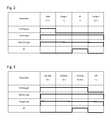
- FIG. 2shows a schematic process sequence of PEALE in one cycle according to an embodiment of the present invention wherein a step illustrated in a column represents an ON state whereas no step illustrated in a column represents an OFF state, and the width of each column does not represent duration of each process.
- FIG. 3shows a schematic process sequence of non-cyclic etching process according to a comparative embodiment wherein a step illustrated in a column represents an ON state whereas no step illustrated in a column represents an OFF state, and the width of each column does not represent duration of each process.
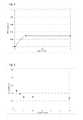
- FIG. 4is a graph showing the relationship between etching rate per cycle (EPC) (nm/cycle) and etching gas feed time per cycle (seconds) according to an embodiment of the present invention.
- FIG. 5is a graph showing the relationship between etching rate per cycle (EPC) (nm/cycle) and purge time per cycle (seconds) according to an embodiment of the present invention.
- gasmay include vaporized solid and/or liquid and may be constituted by a single gas or a mixture of gases.
- a process gas introduced to a reaction chamber through a showerheadmay be comprised of, consist essentially of, or consist of an etching gas and an additive gas.
- the additive gastypically includes a reactant gas for reacting with the etching gas when RF power is applied to the reactant gas.
- the reactant gasmay be diluted with a dilution gas which is introduced to the reaction chamber as a mixed gas with the reactant gas or separately from the reactant gas.
- the etching gascan be introduced with a carrier gas such as a noble gas.
- a gas other than the process gasi.e., a gas introduced without passing through the showerhead, may be used for, e.g., sealing the reaction space, which includes a seal gas such as a noble gas.
- a seal gassuch as a noble gas.
- the term “etching gas”refers generally to at least one gaseous or vaporized compound that participates in etching reaction that etches a layer on a substrate, and particularly to at least one compound that chemisorbs onto the layer in a non-excited state and etches the layer when being activated
- reactant gasrefers to at least one gaseous or vaporized compound that contributes to activation of the etching gas or catalyzes an etching reaction by the etching gas.
- etching gasrefers to an active gas without a carrier gas, or a mixture of an active gas and a carrier gas, depending on the context.
- reactant gasrefers to a reactant gas without a dilution gas, or a reactant gas diluted with a dilution gas, depending on the context.
- carrier gasrefers to an inert or inactive gas in a non-excited state which carries an etching gas to the reaction space in a mixed state and enters the reaction space as a mixed gas including the etching gas.
- the inert gas and the etching gascan converge as a mixed gas anywhere upstream of the reaction space, e.g., (a) in an etching gas line upstream of a mass flow controller provided in the etching gas line, wherein the inert gas is provided as a carrier gas or purge gas flowing through the etching gas line, (b) in an etching gas line downstream of a mass flow controller provided in the etching gas line but upstream of a gas manifold where all or main process gases converge, wherein the inert gas is provided as a part of the etching gas (as a carrier gas or purge gas), and/or (c) in a gas manifold where all or main process gases converge, wherein the inert gas flows in a reactant gas line as a reactant gas or purge gas upstream of the gas manifold.
- the inert gascan serve as a carrier gas (as a part of etching gas) and/or at least a part of a reactant gas, wherein the above gases can serve also as purge gases.
- filmrefers to a layer continuously extending in a direction perpendicular to a thickness direction substantially without pinholes to cover an entire target or concerned surface, or simply a layer covering a target or concerned surface.
- layerrefers to a structure having a certain thickness formed on a surface or a synonym of film or a non-film structure.
- a film or layermay be constituted by a discrete single film or layer having certain characteristics or multiple films or layers, and a boundary between adjacent films or layers may or may not be clear and may be established based on physical, chemical, and/or any other characteristics, formation processes or sequence, and/or functions or purposes of the adjacent films or layers.
- any two numbers of a variablecan constitute a workable range of the variable as the workable range can be determined based on routine work, and any ranges indicated may include or exclude the endpoints.
- any values of variables indicatedmay refer to precise values or approximate values and include equivalents, and may refer to average, median, representative, majority, etc. in some embodiments.
- the terms “constituted by” and “having”refer independently to “typically or broadly comprising”, “comprising”, “consisting essentially of”, or “consisting of” in some embodiments.
- an article “a” or “an”refers to a species or a genus including multiple species. In this disclosure, any defined meanings do not necessarily exclude ordinary and customary meanings in some embodiments.
- Some embodiments which resolve at least one of the problems discussed earlierprovide a method for etching a layer on a substrate placed between electrodes in a reaction space by an atomic layer etching (ALE) process which comprises at least one etching cycle, wherein an etching cycle comprises: (i) continuously providing an inert gas flowing at least as a carrier gas for an etching gas into the reaction space; (ii) providing a pulse of an etching gas into the continuous inert gas flow upstream of the reaction space to chemisorb the etching gas in an unexcited state on a surface of the substrate in the reaction space; and (iii) providing a pulse of RF power discharge between the electrodes to generate a reactive species of the inert gas in the reaction space and to contact the etching gas-chemisorbed surface of the substrate with the reactive species so that the layer on the substrate is etched.
- ALEatomic layer etching
- the term “continuously”refers to without interruption in space (e.g., uninterrupted supply over the substrate), without interruption in flow (e.g., uninterrupted inflow), and/or at a constant rate (the term need not satisfy all of the foregoing simultaneously), depending on the embodiment.
- “continuous” flowhas a constant flow rate (alternatively, even through the flow is “continuous”, its flow rate may be changed with time).
- “chemisorption”refers to chemical saturation adsorption.
- the amount of deposited etching gas moleculesis determined by the number of reactive surface sites and is independent of the precursor exposure after saturation, and a supply of the etching gas is such that the reactive surface sites are saturated thereby per cycle.
- the carrier gasserves also as a reactant gas (e.g., the inert gas used for ALE consists of the carrier gas).
- the methodfurther comprises providing a reactant gas separately from the carrier gas into the reaction space, and in some embodiments, the reactant gas includes an inert gas continuously flowing in the reaction space continuously during the ALE process.
- the pulse of the etching gas and the pulse of RF power dischargedo not overlap.
- a purging periodis taken between the pulse of the etching gas and the pulse of RF power discharge to remove excess etching gas from the reaction space, and a purging period is taken after the pulse of RF power discharge to remove reaction products from the reaction space.
- the etching cycleis repeated multiple times (e.g., 50 times to 5,000 times, typically 200 times to 2,000 times), depending on the target thickness to be etched, wherein the layer is etched to the degree that the etching gas chemisorbed as an atomic layer on a surface of the layer can etch per ALE cycle.
- the etching rate per cycleis at least 0.003 nm/cycle (typically 0.005 nm to 0.05 nm/cycle), and the etching rate per minute is at least 0.10 nm/min (typically 0.15 nm/min to 1.5 nm/min), as measured when a top layer or blanket layer is etched.
- the etching gasis at least one halogen-containing gas such as C 2 F 6 , C 4 F 8 , C 3 F 8 , C 5 F 8 , and/or at least one hydrocarbon gas such as hexane In some embodiments, no gas other than a halogen-containing gas flows as the etching gas throughout the ALE process.
- the inert gasflows as a carrier gas in the reaction space continuously during the ALE process.
- the inert gasflows as a reactant gas in the reaction space continuously during the ALE process.
- the inert gasconstitutes and serves also as a carrier gas, and the reactant gas includes an inert gas, the inert gas of the reactant gas can flow in the reaction space in pulses.
- a reactant gas other than the inert gasmay flow in the reaction space in pulses.
- the carrier gas, reactant gas, or any other continuously flowing gas which is mixed with the etching gas upstream of the reaction spacemay be referred to broadly as a carrier gas since the gas enters into the reaction space together with the etching gas in a mixed state, and also as a purge gas since the continuous flow can purge unwanted etching gas and reaction product from the reaction space and the substrate surface.
- the inert gasis selected from the group consisting of a noble gas (such as He, Ne, Ar, Kr, and/or Xe, preferably Ar and/or He), nitrogen gas, or a combination of a noble gas and nitrogen gas.
- a noble gassuch as He, Ne, Ar, Kr, and/or Xe, preferably Ar and/or He
- nitrogen gasor a combination of a noble gas and nitrogen gas.
- the reactant gasconsists of the inert gas or the inert gas and at least one additional gas which is selected from the group consisting of oxidizing gas (e.g., O 2 gas) and reducing gas (e.g., H 2 gas).
- the inert gas used for ALEconsists of a carrier gas flowing through a carrier gas line, or consists of a carrier gas continuously flowing through a carrier gas line and at least part of a reactant gas continuously flowing through a reactant gas line separated from the carrier gas line.
- the layer of the substratehas a recess pattern. As with atomic layer deposition (ALD), conformality or directionality of etching is very high generally in the ALE process.
- the layer of the substrateis etched anisotropically, by supplying the inert gas to the reaction space at a flow rate of more than 1,000 sccm (e.g., 2,000 sccm, 3,000 sccm, 4,000 sccm, 5,000 sccm, 6,000 sccm, 7,000 sccm, or any values therebetween) wherein the flow rate of carrier gas is more than 500 sccm (e.g., 1,000 sccm, 1,500 sccm, 2,000 sccm, or any values therebetween) under conditions using certain RF power, pressure, etc.
- 500 sccme.g., 1,000 sccm, 1,500 sccm, 2,000 sccm, or any values therebetween
- the etchingis “anisotropic” when conformality of etched surfaces which is a percentage calculated by dividing the etched thickness at a sidewall by the etched thickness at a top surface is 30% or less. If the conformality is 20% or less, 10% or less, or 5% or less, the etching is highly anisotropic.
- conformality or directionality of etchingcan be adjusted by including nitrogen-containing gas, oxidizing gas, and/or reducing gas in the reactant gas.
- the ALE processis conducted at a temperature of 0° C. to 200° C., preferably about 50° C. to about 100° C.
- the reaction spaceis formed in a reaction chamber for film-forming or dry-etching.
- the ALE processcan be conducted using the same reaction chamber used for film-forming or dry-etching so that fabrication of a device can continuously and efficiently be performed.
- the ALE processcan be conducted in a chamber attached to a common wafer-handling chamber of a cluster apparatus.
- the dielectric film to be etchedincludes, but is not limited to, a low-k film made of: silicon-containing insulation film constituted by SiO, SiC, SiCN, SiN, or the like; metal-containing oxide film constituted by Al, Ti, or the like; nitride film; or metal film.
- the dielectric filmis formed in trenches or vias including side walls and bottom surfaces, and/or flat surfaces, by plasma-enhanced CVD, thermal CVD, cyclic CVD, plasma-enhanced ALD, thermal ALD, radical-enhanced ALD, or any other thin film deposition method.
- the thickness of the dielectric filmis in a range of about 50 nm to about 500 nm (a desired film thickness can be selected as deemed appropriate according to the application and purpose of film, etc.).
- the dielectric filmmay be used for double-patterning.
- FIG. 1is a schematic view of a PEALE apparatus, desirably in conjunction with controls programmed to conduct the sequences described below, usable in some embodiments of the present invention.
- This apparatuscan also be used for film deposition by ALD or CVD.
- HRF power13.56 MHz or 27 MHz
- LRF powerof 5 MHz or less (400 kHz-500 kHz) 50 to one side, and electrically grounding 12 to the other side, a plasma is excited between the electrodes.
- a temperature regulatoris provided in a lower stage 2 (the lower electrode), and a temperature of a substrate 1 placed thereon is kept constant at a given temperature.
- the lower electrode 2serves as a susceptor
- the upper electrode 4serves as a shower plate as well, which is made to supply gases uniformly over the entire surface of the substrate 1 placed on the susceptor 2 .
- An etching gas and purge gasare introduced into the reaction chamber 3 through a mass flow controller 23 , a pulse flow control valve 31 , a gas manifold 30 , and the shower plate 4 .
- a gas line on which the mass flow controller 23 is providedis an etching gas line
- a gas line on which a mass flow controller 21 is providedis a nitrogen gas line
- a gas line on which a mass flow controller 22 is providedis a noble gas line, wherein the etching gas line, the nitrogen gas line, and the noble gas line may also be referred to collectively as etching gas lines.
- a noble gasflows through the noble gas line with the mass flow controller 22 and serves as an inert carrier gas which is mixed with the etching gas downstream of the mass flow controller 23 but upstream of the gas manifold 30 .
- a nitrogen gasflows through the nitrogen gas line with the mass flow controller 21 and is added to the etching gas as an inert carrier gas.
- a reactant gasis constituted by a nitrogen gas which flows through a nitrogen gas line on which a mass flow controller 25 is provided, a noble gas which flows through a noble gas line on which a mass flow controller 26 is provided, an oxidizing gas which flows through an oxidizing gas line on which a mass flow controller 27 is provided, and/or a hydrogen gas which flows through a hydrogen gas line on which a mass flow controller 28 is provided, wherein the nitrogen gas line, the noble gas line, the oxidizing gas line, and the hydrogen gas line may also be referred to collectively as reactant gas lines.
- an exhaust pipe 6is provided, through which gas in the interior 11 of the reaction chamber 3 is exhausted. Additionally, the reaction chamber 3 is provided with a seal gas flow controller 24 to introduce seal gas into the interior 11 of the reaction chamber 3 (a separation plate for separating a reaction zone and a transfer zone in the interior of the reaction chamber is omitted from this figure).
- the apparatusincludes one or more controller(s) (not shown) programmed or otherwise configured to cause the deposition and etching processes described elsewhere herein to be conducted.
- the controller(s)are communicated with the various power sources, heating systems, pumps, robotics and gas flow controllers or valves of the reactor, as will be appreciated by the skilled artisan.
- the process sequencemay be set as illustrated in FIG. 2 .
- FIG. 2shows a schematic process sequence of PEALE in one cycle according to an embodiment of the present invention wherein a step illustrated in a column represents an ON state whereas no step illustrated in a column represents an OFF state, and the width of each column does not represent duration of each process.
- one cycle of PEALEconsists of “Feed” where an etching gas is fed to a reaction space via a carrier gas which carries the etching gas without applying RF power to the reaction space, and also, a reactant gas is fed to the reaction space, thereby chemisorbing the etching gas onto a surface of a substrate via self-limiting adsorption; “Purge 1” where no etching gas is fed to the reaction space, while the carrier gas and reactant gas are continuously fed to the reaction space, without applying RF power, thereby removing non-chemisorbed etching gas and excess gas from the surface of the substrate; “RF” where RF power is applied to the reaction space while the carrier gas and reactant gas are continuously fed to the reaction space, without feeding the etching gas, thereby etching a layer on which the etching gas is chemisorbed through plasma reaction with the reactant gas; and “Purge 2” where the carrier gas and reactant gas are continuously fed to the reaction space, without feeding the
- the carrier gascan be constituted by the reactant gas. Due to the continuous flow of the carrier gas entering into the reaction space as a constant stream into which the etching gas is injected intermittently or in pulses, purging can be conducted efficiently to remove excess gas and reaction products quickly from the surface of the layer, thereby efficiently continuing multiple ALE cycles.
- the durations of the Feed step, the Purge 1 step, the RF step, and the Purge 2 stepare 0.3 seconds, one second, one second, and 0.2 seconds, and thus, the total duration of one cycle is 2.5 seconds.
- FIG. 3shows a schematic process sequence of non-cyclic etching process according to a comparative embodiment wherein a step illustrated in a column represents an ON state whereas no step illustrated in a column represents an OFF state, and the width of each column does not represent duration of each process.
- the non-cyclic etching processconsists of “Set Gas”, “Stabilize”, “Etching”, and “Off”.
- the sequence illustrated in FIG. 3is not atomic layer etching. That is, etching is conducted using active species which are generated in a reaction space before reaching a surface of the layer and then reach the surface of the layer, thereby etching the surface.
- the etching gasis fed while RF power is applied, and non-cyclic etching is conducted wherein the duration of the Etching step is long (e.g., 10 to 30 seconds) as compared with the ALE process.
- the etching rate of the non-cyclic etching processis very high, since the active species fall down on the surface of the layer, side walls of recesses of a pattern formed on the substrate are not significantly etched, i.e., etching is typically anisotropic, and it is difficult to form fine, narrow patterns.
- PEALEmay be conducted under conditions shown in Table 1 below.
- the etching rateis low since etching takes place using one etching gas layer at a time, and conformality is generally high since the etching gas is chemisorbed non-directionally in general.
- a noble gasas the inert gas, rather than nitrogen gas
- the reaction spaceii) at an increased flow rate (e.g., 3,000 sccm or higher wherein the flow rate of carrier gas is more than 500 sccm) under conditions with (iii) a certain RF power (e.g., 250 W or higher), and (iv) a certain pressure (e.g., 300 Pa or higher), wherein condition (i) and at least one of conditions (ii) to (iv) are employed, the layer of the substrate can effectively be etched anisotropically.
- a certain RF powere.g., 250 W or higher
- a certain pressuree.g. 300 Pa or higher
- a silicon oxide filmwas formed by PEALD on a 300-mm substrate having a patterned surface having an aspect ratio of about 2 and an opening width of about 50 nm.
- PEALEwas conducted using C 2 F 6 or C 4 F 8 as an etching gas on the silicon oxide film under the conditions shown in Table 2 below using the PEALE apparatus illustrated in FIG. 1 .
- the sequence used in each cycle of PEALEis shown in FIG. 2 and Table 3 below.
- Ar gaswas fed only as a carrier gas flowing through the mass flow controller 22 of the etching gas lines and served also as a reactant gas.
- Nitrogen gas, oxygen gas, and hydrogen gaswere fed as reactant gases flowing through the mass flow controllers 25 , 27 , and 28 of the reactant gas lines, respectively, wherein nitrogen gas was fed as a carrier gas.
- the conformality of etched surfacesis a percentage calculated by dividing the etched thickness at a sidewall or bottom by the etched thickness at a top surface.
- the etching temperaturegreatly affected etching rate.
- the temperaturewas 50° C. (Examples 2), 100° C. (Example 6), 200° C. (Example 7), and 250° C. (Example 8) when the carrier gas was Ar and the reactant gas was 02, the etching rates (EPC) were 0.02, 0.03, 0.02, and 0.01, respectively, indicating that when the temperature was 250° C., the etching rate was significantly lowered.
- the temperaturewas 260° (Comparative Example 3)
- ALEdid not occur, i.e., the etching rate was zero.
- the temperaturewas 50° C. (Examples 5), 100° C. (Example 9), and 200° C.
- Example 10when the carrier gas was N 2 without other gases, the etching rates (EPC) were 0.03, 0.03, and 0.005, respectively, indicating that when the temperature was 200° C., the etching rate was significantly lowered.
- EPCetching rates
- the ALE processgenerally performs conformal etching (isotropic etching; conformality is no less than 80%) and can achieve fine tuning of etching thickness, indicating that the ALE process is suitable for forming micro-patterns with high precision.
- the etching conformalitycan be adjusted by using certain conditions, and when the carrier gas was fed at a high flow rate (6 slm in Example 11), when an RF power was high (500 W in Example 13), when a pressure was high (500 Pa in Example 14), and when both an RF power and a pressure were high (500 W and 400 Pa in Example 15), anisotropic etching was highly effectively performed (Conformality: 3/120 in Example 11, 9/98 in Example 13, 8/95 in Example 14, and 10/105 in Example 15).
- FIG. 4is a graph showing the relationship between etching rate per cycle (EPC) (nm/cycle) and etching gas feed time per cycle (seconds). As shown in FIG. 4 , after the feed time reached 0.2 seconds, EPC was unchanged, indicating that self-limiting adsorption reaction process was conducted.
- EPCetching rate per cycle
- FIG. 5is a graph showing the relationship between etching rate per cycle (EPC) (nm/cycle) and purge time per cycle (seconds). As shown in FIG. 5 , after the purge time reached 0.5 seconds, EPC was unchanged, indicating chemisorption of the etching gas was conducted.
- EPCetching rate per cycle
Landscapes
- Engineering & Computer Science (AREA)
- Physics & Mathematics (AREA)
- Chemical & Material Sciences (AREA)
- Plasma & Fusion (AREA)
- Power Engineering (AREA)
- Microelectronics & Electronic Packaging (AREA)
- Computer Hardware Design (AREA)
- Condensed Matter Physics & Semiconductors (AREA)
- General Physics & Mathematics (AREA)
- Manufacturing & Machinery (AREA)
- Chemical Kinetics & Catalysis (AREA)
- Analytical Chemistry (AREA)
- General Chemical & Material Sciences (AREA)
- Inorganic Chemistry (AREA)
- Drying Of Semiconductors (AREA)
- Plasma Technology (AREA)
- Electromagnetism (AREA)
- Spectroscopy & Molecular Physics (AREA)
Abstract
Description
1. Field of the Invention
The present invention generally relates to a method of atomic layer etching (ALE), particularly to a method of plasma-enhanced ALE (PEALE).
2. Description of the Related Art
In order to cope with various processing accompanying microminiaturization and complex structures of semiconductor devices, precision of processing has been remarkably improved by new technology such as double-patterning. However, conventional etching technology such as continuous etching using excited reaction species may be difficult to form fine, narrow convex-concave patterns and may cause defects of shape. Thus, development of etching technology which is capable of performing atomic layer-level etching and is suitable for e.g., double-patterning processes, becomes important. However, low etching rate, poor controllability over directionality of etching, or the like need to be improved.
Any discussion of problems and solutions in relation to the related art has been included in this disclosure solely for the purposes of providing a context for the present invention, and should not be taken as an admission that any or all of the discussion was known at the time the invention was made.
Some embodiments provide a method of atomic layer-level etching (referred to as atomic layer etching, ALE) characterized by one or more of the following features: (a) An etching gas is supplied to a reaction space through a mass flow controller, together with an inert gas, wherein the etching gas and the inert gas converge downstream of the mass flow controller, and the inert gas is supplied continuously, whereas the etching gas is supplied in pulses, thereby increasing efficiency of purging; (b) a plasma is used for etching, wherein an inert gas or nitrogen gas is supplied as an essential reactant gas to the reaction space for generating a plasma therein, wherein etching rate is controlled by selectively adding an oxidizing gas such as oxygen gas, or reducing gas such as hydrogen gas as an additional reactant gas; (c) the process temperature is controlled at 0° C. to 250° C.; and (d) directionality of etching is controlled to perform either anisotropic or isotropic etching by selecting the type of reactant gas and etching conditions.
In some embodiments, ALE can be performed in a reaction chamber which is also used as a reaction chamber for deposition of film by chemical vapor deposition (CVD), atom layer deposition (ALD), etc., and/or as a reaction chamber for dry etching, wherein no additional chamber is required for performing etching. Alternatively, ALE can be performed in a reaction chamber which is attached to a wafer-handling chamber as one of multiple chambers installed in a cluster apparatus. In some embodiments, ALE is either anisotropic or isotropic ALE performed in the same reaction chamber which is also the same chamber used for O2-ashing, anisotropic etching, etc., in any combination. In some embodiments, ALE is either anisotropic or isotropic ALE performed in one of multiple reaction chambers of a cluster apparatus wherein the other reaction chambers are those for O2-ashing, anisotropic etching, etc., in any combination.
In some embodiments, a plasma for ALE is generated using conductively-coupled electrodes, a remote plasma unit, or a combination of these.
In some embodiments, the etching gas for ALE is at least one gas selected from the group consisting of fluorocarbon, other halogen-containing gas, and hydrocarbon gas.
In some embodiments, the inert gas is continuously supplied as a carrier gas flowing through a carrier gas line, a reactant gas flowing through a reactant gas line, or both carrier gas and reactant gas. Since the inert gas continuously flows, it can function as a purge gas.
For purposes of summarizing aspects of the invention and the advantages achieved over the related art, certain objects and advantages of the invention are described in this disclosure. Of course, it is to be understood that not necessarily all such objects or advantages may be achieved in accordance with any particular embodiment of the invention. Thus, for example, those skilled in the art will recognize that the invention may be embodied or carried out in a manner that achieves or optimizes one advantage or group of advantages as taught herein without necessarily achieving other objects or advantages as may be taught or suggested herein.
Further aspects, features and advantages of this invention will become apparent from the detailed description which follows.
These and other features of this invention will now be described with reference to the drawings of preferred embodiments which are intended to illustrate and not to limit the invention. The drawings are greatly simplified for illustrative purposes and are not necessarily to scale.
In this disclosure, “gas” may include vaporized solid and/or liquid and may be constituted by a single gas or a mixture of gases. In this disclosure, a process gas introduced to a reaction chamber through a showerhead may be comprised of, consist essentially of, or consist of an etching gas and an additive gas. The additive gas typically includes a reactant gas for reacting with the etching gas when RF power is applied to the reactant gas. The reactant gas may be diluted with a dilution gas which is introduced to the reaction chamber as a mixed gas with the reactant gas or separately from the reactant gas. The etching gas can be introduced with a carrier gas such as a noble gas. Also, a gas other than the process gas, i.e., a gas introduced without passing through the showerhead, may be used for, e.g., sealing the reaction space, which includes a seal gas such as a noble gas. In some embodiments, the term “etching gas” refers generally to at least one gaseous or vaporized compound that participates in etching reaction that etches a layer on a substrate, and particularly to at least one compound that chemisorbs onto the layer in a non-excited state and etches the layer when being activated, whereas the term “reactant gas” refers to at least one gaseous or vaporized compound that contributes to activation of the etching gas or catalyzes an etching reaction by the etching gas. The term “etching gas” refers to an active gas without a carrier gas, or a mixture of an active gas and a carrier gas, depending on the context. Similarly, the term “reactant gas” refers to a reactant gas without a dilution gas, or a reactant gas diluted with a dilution gas, depending on the context. The term “carrier gas” refers to an inert or inactive gas in a non-excited state which carries an etching gas to the reaction space in a mixed state and enters the reaction space as a mixed gas including the etching gas. The inert gas and the etching gas can converge as a mixed gas anywhere upstream of the reaction space, e.g., (a) in an etching gas line upstream of a mass flow controller provided in the etching gas line, wherein the inert gas is provided as a carrier gas or purge gas flowing through the etching gas line, (b) in an etching gas line downstream of a mass flow controller provided in the etching gas line but upstream of a gas manifold where all or main process gases converge, wherein the inert gas is provided as a part of the etching gas (as a carrier gas or purge gas), and/or (c) in a gas manifold where all or main process gases converge, wherein the inert gas flows in a reactant gas line as a reactant gas or purge gas upstream of the gas manifold. In the above, typically, (a) is rare. Thus, the inert gas can serve as a carrier gas (as a part of etching gas) and/or at least a part of a reactant gas, wherein the above gases can serve also as purge gases.
In some embodiments, “film” refers to a layer continuously extending in a direction perpendicular to a thickness direction substantially without pinholes to cover an entire target or concerned surface, or simply a layer covering a target or concerned surface. In some embodiments, “layer” refers to a structure having a certain thickness formed on a surface or a synonym of film or a non-film structure. A film or layer may be constituted by a discrete single film or layer having certain characteristics or multiple films or layers, and a boundary between adjacent films or layers may or may not be clear and may be established based on physical, chemical, and/or any other characteristics, formation processes or sequence, and/or functions or purposes of the adjacent films or layers.
Further, in this disclosure, any two numbers of a variable can constitute a workable range of the variable as the workable range can be determined based on routine work, and any ranges indicated may include or exclude the endpoints. Additionally, any values of variables indicated (regardless of whether they are indicated with “about” or not) may refer to precise values or approximate values and include equivalents, and may refer to average, median, representative, majority, etc. in some embodiments. Additionally, the terms “constituted by” and “having” refer independently to “typically or broadly comprising”, “comprising”, “consisting essentially of”, or “consisting of” in some embodiments. Further, an article “a” or “an” refers to a species or a genus including multiple species. In this disclosure, any defined meanings do not necessarily exclude ordinary and customary meanings in some embodiments.
In the present disclosure where conditions and/or structures are not specified, the skilled artisan in the art can readily provide such conditions and/or structures, in view of the present disclosure, as a matter of routine experimentation. In all of the disclosed embodiments, any element used in an embodiment can be replaced with any elements equivalent thereto, including those explicitly, necessarily, or inherently disclosed herein, for the intended purposes. Further, the present invention can equally be applied to apparatuses and methods.
The embodiments will be explained with respect to preferred embodiments. However, the present invention is not limited to the preferred embodiments.
Some embodiments which resolve at least one of the problems discussed earlier provide a method for etching a layer on a substrate placed between electrodes in a reaction space by an atomic layer etching (ALE) process which comprises at least one etching cycle, wherein an etching cycle comprises: (i) continuously providing an inert gas flowing at least as a carrier gas for an etching gas into the reaction space; (ii) providing a pulse of an etching gas into the continuous inert gas flow upstream of the reaction space to chemisorb the etching gas in an unexcited state on a surface of the substrate in the reaction space; and (iii) providing a pulse of RF power discharge between the electrodes to generate a reactive species of the inert gas in the reaction space and to contact the etching gas-chemisorbed surface of the substrate with the reactive species so that the layer on the substrate is etched. In the above, the term “continuously” refers to without interruption in space (e.g., uninterrupted supply over the substrate), without interruption in flow (e.g., uninterrupted inflow), and/or at a constant rate (the term need not satisfy all of the foregoing simultaneously), depending on the embodiment. In some embodiments, “continuous” flow has a constant flow rate (alternatively, even through the flow is “continuous”, its flow rate may be changed with time). In this disclosure, “chemisorption” refers to chemical saturation adsorption. Since chemisorption is a self-limiting adsorption reaction process, the amount of deposited etching gas molecules is determined by the number of reactive surface sites and is independent of the precursor exposure after saturation, and a supply of the etching gas is such that the reactive surface sites are saturated thereby per cycle.
In some embodiments, the carrier gas serves also as a reactant gas (e.g., the inert gas used for ALE consists of the carrier gas). In some embodiments, the method further comprises providing a reactant gas separately from the carrier gas into the reaction space, and in some embodiments, the reactant gas includes an inert gas continuously flowing in the reaction space continuously during the ALE process.
In some embodiments, the pulse of the etching gas and the pulse of RF power discharge do not overlap. In some embodiments, a purging period is taken between the pulse of the etching gas and the pulse of RF power discharge to remove excess etching gas from the reaction space, and a purging period is taken after the pulse of RF power discharge to remove reaction products from the reaction space.
In some embodiments, the etching cycle is repeated multiple times (e.g., 50 times to 5,000 times, typically 200 times to 2,000 times), depending on the target thickness to be etched, wherein the layer is etched to the degree that the etching gas chemisorbed as an atomic layer on a surface of the layer can etch per ALE cycle. In some embodiments, when the layer of the substrate is a silicon-containing dielectric layer such as silicon oxide film, the etching rate per cycle (EPC) is at least 0.003 nm/cycle (typically 0.005 nm to 0.05 nm/cycle), and the etching rate per minute is at least 0.10 nm/min (typically 0.15 nm/min to 1.5 nm/min), as measured when a top layer or blanket layer is etched.
In some embodiments, the etching gas is at least one halogen-containing gas such as C2F6, C4F8, C3F8, C5F8, and/or at least one hydrocarbon gas such as hexane In some embodiments, no gas other than a halogen-containing gas flows as the etching gas throughout the ALE process.
In some embodiments, the inert gas flows as a carrier gas in the reaction space continuously during the ALE process. Alternatively or additionally, the inert gas flows as a reactant gas in the reaction space continuously during the ALE process. If the inert gas constitutes and serves also as a carrier gas, and the reactant gas includes an inert gas, the inert gas of the reactant gas can flow in the reaction space in pulses. A reactant gas other than the inert gas may flow in the reaction space in pulses. The carrier gas, reactant gas, or any other continuously flowing gas which is mixed with the etching gas upstream of the reaction space (e.g., upstream of a showerhead or a gas manifold where multiple gases converge disposed upstream of the showerhead) may be referred to broadly as a carrier gas since the gas enters into the reaction space together with the etching gas in a mixed state, and also as a purge gas since the continuous flow can purge unwanted etching gas and reaction product from the reaction space and the substrate surface.
In some embodiments, the inert gas is selected from the group consisting of a noble gas (such as He, Ne, Ar, Kr, and/or Xe, preferably Ar and/or He), nitrogen gas, or a combination of a noble gas and nitrogen gas.
In some embodiments, the reactant gas consists of the inert gas or the inert gas and at least one additional gas which is selected from the group consisting of oxidizing gas (e.g., O2gas) and reducing gas (e.g., H2gas). In some embodiments, the inert gas used for ALE consists of a carrier gas flowing through a carrier gas line, or consists of a carrier gas continuously flowing through a carrier gas line and at least part of a reactant gas continuously flowing through a reactant gas line separated from the carrier gas line.
In some embodiments, the layer of the substrate has a recess pattern. As with atomic layer deposition (ALD), conformality or directionality of etching is very high generally in the ALE process. However, in some embodiments, the layer of the substrate is etched anisotropically, by supplying the inert gas to the reaction space at a flow rate of more than 1,000 sccm (e.g., 2,000 sccm, 3,000 sccm, 4,000 sccm, 5,000 sccm, 6,000 sccm, 7,000 sccm, or any values therebetween) wherein the flow rate of carrier gas is more than 500 sccm (e.g., 1,000 sccm, 1,500 sccm, 2,000 sccm, or any values therebetween) under conditions using certain RF power, pressure, etc. The etching is “anisotropic” when conformality of etched surfaces which is a percentage calculated by dividing the etched thickness at a sidewall by the etched thickness at a top surface is 30% or less. If the conformality is 20% or less, 10% or less, or 5% or less, the etching is highly anisotropic. In some embodiments, conformality or directionality of etching can be adjusted by including nitrogen-containing gas, oxidizing gas, and/or reducing gas in the reactant gas. In some embodiments, the ALE process is conducted at a temperature of 0° C. to 200° C., preferably about 50° C. to about 100° C.
In some embodiments, the reaction space is formed in a reaction chamber for film-forming or dry-etching. The ALE process can be conducted using the same reaction chamber used for film-forming or dry-etching so that fabrication of a device can continuously and efficiently be performed. Alternatively, the ALE process can be conducted in a chamber attached to a common wafer-handling chamber of a cluster apparatus.
The dielectric film to be etched includes, but is not limited to, a low-k film made of: silicon-containing insulation film constituted by SiO, SiC, SiCN, SiN, or the like; metal-containing oxide film constituted by Al, Ti, or the like; nitride film; or metal film. In some embodiments, the dielectric film is formed in trenches or vias including side walls and bottom surfaces, and/or flat surfaces, by plasma-enhanced CVD, thermal CVD, cyclic CVD, plasma-enhanced ALD, thermal ALD, radical-enhanced ALD, or any other thin film deposition method. Typically, the thickness of the dielectric film is in a range of about 50 nm to about 500 nm (a desired film thickness can be selected as deemed appropriate according to the application and purpose of film, etc.). The dielectric film may be used for double-patterning.
An etching gas and purge gas are introduced into the reaction chamber3 through amass flow controller 23, a pulse flow control valve31, agas manifold 30, and the shower plate4. A gas line on which themass flow controller 23 is provided is an etching gas line, a gas line on which amass flow controller 21 is provided is a nitrogen gas line, and a gas line on which a mass flow controller22 is provided is a noble gas line, wherein the etching gas line, the nitrogen gas line, and the noble gas line may also be referred to collectively as etching gas lines. A noble gas flows through the noble gas line with the mass flow controller22 and serves as an inert carrier gas which is mixed with the etching gas downstream of themass flow controller 23 but upstream of thegas manifold 30. Alternatively or additionally, a nitrogen gas flows through the nitrogen gas line with themass flow controller 21 and is added to the etching gas as an inert carrier gas. A reactant gas is constituted by a nitrogen gas which flows through a nitrogen gas line on which amass flow controller 25 is provided, a noble gas which flows through a noble gas line on which amass flow controller 26 is provided, an oxidizing gas which flows through an oxidizing gas line on which amass flow controller 27 is provided, and/or a hydrogen gas which flows through a hydrogen gas line on which amass flow controller 28 is provided, wherein the nitrogen gas line, the noble gas line, the oxidizing gas line, and the hydrogen gas line may also be referred to collectively as reactant gas lines. The noble gas which flows through the noble gas line on which themass flow controller 26 is provided, and/or the nitrogen gas which flows through the nitrogen gas line on which themass flow controller 25 is provided, serve(s) as an inert reactant gas which is mixed with the etching gas at thegas manifold 30 upstream of the shower plate4. Since the above-described inert gases flow continuously into the reaction space, they also can function as a purge gas. As the continuous inert gas flow, the inert carrier gas flow is more effective than the inert reactant gas flow, and thus, in some embodiments, the inert reactant gas flow can be eliminated.
Additionally, in the reaction chamber3, an exhaust pipe6 is provided, through which gas in the interior11 of the reaction chamber3 is exhausted. Additionally, the reaction chamber3 is provided with a sealgas flow controller 24 to introduce seal gas into the interior11 of the reaction chamber3 (a separation plate for separating a reaction zone and a transfer zone in the interior of the reaction chamber is omitted from this figure).
A skilled artisan will appreciate that the apparatus includes one or more controller(s) (not shown) programmed or otherwise configured to cause the deposition and etching processes described elsewhere herein to be conducted. The controller(s) are communicated with the various power sources, heating systems, pumps, robotics and gas flow controllers or valves of the reactor, as will be appreciated by the skilled artisan.
In some embodiments, the process sequence may be set as illustrated inFIG. 2 .FIG. 2 shows a schematic process sequence of PEALE in one cycle according to an embodiment of the present invention wherein a step illustrated in a column represents an ON state whereas no step illustrated in a column represents an OFF state, and the width of each column does not represent duration of each process. In this embodiment, one cycle of PEALE consists of “Feed” where an etching gas is fed to a reaction space via a carrier gas which carries the etching gas without applying RF power to the reaction space, and also, a reactant gas is fed to the reaction space, thereby chemisorbing the etching gas onto a surface of a substrate via self-limiting adsorption; “Purge 1” where no etching gas is fed to the reaction space, while the carrier gas and reactant gas are continuously fed to the reaction space, without applying RF power, thereby removing non-chemisorbed etching gas and excess gas from the surface of the substrate; “RF” where RF power is applied to the reaction space while the carrier gas and reactant gas are continuously fed to the reaction space, without feeding the etching gas, thereby etching a layer on which the etching gas is chemisorbed through plasma reaction with the reactant gas; and “Purge 2” where the carrier gas and reactant gas are continuously fed to the reaction space, without feeding the etching gas and without applying RF power to the reaction space, thereby removing reaction products and excess gas from the surface of the substrate. The carrier gas can be constituted by the reactant gas. Due to the continuous flow of the carrier gas entering into the reaction space as a constant stream into which the etching gas is injected intermittently or in pulses, purging can be conducted efficiently to remove excess gas and reaction products quickly from the surface of the layer, thereby efficiently continuing multiple ALE cycles. Incidentally, in this embodiment, the durations of the Feed step, thePurge 1 step, the RF step, and thePurge 2 step are 0.3 seconds, one second, one second, and 0.2 seconds, and thus, the total duration of one cycle is 2.5 seconds.
In some embodiments, PEALE may be conducted under conditions shown in Table 1 below.
| TABLE 1 |
| Conditions for PEALE |
| Substrate temperature | 0 to 250 ° C. (preferably 50 to 100° C.) |
| Pressure | 133.3 to 800 Pa (preferably 200 to 400 Pa); |
| 300 to 800 Pa (preferably 400 to 800 Pa) | |
| for anisotropic etching | |
| Inert gas (as a carrier gas | Ar, He, N2 |
| and/or reactant gas) | |
| Total flow rate of inert gas | 300 to 2000 sccm (preferably 500 to 1000 |
| (continuous) | sccm); 1000 to 7000 sccm (preferably 3000 |
| to 6000 sccm) for anisotropic etching | |
| Flow rate of carrier gas | 300 to 1500 sccm (preferably 500 to 1000 |
| (continuous) | sccm); 500 to 2000 sccm (preferably 1000 |
| to 2000 sccm) for anisotropic etching | |
| Auxiliary reactant gas | O2, H2 |
| Flow rate of auxiliary | 100 to 5000 sccm (preferably 500 to 2000 |
| reactant gas (continuous) | sccm) |
| Etching gas | C2F6, C4F8 |
| Flow rate of etching gas (not | 5 to 1000 sccm (preferably 10 to 300 sccm) |
| including carrier gas) | |
| RF power (13.56 MHz) for | 50 to 300 W (preferably 100 to 250 W); |
| a 300-mm wafer | 250 to 800 W (preferably 400 |
| to 700 W) for anisotropic etching | |
| Duration of “Feed” | 0.1 to 5 sec. (preferably 0.1 to 1 sec.) |
| Duration of “ | 0.2 to 20 sec. (preferably 1 to 6 sec.) |
| Duration of “RF” | 0.2 to 10 sec. (preferably 0.5 to 2 sec.) |
| Duration of “ | 0.1 to 5 sec. (preferably 0.1 to 1 sec.) |
| EPC (nm/cycle) | 0.001 to 0.2 (preferably 0.005 to 0.1) on |
| top surface | |
| Etching rate (nm/min) | 0.001 to 2 (preferably 0.04 to 1) on top |
| surface | |
| (the numbers are approximate) | |
In the ALE process, the etching rate is low since etching takes place using one etching gas layer at a time, and conformality is generally high since the etching gas is chemisorbed non-directionally in general. However, by (i) supplying particularly a noble gas as the inert gas, rather than nitrogen gas, to the reaction space (ii) at an increased flow rate (e.g., 3,000 sccm or higher wherein the flow rate of carrier gas is more than 500 sccm) under conditions with (iii) a certain RF power (e.g., 250 W or higher), and (iv) a certain pressure (e.g., 300 Pa or higher), wherein condition (i) and at least one of conditions (ii) to (iv) are employed, the layer of the substrate can effectively be etched anisotropically. It is surprising that changing from conformal etching to anisotropic etching occurs in a critical manner under the above described conditions. Without being limited by theory, under the described conditions, a plasma is enhanced and excited species travel long distance, thereby increasing the reactivity on a horizontal surface rather than sidewalls in recesses and effectively performing anisotropic etching.
The present invention is further explained with reference to working examples below. However, the examples are not intended to limit the present invention. In the examples where conditions and/or structures are not specified, the skilled artisan in the art can readily provide such conditions and/or structures, in view of the present disclosure, as a matter of routine experimentation. Also, the numbers applied in the specific examples can be modified by a range of at least ±50% in some embodiments, and the numbers are approximate.
A silicon oxide film was formed by PEALD on a 300-mm substrate having a patterned surface having an aspect ratio of about 2 and an opening width of about 50 nm. In Examples 1-12 and Comparative Example 3, PEALE was conducted using C2F6or C4F8as an etching gas on the silicon oxide film under the conditions shown in Table 2 below using the PEALE apparatus illustrated inFIG. 1 . The sequence used in each cycle of PEALE is shown inFIG. 2 and Table 3 below. Ar gas was fed only as a carrier gas flowing through the mass flow controller22 of the etching gas lines and served also as a reactant gas. Nitrogen gas, oxygen gas, and hydrogen gas were fed as reactant gases flowing through themass flow controllers
| TABLE 2 | ||||||||
| Etching | ||||||||
| gas flow | ||||||||
| Etching | rate | Ar | N2 | O2 | H2 | RF | Pressure | Temp | |
| Ex | gas | (sccm) | (slm) | (slm) | (slm) | (slm) | (W) | (Pa) | (° C.) |
| Com. 1 | C2F6 | 600 | 2 | — | 1 | — | 200 | 266 | 400 |
| Com. 2 | C2F6 | 600 | 2 | — | 1 | — | 200 | 533 | 400 |
| Com. 3 | C2F6 | 30 | 1 | — | 1 | — | 200 | 200 | 260 |
| Ex 1 | C2F6 | 30 | 1 | — | — | — | 200 | 200 | 50 |
| Ex 2 | C2F6 | 30 | 1 | — | 1 | — | 200 | 200 | 50 |
| Ex 3 | C2F6 | 30 | — | 1 | — | 0.2 | 200 | 200 | 50 |
| Ex 4 | C2F6 | 30 | 1 | — | — | 0.2 | 200 | 200 | 50 |
| Ex 5 | C2F6 | 30 | — | 1 | — | — | 200 | 200 | 50 |
| Ex 6 | C2F6 | 30 | 1 | — | 1 | — | 200 | 200 | 100 |
| Ex 7 | C2F6 | 30 | 1 | — | 1 | — | 200 | 200 | 200 |
| Ex 8 | C2F6 | 30 | 1 | — | 1 | — | 200 | 200 | 250 |
| Ex 9 | C2F6 | 30 | — | 1 | — | — | 200 | 200 | 100 |
| Ex 10 | C2F6 | 30 | — | 1 | — | — | 200 | 200 | 200 |
| Ex 11 | C2F6 | 30 | 6 | — | — | — | 600 | 600 | 100 |
| Ex 12 | C4F8 | 50 | 2 | — | — | — | 200 | 200 | 100 |
| Ex. 13 | C2F6 | 30 | 1 | — | — | 300 | 200 | 50 | |
| Ex. 14 | C2F6 | 30 | 1 | — | — | 200 | 500 | 50 | |
| Ex. 15 | C2F6 | 30 | 2 | — | — | 300 | 400 | 50 | |
| TABLE 3 |
| Conditions for PEALE |
| Duration of “Feed” | 0.3 sec. |
| Duration of “ | 5 sec. ( |
| Duration of “RF” | 1 sec. |
| Duration of “ | 0.2 sec. |
| Number of cycles repeated | |
| ( | Ex 4 = 500; Ex 5 = 334; Ex 6 = 334; |
| Ex 7 = 500; | |
In Comparative Examples 1 and 2, non-cyclic etching was conducted on the silicon oxide film under the conditions shown below using the PEALE apparatus illustrated inFIG. 1 . The sequence used in the non-cyclic etching is shown inFIG. 3 and Table 4 below.
| TABLE 4 |
| Conditions for non-cyclic etching |
| Duration of “Set Gas” | 10 sec. | ||
| Duration of “Stabilize” | 10 sec. | ||
| Duration of “Etching” | 10~30 sec. | ||
| Duration of “Off” | 1 sec. | ||
The results are shown in Table 5 below. The conformality of etched surfaces is a percentage calculated by dividing the etched thickness at a sidewall or bottom by the etched thickness at a top surface.
| TABLE 5 | ||||
| Etching | Etching | Conformality of | ||
| rate (EPC) | rate | etched surfaces | ||
| Ex | (nm/cycle) | (nm/min) | Sidewall/Bottom (%) | Remarks |
| Com. 1 | — | 51 | 0/75 | |
| Com. 2 | — | 80 | 0/69 | |
| Com. 3 | 0 | — | — | No ALE |
| Ex. 1 | 0.04 | 0.33 | 80/95 | |
| Ex. 2 | 0.02 | 0.16 | 82/95 | |
| Ex. 3 | 0.02 | 0.16 | 81/92 | |
| Ex. 4 | 0.02 | 0.16 | 105/115 | |
| Ex. 5 | 0.03 | 0.25 | 82/92 | |
| Ex. 6 | 0.03 | 0.25 | 80/82 | |
| Ex. 7 | 0.02 | 0.16 | 86/82 | |
| Ex. 8 | 0.01 | 0.08 | 83/82 | |
| Ex. 9 | 0.03 | 0.25 | 105/115 | |
| Ex. 10 | 0.005 | 0.04 | 100/119 | |
| Ex. 11 | 0.03 | 0.25 | 3/120 | Anisotropic ALE |
| Ex. 12 | 0.05 | 0.69 | 94/90 | |
| Ex. 13 | 0.02 | 0.16 | 9/98 | Anisotropic ALE |
| Ex. 14 | 0.03 | 0.16 | 8/95 | Anisotropic ALE |
| Ex. 15 | 0.02 | 0.16 | 10/105 | Anisotropic ALE |
As shown in Table 5, when Ar was used as a carrier gas and a reactant gas without other gases (Examples 1, 11, and 12), the etching rate was the highest (EPC=0.04, 0.03, and 0.05, respectively), and when N2was used as a carrier gas and a reactant gas without other gases (Examples 5 and 9), the etching rate was higher (EPC=0.03 and 0.03, respectively) than when other gases were used as a reactant gas. When O2or H2was added to the carrier gas (Example 2, 3, and 4), the etching rate was lowered (EPC=0.02); however, when H2was added to the carrier gas which was Ar (Example 4), the etching conformality was changed to etch the layer more at the bottom and sidewall (Conformality=105/115). A similar phenomenon was observed when N2was used as a carrier gas without other gases at a temperature of 100° C. and 200° C. (Examples 9 and 10) (Conformality=105/115 and 100/119, respectively).
The etching temperature greatly affected etching rate. When the temperature was 50° C. (Examples 2), 100° C. (Example 6), 200° C. (Example 7), and 250° C. (Example 8) when the carrier gas was Ar and the reactant gas was 02, the etching rates (EPC) were 0.02, 0.03, 0.02, and 0.01, respectively, indicating that when the temperature was 250° C., the etching rate was significantly lowered. Further, when the temperature was 260° (Comparative Example 3), ALE did not occur, i.e., the etching rate was zero. Similarly, when the temperature was 50° C. (Examples 5), 100° C. (Example 9), and 200° C. (Example 10) when the carrier gas was N2without other gases, the etching rates (EPC) were 0.03, 0.03, and 0.005, respectively, indicating that when the temperature was 200° C., the etching rate was significantly lowered. When the etching temperature is high, adsorption of etching gas would not sufficiently advance, and when the temperature exceeds 250° C., no ALE process may be performed.
When non-cyclic etching was conducted (Comparative Examples 1 and 2), the etching conformality was zero, indicating that the etching was clearly anisotropic. Further, since etching was not performed cyclically, it would be very difficult to conduct fine tuning of etching thickness. In contrast, the ALE process generally performs conformal etching (isotropic etching; conformality is no less than 80%) and can achieve fine tuning of etching thickness, indicating that the ALE process is suitable for forming micro-patterns with high precision. However, although the ALE process was performed, the etching conformality can be adjusted by using certain conditions, and when the carrier gas was fed at a high flow rate (6 slm in Example 11), when an RF power was high (500 W in Example 13), when a pressure was high (500 Pa in Example 14), and when both an RF power and a pressure were high (500 W and 400 Pa in Example 15), anisotropic etching was highly effectively performed (Conformality: 3/120 in Example 11, 9/98 in Example 13, 8/95 in Example 14, and 10/105 in Example 15).
The ALE process was performed according to Example 5 above, except that the feed time of etching gas was changed.FIG. 4 is a graph showing the relationship between etching rate per cycle (EPC) (nm/cycle) and etching gas feed time per cycle (seconds). As shown inFIG. 4 , after the feed time reached 0.2 seconds, EPC was unchanged, indicating that self-limiting adsorption reaction process was conducted.
The ALE process was performed according to Example 5 above, except that the purge time upon feeding of the etching gas was changed.FIG. 5 is a graph showing the relationship between etching rate per cycle (EPC) (nm/cycle) and purge time per cycle (seconds). As shown inFIG. 5 , after the purge time reached 0.5 seconds, EPC was unchanged, indicating chemisorption of the etching gas was conducted.
It will be understood by those of skill in the art that numerous and various modifications can be made without departing from the spirit of the present invention. Therefore, it should be clearly understood that the forms of the present invention are illustrative only and are not intended to limit the scope of the present invention.
Claims (16)
1. A method for etching a layer on a substrate placed between electrodes in a reaction space by an atomic layer etching (ALE) process which comprises at least one etching cycle, wherein an etching cycle comprises:
continuously providing an inert gas flowing at least as a carrier gas for an etching gas into the reaction space, wherein the carrier gas flows through a mass flow controller and then through a gas manifold disposed upstream of the reaction space, said inert gas referring to a gas that does not etch the substrate in an unexcited state;
providing a pulse of an etching gas into the continuous inert gas flow upstream of the reaction space to chemisorb the etching gas in an unexcited state on a surface of the substrate in the reaction space, wherein the etching gas flows through a mass flow controller and is converged into the carrier gas flow downstream of the mass flow controller for the carrier gas and upstream of the gas manifold;
continuously providing a reactant gas other than the carrier gas and the etching gas into the reaction space, wherein each reaction gas flows through a mass flow controller and is then converged into the etching gas with the carrier gas at the gas manifold; and
providing a pulse of RF power discharge between the electrodes to generate a reactive species of the inert gas in the reaction space and to contact the etching gas-chemisorbed surface of the substrate with the reactive species so that the layer on the substrate is etched.
2. The method according toclaim 1 , wherein the etching gas is a halogen-containing gas and/or hydrocarbon gas.
3. The method according toclaim 1 , wherein the carrier gas functions also as a reactant gas.
4. The method according toclaim 1 , wherein the inert gas is selected from the group consisting of a noble gas and nitrogen gas.
5. The method according toclaim 1 , wherein the reactant gas includes at least one gas which is selected from the group consisting of a noble gas, nitrogen gas, oxidizing gas, and reducing gas.
6. The method according toclaim 1 , wherein the reactant gas includes at least one gas which is selected from the group consisting of oxidizing gas and reducing gas.
7. The method according toclaim 1 , wherein the ALE process is conducted at a temperature of 0° C. to 200° C.
8. The method according toclaim 1 , wherein the pulse of the etching gas and the pulse of RF power discharge do not overlap.
9. The method according toclaim 7 , wherein a purging period is taken between the pulse of the etching gas and the pulse of RF power discharge to remove excess etching gas from the reaction space, and a purging period is taken after the pulse of RF power discharge to remove reaction products from the reaction space.
10. The method according toclaim 1 , wherein no gas other than a halogen-containing gas flows as the etching gas throughout the ALE process.
11. The method according toclaim 1 , wherein the layer of the substrate has a recess pattern.
12. The method according toclaim 11 , wherein at least one of the following conditions is employed during the ALE process: (i) a flow rate of the inert gas is 3,000 sccm or higher, (ii) an RF power is 250 W or higher, and (iii) a pressure is 300 Pa or higher.
13. The method according toclaim 1 , wherein the inert gas is a noble gas, and the layer of the substrate is etched anisotropically by supplying the inert gas to the reaction space.
14. The method according toclaim 1 , wherein the etching cycle is repeated multiple times.
15. The method according toclaim 1 , wherein the reaction space is formed in a reaction chamber for film-forming or dry-etching.
16. The method according toclaim 1 , wherein the layer of the substrate is a silicon-containing dielectric layer, and an etching rate is at least 0.015 nm/min.
Priority Applications (5)
| Application Number | Priority Date | Filing Date | Title |
|---|---|---|---|
| US14/598,532US9396956B1 (en) | 2015-01-16 | 2015-01-16 | Method of plasma-enhanced atomic layer etching |
| TW104141679ATWI689012B (en) | 2015-01-16 | 2015-12-11 | Method of plasma-enhanced atomic layer etching |
| JP2016001928AJP6653577B2 (en) | 2015-01-16 | 2016-01-07 | Method of plasma enhanced atomic layer etching |
| KR1020160004759AKR102605757B1 (en) | 2015-01-16 | 2016-01-14 | Method of plasma-enhanced atomic layer etching |
| CN201610028064.1ACN105810580B (en) | 2015-01-16 | 2016-01-15 | Methods of Plasma Enhanced Atomic Layer Etching |
Applications Claiming Priority (1)
| Application Number | Priority Date | Filing Date | Title |
|---|---|---|---|
| US14/598,532US9396956B1 (en) | 2015-01-16 | 2015-01-16 | Method of plasma-enhanced atomic layer etching |
Publications (2)
| Publication Number | Publication Date |
|---|---|
| US9396956B1true US9396956B1 (en) | 2016-07-19 |
| US20160211147A1 US20160211147A1 (en) | 2016-07-21 |
Family
ID=56381718
Family Applications (1)
| Application Number | Title | Priority Date | Filing Date |
|---|---|---|---|
| US14/598,532ActiveUS9396956B1 (en) | 2015-01-16 | 2015-01-16 | Method of plasma-enhanced atomic layer etching |
Country Status (5)
| Country | Link |
|---|---|
| US (1) | US9396956B1 (en) |
| JP (1) | JP6653577B2 (en) |
| KR (1) | KR102605757B1 (en) |
| CN (1) | CN105810580B (en) |
| TW (1) | TWI689012B (en) |
Cited By (376)
| Publication number | Priority date | Publication date | Assignee | Title |
|---|---|---|---|---|
| US9558931B2 (en) | 2012-07-27 | 2017-01-31 | Asm Ip Holding B.V. | System and method for gas-phase sulfur passivation of a semiconductor surface |
| US9589770B2 (en) | 2013-03-08 | 2017-03-07 | Asm Ip Holding B.V. | Method and systems for in-situ formation of intermediate reactive species |
| US9605342B2 (en) | 2012-09-12 | 2017-03-28 | Asm Ip Holding B.V. | Process gas management for an inductively-coupled plasma deposition reactor |
| US9605343B2 (en) | 2013-11-13 | 2017-03-28 | Asm Ip Holding B.V. | Method for forming conformal carbon films, structures conformal carbon film, and system of forming same |
| US9627221B1 (en) | 2015-12-28 | 2017-04-18 | Asm Ip Holding B.V. | Continuous process incorporating atomic layer etching |
| US9647114B2 (en) | 2015-08-14 | 2017-05-09 | Asm Ip Holding B.V. | Methods of forming highly p-type doped germanium tin films and structures and devices including the films |
| US9657845B2 (en) | 2014-10-07 | 2017-05-23 | Asm Ip Holding B.V. | Variable conductance gas distribution apparatus and method |
| US9659799B2 (en) | 2012-08-28 | 2017-05-23 | Asm Ip Holding B.V. | Systems and methods for dynamic semiconductor process scheduling |
| US9793135B1 (en) | 2016-07-14 | 2017-10-17 | ASM IP Holding B.V | Method of cyclic dry etching using etchant film |
| US9790595B2 (en) | 2013-07-12 | 2017-10-17 | Asm Ip Holding B.V. | Method and system to reduce outgassing in a reaction chamber |
| US9812320B1 (en) | 2016-07-28 | 2017-11-07 | Asm Ip Holding B.V. | Method and apparatus for filling a gap |
| US9859151B1 (en) | 2016-07-08 | 2018-01-02 | Asm Ip Holding B.V. | Selective film deposition method to form air gaps |
| US9887082B1 (en) | 2016-07-28 | 2018-02-06 | Asm Ip Holding B.V. | Method and apparatus for filling a gap |
| US9890456B2 (en) | 2014-08-21 | 2018-02-13 | Asm Ip Holding B.V. | Method and system for in situ formation of gas-phase compounds |
| US9891521B2 (en) | 2014-11-19 | 2018-02-13 | Asm Ip Holding B.V. | Method for depositing thin film |
| US9899405B2 (en) | 2014-12-22 | 2018-02-20 | Asm Ip Holding B.V. | Semiconductor device and manufacturing method thereof |
| US9916980B1 (en) | 2016-12-15 | 2018-03-13 | Asm Ip Holding B.V. | Method of forming a structure on a substrate |
| US10032628B2 (en) | 2016-05-02 | 2018-07-24 | Asm Ip Holding B.V. | Source/drain performance through conformal solid state doping |
| US10043661B2 (en) | 2015-07-13 | 2018-08-07 | Asm Ip Holding B.V. | Method for protecting layer by forming hydrocarbon-based extremely thin film |
| US10083836B2 (en) | 2015-07-24 | 2018-09-25 | Asm Ip Holding B.V. | Formation of boron-doped titanium metal films with high work function |
| US10087522B2 (en) | 2016-04-21 | 2018-10-02 | Asm Ip Holding B.V. | Deposition of metal borides |
| US10090316B2 (en) | 2016-09-01 | 2018-10-02 | Asm Ip Holding B.V. | 3D stacked multilayer semiconductor memory using doped select transistor channel |
| US10087525B2 (en) | 2015-08-04 | 2018-10-02 | Asm Ip Holding B.V. | Variable gap hard stop design |
| USD830981S1 (en) | 2017-04-07 | 2018-10-16 | Asm Ip Holding B.V. | Susceptor for semiconductor substrate processing apparatus |
| US10103040B1 (en) | 2017-03-31 | 2018-10-16 | Asm Ip Holding B.V. | Apparatus and method for manufacturing a semiconductor device |
| US10134757B2 (en) | 2016-11-07 | 2018-11-20 | Asm Ip Holding B.V. | Method of processing a substrate and a device manufactured by using the method |
| US10167557B2 (en) | 2014-03-18 | 2019-01-01 | Asm Ip Holding B.V. | Gas distribution system, reactor including the system, and methods of using the same |
| US10167558B1 (en) | 2017-10-13 | 2019-01-01 | International Business Machines Corporation | Phase shifted gas delivery for high throughput and cost effectiveness associated with atomic layer etching and atomic layer deposition |
| US10177025B2 (en) | 2016-07-28 | 2019-01-08 | Asm Ip Holding B.V. | Method and apparatus for filling a gap |
| US10190213B2 (en) | 2016-04-21 | 2019-01-29 | Asm Ip Holding B.V. | Deposition of metal borides |
| US10211308B2 (en) | 2015-10-21 | 2019-02-19 | Asm Ip Holding B.V. | NbMC layers |
| US10229833B2 (en) | 2016-11-01 | 2019-03-12 | Asm Ip Holding B.V. | Methods for forming a transition metal nitride film on a substrate by atomic layer deposition and related semiconductor device structures |
| US10236177B1 (en) | 2017-08-22 | 2019-03-19 | ASM IP Holding B.V.. | Methods for depositing a doped germanium tin semiconductor and related semiconductor device structures |
| US10249524B2 (en) | 2017-08-09 | 2019-04-02 | Asm Ip Holding B.V. | Cassette holder assembly for a substrate cassette and holding member for use in such assembly |
| US10249577B2 (en) | 2016-05-17 | 2019-04-02 | Asm Ip Holding B.V. | Method of forming metal interconnection and method of fabricating semiconductor apparatus using the method |
| US10262859B2 (en) | 2016-03-24 | 2019-04-16 | Asm Ip Holding B.V. | Process for forming a film on a substrate using multi-port injection assemblies |
| US10269558B2 (en) | 2016-12-22 | 2019-04-23 | Asm Ip Holding B.V. | Method of forming a structure on a substrate |
| US10273584B2 (en) | 2016-12-09 | 2019-04-30 | Asm Ip Holding B.V. | Thermal atomic layer etching processes |
| US10276355B2 (en) | 2015-03-12 | 2019-04-30 | Asm Ip Holding B.V. | Multi-zone reactor, system including the reactor, and method of using the same |
| US10283353B2 (en) | 2017-03-29 | 2019-05-07 | Asm Ip Holding B.V. | Method of reforming insulating film deposited on substrate with recess pattern |
| US10283319B2 (en) | 2016-12-22 | 2019-05-07 | Asm Ip Holding B.V. | Atomic layer etching processes |
| US10290508B1 (en) | 2017-12-05 | 2019-05-14 | Asm Ip Holding B.V. | Method for forming vertical spacers for spacer-defined patterning |
| CN109841510A (en)* | 2017-11-28 | 2019-06-04 | 东京毅力科创株式会社 | Engraving method and Etaching device |
| US10312055B2 (en) | 2017-07-26 | 2019-06-04 | Asm Ip Holding B.V. | Method of depositing film by PEALD using negative bias |
| US10312129B2 (en) | 2015-09-29 | 2019-06-04 | Asm Ip Holding B.V. | Variable adjustment for precise matching of multiple chamber cavity housings |
| US10319588B2 (en) | 2017-10-10 | 2019-06-11 | Asm Ip Holding B.V. | Method for depositing a metal chalcogenide on a substrate by cyclical deposition |
| US10322384B2 (en) | 2015-11-09 | 2019-06-18 | Asm Ip Holding B.V. | Counter flow mixer for process chamber |
| US10340135B2 (en) | 2016-11-28 | 2019-07-02 | Asm Ip Holding B.V. | Method of topologically restricted plasma-enhanced cyclic deposition of silicon or metal nitride |
| US10340125B2 (en) | 2013-03-08 | 2019-07-02 | Asm Ip Holding B.V. | Pulsed remote plasma method and system |
| US10343920B2 (en) | 2016-03-18 | 2019-07-09 | Asm Ip Holding B.V. | Aligned carbon nanotubes |
| US10361201B2 (en) | 2013-09-27 | 2019-07-23 | Asm Ip Holding B.V. | Semiconductor structure and device formed using selective epitaxial process |
| US10367080B2 (en) | 2016-05-02 | 2019-07-30 | Asm Ip Holding B.V. | Method of forming a germanium oxynitride film |
| US10364496B2 (en) | 2011-06-27 | 2019-07-30 | Asm Ip Holding B.V. | Dual section module having shared and unshared mass flow controllers |
| US10381219B1 (en) | 2018-10-25 | 2019-08-13 | Asm Ip Holding B.V. | Methods for forming a silicon nitride film |
| US10381226B2 (en) | 2016-07-27 | 2019-08-13 | Asm Ip Holding B.V. | Method of processing substrate |
| US10378106B2 (en) | 2008-11-14 | 2019-08-13 | Asm Ip Holding B.V. | Method of forming insulation film by modified PEALD |
| US10388509B2 (en) | 2016-06-28 | 2019-08-20 | Asm Ip Holding B.V. | Formation of epitaxial layers via dislocation filtering |
| US10388513B1 (en) | 2018-07-03 | 2019-08-20 | Asm Ip Holding B.V. | Method for depositing silicon-free carbon-containing film as gap-fill layer by pulse plasma-assisted deposition |
| US10395919B2 (en) | 2016-07-28 | 2019-08-27 | Asm Ip Holding B.V. | Method and apparatus for filling a gap |
| US10403504B2 (en) | 2017-10-05 | 2019-09-03 | Asm Ip Holding B.V. | Method for selectively depositing a metallic film on a substrate |
| US10410943B2 (en) | 2016-10-13 | 2019-09-10 | Asm Ip Holding B.V. | Method for passivating a surface of a semiconductor and related systems |
| CN110249412A (en)* | 2017-02-06 | 2019-09-17 | 朗姆研究公司 | dielectric contact etch |
| CN110268507A (en)* | 2017-02-06 | 2019-09-20 | 朗姆研究公司 | The atomic layer etch of hydrogen activation |
| US10435790B2 (en) | 2016-11-01 | 2019-10-08 | Asm Ip Holding B.V. | Method of subatmospheric plasma-enhanced ALD using capacitively coupled electrodes with narrow gap |
| US10446393B2 (en) | 2017-05-08 | 2019-10-15 | Asm Ip Holding B.V. | Methods for forming silicon-containing epitaxial layers and related semiconductor device structures |
| US10458018B2 (en) | 2015-06-26 | 2019-10-29 | Asm Ip Holding B.V. | Structures including metal carbide material, devices including the structures, and methods of forming same |
| US10468251B2 (en) | 2016-02-19 | 2019-11-05 | Asm Ip Holding B.V. | Method for forming spacers using silicon nitride film for spacer-defined multiple patterning |
| US10468262B2 (en) | 2017-02-15 | 2019-11-05 | Asm Ip Holding B.V. | Methods for forming a metallic film on a substrate by a cyclical deposition and related semiconductor device structures |
| US10483099B1 (en) | 2018-07-26 | 2019-11-19 | Asm Ip Holding B.V. | Method for forming thermally stable organosilicon polymer film |
| US10480072B2 (en) | 2009-04-06 | 2019-11-19 | Asm Ip Holding B.V. | Semiconductor processing reactor and components thereof |
| US10501866B2 (en) | 2016-03-09 | 2019-12-10 | Asm Ip Holding B.V. | Gas distribution apparatus for improved film uniformity in an epitaxial system |
| US10504742B2 (en) | 2017-05-31 | 2019-12-10 | Asm Ip Holding B.V. | Method of atomic layer etching using hydrogen plasma |
| US10510536B2 (en) | 2018-03-29 | 2019-12-17 | Asm Ip Holding B.V. | Method of depositing a co-doped polysilicon film on a surface of a substrate within a reaction chamber |
| US10529563B2 (en) | 2017-03-29 | 2020-01-07 | Asm Ip Holdings B.V. | Method for forming doped metal oxide films on a substrate by cyclical deposition and related semiconductor device structures |
| US10529542B2 (en) | 2015-03-11 | 2020-01-07 | Asm Ip Holdings B.V. | Cross-flow reactor and method |
| US10529554B2 (en) | 2016-02-19 | 2020-01-07 | Asm Ip Holding B.V. | Method for forming silicon nitride film selectively on sidewalls or flat surfaces of trenches |
| US10535516B2 (en) | 2018-02-01 | 2020-01-14 | Asm Ip Holdings B.V. | Method for depositing a semiconductor structure on a surface of a substrate and related semiconductor structures |
| US10541333B2 (en) | 2017-07-19 | 2020-01-21 | Asm Ip Holding B.V. | Method for depositing a group IV semiconductor and related semiconductor device structures |
| US10559458B1 (en) | 2018-11-26 | 2020-02-11 | Asm Ip Holding B.V. | Method of forming oxynitride film |
| US10590535B2 (en) | 2017-07-26 | 2020-03-17 | Asm Ip Holdings B.V. | Chemical treatment, deposition and/or infiltration apparatus and method for using the same |
| US10600673B2 (en) | 2015-07-07 | 2020-03-24 | Asm Ip Holding B.V. | Magnetic susceptor to baseplate seal |
| US10607895B2 (en) | 2017-09-18 | 2020-03-31 | Asm Ip Holdings B.V. | Method for forming a semiconductor device structure comprising a gate fill metal |
| US10605530B2 (en) | 2017-07-26 | 2020-03-31 | Asm Ip Holding B.V. | Assembly of a liner and a flange for a vertical furnace as well as the liner and the vertical furnace |
| US10612137B2 (en) | 2016-07-08 | 2020-04-07 | Asm Ip Holdings B.V. | Organic reactants for atomic layer deposition |
| USD880437S1 (en) | 2018-02-01 | 2020-04-07 | Asm Ip Holding B.V. | Gas supply plate for semiconductor manufacturing apparatus |
| US10612136B2 (en) | 2018-06-29 | 2020-04-07 | ASM IP Holding, B.V. | Temperature-controlled flange and reactor system including same |
| US10643826B2 (en) | 2016-10-26 | 2020-05-05 | Asm Ip Holdings B.V. | Methods for thermally calibrating reaction chambers |
| US10643904B2 (en) | 2016-11-01 | 2020-05-05 | Asm Ip Holdings B.V. | Methods for forming a semiconductor device and related semiconductor device structures |
| US10658181B2 (en) | 2018-02-20 | 2020-05-19 | Asm Ip Holding B.V. | Method of spacer-defined direct patterning in semiconductor fabrication |
| US10655221B2 (en)* | 2017-02-09 | 2020-05-19 | Asm Ip Holding B.V. | Method for depositing oxide film by thermal ALD and PEALD |
| US10658205B2 (en) | 2017-09-28 | 2020-05-19 | Asm Ip Holdings B.V. | Chemical dispensing apparatus and methods for dispensing a chemical to a reaction chamber |
| US10685834B2 (en) | 2017-07-05 | 2020-06-16 | Asm Ip Holdings B.V. | Methods for forming a silicon germanium tin layer and related semiconductor device structures |
| US10683571B2 (en) | 2014-02-25 | 2020-06-16 | Asm Ip Holding B.V. | Gas supply manifold and method of supplying gases to chamber using same |
| US10692741B2 (en) | 2017-08-08 | 2020-06-23 | Asm Ip Holdings B.V. | Radiation shield |
| US10707106B2 (en) | 2011-06-06 | 2020-07-07 | Asm Ip Holding B.V. | High-throughput semiconductor-processing apparatus equipped with multiple dual-chamber modules |
| US10714385B2 (en) | 2016-07-19 | 2020-07-14 | Asm Ip Holding B.V. | Selective deposition of tungsten |
| US10714335B2 (en) | 2017-04-25 | 2020-07-14 | Asm Ip Holding B.V. | Method of depositing thin film and method of manufacturing semiconductor device |
| US10714315B2 (en) | 2012-10-12 | 2020-07-14 | Asm Ip Holdings B.V. | Semiconductor reaction chamber showerhead |
| US10714350B2 (en) | 2016-11-01 | 2020-07-14 | ASM IP Holdings, B.V. | Methods for forming a transition metal niobium nitride film on a substrate by atomic layer deposition and related semiconductor device structures |
| US10731249B2 (en) | 2018-02-15 | 2020-08-04 | Asm Ip Holding B.V. | Method of forming a transition metal containing film on a substrate by a cyclical deposition process, a method for supplying a transition metal halide compound to a reaction chamber, and related vapor deposition apparatus |
| US10734244B2 (en) | 2017-11-16 | 2020-08-04 | Asm Ip Holding B.V. | Method of processing a substrate and a device manufactured by the same |
| US10734497B2 (en) | 2017-07-18 | 2020-08-04 | Asm Ip Holding B.V. | Methods for forming a semiconductor device structure and related semiconductor device structures |
| US10755922B2 (en) | 2018-07-03 | 2020-08-25 | Asm Ip Holding B.V. | Method for depositing silicon-free carbon-containing film as gap-fill layer by pulse plasma-assisted deposition |
| US10770336B2 (en) | 2017-08-08 | 2020-09-08 | Asm Ip Holding B.V. | Substrate lift mechanism and reactor including same |
| US10767789B2 (en) | 2018-07-16 | 2020-09-08 | Asm Ip Holding B.V. | Diaphragm valves, valve components, and methods for forming valve components |
| US10770286B2 (en) | 2017-05-08 | 2020-09-08 | Asm Ip Holdings B.V. | Methods for selectively forming a silicon nitride film on a substrate and related semiconductor device structures |
| US10797133B2 (en) | 2018-06-21 | 2020-10-06 | Asm Ip Holding B.V. | Method for depositing a phosphorus doped silicon arsenide film and related semiconductor device structures |
| US10804098B2 (en) | 2009-08-14 | 2020-10-13 | Asm Ip Holding B.V. | Systems and methods for thin-film deposition of metal oxides using excited nitrogen-oxygen species |
| US10811256B2 (en) | 2018-10-16 | 2020-10-20 | Asm Ip Holding B.V. | Method for etching a carbon-containing feature |
| USD900036S1 (en) | 2017-08-24 | 2020-10-27 | Asm Ip Holding B.V. | Heater electrical connector and adapter |
| US10818758B2 (en) | 2018-11-16 | 2020-10-27 | Asm Ip Holding B.V. | Methods for forming a metal silicate film on a substrate in a reaction chamber and related semiconductor device structures |
| US10829852B2 (en) | 2018-08-16 | 2020-11-10 | Asm Ip Holding B.V. | Gas distribution device for a wafer processing apparatus |
| US10832903B2 (en) | 2011-10-28 | 2020-11-10 | Asm Ip Holding B.V. | Process feed management for semiconductor substrate processing |
| US10847371B2 (en) | 2018-03-27 | 2020-11-24 | Asm Ip Holding B.V. | Method of forming an electrode on a substrate and a semiconductor device structure including an electrode |
| US10847365B2 (en) | 2018-10-11 | 2020-11-24 | Asm Ip Holding B.V. | Method of forming conformal silicon carbide film by cyclic CVD |
| US10847366B2 (en) | 2018-11-16 | 2020-11-24 | Asm Ip Holding B.V. | Methods for depositing a transition metal chalcogenide film on a substrate by a cyclical deposition process |
| US10844484B2 (en) | 2017-09-22 | 2020-11-24 | Asm Ip Holding B.V. | Apparatus for dispensing a vapor phase reactant to a reaction chamber and related methods |
| USD903477S1 (en) | 2018-01-24 | 2020-12-01 | Asm Ip Holdings B.V. | Metal clamp |
| US10854498B2 (en) | 2011-07-15 | 2020-12-01 | Asm Ip Holding B.V. | Wafer-supporting device and method for producing same |
| US10858737B2 (en) | 2014-07-28 | 2020-12-08 | Asm Ip Holding B.V. | Showerhead assembly and components thereof |
| US10867788B2 (en) | 2016-12-28 | 2020-12-15 | Asm Ip Holding B.V. | Method of forming a structure on a substrate |
| US10867786B2 (en) | 2018-03-30 | 2020-12-15 | Asm Ip Holding B.V. | Substrate processing method |
| US10865475B2 (en) | 2016-04-21 | 2020-12-15 | Asm Ip Holding B.V. | Deposition of metal borides and silicides |
| US10872771B2 (en) | 2018-01-16 | 2020-12-22 | Asm Ip Holding B. V. | Method for depositing a material film on a substrate within a reaction chamber by a cyclical deposition process and related device structures |
| US10883175B2 (en) | 2018-08-09 | 2021-01-05 | Asm Ip Holding B.V. | Vertical furnace for processing substrates and a liner for use therein |
| US10886123B2 (en) | 2017-06-02 | 2021-01-05 | Asm Ip Holding B.V. | Methods for forming low temperature semiconductor layers and related semiconductor device structures |
| US10892156B2 (en) | 2017-05-08 | 2021-01-12 | Asm Ip Holding B.V. | Methods for forming a silicon nitride film on a substrate and related semiconductor device structures |
| US10896820B2 (en) | 2018-02-14 | 2021-01-19 | Asm Ip Holding B.V. | Method for depositing a ruthenium-containing film on a substrate by a cyclical deposition process |
| US10910262B2 (en) | 2017-11-16 | 2021-02-02 | Asm Ip Holding B.V. | Method of selectively depositing a capping layer structure on a semiconductor device structure |
| US10914004B2 (en) | 2018-06-29 | 2021-02-09 | Asm Ip Holding B.V. | Thin-film deposition method and manufacturing method of semiconductor device |
| US10923344B2 (en) | 2017-10-30 | 2021-02-16 | Asm Ip Holding B.V. | Methods for forming a semiconductor structure and related semiconductor structures |
| US10928731B2 (en) | 2017-09-21 | 2021-02-23 | Asm Ip Holding B.V. | Method of sequential infiltration synthesis treatment of infiltrateable material and structures and devices formed using same |
| US10934619B2 (en) | 2016-11-15 | 2021-03-02 | Asm Ip Holding B.V. | Gas supply unit and substrate processing apparatus including the gas supply unit |
| US10941490B2 (en) | 2014-10-07 | 2021-03-09 | Asm Ip Holding B.V. | Multiple temperature range susceptor, assembly, reactor and system including the susceptor, and methods of using the same |
| US10975470B2 (en) | 2018-02-23 | 2021-04-13 | Asm Ip Holding B.V. | Apparatus for detecting or monitoring for a chemical precursor in a high temperature environment |
| US11001925B2 (en) | 2016-12-19 | 2021-05-11 | Asm Ip Holding B.V. | Substrate processing apparatus |
| US11018002B2 (en) | 2017-07-19 | 2021-05-25 | Asm Ip Holding B.V. | Method for selectively depositing a Group IV semiconductor and related semiconductor device structures |
| US11015245B2 (en) | 2014-03-19 | 2021-05-25 | Asm Ip Holding B.V. | Gas-phase reactor and system having exhaust plenum and components thereof |
| US11018047B2 (en) | 2018-01-25 | 2021-05-25 | Asm Ip Holding B.V. | Hybrid lift pin |
| US11024523B2 (en) | 2018-09-11 | 2021-06-01 | Asm Ip Holding B.V. | Substrate processing apparatus and method |
| US11022879B2 (en) | 2017-11-24 | 2021-06-01 | Asm Ip Holding B.V. | Method of forming an enhanced unexposed photoresist layer |
| US11031242B2 (en) | 2018-11-07 | 2021-06-08 | Asm Ip Holding B.V. | Methods for depositing a boron doped silicon germanium film |
| USD922229S1 (en) | 2019-06-05 | 2021-06-15 | Asm Ip Holding B.V. | Device for controlling a temperature of a gas supply unit |
| US11049751B2 (en) | 2018-09-14 | 2021-06-29 | Asm Ip Holding B.V. | Cassette supply system to store and handle cassettes and processing apparatus equipped therewith |
| US11056344B2 (en) | 2017-08-30 | 2021-07-06 | Asm Ip Holding B.V. | Layer forming method |
| US11053591B2 (en) | 2018-08-06 | 2021-07-06 | Asm Ip Holding B.V. | Multi-port gas injection system and reactor system including same |
| US11056567B2 (en) | 2018-05-11 | 2021-07-06 | Asm Ip Holding B.V. | Method of forming a doped metal carbide film on a substrate and related semiconductor device structures |
| US11069510B2 (en) | 2017-08-30 | 2021-07-20 | Asm Ip Holding B.V. | Substrate processing apparatus |
| US11081345B2 (en) | 2018-02-06 | 2021-08-03 | Asm Ip Holding B.V. | Method of post-deposition treatment for silicon oxide film |
| US11088002B2 (en) | 2018-03-29 | 2021-08-10 | Asm Ip Holding B.V. | Substrate rack and a substrate processing system and method |
| US11087997B2 (en) | 2018-10-31 | 2021-08-10 | Asm Ip Holding B.V. | Substrate processing apparatus for processing substrates |
| US11114283B2 (en) | 2018-03-16 | 2021-09-07 | Asm Ip Holding B.V. | Reactor, system including the reactor, and methods of manufacturing and using same |
| US11114294B2 (en) | 2019-03-08 | 2021-09-07 | Asm Ip Holding B.V. | Structure including SiOC layer and method of forming same |
| USD930782S1 (en) | 2019-08-22 | 2021-09-14 | Asm Ip Holding B.V. | Gas distributor |
| US11127617B2 (en) | 2017-11-27 | 2021-09-21 | Asm Ip Holding B.V. | Storage device for storing wafer cassettes for use with a batch furnace |
| US11127589B2 (en) | 2019-02-01 | 2021-09-21 | Asm Ip Holding B.V. | Method of topology-selective film formation of silicon oxide |
| USD931978S1 (en) | 2019-06-27 | 2021-09-28 | Asm Ip Holding B.V. | Showerhead vacuum transport |
| US11139191B2 (en) | 2017-08-09 | 2021-10-05 | Asm Ip Holding B.V. | Storage apparatus for storing cassettes for substrates and processing apparatus equipped therewith |
| US11139308B2 (en) | 2015-12-29 | 2021-10-05 | Asm Ip Holding B.V. | Atomic layer deposition of III-V compounds to form V-NAND devices |
| US11158513B2 (en) | 2018-12-13 | 2021-10-26 | Asm Ip Holding B.V. | Methods for forming a rhenium-containing film on a substrate by a cyclical deposition process and related semiconductor device structures |
| USD935572S1 (en) | 2019-05-24 | 2021-11-09 | Asm Ip Holding B.V. | Gas channel plate |
| US11171025B2 (en) | 2019-01-22 | 2021-11-09 | Asm Ip Holding B.V. | Substrate processing device |
| US11205585B2 (en) | 2016-07-28 | 2021-12-21 | Asm Ip Holding B.V. | Substrate processing apparatus and method of operating the same |
| US11217444B2 (en) | 2018-11-30 | 2022-01-04 | Asm Ip Holding B.V. | Method for forming an ultraviolet radiation responsive metal oxide-containing film |
| US11222772B2 (en) | 2016-12-14 | 2022-01-11 | Asm Ip Holding B.V. | Substrate processing apparatus |
| USD940837S1 (en) | 2019-08-22 | 2022-01-11 | Asm Ip Holding B.V. | Electrode |
| US11227782B2 (en) | 2019-07-31 | 2022-01-18 | Asm Ip Holding B.V. | Vertical batch furnace assembly |
| US11227789B2 (en) | 2019-02-20 | 2022-01-18 | Asm Ip Holding B.V. | Method and apparatus for filling a recess formed within a substrate surface |
| US11230766B2 (en) | 2018-03-29 | 2022-01-25 | Asm Ip Holding B.V. | Substrate processing apparatus and method |
| US11232963B2 (en) | 2018-10-03 | 2022-01-25 | Asm Ip Holding B.V. | Substrate processing apparatus and method |
| US11251068B2 (en) | 2018-10-19 | 2022-02-15 | Asm Ip Holding B.V. | Substrate processing apparatus and substrate processing method |
| US11251040B2 (en) | 2019-02-20 | 2022-02-15 | Asm Ip Holding B.V. | Cyclical deposition method including treatment step and apparatus for same |
| USD944946S1 (en) | 2019-06-14 | 2022-03-01 | Asm Ip Holding B.V. | Shower plate |
| US11270899B2 (en) | 2018-06-04 | 2022-03-08 | Asm Ip Holding B.V. | Wafer handling chamber with moisture reduction |
| US11274369B2 (en) | 2018-09-11 | 2022-03-15 | Asm Ip Holding B.V. | Thin film deposition method |
| US11282698B2 (en) | 2019-07-19 | 2022-03-22 | Asm Ip Holding B.V. | Method of forming topology-controlled amorphous carbon polymer film |
| US11286558B2 (en) | 2019-08-23 | 2022-03-29 | Asm Ip Holding B.V. | Methods for depositing a molybdenum nitride film on a surface of a substrate by a cyclical deposition process and related semiconductor device structures including a molybdenum nitride film |
| US11286562B2 (en) | 2018-06-08 | 2022-03-29 | Asm Ip Holding B.V. | Gas-phase chemical reactor and method of using same |
| US11289326B2 (en) | 2019-05-07 | 2022-03-29 | Asm Ip Holding B.V. | Method for reforming amorphous carbon polymer film |
| USD947913S1 (en) | 2019-05-17 | 2022-04-05 | Asm Ip Holding B.V. | Susceptor shaft |
| US11295980B2 (en) | 2017-08-30 | 2022-04-05 | Asm Ip Holding B.V. | Methods for depositing a molybdenum metal film over a dielectric surface of a substrate by a cyclical deposition process and related semiconductor device structures |
| USD948463S1 (en) | 2018-10-24 | 2022-04-12 | Asm Ip Holding B.V. | Susceptor for semiconductor substrate supporting apparatus |
| USD949319S1 (en) | 2019-08-22 | 2022-04-19 | Asm Ip Holding B.V. | Exhaust duct |
| US11306395B2 (en) | 2017-06-28 | 2022-04-19 | Asm Ip Holding B.V. | Methods for depositing a transition metal nitride film on a substrate by atomic layer deposition and related deposition apparatus |
| US11315794B2 (en) | 2019-10-21 | 2022-04-26 | Asm Ip Holding B.V. | Apparatus and methods for selectively etching films |
| US11342216B2 (en) | 2019-02-20 | 2022-05-24 | Asm Ip Holding B.V. | Cyclical deposition method and apparatus for filling a recess formed within a substrate surface |
| US11339476B2 (en) | 2019-10-08 | 2022-05-24 | Asm Ip Holding B.V. | Substrate processing device having connection plates, substrate processing method |
| US11345999B2 (en) | 2019-06-06 | 2022-05-31 | Asm Ip Holding B.V. | Method of using a gas-phase reactor system including analyzing exhausted gas |
| US11355338B2 (en) | 2019-05-10 | 2022-06-07 | Asm Ip Holding B.V. | Method of depositing material onto a surface and structure formed according to the method |
| US11361990B2 (en) | 2018-05-28 | 2022-06-14 | Asm Ip Holding B.V. | Substrate processing method and device manufactured by using the same |
| US11374112B2 (en) | 2017-07-19 | 2022-06-28 | Asm Ip Holding B.V. | Method for depositing a group IV semiconductor and related semiconductor device structures |
| US11378337B2 (en) | 2019-03-28 | 2022-07-05 | Asm Ip Holding B.V. | Door opener and substrate processing apparatus provided therewith |
| US11393690B2 (en) | 2018-01-19 | 2022-07-19 | Asm Ip Holding B.V. | Deposition method |
| US11390950B2 (en) | 2017-01-10 | 2022-07-19 | Asm Ip Holding B.V. | Reactor system and method to reduce residue buildup during a film deposition process |
| US11390946B2 (en) | 2019-01-17 | 2022-07-19 | Asm Ip Holding B.V. | Methods of forming a transition metal containing film on a substrate by a cyclical deposition process |
| US11390945B2 (en) | 2019-07-03 | 2022-07-19 | Asm Ip Holding B.V. | Temperature control assembly for substrate processing apparatus and method of using same |
| US11401605B2 (en) | 2019-11-26 | 2022-08-02 | Asm Ip Holding B.V. | Substrate processing apparatus |
| US11414760B2 (en) | 2018-10-08 | 2022-08-16 | Asm Ip Holding B.V. | Substrate support unit, thin film deposition apparatus including the same, and substrate processing apparatus including the same |
| US11424119B2 (en) | 2019-03-08 | 2022-08-23 | Asm Ip Holding B.V. | Method for selective deposition of silicon nitride layer and structure including selectively-deposited silicon nitride layer |
| US11430674B2 (en) | 2018-08-22 | 2022-08-30 | Asm Ip Holding B.V. | Sensor array, apparatus for dispensing a vapor phase reactant to a reaction chamber and related methods |
| US11430640B2 (en) | 2019-07-30 | 2022-08-30 | Asm Ip Holding B.V. | Substrate processing apparatus |
| US11437249B2 (en) | 2019-07-18 | 2022-09-06 | Asm Ip Holding B.V. | Showerhead device for semiconductor processing system |
| US11437241B2 (en) | 2020-04-08 | 2022-09-06 | Asm Ip Holding B.V. | Apparatus and methods for selectively etching silicon oxide films |
| US11443926B2 (en) | 2019-07-30 | 2022-09-13 | Asm Ip Holding B.V. | Substrate processing apparatus |
| US11447864B2 (en) | 2019-04-19 | 2022-09-20 | Asm Ip Holding B.V. | Layer forming method and apparatus |
| US11447861B2 (en) | 2016-12-15 | 2022-09-20 | Asm Ip Holding B.V. | Sequential infiltration synthesis apparatus and a method of forming a patterned structure |
| USD965044S1 (en) | 2019-08-19 | 2022-09-27 | Asm Ip Holding B.V. | Susceptor shaft |
| US11453943B2 (en) | 2016-05-25 | 2022-09-27 | Asm Ip Holding B.V. | Method for forming carbon-containing silicon/metal oxide or nitride film by ALD using silicon precursor and hydrocarbon precursor |
| USD965524S1 (en) | 2019-08-19 | 2022-10-04 | Asm Ip Holding B.V. | Susceptor support |
| US11469098B2 (en) | 2018-05-08 | 2022-10-11 | Asm Ip Holding B.V. | Methods for depositing an oxide film on a substrate by a cyclical deposition process and related device structures |
| US11476109B2 (en) | 2019-06-11 | 2022-10-18 | Asm Ip Holding B.V. | Method of forming an electronic structure using reforming gas, system for performing the method, and structure formed using the method |
| US11473195B2 (en) | 2018-03-01 | 2022-10-18 | Asm Ip Holding B.V. | Semiconductor processing apparatus and a method for processing a substrate |
| US11482412B2 (en) | 2018-01-19 | 2022-10-25 | Asm Ip Holding B.V. | Method for depositing a gap-fill layer by plasma-assisted deposition |
| US11482533B2 (en) | 2019-02-20 | 2022-10-25 | Asm Ip Holding B.V. | Apparatus and methods for plug fill deposition in 3-D NAND applications |
| US11482418B2 (en) | 2018-02-20 | 2022-10-25 | Asm Ip Holding B.V. | Substrate processing method and apparatus |
| US11488819B2 (en) | 2018-12-04 | 2022-11-01 | Asm Ip Holding B.V. | Method of cleaning substrate processing apparatus |
| US11488854B2 (en) | 2020-03-11 | 2022-11-01 | Asm Ip Holding B.V. | Substrate handling device with adjustable joints |
| US11495459B2 (en) | 2019-09-04 | 2022-11-08 | Asm Ip Holding B.V. | Methods for selective deposition using a sacrificial capping layer |
| US11492703B2 (en) | 2018-06-27 | 2022-11-08 | Asm Ip Holding B.V. | Cyclic deposition methods for forming metal-containing material and films and structures including the metal-containing material |
| US11499222B2 (en) | 2018-06-27 | 2022-11-15 | Asm Ip Holding B.V. | Cyclic deposition methods for forming metal-containing material and films and structures including the metal-containing material |
| US11501968B2 (en) | 2019-11-15 | 2022-11-15 | Asm Ip Holding B.V. | Method for providing a semiconductor device with silicon filled gaps |
| US11499226B2 (en) | 2018-11-02 | 2022-11-15 | Asm Ip Holding B.V. | Substrate supporting unit and a substrate processing device including the same |
| US11515188B2 (en) | 2019-05-16 | 2022-11-29 | Asm Ip Holding B.V. | Wafer boat handling device, vertical batch furnace and method |
| US11515187B2 (en) | 2020-05-01 | 2022-11-29 | Asm Ip Holding B.V. | Fast FOUP swapping with a FOUP handler |
| US11521851B2 (en) | 2020-02-03 | 2022-12-06 | Asm Ip Holding B.V. | Method of forming structures including a vanadium or indium layer |
| US11527403B2 (en) | 2019-12-19 | 2022-12-13 | Asm Ip Holding B.V. | Methods for filling a gap feature on a substrate surface and related semiconductor structures |
| US11527400B2 (en) | 2019-08-23 | 2022-12-13 | Asm Ip Holding B.V. | Method for depositing silicon oxide film having improved quality by peald using bis(diethylamino)silane |
| US11530483B2 (en) | 2018-06-21 | 2022-12-20 | Asm Ip Holding B.V. | Substrate processing system |
| US11530876B2 (en) | 2020-04-24 | 2022-12-20 | Asm Ip Holding B.V. | Vertical batch furnace assembly comprising a cooling gas supply |
| US11532757B2 (en) | 2016-10-27 | 2022-12-20 | Asm Ip Holding B.V. | Deposition of charge trapping layers |
| US11551912B2 (en) | 2020-01-20 | 2023-01-10 | Asm Ip Holding B.V. | Method of forming thin film and method of modifying surface of thin film |
| US11551925B2 (en) | 2019-04-01 | 2023-01-10 | Asm Ip Holding B.V. | Method for manufacturing a semiconductor device |
| US11557474B2 (en) | 2019-07-29 | 2023-01-17 | Asm Ip Holding B.V. | Methods for selective deposition utilizing n-type dopants and/or alternative dopants to achieve high dopant incorporation |
| USD975665S1 (en) | 2019-05-17 | 2023-01-17 | Asm Ip Holding B.V. | Susceptor shaft |
| US11562901B2 (en) | 2019-09-25 | 2023-01-24 | Asm Ip Holding B.V. | Substrate processing method |
| US11572620B2 (en) | 2018-11-06 | 2023-02-07 | Asm Ip Holding B.V. | Methods for selectively depositing an amorphous silicon film on a substrate |
| US11574813B2 (en) | 2019-12-10 | 2023-02-07 | Asm Ip Holding B.V. | Atomic layer etching |
| US11581186B2 (en) | 2016-12-15 | 2023-02-14 | Asm Ip Holding B.V. | Sequential infiltration synthesis apparatus |
| US11587815B2 (en) | 2019-07-31 | 2023-02-21 | Asm Ip Holding B.V. | Vertical batch furnace assembly |
| US11587814B2 (en) | 2019-07-31 | 2023-02-21 | Asm Ip Holding B.V. | Vertical batch furnace assembly |
| US11594600B2 (en) | 2019-11-05 | 2023-02-28 | Asm Ip Holding B.V. | Structures with doped semiconductor layers and methods and systems for forming same |
| US11594450B2 (en) | 2019-08-22 | 2023-02-28 | Asm Ip Holding B.V. | Method for forming a structure with a hole |
| USD979506S1 (en) | 2019-08-22 | 2023-02-28 | Asm Ip Holding B.V. | Insulator |
| USD980813S1 (en) | 2021-05-11 | 2023-03-14 | Asm Ip Holding B.V. | Gas flow control plate for substrate processing apparatus |
| US11605528B2 (en) | 2019-07-09 | 2023-03-14 | Asm Ip Holding B.V. | Plasma device using coaxial waveguide, and substrate treatment method |
| USD980814S1 (en) | 2021-05-11 | 2023-03-14 | Asm Ip Holding B.V. | Gas distributor for substrate processing apparatus |
| US11610774B2 (en) | 2019-10-02 | 2023-03-21 | Asm Ip Holding B.V. | Methods for forming a topographically selective silicon oxide film by a cyclical plasma-enhanced deposition process |
| USD981973S1 (en) | 2021-05-11 | 2023-03-28 | Asm Ip Holding B.V. | Reactor wall for substrate processing apparatus |
| US11615970B2 (en) | 2019-07-17 | 2023-03-28 | Asm Ip Holding B.V. | Radical assist ignition plasma system and method |
| US11626308B2 (en) | 2020-05-13 | 2023-04-11 | Asm Ip Holding B.V. | Laser alignment fixture for a reactor system |
| US11626316B2 (en) | 2019-11-20 | 2023-04-11 | Asm Ip Holding B.V. | Method of depositing carbon-containing material on a surface of a substrate, structure formed using the method, and system for forming the structure |
| US11629406B2 (en) | 2018-03-09 | 2023-04-18 | Asm Ip Holding B.V. | Semiconductor processing apparatus comprising one or more pyrometers for measuring a temperature of a substrate during transfer of the substrate |
| US11629407B2 (en) | 2019-02-22 | 2023-04-18 | Asm Ip Holding B.V. | Substrate processing apparatus and method for processing substrates |
| US11637014B2 (en) | 2019-10-17 | 2023-04-25 | Asm Ip Holding B.V. | Methods for selective deposition of doped semiconductor material |
| US11637011B2 (en) | 2019-10-16 | 2023-04-25 | Asm Ip Holding B.V. | Method of topology-selective film formation of silicon oxide |
| US11639811B2 (en) | 2017-11-27 | 2023-05-02 | Asm Ip Holding B.V. | Apparatus including a clean mini environment |
| US11639548B2 (en) | 2019-08-21 | 2023-05-02 | Asm Ip Holding B.V. | Film-forming material mixed-gas forming device and film forming device |
| US11644758B2 (en) | 2020-07-17 | 2023-05-09 | Asm Ip Holding B.V. | Structures and methods for use in photolithography |
| US11646204B2 (en) | 2020-06-24 | 2023-05-09 | Asm Ip Holding B.V. | Method for forming a layer provided with silicon |
| US11646205B2 (en) | 2019-10-29 | 2023-05-09 | Asm Ip Holding B.V. | Methods of selectively forming n-type doped material on a surface, systems for selectively forming n-type doped material, and structures formed using same |
| US11643724B2 (en) | 2019-07-18 | 2023-05-09 | Asm Ip Holding B.V. | Method of forming structures using a neutral beam |
| US11646184B2 (en) | 2019-11-29 | 2023-05-09 | Asm Ip Holding B.V. | Substrate processing apparatus |
| US11658035B2 (en) | 2020-06-30 | 2023-05-23 | Asm Ip Holding B.V. | Substrate processing method |
| US11658029B2 (en) | 2018-12-14 | 2023-05-23 | Asm Ip Holding B.V. | Method of forming a device structure using selective deposition of gallium nitride and system for same |
| US11664267B2 (en) | 2019-07-10 | 2023-05-30 | Asm Ip Holding B.V. | Substrate support assembly and substrate processing device including the same |
| US11664199B2 (en) | 2018-10-19 | 2023-05-30 | Asm Ip Holding B.V. | Substrate processing apparatus and substrate processing method |
| US11664245B2 (en) | 2019-07-16 | 2023-05-30 | Asm Ip Holding B.V. | Substrate processing device |
| US11674220B2 (en) | 2020-07-20 | 2023-06-13 | Asm Ip Holding B.V. | Method for depositing molybdenum layers using an underlayer |
| US11680839B2 (en) | 2019-08-05 | 2023-06-20 | Asm Ip Holding B.V. | Liquid level sensor for a chemical source vessel |
| US11685991B2 (en) | 2018-02-14 | 2023-06-27 | Asm Ip Holding B.V. | Method for depositing a ruthenium-containing film on a substrate by a cyclical deposition process |
| USD990441S1 (en) | 2021-09-07 | 2023-06-27 | Asm Ip Holding B.V. | Gas flow control plate |
| US11688603B2 (en) | 2019-07-17 | 2023-06-27 | Asm Ip Holding B.V. | Methods of forming silicon germanium structures |
| USD990534S1 (en) | 2020-09-11 | 2023-06-27 | Asm Ip Holding B.V. | Weighted lift pin |
| US11705333B2 (en) | 2020-05-21 | 2023-07-18 | Asm Ip Holding B.V. | Structures including multiple carbon layers and methods of forming and using same |
| US11718913B2 (en) | 2018-06-04 | 2023-08-08 | Asm Ip Holding B.V. | Gas distribution system and reactor system including same |
| US11725280B2 (en) | 2020-08-26 | 2023-08-15 | Asm Ip Holding B.V. | Method for forming metal silicon oxide and metal silicon oxynitride layers |
| US11725277B2 (en) | 2011-07-20 | 2023-08-15 | Asm Ip Holding B.V. | Pressure transmitter for a semiconductor processing environment |
| US11735422B2 (en) | 2019-10-10 | 2023-08-22 | Asm Ip Holding B.V. | Method of forming a photoresist underlayer and structure including same |
| US11742198B2 (en) | 2019-03-08 | 2023-08-29 | Asm Ip Holding B.V. | Structure including SiOCN layer and method of forming same |
| US11767589B2 (en) | 2020-05-29 | 2023-09-26 | Asm Ip Holding B.V. | Substrate processing device |
| US11769682B2 (en) | 2017-08-09 | 2023-09-26 | Asm Ip Holding B.V. | Storage apparatus for storing cassettes for substrates and processing apparatus equipped therewith |
| US11776846B2 (en) | 2020-02-07 | 2023-10-03 | Asm Ip Holding B.V. | Methods for depositing gap filling fluids and related systems and devices |
| US11781221B2 (en) | 2019-05-07 | 2023-10-10 | Asm Ip Holding B.V. | Chemical source vessel with dip tube |
| US11781243B2 (en) | 2020-02-17 | 2023-10-10 | Asm Ip Holding B.V. | Method for depositing low temperature phosphorous-doped silicon |
| US11804364B2 (en) | 2020-05-19 | 2023-10-31 | Asm Ip Holding B.V. | Substrate processing apparatus |
| US11814747B2 (en) | 2019-04-24 | 2023-11-14 | Asm Ip Holding B.V. | Gas-phase reactor system-with a reaction chamber, a solid precursor source vessel, a gas distribution system, and a flange assembly |
| US11823876B2 (en) | 2019-09-05 | 2023-11-21 | Asm Ip Holding B.V. | Substrate processing apparatus |
| US11821078B2 (en) | 2020-04-15 | 2023-11-21 | Asm Ip Holding B.V. | Method for forming precoat film and method for forming silicon-containing film |
| US11823866B2 (en) | 2020-04-02 | 2023-11-21 | Asm Ip Holding B.V. | Thin film forming method |
| US11827981B2 (en) | 2020-10-14 | 2023-11-28 | Asm Ip Holding B.V. | Method of depositing material on stepped structure |
| US11828707B2 (en) | 2020-02-04 | 2023-11-28 | Asm Ip Holding B.V. | Method and apparatus for transmittance measurements of large articles |
| US11830738B2 (en) | 2020-04-03 | 2023-11-28 | Asm Ip Holding B.V. | Method for forming barrier layer and method for manufacturing semiconductor device |
| US11830730B2 (en) | 2017-08-29 | 2023-11-28 | Asm Ip Holding B.V. | Layer forming method and apparatus |
| US11840761B2 (en) | 2019-12-04 | 2023-12-12 | Asm Ip Holding B.V. | Substrate processing apparatus |
| US11876356B2 (en) | 2020-03-11 | 2024-01-16 | Asm Ip Holding B.V. | Lockout tagout assembly and system and method of using same |
| US11873557B2 (en) | 2020-10-22 | 2024-01-16 | Asm Ip Holding B.V. | Method of depositing vanadium metal |
| USD1012873S1 (en) | 2020-09-24 | 2024-01-30 | Asm Ip Holding B.V. | Electrode for semiconductor processing apparatus |
| US11887857B2 (en) | 2020-04-24 | 2024-01-30 | Asm Ip Holding B.V. | Methods and systems for depositing a layer comprising vanadium, nitrogen, and a further element |
| US11885013B2 (en) | 2019-12-17 | 2024-01-30 | Asm Ip Holding B.V. | Method of forming vanadium nitride layer and structure including the vanadium nitride layer |
| US11885023B2 (en) | 2018-10-01 | 2024-01-30 | Asm Ip Holding B.V. | Substrate retaining apparatus, system including the apparatus, and method of using same |
| US11885020B2 (en) | 2020-12-22 | 2024-01-30 | Asm Ip Holding B.V. | Transition metal deposition method |
| US11891696B2 (en) | 2020-11-30 | 2024-02-06 | Asm Ip Holding B.V. | Injector configured for arrangement within a reaction chamber of a substrate processing apparatus |
| US11898243B2 (en) | 2020-04-24 | 2024-02-13 | Asm Ip Holding B.V. | Method of forming vanadium nitride-containing layer |
| US11901179B2 (en) | 2020-10-28 | 2024-02-13 | Asm Ip Holding B.V. | Method and device for depositing silicon onto substrates |
| US11915929B2 (en) | 2019-11-26 | 2024-02-27 | Asm Ip Holding B.V. | Methods for selectively forming a target film on a substrate comprising a first dielectric surface and a second metallic surface |
| US11923181B2 (en) | 2019-11-29 | 2024-03-05 | Asm Ip Holding B.V. | Substrate processing apparatus for minimizing the effect of a filling gas during substrate processing |
| US11929251B2 (en) | 2019-12-02 | 2024-03-12 | Asm Ip Holding B.V. | Substrate processing apparatus having electrostatic chuck and substrate processing method |
| US11946137B2 (en) | 2020-12-16 | 2024-04-02 | Asm Ip Holding B.V. | Runout and wobble measurement fixtures |
| US11959168B2 (en) | 2020-04-29 | 2024-04-16 | Asm Ip Holding B.V. | Solid source precursor vessel |
| US11961741B2 (en) | 2020-03-12 | 2024-04-16 | Asm Ip Holding B.V. | Method for fabricating layer structure having target topological profile |
| US11967488B2 (en) | 2013-02-01 | 2024-04-23 | Asm Ip Holding B.V. | Method for treatment of deposition reactor |
| USD1023959S1 (en) | 2021-05-11 | 2024-04-23 | Asm Ip Holding B.V. | Electrode for substrate processing apparatus |
| US11976359B2 (en) | 2020-01-06 | 2024-05-07 | Asm Ip Holding B.V. | Gas supply assembly, components thereof, and reactor system including same |
| US11986868B2 (en) | 2020-02-28 | 2024-05-21 | Asm Ip Holding B.V. | System dedicated for parts cleaning |
| US11987881B2 (en) | 2020-05-22 | 2024-05-21 | Asm Ip Holding B.V. | Apparatus for depositing thin films using hydrogen peroxide |
| US11993843B2 (en) | 2017-08-31 | 2024-05-28 | Asm Ip Holding B.V. | Substrate processing apparatus |
| US11996292B2 (en) | 2019-10-25 | 2024-05-28 | Asm Ip Holding B.V. | Methods for filling a gap feature on a substrate surface and related semiconductor structures |
| US11993847B2 (en) | 2020-01-08 | 2024-05-28 | Asm Ip Holding B.V. | Injector |
| US11996289B2 (en) | 2020-04-16 | 2024-05-28 | Asm Ip Holding B.V. | Methods of forming structures including silicon germanium and silicon layers, devices formed using the methods, and systems for performing the methods |
| US11996309B2 (en) | 2019-05-16 | 2024-05-28 | Asm Ip Holding B.V. | Wafer boat handling device, vertical batch furnace and method |
| US12006572B2 (en) | 2019-10-08 | 2024-06-11 | Asm Ip Holding B.V. | Reactor system including a gas distribution assembly for use with activated species and method of using same |
| US12009224B2 (en) | 2020-09-29 | 2024-06-11 | Asm Ip Holding B.V. | Apparatus and method for etching metal nitrides |
| US12009241B2 (en) | 2019-10-14 | 2024-06-11 | Asm Ip Holding B.V. | Vertical batch furnace assembly with detector to detect cassette |
| US12020934B2 (en) | 2020-07-08 | 2024-06-25 | Asm Ip Holding B.V. | Substrate processing method |
| US12027365B2 (en) | 2020-11-24 | 2024-07-02 | Asm Ip Holding B.V. | Methods for filling a gap and related systems and devices |
| US12025484B2 (en) | 2018-05-08 | 2024-07-02 | Asm Ip Holding B.V. | Thin film forming method |
| US12033885B2 (en) | 2020-01-06 | 2024-07-09 | Asm Ip Holding B.V. | Channeled lift pin |
| US12040199B2 (en) | 2018-11-28 | 2024-07-16 | Asm Ip Holding B.V. | Substrate processing apparatus for processing substrates |
| US12040177B2 (en) | 2020-08-18 | 2024-07-16 | Asm Ip Holding B.V. | Methods for forming a laminate film by cyclical plasma-enhanced deposition processes |
| US12040200B2 (en) | 2017-06-20 | 2024-07-16 | Asm Ip Holding B.V. | Semiconductor processing apparatus and methods for calibrating a semiconductor processing apparatus |
| US12051602B2 (en) | 2020-05-04 | 2024-07-30 | Asm Ip Holding B.V. | Substrate processing system for processing substrates with an electronics module located behind a door in a front wall of the substrate processing system |
| US12051567B2 (en) | 2020-10-07 | 2024-07-30 | Asm Ip Holding B.V. | Gas supply unit and substrate processing apparatus including gas supply unit |
| US12057314B2 (en) | 2020-05-15 | 2024-08-06 | Asm Ip Holding B.V. | Methods for silicon germanium uniformity control using multiple precursors |
| US12074022B2 (en) | 2020-08-27 | 2024-08-27 | Asm Ip Holding B.V. | Method and system for forming patterned structures using multiple patterning process |
| US12087586B2 (en) | 2020-04-15 | 2024-09-10 | Asm Ip Holding B.V. | Method of forming chromium nitride layer and structure including the chromium nitride layer |
| US12107005B2 (en) | 2020-10-06 | 2024-10-01 | Asm Ip Holding B.V. | Deposition method and an apparatus for depositing a silicon-containing material |
| US12106944B2 (en) | 2020-06-02 | 2024-10-01 | Asm Ip Holding B.V. | Rotating substrate support |
| US12112940B2 (en) | 2019-07-19 | 2024-10-08 | Asm Ip Holding B.V. | Method of forming topology-controlled amorphous carbon polymer film |
| US12125700B2 (en) | 2020-01-16 | 2024-10-22 | Asm Ip Holding B.V. | Method of forming high aspect ratio features |
| US12129545B2 (en) | 2020-12-22 | 2024-10-29 | Asm Ip Holding B.V. | Precursor capsule, a vessel and a method |
| US12131885B2 (en) | 2020-12-22 | 2024-10-29 | Asm Ip Holding B.V. | Plasma treatment device having matching box |
| US12148609B2 (en) | 2020-09-16 | 2024-11-19 | Asm Ip Holding B.V. | Silicon oxide deposition method |
| US12154824B2 (en) | 2020-08-14 | 2024-11-26 | Asm Ip Holding B.V. | Substrate processing method |
| US12159788B2 (en) | 2020-12-14 | 2024-12-03 | Asm Ip Holding B.V. | Method of forming structures for threshold voltage control |
| US12169361B2 (en) | 2019-07-30 | 2024-12-17 | Asm Ip Holding B.V. | Substrate processing apparatus and method |
| US12173404B2 (en) | 2020-03-17 | 2024-12-24 | Asm Ip Holding B.V. | Method of depositing epitaxial material, structure formed using the method, and system for performing the method |
| US12195852B2 (en) | 2020-11-23 | 2025-01-14 | Asm Ip Holding B.V. | Substrate processing apparatus with an injector |
| US12209308B2 (en) | 2020-11-12 | 2025-01-28 | Asm Ip Holding B.V. | Reactor and related methods |
| US12211742B2 (en) | 2020-09-10 | 2025-01-28 | Asm Ip Holding B.V. | Methods for depositing gap filling fluid |
| USD1060598S1 (en) | 2021-12-03 | 2025-02-04 | Asm Ip Holding B.V. | Split showerhead cover |
| US12217954B2 (en) | 2020-08-25 | 2025-02-04 | Asm Ip Holding B.V. | Method of cleaning a surface |
| US12218269B2 (en) | 2020-02-13 | 2025-02-04 | Asm Ip Holding B.V. | Substrate processing apparatus including light receiving device and calibration method of light receiving device |
| US12218000B2 (en) | 2020-09-25 | 2025-02-04 | Asm Ip Holding B.V. | Semiconductor processing method |
| US12217946B2 (en) | 2020-10-15 | 2025-02-04 | Asm Ip Holding B.V. | Method of manufacturing semiconductor device, and substrate treatment apparatus using ether-CAT |
| US12221357B2 (en) | 2020-04-24 | 2025-02-11 | Asm Ip Holding B.V. | Methods and apparatus for stabilizing vanadium compounds |
| US12230531B2 (en) | 2018-04-09 | 2025-02-18 | Asm Ip Holding B.V. | Substrate supporting apparatus, substrate processing apparatus including the same, and substrate processing method |
| US12243757B2 (en) | 2020-05-21 | 2025-03-04 | Asm Ip Holding B.V. | Flange and apparatus for processing substrates |
| US12243742B2 (en) | 2020-04-21 | 2025-03-04 | Asm Ip Holding B.V. | Method for processing a substrate |
| US12243747B2 (en) | 2020-04-24 | 2025-03-04 | Asm Ip Holding B.V. | Methods of forming structures including vanadium boride and vanadium phosphide layers |
| US12241158B2 (en) | 2020-07-20 | 2025-03-04 | Asm Ip Holding B.V. | Method for forming structures including transition metal layers |
| US12247286B2 (en) | 2019-08-09 | 2025-03-11 | Asm Ip Holding B.V. | Heater assembly including cooling apparatus and method of using same |
| US12255053B2 (en) | 2020-12-10 | 2025-03-18 | Asm Ip Holding B.V. | Methods and systems for depositing a layer |
| US12252785B2 (en) | 2019-06-10 | 2025-03-18 | Asm Ip Holding B.V. | Method for cleaning quartz epitaxial chambers |
| US12266524B2 (en) | 2020-06-16 | 2025-04-01 | Asm Ip Holding B.V. | Method for depositing boron containing silicon germanium layers |
| US12272527B2 (en) | 2018-05-09 | 2025-04-08 | Asm Ip Holding B.V. | Apparatus for use with hydrogen radicals and method of using same |
| US12276023B2 (en) | 2017-08-04 | 2025-04-15 | Asm Ip Holding B.V. | Showerhead assembly for distributing a gas within a reaction chamber |
| US12278129B2 (en) | 2020-03-04 | 2025-04-15 | Asm Ip Holding B.V. | Alignment fixture for a reactor system |
| US12288710B2 (en) | 2020-12-18 | 2025-04-29 | Asm Ip Holding B.V. | Wafer processing apparatus with a rotatable table |
| US12322591B2 (en) | 2020-07-27 | 2025-06-03 | Asm Ip Holding B.V. | Thin film deposition process |
| US12378665B2 (en) | 2018-10-26 | 2025-08-05 | Asm Ip Holding B.V. | High temperature coatings for a preclean and etch apparatus and related methods |
| US12406846B2 (en) | 2020-05-26 | 2025-09-02 | Asm Ip Holding B.V. | Method for depositing boron and gallium containing silicon germanium layers |
| US12410515B2 (en) | 2020-01-29 | 2025-09-09 | Asm Ip Holding B.V. | Contaminant trap system for a reactor system |
| US12431334B2 (en) | 2020-02-13 | 2025-09-30 | Asm Ip Holding B.V. | Gas distribution assembly |
| US12431354B2 (en) | 2020-07-01 | 2025-09-30 | Asm Ip Holding B.V. | Silicon nitride and silicon oxide deposition methods using fluorine inhibitor |
| US12428726B2 (en) | 2019-10-08 | 2025-09-30 | Asm Ip Holding B.V. | Gas injection system and reactor system including same |
| US12444599B2 (en) | 2021-12-08 | 2025-10-14 | Asm Ip Holding B.V. | Method for forming an ultraviolet radiation responsive metal oxide-containing film |
Families Citing this family (14)
| Publication number | Priority date | Publication date | Assignee | Title |
|---|---|---|---|---|
| US9735024B2 (en)* | 2015-12-28 | 2017-08-15 | Asm Ip Holding B.V. | Method of atomic layer etching using functional group-containing fluorocarbon |
| US10692724B2 (en)* | 2016-12-23 | 2020-06-23 | Lam Research Corporation | Atomic layer etching methods and apparatus |
| CN108690965B (en) | 2017-03-31 | 2020-06-30 | 芝浦机械电子装置株式会社 | Plasma processing device |
| JP7131916B2 (en)* | 2017-03-31 | 2022-09-06 | 芝浦メカトロニクス株式会社 | Plasma processing equipment |
| TWI757545B (en) | 2017-09-15 | 2022-03-11 | 日商關東電化工業股份有限公司 | Atomic Layer Etching Using Acid Halides |
| CN109559995A (en)* | 2017-09-27 | 2019-04-02 | 东莞新科技术研究开发有限公司 | The lithographic method on metal solder joints surface |
| US10927459B2 (en) | 2017-10-16 | 2021-02-23 | Asm Ip Holding B.V. | Systems and methods for atomic layer deposition |
| US10541144B2 (en)* | 2017-12-18 | 2020-01-21 | Lam Research Corporation | Self-assembled monolayers as an etchant in atomic layer etching |
| WO2019235196A1 (en)* | 2018-06-08 | 2019-12-12 | 株式会社アルバック | Method and device for removing oxide film |
| KR20220038717A (en) | 2019-07-29 | 2022-03-29 | 에이이에스 글로벌 홀딩스 피티이 리미티드 | Multiplexed Power Generator Outputs with Channel Offset for Pulse Driving Multiple Loads |
| KR102733594B1 (en) | 2019-12-18 | 2024-11-25 | 주식회사 원익아이피에스 | Method of processing substrate |
| JP7394665B2 (en)* | 2020-03-11 | 2023-12-08 | 東京エレクトロン株式会社 | Substrate processing method and substrate processing apparatus |
| CN114639602A (en)* | 2020-12-15 | 2022-06-17 | 东京毅力科创株式会社 | Etching method and etching apparatus |
| KR102792064B1 (en)* | 2022-10-05 | 2025-04-04 | 충남대학교산학협력단 | Atomic layer etching method using gas pulsing |
Citations (11)
| Publication number | Priority date | Publication date | Assignee | Title |
|---|---|---|---|---|
| US4756794A (en) | 1987-08-31 | 1988-07-12 | The United States Of America As Represented By The Secretary Of The Navy | Atomic layer etching |
| WO2004008827A2 (en) | 2002-07-19 | 2004-01-29 | Aviza Technology, Inc. | Atomic layer deposition of high k dielectric films |
| US7416989B1 (en) | 2006-06-30 | 2008-08-26 | Novellus Systems, Inc. | Adsorption based material removal process |
| US7494882B2 (en) | 2006-03-10 | 2009-02-24 | Texas Instruments Incorporated | Manufacturing a semiconductive device using a controlled atomic layer removal process |
| US20110027999A1 (en) | 2006-08-16 | 2011-02-03 | Freescale Semiconductor, Inc. | Etch method in the manufacture of an integrated circuit |
| US7955516B2 (en)* | 2006-11-02 | 2011-06-07 | Applied Materials, Inc. | Etching of nano-imprint templates using an etch reactor |
| US20110139748A1 (en) | 2009-12-15 | 2011-06-16 | University Of Houston | Atomic layer etching with pulsed plasmas |
| US20110192820A1 (en) | 2010-02-09 | 2011-08-11 | Sungkyunkwan University Foundation For Corporate Collaboration | Atomic layer etching apparatus and etching method using the same |
| US20130168354A1 (en)* | 2011-12-28 | 2013-07-04 | Keren Jacobs Kanarik | Mixed mode pulsing etching in plasma processing systems |
| US8617411B2 (en) | 2011-07-20 | 2013-12-31 | Lam Research Corporation | Methods and apparatus for atomic layer etching |
| US8633115B2 (en) | 2011-11-30 | 2014-01-21 | Applied Materials, Inc. | Methods for atomic layer etching |
Family Cites Families (7)
| Publication number | Priority date | Publication date | Assignee | Title |
|---|---|---|---|---|
| JPS5826746B2 (en)* | 1975-05-20 | 1983-06-04 | 住友化学工業株式会社 | Shitsufuenkikago Buttsunoseizohou |
| US6632322B1 (en)* | 2000-06-30 | 2003-10-14 | Lam Research Corporation | Switched uniformity control |
| JP2008198629A (en)* | 2007-02-08 | 2008-08-28 | Mitsubishi Electric Corp | Surface treatment method and solar battery cell |
| US20090286402A1 (en)* | 2008-05-13 | 2009-11-19 | Applied Materials, Inc | Method for critical dimension shrink using conformal pecvd films |
| US8197915B2 (en)* | 2009-04-01 | 2012-06-12 | Asm Japan K.K. | Method of depositing silicon oxide film by plasma enhanced atomic layer deposition at low temperature |
| JP2012195513A (en)* | 2011-03-17 | 2012-10-11 | Tokyo Electron Ltd | Plasma processing apparatus |
| JP2013235912A (en)* | 2012-05-08 | 2013-11-21 | Tokyo Electron Ltd | Method for etching substrate to be processed and plasma etching device |
- 2015
- 2015-01-16USUS14/598,532patent/US9396956B1/enactiveActive
- 2015-12-11TWTW104141679Apatent/TWI689012B/enactive
- 2016
- 2016-01-07JPJP2016001928Apatent/JP6653577B2/enactiveActive
- 2016-01-14KRKR1020160004759Apatent/KR102605757B1/enactiveActive
- 2016-01-15CNCN201610028064.1Apatent/CN105810580B/enactiveActive
Patent Citations (12)
| Publication number | Priority date | Publication date | Assignee | Title |
|---|---|---|---|---|
| US4756794A (en) | 1987-08-31 | 1988-07-12 | The United States Of America As Represented By The Secretary Of The Navy | Atomic layer etching |
| WO2004008827A2 (en) | 2002-07-19 | 2004-01-29 | Aviza Technology, Inc. | Atomic layer deposition of high k dielectric films |
| US7494882B2 (en) | 2006-03-10 | 2009-02-24 | Texas Instruments Incorporated | Manufacturing a semiconductive device using a controlled atomic layer removal process |
| US7416989B1 (en) | 2006-06-30 | 2008-08-26 | Novellus Systems, Inc. | Adsorption based material removal process |
| US8043972B1 (en) | 2006-06-30 | 2011-10-25 | Novellus Systems, Inc. | Adsorption based material removal process |
| US20110027999A1 (en) | 2006-08-16 | 2011-02-03 | Freescale Semiconductor, Inc. | Etch method in the manufacture of an integrated circuit |
| US7955516B2 (en)* | 2006-11-02 | 2011-06-07 | Applied Materials, Inc. | Etching of nano-imprint templates using an etch reactor |
| US20110139748A1 (en) | 2009-12-15 | 2011-06-16 | University Of Houston | Atomic layer etching with pulsed plasmas |
| US20110192820A1 (en) | 2010-02-09 | 2011-08-11 | Sungkyunkwan University Foundation For Corporate Collaboration | Atomic layer etching apparatus and etching method using the same |
| US8617411B2 (en) | 2011-07-20 | 2013-12-31 | Lam Research Corporation | Methods and apparatus for atomic layer etching |
| US8633115B2 (en) | 2011-11-30 | 2014-01-21 | Applied Materials, Inc. | Methods for atomic layer etching |
| US20130168354A1 (en)* | 2011-12-28 | 2013-07-04 | Keren Jacobs Kanarik | Mixed mode pulsing etching in plasma processing systems |
Non-Patent Citations (2)
| Title |
|---|
| H.J. Yun et al., "Comparison of Atomic Scale Etching of Poly-Si in Inductively Coupled Ar and He Plasmas", Korean Journal of Chemical Engineering, vol. 24, year 2007, pp. 670-673.* |
| S.D. Athavale and D.J. Economou, "Realization of Atomic Layer Etching of Silicon", Journal of Vacuum Science and Technology B, vol. 14, year 1996, pp. 3702-3705.* |
Cited By (506)
| Publication number | Priority date | Publication date | Assignee | Title |
|---|---|---|---|---|
| US10378106B2 (en) | 2008-11-14 | 2019-08-13 | Asm Ip Holding B.V. | Method of forming insulation film by modified PEALD |
| US10480072B2 (en) | 2009-04-06 | 2019-11-19 | Asm Ip Holding B.V. | Semiconductor processing reactor and components thereof |
| US10844486B2 (en) | 2009-04-06 | 2020-11-24 | Asm Ip Holding B.V. | Semiconductor processing reactor and components thereof |
| US10804098B2 (en) | 2009-08-14 | 2020-10-13 | Asm Ip Holding B.V. | Systems and methods for thin-film deposition of metal oxides using excited nitrogen-oxygen species |
| US10707106B2 (en) | 2011-06-06 | 2020-07-07 | Asm Ip Holding B.V. | High-throughput semiconductor-processing apparatus equipped with multiple dual-chamber modules |
| US10364496B2 (en) | 2011-06-27 | 2019-07-30 | Asm Ip Holding B.V. | Dual section module having shared and unshared mass flow controllers |
| US10854498B2 (en) | 2011-07-15 | 2020-12-01 | Asm Ip Holding B.V. | Wafer-supporting device and method for producing same |
| US11725277B2 (en) | 2011-07-20 | 2023-08-15 | Asm Ip Holding B.V. | Pressure transmitter for a semiconductor processing environment |
| US10832903B2 (en) | 2011-10-28 | 2020-11-10 | Asm Ip Holding B.V. | Process feed management for semiconductor substrate processing |
| US9558931B2 (en) | 2012-07-27 | 2017-01-31 | Asm Ip Holding B.V. | System and method for gas-phase sulfur passivation of a semiconductor surface |
| US9659799B2 (en) | 2012-08-28 | 2017-05-23 | Asm Ip Holding B.V. | Systems and methods for dynamic semiconductor process scheduling |
| US10566223B2 (en) | 2012-08-28 | 2020-02-18 | Asm Ip Holdings B.V. | Systems and methods for dynamic semiconductor process scheduling |
| US10023960B2 (en) | 2012-09-12 | 2018-07-17 | Asm Ip Holdings B.V. | Process gas management for an inductively-coupled plasma deposition reactor |
| US9605342B2 (en) | 2012-09-12 | 2017-03-28 | Asm Ip Holding B.V. | Process gas management for an inductively-coupled plasma deposition reactor |
| US10714315B2 (en) | 2012-10-12 | 2020-07-14 | Asm Ip Holdings B.V. | Semiconductor reaction chamber showerhead |
| US11501956B2 (en) | 2012-10-12 | 2022-11-15 | Asm Ip Holding B.V. | Semiconductor reaction chamber showerhead |
| US11967488B2 (en) | 2013-02-01 | 2024-04-23 | Asm Ip Holding B.V. | Method for treatment of deposition reactor |
| US9589770B2 (en) | 2013-03-08 | 2017-03-07 | Asm Ip Holding B.V. | Method and systems for in-situ formation of intermediate reactive species |
| US10340125B2 (en) | 2013-03-08 | 2019-07-02 | Asm Ip Holding B.V. | Pulsed remote plasma method and system |
| US10366864B2 (en) | 2013-03-08 | 2019-07-30 | Asm Ip Holding B.V. | Method and system for in-situ formation of intermediate reactive species |
| US9790595B2 (en) | 2013-07-12 | 2017-10-17 | Asm Ip Holding B.V. | Method and system to reduce outgassing in a reaction chamber |
| US10361201B2 (en) | 2013-09-27 | 2019-07-23 | Asm Ip Holding B.V. | Semiconductor structure and device formed using selective epitaxial process |
| US9605343B2 (en) | 2013-11-13 | 2017-03-28 | Asm Ip Holding B.V. | Method for forming conformal carbon films, structures conformal carbon film, and system of forming same |
| US10683571B2 (en) | 2014-02-25 | 2020-06-16 | Asm Ip Holding B.V. | Gas supply manifold and method of supplying gases to chamber using same |
| US10604847B2 (en) | 2014-03-18 | 2020-03-31 | Asm Ip Holding B.V. | Gas distribution system, reactor including the system, and methods of using the same |
| US10167557B2 (en) | 2014-03-18 | 2019-01-01 | Asm Ip Holding B.V. | Gas distribution system, reactor including the system, and methods of using the same |
| US11015245B2 (en) | 2014-03-19 | 2021-05-25 | Asm Ip Holding B.V. | Gas-phase reactor and system having exhaust plenum and components thereof |
| US10858737B2 (en) | 2014-07-28 | 2020-12-08 | Asm Ip Holding B.V. | Showerhead assembly and components thereof |
| US9890456B2 (en) | 2014-08-21 | 2018-02-13 | Asm Ip Holding B.V. | Method and system for in situ formation of gas-phase compounds |
| US10787741B2 (en) | 2014-08-21 | 2020-09-29 | Asm Ip Holding B.V. | Method and system for in situ formation of gas-phase compounds |
| US11795545B2 (en) | 2014-10-07 | 2023-10-24 | Asm Ip Holding B.V. | Multiple temperature range susceptor, assembly, reactor and system including the susceptor, and methods of using the same |
| US10561975B2 (en) | 2014-10-07 | 2020-02-18 | Asm Ip Holdings B.V. | Variable conductance gas distribution apparatus and method |
| US9657845B2 (en) | 2014-10-07 | 2017-05-23 | Asm Ip Holding B.V. | Variable conductance gas distribution apparatus and method |
| US10941490B2 (en) | 2014-10-07 | 2021-03-09 | Asm Ip Holding B.V. | Multiple temperature range susceptor, assembly, reactor and system including the susceptor, and methods of using the same |
| US9891521B2 (en) | 2014-11-19 | 2018-02-13 | Asm Ip Holding B.V. | Method for depositing thin film |
| US9899405B2 (en) | 2014-12-22 | 2018-02-20 | Asm Ip Holding B.V. | Semiconductor device and manufacturing method thereof |
| US10438965B2 (en) | 2014-12-22 | 2019-10-08 | Asm Ip Holding B.V. | Semiconductor device and manufacturing method thereof |
| US10529542B2 (en) | 2015-03-11 | 2020-01-07 | Asm Ip Holdings B.V. | Cross-flow reactor and method |
| US11742189B2 (en) | 2015-03-12 | 2023-08-29 | Asm Ip Holding B.V. | Multi-zone reactor, system including the reactor, and method of using the same |
| US10276355B2 (en) | 2015-03-12 | 2019-04-30 | Asm Ip Holding B.V. | Multi-zone reactor, system including the reactor, and method of using the same |
| US10458018B2 (en) | 2015-06-26 | 2019-10-29 | Asm Ip Holding B.V. | Structures including metal carbide material, devices including the structures, and methods of forming same |
| US11242598B2 (en) | 2015-06-26 | 2022-02-08 | Asm Ip Holding B.V. | Structures including metal carbide material, devices including the structures, and methods of forming same |
| US10600673B2 (en) | 2015-07-07 | 2020-03-24 | Asm Ip Holding B.V. | Magnetic susceptor to baseplate seal |
| US10043661B2 (en) | 2015-07-13 | 2018-08-07 | Asm Ip Holding B.V. | Method for protecting layer by forming hydrocarbon-based extremely thin film |
| US10083836B2 (en) | 2015-07-24 | 2018-09-25 | Asm Ip Holding B.V. | Formation of boron-doped titanium metal films with high work function |
| US10087525B2 (en) | 2015-08-04 | 2018-10-02 | Asm Ip Holding B.V. | Variable gap hard stop design |
| US9647114B2 (en) | 2015-08-14 | 2017-05-09 | Asm Ip Holding B.V. | Methods of forming highly p-type doped germanium tin films and structures and devices including the films |
| US10312129B2 (en) | 2015-09-29 | 2019-06-04 | Asm Ip Holding B.V. | Variable adjustment for precise matching of multiple chamber cavity housings |
| US11233133B2 (en) | 2015-10-21 | 2022-01-25 | Asm Ip Holding B.V. | NbMC layers |
| US10211308B2 (en) | 2015-10-21 | 2019-02-19 | Asm Ip Holding B.V. | NbMC layers |
| US10322384B2 (en) | 2015-11-09 | 2019-06-18 | Asm Ip Holding B.V. | Counter flow mixer for process chamber |
| US9627221B1 (en) | 2015-12-28 | 2017-04-18 | Asm Ip Holding B.V. | Continuous process incorporating atomic layer etching |
| US11139308B2 (en) | 2015-12-29 | 2021-10-05 | Asm Ip Holding B.V. | Atomic layer deposition of III-V compounds to form V-NAND devices |
| US11956977B2 (en) | 2015-12-29 | 2024-04-09 | Asm Ip Holding B.V. | Atomic layer deposition of III-V compounds to form V-NAND devices |
| US10529554B2 (en) | 2016-02-19 | 2020-01-07 | Asm Ip Holding B.V. | Method for forming silicon nitride film selectively on sidewalls or flat surfaces of trenches |
| US11676812B2 (en) | 2016-02-19 | 2023-06-13 | Asm Ip Holding B.V. | Method for forming silicon nitride film selectively on top/bottom portions |
| US10468251B2 (en) | 2016-02-19 | 2019-11-05 | Asm Ip Holding B.V. | Method for forming spacers using silicon nitride film for spacer-defined multiple patterning |
| US10720322B2 (en) | 2016-02-19 | 2020-07-21 | Asm Ip Holding B.V. | Method for forming silicon nitride film selectively on top surface |
| US10501866B2 (en) | 2016-03-09 | 2019-12-10 | Asm Ip Holding B.V. | Gas distribution apparatus for improved film uniformity in an epitaxial system |
| US10343920B2 (en) | 2016-03-18 | 2019-07-09 | Asm Ip Holding B.V. | Aligned carbon nanotubes |
| US12240760B2 (en) | 2016-03-18 | 2025-03-04 | Asm Ip Holding B.V. | Aligned carbon nanotubes |
| US10262859B2 (en) | 2016-03-24 | 2019-04-16 | Asm Ip Holding B.V. | Process for forming a film on a substrate using multi-port injection assemblies |
| US10851456B2 (en) | 2016-04-21 | 2020-12-01 | Asm Ip Holding B.V. | Deposition of metal borides |
| US10190213B2 (en) | 2016-04-21 | 2019-01-29 | Asm Ip Holding B.V. | Deposition of metal borides |
| US10087522B2 (en) | 2016-04-21 | 2018-10-02 | Asm Ip Holding B.V. | Deposition of metal borides |
| US10865475B2 (en) | 2016-04-21 | 2020-12-15 | Asm Ip Holding B.V. | Deposition of metal borides and silicides |
| US11101370B2 (en) | 2016-05-02 | 2021-08-24 | Asm Ip Holding B.V. | Method of forming a germanium oxynitride film |
| US10665452B2 (en) | 2016-05-02 | 2020-05-26 | Asm Ip Holdings B.V. | Source/drain performance through conformal solid state doping |
| US10367080B2 (en) | 2016-05-02 | 2019-07-30 | Asm Ip Holding B.V. | Method of forming a germanium oxynitride film |
| US10032628B2 (en) | 2016-05-02 | 2018-07-24 | Asm Ip Holding B.V. | Source/drain performance through conformal solid state doping |
| US10249577B2 (en) | 2016-05-17 | 2019-04-02 | Asm Ip Holding B.V. | Method of forming metal interconnection and method of fabricating semiconductor apparatus using the method |
| US11453943B2 (en) | 2016-05-25 | 2022-09-27 | Asm Ip Holding B.V. | Method for forming carbon-containing silicon/metal oxide or nitride film by ALD using silicon precursor and hydrocarbon precursor |
| US10388509B2 (en) | 2016-06-28 | 2019-08-20 | Asm Ip Holding B.V. | Formation of epitaxial layers via dislocation filtering |
| US11094582B2 (en) | 2016-07-08 | 2021-08-17 | Asm Ip Holding B.V. | Selective deposition method to form air gaps |
| US9859151B1 (en) | 2016-07-08 | 2018-01-02 | Asm Ip Holding B.V. | Selective film deposition method to form air gaps |
| US10541173B2 (en) | 2016-07-08 | 2020-01-21 | Asm Ip Holding B.V. | Selective deposition method to form air gaps |
| US11649546B2 (en) | 2016-07-08 | 2023-05-16 | Asm Ip Holding B.V. | Organic reactants for atomic layer deposition |
| US11749562B2 (en) | 2016-07-08 | 2023-09-05 | Asm Ip Holding B.V. | Selective deposition method to form air gaps |
| US10612137B2 (en) | 2016-07-08 | 2020-04-07 | Asm Ip Holdings B.V. | Organic reactants for atomic layer deposition |
| US9793135B1 (en) | 2016-07-14 | 2017-10-17 | ASM IP Holding B.V | Method of cyclic dry etching using etchant film |
| US10714385B2 (en) | 2016-07-19 | 2020-07-14 | Asm Ip Holding B.V. | Selective deposition of tungsten |
| US10381226B2 (en) | 2016-07-27 | 2019-08-13 | Asm Ip Holding B.V. | Method of processing substrate |
| US11107676B2 (en) | 2016-07-28 | 2021-08-31 | Asm Ip Holding B.V. | Method and apparatus for filling a gap |
| US10741385B2 (en) | 2016-07-28 | 2020-08-11 | Asm Ip Holding B.V. | Method and apparatus for filling a gap |
| US9887082B1 (en) | 2016-07-28 | 2018-02-06 | Asm Ip Holding B.V. | Method and apparatus for filling a gap |
| US11610775B2 (en) | 2016-07-28 | 2023-03-21 | Asm Ip Holding B.V. | Method and apparatus for filling a gap |
| US10177025B2 (en) | 2016-07-28 | 2019-01-08 | Asm Ip Holding B.V. | Method and apparatus for filling a gap |
| US10395919B2 (en) | 2016-07-28 | 2019-08-27 | Asm Ip Holding B.V. | Method and apparatus for filling a gap |
| US11205585B2 (en) | 2016-07-28 | 2021-12-21 | Asm Ip Holding B.V. | Substrate processing apparatus and method of operating the same |
| US9812320B1 (en) | 2016-07-28 | 2017-11-07 | Asm Ip Holding B.V. | Method and apparatus for filling a gap |
| US11694892B2 (en) | 2016-07-28 | 2023-07-04 | Asm Ip Holding B.V. | Method and apparatus for filling a gap |
| US10090316B2 (en) | 2016-09-01 | 2018-10-02 | Asm Ip Holding B.V. | 3D stacked multilayer semiconductor memory using doped select transistor channel |
| US10410943B2 (en) | 2016-10-13 | 2019-09-10 | Asm Ip Holding B.V. | Method for passivating a surface of a semiconductor and related systems |
| US10643826B2 (en) | 2016-10-26 | 2020-05-05 | Asm Ip Holdings B.V. | Methods for thermally calibrating reaction chambers |
| US10943771B2 (en) | 2016-10-26 | 2021-03-09 | Asm Ip Holding B.V. | Methods for thermally calibrating reaction chambers |
| US11532757B2 (en) | 2016-10-27 | 2022-12-20 | Asm Ip Holding B.V. | Deposition of charge trapping layers |
| US10720331B2 (en) | 2016-11-01 | 2020-07-21 | ASM IP Holdings, B.V. | Methods for forming a transition metal nitride film on a substrate by atomic layer deposition and related semiconductor device structures |
| US10435790B2 (en) | 2016-11-01 | 2019-10-08 | Asm Ip Holding B.V. | Method of subatmospheric plasma-enhanced ALD using capacitively coupled electrodes with narrow gap |
| US10643904B2 (en) | 2016-11-01 | 2020-05-05 | Asm Ip Holdings B.V. | Methods for forming a semiconductor device and related semiconductor device structures |
| US10714350B2 (en) | 2016-11-01 | 2020-07-14 | ASM IP Holdings, B.V. | Methods for forming a transition metal niobium nitride film on a substrate by atomic layer deposition and related semiconductor device structures |
| US10229833B2 (en) | 2016-11-01 | 2019-03-12 | Asm Ip Holding B.V. | Methods for forming a transition metal nitride film on a substrate by atomic layer deposition and related semiconductor device structures |
| US11810788B2 (en) | 2016-11-01 | 2023-11-07 | Asm Ip Holding B.V. | Methods for forming a transition metal niobium nitride film on a substrate by atomic layer deposition and related semiconductor device structures |
| US10622375B2 (en) | 2016-11-07 | 2020-04-14 | Asm Ip Holding B.V. | Method of processing a substrate and a device manufactured by using the method |
| US10134757B2 (en) | 2016-11-07 | 2018-11-20 | Asm Ip Holding B.V. | Method of processing a substrate and a device manufactured by using the method |
| US10644025B2 (en) | 2016-11-07 | 2020-05-05 | Asm Ip Holding B.V. | Method of processing a substrate and a device manufactured by using the method |
| US10934619B2 (en) | 2016-11-15 | 2021-03-02 | Asm Ip Holding B.V. | Gas supply unit and substrate processing apparatus including the gas supply unit |
| US11396702B2 (en) | 2016-11-15 | 2022-07-26 | Asm Ip Holding B.V. | Gas supply unit and substrate processing apparatus including the gas supply unit |
| US10340135B2 (en) | 2016-11-28 | 2019-07-02 | Asm Ip Holding B.V. | Method of topologically restricted plasma-enhanced cyclic deposition of silicon or metal nitride |
| US11739428B2 (en) | 2016-12-09 | 2023-08-29 | Asm Ip Holding B.V. | Thermal atomic layer etching processes |
| US12312696B2 (en) | 2016-12-09 | 2025-05-27 | Asm Ip Holding B.V. | Thermal atomic layer etching processes |
| US10662534B2 (en) | 2016-12-09 | 2020-05-26 | Asm Ip Holding B.V. | Thermal atomic layer etching processes |
| US11739427B2 (en) | 2016-12-09 | 2023-08-29 | Asm Ip Holding B.V. | Thermal atomic layer etching processes |
| US10662533B2 (en) | 2016-12-09 | 2020-05-26 | Asm Ip Holding B.V. | Thermal atomic layer etching processes |
| US12320012B2 (en) | 2016-12-09 | 2025-06-03 | Asm Ip Holding B.V. | Thermal atomic layer etching processes |
| US10273584B2 (en) | 2016-12-09 | 2019-04-30 | Asm Ip Holding B.V. | Thermal atomic layer etching processes |
| US11230769B2 (en) | 2016-12-09 | 2022-01-25 | Asm Ip Holding B.V. | Thermal atomic layer etching processes |
| US11230770B2 (en) | 2016-12-09 | 2022-01-25 | Asm Ip Holding B.V. | Thermal atomic layer etching processes |
| US10280519B2 (en) | 2016-12-09 | 2019-05-07 | Asm Ip Holding B.V. | Thermal atomic layer etching processes |
| US11222772B2 (en) | 2016-12-14 | 2022-01-11 | Asm Ip Holding B.V. | Substrate processing apparatus |
| US12000042B2 (en) | 2016-12-15 | 2024-06-04 | Asm Ip Holding B.V. | Sequential infiltration synthesis apparatus and a method of forming a patterned structure |
| US11581186B2 (en) | 2016-12-15 | 2023-02-14 | Asm Ip Holding B.V. | Sequential infiltration synthesis apparatus |
| US11447861B2 (en) | 2016-12-15 | 2022-09-20 | Asm Ip Holding B.V. | Sequential infiltration synthesis apparatus and a method of forming a patterned structure |
| US9916980B1 (en) | 2016-12-15 | 2018-03-13 | Asm Ip Holding B.V. | Method of forming a structure on a substrate |
| US11970766B2 (en) | 2016-12-15 | 2024-04-30 | Asm Ip Holding B.V. | Sequential infiltration synthesis apparatus |
| US11851755B2 (en) | 2016-12-15 | 2023-12-26 | Asm Ip Holding B.V. | Sequential infiltration synthesis apparatus and a method of forming a patterned structure |
| US11001925B2 (en) | 2016-12-19 | 2021-05-11 | Asm Ip Holding B.V. | Substrate processing apparatus |
| US11183367B2 (en) | 2016-12-22 | 2021-11-23 | Asm Ip Holding B.V. | Atomic layer etching processes |
| US10283319B2 (en) | 2016-12-22 | 2019-05-07 | Asm Ip Holding B.V. | Atomic layer etching processes |
| US11640899B2 (en) | 2016-12-22 | 2023-05-02 | Asm Ip Holding B.V. | Atomic layer etching processes |
| US12094686B2 (en) | 2016-12-22 | 2024-09-17 | Asm Ip Holding B.V. | Atomic layer etching processes |
| US10784102B2 (en) | 2016-12-22 | 2020-09-22 | Asm Ip Holding B.V. | Method of forming a structure on a substrate |
| US10269558B2 (en) | 2016-12-22 | 2019-04-23 | Asm Ip Holding B.V. | Method of forming a structure on a substrate |
| US11251035B2 (en) | 2016-12-22 | 2022-02-15 | Asm Ip Holding B.V. | Method of forming a structure on a substrate |
| US10665425B2 (en) | 2016-12-22 | 2020-05-26 | Asm Ip Holding B.V. | Atomic layer etching processes |
| US10867788B2 (en) | 2016-12-28 | 2020-12-15 | Asm Ip Holding B.V. | Method of forming a structure on a substrate |
| US12043899B2 (en) | 2017-01-10 | 2024-07-23 | Asm Ip Holding B.V. | Reactor system and method to reduce residue buildup during a film deposition process |
| US11390950B2 (en) | 2017-01-10 | 2022-07-19 | Asm Ip Holding B.V. | Reactor system and method to reduce residue buildup during a film deposition process |
| CN110249412A (en)* | 2017-02-06 | 2019-09-17 | 朗姆研究公司 | dielectric contact etch |
| CN110268507A (en)* | 2017-02-06 | 2019-09-20 | 朗姆研究公司 | The atomic layer etch of hydrogen activation |
| US10655221B2 (en)* | 2017-02-09 | 2020-05-19 | Asm Ip Holding B.V. | Method for depositing oxide film by thermal ALD and PEALD |
| US10468261B2 (en) | 2017-02-15 | 2019-11-05 | Asm Ip Holding B.V. | Methods for forming a metallic film on a substrate by cyclical deposition and related semiconductor device structures |
| US10468262B2 (en) | 2017-02-15 | 2019-11-05 | Asm Ip Holding B.V. | Methods for forming a metallic film on a substrate by a cyclical deposition and related semiconductor device structures |
| US11410851B2 (en) | 2017-02-15 | 2022-08-09 | Asm Ip Holding B.V. | Methods for forming a metallic film on a substrate by cyclical deposition and related semiconductor device structures |
| US12106965B2 (en) | 2017-02-15 | 2024-10-01 | Asm Ip Holding B.V. | Methods for forming a metallic film on a substrate by cyclical deposition and related semiconductor device structures |
| US10529563B2 (en) | 2017-03-29 | 2020-01-07 | Asm Ip Holdings B.V. | Method for forming doped metal oxide films on a substrate by cyclical deposition and related semiconductor device structures |
| US11658030B2 (en) | 2017-03-29 | 2023-05-23 | Asm Ip Holding B.V. | Method for forming doped metal oxide films on a substrate by cyclical deposition and related semiconductor device structures |
| US10283353B2 (en) | 2017-03-29 | 2019-05-07 | Asm Ip Holding B.V. | Method of reforming insulating film deposited on substrate with recess pattern |
| US10103040B1 (en) | 2017-03-31 | 2018-10-16 | Asm Ip Holding B.V. | Apparatus and method for manufacturing a semiconductor device |
| USD830981S1 (en) | 2017-04-07 | 2018-10-16 | Asm Ip Holding B.V. | Susceptor for semiconductor substrate processing apparatus |
| US10714335B2 (en) | 2017-04-25 | 2020-07-14 | Asm Ip Holding B.V. | Method of depositing thin film and method of manufacturing semiconductor device |
| US10950432B2 (en) | 2017-04-25 | 2021-03-16 | Asm Ip Holding B.V. | Method of depositing thin film and method of manufacturing semiconductor device |
| US11848200B2 (en) | 2017-05-08 | 2023-12-19 | Asm Ip Holding B.V. | Methods for selectively forming a silicon nitride film on a substrate and related semiconductor device structures |
| US10446393B2 (en) | 2017-05-08 | 2019-10-15 | Asm Ip Holding B.V. | Methods for forming silicon-containing epitaxial layers and related semiconductor device structures |
| US10770286B2 (en) | 2017-05-08 | 2020-09-08 | Asm Ip Holdings B.V. | Methods for selectively forming a silicon nitride film on a substrate and related semiconductor device structures |
| US10892156B2 (en) | 2017-05-08 | 2021-01-12 | Asm Ip Holding B.V. | Methods for forming a silicon nitride film on a substrate and related semiconductor device structures |
| US10504742B2 (en) | 2017-05-31 | 2019-12-10 | Asm Ip Holding B.V. | Method of atomic layer etching using hydrogen plasma |
| US10886123B2 (en) | 2017-06-02 | 2021-01-05 | Asm Ip Holding B.V. | Methods for forming low temperature semiconductor layers and related semiconductor device structures |
| US12040200B2 (en) | 2017-06-20 | 2024-07-16 | Asm Ip Holding B.V. | Semiconductor processing apparatus and methods for calibrating a semiconductor processing apparatus |
| US11306395B2 (en) | 2017-06-28 | 2022-04-19 | Asm Ip Holding B.V. | Methods for depositing a transition metal nitride film on a substrate by atomic layer deposition and related deposition apparatus |
| US11976361B2 (en) | 2017-06-28 | 2024-05-07 | Asm Ip Holding B.V. | Methods for depositing a transition metal nitride film on a substrate by atomic layer deposition and related deposition apparatus |
| US10685834B2 (en) | 2017-07-05 | 2020-06-16 | Asm Ip Holdings B.V. | Methods for forming a silicon germanium tin layer and related semiconductor device structures |
| US10734497B2 (en) | 2017-07-18 | 2020-08-04 | Asm Ip Holding B.V. | Methods for forming a semiconductor device structure and related semiconductor device structures |
| US11164955B2 (en) | 2017-07-18 | 2021-11-02 | Asm Ip Holding B.V. | Methods for forming a semiconductor device structure and related semiconductor device structures |
| US11695054B2 (en) | 2017-07-18 | 2023-07-04 | Asm Ip Holding B.V. | Methods for forming a semiconductor device structure and related semiconductor device structures |
| US10541333B2 (en) | 2017-07-19 | 2020-01-21 | Asm Ip Holding B.V. | Method for depositing a group IV semiconductor and related semiconductor device structures |
| US11004977B2 (en) | 2017-07-19 | 2021-05-11 | Asm Ip Holding B.V. | Method for depositing a group IV semiconductor and related semiconductor device structures |
| US11018002B2 (en) | 2017-07-19 | 2021-05-25 | Asm Ip Holding B.V. | Method for selectively depositing a Group IV semiconductor and related semiconductor device structures |
| US12363960B2 (en) | 2017-07-19 | 2025-07-15 | Asm Ip Holding B.V. | Method for depositing a Group IV semiconductor and related semiconductor device structures |
| US11374112B2 (en) | 2017-07-19 | 2022-06-28 | Asm Ip Holding B.V. | Method for depositing a group IV semiconductor and related semiconductor device structures |
| US10312055B2 (en) | 2017-07-26 | 2019-06-04 | Asm Ip Holding B.V. | Method of depositing film by PEALD using negative bias |
| US10590535B2 (en) | 2017-07-26 | 2020-03-17 | Asm Ip Holdings B.V. | Chemical treatment, deposition and/or infiltration apparatus and method for using the same |
| US11802338B2 (en) | 2017-07-26 | 2023-10-31 | Asm Ip Holding B.V. | Chemical treatment, deposition and/or infiltration apparatus and method for using the same |
| US10605530B2 (en) | 2017-07-26 | 2020-03-31 | Asm Ip Holding B.V. | Assembly of a liner and a flange for a vertical furnace as well as the liner and the vertical furnace |
| US12276023B2 (en) | 2017-08-04 | 2025-04-15 | Asm Ip Holding B.V. | Showerhead assembly for distributing a gas within a reaction chamber |
| US11587821B2 (en) | 2017-08-08 | 2023-02-21 | Asm Ip Holding B.V. | Substrate lift mechanism and reactor including same |
| US10692741B2 (en) | 2017-08-08 | 2020-06-23 | Asm Ip Holdings B.V. | Radiation shield |
| US10770336B2 (en) | 2017-08-08 | 2020-09-08 | Asm Ip Holding B.V. | Substrate lift mechanism and reactor including same |
| US11417545B2 (en) | 2017-08-08 | 2022-08-16 | Asm Ip Holding B.V. | Radiation shield |
| US10672636B2 (en) | 2017-08-09 | 2020-06-02 | Asm Ip Holding B.V. | Cassette holder assembly for a substrate cassette and holding member for use in such assembly |
| US11139191B2 (en) | 2017-08-09 | 2021-10-05 | Asm Ip Holding B.V. | Storage apparatus for storing cassettes for substrates and processing apparatus equipped therewith |
| US11769682B2 (en) | 2017-08-09 | 2023-09-26 | Asm Ip Holding B.V. | Storage apparatus for storing cassettes for substrates and processing apparatus equipped therewith |
| US10249524B2 (en) | 2017-08-09 | 2019-04-02 | Asm Ip Holding B.V. | Cassette holder assembly for a substrate cassette and holding member for use in such assembly |
| US10236177B1 (en) | 2017-08-22 | 2019-03-19 | ASM IP Holding B.V.. | Methods for depositing a doped germanium tin semiconductor and related semiconductor device structures |
| USD900036S1 (en) | 2017-08-24 | 2020-10-27 | Asm Ip Holding B.V. | Heater electrical connector and adapter |
| US11830730B2 (en) | 2017-08-29 | 2023-11-28 | Asm Ip Holding B.V. | Layer forming method and apparatus |
| US11581220B2 (en) | 2017-08-30 | 2023-02-14 | Asm Ip Holding B.V. | Methods for depositing a molybdenum metal film over a dielectric surface of a substrate by a cyclical deposition process and related semiconductor device structures |
| US11295980B2 (en) | 2017-08-30 | 2022-04-05 | Asm Ip Holding B.V. | Methods for depositing a molybdenum metal film over a dielectric surface of a substrate by a cyclical deposition process and related semiconductor device structures |
| US11069510B2 (en) | 2017-08-30 | 2021-07-20 | Asm Ip Holding B.V. | Substrate processing apparatus |
| US11056344B2 (en) | 2017-08-30 | 2021-07-06 | Asm Ip Holding B.V. | Layer forming method |
| US11993843B2 (en) | 2017-08-31 | 2024-05-28 | Asm Ip Holding B.V. | Substrate processing apparatus |
| US10607895B2 (en) | 2017-09-18 | 2020-03-31 | Asm Ip Holdings B.V. | Method for forming a semiconductor device structure comprising a gate fill metal |
| US10928731B2 (en) | 2017-09-21 | 2021-02-23 | Asm Ip Holding B.V. | Method of sequential infiltration synthesis treatment of infiltrateable material and structures and devices formed using same |
| US10844484B2 (en) | 2017-09-22 | 2020-11-24 | Asm Ip Holding B.V. | Apparatus for dispensing a vapor phase reactant to a reaction chamber and related methods |
| US11387120B2 (en) | 2017-09-28 | 2022-07-12 | Asm Ip Holding B.V. | Chemical dispensing apparatus and methods for dispensing a chemical to a reaction chamber |
| US10658205B2 (en) | 2017-09-28 | 2020-05-19 | Asm Ip Holdings B.V. | Chemical dispensing apparatus and methods for dispensing a chemical to a reaction chamber |
| US10403504B2 (en) | 2017-10-05 | 2019-09-03 | Asm Ip Holding B.V. | Method for selectively depositing a metallic film on a substrate |
| US11094546B2 (en) | 2017-10-05 | 2021-08-17 | Asm Ip Holding B.V. | Method for selectively depositing a metallic film on a substrate |
| US12033861B2 (en) | 2017-10-05 | 2024-07-09 | Asm Ip Holding B.V. | Method for selectively depositing a metallic film on a substrate |
| US10734223B2 (en) | 2017-10-10 | 2020-08-04 | Asm Ip Holding B.V. | Method for depositing a metal chalcogenide on a substrate by cyclical deposition |
| US10319588B2 (en) | 2017-10-10 | 2019-06-11 | Asm Ip Holding B.V. | Method for depositing a metal chalcogenide on a substrate by cyclical deposition |
| US10167558B1 (en) | 2017-10-13 | 2019-01-01 | International Business Machines Corporation | Phase shifted gas delivery for high throughput and cost effectiveness associated with atomic layer etching and atomic layer deposition |
| US12040184B2 (en) | 2017-10-30 | 2024-07-16 | Asm Ip Holding B.V. | Methods for forming a semiconductor structure and related semiconductor structures |
| US10923344B2 (en) | 2017-10-30 | 2021-02-16 | Asm Ip Holding B.V. | Methods for forming a semiconductor structure and related semiconductor structures |
| US10734244B2 (en) | 2017-11-16 | 2020-08-04 | Asm Ip Holding B.V. | Method of processing a substrate and a device manufactured by the same |
| US10910262B2 (en) | 2017-11-16 | 2021-02-02 | Asm Ip Holding B.V. | Method of selectively depositing a capping layer structure on a semiconductor device structure |
| US11022879B2 (en) | 2017-11-24 | 2021-06-01 | Asm Ip Holding B.V. | Method of forming an enhanced unexposed photoresist layer |
| US11639811B2 (en) | 2017-11-27 | 2023-05-02 | Asm Ip Holding B.V. | Apparatus including a clean mini environment |
| US11682572B2 (en) | 2017-11-27 | 2023-06-20 | Asm Ip Holdings B.V. | Storage device for storing wafer cassettes for use with a batch furnace |
| US11127617B2 (en) | 2017-11-27 | 2021-09-21 | Asm Ip Holding B.V. | Storage device for storing wafer cassettes for use with a batch furnace |
| CN109841510A (en)* | 2017-11-28 | 2019-06-04 | 东京毅力科创株式会社 | Engraving method and Etaching device |
| US10290508B1 (en) | 2017-12-05 | 2019-05-14 | Asm Ip Holding B.V. | Method for forming vertical spacers for spacer-defined patterning |
| US10872771B2 (en) | 2018-01-16 | 2020-12-22 | Asm Ip Holding B. V. | Method for depositing a material film on a substrate within a reaction chamber by a cyclical deposition process and related device structures |
| US11501973B2 (en) | 2018-01-16 | 2022-11-15 | Asm Ip Holding B.V. | Method for depositing a material film on a substrate within a reaction chamber by a cyclical deposition process and related device structures |
| US11972944B2 (en) | 2018-01-19 | 2024-04-30 | Asm Ip Holding B.V. | Method for depositing a gap-fill layer by plasma-assisted deposition |
| US12119228B2 (en) | 2018-01-19 | 2024-10-15 | Asm Ip Holding B.V. | Deposition method |
| US11482412B2 (en) | 2018-01-19 | 2022-10-25 | Asm Ip Holding B.V. | Method for depositing a gap-fill layer by plasma-assisted deposition |
| US11393690B2 (en) | 2018-01-19 | 2022-07-19 | Asm Ip Holding B.V. | Deposition method |
| USD903477S1 (en) | 2018-01-24 | 2020-12-01 | Asm Ip Holdings B.V. | Metal clamp |
| US11018047B2 (en) | 2018-01-25 | 2021-05-25 | Asm Ip Holding B.V. | Hybrid lift pin |
| USD913980S1 (en) | 2018-02-01 | 2021-03-23 | Asm Ip Holding B.V. | Gas supply plate for semiconductor manufacturing apparatus |
| USD880437S1 (en) | 2018-02-01 | 2020-04-07 | Asm Ip Holding B.V. | Gas supply plate for semiconductor manufacturing apparatus |
| US10535516B2 (en) | 2018-02-01 | 2020-01-14 | Asm Ip Holdings B.V. | Method for depositing a semiconductor structure on a surface of a substrate and related semiconductor structures |
| US11735414B2 (en) | 2018-02-06 | 2023-08-22 | Asm Ip Holding B.V. | Method of post-deposition treatment for silicon oxide film |
| US11081345B2 (en) | 2018-02-06 | 2021-08-03 | Asm Ip Holding B.V. | Method of post-deposition treatment for silicon oxide film |
| US10896820B2 (en) | 2018-02-14 | 2021-01-19 | Asm Ip Holding B.V. | Method for depositing a ruthenium-containing film on a substrate by a cyclical deposition process |
| US11685991B2 (en) | 2018-02-14 | 2023-06-27 | Asm Ip Holding B.V. | Method for depositing a ruthenium-containing film on a substrate by a cyclical deposition process |
| US11387106B2 (en) | 2018-02-14 | 2022-07-12 | Asm Ip Holding B.V. | Method for depositing a ruthenium-containing film on a substrate by a cyclical deposition process |
| US12173402B2 (en) | 2018-02-15 | 2024-12-24 | Asm Ip Holding B.V. | Method of forming a transition metal containing film on a substrate by a cyclical deposition process, a method for supplying a transition metal halide compound to a reaction chamber, and related vapor deposition apparatus |
| US10731249B2 (en) | 2018-02-15 | 2020-08-04 | Asm Ip Holding B.V. | Method of forming a transition metal containing film on a substrate by a cyclical deposition process, a method for supplying a transition metal halide compound to a reaction chamber, and related vapor deposition apparatus |
| US10658181B2 (en) | 2018-02-20 | 2020-05-19 | Asm Ip Holding B.V. | Method of spacer-defined direct patterning in semiconductor fabrication |
| US11482418B2 (en) | 2018-02-20 | 2022-10-25 | Asm Ip Holding B.V. | Substrate processing method and apparatus |
| US10975470B2 (en) | 2018-02-23 | 2021-04-13 | Asm Ip Holding B.V. | Apparatus for detecting or monitoring for a chemical precursor in a high temperature environment |
| US11939673B2 (en) | 2018-02-23 | 2024-03-26 | Asm Ip Holding B.V. | Apparatus for detecting or monitoring for a chemical precursor in a high temperature environment |
| US11473195B2 (en) | 2018-03-01 | 2022-10-18 | Asm Ip Holding B.V. | Semiconductor processing apparatus and a method for processing a substrate |
| US11629406B2 (en) | 2018-03-09 | 2023-04-18 | Asm Ip Holding B.V. | Semiconductor processing apparatus comprising one or more pyrometers for measuring a temperature of a substrate during transfer of the substrate |
| US11114283B2 (en) | 2018-03-16 | 2021-09-07 | Asm Ip Holding B.V. | Reactor, system including the reactor, and methods of manufacturing and using same |
| US11398382B2 (en) | 2018-03-27 | 2022-07-26 | Asm Ip Holding B.V. | Method of forming an electrode on a substrate and a semiconductor device structure including an electrode |
| US12020938B2 (en) | 2018-03-27 | 2024-06-25 | Asm Ip Holding B.V. | Method of forming an electrode on a substrate and a semiconductor device structure including an electrode |
| US10847371B2 (en) | 2018-03-27 | 2020-11-24 | Asm Ip Holding B.V. | Method of forming an electrode on a substrate and a semiconductor device structure including an electrode |
| US11230766B2 (en) | 2018-03-29 | 2022-01-25 | Asm Ip Holding B.V. | Substrate processing apparatus and method |
| US11088002B2 (en) | 2018-03-29 | 2021-08-10 | Asm Ip Holding B.V. | Substrate rack and a substrate processing system and method |
| US10510536B2 (en) | 2018-03-29 | 2019-12-17 | Asm Ip Holding B.V. | Method of depositing a co-doped polysilicon film on a surface of a substrate within a reaction chamber |
| US10867786B2 (en) | 2018-03-30 | 2020-12-15 | Asm Ip Holding B.V. | Substrate processing method |
| US12230531B2 (en) | 2018-04-09 | 2025-02-18 | Asm Ip Holding B.V. | Substrate supporting apparatus, substrate processing apparatus including the same, and substrate processing method |
| US12025484B2 (en) | 2018-05-08 | 2024-07-02 | Asm Ip Holding B.V. | Thin film forming method |
| US11469098B2 (en) | 2018-05-08 | 2022-10-11 | Asm Ip Holding B.V. | Methods for depositing an oxide film on a substrate by a cyclical deposition process and related device structures |
| US12272527B2 (en) | 2018-05-09 | 2025-04-08 | Asm Ip Holding B.V. | Apparatus for use with hydrogen radicals and method of using same |
| US11056567B2 (en) | 2018-05-11 | 2021-07-06 | Asm Ip Holding B.V. | Method of forming a doped metal carbide film on a substrate and related semiconductor device structures |
| US11908733B2 (en) | 2018-05-28 | 2024-02-20 | Asm Ip Holding B.V. | Substrate processing method and device manufactured by using the same |
| US11361990B2 (en) | 2018-05-28 | 2022-06-14 | Asm Ip Holding B.V. | Substrate processing method and device manufactured by using the same |
| US11837483B2 (en) | 2018-06-04 | 2023-12-05 | Asm Ip Holding B.V. | Wafer handling chamber with moisture reduction |
| US11270899B2 (en) | 2018-06-04 | 2022-03-08 | Asm Ip Holding B.V. | Wafer handling chamber with moisture reduction |
| US11718913B2 (en) | 2018-06-04 | 2023-08-08 | Asm Ip Holding B.V. | Gas distribution system and reactor system including same |
| US11286562B2 (en) | 2018-06-08 | 2022-03-29 | Asm Ip Holding B.V. | Gas-phase chemical reactor and method of using same |
| US10797133B2 (en) | 2018-06-21 | 2020-10-06 | Asm Ip Holding B.V. | Method for depositing a phosphorus doped silicon arsenide film and related semiconductor device structures |
| US11296189B2 (en) | 2018-06-21 | 2022-04-05 | Asm Ip Holding B.V. | Method for depositing a phosphorus doped silicon arsenide film and related semiconductor device structures |
| US11530483B2 (en) | 2018-06-21 | 2022-12-20 | Asm Ip Holding B.V. | Substrate processing system |
| US11952658B2 (en) | 2018-06-27 | 2024-04-09 | Asm Ip Holding B.V. | Cyclic deposition methods for forming metal-containing material and films and structures including the metal-containing material |
| US11492703B2 (en) | 2018-06-27 | 2022-11-08 | Asm Ip Holding B.V. | Cyclic deposition methods for forming metal-containing material and films and structures including the metal-containing material |
| US11814715B2 (en) | 2018-06-27 | 2023-11-14 | Asm Ip Holding B.V. | Cyclic deposition methods for forming metal-containing material and films and structures including the metal-containing material |
| US11499222B2 (en) | 2018-06-27 | 2022-11-15 | Asm Ip Holding B.V. | Cyclic deposition methods for forming metal-containing material and films and structures including the metal-containing material |
| US10914004B2 (en) | 2018-06-29 | 2021-02-09 | Asm Ip Holding B.V. | Thin-film deposition method and manufacturing method of semiconductor device |
| US11168395B2 (en) | 2018-06-29 | 2021-11-09 | Asm Ip Holding B.V. | Temperature-controlled flange and reactor system including same |
| US10612136B2 (en) | 2018-06-29 | 2020-04-07 | ASM IP Holding, B.V. | Temperature-controlled flange and reactor system including same |
| US10388513B1 (en) | 2018-07-03 | 2019-08-20 | Asm Ip Holding B.V. | Method for depositing silicon-free carbon-containing film as gap-fill layer by pulse plasma-assisted deposition |
| US10755922B2 (en) | 2018-07-03 | 2020-08-25 | Asm Ip Holding B.V. | Method for depositing silicon-free carbon-containing film as gap-fill layer by pulse plasma-assisted deposition |
| US11646197B2 (en) | 2018-07-03 | 2023-05-09 | Asm Ip Holding B.V. | Method for depositing silicon-free carbon-containing film as gap-fill layer by pulse plasma-assisted deposition |
| US10755923B2 (en) | 2018-07-03 | 2020-08-25 | Asm Ip Holding B.V. | Method for depositing silicon-free carbon-containing film as gap-fill layer by pulse plasma-assisted deposition |
| US11923190B2 (en) | 2018-07-03 | 2024-03-05 | Asm Ip Holding B.V. | Method for depositing silicon-free carbon-containing film as gap-fill layer by pulse plasma-assisted deposition |
| US10767789B2 (en) | 2018-07-16 | 2020-09-08 | Asm Ip Holding B.V. | Diaphragm valves, valve components, and methods for forming valve components |
| US10483099B1 (en) | 2018-07-26 | 2019-11-19 | Asm Ip Holding B.V. | Method for forming thermally stable organosilicon polymer film |
| US11053591B2 (en) | 2018-08-06 | 2021-07-06 | Asm Ip Holding B.V. | Multi-port gas injection system and reactor system including same |
| US10883175B2 (en) | 2018-08-09 | 2021-01-05 | Asm Ip Holding B.V. | Vertical furnace for processing substrates and a liner for use therein |
| US10829852B2 (en) | 2018-08-16 | 2020-11-10 | Asm Ip Holding B.V. | Gas distribution device for a wafer processing apparatus |
| US11430674B2 (en) | 2018-08-22 | 2022-08-30 | Asm Ip Holding B.V. | Sensor array, apparatus for dispensing a vapor phase reactant to a reaction chamber and related methods |
| US11804388B2 (en) | 2018-09-11 | 2023-10-31 | Asm Ip Holding B.V. | Substrate processing apparatus and method |
| US11024523B2 (en) | 2018-09-11 | 2021-06-01 | Asm Ip Holding B.V. | Substrate processing apparatus and method |
| US11274369B2 (en) | 2018-09-11 | 2022-03-15 | Asm Ip Holding B.V. | Thin film deposition method |
| US11049751B2 (en) | 2018-09-14 | 2021-06-29 | Asm Ip Holding B.V. | Cassette supply system to store and handle cassettes and processing apparatus equipped therewith |
| US11885023B2 (en) | 2018-10-01 | 2024-01-30 | Asm Ip Holding B.V. | Substrate retaining apparatus, system including the apparatus, and method of using same |
| US11232963B2 (en) | 2018-10-03 | 2022-01-25 | Asm Ip Holding B.V. | Substrate processing apparatus and method |
| US11414760B2 (en) | 2018-10-08 | 2022-08-16 | Asm Ip Holding B.V. | Substrate support unit, thin film deposition apparatus including the same, and substrate processing apparatus including the same |
| US10847365B2 (en) | 2018-10-11 | 2020-11-24 | Asm Ip Holding B.V. | Method of forming conformal silicon carbide film by cyclic CVD |
| US10811256B2 (en) | 2018-10-16 | 2020-10-20 | Asm Ip Holding B.V. | Method for etching a carbon-containing feature |
| US11664199B2 (en) | 2018-10-19 | 2023-05-30 | Asm Ip Holding B.V. | Substrate processing apparatus and substrate processing method |
| US11251068B2 (en) | 2018-10-19 | 2022-02-15 | Asm Ip Holding B.V. | Substrate processing apparatus and substrate processing method |
| USD948463S1 (en) | 2018-10-24 | 2022-04-12 | Asm Ip Holding B.V. | Susceptor for semiconductor substrate supporting apparatus |
| US10381219B1 (en) | 2018-10-25 | 2019-08-13 | Asm Ip Holding B.V. | Methods for forming a silicon nitride film |
| US12378665B2 (en) | 2018-10-26 | 2025-08-05 | Asm Ip Holding B.V. | High temperature coatings for a preclean and etch apparatus and related methods |
| US11735445B2 (en) | 2018-10-31 | 2023-08-22 | Asm Ip Holding B.V. | Substrate processing apparatus for processing substrates |
| US11087997B2 (en) | 2018-10-31 | 2021-08-10 | Asm Ip Holding B.V. | Substrate processing apparatus for processing substrates |
| US11499226B2 (en) | 2018-11-02 | 2022-11-15 | Asm Ip Holding B.V. | Substrate supporting unit and a substrate processing device including the same |
| US11866823B2 (en) | 2018-11-02 | 2024-01-09 | Asm Ip Holding B.V. | Substrate supporting unit and a substrate processing device including the same |
| US11572620B2 (en) | 2018-11-06 | 2023-02-07 | Asm Ip Holding B.V. | Methods for selectively depositing an amorphous silicon film on a substrate |
| US11031242B2 (en) | 2018-11-07 | 2021-06-08 | Asm Ip Holding B.V. | Methods for depositing a boron doped silicon germanium film |
| US11798999B2 (en) | 2018-11-16 | 2023-10-24 | Asm Ip Holding B.V. | Methods for forming a metal silicate film on a substrate in a reaction chamber and related semiconductor device structures |
| US10818758B2 (en) | 2018-11-16 | 2020-10-27 | Asm Ip Holding B.V. | Methods for forming a metal silicate film on a substrate in a reaction chamber and related semiconductor device structures |
| US11244825B2 (en) | 2018-11-16 | 2022-02-08 | Asm Ip Holding B.V. | Methods for depositing a transition metal chalcogenide film on a substrate by a cyclical deposition process |
| US10847366B2 (en) | 2018-11-16 | 2020-11-24 | Asm Ip Holding B.V. | Methods for depositing a transition metal chalcogenide film on a substrate by a cyclical deposition process |
| US11411088B2 (en) | 2018-11-16 | 2022-08-09 | Asm Ip Holding B.V. | Methods for forming a metal silicate film on a substrate in a reaction chamber and related semiconductor device structures |
| US10559458B1 (en) | 2018-11-26 | 2020-02-11 | Asm Ip Holding B.V. | Method of forming oxynitride film |
| US12040199B2 (en) | 2018-11-28 | 2024-07-16 | Asm Ip Holding B.V. | Substrate processing apparatus for processing substrates |
| US11217444B2 (en) | 2018-11-30 | 2022-01-04 | Asm Ip Holding B.V. | Method for forming an ultraviolet radiation responsive metal oxide-containing film |
| US11488819B2 (en) | 2018-12-04 | 2022-11-01 | Asm Ip Holding B.V. | Method of cleaning substrate processing apparatus |
| US11158513B2 (en) | 2018-12-13 | 2021-10-26 | Asm Ip Holding B.V. | Methods for forming a rhenium-containing film on a substrate by a cyclical deposition process and related semiconductor device structures |
| US11769670B2 (en) | 2018-12-13 | 2023-09-26 | Asm Ip Holding B.V. | Methods for forming a rhenium-containing film on a substrate by a cyclical deposition process and related semiconductor device structures |
| US11658029B2 (en) | 2018-12-14 | 2023-05-23 | Asm Ip Holding B.V. | Method of forming a device structure using selective deposition of gallium nitride and system for same |
| US11390946B2 (en) | 2019-01-17 | 2022-07-19 | Asm Ip Holding B.V. | Methods of forming a transition metal containing film on a substrate by a cyclical deposition process |
| US11959171B2 (en) | 2019-01-17 | 2024-04-16 | Asm Ip Holding B.V. | Methods of forming a transition metal containing film on a substrate by a cyclical deposition process |
| US11171025B2 (en) | 2019-01-22 | 2021-11-09 | Asm Ip Holding B.V. | Substrate processing device |
| US11127589B2 (en) | 2019-02-01 | 2021-09-21 | Asm Ip Holding B.V. | Method of topology-selective film formation of silicon oxide |
| US11615980B2 (en) | 2019-02-20 | 2023-03-28 | Asm Ip Holding B.V. | Method and apparatus for filling a recess formed within a substrate surface |
| US11227789B2 (en) | 2019-02-20 | 2022-01-18 | Asm Ip Holding B.V. | Method and apparatus for filling a recess formed within a substrate surface |
| US11342216B2 (en) | 2019-02-20 | 2022-05-24 | Asm Ip Holding B.V. | Cyclical deposition method and apparatus for filling a recess formed within a substrate surface |
| US12176243B2 (en) | 2019-02-20 | 2024-12-24 | Asm Ip Holding B.V. | Method and apparatus for filling a recess formed within a substrate surface |
| US11798834B2 (en) | 2019-02-20 | 2023-10-24 | Asm Ip Holding B.V. | Cyclical deposition method and apparatus for filling a recess formed within a substrate surface |
| US11482533B2 (en) | 2019-02-20 | 2022-10-25 | Asm Ip Holding B.V. | Apparatus and methods for plug fill deposition in 3-D NAND applications |
| US11251040B2 (en) | 2019-02-20 | 2022-02-15 | Asm Ip Holding B.V. | Cyclical deposition method including treatment step and apparatus for same |
| US12410522B2 (en) | 2019-02-22 | 2025-09-09 | Asm Ip Holding B.V. | Substrate processing apparatus and method for processing substrates |
| US11629407B2 (en) | 2019-02-22 | 2023-04-18 | Asm Ip Holding B.V. | Substrate processing apparatus and method for processing substrates |
| US11424119B2 (en) | 2019-03-08 | 2022-08-23 | Asm Ip Holding B.V. | Method for selective deposition of silicon nitride layer and structure including selectively-deposited silicon nitride layer |
| US11742198B2 (en) | 2019-03-08 | 2023-08-29 | Asm Ip Holding B.V. | Structure including SiOCN layer and method of forming same |
| US11901175B2 (en) | 2019-03-08 | 2024-02-13 | Asm Ip Holding B.V. | Method for selective deposition of silicon nitride layer and structure including selectively-deposited silicon nitride layer |
| US11114294B2 (en) | 2019-03-08 | 2021-09-07 | Asm Ip Holding B.V. | Structure including SiOC layer and method of forming same |
| US11378337B2 (en) | 2019-03-28 | 2022-07-05 | Asm Ip Holding B.V. | Door opener and substrate processing apparatus provided therewith |
| US11551925B2 (en) | 2019-04-01 | 2023-01-10 | Asm Ip Holding B.V. | Method for manufacturing a semiconductor device |
| US11447864B2 (en) | 2019-04-19 | 2022-09-20 | Asm Ip Holding B.V. | Layer forming method and apparatus |
| US11814747B2 (en) | 2019-04-24 | 2023-11-14 | Asm Ip Holding B.V. | Gas-phase reactor system-with a reaction chamber, a solid precursor source vessel, a gas distribution system, and a flange assembly |
| US11781221B2 (en) | 2019-05-07 | 2023-10-10 | Asm Ip Holding B.V. | Chemical source vessel with dip tube |
| US11289326B2 (en) | 2019-05-07 | 2022-03-29 | Asm Ip Holding B.V. | Method for reforming amorphous carbon polymer film |
| US11355338B2 (en) | 2019-05-10 | 2022-06-07 | Asm Ip Holding B.V. | Method of depositing material onto a surface and structure formed according to the method |
| US11515188B2 (en) | 2019-05-16 | 2022-11-29 | Asm Ip Holding B.V. | Wafer boat handling device, vertical batch furnace and method |
| US11996309B2 (en) | 2019-05-16 | 2024-05-28 | Asm Ip Holding B.V. | Wafer boat handling device, vertical batch furnace and method |
| USD975665S1 (en) | 2019-05-17 | 2023-01-17 | Asm Ip Holding B.V. | Susceptor shaft |
| USD947913S1 (en) | 2019-05-17 | 2022-04-05 | Asm Ip Holding B.V. | Susceptor shaft |
| USD935572S1 (en) | 2019-05-24 | 2021-11-09 | Asm Ip Holding B.V. | Gas channel plate |
| USD922229S1 (en) | 2019-06-05 | 2021-06-15 | Asm Ip Holding B.V. | Device for controlling a temperature of a gas supply unit |
| US11345999B2 (en) | 2019-06-06 | 2022-05-31 | Asm Ip Holding B.V. | Method of using a gas-phase reactor system including analyzing exhausted gas |
| US12195855B2 (en) | 2019-06-06 | 2025-01-14 | Asm Ip Holding B.V. | Gas-phase reactor system including a gas detector |
| US11453946B2 (en) | 2019-06-06 | 2022-09-27 | Asm Ip Holding B.V. | Gas-phase reactor system including a gas detector |
| US12252785B2 (en) | 2019-06-10 | 2025-03-18 | Asm Ip Holding B.V. | Method for cleaning quartz epitaxial chambers |
| US11908684B2 (en) | 2019-06-11 | 2024-02-20 | Asm Ip Holding B.V. | Method of forming an electronic structure using reforming gas, system for performing the method, and structure formed using the method |
| US11476109B2 (en) | 2019-06-11 | 2022-10-18 | Asm Ip Holding B.V. | Method of forming an electronic structure using reforming gas, system for performing the method, and structure formed using the method |
| USD944946S1 (en) | 2019-06-14 | 2022-03-01 | Asm Ip Holding B.V. | Shower plate |
| USD931978S1 (en) | 2019-06-27 | 2021-09-28 | Asm Ip Holding B.V. | Showerhead vacuum transport |
| US11390945B2 (en) | 2019-07-03 | 2022-07-19 | Asm Ip Holding B.V. | Temperature control assembly for substrate processing apparatus and method of using same |
| US11746414B2 (en) | 2019-07-03 | 2023-09-05 | Asm Ip Holding B.V. | Temperature control assembly for substrate processing apparatus and method of using same |
| US11605528B2 (en) | 2019-07-09 | 2023-03-14 | Asm Ip Holding B.V. | Plasma device using coaxial waveguide, and substrate treatment method |
| US12107000B2 (en) | 2019-07-10 | 2024-10-01 | Asm Ip Holding B.V. | Substrate support assembly and substrate processing device including the same |
| US11664267B2 (en) | 2019-07-10 | 2023-05-30 | Asm Ip Holding B.V. | Substrate support assembly and substrate processing device including the same |
| US11664245B2 (en) | 2019-07-16 | 2023-05-30 | Asm Ip Holding B.V. | Substrate processing device |
| US11996304B2 (en) | 2019-07-16 | 2024-05-28 | Asm Ip Holding B.V. | Substrate processing device |
| US11615970B2 (en) | 2019-07-17 | 2023-03-28 | Asm Ip Holding B.V. | Radical assist ignition plasma system and method |
| US11688603B2 (en) | 2019-07-17 | 2023-06-27 | Asm Ip Holding B.V. | Methods of forming silicon germanium structures |
| US12129548B2 (en) | 2019-07-18 | 2024-10-29 | Asm Ip Holding B.V. | Method of forming structures using a neutral beam |
| US12237182B2 (en) | 2019-07-18 | 2025-02-25 | Asm Ip Holding B.V. | Showerhead device for semiconductor processing system |
| US11948813B2 (en) | 2019-07-18 | 2024-04-02 | Asm Ip Holding B.V. | Showerhead device for semiconductor processing system |
| US11643724B2 (en) | 2019-07-18 | 2023-05-09 | Asm Ip Holding B.V. | Method of forming structures using a neutral beam |
| US11437249B2 (en) | 2019-07-18 | 2022-09-06 | Asm Ip Holding B.V. | Showerhead device for semiconductor processing system |
| US11282698B2 (en) | 2019-07-19 | 2022-03-22 | Asm Ip Holding B.V. | Method of forming topology-controlled amorphous carbon polymer film |
| US12112940B2 (en) | 2019-07-19 | 2024-10-08 | Asm Ip Holding B.V. | Method of forming topology-controlled amorphous carbon polymer film |
| US11557474B2 (en) | 2019-07-29 | 2023-01-17 | Asm Ip Holding B.V. | Methods for selective deposition utilizing n-type dopants and/or alternative dopants to achieve high dopant incorporation |
| US11430640B2 (en) | 2019-07-30 | 2022-08-30 | Asm Ip Holding B.V. | Substrate processing apparatus |
| US12169361B2 (en) | 2019-07-30 | 2024-12-17 | Asm Ip Holding B.V. | Substrate processing apparatus and method |
| US11443926B2 (en) | 2019-07-30 | 2022-09-13 | Asm Ip Holding B.V. | Substrate processing apparatus |
| US11587815B2 (en) | 2019-07-31 | 2023-02-21 | Asm Ip Holding B.V. | Vertical batch furnace assembly |
| US11876008B2 (en) | 2019-07-31 | 2024-01-16 | Asm Ip Holding B.V. | Vertical batch furnace assembly |
| US11227782B2 (en) | 2019-07-31 | 2022-01-18 | Asm Ip Holding B.V. | Vertical batch furnace assembly |
| US11587814B2 (en) | 2019-07-31 | 2023-02-21 | Asm Ip Holding B.V. | Vertical batch furnace assembly |
| US11680839B2 (en) | 2019-08-05 | 2023-06-20 | Asm Ip Holding B.V. | Liquid level sensor for a chemical source vessel |
| US12247286B2 (en) | 2019-08-09 | 2025-03-11 | Asm Ip Holding B.V. | Heater assembly including cooling apparatus and method of using same |
| USD965044S1 (en) | 2019-08-19 | 2022-09-27 | Asm Ip Holding B.V. | Susceptor shaft |
| USD965524S1 (en) | 2019-08-19 | 2022-10-04 | Asm Ip Holding B.V. | Susceptor support |
| US11639548B2 (en) | 2019-08-21 | 2023-05-02 | Asm Ip Holding B.V. | Film-forming material mixed-gas forming device and film forming device |
| USD940837S1 (en) | 2019-08-22 | 2022-01-11 | Asm Ip Holding B.V. | Electrode |
| USD949319S1 (en) | 2019-08-22 | 2022-04-19 | Asm Ip Holding B.V. | Exhaust duct |
| USD979506S1 (en) | 2019-08-22 | 2023-02-28 | Asm Ip Holding B.V. | Insulator |
| US11594450B2 (en) | 2019-08-22 | 2023-02-28 | Asm Ip Holding B.V. | Method for forming a structure with a hole |
| USD930782S1 (en) | 2019-08-22 | 2021-09-14 | Asm Ip Holding B.V. | Gas distributor |
| US12040229B2 (en) | 2019-08-22 | 2024-07-16 | Asm Ip Holding B.V. | Method for forming a structure with a hole |
| US11286558B2 (en) | 2019-08-23 | 2022-03-29 | Asm Ip Holding B.V. | Methods for depositing a molybdenum nitride film on a surface of a substrate by a cyclical deposition process and related semiconductor device structures including a molybdenum nitride film |
| US12033849B2 (en) | 2019-08-23 | 2024-07-09 | Asm Ip Holding B.V. | Method for depositing silicon oxide film having improved quality by PEALD using bis(diethylamino)silane |
| US11898242B2 (en) | 2019-08-23 | 2024-02-13 | Asm Ip Holding B.V. | Methods for forming a polycrystalline molybdenum film over a surface of a substrate and related structures including a polycrystalline molybdenum film |
| US11827978B2 (en) | 2019-08-23 | 2023-11-28 | Asm Ip Holding B.V. | Methods for depositing a molybdenum nitride film on a surface of a substrate by a cyclical deposition process and related semiconductor device structures including a molybdenum nitride film |
| US11527400B2 (en) | 2019-08-23 | 2022-12-13 | Asm Ip Holding B.V. | Method for depositing silicon oxide film having improved quality by peald using bis(diethylamino)silane |
| US11495459B2 (en) | 2019-09-04 | 2022-11-08 | Asm Ip Holding B.V. | Methods for selective deposition using a sacrificial capping layer |
| US11823876B2 (en) | 2019-09-05 | 2023-11-21 | Asm Ip Holding B.V. | Substrate processing apparatus |
| US11562901B2 (en) | 2019-09-25 | 2023-01-24 | Asm Ip Holding B.V. | Substrate processing method |
| US12230497B2 (en) | 2019-10-02 | 2025-02-18 | Asm Ip Holding B.V. | Methods for forming a topographically selective silicon oxide film by a cyclical plasma-enhanced deposition process |
| US11610774B2 (en) | 2019-10-02 | 2023-03-21 | Asm Ip Holding B.V. | Methods for forming a topographically selective silicon oxide film by a cyclical plasma-enhanced deposition process |
| US11339476B2 (en) | 2019-10-08 | 2022-05-24 | Asm Ip Holding B.V. | Substrate processing device having connection plates, substrate processing method |
| US12006572B2 (en) | 2019-10-08 | 2024-06-11 | Asm Ip Holding B.V. | Reactor system including a gas distribution assembly for use with activated species and method of using same |
| US12428726B2 (en) | 2019-10-08 | 2025-09-30 | Asm Ip Holding B.V. | Gas injection system and reactor system including same |
| US11735422B2 (en) | 2019-10-10 | 2023-08-22 | Asm Ip Holding B.V. | Method of forming a photoresist underlayer and structure including same |
| US12009241B2 (en) | 2019-10-14 | 2024-06-11 | Asm Ip Holding B.V. | Vertical batch furnace assembly with detector to detect cassette |
| US11637011B2 (en) | 2019-10-16 | 2023-04-25 | Asm Ip Holding B.V. | Method of topology-selective film formation of silicon oxide |
| US11637014B2 (en) | 2019-10-17 | 2023-04-25 | Asm Ip Holding B.V. | Methods for selective deposition of doped semiconductor material |
| US11315794B2 (en) | 2019-10-21 | 2022-04-26 | Asm Ip Holding B.V. | Apparatus and methods for selectively etching films |
| US11996292B2 (en) | 2019-10-25 | 2024-05-28 | Asm Ip Holding B.V. | Methods for filling a gap feature on a substrate surface and related semiconductor structures |
| US11646205B2 (en) | 2019-10-29 | 2023-05-09 | Asm Ip Holding B.V. | Methods of selectively forming n-type doped material on a surface, systems for selectively forming n-type doped material, and structures formed using same |
| US11594600B2 (en) | 2019-11-05 | 2023-02-28 | Asm Ip Holding B.V. | Structures with doped semiconductor layers and methods and systems for forming same |
| US12266695B2 (en) | 2019-11-05 | 2025-04-01 | Asm Ip Holding B.V. | Structures with doped semiconductor layers and methods and systems for forming same |
| US11501968B2 (en) | 2019-11-15 | 2022-11-15 | Asm Ip Holding B.V. | Method for providing a semiconductor device with silicon filled gaps |
| US11626316B2 (en) | 2019-11-20 | 2023-04-11 | Asm Ip Holding B.V. | Method of depositing carbon-containing material on a surface of a substrate, structure formed using the method, and system for forming the structure |
| US11401605B2 (en) | 2019-11-26 | 2022-08-02 | Asm Ip Holding B.V. | Substrate processing apparatus |
| US11915929B2 (en) | 2019-11-26 | 2024-02-27 | Asm Ip Holding B.V. | Methods for selectively forming a target film on a substrate comprising a first dielectric surface and a second metallic surface |
| US11923181B2 (en) | 2019-11-29 | 2024-03-05 | Asm Ip Holding B.V. | Substrate processing apparatus for minimizing the effect of a filling gas during substrate processing |
| US11646184B2 (en) | 2019-11-29 | 2023-05-09 | Asm Ip Holding B.V. | Substrate processing apparatus |
| US11929251B2 (en) | 2019-12-02 | 2024-03-12 | Asm Ip Holding B.V. | Substrate processing apparatus having electrostatic chuck and substrate processing method |
| US11840761B2 (en) | 2019-12-04 | 2023-12-12 | Asm Ip Holding B.V. | Substrate processing apparatus |
| US11574813B2 (en) | 2019-12-10 | 2023-02-07 | Asm Ip Holding B.V. | Atomic layer etching |
| US12040195B2 (en) | 2019-12-10 | 2024-07-16 | Asm Ip Holding B.V. | Atomic layer etching |
| US11885013B2 (en) | 2019-12-17 | 2024-01-30 | Asm Ip Holding B.V. | Method of forming vanadium nitride layer and structure including the vanadium nitride layer |
| US12119220B2 (en) | 2019-12-19 | 2024-10-15 | Asm Ip Holding B.V. | Methods for filling a gap feature on a substrate surface and related semiconductor structures |
| US11527403B2 (en) | 2019-12-19 | 2022-12-13 | Asm Ip Holding B.V. | Methods for filling a gap feature on a substrate surface and related semiconductor structures |
| US11976359B2 (en) | 2020-01-06 | 2024-05-07 | Asm Ip Holding B.V. | Gas supply assembly, components thereof, and reactor system including same |
| US12033885B2 (en) | 2020-01-06 | 2024-07-09 | Asm Ip Holding B.V. | Channeled lift pin |
| US11993847B2 (en) | 2020-01-08 | 2024-05-28 | Asm Ip Holding B.V. | Injector |
| US12125700B2 (en) | 2020-01-16 | 2024-10-22 | Asm Ip Holding B.V. | Method of forming high aspect ratio features |
| US11551912B2 (en) | 2020-01-20 | 2023-01-10 | Asm Ip Holding B.V. | Method of forming thin film and method of modifying surface of thin film |
| US12410515B2 (en) | 2020-01-29 | 2025-09-09 | Asm Ip Holding B.V. | Contaminant trap system for a reactor system |
| US11521851B2 (en) | 2020-02-03 | 2022-12-06 | Asm Ip Holding B.V. | Method of forming structures including a vanadium or indium layer |
| US11828707B2 (en) | 2020-02-04 | 2023-11-28 | Asm Ip Holding B.V. | Method and apparatus for transmittance measurements of large articles |
| US11776846B2 (en) | 2020-02-07 | 2023-10-03 | Asm Ip Holding B.V. | Methods for depositing gap filling fluids and related systems and devices |
| US12431334B2 (en) | 2020-02-13 | 2025-09-30 | Asm Ip Holding B.V. | Gas distribution assembly |
| US12218269B2 (en) | 2020-02-13 | 2025-02-04 | Asm Ip Holding B.V. | Substrate processing apparatus including light receiving device and calibration method of light receiving device |
| US11781243B2 (en) | 2020-02-17 | 2023-10-10 | Asm Ip Holding B.V. | Method for depositing low temperature phosphorous-doped silicon |
| US11986868B2 (en) | 2020-02-28 | 2024-05-21 | Asm Ip Holding B.V. | System dedicated for parts cleaning |
| US12278129B2 (en) | 2020-03-04 | 2025-04-15 | Asm Ip Holding B.V. | Alignment fixture for a reactor system |
| US11876356B2 (en) | 2020-03-11 | 2024-01-16 | Asm Ip Holding B.V. | Lockout tagout assembly and system and method of using same |
| US11488854B2 (en) | 2020-03-11 | 2022-11-01 | Asm Ip Holding B.V. | Substrate handling device with adjustable joints |
| US11837494B2 (en) | 2020-03-11 | 2023-12-05 | Asm Ip Holding B.V. | Substrate handling device with adjustable joints |
| US11961741B2 (en) | 2020-03-12 | 2024-04-16 | Asm Ip Holding B.V. | Method for fabricating layer structure having target topological profile |
| US12173404B2 (en) | 2020-03-17 | 2024-12-24 | Asm Ip Holding B.V. | Method of depositing epitaxial material, structure formed using the method, and system for performing the method |
| US11823866B2 (en) | 2020-04-02 | 2023-11-21 | Asm Ip Holding B.V. | Thin film forming method |
| US11830738B2 (en) | 2020-04-03 | 2023-11-28 | Asm Ip Holding B.V. | Method for forming barrier layer and method for manufacturing semiconductor device |
| US11437241B2 (en) | 2020-04-08 | 2022-09-06 | Asm Ip Holding B.V. | Apparatus and methods for selectively etching silicon oxide films |
| US12087586B2 (en) | 2020-04-15 | 2024-09-10 | Asm Ip Holding B.V. | Method of forming chromium nitride layer and structure including the chromium nitride layer |
| US11821078B2 (en) | 2020-04-15 | 2023-11-21 | Asm Ip Holding B.V. | Method for forming precoat film and method for forming silicon-containing film |
| US11996289B2 (en) | 2020-04-16 | 2024-05-28 | Asm Ip Holding B.V. | Methods of forming structures including silicon germanium and silicon layers, devices formed using the methods, and systems for performing the methods |
| US12243742B2 (en) | 2020-04-21 | 2025-03-04 | Asm Ip Holding B.V. | Method for processing a substrate |
| US12221357B2 (en) | 2020-04-24 | 2025-02-11 | Asm Ip Holding B.V. | Methods and apparatus for stabilizing vanadium compounds |
| US12130084B2 (en) | 2020-04-24 | 2024-10-29 | Asm Ip Holding B.V. | Vertical batch furnace assembly comprising a cooling gas supply |
| US11898243B2 (en) | 2020-04-24 | 2024-02-13 | Asm Ip Holding B.V. | Method of forming vanadium nitride-containing layer |
| US11887857B2 (en) | 2020-04-24 | 2024-01-30 | Asm Ip Holding B.V. | Methods and systems for depositing a layer comprising vanadium, nitrogen, and a further element |
| US12243747B2 (en) | 2020-04-24 | 2025-03-04 | Asm Ip Holding B.V. | Methods of forming structures including vanadium boride and vanadium phosphide layers |
| US11530876B2 (en) | 2020-04-24 | 2022-12-20 | Asm Ip Holding B.V. | Vertical batch furnace assembly comprising a cooling gas supply |
| US11959168B2 (en) | 2020-04-29 | 2024-04-16 | Asm Ip Holding B.V. | Solid source precursor vessel |
| US11515187B2 (en) | 2020-05-01 | 2022-11-29 | Asm Ip Holding B.V. | Fast FOUP swapping with a FOUP handler |
| US11798830B2 (en) | 2020-05-01 | 2023-10-24 | Asm Ip Holding B.V. | Fast FOUP swapping with a FOUP handler |
| US12051602B2 (en) | 2020-05-04 | 2024-07-30 | Asm Ip Holding B.V. | Substrate processing system for processing substrates with an electronics module located behind a door in a front wall of the substrate processing system |
| US11626308B2 (en) | 2020-05-13 | 2023-04-11 | Asm Ip Holding B.V. | Laser alignment fixture for a reactor system |
| US12057314B2 (en) | 2020-05-15 | 2024-08-06 | Asm Ip Holding B.V. | Methods for silicon germanium uniformity control using multiple precursors |
| US11804364B2 (en) | 2020-05-19 | 2023-10-31 | Asm Ip Holding B.V. | Substrate processing apparatus |
| US12243757B2 (en) | 2020-05-21 | 2025-03-04 | Asm Ip Holding B.V. | Flange and apparatus for processing substrates |
| US11705333B2 (en) | 2020-05-21 | 2023-07-18 | Asm Ip Holding B.V. | Structures including multiple carbon layers and methods of forming and using same |
| US11987881B2 (en) | 2020-05-22 | 2024-05-21 | Asm Ip Holding B.V. | Apparatus for depositing thin films using hydrogen peroxide |
| US12406846B2 (en) | 2020-05-26 | 2025-09-02 | Asm Ip Holding B.V. | Method for depositing boron and gallium containing silicon germanium layers |
| US11767589B2 (en) | 2020-05-29 | 2023-09-26 | Asm Ip Holding B.V. | Substrate processing device |
| US12106944B2 (en) | 2020-06-02 | 2024-10-01 | Asm Ip Holding B.V. | Rotating substrate support |
| US12266524B2 (en) | 2020-06-16 | 2025-04-01 | Asm Ip Holding B.V. | Method for depositing boron containing silicon germanium layers |
| US11646204B2 (en) | 2020-06-24 | 2023-05-09 | Asm Ip Holding B.V. | Method for forming a layer provided with silicon |
| US11658035B2 (en) | 2020-06-30 | 2023-05-23 | Asm Ip Holding B.V. | Substrate processing method |
| US12431354B2 (en) | 2020-07-01 | 2025-09-30 | Asm Ip Holding B.V. | Silicon nitride and silicon oxide deposition methods using fluorine inhibitor |
| US12020934B2 (en) | 2020-07-08 | 2024-06-25 | Asm Ip Holding B.V. | Substrate processing method |
| US11644758B2 (en) | 2020-07-17 | 2023-05-09 | Asm Ip Holding B.V. | Structures and methods for use in photolithography |
| US12055863B2 (en) | 2020-07-17 | 2024-08-06 | Asm Ip Holding B.V. | Structures and methods for use in photolithography |
| US12241158B2 (en) | 2020-07-20 | 2025-03-04 | Asm Ip Holding B.V. | Method for forming structures including transition metal layers |
| US11674220B2 (en) | 2020-07-20 | 2023-06-13 | Asm Ip Holding B.V. | Method for depositing molybdenum layers using an underlayer |
| US12322591B2 (en) | 2020-07-27 | 2025-06-03 | Asm Ip Holding B.V. | Thin film deposition process |
| US12154824B2 (en) | 2020-08-14 | 2024-11-26 | Asm Ip Holding B.V. | Substrate processing method |
| US12040177B2 (en) | 2020-08-18 | 2024-07-16 | Asm Ip Holding B.V. | Methods for forming a laminate film by cyclical plasma-enhanced deposition processes |
| US12217954B2 (en) | 2020-08-25 | 2025-02-04 | Asm Ip Holding B.V. | Method of cleaning a surface |
| US11725280B2 (en) | 2020-08-26 | 2023-08-15 | Asm Ip Holding B.V. | Method for forming metal silicon oxide and metal silicon oxynitride layers |
| US12074022B2 (en) | 2020-08-27 | 2024-08-27 | Asm Ip Holding B.V. | Method and system for forming patterned structures using multiple patterning process |
| US12211742B2 (en) | 2020-09-10 | 2025-01-28 | Asm Ip Holding B.V. | Methods for depositing gap filling fluid |
| USD990534S1 (en) | 2020-09-11 | 2023-06-27 | Asm Ip Holding B.V. | Weighted lift pin |
| US12148609B2 (en) | 2020-09-16 | 2024-11-19 | Asm Ip Holding B.V. | Silicon oxide deposition method |
| USD1012873S1 (en) | 2020-09-24 | 2024-01-30 | Asm Ip Holding B.V. | Electrode for semiconductor processing apparatus |
| US12218000B2 (en) | 2020-09-25 | 2025-02-04 | Asm Ip Holding B.V. | Semiconductor processing method |
| US12009224B2 (en) | 2020-09-29 | 2024-06-11 | Asm Ip Holding B.V. | Apparatus and method for etching metal nitrides |
| US12107005B2 (en) | 2020-10-06 | 2024-10-01 | Asm Ip Holding B.V. | Deposition method and an apparatus for depositing a silicon-containing material |
| US12051567B2 (en) | 2020-10-07 | 2024-07-30 | Asm Ip Holding B.V. | Gas supply unit and substrate processing apparatus including gas supply unit |
| US11827981B2 (en) | 2020-10-14 | 2023-11-28 | Asm Ip Holding B.V. | Method of depositing material on stepped structure |
| US12217946B2 (en) | 2020-10-15 | 2025-02-04 | Asm Ip Holding B.V. | Method of manufacturing semiconductor device, and substrate treatment apparatus using ether-CAT |
| US11873557B2 (en) | 2020-10-22 | 2024-01-16 | Asm Ip Holding B.V. | Method of depositing vanadium metal |
| US11901179B2 (en) | 2020-10-28 | 2024-02-13 | Asm Ip Holding B.V. | Method and device for depositing silicon onto substrates |
| US12209308B2 (en) | 2020-11-12 | 2025-01-28 | Asm Ip Holding B.V. | Reactor and related methods |
| US12195852B2 (en) | 2020-11-23 | 2025-01-14 | Asm Ip Holding B.V. | Substrate processing apparatus with an injector |
| US12027365B2 (en) | 2020-11-24 | 2024-07-02 | Asm Ip Holding B.V. | Methods for filling a gap and related systems and devices |
| US11891696B2 (en) | 2020-11-30 | 2024-02-06 | Asm Ip Holding B.V. | Injector configured for arrangement within a reaction chamber of a substrate processing apparatus |
| US12255053B2 (en) | 2020-12-10 | 2025-03-18 | Asm Ip Holding B.V. | Methods and systems for depositing a layer |
| US12159788B2 (en) | 2020-12-14 | 2024-12-03 | Asm Ip Holding B.V. | Method of forming structures for threshold voltage control |
| US11946137B2 (en) | 2020-12-16 | 2024-04-02 | Asm Ip Holding B.V. | Runout and wobble measurement fixtures |
| US12288710B2 (en) | 2020-12-18 | 2025-04-29 | Asm Ip Holding B.V. | Wafer processing apparatus with a rotatable table |
| US11885020B2 (en) | 2020-12-22 | 2024-01-30 | Asm Ip Holding B.V. | Transition metal deposition method |
| US12131885B2 (en) | 2020-12-22 | 2024-10-29 | Asm Ip Holding B.V. | Plasma treatment device having matching box |
| US12129545B2 (en) | 2020-12-22 | 2024-10-29 | Asm Ip Holding B.V. | Precursor capsule, a vessel and a method |
| US12442082B2 (en) | 2021-05-04 | 2025-10-14 | Asm Ip Holding B.V. | Reactor system comprising a tuning circuit |
| USD1023959S1 (en) | 2021-05-11 | 2024-04-23 | Asm Ip Holding B.V. | Electrode for substrate processing apparatus |
| USD980813S1 (en) | 2021-05-11 | 2023-03-14 | Asm Ip Holding B.V. | Gas flow control plate for substrate processing apparatus |
| USD980814S1 (en) | 2021-05-11 | 2023-03-14 | Asm Ip Holding B.V. | Gas distributor for substrate processing apparatus |
| USD981973S1 (en) | 2021-05-11 | 2023-03-28 | Asm Ip Holding B.V. | Reactor wall for substrate processing apparatus |
| USD990441S1 (en) | 2021-09-07 | 2023-06-27 | Asm Ip Holding B.V. | Gas flow control plate |
| USD1060598S1 (en) | 2021-12-03 | 2025-02-04 | Asm Ip Holding B.V. | Split showerhead cover |
| US12444599B2 (en) | 2021-12-08 | 2025-10-14 | Asm Ip Holding B.V. | Method for forming an ultraviolet radiation responsive metal oxide-containing film |
Also Published As
| Publication number | Publication date |
|---|---|
| KR20160088818A (en) | 2016-07-26 |
| JP2016134623A (en) | 2016-07-25 |
| JP6653577B2 (en) | 2020-02-26 |
| US20160211147A1 (en) | 2016-07-21 |
| CN105810580B (en) | 2020-08-25 |
| TW201637095A (en) | 2016-10-16 |
| KR102605757B1 (en) | 2023-11-23 |
| CN105810580A (en) | 2016-07-27 |
| TWI689012B (en) | 2020-03-21 |
Similar Documents
| Publication | Publication Date | Title |
|---|---|---|
| US9396956B1 (en) | Method of plasma-enhanced atomic layer etching | |
| US9627221B1 (en) | Continuous process incorporating atomic layer etching | |
| US10504742B2 (en) | Method of atomic layer etching using hydrogen plasma | |
| US9793135B1 (en) | Method of cyclic dry etching using etchant film | |
| US12112940B2 (en) | Method of forming topology-controlled amorphous carbon polymer film | |
| US11127589B2 (en) | Method of topology-selective film formation of silicon oxide | |
| US11289326B2 (en) | Method for reforming amorphous carbon polymer film | |
| US10435790B2 (en) | Method of subatmospheric plasma-enhanced ALD using capacitively coupled electrodes with narrow gap | |
| TWI857541B (en) | Improved germanium etching systems and methods | |
| US9735024B2 (en) | Method of atomic layer etching using functional group-containing fluorocarbon | |
| US10283353B2 (en) | Method of reforming insulating film deposited on substrate with recess pattern | |
| US8722546B2 (en) | Method for forming silicon-containing dielectric film by cyclic deposition with side wall coverage control | |
| US9455138B1 (en) | Method for forming dielectric film in trenches by PEALD using H-containing gas | |
| US9960033B1 (en) | Method of depositing and etching Si-containing film | |
| US9284642B2 (en) | Method for forming oxide film by plasma-assisted processing | |
| US8465811B2 (en) | Method of depositing film by atomic layer deposition with pulse-time-modulated plasma | |
| US9909214B2 (en) | Method for depositing dielectric film in trenches by PEALD | |
| US20200111669A1 (en) | Method for depositing oxide film by peald using nitrogen | |
| US9309598B2 (en) | Oxide and metal removal | |
| US20190081072A1 (en) | Method of processing a substrate and a device manufactured by using the method | |
| US20140349033A1 (en) | Method For Forming Film By Plasma-Assisted Deposition Using Two-Frequency Combined Pulsed RF Power | |
| TW201448041A (en) | Selective titanium nitride removal | |
| JP2021503551A (en) | Systems and methods for depositing homogeneous interface layers for PECVD metal-doped carbon hardmasks |
Legal Events
| Date | Code | Title | Description |
|---|---|---|---|
| AS | Assignment | Owner name:ASM IP HOLDING B.V., NETHERLANDS Free format text:ASSIGNMENT OF ASSIGNORS INTEREST;ASSIGNOR:FUKAZAWA, ATSUKI;REEL/FRAME:034735/0684 Effective date:20150116 | |
| STCF | Information on status: patent grant | Free format text:PATENTED CASE | |
| MAFP | Maintenance fee payment | Free format text:PAYMENT OF MAINTENANCE FEE, 4TH YEAR, LARGE ENTITY (ORIGINAL EVENT CODE: M1551); ENTITY STATUS OF PATENT OWNER: LARGE ENTITY Year of fee payment:4 | |
| MAFP | Maintenance fee payment | Free format text:PAYMENT OF MAINTENANCE FEE, 8TH YEAR, LARGE ENTITY (ORIGINAL EVENT CODE: M1552); ENTITY STATUS OF PATENT OWNER: LARGE ENTITY Year of fee payment:8 |