US9390278B2 - Systems and methods for code protection in non-volatile memory systems - Google Patents
Systems and methods for code protection in non-volatile memory systemsDownload PDFInfo
- Publication number
- US9390278B2 US9390278B2US13/616,922US201213616922AUS9390278B2US 9390278 B2US9390278 B2US 9390278B2US 201213616922 AUS201213616922 AUS 201213616922AUS 9390278 B2US9390278 B2US 9390278B2
- Authority
- US
- United States
- Prior art keywords
- lockout
- code
- memory
- protectable
- protection
- Prior art date
- Legal status (The legal status is an assumption and is not a legal conclusion. Google has not performed a legal analysis and makes no representation as to the accuracy of the status listed.)
- Active, expires
Links
Images


Classifications
- G—PHYSICS
- G06—COMPUTING OR CALCULATING; COUNTING
- G06F—ELECTRIC DIGITAL DATA PROCESSING
- G06F21/00—Security arrangements for protecting computers, components thereof, programs or data against unauthorised activity
- G06F21/60—Protecting data
- G06F21/62—Protecting access to data via a platform, e.g. using keys or access control rules
- G06F21/6218—Protecting access to data via a platform, e.g. using keys or access control rules to a system of files or objects, e.g. local or distributed file system or database
- G—PHYSICS
- G06—COMPUTING OR CALCULATING; COUNTING
- G06F—ELECTRIC DIGITAL DATA PROCESSING
- G06F12/00—Accessing, addressing or allocating within memory systems or architectures
- G06F12/14—Protection against unauthorised use of memory or access to memory
- G06F12/1458—Protection against unauthorised use of memory or access to memory by checking the subject access rights
- G06F12/1466—Key-lock mechanism
- G—PHYSICS
- G06—COMPUTING OR CALCULATING; COUNTING
- G06F—ELECTRIC DIGITAL DATA PROCESSING
- G06F21/00—Security arrangements for protecting computers, components thereof, programs or data against unauthorised activity
- G06F21/70—Protecting specific internal or peripheral components, in which the protection of a component leads to protection of the entire computer
- G06F21/78—Protecting specific internal or peripheral components, in which the protection of a component leads to protection of the entire computer to assure secure storage of data
- G06F21/79—Protecting specific internal or peripheral components, in which the protection of a component leads to protection of the entire computer to assure secure storage of data in semiconductor storage media, e.g. directly-addressable memories
- G—PHYSICS
- G06—COMPUTING OR CALCULATING; COUNTING
- G06F—ELECTRIC DIGITAL DATA PROCESSING
- G06F12/00—Accessing, addressing or allocating within memory systems or architectures
- G06F12/14—Protection against unauthorised use of memory or access to memory
- G06F12/1458—Protection against unauthorised use of memory or access to memory by checking the subject access rights
- G06F12/1483—Protection against unauthorised use of memory or access to memory by checking the subject access rights using an access-table, e.g. matrix or list
Definitions
- NVMnon-volatile memory
- NVMnon-volatile memory
- NVM systemscan be used, for example, to store instructions, such as boot code and other code blocks, that are accessed and used by processing circuitry to perform various operations. Further, multiple code blocks may be programmed into a single NVM system by one or more vendors prior to the NVM system being received and used by an end user. Still further, updates to these code blocks can also be made by reprogramming the NVM system after an end user has already put the NVM system into use. Protection mechanisms are often provided within an NVM system to allow one vendor to prevent its code blocks from being accidentally or purposefully changed by another user and/or vendor.
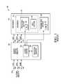
- FIG. 1is a block diagram of an embodiment 100 for an NVM system having a protection code 116 that is used to lock memory sectors within the NVM system 100 .
- the NVM systemincludes memory control circuitry 102 and NVM memory 110 .
- the NVM memory 110includes a read/write memory area 112 that has memory sectors that are readable and writable through read/write commands to the NVM system 100 .
- This read/write memory area 112further includes one or more protectable sectors 114 and one or more open sectors 118 .
- the protectable sectors 114are sectors for which write access is controlled using a protection code (PC) 116 .
- PCprotection code
- the protection code (PC) 116is stored within the protectable sectors 114 and is loaded within the protection register 106 at start-up or after reset of the NVM system 100 .
- the NVM memory 110also includes a program-once area 120 that is not readable through read commands to the NVM system 100 .
- Memory trim parameters (TRIM) 122are stored within the program-once area 120 by writes performed through the access control circuitry 104 .
- the memory trim parameters (TRIM) 122are used to adjust the operation of the NVM memory 110 , for example, based upon post manufacturing test results.
- the memory control circuitry 102communicates with the NVM memory 110 to perform NVM operations using control signals (CNTL) 128 , data signals (DATA) 126 , and address signals (ADDR) 124 .
- the memory control circuitry 102communicates with other external circuitry through connections 132 , which includes control signals (CNTL) 138 , data signals (DATA) 136 , and address signals (ADDR) 134 .
- the memory control circuitry 102also includes access control circuitry 104 and protection register 106 . During operation, the access control circuitry 104 controls write access to the protectable sectors 114 within the NVM memory 110 using the contents of protection register 106 . As indicated above, the protection register 106 is loaded with the protection code (PC) 116 during start-up and/or reset.
- PCprotection code
- This protection code (PC) 116can be a string of protection bits, with each protection bit being associated with one of the protectable sectors 114 (e.g., 32-bits with one protection bit associated with one of 32 different protectable sectors). If the protection bit for the protectable sector indicates that the sector is protected, the access control circuitry 104 will not allow write access to the sector. Alternatively, if the protection bit for a protectable sector indicates that the sector is not protected, the access control circuitry 104 will allow write access to the sector.
- the protection code 116can be accessed and programmed by a user and/or circuitry external to the NVM system 100 using commands issued to the NVM system 100 through connections 132 .
- the access control circuitry 104may grant write access to the protected sector even if it was marked as protected.
- Existing protection schemes for NVM systemstend to work in normal run modes but can be disabled in certain test mode commands and/or with a generic backdoor key. These test mode commands and/or backdoor keys can often become generally known, thereby losing their effectiveness in limiting write access to protected code segments.
- the protection code 116 and/or the protection register 106are subject to being intentionally or unintentionally corrupted, leading to possible corruption of the information stored within protected memory sectors, such as boot code and/or other code blocks.
- FIG. 1is a block diagram of an embodiment for a non-volatile memory (NVM) system having a protection code that is used to lock memory sectors within the NVM system.
- NVMnon-volatile memory
- FIG. 2is a block diagram of an embodiment for an NVM system having lockout codes and lockout keys that are stored in a non-readable program-once area for the NVM system and that are used to lock memory sectors within the NVM system.
- FIG. 3is a block diagram of an embodiment where lockout codes and a protection code are combined to form a merged protection code.
- FIG. 4is a flow diagram of a process embodiment for protecting a sector using a boot lockout code and a boot lockout key.
- FIG. 5is a flow diagram of a process embodiment for updating a protected sector using a boot lockout code and a boot lockout key.
- NVMnon-volatile memory
- Information stored within NVM memory sectorsis protected using lockout codes and lockout keys written in program-once memory areas within the NVM systems.
- lockout codescan be combined into a merged lockout code that can be stored in a merged protection register.
- the merged protection registeris used to control write access to protected memory sectors.
- Lockout code/key pairsare written to the program-once area when a memory sector is protected.
- the program-once areawhich stores the lockout code/key pairs, is not readable by external users. Once protected, a memory sector can not be updated without the lockout code/key pair.
- Different embodiments and variationscan be implemented, as desired, and related or modified systems and method can be utilized, as well.
- NVMnon-volatile memory
- FLASH devicesCode storage in non-volatile memory (NVM) devices, particularly FLASH devices, are often layered with application specific code by a number of different vendors prior to the NVM device being put into operation by an end user.
- code programmed by a primary vendorsuch as boot code or other code blocks
- boot code or other code blockscan be erased or modified intentionally or unintentionally by an intervening vendor.
- the described embodimentsallow a block of code or other information written into an NVM system to be protected from future erasure or modification. Only a user, such as the originating vendor, who has the lockout code and the lockout key used to program the code or information within the protectable memory sectors is able to update the protected code or information.
- the disclosed embodimentsmay overcome weaknesses with prior protection schemes by utilizing write-once areas of an NVM system to store the lockout code/key pairs that identify protected memory sectors. These write-once areas are also not readable by external users of the NVM system thereby further protecting the lockout code/key pairs that are required to update protected memory sectors. As such, protected memory sectors effectively operate as ROM (read only memory) areas to users that do not have the lockout code/key pair information for the protected sector. While program-once areas for NVM systems have been used in the past to store trim information and/or chip serial numbers, these program-once areas for NVM systems have not been used to hold lockout codes/keys that are used to protect memory sectors, as described herein. Further, multiple lockout codes and associated lockout keys can be written into the program-once area to allow layered information and code blocks to be stored and protected within memory sectors. This layered protection allows multiple different vendors to add and protect multiple different layered code blocks within the NVM system.
- FIG. 2is a block diagram of an embodiment 200 for an NVM system having lockout (LO) codes 202 and lockout (LO) keys 204 that are used to lock memory sectors within the NVM system 200 .
- NVM system 200is similar to NVM system 100 .
- the program-once area 120 for the NVM system 200includes the lockout (LO) codes 202 and the lockout (LO) keys 204 .
- the access control circuitry 208is configured to combine the lockout (LO) codes 202 into a combine lockout code that is stored in a merged protection register 210 .
- the access control circuitry 208can also combine the protection code (PC) 116 with the lockout (LO) codes 202 and store this combined lockout code in the merged protection register 210 . As described in further detail below, the access control circuitry 208 utilizes the merged protection register 210 , along with the lockout (LO) codes 202 and lockout (LO) keys 204 to control access to protected sectors.
- PCprotection code
- LOlockout
- the LO codes 202 within the program-once section 120can be written using commands issued to the NVM system 200 through the connections 132 .
- an LO codeis written as one of the LO codes 202 for a new sector to be protected
- an associated LO keyis also written as one of the LO keys 204 .
- the LO codes 202are used to indicate which of the protectable sectors 114 have been protected.
- the LO keys 204are used to further protect and control subsequent access to sectors that have been locked using LO keys 204 .
- the program-once area 120is not readable through commands issued to the NVM system 200 through connections 132 .
- the access control circuitry 208receives the protection code (PC) 116 from the protectable sectors 114 and the lockout (LO) codes 202 from the program-once area 120 . The access control circuitry 208 then combines protection code 116 and the LO codes 202 and stores a merged protection code in the merged protection register 210 . When a write access command is issued through connections 132 , the access control circuitry 208 checks the merged protection register 210 to see if the sector being accessed is protected. If so, then write access is allowed only if a LO code/key pair received along with the write access request matches the LO code/key pair stored for that sector.
- PCprotection code
- LOlockout
- the disclosed embodimentsprovide protectable memory sections 114 that effectively operate as ROM (read only memory) sections once they are protected using lockout code/key pairs 202 / 204 stored in non-readable write-once memory areas 120 of the NVM system 200 .
- the protection code 116could be removed, such that only one or more lockout codes 202 are used. It is further noted that the protectable sectors 114 can be any desired section or area of memory. Further, the protectable sectors 114 can be any desired size and can be different sizes of memory, if desired. While the embodiments herein use one protection bit within the lockout codes 202 to protect each of the protectable sectors 114 , multiple protection bits could also be used for each protectable sector, if desired.
- FIG. 3is a block diagram of an embodiment 300 where a protection code 116 is combined with lockout codes 202 to form a merged protection code.
- the protection code 116 and the lockout codes 202are N-bit codes. Each bit of each N-bit code corresponds to one of the protectable sectors 114 . As such, there are N protectable sectors 114 . Further, a “0” bit is used to indicate that the associated sector is protected. A “1” bit indicates that the sector has not been protected.
- the access control circuitry 208combines the protection code 116 and the lockout codes 202 , and the access control circuitry 208 stores the result in the merged protection register 210 .
- the merged protection registeris also N-bits.
- the lockout codes 202include M different lockout codes from a first lockout code (LO code 0 ) 302 A to an Mth lockout code (LO code M- 1 ) 302 B.
- the access control circuitry 208uses the merged protection code stored in the merged protection register 210 to control write access to the N different protectable sectors 114 (SECTOR 0 , SECTOR 1 . . . SECTOR N- 1 ).
- the protection code 116is an N-bit sequence including bits B N-1 . . . B 1 , B 0 having the logic values “1 . . . 01” where the “0” represents that the second sector (SECTOR 1 ) 304 B is protected.
- the first lockout code (LO code 0 ) 302 Ais an N-bit sequence including bits B N-1 . . . B 1 , B 0 having the logic values “1 . . . 10” where the “0” represents that the first sector (SECTOR 0 ) 304 A is protected.
- the last lockout code (LO code N- 1 ) 302 Bis an N-bit sequence including bits B N-1 . . .
- the access control circuitry 208combines the protection code 116 and the BL codes 202 , for example, using an AND operation such that any “0” bit will result in a “0” in the corresponding bit within the merged protection register 210 .
- the codesare 32-bit codes to represent 32 different protectable sectors (S 31 :S 0 ). Each bit represents a protection bit (B X ) associated with a protectable sector (S X ).
- the hexadecimal representations for the binary codesare also included in parentheses.
- the default bit values within the protection code and boot lockout codesare set to “1.” When protection is desired for a sector, the protection bit for that sector is changed to a “0.” These bit values could be swapped, if desired, and other techniques could also be used, if desired, for indicating whether or not a sector is protected.
- the protection codeindicates protection for Sector 1 by having “0” in protection bit B 1 .
- Lockout Code 0indicates protection for Sector 0 by having “0” in protection bit B 0 .
- Lockout Code 1indicates protection for Sectors 2 - 4 by having “0” in protection bits B 2 , B 3 , and B 4 .
- Lockout Code 2indicates protection for Sector 5 by having “0” in protection bit B 5 .
- Lockout Code 3indicates protection for Sectors 13 and 14 by having “0” in protection bit B 13 and B 14 .
- Lockout Code 4indicates protection for Sector 31 by having “0” in protection bit B 31 .
- Lockout Code 5 and Lockout Code 6have not yet been programmed to protect sectors, and all protection bits are still set to “1.”
- the merged codewhich is a combination of the other codes, indicates protection for all protected sectors (i.e., Sectors 0 - 5 , 13 - 14 and 31 ) by having “0” in protection bits B 0 -B 5 , B 13 -B 14 , and B 31 .
- the protection code and the lockout codesare configured not to have overlapping “0” values for any one protection bit.
- the lockout codescan be used without the protection code, if desired, such that the merged code is a combination only of lockout codes. Further, only one lockout code could be used, if desired, such that no merging of codes would be used.
- a copy of the merged lockout codescan be stored prior to any external access to the merged protection register 210 , if desired, to prevent a change to the merged protection register 210 from occurring during access.
- any command to the NVM systemthat does not use a standard command through connections 132 , such as triggering an erase through an erase-all pin, can be configured to initiate a check of merged lockout codes prior to the non-standard command being allowed to proceed.
- Other techniques and/or modifications to the embodiments hereincould also be implemented, as desired, to further protect desired sectors from being modified.
- the lockout codes 202are located within the program-once area 120 and can only be written once through commands sent to the NVM system 200 . Further, while the boot lockout codes 202 can be accessed and used by the access control circuitry 208 , the boot lockout codes 202 are not accessible or readable by other circuitry through commands communicated through the connections 132 . As such, while the contents of the merged protection register 106 can be accessed by other circuitry, the boot lockout codes 202 can not be accessed.
- the boot lockout keys 204are also located within the program-once area 120 and can only be written once through commands sent to the NVM system 200 . As described in more detail below, these boot lockout keys 204 are required to gain write access to sectors that have been protected using a boot lockout codes 202 . As with the boot lockout codes 202 , the boot lockout keys can be accessed and used by the access control circuitry 208 . However, the boot lockout keys 204 are also not accessible or readable by other circuitry through commands communicated through the connections 132 . As such, once written, the boot lockout keys 204 are only known to the user that wrote the lockout key into the program-once area 120 .
- a boot lockout (BL) codeis written with one or more “0” values to protect one or more sectors.
- a boot lockout (BL) keyis also written and associated with the boot lockout (BL) code.
- TABLE 2 belowprovides an example for the code/key pairs that are stored within the program-once area 120 .
- the boot lockout (BL) keycan be any desired bit string. For example, a 32-bit key can be used. Shorter key lengths could also be used if desired. And longer key lengths, such as 128 bits or more, could be used if enhanced protection is desired.
- FIG. 4is a flow diagram of an embodiment 400 for protecting a sector using a lockout code and a lockout key.
- a lockout command for a sector within the protectable sectors 114is started using communications to the NVM system 200 through connections 132 .
- a lockout code and a lockout key for the sector being protectedare communicated as part of this lockout command request.
- decision block 404a determination is made whether or not the sector is currently locked out. For example, the access control circuitry 208 can check the merged protection register 210 to see if the protection bit for the sector has already been set to indicate protection. If the determination in block 404 is “YES,” then block 410 is reached where an access error is communicated in response to the lockout request.
- the lockout commandthen ends in block 412 . If the determination in block 404 is “NO,” then determination block 406 is reached where a determination is made whether or not an additional lockout code slot is available. If all lockout codes have already been written, then the determination in block 406 is “NO,” and block 409 is reached where a slot error is communicated in response to the lockout request. The lockout command then ends in block 412 . If a lockout code slot is available, then the determination in block 406 is “YES.” Block 408 is then reached where the slot is programmed with the lockout code, and the lockout key associated with the lockout code is also programmed within the write-once area. In addition, the merged protection register is updated. The lockout command then ends in block 412 . Write access to information within the memory sector, such as boot code or other code blocks, is now protected by the lockout code and lockout key that were stored for this protected sector.
- the protected memory sectorcan be erased or updated only if an update command is presented that includes the lockout code and the lockout key that matches the lockout code/key pair stored in the write-once area that protects this protected sector. Without this lockout code/key pair, the protected memory sectors can not be modified.
- FIG. 5is a flow diagram of an embodiment 500 for updating a protected sector using a lockout code and a lockout key.
- an update lockout command for a protected sector within the protectable sectors 114is started using communications to the NVM system 200 through connections 132 .
- a lockout code and a lockout key for the protected sector being updatedare communicated as part of this update lockout command request.
- determination block 504a determination is made by the access control circuitry 208 whether or not the lockout code matches the lockout code that protects the protected sector being accessed. If the determination in block 504 is “NO,” then block 510 is reached where an access error is communicated in response to the update request.
- the update lockout commandthen ends in block 512 .
- determination block 506is reached where a determination is made by the access control circuitry 208 whether or not the lockout key matches the stored lockout key associated with the lockout code protecting the sector being accessed. If the determination in block 506 is “NO,” then block 510 is again reached where an access error is communicated in response to the update request. If the determination in block 506 is “YES,” then block 508 is reached where the access control circuitry 208 modifies the merged protection register 210 to unprotect the sector being updated, thereby allowing information within that sector to be updated. The update lockout command then ends in block 512 . As shown in block 514 , information within the sector, such as boot code or other code blocks for a processor, can be updated. Upon the next reset and/or start-up of the NVM system 200 , the merged protection register 210 will again be set to protect the sector using the lockout code 202 stored within the write-once area 120 .
- lockout code and the lockout keyare written within the program-once area 120 and that this program-once area 120 is not directly accessible to an external system. While the access control circuitry 208 accesses and uses the lockout codes 202 and lockout keys 204 , only the merged protection code stored in the merged protection register 210 is accessible through commands issued to the NVM system 200 through the connections 132 . This inability for subsequent vendors and/or users to determine the lockout code/key pair information significantly enhances protection of protectable sectors 114 as compared to prior solutions.
- a non-volatile memory (NVM) systemincludes at least one protectable memory sector having contents accessible through a read command to the NVM system, a program-once memory area having contents not accessible through a read command to the NVM system and being configured to store at least one lockout code and at least one lockout key associated with the lockout code where the at least one lockout code is configured to identify at least one protectable memory sector as a protected memory sector, and access control circuitry configured to receive a write access request for a protected memory sector and to allow write access to the protected memory sector only if a lockout code and a lockout key are received with the write access request that match a lockout code and a lockout key stored in the program-once memory for the protected memory sector.
- the access control circuitryis further configured to receive a lockout request for a protectable memory sector, to receive a lockout code and a lockout key associated with the lockout request, and to write the lockout code and the lockout key into the program-once memory. Still further, the access control circuitry can be configured to deny the lockout request if the lockout code identifies a protectable memory sector that is already protected. In addition, the at least one protectable memory sector can include a plurality of protectable memory sectors. Further, the program-once memory area can be configured to store a plurality of lockout codes and a plurality of lockout keys.
- the access control circuitrycan be configured to combine the plurality of lockout codes into a merged lockout code and to utilize the merged lockout code to control access to the protectable memory sectors.
- a protection registercan be configured to store the merged lockout code.
- the plurality of protectable sectorscan be configured to store a protection code
- the protection codecan be configured to identify at least one protected memory sector.
- the access control circuitrycan be configured to form the merged lockout code by combining the protection code with the plurality of lockout codes.
- the at least one protectable memory sectorcan be a plurality of protectable memory sectors; the at least one lockout code can be a plurality of protection bits; and each protection bit can be associated with one of the protectable memory sectors.
- the program-once memory areacan be configured to store a single lockout code.
- a method for protecting information stored in a non-volatile memory (NVM) systemincludes storing information within at least one protectable memory sector located within the NVM system where the at least one protectable memory sector has contents accessible through a read command to the NVM system, writing at least one lockout code to a program-once memory area located within the NVM system where the program-once memory area has contents not accessible through a read command to the NVM system and where the at least one lockout code identifies at least one protectable memory sector as a protected memory sector, and writing at least one lockout key associated with the lockout code to the program-once memory area, wherein the NVM system includes access control circuitry configured to receive a write access request for a protected memory sector and to allow write access to the protected memory sector only if a lockout code and a lockout key are received with the write access request that match the lockout code and the lockout key stored in the program-once memory for the protected memory sector.
- the methodcan further include receiving a lockout request for a protectable memory sector and approving the lockout request prior to allowing the writing steps.
- the methodcan further include denying the lockout request if the lockout code identifies a protectable memory sector that is already protected.
- the storing stepcan include storing information within a plurality of protectable memory sectors.
- the writing stepscan include writing a plurality of lockout codes and writing a plurality of lockout keys to protect a plurality of protectable memory sectors.
- the access control circuitrycan be further configured to combine the plurality of lockout codes into a merged lockout code.
- the methodcan further include storing a protection code within the plurality of protectable sectors where the protection code is configured to identify at least one protected memory sector, and forming the merged lockout code by combining the protection code with the plurality of lockout codes.
- a method for accessing protected information stored in a non-volatile memory (NVM) systemincludes operating a non-voltage memory (NVM) system having at least one protected memory sector and at least one program-once area where the at least one protected memory sector stores information to be protected and where the program-once memory area stores at least one lockout code that identifies the at least one protected memory sector and stores at least one lockout key associated with the lockout code.
- NVMnon-voltage memory
- the at least one protected memory sectoris accessible through a read command to the NVM system
- the at least one program-once areais not accessible through a read command to the NVM system.
- the methodalso includes receiving a write access request for the protected memory sector, and allowing write access to the protected memory sector only if a lockout code and a lockout key are received with the write access that match the lockout code and the lockout key stored in the program-once memory for the protected memory sector.
- the program-once areastores a plurality of lockout codes and associated lockout keys that identify a plurality of protected memory sectors
- the methodfurther includes combining the plurality of lockout codes into a merged lockout code and utilizing the merged lockout code to control access to the protected memory sectors.
- a protection code identifying at least one protected memory sectoris also stored within the NVM system, and the method further includes forming the merged lockout code by combining the protection code with the plurality of lockout codes.
- the methodcan further include storing the merged lockout code in a protection register within the NVM system.
Landscapes
- Engineering & Computer Science (AREA)
- Theoretical Computer Science (AREA)
- Computer Security & Cryptography (AREA)
- Computer Hardware Design (AREA)
- General Engineering & Computer Science (AREA)
- Physics & Mathematics (AREA)
- General Physics & Mathematics (AREA)
- Software Systems (AREA)
- General Health & Medical Sciences (AREA)
- Bioethics (AREA)
- Health & Medical Sciences (AREA)
- Databases & Information Systems (AREA)
- Storage Device Security (AREA)
Abstract
Description
| TABLE 1 |
| EXAMPLE MERGED PROTECTION CODE |
| Code | Protection Bits (B31:B0) for Protectable Sectors (S31:S0) |
| Protection | 1111-1111-1111-1111-1111-1111-1111-1101 (FFFF-FFFD) |
| Code | |
| Lockout | 1111-1111-1111-1111-1111-1111-1111-1110 (FFFF-FFFE) |
| Lockout | 1111-1111-1111-1111-1111-1111-1110-0011 (FFFF-FFE3) |
| Lockout | 1111-1111-1111-1111-1111-1111-1101-1111 (FFFF-FFDF) |
| Code 2 | |
| Lockout | 1111-1111-1111-1111-1001-1111-1111-1111 (FFFF-9FFF) |
| Code 3 | |
| Lockout | 0111-1111-1111-1111-1111-1111-1111-1111 (7FFF-FFFF) |
| Code 4 | |
| Lockout | 1111-1111-1111-1111-1111-1111-1111-1111 (FFFF-FFFF) |
| Code 5 | |
| Lockout | 1111-1111-1111-1111-1111-1111-1111-1111 (FFFF-FFFF) |
| Code 6 | |
| Merged | 0111-1111-1111-1111-1001-1111-1100-0000 (7FFF-9FC0)) |
| Code | |
| TABLE 2 |
| EXAMPLE LOCKOUT CODE/KEY PAIRS |
| Lockout Code | Lockout | ||
| LO CODE | |||
| 0 | |||
| . . . | . . . | ||
| LO CODE N | LO KEY N | ||
Claims (22)
Priority Applications (3)
| Application Number | Priority Date | Filing Date | Title |
|---|---|---|---|
| US13/616,922US9390278B2 (en) | 2012-09-14 | 2012-09-14 | Systems and methods for code protection in non-volatile memory systems |
| EP13183411.1AEP2709034B1 (en) | 2012-09-14 | 2013-09-06 | Systems and methods for code protection in non-volatile memory systems |
| CN201310411053.8ACN103679067A (en) | 2012-09-14 | 2013-09-11 | Systems and methods for code protection in non-volatile memory systems |
Applications Claiming Priority (1)
| Application Number | Priority Date | Filing Date | Title |
|---|---|---|---|
| US13/616,922US9390278B2 (en) | 2012-09-14 | 2012-09-14 | Systems and methods for code protection in non-volatile memory systems |
Related Child Applications (1)
| Application Number | Title | Priority Date | Filing Date |
|---|---|---|---|
| EP13183411.1APreviously-Filed-ApplicationEP2709034B1 (en) | 2012-09-14 | 2013-09-06 | Systems and methods for code protection in non-volatile memory systems |
Publications (2)
| Publication Number | Publication Date |
|---|---|
| US20140082257A1 US20140082257A1 (en) | 2014-03-20 |
| US9390278B2true US9390278B2 (en) | 2016-07-12 |
Family
ID=49123733
Family Applications (1)
| Application Number | Title | Priority Date | Filing Date |
|---|---|---|---|
| US13/616,922Active2033-05-02US9390278B2 (en) | 2012-09-14 | 2012-09-14 | Systems and methods for code protection in non-volatile memory systems |
Country Status (3)
| Country | Link |
|---|---|
| US (1) | US9390278B2 (en) |
| EP (1) | EP2709034B1 (en) |
| CN (1) | CN103679067A (en) |
Cited By (2)
| Publication number | Priority date | Publication date | Assignee | Title |
|---|---|---|---|---|
| US20160306978A1 (en)* | 2011-12-22 | 2016-10-20 | Intel Corporation | User controllable platform-level trigger to set policy for protecting platform from malware |
| US20220366087A1 (en)* | 2021-05-13 | 2022-11-17 | AO Kaspersky Lab | Systems and methods for verifying the integrity of a software installation image |
Families Citing this family (15)
| Publication number | Priority date | Publication date | Assignee | Title |
|---|---|---|---|---|
| US9400495B2 (en) | 2012-10-16 | 2016-07-26 | Rockwell Automation Technologies, Inc. | Industrial automation equipment and machine procedure simulation |
| US9830479B2 (en) | 2014-09-16 | 2017-11-28 | Nxp Usa, Inc. | Key storage and revocation in a secure memory system |
| US11086797B2 (en)* | 2014-10-31 | 2021-08-10 | Hewlett Packard Enterprise Development Lp | Systems and methods for restricting write access to non-volatile memory |
| CN104598402B (en)* | 2014-12-30 | 2017-11-10 | 北京兆易创新科技股份有限公司 | A kind of control method of flash controller and flash controller |
| US9645948B2 (en)* | 2015-01-16 | 2017-05-09 | Hamilton Sundstrand Corporation | Access key generation for computer-readable memory |
| CN105138869B (en)* | 2015-08-17 | 2018-05-25 | 四川长虹电器股份有限公司 | Method based on flag bit detection automatic lockout protection flash bootstrap |
| US10223294B2 (en)* | 2015-09-01 | 2019-03-05 | Nxp Usa, Inc. | Fast secure boot from embedded flash memory |
| US10885196B2 (en) | 2016-04-29 | 2021-01-05 | Hewlett Packard Enterprise Development Lp | Executing protected code |
| US10034407B2 (en)* | 2016-07-22 | 2018-07-24 | Intel Corporation | Storage sled for a data center |
| US10296738B2 (en)* | 2017-05-03 | 2019-05-21 | Nuvoton Technology Corporation | Secure integrated-circuit state management |
| US11210238B2 (en)* | 2018-10-30 | 2021-12-28 | Cypress Semiconductor Corporation | Securing data logs in memory devices |
| CN112711780A (en)* | 2019-10-25 | 2021-04-27 | 中车株洲电力机车研究所有限公司 | Memory unlocking method, system, storage medium and computer equipment |
| US11985228B2 (en)* | 2021-07-30 | 2024-05-14 | Cisco Technology, Inc. | Configuration payload separation policies |
| FR3133248A1 (en)* | 2022-03-07 | 2023-09-08 | Stmicroelectronics (Rousset) Sas | Protection of an integrated circuit |
| CN116795299A (en)* | 2023-08-28 | 2023-09-22 | 苏州萨沙迈半导体有限公司 | Analog system of read-only memory |
Citations (20)
| Publication number | Priority date | Publication date | Assignee | Title |
|---|---|---|---|---|
| US5937063A (en) | 1996-09-30 | 1999-08-10 | Intel Corporation | Secure boot |
| US6711675B1 (en) | 2000-02-11 | 2004-03-23 | Intel Corporation | Protected boot flow |
| US20050071592A1 (en) | 2003-09-26 | 2005-03-31 | Decaro Richard V. | Selectable block protection for non-volatile memory |
| US20050114687A1 (en) | 2003-11-21 | 2005-05-26 | Zimmer Vincent J. | Methods and apparatus to provide protection for firmware resources |
| US20080086780A1 (en) | 2006-10-06 | 2008-04-10 | Xuemin Chen | Method and system for protection of customer secrets in a secure reprogrammable system |
| US20080189557A1 (en)* | 2005-01-19 | 2008-08-07 | Stmicroelectronics S.R.I. | Method and architecture for restricting access to a memory device |
| US20090113155A1 (en)* | 2007-10-31 | 2009-04-30 | Echostar Technologies Corporation | Hardware anti-piracy via nonvolatile memory devices |
| US20090172414A1 (en) | 2005-06-22 | 2009-07-02 | Freescale Semiconductor, Inc. | Device and method for securing software |
| US7562360B2 (en) | 2003-12-01 | 2009-07-14 | Texas Instruments Incorporated | Method and system for firmware downloads |
| US20090222652A1 (en) | 2005-08-22 | 2009-09-03 | Nxp B.V. | Embedded memory protection |
| US20090228711A1 (en) | 2008-03-06 | 2009-09-10 | Samsung Electronics Co., Ltd. | Processor apparatus having a security function |
| US20090296933A1 (en) | 2004-11-22 | 2009-12-03 | Freescale Semiconductor, Inc. | Integrated circuit and a method for secure testing |
| US7716470B2 (en) | 2003-06-18 | 2010-05-11 | Architecture Technology Corporation | Active verification of boot firmware |
| US7774596B2 (en) | 2005-02-02 | 2010-08-10 | Insyde Software Corporation | System and method for updating firmware in a secure manner |
| US20110035603A1 (en)* | 2002-11-27 | 2011-02-10 | Aran Ziv | Apparatus and Method for Securing Data on a Portable Storage Device |
| US20110138487A1 (en)* | 2009-12-09 | 2011-06-09 | Ehud Cohen | Storage Device and Method for Using a Virtual File in a Public Memory Area to Access a Plurality of Protected Files in a Private Memory Area |
| US20110153970A1 (en)* | 2004-03-17 | 2011-06-23 | Ralf Hediger | Method and Apparatus for the Execution of a Program |
| US7987351B2 (en) | 2006-10-06 | 2011-07-26 | Broadcom Corporation | Method and system for enhanced boot protection |
| US20110258462A1 (en) | 2009-01-05 | 2011-10-20 | Freescale Semiconductor, Inc. | Method, system and integrated circuit for enabling access to a memory element |
| US20110289137A1 (en)* | 2010-05-20 | 2011-11-24 | Eyal Ittah | Host Device and Method for Accessing a Virtual File in a Storage Device by Bypassing a Cache in the Host Device |
- 2012
- 2012-09-14USUS13/616,922patent/US9390278B2/enactiveActive
- 2013
- 2013-09-06EPEP13183411.1Apatent/EP2709034B1/enactiveActive
- 2013-09-11CNCN201310411053.8Apatent/CN103679067A/enactivePending
Patent Citations (20)
| Publication number | Priority date | Publication date | Assignee | Title |
|---|---|---|---|---|
| US5937063A (en) | 1996-09-30 | 1999-08-10 | Intel Corporation | Secure boot |
| US6711675B1 (en) | 2000-02-11 | 2004-03-23 | Intel Corporation | Protected boot flow |
| US20110035603A1 (en)* | 2002-11-27 | 2011-02-10 | Aran Ziv | Apparatus and Method for Securing Data on a Portable Storage Device |
| US7716470B2 (en) | 2003-06-18 | 2010-05-11 | Architecture Technology Corporation | Active verification of boot firmware |
| US20050071592A1 (en) | 2003-09-26 | 2005-03-31 | Decaro Richard V. | Selectable block protection for non-volatile memory |
| US20050114687A1 (en) | 2003-11-21 | 2005-05-26 | Zimmer Vincent J. | Methods and apparatus to provide protection for firmware resources |
| US7562360B2 (en) | 2003-12-01 | 2009-07-14 | Texas Instruments Incorporated | Method and system for firmware downloads |
| US20110153970A1 (en)* | 2004-03-17 | 2011-06-23 | Ralf Hediger | Method and Apparatus for the Execution of a Program |
| US20090296933A1 (en) | 2004-11-22 | 2009-12-03 | Freescale Semiconductor, Inc. | Integrated circuit and a method for secure testing |
| US20080189557A1 (en)* | 2005-01-19 | 2008-08-07 | Stmicroelectronics S.R.I. | Method and architecture for restricting access to a memory device |
| US7774596B2 (en) | 2005-02-02 | 2010-08-10 | Insyde Software Corporation | System and method for updating firmware in a secure manner |
| US20090172414A1 (en) | 2005-06-22 | 2009-07-02 | Freescale Semiconductor, Inc. | Device and method for securing software |
| US20090222652A1 (en) | 2005-08-22 | 2009-09-03 | Nxp B.V. | Embedded memory protection |
| US20080086780A1 (en) | 2006-10-06 | 2008-04-10 | Xuemin Chen | Method and system for protection of customer secrets in a secure reprogrammable system |
| US7987351B2 (en) | 2006-10-06 | 2011-07-26 | Broadcom Corporation | Method and system for enhanced boot protection |
| US20090113155A1 (en)* | 2007-10-31 | 2009-04-30 | Echostar Technologies Corporation | Hardware anti-piracy via nonvolatile memory devices |
| US20090228711A1 (en) | 2008-03-06 | 2009-09-10 | Samsung Electronics Co., Ltd. | Processor apparatus having a security function |
| US20110258462A1 (en) | 2009-01-05 | 2011-10-20 | Freescale Semiconductor, Inc. | Method, system and integrated circuit for enabling access to a memory element |
| US20110138487A1 (en)* | 2009-12-09 | 2011-06-09 | Ehud Cohen | Storage Device and Method for Using a Virtual File in a Public Memory Area to Access a Plurality of Protected Files in a Private Memory Area |
| US20110289137A1 (en)* | 2010-05-20 | 2011-11-24 | Eyal Ittah | Host Device and Method for Accessing a Virtual File in a Storage Device by Bypassing a Cache in the Host Device |
Non-Patent Citations (1)
| Title |
|---|
| Peng, "On-Chip System Protection Basics for HCS08 Microcontrollers", Freescale Semiconductor, Document No. AN3305, 2007, 26 pgs. |
Cited By (4)
| Publication number | Priority date | Publication date | Assignee | Title |
|---|---|---|---|---|
| US20160306978A1 (en)* | 2011-12-22 | 2016-10-20 | Intel Corporation | User controllable platform-level trigger to set policy for protecting platform from malware |
| US9916454B2 (en)* | 2011-12-22 | 2018-03-13 | Intel Corporation | User controllable platform-level trigger to set policy for protecting platform from malware |
| US20220366087A1 (en)* | 2021-05-13 | 2022-11-17 | AO Kaspersky Lab | Systems and methods for verifying the integrity of a software installation image |
| US12111958B2 (en)* | 2021-05-13 | 2024-10-08 | AO Kaspersky Lab | Systems and methods for verifying the integrity of a software installation image |
Also Published As
| Publication number | Publication date |
|---|---|
| US20140082257A1 (en) | 2014-03-20 |
| EP2709034A1 (en) | 2014-03-19 |
| CN103679067A (en) | 2014-03-26 |
| EP2709034B1 (en) | 2018-11-21 |
Similar Documents
| Publication | Publication Date | Title |
|---|---|---|
| US9390278B2 (en) | Systems and methods for code protection in non-volatile memory systems | |
| US11868278B2 (en) | Block or page lock features in serial interface memory | |
| US11615035B2 (en) | Storage system and method for performing and authenticating write-protection thereof | |
| KR100531192B1 (en) | Non-volatile memory control method | |
| US7574576B2 (en) | Semiconductor device and method of controlling the same | |
| US9256525B2 (en) | Semiconductor memory device including a flag for selectively controlling erasing and writing of confidential information area | |
| US8000153B2 (en) | Enhanced erase for flash storage device | |
| US20100037000A1 (en) | One-time-programmable memory emulation | |
| JP6399523B2 (en) | Method and memory device for protecting the contents of a memory device | |
| JP2002025278A (en) | Semiconductor storage device | |
| JP2001356963A (en) | Semiconductor device and control device therefor | |
| US6948041B2 (en) | Permanent memory block protection in a flash memory device | |
| US11681797B2 (en) | Row activation prevention using fuses | |
| JP2008152549A (en) | Memory device, and password storage method for memory device | |
| US20040186947A1 (en) | Access control system for nonvolatile memory | |
| WO2001061503A1 (en) | Nonvolatile memory | |
| US10783091B2 (en) | Memory access control and verification using address aliasing and markers | |
| JP2000148594A (en) | ROM data read protection circuit | |
| US7890721B2 (en) | Implementation of integrated status of a protection register word in a protection register array | |
| JPH11328326A (en) | IC card | |
| JP2003203012A (en) | Microcomputer device | |
| TWI750073B (en) | Semiconductor device with security function and security method thereof | |
| TWI845325B (en) | Control circuit and control method thereof | |
| JP5885638B2 (en) | Semiconductor memory device | |
| JP2007193913A (en) | Nonvolatile semiconductor memory device |
Legal Events
| Date | Code | Title | Description |
|---|---|---|---|
| AS | Assignment | Owner name:FREESCALE SEMICONDUCTOR, INC., TEXAS Free format text:ASSIGNMENT OF ASSIGNORS INTEREST;ASSIGNORS:SCOULLER, ROSS S.;ANDRE, DANIEL L.;CUNNINGHAM, JEFFREY C.;REEL/FRAME:028973/0911 Effective date:20120913 | |
| AS | Assignment | Owner name:CITIBANK, N.A., AS NOTES COLLATERAL AGENT, NEW YOR Free format text:SUPPLEMENT TO IP SECURITY AGREEMENT;ASSIGNOR:FREESCALE SEMICONDUCTOR, INC.;REEL/FRAME:030256/0471 Effective date:20121031 Owner name:CITIBANK, N.A., AS NOTES COLLATERAL AGENT, NEW YOR Free format text:SUPPLEMENT TO IP SECURITY AGREEMENT;ASSIGNOR:FREESCALE SEMICONDUCTOR, INC.;REEL/FRAME:030256/0625 Effective date:20121031 Owner name:CITIBANK, N.A., AS NOTES COLLATERAL AGENT, NEW YOR Free format text:SUPPLEMENT TO IP SECURITY AGREEMENT;ASSIGNOR:FREESCALE SEMICONDUCTOR, INC.;REEL/FRAME:030256/0544 Effective date:20121031 | |
| AS | Assignment | Owner name:CITIBANK, N.A., AS NOTES COLLATERAL AGENT, NEW YORK Free format text:SECURITY AGREEMENT;ASSIGNOR:FREESCALE SEMICONDUCTOR, INC.;REEL/FRAME:030633/0424 Effective date:20130521 Owner name:CITIBANK, N.A., AS NOTES COLLATERAL AGENT, NEW YOR Free format text:SECURITY AGREEMENT;ASSIGNOR:FREESCALE SEMICONDUCTOR, INC.;REEL/FRAME:030633/0424 Effective date:20130521 | |
| AS | Assignment | Owner name:CITIBANK, N.A., AS NOTES COLLATERAL AGENT, NEW YORK Free format text:SECURITY AGREEMENT;ASSIGNOR:FREESCALE SEMICONDUCTOR, INC.;REEL/FRAME:031591/0266 Effective date:20131101 Owner name:CITIBANK, N.A., AS NOTES COLLATERAL AGENT, NEW YOR Free format text:SECURITY AGREEMENT;ASSIGNOR:FREESCALE SEMICONDUCTOR, INC.;REEL/FRAME:031591/0266 Effective date:20131101 | |
| AS | Assignment | Owner name:FREESCALE SEMICONDUCTOR, INC., TEXAS Free format text:PATENT RELEASE;ASSIGNOR:CITIBANK, N.A., AS COLLATERAL AGENT;REEL/FRAME:037357/0614 Effective date:20151207 Owner name:FREESCALE SEMICONDUCTOR, INC., TEXAS Free format text:PATENT RELEASE;ASSIGNOR:CITIBANK, N.A., AS COLLATERAL AGENT;REEL/FRAME:037357/0652 Effective date:20151207 Owner name:FREESCALE SEMICONDUCTOR, INC., TEXAS Free format text:PATENT RELEASE;ASSIGNOR:CITIBANK, N.A., AS COLLATERAL AGENT;REEL/FRAME:037357/0633 Effective date:20151207 | |
| AS | Assignment | Owner name:MORGAN STANLEY SENIOR FUNDING, INC., MARYLAND Free format text:ASSIGNMENT AND ASSUMPTION OF SECURITY INTEREST IN PATENTS;ASSIGNOR:CITIBANK, N.A.;REEL/FRAME:037486/0517 Effective date:20151207 | |
| AS | Assignment | Owner name:MORGAN STANLEY SENIOR FUNDING, INC., MARYLAND Free format text:ASSIGNMENT AND ASSUMPTION OF SECURITY INTEREST IN PATENTS;ASSIGNOR:CITIBANK, N.A.;REEL/FRAME:037518/0292 Effective date:20151207 | |
| AS | Assignment | Owner name:MORGAN STANLEY SENIOR FUNDING, INC., MARYLAND Free format text:SUPPLEMENT TO THE SECURITY AGREEMENT;ASSIGNOR:FREESCALE SEMICONDUCTOR, INC.;REEL/FRAME:039138/0001 Effective date:20160525 | |
| STCF | Information on status: patent grant | Free format text:PATENTED CASE | |
| AS | Assignment | Owner name:NXP, B.V., F/K/A FREESCALE SEMICONDUCTOR, INC., NETHERLANDS Free format text:RELEASE BY SECURED PARTY;ASSIGNOR:MORGAN STANLEY SENIOR FUNDING, INC.;REEL/FRAME:040925/0001 Effective date:20160912 Owner name:NXP, B.V., F/K/A FREESCALE SEMICONDUCTOR, INC., NE Free format text:RELEASE BY SECURED PARTY;ASSIGNOR:MORGAN STANLEY SENIOR FUNDING, INC.;REEL/FRAME:040925/0001 Effective date:20160912 | |
| AS | Assignment | Owner name:NXP B.V., NETHERLANDS Free format text:RELEASE BY SECURED PARTY;ASSIGNOR:MORGAN STANLEY SENIOR FUNDING, INC.;REEL/FRAME:040928/0001 Effective date:20160622 | |
| AS | Assignment | Owner name:NXP USA, INC., TEXAS Free format text:MERGER;ASSIGNOR:FREESCALE SEMICONDUCTOR, INC.;REEL/FRAME:041144/0363 Effective date:20161107 | |
| AS | Assignment | Owner name:MORGAN STANLEY SENIOR FUNDING, INC., MARYLAND Free format text:CORRECTIVE ASSIGNMENT TO CORRECT THE REMOVE PATENTS 8108266 AND 8062324 AND REPLACE THEM WITH 6108266 AND 8060324 PREVIOUSLY RECORDED ON REEL 037518 FRAME 0292. ASSIGNOR(S) HEREBY CONFIRMS THE ASSIGNMENT AND ASSUMPTION OF SECURITY INTEREST IN PATENTS;ASSIGNOR:CITIBANK, N.A.;REEL/FRAME:041703/0536 Effective date:20151207 | |
| AS | Assignment | Owner name:SHENZHEN XINGUODU TECHNOLOGY CO., LTD., CHINA Free format text:CORRECTIVE ASSIGNMENT TO CORRECT THE TO CORRECT THE APPLICATION NO. FROM 13,883,290 TO 13,833,290 PREVIOUSLY RECORDED ON REEL 041703 FRAME 0536. ASSIGNOR(S) HEREBY CONFIRMS THE THE ASSIGNMENT AND ASSUMPTION OF SECURITYINTEREST IN PATENTS.;ASSIGNOR:MORGAN STANLEY SENIOR FUNDING, INC.;REEL/FRAME:048734/0001 Effective date:20190217 | |
| AS | Assignment | Owner name:NXP B.V., NETHERLANDS Free format text:RELEASE BY SECURED PARTY;ASSIGNOR:MORGAN STANLEY SENIOR FUNDING, INC.;REEL/FRAME:050744/0097 Effective date:20190903 | |
| AS | Assignment | Owner name:MORGAN STANLEY SENIOR FUNDING, INC., MARYLAND Free format text:CORRECTIVE ASSIGNMENT TO CORRECT THE REMOVE APPLICATION11759915 AND REPLACE IT WITH APPLICATION 11759935 PREVIOUSLY RECORDED ON REEL 037486 FRAME 0517. ASSIGNOR(S) HEREBY CONFIRMS THE ASSIGNMENT AND ASSUMPTION OF SECURITYINTEREST IN PATENTS;ASSIGNOR:CITIBANK, N.A.;REEL/FRAME:053547/0421 Effective date:20151207 | |
| MAFP | Maintenance fee payment | Free format text:PAYMENT OF MAINTENANCE FEE, 4TH YEAR, LARGE ENTITY (ORIGINAL EVENT CODE: M1551); ENTITY STATUS OF PATENT OWNER: LARGE ENTITY Year of fee payment:4 | |
| AS | Assignment | Owner name:NXP B.V., NETHERLANDS Free format text:CORRECTIVE ASSIGNMENT TO CORRECT THE REMOVEAPPLICATION 11759915 AND REPLACE IT WITH APPLICATION11759935 PREVIOUSLY RECORDED ON REEL 040928 FRAME 0001. ASSIGNOR(S) HEREBY CONFIRMS THE RELEASE OF SECURITYINTEREST;ASSIGNOR:MORGAN STANLEY SENIOR FUNDING, INC.;REEL/FRAME:052915/0001 Effective date:20160622 | |
| AS | Assignment | Owner name:NXP, B.V. F/K/A FREESCALE SEMICONDUCTOR, INC., NETHERLANDS Free format text:CORRECTIVE ASSIGNMENT TO CORRECT THE REMOVEAPPLICATION 11759915 AND REPLACE IT WITH APPLICATION11759935 PREVIOUSLY RECORDED ON REEL 040925 FRAME 0001. ASSIGNOR(S) HEREBY CONFIRMS THE RELEASE OF SECURITYINTEREST;ASSIGNOR:MORGAN STANLEY SENIOR FUNDING, INC.;REEL/FRAME:052917/0001 Effective date:20160912 | |
| MAFP | Maintenance fee payment | Free format text:PAYMENT OF MAINTENANCE FEE, 8TH YEAR, LARGE ENTITY (ORIGINAL EVENT CODE: M1552); ENTITY STATUS OF PATENT OWNER: LARGE ENTITY Year of fee payment:8 |