US9388491B2 - Method for deposition of conformal films with catalysis assisted low temperature CVD - Google Patents
Method for deposition of conformal films with catalysis assisted low temperature CVDDownload PDFInfo
- Publication number
- US9388491B2 US9388491B2US13/946,012US201313946012AUS9388491B2US 9388491 B2US9388491 B2US 9388491B2US 201313946012 AUS201313946012 AUS 201313946012AUS 9388491 B2US9388491 B2US 9388491B2
- Authority
- US
- United States
- Prior art keywords
- gas
- deposition
- substrate
- film
- temperature
- Prior art date
- Legal status (The legal status is an assumption and is not a legal conclusion. Google has not performed a legal analysis and makes no representation as to the accuracy of the status listed.)
- Active, expires
Links
- 238000000034methodMethods0.000titleclaimsabstractdescription40
- 230000008021depositionEffects0.000titleclaimsdescription23
- 238000006555catalytic reactionMethods0.000title1
- 238000000151depositionMethods0.000claimsabstractdescription29
- 239000000758substrateSubstances0.000claimsabstractdescription26
- 238000012545processingMethods0.000claimsabstractdescription19
- NJPPVKZQTLUDBO-UHFFFAOYSA-NnovaluronChemical compoundC1=C(Cl)C(OC(F)(F)C(OC(F)(F)F)F)=CC=C1NC(=O)NC(=O)C1=C(F)C=CC=C1FNJPPVKZQTLUDBO-UHFFFAOYSA-N0.000claimsabstractdescription15
- 239000002243precursorSubstances0.000claimsabstractdescription15
- 239000000203mixtureSubstances0.000claimsabstractdescription14
- QGZKDVFQNNGYKY-UHFFFAOYSA-NAmmoniaChemical compoundNQGZKDVFQNNGYKY-UHFFFAOYSA-N0.000claimsabstractdescription13
- 238000010438heat treatmentMethods0.000claimsabstractdescription7
- BLRPTPMANUNPDV-UHFFFAOYSA-NSilaneChemical compound[SiH4]BLRPTPMANUNPDV-UHFFFAOYSA-N0.000claimsdescription14
- 238000010926purgeMethods0.000claimsdescription4
- 229910000077silaneInorganic materials0.000claimsdescription4
- 229910052580B4CInorganic materials0.000claimsdescription2
- 229910052582BNInorganic materials0.000claimsdescription2
- PZNSFCLAULLKQX-UHFFFAOYSA-NBoron nitrideChemical compoundN#BPZNSFCLAULLKQX-UHFFFAOYSA-N0.000claimsdescription2
- 229910052581Si3N4Inorganic materials0.000claimsdescription2
- INAHAJYZKVIDIZ-UHFFFAOYSA-Nboron carbideChemical compoundB12B3B4C32B41INAHAJYZKVIDIZ-UHFFFAOYSA-N0.000claimsdescription2
- HQVNEWCFYHHQES-UHFFFAOYSA-Nsilicon nitrideChemical compoundN12[Si]34N5[Si]62N3[Si]51N64HQVNEWCFYHHQES-UHFFFAOYSA-N0.000claimsdescription2
- 239000007789gasSubstances0.000description24
- 238000005229chemical vapour depositionMethods0.000description10
- 238000006243chemical reactionMethods0.000description7
- 230000001276controlling effectEffects0.000description6
- 229910000069nitrogen hydrideInorganic materials0.000description6
- 238000011282treatmentMethods0.000description5
- 235000012431wafersNutrition0.000description5
- VGGSQFUCUMXWEO-UHFFFAOYSA-NEtheneChemical compoundC=CVGGSQFUCUMXWEO-UHFFFAOYSA-N0.000description4
- LWFWUJCJKPUZLV-UHFFFAOYSA-Nn-trimethylsilylacetamideChemical compoundCC(=O)N[Si](C)(C)CLWFWUJCJKPUZLV-UHFFFAOYSA-N0.000description4
- 238000005033Fourier transform infrared spectroscopyMethods0.000description3
- 239000005977EthyleneSubstances0.000description2
- 229910007991Si-NInorganic materials0.000description2
- 229910003697SiBNInorganic materials0.000description2
- 229910006294Si—NInorganic materials0.000description2
- 238000002835absorbanceMethods0.000description2
- 229910021417amorphous siliconInorganic materials0.000description2
- 238000000231atomic layer depositionMethods0.000description2
- 230000003197catalytic effectEffects0.000description2
- 238000004590computer programMethods0.000description2
- 238000000354decomposition reactionMethods0.000description2
- 230000006870functionEffects0.000description2
- 239000001257hydrogenSubstances0.000description2
- 229910052739hydrogenInorganic materials0.000description2
- 238000000623plasma-assisted chemical vapour depositionMethods0.000description2
- 239000004065semiconductorSubstances0.000description2
- 239000000126substanceSubstances0.000description2
- CZDYPVPMEAXLPK-UHFFFAOYSA-NtetramethylsilaneChemical compoundC[Si](C)(C)CCZDYPVPMEAXLPK-UHFFFAOYSA-N0.000description2
- 238000012546transferMethods0.000description2
- ZOXJGFHDIHLPTG-UHFFFAOYSA-NBoronChemical compound[B]ZOXJGFHDIHLPTG-UHFFFAOYSA-N0.000description1
- UFHFLCQGNIYNRP-UHFFFAOYSA-NHydrogenChemical compound[H][H]UFHFLCQGNIYNRP-UHFFFAOYSA-N0.000description1
- 229910021529ammoniaInorganic materials0.000description1
- 238000004458analytical methodMethods0.000description1
- 238000013459approachMethods0.000description1
- 229910052796boronInorganic materials0.000description1
- 239000007833carbon precursorSubstances0.000description1
- 239000012159carrier gasSubstances0.000description1
- 238000001816coolingMethods0.000description1
- 238000005137deposition processMethods0.000description1
- 238000010586diagramMethods0.000description1
- 239000001307heliumSubstances0.000description1
- 229910052734heliumInorganic materials0.000description1
- SWQJXJOGLNCZEY-UHFFFAOYSA-Nhelium atomChemical compound[He]SWQJXJOGLNCZEY-UHFFFAOYSA-N0.000description1
- 150000002431hydrogenChemical class0.000description1
- 229910052751metalInorganic materials0.000description1
- 239000002184metalSubstances0.000description1
- 150000002739metalsChemical class0.000description1
- 238000012986modificationMethods0.000description1
- 230000004048modificationEffects0.000description1
- 150000004767nitridesChemical class0.000description1
- 238000010943off-gassingMethods0.000description1
- 230000001105regulatory effectEffects0.000description1
- 238000012163sequencing techniqueMethods0.000description1
- 238000002230thermal chemical vapour depositionMethods0.000description1
Images


Classifications
- H—ELECTRICITY
- H01—ELECTRIC ELEMENTS
- H01L—SEMICONDUCTOR DEVICES NOT COVERED BY CLASS H10
- H01L21/00—Processes or apparatus adapted for the manufacture or treatment of semiconductor or solid state devices or of parts thereof
- H01L21/02—Manufacture or treatment of semiconductor devices or of parts thereof
- H01L21/02104—Forming layers
- H01L21/02365—Forming inorganic semiconducting materials on a substrate
- H01L21/02612—Formation types
- H01L21/02617—Deposition types
- H01L21/0262—Reduction or decomposition of gaseous compounds, e.g. CVD
- C—CHEMISTRY; METALLURGY
- C23—COATING METALLIC MATERIAL; COATING MATERIAL WITH METALLIC MATERIAL; CHEMICAL SURFACE TREATMENT; DIFFUSION TREATMENT OF METALLIC MATERIAL; COATING BY VACUUM EVAPORATION, BY SPUTTERING, BY ION IMPLANTATION OR BY CHEMICAL VAPOUR DEPOSITION, IN GENERAL; INHIBITING CORROSION OF METALLIC MATERIAL OR INCRUSTATION IN GENERAL
- C23C—COATING METALLIC MATERIAL; COATING MATERIAL WITH METALLIC MATERIAL; SURFACE TREATMENT OF METALLIC MATERIAL BY DIFFUSION INTO THE SURFACE, BY CHEMICAL CONVERSION OR SUBSTITUTION; COATING BY VACUUM EVAPORATION, BY SPUTTERING, BY ION IMPLANTATION OR BY CHEMICAL VAPOUR DEPOSITION, IN GENERAL
- C23C16/00—Chemical coating by decomposition of gaseous compounds, without leaving reaction products of surface material in the coating, i.e. chemical vapour deposition [CVD] processes
- C23C16/22—Chemical coating by decomposition of gaseous compounds, without leaving reaction products of surface material in the coating, i.e. chemical vapour deposition [CVD] processes characterised by the deposition of inorganic material, other than metallic material
- C23C16/30—Deposition of compounds, mixtures or solid solutions, e.g. borides, carbides, nitrides
- C23C16/38—Borides
- C—CHEMISTRY; METALLURGY
- C23—COATING METALLIC MATERIAL; COATING MATERIAL WITH METALLIC MATERIAL; CHEMICAL SURFACE TREATMENT; DIFFUSION TREATMENT OF METALLIC MATERIAL; COATING BY VACUUM EVAPORATION, BY SPUTTERING, BY ION IMPLANTATION OR BY CHEMICAL VAPOUR DEPOSITION, IN GENERAL; INHIBITING CORROSION OF METALLIC MATERIAL OR INCRUSTATION IN GENERAL
- C23C—COATING METALLIC MATERIAL; COATING MATERIAL WITH METALLIC MATERIAL; SURFACE TREATMENT OF METALLIC MATERIAL BY DIFFUSION INTO THE SURFACE, BY CHEMICAL CONVERSION OR SUBSTITUTION; COATING BY VACUUM EVAPORATION, BY SPUTTERING, BY ION IMPLANTATION OR BY CHEMICAL VAPOUR DEPOSITION, IN GENERAL
- C23C16/00—Chemical coating by decomposition of gaseous compounds, without leaving reaction products of surface material in the coating, i.e. chemical vapour deposition [CVD] processes
- C23C16/22—Chemical coating by decomposition of gaseous compounds, without leaving reaction products of surface material in the coating, i.e. chemical vapour deposition [CVD] processes characterised by the deposition of inorganic material, other than metallic material
- C23C16/30—Deposition of compounds, mixtures or solid solutions, e.g. borides, carbides, nitrides
- C23C16/32—Carbides
- C—CHEMISTRY; METALLURGY
- C23—COATING METALLIC MATERIAL; COATING MATERIAL WITH METALLIC MATERIAL; CHEMICAL SURFACE TREATMENT; DIFFUSION TREATMENT OF METALLIC MATERIAL; COATING BY VACUUM EVAPORATION, BY SPUTTERING, BY ION IMPLANTATION OR BY CHEMICAL VAPOUR DEPOSITION, IN GENERAL; INHIBITING CORROSION OF METALLIC MATERIAL OR INCRUSTATION IN GENERAL
- C23C—COATING METALLIC MATERIAL; COATING MATERIAL WITH METALLIC MATERIAL; SURFACE TREATMENT OF METALLIC MATERIAL BY DIFFUSION INTO THE SURFACE, BY CHEMICAL CONVERSION OR SUBSTITUTION; COATING BY VACUUM EVAPORATION, BY SPUTTERING, BY ION IMPLANTATION OR BY CHEMICAL VAPOUR DEPOSITION, IN GENERAL
- C23C16/00—Chemical coating by decomposition of gaseous compounds, without leaving reaction products of surface material in the coating, i.e. chemical vapour deposition [CVD] processes
- C23C16/22—Chemical coating by decomposition of gaseous compounds, without leaving reaction products of surface material in the coating, i.e. chemical vapour deposition [CVD] processes characterised by the deposition of inorganic material, other than metallic material
- C23C16/30—Deposition of compounds, mixtures or solid solutions, e.g. borides, carbides, nitrides
- C23C16/34—Nitrides
- C23C16/345—Silicon nitride
- C—CHEMISTRY; METALLURGY
- C23—COATING METALLIC MATERIAL; COATING MATERIAL WITH METALLIC MATERIAL; CHEMICAL SURFACE TREATMENT; DIFFUSION TREATMENT OF METALLIC MATERIAL; COATING BY VACUUM EVAPORATION, BY SPUTTERING, BY ION IMPLANTATION OR BY CHEMICAL VAPOUR DEPOSITION, IN GENERAL; INHIBITING CORROSION OF METALLIC MATERIAL OR INCRUSTATION IN GENERAL
- C23C—COATING METALLIC MATERIAL; COATING MATERIAL WITH METALLIC MATERIAL; SURFACE TREATMENT OF METALLIC MATERIAL BY DIFFUSION INTO THE SURFACE, BY CHEMICAL CONVERSION OR SUBSTITUTION; COATING BY VACUUM EVAPORATION, BY SPUTTERING, BY ION IMPLANTATION OR BY CHEMICAL VAPOUR DEPOSITION, IN GENERAL
- C23C16/00—Chemical coating by decomposition of gaseous compounds, without leaving reaction products of surface material in the coating, i.e. chemical vapour deposition [CVD] processes
- C23C16/44—Chemical coating by decomposition of gaseous compounds, without leaving reaction products of surface material in the coating, i.e. chemical vapour deposition [CVD] processes characterised by the method of coating
- C23C16/455—Chemical coating by decomposition of gaseous compounds, without leaving reaction products of surface material in the coating, i.e. chemical vapour deposition [CVD] processes characterised by the method of coating characterised by the method used for introducing gases into reaction chamber or for modifying gas flows in reaction chamber
- C23C16/45523—Pulsed gas flow or change of composition over time
- H—ELECTRICITY
- H01—ELECTRIC ELEMENTS
- H01L—SEMICONDUCTOR DEVICES NOT COVERED BY CLASS H10
- H01L21/00—Processes or apparatus adapted for the manufacture or treatment of semiconductor or solid state devices or of parts thereof
- H01L21/02—Manufacture or treatment of semiconductor devices or of parts thereof
- H01L21/02104—Forming layers
- H01L21/02107—Forming insulating materials on a substrate
- H01L21/02225—Forming insulating materials on a substrate characterised by the process for the formation of the insulating layer
- H01L21/0226—Forming insulating materials on a substrate characterised by the process for the formation of the insulating layer formation by a deposition process
- H01L21/02263—Forming insulating materials on a substrate characterised by the process for the formation of the insulating layer formation by a deposition process deposition from the gas or vapour phase
- H01L21/02271—Forming insulating materials on a substrate characterised by the process for the formation of the insulating layer formation by a deposition process deposition from the gas or vapour phase deposition by decomposition or reaction of gaseous or vapour phase compounds, i.e. chemical vapour deposition
- H01L21/02274—Forming insulating materials on a substrate characterised by the process for the formation of the insulating layer formation by a deposition process deposition from the gas or vapour phase deposition by decomposition or reaction of gaseous or vapour phase compounds, i.e. chemical vapour deposition in the presence of a plasma [PECVD]
- H—ELECTRICITY
- H01—ELECTRIC ELEMENTS
- H01L—SEMICONDUCTOR DEVICES NOT COVERED BY CLASS H10
- H01L21/00—Processes or apparatus adapted for the manufacture or treatment of semiconductor or solid state devices or of parts thereof
- H01L21/02—Manufacture or treatment of semiconductor devices or of parts thereof
- H01L21/02104—Forming layers
- H01L21/02107—Forming insulating materials on a substrate
- H01L21/02225—Forming insulating materials on a substrate characterised by the process for the formation of the insulating layer
- H01L21/0226—Forming insulating materials on a substrate characterised by the process for the formation of the insulating layer formation by a deposition process
- H01L21/02263—Forming insulating materials on a substrate characterised by the process for the formation of the insulating layer formation by a deposition process deposition from the gas or vapour phase
- H01L21/02271—Forming insulating materials on a substrate characterised by the process for the formation of the insulating layer formation by a deposition process deposition from the gas or vapour phase deposition by decomposition or reaction of gaseous or vapour phase compounds, i.e. chemical vapour deposition
- H01L21/0228—Forming insulating materials on a substrate characterised by the process for the formation of the insulating layer formation by a deposition process deposition from the gas or vapour phase deposition by decomposition or reaction of gaseous or vapour phase compounds, i.e. chemical vapour deposition deposition by cyclic CVD, e.g. ALD, ALE, pulsed CVD
Definitions
- the present disclosurerelates to chemical vapor deposition, and more specifically to deposition of conformal films using chemical vapor deposition.
- PECVDplasma-enhanced chemical vapor deposition
- ALDatomic layer deposition
- Typical silane (SiH 4 ) based CVDstarts to occur in a reactor at ⁇ 650° C. pedestal temperature, however the deposited film is typically non-uniform. Decomposition of the SiH 4 alone by pyroltic reaction forms amorphous silicon. Adding hydrogen to the reaction results in hydrogenated amorphous silicon, however the pedestal operating temperature still needs to be above ⁇ 650° C. for deposition to occur.
- a substrate processing system for depositing a filmincludes a processing chamber, a heater, and a controller.
- the processing chamberincludes a pedestal to support a substrate.
- the heateris configured to heat the substrate to a temperature within a predetermined temperature range.
- the controlleris configured to supply a gas mixture to the processing chamber for a predetermined period, wherein the gas mixture includes a first precursor gas, ammonia gas and diborane gas, purge the processing chamber after the predetermined period, and repeat the supply and purging one or more times to deposit the film.
- a method for depositing a film in a substrate processing systemincludes arranging a substrate on a pedestal in a processing chamber, heating the substrate to a temperature within a predetermined temperature range, and supplying a gas mixture to the processing chamber for a predetermined period to deposit the film on the substrate, wherein the gas mixture includes a first precursor gas, ammonia gas and diborane gas.
- FIGS. 1 and 2are functional block diagrams of examples of substrate processing systems and methods according to the present disclosure
- FIG. 3is a flowchart illustrating an example of method for depositing a conformal film according to the present disclosure
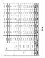
- FIG. 4is a table illustrating various examples of flow ratios according to the present disclosure.
- FIG. 5is a graph illustrating examples of absorbance as a function of wavenumber according to the present disclosure.
- substrate processing systems and methodsare disclosed for forming a conformal film at relatively low temperatures.
- the substrate processing systems and methodsmay employ chemical vapor deposition (CVD) using basic nitride chemistry (for example, silane (SiH 4 ) and ammonia (NH 3 ) (in an inert carrier gas)) with the addition of diborane B 2 H 6 , which acts as a catalyzer.
- CVDchemical vapor deposition
- basic nitride chemistryfor example, silane (SiH 4 ) and ammonia (NH 3 ) (in an inert carrier gas)
- NH 3inert carrier gas
- the substrate processing systems and methods described hereininvolve decomposition by a catalytic and pyroltic reaction, which enables a lower temperature boundary area that is less than 630° C.
- deposition of the conformal filmmay occur at pedestal temperatures at about 500° C. or greater.
- the addition of the catalyzer B 2 H 6 to the process reactionallows the deposition temperature to be significantly lowered to about ⁇ 500° C.
- an example of a CVD reactor 100includes a process chamber 124 , which encloses other components of the CVD reactor 100 .
- a pedestal 118supports a substrate 116 .
- a showerhead 120delivers one or more precursors to the CVD reactor 100 .
- the pedestal 118typically includes a chuck, a fork, or lift pins to hold and transfer the substrate during deposition or other treatment.
- the chuckmay be an electrostatic chuck, a mechanical chuck or other type of chuck.
- the process gasesare introduced via inlet 112 .
- Multiple source gas lines 110are connected to a manifold 108 .
- the gasesmay be premixed or not.
- Appropriate valves and mass flow controllers generally identified at 113are employed to ensure that the correct gases are delivered at predetermined flow rates and mixtures during the deposition and other treatment phases of the process.
- a vacuum pump 126(for example only, a one or two stage mechanical dry pump and/or a turbo-molecular pump) draws process gases out and maintains a suitable pressure within the reactor using a controlled flow restriction device 128 , such as a throttle valve or a pendulum valve.
- the controller 200may include a processor, memory and one or more interfaces.
- the controller 200may be employed to control devices in the system based in part on sensed values.
- the controller 200may be used to control heating and cooling of the showerhead 120 .
- the controller 200may control one or more of valves 202 , filter heaters 204 , pumps 206 , and other devices 208 based on the sensed values and other control parameters.
- the controller 200receives the sensed values from, for example only, pressure manometers 210 , flow meters 212 , temperature sensors 214 , and/or other sensors 216 .
- the controller 200may also be employed to control process conditions during precursor delivery and deposition of the film.
- the controller 200will typically include one or more memory devices and one or more processors.
- the controller 200may control the precursor delivery system and deposition apparatus.
- the controller 200executes computer programs including sets of instructions for controlling process timing, delivery system temperature, pressure differentials across the filters, valve positions, mixture of gases, chamber pressure, chamber temperature, wafer temperature, pedestal RF power levels, wafer chuck or pedestal position, and other parameters of a particular process.
- the controller 200may also monitor the pressure differential and automatically switch vapor precursor delivery from one or more paths to one or more other paths.
- Other computer programs stored on memory devices associated with the controller 200may be employed in some embodiments.
- the user interfacemay include a display 218 (e.g. a display screen and/or graphical software displays of the apparatus and/or process conditions), and user input devices 220 such as pointing devices, keyboards, touch screens, microphones, etc.
- the controller parametersrelate to process conditions such as, for example, filter pressure differentials, process gas composition and flow rates, temperature, pressure, and chamber wall temperature.
- the system softwaremay be designed or configured in many different ways. For example, various chamber component subroutines or control objects may be written to control operation of the chamber components necessary to carry out the deposition processes. Examples of programs or sections of programs for this purpose include substrate positioning code, process gas control code, pressure control code, and heater control code.
- a substrate positioning programmay include program code for controlling chamber components that are used to load the substrate onto a pedestal or chuck and to control the spacing between the substrate and other parts of the chamber such as a gas inlet and/or target.
- a process gas control programmay include code for controlling gas composition and flow rates and optionally for flowing gas into the chamber prior to deposition in order to stabilize the pressure in the chamber.
- a filter monitoring programincludes code comparing the measured differential(s) to predetermined value(s) and/or code for switching paths.
- a pressure control programmay include code for controlling the pressure in the chamber by regulating, e.g., a throttle valve in the exhaust system of the chamber.
- a heater control programmay include code for controlling the current to heating units for heating components in the precursor delivery system, the substrate and/or other portions of the system. Alternatively, the heater control program may control delivery of a heat transfer gas such as helium to the wafer chuck.
- mass flow controllerssuch as the pressure manometers 210
- temperature sensors 214such as the temperature sensors 214 .
- Appropriately programmed feedback and control algorithmsmay be used with data from these sensors to maintain desired process conditions. The foregoing describes implementation of embodiments in a single or multi-chamber semiconductor processing tool.
- the film growthis smooth and conformal.
- ammonia gasNH 3
- NH 3ammonia gas
- the B—N and Si—N peakscan be modulated by a ratio of SiH 4 flow to B 2 H 6 flow.
- the stress and refractive index (RI)can be modulated by changing the ratio of SiH 4 to NH 3 flow.
- the amount of B 2 H 6 flow needed to act as the chemical catalyzer to start the deposition reactioncan be very small.
- the method 300includes setting process conditions for CVD deposition at 304 .
- a process temperature and process pressuremay be set to suitable values.
- flows of a first precursor, NH 3 and B 2 H 6are provided at predetermined flow rates for a predetermined period as determined at 312 .
- the first precursormay include SiH 4 , ethylene (C 2 H 4 ), N-Trimethylsilyl Acetamide (TMSA) or tetramethylsilane (4MS). Purge may be performed at 316 .
- the processmay be repeated one or more times at 320 for the same predetermined period and/or for variable periods.
- conformal filmshave been deposited with SiH 4 to B 2 H 6 ratios ranging from 1:0.01 to 1:0.025, although other ratios may be used.
- Using lower B 2 H 6 flow rates and/or toggling off the B 2 H 6 flow during the deposition of the filmmay decrease the amount of boron (as B—N) in the film and increase the Si—N bonding peak to form a full class of films from the boron nitride and true silicon nitride.
- the filmsare smooth and conformal.
- Multiple different filmscan be made like SiBN, SiB & SiN with chemistry ratio changes with SiH 4 /NH 3 /B 2 H 6 .
- Replacing SiH 4 with carbon precursor like ethylene (C 2 H 4 ), N-Trimethylsilyl Acetamide (TMSA) or tetramethylsilane (4MS)allows deposition of conformal Boron Carbide films.
- FIGS. 4 and 5various examples of the process are shown.
- FTIR analysis, refractive index (RI) and stressare shown for various flow rates of SiH 4 , NH 3 and B 2 H 6 in sccm.
- the process pressuremay be approximately 5 Torr, although other process pressure values may be used.
- absorbanceis shown as a function of wavenumber for the examples of FIG. 5 .
- These examplesemploy a ratio of the silane precursor gas to the diborane gas that is between 1:0.22 and 1:0.5
Landscapes
- Chemical & Material Sciences (AREA)
- Engineering & Computer Science (AREA)
- Chemical Kinetics & Catalysis (AREA)
- Organic Chemistry (AREA)
- General Chemical & Material Sciences (AREA)
- Materials Engineering (AREA)
- Mechanical Engineering (AREA)
- Metallurgy (AREA)
- Inorganic Chemistry (AREA)
- Physics & Mathematics (AREA)
- Condensed Matter Physics & Semiconductors (AREA)
- General Physics & Mathematics (AREA)
- Manufacturing & Machinery (AREA)
- Computer Hardware Design (AREA)
- Microelectronics & Electronic Packaging (AREA)
- Power Engineering (AREA)
- Plasma & Fusion (AREA)
- Chemical Vapour Deposition (AREA)
- Formation Of Insulating Films (AREA)
Abstract
Description
This application claims the benefit of U.S. Provisional Application No. 61/674,611, filed on Jul. 23, 2012. The entire disclosure of the application referenced above is incorporated herein by reference
The present disclosure relates to chemical vapor deposition, and more specifically to deposition of conformal films using chemical vapor deposition.
The background description provided herein is for the purpose of generally presenting the context of the disclosure. Work of the presently named inventors, to the extent it is described in this background section, as well as aspects of the description that may not otherwise qualify as prior art at the time of filing, are neither expressly nor impliedly admitted as prior art against the present disclosure.
Deposition of conformal films at lower temperatures is currently performed using plasma-enhanced chemical vapor deposition (PECVD) using costly, non-generic chemistry that is not widely used in the semiconductor industry. Some deposition techniques used to form conformal films, such as atomic layer deposition (ALD), have complicated sequencing with critical timing steps. As a result of these requirements, yields tend to be lower and cost tends to be higher.
Typical silane (SiH4) based CVD starts to occur in a reactor at ˜650° C. pedestal temperature, however the deposited film is typically non-uniform. Decomposition of the SiH4alone by pyroltic reaction forms amorphous silicon. Adding hydrogen to the reaction results in hydrogenated amorphous silicon, however the pedestal operating temperature still needs to be above ˜650° C. for deposition to occur.
This section provides a general summary of the disclosure, and is not a comprehensive disclosure of its full scope or all of its features.
A substrate processing system for depositing a film includes a processing chamber, a heater, and a controller. The processing chamber includes a pedestal to support a substrate. The heater is configured to heat the substrate to a temperature within a predetermined temperature range. The controller is configured to supply a gas mixture to the processing chamber for a predetermined period, wherein the gas mixture includes a first precursor gas, ammonia gas and diborane gas, purge the processing chamber after the predetermined period, and repeat the supply and purging one or more times to deposit the film.
A method for depositing a film in a substrate processing system includes arranging a substrate on a pedestal in a processing chamber, heating the substrate to a temperature within a predetermined temperature range, and supplying a gas mixture to the processing chamber for a predetermined period to deposit the film on the substrate, wherein the gas mixture includes a first precursor gas, ammonia gas and diborane gas.
Further areas of applicability will become apparent from the description provided herein. The description and specific examples in this summary are intended for purposes of illustration only and are not intended to limit the scope of the present disclosure.
The present disclosure will become more fully understood from the detailed description and the accompanying drawings, wherein:
According to the present disclosure, substrate processing systems and methods are disclosed for forming a conformal film at relatively low temperatures. For example only, the substrate processing systems and methods may employ chemical vapor deposition (CVD) using basic nitride chemistry (for example, silane (SiH4) and ammonia (NH3) (in an inert carrier gas)) with the addition of diborane B2H6, which acts as a catalyzer.
The substrate processing systems and methods described herein involve decomposition by a catalytic and pyroltic reaction, which enables a lower temperature boundary area that is less than 630° C. For example only, deposition of the conformal film may occur at pedestal temperatures at about 500° C. or greater. In other words, the addition of the catalyzer B2H6to the process reaction allows the deposition temperature to be significantly lowered to about ˜500° C.
Referring now toFIG. 1 , an example of aCVD reactor 100 includes aprocess chamber 124, which encloses other components of theCVD reactor 100. Within the CVDreactor 100, apedestal 118 supports asubstrate 116. Ashowerhead 120 delivers one or more precursors to theCVD reactor 100. Thepedestal 118 typically includes a chuck, a fork, or lift pins to hold and transfer the substrate during deposition or other treatment. The chuck may be an electrostatic chuck, a mechanical chuck or other type of chuck.
The process gases are introduced viainlet 112. Multiplesource gas lines 110 are connected to amanifold 108. The gases may be premixed or not. Appropriate valves and mass flow controllers generally identified at113 are employed to ensure that the correct gases are delivered at predetermined flow rates and mixtures during the deposition and other treatment phases of the process.
Process gases exit theprocess chamber 124 via anoutlet 122. A vacuum pump126 (for example only, a one or two stage mechanical dry pump and/or a turbo-molecular pump) draws process gases out and maintains a suitable pressure within the reactor using a controlledflow restriction device 128, such as a throttle valve or a pendulum valve.
It is possible to index the wafers after every deposition and/or post-deposition treatment until all the required depositions and treatments are completed, or multiple depositions and treatments can be conducted at a single station before indexing the wafer.
Referring now toFIG. 2 , an example of acontroller 200 for controlling the system ofFIG. 1 is shown. Thecontroller 200 may include a processor, memory and one or more interfaces. Thecontroller 200 may be employed to control devices in the system based in part on sensed values. In addition, thecontroller 200 may be used to control heating and cooling of theshowerhead 120.
For example only, thecontroller 200 may control one or more ofvalves 202,filter heaters 204,pumps 206, andother devices 208 based on the sensed values and other control parameters. Thecontroller 200 receives the sensed values from, for example only,pressure manometers 210,flow meters 212,temperature sensors 214, and/orother sensors 216. Thecontroller 200 may also be employed to control process conditions during precursor delivery and deposition of the film. Thecontroller 200 will typically include one or more memory devices and one or more processors.
Thecontroller 200 may control the precursor delivery system and deposition apparatus. Thecontroller 200 executes computer programs including sets of instructions for controlling process timing, delivery system temperature, pressure differentials across the filters, valve positions, mixture of gases, chamber pressure, chamber temperature, wafer temperature, pedestal RF power levels, wafer chuck or pedestal position, and other parameters of a particular process. Thecontroller 200 may also monitor the pressure differential and automatically switch vapor precursor delivery from one or more paths to one or more other paths. Other computer programs stored on memory devices associated with thecontroller 200 may be employed in some embodiments.
Typically there will be a user interface associated with thecontroller 200. The user interface may include a display218 (e.g. a display screen and/or graphical software displays of the apparatus and/or process conditions), anduser input devices 220 such as pointing devices, keyboards, touch screens, microphones, etc. The controller parameters relate to process conditions such as, for example, filter pressure differentials, process gas composition and flow rates, temperature, pressure, and chamber wall temperature.
The system software may be designed or configured in many different ways. For example, various chamber component subroutines or control objects may be written to control operation of the chamber components necessary to carry out the deposition processes. Examples of programs or sections of programs for this purpose include substrate positioning code, process gas control code, pressure control code, and heater control code.
A substrate positioning program may include program code for controlling chamber components that are used to load the substrate onto a pedestal or chuck and to control the spacing between the substrate and other parts of the chamber such as a gas inlet and/or target. A process gas control program may include code for controlling gas composition and flow rates and optionally for flowing gas into the chamber prior to deposition in order to stabilize the pressure in the chamber. A filter monitoring program includes code comparing the measured differential(s) to predetermined value(s) and/or code for switching paths. A pressure control program may include code for controlling the pressure in the chamber by regulating, e.g., a throttle valve in the exhaust system of the chamber. A heater control program may include code for controlling the current to heating units for heating components in the precursor delivery system, the substrate and/or other portions of the system. Alternatively, the heater control program may control delivery of a heat transfer gas such as helium to the wafer chuck.
Examples of sensors that may be monitored during deposition include, but are not limited to, mass flow controllers, pressure sensors such as thepressure manometers 210, and thetemperature sensors 214. Appropriately programmed feedback and control algorithms may be used with data from these sensors to maintain desired process conditions. The foregoing describes implementation of embodiments in a single or multi-chamber semiconductor processing tool.
The film growth is smooth and conformal. Using the same process space and temperature, ammonia gas (NH3) can be introduced to the reaction (with or without hydrogen H2) to form SiBN film conditions. The B—N and Si—N peaks (by Fourier transform infrared spectroscopy (FTIR)) can be modulated by a ratio of SiH4flow to B2H6flow. Alternatively, the stress and refractive index (RI) can be modulated by changing the ratio of SiH4to NH3flow. The amount of B2H6flow needed to act as the chemical catalyzer to start the deposition reaction can be very small.
Referring now toFIG. 3 , an example of amethod 300 according to the present disclosure is shown. Themethod 300 includes setting process conditions for CVD deposition at304. For example, a process temperature and process pressure may be set to suitable values. At308, flows of a first precursor, NH3and B2H6are provided at predetermined flow rates for a predetermined period as determined at312. For example only, the first precursor may include SiH4, ethylene (C2H4), N-Trimethylsilyl Acetamide (TMSA) or tetramethylsilane (4MS). Purge may be performed at316. The process may be repeated one or more times at320 for the same predetermined period and/or for variable periods.
For example, conformal films have been deposited with SiH4to B2H6ratios ranging from 1:0.01 to 1:0.025, although other ratios may be used. Using lower B2H6flow rates and/or toggling off the B2H6flow during the deposition of the film may decrease the amount of boron (as B—N) in the film and increase the Si—N bonding peak to form a full class of films from the boron nitride and true silicon nitride. The films are smooth and conformal.
Multiple different films can be made like SiBN, SiB & SiN with chemistry ratio changes with SiH4/NH3/B2H6. Replacing SiH4with carbon precursor like ethylene (C2H4), N-Trimethylsilyl Acetamide (TMSA) or tetramethylsilane (4MS) allows deposition of conformal Boron Carbide films.
The high pedestal temperatures of conventional deposition approaches (about 630° C.) constrain the hardware used since metals such as Al cannot be used at this temperature and chamber heating and outgassing may be problematic. Without adding a chemical to provide a catalytic component to the previously purely pyrolytic reaction, the thermal CVD deposition rate at 500° C. would be near zero.
Referring now toFIGS. 4 and 5 , various examples of the process are shown. InFIG. 4 , FTIR analysis, refractive index (RI) and stress are shown for various flow rates of SiH4, NH3and B2H6in sccm. For example only, the process pressure may be approximately 5 Torr, although other process pressure values may be used. InFIG. 5 , absorbance is shown as a function of wavenumber for the examples ofFIG. 5 . These examples employ a ratio of the silane precursor gas to the diborane gas that is between 1:0.22 and 1:0.5
The foregoing description is merely illustrative in nature and is in no way intended to limit the disclosure, its application, or uses. The broad teachings of the disclosure can be implemented in a variety of forms. Therefore, while this disclosure includes particular examples, the true scope of the disclosure should not be so limited since other modifications will become apparent upon a study of the drawings, the specification, and the following claims. For purposes of clarity, the same reference numbers will be used in the drawings to identify similar elements. As used herein, the phrase at least one of A, B, and C should be construed to mean a logical (A or B or C), using a non-exclusive logical OR. It should be understood that one or more steps within a method may be executed in different order (or concurrently) without altering the principles of the present disclosure.
Claims (5)
1. A method for depositing a conformal film in a substrate processing system, comprising:
a) arranging a substrate on a pedestal in a processing chamber;
b) heating the substrate to a temperature within a predetermined temperature range, wherein the predetermined temperature range is between 500° C. and 630° C.; and
c) supplying a gas mixture to the processing chamber for a predetermined period to deposit the conformal film on the substrate, wherein the gas mixture includes a first precursor gas, ammonia gas and diborane gas, wherein the first precursor gas has a deposition temperature of approximately 650° C., wherein the gas mixture including the diborane gas has a deposition temperature within the predetermined temperature range, and wherein a ratio of the first precursor gas to the diborane gas is between 1:0.01 and 1:0.025.
2. The method ofclaim 1 , further comprising:
d) purging the gas mixture after the predetermined period; and
e) repeating a) to d) one or more times.
3. The method ofclaim 1 , wherein the conformal film includes one of a boron nitride film, a silicon nitride film, and a boron carbide film.
4. The method ofclaim 1 , wherein the first precursor gas includes silane.
5. The method ofclaim 1 , further comprising toggling the diborane gas on and off multiple times during the predetermined period.
Priority Applications (5)
| Application Number | Priority Date | Filing Date | Title |
|---|---|---|---|
| US13/946,012US9388491B2 (en) | 2012-07-23 | 2013-07-19 | Method for deposition of conformal films with catalysis assisted low temperature CVD |
| TW102126335ATWI589723B (en) | 2012-07-23 | 2013-07-23 | Method for deposition of conformal films with catalysis assisted low temperature cvd |
| KR1020130086660AKR102151823B1 (en) | 2012-07-23 | 2013-07-23 | Method for deposition of conformal films with catalysis assited low temperature cvd |
| SG2013056684ASG196751A1 (en) | 2012-07-23 | 2013-07-23 | Method for deposition of conformal films with catalysis assisted low temperature cvd |
| SG10201600467QASG10201600467QA (en) | 2012-07-23 | 2013-07-23 | Method for deposition of conformal films with catalysis assisted low temperature cvd |
Applications Claiming Priority (2)
| Application Number | Priority Date | Filing Date | Title |
|---|---|---|---|
| US201261674611P | 2012-07-23 | 2012-07-23 | |
| US13/946,012US9388491B2 (en) | 2012-07-23 | 2013-07-19 | Method for deposition of conformal films with catalysis assisted low temperature CVD |
Publications (2)
| Publication Number | Publication Date |
|---|---|
| US20140023784A1 US20140023784A1 (en) | 2014-01-23 |
| US9388491B2true US9388491B2 (en) | 2016-07-12 |
Family
ID=49946752
Family Applications (1)
| Application Number | Title | Priority Date | Filing Date |
|---|---|---|---|
| US13/946,012Active2034-05-30US9388491B2 (en) | 2012-07-23 | 2013-07-19 | Method for deposition of conformal films with catalysis assisted low temperature CVD |
Country Status (4)
| Country | Link |
|---|---|
| US (1) | US9388491B2 (en) |
| KR (1) | KR102151823B1 (en) |
| SG (2) | SG10201600467QA (en) |
| TW (1) | TWI589723B (en) |
Cited By (1)
| Publication number | Priority date | Publication date | Assignee | Title |
|---|---|---|---|---|
| CN112449679A (en)* | 2018-07-31 | 2021-03-05 | 应用材料公司 | Precursor delivery system and related method |
Families Citing this family (4)
| Publication number | Priority date | Publication date | Assignee | Title |
|---|---|---|---|---|
| EP3760222A1 (en) | 2013-03-12 | 2021-01-06 | University of Utah Research Foundation | Compositions and methods for inducing apoptosis |
| WO2017049253A1 (en)* | 2015-09-18 | 2017-03-23 | Applied Materials, Inc. | Methods for depositing conformal bcn films |
| US11538677B2 (en) | 2020-09-01 | 2022-12-27 | Applied Materials, Inc. | Systems and methods for depositing high density and high tensile stress films |
| US11710631B2 (en)* | 2020-10-23 | 2023-07-25 | Applied Materials, Inc. | Tensile nitride deposition systems and methods |
Citations (82)
| Publication number | Priority date | Publication date | Assignee | Title |
|---|---|---|---|---|
| US4696702A (en)* | 1985-01-24 | 1987-09-29 | Chronar Corp. | Method of depositing wide bandgap amorphous semiconductor materials |
| EP0394054A1 (en) | 1989-04-21 | 1990-10-24 | Nec Corporation | Method of manufacturing siliconboron nitride film having excellent step coverage characteristic |
| JPH06240459A (en) | 1993-02-16 | 1994-08-30 | G T C:Kk | Method for forming silicon oxide thin film |
| US5399387A (en) | 1993-01-28 | 1995-03-21 | Applied Materials, Inc. | Plasma CVD of silicon nitride thin films on large area glass substrates at high deposition rates |
| US5589233A (en) | 1993-12-28 | 1996-12-31 | Applied Materials, Inc. | Single chamber CVD process for thin film transistors |
| US5851602A (en) | 1993-12-09 | 1998-12-22 | Applied Materials, Inc. | Deposition of high quality conformal silicon oxide thin films for the manufacture of thin film transistors |
| US6066550A (en) | 1998-06-05 | 2000-05-23 | United Integrated Circuits Corp. | Method of improving selectivity between silicon nitride and silicon oxide |
| US6087278A (en) | 1998-06-16 | 2000-07-11 | Hyundai Electronics Industries Co., Ltd. | Method for fabricating semiconductor devices having an HDP-CVD oxide layer as a passivation layer |
| JP2000208422A (en) | 1999-01-08 | 2000-07-28 | Sony Corp | Forming method of laminated film and thin film forming system |
| US6207574B1 (en) | 1998-07-13 | 2001-03-27 | Samsung Electronics Co., Ltd. | Method for fabricating a DRAM cell storage node |
| US6235650B1 (en) | 1997-12-29 | 2001-05-22 | Vanguard International Semiconductor Corporation | Method for improved semiconductor device reliability |
| US20010007245A1 (en) | 1995-12-08 | 2001-07-12 | Unaxis Balzers Ag | Hf-plasma coating chamber or pecvd coating chamber, its use and method of plating cds using the chamber |
| US6294228B1 (en)* | 1998-11-04 | 2001-09-25 | Nec Corporation | Method for forming thin films |
| US20020011656A1 (en) | 2000-06-22 | 2002-01-31 | Swanson Leland S. | Semiconductor device protective overcoat with enhanced adhesion to polymeric materials and method of fabrication |
| US6358573B1 (en) | 1997-12-01 | 2002-03-19 | Applied Materials, Inc. | Mixed frequency CVD process |
| US6407011B1 (en) | 1999-07-27 | 2002-06-18 | Sony Corporation | Low dielectric constant insulating films with laminated carbon-containing silicon oxide and organic layers |
| US6444277B1 (en) | 1993-01-28 | 2002-09-03 | Applied Materials, Inc. | Method for depositing amorphous silicon thin films onto large area glass substrates by chemical vapor deposition at high deposition rates |
| DE10143235A1 (en) | 2001-09-04 | 2003-03-27 | Infineon Technologies Ag | Semiconductor memory component used as flash memory comprises substrate, floating gate electrically isolated from the substrate, tunnel barrier arrangement and device for controlling charge transmission of barrier arrangement |
| US20040011279A1 (en) | 2002-07-18 | 2004-01-22 | Hynix Semiconductor Inc. | Method of manufacturing semiconductor device |
| US20040041239A1 (en) | 2002-08-30 | 2004-03-04 | Hartmut Ruelke | Low-k dielectric layer stack including an etch indicator layer for use in the dual damascene technique |
| US20040087079A1 (en) | 2002-11-05 | 2004-05-06 | Taiwan Semiconductor Manufacturing Company | Method of forming a nitride gate dielectric layer for advanced cmos devices |
| US20040083973A1 (en)* | 2001-03-28 | 2004-05-06 | Hitoshi Sakamoto | Film forming method and film forming device |
| US20040146661A1 (en) | 2003-01-23 | 2004-07-29 | Applied Materials, Inc. | Hydrogen assisted hdp-cvd deposition process for aggressive gap-fill technology |
| US6811831B1 (en) | 2002-11-20 | 2004-11-02 | Silicon Magnetic Systems | Method for depositing silicon nitride |
| US6818533B2 (en) | 2002-05-09 | 2004-11-16 | Taiwan Semiconductor Manufacturing Co., Ltd | Epitaxial plasma enhanced chemical vapor deposition (PECVD) method providing epitaxial layer with attenuated defects |
| US20050045099A1 (en) | 2003-08-27 | 2005-03-03 | Applied Materials, Inc. | Methods and devices to reduce defects in dielectric stack structures |
| US20050186686A1 (en) | 2004-02-25 | 2005-08-25 | International Business Machines Corporation | Method of fabricating data tracks for use in a magnetic shift register memory device |
| US20050196960A1 (en) | 2002-10-17 | 2005-09-08 | Kyeong-Mo Koo | Method of forming metal silicide film and method of manufacturing semiconductor device having metal silicide film |
| US20050233591A1 (en) | 2004-03-31 | 2005-10-20 | Applied Materials, Inc. | Techniques promoting adhesion of porous low K film to underlying barrier layer |
| US20050229848A1 (en) | 2004-04-15 | 2005-10-20 | Asm Japan K.K. | Thin-film deposition apparatus |
| US6962859B2 (en) | 2001-02-12 | 2005-11-08 | Asm America, Inc. | Thin films and method of making them |
| US20060032443A1 (en)* | 2004-07-28 | 2006-02-16 | Kazuhide Hasebe | Film formation method and apparatus for semiconductor process |
| US20060049139A1 (en) | 2004-08-26 | 2006-03-09 | Tokyo Electron Limited | Method and system for etching a gate stack |
| US20060204673A1 (en) | 2005-03-14 | 2006-09-14 | Masami Takayasu | Semiconductor manufacturing method for inter-layer insulating film |
| US20060276011A1 (en) | 2005-06-01 | 2006-12-07 | International Business Machines Corporation | Amorphization/templated recrystallization method for hybrid orientation substrates |
| US20070059942A1 (en) | 2005-09-09 | 2007-03-15 | Chi Lin Technology Co., Ltd. | Plasma cvd process for manufacturing multilayer anti-reflection coatings |
| US20070110918A1 (en) | 2000-06-29 | 2007-05-17 | Katsuhisa Yuda | Remote plasma apparatus for processing substrate with two types of gases |
| US20070144215A1 (en) | 2005-10-07 | 2007-06-28 | Boris Kharas | Method for improving refractive index control in PECVD deposited a-SiNy films |
| US20070215877A1 (en) | 2006-03-17 | 2007-09-20 | Tomoya Kato | Crystallization method, thin film transistor manufacturing method, thin film transistor, display, and semiconductor device |
| CN101071771A (en) | 2006-05-12 | 2007-11-14 | 三星电子株式会社 | Insulation film deposition method for a semiconductor device |
| US20080020591A1 (en) | 2005-05-26 | 2008-01-24 | Applied Materials, Inc. | Method to increase silicon nitride tensile stress using nitrogen plasma in-situ treatment and ex-situ uv cure |
| US20080050883A1 (en) | 2006-08-25 | 2008-02-28 | Atmel Corporation | Hetrojunction bipolar transistor (hbt) with periodic multilayer base |
| US20080113521A1 (en) | 2006-11-14 | 2008-05-15 | Asm Japan K.K. | METHOD OF FORMING ULTRA-THIN SiN FILM BY PLASMA CVD |
| US20080145536A1 (en) | 2006-12-13 | 2008-06-19 | Applied Materials, Inc. | METHOD AND APPARATUS FOR LOW TEMPERATURE AND LOW K SiBN DEPOSITION |
| US20080153300A1 (en) | 2006-12-20 | 2008-06-26 | Hynix Semiconductor Inc. | Method for forming fine pattern of semiconductor device |
| US20080190886A1 (en) | 2007-02-08 | 2008-08-14 | Soo Young Choi | Differential etch rate control of layers deposited by chemical vapor deposition |
| US20080202688A1 (en) | 2007-02-27 | 2008-08-28 | Robert Wu | Silicon Carbide Gas Distribution Plate and RF Electrode for Plasma Etch Chamber |
| US7422776B2 (en) | 2004-08-24 | 2008-09-09 | Applied Materials, Inc. | Low temperature process to produce low-K dielectrics with low stress by plasma-enhanced chemical vapor deposition (PECVD) |
| US20080268176A1 (en) | 2004-04-20 | 2008-10-30 | Applied Materials, Inc. | Method of improving the uniformity of PECVD-deposited thin films |
| US20080299747A1 (en) | 2007-05-30 | 2008-12-04 | Asm Japan K.K. | Method for forming amorphouse silicon film by plasma cvd |
| US7479443B2 (en) | 2004-02-27 | 2009-01-20 | Asm America Inc. | Germanium deposition |
| US20090022908A1 (en) | 2007-07-19 | 2009-01-22 | Applied Materials, Inc. | Plasma enhanced chemical vapor deposition technology for large-size processing |
| US20090035927A1 (en) | 2007-07-30 | 2009-02-05 | Applied Materials, Inc. | Method of forming dielectric layers on a substrate and apparatus therefor |
| US20090098741A1 (en)* | 2007-10-15 | 2009-04-16 | Asm Japan K.K. | Method for forming ultra-thin boron-containing nitride films and related apparatus |
| US20090097105A1 (en) | 2006-08-25 | 2009-04-16 | Gary Allen Hart | Method for producing smooth, dense optical films |
| US20090095221A1 (en) | 2007-10-16 | 2009-04-16 | Alexander Tam | Multi-gas concentric injection showerhead |
| US20090104790A1 (en) | 2007-10-22 | 2009-04-23 | Applied Materials, Inc. | Methods for Forming a Dielectric Layer Within Trenches |
| US20090159119A1 (en) | 2007-03-28 | 2009-06-25 | Basol Bulent M | Technique and apparatus for manufacturing flexible and moisture resistive photovoltaic modules |
| WO2009098548A1 (en) | 2008-02-08 | 2009-08-13 | Freescale Semiconductor, Inc. | Intermediate product for a multichannel fet and process for obtaining an intermediate product |
| US20090246942A1 (en) | 2008-03-31 | 2009-10-01 | Ngk Insulators, Ltd. | Apparatus for depositing silicon-based thin film and method for depositing silicon-based thin film |
| US20090286402A1 (en) | 2008-05-13 | 2009-11-19 | Applied Materials, Inc | Method for critical dimension shrink using conformal pecvd films |
| US7635651B2 (en) | 2005-08-23 | 2009-12-22 | Taiwan Semiconductor Manufacturing Co., Ltd. | Method of smoothening dielectric layer |
| US20100102359A1 (en) | 2006-12-15 | 2010-04-29 | University Of South Carolina | novel fabrication technique for high frequency, high power group iii nitride electronic devices |
| US20100109065A1 (en) | 2008-11-06 | 2010-05-06 | Jin-Yong Oh | Three-dimensional nonvolatile memory devices having sub-divided active bars and methods of manufacturing such devices |
| US20100184302A1 (en) | 2009-01-21 | 2010-07-22 | Asm Japan K.K. | Method of Forming Conformal Dielectric Film Having Si-N Bonds by PECVD |
| US20100210093A1 (en) | 2006-11-09 | 2010-08-19 | Kenji Kato | Method for forming silicon-based thin film by plasma cvd method |
| US7858431B2 (en) | 2007-11-30 | 2010-12-28 | Semiconductor Energy Laboratory Co., Ltd. | Method of manufacturing photoelectric conversion device |
| US20110018044A1 (en) | 2009-07-23 | 2011-01-27 | Ha-Jin Lim | Etch stop layers and methods of forming the same |
| US20110036168A1 (en) | 2009-08-14 | 2011-02-17 | Chung Hua University | RFID Based Thermal Bubble Type Accelerometer And Method Of Manufacturing The Same |
| US20110143019A1 (en) | 2009-12-14 | 2011-06-16 | Amprius, Inc. | Apparatus for Deposition on Two Sides of the Web |
| US20110151142A1 (en) | 2009-12-22 | 2011-06-23 | Applied Materials, Inc. | Pecvd multi-step processing with continuous plasma |
| US20110236600A1 (en) | 2010-03-25 | 2011-09-29 | Keith Fox | Smooth Silicon-Containing Films |
| US20110236594A1 (en) | 2010-03-25 | 2011-09-29 | Jason Haverkamp | In-Situ Deposition of Film Stacks |
| US8076250B1 (en) | 2010-10-06 | 2011-12-13 | Applied Materials, Inc. | PECVD oxide-nitride and oxide-silicon stacks for 3D memory application |
| US20120142172A1 (en) | 2010-03-25 | 2012-06-07 | Keith Fox | Pecvd deposition of smooth polysilicon films |
| US8318575B2 (en) | 2011-02-07 | 2012-11-27 | Infineon Technologies Ag | Compressive polycrystalline silicon film and method of manufacture thereof |
| US20130157466A1 (en) | 2010-03-25 | 2013-06-20 | Keith Fox | Silicon nitride films for semiconductor device applications |
| US20130171834A1 (en) | 2010-03-25 | 2013-07-04 | Jason Haverkamp | In-situ deposition of film stacks |
| WO2013123143A1 (en) | 2012-02-14 | 2013-08-22 | Novellus Systems, Inc. | Silicon nitride films for semiconductor device applications |
| US20130267081A1 (en) | 2012-04-06 | 2013-10-10 | Keith Fox | Post-deposition soft annealing |
| US20130316518A1 (en) | 2012-05-23 | 2013-11-28 | Alice Hollister | Pecvd deposition of smooth silicon films |
| US8895415B1 (en) | 2013-05-31 | 2014-11-25 | Novellus Systems, Inc. | Tensile stressed doped amorphous silicon |
- 2013
- 2013-07-19USUS13/946,012patent/US9388491B2/enactiveActive
- 2013-07-23SGSG10201600467QApatent/SG10201600467QA/enunknown
- 2013-07-23TWTW102126335Apatent/TWI589723B/enactive
- 2013-07-23SGSG2013056684Apatent/SG196751A1/enunknown
- 2013-07-23KRKR1020130086660Apatent/KR102151823B1/enactiveActive
Patent Citations (95)
| Publication number | Priority date | Publication date | Assignee | Title |
|---|---|---|---|---|
| US4696702A (en)* | 1985-01-24 | 1987-09-29 | Chronar Corp. | Method of depositing wide bandgap amorphous semiconductor materials |
| EP0394054A1 (en) | 1989-04-21 | 1990-10-24 | Nec Corporation | Method of manufacturing siliconboron nitride film having excellent step coverage characteristic |
| US5399387A (en) | 1993-01-28 | 1995-03-21 | Applied Materials, Inc. | Plasma CVD of silicon nitride thin films on large area glass substrates at high deposition rates |
| US6444277B1 (en) | 1993-01-28 | 2002-09-03 | Applied Materials, Inc. | Method for depositing amorphous silicon thin films onto large area glass substrates by chemical vapor deposition at high deposition rates |
| JPH06240459A (en) | 1993-02-16 | 1994-08-30 | G T C:Kk | Method for forming silicon oxide thin film |
| US5851602A (en) | 1993-12-09 | 1998-12-22 | Applied Materials, Inc. | Deposition of high quality conformal silicon oxide thin films for the manufacture of thin film transistors |
| US5589233A (en) | 1993-12-28 | 1996-12-31 | Applied Materials, Inc. | Single chamber CVD process for thin film transistors |
| US20010007245A1 (en) | 1995-12-08 | 2001-07-12 | Unaxis Balzers Ag | Hf-plasma coating chamber or pecvd coating chamber, its use and method of plating cds using the chamber |
| US6358573B1 (en) | 1997-12-01 | 2002-03-19 | Applied Materials, Inc. | Mixed frequency CVD process |
| US6235650B1 (en) | 1997-12-29 | 2001-05-22 | Vanguard International Semiconductor Corporation | Method for improved semiconductor device reliability |
| US6066550A (en) | 1998-06-05 | 2000-05-23 | United Integrated Circuits Corp. | Method of improving selectivity between silicon nitride and silicon oxide |
| US6087278A (en) | 1998-06-16 | 2000-07-11 | Hyundai Electronics Industries Co., Ltd. | Method for fabricating semiconductor devices having an HDP-CVD oxide layer as a passivation layer |
| US6207574B1 (en) | 1998-07-13 | 2001-03-27 | Samsung Electronics Co., Ltd. | Method for fabricating a DRAM cell storage node |
| US6294228B1 (en)* | 1998-11-04 | 2001-09-25 | Nec Corporation | Method for forming thin films |
| JP2000208422A (en) | 1999-01-08 | 2000-07-28 | Sony Corp | Forming method of laminated film and thin film forming system |
| US6407011B1 (en) | 1999-07-27 | 2002-06-18 | Sony Corporation | Low dielectric constant insulating films with laminated carbon-containing silicon oxide and organic layers |
| US20020011656A1 (en) | 2000-06-22 | 2002-01-31 | Swanson Leland S. | Semiconductor device protective overcoat with enhanced adhesion to polymeric materials and method of fabrication |
| US20070110918A1 (en) | 2000-06-29 | 2007-05-17 | Katsuhisa Yuda | Remote plasma apparatus for processing substrate with two types of gases |
| US20080073645A1 (en) | 2001-02-12 | 2008-03-27 | Asm America, Inc. | Thin films and methods of making them |
| US6962859B2 (en) | 2001-02-12 | 2005-11-08 | Asm America, Inc. | Thin films and method of making them |
| US20100012030A1 (en) | 2001-02-12 | 2010-01-21 | Asm America, Inc. | Process for Deposition of Semiconductor Films |
| US20040083973A1 (en)* | 2001-03-28 | 2004-05-06 | Hitoshi Sakamoto | Film forming method and film forming device |
| DE10143235A1 (en) | 2001-09-04 | 2003-03-27 | Infineon Technologies Ag | Semiconductor memory component used as flash memory comprises substrate, floating gate electrically isolated from the substrate, tunnel barrier arrangement and device for controlling charge transmission of barrier arrangement |
| US20050040456A1 (en) | 2001-09-04 | 2005-02-24 | Michael Specht | Semiconductor memory element, production method and operational method |
| US6818533B2 (en) | 2002-05-09 | 2004-11-16 | Taiwan Semiconductor Manufacturing Co., Ltd | Epitaxial plasma enhanced chemical vapor deposition (PECVD) method providing epitaxial layer with attenuated defects |
| US20040011279A1 (en) | 2002-07-18 | 2004-01-22 | Hynix Semiconductor Inc. | Method of manufacturing semiconductor device |
| US20040041239A1 (en) | 2002-08-30 | 2004-03-04 | Hartmut Ruelke | Low-k dielectric layer stack including an etch indicator layer for use in the dual damascene technique |
| US20050196960A1 (en) | 2002-10-17 | 2005-09-08 | Kyeong-Mo Koo | Method of forming metal silicide film and method of manufacturing semiconductor device having metal silicide film |
| US20040087079A1 (en) | 2002-11-05 | 2004-05-06 | Taiwan Semiconductor Manufacturing Company | Method of forming a nitride gate dielectric layer for advanced cmos devices |
| US6811831B1 (en) | 2002-11-20 | 2004-11-02 | Silicon Magnetic Systems | Method for depositing silicon nitride |
| US20040146661A1 (en) | 2003-01-23 | 2004-07-29 | Applied Materials, Inc. | Hydrogen assisted hdp-cvd deposition process for aggressive gap-fill technology |
| US20050045099A1 (en) | 2003-08-27 | 2005-03-03 | Applied Materials, Inc. | Methods and devices to reduce defects in dielectric stack structures |
| US7608300B2 (en) | 2003-08-27 | 2009-10-27 | Applied Materials, Inc. | Methods and devices to reduce defects in dielectric stack structures |
| US20050186686A1 (en) | 2004-02-25 | 2005-08-25 | International Business Machines Corporation | Method of fabricating data tracks for use in a magnetic shift register memory device |
| US7479443B2 (en) | 2004-02-27 | 2009-01-20 | Asm America Inc. | Germanium deposition |
| US20050233591A1 (en) | 2004-03-31 | 2005-10-20 | Applied Materials, Inc. | Techniques promoting adhesion of porous low K film to underlying barrier layer |
| US20050229848A1 (en) | 2004-04-15 | 2005-10-20 | Asm Japan K.K. | Thin-film deposition apparatus |
| US20080268176A1 (en) | 2004-04-20 | 2008-10-30 | Applied Materials, Inc. | Method of improving the uniformity of PECVD-deposited thin films |
| US20060032443A1 (en)* | 2004-07-28 | 2006-02-16 | Kazuhide Hasebe | Film formation method and apparatus for semiconductor process |
| US7422776B2 (en) | 2004-08-24 | 2008-09-09 | Applied Materials, Inc. | Low temperature process to produce low-K dielectrics with low stress by plasma-enhanced chemical vapor deposition (PECVD) |
| US20060049139A1 (en) | 2004-08-26 | 2006-03-09 | Tokyo Electron Limited | Method and system for etching a gate stack |
| US20060204673A1 (en) | 2005-03-14 | 2006-09-14 | Masami Takayasu | Semiconductor manufacturing method for inter-layer insulating film |
| US20080020591A1 (en) | 2005-05-26 | 2008-01-24 | Applied Materials, Inc. | Method to increase silicon nitride tensile stress using nitrogen plasma in-situ treatment and ex-situ uv cure |
| US20060276011A1 (en) | 2005-06-01 | 2006-12-07 | International Business Machines Corporation | Amorphization/templated recrystallization method for hybrid orientation substrates |
| US7635651B2 (en) | 2005-08-23 | 2009-12-22 | Taiwan Semiconductor Manufacturing Co., Ltd. | Method of smoothening dielectric layer |
| US20070059942A1 (en) | 2005-09-09 | 2007-03-15 | Chi Lin Technology Co., Ltd. | Plasma cvd process for manufacturing multilayer anti-reflection coatings |
| US20070144215A1 (en) | 2005-10-07 | 2007-06-28 | Boris Kharas | Method for improving refractive index control in PECVD deposited a-SiNy films |
| US20070215877A1 (en) | 2006-03-17 | 2007-09-20 | Tomoya Kato | Crystallization method, thin film transistor manufacturing method, thin film transistor, display, and semiconductor device |
| US20070264842A1 (en) | 2006-05-12 | 2007-11-15 | Samsung Electronics Co., Ltd. | Insulation film deposition method for a semiconductor device |
| CN101071771A (en) | 2006-05-12 | 2007-11-14 | 三星电子株式会社 | Insulation film deposition method for a semiconductor device |
| US20080050883A1 (en) | 2006-08-25 | 2008-02-28 | Atmel Corporation | Hetrojunction bipolar transistor (hbt) with periodic multilayer base |
| US20090097105A1 (en) | 2006-08-25 | 2009-04-16 | Gary Allen Hart | Method for producing smooth, dense optical films |
| US20100210093A1 (en) | 2006-11-09 | 2010-08-19 | Kenji Kato | Method for forming silicon-based thin film by plasma cvd method |
| US20080113521A1 (en) | 2006-11-14 | 2008-05-15 | Asm Japan K.K. | METHOD OF FORMING ULTRA-THIN SiN FILM BY PLASMA CVD |
| US20080145536A1 (en) | 2006-12-13 | 2008-06-19 | Applied Materials, Inc. | METHOD AND APPARATUS FOR LOW TEMPERATURE AND LOW K SiBN DEPOSITION |
| US20100102359A1 (en) | 2006-12-15 | 2010-04-29 | University Of South Carolina | novel fabrication technique for high frequency, high power group iii nitride electronic devices |
| US20080153300A1 (en) | 2006-12-20 | 2008-06-26 | Hynix Semiconductor Inc. | Method for forming fine pattern of semiconductor device |
| US20080190886A1 (en) | 2007-02-08 | 2008-08-14 | Soo Young Choi | Differential etch rate control of layers deposited by chemical vapor deposition |
| US20080202688A1 (en) | 2007-02-27 | 2008-08-28 | Robert Wu | Silicon Carbide Gas Distribution Plate and RF Electrode for Plasma Etch Chamber |
| CN101255552A (en) | 2007-02-27 | 2008-09-03 | 中微半导体设备(上海)有限公司 | Gas sprayer assembly applied in plasma reaction chamber, manufacture method and renewing reutilization method thereof |
| US20090159119A1 (en) | 2007-03-28 | 2009-06-25 | Basol Bulent M | Technique and apparatus for manufacturing flexible and moisture resistive photovoltaic modules |
| US20080299747A1 (en) | 2007-05-30 | 2008-12-04 | Asm Japan K.K. | Method for forming amorphouse silicon film by plasma cvd |
| US20090022908A1 (en) | 2007-07-19 | 2009-01-22 | Applied Materials, Inc. | Plasma enhanced chemical vapor deposition technology for large-size processing |
| US20090035927A1 (en) | 2007-07-30 | 2009-02-05 | Applied Materials, Inc. | Method of forming dielectric layers on a substrate and apparatus therefor |
| US20090098741A1 (en)* | 2007-10-15 | 2009-04-16 | Asm Japan K.K. | Method for forming ultra-thin boron-containing nitride films and related apparatus |
| US20090095221A1 (en) | 2007-10-16 | 2009-04-16 | Alexander Tam | Multi-gas concentric injection showerhead |
| US20090104790A1 (en) | 2007-10-22 | 2009-04-23 | Applied Materials, Inc. | Methods for Forming a Dielectric Layer Within Trenches |
| CN101419914A (en) | 2007-10-22 | 2009-04-29 | 应用材料股份有限公司 | Methods for forming a dielectric layer within trenches |
| US7858431B2 (en) | 2007-11-30 | 2010-12-28 | Semiconductor Energy Laboratory Co., Ltd. | Method of manufacturing photoelectric conversion device |
| WO2009098548A1 (en) | 2008-02-08 | 2009-08-13 | Freescale Semiconductor, Inc. | Intermediate product for a multichannel fet and process for obtaining an intermediate product |
| US20090246942A1 (en) | 2008-03-31 | 2009-10-01 | Ngk Insulators, Ltd. | Apparatus for depositing silicon-based thin film and method for depositing silicon-based thin film |
| US20090286402A1 (en) | 2008-05-13 | 2009-11-19 | Applied Materials, Inc | Method for critical dimension shrink using conformal pecvd films |
| US20100109065A1 (en) | 2008-11-06 | 2010-05-06 | Jin-Yong Oh | Three-dimensional nonvolatile memory devices having sub-divided active bars and methods of manufacturing such devices |
| US20100184302A1 (en) | 2009-01-21 | 2010-07-22 | Asm Japan K.K. | Method of Forming Conformal Dielectric Film Having Si-N Bonds by PECVD |
| US20110018044A1 (en) | 2009-07-23 | 2011-01-27 | Ha-Jin Lim | Etch stop layers and methods of forming the same |
| US20110036168A1 (en) | 2009-08-14 | 2011-02-17 | Chung Hua University | RFID Based Thermal Bubble Type Accelerometer And Method Of Manufacturing The Same |
| US20110143019A1 (en) | 2009-12-14 | 2011-06-16 | Amprius, Inc. | Apparatus for Deposition on Two Sides of the Web |
| US20110151142A1 (en) | 2009-12-22 | 2011-06-23 | Applied Materials, Inc. | Pecvd multi-step processing with continuous plasma |
| US8709551B2 (en) | 2010-03-25 | 2014-04-29 | Novellus Systems, Inc. | Smooth silicon-containing films |
| US20110236600A1 (en) | 2010-03-25 | 2011-09-29 | Keith Fox | Smooth Silicon-Containing Films |
| US20110236594A1 (en) | 2010-03-25 | 2011-09-29 | Jason Haverkamp | In-Situ Deposition of Film Stacks |
| US20120142172A1 (en) | 2010-03-25 | 2012-06-07 | Keith Fox | Pecvd deposition of smooth polysilicon films |
| US9028924B2 (en) | 2010-03-25 | 2015-05-12 | Novellus Systems, Inc. | In-situ deposition of film stacks |
| US20130157466A1 (en) | 2010-03-25 | 2013-06-20 | Keith Fox | Silicon nitride films for semiconductor device applications |
| US20130171834A1 (en) | 2010-03-25 | 2013-07-04 | Jason Haverkamp | In-situ deposition of film stacks |
| US20150013607A1 (en) | 2010-03-25 | 2015-01-15 | Novellus Systems, Inc. | In-situ deposition of film stacks |
| US8741394B2 (en) | 2010-03-25 | 2014-06-03 | Novellus Systems, Inc. | In-situ deposition of film stacks |
| WO2012036808A2 (en) | 2010-09-13 | 2012-03-22 | Novellus Systems, Inc. | Smooth silicon-containing films |
| US8076250B1 (en) | 2010-10-06 | 2011-12-13 | Applied Materials, Inc. | PECVD oxide-nitride and oxide-silicon stacks for 3D memory application |
| US8318575B2 (en) | 2011-02-07 | 2012-11-27 | Infineon Technologies Ag | Compressive polycrystalline silicon film and method of manufacture thereof |
| WO2013123143A1 (en) | 2012-02-14 | 2013-08-22 | Novellus Systems, Inc. | Silicon nitride films for semiconductor device applications |
| US20130267081A1 (en) | 2012-04-06 | 2013-10-10 | Keith Fox | Post-deposition soft annealing |
| US20130316518A1 (en) | 2012-05-23 | 2013-11-28 | Alice Hollister | Pecvd deposition of smooth silicon films |
| US8895415B1 (en) | 2013-05-31 | 2014-11-25 | Novellus Systems, Inc. | Tensile stressed doped amorphous silicon |
| US20140357064A1 (en) | 2013-05-31 | 2014-12-04 | Novellus Systems, Inc. | Tensile stressed doped amorphous silicon |
Non-Patent Citations (50)
| Title |
|---|
| "Diaphragm Valves," (Oct. 2003) Microelectronics Product Line, Catalog 4505/USA, Parker Hannifin Corporation, pp. 1-49. |
| Bahari et al., (Jul./Aug. 2006) "Growth of a stacked silicon nitride/silicon oxide dielectric on Si (100)," J. Vac. Sci. Technol. B 24(4): pp. 2119-2123. |
| Chinese Office Action [official action and description in English] dated Mar. 26, 2015 issued in CN 201180044067.X, 14 pages. |
| Gatz, S., et al., (2008) "Thermal stability of amorphous silicon/silicon nitride stacks for passivating crystalline silicon solar cells," Applied Physics Letters 93:(173502):pp. 1-3. |
| Han et al. (Jun. 1994) "Modeling the Properties of PECVD Silicon Dioxide Films Using Optimized Back-Propagation Neural Networks," IEEE Transaction on Components, Packaging, and Manufacturing Technology-Part A, 17 (2): 17 4-182. |
| Hoogeland et al., (2009) "Plasma-assisted atomic layer deposition of TiN/A1203 stacks for metal-oxide-semiconductor capacitor applications," Journal of Applied Physics 106, 114107-1-114107-7, 7 pages. |
| Jang, J., et al., "Vertical Cell Array Using TCAT (Terabit Cell Array Transistor) Technology for Ultra High Density NAND Flash Memory," 2009 Symposium on VLSI Technology Digest of Technical Papers, 2009, pp. 192-193. |
| Keipert-Colberg, Sinje, et al., (Sep. 5-9, 2011) "Investigation of a PECVD silicon oxide/silicon nitride passivation system concerning process influences,"Presented at the 26th European PV Solar Energy Conference and Exhibition, Hamburg, Germany, pp. 1-4. |
| Kim et al., (2013) "Double antireflection coating layer with silicon nitride and silicon oxide for crystalline silicon solar cell," J. Electroceram, 30: pp. 41-45. |
| Kim, J., et al., "Novel Vertical-Stacked-Array-Transistor (VSAT) for Ultra-High-Density and Cost-Effective NAND Flash Memory Devices and SSD (Sold State Drive)," 2009 Symposium on VLSI Technology Digest of Technical Papers, 2009, pp. 186-187. |
| Kim, W., et al., "Multi-Layered Vertical Gate NAND Flash Overcoming Stacking Limit for Terabit Density Storage," 2009 Symposium on VLSI Technology Digest of Technical Papers, 2009, pp. 188-189. |
| Moisan, M. et al., (Oct. 1987) "New surface wave launchers for sustaining plasma columns at submicrowave frequencies (1-300 MHz)" Rev. Sci. Instrum. 58(10): pp. 1895-1900. |
| Ong, Y. et al., Process Analysis and Optimization on PECVD Amorphous Silicon on Glass Substrate, Journal of Physics: Conference Series, vol. 34, 2006, pp. 812-817. |
| PCT International Preliminary Report on Patentability and Written Opinion dated Apr. 9, 2012, issued in PCT/US2011/047107. |
| PCT International Preliminary Report on Patentability and Written Opinion dated Jun. 3, 2013, issued in PCT/US2013/026069. |
| PCT International Search Report and Written Opinion dated Jun. 3, 2013, issued in PCT/US2013/026069. |
| Schmidt et al., (2001) "Surface Passivation of silicon solar cells using plasma enhanced chemical-vapour-deposited SiN films and thin thermal Si02/plasma SiN stacks." Semicond. Sci. Teclmol., 16: pp. 164-170. |
| Schultz et al., (2005) "Silicon Oxide/Silicon Nitride Stack System for 20% Efficient Silicon Solar Cells," IEEE, pp. 872-876. |
| Singapore Search and Examination Report dated Apr. 18, 2013, issued in SG 201102162-3, 17 pages. |
| Singapore Search and Examination Report dated Mar. 13, 2014, issued in SG 201301550-8, 16 pages. |
| Singapore Search Report and Written Opinion dated Nov. 28, 2013, issued in SG201102162-3, 6 pages. |
| Su, Chen-Yi, et al., (2012) "Deposition and characterization of MgO/Si gate stacks grown by molecular beam epitaxy ," Thin Solid Films 520: pp. 4508-4511. |
| U.S. Appl. No. 13/478,999, filed May 23, 2012, entitled "PECVD Deposition of Smooth Silicon Films," Hollister et al. |
| U.S. Appl. No. 13/667,282, filed Nov. 2, 2012, entitled "Flow Balancing in Gas Distribution Networks," Womack et al. |
| U.S. Appl. No. 13/857,566, filed Apr. 5, 2013, entitled "Post-Deposition Soft Annealing," Fox et al. |
| U.S. Appl. No. 13/907,742, filed May 31,2013, entitled "Tensile Stressed Doped Amorphous Silicon," Fox et al. |
| U.S. Appl. No. 14/262,196, filed Apr. 25, 2014, entitled "In-Situ Deposition of Film Stacks," Haverkamp et al. |
| US Final Office Action dated Aug. 9, 2013 issued in U.S. Appl. No. 12/970,853. |
| US Final Office Action dated Feb. 13, 2015 issued in U.S. Appl. No. 13/857,566. |
| US Final Office Action dated Jul. 2, 2014 issued in U.S. Appl. No. 13/478,999. |
| US Final Office Action dated May 13, 2014 issued in U.S. Appl. No. 13/313,422. |
| US Final Office Action dated May 16, 2013 issued in U.S. Appl. No. 12/970,846. |
| US Notice of Allowance dated Apr. 20, 2015 issued in U.S. Appl. No. 13/478,999. |
| US Notice of Allowance dated Dec. 15, 2014 issued in U.S. Appl. No. 13/671,424. |
| US Notice of Allowance dated Dec. 18, 2013 issued in U.S. Appl. No. 12/970,853. |
| US Notice of Allowance dated Jan. 24, 2014 issued in U.S. Appl. No. 12/970,846. |
| US Notice of Allowance dated Jul. 14, 2014 issued in U.S. Appl. No. 13/671,424. |
| US Notice of Allowance dated Jun. 17, 2015 issued in U.S. Appl. No. 13/857,566. |
| US Notice of Allowance dated Jun. 23, 2014 issued in U.S. Appl. No. 13/907,742. |
| US Notice of Allowance dated Oct. 16, 2014 issued in U.S. Appl. No. 13/907,742. |
| US Office Action dated Apr. 9, 2013 issued in U.S. Appl. No. 12/970,853. |
| US Office Action dated Feb. 28, 2014 issued in U.S. Appl. No. 13/671,424. |
| US Office Action dated Feb. 5, 2014 issued in U.S. Appl. No. 13/478,999. |
| US Office Action dated Jan. 30, 2014 issued in U.S. Appl. No. 13/313,422. |
| US Office Action dated Jul. 10, 2014 issued in U.S. Appl. No. 13/857,566. |
| US Office Action dated Nov. 26, 2012 issued in U.S. Appl. No. 12/970,846. |
| US Office Action dated Nov. 6, 2014 issued in U.S. Appl. No. 13/478,999. |
| US Office Action dated Sep. 11, 2013 issued in U.S. Appl. No. 12/970,846. |
| Viana et al. (Jun. 2001) "Analysis of Si02 Thin Film Deposited by PECVD using an Oxygen-TEOS-Argon Mixture," Brazilian Journal of Physics, 31(2): pp. 299-303. |
| Zohni et al., (2007) "Investigating thin film stresses in stacked silicon dioxide/silicon nitride structures and quantifying their effects on frequency response," J. Micromech. Microeng. 17: pp. 1042-1051. |
Cited By (1)
| Publication number | Priority date | Publication date | Assignee | Title |
|---|---|---|---|---|
| CN112449679A (en)* | 2018-07-31 | 2021-03-05 | 应用材料公司 | Precursor delivery system and related method |
Also Published As
| Publication number | Publication date |
|---|---|
| KR20140012901A (en) | 2014-02-04 |
| KR102151823B1 (en) | 2020-09-04 |
| SG196751A1 (en) | 2014-02-13 |
| US20140023784A1 (en) | 2014-01-23 |
| TWI589723B (en) | 2017-07-01 |
| TW201413038A (en) | 2014-04-01 |
| SG10201600467QA (en) | 2016-02-26 |
Similar Documents
| Publication | Publication Date | Title |
|---|---|---|
| US11814727B2 (en) | Systems and methods for atomic layer deposition | |
| KR102542125B1 (en) | Selective deposition of silicon nitride on silicon oxide using catalytic control | |
| US8956704B2 (en) | Methods for modulating step coverage during conformal film deposition | |
| US10340125B2 (en) | Pulsed remote plasma method and system | |
| US10787741B2 (en) | Method and system for in situ formation of gas-phase compounds | |
| KR102857895B1 (en) | Techniques for depositing a film on a substrate | |
| CN1934287B (en) | Apparatus and method for atomic layer deposition of high dielectric constant hafnium-containing dielectric materials | |
| KR101149383B1 (en) | Method of manufacturing semiconductor device and substrate processing apparatus | |
| US9388491B2 (en) | Method for deposition of conformal films with catalysis assisted low temperature CVD | |
| US20170216762A1 (en) | Variable conductance gas distribution apparatus and method | |
| CN102369589A (en) | Method and apparatus for growing a thin film onto a substrate | |
| US20120258261A1 (en) | Increasing etch selectivity of carbon films with lower absorption co-efficient and stress | |
| JP2017174919A (en) | Formation method of nitride film | |
| US10128104B2 (en) | Method of manufacturing semiconductor device, substrate processing apparatus, and recording medium | |
| JP6778318B2 (en) | Semiconductor device manufacturing methods, substrate processing devices and programs | |
| US20220384186A1 (en) | Methods to enable seamless high quality gapfill | |
| WO2014094263A1 (en) | Method for utilizing atomic layer deposition to prepare thin film | |
| US20210319983A1 (en) | Apparatuses and methods of protecting nickel and nickel containing components with thin films |
Legal Events
| Date | Code | Title | Description |
|---|---|---|---|
| AS | Assignment | Owner name:NOVELLUS SYSTEMS, INC., CALIFORNIA Free format text:ASSIGNMENT OF ASSIGNORS INTEREST;ASSIGNOR:FOX, KEITH;REEL/FRAME:031614/0233 Effective date:20131111 | |
| STCF | Information on status: patent grant | Free format text:PATENTED CASE | |
| MAFP | Maintenance fee payment | Free format text:PAYMENT OF MAINTENANCE FEE, 4TH YEAR, LARGE ENTITY (ORIGINAL EVENT CODE: M1551); ENTITY STATUS OF PATENT OWNER: LARGE ENTITY Year of fee payment:4 | |
| MAFP | Maintenance fee payment | Free format text:PAYMENT OF MAINTENANCE FEE, 8TH YEAR, LARGE ENTITY (ORIGINAL EVENT CODE: M1552); ENTITY STATUS OF PATENT OWNER: LARGE ENTITY Year of fee payment:8 |