US9385598B2 - Boost converter stage switch controller - Google Patents
Boost converter stage switch controllerDownload PDFInfo
- Publication number
- US9385598B2 US9385598B2US14/303,068US201414303068AUS9385598B2US 9385598 B2US9385598 B2US 9385598B2US 201414303068 AUS201414303068 AUS 201414303068AUS 9385598 B2US9385598 B2US 9385598B2
- Authority
- US
- United States
- Prior art keywords
- switch
- signal
- controller
- transformer
- control signal
- Prior art date
- Legal status (The legal status is an assumption and is not a legal conclusion. Google has not performed a legal analysis and makes no representation as to the accuracy of the status listed.)
- Expired - Fee Related, expires
Links
- 230000007704transitionEffects0.000claimsabstractdescription70
- 230000010355oscillationEffects0.000claimsdescription43
- 238000000034methodMethods0.000claimsdescription12
- 239000003990capacitorSubstances0.000claimsdescription7
- 238000012544monitoring processMethods0.000claimsdescription7
- 238000012546transferMethods0.000abstractdescription29
- 238000001514detection methodMethods0.000description6
- 230000004075alterationEffects0.000description3
- 230000007423decreaseEffects0.000description3
- 230000006870functionEffects0.000description3
- 229910052736halogenInorganic materials0.000description3
- 150000002367halogensChemical class0.000description3
- 238000006467substitution reactionMethods0.000description3
- 230000008859changeEffects0.000description2
- 238000010586diagramMethods0.000description2
- 238000012986modificationMethods0.000description2
- 230000004048modificationEffects0.000description2
- 230000000630rising effectEffects0.000description2
- 238000013459approachMethods0.000description1
- 238000004891communicationMethods0.000description1
- 230000003247decreasing effectEffects0.000description1
- 230000003111delayed effectEffects0.000description1
- 238000007599dischargingMethods0.000description1
- 238000003708edge detectionMethods0.000description1
- 230000005669field effectEffects0.000description1
- 230000006872improvementEffects0.000description1
- 238000012886linear functionMethods0.000description1
- 230000004044responseEffects0.000description1
- 239000007787solidSubstances0.000description1
- 230000001360synchronised effectEffects0.000description1
Images


Classifications
- H—ELECTRICITY
- H05—ELECTRIC TECHNIQUES NOT OTHERWISE PROVIDED FOR
- H05B—ELECTRIC HEATING; ELECTRIC LIGHT SOURCES NOT OTHERWISE PROVIDED FOR; CIRCUIT ARRANGEMENTS FOR ELECTRIC LIGHT SOURCES, IN GENERAL
- H05B45/00—Circuit arrangements for operating light-emitting diodes [LED]
- H—ELECTRICITY
- H05—ELECTRIC TECHNIQUES NOT OTHERWISE PROVIDED FOR
- H05B—ELECTRIC HEATING; ELECTRIC LIGHT SOURCES NOT OTHERWISE PROVIDED FOR; CIRCUIT ARRANGEMENTS FOR ELECTRIC LIGHT SOURCES, IN GENERAL
- H05B44/00—Circuit arrangements for operating electroluminescent light sources
- H—ELECTRICITY
- H02—GENERATION; CONVERSION OR DISTRIBUTION OF ELECTRIC POWER
- H02M—APPARATUS FOR CONVERSION BETWEEN AC AND AC, BETWEEN AC AND DC, OR BETWEEN DC AND DC, AND FOR USE WITH MAINS OR SIMILAR POWER SUPPLY SYSTEMS; CONVERSION OF DC OR AC INPUT POWER INTO SURGE OUTPUT POWER; CONTROL OR REGULATION THEREOF
- H02M3/00—Conversion of DC power input into DC power output
- H02M3/02—Conversion of DC power input into DC power output without intermediate conversion into AC
- H02M3/04—Conversion of DC power input into DC power output without intermediate conversion into AC by static converters
- H02M3/10—Conversion of DC power input into DC power output without intermediate conversion into AC by static converters using discharge tubes with control electrode or semiconductor devices with control electrode
- H02M3/145—Conversion of DC power input into DC power output without intermediate conversion into AC by static converters using discharge tubes with control electrode or semiconductor devices with control electrode using devices of a triode or transistor type requiring continuous application of a control signal
- H02M3/155—Conversion of DC power input into DC power output without intermediate conversion into AC by static converters using discharge tubes with control electrode or semiconductor devices with control electrode using devices of a triode or transistor type requiring continuous application of a control signal using semiconductor devices only
- H02M3/156—Conversion of DC power input into DC power output without intermediate conversion into AC by static converters using discharge tubes with control electrode or semiconductor devices with control electrode using devices of a triode or transistor type requiring continuous application of a control signal using semiconductor devices only with automatic control of output voltage or current, e.g. switching regulators
- H05B33/0815—
- H—ELECTRICITY
- H05—ELECTRIC TECHNIQUES NOT OTHERWISE PROVIDED FOR
- H05B—ELECTRIC HEATING; ELECTRIC LIGHT SOURCES NOT OTHERWISE PROVIDED FOR; CIRCUIT ARRANGEMENTS FOR ELECTRIC LIGHT SOURCES, IN GENERAL
- H05B45/00—Circuit arrangements for operating light-emitting diodes [LED]
- H05B45/30—Driver circuits
- H05B45/37—Converter circuits
- H05B45/3725—Switched mode power supply [SMPS]
- H05B45/38—Switched mode power supply [SMPS] using boost topology
- H—ELECTRICITY
- H05—ELECTRIC TECHNIQUES NOT OTHERWISE PROVIDED FOR
- H05B—ELECTRIC HEATING; ELECTRIC LIGHT SOURCES NOT OTHERWISE PROVIDED FOR; CIRCUIT ARRANGEMENTS FOR ELECTRIC LIGHT SOURCES, IN GENERAL
- H05B45/00—Circuit arrangements for operating light-emitting diodes [LED]
- H05B45/30—Driver circuits
- H05B45/37—Converter circuits
- H05B45/3725—Switched mode power supply [SMPS]
- H05B45/382—Switched mode power supply [SMPS] with galvanic isolation between input and output
- Y—GENERAL TAGGING OF NEW TECHNOLOGICAL DEVELOPMENTS; GENERAL TAGGING OF CROSS-SECTIONAL TECHNOLOGIES SPANNING OVER SEVERAL SECTIONS OF THE IPC; TECHNICAL SUBJECTS COVERED BY FORMER USPC CROSS-REFERENCE ART COLLECTIONS [XRACs] AND DIGESTS
- Y02—TECHNOLOGIES OR APPLICATIONS FOR MITIGATION OR ADAPTATION AGAINST CLIMATE CHANGE
- Y02B—CLIMATE CHANGE MITIGATION TECHNOLOGIES RELATED TO BUILDINGS, e.g. HOUSING, HOUSE APPLIANCES OR RELATED END-USER APPLICATIONS
- Y02B20/00—Energy efficient lighting technologies, e.g. halogen lamps or gas discharge lamps
- Y02B20/30—Semiconductor lamps, e.g. solid state lamps [SSL] light emitting diodes [LED] or organic LED [OLED]
Definitions
- the present disclosurerelates in general to the field of low voltage lighting, and more specifically to systems and methods for providing power to a low voltage lamp with an electronic transformer.
- FIG. 1illustrates a prior art low voltage lighting system 10 including a main supply 12 providing a main supply signal 14 representing, for example, the voltage 15 across output terminals 16 , to a dimmer 20 , which is an optional component that may be replaced with a simple switch.
- dimmer 20generates a dimmer signal 24 representing, for example, the voltage 25 across dimmer output 26 , that has a lower average power than main supply signal 14 .
- Dimmer 20may, for example, cut the phase of main supply signal 14 .
- the dimmer signal 24is provided to an electronic transformer 30 .
- the electronic transformer 30converts dimmer signal 24 to a transformer output signal 34 representing, for example, the voltage 35 across transformer output 36 that provides a supply signal for a low voltage lamp 40 , which draws a lamp current 42 from electronic transformer 30 .
- Low voltage lamp 40may be a halogen lamp, a light emitting diode (LED) lamp, or another type of lamp that operates on a low voltage supply, i.e., a supply producing a supply voltage of 12 V RMS (root mean squared) or less.
- the electronic transformer 30may include self-oscillating circuitry that requires a minimum current, referred to as the oscillating current, to self-sustain reliable oscillation. If the lamp current 42 is less than the oscillating current specified for electronic transformer 30 , electronic transformer 30 may fail to operate reliably and low voltage lamp 40 may flicker or fail to illuminate.
- the lamp current of halogen lampsis typically greater than the oscillating current specified for electronic transformer 30 .
- LED lampsare generally more efficient and have lower power ratings than halogen lamps of comparable luminosity. While higher efficiency and lower power consumption are generally desirable, the lamp current 42 associated with an LED lamp may be lower than the oscillation current specified for the electronic transformer 30 .
- a low voltage lamp suitable for use with a low voltage electronic transformercomprises a boost converter stage coupled to a load that may include one or more LEDs or other low voltage light produced components.
- the boost converter stageincludes an inductor, a switch, and a switch controller that turns the switch on and off.
- the inductorreceives the output of the electronic transformer and provides an inductor current to a rectifier that provides a rectified current to a switch node.
- the switchmay be configured to determine whether the rectified current is routed to the load or returned to the electronic transformer.
- the switchmay be configured wherein the rectified current is provided to the load when the switch is off and returned to the electronic transformer when the switch is on.
- the switch controllermay be configured to turn on the switch by asserting a switch control signal that the switch controller provides to a control terminal of the switch.
- the switch controllermay also be configured to synchronize assertions of the switch control signal with the transformer output.
- the switch controllermay be configured to control the interval of time between edge transitions of the transformer output and assertions of the switch control signal.
- the switch controllermay receive a set of one or more inputs from the boost converter stage and control the switch control signal in further accordance with any one or more these inputs.
- portions of the boost converter stagemay be selectively connected only when the transformer providing power to the LED lamp is an electronic transformer.
- the LED lampmay include electronic transformer detection circuitry configured to activate the boost converter circuit in response to detecting that the transformer providing power to the LED lamp is an electronic transformer.
- the electronic transformer detection circuitrymay include, as an example, a high pass filter that triggers a switch configured to include or exclude the inductor from a power stage of the LED lamp that receives the transformer output.
- the high pass filtermay be configured to differentiate between an electronic transformer output and a magnetic transformer output based on high frequency components characteristic of electronic transformer outputs.
- Suitable electronic transformer detection circuitrymay include elements of electronic transformer detection circuits disclosed in U.S.
- the boost converter circuitmay include an inductor coupled to a switch and may be configured to operate in either a real power transfer mode or a reactive power transfer mode.
- energymay be transferred back and forth between the electronic transformer and the inductor.
- the inductor current associated with reactive power transfercontributes to the total current drawn by the LED lamp from the electronic transformer.
- a low voltage LED lamp including a boost power circuit and a controller as disclosed hereinbeneficially satisfies the oscillating current requirement of the electronic transformer without sacrificing the higher efficiency of the LED lamp and without introducing dimmer compatibility issues.
- a low voltage boost converter stage of a low voltage lampmay include an inductor, a switch, and a switch controller configured to receive one or more controller inputs.
- the controller inputsmay include, as examples, a transformer input, a sense input, and a load input.
- the transformer inputmay be coupled to or otherwise configured to receive the output of an electronic transformer.
- the sense inputmay be configured to receive a sense signal that indicates the current flowing through the switch, which may indicate the inductor current.
- the load inputmay be configured to receive a LOAD signal indicative of a load voltage.
- the switch controllermay include controller logic configured to generate or control a switch control signal based, at least in part, on one or more of the controller inputs.
- the switch control signalmay be coupled to a control input of the switch to close and open the switch or otherwise control a conductive state of the switch.
- the switchwhen closed, may provide a current path for at least a portion of the inductor current. Current traversing the current path provided by the switch when closed may represent reactive transfer of energy between the inductor and the electronic transformer.
- the controller logicis configured to synchronize at least some transitions of the switch control signal, i.e., closings and openings of the switch, with edge transitions of the transformer output in accordance with threshold values, predetermined or otherwise, of an inductor current parameter.
- a negative to positive transition of the transformer outputmay represent the end of an inductor charging period and the controller logic may be configured to close the switch long enough before the end of the charging period to ensure that the inductor current at the end of the charging period, which corresponds to the minimum peak inductor current, is greater than or equal to the minimum peak inductor current specified for the electronic transformer.
- the timing of the closing of the switchmay be influenced by factors including the specified minimum peak inductor current, the inductance of the inductor, and the amplitude and oscillation frequency of the transformer output.
- the synchronization of the switch control signal and the transformer outputfacilitates stable and reliable oscillation of the electronic transformer by ensuring compliance with a minimum peak inductor current requirement of the electronic transformer.
- assertions of the switch control signalare further controlled to ensure that the minimum peak inductor current does not exceed a maximum threshold specified for the inductor.
- the controller logicmay be configured to delay the closing of switch sufficiently to ensure that the inductor current at the end of the charging period is less than or equal to maximum inductor current specified for the inductor. The amount of delay may be determined by factors including the maximum inductor current, the inductance of the inductor, the amplitude of the transformer output and the oscillation frequency of the transformer.
- the controller logicmay be configured to de-assert the switch control signal or to otherwise turn off the switch during an inductor discharging period, e.g., the period following a positive-to-negative transition of the transformer output, in accordance with a triggering value of the LOAD signal.
- a real transfer of energy stored in the inductoroccurs when the switch is turned off as the inductor energy is dissipated in the load.
- a change of the triggering valuemay result in more or less energy being transferred from the inductor to the load.
- Embodiments of the controller logicthus offer the ability to operate the switch exclusively or primarily in the reactive transfer mode when the load requires a current that is small relative to the oscillation current required by the electronic transformer and thereby motivate better electronic transformer performance by increasing the current drawn from the electronic transformer without substantially increasing power dissipated in the load.
- the controller logicmay operate the switch to produce more real transfer of energy from the inductor to the load when the load requires a current that is closer to or exceeds the oscillation current. In this mode of operation, the switching of the inductor again promotes increased current drawn from the transformer and the corresponding improvement in electronic transformer performance, but uses the energy stored in the inductor to provide real power required by the load.
- the controller logicmay support a single pulse mode of operation in which the controller logic turns the switch on once per half-cycle or half-period of the transformer output.
- the controller logicmay also support a multi-pulse mode in which the controller logic cycles the switch off and on multiple times during a transformer output half-period.
- the controller logicmay close the switch early in the charging period and then, as the inductor current approaches a specified high value, e.g., a value between the minimum peak inductor current and the maximum inductor current, the controller logic may turn the switch off. When the switch is off, energy stored in the inductor is dissipated in the load and the inductor current falls.
- the controller logicmay turn the switch back on, causing the inductor current to begin rising again. This sequence may be repeated for the duration of the charging period.
- the multi-pulse modebeneficially enables the controller logic to ensure compliance with minimum peak inductor current and maximum inductor current parameters while utilizing energy stored in the inductor to satisfy energy requirements of the load.
- the switch controllermay implement or otherwise operate as a finite state machine that defines a set of states that controller logic may assume and criteria for transitioning from one state to another.
- the finite state machinemay include a single pulse finite state machine, a multi-pulse finite state machine, or both.
- the single pulse finite state machinemay include a set of three states.
- the controller logicmay initiate to an ON state in which the switch is closed.
- the controller logicmay transition from the ON state to an EDGE state when an oscillation signal and an edge signal are both TRUE.
- the oscillation signalmay indicate when the electronic transformer is oscillating properly.
- the edge signalmay indicate an edge transition of the transformer output, e.g., a relatively rapid transition from a first voltage to a second voltage or vice versa including a transition from a positive voltage to a negative voltage of the same or similar amplitude and vice versa or a transition from a positive voltage to a zero voltage or vice versa.
- the single pulse finite state machinemay keep the switch closed and monitor a COMP_LO signal indicative of whether a value of the sense signal is less than a low threshold value.
- the single pulse finite state machinemay transition from the EDGE state to an OFF state upon detecting that the COMP_LO signal is FALSE, i.e., the sense signal is less than the low threshold value.
- the single pulse finite state machinemay open the switch or otherwise turn the switch off and monitor an OFF counter that indicates how long the finite state machine has been in the current OFF state.
- the value of the OFF counterreaches or exceeds a threshold value, the finite state machine may transition to the ON state and turn the switch on.
- the threshold value of the OFF counterdetermines how long the switch is kept open following the beginning of a transformer output half-period, which may be used to control the minimum peak inductor current that the inductor experiences.
- Embodiments of the switch controller that support multi-pulse operationmay execute a finite state machine that includes finite state machine states different than or in addition to the finite state machine states of the single pulse finite state machine.
- the multi-pulse finite state machinemay include an ON state, similar to the single pulse finite state machine, in which the switch is closed, and the controller logic is configured to respond to detecting the oscillation signal and a COMP_HI signal both asserted, by de-asserting the switch control signal, transitioning to a CCM_OFF state, and monitoring a CCM_OFF counter indicative of a duration of the CCM_OFF state.
- the controller logicmay be further configured to respond, while in the CCM_OFF state, to detecting the CCM_OFF counter exceeding a CCM_OFF threshold by asserting the switch control signal, transitioning to a CCM_ON state.
- the controller logicmay monitor the COMP_HI signal, a CCM_ON counter, and the COMP_LO signal. If the COMP_HI signal is TRUE, the controller logic may transition back to the CCM_OFF state, open the switch, and monitor the CCM_OFF counter as before. If, before the COMP_HI signal is asserted, the controller logic detects the CCM_ON counter exceeding a CCM_ON threshold as well as the COMP_LO signal being FALSE, the controller logic may open the switch and transition from the CCM_ON state to the OFF state.
- the controller logicmay be configured to monitor an OFF counter and respond to detecting the OFF counter exceeding an OFF threshold by turning the switch on and transitioning back to the ON state.
- the controller logicWhen in the ON state, if the controller logic detects the oscillation signal and the edge signal both asserted before the COMP_HI signal is asserted, the controller logic may close the switch and transition to an EDGE state. The controller logic may remain in the EDGE state until the COMP_LO signal is TRUE, at which point the controller logic may transition to the OFF state.
- a low voltage apparatusincluding, without limitation a low voltage lighting apparatus, may include a boost converter stage configured to receive a transformer output signal and provide a load current to a load.
- the boost converter stagemay include an inductor coupled to an input port configured to receive the transformer output signal, a switch coupled to the inductor, and a controller.
- the controllermay include controller inputs, including, without limitation, a transformer input configured to receive a transformer output from a transformer, a sense input configured to receive a sense signal indicative of current in the switch, and a load input configured to receive a LOAD signal indicative of a load voltage, and controller logic configured to generate a switch control signal based, at least in part, on the controller inputs.
- the switch control signalmay be configured to control the state of the switch.
- the apparatusmay further include a low voltage light emitting diode lamp.
- the controller logicmay be configured to assert the switch control signal in accordance with a minimum threshold for the inductor current.
- a switch control methodmay include receiving controller inputs, including receiving a transformer output from a transformer, receiving a sense signal indicative of current in a switch, and receiving a LOAD signal indicative of a load voltage.
- the methodmay include generating a switch control signal based, at least in part, on the controller inputs, wherein the switch control signal is configured to control the state of the switch and wherein the switch influences a current path of inductor current associated with an inductor coupled to the transformer output.
- FIG. 1illustrates a low voltage lighting system, as is known in the art
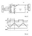
- FIG. 2illustrates a boost converter stage of a low voltage lamp including a switch controller to operate a switch associated with an inductor;
- FIG. 3illustrates the FIG. 2 boost converter stage operating in a reactive power transfer mode
- FIG. 4includes first example waveforms illustrating reactive power transfer mode operation
- FIG. 5includes second example waveforms illustrating reactive power transfer mode operation
- FIG. 6illustrates the FIG. 2 boost converter stage operating in a real power transfer mode
- FIG. 7includes example waveforms illustrating single pulse operation of the controller with transfer of real energy from the inductor and to the load;
- FIG. 8includes a second example of waveforms illustrating single pulse operation of the controller with transfer of real energy from the inductor and to the load;
- FIG. 9includes example waveforms illustrating multi pulse operation of the controller
- FIG. 10illustrates example elements of the FIG. 2 switch controller
- FIG. 11illustrates a finite state machine supported by the FIG. 2 switch controller in a single pulse mode
- FIG. 12includes example waveforms illustrating the FIG. 11 operations
- FIG. 13illustrates a finite state machine supported by the FIG. 2 switch controller in a multi-pulse mode
- FIG. 14includes example waveforms illustrating the FIG. 11 operations.
- FIG. 15illustrates operation of oscillation signal logic of the FIG. 2 switch controller.
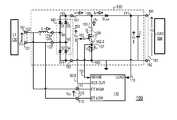
- FIG. 2illustrates selected elements of a low voltage lamp 199 including a boost converter stage 100 coupled to a switch controller 110 and a load 190 .
- Load 190may include one or more low voltage light producing components including one or more low voltage light emitting diodes.
- the illustrated boost converter stage 100includes an inductor L that receives the output of electronic transformer 130 and provides an inductor current I L to a rectifier 140 .
- Rectifier 140provides a rectified current I R to a switch node 155 .
- the rectified current I Ris generally positive and approximately equal in magnitude to the inductor current I L .
- the switch node 155is connected to the switch Q and is also connected to the load 190 via a linking circuit that includes a linking diode D LINK and a linking capacitor C.
- Linking capacitor Cis connected across an output 181 of boost convert stage 100 .
- Boost converter stage output 181is provided to the load 190 .
- the switch controller 110 illustrated in FIG. 2generates a switch control signal SCS that operates switch Q based on the output of electronic transformer 130 and one or more inputs from boost converter stage 100 .
- switch QWhen switch Q is open, the switch current I Q flowing through switch Q is negligible and substantially all of the rectified current I R flows through the link diode D LINK as the link diode current I D .
- switch QWhen switch Q is closed, substantially all of the rectified current I R flows back to electronic transformer 130 through switch Q, i.e., I R is substantially equal to I Q and I D is zero or negligible.
- the switch current I Qrepresents current drawn from electronic transformer 130 that is not dissipated in load 190 and does not, therefore, increase power consumption.
- the switch controller 110may assert the switch control signal SCS for a duration sufficient to ensure that the inductor current I L reaches a minimum peak value required to maintain stable operation of electronic transformer 130 , but not so long that the inductor current I L exceeds a maximum inductor current specified for the inductor.
- the boost converter stage 100 illustrated in FIG. 2includes an input 103 including a first terminal 101 and a second terminal 102 .
- Input 103is configured to receive transformer output voltage V OT from electronic transformer 130 .
- An input 113 of a switch controller 110is connected in parallel with input 103 such that switch controller 110 receives the transformer output voltage V OT from electronic transformer 130 .
- An inductor Lis connected between first terminal 101 of input 103 and a first terminal 131 of a rectifier input 133 of a rectifier 140 .
- Second terminal 102 of input 103is connected to a second terminal 132 of rectifier input 133 .
- the rectifier 140 illustrated in FIG. 2is a diode bridge rectifier that includes input nodes 141 and 142 , diodes D 1 , D 2 , D 3 , and D 4 , and output nodes 143 and 144 .
- the cathodes of diodes D 1 and D 3are connected to first output node 143 and the anodes of diodes D 2 and D 4 are connected to second output node 144 .
- First input node 141is connected to the D 1 anode and the D 2 cathode and second input node 142 is connected to the D 3 anode and to the D 4 cathode.
- FIG. 2the cathodes of diodes D 1 and D 3 are connected to first output node 143 and the anodes of diodes D 2 and D 4 are connected to second output node 144 .
- First input node 141is connected to the D 1 anode and the D 2 cathode and second input node 142 is connected to the D 3 an
- first output node 143is connected to a first terminal 151 of rectifier output 153 .
- Second output node 144is connected to a second terminal 152 of rectifier output 153 .
- rectifier 140 illustrated in FIG. 2is a diode bridge rectifier, rectifier 140 may be implemented in other suitable configurations.
- First terminal 151 of rectifier output 153is connected to a switch node 155 and second terminal 152 of rectifier output 153 is connected to ground node 159 .
- Rectifier 140provides a rectified current IR to switch node 155 .
- Switch node 155is connected to an anode of a diode referred to herein as link diode D LINK and to a first output terminal 162 - 1 of switch Q.
- the switch Q illustrated in FIG. 2is a solid state transistor 165 , which may be implemented as either a bipolar transistor or a field effect transistor.
- a second output terminal 162 - 2 of switch Qis connected to a sense node 157 .
- Controller 110receives a sense signal 115 from sense node 157 .
- Sense node 157is connected to a first terminal of a sense transistor R S .
- a second terminal of sense resistor R Sis connected to ground node 159 .
- switch control signal SCSWhen the switch controller 110 illustrated in FIG. 2 asserts switch control signal SCS to close, activate, turn on or otherwise place switch Q in a low impedance OR conductive state, a short circuit or a virtual short circuit is created between switch node 155 and sense node 157 and the rectified current I R may flow readily through switch Q between first output terminal 162 - 1 and second output terminal 162 - 2 .
- switch controller 110de-asserts switch control signal SCS
- switch Qis opened, deactivated, turned off, or otherwise placed in a high impedance state
- an open circuit or a virtual open circuitis established between switch node 155 and sense node 157 and the rectified current I R is prevented or substantially prevented from flowing between first output terminal 162 - 1 and second output terminal 162 - 2 .
- the cathode of link diode D LINKis connected to output node 171 .
- Output node 171connects to a first terminal 181 of a boost converter stage output 183 .
- Output node 171also provides LOAD signal 116 to a LOAD input of switch controller 110 .
- a link capacitor Cis shown connected between output node 171 and ground node 159 , to which a second terminal 182 of boost converter stage output 183 is also connected.
- the link capacitor voltage, V Cequals the boost converter stage output voltage, V B , that drives load 190 .
- Switch Qis shown with its output terminals 162 - 1 and 162 - 2 connected in series with a sense resistor R S .
- the switch current I Q flowing from switch node 155 through switch Q when switch Q is closedis substantially equal to the rectifier current I R .
- switch current I Qis negligible and the rectified current I R flows through link diode D LINK as the diode current I D . If switch Q is then closed, the voltage at switch node 155 will jump as the inductor current I L , the rectified current I R , and the diode current I D all increase rapidly.
- the rapid increase in the diode current I Dwill cause the link capacitor voltage V C to rise above the steady state voltage and, in this manner, the boost converter output voltage, V B , is boosted with respect to the amplitude of the rectified output 153 . If the switch Q is opened and closed periodically, the magnitude of boost converter stage output voltage V B will be greater than the amplitude of the rectifier output voltage V R .
- the sense voltage V S at sense node 157 when switch Q is closedis a function of the inductor current I L and the sense resistance R S .
- the sense voltage V S in millivolts (mV)closely approximates the magnitude of inductor current I L in milliamps (mA).
- the boost converter stage illustrated in FIG. 2provides the sense voltage V S to switch controller 110 as the sense signal 115 .
- switch controller 110in conjunction with switch Q and inductor L, is suitable for connecting a low voltage LED lamp to an electronic transformer.
- switch controller 110can control the inductor current I L to ensure compliance with the minimum peak inductor current required by the electronic transformer without violating a maximum inductor current limit.
- switch controller 110may monitor the inductor current I L via sense signal 157 and, based on the inductor current sensed, switch controller 110 may open switch Q when the inductor current I L reaches a specified or desired value.
- the ability to sense inductor current I Ldirectly reduces concerns with the size of the inductor, the magnitude of the transformer voltage, and other various parameters that contribute to the inductor current and the rate of change of instructor current.
- FIG. 3illustrates boost converter stage 100 operating in a reactive power transfer mode when switch Q is on.
- inductor current I Lfollows current path 301 from the electronic transformer 130 , through diode D 1 , switch Q, and diode D 4 when I L is positive and through diode D 3 , switch Q, and diode D 2 when negative, depending on the polarity of the transformer output voltage V OT .
- electronic transformer 130 and inductor Lexchange energy reactively.
- the inductor current I L associated with the reactive power transfer mode of FIG. 3 and the current path 301emphasize the ability to sustain the oscillation current required by electronic transformer 130 with no or little real power consumption.
- FIG. 4illustrates example waveforms of the transformer output voltage V OT , the inductor current I L , and switch control signal SCS, operating in a reactive power transfer mode, with the switch control signal SCS always on.
- the transformer output voltage VOTis illustrated oscillating between a positive voltage V HI and a negative voltage V LO at a frequency of (2*T W ) ⁇ 1 , where T W is the half period of V OT .
- V Lis approximately equal to V OT when the switch Q is closed and the rate at which the inductor current I L increases is approximately V OT /L.
- FIG. 5depicts an example of the reactive power transfer mode emphasizing the use of switch control signal SCS to control the peak value I PEAK of the inductor current I L independent of the duration of the transformer output voltage half-period T W .
- FIG. 5depicts an example of the reactive power transfer mode emphasizing the use of switch control signal SCS to control the peak value I PEAK of the inductor current I L independent of the duration of the transformer output voltage half-period T W .
- T DELAYillustrates a value of T DELAY that results in a peak inductor current I PEAK that is greater than the minimum peak inductor current I MINPEAK required by electronic transformer 130 and less than the maximum inductor current I MAX specified for the inductor L.
- the timing diagram of FIG. 5also illustrates the inductor current I L decreasing from the peak value I PEAK to zero beginning at V OT edge 197 , when the polarity of the transformer output voltage V OT transitions from positive (V HI ) to negative (V LO ).
- the switch control signal SCS illustrated in FIG. 5is de-asserted, at SCS edge 198 , just as the inductor current I L reaches zero. Because the switch control signal SCS illustrated in FIG. 5 remains asserted until there is no energy stored in inductor L, i.e., until I L reaches 0, all transfer of energy in FIG. 5 is reactive energy transfer.
- FIG. 6illustrates boost converter stage 100 operating in a real power transfer mode when the switch Q is open.
- inductor current I Lfollows current path 302 from inductor L, through rectifier diode D 1 , when I L is positive, and link diode D LINK , to output node 171 .
- energy stored in the inductor Lcharges the link capacitor C, is dissipated in load 190 , or both.
- FIG. 7illustrates waveform examples similar to FIG. 5 .
- the switch control signal SCSis de-asserted at 202 before all of the stored energy in the inductor L is returned to the electronic transformer, i.e., before the magnitude of the inductor current I L returns to zero.
- the energy 210 that is stored in inductor L when the switch Q is openedis transferred to the load 190 (of FIG. 6 ).
- switch controller 110can control the amount of energy stored in inductor L that is transferred to the load.
- FIG. 8illustrates waveforms similar to FIG. 7 except that de-assertion of the SCS signal at 212 in FIG. 8 occurs substantially at the same time as the end of cycle transition of the transformer output voltage V OT .
- the inductor current I L when the switch is openedis greater than the inductor current I L when the switch was opened in FIG. 7 and, as a result, the real power transfer that occurs in FIG. 8 , represented by the reference numeral 220 , is greater than the real power transfer of FIG. 7 , represented by reference numeral 210 .
- the timing configurations illustrated in FIG. 4 , FIG. 5 , FIG. 7 , and FIG. 8are all single pulse configurations in which the switch control signal SCS is asserted only once per half-period of transformer output voltage V OT .
- FIG. 9illustrates a multi-pulse timing configuration in which switch control signal SCS is asserted two or more times within a single half-period of transformer output voltage V OT .
- switch control signal SCSis asserted two or more times within a single half-period of transformer output voltage V OT .
- the inductor currentincreases from zero to a specified value, identified in FIG. 9 as the COMP_HI value, at time 322 , well before the end of the transformer output signal half-period.
- Switch Qis then turned off, by de-asserting switch control signal SCS at 322 , for an interval labeled as the CCM_OFF interval, during which energy stored in the inductor L is partially transferred to the load.
- FIG. 9illustrates a multi-pulse timing configuration in which switch control signal SCS is asserted two or more times within a single half-period of transformer output voltage V OT .
- switch control signal SCSbeing re-asserted as switch Q is turned back on when I L reaches a COMP_LO value at 325 and inductor current I L begins to increase during an interval labeled as CCM_ON.
- switch Qis again turned off to begin a second CCM_OFF interval. This sequence of CCM_OFF intervals followed by CCM_ON intervals may continue through the end of the transformer output signal half-period at time 328 .
- the switch control signal SCSis in an asserted state at the end of the transformer output signal half-period and remains asserted for an interval following the end of the half-period, until SCS is de-asserted at time 329 and the energy 330 remaining in inductor L is transferred to the load.
- Embodiments of switch controller 110may open the switch Q at 329 based upon satisfaction of one or more criteria. For example, the de-assertion of the SCS signal at 329 may occur when I L drops below COMP_LO and the width of the last assertion 331 of the switch control signal SCS is greater than a minimum CCM_ON threshold.
- FIG. 9illustrates SCS in an asserted state at the end of the transfer output signal half-period, SCS signal may be in a de-asserted state at the end of the transformer output signal half-period.
- FIG. 9 waveformsillustrate the ability to control the inductor current I L and utilize energy stored in the inductor by turning on switch Q relatively early in the transformer output signal half-period, monitoring the inductor current until it reaches a COMP_HI value, for example, that is greater than the minimum peak inductor current, but less than the maximum inductor current I MAX , and then begin toggling switch Q off and on to transfer a portion of the inductor energy to the load while maintaining the inductor current in a relatively narrow range between the minimum peak inductor current and the maximum inductor current.
- COMP_HI valuefor example, that is greater than the minimum peak inductor current, but less than the maximum inductor current I MAX
- FIG. 10illustrates elements of an example switch controller 110 suitable for use in boost converter stage 100 of FIG. 1 .
- the switch controller 110 illustrated in FIG. 10receives sense signal 115 at a SENSE_IN input, LOAD signal 116 at a LOAD_IN input, and transformer output voltage V OT via an input pair identified as VA_IN and VB_IN.
- switch controller 110derives a set of one or more internal signals from the received inputs.
- the switch controller 110 illustrated in FIG. 10includes controller logic 400 that receives the internal signals and generates the switch control signal SCS, which is output on the SCS_OUT output.
- switch controller 110provides sense signal 115 to a first input of a first comparator 401 and to a first input of a second comparator 402 .
- a second input of first comparator 401receives a predetermined or configurable DAC_HI signal 405 from a digital to analog converter 403 while a second input of second comparator 402 receives a predetermined or configurable DAC_LO signal 406 from a digital to analog converter 404 .
- the switch controller 110 illustrated in FIG. 10generates a COMP_HI signal 410 , based on the relative values of sense signal 115 and DAC_HI signal 405 .
- Switch controller 110also generates a COMP_LO signal 420 based on a comparison of sense signal 115 and DAC_LO signal 406 as determined by comparator 402 .
- the switch controller 110 illustrated in FIG. 10provides COMP_LO signal 420 to an oscillation logic 430 that generates an oscillation signal 431 .
- Oscillation signal 431may indicate an operational status of the electronic transformer 130 .
- oscillation signal 431by indicating when the inductor current I L exceeds I MINPEAK or another minimum threshold value, may indicate whether boost converter stage 100 is drawing sufficient current to maintain reliable operation of the electronic transformer.
- An example implementation of oscillation logic 430is described in greater detail with respect FIG. 15 .
- the transformer output signal V OTis received by EDGE detection logic 440 , which generates EDGE signal 441 to indicate transformer output signal transitions, e.g., edges of transformer output voltage V OT .
- FIG. 10illustrates LOAD signal 116 provided to a first input of counter logic 450 , which receives a reference voltage signal 452 as a second input.
- Counter logic 450as illustrated in FIG. 10 generates a counter value, identified as OFF_COUNT_MAX 451 that may be used to time the first assertion of the switch control signal SCS following the beginning of a transformer output voltage half-period.
- counter logic 450generates a larger value of OFF_COUNT_MAX when the LOAD signal 116 indicates less loading.
- counter logic 450may generate lower values of OFF_COUNT_MAX when LOAD signal 116 indicates relatively more loading.
- Controller 110 as illustrated in FIG. 10includes a memory or storage element 470 .
- Memory 470may be implemented with any suitable form of computer readable memory or storage including, without limitation, magnetic storage, solid-state storage, nonvolatile storage, volatile storage, and so forth.
- the memory 470 illustrated in FIG. 10stores or otherwise includes configuration settings 480 .
- a multi-pulse configuration settingenabling or indicating multi-pulse operation
- a DAC_HI configuration settingcorresponding to DAC_HI reference 403 used to determine the COMP_HI signal
- a minimum peak inductor current configuration settingindicating a minimum peak current specified for inductor L
- a maximum inductor current I MAX settingcorresponding to the maximum current recommended for the inductor L
- an inductance configuration setting indicating the inductance of inductor Land electronic transformer frequency configuration setting
- a CCM_ON configuration settingto indicate a CCM_ON interval
- a CCM_OFF settingto indicate a CCM_OFF interval.
- Other embodimentsmay employ more configuration settings, fewer configuration settings, and/or different configuration settings from those illustrated in FIG. 10 .
- the controller logic 400 of FIG. 10may receive controller logic inputs including, as non-limiting examples, COMP_HI signal 410 , COMP_LO signal 420 , oscillation signal 431 , EDGE signal 441 , and OFF — COUNT_MAX signal 451 .
- the controller logic 400 illustrated in FIG. 10generates the switch control signal SCS based upon the controller logic inputs received by controller logic 400 and the configuration settings 480 .
- Controller logic 400may control switch control signal SCS to support any of the timing configurations illustrated in FIG. 4 , FIG. 5 , FIG. 7 , FIG. 8 , and FIG. 9 as well as variations of those illustrated configurations.
- switch controller 110implements a finite state machine that includes a defined set of operational states and defined criteria for transitioning between the defined states.
- FIG. 11illustrates an example finite state machine 501 supported by switch controller 110 in a single pulse mode.
- the finite state machine 501 illustrated in FIG. 11includes an ON state 502 , and EDGE state 510 , and an OFF state 520 .
- switch controller 110initiates, e.g., after a power reset, to the ON state 502 .
- switch Qis closed and switch controller 110 is monitoring the oscillation signal 431 and the edge signal 441 .
- finite state machine 501 illustrated in FIG. 11transitions from ON state 502 to EDGE state 510 along transition path 503 if and when oscillation signal 431 and edge signal 441 are both TRUE.
- the finite state machine 501 illustrated in FIG. 11transitions from EDGE state 510 to OFF state 520 along transition path 504 upon detecting COMP_LO signal in a FALSE state, i.e., NOT COMP_LO is true.
- finite state machine 501transitions to OFF state 520
- finite state machine 501turns switch Q off and clears an OFF counter.
- the OFF counterincrements once per cycle of a logic clock signal provided to controller 110 and controller 110 monitors the OFF counter against the OFF_COUNT_MAX setting 451 .
- the finite state machine 501 illustrated in FIG. 11transitions from OFF state 520 to ON state 502 .
- FIG. 12illustrates example waveforms of transformer output voltage V OT , inductor current I L , and switch control signal SCS, for the finite state machine 501 of FIG. 11 .
- the duration T DELAY of the OFF staterepresents the amount of time switch control signal SCS remains de-asserted after a lo-to-hi transition of transformer output voltage V OT .
- finite state machine 501transitions to ON state 502 and switch control signal SCS is asserted and the inductor current I L begins to rise.
- the EDGE signal 441is TRUE and switch controller 110 transitions to the EDGE state 510 , switch Q remains closed and the inductor current I L decreases as inductor energy is returned to electronic transformer 130 .
- Finite state machine 501transitions from EDGE state 510 to OFF state 520 when the inductor current I L falls below the COMP_LO threshold required to maintain the COMP_LO signal 410 TRUE.
- Finite state machine 501de-asserts switch control signal SCS at SCS edge 533 to open the switch Q.
- switch Qis turned off, inductor energy 535 remaining in inductor L is transferred to the load.
- FIG. 13illustrates a finite state machine 601 that supports multi-pulse operation and includes five states.
- Finite state machine 601includes an ON state 602 , an EDGE state 610 , and an OFF state 620 that are analogous to the ON state 502 , EDGE state 510 , and OFF state 520 , illustrated in FIG. 11 .
- ON state 502 of finite state machine 501 illustrated in FIG. 11can transition only to the EDGE state 510
- the finite state machine 601 illustrated in FIG. 13can transition from ON state 602 to two different states. Both transitions from ON state 602 require the detection of the oscillation signal 431 .
- finite state machine 601monitors a COMP_HI signal in addition to the edge signal and the oscillation signal monitored by the finite state machine 501 .
- the finite state machine 601 illustrated in FIG. 13transitions from ON state 602 to a CCM_OFF state 630 upon detecting the oscillation signal and the COMP_HI signal both asserted.
- Finite state machine 601transitions from the ON state 602 to EDGE state 610 upon detecting the oscillation signal and the edge signal both asserted.
- finite state machine 601transitions to CCM_OFF state 630 if the inductor current I L equals or exceeds the COMP_HI threshold before an end of the transformer output half-period.
- switch controller 110opens switch Q while the transformer output voltage V OT is maintained, in the depicted example, at a positive voltage. With switch Q open, inductor L begins to transfer energy to the load and the inductor current I L begins to drop.
- finite state machine 601monitors a CCM_OFF counter to determine how long switch controller 110 remains in the CCM_OFF state 630 .
- finite state machine 601transitions from CCM_OFF state 630 to CCM_ON state 640 , in which the switch control signal SCS is asserted and a second signal, the edge enable signal, is set to 1.
- the finite state machine 601 illustrated in FIG. 13may transition from CCM_ON state 640 to either the CCM_OFF state 630 or to the OFF state 620 . If the COMP_HI signal is asserted while finite state machine 601 is in the CCM_ON state 640 , the finite state machine 601 transitions back to CCM_OFF state 630 . This transition from CCM_ON state 640 to CCM_OFF state 630 is illustrated graphically at edge transition 641 of FIG. 14 .
- finite state machine 601may oscillate back-and-forth between CCM_OFF state 630 and CCM_ON state 640 two or more cycles as the inductor current I L rises and falls between COMP_HI and COMP_LO values while the transformer output voltage V OT remains substantially constant.
- the finite state machine 601 illustrated in FIG. 13may transition from CCM_ON state 640 to the OFF state 620 if and when a CCM_ON counter exceeds a CCM_ON_MIN value and the COMP_LO signal is FALSE.
- the transition from CCM_ON state 640 to the OFF state 620may occur after the transformer output voltage V OT edge 651 .
- V OTchanges to a negative value while the switch control signal SCS keeps switch Q closed.
- Finite state machine 501begins to transfer reactive energy stored in the inductor L back to the electronic transformer 130 and the inductor current I L begins to fall.
- switch control signal SCSis then de-asserted at reference 661 , switch Q is opened and inductor L transfers its remaining energy 655 to the load.
- finite state machine 601can implement the state machine transitions illustrated in FIG. 14 flexibly to control the duration of T DELAY , and the number and duration of the CCM_ON/CCM_OFF intervals.
- the COMP_HI threshold and the COMP_LO thresholdare both within the range between the minimum peak inductor current I MINPEAK and the maximum inductor current I MAX , with the COMP_HI threshold being greater than the COMP_LO threshold.
- the switch controller 110ensures reliable operation of the electronic transformer by satisfying the criteria for oscillation current without violating the maximum current rated for the inductor.
- Finite state machine 601 illustrated in FIG. 13 and FIG. 14 and finite state machine 501 illustrated in FIG. 11 and FIG. 12both monitor an oscillation signal for, among other things, transition from the initial ON state to some other state.
- the finite state machine of boost converter stage 100remains in the initial ON state with the switch control signal asserted until the oscillation signal indicates proper functioning of the electronic transformer circuit.
- a portion of finite state machine 501 , finite state machine 601 , or another suitable finite state machinemay include oscillation signal logic operable to perform operations according to the flow diagram of FIG. 15 .
- the operations 700include an initial comparison (block 702 ) of the COMP_LO signal.
- operation 700transitions to block 704 where a dead counter is initialized to zero and an oscillation signal is asserted.
- Method 700 illustrated in FIG. 15then transitions back to block 702 . If the compare low is un-asserted when the comparison of block 702 is made, the method 700 illustrated in FIG. 15 transitions from block 702 to block 706 , in which the dead counter is incremented. The method 700 illustrated in FIG. 15 then compares the dead counter with a dead counter maximum at block 708 . If the dead counter equals or exceeds the dead counter maximum, method 700 transitions to block 710 where the oscillation signal is de-asserted and the dead counter is set to the dead counter maximum value. If, in block 708 , the dead counter is less than the dead counter maximum value, methods 700 sets the oscillation signal to one at block 712 and transitions back to block 702 .
- method 700asserts the oscillation signal initially and maintains the oscillation signal unless the COMP_LO signal remains de-asserted for a duration determined by the dead counter maximum value. If the COMP_LO signal remains de-asserted for longer than the interval determined by the dead counter maximum, the oscillation signal is de-asserted in block 710 .
- references in the appended claims to an apparatus or system or a component of an apparatus or system being adapted to, arranged to, capable of, configured to, enabled to, operable to, or operative to perform a particular functionencompasses that apparatus, system, or component, whether or not it or that particular function is activated, turned on, or unlocked, as long as that apparatus, system, or component is so adapted, arranged, capable, configured, enabled, operable, or operative.
Landscapes
- Engineering & Computer Science (AREA)
- Power Engineering (AREA)
- Physics & Mathematics (AREA)
- Microelectronics & Electronic Packaging (AREA)
- Optics & Photonics (AREA)
- Dc-Dc Converters (AREA)
Abstract
Description
Claims (35)
Priority Applications (6)
| Application Number | Priority Date | Filing Date | Title |
|---|---|---|---|
| US14/303,068US9385598B2 (en) | 2014-06-12 | 2014-06-12 | Boost converter stage switch controller |
| RU2017100449ARU2683025C2 (en) | 2014-06-12 | 2015-06-10 | Switch controller of boost converter stage |
| PCT/US2015/035052WO2015191680A1 (en) | 2014-06-12 | 2015-06-10 | Boost converter stage switch controller |
| JP2016572582AJP6339243B2 (en) | 2014-06-12 | 2015-06-10 | Boost converter stage switch controller |
| EP15731191.1AEP3155876A1 (en) | 2014-06-12 | 2015-06-10 | Boost converter stage switch controller |
| CN201580031055.1ACN106797686B (en) | 2014-06-12 | 2015-06-10 | Boost conversion grade switch controller |
Applications Claiming Priority (1)
| Application Number | Priority Date | Filing Date | Title |
|---|---|---|---|
| US14/303,068US9385598B2 (en) | 2014-06-12 | 2014-06-12 | Boost converter stage switch controller |
Publications (2)
| Publication Number | Publication Date |
|---|---|
| US20150364993A1 US20150364993A1 (en) | 2015-12-17 |
| US9385598B2true US9385598B2 (en) | 2016-07-05 |
Family
ID=53484168
Family Applications (1)
| Application Number | Title | Priority Date | Filing Date |
|---|---|---|---|
| US14/303,068Expired - Fee RelatedUS9385598B2 (en) | 2014-06-12 | 2014-06-12 | Boost converter stage switch controller |
Country Status (6)
| Country | Link |
|---|---|
| US (1) | US9385598B2 (en) |
| EP (1) | EP3155876A1 (en) |
| JP (1) | JP6339243B2 (en) |
| CN (1) | CN106797686B (en) |
| RU (1) | RU2683025C2 (en) |
| WO (1) | WO2015191680A1 (en) |
Cited By (1)
| Publication number | Priority date | Publication date | Assignee | Title |
|---|---|---|---|---|
| US20180054863A1 (en)* | 2015-05-27 | 2018-02-22 | Dialog Semiconductor (Uk) Limited | Solid State Lighting Driver Circuit with Ballast Compatibility |
Families Citing this family (4)
| Publication number | Priority date | Publication date | Assignee | Title |
|---|---|---|---|---|
| US9341358B2 (en) | 2012-12-13 | 2016-05-17 | Koninklijke Philips N.V. | Systems and methods for controlling a power controller |
| US9494139B2 (en)* | 2014-07-31 | 2016-11-15 | General Electric Company | System and method for controlling a power output of a wind turbine generator |
| SG11202012626YA (en)* | 2018-06-20 | 2021-02-25 | Vivita Japan Inc | Electronic device |
| US12009743B2 (en)* | 2021-03-25 | 2024-06-11 | Stmicroelectronics S.R.L. | Method of operating an electronic converter, corresponding control circuit and electronic converter |
Citations (76)
| Publication number | Priority date | Publication date | Assignee | Title |
|---|---|---|---|---|
| US3806829A (en) | 1971-04-13 | 1974-04-23 | Sys Inc | Pulsed laser system having improved energy control with improved power supply laser emission energy sensor and adjustable repetition rate control features |
| US4008414A (en) | 1975-07-28 | 1977-02-15 | Power Saver Corporation | Circuit for powering fluorescent lamps |
| US4562382A (en) | 1982-11-26 | 1985-12-31 | Quietlite International Ltd. | Solid-state inverter including a multiple core transformer |
| US5040236A (en) | 1990-07-18 | 1991-08-13 | Argus International | Apparatus for irradiation of printed wiring boards and the like |
| US5089753A (en) | 1990-07-09 | 1992-02-18 | North American Philips Corporation | Arrangement for predicting failure in fluorescent lamp systems |
| US5416387A (en) | 1993-11-24 | 1995-05-16 | California Institute Of Technology | Single stage, high power factor, gas discharge lamp ballast |
| US5583402A (en) | 1994-01-31 | 1996-12-10 | Magnetek, Inc. | Symmetry control circuit and method |
| US5650694A (en) | 1995-03-31 | 1997-07-22 | Philips Electronics North America Corporation | Lamp controller with lamp status detection and safety circuitry |
| US5872429A (en) | 1995-03-31 | 1999-02-16 | Philips Electronics North America Corporation | Coded communication system and method for controlling an electric lamp |
| US6369461B1 (en) | 2000-09-01 | 2002-04-09 | Abb Inc. | High efficiency power conditioner employing low voltage DC bus and buck and boost converters |
| US6407935B1 (en) | 2000-05-30 | 2002-06-18 | Koninklijke Philips Electronics N.V. | High frequency electronic ballast with reactive power compensation |
| US20030127994A1 (en) | 2002-01-10 | 2003-07-10 | Lightech Electronic Industries Ltd. | Lamp transformer for use with an electronic dimmer and method for use thereof for reducing acoustic noise |
| US20030151931A1 (en) | 2002-02-14 | 2003-08-14 | Kazuo Kohno | Self oscillation circuits |
| US20050174162A1 (en) | 2004-02-09 | 2005-08-11 | Taiwan Semiconductor Manufacturing Company | Configurable voltage generator |
| US20050249667A1 (en) | 2004-03-24 | 2005-11-10 | Tuszynski Jack A | Process for treating a biological organism |
| US20060147371A1 (en) | 2003-10-31 | 2006-07-06 | Tuszynski Jack A | Water-soluble compound |
| US20070040516A1 (en) | 2005-08-15 | 2007-02-22 | Liang Chen | AC to DC power supply with PFC for lamp |
| US20070076459A1 (en) | 2003-05-02 | 2007-04-05 | Limpkin George A | Apparatus for supplying energy to a load and a related system |
| US20070262654A1 (en) | 2005-06-06 | 2007-11-15 | Donald Mosebrook | Load control device for use with lighting circuits having three-way switches |
| US20070285028A1 (en) | 2004-08-16 | 2007-12-13 | Lightech Electronic Industries Ltd. | Controllable Power Supply Circuit for an Illumination System and Methods of Operation Thereof |
| US20080013343A1 (en) | 2006-07-12 | 2008-01-17 | David Michael Hugh Matthews | Method and apparatus for a high voltage power supply circuit |
| US20080018261A1 (en) | 2006-05-01 | 2008-01-24 | Kastner Mark A | LED power supply with options for dimming |
| US20080024074A1 (en) | 2005-06-06 | 2008-01-31 | Donald Mosebrook | Load control device for use with lighting circuits having three-way switches |
| US20080119421A1 (en) | 2003-10-31 | 2008-05-22 | Jack Tuszynski | Process for treating a biological organism |
| US20080224636A1 (en) | 2007-03-12 | 2008-09-18 | Melanson John L | Power control system for current regulated light sources |
| US20090184662A1 (en) | 2008-01-23 | 2009-07-23 | Cree Led Lighting Solutions, Inc. | Dimming signal generation and methods of generating dimming signals |
| US20090295292A1 (en) | 2008-05-28 | 2009-12-03 | Harmgardt Hans L G | LED replacement for low voltage lamps |
| US20100013409A1 (en) | 2008-07-16 | 2010-01-21 | Iwatt Inc. | LED Lamp |
| US20100141178A1 (en) | 2008-12-10 | 2010-06-10 | Linear Technology Corporation | Dimmer control leakage pull down using main power device in flyback converter |
| US20100164406A1 (en) | 2008-07-25 | 2010-07-01 | Kost Michael A | Switching power converter control with triac-based leading edge dimmer compatibility |
| US20100225251A1 (en) | 2009-03-06 | 2010-09-09 | Yasuhiro Maruyama | Led drive circuit, led lamp, led lighting appliance, and led lighting system |
| US20100244726A1 (en) | 2008-12-07 | 2010-09-30 | Melanson John L | Primary-side based control of secondary-side current for a transformer |
| US20110012530A1 (en) | 2009-07-14 | 2011-01-20 | Iwatt Inc. | Adaptive dimmer detection and control for led lamp |
| US20110115400A1 (en) | 2009-11-17 | 2011-05-19 | Harrison Daniel J | Led dimmer control |
| WO2011063205A1 (en) | 2009-11-20 | 2011-05-26 | Lutron Electronics Co., Inc. | Controllable-load circuit for use with a load control device |
| US20110121754A1 (en) | 2006-01-20 | 2011-05-26 | Exclara Inc. | Adaptive Current Regulation for Solid State Lighting |
| US20110121752A1 (en) | 2009-11-25 | 2011-05-26 | Lutron Electronics Co., Inc. | Two-wire dimmer switch for low-power loads |
| US20110127925A1 (en) | 2009-11-30 | 2011-06-02 | Yong Huang | Triac dimmer compatible wled driving circuit and method thereof |
| US20110199017A1 (en) | 2010-02-15 | 2011-08-18 | Osram Gesellschaft Mit Beschraenkter Haftung | Circuit and method for driving a luminous means |
| US20110210674A1 (en) | 2007-08-24 | 2011-09-01 | Cirrus Logic, Inc. | Multi-LED Control |
| WO2011111005A1 (en) | 2010-03-12 | 2011-09-15 | Koninklijke Philips Electronics N.V. | Power interface for a power supply circuit |
| US20110266968A1 (en) | 2010-04-30 | 2011-11-03 | Osram Gesellschaft Mit Beschraenkter Haftung | Method and device for obtaining conduction angle, method and device for driving led |
| US8067902B2 (en) | 2008-09-05 | 2011-11-29 | Lutron Electronics Co., Inc. | Electronic ballast having a symmetric topology |
| US20110309759A1 (en) | 2006-01-20 | 2011-12-22 | Exclara Inc. | Adaptive Current Regulation for Solid State Lighting |
| US20120025729A1 (en) | 2010-07-30 | 2012-02-02 | Melanson John L | Powering high-efficiency lighting devices from a triac-based dimmer |
| US20120043913A1 (en) | 2010-08-17 | 2012-02-23 | Melanson John L | Dimmer Output Emulation |
| US20120049752A1 (en) | 2010-08-24 | 2012-03-01 | King Eric J | Multi-Mode Dimmer Interfacing Including Attach State Control |
| US20120098454A1 (en) | 2009-10-26 | 2012-04-26 | Light-Based Technologies Incorporated | Current offset circuits for phase-cut power control |
| US20120106216A1 (en) | 2010-04-29 | 2012-05-03 | Victor Tzinker | Ac-dc converter with unity power factor |
| US20120112648A1 (en) | 2010-11-08 | 2012-05-10 | Suresh Hariharan | Electronic Transformer Compatibility for Light Emitting Diode Systems |
| US20120112638A1 (en) | 2010-11-04 | 2012-05-10 | Melanson John L | Thermal Management In A Lighting System Using Multiple, Controlled Power Dissipation Circuits |
| US20120119669A1 (en) | 2010-11-16 | 2012-05-17 | Melanson John L | Trailing Edge Dimmer Compatibility With Dimmer High Resistance Prediction |
| US20120139431A1 (en) | 2006-09-04 | 2012-06-07 | Lutron Electronics Co., Inc. | Variable load circuits for use with lighting control devices |
| US20120146546A1 (en) | 2010-12-09 | 2012-06-14 | Delta Electronics, Inc. | Load current balancing circuit |
| US20120169240A1 (en) | 2010-07-01 | 2012-07-05 | Alistair Allan Macfarlane | Semi resonant switching regulator, power factor control and led lighting |
| US20120230073A1 (en) | 2009-11-25 | 2012-09-13 | Lutron Electronics Co., Inc. | Two-wire dimmer switch for low-power loads |
| US20120229041A1 (en) | 2009-11-05 | 2012-09-13 | Eldolab Holding B.V. | Led driver for powering an led unit from a electronic transformer |
| US20120242238A1 (en) | 2011-03-22 | 2012-09-27 | Richtek Technology Corporation | Light Emitting Device Power Supply Circuit, and Light Emitting Device Driver Circuit and Control Method Thereof |
| US20120286826A1 (en) | 2010-11-04 | 2012-11-15 | Cirrus Logic, Inc. | Switching Power Converter Input Voltage Approximate Zero Crossing Determination |
| US20120286684A1 (en) | 2010-11-04 | 2012-11-15 | Cirrus Logic. Inc. | Controlled Power Dissipation In A Switch Path In A Lighting System |
| US20120286696A1 (en) | 2011-05-13 | 2012-11-15 | Mohamed Cherif Ghanem | Dimmable led lamp |
| US20130002163A1 (en) | 2010-08-17 | 2013-01-03 | Zhaohui He | Input Voltage Sensing For A Switching Power Converter And A Triac-Based Dimmer |
| EP2590477A1 (en) | 2011-11-07 | 2013-05-08 | Nxp B.V. | A method of controlling a ballast, a ballast, a lighting controller, and a digital signal processor |
| US20130113458A1 (en) | 2011-11-09 | 2013-05-09 | Crs Electronics | Led lamp driver identification |
| WO2013090904A1 (en) | 2011-12-16 | 2013-06-20 | Terralux, Inc. | System and methods of applying bleed circuits in led lamps |
| US20130278159A1 (en) | 2012-04-18 | 2013-10-24 | Power Integrations, Inc. | Bleeder circuit for use in a power supply |
| US20140009079A1 (en) | 2012-07-03 | 2014-01-09 | Cirrus Logic, Inc. | Systems and methods for low-power lamp compatibility with a leading-edge dimmer and a magnetic transformer |
| US20140028214A1 (en)* | 2012-07-03 | 2014-01-30 | Cirrus Logic, Inc. | Systems and methods for low-power lamp compatibility with a trailing-edge dimmer and an electronic transformer |
| US8653759B2 (en) | 2010-10-29 | 2014-02-18 | General Electric Company | Lighting system electronic ballast or driver with shunt control for lighting control quiescent current |
| US8664883B2 (en) | 2010-07-20 | 2014-03-04 | Panasonic Corporation | LED lighting device with chopper circuit and dimming control method |
| US8723431B2 (en) | 2009-07-27 | 2014-05-13 | Koninklijke Philips N.V. | Bleeder circuit |
| US20140167652A1 (en) | 2012-12-13 | 2014-06-19 | Cirrus Logic, Inc. | Systems and methods for controlling a power controller |
| US20140333205A1 (en) | 2013-05-13 | 2014-11-13 | Cirrus Logic, Inc. | Stabilization circuit for low-voltage lighting |
| US8928243B2 (en) | 2011-12-27 | 2015-01-06 | Texas Instruments Incorporated | Light driving system and method |
| US8933648B1 (en) | 2012-07-03 | 2015-01-13 | Cirrus Logic, Inc. | Systems and methods for selecting a compatibility mode of operation for a lamp assembly |
| US20150061536A1 (en) | 2013-08-30 | 2015-03-05 | Cirrus Logic, Inc. | Systems and methods for low-power lamp compatibility with a trailing-edge dimmer and an electronic transformer |
Family Cites Families (4)
| Publication number | Priority date | Publication date | Assignee | Title |
|---|---|---|---|---|
| JP4688846B2 (en)* | 2007-06-12 | 2011-05-25 | 三菱電機株式会社 | Converter device |
| JP5241578B2 (en)* | 2009-03-19 | 2013-07-17 | 株式会社日清製粉グループ本社 | Induction thermal plasma generation method and apparatus |
| RU92282U1 (en)* | 2009-10-07 | 2010-03-10 | Закрытое акционерное общество "УРАЛЬСКИЙ ПРОЕКТ" | LED LIGHT SOURCE |
| IN2014CN03663A (en)* | 2011-11-16 | 2015-10-16 | Koninkl Philips Nv |
- 2014
- 2014-06-12USUS14/303,068patent/US9385598B2/ennot_activeExpired - Fee Related
- 2015
- 2015-06-10RURU2017100449Apatent/RU2683025C2/enactive
- 2015-06-10JPJP2016572582Apatent/JP6339243B2/ennot_activeExpired - Fee Related
- 2015-06-10EPEP15731191.1Apatent/EP3155876A1/ennot_activeWithdrawn
- 2015-06-10CNCN201580031055.1Apatent/CN106797686B/ennot_activeExpired - Fee Related
- 2015-06-10WOPCT/US2015/035052patent/WO2015191680A1/enactiveApplication Filing
Patent Citations (88)
| Publication number | Priority date | Publication date | Assignee | Title |
|---|---|---|---|---|
| US3806829A (en) | 1971-04-13 | 1974-04-23 | Sys Inc | Pulsed laser system having improved energy control with improved power supply laser emission energy sensor and adjustable repetition rate control features |
| US4008414A (en) | 1975-07-28 | 1977-02-15 | Power Saver Corporation | Circuit for powering fluorescent lamps |
| US4562382A (en) | 1982-11-26 | 1985-12-31 | Quietlite International Ltd. | Solid-state inverter including a multiple core transformer |
| US5089753A (en) | 1990-07-09 | 1992-02-18 | North American Philips Corporation | Arrangement for predicting failure in fluorescent lamp systems |
| US5040236A (en) | 1990-07-18 | 1991-08-13 | Argus International | Apparatus for irradiation of printed wiring boards and the like |
| US5416387A (en) | 1993-11-24 | 1995-05-16 | California Institute Of Technology | Single stage, high power factor, gas discharge lamp ballast |
| US5583402A (en) | 1994-01-31 | 1996-12-10 | Magnetek, Inc. | Symmetry control circuit and method |
| US5872429A (en) | 1995-03-31 | 1999-02-16 | Philips Electronics North America Corporation | Coded communication system and method for controlling an electric lamp |
| US5650694A (en) | 1995-03-31 | 1997-07-22 | Philips Electronics North America Corporation | Lamp controller with lamp status detection and safety circuitry |
| US6407935B1 (en) | 2000-05-30 | 2002-06-18 | Koninklijke Philips Electronics N.V. | High frequency electronic ballast with reactive power compensation |
| US6369461B1 (en) | 2000-09-01 | 2002-04-09 | Abb Inc. | High efficiency power conditioner employing low voltage DC bus and buck and boost converters |
| US20030127994A1 (en) | 2002-01-10 | 2003-07-10 | Lightech Electronic Industries Ltd. | Lamp transformer for use with an electronic dimmer and method for use thereof for reducing acoustic noise |
| US20030151931A1 (en) | 2002-02-14 | 2003-08-14 | Kazuo Kohno | Self oscillation circuits |
| US20070076459A1 (en) | 2003-05-02 | 2007-04-05 | Limpkin George A | Apparatus for supplying energy to a load and a related system |
| US20060147371A1 (en) | 2003-10-31 | 2006-07-06 | Tuszynski Jack A | Water-soluble compound |
| US20080119421A1 (en) | 2003-10-31 | 2008-05-22 | Jack Tuszynski | Process for treating a biological organism |
| US20050174162A1 (en) | 2004-02-09 | 2005-08-11 | Taiwan Semiconductor Manufacturing Company | Configurable voltage generator |
| US20050249667A1 (en) | 2004-03-24 | 2005-11-10 | Tuszynski Jack A | Process for treating a biological organism |
| US20070285028A1 (en) | 2004-08-16 | 2007-12-13 | Lightech Electronic Industries Ltd. | Controllable Power Supply Circuit for an Illumination System and Methods of Operation Thereof |
| US20070262654A1 (en) | 2005-06-06 | 2007-11-15 | Donald Mosebrook | Load control device for use with lighting circuits having three-way switches |
| US20080024074A1 (en) | 2005-06-06 | 2008-01-31 | Donald Mosebrook | Load control device for use with lighting circuits having three-way switches |
| US20070040516A1 (en) | 2005-08-15 | 2007-02-22 | Liang Chen | AC to DC power supply with PFC for lamp |
| US8742674B2 (en) | 2006-01-20 | 2014-06-03 | Point Somee Limited Liability Company | Adaptive current regulation for solid state lighting |
| US20110121754A1 (en) | 2006-01-20 | 2011-05-26 | Exclara Inc. | Adaptive Current Regulation for Solid State Lighting |
| US20110309759A1 (en) | 2006-01-20 | 2011-12-22 | Exclara Inc. | Adaptive Current Regulation for Solid State Lighting |
| US20140239832A1 (en) | 2006-01-20 | 2014-08-28 | Point Somee Limited Liability Company | Power Conversion Apparatus and System for Solid State Lighting |
| US20080018261A1 (en) | 2006-05-01 | 2008-01-24 | Kastner Mark A | LED power supply with options for dimming |
| US20080013343A1 (en) | 2006-07-12 | 2008-01-17 | David Michael Hugh Matthews | Method and apparatus for a high voltage power supply circuit |
| US20120139431A1 (en) | 2006-09-04 | 2012-06-07 | Lutron Electronics Co., Inc. | Variable load circuits for use with lighting control devices |
| US20080224636A1 (en) | 2007-03-12 | 2008-09-18 | Melanson John L | Power control system for current regulated light sources |
| US20110210674A1 (en) | 2007-08-24 | 2011-09-01 | Cirrus Logic, Inc. | Multi-LED Control |
| US20090184662A1 (en) | 2008-01-23 | 2009-07-23 | Cree Led Lighting Solutions, Inc. | Dimming signal generation and methods of generating dimming signals |
| US7812550B2 (en) | 2008-05-28 | 2010-10-12 | Revlite Technologies Inc. | LED replacement for low voltage lamps |
| US20090295292A1 (en) | 2008-05-28 | 2009-12-03 | Harmgardt Hans L G | LED replacement for low voltage lamps |
| US20100013409A1 (en) | 2008-07-16 | 2010-01-21 | Iwatt Inc. | LED Lamp |
| US20100164406A1 (en) | 2008-07-25 | 2010-07-01 | Kost Michael A | Switching power converter control with triac-based leading edge dimmer compatibility |
| US20120299501A1 (en) | 2008-07-25 | 2012-11-29 | Kost Michael A | Switching Power Converter Control With Triac-Based Leading Edge Dimmer Compatibility |
| US8212491B2 (en) | 2008-07-25 | 2012-07-03 | Cirrus Logic, Inc. | Switching power converter control with triac-based leading edge dimmer compatibility |
| US8067902B2 (en) | 2008-09-05 | 2011-11-29 | Lutron Electronics Co., Inc. | Electronic ballast having a symmetric topology |
| US20100244726A1 (en) | 2008-12-07 | 2010-09-30 | Melanson John L | Primary-side based control of secondary-side current for a transformer |
| US20100141178A1 (en) | 2008-12-10 | 2010-06-10 | Linear Technology Corporation | Dimmer control leakage pull down using main power device in flyback converter |
| US20100225251A1 (en) | 2009-03-06 | 2010-09-09 | Yasuhiro Maruyama | Led drive circuit, led lamp, led lighting appliance, and led lighting system |
| US20110012530A1 (en) | 2009-07-14 | 2011-01-20 | Iwatt Inc. | Adaptive dimmer detection and control for led lamp |
| US8723431B2 (en) | 2009-07-27 | 2014-05-13 | Koninklijke Philips N.V. | Bleeder circuit |
| US20120098454A1 (en) | 2009-10-26 | 2012-04-26 | Light-Based Technologies Incorporated | Current offset circuits for phase-cut power control |
| US20120229041A1 (en) | 2009-11-05 | 2012-09-13 | Eldolab Holding B.V. | Led driver for powering an led unit from a electronic transformer |
| US20110121751A1 (en) | 2009-11-17 | 2011-05-26 | Harrison Daniel J | Led power-supply detection and control |
| US20110115400A1 (en) | 2009-11-17 | 2011-05-19 | Harrison Daniel J | Led dimmer control |
| WO2011063205A1 (en) | 2009-11-20 | 2011-05-26 | Lutron Electronics Co., Inc. | Controllable-load circuit for use with a load control device |
| US20110121752A1 (en) | 2009-11-25 | 2011-05-26 | Lutron Electronics Co., Inc. | Two-wire dimmer switch for low-power loads |
| US20120230073A1 (en) | 2009-11-25 | 2012-09-13 | Lutron Electronics Co., Inc. | Two-wire dimmer switch for low-power loads |
| US20110127925A1 (en) | 2009-11-30 | 2011-06-02 | Yong Huang | Triac dimmer compatible wled driving circuit and method thereof |
| US20110199017A1 (en) | 2010-02-15 | 2011-08-18 | Osram Gesellschaft Mit Beschraenkter Haftung | Circuit and method for driving a luminous means |
| WO2011111005A1 (en) | 2010-03-12 | 2011-09-15 | Koninklijke Philips Electronics N.V. | Power interface for a power supply circuit |
| US20120106216A1 (en) | 2010-04-29 | 2012-05-03 | Victor Tzinker | Ac-dc converter with unity power factor |
| US20110266968A1 (en) | 2010-04-30 | 2011-11-03 | Osram Gesellschaft Mit Beschraenkter Haftung | Method and device for obtaining conduction angle, method and device for driving led |
| US20120169240A1 (en) | 2010-07-01 | 2012-07-05 | Alistair Allan Macfarlane | Semi resonant switching regulator, power factor control and led lighting |
| US8664883B2 (en) | 2010-07-20 | 2014-03-04 | Panasonic Corporation | LED lighting device with chopper circuit and dimming control method |
| US8716957B2 (en) | 2010-07-30 | 2014-05-06 | Cirrus Logic, Inc. | Powering high-efficiency lighting devices from a triac-based dimmer |
| US20120025729A1 (en) | 2010-07-30 | 2012-02-02 | Melanson John L | Powering high-efficiency lighting devices from a triac-based dimmer |
| US20120043913A1 (en) | 2010-08-17 | 2012-02-23 | Melanson John L | Dimmer Output Emulation |
| US20130002163A1 (en) | 2010-08-17 | 2013-01-03 | Zhaohui He | Input Voltage Sensing For A Switching Power Converter And A Triac-Based Dimmer |
| US20120049752A1 (en) | 2010-08-24 | 2012-03-01 | King Eric J | Multi-Mode Dimmer Interfacing Including Attach State Control |
| US8653759B2 (en) | 2010-10-29 | 2014-02-18 | General Electric Company | Lighting system electronic ballast or driver with shunt control for lighting control quiescent current |
| US20120286684A1 (en) | 2010-11-04 | 2012-11-15 | Cirrus Logic. Inc. | Controlled Power Dissipation In A Switch Path In A Lighting System |
| US20120286826A1 (en) | 2010-11-04 | 2012-11-15 | Cirrus Logic, Inc. | Switching Power Converter Input Voltage Approximate Zero Crossing Determination |
| US20120112638A1 (en) | 2010-11-04 | 2012-05-10 | Melanson John L | Thermal Management In A Lighting System Using Multiple, Controlled Power Dissipation Circuits |
| US20120112648A1 (en) | 2010-11-08 | 2012-05-10 | Suresh Hariharan | Electronic Transformer Compatibility for Light Emitting Diode Systems |
| US8547034B2 (en) | 2010-11-16 | 2013-10-01 | Cirrus Logic, Inc. | Trailing edge dimmer compatibility with dimmer high resistance prediction |
| US20120119669A1 (en) | 2010-11-16 | 2012-05-17 | Melanson John L | Trailing Edge Dimmer Compatibility With Dimmer High Resistance Prediction |
| US20120146546A1 (en) | 2010-12-09 | 2012-06-14 | Delta Electronics, Inc. | Load current balancing circuit |
| US20120242238A1 (en) | 2011-03-22 | 2012-09-27 | Richtek Technology Corporation | Light Emitting Device Power Supply Circuit, and Light Emitting Device Driver Circuit and Control Method Thereof |
| US20120286696A1 (en) | 2011-05-13 | 2012-11-15 | Mohamed Cherif Ghanem | Dimmable led lamp |
| EP2590477A1 (en) | 2011-11-07 | 2013-05-08 | Nxp B.V. | A method of controlling a ballast, a ballast, a lighting controller, and a digital signal processor |
| US20130113458A1 (en) | 2011-11-09 | 2013-05-09 | Crs Electronics | Led lamp driver identification |
| WO2013090904A1 (en) | 2011-12-16 | 2013-06-20 | Terralux, Inc. | System and methods of applying bleed circuits in led lamps |
| US8928243B2 (en) | 2011-12-27 | 2015-01-06 | Texas Instruments Incorporated | Light driving system and method |
| US20130278159A1 (en) | 2012-04-18 | 2013-10-24 | Power Integrations, Inc. | Bleeder circuit for use in a power supply |
| US20140009082A1 (en)* | 2012-07-03 | 2014-01-09 | Cirrus Logic, Inc. | Systems and methods for determining a type of transformer to which a load is coupled |
| US20140028214A1 (en)* | 2012-07-03 | 2014-01-30 | Cirrus Logic, Inc. | Systems and methods for low-power lamp compatibility with a trailing-edge dimmer and an electronic transformer |
| US20140009078A1 (en) | 2012-07-03 | 2014-01-09 | Cirrus Logic, Inc. | Systems and methods for low-power lamp compatibility with a trailing-edge dimmer and an electronic transformer |
| US20140009079A1 (en) | 2012-07-03 | 2014-01-09 | Cirrus Logic, Inc. | Systems and methods for low-power lamp compatibility with a leading-edge dimmer and a magnetic transformer |
| US8933648B1 (en) | 2012-07-03 | 2015-01-13 | Cirrus Logic, Inc. | Systems and methods for selecting a compatibility mode of operation for a lamp assembly |
| US9072125B2 (en) | 2012-07-03 | 2015-06-30 | Cirrus Logic, Inc. | Systems and methods for determining a type of transformer to which a load is coupled |
| US20140167652A1 (en) | 2012-12-13 | 2014-06-19 | Cirrus Logic, Inc. | Systems and methods for controlling a power controller |
| US20140167639A1 (en) | 2012-12-13 | 2014-06-19 | Cirrus Logic, Inc. | Systems and methods for low-power lamp compatibility with a leading-edge dimmer and an electronic transformer |
| US20140333205A1 (en) | 2013-05-13 | 2014-11-13 | Cirrus Logic, Inc. | Stabilization circuit for low-voltage lighting |
| US20150061536A1 (en) | 2013-08-30 | 2015-03-05 | Cirrus Logic, Inc. | Systems and methods for low-power lamp compatibility with a trailing-edge dimmer and an electronic transformer |
Non-Patent Citations (5)
| Title |
|---|
| International Search Report and Written Opinion, International Patent Application No. PCT/US2013/047777, mailed Jun. 26, 2014, 21 pages. |
| International Search Report and Written Opinion, International Patent Application No. PCT/US2013/047844, mailed Jul. 23, 2014, 14 pages. |
| International Search Report and Written Opinion, International Patent Application No. PCT/US2013/071690, mailed Jun. 4, 2014, 13 pages. |
| International Search Report and Written Opinion, International Patent Application No. PCT/US2014/032182, mailed Jul. 24, 2014, 10 pages. |
| International Search Report and Written Opinion, International Patent Application No. PCT/US2014/037864, mailed Sep. 29, 2014, 8 pages. |
Cited By (1)
| Publication number | Priority date | Publication date | Assignee | Title |
|---|---|---|---|---|
| US20180054863A1 (en)* | 2015-05-27 | 2018-02-22 | Dialog Semiconductor (Uk) Limited | Solid State Lighting Driver Circuit with Ballast Compatibility |
Also Published As
| Publication number | Publication date |
|---|---|
| RU2683025C2 (en) | 2019-03-26 |
| WO2015191680A1 (en) | 2015-12-17 |
| JP6339243B2 (en) | 2018-06-06 |
| CN106797686A (en) | 2017-05-31 |
| RU2017100449A (en) | 2018-07-18 |
| JP2017525326A (en) | 2017-08-31 |
| US20150364993A1 (en) | 2015-12-17 |
| EP3155876A1 (en) | 2017-04-19 |
| RU2017100449A3 (en) | 2019-01-23 |
| CN106797686B (en) | 2019-07-12 |
Similar Documents
| Publication | Publication Date | Title |
|---|---|---|
| US9554432B2 (en) | Systems and methods for dimming control using system controllers | |
| US9912244B2 (en) | Control method and circuit for resonant converters with capacitive protection | |
| US8981661B2 (en) | Powering high-efficiency lighting devices from a triac-based dimmer | |
| CN106105396B (en) | The controllable electric power of LED (light emitting diode) string drivings | |
| US10264642B2 (en) | Systems and methods for intelligent control related to TRIAC dimmers by using modulation signals | |
| US9385598B2 (en) | Boost converter stage switch controller | |
| US9544962B2 (en) | Driver device and driving method for driving an LED unit | |
| US20170093296A1 (en) | Resonant converter with capacitive mode control and associated control method | |
| US20150351178A1 (en) | Adaptive Current Control Timing and Responsive Current Control for Interfacing with a Dimmer | |
| US9504105B2 (en) | On-time control for switched mode power supplies | |
| EP2974542A1 (en) | System and method for learning dimmer characteristics | |
| US9331586B2 (en) | Sampling for dimmer edge detection in power converter | |
| EP3005840A1 (en) | Method and circuitry for detecting a leading-edge phase-cut dimmer | |
| US9698693B2 (en) | Control circuit, control method and switch-type converter | |
| US9655175B2 (en) | Off-time control for switched mode power supplies | |
| TW201334620A (en) | LED driver system with dimmer detection | |
| US10306730B1 (en) | Light state regulation controller, control system and control method | |
| CN104853477A (en) | Universal input and wide output function for light emitting diode (LED) driver | |
| JP2020198752A (en) | Power source device, semiconductor integrated circuit, and ripple suppressing method | |
| CN210629909U (en) | Power frequency non-inductance constant current control circuit | |
| US8686656B2 (en) | Power supply device and light-emitting element drive device | |
| Kadota et al. | A new bleeder circuit for TRIAC dimmable LED driver based on single-stage topology with a capacitor input rectifier | |
| BE1019523A5 (en) | ZERO TRANSACTION DETECTOR, USE OF SUCH DETECTOR AND DIMMER INCLUDING SUCH DETECTOR. | |
| CN112913326A (en) | Electronic controller device and control method |
Legal Events
| Date | Code | Title | Description |
|---|---|---|---|
| AS | Assignment | Owner name:CIRRUS LOGIC, INC., TEXAS Free format text:ASSIGNMENT OF ASSIGNORS INTEREST;ASSIGNORS:WANG, KAN;KOST, MICHAEL A.;KING, ERIC J.;AND OTHERS;SIGNING DATES FROM 20141017 TO 20141106;REEL/FRAME:034942/0563 | |
| AS | Assignment | Owner name:KONINKLIJKE PHILIPS N.V., NETHERLANDS Free format text:ASSIGNMENT OF ASSIGNORS INTEREST;ASSIGNOR:CIRRUS LOGIC, INC.;REEL/FRAME:037563/0720 Effective date:20150928 | |
| ZAAA | Notice of allowance and fees due | Free format text:ORIGINAL CODE: NOA | |
| ZAAB | Notice of allowance mailed | Free format text:ORIGINAL CODE: MN/=. | |
| STCF | Information on status: patent grant | Free format text:PATENTED CASE | |
| AS | Assignment | Owner name:PHILIPS LIGHTING HOLDING B.V., NETHERLANDS Free format text:ASSIGNMENT OF ASSIGNORS INTEREST;ASSIGNOR:KONINKLIJKE PHILIPS N.V.;REEL/FRAME:041170/0806 Effective date:20161101 | |
| AS | Assignment | Owner name:SIGNIFY HOLDING B.V., NETHERLANDS Free format text:CHANGE OF NAME;ASSIGNOR:PHILIPS LIGHTING HOLDING B.V.;REEL/FRAME:050837/0576 Effective date:20190201 | |
| MAFP | Maintenance fee payment | Free format text:PAYMENT OF MAINTENANCE FEE, 4TH YEAR, LARGE ENTITY (ORIGINAL EVENT CODE: M1551); ENTITY STATUS OF PATENT OWNER: LARGE ENTITY Year of fee payment:4 | |
| FEPP | Fee payment procedure | Free format text:MAINTENANCE FEE REMINDER MAILED (ORIGINAL EVENT CODE: REM.); ENTITY STATUS OF PATENT OWNER: LARGE ENTITY | |
| LAPS | Lapse for failure to pay maintenance fees | Free format text:PATENT EXPIRED FOR FAILURE TO PAY MAINTENANCE FEES (ORIGINAL EVENT CODE: EXP.); ENTITY STATUS OF PATENT OWNER: LARGE ENTITY | |
| STCH | Information on status: patent discontinuation | Free format text:PATENT EXPIRED DUE TO NONPAYMENT OF MAINTENANCE FEES UNDER 37 CFR 1.362 | |
| FP | Lapsed due to failure to pay maintenance fee | Effective date:20240705 |