US9385322B2 - Method and apparatus for depositing LED organic film - Google Patents
Method and apparatus for depositing LED organic filmDownload PDFInfo
- Publication number
- US9385322B2 US9385322B2US13/095,619US201113095619AUS9385322B2US 9385322 B2US9385322 B2US 9385322B2US 201113095619 AUS201113095619 AUS 201113095619AUS 9385322 B2US9385322 B2US 9385322B2
- Authority
- US
- United States
- Prior art keywords
- discharge nozzle
- micro
- organic
- organic particles
- particles
- Prior art date
- Legal status (The legal status is an assumption and is not a legal conclusion. Google has not performed a legal analysis and makes no representation as to the accuracy of the status listed.)
- Active, expires
Links
Images


Classifications
- H—ELECTRICITY
- H10—SEMICONDUCTOR DEVICES; ELECTRIC SOLID-STATE DEVICES NOT OTHERWISE PROVIDED FOR
- H10K—ORGANIC ELECTRIC SOLID-STATE DEVICES
- H10K71/00—Manufacture or treatment specially adapted for the organic devices covered by this subclass
- H10K71/10—Deposition of organic active material
- H10K71/16—Deposition of organic active material using physical vapour deposition [PVD], e.g. vacuum deposition or sputtering
- H10K71/166—Deposition of organic active material using physical vapour deposition [PVD], e.g. vacuum deposition or sputtering using selective deposition, e.g. using a mask
- H01L51/0011—
- C—CHEMISTRY; METALLURGY
- C23—COATING METALLIC MATERIAL; COATING MATERIAL WITH METALLIC MATERIAL; CHEMICAL SURFACE TREATMENT; DIFFUSION TREATMENT OF METALLIC MATERIAL; COATING BY VACUUM EVAPORATION, BY SPUTTERING, BY ION IMPLANTATION OR BY CHEMICAL VAPOUR DEPOSITION, IN GENERAL; INHIBITING CORROSION OF METALLIC MATERIAL OR INCRUSTATION IN GENERAL
- C23C—COATING METALLIC MATERIAL; COATING MATERIAL WITH METALLIC MATERIAL; SURFACE TREATMENT OF METALLIC MATERIAL BY DIFFUSION INTO THE SURFACE, BY CHEMICAL CONVERSION OR SUBSTITUTION; COATING BY VACUUM EVAPORATION, BY SPUTTERING, BY ION IMPLANTATION OR BY CHEMICAL VAPOUR DEPOSITION, IN GENERAL
- C23C16/00—Chemical coating by decomposition of gaseous compounds, without leaving reaction products of surface material in the coating, i.e. chemical vapour deposition [CVD] processes
- C23C16/04—Coating on selected surface areas, e.g. using masks
- C23C16/042—Coating on selected surface areas, e.g. using masks using masks
- C—CHEMISTRY; METALLURGY
- C23—COATING METALLIC MATERIAL; COATING MATERIAL WITH METALLIC MATERIAL; CHEMICAL SURFACE TREATMENT; DIFFUSION TREATMENT OF METALLIC MATERIAL; COATING BY VACUUM EVAPORATION, BY SPUTTERING, BY ION IMPLANTATION OR BY CHEMICAL VAPOUR DEPOSITION, IN GENERAL; INHIBITING CORROSION OF METALLIC MATERIAL OR INCRUSTATION IN GENERAL
- C23C—COATING METALLIC MATERIAL; COATING MATERIAL WITH METALLIC MATERIAL; SURFACE TREATMENT OF METALLIC MATERIAL BY DIFFUSION INTO THE SURFACE, BY CHEMICAL CONVERSION OR SUBSTITUTION; COATING BY VACUUM EVAPORATION, BY SPUTTERING, BY ION IMPLANTATION OR BY CHEMICAL VAPOUR DEPOSITION, IN GENERAL
- C23C16/00—Chemical coating by decomposition of gaseous compounds, without leaving reaction products of surface material in the coating, i.e. chemical vapour deposition [CVD] processes
- C23C16/44—Chemical coating by decomposition of gaseous compounds, without leaving reaction products of surface material in the coating, i.e. chemical vapour deposition [CVD] processes characterised by the method of coating
- C23C16/448—Chemical coating by decomposition of gaseous compounds, without leaving reaction products of surface material in the coating, i.e. chemical vapour deposition [CVD] processes characterised by the method of coating characterised by the method used for generating reactive gas streams, e.g. by evaporation or sublimation of precursor materials
- C23C16/4481—Chemical coating by decomposition of gaseous compounds, without leaving reaction products of surface material in the coating, i.e. chemical vapour deposition [CVD] processes characterised by the method of coating characterised by the method used for generating reactive gas streams, e.g. by evaporation or sublimation of precursor materials by evaporation using carrier gas in contact with the source material
- C23C16/4483—Chemical coating by decomposition of gaseous compounds, without leaving reaction products of surface material in the coating, i.e. chemical vapour deposition [CVD] processes characterised by the method of coating characterised by the method used for generating reactive gas streams, e.g. by evaporation or sublimation of precursor materials by evaporation using carrier gas in contact with the source material using a porous body
- C—CHEMISTRY; METALLURGY
- C23—COATING METALLIC MATERIAL; COATING MATERIAL WITH METALLIC MATERIAL; CHEMICAL SURFACE TREATMENT; DIFFUSION TREATMENT OF METALLIC MATERIAL; COATING BY VACUUM EVAPORATION, BY SPUTTERING, BY ION IMPLANTATION OR BY CHEMICAL VAPOUR DEPOSITION, IN GENERAL; INHIBITING CORROSION OF METALLIC MATERIAL OR INCRUSTATION IN GENERAL
- C23C—COATING METALLIC MATERIAL; COATING MATERIAL WITH METALLIC MATERIAL; SURFACE TREATMENT OF METALLIC MATERIAL BY DIFFUSION INTO THE SURFACE, BY CHEMICAL CONVERSION OR SUBSTITUTION; COATING BY VACUUM EVAPORATION, BY SPUTTERING, BY ION IMPLANTATION OR BY CHEMICAL VAPOUR DEPOSITION, IN GENERAL
- C23C16/00—Chemical coating by decomposition of gaseous compounds, without leaving reaction products of surface material in the coating, i.e. chemical vapour deposition [CVD] processes
- C23C16/44—Chemical coating by decomposition of gaseous compounds, without leaving reaction products of surface material in the coating, i.e. chemical vapour deposition [CVD] processes characterised by the method of coating
- C23C16/448—Chemical coating by decomposition of gaseous compounds, without leaving reaction products of surface material in the coating, i.e. chemical vapour deposition [CVD] processes characterised by the method of coating characterised by the method used for generating reactive gas streams, e.g. by evaporation or sublimation of precursor materials
- C23C16/4485—Chemical coating by decomposition of gaseous compounds, without leaving reaction products of surface material in the coating, i.e. chemical vapour deposition [CVD] processes characterised by the method of coating characterised by the method used for generating reactive gas streams, e.g. by evaporation or sublimation of precursor materials by evaporation without using carrier gas in contact with the source material
- C—CHEMISTRY; METALLURGY
- C23—COATING METALLIC MATERIAL; COATING MATERIAL WITH METALLIC MATERIAL; CHEMICAL SURFACE TREATMENT; DIFFUSION TREATMENT OF METALLIC MATERIAL; COATING BY VACUUM EVAPORATION, BY SPUTTERING, BY ION IMPLANTATION OR BY CHEMICAL VAPOUR DEPOSITION, IN GENERAL; INHIBITING CORROSION OF METALLIC MATERIAL OR INCRUSTATION IN GENERAL
- C23C—COATING METALLIC MATERIAL; COATING MATERIAL WITH METALLIC MATERIAL; SURFACE TREATMENT OF METALLIC MATERIAL BY DIFFUSION INTO THE SURFACE, BY CHEMICAL CONVERSION OR SUBSTITUTION; COATING BY VACUUM EVAPORATION, BY SPUTTERING, BY ION IMPLANTATION OR BY CHEMICAL VAPOUR DEPOSITION, IN GENERAL
- C23C16/00—Chemical coating by decomposition of gaseous compounds, without leaving reaction products of surface material in the coating, i.e. chemical vapour deposition [CVD] processes
- C23C16/44—Chemical coating by decomposition of gaseous compounds, without leaving reaction products of surface material in the coating, i.e. chemical vapour deposition [CVD] processes characterised by the method of coating
- C23C16/455—Chemical coating by decomposition of gaseous compounds, without leaving reaction products of surface material in the coating, i.e. chemical vapour deposition [CVD] processes characterised by the method of coating characterised by the method used for introducing gases into reaction chamber or for modifying gas flows in reaction chamber
- C23C16/45563—Gas nozzles
- C23C16/45568—Porous nozzles
- H—ELECTRICITY
- H10—SEMICONDUCTOR DEVICES; ELECTRIC SOLID-STATE DEVICES NOT OTHERWISE PROVIDED FOR
- H10K—ORGANIC ELECTRIC SOLID-STATE DEVICES
- H10K71/00—Manufacture or treatment specially adapted for the organic devices covered by this subclass
- H10K71/40—Thermal treatment, e.g. annealing in the presence of a solvent vapour
- B—PERFORMING OPERATIONS; TRANSPORTING
- B05—SPRAYING OR ATOMISING IN GENERAL; APPLYING FLUENT MATERIALS TO SURFACES, IN GENERAL
- B05D—PROCESSES FOR APPLYING FLUENT MATERIALS TO SURFACES, IN GENERAL
- B05D1/00—Processes for applying liquids or other fluent materials
- B05D1/02—Processes for applying liquids or other fluent materials performed by spraying
- B05D1/12—Applying particulate materials
- C—CHEMISTRY; METALLURGY
- C23—COATING METALLIC MATERIAL; COATING MATERIAL WITH METALLIC MATERIAL; CHEMICAL SURFACE TREATMENT; DIFFUSION TREATMENT OF METALLIC MATERIAL; COATING BY VACUUM EVAPORATION, BY SPUTTERING, BY ION IMPLANTATION OR BY CHEMICAL VAPOUR DEPOSITION, IN GENERAL; INHIBITING CORROSION OF METALLIC MATERIAL OR INCRUSTATION IN GENERAL
- C23C—COATING METALLIC MATERIAL; COATING MATERIAL WITH METALLIC MATERIAL; SURFACE TREATMENT OF METALLIC MATERIAL BY DIFFUSION INTO THE SURFACE, BY CHEMICAL CONVERSION OR SUBSTITUTION; COATING BY VACUUM EVAPORATION, BY SPUTTERING, BY ION IMPLANTATION OR BY CHEMICAL VAPOUR DEPOSITION, IN GENERAL
- C23C16/00—Chemical coating by decomposition of gaseous compounds, without leaving reaction products of surface material in the coating, i.e. chemical vapour deposition [CVD] processes
- C23C16/44—Chemical coating by decomposition of gaseous compounds, without leaving reaction products of surface material in the coating, i.e. chemical vapour deposition [CVD] processes characterised by the method of coating
- C23C16/455—Chemical coating by decomposition of gaseous compounds, without leaving reaction products of surface material in the coating, i.e. chemical vapour deposition [CVD] processes characterised by the method of coating characterised by the method used for introducing gases into reaction chamber or for modifying gas flows in reaction chamber
- C23C16/45563—Gas nozzles
- C23C16/45565—Shower nozzles
- H01L51/56—
- H—ELECTRICITY
- H10—SEMICONDUCTOR DEVICES; ELECTRIC SOLID-STATE DEVICES NOT OTHERWISE PROVIDED FOR
- H10K—ORGANIC ELECTRIC SOLID-STATE DEVICES
- H10K71/00—Manufacture or treatment specially adapted for the organic devices covered by this subclass
Definitions
- the disclosurerelates to a method and apparatus for depositing an organic film on a substrate.
- Manufacturing light emitting diode (LED) cellrequires depositing of two thin organic films on a substrate and coupling each of the thin films to an electrode.
- the deposition stepis carried out by evaporating the desired organic film on the substrate.
- the film thicknessis a prime consideration.
- the layer thicknessis about 100 nm and each layer is optimally deposited to an accuracy of about .+ ⁇ 0.10 nm.
- conventional apparatusform multiple layers on a substrate with each layer having a thickness of about 10 nm. A combination of these layers will form the overall film. Because the organic constituents of the LED are often suspended in a solvent, removing the solvent prior to depositing each layer is crucial. A small amount of solvent in one layer of deposited organic thin film can cause contamination and destruction of the adjacent layers. Conventional techniques have failed to address this deficiency.
- Shadow maskingAnother consideration in depositing organic thin films of an LED device is placing the films precisely at the desired location.
- Conventional technologiesuse shadow masking to form LED films of desired configuration.
- the shadow masking techniquesrequire placing a well-defined mask over a region of the substrate followed by depositing the film over the entire substrate. Once deposition is complete, the shadow mask is removed to expose the protected portions of the substrate. Since every deposition step starts by forming a shadow mask and ends with removing and discarding the mask, a drawback of shadow masking technique is inefficiency.
- the disclosurerelates to an apparatus for depositing an organic material on a substrate, the apparatus comprising: a source heater for heating organic particles to form suspended organic particles; a transport stream for delivering the suspended organic particles to a discharge nozzle, the discharge nozzle having a plurality of micro-pores, the micro-pores providing a conduit for passage of the suspended organic particles; and a nozzle heater for pulsatingly heating the nozzle to discharge the suspended organic particles from the discharge nozzle.
- the disclosurerelates to a method for depositing a layer of substantially solvent-free organic material on a substrate, comprising heating the organic material to form a plurality of suspended organic particles; delivering the suspended organic particles to a discharge nozzle, the discharge nozzle having a plurality of micro-pores for receiving the suspended organic particles; and energizing the discharge nozzle to pulsatingly eject the suspended organic particles from the discharge nozzle.
- Organic particlemay include an organic molecule or a molecular aggregate.
- the disclosurerelates to a method for depositing a layer of organic material on a substrate.
- the organic materialmay be suspended in solvent to provide crystal growth or to convert an amorphous organic structure into a crystalline structure.
- the methodcan include heating the organic material to form a plurality of suspended organic particles; delivering the suspended organic particles to a discharge nozzle, the discharge nozzle having a plurality of micro-pores for receiving the suspended organic particles; and energizing the discharge nozzle to pulsatingly eject the suspended organic particles from the discharge nozzle.
- Organic particlemay include an organic molecule or a molecular aggregate.
- the disclosurerelates to an apparatus for depositing an organic compound on a substrate comprising a chamber having a reservoir for receiving the organic compound, the chamber having an inlet and an outlet for receiving a transport gas; a discharge nozzle having a plurality of micro-porous conduits for receiving the organic compound delivered by the transport gas; and an energy source coupled to the discharge nozzle to provide pulsating energy adapted to discharge at least a portion of the organic compound from one of the micro-porous conduits to a substrate.
- an apparatus for depositing an organic compoundcomprises a chamber having a reservoir for housing the organic material dissolved in a solvent, the reservoir separated from the chamber through an orifice; a discharge nozzle defined by a plurality of micro-porous conduits for receiving the organic compound communicated from the reservoir; and an energy source coupled to the discharge nozzle providing pulsating energy for discharging at least a portion of the organic compound from one of the micro-porous conduits to a substrate; and a delivery path connecting the chamber and the nozzle.
- the organic compoundmay be substantially free of solvent.
- the organic compoundmay include in solvent. In a solvent-based system, the solvent discharge from the nozzle provides the added benefit of cooling the nozzle upon discharge.
- a micro-porous nozzle for depositing an organic composition on a substrateincludes a thermal source communicating energy to organic material interposed between the heater and a porous medium, the porous medium having an integrated mask formed thereon to define a deposition pattern.
- FIG. 1is a schematic representation of a discharge apparatus for discharging organic compounds, or its mixture, according to one embodiment of the disclosure
- FIG. 2is a schematic representation of a discharge apparatus for discharging organic compounds according to another embodiment of the disclosure
- FIG. 3schematically illustrates a discharge nozzle according to one embodiment of the disclosure
- FIGS. 4A and 4Bshow an image printed according to one embodiment of the disclosure
- FIG. 5is a photoluminescence image of a pattern printed by molecular jet printer system
- FIGS. 6A and 6Bshow the surface and the cross section, respectively, of a porous medium
- FIGS. 7A and 7Billustrate a molecular jet printing apparatus according one embodiment of the disclosure in cross-sectional and top views, respectively.
- the disclosurerelates to a method and apparatus for depositing a pure organic thin film, or a mixed organic film, or an organic thin film mixed with inorganic particles, or inorganic thin film on a substrate.
- a pure organic thin filmor a mixed organic film, or an organic thin film mixed with inorganic particles, or inorganic thin film on a substrate.
- Such filmscan be used, among others, in the design and construction of organic LED.
- FIG. 1is a schematic representation of a discharge apparatus for discharging organic compounds, or its mixture, according to one embodiment of the disclosure.
- exemplary apparatus for deposing an organic material on a substrateincludes housing 105 having discharge nozzle 125 at one end and a reservoir 107 at another end.
- Reservoir 107may contain organic constituents required for forming an LED film.
- the organic constituentmay be liquid or solid.
- Heat source 110is provided to heat reservoir 107 and the content thereof. Heat source 110 can provide heating of about 100-700.degree. C.
- Housing 105may optionally include inlet 115 and outlet 120 .
- the inlet and outletcan be defined by a flange adapted to receive a carrier gas (interchangeably, transport gas.)
- the carrier gasis an inert gas such as nitrogen or argon.
- Delivery path 135can be formed within housing 105 to guide the flow of the carrier gas.
- Thermal shields 160may be positioned to deflect thermal radiation from heat source 110 to thereby protect discharge nozzle 125 and organic particles contained therein.
- the discharge sectionincludes discharge nozzle 125 and nozzle heater 130 .
- the discharge nozzlecan be formed from anodized porous aluminum oxide or porous silicon membranes or other solid membranes. Such material are capable of blocking organic material from escaping through the porous medium when the organic material is delivered onto the porous medium's surface.
- Discharge nozzle 125includes rigid portions 141 separated by micro-pores 140 . Micro-pores 140 block organic material from escaping through the medium until the medium is appropriately activated. Depending on the desired application, micro-pores 140 can provide conduits (or passages) in the order of micro- or nano-pores. In one embodiment, the pore size is in the range of about 5 nm-100 microns.
- poresare about 100 nm to about 10 microns.
- Nozzle heater 130is positioned proximal to the discharge nozzle 125 . When activated, nozzle heater 130 provides a pulse of energy, for example as heat, to discharge nozzle 125 . The activation energy of the pulse dislodges organic material 109 contained within micro-pores 140 .
- reservoir 107is commissioned with organic material suitable for LED deposition.
- the organic materialmay be in liquid or solid form.
- Source heater 110provides heat adequate to evaporate the organic material and form suspended particles 109 .
- the carrier gasis directed to gas outlet 120 through delivery path 135 .
- Particles 109 reaching discharge nozzleare lodged in micro-pores 130 .
- Activating nozzle heater 130 to provide energy to discharge nozzle 125can cause ejection of organic particles 109 from the discharge nozzle.
- Nozzle heater 130can provide energy in cyclical pulses.
- the intensity and the duration of each pulsecan be defined by a controller (not shown.)
- the activating energycan be thermal energy.
- a substratecan be positioned immediately adjacent to discharge nozzle 125 to receive the ejected organic particles. Applicants have discovered that the exemplary embodiment shown in FIG. 1 can form a think organic film on a substrate with great accuracy. The embodiment of FIG. 1 is also advantageous in that it can substantially reduce substrate heating, minimizes local clogging and provide the most efficient use of organic material.
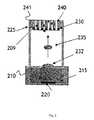
- FIG. 2is a schematic representation of a discharge apparatus for discharging organic compounds according to another embodiment of the disclosure.
- apparatus 200is adapted for forming an organic film substantially free from solvent.
- Apparatus 200includes reservoir 210 for receiving organic solution 215 .
- organic solution 215contains organic material dissolved in a solvent.
- Thermal resistor 220is positioned proximal to reservoir 210 to heat organic solution 215 .
- Orifice 232separates reservoir 210 from discharge nozzle 225 .
- Discharge nozzle 225comprises micro-pores 240 separated by rigid sections 241 .
- nozzle heater 230By activating nozzle heater 230 , micro-pores 240 dislodge organic particles 209 , thereby forming a film on an immediately adjacent substrate (not shown.)
- nozzle heater 230can be activated in a pulse-like manner to provide heat to discharge nozzle cyclically.
- FIG. 3schematically illustrates a discharge nozzle according to one embodiment of the disclosure.
- discharge nozzle 300comprises heater 330 , porous medium 340 and integrated mask 345 .
- Heater 330is communicates pulse energy in the form of heat to organic material 309 causing dislodge thereof from porous medium 340 .
- Integrated mask 345effectively masks portions of the porous medium from transmitting organic ink material 309 . Consequently, a film forming on substrate 360 will define a negative image of the integrated mask.
- the particlescan be discharged from the porous medium by receiving thermal energy from a proximal resistive heater, or a thermal radiation heater, or by electrostatic force pull out of the micro-porous, or by mechanical vibration.
- FIGS. 4A and 4Bshow an image printed according to one embodiment of the disclosure. Specifically, FIG. 4 shows the printing result using the exemplary apparatus shown in FIG. 3 .
- the ink materialis Alq3 and was pre-coated on the backside of an anodized porous alumina disc.
- FIG. 4Ashows the LED organic printed pattern under halogen illumination.
- FIG. 4Bshows the photoluminescence image under UV illumination.
- FIG. 5is a photoluminescence image of a pattern printed by molecular jet printer system according to another embodiment of the disclosure.
- FIG. 5was obtained by using the discharge nozzle shown in FIG. 3 .
- the ink materialwas Alq3.
- the ink materialwas drop cast on the backside of anodized porous alumina disc.
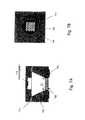
- FIGS. 6A and 6Bshow the surface and the cross section, respectively, of a porous medium.
- the porous mediumcan be used according to the principles disclosed herein with a discharge nozzle or as a part of a nozzle having an integrated mask (see FIG. 3 .)
- FIG. 6Ashows the surface of the porous medium.
- FIG. 6Bshows a cross-section of the porous medium.
- FIG. 6Ashows a scale of 1 ⁇ m and FIG. 6B has a scale of 2 ⁇ m.
- FIGS. 7A and 7Billustrate a molecular jet printing apparatus according to an embodiment of the disclosure in cross-sectional and top views, respectively.
- printing apparatus 700includes micro-heater 710 which can be used as a liquid delivery system.
- Wafer bonding layer 715connects the liquid delivery system to nozzle section 720 .
- Porous openings 730are positioned at a discharge end of nozzle 720 and micro-heaters 740 are positioned adjacent to porous openings 730 to providing energy required to eject organic material or ink from nozzle 720 .
- FIG. 7Bshows a top view of the nozzle shown in FIG. 7A including porous openings 730 and heaters 740 .
Landscapes
- Chemical & Material Sciences (AREA)
- Engineering & Computer Science (AREA)
- General Chemical & Material Sciences (AREA)
- Chemical Kinetics & Catalysis (AREA)
- Materials Engineering (AREA)
- Mechanical Engineering (AREA)
- Metallurgy (AREA)
- Organic Chemistry (AREA)
- Manufacturing & Machinery (AREA)
- Electroluminescent Light Sources (AREA)
- Physical Vapour Deposition (AREA)
Abstract
Description
This instant application is a continuation of both U.S. Non-Provisional application Ser. No. 11/282,472 filed Nov. 21, 2005; U.S. Non-Provisional application Ser. No. 13/050,907 filed Mar. 17, 2011; U.S. Non-Provisional application Ser. No. 13/088,323 and claims the filing-date priority to U.S. Provisional Application No. 60/629,312, filed Nov. 19, 2004.
The disclosure relates to a method and apparatus for depositing an organic film on a substrate. Manufacturing light emitting diode (LED) cell requires depositing of two thin organic films on a substrate and coupling each of the thin films to an electrode. Conventionally, the deposition step is carried out by evaporating the desired organic film on the substrate. The film thickness is a prime consideration. The layer thickness is about 100 nm and each layer is optimally deposited to an accuracy of about .+−0.10 nm. As a result, conventional apparatus form multiple layers on a substrate with each layer having a thickness of about 10 nm. A combination of these layers will form the overall film. Because the organic constituents of the LED are often suspended in a solvent, removing the solvent prior to depositing each layer is crucial. A small amount of solvent in one layer of deposited organic thin film can cause contamination and destruction of the adjacent layers. Conventional techniques have failed to address this deficiency.
Another consideration in depositing organic thin films of an LED device is placing the films precisely at the desired location. Conventional technologies use shadow masking to form LED films of desired configuration. The shadow masking techniques require placing a well-defined mask over a region of the substrate followed by depositing the film over the entire substrate. Once deposition is complete, the shadow mask is removed to expose the protected portions of the substrate. Since every deposition step starts by forming a shadow mask and ends with removing and discarding the mask, a drawback of shadow masking technique is inefficiency.
In one embodiment the disclosure relates to an apparatus for depositing an organic material on a substrate, the apparatus comprising: a source heater for heating organic particles to form suspended organic particles; a transport stream for delivering the suspended organic particles to a discharge nozzle, the discharge nozzle having a plurality of micro-pores, the micro-pores providing a conduit for passage of the suspended organic particles; and a nozzle heater for pulsatingly heating the nozzle to discharge the suspended organic particles from the discharge nozzle.
According to another embodiment, the disclosure relates to a method for depositing a layer of substantially solvent-free organic material on a substrate, comprising heating the organic material to form a plurality of suspended organic particles; delivering the suspended organic particles to a discharge nozzle, the discharge nozzle having a plurality of micro-pores for receiving the suspended organic particles; and energizing the discharge nozzle to pulsatingly eject the suspended organic particles from the discharge nozzle. Organic particle may include an organic molecule or a molecular aggregate.
According to another embodiment, the disclosure relates to a method for depositing a layer of organic material on a substrate. The organic material may be suspended in solvent to provide crystal growth or to convert an amorphous organic structure into a crystalline structure. The method can include heating the organic material to form a plurality of suspended organic particles; delivering the suspended organic particles to a discharge nozzle, the discharge nozzle having a plurality of micro-pores for receiving the suspended organic particles; and energizing the discharge nozzle to pulsatingly eject the suspended organic particles from the discharge nozzle. Organic particle may include an organic molecule or a molecular aggregate.
According to still another embodiment, the disclosure relates to an apparatus for depositing an organic compound on a substrate comprising a chamber having a reservoir for receiving the organic compound, the chamber having an inlet and an outlet for receiving a transport gas; a discharge nozzle having a plurality of micro-porous conduits for receiving the organic compound delivered by the transport gas; and an energy source coupled to the discharge nozzle to provide pulsating energy adapted to discharge at least a portion of the organic compound from one of the micro-porous conduits to a substrate.
In yet another embodiment, an apparatus for depositing an organic compound comprises a chamber having a reservoir for housing the organic material dissolved in a solvent, the reservoir separated from the chamber through an orifice; a discharge nozzle defined by a plurality of micro-porous conduits for receiving the organic compound communicated from the reservoir; and an energy source coupled to the discharge nozzle providing pulsating energy for discharging at least a portion of the organic compound from one of the micro-porous conduits to a substrate; and a delivery path connecting the chamber and the nozzle. The organic compound may be substantially free of solvent. Alternatively, the organic compound may include in solvent. In a solvent-based system, the solvent discharge from the nozzle provides the added benefit of cooling the nozzle upon discharge.
In still another embodiment, a micro-porous nozzle for depositing an organic composition on a substrate includes a thermal source communicating energy to organic material interposed between the heater and a porous medium, the porous medium having an integrated mask formed thereon to define a deposition pattern.
In one embodiment, the disclosure relates to a method and apparatus for depositing a pure organic thin film, or a mixed organic film, or an organic thin film mixed with inorganic particles, or inorganic thin film on a substrate. Such films can be used, among others, in the design and construction of organic LED.
In the exemplary embodiment ofFIG. 1 , the discharge section includesdischarge nozzle 125 andnozzle heater 130. Among others, the discharge nozzle can be formed from anodized porous aluminum oxide or porous silicon membranes or other solid membranes. Such material are capable of blocking organic material from escaping through the porous medium when the organic material is delivered onto the porous medium's surface.Discharge nozzle 125 includesrigid portions 141 separated by micro-pores140.Micro-pores 140 block organic material from escaping through the medium until the medium is appropriately activated. Depending on the desired application, micro-pores140 can provide conduits (or passages) in the order of micro- or nano-pores. In one embodiment, the pore size is in the range of about 5 nm-100 microns. In another embodiment pores are about 100 nm to about 10 microns.Nozzle heater 130 is positioned proximal to thedischarge nozzle 125. When activated,nozzle heater 130 provides a pulse of energy, for example as heat, to dischargenozzle 125. The activation energy of the pulse dislodgesorganic material 109 contained withinmicro-pores 140.
In a method according to one embodiment of the disclosure,reservoir 107 is commissioned with organic material suitable for LED deposition. The organic material may be in liquid or solid form.Source heater 110 provides heat adequate to evaporate the organic material and form suspendedparticles 109. By engaging acarrier gas inlet 115, suspendedparticles 109 are transported throughthermal shields 160 towarddischarge nozzle 125. The carrier gas is directed togas outlet 120 throughdelivery path 135.Particles 109 reaching discharge nozzle are lodged inmicro-pores 130. Activatingnozzle heater 130 to provide energy to dischargenozzle 125 can cause ejection oforganic particles 109 from the discharge nozzle.Nozzle heater 130 can provide energy in cyclical pulses. The intensity and the duration of each pulse can be defined by a controller (not shown.) The activating energy can be thermal energy. A substrate can be positioned immediately adjacent to dischargenozzle 125 to receive the ejected organic particles. Applicants have discovered that the exemplary embodiment shown inFIG. 1 can form a think organic film on a substrate with great accuracy. The embodiment ofFIG. 1 is also advantageous in that it can substantially reduce substrate heating, minimizes local clogging and provide the most efficient use of organic material.
Because of the size oforifice 232, surface tension of organic solution prevents discharge oforganic solution 215 from the reservoir until appropriately activated. Oncethermal resistor 220 is activated, energy in the form of heat causes evaporation ofdroplet 235 within a chamber of apparatus200. Solvents have a lower vapor pressure and evaporate rapidly. Once evaporates, organic compound withindroplet 235 is transported to dischargenozzle 225.Discharge nozzle 225 receives theorganic material 209 withinmicro-pores 240. The solvent can be recycled back toorganic solution 215 or can be removed from the chamber (not shown). By activatingnozzle heater 230, micro-pores240 dislodgeorganic particles 209, thereby forming a film on an immediately adjacent substrate (not shown.) In one embodiment,nozzle heater 230 can be activated in a pulse-like manner to provide heat to discharge nozzle cyclically.
Thus, in one embodiment, the particles can be discharged from the porous medium by receiving thermal energy from a proximal resistive heater, or a thermal radiation heater, or by electrostatic force pull out of the micro-porous, or by mechanical vibration.
While the principles of the disclosure have been illustrated in relation to the exemplary embodiments shown herein, the principles of the disclosure are not limited thereto and include any modification, variation or permutation thereof.
Claims (13)
1. A method for depositing a layer of substantially solvent-free organic material on a substrate, comprising:
heating the organic material to form a plurality of suspended organic particles;
delivering the suspended organic particles to a discharge nozzle, the discharge nozzle having a plurality of micro-pores for receiving the suspended organic particles;
processing the suspended organic particles through the plurality of micro-pores to substantially block a portion of the suspended organic particles; and
energizing the discharge nozzle to pulsatingly eject the suspended organic particles from the plurality of micro-pores onto the substrate.
2. The method of claim further comprising positioning the discharge nozzle proximal to the substrate.
3. The method ofclaim 1 , wherein the step of energizing the discharge nozzle further comprises heating the discharge nozzle.
4. The method ofclaim 1 , wherein the step of delivering the suspended organic particles further comprises transporting the suspended organic particles with a carrier gas.
5. The method ofclaim 4 , wherein the carrier gas is inert.
6. The method ofclaim 1 , wherein the step of energizing the discharge nozzle further comprises mechanically vibrating the discharge nozzle.
7. The method ofclaim 1 , wherein processing the suspended organic material further comprises processing the suspended organic material through micro-pores having a porous medium to separate a quantity of organic particles from a quantity of solvent.
8. The method ofclaim 1 , wherein processing the suspended organic material further comprises separating an organic material from a solvent.
9. The method ofclaim 1 , further comprising deflecting thermal radiation from the discharge nozzle.
10. A method for depositing substantially solvent-free organic film on a substrate, the method comprising:
transporting an OLED solution from a reservoir to a discharge nozzle, the OLED solution having OLED particles in a solvent;
receiving the OLED solution at a plurality of micro-pores of the discharge nozzle, each micro-pore containing a porous medium;
separating a quantity of OLED particles from the solvent at the porous medium of the micro-pores;
removing the solvent from the discharge nozzle; and
dislodging the quantity of organic particles from the discharge nozzle onto a substrate.
11. The method ofclaim 10 , wherein transporting an OLED solution from a reservoir to a discharge nozzle further comprises heating the OLED solution.
12. The method ofclaim 10 , wherein the OLED solution comprises a quantity of OLED particles dissolved in solvent.
13. The method ofclaim 10 , further comprising heating the discharge nozzle to dislodge the quantity of organic particles.
Priority Applications (6)
| Application Number | Priority Date | Filing Date | Title |
|---|---|---|---|
| US13/095,619US9385322B2 (en) | 2005-11-21 | 2011-04-27 | Method and apparatus for depositing LED organic film |
| US13/707,562US20130209668A1 (en) | 2004-11-19 | 2012-12-06 | Method and apparatus for depositing films |
| US13/738,710US20130208041A1 (en) | 2004-11-19 | 2013-01-10 | Method and apparatus for controlling film deposition |
| US13/738,707US20130208040A1 (en) | 2004-11-19 | 2013-01-10 | Method and apparatus for thermal jet printing |
| US13/778,072US8962073B2 (en) | 2004-11-19 | 2013-02-26 | Method and apparatus for controlling film deposition |
| US13/935,830US20140160192A1 (en) | 2005-11-21 | 2013-07-05 | Method and apparatus for depositing films |
Applications Claiming Priority (4)
| Application Number | Priority Date | Filing Date | Title |
|---|---|---|---|
| US11/282,472US8128753B2 (en) | 2004-11-19 | 2005-11-21 | Method and apparatus for depositing LED organic film |
| US201113050907A | 2011-03-17 | 2011-03-17 | |
| US13/088,323US8986780B2 (en) | 2004-11-19 | 2011-04-15 | Method and apparatus for depositing LED organic film |
| US13/095,619US9385322B2 (en) | 2005-11-21 | 2011-04-27 | Method and apparatus for depositing LED organic film |
Related Parent Applications (2)
| Application Number | Title | Priority Date | Filing Date |
|---|---|---|---|
| US11/282,472DivisionUS8128753B2 (en) | 2004-11-19 | 2005-11-21 | Method and apparatus for depositing LED organic film |
| US11/282,472ContinuationUS8128753B2 (en) | 2004-11-19 | 2005-11-21 | Method and apparatus for depositing LED organic film |
Related Child Applications (4)
| Application Number | Title | Priority Date | Filing Date |
|---|---|---|---|
| US12/139,404Continuation-In-PartUS20080311289A1 (en) | 2004-11-19 | 2008-06-13 | Method and apparatus for controlling film deposition |
| US12/139,409Continuation-In-PartUS20080308037A1 (en) | 2004-11-19 | 2008-06-13 | Method and apparatus for thermal jet printing |
| US12/139,391Continuation-In-PartUS20080311307A1 (en) | 2004-11-19 | 2008-06-13 | Method and apparatus for depositing films |
| US13/778,072Continuation-In-PartUS8962073B2 (en) | 2004-11-19 | 2013-02-26 | Method and apparatus for controlling film deposition |
Publications (2)
| Publication Number | Publication Date |
|---|---|
| US20110262624A1 US20110262624A1 (en) | 2011-10-27 |
| US9385322B2true US9385322B2 (en) | 2016-07-05 |
Family
ID=44816012
Family Applications (3)
| Application Number | Title | Priority Date | Filing Date |
|---|---|---|---|
| US11/282,472Expired - Fee RelatedUS8128753B2 (en) | 2004-11-19 | 2005-11-21 | Method and apparatus for depositing LED organic film |
| US13/095,619Active2027-07-23US9385322B2 (en) | 2004-11-19 | 2011-04-27 | Method and apparatus for depositing LED organic film |
| US13/359,434ActiveUS9005365B2 (en) | 2004-11-19 | 2012-01-26 | Method and apparatus for depositing LED organic film |
Family Applications Before (1)
| Application Number | Title | Priority Date | Filing Date |
|---|---|---|---|
| US11/282,472Expired - Fee RelatedUS8128753B2 (en) | 2004-11-19 | 2005-11-21 | Method and apparatus for depositing LED organic film |
Family Applications After (1)
| Application Number | Title | Priority Date | Filing Date |
|---|---|---|---|
| US13/359,434ActiveUS9005365B2 (en) | 2004-11-19 | 2012-01-26 | Method and apparatus for depositing LED organic film |
Country Status (1)
| Country | Link |
|---|---|
| US (3) | US8128753B2 (en) |
Families Citing this family (61)
| Publication number | Priority date | Publication date | Assignee | Title |
|---|---|---|---|---|
| WO2005101530A1 (en) | 2004-04-19 | 2005-10-27 | Edward Sargent | Optically-regulated optical emission using colloidal quantum dot nanocrystals |
| US7742322B2 (en) | 2005-01-07 | 2010-06-22 | Invisage Technologies, Inc. | Electronic and optoelectronic devices with quantum dot films |
| US7746681B2 (en) | 2005-01-07 | 2010-06-29 | Invisage Technologies, Inc. | Methods of making quantum dot films |
| US7773404B2 (en) | 2005-01-07 | 2010-08-10 | Invisage Technologies, Inc. | Quantum dot optical devices with enhanced gain and sensitivity and methods of making same |
| US8986780B2 (en) | 2004-11-19 | 2015-03-24 | Massachusetts Institute Of Technology | Method and apparatus for depositing LED organic film |
| US8128753B2 (en) | 2004-11-19 | 2012-03-06 | Massachusetts Institute Of Technology | Method and apparatus for depositing LED organic film |
| CA2519608A1 (en) | 2005-01-07 | 2006-07-07 | Edward Sargent | Quantum dot-polymer nanocomposite photodetectors and photovoltaics |
| US8556389B2 (en) | 2011-02-04 | 2013-10-15 | Kateeva, Inc. | Low-profile MEMS thermal printhead die having backside electrical connections |
| EP2155494A4 (en)* | 2007-06-14 | 2010-08-11 | Massachusetts Inst Technology | METHOD AND APPARATUS FOR REGULATING A FILM DEPOSITION |
| US20120038705A1 (en)* | 2007-06-14 | 2012-02-16 | Kateeva, Inc. | Method and Apparatus for Delivering Ink Material from a Discharge Nozzle |
| US11975546B2 (en) | 2008-06-13 | 2024-05-07 | Kateeva, Inc. | Gas enclosure assembly and system |
| US12064979B2 (en) | 2008-06-13 | 2024-08-20 | Kateeva, Inc. | Low-particle gas enclosure systems and methods |
| US8899171B2 (en) | 2008-06-13 | 2014-12-02 | Kateeva, Inc. | Gas enclosure assembly and system |
| US9048344B2 (en) | 2008-06-13 | 2015-06-02 | Kateeva, Inc. | Gas enclosure assembly and system |
| US10434804B2 (en) | 2008-06-13 | 2019-10-08 | Kateeva, Inc. | Low particle gas enclosure systems and methods |
| US12018857B2 (en) | 2008-06-13 | 2024-06-25 | Kateeva, Inc. | Gas enclosure assembly and system |
| US8632145B2 (en) | 2008-06-13 | 2014-01-21 | Kateeva, Inc. | Method and apparatus for printing using a facetted drum |
| US9604245B2 (en) | 2008-06-13 | 2017-03-28 | Kateeva, Inc. | Gas enclosure systems and methods utilizing an auxiliary enclosure |
| US8383202B2 (en) | 2008-06-13 | 2013-02-26 | Kateeva, Inc. | Method and apparatus for load-locked printing |
| US20120056923A1 (en)* | 2009-01-05 | 2012-03-08 | Kateeva, Inc. | Control systems and methods for thermal-jet printing |
| US20100188457A1 (en)* | 2009-01-05 | 2010-07-29 | Madigan Connor F | Method and apparatus for controlling the temperature of an electrically-heated discharge nozzle |
| EP2425470A2 (en)* | 2009-05-01 | 2012-03-07 | Kateeva, Inc. | Method and apparatus for organic vapor printing |
| US8486737B2 (en)* | 2009-08-25 | 2013-07-16 | Samsung Display Co., Ltd. | Thin film deposition apparatus and method of manufacturing organic light-emitting display device by using the same |
| JP5328726B2 (en) | 2009-08-25 | 2013-10-30 | 三星ディスプレイ株式會社 | Thin film deposition apparatus and organic light emitting display device manufacturing method using the same |
| JP5677785B2 (en) | 2009-08-27 | 2015-02-25 | 三星ディスプレイ株式會社Samsung Display Co.,Ltd. | Thin film deposition apparatus and organic light emitting display device manufacturing method using the same |
| US8801856B2 (en)* | 2009-09-08 | 2014-08-12 | Universal Display Corporation | Method and system for high-throughput deposition of patterned organic thin films |
| US8876975B2 (en) | 2009-10-19 | 2014-11-04 | Samsung Display Co., Ltd. | Thin film deposition apparatus |
| KR101084184B1 (en) | 2010-01-11 | 2011-11-17 | 삼성모바일디스플레이주식회사 | Thin film deposition apparatus |
| KR101174875B1 (en) | 2010-01-14 | 2012-08-17 | 삼성디스플레이 주식회사 | Apparatus for thin layer deposition, method for manufacturing of organic light emitting display apparatus using the same, and organic light emitting display apparatus manufactured by the method |
| KR101193186B1 (en) | 2010-02-01 | 2012-10-19 | 삼성디스플레이 주식회사 | Apparatus for thin layer deposition, method for manufacturing of organic light emitting display apparatus using the same, and organic light emitting display apparatus manufactured by the method |
| KR101156441B1 (en) | 2010-03-11 | 2012-06-18 | 삼성모바일디스플레이주식회사 | Apparatus for thin layer deposition |
| KR101202348B1 (en) | 2010-04-06 | 2012-11-16 | 삼성디스플레이 주식회사 | Apparatus for thin layer deposition and method for manufacturing of organic light emitting display apparatus using the same |
| US8894458B2 (en) | 2010-04-28 | 2014-11-25 | Samsung Display Co., Ltd. | Thin film deposition apparatus, method of manufacturing organic light-emitting display device by using the apparatus, and organic light-emitting display device manufactured by using the method |
| KR101223723B1 (en) | 2010-07-07 | 2013-01-18 | 삼성디스플레이 주식회사 | Apparatus for thin layer deposition, method for manufacturing of organic light emitting display apparatus using the same, and organic light emitting display apparatus manufactured by the method |
| KR101723506B1 (en) | 2010-10-22 | 2017-04-19 | 삼성디스플레이 주식회사 | Apparatus for organic layer deposition and method for manufacturing of organic light emitting display apparatus using the same |
| KR101738531B1 (en) | 2010-10-22 | 2017-05-23 | 삼성디스플레이 주식회사 | Method for manufacturing of organic light emitting display apparatus, and organic light emitting display apparatus manufactured by the method |
| KR20120045865A (en) | 2010-11-01 | 2012-05-09 | 삼성모바일디스플레이주식회사 | Apparatus for organic layer deposition |
| KR20120065789A (en) | 2010-12-13 | 2012-06-21 | 삼성모바일디스플레이주식회사 | Apparatus for organic layer deposition |
| KR101760897B1 (en) | 2011-01-12 | 2017-07-25 | 삼성디스플레이 주식회사 | Deposition source and apparatus for organic layer deposition having the same |
| KR101852517B1 (en) | 2011-05-25 | 2018-04-27 | 삼성디스플레이 주식회사 | Apparatus for organic layer deposition and method for manufacturing of organic light emitting display apparatus using the same |
| KR101840654B1 (en) | 2011-05-25 | 2018-03-22 | 삼성디스플레이 주식회사 | Apparatus for organic layer deposition and method for manufacturing of organic light emitting display apparatus using the same |
| KR101857249B1 (en) | 2011-05-27 | 2018-05-14 | 삼성디스플레이 주식회사 | Patterning slit sheet assembly, apparatus for organic layer deposition, method for manufacturing organic light emitting display apparatus and organic light emitting display apparatus |
| EP2723914B1 (en) | 2011-06-22 | 2018-09-26 | Aixtron SE | Method and apparatus for vapor deposition |
| DE102011051260A1 (en) | 2011-06-22 | 2012-12-27 | Aixtron Se | Method and device for depositing OLEDs |
| JP5848822B2 (en) | 2011-06-22 | 2016-01-27 | アイクストロン、エスイー | Vapor deposition system and supply head |
| JP5877244B2 (en) | 2011-06-22 | 2016-03-02 | アイクストロン、エスイー | Vapor deposition material source and method for producing the same |
| KR101826068B1 (en) | 2011-07-04 | 2018-02-07 | 삼성디스플레이 주식회사 | Apparatus for thin layer deposition |
| US20140178604A1 (en)* | 2012-12-21 | 2014-06-26 | Gary S. Selwyn | Dual-Zone, Atmospheric-Pressure Plasma Reactor for Materials Processing |
| WO2014171535A1 (en)* | 2013-04-20 | 2014-10-23 | エムテックスマート株式会社 | Particulate coating or distribution method |
| US10468279B2 (en) | 2013-12-26 | 2019-11-05 | Kateeva, Inc. | Apparatus and techniques for thermal treatment of electronic devices |
| KR102307190B1 (en) | 2014-01-21 | 2021-09-30 | 카티바, 인크. | Apparatus and techniques for electronic device encapsulation |
| EP3882961B1 (en) | 2014-04-30 | 2023-07-26 | Kateeva, Inc. | Gas cushion apparatus and techniques for substrate coating |
| TWI546464B (en)* | 2014-05-27 | 2016-08-21 | 財團法人金屬工業研究發展中心 | Manufacture of porous aerostatic bearing |
| US11220737B2 (en)* | 2014-06-25 | 2022-01-11 | Universal Display Corporation | Systems and methods of modulating flow during vapor jet deposition of organic materials |
| EP2960059B1 (en) | 2014-06-25 | 2018-10-24 | Universal Display Corporation | Systems and methods of modulating flow during vapor jet deposition of organic materials |
| US11267012B2 (en)* | 2014-06-25 | 2022-03-08 | Universal Display Corporation | Spatial control of vapor condensation using convection |
| DE102014109194A1 (en) | 2014-07-01 | 2016-01-07 | Aixtron Se | Apparatus and method for generating a vapor for a CVD or PVD device |
| US10566534B2 (en) | 2015-10-12 | 2020-02-18 | Universal Display Corporation | Apparatus and method to deliver organic material via organic vapor-jet printing (OVJP) |
| US12152807B2 (en)* | 2018-02-12 | 2024-11-26 | Noritake Co., Limited | Liquid atomizing apparatus |
| WO2020021796A1 (en)* | 2018-07-24 | 2020-01-30 | 株式会社リンテック | Vaporizer |
| GB2577522B (en)* | 2018-09-27 | 2022-12-28 | 2D Heat Ltd | A heating device, and applications therefore |
Citations (124)
| Publication number | Priority date | Publication date | Assignee | Title |
|---|---|---|---|---|
| US4238807A (en) | 1977-12-28 | 1980-12-09 | Ing. C. Olivetti & C., S.P.A. | Non-impact printing device |
| US4751531A (en) | 1986-03-27 | 1988-06-14 | Fuji Xerox Co., Ltd. | Thermal-electrostatic ink jet recording apparatus |
| US5041161A (en) | 1988-02-24 | 1991-08-20 | Dataproducts Corporation | Semi-solid ink jet and method of using same |
| US5116148A (en) | 1986-08-27 | 1992-05-26 | Hitachi, Ltd. | Heat transfer ink sheet having a precoating layer which is thermally transferred prior to sublimation of an ink dye |
| US5155502A (en) | 1989-01-13 | 1992-10-13 | Canon Kabushiki Kaisha | Ink-jet cartridge |
| US5172139A (en) | 1989-05-09 | 1992-12-15 | Ricoh Company, Ltd. | Liquid jet head for gradation recording |
| US5202659A (en) | 1984-04-16 | 1993-04-13 | Dataproducts, Corporation | Method and apparatus for selective multi-resonant operation of an ink jet controlling dot size |
| US5247190A (en) | 1989-04-20 | 1993-09-21 | Cambridge Research And Innovation Limited | Electroluminescent devices |
| JPH05255630A (en) | 1992-03-16 | 1993-10-05 | Ricoh Co Ltd | Hot melt ink composition and recording method using the same |
| JPH06122201A (en) | 1992-08-24 | 1994-05-06 | Sony Corp | Ink jet print head and ink jet printer |
| US5405710A (en) | 1993-11-22 | 1995-04-11 | At&T Corp. | Article comprising microcavity light sources |
| JPH08216401A (en) | 1995-02-17 | 1996-08-27 | Sony Corp | Recording method and recording liquid |
| US5574485A (en) | 1994-10-13 | 1996-11-12 | Xerox Corporation | Ultrasonic liquid wiper for ink jet printhead maintenance |
| US5623292A (en) | 1993-12-17 | 1997-04-22 | Videojet Systems International, Inc. | Temperature controller for ink jet printing |
| JPH09248918A (en) | 1996-03-15 | 1997-09-22 | Sharp Corp | Image recording device |
| US5703436A (en) | 1994-12-13 | 1997-12-30 | The Trustees Of Princeton University | Transparent contacts for organic devices |
| US5707745A (en) | 1994-12-13 | 1998-01-13 | The Trustees Of Princeton University | Multicolor organic light emitting devices |
| US5731828A (en) | 1994-10-20 | 1998-03-24 | Canon Kabushiki Kaisha | Ink jet head, ink jet head cartridge and ink jet apparatus |
| US5801721A (en) | 1994-09-09 | 1998-09-01 | Signtech U.S.A. Ltd. | Apparatus for producing an image on a first side of a substrate and a mirror image on a second side of the substrate |
| US5834893A (en) | 1996-12-23 | 1998-11-10 | The Trustees Of Princeton University | High efficiency organic light emitting devices with light directing structures |
| US5844363A (en) | 1997-01-23 | 1998-12-01 | The Trustees Of Princeton Univ. | Vacuum deposited, non-polymeric flexible organic light emitting devices |
| US5865860A (en) | 1997-06-20 | 1999-02-02 | Imra America, Inc. | Process for filling electrochemical cells with electrolyte |
| US5947022A (en) | 1997-11-07 | 1999-09-07 | Speedline Technologies, Inc. | Apparatus for dispensing material in a printer |
| US5956051A (en) | 1997-05-29 | 1999-09-21 | Pitney Bowes Inc. | Disabling a mailing machine when a print head is not installed |
| KR100232852B1 (en) | 1997-10-15 | 1999-12-01 | 윤종용 | Inkjet Printer Head and Manufacturing Method Thereof |
| US6013982A (en) | 1996-12-23 | 2000-01-11 | The Trustees Of Princeton University | Multicolor display devices |
| US6065825A (en) | 1997-11-13 | 2000-05-23 | Eastman Kodak Company | Printer having mechanically-assisted ink droplet separation and method of using same |
| US6086195A (en) | 1998-09-24 | 2000-07-11 | Hewlett-Packard Company | Filter for an inkjet printhead |
| US6086679A (en) | 1997-10-24 | 2000-07-11 | Quester Technology, Inc. | Deposition systems and processes for transport polymerization and chemical vapor deposition |
| US6087196A (en) | 1998-01-30 | 2000-07-11 | The Trustees Of Princeton University | Fabrication of organic semiconductor devices using ink jet printing |
| US6086196A (en) | 1995-04-14 | 2000-07-11 | Sony Corporation | Printing device |
| US6091195A (en) | 1997-02-03 | 2000-07-18 | The Trustees Of Princeton University | Displays having mesa pixel configuration |
| US6095630A (en) | 1997-07-02 | 2000-08-01 | Sony Corporation | Ink-jet printer and drive method of recording head for ink-jet printer |
| US6097147A (en) | 1998-09-14 | 2000-08-01 | The Trustees Of Princeton University | Structure for high efficiency electroluminescent device |
| US6189989B1 (en) | 1993-04-12 | 2001-02-20 | Canon Kabushiki Kaisha | Embroidering using ink jet printing apparatus |
| US6250747B1 (en) | 1999-01-28 | 2001-06-26 | Hewlett-Packard Company | Print cartridge with improved back-pressure regulation |
| US6294398B1 (en) | 1999-11-23 | 2001-09-25 | The Trustees Of Princeton University | Method for patterning devices |
| US6303238B1 (en) | 1997-12-01 | 2001-10-16 | The Trustees Of Princeton University | OLEDs doped with phosphorescent compounds |
| US6312083B1 (en) | 1999-12-20 | 2001-11-06 | Xerox Corporation | Printhead assembly with ink monitoring system |
| US20010045973A1 (en) | 2000-01-11 | 2001-11-29 | Eastman Kodak Company | Assisted drop-on-demand inkjet printer |
| US6326224B1 (en) | 1998-04-27 | 2001-12-04 | Motorola, Inc. | Method of purifying a primary color generated by an OED |
| US6337102B1 (en) | 1997-11-17 | 2002-01-08 | The Trustees Of Princeton University | Low pressure vapor phase deposition of organic thin films |
| US20020008732A1 (en) | 2000-07-20 | 2002-01-24 | Moon Jae-Ho | Ink-jet printhead |
| JP2002069650A (en) | 2000-08-31 | 2002-03-08 | Applied Materials Inc | Vapor phase deposition method and apparatus, and semiconductor device manufacturing method and apparatus |
| US6431702B2 (en) | 1999-06-08 | 2002-08-13 | Hewlett-Packard Company | Apparatus and method using ultrasonic energy to fix ink to print media |
| US6444400B1 (en) | 1999-08-23 | 2002-09-03 | Agfa-Gevaert | Method of making an electroconductive pattern on a support |
| US6453810B1 (en) | 1997-11-07 | 2002-09-24 | Speedline Technologies, Inc. | Method and apparatus for dispensing material in a printer |
| US6460972B1 (en) | 2001-11-06 | 2002-10-08 | Eastman Kodak Company | Thermal actuator drop-on-demand apparatus and method for high frequency |
| US6472962B1 (en) | 2001-05-17 | 2002-10-29 | Institute Of Microelectronics | Inductor-capacitor resonant RF switch |
| US20020191063A1 (en) | 2000-08-30 | 2002-12-19 | Daniel Gelbart | Method for imaging with UV curable inks |
| US6498802B1 (en) | 1999-12-02 | 2002-12-24 | Electronics And Telecommunications Research Institute | Organic micro-cavity laser |
| US20030000476A1 (en) | 2001-06-28 | 2003-01-02 | Hitachi Kokusai Electric Inc. | Substrate processing apparatus, conveying unit thereof, and semiconductor device fabricating Method |
| US6513903B2 (en) | 2000-12-29 | 2003-02-04 | Eastman Kodak Company | Ink jet print head with capillary flow cleaning |
| US6548956B2 (en) | 1994-12-13 | 2003-04-15 | The Trustees Of Princeton University | Transparent contacts for organic devices |
| US6562405B2 (en) | 2001-09-14 | 2003-05-13 | University Of Delaware | Multiple-nozzle thermal evaporation source |
| US6576134B1 (en) | 1998-10-20 | 2003-06-10 | Erik Agner | Method for displacement chromatography |
| US6586763B2 (en) | 1996-06-25 | 2003-07-01 | Northwestern University | Organic light-emitting diodes and methods for assembly and emission control |
| US6601936B2 (en) | 2000-11-14 | 2003-08-05 | Cypress Semiconductor Corp. | Real time adaptive inkjet temperature regulation controller |
| US20030175414A1 (en) | 2002-01-23 | 2003-09-18 | Seiko Epson Corporation | Method of, and apparatus for, manufacturing organic EL device; organic EL device; electronic device; and liquid droplet ejection apparatus |
| US20030230980A1 (en) | 2002-06-18 | 2003-12-18 | Forrest Stephen R | Very low voltage, high efficiency phosphorescent oled in a p-i-n structure |
| US6666548B1 (en) | 2002-11-04 | 2003-12-23 | Eastman Kodak Company | Method and apparatus for continuous marking |
| US20040009304A1 (en) | 2002-07-09 | 2004-01-15 | Osram Opto Semiconductors Gmbh & Co. Ogh | Process and tool with energy source for fabrication of organic electronic devices |
| US20040048000A1 (en) | 2001-09-04 | 2004-03-11 | Max Shtein | Device and method for organic vapor jet deposition |
| US20040048183A1 (en) | 2002-06-10 | 2004-03-11 | Seiko Epson Corporation | Production method of toner, toner, and toner producing apparatus |
| US20040056244A1 (en) | 2002-09-23 | 2004-03-25 | Eastman Kodak Company | Device for depositing patterned layers in OLED displays |
| US20040086631A1 (en) | 2002-10-25 | 2004-05-06 | Yu-Kai Han | Ink jet printing device and method |
| US20040174116A1 (en) | 2001-08-20 | 2004-09-09 | Lu Min-Hao Michael | Transparent electrodes |
| US20040202794A1 (en) | 2003-04-11 | 2004-10-14 | Dainippon Screen Mfg. Co., Ltd. | Coating material applying method and coating material applying apparatus for applying a coating material to surfaces of prints, and a printing machine having the coating material applying apparatus |
| US6811896B2 (en) | 2002-07-29 | 2004-11-02 | Xerox Corporation | Organic light emitting device (OLED) with thick (100 to 250 nanometers) porphyrin buffer layer |
| US6824262B2 (en) | 2001-08-10 | 2004-11-30 | Seiko Epson Corporation | Ink set and ink jet recording method |
| US20050005850A1 (en) | 1999-07-23 | 2005-01-13 | Semiconductor Energy Laboratory Co., Ltd. | Method of fabricating an EL display device, and apparatus for forming a thin film |
| US6861800B2 (en) | 2003-02-18 | 2005-03-01 | Eastman Kodak Company | Tuned microcavity color OLED display |
| US20050087131A1 (en)* | 2003-10-23 | 2005-04-28 | Max Shtein | Method and apparatus for depositing material |
| US20050100690A1 (en)* | 2003-11-06 | 2005-05-12 | Optical Coating Laboratory Inc., A Jds Uniphase Company | Dyed polymer coating for display panel |
| US6896346B2 (en) | 2002-12-26 | 2005-05-24 | Eastman Kodak Company | Thermo-mechanical actuator drop-on-demand apparatus and method with multiple drop volumes |
| US6917159B2 (en) | 2003-08-14 | 2005-07-12 | Eastman Kodak Company | Microcavity OLED device |
| US20050190220A1 (en) | 2004-02-27 | 2005-09-01 | Lim Seong-Taek | Method of driving an ink-jet printhead |
| JP2005286069A (en) | 2004-03-29 | 2005-10-13 | Kyocera Corp | Gas nozzle, manufacturing method thereof, and thin film forming apparatus using the same |
| US20050223994A1 (en) | 2004-04-08 | 2005-10-13 | Blomiley Eric R | Substrate susceptors for receiving semiconductor substrates to be deposited upon and methods of depositing materials over semiconductor substrates |
| US20050255249A1 (en) | 2002-05-29 | 2005-11-17 | Dirk Schlatterbeck | Method for applying coatings to surfaces |
| US20060012290A1 (en) | 2004-07-15 | 2006-01-19 | Chang-Ho Kang | Mask frame assembly for depositing thin layer and organic light emitting display device manufactured using the mask frame assembly |
| US7023013B2 (en) | 2004-06-16 | 2006-04-04 | Eastman Kodak Company | Array of light-emitting OLED microcavity pixels |
| JP2006123551A (en) | 2004-10-29 | 2006-05-18 | Samsung Electronics Co Ltd | NOZZLE PLATE, INKJET PRINT HEAD HAVING THE SAME, AND METHOD FOR PRODUCING NOZZLE PLATE |
| US20060115585A1 (en) | 2004-11-19 | 2006-06-01 | Vladimir Bulovic | Method and apparatus for depositing LED organic film |
| JP2006150900A (en) | 2004-12-01 | 2006-06-15 | Canon Inc | Liquid discharge head and manufacturing method thereof |
| US7077513B2 (en) | 2001-02-09 | 2006-07-18 | Seiko Epson Corporation | Ink jet recording apparatus, control and ink replenishing method executed in the same, ink supply system incorporated in the same, and method of managing ink amount supplied by the system |
| US20070040877A1 (en) | 2005-08-16 | 2007-02-22 | Fuji Photo Film Co., Ltd. | Ink supply device, ink jet recording apparatus and ink cartridge |
| WO2005090085A3 (en) | 2004-03-19 | 2007-02-22 | Zipher Ltd | Liquid supply system |
| US20070058010A1 (en) | 2005-09-14 | 2007-03-15 | Fuji Photo Film Co., Ltd. | Liquid ejection head and image forming apparatus |
| JP2007095343A (en) | 2005-09-27 | 2007-04-12 | Toppan Printing Co Ltd | Method for producing printed matter and printed matter |
| US20070098891A1 (en) | 2005-10-31 | 2007-05-03 | Eastman Kodak Company | Vapor deposition apparatus and method |
| US20070134512A1 (en) | 2005-12-13 | 2007-06-14 | Eastman Kodak Company | Electroluminescent device containing an anthracene derivative |
| US7247394B2 (en) | 2004-05-04 | 2007-07-24 | Eastman Kodak Company | Tuned microcavity color OLED display |
| JP2007299616A (en) | 2006-04-28 | 2007-11-15 | Toppan Printing Co Ltd | Method for manufacturing organic EL element and organic EL element |
| US20070286944A1 (en) | 2006-06-13 | 2007-12-13 | Itc Inc., Ltd. | Fabrication of full-color oled panel using micro-cavity structure |
| US7374984B2 (en) | 2004-10-29 | 2008-05-20 | Randy Hoffman | Method of forming a thin film component |
| US7377616B2 (en) | 2004-09-09 | 2008-05-27 | Brother Kogyo Kabushiki Kaisha | Inkjet printer including discharger with cap |
| KR20080060111A (en) | 2006-12-26 | 2008-07-01 | 엘지디스플레이 주식회사 | Manufacturing method of organic light emitting device |
| US20080174235A1 (en) | 2006-10-13 | 2008-07-24 | Samsung Sdi Co., Ltd. | Mask used to fabricate organic light-emitting diode (oled) display device, method of fabricating oled display device using the mask, oled display device fabricated using the mask, and method of fabricating the mask |
| US7406761B2 (en) | 2005-03-21 | 2008-08-05 | Honeywell International Inc. | Method of manufacturing vibrating micromechanical structures |
| US7410240B2 (en) | 2004-03-04 | 2008-08-12 | Fujifilm Corporation | Inkjet recording head and inkjet recording apparatus |
| US20080238310A1 (en) | 2007-03-30 | 2008-10-02 | Forrest Stephen R | OLED with improved light outcoupling |
| US7431435B2 (en) | 2004-08-06 | 2008-10-07 | Matthew Grant Lopez | Systems and methods for varying dye concentrations |
| US7431968B1 (en) | 2001-09-04 | 2008-10-07 | The Trustees Of Princeton University | Process and apparatus for organic vapor jet deposition |
| US20080311289A1 (en) | 2007-06-14 | 2008-12-18 | Vladimir Bulovic | Method and apparatus for controlling film deposition |
| US20090031579A1 (en) | 2007-07-31 | 2009-02-05 | Piatt Michael J | Micro-structured drying for inkjet printers |
| US20090045739A1 (en) | 2007-08-16 | 2009-02-19 | Sam-Il Kho | Organic light emitting diode display device and method of fabricating the same |
| US20090115706A1 (en) | 2007-11-05 | 2009-05-07 | Samsung Electronics Co., Ltd. | Organic light emitting diode display and method for manufacturing the same |
| US7530778B2 (en) | 2001-12-27 | 2009-05-12 | Coreflow Ltd. | High-Performance non-contact support platforms |
| US20090167162A1 (en) | 2007-12-28 | 2009-07-02 | Universal Display Corporation | Dibenzothiophene-containing materials in phosphorescent light emitting diodes |
| US20090220680A1 (en) | 2008-02-29 | 2009-09-03 | Winters Dustin L | Oled device with short reduction |
| US7604439B2 (en) | 2004-04-14 | 2009-10-20 | Coreflow Scientific Solutions Ltd. | Non-contact support platforms for distance adjustment |
| US20100055810A1 (en) | 2008-09-01 | 2010-03-04 | Samsung Mobile Display Co.,Ltd. | Mask for thin film deposition and method of manufacturing oled using the same |
| US7677690B2 (en) | 2005-11-22 | 2010-03-16 | Fujifilm Corporation | Liquid ejection apparatus and liquid agitation method |
| US20100079513A1 (en) | 2008-09-26 | 2010-04-01 | Brother Kogyo Kabushiki Kaisha | Liquid-ejection apparatus |
| US20100171780A1 (en) | 2009-01-05 | 2010-07-08 | Kateeva, Inc. | Rapid Ink-Charging Of A Dry Ink Discharge Nozzle |
| US20100201749A1 (en) | 2008-06-13 | 2010-08-12 | Kateeva, Inc. | Method And Apparatus for Load-Locked Printing |
| US20100310424A1 (en) | 2003-12-05 | 2010-12-09 | Massachusetts Institute Of Technology | Organic materials able to detect analytes |
| US7857121B2 (en) | 2005-09-15 | 2010-12-28 | Coreflow Scientific Solutions Ltd. | System and method for enhancing conveying performance of conveyors |
| US20110008541A1 (en) | 2009-05-01 | 2011-01-13 | Kateeva, Inc. | Method and apparatus for organic vapor printing |
| US7883832B2 (en) | 2005-01-04 | 2011-02-08 | International Business Machines Corporation | Method and apparatus for direct referencing of top surface of workpiece during imprint lithography |
| US20110057171A1 (en) | 2006-12-28 | 2011-03-10 | Universal Display Corporation | Long lifetime Phosphorescent Organic Light Emitting Device (OLED) Structures |
| US7908885B2 (en) | 2004-11-08 | 2011-03-22 | New Way Machine Components, Inc. | Non-contact porous air bearing and glass flattening device |
| US20110293818A1 (en) | 2009-11-27 | 2011-12-01 | Kateeva Inc. | Method and Apparatus for Depositing A Film Using A Rotating Source |
Family Cites Families (18)
| Publication number | Priority date | Publication date | Assignee | Title |
|---|---|---|---|---|
| US3864161A (en)* | 1973-08-10 | 1975-02-04 | Western Electric Co | Method and apparatus for adjusting resonators formed on a piezoelectric wafer |
| US6062668A (en) | 1996-12-12 | 2000-05-16 | Hitachi Koki Imaging Solutions, Inc. | Drop detector for ink jet apparatus |
| DE60026759T2 (en) | 1999-06-04 | 2006-09-28 | Canon K.K. | Ink jet recording head and ink jet recording device |
| US6716656B2 (en)* | 2001-09-04 | 2004-04-06 | The Trustees Of Princeton University | Self-aligned hybrid deposition |
| US20030168013A1 (en)* | 2002-03-08 | 2003-09-11 | Eastman Kodak Company | Elongated thermal physical vapor deposition source with plural apertures for making an organic light-emitting device |
| US20030230238A1 (en)* | 2002-06-03 | 2003-12-18 | Fotios Papadimitrakopoulos | Single-pass growth of multilayer patterned electronic and photonic devices using a scanning localized evaporation methodology (SLEM) |
| US7326303B2 (en)* | 2002-06-03 | 2008-02-05 | Optoelectronics Systems Consulting Inc. | Single-pass growth of multilayer patterned electronic and photonic devices using a scanning localized evaporation methodology (SLEM) |
| TWI277363B (en)* | 2002-08-30 | 2007-03-21 | Semiconductor Energy Lab | Fabrication system, light-emitting device and fabricating method of organic compound-containing layer |
| US7067170B2 (en)* | 2002-09-23 | 2006-06-27 | Eastman Kodak Company | Depositing layers in OLED devices using viscous flow |
| US20040086639A1 (en)* | 2002-09-24 | 2004-05-06 | Grantham Daniel Harrison | Patterned thin-film deposition using collimating heated mask asembly |
| WO2004084590A1 (en)* | 2003-03-17 | 2004-09-30 | Fujitsu Limited | Organic electroluminescence display and its manufacturing method |
| EP1738100A4 (en) | 2004-03-17 | 2011-01-19 | Coreflow Scient Solutions Ltd | Non-contact thermal platforms |
| US7374274B2 (en) | 2004-08-20 | 2008-05-20 | Lexmark International, Inc. | Method of operating a microelectromechanical inkjet ejector to achieve a predetermined mechanical deflection |
| US8986780B2 (en)* | 2004-11-19 | 2015-03-24 | Massachusetts Institute Of Technology | Method and apparatus for depositing LED organic film |
| US8556389B2 (en)* | 2011-02-04 | 2013-10-15 | Kateeva, Inc. | Low-profile MEMS thermal printhead die having backside electrical connections |
| US20120038705A1 (en)* | 2007-06-14 | 2012-02-16 | Kateeva, Inc. | Method and Apparatus for Delivering Ink Material from a Discharge Nozzle |
| US20120056923A1 (en)* | 2009-01-05 | 2012-03-08 | Kateeva, Inc. | Control systems and methods for thermal-jet printing |
| KR101747059B1 (en)* | 2011-06-21 | 2017-07-11 | 카티바, 인크. | Materials and methods for oled microcavities and buffer layers |
- 2005
- 2005-11-21USUS11/282,472patent/US8128753B2/ennot_activeExpired - Fee Related
- 2011
- 2011-04-27USUS13/095,619patent/US9385322B2/enactiveActive
- 2012
- 2012-01-26USUS13/359,434patent/US9005365B2/enactiveActive
Patent Citations (142)
| Publication number | Priority date | Publication date | Assignee | Title |
|---|---|---|---|---|
| US4238807A (en) | 1977-12-28 | 1980-12-09 | Ing. C. Olivetti & C., S.P.A. | Non-impact printing device |
| US5202659A (en) | 1984-04-16 | 1993-04-13 | Dataproducts, Corporation | Method and apparatus for selective multi-resonant operation of an ink jet controlling dot size |
| US4751531A (en) | 1986-03-27 | 1988-06-14 | Fuji Xerox Co., Ltd. | Thermal-electrostatic ink jet recording apparatus |
| US5116148A (en) | 1986-08-27 | 1992-05-26 | Hitachi, Ltd. | Heat transfer ink sheet having a precoating layer which is thermally transferred prior to sublimation of an ink dye |
| US5041161A (en) | 1988-02-24 | 1991-08-20 | Dataproducts Corporation | Semi-solid ink jet and method of using same |
| US5155502A (en) | 1989-01-13 | 1992-10-13 | Canon Kabushiki Kaisha | Ink-jet cartridge |
| US5247190A (en) | 1989-04-20 | 1993-09-21 | Cambridge Research And Innovation Limited | Electroluminescent devices |
| US5172139A (en) | 1989-05-09 | 1992-12-15 | Ricoh Company, Ltd. | Liquid jet head for gradation recording |
| JPH05255630A (en) | 1992-03-16 | 1993-10-05 | Ricoh Co Ltd | Hot melt ink composition and recording method using the same |
| JPH06122201A (en) | 1992-08-24 | 1994-05-06 | Sony Corp | Ink jet print head and ink jet printer |
| US6189989B1 (en) | 1993-04-12 | 2001-02-20 | Canon Kabushiki Kaisha | Embroidering using ink jet printing apparatus |
| US5405710A (en) | 1993-11-22 | 1995-04-11 | At&T Corp. | Article comprising microcavity light sources |
| US5623292A (en) | 1993-12-17 | 1997-04-22 | Videojet Systems International, Inc. | Temperature controller for ink jet printing |
| US5801721A (en) | 1994-09-09 | 1998-09-01 | Signtech U.S.A. Ltd. | Apparatus for producing an image on a first side of a substrate and a mirror image on a second side of the substrate |
| US5574485A (en) | 1994-10-13 | 1996-11-12 | Xerox Corporation | Ultrasonic liquid wiper for ink jet printhead maintenance |
| US5731828A (en) | 1994-10-20 | 1998-03-24 | Canon Kabushiki Kaisha | Ink jet head, ink jet head cartridge and ink jet apparatus |
| US6548956B2 (en) | 1994-12-13 | 2003-04-15 | The Trustees Of Princeton University | Transparent contacts for organic devices |
| US5703436A (en) | 1994-12-13 | 1997-12-30 | The Trustees Of Princeton University | Transparent contacts for organic devices |
| US5707745A (en) | 1994-12-13 | 1998-01-13 | The Trustees Of Princeton University | Multicolor organic light emitting devices |
| US5781210A (en) | 1995-02-17 | 1998-07-14 | Sony Corporation | Recording method and recording solution |
| JPH08216401A (en) | 1995-02-17 | 1996-08-27 | Sony Corp | Recording method and recording liquid |
| US6086196A (en) | 1995-04-14 | 2000-07-11 | Sony Corporation | Printing device |
| JPH09248918A (en) | 1996-03-15 | 1997-09-22 | Sharp Corp | Image recording device |
| US6586763B2 (en) | 1996-06-25 | 2003-07-01 | Northwestern University | Organic light-emitting diodes and methods for assembly and emission control |
| US5834893A (en) | 1996-12-23 | 1998-11-10 | The Trustees Of Princeton University | High efficiency organic light emitting devices with light directing structures |
| US6013982A (en) | 1996-12-23 | 2000-01-11 | The Trustees Of Princeton University | Multicolor display devices |
| US5844363A (en) | 1997-01-23 | 1998-12-01 | The Trustees Of Princeton Univ. | Vacuum deposited, non-polymeric flexible organic light emitting devices |
| US6091195A (en) | 1997-02-03 | 2000-07-18 | The Trustees Of Princeton University | Displays having mesa pixel configuration |
| US5956051A (en) | 1997-05-29 | 1999-09-21 | Pitney Bowes Inc. | Disabling a mailing machine when a print head is not installed |
| US5865860A (en) | 1997-06-20 | 1999-02-02 | Imra America, Inc. | Process for filling electrochemical cells with electrolyte |
| US6095630A (en) | 1997-07-02 | 2000-08-01 | Sony Corporation | Ink-jet printer and drive method of recording head for ink-jet printer |
| KR100232852B1 (en) | 1997-10-15 | 1999-12-01 | 윤종용 | Inkjet Printer Head and Manufacturing Method Thereof |
| US6257706B1 (en) | 1997-10-15 | 2001-07-10 | Samsung Electronics Co., Ltd. | Micro injecting device and a method of manufacturing |
| US6086679A (en) | 1997-10-24 | 2000-07-11 | Quester Technology, Inc. | Deposition systems and processes for transport polymerization and chemical vapor deposition |
| US5947022A (en) | 1997-11-07 | 1999-09-07 | Speedline Technologies, Inc. | Apparatus for dispensing material in a printer |
| US6453810B1 (en) | 1997-11-07 | 2002-09-24 | Speedline Technologies, Inc. | Method and apparatus for dispensing material in a printer |
| US6065825A (en) | 1997-11-13 | 2000-05-23 | Eastman Kodak Company | Printer having mechanically-assisted ink droplet separation and method of using same |
| US6337102B1 (en) | 1997-11-17 | 2002-01-08 | The Trustees Of Princeton University | Low pressure vapor phase deposition of organic thin films |
| US6303238B1 (en) | 1997-12-01 | 2001-10-16 | The Trustees Of Princeton University | OLEDs doped with phosphorescent compounds |
| US6087196A (en) | 1998-01-30 | 2000-07-11 | The Trustees Of Princeton University | Fabrication of organic semiconductor devices using ink jet printing |
| US6326224B1 (en) | 1998-04-27 | 2001-12-04 | Motorola, Inc. | Method of purifying a primary color generated by an OED |
| US6097147A (en) | 1998-09-14 | 2000-08-01 | The Trustees Of Princeton University | Structure for high efficiency electroluminescent device |
| US6086195A (en) | 1998-09-24 | 2000-07-11 | Hewlett-Packard Company | Filter for an inkjet printhead |
| US6576134B1 (en) | 1998-10-20 | 2003-06-10 | Erik Agner | Method for displacement chromatography |
| US6250747B1 (en) | 1999-01-28 | 2001-06-26 | Hewlett-Packard Company | Print cartridge with improved back-pressure regulation |
| US6431702B2 (en) | 1999-06-08 | 2002-08-13 | Hewlett-Packard Company | Apparatus and method using ultrasonic energy to fix ink to print media |
| US20050005850A1 (en) | 1999-07-23 | 2005-01-13 | Semiconductor Energy Laboratory Co., Ltd. | Method of fabricating an EL display device, and apparatus for forming a thin film |
| US6444400B1 (en) | 1999-08-23 | 2002-09-03 | Agfa-Gevaert | Method of making an electroconductive pattern on a support |
| US6468819B1 (en) | 1999-11-23 | 2002-10-22 | The Trustees Of Princeton University | Method for patterning organic thin film devices using a die |
| US6294398B1 (en) | 1999-11-23 | 2001-09-25 | The Trustees Of Princeton University | Method for patterning devices |
| US6498802B1 (en) | 1999-12-02 | 2002-12-24 | Electronics And Telecommunications Research Institute | Organic micro-cavity laser |
| US6312083B1 (en) | 1999-12-20 | 2001-11-06 | Xerox Corporation | Printhead assembly with ink monitoring system |
| US20010045973A1 (en) | 2000-01-11 | 2001-11-29 | Eastman Kodak Company | Assisted drop-on-demand inkjet printer |
| US20020008732A1 (en) | 2000-07-20 | 2002-01-24 | Moon Jae-Ho | Ink-jet printhead |
| US20020191063A1 (en) | 2000-08-30 | 2002-12-19 | Daniel Gelbart | Method for imaging with UV curable inks |
| JP2002069650A (en) | 2000-08-31 | 2002-03-08 | Applied Materials Inc | Vapor phase deposition method and apparatus, and semiconductor device manufacturing method and apparatus |
| US6601936B2 (en) | 2000-11-14 | 2003-08-05 | Cypress Semiconductor Corp. | Real time adaptive inkjet temperature regulation controller |
| US6513903B2 (en) | 2000-12-29 | 2003-02-04 | Eastman Kodak Company | Ink jet print head with capillary flow cleaning |
| US7077513B2 (en) | 2001-02-09 | 2006-07-18 | Seiko Epson Corporation | Ink jet recording apparatus, control and ink replenishing method executed in the same, ink supply system incorporated in the same, and method of managing ink amount supplied by the system |
| US6472962B1 (en) | 2001-05-17 | 2002-10-29 | Institute Of Microelectronics | Inductor-capacitor resonant RF switch |
| US20030000476A1 (en) | 2001-06-28 | 2003-01-02 | Hitachi Kokusai Electric Inc. | Substrate processing apparatus, conveying unit thereof, and semiconductor device fabricating Method |
| US6824262B2 (en) | 2001-08-10 | 2004-11-30 | Seiko Epson Corporation | Ink set and ink jet recording method |
| US20040174116A1 (en) | 2001-08-20 | 2004-09-09 | Lu Min-Hao Michael | Transparent electrodes |
| US7404862B2 (en) | 2001-09-04 | 2008-07-29 | The Trustees Of Princeton University | Device and method for organic vapor jet deposition |
| US20080299311A1 (en) | 2001-09-04 | 2008-12-04 | The Trustees Of Princeton University | Process and Apparatus for Organic Vapor Jet Deposition |
| US7431968B1 (en) | 2001-09-04 | 2008-10-07 | The Trustees Of Princeton University | Process and apparatus for organic vapor jet deposition |
| US20040048000A1 (en) | 2001-09-04 | 2004-03-11 | Max Shtein | Device and method for organic vapor jet deposition |
| US20080311296A1 (en) | 2001-09-04 | 2008-12-18 | The Trustees Of Princeton University | Device and Method for Organic Vapor Jet Deposition |
| US6562405B2 (en) | 2001-09-14 | 2003-05-13 | University Of Delaware | Multiple-nozzle thermal evaporation source |
| US6982005B2 (en) | 2001-09-14 | 2006-01-03 | University Of Delaware | Multiple-nozzle thermal evaporation source |
| US6460972B1 (en) | 2001-11-06 | 2002-10-08 | Eastman Kodak Company | Thermal actuator drop-on-demand apparatus and method for high frequency |
| US7530778B2 (en) | 2001-12-27 | 2009-05-12 | Coreflow Ltd. | High-Performance non-contact support platforms |
| US20030175414A1 (en) | 2002-01-23 | 2003-09-18 | Seiko Epson Corporation | Method of, and apparatus for, manufacturing organic EL device; organic EL device; electronic device; and liquid droplet ejection apparatus |
| US20050255249A1 (en) | 2002-05-29 | 2005-11-17 | Dirk Schlatterbeck | Method for applying coatings to surfaces |
| US20040048183A1 (en) | 2002-06-10 | 2004-03-11 | Seiko Epson Corporation | Production method of toner, toner, and toner producing apparatus |
| US20030230980A1 (en) | 2002-06-18 | 2003-12-18 | Forrest Stephen R | Very low voltage, high efficiency phosphorescent oled in a p-i-n structure |
| US20040009304A1 (en) | 2002-07-09 | 2004-01-15 | Osram Opto Semiconductors Gmbh & Co. Ogh | Process and tool with energy source for fabrication of organic electronic devices |
| US6811896B2 (en) | 2002-07-29 | 2004-11-02 | Xerox Corporation | Organic light emitting device (OLED) with thick (100 to 250 nanometers) porphyrin buffer layer |
| US20040056244A1 (en) | 2002-09-23 | 2004-03-25 | Eastman Kodak Company | Device for depositing patterned layers in OLED displays |
| US6911671B2 (en) | 2002-09-23 | 2005-06-28 | Eastman Kodak Company | Device for depositing patterned layers in OLED displays |
| US20040086631A1 (en) | 2002-10-25 | 2004-05-06 | Yu-Kai Han | Ink jet printing device and method |
| US6666548B1 (en) | 2002-11-04 | 2003-12-23 | Eastman Kodak Company | Method and apparatus for continuous marking |
| US6896346B2 (en) | 2002-12-26 | 2005-05-24 | Eastman Kodak Company | Thermo-mechanical actuator drop-on-demand apparatus and method with multiple drop volumes |
| US6861800B2 (en) | 2003-02-18 | 2005-03-01 | Eastman Kodak Company | Tuned microcavity color OLED display |
| US20040202794A1 (en) | 2003-04-11 | 2004-10-14 | Dainippon Screen Mfg. Co., Ltd. | Coating material applying method and coating material applying apparatus for applying a coating material to surfaces of prints, and a printing machine having the coating material applying apparatus |
| US6917159B2 (en) | 2003-08-14 | 2005-07-12 | Eastman Kodak Company | Microcavity OLED device |
| US20050087131A1 (en)* | 2003-10-23 | 2005-04-28 | Max Shtein | Method and apparatus for depositing material |
| US20050100690A1 (en)* | 2003-11-06 | 2005-05-12 | Optical Coating Laboratory Inc., A Jds Uniphase Company | Dyed polymer coating for display panel |
| US20100310424A1 (en) | 2003-12-05 | 2010-12-09 | Massachusetts Institute Of Technology | Organic materials able to detect analytes |
| US20050190220A1 (en) | 2004-02-27 | 2005-09-01 | Lim Seong-Taek | Method of driving an ink-jet printhead |
| US7410240B2 (en) | 2004-03-04 | 2008-08-12 | Fujifilm Corporation | Inkjet recording head and inkjet recording apparatus |
| WO2005090085A3 (en) | 2004-03-19 | 2007-02-22 | Zipher Ltd | Liquid supply system |
| JP2005286069A (en) | 2004-03-29 | 2005-10-13 | Kyocera Corp | Gas nozzle, manufacturing method thereof, and thin film forming apparatus using the same |
| US20050223994A1 (en) | 2004-04-08 | 2005-10-13 | Blomiley Eric R | Substrate susceptors for receiving semiconductor substrates to be deposited upon and methods of depositing materials over semiconductor substrates |
| US7604439B2 (en) | 2004-04-14 | 2009-10-20 | Coreflow Scientific Solutions Ltd. | Non-contact support platforms for distance adjustment |
| US7247394B2 (en) | 2004-05-04 | 2007-07-24 | Eastman Kodak Company | Tuned microcavity color OLED display |
| US7023013B2 (en) | 2004-06-16 | 2006-04-04 | Eastman Kodak Company | Array of light-emitting OLED microcavity pixels |
| US7802537B2 (en) | 2004-07-15 | 2010-09-28 | Samsung Mobile Display Co., Ltd. | Mask frame assembly for depositing thin layer and organic light emitting display device manufactured using the mask frame assembly |
| US20060012290A1 (en) | 2004-07-15 | 2006-01-19 | Chang-Ho Kang | Mask frame assembly for depositing thin layer and organic light emitting display device manufactured using the mask frame assembly |
| EP1626103B1 (en) | 2004-07-15 | 2009-10-28 | Samsung Mobile Display Co., Ltd. | Mask frame assembly for depositing thin layer and organic light emitting display device manufactured using the mask frame assembly |
| US7431435B2 (en) | 2004-08-06 | 2008-10-07 | Matthew Grant Lopez | Systems and methods for varying dye concentrations |
| US7377616B2 (en) | 2004-09-09 | 2008-05-27 | Brother Kogyo Kabushiki Kaisha | Inkjet printer including discharger with cap |
| US7374984B2 (en) | 2004-10-29 | 2008-05-20 | Randy Hoffman | Method of forming a thin film component |
| JP2006123551A (en) | 2004-10-29 | 2006-05-18 | Samsung Electronics Co Ltd | NOZZLE PLATE, INKJET PRINT HEAD HAVING THE SAME, AND METHOD FOR PRODUCING NOZZLE PLATE |
| US7908885B2 (en) | 2004-11-08 | 2011-03-22 | New Way Machine Components, Inc. | Non-contact porous air bearing and glass flattening device |
| US8128753B2 (en) | 2004-11-19 | 2012-03-06 | Massachusetts Institute Of Technology | Method and apparatus for depositing LED organic film |
| US20060115585A1 (en) | 2004-11-19 | 2006-06-01 | Vladimir Bulovic | Method and apparatus for depositing LED organic film |
| JP2006150900A (en) | 2004-12-01 | 2006-06-15 | Canon Inc | Liquid discharge head and manufacturing method thereof |
| US7883832B2 (en) | 2005-01-04 | 2011-02-08 | International Business Machines Corporation | Method and apparatus for direct referencing of top surface of workpiece during imprint lithography |
| US7406761B2 (en) | 2005-03-21 | 2008-08-05 | Honeywell International Inc. | Method of manufacturing vibrating micromechanical structures |
| US20070040877A1 (en) | 2005-08-16 | 2007-02-22 | Fuji Photo Film Co., Ltd. | Ink supply device, ink jet recording apparatus and ink cartridge |
| US7648230B2 (en) | 2005-08-16 | 2010-01-19 | Fujifilm Corporation | Ink supply device, ink jet recording apparatus and ink cartridge |
| JP2007076168A (en) | 2005-09-14 | 2007-03-29 | Fujifilm Corp | Liquid ejection head and image forming apparatus |
| US20070058010A1 (en) | 2005-09-14 | 2007-03-15 | Fuji Photo Film Co., Ltd. | Liquid ejection head and image forming apparatus |
| US7857121B2 (en) | 2005-09-15 | 2010-12-28 | Coreflow Scientific Solutions Ltd. | System and method for enhancing conveying performance of conveyors |
| JP2007095343A (en) | 2005-09-27 | 2007-04-12 | Toppan Printing Co Ltd | Method for producing printed matter and printed matter |
| US20070098891A1 (en) | 2005-10-31 | 2007-05-03 | Eastman Kodak Company | Vapor deposition apparatus and method |
| US7677690B2 (en) | 2005-11-22 | 2010-03-16 | Fujifilm Corporation | Liquid ejection apparatus and liquid agitation method |
| US20070134512A1 (en) | 2005-12-13 | 2007-06-14 | Eastman Kodak Company | Electroluminescent device containing an anthracene derivative |
| JP2007299616A (en) | 2006-04-28 | 2007-11-15 | Toppan Printing Co Ltd | Method for manufacturing organic EL element and organic EL element |
| US20070286944A1 (en) | 2006-06-13 | 2007-12-13 | Itc Inc., Ltd. | Fabrication of full-color oled panel using micro-cavity structure |
| US20080174235A1 (en) | 2006-10-13 | 2008-07-24 | Samsung Sdi Co., Ltd. | Mask used to fabricate organic light-emitting diode (oled) display device, method of fabricating oled display device using the mask, oled display device fabricated using the mask, and method of fabricating the mask |
| KR20080060111A (en) | 2006-12-26 | 2008-07-01 | 엘지디스플레이 주식회사 | Manufacturing method of organic light emitting device |
| US20110057171A1 (en) | 2006-12-28 | 2011-03-10 | Universal Display Corporation | Long lifetime Phosphorescent Organic Light Emitting Device (OLED) Structures |
| US20080238310A1 (en) | 2007-03-30 | 2008-10-02 | Forrest Stephen R | OLED with improved light outcoupling |
| US20080311289A1 (en) | 2007-06-14 | 2008-12-18 | Vladimir Bulovic | Method and apparatus for controlling film deposition |
| US20110267390A1 (en) | 2007-06-14 | 2011-11-03 | Massachusetts Institute Of Technology | Method and apparatus for depositing films |
| US20110181644A1 (en) | 2007-06-14 | 2011-07-28 | Massachusetts Institute Of Technology | Method and Apparatus for Controlling Film Deposition |
| US20080311307A1 (en) | 2007-06-14 | 2008-12-18 | Massachusetts Institute Of Technology | Method and apparatus for depositing films |
| US20080308037A1 (en) | 2007-06-14 | 2008-12-18 | Massachusetts Institute Of Technology | Method and apparatus for thermal jet printing |
| US20090031579A1 (en) | 2007-07-31 | 2009-02-05 | Piatt Michael J | Micro-structured drying for inkjet printers |
| US20090045739A1 (en) | 2007-08-16 | 2009-02-19 | Sam-Il Kho | Organic light emitting diode display device and method of fabricating the same |
| US20090115706A1 (en) | 2007-11-05 | 2009-05-07 | Samsung Electronics Co., Ltd. | Organic light emitting diode display and method for manufacturing the same |
| US20090167162A1 (en) | 2007-12-28 | 2009-07-02 | Universal Display Corporation | Dibenzothiophene-containing materials in phosphorescent light emitting diodes |
| US20090220680A1 (en) | 2008-02-29 | 2009-09-03 | Winters Dustin L | Oled device with short reduction |
| US20100201749A1 (en) | 2008-06-13 | 2010-08-12 | Kateeva, Inc. | Method And Apparatus for Load-Locked Printing |
| US20100055810A1 (en) | 2008-09-01 | 2010-03-04 | Samsung Mobile Display Co.,Ltd. | Mask for thin film deposition and method of manufacturing oled using the same |
| US20100079513A1 (en) | 2008-09-26 | 2010-04-01 | Brother Kogyo Kabushiki Kaisha | Liquid-ejection apparatus |
| US20100188457A1 (en) | 2009-01-05 | 2010-07-29 | Madigan Connor F | Method and apparatus for controlling the temperature of an electrically-heated discharge nozzle |
| US20100171780A1 (en) | 2009-01-05 | 2010-07-08 | Kateeva, Inc. | Rapid Ink-Charging Of A Dry Ink Discharge Nozzle |
| US20110008541A1 (en) | 2009-05-01 | 2011-01-13 | Kateeva, Inc. | Method and apparatus for organic vapor printing |
| US20110293818A1 (en) | 2009-11-27 | 2011-12-01 | Kateeva Inc. | Method and Apparatus for Depositing A Film Using A Rotating Source |
Non-Patent Citations (25)
| Title |
|---|
| C. Ducso, et al. "Porous Silicon Bulk Micromachining for Thermally Isolated Membrane Formation," Sensors and Actuators A, 1997, vol. 60, pp. 235-239. |
| C. Tsamis, et al. "Thermal Properties of Suspended Porous Micro-hotplates for Sensor Applications," Sensor and Actuators B, 2003, vol. 95, pp. 78-82. |
| Chen et al., "Ambient Environment Patterning of Organic Thin Films by a Second Generation Molecular Jet (MoJet) Printer," Progress Report 2006-2007, Oct. 2007, pp. 26-6; 26-7. |
| Chen et al., "Evaporative Deposition of Molecular Organics in Ambient with a Molecular Jet Printer," Digital Fabrication, Sep. 2006, pp. 63-65 (Abstract only). |
| Chen, Jianglong, "Novel Patterning Techniques for Manufacturing Organic and Nanostructured Electronics," M.S. Materials Science and Engineering, Massachusetts Institute of Technology, 2003, pp. 1-206. |
| Chen, Jingkuang et al., "A High-Resolution Silicon Monolithic Nozzle Array for Inkjet Printing," IEEE Transactions on Electron Devices, vol. 44, No. 9, Sep. 1997, pp. 1401-1409. |
| Chin, Byung Doo, "Effective Hole Transport Layer Structure for Top Emitting Devices Based on Laser Transfer Patterning," Journal of Physics D: Applied Physics, 2007, vol. 40, pp. 5541-5546. |
| Elwenspoek et al., "Silicon Micromachining," Aug. 2004, Cambridge University, Cambridge, U.K. ISBN 0521607671. [Abstract]. |
| Forrest, Stephen R., "The Path to Ubiquitous and Low-cost Organic Electronic Appliances on Plastic," Nature, Apr. 29, 2004, vol. 428, 8 pages. |
| G.S. Chung, "Fabrication and Characterization of Micro-heaters with Low-power Consumption using SOI membrane and Trench Structures," Sensors and Actuators A, 2004, vol. 112, pp. 55-60. |
| Geffroy et al., "Organic Light-emitting Diode (OLED) Technology: Material Devices and Display Technologies," Polymer International, Jun. 2006, vol. 55, pp. 572-582. (Abstract only). |
| Huang et al., "Reducing Blueshift of Viewing Angle for Top-Eimtting Organic Light-Emitting Devices," Dec. 6, 2008, 3 pages. |
| International Preliminary Report on Patentability issued on Dec. 17, 2009 for PCT Application No. PCT/US08/66975. |
| International Preliminary Report on Patentability issued on Dec. 17, 2009 for PCT Application No. PCT/US08/67002. |
| International Preliminary Report on Patentability issued on Dec. 7, 2009 for PCT Application No. PCT/US08/066991. |
| International Search Report and Written Opinion issued on Mar. 24, 2011 for PCT Application No. PCT/US10/058145. |
| International Search Report issued on Dec. 15, 2010 for PCT Application No. PCT/US10/020144. |
| International Search Report issued on Sep. 2, 2010 for PCT Application No. PCT/US10/033315. |
| J. C. Belmonte, et al. "High-temperature Low-power Performing Micromachined Suspended Micro-hotplate for Gas Sensing Applications<" Sensors and Actuators B, 2006, vol. 114, pp. 826-835. |
| J. Lee, et al. "Cavity Effects on Light Extraction in Organic Light emitting Devices," Applied Physics Letters, Jan. 24, 2008, vol. 92, No. 3, 5 pages. |
| J. Lee, et al. "Differential Scanning Calorimeter Based on Suspended Membrane Single Crystal Silicon Microhotplate," Journal of Microelectromechanical Systems, Dec. 2008, vol. 17, No. 6, pp. 1513-1525. |
| Leblanc et al., "Micromachined Printheads for the Evaporative Patterning of Organic Materials and Metals," Journal of Microelectromechanical Systems, Apr. 2007, vol. 16, No. 2, 7 pp. 1-139. |
| Lindermann et al., "Thermal Bubble Jet Printhead with Integrated Nozzle Plate," NIP20: International Conference on Digital Printing Technologies, Oct. 2004, pp. 834-839. |
| S.H. Kim et al. "Fabrication and Characterization of co-planar type MEMS Structures on SiO2/sI3n4 Membrane for Gas Sensrors with Dispensing Method Guided by Micromachined Wells," Journal of Electroceramicx, 2006, vol. 17, No. 2-4, pp. 995-998. |
| Street et al., "Jet Printing of Active-Matrix TFT Backplanes for Displays and Sensors", IS&T Archiving, Dec. 2005, vol. 20, No. 5, 16 pages. |
Also Published As
| Publication number | Publication date |
|---|---|
| US20120148743A1 (en) | 2012-06-14 |
| US8128753B2 (en) | 2012-03-06 |
| US9005365B2 (en) | 2015-04-14 |
| US20110262624A1 (en) | 2011-10-27 |
| US20060115585A1 (en) | 2006-06-01 |
Similar Documents
| Publication | Publication Date | Title |
|---|---|---|
| US9385322B2 (en) | Method and apparatus for depositing LED organic film | |
| US8962073B2 (en) | Method and apparatus for controlling film deposition | |
| US8235487B2 (en) | Rapid ink-charging of a dry ink discharge nozzle | |
| US8986780B2 (en) | Method and apparatus for depositing LED organic film | |
| JP4182921B2 (en) | Nozzle plate manufacturing method | |
| US20120038705A1 (en) | Method and Apparatus for Delivering Ink Material from a Discharge Nozzle | |
| US11823943B2 (en) | Wafer assembly for MEMS fabrication |
Legal Events
| Date | Code | Title | Description |
|---|---|---|---|
| STCF | Information on status: patent grant | Free format text:PATENTED CASE | |
| MAFP | Maintenance fee payment | Free format text:PAYMENT OF MAINTENANCE FEE, 4TH YEAR, LARGE ENTITY (ORIGINAL EVENT CODE: M1551); ENTITY STATUS OF PATENT OWNER: LARGE ENTITY Year of fee payment:4 | |
| MAFP | Maintenance fee payment | Free format text:PAYMENT OF MAINTENANCE FEE, 8TH YEAR, LARGE ENTITY (ORIGINAL EVENT CODE: M1552); ENTITY STATUS OF PATENT OWNER: LARGE ENTITY Year of fee payment:8 |