US9379222B2 - Method of making a split gate non-volatile memory (NVM) cell - Google Patents
Method of making a split gate non-volatile memory (NVM) cellDownload PDFInfo
- Publication number
- US9379222B2 US9379222B2US14/291,320US201414291320AUS9379222B2US 9379222 B2US9379222 B2US 9379222B2US 201414291320 AUS201414291320 AUS 201414291320AUS 9379222 B2US9379222 B2US 9379222B2
- Authority
- US
- United States
- Prior art keywords
- dummy
- select gate
- gate structure
- layer
- control gate
- Prior art date
- Legal status (The legal status is an assumption and is not a legal conclusion. Google has not performed a legal analysis and makes no representation as to the accuracy of the status listed.)
- Active, expires
Links
Images


Classifications
- H01L29/66833—
- H—ELECTRICITY
- H10—SEMICONDUCTOR DEVICES; ELECTRIC SOLID-STATE DEVICES NOT OTHERWISE PROVIDED FOR
- H10D—INORGANIC ELECTRIC SEMICONDUCTOR DEVICES
- H10D30/00—Field-effect transistors [FET]
- H10D30/01—Manufacture or treatment
- H10D30/021—Manufacture or treatment of FETs having insulated gates [IGFET]
- H10D30/0413—Manufacture or treatment of FETs having insulated gates [IGFET] of FETs having charge-trapping gate insulators, e.g. MNOS transistors
- H—ELECTRICITY
- H01—ELECTRIC ELEMENTS
- H01L—SEMICONDUCTOR DEVICES NOT COVERED BY CLASS H10
- H01L21/00—Processes or apparatus adapted for the manufacture or treatment of semiconductor or solid state devices or of parts thereof
- H01L21/02—Manufacture or treatment of semiconductor devices or of parts thereof
- H01L21/04—Manufacture or treatment of semiconductor devices or of parts thereof the devices having potential barriers, e.g. a PN junction, depletion layer or carrier concentration layer
- H01L21/18—Manufacture or treatment of semiconductor devices or of parts thereof the devices having potential barriers, e.g. a PN junction, depletion layer or carrier concentration layer the devices having semiconductor bodies comprising elements of Group IV of the Periodic Table or AIIIBV compounds with or without impurities, e.g. doping materials
- H01L21/28—Manufacture of electrodes on semiconductor bodies using processes or apparatus not provided for in groups H01L21/20 - H01L21/268
- H01L21/28008—Making conductor-insulator-semiconductor electrodes
- H01L21/28017—Making conductor-insulator-semiconductor electrodes the insulator being formed after the semiconductor body, the semiconductor being silicon
- H01L21/28026—Making conductor-insulator-semiconductor electrodes the insulator being formed after the semiconductor body, the semiconductor being silicon characterised by the conductor
- H01L21/28035—Making conductor-insulator-semiconductor electrodes the insulator being formed after the semiconductor body, the semiconductor being silicon characterised by the conductor the final conductor layer next to the insulator being silicon, e.g. polysilicon, with or without impurities
- H01L21/28282—
- H—ELECTRICITY
- H01—ELECTRIC ELEMENTS
- H01L—SEMICONDUCTOR DEVICES NOT COVERED BY CLASS H10
- H01L21/00—Processes or apparatus adapted for the manufacture or treatment of semiconductor or solid state devices or of parts thereof
- H01L21/02—Manufacture or treatment of semiconductor devices or of parts thereof
- H01L21/04—Manufacture or treatment of semiconductor devices or of parts thereof the devices having potential barriers, e.g. a PN junction, depletion layer or carrier concentration layer
- H01L21/18—Manufacture or treatment of semiconductor devices or of parts thereof the devices having potential barriers, e.g. a PN junction, depletion layer or carrier concentration layer the devices having semiconductor bodies comprising elements of Group IV of the Periodic Table or AIIIBV compounds with or without impurities, e.g. doping materials
- H01L21/30—Treatment of semiconductor bodies using processes or apparatus not provided for in groups H01L21/20 - H01L21/26
- H01L21/302—Treatment of semiconductor bodies using processes or apparatus not provided for in groups H01L21/20 - H01L21/26 to change their surface-physical characteristics or shape, e.g. etching, polishing, cutting
- H01L21/306—Chemical or electrical treatment, e.g. electrolytic etching
- H01L21/30625—With simultaneous mechanical treatment, e.g. mechanico-chemical polishing
- H—ELECTRICITY
- H01—ELECTRIC ELEMENTS
- H01L—SEMICONDUCTOR DEVICES NOT COVERED BY CLASS H10
- H01L21/00—Processes or apparatus adapted for the manufacture or treatment of semiconductor or solid state devices or of parts thereof
- H01L21/02—Manufacture or treatment of semiconductor devices or of parts thereof
- H01L21/04—Manufacture or treatment of semiconductor devices or of parts thereof the devices having potential barriers, e.g. a PN junction, depletion layer or carrier concentration layer
- H01L21/18—Manufacture or treatment of semiconductor devices or of parts thereof the devices having potential barriers, e.g. a PN junction, depletion layer or carrier concentration layer the devices having semiconductor bodies comprising elements of Group IV of the Periodic Table or AIIIBV compounds with or without impurities, e.g. doping materials
- H01L21/30—Treatment of semiconductor bodies using processes or apparatus not provided for in groups H01L21/20 - H01L21/26
- H01L21/31—Treatment of semiconductor bodies using processes or apparatus not provided for in groups H01L21/20 - H01L21/26 to form insulating layers thereon, e.g. for masking or by using photolithographic techniques; After treatment of these layers; Selection of materials for these layers
- H01L21/3205—Deposition of non-insulating-, e.g. conductive- or resistive-, layers on insulating layers; After-treatment of these layers
- H01L21/321—After treatment
- H01L21/3213—Physical or chemical etching of the layers, e.g. to produce a patterned layer from a pre-deposited extensive layer
- H01L21/32133—Physical or chemical etching of the layers, e.g. to produce a patterned layer from a pre-deposited extensive layer by chemical means only
- H01L29/42332—
- H01L29/42344—
- H01L29/4916—
- H01L29/66545—
- H01L29/66825—
- H01L29/7881—
- H01L29/792—
- H—ELECTRICITY
- H10—SEMICONDUCTOR DEVICES; ELECTRIC SOLID-STATE DEVICES NOT OTHERWISE PROVIDED FOR
- H10D—INORGANIC ELECTRIC SEMICONDUCTOR DEVICES
- H10D30/00—Field-effect transistors [FET]
- H10D30/01—Manufacture or treatment
- H10D30/021—Manufacture or treatment of FETs having insulated gates [IGFET]
- H10D30/0411—Manufacture or treatment of FETs having insulated gates [IGFET] of FETs having floating gates
- H—ELECTRICITY
- H10—SEMICONDUCTOR DEVICES; ELECTRIC SOLID-STATE DEVICES NOT OTHERWISE PROVIDED FOR
- H10D—INORGANIC ELECTRIC SEMICONDUCTOR DEVICES
- H10D30/00—Field-effect transistors [FET]
- H10D30/60—Insulated-gate field-effect transistors [IGFET]
- H10D30/68—Floating-gate IGFETs
- H10D30/681—Floating-gate IGFETs having only two programming levels
- H—ELECTRICITY
- H10—SEMICONDUCTOR DEVICES; ELECTRIC SOLID-STATE DEVICES NOT OTHERWISE PROVIDED FOR
- H10D—INORGANIC ELECTRIC SEMICONDUCTOR DEVICES
- H10D30/00—Field-effect transistors [FET]
- H10D30/60—Insulated-gate field-effect transistors [IGFET]
- H10D30/68—Floating-gate IGFETs
- H10D30/6891—Floating-gate IGFETs characterised by the shapes, relative sizes or dispositions of the floating gate electrode
- H10D30/6893—Floating-gate IGFETs characterised by the shapes, relative sizes or dispositions of the floating gate electrode wherein the floating gate has multiple non-connected parts, e.g. multi-particle floating gate
- H—ELECTRICITY
- H10—SEMICONDUCTOR DEVICES; ELECTRIC SOLID-STATE DEVICES NOT OTHERWISE PROVIDED FOR
- H10D—INORGANIC ELECTRIC SEMICONDUCTOR DEVICES
- H10D30/00—Field-effect transistors [FET]
- H10D30/60—Insulated-gate field-effect transistors [IGFET]
- H10D30/69—IGFETs having charge trapping gate insulators, e.g. MNOS transistors
- H10D30/694—IGFETs having charge trapping gate insulators, e.g. MNOS transistors characterised by the shapes, relative sizes or dispositions of the gate electrodes
- H10D30/696—IGFETs having charge trapping gate insulators, e.g. MNOS transistors characterised by the shapes, relative sizes or dispositions of the gate electrodes having at least one additional gate, e.g. program gate, erase gate or select gate
- H—ELECTRICITY
- H10—SEMICONDUCTOR DEVICES; ELECTRIC SOLID-STATE DEVICES NOT OTHERWISE PROVIDED FOR
- H10D—INORGANIC ELECTRIC SEMICONDUCTOR DEVICES
- H10D64/00—Electrodes of devices having potential barriers
- H10D64/01—Manufacture or treatment
- H10D64/017—Manufacture or treatment using dummy gates in processes wherein at least parts of the final gates are self-aligned to the dummy gates, i.e. replacement gate processes
- H—ELECTRICITY
- H10—SEMICONDUCTOR DEVICES; ELECTRIC SOLID-STATE DEVICES NOT OTHERWISE PROVIDED FOR
- H10D—INORGANIC ELECTRIC SEMICONDUCTOR DEVICES
- H10D64/00—Electrodes of devices having potential barriers
- H10D64/01—Manufacture or treatment
- H10D64/031—Manufacture or treatment of data-storage electrodes
- H10D64/037—Manufacture or treatment of data-storage electrodes comprising charge-trapping insulators
- H—ELECTRICITY
- H10—SEMICONDUCTOR DEVICES; ELECTRIC SOLID-STATE DEVICES NOT OTHERWISE PROVIDED FOR
- H10D—INORGANIC ELECTRIC SEMICONDUCTOR DEVICES
- H10D64/00—Electrodes of devices having potential barriers
- H10D64/60—Electrodes characterised by their materials
- H10D64/66—Electrodes having a conductor capacitively coupled to a semiconductor by an insulator, e.g. MIS electrodes
- H10D64/661—Electrodes having a conductor capacitively coupled to a semiconductor by an insulator, e.g. MIS electrodes the conductor comprising a layer of silicon contacting the insulator, e.g. polysilicon having vertical doping variation
Definitions
- This disclosurerelates generally to non-volatile memory (NVM) manufacturing, and more specifically, to the making split gate NVM cells.
- NVMsNon-volatile memories
- the cost of making the NVMis accordingly kept as low as possible while achieving the needed performance. Ways of achieving this normally includes using techniques that can be implemented with commonly available equipment and using materials that are well characterized.
- An effective approach for achieving the desired performancehas been found to be the use of split gate NVM cells which utilize a select gate and a control gate over a continuous channel.
- FIG. 1is a cross section of a split gate non-volatile memory (NVM) cell according to a first embodiment at a stage in processing;
- NVMnon-volatile memory
- FIG. 2is a cross section of the split gate NVM cell of FIG. 1 at a subsequent stage in processing
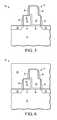
- FIG. 3is a cross section of the split gate NVM cell of FIG. 2 at a subsequent stage in processing
- FIG. 4is a cross section of the split gate NVM cell of FIG. 3 at a subsequent stage in processing
- FIG. 5is a cross section of the split gate NVM cell of FIG. 4 at a subsequent stage in processing
- FIG. 6is a cross section of the split gate NVM cell of FIG. 5 at a subsequent stage in processing
- FIG. 7is a cross section of the split gate NVM cell of FIG. 6 at a subsequent stage in processing
- FIG. 8is a cross section of the split gate NVM cell of FIG. 7 at a subsequent stage in processing
- FIG. 9is a cross section of the split gate NVM cell of FIG. 8 at a subsequent stage in processing
- FIG. 10is a cross section of a split gate NVM cell according to a second embodiment at a stage in processing
- FIG. 11is a cross section of the split gate NVM cell of FIG. 10 at a subsequent stage in processing
- FIG. 12is a cross section of the split gate NVM cell of FIG. 10 at a subsequent stage in processing
- FIG. 13is a cross section of the split gate NVM cell of FIG. 10 at a subsequent stage in processing
- FIG. 14is a cross section of the split gate NVM cell of FIG. 10 at a subsequent stage in processing
- FIG. 15is a cross section of the split gate NVM cell of FIG. 10 at a subsequent stage in processing.
- FIG. 16is a cross section of the split gate NVM cell of FIG. 10 at a subsequent stage in processing.
- a split gate NVM cellis formed using replacement gate for both the select gate and the control gate.
- the material of the dummy select gateis chosen so that the dummy control gate and other exposed materials are not appreciably etched during the etch, which is performed without requiring photolithographic mask, of the dummy select gate.
- the dummy select gateis then replaced with a metal select gate.
- the material of the dummy control gateis chosen so that the metal select gate and the other exposed materials are not appreciably etched during the etch, which is performed without requiring photolithographic mask, of the dummy control gate.
- the dummy control gateis then replaced with a material that results in the control gate used in the final split gate NVM cell.
- the semiconductor substrate described hereincan be any semiconductor material or combinations of materials, such as gallium arsenide, silicon germanium, silicon-on-insulator (SOI), silicon, monocrystalline silicon, the like, and combinations of the above.
- SOIsilicon-on-insulator
- FIG. 1Shown in FIG. 1 is a semiconductor device 10 having a substrate 12 , a gate dielectric 14 on a top surface of the substrate, and a dummy gate layer 16 on gate dielectric 14 .
- Gate dielectric 14may be a thermal oxide or other material such as a high-k dielectric.
- Dummy gate layer 16may be, for example, polysilicon. Dummy gate layer 16 is about the desired thickness of the select gate to be formed.
- FIG. 2Shown in FIG. 2 is semiconductor device 10 after performing an etch of dummy gate layer 16 and gate dielectric 14 to form a dummy select gate which is the resulting patterned dummy gate layer 16 .
- This etchis a patterned etch using photolithography. Etches using photolithography involve a mask that is used to expose a pattern on photoresist. The resulting patterned photoresist may be directly used or indirectly used through a hard mask in the etch to form the dummy select gate. This etch exposes a portion of the top surface of substrate 12 adjacent to the dummy select gate.
- charge storage layer 18Shown in FIG. 3 is semiconductor device 10 after forming a charge storage layer 18 over the exposed top surface of substrate 12 , along the sides of the dummy select gate, and on the top of the dummy select gate.
- Charge storage layer 18may be nanocrystals.
- Charge storage layer 18may also use another type of charge storage such as nitride.
- charge storage layer 18may be formed by forming a first oxide layer, forming nanocrystals on the first oxide layer, and forming a second oxide layer that is among and over the nanocrystals.
- semiconductor device 10shows forming a layer 20 of dummy control gate material over charge storage layer 18 .
- Layer 20may be titanium nitride (TiN). Titanium nitride can be etched selectively to many metals that are used as metal gates and to silicon oxide. It can also be etched selective to silicon nitride. Layer 20 is about the thickness of the dummy select gate which is patterned dummy gate layer 16 .
- FIG. 4Shown in FIG. 4 is semiconductor device 10 after patterning layer 20 and charge storage layer 18 using a patterned etch using photolithography.
- a small portion of the top surface of the dummy select gate, which is patterned dummy gate layer 16has a remaining portion of charge storage layer 18 and layer 20 .
- the remaining portion of charge storage layer 18 and layer 20also extends from a side of the dummy select gate over substrate 12 which, in combination with the dummy select gate, establish a gate length of the split gate NVM cell being formed.
- An upper portion 21 of the remaining portion of charge storage layer 18 and layer 20 that is higher than the top surface of the dummy select gatecan be considered a sacrificial portion because upper portion 21 will be removed prior to replacing the dummy select gate with a metal select gate. Also upper portion 21 will be removed to leave a dummy control gate of the remaining portion of layer 20 .
- FIG. 5Shown in FIG. 5 is semiconductor device 10 after forming a liner 22 on the exposed surfaces of the semiconductor device 10 of FIG. 4 , forming sidewall spacer 24 and sidewall spacer 26 around upper portion 21 on liner 22 , forming sidewall spacer 28 on the side of the dummy select gate, which is patterned dummy gate layer 16 , that is away from the remaining portion of charge storage layer 18 and layer 20 , and forming a sidewall spacer 30 on the side of the remaining portion of charge storage layer 18 and layer 20 that is away from the dummy select gate. Also shown in FIG. 5 is semiconductor device 10 after forming source/drain region 32 substrate 12 using sidewall spacer 28 and forming source/drain region 34 using sidewall spacer 30 .
- FIG. 6Shown in FIG. 6 is semiconductor device 10 after forming an interlayer dielectric (ILD) 36 over semiconductor device 10 sufficiently thick to cover upper portion 21 .
- ILDinterlayer dielectric
- FIG. 7Shown in FIG. 7 is semiconductor device 10 after performing a planarizing step that removes the portion of semiconductor device 10 shown in FIG. 10 higher than the top surface of the dummy select gate which is patterned dummy gate layer 16 .
- the planarizing stepwhich may be by chemical mechanical polishing (CMP), leaves the top surface of layer 20 and the exposed surface of charge storage layer 18 coplanar with the top surface of the dummy select gate.
- the remaining portion of layer 20is a dummy control gate.
- top portion 39could simply be the top portion of the metal used in forming select gate stack 38 or it could be a different material such as polysilicon, or even an insulating material such as silicon oxide or silicon nitride.
- Select gate stack 38may also have a thin barrier metal that functions as a work function setting material that interfaces with gate dielectric 14 .
- gate dielectric 14may be removed and replaced with a different gate dielectric.
- the etchant for removing the dummy select gate, for the case where the dummy select gate is polysiliconmay be chlorine/oxygen (Cl2/O2) plasma.
- FIG. 9Shown in FIG. 9 is semiconductor device 10 after replacing the remaining portion of layer 20 with a select gate 40 , which may be polysilicon.
- An etchantin the case of layer 20 being TiN, that can be used in the removal of the remaining portion of layer 20 is sulfuric acid and peroxide (H2SO4/H2O2) with top portion of 39 being a layer of oxide.
- FIG. 10Shown in FIG. 10 is semiconductor device 10 showing an alternative to obtaining FIG. 4 following from FIG. 3 .
- the result in FIG. 10occurs from an anisotropic etch applied to the structure of FIG. 3 .
- FIG. 10there is dummy select gate 56 on gate dielectric 54 with an overlying dummy control gate layer 60 having been etched with an anisotropic etch.
- the anisotropic etchresults in sidewall spacers, which are shown in FIG. 10 , of dummy control gate material 60 .
- Dummy control gate material 60may be titanium nitride.
- FIG. 11Shown in FIG. 11 is semiconductor device 50 after pattern etching using photolithography to remove a portion of the sidewall spacers of control gate material 60 to leave a dummy control gate after the pattern etching. As shown, a remaining portion of dummy control gate layer 60 , which is the dummy control gate, is left on one side of dummy select gate 55 and dummy control gate layer 60 is removed from the other side of dummy select gate 55 . Thus, this remaining portion of dummy control gate layer 60 is a spacer structure and may be referenced as dummy control gate 60 .
- semiconductor device 50Shown in FIG. 12 is semiconductor device 50 after removing charge storage layer 58 where it is exposed. This can be achieved without a masking step so that photolithography is not required.
- FIG. 13Shown in FIG. 13 is semiconductor device 50 after forming a liner 62 over semiconductor device 10 of FIG. 12 .
- Liner 62may be deposited silicon oxide.
- a sidewall spacerOn the side of dummy select gate 56 away from the dummy control gate 60 is formed a sidewall spacer which may be silicon nitride.
- a sidewall spacer 66On the side of dummy control gate 60 on the side away from dummy select gate 56 is a sidewall spacer 66 which may be silicon nitride.
- substrate 52 on the side of sidewall spacer 64is a source/drain 68 and on the side of sidewall spacer 66 is a source/drain 70 .
- semiconductor device 50after forming an interlayer dielectric 72 having a top surface that has been planarized to be coplanar with the top surface of dummy select gate 56 and the top surface of dummy control gate 60 .
- FIG. 15Shown in FIG. 15 is semiconductor device 50 after replacing dummy select gate 56 with select gate 74 having metal and having a top portion which is chosen for its etch characteristic relative to the etchant used to etch dummy control gate 60 .
- an etchantis applied to remove dummy select gate 56 .
- the etchantmay be chlorine/oxygen (Cl2/O2) plasma.
- FIG. 16Shown in FIG. 16 is semiconductor device 50 after replacing dummy control gate 60 with control gate 76 that may include polysilicon. This resulting replacement of control gate 76 may also be considered a spacer structure.
- the etchant used in removing dummy control gate 60may be sulfuric acid and peroxide (H2SO4/H2O2).
- H2SO4/H2O2sulfuric acid and peroxide
- FIGS. 10-16is very similar to that described for FIGS. 1-9 .
- the formation of dummy control gate 60 by an isotropic etch used in forming sidewall spacersis the significant difference. The considerations in choosing etchants and materials for dummy select and control gates and the material for the select gate are relevant for both approaches.
- the semiconductor structurecomprises a split gate non-volatile memory (NVM) structure in an NVM region of the semiconductor structure.
- the methodincludes forming a dummy select gate structure including a first material on the substrate.
- the methodfurther includes forming a dummy control gate structure including a second material on the substrate, wherein the first material is different from the second material.
- the methodfurther includes replacing the dummy select gate structure with a metal select gate structure, wherein the replacing the dummy select gate structure includes removing the dummy select gate structure without removing the dummy control gate structure and replacing the dummy control gate structure with a polysilicon control gate structure and the replacing the dummy control gate structure includes removing the dummy control gate structure without removing the metal select gate structure.
- the methodmay have a further characterization by which the replacing the dummy select gate structure includes etching the first material included in the dummy select gate structure using an etchant to leave an opening, wherein the etchant substantially removes the first material and the etchant does not substantially remove the second material included in the dummy control gate structure.
- the methodmay have a further characterization by which the replacing the dummy select gate structure further includes forming a metal gate stack in the opening to form the metal select gate structure.
- the methodmay have a further characterization by which the replacing the dummy control gate structure includes etching the second material included in the dummy control gate structure using an etchant to leave an opening, wherein the etchant substantially removes the second material and the etchant does not substantially remove the third material included in the metal select gate structure.
- the methodmay have a further characterization by which the third material forms a capping layer on the metal select gate structure.
- the methodmay have a further characterization by which the replacing the dummy control gate structure further includes forming a polysilicon gate stack in the opening to form the polysilicon control gate structure.
- the methodmay have a further characterization by which the forming the dummy select gate structure and the forming the dummy control gate structure includes forming a charge storage layer over the substrate including over a first portion of the first material and along a side of the first portion, forming a second layer of the second material over the charge storage layer, and etching the second layer and the charge storage layer to form the dummy select gate structure and the dummy control gate structure.
- the methodmay further include, prior to the replacing the dummy select gate structure and the replacing the dummy control gate structure, forming an interlayer dielectric (ILD) layer over the substrate including over the dummy select gate structure and the dummy control gate structure and performing chemical mechanical polishing on the NVM region to reveal a top first surface of the first material and a second top surface of the second material.
- the methodmay have a further characterization by which an etchant utilized in one of the replacing the dummy select gate structure and the replacing the dummy control gate structure does not substantially remove oxide and an interlayer dielectric (ILD) material.
- the methodmay have a further characterization by which the dummy control gate structure is a spacer structure.
- the methodincludes etching a first dummy material included in a dummy select gate stack formed on the semiconductor substrate to form a first opening, wherein the etching the first dummy material does not substantially remove a second dummy material included in a dummy control gate stack formed on the semiconductor substrate and the first dummy material is different from the second dummy material.
- the methodfurther includes forming a metal select gate stack in the first op.
- the methodfurther includes etching the second dummy material to form a second opening, wherein the etching the second dummy material does not substantially remove a third material included in the metal select gate stack.
- the methodfurther includes forming a polysilicon control gate stack in the second opening.
- the methodmay further include forming the dummy select gate stack and the dummy control gate stack including etching a first layer of the first dummy material formed over the semiconductor substrate to form at least a first side of the dummy select gate stack, forming a charge storage layer over the semiconductor substrate including along the first side of the dummy select gate stack, forming a second layer of the second dummy material over the charge storage layer, and etching the second layer and the charge storage layer to form the dummy control gate stack and a second side of the dummy select gate stack.
- the methodmay have a further characterization by which the etching the second layer and the charge storage layer further includes etching the first layer to form the second side of the dummy select gate stack.
- the methodmay further include, prior to the etching the first layer and the etching the second layer and the charge storage layer, forming an interlayer dielectric (ILD) layer over the semiconductor substrate including over the dummy select gate stack and the dummy control gate stack.
- the methodmay further include, prior to the etching the first layer and the etching the second layer and the charge storage layer, performing chemical mechanical polishing on the semiconductor substrate to reveal a first top surface of the first dummy material included in the dummy select gate stack and a second top surface of the second dummy material included in the dummy control gate stack.
- ILDinterlayer dielectric
- the methodmay have a further characterization by which the chemical mechanical polishing removes an upper portion of the dummy select gate stack and of the dummy control gate stack.
- the methodmay further include forming sidewall spacers along the second side of the dummy select gate stack and a third side of the dummy control gate stack.
- the methodmay have a further characterization by which the etching the second layer and the charge storage layer includes performing a spacer etch on the second layer to form the dummy control gate stack, wherein, the dummy control gate stack is a spacer structure.
- the methodmay have a further characterization by which the third material forms a capping layer on the metal select gate stack.
- NVMnon-volatile memory
- the methodincludes forming a select gate structure including a first dummy material on the semiconductor substrate.
- the methodfurther includes forming a control gate structure including a second dummy material on the semiconductor substrate, wherein the first dummy material is different from the second dummy material.
- the methodfurther includes replacing the first dummy material with metal.
- the methodfurther includes replacing the second dummy material with polysilicon.
- Coupledis not intended to be limited to a direct coupling or a mechanical coupling.
Landscapes
- Engineering & Computer Science (AREA)
- Microelectronics & Electronic Packaging (AREA)
- Condensed Matter Physics & Semiconductors (AREA)
- General Physics & Mathematics (AREA)
- Manufacturing & Machinery (AREA)
- Computer Hardware Design (AREA)
- Physics & Mathematics (AREA)
- Power Engineering (AREA)
- Chemical & Material Sciences (AREA)
- Chemical Kinetics & Catalysis (AREA)
- General Chemical & Material Sciences (AREA)
- Semiconductor Memories (AREA)
- Non-Volatile Memory (AREA)
- Insulated Gate Type Field-Effect Transistor (AREA)
Abstract
Description
Claims (19)
Priority Applications (1)
| Application Number | Priority Date | Filing Date | Title |
|---|---|---|---|
| US14/291,320US9379222B2 (en) | 2014-05-30 | 2014-05-30 | Method of making a split gate non-volatile memory (NVM) cell |
Applications Claiming Priority (1)
| Application Number | Priority Date | Filing Date | Title |
|---|---|---|---|
| US14/291,320US9379222B2 (en) | 2014-05-30 | 2014-05-30 | Method of making a split gate non-volatile memory (NVM) cell |
Publications (2)
| Publication Number | Publication Date |
|---|---|
| US20150349096A1 US20150349096A1 (en) | 2015-12-03 |
| US9379222B2true US9379222B2 (en) | 2016-06-28 |
Family
ID=54702745
Family Applications (1)
| Application Number | Title | Priority Date | Filing Date |
|---|---|---|---|
| US14/291,320Active2034-09-25US9379222B2 (en) | 2014-05-30 | 2014-05-30 | Method of making a split gate non-volatile memory (NVM) cell |
Country Status (1)
| Country | Link |
|---|---|
| US (1) | US9379222B2 (en) |
Families Citing this family (8)
| Publication number | Priority date | Publication date | Assignee | Title |
|---|---|---|---|---|
| CN103811315B (en)* | 2012-11-07 | 2016-09-28 | 中国科学院微电子研究所 | Semiconductor device and method for manufacturing the same |
| US9397176B2 (en)* | 2014-07-30 | 2016-07-19 | Freescale Semiconductor, Inc. | Method of forming split gate memory with improved reliability |
| US9472645B1 (en)* | 2015-06-08 | 2016-10-18 | Taiwan Semiconductor Manufacturing Co., Ltd. | Dual control gate spacer structure for embedded flash memory |
| JP6620046B2 (en)* | 2016-03-15 | 2019-12-11 | ルネサスエレクトロニクス株式会社 | Semiconductor device manufacturing method and semiconductor device |
| CN107305892B (en) | 2016-04-20 | 2020-10-02 | 硅存储技术公司 | Method of Forming Tri-Gate Non-Volatile Flash Memory Cell Pairs Using Two Polysilicon Deposition Steps |
| JP6778607B2 (en)* | 2016-12-22 | 2020-11-04 | ルネサスエレクトロニクス株式会社 | Manufacturing method of semiconductor devices |
| TWI694592B (en)* | 2018-11-09 | 2020-05-21 | 物聯記憶體科技股份有限公司 | Non-volatile memory and manufacturing method thereof |
| CN113013256B (en)* | 2021-02-04 | 2024-06-14 | 上海华力集成电路制造有限公司 | Split-gate MONOS flash memory and manufacturing method thereof |
Citations (117)
| Publication number | Priority date | Publication date | Assignee | Title |
|---|---|---|---|---|
| US5614746A (en) | 1994-11-28 | 1997-03-25 | United Microelectronics Corporation | Structure and process of manufacture of split gate flash memory cell |
| US6087225A (en) | 1998-02-05 | 2000-07-11 | International Business Machines Corporation | Method for dual gate oxide dual workfunction CMOS |
| US6194301B1 (en) | 1999-07-12 | 2001-02-27 | International Business Machines Corporation | Method of fabricating an integrated circuit of logic and memory using damascene gate structure |
| US6235574B1 (en) | 1999-03-22 | 2001-05-22 | Infineon North America Corp. | High performance DRAM and method of manufacture |
| US20010049166A1 (en) | 2000-03-29 | 2001-12-06 | Stmicroelectronics S.R.L. | Method of manufacturing an electrically programmable, non-volatile memory and high-performance logic circuitry in the same semiconductor chip |
| US6333223B1 (en) | 1998-12-25 | 2001-12-25 | Matsushita Electric Industrial Co., Ltd. | Semiconductor device and method of manufacturing the same |
| US20020061616A1 (en) | 2000-11-22 | 2002-05-23 | Kim Jae Hyung | Method for fabricating semiconductor device |
| US20030022434A1 (en) | 1998-12-25 | 2003-01-30 | Yasuhiro Taniguchi | Semiconductor integrated circuit device and a method of manufacturing the same |
| US6531734B1 (en) | 2002-05-24 | 2003-03-11 | Silicon Based Technology Corp. | Self-aligned split-gate flash memory cell having an integrated source-side erase structure and its contactless flash memory arrays |
| US6635526B1 (en) | 2002-06-07 | 2003-10-21 | Infineon Technologies Ag | Structure and method for dual work function logic devices in vertical DRAM process |
| US6707079B2 (en) | 2001-02-22 | 2004-03-16 | Halo Lsi, Inc. | Twin MONOS cell fabrication method and array organization |
| US20040075133A1 (en) | 2000-09-29 | 2004-04-22 | Fujitsu Limited | Semiconductor device and its manufacturing method |
| US6777761B2 (en) | 2002-08-06 | 2004-08-17 | International Business Machines Corporation | Semiconductor chip using both polysilicon and metal gate devices |
| US6785165B2 (en) | 2002-01-25 | 2004-08-31 | Renesas Technology Corporation | Semiconductor device |
| US20040262670A1 (en) | 2003-06-30 | 2004-12-30 | Kabushiki Kaisha Toshiba | Semiconductor device including nonvolatile memory and method for fabricating the same |
| US20050145949A1 (en) | 2003-10-27 | 2005-07-07 | Kayvan Sadra | Application of different isolation schemes for logic and embedded memory |
| US6939767B2 (en) | 2003-11-19 | 2005-09-06 | Freescale Semiconductor, Inc. | Multi-bit non-volatile integrated circuit memory and method therefor |
| US20060038240A1 (en) | 2004-08-17 | 2006-02-23 | Fujitsu Limited | Semiconductor device and manufacturing method of the same |
| US20060046449A1 (en) | 2004-08-27 | 2006-03-02 | Taiwan Semiconductor Manufacturing Co., Ltd. | Metal gate structure for mos devices |
| US20060099798A1 (en) | 2004-11-08 | 2006-05-11 | Fujitsu Limited | Semiconductor device and manufacturing method of the same |
| US20060134864A1 (en) | 2004-12-22 | 2006-06-22 | Masaaki Higashitani | Multi-thickness dielectric for semiconductor memory |
| US20060211206A1 (en) | 2005-03-18 | 2006-09-21 | Freescale Semiconductor, Inc. | Electronic devices including non-volatile memory and processes for forming the same |
| US20060221688A1 (en) | 1999-02-01 | 2006-10-05 | Shoji Shukuri | Semiconductor integrated circuit and nonvolatile memory element |
| US7154779B2 (en) | 2004-01-21 | 2006-12-26 | Sandisk Corporation | Non-volatile memory cell using high-k material inter-gate programming |
| US20070037343A1 (en) | 2005-08-10 | 2007-02-15 | Texas Instruments Inc. | Process for manufacturing dual work function metal gates in a microelectronics device |
| US7183159B2 (en) | 2005-01-14 | 2007-02-27 | Freescale Semiconductor, Inc. | Method of forming an integrated circuit having nanocluster devices and non-nanocluster devices |
| US7190022B2 (en) | 2003-06-27 | 2007-03-13 | Infineon Technologies Ag | One transistor flash memory cell |
| US20070077705A1 (en) | 2005-09-30 | 2007-04-05 | Prinz Erwin J | Split gate memory cell and method therefor |
| US7202524B2 (en) | 2004-12-08 | 2007-04-10 | Samsung Electronics Co., Ltd. | Nonvolatile memory device and method of manufacturing the same |
| US7208793B2 (en) | 2004-11-23 | 2007-04-24 | Micron Technology, Inc. | Scalable integrated logic and non-volatile memory |
| US20070115725A1 (en) | 2004-12-22 | 2007-05-24 | Tuan Pham | Low-Voltage, Multiple Thin-Gate Oxide and Low-Resistance Gate Electrode |
| US7256125B2 (en) | 2003-08-25 | 2007-08-14 | Renesas Technology Corp. | Method of manufacturing a semiconductor device |
| US7271050B2 (en) | 2002-08-27 | 2007-09-18 | Micron Technology, Inc. | Silicon nanocrystal capacitor and process for forming same |
| US20070215917A1 (en) | 2006-03-20 | 2007-09-20 | Renesas Technology Corp. | Semiconductor integrated circuit device and a method of manufacturing the same |
| US20070224772A1 (en) | 2006-03-21 | 2007-09-27 | Freescale Semiconductor, Inc. | Method for forming a stressor structure |
| US20070249129A1 (en) | 2006-04-21 | 2007-10-25 | Freescale Semiconductor, Inc. | STI stressor integration for minimal phosphoric exposure and divot-free topography |
| US20070264776A1 (en) | 2003-11-19 | 2007-11-15 | Zhong Dong | Precision creation of inter-gates insulator |
| US20080029805A1 (en) | 2006-08-03 | 2008-02-07 | Yasuhiro Shimamoto | Semiconductor device and manufacturing method of the same |
| US20080050875A1 (en) | 2006-08-25 | 2008-02-28 | Jung-Ho Moon | Methods of fabricating embedded flash memory devices |
| US20080067599A1 (en) | 2005-05-23 | 2008-03-20 | Fujitsu Limited | Semiconductor device and method of manufacturing the same |
| US7365389B1 (en) | 2004-12-10 | 2008-04-29 | Spansion Llc | Memory cell having enhanced high-K dielectric |
| US20080105945A1 (en) | 2004-11-12 | 2008-05-08 | Freescale Semiconductor, Inc. | Method of forming a nanocluster charge storage device |
| US20080121983A1 (en) | 2006-09-22 | 2008-05-29 | Seong Geum-Jung | Gate and method of forming the same, and memory device and method of manufacturing the same |
| US20080128785A1 (en) | 2006-11-30 | 2008-06-05 | Jin-Ha Park | Flash memory device and method of manufacturing the same |
| US20080145985A1 (en) | 2006-12-15 | 2008-06-19 | Semiconductor Manufacturing International (Shanghai) Corporation | Embedded semiconductor memory devices and methods for fabricating the same |
| US7391075B2 (en) | 2004-10-08 | 2008-06-24 | Samsung Electronics Co., Ltd. | Non-volatile semiconductor memory device with alternative metal gate material |
| US7402493B2 (en) | 2004-04-12 | 2008-07-22 | Samsung Electronics Co., Ltd. | Method for forming non-volatile memory devices |
| US20080185635A1 (en) | 2007-02-01 | 2008-08-07 | Renesas Technology Corp. | Semiconductor storage device and manufacturing method thereof |
| US20080237690A1 (en) | 2007-03-26 | 2008-10-02 | Fujitsu Limited | Semiconductor device and method of manufacturing the same |
| US20080237700A1 (en) | 2007-03-28 | 2008-10-02 | Samsung Electronics Co., Ltd. | Nonvolatile memory device having cell and peripheral regions and method of making the same |
| US7439134B1 (en) | 2007-04-20 | 2008-10-21 | Freescale Semiconductor, Inc. | Method for process integration of non-volatile memory cell transistors with transistors of another type |
| US20080283900A1 (en) | 2005-12-14 | 2008-11-20 | Fujitsu Limited | Semiconductor device and method for manufacturing the same |
| US20080290385A1 (en) | 2007-05-24 | 2008-11-27 | Seiko Epson Corporation | Method for manufacturing ferroelectric capacitor, and ferroelectric capacitor |
| US20080308876A1 (en) | 2007-06-12 | 2008-12-18 | Hye-Lan Lee | Semiconductor device and method of manufacturing the same |
| US20090050955A1 (en) | 2007-08-24 | 2009-02-26 | Kenichi Akita | Nonvolatile semiconductor device and method of manufacturing the same |
| US20090065845A1 (en) | 2007-09-11 | 2009-03-12 | Samsung Electronics Co., Ltd. | Embedded semiconductor device and method of manufacturing an embedded semiconductor device |
| US20090072274A1 (en) | 2007-09-14 | 2009-03-19 | Qimonda Ag | Integrated circuit including a first gate stack and a second gate stack and a method of manufacturing |
| US20090078986A1 (en) | 2007-09-20 | 2009-03-26 | Lars Bach | Manufacturing method for an integrated circuit including different types of gate stacks, corresponding intermediate integrated circuit structure and corresponding integrated circuit |
| US7521314B2 (en) | 2007-04-20 | 2009-04-21 | Freescale Semiconductor, Inc. | Method for selective removal of a layer |
| US20090101961A1 (en) | 2007-10-22 | 2009-04-23 | Yue-Song He | Memory devices with split gate and blocking layer |
| US7524719B2 (en) | 2006-08-31 | 2009-04-28 | Freescale Semiconductor, Inc. | Method of making self-aligned split gate memory cell |
| US20090111229A1 (en) | 2007-10-31 | 2009-04-30 | Steimle Robert F | Method of forming a split gate non-volatile memory cell |
| WO2009058486A1 (en) | 2007-10-29 | 2009-05-07 | Freescale Semiconductor Inc. | Method for integrating nvm circuitry with logic circuitry |
| US7544490B2 (en) | 2002-02-08 | 2009-06-09 | Genencor International, Inc. | Secretion, transcription and sporulation genes in Bacillus clausii |
| US7544980B2 (en) | 2006-01-27 | 2009-06-09 | Freescale Semiconductor, Inc. | Split gate memory cell in a FinFET |
| US7560767B2 (en) | 2005-10-14 | 2009-07-14 | Kabushiki Kaisha Toshiba | Nonvolatile semiconductor memory device |
| US20090179283A1 (en) | 2007-12-12 | 2009-07-16 | International Business Machines Corporation | Metal gate stack and semiconductor gate stack for cmos devices |
| US20090225602A1 (en) | 2005-05-26 | 2009-09-10 | Micron Technology, Inc. | Multi-state memory cell |
| US20090256211A1 (en) | 2008-04-10 | 2009-10-15 | International Business Machines Corporation | Metal gate compatible flash memory gate stack |
| US20090269893A1 (en) | 2001-07-05 | 2009-10-29 | Fujitsu Limited | Semiconductor integrated circuit device and method of producing the same |
| US20090273013A1 (en) | 2008-04-30 | 2009-11-05 | Winstead Brian A | Method of forming a split gate memory device and apparatus |
| US20090278187A1 (en) | 2008-05-09 | 2009-11-12 | Toba Takayuki | Semiconductor device and manufacturing method of semiconductor device |
| US7799650B2 (en) | 2007-08-08 | 2010-09-21 | Freescale Semiconductor, Inc. | Method for making a transistor with a stressor |
| US7816727B2 (en) | 2007-08-27 | 2010-10-19 | Macronix International Co., Ltd. | High-κ capped blocking dielectric bandgap engineered SONOS and MONOS |
| US7821055B2 (en) | 2009-03-31 | 2010-10-26 | Freescale Semiconductor, Inc. | Stressed semiconductor device and method for making |
| US20110031548A1 (en) | 2008-04-15 | 2011-02-10 | Freescale Semiconductor, Inc. | Split gate non-volatile memory cell with improved endurance and method therefor |
| US7906396B1 (en) | 2009-09-02 | 2011-03-15 | Winbond Electronics Corp. | Flash memory and method of fabricating the same |
| US7932146B2 (en) | 2008-03-20 | 2011-04-26 | United Microelectronics Corp. | Metal gate transistor and polysilicon resistor and method for fabricating the same |
| US20110095348A1 (en) | 2009-10-28 | 2011-04-28 | Renesas Electronics Corporation | Semiconductor device and method of manufacturing the same |
| US7989871B2 (en) | 2006-03-15 | 2011-08-02 | Kabushiki Kaisha Toshiba | Nonvolatile semiconductor memory device having insulating films that include multiple layers formed by insulating materials having d-orbital metal element and insulating materials without d-orbital metal element |
| US7999304B2 (en) | 2007-02-07 | 2011-08-16 | Kabushiki Kaisha Toshiba | Semiconductor device |
| US20110204450A1 (en) | 2010-02-25 | 2011-08-25 | Renesas Electronics Corporation | Semiconductor device and manufacturing method thereof |
| US8017991B2 (en) | 2006-07-28 | 2011-09-13 | Samsung Electronics Co., Ltd. | Non-volatile memory device and methods of operating and fabricating the same |
| US8043951B2 (en) | 2007-08-01 | 2011-10-25 | Freescale Semiconductor, Inc. | Method of manufacturing a semiconductor device and semiconductor device obtainable therewith |
| US20110260258A1 (en) | 2009-12-31 | 2011-10-27 | Institute of Microelectronics, Chinese Academy of Sciences | Field effect transistor device with improved carrier mobility and method of manufacturing the same |
| US20110272764A1 (en)* | 2010-05-04 | 2011-11-10 | Samsung Electronics Co., Ltd. | Semiconductor Device Having e-Fuse Structure And Method Of Fabricating The Same |
| US8063434B1 (en) | 2007-05-25 | 2011-11-22 | Cypress Semiconductor Corporation | Memory transistor with multiple charge storing layers and a high work function gate electrode |
| US8093128B2 (en) | 2007-05-25 | 2012-01-10 | Cypress Semiconductor Corporation | Integration of non-volatile charge trap memory devices and logic CMOS devices |
| US20120034751A1 (en) | 2010-08-06 | 2012-02-09 | Fujitsu Semiconductor Limited | Method of manufacturing semiconductor device |
| US8138037B2 (en) | 2009-03-17 | 2012-03-20 | International Business Machines Corporation | Method and structure for gate height scaling with high-k/metal gate technology |
| US8168493B2 (en) | 2010-03-05 | 2012-05-01 | Samsung Electronics Co., Ltd. | Semiconductor memory device and method of manufacturing the same |
| US20120104483A1 (en) | 2010-10-29 | 2012-05-03 | Shroff Mehul D | Non-volatile memory and logic circuit process integration |
| US20120132978A1 (en) | 2010-11-25 | 2012-05-31 | Renesas Electronics Corporation | Semiconductor device and manufacturing method of semiconductor device |
| US20120142153A1 (en) | 2005-03-08 | 2012-06-07 | Magnachip Semiconductor Ltd. | Non-volatile memory device and method for fabricating the same |
| US20120248523A1 (en) | 2011-03-31 | 2012-10-04 | Shroff Mehul D | Non-volatile memory and logic circuit process integration |
| US20120252171A1 (en) | 2011-03-31 | 2012-10-04 | Shroff Mehul D | Non-volatile memory and logic circuit process integration |
| US8298885B2 (en) | 2009-05-15 | 2012-10-30 | Globalfoundries Inc. | Semiconductor device comprising metal gates and a silicon containing resistor formed on an isolation structure |
| US8334198B2 (en) | 2011-04-12 | 2012-12-18 | Taiwan Semiconductor Manufacturing Company, Ltd. | Method of fabricating a plurality of gate structures |
| US20130026553A1 (en) | 2011-07-26 | 2013-01-31 | Synopsys, Inc. | NVM Bitcell with a Replacement Control Gate and Additional Floating Gate |
| US8372699B2 (en) | 2010-02-22 | 2013-02-12 | Freescale Semiconductor, Inc. | Method for forming a split-gate memory cell |
| US20130037886A1 (en) | 2011-08-10 | 2013-02-14 | Teng-Chun Tsai | Semiconductor device and method of making the same |
| US20130065366A1 (en) | 2011-09-08 | 2013-03-14 | Stmicroelectronics | Soi integrated circuit comprising adjacent cells of different types |
| US20130084684A1 (en) | 2011-10-03 | 2013-04-04 | Renesas Electronics Corporation | Manufacturing method of semiconductor device |
| US20130137227A1 (en) | 2011-11-30 | 2013-05-30 | Mehul D. Shroff | Logic and non-volatile memory (nvm) integration |
| US20130171785A1 (en) | 2012-01-04 | 2013-07-04 | Mehul D. Shroff | Non-volatile memory (nvm) and logic integration |
| US20130171786A1 (en) | 2012-01-04 | 2013-07-04 | Freescale Semiconductor, Inc. | Non-volatile memory (nvm) and logic integration |
| US20130178027A1 (en) | 2012-01-04 | 2013-07-11 | Freescale Semiconductor, Inc. | Non-volatile memory (nvm) and logic integration |
| US8524557B1 (en) | 2012-02-22 | 2013-09-03 | Freescale Semiconductor, Inc. | Integration technique using thermal oxide select gate dielectric for select gate and replacement gate for logic |
| US20130264633A1 (en) | 2012-04-09 | 2013-10-10 | Mark D. Hall | Logic transistor and non-volatile memory cell integration |
| US20130267074A1 (en) | 2012-04-09 | 2013-10-10 | Freescale Semiconductor Inc. | Integration technique using thermal oxide select gate dielectric for select gate and apartial replacement gate for logic |
| US20130267072A1 (en) | 2012-04-06 | 2013-10-10 | Freescale Semiconductor, Inc. | Non-volatile memory (nvm) and logic integration |
| US20130323922A1 (en) | 2011-09-29 | 2013-12-05 | Freescale Semiconductor, Inc. | Split gate memory device with gap spacer |
| US20140035027A1 (en) | 2009-11-25 | 2014-02-06 | Renesas Electronics Corporation | Semiconductor device and a manufacturing method thereof |
| US20140050029A1 (en) | 2012-08-20 | 2014-02-20 | Sung-taeg Kang | Split-gate memory cells having select-gate sidewall metal silicide regions and related manufacturing methods |
| US20140120713A1 (en) | 2012-10-26 | 2014-05-01 | Mehul D. Shroff | Method of making a logic transistor and a non-volatile memory (nvm) cell |
| US20140213030A1 (en)* | 2013-01-25 | 2014-07-31 | Renesas Electronics Corporation | Manufacturing method of semiconductor device |
| US20150129952A1 (en)* | 2013-11-08 | 2015-05-14 | Taiwan Semiconductor Manufacturing Co., Ltd. | Semiconductor device and method for manufacturing the same |
- 2014
- 2014-05-30USUS14/291,320patent/US9379222B2/enactiveActive
Patent Citations (130)
| Publication number | Priority date | Publication date | Assignee | Title |
|---|---|---|---|---|
| US5614746A (en) | 1994-11-28 | 1997-03-25 | United Microelectronics Corporation | Structure and process of manufacture of split gate flash memory cell |
| US6087225A (en) | 1998-02-05 | 2000-07-11 | International Business Machines Corporation | Method for dual gate oxide dual workfunction CMOS |
| US6333223B1 (en) | 1998-12-25 | 2001-12-25 | Matsushita Electric Industrial Co., Ltd. | Semiconductor device and method of manufacturing the same |
| US6509225B2 (en) | 1998-12-25 | 2003-01-21 | Matsushita Electric Industrial Co., Ltd. | Semiconductor device and method of manufacturing the same |
| US20030022434A1 (en) | 1998-12-25 | 2003-01-30 | Yasuhiro Taniguchi | Semiconductor integrated circuit device and a method of manufacturing the same |
| US20060221688A1 (en) | 1999-02-01 | 2006-10-05 | Shoji Shukuri | Semiconductor integrated circuit and nonvolatile memory element |
| US6235574B1 (en) | 1999-03-22 | 2001-05-22 | Infineon North America Corp. | High performance DRAM and method of manufacture |
| US6194301B1 (en) | 1999-07-12 | 2001-02-27 | International Business Machines Corporation | Method of fabricating an integrated circuit of logic and memory using damascene gate structure |
| US6388294B1 (en) | 1999-07-12 | 2002-05-14 | International Business Machines Corporation | Integrated circuit using damascene gate structure |
| US20010049166A1 (en) | 2000-03-29 | 2001-12-06 | Stmicroelectronics S.R.L. | Method of manufacturing an electrically programmable, non-volatile memory and high-performance logic circuitry in the same semiconductor chip |
| US7476582B2 (en) | 2000-09-29 | 2009-01-13 | Fujitsu Limited | Semiconductor device and its manufacturing method |
| US20040075133A1 (en) | 2000-09-29 | 2004-04-22 | Fujitsu Limited | Semiconductor device and its manufacturing method |
| US20020061616A1 (en) | 2000-11-22 | 2002-05-23 | Kim Jae Hyung | Method for fabricating semiconductor device |
| US6707079B2 (en) | 2001-02-22 | 2004-03-16 | Halo Lsi, Inc. | Twin MONOS cell fabrication method and array organization |
| US20090269893A1 (en) | 2001-07-05 | 2009-10-29 | Fujitsu Limited | Semiconductor integrated circuit device and method of producing the same |
| US6785165B2 (en) | 2002-01-25 | 2004-08-31 | Renesas Technology Corporation | Semiconductor device |
| US7544490B2 (en) | 2002-02-08 | 2009-06-09 | Genencor International, Inc. | Secretion, transcription and sporulation genes in Bacillus clausii |
| US6531734B1 (en) | 2002-05-24 | 2003-03-11 | Silicon Based Technology Corp. | Self-aligned split-gate flash memory cell having an integrated source-side erase structure and its contactless flash memory arrays |
| US6635526B1 (en) | 2002-06-07 | 2003-10-21 | Infineon Technologies Ag | Structure and method for dual work function logic devices in vertical DRAM process |
| US6777761B2 (en) | 2002-08-06 | 2004-08-17 | International Business Machines Corporation | Semiconductor chip using both polysilicon and metal gate devices |
| US7271050B2 (en) | 2002-08-27 | 2007-09-18 | Micron Technology, Inc. | Silicon nanocrystal capacitor and process for forming same |
| US7190022B2 (en) | 2003-06-27 | 2007-03-13 | Infineon Technologies Ag | One transistor flash memory cell |
| US20040262670A1 (en) | 2003-06-30 | 2004-12-30 | Kabushiki Kaisha Toshiba | Semiconductor device including nonvolatile memory and method for fabricating the same |
| US7256125B2 (en) | 2003-08-25 | 2007-08-14 | Renesas Technology Corp. | Method of manufacturing a semiconductor device |
| US20050145949A1 (en) | 2003-10-27 | 2005-07-07 | Kayvan Sadra | Application of different isolation schemes for logic and embedded memory |
| US6939767B2 (en) | 2003-11-19 | 2005-09-06 | Freescale Semiconductor, Inc. | Multi-bit non-volatile integrated circuit memory and method therefor |
| US20070264776A1 (en) | 2003-11-19 | 2007-11-15 | Zhong Dong | Precision creation of inter-gates insulator |
| US7405968B2 (en) | 2004-01-21 | 2008-07-29 | Sandisk Corporation | Non-volatile memory cell using high-K material and inter-gate programming |
| US7154779B2 (en) | 2004-01-21 | 2006-12-26 | Sandisk Corporation | Non-volatile memory cell using high-k material inter-gate programming |
| US7402493B2 (en) | 2004-04-12 | 2008-07-22 | Samsung Electronics Co., Ltd. | Method for forming non-volatile memory devices |
| US20060038240A1 (en) | 2004-08-17 | 2006-02-23 | Fujitsu Limited | Semiconductor device and manufacturing method of the same |
| US20060046449A1 (en) | 2004-08-27 | 2006-03-02 | Taiwan Semiconductor Manufacturing Co., Ltd. | Metal gate structure for mos devices |
| US7391075B2 (en) | 2004-10-08 | 2008-06-24 | Samsung Electronics Co., Ltd. | Non-volatile semiconductor memory device with alternative metal gate material |
| US20060099798A1 (en) | 2004-11-08 | 2006-05-11 | Fujitsu Limited | Semiconductor device and manufacturing method of the same |
| US20080105945A1 (en) | 2004-11-12 | 2008-05-08 | Freescale Semiconductor, Inc. | Method of forming a nanocluster charge storage device |
| US7544990B2 (en) | 2004-11-23 | 2009-06-09 | Micron Technology, Inc. | Scalable integrated logic and non-volatile memory |
| US7208793B2 (en) | 2004-11-23 | 2007-04-24 | Micron Technology, Inc. | Scalable integrated logic and non-volatile memory |
| US7202524B2 (en) | 2004-12-08 | 2007-04-10 | Samsung Electronics Co., Ltd. | Nonvolatile memory device and method of manufacturing the same |
| US7365389B1 (en) | 2004-12-10 | 2008-04-29 | Spansion Llc | Memory cell having enhanced high-K dielectric |
| US20070115725A1 (en) | 2004-12-22 | 2007-05-24 | Tuan Pham | Low-Voltage, Multiple Thin-Gate Oxide and Low-Resistance Gate Electrode |
| US20060134864A1 (en) | 2004-12-22 | 2006-06-22 | Masaaki Higashitani | Multi-thickness dielectric for semiconductor memory |
| US7183159B2 (en) | 2005-01-14 | 2007-02-27 | Freescale Semiconductor, Inc. | Method of forming an integrated circuit having nanocluster devices and non-nanocluster devices |
| US20120142153A1 (en) | 2005-03-08 | 2012-06-07 | Magnachip Semiconductor Ltd. | Non-volatile memory device and method for fabricating the same |
| US20060211206A1 (en) | 2005-03-18 | 2006-09-21 | Freescale Semiconductor, Inc. | Electronic devices including non-volatile memory and processes for forming the same |
| US20080067599A1 (en) | 2005-05-23 | 2008-03-20 | Fujitsu Limited | Semiconductor device and method of manufacturing the same |
| US20090225602A1 (en) | 2005-05-26 | 2009-09-10 | Micron Technology, Inc. | Multi-state memory cell |
| US20070037343A1 (en) | 2005-08-10 | 2007-02-15 | Texas Instruments Inc. | Process for manufacturing dual work function metal gates in a microelectronics device |
| US20070077705A1 (en) | 2005-09-30 | 2007-04-05 | Prinz Erwin J | Split gate memory cell and method therefor |
| US7560767B2 (en) | 2005-10-14 | 2009-07-14 | Kabushiki Kaisha Toshiba | Nonvolatile semiconductor memory device |
| US20080283900A1 (en) | 2005-12-14 | 2008-11-20 | Fujitsu Limited | Semiconductor device and method for manufacturing the same |
| US7544980B2 (en) | 2006-01-27 | 2009-06-09 | Freescale Semiconductor, Inc. | Split gate memory cell in a FinFET |
| US7989871B2 (en) | 2006-03-15 | 2011-08-02 | Kabushiki Kaisha Toshiba | Nonvolatile semiconductor memory device having insulating films that include multiple layers formed by insulating materials having d-orbital metal element and insulating materials without d-orbital metal element |
| US20070215917A1 (en) | 2006-03-20 | 2007-09-20 | Renesas Technology Corp. | Semiconductor integrated circuit device and a method of manufacturing the same |
| US20070224772A1 (en) | 2006-03-21 | 2007-09-27 | Freescale Semiconductor, Inc. | Method for forming a stressor structure |
| US20070249129A1 (en) | 2006-04-21 | 2007-10-25 | Freescale Semiconductor, Inc. | STI stressor integration for minimal phosphoric exposure and divot-free topography |
| US8017991B2 (en) | 2006-07-28 | 2011-09-13 | Samsung Electronics Co., Ltd. | Non-volatile memory device and methods of operating and fabricating the same |
| US20080029805A1 (en) | 2006-08-03 | 2008-02-07 | Yasuhiro Shimamoto | Semiconductor device and manufacturing method of the same |
| US20080050875A1 (en) | 2006-08-25 | 2008-02-28 | Jung-Ho Moon | Methods of fabricating embedded flash memory devices |
| US7524719B2 (en) | 2006-08-31 | 2009-04-28 | Freescale Semiconductor, Inc. | Method of making self-aligned split gate memory cell |
| US20080121983A1 (en) | 2006-09-22 | 2008-05-29 | Seong Geum-Jung | Gate and method of forming the same, and memory device and method of manufacturing the same |
| US20080128785A1 (en) | 2006-11-30 | 2008-06-05 | Jin-Ha Park | Flash memory device and method of manufacturing the same |
| US20080145985A1 (en) | 2006-12-15 | 2008-06-19 | Semiconductor Manufacturing International (Shanghai) Corporation | Embedded semiconductor memory devices and methods for fabricating the same |
| US20080185635A1 (en) | 2007-02-01 | 2008-08-07 | Renesas Technology Corp. | Semiconductor storage device and manufacturing method thereof |
| US7999304B2 (en) | 2007-02-07 | 2011-08-16 | Kabushiki Kaisha Toshiba | Semiconductor device |
| US20080237690A1 (en) | 2007-03-26 | 2008-10-02 | Fujitsu Limited | Semiconductor device and method of manufacturing the same |
| US20080237700A1 (en) | 2007-03-28 | 2008-10-02 | Samsung Electronics Co., Ltd. | Nonvolatile memory device having cell and peripheral regions and method of making the same |
| US7521314B2 (en) | 2007-04-20 | 2009-04-21 | Freescale Semiconductor, Inc. | Method for selective removal of a layer |
| US7439134B1 (en) | 2007-04-20 | 2008-10-21 | Freescale Semiconductor, Inc. | Method for process integration of non-volatile memory cell transistors with transistors of another type |
| US20080290385A1 (en) | 2007-05-24 | 2008-11-27 | Seiko Epson Corporation | Method for manufacturing ferroelectric capacitor, and ferroelectric capacitor |
| US8063434B1 (en) | 2007-05-25 | 2011-11-22 | Cypress Semiconductor Corporation | Memory transistor with multiple charge storing layers and a high work function gate electrode |
| US8679927B2 (en) | 2007-05-25 | 2014-03-25 | Cypress Semiconductor Corporation | Integration of non-volatile charge trap memory devices and logic CMOS devices |
| US8093128B2 (en) | 2007-05-25 | 2012-01-10 | Cypress Semiconductor Corporation | Integration of non-volatile charge trap memory devices and logic CMOS devices |
| US20080308876A1 (en) | 2007-06-12 | 2008-12-18 | Hye-Lan Lee | Semiconductor device and method of manufacturing the same |
| US8043951B2 (en) | 2007-08-01 | 2011-10-25 | Freescale Semiconductor, Inc. | Method of manufacturing a semiconductor device and semiconductor device obtainable therewith |
| US7799650B2 (en) | 2007-08-08 | 2010-09-21 | Freescale Semiconductor, Inc. | Method for making a transistor with a stressor |
| US20090050955A1 (en) | 2007-08-24 | 2009-02-26 | Kenichi Akita | Nonvolatile semiconductor device and method of manufacturing the same |
| US7816727B2 (en) | 2007-08-27 | 2010-10-19 | Macronix International Co., Ltd. | High-κ capped blocking dielectric bandgap engineered SONOS and MONOS |
| US20090065845A1 (en) | 2007-09-11 | 2009-03-12 | Samsung Electronics Co., Ltd. | Embedded semiconductor device and method of manufacturing an embedded semiconductor device |
| US20090072274A1 (en) | 2007-09-14 | 2009-03-19 | Qimonda Ag | Integrated circuit including a first gate stack and a second gate stack and a method of manufacturing |
| US20090078986A1 (en) | 2007-09-20 | 2009-03-26 | Lars Bach | Manufacturing method for an integrated circuit including different types of gate stacks, corresponding intermediate integrated circuit structure and corresponding integrated circuit |
| US20090101961A1 (en) | 2007-10-22 | 2009-04-23 | Yue-Song He | Memory devices with split gate and blocking layer |
| WO2009058486A1 (en) | 2007-10-29 | 2009-05-07 | Freescale Semiconductor Inc. | Method for integrating nvm circuitry with logic circuitry |
| US20090111229A1 (en) | 2007-10-31 | 2009-04-30 | Steimle Robert F | Method of forming a split gate non-volatile memory cell |
| US20090179283A1 (en) | 2007-12-12 | 2009-07-16 | International Business Machines Corporation | Metal gate stack and semiconductor gate stack for cmos devices |
| US7932146B2 (en) | 2008-03-20 | 2011-04-26 | United Microelectronics Corp. | Metal gate transistor and polysilicon resistor and method for fabricating the same |
| US20090256211A1 (en) | 2008-04-10 | 2009-10-15 | International Business Machines Corporation | Metal gate compatible flash memory gate stack |
| US20110031548A1 (en) | 2008-04-15 | 2011-02-10 | Freescale Semiconductor, Inc. | Split gate non-volatile memory cell with improved endurance and method therefor |
| US20090273013A1 (en) | 2008-04-30 | 2009-11-05 | Winstead Brian A | Method of forming a split gate memory device and apparatus |
| US7795091B2 (en) | 2008-04-30 | 2010-09-14 | Winstead Brian A | Method of forming a split gate memory device and apparatus |
| US20090278187A1 (en) | 2008-05-09 | 2009-11-12 | Toba Takayuki | Semiconductor device and manufacturing method of semiconductor device |
| US8138037B2 (en) | 2009-03-17 | 2012-03-20 | International Business Machines Corporation | Method and structure for gate height scaling with high-k/metal gate technology |
| US7821055B2 (en) | 2009-03-31 | 2010-10-26 | Freescale Semiconductor, Inc. | Stressed semiconductor device and method for making |
| US8298885B2 (en) | 2009-05-15 | 2012-10-30 | Globalfoundries Inc. | Semiconductor device comprising metal gates and a silicon containing resistor formed on an isolation structure |
| US7906396B1 (en) | 2009-09-02 | 2011-03-15 | Winbond Electronics Corp. | Flash memory and method of fabricating the same |
| US20110095348A1 (en) | 2009-10-28 | 2011-04-28 | Renesas Electronics Corporation | Semiconductor device and method of manufacturing the same |
| US20140035027A1 (en) | 2009-11-25 | 2014-02-06 | Renesas Electronics Corporation | Semiconductor device and a manufacturing method thereof |
| US20110260258A1 (en) | 2009-12-31 | 2011-10-27 | Institute of Microelectronics, Chinese Academy of Sciences | Field effect transistor device with improved carrier mobility and method of manufacturing the same |
| US8372699B2 (en) | 2010-02-22 | 2013-02-12 | Freescale Semiconductor, Inc. | Method for forming a split-gate memory cell |
| US20110204450A1 (en) | 2010-02-25 | 2011-08-25 | Renesas Electronics Corporation | Semiconductor device and manufacturing method thereof |
| US8168493B2 (en) | 2010-03-05 | 2012-05-01 | Samsung Electronics Co., Ltd. | Semiconductor memory device and method of manufacturing the same |
| US20110272764A1 (en)* | 2010-05-04 | 2011-11-10 | Samsung Electronics Co., Ltd. | Semiconductor Device Having e-Fuse Structure And Method Of Fabricating The Same |
| US20120034751A1 (en) | 2010-08-06 | 2012-02-09 | Fujitsu Semiconductor Limited | Method of manufacturing semiconductor device |
| US20120104483A1 (en) | 2010-10-29 | 2012-05-03 | Shroff Mehul D | Non-volatile memory and logic circuit process integration |
| US8399310B2 (en) | 2010-10-29 | 2013-03-19 | Freescale Semiconductor, Inc. | Non-volatile memory and logic circuit process integration |
| US20130178054A1 (en) | 2010-10-29 | 2013-07-11 | Freescale Semiconductor, Inc. | Methods of making logic transistors and non-volatile memory cells |
| US20120132978A1 (en) | 2010-11-25 | 2012-05-31 | Renesas Electronics Corporation | Semiconductor device and manufacturing method of semiconductor device |
| US8389365B2 (en) | 2011-03-31 | 2013-03-05 | Freescale Semiconductor, Inc. | Non-volatile memory and logic circuit process integration |
| US20120252171A1 (en) | 2011-03-31 | 2012-10-04 | Shroff Mehul D | Non-volatile memory and logic circuit process integration |
| US20120248523A1 (en) | 2011-03-31 | 2012-10-04 | Shroff Mehul D | Non-volatile memory and logic circuit process integration |
| US8334198B2 (en) | 2011-04-12 | 2012-12-18 | Taiwan Semiconductor Manufacturing Company, Ltd. | Method of fabricating a plurality of gate structures |
| US20130026553A1 (en) | 2011-07-26 | 2013-01-31 | Synopsys, Inc. | NVM Bitcell with a Replacement Control Gate and Additional Floating Gate |
| US20130037886A1 (en) | 2011-08-10 | 2013-02-14 | Teng-Chun Tsai | Semiconductor device and method of making the same |
| US20130065366A1 (en) | 2011-09-08 | 2013-03-14 | Stmicroelectronics | Soi integrated circuit comprising adjacent cells of different types |
| US20130323922A1 (en) | 2011-09-29 | 2013-12-05 | Freescale Semiconductor, Inc. | Split gate memory device with gap spacer |
| US20130084684A1 (en) | 2011-10-03 | 2013-04-04 | Renesas Electronics Corporation | Manufacturing method of semiconductor device |
| US20130137227A1 (en) | 2011-11-30 | 2013-05-30 | Mehul D. Shroff | Logic and non-volatile memory (nvm) integration |
| US8536006B2 (en) | 2011-11-30 | 2013-09-17 | Freescale Semiconductor, Inc. | Logic and non-volatile memory (NVM) integration |
| US20130171786A1 (en) | 2012-01-04 | 2013-07-04 | Freescale Semiconductor, Inc. | Non-volatile memory (nvm) and logic integration |
| US20130178027A1 (en) | 2012-01-04 | 2013-07-11 | Freescale Semiconductor, Inc. | Non-volatile memory (nvm) and logic integration |
| US20130171785A1 (en) | 2012-01-04 | 2013-07-04 | Mehul D. Shroff | Non-volatile memory (nvm) and logic integration |
| US8524557B1 (en) | 2012-02-22 | 2013-09-03 | Freescale Semiconductor, Inc. | Integration technique using thermal oxide select gate dielectric for select gate and replacement gate for logic |
| US8536007B2 (en) | 2012-02-22 | 2013-09-17 | Freescale Semiconductor, Inc. | Non-volatile memory cell and logic transistor integration |
| US20130267072A1 (en) | 2012-04-06 | 2013-10-10 | Freescale Semiconductor, Inc. | Non-volatile memory (nvm) and logic integration |
| US20130264634A1 (en) | 2012-04-09 | 2013-10-10 | Freescalese Miconductor, Inc. | Logic transistor and non-volatile memory cell integration |
| US20130267074A1 (en) | 2012-04-09 | 2013-10-10 | Freescale Semiconductor Inc. | Integration technique using thermal oxide select gate dielectric for select gate and apartial replacement gate for logic |
| US20130264633A1 (en) | 2012-04-09 | 2013-10-10 | Mark D. Hall | Logic transistor and non-volatile memory cell integration |
| US20140050029A1 (en) | 2012-08-20 | 2014-02-20 | Sung-taeg Kang | Split-gate memory cells having select-gate sidewall metal silicide regions and related manufacturing methods |
| US20140120713A1 (en) | 2012-10-26 | 2014-05-01 | Mehul D. Shroff | Method of making a logic transistor and a non-volatile memory (nvm) cell |
| US20140213030A1 (en)* | 2013-01-25 | 2014-07-31 | Renesas Electronics Corporation | Manufacturing method of semiconductor device |
| US20150129952A1 (en)* | 2013-11-08 | 2015-05-14 | Taiwan Semiconductor Manufacturing Co., Ltd. | Semiconductor device and method for manufacturing the same |
Non-Patent Citations (76)
| Title |
|---|
| Chen, J.H., et al., "Nonvolatile Flash Memory Device Using Ge Nanocrystals Embedded in HfA10 High-k Tunneling and Control Oxides: Device Fabrication and Electrical Performance", IEEE Transactions on Electron Devices, vol. 51, No. 11, Nov. 2004, pp. 1840-1848. |
| Kang, T.K., et al., "Improved characteristics for Pd nanocrystal memory with stacked HfAIO-SiO2 tunnel layer", Sciencedirect.com, Solid-State Electronics, vol. 61, Issue 1, Jul. 2011, pp. 100-105, http://wwww.sciencedirect.com/science/article/pii/S0038110111000803. |
| Krishnan, S., et al.., "A Manufacturable Dual Channel (Si and SiGe) High-K Metal Gate CMOS Technology with Multiple Oxides for High Performance and Low Power Applications", IEEE, Feb. 2011 IEEE International Electron Devices Meeting (IEDM), 28.1.1-28.1.4, pp. 634-637. |
| Lee, J.J., et al., "Theoretical and Experimental Investigation of Si Nanocrystal Memory Device with HfO2 High-K Tunneling Dielectric", IEEE Transactions on Electron Devices, vol. 50, No. 10, Oct. 2003, pp. 2067-2072. |
| Liu, Z., et al., "Metal Nanocrystal Memories-Part I: Device Design and Fabrication", IEEE Transactions on Electron Devices, vol. 49, No. 9, Sep. 2002, pp. 1606-1613. |
| Mao, P., et al. "Nonvolatile Memory Characteristics with Embedded high Density Ruthenium Nanocrystals", http://iopscience.iop.org/0256-307X/26/5/056104, Chinese Physics Letters, vol. 26, No. 5, 2009. |
| Mao, P., et al., "Nonvolatile memory devices with high density ruthenium nanocrystals", Applied Physics Letters, vol. 93, Issue 24, Electronic Transport and Semiconductors, 2006. |
| Pei, Y., et al., "MOSFET nonvolatile Memory with High-Density Cobalt-Nanodots Floating Gate and HfO2 High-k Blocking Dielectric", IEEE Transactions of Nanotechnology, vol. 10, No. 3, May 2011, pp. 528-531. |
| U.S. Appl. No. 12/915,726, Office Action-Allowance, Dec. 10, 2012. |
| U.S. Appl. No. 12/915,726, Office Action-Restriction, Jul. 31, 2012. |
| U.S. Appl. No. 13/077,491, Office Action-Allowance, Jun. 18, 2013. |
| U.S. Appl. No. 13/077,491, Office Action-Rejection, Aug. 15, 2012. |
| U.S. Appl. No. 13/077,491, Office Action-Rejection, Feb. 6, 2013. |
| U.S. Appl. No. 13/077,501, Office Action-Allowance, Nov. 26, 2012. |
| U.S. Appl. No. 13/307,719, Office Action-Allowance, May 29, 2013. |
| U.S. Appl. No. 13/313,179, Office Action-Rejection, Aug. 15, 2013. |
| U.S. Appl. No. 13/343,331, Office Action-Allowance, Jun. 24, 2013. |
| U.S. Appl. No. 13/343,331, Office Action-Allowance, Nov. 8, 2013 |
| U.S. Appl. No. 13/343,331, Office Action-Rejection, Mar. 13, 2013. |
| U.S. Appl. No. 13/402,426, Office Action-Allowance-May 3, 2013. |
| U.S. Appl. No. 13/441,426, Office Action-Allowance, Feb. 21, 2014. |
| U.S. Appl. No. 13/441,426, Office Action-Allowance, Sep. 9, 2013. |
| U.S. Appl. No. 13/441,426, Shroff, M. D., et al., Office Action-Allowance, mailed Jun. 9, 2014. |
| U.S. Appl. No. 13/441,426, Shroff, Office Action-Allowance, mailed Sep. 26, 2014. |
| U.S. Appl. No. 13/442,142, Office Action-Allowance, Aug. 2, 2013. |
| U.S. Appl. No. 13/442,142, Office Action-Allowance, Dec. 31, 2013. |
| U.S. Appl. No. 13/442,142, Office Action-Allowance, Feb. 28, 2014. |
| U.S. Appl. No. 13/442,142, Office Action-Ex Parte Quayle, Apr. 4, 2013. |
| U.S. Appl. No. 13/491,760, Office Action-Allowance, Jul. 1, 2013. |
| U.S. Appl. No. 13/491,760, Shroff, M.D., et al., "Integrating Formation of a Replacement Gate Transistor and a Non-Volatile Memory Cell Using an Interlayer Dielectric", filed Jun. 8, 2012. |
| U.S. Appl. No. 13/491,771, Hall, M., et al., "Integrating Formation of a Replacement Gate Transistor and a Non-Volatile Memory Cell Using a High-K Dielectric", filed Jun. 8, 2012. |
| U.S. Appl. No. 13/491,771, Office Action mailed Mar. 6, 2014. |
| U.S. Appl. No. 13/491,771, Office Action-Allowance, Jan. 16, 2014. |
| U.S. Appl. No. 13/491,771, Office Action-Rejection, Sep. 9, 2013. |
| U.S. Appl. No. 13/661,157, Office Action-Restriction, mailed Oct. 2, 2014. |
| U.S. Appl. No. 13/661,157, Shroff, M.D., et al., "Method of Making a Logic Transistor and a Non-Volatile Memory (NVM) Cell", file Oct. 26, 2012. |
| U.S. Appl. No. 13/780,574, Office Action-Allowance, Sep. 6, 2013. |
| U.S. Appl. No. 13/780,591, Hall, M.D., et al., "Non-Volatile Memory (NVM) and Logic Integration", filed Feb. 28, 2013. |
| U.S. Appl. No. 13/780,591, Office Action-Allowance, Nov. 22, 2013. |
| U.S. Appl. No. 13/781,727, Office Action-Allowance, Jan. 31, 2014. |
| U.S. Appl. No. 13/781,727, Office Action-Allowance, May 12, 2014. |
| U.S. Appl. No. 13/781,727, Office Action-Rejection, Aug. 22, 2013. |
| U.S. Appl. No. 13/781,727, Office Action-Restriction, Jun. 21, 2013. |
| U.S. Appl. No. 13/781,727, Shroff, Office Action-Allowance, mailed Aug. 15, 2014. |
| U.S. Appl. No. 13/789,971, Office Action-Allowance-May 15, 2013. |
| U.S. Appl. No. 13/790,014, Hall, M., et al., "Integrating Formation of a Logic Transistor and a None-Volatile Memory Cell Using a Partial Replacement Gate Technique", filed Mar. 8, 2013. |
| U.S. Appl. No. 13/790,014, Office Action-Allowance, Dec. 24, 2013. |
| U.S. Appl. No. 13/790,014, Office Action-Allowance, Mar. 3, 2014. |
| U.S. Appl. No. 13/790,225, Hall, M., et al., "Integrating Formation of a Replacement Gate Transistor and a non-Volatile Memory Cell Having Thin Film Storage", filed Mar. 8, 2013. |
| U.S. Appl. No. 13/790,225, Office Action-Allowance, Dec. 24, 2013. |
| U.S. Appl. No. 13/790,225, Office Action-Allowance, Mar. 12, 2014. |
| U.S. Appl. No. 13/907,491, Office Action-Allowance, Mar. 11, 2014. |
| U.S. Appl. No. 13/907,491, Office Action-Rejection, Sep. 3, 2013. |
| U.S. Appl. No. 13/928,666, Hong, C. M., et al., "Non-Volatile Memory (NVM) and High Voltage Transistor Integration", filed Jun. 27, 2013. |
| U.S. Appl. No. 13/928,666, Hong, Office Action-Rejection, mailed Jul. 23, 2014. |
| U.S. Appl. No. 13/955,665, Office Action-Allowance, mailed Aug. 20, 2014. |
| U.S. Appl. No. 13/955,665, Perera, A.H., "Non-Volatile Memory (NVM) and High K and Metal Gate Integration Using Gate First Methodology", filed Jul. 31, 2013. |
| U.S. Appl. No. 13/962,338, Perera, A.H., "Nonvolatile Memory Bitcell With Inlaid High K Metal Select Gate", filed Aug. 8, 2013. |
| U.S. Appl. No. 13/969,180, Perera, A.H., et al., "Non-Volatile Memory (NVM) Cell, High Voltage Transistor, and High-K and Metal Gate Transistor Integration", filed Aug. 16, 2013. |
| U.S. Appl. No. 13/969,180, Perera, Office Action-Allowance, mailed Aug. 5, 2014. |
| U.S. Appl. No. 13/971,987, Perera, A.H., et al., "Integrated Split Gate Non-Volatile Memory Cell and Logic Structure", filed Aug. 21, 2013. |
| U.S. Appl. No. 13/972,372, Perera, A.H., et al., "Integrated Split Gate Non-Volatile Memory Cell and Logic Device", filed Aug. 21, 2013. |
| U.S. Appl. No. 13/973,433, Perera, A.H., et al., "Method to Form a Polysilicon Nanocrystal Thin Film Storage Bitcell within a High K Metal Gate Platform Technology Using a Gate Last Process to Form Transistor Gates", filed Aug. 22, 2013. |
| U.S. Appl. No. 13/973,549, Hong, C.M., et al., "Split-Gate non-Volatile Memory (NVM) Cell and Device Structure Integration", filed Aug. 22, 2013. |
| U.S. Appl. No. 13/973,549, Hong, Office Action-Restriction, mailed Aug. 26, 2014. |
| U.S. Appl. No. 14/023,440, Baker, F.K., Jr., et al., "Non-Volatile Memory (NVM) Cell and High-K and Metal Gate Transistor Integration", filed Sep. 10, 2013. |
| U.S. Appl. No. 14/041,591, Perera, A.H., "Non-Volatile Memory (NVM) and High K and Metal Gate Integration Using Gate Last Methodology", filed Sep. 30, 2013. |
| U.S. Appl. No. 14/041,647, Perera, A.H., et al., "Non-Volatile Memory (NVM) and High-K and Metal Gate Integration Using Gate-First", filed Sep. 30, 2013. |
| U.S. Appl. No. 14/041,662, Perera, A. H., et al., "Non-Volatile Memory (NVM) and High-K and Metal Gate Integration Using Gate-Last Methodology", filed Sep. 30, 2013. |
| U.S. Appl. No. 14/041,662, Perera, Office Action-Allowance, mailed Oct. 17, 2014. |
| U.S. Appl. No. 14/041,662, Perera, Office Action-Restriction, mailed Aug. 1, 2014. |
| U.S. Appl. No. 14/195,299, Shroff, M., et al., "Method of Making a Logic Transistor and a Non-Volatile Memory (NVM) Cell", filed Mar. 3, 2014. |
| U.S. Appl. No. 14/228,672, Hall, M.D., et al., "Method of Forming a Split-Gate Device", filed Mar. 28, 2014. |
| U.S. Appl. No. 14/228,678, Hall, M.D., et al., "Method of Forming a Split-Gate Device", filed Mar. 28, 2014. |
| U.S. Appl. No. 14/228,682, Shroff, M., et al., "Method of Forming a Split-Gate Device", filed Mar. 28, 2014. |
| Wang, X.P., et al., Dual Metal Gates with Band-Edge Work Functions on Novel HfLaO High-K Gate Dielectric, IEEE, Symposium on VLSI Technology Digest of Technical Papers, 2006. |
Also Published As
| Publication number | Publication date |
|---|---|
| US20150349096A1 (en) | 2015-12-03 |
Similar Documents
| Publication | Publication Date | Title |
|---|---|---|
| US9379222B2 (en) | Method of making a split gate non-volatile memory (NVM) cell | |
| KR101643014B1 (en) | Method of making a split gate memory cell | |
| US8536007B2 (en) | Non-volatile memory cell and logic transistor integration | |
| EP2650910B1 (en) | Logic transistor and non-volatile memory cell integration | |
| US6790719B1 (en) | Process for forming dual metal gate structures | |
| US7416945B1 (en) | Method for forming a split gate memory device | |
| US20150076624A1 (en) | Integrated circuits having smooth metal gates and methods for fabricating same | |
| US9136129B2 (en) | Non-volatile memory (NVM) and high-k and metal gate integration using gate-last methodology | |
| US10229854B1 (en) | FinFET gate cut after dummy gate removal | |
| US9129855B2 (en) | Non-volatile memory (NVM) and high-k and metal gate integration using gate-first methodology | |
| US9590058B2 (en) | Methods and structures for a split gate memory cell structure | |
| US9748111B2 (en) | Method of fabricating semiconductor structure using planarization process and cleaning process | |
| US9318568B2 (en) | Integration of a non-volatile memory (NVM) cell and a logic transistor and method therefor | |
| US9257445B2 (en) | Method of making a split gate non-volatile memory (NVM) cell and a logic transistor | |
| US9972493B2 (en) | Method of forming low height split gate memory cells | |
| US7785966B2 (en) | Method for fabricating floating gates structures with reduced and more uniform forward tunneling voltages | |
| US9728410B2 (en) | Split-gate non-volatile memory (NVM) cell and method therefor | |
| US9425100B1 (en) | Methods of facilitating fabricating transistors | |
| US8741719B1 (en) | Integrating formation of a logic transistor and a non-volatile memory cell using a partial replacement gate technique | |
| US7745298B2 (en) | Method of forming a via | |
| TWI515800B (en) | Semiconductor device having metal gate and manufacturing method thereof | |
| CN105161457B (en) | The preparation method of semiconductor substrate | |
| CN105097692B (en) | The forming method of semiconductor devices | |
| JP2008124172A (en) | Semiconductor device and manufacturing method thereof |
Legal Events
| Date | Code | Title | Description |
|---|---|---|---|
| AS | Assignment | Owner name:FREESCALE SEMICONDUCTOR, INC., TEXAS Free format text:ASSIGNMENT OF ASSIGNORS INTEREST;ASSIGNORS:WINSTEAD, BRIAN A.;LOIKO, KONSTANTIN V.;SIGNING DATES FROM 20140520 TO 20140521;REEL/FRAME:032999/0978 | |
| AS | Assignment | Owner name:CITIBANK, N.A., AS NOTES COLLATERAL AGENT, NEW YORK Free format text:SUPPLEMENT TO IP SECURITY AGREEMENT;ASSIGNOR:FREESCALE SEMICONDUCTOR, INC.;REEL/FRAME:033462/0267 Effective date:20140729 Owner name:CITIBANK, N.A., AS NOTES COLLATERAL AGENT, NEW YORK Free format text:SUPPLEMENT TO IP SECURITY AGREEMENT;ASSIGNOR:FREESCALE SEMICONDUCTOR, INC.;REEL/FRAME:033462/0293 Effective date:20140729 Owner name:CITIBANK, N.A., AS NOTES COLLATERAL AGENT, NEW YORK Free format text:SUPPLEMENT TO IP SECURITY AGREEMENT;ASSIGNOR:FREESCALE SEMICONDUCTOR, INC.;REEL/FRAME:033460/0337 Effective date:20140729 Owner name:CITIBANK, N.A., AS NOTES COLLATERAL AGENT, NEW YOR Free format text:SUPPLEMENT TO IP SECURITY AGREEMENT;ASSIGNOR:FREESCALE SEMICONDUCTOR, INC.;REEL/FRAME:033462/0293 Effective date:20140729 Owner name:CITIBANK, N.A., AS NOTES COLLATERAL AGENT, NEW YOR Free format text:SUPPLEMENT TO IP SECURITY AGREEMENT;ASSIGNOR:FREESCALE SEMICONDUCTOR, INC.;REEL/FRAME:033462/0267 Effective date:20140729 Owner name:CITIBANK, N.A., AS NOTES COLLATERAL AGENT, NEW YOR Free format text:SUPPLEMENT TO IP SECURITY AGREEMENT;ASSIGNOR:FREESCALE SEMICONDUCTOR, INC.;REEL/FRAME:033460/0337 Effective date:20140729 | |
| AS | Assignment | Owner name:FREESCALE SEMICONDUCTOR, INC., TEXAS Free format text:PATENT RELEASE;ASSIGNOR:CITIBANK, N.A., AS COLLATERAL AGENT;REEL/FRAME:037357/0903 Effective date:20151207 | |
| AS | Assignment | Owner name:MORGAN STANLEY SENIOR FUNDING, INC., MARYLAND Free format text:ASSIGNMENT AND ASSUMPTION OF SECURITY INTEREST IN PATENTS;ASSIGNOR:CITIBANK, N.A.;REEL/FRAME:037444/0082 Effective date:20151207 Owner name:MORGAN STANLEY SENIOR FUNDING, INC., MARYLAND Free format text:ASSIGNMENT AND ASSUMPTION OF SECURITY INTEREST IN PATENTS;ASSIGNOR:CITIBANK, N.A.;REEL/FRAME:037444/0109 Effective date:20151207 | |
| STCF | Information on status: patent grant | Free format text:PATENTED CASE | |
| AS | Assignment | Owner name:MORGAN STANLEY SENIOR FUNDING, INC., MARYLAND Free format text:SUPPLEMENT TO THE SECURITY AGREEMENT;ASSIGNOR:FREESCALE SEMICONDUCTOR, INC.;REEL/FRAME:039138/0001 Effective date:20160525 | |
| AS | Assignment | Owner name:MORGAN STANLEY SENIOR FUNDING, INC., MARYLAND Free format text:CORRECTIVE ASSIGNMENT TO CORRECT THE REMOVE APPLICATION14/258,829 AND REPLACE IT WITH 14/258,629 PREVIOUSLY RECORDED ON REEL 037444 FRAME 0109. ASSIGNOR(S) HEREBY CONFIRMS THE ASSIGNMENT AND ASSUMPTION OF SECURITY INTEREST IN PATENTS;ASSIGNOR:CITIBANK, N.A.;REEL/FRAME:039639/0208 Effective date:20151207 Owner name:MORGAN STANLEY SENIOR FUNDING, INC., MARYLAND Free format text:CORRECTIVE ASSIGNMENT TO CORRECT THE REMOVE APPLICATION 14/258,829 AND REPLACE ITWITH 14/258,629 PREVIOUSLY RECORDED ON REEL 037444 FRAME 0082. ASSIGNOR(S) HEREBY CONFIRMS THE ASSIGNMENT AND ASSUMPTION OFSECURITY INTEREST IN PATENTS;ASSIGNOR:CITIBANK, N.A.;REEL/FRAME:039639/0332 Effective date:20151207 Owner name:MORGAN STANLEY SENIOR FUNDING, INC., MARYLAND Free format text:CORRECTIVE ASSIGNMENT OF INCORRECT APPLICATION 14/258,829 PREVIOUSLY RECORDED ON REEL 037444 FRAME 0109. ASSIGNOR(S) HEREBY CONFIRMS THE ASSIGNMENT AND ASSUMPTION OF SECURITY INTEREST IN PATENTS;ASSIGNOR:CITIBANK, N.A.;REEL/FRAME:039639/0208 Effective date:20151207 | |
| AS | Assignment | Owner name:NXP, B.V., F/K/A FREESCALE SEMICONDUCTOR, INC., NETHERLANDS Free format text:RELEASE BY SECURED PARTY;ASSIGNOR:MORGAN STANLEY SENIOR FUNDING, INC.;REEL/FRAME:040925/0001 Effective date:20160912 Owner name:NXP, B.V., F/K/A FREESCALE SEMICONDUCTOR, INC., NE Free format text:RELEASE BY SECURED PARTY;ASSIGNOR:MORGAN STANLEY SENIOR FUNDING, INC.;REEL/FRAME:040925/0001 Effective date:20160912 | |
| AS | Assignment | Owner name:NXP B.V., NETHERLANDS Free format text:RELEASE BY SECURED PARTY;ASSIGNOR:MORGAN STANLEY SENIOR FUNDING, INC.;REEL/FRAME:040928/0001 Effective date:20160622 | |
| AS | Assignment | Owner name:NXP USA, INC., TEXAS Free format text:MERGER;ASSIGNOR:FREESCALE SEMICONDUCTOR, INC.;REEL/FRAME:041144/0363 Effective date:20161107 | |
| AS | Assignment | Owner name:NXP B.V., NETHERLANDS Free format text:RELEASE BY SECURED PARTY;ASSIGNOR:MORGAN STANLEY SENIOR FUNDING, INC.;REEL/FRAME:050744/0097 Effective date:20190903 | |
| MAFP | Maintenance fee payment | Free format text:PAYMENT OF MAINTENANCE FEE, 4TH YEAR, LARGE ENTITY (ORIGINAL EVENT CODE: M1551); ENTITY STATUS OF PATENT OWNER: LARGE ENTITY Year of fee payment:4 | |
| AS | Assignment | Owner name:NXP B.V., NETHERLANDS Free format text:CORRECTIVE ASSIGNMENT TO CORRECT THE REMOVEAPPLICATION 11759915 AND REPLACE IT WITH APPLICATION11759935 PREVIOUSLY RECORDED ON REEL 040928 FRAME 0001. ASSIGNOR(S) HEREBY CONFIRMS THE RELEASE OF SECURITYINTEREST;ASSIGNOR:MORGAN STANLEY SENIOR FUNDING, INC.;REEL/FRAME:052915/0001 Effective date:20160622 | |
| AS | Assignment | Owner name:NXP, B.V. F/K/A FREESCALE SEMICONDUCTOR, INC., NETHERLANDS Free format text:CORRECTIVE ASSIGNMENT TO CORRECT THE REMOVEAPPLICATION 11759915 AND REPLACE IT WITH APPLICATION11759935 PREVIOUSLY RECORDED ON REEL 040925 FRAME 0001. ASSIGNOR(S) HEREBY CONFIRMS THE RELEASE OF SECURITYINTEREST;ASSIGNOR:MORGAN STANLEY SENIOR FUNDING, INC.;REEL/FRAME:052917/0001 Effective date:20160912 | |
| MAFP | Maintenance fee payment | Free format text:PAYMENT OF MAINTENANCE FEE, 8TH YEAR, LARGE ENTITY (ORIGINAL EVENT CODE: M1552); ENTITY STATUS OF PATENT OWNER: LARGE ENTITY Year of fee payment:8 |