US9379198B2 - Integrated circuit structure having selectively formed metal cap - Google Patents
Integrated circuit structure having selectively formed metal capDownload PDFInfo
- Publication number
- US9379198B2 US9379198B2US14/494,699US201414494699AUS9379198B2US 9379198 B2US9379198 B2US 9379198B2US 201414494699 AUS201414494699 AUS 201414494699AUS 9379198 B2US9379198 B2US 9379198B2
- Authority
- US
- United States
- Prior art keywords
- etch stop
- stop layer
- integrated circuit
- circuit structure
- metal gate
- Prior art date
- Legal status (The legal status is an assumption and is not a legal conclusion. Google has not performed a legal analysis and makes no representation as to the accuracy of the status listed.)
- Active, expires
Links
- 229910052751metalInorganic materials0.000titleclaimsabstractdescription89
- 239000002184metalSubstances0.000titleclaimsabstractdescription89
- 239000000758substrateSubstances0.000claimsabstractdescription23
- 229910052741iridiumInorganic materials0.000claimsabstractdescription8
- GKOZUEZYRPOHIO-UHFFFAOYSA-Niridium atomChemical compound[Ir]GKOZUEZYRPOHIO-UHFFFAOYSA-N0.000claimsabstractdescription8
- 125000006850spacer groupChemical group0.000claimsdescription20
- 239000011572manganeseSubstances0.000abstractdescription12
- 239000010948rhodiumSubstances0.000abstractdescription11
- 229910052721tungstenInorganic materials0.000abstractdescription8
- KJTLSVCANCCWHF-UHFFFAOYSA-NRutheniumChemical compound[Ru]KJTLSVCANCCWHF-UHFFFAOYSA-N0.000abstractdescription7
- 229910052707rutheniumInorganic materials0.000abstractdescription7
- 239000010937tungstenSubstances0.000abstractdescription7
- PWHULOQIROXLJO-UHFFFAOYSA-NManganeseChemical compound[Mn]PWHULOQIROXLJO-UHFFFAOYSA-N0.000abstractdescription6
- 229910017052cobaltInorganic materials0.000abstractdescription6
- 239000010941cobaltSubstances0.000abstractdescription6
- GUTLYIVDDKVIGB-UHFFFAOYSA-Ncobalt atomChemical compound[Co]GUTLYIVDDKVIGB-UHFFFAOYSA-N0.000abstractdescription6
- 229910052748manganeseInorganic materials0.000abstractdescription6
- WFKWXMTUELFFGS-UHFFFAOYSA-NtungstenChemical compound[W]WFKWXMTUELFFGS-UHFFFAOYSA-N0.000abstractdescription6
- 229910052703rhodiumInorganic materials0.000abstractdescription5
- MHOVAHRLVXNVSD-UHFFFAOYSA-Nrhodium atomChemical compound[Rh]MHOVAHRLVXNVSD-UHFFFAOYSA-N0.000abstractdescription5
- 238000000034methodMethods0.000description30
- 239000000463materialSubstances0.000description12
- 238000000151depositionMethods0.000description9
- 230000001590oxidative effectEffects0.000description7
- 239000002243precursorSubstances0.000description7
- 238000005229chemical vapour depositionMethods0.000description5
- 229910052581Si3N4Inorganic materials0.000description4
- VYPSYNLAJGMNEJ-UHFFFAOYSA-NSilicium dioxideChemical compoundO=[Si]=OVYPSYNLAJGMNEJ-UHFFFAOYSA-N0.000description4
- 238000000231atomic layer depositionMethods0.000description4
- 230000015572biosynthetic processEffects0.000description4
- 238000007796conventional methodMethods0.000description4
- 230000008021depositionEffects0.000description4
- 239000004065semiconductorSubstances0.000description4
- HQVNEWCFYHHQES-UHFFFAOYSA-Nsilicon nitrideChemical compoundN12[Si]34N5[Si]62N3[Si]51N64HQVNEWCFYHHQES-UHFFFAOYSA-N0.000description4
- 239000010949copperSubstances0.000description3
- HBMJWWWQQXIZIP-UHFFFAOYSA-Nsilicon carbideChemical compound[Si+]#[C-]HBMJWWWQQXIZIP-UHFFFAOYSA-N0.000description3
- BPQQTUXANYXVAA-UHFFFAOYSA-NOrthosilicateChemical compound[O-][Si]([O-])([O-])[O-]BPQQTUXANYXVAA-UHFFFAOYSA-N0.000description2
- VKJLWXGJGDEGSO-UHFFFAOYSA-Nbarium(2+);oxygen(2-);titanium(4+)Chemical compound[O-2].[O-2].[O-2].[Ti+4].[Ba+2]VKJLWXGJGDEGSO-UHFFFAOYSA-N0.000description2
- 150000001875compoundsChemical class0.000description2
- 229910052802copperInorganic materials0.000description2
- 230000000694effectsEffects0.000description2
- 238000005530etchingMethods0.000description2
- 229910052735hafniumInorganic materials0.000description2
- VBJZVLUMGGDVMO-UHFFFAOYSA-Nhafnium atomChemical compound[Hf]VBJZVLUMGGDVMO-UHFFFAOYSA-N0.000description2
- 239000012212insulatorSubstances0.000description2
- 238000012986modificationMethods0.000description2
- 230000004048modificationEffects0.000description2
- TWNQGVIAIRXVLR-UHFFFAOYSA-Noxo(oxoalumanyloxy)alumaneChemical compoundO=[Al]O[Al]=OTWNQGVIAIRXVLR-UHFFFAOYSA-N0.000description2
- RVTZCBVAJQQJTK-UHFFFAOYSA-Noxygen(2-);zirconium(4+)Chemical compound[O-2].[O-2].[Zr+4]RVTZCBVAJQQJTK-UHFFFAOYSA-N0.000description2
- 229910010271silicon carbideInorganic materials0.000description2
- 239000000377silicon dioxideSubstances0.000description2
- -1tungsten nitrideChemical class0.000description2
- 229910001928zirconium oxideInorganic materials0.000description2
- RYGMFSIKBFXOCR-UHFFFAOYSA-NCopperChemical compound[Cu]RYGMFSIKBFXOCR-UHFFFAOYSA-N0.000description1
- XUIMIQQOPSSXEZ-UHFFFAOYSA-NSiliconChemical compound[Si]XUIMIQQOPSSXEZ-UHFFFAOYSA-N0.000description1
- 229910000577Silicon-germaniumInorganic materials0.000description1
- ATJFFYVFTNAWJD-UHFFFAOYSA-NTinChemical compound[Sn]ATJFFYVFTNAWJD-UHFFFAOYSA-N0.000description1
- RTAQQCXQSZGOHL-UHFFFAOYSA-NTitaniumChemical compound[Ti]RTAQQCXQSZGOHL-UHFFFAOYSA-N0.000description1
- NRTOMJZYCJJWKI-UHFFFAOYSA-NTitanium nitrideChemical compound[Ti]#NNRTOMJZYCJJWKI-UHFFFAOYSA-N0.000description1
- LEVVHYCKPQWKOP-UHFFFAOYSA-N[Si].[Ge]Chemical compound[Si].[Ge]LEVVHYCKPQWKOP-UHFFFAOYSA-N0.000description1
- 230000002411adverseEffects0.000description1
- 229910052782aluminiumInorganic materials0.000description1
- XAGFODPZIPBFFR-UHFFFAOYSA-NaluminiumChemical compound[Al]XAGFODPZIPBFFR-UHFFFAOYSA-N0.000description1
- QVGXLLKOCUKJST-UHFFFAOYSA-Natomic oxygenChemical compound[O]QVGXLLKOCUKJST-UHFFFAOYSA-N0.000description1
- 230000003247decreasing effectEffects0.000description1
- 239000003989dielectric materialSubstances0.000description1
- 238000010292electrical insulationMethods0.000description1
- 230000005669field effectEffects0.000description1
- 229910052732germaniumInorganic materials0.000description1
- GNPVGFCGXDBREM-UHFFFAOYSA-Ngermanium atomChemical compound[Ge]GNPVGFCGXDBREM-UHFFFAOYSA-N0.000description1
- CJNBYAVZURUTKZ-UHFFFAOYSA-Nhafnium(iv) oxideChemical compoundO=[Hf]=OCJNBYAVZURUTKZ-UHFFFAOYSA-N0.000description1
- 229910044991metal oxideInorganic materials0.000description1
- 150000004706metal oxidesChemical class0.000description1
- 229910052914metal silicateInorganic materials0.000description1
- 150000002739metalsChemical class0.000description1
- 230000003647oxidationEffects0.000description1
- 238000007254oxidation reactionMethods0.000description1
- 229910052760oxygenInorganic materials0.000description1
- 239000001301oxygenSubstances0.000description1
- BPUBBGLMJRNUCC-UHFFFAOYSA-Noxygen(2-);tantalum(5+)Chemical compound[O-2].[O-2].[O-2].[O-2].[O-2].[Ta+5].[Ta+5]BPUBBGLMJRNUCC-UHFFFAOYSA-N0.000description1
- 238000005498polishingMethods0.000description1
- 229910052710siliconInorganic materials0.000description1
- 239000010703siliconSubstances0.000description1
- 235000012239silicon dioxideNutrition0.000description1
- 229910052715tantalumInorganic materials0.000description1
- GUVRBAGPIYLISA-UHFFFAOYSA-Ntantalum atomChemical compound[Ta]GUVRBAGPIYLISA-UHFFFAOYSA-N0.000description1
- MZLGASXMSKOWSE-UHFFFAOYSA-Ntantalum nitrideChemical compound[Ta]#NMZLGASXMSKOWSE-UHFFFAOYSA-N0.000description1
- 239000010936titaniumSubstances0.000description1
- 229910052719titaniumInorganic materials0.000description1
Images


Classifications
- H01L29/42372—
- H—ELECTRICITY
- H01—ELECTRIC ELEMENTS
- H01L—SEMICONDUCTOR DEVICES NOT COVERED BY CLASS H10
- H01L21/00—Processes or apparatus adapted for the manufacture or treatment of semiconductor or solid state devices or of parts thereof
- H01L21/70—Manufacture or treatment of devices consisting of a plurality of solid state components formed in or on a common substrate or of parts thereof; Manufacture of integrated circuit devices or of parts thereof
- H01L21/71—Manufacture of specific parts of devices defined in group H01L21/70
- H01L21/768—Applying interconnections to be used for carrying current between separate components within a device comprising conductors and dielectrics
- H01L21/76838—Applying interconnections to be used for carrying current between separate components within a device comprising conductors and dielectrics characterised by the formation and the after-treatment of the conductors
- H01L21/76886—Modifying permanently or temporarily the pattern or the conductivity of conductive members, e.g. formation of alloys, reduction of contact resistances
- H01L21/76888—By rendering at least a portion of the conductor non conductive, e.g. oxidation
- H—ELECTRICITY
- H10—SEMICONDUCTOR DEVICES; ELECTRIC SOLID-STATE DEVICES NOT OTHERWISE PROVIDED FOR
- H10D—INORGANIC ELECTRIC SEMICONDUCTOR DEVICES
- H10D64/00—Electrodes of devices having potential barriers
- H10D64/20—Electrodes characterised by their shapes, relative sizes or dispositions
- H10D64/27—Electrodes not carrying the current to be rectified, amplified, oscillated or switched, e.g. gates
- H10D64/311—Gate electrodes for field-effect devices
- H10D64/411—Gate electrodes for field-effect devices for FETs
- H10D64/511—Gate electrodes for field-effect devices for FETs for IGFETs
- H10D64/517—Gate electrodes for field-effect devices for FETs for IGFETs characterised by the conducting layers
- H—ELECTRICITY
- H01—ELECTRIC ELEMENTS
- H01L—SEMICONDUCTOR DEVICES NOT COVERED BY CLASS H10
- H01L21/00—Processes or apparatus adapted for the manufacture or treatment of semiconductor or solid state devices or of parts thereof
- H01L21/02—Manufacture or treatment of semiconductor devices or of parts thereof
- H01L21/04—Manufacture or treatment of semiconductor devices or of parts thereof the devices having potential barriers, e.g. a PN junction, depletion layer or carrier concentration layer
- H01L21/18—Manufacture or treatment of semiconductor devices or of parts thereof the devices having potential barriers, e.g. a PN junction, depletion layer or carrier concentration layer the devices having semiconductor bodies comprising elements of Group IV of the Periodic Table or AIIIBV compounds with or without impurities, e.g. doping materials
- H01L21/28—Manufacture of electrodes on semiconductor bodies using processes or apparatus not provided for in groups H01L21/20 - H01L21/268
- H01L21/28008—Making conductor-insulator-semiconductor electrodes
- H01L21/28017—Making conductor-insulator-semiconductor electrodes the insulator being formed after the semiconductor body, the semiconductor being silicon
- H01L21/28247—Making conductor-insulator-semiconductor electrodes the insulator being formed after the semiconductor body, the semiconductor being silicon passivation or protection of the electrode, e.g. using re-oxidation
- H—ELECTRICITY
- H01—ELECTRIC ELEMENTS
- H01L—SEMICONDUCTOR DEVICES NOT COVERED BY CLASS H10
- H01L21/00—Processes or apparatus adapted for the manufacture or treatment of semiconductor or solid state devices or of parts thereof
- H01L21/70—Manufacture or treatment of devices consisting of a plurality of solid state components formed in or on a common substrate or of parts thereof; Manufacture of integrated circuit devices or of parts thereof
- H01L21/71—Manufacture of specific parts of devices defined in group H01L21/70
- H01L21/768—Applying interconnections to be used for carrying current between separate components within a device comprising conductors and dielectrics
- H01L21/76801—Applying interconnections to be used for carrying current between separate components within a device comprising conductors and dielectrics characterised by the formation and the after-treatment of the dielectrics, e.g. smoothing
- H01L21/76829—Applying interconnections to be used for carrying current between separate components within a device comprising conductors and dielectrics characterised by the formation and the after-treatment of the dielectrics, e.g. smoothing characterised by the formation of thin functional dielectric layers, e.g. dielectric etch-stop, barrier, capping or liner layers
- H01L21/76834—Applying interconnections to be used for carrying current between separate components within a device comprising conductors and dielectrics characterised by the formation and the after-treatment of the dielectrics, e.g. smoothing characterised by the formation of thin functional dielectric layers, e.g. dielectric etch-stop, barrier, capping or liner layers formation of thin insulating films on the sidewalls or on top of conductors
- H—ELECTRICITY
- H01—ELECTRIC ELEMENTS
- H01L—SEMICONDUCTOR DEVICES NOT COVERED BY CLASS H10
- H01L21/00—Processes or apparatus adapted for the manufacture or treatment of semiconductor or solid state devices or of parts thereof
- H01L21/70—Manufacture or treatment of devices consisting of a plurality of solid state components formed in or on a common substrate or of parts thereof; Manufacture of integrated circuit devices or of parts thereof
- H01L21/71—Manufacture of specific parts of devices defined in group H01L21/70
- H01L21/768—Applying interconnections to be used for carrying current between separate components within a device comprising conductors and dielectrics
- H01L21/76838—Applying interconnections to be used for carrying current between separate components within a device comprising conductors and dielectrics characterised by the formation and the after-treatment of the conductors
- H01L21/76841—Barrier, adhesion or liner layers
- H01L21/7685—Barrier, adhesion or liner layers the layer covering a conductive structure
- H—ELECTRICITY
- H01—ELECTRIC ELEMENTS
- H01L—SEMICONDUCTOR DEVICES NOT COVERED BY CLASS H10
- H01L21/00—Processes or apparatus adapted for the manufacture or treatment of semiconductor or solid state devices or of parts thereof
- H01L21/70—Manufacture or treatment of devices consisting of a plurality of solid state components formed in or on a common substrate or of parts thereof; Manufacture of integrated circuit devices or of parts thereof
- H01L21/71—Manufacture of specific parts of devices defined in group H01L21/70
- H01L21/768—Applying interconnections to be used for carrying current between separate components within a device comprising conductors and dielectrics
- H01L21/76838—Applying interconnections to be used for carrying current between separate components within a device comprising conductors and dielectrics characterised by the formation and the after-treatment of the conductors
- H01L21/76841—Barrier, adhesion or liner layers
- H01L21/76853—Barrier, adhesion or liner layers characterized by particular after-treatment steps
- H01L21/76855—After-treatment introducing at least one additional element into the layer
- H01L21/76856—After-treatment introducing at least one additional element into the layer by treatment in plasmas or gaseous environments, e.g. nitriding a refractory metal liner
- H—ELECTRICITY
- H01—ELECTRIC ELEMENTS
- H01L—SEMICONDUCTOR DEVICES NOT COVERED BY CLASS H10
- H01L21/00—Processes or apparatus adapted for the manufacture or treatment of semiconductor or solid state devices or of parts thereof
- H01L21/70—Manufacture or treatment of devices consisting of a plurality of solid state components formed in or on a common substrate or of parts thereof; Manufacture of integrated circuit devices or of parts thereof
- H01L21/71—Manufacture of specific parts of devices defined in group H01L21/70
- H01L21/768—Applying interconnections to be used for carrying current between separate components within a device comprising conductors and dielectrics
- H01L21/76897—Formation of self-aligned vias or contact plugs, i.e. involving a lithographically uncritical step
- H01L29/495—
- H01L29/517—
- H—ELECTRICITY
- H10—SEMICONDUCTOR DEVICES; ELECTRIC SOLID-STATE DEVICES NOT OTHERWISE PROVIDED FOR
- H10D—INORGANIC ELECTRIC SEMICONDUCTOR DEVICES
- H10D64/00—Electrodes of devices having potential barriers
- H10D64/60—Electrodes characterised by their materials
- H10D64/66—Electrodes having a conductor capacitively coupled to a semiconductor by an insulator, e.g. MIS electrodes
- H10D64/665—Electrodes having a conductor capacitively coupled to a semiconductor by an insulator, e.g. MIS electrodes the conductor comprising a layer of elemental metal contacting the insulator, e.g. tungsten or molybdenum
- H—ELECTRICITY
- H10—SEMICONDUCTOR DEVICES; ELECTRIC SOLID-STATE DEVICES NOT OTHERWISE PROVIDED FOR
- H10D—INORGANIC ELECTRIC SEMICONDUCTOR DEVICES
- H10D64/00—Electrodes of devices having potential barriers
- H10D64/60—Electrodes characterised by their materials
- H10D64/66—Electrodes having a conductor capacitively coupled to a semiconductor by an insulator, e.g. MIS electrodes
- H10D64/68—Electrodes having a conductor capacitively coupled to a semiconductor by an insulator, e.g. MIS electrodes characterised by the insulator, e.g. by the gate insulator
- H10D64/691—Electrodes having a conductor capacitively coupled to a semiconductor by an insulator, e.g. MIS electrodes characterised by the insulator, e.g. by the gate insulator comprising metallic compounds, e.g. metal oxides or metal silicates
- H01L29/78—
- H—ELECTRICITY
- H10—SEMICONDUCTOR DEVICES; ELECTRIC SOLID-STATE DEVICES NOT OTHERWISE PROVIDED FOR
- H10D—INORGANIC ELECTRIC SEMICONDUCTOR DEVICES
- H10D30/00—Field-effect transistors [FET]
- H10D30/60—Insulated-gate field-effect transistors [IGFET]
Definitions
- the subject matter disclosed hereinrelates to a method of forming an integrated circuit and the structure formed thereby. More specifically, aspects of the invention relate to forming borderless contact to a transistor.
- forming self-aligned contacts in transistors having full-metal gatesinvolves using a dielectric cap and a high-k material layer over the cap, which acts as an etch-stop layer during the self-alignment process.
- the dielectric cap and high-k material combinationis also useful in forming replacement metal gates (RMG).
- RMGreplacement metal gates
- the high-k materialmust be formed after the dielectric cap in the RMG scenario. In this scenario, the high-k material remains in the final integrated circuit device (including the structure). The presence of this high-k layer in the final integrated circuit device increases the capacitance effects within the integrated circuit. This increased capacitance can adversely affect the performance of the device.
- a methodincludes providing a precursor structure including a transistor having a metal gate; forming an etch stop layer over an exposed portion of the metal gate; at least partially oxidizing the etch stop layer; and forming a dielectric layer over the at least partially oxidized etch stop layer.
- a first aspect of the disclosureincludes a method including: providing a precursor structure including a transistor having a metal gate; forming an etch stop layer over an exposed portion of the metal gate; at least partially oxidizing the etch stop layer; and forming a dielectric layer over the at least partially oxidized etch stop layer.
- a second aspect of the disclosureincludes a method of forming an integrated circuit structure, the method including: forming a transistor structure having an exposed metal gate and spacers adjacent the exposed metal gate; depositing an etch stop layer over the exposed metal gate, exclusive of the spacers; oxidizing substantially an entirety of the etch stop layer; and forming a dielectric layer over the etch stop layer.
- a third aspect of the disclosureincludes an integrated circuit structure having: a substrate; a metal gate located over the substrate; at least one liner layer over the substrate and substantially surrounding the metal gate; and an at least partially oxidized etch stop layer located directly over the metal gate, the etch stop layer including at least one of cobalt (Co), manganese (Mn), tungsten (W), iridium (Ir), rhodium (Rh) or ruthenium (Ru).
- Cocobalt
- Mnmanganese
- Wtungsten
- Iriridium
- Rhrhodium
- Ruruthenium
- a fourth aspect of the disclosureincludes a integrated circuit structure having: a substrate; a metal gate located over the substrate; at least one liner layer over the substrate and substantially surrounding the metal gate; an at least partially oxidized etch stop layer located directly over the metal gate, the etch stop layer including at least one of cobalt (Co), manganese (Mn), tungsten (W), iridium (Ir), rhodium (Rh) or ruthenium (Ru), wherein the at least partially oxidized etch stop layer has a thickness of approximately 0.5 nanometers (nm); and a dielectric layer over the at least partially oxidized etch stop layer.
- Cocobalt
- Mnmanganese
- Wtungsten
- Iriridium
- Rhrhodium
- Ruruthenium
- a fifth aspect of the disclosureincludes An integrated circuit structure including: a transistor structure having: a metal gate; a metal liner contacting the metal gate; a high-k liner surrounding the metal liner; spacers abutting the high-k liner; and a conductive layer below and alongside at least one of the spacers; an at least partially oxidized etch stop layer over only the metal gate, the metal liner and the high-k liner, exclusive of the spacers; a dielectric layer over the etch stop layer; and a contact contacting the conductive layer through the dielectric layer.
- FIG. 1shows a cross-sectional view of a conventional integrated circuit structure.
- FIG. 2shows a cross-sectional view of the integrated circuit structure of FIG. 1 after a processing step performed according to embodiments.
- FIG. 3shows a cross-sectional view of the integrated circuit structure of FIG. 2 after a processing step performed according to embodiments.
- FIG. 4shows a cross-sectional view of the integrated circuit structure of FIG. 3 after a processing step performed according to embodiments.
- FIG. 5shows a cross-sectional view of the integrated circuit structure of FIG. 4 after a processing step performed according to embodiments.
- FIG. 6shows a cross-sectional view of an integrated circuit structure according to embodiments.
- FIG. 7shows a cross-sectional view of an integrated circuit structure according to alternative embodiments.
- the subject matter disclosed hereinrelates to methods of forming an integrated circuit structure having an at least partially oxidized metal cap over a gate, and the structures so formed. More specifically, aspects of the invention provide for an integrated circuit structure having a selectively formed and at least partially oxidized metal cap, and solutions for forming such a structure.
- aspects of the inventioninclude a method of forming an integrated circuit structure.
- the methodcan include selectively forming (e.g., depositing) a metal over an exposed portion of a metal gate, where the metal gate is substantially contained within an adjacent metal liner and a high-k liner layer, respectively.
- the metalcan be deposited in one of several manners, including chemical vapor deposition (CVD), atomic layer deposition (ALD), or electroless deposition, to a thickness of approximately 0.5-10 nanometers.
- CVDchemical vapor deposition
- ALDatomic layer deposition
- electroless depositionelectroless deposition
- Another embodimentincludes a method of forming an integrated circuit structure, the method including: forming a transistor structure having an exposed metal gate; selectively depositing an etch stop layer over the exposed metal gate; oxidizing substantially an entirety of the etch stop layer; and forming a dielectric layer over the etch stop layer.
- Another embodimentincludes an integrated circuit structure having a metal gate and a selectively deposited etch stop layer formed directly over the metal gate.
- the etch stop layeris at least partially oxidized, and can include one or more of cobalt (Co), manganese (Mn), tungsten (W), iridium (Ir), rhodium (Rh) or ruthenium (Ru).
- Cocobalt
- Mnmanganese
- Wtungsten
- Iriridium
- Rhrhodium
- Ruruthenium
- an inner (or, core) region of the etch stop layeris not oxidized, and an outer portion of the etch stop layer is oxidized.
- substantially all of the etch stop layeris oxidized.
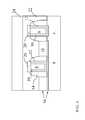
- FIG. 1a cross-sectional view of a prior art precursor integrated circuit (IC) structure 2 is shown.
- this precursor IC structure 2can be subsequently processed according to embodiments in order to form an unconventional integrated circuit structure.
- the precursor IC structure 2includes a conventional substrate 4 .
- the precursor IC structure 2further includes two conventional transistor structures 6 (e.g., field-effect transistors or FETS) formed over the substrate 4 .
- transistor structures 6e.g., field-effect transistors or FETS
- FETSfield-effect transistors
- one or more transistor structure 6can include a metal gate 8 , which can be formed of one or more of aluminum (Al), copper (Cu), rhodium (Rh), iridium (Ir), ruthenium (Rh) or tungsten (W).
- Transistor structure 6can also include a metal liner 10 lining the metal gate 8 , where the metal liner 10 includes one or more of tantalum (e.g., tantalum nitride, TaN), tungsten (e.g., tungsten nitride, WN) or titanium (e.g., titanium nitride, TiN).
- the metal liner 10contacts the metal gate 8 and can substantially surround or encompass the metal gate 8 .
- a high-k (or, high-dielectric constant) liner 12Surrounding the metal liner 10 is a high-k (or, high-dielectric constant) liner 12 , which can be formed of any high dielectric constant material, e.g., metal oxides such as tantalum oxide (Ta 2 O 5 ), barium titanium oxide (BaTiO 3 ), hafnium oxide (HfO 2 ), zirconium oxide (ZrO 2 ), aluminum oxide (Al 2 O 3 ), or metal silicates such as hafnium silicate oxide (Hf A1 Si A2 O A3 ) or hafnium silicate oxynitride (Hf A1 Si A2 O A3 N A4 ), where A1, A2, A3, and A4 represent relative proportions, each greater than or equal to zero and A1+A2+A3+A4 (1 being the total relative mole quantity).
- metal oxidessuch as tantalum oxide (Ta 2 O 5 ), barium titanium oxide (Ba
- the high-k liner 12is abutted by spacers 14 , which can be formed of conventional spacer materials (e.g., silicon nitride, Si 3 N 4 ). These spacers 14 are located approximately adjacent, or proximate the metal gate 8 , and can substantially surround the metal gate 8 . Also shown included in the transistor structures 6 are conductive layers 16 , which can be formed of any suitable contact metals for performing functions associated with the transistor structures 6 .
- FIG. 2illustrates a process performed to the precursor integrated circuit structure 2 of FIG. 1 , where this process is part of a method performed according to embodiments.
- FIG. 2illustrates selectively forming an etch stop layer (e.g., a metal etch stop) 18 to the metal gate 8 .
- the etch stop layer 18can be formed over the metal gate 8 by one or more selective deposition techniques, including, chemical vapor deposition (CVD), atomic layer deposition (ALD), or electroless deposition.
- the etch stop layer 18can be deposited to a thickness of approximately 0.5-10 nanometers (nm) in some embodiments.
- the etch stop layer 18can include one or more of cobalt (Co), manganese (Mn), or ruthenium (Ru).
- the etch stop layer 18is formed selectively over only the metal gate 8 . In other embodiments, the etch stop layer 18 is formed selectively to the metal gate 8 as well as the metal liner 10 and the high-k liner 12 .
- the deposition techniquecan be selective to the top, or planar portion of the semiconductor structure 6 , and exclusive of the spacers 14 .
- the term “selective”can be an inclusive term, such that forming a first layer “selective” to second layer means that the first layer is formed only over the second layer. As such, the layer is formed exclusive of other, unnamed layers (e.g., adjacent layer) in some embodiments.
- etch stop layer 18selectively forming the etch stop layer 18 to the metal gate 8 allows for electrical insulation of the metal gate with decreased capacitive effects when compared with conventional integrated circuit structures that utilize an entire high-k layer overlying both the gate and spacers.
- FIG. 3illustrates the process of at least partially oxidizing the etch stop layer 18 of FIG. 2 to form an oxidized metal etch stop layer (or, oxidized etch stop) 20 .
- the oxidized etch stop 20can be partially oxidized, or completely oxidized through a plasma-contained process, or a thermal process within an oxygen-contained or an ozone-contained ambient.
- the oxidation processallows the oxidized etch stop 20 to act as an effective insulator between the metal gate 8 and a subsequently formed contact layer (as shown and described with reference to FIGS. 6 and 7 ).
- FIG. 3illustrates a completely oxidized etch stop 20 according to embodiments.
- FIG. 4illustrates the process of forming a dielectric layer 22 and dielectric layer 24 over the structure of FIG. 3 .
- the dielectric layers 22 , 24can include one or more conventional dielectric materials such as, silicon dioxide (SiO 2 ), silicon nitride (Si3N4), silicon carbide (SiC), oxygen and hydrogen-doped silicon carbide (SiCOH), etc.
- These dielectric layers 22 , 24can be formed using conventional techniques such as chemical vapor deposition, spin-on methods, etc. It is understood that these dielectric layers 22 , 24 can be formed as a single dielectric layer, or as multiple dielectric layers, as is known in the art.
- FIG. 5illustrates the process of forming an opening 26 in the dielectric layer 22 and dielectric layer 24 , respectively.
- the opening 26is formed to expose the conductive layers 16 , alongside the spacer 14 , for subsequent formation of a contact ( FIGS. 6 and 7 ).
- the opening 26can be formed using any conventional etching technique, and is preferably selectively formed (anisotropically). In some cases, the opening 26 can be self-aligned, that is, formation of the opening 26 is dictated by the etch-resistant properties of the underlying layers (e.g., the oxidized etch stop layer 20 and the spacer 14 ).
- the oxidized etch stop layer 20can act as an etch stop over the metal gate 8 to protect the gate 8 from physical damage during the etching process. Additionally, the oxidized etch stop layer 20 can physically and electrically isolate the gate from the later-formed contact formed in the opening 26 (e.g., contact 28 in FIGS. 6 and 7 ).
- FIG. 6illustrates the process of forming a contact 28 to the conductive layers 16 in the opening 26 .
- the contact 28can be formed using any conventional methods (e.g., deposition and/or epitaxial growth), and can be formed of a conventional contact material including one or more of Cu, W, etc.
- the contact 28can be formed (e.g., by filling the opening), and additional contact material can be etched back or otherwise removed using conventional methods (e.g., CMP or other polishing/planarizing methods).
- the oxidized etch stop layer 20can physically and electrically isolate (or, separate) the metal gate 8 from the contact 28 during, and after, formation of the contact 28 .
- this final integrated circuit structure 102includes a substrate 4 ; a metal gate 8 located over the substrate 4 ; at least one liner layer (metal liner 10 or high-k liner 12 ) or over the substrate 4 and substantially surrounding the metal gate 8 ; and an oxidized etch stop layer 20 located directly over the metal gate 8 .
- the oxidized etch stop layer 20can include of at least one of cobalt (Co), manganese (Mn), or ruthenium (Ru), and is approximately completely oxidized.
- FIG. 7shows an alternative embodiment of an integrated circuit structure 202 , where the etch stop layer 20 is only partially oxidized.
- the etch stop layer 20includes a non-oxidized core region 30 directly contacting the metal gate 8 , and an outer (or surrounding) region 32 substantially surrounding the core region 30 (but for the portions of the core region 30 contacting the metal gate 8 ).
- the outer region 32can be oxidized using the conventional techniques described herein, and in some cases, is formed by partially oxidizing the etch stop layer 20 during the oxidizing process, such that the core 30 remains non-oxidized.
Landscapes
- Engineering & Computer Science (AREA)
- Physics & Mathematics (AREA)
- Microelectronics & Electronic Packaging (AREA)
- General Physics & Mathematics (AREA)
- Manufacturing & Machinery (AREA)
- Computer Hardware Design (AREA)
- Condensed Matter Physics & Semiconductors (AREA)
- Power Engineering (AREA)
- Plasma & Fusion (AREA)
- Electrodes Of Semiconductors (AREA)
- Internal Circuitry In Semiconductor Integrated Circuit Devices (AREA)
- Insulated Gate Type Field-Effect Transistor (AREA)
- Metal-Oxide And Bipolar Metal-Oxide Semiconductor Integrated Circuits (AREA)
Abstract
Description
Claims (13)
Priority Applications (1)
| Application Number | Priority Date | Filing Date | Title |
|---|---|---|---|
| US14/494,699US9379198B2 (en) | 2011-09-15 | 2014-09-24 | Integrated circuit structure having selectively formed metal cap |
Applications Claiming Priority (2)
| Application Number | Priority Date | Filing Date | Title |
|---|---|---|---|
| US13/233,064US8877645B2 (en) | 2011-09-15 | 2011-09-15 | Integrated circuit structure having selectively formed metal cap |
| US14/494,699US9379198B2 (en) | 2011-09-15 | 2014-09-24 | Integrated circuit structure having selectively formed metal cap |
Related Parent Applications (1)
| Application Number | Title | Priority Date | Filing Date |
|---|---|---|---|
| US13/233,064DivisionUS8877645B2 (en) | 2011-09-15 | 2011-09-15 | Integrated circuit structure having selectively formed metal cap |
Publications (2)
| Publication Number | Publication Date |
|---|---|
| US20150008527A1 US20150008527A1 (en) | 2015-01-08 |
| US9379198B2true US9379198B2 (en) | 2016-06-28 |
Family
ID=47879862
Family Applications (2)
| Application Number | Title | Priority Date | Filing Date |
|---|---|---|---|
| US13/233,064Expired - Fee RelatedUS8877645B2 (en) | 2011-09-15 | 2011-09-15 | Integrated circuit structure having selectively formed metal cap |
| US14/494,699Active2031-09-16US9379198B2 (en) | 2011-09-15 | 2014-09-24 | Integrated circuit structure having selectively formed metal cap |
Family Applications Before (1)
| Application Number | Title | Priority Date | Filing Date |
|---|---|---|---|
| US13/233,064Expired - Fee RelatedUS8877645B2 (en) | 2011-09-15 | 2011-09-15 | Integrated circuit structure having selectively formed metal cap |
Country Status (3)
| Country | Link |
|---|---|
| US (2) | US8877645B2 (en) |
| CN (1) | CN103828026B (en) |
| WO (1) | WO2013039580A1 (en) |
Families Citing this family (7)
| Publication number | Priority date | Publication date | Assignee | Title |
|---|---|---|---|---|
| CN105826174B (en) | 2015-01-05 | 2021-06-15 | 联华电子股份有限公司 | Semiconductor device and method of making the same |
| TWI658591B (en)* | 2015-03-13 | 2019-05-01 | 聯華電子股份有限公司 | Semiconductor component and manufacturing method thereof |
| US9698232B2 (en) | 2015-03-18 | 2017-07-04 | Qualcomm Incorporated | Conductive cap for metal-gate transistor |
| US10062763B2 (en) | 2015-05-27 | 2018-08-28 | Qualcomm Incorporated | Method and apparatus for selectively forming nitride caps on metal gate |
| TWI653673B (en) | 2015-08-27 | 2019-03-11 | 聯華電子股份有限公司 | Semiconductor structure and manufacturing method thereof |
| US11189525B2 (en) | 2020-02-21 | 2021-11-30 | Taiwan Semiconductor Manufacturing Company, Ltd. | Via-first process for connecting a contact and a gate electrode |
| US20230187535A1 (en)* | 2021-12-14 | 2023-06-15 | Taiwan Semiconductor Manufacturing Company, Ltd. | Semiconductor structure with modified spacer and method for forming the same |
Citations (24)
| Publication number | Priority date | Publication date | Assignee | Title |
|---|---|---|---|---|
| US5549808A (en)* | 1995-05-12 | 1996-08-27 | International Business Machines Corporation | Method for forming capped copper electrical interconnects |
| KR960013638B1 (en) | 1993-03-03 | 1996-10-10 | 삼성전자 주식회사 | Method of forming contact window of semiconductor device |
| US5585673A (en) | 1992-02-26 | 1996-12-17 | International Business Machines Corporation | Refractory metal capped low resistivity metal conductor lines and vias |
| US5695810A (en) | 1996-11-20 | 1997-12-09 | Cornell Research Foundation, Inc. | Use of cobalt tungsten phosphide as a barrier material for copper metallization |
| US6171957B1 (en)* | 1997-07-16 | 2001-01-09 | Mitsubishi Denki Kabushiki Kaisha | Manufacturing method of semiconductor device having high pressure reflow process |
| US20010003063A1 (en) | 1999-04-16 | 2001-06-07 | Hu Yongjun Jeff | Electrochemical cobalt silicide liner for metal contact fills and damascene processes |
| US6255164B1 (en) | 1999-08-03 | 2001-07-03 | Worldwide Semiconductor Manufacturing Corp. | EPROM cell structure and a method for forming the EPROM cell structure |
| KR20010057491A (en) | 1999-12-23 | 2001-07-04 | 박종섭 | Manufacturing method for semiconductor device |
| US6342733B1 (en) | 1999-07-27 | 2002-01-29 | International Business Machines Corporation | Reduced electromigration and stressed induced migration of Cu wires by surface coating |
| US6706625B1 (en) | 2002-12-06 | 2004-03-16 | Chartered Semiconductor Manufacturing Ltd. | Copper recess formation using chemical process for fabricating barrier cap for lines and vias |
| US20040113279A1 (en) | 2002-12-16 | 2004-06-17 | International Business Machines Corporation | Copper recess process with application to selective capping and electroless plating |
| US20040175910A1 (en) | 2003-02-10 | 2004-09-09 | Advanced Micro Devices, Inc. | Engineered metal gate electrode |
| US6908806B2 (en) | 2003-01-31 | 2005-06-21 | Infineon Technologies Ag | Gate metal recess for oxidation protection and parasitic capacitance reduction |
| US7026689B2 (en) | 2004-08-27 | 2006-04-11 | Taiwan Semiconductor Manufacturing Company | Metal gate structure for MOS devices |
| US20080157365A1 (en) | 2006-12-27 | 2008-07-03 | Andrew Ott | Transistor having an etch stop layer including a metal compound that is selectively formed over a metal gate, and method therefor |
| US20080315426A1 (en) | 2007-06-21 | 2008-12-25 | International Business Machines Corporation | METAL CAP WITH ULTRA-LOW k DIELECTRIC MATERIAL FOR CIRCUIT INTERCONNECT APPLICATIONS |
| US20090283922A1 (en) | 2007-12-27 | 2009-11-19 | Willy Rachmady | Integrating high stress cap layer in high-k metal gate transistor |
| US20100038713A1 (en)* | 2008-08-13 | 2010-02-18 | Prashant Majhi | Self-aligned tunneling pocket in field-effect transistors and processes to form same |
| US20100048013A1 (en) | 2008-08-21 | 2010-02-25 | Taiwan Semiconductor Manufacturing Company, Ltd. | Novel high-k metal gate cmos patterning method |
| US20100068876A1 (en) | 2008-09-12 | 2010-03-18 | Taiwan Semiconductor Manufacturing Company, Ltd. | Methods of fabricating high-k metal gate devices |
| US7790631B2 (en) | 2006-11-21 | 2010-09-07 | Intel Corporation | Selective deposition of a dielectric on a self-assembled monolayer-adsorbed metal |
| US7884475B2 (en) | 2007-10-16 | 2011-02-08 | International Business Machines Corporation | Conductor structure including manganese oxide capping layer |
| US20110031562A1 (en) | 2009-08-07 | 2011-02-10 | Taiwan Semiconductor Manufacturing Company, Ltd. | Sealing layer of a field effect transistor |
| US20110156107A1 (en)* | 2009-12-30 | 2011-06-30 | Bohr Mark T | Self-aligned contacts |
Family Cites Families (1)
| Publication number | Priority date | Publication date | Assignee | Title |
|---|---|---|---|---|
| JPH1187349A (en)* | 1997-07-16 | 1999-03-30 | Mitsubishi Electric Corp | Semiconductor device manufacturing method and semiconductor device |
- 2011
- 2011-09-15USUS13/233,064patent/US8877645B2/ennot_activeExpired - Fee Related
- 2012
- 2012-06-13WOPCT/US2012/042170patent/WO2013039580A1/enactiveApplication Filing
- 2012-06-13CNCN201280044778.1Apatent/CN103828026B/ennot_activeExpired - Fee Related
- 2014
- 2014-09-24USUS14/494,699patent/US9379198B2/enactiveActive
Patent Citations (26)
| Publication number | Priority date | Publication date | Assignee | Title |
|---|---|---|---|---|
| US6323554B1 (en) | 1992-02-26 | 2001-11-27 | International Business Machines Corporation | Refractory metal capped low resistivity metal conductor lines and vias formed using PVD and CVD |
| US5585673A (en) | 1992-02-26 | 1996-12-17 | International Business Machines Corporation | Refractory metal capped low resistivity metal conductor lines and vias |
| KR960013638B1 (en) | 1993-03-03 | 1996-10-10 | 삼성전자 주식회사 | Method of forming contact window of semiconductor device |
| US5549808A (en)* | 1995-05-12 | 1996-08-27 | International Business Machines Corporation | Method for forming capped copper electrical interconnects |
| US5695810A (en) | 1996-11-20 | 1997-12-09 | Cornell Research Foundation, Inc. | Use of cobalt tungsten phosphide as a barrier material for copper metallization |
| US6171957B1 (en)* | 1997-07-16 | 2001-01-09 | Mitsubishi Denki Kabushiki Kaisha | Manufacturing method of semiconductor device having high pressure reflow process |
| US20010003063A1 (en) | 1999-04-16 | 2001-06-07 | Hu Yongjun Jeff | Electrochemical cobalt silicide liner for metal contact fills and damascene processes |
| US6342733B1 (en) | 1999-07-27 | 2002-01-29 | International Business Machines Corporation | Reduced electromigration and stressed induced migration of Cu wires by surface coating |
| US6255164B1 (en) | 1999-08-03 | 2001-07-03 | Worldwide Semiconductor Manufacturing Corp. | EPROM cell structure and a method for forming the EPROM cell structure |
| KR20010057491A (en) | 1999-12-23 | 2001-07-04 | 박종섭 | Manufacturing method for semiconductor device |
| US6706625B1 (en) | 2002-12-06 | 2004-03-16 | Chartered Semiconductor Manufacturing Ltd. | Copper recess formation using chemical process for fabricating barrier cap for lines and vias |
| US20040113279A1 (en) | 2002-12-16 | 2004-06-17 | International Business Machines Corporation | Copper recess process with application to selective capping and electroless plating |
| US6908806B2 (en) | 2003-01-31 | 2005-06-21 | Infineon Technologies Ag | Gate metal recess for oxidation protection and parasitic capacitance reduction |
| US20040175910A1 (en) | 2003-02-10 | 2004-09-09 | Advanced Micro Devices, Inc. | Engineered metal gate electrode |
| US7026689B2 (en) | 2004-08-27 | 2006-04-11 | Taiwan Semiconductor Manufacturing Company | Metal gate structure for MOS devices |
| US7790631B2 (en) | 2006-11-21 | 2010-09-07 | Intel Corporation | Selective deposition of a dielectric on a self-assembled monolayer-adsorbed metal |
| US20080157365A1 (en) | 2006-12-27 | 2008-07-03 | Andrew Ott | Transistor having an etch stop layer including a metal compound that is selectively formed over a metal gate, and method therefor |
| US8120114B2 (en)* | 2006-12-27 | 2012-02-21 | Intel Corporation | Transistor having an etch stop layer including a metal compound that is selectively formed over a metal gate |
| US20080315426A1 (en) | 2007-06-21 | 2008-12-25 | International Business Machines Corporation | METAL CAP WITH ULTRA-LOW k DIELECTRIC MATERIAL FOR CIRCUIT INTERCONNECT APPLICATIONS |
| US7884475B2 (en) | 2007-10-16 | 2011-02-08 | International Business Machines Corporation | Conductor structure including manganese oxide capping layer |
| US20090283922A1 (en) | 2007-12-27 | 2009-11-19 | Willy Rachmady | Integrating high stress cap layer in high-k metal gate transistor |
| US20100038713A1 (en)* | 2008-08-13 | 2010-02-18 | Prashant Majhi | Self-aligned tunneling pocket in field-effect transistors and processes to form same |
| US20100048013A1 (en) | 2008-08-21 | 2010-02-25 | Taiwan Semiconductor Manufacturing Company, Ltd. | Novel high-k metal gate cmos patterning method |
| US20100068876A1 (en) | 2008-09-12 | 2010-03-18 | Taiwan Semiconductor Manufacturing Company, Ltd. | Methods of fabricating high-k metal gate devices |
| US20110031562A1 (en) | 2009-08-07 | 2011-02-10 | Taiwan Semiconductor Manufacturing Company, Ltd. | Sealing layer of a field effect transistor |
| US20110156107A1 (en)* | 2009-12-30 | 2011-06-30 | Bohr Mark T | Self-aligned contacts |
Non-Patent Citations (9)
| Title |
|---|
| Au et al., "Selective Chemical Vapor Deposition of Manganese Self-Aligned Capping Layer for Cu Interconnections in Microelectronics", Journal of the Electrochemical Society, 157 (6) D341-D345 (2010). |
| Dakhel et al., "Correlated Structural and Electrical Properties of Thin Manganese Oxide Films", Thin Solid Films 496 (2006), 353-359. |
| Mayuzumi Satoru, et al., High-Performance Metal/High-k-n-and p-MOSFETs with Top-Cut Dual Stress Liner Using Gate-Last Damascene Process on (100) Substrates. IEEE Transactions on Electron Devices; Apr. 2009, vol. 56 No. 4, pp. 620-625. |
| PCT Notification of Transmittal of the International Search Report and the Written Opinion of the International Searching Authority, or the Declaration dated Jan. 10, 2013. |
| U.S. Appl. No. 13/233,064, Notice of Allowance and Fees Due dated Jul. 3, 2014. |
| U.S. Appl. No. 13/233,064, Office Action dated Jan. 9, 2014. |
| U.S. Appl. No. 13/233,064, Office Action dated Jul. 30, 2013. |
| U.S. Appl. No. 13/233,064, Office Action dated Mar. 1, 2013. |
| U.S. Appl. No. 13/233,064, Office Action dated Oct. 30, 2013. |
Also Published As
| Publication number | Publication date |
|---|---|
| CN103828026A (en) | 2014-05-28 |
| US20130069161A1 (en) | 2013-03-21 |
| WO2013039580A1 (en) | 2013-03-21 |
| CN103828026B (en) | 2016-08-17 |
| US8877645B2 (en) | 2014-11-04 |
| US20150008527A1 (en) | 2015-01-08 |
Similar Documents
| Publication | Publication Date | Title |
|---|---|---|
| US9379198B2 (en) | Integrated circuit structure having selectively formed metal cap | |
| US11569362B2 (en) | Semiconductor device and a method for fabricating the same | |
| US9917014B2 (en) | Vertical air gap subtractive etch back end metal | |
| CN107017297B (en) | Semiconductor device and method of manufacturing the same | |
| US7994641B2 (en) | Semiconductor device and method of fabricating the same | |
| CN103854990B (en) | Methods for fabricating integrated circuits having low resistance metal gate structures | |
| JP5503517B2 (en) | Method for manufacturing field effect transistor | |
| US8536040B1 (en) | Techniques for using material substitution processes to form replacement metal gate electrodes of semiconductor devices with self-aligned contacts | |
| US20080157365A1 (en) | Transistor having an etch stop layer including a metal compound that is selectively formed over a metal gate, and method therefor | |
| US10056462B2 (en) | Metal gate structure and manufacturing method thereof | |
| CN106910737B (en) | Semiconductor device and method for forming the same | |
| CN112951762B (en) | Dual dielectric layers for sealing seams in air-gap structures | |
| CN110610903A (en) | Manufacturing method of semiconductor device | |
| US9595450B2 (en) | Composite structure for gate level inter-layer dielectric | |
| US8581351B2 (en) | Replacement gate with reduced gate leakage current | |
| CN104867967A (en) | Semiconductor Device And Fabricating Method Thereof | |
| US9111783B2 (en) | Semiconductor devices with self-aligned source drain contacts and methods for making the same | |
| CN103871895A (en) | Method for fabricating a field effect transistor device | |
| US20080023774A1 (en) | Semiconductor device and method for fabricating the same | |
| JP6731344B2 (en) | Hybrid high-k first and high-k last replacement gate process | |
| CN111554659B (en) | Plug structure and its manufacturing process | |
| US8598033B1 (en) | Method for forming a salicide layer | |
| US20120286373A1 (en) | Gate structure and method for manufacturing the same | |
| CN203134802U (en) | Semiconductor structure | |
| US12255070B2 (en) | Semiconductor devices and methods of manufacturing |
Legal Events
| Date | Code | Title | Description |
|---|---|---|---|
| AS | Assignment | Owner name:INTERNATIONAL BUSINESS MACHINES CORPORATION, NEW Y Free format text:ASSIGNMENT OF ASSIGNORS INTEREST;ASSIGNORS:YANG, CHIH-CHAO;HORAK, DAVID V.;KOBURGER, CHARLES W., III;AND OTHERS;SIGNING DATES FROM 20140912 TO 20140923;REEL/FRAME:033803/0977 | |
| AS | Assignment | Owner name:GLOBALFOUNDRIES U.S. 2 LLC, NEW YORK Free format text:ASSIGNMENT OF ASSIGNORS INTEREST;ASSIGNOR:INTERNATIONAL BUSINESS MACHINES CORPORATION;REEL/FRAME:036550/0001 Effective date:20150629 | |
| AS | Assignment | Owner name:GLOBALFOUNDRIES INC., CAYMAN ISLANDS Free format text:ASSIGNMENT OF ASSIGNORS INTEREST;ASSIGNORS:GLOBALFOUNDRIES U.S. 2 LLC;GLOBALFOUNDRIES U.S. INC.;REEL/FRAME:036779/0001 Effective date:20150910 | |
| FEPP | Fee payment procedure | Free format text:PAYOR NUMBER ASSIGNED (ORIGINAL EVENT CODE: ASPN); ENTITY STATUS OF PATENT OWNER: LARGE ENTITY Free format text:PAYER NUMBER DE-ASSIGNED (ORIGINAL EVENT CODE: RMPN); ENTITY STATUS OF PATENT OWNER: LARGE ENTITY | |
| STCF | Information on status: patent grant | Free format text:PATENTED CASE | |
| AS | Assignment | Owner name:WILMINGTON TRUST, NATIONAL ASSOCIATION, DELAWARE Free format text:SECURITY AGREEMENT;ASSIGNOR:GLOBALFOUNDRIES INC.;REEL/FRAME:049490/0001 Effective date:20181127 | |
| FEPP | Fee payment procedure | Free format text:MAINTENANCE FEE REMINDER MAILED (ORIGINAL EVENT CODE: REM.); ENTITY STATUS OF PATENT OWNER: LARGE ENTITY | |
| FEPP | Fee payment procedure | Free format text:SURCHARGE FOR LATE PAYMENT, LARGE ENTITY (ORIGINAL EVENT CODE: M1554); ENTITY STATUS OF PATENT OWNER: LARGE ENTITY | |
| MAFP | Maintenance fee payment | Free format text:PAYMENT OF MAINTENANCE FEE, 4TH YEAR, LARGE ENTITY (ORIGINAL EVENT CODE: M1551); ENTITY STATUS OF PATENT OWNER: LARGE ENTITY Year of fee payment:4 | |
| AS | Assignment | Owner name:GLOBALFOUNDRIES INC., CAYMAN ISLANDS Free format text:RELEASE BY SECURED PARTY;ASSIGNOR:WILMINGTON TRUST, NATIONAL ASSOCIATION;REEL/FRAME:054479/0842 Effective date:20200410 Owner name:TAIWAN SEMICONDUCTOR MANUFACTURING CO., LTD., TAIWAN Free format text:ASSIGNMENT OF ASSIGNORS INTEREST;ASSIGNOR:GLOBALFOUNDRIES INC.;REEL/FRAME:054482/0862 Effective date:20200515 | |
| AS | Assignment | Owner name:GLOBALFOUNDRIES INC., CAYMAN ISLANDS Free format text:RELEASE BY SECURED PARTY;ASSIGNOR:WILMINGTON TRUST, NATIONAL ASSOCIATION;REEL/FRAME:054636/0001 Effective date:20201117 | |
| MAFP | Maintenance fee payment | Free format text:PAYMENT OF MAINTENANCE FEE, 8TH YEAR, LARGE ENTITY (ORIGINAL EVENT CODE: M1552); ENTITY STATUS OF PATENT OWNER: LARGE ENTITY Year of fee payment:8 |