US9377487B2 - Transducer structure and method for MEMS devices - Google Patents
Transducer structure and method for MEMS devicesDownload PDFInfo
- Publication number
- US9377487B2 US9377487B2US13/922,539US201313922539AUS9377487B2US 9377487 B2US9377487 B2US 9377487B2US 201313922539 AUS201313922539 AUS 201313922539AUS 9377487 B2US9377487 B2US 9377487B2
- Authority
- US
- United States
- Prior art keywords
- surface region
- spring
- movable base
- disposed
- base structure
- Prior art date
- Legal status (The legal status is an assumption and is not a legal conclusion. Google has not performed a legal analysis and makes no representation as to the accuracy of the status listed.)
- Active, expires
Links
Images


Classifications
- G—PHYSICS
- G01—MEASURING; TESTING
- G01R—MEASURING ELECTRIC VARIABLES; MEASURING MAGNETIC VARIABLES
- G01R3/00—Apparatus or processes specially adapted for the manufacture or maintenance of measuring instruments, e.g. of probe tips
- B—PERFORMING OPERATIONS; TRANSPORTING
- B81—MICROSTRUCTURAL TECHNOLOGY
- B81B—MICROSTRUCTURAL DEVICES OR SYSTEMS, e.g. MICROMECHANICAL DEVICES
- B81B3/00—Devices comprising flexible or deformable elements, e.g. comprising elastic tongues or membranes
- B81B3/0064—Constitution or structural means for improving or controlling the physical properties of a device
- B81B3/0067—Mechanical properties
- B81B3/0072—For controlling internal stress or strain in moving or flexible elements, e.g. stress compensating layers
- G—PHYSICS
- G01—MEASURING; TESTING
- G01C—MEASURING DISTANCES, LEVELS OR BEARINGS; SURVEYING; NAVIGATION; GYROSCOPIC INSTRUMENTS; PHOTOGRAMMETRY OR VIDEOGRAMMETRY
- G01C19/00—Gyroscopes; Turn-sensitive devices using vibrating masses; Turn-sensitive devices without moving masses; Measuring angular rate using gyroscopic effects
- G01C19/56—Turn-sensitive devices using vibrating masses, e.g. vibratory angular rate sensors based on Coriolis forces
- G01C19/5783—Mountings or housings not specific to any of the devices covered by groups G01C19/5607 - G01C19/5719
- G—PHYSICS
- G01—MEASURING; TESTING
- G01P—MEASURING LINEAR OR ANGULAR SPEED, ACCELERATION, DECELERATION, OR SHOCK; INDICATING PRESENCE, ABSENCE, OR DIRECTION, OF MOVEMENT
- G01P15/00—Measuring acceleration; Measuring deceleration; Measuring shock, i.e. sudden change of acceleration
- G01P15/02—Measuring acceleration; Measuring deceleration; Measuring shock, i.e. sudden change of acceleration by making use of inertia forces using solid seismic masses
- G01P15/08—Measuring acceleration; Measuring deceleration; Measuring shock, i.e. sudden change of acceleration by making use of inertia forces using solid seismic masses with conversion into electric or magnetic values
- G01P15/125—Measuring acceleration; Measuring deceleration; Measuring shock, i.e. sudden change of acceleration by making use of inertia forces using solid seismic masses with conversion into electric or magnetic values by capacitive pick-up
- B—PERFORMING OPERATIONS; TRANSPORTING
- B81—MICROSTRUCTURAL TECHNOLOGY
- B81B—MICROSTRUCTURAL DEVICES OR SYSTEMS, e.g. MICROMECHANICAL DEVICES
- B81B2203/00—Basic microelectromechanical structures
- B81B2203/01—Suspended structures, i.e. structures allowing a movement
- B81B2203/0145—Flexible holders
- B81B2203/0163—Spring holders
- B—PERFORMING OPERATIONS; TRANSPORTING
- B81—MICROSTRUCTURAL TECHNOLOGY
- B81B—MICROSTRUCTURAL DEVICES OR SYSTEMS, e.g. MICROMECHANICAL DEVICES
- B81B2203/00—Basic microelectromechanical structures
- B81B2203/03—Static structures
- B81B2203/0307—Anchors
- G—PHYSICS
- G01—MEASURING; TESTING
- G01P—MEASURING LINEAR OR ANGULAR SPEED, ACCELERATION, DECELERATION, OR SHOCK; INDICATING PRESENCE, ABSENCE, OR DIRECTION, OF MOVEMENT
- G01P15/00—Measuring acceleration; Measuring deceleration; Measuring shock, i.e. sudden change of acceleration
- G01P15/02—Measuring acceleration; Measuring deceleration; Measuring shock, i.e. sudden change of acceleration by making use of inertia forces using solid seismic masses
- G01P15/08—Measuring acceleration; Measuring deceleration; Measuring shock, i.e. sudden change of acceleration by making use of inertia forces using solid seismic masses with conversion into electric or magnetic values
- G01P2015/0805—Measuring acceleration; Measuring deceleration; Measuring shock, i.e. sudden change of acceleration by making use of inertia forces using solid seismic masses with conversion into electric or magnetic values being provided with a particular type of spring-mass-system for defining the displacement of a seismic mass due to an external acceleration
- G01P2015/0857—Measuring acceleration; Measuring deceleration; Measuring shock, i.e. sudden change of acceleration by making use of inertia forces using solid seismic masses with conversion into electric or magnetic values being provided with a particular type of spring-mass-system for defining the displacement of a seismic mass due to an external acceleration using a particular shape of the suspension spring
- Y—GENERAL TAGGING OF NEW TECHNOLOGICAL DEVELOPMENTS; GENERAL TAGGING OF CROSS-SECTIONAL TECHNOLOGIES SPANNING OVER SEVERAL SECTIONS OF THE IPC; TECHNICAL SUBJECTS COVERED BY FORMER USPC CROSS-REFERENCE ART COLLECTIONS [XRACs] AND DIGESTS
- Y10—TECHNICAL SUBJECTS COVERED BY FORMER USPC
- Y10T—TECHNICAL SUBJECTS COVERED BY FORMER US CLASSIFICATION
- Y10T29/00—Metal working
- Y10T29/49—Method of mechanical manufacture
- Y10T29/49002—Electrical device making
- Y10T29/49007—Indicating transducer
Definitions
- This inventionrelates generally to integrated devices. More specifically, the invention provides an integrated transducer apparatus that can be used in combination with other micro-electromechanical systems (MEMS) devices, but can have other uses as well.
- MEMS devicesinclude accelerometers, angular rate sensors, magnetic field sensors, pressure sensors, microphones, humidity sensors, temperature sensors, chemical sensors, biosensors, inertial sensors, and others.
- CMOS technologyhas become the predominant fabrication technology for integrated circuits (ICs).
- ICsare the “brains” of an integrated device and provide decision-making capabilities
- MEMSare the “eyes” and “arms” and provide the ability to sense and control the environment.
- RFradio frequency
- Some examples of the widespread application of these technologiesare the switches in radio frequency (RF) antenna systems, such as those in the iPhoneTM or iPadTM device by Apple, Inc. of Cupertino, Calif. and the BlackberryTM phone by Research In Motion Limited of Waterloo, Ontario, Canada. They are also used to provide accelerometers in sensor-equipped game devices, such as those in the WiiTM controller manufactured by Nintendo Company Limited of Japan. Though they are not always easily identifiable, these technologies are becoming more prevalent every day.
- RFradio frequency
- MEMSIntegrated Multimedia Subsystems
- accelerometers and angular rate sensorsare used to deploy airbags and trigger dynamic stability control functions, respectively.
- MEMS angular rate sensorscan also be used for image stabilization systems in video and still cameras, automatic steering systems in airplanes and guided munitions, or the like.
- MEMScan also be in the form of biological MEMS (Bio-MEMS) that can be used to implement biological and/or chemical sensors for Lab-On-Chip applications. Such applications may integrate one or more laboratory functions on a single millimeter-sized chip.
- Other applicationsinclude Internet and telephone networks, security and financial applications, and health care and medical systems.
- ICs and MEMScan be used to practically engage in various type of environmental interaction.
- the present inventionprovides an improved MEMS transducer apparatus that can be used in combination with other MEMS devices, or other devices.
- Typical MEMS devicesinclude accelerometers, angular rate sensors, magnetic field sensors, pressure sensors, microphones, humidity sensors, temperature sensors, chemical sensors, biosensors, inertial sensors, and others. It will be recognized that the invention has a broad range of applicability.
- the inventionprovides an integrated transducer apparatus disposed upon a substrate member having a surface region.
- the apparatushas a movable base structure having an outer surface region.
- the movable base membercan have at least one portion removed to form at least one inner surface region.
- At least one intermediate anchor structurecan be spatially disposed within a vicinity of the inner surface region(s) and at least one intermediate spring structure can be coupled to at least one portion of the inner surface region(s) and the intermediate anchor structure(s).
- the present techniqueprovides an easy to use process.
- the methodprovides higher device yields in dice per wafer with the integrated approach.
- the methodprovides a process and apparatus that are compatible with existing process technology without substantial modifications to equipment and processes.
- the inventionprovides for an improved MEMS device apparatus for a variety of uses.
- the inventionprovides an improved MEMS transducer apparatus, which may be integrated on at least one integrated electronic device structure.
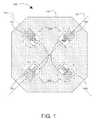
- FIG. 1is a simplified top diagram of a transducer apparatus according to an embodiment of the present invention
- FIG. 2is a simplified perspective diagram of a transducer apparatus according to an embodiment of the present invention.
- FIG. 3is a simplified cross-sectional side diagram of a transducer apparatus according to an embodiment of the present invention.
- FIG. 4is a simplified cross-sectional close-up diagram of a transducer apparatus according to an embodiment of the present invention.
- FIG. 5is a simplified flow diagram of a transducer apparatus according to an embodiment of the present invention.
- FIG. 6is a simplified block diagram of a device incorporating various embodiments of the present invention.
- FIG. 1is a simplified top diagram of a transducer apparatus according to an embodiment of the present invention.
- apparatus 100includes a movable base structure 110 , at least one intermediate anchor structure 120 , and at least one intermediate spring structure 130 .
- apparatus 100can be configured to improve tolerance of external deformations.
- movable base structure 110can have an outer surface region, and have at least one portion removed to form at least one cavity having a cavity inner surface region 102 , the cavity disposed substantially within the movable base structure.
- movable base structure 110can be formed from a single crystal silicon, polycrystalline silicon, or amorphous silicon material.
- Moveable base structure 110can also include a thickness of a polymer or a thickness of a metal material.
- movable base structure 110can include other materials and combinations thereof.
- movable base structure 110can be a rectangular movable base structure, a patterned polygonal base structure, or the like.
- intermediate anchor structure(s) 120can be spatially disposed within a vicinity of inner surface region(s) 102 of the movable base structure.
- intermediate anchor structure(s) 120can be formed from single crystal silicon, polycrystalline silicon, amorphous silicon material, or the like.
- Intermediate anchor structure(s) 120can also include a polymer or metal material, or other materials or combinations thereof.
- intermediate spring structure(s) 130can be operably coupled to the intermediate anchor structure(s) 120 and at least one portion of inner surface region(s) 102 of movable base structure 110 .
- intermediate spring structure(s) 130can be formed from single crystal silicon, polycrystalline silicon, amorphous silicon material, or the like.
- Intermediate spring structure(s) 130can also include a polymer or metal material, or other materials or combinations thereof.
- intermediate spring structure(s) 130can be spatially oriented to be substantially 45 degrees or substantially (pi/4) radians to the edges of the die.
- the intermediate spring structure(s)can have at least one segment having a segment length.
- the segments of the springwhich are connected by folds, are used as a reference.
- the segmentswould be positioned such that the segments are perpendicular to diagonal lines 101 .
- Another way to determine the orientation of a springcan be done by drawing a “line” connecting the contacts of the spring from the anchor to the movable base (i.e. the end points of the spring). In this case, the proper orientation of the spring would have the “line” forming a substantially 45 degree or (pi/4) radian angle with the edges of a die (pointed along diagonal lines 101 ).
- apparatus 100can include at least one capacitor element spatially disposed within a vicinity of inner surface region(s) 102 of movable base structure 110 .
- the capacitor element(s)can include a fixed capacitor element and a movable capacitor element.
- the movable capacitor elementwill generally be disposed in a portion of the movable base structure 110 .
- the physical basis of apparatus 100is to have the average displacement of the fixed capacitor element(s) match the average displacement of the movable capacitor element(s) in response to external deformations.
- apparatus 100can be coupled to another MEMS device or an electronic device.
- apparatus 100can be configured to be tolerant of external deformations.
- Apparatus 100can be a transducer apparatus which reduces the area needed for anchors and springs and provides more area for other MEMS components.
- Another desirable design aspect contemplated by the inventorsis the reduction of the area used for springs. This can be achieved via two approaches. First, by having the springs oriented at substantially 45 degrees or substantially (pi/4) radians with respect to the edges of a die (i.e. aligned to diagonal lines 101 ), the Young's modulus is reduced and/or minimized with respect to orientation angle for single crystal silicon and standard silicon wafer crystal orientations.
- One way to determine the orientation of a springcan be done by using the segments of the spring, which are connected by folds, as a reference. The segments would be positioned such that the segments are perpendicular to diagonal lines 101 .
- Another way to determine the orientation of a springcan be done by drawing a “line” connecting the contacts of the spring from the anchor to the movable base (i.e. the end points of the spring). In this case, the proper orientation of the spring would have the “line” forming a substantially 45 degree or (pi/4) radian angle with the edges of a die (pointed along diagonal lines 101 ). However, the orientations of the springs may only be approximately oriented at the suggested angles due to manufacturing tolerances (orientation angles may be less than or greater than 45 degrees or (pi/4) radians). Second, the number of spring segments, which are connected by folds, should be regulated as too many spring segments may cause the spring structure to be not stiff enough.
- the number of segmentscannot be below a certain number, or the spring segment length will exceed the available die size, or make it impossible to put the anchor for the springs at the properly optimized “intermediate” locations to minimize undesirable variations of output with temperature.
- the spring configuration with variable number of spring segments and spring segment length in either of two perpendicular directionsrepresents various embodiments of the present invention. In such embodiments, the area is reduced while keeping the anchor and attachment point to the movable mass along a diagonal center line.
- FIG. 2is a simplified perspective diagram of a transducer apparatus according to an embodiment of the present invention.
- apparatus 100includes a movable base structure 110 , at least one intermediate anchor structure 120 , and at least one intermediate spring structure 130 .
- apparatus 100can be configured to improve tolerance of external deformations. A detailed description regarding the elements and configuration of apparatus 100 can be found above in the description for FIG. 1 .
- FIG. 3is a simplified cross-sectional side diagram of a transducer apparatus according to an embodiment of the present invention.
- apparatus 100includes a movable base structure 110 , at least one intermediate anchor structure 120 , and at least one intermediate spring structure 130 .
- apparatus 100can be configured to improve tolerance of external deformations. A detailed description regarding the elements and configuration of apparatus 100 can be found above in the description for FIG. 1 .
- FIG. 4is a simplified cross-sectional close-up diagram of a transducer apparatus according to an embodiment of the present invention.
- apparatus 400includes a movable base structure 410 and at least one capacitor element 460 .
- capacitor element(s) 460can include a fixed capacitor element and a movable capacitor element.
- the movable capacitor elementcan be disposed on a portion of the movable base structure and the fixed capacitor element can be disposed on a portion of the anchor structure(s).
- the capacitor element(s)can be tall vertical structures, which can include silicon materials and the like.
- apparatus 400can be configured to improve tolerance of external deformations.
- Capacitor element(s) 460can be spatially disposed within a vicinity of inner surface region(s) 402 of the movable base structure.
- Capacitor element(s) 460can also include differential capacitor element pair(s).
- the differential capacitor element pair(s)can operate during motion of movable base structure 410 . The charge on one element of the pair can increase while the charge on the other complementary element can decrease.
- Each differential paircan also be spatially disposed within a vicinity of inner surface region(s) 402 , and each pair can be disposed within a vicinity of its own inner surface region, isolated from other pairs.
- FIG. 5is a simplified flow diagram illustrating a method for fabricating a transducer apparatus according to an embodiment of the present invention. It is also understood that the examples and embodiments described herein are for illustrative purposes only and that various modifications or changes in light thereof will be suggested to persons skilled in the art and are to be included within the spirit and purview of this process and scope of the appended claims.
- the present methodcan be briefly outlined below.
- method 500begins at start, step 502 .
- the methodprovides a fabrication method for forming a MEMS transducer apparatus.
- the methodprovides higher device yields in dice per wafer with the integrated approach.
- the methodprovides a process and system that are compatible with conventional CMOS process technology without substantial modifications to equipment and processes.
- the inventionprovides for an improved integrated micro electro-mechanical systems and electronic devices and related methods for a variety of uses.
- a substrate member having a surface regioncan be provided, step 504 .
- the substrate membercan include single crystal, polycrystalline, or amorphous silicon.
- a movable base structurecan be formed overlying the surface region, step 506 , which can have an outer surface region.
- the movable base structurecan include a single crystal silicon, polycrystalline silicon, or amorphous silicon.
- the moveable base structurecan also include a thickness of a polymer or a thickness of a metal material. In other embodiments, the movable base structure can include other materials and combinations thereof. Additionally, the movable base structure can have at least one portion removed to form at least one inner surface region, step 508 .
- At least one intermediate anchor structurecan be formed and spatially disposed within a vicinity of the inner surface region(s) of the movable base structure, step 510 .
- the central anchor structure(s) and the peripheral anchor structure(s)can include single crystal silicon, polycrystalline silicon, or amorphous silicon.
- the anchor structurescan also include a polymer or metal material, or other materials or combinations thereof.
- At least one intermediate spring structurecan be formed and operably coupled to the central anchor structure(s) and at least one portion of the inner surface region(s) of movable base structure, step 512 .
- the intermediate spring structure(s)can include single crystal silicon, polycrystalline silicon, or amorphous silicon.
- the intermediate spring structure(s)can also include a polymer or metal material, or other materials or combinations thereof.
- the intermediate spring structure(s)can be spatially oriented to be substantially 45 degrees or substantially (pi/4) radians to the edges of a die.
- At least one capacitor elementcan be spatially disposed within a vicinity of the inner surface region(s) of the movable base structure, step 518 .
- the capacitor element(s)can each include a differential capacitor element pair.
- the capacitor element(s)can include a fixed capacitor element and a movable capacitor element.
- the capacitor element(s)can be tall vertical structures, which can include silicon materials and the like.
- the physical basis of the apparatusis to have the average displacement of the fixed capacitor element(s) match the average displacement of the movable capacitor element(s) in response to external deformations.
- the differential capacitor element pair(s)can operate during motion of the movable base structure. The charge on one element of the pair can increase while the charge on the other complementary element can decrease.
- Each differential paircan also be spatially disposed within a vicinity of the inner surface region(s), and each pair can be disposed within a vicinity of its own inner surface region, isolated from other pairs.
- the apparatuscan be coupled to another MEMS device or an electronic device.
- the apparatuscan be configured to be tolerant of external deformations.
- the apparatus formed by method 500can be an integrated transducer apparatus which reduces the area needed for anchors and springs and provides more area for other MEMS components. There can be other variations, modifications, and alternatives as well.
- the above sequence of processesprovides a fabrication method for forming a MEMS transducer apparatus according to an embodiment of the present invention. As shown, the method uses a combination of steps including providing a substrate member, forming a movable base, removing a portion of the base, forming anchor structure(s), forming spring structure(s), and forming at least one capacitor element. Other alternatives can also be provided where steps are added, one or more steps are removed, or one or more steps are provided in a different sequence without departing from the scope of the claims herein.
- FIG. 6illustrates a functional block diagram of various embodiments of the present invention.
- a computing device 600typically includes an applications processor 610 , memory 620 , a touch screen display 630 and driver 640 , an image acquisition device 650 , audio input/output devices 660 , and the like. Additional communications from and to computing device are typically provided by via a wired interface 670 , a GPS/Wi-Fi/Bluetooth interface 680 , RF interfaces 690 and driver 700 , and the like. Also included in various embodiments are physical sensors 710 .
- computing device 600may be a hand-held computing device (e.g. Apple iPad, Apple iTouch, Dell Mini slate, Lenovo Skylight/IdeaPad, Asus EEE series, Microsoft Courier, Notion Ink Adam), a portable telephone (e.g. Apple iPhone, Motorola Droid, Google Nexus One, HTC Incredible/EVO 4G, Palm Pre series, Nokia N900), a portable computer (e.g. netbook, laptop), a media player (e.g. Microsoft Zune, Apple iPod), a reading device (e.g. Amazon Kindle, Barnes and Noble Nook), or the like.
- a hand-held computing devicee.g. Apple iPad, Apple iTouch, Dell Mini slate, Lenovo Skylight/IdeaPad, Asus EEE series, Microsoft Courier, Notion Ink Adam
- a portable telephonee.g. Apple iPhone, Motorola Droid, Google Nexus One, HTC Incredible/EVO 4G, Palm Pre series, Nokia N900
- a portable computere.g. netbook, laptop
- computing device 600may include one or more processors 610 .
- processors 610may also be termed application processors, and may include a processor core, a video/graphics core, and other cores.
- Processors 610may be a processor from Apple (A4), Intel (Atom), NVidia (Tegra 2), Marvell (Armada), Qualcomm (Snapdragon), Samsung, TI (OMAP), or the like.
- the processor coremay be an Intel processor, an ARM Holdings processor such as the Cortex-A, -M, -R or ARM series processors, or the like.
- the video/graphics coremay be an Imagination Technologies processor PowerVR-SGX, -MBX, -VGX graphics, an Nvidia graphics processor (e.g. GeForce), or the like.
- Other processing capabilitymay include audio processors, interface controllers, and the like. It is contemplated that other existing and/or later-developed processors may be used in various embodiments of the present invention.
- memory 620may include different types of memory (including memory controllers), such as flash memory (e.g. NOR, NAND), pseudo SRAM, DDR SDRAM, or the like.
- Memory 620may be fixed within computing device 600 or removable (e.g. SD, SDHC, MMC, MINI SD, MICRO SD, CF, SIM).
- computer-executable software codee.g. firmware, application programs
- application dataoperating system data or the like. It is contemplated that other existing and/or later-developed memory and memory technology may be used in various embodiments of the present invention.
- touch screen display 630 and driver 640may be based upon a variety of later-developed or current touch screen technology including resistive displays, capacitive displays, optical sensor displays, electromagnetic resonance, or the like. Additionally, touch screen display 630 may include single touch or multiple-touch sensing capability. Any later-developed or conventional output display technology may be used for the output display, such as TFT-LCD, OLED, Plasma, trans-reflective (Pixel Qi), electronic ink (e.g. electrophoretic, electrowetting, interferometric modulating). In various embodiments, the resolution of such displays and the resolution of such touch sensors may be set based upon engineering or non-engineering factors (e.g. sales, marketing). In some embodiments of the present invention, a display output port, such as an HDMI-based port or DVI-based port may also be included.
- a display output portsuch as an HDMI-based port or DVI-based port may also be included.
- image capture device 650may include a sensor, driver, lens and the like.
- the sensormay be based upon any later-developed or convention sensor technology, such as CMOS, CCD, or the like.
- image recognition software programsare provided to process the image data.
- such softwaremay provide functionality such as: facial recognition, head tracking, camera parameter control, or the like.
- audio input/output 660may include conventional microphone(s)/speakers. In some embodiments of the present invention, three-wire or four-wire audio connector ports are included to enable the user to use an external audio device such as external speakers, headphones or combination headphone/microphones.
- voice processing and/or recognition softwaremay be provided to applications processor 610 to enable the user to operate computing device 600 by stating voice commands. Additionally, a speech engine may be provided in various embodiments to enable computing device 600 to provide audio status messages, audio response messages, or the like.
- wired interface 670may be used to provide data transfers between computing device 600 and an external source, such as a computer, a remote server, a storage network, another computing device 600 , or the like.
- datamay include application data, operating system data, firmware, or the like.
- Embodimentsmay include any later-developed or conventional physical interface/protocol, such as: USB 2.0, 3.0, micro USB, mini USB, Firewire, Apple iPod connector, Ethernet, POTS, or the like. Additionally, software that enables communications over such networks is typically provided.
- a wireless interface 680may also be provided to provide wireless data transfers between computing device 600 and external sources, such as computers, storage networks, headphones, microphones, cameras, or the like.
- wireless protocolsmay include Wi-Fi (e.g. IEEE 802.11a/b/g/n, WiMax), Bluetooth, IR and the like.
- GPS receiving capabilitymay also be included in various embodiments of the present invention, however is not required. As illustrated in FIG. 6 , GPS functionality is included as part of wireless interface 180 merely for sake of convenience, although in implementation, such functionality is currently performed by circuitry that is distinct from the Wi-Fi circuitry and distinct from the Bluetooth circuitry.
- RF interfaces 690may support any future-developed or conventional radio frequency communications protocol, such as CDMA-based protocols (e.g. WCDMA), GSM-based protocols, HSUPA-based protocols, or the like.
- CDMA-based protocolse.g. WCDMA
- GSM-based protocolse.g. GSM-based protocols
- HSUPA-based protocolse.g. HSUPA-based protocols
- driver 700is illustrated as being distinct from applications processor 610 . However, in some embodiments, these functionality are provided upon a single IC package, for example the Marvel PXA330 processor, and the like. It is contemplated that some embodiments of computing device 600 need not include the RF functionality provided by RF interface 690 and driver 700 .
- FIG. 6also illustrates computing device 600 to include physical sensors 710 .
- physical sensors 710can be single axis or multi-axis Micro-Electro-Mechanical Systems (MEMS) based devices being developed by M-cube, the assignee of the present patent application.
- Physical sensors 710can include accelerometers, gyroscopes, pressure sensors, magnetic field sensors, bio sensors, and the like.
- conventional physical sensors 710from Bosch, STMicroelectronics, Analog Devices, Kionix or the like may be used.
- the operating systemmay be a multi-threaded multi-tasking operating system. Accordingly, inputs and/or outputs from and to touch screen display 630 and driver 640 and inputs/or outputs to physical sensors 710 may be processed in parallel processing threads. In other embodiments, such events or outputs may be processed serially, or the like. Inputs and outputs from other functional blocks may also be processed in parallel or serially, in other embodiments of the present invention, such as image acquisition device 650 and physical sensors 710 .
- FIG. 6is representative of one computing device 600 capable of embodying the present invention. It will be readily apparent to one of ordinary skill in the art that many other hardware and software configurations are suitable for use with the present invention. Embodiments of the present invention may include at least some but need not include all of the functional blocks illustrated in FIG. 6 .
- computing device 600may lack image acquisition unit 650 , or RF interface 690 and/or driver 700 , or GPS capability, or the like. Additional functions may also be added to various embodiments of computing device 600 , such as a physical keyboard, an additional image acquisition device, a trackball or trackpad, a joystick, or the like.
- multiple functional blocksmay be embodied into a single physical package or device, and various functional blocks may be divided and be performed among separate physical packages or devices.
Landscapes
- Engineering & Computer Science (AREA)
- Physics & Mathematics (AREA)
- General Physics & Mathematics (AREA)
- Mechanical Engineering (AREA)
- Computer Hardware Design (AREA)
- Microelectronics & Electronic Packaging (AREA)
- Radar, Positioning & Navigation (AREA)
- Remote Sensing (AREA)
- Pressure Sensors (AREA)
- Micromachines (AREA)
Abstract
Description
spring constant,kis proportional toNspring/[Nsegment*(L^3)], whereNspring=# of springs,Nsegment=# of segments per spring, andL=segment length.
However, the number of segments cannot be below a certain number, or the spring segment length will exceed the available die size, or make it impossible to put the anchor for the springs at the properly optimized “intermediate” locations to minimize undesirable variations of output with temperature. As shown, the spring configuration with variable number of spring segments and spring segment length in either of two perpendicular directions represents various embodiments of the present invention. In such embodiments, the area is reduced while keeping the anchor and attachment point to the movable mass along a diagonal center line.
Claims (16)
Priority Applications (1)
| Application Number | Priority Date | Filing Date | Title |
|---|---|---|---|
| US13/922,539US9377487B2 (en) | 2010-08-19 | 2013-06-20 | Transducer structure and method for MEMS devices |
Applications Claiming Priority (2)
| Application Number | Priority Date | Filing Date | Title |
|---|---|---|---|
| US12/859,672US8477473B1 (en) | 2010-08-19 | 2010-08-19 | Transducer structure and method for MEMS devices |
| US13/922,539US9377487B2 (en) | 2010-08-19 | 2013-06-20 | Transducer structure and method for MEMS devices |
Related Parent Applications (1)
| Application Number | Title | Priority Date | Filing Date |
|---|---|---|---|
| US12/859,672DivisionUS8477473B1 (en) | 2009-06-23 | 2010-08-19 | Transducer structure and method for MEMS devices |
Publications (2)
| Publication Number | Publication Date |
|---|---|
| US20150241479A1 US20150241479A1 (en) | 2015-08-27 |
| US9377487B2true US9377487B2 (en) | 2016-06-28 |
Family
ID=48671236
Family Applications (2)
| Application Number | Title | Priority Date | Filing Date |
|---|---|---|---|
| US12/859,672Active2031-06-02US8477473B1 (en) | 2009-06-23 | 2010-08-19 | Transducer structure and method for MEMS devices |
| US13/922,539Active2031-07-07US9377487B2 (en) | 2010-08-19 | 2013-06-20 | Transducer structure and method for MEMS devices |
Family Applications Before (1)
| Application Number | Title | Priority Date | Filing Date |
|---|---|---|---|
| US12/859,672Active2031-06-02US8477473B1 (en) | 2009-06-23 | 2010-08-19 | Transducer structure and method for MEMS devices |
Country Status (1)
| Country | Link |
|---|---|
| US (2) | US8477473B1 (en) |
Cited By (1)
| Publication number | Priority date | Publication date | Assignee | Title |
|---|---|---|---|---|
| US20160152202A1 (en)* | 2014-12-01 | 2016-06-02 | Murata Manufacturing Co., Ltd. | Mems sensor and a semiconductor package |
Families Citing this family (26)
| Publication number | Priority date | Publication date | Assignee | Title |
|---|---|---|---|---|
| US8928602B1 (en) | 2009-03-03 | 2015-01-06 | MCube Inc. | Methods and apparatus for object tracking on a hand-held device |
| US8797279B2 (en) | 2010-05-25 | 2014-08-05 | MCube Inc. | Analog touchscreen methods and apparatus |
| US8823007B2 (en) | 2009-10-28 | 2014-09-02 | MCube Inc. | Integrated system on chip using multiple MEMS and CMOS devices |
| US8421082B1 (en) | 2010-01-19 | 2013-04-16 | Mcube, Inc. | Integrated CMOS and MEMS with air dielectric method and system |
| US8476129B1 (en) | 2010-05-24 | 2013-07-02 | MCube Inc. | Method and structure of sensors and MEMS devices using vertical mounting with interconnections |
| US8710597B1 (en) | 2010-04-21 | 2014-04-29 | MCube Inc. | Method and structure for adding mass with stress isolation to MEMS structures |
| US8477473B1 (en) | 2010-08-19 | 2013-07-02 | MCube Inc. | Transducer structure and method for MEMS devices |
| US8553389B1 (en) | 2010-08-19 | 2013-10-08 | MCube Inc. | Anchor design and method for MEMS transducer apparatuses |
| US9709509B1 (en)* | 2009-11-13 | 2017-07-18 | MCube Inc. | System configured for integrated communication, MEMS, Processor, and applications using a foundry compatible semiconductor process |
| US8936959B1 (en) | 2010-02-27 | 2015-01-20 | MCube Inc. | Integrated rf MEMS, control systems and methods |
| US8794065B1 (en) | 2010-02-27 | 2014-08-05 | MCube Inc. | Integrated inertial sensing apparatus using MEMS and quartz configured on crystallographic planes |
| US8367522B1 (en) | 2010-04-08 | 2013-02-05 | MCube Inc. | Method and structure of integrated micro electro-mechanical systems and electronic devices using edge bond pads |
| US8928696B1 (en) | 2010-05-25 | 2015-01-06 | MCube Inc. | Methods and apparatus for operating hysteresis on a hand held device |
| US8652961B1 (en) | 2010-06-18 | 2014-02-18 | MCube Inc. | Methods and structure for adapting MEMS structures to form electrical interconnections for integrated circuits |
| US8869616B1 (en) | 2010-06-18 | 2014-10-28 | MCube Inc. | Method and structure of an inertial sensor using tilt conversion |
| US8993362B1 (en) | 2010-07-23 | 2015-03-31 | MCube Inc. | Oxide retainer method for MEMS devices |
| US8723986B1 (en) | 2010-11-04 | 2014-05-13 | MCube Inc. | Methods and apparatus for initiating image capture on a hand-held device |
| US9540232B2 (en) | 2010-11-12 | 2017-01-10 | MCube Inc. | Method and structure of MEMS WLCSP fabrication |
| US8969101B1 (en) | 2011-08-17 | 2015-03-03 | MCube Inc. | Three axis magnetic sensor device and method using flex cables |
| US9103705B2 (en)* | 2012-02-27 | 2015-08-11 | Freescale Semiconductor, Inc. | Combined environmental parameter sensor |
| US10913653B2 (en) | 2013-03-07 | 2021-02-09 | MCube Inc. | Method of fabricating MEMS devices using plasma etching and device therefor |
| US10336605B2 (en)* | 2013-11-21 | 2019-07-02 | Samsung Electro-Mechanics Co., Ltd. | Micro electro mechanical systems sensor |
| US10520526B2 (en) | 2016-10-11 | 2019-12-31 | Analog Devices, Inc. | Folded tether structure for MEMS sensor devices |
| US10125013B2 (en)* | 2016-11-17 | 2018-11-13 | Intel Corporation | Microelectromechanical system with spring for magnet placement |
| US10551191B2 (en)* | 2017-02-17 | 2020-02-04 | Invensense, Inc. | Deformation rejection mechanism for offset minimization of out-of-plane sensing MEMS device |
| EP3583386B1 (en) | 2017-02-17 | 2021-03-24 | InvenSense, Inc. | Anchoring structure for a sensor insensitive to anchor movement |
Citations (166)
| Publication number | Priority date | Publication date | Assignee | Title |
|---|---|---|---|---|
| US3614677A (en) | 1966-04-29 | 1971-10-19 | Ibm | Electromechanical monolithic resonator |
| US4954698A (en) | 1985-01-14 | 1990-09-04 | Sumitomo Electric Industries, Ltd. | Sensor aligning means for optical reading apparatus |
| US5140745A (en) | 1990-07-23 | 1992-08-25 | Mckenzie Jr Joseph A | Method for forming traces on side edges of printed circuit boards and devices formed thereby |
| US5157841A (en) | 1991-02-01 | 1992-10-27 | Dinsmore Robert C | Portable electronic compass |
| US5173597A (en) | 1990-11-23 | 1992-12-22 | Verifone, Inc. | Card reader with tapered card slot guide surface |
| US5488765A (en) | 1992-07-27 | 1996-02-06 | Murata Manufacturing Co., Ltd. | Method of measuring characteristics of a multilayer electronic component |
| US5493769A (en) | 1993-08-05 | 1996-02-27 | Murata Manufacturing Co., Ltd. | Method of manufacturing electronic component and measuring characteristics of same |
| US5610414A (en) | 1993-07-28 | 1997-03-11 | Sharp Kabushiki Kaisha | Semiconductor device |
| US5668033A (en) | 1995-05-18 | 1997-09-16 | Nippondenso Co., Ltd. | Method for manufacturing a semiconductor acceleration sensor device |
| US5729074A (en) | 1994-03-24 | 1998-03-17 | Sumitomo Electric Industries, Ltd. | Micro mechanical component and production process thereof |
| US6046409A (en) | 1997-02-26 | 2000-04-04 | Ngk Spark Plug Co., Ltd. | Multilayer microelectronic circuit |
| US6076731A (en) | 1997-04-10 | 2000-06-20 | Intermec Ip Corp. | Magnetic stripe reader with signature scanner |
| US6115261A (en) | 1999-06-14 | 2000-09-05 | Honeywell Inc. | Wedge mount for integrated circuit sensors |
| US6188322B1 (en) | 1999-09-28 | 2001-02-13 | Rockwell Technologies, Llc | Method for sensing electrical current |
| US6263736B1 (en) | 1999-09-24 | 2001-07-24 | Ut-Battelle, Llc | Electrostatically tunable resonance frequency beam utilizing a stress-sensitive film |
| US6278178B1 (en) | 1998-02-10 | 2001-08-21 | Hyundai Electronics Industries Co., Ltd. | Integrated device package and fabrication methods thereof |
| US20010053565A1 (en) | 2000-06-19 | 2001-12-20 | Khoury Theodore A. | Method and apparatus for edge connection between elements of an integrated circuit |
| US20020072163A1 (en) | 2000-08-24 | 2002-06-13 | Ark-Chew Wong | Module and method of making same |
| US20020134837A1 (en) | 2001-01-23 | 2002-09-26 | Jakob Kishon | Method and apparatus for electronically exchanging data |
| US6480699B1 (en) | 1998-08-28 | 2002-11-12 | Woodtoga Holdings Company | Stand-alone device for transmitting a wireless signal containing data from a memory or a sensor |
| US6483172B1 (en) | 1998-03-09 | 2002-11-19 | Siemens Aktiengesellschaft | Semiconductor device structure with hydrogen-rich layer for facilitating passivation of surface states |
| US6485273B1 (en) | 2000-09-01 | 2002-11-26 | Mcnc | Distributed MEMS electrostatic pumping devices |
| US6534726B1 (en) | 1999-10-25 | 2003-03-18 | Murata Manufacturing Co., Ltd. | Module substrate and method of producing the same |
| US20030058069A1 (en) | 2001-09-21 | 2003-03-27 | Schwartz Robert N. | Stress bimorph MEMS switches and methods of making same |
| US20030095115A1 (en) | 2001-11-22 | 2003-05-22 | Taylor Brian | Stylus input device utilizing a permanent magnet |
| US6576999B2 (en) | 2000-07-06 | 2003-06-10 | Murata Manufacturing Co., Ltd. | Mounting structure for an electronic component having an external terminal electrode |
| US20030133489A1 (en) | 2002-01-17 | 2003-07-17 | Nissan Motor Co., Ltd. | Infrared radiation detecting device |
| US20030184189A1 (en) | 2002-03-29 | 2003-10-02 | Sinclair Michael J. | Electrostatic bimorph actuator |
| US6656604B2 (en) | 2000-04-06 | 2003-12-02 | Alps Electric Co., Ltd. | Magnetoresistive thin-film magnetic element and method for making the same |
| US20030230802A1 (en) | 2002-06-18 | 2003-12-18 | Poo Chia Yong | Semiconductor devices and semiconductor device components with peripherally located, castellated contacts, assemblies and packages including such semiconductor devices or packages and associated methods |
| US20040002808A1 (en) | 2002-06-26 | 2004-01-01 | Mitsubishi Denki Kabushiki Kaisha | Vehicle engine control device |
| US20040016995A1 (en) | 2002-07-25 | 2004-01-29 | Kuo Shun Meen | MEMS control chip integration |
| US20040017644A1 (en) | 2001-09-07 | 2004-01-29 | Mcnc | Overdrive structures for flexible electrostatic switch |
| US20040056742A1 (en) | 2000-12-11 | 2004-03-25 | Dabbaj Rad H. | Electrostatic device |
| US20040063325A1 (en) | 2002-01-11 | 2004-04-01 | Masami Urano | Semiconductor device having MEMS |
| US20040104268A1 (en) | 2002-07-30 | 2004-06-03 | Bailey Kenneth Stephen | Plug in credit card reader module for wireless cellular phone verifications |
| US20040113246A1 (en) | 2000-02-16 | 2004-06-17 | Micron Technology, Inc. | Method of packaging at a wafer level |
| US6753664B2 (en) | 2001-03-22 | 2004-06-22 | Creo Products Inc. | Method for linearization of an actuator via force gradient modification |
| US20040119836A1 (en) | 1998-06-26 | 2004-06-24 | Takashi Kitaguchi | Apparatus and method for correction of a deviation of digital camera |
| US20040140962A1 (en) | 2003-01-21 | 2004-07-22 | Microsoft Corporation | Inertial sensors integration |
| US20040177045A1 (en) | 2001-04-17 | 2004-09-09 | Brown Kerry Dennis | Three-legacy mode payment card with parametric authentication and data input elements |
| US20040207035A1 (en) | 2003-04-15 | 2004-10-21 | Honeywell International Inc. | Semiconductor device and magneto-resistive sensor integration |
| US20040227201A1 (en) | 2003-05-13 | 2004-11-18 | Innovative Technology Licensing, Llc | Modules integrating MEMS devices with pre-processed electronic circuitry, and methods for fabricating such modules |
| US20040227160A1 (en) | 2003-05-12 | 2004-11-18 | Hitachi, Ltd. | Semiconductor device |
| US6855572B2 (en) | 2002-08-28 | 2005-02-15 | Micron Technology, Inc. | Castellation wafer level packaging of integrated circuit chips |
| US20050074147A1 (en) | 2003-09-23 | 2005-04-07 | Ncr Corporation | Biometric system |
| US20050090038A1 (en) | 2001-08-03 | 2005-04-28 | Wallace Robert F. | Card manufacturing technique and resulting card |
| US6912336B2 (en) | 2002-03-15 | 2005-06-28 | Nippon Telegraph And Telephone Corporation | Optical switch device |
| US20050174338A1 (en) | 2002-06-12 | 2005-08-11 | Ros Kiri Ing | Method for locating an impact on a surface and device therefor |
| US6933165B2 (en) | 2001-08-31 | 2005-08-23 | Superconductor Technologies, Inc. | Method of making an electrostatic actuator |
| US20050199791A1 (en) | 2004-03-12 | 2005-09-15 | Kabushiki Kaisha Tokai Rika Denki Seisakusho | Encoder |
| US20050247787A1 (en) | 2002-02-12 | 2005-11-10 | Clay Von Mueller | Magnetic stripe reader with power management control for attachment to a PDA device |
| US20060049826A1 (en) | 2001-03-01 | 2006-03-09 | Onix Microsystems | Optical cross-connect system |
| US7019434B2 (en) | 2002-11-08 | 2006-03-28 | Iris Ao, Inc. | Deformable mirror method and apparatus including bimorph flexures and integrated drive |
| US20060081954A1 (en) | 2004-09-29 | 2006-04-20 | Nve Corporation | Magnetic particle flow detector |
| US20060141786A1 (en) | 2003-02-11 | 2006-06-29 | Koninklijke Philips Electronics N.V. | Method of manufacturing an electronic device and electronic device |
| US20060168832A1 (en) | 2004-10-07 | 2006-08-03 | Yamaha Corporation | Geomagnetic sensor and geomagnetic sensor correction method, temperature sensor and temperature sensor correction method, geomagnetism detection device |
| US7095226B2 (en) | 2003-12-04 | 2006-08-22 | Honeywell International, Inc. | Vertical die chip-on-board |
| US20060192465A1 (en) | 2004-03-12 | 2006-08-31 | Sri International, A California Corporation | Mechanical meta-materials |
| US20060208326A1 (en) | 2005-03-18 | 2006-09-21 | Nasiri Steven S | Method of fabrication of ai/ge bonding in a wafer packaging environment and a product produced therefrom |
| US20060211044A1 (en) | 2003-02-24 | 2006-09-21 | Green Lawrence R | Translucent solid matrix assay device dor microarray analysis |
| US20060238621A1 (en) | 2005-04-26 | 2006-10-26 | Mitsumasa Okubo | Image pickup apparatus |
| US20060243049A1 (en) | 2005-04-28 | 2006-11-02 | Fujitsu Media Devices Limited | Angular velocity sensor |
| US7145555B2 (en) | 2000-11-22 | 2006-12-05 | Cirque Corporation | Stylus input device utilizing a permanent magnet |
| US20060274399A1 (en) | 2005-06-01 | 2006-12-07 | Miradia Inc. | Method and device for fabricating a release structure to facilitate bonding of mirror devices onto a substrate |
| US7183630B1 (en) | 2002-04-15 | 2007-02-27 | Amkor Technology, Inc. | Lead frame with plated end leads |
| US20070046239A1 (en) | 2005-08-26 | 2007-03-01 | Nissan Motor Co., Ltd. | Device and method for controlling optical axis of headlamps |
| US7195945B1 (en) | 2004-09-15 | 2007-03-27 | United States Of America As Represented By The Secretary Of The Army | Minimizing the effect of 1/ƒ noise with a MEMS flux concentrator |
| US20070132733A1 (en) | 2004-06-08 | 2007-06-14 | Pranil Ram | Computer Apparatus with added functionality |
| US20070152976A1 (en) | 2005-12-30 | 2007-07-05 | Microsoft Corporation | Unintentional touch rejection |
| US7253079B2 (en) | 2002-05-09 | 2007-08-07 | The Charles Stark Draper Laboratory, Inc. | Coplanar mounting member for a MEM sensor |
| US20070181962A1 (en) | 2006-01-20 | 2007-08-09 | Aaron Partridge | Wafer encapsulated microelectromechanical structure and method of manufacturing same |
| US7258009B2 (en) | 2004-01-27 | 2007-08-21 | Seiko Epson Corporation | Clock generating device, vibration type gyro sensor, navigation device, imaging device, and electronic apparatus |
| US20070200564A1 (en) | 2006-02-28 | 2007-08-30 | Mario Motz | Magnetic Field Sensor, Sensor Comprising Same and Method for Manufacturing Same |
| US20070281379A1 (en) | 2006-06-04 | 2007-12-06 | Stark Brian H | Microelectromechanical systems having stored charge and methods for fabricating and using same |
| US20080014682A1 (en) | 2003-10-24 | 2008-01-17 | Miradia Inc. | Method and system for sealing packages for optics |
| US20080066547A1 (en) | 2005-03-31 | 2008-03-20 | Fujitsu Media Devices Limited | Angular velocity sensor |
| US7358724B2 (en) | 2005-05-16 | 2008-04-15 | Allegro Microsystems, Inc. | Integrated magnetic flux concentrator |
| US7370530B2 (en) | 2004-09-01 | 2008-05-13 | Honeywell International Inc. | Package for MEMS devices |
| US20080110259A1 (en) | 2004-10-07 | 2008-05-15 | Shoichi Takeno | Angular Velocity Sensor Unit And Angular Velocity Sensor Diagnosing Device |
| US20080119000A1 (en) | 2006-11-20 | 2008-05-22 | Richard Yeh | Monolithic IC and MEMS microfabrication process |
| US20080123242A1 (en) | 2006-11-28 | 2008-05-29 | Zhou Tiansheng | Monolithic capacitive transducer |
| US7402449B2 (en) | 2005-02-25 | 2008-07-22 | Hitachi, Ltd. | Integrated micro electro-mechanical system and manufacturing method thereof |
| US20080211113A1 (en) | 2002-06-14 | 2008-09-04 | Micron Technology, Inc. | Wafer level packaging |
| US20080210007A1 (en) | 2007-01-23 | 2008-09-04 | Fujitsu Media Devices Limited | Angular velocity sensor |
| US20080211043A1 (en) | 2007-03-02 | 2008-09-04 | Miradia Inc. | Method and system for flip chip packaging of micro-mirror devices |
| US20080211450A1 (en) | 2007-03-02 | 2008-09-04 | Denso Corporation | Rotating machinery controller |
| US20080277747A1 (en) | 2007-05-08 | 2008-11-13 | Nazir Ahmad | MEMS device support structure for sensor packaging |
| US7454705B2 (en) | 2000-03-02 | 2008-11-18 | Microsoft Corporation | Cluster-based visualization of user traffic on an internet site |
| US7453269B2 (en) | 2004-05-11 | 2008-11-18 | Samsung Electronics Co., Ltd. | Magnetic MEMS sensor device |
| US20080283991A1 (en) | 2007-05-14 | 2008-11-20 | Fraunhofer-Gesellschaft Zur Foerderung Der Angewandten Forschung E.V. | Housed active microstructures with direct contacting to a substrate |
| US20090007661A1 (en) | 2007-07-06 | 2009-01-08 | Invensense Inc. | Integrated Motion Processing Unit (MPU) With MEMS Inertial Sensing And Embedded Digital Electronics |
| US20090015251A1 (en) | 2007-06-13 | 2009-01-15 | Junichi Azumi | Magnetic sensor and production method thereof |
| US7498715B2 (en) | 2005-10-31 | 2009-03-03 | Xiao Yang | Method and structure for an out-of plane compliant micro actuator |
| US7511379B1 (en) | 2006-03-23 | 2009-03-31 | National Semiconductor Corporation | Surface mountable direct chip attach device and method including integral integrated circuit |
| US7514760B1 (en) | 2007-03-09 | 2009-04-07 | Silicon Clocks, Inc. | IC-compatible MEMS structure |
| US7521783B2 (en) | 2004-06-12 | 2009-04-21 | Macronix International Co., Ltd. | Ultra thin image sensor package structure and method for fabrication |
| US20090108440A1 (en) | 2007-10-26 | 2009-04-30 | Infineon Technologies Ag | Semiconductor device |
| US20090115412A1 (en) | 2005-03-24 | 2009-05-07 | Alps Electric Co., Ltd. | Magnetic sensing device and electronic compass using the same |
| US7536909B2 (en) | 2006-01-20 | 2009-05-26 | Memsic, Inc. | Three-dimensional multi-chips and tri-axial sensors and methods of manufacturing the same |
| US20090153500A1 (en) | 2007-12-17 | 2009-06-18 | Samsung Electronics Co., Ltd. | Dual pointing device and method based on 3-D motion and touch sensors |
| US7585750B2 (en) | 2007-05-04 | 2009-09-08 | Stats Chippac, Ltd. | Semiconductor package having through-hole via on saw streets formed with partial saw |
| US7599277B1 (en) | 1998-11-09 | 2009-10-06 | Seiko Instruments Inc. | Near-field optical head having tapered hole for guiding light beam |
| US20090262074A1 (en) | 2007-01-05 | 2009-10-22 | Invensense Inc. | Controlling and accessing content using motion processing on mobile devices |
| US20090267906A1 (en) | 2008-04-25 | 2009-10-29 | Nokia Corporation | Touch sensitive apparatus |
| US7612443B1 (en) | 2003-09-04 | 2009-11-03 | University Of Notre Dame Du Lac | Inter-chip communication |
| US20090307557A1 (en) | 2008-06-06 | 2009-12-10 | Satyanarayana Rao | Packet Re-transmission Controller for Block Acknowledgement in a Communications System |
| US20090321510A1 (en) | 2008-05-30 | 2009-12-31 | Ncr Corporation | Token communication |
| US20100045282A1 (en) | 2006-11-30 | 2010-02-25 | Ichiro Shibasaki | Thin film lamination, thin film magnetic sensor using the thin film lamination and method for manufacturing the thin film lamination |
| US20100044121A1 (en) | 2008-08-15 | 2010-02-25 | Simon Steven H | Sensors, algorithms and applications for a high dimensional touchpad |
| US7671478B2 (en) | 2005-09-02 | 2010-03-02 | Honeywell International Inc. | Low height vertical sensor packaging |
| US20100075481A1 (en) | 2008-07-08 | 2010-03-25 | Xiao (Charles) Yang | Method and structure of monolithically integrated ic-mems oscillator using ic foundry-compatible processes |
| US20100071467A1 (en) | 2008-09-24 | 2010-03-25 | Invensense | Integrated multiaxis motion sensor |
| US7690255B2 (en) | 2006-08-31 | 2010-04-06 | Evigia Systems, Inc. | Three-axis inertial sensor and method of forming |
| US20100083756A1 (en) | 2007-04-05 | 2010-04-08 | Fraunhofer-Gesellschaft zur Foeerderung der angewa | Micromechanical Inertial Sensor for Measuring Rotation Rates |
| US20100095769A1 (en) | 2006-09-15 | 2010-04-22 | Hitachi, Ltd. | Angular Velocity Measuring Device |
| US7708189B1 (en) | 2002-05-17 | 2010-05-04 | Cipriano Joseph J | Identification verification system and method |
| US20100109102A1 (en) | 2005-01-03 | 2010-05-06 | Miradia Inc. | Method and structure for forming a gyroscope and accelerometer |
| US20100171570A1 (en) | 2008-10-29 | 2010-07-08 | Cornell University | Digitally Programmable RF Mems Filters with Mechanically Coupled Resonators |
| US20100208118A1 (en) | 2009-02-17 | 2010-08-19 | Canon Kabushiki Kaisha | Image processing apparatus and method |
| US7779689B2 (en) | 2007-02-21 | 2010-08-24 | Freescale Semiconductor, Inc. | Multiple axis transducer with multiple sensing range capability |
| US20100236327A1 (en) | 2009-03-17 | 2010-09-23 | Minyao Mao | Tri-axis Angular Rate Sensor |
| US20100248662A1 (en) | 2009-03-25 | 2010-09-30 | Qualcomm Incorporated | Altitude-dependent power management |
| US20100260388A1 (en) | 2008-12-31 | 2010-10-14 | Peter Garrett | Hand-held Electronics Device for Aggregation of and Management of Personal Electronic Data |
| US7814792B2 (en) | 2007-01-26 | 2010-10-19 | Epson Toyocom Corporation | Gyro-module |
| US7814793B2 (en) | 2007-02-05 | 2010-10-19 | Epson Toyocom Corporation | Gyro sensor module and angular velocity detection method |
| US7814791B2 (en) | 2004-10-20 | 2010-10-19 | Imego Ab | Sensor device |
| US20100306117A1 (en) | 2009-05-29 | 2010-12-02 | Fujifilm Corporation | Construction inspection system, portable terminal, construction inspection method, program, and recording medium |
| US20100302199A1 (en) | 2009-05-26 | 2010-12-02 | Microsoft Corporation | Ferromagnetic user interfaces |
| US20100307016A1 (en) | 2009-06-05 | 2010-12-09 | Apple Inc. | Magnetometer Accuracy and Use |
| US20100312519A1 (en) | 2009-06-03 | 2010-12-09 | Apple Inc. | Automatically identifying geographic direction |
| US7861422B2 (en) | 2007-08-22 | 2011-01-04 | Solmetric Corporation | Skyline imaging system for solar access determination |
| US20110146401A1 (en) | 2009-12-22 | 2011-06-23 | Sony Corporation | Angular velocity sensor and electronic apparatus |
| US20110154905A1 (en) | 2009-12-25 | 2011-06-30 | Industrial Technology Research Institute | Capacitive sensor and manufacturing method thereof |
| US20110172918A1 (en) | 2010-01-13 | 2011-07-14 | Qualcomm Incorporated | Motion state detection for mobile device |
| US20110183456A1 (en) | 2010-01-22 | 2011-07-28 | Solid State System Co., Ltd. | Method for fabricating mems device |
| US20110198395A1 (en) | 2010-02-16 | 2011-08-18 | Mike Chen | Handheld mobile credit card reader |
| US8011577B2 (en) | 2007-12-24 | 2011-09-06 | Dynamics Inc. | Payment cards and devices with gift card, global integration, and magnetic stripe reader communication functionality |
| US8016191B2 (en) | 2004-07-01 | 2011-09-13 | American Express Travel Related Services Company, Inc. | Smartcard transaction system and method |
| US8037758B2 (en) | 2007-06-20 | 2011-10-18 | Seiko Epson Corporation | Angular velocity detection apparatus |
| US20110265574A1 (en) | 2009-10-28 | 2011-11-03 | Mcube, Inc. | System on a Chip Using Integrated MEMS and CMOS Devices |
| US20110266340A9 (en) | 1998-04-17 | 2011-11-03 | James Block | Cash dispensing automated banking machine with flexible display |
| US8056412B2 (en) | 2008-09-10 | 2011-11-15 | Rosemount Aerospace Inc. | Inertial measurement unit and method of constructing the same using two orthogonal surfaces |
| US20110312349A1 (en) | 2010-06-16 | 2011-12-22 | Qualcomm Incorporated | Layout design of proximity sensors to enable shortcuts |
| US8087296B2 (en) | 2006-03-15 | 2012-01-03 | Panasonic Corporation | Angular velocity sensor |
| US20120007597A1 (en) | 2010-07-09 | 2012-01-12 | Invensense, Inc. | Micromachined offset reduction structures for magnetic field sensing |
| US20120007598A1 (en) | 2010-07-09 | 2012-01-12 | Invensense, Inc. | Micromachined magnetic field sensors |
| US8140358B1 (en) | 1996-01-29 | 2012-03-20 | Progressive Casualty Insurance Company | Vehicle monitoring system |
| US8148808B2 (en) | 2007-08-13 | 2012-04-03 | Lv Sensors, Inc. | Partitioning of electronic packages |
| US8181874B1 (en) | 2010-11-04 | 2012-05-22 | MCube Inc. | Methods and apparatus for facilitating capture of magnetic credit card data on a hand held device |
| US8227285B1 (en) | 2008-06-25 | 2012-07-24 | MCube Inc. | Method and structure of monolithetically integrated inertial sensor using IC foundry-compatible processes |
| US8236577B1 (en) | 2010-01-15 | 2012-08-07 | MCube Inc. | Foundry compatible process for manufacturing a magneto meter using lorentz force for integrated systems |
| US8245923B1 (en) | 2010-11-04 | 2012-08-21 | MCube Inc. | Methods and apparatus for capturing magnetic credit card data on a hand held device |
| US20120215475A1 (en) | 2010-08-20 | 2012-08-23 | Seektech, Inc. | Magnetic sensing user interface device methods and apparatus |
| US8259311B2 (en) | 2007-05-10 | 2012-09-04 | Leica Geosystems Ag | Method for determining position, laser beam detector and detector-reflector device for a system for determining position |
| US8324047B1 (en) | 2009-11-13 | 2012-12-04 | MCube Inc. | Method and structure of an integrated CMOS and MEMS device using air dielectric |
| US8342021B2 (en) | 2009-02-17 | 2013-01-01 | Seiko Epson Corporation | Composite sensor and electronic device |
| US8367522B1 (en) | 2010-04-08 | 2013-02-05 | MCube Inc. | Method and structure of integrated micro electro-mechanical systems and electronic devices using edge bond pads |
| US8395252B1 (en) | 2009-11-13 | 2013-03-12 | MCube Inc. | Integrated MEMS and CMOS package and method |
| US8402666B1 (en) | 2009-11-30 | 2013-03-26 | Mcube, Inc. | Magneto meter using lorentz force for integrated systems |
| US8407905B1 (en) | 2010-01-15 | 2013-04-02 | Mcube, Inc. | Multiple magneto meters using Lorentz force for integrated systems |
| US8421082B1 (en) | 2010-01-19 | 2013-04-16 | Mcube, Inc. | Integrated CMOS and MEMS with air dielectric method and system |
| US8476084B1 (en) | 2010-05-24 | 2013-07-02 | MCube Inc. | Method and structure of sensors or electronic devices using vertical mounting |
| US8476129B1 (en) | 2010-05-24 | 2013-07-02 | MCube Inc. | Method and structure of sensors and MEMS devices using vertical mounting with interconnections |
| US8477473B1 (en) | 2010-08-19 | 2013-07-02 | MCube Inc. | Transducer structure and method for MEMS devices |
| US8486723B1 (en) | 2010-08-19 | 2013-07-16 | MCube Inc. | Three axis magnetic sensor device and method |
- 2010
- 2010-08-19USUS12/859,672patent/US8477473B1/enactiveActive
- 2013
- 2013-06-20USUS13/922,539patent/US9377487B2/enactiveActive
Patent Citations (183)
| Publication number | Priority date | Publication date | Assignee | Title |
|---|---|---|---|---|
| US3614677A (en) | 1966-04-29 | 1971-10-19 | Ibm | Electromechanical monolithic resonator |
| US4954698A (en) | 1985-01-14 | 1990-09-04 | Sumitomo Electric Industries, Ltd. | Sensor aligning means for optical reading apparatus |
| US5140745A (en) | 1990-07-23 | 1992-08-25 | Mckenzie Jr Joseph A | Method for forming traces on side edges of printed circuit boards and devices formed thereby |
| US5173597A (en) | 1990-11-23 | 1992-12-22 | Verifone, Inc. | Card reader with tapered card slot guide surface |
| US5157841A (en) | 1991-02-01 | 1992-10-27 | Dinsmore Robert C | Portable electronic compass |
| US5488765A (en) | 1992-07-27 | 1996-02-06 | Murata Manufacturing Co., Ltd. | Method of measuring characteristics of a multilayer electronic component |
| US5610414A (en) | 1993-07-28 | 1997-03-11 | Sharp Kabushiki Kaisha | Semiconductor device |
| US5493769A (en) | 1993-08-05 | 1996-02-27 | Murata Manufacturing Co., Ltd. | Method of manufacturing electronic component and measuring characteristics of same |
| US5729074A (en) | 1994-03-24 | 1998-03-17 | Sumitomo Electric Industries, Ltd. | Micro mechanical component and production process thereof |
| US5668033A (en) | 1995-05-18 | 1997-09-16 | Nippondenso Co., Ltd. | Method for manufacturing a semiconductor acceleration sensor device |
| US8140358B1 (en) | 1996-01-29 | 2012-03-20 | Progressive Casualty Insurance Company | Vehicle monitoring system |
| US6046409A (en) | 1997-02-26 | 2000-04-04 | Ngk Spark Plug Co., Ltd. | Multilayer microelectronic circuit |
| US6076731A (en) | 1997-04-10 | 2000-06-20 | Intermec Ip Corp. | Magnetic stripe reader with signature scanner |
| US6278178B1 (en) | 1998-02-10 | 2001-08-21 | Hyundai Electronics Industries Co., Ltd. | Integrated device package and fabrication methods thereof |
| US6483172B1 (en) | 1998-03-09 | 2002-11-19 | Siemens Aktiengesellschaft | Semiconductor device structure with hydrogen-rich layer for facilitating passivation of surface states |
| US8070055B2 (en) | 1998-04-17 | 2011-12-06 | Diebold Self-Service Systems Division Of Diebold, Incorporated | Banking terminal that operates to cause financial transfers responsive to data bearing records |
| US20110266340A9 (en) | 1998-04-17 | 2011-11-03 | James Block | Cash dispensing automated banking machine with flexible display |
| US20040119836A1 (en) | 1998-06-26 | 2004-06-24 | Takashi Kitaguchi | Apparatus and method for correction of a deviation of digital camera |
| US6480699B1 (en) | 1998-08-28 | 2002-11-12 | Woodtoga Holdings Company | Stand-alone device for transmitting a wireless signal containing data from a memory or a sensor |
| US7599277B1 (en) | 1998-11-09 | 2009-10-06 | Seiko Instruments Inc. | Near-field optical head having tapered hole for guiding light beam |
| US6115261A (en) | 1999-06-14 | 2000-09-05 | Honeywell Inc. | Wedge mount for integrated circuit sensors |
| US6263736B1 (en) | 1999-09-24 | 2001-07-24 | Ut-Battelle, Llc | Electrostatically tunable resonance frequency beam utilizing a stress-sensitive film |
| US6188322B1 (en) | 1999-09-28 | 2001-02-13 | Rockwell Technologies, Llc | Method for sensing electrical current |
| US6534726B1 (en) | 1999-10-25 | 2003-03-18 | Murata Manufacturing Co., Ltd. | Module substrate and method of producing the same |
| US20040113246A1 (en) | 2000-02-16 | 2004-06-17 | Micron Technology, Inc. | Method of packaging at a wafer level |
| US7454705B2 (en) | 2000-03-02 | 2008-11-18 | Microsoft Corporation | Cluster-based visualization of user traffic on an internet site |
| US6656604B2 (en) | 2000-04-06 | 2003-12-02 | Alps Electric Co., Ltd. | Magnetoresistive thin-film magnetic element and method for making the same |
| US20010053565A1 (en) | 2000-06-19 | 2001-12-20 | Khoury Theodore A. | Method and apparatus for edge connection between elements of an integrated circuit |
| US6576999B2 (en) | 2000-07-06 | 2003-06-10 | Murata Manufacturing Co., Ltd. | Mounting structure for an electronic component having an external terminal electrode |
| US20020072163A1 (en) | 2000-08-24 | 2002-06-13 | Ark-Chew Wong | Module and method of making same |
| US6485273B1 (en) | 2000-09-01 | 2002-11-26 | Mcnc | Distributed MEMS electrostatic pumping devices |
| US7145555B2 (en) | 2000-11-22 | 2006-12-05 | Cirque Corporation | Stylus input device utilizing a permanent magnet |
| US20040056742A1 (en) | 2000-12-11 | 2004-03-25 | Dabbaj Rad H. | Electrostatic device |
| US20020134837A1 (en) | 2001-01-23 | 2002-09-26 | Jakob Kishon | Method and apparatus for electronically exchanging data |
| US20060049826A1 (en) | 2001-03-01 | 2006-03-09 | Onix Microsystems | Optical cross-connect system |
| US6753664B2 (en) | 2001-03-22 | 2004-06-22 | Creo Products Inc. | Method for linearization of an actuator via force gradient modification |
| US20040177045A1 (en) | 2001-04-17 | 2004-09-09 | Brown Kerry Dennis | Three-legacy mode payment card with parametric authentication and data input elements |
| US20050090038A1 (en) | 2001-08-03 | 2005-04-28 | Wallace Robert F. | Card manufacturing technique and resulting card |
| US6933165B2 (en) | 2001-08-31 | 2005-08-23 | Superconductor Technologies, Inc. | Method of making an electrostatic actuator |
| US20040017644A1 (en) | 2001-09-07 | 2004-01-29 | Mcnc | Overdrive structures for flexible electrostatic switch |
| US20030058069A1 (en) | 2001-09-21 | 2003-03-27 | Schwartz Robert N. | Stress bimorph MEMS switches and methods of making same |
| US20030095115A1 (en) | 2001-11-22 | 2003-05-22 | Taylor Brian | Stylus input device utilizing a permanent magnet |
| US20040063325A1 (en) | 2002-01-11 | 2004-04-01 | Masami Urano | Semiconductor device having MEMS |
| US20030133489A1 (en) | 2002-01-17 | 2003-07-17 | Nissan Motor Co., Ltd. | Infrared radiation detecting device |
| US7430674B2 (en) | 2002-02-12 | 2008-09-30 | Semtek Innovative Solutions, Inc. | Magnetic stripe reader with power management control for attachment to a PDA device |
| US20050247787A1 (en) | 2002-02-12 | 2005-11-10 | Clay Von Mueller | Magnetic stripe reader with power management control for attachment to a PDA device |
| US6912336B2 (en) | 2002-03-15 | 2005-06-28 | Nippon Telegraph And Telephone Corporation | Optical switch device |
| US20030184189A1 (en) | 2002-03-29 | 2003-10-02 | Sinclair Michael J. | Electrostatic bimorph actuator |
| US7183630B1 (en) | 2002-04-15 | 2007-02-27 | Amkor Technology, Inc. | Lead frame with plated end leads |
| US7253079B2 (en) | 2002-05-09 | 2007-08-07 | The Charles Stark Draper Laboratory, Inc. | Coplanar mounting member for a MEM sensor |
| US7708189B1 (en) | 2002-05-17 | 2010-05-04 | Cipriano Joseph J | Identification verification system and method |
| US20050174338A1 (en) | 2002-06-12 | 2005-08-11 | Ros Kiri Ing | Method for locating an impact on a surface and device therefor |
| US20080211113A1 (en) | 2002-06-14 | 2008-09-04 | Micron Technology, Inc. | Wafer level packaging |
| US20030230802A1 (en) | 2002-06-18 | 2003-12-18 | Poo Chia Yong | Semiconductor devices and semiconductor device components with peripherally located, castellated contacts, assemblies and packages including such semiconductor devices or packages and associated methods |
| US20040002808A1 (en) | 2002-06-26 | 2004-01-01 | Mitsubishi Denki Kabushiki Kaisha | Vehicle engine control device |
| US20040016995A1 (en) | 2002-07-25 | 2004-01-29 | Kuo Shun Meen | MEMS control chip integration |
| US20040104268A1 (en) | 2002-07-30 | 2004-06-03 | Bailey Kenneth Stephen | Plug in credit card reader module for wireless cellular phone verifications |
| US6855572B2 (en) | 2002-08-28 | 2005-02-15 | Micron Technology, Inc. | Castellation wafer level packaging of integrated circuit chips |
| US7193312B2 (en) | 2002-08-28 | 2007-03-20 | Micron Technology, Inc. | Castellation wafer level packaging of integrated circuit chips |
| US7019434B2 (en) | 2002-11-08 | 2006-03-28 | Iris Ao, Inc. | Deformable mirror method and apparatus including bimorph flexures and integrated drive |
| US20040140962A1 (en) | 2003-01-21 | 2004-07-22 | Microsoft Corporation | Inertial sensors integration |
| US20060141786A1 (en) | 2003-02-11 | 2006-06-29 | Koninklijke Philips Electronics N.V. | Method of manufacturing an electronic device and electronic device |
| US20060211044A1 (en) | 2003-02-24 | 2006-09-21 | Green Lawrence R | Translucent solid matrix assay device dor microarray analysis |
| US20040207035A1 (en) | 2003-04-15 | 2004-10-21 | Honeywell International Inc. | Semiconductor device and magneto-resistive sensor integration |
| US7239000B2 (en) | 2003-04-15 | 2007-07-03 | Honeywell International Inc. | Semiconductor device and magneto-resistive sensor integration |
| US20040227160A1 (en) | 2003-05-12 | 2004-11-18 | Hitachi, Ltd. | Semiconductor device |
| US6979872B2 (en) | 2003-05-13 | 2005-12-27 | Rockwell Scientific Licensing, Llc | Modules integrating MEMS devices with pre-processed electronic circuitry, and methods for fabricating such modules |
| US20040227201A1 (en) | 2003-05-13 | 2004-11-18 | Innovative Technology Licensing, Llc | Modules integrating MEMS devices with pre-processed electronic circuitry, and methods for fabricating such modules |
| US7612443B1 (en) | 2003-09-04 | 2009-11-03 | University Of Notre Dame Du Lac | Inter-chip communication |
| US20050074147A1 (en) | 2003-09-23 | 2005-04-07 | Ncr Corporation | Biometric system |
| US7493496B2 (en) | 2003-09-23 | 2009-02-17 | Ncr Corporation | Biometric system |
| US20080014682A1 (en) | 2003-10-24 | 2008-01-17 | Miradia Inc. | Method and system for sealing packages for optics |
| US7095226B2 (en) | 2003-12-04 | 2006-08-22 | Honeywell International, Inc. | Vertical die chip-on-board |
| US7258009B2 (en) | 2004-01-27 | 2007-08-21 | Seiko Epson Corporation | Clock generating device, vibration type gyro sensor, navigation device, imaging device, and electronic apparatus |
| US20060192465A1 (en) | 2004-03-12 | 2006-08-31 | Sri International, A California Corporation | Mechanical meta-materials |
| US20050199791A1 (en) | 2004-03-12 | 2005-09-15 | Kabushiki Kaisha Tokai Rika Denki Seisakusho | Encoder |
| US7453269B2 (en) | 2004-05-11 | 2008-11-18 | Samsung Electronics Co., Ltd. | Magnetic MEMS sensor device |
| US20070132733A1 (en) | 2004-06-08 | 2007-06-14 | Pranil Ram | Computer Apparatus with added functionality |
| US7521783B2 (en) | 2004-06-12 | 2009-04-21 | Macronix International Co., Ltd. | Ultra thin image sensor package structure and method for fabrication |
| US8016191B2 (en) | 2004-07-01 | 2011-09-13 | American Express Travel Related Services Company, Inc. | Smartcard transaction system and method |
| US7370530B2 (en) | 2004-09-01 | 2008-05-13 | Honeywell International Inc. | Package for MEMS devices |
| US7195945B1 (en) | 2004-09-15 | 2007-03-27 | United States Of America As Represented By The Secretary Of The Army | Minimizing the effect of 1/ƒ noise with a MEMS flux concentrator |
| US7391091B2 (en) | 2004-09-29 | 2008-06-24 | Nve Corporation | Magnetic particle flow detector |
| US20060081954A1 (en) | 2004-09-29 | 2006-04-20 | Nve Corporation | Magnetic particle flow detector |
| US20080110259A1 (en) | 2004-10-07 | 2008-05-15 | Shoichi Takeno | Angular Velocity Sensor Unit And Angular Velocity Sensor Diagnosing Device |
| US20060168832A1 (en) | 2004-10-07 | 2006-08-03 | Yamaha Corporation | Geomagnetic sensor and geomagnetic sensor correction method, temperature sensor and temperature sensor correction method, geomagnetism detection device |
| US7676340B2 (en) | 2004-10-07 | 2010-03-09 | Yamaha Corporation | Geomagnetic sensor and geomagnetic sensor correction method, temperature sensor and temperature sensor correction method, geomagnetism detection device |
| US7814791B2 (en) | 2004-10-20 | 2010-10-19 | Imego Ab | Sensor device |
| US20100109102A1 (en) | 2005-01-03 | 2010-05-06 | Miradia Inc. | Method and structure for forming a gyroscope and accelerometer |
| US7402449B2 (en) | 2005-02-25 | 2008-07-22 | Hitachi, Ltd. | Integrated micro electro-mechanical system and manufacturing method thereof |
| US20090049911A1 (en) | 2005-02-25 | 2009-02-26 | Hitachi, Ltd. | Integrated micro electro-mechanical system and manufacturing method thereof |
| US20060208326A1 (en) | 2005-03-18 | 2006-09-21 | Nasiri Steven S | Method of fabrication of ai/ge bonding in a wafer packaging environment and a product produced therefrom |
| US20090115412A1 (en) | 2005-03-24 | 2009-05-07 | Alps Electric Co., Ltd. | Magnetic sensing device and electronic compass using the same |
| US20080066547A1 (en) | 2005-03-31 | 2008-03-20 | Fujitsu Media Devices Limited | Angular velocity sensor |
| US20060238621A1 (en) | 2005-04-26 | 2006-10-26 | Mitsumasa Okubo | Image pickup apparatus |
| US20060243049A1 (en) | 2005-04-28 | 2006-11-02 | Fujitsu Media Devices Limited | Angular velocity sensor |
| US7358724B2 (en) | 2005-05-16 | 2008-04-15 | Allegro Microsystems, Inc. | Integrated magnetic flux concentrator |
| US20060274399A1 (en) | 2005-06-01 | 2006-12-07 | Miradia Inc. | Method and device for fabricating a release structure to facilitate bonding of mirror devices onto a substrate |
| US20070046239A1 (en) | 2005-08-26 | 2007-03-01 | Nissan Motor Co., Ltd. | Device and method for controlling optical axis of headlamps |
| US7671478B2 (en) | 2005-09-02 | 2010-03-02 | Honeywell International Inc. | Low height vertical sensor packaging |
| US7498715B2 (en) | 2005-10-31 | 2009-03-03 | Xiao Yang | Method and structure for an out-of plane compliant micro actuator |
| US20070152976A1 (en) | 2005-12-30 | 2007-07-05 | Microsoft Corporation | Unintentional touch rejection |
| US7536909B2 (en) | 2006-01-20 | 2009-05-26 | Memsic, Inc. | Three-dimensional multi-chips and tri-axial sensors and methods of manufacturing the same |
| US20070181962A1 (en) | 2006-01-20 | 2007-08-09 | Aaron Partridge | Wafer encapsulated microelectromechanical structure and method of manufacturing same |
| US20070200564A1 (en) | 2006-02-28 | 2007-08-30 | Mario Motz | Magnetic Field Sensor, Sensor Comprising Same and Method for Manufacturing Same |
| US8087296B2 (en) | 2006-03-15 | 2012-01-03 | Panasonic Corporation | Angular velocity sensor |
| US7713785B1 (en) | 2006-03-23 | 2010-05-11 | National Semiconductor Corporation | Surface mountable direct chip attach device and method including integral integrated circuit |
| US7511379B1 (en) | 2006-03-23 | 2009-03-31 | National Semiconductor Corporation | Surface mountable direct chip attach device and method including integral integrated circuit |
| US7456042B2 (en) | 2006-06-04 | 2008-11-25 | Robert Bosch Gmbh | Microelectromechanical systems having stored charge and methods for fabricating and using same |
| US20070281379A1 (en) | 2006-06-04 | 2007-12-06 | Stark Brian H | Microelectromechanical systems having stored charge and methods for fabricating and using same |
| US7690255B2 (en) | 2006-08-31 | 2010-04-06 | Evigia Systems, Inc. | Three-axis inertial sensor and method of forming |
| US20100095769A1 (en) | 2006-09-15 | 2010-04-22 | Hitachi, Ltd. | Angular Velocity Measuring Device |
| US20080119000A1 (en) | 2006-11-20 | 2008-05-22 | Richard Yeh | Monolithic IC and MEMS microfabrication process |
| US20080123242A1 (en) | 2006-11-28 | 2008-05-29 | Zhou Tiansheng | Monolithic capacitive transducer |
| US8165323B2 (en) | 2006-11-28 | 2012-04-24 | Zhou Tiansheng | Monolithic capacitive transducer |
| US20100045282A1 (en) | 2006-11-30 | 2010-02-25 | Ichiro Shibasaki | Thin film lamination, thin film magnetic sensor using the thin film lamination and method for manufacturing the thin film lamination |
| US20090262074A1 (en) | 2007-01-05 | 2009-10-22 | Invensense Inc. | Controlling and accessing content using motion processing on mobile devices |
| US20080210007A1 (en) | 2007-01-23 | 2008-09-04 | Fujitsu Media Devices Limited | Angular velocity sensor |
| US7814792B2 (en) | 2007-01-26 | 2010-10-19 | Epson Toyocom Corporation | Gyro-module |
| US7814793B2 (en) | 2007-02-05 | 2010-10-19 | Epson Toyocom Corporation | Gyro sensor module and angular velocity detection method |
| US7779689B2 (en) | 2007-02-21 | 2010-08-24 | Freescale Semiconductor, Inc. | Multiple axis transducer with multiple sensing range capability |
| US20080211043A1 (en) | 2007-03-02 | 2008-09-04 | Miradia Inc. | Method and system for flip chip packaging of micro-mirror devices |
| US20080211450A1 (en) | 2007-03-02 | 2008-09-04 | Denso Corporation | Rotating machinery controller |
| US7514760B1 (en) | 2007-03-09 | 2009-04-07 | Silicon Clocks, Inc. | IC-compatible MEMS structure |
| US20100083756A1 (en) | 2007-04-05 | 2010-04-08 | Fraunhofer-Gesellschaft zur Foeerderung der angewa | Micromechanical Inertial Sensor for Measuring Rotation Rates |
| US7585750B2 (en) | 2007-05-04 | 2009-09-08 | Stats Chippac, Ltd. | Semiconductor package having through-hole via on saw streets formed with partial saw |
| US20080277747A1 (en) | 2007-05-08 | 2008-11-13 | Nazir Ahmad | MEMS device support structure for sensor packaging |
| US8259311B2 (en) | 2007-05-10 | 2012-09-04 | Leica Geosystems Ag | Method for determining position, laser beam detector and detector-reflector device for a system for determining position |
| US20080283991A1 (en) | 2007-05-14 | 2008-11-20 | Fraunhofer-Gesellschaft Zur Foerderung Der Angewandten Forschung E.V. | Housed active microstructures with direct contacting to a substrate |
| US20090015251A1 (en) | 2007-06-13 | 2009-01-15 | Junichi Azumi | Magnetic sensor and production method thereof |
| US8037758B2 (en) | 2007-06-20 | 2011-10-18 | Seiko Epson Corporation | Angular velocity detection apparatus |
| US8250921B2 (en) | 2007-07-06 | 2012-08-28 | Invensense, Inc. | Integrated motion processing unit (MPU) with MEMS inertial sensing and embedded digital electronics |
| US20090007661A1 (en) | 2007-07-06 | 2009-01-08 | Invensense Inc. | Integrated Motion Processing Unit (MPU) With MEMS Inertial Sensing And Embedded Digital Electronics |
| US8148808B2 (en) | 2007-08-13 | 2012-04-03 | Lv Sensors, Inc. | Partitioning of electronic packages |
| US7861422B2 (en) | 2007-08-22 | 2011-01-04 | Solmetric Corporation | Skyline imaging system for solar access determination |
| US20090108440A1 (en) | 2007-10-26 | 2009-04-30 | Infineon Technologies Ag | Semiconductor device |
| US20090153500A1 (en) | 2007-12-17 | 2009-06-18 | Samsung Electronics Co., Ltd. | Dual pointing device and method based on 3-D motion and touch sensors |
| US8011577B2 (en) | 2007-12-24 | 2011-09-06 | Dynamics Inc. | Payment cards and devices with gift card, global integration, and magnetic stripe reader communication functionality |
| US20090267906A1 (en) | 2008-04-25 | 2009-10-29 | Nokia Corporation | Touch sensitive apparatus |
| US20090321510A1 (en) | 2008-05-30 | 2009-12-31 | Ncr Corporation | Token communication |
| US20090307557A1 (en) | 2008-06-06 | 2009-12-10 | Satyanarayana Rao | Packet Re-transmission Controller for Block Acknowledgement in a Communications System |
| US8227285B1 (en) | 2008-06-25 | 2012-07-24 | MCube Inc. | Method and structure of monolithetically integrated inertial sensor using IC foundry-compatible processes |
| US20100075481A1 (en) | 2008-07-08 | 2010-03-25 | Xiao (Charles) Yang | Method and structure of monolithically integrated ic-mems oscillator using ic foundry-compatible processes |
| US20100044121A1 (en) | 2008-08-15 | 2010-02-25 | Simon Steven H | Sensors, algorithms and applications for a high dimensional touchpad |
| US8056412B2 (en) | 2008-09-10 | 2011-11-15 | Rosemount Aerospace Inc. | Inertial measurement unit and method of constructing the same using two orthogonal surfaces |
| US20100071467A1 (en) | 2008-09-24 | 2010-03-25 | Invensense | Integrated multiaxis motion sensor |
| US20100171570A1 (en) | 2008-10-29 | 2010-07-08 | Cornell University | Digitally Programmable RF Mems Filters with Mechanically Coupled Resonators |
| US20100260388A1 (en) | 2008-12-31 | 2010-10-14 | Peter Garrett | Hand-held Electronics Device for Aggregation of and Management of Personal Electronic Data |
| US8342021B2 (en) | 2009-02-17 | 2013-01-01 | Seiko Epson Corporation | Composite sensor and electronic device |
| US20100208118A1 (en) | 2009-02-17 | 2010-08-19 | Canon Kabushiki Kaisha | Image processing apparatus and method |
| US20100236327A1 (en) | 2009-03-17 | 2010-09-23 | Minyao Mao | Tri-axis Angular Rate Sensor |
| US20100248662A1 (en) | 2009-03-25 | 2010-09-30 | Qualcomm Incorporated | Altitude-dependent power management |
| US20100302199A1 (en) | 2009-05-26 | 2010-12-02 | Microsoft Corporation | Ferromagnetic user interfaces |
| US20100306117A1 (en) | 2009-05-29 | 2010-12-02 | Fujifilm Corporation | Construction inspection system, portable terminal, construction inspection method, program, and recording medium |
| US20100312519A1 (en) | 2009-06-03 | 2010-12-09 | Apple Inc. | Automatically identifying geographic direction |
| US20100307016A1 (en) | 2009-06-05 | 2010-12-09 | Apple Inc. | Magnetometer Accuracy and Use |
| US8061049B2 (en) | 2009-06-05 | 2011-11-22 | Apple Inc. | Magnetometer accuracy and use |
| US20110131825A1 (en) | 2009-06-05 | 2011-06-09 | Apple Inc. | Magnetometer Accuracy and Use |
| US7891103B2 (en) | 2009-06-05 | 2011-02-22 | Apple Inc. | Magnetometer accuracy and use |
| US20110265574A1 (en) | 2009-10-28 | 2011-11-03 | Mcube, Inc. | System on a Chip Using Integrated MEMS and CMOS Devices |
| US8395252B1 (en) | 2009-11-13 | 2013-03-12 | MCube Inc. | Integrated MEMS and CMOS package and method |
| US8324047B1 (en) | 2009-11-13 | 2012-12-04 | MCube Inc. | Method and structure of an integrated CMOS and MEMS device using air dielectric |
| US8402666B1 (en) | 2009-11-30 | 2013-03-26 | Mcube, Inc. | Magneto meter using lorentz force for integrated systems |
| US20110146401A1 (en) | 2009-12-22 | 2011-06-23 | Sony Corporation | Angular velocity sensor and electronic apparatus |
| US20110154905A1 (en) | 2009-12-25 | 2011-06-30 | Industrial Technology Research Institute | Capacitive sensor and manufacturing method thereof |
| US20110172918A1 (en) | 2010-01-13 | 2011-07-14 | Qualcomm Incorporated | Motion state detection for mobile device |
| US8236577B1 (en) | 2010-01-15 | 2012-08-07 | MCube Inc. | Foundry compatible process for manufacturing a magneto meter using lorentz force for integrated systems |
| US8407905B1 (en) | 2010-01-15 | 2013-04-02 | Mcube, Inc. | Multiple magneto meters using Lorentz force for integrated systems |
| US8421082B1 (en) | 2010-01-19 | 2013-04-16 | Mcube, Inc. | Integrated CMOS and MEMS with air dielectric method and system |
| US20110183456A1 (en) | 2010-01-22 | 2011-07-28 | Solid State System Co., Ltd. | Method for fabricating mems device |
| US20110198395A1 (en) | 2010-02-16 | 2011-08-18 | Mike Chen | Handheld mobile credit card reader |
| US8367522B1 (en) | 2010-04-08 | 2013-02-05 | MCube Inc. | Method and structure of integrated micro electro-mechanical systems and electronic devices using edge bond pads |
| US8476084B1 (en) | 2010-05-24 | 2013-07-02 | MCube Inc. | Method and structure of sensors or electronic devices using vertical mounting |
| US8476129B1 (en) | 2010-05-24 | 2013-07-02 | MCube Inc. | Method and structure of sensors and MEMS devices using vertical mounting with interconnections |
| US20110312349A1 (en) | 2010-06-16 | 2011-12-22 | Qualcomm Incorporated | Layout design of proximity sensors to enable shortcuts |
| US20120007597A1 (en) | 2010-07-09 | 2012-01-12 | Invensense, Inc. | Micromachined offset reduction structures for magnetic field sensing |
| US8395381B2 (en) | 2010-07-09 | 2013-03-12 | Invensense, Inc. | Micromachined magnetic field sensors |
| US20120007598A1 (en) | 2010-07-09 | 2012-01-12 | Invensense, Inc. | Micromachined magnetic field sensors |
| US8477473B1 (en) | 2010-08-19 | 2013-07-02 | MCube Inc. | Transducer structure and method for MEMS devices |
| US8486723B1 (en) | 2010-08-19 | 2013-07-16 | MCube Inc. | Three axis magnetic sensor device and method |
| US20120215475A1 (en) | 2010-08-20 | 2012-08-23 | Seektech, Inc. | Magnetic sensing user interface device methods and apparatus |
| US8245923B1 (en) | 2010-11-04 | 2012-08-21 | MCube Inc. | Methods and apparatus for capturing magnetic credit card data on a hand held device |
| US8181874B1 (en) | 2010-11-04 | 2012-05-22 | MCube Inc. | Methods and apparatus for facilitating capture of magnetic credit card data on a hand held device |
Cited By (2)
| Publication number | Priority date | Publication date | Assignee | Title |
|---|---|---|---|---|
| US20160152202A1 (en)* | 2014-12-01 | 2016-06-02 | Murata Manufacturing Co., Ltd. | Mems sensor and a semiconductor package |
| US10137851B2 (en)* | 2014-12-01 | 2018-11-27 | Murata Manufacturing Co., Ltd. | MEMS sensor and a semiconductor package |
Also Published As
| Publication number | Publication date |
|---|---|
| US8477473B1 (en) | 2013-07-02 |
| US20150241479A1 (en) | 2015-08-27 |
Similar Documents
| Publication | Publication Date | Title |
|---|---|---|
| US9377487B2 (en) | Transducer structure and method for MEMS devices | |
| US9440846B2 (en) | System on a chip using integrated MEMS and CMOS devices | |
| US9150406B2 (en) | Multi-axis integrated MEMS devices with CMOS circuits and method therefor | |
| US8395252B1 (en) | Integrated MEMS and CMOS package and method | |
| US8869616B1 (en) | Method and structure of an inertial sensor using tilt conversion | |
| US8749004B2 (en) | Method and structure of sensors or electronic devices using vertical mounting | |
| US9950924B2 (en) | Methods and structures of integrated MEMS-CMOS devices | |
| US8936959B1 (en) | Integrated rf MEMS, control systems and methods | |
| US9376312B2 (en) | Method for fabricating a transducer apparatus | |
| US10343896B2 (en) | Method and device of MEMS process control monitoring and packaged MEMS with different cavity pressures | |
| US20130214367A1 (en) | Mems-based dual and single proof-mass accelerometer methods and apparatus | |
| US9709509B1 (en) | System configured for integrated communication, MEMS, Processor, and applications using a foundry compatible semiconductor process | |
| US8652961B1 (en) | Methods and structure for adapting MEMS structures to form electrical interconnections for integrated circuits | |
| US8969101B1 (en) | Three axis magnetic sensor device and method using flex cables | |
| US9291638B2 (en) | Substrate curvature compensation methods and apparatus | |
| US8928696B1 (en) | Methods and apparatus for operating hysteresis on a hand held device | |
| US9540232B2 (en) | Method and structure of MEMS WLCSP fabrication | |
| US8993362B1 (en) | Oxide retainer method for MEMS devices | |
| US20140047259A1 (en) | Methods and Apparatus for Mobile Device Power Management Using Accelerometer Data | |
| US9464899B2 (en) | Method of reducing gyroscope oscillator start-up time and device therefor | |
| US8584521B1 (en) | Accurate gyroscope device using MEMS and quartz | |
| US8710597B1 (en) | Method and structure for adding mass with stress isolation to MEMS structures | |
| US10961119B1 (en) | MEMS device with stiction recover and methods | |
| US9588194B2 (en) | Method and device for magnetoresistive sensor | |
| US10322926B1 (en) | MEMS device with reduced dynamic stress and methods |
Legal Events
| Date | Code | Title | Description |
|---|---|---|---|
| STCF | Information on status: patent grant | Free format text:PATENTED CASE | |
| MAFP | Maintenance fee payment | Free format text:PAYMENT OF MAINTENANCE FEE, 4TH YR, SMALL ENTITY (ORIGINAL EVENT CODE: M2551); ENTITY STATUS OF PATENT OWNER: SMALL ENTITY Year of fee payment:4 | |
| AS | Assignment | Owner name:SILICON VALLEY BANK, CALIFORNIA Free format text:SECURITY INTEREST;ASSIGNOR:MOVELLA INC. (FKA MCUBE, INC.);REEL/FRAME:059147/0471 Effective date:20220225 | |
| AS | Assignment | Owner name:MOVELLA INC. (FORMERLY KNOWN AS MCUBE, INC.), CALIFORNIA Free format text:RELEASE BY SECURED PARTY;ASSIGNOR:SILICON VALLEY BANK;REEL/FRAME:061763/0864 Effective date:20221114 | |
| AS | Assignment | Owner name:WILMINGTON SAVINGS FUND SOCIETY, FSB, AS AGENT, DELAWARE Free format text:NOTICE OF GRANT OF SECURITY INTEREST IN PATENTS;ASSIGNOR:MOVELLA INC.;REEL/FRAME:061948/0764 Effective date:20221114 | |
| MAFP | Maintenance fee payment | Free format text:PAYMENT OF MAINTENANCE FEE, 8TH YR, SMALL ENTITY (ORIGINAL EVENT CODE: M2552); ENTITY STATUS OF PATENT OWNER: SMALL ENTITY Year of fee payment:8 | |
| AS | Assignment | Owner name:MOVELLA INC., CALIFORNIA Free format text:PARTIAL TERMINATION AND RELEASE OF SECURITY INTEREST IN PATENTS AT REEL/FRAME NO. 61948/0764;ASSIGNOR:WILMINGTON SAVINGS FUND SOCIETY, FSB, AS AGENT;REEL/FRAME:071161/0930 Effective date:20250502 |