US9373565B2 - Stub minimization for assemblies without wirebonds to package substrate - Google Patents
Stub minimization for assemblies without wirebonds to package substrateDownload PDFInfo
- Publication number
- US9373565B2 US9373565B2US14/107,564US201314107564AUS9373565B2US 9373565 B2US9373565 B2US 9373565B2US 201314107564 AUS201314107564 AUS 201314107564AUS 9373565 B2US9373565 B2US 9373565B2
- Authority
- US
- United States
- Prior art keywords
- terminals
- microelectronic
- package
- columns
- contacts
- Prior art date
- Legal status (The legal status is an assumption and is not a legal conclusion. Google has not performed a legal analysis and makes no representation as to the accuracy of the status listed.)
- Active
Links
Images


Classifications
- H—ELECTRICITY
- H01—ELECTRIC ELEMENTS
- H01L—SEMICONDUCTOR DEVICES NOT COVERED BY CLASS H10
- H01L23/00—Details of semiconductor or other solid state devices
- H01L23/48—Arrangements for conducting electric current to or from the solid state body in operation, e.g. leads, terminal arrangements ; Selection of materials therefor
- H01L23/482—Arrangements for conducting electric current to or from the solid state body in operation, e.g. leads, terminal arrangements ; Selection of materials therefor consisting of lead-in layers inseparably applied to the semiconductor body (electrodes)
- H01L23/4824—Pads with extended contours, e.g. grid structure, branch structure, finger structure
- G—PHYSICS
- G11—INFORMATION STORAGE
- G11C—STATIC STORES
- G11C5/00—Details of stores covered by group G11C11/00
- G11C5/02—Disposition of storage elements, e.g. in the form of a matrix array
- G11C5/04—Supports for storage elements, e.g. memory modules; Mounting or fixing of storage elements on such supports
- G—PHYSICS
- G11—INFORMATION STORAGE
- G11C—STATIC STORES
- G11C5/00—Details of stores covered by group G11C11/00
- G11C5/06—Arrangements for interconnecting storage elements electrically, e.g. by wiring
- G11C5/063—Voltage and signal distribution in integrated semi-conductor memory access lines, e.g. word-line, bit-line, cross-over resistance, propagation delay
- H—ELECTRICITY
- H01—ELECTRIC ELEMENTS
- H01L—SEMICONDUCTOR DEVICES NOT COVERED BY CLASS H10
- H01L23/00—Details of semiconductor or other solid state devices
- H01L23/12—Mountings, e.g. non-detachable insulating substrates
- H01L23/13—Mountings, e.g. non-detachable insulating substrates characterised by the shape
- H—ELECTRICITY
- H01—ELECTRIC ELEMENTS
- H01L—SEMICONDUCTOR DEVICES NOT COVERED BY CLASS H10
- H01L23/00—Details of semiconductor or other solid state devices
- H01L23/28—Encapsulations, e.g. encapsulating layers, coatings, e.g. for protection
- H01L23/31—Encapsulations, e.g. encapsulating layers, coatings, e.g. for protection characterised by the arrangement or shape
- H01L23/3107—Encapsulations, e.g. encapsulating layers, coatings, e.g. for protection characterised by the arrangement or shape the device being completely enclosed
- H01L23/3114—Encapsulations, e.g. encapsulating layers, coatings, e.g. for protection characterised by the arrangement or shape the device being completely enclosed the device being a chip scale package, e.g. CSP
- H—ELECTRICITY
- H01—ELECTRIC ELEMENTS
- H01L—SEMICONDUCTOR DEVICES NOT COVERED BY CLASS H10
- H01L23/00—Details of semiconductor or other solid state devices
- H01L23/28—Encapsulations, e.g. encapsulating layers, coatings, e.g. for protection
- H01L23/31—Encapsulations, e.g. encapsulating layers, coatings, e.g. for protection characterised by the arrangement or shape
- H01L23/3157—Partial encapsulation or coating
- H01L23/3171—Partial encapsulation or coating the coating being directly applied to the semiconductor body, e.g. passivation layer
- H—ELECTRICITY
- H01—ELECTRIC ELEMENTS
- H01L—SEMICONDUCTOR DEVICES NOT COVERED BY CLASS H10
- H01L23/00—Details of semiconductor or other solid state devices
- H01L23/48—Arrangements for conducting electric current to or from the solid state body in operation, e.g. leads, terminal arrangements ; Selection of materials therefor
- H01L23/488—Arrangements for conducting electric current to or from the solid state body in operation, e.g. leads, terminal arrangements ; Selection of materials therefor consisting of soldered or bonded constructions
- H01L23/498—Leads, i.e. metallisations or lead-frames on insulating substrates, e.g. chip carriers
- H01L23/49811—Additional leads joined to the metallisation on the insulating substrate, e.g. pins, bumps, wires, flat leads
- H—ELECTRICITY
- H01—ELECTRIC ELEMENTS
- H01L—SEMICONDUCTOR DEVICES NOT COVERED BY CLASS H10
- H01L23/00—Details of semiconductor or other solid state devices
- H01L23/48—Arrangements for conducting electric current to or from the solid state body in operation, e.g. leads, terminal arrangements ; Selection of materials therefor
- H01L23/488—Arrangements for conducting electric current to or from the solid state body in operation, e.g. leads, terminal arrangements ; Selection of materials therefor consisting of soldered or bonded constructions
- H01L23/498—Leads, i.e. metallisations or lead-frames on insulating substrates, e.g. chip carriers
- H01L23/49827—Via connections through the substrates, e.g. pins going through the substrate, coaxial cables
- H—ELECTRICITY
- H01—ELECTRIC ELEMENTS
- H01L—SEMICONDUCTOR DEVICES NOT COVERED BY CLASS H10
- H01L23/00—Details of semiconductor or other solid state devices
- H01L23/48—Arrangements for conducting electric current to or from the solid state body in operation, e.g. leads, terminal arrangements ; Selection of materials therefor
- H01L23/488—Arrangements for conducting electric current to or from the solid state body in operation, e.g. leads, terminal arrangements ; Selection of materials therefor consisting of soldered or bonded constructions
- H01L23/498—Leads, i.e. metallisations or lead-frames on insulating substrates, e.g. chip carriers
- H01L23/49838—Geometry or layout
- H—ELECTRICITY
- H01—ELECTRIC ELEMENTS
- H01L—SEMICONDUCTOR DEVICES NOT COVERED BY CLASS H10
- H01L23/00—Details of semiconductor or other solid state devices
- H01L23/48—Arrangements for conducting electric current to or from the solid state body in operation, e.g. leads, terminal arrangements ; Selection of materials therefor
- H01L23/50—Arrangements for conducting electric current to or from the solid state body in operation, e.g. leads, terminal arrangements ; Selection of materials therefor for integrated circuit devices, e.g. power bus, number of leads
- H—ELECTRICITY
- H01—ELECTRIC ELEMENTS
- H01L—SEMICONDUCTOR DEVICES NOT COVERED BY CLASS H10
- H01L23/00—Details of semiconductor or other solid state devices
- H01L23/52—Arrangements for conducting electric current within the device in operation from one component to another, i.e. interconnections, e.g. wires, lead frames
- H—ELECTRICITY
- H01—ELECTRIC ELEMENTS
- H01L—SEMICONDUCTOR DEVICES NOT COVERED BY CLASS H10
- H01L24/00—Arrangements for connecting or disconnecting semiconductor or solid-state bodies; Methods or apparatus related thereto
- H01L24/01—Means for bonding being attached to, or being formed on, the surface to be connected, e.g. chip-to-package, die-attach, "first-level" interconnects; Manufacturing methods related thereto
- H01L24/18—High density interconnect [HDI] connectors; Manufacturing methods related thereto
- H01L24/19—Manufacturing methods of high density interconnect preforms
- H—ELECTRICITY
- H01—ELECTRIC ELEMENTS
- H01L—SEMICONDUCTOR DEVICES NOT COVERED BY CLASS H10
- H01L24/00—Arrangements for connecting or disconnecting semiconductor or solid-state bodies; Methods or apparatus related thereto
- H01L24/01—Means for bonding being attached to, or being formed on, the surface to be connected, e.g. chip-to-package, die-attach, "first-level" interconnects; Manufacturing methods related thereto
- H01L24/18—High density interconnect [HDI] connectors; Manufacturing methods related thereto
- H01L24/20—Structure, shape, material or disposition of high density interconnect preforms
- H—ELECTRICITY
- H01—ELECTRIC ELEMENTS
- H01L—SEMICONDUCTOR DEVICES NOT COVERED BY CLASS H10
- H01L24/00—Arrangements for connecting or disconnecting semiconductor or solid-state bodies; Methods or apparatus related thereto
- H01L24/01—Means for bonding being attached to, or being formed on, the surface to be connected, e.g. chip-to-package, die-attach, "first-level" interconnects; Manufacturing methods related thereto
- H01L24/18—High density interconnect [HDI] connectors; Manufacturing methods related thereto
- H01L24/23—Structure, shape, material or disposition of the high density interconnect connectors after the connecting process
- H01L24/24—Structure, shape, material or disposition of the high density interconnect connectors after the connecting process of an individual high density interconnect connector
- H—ELECTRICITY
- H01—ELECTRIC ELEMENTS
- H01L—SEMICONDUCTOR DEVICES NOT COVERED BY CLASS H10
- H01L25/00—Assemblies consisting of a plurality of semiconductor or other solid state devices
- H01L25/03—Assemblies consisting of a plurality of semiconductor or other solid state devices all the devices being of a type provided for in a single subclass of subclasses H10B, H10D, H10F, H10H, H10K or H10N, e.g. assemblies of rectifier diodes
- H01L25/04—Assemblies consisting of a plurality of semiconductor or other solid state devices all the devices being of a type provided for in a single subclass of subclasses H10B, H10D, H10F, H10H, H10K or H10N, e.g. assemblies of rectifier diodes the devices not having separate containers
- H01L25/065—Assemblies consisting of a plurality of semiconductor or other solid state devices all the devices being of a type provided for in a single subclass of subclasses H10B, H10D, H10F, H10H, H10K or H10N, e.g. assemblies of rectifier diodes the devices not having separate containers the devices being of a type provided for in group H10D89/00
- H01L25/0655—Assemblies consisting of a plurality of semiconductor or other solid state devices all the devices being of a type provided for in a single subclass of subclasses H10B, H10D, H10F, H10H, H10K or H10N, e.g. assemblies of rectifier diodes the devices not having separate containers the devices being of a type provided for in group H10D89/00 the devices being arranged next to each other
- H—ELECTRICITY
- H01—ELECTRIC ELEMENTS
- H01L—SEMICONDUCTOR DEVICES NOT COVERED BY CLASS H10
- H01L25/00—Assemblies consisting of a plurality of semiconductor or other solid state devices
- H01L25/03—Assemblies consisting of a plurality of semiconductor or other solid state devices all the devices being of a type provided for in a single subclass of subclasses H10B, H10D, H10F, H10H, H10K or H10N, e.g. assemblies of rectifier diodes
- H01L25/04—Assemblies consisting of a plurality of semiconductor or other solid state devices all the devices being of a type provided for in a single subclass of subclasses H10B, H10D, H10F, H10H, H10K or H10N, e.g. assemblies of rectifier diodes the devices not having separate containers
- H01L25/065—Assemblies consisting of a plurality of semiconductor or other solid state devices all the devices being of a type provided for in a single subclass of subclasses H10B, H10D, H10F, H10H, H10K or H10N, e.g. assemblies of rectifier diodes the devices not having separate containers the devices being of a type provided for in group H10D89/00
- H01L25/0657—Stacked arrangements of devices
- H—ELECTRICITY
- H01—ELECTRIC ELEMENTS
- H01L—SEMICONDUCTOR DEVICES NOT COVERED BY CLASS H10
- H01L25/00—Assemblies consisting of a plurality of semiconductor or other solid state devices
- H01L25/03—Assemblies consisting of a plurality of semiconductor or other solid state devices all the devices being of a type provided for in a single subclass of subclasses H10B, H10D, H10F, H10H, H10K or H10N, e.g. assemblies of rectifier diodes
- H01L25/10—Assemblies consisting of a plurality of semiconductor or other solid state devices all the devices being of a type provided for in a single subclass of subclasses H10B, H10D, H10F, H10H, H10K or H10N, e.g. assemblies of rectifier diodes the devices having separate containers
- H01L25/105—Assemblies consisting of a plurality of semiconductor or other solid state devices all the devices being of a type provided for in a single subclass of subclasses H10B, H10D, H10F, H10H, H10K or H10N, e.g. assemblies of rectifier diodes the devices having separate containers the devices being integrated devices of class H10
- H—ELECTRICITY
- H01—ELECTRIC ELEMENTS
- H01L—SEMICONDUCTOR DEVICES NOT COVERED BY CLASS H10
- H01L25/00—Assemblies consisting of a plurality of semiconductor or other solid state devices
- H01L25/16—Assemblies consisting of a plurality of semiconductor or other solid state devices the devices being of types provided for in two or more different subclasses of H10B, H10D, H10F, H10H, H10K or H10N, e.g. forming hybrid circuits
- H—ELECTRICITY
- H10—SEMICONDUCTOR DEVICES; ELECTRIC SOLID-STATE DEVICES NOT OTHERWISE PROVIDED FOR
- H10B—ELECTRONIC MEMORY DEVICES
- H10B12/00—Dynamic random access memory [DRAM] devices
- H—ELECTRICITY
- H01—ELECTRIC ELEMENTS
- H01L—SEMICONDUCTOR DEVICES NOT COVERED BY CLASS H10
- H01L2224/00—Indexing scheme for arrangements for connecting or disconnecting semiconductor or solid-state bodies and methods related thereto as covered by H01L24/00
- H01L2224/01—Means for bonding being attached to, or being formed on, the surface to be connected, e.g. chip-to-package, die-attach, "first-level" interconnects; Manufacturing methods related thereto
- H01L2224/02—Bonding areas; Manufacturing methods related thereto
- H01L2224/04—Structure, shape, material or disposition of the bonding areas prior to the connecting process
- H01L2224/0401—Bonding areas specifically adapted for bump connectors, e.g. under bump metallisation [UBM]
- H—ELECTRICITY
- H01—ELECTRIC ELEMENTS
- H01L—SEMICONDUCTOR DEVICES NOT COVERED BY CLASS H10
- H01L2224/00—Indexing scheme for arrangements for connecting or disconnecting semiconductor or solid-state bodies and methods related thereto as covered by H01L24/00
- H01L2224/01—Means for bonding being attached to, or being formed on, the surface to be connected, e.g. chip-to-package, die-attach, "first-level" interconnects; Manufacturing methods related thereto
- H01L2224/02—Bonding areas; Manufacturing methods related thereto
- H01L2224/04—Structure, shape, material or disposition of the bonding areas prior to the connecting process
- H01L2224/04042—Bonding areas specifically adapted for wire connectors, e.g. wirebond pads
- H—ELECTRICITY
- H01—ELECTRIC ELEMENTS
- H01L—SEMICONDUCTOR DEVICES NOT COVERED BY CLASS H10
- H01L2224/00—Indexing scheme for arrangements for connecting or disconnecting semiconductor or solid-state bodies and methods related thereto as covered by H01L24/00
- H01L2224/01—Means for bonding being attached to, or being formed on, the surface to be connected, e.g. chip-to-package, die-attach, "first-level" interconnects; Manufacturing methods related thereto
- H01L2224/02—Bonding areas; Manufacturing methods related thereto
- H01L2224/04—Structure, shape, material or disposition of the bonding areas prior to the connecting process
- H01L2224/04105—Bonding areas formed on an encapsulation of the semiconductor or solid-state body, e.g. bonding areas on chip-scale packages
- H—ELECTRICITY
- H01—ELECTRIC ELEMENTS
- H01L—SEMICONDUCTOR DEVICES NOT COVERED BY CLASS H10
- H01L2224/00—Indexing scheme for arrangements for connecting or disconnecting semiconductor or solid-state bodies and methods related thereto as covered by H01L24/00
- H01L2224/01—Means for bonding being attached to, or being formed on, the surface to be connected, e.g. chip-to-package, die-attach, "first-level" interconnects; Manufacturing methods related thereto
- H01L2224/02—Bonding areas; Manufacturing methods related thereto
- H01L2224/04—Structure, shape, material or disposition of the bonding areas prior to the connecting process
- H01L2224/05—Structure, shape, material or disposition of the bonding areas prior to the connecting process of an individual bonding area
- H01L2224/0554—External layer
- H01L2224/0555—Shape
- H01L2224/05552—Shape in top view
- H01L2224/05554—Shape in top view being square
- H—ELECTRICITY
- H01—ELECTRIC ELEMENTS
- H01L—SEMICONDUCTOR DEVICES NOT COVERED BY CLASS H10
- H01L2224/00—Indexing scheme for arrangements for connecting or disconnecting semiconductor or solid-state bodies and methods related thereto as covered by H01L24/00
- H01L2224/01—Means for bonding being attached to, or being formed on, the surface to be connected, e.g. chip-to-package, die-attach, "first-level" interconnects; Manufacturing methods related thereto
- H01L2224/02—Bonding areas; Manufacturing methods related thereto
- H01L2224/04—Structure, shape, material or disposition of the bonding areas prior to the connecting process
- H01L2224/05—Structure, shape, material or disposition of the bonding areas prior to the connecting process of an individual bonding area
- H01L2224/0554—External layer
- H01L2224/0556—Disposition
- H01L2224/05569—Disposition the external layer being disposed on a redistribution layer on the semiconductor or solid-state body
- H—ELECTRICITY
- H01—ELECTRIC ELEMENTS
- H01L—SEMICONDUCTOR DEVICES NOT COVERED BY CLASS H10
- H01L2224/00—Indexing scheme for arrangements for connecting or disconnecting semiconductor or solid-state bodies and methods related thereto as covered by H01L24/00
- H01L2224/01—Means for bonding being attached to, or being formed on, the surface to be connected, e.g. chip-to-package, die-attach, "first-level" interconnects; Manufacturing methods related thereto
- H01L2224/02—Bonding areas; Manufacturing methods related thereto
- H01L2224/04—Structure, shape, material or disposition of the bonding areas prior to the connecting process
- H01L2224/05—Structure, shape, material or disposition of the bonding areas prior to the connecting process of an individual bonding area
- H01L2224/0554—External layer
- H01L2224/0556—Disposition
- H01L2224/0557—Disposition the external layer being disposed on a via connection of the semiconductor or solid-state body
- H—ELECTRICITY
- H01—ELECTRIC ELEMENTS
- H01L—SEMICONDUCTOR DEVICES NOT COVERED BY CLASS H10
- H01L2224/00—Indexing scheme for arrangements for connecting or disconnecting semiconductor or solid-state bodies and methods related thereto as covered by H01L24/00
- H01L2224/01—Means for bonding being attached to, or being formed on, the surface to be connected, e.g. chip-to-package, die-attach, "first-level" interconnects; Manufacturing methods related thereto
- H01L2224/02—Bonding areas; Manufacturing methods related thereto
- H01L2224/04—Structure, shape, material or disposition of the bonding areas prior to the connecting process
- H01L2224/06—Structure, shape, material or disposition of the bonding areas prior to the connecting process of a plurality of bonding areas
- H01L2224/061—Disposition
- H01L2224/0612—Layout
- H01L2224/0615—Mirror array, i.e. array having only a reflection symmetry, i.e. bilateral symmetry
- H01L2224/06154—Mirror array, i.e. array having only a reflection symmetry, i.e. bilateral symmetry covering only portions of the surface to be connected
- H01L2224/06156—Covering only the central area of the surface to be connected, i.e. central arrangements
- H—ELECTRICITY
- H01—ELECTRIC ELEMENTS
- H01L—SEMICONDUCTOR DEVICES NOT COVERED BY CLASS H10
- H01L2224/00—Indexing scheme for arrangements for connecting or disconnecting semiconductor or solid-state bodies and methods related thereto as covered by H01L24/00
- H01L2224/01—Means for bonding being attached to, or being formed on, the surface to be connected, e.g. chip-to-package, die-attach, "first-level" interconnects; Manufacturing methods related thereto
- H01L2224/02—Bonding areas; Manufacturing methods related thereto
- H01L2224/04—Structure, shape, material or disposition of the bonding areas prior to the connecting process
- H01L2224/06—Structure, shape, material or disposition of the bonding areas prior to the connecting process of a plurality of bonding areas
- H01L2224/061—Disposition
- H01L2224/0612—Layout
- H01L2224/0616—Random array, i.e. array with no symmetry
- H01L2224/06164—Random array, i.e. array with no symmetry covering only portions of the surface to be connected
- H—ELECTRICITY
- H01—ELECTRIC ELEMENTS
- H01L—SEMICONDUCTOR DEVICES NOT COVERED BY CLASS H10
- H01L2224/00—Indexing scheme for arrangements for connecting or disconnecting semiconductor or solid-state bodies and methods related thereto as covered by H01L24/00
- H01L2224/01—Means for bonding being attached to, or being formed on, the surface to be connected, e.g. chip-to-package, die-attach, "first-level" interconnects; Manufacturing methods related thereto
- H01L2224/10—Bump connectors; Manufacturing methods related thereto
- H01L2224/12—Structure, shape, material or disposition of the bump connectors prior to the connecting process
- H01L2224/12105—Bump connectors formed on an encapsulation of the semiconductor or solid-state body, e.g. bumps on chip-scale packages
- H—ELECTRICITY
- H01—ELECTRIC ELEMENTS
- H01L—SEMICONDUCTOR DEVICES NOT COVERED BY CLASS H10
- H01L2224/00—Indexing scheme for arrangements for connecting or disconnecting semiconductor or solid-state bodies and methods related thereto as covered by H01L24/00
- H01L2224/01—Means for bonding being attached to, or being formed on, the surface to be connected, e.g. chip-to-package, die-attach, "first-level" interconnects; Manufacturing methods related thereto
- H01L2224/10—Bump connectors; Manufacturing methods related thereto
- H01L2224/12—Structure, shape, material or disposition of the bump connectors prior to the connecting process
- H01L2224/13—Structure, shape, material or disposition of the bump connectors prior to the connecting process of an individual bump connector
- H01L2224/13001—Core members of the bump connector
- H01L2224/13099—Material
- H01L2224/131—Material with a principal constituent of the material being a metal or a metalloid, e.g. boron [B], silicon [Si], germanium [Ge], arsenic [As], antimony [Sb], tellurium [Te] and polonium [Po], and alloys thereof
- H01L2224/13101—Material with a principal constituent of the material being a metal or a metalloid, e.g. boron [B], silicon [Si], germanium [Ge], arsenic [As], antimony [Sb], tellurium [Te] and polonium [Po], and alloys thereof the principal constituent melting at a temperature of less than 400°C
- H01L2224/13109—Indium [In] as principal constituent
- H—ELECTRICITY
- H01—ELECTRIC ELEMENTS
- H01L—SEMICONDUCTOR DEVICES NOT COVERED BY CLASS H10
- H01L2224/00—Indexing scheme for arrangements for connecting or disconnecting semiconductor or solid-state bodies and methods related thereto as covered by H01L24/00
- H01L2224/01—Means for bonding being attached to, or being formed on, the surface to be connected, e.g. chip-to-package, die-attach, "first-level" interconnects; Manufacturing methods related thereto
- H01L2224/10—Bump connectors; Manufacturing methods related thereto
- H01L2224/12—Structure, shape, material or disposition of the bump connectors prior to the connecting process
- H01L2224/13—Structure, shape, material or disposition of the bump connectors prior to the connecting process of an individual bump connector
- H01L2224/13001—Core members of the bump connector
- H01L2224/13099—Material
- H01L2224/131—Material with a principal constituent of the material being a metal or a metalloid, e.g. boron [B], silicon [Si], germanium [Ge], arsenic [As], antimony [Sb], tellurium [Te] and polonium [Po], and alloys thereof
- H01L2224/13101—Material with a principal constituent of the material being a metal or a metalloid, e.g. boron [B], silicon [Si], germanium [Ge], arsenic [As], antimony [Sb], tellurium [Te] and polonium [Po], and alloys thereof the principal constituent melting at a temperature of less than 400°C
- H01L2224/13111—Tin [Sn] as principal constituent
- H—ELECTRICITY
- H01—ELECTRIC ELEMENTS
- H01L—SEMICONDUCTOR DEVICES NOT COVERED BY CLASS H10
- H01L2224/00—Indexing scheme for arrangements for connecting or disconnecting semiconductor or solid-state bodies and methods related thereto as covered by H01L24/00
- H01L2224/01—Means for bonding being attached to, or being formed on, the surface to be connected, e.g. chip-to-package, die-attach, "first-level" interconnects; Manufacturing methods related thereto
- H01L2224/10—Bump connectors; Manufacturing methods related thereto
- H01L2224/12—Structure, shape, material or disposition of the bump connectors prior to the connecting process
- H01L2224/13—Structure, shape, material or disposition of the bump connectors prior to the connecting process of an individual bump connector
- H01L2224/13001—Core members of the bump connector
- H01L2224/13099—Material
- H01L2224/131—Material with a principal constituent of the material being a metal or a metalloid, e.g. boron [B], silicon [Si], germanium [Ge], arsenic [As], antimony [Sb], tellurium [Te] and polonium [Po], and alloys thereof
- H01L2224/13138—Material with a principal constituent of the material being a metal or a metalloid, e.g. boron [B], silicon [Si], germanium [Ge], arsenic [As], antimony [Sb], tellurium [Te] and polonium [Po], and alloys thereof the principal constituent melting at a temperature of greater than or equal to 950°C and less than 1550°C
- H01L2224/13144—Gold [Au] as principal constituent
- H—ELECTRICITY
- H01—ELECTRIC ELEMENTS
- H01L—SEMICONDUCTOR DEVICES NOT COVERED BY CLASS H10
- H01L2224/00—Indexing scheme for arrangements for connecting or disconnecting semiconductor or solid-state bodies and methods related thereto as covered by H01L24/00
- H01L2224/01—Means for bonding being attached to, or being formed on, the surface to be connected, e.g. chip-to-package, die-attach, "first-level" interconnects; Manufacturing methods related thereto
- H01L2224/10—Bump connectors; Manufacturing methods related thereto
- H01L2224/12—Structure, shape, material or disposition of the bump connectors prior to the connecting process
- H01L2224/13—Structure, shape, material or disposition of the bump connectors prior to the connecting process of an individual bump connector
- H01L2224/13001—Core members of the bump connector
- H01L2224/13099—Material
- H01L2224/131—Material with a principal constituent of the material being a metal or a metalloid, e.g. boron [B], silicon [Si], germanium [Ge], arsenic [As], antimony [Sb], tellurium [Te] and polonium [Po], and alloys thereof
- H01L2224/13138—Material with a principal constituent of the material being a metal or a metalloid, e.g. boron [B], silicon [Si], germanium [Ge], arsenic [As], antimony [Sb], tellurium [Te] and polonium [Po], and alloys thereof the principal constituent melting at a temperature of greater than or equal to 950°C and less than 1550°C
- H01L2224/13147—Copper [Cu] as principal constituent
- H—ELECTRICITY
- H01—ELECTRIC ELEMENTS
- H01L—SEMICONDUCTOR DEVICES NOT COVERED BY CLASS H10
- H01L2224/00—Indexing scheme for arrangements for connecting or disconnecting semiconductor or solid-state bodies and methods related thereto as covered by H01L24/00
- H01L2224/01—Means for bonding being attached to, or being formed on, the surface to be connected, e.g. chip-to-package, die-attach, "first-level" interconnects; Manufacturing methods related thereto
- H01L2224/10—Bump connectors; Manufacturing methods related thereto
- H01L2224/15—Structure, shape, material or disposition of the bump connectors after the connecting process
- H01L2224/16—Structure, shape, material or disposition of the bump connectors after the connecting process of an individual bump connector
- H01L2224/161—Disposition
- H01L2224/16135—Disposition the bump connector connecting between different semiconductor or solid-state bodies, i.e. chip-to-chip
- H01L2224/16145—Disposition the bump connector connecting between different semiconductor or solid-state bodies, i.e. chip-to-chip the bodies being stacked
- H—ELECTRICITY
- H01—ELECTRIC ELEMENTS
- H01L—SEMICONDUCTOR DEVICES NOT COVERED BY CLASS H10
- H01L2224/00—Indexing scheme for arrangements for connecting or disconnecting semiconductor or solid-state bodies and methods related thereto as covered by H01L24/00
- H01L2224/01—Means for bonding being attached to, or being formed on, the surface to be connected, e.g. chip-to-package, die-attach, "first-level" interconnects; Manufacturing methods related thereto
- H01L2224/10—Bump connectors; Manufacturing methods related thereto
- H01L2224/15—Structure, shape, material or disposition of the bump connectors after the connecting process
- H01L2224/16—Structure, shape, material or disposition of the bump connectors after the connecting process of an individual bump connector
- H01L2224/161—Disposition
- H01L2224/16151—Disposition the bump connector connecting between a semiconductor or solid-state body and an item not being a semiconductor or solid-state body, e.g. chip-to-substrate, chip-to-passive
- H01L2224/16221—Disposition the bump connector connecting between a semiconductor or solid-state body and an item not being a semiconductor or solid-state body, e.g. chip-to-substrate, chip-to-passive the body and the item being stacked
- H01L2224/16225—Disposition the bump connector connecting between a semiconductor or solid-state body and an item not being a semiconductor or solid-state body, e.g. chip-to-substrate, chip-to-passive the body and the item being stacked the item being non-metallic, e.g. insulating substrate with or without metallisation
- H—ELECTRICITY
- H01—ELECTRIC ELEMENTS
- H01L—SEMICONDUCTOR DEVICES NOT COVERED BY CLASS H10
- H01L2224/00—Indexing scheme for arrangements for connecting or disconnecting semiconductor or solid-state bodies and methods related thereto as covered by H01L24/00
- H01L2224/01—Means for bonding being attached to, or being formed on, the surface to be connected, e.g. chip-to-package, die-attach, "first-level" interconnects; Manufacturing methods related thereto
- H01L2224/18—High density interconnect [HDI] connectors; Manufacturing methods related thereto
- H01L2224/23—Structure, shape, material or disposition of the high density interconnect connectors after the connecting process
- H01L2224/24—Structure, shape, material or disposition of the high density interconnect connectors after the connecting process of an individual high density interconnect connector
- H01L2224/241—Disposition
- H01L2224/24135—Connecting between different semiconductor or solid-state bodies, i.e. chip-to-chip
- H01L2224/24145—Connecting between different semiconductor or solid-state bodies, i.e. chip-to-chip the bodies being stacked
- H—ELECTRICITY
- H01—ELECTRIC ELEMENTS
- H01L—SEMICONDUCTOR DEVICES NOT COVERED BY CLASS H10
- H01L2224/00—Indexing scheme for arrangements for connecting or disconnecting semiconductor or solid-state bodies and methods related thereto as covered by H01L24/00
- H01L2224/01—Means for bonding being attached to, or being formed on, the surface to be connected, e.g. chip-to-package, die-attach, "first-level" interconnects; Manufacturing methods related thereto
- H01L2224/26—Layer connectors, e.g. plate connectors, solder or adhesive layers; Manufacturing methods related thereto
- H01L2224/31—Structure, shape, material or disposition of the layer connectors after the connecting process
- H01L2224/32—Structure, shape, material or disposition of the layer connectors after the connecting process of an individual layer connector
- H01L2224/321—Disposition
- H01L2224/32135—Disposition the layer connector connecting between different semiconductor or solid-state bodies, i.e. chip-to-chip
- H01L2224/32145—Disposition the layer connector connecting between different semiconductor or solid-state bodies, i.e. chip-to-chip the bodies being stacked
- H—ELECTRICITY
- H01—ELECTRIC ELEMENTS
- H01L—SEMICONDUCTOR DEVICES NOT COVERED BY CLASS H10
- H01L2224/00—Indexing scheme for arrangements for connecting or disconnecting semiconductor or solid-state bodies and methods related thereto as covered by H01L24/00
- H01L2224/01—Means for bonding being attached to, or being formed on, the surface to be connected, e.g. chip-to-package, die-attach, "first-level" interconnects; Manufacturing methods related thereto
- H01L2224/26—Layer connectors, e.g. plate connectors, solder or adhesive layers; Manufacturing methods related thereto
- H01L2224/31—Structure, shape, material or disposition of the layer connectors after the connecting process
- H01L2224/32—Structure, shape, material or disposition of the layer connectors after the connecting process of an individual layer connector
- H01L2224/321—Disposition
- H01L2224/32151—Disposition the layer connector connecting between a semiconductor or solid-state body and an item not being a semiconductor or solid-state body, e.g. chip-to-substrate, chip-to-passive
- H01L2224/32221—Disposition the layer connector connecting between a semiconductor or solid-state body and an item not being a semiconductor or solid-state body, e.g. chip-to-substrate, chip-to-passive the body and the item being stacked
- H01L2224/32225—Disposition the layer connector connecting between a semiconductor or solid-state body and an item not being a semiconductor or solid-state body, e.g. chip-to-substrate, chip-to-passive the body and the item being stacked the item being non-metallic, e.g. insulating substrate with or without metallisation
- H—ELECTRICITY
- H01—ELECTRIC ELEMENTS
- H01L—SEMICONDUCTOR DEVICES NOT COVERED BY CLASS H10
- H01L2224/00—Indexing scheme for arrangements for connecting or disconnecting semiconductor or solid-state bodies and methods related thereto as covered by H01L24/00
- H01L2224/01—Means for bonding being attached to, or being formed on, the surface to be connected, e.g. chip-to-package, die-attach, "first-level" interconnects; Manufacturing methods related thereto
- H01L2224/42—Wire connectors; Manufacturing methods related thereto
- H01L2224/47—Structure, shape, material or disposition of the wire connectors after the connecting process
- H01L2224/48—Structure, shape, material or disposition of the wire connectors after the connecting process of an individual wire connector
- H01L2224/481—Disposition
- H01L2224/48135—Connecting between different semiconductor or solid-state bodies, i.e. chip-to-chip
- H01L2224/48145—Connecting between different semiconductor or solid-state bodies, i.e. chip-to-chip the bodies being stacked
- H—ELECTRICITY
- H01—ELECTRIC ELEMENTS
- H01L—SEMICONDUCTOR DEVICES NOT COVERED BY CLASS H10
- H01L2224/00—Indexing scheme for arrangements for connecting or disconnecting semiconductor or solid-state bodies and methods related thereto as covered by H01L24/00
- H01L2224/01—Means for bonding being attached to, or being formed on, the surface to be connected, e.g. chip-to-package, die-attach, "first-level" interconnects; Manufacturing methods related thereto
- H01L2224/42—Wire connectors; Manufacturing methods related thereto
- H01L2224/47—Structure, shape, material or disposition of the wire connectors after the connecting process
- H01L2224/48—Structure, shape, material or disposition of the wire connectors after the connecting process of an individual wire connector
- H01L2224/481—Disposition
- H01L2224/48151—Connecting between a semiconductor or solid-state body and an item not being a semiconductor or solid-state body, e.g. chip-to-substrate, chip-to-passive
- H01L2224/48221—Connecting between a semiconductor or solid-state body and an item not being a semiconductor or solid-state body, e.g. chip-to-substrate, chip-to-passive the body and the item being stacked
- H01L2224/48225—Connecting between a semiconductor or solid-state body and an item not being a semiconductor or solid-state body, e.g. chip-to-substrate, chip-to-passive the body and the item being stacked the item being non-metallic, e.g. insulating substrate with or without metallisation
- H01L2224/4824—Connecting between the body and an opposite side of the item with respect to the body
- H—ELECTRICITY
- H01—ELECTRIC ELEMENTS
- H01L—SEMICONDUCTOR DEVICES NOT COVERED BY CLASS H10
- H01L2224/00—Indexing scheme for arrangements for connecting or disconnecting semiconductor or solid-state bodies and methods related thereto as covered by H01L24/00
- H01L2224/73—Means for bonding being of different types provided for in two or more of groups H01L2224/10, H01L2224/18, H01L2224/26, H01L2224/34, H01L2224/42, H01L2224/50, H01L2224/63, H01L2224/71
- H01L2224/732—Location after the connecting process
- H01L2224/73201—Location after the connecting process on the same surface
- H01L2224/73203—Bump and layer connectors
- H01L2224/73204—Bump and layer connectors the bump connector being embedded into the layer connector
- H—ELECTRICITY
- H01—ELECTRIC ELEMENTS
- H01L—SEMICONDUCTOR DEVICES NOT COVERED BY CLASS H10
- H01L2224/00—Indexing scheme for arrangements for connecting or disconnecting semiconductor or solid-state bodies and methods related thereto as covered by H01L24/00
- H01L2224/73—Means for bonding being of different types provided for in two or more of groups H01L2224/10, H01L2224/18, H01L2224/26, H01L2224/34, H01L2224/42, H01L2224/50, H01L2224/63, H01L2224/71
- H01L2224/732—Location after the connecting process
- H01L2224/73201—Location after the connecting process on the same surface
- H01L2224/73215—Layer and wire connectors
- H—ELECTRICITY
- H01—ELECTRIC ELEMENTS
- H01L—SEMICONDUCTOR DEVICES NOT COVERED BY CLASS H10
- H01L2224/00—Indexing scheme for arrangements for connecting or disconnecting semiconductor or solid-state bodies and methods related thereto as covered by H01L24/00
- H01L2224/80—Methods for connecting semiconductor or other solid state bodies using means for bonding being attached to, or being formed on, the surface to be connected
- H01L2224/81—Methods for connecting semiconductor or other solid state bodies using means for bonding being attached to, or being formed on, the surface to be connected using a bump connector
- H01L2224/8119—Arrangement of the bump connectors prior to mounting
- H01L2224/81191—Arrangement of the bump connectors prior to mounting wherein the bump connectors are disposed only on the semiconductor or solid-state body
- H—ELECTRICITY
- H01—ELECTRIC ELEMENTS
- H01L—SEMICONDUCTOR DEVICES NOT COVERED BY CLASS H10
- H01L2224/00—Indexing scheme for arrangements for connecting or disconnecting semiconductor or solid-state bodies and methods related thereto as covered by H01L24/00
- H01L2224/80—Methods for connecting semiconductor or other solid state bodies using means for bonding being attached to, or being formed on, the surface to be connected
- H01L2224/81—Methods for connecting semiconductor or other solid state bodies using means for bonding being attached to, or being formed on, the surface to be connected using a bump connector
- H01L2224/8119—Arrangement of the bump connectors prior to mounting
- H01L2224/81193—Arrangement of the bump connectors prior to mounting wherein the bump connectors are disposed on both the semiconductor or solid-state body and another item or body to be connected to the semiconductor or solid-state body
- H—ELECTRICITY
- H01—ELECTRIC ELEMENTS
- H01L—SEMICONDUCTOR DEVICES NOT COVERED BY CLASS H10
- H01L2224/00—Indexing scheme for arrangements for connecting or disconnecting semiconductor or solid-state bodies and methods related thereto as covered by H01L24/00
- H01L2224/80—Methods for connecting semiconductor or other solid state bodies using means for bonding being attached to, or being formed on, the surface to be connected
- H01L2224/81—Methods for connecting semiconductor or other solid state bodies using means for bonding being attached to, or being formed on, the surface to be connected using a bump connector
- H01L2224/8138—Bonding interfaces outside the semiconductor or solid-state body
- H01L2224/81399—Material
- H01L2224/814—Material with a principal constituent of the material being a metal or a metalloid, e.g. boron [B], silicon [Si], germanium [Ge], arsenic [As], antimony [Sb], tellurium [Te] and polonium [Po], and alloys thereof
- H01L2224/81438—Material with a principal constituent of the material being a metal or a metalloid, e.g. boron [B], silicon [Si], germanium [Ge], arsenic [As], antimony [Sb], tellurium [Te] and polonium [Po], and alloys thereof the principal constituent melting at a temperature of greater than or equal to 950°C and less than 1550°C
- H01L2224/81447—Copper [Cu] as principal constituent
- H—ELECTRICITY
- H01—ELECTRIC ELEMENTS
- H01L—SEMICONDUCTOR DEVICES NOT COVERED BY CLASS H10
- H01L2224/00—Indexing scheme for arrangements for connecting or disconnecting semiconductor or solid-state bodies and methods related thereto as covered by H01L24/00
- H01L2224/80—Methods for connecting semiconductor or other solid state bodies using means for bonding being attached to, or being formed on, the surface to be connected
- H01L2224/81—Methods for connecting semiconductor or other solid state bodies using means for bonding being attached to, or being formed on, the surface to be connected using a bump connector
- H01L2224/818—Bonding techniques
- H01L2224/81801—Soldering or alloying
- H01L2224/81805—Soldering or alloying involving forming a eutectic alloy at the bonding interface
- H—ELECTRICITY
- H01—ELECTRIC ELEMENTS
- H01L—SEMICONDUCTOR DEVICES NOT COVERED BY CLASS H10
- H01L2224/00—Indexing scheme for arrangements for connecting or disconnecting semiconductor or solid-state bodies and methods related thereto as covered by H01L24/00
- H01L2224/91—Methods for connecting semiconductor or solid state bodies including different methods provided for in two or more of groups H01L2224/80 - H01L2224/90
- H01L2224/92—Specific sequence of method steps
- H01L2224/9202—Forming additional connectors after the connecting process
- H—ELECTRICITY
- H01—ELECTRIC ELEMENTS
- H01L—SEMICONDUCTOR DEVICES NOT COVERED BY CLASS H10
- H01L2225/00—Details relating to assemblies covered by the group H01L25/00 but not provided for in its subgroups
- H01L2225/03—All the devices being of a type provided for in the same main group of the same subclass of class H10, e.g. assemblies of rectifier diodes
- H01L2225/04—All the devices being of a type provided for in the same main group of the same subclass of class H10, e.g. assemblies of rectifier diodes the devices not having separate containers
- H01L2225/065—All the devices being of a type provided for in the same main group of the same subclass of class H10
- H01L2225/06503—Stacked arrangements of devices
- H01L2225/06506—Wire or wire-like electrical connections between devices
- H—ELECTRICITY
- H01—ELECTRIC ELEMENTS
- H01L—SEMICONDUCTOR DEVICES NOT COVERED BY CLASS H10
- H01L2225/00—Details relating to assemblies covered by the group H01L25/00 but not provided for in its subgroups
- H01L2225/03—All the devices being of a type provided for in the same main group of the same subclass of class H10, e.g. assemblies of rectifier diodes
- H01L2225/04—All the devices being of a type provided for in the same main group of the same subclass of class H10, e.g. assemblies of rectifier diodes the devices not having separate containers
- H01L2225/065—All the devices being of a type provided for in the same main group of the same subclass of class H10
- H01L2225/06503—Stacked arrangements of devices
- H01L2225/06513—Bump or bump-like direct electrical connections between devices, e.g. flip-chip connection, solder bumps
- H—ELECTRICITY
- H01—ELECTRIC ELEMENTS
- H01L—SEMICONDUCTOR DEVICES NOT COVERED BY CLASS H10
- H01L2225/00—Details relating to assemblies covered by the group H01L25/00 but not provided for in its subgroups
- H01L2225/03—All the devices being of a type provided for in the same main group of the same subclass of class H10, e.g. assemblies of rectifier diodes
- H01L2225/04—All the devices being of a type provided for in the same main group of the same subclass of class H10, e.g. assemblies of rectifier diodes the devices not having separate containers
- H01L2225/065—All the devices being of a type provided for in the same main group of the same subclass of class H10
- H01L2225/06503—Stacked arrangements of devices
- H01L2225/06517—Bump or bump-like direct electrical connections from device to substrate
- H—ELECTRICITY
- H01—ELECTRIC ELEMENTS
- H01L—SEMICONDUCTOR DEVICES NOT COVERED BY CLASS H10
- H01L2225/00—Details relating to assemblies covered by the group H01L25/00 but not provided for in its subgroups
- H01L2225/03—All the devices being of a type provided for in the same main group of the same subclass of class H10, e.g. assemblies of rectifier diodes
- H01L2225/04—All the devices being of a type provided for in the same main group of the same subclass of class H10, e.g. assemblies of rectifier diodes the devices not having separate containers
- H01L2225/065—All the devices being of a type provided for in the same main group of the same subclass of class H10
- H01L2225/06503—Stacked arrangements of devices
- H01L2225/06541—Conductive via connections through the device, e.g. vertical interconnects, through silicon via [TSV]
- H—ELECTRICITY
- H01—ELECTRIC ELEMENTS
- H01L—SEMICONDUCTOR DEVICES NOT COVERED BY CLASS H10
- H01L2225/00—Details relating to assemblies covered by the group H01L25/00 but not provided for in its subgroups
- H01L2225/03—All the devices being of a type provided for in the same main group of the same subclass of class H10, e.g. assemblies of rectifier diodes
- H01L2225/04—All the devices being of a type provided for in the same main group of the same subclass of class H10, e.g. assemblies of rectifier diodes the devices not having separate containers
- H01L2225/065—All the devices being of a type provided for in the same main group of the same subclass of class H10
- H01L2225/06503—Stacked arrangements of devices
- H01L2225/06551—Conductive connections on the side of the device
- H—ELECTRICITY
- H01—ELECTRIC ELEMENTS
- H01L—SEMICONDUCTOR DEVICES NOT COVERED BY CLASS H10
- H01L2225/00—Details relating to assemblies covered by the group H01L25/00 but not provided for in its subgroups
- H01L2225/03—All the devices being of a type provided for in the same main group of the same subclass of class H10, e.g. assemblies of rectifier diodes
- H01L2225/04—All the devices being of a type provided for in the same main group of the same subclass of class H10, e.g. assemblies of rectifier diodes the devices not having separate containers
- H01L2225/065—All the devices being of a type provided for in the same main group of the same subclass of class H10
- H01L2225/06503—Stacked arrangements of devices
- H01L2225/06555—Geometry of the stack, e.g. form of the devices, geometry to facilitate stacking
- H01L2225/06562—Geometry of the stack, e.g. form of the devices, geometry to facilitate stacking at least one device in the stack being rotated or offset
- H—ELECTRICITY
- H01—ELECTRIC ELEMENTS
- H01L—SEMICONDUCTOR DEVICES NOT COVERED BY CLASS H10
- H01L2225/00—Details relating to assemblies covered by the group H01L25/00 but not provided for in its subgroups
- H01L2225/03—All the devices being of a type provided for in the same main group of the same subclass of class H10, e.g. assemblies of rectifier diodes
- H01L2225/04—All the devices being of a type provided for in the same main group of the same subclass of class H10, e.g. assemblies of rectifier diodes the devices not having separate containers
- H01L2225/065—All the devices being of a type provided for in the same main group of the same subclass of class H10
- H01L2225/06503—Stacked arrangements of devices
- H01L2225/06555—Geometry of the stack, e.g. form of the devices, geometry to facilitate stacking
- H01L2225/06565—Geometry of the stack, e.g. form of the devices, geometry to facilitate stacking the devices having the same size and there being no auxiliary carrier between the devices
- H—ELECTRICITY
- H01—ELECTRIC ELEMENTS
- H01L—SEMICONDUCTOR DEVICES NOT COVERED BY CLASS H10
- H01L2225/00—Details relating to assemblies covered by the group H01L25/00 but not provided for in its subgroups
- H01L2225/03—All the devices being of a type provided for in the same main group of the same subclass of class H10, e.g. assemblies of rectifier diodes
- H01L2225/04—All the devices being of a type provided for in the same main group of the same subclass of class H10, e.g. assemblies of rectifier diodes the devices not having separate containers
- H01L2225/065—All the devices being of a type provided for in the same main group of the same subclass of class H10
- H01L2225/06503—Stacked arrangements of devices
- H01L2225/06589—Thermal management, e.g. cooling
- H—ELECTRICITY
- H01—ELECTRIC ELEMENTS
- H01L—SEMICONDUCTOR DEVICES NOT COVERED BY CLASS H10
- H01L2225/00—Details relating to assemblies covered by the group H01L25/00 but not provided for in its subgroups
- H01L2225/03—All the devices being of a type provided for in the same main group of the same subclass of class H10, e.g. assemblies of rectifier diodes
- H01L2225/10—All the devices being of a type provided for in the same main group of the same subclass of class H10, e.g. assemblies of rectifier diodes the devices having separate containers
- H01L2225/1005—All the devices being of a type provided for in the same main group of the same subclass of class H10, e.g. assemblies of rectifier diodes the devices having separate containers the devices being integrated devices of class H10
- H01L2225/1011—All the devices being of a type provided for in the same main group of the same subclass of class H10, e.g. assemblies of rectifier diodes the devices having separate containers the devices being integrated devices of class H10 the containers being in a stacked arrangement
- H01L2225/1017—All the devices being of a type provided for in the same main group of the same subclass of class H10, e.g. assemblies of rectifier diodes the devices having separate containers the devices being integrated devices of class H10 the containers being in a stacked arrangement the lowermost container comprising a device support
- H01L2225/1023—All the devices being of a type provided for in the same main group of the same subclass of class H10, e.g. assemblies of rectifier diodes the devices having separate containers the devices being integrated devices of class H10 the containers being in a stacked arrangement the lowermost container comprising a device support the support being an insulating substrate
- H—ELECTRICITY
- H01—ELECTRIC ELEMENTS
- H01L—SEMICONDUCTOR DEVICES NOT COVERED BY CLASS H10
- H01L2225/00—Details relating to assemblies covered by the group H01L25/00 but not provided for in its subgroups
- H01L2225/03—All the devices being of a type provided for in the same main group of the same subclass of class H10, e.g. assemblies of rectifier diodes
- H01L2225/10—All the devices being of a type provided for in the same main group of the same subclass of class H10, e.g. assemblies of rectifier diodes the devices having separate containers
- H01L2225/1005—All the devices being of a type provided for in the same main group of the same subclass of class H10, e.g. assemblies of rectifier diodes the devices having separate containers the devices being integrated devices of class H10
- H01L2225/1011—All the devices being of a type provided for in the same main group of the same subclass of class H10, e.g. assemblies of rectifier diodes the devices having separate containers the devices being integrated devices of class H10 the containers being in a stacked arrangement
- H01L2225/1047—Details of electrical connections between containers
- H01L2225/1064—Electrical connections provided on a side surface of one or more of the containers
- H—ELECTRICITY
- H01—ELECTRIC ELEMENTS
- H01L—SEMICONDUCTOR DEVICES NOT COVERED BY CLASS H10
- H01L2225/00—Details relating to assemblies covered by the group H01L25/00 but not provided for in its subgroups
- H01L2225/03—All the devices being of a type provided for in the same main group of the same subclass of class H10, e.g. assemblies of rectifier diodes
- H01L2225/10—All the devices being of a type provided for in the same main group of the same subclass of class H10, e.g. assemblies of rectifier diodes the devices having separate containers
- H01L2225/1005—All the devices being of a type provided for in the same main group of the same subclass of class H10, e.g. assemblies of rectifier diodes the devices having separate containers the devices being integrated devices of class H10
- H01L2225/1011—All the devices being of a type provided for in the same main group of the same subclass of class H10, e.g. assemblies of rectifier diodes the devices having separate containers the devices being integrated devices of class H10 the containers being in a stacked arrangement
- H01L2225/1047—Details of electrical connections between containers
- H01L2225/107—Indirect electrical connections, e.g. via an interposer, a flexible substrate, using TAB
- H—ELECTRICITY
- H01—ELECTRIC ELEMENTS
- H01L—SEMICONDUCTOR DEVICES NOT COVERED BY CLASS H10
- H01L24/00—Arrangements for connecting or disconnecting semiconductor or solid-state bodies; Methods or apparatus related thereto
- H01L24/01—Means for bonding being attached to, or being formed on, the surface to be connected, e.g. chip-to-package, die-attach, "first-level" interconnects; Manufacturing methods related thereto
- H01L24/02—Bonding areas ; Manufacturing methods related thereto
- H01L24/04—Structure, shape, material or disposition of the bonding areas prior to the connecting process
- H01L24/05—Structure, shape, material or disposition of the bonding areas prior to the connecting process of an individual bonding area
- H—ELECTRICITY
- H01—ELECTRIC ELEMENTS
- H01L—SEMICONDUCTOR DEVICES NOT COVERED BY CLASS H10
- H01L24/00—Arrangements for connecting or disconnecting semiconductor or solid-state bodies; Methods or apparatus related thereto
- H01L24/01—Means for bonding being attached to, or being formed on, the surface to be connected, e.g. chip-to-package, die-attach, "first-level" interconnects; Manufacturing methods related thereto
- H01L24/10—Bump connectors ; Manufacturing methods related thereto
- H01L24/12—Structure, shape, material or disposition of the bump connectors prior to the connecting process
- H01L24/13—Structure, shape, material or disposition of the bump connectors prior to the connecting process of an individual bump connector
- H—ELECTRICITY
- H01—ELECTRIC ELEMENTS
- H01L—SEMICONDUCTOR DEVICES NOT COVERED BY CLASS H10
- H01L24/00—Arrangements for connecting or disconnecting semiconductor or solid-state bodies; Methods or apparatus related thereto
- H01L24/01—Means for bonding being attached to, or being formed on, the surface to be connected, e.g. chip-to-package, die-attach, "first-level" interconnects; Manufacturing methods related thereto
- H01L24/10—Bump connectors ; Manufacturing methods related thereto
- H01L24/15—Structure, shape, material or disposition of the bump connectors after the connecting process
- H01L24/16—Structure, shape, material or disposition of the bump connectors after the connecting process of an individual bump connector
- H—ELECTRICITY
- H01—ELECTRIC ELEMENTS
- H01L—SEMICONDUCTOR DEVICES NOT COVERED BY CLASS H10
- H01L24/00—Arrangements for connecting or disconnecting semiconductor or solid-state bodies; Methods or apparatus related thereto
- H01L24/01—Means for bonding being attached to, or being formed on, the surface to be connected, e.g. chip-to-package, die-attach, "first-level" interconnects; Manufacturing methods related thereto
- H01L24/26—Layer connectors, e.g. plate connectors, solder or adhesive layers; Manufacturing methods related thereto
- H01L24/31—Structure, shape, material or disposition of the layer connectors after the connecting process
- H01L24/32—Structure, shape, material or disposition of the layer connectors after the connecting process of an individual layer connector
- H—ELECTRICITY
- H01—ELECTRIC ELEMENTS
- H01L—SEMICONDUCTOR DEVICES NOT COVERED BY CLASS H10
- H01L24/00—Arrangements for connecting or disconnecting semiconductor or solid-state bodies; Methods or apparatus related thereto
- H01L24/01—Means for bonding being attached to, or being formed on, the surface to be connected, e.g. chip-to-package, die-attach, "first-level" interconnects; Manufacturing methods related thereto
- H01L24/42—Wire connectors; Manufacturing methods related thereto
- H01L24/47—Structure, shape, material or disposition of the wire connectors after the connecting process
- H01L24/48—Structure, shape, material or disposition of the wire connectors after the connecting process of an individual wire connector
- H—ELECTRICITY
- H01—ELECTRIC ELEMENTS
- H01L—SEMICONDUCTOR DEVICES NOT COVERED BY CLASS H10
- H01L24/00—Arrangements for connecting or disconnecting semiconductor or solid-state bodies; Methods or apparatus related thereto
- H01L24/73—Means for bonding being of different types provided for in two or more of groups H01L24/10, H01L24/18, H01L24/26, H01L24/34, H01L24/42, H01L24/50, H01L24/63, H01L24/71
- H—ELECTRICITY
- H01—ELECTRIC ELEMENTS
- H01L—SEMICONDUCTOR DEVICES NOT COVERED BY CLASS H10
- H01L24/00—Arrangements for connecting or disconnecting semiconductor or solid-state bodies; Methods or apparatus related thereto
- H01L24/80—Methods for connecting semiconductor or other solid state bodies using means for bonding being attached to, or being formed on, the surface to be connected
- H01L24/81—Methods for connecting semiconductor or other solid state bodies using means for bonding being attached to, or being formed on, the surface to be connected using a bump connector
- H—ELECTRICITY
- H01—ELECTRIC ELEMENTS
- H01L—SEMICONDUCTOR DEVICES NOT COVERED BY CLASS H10
- H01L24/00—Arrangements for connecting or disconnecting semiconductor or solid-state bodies; Methods or apparatus related thereto
- H01L24/91—Methods for connecting semiconductor or solid state bodies including different methods provided for in two or more of groups H01L24/80 - H01L24/90
- H01L24/92—Specific sequence of method steps
- H—ELECTRICITY
- H01—ELECTRIC ELEMENTS
- H01L—SEMICONDUCTOR DEVICES NOT COVERED BY CLASS H10
- H01L2924/00—Indexing scheme for arrangements or methods for connecting or disconnecting semiconductor or solid-state bodies as covered by H01L24/00
- H—ELECTRICITY
- H01—ELECTRIC ELEMENTS
- H01L—SEMICONDUCTOR DEVICES NOT COVERED BY CLASS H10
- H01L2924/00—Indexing scheme for arrangements or methods for connecting or disconnecting semiconductor or solid-state bodies as covered by H01L24/00
- H01L2924/0001—Technical content checked by a classifier
- H01L2924/00012—Relevant to the scope of the group, the symbol of which is combined with the symbol of this group
- H—ELECTRICITY
- H01—ELECTRIC ELEMENTS
- H01L—SEMICONDUCTOR DEVICES NOT COVERED BY CLASS H10
- H01L2924/00—Indexing scheme for arrangements or methods for connecting or disconnecting semiconductor or solid-state bodies as covered by H01L24/00
- H01L2924/0001—Technical content checked by a classifier
- H01L2924/00014—Technical content checked by a classifier the subject-matter covered by the group, the symbol of which is combined with the symbol of this group, being disclosed without further technical details
- H—ELECTRICITY
- H01—ELECTRIC ELEMENTS
- H01L—SEMICONDUCTOR DEVICES NOT COVERED BY CLASS H10
- H01L2924/00—Indexing scheme for arrangements or methods for connecting or disconnecting semiconductor or solid-state bodies as covered by H01L24/00
- H01L2924/01—Chemical elements
- H01L2924/01029—Copper [Cu]
- H—ELECTRICITY
- H01—ELECTRIC ELEMENTS
- H01L—SEMICONDUCTOR DEVICES NOT COVERED BY CLASS H10
- H01L2924/00—Indexing scheme for arrangements or methods for connecting or disconnecting semiconductor or solid-state bodies as covered by H01L24/00
- H01L2924/013—Alloys
- H01L2924/0132—Binary Alloys
- H01L2924/01322—Eutectic Alloys, i.e. obtained by a liquid transforming into two solid phases
- H—ELECTRICITY
- H01—ELECTRIC ELEMENTS
- H01L—SEMICONDUCTOR DEVICES NOT COVERED BY CLASS H10
- H01L2924/00—Indexing scheme for arrangements or methods for connecting or disconnecting semiconductor or solid-state bodies as covered by H01L24/00
- H01L2924/013—Alloys
- H01L2924/014—Solder alloys
- H—ELECTRICITY
- H01—ELECTRIC ELEMENTS
- H01L—SEMICONDUCTOR DEVICES NOT COVERED BY CLASS H10
- H01L2924/00—Indexing scheme for arrangements or methods for connecting or disconnecting semiconductor or solid-state bodies as covered by H01L24/00
- H01L2924/10—Details of semiconductor or other solid state devices to be connected
- H01L2924/11—Device type
- H01L2924/14—Integrated circuits
- H01L2924/143—Digital devices
- H01L2924/1434—Memory
- H01L2924/1435—Random access memory [RAM]
- H01L2924/1436—Dynamic random-access memory [DRAM]
- H—ELECTRICITY
- H01—ELECTRIC ELEMENTS
- H01L—SEMICONDUCTOR DEVICES NOT COVERED BY CLASS H10
- H01L2924/00—Indexing scheme for arrangements or methods for connecting or disconnecting semiconductor or solid-state bodies as covered by H01L24/00
- H01L2924/15—Details of package parts other than the semiconductor or other solid state devices to be connected
- H01L2924/151—Die mounting substrate
- H01L2924/153—Connection portion
- H01L2924/1531—Connection portion the connection portion being formed only on the surface of the substrate opposite to the die mounting surface
- H01L2924/15311—Connection portion the connection portion being formed only on the surface of the substrate opposite to the die mounting surface being a ball array, e.g. BGA
- H—ELECTRICITY
- H01—ELECTRIC ELEMENTS
- H01L—SEMICONDUCTOR DEVICES NOT COVERED BY CLASS H10
- H01L2924/00—Indexing scheme for arrangements or methods for connecting or disconnecting semiconductor or solid-state bodies as covered by H01L24/00
- H01L2924/15—Details of package parts other than the semiconductor or other solid state devices to be connected
- H01L2924/151—Die mounting substrate
- H01L2924/156—Material
- H01L2924/157—Material with a principal constituent of the material being a metal or a metalloid, e.g. boron [B], silicon [Si], germanium [Ge], arsenic [As], antimony [Sb], tellurium [Te] and polonium [Po], and alloys thereof
- H—ELECTRICITY
- H01—ELECTRIC ELEMENTS
- H01L—SEMICONDUCTOR DEVICES NOT COVERED BY CLASS H10
- H01L2924/00—Indexing scheme for arrangements or methods for connecting or disconnecting semiconductor or solid-state bodies as covered by H01L24/00
- H01L2924/15—Details of package parts other than the semiconductor or other solid state devices to be connected
- H01L2924/151—Die mounting substrate
- H01L2924/156—Material
- H01L2924/15786—Material with a principal constituent of the material being a non metallic, non metalloid inorganic material
- H01L2924/15787—Ceramics, e.g. crystalline carbides, nitrides or oxides
- H—ELECTRICITY
- H01—ELECTRIC ELEMENTS
- H01L—SEMICONDUCTOR DEVICES NOT COVERED BY CLASS H10
- H01L2924/00—Indexing scheme for arrangements or methods for connecting or disconnecting semiconductor or solid-state bodies as covered by H01L24/00
- H01L2924/15—Details of package parts other than the semiconductor or other solid state devices to be connected
- H01L2924/151—Die mounting substrate
- H01L2924/156—Material
- H01L2924/15786—Material with a principal constituent of the material being a non metallic, non metalloid inorganic material
- H01L2924/15788—Glasses, e.g. amorphous oxides, nitrides or fluorides
- H—ELECTRICITY
- H01—ELECTRIC ELEMENTS
- H01L—SEMICONDUCTOR DEVICES NOT COVERED BY CLASS H10
- H01L2924/00—Indexing scheme for arrangements or methods for connecting or disconnecting semiconductor or solid-state bodies as covered by H01L24/00
- H01L2924/30—Technical effects
- H01L2924/301—Electrical effects
- H01L2924/3011—Impedance
Definitions
- the subject matter of the present applicationrelates to microelectronic packages and assemblies incorporating microelectronic packages.
- a standard chiphas a flat, rectangular body with a large front face having contacts connected to the internal circuitry of the chip.
- Each individual chiptypically is contained in a package having external terminals which, in turn, are electrically connected to a circuit panel such as a printed circuit board and which connects the contacts of the chip to conductors of the circuit panel.
- the chip packageoccupies an area of the circuit panel considerably larger than the area of the chip itself.
- the “area of the chip”should be understood as referring to the area of the front face.
- each packagecan be a “chip-scale package” which occupies an area of the circuit panel equal to or slightly larger than the area of the chip's front face, such as disclosed, for example, in certain embodiments of commonly-assigned U.S. Pat. Nos.
- Such devicescan provide capabilities such as full internet connectivity, entertainment including full-resolution video, navigation, electronic banking and more, all in a pocket-size device.
- Complex portable devicesrequire packing numerous chips into a small space. Moreover, some of the chips have many input and output connections, commonly referred to as “I/Os.” These I/Os must be interconnected with the I/Os of other chips. The interconnections should be short to minimize signal propagation delays. The components which form the interconnections should not greatly increase the size of the assembly. Similar needs arise in other applications as, for example, in data servers such as those used in internet search engines where increased performance and size reduction are needed.
- DRAMsdynamic random access memory chips
- flash memory chipsare commonly packaged in multiple-chip packages and assemblies.
- Each packagehas many electrical connections for carrying signals, power and ground between terminals, i.e., external connection points of the package, and the chips therein.
- the electrical connectionscan include different kinds of conductors such as horizontal conductors, e.g., traces, beam leads, etc., which extend in a horizontal direction relative to a contact-bearing surface of a chip, vertical conductors such as vias, which extend in a vertical direction relative to the surface of the chip, and wire bonds which extending in both horizontal and vertical directions relative to the surface of the chip.
- microelectronic packagescan incorporate a microelectronic element predominantly having memory storage array function, i.e., one that embodies a greater number of active devices to provide memory storage array function than any other function.
- the microelectronic elementmay be or include a dynamic random access memory (DRAM) chip, or a stacked electrically interconnected assembly of such semiconductor chips.
- DRAMdynamic random access memory
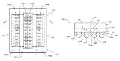
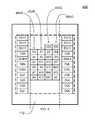
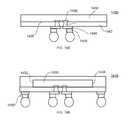
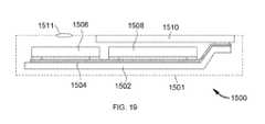
- all of the terminals of such packageare placed in sets of columns adjacent to one or more peripheral edges of a package substrate to which the microelectronic element is mounted. For example, in one conventional microelectronic package 12 seen in FIG.
- FIG. 1further shows a semiconductor chip 11 within the package having element contacts 26 on a face 28 thereof which are electrically interconnected with the columns 14 , 18 of terminals of the package 12 with wire bonds extending through an aperture, e.g., bond window, in the central region 24 of package substrate 20 .
- an adhesive layer 32may be disposed between the face 28 of the microelectronic element 11 and the substrate 20 to reinforce the mechanical connection between the microelectronic element and the substrate, with the wire bonds extending through an opening in the adhesive layer 32 .
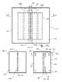
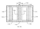
- a microelectronic packagecan include first and second microelectronic elements each embodying a greater number of active devices to provide memory storage array function than any other function.
- Each microelectronic elementmay have one or more columns of element contacts each column of element contacts extending in a first direction along a face of such microelectronic element.
- the packagemay include a substrate which has first and second opposed surfaces and first and second opposed edges extending between the first and second surfaces.
- the first surfacemay have first substrate contacts and second substrate contacts thereon.
- the first substrate contactsmay face the element contacts of the first microelectronic element and be joined thereto, and the second substrate contacts may face the element contacts of the second microelectronic element and be joined thereto.
- a plurality of terminalscan be exposed at the second surface of the substrate and electrically connected with the first and second substrate contacts.
- the terminalscan be disposed at positions within a plurality of parallel columns extending in the first direction along the second surface of the substrate and can be configured to connect the microelectronic package to at least one component external to the microelectronic package.
- the terminalscan include first terminals disposed within at least one of the columns of terminals in a central region of the second surface of the substrate.
- the first terminalscan be configured to carry address information usable by circuitry within the microelectronic package to determine an addressable memory location from among all the available addressable memory locations of a memory storage array within a microelectronic element of the first and second microelectronic elements.
- the central regionmay have a width in a second direction along the second surface of the substrate transverse to the first direction.
- the width of the central regioncan be not more than three and one-half times a minimum pitch between any two adjacent columns of the parallel columns of the terminals.
- An axial plane extending in the first direction and centered relative to the columns of element contacts of the first and second microelectronic elementscan extend in a third direction normal to the second surface of the substrate and may intersect the central region of the second surface.
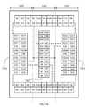
- the first terminalsare configured to carry all of the address information usable by the circuitry within the package to determine the addressable memory location.
- the first terminalsmay be configured to carry information that controls an operating mode of a microelectronic element of the first and second microelectronic elements.
- the first terminalscan be configured to carry all of the command signals transferred to the microelectronic package.
- the command signalscan be write enable, row address strobe, and column address strobe signals.
- the first terminalscan be configured to carry clock signals transferred to the microelectronic package.
- the microelectronic packagecan be configured to use the clock signals to sample signals received at the terminals which carry the address information.
- the first terminalscan be configured to carry all of the bank address signals transferred to the microelectronic package.
- the element contactscan include the one or more columns of element contacts, which can be first contacts containing a majority of the element contacts.
- the element contactscan further include second contacts on the face of at least one of the microelectronic elements which can be disposed adjacent to one or more edges of such face.
- the second contactscan be fewer than the number of first contacts in any one column thereof.
- the axial planecan be centered with respect to the first contacts, regardless of the positions of the second contacts.
- each of the second contactscan be configured for at least one of: connection to at least one of a source of power or ground; or for contact with a probing device.
- the first terminalscan be disposed at positions within no more than four of the columns of terminals.
- the substratecan include a dielectric element can have a coefficient of thermal expansion (“CTE”) in the plane of the dielectric element of less than 30 parts per million per degree Celsius (“ppm/° C.”).
- CTEcoefficient of thermal expansion
- the substratecan include an element which has a CTE of less than 12 ppm/° C.
- the terminalscan be configured for connecting the microelectronic package to an external component can be a circuit panel.
- the faces of the first and second microelectronic elementscan extend in a single plane parallel to the first surface of the substrate.
- the microelectronic packagemay further include third and fourth microelectronic elements overlying the first surface of the substrate.
- Each of the third and fourth microelectronic elementsmay embody a greater number of active devices to provide memory storage array function than any other function.
- the third and fourth microelectronic elementseach can have a face and element contacts on such face facing and joined to respective third and fourth substrate contacts on the first surface of the substrate.
- each columnmay include a plurality of the element contacts and extending along the face of the respective third or fourth microelectronic element.
- each column of element contacts of the third and fourth microelectronic elementsmay extend in the first direction, wherein the axial plane can be centered among all the columns of the first, second, third and fourth microelectronic elements.
- the faces of the third and fourth microelectronic elementscan extend in the single plane.
- At least some of the element contacts of the third and fourth microelectronic elementscan be disposed within one or more columns, and each such column may include a plurality of element contacts and extending along the face of the respective third or fourth microelectronic element in at least one direction transverse to the first direction.
- the central regioncan be disposed within a rectangular area of the substrate beyond which none of the faces of the first, second, third and fourth microelectronic elements extends.
- each of the first, second, third and fourth microelectronic elementsmay have two parallel first edges extending in the same direction as the columns of element contacts on the respective microelectronic element.
- Each such microelectronic elementmay have two parallel second edges extending in a direction transverse to the first edges of the respective microelectronic element.
- a plane containing either first edge of a respective microelectronic element and which extends in a direction normal to the face of the respective microelectronic elementcan intersect the first edge of another of the microelectronic elements.
- the plane containing either first edge of the respective microelectronic elementcan interest the first edge of only one of the other microelectronic elements.
- a microelectronic packagecan include first and second microelectronic elements each embodying a greater number of active devices to provide memory storage array function than any other function.
- Each microelectronic elementcan have one or more columns of element contacts. Each such column of element contacts may extend in a first direction along a face of such microelectronic element.
- a substratecan have first and second opposed surfaces and first and second opposed edges extending between the first and second surfaces. The first surface can have first substrate contacts and second substrate contacts thereon. The first substrate contacts can face the element contacts of the first microelectronic element and be joined thereto. The second substrate contacts can face the element contacts of the second microelectronic element and be joined thereto.
- a plurality of terminalscan be exposed at the second surface of the substrate and electrically connected with the first and second substrate contacts.
- the terminalscan be disposed at positions within a plurality of parallel columns extending in the first direction along the second surface of the substrate and can be configured to connect the microelectronic package to at least one component external to the microelectronic package.
- the terminalscan include first terminals disposed within at least one of the columns of terminals in a central region of the second surface.
- the first terminalscan be configured to carry a majority of address information usable by circuitry within the microelectronic package to determine an addressable memory location from among all the available addressable memory locations of a memory storage array within a microelectronic element of the first and second microelectronic elements.
- the central regionmay have a width in a second direction along the second surface of the substrate transverse to the first direction which is not more than three and one-half times a minimum pitch between any two adjacent columns of the parallel columns of the terminals.
- An axial plane extending in the first direction and centered relative to the columns of element contacts of the first and second microelectronic elementscan extend in a third direction normal to the second surface of the substrate and can intersect the central region of the second surface.
- the first terminalscan be configured to carry at least three quarters of the address information usable by the circuitry within the package to determine the addressable memory location.
- a microelectronic packagecan include a microelectronic element embodying a greater number of active devices to provide memory storage array function than any other function.
- the microelectronic elementcan have one or more columns of element contacts each column extending in a first direction along a face of the microelectronic element, such that an axial plane extending in a direction normal to the face of the microelectronic element intersects the face of the microelectronic element along a line extending in the first direction and centered relative to the one or more columns of element contacts.
- the microelectronic packagefurther includes packaging structure, such as a dielectric layer having a surface overlying the face of the microelectronic element and facing away from the face of the microelectronic element.
- packaging structuresuch as a dielectric layer having a surface overlying the face of the microelectronic element and facing away from the face of the microelectronic element.
- a plurality of terminalscan be exposed at the surface of the dielectric layer, at least some of the terminals which can be electrically connected with the element contacts through traces extending along the dielectric layer and metallized vias extending from the traces and contacting the element contacts.
- the terminalscan be disposed at positions within a plurality of parallel columns and can be configured for connecting the microelectronic package to at least one component external to the microelectronic package.
- the terminalscan include first terminals disposed within at least one column in the central region.
- the first terminalscan be configured to carry address information usable by circuitry within the package to determine an addressable memory location from among all the available addressable memory locations of a memory storage array within the microelectronic element.
- the central regioncan be not wider than three and one-half times a minimum pitch between any two adjacent columns of the terminals, and the axial plane may intersect the central region.
- the first terminalscan be configured to carry all of the address information usable by the circuitry within the package to determine the addressable memory location.
- the first terminalscan be configured to carry information that controls an operating mode of the microelectronic element.
- the first terminalscan be configured to carry all of the command signals transferred to the microelectronic package, the command signals can be write enable, row address strobe, and column address strobe signals.
- the first terminalscan be configured to carry clock signals transferred to the microelectronic package, each microelectronic package can be configured to use the clock signals to sample signals received at the terminals which carry the address information.
- the first terminalscan be configured to carry all of the bank address signals transferred to the microelectronic package.
- the terminalscan be configured for connecting the microelectronic package to an external component can be a circuit panel.
- FIG. 1is a sectional view illustrating a conventional microelectronic package containing a DRAM chip.
- FIG. 2is a diagrammatic schematic diagram illustrating a microelectronic assembly, e.g., a DIMM module, incorporating a circuit panel and a plurality of microelectronic packages mounted opposite one another to first and second opposite surfaces thereof.
- a microelectronic assemblye.g., a DIMM module
- FIG. 3is a sectional view further illustrating an electrical interconnection between first and second microelectronic packages and a circuit panel in an assembly such as shown in FIG. 2 .
- FIG. 4is a diagrammatic plan view further illustrating the electrical interconnection between first and second microelectronic packages in an assembly such as shown in FIG. 2 .
- FIG. 5is a diagrammatic plan view illustrating an arrangement and signal assignment of terminals in a microelectronic package according to an embodiment of the invention.
- FIG. 6Ais a sectional view through line 6 A- 6 A of FIG. 5 further illustrating the microelectronic package shown in FIG. 5 .
- FIG. 6Bis a plan view further illustrating a possible arrangement of element contacts and types of contacts on a microelectronic element within a microelectronic package according to any of the embodiments claimed herein, among which is the embodiment shown in FIGS. 5 and 6A .
- FIG. 6Cis a plan view further illustrating a possible arrangement of element contacts and types of contacts on a microelectronic element within a microelectronic package according to any of the embodiments claimed herein, among which is the embodiment shown in FIGS. 5 and 6A .
- FIG. 7Ais a plan view further illustrating another possible arrangement of element contacts on a microelectronic element within a microelectronic package according to the embodiment shown in FIGS. 5 and 6A .
- FIG. 7Bis a plan view further illustrating an arrangement of terminals in accordance with the embodiment shown in FIGS. 5 and 6A .
- FIG. 7Cis a sectional view illustrating a microelectronic assembly and first and second microelectronic packages electrically interconnected therewith in accordance with an embodiment of the invention.
- FIG. 7Dis a schematic diagram illustrating a microelectronic assembly including a circuit panel and microelectronic packages electrically connected thereto, e.g., a memory module, among others, according to an embodiment of the invention.
- FIG. 8is a plan view illustrating an alternative arrangement of terminals on a microelectronic package according to a variation of the embodiment shown in FIGS. 5 and 6A .
- FIG. 9Ais a plan view and FIG. 9B is a corresponding sectional view through line 9 B- 9 B of FIG. 9A illustrating a microelectronic package according to a variation of the embodiment shown in FIGS. 5 and 6A .
- FIG. 9Cis a plan view illustrating an arrangement of element contacts and electrical interconnection between a microelectronic element and a substrate in an embodiment of a microelectronic package as shown in FIGS. 9A-B .
- FIG. 10is a sectional view illustrating a microelectronic package including a stacked electrically connected assembly of semiconductor chips therein in accordance with an embodiment of the invention.
- FIG. 11Ais a sectional view illustrating a microelectronic package including a stacked electrically connected assembly of semiconductor chips therein in accordance with an embodiment of the invention.
- FIG. 11Bis a sectional view illustrating a microelectronic package including a stacked electrically connected assembly of semiconductor chips therein in accordance with an embodiment of the invention.
- FIG. 12is a sectional view illustrating a microelectronic package including a stacked electrically connected assembly of semiconductor chips therein in accordance with an embodiment of the invention.
- FIG. 13Ais a sectional view illustrating a microelectronic package including a stacked electrically connected assembly of semiconductor chips therein in accordance with an embodiment of the invention.
- FIG. 13Bis a sectional view illustrating a microelectronic package including a stacked electrically connected assembly of semiconductor chips therein in accordance with an embodiment of the invention.
- FIG. 14is a sectional view illustrating an embodiment of a microelectronic package including first and second microelectronic elements therein each having element contacts facing and joined to corresponding substrate contacts.
- FIG. 15Ais a diagrammatic plan view illustrating a signal assignment of terminals on a microelectronic package according to the embodiment shown in FIG. 14 , wherein FIG. 14 is a sectional view through line 14 - 14 of FIG. 15A .
- FIG. 15Bis a plan view further illustrating a possible placement of terminals on the package of FIGS. 14 and 15A relative to the element contacts on the first and second microelectronic elements therein.
- FIG. 16Ais a plan view illustrating another embodiment of a microelectronic package having first, second, third and fourth microelectronic elements therein spaced apart from one another on a substrate.
- FIG. 16Bis a plan view illustrating a possible arrangement and signal assignment of terminals on the microelectronic package according to the embodiment shown in FIG. 16A .
- FIG. 17Ais a plan view illustrating another embodiment of a microelectronic package having first, second, third and fourth microelectronic elements therein spaced apart from one another in a pinwheel arrangement on a substrate.
- FIG. 17Bis a plan view illustrating a possible arrangement and signal assignment of terminals on the microelectronic package according to the embodiment shown in FIG. 17A .
- FIG. 18Ais a sectional view illustrating a wafer-level microelectronic package according to a variation of the embodiment shown in FIGS. 5 and 6A .
- FIG. 18Bis a sectional view illustrating a fan-out wafer-level microelectronic package according to a variation of the embodiment shown in FIG. 18A .
- FIG. 19is a schematic sectional view illustrating a system according to an embodiment of the invention.
- the inventorshave recognized improvements which can be made that may help improve the electrical performance of a package incorporating a memory storage array chip, and an assembly which incorporates such package.
- Improvementscan be made particularly for use of a microelectronic package when provided in an assembly such as shown in FIGS. 2-4 , in which a package 12 A is mounted to a surface of a circuit panel with another like package 12 B mounted opposite thereto on an opposite surface of the circuit panel.
- the packages 12 A, 12 Btypically are functionally and mechanically equivalent to one another.
- Other pairs 12 C and 12 D; and 12 E and 12 F, of functionally and mechanically equivalent packagestypically are also mounted to the same circuit panel 34 .
- the circuit panel and the packages assembled theretomay form a portion of an assembly commonly referred to as a dual in-line memory module (“DIMM”).
- DIMMdual in-line memory module
- the packages in each oppositely mounted pair of packagesconnect to contacts on opposite surfaces of the circuit panel so that the packages in each pair overlie one another typically by more than 90% of their respective areas.
- Local wiring within the circuit panel 34connects terminals, e.g., the terminals labeled “ 1 ” and “ 5 ” on each package to global wiring on the circuit panel.
- the global wiringincludes the signal conductors of a bus 36 used to conduct some signals to connection sites on the circuit panel 34 such as sites I, II and III.
- packages 12 A, 12 Bare electrically connected to the bus 36 by local wiring coupled to a connection site I
- packages 12 C, 12 Dare electrically connected to the bus by local wiring coupled to connection site II
- packages 12 E, 12 Fare electrically connected to the bus by local wiring coupled to connection site III.
- the circuit panel 34electrically interconnects the terminals of the respective packages 12 A, 12 B using local interconnect wiring that appears similar to a crisscross or “shoelace” pattern in which a terminal labeled “ 1 ” near one edge of package 12 A connects through the circuit panel 34 to a terminal labeled “ 1 ” of package 12 B near the same edge 16 of package 12 B.
- the edge 16 of package 12 B as assembled to circuit panel 34is far from the edge 16 of package 12 A.
- FIGS. 2-4further shows that a terminal labeled “ 5 ” near an edge 22 of package 12 A is connected through the circuit panel 34 to a terminal labeled “ 5 ” of package 12 B near the same edge 22 of package 12 B. In assembly 38 the edge 22 of package 12 A is far from the edge 22 of package 12 B.
- connections through the circuit panel between terminals on each package, e.g., package 12 A, to the corresponding terminals on the package mounted opposite thereto, i.e., package 12 B,are fairly long.
- the circuit panel 34may electrically interconnect a signal conductor of the bus 36 with the terminal of package 12 A marked “ 1 ” and the corresponding terminal of package 12 B marked “ 1 ”, when the same signal from the bus is to be transmitted to each package.
- the circuit panel 34may electrically interconnect another signal conductor of the bus 36 with the terminal of package 12 A marked “ 2 ” and the corresponding terminal of package 12 B marked “ 2 ”.
- connection arrangementmay also apply to other signal conductors of the bus and corresponding terminals of each package.
- Local wiring between the bus 36 on the circuit panel 34 and each package of the respective pair of packages, e.g., packages 12 A, 12 B ( FIG. 2 ) at a connection site I of the boardcan be in form of unterminated stubs. Such local wiring when relatively long may in some cases impact the performance of the assembly 38 as discussed below.
- the circuit panel 34also requires local wiring to electrically interconnect certain terminals of other packages: the pair of packages 12 C and 12 D, and the pair of packages 12 E and 12 F to the global wiring of the bus 36 , and such wiring can also impact the performance of the assembly in the same way.
- FIG. 4further illustrates the interconnection between microelectronic packages 12 A, 12 B of respective pairs of terminals assigned to carry signals “ 1 ”, “ 2 ”, “ 3 ”, “ 4 ”, “ 5 ”, “ 6 ”, “ 7 ”, and “ 8 ”.
- the wiring needed to traverse the circuit panel 34 in a direction 40 transverse to the direction 42 in which the columns 14 , 18 of terminals extendcan be quite long.
- the length of the local wiring in a circuit panel 34 in an assembly 38 seen in FIGS. 2-4that is required to route the same signal to the corresponding terminals of two oppositely mounted packages 12 A, 12 B can range between five and ten millimeters and may typically be about seven millimeters.
- the lengths of the circuit panel wiring required to connect the terminals of such oppositely mounted microelectronic packagesmay not severely impact the electrical performance of the assembly.
- the signal carried by the connected pair of terminals on the packages 12 A, 12 Bis a signal from a bus 36 used to carry address information or other information such as clock information for sampling the address information which is common to operation of the memory storage array function of a plurality of packages connected to the circuit panel
- the inventorsrecognize that the wiring length of the stubs extending from the bus 36 to the terminals on each package may significantly affect performance.
- the interconnecting wiringis relatively long, a more severe impact occurs, which can increase settling time, ringing, jitter, or intersymbol interference for a transmitted signal to an unacceptable degree.
- the bus 36 used to carry address informationcan be a command-address bus 36 configured to carry command information, address information, bank address information and clock information.
- the command informationcan be transmitted as command signals on respective signal conductors on the circuit panel. It is also possible for the address information to be transmitted as address signals on respective signal conductors, as it is also possible for the bank address information to be transmitted as bank address signals on respective signal conductors, and it is also possible for the clock information to be transmitted as clock signals on respective signal conductors.
- the command signals which can be carried by the bus 36can be write enable, row address strobe and column address strobe, and the clock signals which can be carried by the bus 36 can be clock signals used at least for sampling address signals carried by the bus 36 .
- certain embodiments of the invention described hereinprovide a microelectronic package configured so as to permit the lengths of stubs on a circuit panel to be reduced when first and second such packages are mounted opposite one another on opposite surfaces of a circuit panel, e.g., a circuit board, module board or card, or flexible circuit panel.
- Assemblies which incorporate first and second microelectronic packages electrically connected to a circuit panel at locations of the circuit panel opposite from one anothercan have significantly reduced stub lengths between the respective packages. Reducing the stub lengths within such assemblies can improve electrical performance, such as by reducing one or more of settling time, ringing, jitter, or intersymbol interference, among others.
- the package 100can include a microelectronic element 101 configured to predominantly provide memory storage array function, in that the microelectronic element has a greater number of active devices, e.g., transistors, configured to provide memory storage array function than any other function, as indicated above.
- active devicese.g., transistors
- the packagecan include a substrate 102 on which a plurality of first terminals 104 and a plurality of second terminals 106 A and 106 B are disposed.
- the substratecan include a sheet-like dielectric element, which in some cases can consist essentially of polymeric material, e.g., a resin or polyimide, among others.
- the substratecan include a dielectric element having a composite construction such as glass-reinforced epoxy, e.g., of BT resin or FR-4 construction.
- the substratecan include a supporting element of material having a coefficient of thermal expansion (“CTE”) of less than 12 parts per million, on which the terminals and other conductive structure are disposed.
- CTEcoefficient of thermal expansion
- such low CTE elementcan consist essentially of glass, ceramic or semiconductor material or liquid crystal polymer material, or a combination of such materials.
- the terminalscan be disposed at locations within a plurality of parallel columns 104 A, 104 B, 106 A and 106 B on a surface 110 of the substrate.
- columns 104 A and 104 Bmay each contain some first terminals disposed in a central region 112 of the surface 110
- columns 106 A, 106 Bmay each contain some terminals in respective peripheral regions 114 A, 114 B disposed beyond the central region.
- the central regionis not wider than three and one-half times a minimum pitch between adjacent ones of the parallel columns of the terminals, as seen and further described relative to FIG. 7B below.
- the first terminalscan be configured to carry address information transferred to the microelectronic package.
- the address informationcan be received by the first terminals from a bus 36 on the circuit panel, e.g., a command-address bus.
- the address informationcan be received as individual address signals, e.g., signals A 0 through A 15 on the respective terminals, or some or all of the address information can be received as a combination of voltage levels received on more than one terminal, e.g., as information in encoded form when received.
- some or all of the address informationcan be received on one or more of the terminals on a rising transition of a clock used to sample the information, i.e., a transition of a clock from a first state of higher voltage to a second state of lower voltage, or some or all of the address information can be received on one or more of the terminals on a falling transition of the clock, i.e., a transition of the clock from the second state of lower voltage to the first state of higher voltage.
- some of the address informationcan be received on one or more of the terminals on a rising transition of the clock while some or the address information can be received on one or more of the terminals on a falling transition of the clock.
- the second terminals 106 A, 106 Bmay be disposed at positions within one or more of first and second peripheral regions 114 A, 114 B of the substrate surface 110 .
- the first and second peripheral regionsmay in some cases be adjacent to first and second opposed edges 116 , 118 of the surface 110 , as seen in FIG. 5 .
- the central region 104is disposed between the first and second peripheral regions 114 A, 114 B.
- the second terminalsare disposed at locations within one or more columns each having a plurality of second terminals.
- the terminals in the central regioncan be configured to carry address information transferred to the microelectronic package which is usable by circuitry within the package, e.g., by row address and column address decoders, and bank selection circuitry, if present, to determine an addressable memory location from among all the available addressable memory locations of a memory storage array within the microelectronic element.
- the address information in one embodimentcan include all address information transferred to the package from a component external to the package, e.g., a circuit panel, which is used for determining a random access addressable memory location within a memory storage array within the microelectronic package for read access thereto, or for either read or write access thereto.
- a component external to the packagee.g., a circuit panel, which is used for determining a random access addressable memory location within a memory storage array within the microelectronic package for read access thereto, or for either read or write access thereto.
- the first terminalsmay be configured to carry address signals, bank address signals, certain command signals, and clock signals which are clocks used for sampling the address signals.
- the clock signalscan be of various types, in one embodiment, the clock signals carried by these terminals can be one or more pairs of differential clock signals received as differential or true and complement clock signals.
- the “command signals” in this casecan be a write enable signal, a row address strobe signal, and a column address strobe signal utilized by a microelectronic element within the microelectronic package. For example, in a particular example as seen in FIG.
- the first terminalscan include clock signals CK and CKB, row address strobe RAS, column address strobe CAS and write enable signals WE, as well as address signals A 0 through A 15 inclusive, and bank address signals BA 0 , BA 1 and BA 2 .
- a microelectronic element 130 within microelectronic package 100has element contacts 132 on a face 134 of the microelectronic element 130 .
- the element contacts 132face corresponding substrate contacts 136 exposed at a surface 120 of a substrate 102 and the element contacts are joined to the substrate contacts.
- the contacts of the microelectronic elementcan be joined with the contacts of the substrate in flip-chip manner using a bond metal such as solder, tin, indium, gold, eutectic or other electrically conductive bond metal or bond material.
- a bond metalsuch as solder, tin, indium, gold, eutectic or other electrically conductive bond metal or bond material.
- another techniquecan be used such as metal-to-metal joining, e.g., a copper-copper joining process utilizing copper bumps on one or both of the element contacts 132 and corresponding substrate contacts 136 .
- a microelectronic package 100has columns 104 A, 104 B of first terminals disposed in the central region 112 of the surface 110 of the substrate 102 .
- element contacts 132 on the microelectronic element 130can be disposed at locations within first and second columns 138 , 139 each extending in a first direction 142 on the face 134 of the microelectronic element.
- a column of contacts on the microelectronic elementcan be fully populated as in the case of column 138 , or a column of contacts may only have contacts at some of the positions within the column, as in the case of column 139 .
- an axial plane 140 of the microelectronic element 130intersects the face 134 of the microelectronic element 130 along a line extending in the first direction 142 , and the axial plane 140 also extends in a second direction normal to the face 134 of the microelectronic element.
- the axial plane 140can intersect the face 134 of the microelectronic element at points centered, e.g., equidistant between columns 138 , 139 of the element contacts.
- the axial plane 140can be and typically is displaced in a perpendicular direction 143 along the face 134 from a central line 144 that extends in the first direction 142 and is centered precisely between the opposed edges 146 , 148 .
- the axial plane 140can coincide with the central line 144 .
- the microelectronic element 130may additionally include a plurality of peripheral contacts adjacent to one or more of the peripheral edges 146 , 148 . These peripheral contacts may be used for connection to power, ground, or as contacts available for contact with a probing device, such as may be used for testing.
- the intersection of the axial plane 140 with the face 134 of the microelectronic elementcan be centered relative to only columns 138 , 139 of contacts which are disposed adjacent to one another near the center of the microelectronic element.
- the other contacts 192which are disposed adjacent to one of the edges 146 or 148 of the microelectronic element and which are configured for connection to power, ground, or probing are ignored in determining the location of the intersection of the axial plane 140 with the microelectronic element 130 .
- the contacts of the microelectronic elementmay include the one or more columns of contacts 138 , 139 being first contacts and containing a majority of the contacts.
- the contacts of the microelectronic elementmay further include second contacts 192 on the face of the microelectronic element disposed adjacent to one or more edges of the face.
- the second contacts 192are fewer than the number of first contacts in any one column thereof.
- each of the second contactsmay be configured to be connected to one of a source of power, a ground, or be configured for connection to a probing device. In the completed package 100 , these contacts may be without electrical connections with the substrate 102 , or in some cases may be electrically connected only to corresponding power or ground conductors on the substrate.
- intersection of the axial plane 140 with the face 134 of the microelectronic element 130can be centered with respect to the columns of the first contacts, e.g., columns 138 , 139 as seen in FIG. 6B , regardless of the positions of the second contacts 192 .
- FIG. 6Cillustrates yet another example in which contact pads 332 of a microelectronic element can be disposed in one or two columns 338 , 339 near the center of the microelectronic element 330 , e.g., adjacent a central axis 140 of the microelectronic element.
- the element contacts which are joined to corresponding contacts 136 ( FIG. 6A ) of the substratecan be redistribution contacts 145 , 147 on the microelectronic element.
- Some or all of the redistribution contacts 145 , 147which are electrically connected with the contact pads 332 can be displaced from the contact pads 332 in one or more directions 142 , 143 along a face of the microelectronic element.
- the redistribution contactscan be disposed in a plurality of columns 135 , 137 which are closer to the edges 146 , 148 of the microelectronic element than the columns 338 , 339 of contact pads 332 .
- the redistribution contactscan be distributed in an area array exposed at the surface of the microelectronic element.
- the redistribution contactscan be distributed along one or more peripheral edges 146 , 148 of the microelectronic element which extend in a first direction 142 , or be distributed along one or more peripheral edges 151 , 153 of the microelectronic element which extend in a second direction 143 transverse to direction 142 .
- the redistribution contactscan be distributed along two or more of the peripheral edges 146 , 148 , 151 , 153 of the microelectronic element.
- the redistribution contacts 145 , 147can be disposed on the same face of the microelectronic element as the contact pads 332 , or be disposed on a face of the microelectronic element opposite from the contact pads.
- each contact padcan be connected to a redistribution contact.
- Such one or more contact pads 332 which are not connected to a redistribution contactmay or may not be electrically connected to one or more corresponding terminals of the package.
- the axial plane 140intersects the central region 112 of the surface 110 of the substrate 102 of the microelectronic package 100 . Accordingly, the axial plane intersects the central region 112 of the substrate surface 110 on which the terminals 104 A, 104 B configured to carry the aforementioned address information, or in a particular implementation, the terminals configured to carry command-address bus information or command-address bus signals, are disposed.
- first terminalswill be understood to refer to terminals exposed in the central region 112 of the substrate surface, wherein in aggregate, such terminals are configured to carry address information that is usable by circuitry within the microelectronic package to determine an addressable memory location from among all the available addressable memory locations of a memory storage array within a microelectronic element in the microelectronic package, whether the first terminals are configured to carry all or at least a majority, or in one example, three quarters or more of the address information used by circuitry within the package to determine an addressable memory location within such memory storage array.
- the first terminalsmay also be configured to carry additional information or signals as well, such as command information or command signals for write enable, row address strobe and column address strobe function, bank address information, and clock information, as described above.
- joining elements 154 A, 154 B of a bond metale.g., solder, tin, indium or eutectic, or other electrically conductive bond material can be joined to the terminals 104 A, 104 B, which can be used to join the terminals of the package 100 to a component external to the package, such as to corresponding contacts of a circuit panel.
- a bond metale.g., solder, tin, indium or eutectic, or other electrically conductive bond material
- a microelectronic element 230may have only one column 238 containing a plurality of contacts on the face 134 , in which case the axial plane 240 extends through the column 238 of contacts.
- the axial plane 240may intersect the central region 112 of the substrate surface at a location between columns 104 A, 104 B of terminals, wherein the axial plane 240 and each of the columns 104 A, 104 B extend in a first direction 142 in which a column 238 of the contacts of the microelectronic element extend.
- the axial plane 240may intersect the central region 112 along a line extending in the first direction, wherein the line intersects one of the columns 104 A or 104 B of the terminals.
- a minimum pitch 150exists as the smallest distance between any two adjacent columns of terminals on the substrate.
- the minimum pitchis defined as the minimum distance between centerlines extending in the direction 162 through the respective adjacent columns.
- the minimum pitchis in a direction 143 perpendicular to the direction 142 in which the terminals in a particular column, e.g., column 104 A are arranged.
- the minimum pitchoccurs between columns 104 A, 104 B which are closest to one another between edges 116 and 118 of the substrate 110 .
- the central region 112has a maximum width 152 along the substrate surface 110 in the direction 143 of the pitch, i.e., in a second direction transverse to the first direction 142 , the width 152 being not greater than three and one-half times the minimum pitch between any two adjacent columns of the terminals, e.g., columns 104 A, 104 B of the terminals.
- FIG. 7Cillustrates a microelectronic assembly 300 of first and second microelectronic packages 100 A, 100 B, each being a microelectronic package 100 as described with reference to FIGS. 5-6B above, as mounted to opposite first and second surfaces 350 , 352 of a circuit panel 354 .
- the circuit panelcan be of various types, such as a printed circuit board used in a dual inline memory module (“DIMM”) module, a circuit board or panel to be connected with other components in a system, or a motherboard, among others.
- DIMMdual inline memory module
- the circuit panelhas contacts configured to electrically connect to microelectronic packages.
- the circuit panelmay include an element having a coefficient of thermal expansion (“CTE”) of less than 12 parts per million per degree Celsius (“ppm/° C.”), wherein the panel contacts at the first and second surfaces are connected by vias extending through the element.
- CTEcoefficient of thermal expansion
- the elementmay consist essentially of semiconductor, glass, ceramic or liquid crystal polymer material.
- the first and second microelectronic packages 100 A, 100 Bcan be mounted to corresponding panel contacts 360 , 362 exposed at the first and second surfaces 350 , 352 of the circuit panel 354 .
- the first terminals 104 A, 104 Bcan be disposed at locations in a grid 104 on the first package 100 A.
- the first terminals 104 A, 104 B of the second package 100 Bcan also be disposed at locations within a grid 104 on the second package.
- Each grid of terminalsmay be fully populated, i.e., there being a terminal occupying each position of each grid. Alternatively, one or more positions of each grid may not be occupied by a terminal. As evident from FIG.
- the gridscan be aligned within one ball pitch of one another in x and y orthogonal directions parallel to the surface 350 of the circuit panel, the ball pitch being no greater than a minimum pitch between any two adjacent parallel columns of the terminals on either package.
- at least half of the positions of the grids of the first and second packagesmay be aligned with one another in x and y orthogonal directions parallel to the first surface of the circuit panel.
- the gridsmay be aligned with one another in the x and y directions such that at least some of the first terminals on the first and second microelectronic packages are coincident with one another.
- the alignmentcan be within customary manufacturing tolerances or can be within a tolerance of less than one-half of one ball pitch of one another in x and y orthogonal directions parallel to the first and second circuit panel surfaces, the ball pitch being as described above.
- Wiring within the circuit panel 354electrically connects the terminals 104 A of package 100 A with terminals 104 A of package 100 B, as shown.
- the wiring that forms the electrical connectionsis shown schematically by the dashed line 320 in FIG. 7C , because the wiring can be hidden from the particular view provided in FIG. 7C .
- wiring within the circuit panel 354electrically connects the terminals 104 B of package 100 A with terminals 104 B of package 100 B, and the electrical interconnections between such terminals is shown schematically by the dashed line 322 in FIG. 7C .
- the wiring on the circuit panel 354 required to connect one of the first terminals labeled “A” of package 100 A with one of the first terminals labeled “A” of package 100 Bcan be relatively short.
- each grid 104 on each packagehas two columns 104 A, 104 B, and the grids 104 are aligned in the above-described manner, then the first column 104 A of the first package 100 A is aligned within one ball pitch of the second column 104 B of the second package in x and y orthogonal directions parallel to the first surface 350 of the circuit panel, and the second column 104 B of the first package 100 A is aligned within one ball pitch of the first column 104 A of the second package in x and y orthogonal directions parallel to the first surface 350 of the circuit panel.
- the electrical lengths of stubs on the circuit panel 354 which electrically connect a first terminal 104 A of the first package 100 A with the corresponding first terminal 104 A on the second package 100 Bcan be less than seven times a minimum pitch of the first terminals on each package, for example, less than seven times the pitch 150 between columns 104 A, 104 B of first terminals in FIG. 7B .
- the total combined length of the conductive elements connecting a pair of electrically coupled first and second panel contacts exposed at the first and second surfaces of the circuit panel, for electrically interconnecting the first and second panel contacts with a corresponding conductor of a bus on the circuit panelcan be less than seven times a minimum pitch of the panel contacts, for example.
- the length of a stub of at least one of the electrical connections between one of the first terminals of the first microelectronic package and a corresponding one of the first terminals of the second microelectronic packagecan be less than seven times a minimum pitch of the first terminals on the first microelectronic package.
- the total combined length of the conductive elements connecting a pair of electrically coupled first and second panel contacts exposed at the first and second surfaces of the circuit panel for electrically interconnecting the first and second panel contacts with one of the corresponding command-address bus signals on the circuit panelcan be less than seven times a smallest pitch of the panel contacts.
- the electrical length of the connection between a first terminal 104 A of the first package 100 A with the corresponding first terminal 104 A on the second package 100 Bmay be approximately the same as a thickness 356 of the circuit panel 354 between first and second surfaces 350 , 352 .
- the reductions in the lengths of these electrical connectionscan reduce stub lengths in the circuit panel and the assembly, which can help improve the electrical performance, such as reducing settling time, ringing, jitter, or intersymbol interference, among others, for the above-noted signals which are carried by the first terminals and which are transferred to microelectronic elements in both the first and second packages.
- connections on the circuit panelmay require fewer layers of wiring to interconnect the first terminals of each package to the bus on the circuit panel, such as the above-discussed bus which carries address information or a command-address bus.
- the number of global routing layers of conductorsi.e., wiring extending in at least one direction generally parallel to a surface of the circuit panel, which is required to route signals from the above-noted signals carried by the first terminals, e.g., address information or command-address bus signals can sometimes be reduced.
- the number of such global routing layers between a connection site where a first pair of microelectronic packages 100 A, 100 B is connected and a different connection site where at least one other microelectronic package is connected, e.g., between connection sites II and III ( FIG. 7D ) thereoncan be reduced when the microelectronic packages attached thereto are constructed according to the principles herein.
- the number of global routing layers required to route such signals along the circuit panelmay in some cases be reduced to two or fewer routing layers.
- FIG. 7Dillustrates a microelectronic assembly such as, for example, a DIMM, among others, incorporating a circuit panel and a plurality of microelectronic packages mounted opposite one another to first and second opposite surfaces thereof.
- the above-noted address signals or command-address bus signalscan be routed on a bus 36 , e.g., an address bus or command-address bus on the circuit panel or circuit board 354 in at least one direction 143 between connection sites I, II or III at which respective pairs of microelectronic packages 100 A, 110 B are connected to opposite sides of the circuit panel. Signals of such bus 36 reach each pair of packages at the respective connection sites I, II or III at slightly different times.
- the at least one direction 143can be transverse or orthogonal to a direction 142 in which at least one column 138 of a plurality of contacts on at least one microelectronic element within each package 100 A or 100 B extends.
- the signal conductors of the bus 36 on (i.e., on or within) the circuit panel 354can in some cases be spaced apart from one another in a direction 142 which is parallel to the at least one column 138 of contacts on a microelectronic element within a package 100 A, or 100 B connected to the circuit panel.
- Such configurationmay help simplify the routing of signal conductors of one or more global routing layers on the circuit panel used to route the signals of the bus 36 .
- first terminalsconfigured to receive address signals A 3 and A 1 .
- the microelectronic assembly 354can have a second microelectronic element 358 that can include a semiconductor chip configured to perform buffering of at least some signals transferred to the microelectronic packages 100 A, 100 B of the assembly 354 .
- the second microelectronic elementcan be configured predominantly to perform a logic function, such as a solid state drive controller, and one or more of the microelectronic elements 358 in the microelectronic packages 100 A and 100 B can each include memory storage elements such as nonvolatile flash memory.
- the second microelectronic element 358can include a special purpose processor that is configured to relieve a central processing unit of a system such as the system 1500 ( FIG.
- Such a microelectronic element 358 including a solid state drive controllercan provide direct memory access to and from a data bus on a motherboard (e.g., the circuit panel 1502 shown in FIG. 19 ) of a system such as the system 1500 .
- the microelectronic element 358can have a buffering function.
- Such a microelectronic element 358can be configured to help provide impedance isolation for each of the microelectronic elements 130 in microelectronic packages 100 A, 100 B with respect to components external to the microelectronic assembly 354 or system 1500 ( FIG. 19 ).
- the first terminals 104 of the microelectronic packagecan be configured to carry information that controls an operating mode of the microelectronic element 101 . More specifically, the first terminals can be configured to carry all of a particular set of command signals and/or clock signals transferred to the microelectronic package 100 . In one embodiment, the first terminals 104 can be configured to carry all of the command signals, address signals, bank address signals, and clock signals transferred to the microelectronic package 100 from an external component, wherein the command signals include row address strobe, column address strobe and write enable. In such embodiment, the first chip can be configured to regenerate the information that controls the operating mode.
- the first chipcan be configured to partially or fully decode the information that controls the operating mode of the microelectronic element.
- each second chipmay or may not be configured to fully decode one or more of address information, command information, or information that controls an operating mode of the microelectronic element.
- Microelectronic packages having other arrangements of terminals thereoncan be provided.
- the microelectronic package 400 illustrated in FIG. 8four columns 404 A, 404 B, 404 C, and 404 D of terminals are disposed in a central region 112 of the substrate surface, these columns containing the first terminals which are configured to carry all of the command signals, address signals, bank address signals and clock signals used to sample the address signals.
- the first terminals of a microelectronic packageit is also possible for the first terminals of a microelectronic package to be disposed at positions within three columns.
- the first terminalsare disposed at positions within a single column 504 disposed in the central region 512 of the substrate surface, the single column extending in a direction parallel to the edges 516 , 518 of the microelectronic package.
- the second terminalsare omitted from FIG. 9B for clarity.
- the minimum pitch between any two columns of terminals on the substrateis the pitch 552 between the adjacent columns 506 B and 506 C of second terminals disposed in peripheral region 514 B of the substrate surface.
- the width 554 of the central regionis not greater than three and one-half times the minimum pitch 552 between the columns 506 B and 506 C of terminals.
- the microelectronic element 530 in microelectronic package 500may have a single column of element contacts 538 on the face 534 of the microelectronic element.
- the internal electrical connections between the element contacts 538 and the terminals 504 of the microelectronic package 500can be particularly short.
- connections between element contacts 538 A and the terminals 504may in one case extend only or mainly in a first direction 542 in which the column 538 A of element contacts extend on the face 534 of the microelectronic element 530 .
- connections between element contacts 538 B and the terminals 504may in one case extend only in a vertical direction above the contacts 538 B, so that at least some terminals 504 of the package 500 may at least partially overlie the element contacts 538 to which the contacts 538 B are electrically connected.
- FIG. 10illustrates a microelectronic package 600 according to a particular example in which the microelectronic element 630 includes a plurality of vertically stacked electrically interconnected semiconductor chips 632 and 634 .
- the microelectronic element 630includes a first semiconductor chip 632 having element contacts 636 on a face 638 thereof which face substrate contacts 640 on a first surface 610 of the substrate and are joined to the substrate contacts 640 .
- the microelectronic elementalso includes one or more second semiconductor chips 634 which overlie a face 642 of the first semiconductor chip 632 opposite the face 638 of the first semiconductor chip, the face 642 being remote from the first surface 610 of the substrate 602 .
- the one or more second semiconductor chips 634are electrically interconnected with the first semiconductor chip 632 .
- each of the first and second semiconductor chips 632 , 634can be configured such that each such semiconductor chip embodies a greater number of active devices to provide memory storage array function than any other function.
- each of the first and second semiconductor chipsmay include a memory storage array and all circuitry required for inputting data to and outputting data from the memory storage array.
- each of the semiconductor chipsmay include circuitry configured to receive external data input from terminals of the package, as well as circuitry configured to transfer data output from such semiconductor chip to terminals of the package.
- each first and each second semiconductor chip 632 , 634can be a dynamic random access memory (“DRAM”) chip or other memory chip which is capable of inputting and outputting data from the memory storage array within such semiconductor chip and receiving and transmitting such data to a component external to the microelectronic package.
- DRAMdynamic random access memory
- signals to and from the memory storage array within each DRAM chip or other memory chipdoes not require buffering by an additional semiconductor chip within the microelectronic package.
- the one or more second semiconductor chips 634may embody a greater number of active devices to provide memory storage array function than any other function, but the first semiconductor chip 632 may be a different type of chip.
- the first semiconductor chip 632can be configured, e.g., designed, constructed, or set up, to buffer signals, i.e., regenerate signals received at the terminals for transfer to the one or more second semiconductor chips 634 , or to regenerate signals received from one or more of the second semiconductor chips 634 for transfer to the terminals, or to regenerate signals being transferred in both directions from the terminals to the one or more second semiconductor chips 634 ; and from the one or more semiconductor chips to the terminals of the microelectronic package.
- the first chip in such a composite microelectronic elementcan be configured to partially or fully decode the information that controls the operating mode of the microelectronic element.
- the first semiconductor chip in such composite microelectronic elementcan be configured to partially or fully decode at least one of address information or command information received at the terminals, such as at the first terminals. The first chip can then output the result of such partial or full decoding for transfer to the one or more second semiconductor chips 634 .
- the first semiconductor chipcan be configured to buffer the address information, or in one example, the command signals, address signals and clock signals which are transferred to the one or more second semiconductor chips.
- the first semiconductor chip 632can be a buffer chip which embodies a greater number of active devices to provide a buffering function in transferring signals to other devices, e.g., to the one or more second semiconductor chips 634 , than for any other function.
- the one or more second semiconductor chipsmay be reduced function chips which have memory storage arrays but which can omit circuitry common to DRAM chips, such as buffer circuitry, decoders or predecoders or wordline drivers, among others.
- the first chip 632may function as a “master” chip in the stack and to control operations in each of the second semiconductor chips 634 .
- the second semiconductor chipsmay be configured such that they are not capable of performing the buffering function.
- the stacked arrangement of the first and second semiconductor chipsis configured such that the buffering function required in the microelectronic package can be performed by the first semiconductor chip, and cannot be performed by any of the second semiconductor chips in the stacked arrangement.
- the one or more second semiconductor chipscan be implemented in one or more of the following technologies: DRAM, NAND flash memory, RRAM (“resistive RAM” or “resistive random access memory”), phase-change memory (“PCM”), magnetoresistive random access memory, e.g. such as may embodiment tunnel junction devices, spin-torque RAM, or content-addressable memory, among others.
- FIG. 10further illustrates a microelectronic package 600 according to a particular example in which the one or more second semiconductor chips 634 is electrically connected with the first semiconductor chip 632 by through silicon vias (“TSVs”) 650 which extend in a direction of a thickness 652 of the first semiconductor chip 632 between first and second opposed faces 638 , 642 thereof.
- TSVs 650can be electrically connected with the element contacts 636 of the first semiconductor chip 632 , such as by traces 654 extending along a face 638 of the first semiconductor chip 632 .
- any electrical connections between the first and second semiconductor chipscan be made in this manner, such connections are well-suited for the distribution of power and ground to the first and second semiconductor chips.
- TSVsSignals which are regenerated by a first semiconductor chip 632 operating as a buffer element, which are then transferred to the one or more second semiconductor chips, can be routed through TSVs connected to internal circuitry, for example.
- the microelectronic packagemay also include through-silicon-vias 650 extending partially or completely through one or more of the second semiconductor chips 634 .
- TSVs 650may not directly connect to the substrate 602 , but may instead terminate on circuitry contained in semiconductor chip 632 .
- FIG. 11Afurther illustrates microelectronic package 700 according to a variation of the embodiment seen in FIG. 10 .
- the first semiconductor chip 732is interconnected with the substrate 702 in the same manner as described above relative to FIG. 10 .
- the one or more second semiconductor chips 734is electrically interconnected with the first semiconductor chip 732 through wire bonds.
- the second semiconductor chips 734are placed with their front faces and contacts 731 thereon facing upwardly, that is, facing away from the first semiconductor chip 732 .
- the first and second semiconductor chips 832 , 834can be mounted together in the microelectronic package is for each of the second semiconductor chips 834 to be placed with their front faces and contacts 831 facing downwardly, that is, towards the substrate 602 .
- the contacts 831can be electrically connected to corresponding contacts 841 on the front face 838 of the first semiconductor chip 832 through wire bonds 836 .
- the contacts 841can be electrically connected to the element contacts 636 on the first semiconductor chip 832 such as by traces 838 extending along the front face 838 of the first semiconductor chip 832 , with the connections between the element contacts 636 and the terminals 640 being as described above relative to FIG. 10 .
- FIG. 12illustrates a microelectronic package according to a further variation of the embodiment described above relative to FIG. 10 , in which connections between contacts of the one or more second semiconductor chips 934 and the first semiconductor chip 932 can include traces 936 which extend along one or more edges of the microelectronic element 930 , i.e., along edges of the semiconductor chips 932 , 934 within the microelectronic element.
- the electrical connections between the semiconductor chips 932 , 934may further include traces 938 , 940 which extend along front faces of the first semiconductor chip 932 and the second semiconductor chips 934 , respectively.
- the front faces 942 of the second semiconductor chipsmay face upwardly away from the substrate 602 or downwardly towards the substrate 602 .
- TSVs within the first semiconductor chip 932may extend partially or completely through a thickness of the first semiconductor chip 932 , or some of the TSVs in the first semiconductor chip 932 may extend partially its thickness while others of the TSVs extend completely through the thickness of the first semiconductor chip 932 .
- FIG. 13Aillustrates a microelectronic package according to yet another variation of the embodiment described above relative to FIG. 10 , in which a second semiconductor chip 1034 has contacts 946 facing corresponding contacts 948 on a face of the first semiconductor chip 952 , the contacts 946 , 948 being joined together such as through a metal, bond metal or other electrically conductive material, so as to form a flip-chip connection between the first and second semiconductor chips 952 , 954 .
- FIG. 13Billustrates a variation of the microelectronic package shown in FIG. 13A .
- semiconductor chip 964which can be configured to regenerate or at least partially decode address information or other information, e.g., regenerate signals for transfer to other semiconductor chips in the package, is not located adjacent to the first surface 108 of the substrate 902 . Rather, in this case, the semiconductor chip 964 can be disposed at a position within the package that overlies one or more other semiconductor chips. For example, as shown in FIG. 13B , the chip 964 at least partially overlies the semiconductor chip 962 that is disposed adjacent to the first surface 108 of the substrate 902 and at least partially overlies semiconductor chips 963 A and 963 B which are disposed atop semiconductor chip 962 .
- the semiconductor chips 962 , 963 A, and 963 Bmay include memory storage arrays. As in the examples described above, such chips 962 , 963 A, and 963 B may each incorporate circuits configured to buffer, e.g., temporarily store, data that is to be written to such chip, or data that is being read from such chip, or both. Alternatively, the chips 962 , 963 A, and 963 B may be more limited in function and may need to be used together with at least one other chip that is configured to temporarily store data that is to be written to such chip or data that is being read from such chip, or both.
- the semiconductor chip 964can be electrically connected to terminals of the microelectronic package, e.g., to grids in which the first terminals 904 and the second terminals 906 are disposed, through electrically conductive structure, e.g., TSVs 972 a and 972 b (collectively TSVs 972 ), that connect to contacts exposed at the first surface 108 of the substrate 902 .
- electrically conductive structuree.g., TSVs 972 a and 972 b (collectively TSVs 972 )
- the electrically conductive structuree.g., the TSVs 972
- the electrically conductive structurecan electrically connect to the semiconductor chip 964 through contacts 938 on the chip 964 and through conductors (not shown) that extend along the face 943 of the chip 964 , or along a confronting face 931 of the chip 963 A, or along the faces 931 , 943 of both of the chips 963 A, 964 .
- the semiconductor chip 964may be configured to regenerate or at least partially decode signals or information that it receives through the conductive structure, e.g., the TSVs 972 such as TSVs 972 a and 972 b , and it may be configured to transfer the regenerated or at least partially decoded signals or information to other chips within the package such as to the chips 962 , 963 A, and 963 B.
- the TSVs 972such as TSVs 972 a and 972 b
- the semiconductor chip 964may be configured to regenerate or at least partially decode signals or information that it receives through the conductive structure, e.g., the TSVs 972 such as TSVs 972 a and 972 b , and it may be configured to transfer the regenerated or at least partially decoded signals or information to other chips within the package such as to the chips 962 , 963 A, and 963 B.
- the semiconductor chips 962 , 963 A, and 963 Bcan be electrically connected to the semiconductor chip 964 and to one another by a plurality of through-silicon vias (“TSVs”) 972 , 974 , and 976 that can extend through one, two, or three or more of such chips.
- TSVsthrough-silicon vias
- Each such TSVmay electrically connect with wiring within the package, e.g., conductive pads or traces of two or more of the semiconductor chips 962 , 963 A, 963 B, and 964 .
- signals or informationcan be transferred from the substrate 902 to the chip 964 along a first subset of TSVs 972 a
- signals or informationcan be transferred from the chip 964 to the substrate along a second subset of TSVs 972 b .
- at least a portion of the TSVs 972can be configured to have signals or information be transferred in either direction between the chip 964 and the substrate 902 , depending on the particular signals or information.
- through silicon viasmay extend through the thicknesses of all semiconductor chips 962 , 963 A, and 963 B, even though each through silicon via may not electrically connect with each such semiconductor chip through which it extends.
- a heat sink or heat spreader 968which may include a plurality of fins 971 , can be thermally coupled to a face of the semiconductor chip 964 , e.g., a rear face 933 thereof, such as through a thermally conductive material 969 such as thermal adhesive, thermally conductive grease, or solder, among others.
- the microelectronic assembly 995 shown in FIG. 13Bmay be configured to operate as a memory module capable of transferring a designated number of data bits per cycle onto or off of the microelectronic package through the first and second terminals provided therefor on the substrate.
- the microelectronic assemblymay be configured to transfer a number of data bits such as thirty-two data bits, sixty-four data bits, or ninety-six data bits, among other possible configurations, to or from an external component such as a circuit panel that can be electrically connected with the first terminals 904 and second terminals 906 .
- the number of bits transferred per cycle to or from the packagemay be a different number such as thirty-six bits, seventy-two bits, or one-hundred-eight bits, for example.
- FIGS. 14, 15A and 15Billustrate a microelectronic package 1100 according to a further variation of one or more of the above-described embodiments.
- the package 1100includes first and second microelectronic elements 1130 , 1131 , each of which has contacts 1138 facing and joined to corresponding substrate contacts 1140 on a first surface 1120 of the substrate 1102 .
- some of the substrate contacts 1140are electrically connected with first terminals 1142 in a central region of the second surface 1110 , such as through electrically conductive traces 1144 .
- some of the substrate contacts 1138may instead be electrically connected with second terminals 1162 in one or more peripheral regions 1164 of the second surface.
- a multiple chip packagecan reduce the amount of area or space required to connect the chips therein to a circuit panel, e.g., printed wiring board to which the package may be electrically and mechanically connected through an array of terminals, such as a ball grid array, land grid array or pin grid array, among others.
- a circuit panele.g., printed wiring board to which the package may be electrically and mechanically connected through an array of terminals, such as a ball grid array, land grid array or pin grid array, among others.
- Such connection spaceis particularly limited in small or portable computing devices, e.g., handheld devices such as “smartphones” or tablets that typically combine the function of personal computers with wireless connectivity to the broader world.
- Multi-chip packagescan be particularly useful for making large amounts of relatively inexpensive memory available to a system, such as, for example, advanced high performance dynamic random access memory (“DRAM”) chips, e.g., in DDR3 type DRAM chips and its follow-ons.
- DRAMadvanced high performance dynamic random access memory
- the amount of area of the circuit panel needed to connect the multi-chip package theretocan be reduced by providing common terminals on the package through which at least some signals travel on their way to or from two or more chips within the package.
- corresponding contacts of multiple chips within the packagecan be electrically connected with a single common terminal of the package configured to connect with a component external to the package, such as a circuit panel, e.g., printed circuit board, external microelectronic element, or other component.
- the central region 1112 of the substrate surface 1110has a width 1154 that is not greater than three and one-half times a minimum pitch 1152 between any two adjacent columns of terminals 1142 on the package, where each of the two adjacent columns has a plurality of terminals therein.
- An axial plane 1150 extending in a direction orthogonal to the faces of the microelectronic elementsextends in the same first direction in which each column containing a plurality of element contacts extends and is centered among all the columns 1138 of the element contacts of the first and second microelectronic elements 1130 , 1131 .
- the axial planeintersects the central region of the substrate.
- one or more columns of first terminals 1142can be disposed between adjacent edges 1134 , 1135 of the first and second microelectronic elements as shown therein, or although not shown, one or more of the columns of first terminals 1142 can overlie one or more of the faces 1136 of the first and second microelectronic elements 1130 , 1131 .
- the faces 1136 of the first and second microelectronic elementscan extend within a single plane 1146 parallel to the first surface 1120 of the substrate 1102 .
- FIGS. 16A-16Billustrate a microelectronic package 1200 according to a variation of the embodiment seen in FIGS. 14, 15A -B which, in addition to first and second microelectronic elements 1230 , 1231 having the same arrangement and electrical interconnections within the package 1200 as discussed above regarding microelectronic package 1100 ( FIGS. 14, 15A -B), further includes third and fourth microelectronic elements 1233 and 1235 .
- the third and fourth microelectronic elementsmay each embody a greater number of active devices to provide memory storage array function than any other function.
- the third and fourth microelectronic elements 1233 and 1235are electrically interconnected with terminals 1242 of the package through element contacts 1238 which face corresponding substrate contacts on a first surface 1120 ( FIG. 14 ) of the substrate and are joined thereto, such as in the flip-chip manner described in the foregoing with reference to FIG. 15A .
- the first terminals 1242 of the microelectronic packagecan be disposed within columns in a central region 1254 having width no greater than three and one-half times the minimum pitch between columns of terminals, as described above.
- the axial plane 1250can be parallel to and centered among all the columns 1238 of element contacts on the faces 1236 of the first, second, third and fourth microelectronic elements within the package 1200 . In the example as shown in FIG. 16A , the axial plane 1250 extends in a direction
- the faces 1236 of the microelectronic elements 1230 , 1231 , 1233 and 1235can be arranged within the package 1200 such that all of the faces 1236 are co-planar, i.e., extend within a single plane, i.e., such as a single plane 1146 as illustrated in FIG. 14 .
- FIG. 16Billustrates a possible signal assignment of terminals on the package 1200 in which first terminals 1242 are disposed within one or more columns in the central region and second terminals 1244 are disposed at positions within multiple areas near peripheral edges 1260 , 1261 , 1262 and 1263 of the package.
- some second terminalscan be disposed at positions within a grid such as grid 1270
- some second terminalscan be disposed at positions within a grid such as grid 1272
- some second terminalscan be disposed at positions within a grid such as grid 1274
- some second terminalscan be disposed at positions within a grid 1276 .
- the signal class assignments of the second terminals in grid 1274can be symmetric about the vertical axis 1250
- the signal class assignments of the second terminals in grid 1276can be symmetric about the vertical axis 1250 .
- two signal class assignmentscan be symmetric with respect to one another if the signal assignments are in the same class of assignments, even if the numerical index within the class differs.
- Exemplary signal class assignmentscan include data signals, data strobe signals, data strobe complement signals, and data mask signals.
- the second terminals having signal assignments DQSH# and DQSL#are symmetric about the vertical axis 1250 with respect to their signal class assignment, which is data strobe complement, even though those second terminals have different signal assignments.
- the assignments of the data signals to the spatial positions of the second terminals on the microelectronic packagecan have modulo-X symmetry about the vertical axis 1250 .
- the modulo-X symmetrycan help preserve signal integrity in an assembly 300 or 354 such as seen in FIGS. 7C and 7D , in which one or more pairs of first and second packages are mounted opposite one another to a circuit panel, and the circuit panel electrically connects corresponding pairs of second terminals of those first and second packages in each oppositely mounted package pair.
- modulo-X symmetrycan permit electrical connections to be made through the circuit panel so that a terminal DQ 0 of a first package can be electrically connected through the circuit panel to a terminal DQ 8 of the second package which has the same number modulo X (X being 8 in this case), so that the connection can be made in a direction essentially straight through, i.e., normal to, the thickness of the circuit panel.
- “X”can be a number 2n (2 to the power of n), wherein n is greater than or equal to 2, or X can be 8 ⁇ N, N being two or more.
- Xmay be equal to the number of bits in a half-byte (4 bits), byte (8 bits), multiple bytes (8 ⁇ N, N being two or more), a word (32 bits) or multiple words.
- the signal assignment of a package terminal DQ 0 in grid 1274is configured to carry data signal DQ 0 is symmetric about the vertical axis 1250 with the signal assignment of another package terminal DQ 8 configured to carry data signal DQ 8 .
- the signal assignments of package terminals DQ 2 and DQ 10 in grid 1274have modulo-8 symmetry about the vertical axis, and the same is also true for grid 1276 .
- Modulo-8 symmetrysuch as described herein can be seen in grids 1274 , 1276 with respect to each of the signal assignments of package terminals DQ 0 through DQ 15 .
- the modulo number “X”can be a number other than 2n (2 to the power of n) and can be any number greater than two.
- the modulo number X upon which the symmetry is basedcan depend upon how many bits are present in a data size for which the package is constructed or configured. For example, when the data size is 10 bits instead of 8, then the signal assignments may have modulo-10 symmetry. It may even be the case that when the data size has an odd number of bits, the modulo number X can have such number.
- FIGS. 17A-17Billustrate a microelectronic package 1300 according to a variation of the embodiment 1200 described above relative to FIGS. 16A and 16B , the package 1300 having a substrate surface 1310 having a central region 1312 in which first terminals 1341 are disposed.
- first and second microelectronic elements 1330 , 1331are arranged on substrate 1302 in a manner similar to the arrangement of microelectronic elements 1130 , 1131 of microelectronic package 1100 ( FIGS. 14, 15A -B), in that the element contacts on these microelectronic elements are disposed at positions within columns which extend in the same first direction 1342 .
- FIG. 14illustrates a microelectronic package 1300 according to a variation of the embodiment 1200 described above relative to FIGS. 16A and 16B , the package 1300 having a substrate surface 1310 having a central region 1312 in which first terminals 1341 are disposed.
- first and second microelectronic elements 1330 , 1331
- third and fourth microelectronic elements 1332 and 1333have element contacts which are disposed at positions within columns 1340 which extend along the faces of the microelectronic elements 1332 , 1333 in another direction 1344 transverse to the first direction 1342 .
- the other direction 1344is perpendicular to the first direction 1342 .
- each of the microelectronic elements 1330 , 1331 , 1332 , and 1333typically has two first parallel edges 1360 which extend in the same direction as the one or more columns of contacts on the respective microelectronic element, and two second parallel edges 1362 which extend in a direction transverse to the direction in which the first edges extend.
- the first edges 1360 of a respective microelectronic elementcan have greater length than the second edges 1362 of such microelectronic element.
- the second edges 1362can have greater length than the first edges 1360 .
- a plane 1370 that contains either first edge 1360 of any of the microelectronic elements 1330 , 1331 , 1332 , or 1333 and which is normal to the face of such microelectronic elementintersects the edge 1360 of another microelectronic element within the package 1300 .
- the plane 1370 that contains the edge 1360 of microelectronic element 1333extends in direction 1344 and intersects the edge 1360 of microelectronic element 1330 within the package.
- the plane 1370intersects the edge 1360 of only one other microelectronic element within the package.
- the central region 1312can be further limited. Specifically, FIG. 17A shows that there is a minimum rectangular area 1372 on the surface 1302 of the substrate 1302 which will accommodate the microelectronic elements 1330 , 1331 , 1332 , 1333 as disposed on the substrate surface 1302 , and beyond which none of the faces of the first, second, third and fourth microelectronic elements 1330 , 1331 , 1332 and 1333 extend. In the microelectronic package 1300 depicted in FIGS. 17A-17B , the central region 1312 does not extend beyond any edge of that rectangular area 1372 . FIG.
- 17Bfurther illustrates a possible arrangement of terminals within microelectronic package 1300 in which first terminals 1341 are disposed within the central region 1312 which spans a width in a direction between, i.e., orthogonal to opposed edges 1316 , 1318 of the package that is no greater than three and one-half times the minimum pitch between the closest two adjacent columns of terminals on the package.
- Peripheral regionstake up the remaining area of the surface 1310 of the substrate 1302 , spanning widths 1356 , 1357 between edges of the central region and the opposed edges 1316 , 1318 of the package, respectively.
- FIG. 18Aillustrates a microelectronic package 1400 according to a variation of one or more of the above-described embodiments.
- the substratecan be omitted, such that the microelectronic package 1400 can be in form of a microelectronic element 1430 having packaging structure which includes an electrically conductive redistribution layer overlying the front face 1428 of the microelectronic element 1430 .
- the redistribution layerhas electrically conductive metallized vias 1440 extending through a dielectric layer 1442 of the package to contacts 1438 of the microelectronic element.
- the redistribution layermay include terminals 1446 and traces 1448 electrically connected with the terminals 1446 , such that the terminals are electrically connected with the contacts 1438 , such as through the metallized vias 1440 or through metallized vias 1440 and electrically conductive traces 1448 .
- the packagecan be referred to as a “wafer-level package having a redistribution layer thereon.”
- FIG. 18Billustrates a microelectronic package 1410 similar to the microelectronic package 1400 , with the exception that one or more columns 1450 of second terminals can be disposed on areas of the dielectric layer 1442 which extend beyond one or more edges 1432 , 1434 of the microelectronic element 1430 .
- the package 1410can be referred to as a “fan-out wafer-level package having a redistribution layer thereon.”
- a system 1500 in accordance with a further embodiment of the inventionincludes a microelectronic package or structure 1506 as described above in conjunction with other electronic components 1508 and 1510 .
- component 1508can be a semiconductor chip or microelectronic package whereas component 1510 is a display screen, but any other components can be used.
- the systemmay include any number of such components.
- the structure 1506 as described abovemay be, for example, a microelectronic package as discussed above in connection with any of the above-described embodiments.
- more than one packagemay be provided, and any number of such packages can be used.
- Package 1506 and components 1508 and 1510are mounted in a common housing 1501 , schematically depicted in broken lines, and are electrically interconnected with one another as necessary to form the desired circuit.
- the systemincludes a circuit panel 1502 such as a flexible printed circuit panel or circuit board, and the circuit panel includes numerous conductors 1504 , of which only one is depicted in FIG. 19 , interconnecting the components with one another.
- a circuit panel 1502such as a flexible printed circuit panel or circuit board
- the circuit panelincludes numerous conductors 1504 , of which only one is depicted in FIG. 19 , interconnecting the components with one another.
- thisis merely exemplary; any suitable structure for making electrical connections can be used.
- the housing 1501is depicted as a portable housing of the type usable, for example, in a cellular telephone or personal digital assistant, and screen 1510 is exposed at the surface of the housing.
- structure 1506includes a light-sensitive element such as an imaging chip
- a lens 1511 or other optical devicealso may be provided for routing light to the structure.
- FIG. 19the simplified system shown in FIG. 19 is merely exemplary; other systems, including systems commonly regarded as fixed structures, such as desktop computers, routers and the like can be made using the structures discussed above.
Landscapes
- Engineering & Computer Science (AREA)
- Microelectronics & Electronic Packaging (AREA)
- Power Engineering (AREA)
- Computer Hardware Design (AREA)
- Physics & Mathematics (AREA)
- Condensed Matter Physics & Semiconductors (AREA)
- General Physics & Mathematics (AREA)
- Geometry (AREA)
- Manufacturing & Machinery (AREA)
- Semiconductor Memories (AREA)
- Dram (AREA)
Abstract
Description
Claims (17)
Priority Applications (2)
| Application Number | Priority Date | Filing Date | Title |
|---|---|---|---|
| US14/107,564US9373565B2 (en) | 2011-10-03 | 2013-12-16 | Stub minimization for assemblies without wirebonds to package substrate |
| US15/165,323US9679838B2 (en) | 2011-10-03 | 2016-05-26 | Stub minimization for assemblies without wirebonds to package substrate |
Applications Claiming Priority (6)
| Application Number | Priority Date | Filing Date | Title |
|---|---|---|---|
| US201161542553P | 2011-10-03 | 2011-10-03 | |
| US201161542488P | 2011-10-03 | 2011-10-03 | |
| US201161542495P | 2011-10-03 | 2011-10-03 | |
| US201261600361P | 2012-02-17 | 2012-02-17 | |
| US13/439,299US8610260B2 (en) | 2011-10-03 | 2012-04-04 | Stub minimization for assemblies without wirebonds to package substrate |
| US14/107,564US9373565B2 (en) | 2011-10-03 | 2013-12-16 | Stub minimization for assemblies without wirebonds to package substrate |
Related Parent Applications (1)
| Application Number | Title | Priority Date | Filing Date |
|---|---|---|---|
| US13/439,299DivisionUS8610260B2 (en) | 2011-10-03 | 2012-04-04 | Stub minimization for assemblies without wirebonds to package substrate |
Related Child Applications (1)
| Application Number | Title | Priority Date | Filing Date |
|---|---|---|---|
| US15/165,323ContinuationUS9679838B2 (en) | 2011-10-03 | 2016-05-26 | Stub minimization for assemblies without wirebonds to package substrate |
Publications (2)
| Publication Number | Publication Date |
|---|---|
| US20140103535A1 US20140103535A1 (en) | 2014-04-17 |
| US9373565B2true US9373565B2 (en) | 2016-06-21 |
Family
ID=47991797
Family Applications (5)
| Application Number | Title | Priority Date | Filing Date |
|---|---|---|---|
| US13/439,286Expired - Fee RelatedUS8525327B2 (en) | 2011-10-03 | 2012-04-04 | Stub minimization for assemblies without wirebonds to package substrate |
| US13/439,299ActiveUS8610260B2 (en) | 2011-10-03 | 2012-04-04 | Stub minimization for assemblies without wirebonds to package substrate |
| US13/439,354ActiveUS8629545B2 (en) | 2011-10-03 | 2012-04-04 | Stub minimization for assemblies without wirebonds to package substrate |
| US14/107,564ActiveUS9373565B2 (en) | 2011-10-03 | 2013-12-16 | Stub minimization for assemblies without wirebonds to package substrate |
| US15/165,323ActiveUS9679838B2 (en) | 2011-10-03 | 2016-05-26 | Stub minimization for assemblies without wirebonds to package substrate |
Family Applications Before (3)
| Application Number | Title | Priority Date | Filing Date |
|---|---|---|---|
| US13/439,286Expired - Fee RelatedUS8525327B2 (en) | 2011-10-03 | 2012-04-04 | Stub minimization for assemblies without wirebonds to package substrate |
| US13/439,299ActiveUS8610260B2 (en) | 2011-10-03 | 2012-04-04 | Stub minimization for assemblies without wirebonds to package substrate |
| US13/439,354ActiveUS8629545B2 (en) | 2011-10-03 | 2012-04-04 | Stub minimization for assemblies without wirebonds to package substrate |
Family Applications After (1)
| Application Number | Title | Priority Date | Filing Date |
|---|---|---|---|
| US15/165,323ActiveUS9679838B2 (en) | 2011-10-03 | 2016-05-26 | Stub minimization for assemblies without wirebonds to package substrate |
Country Status (1)
| Country | Link |
|---|---|
| US (5) | US8525327B2 (en) |
Families Citing this family (31)
| Publication number | Priority date | Publication date | Assignee | Title |
|---|---|---|---|---|
| US8823165B2 (en) | 2011-07-12 | 2014-09-02 | Invensas Corporation | Memory module in a package |
| US8653646B2 (en) | 2011-10-03 | 2014-02-18 | Invensas Corporation | Stub minimization using duplicate sets of terminals for wirebond assemblies without windows |
| US8436477B2 (en) | 2011-10-03 | 2013-05-07 | Invensas Corporation | Stub minimization using duplicate sets of signal terminals in assemblies without wirebonds to package substrate |
| US8405207B1 (en) | 2011-10-03 | 2013-03-26 | Invensas Corporation | Stub minimization for wirebond assemblies without windows |
| JP5947904B2 (en) | 2011-10-03 | 2016-07-06 | インヴェンサス・コーポレイション | Stub minimization for multi-die wirebond assemblies with orthogonal windows |
| US8525327B2 (en) | 2011-10-03 | 2013-09-03 | Invensas Corporation | Stub minimization for assemblies without wirebonds to package substrate |
| TWI515864B (en) | 2011-10-03 | 2016-01-01 | 英帆薩斯公司 | Stub minimization with terminal grids offset from center of package |
| KR101894823B1 (en) | 2011-10-03 | 2018-09-04 | 인벤사스 코포레이션 | Stub minimization for multi-die wirebond assemblies with parallel windows |
| US9368477B2 (en) | 2012-08-27 | 2016-06-14 | Invensas Corporation | Co-support circuit panel and microelectronic packages |
| US8848392B2 (en) | 2012-08-27 | 2014-09-30 | Invensas Corporation | Co-support module and microelectronic assembly |
| US8848391B2 (en) | 2012-08-27 | 2014-09-30 | Invensas Corporation | Co-support component and microelectronic assembly |
| US9070423B2 (en) | 2013-06-11 | 2015-06-30 | Invensas Corporation | Single package dual channel memory with co-support |
| US8883563B1 (en) | 2013-07-15 | 2014-11-11 | Invensas Corporation | Fabrication of microelectronic assemblies having stack terminals coupled by connectors extending through encapsulation |
| US9034696B2 (en) | 2013-07-15 | 2015-05-19 | Invensas Corporation | Microelectronic assemblies having reinforcing collars on connectors extending through encapsulation |
| US9023691B2 (en) | 2013-07-15 | 2015-05-05 | Invensas Corporation | Microelectronic assemblies with stack terminals coupled by connectors extending through encapsulation |
| US9559040B2 (en)* | 2013-12-30 | 2017-01-31 | International Business Machines Corporation | Double-sided segmented line architecture in 3D integration |
| US9214454B2 (en) | 2014-03-31 | 2015-12-15 | Invensas Corporation | Batch process fabrication of package-on-package microelectronic assemblies |
| US10642087B2 (en) | 2014-05-23 | 2020-05-05 | Eyesafe, Llc | Light emission reducing compounds for electronic devices |
| US9281296B2 (en) | 2014-07-31 | 2016-03-08 | Invensas Corporation | Die stacking techniques in BGA memory package for small footprint CPU and memory motherboard design |
| US9691437B2 (en) | 2014-09-25 | 2017-06-27 | Invensas Corporation | Compact microelectronic assembly having reduced spacing between controller and memory packages |
| EP3231011B1 (en) | 2015-03-27 | 2022-11-09 | Hewlett-Packard Development Company, L.P. | Circuit package for fluidic applications |
| WO2017034515A1 (en)* | 2015-08-21 | 2017-03-02 | Hewlett-Packard Development Company, L.P. | Circuit package |
| US9484080B1 (en) | 2015-11-09 | 2016-11-01 | Invensas Corporation | High-bandwidth memory application with controlled impedance loading |
| US10037946B2 (en) | 2016-02-05 | 2018-07-31 | Dyi-chung Hu | Package structure having embedded bonding film and manufacturing method thereof |
| US9806044B2 (en)* | 2016-02-05 | 2017-10-31 | Dyi-chung Hu | Bonding film for signal communication between central chip and peripheral chips and fabricating method thereof |
| US9955605B2 (en)* | 2016-03-30 | 2018-04-24 | Intel Corporation | Hardware interface with space-efficient cell pattern |
| US9679613B1 (en) | 2016-05-06 | 2017-06-13 | Invensas Corporation | TFD I/O partition for high-speed, high-density applications |
| US10068866B2 (en)* | 2016-09-29 | 2018-09-04 | Intel Corporation | Integrated circuit package having rectangular aspect ratio |
| WO2020220556A1 (en)* | 2019-04-30 | 2020-11-05 | Yangtze Memory Technologies Co., Ltd. | Three-dimensional memory device with three-dimensional phase-change memory |
| KR102699633B1 (en) | 2019-06-25 | 2024-08-29 | 삼성전자주식회사 | Semiconductor device and a method for manufacturing the same |
| US11309246B2 (en) | 2020-02-05 | 2022-04-19 | Apple Inc. | High density 3D interconnect configuration |
Citations (218)
| Publication number | Priority date | Publication date | Assignee | Title |
|---|---|---|---|---|
| US3670208A (en) | 1970-07-13 | 1972-06-13 | Logic Dynamics Inc | Microelectronic package, buss strip and printed circuit base assembly |
| JPS641257A (en) | 1987-06-23 | 1989-01-05 | Fujitsu Ltd | Semiconductor device |
| US5148266A (en) | 1990-09-24 | 1992-09-15 | Ist Associates, Inc. | Semiconductor chip assemblies having interposer and flexible lead |
| US5148265A (en) | 1990-09-24 | 1992-09-15 | Ist Associates, Inc. | Semiconductor chip assemblies with fan-in leads |
| US5480840A (en) | 1992-07-14 | 1996-01-02 | At&T Global Information Solutions Company | Multi-chip module with multiple compartments |
| TW312044B (en) | 1996-02-23 | 1997-08-01 | Mitsubishi Electric Corp | The semiconductor package |
| US5679977A (en) | 1990-09-24 | 1997-10-21 | Tessera, Inc. | Semiconductor chip assemblies, methods of making same and components for same |
| US5691570A (en) | 1993-09-29 | 1997-11-25 | Kabushiki Kaisha Toshiba | Integrated circuits having patterns of mirror images and packages incorporating the same |
| US5777391A (en) | 1994-12-20 | 1998-07-07 | Hitachi, Ltd. | Semiconductor device having an improved connection arrangement between a semiconductor pellet and base substrate electrodes and a method of manufacture thereof |
| US5821614A (en) | 1994-05-06 | 1998-10-13 | Seiko Epson Corporation | Card type semiconductor device |
| US5899705A (en) | 1997-11-20 | 1999-05-04 | Akram; Salman | Stacked leads-over chip multi-chip module |
| US5929517A (en) | 1994-12-29 | 1999-07-27 | Tessera, Inc. | Compliant integrated circuit package and method of fabricating the same |
| US5949700A (en) | 1998-05-26 | 1999-09-07 | International Business Machines Corporation | Five square vertical dynamic random access memory cell |
| US5973403A (en) | 1996-11-20 | 1999-10-26 | Micron Technology, Inc. | Device and method for stacking wire-bonded integrated circuit dice on flip-chip bonded integrated circuit dice |
| US6086386A (en) | 1996-05-24 | 2000-07-11 | Tessera, Inc. | Flexible connectors for microelectronic elements |
| US6130116A (en) | 1996-12-13 | 2000-10-10 | Tessera, Inc. | Method of encapsulating a microelectronic assembly utilizing a barrier |
| US6159837A (en)* | 1998-07-16 | 2000-12-12 | Kabushiki Kaisha Toshiba | Manufacturing method of semiconductor device |
| KR20010002214A (en) | 1999-06-12 | 2001-01-05 | 마이클 디. 오브라이언 | A semiconductor packages and manufacturing method for it |
| US6177636B1 (en) | 1994-12-29 | 2001-01-23 | Tessera, Inc. | Connection components with posts |
| US6197665B1 (en) | 1998-04-15 | 2001-03-06 | Tessera, Inc. | Lamination machine and method to laminate a coverlay to a microelectronic package |
| TW428258B (en) | 1998-11-10 | 2001-04-01 | Nippon Electric Co | Semiconductor device with connection terminals in the form of a grid array |
| TW429561B (en) | 1999-05-31 | 2001-04-11 | Mitsubishi Electric Corp | Semiconductor package |
| US20010002727A1 (en) | 1997-09-16 | 2001-06-07 | Tsukasa Shiraishi | Semiconductor device and module of the same |
| US6252264B1 (en) | 1999-07-30 | 2001-06-26 | International Business Machines Corporation | Integrated circuit chip with features that facilitate a multi-chip module having a number of the chips |
| US6255899B1 (en) | 1999-09-01 | 2001-07-03 | International Business Machines Corporation | Method and apparatus for increasing interchip communications rates |
| US6261867B1 (en) | 1998-03-13 | 2001-07-17 | Stratedge Corporation | Method of making a package for microelectronic devices using iron oxide as a bonding agent |
| US20010013662A1 (en)* | 1996-02-29 | 2001-08-16 | Manami Kudou | Pad layout and lead layout in semiconductor device |
| US20010022740A1 (en) | 1999-09-02 | 2001-09-20 | Nuxoll James P. | Semiconductor devices having mirrored terminal arrangements, devices including same, and methods of testing such semiconductor devices |
| US6297960B1 (en) | 1998-06-30 | 2001-10-02 | Micron Technology, Inc. | Heat sink with alignment and retaining features |
| US6313532B1 (en)* | 1997-06-06 | 2001-11-06 | Matsushita Electric Industrial Co., Ltd. | Semiconductor device and method for manufacturing the same |
| US20010038106A1 (en) | 2000-04-24 | 2001-11-08 | Coteus Paul William | AC drive cross point adjust method and apparatus |
| US6323436B1 (en) | 1997-04-08 | 2001-11-27 | International Business Machines Corporation | High density printed wiring board possessing controlled coefficient of thermal expansion with thin film redistribution layer |
| US20020000583A1 (en) | 1995-11-09 | 2002-01-03 | Goro Kitsukawa | System with meshed power and signal buses on cell array |
| US6343019B1 (en) | 1997-12-22 | 2002-01-29 | Micron Technology, Inc. | Apparatus and method of stacking die on a substrate |
| US20020016056A1 (en) | 1999-02-19 | 2002-02-07 | Corisis David J. | Methods of packaging an integrated circuit |
| TW478137B (en) | 2000-02-10 | 2002-03-01 | Mitsubishi Electric Corp | Semiconductor device |
| US20020027019A1 (en) | 2000-09-05 | 2002-03-07 | Seiko Epson Corporation | Semiconductor device and method of manufacture thereof, circuit board, and electronic instrument |
| US20020030261A1 (en) | 1999-12-17 | 2002-03-14 | Rolda Ruben A. | Multi-flip-chip semiconductor assembly |
| JP2002076252A (en) | 2000-08-31 | 2002-03-15 | Nec Kyushu Ltd | Semiconductor device |
| US20020043719A1 (en) | 1999-05-06 | 2002-04-18 | Hitachi, Ltd. | Semiconductor device |
| US6376769B1 (en) | 1999-05-18 | 2002-04-23 | Amerasia International Technology, Inc. | High-density electronic package, and method for making same |
| US6380318B1 (en) | 1997-07-25 | 2002-04-30 | Nippon Mektron, Limited | Process for producing modified acrylic rubber |
| US6384473B1 (en) | 2000-05-16 | 2002-05-07 | Sandia Corporation | Microelectronic device package with an integral window |
| EP1205977A2 (en) | 2000-11-07 | 2002-05-15 | Infineon Technologies AG | Memory device with central connecting area |
| US20020066950A1 (en) | 2000-12-04 | 2002-06-06 | Fairchild Semiconductor Corporation | Flip chip in leaded molded package with two dies |
| US6426560B1 (en) | 1999-08-06 | 2002-07-30 | Hitachi, Ltd. | Semiconductor device and memory module |
| US20020130412A1 (en)* | 1999-12-30 | 2002-09-19 | Akira Nagai | Semiconductor device and method of manufacture thereof |
| US6461895B1 (en) | 1999-01-05 | 2002-10-08 | Intel Corporation | Process for making active interposer for high performance packaging applications |
| US6462423B1 (en) | 2000-08-31 | 2002-10-08 | Micron Technology, Inc. | Flip-chip with matched lines and ground plane |
| US20020171142A1 (en) | 2001-05-21 | 2002-11-21 | Kinsman Larry D. | Bumped die and wire bonded board-on-chip package |
| US6521981B2 (en)* | 1996-03-22 | 2003-02-18 | Hitachi, Ltd. | Semiconductor device and manufacturing method thereof |
| US20030064547A1 (en) | 1999-02-01 | 2003-04-03 | Salman Akram | High density modularity for IC's |
| US20030089982A1 (en)* | 2001-08-16 | 2003-05-15 | Robert Feurle | Sharing of multiple-access signal line in a printed circuit board |
| US20030089978A1 (en)* | 1999-02-26 | 2003-05-15 | Hitachi, Ltd. | Memory-module and a method of manufacturing the same |
| US6577004B1 (en) | 2000-08-31 | 2003-06-10 | Micron Technology, Inc. | Solder ball landpad design to improve laminate performance |
| US20030107118A1 (en) | 2001-10-09 | 2003-06-12 | Tessera, Inc. | Stacked packages |
| US20030107908A1 (en) | 2001-12-06 | 2003-06-12 | Samsung Electronics Co., Ltd. | Integrated circuit device and module with integrated circuits |
| US6611057B2 (en) | 2000-11-09 | 2003-08-26 | Nec Corporation | Semiconductor device attaining both high speed processing and sufficient cooling capacity |
| US6617695B1 (en) | 2000-05-30 | 2003-09-09 | Mitsubishi Denki Kabushiki Kaisha | Semiconductor device and semiconductor module using the same |
| US6619973B2 (en) | 1995-05-26 | 2003-09-16 | Rambus, Inc. | Chip socket assembly and chip file assembly for semiconductor chips |
| US6620648B2 (en) | 1999-08-17 | 2003-09-16 | Micron Technology, Inc. | Multi-chip module with extension |
| US6633078B2 (en) | 2000-03-21 | 2003-10-14 | Mitsubishi Denki Kabushiki Kaisha | Semiconductor device, method for manufacturing an electronic equipment, electronic equipment and portable information terminal |
| US20030205801A1 (en) | 2002-05-03 | 2003-11-06 | Baik Hyung Gil | Ball grid array package with stacked center pad chips and method for manufacturing the same |
| US20030211660A1 (en) | 2001-12-12 | 2003-11-13 | Micron Technology, Inc. | BOC BGA package for die with I-shaped bond pad layout |
| US6658530B1 (en) | 2000-10-12 | 2003-12-02 | Sun Microsystems, Inc. | High-performance memory module |
| US6661089B2 (en) | 2000-05-19 | 2003-12-09 | Siliconware Precision Industries Co., Ltd. | Semiconductor package which has no resinous flash formed on lead frame and method for manufacturing the same |
| TW567593B (en) | 2002-03-21 | 2003-12-21 | Nanya Technology Corp | Packaging method of memory and apparatus of the same |
| US20040016999A1 (en) | 2002-07-29 | 2004-01-29 | Mitsubishi Denki Kabushiki Kaisha | Semiconductor device |
| US6692987B2 (en) | 2001-12-12 | 2004-02-17 | Micron Technology, Inc. | BOC BGA package for die with I-shaped bond pad layout |
| US20040061211A1 (en) | 2002-10-01 | 2004-04-01 | Mitsubishi Denki Kabushiki Kaisha | Semiconductor package |
| US20040061577A1 (en) | 2002-02-01 | 2004-04-01 | James Breisch | Dual referenced microstrip |
| US20040090756A1 (en) | 2002-11-07 | 2004-05-13 | Kwun-Yo Ho | Chip packaging structure and manufacturing process thereof |
| US6742098B1 (en) | 2000-10-03 | 2004-05-25 | Intel Corporation | Dual-port buffer-to-memory interface |
| US20040112088A1 (en) | 2000-11-30 | 2004-06-17 | Tetsuji Ueda | Blank for an optical member as well as vessel and method of producing the same |
| US6765288B2 (en) | 2002-08-05 | 2004-07-20 | Tessera, Inc. | Microelectronic adaptors, assemblies and methods |
| US20040145054A1 (en) | 2002-09-06 | 2004-07-29 | Tessera, Inc. | Components, methods and assemblies for stacked packages |
| US20040145042A1 (en) | 2003-01-14 | 2004-07-29 | Sadayuki Morita | Semiconductor device |
| US6781220B2 (en) | 2001-05-30 | 2004-08-24 | Infineon Technologies Ag | Printed circuit board for semiconductor memory device |
| US20040164382A1 (en) | 2003-02-21 | 2004-08-26 | Gerber Mark A. | Multi-die semiconductor package |
| US20040168826A1 (en) | 2002-03-01 | 2004-09-02 | Tongbi Jiang | Selectively configurable circuit board |
| US20040184240A1 (en) | 2003-03-18 | 2004-09-23 | Ultratera Corporation | Semiconductor package with heat sink |
| US20040201111A1 (en)* | 2003-04-09 | 2004-10-14 | Thurgood Blaine J. | Interposer substrates with multisegment interconnect slots, semiconductor die packages including same, semiconductor dice for use therewith and methods of fabrication |
| US6876088B2 (en) | 2003-01-16 | 2005-04-05 | International Business Machines Corporation | Flex-based IC package construction employing a balanced lamination |
| US6894381B2 (en) | 2002-12-17 | 2005-05-17 | Infineon Technologies Ag | Electronic device having a stack of semiconductor chips and method for the production thereof |
| US20050116358A1 (en) | 2003-11-12 | 2005-06-02 | Tessera,Inc. | Stacked microelectronic assemblies with central contacts |
| US6906415B2 (en) | 2002-06-27 | 2005-06-14 | Micron Technology, Inc. | Semiconductor device assemblies and packages including multiple semiconductor devices and methods |
| US20050194672A1 (en) | 2003-11-04 | 2005-09-08 | Tessera, Inc. | Stacked packages and systems incorporating the same |
| US6943057B1 (en) | 2004-08-31 | 2005-09-13 | Stats Chippac Ltd. | Multichip module package and fabrication method |
| US20050206585A1 (en) | 2000-09-27 | 2005-09-22 | Stewart Roger G | Display devices and integrated circuits |
| US20050243590A1 (en) | 2003-01-23 | 2005-11-03 | Lee Terry R | Apparatus and methods for optically-coupled memory systems |
| US20050258532A1 (en) | 2004-05-24 | 2005-11-24 | Yasuhiro Yoshikawa | Semiconductor device |
| US6977440B2 (en) | 2001-10-09 | 2005-12-20 | Tessera, Inc. | Stacked packages |
| KR20050119414A (en) | 2004-06-16 | 2005-12-21 | 삼성전자주식회사 | Stacked package comprising two edge pad-type semiconductor chips and method of manufacturing the same |
| US6982485B1 (en) | 2002-02-13 | 2006-01-03 | Amkor Technology, Inc. | Stacking structure for semiconductor chips and a semiconductor package using it |
| US20060004981A1 (en) | 2004-06-30 | 2006-01-05 | Bains Kuljit S | Apparatus and method for initialization of a double-sided dimm having at least one pair of mirrored pins |
| US20060081983A1 (en) | 2004-10-14 | 2006-04-20 | Giles Humpston | Wafer level microelectronic packaging with double isolation |
| US20060087013A1 (en) | 2004-10-21 | 2006-04-27 | Etron Technology, Inc. | Stacked multiple integrated circuit die package assembly |
| US20060091518A1 (en) | 2004-10-08 | 2006-05-04 | Jurgen Grafe | Semiconductor module having an internal semiconductor chip stack, and method for producing said semiconductor module |
| US7061105B2 (en) | 2000-01-31 | 2006-06-13 | Hitachi, Ltd. | Semiconductor device and a method of manufacturing the same |
| US20060170093A1 (en)* | 2003-11-08 | 2006-08-03 | Chippac, Inc. | Flip chip interconnection pad layout |
| US7091064B2 (en) | 2002-04-04 | 2006-08-15 | Micron Technology, Inc. | Method and apparatus for attaching microelectronic substrates and support members |
| US20060207788A1 (en) | 2005-03-15 | 2006-09-21 | Chil-Nam Yoon | Memory module and signal line arrangement method thereof |
| US7123497B2 (en) | 2003-04-21 | 2006-10-17 | Elpida Memory, Inc. | Memory module and memory system |
| US7122897B2 (en)* | 2004-05-12 | 2006-10-17 | Fujitsu Limited | Semiconductor device and method of manufacturing the semiconductor device |
| US7138709B2 (en) | 2003-06-30 | 2006-11-21 | Intel Corporation | Microelectronic package array |
| KR20060120365A (en) | 2005-05-19 | 2006-11-27 | 삼성테크윈 주식회사 | Semiconductor chip stack package |
| US7141879B2 (en)* | 2000-10-10 | 2006-11-28 | Renesas Technology Corp. | Semiconductor device |
| US7151319B2 (en) | 2003-06-27 | 2006-12-19 | Hitachi, Ltd. | Semiconductor device |
| US20060290005A1 (en) | 2005-06-28 | 2006-12-28 | Jochen Thomas | Multi-chip device and method for producing a multi-chip device |
| US7164149B2 (en)* | 2003-04-18 | 2007-01-16 | Kabushiki Kaisha Toshiba | Semiconductor device, semiconductor device manufacturing method, and semiconductor device test method |
| US7170158B2 (en) | 2001-06-29 | 2007-01-30 | Samsung Electronics Co., Ltd. | Double-sided circuit board and multi-chip package including such a circuit board and method for manufacture |
| US20070025131A1 (en) | 2005-07-29 | 2007-02-01 | Hermann Ruckerbauer | Semiconductor memory module and system |
| US20070108592A1 (en) | 2004-12-02 | 2007-05-17 | Siliconware Precision Industries Co., Ltd. | Method for fabricating semiconductor package |
| US20070120245A1 (en) | 2005-11-28 | 2007-05-31 | Yasuhiro Yoshikawa | Semiconductor device |
| US20070143553A1 (en) | 2004-02-05 | 2007-06-21 | Micron Technology, Inc. | Dynamic command and/or address mirroring system and method for memory modules |
| US20070187836A1 (en) | 2006-02-15 | 2007-08-16 | Texas Instruments Incorporated | Package on package design a combination of laminate and tape substrate, with back-to-back die combination |
| US7262507B2 (en) | 2003-12-26 | 2007-08-28 | Nec Electronics Corporation | Semiconductor-mounted device and method for producing same |
| KR20070088177A (en) | 2006-02-24 | 2007-08-29 | 삼성테크윈 주식회사 | Semiconductor package and manufacturing method thereof |
| US7272888B2 (en) | 1996-03-07 | 2007-09-25 | Tessera, Inc. | Method of fabricating semiconductor chip assemblies |
| US20070241441A1 (en) | 2006-04-17 | 2007-10-18 | Stats Chippac Ltd. | Multichip package system |
| US20080012110A1 (en) | 2006-07-17 | 2008-01-17 | Micron Technology, Inc. | Microelectronic packages with leadframes, including leadframes configured for stacked die packages, and associated systems and methods |
| US7324352B2 (en) | 2004-09-03 | 2008-01-29 | Staktek Group L.P. | High capacity thin module system and method |
| US20080052462A1 (en) | 2006-08-24 | 2008-02-28 | Blakely Robert J | Buffered memory architecture |
| US20080061423A1 (en) | 2006-09-12 | 2008-03-13 | Martin Brox | Method for producing a circuit module comprising at least one integrated circuit |
| US20080088033A1 (en) | 2006-10-17 | 2008-04-17 | Tessera, Inc. | Microelectronic packages and methods therefor |
| US20080098277A1 (en) | 2006-10-23 | 2008-04-24 | International Business Machines Corporation | High density high reliability memory module with power gating and a fault tolerant address and command bus |
| US7368319B2 (en) | 2006-03-17 | 2008-05-06 | Stats Chippac Ltd. | Stacked integrated circuit package-in-package system |
| US7372169B2 (en) | 2005-10-11 | 2008-05-13 | Via Technologies, Inc. | Arrangement of conductive pads on grid array package and on circuit board |
| US7389937B2 (en) | 2004-12-15 | 2008-06-24 | Kabushiki Kaisha Toshiba | Card-shaped memory device incorporating IC card function |
| US20080150155A1 (en) | 2006-12-20 | 2008-06-26 | Shanggar Periaman | Stacked-die packages with silicon vias and surface activated bonding |
| US7405471B2 (en) | 2000-10-16 | 2008-07-29 | Legacy Electronics, Inc. | Carrier-based electronic module |
| US20080182443A1 (en) | 2006-10-12 | 2008-07-31 | International Business Machines Corporation | Socket and Method for Compensating for Differing Coefficients of Thermal Expansion |
| JP3143893U (en) | 2008-02-14 | 2008-08-07 | 華泰電子股▲分▼有限公司 | Multi-chip sealed package |
| US20080185705A1 (en) | 2005-12-23 | 2008-08-07 | Tessera, Inc. | Microelectronic packages and methods therefor |
| US20080191338A1 (en) | 2007-02-14 | 2008-08-14 | Samsung Electronics Co., Ltd | Semiconductor memory device, memory device support and memory module |
| US7414312B2 (en) | 2005-05-24 | 2008-08-19 | Kingston Technology Corp. | Memory-module board layout for use with memory chips of different data widths |
| JP2008198841A (en) | 2007-02-14 | 2008-08-28 | Elpida Memory Inc | Semiconductor device |
| US7420284B2 (en)* | 1996-03-22 | 2008-09-02 | Renesas Technology Corp. | Semiconductor device and manufacturing method thereof |
| US20080230888A1 (en) | 2007-03-19 | 2008-09-25 | Nec Electronics Corporation | Semiconductor device |
| US20080256281A1 (en) | 2007-04-16 | 2008-10-16 | International Business Machines Corporation | System and method for providing an adapter for re-use of legacy dimms in a fully buffered memory environment |
| US20080265397A1 (en) | 2007-04-30 | 2008-10-30 | Chipmos Technology Inc. | Chip-Stacked Package Structure |
| TW200842998A (en) | 2007-04-18 | 2008-11-01 | Siliconware Precision Industries Co Ltd | Semiconductor device and manufacturing method thereof |
| TW200901194A (en) | 2007-02-16 | 2009-01-01 | Mosaid Technologies Inc | Clock mode determination in a memory system |
| US7476975B2 (en) | 2004-08-23 | 2009-01-13 | Seiko Epson Corporation | Semiconductor device and resin structure therefor |
| KR20090008341A (en) | 2006-05-15 | 2009-01-21 | 산요덴키가부시키가이샤 | Refrigeration unit |
| US20090065948A1 (en) | 2007-09-06 | 2009-03-12 | Micron Technology, Inc. | Package structure for multiple die stack |
| US7518226B2 (en) | 2007-02-06 | 2009-04-14 | Stats Chippac Ltd. | Integrated circuit packaging system with interposer |
| US20090108425A1 (en) | 2007-10-30 | 2009-04-30 | Samsung Electronics Co. Ltd. | Stacked package and method of manufacturing the same |
| US7535110B2 (en) | 2006-06-15 | 2009-05-19 | Marvell World Trade Ltd. | Stack die packages |
| US20090140442A1 (en) | 2007-12-03 | 2009-06-04 | Stats Chippac, Ltd. | Wafer Level Package Integration and Method |
| US7550842B2 (en) | 2002-12-12 | 2009-06-23 | Formfactor, Inc. | Integrated circuit assembly |
| TWM363079U (en) | 2009-03-24 | 2009-08-11 | Xintec Inc | Semiconductor device and layout structure for array package |
| KR20090086314A (en) | 2008-02-08 | 2009-08-12 | 가부시끼가이샤 르네사스 테크놀로지 | Semiconductor devices |
| US20090250255A1 (en) | 2008-04-02 | 2009-10-08 | Spansion Llc | Connections for electronic devices on double-sided circuit board |
| US20090250822A1 (en) | 2008-04-07 | 2009-10-08 | Nanya Technology Corporation | Multi-chip stack package |
| US20090294938A1 (en) | 2008-05-27 | 2009-12-03 | Nan-Cheng Chen | Flip-chip package with fan-out wlcsp |
| US7633147B2 (en) | 2002-09-26 | 2009-12-15 | Elpida Memory, Inc. | Semiconductor unit having two device terminals for every one input/output signal |
| US20090314538A1 (en) | 2008-06-20 | 2009-12-24 | Houssam Jomaa | Dual epoxy dielectric and photosensitive solder mask coatings, and processes of making same |
| US7642635B2 (en) | 2003-02-28 | 2010-01-05 | Elpida Memory, Inc. | Stacked semiconductor package |
| US20100052111A1 (en) | 2008-08-26 | 2010-03-04 | Kabushiki Kaisha Toshiba | Stacked-chip device |
| US20100102428A1 (en) | 2008-10-28 | 2010-04-29 | Samsung Electronics Co., Ltd | Semiconductor package |
| JP2010098098A (en) | 2008-10-16 | 2010-04-30 | Denso Corp | Method of manufacturing electronic apparatus |
| US20100182040A1 (en) | 2009-01-22 | 2010-07-22 | International Business Machines Corporation | Programmable through silicon via |
| US7763964B2 (en) | 2007-02-20 | 2010-07-27 | Kabushiki Kaisha Toshiba | Semiconductor device and semiconductor module using the same |
| US7763969B2 (en) | 2005-12-23 | 2010-07-27 | Phoenix Precision Technology Corporation | Structure with semiconductor chips embeded therein |
| US7795721B2 (en) | 2004-06-30 | 2010-09-14 | Nec Electronics Corporation | Semiconductor device and method for manufacturing the same |
| US20100244272A1 (en) | 2008-06-10 | 2010-09-30 | Micron Technology, Inc. | Packaged microelectronic devices and methods for manufacturing packaged microelectronic devices |
| US20100244278A1 (en) | 2009-03-27 | 2010-09-30 | Chipmos Technologies Inc. | Stacked multichip package |
| WO2010120310A1 (en) | 2009-04-17 | 2010-10-21 | Hewlett-Packard Company | Method and system for reducing trace length and capacitance in a large memory footprint background |
| US20100295166A1 (en) | 2009-05-21 | 2010-11-25 | Samsung Electronics Co., Ltd. | Semiconductor package |
| USRE41972E1 (en) | 1994-07-20 | 2010-11-30 | Sandvik Intellectual Property Ab | Aluminum oxide coated tool |
| US20100301466A1 (en) | 2009-05-29 | 2010-12-02 | Renesas Technology Corp. | Semiconductor device |
| US7855445B2 (en) | 2008-04-29 | 2010-12-21 | Silicon Laboratories, Inc. | Circuit device including rotated stacked die |
| US20100327457A1 (en) | 2008-02-19 | 2010-12-30 | Liquid Design Systems, Inc. | Semiconductor chip and semiconductor device |
| TWM398313U (en) | 2009-03-27 | 2011-02-11 | Molex Inc | Microelectronic component support with reinforced structure |
| US20110042824A1 (en) | 2009-08-20 | 2011-02-24 | Fujitsu Limited | Multi-chip module and method of manufacturing the same |
| US20110084758A1 (en) | 2009-10-09 | 2011-04-14 | Elpida Memory, Inc. | Semiconductor device |
| TW201115659A (en) | 2009-10-22 | 2011-05-01 | Powertech Technology Inc | Back-to-back chip assembly stacked packaging method and structure |
| US20110140247A1 (en) | 2009-12-11 | 2011-06-16 | Reza Argenty Pagaila | Integrated circuit packaging system with shielded package and method of manufacture thereof |
| US7989940B2 (en) | 2003-12-19 | 2011-08-02 | Tessera, Inc. | System and method for increasing the number of IO-s on a ball grid package by wire bond stacking of same size packages through apertures |
| US20110193178A1 (en) | 2010-02-09 | 2011-08-11 | Taiwan Semiconductor Manufacturing Company, Ltd. | Bottom-Notched SiGe FinFET Formation Using Condensation |
| US20110193226A1 (en) | 2010-02-08 | 2011-08-11 | Micron Technology, Inc. | Microelectronic devices with through-substrate interconnects and associated methods of manufacturing |
| US20110254156A1 (en) | 2007-12-03 | 2011-10-20 | Stats Chippac, Ltd. | Semiconductor Device and Method of Wafer Level Package Integration |
| US8072037B2 (en) | 2001-10-15 | 2011-12-06 | Micron Technology, Inc. | Method and system for electrically coupling a chip to chip package |
| US20120018863A1 (en) | 2010-07-23 | 2012-01-26 | Tessera Research Llc | Microelectronic elements with rear contacts connected with via first or via middle structures |
| US20120020026A1 (en) | 2010-07-23 | 2012-01-26 | Tessera Research Llc | Microelectronic elements with post-assembly planarization |
| TW201208004A (en) | 2010-08-13 | 2012-02-16 | King Dragon Internat Inc | Semiconductor device package structure and forming method of the same |
| US8138015B2 (en) | 2008-04-28 | 2012-03-20 | International Business Machines Corporation | Interconnection in multi-chip with interposers and bridges |
| TWM426922U (en) | 2011-11-08 | 2012-04-11 | Wistron Neweb Corp | Memory card connector |
| TW201222684A (en) | 2010-08-13 | 2012-06-01 | Tesa Se | Method for encapsulating an electronic arrangement |
| US20120153435A1 (en) | 2010-12-17 | 2012-06-21 | Tessera, Inc. | Enhanced stacked microelectronic assemblies with central contacts and improved ground or power distribution |
| US20120155049A1 (en) | 2010-12-17 | 2012-06-21 | Tessera Research Llc | Enhanced stacked microelectronic assemblies with central contacts |
| US20120206181A1 (en) | 2011-02-15 | 2012-08-16 | Cavium, Inc. | Multi-function delay locked loop |
| US20120217645A1 (en)* | 2011-02-25 | 2012-08-30 | Stats Chippac, Ltd. | Semiconductor Device and Method of Forming Interposer and Opposing Build-Up Interconnect Structure with Connecting Conductive TMV for Electrical Interconnect of FO-WLCSP |
| US8278764B1 (en) | 2011-10-03 | 2012-10-02 | Invensas Corporation | Stub minimization for multi-die wirebond assemblies with orthogonal windows |
| US20120313239A1 (en) | 2011-06-13 | 2012-12-13 | Tessera, Inc. | Flip chip assembly and process with sintering material on metal bumps |
| US20120313253A1 (en) | 2011-06-08 | 2012-12-13 | c/o Tessera, Inc. | Fan-out wlp with package |
| US8338963B2 (en) | 2011-04-21 | 2012-12-25 | Tessera, Inc. | Multiple die face-down stacking for two or more die |
| US8345441B1 (en) | 2011-10-03 | 2013-01-01 | Invensas Corporation | Stub minimization for multi-die wirebond assemblies with parallel windows |
| US20130009308A1 (en) | 2011-07-06 | 2013-01-10 | Heung-Kyu Kwon | Semiconductor stack package apparatus |
| US20130015590A1 (en) | 2011-07-12 | 2013-01-17 | Invensas Corporation | Memory module in a package |
| US8378478B2 (en) | 2010-11-24 | 2013-02-19 | Tessera, Inc. | Enhanced stacked microelectronic assemblies with central contacts and vias connected to the central contacts |
| US8405207B1 (en) | 2011-10-03 | 2013-03-26 | Invensas Corporation | Stub minimization for wirebond assemblies without windows |
| US20130083583A1 (en) | 2011-10-03 | 2013-04-04 | Invensas Corporation | Stub minimization for multi-die wirebond assemblies with parallel windows |
| US8432046B2 (en)* | 2005-10-03 | 2013-04-30 | Rohm Co., Ltd. | Semiconductor device |
| US8436477B2 (en) | 2011-10-03 | 2013-05-07 | Invensas Corporation | Stub minimization using duplicate sets of signal terminals in assemblies without wirebonds to package substrate |
| US20130168843A1 (en) | 2011-12-29 | 2013-07-04 | Invensas Corporation | Embedded heat spreader for package with multiple microelectronic elements and face-down connection |
| US8502390B2 (en) | 2011-07-12 | 2013-08-06 | Tessera, Inc. | De-skewed multi-die packages |
| US8513813B2 (en) | 2011-10-03 | 2013-08-20 | Invensas Corporation | Stub minimization using duplicate sets of terminals for wirebond assemblies without windows |
| US8513817B2 (en) | 2011-07-12 | 2013-08-20 | Invensas Corporation | Memory module in a package |
| US8525327B2 (en) | 2011-10-03 | 2013-09-03 | Invensas Corporation | Stub minimization for assemblies without wirebonds to package substrate |
| US20130286707A1 (en) | 2011-10-03 | 2013-10-31 | Invensas Corporation | Stub minimization using duplicate sets of signal terminals |
| US20140042644A1 (en) | 2011-04-21 | 2014-02-13 | Tessera, Inc. | Flip-chip, face-up and face-down wirebond combination package |
| US20140055970A1 (en) | 2012-08-27 | 2014-02-27 | Invensas Corporation | Co-support component and microelectronic assembly |
| US20140055942A1 (en) | 2012-08-27 | 2014-02-27 | Invensas Corp. | Co-support module and microelectronic assembly |
| US20140055941A1 (en) | 2012-08-27 | 2014-02-27 | Invensas Corporation | Co-support system and microelectronic assembly |
| US8902680B2 (en) | 2013-01-23 | 2014-12-02 | Micron Technology, Inc. | Identifying stacked dice |
| US8917532B2 (en) | 2011-10-03 | 2014-12-23 | Invensas Corporation | Stub minimization with terminal grids offset from center of package |
Family Cites Families (48)
| Publication number | Priority date | Publication date | Assignee | Title |
|---|---|---|---|---|
| US4599634A (en) | 1978-08-15 | 1986-07-08 | National Semiconductor Corporation | Stress insensitive integrated circuit |
| US5163024A (en) | 1983-12-30 | 1992-11-10 | Texas Instruments Incorporated | Video display system using memory with parallel and serial access employing serial shift registers selected by column address |
| US4747081A (en) | 1983-12-30 | 1988-05-24 | Texas Instruments Incorporated | Video display system using memory with parallel and serial access employing serial shift registers selected by column address |
| US5210639A (en) | 1983-12-30 | 1993-05-11 | Texas Instruments, Inc. | Dual-port memory with inhibited random access during transfer cycles with serial access |
| JPS6193694A (en) | 1984-10-15 | 1986-05-12 | 松下電器産業株式会社 | integrated circuit device |
| JPS63232389A (en) | 1987-03-20 | 1988-09-28 | 株式会社日立製作所 | Wiring method for surface mount package |
| US5731633A (en) | 1992-09-16 | 1998-03-24 | Gary W. Hamilton | Thin multichip module |
| JPH1187640A (en) | 1997-09-09 | 1999-03-30 | Hitachi Ltd | Semiconductor device and electronic device |
| JP3484985B2 (en) | 1998-08-17 | 2004-01-06 | 東亞合成株式会社 | Photocurable adhesive composition |
| JP3490314B2 (en) | 1998-12-24 | 2004-01-26 | シャープ株式会社 | Multi-chip type semiconductor device |
| JP3815936B2 (en) | 2000-01-25 | 2006-08-30 | 株式会社ルネサステクノロジ | IC card |
| US6628528B2 (en) | 2000-11-30 | 2003-09-30 | Theodore Zale Schoenborn | Current sharing in memory packages |
| JP5004385B2 (en) | 2001-08-03 | 2012-08-22 | ルネサスエレクトロニクス株式会社 | Semiconductor memory chip and semiconductor memory device using the same |
| JP2003264256A (en) | 2002-03-08 | 2003-09-19 | Hitachi Ltd | Semiconductor device |
| DE10234951B4 (en) | 2002-07-31 | 2009-01-02 | Qimonda Ag | Process for the production of semiconductor circuit modules |
| JP3742051B2 (en) | 2002-10-31 | 2006-02-01 | エルピーダメモリ株式会社 | Memory module, memory chip, and memory system |
| US20040245617A1 (en) | 2003-05-06 | 2004-12-09 | Tessera, Inc. | Dense multichip module |
| JP4543755B2 (en) | 2004-05-31 | 2010-09-15 | パナソニック株式会社 | Semiconductor integrated circuit |
| JP4674850B2 (en) | 2005-02-25 | 2011-04-20 | ルネサスエレクトロニクス株式会社 | Semiconductor device |
| JP4707446B2 (en) | 2005-04-26 | 2011-06-22 | 富士通セミコンダクター株式会社 | Semiconductor device |
| US20070260841A1 (en) | 2006-05-02 | 2007-11-08 | Hampel Craig E | Memory module with reduced access granularity |
| JP2007013146A (en) | 2006-06-26 | 2007-01-18 | Renesas Technology Corp | Semiconductor integrated circuit device |
| JP4362784B2 (en) | 2006-07-06 | 2009-11-11 | エルピーダメモリ株式会社 | Semiconductor device |
| JP4791924B2 (en) | 2006-09-22 | 2011-10-12 | 株式会社東芝 | Semiconductor memory device |
| US20080088030A1 (en) | 2006-10-16 | 2008-04-17 | Formfactor, Inc. | Attaching and interconnecting dies to a substrate |
| JP4389228B2 (en) | 2006-11-29 | 2009-12-24 | エルピーダメモリ株式会社 | Memory module |
| SG148054A1 (en) | 2007-05-17 | 2008-12-31 | Micron Technology Inc | Semiconductor packages and method for fabricating semiconductor packages with discrete components |
| US8301833B1 (en) | 2007-06-01 | 2012-10-30 | Netlist, Inc. | Non-volatile memory module |
| TWI335055B (en) | 2007-06-29 | 2010-12-21 | Chipmos Technologies Inc | Chip-stacked package structure |
| JP5497266B2 (en) | 2008-01-31 | 2014-05-21 | ピーエスフォー ルクスコ エスエイアールエル | Semiconductor module, substrate and wiring method |
| US8264085B2 (en) | 2008-05-05 | 2012-09-11 | Infineon Technologies Ag | Semiconductor device package interconnections |
| US8245105B2 (en) | 2008-07-01 | 2012-08-14 | International Business Machines Corporation | Cascade interconnect memory system with enhanced reliability |
| KR101479461B1 (en) | 2008-10-14 | 2015-01-06 | 삼성전자주식회사 | Laminated package and method of manufacturing the same |
| JP2010147070A (en) | 2008-12-16 | 2010-07-01 | Elpida Memory Inc | Semiconductor device |
| JP2010282510A (en) | 2009-06-05 | 2010-12-16 | Elpida Memory Inc | Memory module |
| US8508954B2 (en) | 2009-12-17 | 2013-08-13 | Samsung Electronics Co., Ltd. | Systems employing a stacked semiconductor package |
| JP2011155203A (en) | 2010-01-28 | 2011-08-11 | Elpida Memory Inc | Semiconductor device |
| US8705392B2 (en) | 2010-04-05 | 2014-04-22 | Nec Laboratories America, Inc. | MU-MIMO-OFDMA multi-rank CQI and precoder signaling schemes |
| WO2011160311A1 (en) | 2010-06-25 | 2011-12-29 | Biwin Technology Limited | Memory device |
| JP4979097B2 (en) | 2010-12-06 | 2012-07-18 | ルネサスエレクトロニクス株式会社 | Multi-chip module |
| US9171792B2 (en) | 2011-02-28 | 2015-10-27 | Advanced Semiconductor Engineering, Inc. | Semiconductor device packages having a side-by-side device arrangement and stacking functionality |
| US9432298B1 (en) | 2011-12-09 | 2016-08-30 | P4tents1, LLC | System, method, and computer program product for improving memory systems |
| US8421237B2 (en) | 2011-07-07 | 2013-04-16 | Cisco Technology, Inc. | Stacked memory layers having multiple orientations and through-layer interconnects |
| KR101894823B1 (en) | 2011-10-03 | 2018-09-04 | 인벤사스 코포레이션 | Stub minimization for multi-die wirebond assemblies with parallel windows |
| US8723329B1 (en) | 2013-03-15 | 2014-05-13 | Invensas Corporation | In-package fly-by signaling |
| US9070423B2 (en) | 2013-06-11 | 2015-06-30 | Invensas Corporation | Single package dual channel memory with co-support |
| KR20150017276A (en) | 2013-08-06 | 2015-02-16 | 삼성전자주식회사 | Refresh method of volatile memory device for improving refresh leveraging efficiency |
| KR102064870B1 (en) | 2013-08-16 | 2020-02-11 | 삼성전자주식회사 | Semiconductor package including the same |
- 2012
- 2012-04-04USUS13/439,286patent/US8525327B2/ennot_activeExpired - Fee Related
- 2012-04-04USUS13/439,299patent/US8610260B2/enactiveActive
- 2012-04-04USUS13/439,354patent/US8629545B2/enactiveActive
- 2013
- 2013-12-16USUS14/107,564patent/US9373565B2/enactiveActive
- 2016
- 2016-05-26USUS15/165,323patent/US9679838B2/enactiveActive
Patent Citations (263)
| Publication number | Priority date | Publication date | Assignee | Title |
|---|---|---|---|---|
| US3670208A (en) | 1970-07-13 | 1972-06-13 | Logic Dynamics Inc | Microelectronic package, buss strip and printed circuit base assembly |
| JPS641257A (en) | 1987-06-23 | 1989-01-05 | Fujitsu Ltd | Semiconductor device |
| US5148266A (en) | 1990-09-24 | 1992-09-15 | Ist Associates, Inc. | Semiconductor chip assemblies having interposer and flexible lead |
| US5148265A (en) | 1990-09-24 | 1992-09-15 | Ist Associates, Inc. | Semiconductor chip assemblies with fan-in leads |
| US5679977A (en) | 1990-09-24 | 1997-10-21 | Tessera, Inc. | Semiconductor chip assemblies, methods of making same and components for same |
| US5480840A (en) | 1992-07-14 | 1996-01-02 | At&T Global Information Solutions Company | Multi-chip module with multiple compartments |
| US5691570A (en) | 1993-09-29 | 1997-11-25 | Kabushiki Kaisha Toshiba | Integrated circuits having patterns of mirror images and packages incorporating the same |
| US5821614A (en) | 1994-05-06 | 1998-10-13 | Seiko Epson Corporation | Card type semiconductor device |
| USRE41972E1 (en) | 1994-07-20 | 2010-11-30 | Sandvik Intellectual Property Ab | Aluminum oxide coated tool |
| US5777391A (en) | 1994-12-20 | 1998-07-07 | Hitachi, Ltd. | Semiconductor device having an improved connection arrangement between a semiconductor pellet and base substrate electrodes and a method of manufacture thereof |
| USRE41478E1 (en) | 1994-12-20 | 2010-08-10 | Renesas Electronics Corporation | Semiconductor device having an improved connection arrangement between a semiconductor pellet and base substrate electrodes and a method of manufacture thereof |
| USRE41721E1 (en) | 1994-12-20 | 2010-09-21 | Renesas Electronics Corporation | Semiconductor device having an improved connected arrangement between a semiconductor pellet and base substrate electrodes |
| USRE41722E1 (en) | 1994-12-20 | 2010-09-21 | Renesas Electronics Corp. | Semiconductor device having an improved connection arrangement between a semiconductor pellet and base substrate electrodes and a method of manufacture thereof |
| USRE42972E1 (en) | 1994-12-20 | 2011-11-29 | Renesas Electronics Corporation | Semiconductor device having an improved connection arrangement between a semiconductor pellet and base substrate electrodes and a method of manufacture thereof |
| US5929517A (en) | 1994-12-29 | 1999-07-27 | Tessera, Inc. | Compliant integrated circuit package and method of fabricating the same |
| US6177636B1 (en) | 1994-12-29 | 2001-01-23 | Tessera, Inc. | Connection components with posts |
| US6619973B2 (en) | 1995-05-26 | 2003-09-16 | Rambus, Inc. | Chip socket assembly and chip file assembly for semiconductor chips |
| US20020000583A1 (en) | 1995-11-09 | 2002-01-03 | Goro Kitsukawa | System with meshed power and signal buses on cell array |
| TW312044B (en) | 1996-02-23 | 1997-08-01 | Mitsubishi Electric Corp | The semiconductor package |
| US20010013662A1 (en)* | 1996-02-29 | 2001-08-16 | Manami Kudou | Pad layout and lead layout in semiconductor device |
| US7272888B2 (en) | 1996-03-07 | 2007-09-25 | Tessera, Inc. | Method of fabricating semiconductor chip assemblies |
| US7420284B2 (en)* | 1996-03-22 | 2008-09-02 | Renesas Technology Corp. | Semiconductor device and manufacturing method thereof |
| US6521981B2 (en)* | 1996-03-22 | 2003-02-18 | Hitachi, Ltd. | Semiconductor device and manufacturing method thereof |
| US6086386A (en) | 1996-05-24 | 2000-07-11 | Tessera, Inc. | Flexible connectors for microelectronic elements |
| US6707141B2 (en) | 1996-06-26 | 2004-03-16 | Micron Technology, Inc. | Multi-chip module substrate for use with leads-over chip type semiconductor devices |
| US5973403A (en) | 1996-11-20 | 1999-10-26 | Micron Technology, Inc. | Device and method for stacking wire-bonded integrated circuit dice on flip-chip bonded integrated circuit dice |
| US6130116A (en) | 1996-12-13 | 2000-10-10 | Tessera, Inc. | Method of encapsulating a microelectronic assembly utilizing a barrier |
| US6821815B2 (en) | 1996-12-13 | 2004-11-23 | Tessera, Inc. | Method of assembling a semiconductor chip package |
| US6323436B1 (en) | 1997-04-08 | 2001-11-27 | International Business Machines Corporation | High density printed wiring board possessing controlled coefficient of thermal expansion with thin film redistribution layer |
| US6313532B1 (en)* | 1997-06-06 | 2001-11-06 | Matsushita Electric Industrial Co., Ltd. | Semiconductor device and method for manufacturing the same |
| US6380318B1 (en) | 1997-07-25 | 2002-04-30 | Nippon Mektron, Limited | Process for producing modified acrylic rubber |
| US20010002727A1 (en) | 1997-09-16 | 2001-06-07 | Tsukasa Shiraishi | Semiconductor device and module of the same |
| US5936305A (en) | 1997-11-20 | 1999-08-10 | Micron Technology, Inc. | Stacked leads-over chip multi-chip module |
| US5899705A (en) | 1997-11-20 | 1999-05-04 | Akram; Salman | Stacked leads-over chip multi-chip module |
| US6343019B1 (en) | 1997-12-22 | 2002-01-29 | Micron Technology, Inc. | Apparatus and method of stacking die on a substrate |
| US6261867B1 (en) | 1998-03-13 | 2001-07-17 | Stratedge Corporation | Method of making a package for microelectronic devices using iron oxide as a bonding agent |
| US6197665B1 (en) | 1998-04-15 | 2001-03-06 | Tessera, Inc. | Lamination machine and method to laminate a coverlay to a microelectronic package |
| US5949700A (en) | 1998-05-26 | 1999-09-07 | International Business Machines Corporation | Five square vertical dynamic random access memory cell |
| US6297960B1 (en) | 1998-06-30 | 2001-10-02 | Micron Technology, Inc. | Heat sink with alignment and retaining features |
| US6159837A (en)* | 1998-07-16 | 2000-12-12 | Kabushiki Kaisha Toshiba | Manufacturing method of semiconductor device |
| US20020105096A1 (en) | 1998-11-10 | 2002-08-08 | Masayoshi Hirata | Semiconductor device with connection terminals in the form of a grid array |
| TW428258B (en) | 1998-11-10 | 2001-04-01 | Nippon Electric Co | Semiconductor device with connection terminals in the form of a grid array |
| US6461895B1 (en) | 1999-01-05 | 2002-10-08 | Intel Corporation | Process for making active interposer for high performance packaging applications |
| US7061092B2 (en) | 1999-02-01 | 2006-06-13 | Micron Technology, Inc. | High-density modularity for ICS |
| US20030064547A1 (en) | 1999-02-01 | 2003-04-03 | Salman Akram | High density modularity for IC's |
| US20020016056A1 (en) | 1999-02-19 | 2002-02-07 | Corisis David J. | Methods of packaging an integrated circuit |
| US20030089978A1 (en)* | 1999-02-26 | 2003-05-15 | Hitachi, Ltd. | Memory-module and a method of manufacturing the same |
| US6452266B1 (en) | 1999-05-06 | 2002-09-17 | Hitachi, Ltd. | Semiconductor device |
| US20020043719A1 (en) | 1999-05-06 | 2002-04-18 | Hitachi, Ltd. | Semiconductor device |
| US20020053732A1 (en) | 1999-05-06 | 2002-05-09 | Hitachi, Ltd. | Semiconductor device |
| US6376769B1 (en) | 1999-05-18 | 2002-04-23 | Amerasia International Technology, Inc. | High-density electronic package, and method for making same |
| US6433422B1 (en) | 1999-05-31 | 2002-08-13 | Mitsubishi Denki Kabushiki Kaisha | Semiconductor integrated circuit having semiconductor packages for mounting integrated circuit chips on both sides of a substrate |
| TW429561B (en) | 1999-05-31 | 2001-04-11 | Mitsubishi Electric Corp | Semiconductor package |
| KR20010002214A (en) | 1999-06-12 | 2001-01-05 | 마이클 디. 오브라이언 | A semiconductor packages and manufacturing method for it |
| US6252264B1 (en) | 1999-07-30 | 2001-06-26 | International Business Machines Corporation | Integrated circuit chip with features that facilitate a multi-chip module having a number of the chips |
| US6426560B1 (en) | 1999-08-06 | 2002-07-30 | Hitachi, Ltd. | Semiconductor device and memory module |
| US6620648B2 (en) | 1999-08-17 | 2003-09-16 | Micron Technology, Inc. | Multi-chip module with extension |
| US6255899B1 (en) | 1999-09-01 | 2001-07-03 | International Business Machines Corporation | Method and apparatus for increasing interchip communications rates |
| US20010022740A1 (en) | 1999-09-02 | 2001-09-20 | Nuxoll James P. | Semiconductor devices having mirrored terminal arrangements, devices including same, and methods of testing such semiconductor devices |
| US20020030261A1 (en) | 1999-12-17 | 2002-03-14 | Rolda Ruben A. | Multi-flip-chip semiconductor assembly |
| US20020130412A1 (en)* | 1999-12-30 | 2002-09-19 | Akira Nagai | Semiconductor device and method of manufacture thereof |
| US7633146B2 (en) | 2000-01-31 | 2009-12-15 | Elpida Memory Inc. | Semiconductor device and a method of manufacturing the same |
| US7061105B2 (en) | 2000-01-31 | 2006-06-13 | Hitachi, Ltd. | Semiconductor device and a method of manufacturing the same |
| US6445594B1 (en) | 2000-02-10 | 2002-09-03 | Mitsubishi Denki Kabushiki Kaisha | Semiconductor device having stacked semiconductor elements |
| TW478137B (en) | 2000-02-10 | 2002-03-01 | Mitsubishi Electric Corp | Semiconductor device |
| US6633078B2 (en) | 2000-03-21 | 2003-10-14 | Mitsubishi Denki Kabushiki Kaisha | Semiconductor device, method for manufacturing an electronic equipment, electronic equipment and portable information terminal |
| US20010038106A1 (en) | 2000-04-24 | 2001-11-08 | Coteus Paul William | AC drive cross point adjust method and apparatus |
| US6384473B1 (en) | 2000-05-16 | 2002-05-07 | Sandia Corporation | Microelectronic device package with an integral window |
| US6661089B2 (en) | 2000-05-19 | 2003-12-09 | Siliconware Precision Industries Co., Ltd. | Semiconductor package which has no resinous flash formed on lead frame and method for manufacturing the same |
| US6617695B1 (en) | 2000-05-30 | 2003-09-09 | Mitsubishi Denki Kabushiki Kaisha | Semiconductor device and semiconductor module using the same |
| JP2002076252A (en) | 2000-08-31 | 2002-03-15 | Nec Kyushu Ltd | Semiconductor device |
| US6577004B1 (en) | 2000-08-31 | 2003-06-10 | Micron Technology, Inc. | Solder ball landpad design to improve laminate performance |
| US20020053727A1 (en) | 2000-08-31 | 2002-05-09 | Naoto Kimura | Semiconductor device |
| US6462423B1 (en) | 2000-08-31 | 2002-10-08 | Micron Technology, Inc. | Flip-chip with matched lines and ground plane |
| US20020027019A1 (en) | 2000-09-05 | 2002-03-07 | Seiko Epson Corporation | Semiconductor device and method of manufacture thereof, circuit board, and electronic instrument |
| US20050206585A1 (en) | 2000-09-27 | 2005-09-22 | Stewart Roger G | Display devices and integrated circuits |
| US6742098B1 (en) | 2000-10-03 | 2004-05-25 | Intel Corporation | Dual-port buffer-to-memory interface |
| US7141879B2 (en)* | 2000-10-10 | 2006-11-28 | Renesas Technology Corp. | Semiconductor device |
| US6658530B1 (en) | 2000-10-12 | 2003-12-02 | Sun Microsystems, Inc. | High-performance memory module |
| US7405471B2 (en) | 2000-10-16 | 2008-07-29 | Legacy Electronics, Inc. | Carrier-based electronic module |
| US6560134B2 (en) | 2000-11-07 | 2003-05-06 | Infineon Technologies Ag | Memory configuration with a central connection area |
| EP1205977A2 (en) | 2000-11-07 | 2002-05-15 | Infineon Technologies AG | Memory device with central connecting area |
| US6611057B2 (en) | 2000-11-09 | 2003-08-26 | Nec Corporation | Semiconductor device attaining both high speed processing and sufficient cooling capacity |
| US20040112088A1 (en) | 2000-11-30 | 2004-06-17 | Tetsuji Ueda | Blank for an optical member as well as vessel and method of producing the same |
| US20020066950A1 (en) | 2000-12-04 | 2002-06-06 | Fairchild Semiconductor Corporation | Flip chip in leaded molded package with two dies |
| US20020171142A1 (en) | 2001-05-21 | 2002-11-21 | Kinsman Larry D. | Bumped die and wire bonded board-on-chip package |
| US6744137B2 (en) | 2001-05-21 | 2004-06-01 | Micron Technology, Inc. | Bumped die and wire bonded board-on-chip package |
| US6781220B2 (en) | 2001-05-30 | 2004-08-24 | Infineon Technologies Ag | Printed circuit board for semiconductor memory device |
| US7170158B2 (en) | 2001-06-29 | 2007-01-30 | Samsung Electronics Co., Ltd. | Double-sided circuit board and multi-chip package including such a circuit board and method for manufacture |
| US6894379B2 (en) | 2001-08-16 | 2005-05-17 | Infineon Technologies Ag | Sharing of multiple-access signal line in a printed circuit board |
| US20030089982A1 (en)* | 2001-08-16 | 2003-05-15 | Robert Feurle | Sharing of multiple-access signal line in a printed circuit board |
| US6977440B2 (en) | 2001-10-09 | 2005-12-20 | Tessera, Inc. | Stacked packages |
| US20030107118A1 (en) | 2001-10-09 | 2003-06-12 | Tessera, Inc. | Stacked packages |
| US8072037B2 (en) | 2001-10-15 | 2011-12-06 | Micron Technology, Inc. | Method and system for electrically coupling a chip to chip package |
| US20030107908A1 (en) | 2001-12-06 | 2003-06-12 | Samsung Electronics Co., Ltd. | Integrated circuit device and module with integrated circuits |
| US6720666B2 (en) | 2001-12-12 | 2004-04-13 | Micron Technology, Inc. | BOC BGA package for die with I-shaped bond pad layout |
| US20030211660A1 (en) | 2001-12-12 | 2003-11-13 | Micron Technology, Inc. | BOC BGA package for die with I-shaped bond pad layout |
| US6692987B2 (en) | 2001-12-12 | 2004-02-17 | Micron Technology, Inc. | BOC BGA package for die with I-shaped bond pad layout |
| US20040061577A1 (en) | 2002-02-01 | 2004-04-01 | James Breisch | Dual referenced microstrip |
| US6982485B1 (en) | 2002-02-13 | 2006-01-03 | Amkor Technology, Inc. | Stacking structure for semiconductor chips and a semiconductor package using it |
| US20040168826A1 (en) | 2002-03-01 | 2004-09-02 | Tongbi Jiang | Selectively configurable circuit board |
| TW567593B (en) | 2002-03-21 | 2003-12-21 | Nanya Technology Corp | Packaging method of memory and apparatus of the same |
| US7091064B2 (en) | 2002-04-04 | 2006-08-15 | Micron Technology, Inc. | Method and apparatus for attaching microelectronic substrates and support members |
| US20030205801A1 (en) | 2002-05-03 | 2003-11-06 | Baik Hyung Gil | Ball grid array package with stacked center pad chips and method for manufacturing the same |
| US6906415B2 (en) | 2002-06-27 | 2005-06-14 | Micron Technology, Inc. | Semiconductor device assemblies and packages including multiple semiconductor devices and methods |
| US20040016999A1 (en) | 2002-07-29 | 2004-01-29 | Mitsubishi Denki Kabushiki Kaisha | Semiconductor device |
| JP2004063767A (en) | 2002-07-29 | 2004-02-26 | Renesas Technology Corp | Semiconductor device |
| US6765288B2 (en) | 2002-08-05 | 2004-07-20 | Tessera, Inc. | Microelectronic adaptors, assemblies and methods |
| US7294928B2 (en) | 2002-09-06 | 2007-11-13 | Tessera, Inc. | Components, methods and assemblies for stacked packages |
| US20040145054A1 (en) | 2002-09-06 | 2004-07-29 | Tessera, Inc. | Components, methods and assemblies for stacked packages |
| US7633147B2 (en) | 2002-09-26 | 2009-12-15 | Elpida Memory, Inc. | Semiconductor unit having two device terminals for every one input/output signal |
| US20040061211A1 (en) | 2002-10-01 | 2004-04-01 | Mitsubishi Denki Kabushiki Kaisha | Semiconductor package |
| US6836007B2 (en) | 2002-10-01 | 2004-12-28 | Renesas Technology Corp. | Semiconductor package including stacked semiconductor chips |
| US20040090756A1 (en) | 2002-11-07 | 2004-05-13 | Kwun-Yo Ho | Chip packaging structure and manufacturing process thereof |
| US7550842B2 (en) | 2002-12-12 | 2009-06-23 | Formfactor, Inc. | Integrated circuit assembly |
| US6894381B2 (en) | 2002-12-17 | 2005-05-17 | Infineon Technologies Ag | Electronic device having a stack of semiconductor chips and method for the production thereof |
| US20040145042A1 (en) | 2003-01-14 | 2004-07-29 | Sadayuki Morita | Semiconductor device |
| US6876088B2 (en) | 2003-01-16 | 2005-04-05 | International Business Machines Corporation | Flex-based IC package construction employing a balanced lamination |
| US20050243590A1 (en) | 2003-01-23 | 2005-11-03 | Lee Terry R | Apparatus and methods for optically-coupled memory systems |
| US20040164382A1 (en) | 2003-02-21 | 2004-08-26 | Gerber Mark A. | Multi-die semiconductor package |
| US7642635B2 (en) | 2003-02-28 | 2010-01-05 | Elpida Memory, Inc. | Stacked semiconductor package |
| US20040184240A1 (en) | 2003-03-18 | 2004-09-23 | Ultratera Corporation | Semiconductor package with heat sink |
| US20040201111A1 (en)* | 2003-04-09 | 2004-10-14 | Thurgood Blaine J. | Interposer substrates with multisegment interconnect slots, semiconductor die packages including same, semiconductor dice for use therewith and methods of fabrication |
| US7164149B2 (en)* | 2003-04-18 | 2007-01-16 | Kabushiki Kaisha Toshiba | Semiconductor device, semiconductor device manufacturing method, and semiconductor device test method |
| US7123497B2 (en) | 2003-04-21 | 2006-10-17 | Elpida Memory, Inc. | Memory module and memory system |
| US7151319B2 (en) | 2003-06-27 | 2006-12-19 | Hitachi, Ltd. | Semiconductor device |
| US7145226B2 (en) | 2003-06-30 | 2006-12-05 | Intel Corporation | Scalable microelectronic package using conductive risers |
| US7138709B2 (en) | 2003-06-30 | 2006-11-21 | Intel Corporation | Microelectronic package array |
| US20050194672A1 (en) | 2003-11-04 | 2005-09-08 | Tessera, Inc. | Stacked packages and systems incorporating the same |
| US7589409B2 (en) | 2003-11-04 | 2009-09-15 | Tessera, Inc. | Stacked packages and microelectronic assemblies incorporating the same |
| US20060170093A1 (en)* | 2003-11-08 | 2006-08-03 | Chippac, Inc. | Flip chip interconnection pad layout |
| US20050116358A1 (en) | 2003-11-12 | 2005-06-02 | Tessera,Inc. | Stacked microelectronic assemblies with central contacts |
| US7061121B2 (en) | 2003-11-12 | 2006-06-13 | Tessera, Inc. | Stacked microelectronic assemblies with central contacts |
| US7989940B2 (en) | 2003-12-19 | 2011-08-02 | Tessera, Inc. | System and method for increasing the number of IO-s on a ball grid package by wire bond stacking of same size packages through apertures |
| US7262507B2 (en) | 2003-12-26 | 2007-08-28 | Nec Electronics Corporation | Semiconductor-mounted device and method for producing same |
| US20070143553A1 (en) | 2004-02-05 | 2007-06-21 | Micron Technology, Inc. | Dynamic command and/or address mirroring system and method for memory modules |
| US7122897B2 (en)* | 2004-05-12 | 2006-10-17 | Fujitsu Limited | Semiconductor device and method of manufacturing the semiconductor device |
| US20050258532A1 (en) | 2004-05-24 | 2005-11-24 | Yasuhiro Yoshikawa | Semiconductor device |
| KR20050119414A (en) | 2004-06-16 | 2005-12-21 | 삼성전자주식회사 | Stacked package comprising two edge pad-type semiconductor chips and method of manufacturing the same |
| US20060004981A1 (en) | 2004-06-30 | 2006-01-05 | Bains Kuljit S | Apparatus and method for initialization of a double-sided dimm having at least one pair of mirrored pins |
| US7795721B2 (en) | 2004-06-30 | 2010-09-14 | Nec Electronics Corporation | Semiconductor device and method for manufacturing the same |
| US7476975B2 (en) | 2004-08-23 | 2009-01-13 | Seiko Epson Corporation | Semiconductor device and resin structure therefor |
| US6943057B1 (en) | 2004-08-31 | 2005-09-13 | Stats Chippac Ltd. | Multichip module package and fabrication method |
| US7324352B2 (en) | 2004-09-03 | 2008-01-29 | Staktek Group L.P. | High capacity thin module system and method |
| US20060091518A1 (en) | 2004-10-08 | 2006-05-04 | Jurgen Grafe | Semiconductor module having an internal semiconductor chip stack, and method for producing said semiconductor module |
| US20060081983A1 (en) | 2004-10-14 | 2006-04-20 | Giles Humpston | Wafer level microelectronic packaging with double isolation |
| US20060087013A1 (en) | 2004-10-21 | 2006-04-27 | Etron Technology, Inc. | Stacked multiple integrated circuit die package assembly |
| US20070108592A1 (en) | 2004-12-02 | 2007-05-17 | Siliconware Precision Industries Co., Ltd. | Method for fabricating semiconductor package |
| US7389937B2 (en) | 2004-12-15 | 2008-06-24 | Kabushiki Kaisha Toshiba | Card-shaped memory device incorporating IC card function |
| US20060207788A1 (en) | 2005-03-15 | 2006-09-21 | Chil-Nam Yoon | Memory module and signal line arrangement method thereof |
| KR20060120365A (en) | 2005-05-19 | 2006-11-27 | 삼성테크윈 주식회사 | Semiconductor chip stack package |
| US7414312B2 (en) | 2005-05-24 | 2008-08-19 | Kingston Technology Corp. | Memory-module board layout for use with memory chips of different data widths |
| US20060290005A1 (en) | 2005-06-28 | 2006-12-28 | Jochen Thomas | Multi-chip device and method for producing a multi-chip device |
| US20070025131A1 (en) | 2005-07-29 | 2007-02-01 | Hermann Ruckerbauer | Semiconductor memory module and system |
| US8432046B2 (en)* | 2005-10-03 | 2013-04-30 | Rohm Co., Ltd. | Semiconductor device |
| US7372169B2 (en) | 2005-10-11 | 2008-05-13 | Via Technologies, Inc. | Arrangement of conductive pads on grid array package and on circuit board |
| US20070120245A1 (en) | 2005-11-28 | 2007-05-31 | Yasuhiro Yoshikawa | Semiconductor device |
| US7763969B2 (en) | 2005-12-23 | 2010-07-27 | Phoenix Precision Technology Corporation | Structure with semiconductor chips embeded therein |
| US20080185705A1 (en) | 2005-12-23 | 2008-08-07 | Tessera, Inc. | Microelectronic packages and methods therefor |
| US20070187836A1 (en) | 2006-02-15 | 2007-08-16 | Texas Instruments Incorporated | Package on package design a combination of laminate and tape substrate, with back-to-back die combination |
| KR20070088177A (en) | 2006-02-24 | 2007-08-29 | 삼성테크윈 주식회사 | Semiconductor package and manufacturing method thereof |
| US7368319B2 (en) | 2006-03-17 | 2008-05-06 | Stats Chippac Ltd. | Stacked integrated circuit package-in-package system |
| US20070241441A1 (en) | 2006-04-17 | 2007-10-18 | Stats Chippac Ltd. | Multichip package system |
| KR20090008341A (en) | 2006-05-15 | 2009-01-21 | 산요덴키가부시키가이샤 | Refrigeration unit |
| US7535110B2 (en) | 2006-06-15 | 2009-05-19 | Marvell World Trade Ltd. | Stack die packages |
| US7692931B2 (en) | 2006-07-17 | 2010-04-06 | Micron Technology, Inc. | Microelectronic packages with leadframes, including leadframes configured for stacked die packages, and associated systems and methods |
| US20080012110A1 (en) | 2006-07-17 | 2008-01-17 | Micron Technology, Inc. | Microelectronic packages with leadframes, including leadframes configured for stacked die packages, and associated systems and methods |
| US20080052462A1 (en) | 2006-08-24 | 2008-02-28 | Blakely Robert J | Buffered memory architecture |
| US20080061423A1 (en) | 2006-09-12 | 2008-03-13 | Martin Brox | Method for producing a circuit module comprising at least one integrated circuit |
| US20080182443A1 (en) | 2006-10-12 | 2008-07-31 | International Business Machines Corporation | Socket and Method for Compensating for Differing Coefficients of Thermal Expansion |
| US20080088033A1 (en) | 2006-10-17 | 2008-04-17 | Tessera, Inc. | Microelectronic packages and methods therefor |
| US20080098277A1 (en) | 2006-10-23 | 2008-04-24 | International Business Machines Corporation | High density high reliability memory module with power gating and a fault tolerant address and command bus |
| US20080150155A1 (en) | 2006-12-20 | 2008-06-26 | Shanggar Periaman | Stacked-die packages with silicon vias and surface activated bonding |
| US7518226B2 (en) | 2007-02-06 | 2009-04-14 | Stats Chippac Ltd. | Integrated circuit packaging system with interposer |
| US20080191338A1 (en) | 2007-02-14 | 2008-08-14 | Samsung Electronics Co., Ltd | Semiconductor memory device, memory device support and memory module |
| JP2008198841A (en) | 2007-02-14 | 2008-08-28 | Elpida Memory Inc | Semiconductor device |
| US20110110165A1 (en) | 2007-02-16 | 2011-05-12 | Mosaid Technologies Incorporated | Clock mode determination in a memory system |
| TW200901194A (en) | 2007-02-16 | 2009-01-01 | Mosaid Technologies Inc | Clock mode determination in a memory system |
| US7763964B2 (en) | 2007-02-20 | 2010-07-27 | Kabushiki Kaisha Toshiba | Semiconductor device and semiconductor module using the same |
| US20080230888A1 (en) | 2007-03-19 | 2008-09-25 | Nec Electronics Corporation | Semiconductor device |
| US20080256281A1 (en) | 2007-04-16 | 2008-10-16 | International Business Machines Corporation | System and method for providing an adapter for re-use of legacy dimms in a fully buffered memory environment |
| TW200842998A (en) | 2007-04-18 | 2008-11-01 | Siliconware Precision Industries Co Ltd | Semiconductor device and manufacturing method thereof |
| US20080265397A1 (en) | 2007-04-30 | 2008-10-30 | Chipmos Technology Inc. | Chip-Stacked Package Structure |
| US20090065948A1 (en) | 2007-09-06 | 2009-03-12 | Micron Technology, Inc. | Package structure for multiple die stack |
| US20090108425A1 (en) | 2007-10-30 | 2009-04-30 | Samsung Electronics Co. Ltd. | Stacked package and method of manufacturing the same |
| US20110254156A1 (en) | 2007-12-03 | 2011-10-20 | Stats Chippac, Ltd. | Semiconductor Device and Method of Wafer Level Package Integration |
| US20090140442A1 (en) | 2007-12-03 | 2009-06-04 | Stats Chippac, Ltd. | Wafer Level Package Integration and Method |
| TW200926312A (en) | 2007-12-03 | 2009-06-16 | Stats Chippac Ltd | Wafer level package integration and method |
| KR20090086314A (en) | 2008-02-08 | 2009-08-12 | 가부시끼가이샤 르네사스 테크놀로지 | Semiconductor devices |
| US20090200680A1 (en) | 2008-02-08 | 2009-08-13 | Renesas Technology Corp. | Semiconductor device |
| JP3143893U (en) | 2008-02-14 | 2008-08-07 | 華泰電子股▲分▼有限公司 | Multi-chip sealed package |
| TWM338433U (en) | 2008-02-14 | 2008-08-11 | Orient Semiconductor Elect Ltd | Multi-chip package structure |
| US20100327457A1 (en) | 2008-02-19 | 2010-12-30 | Liquid Design Systems, Inc. | Semiconductor chip and semiconductor device |
| US20090250255A1 (en) | 2008-04-02 | 2009-10-08 | Spansion Llc | Connections for electronic devices on double-sided circuit board |
| US20090250822A1 (en) | 2008-04-07 | 2009-10-08 | Nanya Technology Corporation | Multi-chip stack package |
| US8138015B2 (en) | 2008-04-28 | 2012-03-20 | International Business Machines Corporation | Interconnection in multi-chip with interposers and bridges |
| US7855445B2 (en) | 2008-04-29 | 2010-12-21 | Silicon Laboratories, Inc. | Circuit device including rotated stacked die |
| US20090294938A1 (en) | 2008-05-27 | 2009-12-03 | Nan-Cheng Chen | Flip-chip package with fan-out wlcsp |
| US20100244272A1 (en) | 2008-06-10 | 2010-09-30 | Micron Technology, Inc. | Packaged microelectronic devices and methods for manufacturing packaged microelectronic devices |
| US20090314538A1 (en) | 2008-06-20 | 2009-12-24 | Houssam Jomaa | Dual epoxy dielectric and photosensitive solder mask coatings, and processes of making same |
| US20100052111A1 (en) | 2008-08-26 | 2010-03-04 | Kabushiki Kaisha Toshiba | Stacked-chip device |
| JP2010098098A (en) | 2008-10-16 | 2010-04-30 | Denso Corp | Method of manufacturing electronic apparatus |
| US20100102428A1 (en) | 2008-10-28 | 2010-04-29 | Samsung Electronics Co., Ltd | Semiconductor package |
| US20100182040A1 (en) | 2009-01-22 | 2010-07-22 | International Business Machines Corporation | Programmable through silicon via |
| TWM363079U (en) | 2009-03-24 | 2009-08-11 | Xintec Inc | Semiconductor device and layout structure for array package |
| US20100244278A1 (en) | 2009-03-27 | 2010-09-30 | Chipmos Technologies Inc. | Stacked multichip package |
| TWM398313U (en) | 2009-03-27 | 2011-02-11 | Molex Inc | Microelectronic component support with reinforced structure |
| WO2010120310A1 (en) | 2009-04-17 | 2010-10-21 | Hewlett-Packard Company | Method and system for reducing trace length and capacitance in a large memory footprint background |
| US20100295166A1 (en) | 2009-05-21 | 2010-11-25 | Samsung Electronics Co., Ltd. | Semiconductor package |
| US20100301466A1 (en) | 2009-05-29 | 2010-12-02 | Renesas Technology Corp. | Semiconductor device |
| US20110042824A1 (en) | 2009-08-20 | 2011-02-24 | Fujitsu Limited | Multi-chip module and method of manufacturing the same |
| US20110084758A1 (en) | 2009-10-09 | 2011-04-14 | Elpida Memory, Inc. | Semiconductor device |
| TW201115659A (en) | 2009-10-22 | 2011-05-01 | Powertech Technology Inc | Back-to-back chip assembly stacked packaging method and structure |
| US20110140247A1 (en) | 2009-12-11 | 2011-06-16 | Reza Argenty Pagaila | Integrated circuit packaging system with shielded package and method of manufacture thereof |
| US20110193226A1 (en) | 2010-02-08 | 2011-08-11 | Micron Technology, Inc. | Microelectronic devices with through-substrate interconnects and associated methods of manufacturing |
| US20110193178A1 (en) | 2010-02-09 | 2011-08-11 | Taiwan Semiconductor Manufacturing Company, Ltd. | Bottom-Notched SiGe FinFET Formation Using Condensation |
| US20120020026A1 (en) | 2010-07-23 | 2012-01-26 | Tessera Research Llc | Microelectronic elements with post-assembly planarization |
| US20120018863A1 (en) | 2010-07-23 | 2012-01-26 | Tessera Research Llc | Microelectronic elements with rear contacts connected with via first or via middle structures |
| TW201208004A (en) | 2010-08-13 | 2012-02-16 | King Dragon Internat Inc | Semiconductor device package structure and forming method of the same |
| TW201222684A (en) | 2010-08-13 | 2012-06-01 | Tesa Se | Method for encapsulating an electronic arrangement |
| US8378478B2 (en) | 2010-11-24 | 2013-02-19 | Tessera, Inc. | Enhanced stacked microelectronic assemblies with central contacts and vias connected to the central contacts |
| US20120153435A1 (en) | 2010-12-17 | 2012-06-21 | Tessera, Inc. | Enhanced stacked microelectronic assemblies with central contacts and improved ground or power distribution |
| US20120155049A1 (en) | 2010-12-17 | 2012-06-21 | Tessera Research Llc | Enhanced stacked microelectronic assemblies with central contacts |
| TW201234556A (en) | 2010-12-17 | 2012-08-16 | Tessera Inc | Enhanced stacked microelectronic assemblies with central contacts and improved ground or power distribution |
| US20120206181A1 (en) | 2011-02-15 | 2012-08-16 | Cavium, Inc. | Multi-function delay locked loop |
| US20120217645A1 (en)* | 2011-02-25 | 2012-08-30 | Stats Chippac, Ltd. | Semiconductor Device and Method of Forming Interposer and Opposing Build-Up Interconnect Structure with Connecting Conductive TMV for Electrical Interconnect of FO-WLCSP |
| US8338963B2 (en) | 2011-04-21 | 2012-12-25 | Tessera, Inc. | Multiple die face-down stacking for two or more die |
| US20140042644A1 (en) | 2011-04-21 | 2014-02-13 | Tessera, Inc. | Flip-chip, face-up and face-down wirebond combination package |
| US20120313253A1 (en) | 2011-06-08 | 2012-12-13 | c/o Tessera, Inc. | Fan-out wlp with package |
| US20120313239A1 (en) | 2011-06-13 | 2012-12-13 | Tessera, Inc. | Flip chip assembly and process with sintering material on metal bumps |
| US20130009308A1 (en) | 2011-07-06 | 2013-01-10 | Heung-Kyu Kwon | Semiconductor stack package apparatus |
| US20130307138A1 (en) | 2011-07-12 | 2013-11-21 | Tessera, Inc. | Deskewed multi-die packages |
| US20130015590A1 (en) | 2011-07-12 | 2013-01-17 | Invensas Corporation | Memory module in a package |
| US8513817B2 (en) | 2011-07-12 | 2013-08-20 | Invensas Corporation | Memory module in a package |
| US8502390B2 (en) | 2011-07-12 | 2013-08-06 | Tessera, Inc. | De-skewed multi-die packages |
| US8823165B2 (en) | 2011-07-12 | 2014-09-02 | Invensas Corporation | Memory module in a package |
| US8436457B2 (en) | 2011-10-03 | 2013-05-07 | Invensas Corporation | Stub minimization for multi-die wirebond assemblies with parallel windows |
| US8278764B1 (en) | 2011-10-03 | 2012-10-02 | Invensas Corporation | Stub minimization for multi-die wirebond assemblies with orthogonal windows |
| US20130082394A1 (en) | 2011-10-03 | 2013-04-04 | Invensas Corporation | Stub minimization for multi-die wirebond assemblies with parallel windows |
| US8441111B2 (en) | 2011-10-03 | 2013-05-14 | Invensas Corporation | Stub minimization for multi-die wirebond assemblies with parallel windows |
| US8917532B2 (en) | 2011-10-03 | 2014-12-23 | Invensas Corporation | Stub minimization with terminal grids offset from center of package |
| US20130083583A1 (en) | 2011-10-03 | 2013-04-04 | Invensas Corporation | Stub minimization for multi-die wirebond assemblies with parallel windows |
| US8513813B2 (en) | 2011-10-03 | 2013-08-20 | Invensas Corporation | Stub minimization using duplicate sets of terminals for wirebond assemblies without windows |
| US8405207B1 (en) | 2011-10-03 | 2013-03-26 | Invensas Corporation | Stub minimization for wirebond assemblies without windows |
| US8525327B2 (en) | 2011-10-03 | 2013-09-03 | Invensas Corporation | Stub minimization for assemblies without wirebonds to package substrate |
| US20130286707A1 (en) | 2011-10-03 | 2013-10-31 | Invensas Corporation | Stub minimization using duplicate sets of signal terminals |
| US8345441B1 (en) | 2011-10-03 | 2013-01-01 | Invensas Corporation | Stub minimization for multi-die wirebond assemblies with parallel windows |
| US8610260B2 (en) | 2011-10-03 | 2013-12-17 | Invensas Corporation | Stub minimization for assemblies without wirebonds to package substrate |
| US8629545B2 (en)* | 2011-10-03 | 2014-01-14 | Invensas Corporation | Stub minimization for assemblies without wirebonds to package substrate |
| US8436477B2 (en) | 2011-10-03 | 2013-05-07 | Invensas Corporation | Stub minimization using duplicate sets of signal terminals in assemblies without wirebonds to package substrate |
| US8653646B2 (en) | 2011-10-03 | 2014-02-18 | Invensas Corporation | Stub minimization using duplicate sets of terminals for wirebond assemblies without windows |
| US8659142B2 (en) | 2011-10-03 | 2014-02-25 | Invensas Corporation | Stub minimization for wirebond assemblies without windows |
| US8659139B2 (en) | 2011-10-03 | 2014-02-25 | Invensas Corporation | Stub minimization using duplicate sets of signal terminals in assemblies without wirebonds to package substrate |
| US8659140B2 (en) | 2011-10-03 | 2014-02-25 | Invensas Corporation | Stub minimization using duplicate sets of signal terminals in assemblies without wirebonds to package substrate |
| US8659143B2 (en) | 2011-10-03 | 2014-02-25 | Invensas Corporation | Stub minimization for wirebond assemblies without windows |
| US8659141B2 (en) | 2011-10-03 | 2014-02-25 | Invensas Corporation | Stub minimization using duplicate sets of terminals for wirebond assemblies without windows |
| US8670261B2 (en) | 2011-10-03 | 2014-03-11 | Invensas Corporation | Stub minimization using duplicate sets of signal terminals |
| TWM426922U (en) | 2011-11-08 | 2012-04-11 | Wistron Neweb Corp | Memory card connector |
| US20130168843A1 (en) | 2011-12-29 | 2013-07-04 | Invensas Corporation | Embedded heat spreader for package with multiple microelectronic elements and face-down connection |
| US20140055942A1 (en) | 2012-08-27 | 2014-02-27 | Invensas Corp. | Co-support module and microelectronic assembly |
| US20140055941A1 (en) | 2012-08-27 | 2014-02-27 | Invensas Corporation | Co-support system and microelectronic assembly |
| US20140055970A1 (en) | 2012-08-27 | 2014-02-27 | Invensas Corporation | Co-support component and microelectronic assembly |
| US8902680B2 (en) | 2013-01-23 | 2014-12-02 | Micron Technology, Inc. | Identifying stacked dice |
Non-Patent Citations (84)
| Title |
|---|
| Elpida User's Manual, "Introduction to GDDR5 SGRAM", Document No. E1600E10 (Ver. 1.0), Published Mar. 2010, Japan, URL: http:'www.elpida.com. |
| Hynix, "2GB (64Mx32) GDDR5 SGRAM HRGQ2H24AFR", Nov. 2011-Feb. 2012. |
| International Search Report and Written Opinion dated Mar. 21, 2013 for Application No. PCT/US2012/000425. |
| International Search Report and Written Opinion dated Mar. 21, 2013 for Application No. PCT/US2012/057911. |
| International Search Report and Written Opinion for Application No. PCT/US2012/046049 dated Jan. 10, 2013. |
| International Search Report and Written Opinion for Application No. PCT/US2012/046049 dated Nov. 29, 2012. |
| International Search Report and Written Opinion for Application No. PCT/US2012/046249 dated Mar. 20, 2013. |
| International Search Report and Written Opinion for Application No. PCT/US2012/046255 dated Mar. 20, 2013. |
| International Search Report and Written Opinion for Application No. PCT/US2012/057170 dated Mar. 22, 2013. |
| International Search Report and Written Opinion for Application No. PCT/US2012/057179 dated Apr. 4, 2013. |
| International Search Report and Written Opinion for Application No. PCT/US2012/057200 dated Mar. 1, 2013. |
| International Search Report and Written Opinion for Application No. PCT/US2012/057204 dated Aug. 30, 2013. |
| International Search Report and Written Opinion for Application No. PCT/US2012/057554 dated Feb. 28, 2013. |
| International Search Report and Written Opinion for Application No. PCT/US2012/057563 dated Mar. 5, 2013. |
| International Search Report and Written Opinion for Application No. PCT/US2012/057810 dated Jul. 23, 2013. |
| International Search Report and Written Opinion for Application No. PCT/US2012/057895 dated Jun. 10, 2013. |
| International Search Report and Written Opinion for Application No. PCT/US2012/058229 dated Jul. 3, 2013. |
| International Search Report and Written Opinion for Application No. PCT/US2012/058273 dated Mar. 6, 2013. |
| International Search Report and Written Opinion for Application No. PCT/US2012/058398 dated Jul. 4, 2013. |
| International Search Report and Written Opinion for Application No. PCT/US2012/058407 dated Mar. 28, 2013. |
| International Search Report and Written Opinion for Application No. PCT/US2012/058423 dated Mar. 20, 2013. |
| International Search Report and Written Opinion for Application No. PCT/US2012/058434 dated Jun. 21, 2013. |
| International Search Report and Written Opinion for Application No. PCT/US2012/058557 dated Mar. 12, 2013. |
| International Search Report and Written Opinion for Application No. PCT/US2013/056777 dated Jan. 21, 2015. |
| International Search Report and Written Opinion for Application No. PCT/US2014/041709 dated Nov. 4, 2014. |
| International Search Report for Application No. PCT/US2012/057173 dated Aug. 5, 2013. |
| International Search Report for Application No. PCT/US2012/057905 dated Aug. 20, 2013. |
| Kang, et al., 8Gb 3D DDR3 DRAM Using Through-Silicon-Via Technology, IEEE, International Solid-State Circuits Conference, 2009, pp. 130-132. |
| Kang, et al., 8Gb 3D DDR3 DRAM Using Through-Silicon-Via Technology, IEEE, International Solid-State Circuits Conference, 2009, Samsung Electronics, Hwasung, Korea. |
| Office Action from Taiwan for Application No. 101125197 dated May 19, 2014. |
| Partial International Search Report dated Oct. 12, 2012 in International Patent Appl. No. PCT/US2012/046249. |
| Partial International Search Report dated Oct. 12, 2012 in International Patent Appl. No. PCT/US2012/046255. |
| Partial International Search Report dated Oct. 26, 2012 in International Patent Appl. No. PCT/US2012/046049. |
| Partial Search Report for Application No. PCT/US2012/000425 dated Jan. 30, 2013. |
| Partial Search Report for Application No. PCT/US2012/057170 dated Jan. 31, 2013. |
| Partial Search Report for Application No. PCT/US2012/057554 dated Jan. 24, 2013. |
| Partial Search Report for Application No. PCT/US2012/058273 dated Jan. 24, 2013. |
| Partial Search Report for Application No. PCT/US2012/058557 dated Feb. 4, 2013. |
| Sandforce, "SF-2200 & SF-2100 Client SSD Processors", 2011. |
| Taiwanese Allowance and Search Report for Application No. 101136592 dated Jun. 27, 2014. |
| Taiwanese Notice of Allowance for Application No. 102130518 dated Mar. 31, 2015. |
| Taiwanese Office Action for Application No. 101125193 dated Aug. 4, 2015. |
| Taiwanese Office Action for Application No. 101136575 dated Oct. 28, 2014. |
| Taiwanese Office Action for Application No. 101136577 dated May 12, 2015. |
| Taiwanese Office Action for Application No. 101136578 dated May 12, 2015. |
| Taiwanese Office Action for Application No. 101136585 dated Jan. 21, 2015. |
| Taiwanese Office Action for Application No. 101136594 dated Aug. 13, 2014. |
| Taiwanese Office Action for Application No. 101136595 dated Oct. 27, 2014. |
| Taiwanese Office Action for Application No. 101136606 dated Mar. 27, 2015. |
| Taiwanese Office Action for Application No. 102130519 dated May 7, 2015. |
| U.S. Appl. No. 13/080,876, filed Apr. 6, 2011. |
| U.S. Appl. No. 13/306,068, filed Nov. 29, 2011. |
| U.S. Appl. No. 13/306,300, filed Nov. 29, 2011. |
| U.S. Appl. No. 13/337,565, filed Dec. 27, 2011. |
| U.S. Appl. No. 13/337,575, filed Dec. 27, 2011. |
| U.S. Appl. No. 13/346,185, filed Jan. 9, 2012. |
| U.S. Appl. No. 13/346,201, filed Jan. 9, 2012. |
| U.S. Appl. No. 13/354,747, filed Jan. 20, 2012. |
| U.S. Appl. No. 13/354,772, filed Jan. 20, 2012. |
| U.S. Appl. No. 13/439,228, filed Apr. 4, 2012. |
| U.S. Appl. No. 13/439,273, filed Apr. 4, 2012. |
| U.S. Appl. No. 13/439,286, filed Apr. 5, 2012. |
| U.S. Appl. No. 13/439,299, filed Apr. 4, 2012. |
| U.S. Appl. No. 13/439,317, filed Apr. 5, 2012. |
| U.S. Appl. No. 13/439,354, filed Apr. 4, 2012. |
| U.S. Appl. No. 13/440,199, filed Apr. 5, 2012. |
| U.S. Appl. No. 13/440,212, filed Apr. 5, 2012. |
| U.S. Appl. No. 13/440,280, filed Apr. 5, 2012. |
| U.S. Appl. No. 13/440,290, filed Apr. 5, 2012. |
| U.S. Appl. No. 13/440,299, filed Apr. 5, 2012. |
| U.S. Appl. No. 13/440,313, filed Apr. 5, 2012. |
| U.S. Appl. No. 13/440,515, filed Apr. 5, 2012. |
| U.S. Appl. No. 13/839,402, filed Mar. 15, 2013. |
| U.S. Appl. No. 13/840,353, filed Mar. 15, 2013. |
| U.S. Appl. No. 13/840,542, filed Mar. 15, 2013. |
| U.S. Appl. No. 13/841,052, filed Mar. 15, 2013. |
| U.S. Appl. No. 61/477,877, filed Apr. 21, 2011. |
| US Amendment for U.S. Appl. No. 13/439,299 dated Jan. 18, 2013. |
| US Amendment for U.S. Appl. No. 13/440,199 dated Nov. 30, 2012. |
| US Amendment for U.S. Appl. No. 13/440,280 dated Nov. 30, 2012. |
| US Non Final Office Action dated Oct. 18, 2012 for U.S. Appl. No. 13/439,299. |
| US Non-Final Office Action for U.S. Appl. No. 13/440,199 dated Aug. 31, 2012. |
| US Non-Final Office Action for U.S. Appl. No. 13/440,280 dated Aug. 31, 2012. |
| Written Opinion of the International Preliminary Examining Authority for Application No. PCT/US2014/041709 dated Jun. 1, 2015. |
Also Published As
| Publication number | Publication date |
|---|---|
| US20130082375A1 (en) | 2013-04-04 |
| US9679838B2 (en) | 2017-06-13 |
| US8610260B2 (en) | 2013-12-17 |
| US20130082389A1 (en) | 2013-04-04 |
| US20140103535A1 (en) | 2014-04-17 |
| US20160268187A1 (en) | 2016-09-15 |
| US8629545B2 (en) | 2014-01-14 |
| US8525327B2 (en) | 2013-09-03 |
| US20130083582A1 (en) | 2013-04-04 |
Similar Documents
| Publication | Publication Date | Title |
|---|---|---|
| US10692842B2 (en) | Microelectronic package including microelectronic elements having stub minimization for wirebond assemblies without windows | |
| US9679838B2 (en) | Stub minimization for assemblies without wirebonds to package substrate | |
| US8436477B2 (en) | Stub minimization using duplicate sets of signal terminals in assemblies without wirebonds to package substrate | |
| JP5881833B2 (en) | Minimizing stubs in assemblies without wire bonds to the package substrate | |
| EP2766931B1 (en) | Stub minimization for wirebond assemblies without windows |
Legal Events
| Date | Code | Title | Description |
|---|---|---|---|
| AS | Assignment | Owner name:INVENSAS CORPORATION, CALIFORNIA Free format text:ASSIGNMENT OF ASSIGNORS INTEREST;ASSIGNORS:CRISP, RICHARD DEWITT;ZOHNI, WAEL;HABA, BELGACEM;AND OTHERS;REEL/FRAME:031808/0296 Effective date:20120402 | |
| STCF | Information on status: patent grant | Free format text:PATENTED CASE | |
| AS | Assignment | Owner name:ROYAL BANK OF CANADA, AS COLLATERAL AGENT, CANADA Free format text:SECURITY INTEREST;ASSIGNORS:INVENSAS CORPORATION;TESSERA, INC.;TESSERA ADVANCED TECHNOLOGIES, INC.;AND OTHERS;REEL/FRAME:040797/0001 Effective date:20161201 | |
| MAFP | Maintenance fee payment | Free format text:PAYMENT OF MAINTENANCE FEE, 4TH YEAR, LARGE ENTITY (ORIGINAL EVENT CODE: M1551); ENTITY STATUS OF PATENT OWNER: LARGE ENTITY Year of fee payment:4 | |
| AS | Assignment | Owner name:BANK OF AMERICA, N.A., NORTH CAROLINA Free format text:SECURITY INTEREST;ASSIGNORS:ROVI SOLUTIONS CORPORATION;ROVI TECHNOLOGIES CORPORATION;ROVI GUIDES, INC.;AND OTHERS;REEL/FRAME:053468/0001 Effective date:20200601 | |
| AS | Assignment | Owner name:TESSERA ADVANCED TECHNOLOGIES, INC, CALIFORNIA Free format text:RELEASE BY SECURED PARTY;ASSIGNOR:ROYAL BANK OF CANADA;REEL/FRAME:052920/0001 Effective date:20200601 Owner name:FOTONATION CORPORATION (F/K/A DIGITALOPTICS CORPORATION AND F/K/A DIGITALOPTICS CORPORATION MEMS), CALIFORNIA Free format text:RELEASE BY SECURED PARTY;ASSIGNOR:ROYAL BANK OF CANADA;REEL/FRAME:052920/0001 Effective date:20200601 Owner name:DTS LLC, CALIFORNIA Free format text:RELEASE BY SECURED PARTY;ASSIGNOR:ROYAL BANK OF CANADA;REEL/FRAME:052920/0001 Effective date:20200601 Owner name:DTS, INC., CALIFORNIA Free format text:RELEASE BY SECURED PARTY;ASSIGNOR:ROYAL BANK OF CANADA;REEL/FRAME:052920/0001 Effective date:20200601 Owner name:IBIQUITY DIGITAL CORPORATION, MARYLAND Free format text:RELEASE BY SECURED PARTY;ASSIGNOR:ROYAL BANK OF CANADA;REEL/FRAME:052920/0001 Effective date:20200601 Owner name:PHORUS, INC., CALIFORNIA Free format text:RELEASE BY SECURED PARTY;ASSIGNOR:ROYAL BANK OF CANADA;REEL/FRAME:052920/0001 Effective date:20200601 Owner name:TESSERA, INC., CALIFORNIA Free format text:RELEASE BY SECURED PARTY;ASSIGNOR:ROYAL BANK OF CANADA;REEL/FRAME:052920/0001 Effective date:20200601 Owner name:INVENSAS BONDING TECHNOLOGIES, INC. (F/K/A ZIPTRONIX, INC.), CALIFORNIA Free format text:RELEASE BY SECURED PARTY;ASSIGNOR:ROYAL BANK OF CANADA;REEL/FRAME:052920/0001 Effective date:20200601 Owner name:INVENSAS CORPORATION, CALIFORNIA Free format text:RELEASE BY SECURED PARTY;ASSIGNOR:ROYAL BANK OF CANADA;REEL/FRAME:052920/0001 Effective date:20200601 | |
| MAFP | Maintenance fee payment | Free format text:PAYMENT OF MAINTENANCE FEE, 8TH YEAR, LARGE ENTITY (ORIGINAL EVENT CODE: M1552); ENTITY STATUS OF PATENT OWNER: LARGE ENTITY Year of fee payment:8 |