US9373517B2 - Semiconductor processing with DC assisted RF power for improved control - Google Patents
Semiconductor processing with DC assisted RF power for improved controlDownload PDFInfo
- Publication number
- US9373517B2 US9373517B2US13/829,669US201313829669AUS9373517B2US 9373517 B2US9373517 B2US 9373517B2US 201313829669 AUS201313829669 AUS 201313829669AUS 9373517 B2US9373517 B2US 9373517B2
- Authority
- US
- United States
- Prior art keywords
- power supply
- lid assembly
- grid electrode
- plasma
- processing system
- Prior art date
- Legal status (The legal status is an assumption and is not a legal conclusion. Google has not performed a legal analysis and makes no representation as to the accuracy of the status listed.)
- Expired - Fee Related
Links
Images


Classifications
- H—ELECTRICITY
- H01—ELECTRIC ELEMENTS
- H01L—SEMICONDUCTOR DEVICES NOT COVERED BY CLASS H10
- H01L21/00—Processes or apparatus adapted for the manufacture or treatment of semiconductor or solid state devices or of parts thereof
- H01L21/02—Manufacture or treatment of semiconductor devices or of parts thereof
- H01L21/04—Manufacture or treatment of semiconductor devices or of parts thereof the devices having potential barriers, e.g. a PN junction, depletion layer or carrier concentration layer
- H01L21/18—Manufacture or treatment of semiconductor devices or of parts thereof the devices having potential barriers, e.g. a PN junction, depletion layer or carrier concentration layer the devices having semiconductor bodies comprising elements of Group IV of the Periodic Table or AIIIBV compounds with or without impurities, e.g. doping materials
- H01L21/30—Treatment of semiconductor bodies using processes or apparatus not provided for in groups H01L21/20 - H01L21/26
- H01L21/302—Treatment of semiconductor bodies using processes or apparatus not provided for in groups H01L21/20 - H01L21/26 to change their surface-physical characteristics or shape, e.g. etching, polishing, cutting
- H01L21/306—Chemical or electrical treatment, e.g. electrolytic etching
- H01L21/3065—Plasma etching; Reactive-ion etching
- C—CHEMISTRY; METALLURGY
- C23—COATING METALLIC MATERIAL; COATING MATERIAL WITH METALLIC MATERIAL; CHEMICAL SURFACE TREATMENT; DIFFUSION TREATMENT OF METALLIC MATERIAL; COATING BY VACUUM EVAPORATION, BY SPUTTERING, BY ION IMPLANTATION OR BY CHEMICAL VAPOUR DEPOSITION, IN GENERAL; INHIBITING CORROSION OF METALLIC MATERIAL OR INCRUSTATION IN GENERAL
- C23C—COATING METALLIC MATERIAL; COATING MATERIAL WITH METALLIC MATERIAL; SURFACE TREATMENT OF METALLIC MATERIAL BY DIFFUSION INTO THE SURFACE, BY CHEMICAL CONVERSION OR SUBSTITUTION; COATING BY VACUUM EVAPORATION, BY SPUTTERING, BY ION IMPLANTATION OR BY CHEMICAL VAPOUR DEPOSITION, IN GENERAL
- C23C16/00—Chemical coating by decomposition of gaseous compounds, without leaving reaction products of surface material in the coating, i.e. chemical vapour deposition [CVD] processes
- C23C16/44—Chemical coating by decomposition of gaseous compounds, without leaving reaction products of surface material in the coating, i.e. chemical vapour deposition [CVD] processes characterised by the method of coating
- C23C16/50—Chemical coating by decomposition of gaseous compounds, without leaving reaction products of surface material in the coating, i.e. chemical vapour deposition [CVD] processes characterised by the method of coating using electric discharges
- C23C16/503—Chemical coating by decomposition of gaseous compounds, without leaving reaction products of surface material in the coating, i.e. chemical vapour deposition [CVD] processes characterised by the method of coating using electric discharges using DC or AC discharges
- C—CHEMISTRY; METALLURGY
- C23—COATING METALLIC MATERIAL; COATING MATERIAL WITH METALLIC MATERIAL; CHEMICAL SURFACE TREATMENT; DIFFUSION TREATMENT OF METALLIC MATERIAL; COATING BY VACUUM EVAPORATION, BY SPUTTERING, BY ION IMPLANTATION OR BY CHEMICAL VAPOUR DEPOSITION, IN GENERAL; INHIBITING CORROSION OF METALLIC MATERIAL OR INCRUSTATION IN GENERAL
- C23C—COATING METALLIC MATERIAL; COATING MATERIAL WITH METALLIC MATERIAL; SURFACE TREATMENT OF METALLIC MATERIAL BY DIFFUSION INTO THE SURFACE, BY CHEMICAL CONVERSION OR SUBSTITUTION; COATING BY VACUUM EVAPORATION, BY SPUTTERING, BY ION IMPLANTATION OR BY CHEMICAL VAPOUR DEPOSITION, IN GENERAL
- C23C16/00—Chemical coating by decomposition of gaseous compounds, without leaving reaction products of surface material in the coating, i.e. chemical vapour deposition [CVD] processes
- C23C16/44—Chemical coating by decomposition of gaseous compounds, without leaving reaction products of surface material in the coating, i.e. chemical vapour deposition [CVD] processes characterised by the method of coating
- C23C16/50—Chemical coating by decomposition of gaseous compounds, without leaving reaction products of surface material in the coating, i.e. chemical vapour deposition [CVD] processes characterised by the method of coating using electric discharges
- C23C16/505—Chemical coating by decomposition of gaseous compounds, without leaving reaction products of surface material in the coating, i.e. chemical vapour deposition [CVD] processes characterised by the method of coating using electric discharges using radio frequency discharges
- C23C16/509—Chemical coating by decomposition of gaseous compounds, without leaving reaction products of surface material in the coating, i.e. chemical vapour deposition [CVD] processes characterised by the method of coating using electric discharges using radio frequency discharges using internal electrodes
- C23C16/5093—Coaxial electrodes
- H—ELECTRICITY
- H01—ELECTRIC ELEMENTS
- H01J—ELECTRIC DISCHARGE TUBES OR DISCHARGE LAMPS
- H01J37/00—Discharge tubes with provision for introducing objects or material to be exposed to the discharge, e.g. for the purpose of examination or processing thereof
- H01J37/32—Gas-filled discharge tubes
- H01J37/32009—Arrangements for generation of plasma specially adapted for examination or treatment of objects, e.g. plasma sources
- H01J37/32082—Radio frequency generated discharge
- H01J37/32091—Radio frequency generated discharge the radio frequency energy being capacitively coupled to the plasma
- H—ELECTRICITY
- H01—ELECTRIC ELEMENTS
- H01J—ELECTRIC DISCHARGE TUBES OR DISCHARGE LAMPS
- H01J37/00—Discharge tubes with provision for introducing objects or material to be exposed to the discharge, e.g. for the purpose of examination or processing thereof
- H01J37/32—Gas-filled discharge tubes
- H01J37/32009—Arrangements for generation of plasma specially adapted for examination or treatment of objects, e.g. plasma sources
- H01J37/32082—Radio frequency generated discharge
- H01J37/32137—Radio frequency generated discharge controlling of the discharge by modulation of energy
- H01J37/32146—Amplitude modulation, includes pulsing
- H—ELECTRICITY
- H01—ELECTRIC ELEMENTS
- H01J—ELECTRIC DISCHARGE TUBES OR DISCHARGE LAMPS
- H01J37/00—Discharge tubes with provision for introducing objects or material to be exposed to the discharge, e.g. for the purpose of examination or processing thereof
- H01J37/32—Gas-filled discharge tubes
- H01J37/32009—Arrangements for generation of plasma specially adapted for examination or treatment of objects, e.g. plasma sources
- H01J37/32422—Arrangement for selecting ions or species in the plasma
- H—ELECTRICITY
- H01—ELECTRIC ELEMENTS
- H01J—ELECTRIC DISCHARGE TUBES OR DISCHARGE LAMPS
- H01J37/00—Discharge tubes with provision for introducing objects or material to be exposed to the discharge, e.g. for the purpose of examination or processing thereof
- H01J37/32—Gas-filled discharge tubes
- H01J37/32431—Constructional details of the reactor
- H01J37/3244—Gas supply means
- H—ELECTRICITY
- H01—ELECTRIC ELEMENTS
- H01J—ELECTRIC DISCHARGE TUBES OR DISCHARGE LAMPS
- H01J37/00—Discharge tubes with provision for introducing objects or material to be exposed to the discharge, e.g. for the purpose of examination or processing thereof
- H01J37/32—Gas-filled discharge tubes
- H01J37/32431—Constructional details of the reactor
- H01J37/32532—Electrodes
- H01J37/32568—Relative arrangement or disposition of electrodes; moving means
- H—ELECTRICITY
- H01—ELECTRIC ELEMENTS
- H01L—SEMICONDUCTOR DEVICES NOT COVERED BY CLASS H10
- H01L21/00—Processes or apparatus adapted for the manufacture or treatment of semiconductor or solid state devices or of parts thereof
- H01L21/67—Apparatus specially adapted for handling semiconductor or electric solid state devices during manufacture or treatment thereof; Apparatus specially adapted for handling wafers during manufacture or treatment of semiconductor or electric solid state devices or components ; Apparatus not specifically provided for elsewhere
- H01L21/67005—Apparatus not specifically provided for elsewhere
- H01L21/67011—Apparatus for manufacture or treatment
- H01L21/67017—Apparatus for fluid treatment
- H01L21/67063—Apparatus for fluid treatment for etching
- H01L21/67069—Apparatus for fluid treatment for etching for drying etching
- H—ELECTRICITY
- H01—ELECTRIC ELEMENTS
- H01L—SEMICONDUCTOR DEVICES NOT COVERED BY CLASS H10
- H01L21/00—Processes or apparatus adapted for the manufacture or treatment of semiconductor or solid state devices or of parts thereof
- H01L21/67—Apparatus specially adapted for handling semiconductor or electric solid state devices during manufacture or treatment thereof; Apparatus specially adapted for handling wafers during manufacture or treatment of semiconductor or electric solid state devices or components ; Apparatus not specifically provided for elsewhere
- H01L21/67005—Apparatus not specifically provided for elsewhere
- H01L21/67011—Apparatus for manufacture or treatment
- H01L21/67017—Apparatus for fluid treatment
- H01L21/67063—Apparatus for fluid treatment for etching
- H01L21/67075—Apparatus for fluid treatment for etching for wet etching
- H—ELECTRICITY
- H01—ELECTRIC ELEMENTS
- H01J—ELECTRIC DISCHARGE TUBES OR DISCHARGE LAMPS
- H01J2237/00—Discharge tubes exposing object to beam, e.g. for analysis treatment, etching, imaging
- H01J2237/32—Processing objects by plasma generation
- H01J2237/33—Processing objects by plasma generation characterised by the type of processing
- H01J2237/332—Coating
- H—ELECTRICITY
- H01—ELECTRIC ELEMENTS
- H01J—ELECTRIC DISCHARGE TUBES OR DISCHARGE LAMPS
- H01J2237/00—Discharge tubes exposing object to beam, e.g. for analysis treatment, etching, imaging
- H01J2237/32—Processing objects by plasma generation
- H01J2237/33—Processing objects by plasma generation characterised by the type of processing
- H01J2237/334—Etching
- H—ELECTRICITY
- H01—ELECTRIC ELEMENTS
- H01L—SEMICONDUCTOR DEVICES NOT COVERED BY CLASS H10
- H01L21/00—Processes or apparatus adapted for the manufacture or treatment of semiconductor or solid state devices or of parts thereof
- H01L21/02—Manufacture or treatment of semiconductor devices or of parts thereof
- H01L21/02104—Forming layers
- H01L21/02107—Forming insulating materials on a substrate
- H01L21/02225—Forming insulating materials on a substrate characterised by the process for the formation of the insulating layer
- H01L21/0226—Forming insulating materials on a substrate characterised by the process for the formation of the insulating layer formation by a deposition process
- H01L21/02263—Forming insulating materials on a substrate characterised by the process for the formation of the insulating layer formation by a deposition process deposition from the gas or vapour phase
- H01L21/02271—Forming insulating materials on a substrate characterised by the process for the formation of the insulating layer formation by a deposition process deposition from the gas or vapour phase deposition by decomposition or reaction of gaseous or vapour phase compounds, i.e. chemical vapour deposition
- H01L21/02274—Forming insulating materials on a substrate characterised by the process for the formation of the insulating layer formation by a deposition process deposition from the gas or vapour phase deposition by decomposition or reaction of gaseous or vapour phase compounds, i.e. chemical vapour deposition in the presence of a plasma [PECVD]
- H—ELECTRICITY
- H01—ELECTRIC ELEMENTS
- H01L—SEMICONDUCTOR DEVICES NOT COVERED BY CLASS H10
- H01L21/00—Processes or apparatus adapted for the manufacture or treatment of semiconductor or solid state devices or of parts thereof
- H01L21/02—Manufacture or treatment of semiconductor devices or of parts thereof
- H01L21/02104—Forming layers
- H01L21/02365—Forming inorganic semiconducting materials on a substrate
- H01L21/02612—Formation types
- H01L21/02617—Deposition types
- H01L21/0262—Reduction or decomposition of gaseous compounds, e.g. CVD
- H—ELECTRICITY
- H01—ELECTRIC ELEMENTS
- H01L—SEMICONDUCTOR DEVICES NOT COVERED BY CLASS H10
- H01L21/00—Processes or apparatus adapted for the manufacture or treatment of semiconductor or solid state devices or of parts thereof
- H01L21/02—Manufacture or treatment of semiconductor devices or of parts thereof
- H01L21/04—Manufacture or treatment of semiconductor devices or of parts thereof the devices having potential barriers, e.g. a PN junction, depletion layer or carrier concentration layer
- H01L21/18—Manufacture or treatment of semiconductor devices or of parts thereof the devices having potential barriers, e.g. a PN junction, depletion layer or carrier concentration layer the devices having semiconductor bodies comprising elements of Group IV of the Periodic Table or AIIIBV compounds with or without impurities, e.g. doping materials
- H01L21/28—Manufacture of electrodes on semiconductor bodies using processes or apparatus not provided for in groups H01L21/20 - H01L21/268
- H01L21/283—Deposition of conductive or insulating materials for electrodes conducting electric current
- H01L21/285—Deposition of conductive or insulating materials for electrodes conducting electric current from a gas or vapour, e.g. condensation
- H01L21/28506—Deposition of conductive or insulating materials for electrodes conducting electric current from a gas or vapour, e.g. condensation of conductive layers
- H01L21/28512—Deposition of conductive or insulating materials for electrodes conducting electric current from a gas or vapour, e.g. condensation of conductive layers on semiconductor bodies comprising elements of Group IV of the Periodic Table
- H01L21/28556—Deposition of conductive or insulating materials for electrodes conducting electric current from a gas or vapour, e.g. condensation of conductive layers on semiconductor bodies comprising elements of Group IV of the Periodic Table by chemical means, e.g. CVD, LPCVD, PECVD, laser CVD
- H—ELECTRICITY
- H01—ELECTRIC ELEMENTS
- H01L—SEMICONDUCTOR DEVICES NOT COVERED BY CLASS H10
- H01L21/00—Processes or apparatus adapted for the manufacture or treatment of semiconductor or solid state devices or of parts thereof
- H01L21/02—Manufacture or treatment of semiconductor devices or of parts thereof
- H01L21/04—Manufacture or treatment of semiconductor devices or of parts thereof the devices having potential barriers, e.g. a PN junction, depletion layer or carrier concentration layer
- H01L21/18—Manufacture or treatment of semiconductor devices or of parts thereof the devices having potential barriers, e.g. a PN junction, depletion layer or carrier concentration layer the devices having semiconductor bodies comprising elements of Group IV of the Periodic Table or AIIIBV compounds with or without impurities, e.g. doping materials
- H01L21/30—Treatment of semiconductor bodies using processes or apparatus not provided for in groups H01L21/20 - H01L21/26
- H01L21/31—Treatment of semiconductor bodies using processes or apparatus not provided for in groups H01L21/20 - H01L21/26 to form insulating layers thereon, e.g. for masking or by using photolithographic techniques; After treatment of these layers; Selection of materials for these layers
- H01L21/3105—After-treatment
- H01L21/311—Etching the insulating layers by chemical or physical means
- H01L21/31105—Etching inorganic layers
- H01L21/31111—Etching inorganic layers by chemical means
- H01L21/31116—Etching inorganic layers by chemical means by dry-etching
- H—ELECTRICITY
- H01—ELECTRIC ELEMENTS
- H01L—SEMICONDUCTOR DEVICES NOT COVERED BY CLASS H10
- H01L21/00—Processes or apparatus adapted for the manufacture or treatment of semiconductor or solid state devices or of parts thereof
- H01L21/02—Manufacture or treatment of semiconductor devices or of parts thereof
- H01L21/04—Manufacture or treatment of semiconductor devices or of parts thereof the devices having potential barriers, e.g. a PN junction, depletion layer or carrier concentration layer
- H01L21/18—Manufacture or treatment of semiconductor devices or of parts thereof the devices having potential barriers, e.g. a PN junction, depletion layer or carrier concentration layer the devices having semiconductor bodies comprising elements of Group IV of the Periodic Table or AIIIBV compounds with or without impurities, e.g. doping materials
- H01L21/30—Treatment of semiconductor bodies using processes or apparatus not provided for in groups H01L21/20 - H01L21/26
- H01L21/31—Treatment of semiconductor bodies using processes or apparatus not provided for in groups H01L21/20 - H01L21/26 to form insulating layers thereon, e.g. for masking or by using photolithographic techniques; After treatment of these layers; Selection of materials for these layers
- H01L21/3105—After-treatment
- H01L21/311—Etching the insulating layers by chemical or physical means
- H01L21/31127—Etching organic layers
- H01L21/31133—Etching organic layers by chemical means
- H01L21/31138—Etching organic layers by chemical means by dry-etching
- H—ELECTRICITY
- H01—ELECTRIC ELEMENTS
- H01L—SEMICONDUCTOR DEVICES NOT COVERED BY CLASS H10
- H01L21/00—Processes or apparatus adapted for the manufacture or treatment of semiconductor or solid state devices or of parts thereof
- H01L21/02—Manufacture or treatment of semiconductor devices or of parts thereof
- H01L21/04—Manufacture or treatment of semiconductor devices or of parts thereof the devices having potential barriers, e.g. a PN junction, depletion layer or carrier concentration layer
- H01L21/18—Manufacture or treatment of semiconductor devices or of parts thereof the devices having potential barriers, e.g. a PN junction, depletion layer or carrier concentration layer the devices having semiconductor bodies comprising elements of Group IV of the Periodic Table or AIIIBV compounds with or without impurities, e.g. doping materials
- H01L21/30—Treatment of semiconductor bodies using processes or apparatus not provided for in groups H01L21/20 - H01L21/26
- H01L21/31—Treatment of semiconductor bodies using processes or apparatus not provided for in groups H01L21/20 - H01L21/26 to form insulating layers thereon, e.g. for masking or by using photolithographic techniques; After treatment of these layers; Selection of materials for these layers
- H01L21/3205—Deposition of non-insulating-, e.g. conductive- or resistive-, layers on insulating layers; After-treatment of these layers
- H01L21/321—After treatment
- H01L21/3213—Physical or chemical etching of the layers, e.g. to produce a patterned layer from a pre-deposited extensive layer
- H01L21/32133—Physical or chemical etching of the layers, e.g. to produce a patterned layer from a pre-deposited extensive layer by chemical means only
- H01L21/32135—Physical or chemical etching of the layers, e.g. to produce a patterned layer from a pre-deposited extensive layer by chemical means only by vapour etching only
- H01L21/32136—Physical or chemical etching of the layers, e.g. to produce a patterned layer from a pre-deposited extensive layer by chemical means only by vapour etching only using plasmas
Definitions
- the present technologyrelates to semiconductor processes and equipment. More specifically, the present technology relates to processing system plasma components.
- Integrated circuitsare made possible by processes which produce intricately patterned material layers on substrate surfaces. Producing patterned material on a substrate requires controlled methods for removal of exposed material. Chemical etching is used for a variety of purposes including transferring a pattern in photoresist into underlying layers, thinning layers, or thinning lateral dimensions of features already present on the surface. Often it is desirable to have an etch process that etches one material faster than another facilitating, for example, a pattern transfer process. Such an etch process is said to be selective to the first material. As a result of the diversity of materials, circuits, and processes, etch processes have been developed with a selectivity towards a variety of materials.
- Dry etches produced in local plasmas formed within the substrate processing regioncan penetrate more constrained trenches and exhibit less deformation of delicate remaining structures.
- the equipment that delivers the precursorscan impact the uniformity and quality of the precursors and plasma species used, and the formation and profile of the plasma may also affect the quality of film deposition and etching.
- the process chambermay include a lid assembly, grid electrode, conductive insert, and ground electrode.
- Each componentmay be coupled with one or more power supplies operable to produce a plasma within the process chamber.
- Each componentmay be electrically isolated through the positioning of a plurality of insulation members.
- the one or more power suppliesmay be electrically coupled with the process chamber with the use of switching mechanisms.
- the switchesmay be switchable to electrically couple the one or more power supplies to the components of the process chamber.
- An exemplary processing systemmay include a processing chamber that includes a lid assembly defining a precursor inlet through which precursor species may be delivered.
- the chambermay also include a ground electrode and a grid electrode disposed between the lid assembly and the ground electrode, and defining a first plasma region within the chamber between the grid electrode and the lid assembly and a second plasma region within the chamber between the grid electrode and the ground electrode.
- the chambermay also include a conductive insert disposed between the lid assembly and the grid electrode at a periphery of the first plasma region.
- the chambermay further include an insulation member positioned to electrically isolate the grid electrode from the conductive insert.
- the processing systemmay also include a first power supply electrically coupled with the lid assembly, and a second power supply electrically coupled with at least one of the lid assembly, the grid electrode, or the conductive insert.
- a switchsuch as a first switch may be electrically coupled with the second power supply.
- the switchmay be switchable to electrically couple the second power supply to one of the lid assembly, the grid electrode, or the conductive insert, among other conductive portions of the processing chamber.
- the processing systemmay additionally include a second switch that is switchable to electrically couple at least two of the lid assembly, the ground electrode, or the grid electrode such that an electrical potential applied to one of the coupled structures will be applied to both of the coupled structures.
- the processing systemmay have the first switch switched to electrically couple the second power supply with the conductive insert.
- the second switchmay also be switched to electrically couple the grid electrode and the ground electrode.
- the second power supplymay be configured to deliver a negative voltage to the conductive insert, and the first power supply may be configured to ignite a plasma in the first plasma region where electron flux is directed to the grid electrode.
- the second power supplymay also be configured to deliver a positive voltage to the conductive insert, and the first power supply may be configured to ignite a plasma in the first plasma region where ion flux is directed to the grid electrode.
- the first switchmay also be switched to electrically couple the second power supply with the lid assembly such that both the first and second power supplies are electrically coupled with the lid assembly.
- the second switchmay also be switched to electrically couple the grid electrode and the ground electrode.
- the second power supplymay also be configured to provide constant voltage to the lid assembly, and the first power supply may be configured to provide pulsed frequency power to the lid assembly.
- the processing systemmay also be configured where the first switch may be switched to electrically couple the second power supply with the lid assembly such that both the first and second power supplies are electrically coupled with the lid assembly, and the second switch may be switched to electrically couple the grid electrode and the lid assembly.
- the second power supplymay also be configured to provide constant voltage to the lid assembly, and the first power supply may be configured to provide pulsed frequency power to the lid assembly.
- the first switchmay be switched to electrically couple the second power supply with the grid electrode.
- the second power supplymay be configured to provide constant voltage to the grid electrode, and the first power supply may be configured to provide pulsed frequency power to the lid assembly.
- the first power supplymay be an RF power supply
- the second power supplymay be a DC power supply.
- Methods of producing a plasma in a semiconductor processing chambermay include coupling a first power supply with the processing chamber lid assembly to form a plasma within the processing chamber.
- the methodsmay also include coupling a second power supply with the processing chamber, and tuning the plasma with the second power supply.
- the tuningmay include a variety of operations including applying a negative voltage with the second power supply to increase the electron flux. Also, the tuning may include applying a positive voltage with the second power supply to increase the ion flux.
- the methodsmay include electrically coupling the second power supply with a switch that may be switchably coupled with multiple conductive sections of the processing chamber.
- the second power supplymay be switched to be coupled with the lid assembly.
- the methodsmay include operating the first power supply so that it provides pulsing power to the lid assembly.
- the methodsmay also include utilizing an RF power supply for the first power supply, and a DC power supply for the second power supply.
- tunable plasmasmay allow increased control over plasma profiles being used in processing operations. Additionally, by adjusting the ion/electron flux profile, etching operations may be tuned in situ as processes are being performed.
- FIG. 1shows a simplified cross-sectional view of a processing system according to embodiments of the present technology.
- FIG. 2shows a simplified cross-sectional view of a processing chamber assembly according to embodiments of the present technology.
- FIG. 3shows a simplified cross-sectional view of a processing system having plasma generation components according to embodiments of the present technology.
- FIG. 4shows a simplified cross-sectional view of another processing system having plasma generation components according to embodiments of the present technology.
- FIG. 5shows a simplified cross-sectional view of another processing system having plasma generation components according to embodiments of the present technology.
- FIG. 6shows a simplified cross-sectional view of another processing system having plasma generation components according to embodiments of the present technology.
- FIG. 7illustrates operations of an exemplary method of tuning a plasma according to embodiments of the present technology.
- the plasmamay originate inside the processing chamber, outside the processing chamber in a remote plasma unit, or both. Inside the chamber, the plasma is contained and may be separated from a substrate wafer with the use of power supplies electrically coupled with components of the processing chamber that may serve as electrodes.
- the componentsmay also function as part of a gas/precursor distribution system and may include a suppressor and/or a showerhead, as well as other components of the processing system.
- the componentsmay function to define a partition between a plasma generation region and a gas reaction region that etches and/or deposits material on exposed surfaces of the substrate wafer.
- the present technologyincludes improved power and control schemes for plasma modulation within a semiconductor process chamber. While conventional plasma generation may simply provide an internal plasma with limited tuning, the presently described technology may allow for improved control and modulation of etching chemistries via plasma manipulation. In so doing, etching depths, profiles, and selectivities may be adjusted as required for a variety of operational conditions.
- Exemplary processing system configurationsinclude one or more power supplies that are used as part of a capacitively coupled plasma (“CCP”) system.
- CCPcapacitively coupled plasma
- an RF power supplymay be electrically coupled with one portion of the processing chamber, while a DC power supply may be coupled with the same or a different portion of the processing chamber.
- the DC power supplymay allow for a plasma within the processing chamber to be sustained during cycling of the RF power supply, along with manipulation of the generated plasma.
- the manipulationmay include adjusting the specific etch chemistry directed to the substrate wafer or chamber post, the ion flux directed to the substrate wafer or chamber post, as well as the functional capabilities of the ions utilized.
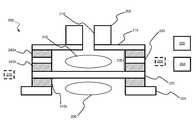
- FIG. 1shows a simplified cross-sectional view of a processing system 100 according to embodiments of the present technology.
- the processing systemmay optionally include components located outside the processing chamber 105 , such as fluid supply system 110 .
- the processing chamber 105may hold an internal pressure different than the surrounding pressure.
- the pressure inside the processing chambermay be about 10 mTorr to about 20 Torr during processing.
- the CCP systemmay be composed of several of the processing chamber components, and may function to generate a plasma inside the processing chamber 105 .
- the components of the CCP systemmay include a lid assembly or hot electrode 115 that may be composed of several components including a gas box, a blocker, and a faceplate. These components may be directly or indirectly coupled mechanically in order to function as a single electrode.
- the CCP systemalso may include a grid electrode 120 that also may be composed of one or more chamber components.
- the grid electrode 120may be composed of an ion suppressor or blocker and/or a manifold or showerhead for precursor delivery to the substrate wafer.
- the componentsmay be electrically coupled with each other in order to function as a single electrode.
- the CCP systemmay also include a ground electrode 125 that may include one or more chamber components including a lid spacer.
- the lid 115 and grid electrode 120are electrically conductive electrodes that can be electrically biased with respect to each other to generate an electric field strong enough to ionize gases between the electrodes into a plasma.
- An electrical insulator 130may separate the lid 115 and the grid 120 electrodes to prevent them from short-circuiting when a plasma is generated.
- the electrical insulator 130may include multiple layers of material, as will be explained in more detail below with regard to the embodiments discussed with FIG. 2 , and may alternatively include additional electrode layers.
- the plasma exposed surfaces of the lid 115 , insulator 130 , and grid electrode 120may define a plasma excitation region 135 in the processing chamber 105 .
- Plasma generating gasesmay travel from a gas supply system 110 through a gas inlet 140 into the plasma excitation region 135 .
- the plasma generating gasesmay be used to strike a plasma in the excitation region 135 , or may maintain a plasma that has already been formed.
- the plasma generating gasesmay have already been at least partially converted into plasma excited species in a remote plasma system 145 positioned outside the processing chamber 105 before traveling downstream though the inlet 140 to the plasma excitation region 135 .
- the plasma excited speciesreach the plasma excitation region 135 , they may be further excited and affected by the characteristics of the plasma generated in the plasma excitation region.
- the degree of added excitation provided by the CCP systemmay change over time depending on the substrate processing sequence and/or conditions.
- the plasma generating gases and/or plasma excited speciesmay pass through a plurality of holes (not shown) in lid 115 for a more uniform delivery into the plasma excitation region 135 .
- Exemplary configurationsinclude having the inlet 140 open into a gas supply region 150 partitioned from the plasma excitation region 135 by lid 115 so that the gases/species flow through the holes in the lid 115 into the plasma excitation region 135 .
- Structural and operational featuresmay be selected to prevent significant backflow of plasma from the plasma excitation region 135 back into the supply region 150 , inlet 140 , and fluid supply system 110 .
- the structural featuresmay include the selection of dimensions and cross-sectional geometry of the holes in lid 115 that deactivates back-streaming plasma.
- the operational featuresmay include maintaining a pressure difference between the gas supply region 150 and plasma excitation region 135 that maintains a unidirectional flow of plasma through the grid electrode 120 .
- the lid 115 and the grid electrode 120may function as a first electrode and second electrode, respectively, so that the lid 115 and/or grid electrode 120 may receive an electric charge.
- electrical powersuch as RF power may be applied to the lid 115 , grid electrode 120 , or both.
- electrical powermay be applied to the lid 115 while the grid electrode 120 is grounded.
- the substrate processing system 100may include an RF generator 155 that provides electrical power to the lid 115 and/or one or more other components of the chamber 105 .
- the electrically charged lid 115may facilitate a uniform distribution of plasma, i.e., reduce localized plasma, within the plasma excitation region 135 .
- insulator 130may electrically insulate lid 115 and grid electrode 120 .
- Insulator 130may be made from a ceramic and may have a high breakdown voltage to avoid sparking.
- the insulator 130includes several components that may be further utilized to affect the generated plasma, and may include additional electrode materials.
- the CCP systemmay also include a DC power system as will be described further below for modulating the RF generated plasma inside the chamber.
- the CCP systemmay further include a cooling unit (not shown) that includes one or more cooling fluid channels to cool surfaces exposed to the plasma with a circulating coolant (e.g., water).
- the cooling unitmay include jacketing coupled with the exterior of the chamber 105 walls, as well as channels defined within the interior of the chamber walls that circulate a temperature controlled fluid.
- the grid electrode 120may include a plurality of holes 122 that suppress the migration of ionically-charged species out of the plasma excitation region 135 while allowing uncharged neutral or radical species to pass through the grid electrode 120 .
- These uncharged speciesmay include highly reactive species that are transported with less reactive carrier gas through the holes 122 .
- the migration of ionic species through the holes 122may be reduced, and in some instances completely suppressed. Controlling the amount of ionic species passing through the grid electrode 120 may provide increased control over the gas mixture brought into contact with the underlying wafer substrate, which in turn increases control of the deposition and/or etch characteristics of the gas mixture.
- adjustments in the ion concentration of the gas mixturecan significantly alter its etch selectivity (e.g., SiOx:SiNx etch ratios, Poly-Si:SiOx etch ratios, etc.), as well as shift the balance of conformal-to-flowable of a deposited dielectric material.
- etch selectivitye.g., SiOx:SiNx etch ratios, Poly-Si:SiOx etch ratios, etc.
- the plurality of holes 122may be configured to control the passage of the activated gas (i.e., the ionic, radical, and/or neutral species) through the grid electrode 120 .
- the aspect ratio of the holes 122i.e., the hole diameter to length
- the geometry of the holes 122may be controlled so that the flow of ionically-charged species in the activated gas passing through the grid electrode 120 is reduced.
- the holes in the ion blockerwhich may be disposed above the showerhead, may include a tapered portion that faces the plasma excitation region 135 , and a cylindrical portion that faces the showerhead. The cylindrical portion may be shaped and dimensioned to control the flow of ionic species passing to the showerhead.
- An adjustable electrical biasmay also be applied to the grid electrode 120 as an additional means to control the flow of ionic species through the electrode.
- gases and plasma excited speciesmay pass through the grid electrode 120 and be directed to the substrate.
- the showerheadwhich may be a component included in the grid electrode, can further direct the flow of gases or plasma species.
- the showerheadmay be a dual-zone showerhead that may include multiple fluid channels for directing the flow of one or more gases.
- the dual-zone showerheadmay have a first set of channels to permit the passage of plasma excited species into reaction region 160 , and a second set of channels that deliver a second gas/precursor mixture into the reaction region 160 .
- a fluid delivery sourcemay be coupled with the showerhead to deliver a precursor that is able to bypass plasma excitation region 135 and enter reaction region 160 from within the showerhead through the second set of channels.
- the second set of channels in the showerheadmay be fluidly coupled with a source gas/precursor mixture (not shown) that is selected for the process to be performed.
- the source gas/precursor mixturemay include etchants such as oxidants, halogens, water vapor and/or carrier gases that mix in the reaction region 160 with plasma excited species distributed from the first set of channels in the showerhead. Excessive ions in the plasma excited species may be reduced as the species move through the holes 122 in the grid electrode 120 , and reduced further as the species move through channels in the showerhead.
- the processing systemmay still further include a pedestal 165 that is operable to support and move the substrate or wafer.
- the distance between the pedestal 165 and the bottom of the grid electrode 120help define the reaction region 160 along with lid spacer 125 defining the periphery of the reaction region 160 .
- the pedestal 165may be vertically or axially adjustable within the processing chamber 105 to increase or decrease the reaction region 160 and affect the deposition or etching of the wafer substrate by repositioning the wafer substrate with respect to the gases passed through the grid electrode 120 .
- the pedestal 165may have a heat exchange channel through which a heat exchange fluid flows to control the temperature of the wafer substrate. Circulation of the heat exchange fluid allows the substrate temperature to be maintained at relatively low temperatures (e.g., about ⁇ 20° C. to about 90° C.).
- Exemplary heat exchange fluidsinclude ethylene glycol and water.
- the pedestal 165may also be configured with a heating element such as a resistive heating element to maintain the substrate at heating temperatures (e.g., about 90° C. to about 1100° C.).
- a heating elementsuch as a resistive heating element to maintain the substrate at heating temperatures (e.g., about 90° C. to about 1100° C.).
- Exemplary heating elementsmay include a single-loop heater element embedded in the substrate support platter that makes two or more full turns in the form of parallel concentric circles. An outer portion of the heater element may run adjacent to a perimeter of the support platten, while an inner portion may run on the path of a concentric circle having a smaller radius.
- the wiring to the heater elementmay pass through the stem of the pedestal.
- FIG. 2shows a simplified cross-sectional schematic of a processing chamber assembly according to embodiments of the present technology.
- the schematicillustrates a portion of a processing chamber 205 that may be used in semiconductor fabrication processes.
- Chamber 205may be similar to processing chamber 105 as shown in FIG. 1 .
- Chamber 205may include a lid assembly 215 that may in some aspects be comparable to the lid assembly 115 as shown in FIG. 1 .
- lid assembly 215may define precursor inlet 210 , through which a precursor species may be delivered.
- a remote plasma unit(not shown) may be fluidly coupled with the precursor inlet 210 to provide radical precursor species into processing chamber 205 .
- the radical precursor provided by the plasma unitmay be mixed with additional gases inside the processing chamber 205 that are separately flowed into the chamber 205 through alternate channels (not shown).
- Processing chamber 205may include a grid electrode 220 that may include one or more chamber components electrically coupled.
- the grid electrode 220may include one or more manifolds, and may include an ion blocker, as well as a showerhead, such as a dual-zone showerhead as previously described.
- the processing chamber 205may include a ground electrode 225 that may be composed of additional chamber 205 components.
- the ground electrode 225may be a lid spacer or other wall component of the processing chamber 205 .
- the ground electrodemay alternatively include a ground connection to a substrate pedestal (not shown), but this may not be required for embodiments of the technology.
- Processing chamber 205may include an insulation section 230 similar to insulator 130 as illustrated in FIG. 1 . However, as illustrated in processing chamber 205 , insulation section 230 includes multiple components.
- the processing chamber 205may include a conductive insert 235 disposed between lid assembly 215 and grid electrode 220 .
- the conductive insert 235may be a single piece of conductive material of an annular shape disposed as a portion of the chamber 205 wall.
- a plurality of insulation membersmay additionally be incorporated into processing chamber 205 to electrically isolate the chamber components.
- insulation members 240 a - care positioned between each of the conductive components and electrodes of the chamber housing.
- the insulation members 240may be of a single annular shape, or be composed of several sections that when combined provide an electrical barrier between chamber components.
- the insulation membermay resist the flow of electrical charge, and may be of a material having a high dielectric strength.
- Exemplary insulation membersinclude ceramic plates that may be annular in shape and disposed above and below components including the conductive insert 235 . Multiple layers of the insulation members may be positioned in chamber 205 to further isolate components of the chamber.
- At least one of the plurality of insulation membersmay be positioned to electrically isolate the conductive insert 235 from the grid electrode 220 .
- the insulation membersmay additionally isolate both the conductive insert 235 and the grid electrode 220 from the lid assembly 215 and the ground electrode 225 . In this way, each conductive section may be electrically isolated from any other conductive section of the processing chamber 205 .
- the chamber componentsmay define plasma regions within the processing chamber.
- a first plasma region 245may be at least partially defined above and below by the lid assembly 215 and the grid electrode 220 .
- the conductive insertmay be disposed along the periphery of the first plasma region 245 .
- a second plasma region 250may be at least partially defined above by the grid electrode 220 .
- the second plasma region 250may be at least partially defined below by a substrate pedestal (not shown), that may be moveable vertically, axially, or both, to define the area in which the second plasma region 250 exists.
- the ground electrode 225may be disposed along the periphery of the second plasma region 250 , or may be utilized to produce a boundary at least partially defining the lower bounds of the second plasma region 250 .
- Power supplies 255 , 260 and optionally electrical switches 265 , 270may be coupled with processing chamber 205 to produce a processing system 200 with plasma control.
- the optional switchesmay be used to electrically couple components of the system.
- electrical switch 265may be electrically coupled with power supply 260 , alternatively with power supply 255 and 260 , alternatively with power supply 255 , or still alternatively with either power supply while an additional switch (not shown) is used to electrically couple the other power supply.
- the switchesmay be bypassed to directly couple each of the power supplies 255 , 260 to portions of the processing chamber.
- the power supplies 255 , 260may be of any type of power useful in semiconductor manufacturing, and may include RF power supplies, DC power supplies, etc.
- Optional switch 270may be used to electrically couple components of the processing chamber 205 .
- switch 270may be switchable to electrically couple any two or more of the lid assembly 215 , the conductive insert 235 , the grid electrode 220 , and the ground electrode 225 .
- optional switch 270may be bypassed to directly electrically couple one or more components of the processing chamber 205 .
- the switches 265 , 270may provide additional functionality so that the type of plasma generated, and the location of the plasma may be adjusted at any time during processing operations.
- the optional switches 265 , 270 and power supplies 255 , 260may additionally include remotely located controls to manipulate the settings of the components as will be described further below.
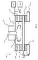
- FIG. 3shows a simplified cross-sectional schematic of a processing system 300 having plasma generation components according to embodiments of the present technology.
- Chamber 305 of processing system 300may include similar components as previously described with respect to FIG. 2 .
- Chamber 305may define a gas inlet 310 through which reactive precursor species may be delivered from, for example, a remote plasma unit (not shown).
- Chamber 305may include a lid assembly 315 , conductive insert 335 , grid electrode 320 , and ground electrode 325 along with additional chamber components.
- One or more of the lid assembly 315 , conductive insert 335 , grid electrode 320 , and ground electrode 325may be electrically isolated from the other listed components by one or more of a plurality of insulation members 340 a - c .
- System 300may additionally include power supplies 355 , 360 as well as optional switches 365 , 370 for electrically coupling the power supplies to the chamber, or components in the chamber to one another.
- power supply 355may be electrically coupled with lid assembly 315 .
- power supply 355is an RF power supply.
- the power supplymay provide an electrical charge to lid assembly 315 which may act as a hot electrode for plasma generation.
- Grid electrode 320may be coupled with ground electrode 325 thereby defining a plasma region 345 in which plasma may be generated, or plasma conditions may be modulated.
- the grid electrode 320may be directly coupled with ground electrode 325 , or alternatively may be electrically isolated with insulation member 340 c . The insulation may be overcome by electrically coupling the grid electrode 320 and the ground electrode 325 .
- a conductive meansmay be used to electrically couple the electrodes, and an exemplary system may utilize optional switch 370 that is switchable for electrically coupling the components.
- the RF power supply 355may be configured to deliver an adjustable amount of power to the lid assembly 315 depending on the process performed.
- Exemplary power suppliesmay be configured to deliver an adjustable amount of power over a range of from 0 to about 3 kW of power.
- the power delivered to the lid assembly 315may be adjusted to set the conformality of the deposited layer.
- Deposited dielectric filmsare typically more flowable at lower plasma powers and shift from flowable to conformal when the plasma power is increased.
- an argon containing plasma maintained in the plasma excitation region 345may produce a more flowable silicon oxide layer as the plasma power is decreased from about 1000 Watts to about 100 Watts or lower (e.g., about 900, 700, 500, 300, 200, 100, 50, 25 Watts, or less), and a more conformal layer as the plasma power is increased from about 1000 Watts, or more (e.g., about 1200, 1500, 1800, 2000, 2200, 2400, 2600, 2800 Watts, or more).
- the transition from a flowable to conformal deposited filmmay be relatively smooth and continuous or progress through relatively discrete thresholds.
- the plasma powermay be adjusted to select a balance between the conformal and flowable properties of the deposited film. For etching processes, reducing the power from 3 kW down below 1 kW or less can affect the removal rate of material being etched, and may reduce the rate at which deposited films are removed. Increasing the power above 1 kW and up to 3 kW can produce higher removal rates of deposited films.
- the frequency and duty cycle of the RF powermay be adjusted to modulate the chemistry and flux characteristics of the films.
- the inventorshave also determined that certain frequencies of RF supply may affect the impact on chamber components, such as the grid electrode.
- frequenciessuch as up to about 400 kHz, between about 400 kHz and about 13.56 MHz, between about 13.56 MHz and about 60 MHz, and above 60 MHz may be employed.
- increasing the frequencymay produce etchant radicals more efficiently, as well as reduce the damage caused to chamber components.
- Power supply 360may also be utilized during the operation of power supply 355 , and may be a DC power supply in some embodiments. Exemplary DC power supplies may be configured for adjustable control between about 500 to about ⁇ 500 V. Alternatively, power supply 360 may be configured for adjustable control between about 400 to about ⁇ 400 V, between about 300 to about ⁇ 300 V, between about 200 to about ⁇ 200 V, between about 100 to about ⁇ 100 V, etc., or less. Power supply 360 may be directly coupled with components of chamber 305 , or electrically coupled to components with switch 365 that may be switchable to electrically couple power supply 360 to components of the chamber 305 . In one embodiment, DC power supply 360 is electrically coupled with conductive insert 335 .
- RF power supply 355 and DC power supply 360may be operated together, alternately, or in some other combination.
- RF power supply 355may be operated continuously between about 0 and about 3000 kW to maintain a plasma in plasma reaction region 345 .
- the DC power supply 360may be unused or off, may be continuously operated, or alternatively may be pulsed during operation. The assistance of DC power may produce effects on the material being etched. For example, if the DC bias is positive, more ion flux from the plasma may move to the grid electrode, and subsequently to the substrate wafer. If the DC bias is negative, more electron flux may be directed to the grid electrode.
- the etch characteristics of the plasmacan be modulated. Accordingly, depending on the characteristics of the substrate or on the characteristics of the films being etched, the chemistry of the etchants may be adjusted to produce optimum etching results. For example, the more the etchant chemistry is adjusted to increase the ion or electron flux, the more the etchant fluids may be selective towards one or more deposited films.
- the DC power supply 360with the RF power supply 355 , more chemistry modulation may be obtained as compared to an RF power supply alone. With the enhanced etchant chemistry modulation, improved etching selectivities may be obtained, which may also provide improved ability for more sensitive removals of deposited films. Sensitivity with removal rates may allow less material to be removed overall, which may allow less material to be deposited initially.
- An alternative operational scheme as illustrated by FIG. 3includes pulsing of the RF power supply 355 along with continuous or pulsed operation of the DC power supply 360 .
- the RF power supply 355may be configured to provide continuous adjustable modulation of RF pulsing from continuous wave down to about 1000 kHz or more.
- the RFmay be adjusted in discrete increments from continuous wave to about 0.01 kHz, or alternatively about 0.1 kHz, 1 kHz, 10 kHz, 100 kHz, 1000 kHz, etc., or more.
- the RF power supply 355may be pulsed in any variety or range of values between the listed values.
- the duty cyclemay be modulated. Adjusting the duty cycle, or the time in the active state, for the RF power supply may affect the flux of ions produced in the plasma. For example, when a reduction in the duty cycle occurs, a relatively or substantially commensurate reduction in ion current may be produced. During etching processes, by reducing the ion current, the etching rate may be reduced proportionately. However, when an RF power supply is cycled, it is switched on and off during the cycling time. When the RF power is cycled off, the generated plasma may dissipate. Accordingly, the amount of duty cycle reduction may conventionally have been limited to the times that may allow the plasma to be maintained at a certain level.
- the DC power supply 360may be capable of adjusting the chemistry by maintaining ion and electron movement during the periods that the RF power is off. Additionally, by having a certain amount of DC power during the periods when the RF power is off, the plasma may be at least partially sustained by the DC power. In this way, the plasma may not fully dissipate when the RF power is cycled off. This may allow further adjustment of the chemistry because the etchant chemistry may adjust when the RF power is switched from on to off. By utilizing the DC power supply 360 during some or all of the on and/or off times of the RF power supply 355 , the etchant chemistries may be further modified.
- the duty cycle of the RF powermay be operated from about 100% to about 0% during operation, less than or about 75%, less than or about 50%, or less than or about 25%.
- the duty cyclemay be operated at about 90%, 80%, 75%, 70%, 60% 50%, 40%, 30%, 25%, 20%, 15%, 10%, 5%, or less.
- the power supplymay be configured to have an adjustable duty cycle at or between any of the listed cycle percentages, as well as ranges of any of the recited cycles. Pulsing of the RF power supply may allow further adjustment of the etching parameters by allowing reduced and more selective removals.
- RF pulsingmay be employed.
- the RF pulsingmay be capable of removing amounts of less than 100 nm of material, or alternatively less than or about 50 nm, 30 nm, 22 nm, 15 nm, or less including down to a monolayer of deposited film.
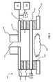
- FIG. 4shows a simplified cross-sectional schematic of another processing system 400 having plasma generation components according to embodiments of the present technology.
- Chamber 405 of processing system 400may include similar components as previously described with respect to FIG. 2 .
- Chamber 405may define a gas inlet 410 through which reactive precursor species may be delivered from, for example, a remote plasma unit (not shown).
- Chamber 405may include a lid assembly 415 , conductive insert 435 , grid electrode 420 , and ground electrode 425 along with additional chamber components.
- One or more of the lid assembly 415 , conductive insert 435 , grid electrode 420 , and ground electrode 425may be electrically isolated from the other listed components by one or more of a plurality of insulation members 440 a - c .
- System 400may additionally include power supplies 455 , 460 as well as optional switches 465 , 470 for electrically coupling the power supplies to the chamber, or components in the chamber to one another.
- power supply 455is electrically coupled with lid assembly 415 .
- power supply 455is an RF power supply.
- the power supply 455provides an electrical charge to lid assembly 415 which may act as a hot electrode for plasma generation.
- Grid electrode 420may be coupled with ground electrode 425 thereby defining a plasma region 445 in which plasma may be generated, or plasma conditions may be modulated.
- the grid electrode 420may be directly coupled with ground electrode 425 , or alternatively may be electrically isolated with insulation member 440 c . The insulation may be overcome by electrically coupling the grid electrode 420 and the ground electrode 425 .
- a conductive meansmay be used to electrically couple the electrodes, and an exemplary system may utilize optional switch 470 for electrically coupling the components.
- RF power supply 455may be configured to be adjustable with any of the parameters as previously discussed.
- Power supply 460may also be utilized during the operation of power supply 455 , and may be a DC power supply in some embodiments. Exemplary DC power supplies may be configured for adjustable control with any of the parameters as previously described. DC power supply 460 may be operated in continuous or pulsing fashion as previously described. As illustrated in FIG. 4 , DC power supply 460 is electrically coupled to lid assembly 415 along with RF power supply 455 . Power supply 460 may be directly coupled with the lid assembly 415 or the electrical coupling of RF power supply 455 , or electrically coupled to the lid assembly 415 or electrical coupling of RF power supply 455 with switch 465 that may be switchable to electrically couple DC power supply 460 to the components of the chamber 405 .
- RF power supply 455 and DC power supply 460may be operated as illustrated in FIG. 4 to provide additional chemistry modulation of precursor species via an additional form of plasma modulation.
- Radical precursor speciesmay be delivered to processing chamber 405 from a remote plasma system (not shown) fluidly coupled to gas inlet 410 .
- RF power supply 455may be operated as a continuous wave or pulsed to deliver modulated power to lid assembly 415 .
- power supply 455When engaged in the illustrated configuration, power supply 455 may generate a plasma in plasma region 445 .
- Lid assembly 415as the hot electrode, may be a major plasma generation area.
- DC power supply 460may be operated to assist RF power supply 455 in maintaining plasma function in the plasma region 445 . When RF power supply 455 is cycled off, DC power supply 460 may hold some plasma.
- DC power supply 460may be operated in continuous fashion while RF power supply 455 is pulsed.
- DC power supply 460when electrically coupled with lid assembly 415 and operated continuously, may maintain a plasma in plasma region 445 generated by RF power supply 455 .
- RF power supplymay be modulated on and off, and continuously operated power supply 460 may maintain the plasma during the off cycle.
- RF power supply 455may be modulated with reduced duty cycles.
- the duty cycle of the RF powermay be operated from about 100% to about 0% during operation, less than or about 75%, less than or about 50%, or less than or about 25%.
- the duty cyclemay be operated at about 90%, 80%, 75%, 70%, 60%, 50%, 40%, 30%, 25%, 20%, 15%, 10%, 5%, or less.
- the power supplymay be configured to have an adjustable duty cycle at or between any of the listed cycle percentages, as well as ranges of any of the recited cycles.
- the pulsing capability of RF power supply 455may be modulated continuously as previously discussed from continuous wave to about 1000 kHz or more.
- the RFmay be adjusted in discrete increments from continuous wave to about 0.01 kHz, or alternatively about 0.1 kHz, 1 kHz, 10 kHz, 100 kHz, 1000 kHz, etc., or more.
- the RF power supply 455may be pulsed in any variety or range of values between the listed values. When pulsed, the ion current may be reduced as compared to continuous wave operation. Because the DC power supply may assist in holding a plasma during the ‘off’ cycle of RF power supply 455 , further pulsing modulation may be effected.
- reduced etchingmay be performed to the level of less than 100 nm during an etching process.
- the same time period for etchingmay result in a reduced etching amount.
- further reduction of the ion current via power supply modulation as discussedmay allow etching amounts of less than or about 50 nm, 40 nm, 30 nm, 20 nm, 10 nm, 5 nm, etc., or less.
- reducing the duty cyclemay further modify the etching amounts by additionally reducing the ion current as the duty cycle is reduced.
- pulsing and reduced duty cyclemay be combined to provide further chemistry modulation and ion current to allow improved flexibility of operation.
- the DC power supplymay be utilized in several ways.
- the DC power supplymay have a greater impact on ion and electron flux, and a positive and negative bias may be applied over a range of power levels to affect the chemistry of the precursors directed to the substrate.
- the DC power supply 460when the DC power supply 460 is coupled with the lid assembly in conjunction with the RF power supply 455 , the DC power supply 460 may be used for plasma holding, and as such ion current may be further modulated via the RF power supply 455 .
- switch 465that may be electrically coupled with power supply 460 , DC power supply 465 may be electrically coupled with different components of processing chamber 405 during different operations.
- DC power supply 460may be appropriately coupled with the chamber 405 to produce the plasma assistance most beneficial for the particular operation. Additionally, these parameters may be adjusted during operation such as if multiple deposited films are being removed, the coupling of power supply 460 , and the modulation of both power supplies 455 , 460 may be adjusted during processing when operational parameters may benefit from a change in etch performance.
- FIG. 5shows a simplified cross-sectional schematic of another processing system 500 having plasma generation components according to embodiments of the present technology.
- Chamber 505 of processing system 500may include similar components as previously described with respect to FIG. 2 .
- Chamber 505may define a gas inlet 510 through which reactive precursor species may be delivered from, for example, a remote plasma unit (not shown).
- Chamber 505may include a lid assembly 515 , conductive insert 535 , grid electrode 520 , and ground electrode 525 along with additional chamber components.
- One or more of the lid assembly 515 , conductive insert 535 , grid electrode 520 , and ground electrode 525may be electrically isolated from the other listed components by one or more of a plurality of insulation members 540 a - c .
- System 500may additionally include power supplies 555 , 560 as well as optional switches 565 , 570 for electrically coupling the power supplies to the chamber, or components in the chamber to one another.
- power supply 555is electrically coupled with lid assembly 515 .
- power supply 555is an RF power supply.
- the power supply 555provides an electrical charge to lid assembly 515 which may act as a hot electrode for plasma generation.
- Grid electrode 520may be coupled with lid assembly 515 which allows the hot electrode function to move to the grid electrode 520 level. As such, plasma generation may be shifted below the grid electrode 520 to the wafer level in plasma region 550 .
- the grid electrode 520may be electrically coupled with lid assembly, and an exemplary system may utilize optional switch 570 for electrically coupling the components.
- RF power supply 555may be configured to be adjustable with any of the parameters as previously discussed.
- Power supply 560may also be utilized during the operation of power supply 555 , and may be a DC power supply in some embodiments. Exemplary DC power supplies may be configured for adjustable control with any of the parameters as previously described. DC power supply 560 may be operated in continuous or pulsing fashion as previously described. As illustrated in FIG. 5 , DC power supply 560 may be electrically coupled with lid assembly 515 along with RF power supply 555 . Power supply 560 may be directly coupled with the lid assembly 515 or the electrical coupling of RF power supply 555 , or electrically coupled to the lid assembly 515 or electrical coupling of RF power supply 555 with switch 565 that may be switchable to electrically couple DC power supply 560 to the components of the chamber 505 .
- the exemplary system configuration illustrated in FIG. 5may be utilized for treatment operations. For example, after an etch process has been performed, such as with one of the prior etch configurations, byproducts may be formed or remain on the substrate surface. Remote plasma systems may be less effective in some circumstances than plasma generated at the wafer level. Accordingly, by utilizing the system configuration illustrated in FIG. 5 , a more effective plasma treatment may be formed at the substrate level. However, depending on the type of byproduct and the amount remaining on the surface, plasma modulation may still be utilized with any of the operational manipulations previously discussed. Accordingly, by utilizing one or more of the power supply configurations as previously discussed, modulation of the treatment chemistry may be modulated as previously described.
- switch 570may be switchable to couple multiple components of the processing chamber 505 .
- switch 570may be operated to switch the electrical coupling of the grid electrode 520 from the ground electrode 525 to the lid assembly 515 .
- a subsequent treatment processmay be performed with wafer level plasma as illustrated in FIG. 5 .
- an etching operationmay be performed as described with regard to the embodiment shown in FIG. 3 .
- switch 565may be operated to switch the coupling of DC power supply 560 from the conductive insert 535 to the lid assembly 515 or RF power supply 555 electrical coupling
- switch 570may be operated to switch the electrical coupling of the grid electrode 520 from the ground electrode 525 to the lid assembly 515 .
- Many such optionsare available with the configurations and switching capabilities as described herein.
- FIG. 6shows a simplified cross-sectional schematic of another processing system 600 having plasma generation components according to embodiments of the present technology.
- Chamber 605 of processing system 600may include similar components as previously described with respect to FIG. 2 .
- Chamber 605may define a gas inlet 610 through which reactive precursor species may be delivered from, for example, a remote plasma unit (not shown).
- Chamber 605may include a lid assembly 615 , conductive insert 635 , grid electrode 620 , and ground electrode 625 along with additional chamber components.
- One or more of the lid assembly 615 , conductive insert 635 , grid electrode 620 , and ground electrode 625may be electrically isolated from the other listed components by one or more of a plurality of insulation members 640 a - c .
- System 600may additionally include power supplies 655 , 660 as well as optional switches 665 , 670 for electrically coupling the power supplies to the chamber, or components in the chamber to one another.
- power supply 655is electrically coupled with lid assembly 615 .
- power supply 655is an RF power supply.
- the power supply 655provides an electrical charge to lid assembly 615 which may act as a hot electrode for plasma generation.
- grid electrode 620may not be electrically coupled with ground electrode 625 . Accordingly, the ground electrode of the power system may be shifted from the grid electrode 620 to the ground electrode 625 . In so doing, the plasma may develop over a slightly larger region of processing chamber 605 including into and through the grid electrode 620 .
- RF power supply 455may be configured to be adjustable with any of the parameters as previously discussed.
- Power supply 660may also be utilized during the operation of power supply 655 , and may be a DC power supply in some embodiments. Exemplary DC power supplies may be configured for adjustable control with any of the parameters as previously described. DC power supply 660 may be operated in continuous or pulsing fashion as previously described, and also may be electrically coupled with any of the components of processing chamber 605 as previously described. In the exemplary system illustrated in FIG. 6 , DC power supply 660 is electrically coupled with grid electrode 620 . Power supply 660 may be directly coupled with grid electrode 620 , or alternatively with switch 665 that may be switchable to electrically couple DC power supply 660 to the components of the chamber 605 .
- RF power supply 655 and DC power supply 660may be operated as illustrated in FIG. 6 to provide additional chemistry modulation of precursor species via an additional form of plasma modulation.
- Radical precursor speciesmay be delivered to processing chamber 605 from a remote plasma system (not shown) fluidly coupled with gas inlet 610 .
- RF power supply 655may be operated as a continuous wave or pulsed to deliver modulated power to lid assembly 615 .
- power supply 655When engaged in the illustrated configuration, power supply 655 may generate a plasma in plasma region 645 .
- byproductsmay remain in trench features previously etched.
- the expanded plasma regionmay allow certain plasma species to interact at the substrate level and may provide directionality to species that may be utilized in byproduct removal.
- RF power supply 655may be modulated via pulsing, or duty cycle modulation may be performed as previously described.
- DC power supply 660may be operated to assist RF power supply 655 in any of the ways previously described.
- the DC power supply 660may be used to provide additional ion and electron flux control with the plasma generated.
- ion and electron fluxcan be adjusted through the grid electrode 620 components depending on the bias and power level of the DC power supply as explained above.
- Alternative embodimentsmay also electrically couple the DC power supply 660 with the conductive insert 635 or the lid assembly 615 as previously described.
- FIG. 7is shown a method of producing a plasma in a processing chamber according to the present technology.
- the chambermay be similar to chamber 100 as previously described.
- the chambermay include one or more power supplies such as supply 155 .
- a first power supplymay be coupled with the processing chamber lid assembly.
- the power supplymay also be coupled electrically with additional or alternative structures of the processing chamber.
- a second power supplymay be coupled with the processing chamber, and may be coupled with a similar or different portion of the processing chamber as the first power supply.
- the second and/or first power supplymay be coupled with a switch that may be switchably coupled with one or more conductive sections of the processing chamber.
- the second power supplymay be switchably coupled with the lid assembly or an additional conductive portion of the chamber as previously described.
- a plasmamay be ignited or otherwise formed in the processing chamber by engaging the first power supply.
- the action of coupling the power supply if engagedmay ignite the plasma between the structure to which the first power supply is electrically coupled and a ground source located within the chamber.
- the second power supplymay be used to tune the plasma profile in one or more ways. For example, a negative voltage may be applied with the second power supply, which may cause a greater electron flux to flow through the chamber such as towards a grid electrode or processing region. Also, a positive voltage may be applied with the second power supply to increase the ion flux through the chamber towards an electrode structure or the processing region.
- the first power supplymay also be operated in a variety of modes, and for example, the first power supply may provide pulsing power to the lid assembly.
- the first power supplymay include an RF power supply
- the second power supplymay include a DC power supply.
Landscapes
- Engineering & Computer Science (AREA)
- Chemical & Material Sciences (AREA)
- Physics & Mathematics (AREA)
- Plasma & Fusion (AREA)
- Analytical Chemistry (AREA)
- Chemical Kinetics & Catalysis (AREA)
- Materials Engineering (AREA)
- Mechanical Engineering (AREA)
- Metallurgy (AREA)
- Organic Chemistry (AREA)
- General Chemical & Material Sciences (AREA)
- General Physics & Mathematics (AREA)
- Condensed Matter Physics & Semiconductors (AREA)
- Manufacturing & Machinery (AREA)
- Computer Hardware Design (AREA)
- Microelectronics & Electronic Packaging (AREA)
- Power Engineering (AREA)
- Plasma Technology (AREA)
- Particle Accelerators (AREA)
- Drying Of Semiconductors (AREA)
- Chemical Vapour Deposition (AREA)
Abstract
Description
Claims (20)
Priority Applications (7)
| Application Number | Priority Date | Filing Date | Title |
|---|---|---|---|
| US13/829,669US9373517B2 (en) | 2012-08-02 | 2013-03-14 | Semiconductor processing with DC assisted RF power for improved control |
| CN201380041015.6ACN104508804B (en) | 2012-08-02 | 2013-07-25 | Semiconductor processing using DC assisted RF power for improved control |
| JP2015525467AJP6258320B2 (en) | 2012-08-02 | 2013-07-25 | Semiconductor processing using DC assisted RF power for improved control |
| KR1020157005502AKR102111919B1 (en) | 2012-08-02 | 2013-07-25 | Semiconductor processing with dc assisted rf power for improved control |
| PCT/US2013/052039WO2014022192A1 (en) | 2012-08-02 | 2013-07-25 | Semiconductor processing with dc assisted rf power for improved control |
| TW102127133ATWI594319B (en) | 2012-08-02 | 2013-07-29 | Semiconductor processing with dc assisted rf power for improved control |
| US15/187,211US10032606B2 (en) | 2012-08-02 | 2016-06-20 | Semiconductor processing with DC assisted RF power for improved control |
Applications Claiming Priority (2)
| Application Number | Priority Date | Filing Date | Title |
|---|---|---|---|
| US201261678964P | 2012-08-02 | 2012-08-02 | |
| US13/829,669US9373517B2 (en) | 2012-08-02 | 2013-03-14 | Semiconductor processing with DC assisted RF power for improved control |
Related Child Applications (1)
| Application Number | Title | Priority Date | Filing Date |
|---|---|---|---|
| US15/187,211DivisionUS10032606B2 (en) | 2012-08-02 | 2016-06-20 | Semiconductor processing with DC assisted RF power for improved control |
Publications (2)
| Publication Number | Publication Date |
|---|---|
| US20140057447A1 US20140057447A1 (en) | 2014-02-27 |
| US9373517B2true US9373517B2 (en) | 2016-06-21 |
Family
ID=50028443
Family Applications (2)
| Application Number | Title | Priority Date | Filing Date |
|---|---|---|---|
| US13/829,669Expired - Fee RelatedUS9373517B2 (en) | 2012-08-02 | 2013-03-14 | Semiconductor processing with DC assisted RF power for improved control |
| US15/187,211Active2033-10-18US10032606B2 (en) | 2012-08-02 | 2016-06-20 | Semiconductor processing with DC assisted RF power for improved control |
Family Applications After (1)
| Application Number | Title | Priority Date | Filing Date |
|---|---|---|---|
| US15/187,211Active2033-10-18US10032606B2 (en) | 2012-08-02 | 2016-06-20 | Semiconductor processing with DC assisted RF power for improved control |
Country Status (6)
| Country | Link |
|---|---|
| US (2) | US9373517B2 (en) |
| JP (1) | JP6258320B2 (en) |
| KR (1) | KR102111919B1 (en) |
| CN (1) | CN104508804B (en) |
| TW (1) | TWI594319B (en) |
| WO (1) | WO2014022192A1 (en) |
Cited By (100)
| Publication number | Priority date | Publication date | Assignee | Title |
|---|---|---|---|---|
| US9520303B2 (en) | 2013-11-12 | 2016-12-13 | Applied Materials, Inc. | Aluminum selective etch |
| US9553102B2 (en) | 2014-08-19 | 2017-01-24 | Applied Materials, Inc. | Tungsten separation |
| US9564296B2 (en) | 2014-03-20 | 2017-02-07 | Applied Materials, Inc. | Radial waveguide systems and methods for post-match control of microwaves |
| US9576809B2 (en) | 2013-11-04 | 2017-02-21 | Applied Materials, Inc. | Etch suppression with germanium |
| US9613822B2 (en) | 2014-09-25 | 2017-04-04 | Applied Materials, Inc. | Oxide etch selectivity enhancement |
| US9659753B2 (en) | 2014-08-07 | 2017-05-23 | Applied Materials, Inc. | Grooved insulator to reduce leakage current |
| US9659792B2 (en) | 2013-03-15 | 2017-05-23 | Applied Materials, Inc. | Processing systems and methods for halide scavenging |
| US9691645B2 (en) | 2015-08-06 | 2017-06-27 | Applied Materials, Inc. | Bolted wafer chuck thermal management systems and methods for wafer processing systems |
| US9721789B1 (en) | 2016-10-04 | 2017-08-01 | Applied Materials, Inc. | Saving ion-damaged spacers |
| US9728437B2 (en) | 2015-02-03 | 2017-08-08 | Applied Materials, Inc. | High temperature chuck for plasma processing systems |
| US9754800B2 (en) | 2010-05-27 | 2017-09-05 | Applied Materials, Inc. | Selective etch for silicon films |
| US9768034B1 (en) | 2016-11-11 | 2017-09-19 | Applied Materials, Inc. | Removal methods for high aspect ratio structures |
| US9773695B2 (en) | 2014-07-31 | 2017-09-26 | Applied Materials, Inc. | Integrated bit-line airgap formation and gate stack post clean |
| US9773648B2 (en) | 2013-08-30 | 2017-09-26 | Applied Materials, Inc. | Dual discharge modes operation for remote plasma |
| US9842744B2 (en) | 2011-03-14 | 2017-12-12 | Applied Materials, Inc. | Methods for etch of SiN films |
| US9865484B1 (en) | 2016-06-29 | 2018-01-09 | Applied Materials, Inc. | Selective etch using material modification and RF pulsing |
| US9881805B2 (en) | 2015-03-02 | 2018-01-30 | Applied Materials, Inc. | Silicon selective removal |
| US9885117B2 (en) | 2014-03-31 | 2018-02-06 | Applied Materials, Inc. | Conditioned semiconductor system parts |
| US9934942B1 (en) | 2016-10-04 | 2018-04-03 | Applied Materials, Inc. | Chamber with flow-through source |
| US9941111B2 (en)* | 2015-05-29 | 2018-04-10 | Infineon Technologies Ag | Method for processing a semiconductor layer, method for processing a silicon substrate, and method for processing a silicon layer |
| US9947549B1 (en) | 2016-10-10 | 2018-04-17 | Applied Materials, Inc. | Cobalt-containing material removal |
| US9978564B2 (en) | 2012-09-21 | 2018-05-22 | Applied Materials, Inc. | Chemical control features in wafer process equipment |
| US10014192B2 (en)* | 2011-07-20 | 2018-07-03 | Lam Research Corporation | Apparatus for atomic layering etching |
| US10026621B2 (en) | 2016-11-14 | 2018-07-17 | Applied Materials, Inc. | SiN spacer profile patterning |
| US10032606B2 (en) | 2012-08-02 | 2018-07-24 | Applied Materials, Inc. | Semiconductor processing with DC assisted RF power for improved control |
| US10043674B1 (en) | 2017-08-04 | 2018-08-07 | Applied Materials, Inc. | Germanium etching systems and methods |
| US10043684B1 (en) | 2017-02-06 | 2018-08-07 | Applied Materials, Inc. | Self-limiting atomic thermal etching systems and methods |
| US10049891B1 (en) | 2017-05-31 | 2018-08-14 | Applied Materials, Inc. | Selective in situ cobalt residue removal |
| US10062575B2 (en) | 2016-09-09 | 2018-08-28 | Applied Materials, Inc. | Poly directional etch by oxidation |
| US10062587B2 (en) | 2012-07-18 | 2018-08-28 | Applied Materials, Inc. | Pedestal with multi-zone temperature control and multiple purge capabilities |
| US10062579B2 (en) | 2016-10-07 | 2018-08-28 | Applied Materials, Inc. | Selective SiN lateral recess |
| US10062578B2 (en) | 2011-03-14 | 2018-08-28 | Applied Materials, Inc. | Methods for etch of metal and metal-oxide films |
| US10062585B2 (en) | 2016-10-04 | 2018-08-28 | Applied Materials, Inc. | Oxygen compatible plasma source |
| US10128086B1 (en) | 2017-10-24 | 2018-11-13 | Applied Materials, Inc. | Silicon pretreatment for nitride removal |
| US10163696B2 (en) | 2016-11-11 | 2018-12-25 | Applied Materials, Inc. | Selective cobalt removal for bottom up gapfill |
| US10170336B1 (en) | 2017-08-04 | 2019-01-01 | Applied Materials, Inc. | Methods for anisotropic control of selective silicon removal |
| US10242908B2 (en) | 2016-11-14 | 2019-03-26 | Applied Materials, Inc. | Airgap formation with damage-free copper |
| US10256112B1 (en) | 2017-12-08 | 2019-04-09 | Applied Materials, Inc. | Selective tungsten removal |
| US10256079B2 (en) | 2013-02-08 | 2019-04-09 | Applied Materials, Inc. | Semiconductor processing systems having multiple plasma configurations |
| US10283324B1 (en) | 2017-10-24 | 2019-05-07 | Applied Materials, Inc. | Oxygen treatment for nitride etching |
| US10283321B2 (en) | 2011-01-18 | 2019-05-07 | Applied Materials, Inc. | Semiconductor processing system and methods using capacitively coupled plasma |
| US10297458B2 (en) | 2017-08-07 | 2019-05-21 | Applied Materials, Inc. | Process window widening using coated parts in plasma etch processes |
| US10319649B2 (en) | 2017-04-11 | 2019-06-11 | Applied Materials, Inc. | Optical emission spectroscopy (OES) for remote plasma monitoring |
| US10319739B2 (en) | 2017-02-08 | 2019-06-11 | Applied Materials, Inc. | Accommodating imperfectly aligned memory holes |
| US10319600B1 (en) | 2018-03-12 | 2019-06-11 | Applied Materials, Inc. | Thermal silicon etch |
| US10354889B2 (en) | 2017-07-17 | 2019-07-16 | Applied Materials, Inc. | Non-halogen etching of silicon-containing materials |
| US10403507B2 (en) | 2017-02-03 | 2019-09-03 | Applied Materials, Inc. | Shaped etch profile with oxidation |
| US10424464B2 (en)* | 2015-08-07 | 2019-09-24 | Applied Materials, Inc. | Oxide etch selectivity systems and methods |
| US10424485B2 (en) | 2013-03-01 | 2019-09-24 | Applied Materials, Inc. | Enhanced etching processes using remote plasma sources |
| US10431429B2 (en) | 2017-02-03 | 2019-10-01 | Applied Materials, Inc. | Systems and methods for radial and azimuthal control of plasma uniformity |
| US10468276B2 (en) | 2015-08-06 | 2019-11-05 | Applied Materials, Inc. | Thermal management systems and methods for wafer processing systems |
| US10468267B2 (en) | 2017-05-31 | 2019-11-05 | Applied Materials, Inc. | Water-free etching methods |
| US10465294B2 (en) | 2014-05-28 | 2019-11-05 | Applied Materials, Inc. | Oxide and metal removal |
| US10490406B2 (en) | 2018-04-10 | 2019-11-26 | Appled Materials, Inc. | Systems and methods for material breakthrough |
| US10490418B2 (en) | 2014-10-14 | 2019-11-26 | Applied Materials, Inc. | Systems and methods for internal surface conditioning assessment in plasma processing equipment |
| US10497573B2 (en) | 2018-03-13 | 2019-12-03 | Applied Materials, Inc. | Selective atomic layer etching of semiconductor materials |
| US10504754B2 (en) | 2016-05-19 | 2019-12-10 | Applied Materials, Inc. | Systems and methods for improved semiconductor etching and component protection |
| US10522371B2 (en) | 2016-05-19 | 2019-12-31 | Applied Materials, Inc. | Systems and methods for improved semiconductor etching and component protection |
| US10541246B2 (en) | 2017-06-26 | 2020-01-21 | Applied Materials, Inc. | 3D flash memory cells which discourage cross-cell electrical tunneling |
| US10541184B2 (en) | 2017-07-11 | 2020-01-21 | Applied Materials, Inc. | Optical emission spectroscopic techniques for monitoring etching |
| US10546729B2 (en) | 2016-10-04 | 2020-01-28 | Applied Materials, Inc. | Dual-channel showerhead with improved profile |
| US10566206B2 (en) | 2016-12-27 | 2020-02-18 | Applied Materials, Inc. | Systems and methods for anisotropic material breakthrough |
| US10573527B2 (en) | 2018-04-06 | 2020-02-25 | Applied Materials, Inc. | Gas-phase selective etching systems and methods |
| US10593560B2 (en) | 2018-03-01 | 2020-03-17 | Applied Materials, Inc. | Magnetic induction plasma source for semiconductor processes and equipment |
| US10615047B2 (en) | 2018-02-28 | 2020-04-07 | Applied Materials, Inc. | Systems and methods to form airgaps |
| US10629473B2 (en) | 2016-09-09 | 2020-04-21 | Applied Materials, Inc. | Footing removal for nitride spacer |
| US10672642B2 (en) | 2018-07-24 | 2020-06-02 | Applied Materials, Inc. | Systems and methods for pedestal configuration |
| US10679870B2 (en) | 2018-02-15 | 2020-06-09 | Applied Materials, Inc. | Semiconductor processing chamber multistage mixing apparatus |
| US10699879B2 (en) | 2018-04-17 | 2020-06-30 | Applied Materials, Inc. | Two piece electrode assembly with gap for plasma control |
| US10707061B2 (en) | 2014-10-14 | 2020-07-07 | Applied Materials, Inc. | Systems and methods for internal surface conditioning in plasma processing equipment |
| US10727080B2 (en) | 2017-07-07 | 2020-07-28 | Applied Materials, Inc. | Tantalum-containing material removal |
| US10755941B2 (en) | 2018-07-06 | 2020-08-25 | Applied Materials, Inc. | Self-limiting selective etching systems and methods |
| US10854426B2 (en) | 2018-01-08 | 2020-12-01 | Applied Materials, Inc. | Metal recess for semiconductor structures |
| US10872778B2 (en) | 2018-07-06 | 2020-12-22 | Applied Materials, Inc. | Systems and methods utilizing solid-phase etchants |
| US10886137B2 (en) | 2018-04-30 | 2021-01-05 | Applied Materials, Inc. | Selective nitride removal |
| US10892198B2 (en) | 2018-09-14 | 2021-01-12 | Applied Materials, Inc. | Systems and methods for improved performance in semiconductor processing |
| US10903054B2 (en) | 2017-12-19 | 2021-01-26 | Applied Materials, Inc. | Multi-zone gas distribution systems and methods |
| US10920319B2 (en) | 2019-01-11 | 2021-02-16 | Applied Materials, Inc. | Ceramic showerheads with conductive electrodes |
| US10920320B2 (en) | 2017-06-16 | 2021-02-16 | Applied Materials, Inc. | Plasma health determination in semiconductor substrate processing reactors |
| US10943834B2 (en) | 2017-03-13 | 2021-03-09 | Applied Materials, Inc. | Replacement contact process |
| US10964512B2 (en) | 2018-02-15 | 2021-03-30 | Applied Materials, Inc. | Semiconductor processing chamber multistage mixing apparatus and methods |
| US11049755B2 (en) | 2018-09-14 | 2021-06-29 | Applied Materials, Inc. | Semiconductor substrate supports with embedded RF shield |
| US11062887B2 (en) | 2018-09-17 | 2021-07-13 | Applied Materials, Inc. | High temperature RF heater pedestals |
| US11069514B2 (en) | 2018-07-27 | 2021-07-20 | Applied Materials, Inc. | Remote capacitively coupled plasma source with improved ion blocker |
| US11121002B2 (en) | 2018-10-24 | 2021-09-14 | Applied Materials, Inc. | Systems and methods for etching metals and metal derivatives |
| US11154903B2 (en)* | 2016-05-13 | 2021-10-26 | Jiangsu Favored Nanotechnology Co., Ltd. | Apparatus and method for surface coating by means of grid control and plasma-initiated gas-phase polymerization |
| US11239061B2 (en) | 2014-11-26 | 2022-02-01 | Applied Materials, Inc. | Methods and systems to enhance process uniformity |
| US11257693B2 (en) | 2015-01-09 | 2022-02-22 | Applied Materials, Inc. | Methods and systems to improve pedestal temperature control |
| US11276559B2 (en) | 2017-05-17 | 2022-03-15 | Applied Materials, Inc. | Semiconductor processing chamber for multiple precursor flow |
| US11276590B2 (en) | 2017-05-17 | 2022-03-15 | Applied Materials, Inc. | Multi-zone semiconductor substrate supports |
| US11328909B2 (en) | 2017-12-22 | 2022-05-10 | Applied Materials, Inc. | Chamber conditioning and removal processes |
| US11417534B2 (en) | 2018-09-21 | 2022-08-16 | Applied Materials, Inc. | Selective material removal |
| US11437242B2 (en) | 2018-11-27 | 2022-09-06 | Applied Materials, Inc. | Selective removal of silicon-containing materials |
| US11476093B2 (en) | 2015-08-27 | 2022-10-18 | Applied Materials, Inc. | Plasma etching systems and methods with secondary plasma injection |
| US11578407B2 (en)* | 2018-05-21 | 2023-02-14 | Tokyo Electron Limited | Film-forming apparatus and film-forming method |
| US11594428B2 (en) | 2015-02-03 | 2023-02-28 | Applied Materials, Inc. | Low temperature chuck for plasma processing systems |
| US11682560B2 (en) | 2018-10-11 | 2023-06-20 | Applied Materials, Inc. | Systems and methods for hafnium-containing film removal |
| US11721527B2 (en) | 2019-01-07 | 2023-08-08 | Applied Materials, Inc. | Processing chamber mixing systems |
| US20230343552A1 (en)* | 2020-09-08 | 2023-10-26 | Applied Materials, Inc. | Semiconductor processing chambers and methods for deposition and etch |
| US12340979B2 (en) | 2017-05-17 | 2025-06-24 | Applied Materials, Inc. | Semiconductor processing chamber for improved precursor flow |
Families Citing this family (75)
| Publication number | Priority date | Publication date | Assignee | Title |
|---|---|---|---|---|
| US8808563B2 (en) | 2011-10-07 | 2014-08-19 | Applied Materials, Inc. | Selective etch of silicon by way of metastable hydrogen termination |
| US9034770B2 (en) | 2012-09-17 | 2015-05-19 | Applied Materials, Inc. | Differential silicon oxide etch |
| US9023734B2 (en) | 2012-09-18 | 2015-05-05 | Applied Materials, Inc. | Radical-component oxide etch |
| US9390937B2 (en) | 2012-09-20 | 2016-07-12 | Applied Materials, Inc. | Silicon-carbon-nitride selective etch |
| US8969212B2 (en) | 2012-11-20 | 2015-03-03 | Applied Materials, Inc. | Dry-etch selectivity |
| US8980763B2 (en) | 2012-11-30 | 2015-03-17 | Applied Materials, Inc. | Dry-etch for selective tungsten removal |
| US9111877B2 (en) | 2012-12-18 | 2015-08-18 | Applied Materials, Inc. | Non-local plasma oxide etch |
| US8921234B2 (en) | 2012-12-21 | 2014-12-30 | Applied Materials, Inc. | Selective titanium nitride etching |
| US9040422B2 (en) | 2013-03-05 | 2015-05-26 | Applied Materials, Inc. | Selective titanium nitride removal |
| US9493879B2 (en) | 2013-07-12 | 2016-11-15 | Applied Materials, Inc. | Selective sputtering for pattern transfer |
| US9245762B2 (en) | 2013-12-02 | 2016-01-26 | Applied Materials, Inc. | Procedure for etch rate consistency |
| US9287095B2 (en) | 2013-12-17 | 2016-03-15 | Applied Materials, Inc. | Semiconductor system assemblies and methods of operation |
| US9287134B2 (en) | 2014-01-17 | 2016-03-15 | Applied Materials, Inc. | Titanium oxide etch |
| US9396989B2 (en) | 2014-01-27 | 2016-07-19 | Applied Materials, Inc. | Air gaps between copper lines |
| US9293568B2 (en) | 2014-01-27 | 2016-03-22 | Applied Materials, Inc. | Method of fin patterning |
| US9385028B2 (en) | 2014-02-03 | 2016-07-05 | Applied Materials, Inc. | Air gap process |
| US9499898B2 (en) | 2014-03-03 | 2016-11-22 | Applied Materials, Inc. | Layered thin film heater and method of fabrication |
| US9299575B2 (en) | 2014-03-17 | 2016-03-29 | Applied Materials, Inc. | Gas-phase tungsten etch |
| US9299538B2 (en) | 2014-03-20 | 2016-03-29 | Applied Materials, Inc. | Radial waveguide systems and methods for post-match control of microwaves |
| US9269590B2 (en) | 2014-04-07 | 2016-02-23 | Applied Materials, Inc. | Spacer formation |
| US9406523B2 (en) | 2014-06-19 | 2016-08-02 | Applied Materials, Inc. | Highly selective doped oxide removal method |
| US9378969B2 (en) | 2014-06-19 | 2016-06-28 | Applied Materials, Inc. | Low temperature gas-phase carbon removal |
| US9425058B2 (en) | 2014-07-24 | 2016-08-23 | Applied Materials, Inc. | Simplified litho-etch-litho-etch process |
| US9378978B2 (en) | 2014-07-31 | 2016-06-28 | Applied Materials, Inc. | Integrated oxide recess and floating gate fin trimming |
| CN105448635B (en)* | 2014-08-28 | 2018-01-09 | 北京北方华创微电子装备有限公司 | Atomic layer etching device and use its atomic layer lithographic method |
| US9355856B2 (en) | 2014-09-12 | 2016-05-31 | Applied Materials, Inc. | V trench dry etch |
| US9368364B2 (en) | 2014-09-24 | 2016-06-14 | Applied Materials, Inc. | Silicon etch process with tunable selectivity to SiO2 and other materials |
| US9355862B2 (en) | 2014-09-24 | 2016-05-31 | Applied Materials, Inc. | Fluorine-based hardmask removal |
| US9449796B2 (en)* | 2014-10-24 | 2016-09-20 | Applied Materials, Inc. | Plasma processing system including a symmetrical remote plasma source for minimal ion energy |
| US9299583B1 (en) | 2014-12-05 | 2016-03-29 | Applied Materials, Inc. | Aluminum oxide selective etch |
| US10224210B2 (en) | 2014-12-09 | 2019-03-05 | Applied Materials, Inc. | Plasma processing system with direct outlet toroidal plasma source |
| US10573496B2 (en) | 2014-12-09 | 2020-02-25 | Applied Materials, Inc. | Direct outlet toroidal plasma source |
| US9502258B2 (en) | 2014-12-23 | 2016-11-22 | Applied Materials, Inc. | Anisotropic gap etch |
| US9343272B1 (en) | 2015-01-08 | 2016-05-17 | Applied Materials, Inc. | Self-aligned process |
| US9373522B1 (en) | 2015-01-22 | 2016-06-21 | Applied Mateials, Inc. | Titanium nitride removal |
| US9449846B2 (en) | 2015-01-28 | 2016-09-20 | Applied Materials, Inc. | Vertical gate separation |
| WO2016190036A1 (en)* | 2015-05-22 | 2016-12-01 | 株式会社 日立ハイテクノロジーズ | Plasma processing device and plasma processing method using same |
| KR102589972B1 (en)* | 2015-09-11 | 2023-10-13 | 어플라이드 머티어리얼스, 인코포레이티드 | Plasma module with slotted ground plate |
| KR102156390B1 (en)* | 2016-05-20 | 2020-09-16 | 어플라이드 머티어리얼스, 인코포레이티드 | Gas distribution showerhead for semiconductor processing |
| TWI747998B (en)* | 2016-11-18 | 2021-12-01 | 美商帕斯馬舍門有限責任公司 | Ion filter |
| TWI794240B (en)* | 2017-06-22 | 2023-03-01 | 美商應用材料股份有限公司 | Processing tool for plasma process and plasma reactor |
| US11355321B2 (en) | 2017-06-22 | 2022-06-07 | Applied Materials, Inc. | Plasma reactor with electrode assembly for moving substrate |
| US10510575B2 (en)* | 2017-09-20 | 2019-12-17 | Applied Materials, Inc. | Substrate support with multiple embedded electrodes |
| US10424487B2 (en) | 2017-10-24 | 2019-09-24 | Applied Materials, Inc. | Atomic layer etching processes |
| JP6902991B2 (en) | 2017-12-19 | 2021-07-14 | 株式会社日立ハイテク | Plasma processing equipment |
| WO2019199648A1 (en)* | 2018-04-10 | 2019-10-17 | Applied Materials, Inc. | Microwave plasma source with split window |
| US10555412B2 (en) | 2018-05-10 | 2020-02-04 | Applied Materials, Inc. | Method of controlling ion energy distribution using a pulse generator with a current-return output stage |
| JP7094154B2 (en) | 2018-06-13 | 2022-07-01 | 東京エレクトロン株式会社 | Film forming equipment and film forming method |
| US11476145B2 (en) | 2018-11-20 | 2022-10-18 | Applied Materials, Inc. | Automatic ESC bias compensation when using pulsed DC bias |
| KR102827481B1 (en) | 2019-01-22 | 2025-06-30 | 어플라이드 머티어리얼스, 인코포레이티드 | Feedback loop to control pulse voltage waveform |
| US11508554B2 (en) | 2019-01-24 | 2022-11-22 | Applied Materials, Inc. | High voltage filter assembly |
| US20220119954A1 (en)* | 2019-02-07 | 2022-04-21 | Lam Research Corporation | Substrate processing tool capable of modulating one or more plasma temporally and/or spatially |
| JP7228539B2 (en)* | 2019-06-28 | 2023-02-24 | 株式会社東芝 | switch device |
| KR102392039B1 (en) | 2019-09-11 | 2022-04-27 | 세메스 주식회사 | Substrate treating apparatus and substrate treating method |
| CN113767453B (en) | 2020-04-03 | 2023-12-12 | 株式会社日立高新技术 | Plasma processing apparatus and plasma processing method |
| US11773484B2 (en)* | 2020-06-26 | 2023-10-03 | Tokyo Electron Limited | Hard mask deposition using direct current superimposed radio frequency plasma |
| US11848176B2 (en) | 2020-07-31 | 2023-12-19 | Applied Materials, Inc. | Plasma processing using pulsed-voltage and radio-frequency power |
| US11901157B2 (en) | 2020-11-16 | 2024-02-13 | Applied Materials, Inc. | Apparatus and methods for controlling ion energy distribution |
| US11798790B2 (en) | 2020-11-16 | 2023-10-24 | Applied Materials, Inc. | Apparatus and methods for controlling ion energy distribution |
| US11495470B1 (en) | 2021-04-16 | 2022-11-08 | Applied Materials, Inc. | Method of enhancing etching selectivity using a pulsed plasma |
| US11791138B2 (en) | 2021-05-12 | 2023-10-17 | Applied Materials, Inc. | Automatic electrostatic chuck bias compensation during plasma processing |
| US11948780B2 (en) | 2021-05-12 | 2024-04-02 | Applied Materials, Inc. | Automatic electrostatic chuck bias compensation during plasma processing |
| US11967483B2 (en) | 2021-06-02 | 2024-04-23 | Applied Materials, Inc. | Plasma excitation with ion energy control |
| US20220399185A1 (en) | 2021-06-09 | 2022-12-15 | Applied Materials, Inc. | Plasma chamber and chamber component cleaning methods |
| US12394596B2 (en) | 2021-06-09 | 2025-08-19 | Applied Materials, Inc. | Plasma uniformity control in pulsed DC plasma chamber |
| US11810760B2 (en) | 2021-06-16 | 2023-11-07 | Applied Materials, Inc. | Apparatus and method of ion current compensation |
| US11569066B2 (en) | 2021-06-23 | 2023-01-31 | Applied Materials, Inc. | Pulsed voltage source for plasma processing applications |
| US11776788B2 (en) | 2021-06-28 | 2023-10-03 | Applied Materials, Inc. | Pulsed voltage boost for substrate processing |
| KR102852461B1 (en)* | 2021-07-22 | 2025-09-01 | 세메스 주식회사 | Apparatus for treating substrate |
| US11476090B1 (en) | 2021-08-24 | 2022-10-18 | Applied Materials, Inc. | Voltage pulse time-domain multiplexing |
| US12106938B2 (en) | 2021-09-14 | 2024-10-01 | Applied Materials, Inc. | Distortion current mitigation in a radio frequency plasma processing chamber |
| US11972924B2 (en) | 2022-06-08 | 2024-04-30 | Applied Materials, Inc. | Pulsed voltage source for plasma processing applications |
| US12315732B2 (en) | 2022-06-10 | 2025-05-27 | Applied Materials, Inc. | Method and apparatus for etching a semiconductor substrate in a plasma etch chamber |
| US12272524B2 (en) | 2022-09-19 | 2025-04-08 | Applied Materials, Inc. | Wideband variable impedance load for high volume manufacturing qualification and on-site diagnostics |
| US12111341B2 (en) | 2022-10-05 | 2024-10-08 | Applied Materials, Inc. | In-situ electric field detection method and apparatus |
Citations (1098)
| Publication number | Priority date | Publication date | Assignee | Title |
|---|---|---|---|---|
| US2369620A (en) | 1941-03-07 | 1945-02-13 | Battelle Development Corp | Method of coating cupreous metal with tin |
| US3451840A (en) | 1965-10-06 | 1969-06-24 | Us Air Force | Wire coated with boron nitride and boron |
| US3937857A (en) | 1974-07-22 | 1976-02-10 | Amp Incorporated | Catalyst for electroless deposition of metals |
| US3969077A (en) | 1971-12-16 | 1976-07-13 | Varian Associates | Alkali metal leak detection method and apparatus |
| US4006047A (en) | 1974-07-22 | 1977-02-01 | Amp Incorporated | Catalysts for electroless deposition of metals on comparatively low-temperature polyolefin and polyester substrates |
| US4209357A (en) | 1979-05-18 | 1980-06-24 | Tegal Corporation | Plasma reactor apparatus |
| US4214946A (en) | 1979-02-21 | 1980-07-29 | International Business Machines Corporation | Selective reactive ion etching of polysilicon against SiO2 utilizing SF6 -Cl2 -inert gas etchant |
| US4232060A (en) | 1979-01-22 | 1980-11-04 | Richardson Chemical Company | Method of preparing substrate surface for electroless plating and products produced thereby |
| US4234628A (en) | 1978-11-28 | 1980-11-18 | The Harshaw Chemical Company | Two-step preplate system for polymeric surfaces |
| US4265943A (en) | 1978-11-27 | 1981-05-05 | Macdermid Incorporated | Method and composition for continuous electroless copper deposition using a hypophosphite reducing agent in the presence of cobalt or nickel ions |
| US4361441A (en) | 1979-04-17 | 1982-11-30 | Plasma Holdings N.V. | Treatment of matter in low temperature plasmas |
| US4364803A (en) | 1980-03-11 | 1982-12-21 | Oronzio De Nora Impianti Elettrochimici S.P.A. | Deposition of catalytic electrodes on ion-exchange membranes |
| US4368223A (en) | 1981-06-01 | 1983-01-11 | Asahi Glass Company, Ltd. | Process for preparing nickel layer |
| US4374698A (en) | 1980-07-11 | 1983-02-22 | U.S. Philips Corporation | Method of manufacturing a semiconductor device |
| US4397812A (en) | 1974-05-24 | 1983-08-09 | Richardson Chemical Company | Electroless nickel polyalloys |
| US4468413A (en) | 1982-02-15 | 1984-08-28 | U.S. Philips Corporation | Method of manufacturing fluorine-doped optical fibers |
| US4565601A (en) | 1983-09-12 | 1986-01-21 | Hitachi, Ltd. | Method and apparatus for controlling sample temperature |
| US4571819A (en) | 1984-11-01 | 1986-02-25 | Ncr Corporation | Method for forming trench isolation structures |
| US4579618A (en) | 1984-01-06 | 1986-04-01 | Tegal Corporation | Plasma reactor apparatus |
| US4585920A (en) | 1982-05-21 | 1986-04-29 | Tegal Corporation | Plasma reactor removable insert |
| JPS61276977A (en) | 1985-05-30 | 1986-12-06 | Canon Inc | Deposited film formation method |
| US4632857A (en) | 1974-05-24 | 1986-12-30 | Richardson Chemical Company | Electrolessly plated product having a polymetallic catalytic film underlayer |
| US4656052A (en) | 1984-02-13 | 1987-04-07 | Kyocera Corporation | Process for production of high-hardness boron nitride film |
| US4690746A (en) | 1986-02-24 | 1987-09-01 | Genus, Inc. | Interlayer dielectric process |
| US4714520A (en) | 1985-07-25 | 1987-12-22 | Advanced Micro Devices, Inc. | Method for filling a trench in an integrated circuit structure without producing voids |
| US4715937A (en) | 1986-05-05 | 1987-12-29 | The Board Of Trustees Of The Leland Stanford Junior University | Low-temperature direct nitridation of silicon in nitrogen plasma generated by microwave discharge |
| US4749440A (en) | 1985-08-28 | 1988-06-07 | Fsi Corporation | Gaseous process and apparatus for removing films from substrates |
| US4753898A (en) | 1987-07-09 | 1988-06-28 | Motorola, Inc. | LDD CMOS process |
| US4786360A (en) | 1987-03-30 | 1988-11-22 | International Business Machines Corporation | Anisotropic etch process for tungsten metallurgy |
| US4793897A (en) | 1987-03-20 | 1988-12-27 | Applied Materials, Inc. | Selective thin film etch process |
| US4807016A (en) | 1985-07-15 | 1989-02-21 | Texas Instruments Incorporated | Dry etch of phosphosilicate glass with selectivity to undoped oxide |
| US4810520A (en) | 1987-09-23 | 1989-03-07 | Magnetic Peripherals Inc. | Method for controlling electroless magnetic plating |
| US4816638A (en) | 1987-02-20 | 1989-03-28 | Anelva Corporation | Vacuum processing apparatus |
| US4820377A (en) | 1987-07-16 | 1989-04-11 | Texas Instruments Incorporated | Method for cleanup processing chamber and vacuum process module |
| US4828649A (en) | 1987-07-16 | 1989-05-09 | Texas Instruments Incorporated | Method for etching an aluminum film doped with silicon |
| US4838990A (en) | 1987-07-16 | 1989-06-13 | Texas Instruments Incorporated | Method for plasma etching tungsten |
| US4851370A (en) | 1987-12-28 | 1989-07-25 | American Telephone And Telegraph Company, At&T Bell Laboratories | Fabricating a semiconductor device with low defect density oxide |
| US4857140A (en) | 1987-07-16 | 1989-08-15 | Texas Instruments Incorporated | Method for etching silicon nitride |
| EP0329406A1 (en) | 1988-02-16 | 1989-08-23 | Polyonics Corporation | Metal coated laminate products made from textured polymide film |
| US4865685A (en) | 1987-11-03 | 1989-09-12 | North Carolina State University | Dry etching of silicon carbide |
| US4872947A (en) | 1986-12-19 | 1989-10-10 | Applied Materials, Inc. | CVD of silicon oxide using TEOS decomposition and in-situ planarization process |
| US4878994A (en) | 1987-07-16 | 1989-11-07 | Texas Instruments Incorporated | Method for etching titanium nitride local interconnects |
| US4886570A (en) | 1987-07-16 | 1989-12-12 | Texas Instruments Incorporated | Processing apparatus and method |
| US4892753A (en) | 1986-12-19 | 1990-01-09 | Applied Materials, Inc. | Process for PECVD of silicon oxide using TEOS decomposition |
| US4894352A (en) | 1988-10-26 | 1990-01-16 | Texas Instruments Inc. | Deposition of silicon-containing films using organosilicon compounds and nitrogen trifluoride |
| US4904621A (en) | 1987-07-16 | 1990-02-27 | Texas Instruments Incorporated | Remote plasma generation process using a two-stage showerhead |
| US4904341A (en) | 1988-08-22 | 1990-02-27 | Westinghouse Electric Corp. | Selective silicon dioxide etchant for superconductor integrated circuits |
| US4913929A (en) | 1987-04-21 | 1990-04-03 | The Board Of Trustees Of The Leland Stanford Junior University | Thermal/microwave remote plasma multiprocessing reactor and method of use |
| US4946903A (en) | 1989-03-27 | 1990-08-07 | The Research Foundation Of State University Of Ny | Oxyfluoropolymers having chemically reactive surface functionality and increased surface energies |
| US4951601A (en) | 1986-12-19 | 1990-08-28 | Applied Materials, Inc. | Multi-chamber integrated process system |
| US4960488A (en) | 1986-12-19 | 1990-10-02 | Applied Materials, Inc. | Reactor chamber self-cleaning process |
| JPH02121330U (en) | 1989-03-15 | 1990-10-02 | ||
| JPH02256235A (en) | 1988-12-27 | 1990-10-17 | Toshiba Corp | Surface treatment method |
| US4980018A (en) | 1989-11-14 | 1990-12-25 | Intel Corporation | Plasma etching process for refractory metal vias |
| US4981551A (en) | 1987-11-03 | 1991-01-01 | North Carolina State University | Dry etching of silicon carbide |
| US4985372A (en) | 1989-02-17 | 1991-01-15 | Tokyo Electron Limited | Method of forming conductive layer including removal of native oxide |
| US4991542A (en) | 1987-10-14 | 1991-02-12 | The Furukawa Electric Co., Ltd. | Method of forming a thin film by plasma CVD and apapratus for forming a thin film |
| US4992136A (en) | 1987-07-29 | 1991-02-12 | Hitachi, Ltd. | Dry etching method |
| US4994404A (en) | 1989-08-28 | 1991-02-19 | Motorola, Inc. | Method for forming a lightly-doped drain (LDD) structure in a semiconductor device |
| US5000113A (en) | 1986-12-19 | 1991-03-19 | Applied Materials, Inc. | Thermal CVD/PECVD reactor and use for thermal chemical vapor deposition of silicon dioxide and in-situ multi-step planarized process |
| US5006192A (en)* | 1988-06-28 | 1991-04-09 | Mitsubishi Denki Kabushiki Kaisha | Apparatus for producing semiconductor devices |
| US5013691A (en) | 1989-07-31 | 1991-05-07 | At&T Bell Laboratories | Anisotropic deposition of silicon dioxide |
| US5028565A (en) | 1989-08-25 | 1991-07-02 | Applied Materials, Inc. | Process for CVD deposition of tungsten layer on semiconductor wafer |
| US5030319A (en) | 1988-12-27 | 1991-07-09 | Kabushiki Kaisha Toshiba | Method of oxide etching with condensed plasma reaction product |
| US5061838A (en) | 1989-06-23 | 1991-10-29 | Massachusetts Institute Of Technology | Toroidal electron cyclotron resonance reactor |
| US5083030A (en) | 1990-07-18 | 1992-01-21 | Applied Photonics Research | Double-sided radiation-assisted processing apparatus |
| US5089441A (en) | 1990-04-16 | 1992-02-18 | Texas Instruments Incorporated | Low-temperature in-situ dry cleaning process for semiconductor wafers |
| US5089442A (en) | 1990-09-20 | 1992-02-18 | At&T Bell Laboratories | Silicon dioxide deposition method using a magnetic field and both sputter deposition and plasma-enhanced cvd |
| EP0496543A2 (en) | 1991-01-23 | 1992-07-29 | Nec Corporation | Method of forming silicon oxide film containing fluorine |
| JPH04239723A (en) | 1991-01-23 | 1992-08-27 | Nec Corp | Manufacture of semiconductor device |
| US5147692A (en) | 1990-05-08 | 1992-09-15 | Macdermid, Incorporated | Electroless plating of nickel onto surfaces such as copper or fused tungston |
| US5156881A (en) | 1987-03-18 | 1992-10-20 | Kabushiki Kaisha Toshiba | Method for forming a film on a substrate by activating a reactive gas |
| WO1992020833A1 (en) | 1991-05-17 | 1992-11-26 | Lam Research Corporation | A PROCESS FOR DEPOSITING A SIOx FILM HAVING REDUCED INTRINSIC STRESS AND/OR REDUCED HYDROGEN CONTENT |
| JPH04341568A (en) | 1991-05-16 | 1992-11-27 | Toshiba Corp | Thin film forming method and thin film forming apparatus |
| US5180435A (en) | 1987-09-24 | 1993-01-19 | Research Triangle Institute, Inc. | Remote plasma enhanced CVD method and apparatus for growing an epitaxial semiconductor layer |
| US5186718A (en) | 1989-05-19 | 1993-02-16 | Applied Materials, Inc. | Staged-vacuum wafer processing system and method |
| US5188706A (en) | 1989-03-18 | 1993-02-23 | Kabushiki Kaisha Toshiba | Method of manufacturing an x-ray exposure mask and device for controlling the internal stress of thin films |
| US5198034A (en) | 1987-03-31 | 1993-03-30 | Epsilon Technology, Inc. | Rotatable substrate supporting mechanism with temperature sensing device for use in chemical vapor deposition equipment |
| US5203911A (en) | 1991-06-24 | 1993-04-20 | Shipley Company Inc. | Controlled electroless plating |
| US5228501A (en) | 1986-12-19 | 1993-07-20 | Applied Materials, Inc. | Physical vapor deposition clamping mechanism and heater/cooler |
| US5231690A (en) | 1990-03-12 | 1993-07-27 | Ngk Insulators, Ltd. | Wafer heaters for use in semiconductor-producing apparatus and heating units using such wafer heaters |
| US5235139A (en) | 1990-09-12 | 1993-08-10 | Macdermid, Incorprated | Method for fabricating printed circuits |
| US5238499A (en) | 1990-07-16 | 1993-08-24 | Novellus Systems, Inc. | Gas-based substrate protection during processing |
| US5240497A (en) | 1991-10-08 | 1993-08-31 | Cornell Research Foundation, Inc. | Alkaline free electroless deposition |
| US5248371A (en) | 1992-08-13 | 1993-09-28 | General Signal Corporation | Hollow-anode glow discharge apparatus |
| US5248527A (en) | 1991-03-01 | 1993-09-28 | C. Uyemura And Company, Limited | Process for electroless plating tin, lead or tin-lead alloy |
| US5252178A (en)* | 1992-06-24 | 1993-10-12 | Texas Instruments Incorporated | Multi-zone plasma processing method and apparatus |
| US5269881A (en)* | 1991-09-03 | 1993-12-14 | Mitsubishi Denki Kabushiki Kaisha | Plasma processing apparatus and plasma cleaning method |
| US5270125A (en) | 1989-07-11 | 1993-12-14 | Redwood Microsystems, Inc. | Boron nutride membrane in wafer structure |
| US5271972A (en) | 1992-08-17 | 1993-12-21 | Applied Materials, Inc. | Method for depositing ozone/TEOS silicon oxide films of reduced surface sensitivity |
| US5275977A (en) | 1990-03-19 | 1994-01-04 | Hitachi, Ltd. | Insulating film forming method for semiconductor device interconnection |
| US5279669A (en) | 1991-12-13 | 1994-01-18 | International Business Machines Corporation | Plasma reactor for processing substrates comprising means for inducing electron cyclotron resonance (ECR) and ion cyclotron resonance (ICR) conditions |
| US5279865A (en) | 1991-06-28 | 1994-01-18 | Digital Equipment Corporation | High throughput interlevel dielectric gap filling process |
| US5288518A (en) | 1991-06-07 | 1994-02-22 | Nec Corproation | Chemical vapor deposition method for forming fluorine containing silicon oxide film |
| US5290382A (en) | 1991-12-13 | 1994-03-01 | Hughes Aircraft Company | Methods and apparatus for generating a plasma for "downstream" rapid shaping of surfaces of substrates and films |
| US5292370A (en)* | 1992-08-14 | 1994-03-08 | Martin Marietta Energy Systems, Inc. | Coupled microwave ECR and radio-frequency plasma source for plasma processing |
| US5302233A (en) | 1993-03-19 | 1994-04-12 | Micron Semiconductor, Inc. | Method for shaping features of a semiconductor structure using chemical mechanical planarization (CMP) |
| US5306530A (en) | 1992-11-23 | 1994-04-26 | Associated Universities, Inc. | Method for producing high quality thin layer films on substrates |
| US5314724A (en) | 1991-01-08 | 1994-05-24 | Fujitsu Limited | Process for forming silicon oxide film |
| US5316804A (en) | 1990-08-10 | 1994-05-31 | Sumitomo Electric Industries, Ltd. | Process for the synthesis of hard boron nitride |
| US5319247A (en) | 1990-10-30 | 1994-06-07 | Mitsubishi Denki Kabushiki Kaisha | Semiconductor device having an interlayer insulating film of high crack resistance |
| US5326427A (en) | 1992-09-11 | 1994-07-05 | Lsi Logic Corporation | Method of selectively etching titanium-containing materials on a semiconductor wafer using remote plasma generation |
| US5328558A (en) | 1992-03-25 | 1994-07-12 | Tokyo Electron Limited | Method for etching an SiO2 film |
| US5328218A (en) | 1989-03-07 | 1994-07-12 | Roltra-Morse, S.P.A. | Electric lock actuator device |
| US5334552A (en) | 1991-12-04 | 1994-08-02 | Nec Corporation | Method for fabricating a semiconductor device having a multi-layered interconnection structure |
| US5345999A (en) | 1993-03-17 | 1994-09-13 | Applied Materials, Inc. | Method and apparatus for cooling semiconductor wafers |
| US5352636A (en) | 1992-01-16 | 1994-10-04 | Applied Materials, Inc. | In situ method for cleaning silicon surface and forming layer thereon in same chamber |
| US5356478A (en) | 1992-06-22 | 1994-10-18 | Lam Research Corporation | Plasma cleaning method for removing residues in a plasma treatment chamber |
| US5368897A (en) | 1987-04-03 | 1994-11-29 | Fujitsu Limited | Method for arc discharge plasma vapor deposition of diamond |
| US5380560A (en) | 1992-07-28 | 1995-01-10 | International Business Machines Corporation | Palladium sulfate solution for the selective seeding of the metal interconnections on polyimide dielectrics for electroless metal deposition |
| US5382311A (en) | 1992-12-17 | 1995-01-17 | Tokyo Electron Limited | Stage having electrostatic chuck and plasma processing apparatus using same |
| US5384284A (en) | 1993-10-01 | 1995-01-24 | Micron Semiconductor, Inc. | Method to form a low resistant bond pad interconnect |
| US5399237A (en) | 1994-01-27 | 1995-03-21 | Applied Materials, Inc. | Etching titanium nitride using carbon-fluoride and carbon-oxide gas |
| US5399529A (en) | 1992-05-27 | 1995-03-21 | Nec Corporation | Process for producing semiconductor devices |
| US5403434A (en) | 1994-01-06 | 1995-04-04 | Texas Instruments Incorporated | Low-temperature in-situ dry cleaning process for semiconductor wafer |
| US5413670A (en) | 1993-07-08 | 1995-05-09 | Air Products And Chemicals, Inc. | Method for plasma etching or cleaning with diluted NF3 |
| US5415890A (en) | 1994-01-03 | 1995-05-16 | Eaton Corporation | Modular apparatus and method for surface treatment of parts with liquid baths |
| US5416048A (en) | 1993-04-16 | 1995-05-16 | Micron Semiconductor, Inc. | Method to slope conductor profile prior to dielectric deposition to improve dielectric step-coverage |
| JPH07130713A (en) | 1993-11-04 | 1995-05-19 | Fujitsu Ltd | Downflow etching equipment |
| US5420075A (en) | 1992-04-15 | 1995-05-30 | Nec Corporation | Forming multi-layered interconnections with fluorine compound treatment permitting selective deposition of insulator |
| EP0658928A1 (en) | 1993-12-16 | 1995-06-21 | International Business Machines Corporation | Method of plasma etching silicon dioxide, selectively to silicon nitride and polysilicon |
| JPH07161703A (en) | 1993-12-03 | 1995-06-23 | Ricoh Co Ltd | Method for manufacturing semiconductor device |
| GB2285174A (en) | 1993-12-27 | 1995-06-28 | Mitsubishi Electric Corp | Via-hole and production method of via-hole |
| US5429995A (en) | 1992-07-17 | 1995-07-04 | Kabushiki Kaisha Toshiba | Method of manufacturing silicon oxide film containing fluorine |
| US5439553A (en) | 1994-03-30 | 1995-08-08 | Penn State Research Foundation | Controlled etching of oxides via gas phase reactions |
| US5451259A (en) | 1994-02-17 | 1995-09-19 | Krogh; Ole D. | ECR plasma source for remote processing |
| US5464499A (en)* | 1992-06-24 | 1995-11-07 | Texas Instruments Incorporated | Multi-electrode plasma processing apparatus |
| US5468342A (en) | 1994-04-28 | 1995-11-21 | Cypress Semiconductor Corp. | Method of etching an oxide layer |
| US5474589A (en) | 1990-11-28 | 1995-12-12 | Sumitomo Electric Industries, Ltd. | UV light-permeable glass and article comprising the same |
| US5478462A (en) | 1987-02-24 | 1995-12-26 | Polyonics Corporation, Inc. | Process for forming polyimide-metal laminates |
| US5483920A (en) | 1993-08-05 | 1996-01-16 | Board Of Governors Of Wayne State University | Method of forming cubic boron nitride films |
| EP0697467A1 (en) | 1994-07-21 | 1996-02-21 | Applied Materials, Inc. | Method and apparatus for cleaning a deposition chamber |
| US5500249A (en) | 1992-12-22 | 1996-03-19 | Applied Materials, Inc. | Uniform tungsten silicide films produced by chemical vapor deposition |
| US5510216A (en) | 1993-08-25 | 1996-04-23 | Shipley Company Inc. | Selective metallization process |
| US5516367A (en) | 1993-04-05 | 1996-05-14 | Applied Materials, Inc. | Chemical vapor deposition chamber with a purge guide |
| US5518962A (en) | 1992-11-26 | 1996-05-21 | Nec Corporation | Planarized interlayer insulating film formed of stacked BPSG film and ozone-teos NSG film in semiconductor device and method for forming the same |
| JPH08148470A (en) | 1994-11-21 | 1996-06-07 | Sanyo Electric Co Ltd | Manufacture of semiconductor device |
| US5531835A (en) | 1994-05-18 | 1996-07-02 | Applied Materials, Inc. | Patterned susceptor to reduce electrostatic force in a CVD chamber |
| US5534070A (en) | 1993-03-31 | 1996-07-09 | Canon Kabushiki Kaisha | Plasma CVD process using a very-high-frequency and plasma CVD apparatus |
| US5536360A (en) | 1993-04-09 | 1996-07-16 | International Business Machines Corporation | Method for etching boron nitride |
| US5549780A (en) | 1990-10-23 | 1996-08-27 | Semiconductor Energy Laboratory Co., Ltd. | Method for plasma processing and apparatus for plasma processing |
| US5558717A (en) | 1994-11-30 | 1996-09-24 | Applied Materials | CVD Processing chamber |
| US5560779A (en) | 1993-07-12 | 1996-10-01 | Olin Corporation | Apparatus for synthesizing diamond films utilizing an arc plasma |
| US5563105A (en) | 1994-09-30 | 1996-10-08 | International Business Machines Corporation | PECVD method of depositing fluorine doped oxide using a fluorine precursor containing a glass-forming element |
| US5567243A (en) | 1994-06-03 | 1996-10-22 | Sony Corporation | Apparatus for producing thin films by low temperature plasma-enhanced chemical vapor deposition using a rotating susceptor reactor |
| US5571576A (en) | 1995-02-10 | 1996-11-05 | Watkins-Johnson | Method of forming a fluorinated silicon oxide layer using plasma chemical vapor deposition |
| JPH08306671A (en) | 1995-05-08 | 1996-11-22 | Yasuhiro Horiike | Plasma etching equipment |
| US5578130A (en) | 1990-12-12 | 1996-11-26 | Semiconductor Energy Laboratory Co., Ltd. | Apparatus and method for depositing a film |
| US5578161A (en) | 1991-04-30 | 1996-11-26 | International Business Machines Corporation | Method and apparatus for in-situ and on-line monitoring of trench formation process |
| US5580421A (en) | 1994-06-14 | 1996-12-03 | Fsi International | Apparatus for surface conditioning |
| US5591269A (en) | 1993-06-24 | 1997-01-07 | Tokyo Electron Limited | Vacuum processing apparatus |
| US5599740A (en) | 1995-11-16 | 1997-02-04 | Taiwan Semiconductor Manufacturing Company, Ltd. | Deposit-etch-deposit ozone/teos insulator layer method |
| US5614055A (en)* | 1993-08-27 | 1997-03-25 | Applied Materials, Inc. | High density plasma CVD and etching reactor |
| US5616518A (en) | 1990-09-27 | 1997-04-01 | Lucent Technologies Inc. | Process for fabricating integrating circuits |
| US5624582A (en) | 1993-01-21 | 1997-04-29 | Vlsi Technology, Inc. | Optimization of dry etching through the control of helium backside pressure |
| US5626922A (en) | 1990-09-25 | 1997-05-06 | Semiconductor Energy Laboratory Co., Ltd. | Plasma processing method |
| US5628829A (en) | 1994-06-03 | 1997-05-13 | Materials Research Corporation | Method and apparatus for low temperature deposition of CVD and PECVD films |
| US5635086A (en) | 1995-10-10 | 1997-06-03 | The Esab Group, Inc. | Laser-plasma arc metal cutting apparatus |
| JPH09153481A (en) | 1995-11-30 | 1997-06-10 | Sumitomo Metal Ind Ltd | Plasma processing equipment |
| US5645645A (en) | 1995-04-07 | 1997-07-08 | Board Of Trustees Operating Michigan State University | Method and apparatus for plasma treatment of a surface |
| US5648175A (en) | 1996-02-14 | 1997-07-15 | Applied Materials, Inc. | Chemical vapor deposition reactor system and integrated circuit |
| US5648125A (en) | 1995-11-16 | 1997-07-15 | Cane; Frank N. | Electroless plating process for the manufacture of printed circuit boards |
| JPH09205140A (en) | 1995-11-21 | 1997-08-05 | Toshiba Corp | Element-isolated semiconductor substrate and manufacturing method thereof |
| US5656093A (en) | 1996-03-08 | 1997-08-12 | Applied Materials, Inc. | Wafer spacing mask for a substrate support chuck and method of fabricating same |
| US5661093A (en)* | 1996-09-12 | 1997-08-26 | Applied Materials, Inc. | Method for the stabilization of halogen-doped films through the use of multiple sealing layers |
| US5674787A (en) | 1996-01-16 | 1997-10-07 | Sematech, Inc. | Selective electroless copper deposited interconnect plugs for ULSI applications |
| US5676758A (en) | 1995-06-08 | 1997-10-14 | Anelva Corporation | CVD apparatus |
| US5679606A (en) | 1995-12-27 | 1997-10-21 | Taiwan Semiconductor Manufacturing Company, Ltd. | method of forming inter-metal-dielectric structure |
| US5685946A (en) | 1993-08-11 | 1997-11-11 | The United States Of America As Represented By The Administrator Of The National Aeronautics And Space Administration | Method of producing buried porous silicon-geramanium layers in monocrystalline silicon lattices |
| US5695810A (en) | 1996-11-20 | 1997-12-09 | Cornell Research Foundation, Inc. | Use of cobalt tungsten phosphide as a barrier material for copper metallization |
| US5712185A (en) | 1996-04-23 | 1998-01-27 | United Microelectronics | Method for forming shallow trench isolation |
| US5716500A (en) | 1993-10-18 | 1998-02-10 | Surfcoat Oy | Method and an apparatus for generation of a discharge in own vapors of a radio frequency electrode for sustained self-sputtering and evaporation of the electrode |
| US5716506A (en) | 1995-10-06 | 1998-02-10 | Board Of Trustees Of The University Of Illinois | Electrochemical sensors for gas detection |
| US5719085A (en) | 1995-09-29 | 1998-02-17 | Intel Corporation | Shallow trench isolation technique |
| US5733816A (en) | 1995-12-13 | 1998-03-31 | Micron Technology, Inc. | Method for depositing a tungsten layer on silicon |
| US5747373A (en) | 1996-09-24 | 1998-05-05 | Taiwan Semiconductor Manufacturing Company Ltd. | Nitride-oxide sidewall spacer for salicide formation |
| US5753886A (en)* | 1995-02-07 | 1998-05-19 | Seiko Epson Corporation | Plasma treatment apparatus and method |
| US5756402A (en) | 1992-12-28 | 1998-05-26 | Kabushiki Kaisha Toshiba | Method of etching silicon nitride film |
| US5756400A (en) | 1995-12-08 | 1998-05-26 | Applied Materials, Inc. | Method and apparatus for cleaning by-products from plasma chamber surfaces |
| US5755859A (en) | 1995-08-24 | 1998-05-26 | International Business Machines Corporation | Cobalt-tin alloys and their applications for devices, chip interconnections and packaging |
| JPH10178004A (en) | 1996-11-13 | 1998-06-30 | Applied Materials Inc | Method and apparatus for cleaning a surface in a substrate processing system |
| US5772770A (en)* | 1995-01-27 | 1998-06-30 | Kokusai Electric Co, Ltd. | Substrate processing apparatus |
| US5781693A (en) | 1996-07-24 | 1998-07-14 | Applied Materials, Inc. | Gas introduction showerhead for an RTP chamber with upper and lower transparent plates and gas flow therebetween |
| US5786276A (en) | 1997-03-31 | 1998-07-28 | Applied Materials, Inc. | Selective plasma etching of silicon nitride in presence of silicon or silicon oxides using mixture of CH3F or CH2F2 and CF4 and O2 |
| US5789300A (en) | 1997-02-25 | 1998-08-04 | Advanced Micro Devices, Inc. | Method of making IGFETs in densely and sparsely populated areas of a substrate |
| US5804259A (en)* | 1996-11-07 | 1998-09-08 | Applied Materials, Inc. | Method and apparatus for depositing a multilayered low dielectric constant film |
| US5814365A (en) | 1997-08-15 | 1998-09-29 | Micro C Technologies, Inc. | Reactor and method of processing a semiconductor substate |
| US5820723A (en) | 1996-06-05 | 1998-10-13 | Lam Research Corporation | Universal vacuum chamber including equipment modules such as a plasma generating source, vacuum pumping arrangement and/or cantilevered substrate support |
| US5824599A (en) | 1996-01-16 | 1998-10-20 | Cornell Research Foundation, Inc. | Protected encapsulation of catalytic layer for electroless copper interconnect |
| US5830805A (en) | 1996-11-18 | 1998-11-03 | Cornell Research Foundation | Electroless deposition equipment or apparatus and method of performing electroless deposition |
| US5838055A (en) | 1997-05-29 | 1998-11-17 | International Business Machines Corporation | Trench sidewall patterned by vapor phase etching |
| US5844195A (en) | 1996-11-18 | 1998-12-01 | Applied Materials, Inc. | Remote plasma source |
| US5843538A (en) | 1996-12-09 | 1998-12-01 | John L. Raymond | Method for electroless nickel plating of metal substrates |
| US5843847A (en) | 1996-04-29 | 1998-12-01 | Applied Materials, Inc. | Method for etching dielectric layers with high selectivity and low microloading |
| US5846598A (en) | 1995-11-30 | 1998-12-08 | International Business Machines Corporation | Electroless plating of metallic features on nonmetallic or semiconductor layer without extraneous plating |
| US5846332A (en) | 1996-07-12 | 1998-12-08 | Applied Materials, Inc. | Thermally floating pedestal collar in a chemical vapor deposition chamber |
| US5846375A (en) | 1996-09-26 | 1998-12-08 | Micron Technology, Inc. | Area specific temperature control for electrode plates and chucks used in semiconductor processing equipment |
| US5850105A (en) | 1997-03-21 | 1998-12-15 | Advanced Micro Devices, Inc. | Substantially planar semiconductor topography using dielectrics and chemical mechanical polish |
| US5849639A (en) | 1997-11-26 | 1998-12-15 | Lucent Technologies Inc. | Method for removing etching residues and contaminants |
| US5855681A (en) | 1996-11-18 | 1999-01-05 | Applied Materials, Inc. | Ultra high throughput wafer vacuum processing system |
| US5858876A (en) | 1996-04-01 | 1999-01-12 | Chartered Semiconductor Manufacturing, Ltd. | Simultaneous deposit and etch method for forming a void-free and gap-filling insulator layer upon a patterned substrate layer |
| US5866483A (en) | 1997-04-04 | 1999-02-02 | Applied Materials, Inc. | Method for anisotropically etching tungsten using SF6, CHF3, and N2 |
| US5865896A (en)* | 1993-08-27 | 1999-02-02 | Applied Materials, Inc. | High density plasma CVD reactor with combined inductive and capacitive coupling |
| US5872052A (en) | 1996-02-12 | 1999-02-16 | Micron Technology, Inc. | Planarization using plasma oxidized amorphous silicon |
| US5872058A (en) | 1997-06-17 | 1999-02-16 | Novellus Systems, Inc. | High aspect ratio gapfill process by using HDP |
| US5882786A (en) | 1996-11-15 | 1999-03-16 | C3, Inc. | Gemstones formed of silicon carbide with diamond coating |
| US5882424A (en)* | 1997-01-21 | 1999-03-16 | Applied Materials, Inc. | Plasma cleaning of a CVD or etch reactor using a low or mixed frequency excitation field |
| US5883012A (en) | 1995-12-21 | 1999-03-16 | Motorola, Inc. | Method of etching a trench into a semiconductor substrate |
| US5885749A (en) | 1997-06-20 | 1999-03-23 | Clear Logic, Inc. | Method of customizing integrated circuits by selective secondary deposition of layer interconnect material |
| US5885404A (en) | 1996-11-05 | 1999-03-23 | Samsung Electronics Co., Ltd. | Pedestal with self retaining sealing ring for semiconductor device etching system |
| US5888906A (en) | 1996-09-16 | 1999-03-30 | Micron Technology, Inc. | Plasmaless dry contact cleaning method using interhalogen compounds |
| US5891349A (en) | 1995-10-11 | 1999-04-06 | Anelva Corporation | Plasma enhanced CVD apparatus and process, and dry etching apparatus and process |
| US5891513A (en) | 1996-01-16 | 1999-04-06 | Cornell Research Foundation | Electroless CU deposition on a barrier layer by CU contact displacement for ULSI applications |
| US5897751A (en) | 1991-03-11 | 1999-04-27 | Regents Of The University Of California | Method of fabricating boron containing coatings |
| US5899752A (en) | 1993-07-30 | 1999-05-04 | Applied Materials, Inc. | Method for in-situ cleaning of native oxide from silicon surfaces |
| JPH11124682A (en) | 1997-10-15 | 1999-05-11 | Sumitomo Special Metals Co Ltd | Method for plating plastic microbead |
| US5904827A (en) | 1996-10-15 | 1999-05-18 | Reynolds Tech Fabricators, Inc. | Plating cell with rotary wiper and megasonic transducer |
| US5907790A (en) | 1993-07-15 | 1999-05-25 | Astarix Inc. | Aluminum-palladium alloy for initiation of electroless plating |
| WO1999026277A1 (en) | 1997-11-17 | 1999-05-27 | Mattson Technology, Inc. | Systems and methods for plasma enhanced processing of semiconductor wafers |
| US5910340A (en) | 1995-10-23 | 1999-06-08 | C. Uyemura & Co., Ltd. | Electroless nickel plating solution and method |
| US5913147A (en) | 1997-01-21 | 1999-06-15 | Advanced Micro Devices, Inc. | Method for fabricating copper-aluminum metallization |
| US5913140A (en) | 1996-12-23 | 1999-06-15 | Lam Research Corporation | Method for reduction of plasma charging damage during chemical vapor deposition |
| US5915190A (en) | 1995-12-27 | 1999-06-22 | Lam Research Corporation | Methods for filling trenches in a semiconductor wafer |
| US5918116A (en) | 1994-11-30 | 1999-06-29 | Lucent Technologies Inc. | Process for forming gate oxides possessing different thicknesses on a semiconductor substrate |
| US5920792A (en) | 1998-03-19 | 1999-07-06 | Winbond Electronics Corp | High density plasma enhanced chemical vapor deposition process in combination with chemical mechanical polishing process for preparation and planarization of intemetal dielectric layers |
| US5926737A (en) | 1997-08-19 | 1999-07-20 | Tokyo Electron Limited | Use of TiCl4 etchback process during integrated CVD-Ti/TiN wafer processing |
| JPH11204442A (en) | 1998-01-12 | 1999-07-30 | Tokyo Electron Ltd | Single wafer heat treatment device |
| US5933757A (en) | 1997-06-23 | 1999-08-03 | Lsi Logic Corporation | Etch process selective to cobalt silicide for formation of integrated circuit structures |
| US5932077A (en) | 1998-02-09 | 1999-08-03 | Reynolds Tech Fabricators, Inc. | Plating cell with horizontal product load mechanism |
| US5935334A (en) | 1996-11-13 | 1999-08-10 | Applied Materials, Inc. | Substrate processing apparatus with bottom-mounted remote plasma system |
| US5937323A (en) | 1997-06-03 | 1999-08-10 | Applied Materials, Inc. | Sequencing of the recipe steps for the optimal low-k HDP-CVD processing |
| US5939831A (en) | 1996-11-13 | 1999-08-17 | Applied Materials, Inc. | Methods and apparatus for pre-stabilized plasma generation for microwave clean applications |
| US5942075A (en) | 1995-06-18 | 1999-08-24 | Tokyo Electron Limited | Plasma processing apparatus |
| US5944902A (en) | 1997-02-10 | 1999-08-31 | Applied Materials, Inc. | Plasma source for HDP-CVD chamber |
| US5948702A (en) | 1996-12-19 | 1999-09-07 | Texas Instruments Incorporated | Selective removal of TixNy |
| US5951601A (en) | 1996-03-25 | 1999-09-14 | Lesinski; S. George | Attaching an implantable hearing aid microactuator |
| US5951776A (en) | 1996-10-25 | 1999-09-14 | Applied Materials, Inc. | Self aligning lift mechanism |
| US5953591A (en) | 1995-12-28 | 1999-09-14 | Nippon Sanso Corporation | Process for laser detection of gas and contaminants in a wafer transport gas tunnel |
| US5951896A (en) | 1996-12-04 | 1999-09-14 | Micro C Technologies, Inc. | Rapid thermal processing heater technology and method of use |
| US5953635A (en) | 1996-12-19 | 1999-09-14 | Intel Corporation | Interlayer dielectric with a composite dielectric stack |
| US5968610A (en) | 1997-04-02 | 1999-10-19 | United Microelectronics Corp. | Multi-step high density plasma chemical vapor deposition process |
| US5969422A (en) | 1997-05-15 | 1999-10-19 | Advanced Micro Devices, Inc. | Plated copper interconnect structure |
| US5976327A (en) | 1997-12-12 | 1999-11-02 | Applied Materials, Inc. | Step coverage and overhang improvement by pedestal bias voltage modulation |
| US5990013A (en) | 1996-12-04 | 1999-11-23 | France Telecom | Process for treating a semiconductor substrate comprising a surface-treatment step |
| US5990000A (en) | 1997-02-20 | 1999-11-23 | Applied Materials, Inc. | Method and apparatus for improving gap-fill capability using chemical and physical etchbacks |
| US5993916A (en) | 1996-07-12 | 1999-11-30 | Applied Materials, Inc. | Method for substrate processing with improved throughput and yield |
| WO1999062108A2 (en) | 1998-05-22 | 1999-12-02 | Applied Materials, Inc. | Methods for forming self-planarized dielectric layer for shallow trench isolation |
| US6004884A (en) | 1996-02-15 | 1999-12-21 | Lam Research Corporation | Methods and apparatus for etching semiconductor wafers |
| US6007635A (en) | 1997-11-26 | 1999-12-28 | Micro C Technologies, Inc. | Platform for supporting a semiconductor substrate and method of supporting a substrate during rapid high temperature processing |
| US6007785A (en)* | 1998-05-20 | 1999-12-28 | Academia Sinica | Apparatus for efficient ozone generation |
| US6010962A (en) | 1999-02-12 | 2000-01-04 | Taiwan Semiconductor Manufacturing Company | Copper chemical-mechanical-polishing (CMP) dishing |
| US6013584A (en)* | 1997-02-19 | 2000-01-11 | Applied Materials, Inc. | Methods and apparatus for forming HDP-CVD PSG film used for advanced pre-metal dielectric layer applications |
| US6013191A (en) | 1997-10-27 | 2000-01-11 | Advanced Refractory Technologies, Inc. | Method of polishing CVD diamond films by oxygen plasma |
| JP2000012514A (en) | 1998-06-19 | 2000-01-14 | Hitachi Ltd | Post-treating method |
| US6015747A (en) | 1998-12-07 | 2000-01-18 | Advanced Micro Device | Method of metal/polysilicon gate formation in a field effect transistor |
| US6015724A (en) | 1995-11-02 | 2000-01-18 | Semiconductor Energy Laboratory Co. | Manufacturing method of a semiconductor device |
| US6020271A (en) | 1997-02-04 | 2000-02-01 | Sony Corporation | Manufacturing method of semiconductor device |
| KR20000008278A (en) | 1998-07-11 | 2000-02-07 | 황철주 | Apparatus for fabricating semiconductor |
| US6030666A (en) | 1997-03-31 | 2000-02-29 | Lam Research Corporation | Method for microwave plasma substrate heating |
| US6030881A (en) | 1998-05-05 | 2000-02-29 | Novellus Systems, Inc. | High throughput chemical vapor deposition process capable of filling high aspect ratio structures |
| US6035101A (en) | 1997-02-12 | 2000-03-07 | Applied Materials, Inc. | High temperature multi-layered alloy heater assembly and related methods |
| WO2000013225A1 (en) | 1998-08-31 | 2000-03-09 | Applied Materials, Inc. | A process for back-etching polysilicon and application to the fabrication of a trench capacitor |
| US6037266A (en) | 1998-09-28 | 2000-03-14 | Taiwan Semiconductor Manufacturing Company | Method for patterning a polysilicon gate with a thin gate oxide in a polysilicon etcher |
| US6037018A (en) | 1998-07-01 | 2000-03-14 | Taiwan Semiconductor Maufacturing Company | Shallow trench isolation filled by high density plasma chemical vapor deposition |
| US6039851A (en) | 1995-03-22 | 2000-03-21 | Micron Technology, Inc. | Reactive sputter faceting of silicon dioxide to enhance gap fill of spaces between metal lines |
| WO1999054920A3 (en) | 1998-04-21 | 2000-04-06 | Applied Materials Inc | Electro-chemical deposition cell for face-up processing of single semiconductor substrates |
| WO2000022671A1 (en) | 1998-10-14 | 2000-04-20 | Advanced Micro Devices, Inc. | Method of making dual damascene conductive interconnections and integrated circuit device comprising same |
| US6053982A (en) | 1995-09-01 | 2000-04-25 | Asm America, Inc. | Wafer support system |
| US6059643A (en) | 1997-02-21 | 2000-05-09 | Aplex, Inc. | Apparatus and method for polishing a flat surface using a belted polishing pad |
| US6063683A (en) | 1998-07-27 | 2000-05-16 | Acer Semiconductor Manufacturing, Inc. | Method of fabricating a self-aligned crown-shaped capacitor for high density DRAM cells |
| US6063712A (en) | 1997-11-25 | 2000-05-16 | Micron Technology, Inc. | Oxide etch and method of etching |
| US6065424A (en) | 1995-12-19 | 2000-05-23 | Cornell Research Foundation, Inc. | Electroless deposition of metal films with spray processor |
| US6072147A (en) | 1996-12-05 | 2000-06-06 | Tokyo Electron Limited | Plasma processing system |
| US6072227A (en) | 1998-02-11 | 2000-06-06 | Applied Materials, Inc. | Low power method of depositing a low k dielectric with organo silane |
| US6074512A (en)* | 1991-06-27 | 2000-06-13 | Applied Materials, Inc. | Inductively coupled RF plasma reactor having an overhead solenoidal antenna and modular confinement magnet liners |
| US6077780A (en) | 1997-12-03 | 2000-06-20 | Advanced Micro Devices, Inc. | Method for filling high aspect ratio openings of an integrated circuit to minimize electromigration failure |
| US6080529A (en) | 1997-12-12 | 2000-06-27 | Applied Materials, Inc. | Method of etching patterned layers useful as masking during subsequent etching or for damascene structures |
| US6083344A (en) | 1997-05-29 | 2000-07-04 | Applied Materials, Inc. | Multi-zone RF inductively coupled source configuration |
| US6083844A (en) | 1997-12-22 | 2000-07-04 | Lam Research Corporation | Techniques for etching an oxide layer |
| US6086677A (en) | 1998-06-16 | 2000-07-11 | Applied Materials, Inc. | Dual gas faceplate for a showerhead in a semiconductor wafer processing system |
| US6087278A (en) | 1998-06-16 | 2000-07-11 | Hyundai Electronics Industries Co., Ltd. | Method for fabricating semiconductor devices having an HDP-CVD oxide layer as a passivation layer |
| KR20000044928A (en) | 1998-12-30 | 2000-07-15 | 김영환 | Method for forming trench of semiconductor device |
| US6090212A (en) | 1997-08-15 | 2000-07-18 | Micro C Technologies, Inc. | Substrate platform for a semiconductor substrate during rapid high temperature processing and method of supporting a substrate |
| US6093457A (en) | 1997-03-27 | 2000-07-25 | Matsushita Electric Industrial Co., Ltd. | Method for plasma processing |
| US6093594A (en) | 1998-04-29 | 2000-07-25 | Advanced Micro Devices, Inc. | CMOS optimization method utilizing sacrificial sidewall spacer |
| US6099697A (en) | 1999-04-13 | 2000-08-08 | Applied Materials, Inc. | Method of and apparatus for restoring a support surface in a semiconductor wafer processing system |
| US6107199A (en) | 1998-10-24 | 2000-08-22 | International Business Machines Corporation | Method for improving the morphology of refractory metal thin films |
| US6110530A (en) | 1999-06-25 | 2000-08-29 | Applied Materials, Inc. | CVD method of depositing copper films by using improved organocopper precursor blend |
| US6110836A (en) | 1999-04-22 | 2000-08-29 | Applied Materials, Inc. | Reactive plasma etch cleaning of high aspect ratio openings |
| US6113771A (en) | 1998-04-21 | 2000-09-05 | Applied Materials, Inc. | Electro deposition chemistry |
| US6117245A (en) | 1998-04-08 | 2000-09-12 | Applied Materials, Inc. | Method and apparatus for controlling cooling and heating fluids for a gas distribution plate |
| US6120640A (en) | 1996-12-19 | 2000-09-19 | Applied Materials, Inc. | Boron carbide parts and coatings in a plasma reactor |
| US6136163A (en) | 1999-03-05 | 2000-10-24 | Applied Materials, Inc. | Apparatus for electro-chemical deposition with thermal anneal chamber |
| US6136685A (en) | 1997-06-03 | 2000-10-24 | Applied Materials, Inc. | High deposition rate recipe for low dielectric constant films |
| US6136693A (en) | 1997-10-27 | 2000-10-24 | Chartered Semiconductor Manufacturing Ltd. | Method for planarized interconnect vias using electroless plating and CMP |
| US6140234A (en) | 1998-01-20 | 2000-10-31 | International Business Machines Corporation | Method to selectively fill recesses with conductive metal |
| US6144099A (en) | 1999-03-30 | 2000-11-07 | Advanced Micro Devices, Inc. | Semiconductor metalization barrier |
| US6147009A (en) | 1998-06-29 | 2000-11-14 | International Business Machines Corporation | Hydrogenated oxidized silicon carbon material |
| US6149828A (en) | 1997-05-05 | 2000-11-21 | Micron Technology, Inc. | Supercritical etching compositions and method of using same |
| US6150628A (en) | 1997-06-26 | 2000-11-21 | Applied Science And Technology, Inc. | Toroidal low-field reactive gas source |
| US6153935A (en) | 1999-09-30 | 2000-11-28 | International Business Machines Corporation | Dual etch stop/diffusion barrier for damascene interconnects |
| US6165912A (en) | 1998-09-17 | 2000-12-26 | Cfmt, Inc. | Electroless metal deposition of electronic components in an enclosable vessel |
| US6169021B1 (en) | 1998-07-06 | 2001-01-02 | Micron Technology, Inc. | Method of making a metallized recess in a substrate |
| US6170428B1 (en) | 1996-07-15 | 2001-01-09 | Applied Materials, Inc. | Symmetric tunable inductively coupled HDP-CVD reactor |
| US6171661B1 (en) | 1998-02-25 | 2001-01-09 | Applied Materials, Inc. | Deposition of copper with increased adhesion |
| US6174450B1 (en) | 1997-04-16 | 2001-01-16 | Lam Research Corporation | Methods and apparatus for controlling ion energy and plasma density in a plasma processing system |
| US6174812B1 (en) | 1999-06-08 | 2001-01-16 | United Microelectronics Corp. | Copper damascene technology for ultra large scale integration circuits |
| US6176667B1 (en) | 1996-04-30 | 2001-01-23 | Applied Materials, Inc. | Multideck wafer processing system |
| US6176198B1 (en) | 1998-11-02 | 2001-01-23 | Applied Materials, Inc. | Apparatus and method for depositing low K dielectric materials |
| US6177245B1 (en) | 1994-06-16 | 2001-01-23 | Novartis Finance Corporation | Manipulation of protoporphyrinogen oxidase enzyme activity in eukaryotic organisms |
| US6180523B1 (en) | 1998-10-13 | 2001-01-30 | Industrial Technology Research Institute | Copper metallization of USLI by electroless process |
| US6179924B1 (en) | 1998-04-28 | 2001-01-30 | Applied Materials, Inc. | Heater for use in substrate processing apparatus to deposit tungsten |
| US6184121B1 (en) | 1997-07-10 | 2001-02-06 | International Business Machines Corporation | Chip interconnect wiring structure with low dielectric constant insulator and methods for fabricating the same |
| US6191026B1 (en) | 1996-01-09 | 2001-02-20 | Applied Materials, Inc. | Method for submicron gap filling on a semiconductor substrate |
| US6190233B1 (en) | 1997-02-20 | 2001-02-20 | Applied Materials, Inc. | Method and apparatus for improving gap-fill capability using chemical and physical etchbacks |
| US6189483B1 (en) | 1997-05-29 | 2001-02-20 | Applied Materials, Inc. | Process kit |
| US6194038B1 (en) | 1998-03-20 | 2001-02-27 | Applied Materials, Inc. | Method for deposition of a conformal layer on a substrate |
| US6197705B1 (en) | 1999-03-18 | 2001-03-06 | Chartered Semiconductor Manufacturing Ltd. | Method of silicon oxide and silicon glass films deposition |
| US6197364B1 (en) | 1995-08-22 | 2001-03-06 | International Business Machines Corporation | Production of electroless Co(P) with designed coercivity |
| US6197680B1 (en) | 1999-01-25 | 2001-03-06 | United Semiconductor Corp. | Method for forming conductive line |
| US6197688B1 (en) | 1998-02-12 | 2001-03-06 | Motorola Inc. | Interconnect structure in a semiconductor device and method of formation |
| US6197181B1 (en) | 1998-03-20 | 2001-03-06 | Semitool, Inc. | Apparatus and method for electrolytically depositing a metal on a microelectronic workpiece |
| US6204200B1 (en) | 1997-05-05 | 2001-03-20 | Texas Instruments Incorporated | Process scheme to form controlled airgaps between interconnect lines to reduce capacitance |
| US6203863B1 (en) | 1998-11-27 | 2001-03-20 | United Microelectronics Corp. | Method of gap filling |
| US6210486B1 (en) | 1997-07-16 | 2001-04-03 | Tokyo Electron Limited | CVD film forming method in which a film formation preventing gas is supplied in a direction from a rear surface of an object to be processed |
| US6228751B1 (en) | 1995-09-08 | 2001-05-08 | Semiconductor Energy Laboratory Co., Ltd. | Method of manufacturing a semiconductor device |
| US6228233B1 (en) | 1998-11-30 | 2001-05-08 | Applied Materials, Inc. | Inflatable compliant bladder assembly |
| EP1099776A1 (en) | 1999-11-09 | 2001-05-16 | Applied Materials, Inc. | Plasma cleaning step in a salicide process |
| US6235643B1 (en) | 1999-08-10 | 2001-05-22 | Applied Materials, Inc. | Method for etching a trench having rounded top and bottom corners in a silicon substrate |
| US6237527B1 (en) | 1999-08-06 | 2001-05-29 | Axcelis Technologies, Inc. | System for improving energy purity and implant consistency, and for minimizing charge accumulation of an implanted substrate |
| US6238582B1 (en) | 1999-03-30 | 2001-05-29 | Veeco Instruments, Inc. | Reactive ion beam etching method and a thin film head fabricated using the method |
| US6238513B1 (en) | 1999-12-28 | 2001-05-29 | International Business Machines Corporation | Wafer lift assembly |
| US6241845B1 (en) | 1996-06-05 | 2001-06-05 | Lam Research Corporation | Apparatus for reducing process drift in inductive coupled plasma etching such as oxide layer |
| US6242349B1 (en) | 1998-12-09 | 2001-06-05 | Advanced Micro Devices, Inc. | Method of forming copper/copper alloy interconnection with reduced electromigration |
| US6245670B1 (en) | 1999-02-19 | 2001-06-12 | Advanced Micro Devices, Inc. | Method for filling a dual damascene opening having high aspect ratio to minimize electromigration failure |
| US6244211B1 (en)* | 1999-05-19 | 2001-06-12 | Mitsubishi Denki Kabushiki Kaisha | Plasma processing apparatus |
| US6245396B1 (en) | 1998-02-26 | 2001-06-12 | Anelva Corporation | CVD apparatus and method of using same |
| EP1107288A2 (en) | 1999-11-30 | 2001-06-13 | Applied Materials, Inc. | Substrate processing system and method |
| US6251802B1 (en) | 1998-10-19 | 2001-06-26 | Micron Technology, Inc. | Methods of forming carbon-containing layers |
| US6251236B1 (en) | 1998-11-30 | 2001-06-26 | Applied Materials, Inc. | Cathode contact ring for electrochemical deposition |
| KR20010058774A (en) | 1999-12-30 | 2001-07-06 | 박종섭 | Method for manufacturing semiconductor device |
| US6258220B1 (en) | 1998-11-30 | 2001-07-10 | Applied Materials, Inc. | Electro-chemical deposition system |
| US6258223B1 (en) | 1999-07-09 | 2001-07-10 | Applied Materials, Inc. | In-situ electroless copper seed layer enhancement in an electroplating system |
| US6258270B1 (en) | 1997-01-07 | 2001-07-10 | Gkss-Forschungszentrum Geesthacht Gmbh | Filtration apparatus having channeled flow guide elements |
| US6261637B1 (en) | 1995-12-15 | 2001-07-17 | Enthone-Omi, Inc. | Use of palladium immersion deposition to selectively initiate electroless plating on Ti and W alloys for wafer fabrication |
| US20010008803A1 (en) | 1998-03-17 | 2001-07-19 | Toshi Takamatsu | Plasma surface treatment method and resulting device |
| US6277763B1 (en) | 1999-12-16 | 2001-08-21 | Applied Materials, Inc. | Plasma processing of tungsten using a gas mixture comprising a fluorinated gas and oxygen |
| US6277752B1 (en) | 1999-06-28 | 2001-08-21 | Taiwan Semiconductor Manufacturing Company | Multiple etch method for forming residue free patterned hard mask layer |
| US6277733B1 (en) | 1998-10-05 | 2001-08-21 | Texas Instruments Incorporated | Oxygen-free, dry plasma process for polymer removal |
| US20010015261A1 (en) | 1997-06-04 | 2001-08-23 | Tokyo Electro Limited | Processing method and apparatus for removing oxide film |
| US6281072B1 (en) | 1998-05-11 | 2001-08-28 | Micron Technology, Inc. | Multiple step methods for forming conformal layers |
| KR20010082109A (en) | 2000-02-10 | 2001-08-29 | 엔도 마코토 | Substrate processing apparatus and substrate processing method |
| US6291282B1 (en) | 1999-02-26 | 2001-09-18 | Texas Instruments Incorporated | Method of forming dual metal gate structures or CMOS devices |
| US6291348B1 (en) | 2000-11-30 | 2001-09-18 | Advanced Micro Devices, Inc. | Method of forming Cu-Ca-O thin films on Cu surfaces in a chemical solution and semiconductor device thereby formed |
| US20010028922A1 (en) | 1995-06-07 | 2001-10-11 | Sandhu Gurtej S. | High throughput ILD fill process for high aspect ratio gap fill |
| US20010028093A1 (en) | 2000-03-30 | 2001-10-11 | Kazuo Yamazaki | Fabrication method for semiconductor integrated circuit devices and semiconductor integrated circuit device |
| US6303044B1 (en) | 1997-03-31 | 2001-10-16 | Lam Research Corporation | Method of and apparatus for detecting and controlling in situ cleaning time of vacuum processing chambers |
| US20010030366A1 (en) | 2000-03-08 | 2001-10-18 | Hiroshi Nakano | Semiconducting system and production method |
| US6306772B1 (en) | 2000-03-31 | 2001-10-23 | Promos Technology, Inc | Deep trench bottle-shaped etching using Cl2 gas |
| US20010034121A1 (en) | 1999-02-05 | 2001-10-25 | Taiwan Semiconductor Manufacturing Company | High selectivity Si-rich SiON etch-stop layer |
| US20010034106A1 (en) | 1999-12-22 | 2001-10-25 | Theodore Moise | Hardmask designs for dry etching FeRAM capacitor stacks |
| US20010036706A1 (en) | 2000-04-21 | 2001-11-01 | Masayuki Kitamura | Thermal processing apparatus for introducing gas between a target object and a cooling unit for cooling the target object |
| US6313035B1 (en) | 1996-05-31 | 2001-11-06 | Micron Technology, Inc. | Chemical vapor deposition using organometallic precursors |
| US6312554B1 (en) | 1996-12-05 | 2001-11-06 | Applied Materials, Inc. | Apparatus and method for controlling the ratio of reactive to non-reactive ions in a semiconductor wafer processing chamber |
| US6312995B1 (en) | 1999-03-08 | 2001-11-06 | Advanced Micro Devices, Inc. | MOS transistor with assisted-gates and ultra-shallow “Psuedo” source and drain extensions for ultra-large-scale integration |
| US20010037856A1 (en) | 1996-12-24 | 2001-11-08 | Choul-Gue Park | Etching apparatus for manufacturing semiconductor devices |
| US20010037941A1 (en)* | 1999-05-14 | 2001-11-08 | Thompson Donald E. | Electrostatic filter for dielectric fluid |
| US20010041444A1 (en) | 1999-10-29 | 2001-11-15 | Jeffrey A. Shields | Tin contact barc for tungsten polished contacts |
| US6319387B1 (en) | 1998-06-30 | 2001-11-20 | Semitool, Inc. | Copper alloy electroplating bath for microelectronic applications |
| US6322716B1 (en) | 1999-08-30 | 2001-11-27 | Cypress Semiconductor Corp. | Method for conditioning a plasma etch chamber |
| US6323128B1 (en) | 1999-05-26 | 2001-11-27 | International Business Machines Corporation | Method for forming Co-W-P-Au films |
| US20010047760A1 (en) | 1996-07-10 | 2001-12-06 | Moslehi Mehrdad M. | Apparatus and method for multi-zone high-density inductively-coupled plasma generation |
| WO2001094719A1 (en) | 2000-06-09 | 2001-12-13 | United Solar System Corporation | Self-adhesive photovoltaic module |
| US20010053610A1 (en) | 1999-09-14 | 2001-12-20 | Satish D. Athavale | Method of plasma etching thin films of difficult to dry etch materials |
| US20010053585A1 (en) | 2000-05-09 | 2001-12-20 | M-Fsi Ltd. | Cleaning process for substrate surface |
| US20010054381A1 (en) | 1998-12-14 | 2001-12-27 | Salvador P Umotoy | High temperature chemical vapor deposition chamber |
| US6335261B1 (en) | 2000-05-31 | 2002-01-01 | International Business Machines Corporation | Directional CVD process with optimized etchback |
| US6335288B1 (en) | 2000-08-24 | 2002-01-01 | Applied Materials, Inc. | Gas chemistry cycling to achieve high aspect ratio gapfill with HDP-CVD |
| US20020000202A1 (en) | 2000-06-29 | 2002-01-03 | Katsuhisa Yuda | Remote plasma apparatus for processing sustrate with two types of gases |
| US6340435B1 (en) | 1998-02-11 | 2002-01-22 | Applied Materials, Inc. | Integrated low K dielectrics and etch stops |
| US6342733B1 (en) | 1999-07-27 | 2002-01-29 | International Business Machines Corporation | Reduced electromigration and stressed induced migration of Cu wires by surface coating |
| US20020011210A1 (en) | 2000-01-18 | 2002-01-31 | Kiyoshi Satoh | Semiconductor-processing device provided with a remote plasma source for self-cleaning |
| US20020016080A1 (en) | 2000-02-25 | 2002-02-07 | Anisul Khan | Two etchant etch method |
| US20020016085A1 (en) | 2000-07-14 | 2002-02-07 | Kegang Huang | Method and apparatus for treating low k dielectric layers to reduce diffusion |
| US6350697B1 (en) | 1999-12-22 | 2002-02-26 | Lam Research Corporation | Method of cleaning and conditioning plasma reaction chamber |
| US6351013B1 (en) | 1999-07-13 | 2002-02-26 | Advanced Micro Devices, Inc. | Low-K sub spacer pocket formation for gate capacitance reduction |
| US6350320B1 (en) | 2000-02-22 | 2002-02-26 | Applied Materials, Inc. | Heater for processing chamber |
| US6352081B1 (en) | 1999-07-09 | 2002-03-05 | Applied Materials, Inc. | Method of cleaning a semiconductor device processing chamber after a copper etch process |
| US20020028585A1 (en) | 2000-07-18 | 2002-03-07 | Samsung Electronics Co., Ltd. | Method of removing contaminants from integrated circuit substrates using cleaning solutions |
| US20020028582A1 (en) | 2000-07-12 | 2002-03-07 | Applied Materials, Inc. | Method of etching tungsten or tungsten nitride electrode gates in semiconductor structures |
| US6355573B1 (en) | 1999-05-10 | 2002-03-12 | Matsushita Electric Industrial Co., Ltd. | Plasma processing method and apparatus |
| US20020029747A1 (en) | 1999-09-30 | 2002-03-14 | Novellus Systems, Inc. | Apparatus and method for injecting and modifying gas concentration of a meta-stable or atomic species in a downstream plasma reactor |
| US20020033233A1 (en) | 1999-06-08 | 2002-03-21 | Stephen E. Savas | Icp reactor having a conically-shaped plasma-generating section |
| US20020036143A1 (en) | 2000-04-10 | 2002-03-28 | Yuji Segawa | Method of electroless plating and electroless plating apparatus |
| US6364957B1 (en) | 1997-10-09 | 2002-04-02 | Applied Materials, Inc. | Support assembly with thermal expansion compensation |
| US6364949B1 (en) | 1999-10-19 | 2002-04-02 | Applied Materials, Inc. | 300 mm CVD chamber design for metal-organic thin film deposition |
| JP2002100578A (en) | 2000-09-25 | 2002-04-05 | Crystage Co Ltd | Thin film forming system |
| US20020040766A1 (en) | 1998-10-12 | 2002-04-11 | Kazue Takahashi | Plasma processing apparatus and a plasma processing method |
| US6372657B1 (en) | 2000-08-31 | 2002-04-16 | Micron Technology, Inc. | Method for selective etching of oxides |
| US20020045966A1 (en) | 2000-10-18 | 2002-04-18 | Hee-Tae Lee | Chemical vapor deposition process and apparatus for performing the same |
| US6375748B1 (en) | 1999-09-01 | 2002-04-23 | Applied Materials, Inc. | Method and apparatus for preventing edge deposition |
| US6376386B1 (en) | 1997-02-25 | 2002-04-23 | Fujitsu Limited | Method of etching silicon nitride by a mixture of CH2 F2, CH3F or CHF3 and an inert gas |
| US6379575B1 (en) | 1997-10-21 | 2002-04-30 | Applied Materials, Inc. | Treatment of etching chambers using activated cleaning gas |
| US6383951B1 (en) | 1998-09-03 | 2002-05-07 | Micron Technology, Inc. | Low dielectric constant material for integrated circuit fabrication |
| US20020054962A1 (en) | 1999-06-18 | 2002-05-09 | Judy Huang | Plasma treatment to enhance adhesion and to minimize oxidation of carbon-containing layers |
| US6387207B1 (en) | 2000-04-28 | 2002-05-14 | Applied Materials, Inc. | Integration of remote plasma generator with semiconductor processing chamber |
| US6391753B1 (en) | 2000-06-20 | 2002-05-21 | Advanced Micro Devices, Inc. | Process for forming gate conductors |
| US6395150B1 (en) | 1998-04-01 | 2002-05-28 | Novellus Systems, Inc. | Very high aspect ratio gapfill using HDP |
| US6403491B1 (en) | 2000-11-01 | 2002-06-11 | Applied Materials, Inc. | Etch method using a dielectric etch chamber with expanded process window |
| US20020070414A1 (en) | 1999-01-14 | 2002-06-13 | Dirk Drescher | Semiconductor component and process for its fabrication |
| US20020069820A1 (en) | 2000-12-08 | 2002-06-13 | Applied Materials, Inc. | Heater with detachable ceramic top plate |
| US20020074573A1 (en) | 1998-09-29 | 2002-06-20 | Yuji Takeuchi | Semiconductor device and semiconductor integrated circuit having a conductive film on element region |
| US6415736B1 (en) | 1999-06-30 | 2002-07-09 | Lam Research Corporation | Gas distribution apparatus for semiconductor processing |
| US6416874B1 (en) | 1998-03-12 | 2002-07-09 | Xerox Corporation | Coated photographic papers |
| US20020090781A1 (en) | 2001-01-11 | 2002-07-11 | Stmicroelectronics S.A. | DRAM cell with high integration density, and associated method |
| US20020090835A1 (en) | 2001-01-08 | 2002-07-11 | Chakravarti Ashima B. | Methods and materials for depositing films on semiconductor substrates |
| US6423284B1 (en) | 1999-10-18 | 2002-07-23 | Advanced Technology Materials, Inc. | Fluorine abatement using steam injection in oxidation treatment of semiconductor manufacturing effluent gases |
| US20020096493A1 (en) | 2000-03-28 | 2002-07-25 | Kazuhiro Hattori | Dry etching method, microfabrication process and dry etching mask |
| US6427623B2 (en) | 2000-06-23 | 2002-08-06 | Anelva Corporation | Chemical vapor deposition system |
| US20020106845A1 (en) | 1999-11-29 | 2002-08-08 | John Chao | Method for rounding corners and removing damaged outer surfaces of a trench |
| JP2002222861A (en) | 2000-11-24 | 2002-08-09 | Samsung Electronics Co Ltd | Method for manufacturing semiconductor device in apparatus having plasma pretreatment module |
| US6432819B1 (en) | 1999-09-27 | 2002-08-13 | Applied Materials, Inc. | Method and apparatus of forming a sputtered doped seed layer |
| US6432831B2 (en) | 1999-06-30 | 2002-08-13 | Lam Research Corporation | Gas distribution apparatus for semiconductor processing |
| US6436816B1 (en) | 1998-07-31 | 2002-08-20 | Industrial Technology Research Institute | Method of electroless plating copper on nitride barrier |
| US6436193B1 (en) | 1999-04-07 | 2002-08-20 | Tokyo Electron Limited | Gas processing apparatus baffle member, and gas processing method |
| US6441492B1 (en) | 1999-09-10 | 2002-08-27 | James A. Cunningham | Diffusion barriers for copper interconnect systems |
| US6440863B1 (en) | 1998-09-04 | 2002-08-27 | Taiwan Semiconductor Manufacturing Company | Plasma etch method for forming patterned oxygen containing plasma etchable layer |
| US6448537B1 (en) | 2000-12-11 | 2002-09-10 | Eric Anton Nering | Single-wafer process chamber thermal convection processes |
| US6446572B1 (en) | 2000-08-18 | 2002-09-10 | Tokyo Electron Limited | Embedded plasma source for plasma density improvement |
| JP2002256235A (en) | 2001-03-01 | 2002-09-11 | Hitachi Chem Co Ltd | Adhesive sheet, method for producing semiconductor device and semiconductor device |
| US20020129902A1 (en)* | 1999-05-14 | 2002-09-19 | Babayan Steven E. | Low-temperature compatible wide-pressure-range plasma flow device |
| US20020129769A1 (en) | 2001-03-19 | 2002-09-19 | Apex Co. Ltd. | Chemical vapor deposition apparatus |
| US6461974B1 (en) | 2000-10-06 | 2002-10-08 | Lam Research Corporation | High temperature tungsten etching process |
| US6462371B1 (en) | 1998-11-24 | 2002-10-08 | Micron Technology Inc. | Films doped with carbon for use in integrated circuit technology |
| US6465366B1 (en) | 2000-09-12 | 2002-10-15 | Applied Materials, Inc. | Dual frequency plasma enhanced chemical vapor deposition of silicon carbide layers |
| US6465051B1 (en)* | 1994-04-28 | 2002-10-15 | Applied Materials, Inc. | Method of operating high density plasma CVD reactor with combined inductive and capacitive coupling |
| US20020153808A1 (en) | 2001-04-03 | 2002-10-24 | Thomas Skotnicki | Vibratory beam electromechanical resonator |
| WO2002083981A1 (en) | 2001-04-06 | 2002-10-24 | Sony Corporation | Device and method for electroless plating |
| US20020164885A1 (en) | 2001-05-07 | 2002-11-07 | Lill Thorsten B. | Method of making small transistor lengths |
| US6479373B2 (en) | 1997-02-20 | 2002-11-12 | Infineon Technologies Ag | Method of structuring layers with a polysilicon layer and an overlying metal or metal silicide layer using a three step etching process with fluorine, chlorine, bromine containing gases |
| US6477980B1 (en) | 2000-01-20 | 2002-11-12 | Applied Materials, Inc. | Flexibly suspended gas distribution manifold for plasma chamber |
| US20020177322A1 (en) | 2001-03-30 | 2002-11-28 | Li Si Yi | Method of plasma etching of silicon carbide |
| US6488984B1 (en) | 1998-10-29 | 2002-12-03 | Applied Materials Inc. | Film deposition method and apparatus |
| US20020187280A1 (en) | 1999-12-22 | 2002-12-12 | Tokyo Electron Limited | Method and system for reducing damage to substrates during plasma processing with a resonator source |
| US20020187655A1 (en) | 2001-05-11 | 2002-12-12 | Applied Materials, Inc. | HDP-CVD deposition process for filling high aspect ratio gaps |
| US6494959B1 (en) | 2000-01-28 | 2002-12-17 | Applied Materials, Inc. | Process and apparatus for cleaning a silicon surface |
| US20020197823A1 (en) | 2001-05-18 | 2002-12-26 | Yoo Jae-Yoon | Isolation method for semiconductor device |
| US6500728B1 (en) | 2002-05-24 | 2002-12-31 | Taiwan Semiconductor Manufacturing Company | Shallow trench isolation (STI) module to improve contact etch process window |
| US6499425B1 (en) | 1999-01-22 | 2002-12-31 | Micron Technology, Inc. | Quasi-remote plasma processing method and apparatus |
| US6503843B1 (en) | 1999-09-21 | 2003-01-07 | Applied Materials, Inc. | Multistep chamber cleaning and film deposition process using a remote plasma that also enhances film gap fill |
| US20030007910A1 (en)* | 2001-06-22 | 2003-01-09 | Stela Diamant Lazarovich | Plasma treatment of processing gases |
| US6506291B2 (en) | 2001-06-14 | 2003-01-14 | Applied Materials, Inc. | Substrate support with multilevel heat transfer mechanism |
| US20030010645A1 (en) | 2001-06-14 | 2003-01-16 | Mattson Technology, Inc. | Barrier enhancement process for copper interconnects |
| JP2003019433A (en) | 2001-07-06 | 2003-01-21 | Sekisui Chem Co Ltd | Discharge plasma treating apparatus and treating method using the same |
| US6509623B2 (en) | 2000-06-15 | 2003-01-21 | Newport Fab, Llc | Microelectronic air-gap structures and methods of forming the same |
| US20030019428A1 (en) | 2001-04-28 | 2003-01-30 | Applied Materials, Inc. | Chemical vapor deposition chamber |
| US20030019580A1 (en) | 2000-03-30 | 2003-01-30 | Strang Eric J. | Method of and apparatus for tunable gas injection in a plasma processing system |
| US20030026060A1 (en) | 2000-05-10 | 2003-02-06 | Yasuji Hiramatsu | Electrostatic chuck |
| US6516815B1 (en) | 1999-07-09 | 2003-02-11 | Applied Materials, Inc. | Edge bead removal/spin rinse dry (EBR/SRD) module |
| US20030029567A1 (en)* | 2001-08-08 | 2003-02-13 | Rajinder Dhindsa | Dual frequency plasma processor |
| US20030029566A1 (en) | 1998-01-08 | 2003-02-13 | The University Of Tennessee Research Corporation | Remote exposure of workpieces using a plasma |
| US20030032284A1 (en) | 2001-08-07 | 2003-02-13 | Hiroyuki Enomoto | Fabrication method of semiconductor integrated circuit device |
| US20030029715A1 (en) | 2001-07-25 | 2003-02-13 | Applied Materials, Inc. | An Apparatus For Annealing Substrates In Physical Vapor Deposition Systems |
| US20030038127A1 (en) | 2001-08-23 | 2003-02-27 | Yong Liu | System and method of fast ambient switching for rapid thermal processing |
| US20030038305A1 (en) | 2001-08-21 | 2003-02-27 | Wasshuber Christoph A. | Method for manufacturing and structure of transistor with low-k spacer |
| JP2003059914A (en) | 2001-08-21 | 2003-02-28 | Hitachi Kokusai Electric Inc | Plasma processing equipment |
| US6527968B1 (en) | 2000-03-27 | 2003-03-04 | Applied Materials Inc. | Two-stage self-cleaning silicon etch process |
| US6528409B1 (en) | 2002-04-29 | 2003-03-04 | Advanced Micro Devices, Inc. | Interconnect structure formed in porous dielectric material with minimized degradation and electromigration |
| US6531377B2 (en) | 2001-07-13 | 2003-03-11 | Infineon Technologies Ag | Method for high aspect ratio gap fill using sequential HDP-CVD |
| US20030054608A1 (en) | 2001-09-17 | 2003-03-20 | Vanguard International Semiconductor Corporation | Method for forming shallow trench isolation in semiconductor device |
| US6537733B2 (en) | 2001-02-23 | 2003-03-25 | Applied Materials, Inc. | Method of depositing low dielectric constant silicon carbide layers |
| US6541397B1 (en) | 2002-03-29 | 2003-04-01 | Applied Materials, Inc. | Removable amorphous carbon CMP stop |
| US6541671B1 (en) | 2002-02-13 | 2003-04-01 | The Regents Of The University Of California | Synthesis of 2H- and 13C-substituted dithanes |
| US6547977B1 (en) | 1998-04-02 | 2003-04-15 | Applied Materials Inc. | Method for etching low k dielectrics |
| US20030072639A1 (en) | 2001-10-17 | 2003-04-17 | Applied Materials, Inc. | Substrate support |
| US6551924B1 (en) | 1999-11-02 | 2003-04-22 | International Business Machines Corporation | Post metalization chem-mech polishing dielectric etch |
| CN1412861A (en) | 2001-10-12 | 2003-04-23 | 拜尔公司 | Photoelectric assembly with thermoplastic hotmelt adhesive layer, and its producing method |
| US20030075808A1 (en) | 2001-08-13 | 2003-04-24 | Hiroaki Inoue | Semiconductor device, method for manufacturing the same, and plating solution |
| US20030077909A1 (en) | 2001-10-24 | 2003-04-24 | Nobuhiro Jiwari | Etching method |
| US20030079686A1 (en) | 2001-10-26 | 2003-05-01 | Ling Chen | Gas delivery apparatus and method for atomic layer deposition |
| US6558564B1 (en) | 2000-04-05 | 2003-05-06 | Applied Materials Inc. | Plasma energy control by inducing plasma instability |
| US20030087531A1 (en) | 2001-03-30 | 2003-05-08 | Lam Research Corporation | Method for etching silicon carbide |
| US20030091938A1 (en) | 2000-02-17 | 2003-05-15 | Applied Materials, Inc. | Method of depositing an amorphous carbon layer |
| US6565729B2 (en) | 1998-03-20 | 2003-05-20 | Semitool, Inc. | Method for electrochemically depositing metal on a semiconductor workpiece |
| US6569773B1 (en) | 1998-12-24 | 2003-05-27 | Temic Semiconductor Gmbh | Method for anisotropic plasma-chemical dry etching of silicon nitride layers using a gas mixture containing fluorine |
| US20030098125A1 (en) | 2001-11-29 | 2003-05-29 | Jae-Hyuck An | Method of and apparatus for performing sequential processes requiring different amounts of time in the manufacturing of semiconductor devices |
| US6573606B2 (en) | 2001-06-14 | 2003-06-03 | International Business Machines Corporation | Chip to wiring interface with single metal alloy layer applied to surface of copper interconnect |
| US20030109143A1 (en) | 2001-12-12 | 2003-06-12 | Applied Materials, Inc. | Process for selectively etching dielectric layers |
| US20030116439A1 (en) | 2001-12-21 | 2003-06-26 | International Business Machines Corporation | Method for forming encapsulated metal interconnect structures in semiconductor integrated circuit devices |
| US20030116087A1 (en) | 2001-12-21 | 2003-06-26 | Nguyen Anh N. | Chamber hardware design for titanium nitride atomic layer deposition |
| JP2003179038A (en) | 2002-12-17 | 2003-06-27 | Oki Electric Ind Co Ltd | Dry etching method |
| US6586163B1 (en) | 1999-06-02 | 2003-07-01 | Semiconductor Leading Edge Technologies Inc. | Method of forming fine pattern |
| US6585851B1 (en)* | 1997-03-07 | 2003-07-01 | Tadahiro Ohmi | Plasma etching device |
| US20030121609A1 (en)* | 1999-11-26 | 2003-07-03 | Tadahiro Ohmi | Plasma etching device |
| US20030124842A1 (en) | 2001-12-27 | 2003-07-03 | Applied Materials, Inc. | Dual-gas delivery system for chemical vapor deposition processes |
| US20030121608A1 (en) | 2001-10-26 | 2003-07-03 | Applied Materials, Inc. | Gas delivery apparatus for atomic layer deposition |
| US20030129827A1 (en) | 2001-12-14 | 2003-07-10 | Applied Materials, Inc. | Method of depositing dielectric materials in damascene applications |
| US20030129106A1 (en) | 2001-08-29 | 2003-07-10 | Applied Materials, Inc. | Semiconductor processing using an efficiently coupled gas source |
| US20030127740A1 (en) | 2001-09-28 | 2003-07-10 | Sharp Laboratories Of America, Inc. | Air gaps copper interconnect structure |
| US20030132319A1 (en)* | 2002-01-15 | 2003-07-17 | Hytros Mark M. | Showerhead assembly for a processing chamber |
| US6596654B1 (en) | 2001-08-24 | 2003-07-22 | Novellus Systems, Inc. | Gap fill for high aspect ratio structures |
| US6596602B2 (en) | 2001-01-29 | 2003-07-22 | Nec Corporation | Method of fabricating a high dielectric constant metal oxide capacity insulator film using atomic layer CVD |
| US6596599B1 (en) | 2001-07-16 | 2003-07-22 | Taiwan Semiconductor Manufacturing Company | Gate stack for high performance sub-micron CMOS devices |
| US20030143328A1 (en) | 2002-01-26 | 2003-07-31 | Applied Materials, Inc. | Apparatus and method for plasma assisted deposition |
| JP2003217898A (en) | 2002-01-16 | 2003-07-31 | Sekisui Chem Co Ltd | Discharge plasma processing device |
| US20030140844A1 (en) | 2002-01-31 | 2003-07-31 | Maa Jer-Shen | Method to form thick relaxed SiGe Layer with trench structure |
| US6603269B1 (en) | 2000-06-13 | 2003-08-05 | Applied Materials, Inc. | Resonant chamber applicator for remote plasma source |
| US6602434B1 (en) | 1998-03-27 | 2003-08-05 | Applied Materials, Inc. | Process for etching oxide using hexafluorobutadiene or related fluorocarbons and manifesting a wide process window |
| US20030148035A1 (en) | 2002-02-07 | 2003-08-07 | Applied Materials, Inc. | Article for use in a semiconductor processing chamber and method of fabricating same |
| US6605874B2 (en) | 2001-12-19 | 2003-08-12 | Intel Corporation | Method of making semiconductor device using an interconnect |
| US20030152691A1 (en) | 2002-02-14 | 2003-08-14 | 3M Innovative Properties Company | In-line deposition processes for circuit fabrication |
| US20030159307A1 (en) | 2002-02-28 | 2003-08-28 | Anelva Corporation | Substrate processing apparatus |
| US6616967B1 (en) | 2002-04-15 | 2003-09-09 | Texas Instruments Incorporated | Method to achieve continuous hydrogen saturation in sparingly used electroless nickel plating process |
| US20030173675A1 (en) | 2002-03-15 | 2003-09-18 | Fujitsu Limited | Semiconductor device, method of manufacturing the same, and phase shift mask |
| US20030173347A1 (en) | 2002-03-15 | 2003-09-18 | Guiver Harold Chris | Vacuum thermal annealer |
| US20030181040A1 (en) | 2002-03-22 | 2003-09-25 | Igor Ivanov | Apparatus and method for electroless deposition of materials on semiconductor substrates |
| US6627532B1 (en) | 1998-02-11 | 2003-09-30 | Applied Materials, Inc. | Method of decreasing the K value in SiOC layer deposited by chemical vapor deposition |
| US20030183244A1 (en) | 2002-04-02 | 2003-10-02 | Applied Materials, Inc. | Method of cleaning a semiconductor processing chamber |
| US20030190426A1 (en) | 2002-04-03 | 2003-10-09 | Deenesh Padhi | Electroless deposition method |
| KR20030081177A (en) | 2002-04-12 | 2003-10-17 | 에이에스엠 저펜 가부시기가이샤 | Apparatus and method for single-wafer-processing type cvd |
| US20030196760A1 (en)* | 2002-04-19 | 2003-10-23 | Nordson Corporation | Plasma treatment system |
| US6638810B2 (en) | 2000-02-22 | 2003-10-28 | Applied Materials, Inc. | Tantalum nitride CVD deposition by tantalum oxide densification |
| US20030205329A1 (en) | 2000-02-28 | 2003-11-06 | Rudolf Gujer | Semiconductor wafer support lift-pin assembly |
| US6645550B1 (en) | 2000-06-22 | 2003-11-11 | Applied Materials, Inc. | Method of treating a substrate |
| US6645301B2 (en) | 2000-11-30 | 2003-11-11 | Saintech Pty Limited | Ion source |
| US20030216044A1 (en) | 2002-05-16 | 2003-11-20 | Nanya Technology Corporation | Method for forming bottle trenches |
| US20030215963A1 (en) | 2002-05-17 | 2003-11-20 | Amrhein Fred | Plasma etch resistant coating and process |
| US6656831B1 (en) | 2000-01-26 | 2003-12-02 | Applied Materials, Inc. | Plasma-enhanced chemical vapor deposition of a metal nitride layer |
| US6656837B2 (en) | 2001-10-11 | 2003-12-02 | Applied Materials, Inc. | Method of eliminating photoresist poisoning in damascene applications |
| US20030221780A1 (en) | 2002-01-26 | 2003-12-04 | Lei Lawrence C. | Clamshell and small volume chamber with fixed substrate support |
| US20030224217A1 (en) | 2002-05-31 | 2003-12-04 | Applied Materials, Inc. | Metal nitride formation |
| US20030224617A1 (en) | 2002-06-04 | 2003-12-04 | Eun-Kyung Baek | Method of manufacturing a semiconductor device |
| JP2003347278A (en) | 2002-05-23 | 2003-12-05 | Hitachi Kokusai Electric Inc | Substrate treatment apparatus and method for manufacturing semiconductor device |
| US6663715B1 (en) | 1999-11-10 | 2003-12-16 | Nec Corporation | Plasma CVD apparatus for large area CVD film |
| US20040005726A1 (en) | 2002-07-03 | 2004-01-08 | Taiwan Semiconductor Manufacturing Co., Ltd. | Plasma chamber equipped with temperature-controlled focus ring and method of operating |
| US6677242B1 (en) | 2000-08-12 | 2004-01-13 | Applied Materials Inc. | Integrated shallow trench isolation approach |
| US6677247B2 (en) | 2002-01-07 | 2004-01-13 | Applied Materials Inc. | Method of increasing the etch selectivity of a contact sidewall to a preclean etchant |
| US6679981B1 (en) | 2000-05-11 | 2004-01-20 | Applied Materials, Inc. | Inductive plasma loop enhancing magnetron sputtering |
| US20040020801A1 (en) | 2000-10-08 | 2004-02-05 | Tino Solling | Storage device for a data carrier |
| US6688375B1 (en) | 1997-10-14 | 2004-02-10 | Applied Materials, Inc. | Vacuum processing system having improved substrate heating and cooling |
| US20040026371A1 (en) | 2002-08-06 | 2004-02-12 | Tue Nguyen | Two-compartment chamber for sequential processing method |
| JP2004047956A (en) | 2002-04-24 | 2004-02-12 | Samsung Electronics Co Ltd | Insulating film of semiconductor device having multilayer nanolaminate structure and method of forming the same |
| US20040033684A1 (en) | 2002-08-13 | 2004-02-19 | Li Li | Methods for forming openings in doped silicon dioxide |
| US20040033678A1 (en) | 2002-08-14 | 2004-02-19 | Reza Arghavani | Method and apparatus to prevent lateral oxidation in a transistor utilizing an ultra thin oxygen-diffusion barrier |
| US20040050328A1 (en) | 2002-09-17 | 2004-03-18 | Akira Kumagai | Film-forming system and film-forming method |
| US20040058293A1 (en) | 2002-08-06 | 2004-03-25 | Tue Nguyen | Assembly line processing system |
| US6713356B1 (en) | 1999-06-28 | 2004-03-30 | FRANCE TéLéCOM | Method for making a semiconductor device comprising a stack alternately consisting of silicon layers and dielectric material layers |
| US6713835B1 (en) | 2003-05-22 | 2004-03-30 | International Business Machines Corporation | Method for manufacturing a multi-level interconnect structure |
| US6717189B2 (en) | 2001-06-01 | 2004-04-06 | Ebara Corporation | Electroless plating liquid and semiconductor device |
| US6720213B1 (en) | 2003-01-15 | 2004-04-13 | International Business Machines Corporation | Low-K gate spacers by fluorine implantation |
| US20040072446A1 (en) | 2002-07-02 | 2004-04-15 | Applied Materials, Inc. | Method for fabricating an ultra shallow junction of a field effect transistor |
| US20040070346A1 (en) | 2002-10-10 | 2004-04-15 | Dae-Kyu Choi | Remote plasma generator |
| US20040069225A1 (en) | 1996-11-18 | 2004-04-15 | Applied Materials, Inc. | Tandem process chamber |
| US20040092063A1 (en) | 2002-11-12 | 2004-05-13 | Renesas Technology Corp. | Semiconductor device and manufacturing method thereof |
| WO2003096140A3 (en) | 2002-05-10 | 2004-05-21 | Nokia Corp | System and method of secure authentication and billing for goods and services using a cellular telecomunication and an authorization infrastructure |
| US20040099378A1 (en) | 2002-11-15 | 2004-05-27 | Tae-Wan Kim | Gas injection apparatus for semiconductor processing system |
| US20040101667A1 (en) | 2002-11-27 | 2004-05-27 | O'loughlin Jennifer | Adhesion between dielectric materials |
| US6743732B1 (en) | 2001-01-26 | 2004-06-01 | Taiwan Semiconductor Manufacturing Company | Organic low K dielectric etch with NH3 chemistry |
| US6743473B1 (en) | 2000-02-16 | 2004-06-01 | Applied Materials, Inc. | Chemical vapor deposition of barriers from novel precursors |
| US20040108068A1 (en)* | 2000-05-17 | 2004-06-10 | Shigeru Senzaki | Processing device and method of maintaining the device, mechanism and method for assembling processing device part, and lock mechanism and method for locking the lock mechanism |
| US20040110354A1 (en) | 2002-12-10 | 2004-06-10 | International Business Machines Corporation | Low defect pre-emitter and pre-base oxide etch for bipolar transistors and related tooling |
| KR20040049739A (en) | 2002-12-07 | 2004-06-12 | 주식회사 하이닉스반도체 | Method of forming isolation layer for semiconductor device |
| US20040115876A1 (en) | 2002-10-10 | 2004-06-17 | Asm Japan K.K. | Method of manufacturing silicon carbide film |
| US6756235B1 (en) | 1999-08-20 | 2004-06-29 | Tokyo Electron Limited | Metal oxide film formation method and apparatus |
| US6759261B2 (en) | 1999-05-07 | 2004-07-06 | Tokyo Institute Of Technology | Thin film-structure and a method for producing the same |
| US20040129224A1 (en) | 2001-05-18 | 2004-07-08 | Koichi Yamazaki | Cooling mechanism with coolant, and treatment device with cooling mechanism |
| US20040129671A1 (en) | 2002-07-18 | 2004-07-08 | Bing Ji | Method for etching high dielectric constant materials and for cleaning deposition chambers for high dielectric constant materials |
| US6762435B2 (en) | 2000-11-20 | 2004-07-13 | Intel Corporation | Semiconductor device with boron containing carbon doped silicon oxide layer |
| US6762127B2 (en) | 2001-08-23 | 2004-07-13 | Yves Pierre Boiteux | Etch process for dielectric materials comprising oxidized organo silane materials |
| US6765273B1 (en) | 1997-06-30 | 2004-07-20 | Intel Corporation | Device structure and method for reducing silicide encroachment |
| US6764958B1 (en) | 2000-07-28 | 2004-07-20 | Applied Materials Inc. | Method of depositing dielectric films |
| US20040144490A1 (en)* | 2003-01-27 | 2004-07-29 | Applied Materials, Inc. | Method and apparatus for cleaning a CVD chamber |
| US20040147126A1 (en) | 2000-04-19 | 2004-07-29 | Matsushita Electric Industrial Co., Ltd. | Dry etching method, fabrication method for semiconductor device, and dry etching apparatus |
| US6770166B1 (en)* | 2001-06-29 | 2004-08-03 | Lam Research Corp. | Apparatus and method for radio frequency de-coupling and bias voltage control in a plasma reactor |
| US20040149394A1 (en)* | 2003-02-03 | 2004-08-05 | Applied Materials, Inc. | Apparatus for uniformly etching a dielectric layer |
| US20040152342A1 (en) | 2003-02-04 | 2004-08-05 | Micron Technology, Inc. | Method of eliminating residual carbon from flowable oxide fill |
| US6772827B2 (en) | 2000-01-20 | 2004-08-10 | Applied Materials, Inc. | Suspended gas distribution manifold for plasma chamber |
| US20040157444A1 (en) | 2003-02-10 | 2004-08-12 | Taiwan Semiconductor Manufacturing Company | Photoresist intensive patterning and processing |
| US20040154535A1 (en) | 2002-10-18 | 2004-08-12 | Applied Materials, Inc. | Modular electrochemical processing system |
| WO2003014416A3 (en) | 2001-08-10 | 2004-08-19 | Ebara Corp | Plating device and method |
| US20040175929A1 (en) | 2003-03-07 | 2004-09-09 | Applied Materials, Inc. | Method of improving interlayer adhesion |
| US6792889B2 (en)* | 2002-01-30 | 2004-09-21 | Alps Electric Co., Ltd. | Plasma processing apparatus and method capable of performing uniform plasma treatment by control of excitation power |
| US6794290B1 (en) | 2001-12-03 | 2004-09-21 | Novellus Systems, Inc. | Method of chemical modification of structure topography |
| US20040182315A1 (en) | 2003-03-17 | 2004-09-23 | Tokyo Electron Limited | Reduced maintenance chemical oxide removal (COR) processing system |
| US6797189B2 (en) | 1999-03-25 | 2004-09-28 | Hoiman (Raymond) Hung | Enhancement of silicon oxide etch rate and nitride selectivity using hexafluorobutadiene or other heavy perfluorocarbon |
| US6796314B1 (en) | 2001-09-07 | 2004-09-28 | Novellus Systems, Inc. | Using hydrogen gas in a post-etch radio frequency-plasma contact cleaning process |
| US20040192032A1 (en) | 2002-10-17 | 2004-09-30 | Renesas Technology Corp. | Semiconductor device and manufacturing method thereof |
| US6800336B1 (en) | 1999-10-30 | 2004-10-05 | Foernsel Peter | Method and device for plasma coating surfaces |
| US6800830B2 (en) | 2000-08-18 | 2004-10-05 | Hitachi Kokusai Electric, Inc. | Chemistry for boron diffusion barrier layer and method of application in semiconductor device fabrication |
| US20040194799A1 (en) | 2001-01-08 | 2004-10-07 | Kim Jeong-Ho | Apparatus and method for surface cleaning using plasma |
| US6802944B2 (en) | 2002-10-23 | 2004-10-12 | Applied Materials, Inc. | High density plasma CVD process for gapfill into high aspect ratio features |
| US20040200499A1 (en) | 2003-04-11 | 2004-10-14 | Applied Materials, Inc. | Backflush chamber clean |
| WO2004074932A3 (en) | 2003-02-14 | 2004-10-21 | Applied Materials Inc | Method and apparatus for cleaning of native oxides with hydroge-containing radicals |
| US6808748B2 (en) | 2003-01-23 | 2004-10-26 | Applied Materials, Inc. | Hydrogen assisted HDP-CVD deposition process for aggressive gap-fill technology |
| US6808564B2 (en) | 1998-06-30 | 2004-10-26 | Seh America, Inc. | In-situ post epitaxial treatment process |
| US20040211357A1 (en) | 2003-04-24 | 2004-10-28 | Gadgil Pradad N. | Method of manufacturing a gap-filled structure of a semiconductor device |
| US20040219737A1 (en)* | 2001-12-20 | 2004-11-04 | Tokyo Electron Limited | Method and apparatus for processing a workpiece with a plasma |
| KR20040096365A (en) | 2003-05-09 | 2004-11-16 | 주식회사 하이닉스반도체 | Manufacturing method for semiconductor device |
| US20040245091A1 (en) | 2003-06-04 | 2004-12-09 | Applied Materials, Inc. | Hdp-cvd multistep gapfill process |
| US6830624B2 (en) | 2003-05-02 | 2004-12-14 | Applied Materials, Inc. | Blocker plate by-pass for remote plasma clean |
| US20040263827A1 (en) | 2003-06-26 | 2004-12-30 | Applied Materials, Inc. | Novel methodology for in-situ and real-time chamber condition monitoring and process recovery during plasma processing |
| US20050003676A1 (en) | 2001-02-12 | 2005-01-06 | Ho Chok W. | Use of ammonia for etching organic low-k dielectrics |
| US20050001276A1 (en) | 2003-07-03 | 2005-01-06 | The Regents Of The University Of California | Selective etching of silicon carbide films |
| EP1496542A2 (en) | 2003-07-07 | 2005-01-12 | Ebara Corporation | Method and apparatus for forming capping film |
| US20050009358A1 (en) | 2003-07-10 | 2005-01-13 | Applied Materials, Inc. | Method of fabricating a gate structure of a field effect transistor having a metal-containing gate electrode |
| US6846745B1 (en) | 2001-08-03 | 2005-01-25 | Novellus Systems, Inc. | High-density plasma process for filling high aspect ratio structures |
| JP2005033023A (en) | 2003-07-07 | 2005-02-03 | Sony Corp | Semiconductor device and manufacturing method thereof |
| US20050026430A1 (en) | 2003-08-01 | 2005-02-03 | Applied Materials, Inc. | Selective etching of carbon-doped low-k dielectrics |
| US20050026431A1 (en) | 2003-07-30 | 2005-02-03 | Hitachi High-Technologies Corporation | LSI device etching method and apparatus thereof |
| US6852550B2 (en) | 2002-08-29 | 2005-02-08 | Micron Technology, Inc. | MRAM sense layer area control |
| US20050035455A1 (en) | 2003-08-14 | 2005-02-17 | Chenming Hu | Device with low-k dielectric in close proximity thereto and its method of fabrication |
| US6861332B2 (en) | 2002-11-21 | 2005-03-01 | Intel Corporation | Air gap interconnect method |
| US6861097B1 (en) | 1997-10-17 | 2005-03-01 | Shipley Company, L.L.C. | Electroless plating processes |
| US20050048801A1 (en) | 2003-09-03 | 2005-03-03 | Applied Materials, Inc. | In-situ-etch-assisted HDP deposition using SiF4 and hydrogen |
| US20050051094A1 (en) | 2003-09-05 | 2005-03-10 | Mark Schaepkens | Replaceable plate expanded thermal plasma apparatus and method |
| US6867141B2 (en) | 2001-07-07 | 2005-03-15 | Samsung Electronics Co., Ltd. | Method for fabricating semiconductor device and forming interlayer dielectric film using high-density plasma |
| US6869880B2 (en) | 2002-01-24 | 2005-03-22 | Applied Materials, Inc. | In situ application of etch back for improved deposition into high-aspect-ratio features |
| US20050073051A1 (en) | 2003-09-24 | 2005-04-07 | Naoki Yamamoto | Semiconductor integrated circuit device and manufacturing method thereof |
| US6878206B2 (en) | 2001-07-16 | 2005-04-12 | Applied Materials, Inc. | Lid assembly for a processing system to facilitate sequential deposition techniques |
| US6879981B2 (en) | 2001-01-16 | 2005-04-12 | Corigin Ltd. | Sharing live data with a non cooperative DBMS |
| US20050079706A1 (en) | 2003-10-14 | 2005-04-14 | Kaushik Kumar | Dual damascene structure and method |
| US20050090120A1 (en) | 2003-10-23 | 2005-04-28 | Norio Hasegawa | Manufacturing method of semiconductor integrated circuit device |
| KR20050042701A (en) | 2003-11-04 | 2005-05-10 | 삼성전자주식회사 | Helical resonator type plasma processing apparatus |
| US6893967B1 (en) | 2004-01-13 | 2005-05-17 | Advanced Micro Devices, Inc. | L-shaped spacer incorporating or patterned using amorphous carbon or CVD organic materials |
| US6892669B2 (en) | 1998-02-26 | 2005-05-17 | Anelva Corporation | CVD apparatus |
| US20050105991A1 (en) | 2002-07-22 | 2005-05-19 | Christopher Hofmeister | Substrate processing apparatus |
| US6897532B1 (en) | 2002-04-15 | 2005-05-24 | Cypress Semiconductor Corp. | Magnetic tunneling junction configuration and a method for making the same |
| US20050112901A1 (en) | 2003-09-30 | 2005-05-26 | Bing Ji | Removal of transition metal ternary and/or quaternary barrier materials from a substrate |
| US20050112876A1 (en) | 2003-11-26 | 2005-05-26 | Chih-Ta Wu | Method to form a robust TiCI4 based CVD TiN film |
| US6900596B2 (en)* | 2002-07-09 | 2005-05-31 | Applied Materials, Inc. | Capacitively coupled plasma reactor with uniform radial distribution of plasma |
| US6903511B2 (en) | 2003-05-06 | 2005-06-07 | Zond, Inc. | Generation of uniformly-distributed plasma |
| WO2005036615A3 (en) | 2003-10-06 | 2005-06-09 | Applied Materials Inc | Apparatus to improve wafer temperature uniformity for face-up wet processing |
| US20050121750A1 (en) | 2003-12-05 | 2005-06-09 | Taiwan Semiconductor Manufacturing Co., Ltd. | Microelectronic device having disposable spacer |
| US6908862B2 (en) | 2002-05-03 | 2005-06-21 | Applied Materials, Inc. | HDP-CVD dep/etch/dep process for improved deposition into high aspect ratio features |
| US6911401B2 (en) | 1999-12-03 | 2005-06-28 | Applied Materials, Inc. | Method for CVD process control for enhancing device performance |
| US20050164479A1 (en) | 2004-01-27 | 2005-07-28 | Taiwan Semiconductor Manufacturing Co. | Zirconium oxide and hafnium oxide etching using halogen containing chemicals |
| US6924191B2 (en) | 2002-06-20 | 2005-08-02 | Applied Materials, Inc. | Method for fabricating a gate structure of a field effect transistor |
| US20050167394A1 (en) | 2004-01-30 | 2005-08-04 | Wei Liu | Techniques for the use of amorphous carbon (APF) for various etch and litho integration scheme |
| US6930047B2 (en) | 2000-10-04 | 2005-08-16 | Semiconductor Energy Laboratory Co., Ltd. | Dry etching apparatus, etching method, and method of forming a wiring |
| US20050181588A1 (en) | 2004-02-13 | 2005-08-18 | Kim Jeong-Ho | Method to form a contact hole |
| US6935269B2 (en)* | 2000-05-02 | 2005-08-30 | Sem Technology Co., Ltd. | Apparatus for treating the surface with neutral particle beams |
| US20050196967A1 (en) | 2004-01-20 | 2005-09-08 | Savas Stephen E. | System and method for removal of photoresist and residues following contact etch with a stop layer present |
| US6942753B2 (en) | 2003-04-16 | 2005-09-13 | Applied Materials, Inc. | Gas distribution plate assembly for large area plasma enhanced chemical vapor deposition |
| US20050199489A1 (en) | 2002-01-28 | 2005-09-15 | Applied Materials, Inc. | Electroless deposition apparatus |
| US6946033B2 (en) | 2002-09-16 | 2005-09-20 | Applied Materials Inc. | Heated gas distribution plate for a processing chamber |
| US20050205862A1 (en) | 2004-03-17 | 2005-09-22 | Lam Research Corporation | Dual doped polysilicon and silicon germanium etch |
| US20050205110A1 (en) | 2004-02-26 | 2005-09-22 | Applied Materials, Inc. | Method for front end of line fabrication |
| US20050208215A1 (en) | 2002-06-14 | 2005-09-22 | Yuji Eguchi | Oxide film forming method and oxide film forming apparatus |
| US20050214477A1 (en)* | 2004-03-26 | 2005-09-29 | Applied Materials, Inc. | Chemical vapor deposition plasma process using an ion shower grid |
| US6951821B2 (en) | 2003-03-17 | 2005-10-04 | Tokyo Electron Limited | Processing system and method for chemically treating a substrate |
| US6958175B2 (en) | 2001-03-28 | 2005-10-25 | Kabushiki Kaisha Watanabe Shoko | Film forming method and film forming device |
| US6958286B2 (en) | 2004-01-02 | 2005-10-25 | International Business Machines Corporation | Method of preventing surface roughening during hydrogen prebake of SiGe substrates |
| US20050239282A1 (en) | 2004-04-23 | 2005-10-27 | Meng-Hung Chen | Method for forming self-aligned contact in semiconductor device |
| US20050236694A1 (en) | 2004-04-27 | 2005-10-27 | Zhen-Cheng Wu | Silicon oxycarbide and silicon carbonitride based materials for MOS devices |
| US20050251990A1 (en) | 2004-05-12 | 2005-11-17 | Applied Materials, Inc. | Plasma uniformity control by gas diffuser hole design |
| US20050266622A1 (en) | 2004-05-25 | 2005-12-01 | Applied Materials, Inc., A Delaware Corporation | Method for forming a low thermal budget spacer |
| US20050266691A1 (en) | 2004-05-11 | 2005-12-01 | Applied Materials Inc. | Carbon-doped-Si oxide etch using H2 additive in fluorocarbon etch chemistry |
| US20050269030A1 (en) | 2004-06-04 | 2005-12-08 | Tokyo Electron Limited | Processing system and method for treating a substrate |
| US6974780B2 (en) | 1996-08-13 | 2005-12-13 | Micron Technology, Inc. | Semiconductor processing methods of chemical vapor depositing SiO2 on a substrate |
| US20050287771A1 (en) | 2004-03-05 | 2005-12-29 | Applied Materials, Inc. | Liquid precursors for the CVD deposition of amorphous carbon films |
| US20050287755A1 (en) | 2002-12-20 | 2005-12-29 | Jens Bachmann | Capacitor assemblies |
| US20060000805A1 (en) | 2004-06-30 | 2006-01-05 | Applied Materials, Inc. | Method and apparatus for stable plasma processing |
| US20060000802A1 (en) | 2004-06-30 | 2006-01-05 | Ajay Kumar | Method and apparatus for photomask plasma etching |
| US20060005856A1 (en) | 2004-06-29 | 2006-01-12 | Applied Materials, Inc. | Reduction of reactive gas attack on substrate heater |
| US20060006057A1 (en) | 2002-06-28 | 2006-01-12 | Robert Bosch Gmbh | Device and method for the production of chlorotriflouride and system for etching semiconductor substrates using said device |
| US20060011299A1 (en)* | 2004-07-13 | 2006-01-19 | Condrashoff Robert S | Ultra high speed uniform plasma processing system |
| US20060011298A1 (en) | 2004-07-15 | 2006-01-19 | Ji-Eun Lim | Showerhead with branched gas receiving channel and apparatus including the same for use in manufacturing semiconductor substrates |
| US20060019456A1 (en) | 2004-07-26 | 2006-01-26 | Haowen Bu | Transistor fabrication methods using dual sidewall spacers |
| US20060019486A1 (en) | 2003-09-24 | 2006-01-26 | Novellus Systems, Inc. | Novel film for copper diffusion barrier |
| US20060016783A1 (en) | 2004-07-22 | 2006-01-26 | Dingjun Wu | Process for titanium nitride removal |
| US20060021574A1 (en) | 2004-08-02 | 2006-02-02 | Veeco Instruments Inc. | Multi-gas distribution injector for chemical vapor deposition reactors |
| US20060024956A1 (en) | 2004-07-30 | 2006-02-02 | Lu Zhijian | Method of eliminating etch ridges in a dual damascene process |
| US20060024954A1 (en) | 2004-08-02 | 2006-02-02 | Zhen-Cheng Wu | Copper damascene barrier and capping layer |
| US6995073B2 (en) | 2003-07-16 | 2006-02-07 | Intel Corporation | Air gap integration |
| US20060033678A1 (en) | 2004-01-26 | 2006-02-16 | Applied Materials, Inc. | Integrated electroless deposition system |
| US20060040055A1 (en) | 2002-08-06 | 2006-02-23 | Tegal Corporation | Method and system for sequential processing in a two-compartment chamber |
| US20060046419A1 (en) | 2004-09-02 | 2006-03-02 | Sandhu Gurtej S | Double-sided container capacitors using a sacrificial layer |
| US20060043066A1 (en) | 2004-08-26 | 2006-03-02 | Kamp Thomas A | Processes for pre-tapering silicon or silicon-germanium prior to etching shallow trenches |
| US20060046412A1 (en) | 2002-08-06 | 2006-03-02 | Tegal Corporation | Method and system for sequential processing in a two-compartment chamber |
| US20060046484A1 (en) | 2004-09-02 | 2006-03-02 | Abatchev Mirzafer K | Method for integrated circuit fabrication using pitch multiplication |
| US20060051968A1 (en) | 2001-12-13 | 2006-03-09 | Joshi Ajey M | Self-aligned contact etch with high sensitivity to nitride shoulder |
| US20060051966A1 (en) | 2004-02-26 | 2006-03-09 | Applied Materials, Inc. | In-situ chamber clean process to remove by-product deposits from chemical vapor etch chamber |
| US20060054184A1 (en) | 2003-05-08 | 2006-03-16 | Miran Mozetic | Plasma treatment for purifying copper or nickel |
| US20060060942A1 (en) | 2003-02-28 | 2006-03-23 | Austriamicrosystems Ag | Bipolar transistor with an improved base emitter junction and method for the production thereof |
| US7018941B2 (en) | 2004-04-21 | 2006-03-28 | Applied Materials, Inc. | Post treatment of low k dielectric films |
| US7030034B2 (en) | 2003-09-18 | 2006-04-18 | Micron Technology, Inc. | Methods of etching silicon nitride substantially selectively relative to an oxide of aluminum |
| US20060093756A1 (en) | 2004-11-03 | 2006-05-04 | Nagarajan Rajagopalan | High-power dielectric seasoning for stable wafer-to-wafer thickness uniformity of dielectric CVD films |
| US20060097397A1 (en) | 2004-11-10 | 2006-05-11 | Russell Stephen W | Method for forming a dual layer, low resistance metallization during the formation of a semiconductor device |
| US20060102076A1 (en) | 2003-11-25 | 2006-05-18 | Applied Materials, Inc. | Apparatus and method for the deposition of silicon nitride films |
| US20060102587A1 (en) | 2003-04-11 | 2006-05-18 | Yasuki Kimura | Method for etching chromium thin film and method for producing photomask |
| US20060121724A1 (en) | 2004-12-02 | 2006-06-08 | Texas Instruments, Inc. | Contact resistance reduction by new barrier stack process |
| US20060124242A1 (en) | 2004-10-27 | 2006-06-15 | Kanarik Keren J | Photoresist conditioning with hydrogen ramping |
| US20060130971A1 (en) | 2004-12-21 | 2006-06-22 | Applied Materials, Inc. | Apparatus for generating plasma by RF power |
| WO2006069085A2 (en) | 2004-12-21 | 2006-06-29 | Applied Materials, Inc. | An in-situ chamber clean process to remove by-product deposits from chemical vapor etch chamber |
| US7071532B2 (en) | 2003-09-30 | 2006-07-04 | International Business Machines Corporation | Adjustable self-aligned air gap dielectric for low capacitance wiring |
| US7078312B1 (en) | 2003-09-02 | 2006-07-18 | Novellus Systems, Inc. | Method for controlling etch process repeatability |
| US7081414B2 (en) | 2003-05-23 | 2006-07-25 | Applied Materials, Inc. | Deposition-selective etch-deposition process for dielectric film gapfill |
| US20060162661A1 (en) | 2005-01-22 | 2006-07-27 | Applied Materials, Inc. | Mixing energized and non-energized gases for silicon nitride deposition |
| US20060166107A1 (en) | 2005-01-27 | 2006-07-27 | Applied Materials, Inc. | Method for plasma etching a chromium layer suitable for photomask fabrication |
| US7084070B1 (en) | 2001-03-30 | 2006-08-01 | Lam Research Corporation | Treatment for corrosion in substrate processing |
| US20060178008A1 (en) | 2005-02-08 | 2006-08-10 | Taiwan Semiconductor Manufacturing Company, Ltd. | Post etch copper cleaning using dry plasma |
| US20060185592A1 (en) | 2005-02-18 | 2006-08-24 | Hiroyuki Matsuura | Vertical batch processing apparatus |
| US20060191637A1 (en) | 2001-06-21 | 2006-08-31 | John Zajac | Etching Apparatus and Process with Thickness and Uniformity Control |
| US20060191479A1 (en) | 1998-07-09 | 2006-08-31 | Hiroyuki Mizukami | Surface treatment apparatus |
| US20060207504A1 (en) | 2005-03-11 | 2006-09-21 | Kazuhide Hasebe | Film formation method and apparatus for semiconductor process |
| US20060211260A1 (en) | 2005-03-15 | 2006-09-21 | Luan Tran | Pitch reduced patterns relative to photolithography features |
| US20060210723A1 (en) | 2005-03-21 | 2006-09-21 | Tokyo Electron Limited | Plasma enhanced atomic layer deposition system and method |
| US20060216923A1 (en) | 2005-03-28 | 2006-09-28 | Tran Luan C | Integrated circuit fabrication |
| US20060216878A1 (en) | 2005-03-25 | 2006-09-28 | Hynix Semiconductor Inc. | Method for fabricating semiconductor device |
| US20060222481A1 (en) | 2002-03-08 | 2006-10-05 | Foree Michael T | Method of supporting a substrate in a gas cushion susceptor system |
| US20060228889A1 (en) | 2005-03-31 | 2006-10-12 | Edelberg Erik A | Methods of removing resist from substrates in resist stripping chambers |
| US7122949B2 (en) | 2004-06-21 | 2006-10-17 | Neocera, Inc. | Cylindrical electron beam generating/triggering device and method for generation of electrons |
| US20060240661A1 (en) | 2003-12-16 | 2006-10-26 | Rao Annapragada | Method of preventing damage to porous low-K materials during resist stripping |
| US20060244107A1 (en) | 2003-06-20 | 2006-11-02 | Toshinori Sugihara | Semiconductor device, manufacturing method, and electronic device |
| US20060246717A1 (en) | 2004-12-30 | 2006-11-02 | Jeng-Ho Wang | Method for fabricating a dual damascene and polymer removal |
| US20060252252A1 (en) | 2005-03-18 | 2006-11-09 | Zhize Zhu | Electroless deposition processes and compositions for forming interconnects |
| US20060252265A1 (en) | 2002-03-06 | 2006-11-09 | Guangxiang Jin | Etching high-kappa dielectric materials with good high-kappa foot control and silicon recess control |
| US20060254716A1 (en) | 2004-07-06 | 2006-11-16 | Tokyo Electron Limited | Processing system and method for chemically treating a tera layer |
| US20060261490A1 (en) | 2003-04-15 | 2006-11-23 | Chao-Yuan Su | Apparatus and method for manufacturing a semiconductor wafer with reduced delamination and peeling |
| US20060264043A1 (en) | 2005-03-18 | 2006-11-23 | Stewart Michael P | Electroless deposition process on a silicon contact |
| US20060264003A1 (en) | 2005-05-18 | 2006-11-23 | Hynix Semiconductor Inc. | Trench isolation structure in a semiconductor device and method for fabricating the same |
| US20060260750A1 (en) | 2004-08-30 | 2006-11-23 | Rueger Neal R | Plasma processing apparatuses and methods |
| US20060266288A1 (en) | 2005-05-27 | 2006-11-30 | Applied Materials, Inc. | High plasma utilization for remote plasma clean |
| US7145725B2 (en) | 2003-08-13 | 2006-12-05 | Seiko Epson Corporation | Micro lens and fabrication method of micro lens, optical device, optical transmitter, laser printer head, and laser printer |
| US7166233B2 (en) | 1999-08-17 | 2007-01-23 | Tokyo Electron Limited | Pulsed plasma processing method and apparatus |
| US20070025907A1 (en) | 2005-05-18 | 2007-02-01 | National Research Council Of Canada And University Of Alberta | Nano-tip fabrication by spatially controlled etching |
| US7183214B2 (en) | 2005-03-29 | 2007-02-27 | Samsung Electronics Co., Lgd. | High-density plasma (HDP) chemical vapor deposition (CVD) methods and methods of fabricating semiconductor devices employing the same |
| US20070048977A1 (en) | 2005-08-24 | 2007-03-01 | Jung-Wook Lee | Method of depositing Ge-Sb-Te thin film |
| US20070056925A1 (en) | 2005-09-09 | 2007-03-15 | Lam Research Corporation | Selective etch of films with high dielectric constant with H2 addition |
| US20070062453A1 (en) | 2005-06-15 | 2007-03-22 | Tokyo Electron Limited | Substrate processing method, computer readable recording medium and substrate processing apparatus |
| US7196342B2 (en) | 2004-03-10 | 2007-03-27 | Cymer, Inc. | Systems and methods for reducing the influence of plasma-generated debris on the internal components of an EUV light source |
| US20070071888A1 (en) | 2005-09-21 | 2007-03-29 | Arulkumar Shanmugasundram | Method and apparatus for forming device features in an integrated electroless deposition system |
| US20070099438A1 (en) | 2005-10-28 | 2007-05-03 | Applied Materials, Inc. | Thin film deposition |
| US20070099431A1 (en) | 2005-11-01 | 2007-05-03 | Micron Technology, Inc. | Process for increasing feature density during the manufacture of a semiconductor device |
| US20070099428A1 (en) | 2005-10-28 | 2007-05-03 | Denis Shamiryan | Plasma for patterning advanced gate stacks |
| US20070111519A1 (en) | 2003-10-15 | 2007-05-17 | Applied Materials, Inc. | Integrated electroless deposition system |
| US20070108404A1 (en) | 2005-10-28 | 2007-05-17 | Stewart Michael P | Method of selectively depositing a thin film material at a semiconductor interface |
| US20070107750A1 (en) | 2005-11-14 | 2007-05-17 | Sawin Herbert H | Method of using NF3 for removing surface deposits from the interior of chemical vapor deposition chambers |
| US7223701B2 (en) | 2002-09-06 | 2007-05-29 | Intel Corporation | In-situ sequential high density plasma deposition and etch processing for gap fill |
| US20070119370A1 (en) | 2005-11-04 | 2007-05-31 | Paul Ma | Apparatus and process for plasma-enhanced atomic layer deposition |
| US20070123051A1 (en) | 2004-02-26 | 2007-05-31 | Reza Arghavani | Oxide etch with nh4-nf3 chemistry |
| US7226805B2 (en) | 2004-03-18 | 2007-06-05 | Cree, Inc. | Sequential lithographic methods to reduce stacking fault nucleation sites |
| US7235137B2 (en) | 2001-01-23 | 2007-06-26 | Tokyo Electron Limited | Conductor treating single-wafer type treating device and method for semi-conductor treating |
| JP2007173383A (en) | 2005-12-20 | 2007-07-05 | Sharp Corp | Method for forming trench element isolation region, method for forming silicon nitride film liner, and method for manufacturing semiconductor device |
| US20070154838A1 (en) | 2005-12-30 | 2007-07-05 | Hynix Semiconductor Inc. | Hard Mask Composition and Method for Manufacturing Semiconductor Device |
| US20070163440A1 (en) | 2006-01-19 | 2007-07-19 | Atto Co., Ltd. | Gas separation type showerhead |
| US7253123B2 (en) | 2005-01-10 | 2007-08-07 | Applied Materials, Inc. | Method for producing gate stack sidewall spacers |
| US20070181057A1 (en) | 2006-02-03 | 2007-08-09 | Applied Materials, Inc. | Epitaxial deposition process and apparatus |
| US20070197028A1 (en) | 2000-06-27 | 2007-08-23 | Byun Jeong S | Formation of boride barrier layers using chemisorption techniques |
| US20070193515A1 (en) | 2006-02-17 | 2007-08-23 | Industry-University Cooperation Foundation Hanyang University | Apparatus for generating remote plasma |
| US20070212288A1 (en) | 1996-12-31 | 2007-09-13 | Mark Holst | Effluent gas stream treatment system having utility for oxidation treatment of semiconductor manufacturing effluent gases |
| US20070231109A1 (en) | 2006-03-28 | 2007-10-04 | Pak Samuel S | Apparatus and method for processing substrates using one or more vacuum transfer chamber units |
| US20070232071A1 (en) | 2006-03-31 | 2007-10-04 | Applied Materials, Inc. | Method to improve the step coverage and pattern loading for dielectric films |
| US20070235134A1 (en) | 2006-03-28 | 2007-10-11 | Shunichi Iimuro | Multi-zone substrate temperature control system and method of operating |
| US20070238321A1 (en) | 2006-04-10 | 2007-10-11 | Takuya Futase | Method of manufacturing semiconductor device |
| US20070238199A1 (en) | 2006-03-31 | 2007-10-11 | Tokyo Electron Limited | Method for conditioning a process chamber |
| US20070243685A1 (en) | 2006-04-12 | 2007-10-18 | Semiconductor Manufacturing International (Shanghai) Corporation | Method and structure for self aligned formation of a gate polysilicon layer |
| US7288482B2 (en) | 2005-05-04 | 2007-10-30 | International Business Machines Corporation | Silicon nitride etching methods |
| US7291360B2 (en)* | 2004-03-26 | 2007-11-06 | Applied Materials, Inc. | Chemical vapor deposition plasma process using plural ion shower grids |
| US20070259467A1 (en) | 2006-05-02 | 2007-11-08 | Sharp Laboratories Of America, Inc. | Fabrication of vertical sidewalls on (110) silicon substrates for use in si/sige photodetectors |
| US20070264820A1 (en) | 2006-05-15 | 2007-11-15 | Chartered Semiconductor Manufacturing Ltd | Protruded contact and insertion of inter-layer-dielectric material to match damascene hardmask to improve undercut for low-k interconnects |
| US20070266946A1 (en) | 2006-05-22 | 2007-11-22 | Byung-Chul Choi | Semiconductor device manufacturing apparatus and method of using the same |
| US20070269976A1 (en) | 2006-05-18 | 2007-11-22 | Takuya Futase | Method of manufacturing semiconductor device |
| US20070277734A1 (en) | 2006-05-30 | 2007-12-06 | Applied Materials, Inc. | Process chamber for dielectric gapfill |
| US20070281106A1 (en) | 2006-05-30 | 2007-12-06 | Applied Materials, Inc. | Process chamber for dielectric gapfill |
| US20070287292A1 (en) | 2004-06-10 | 2007-12-13 | Lam Research Corporation | Preventing damage to low-k materials during resist stripping |
| US20080020570A1 (en) | 2006-07-18 | 2008-01-24 | Applied Materials, Inc. | Dual damascene fabrication with low k materials |
| US7329608B2 (en)* | 1999-05-14 | 2008-02-12 | The Regents Of The University Of California | Method of processing a substrate |
| US7341633B2 (en) | 2003-10-15 | 2008-03-11 | Applied Materials, Inc. | Apparatus for electroless deposition |
| US20080063810A1 (en) | 2006-08-23 | 2008-03-13 | Applied Materials, Inc. | In-situ process state monitoring of chamber |
| US20080075668A1 (en) | 2006-09-27 | 2008-03-27 | Goldstein Alan H | Security Device Using Reversibly Self-Assembling Systems |
| US20080085604A1 (en) | 2004-07-07 | 2008-04-10 | Showa Denko K.K. | Plasma Treatment Method and Plasma Etching Method |
| US7358192B2 (en) | 2004-04-08 | 2008-04-15 | Applied Materials, Inc. | Method and apparatus for in-situ film stack processing |
| US7365016B2 (en) | 2004-12-27 | 2008-04-29 | Dalsa Semiconductor Inc. | Anhydrous HF release of process for MEMS devices |
| US7364956B2 (en) | 2005-07-26 | 2008-04-29 | Hitachi High-Technologies Corporation | Method for manufacturing semiconductor devices |
| US20080099147A1 (en) | 2006-10-26 | 2008-05-01 | Nyi Oo Myo | Temperature controlled multi-gas distribution assembly |
| US20080102640A1 (en) | 2006-10-30 | 2008-05-01 | Applied Materials, Inc. | Etching oxide with high selectivity to titanium nitride |
| US20080099431A1 (en) | 2006-10-30 | 2008-05-01 | Applied Materials, Inc. | Method and apparatus for photomask plasma etching |
| US20080099876A1 (en) | 2006-10-27 | 2008-05-01 | Oki Electric Industry Co., Ltd. | Manufacturing method of semiconductor device and semiconductor device |
| US20080102570A1 (en) | 2006-11-01 | 2008-05-01 | Micron Technology, Inc. | Fin field emission transistor apparatus and processes |
| US20080124919A1 (en) | 2006-11-06 | 2008-05-29 | Cheng-Lin Huang | Cleaning processes in the formation of integrated circuit interconnect structures |
| US20080124937A1 (en) | 2006-08-16 | 2008-05-29 | Songlin Xu | Selective etching method and apparatus |
| US20080121970A1 (en) | 2006-08-31 | 2008-05-29 | Micron Technology, Inc. | Finned memory cells and the fabrication thereof |
| US20080142483A1 (en) | 2006-12-07 | 2008-06-19 | Applied Materials, Inc. | Multi-step dep-etch-dep high density plasma chemical vapor deposition processes for dielectric gapfills |
| US20080142831A1 (en) | 2006-12-18 | 2008-06-19 | Lighthouse Technology Co., Ltd | Package structure |
| US7390710B2 (en) | 2004-09-02 | 2008-06-24 | Micron Technology, Inc. | Protection of tunnel dielectric using epitaxial silicon |
| US20080153306A1 (en) | 2006-12-11 | 2008-06-26 | Applied Materials, Inc. | Dry photoresist stripping process and apparatus |
| US20080157225A1 (en) | 2006-12-29 | 2008-07-03 | Suman Datta | SRAM and logic transistors with variable height multi-gate transistor architecture |
| US20080156771A1 (en) | 2007-01-03 | 2008-07-03 | Samsung Electronics Co., Ltd. | Etching apparatus using neutral beam and method thereof |
| US20080162781A1 (en) | 2006-12-29 | 2008-07-03 | Gordon Haller | Method, apparatus, and system for flash memory |
| US20080160210A1 (en) | 2004-02-26 | 2008-07-03 | Haichun Yang | Passivation layer formation by plasma clean process to reduce native oxide growth |
| US20080171407A1 (en) | 2007-01-17 | 2008-07-17 | Tokyo Electron Limited | Manufacturing method of fin-type field effect transistor |
| US20080173906A1 (en) | 2007-01-19 | 2008-07-24 | International Business Machines Corporation | Enhanced mobility cmos transistors with a v-shaped channel with self-alignment to shallow trench isolation |
| US20080182383A1 (en) | 2007-01-31 | 2008-07-31 | Seung-Heon Lee | Method of removing an oxide and method of filling a trench using the same |
| US20080182382A1 (en) | 2006-12-07 | 2008-07-31 | Applied Materials, Inc. | Methods of thin film process |
| US20080182381A1 (en) | 2006-10-20 | 2008-07-31 | Masahiro Kiyotoshi | Manufacturing method of semiconductor device using sti technique |
| US7416989B1 (en) | 2006-06-30 | 2008-08-26 | Novellus Systems, Inc. | Adsorption based material removal process |
| US20080202892A1 (en) | 2007-02-27 | 2008-08-28 | Smith John M | Stacked process chambers for substrate vacuum processing tool |
| US20080230519A1 (en) | 2007-03-23 | 2008-09-25 | Tokyo Electron Limited | Method and system for dry etching a metal nitride |
| US20080233709A1 (en) | 2007-03-22 | 2008-09-25 | Infineon Technologies North America Corp. | Method for removing material from a semiconductor |
| US20080236751A1 (en)* | 2007-03-30 | 2008-10-02 | Tooru Aramaki | Plasma Processing Apparatus |
| US20080254635A1 (en) | 2005-09-30 | 2008-10-16 | Hubert Benzel | Method for Accelerated Etching of Silicon |
| US20080261404A1 (en) | 2005-12-13 | 2008-10-23 | Tokyo Electron Limited | Method of making semiconductor device |
| US20080293248A1 (en) | 2007-05-22 | 2008-11-27 | Tes Co., Ltd. | Method of forming amorphous carbon film and method of manufacturing semiconductor device using the same |
| US20080292798A1 (en) | 2007-05-23 | 2008-11-27 | Jeong-Uk Huh | Boron nitride and boron nitride-derived materials deposition method |
| US7468319B2 (en) | 2004-07-20 | 2008-12-23 | Dongbu Electronics Co., Ltd. | Method for preventing a metal corrosion in a semiconductor device |
| US20090004849A1 (en) | 2007-06-28 | 2009-01-01 | Hynix Semiconductor Inc. | Method for fabricating an inter dielectric layer in semiconductor device |
| US20090001480A1 (en) | 2007-06-27 | 2009-01-01 | International Business Machines Corporation | HIGH-k/METAL GATE MOSFET WITH REDUCED PARASITIC CAPACITANCE |
| US20090017227A1 (en) | 2007-07-11 | 2009-01-15 | Applied Materials, Inc. | Remote Plasma Source for Pre-Treatment of Substrates Prior to Deposition |
| US7488688B2 (en) | 1999-10-25 | 2009-02-10 | Samsung Electronics Co., Ltd. | Method of removing oxide layer and semiconductor manufacturing apparatus for removing oxide layer |
| US20090045167A1 (en) | 2005-03-28 | 2009-02-19 | Tokyo Electron Limited | Plasma etching method and apparatus therefor |
| US20090072401A1 (en) | 2007-09-19 | 2009-03-19 | International Business Machines Corporation | Methods to mitigate plasma damage in organosilicate dielectrics using a protective sidewall spacer |
| US20090081878A1 (en)* | 2007-09-25 | 2009-03-26 | Lam Research Corporation | Temperature control modules for showerhead electrode assemblies for plasma processing apparatuses |
| US20090087960A1 (en) | 2007-09-28 | 2009-04-02 | Hynix Semiconductor Inc. | Method for fabricating recess gate in semiconductor device |
| US20090087979A1 (en) | 2007-09-28 | 2009-04-02 | Usha Raghuram | Dual damascene with amorphous carbon for 3d deep via/trench application |
| US20090084317A1 (en) | 2007-09-28 | 2009-04-02 | Applied Materials, Inc. | Atomic layer deposition chamber and components |
| US20090098706A1 (en) | 2007-10-12 | 2009-04-16 | Samsung Electronics Co., Ltd. | Methods of Forming Integrated Circuit Devices Having Ion-Cured Electrically Insulating Layers Therein |
| US20090104764A1 (en) | 2007-10-22 | 2009-04-23 | Applied Materials, Inc. | Methods and Systems for Forming at Least One Dielectric Layer |
| US20090104782A1 (en) | 2007-10-22 | 2009-04-23 | Applied Materials, Inc. | Selective etching of silicon nitride |
| US20090104738A1 (en) | 2000-04-11 | 2009-04-23 | Cree, Inc. | Method of Forming Vias in Silicon Carbide and Resulting Devices and Circuits |
| US20090120464A1 (en) | 2007-11-08 | 2009-05-14 | Applied Materials, Inc. | Multi-port pumping system for substrate processing chambers |
| WO2009071627A2 (en) | 2007-12-04 | 2009-06-11 | Parabel Ag | Multilayer solar element |
| CN101465386A (en) | 2007-12-18 | 2009-06-24 | 高岛株式会社 | Flexible film-like solar cell composite layer |
| US7553756B2 (en) | 2005-11-16 | 2009-06-30 | Hitachi, Ltd. | Process for producing semiconductor integrated circuit device |
| US20090170331A1 (en) | 2007-12-27 | 2009-07-02 | International Business Machines Corporation | Method of forming a bottle-shaped trench by ion implantation |
| US20090170221A1 (en) | 2007-12-28 | 2009-07-02 | Texas Instruments Incorporated | Etch residue reduction by ash methodology |
| US20090179300A1 (en) | 2008-01-14 | 2009-07-16 | Toshiba America Electronic Components, Inc. | Trench Sidewall Protection by a Carbon-Rich Layer in a Semiconductor Device |
| US20090194810A1 (en) | 2008-01-31 | 2009-08-06 | Masahiro Kiyotoshi | Semiconductor device using element isolation region of trench isolation structure and manufacturing method thereof |
| US20090202721A1 (en) | 2005-03-15 | 2009-08-13 | Hiroshi Nogami | Method for Thin Film Formation |
| US7575007B2 (en) | 2006-08-23 | 2009-08-18 | Applied Materials, Inc. | Chamber recovery after opening barrier over copper |
| US7581511B2 (en) | 2003-10-10 | 2009-09-01 | Micron Technology, Inc. | Apparatus and methods for manufacturing microfeatures on workpieces using plasma vapor processes |
| US20090255902A1 (en) | 2004-11-15 | 2009-10-15 | Tokyo Electron Limited | Focus ring, plasma etching apparatus and plasma etching method |
| US20090258162A1 (en) | 2008-04-12 | 2009-10-15 | Applied Materials, Inc. | Plasma processing apparatus and method |
| US20090269934A1 (en) | 2008-04-25 | 2009-10-29 | Applied Materials, Inc. | Plasma treatment method for preventing defects in doped silicon oxide surfaces during exposure to atmosphere |
| US20090275205A1 (en) | 2008-05-02 | 2009-11-05 | Micron Technology, Inc. | Methods of removing silicon oxide and gaseous mixtures for achieving same |
| US20090275206A1 (en) | 2008-05-05 | 2009-11-05 | Applied Materials, Inc. | Plasma process employing multiple zone gas distribution for improved uniformity of critical dimension bias |
| US20090275146A1 (en) | 2008-04-23 | 2009-11-05 | Ulvac, Inc. | Method and apparatus for manufacturing device |
| US20090280650A1 (en)* | 2008-05-09 | 2009-11-12 | Applied Materials, Inc. | Flowable dielectric equipment and processes |
| US20090277587A1 (en)* | 2008-05-09 | 2009-11-12 | Applied Materials, Inc. | Flowable dielectric equipment and processes |
| US20090277874A1 (en) | 2008-05-09 | 2009-11-12 | Applied Materials, Inc. | Method and apparatus for removing polymer from a substrate |
| US20090286400A1 (en) | 2008-05-13 | 2009-11-19 | Lam Research Corporation | Plasma process with photoresist mask pretreatment |
| US20090294898A1 (en) | 2008-05-30 | 2009-12-03 | Frank Feustel | Microstructure device including a metallization structure with self-aligned air gaps between closely spaced metal lines |
| US7628897B2 (en) | 2002-10-23 | 2009-12-08 | Applied Materials, Inc. | Reactive ion etching for semiconductor device feature topography modification |
| US20100003824A1 (en) | 2008-07-07 | 2010-01-07 | Lam Research Corporation | Clamped showerhead electrode assembly |
| US20100022030A1 (en) | 2006-03-16 | 2010-01-28 | Tegal Corporation | Dry etch stop process for eliminating electrical shorting in mram device structures |
| KR20100013980A (en) | 2008-08-01 | 2010-02-10 | 주식회사 하이닉스반도체 | Method of fabricating the trench isolation layer for semiconductor device |
| US20100048027A1 (en) | 2008-08-21 | 2010-02-25 | International Business Machines Corporation | Smooth and vertical semiconductor fin structure |
| US20100055408A1 (en) | 2008-08-26 | 2010-03-04 | Korea Kumho Petrochemical Co., Ltd. | Organic anti-reflective layer composition containing ring-opened phthalic anhydride and method for preparation thereof |
| US20100055917A1 (en) | 2008-09-02 | 2010-03-04 | Myung-Ok Kim | Method for forming active pillar of vertical channel transistor |
| US20100062603A1 (en) | 2008-09-11 | 2010-03-11 | Udayan Ganguly | Semiconductor devices suitable for narrow pitch applications and methods of fabrication thereof |
| US20100059889A1 (en) | 2006-12-20 | 2010-03-11 | Nxp, B.V. | Adhesion of diffusion barrier on copper-containing interconnect element |
| US7682518B2 (en) | 2003-08-28 | 2010-03-23 | Applied Materials, Inc. | Process for etching a metal layer suitable for use in photomask fabrication |
| US20100075503A1 (en) | 2008-09-19 | 2010-03-25 | Applied Materials, Inc. | Integral patterning of large features along with array using spacer mask patterning process flow |
| US7695590B2 (en)* | 2004-03-26 | 2010-04-13 | Applied Materials, Inc. | Chemical vapor deposition plasma reactor having plural ion shower grids |
| US20100099236A1 (en) | 2008-10-16 | 2010-04-22 | Applied Materials, Inc. | Gapfill improvement with low etch rate dielectric liners |
| US20100098884A1 (en) | 2008-10-16 | 2010-04-22 | Applied Materials, Inc. | Boron film interface engineering |
| US20100099263A1 (en) | 2008-10-20 | 2010-04-22 | Applied Materials, Inc. | Nf3/h2 remote plasma process with high etch selectivity of psg/bpsg over thermal oxide and low density surface defects |
| US20100105209A1 (en) | 2008-10-23 | 2010-04-29 | Lam Research Corporation | Silicon etch with passivation using plasma enhanced oxidation |
| US20100101727A1 (en) | 2008-10-27 | 2010-04-29 | Helin Ji | Capacitively coupled remote plasma source with large operating pressure range |
| US7708859B2 (en) | 2004-04-30 | 2010-05-04 | Lam Research Corporation | Gas distribution system having fast gas switching capabilities |
| US7722925B2 (en) | 2004-02-24 | 2010-05-25 | Applied Materials, Inc. | Showerhead mounting to accommodate thermal expansion |
| US7723221B2 (en) | 2006-05-16 | 2010-05-25 | Nec Corporation | Stacked film patterning method and gate electrode forming method |
| US20100130001A1 (en) | 2008-10-28 | 2010-05-27 | Hitachi, Ltd. | Semiconductor device and manufacturing method thereof |
| US20100144140A1 (en) | 2008-12-10 | 2010-06-10 | Novellus Systems, Inc. | Methods for depositing tungsten films having low resistivity for gapfill applications |
| US20100164422A1 (en) | 2008-12-26 | 2010-07-01 | Hitachi, Ltd. | Variable magnetic flux electric rotary machine |
| KR20100074508A (en) | 2008-12-24 | 2010-07-02 | 주식회사 동부하이텍 | Method of manufacturing semiconductor device |
| US7749326B2 (en) | 2008-05-22 | 2010-07-06 | Samsung Led Co., Ltd. | Chemical vapor deposition apparatus |
| US20100173499A1 (en) | 2003-11-05 | 2010-07-08 | Taiwan Semiconductor Manufacturing Co., Ltd. | Low k dielectric surface damage control |
| US20100178755A1 (en) | 2009-01-14 | 2010-07-15 | Samsung Electronics Co., Ltd. | Method of fabricating nonvolatile memory device |
| US20100178748A1 (en) | 2007-12-03 | 2010-07-15 | Micron Technology, Inc. | Methods of Etching Trenches Into Silicon of a Semiconductor Substrate, Methods of Forming Trench Isolation in Silicon of a Semiconductor Substrate, and Methods of Forming a Plurality of Diodes |
| US20100180819A1 (en) | 2007-04-17 | 2010-07-22 | Ulvac, Inc. | Film-forming apparatus |
| US20100187534A1 (en) | 2004-05-21 | 2010-07-29 | Semiconductor Energy Laboratory Co., Ltd. | Semiconductor device and manufacturing method thereof |
| US20100187588A1 (en) | 2009-01-29 | 2010-07-29 | Kim Gil-Sub | Semiconductor memory device including a cylinder type storage node and a method of fabricating the same |
| US20100190352A1 (en) | 2009-01-29 | 2010-07-29 | Rajneesh Jaiswal | Use of a biased precoat for reduced first wafer defects in high-density plasma process |
| US20100187694A1 (en) | 2009-01-28 | 2010-07-29 | Chen-Hua Yu | Through-Silicon Via Sidewall Isolation Structure |
| US20100197143A1 (en) | 2009-02-03 | 2010-08-05 | Tokyo Electron Limited | Dry etching method for silicon nitride film |
| US20100203739A1 (en) | 2007-07-19 | 2010-08-12 | Volker Becker | Method for etching a layer on a silicon semiconductor substrate |
| US20100207205A1 (en) | 2009-02-19 | 2010-08-19 | Grebs Thomas E | Structures and Methods for Improving Trench-Shielded Semiconductor Devices and Schottky Barrier Rectifier Devices |
| US7785672B2 (en) | 2004-04-20 | 2010-08-31 | Applied Materials, Inc. | Method of controlling the film properties of PECVD-deposited thin films |
| US7790634B2 (en) | 2006-05-30 | 2010-09-07 | Applied Materials, Inc | Method for depositing and curing low-k films for gapfill and conformal film applications |
| US20100240205A1 (en) | 2009-03-19 | 2010-09-23 | Samsung Electronics Co., Ltd. | Methods of fabricating three-dimensional nonvolatile memory devices using expansions |
| US7807578B2 (en) | 2007-06-01 | 2010-10-05 | Applied Materials, Inc. | Frequency doubling using spacer mask |
| US7806078B2 (en) | 2002-08-09 | 2010-10-05 | Mitsubishi Heavy Industries, Ltd. | Plasma treatment apparatus |
| US7825038B2 (en) | 2006-05-30 | 2010-11-02 | Applied Materials, Inc. | Chemical vapor deposition of high quality flow-like silicon dioxide using a silicon containing precursor and atomic oxygen |
| US7837828B2 (en) | 2003-03-12 | 2010-11-23 | Tokyo Electron Limited | Substrate supporting structure for semiconductor processing, and plasma processing device |
| US20100294199A1 (en) | 2009-04-21 | 2010-11-25 | Applied Materials, Inc. | Cvd apparatus for improved film thickness non-uniformity and particle performance |
| US20110008950A1 (en) | 2009-04-20 | 2011-01-13 | Applied Materials, Inc. | Remote Hydrogen Plasma With Ion Filter for Terminating Silicon Dangling Bonds |
| US20110011338A1 (en) | 2009-07-15 | 2011-01-20 | Applied Materials, Inc. | Flow control features of cvd chambers |
| US20110039407A1 (en) | 2007-08-31 | 2011-02-17 | Tokyo Electron Limited | Semiconductor device manufacturing method |
| US20110045676A1 (en) | 2009-08-18 | 2011-02-24 | Applied Materials, Inc. | Remote plasma source seasoning |
| US20110053380A1 (en) | 2009-08-31 | 2011-03-03 | Applied Materials, Inc. | Silicon-selective dry etch for carbon-containing films |
| US20110065276A1 (en)* | 2009-09-11 | 2011-03-17 | Applied Materials, Inc. | Apparatus and Methods for Cyclical Oxidation and Etching |
| US20110061810A1 (en)* | 2009-09-11 | 2011-03-17 | Applied Materials, Inc. | Apparatus and Methods for Cyclical Oxidation and Etching |
| US20110061812A1 (en)* | 2009-09-11 | 2011-03-17 | Applied Materials, Inc. | Apparatus and Methods for Cyclical Oxidation and Etching |
| US7915139B1 (en) | 2005-12-29 | 2011-03-29 | Novellus Systems, Inc. | CVD flowable gap fill |
| US7932181B2 (en) | 2006-06-20 | 2011-04-26 | Lam Research Corporation | Edge gas injection for critical dimension uniformity improvement |
| US20110100489A1 (en) | 2009-11-04 | 2011-05-05 | Tokyo Electron Limited | Substrate process apparatus, substrate process method, and computer readable storage medium |
| US20110111596A1 (en) | 2009-11-06 | 2011-05-12 | International Business Machine Corporation | Sidewall Image Transfer Using the Lithographic Stack as the Mandrel |
| US20110115378A1 (en) | 2009-11-18 | 2011-05-19 | Applied Materials, Inc. | Plasma source design |
| US20110114601A1 (en) | 2009-11-18 | 2011-05-19 | Applied Materials, Inc. | Plasma source design |
| US20110124144A1 (en) | 2009-03-17 | 2011-05-26 | Roth & Rau Ag | Substrate processing system and substrate processing method |
| US20110143542A1 (en) | 2009-12-11 | 2011-06-16 | Tokyo Electron Limited | Method to remove capping layer of insulation dielectric in interconnect structures |
| US20110151677A1 (en) | 2009-12-21 | 2011-06-23 | Applied Materials, Inc. | Wet oxidation process performed on a dielectric material formed from a flowable cvd process |
| US20110151674A1 (en) | 2009-12-23 | 2011-06-23 | Applied Materials, Inc. | Smooth siconi etch for silicon-containing films |
| US7968441B2 (en) | 2008-10-08 | 2011-06-28 | Applied Materials, Inc. | Dopant activation anneal to achieve less dopant diffusion (better USJ profile) and higher activation percentage |
| US20110159690A1 (en) | 2009-08-04 | 2011-06-30 | Anand Chandrashekar | Depositing tungsten into high aspect ratio features |
| US20110155181A1 (en) | 2009-12-25 | 2011-06-30 | Tokyo Electron Limited | Substrate processing method, storage medium storing program for executing substrate processing method and substrate processing apparatus |
| US20110165057A1 (en)* | 2008-07-01 | 2011-07-07 | Yuuji Honda | Plasma cvd device, dlc film, and method for depositing thin film |
| US7976631B2 (en) | 2007-10-16 | 2011-07-12 | Applied Materials, Inc. | Multi-gas straight channel showerhead |
| US7981806B2 (en) | 2007-03-19 | 2011-07-19 | Hynix Semiconductor Inc. | Method for forming trench and method for fabricating semiconductor device using the same |
| KR101050454B1 (en) | 2007-07-02 | 2011-07-19 | 주식회사 하이닉스반도체 | Device Separation Film of Semiconductor Device and Formation Method Thereof |
| US20110180847A1 (en) | 2010-01-22 | 2011-07-28 | Keiji Ikeda | Semiconductor device and fabrication method thereof |
| US8008166B2 (en) | 2007-07-26 | 2011-08-30 | Applied Materials, Inc. | Method and apparatus for cleaning a substrate surface |
| US20110217851A1 (en) | 2010-03-05 | 2011-09-08 | Applied Materials, Inc. | Conformal layers by radical-component cvd |
| US20110227028A1 (en) | 2010-03-16 | 2011-09-22 | Deepak Chandra Sekar | Bottom electrodes for use with metal oxide resistivity switching layers |
| WO2011115761A2 (en) | 2010-03-17 | 2011-09-22 | Applied Materials, Inc. | Invertable pattern loading with dry etch |
| US20110226734A1 (en) | 2010-03-16 | 2011-09-22 | Masahiro Sumiya | Plasma processing apparatus and plasma processing method |
| US20110266682A1 (en) | 2010-04-29 | 2011-11-03 | International Business Machines Corporation | Microelectronic structure including air gap |
| US20110266252A1 (en) | 2010-04-30 | 2011-11-03 | Applied Materials, Inc. | High-temperature selective dry etch having reduced post-etch solid residue |
| US8058179B1 (en) | 2008-12-23 | 2011-11-15 | Novellus Systems, Inc. | Atomic layer removal process with higher etch amount |
| KR20110126675A (en) | 2009-02-13 | 2011-11-23 | 어플라이드 머티어리얼스, 인코포레이티드 | RF bus and RF return bus for plasma chamber electrodes |
| US20110294300A1 (en) | 2010-05-27 | 2011-12-01 | Applied Materials, Inc. | Selective etch for silicon films |
| US8071482B2 (en) | 2007-05-21 | 2011-12-06 | Fuji Electric Co., Ltd. | Manufacturing method of a silicon carbide semiconductor device |
| US20110298061A1 (en) | 2010-06-08 | 2011-12-08 | International Business Machines Corporation | Structure and method for replacement gate mosfet with self-aligned contact using sacrificial mandrel dielectric |
| US8074599B2 (en) | 2004-05-12 | 2011-12-13 | Applied Materials, Inc. | Plasma uniformity control by gas diffuser curvature |
| US20120009796A1 (en) | 2010-07-09 | 2012-01-12 | Applied Materials, Inc. | Post-ash sidewall healing |
| US20120025289A1 (en) | 2010-07-28 | 2012-02-02 | Jarrett Jun Liang | Metal control gate formation in non-volatile storage |
| US20120034786A1 (en)* | 2010-08-04 | 2012-02-09 | Lam Research Corporation | Plasma Processing Chamber with Dual Axial Gas Injection and Exhaust |
| WO2012018449A2 (en) | 2010-08-04 | 2012-02-09 | Lam Research Corporation | Dual plasma volume processing apparatus for neutral/ion flux control |
| US8119530B2 (en) | 2006-12-25 | 2012-02-21 | National University Corporation Nagoya University | Pattern forming method and semiconductor device manufacturing method |
| US20120052683A1 (en) | 2007-11-08 | 2012-03-01 | Lam Research Corporation | Pitch reduction using oxide spacer |
| US8133349B1 (en) | 2010-11-03 | 2012-03-13 | Lam Research Corporation | Rapid and uniform gas switching for a plasma etch process |
| US20120103518A1 (en) | 2010-10-29 | 2012-05-03 | Tokyo Electron Limited | Film formation apparatus |
| US20120104564A1 (en) | 2010-11-01 | 2012-05-03 | Magnachip Semiconductor, Ltd. | Semiconductor device and method of fabricating the same |
| US8183134B2 (en) | 2010-10-19 | 2012-05-22 | Taiwan Semiconductor Manufacturing Company, Ltd. | Semiconductor device and manufacturing method with improved epitaxial quality of III-V compound on silicon surfaces |
| US20120129354A1 (en) | 2010-11-22 | 2012-05-24 | Tokyo Electron Limited | Process for etching silicon with selectivity to silicon-germanium |
| US8187486B1 (en) | 2007-12-13 | 2012-05-29 | Novellus Systems, Inc. | Modulating etch selectivity and etch rate of silicon nitride thin films |
| US20120164839A1 (en) | 2010-12-24 | 2012-06-28 | Tokyo Electron Limited | Substrate processing method |
| US20120161405A1 (en) | 2010-12-20 | 2012-06-28 | Mohn Jonathan D | System and apparatus for flowable deposition in semiconductor fabrication |
| US20120180954A1 (en) | 2011-01-18 | 2012-07-19 | Applied Materials, Inc. | Semiconductor processing system and methods using capacitively coupled plasma |
| US20120181599A1 (en) | 2011-01-19 | 2012-07-19 | Macronix International Co., Ltd. | Low cost scalable 3d memory |
| KR20120082640A (en) | 2011-01-14 | 2012-07-24 | 성균관대학교산학협력단 | Apparatus and method for treating substrate using plasma |
| US20120196447A1 (en) | 2010-12-14 | 2012-08-02 | Applied Materials, Inc. | Uniform dry etch in two stages |
| US20120211462A1 (en) | 2011-02-22 | 2012-08-23 | Applied Materials, Inc. | Remotely-excited fluorine and water vapor etch |
| US20120223048A1 (en) | 2009-08-26 | 2012-09-06 | Veeco Process Equipment Inc. | System for Fabricating a Pattern on Magnetic Recording Media |
| US20120225557A1 (en) | 2011-03-01 | 2012-09-06 | The American University In Cairo | Silicon germanium mask for deep silicon etching |
| US20120228642A1 (en) | 2011-03-07 | 2012-09-13 | Michel Aube | Method of treating an oxidized layer of metal nitride |
| US20120238102A1 (en)* | 2011-03-14 | 2012-09-20 | Applied Materials, Inc. | Methods for etch of sin films |
| WO2012125654A2 (en) | 2011-03-14 | 2012-09-20 | Applied Materials, Inc. | Methods for etch of metal and metal-oxide films |
| US8272346B2 (en)* | 2009-04-10 | 2012-09-25 | Lam Research Corporation | Gasket with positioning feature for clamped monolithic showerhead electrode |
| US20120247390A1 (en)* | 2009-09-17 | 2012-10-04 | Tokyo Electron Limited | Film formation apparatus |
| US20120247670A1 (en) | 2011-03-31 | 2012-10-04 | Iwatani Corporation | Substrate cleaning apparatus and vacuum processing system |
| US20120247671A1 (en) | 2011-03-31 | 2012-10-04 | Tokyo Electron Limited | Substrate processing apparatus |
| US8298627B2 (en) | 2008-07-15 | 2012-10-30 | Canon Anelva Corporation | Method and apparatus of plasma treatment |
| US20120285621A1 (en)* | 2011-05-10 | 2012-11-15 | Applied Materials, Inc. | Semiconductor chamber apparatus for dielectric processing |
| US8312839B2 (en)* | 2009-03-24 | 2012-11-20 | Applied Materials, Inc. | Mixing frequency at multiple feeding points |
| US20120292664A1 (en) | 2011-05-16 | 2012-11-22 | International Business Machines Corporation | Integrated Circuit (IC) Chip Having Both Metal and Silicon Gate Field Effect Transistors (FETs) and Method of Manufacture |
| US20120309204A1 (en) | 2011-05-31 | 2012-12-06 | Lam Research Corporation | Gas distribution showerhead for inductively coupled plasma etch reactor |
| US8328939B2 (en) | 2004-05-12 | 2012-12-11 | Applied Materials, Inc. | Diffuser plate with slit valve compensation |
| US20130005103A1 (en) | 2011-06-29 | 2013-01-03 | Globalfoundries Inc. | Methods for fabricating a finfet integrated circuit on a bulk silicon substrate |
| US20130005140A1 (en) | 2011-06-30 | 2013-01-03 | Novellus Systems, Inc. | Systems and methods for controlling etch selectivity of various materials |
| US8368308B2 (en) | 2009-03-05 | 2013-02-05 | Applied Materials, Inc. | Inductively coupled plasma reactor having RF phase control and methods of use thereof |
| US20130034666A1 (en)* | 2011-08-01 | 2013-02-07 | Applied Materials, Inc. | Inductive plasma sources for wafer processing and chamber cleaning |
| US20130032574A1 (en)* | 2011-08-02 | 2013-02-07 | Zhongdu Liu | Capacitive-coupled plasma processing apparatus and method for processing substrate |
| US20130034968A1 (en)* | 2011-08-01 | 2013-02-07 | Applied Materials, Inc. | Dry-etch for silicon-and-carbon-containing films |
| US20130045605A1 (en)* | 2011-08-18 | 2013-02-21 | Applied Materials, Inc. | Dry-etch for silicon-and-nitrogen-containing films |
| US20130052827A1 (en) | 2011-08-26 | 2013-02-28 | Applied Materials, Inc. | Selective suppression of dry-etch rate of materials containing both silicon and oxygen |
| US20130052833A1 (en) | 2011-08-25 | 2013-02-28 | Tokyo Electron Limited | Method for etching high-k dielectric using pulsed bias power |
| US20130059440A1 (en) | 2011-09-01 | 2013-03-07 | Applied Materials, Inc. | Selective suppression of dry-etch rate of materials containing both silicon and nitrogen |
| US20130065398A1 (en) | 2011-09-12 | 2013-03-14 | Tokyo Electron Limited | Dry metal etching method |
| US20130082197A1 (en) | 2011-01-18 | 2013-04-04 | Applied Materials, Inc. | Semiconductor processing system and methods using capacitively coupled plasma |
| US20130089988A1 (en) | 2011-10-07 | 2013-04-11 | Applied Materials, Inc. | Selective etch of silicon by way of metastable hydrogen termination |
| US8427067B2 (en) | 2005-10-04 | 2013-04-23 | Topanga Technologies, Inc. | External resonator electrode-less plasma lamp and method of exciting with radio-frequency energy |
| US20130098868A1 (en) | 2011-10-20 | 2013-04-25 | Tokyo Electron Limited | Dry etching method for metal film |
| US20130119016A1 (en) | 2011-11-15 | 2013-05-16 | Hitachi High-Technologies Corporation | Plasma processing apparatus and plasma processing method |
| US20130119457A1 (en) | 2011-01-19 | 2013-05-16 | Macronix International Co., Ltd. | Memory device, manufacturing method and operating method of the same |
| US20130119483A1 (en) | 2011-04-29 | 2013-05-16 | International Business Machines Corporation | Silicide contacts having different shapes on regions of a semiconductor device |
| US8491805B2 (en) | 2010-02-05 | 2013-07-23 | Tokyo Electron Limited | Semiconductor device manufacturing method and plasma etching apparatus |
| US20130187220A1 (en) | 2012-01-20 | 2013-07-25 | Micron Technology, Inc. | Vertical memory devices, apparatuses including vertical memory devices, and methods for forming such vertical memory devices and apparatuses |
| US20130193108A1 (en) | 2012-01-27 | 2013-08-01 | Applied Materials, Inc. | Methods of end point detection for substrate fabrication processes |
| US8506713B2 (en) | 2007-09-12 | 2013-08-13 | Tokyo Electron Limited | Film deposition apparatus and film deposition method |
| US8512509B2 (en) | 2007-12-19 | 2013-08-20 | Applied Materials, Inc. | Plasma reactor gas distribution plate with radially distributed path splitting manifold |
| US20130217243A1 (en) | 2011-09-09 | 2013-08-22 | Applied Materials, Inc. | Doping of dielectric layers |
| US20130224960A1 (en) | 2010-10-29 | 2013-08-29 | Applied Materials, Inc. | Methods for etching oxide layers using process gas pulsing |
| US8540844B2 (en)* | 2008-12-19 | 2013-09-24 | Lam Research Corporation | Plasma confinement structures in plasma processing systems |
| US20130260564A1 (en) | 2011-09-26 | 2013-10-03 | Applied Materials, Inc. | Insensitive dry removal process for semiconductor integration |
| US8551891B2 (en) | 2011-10-04 | 2013-10-08 | Applied Materials, Inc. | Remote plasma burn-in |
| US20130284369A1 (en) | 2012-04-26 | 2013-10-31 | Applied Materials, Inc. | Two-phase operation of plasma chamber by phase locked loop |
| US20130284370A1 (en) | 2012-04-26 | 2013-10-31 | Applied Materials, Inc. | Independent control of rf phases of separate coils of an inductively coupled plasma reactor |
| US8573152B2 (en) | 2010-09-03 | 2013-11-05 | Lam Research Corporation | Showerhead electrode |
| US20130295297A1 (en)* | 2012-05-01 | 2013-11-07 | Taiwan Semiconductor Manufacturing Co., Ltd. | Semiconductor film formation apparatus and process |
| US20130302980A1 (en) | 2009-08-04 | 2013-11-14 | Anand Chandrashekar | Tungsten feature fill |
| US20130298942A1 (en) | 2012-05-14 | 2013-11-14 | Applied Materials, Inc. | Etch remnant removal |
| US20130337655A1 (en) | 2011-03-01 | 2013-12-19 | Applied Materials, Inc. | Abatement and strip process chamber in a dual loadlock configuration |
| US20140004708A1 (en) | 2012-07-02 | 2014-01-02 | Novellus Systems, Inc. | Removal of native oxide with high selectivity |
| US8623148B2 (en) | 2009-09-10 | 2014-01-07 | Matheson Tri-Gas, Inc. | NF3 chamber clean additive |
| US8622021B2 (en)* | 2007-10-31 | 2014-01-07 | Lam Research Corporation | High lifetime consumable silicon nitride-silicon dioxide plasma processing components |
| US20140020708A1 (en)* | 2012-07-19 | 2014-01-23 | Lam Research Corporation | Edge exclusion control with adjustable plasma exclusion zone ring |
| US20140021673A1 (en) | 2012-07-18 | 2014-01-23 | Applied Materials, Inc. | Pedestal with multi-zone temperature control and multiple purge capabilities |
| US8652298B2 (en)* | 2011-11-21 | 2014-02-18 | Lam Research Corporation | Triode reactor design with multiple radiofrequency powers |
| US20140057447A1 (en)* | 2012-08-02 | 2014-02-27 | Applied Materials, Inc. | Semiconductor processing with dc assisted rf power for improved control |
| US20140065842A1 (en) | 2012-08-28 | 2014-03-06 | Jeffrey W. Anthis | Methods And Apparatus For Forming Tantalum Silicate Layers On Germanium Or III-V Semiconductor Devices |
| US20140080308A1 (en) | 2012-09-18 | 2014-03-20 | Applied Materials, Inc. | Radical-component oxide etch |
| US20140080309A1 (en) | 2012-09-17 | 2014-03-20 | Applied Materials, Inc. | Differential silicon oxide etch |
| US20140080310A1 (en) | 2012-09-20 | 2014-03-20 | Applied Materials Inc. | Silicon-carbon-nitride selective etch |
| US20140087488A1 (en) | 2012-09-24 | 2014-03-27 | Lam Research Corporation | Showerhead electrode assembly in a capacitively coupled plasma processing apparatus |
| US20140099794A1 (en) | 2012-09-21 | 2014-04-10 | Applied Materials, Inc. | Radical chemistry modulation and control using multiple flow pathways |
| US20140097270A1 (en) | 2012-09-21 | 2014-04-10 | Applied Materials, Inc. | Chemical control features in wafer process equipment |
| US8702902B2 (en)* | 2008-08-20 | 2014-04-22 | Vision Dynamics Holding B.V. | Device for generating a plasma discharge for patterning the surface of a substrate |
| US20140134847A1 (en) | 2012-11-09 | 2014-05-15 | Tokyo Electron Limited | Plasma etching method and plasma etching apparatus |
| US20140141621A1 (en) | 2012-11-20 | 2014-05-22 | Applied Materials, Inc. | Dry-etch selectivity |
| US8747680B1 (en) | 2012-08-14 | 2014-06-10 | Everspin Technologies, Inc. | Method of manufacturing a magnetoresistive-based device |
| US20140166617A1 (en) | 2012-12-18 | 2014-06-19 | Applied Materials, Inc. | Non-local plasma oxide etch |
| US20140166618A1 (en) | 2012-12-14 | 2014-06-19 | The Penn State Research Foundation | Ultra-high speed anisotropic reactive ion etching |
| US8765574B2 (en) | 2012-11-09 | 2014-07-01 | Applied Materials, Inc. | Dry etch process |
| US8772888B2 (en) | 2012-08-10 | 2014-07-08 | Avalanche Technology Inc. | MTJ MRAM with stud patterning |
| US20140190410A1 (en) | 2011-08-02 | 2014-07-10 | Eugene Technology Co., Ltd. | Equipment for manufacturing semiconductor |
| US8778079B2 (en) | 2007-10-11 | 2014-07-15 | Valence Process Equipment, Inc. | Chemical vapor deposition reactor |
| US20140199851A1 (en) | 2013-01-16 | 2014-07-17 | Applied Materials, Inc. | Method of patterning a silicon nitride dielectric film |
| US8801952B1 (en) | 2013-03-07 | 2014-08-12 | Applied Materials, Inc. | Conformal oxide dry etch |
| US20140227881A1 (en)* | 2013-02-08 | 2014-08-14 | Applied Materials, Inc. | Semiconductor processing systems having multiple plasma configurations |
| US20140225504A1 (en) | 2013-02-12 | 2014-08-14 | Tokyo Electron Limited | Plasma processing apparatus, plasma processing method and high frequency generator |
| US20140234466A1 (en) | 2013-02-21 | 2014-08-21 | HGST Netherlands B.V. | Imprint mold and method for making using sidewall spacer line doubling |
| US20140248780A1 (en) | 2013-03-01 | 2014-09-04 | Applied Materials, Inc. | Enhanced etching processes using remote plasma sources |
| US20140256131A1 (en) | 2013-03-05 | 2014-09-11 | Applied Materials, Inc. | Selective titanium nitride removal |
| US20140273462A1 (en) | 2013-03-15 | 2014-09-18 | Micron Technology, Inc. | Methods of Fabricating Integrated Structures, and Methods of Forming Vertically-Stacked Memory Cells |
| US20140273492A1 (en) | 2013-03-13 | 2014-09-18 | Jeffrey W. Anthis | Methods Of Etching Films Comprising Transition Metals |
| US20140262031A1 (en) | 2013-03-12 | 2014-09-18 | Sergey G. BELOSTOTSKIY | Multi-mode etch chamber source assembly |
| US20140273373A1 (en) | 2013-03-12 | 2014-09-18 | SanDisk Technologies, Inc. | Method of making a vertical nand device using sequential etching of multilayer stacks |
| US20140273489A1 (en) | 2013-03-15 | 2014-09-18 | Applied Materials, Inc. | Processing systems and methods for halide scavenging |
| US20140264533A1 (en) | 2013-03-15 | 2014-09-18 | Micron Technology, Inc. | Cell pillar structures and integrated flows |
| US20140263272A1 (en) | 2013-03-14 | 2014-09-18 | Applied Materials, Inc. | Yttria-based material coated chemical vapor deposition chamber heater |
| US20140273451A1 (en) | 2013-03-13 | 2014-09-18 | Applied Materials, Inc. | Tungsten deposition sequence |
| US20140273496A1 (en) | 2013-03-14 | 2014-09-18 | Chia-Ling Kao | Method of removing a metal hardmask |
| US20140288528A1 (en) | 2013-03-15 | 2014-09-25 | Dr. Py Institute, Llc | Single-use needle assembly and method |
| US20140302680A1 (en) | 2013-04-05 | 2014-10-09 | Lam Research Corporation | Internal plasma grid for semiconductor fabrication |
| US20140302678A1 (en) | 2013-04-05 | 2014-10-09 | Lam Research Corporation | Internal plasma grid applications for semiconductor fabrication |
| US20140308758A1 (en) | 2013-04-10 | 2014-10-16 | Applied Materials, Inc. | Patterning magnetic memory |
| US20140311581A1 (en)* | 2013-04-19 | 2014-10-23 | Applied Materials, Inc. | Pressure controller configuration for semiconductor processing applications |
| US20140342569A1 (en) | 2013-05-16 | 2014-11-20 | Applied Materials, Inc. | Near surface etch selectivity enhancement |
| US20140342532A1 (en) | 2013-05-16 | 2014-11-20 | Applied Materials, Inc. | Delicate dry clean |
| US20140349477A1 (en) | 2013-05-24 | 2014-11-27 | Lam Research Corporation | Methods and apparatuses for void-free tungsten fill in three-dimensional semiconductor features |
| US8900364B2 (en) | 2011-11-29 | 2014-12-02 | Intermolecular, Inc. | High productivity vapor processing system |
| US8921234B2 (en) | 2012-12-21 | 2014-12-30 | Applied Materials, Inc. | Selective titanium nitride etching |
| US8927390B2 (en) | 2011-09-26 | 2015-01-06 | Applied Materials, Inc. | Intrench profile |
| US20150011096A1 (en) | 2013-07-03 | 2015-01-08 | Lam Research Corporation | Deposition apparatus including an isothermal processing zone |
| US20150014152A1 (en) | 2013-07-12 | 2015-01-15 | International Business Machines Corporation | Selective sputtering for pattern transfer |
| US8951429B1 (en) | 2013-10-29 | 2015-02-10 | Applied Materials, Inc. | Tungsten oxide processing |
| US8956980B1 (en)* | 2013-09-16 | 2015-02-17 | Applied Materials, Inc. | Selective etch of silicon nitride |
| US20150060265A1 (en) | 2013-08-30 | 2015-03-05 | Applied Materials, Inc. | Dual discharge modes operation for remote plasma |
| US8980005B2 (en) | 2011-03-22 | 2015-03-17 | Applied Materials, Inc. | Liner assembly for chemical vapor deposition chamber |
| US8980758B1 (en) | 2013-09-17 | 2015-03-17 | Applied Materials, Inc. | Methods for etching an etching stop layer utilizing a cyclical etching process |
| US8980763B2 (en) | 2012-11-30 | 2015-03-17 | Applied Materials, Inc. | Dry-etch for selective tungsten removal |
| US20150076110A1 (en) | 2013-09-16 | 2015-03-19 | Applied Materials, Inc. | Boron ionization for aluminum oxide etch enhancement |
| US8992733B2 (en) | 2010-02-15 | 2015-03-31 | Daikin Industries, Ltd. | Water and oil resistant agent for paper and paper treatment process |
| US8999839B2 (en) | 2010-02-18 | 2015-04-07 | Taiwan Semiconductor Manufacturing Company, Ltd. | Semiconductor structure having an air-gap region and a method of manufacturing the same |
| US8999656B2 (en) | 2009-10-26 | 2015-04-07 | Atlas Antibodies Ab | PODXL protein in colorectal cancer |
| US9017481B1 (en) | 2011-10-28 | 2015-04-28 | Asm America, Inc. | Process feed management for semiconductor substrate processing |
| US20150118858A1 (en) | 2012-05-08 | 2015-04-30 | Tokyo Electron Limited | Etching method for substrate to be processed and plasma-etching device |
| US20150126039A1 (en) | 2013-11-04 | 2015-05-07 | Applied Materials, Inc. | Etch suppression with germanium |
| US20150126040A1 (en) | 2013-11-04 | 2015-05-07 | Applied Materials, Inc. | Silicon germanium processing |
| US20150126035A1 (en) | 2013-11-06 | 2015-05-07 | Mattson Technology, Inc. | Novel Mask Removal Process Strategy for Vertical NAND Device |
| US20150132953A1 (en) | 2013-11-13 | 2015-05-14 | Intermolecular Inc. | Etching of semiconductor structures that include titanium-based layers |
| US20150129546A1 (en) | 2013-11-12 | 2015-05-14 | Applied Materials, Inc. | Plasma-free metal etch |
| US20150155177A1 (en) | 2013-12-02 | 2015-06-04 | Applied Materials, Inc. | Procedure for etch rate consistency |
| US20150171008A1 (en) | 2013-12-17 | 2015-06-18 | GLOBAL FOUNDRIES Singapore Ptd. Ltd. | Integrated circuits with dummy contacts and methods for producing such integrated circuits |
| US20150170943A1 (en)* | 2013-12-17 | 2015-06-18 | Applied Materials, Inc. | Semiconductor system assemblies and methods of operation |
| US20150170924A1 (en)* | 2013-12-17 | 2015-06-18 | Applied Materials, Inc. | Semiconductor system assemblies and methods of operation |
| US20150170879A1 (en)* | 2013-12-17 | 2015-06-18 | Applied Materials, Inc. | Semiconductor system assemblies and methods of operation |
| US20150170920A1 (en) | 2013-12-17 | 2015-06-18 | Applied Materials, Inc. | Dopant etch selectivity control |
| US20150170935A1 (en) | 2013-12-18 | 2015-06-18 | Applied Materials, Inc. | Even tungsten etch for high aspect ratio trenches |
| US9064816B2 (en) | 2012-11-30 | 2015-06-23 | Applied Materials, Inc. | Dry-etch for selective oxidation removal |
| US9072158B2 (en) | 2010-01-18 | 2015-06-30 | Tokyo Electron Limited | Electromagnetic-radiation power-supply mechanism for exciting a coaxial waveguide by using first and second poles and a ring-shaped reflection portion |
| US20150206764A1 (en) | 2014-01-17 | 2015-07-23 | Applied Materials, Inc. | Titanium oxide etch |
| US20150214066A1 (en) | 2014-01-27 | 2015-07-30 | Applied Materials, Inc. | Method for material removal in dry etch reactor |
| US20150214337A1 (en)* | 2014-01-27 | 2015-07-30 | Applied Materials, Inc. | Method of fin patterning |
| US20150214092A1 (en) | 2014-01-27 | 2015-07-30 | Applied Materials, Inc. | Air gaps between copper lines |
| US20150221541A1 (en) | 2014-02-03 | 2015-08-06 | Applied Materials, Inc. | Air gap process |
| US9111907B2 (en) | 2014-01-02 | 2015-08-18 | Globalfoundries Inc. | Silicide protection during contact metallization and resulting semiconductor structures |
| US20150235809A1 (en)* | 2012-09-12 | 2015-08-20 | Tokyo Electron Limited | Plasma processing apparatus and filter unit |
| US9117855B2 (en) | 2013-12-04 | 2015-08-25 | Applied Materials, Inc. | Polarity control for remote plasma |
| US9114438B2 (en) | 2013-05-21 | 2015-08-25 | Applied Materials, Inc. | Copper residue chamber clean |
| US20150247231A1 (en) | 2014-03-03 | 2015-09-03 | Applied Materials, Inc. | Layered thin film heater and method of fabrication |
| US9136273B1 (en) | 2014-03-21 | 2015-09-15 | Applied Materials, Inc. | Flash gate air gap |
| US20150270140A1 (en) | 2014-06-09 | 2015-09-24 | American Air Liquide, Inc. | Atomic layer or cyclic plasma etching chemistries and processes |
| US20150275361A1 (en) | 2014-03-31 | 2015-10-01 | Applied Materials, Inc. | Conditioned semiconductor system parts |
| US9159606B1 (en)* | 2014-07-31 | 2015-10-13 | Applied Materials, Inc. | Metal air gap |
| US20150294980A1 (en) | 2014-04-09 | 2015-10-15 | Jaegoo Lee | Semiconductor Memory Devices Including Fine Patterns and Methods of Fabricatring the Same |
| US9165786B1 (en)* | 2014-08-05 | 2015-10-20 | Applied Materials, Inc. | Integrated oxide and nitride recess for better channel contact in 3D architectures |
| US9190302B2 (en)* | 2002-12-20 | 2015-11-17 | Lam Research Corporation | System and method for controlling plasma with an adjustable coupling to ground circuit |
| US20150371864A1 (en) | 2014-06-19 | 2015-12-24 | Applied Materials, Inc. | Low temperature gas-phase carbon removal |
| US20150371865A1 (en) | 2014-06-19 | 2015-12-24 | Applied Materials, Inc. | High selectivity gas phase silicon nitride removal |
| US20150371861A1 (en) | 2014-06-23 | 2015-12-24 | Applied Materials, Inc. | Protective silicon oxide patterning |
| US20150371866A1 (en) | 2014-06-19 | 2015-12-24 | Applied Materials, Inc. | Highly selective doped oxide removal method |
| US20160005833A1 (en) | 2014-07-03 | 2016-01-07 | Applied Materials, Inc. | Feol low-k spacers |
| US20160027654A1 (en) | 2014-07-24 | 2016-01-28 | Applied Materials, Inc. | Simplified litho-etch-litho-etch process |
| US20160035614A1 (en) | 2014-07-31 | 2016-02-04 | Applied Materials, Inc. | Integrated bit-line airgap formation and gate stack post clean |
| US20160035586A1 (en) | 2014-07-31 | 2016-02-04 | Applied Materials, Inc. | Integrated oxide recess and floating gate fin trimming |
Family Cites Families (504)
| Publication number | Priority date | Publication date | Assignee | Title |
|---|---|---|---|---|
| US3401302A (en) | 1965-11-01 | 1968-09-10 | Humphreys Corp | Induction plasma generator including cooling means, gas flow means, and operating means therefor |
| US3537474A (en) | 1968-02-19 | 1970-11-03 | Varian Associates | Push button vacuum control valve and vacuum system using same |
| US3756511A (en) | 1971-02-02 | 1973-09-04 | Kogyo Kaihatsu Kenyusho | Nozzle and torch for plasma jet |
| US4341592A (en) | 1975-08-04 | 1982-07-27 | Texas Instruments Incorporated | Method for removing photoresist layer from substrate by ozone treatment |
| US4361418A (en) | 1980-05-06 | 1982-11-30 | Risdon Corporation | High vacuum processing system having improved recycle draw-down capability under high humidity ambient atmospheric conditions |
| US4340462A (en) | 1981-02-13 | 1982-07-20 | Lam Research Corporation | Adjustable electrode plasma processing chamber |
| JPS591671A (en) | 1982-05-28 | 1984-01-07 | Fujitsu Ltd | Plasma cvd device |
| JPS59126778A (en) | 1983-01-11 | 1984-07-21 | Tokyo Denshi Kagaku Kabushiki | Method and device for plasma etching |
| US4656076A (en) | 1985-04-26 | 1987-04-07 | Triquint Semiconductors, Inc. | Self-aligned recessed gate process |
| US4610775A (en) | 1985-07-26 | 1986-09-09 | Westinghouse Electric Corp. | Method and apparatus for clearing short-circuited, high-voltage cathodes in a sputtering chamber |
| US4668335A (en) | 1985-08-30 | 1987-05-26 | Advanced Micro Devices, Inc. | Anti-corrosion treatment for patterning of metallic layers |
| US4867841A (en) | 1987-07-16 | 1989-09-19 | Texas Instruments Incorporated | Method for etch of polysilicon film |
| US4919750A (en) | 1987-09-14 | 1990-04-24 | International Business Machines Corporation | Etching metal films with complexing chloride plasma |
| US4792378A (en) | 1987-12-15 | 1988-12-20 | Texas Instruments Incorporated | Gas dispersion disk for use in plasma enhanced chemical vapor deposition reactor |
| JP2804037B2 (en) | 1988-02-05 | 1998-09-24 | 株式会社東芝 | Dry etching method |
| JPH01297141A (en) | 1988-05-25 | 1989-11-30 | Canon Inc | Microwave plasma processing device |
| US4900856A (en) | 1988-05-26 | 1990-02-13 | Ethyl Corporation | Preparation of metal halide-amine complexes |
| JPH02114525A (en) | 1988-10-24 | 1990-04-26 | Toshiba Corp | Organic compound film removal method and removal device |
| KR930004115B1 (en) | 1988-10-31 | 1993-05-20 | 후지쓰 가부시끼가이샤 | Ashing method and apparatus |
| US4993358A (en) | 1989-07-28 | 1991-02-19 | Watkins-Johnson Company | Chemical vapor deposition reactor and method of operation |
| US5328810A (en) | 1990-05-07 | 1994-07-12 | Micron Technology, Inc. | Method for reducing, by a factor or 2-N, the minimum masking pitch of a photolithographic process |
| US5069938A (en) | 1990-06-07 | 1991-12-03 | Applied Materials, Inc. | Method of forming a corrosion-resistant protective coating on aluminum substrate |
| JPH04142738A (en) | 1990-10-04 | 1992-05-15 | Sony Corp | Dry-etching method |
| DE4107006A1 (en) | 1991-03-05 | 1992-09-10 | Siemens Ag | METHOD FOR ANISOTROPICALLY DRYING ALUMINUM OR BZW. ALUMINUM ALLOYS CONTAINING LADDER RAILINGS IN INTEGRATED SEMICONDUCTOR CIRCUITS |
| US5330578A (en) | 1991-03-12 | 1994-07-19 | Semiconductor Energy Laboratory Co., Ltd. | Plasma treatment apparatus |
| WO1992017900A1 (en) | 1991-04-03 | 1992-10-15 | Eastman Kodak Company | HIGH DURABILITY MASK FOR DRY ETCHING OF GaAs |
| US6077384A (en) | 1994-08-11 | 2000-06-20 | Applied Materials, Inc. | Plasma reactor having an inductive antenna coupling power through a parallel plate electrode |
| JPH0521393A (en) | 1991-07-11 | 1993-01-29 | Sony Corp | Plasma processor |
| US5300463A (en) | 1992-03-06 | 1994-04-05 | Micron Technology, Inc. | Method of selectively etching silicon dioxide dielectric layers on semiconductor wafers |
| US5366585A (en) | 1993-01-28 | 1994-11-22 | Applied Materials, Inc. | Method and apparatus for protection of conductive surfaces in a plasma processing reactor |
| EP0628644B1 (en) | 1993-05-27 | 2003-04-02 | Applied Materials, Inc. | Improvements in or relating to susceptors suitable for use in chemical vapour deposition devices |
| US5292682A (en) | 1993-07-06 | 1994-03-08 | Eastman Kodak Company | Method of making two-phase charge coupled device |
| JP3188363B2 (en) | 1994-01-21 | 2001-07-16 | エフエスアイ・インターナショナル・インコーポレーテッド | Temperature controller using circulating coolant and temperature control method therefor |
| US6110838A (en) | 1994-04-29 | 2000-08-29 | Texas Instruments Incorporated | Isotropic polysilicon plus nitride stripping |
| JP3501524B2 (en) | 1994-07-01 | 2004-03-02 | 東京エレクトロン株式会社 | Vacuum exhaust system for processing equipment |
| JP3411678B2 (en) | 1994-07-08 | 2003-06-03 | 東京エレクトロン株式会社 | Processing equipment |
| US5592358A (en) | 1994-07-18 | 1997-01-07 | Applied Materials, Inc. | Electrostatic chuck for magnetic flux processing |
| JPH08107101A (en)* | 1994-10-03 | 1996-04-23 | Fujitsu Ltd | Plasma processing apparatus and plasma processing method |
| CN1053764C (en) | 1994-12-09 | 2000-06-21 | 中国科学院微电子中心 | Beam caused electrographic technology |
| US5792376A (en) | 1995-01-06 | 1998-08-11 | Kabushiki Kaisha Toshiba | Plasma processing apparatus and plasma processing method |
| US5670066A (en) | 1995-03-17 | 1997-09-23 | Lam Research Corporation | Vacuum plasma processing wherein workpiece position is detected prior to chuck being activated |
| JPH08264510A (en) | 1995-03-27 | 1996-10-11 | Toshiba Corp | Silicon nitride film etching method and etching apparatus |
| JP3270852B2 (en) | 1995-04-20 | 2002-04-02 | 東京エレクトロン株式会社 | Pressure adjusting device and room communication method using the same |
| TW323387B (en) | 1995-06-07 | 1997-12-21 | Tokyo Electron Co Ltd | |
| US5997962A (en) | 1995-06-30 | 1999-12-07 | Tokyo Electron Limited | Plasma process utilizing an electrostatic chuck |
| JPH09106898A (en) | 1995-10-09 | 1997-04-22 | Anelva Corp | Plasma CVD apparatus, plasma processing apparatus and plasma CVD method |
| US5814238A (en) | 1995-10-12 | 1998-09-29 | Sandia Corporation | Method for dry etching of transition metals |
| US6036878A (en) | 1996-02-02 | 2000-03-14 | Applied Materials, Inc. | Low density high frequency process for a parallel-plate electrode plasma reactor having an inductive antenna |
| TW335517B (en) | 1996-03-01 | 1998-07-01 | Hitachi Ltd | Apparatus and method for processing plasma |
| US6065425A (en) | 1996-03-25 | 2000-05-23 | Canon Kabushiki Kaisha | Plasma process apparatus and plasma process method |
| KR100230981B1 (en) | 1996-05-08 | 1999-11-15 | 김광호 | Plasma Etching Method in Semiconductor Device Manufacturing Process |
| US5660957A (en) | 1996-05-16 | 1997-08-26 | Fujitsu Limited | Electron-beam treatment procedure for patterned mask layers |
| US5863376A (en) | 1996-06-05 | 1999-01-26 | Lam Research Corporation | Temperature controlling method and apparatus for a plasma processing chamber |
| JPH1068094A (en) | 1996-06-13 | 1998-03-10 | Samsung Electron Co Ltd | Etching gas mixture for transition metal thin film and method of etching transition metal thin film using the same |
| US5846373A (en) | 1996-06-28 | 1998-12-08 | Lam Research Corporation | Method for monitoring process endpoints in a plasma chamber and a process monitoring arrangement in a plasma chamber |
| US5835334A (en) | 1996-09-30 | 1998-11-10 | Lam Research | Variable high temperature chuck for high density plasma chemical vapor deposition |
| US5935340A (en) | 1996-11-13 | 1999-08-10 | Applied Materials, Inc. | Method and apparatus for gettering fluorine from chamber material surfaces |
| US6019848A (en) | 1996-11-13 | 2000-02-01 | Applied Materials, Inc. | Lid assembly for high temperature processing chamber |
| US6114216A (en) | 1996-11-13 | 2000-09-05 | Applied Materials, Inc. | Methods for shallow trench isolation |
| US5994209A (en) | 1996-11-13 | 1999-11-30 | Applied Materials, Inc. | Methods and apparatus for forming ultra-shallow doped regions using doped silicon oxide films |
| US5963840A (en) | 1996-11-13 | 1999-10-05 | Applied Materials, Inc. | Methods for depositing premetal dielectric layer at sub-atmospheric and high temperature conditions |
| US5968587A (en) | 1996-11-13 | 1999-10-19 | Applied Materials, Inc. | Systems and methods for controlling the temperature of a vapor deposition apparatus |
| US5873781A (en) | 1996-11-14 | 1999-02-23 | Bally Gaming International, Inc. | Gaming machine having truly random results |
| US5788825A (en) | 1996-12-30 | 1998-08-04 | Samsung Electronics Co., Ltd. | Vacuum pumping system for a sputtering device |
| DE19706682C2 (en) | 1997-02-20 | 1999-01-14 | Bosch Gmbh Robert | Anisotropic fluorine-based plasma etching process for silicon |
| US6328803B2 (en) | 1997-02-21 | 2001-12-11 | Micron Technology, Inc. | Method and apparatus for controlling rate of pressure change in a vacuum process chamber |
| US6039834A (en) | 1997-03-05 | 2000-03-21 | Applied Materials, Inc. | Apparatus and methods for upgraded substrate processing system with microwave plasma source |
| JPH10284360A (en) | 1997-04-02 | 1998-10-23 | Hitachi Ltd | Substrate temperature control device and method |
| US6388226B1 (en) | 1997-06-26 | 2002-05-14 | Applied Science And Technology, Inc. | Toroidal low-field reactive gas source |
| US5944049A (en) | 1997-07-15 | 1999-08-31 | Applied Materials, Inc. | Apparatus and method for regulating a pressure in a chamber |
| US6258170B1 (en) | 1997-09-11 | 2001-07-10 | Applied Materials, Inc. | Vaporization and deposition apparatus |
| US6063688A (en) | 1997-09-29 | 2000-05-16 | Intel Corporation | Fabrication of deep submicron structures and quantum wire transistors using hard-mask transistor width definition |
| US6136165A (en) | 1997-11-26 | 2000-10-24 | Cvc Products, Inc. | Apparatus for inductively-coupled-plasma-enhanced ionized physical-vapor deposition |
| US6415858B1 (en) | 1997-12-31 | 2002-07-09 | Temptronic Corporation | Temperature control system for a workpiece chuck |
| US6074514A (en) | 1998-02-09 | 2000-06-13 | Applied Materials, Inc. | High selectivity etch using an external plasma discharge |
| US6635578B1 (en) | 1998-02-09 | 2003-10-21 | Applied Materials, Inc | Method of operating a dual chamber reactor with neutral density decoupled from ion density |
| US6186091B1 (en) | 1998-02-11 | 2001-02-13 | Silicon Genesis Corporation | Shielded platen design for plasma immersion ion implantation |
| US6203657B1 (en) | 1998-03-31 | 2001-03-20 | Lam Research Corporation | Inductively coupled plasma downstream strip module |
| US6198616B1 (en) | 1998-04-03 | 2001-03-06 | Applied Materials, Inc. | Method and apparatus for supplying a chucking voltage to an electrostatic chuck within a semiconductor wafer processing system |
| US6081414A (en) | 1998-05-01 | 2000-06-27 | Applied Materials, Inc. | Apparatus for improved biasing and retaining of a workpiece in a workpiece processing system |
| US6509283B1 (en) | 1998-05-13 | 2003-01-21 | National Semiconductor Corporation | Thermal oxidation method utilizing atomic oxygen to reduce dangling bonds in silicon dioxide grown on silicon |
| US6182603B1 (en) | 1998-07-13 | 2001-02-06 | Applied Komatsu Technology, Inc. | Surface-treated shower head for use in a substrate processing chamber |
| JP3330554B2 (en) | 1999-01-27 | 2002-09-30 | 松下電器産業株式会社 | Etching method |
| TW469534B (en) | 1999-02-23 | 2001-12-21 | Matsushita Electric Industrial Co Ltd | Plasma processing method and apparatus |
| US6263830B1 (en) | 1999-04-12 | 2001-07-24 | Matrix Integrated Systems, Inc. | Microwave choke for remote plasma generator |
| US6110832A (en) | 1999-04-28 | 2000-08-29 | International Business Machines Corporation | Method and apparatus for slurry polishing |
| US6916399B1 (en) | 1999-06-03 | 2005-07-12 | Applied Materials Inc | Temperature controlled window with a fluid supply system |
| US6565661B1 (en) | 1999-06-04 | 2003-05-20 | Simplus Systems Corporation | High flow conductance and high thermal conductance showerhead system and method |
| US6367413B1 (en) | 1999-06-15 | 2002-04-09 | Tokyo Electron Limited | Apparatus for monitoring substrate biasing during plasma processing of a substrate |
| US6161576A (en) | 1999-06-23 | 2000-12-19 | Mks Instruments, Inc. | Integrated turbo pump and control valve system |
| US6281135B1 (en) | 1999-08-05 | 2001-08-28 | Axcelis Technologies, Inc. | Oxygen free plasma stripping process |
| JP3514186B2 (en) | 1999-09-16 | 2004-03-31 | 日新電機株式会社 | Thin film forming method and apparatus |
| US6321587B1 (en) | 1999-10-15 | 2001-11-27 | Radian International Llc | Solid state fluorine sensor system and method |
| US6162302A (en) | 1999-11-16 | 2000-12-19 | Agilent Technologies | Method of cleaning quartz substrates using conductive solutions |
| WO2001040537A1 (en) | 1999-11-30 | 2001-06-07 | The Regents Of The University Of California | Method for producing fluorinated diamond-like carbon films |
| DE10060002B4 (en) | 1999-12-07 | 2016-01-28 | Komatsu Ltd. | Device for surface treatment |
| KR20010062209A (en) | 1999-12-10 | 2001-07-07 | 히가시 데쓰로 | Processing apparatus with a chamber having therein a high-etching resistant sprayed film |
| JP3659101B2 (en) | 1999-12-13 | 2005-06-15 | 富士ゼロックス株式会社 | Nitride semiconductor device and manufacturing method thereof |
| JP4695238B2 (en) | 1999-12-14 | 2011-06-08 | 東京エレクトロン株式会社 | Pressure control method |
| US6225745B1 (en) | 1999-12-17 | 2001-05-01 | Axcelis Technologies, Inc. | Dual plasma source for plasma process chamber |
| JP2001319885A (en) | 2000-03-02 | 2001-11-16 | Hitachi Kokusai Electric Inc | Substrate processing apparatus and semiconductor manufacturing method |
| US6537707B1 (en) | 2000-03-15 | 2003-03-25 | Agilent Technologies, Inc. | Two-stage roughing and controlled deposition rates for fabricating laser ablation masks |
| US6528751B1 (en) | 2000-03-17 | 2003-03-04 | Applied Materials, Inc. | Plasma reactor with overhead RF electrode tuned to the plasma |
| KR20010096229A (en) | 2000-04-18 | 2001-11-07 | 황 철 주 | Apparatus and method for forming ultra-thin film of semiconductor device |
| US6458718B1 (en) | 2000-04-28 | 2002-10-01 | Asm Japan K.K. | Fluorine-containing materials and processes |
| JP2001313282A (en) | 2000-04-28 | 2001-11-09 | Nec Corp | Method of dry etching |
| JP3448737B2 (en) | 2000-05-25 | 2003-09-22 | 住友重機械工業株式会社 | Wafer chuck cooling plate and wafer chuck |
| US6418874B1 (en) | 2000-05-25 | 2002-07-16 | Applied Materials, Inc. | Toroidal plasma source for plasma processing |
| US6645585B2 (en) | 2000-05-30 | 2003-11-11 | Kyocera Corporation | Container for treating with corrosive-gas and plasma and method for manufacturing the same |
| JP2002194547A (en) | 2000-06-08 | 2002-07-10 | Applied Materials Inc | Method for depositing amorphous carbon layer |
| KR20010111058A (en) | 2000-06-09 | 2001-12-15 | 조셉 제이. 스위니 | Full area temperature controlled electrostatic chuck and method of fabricating same |
| US6303418B1 (en) | 2000-06-30 | 2001-10-16 | Chartered Semiconductor Manufacturing Ltd. | Method of fabricating CMOS devices featuring dual gate structures and a high dielectric constant gate insulator layer |
| DE10032607B4 (en) | 2000-07-07 | 2004-08-12 | Leo Elektronenmikroskopie Gmbh | Particle beam device with a particle source to be operated in ultra-high vacuum and a cascade-shaped pump arrangement for such a particle beam device |
| US6939434B2 (en) | 2000-08-11 | 2005-09-06 | Applied Materials, Inc. | Externally excited torroidal plasma source with magnetic control of ion distribution |
| US6459066B1 (en) | 2000-08-25 | 2002-10-01 | Board Of Regents, The University Of Texas System | Transmission line based inductively coupled plasma source with stable impedance |
| JP4484345B2 (en) | 2000-09-11 | 2010-06-16 | 東京エレクトロン株式会社 | Semiconductor device and manufacturing method thereof |
| US6461972B1 (en) | 2000-12-22 | 2002-10-08 | Lsi Logic Corporation | Integrated circuit fabrication dual plasma process with separate introduction of different gases into gas flow |
| US6533910B2 (en) | 2000-12-29 | 2003-03-18 | Lam Research Corporation | Carbonitride coated component of semiconductor processing equipment and method of manufacturing thereof |
| US6537429B2 (en) | 2000-12-29 | 2003-03-25 | Lam Research Corporation | Diamond coatings on reactor wall and method of manufacturing thereof |
| US6849854B2 (en) | 2001-01-18 | 2005-02-01 | Saintech Pty Ltd. | Ion source |
| US6348407B1 (en) | 2001-03-15 | 2002-02-19 | Chartered Semiconductor Manufacturing Inc. | Method to improve adhesion of organic dielectrics in dual damascene interconnects |
| KR100423953B1 (en) | 2001-03-19 | 2004-03-24 | 디지웨이브 테크놀러지스 주식회사 | Chemical Vapor Deposition Apparatus |
| US20020144657A1 (en) | 2001-04-05 | 2002-10-10 | Chiang Tony P. | ALD reactor employing electrostatic chuck |
| US6761796B2 (en) | 2001-04-06 | 2004-07-13 | Axcelis Technologies, Inc. | Method and apparatus for micro-jet enabled, low-energy ion generation transport in plasma processing |
| US7179556B2 (en) | 2001-08-10 | 2007-02-20 | Denso Corporation | Fuel cell system |
| WO2003021002A1 (en) | 2001-08-29 | 2003-03-13 | Tokyo Electron Limited | Apparatus and method for plasma processing |
| KR100441297B1 (en) | 2001-09-14 | 2004-07-23 | 주성엔지니어링(주) | Remote plasma-Assisted CCP type PECVD apparatus |
| US6855906B2 (en) | 2001-10-16 | 2005-02-15 | Adam Alexander Brailove | Induction plasma reactor |
| KR100433091B1 (en) | 2001-10-23 | 2004-05-28 | 주식회사 하이닉스반도체 | Method for forming metal line using damascene process |
| US20030087488A1 (en) | 2001-11-07 | 2003-05-08 | Tokyo Electron Limited | Inductively coupled plasma source for improved process uniformity |
| JP4040284B2 (en) | 2001-11-08 | 2008-01-30 | 住友大阪セメント株式会社 | Electrode built-in susceptor for plasma generation and manufacturing method thereof |
| JP2003158080A (en) | 2001-11-22 | 2003-05-30 | Mitsubishi Electric Corp | Semiconductor manufacturing apparatus, deposit removing method in semiconductor manufacturing apparatus, and semiconductor device manufacturing method |
| JP4392852B2 (en) | 2001-12-07 | 2010-01-06 | 東京エレクトロン株式会社 | Exhaust ring mechanism and plasma processing apparatus used in plasma processing apparatus |
| AU2002354103A1 (en) | 2001-12-07 | 2003-06-17 | Tokyo Electron Limited | Nitriding method for insulation film, semiconductor device and production method for semiconductor device, substrate treating device and substrate treating method |
| KR100442167B1 (en) | 2001-12-26 | 2004-07-30 | 주성엔지니어링(주) | Method of removing native oxide film |
| KR100484258B1 (en) | 2001-12-27 | 2005-04-22 | 주식회사 하이닉스반도체 | Method for fabricating semiconductor device |
| US6828241B2 (en) | 2002-01-07 | 2004-12-07 | Applied Materials, Inc. | Efficient cleaning by secondary in-situ activation of etch precursor from remote plasma source |
| US6942929B2 (en) | 2002-01-08 | 2005-09-13 | Nianci Han | Process chamber having component with yttrium-aluminum coating |
| US7479304B2 (en) | 2002-02-14 | 2009-01-20 | Applied Materials, Inc. | Gas distribution plate fabricated from a solid yttrium oxide-comprising substrate |
| US6656848B1 (en) | 2002-02-22 | 2003-12-02 | Scientific Systems Research Limited | Plasma chamber conditioning |
| US6677167B2 (en) | 2002-03-04 | 2004-01-13 | Hitachi High-Technologies Corporation | Wafer processing apparatus and a wafer stage and a wafer processing method |
| US6646233B2 (en) | 2002-03-05 | 2003-11-11 | Hitachi High-Technologies Corporation | Wafer stage for wafer processing apparatus and wafer processing method |
| US7252011B2 (en) | 2002-03-11 | 2007-08-07 | Mks Instruments, Inc. | Surface area deposition trap |
| JP4053326B2 (en) | 2002-03-27 | 2008-02-27 | 東芝松下ディスプレイテクノロジー株式会社 | Thin film transistor manufacturing method |
| JP2003324072A (en) | 2002-05-07 | 2003-11-14 | Nec Electronics Corp | Semiconductor manufacturing equipment |
| US20030230385A1 (en) | 2002-06-13 | 2003-12-18 | Applied Materials, Inc. | Electro-magnetic configuration for uniformity enhancement in a dual chamber plasma processing system |
| US6838125B2 (en) | 2002-07-10 | 2005-01-04 | Applied Materials, Inc. | Method of film deposition using activated precursor gases |
| EP1585999A4 (en) | 2002-08-02 | 2008-09-17 | E A Fischione Instr Inc | Methods and apparatus for preparing specimens for microscopy |
| US7335609B2 (en) | 2004-08-27 | 2008-02-26 | Applied Materials, Inc. | Gap-fill depositions introducing hydroxyl-containing precursors in the formation of silicon containing dielectric materials |
| JP4260450B2 (en) | 2002-09-20 | 2009-04-30 | 東京エレクトロン株式会社 | Manufacturing method of electrostatic chuck in vacuum processing apparatus |
| US7166200B2 (en) | 2002-09-30 | 2007-01-23 | Tokyo Electron Limited | Method and apparatus for an improved upper electrode plate in a plasma processing system |
| US20070051471A1 (en) | 2002-10-04 | 2007-03-08 | Applied Materials, Inc. | Methods and apparatus for stripping |
| US6853043B2 (en) | 2002-11-04 | 2005-02-08 | Applied Materials, Inc. | Nitrogen-free antireflective coating for use with photolithographic patterning |
| EP1420080A3 (en) | 2002-11-14 | 2005-11-09 | Applied Materials, Inc. | Apparatus and method for hybrid chemical deposition processes |
| US6902628B2 (en) | 2002-11-25 | 2005-06-07 | Applied Materials, Inc. | Method of cleaning a coated process chamber component |
| JP2004179426A (en) | 2002-11-27 | 2004-06-24 | Tokyo Electron Ltd | Cleaning method of substrate processing apparatus |
| US7396773B1 (en) | 2002-12-06 | 2008-07-08 | Cypress Semiconductor Company | Method for cleaning a gate stack |
| US6806949B2 (en) | 2002-12-31 | 2004-10-19 | Tokyo Electron Limited | Monitoring material buildup on system components by optical emission |
| US20060137613A1 (en) | 2004-01-27 | 2006-06-29 | Shigeru Kasai | Plasma generating apparatus, plasma generating method and remote plasma processing apparatus |
| US6982175B2 (en) | 2003-02-14 | 2006-01-03 | Unaxis Usa Inc. | End point detection in time division multiplexed etch processes |
| JP2004296467A (en) | 2003-03-25 | 2004-10-21 | Hitachi Kokusai Electric Inc | Substrate processing equipment |
| US20040187787A1 (en) | 2003-03-31 | 2004-09-30 | Dawson Keith E. | Substrate support having temperature controlled substrate support surface |
| US6872909B2 (en) | 2003-04-16 | 2005-03-29 | Applied Science And Technology, Inc. | Toroidal low-field reactive gas and plasma source having a dielectric vacuum vessel |
| US7045020B2 (en) | 2003-05-22 | 2006-05-16 | Applied Materials, Inc. | Cleaning a component of a process chamber |
| KR100853388B1 (en) | 2003-06-27 | 2008-08-21 | 도쿄엘렉트론가부시키가이샤 | Cleaning method and substrate processing method |
| US7182816B2 (en) | 2003-08-18 | 2007-02-27 | Tokyo Electron Limited | Particulate reduction using temperature-controlled chamber shield |
| US7361865B2 (en) | 2003-08-27 | 2008-04-22 | Kyocera Corporation | Heater for heating a wafer and method for fabricating the same |
| JP4399227B2 (en) | 2003-10-06 | 2010-01-13 | 株式会社フジキン | Chamber internal pressure control device and internal pressure controlled chamber |
| US20050087517A1 (en) | 2003-10-09 | 2005-04-28 | Andrew Ott | Adhesion between carbon doped oxide and etch stop layers |
| JP2005129666A (en) | 2003-10-22 | 2005-05-19 | Canon Inc | Processing method and apparatus |
| US7053994B2 (en) | 2003-10-28 | 2006-05-30 | Lam Research Corporation | Method and apparatus for etch endpoint detection |
| US20050103267A1 (en) | 2003-11-14 | 2005-05-19 | Hur Gwang H. | Flat panel display manufacturing apparatus |
| JP4256763B2 (en) | 2003-11-19 | 2009-04-22 | 東京エレクトロン株式会社 | Plasma processing method and plasma processing apparatus |
| US20050145341A1 (en) | 2003-11-19 | 2005-07-07 | Masaki Suzuki | Plasma processing apparatus |
| JP4393844B2 (en) | 2003-11-19 | 2010-01-06 | 東京エレクトロン株式会社 | Plasma film forming apparatus and plasma film forming method |
| KR100558925B1 (en) | 2003-11-24 | 2006-03-10 | 세메스 주식회사 | Wafer Edge Etching Equipment |
| US7431966B2 (en) | 2003-12-09 | 2008-10-07 | Micron Technology, Inc. | Atomic layer deposition method of depositing an oxide on a substrate |
| US7220497B2 (en) | 2003-12-18 | 2007-05-22 | Lam Research Corporation | Yttria-coated ceramic components of semiconductor material processing apparatuses and methods of manufacturing the components |
| US7528074B2 (en) | 2004-02-09 | 2009-05-05 | Foundation For Advancement Of International Science | Method of manufacturing a semiconductor device and method of etching an insulating film |
| US7015415B2 (en) | 2004-02-18 | 2006-03-21 | Dry Plasma Systems, Inc. | Higher power density downstream plasma |
| JP4707959B2 (en) | 2004-02-20 | 2011-06-22 | 日本エー・エス・エム株式会社 | Shower plate, plasma processing apparatus and plasma processing method |
| US8037896B2 (en) | 2004-03-09 | 2011-10-18 | Mks Instruments, Inc. | Pressure regulation in remote zones |
| US7697260B2 (en) | 2004-03-31 | 2010-04-13 | Applied Materials, Inc. | Detachable electrostatic chuck |
| US20050238807A1 (en) | 2004-04-27 | 2005-10-27 | Applied Materials, Inc. | Refurbishment of a coated chamber component |
| KR100624566B1 (en) | 2004-05-31 | 2006-09-19 | 주식회사 하이닉스반도체 | Semiconductor device having a fluid insulating film on top of capacitor and its manufacturing method |
| US20050274324A1 (en) | 2004-06-04 | 2005-12-15 | Tokyo Electron Limited | Plasma processing apparatus and mounting unit thereof |
| US20050274396A1 (en) | 2004-06-09 | 2005-12-15 | Hong Shih | Methods for wet cleaning quartz surfaces of components for plasma processing chambers |
| US7430496B2 (en) | 2004-06-16 | 2008-09-30 | Tokyo Electron Limited | Method and apparatus for using a pressure control system to monitor a plasma processing system |
| US7253107B2 (en) | 2004-06-17 | 2007-08-07 | Asm International N.V. | Pressure control system |
| US20060165994A1 (en) | 2004-07-07 | 2006-07-27 | General Electric Company | Protective coating on a substrate and method of making thereof |
| US7767561B2 (en) | 2004-07-20 | 2010-08-03 | Applied Materials, Inc. | Plasma immersion ion implantation reactor having an ion shower grid |
| JP4492947B2 (en) | 2004-07-23 | 2010-06-30 | ルネサスエレクトロニクス株式会社 | Manufacturing method of semiconductor device |
| JP4579611B2 (en) | 2004-07-26 | 2010-11-10 | 株式会社日立ハイテクノロジーズ | Dry etching method |
| US20060021703A1 (en) | 2004-07-29 | 2006-02-02 | Applied Materials, Inc. | Dual gas faceplate for a showerhead in a semiconductor wafer processing system |
| US7381291B2 (en) | 2004-07-29 | 2008-06-03 | Asm Japan K.K. | Dual-chamber plasma processing apparatus |
| US7806077B2 (en) | 2004-07-30 | 2010-10-05 | Amarante Technologies, Inc. | Plasma nozzle array for providing uniform scalable microwave plasma generation |
| JP4718141B2 (en) | 2004-08-06 | 2011-07-06 | 東京エレクトロン株式会社 | Thin film forming method and thin film forming apparatus |
| US7247570B2 (en) | 2004-08-19 | 2007-07-24 | Micron Technology, Inc. | Silicon pillars for vertical transistors |
| CN101053063B (en) | 2004-09-01 | 2012-10-03 | 艾克塞利斯技术公司 | Apparatus and plasma ashing method for increasing photoresist removal rate |
| US20060292846A1 (en) | 2004-09-17 | 2006-12-28 | Pinto Gustavo A | Material management in substrate processing |
| US7138767B2 (en) | 2004-09-30 | 2006-11-21 | Tokyo Electron Limited | Surface wave plasma processing system and method of using |
| JP4467453B2 (en) | 2004-09-30 | 2010-05-26 | 日本碍子株式会社 | Ceramic member and manufacturing method thereof |
| US7268084B2 (en) | 2004-09-30 | 2007-09-11 | Tokyo Electron Limited | Method for treating a substrate |
| US7544251B2 (en) | 2004-10-07 | 2009-06-09 | Applied Materials, Inc. | Method and apparatus for controlling temperature of a substrate |
| US7148155B1 (en) | 2004-10-26 | 2006-12-12 | Novellus Systems, Inc. | Sequential deposition/anneal film densification method |
| JP2006128485A (en) | 2004-10-29 | 2006-05-18 | Asm Japan Kk | Semiconductor processing apparatus |
| EP1662546A1 (en) | 2004-11-25 | 2006-05-31 | The European Community, represented by the European Commission | Inductively coupled plasma processing apparatus |
| US7052553B1 (en) | 2004-12-01 | 2006-05-30 | Lam Research Corporation | Wet cleaning of electrostatic chucks |
| US20060118240A1 (en) | 2004-12-03 | 2006-06-08 | Applied Science And Technology, Inc. | Methods and apparatus for downstream dissociation of gases |
| FR2878913B1 (en) | 2004-12-03 | 2007-01-19 | Cit Alcatel | CONTROL OF PARTIAL GAS PRESSURES FOR PROCESS OPTIMIZATION |
| JP2006193822A (en) | 2004-12-16 | 2006-07-27 | Sharp Corp | Plating apparatus, plating method, semiconductor device, and manufacturing method of semiconductor device |
| JP2006179693A (en) | 2004-12-22 | 2006-07-06 | Shin Etsu Chem Co Ltd | Electrostatic chuck with heater |
| JP4191137B2 (en) | 2004-12-24 | 2008-12-03 | 東京エレクトロン株式会社 | Cleaning method for substrate processing apparatus |
| KR100653722B1 (en) | 2005-01-05 | 2006-12-05 | 삼성전자주식회사 | Method for manufacturing a semiconductor device having a low dielectric film |
| US7465953B1 (en) | 2005-01-07 | 2008-12-16 | Board Of Regents, The University Of Texas System | Positioning of nanoparticles and fabrication of single election devices |
| GB0502149D0 (en) | 2005-02-02 | 2005-03-09 | Boc Group Inc | Method of operating a pumping system |
| US7344912B1 (en) | 2005-03-01 | 2008-03-18 | Spansion Llc | Method for patterning electrically conducting poly(phenyl acetylene) and poly(diphenyl acetylene) |
| JP4518986B2 (en) | 2005-03-17 | 2010-08-04 | 東京エレクトロン株式会社 | Atmospheric transfer chamber, post-processing transfer method, program, and storage medium |
| US20060215347A1 (en) | 2005-03-28 | 2006-09-28 | Tokyo Electron Limited | Processing apparatus and recording medium |
| US7789962B2 (en) | 2005-03-31 | 2010-09-07 | Tokyo Electron Limited | Device and method for controlling temperature of a mounting table, a program therefor, and a processing apparatus including same |
| KR100731164B1 (en) | 2005-05-19 | 2007-06-20 | 주식회사 피에조닉스 | Apparatus of chemical vapor deposition with a shower head and method therof |
| CN101010448B (en) | 2005-06-23 | 2010-09-29 | 东京毅力科创株式会社 | Constitutional member for semiconductor processing apparatus and method for producing same |
| US8535443B2 (en) | 2005-07-27 | 2013-09-17 | Applied Materials, Inc. | Gas line weldment design and process for CVD aluminum |
| US7833381B2 (en) | 2005-08-18 | 2010-11-16 | David Johnson | Optical emission interferometry for PECVD using a gas injection hole |
| JP4823628B2 (en) | 2005-09-26 | 2011-11-24 | 東京エレクトロン株式会社 | Substrate processing method and recording medium |
| US7438534B2 (en) | 2005-10-07 | 2008-10-21 | Edwards Vacuum, Inc. | Wide range pressure control using turbo pump |
| KR100703014B1 (en) | 2005-10-26 | 2007-04-06 | 삼성전자주식회사 | Silicon oxide etchant and method for manufacturing semiconductor device using same |
| US20070117396A1 (en) | 2005-11-22 | 2007-05-24 | Dingjun Wu | Selective etching of titanium nitride with xenon difluoride |
| US7704887B2 (en) | 2005-11-22 | 2010-04-27 | Applied Materials, Inc. | Remote plasma pre-clean with low hydrogen pressure |
| US7662723B2 (en) | 2005-12-13 | 2010-02-16 | Lam Research Corporation | Methods and apparatus for in-situ substrate processing |
| KR100712727B1 (en) | 2006-01-26 | 2007-05-04 | 주식회사 아토 | Shower head with insulator |
| US8173228B2 (en) | 2006-01-27 | 2012-05-08 | Applied Materials, Inc. | Particle reduction on surfaces of chemical vapor deposition processing apparatus |
| KR100785164B1 (en) | 2006-02-04 | 2007-12-11 | 위순임 | Multiple output remote plasma generator and substrate processing system having same |
| US20070207275A1 (en) | 2006-02-21 | 2007-09-06 | Applied Materials, Inc. | Enhancement of remote plasma source clean for dielectric films |
| CN101378850A (en) | 2006-02-21 | 2009-03-04 | 应用材料股份有限公司 | Enhanced Remote Plasma Source Cleaning for Dielectric Coatings |
| US7381651B2 (en) | 2006-03-22 | 2008-06-03 | Axcelis Technologies, Inc. | Processes for monitoring the levels of oxygen and/or nitrogen species in a substantially oxygen and nitrogen-free plasma ashing process |
| US7977245B2 (en) | 2006-03-22 | 2011-07-12 | Applied Materials, Inc. | Methods for etching a dielectric barrier layer with high selectivity |
| US20070243714A1 (en) | 2006-04-18 | 2007-10-18 | Applied Materials, Inc. | Method of controlling silicon-containing polymer build up during etching by using a periodic cleaning step |
| US7488685B2 (en) | 2006-04-25 | 2009-02-10 | Micron Technology, Inc. | Process for improving critical dimension uniformity of integrated circuit arrays |
| US8226769B2 (en) | 2006-04-27 | 2012-07-24 | Applied Materials, Inc. | Substrate support with electrostatic chuck having dual temperature zones |
| US20070254169A1 (en) | 2006-04-28 | 2007-11-01 | Kamins Theodore I | Structures including organic self-assembled monolayers and methods of making the structures |
| US7665951B2 (en) | 2006-06-02 | 2010-02-23 | Applied Materials, Inc. | Multiple slot load lock chamber and method of operation |
| US20070296967A1 (en) | 2006-06-27 | 2007-12-27 | Bhupendra Kumra Gupta | Analysis of component for presence, composition and/or thickness of coating |
| US9275887B2 (en) | 2006-07-20 | 2016-03-01 | Applied Materials, Inc. | Substrate processing with rapid temperature gradient control |
| KR100818708B1 (en) | 2006-08-18 | 2008-04-01 | 주식회사 하이닉스반도체 | Method of manufacturing semiconductor device including surface cleaning |
| US8110787B1 (en) | 2006-08-23 | 2012-02-07 | ON Semiconductor Trading, Ltd | Image sensor with a reflective waveguide |
| US7611980B2 (en) | 2006-08-30 | 2009-11-03 | Micron Technology, Inc. | Single spacer process for multiplying pitch by a factor greater than two and related intermediate IC structures |
| CN101153396B (en) | 2006-09-30 | 2010-06-09 | 中芯国际集成电路制造(上海)有限公司 | Plasma etching method |
| US7655571B2 (en) | 2006-10-26 | 2010-02-02 | Applied Materials, Inc. | Integrated method and apparatus for efficient removal of halogen residues from etched substrates |
| US8002946B2 (en) | 2006-10-30 | 2011-08-23 | Applied Materials, Inc. | Mask etch plasma reactor with cathode providing a uniform distribution of etch rate |
| US7725974B2 (en) | 2006-11-02 | 2010-06-01 | Hughes Randall L | Shoe and foot cleaning and disinfecting system |
| US7922863B2 (en) | 2006-12-22 | 2011-04-12 | Applied Materials, Inc. | Apparatus for integrated gas and radiation delivery |
| US8097105B2 (en) | 2007-01-11 | 2012-01-17 | Lam Research Corporation | Extending lifetime of yttrium oxide as a plasma chamber material |
| JP4299863B2 (en) | 2007-01-22 | 2009-07-22 | エルピーダメモリ株式会社 | Manufacturing method of semiconductor device |
| US8444926B2 (en) | 2007-01-30 | 2013-05-21 | Applied Materials, Inc. | Processing chamber with heated chamber liner |
| JP5048352B2 (en) | 2007-01-31 | 2012-10-17 | 東京エレクトロン株式会社 | Substrate processing method and substrate processing apparatus |
| KR100843236B1 (en) | 2007-02-06 | 2008-07-03 | 삼성전자주식회사 | Micro pattern formation method of semiconductor device using double patterning process |
| CN100577866C (en) | 2007-02-27 | 2010-01-06 | 中微半导体设备(上海)有限公司 | Gas shower head assembly used in plasma reaction chamber, its manufacturing method and its refurbishment and reuse method |
| US20080216901A1 (en) | 2007-03-06 | 2008-09-11 | Mks Instruments, Inc. | Pressure control for vacuum processing system |
| US20080216958A1 (en) | 2007-03-07 | 2008-09-11 | Novellus Systems, Inc. | Plasma Reaction Apparatus Having Pre-Seasoned Showerheads and Methods for Manufacturing the Same |
| JP2010521820A (en) | 2007-03-12 | 2010-06-24 | 東京エレクトロン株式会社 | Dynamic temperature backside gas control to improve process uniformity within the substrate |
| US8235001B2 (en) | 2007-04-02 | 2012-08-07 | Hitachi Kokusai Electric Inc. | Substrate processing apparatus and method for manufacturing semiconductor device |
| JP5282419B2 (en) | 2007-04-18 | 2013-09-04 | ソニー株式会社 | Semiconductor device and manufacturing method thereof |
| US7942969B2 (en) | 2007-05-30 | 2011-05-17 | Applied Materials, Inc. | Substrate cleaning chamber and components |
| US20090004873A1 (en) | 2007-06-26 | 2009-01-01 | Intevac, Inc. | Hybrid etch chamber with decoupled plasma controls |
| JP5008478B2 (en) | 2007-06-27 | 2012-08-22 | 東京エレクトロン株式会社 | Substrate processing apparatus and shower head |
| US20090000641A1 (en) | 2007-06-28 | 2009-01-01 | Applied Materials, Inc. | Methods and apparatus for cleaning deposition chamber parts using selective spray etch |
| JP4438008B2 (en) | 2007-06-29 | 2010-03-24 | 東京エレクトロン株式会社 | Substrate processing equipment |
| US8197636B2 (en) | 2007-07-12 | 2012-06-12 | Applied Materials, Inc. | Systems for plasma enhanced chemical vapor deposition and bevel edge etching |
| JP5660753B2 (en) | 2007-07-13 | 2015-01-28 | アプライド マテリアルズ インコーポレイテッドApplied Materials,Incorporated | High temperature cathode for plasma etching |
| US8488971B2 (en) | 2007-07-19 | 2013-07-16 | Koninklijke Philips N.V. | Method, system and device for transmitting lighting device data |
| EP2042516A1 (en) | 2007-09-27 | 2009-04-01 | Protaffin Biotechnologie AG | Glycosaminoglycan-antagonising MCP-1 mutants and methods of using same |
| US8367227B2 (en) | 2007-08-02 | 2013-02-05 | Applied Materials, Inc. | Plasma-resistant ceramics with controlled electrical resistivity |
| US20120122319A1 (en) | 2007-09-19 | 2012-05-17 | Hironobu Shimizu | Coating method for coating reaction tube prior to film forming process |
| TWI508129B (en) | 2007-10-31 | 2015-11-11 | Lam Res Corp | Temperature control module using gas pressure to control thermal conductance between liquid coolant and component body |
| JP5172617B2 (en) | 2007-11-12 | 2013-03-27 | シャープ株式会社 | Vapor growth apparatus and vapor growth method |
| US7989329B2 (en) | 2007-12-21 | 2011-08-02 | Applied Materials, Inc. | Removal of surface dopants from a substrate |
| CN101903996B (en) | 2007-12-21 | 2013-04-03 | 应用材料公司 | Method and apparatus for controlling temperature of a substrate |
| US8129029B2 (en) | 2007-12-21 | 2012-03-06 | Applied Materials, Inc. | Erosion-resistant plasma chamber components comprising a metal base structure with an overlying thermal oxidation coating |
| WO2009084194A1 (en) | 2007-12-28 | 2009-07-09 | Tokyo Electron Limited | Etching method for metal film and metal oxide film, and manufacturing method for semiconductor device |
| US20090191711A1 (en) | 2008-01-30 | 2009-07-30 | Ying Rui | Hardmask open process with enhanced cd space shrink and reduction |
| TW200933812A (en) | 2008-01-30 | 2009-08-01 | Promos Technologies Inc | Process for forming trench isolation structure and semiconductor device produced thereby |
| US20090214825A1 (en) | 2008-02-26 | 2009-08-27 | Applied Materials, Inc. | Ceramic coating comprising yttrium which is resistant to a reducing plasma |
| TWI478275B (en) | 2008-02-26 | 2015-03-21 | Kyocera Corp | A wafer support portion and a method of manufacturing the same, and an electrostatic chuck using the same |
| US9520275B2 (en)* | 2008-03-21 | 2016-12-13 | Tokyo Electron Limited | Mono-energetic neutral beam activated chemical processing system and method of using |
| JP5352103B2 (en) | 2008-03-27 | 2013-11-27 | 東京エレクトロン株式会社 | Heat treatment apparatus and treatment system |
| DE102008016425B4 (en) | 2008-03-31 | 2015-11-19 | Advanced Micro Devices, Inc. | A method of patterning a metallization layer by reducing degradation of the dielectric material caused by resist removal |
| US20090274590A1 (en) | 2008-05-05 | 2009-11-05 | Applied Materials, Inc. | Plasma reactor electrostatic chuck having a coaxial rf feed and multizone ac heater power transmission through the coaxial feed |
| KR101006848B1 (en) | 2008-05-28 | 2011-01-14 | 주식회사 코미코 | Substrate support device and substrate processing apparatus including same |
| KR20090128913A (en) | 2008-06-11 | 2009-12-16 | 성균관대학교산학협력단 | Texturing device and method of silicon substrate for solar cell |
| JP2010003826A (en) | 2008-06-19 | 2010-01-07 | Toshiba Corp | Method of manufacturing semiconductor device |
| JP5222040B2 (en) | 2008-06-25 | 2013-06-26 | 東京エレクトロン株式会社 | Microwave plasma processing equipment |
| EP2290124A1 (en) | 2008-06-27 | 2011-03-02 | Mitsubishi Heavy Industries, Ltd. | Vacuum processing apparatus and method for operating vacuum processing apparatus |
| US8206506B2 (en) | 2008-07-07 | 2012-06-26 | Lam Research Corporation | Showerhead electrode |
| KR101245430B1 (en) | 2008-07-11 | 2013-03-19 | 도쿄엘렉트론가부시키가이샤 | Plasma processing apparatus and plasma processing method |
| US8336188B2 (en) | 2008-07-17 | 2012-12-25 | Formfactor, Inc. | Thin wafer chuck |
| JP2011253832A (en) | 2008-07-24 | 2011-12-15 | Canon Anelva Corp | Resist trimming method and trimming device |
| US20100025370A1 (en) | 2008-08-04 | 2010-02-04 | Applied Materials, Inc. | Reactive gas distributor, reactive gas treatment system, and reactive gas treatment method |
| KR101582785B1 (en) | 2008-08-12 | 2016-01-07 | 어플라이드 머티어리얼스, 인코포레이티드 | Electrostatic chuck assembly |
| US8168268B2 (en) | 2008-12-12 | 2012-05-01 | Ovishinsky Innovation, LLC | Thin film deposition via a spatially-coordinated and time-synchronized process |
| US20100081285A1 (en) | 2008-09-30 | 2010-04-01 | Tokyo Electron Limited | Apparatus and Method for Improving Photoresist Properties |
| US7928003B2 (en) | 2008-10-10 | 2011-04-19 | Applied Materials, Inc. | Air gap interconnects using carbon-based films |
| US8207470B2 (en) | 2008-10-20 | 2012-06-26 | Industry-University Cooperation Foundation Hanyang University | Apparatus for generating remote plasma |
| US8206829B2 (en) | 2008-11-10 | 2012-06-26 | Applied Materials, Inc. | Plasma resistant coatings for plasma chamber components |
| US20100116788A1 (en) | 2008-11-12 | 2010-05-13 | Lam Research Corporation | Substrate temperature control by using liquid controlled multizone substrate support |
| JP5358165B2 (en) | 2008-11-26 | 2013-12-04 | ルネサスエレクトロニクス株式会社 | Manufacturing method of semiconductor integrated circuit device |
| US20100147219A1 (en) | 2008-12-12 | 2010-06-17 | Jui Hai Hsieh | High temperature and high voltage electrode assembly design |
| US20100183825A1 (en) | 2008-12-31 | 2010-07-22 | Cambridge Nanotech Inc. | Plasma atomic layer deposition system and method |
| KR101527195B1 (en) | 2009-02-02 | 2015-06-10 | 삼성전자주식회사 | Nonvolatile memory device having vertical structure |
| JP2010180458A (en) | 2009-02-06 | 2010-08-19 | Kit:Kk | Method for forming oxide layer on aluminum surface and method for manufacturing semiconductor device |
| KR101566922B1 (en) | 2009-02-16 | 2015-11-09 | 삼성전자주식회사 | Method for forming metal silicide layer of semiconductor device combining just dry etching and chemical dry etching |
| US20110048325A1 (en) | 2009-03-03 | 2011-03-03 | Sun Hong Choi | Gas Distribution Apparatus and Substrate Processing Apparatus Having the Same |
| JP5657262B2 (en) | 2009-03-27 | 2015-01-21 | 東京エレクトロン株式会社 | Plasma processing equipment |
| KR101534357B1 (en) | 2009-03-31 | 2015-07-06 | 도쿄엘렉트론가부시키가이샤 | Substrate support device and substrate support method |
| JP5501807B2 (en) | 2009-03-31 | 2014-05-28 | 東京エレクトロン株式会社 | Processing equipment |
| US8026179B2 (en) | 2009-04-09 | 2011-09-27 | Macronix International Co., Ltd. | Patterning method and integrated circuit structure |
| JP5710591B2 (en) | 2009-04-20 | 2015-04-30 | アプライド マテリアルズ インコーポレイテッドApplied Materials,Incorporated | Enhanced removal of residual fluorine radicals using a silicon coating on the process chamber walls |
| US9431237B2 (en) | 2009-04-20 | 2016-08-30 | Applied Materials, Inc. | Post treatment methods for oxide layers on semiconductor devices |
| US8623141B2 (en) | 2009-05-18 | 2014-01-07 | Taiwan Semiconductor Manufacturing Co., Ltd. | Piping system and control for semiconductor processing |
| US8492292B2 (en) | 2009-06-29 | 2013-07-23 | Applied Materials, Inc. | Methods of forming oxide layers on substrates |
| US7935643B2 (en) | 2009-08-06 | 2011-05-03 | Applied Materials, Inc. | Stress management for tensile films |
| US8404598B2 (en) | 2009-08-07 | 2013-03-26 | Applied Materials, Inc. | Synchronized radio frequency pulsing for plasma etching |
| KR101095119B1 (en) | 2009-08-19 | 2011-12-16 | 삼성전기주식회사 | Die package and its manufacturing method |
| US20110117728A1 (en) | 2009-08-27 | 2011-05-19 | Applied Materials, Inc. | Method of decontamination of process chamber after in-situ chamber clean |
| WO2011027515A1 (en) | 2009-09-02 | 2011-03-10 | 積水化学工業株式会社 | Method for etching silicon-containing film |
| US8997909B2 (en) | 2009-09-03 | 2015-04-07 | Game Changers, Llc | Air cushion transport |
| WO2011028349A2 (en) | 2009-09-04 | 2011-03-10 | Applied Materials, Inc. | Remote hydrogen plasma source of silicon containing film deposition |
| US8216640B2 (en) | 2009-09-25 | 2012-07-10 | Hermes-Epitek Corporation | Method of making showerhead for semiconductor processing apparatus |
| US8329587B2 (en) | 2009-10-05 | 2012-12-11 | Applied Materials, Inc. | Post-planarization densification |
| WO2011044451A2 (en) | 2009-10-09 | 2011-04-14 | Applied Materials, Inc. | Multi-gas centrally cooled showerhead design |
| CN102598131B (en) | 2009-11-04 | 2016-04-13 | 应用材料公司 | For the Plasma ion implantation technique that the magnetic disk medium of patterning is applied |
| JP2013510438A (en) | 2009-11-06 | 2013-03-21 | ラムバス・インコーポレーテッド | Three-dimensional memory array stack structure |
| WO2011066508A2 (en) | 2009-11-30 | 2011-06-03 | Applied Materials, Inc. | Chamber for processing hard disk drive substrates |
| US8604697B2 (en) | 2009-12-09 | 2013-12-10 | Jehara Corporation | Apparatus for generating plasma |
| WO2011072143A2 (en) | 2009-12-09 | 2011-06-16 | Novellus Systems, Inc. | Novel gap fill integration |
| US20110140229A1 (en) | 2009-12-16 | 2011-06-16 | Willy Rachmady | Techniques for forming shallow trench isolation |
| US8274017B2 (en) | 2009-12-18 | 2012-09-25 | Applied Materials, Inc. | Multifunctional heater/chiller pedestal for wide range wafer temperature control |
| US8329262B2 (en) | 2010-01-05 | 2012-12-11 | Applied Materials, Inc. | Dielectric film formation using inert gas excitation |
| EP2360292B1 (en) | 2010-02-08 | 2012-03-28 | Roth & Rau AG | Parallel plate reactor for uniform thin film deposition with reduced tool foot-print |
| US20110198034A1 (en) | 2010-02-11 | 2011-08-18 | Jennifer Sun | Gas distribution showerhead with coating material for semiconductor processing |
| US8361338B2 (en) | 2010-02-11 | 2013-01-29 | Taiwan Semiconductor Manufacturing Company, Ltd. | Hard mask removal method |
| JP5476152B2 (en) | 2010-02-16 | 2014-04-23 | 積水化学工業株式会社 | Silicon nitride etching method and apparatus |
| JP5662079B2 (en) | 2010-02-24 | 2015-01-28 | 東京エレクトロン株式会社 | Etching method |
| US20110207332A1 (en) | 2010-02-25 | 2011-08-25 | Taiwan Semiconductor Manufacturing Co., Ltd. | Thin film coated process kits for semiconductor manufacturing tools |
| KR20130055582A (en) | 2010-03-17 | 2013-05-28 | 어플라이드 머티어리얼스, 인코포레이티드 | Method and apparatus for remote plasma source assisted silicon-containing film deposition |
| US8637411B2 (en) | 2010-04-15 | 2014-01-28 | Novellus Systems, Inc. | Plasma activated conformal dielectric film deposition |
| US20110256421A1 (en) | 2010-04-16 | 2011-10-20 | United Technologies Corporation | Metallic coating for single crystal alloys |
| US8496756B2 (en) | 2010-04-30 | 2013-07-30 | Applied Materials, Inc. | Methods for processing substrates in process systems having shared resources |
| US20110265951A1 (en) | 2010-04-30 | 2011-11-03 | Applied Materials, Inc. | Twin chamber processing system |
| US20110265884A1 (en) | 2010-04-30 | 2011-11-03 | Applied Materials, Inc. | Twin chamber processing system with shared vacuum pump |
| US20110278260A1 (en) | 2010-05-14 | 2011-11-17 | Applied Materials, Inc. | Inductive plasma source with metallic shower head using b-field concentrator |
| US8361906B2 (en) | 2010-05-20 | 2013-01-29 | Applied Materials, Inc. | Ultra high selectivity ashable hard mask film |
| US20140154668A1 (en) | 2010-05-21 | 2014-06-05 | The Trustees Of Princeton University | Structures for Enhancement of Local Electric Field, Light Absorption, Light Radiation, Material Detection and Methods for Making and Using of the Same. |
| JP5751895B2 (en) | 2010-06-08 | 2015-07-22 | 株式会社日立国際電気 | Semiconductor device manufacturing method, cleaning method, and substrate processing apparatus |
| JP2011258768A (en) | 2010-06-09 | 2011-12-22 | Sumitomo Electric Ind Ltd | Silicon carbide substrate, substrate with epitaxial layer, semiconductor device and method of manufacturing silicon carbide substrate |
| US20110304078A1 (en) | 2010-06-14 | 2011-12-15 | Applied Materials, Inc. | Methods for removing byproducts from load lock chambers |
| JP5463224B2 (en) | 2010-07-09 | 2014-04-09 | 日本発條株式会社 | Manufacturing method of plate with flow path, plate with flow path, temperature control plate, cold plate, and shower plate |
| US9449793B2 (en) | 2010-08-06 | 2016-09-20 | Lam Research Corporation | Systems, methods and apparatus for choked flow element extraction |
| JP5198611B2 (en) | 2010-08-12 | 2013-05-15 | 株式会社東芝 | Gas supply member, plasma processing apparatus, and method for forming yttria-containing film |
| WO2012052858A1 (en) | 2010-08-16 | 2012-04-26 | L'air Liquide Societe Anonyme Pour L'etude Et L'exploitation Des Procedes Georges Claude | Etching of oxide materials |
| KR20120022251A (en) | 2010-09-01 | 2012-03-12 | 삼성전자주식회사 | Plasma etching method and apparatus thereof |
| US8580699B2 (en) | 2010-09-10 | 2013-11-12 | Applied Materials, Inc. | Embedded catalyst for atomic layer deposition of silicon oxide |
| KR20120029291A (en) | 2010-09-16 | 2012-03-26 | 삼성전자주식회사 | Semiconductor devices and methods of fabricating the same |
| US8993434B2 (en) | 2010-09-21 | 2015-03-31 | Applied Materials, Inc. | Methods for forming layers on a substrate |
| KR101209003B1 (en) | 2010-10-14 | 2012-12-06 | 주식회사 유진테크 | Method and apparatus for manufacturing memory device having 3 dimensional structure |
| US8633423B2 (en) | 2010-10-14 | 2014-01-21 | Applied Materials, Inc. | Methods and apparatus for controlling substrate temperature in a process chamber |
| US20120097330A1 (en) | 2010-10-20 | 2012-04-26 | Applied Materials, Inc. | Dual delivery chamber design |
| KR20120058962A (en) | 2010-11-30 | 2012-06-08 | 삼성전자주식회사 | Fabricating method of semiconductor device |
| US8475103B2 (en) | 2010-12-09 | 2013-07-02 | Hamilton Sundstand Corporation | Sealing washer assembly for large diameter holes on flat surfaces |
| US8470713B2 (en) | 2010-12-13 | 2013-06-25 | International Business Machines Corporation | Nitride etch for improved spacer uniformity |
| US20120177846A1 (en) | 2011-01-07 | 2012-07-12 | Applied Materials, Inc. | Radical steam cvd |
| US9443749B2 (en) | 2011-01-20 | 2016-09-13 | Tokyo Electron Limited | Vacuum processing apparatus |
| KR101732936B1 (en) | 2011-02-14 | 2017-05-08 | 삼성전자주식회사 | Method for forming fine patterns of a semiconductor device |
| WO2012118847A2 (en) | 2011-02-28 | 2012-09-07 | Inpria Corportion | Solution processible hardmarks for high resolusion lithography |
| KR101937115B1 (en) | 2011-03-04 | 2019-01-09 | 노벨러스 시스템즈, 인코포레이티드 | Hybrid ceramic showerhead |
| JP5994772B2 (en) | 2011-03-23 | 2016-09-21 | 住友大阪セメント株式会社 | Electrostatic chuck device |
| US8980418B2 (en) | 2011-03-24 | 2015-03-17 | Uchicago Argonne, Llc | Sequential infiltration synthesis for advanced lithography |
| JP5864879B2 (en) | 2011-03-31 | 2016-02-17 | 東京エレクトロン株式会社 | Substrate processing apparatus and control method thereof |
| US8460569B2 (en) | 2011-04-07 | 2013-06-11 | Varian Semiconductor Equipment Associates, Inc. | Method and system for post-etch treatment of patterned substrate features |
| US9695510B2 (en) | 2011-04-21 | 2017-07-04 | Kurt J. Lesker Company | Atomic layer deposition apparatus and process |
| US8298954B1 (en) | 2011-05-06 | 2012-10-30 | International Business Machines Corporation | Sidewall image transfer process employing a cap material layer for a metal nitride layer |
| JP5563522B2 (en) | 2011-05-23 | 2014-07-30 | 東京エレクトロン株式会社 | Plasma processing equipment |
| KR101390900B1 (en) | 2011-05-31 | 2014-04-30 | 세메스 주식회사 | Apparatus for treating substrate |
| US8466073B2 (en) | 2011-06-03 | 2013-06-18 | Applied Materials, Inc. | Capping layer for reduced outgassing |
| WO2012169747A2 (en) | 2011-06-09 | 2012-12-13 | 한국기초과학지원연구원 | Plasma-generating source comprising a belt-type magnet, and thin-film deposition system using same |
| US9117867B2 (en) | 2011-07-01 | 2015-08-25 | Applied Materials, Inc. | Electrostatic chuck assembly |
| US9054048B2 (en) | 2011-07-05 | 2015-06-09 | Applied Materials, Inc. | NH3 containing plasma nitridation of a layer on a substrate |
| KR20110086540A (en) | 2011-07-12 | 2011-07-28 | 조인숙 | Selective Etching Method of Film Using Fluorine Compound |
| US8741775B2 (en) | 2011-07-20 | 2014-06-03 | Applied Materials, Inc. | Method of patterning a low-K dielectric film |
| JP2013033965A (en) | 2011-07-29 | 2013-02-14 | Semes Co Ltd | Substrate processing apparatus, substrate processing facility, and substrate processing method |
| US9117759B2 (en) | 2011-08-10 | 2015-08-25 | Micron Technology, Inc. | Methods of forming bulb-shaped trenches in silicon |
| US8664012B2 (en) | 2011-09-30 | 2014-03-04 | Tokyo Electron Limited | Combined silicon oxide etch and contamination removal process |
| US9653267B2 (en) | 2011-10-06 | 2017-05-16 | Applied Materials, Inc. | Temperature controlled chamber liner |
| US20130087309A1 (en) | 2011-10-11 | 2013-04-11 | Applied Materials, Inc. | Substrate support with temperature control |
| US9666414B2 (en) | 2011-10-27 | 2017-05-30 | Applied Materials, Inc. | Process chamber for etching low k and other dielectric films |
| US20130115372A1 (en) | 2011-11-08 | 2013-05-09 | Primestar Solar, Inc. | High emissivity distribution plate in vapor deposition apparatus and processes |
| US8440523B1 (en) | 2011-12-07 | 2013-05-14 | International Business Machines Corporation | Micromechanical device and methods to fabricate same using hard mask resistant to structure release etch |
| KR20130072911A (en) | 2011-12-22 | 2013-07-02 | 에스케이하이닉스 주식회사 | Nonvolatile memory device and method for fabricating the same |
| KR101878311B1 (en) | 2011-12-30 | 2018-07-17 | 삼성전자주식회사 | Method of forming semiconductor device using high-K layer for spacer etch stop and related device |
| JP6010406B2 (en) | 2012-01-27 | 2016-10-19 | 東京エレクトロン株式会社 | Microwave radiation mechanism, microwave plasma source, and surface wave plasma processing apparatus |
| SG11201403527UA (en) | 2012-02-08 | 2014-09-26 | Iwatani Corp | Method for treating inner surface of chlorine trifluoride supply passage in apparatus using chlorine trifluoride |
| US20130175654A1 (en) | 2012-02-10 | 2013-07-11 | Sylvain Muckenhirn | Bulk nanohole structures for thermoelectric devices and methods for making the same |
| US8937800B2 (en) | 2012-04-24 | 2015-01-20 | Applied Materials, Inc. | Electrostatic chuck with advanced RF and temperature uniformity |
| CN104247003B (en) | 2012-04-26 | 2018-06-15 | 应用材料公司 | Method and apparatus for preventing bonding adhesive erosion of electrostatic chucks |
| US9948214B2 (en) | 2012-04-26 | 2018-04-17 | Applied Materials, Inc. | High temperature electrostatic chuck with real-time heat zone regulating capability |
| US9394615B2 (en) | 2012-04-27 | 2016-07-19 | Applied Materials, Inc. | Plasma resistant ceramic coated conductive article |
| FR2991320B1 (en) | 2012-06-05 | 2014-06-27 | Commissariat Energie Atomique | PROCESS FOR THE PREPARATION OF METHYL AMINES |
| US8974164B2 (en) | 2012-06-26 | 2015-03-10 | Newfrey Llc | Plastic high heat fastener |
| US8916477B2 (en) | 2012-07-02 | 2014-12-23 | Novellus Systems, Inc. | Polysilicon etch with high selectivity |
| US8802572B2 (en) | 2012-07-10 | 2014-08-12 | Applied Materials, Inc. | Method of patterning a low-k dielectric film |
| US9631273B2 (en) | 2012-07-25 | 2017-04-25 | Taiwan Semiconductor Manufacturing Company, Ltd. | Apparatus for dielectric deposition process |
| JP2015529395A (en) | 2012-08-23 | 2015-10-05 | アプライド マテリアルズ インコーポレイテッドApplied Materials,Incorporated | Method and hardware for cleaning a UV chamber |
| US20140062285A1 (en) | 2012-08-29 | 2014-03-06 | Mks Instruments, Inc. | Method and Apparatus for a Large Area Inductive Plasma Source |
| TWI604528B (en) | 2012-10-02 | 2017-11-01 | 應用材料股份有限公司 | Directional sio2 etch using plasma pre-treatment and high-temperature etchant deposition |
| US9165783B2 (en) | 2012-11-01 | 2015-10-20 | Applied Materials, Inc. | Method of patterning a low-k dielectric film |
| US9777564B2 (en) | 2012-12-03 | 2017-10-03 | Pyrophase, Inc. | Stimulating production from oil wells using an RF dipole antenna |
| US9982343B2 (en) | 2012-12-14 | 2018-05-29 | Applied Materials, Inc. | Apparatus for providing plasma to a process chamber |
| JP6328931B2 (en) | 2012-12-31 | 2018-05-23 | ローム アンド ハース エレクトロニック マテリアルズ エルエルシーRohm and Haas Electronic Materials LLC | Photoresist pattern trimming method |
| US9165823B2 (en) | 2013-01-08 | 2015-10-20 | Macronix International Co., Ltd. | 3D stacking semiconductor device and manufacturing method thereof |
| JP6080571B2 (en) | 2013-01-31 | 2017-02-15 | 東京エレクトロン株式会社 | Mounting table and plasma processing apparatus |
| US8970114B2 (en) | 2013-02-01 | 2015-03-03 | Lam Research Corporation | Temperature controlled window of a plasma processing chamber component |
| TWI487004B (en) | 2013-03-01 | 2015-06-01 | Winbond Electronics Corp | Patterning method and method of forming memory device |
| US8859433B2 (en) | 2013-03-11 | 2014-10-14 | International Business Machines Corporation | DSA grapho-epitaxy process with etch stop material |
| CN105122431A (en) | 2013-03-13 | 2015-12-02 | 应用材料公司 | Pulsed pc plasma etching process and apparatus |
| WO2014159427A1 (en) | 2013-03-14 | 2014-10-02 | Applied Materials, Inc | Resist hardening and development processes for semiconductor device manufacturing |
| JP5386046B1 (en) | 2013-03-27 | 2014-01-15 | エピクルー株式会社 | Susceptor support and epitaxial growth apparatus provided with this susceptor support |
| US10941501B2 (en) | 2013-03-29 | 2021-03-09 | Analytical Specialties, Inc. | Method and composition for metal finishing |
| US8748322B1 (en) | 2013-04-16 | 2014-06-10 | Applied Materials, Inc. | Silicon oxide recess etch |
| US9720022B2 (en) | 2015-05-19 | 2017-08-01 | Lam Research Corporation | Systems and methods for providing characteristics of an impedance matching model for use with matching networks |
| US20140357083A1 (en) | 2013-05-31 | 2014-12-04 | Applied Materials, Inc. | Directed block copolymer self-assembly patterns for advanced photolithography applications |
| US8871651B1 (en) | 2013-07-12 | 2014-10-28 | Globalfoundries Inc. | Mask formation processing |
| KR102154112B1 (en) | 2013-08-01 | 2020-09-09 | 삼성전자주식회사 | a semiconductor device including metal interconnections and method for fabricating the same |
| US9543163B2 (en) | 2013-08-20 | 2017-01-10 | Applied Materials, Inc. | Methods for forming features in a material layer utilizing a combination of a main etching and a cyclical etching process |
| JP2016529736A (en) | 2013-08-27 | 2016-09-23 | 東京エレクトロン株式会社 | How to trim a hard mask horizontally |
| JP5837012B2 (en) | 2013-09-12 | 2015-12-24 | ラピスセミコンダクタ株式会社 | MONITORING METHOD, PLASMA MONITORING METHOD, MONITORING SYSTEM, AND PLASMA MONITORING SYSTEM |
| US9230980B2 (en) | 2013-09-15 | 2016-01-05 | Sandisk Technologies Inc. | Single-semiconductor-layer channel in a memory opening for a three-dimensional non-volatile memory device |
| TWI660429B (en) | 2013-09-27 | 2019-05-21 | 美商應用材料股份有限公司 | Method of enabling seamless cobalt gap-fill |
| US20150170926A1 (en) | 2013-12-16 | 2015-06-18 | David J. Michalak | Dielectric layers having ordered elongate pores |
| US9622375B2 (en) | 2013-12-31 | 2017-04-11 | Applied Materials, Inc. | Electrostatic chuck with external flow adjustments for improved temperature distribution |
| US20150200042A1 (en) | 2014-01-10 | 2015-07-16 | Applied Materials, Inc. | Recessing ultra-low k dielectric using remote plasma source |
| JP6059165B2 (en) | 2014-02-19 | 2017-01-11 | 東京エレクトロン株式会社 | Etching method and plasma processing apparatus |
| US9299575B2 (en) | 2014-03-17 | 2016-03-29 | Applied Materials, Inc. | Gas-phase tungsten etch |
| US9299538B2 (en) | 2014-03-20 | 2016-03-29 | Applied Materials, Inc. | Radial waveguide systems and methods for post-match control of microwaves |
| US9299537B2 (en) | 2014-03-20 | 2016-03-29 | Applied Materials, Inc. | Radial waveguide systems and methods for post-match control of microwaves |
| US9269590B2 (en) | 2014-04-07 | 2016-02-23 | Applied Materials, Inc. | Spacer formation |
| US9881788B2 (en) | 2014-05-22 | 2018-01-30 | Lam Research Corporation | Back side deposition apparatus and applications |
| US20150345029A1 (en) | 2014-05-28 | 2015-12-03 | Applied Materials, Inc. | Metal removal |
| US9309598B2 (en) | 2014-05-28 | 2016-04-12 | Applied Materials, Inc. | Oxide and metal removal |
| US9666449B2 (en) | 2014-06-17 | 2017-05-30 | Micron Technology, Inc. | Conductors having a variable concentration of germanium for governing removal rates of the conductor during control gate formation |
| KR102248205B1 (en) | 2014-06-25 | 2021-05-04 | 삼성전자주식회사 | Semiconductor device having vertical channel and air gap |
| KR20160002543A (en) | 2014-06-30 | 2016-01-08 | 세메스 주식회사 | Substrate treating apparatus |
| US20160042968A1 (en) | 2014-08-05 | 2016-02-11 | Applied Materials, Inc. | Integrated oxide and si etch for 3d cell channel mobility improvements |
| US9659753B2 (en) | 2014-08-07 | 2017-05-23 | Applied Materials, Inc. | Grooved insulator to reduce leakage current |
| US9553102B2 (en) | 2014-08-19 | 2017-01-24 | Applied Materials, Inc. | Tungsten separation |
| US9355856B2 (en) | 2014-09-12 | 2016-05-31 | Applied Materials, Inc. | V trench dry etch |
| US9355862B2 (en) | 2014-09-24 | 2016-05-31 | Applied Materials, Inc. | Fluorine-based hardmask removal |
| US10083818B2 (en) | 2014-09-24 | 2018-09-25 | Applied Materials, Inc. | Auto frequency tuned remote plasma source |
| US9368364B2 (en) | 2014-09-24 | 2016-06-14 | Applied Materials, Inc. | Silicon etch process with tunable selectivity to SiO2 and other materials |
| US9613822B2 (en) | 2014-09-25 | 2017-04-04 | Applied Materials, Inc. | Oxide etch selectivity enhancement |
| CN105448737A (en) | 2014-09-30 | 2016-03-30 | 联华电子股份有限公司 | Etching process method for forming silicon groove and fin field effect transistor |
| US9240315B1 (en) | 2014-10-10 | 2016-01-19 | Applied Materials, Inc. | CVD oxide surface pre-conditioning by inductively coupled O2 plasma |
| US9355922B2 (en) | 2014-10-14 | 2016-05-31 | Applied Materials, Inc. | Systems and methods for internal surface conditioning in plasma processing equipment |
| US9966240B2 (en) | 2014-10-14 | 2018-05-08 | Applied Materials, Inc. | Systems and methods for internal surface conditioning assessment in plasma processing equipment |
| US9652567B2 (en) | 2014-10-20 | 2017-05-16 | Lam Research Corporation | System, method and apparatus for improving accuracy of RF transmission models for selected portions of an RF transmission path |
| US9508529B2 (en) | 2014-10-23 | 2016-11-29 | Lam Research Corporation | System, method and apparatus for RF power compensation in a plasma processing system |
| US10102321B2 (en) | 2014-10-24 | 2018-10-16 | Lam Research Corporation | System, method and apparatus for refining radio frequency transmission system models |
| US9368369B2 (en) | 2014-11-06 | 2016-06-14 | Applied Materials, Inc. | Methods for forming a self-aligned contact via selective lateral etch |
| US11637002B2 (en) | 2014-11-26 | 2023-04-25 | Applied Materials, Inc. | Methods and systems to enhance process uniformity |
| US9299583B1 (en) | 2014-12-05 | 2016-03-29 | Applied Materials, Inc. | Aluminum oxide selective etch |
| JP6320282B2 (en) | 2014-12-05 | 2018-05-09 | 東京エレクトロン株式会社 | Etching method |
| US10573496B2 (en) | 2014-12-09 | 2020-02-25 | Applied Materials, Inc. | Direct outlet toroidal plasma source |
| US10224210B2 (en) | 2014-12-09 | 2019-03-05 | Applied Materials, Inc. | Plasma processing system with direct outlet toroidal plasma source |
| US9536749B2 (en) | 2014-12-15 | 2017-01-03 | Lam Research Corporation | Ion energy control by RF pulse shape |
| US20160181116A1 (en) | 2014-12-18 | 2016-06-23 | Lam Research Corporation | Selective nitride etch |
| US9502258B2 (en) | 2014-12-23 | 2016-11-22 | Applied Materials, Inc. | Anisotropic gap etch |
| US9431268B2 (en) | 2015-01-05 | 2016-08-30 | Lam Research Corporation | Isotropic atomic layer etch for silicon and germanium oxides |
| US9425041B2 (en) | 2015-01-06 | 2016-08-23 | Lam Research Corporation | Isotropic atomic layer etch for silicon oxides using no activation |
| US9343272B1 (en) | 2015-01-08 | 2016-05-17 | Applied Materials, Inc. | Self-aligned process |
| US11257693B2 (en) | 2015-01-09 | 2022-02-22 | Applied Materials, Inc. | Methods and systems to improve pedestal temperature control |
| US9373522B1 (en) | 2015-01-22 | 2016-06-21 | Applied Mateials, Inc. | Titanium nitride removal |
| US9449846B2 (en) | 2015-01-28 | 2016-09-20 | Applied Materials, Inc. | Vertical gate separation |
| US20160225652A1 (en) | 2015-02-03 | 2016-08-04 | Applied Materials, Inc. | Low temperature chuck for plasma processing systems |
| US9728437B2 (en) | 2015-02-03 | 2017-08-08 | Applied Materials, Inc. | High temperature chuck for plasma processing systems |
| KR102314442B1 (en) | 2015-02-06 | 2021-10-19 | 삼성전자주식회사 | System and method of user equipment discovery in device-to-device networks |
| US20160237570A1 (en) | 2015-02-13 | 2016-08-18 | Applied Materials, Inc. | Gas delivery apparatus for process equipment |
| US9275834B1 (en) | 2015-02-20 | 2016-03-01 | Applied Materials, Inc. | Selective titanium nitride etch |
| US9881805B2 (en) | 2015-03-02 | 2018-01-30 | Applied Materials, Inc. | Silicon selective removal |
| TWI670749B (en) | 2015-03-13 | 2019-09-01 | 美商應用材料股份有限公司 | Plasma source coupled to a process chamber |
| US9478433B1 (en) | 2015-03-30 | 2016-10-25 | Applied Materials, Inc. | Cyclic spacer etching process with improved profile control |
| US20160307772A1 (en) | 2015-04-15 | 2016-10-20 | Applied Materials, Inc. | Spacer formation process with flat top profile |
| US9870899B2 (en) | 2015-04-24 | 2018-01-16 | Lam Research Corporation | Cobalt etch back |
| US9576788B2 (en) | 2015-04-24 | 2017-02-21 | Applied Materials, Inc. | Cleaning high aspect ratio vias |
| US9691645B2 (en) | 2015-08-06 | 2017-06-27 | Applied Materials, Inc. | Bolted wafer chuck thermal management systems and methods for wafer processing systems |
| US9741593B2 (en) | 2015-08-06 | 2017-08-22 | Applied Materials, Inc. | Thermal management systems and methods for wafer processing systems |
| US9349605B1 (en) | 2015-08-07 | 2016-05-24 | Applied Materials, Inc. | Oxide etch selectivity systems and methods |
| US9972504B2 (en) | 2015-08-07 | 2018-05-15 | Lam Research Corporation | Atomic layer etching of tungsten for enhanced tungsten deposition fill |
| US10504700B2 (en) | 2015-08-27 | 2019-12-10 | Applied Materials, Inc. | Plasma etching systems and methods with secondary plasma injection |
| US9564338B1 (en) | 2015-09-08 | 2017-02-07 | Applied Materials, Inc. | Silicon-selective removal |
| US9460959B1 (en) | 2015-10-02 | 2016-10-04 | Applied Materials, Inc. | Methods for pre-cleaning conductive interconnect structures |
| US10522371B2 (en) | 2016-05-19 | 2019-12-31 | Applied Materials, Inc. | Systems and methods for improved semiconductor etching and component protection |
| US10504754B2 (en) | 2016-05-19 | 2019-12-10 | Applied Materials, Inc. | Systems and methods for improved semiconductor etching and component protection |
| US9865484B1 (en) | 2016-06-29 | 2018-01-09 | Applied Materials, Inc. | Selective etch using material modification and RF pulsing |
| US9721789B1 (en) | 2016-10-04 | 2017-08-01 | Applied Materials, Inc. | Saving ion-damaged spacers |
| US9768034B1 (en) | 2016-11-11 | 2017-09-19 | Applied Materials, Inc. | Removal methods for high aspect ratio structures |
- 2013
- 2013-03-14USUS13/829,669patent/US9373517B2/ennot_activeExpired - Fee Related
- 2013-07-25WOPCT/US2013/052039patent/WO2014022192A1/enactiveApplication Filing
- 2013-07-25KRKR1020157005502Apatent/KR102111919B1/ennot_activeExpired - Fee Related
- 2013-07-25CNCN201380041015.6Apatent/CN104508804B/ennot_activeExpired - Fee Related
- 2013-07-25JPJP2015525467Apatent/JP6258320B2/ennot_activeExpired - Fee Related
- 2013-07-29TWTW102127133Apatent/TWI594319B/ennot_activeIP Right Cessation
- 2016
- 2016-06-20USUS15/187,211patent/US10032606B2/enactiveActive
Patent Citations (1267)
| Publication number | Priority date | Publication date | Assignee | Title |
|---|---|---|---|---|
| US2369620A (en) | 1941-03-07 | 1945-02-13 | Battelle Development Corp | Method of coating cupreous metal with tin |
| US3451840A (en) | 1965-10-06 | 1969-06-24 | Us Air Force | Wire coated with boron nitride and boron |
| US3969077A (en) | 1971-12-16 | 1976-07-13 | Varian Associates | Alkali metal leak detection method and apparatus |
| US4632857A (en) | 1974-05-24 | 1986-12-30 | Richardson Chemical Company | Electrolessly plated product having a polymetallic catalytic film underlayer |
| US4397812A (en) | 1974-05-24 | 1983-08-09 | Richardson Chemical Company | Electroless nickel polyalloys |
| US3937857A (en) | 1974-07-22 | 1976-02-10 | Amp Incorporated | Catalyst for electroless deposition of metals |
| US4006047A (en) | 1974-07-22 | 1977-02-01 | Amp Incorporated | Catalysts for electroless deposition of metals on comparatively low-temperature polyolefin and polyester substrates |
| US4265943A (en) | 1978-11-27 | 1981-05-05 | Macdermid Incorporated | Method and composition for continuous electroless copper deposition using a hypophosphite reducing agent in the presence of cobalt or nickel ions |
| US4234628A (en) | 1978-11-28 | 1980-11-18 | The Harshaw Chemical Company | Two-step preplate system for polymeric surfaces |
| US4232060A (en) | 1979-01-22 | 1980-11-04 | Richardson Chemical Company | Method of preparing substrate surface for electroless plating and products produced thereby |
| US4214946A (en) | 1979-02-21 | 1980-07-29 | International Business Machines Corporation | Selective reactive ion etching of polysilicon against SiO2 utilizing SF6 -Cl2 -inert gas etchant |
| US4361441A (en) | 1979-04-17 | 1982-11-30 | Plasma Holdings N.V. | Treatment of matter in low temperature plasmas |
| US4209357A (en) | 1979-05-18 | 1980-06-24 | Tegal Corporation | Plasma reactor apparatus |
| US4364803A (en) | 1980-03-11 | 1982-12-21 | Oronzio De Nora Impianti Elettrochimici S.P.A. | Deposition of catalytic electrodes on ion-exchange membranes |
| US4374698A (en) | 1980-07-11 | 1983-02-22 | U.S. Philips Corporation | Method of manufacturing a semiconductor device |
| US4368223A (en) | 1981-06-01 | 1983-01-11 | Asahi Glass Company, Ltd. | Process for preparing nickel layer |
| US4468413A (en) | 1982-02-15 | 1984-08-28 | U.S. Philips Corporation | Method of manufacturing fluorine-doped optical fibers |
| US4585920A (en) | 1982-05-21 | 1986-04-29 | Tegal Corporation | Plasma reactor removable insert |
| US4565601A (en) | 1983-09-12 | 1986-01-21 | Hitachi, Ltd. | Method and apparatus for controlling sample temperature |
| US4579618A (en) | 1984-01-06 | 1986-04-01 | Tegal Corporation | Plasma reactor apparatus |
| US4656052A (en) | 1984-02-13 | 1987-04-07 | Kyocera Corporation | Process for production of high-hardness boron nitride film |
| US4571819A (en) | 1984-11-01 | 1986-02-25 | Ncr Corporation | Method for forming trench isolation structures |
| JPS61276977A (en) | 1985-05-30 | 1986-12-06 | Canon Inc | Deposited film formation method |
| US4807016A (en) | 1985-07-15 | 1989-02-21 | Texas Instruments Incorporated | Dry etch of phosphosilicate glass with selectivity to undoped oxide |
| US4714520A (en) | 1985-07-25 | 1987-12-22 | Advanced Micro Devices, Inc. | Method for filling a trench in an integrated circuit structure without producing voids |
| US4749440A (en) | 1985-08-28 | 1988-06-07 | Fsi Corporation | Gaseous process and apparatus for removing films from substrates |
| US4690746A (en) | 1986-02-24 | 1987-09-01 | Genus, Inc. | Interlayer dielectric process |
| US4715937A (en) | 1986-05-05 | 1987-12-29 | The Board Of Trustees Of The Leland Stanford Junior University | Low-temperature direct nitridation of silicon in nitrogen plasma generated by microwave discharge |
| US5362526A (en) | 1986-12-19 | 1994-11-08 | Applied Materials, Inc. | Plasma-enhanced CVD process using TEOS for depositing silicon oxide |
| US6167834B1 (en) | 1986-12-19 | 2001-01-02 | Applied Materials, Inc. | Thermal CVD/PECVD reactor and use for thermal chemical vapor deposition of silicon dioxide and in-situ multi-step planarized process |
| US5228501A (en) | 1986-12-19 | 1993-07-20 | Applied Materials, Inc. | Physical vapor deposition clamping mechanism and heater/cooler |
| US4872947A (en) | 1986-12-19 | 1989-10-10 | Applied Materials, Inc. | CVD of silicon oxide using TEOS decomposition and in-situ planarization process |
| US5000113A (en) | 1986-12-19 | 1991-03-19 | Applied Materials, Inc. | Thermal CVD/PECVD reactor and use for thermal chemical vapor deposition of silicon dioxide and in-situ multi-step planarized process |
| US4960488A (en) | 1986-12-19 | 1990-10-02 | Applied Materials, Inc. | Reactor chamber self-cleaning process |
| US4951601A (en) | 1986-12-19 | 1990-08-28 | Applied Materials, Inc. | Multi-chamber integrated process system |
| US4892753A (en) | 1986-12-19 | 1990-01-09 | Applied Materials, Inc. | Process for PECVD of silicon oxide using TEOS decomposition |
| US4816638A (en) | 1987-02-20 | 1989-03-28 | Anelva Corporation | Vacuum processing apparatus |
| US4868071A (en) | 1987-02-24 | 1989-09-19 | Polyonics Corporation | Thermally stable dual metal coated laminate products made from textured polyimide film |
| US5478462A (en) | 1987-02-24 | 1995-12-26 | Polyonics Corporation, Inc. | Process for forming polyimide-metal laminates |
| US5156881A (en) | 1987-03-18 | 1992-10-20 | Kabushiki Kaisha Toshiba | Method for forming a film on a substrate by activating a reactive gas |
| US5385763A (en) | 1987-03-18 | 1995-01-31 | Kabushiki Kaisha Toshiba | Method for forming a film on a substrate by activating a reactive gas |
| US4793897A (en) | 1987-03-20 | 1988-12-27 | Applied Materials, Inc. | Selective thin film etch process |
| US4786360A (en) | 1987-03-30 | 1988-11-22 | International Business Machines Corporation | Anisotropic etch process for tungsten metallurgy |
| US5198034A (en) | 1987-03-31 | 1993-03-30 | Epsilon Technology, Inc. | Rotatable substrate supporting mechanism with temperature sensing device for use in chemical vapor deposition equipment |
| US5368897A (en) | 1987-04-03 | 1994-11-29 | Fujitsu Limited | Method for arc discharge plasma vapor deposition of diamond |
| US4913929A (en) | 1987-04-21 | 1990-04-03 | The Board Of Trustees Of The Leland Stanford Junior University | Thermal/microwave remote plasma multiprocessing reactor and method of use |
| US4753898A (en) | 1987-07-09 | 1988-06-28 | Motorola, Inc. | LDD CMOS process |
| US4820377A (en) | 1987-07-16 | 1989-04-11 | Texas Instruments Incorporated | Method for cleanup processing chamber and vacuum process module |
| US4886570A (en) | 1987-07-16 | 1989-12-12 | Texas Instruments Incorporated | Processing apparatus and method |
| US4838990A (en) | 1987-07-16 | 1989-06-13 | Texas Instruments Incorporated | Method for plasma etching tungsten |
| US4828649A (en) | 1987-07-16 | 1989-05-09 | Texas Instruments Incorporated | Method for etching an aluminum film doped with silicon |
| US4904621A (en) | 1987-07-16 | 1990-02-27 | Texas Instruments Incorporated | Remote plasma generation process using a two-stage showerhead |
| US4857140A (en) | 1987-07-16 | 1989-08-15 | Texas Instruments Incorporated | Method for etching silicon nitride |
| US4878994A (en) | 1987-07-16 | 1989-11-07 | Texas Instruments Incorporated | Method for etching titanium nitride local interconnects |
| US4992136A (en) | 1987-07-29 | 1991-02-12 | Hitachi, Ltd. | Dry etching method |
| US4810520A (en) | 1987-09-23 | 1989-03-07 | Magnetic Peripherals Inc. | Method for controlling electroless magnetic plating |
| US5180435A (en) | 1987-09-24 | 1993-01-19 | Research Triangle Institute, Inc. | Remote plasma enhanced CVD method and apparatus for growing an epitaxial semiconductor layer |
| US4991542A (en) | 1987-10-14 | 1991-02-12 | The Furukawa Electric Co., Ltd. | Method of forming a thin film by plasma CVD and apapratus for forming a thin film |
| US4981551A (en) | 1987-11-03 | 1991-01-01 | North Carolina State University | Dry etching of silicon carbide |
| US4865685A (en) | 1987-11-03 | 1989-09-12 | North Carolina State University | Dry etching of silicon carbide |
| US4851370A (en) | 1987-12-28 | 1989-07-25 | American Telephone And Telegraph Company, At&T Bell Laboratories | Fabricating a semiconductor device with low defect density oxide |
| EP0329406A1 (en) | 1988-02-16 | 1989-08-23 | Polyonics Corporation | Metal coated laminate products made from textured polymide film |
| US5006192A (en)* | 1988-06-28 | 1991-04-09 | Mitsubishi Denki Kabushiki Kaisha | Apparatus for producing semiconductor devices |
| US4904341A (en) | 1988-08-22 | 1990-02-27 | Westinghouse Electric Corp. | Selective silicon dioxide etchant for superconductor integrated circuits |
| US4894352A (en) | 1988-10-26 | 1990-01-16 | Texas Instruments Inc. | Deposition of silicon-containing films using organosilicon compounds and nitrogen trifluoride |
| US5030319A (en) | 1988-12-27 | 1991-07-09 | Kabushiki Kaisha Toshiba | Method of oxide etching with condensed plasma reaction product |
| EP0376252B1 (en) | 1988-12-27 | 1997-10-22 | Kabushiki Kaisha Toshiba | Method of removing an oxide film on a substrate |
| JPH02256235A (en) | 1988-12-27 | 1990-10-17 | Toshiba Corp | Surface treatment method |
| US4985372A (en) | 1989-02-17 | 1991-01-15 | Tokyo Electron Limited | Method of forming conductive layer including removal of native oxide |
| US5328218A (en) | 1989-03-07 | 1994-07-12 | Roltra-Morse, S.P.A. | Electric lock actuator device |
| JPH02121330U (en) | 1989-03-15 | 1990-10-02 | ||
| US5188706A (en) | 1989-03-18 | 1993-02-23 | Kabushiki Kaisha Toshiba | Method of manufacturing an x-ray exposure mask and device for controlling the internal stress of thin films |
| US4946903A (en) | 1989-03-27 | 1990-08-07 | The Research Foundation Of State University Of Ny | Oxyfluoropolymers having chemically reactive surface functionality and increased surface energies |
| US5186718A (en) | 1989-05-19 | 1993-02-16 | Applied Materials, Inc. | Staged-vacuum wafer processing system and method |
| US5061838A (en) | 1989-06-23 | 1991-10-29 | Massachusetts Institute Of Technology | Toroidal electron cyclotron resonance reactor |
| US5270125A (en) | 1989-07-11 | 1993-12-14 | Redwood Microsystems, Inc. | Boron nutride membrane in wafer structure |
| US5013691A (en) | 1989-07-31 | 1991-05-07 | At&T Bell Laboratories | Anisotropic deposition of silicon dioxide |
| US5028565A (en) | 1989-08-25 | 1991-07-02 | Applied Materials, Inc. | Process for CVD deposition of tungsten layer on semiconductor wafer |
| US4994404A (en) | 1989-08-28 | 1991-02-19 | Motorola, Inc. | Method for forming a lightly-doped drain (LDD) structure in a semiconductor device |
| US4980018A (en) | 1989-11-14 | 1990-12-25 | Intel Corporation | Plasma etching process for refractory metal vias |
| US5231690A (en) | 1990-03-12 | 1993-07-27 | Ngk Insulators, Ltd. | Wafer heaters for use in semiconductor-producing apparatus and heating units using such wafer heaters |
| US5275977A (en) | 1990-03-19 | 1994-01-04 | Hitachi, Ltd. | Insulating film forming method for semiconductor device interconnection |
| US5089441A (en) | 1990-04-16 | 1992-02-18 | Texas Instruments Incorporated | Low-temperature in-situ dry cleaning process for semiconductor wafers |
| US5147692A (en) | 1990-05-08 | 1992-09-15 | Macdermid, Incorporated | Electroless plating of nickel onto surfaces such as copper or fused tungston |
| US5238499A (en) | 1990-07-16 | 1993-08-24 | Novellus Systems, Inc. | Gas-based substrate protection during processing |
| US5083030A (en) | 1990-07-18 | 1992-01-21 | Applied Photonics Research | Double-sided radiation-assisted processing apparatus |
| US5316804A (en) | 1990-08-10 | 1994-05-31 | Sumitomo Electric Industries, Ltd. | Process for the synthesis of hard boron nitride |
| EP0475567B1 (en) | 1990-09-12 | 1997-03-19 | Macdermid Incorporated | Method for fabricating printed circuits |
| US5235139A (en) | 1990-09-12 | 1993-08-10 | Macdermid, Incorprated | Method for fabricating printed circuits |
| US5089442A (en) | 1990-09-20 | 1992-02-18 | At&T Bell Laboratories | Silicon dioxide deposition method using a magnetic field and both sputter deposition and plasma-enhanced cvd |
| US5626922A (en) | 1990-09-25 | 1997-05-06 | Semiconductor Energy Laboratory Co., Ltd. | Plasma processing method |
| US5616518A (en) | 1990-09-27 | 1997-04-01 | Lucent Technologies Inc. | Process for fabricating integrating circuits |
| US5549780A (en) | 1990-10-23 | 1996-08-27 | Semiconductor Energy Laboratory Co., Ltd. | Method for plasma processing and apparatus for plasma processing |
| US5319247A (en) | 1990-10-30 | 1994-06-07 | Mitsubishi Denki Kabushiki Kaisha | Semiconductor device having an interlayer insulating film of high crack resistance |
| US5474589A (en) | 1990-11-28 | 1995-12-12 | Sumitomo Electric Industries, Ltd. | UV light-permeable glass and article comprising the same |
| US5578130A (en) | 1990-12-12 | 1996-11-26 | Semiconductor Energy Laboratory Co., Ltd. | Apparatus and method for depositing a film |
| US5314724A (en) | 1991-01-08 | 1994-05-24 | Fujitsu Limited | Process for forming silicon oxide film |
| JPH04239723A (en) | 1991-01-23 | 1992-08-27 | Nec Corp | Manufacture of semiconductor device |
| JPH04239750A (en) | 1991-01-23 | 1992-08-27 | Nec Corp | Forming method for fluorine-containing silicon oxide film |
| US5215787A (en) | 1991-01-23 | 1993-06-01 | Nec Corporation | Method of forming silicon oxide film containing fluorine |
| EP0496543A2 (en) | 1991-01-23 | 1992-07-29 | Nec Corporation | Method of forming silicon oxide film containing fluorine |
| US5248527A (en) | 1991-03-01 | 1993-09-28 | C. Uyemura And Company, Limited | Process for electroless plating tin, lead or tin-lead alloy |
| US5897751A (en) | 1991-03-11 | 1999-04-27 | Regents Of The University Of California | Method of fabricating boron containing coatings |
| US5578161A (en) | 1991-04-30 | 1996-11-26 | International Business Machines Corporation | Method and apparatus for in-situ and on-line monitoring of trench formation process |
| JPH04341568A (en) | 1991-05-16 | 1992-11-27 | Toshiba Corp | Thin film forming method and thin film forming apparatus |
| US5413967A (en) | 1991-05-16 | 1995-05-09 | Kabushiki Kaisha Toshiba | Method of manufacturing semiconductor devices |
| WO1992020833A1 (en) | 1991-05-17 | 1992-11-26 | Lam Research Corporation | A PROCESS FOR DEPOSITING A SIOx FILM HAVING REDUCED INTRINSIC STRESS AND/OR REDUCED HYDROGEN CONTENT |
| US5288518A (en) | 1991-06-07 | 1994-02-22 | Nec Corproation | Chemical vapor deposition method for forming fluorine containing silicon oxide film |
| US5203911A (en) | 1991-06-24 | 1993-04-20 | Shipley Company Inc. | Controlled electroless plating |
| US6074512A (en)* | 1991-06-27 | 2000-06-13 | Applied Materials, Inc. | Inductively coupled RF plasma reactor having an overhead solenoidal antenna and modular confinement magnet liners |
| US5279865A (en) | 1991-06-28 | 1994-01-18 | Digital Equipment Corporation | High throughput interlevel dielectric gap filling process |
| US5269881A (en)* | 1991-09-03 | 1993-12-14 | Mitsubishi Denki Kabushiki Kaisha | Plasma processing apparatus and plasma cleaning method |
| US5240497A (en) | 1991-10-08 | 1993-08-31 | Cornell Research Foundation, Inc. | Alkaline free electroless deposition |
| US5334552A (en) | 1991-12-04 | 1994-08-02 | Nec Corporation | Method for fabricating a semiconductor device having a multi-layered interconnection structure |
| US5279669A (en) | 1991-12-13 | 1994-01-18 | International Business Machines Corporation | Plasma reactor for processing substrates comprising means for inducing electron cyclotron resonance (ECR) and ion cyclotron resonance (ICR) conditions |
| US5290382A (en) | 1991-12-13 | 1994-03-01 | Hughes Aircraft Company | Methods and apparatus for generating a plasma for "downstream" rapid shaping of surfaces of substrates and films |
| US5352636A (en) | 1992-01-16 | 1994-10-04 | Applied Materials, Inc. | In situ method for cleaning silicon surface and forming layer thereon in same chamber |
| US5328558A (en) | 1992-03-25 | 1994-07-12 | Tokyo Electron Limited | Method for etching an SiO2 film |
| US5420075A (en) | 1992-04-15 | 1995-05-30 | Nec Corporation | Forming multi-layered interconnections with fluorine compound treatment permitting selective deposition of insulator |
| US5399529A (en) | 1992-05-27 | 1995-03-21 | Nec Corporation | Process for producing semiconductor devices |
| US5356478A (en) | 1992-06-22 | 1994-10-18 | Lam Research Corporation | Plasma cleaning method for removing residues in a plasma treatment chamber |
| US5252178A (en)* | 1992-06-24 | 1993-10-12 | Texas Instruments Incorporated | Multi-zone plasma processing method and apparatus |
| US5464499A (en)* | 1992-06-24 | 1995-11-07 | Texas Instruments Incorporated | Multi-electrode plasma processing apparatus |
| US5429995A (en) | 1992-07-17 | 1995-07-04 | Kabushiki Kaisha Toshiba | Method of manufacturing silicon oxide film containing fluorine |
| US5380560A (en) | 1992-07-28 | 1995-01-10 | International Business Machines Corporation | Palladium sulfate solution for the selective seeding of the metal interconnections on polyimide dielectrics for electroless metal deposition |
| US5248371A (en) | 1992-08-13 | 1993-09-28 | General Signal Corporation | Hollow-anode glow discharge apparatus |
| US5292370A (en)* | 1992-08-14 | 1994-03-08 | Martin Marietta Energy Systems, Inc. | Coupled microwave ECR and radio-frequency plasma source for plasma processing |
| US5271972A (en) | 1992-08-17 | 1993-12-21 | Applied Materials, Inc. | Method for depositing ozone/TEOS silicon oxide films of reduced surface sensitivity |
| US5326427A (en) | 1992-09-11 | 1994-07-05 | Lsi Logic Corporation | Method of selectively etching titanium-containing materials on a semiconductor wafer using remote plasma generation |
| US5306530A (en) | 1992-11-23 | 1994-04-26 | Associated Universities, Inc. | Method for producing high quality thin layer films on substrates |
| US5518962A (en) | 1992-11-26 | 1996-05-21 | Nec Corporation | Planarized interlayer insulating film formed of stacked BPSG film and ozone-teos NSG film in semiconductor device and method for forming the same |
| US5382311A (en) | 1992-12-17 | 1995-01-17 | Tokyo Electron Limited | Stage having electrostatic chuck and plasma processing apparatus using same |
| US5500249A (en) | 1992-12-22 | 1996-03-19 | Applied Materials, Inc. | Uniform tungsten silicide films produced by chemical vapor deposition |
| US5756402A (en) | 1992-12-28 | 1998-05-26 | Kabushiki Kaisha Toshiba | Method of etching silicon nitride film |
| US5624582A (en) | 1993-01-21 | 1997-04-29 | Vlsi Technology, Inc. | Optimization of dry etching through the control of helium backside pressure |
| US5345999A (en) | 1993-03-17 | 1994-09-13 | Applied Materials, Inc. | Method and apparatus for cooling semiconductor wafers |
| US5302233A (en) | 1993-03-19 | 1994-04-12 | Micron Semiconductor, Inc. | Method for shaping features of a semiconductor structure using chemical mechanical planarization (CMP) |
| US5534070A (en) | 1993-03-31 | 1996-07-09 | Canon Kabushiki Kaisha | Plasma CVD process using a very-high-frequency and plasma CVD apparatus |
| US5856240A (en) | 1993-04-05 | 1999-01-05 | Applied Materials, Inc. | Chemical vapor deposition of a thin film onto a substrate |
| US5800686A (en) | 1993-04-05 | 1998-09-01 | Applied Materials, Inc. | Chemical vapor deposition chamber with substrate edge protection |
| US5516367A (en) | 1993-04-05 | 1996-05-14 | Applied Materials, Inc. | Chemical vapor deposition chamber with a purge guide |
| US5536360A (en) | 1993-04-09 | 1996-07-16 | International Business Machines Corporation | Method for etching boron nitride |
| US5416048A (en) | 1993-04-16 | 1995-05-16 | Micron Semiconductor, Inc. | Method to slope conductor profile prior to dielectric deposition to improve dielectric step-coverage |
| US5591269A (en) | 1993-06-24 | 1997-01-07 | Tokyo Electron Limited | Vacuum processing apparatus |
| US5413670A (en) | 1993-07-08 | 1995-05-09 | Air Products And Chemicals, Inc. | Method for plasma etching or cleaning with diluted NF3 |
| US5560779A (en) | 1993-07-12 | 1996-10-01 | Olin Corporation | Apparatus for synthesizing diamond films utilizing an arc plasma |
| US5907790A (en) | 1993-07-15 | 1999-05-25 | Astarix Inc. | Aluminum-palladium alloy for initiation of electroless plating |
| US5899752A (en) | 1993-07-30 | 1999-05-04 | Applied Materials, Inc. | Method for in-situ cleaning of native oxide from silicon surfaces |
| US5483920A (en) | 1993-08-05 | 1996-01-16 | Board Of Governors Of Wayne State University | Method of forming cubic boron nitride films |
| US5685946A (en) | 1993-08-11 | 1997-11-11 | The United States Of America As Represented By The Administrator Of The National Aeronautics And Space Administration | Method of producing buried porous silicon-geramanium layers in monocrystalline silicon lattices |
| US5510216A (en) | 1993-08-25 | 1996-04-23 | Shipley Company Inc. | Selective metallization process |
| US5614055A (en)* | 1993-08-27 | 1997-03-25 | Applied Materials, Inc. | High density plasma CVD and etching reactor |
| US6220201B1 (en)* | 1993-08-27 | 2001-04-24 | Applied Materials, Inc. | High density plasma CVD reactor with combined inductive and capacitive coupling |
| US5865896A (en)* | 1993-08-27 | 1999-02-02 | Applied Materials, Inc. | High density plasma CVD reactor with combined inductive and capacitive coupling |
| US5384284A (en) | 1993-10-01 | 1995-01-24 | Micron Semiconductor, Inc. | Method to form a low resistant bond pad interconnect |
| US5716500A (en) | 1993-10-18 | 1998-02-10 | Surfcoat Oy | Method and an apparatus for generation of a discharge in own vapors of a radio frequency electrode for sustained self-sputtering and evaporation of the electrode |
| JPH07130713A (en) | 1993-11-04 | 1995-05-19 | Fujitsu Ltd | Downflow etching equipment |
| JPH07161703A (en) | 1993-12-03 | 1995-06-23 | Ricoh Co Ltd | Method for manufacturing semiconductor device |
| EP0658928A1 (en) | 1993-12-16 | 1995-06-21 | International Business Machines Corporation | Method of plasma etching silicon dioxide, selectively to silicon nitride and polysilicon |
| US5505816A (en) | 1993-12-16 | 1996-04-09 | International Business Machines Corporation | Etching of silicon dioxide selectively to silicon nitride and polysilicon |
| GB2285174A (en) | 1993-12-27 | 1995-06-28 | Mitsubishi Electric Corp | Via-hole and production method of via-hole |
| US5415890A (en) | 1994-01-03 | 1995-05-16 | Eaton Corporation | Modular apparatus and method for surface treatment of parts with liquid baths |
| US5403434A (en) | 1994-01-06 | 1995-04-04 | Texas Instruments Incorporated | Low-temperature in-situ dry cleaning process for semiconductor wafer |
| US5399237A (en) | 1994-01-27 | 1995-03-21 | Applied Materials, Inc. | Etching titanium nitride using carbon-fluoride and carbon-oxide gas |
| US5451259A (en) | 1994-02-17 | 1995-09-19 | Krogh; Ole D. | ECR plasma source for remote processing |
| US5439553A (en) | 1994-03-30 | 1995-08-08 | Penn State Research Foundation | Controlled etching of oxides via gas phase reactions |
| US5468342A (en) | 1994-04-28 | 1995-11-21 | Cypress Semiconductor Corp. | Method of etching an oxide layer |
| US6465051B1 (en)* | 1994-04-28 | 2002-10-15 | Applied Materials, Inc. | Method of operating high density plasma CVD reactor with combined inductive and capacitive coupling |
| KR100236219B1 (en) | 1994-05-18 | 1999-12-15 | 제임스 조셉 드롱 | PATTERNED SUSCEPTOR TO REDUCE ELECTROSTATIC FORCE |
| US5531835A (en) | 1994-05-18 | 1996-07-02 | Applied Materials, Inc. | Patterned susceptor to reduce electrostatic force in a CVD chamber |
| US5628829A (en) | 1994-06-03 | 1997-05-13 | Materials Research Corporation | Method and apparatus for low temperature deposition of CVD and PECVD films |
| US5567243A (en) | 1994-06-03 | 1996-10-22 | Sony Corporation | Apparatus for producing thin films by low temperature plasma-enhanced chemical vapor deposition using a rotating susceptor reactor |
| US5580421A (en) | 1994-06-14 | 1996-12-03 | Fsi International | Apparatus for surface conditioning |
| US6177245B1 (en) | 1994-06-16 | 2001-01-23 | Novartis Finance Corporation | Manipulation of protoporphyrinogen oxidase enzyme activity in eukaryotic organisms |
| JP2004156143A (en) | 1994-07-21 | 2004-06-03 | Akt America Inc | Technique for cleaning deposition chamber using remote excitation source |
| EP0697467A1 (en) | 1994-07-21 | 1996-02-21 | Applied Materials, Inc. | Method and apparatus for cleaning a deposition chamber |
| US5563105A (en) | 1994-09-30 | 1996-10-08 | International Business Machines Corporation | PECVD method of depositing fluorine doped oxide using a fluorine precursor containing a glass-forming element |
| JPH08148470A (en) | 1994-11-21 | 1996-06-07 | Sanyo Electric Co Ltd | Manufacture of semiconductor device |
| US5918116A (en) | 1994-11-30 | 1999-06-29 | Lucent Technologies Inc. | Process for forming gate oxides possessing different thicknesses on a semiconductor substrate |
| US5558717A (en) | 1994-11-30 | 1996-09-24 | Applied Materials | CVD Processing chamber |
| US5772770A (en)* | 1995-01-27 | 1998-06-30 | Kokusai Electric Co, Ltd. | Substrate processing apparatus |
| US5753886A (en)* | 1995-02-07 | 1998-05-19 | Seiko Epson Corporation | Plasma treatment apparatus and method |
| US5571576A (en) | 1995-02-10 | 1996-11-05 | Watkins-Johnson | Method of forming a fluorinated silicon oxide layer using plasma chemical vapor deposition |
| US6039851A (en) | 1995-03-22 | 2000-03-21 | Micron Technology, Inc. | Reactive sputter faceting of silicon dioxide to enhance gap fill of spaces between metal lines |
| US5645645A (en) | 1995-04-07 | 1997-07-08 | Board Of Trustees Operating Michigan State University | Method and apparatus for plasma treatment of a surface |
| JPH08306671A (en) | 1995-05-08 | 1996-11-22 | Yasuhiro Horiike | Plasma etching equipment |
| US20010028922A1 (en) | 1995-06-07 | 2001-10-11 | Sandhu Gurtej S. | High throughput ILD fill process for high aspect ratio gap fill |
| US5676758A (en) | 1995-06-08 | 1997-10-14 | Anelva Corporation | CVD apparatus |
| US5942075A (en) | 1995-06-18 | 1999-08-24 | Tokyo Electron Limited | Plasma processing apparatus |
| US6197364B1 (en) | 1995-08-22 | 2001-03-06 | International Business Machines Corporation | Production of electroless Co(P) with designed coercivity |
| US5755859A (en) | 1995-08-24 | 1998-05-26 | International Business Machines Corporation | Cobalt-tin alloys and their applications for devices, chip interconnections and packaging |
| US6053982A (en) | 1995-09-01 | 2000-04-25 | Asm America, Inc. | Wafer support system |
| US6228751B1 (en) | 1995-09-08 | 2001-05-08 | Semiconductor Energy Laboratory Co., Ltd. | Method of manufacturing a semiconductor device |
| US5719085A (en) | 1995-09-29 | 1998-02-17 | Intel Corporation | Shallow trench isolation technique |
| US5716506A (en) | 1995-10-06 | 1998-02-10 | Board Of Trustees Of The University Of Illinois | Electrochemical sensors for gas detection |
| US5635086A (en) | 1995-10-10 | 1997-06-03 | The Esab Group, Inc. | Laser-plasma arc metal cutting apparatus |
| US5891349A (en) | 1995-10-11 | 1999-04-06 | Anelva Corporation | Plasma enhanced CVD apparatus and process, and dry etching apparatus and process |
| US5910340A (en) | 1995-10-23 | 1999-06-08 | C. Uyemura & Co., Ltd. | Electroless nickel plating solution and method |
| US6015724A (en) | 1995-11-02 | 2000-01-18 | Semiconductor Energy Laboratory Co. | Manufacturing method of a semiconductor device |
| US5648125A (en) | 1995-11-16 | 1997-07-15 | Cane; Frank N. | Electroless plating process for the manufacture of printed circuit boards |
| US5599740A (en) | 1995-11-16 | 1997-02-04 | Taiwan Semiconductor Manufacturing Company, Ltd. | Deposit-etch-deposit ozone/teos insulator layer method |
| JPH09205140A (en) | 1995-11-21 | 1997-08-05 | Toshiba Corp | Element-isolated semiconductor substrate and manufacturing method thereof |
| US5846598A (en) | 1995-11-30 | 1998-12-08 | International Business Machines Corporation | Electroless plating of metallic features on nonmetallic or semiconductor layer without extraneous plating |
| JPH09153481A (en) | 1995-11-30 | 1997-06-10 | Sumitomo Metal Ind Ltd | Plasma processing equipment |
| US5756400A (en) | 1995-12-08 | 1998-05-26 | Applied Materials, Inc. | Method and apparatus for cleaning by-products from plasma chamber surfaces |
| US5733816A (en) | 1995-12-13 | 1998-03-31 | Micron Technology, Inc. | Method for depositing a tungsten layer on silicon |
| US6261637B1 (en) | 1995-12-15 | 2001-07-17 | Enthone-Omi, Inc. | Use of palladium immersion deposition to selectively initiate electroless plating on Ti and W alloys for wafer fabrication |
| US6065424A (en) | 1995-12-19 | 2000-05-23 | Cornell Research Foundation, Inc. | Electroless deposition of metal films with spray processor |
| US5883012A (en) | 1995-12-21 | 1999-03-16 | Motorola, Inc. | Method of etching a trench into a semiconductor substrate |
| US5915190A (en) | 1995-12-27 | 1999-06-22 | Lam Research Corporation | Methods for filling trenches in a semiconductor wafer |
| US5679606A (en) | 1995-12-27 | 1997-10-21 | Taiwan Semiconductor Manufacturing Company, Ltd. | method of forming inter-metal-dielectric structure |
| US5953591A (en) | 1995-12-28 | 1999-09-14 | Nippon Sanso Corporation | Process for laser detection of gas and contaminants in a wafer transport gas tunnel |
| US6191026B1 (en) | 1996-01-09 | 2001-02-20 | Applied Materials, Inc. | Method for submicron gap filling on a semiconductor substrate |
| US5824599A (en) | 1996-01-16 | 1998-10-20 | Cornell Research Foundation, Inc. | Protected encapsulation of catalytic layer for electroless copper interconnect |
| US5891513A (en) | 1996-01-16 | 1999-04-06 | Cornell Research Foundation | Electroless CU deposition on a barrier layer by CU contact displacement for ULSI applications |
| US5674787A (en) | 1996-01-16 | 1997-10-07 | Sematech, Inc. | Selective electroless copper deposited interconnect plugs for ULSI applications |
| US5872052A (en) | 1996-02-12 | 1999-02-16 | Micron Technology, Inc. | Planarization using plasma oxidized amorphous silicon |
| US5648175A (en) | 1996-02-14 | 1997-07-15 | Applied Materials, Inc. | Chemical vapor deposition reactor system and integrated circuit |
| US6004884A (en) | 1996-02-15 | 1999-12-21 | Lam Research Corporation | Methods and apparatus for etching semiconductor wafers |
| US5656093A (en) | 1996-03-08 | 1997-08-12 | Applied Materials, Inc. | Wafer spacing mask for a substrate support chuck and method of fabricating same |
| US5951601A (en) | 1996-03-25 | 1999-09-14 | Lesinski; S. George | Attaching an implantable hearing aid microactuator |
| US5858876A (en) | 1996-04-01 | 1999-01-12 | Chartered Semiconductor Manufacturing, Ltd. | Simultaneous deposit and etch method for forming a void-free and gap-filling insulator layer upon a patterned substrate layer |
| US5712185A (en) | 1996-04-23 | 1998-01-27 | United Microelectronics | Method for forming shallow trench isolation |
| US5843847A (en) | 1996-04-29 | 1998-12-01 | Applied Materials, Inc. | Method for etching dielectric layers with high selectivity and low microloading |
| US6176667B1 (en) | 1996-04-30 | 2001-01-23 | Applied Materials, Inc. | Multideck wafer processing system |
| US6313035B1 (en) | 1996-05-31 | 2001-11-06 | Micron Technology, Inc. | Chemical vapor deposition using organometallic precursors |
| US6241845B1 (en) | 1996-06-05 | 2001-06-05 | Lam Research Corporation | Apparatus for reducing process drift in inductive coupled plasma etching such as oxide layer |
| US5820723A (en) | 1996-06-05 | 1998-10-13 | Lam Research Corporation | Universal vacuum chamber including equipment modules such as a plasma generating source, vacuum pumping arrangement and/or cantilevered substrate support |
| US20010047760A1 (en) | 1996-07-10 | 2001-12-06 | Moslehi Mehrdad M. | Apparatus and method for multi-zone high-density inductively-coupled plasma generation |
| US5993916A (en) | 1996-07-12 | 1999-11-30 | Applied Materials, Inc. | Method for substrate processing with improved throughput and yield |
| US5846332A (en) | 1996-07-12 | 1998-12-08 | Applied Materials, Inc. | Thermally floating pedestal collar in a chemical vapor deposition chamber |
| US6182602B1 (en) | 1996-07-15 | 2001-02-06 | Applied Materials, Inc. | Inductively coupled HDP-CVD reactor |
| US6170428B1 (en) | 1996-07-15 | 2001-01-09 | Applied Materials, Inc. | Symmetric tunable inductively coupled HDP-CVD reactor |
| US5781693A (en) | 1996-07-24 | 1998-07-14 | Applied Materials, Inc. | Gas introduction showerhead for an RTP chamber with upper and lower transparent plates and gas flow therebetween |
| US6974780B2 (en) | 1996-08-13 | 2005-12-13 | Micron Technology, Inc. | Semiconductor processing methods of chemical vapor depositing SiO2 on a substrate |
| US5661093A (en)* | 1996-09-12 | 1997-08-26 | Applied Materials, Inc. | Method for the stabilization of halogen-doped films through the use of multiple sealing layers |
| US5888906A (en) | 1996-09-16 | 1999-03-30 | Micron Technology, Inc. | Plasmaless dry contact cleaning method using interhalogen compounds |
| US5747373A (en) | 1996-09-24 | 1998-05-05 | Taiwan Semiconductor Manufacturing Company Ltd. | Nitride-oxide sidewall spacer for salicide formation |
| US5846375A (en) | 1996-09-26 | 1998-12-08 | Micron Technology, Inc. | Area specific temperature control for electrode plates and chucks used in semiconductor processing equipment |
| US5904827A (en) | 1996-10-15 | 1999-05-18 | Reynolds Tech Fabricators, Inc. | Plating cell with rotary wiper and megasonic transducer |
| US5951776A (en) | 1996-10-25 | 1999-09-14 | Applied Materials, Inc. | Self aligning lift mechanism |
| US5885404A (en) | 1996-11-05 | 1999-03-23 | Samsung Electronics Co., Ltd. | Pedestal with self retaining sealing ring for semiconductor device etching system |
| US5804259A (en)* | 1996-11-07 | 1998-09-08 | Applied Materials, Inc. | Method and apparatus for depositing a multilayered low dielectric constant film |
| US5935334A (en) | 1996-11-13 | 1999-08-10 | Applied Materials, Inc. | Substrate processing apparatus with bottom-mounted remote plasma system |
| US5939831A (en) | 1996-11-13 | 1999-08-17 | Applied Materials, Inc. | Methods and apparatus for pre-stabilized plasma generation for microwave clean applications |
| US5812403A (en) | 1996-11-13 | 1998-09-22 | Applied Materials, Inc. | Methods and apparatus for cleaning surfaces in a substrate processing system |
| JPH10178004A (en) | 1996-11-13 | 1998-06-30 | Applied Materials Inc | Method and apparatus for cleaning a surface in a substrate processing system |
| US5882786A (en) | 1996-11-15 | 1999-03-16 | C3, Inc. | Gemstones formed of silicon carbide with diamond coating |
| US20040069225A1 (en) | 1996-11-18 | 2004-04-15 | Applied Materials, Inc. | Tandem process chamber |
| US5844195A (en) | 1996-11-18 | 1998-12-01 | Applied Materials, Inc. | Remote plasma source |
| US5830805A (en) | 1996-11-18 | 1998-11-03 | Cornell Research Foundation | Electroless deposition equipment or apparatus and method of performing electroless deposition |
| US5855681A (en) | 1996-11-18 | 1999-01-05 | Applied Materials, Inc. | Ultra high throughput wafer vacuum processing system |
| US5695810A (en) | 1996-11-20 | 1997-12-09 | Cornell Research Foundation, Inc. | Use of cobalt tungsten phosphide as a barrier material for copper metallization |
| US5990013A (en) | 1996-12-04 | 1999-11-23 | France Telecom | Process for treating a semiconductor substrate comprising a surface-treatment step |
| US5951896A (en) | 1996-12-04 | 1999-09-14 | Micro C Technologies, Inc. | Rapid thermal processing heater technology and method of use |
| US6312554B1 (en) | 1996-12-05 | 2001-11-06 | Applied Materials, Inc. | Apparatus and method for controlling the ratio of reactive to non-reactive ions in a semiconductor wafer processing chamber |
| US6072147A (en) | 1996-12-05 | 2000-06-06 | Tokyo Electron Limited | Plasma processing system |
| US5843538A (en) | 1996-12-09 | 1998-12-01 | John L. Raymond | Method for electroless nickel plating of metal substrates |
| US5953635A (en) | 1996-12-19 | 1999-09-14 | Intel Corporation | Interlayer dielectric with a composite dielectric stack |
| US6120640A (en) | 1996-12-19 | 2000-09-19 | Applied Materials, Inc. | Boron carbide parts and coatings in a plasma reactor |
| US5948702A (en) | 1996-12-19 | 1999-09-07 | Texas Instruments Incorporated | Selective removal of TixNy |
| US5913140A (en) | 1996-12-23 | 1999-06-15 | Lam Research Corporation | Method for reduction of plasma charging damage during chemical vapor deposition |
| US20010037856A1 (en) | 1996-12-24 | 2001-11-08 | Choul-Gue Park | Etching apparatus for manufacturing semiconductor devices |
| US20070212288A1 (en) | 1996-12-31 | 2007-09-13 | Mark Holst | Effluent gas stream treatment system having utility for oxidation treatment of semiconductor manufacturing effluent gases |
| US6258270B1 (en) | 1997-01-07 | 2001-07-10 | Gkss-Forschungszentrum Geesthacht Gmbh | Filtration apparatus having channeled flow guide elements |
| US5882424A (en)* | 1997-01-21 | 1999-03-16 | Applied Materials, Inc. | Plasma cleaning of a CVD or etch reactor using a low or mixed frequency excitation field |
| US5913147A (en) | 1997-01-21 | 1999-06-15 | Advanced Micro Devices, Inc. | Method for fabricating copper-aluminum metallization |
| US6020271A (en) | 1997-02-04 | 2000-02-01 | Sony Corporation | Manufacturing method of semiconductor device |
| US5944902A (en) | 1997-02-10 | 1999-08-31 | Applied Materials, Inc. | Plasma source for HDP-CVD chamber |
| US6035101A (en) | 1997-02-12 | 2000-03-07 | Applied Materials, Inc. | High temperature multi-layered alloy heater assembly and related methods |
| US6013584A (en)* | 1997-02-19 | 2000-01-11 | Applied Materials, Inc. | Methods and apparatus for forming HDP-CVD PSG film used for advanced pre-metal dielectric layer applications |
| US6479373B2 (en) | 1997-02-20 | 2002-11-12 | Infineon Technologies Ag | Method of structuring layers with a polysilicon layer and an overlying metal or metal silicide layer using a three step etching process with fluorine, chlorine, bromine containing gases |
| US5990000A (en) | 1997-02-20 | 1999-11-23 | Applied Materials, Inc. | Method and apparatus for improving gap-fill capability using chemical and physical etchbacks |
| US6190233B1 (en) | 1997-02-20 | 2001-02-20 | Applied Materials, Inc. | Method and apparatus for improving gap-fill capability using chemical and physical etchbacks |
| US6059643A (en) | 1997-02-21 | 2000-05-09 | Aplex, Inc. | Apparatus and method for polishing a flat surface using a belted polishing pad |
| US6376386B1 (en) | 1997-02-25 | 2002-04-23 | Fujitsu Limited | Method of etching silicon nitride by a mixture of CH2 F2, CH3F or CHF3 and an inert gas |
| US5789300A (en) | 1997-02-25 | 1998-08-04 | Advanced Micro Devices, Inc. | Method of making IGFETs in densely and sparsely populated areas of a substrate |
| US6585851B1 (en)* | 1997-03-07 | 2003-07-01 | Tadahiro Ohmi | Plasma etching device |
| US5850105A (en) | 1997-03-21 | 1998-12-15 | Advanced Micro Devices, Inc. | Substantially planar semiconductor topography using dielectrics and chemical mechanical polish |
| US6093457A (en) | 1997-03-27 | 2000-07-25 | Matsushita Electric Industrial Co., Ltd. | Method for plasma processing |
| US5786276A (en) | 1997-03-31 | 1998-07-28 | Applied Materials, Inc. | Selective plasma etching of silicon nitride in presence of silicon or silicon oxides using mixture of CH3F or CH2F2 and CF4 and O2 |
| US6030666A (en) | 1997-03-31 | 2000-02-29 | Lam Research Corporation | Method for microwave plasma substrate heating |
| US6303044B1 (en) | 1997-03-31 | 2001-10-16 | Lam Research Corporation | Method of and apparatus for detecting and controlling in situ cleaning time of vacuum processing chambers |
| US5968610A (en) | 1997-04-02 | 1999-10-19 | United Microelectronics Corp. | Multi-step high density plasma chemical vapor deposition process |
| US5866483A (en) | 1997-04-04 | 1999-02-02 | Applied Materials, Inc. | Method for anisotropically etching tungsten using SF6, CHF3, and N2 |
| US6174450B1 (en) | 1997-04-16 | 2001-01-16 | Lam Research Corporation | Methods and apparatus for controlling ion energy and plasma density in a plasma processing system |
| US6204200B1 (en) | 1997-05-05 | 2001-03-20 | Texas Instruments Incorporated | Process scheme to form controlled airgaps between interconnect lines to reduce capacitance |
| US6149828A (en) | 1997-05-05 | 2000-11-21 | Micron Technology, Inc. | Supercritical etching compositions and method of using same |
| US5969422A (en) | 1997-05-15 | 1999-10-19 | Advanced Micro Devices, Inc. | Plated copper interconnect structure |
| US5838055A (en) | 1997-05-29 | 1998-11-17 | International Business Machines Corporation | Trench sidewall patterned by vapor phase etching |
| US6083344A (en) | 1997-05-29 | 2000-07-04 | Applied Materials, Inc. | Multi-zone RF inductively coupled source configuration |
| US6189483B1 (en) | 1997-05-29 | 2001-02-20 | Applied Materials, Inc. | Process kit |
| US5937323A (en) | 1997-06-03 | 1999-08-10 | Applied Materials, Inc. | Sequencing of the recipe steps for the optimal low-k HDP-CVD processing |
| US6136685A (en) | 1997-06-03 | 2000-10-24 | Applied Materials, Inc. | High deposition rate recipe for low dielectric constant films |
| US6217658B1 (en) | 1997-06-03 | 2001-04-17 | Applied Materials, Inc. | Sequencing of the recipe steps for the optimal low-dielectric constant HDP-CVD Processing |
| US20010015261A1 (en) | 1997-06-04 | 2001-08-23 | Tokyo Electro Limited | Processing method and apparatus for removing oxide film |
| US5872058A (en) | 1997-06-17 | 1999-02-16 | Novellus Systems, Inc. | High aspect ratio gapfill process by using HDP |
| US5885749A (en) | 1997-06-20 | 1999-03-23 | Clear Logic, Inc. | Method of customizing integrated circuits by selective secondary deposition of layer interconnect material |
| US5933757A (en) | 1997-06-23 | 1999-08-03 | Lsi Logic Corporation | Etch process selective to cobalt silicide for formation of integrated circuit structures |
| US6150628A (en) | 1997-06-26 | 2000-11-21 | Applied Science And Technology, Inc. | Toroidal low-field reactive gas source |
| US6765273B1 (en) | 1997-06-30 | 2004-07-20 | Intel Corporation | Device structure and method for reducing silicide encroachment |
| US6184121B1 (en) | 1997-07-10 | 2001-02-06 | International Business Machines Corporation | Chip interconnect wiring structure with low dielectric constant insulator and methods for fabricating the same |
| US6210486B1 (en) | 1997-07-16 | 2001-04-03 | Tokyo Electron Limited | CVD film forming method in which a film formation preventing gas is supplied in a direction from a rear surface of an object to be processed |
| USRE37546E1 (en) | 1997-08-15 | 2002-02-12 | Micro C Technologies, Inc. | Reactor and method of processing a semiconductor substrate |
| US6090212A (en) | 1997-08-15 | 2000-07-18 | Micro C Technologies, Inc. | Substrate platform for a semiconductor substrate during rapid high temperature processing and method of supporting a substrate |
| US5814365A (en) | 1997-08-15 | 1998-09-29 | Micro C Technologies, Inc. | Reactor and method of processing a semiconductor substate |
| US5926737A (en) | 1997-08-19 | 1999-07-20 | Tokyo Electron Limited | Use of TiCl4 etchback process during integrated CVD-Ti/TiN wafer processing |
| US6364957B1 (en) | 1997-10-09 | 2002-04-02 | Applied Materials, Inc. | Support assembly with thermal expansion compensation |
| US6688375B1 (en) | 1997-10-14 | 2004-02-10 | Applied Materials, Inc. | Vacuum processing system having improved substrate heating and cooling |
| JPH11124682A (en) | 1997-10-15 | 1999-05-11 | Sumitomo Special Metals Co Ltd | Method for plating plastic microbead |
| US6861097B1 (en) | 1997-10-17 | 2005-03-01 | Shipley Company, L.L.C. | Electroless plating processes |
| EP0913498B1 (en) | 1997-10-17 | 2005-05-25 | Shipley Company LLC | Electroless plating processes |
| US6379575B1 (en) | 1997-10-21 | 2002-04-30 | Applied Materials, Inc. | Treatment of etching chambers using activated cleaning gas |
| US6013191A (en) | 1997-10-27 | 2000-01-11 | Advanced Refractory Technologies, Inc. | Method of polishing CVD diamond films by oxygen plasma |
| US6136693A (en) | 1997-10-27 | 2000-10-24 | Chartered Semiconductor Manufacturing Ltd. | Method for planarized interconnect vias using electroless plating and CMP |
| WO1999026277A1 (en) | 1997-11-17 | 1999-05-27 | Mattson Technology, Inc. | Systems and methods for plasma enhanced processing of semiconductor wafers |
| US6063712A (en) | 1997-11-25 | 2000-05-16 | Micron Technology, Inc. | Oxide etch and method of etching |
| US6007635A (en) | 1997-11-26 | 1999-12-28 | Micro C Technologies, Inc. | Platform for supporting a semiconductor substrate and method of supporting a substrate during rapid high temperature processing |
| US5849639A (en) | 1997-11-26 | 1998-12-15 | Lucent Technologies Inc. | Method for removing etching residues and contaminants |
| US6077780A (en) | 1997-12-03 | 2000-06-20 | Advanced Micro Devices, Inc. | Method for filling high aspect ratio openings of an integrated circuit to minimize electromigration failure |
| US6080529A (en) | 1997-12-12 | 2000-06-27 | Applied Materials, Inc. | Method of etching patterned layers useful as masking during subsequent etching or for damascene structures |
| US5976327A (en) | 1997-12-12 | 1999-11-02 | Applied Materials, Inc. | Step coverage and overhang improvement by pedestal bias voltage modulation |
| US6083844A (en) | 1997-12-22 | 2000-07-04 | Lam Research Corporation | Techniques for etching an oxide layer |
| US20030029566A1 (en) | 1998-01-08 | 2003-02-13 | The University Of Tennessee Research Corporation | Remote exposure of workpieces using a plasma |
| JPH11204442A (en) | 1998-01-12 | 1999-07-30 | Tokyo Electron Ltd | Single wafer heat treatment device |
| US6140234A (en) | 1998-01-20 | 2000-10-31 | International Business Machines Corporation | Method to selectively fill recesses with conductive metal |
| US5932077A (en) | 1998-02-09 | 1999-08-03 | Reynolds Tech Fabricators, Inc. | Plating cell with horizontal product load mechanism |
| US6340435B1 (en) | 1998-02-11 | 2002-01-22 | Applied Materials, Inc. | Integrated low K dielectrics and etch stops |
| US6627532B1 (en) | 1998-02-11 | 2003-09-30 | Applied Materials, Inc. | Method of decreasing the K value in SiOC layer deposited by chemical vapor deposition |
| US6858153B2 (en) | 1998-02-11 | 2005-02-22 | Applied Materials Inc. | Integrated low K dielectrics and etch stops |
| US6072227A (en) | 1998-02-11 | 2000-06-06 | Applied Materials, Inc. | Low power method of depositing a low k dielectric with organo silane |
| US6197688B1 (en) | 1998-02-12 | 2001-03-06 | Motorola Inc. | Interconnect structure in a semiconductor device and method of formation |
| US6171661B1 (en) | 1998-02-25 | 2001-01-09 | Applied Materials, Inc. | Deposition of copper with increased adhesion |
| US6892669B2 (en) | 1998-02-26 | 2005-05-17 | Anelva Corporation | CVD apparatus |
| US6245396B1 (en) | 1998-02-26 | 2001-06-12 | Anelva Corporation | CVD apparatus and method of using same |
| US6416874B1 (en) | 1998-03-12 | 2002-07-09 | Xerox Corporation | Coated photographic papers |
| US20010008803A1 (en) | 1998-03-17 | 2001-07-19 | Toshi Takamatsu | Plasma surface treatment method and resulting device |
| US5920792A (en) | 1998-03-19 | 1999-07-06 | Winbond Electronics Corp | High density plasma enhanced chemical vapor deposition process in combination with chemical mechanical polishing process for preparation and planarization of intemetal dielectric layers |
| US6565729B2 (en) | 1998-03-20 | 2003-05-20 | Semitool, Inc. | Method for electrochemically depositing metal on a semiconductor workpiece |
| US6194038B1 (en) | 1998-03-20 | 2001-02-27 | Applied Materials, Inc. | Method for deposition of a conformal layer on a substrate |
| US6197181B1 (en) | 1998-03-20 | 2001-03-06 | Semitool, Inc. | Apparatus and method for electrolytically depositing a metal on a microelectronic workpiece |
| US6602434B1 (en) | 1998-03-27 | 2003-08-05 | Applied Materials, Inc. | Process for etching oxide using hexafluorobutadiene or related fluorocarbons and manifesting a wide process window |
| US6395150B1 (en) | 1998-04-01 | 2002-05-28 | Novellus Systems, Inc. | Very high aspect ratio gapfill using HDP |
| US6547977B1 (en) | 1998-04-02 | 2003-04-15 | Applied Materials Inc. | Method for etching low k dielectrics |
| US6117245A (en) | 1998-04-08 | 2000-09-12 | Applied Materials, Inc. | Method and apparatus for controlling cooling and heating fluids for a gas distribution plate |
| KR20010014064A (en) | 1998-04-21 | 2001-02-26 | 조셉 제이. 스위니 | Electro-chemical deposition cell for face-up processing of single semiconductor substrates |
| US6113771A (en) | 1998-04-21 | 2000-09-05 | Applied Materials, Inc. | Electro deposition chemistry |
| US6416647B1 (en) | 1998-04-21 | 2002-07-09 | Applied Materials, Inc. | Electro-chemical deposition cell for face-up processing of single semiconductor substrates |
| WO1999054920A3 (en) | 1998-04-21 | 2000-04-06 | Applied Materials Inc | Electro-chemical deposition cell for face-up processing of single semiconductor substrates |
| US6179924B1 (en) | 1998-04-28 | 2001-01-30 | Applied Materials, Inc. | Heater for use in substrate processing apparatus to deposit tungsten |
| US6093594A (en) | 1998-04-29 | 2000-07-25 | Advanced Micro Devices, Inc. | CMOS optimization method utilizing sacrificial sidewall spacer |
| US6030881A (en) | 1998-05-05 | 2000-02-29 | Novellus Systems, Inc. | High throughput chemical vapor deposition process capable of filling high aspect ratio structures |
| US6281072B1 (en) | 1998-05-11 | 2001-08-28 | Micron Technology, Inc. | Multiple step methods for forming conformal layers |
| US6007785A (en)* | 1998-05-20 | 1999-12-28 | Academia Sinica | Apparatus for efficient ozone generation |
| WO1999062108A2 (en) | 1998-05-22 | 1999-12-02 | Applied Materials, Inc. | Methods for forming self-planarized dielectric layer for shallow trench isolation |
| US6086677A (en) | 1998-06-16 | 2000-07-11 | Applied Materials, Inc. | Dual gas faceplate for a showerhead in a semiconductor wafer processing system |
| US6087278A (en) | 1998-06-16 | 2000-07-11 | Hyundai Electronics Industries Co., Ltd. | Method for fabricating semiconductor devices having an HDP-CVD oxide layer as a passivation layer |
| JP2000012514A (en) | 1998-06-19 | 2000-01-14 | Hitachi Ltd | Post-treating method |
| US6147009A (en) | 1998-06-29 | 2000-11-14 | International Business Machines Corporation | Hydrogenated oxidized silicon carbon material |
| US6808564B2 (en) | 1998-06-30 | 2004-10-26 | Seh America, Inc. | In-situ post epitaxial treatment process |
| US6319387B1 (en) | 1998-06-30 | 2001-11-20 | Semitool, Inc. | Copper alloy electroplating bath for microelectronic applications |
| US6037018A (en) | 1998-07-01 | 2000-03-14 | Taiwan Semiconductor Maufacturing Company | Shallow trench isolation filled by high density plasma chemical vapor deposition |
| US6169021B1 (en) | 1998-07-06 | 2001-01-02 | Micron Technology, Inc. | Method of making a metallized recess in a substrate |
| US20060191479A1 (en) | 1998-07-09 | 2006-08-31 | Hiroyuki Mizukami | Surface treatment apparatus |
| KR20000008278A (en) | 1998-07-11 | 2000-02-07 | 황철주 | Apparatus for fabricating semiconductor |
| US6063683A (en) | 1998-07-27 | 2000-05-16 | Acer Semiconductor Manufacturing, Inc. | Method of fabricating a self-aligned crown-shaped capacitor for high density DRAM cells |
| US6436816B1 (en) | 1998-07-31 | 2002-08-20 | Industrial Technology Research Institute | Method of electroless plating copper on nitride barrier |
| WO2000013225A1 (en) | 1998-08-31 | 2000-03-09 | Applied Materials, Inc. | A process for back-etching polysilicon and application to the fabrication of a trench capacitor |
| US6835995B2 (en) | 1998-09-03 | 2004-12-28 | Micron Technology, Inc. | Low dielectric constant material for integrated circuit fabrication |
| US6383951B1 (en) | 1998-09-03 | 2002-05-07 | Micron Technology, Inc. | Low dielectric constant material for integrated circuit fabrication |
| US6440863B1 (en) | 1998-09-04 | 2002-08-27 | Taiwan Semiconductor Manufacturing Company | Plasma etch method for forming patterned oxygen containing plasma etchable layer |
| US6165912A (en) | 1998-09-17 | 2000-12-26 | Cfmt, Inc. | Electroless metal deposition of electronic components in an enclosable vessel |
| US6037266A (en) | 1998-09-28 | 2000-03-14 | Taiwan Semiconductor Manufacturing Company | Method for patterning a polysilicon gate with a thin gate oxide in a polysilicon etcher |
| US20020074573A1 (en) | 1998-09-29 | 2002-06-20 | Yuji Takeuchi | Semiconductor device and semiconductor integrated circuit having a conductive film on element region |
| US6277733B1 (en) | 1998-10-05 | 2001-08-21 | Texas Instruments Incorporated | Oxygen-free, dry plasma process for polymer removal |
| US20060157449A1 (en) | 1998-10-12 | 2006-07-20 | Kazue Takahashi | Plasma processing apparatus and a plasma processing method |
| US20020040766A1 (en) | 1998-10-12 | 2002-04-11 | Kazue Takahashi | Plasma processing apparatus and a plasma processing method |
| US6180523B1 (en) | 1998-10-13 | 2001-01-30 | Industrial Technology Research Institute | Copper metallization of USLI by electroless process |
| WO2000022671A1 (en) | 1998-10-14 | 2000-04-20 | Advanced Micro Devices, Inc. | Method of making dual damascene conductive interconnections and integrated circuit device comprising same |
| US6228758B1 (en) | 1998-10-14 | 2001-05-08 | Advanced Micro Devices, Inc. | Method of making dual damascene conductive interconnections and integrated circuit device comprising same |
| US6251802B1 (en) | 1998-10-19 | 2001-06-26 | Micron Technology, Inc. | Methods of forming carbon-containing layers |
| US6107199A (en) | 1998-10-24 | 2000-08-22 | International Business Machines Corporation | Method for improving the morphology of refractory metal thin films |
| US6488984B1 (en) | 1998-10-29 | 2002-12-03 | Applied Materials Inc. | Film deposition method and apparatus |
| US6176198B1 (en) | 1998-11-02 | 2001-01-23 | Applied Materials, Inc. | Apparatus and method for depositing low K dielectric materials |
| US6462371B1 (en) | 1998-11-24 | 2002-10-08 | Micron Technology Inc. | Films doped with carbon for use in integrated circuit technology |
| US6203863B1 (en) | 1998-11-27 | 2001-03-20 | United Microelectronics Corp. | Method of gap filling |
| US6251236B1 (en) | 1998-11-30 | 2001-06-26 | Applied Materials, Inc. | Cathode contact ring for electrochemical deposition |
| US6228233B1 (en) | 1998-11-30 | 2001-05-08 | Applied Materials, Inc. | Inflatable compliant bladder assembly |
| US6258220B1 (en) | 1998-11-30 | 2001-07-10 | Applied Materials, Inc. | Electro-chemical deposition system |
| US6015747A (en) | 1998-12-07 | 2000-01-18 | Advanced Micro Device | Method of metal/polysilicon gate formation in a field effect transistor |
| US6242349B1 (en) | 1998-12-09 | 2001-06-05 | Advanced Micro Devices, Inc. | Method of forming copper/copper alloy interconnection with reduced electromigration |
| US6364954B2 (en) | 1998-12-14 | 2002-04-02 | Applied Materials, Inc. | High temperature chemical vapor deposition chamber |
| US20010054381A1 (en) | 1998-12-14 | 2001-12-27 | Salvador P Umotoy | High temperature chemical vapor deposition chamber |
| US6569773B1 (en) | 1998-12-24 | 2003-05-27 | Temic Semiconductor Gmbh | Method for anisotropic plasma-chemical dry etching of silicon nitride layers using a gas mixture containing fluorine |
| KR20000044928A (en) | 1998-12-30 | 2000-07-15 | 김영환 | Method for forming trench of semiconductor device |
| US20020070414A1 (en) | 1999-01-14 | 2002-06-13 | Dirk Drescher | Semiconductor component and process for its fabrication |
| US6499425B1 (en) | 1999-01-22 | 2002-12-31 | Micron Technology, Inc. | Quasi-remote plasma processing method and apparatus |
| US6197680B1 (en) | 1999-01-25 | 2001-03-06 | United Semiconductor Corp. | Method for forming conductive line |
| US20010034121A1 (en) | 1999-02-05 | 2001-10-25 | Taiwan Semiconductor Manufacturing Company | High selectivity Si-rich SiON etch-stop layer |
| US6010962A (en) | 1999-02-12 | 2000-01-04 | Taiwan Semiconductor Manufacturing Company | Copper chemical-mechanical-polishing (CMP) dishing |
| US6245670B1 (en) | 1999-02-19 | 2001-06-12 | Advanced Micro Devices, Inc. | Method for filling a dual damascene opening having high aspect ratio to minimize electromigration failure |
| US6291282B1 (en) | 1999-02-26 | 2001-09-18 | Texas Instruments Incorporated | Method of forming dual metal gate structures or CMOS devices |
| US6136163A (en) | 1999-03-05 | 2000-10-24 | Applied Materials, Inc. | Apparatus for electro-chemical deposition with thermal anneal chamber |
| US6312995B1 (en) | 1999-03-08 | 2001-11-06 | Advanced Micro Devices, Inc. | MOS transistor with assisted-gates and ultra-shallow “Psuedo” source and drain extensions for ultra-large-scale integration |
| US6197705B1 (en) | 1999-03-18 | 2001-03-06 | Chartered Semiconductor Manufacturing Ltd. | Method of silicon oxide and silicon glass films deposition |
| US6797189B2 (en) | 1999-03-25 | 2004-09-28 | Hoiman (Raymond) Hung | Enhancement of silicon oxide etch rate and nitride selectivity using hexafluorobutadiene or other heavy perfluorocarbon |
| US6238582B1 (en) | 1999-03-30 | 2001-05-29 | Veeco Instruments, Inc. | Reactive ion beam etching method and a thin film head fabricated using the method |
| US6344410B1 (en) | 1999-03-30 | 2002-02-05 | Advanced Micro Devices, Inc. | Manufacturing method for semiconductor metalization barrier |
| US6144099A (en) | 1999-03-30 | 2000-11-07 | Advanced Micro Devices, Inc. | Semiconductor metalization barrier |
| US6436193B1 (en) | 1999-04-07 | 2002-08-20 | Tokyo Electron Limited | Gas processing apparatus baffle member, and gas processing method |
| US6099697A (en) | 1999-04-13 | 2000-08-08 | Applied Materials, Inc. | Method of and apparatus for restoring a support surface in a semiconductor wafer processing system |
| US6110836A (en) | 1999-04-22 | 2000-08-29 | Applied Materials, Inc. | Reactive plasma etch cleaning of high aspect ratio openings |
| KR20010049274A (en) | 1999-04-22 | 2001-06-15 | 조셉 제이. 스위니 | Reactive plasma etch cleaning of high aspect ratio openings |
| US6759261B2 (en) | 1999-05-07 | 2004-07-06 | Tokyo Institute Of Technology | Thin film-structure and a method for producing the same |
| US6355573B1 (en) | 1999-05-10 | 2002-03-12 | Matsushita Electric Industrial Co., Ltd. | Plasma processing method and apparatus |
| US7329608B2 (en)* | 1999-05-14 | 2008-02-12 | The Regents Of The University Of California | Method of processing a substrate |
| US20010037941A1 (en)* | 1999-05-14 | 2001-11-08 | Thompson Donald E. | Electrostatic filter for dielectric fluid |
| US20020129902A1 (en)* | 1999-05-14 | 2002-09-19 | Babayan Steven E. | Low-temperature compatible wide-pressure-range plasma flow device |
| US6244211B1 (en)* | 1999-05-19 | 2001-06-12 | Mitsubishi Denki Kabushiki Kaisha | Plasma processing apparatus |
| US6323128B1 (en) | 1999-05-26 | 2001-11-27 | International Business Machines Corporation | Method for forming Co-W-P-Au films |
| US6586163B1 (en) | 1999-06-02 | 2003-07-01 | Semiconductor Leading Edge Technologies Inc. | Method of forming fine pattern |
| US6174812B1 (en) | 1999-06-08 | 2001-01-16 | United Microelectronics Corp. | Copper damascene technology for ultra large scale integration circuits |
| US20020033233A1 (en) | 1999-06-08 | 2002-03-21 | Stephen E. Savas | Icp reactor having a conically-shaped plasma-generating section |
| US20020054962A1 (en) | 1999-06-18 | 2002-05-09 | Judy Huang | Plasma treatment to enhance adhesion and to minimize oxidation of carbon-containing layers |
| US6821571B2 (en) | 1999-06-18 | 2004-11-23 | Applied Materials Inc. | Plasma treatment to enhance adhesion and to minimize oxidation of carbon-containing layers |
| US6110530A (en) | 1999-06-25 | 2000-08-29 | Applied Materials, Inc. | CVD method of depositing copper films by using improved organocopper precursor blend |
| US6713356B1 (en) | 1999-06-28 | 2004-03-30 | FRANCE TéLéCOM | Method for making a semiconductor device comprising a stack alternately consisting of silicon layers and dielectric material layers |
| US6277752B1 (en) | 1999-06-28 | 2001-08-21 | Taiwan Semiconductor Manufacturing Company | Multiple etch method for forming residue free patterned hard mask layer |
| US6432831B2 (en) | 1999-06-30 | 2002-08-13 | Lam Research Corporation | Gas distribution apparatus for semiconductor processing |
| US6415736B1 (en) | 1999-06-30 | 2002-07-09 | Lam Research Corporation | Gas distribution apparatus for semiconductor processing |
| US6258223B1 (en) | 1999-07-09 | 2001-07-10 | Applied Materials, Inc. | In-situ electroless copper seed layer enhancement in an electroplating system |
| US6352081B1 (en) | 1999-07-09 | 2002-03-05 | Applied Materials, Inc. | Method of cleaning a semiconductor device processing chamber after a copper etch process |
| US6516815B1 (en) | 1999-07-09 | 2003-02-11 | Applied Materials, Inc. | Edge bead removal/spin rinse dry (EBR/SRD) module |
| US6351013B1 (en) | 1999-07-13 | 2002-02-26 | Advanced Micro Devices, Inc. | Low-K sub spacer pocket formation for gate capacitance reduction |
| US20020098681A1 (en) | 1999-07-27 | 2002-07-25 | Chao-Kun Hu | Reduced electromigration and stressed induced migration of Cu wires by surface coating |
| US6342733B1 (en) | 1999-07-27 | 2002-01-29 | International Business Machines Corporation | Reduced electromigration and stressed induced migration of Cu wires by surface coating |
| US6237527B1 (en) | 1999-08-06 | 2001-05-29 | Axcelis Technologies, Inc. | System for improving energy purity and implant consistency, and for minimizing charge accumulation of an implanted substrate |
| US6235643B1 (en) | 1999-08-10 | 2001-05-22 | Applied Materials, Inc. | Method for etching a trench having rounded top and bottom corners in a silicon substrate |
| US7166233B2 (en) | 1999-08-17 | 2007-01-23 | Tokyo Electron Limited | Pulsed plasma processing method and apparatus |
| US6756235B1 (en) | 1999-08-20 | 2004-06-29 | Tokyo Electron Limited | Metal oxide film formation method and apparatus |
| US6322716B1 (en) | 1999-08-30 | 2001-11-27 | Cypress Semiconductor Corp. | Method for conditioning a plasma etch chamber |
| US6375748B1 (en) | 1999-09-01 | 2002-04-23 | Applied Materials, Inc. | Method and apparatus for preventing edge deposition |
| US6441492B1 (en) | 1999-09-10 | 2002-08-27 | James A. Cunningham | Diffusion barriers for copper interconnect systems |
| US20010053610A1 (en) | 1999-09-14 | 2001-12-20 | Satish D. Athavale | Method of plasma etching thin films of difficult to dry etch materials |
| US6503843B1 (en) | 1999-09-21 | 2003-01-07 | Applied Materials, Inc. | Multistep chamber cleaning and film deposition process using a remote plasma that also enhances film gap fill |
| US6432819B1 (en) | 1999-09-27 | 2002-08-13 | Applied Materials, Inc. | Method and apparatus of forming a sputtered doped seed layer |
| US6153935A (en) | 1999-09-30 | 2000-11-28 | International Business Machines Corporation | Dual etch stop/diffusion barrier for damascene interconnects |
| US20020029747A1 (en) | 1999-09-30 | 2002-03-14 | Novellus Systems, Inc. | Apparatus and method for injecting and modifying gas concentration of a meta-stable or atomic species in a downstream plasma reactor |
| US6423284B1 (en) | 1999-10-18 | 2002-07-23 | Advanced Technology Materials, Inc. | Fluorine abatement using steam injection in oxidation treatment of semiconductor manufacturing effluent gases |
| US6364949B1 (en) | 1999-10-19 | 2002-04-02 | Applied Materials, Inc. | 300 mm CVD chamber design for metal-organic thin film deposition |
| US7488688B2 (en) | 1999-10-25 | 2009-02-10 | Samsung Electronics Co., Ltd. | Method of removing oxide layer and semiconductor manufacturing apparatus for removing oxide layer |
| US20010041444A1 (en) | 1999-10-29 | 2001-11-15 | Jeffrey A. Shields | Tin contact barc for tungsten polished contacts |
| US6800336B1 (en) | 1999-10-30 | 2004-10-05 | Foernsel Peter | Method and device for plasma coating surfaces |
| US6551924B1 (en) | 1999-11-02 | 2003-04-22 | International Business Machines Corporation | Post metalization chem-mech polishing dielectric etch |
| EP1099776A1 (en) | 1999-11-09 | 2001-05-16 | Applied Materials, Inc. | Plasma cleaning step in a salicide process |
| US6663715B1 (en) | 1999-11-10 | 2003-12-16 | Nec Corporation | Plasma CVD apparatus for large area CVD film |
| US20030121609A1 (en)* | 1999-11-26 | 2003-07-03 | Tadahiro Ohmi | Plasma etching device |
| US8114245B2 (en)* | 1999-11-26 | 2012-02-14 | Tadahiro Ohmi | Plasma etching device |
| US20020106845A1 (en) | 1999-11-29 | 2002-08-08 | John Chao | Method for rounding corners and removing damaged outer surfaces of a trench |
| EP1107288A2 (en) | 1999-11-30 | 2001-06-13 | Applied Materials, Inc. | Substrate processing system and method |
| US6911401B2 (en) | 1999-12-03 | 2005-06-28 | Applied Materials, Inc. | Method for CVD process control for enhancing device performance |
| US6277763B1 (en) | 1999-12-16 | 2001-08-21 | Applied Materials, Inc. | Plasma processing of tungsten using a gas mixture comprising a fluorinated gas and oxygen |
| US6350697B1 (en) | 1999-12-22 | 2002-02-26 | Lam Research Corporation | Method of cleaning and conditioning plasma reaction chamber |
| US20010034106A1 (en) | 1999-12-22 | 2001-10-25 | Theodore Moise | Hardmask designs for dry etching FeRAM capacitor stacks |
| US20020187280A1 (en) | 1999-12-22 | 2002-12-12 | Tokyo Electron Limited | Method and system for reducing damage to substrates during plasma processing with a resonator source |
| US6238513B1 (en) | 1999-12-28 | 2001-05-29 | International Business Machines Corporation | Wafer lift assembly |
| KR20010058774A (en) | 1999-12-30 | 2001-07-06 | 박종섭 | Method for manufacturing semiconductor device |
| US20070227554A1 (en) | 2000-01-18 | 2007-10-04 | Asm Japan K.K. | Semiconductor processing with a remote plasma source for self-cleaning |
| US20020011210A1 (en) | 2000-01-18 | 2002-01-31 | Kiyoshi Satoh | Semiconductor-processing device provided with a remote plasma source for self-cleaning |
| US6477980B1 (en) | 2000-01-20 | 2002-11-12 | Applied Materials, Inc. | Flexibly suspended gas distribution manifold for plasma chamber |
| US7484473B2 (en) | 2000-01-20 | 2009-02-03 | Applied Materials, Inc. | Suspended gas distribution manifold for plasma chamber |
| US7017269B2 (en) | 2000-01-20 | 2006-03-28 | Applied Materials, Inc. | Suspended gas distribution plate |
| US6772827B2 (en) | 2000-01-20 | 2004-08-10 | Applied Materials, Inc. | Suspended gas distribution manifold for plasma chamber |
| US6823589B2 (en) | 2000-01-20 | 2004-11-30 | Applied Materials, Inc. | Flexibly suspended gas distribution manifold for plasma chamber |
| US6656831B1 (en) | 2000-01-26 | 2003-12-02 | Applied Materials, Inc. | Plasma-enhanced chemical vapor deposition of a metal nitride layer |
| US6494959B1 (en) | 2000-01-28 | 2002-12-17 | Applied Materials, Inc. | Process and apparatus for cleaning a silicon surface |
| KR20010082109A (en) | 2000-02-10 | 2001-08-29 | 엔도 마코토 | Substrate processing apparatus and substrate processing method |
| US6875280B2 (en) | 2000-02-10 | 2005-04-05 | Hitachi Kokusai Electric Inc | Substrate processing apparatus and substrate processing method |
| US6743473B1 (en) | 2000-02-16 | 2004-06-01 | Applied Materials, Inc. | Chemical vapor deposition of barriers from novel precursors |
| US20030091938A1 (en) | 2000-02-17 | 2003-05-15 | Applied Materials, Inc. | Method of depositing an amorphous carbon layer |
| US6573030B1 (en) | 2000-02-17 | 2003-06-03 | Applied Materials, Inc. | Method for depositing an amorphous carbon layer |
| US6638810B2 (en) | 2000-02-22 | 2003-10-28 | Applied Materials, Inc. | Tantalum nitride CVD deposition by tantalum oxide densification |
| US6350320B1 (en) | 2000-02-22 | 2002-02-26 | Applied Materials, Inc. | Heater for processing chamber |
| US20020016080A1 (en) | 2000-02-25 | 2002-02-07 | Anisul Khan | Two etchant etch method |
| US20030205329A1 (en) | 2000-02-28 | 2003-11-06 | Rudolf Gujer | Semiconductor wafer support lift-pin assembly |
| US20010030366A1 (en) | 2000-03-08 | 2001-10-18 | Hiroshi Nakano | Semiconducting system and production method |
| US6527968B1 (en) | 2000-03-27 | 2003-03-04 | Applied Materials Inc. | Two-stage self-cleaning silicon etch process |
| US20030173333A1 (en) | 2000-03-27 | 2003-09-18 | Applied Materials, Inc. | Two-stage etching process |
| US20020096493A1 (en) | 2000-03-28 | 2002-07-25 | Kazuhiro Hattori | Dry etching method, microfabrication process and dry etching mask |
| US20030019580A1 (en) | 2000-03-30 | 2003-01-30 | Strang Eric J. | Method of and apparatus for tunable gas injection in a plasma processing system |
| US20010028093A1 (en) | 2000-03-30 | 2001-10-11 | Kazuo Yamazaki | Fabrication method for semiconductor integrated circuit devices and semiconductor integrated circuit device |
| US6306772B1 (en) | 2000-03-31 | 2001-10-23 | Promos Technology, Inc | Deep trench bottle-shaped etching using Cl2 gas |
| US6558564B1 (en) | 2000-04-05 | 2003-05-06 | Applied Materials Inc. | Plasma energy control by inducing plasma instability |
| US20020036143A1 (en) | 2000-04-10 | 2002-03-28 | Yuji Segawa | Method of electroless plating and electroless plating apparatus |
| US20090104738A1 (en) | 2000-04-11 | 2009-04-23 | Cree, Inc. | Method of Forming Vias in Silicon Carbide and Resulting Devices and Circuits |
| US20110165771A1 (en) | 2000-04-11 | 2011-07-07 | Cree, Inc. | Method of forming vias in silicon carbide and resulting devices and circuits |
| US20040147126A1 (en) | 2000-04-19 | 2004-07-29 | Matsushita Electric Industrial Co., Ltd. | Dry etching method, fabrication method for semiconductor device, and dry etching apparatus |
| US20010036706A1 (en) | 2000-04-21 | 2001-11-01 | Masayuki Kitamura | Thermal processing apparatus for introducing gas between a target object and a cooling unit for cooling the target object |
| JP2001308023A (en) | 2000-04-21 | 2001-11-02 | Tokyo Electron Ltd | Heat treatment apparatus and method |
| US6387207B1 (en) | 2000-04-28 | 2002-05-14 | Applied Materials, Inc. | Integration of remote plasma generator with semiconductor processing chamber |
| US6935269B2 (en)* | 2000-05-02 | 2005-08-30 | Sem Technology Co., Ltd. | Apparatus for treating the surface with neutral particle beams |
| US20010053585A1 (en) | 2000-05-09 | 2001-12-20 | M-Fsi Ltd. | Cleaning process for substrate surface |
| US20030026060A1 (en) | 2000-05-10 | 2003-02-06 | Yasuji Hiramatsu | Electrostatic chuck |
| US6679981B1 (en) | 2000-05-11 | 2004-01-20 | Applied Materials, Inc. | Inductive plasma loop enhancing magnetron sputtering |
| US20040108068A1 (en)* | 2000-05-17 | 2004-06-10 | Shigeru Senzaki | Processing device and method of maintaining the device, mechanism and method for assembling processing device part, and lock mechanism and method for locking the lock mechanism |
| US6335261B1 (en) | 2000-05-31 | 2002-01-01 | International Business Machines Corporation | Directional CVD process with optimized etchback |
| WO2001094719A1 (en) | 2000-06-09 | 2001-12-13 | United Solar System Corporation | Self-adhesive photovoltaic module |
| US6603269B1 (en) | 2000-06-13 | 2003-08-05 | Applied Materials, Inc. | Resonant chamber applicator for remote plasma source |
| US6509623B2 (en) | 2000-06-15 | 2003-01-21 | Newport Fab, Llc | Microelectronic air-gap structures and methods of forming the same |
| US6391753B1 (en) | 2000-06-20 | 2002-05-21 | Advanced Micro Devices, Inc. | Process for forming gate conductors |
| US6645550B1 (en) | 2000-06-22 | 2003-11-11 | Applied Materials, Inc. | Method of treating a substrate |
| US6427623B2 (en) | 2000-06-23 | 2002-08-06 | Anelva Corporation | Chemical vapor deposition system |
| US20070197028A1 (en) | 2000-06-27 | 2007-08-23 | Byun Jeong S | Formation of boride barrier layers using chemisorption techniques |
| US20020000202A1 (en) | 2000-06-29 | 2002-01-03 | Katsuhisa Yuda | Remote plasma apparatus for processing sustrate with two types of gases |
| US20030003757A1 (en) | 2000-07-12 | 2003-01-02 | Padmapani Nallan | Method of etching tungsten or tungsten nitride in semiconductor structures |
| US20020028582A1 (en) | 2000-07-12 | 2002-03-07 | Applied Materials, Inc. | Method of etching tungsten or tungsten nitride electrode gates in semiconductor structures |
| US20020016085A1 (en) | 2000-07-14 | 2002-02-07 | Kegang Huang | Method and apparatus for treating low k dielectric layers to reduce diffusion |
| US6794311B2 (en) | 2000-07-14 | 2004-09-21 | Applied Materials Inc. | Method and apparatus for treating low k dielectric layers to reduce diffusion |
| US20020028585A1 (en) | 2000-07-18 | 2002-03-07 | Samsung Electronics Co., Ltd. | Method of removing contaminants from integrated circuit substrates using cleaning solutions |
| US6764958B1 (en) | 2000-07-28 | 2004-07-20 | Applied Materials Inc. | Method of depositing dielectric films |
| US6677242B1 (en) | 2000-08-12 | 2004-01-13 | Applied Materials Inc. | Integrated shallow trench isolation approach |
| US6800830B2 (en) | 2000-08-18 | 2004-10-05 | Hitachi Kokusai Electric, Inc. | Chemistry for boron diffusion barrier layer and method of application in semiconductor device fabrication |
| US6446572B1 (en) | 2000-08-18 | 2002-09-10 | Tokyo Electron Limited | Embedded plasma source for plasma density improvement |
| US6335288B1 (en) | 2000-08-24 | 2002-01-01 | Applied Materials, Inc. | Gas chemistry cycling to achieve high aspect ratio gapfill with HDP-CVD |
| JP2002141349A (en) | 2000-08-24 | 2002-05-17 | Applied Materials Inc | Gas-chemical cycling to achieve high aspect ratio gap fill using HDP-CVD |
| US20020040764A1 (en) | 2000-08-24 | 2002-04-11 | Applied Materials, Inc. | Gas chemistry cycling to achieve high aspect ratio gapfill with HDP-CVD |
| US6372657B1 (en) | 2000-08-31 | 2002-04-16 | Micron Technology, Inc. | Method for selective etching of oxides |
| US6465366B1 (en) | 2000-09-12 | 2002-10-15 | Applied Materials, Inc. | Dual frequency plasma enhanced chemical vapor deposition of silicon carbide layers |
| JP2002100578A (en) | 2000-09-25 | 2002-04-05 | Crystage Co Ltd | Thin film forming system |
| US6930047B2 (en) | 2000-10-04 | 2005-08-16 | Semiconductor Energy Laboratory Co., Ltd. | Dry etching apparatus, etching method, and method of forming a wiring |
| US6461974B1 (en) | 2000-10-06 | 2002-10-08 | Lam Research Corporation | High temperature tungsten etching process |
| US20040020801A1 (en) | 2000-10-08 | 2004-02-05 | Tino Solling | Storage device for a data carrier |
| US20020045966A1 (en) | 2000-10-18 | 2002-04-18 | Hee-Tae Lee | Chemical vapor deposition process and apparatus for performing the same |
| US6403491B1 (en) | 2000-11-01 | 2002-06-11 | Applied Materials, Inc. | Etch method using a dielectric etch chamber with expanded process window |
| US6762435B2 (en) | 2000-11-20 | 2004-07-13 | Intel Corporation | Semiconductor device with boron containing carbon doped silicon oxide layer |
| US6767834B2 (en) | 2000-11-24 | 2004-07-27 | Samsung Electronics Co., Ltd. | Method of manufacturing a contact of a semiconductor device using cluster apparatus having at least one plasma pretreatment module |
| JP2002222861A (en) | 2000-11-24 | 2002-08-09 | Samsung Electronics Co Ltd | Method for manufacturing semiconductor device in apparatus having plasma pretreatment module |
| US6291348B1 (en) | 2000-11-30 | 2001-09-18 | Advanced Micro Devices, Inc. | Method of forming Cu-Ca-O thin films on Cu surfaces in a chemical solution and semiconductor device thereby formed |
| US6645301B2 (en) | 2000-11-30 | 2003-11-11 | Saintech Pty Limited | Ion source |
| US20020069820A1 (en) | 2000-12-08 | 2002-06-13 | Applied Materials, Inc. | Heater with detachable ceramic top plate |
| US6544340B2 (en) | 2000-12-08 | 2003-04-08 | Applied Materials, Inc. | Heater with detachable ceramic top plate |
| US6448537B1 (en) | 2000-12-11 | 2002-09-10 | Eric Anton Nering | Single-wafer process chamber thermal convection processes |
| US20020090835A1 (en) | 2001-01-08 | 2002-07-11 | Chakravarti Ashima B. | Methods and materials for depositing films on semiconductor substrates |
| US20040194799A1 (en) | 2001-01-08 | 2004-10-07 | Kim Jeong-Ho | Apparatus and method for surface cleaning using plasma |
| US20020090781A1 (en) | 2001-01-11 | 2002-07-11 | Stmicroelectronics S.A. | DRAM cell with high integration density, and associated method |
| US6879981B2 (en) | 2001-01-16 | 2005-04-12 | Corigin Ltd. | Sharing live data with a non cooperative DBMS |
| US7235137B2 (en) | 2001-01-23 | 2007-06-26 | Tokyo Electron Limited | Conductor treating single-wafer type treating device and method for semi-conductor treating |
| US6743732B1 (en) | 2001-01-26 | 2004-06-01 | Taiwan Semiconductor Manufacturing Company | Organic low K dielectric etch with NH3 chemistry |
| US6596602B2 (en) | 2001-01-29 | 2003-07-22 | Nec Corporation | Method of fabricating a high dielectric constant metal oxide capacity insulator film using atomic layer CVD |
| US20050003676A1 (en) | 2001-02-12 | 2005-01-06 | Ho Chok W. | Use of ammonia for etching organic low-k dielectrics |
| US6537733B2 (en) | 2001-02-23 | 2003-03-25 | Applied Materials, Inc. | Method of depositing low dielectric constant silicon carbide layers |
| JP2002256235A (en) | 2001-03-01 | 2002-09-11 | Hitachi Chem Co Ltd | Adhesive sheet, method for producing semiconductor device and semiconductor device |
| CN1375575A (en) | 2001-03-19 | 2002-10-23 | 株式会社Apex | Chemical Vapor Deposition Equipment |
| US20020129769A1 (en) | 2001-03-19 | 2002-09-19 | Apex Co. Ltd. | Chemical vapor deposition apparatus |
| US6886491B2 (en) | 2001-03-19 | 2005-05-03 | Apex Co. Ltd. | Plasma chemical vapor deposition apparatus |
| US6958175B2 (en) | 2001-03-28 | 2005-10-25 | Kabushiki Kaisha Watanabe Shoko | Film forming method and film forming device |
| US7084070B1 (en) | 2001-03-30 | 2006-08-01 | Lam Research Corporation | Treatment for corrosion in substrate processing |
| US20030199170A1 (en) | 2001-03-30 | 2003-10-23 | Li Si Yi | Plasma etching of silicon carbide |
| US20030087531A1 (en) | 2001-03-30 | 2003-05-08 | Lam Research Corporation | Method for etching silicon carbide |
| US20020177322A1 (en) | 2001-03-30 | 2002-11-28 | Li Si Yi | Method of plasma etching of silicon carbide |
| US20020153808A1 (en) | 2001-04-03 | 2002-10-24 | Thomas Skotnicki | Vibratory beam electromechanical resonator |
| US20040137161A1 (en) | 2001-04-06 | 2004-07-15 | Yuji Segawa | Device and method for electroless plating |
| WO2002083981A1 (en) | 2001-04-06 | 2002-10-24 | Sony Corporation | Device and method for electroless plating |
| US20030019428A1 (en) | 2001-04-28 | 2003-01-30 | Applied Materials, Inc. | Chemical vapor deposition chamber |
| US20020164885A1 (en) | 2001-05-07 | 2002-11-07 | Lill Thorsten B. | Method of making small transistor lengths |
| US20020187655A1 (en) | 2001-05-11 | 2002-12-12 | Applied Materials, Inc. | HDP-CVD deposition process for filling high aspect ratio gaps |
| US20040129224A1 (en) | 2001-05-18 | 2004-07-08 | Koichi Yamazaki | Cooling mechanism with coolant, and treatment device with cooling mechanism |
| US20020197823A1 (en) | 2001-05-18 | 2002-12-26 | Yoo Jae-Yoon | Isolation method for semiconductor device |
| US6717189B2 (en) | 2001-06-01 | 2004-04-06 | Ebara Corporation | Electroless plating liquid and semiconductor device |
| US20030010645A1 (en) | 2001-06-14 | 2003-01-16 | Mattson Technology, Inc. | Barrier enhancement process for copper interconnects |
| US6573606B2 (en) | 2001-06-14 | 2003-06-03 | International Business Machines Corporation | Chip to wiring interface with single metal alloy layer applied to surface of copper interconnect |
| US6506291B2 (en) | 2001-06-14 | 2003-01-14 | Applied Materials, Inc. | Substrate support with multilevel heat transfer mechanism |
| US20060191637A1 (en) | 2001-06-21 | 2006-08-31 | John Zajac | Etching Apparatus and Process with Thickness and Uniformity Control |
| US20030007910A1 (en)* | 2001-06-22 | 2003-01-09 | Stela Diamant Lazarovich | Plasma treatment of processing gases |
| US6770166B1 (en)* | 2001-06-29 | 2004-08-03 | Lam Research Corp. | Apparatus and method for radio frequency de-coupling and bias voltage control in a plasma reactor |
| JP2003019433A (en) | 2001-07-06 | 2003-01-21 | Sekisui Chem Co Ltd | Discharge plasma treating apparatus and treating method using the same |
| US6867141B2 (en) | 2001-07-07 | 2005-03-15 | Samsung Electronics Co., Ltd. | Method for fabricating semiconductor device and forming interlayer dielectric film using high-density plasma |
| US6531377B2 (en) | 2001-07-13 | 2003-03-11 | Infineon Technologies Ag | Method for high aspect ratio gap fill using sequential HDP-CVD |
| US6596599B1 (en) | 2001-07-16 | 2003-07-22 | Taiwan Semiconductor Manufacturing Company | Gate stack for high performance sub-micron CMOS devices |
| US6878206B2 (en) | 2001-07-16 | 2005-04-12 | Applied Materials, Inc. | Lid assembly for a processing system to facilitate sequential deposition techniques |
| US20030029715A1 (en) | 2001-07-25 | 2003-02-13 | Applied Materials, Inc. | An Apparatus For Annealing Substrates In Physical Vapor Deposition Systems |
| US6740585B2 (en) | 2001-07-25 | 2004-05-25 | Applied Materials, Inc. | Barrier formation using novel sputter deposition method with PVD, CVD, or ALD |
| US6846745B1 (en) | 2001-08-03 | 2005-01-25 | Novellus Systems, Inc. | High-density plasma process for filling high aspect ratio structures |
| US20070072408A1 (en) | 2001-08-07 | 2007-03-29 | Hiroyuki Enomoto | Fabrication Method of Semiconductor Integrated Circuit Device |
| US20030032284A1 (en) | 2001-08-07 | 2003-02-13 | Hiroyuki Enomoto | Fabrication method of semiconductor integrated circuit device |
| US20030029567A1 (en)* | 2001-08-08 | 2003-02-13 | Rajinder Dhindsa | Dual frequency plasma processor |
| WO2003014416A3 (en) | 2001-08-10 | 2004-08-19 | Ebara Corp | Plating device and method |
| US20030075808A1 (en) | 2001-08-13 | 2003-04-24 | Hiroaki Inoue | Semiconductor device, method for manufacturing the same, and plating solution |
| US20030038305A1 (en) | 2001-08-21 | 2003-02-27 | Wasshuber Christoph A. | Method for manufacturing and structure of transistor with low-k spacer |
| JP2003059914A (en) | 2001-08-21 | 2003-02-28 | Hitachi Kokusai Electric Inc | Plasma processing equipment |
| US6762127B2 (en) | 2001-08-23 | 2004-07-13 | Yves Pierre Boiteux | Etch process for dielectric materials comprising oxidized organo silane materials |
| US20030038127A1 (en) | 2001-08-23 | 2003-02-27 | Yong Liu | System and method of fast ambient switching for rapid thermal processing |
| US6596654B1 (en) | 2001-08-24 | 2003-07-22 | Novellus Systems, Inc. | Gap fill for high aspect ratio structures |
| US20030129106A1 (en) | 2001-08-29 | 2003-07-10 | Applied Materials, Inc. | Semiconductor processing using an efficiently coupled gas source |
| US6796314B1 (en) | 2001-09-07 | 2004-09-28 | Novellus Systems, Inc. | Using hydrogen gas in a post-etch radio frequency-plasma contact cleaning process |
| US20030054608A1 (en) | 2001-09-17 | 2003-03-20 | Vanguard International Semiconductor Corporation | Method for forming shallow trench isolation in semiconductor device |
| US20030127740A1 (en) | 2001-09-28 | 2003-07-10 | Sharp Laboratories Of America, Inc. | Air gaps copper interconnect structure |
| US6656837B2 (en) | 2001-10-11 | 2003-12-02 | Applied Materials, Inc. | Method of eliminating photoresist poisoning in damascene applications |
| CN1412861A (en) | 2001-10-12 | 2003-04-23 | 拜尔公司 | Photoelectric assembly with thermoplastic hotmelt adhesive layer, and its producing method |
| US20070131274A1 (en) | 2001-10-12 | 2007-06-14 | Gunther Stollwerck | Photovoltaic modules with a thermoplastic hot-melt adhesive layer and a process for their production |
| US20030072639A1 (en) | 2001-10-17 | 2003-04-17 | Applied Materials, Inc. | Substrate support |
| US20030077909A1 (en) | 2001-10-24 | 2003-04-24 | Nobuhiro Jiwari | Etching method |
| US20030121608A1 (en) | 2001-10-26 | 2003-07-03 | Applied Materials, Inc. | Gas delivery apparatus for atomic layer deposition |
| US20030079686A1 (en) | 2001-10-26 | 2003-05-01 | Ling Chen | Gas delivery apparatus and method for atomic layer deposition |
| US6911112B2 (en) | 2001-11-29 | 2005-06-28 | Samsung Electronics Co., Ltd. | Method of and apparatus for performing sequential processes requiring different amounts of time in the manufacturing of semiconductor devices |
| US20030098125A1 (en) | 2001-11-29 | 2003-05-29 | Jae-Hyuck An | Method of and apparatus for performing sequential processes requiring different amounts of time in the manufacturing of semiconductor devices |
| US6794290B1 (en) | 2001-12-03 | 2004-09-21 | Novellus Systems, Inc. | Method of chemical modification of structure topography |
| US20030109143A1 (en) | 2001-12-12 | 2003-06-12 | Applied Materials, Inc. | Process for selectively etching dielectric layers |
| US20060051968A1 (en) | 2001-12-13 | 2006-03-09 | Joshi Ajey M | Self-aligned contact etch with high sensitivity to nitride shoulder |
| US20030129827A1 (en) | 2001-12-14 | 2003-07-10 | Applied Materials, Inc. | Method of depositing dielectric materials in damascene applications |
| US6605874B2 (en) | 2001-12-19 | 2003-08-12 | Intel Corporation | Method of making semiconductor device using an interconnect |
| US20040219737A1 (en)* | 2001-12-20 | 2004-11-04 | Tokyo Electron Limited | Method and apparatus for processing a workpiece with a plasma |
| US20030116439A1 (en) | 2001-12-21 | 2003-06-26 | International Business Machines Corporation | Method for forming encapsulated metal interconnect structures in semiconductor integrated circuit devices |
| US20030116087A1 (en) | 2001-12-21 | 2003-06-26 | Nguyen Anh N. | Chamber hardware design for titanium nitride atomic layer deposition |
| US20030124842A1 (en) | 2001-12-27 | 2003-07-03 | Applied Materials, Inc. | Dual-gas delivery system for chemical vapor deposition processes |
| US6677247B2 (en) | 2002-01-07 | 2004-01-13 | Applied Materials Inc. | Method of increasing the etch selectivity of a contact sidewall to a preclean etchant |
| US20030132319A1 (en)* | 2002-01-15 | 2003-07-17 | Hytros Mark M. | Showerhead assembly for a processing chamber |
| JP2003217898A (en) | 2002-01-16 | 2003-07-31 | Sekisui Chem Co Ltd | Discharge plasma processing device |
| US6869880B2 (en) | 2002-01-24 | 2005-03-22 | Applied Materials, Inc. | In situ application of etch back for improved deposition into high-aspect-ratio features |
| US20030143328A1 (en) | 2002-01-26 | 2003-07-31 | Applied Materials, Inc. | Apparatus and method for plasma assisted deposition |
| US20030221780A1 (en) | 2002-01-26 | 2003-12-04 | Lei Lawrence C. | Clamshell and small volume chamber with fixed substrate support |
| US20050199489A1 (en) | 2002-01-28 | 2005-09-15 | Applied Materials, Inc. | Electroless deposition apparatus |
| US6792889B2 (en)* | 2002-01-30 | 2004-09-21 | Alps Electric Co., Ltd. | Plasma processing apparatus and method capable of performing uniform plasma treatment by control of excitation power |
| US20030140844A1 (en) | 2002-01-31 | 2003-07-31 | Maa Jer-Shen | Method to form thick relaxed SiGe Layer with trench structure |
| US20030148035A1 (en) | 2002-02-07 | 2003-08-07 | Applied Materials, Inc. | Article for use in a semiconductor processing chamber and method of fabricating same |
| US6541671B1 (en) | 2002-02-13 | 2003-04-01 | The Regents Of The University Of California | Synthesis of 2H- and 13C-substituted dithanes |
| US20030152691A1 (en) | 2002-02-14 | 2003-08-14 | 3M Innovative Properties Company | In-line deposition processes for circuit fabrication |
| US20030159307A1 (en) | 2002-02-28 | 2003-08-28 | Anelva Corporation | Substrate processing apparatus |
| US20090197418A1 (en) | 2002-02-28 | 2009-08-06 | Canon Anelva Corporation | Substrate processing apparatus |
| US20060252265A1 (en) | 2002-03-06 | 2006-11-09 | Guangxiang Jin | Etching high-kappa dielectric materials with good high-kappa foot control and silicon recess control |
| US20060222481A1 (en) | 2002-03-08 | 2006-10-05 | Foree Michael T | Method of supporting a substrate in a gas cushion susceptor system |
| US7256370B2 (en) | 2002-03-15 | 2007-08-14 | Steed Technology, Inc. | Vacuum thermal annealer |
| US20030173675A1 (en) | 2002-03-15 | 2003-09-18 | Fujitsu Limited | Semiconductor device, method of manufacturing the same, and phase shift mask |
| US20030173347A1 (en) | 2002-03-15 | 2003-09-18 | Guiver Harold Chris | Vacuum thermal annealer |
| US20030181040A1 (en) | 2002-03-22 | 2003-09-25 | Igor Ivanov | Apparatus and method for electroless deposition of materials on semiconductor substrates |
| US6541397B1 (en) | 2002-03-29 | 2003-04-01 | Applied Materials, Inc. | Removable amorphous carbon CMP stop |
| US20030183244A1 (en) | 2002-04-02 | 2003-10-02 | Applied Materials, Inc. | Method of cleaning a semiconductor processing chamber |
| US20030190426A1 (en) | 2002-04-03 | 2003-10-09 | Deenesh Padhi | Electroless deposition method |
| KR20030081177A (en) | 2002-04-12 | 2003-10-17 | 에이에스엠 저펜 가부시기가이샤 | Apparatus and method for single-wafer-processing type cvd |
| US6921556B2 (en) | 2002-04-12 | 2005-07-26 | Asm Japan K.K. | Method of film deposition using single-wafer-processing type CVD |
| US20050098111A1 (en) | 2002-04-12 | 2005-05-12 | Asm Japan K.K. | Apparatus for single-wafer-processing type CVD |
| US6616967B1 (en) | 2002-04-15 | 2003-09-09 | Texas Instruments Incorporated | Method to achieve continuous hydrogen saturation in sparingly used electroless nickel plating process |
| US6897532B1 (en) | 2002-04-15 | 2005-05-24 | Cypress Semiconductor Corp. | Magnetic tunneling junction configuration and a method for making the same |
| JP2003318158A (en) | 2002-04-19 | 2003-11-07 | Nordson Corp | Plasma treatment system |
| US8623471B2 (en)* | 2002-04-19 | 2014-01-07 | Nordson Corporation | Plasma treatment system |
| US20030196760A1 (en)* | 2002-04-19 | 2003-10-23 | Nordson Corporation | Plasma treatment system |
| US8480850B2 (en)* | 2002-04-19 | 2013-07-09 | Nordson Corporation | Plasma treatment system |
| JP2004047956A (en) | 2002-04-24 | 2004-02-12 | Samsung Electronics Co Ltd | Insulating film of semiconductor device having multilayer nanolaminate structure and method of forming the same |
| US6740977B2 (en) | 2002-04-24 | 2004-05-25 | Samsung Electronics Co., Ltd. | Insulating layers in semiconductor devices having a multi-layer nanolaminate structure of SiNx thin film and BN thin film and methods for forming the same |
| US6528409B1 (en) | 2002-04-29 | 2003-03-04 | Advanced Micro Devices, Inc. | Interconnect structure formed in porous dielectric material with minimized degradation and electromigration |
| US6908862B2 (en) | 2002-05-03 | 2005-06-21 | Applied Materials, Inc. | HDP-CVD dep/etch/dep process for improved deposition into high aspect ratio features |
| WO2003096140A3 (en) | 2002-05-10 | 2004-05-21 | Nokia Corp | System and method of secure authentication and billing for goods and services using a cellular telecomunication and an authorization infrastructure |
| US20030216044A1 (en) | 2002-05-16 | 2003-11-20 | Nanya Technology Corporation | Method for forming bottle trenches |
| US20030215963A1 (en) | 2002-05-17 | 2003-11-20 | Amrhein Fred | Plasma etch resistant coating and process |
| JP2003347278A (en) | 2002-05-23 | 2003-12-05 | Hitachi Kokusai Electric Inc | Substrate treatment apparatus and method for manufacturing semiconductor device |
| US6500728B1 (en) | 2002-05-24 | 2002-12-31 | Taiwan Semiconductor Manufacturing Company | Shallow trench isolation (STI) module to improve contact etch process window |
| US20030224217A1 (en) | 2002-05-31 | 2003-12-04 | Applied Materials, Inc. | Metal nitride formation |
| US20030224617A1 (en) | 2002-06-04 | 2003-12-04 | Eun-Kyung Baek | Method of manufacturing a semiconductor device |
| US20050208215A1 (en) | 2002-06-14 | 2005-09-22 | Yuji Eguchi | Oxide film forming method and oxide film forming apparatus |
| US6924191B2 (en) | 2002-06-20 | 2005-08-02 | Applied Materials, Inc. | Method for fabricating a gate structure of a field effect transistor |
| US20060006057A1 (en) | 2002-06-28 | 2006-01-12 | Robert Bosch Gmbh | Device and method for the production of chlorotriflouride and system for etching semiconductor substrates using said device |
| WO2004006303A3 (en) | 2002-07-02 | 2004-04-15 | Applied Materials Inc | Method for fabricating an ultra shallow junction of a field effect transistor |
| US20040072446A1 (en) | 2002-07-02 | 2004-04-15 | Applied Materials, Inc. | Method for fabricating an ultra shallow junction of a field effect transistor |
| US20040005726A1 (en) | 2002-07-03 | 2004-01-08 | Taiwan Semiconductor Manufacturing Co., Ltd. | Plasma chamber equipped with temperature-controlled focus ring and method of operating |
| US6900596B2 (en)* | 2002-07-09 | 2005-05-31 | Applied Materials, Inc. | Capacitively coupled plasma reactor with uniform radial distribution of plasma |
| US20040129671A1 (en) | 2002-07-18 | 2004-07-08 | Bing Ji | Method for etching high dielectric constant materials and for cleaning deposition chambers for high dielectric constant materials |
| US20050105991A1 (en) | 2002-07-22 | 2005-05-19 | Christopher Hofmeister | Substrate processing apparatus |
| US20040026371A1 (en) | 2002-08-06 | 2004-02-12 | Tue Nguyen | Two-compartment chamber for sequential processing method |
| US20040058293A1 (en) | 2002-08-06 | 2004-03-25 | Tue Nguyen | Assembly line processing system |
| US20060046412A1 (en) | 2002-08-06 | 2006-03-02 | Tegal Corporation | Method and system for sequential processing in a two-compartment chamber |
| US20060040055A1 (en) | 2002-08-06 | 2006-02-23 | Tegal Corporation | Method and system for sequential processing in a two-compartment chamber |
| US7806078B2 (en) | 2002-08-09 | 2010-10-05 | Mitsubishi Heavy Industries, Ltd. | Plasma treatment apparatus |
| US20040033684A1 (en) | 2002-08-13 | 2004-02-19 | Li Li | Methods for forming openings in doped silicon dioxide |
| US20040033678A1 (en) | 2002-08-14 | 2004-02-19 | Reza Arghavani | Method and apparatus to prevent lateral oxidation in a transistor utilizing an ultra thin oxygen-diffusion barrier |
| US6852550B2 (en) | 2002-08-29 | 2005-02-08 | Micron Technology, Inc. | MRAM sense layer area control |
| US7223701B2 (en) | 2002-09-06 | 2007-05-29 | Intel Corporation | In-situ sequential high density plasma deposition and etch processing for gap fill |
| US6946033B2 (en) | 2002-09-16 | 2005-09-20 | Applied Materials Inc. | Heated gas distribution plate for a processing chamber |
| US20040050328A1 (en) | 2002-09-17 | 2004-03-18 | Akira Kumagai | Film-forming system and film-forming method |
| US20040070346A1 (en) | 2002-10-10 | 2004-04-15 | Dae-Kyu Choi | Remote plasma generator |
| US20040115876A1 (en) | 2002-10-10 | 2004-06-17 | Asm Japan K.K. | Method of manufacturing silicon carbide film |
| US20040192032A1 (en) | 2002-10-17 | 2004-09-30 | Renesas Technology Corp. | Semiconductor device and manufacturing method thereof |
| US20040154535A1 (en) | 2002-10-18 | 2004-08-12 | Applied Materials, Inc. | Modular electrochemical processing system |
| US6802944B2 (en) | 2002-10-23 | 2004-10-12 | Applied Materials, Inc. | High density plasma CVD process for gapfill into high aspect ratio features |
| US7628897B2 (en) | 2002-10-23 | 2009-12-08 | Applied Materials, Inc. | Reactive ion etching for semiconductor device feature topography modification |
| US20040092063A1 (en) | 2002-11-12 | 2004-05-13 | Renesas Technology Corp. | Semiconductor device and manufacturing method thereof |
| US20040099378A1 (en) | 2002-11-15 | 2004-05-27 | Tae-Wan Kim | Gas injection apparatus for semiconductor processing system |
| US7252716B2 (en) | 2002-11-15 | 2007-08-07 | Samsung Electronics Co., Ltd. | Gas injection apparatus for semiconductor processing system |
| US6861332B2 (en) | 2002-11-21 | 2005-03-01 | Intel Corporation | Air gap interconnect method |
| US20040101667A1 (en) | 2002-11-27 | 2004-05-27 | O'loughlin Jennifer | Adhesion between dielectric materials |
| KR20040049739A (en) | 2002-12-07 | 2004-06-12 | 주식회사 하이닉스반도체 | Method of forming isolation layer for semiconductor device |
| US20040110354A1 (en) | 2002-12-10 | 2004-06-10 | International Business Machines Corporation | Low defect pre-emitter and pre-base oxide etch for bipolar transistors and related tooling |
| JP2003179038A (en) | 2002-12-17 | 2003-06-27 | Oki Electric Ind Co Ltd | Dry etching method |
| US20050287755A1 (en) | 2002-12-20 | 2005-12-29 | Jens Bachmann | Capacitor assemblies |
| US9190302B2 (en)* | 2002-12-20 | 2015-11-17 | Lam Research Corporation | System and method for controlling plasma with an adjustable coupling to ground circuit |
| US6720213B1 (en) | 2003-01-15 | 2004-04-13 | International Business Machines Corporation | Low-K gate spacers by fluorine implantation |
| US6808748B2 (en) | 2003-01-23 | 2004-10-26 | Applied Materials, Inc. | Hydrogen assisted HDP-CVD deposition process for aggressive gap-fill technology |
| US7500445B2 (en)* | 2003-01-27 | 2009-03-10 | Applied Materials, Inc. | Method and apparatus for cleaning a CVD chamber |
| US20040144490A1 (en)* | 2003-01-27 | 2004-07-29 | Applied Materials, Inc. | Method and apparatus for cleaning a CVD chamber |
| US20040149394A1 (en)* | 2003-02-03 | 2004-08-05 | Applied Materials, Inc. | Apparatus for uniformly etching a dielectric layer |
| US7316761B2 (en)* | 2003-02-03 | 2008-01-08 | Applied Materials, Inc. | Apparatus for uniformly etching a dielectric layer |
| US20040152342A1 (en) | 2003-02-04 | 2004-08-05 | Micron Technology, Inc. | Method of eliminating residual carbon from flowable oxide fill |
| US20040157444A1 (en) | 2003-02-10 | 2004-08-12 | Taiwan Semiconductor Manufacturing Company | Photoresist intensive patterning and processing |
| WO2004074932A3 (en) | 2003-02-14 | 2004-10-21 | Applied Materials Inc | Method and apparatus for cleaning of native oxides with hydroge-containing radicals |
| US20040219789A1 (en) | 2003-02-14 | 2004-11-04 | Applied Materials, Inc. | Cleaning of native oxide with hydrogen-containing radicals |
| US7604708B2 (en) | 2003-02-14 | 2009-10-20 | Applied Materials, Inc. | Cleaning of native oxide with hydrogen-containing radicals |
| US20060060942A1 (en) | 2003-02-28 | 2006-03-23 | Austriamicrosystems Ag | Bipolar transistor with an improved base emitter junction and method for the production thereof |
| US20040175929A1 (en) | 2003-03-07 | 2004-09-09 | Applied Materials, Inc. | Method of improving interlayer adhesion |
| US7837828B2 (en) | 2003-03-12 | 2010-11-23 | Tokyo Electron Limited | Substrate supporting structure for semiconductor processing, and plasma processing device |
| US6951821B2 (en) | 2003-03-17 | 2005-10-04 | Tokyo Electron Limited | Processing system and method for chemically treating a substrate |
| US20040182315A1 (en) | 2003-03-17 | 2004-09-23 | Tokyo Electron Limited | Reduced maintenance chemical oxide removal (COR) processing system |
| US20040200499A1 (en) | 2003-04-11 | 2004-10-14 | Applied Materials, Inc. | Backflush chamber clean |
| US20060102587A1 (en) | 2003-04-11 | 2006-05-18 | Yasuki Kimura | Method for etching chromium thin film and method for producing photomask |
| US20060261490A1 (en) | 2003-04-15 | 2006-11-23 | Chao-Yuan Su | Apparatus and method for manufacturing a semiconductor wafer with reduced delamination and peeling |
| US6942753B2 (en) | 2003-04-16 | 2005-09-13 | Applied Materials, Inc. | Gas distribution plate assembly for large area plasma enhanced chemical vapor deposition |
| US20040211357A1 (en) | 2003-04-24 | 2004-10-28 | Gadgil Pradad N. | Method of manufacturing a gap-filled structure of a semiconductor device |
| US6830624B2 (en) | 2003-05-02 | 2004-12-14 | Applied Materials, Inc. | Blocker plate by-pass for remote plasma clean |
| US6903511B2 (en) | 2003-05-06 | 2005-06-07 | Zond, Inc. | Generation of uniformly-distributed plasma |
| US20060054184A1 (en) | 2003-05-08 | 2006-03-16 | Miran Mozetic | Plasma treatment for purifying copper or nickel |
| KR20040096365A (en) | 2003-05-09 | 2004-11-16 | 주식회사 하이닉스반도체 | Manufacturing method for semiconductor device |
| US6713835B1 (en) | 2003-05-22 | 2004-03-30 | International Business Machines Corporation | Method for manufacturing a multi-level interconnect structure |
| US7081414B2 (en) | 2003-05-23 | 2006-07-25 | Applied Materials, Inc. | Deposition-selective etch-deposition process for dielectric film gapfill |
| US20040245091A1 (en) | 2003-06-04 | 2004-12-09 | Applied Materials, Inc. | Hdp-cvd multistep gapfill process |
| WO2004114366A2 (en) | 2003-06-04 | 2004-12-29 | Applied Materials, Inc. | Hdp-cvd multistep gapfill process |
| US7205240B2 (en) | 2003-06-04 | 2007-04-17 | Applied Materials, Inc. | HDP-CVD multistep gapfill process |
| US20060244107A1 (en) | 2003-06-20 | 2006-11-02 | Toshinori Sugihara | Semiconductor device, manufacturing method, and electronic device |
| US20040263827A1 (en) | 2003-06-26 | 2004-12-30 | Applied Materials, Inc. | Novel methodology for in-situ and real-time chamber condition monitoring and process recovery during plasma processing |
| US20050001276A1 (en) | 2003-07-03 | 2005-01-06 | The Regents Of The University Of California | Selective etching of silicon carbide films |
| EP1496542A2 (en) | 2003-07-07 | 2005-01-12 | Ebara Corporation | Method and apparatus for forming capping film |
| US20050009340A1 (en) | 2003-07-07 | 2005-01-13 | Yasuhiko Saijo | Method and apparatus for forming capping film |
| JP2005033023A (en) | 2003-07-07 | 2005-02-03 | Sony Corp | Semiconductor device and manufacturing method thereof |
| US20050009358A1 (en) | 2003-07-10 | 2005-01-13 | Applied Materials, Inc. | Method of fabricating a gate structure of a field effect transistor having a metal-containing gate electrode |
| US6995073B2 (en) | 2003-07-16 | 2006-02-07 | Intel Corporation | Air gap integration |
| US20050026431A1 (en) | 2003-07-30 | 2005-02-03 | Hitachi High-Technologies Corporation | LSI device etching method and apparatus thereof |
| US20050026430A1 (en) | 2003-08-01 | 2005-02-03 | Applied Materials, Inc. | Selective etching of carbon-doped low-k dielectrics |
| US7145725B2 (en) | 2003-08-13 | 2006-12-05 | Seiko Epson Corporation | Micro lens and fabrication method of micro lens, optical device, optical transmitter, laser printer head, and laser printer |
| US20050035455A1 (en) | 2003-08-14 | 2005-02-17 | Chenming Hu | Device with low-k dielectric in close proximity thereto and its method of fabrication |
| US7682518B2 (en) | 2003-08-28 | 2010-03-23 | Applied Materials, Inc. | Process for etching a metal layer suitable for use in photomask fabrication |
| US7078312B1 (en) | 2003-09-02 | 2006-07-18 | Novellus Systems, Inc. | Method for controlling etch process repeatability |
| US20050048801A1 (en) | 2003-09-03 | 2005-03-03 | Applied Materials, Inc. | In-situ-etch-assisted HDP deposition using SiF4 and hydrogen |
| US20060166515A1 (en) | 2003-09-03 | 2006-07-27 | Applied Materials, Inc. | In-situ-etch-assisted HDP deposition |
| US6903031B2 (en) | 2003-09-03 | 2005-06-07 | Applied Materials, Inc. | In-situ-etch-assisted HDP deposition using SiF4 and hydrogen |
| US20050051094A1 (en) | 2003-09-05 | 2005-03-10 | Mark Schaepkens | Replaceable plate expanded thermal plasma apparatus and method |
| US7030034B2 (en) | 2003-09-18 | 2006-04-18 | Micron Technology, Inc. | Methods of etching silicon nitride substantially selectively relative to an oxide of aluminum |
| US20050073051A1 (en) | 2003-09-24 | 2005-04-07 | Naoki Yamamoto | Semiconductor integrated circuit device and manufacturing method thereof |
| US20060019486A1 (en) | 2003-09-24 | 2006-01-26 | Novellus Systems, Inc. | Novel film for copper diffusion barrier |
| US20050112901A1 (en) | 2003-09-30 | 2005-05-26 | Bing Ji | Removal of transition metal ternary and/or quaternary barrier materials from a substrate |
| US7071532B2 (en) | 2003-09-30 | 2006-07-04 | International Business Machines Corporation | Adjustable self-aligned air gap dielectric for low capacitance wiring |
| WO2005036615A3 (en) | 2003-10-06 | 2005-06-09 | Applied Materials Inc | Apparatus to improve wafer temperature uniformity for face-up wet processing |
| US7581511B2 (en) | 2003-10-10 | 2009-09-01 | Micron Technology, Inc. | Apparatus and methods for manufacturing microfeatures on workpieces using plasma vapor processes |
| US20050079706A1 (en) | 2003-10-14 | 2005-04-14 | Kaushik Kumar | Dual damascene structure and method |
| US20070111519A1 (en) | 2003-10-15 | 2007-05-17 | Applied Materials, Inc. | Integrated electroless deposition system |
| US7341633B2 (en) | 2003-10-15 | 2008-03-11 | Applied Materials, Inc. | Apparatus for electroless deposition |
| US7465358B2 (en) | 2003-10-15 | 2008-12-16 | Applied Materials, Inc. | Measurement techniques for controlling aspects of a electroless deposition process |
| US20050090120A1 (en) | 2003-10-23 | 2005-04-28 | Norio Hasegawa | Manufacturing method of semiconductor integrated circuit device |
| KR20050042701A (en) | 2003-11-04 | 2005-05-10 | 삼성전자주식회사 | Helical resonator type plasma processing apparatus |
| US20100173499A1 (en) | 2003-11-05 | 2010-07-08 | Taiwan Semiconductor Manufacturing Co., Ltd. | Low k dielectric surface damage control |
| US20060102076A1 (en) | 2003-11-25 | 2006-05-18 | Applied Materials, Inc. | Apparatus and method for the deposition of silicon nitride films |
| US20050112876A1 (en) | 2003-11-26 | 2005-05-26 | Chih-Ta Wu | Method to form a robust TiCI4 based CVD TiN film |
| US20050121750A1 (en) | 2003-12-05 | 2005-06-09 | Taiwan Semiconductor Manufacturing Co., Ltd. | Microelectronic device having disposable spacer |
| US20060240661A1 (en) | 2003-12-16 | 2006-10-26 | Rao Annapragada | Method of preventing damage to porous low-K materials during resist stripping |
| US6958286B2 (en) | 2004-01-02 | 2005-10-25 | International Business Machines Corporation | Method of preventing surface roughening during hydrogen prebake of SiGe substrates |
| US6893967B1 (en) | 2004-01-13 | 2005-05-17 | Advanced Micro Devices, Inc. | L-shaped spacer incorporating or patterned using amorphous carbon or CVD organic materials |
| US20050196967A1 (en) | 2004-01-20 | 2005-09-08 | Savas Stephen E. | System and method for removal of photoresist and residues following contact etch with a stop layer present |
| US20060033678A1 (en) | 2004-01-26 | 2006-02-16 | Applied Materials, Inc. | Integrated electroless deposition system |
| US20050164479A1 (en) | 2004-01-27 | 2005-07-28 | Taiwan Semiconductor Manufacturing Co. | Zirconium oxide and hafnium oxide etching using halogen containing chemicals |
| US20050167394A1 (en) | 2004-01-30 | 2005-08-04 | Wei Liu | Techniques for the use of amorphous carbon (APF) for various etch and litho integration scheme |
| US20050181588A1 (en) | 2004-02-13 | 2005-08-18 | Kim Jeong-Ho | Method to form a contact hole |
| US7722925B2 (en) | 2004-02-24 | 2010-05-25 | Applied Materials, Inc. | Showerhead mounting to accommodate thermal expansion |
| US20050218507A1 (en) | 2004-02-26 | 2005-10-06 | Applied Materials, Inc. | Lid assembly for front end of line fabrication |
| US20060051966A1 (en) | 2004-02-26 | 2006-03-09 | Applied Materials, Inc. | In-situ chamber clean process to remove by-product deposits from chemical vapor etch chamber |
| EP1568797B1 (en) | 2004-02-26 | 2014-07-23 | Applied Materials, Inc. | In-situ dry clean chamber for front end of line fabrication |
| US20120267346A1 (en) | 2004-02-26 | 2012-10-25 | Chien-Teh Kao | Support assembly |
| US20080160210A1 (en) | 2004-02-26 | 2008-07-03 | Haichun Yang | Passivation layer formation by plasma clean process to reduce native oxide growth |
| US20070123051A1 (en) | 2004-02-26 | 2007-05-31 | Reza Arghavani | Oxide etch with nh4-nf3 chemistry |
| US7396480B2 (en) | 2004-02-26 | 2008-07-08 | Applied Materials, Inc. | Method for front end of line fabrication |
| US20050230350A1 (en) | 2004-02-26 | 2005-10-20 | Applied Materials, Inc. | In-situ dry clean chamber for front end of line fabrication |
| US20080268645A1 (en) | 2004-02-26 | 2008-10-30 | Chien-Teh Kao | Method for front end of line fabrication |
| US8846163B2 (en) | 2004-02-26 | 2014-09-30 | Applied Materials, Inc. | Method for removing oxides |
| US20090095621A1 (en) | 2004-02-26 | 2009-04-16 | Chien-Teh Kao | Support assembly |
| US20050221552A1 (en) | 2004-02-26 | 2005-10-06 | Applied Materials, Inc. | Substrate support for in-situ dry clean chamber for front end of line fabrication |
| US20050205110A1 (en) | 2004-02-26 | 2005-09-22 | Applied Materials, Inc. | Method for front end of line fabrication |
| US20090111280A1 (en) | 2004-02-26 | 2009-04-30 | Applied Materials, Inc. | Method for removing oxides |
| US20050287771A1 (en) | 2004-03-05 | 2005-12-29 | Applied Materials, Inc. | Liquid precursors for the CVD deposition of amorphous carbon films |
| US7196342B2 (en) | 2004-03-10 | 2007-03-27 | Cymer, Inc. | Systems and methods for reducing the influence of plasma-generated debris on the internal components of an EUV light source |
| US20050205862A1 (en) | 2004-03-17 | 2005-09-22 | Lam Research Corporation | Dual doped polysilicon and silicon germanium etch |
| US7226805B2 (en) | 2004-03-18 | 2007-06-05 | Cree, Inc. | Sequential lithographic methods to reduce stacking fault nucleation sites |
| US20050214477A1 (en)* | 2004-03-26 | 2005-09-29 | Applied Materials, Inc. | Chemical vapor deposition plasma process using an ion shower grid |
| US7244474B2 (en)* | 2004-03-26 | 2007-07-17 | Applied Materials, Inc. | Chemical vapor deposition plasma process using an ion shower grid |
| US7291360B2 (en)* | 2004-03-26 | 2007-11-06 | Applied Materials, Inc. | Chemical vapor deposition plasma process using plural ion shower grids |
| US7695590B2 (en)* | 2004-03-26 | 2010-04-13 | Applied Materials, Inc. | Chemical vapor deposition plasma reactor having plural ion shower grids |
| US7358192B2 (en) | 2004-04-08 | 2008-04-15 | Applied Materials, Inc. | Method and apparatus for in-situ film stack processing |
| US7785672B2 (en) | 2004-04-20 | 2010-08-31 | Applied Materials, Inc. | Method of controlling the film properties of PECVD-deposited thin films |
| US7018941B2 (en) | 2004-04-21 | 2006-03-28 | Applied Materials, Inc. | Post treatment of low k dielectric films |
| US20050239282A1 (en) | 2004-04-23 | 2005-10-27 | Meng-Hung Chen | Method for forming self-aligned contact in semiconductor device |
| US20050236694A1 (en) | 2004-04-27 | 2005-10-27 | Zhen-Cheng Wu | Silicon oxycarbide and silicon carbonitride based materials for MOS devices |
| US7708859B2 (en) | 2004-04-30 | 2010-05-04 | Lam Research Corporation | Gas distribution system having fast gas switching capabilities |
| US20050266691A1 (en) | 2004-05-11 | 2005-12-01 | Applied Materials Inc. | Carbon-doped-Si oxide etch using H2 additive in fluorocarbon etch chemistry |
| US8083853B2 (en) | 2004-05-12 | 2011-12-27 | Applied Materials, Inc. | Plasma uniformity control by gas diffuser hole design |
| US8328939B2 (en) | 2004-05-12 | 2012-12-11 | Applied Materials, Inc. | Diffuser plate with slit valve compensation |
| US8074599B2 (en) | 2004-05-12 | 2011-12-13 | Applied Materials, Inc. | Plasma uniformity control by gas diffuser curvature |
| US20050251990A1 (en) | 2004-05-12 | 2005-11-17 | Applied Materials, Inc. | Plasma uniformity control by gas diffuser hole design |
| US20100187534A1 (en) | 2004-05-21 | 2010-07-29 | Semiconductor Energy Laboratory Co., Ltd. | Semiconductor device and manufacturing method thereof |
| US20050266622A1 (en) | 2004-05-25 | 2005-12-01 | Applied Materials, Inc., A Delaware Corporation | Method for forming a low thermal budget spacer |
| US7049200B2 (en) | 2004-05-25 | 2006-05-23 | Applied Materials Inc. | Method for forming a low thermal budget spacer |
| US20050269030A1 (en) | 2004-06-04 | 2005-12-08 | Tokyo Electron Limited | Processing system and method for treating a substrate |
| US20070287292A1 (en) | 2004-06-10 | 2007-12-13 | Lam Research Corporation | Preventing damage to low-k materials during resist stripping |
| US7122949B2 (en) | 2004-06-21 | 2006-10-17 | Neocera, Inc. | Cylindrical electron beam generating/triggering device and method for generation of electrons |
| US20060005856A1 (en) | 2004-06-29 | 2006-01-12 | Applied Materials, Inc. | Reduction of reactive gas attack on substrate heater |
| US20060000802A1 (en) | 2004-06-30 | 2006-01-05 | Ajay Kumar | Method and apparatus for photomask plasma etching |
| US20060000805A1 (en) | 2004-06-30 | 2006-01-05 | Applied Materials, Inc. | Method and apparatus for stable plasma processing |
| US20060254716A1 (en) | 2004-07-06 | 2006-11-16 | Tokyo Electron Limited | Processing system and method for chemically treating a tera layer |
| US20080085604A1 (en) | 2004-07-07 | 2008-04-10 | Showa Denko K.K. | Plasma Treatment Method and Plasma Etching Method |
| US20060011299A1 (en)* | 2004-07-13 | 2006-01-19 | Condrashoff Robert S | Ultra high speed uniform plasma processing system |
| US7845309B2 (en)* | 2004-07-13 | 2010-12-07 | Nordson Corporation | Ultra high speed uniform plasma processing system |
| US20060011298A1 (en) | 2004-07-15 | 2006-01-19 | Ji-Eun Lim | Showerhead with branched gas receiving channel and apparatus including the same for use in manufacturing semiconductor substrates |
| US7468319B2 (en) | 2004-07-20 | 2008-12-23 | Dongbu Electronics Co., Ltd. | Method for preventing a metal corrosion in a semiconductor device |
| US20060016783A1 (en) | 2004-07-22 | 2006-01-26 | Dingjun Wu | Process for titanium nitride removal |
| US20060019456A1 (en) | 2004-07-26 | 2006-01-26 | Haowen Bu | Transistor fabrication methods using dual sidewall spacers |
| US20060024956A1 (en) | 2004-07-30 | 2006-02-02 | Lu Zhijian | Method of eliminating etch ridges in a dual damascene process |
| US20060021574A1 (en) | 2004-08-02 | 2006-02-02 | Veeco Instruments Inc. | Multi-gas distribution injector for chemical vapor deposition reactors |
| US20060024954A1 (en) | 2004-08-02 | 2006-02-02 | Zhen-Cheng Wu | Copper damascene barrier and capping layer |
| US20060043066A1 (en) | 2004-08-26 | 2006-03-02 | Kamp Thomas A | Processes for pre-tapering silicon or silicon-germanium prior to etching shallow trenches |
| US20060260750A1 (en) | 2004-08-30 | 2006-11-23 | Rueger Neal R | Plasma processing apparatuses and methods |
| US20060046484A1 (en) | 2004-09-02 | 2006-03-02 | Abatchev Mirzafer K | Method for integrated circuit fabrication using pitch multiplication |
| US20060046419A1 (en) | 2004-09-02 | 2006-03-02 | Sandhu Gurtej S | Double-sided container capacitors using a sacrificial layer |
| US7390710B2 (en) | 2004-09-02 | 2008-06-24 | Micron Technology, Inc. | Protection of tunnel dielectric using epitaxial silicon |
| US7115525B2 (en) | 2004-09-02 | 2006-10-03 | Micron Technology, Inc. | Method for integrated circuit fabrication using pitch multiplication |
| US20060124242A1 (en) | 2004-10-27 | 2006-06-15 | Kanarik Keren J | Photoresist conditioning with hydrogen ramping |
| US20060093756A1 (en) | 2004-11-03 | 2006-05-04 | Nagarajan Rajagopalan | High-power dielectric seasoning for stable wafer-to-wafer thickness uniformity of dielectric CVD films |
| US20060097397A1 (en) | 2004-11-10 | 2006-05-11 | Russell Stephen W | Method for forming a dual layer, low resistance metallization during the formation of a semiconductor device |
| US20090255902A1 (en) | 2004-11-15 | 2009-10-15 | Tokyo Electron Limited | Focus ring, plasma etching apparatus and plasma etching method |
| US20060121724A1 (en) | 2004-12-02 | 2006-06-08 | Texas Instruments, Inc. | Contact resistance reduction by new barrier stack process |
| US20060130971A1 (en) | 2004-12-21 | 2006-06-22 | Applied Materials, Inc. | Apparatus for generating plasma by RF power |
| WO2006069085A2 (en) | 2004-12-21 | 2006-06-29 | Applied Materials, Inc. | An in-situ chamber clean process to remove by-product deposits from chemical vapor etch chamber |
| US7365016B2 (en) | 2004-12-27 | 2008-04-29 | Dalsa Semiconductor Inc. | Anhydrous HF release of process for MEMS devices |
| US20060246717A1 (en) | 2004-12-30 | 2006-11-02 | Jeng-Ho Wang | Method for fabricating a dual damascene and polymer removal |
| US7253123B2 (en) | 2005-01-10 | 2007-08-07 | Applied Materials, Inc. | Method for producing gate stack sidewall spacers |
| US20060162661A1 (en) | 2005-01-22 | 2006-07-27 | Applied Materials, Inc. | Mixing energized and non-energized gases for silicon nitride deposition |
| US20060166107A1 (en) | 2005-01-27 | 2006-07-27 | Applied Materials, Inc. | Method for plasma etching a chromium layer suitable for photomask fabrication |
| US20060178008A1 (en) | 2005-02-08 | 2006-08-10 | Taiwan Semiconductor Manufacturing Company, Ltd. | Post etch copper cleaning using dry plasma |
| US20060185592A1 (en) | 2005-02-18 | 2006-08-24 | Hiroyuki Matsuura | Vertical batch processing apparatus |
| US20060207504A1 (en) | 2005-03-11 | 2006-09-21 | Kazuhide Hasebe | Film formation method and apparatus for semiconductor process |
| US20060211260A1 (en) | 2005-03-15 | 2006-09-21 | Luan Tran | Pitch reduced patterns relative to photolithography features |
| US20090202721A1 (en) | 2005-03-15 | 2009-08-13 | Hiroshi Nogami | Method for Thin Film Formation |
| US20060264043A1 (en) | 2005-03-18 | 2006-11-23 | Stewart Michael P | Electroless deposition process on a silicon contact |
| US20060251800A1 (en) | 2005-03-18 | 2006-11-09 | Weidman Timothy W | Contact metallization scheme using a barrier layer over a silicide layer |
| US20060252252A1 (en) | 2005-03-18 | 2006-11-09 | Zhize Zhu | Electroless deposition processes and compositions for forming interconnects |
| US20060251801A1 (en) | 2005-03-18 | 2006-11-09 | Weidman Timothy W | In-situ silicidation metallization process |
| US20060210723A1 (en) | 2005-03-21 | 2006-09-21 | Tokyo Electron Limited | Plasma enhanced atomic layer deposition system and method |
| US20060216878A1 (en) | 2005-03-25 | 2006-09-28 | Hynix Semiconductor Inc. | Method for fabricating semiconductor device |
| US20090045167A1 (en) | 2005-03-28 | 2009-02-19 | Tokyo Electron Limited | Plasma etching method and apparatus therefor |
| US20060216923A1 (en) | 2005-03-28 | 2006-09-28 | Tran Luan C | Integrated circuit fabrication |
| US7183214B2 (en) | 2005-03-29 | 2007-02-27 | Samsung Electronics Co., Lgd. | High-density plasma (HDP) chemical vapor deposition (CVD) methods and methods of fabricating semiconductor devices employing the same |
| US20060228889A1 (en) | 2005-03-31 | 2006-10-12 | Edelberg Erik A | Methods of removing resist from substrates in resist stripping chambers |
| US7288482B2 (en) | 2005-05-04 | 2007-10-30 | International Business Machines Corporation | Silicon nitride etching methods |
| US20060264003A1 (en) | 2005-05-18 | 2006-11-23 | Hynix Semiconductor Inc. | Trench isolation structure in a semiconductor device and method for fabricating the same |
| US20070025907A1 (en) | 2005-05-18 | 2007-02-01 | National Research Council Of Canada And University Of Alberta | Nano-tip fabrication by spatially controlled etching |
| US20060266288A1 (en) | 2005-05-27 | 2006-11-30 | Applied Materials, Inc. | High plasma utilization for remote plasma clean |
| US20070062453A1 (en) | 2005-06-15 | 2007-03-22 | Tokyo Electron Limited | Substrate processing method, computer readable recording medium and substrate processing apparatus |
| US7364956B2 (en) | 2005-07-26 | 2008-04-29 | Hitachi High-Technologies Corporation | Method for manufacturing semiconductor devices |
| US20070048977A1 (en) | 2005-08-24 | 2007-03-01 | Jung-Wook Lee | Method of depositing Ge-Sb-Te thin film |
| US20070056925A1 (en) | 2005-09-09 | 2007-03-15 | Lam Research Corporation | Selective etch of films with high dielectric constant with H2 addition |
| US20070071888A1 (en) | 2005-09-21 | 2007-03-29 | Arulkumar Shanmugasundram | Method and apparatus for forming device features in an integrated electroless deposition system |
| US20080254635A1 (en) | 2005-09-30 | 2008-10-16 | Hubert Benzel | Method for Accelerated Etching of Silicon |
| US8427067B2 (en) | 2005-10-04 | 2013-04-23 | Topanga Technologies, Inc. | External resonator electrode-less plasma lamp and method of exciting with radio-frequency energy |
| US20070108404A1 (en) | 2005-10-28 | 2007-05-17 | Stewart Michael P | Method of selectively depositing a thin film material at a semiconductor interface |
| US20070099438A1 (en) | 2005-10-28 | 2007-05-03 | Applied Materials, Inc. | Thin film deposition |
| US20070099428A1 (en) | 2005-10-28 | 2007-05-03 | Denis Shamiryan | Plasma for patterning advanced gate stacks |
| US20070099431A1 (en) | 2005-11-01 | 2007-05-03 | Micron Technology, Inc. | Process for increasing feature density during the manufacture of a semiconductor device |
| US20070119370A1 (en) | 2005-11-04 | 2007-05-31 | Paul Ma | Apparatus and process for plasma-enhanced atomic layer deposition |
| US20070119371A1 (en) | 2005-11-04 | 2007-05-31 | Paul Ma | Apparatus and process for plasma-enhanced atomic layer deposition |
| US20070107750A1 (en) | 2005-11-14 | 2007-05-17 | Sawin Herbert H | Method of using NF3 for removing surface deposits from the interior of chemical vapor deposition chambers |
| US7553756B2 (en) | 2005-11-16 | 2009-06-30 | Hitachi, Ltd. | Process for producing semiconductor integrated circuit device |
| US20080261404A1 (en) | 2005-12-13 | 2008-10-23 | Tokyo Electron Limited | Method of making semiconductor device |
| JP2007173383A (en) | 2005-12-20 | 2007-07-05 | Sharp Corp | Method for forming trench element isolation region, method for forming silicon nitride film liner, and method for manufacturing semiconductor device |
| US7915139B1 (en) | 2005-12-29 | 2011-03-29 | Novellus Systems, Inc. | CVD flowable gap fill |
| US20070154838A1 (en) | 2005-12-30 | 2007-07-05 | Hynix Semiconductor Inc. | Hard Mask Composition and Method for Manufacturing Semiconductor Device |
| US20070163440A1 (en) | 2006-01-19 | 2007-07-19 | Atto Co., Ltd. | Gas separation type showerhead |
| US20070181057A1 (en) | 2006-02-03 | 2007-08-09 | Applied Materials, Inc. | Epitaxial deposition process and apparatus |
| US7494545B2 (en) | 2006-02-03 | 2009-02-24 | Applied Materials, Inc. | Epitaxial deposition process and apparatus |
| US20070193515A1 (en) | 2006-02-17 | 2007-08-23 | Industry-University Cooperation Foundation Hanyang University | Apparatus for generating remote plasma |
| US20100022030A1 (en) | 2006-03-16 | 2010-01-28 | Tegal Corporation | Dry etch stop process for eliminating electrical shorting in mram device structures |
| US20070235134A1 (en) | 2006-03-28 | 2007-10-11 | Shunichi Iimuro | Multi-zone substrate temperature control system and method of operating |
| US20070231109A1 (en) | 2006-03-28 | 2007-10-04 | Pak Samuel S | Apparatus and method for processing substrates using one or more vacuum transfer chamber units |
| US20070232071A1 (en) | 2006-03-31 | 2007-10-04 | Applied Materials, Inc. | Method to improve the step coverage and pattern loading for dielectric films |
| US20070238199A1 (en) | 2006-03-31 | 2007-10-11 | Tokyo Electron Limited | Method for conditioning a process chamber |
| US20070238321A1 (en) | 2006-04-10 | 2007-10-11 | Takuya Futase | Method of manufacturing semiconductor device |
| US20070243685A1 (en) | 2006-04-12 | 2007-10-18 | Semiconductor Manufacturing International (Shanghai) Corporation | Method and structure for self aligned formation of a gate polysilicon layer |
| US20070259467A1 (en) | 2006-05-02 | 2007-11-08 | Sharp Laboratories Of America, Inc. | Fabrication of vertical sidewalls on (110) silicon substrates for use in si/sige photodetectors |
| US20070264820A1 (en) | 2006-05-15 | 2007-11-15 | Chartered Semiconductor Manufacturing Ltd | Protruded contact and insertion of inter-layer-dielectric material to match damascene hardmask to improve undercut for low-k interconnects |
| US7723221B2 (en) | 2006-05-16 | 2010-05-25 | Nec Corporation | Stacked film patterning method and gate electrode forming method |
| US20070269976A1 (en) | 2006-05-18 | 2007-11-22 | Takuya Futase | Method of manufacturing semiconductor device |
| US20070266946A1 (en) | 2006-05-22 | 2007-11-22 | Byung-Chul Choi | Semiconductor device manufacturing apparatus and method of using the same |
| US7790634B2 (en) | 2006-05-30 | 2010-09-07 | Applied Materials, Inc | Method for depositing and curing low-k films for gapfill and conformal film applications |
| US7825038B2 (en) | 2006-05-30 | 2010-11-02 | Applied Materials, Inc. | Chemical vapor deposition of high quality flow-like silicon dioxide using a silicon containing precursor and atomic oxygen |
| US20140083362A1 (en) | 2006-05-30 | 2014-03-27 | Applied Materials, Inc. | Process chamber for dielectric gapfill |
| US20070277734A1 (en) | 2006-05-30 | 2007-12-06 | Applied Materials, Inc. | Process chamber for dielectric gapfill |
| US20070281106A1 (en) | 2006-05-30 | 2007-12-06 | Applied Materials, Inc. | Process chamber for dielectric gapfill |
| US7932181B2 (en) | 2006-06-20 | 2011-04-26 | Lam Research Corporation | Edge gas injection for critical dimension uniformity improvement |
| US7416989B1 (en) | 2006-06-30 | 2008-08-26 | Novellus Systems, Inc. | Adsorption based material removal process |
| US20080020570A1 (en) | 2006-07-18 | 2008-01-24 | Applied Materials, Inc. | Dual damascene fabrication with low k materials |
| US20080124937A1 (en) | 2006-08-16 | 2008-05-29 | Songlin Xu | Selective etching method and apparatus |
| US20080063810A1 (en) | 2006-08-23 | 2008-03-13 | Applied Materials, Inc. | In-situ process state monitoring of chamber |
| US7575007B2 (en) | 2006-08-23 | 2009-08-18 | Applied Materials, Inc. | Chamber recovery after opening barrier over copper |
| US20080121970A1 (en) | 2006-08-31 | 2008-05-29 | Micron Technology, Inc. | Finned memory cells and the fabrication thereof |
| US20080075668A1 (en) | 2006-09-27 | 2008-03-27 | Goldstein Alan H | Security Device Using Reversibly Self-Assembling Systems |
| US20080182381A1 (en) | 2006-10-20 | 2008-07-31 | Masahiro Kiyotoshi | Manufacturing method of semiconductor device using sti technique |
| US20080099147A1 (en) | 2006-10-26 | 2008-05-01 | Nyi Oo Myo | Temperature controlled multi-gas distribution assembly |
| US20080099876A1 (en) | 2006-10-27 | 2008-05-01 | Oki Electric Industry Co., Ltd. | Manufacturing method of semiconductor device and semiconductor device |
| US20080099431A1 (en) | 2006-10-30 | 2008-05-01 | Applied Materials, Inc. | Method and apparatus for photomask plasma etching |
| US20080102640A1 (en) | 2006-10-30 | 2008-05-01 | Applied Materials, Inc. | Etching oxide with high selectivity to titanium nitride |
| US20080102570A1 (en) | 2006-11-01 | 2008-05-01 | Micron Technology, Inc. | Fin field emission transistor apparatus and processes |
| US20080124919A1 (en) | 2006-11-06 | 2008-05-29 | Cheng-Lin Huang | Cleaning processes in the formation of integrated circuit interconnect structures |
| US20110151676A1 (en) | 2006-12-07 | 2011-06-23 | Applied Materials, Inc. | Methods of thin film process |
| US7939422B2 (en) | 2006-12-07 | 2011-05-10 | Applied Materials, Inc. | Methods of thin film process |
| US20080182382A1 (en) | 2006-12-07 | 2008-07-31 | Applied Materials, Inc. | Methods of thin film process |
| US20080142483A1 (en) | 2006-12-07 | 2008-06-19 | Applied Materials, Inc. | Multi-step dep-etch-dep high density plasma chemical vapor deposition processes for dielectric gapfills |
| US20080153306A1 (en) | 2006-12-11 | 2008-06-26 | Applied Materials, Inc. | Dry photoresist stripping process and apparatus |
| US20080142831A1 (en) | 2006-12-18 | 2008-06-19 | Lighthouse Technology Co., Ltd | Package structure |
| US20100059889A1 (en) | 2006-12-20 | 2010-03-11 | Nxp, B.V. | Adhesion of diffusion barrier on copper-containing interconnect element |
| US8119530B2 (en) | 2006-12-25 | 2012-02-21 | National University Corporation Nagoya University | Pattern forming method and semiconductor device manufacturing method |
| US20080157225A1 (en) | 2006-12-29 | 2008-07-03 | Suman Datta | SRAM and logic transistors with variable height multi-gate transistor architecture |
| US20080162781A1 (en) | 2006-12-29 | 2008-07-03 | Gordon Haller | Method, apparatus, and system for flash memory |
| US20080156771A1 (en) | 2007-01-03 | 2008-07-03 | Samsung Electronics Co., Ltd. | Etching apparatus using neutral beam and method thereof |
| KR20080063988A (en) | 2007-01-03 | 2008-07-08 | 삼성전자주식회사 | Etching Device Using Neutral Beam |
| US20100093151A1 (en) | 2007-01-11 | 2010-04-15 | Reza Arghavani | Oxide etch with nh4-nf3 chemistry |
| US20080171407A1 (en) | 2007-01-17 | 2008-07-17 | Tokyo Electron Limited | Manufacturing method of fin-type field effect transistor |
| US20080173906A1 (en) | 2007-01-19 | 2008-07-24 | International Business Machines Corporation | Enhanced mobility cmos transistors with a v-shaped channel with self-alignment to shallow trench isolation |
| US20080182383A1 (en) | 2007-01-31 | 2008-07-31 | Seung-Heon Lee | Method of removing an oxide and method of filling a trench using the same |
| US20080202892A1 (en) | 2007-02-27 | 2008-08-28 | Smith John M | Stacked process chambers for substrate vacuum processing tool |
| US7981806B2 (en) | 2007-03-19 | 2011-07-19 | Hynix Semiconductor Inc. | Method for forming trench and method for fabricating semiconductor device using the same |
| US20080233709A1 (en) | 2007-03-22 | 2008-09-25 | Infineon Technologies North America Corp. | Method for removing material from a semiconductor |
| US20080230519A1 (en) | 2007-03-23 | 2008-09-25 | Tokyo Electron Limited | Method and system for dry etching a metal nitride |
| US20080236751A1 (en)* | 2007-03-30 | 2008-10-02 | Tooru Aramaki | Plasma Processing Apparatus |
| US20100180819A1 (en) | 2007-04-17 | 2010-07-22 | Ulvac, Inc. | Film-forming apparatus |
| US8071482B2 (en) | 2007-05-21 | 2011-12-06 | Fuji Electric Co., Ltd. | Manufacturing method of a silicon carbide semiconductor device |
| US20080293248A1 (en) | 2007-05-22 | 2008-11-27 | Tes Co., Ltd. | Method of forming amorphous carbon film and method of manufacturing semiconductor device using the same |
| US20080292798A1 (en) | 2007-05-23 | 2008-11-27 | Jeong-Uk Huh | Boron nitride and boron nitride-derived materials deposition method |
| US7807578B2 (en) | 2007-06-01 | 2010-10-05 | Applied Materials, Inc. | Frequency doubling using spacer mask |
| US20090001480A1 (en) | 2007-06-27 | 2009-01-01 | International Business Machines Corporation | HIGH-k/METAL GATE MOSFET WITH REDUCED PARASITIC CAPACITANCE |
| US20090004849A1 (en) | 2007-06-28 | 2009-01-01 | Hynix Semiconductor Inc. | Method for fabricating an inter dielectric layer in semiconductor device |
| KR101050454B1 (en) | 2007-07-02 | 2011-07-19 | 주식회사 하이닉스반도체 | Device Separation Film of Semiconductor Device and Formation Method Thereof |
| US20090017227A1 (en) | 2007-07-11 | 2009-01-15 | Applied Materials, Inc. | Remote Plasma Source for Pre-Treatment of Substrates Prior to Deposition |
| US20100203739A1 (en) | 2007-07-19 | 2010-08-12 | Volker Becker | Method for etching a layer on a silicon semiconductor substrate |
| US8309440B2 (en) | 2007-07-26 | 2012-11-13 | Applied Materials, Inc. | Method and apparatus for cleaning a substrate surface |
| US8008166B2 (en) | 2007-07-26 | 2011-08-30 | Applied Materials, Inc. | Method and apparatus for cleaning a substrate surface |
| US20110039407A1 (en) | 2007-08-31 | 2011-02-17 | Tokyo Electron Limited | Semiconductor device manufacturing method |
| US20150235867A1 (en) | 2007-08-31 | 2015-08-20 | Tokyo Electron Limited | Semiconductor device manufacturing method |
| US8506713B2 (en) | 2007-09-12 | 2013-08-13 | Tokyo Electron Limited | Film deposition apparatus and film deposition method |
| US20090072401A1 (en) | 2007-09-19 | 2009-03-19 | International Business Machines Corporation | Methods to mitigate plasma damage in organosilicate dielectrics using a protective sidewall spacer |
| US20090081878A1 (en)* | 2007-09-25 | 2009-03-26 | Lam Research Corporation | Temperature control modules for showerhead electrode assemblies for plasma processing apparatuses |
| US8313610B2 (en)* | 2007-09-25 | 2012-11-20 | Lam Research Corporation | Temperature control modules for showerhead electrode assemblies for plasma processing apparatuses |
| US20090084317A1 (en) | 2007-09-28 | 2009-04-02 | Applied Materials, Inc. | Atomic layer deposition chamber and components |
| US20090087960A1 (en) | 2007-09-28 | 2009-04-02 | Hynix Semiconductor Inc. | Method for fabricating recess gate in semiconductor device |
| US20090087979A1 (en) | 2007-09-28 | 2009-04-02 | Usha Raghuram | Dual damascene with amorphous carbon for 3d deep via/trench application |
| US8778079B2 (en) | 2007-10-11 | 2014-07-15 | Valence Process Equipment, Inc. | Chemical vapor deposition reactor |
| US20090098706A1 (en) | 2007-10-12 | 2009-04-16 | Samsung Electronics Co., Ltd. | Methods of Forming Integrated Circuit Devices Having Ion-Cured Electrically Insulating Layers Therein |
| US7976631B2 (en) | 2007-10-16 | 2011-07-12 | Applied Materials, Inc. | Multi-gas straight channel showerhead |
| US20090104764A1 (en) | 2007-10-22 | 2009-04-23 | Applied Materials, Inc. | Methods and Systems for Forming at Least One Dielectric Layer |
| US20090104782A1 (en) | 2007-10-22 | 2009-04-23 | Applied Materials, Inc. | Selective etching of silicon nitride |
| US7871926B2 (en) | 2007-10-22 | 2011-01-18 | Applied Materials, Inc. | Methods and systems for forming at least one dielectric layer |
| US8622021B2 (en)* | 2007-10-31 | 2014-01-07 | Lam Research Corporation | High lifetime consumable silicon nitride-silicon dioxide plasma processing components |
| US20090120464A1 (en) | 2007-11-08 | 2009-05-14 | Applied Materials, Inc. | Multi-port pumping system for substrate processing chambers |
| US20120052683A1 (en) | 2007-11-08 | 2012-03-01 | Lam Research Corporation | Pitch reduction using oxide spacer |
| US20100178748A1 (en) | 2007-12-03 | 2010-07-15 | Micron Technology, Inc. | Methods of Etching Trenches Into Silicon of a Semiconductor Substrate, Methods of Forming Trench Isolation in Silicon of a Semiconductor Substrate, and Methods of Forming a Plurality of Diodes |
| WO2009071627A2 (en) | 2007-12-04 | 2009-06-11 | Parabel Ag | Multilayer solar element |
| US20110232737A1 (en) | 2007-12-04 | 2011-09-29 | Parabel Ag | Multilayer solar element |
| US8187486B1 (en) | 2007-12-13 | 2012-05-29 | Novellus Systems, Inc. | Modulating etch selectivity and etch rate of silicon nitride thin films |
| CN101465386A (en) | 2007-12-18 | 2009-06-24 | 高岛株式会社 | Flexible film-like solar cell composite layer |
| US8512509B2 (en) | 2007-12-19 | 2013-08-20 | Applied Materials, Inc. | Plasma reactor gas distribution plate with radially distributed path splitting manifold |
| US20090170331A1 (en) | 2007-12-27 | 2009-07-02 | International Business Machines Corporation | Method of forming a bottle-shaped trench by ion implantation |
| US20090170221A1 (en) | 2007-12-28 | 2009-07-02 | Texas Instruments Incorporated | Etch residue reduction by ash methodology |
| US20090179300A1 (en) | 2008-01-14 | 2009-07-16 | Toshiba America Electronic Components, Inc. | Trench Sidewall Protection by a Carbon-Rich Layer in a Semiconductor Device |
| US20090194810A1 (en) | 2008-01-31 | 2009-08-06 | Masahiro Kiyotoshi | Semiconductor device using element isolation region of trench isolation structure and manufacturing method thereof |
| US20090258162A1 (en) | 2008-04-12 | 2009-10-15 | Applied Materials, Inc. | Plasma processing apparatus and method |
| US20090275146A1 (en) | 2008-04-23 | 2009-11-05 | Ulvac, Inc. | Method and apparatus for manufacturing device |
| US20090269934A1 (en) | 2008-04-25 | 2009-10-29 | Applied Materials, Inc. | Plasma treatment method for preventing defects in doped silicon oxide surfaces during exposure to atmosphere |
| US20090275205A1 (en) | 2008-05-02 | 2009-11-05 | Micron Technology, Inc. | Methods of removing silicon oxide and gaseous mixtures for achieving same |
| US20090275206A1 (en) | 2008-05-05 | 2009-11-05 | Applied Materials, Inc. | Plasma process employing multiple zone gas distribution for improved uniformity of critical dimension bias |
| US20090280650A1 (en)* | 2008-05-09 | 2009-11-12 | Applied Materials, Inc. | Flowable dielectric equipment and processes |
| US20090277874A1 (en) | 2008-05-09 | 2009-11-12 | Applied Materials, Inc. | Method and apparatus for removing polymer from a substrate |
| US20090277587A1 (en)* | 2008-05-09 | 2009-11-12 | Applied Materials, Inc. | Flowable dielectric equipment and processes |
| US8357435B2 (en)* | 2008-05-09 | 2013-01-22 | Applied Materials, Inc. | Flowable dielectric equipment and processes |
| US20090286400A1 (en) | 2008-05-13 | 2009-11-19 | Lam Research Corporation | Plasma process with photoresist mask pretreatment |
| US7749326B2 (en) | 2008-05-22 | 2010-07-06 | Samsung Led Co., Ltd. | Chemical vapor deposition apparatus |
| US20090294898A1 (en) | 2008-05-30 | 2009-12-03 | Frank Feustel | Microstructure device including a metallization structure with self-aligned air gaps between closely spaced metal lines |
| US20110165057A1 (en)* | 2008-07-01 | 2011-07-07 | Yuuji Honda | Plasma cvd device, dlc film, and method for depositing thin film |
| US20100003824A1 (en) | 2008-07-07 | 2010-01-07 | Lam Research Corporation | Clamped showerhead electrode assembly |
| US8298627B2 (en) | 2008-07-15 | 2012-10-30 | Canon Anelva Corporation | Method and apparatus of plasma treatment |
| KR20100013980A (en) | 2008-08-01 | 2010-02-10 | 주식회사 하이닉스반도체 | Method of fabricating the trench isolation layer for semiconductor device |
| US8702902B2 (en)* | 2008-08-20 | 2014-04-22 | Vision Dynamics Holding B.V. | Device for generating a plasma discharge for patterning the surface of a substrate |
| US20100048027A1 (en) | 2008-08-21 | 2010-02-25 | International Business Machines Corporation | Smooth and vertical semiconductor fin structure |
| US20100055408A1 (en) | 2008-08-26 | 2010-03-04 | Korea Kumho Petrochemical Co., Ltd. | Organic anti-reflective layer composition containing ring-opened phthalic anhydride and method for preparation thereof |
| US20100055917A1 (en) | 2008-09-02 | 2010-03-04 | Myung-Ok Kim | Method for forming active pillar of vertical channel transistor |
| US20100062603A1 (en) | 2008-09-11 | 2010-03-11 | Udayan Ganguly | Semiconductor devices suitable for narrow pitch applications and methods of fabrication thereof |
| US20100075503A1 (en) | 2008-09-19 | 2010-03-25 | Applied Materials, Inc. | Integral patterning of large features along with array using spacer mask patterning process flow |
| US7709396B2 (en) | 2008-09-19 | 2010-05-04 | Applied Materials, Inc. | Integral patterning of large features along with array using spacer mask patterning process flow |
| US7968441B2 (en) | 2008-10-08 | 2011-06-28 | Applied Materials, Inc. | Dopant activation anneal to achieve less dopant diffusion (better USJ profile) and higher activation percentage |
| US7910491B2 (en) | 2008-10-16 | 2011-03-22 | Applied Materials, Inc. | Gapfill improvement with low etch rate dielectric liners |
| US20100098884A1 (en) | 2008-10-16 | 2010-04-22 | Applied Materials, Inc. | Boron film interface engineering |
| US20100099236A1 (en) | 2008-10-16 | 2010-04-22 | Applied Materials, Inc. | Gapfill improvement with low etch rate dielectric liners |
| US20100099263A1 (en) | 2008-10-20 | 2010-04-22 | Applied Materials, Inc. | Nf3/h2 remote plasma process with high etch selectivity of psg/bpsg over thermal oxide and low density surface defects |
| US20100105209A1 (en) | 2008-10-23 | 2010-04-29 | Lam Research Corporation | Silicon etch with passivation using plasma enhanced oxidation |
| US20100101727A1 (en) | 2008-10-27 | 2010-04-29 | Helin Ji | Capacitively coupled remote plasma source with large operating pressure range |
| US20100130001A1 (en) | 2008-10-28 | 2010-05-27 | Hitachi, Ltd. | Semiconductor device and manufacturing method thereof |
| US20100144140A1 (en) | 2008-12-10 | 2010-06-10 | Novellus Systems, Inc. | Methods for depositing tungsten films having low resistivity for gapfill applications |
| US8540844B2 (en)* | 2008-12-19 | 2013-09-24 | Lam Research Corporation | Plasma confinement structures in plasma processing systems |
| US8058179B1 (en) | 2008-12-23 | 2011-11-15 | Novellus Systems, Inc. | Atomic layer removal process with higher etch amount |
| KR20100074508A (en) | 2008-12-24 | 2010-07-02 | 주식회사 동부하이텍 | Method of manufacturing semiconductor device |
| JP2010154699A (en) | 2008-12-26 | 2010-07-08 | Hitachi Ltd | Magnetic flux variable type rotating electrical machine |
| US20100164422A1 (en) | 2008-12-26 | 2010-07-01 | Hitachi, Ltd. | Variable magnetic flux electric rotary machine |
| US20100178755A1 (en) | 2009-01-14 | 2010-07-15 | Samsung Electronics Co., Ltd. | Method of fabricating nonvolatile memory device |
| US8076198B2 (en) | 2009-01-14 | 2011-12-13 | Samsung Electronics Co., Ltd. | Method of fabricating nonvolatile memory device |
| US20100187694A1 (en) | 2009-01-28 | 2010-07-29 | Chen-Hua Yu | Through-Silicon Via Sidewall Isolation Structure |
| US20100187588A1 (en) | 2009-01-29 | 2010-07-29 | Kim Gil-Sub | Semiconductor memory device including a cylinder type storage node and a method of fabricating the same |
| US20100190352A1 (en) | 2009-01-29 | 2010-07-29 | Rajneesh Jaiswal | Use of a biased precoat for reduced first wafer defects in high-density plasma process |
| US20100197143A1 (en) | 2009-02-03 | 2010-08-05 | Tokyo Electron Limited | Dry etching method for silicon nitride film |
| KR20110126675A (en) | 2009-02-13 | 2011-11-23 | 어플라이드 머티어리얼스, 인코포레이티드 | RF bus and RF return bus for plasma chamber electrodes |
| US20100207205A1 (en) | 2009-02-19 | 2010-08-19 | Grebs Thomas E | Structures and Methods for Improving Trench-Shielded Semiconductor Devices and Schottky Barrier Rectifier Devices |
| US8368308B2 (en) | 2009-03-05 | 2013-02-05 | Applied Materials, Inc. | Inductively coupled plasma reactor having RF phase control and methods of use thereof |
| US20110124144A1 (en) | 2009-03-17 | 2011-05-26 | Roth & Rau Ag | Substrate processing system and substrate processing method |
| US20100240205A1 (en) | 2009-03-19 | 2010-09-23 | Samsung Electronics Co., Ltd. | Methods of fabricating three-dimensional nonvolatile memory devices using expansions |
| US8312839B2 (en)* | 2009-03-24 | 2012-11-20 | Applied Materials, Inc. | Mixing frequency at multiple feeding points |
| US8272346B2 (en)* | 2009-04-10 | 2012-09-25 | Lam Research Corporation | Gasket with positioning feature for clamped monolithic showerhead electrode |
| US20110008950A1 (en) | 2009-04-20 | 2011-01-13 | Applied Materials, Inc. | Remote Hydrogen Plasma With Ion Filter for Terminating Silicon Dangling Bonds |
| US20100294199A1 (en) | 2009-04-21 | 2010-11-25 | Applied Materials, Inc. | Cvd apparatus for improved film thickness non-uniformity and particle performance |
| US20110011338A1 (en) | 2009-07-15 | 2011-01-20 | Applied Materials, Inc. | Flow control features of cvd chambers |
| US20110159690A1 (en) | 2009-08-04 | 2011-06-30 | Anand Chandrashekar | Depositing tungsten into high aspect ratio features |
| US20130302980A1 (en) | 2009-08-04 | 2013-11-14 | Anand Chandrashekar | Tungsten feature fill |
| US7989365B2 (en) | 2009-08-18 | 2011-08-02 | Applied Materials, Inc. | Remote plasma source seasoning |
| US20110045676A1 (en) | 2009-08-18 | 2011-02-24 | Applied Materials, Inc. | Remote plasma source seasoning |
| US20120223048A1 (en) | 2009-08-26 | 2012-09-06 | Veeco Process Equipment Inc. | System for Fabricating a Pattern on Magnetic Recording Media |
| US8211808B2 (en) | 2009-08-31 | 2012-07-03 | Applied Materials, Inc. | Silicon-selective dry etch for carbon-containing films |
| US20110053380A1 (en) | 2009-08-31 | 2011-03-03 | Applied Materials, Inc. | Silicon-selective dry etch for carbon-containing films |
| US8623148B2 (en) | 2009-09-10 | 2014-01-07 | Matheson Tri-Gas, Inc. | NF3 chamber clean additive |
| US20110065276A1 (en)* | 2009-09-11 | 2011-03-17 | Applied Materials, Inc. | Apparatus and Methods for Cyclical Oxidation and Etching |
| US20110061812A1 (en)* | 2009-09-11 | 2011-03-17 | Applied Materials, Inc. | Apparatus and Methods for Cyclical Oxidation and Etching |
| US20110061810A1 (en)* | 2009-09-11 | 2011-03-17 | Applied Materials, Inc. | Apparatus and Methods for Cyclical Oxidation and Etching |
| US20120247390A1 (en)* | 2009-09-17 | 2012-10-04 | Tokyo Electron Limited | Film formation apparatus |
| US8999656B2 (en) | 2009-10-26 | 2015-04-07 | Atlas Antibodies Ab | PODXL protein in colorectal cancer |
| US20110100489A1 (en) | 2009-11-04 | 2011-05-05 | Tokyo Electron Limited | Substrate process apparatus, substrate process method, and computer readable storage medium |
| US20110111596A1 (en) | 2009-11-06 | 2011-05-12 | International Business Machine Corporation | Sidewall Image Transfer Using the Lithographic Stack as the Mandrel |
| US20110115378A1 (en) | 2009-11-18 | 2011-05-19 | Applied Materials, Inc. | Plasma source design |
| US20110114601A1 (en) | 2009-11-18 | 2011-05-19 | Applied Materials, Inc. | Plasma source design |
| US20110143542A1 (en) | 2009-12-11 | 2011-06-16 | Tokyo Electron Limited | Method to remove capping layer of insulation dielectric in interconnect structures |
| US20110151677A1 (en) | 2009-12-21 | 2011-06-23 | Applied Materials, Inc. | Wet oxidation process performed on a dielectric material formed from a flowable cvd process |
| WO2011087580A1 (en) | 2009-12-23 | 2011-07-21 | Applied Materials, Inc. | Smooth siconi etch for silicon-containing films |
| US8501629B2 (en) | 2009-12-23 | 2013-08-06 | Applied Materials, Inc. | Smooth SiConi etch for silicon-containing films |
| US20110151674A1 (en) | 2009-12-23 | 2011-06-23 | Applied Materials, Inc. | Smooth siconi etch for silicon-containing films |
| US20110155181A1 (en) | 2009-12-25 | 2011-06-30 | Tokyo Electron Limited | Substrate processing method, storage medium storing program for executing substrate processing method and substrate processing apparatus |
| US9072158B2 (en) | 2010-01-18 | 2015-06-30 | Tokyo Electron Limited | Electromagnetic-radiation power-supply mechanism for exciting a coaxial waveguide by using first and second poles and a ring-shaped reflection portion |
| US20110180847A1 (en) | 2010-01-22 | 2011-07-28 | Keiji Ikeda | Semiconductor device and fabrication method thereof |
| US8491805B2 (en) | 2010-02-05 | 2013-07-23 | Tokyo Electron Limited | Semiconductor device manufacturing method and plasma etching apparatus |
| US8992733B2 (en) | 2010-02-15 | 2015-03-31 | Daikin Industries, Ltd. | Water and oil resistant agent for paper and paper treatment process |
| US8999839B2 (en) | 2010-02-18 | 2015-04-07 | Taiwan Semiconductor Manufacturing Company, Ltd. | Semiconductor structure having an air-gap region and a method of manufacturing the same |
| US20110217851A1 (en) | 2010-03-05 | 2011-09-08 | Applied Materials, Inc. | Conformal layers by radical-component cvd |
| US20110226734A1 (en) | 2010-03-16 | 2011-09-22 | Masahiro Sumiya | Plasma processing apparatus and plasma processing method |
| US20110227028A1 (en) | 2010-03-16 | 2011-09-22 | Deepak Chandra Sekar | Bottom electrodes for use with metal oxide resistivity switching layers |
| US20110230052A1 (en) | 2010-03-17 | 2011-09-22 | Applied Materials, Inc. | Invertable pattern loading with dry etch |
| US8435902B2 (en) | 2010-03-17 | 2013-05-07 | Applied Materials, Inc. | Invertable pattern loading with dry etch |
| WO2011115761A2 (en) | 2010-03-17 | 2011-09-22 | Applied Materials, Inc. | Invertable pattern loading with dry etch |
| US20110266682A1 (en) | 2010-04-29 | 2011-11-03 | International Business Machines Corporation | Microelectronic structure including air gap |
| US20110266252A1 (en) | 2010-04-30 | 2011-11-03 | Applied Materials, Inc. | High-temperature selective dry etch having reduced post-etch solid residue |
| US8475674B2 (en) | 2010-04-30 | 2013-07-02 | Applied Materials, Inc. | High-temperature selective dry etch having reduced post-etch solid residue |
| WO2011139435A2 (en) | 2010-04-30 | 2011-11-10 | Applied Materials, Inc. | High-temperature selective dry etch having reduced post-etch solid residue |
| US20110294300A1 (en) | 2010-05-27 | 2011-12-01 | Applied Materials, Inc. | Selective etch for silicon films |
| US20110298061A1 (en) | 2010-06-08 | 2011-12-08 | International Business Machines Corporation | Structure and method for replacement gate mosfet with self-aligned contact using sacrificial mandrel dielectric |
| US20120009796A1 (en) | 2010-07-09 | 2012-01-12 | Applied Materials, Inc. | Post-ash sidewall healing |
| US20120025289A1 (en) | 2010-07-28 | 2012-02-02 | Jarrett Jun Liang | Metal control gate formation in non-volatile storage |
| US20120034786A1 (en)* | 2010-08-04 | 2012-02-09 | Lam Research Corporation | Plasma Processing Chamber with Dual Axial Gas Injection and Exhaust |
| US8869742B2 (en)* | 2010-08-04 | 2014-10-28 | Lam Research Corporation | Plasma processing chamber with dual axial gas injection and exhaust |
| WO2012018449A2 (en) | 2010-08-04 | 2012-02-09 | Lam Research Corporation | Dual plasma volume processing apparatus for neutral/ion flux control |
| US20120031559A1 (en)* | 2010-08-04 | 2012-02-09 | Lam Research Corporation | Dual Plasma Volume Processing Apparatus for Neutral/Ion Flux Control |
| US8573152B2 (en) | 2010-09-03 | 2013-11-05 | Lam Research Corporation | Showerhead electrode |
| US8183134B2 (en) | 2010-10-19 | 2012-05-22 | Taiwan Semiconductor Manufacturing Company, Ltd. | Semiconductor device and manufacturing method with improved epitaxial quality of III-V compound on silicon surfaces |
| US20130224960A1 (en) | 2010-10-29 | 2013-08-29 | Applied Materials, Inc. | Methods for etching oxide layers using process gas pulsing |
| US20120103518A1 (en) | 2010-10-29 | 2012-05-03 | Tokyo Electron Limited | Film formation apparatus |
| US20120104564A1 (en) | 2010-11-01 | 2012-05-03 | Magnachip Semiconductor, Ltd. | Semiconductor device and method of fabricating the same |
| US8133349B1 (en) | 2010-11-03 | 2012-03-13 | Lam Research Corporation | Rapid and uniform gas switching for a plasma etch process |
| US20120129354A1 (en) | 2010-11-22 | 2012-05-24 | Tokyo Electron Limited | Process for etching silicon with selectivity to silicon-germanium |
| US8741778B2 (en) | 2010-12-14 | 2014-06-03 | Applied Materials, Inc. | Uniform dry etch in two stages |
| US20120196447A1 (en) | 2010-12-14 | 2012-08-02 | Applied Materials, Inc. | Uniform dry etch in two stages |
| US20120161405A1 (en) | 2010-12-20 | 2012-06-28 | Mohn Jonathan D | System and apparatus for flowable deposition in semiconductor fabrication |
| US20120164839A1 (en) | 2010-12-24 | 2012-06-28 | Tokyo Electron Limited | Substrate processing method |
| KR20120082640A (en) | 2011-01-14 | 2012-07-24 | 성균관대학교산학협력단 | Apparatus and method for treating substrate using plasma |
| US20130082197A1 (en) | 2011-01-18 | 2013-04-04 | Applied Materials, Inc. | Semiconductor processing system and methods using capacitively coupled plasma |
| US9144147B2 (en)* | 2011-01-18 | 2015-09-22 | Applied Materials, Inc. | Semiconductor processing system and methods using capacitively coupled plasma |
| US20120180954A1 (en) | 2011-01-18 | 2012-07-19 | Applied Materials, Inc. | Semiconductor processing system and methods using capacitively coupled plasma |
| US20130119457A1 (en) | 2011-01-19 | 2013-05-16 | Macronix International Co., Ltd. | Memory device, manufacturing method and operating method of the same |
| US20120181599A1 (en) | 2011-01-19 | 2012-07-19 | Macronix International Co., Ltd. | Low cost scalable 3d memory |
| US8771539B2 (en) | 2011-02-22 | 2014-07-08 | Applied Materials, Inc. | Remotely-excited fluorine and water vapor etch |
| US20120211462A1 (en) | 2011-02-22 | 2012-08-23 | Applied Materials, Inc. | Remotely-excited fluorine and water vapor etch |
| US20120225557A1 (en) | 2011-03-01 | 2012-09-06 | The American University In Cairo | Silicon germanium mask for deep silicon etching |
| US20130337655A1 (en) | 2011-03-01 | 2013-12-19 | Applied Materials, Inc. | Abatement and strip process chamber in a dual loadlock configuration |
| US20120228642A1 (en) | 2011-03-07 | 2012-09-13 | Michel Aube | Method of treating an oxidized layer of metal nitride |
| US8999856B2 (en)* | 2011-03-14 | 2015-04-07 | Applied Materials, Inc. | Methods for etch of sin films |
| US20120238102A1 (en)* | 2011-03-14 | 2012-09-20 | Applied Materials, Inc. | Methods for etch of sin films |
| US20150214067A1 (en) | 2011-03-14 | 2015-07-30 | Applied Materials, Inc. | Methods for etch of sin films |
| US9064815B2 (en)* | 2011-03-14 | 2015-06-23 | Applied Materials, Inc. | Methods for etch of metal and metal-oxide films |
| US20120238103A1 (en)* | 2011-03-14 | 2012-09-20 | Applied Materials, Inc. | Methods for etch of metal and metal-oxide films |
| WO2012125654A2 (en) | 2011-03-14 | 2012-09-20 | Applied Materials, Inc. | Methods for etch of metal and metal-oxide films |
| US8980005B2 (en) | 2011-03-22 | 2015-03-17 | Applied Materials, Inc. | Liner assembly for chemical vapor deposition chamber |
| US20120247671A1 (en) | 2011-03-31 | 2012-10-04 | Tokyo Electron Limited | Substrate processing apparatus |
| US20120247670A1 (en) | 2011-03-31 | 2012-10-04 | Iwatani Corporation | Substrate cleaning apparatus and vacuum processing system |
| US20130119483A1 (en) | 2011-04-29 | 2013-05-16 | International Business Machines Corporation | Silicide contacts having different shapes on regions of a semiconductor device |
| US20120285621A1 (en)* | 2011-05-10 | 2012-11-15 | Applied Materials, Inc. | Semiconductor chamber apparatus for dielectric processing |
| US20120292664A1 (en) | 2011-05-16 | 2012-11-22 | International Business Machines Corporation | Integrated Circuit (IC) Chip Having Both Metal and Silicon Gate Field Effect Transistors (FETs) and Method of Manufacture |
| US20120309204A1 (en) | 2011-05-31 | 2012-12-06 | Lam Research Corporation | Gas distribution showerhead for inductively coupled plasma etch reactor |
| US20130005103A1 (en) | 2011-06-29 | 2013-01-03 | Globalfoundries Inc. | Methods for fabricating a finfet integrated circuit on a bulk silicon substrate |
| US20130005140A1 (en) | 2011-06-30 | 2013-01-03 | Novellus Systems, Inc. | Systems and methods for controlling etch selectivity of various materials |
| US8771536B2 (en)* | 2011-08-01 | 2014-07-08 | Applied Materials, Inc. | Dry-etch for silicon-and-carbon-containing films |
| US20130034666A1 (en)* | 2011-08-01 | 2013-02-07 | Applied Materials, Inc. | Inductive plasma sources for wafer processing and chamber cleaning |
| US20140273491A1 (en) | 2011-08-01 | 2014-09-18 | Applied Materials, Inc. | Dry-etch for silicon-and-carbon-containing films |
| US20130034968A1 (en)* | 2011-08-01 | 2013-02-07 | Applied Materials, Inc. | Dry-etch for silicon-and-carbon-containing films |
| US20140190410A1 (en) | 2011-08-02 | 2014-07-10 | Eugene Technology Co., Ltd. | Equipment for manufacturing semiconductor |
| US20130032574A1 (en)* | 2011-08-02 | 2013-02-07 | Zhongdu Liu | Capacitive-coupled plasma processing apparatus and method for processing substrate |
| US20130130507A1 (en) | 2011-08-18 | 2013-05-23 | Applied Materials, Inc. | Dry-etch for silicon-and-nitrogen-containing films |
| US8642481B2 (en) | 2011-08-18 | 2014-02-04 | Applied Materials, Inc. | Dry-etch for silicon-and-nitrogen-containing films |
| US20130045605A1 (en)* | 2011-08-18 | 2013-02-21 | Applied Materials, Inc. | Dry-etch for silicon-and-nitrogen-containing films |
| US20130052833A1 (en) | 2011-08-25 | 2013-02-28 | Tokyo Electron Limited | Method for etching high-k dielectric using pulsed bias power |
| US8679982B2 (en) | 2011-08-26 | 2014-03-25 | Applied Materials, Inc. | Selective suppression of dry-etch rate of materials containing both silicon and oxygen |
| US20130052827A1 (en) | 2011-08-26 | 2013-02-28 | Applied Materials, Inc. | Selective suppression of dry-etch rate of materials containing both silicon and oxygen |
| US8679983B2 (en) | 2011-09-01 | 2014-03-25 | Applied Materials, Inc. | Selective suppression of dry-etch rate of materials containing both silicon and nitrogen |
| US20130059440A1 (en) | 2011-09-01 | 2013-03-07 | Applied Materials, Inc. | Selective suppression of dry-etch rate of materials containing both silicon and nitrogen |
| US20130217243A1 (en) | 2011-09-09 | 2013-08-22 | Applied Materials, Inc. | Doping of dielectric layers |
| US20130065398A1 (en) | 2011-09-12 | 2013-03-14 | Tokyo Electron Limited | Dry metal etching method |
| US9012302B2 (en) | 2011-09-26 | 2015-04-21 | Applied Materials, Inc. | Intrench profile |
| US20150031211A1 (en) | 2011-09-26 | 2015-01-29 | Applied Materials, Inc. | Intrench profile |
| US20130260564A1 (en) | 2011-09-26 | 2013-10-03 | Applied Materials, Inc. | Insensitive dry removal process for semiconductor integration |
| US8927390B2 (en) | 2011-09-26 | 2015-01-06 | Applied Materials, Inc. | Intrench profile |
| US8551891B2 (en) | 2011-10-04 | 2013-10-08 | Applied Materials, Inc. | Remote plasma burn-in |
| US8808563B2 (en) | 2011-10-07 | 2014-08-19 | Applied Materials, Inc. | Selective etch of silicon by way of metastable hydrogen termination |
| US20140308816A1 (en) | 2011-10-07 | 2014-10-16 | Applied Materials, Inc. | Selective etch of silicon by way of metastable hydrogen termination |
| US20130089988A1 (en) | 2011-10-07 | 2013-04-11 | Applied Materials, Inc. | Selective etch of silicon by way of metastable hydrogen termination |
| US20130098868A1 (en) | 2011-10-20 | 2013-04-25 | Tokyo Electron Limited | Dry etching method for metal film |
| US9017481B1 (en) | 2011-10-28 | 2015-04-28 | Asm America, Inc. | Process feed management for semiconductor substrate processing |
| US20130119016A1 (en) | 2011-11-15 | 2013-05-16 | Hitachi High-Technologies Corporation | Plasma processing apparatus and plasma processing method |
| US8652298B2 (en)* | 2011-11-21 | 2014-02-18 | Lam Research Corporation | Triode reactor design with multiple radiofrequency powers |
| US8900364B2 (en) | 2011-11-29 | 2014-12-02 | Intermolecular, Inc. | High productivity vapor processing system |
| US20130187220A1 (en) | 2012-01-20 | 2013-07-25 | Micron Technology, Inc. | Vertical memory devices, apparatuses including vertical memory devices, and methods for forming such vertical memory devices and apparatuses |
| US20130193108A1 (en) | 2012-01-27 | 2013-08-01 | Applied Materials, Inc. | Methods of end point detection for substrate fabrication processes |
| US20130284369A1 (en) | 2012-04-26 | 2013-10-31 | Applied Materials, Inc. | Two-phase operation of plasma chamber by phase locked loop |
| US20130284370A1 (en) | 2012-04-26 | 2013-10-31 | Applied Materials, Inc. | Independent control of rf phases of separate coils of an inductively coupled plasma reactor |
| US20130295297A1 (en)* | 2012-05-01 | 2013-11-07 | Taiwan Semiconductor Manufacturing Co., Ltd. | Semiconductor film formation apparatus and process |
| US20150118858A1 (en) | 2012-05-08 | 2015-04-30 | Tokyo Electron Limited | Etching method for substrate to be processed and plasma-etching device |
| US20130298942A1 (en) | 2012-05-14 | 2013-11-14 | Applied Materials, Inc. | Etch remnant removal |
| US20140004708A1 (en) | 2012-07-02 | 2014-01-02 | Novellus Systems, Inc. | Removal of native oxide with high selectivity |
| US20140021673A1 (en) | 2012-07-18 | 2014-01-23 | Applied Materials, Inc. | Pedestal with multi-zone temperature control and multiple purge capabilities |
| US20140020708A1 (en)* | 2012-07-19 | 2014-01-23 | Lam Research Corporation | Edge exclusion control with adjustable plasma exclusion zone ring |
| US20140057447A1 (en)* | 2012-08-02 | 2014-02-27 | Applied Materials, Inc. | Semiconductor processing with dc assisted rf power for improved control |
| US8772888B2 (en) | 2012-08-10 | 2014-07-08 | Avalanche Technology Inc. | MTJ MRAM with stud patterning |
| US8747680B1 (en) | 2012-08-14 | 2014-06-10 | Everspin Technologies, Inc. | Method of manufacturing a magnetoresistive-based device |
| US20140065842A1 (en) | 2012-08-28 | 2014-03-06 | Jeffrey W. Anthis | Methods And Apparatus For Forming Tantalum Silicate Layers On Germanium Or III-V Semiconductor Devices |
| US20150235809A1 (en)* | 2012-09-12 | 2015-08-20 | Tokyo Electron Limited | Plasma processing apparatus and filter unit |
| US9034770B2 (en) | 2012-09-17 | 2015-05-19 | Applied Materials, Inc. | Differential silicon oxide etch |
| US20150249018A1 (en) | 2012-09-17 | 2015-09-03 | Applied Materials, Inc. | Differential silicon oxide etch |
| US20140080309A1 (en) | 2012-09-17 | 2014-03-20 | Applied Materials, Inc. | Differential silicon oxide etch |
| US20140080308A1 (en) | 2012-09-18 | 2014-03-20 | Applied Materials, Inc. | Radical-component oxide etch |
| US20150235863A1 (en) | 2012-09-18 | 2015-08-20 | Applied Materials, Inc. | Radical-component oxide etch |
| US9023734B2 (en) | 2012-09-18 | 2015-05-05 | Applied Materials, Inc. | Radical-component oxide etch |
| US20140080310A1 (en) | 2012-09-20 | 2014-03-20 | Applied Materials Inc. | Silicon-carbon-nitride selective etch |
| US20160005572A1 (en) | 2012-09-21 | 2016-01-07 | Applied Materials, Inc. | Chemical control features in wafer process equipment |
| US20140099794A1 (en) | 2012-09-21 | 2014-04-10 | Applied Materials, Inc. | Radical chemistry modulation and control using multiple flow pathways |
| US9132436B2 (en) | 2012-09-21 | 2015-09-15 | Applied Materials, Inc. | Chemical control features in wafer process equipment |
| US20140097270A1 (en) | 2012-09-21 | 2014-04-10 | Applied Materials, Inc. | Chemical control features in wafer process equipment |
| US20140087488A1 (en) | 2012-09-24 | 2014-03-27 | Lam Research Corporation | Showerhead electrode assembly in a capacitively coupled plasma processing apparatus |
| US8765574B2 (en) | 2012-11-09 | 2014-07-01 | Applied Materials, Inc. | Dry etch process |
| US20140134847A1 (en) | 2012-11-09 | 2014-05-15 | Tokyo Electron Limited | Plasma etching method and plasma etching apparatus |
| US8969212B2 (en) | 2012-11-20 | 2015-03-03 | Applied Materials, Inc. | Dry-etch selectivity |
| US20150132968A1 (en) | 2012-11-20 | 2015-05-14 | Applied Materials, Inc. | Dry-etch selectivity |
| US20140141621A1 (en) | 2012-11-20 | 2014-05-22 | Applied Materials, Inc. | Dry-etch selectivity |
| US8980763B2 (en) | 2012-11-30 | 2015-03-17 | Applied Materials, Inc. | Dry-etch for selective tungsten removal |
| US20150179464A1 (en) | 2012-11-30 | 2015-06-25 | Applied Materials, Inc. | Dry-etch for selective tungsten removal |
| US9064816B2 (en) | 2012-11-30 | 2015-06-23 | Applied Materials, Inc. | Dry-etch for selective oxidation removal |
| US20140166618A1 (en) | 2012-12-14 | 2014-06-19 | The Penn State Research Foundation | Ultra-high speed anisotropic reactive ion etching |
| US20140166617A1 (en) | 2012-12-18 | 2014-06-19 | Applied Materials, Inc. | Non-local plasma oxide etch |
| US20150357201A1 (en) | 2012-12-18 | 2015-12-10 | Applied Materials, Inc. | Non-local plasma oxide etch |
| US9111877B2 (en) | 2012-12-18 | 2015-08-18 | Applied Materials, Inc. | Non-local plasma oxide etch |
| US8921234B2 (en) | 2012-12-21 | 2014-12-30 | Applied Materials, Inc. | Selective titanium nitride etching |
| US20140199851A1 (en) | 2013-01-16 | 2014-07-17 | Applied Materials, Inc. | Method of patterning a silicon nitride dielectric film |
| US20140227881A1 (en)* | 2013-02-08 | 2014-08-14 | Applied Materials, Inc. | Semiconductor processing systems having multiple plasma configurations |
| US20140225504A1 (en) | 2013-02-12 | 2014-08-14 | Tokyo Electron Limited | Plasma processing apparatus, plasma processing method and high frequency generator |
| US20140234466A1 (en) | 2013-02-21 | 2014-08-21 | HGST Netherlands B.V. | Imprint mold and method for making using sidewall spacer line doubling |
| US20140248780A1 (en) | 2013-03-01 | 2014-09-04 | Applied Materials, Inc. | Enhanced etching processes using remote plasma sources |
| US20140256131A1 (en) | 2013-03-05 | 2014-09-11 | Applied Materials, Inc. | Selective titanium nitride removal |
| US20150357205A1 (en) | 2013-03-05 | 2015-12-10 | Applied Materials, Inc. | Selective titanium nitride removal |
| US9040422B2 (en) | 2013-03-05 | 2015-05-26 | Applied Materials, Inc. | Selective titanium nitride removal |
| US9093390B2 (en) | 2013-03-07 | 2015-07-28 | Applied Materials, Inc. | Conformal oxide dry etch |
| US8801952B1 (en) | 2013-03-07 | 2014-08-12 | Applied Materials, Inc. | Conformal oxide dry etch |
| US20140273373A1 (en) | 2013-03-12 | 2014-09-18 | SanDisk Technologies, Inc. | Method of making a vertical nand device using sequential etching of multilayer stacks |
| US20140262031A1 (en) | 2013-03-12 | 2014-09-18 | Sergey G. BELOSTOTSKIY | Multi-mode etch chamber source assembly |
| US20140273451A1 (en) | 2013-03-13 | 2014-09-18 | Applied Materials, Inc. | Tungsten deposition sequence |
| US20140273492A1 (en) | 2013-03-13 | 2014-09-18 | Jeffrey W. Anthis | Methods Of Etching Films Comprising Transition Metals |
| US20140263272A1 (en) | 2013-03-14 | 2014-09-18 | Applied Materials, Inc. | Yttria-based material coated chemical vapor deposition chamber heater |
| US20140273496A1 (en) | 2013-03-14 | 2014-09-18 | Chia-Ling Kao | Method of removing a metal hardmask |
| US20140273406A1 (en) | 2013-03-15 | 2014-09-18 | Applied Materials, Inc. | Processing systems and methods for halide scavenging |
| US9093371B2 (en) | 2013-03-15 | 2015-07-28 | Applied Materials, Inc. | Processing systems and methods for halide scavenging |
| US9023732B2 (en)* | 2013-03-15 | 2015-05-05 | Applied Materials, Inc. | Processing systems and methods for halide scavenging |
| US20140288528A1 (en) | 2013-03-15 | 2014-09-25 | Dr. Py Institute, Llc | Single-use needle assembly and method |
| US20150235865A1 (en)* | 2013-03-15 | 2015-08-20 | Applied Materials, Inc. | Processing systems and methods for halide scavenging |
| US20140273489A1 (en) | 2013-03-15 | 2014-09-18 | Applied Materials, Inc. | Processing systems and methods for halide scavenging |
| US20140264533A1 (en) | 2013-03-15 | 2014-09-18 | Micron Technology, Inc. | Cell pillar structures and integrated flows |
| US20160027673A1 (en) | 2013-03-15 | 2016-01-28 | Applied Materials, Inc. | Processing systems and methods for halide scavenging |
| US20140273462A1 (en) | 2013-03-15 | 2014-09-18 | Micron Technology, Inc. | Methods of Fabricating Integrated Structures, and Methods of Forming Vertically-Stacked Memory Cells |
| US20140271097A1 (en) | 2013-03-15 | 2014-09-18 | Applied Materials, Inc. | Processing systems and methods for halide scavenging |
| US20140262038A1 (en) | 2013-03-15 | 2014-09-18 | Applied Materials, Inc. | Processing systems and methods for halide scavenging |
| US9153442B2 (en) | 2013-03-15 | 2015-10-06 | Applied Materials, Inc. | Processing systems and methods for halide scavenging |
| US9184055B2 (en) | 2013-03-15 | 2015-11-10 | Applied Materials, Inc. | Processing systems and methods for halide scavenging |
| US20150332930A1 (en) | 2013-03-15 | 2015-11-19 | Applied Materials, Inc. | Processing systems and methods for halide scavenging |
| US20140302678A1 (en) | 2013-04-05 | 2014-10-09 | Lam Research Corporation | Internal plasma grid applications for semiconductor fabrication |
| US20140302680A1 (en) | 2013-04-05 | 2014-10-09 | Lam Research Corporation | Internal plasma grid for semiconductor fabrication |
| US20140308758A1 (en) | 2013-04-10 | 2014-10-16 | Applied Materials, Inc. | Patterning magnetic memory |
| US20140311581A1 (en)* | 2013-04-19 | 2014-10-23 | Applied Materials, Inc. | Pressure controller configuration for semiconductor processing applications |
| US20140342569A1 (en) | 2013-05-16 | 2014-11-20 | Applied Materials, Inc. | Near surface etch selectivity enhancement |
| US20140342532A1 (en) | 2013-05-16 | 2014-11-20 | Applied Materials, Inc. | Delicate dry clean |
| US8895449B1 (en) | 2013-05-16 | 2014-11-25 | Applied Materials, Inc. | Delicate dry clean |
| US9114438B2 (en) | 2013-05-21 | 2015-08-25 | Applied Materials, Inc. | Copper residue chamber clean |
| US20140349477A1 (en) | 2013-05-24 | 2014-11-27 | Lam Research Corporation | Methods and apparatuses for void-free tungsten fill in three-dimensional semiconductor features |
| US20150011096A1 (en) | 2013-07-03 | 2015-01-08 | Lam Research Corporation | Deposition apparatus including an isothermal processing zone |
| US20150014152A1 (en) | 2013-07-12 | 2015-01-15 | International Business Machines Corporation | Selective sputtering for pattern transfer |
| US20150060265A1 (en) | 2013-08-30 | 2015-03-05 | Applied Materials, Inc. | Dual discharge modes operation for remote plasma |
| US20150079797A1 (en) | 2013-09-16 | 2015-03-19 | Applied Materials, Inc. | Selective etch of silicon nitride |
| US20150076110A1 (en) | 2013-09-16 | 2015-03-19 | Applied Materials, Inc. | Boron ionization for aluminum oxide etch enhancement |
| US9209012B2 (en) | 2013-09-16 | 2015-12-08 | Applied Materials, Inc. | Selective etch of silicon nitride |
| US8956980B1 (en)* | 2013-09-16 | 2015-02-17 | Applied Materials, Inc. | Selective etch of silicon nitride |
| US8980758B1 (en) | 2013-09-17 | 2015-03-17 | Applied Materials, Inc. | Methods for etching an etching stop layer utilizing a cyclical etching process |
| US8951429B1 (en) | 2013-10-29 | 2015-02-10 | Applied Materials, Inc. | Tungsten oxide processing |
| US9236265B2 (en)* | 2013-11-04 | 2016-01-12 | Applied Materials, Inc. | Silicon germanium processing |
| US20150126040A1 (en) | 2013-11-04 | 2015-05-07 | Applied Materials, Inc. | Silicon germanium processing |
| US20150126039A1 (en) | 2013-11-04 | 2015-05-07 | Applied Materials, Inc. | Etch suppression with germanium |
| US20150126035A1 (en) | 2013-11-06 | 2015-05-07 | Mattson Technology, Inc. | Novel Mask Removal Process Strategy for Vertical NAND Device |
| US20150129546A1 (en) | 2013-11-12 | 2015-05-14 | Applied Materials, Inc. | Plasma-free metal etch |
| US20150129541A1 (en) | 2013-11-12 | 2015-05-14 | Applied Materials, Inc. | Aluminum selective etch |
| US20150129545A1 (en) | 2013-11-12 | 2015-05-14 | Applied Materials, Inc. | Selective etch for metal-containing materials |
| US20150132953A1 (en) | 2013-11-13 | 2015-05-14 | Intermolecular Inc. | Etching of semiconductor structures that include titanium-based layers |
| US20150155177A1 (en) | 2013-12-02 | 2015-06-04 | Applied Materials, Inc. | Procedure for etch rate consistency |
| US9245762B2 (en)* | 2013-12-02 | 2016-01-26 | Applied Materials, Inc. | Procedure for etch rate consistency |
| US9117855B2 (en) | 2013-12-04 | 2015-08-25 | Applied Materials, Inc. | Polarity control for remote plasma |
| US20150170920A1 (en) | 2013-12-17 | 2015-06-18 | Applied Materials, Inc. | Dopant etch selectivity control |
| US20150171008A1 (en) | 2013-12-17 | 2015-06-18 | GLOBAL FOUNDRIES Singapore Ptd. Ltd. | Integrated circuits with dummy contacts and methods for producing such integrated circuits |
| US20150170943A1 (en)* | 2013-12-17 | 2015-06-18 | Applied Materials, Inc. | Semiconductor system assemblies and methods of operation |
| US20150170924A1 (en)* | 2013-12-17 | 2015-06-18 | Applied Materials, Inc. | Semiconductor system assemblies and methods of operation |
| US20150170879A1 (en)* | 2013-12-17 | 2015-06-18 | Applied Materials, Inc. | Semiconductor system assemblies and methods of operation |
| US9190293B2 (en)* | 2013-12-18 | 2015-11-17 | Applied Materials, Inc. | Even tungsten etch for high aspect ratio trenches |
| US20150170935A1 (en) | 2013-12-18 | 2015-06-18 | Applied Materials, Inc. | Even tungsten etch for high aspect ratio trenches |
| US9111907B2 (en) | 2014-01-02 | 2015-08-18 | Globalfoundries Inc. | Silicide protection during contact metallization and resulting semiconductor structures |
| US20150206764A1 (en) | 2014-01-17 | 2015-07-23 | Applied Materials, Inc. | Titanium oxide etch |
| US20150214337A1 (en)* | 2014-01-27 | 2015-07-30 | Applied Materials, Inc. | Method of fin patterning |
| US20150214092A1 (en) | 2014-01-27 | 2015-07-30 | Applied Materials, Inc. | Air gaps between copper lines |
| US20150214066A1 (en) | 2014-01-27 | 2015-07-30 | Applied Materials, Inc. | Method for material removal in dry etch reactor |
| US20150221541A1 (en) | 2014-02-03 | 2015-08-06 | Applied Materials, Inc. | Air gap process |
| US20150247231A1 (en) | 2014-03-03 | 2015-09-03 | Applied Materials, Inc. | Layered thin film heater and method of fabrication |
| US9136273B1 (en) | 2014-03-21 | 2015-09-15 | Applied Materials, Inc. | Flash gate air gap |
| US20150275375A1 (en) | 2014-03-31 | 2015-10-01 | Applied Materials, Inc. | Generation of compact alumina passivation layers on aluminum plasma equipment components |
| US20150275361A1 (en) | 2014-03-31 | 2015-10-01 | Applied Materials, Inc. | Conditioned semiconductor system parts |
| US20150294980A1 (en) | 2014-04-09 | 2015-10-15 | Jaegoo Lee | Semiconductor Memory Devices Including Fine Patterns and Methods of Fabricatring the Same |
| US20150270140A1 (en) | 2014-06-09 | 2015-09-24 | American Air Liquide, Inc. | Atomic layer or cyclic plasma etching chemistries and processes |
| US20150371866A1 (en) | 2014-06-19 | 2015-12-24 | Applied Materials, Inc. | Highly selective doped oxide removal method |
| US20150371865A1 (en) | 2014-06-19 | 2015-12-24 | Applied Materials, Inc. | High selectivity gas phase silicon nitride removal |
| US20150371864A1 (en) | 2014-06-19 | 2015-12-24 | Applied Materials, Inc. | Low temperature gas-phase carbon removal |
| US20150371861A1 (en) | 2014-06-23 | 2015-12-24 | Applied Materials, Inc. | Protective silicon oxide patterning |
| US20160005833A1 (en) | 2014-07-03 | 2016-01-07 | Applied Materials, Inc. | Feol low-k spacers |
| US20160027654A1 (en) | 2014-07-24 | 2016-01-28 | Applied Materials, Inc. | Simplified litho-etch-litho-etch process |
| US9159606B1 (en)* | 2014-07-31 | 2015-10-13 | Applied Materials, Inc. | Metal air gap |
| US20160035614A1 (en) | 2014-07-31 | 2016-02-04 | Applied Materials, Inc. | Integrated bit-line airgap formation and gate stack post clean |
| US20160035586A1 (en) | 2014-07-31 | 2016-02-04 | Applied Materials, Inc. | Integrated oxide recess and floating gate fin trimming |
| US9165786B1 (en)* | 2014-08-05 | 2015-10-20 | Applied Materials, Inc. | Integrated oxide and nitride recess for better channel contact in 3D architectures |
Non-Patent Citations (69)
| Title |
|---|
| Abraham, "Reactive Facet Tapering of Plasma Oxide for Multilevel Interconnect Applications", IEEE, V-MIC Conference, Jun. 15-16, 1987, pp. 115-121. |
| Applied Materials, Inc., "Applied Siconi (TM) Preclean," printed on Aug. 7, 2009, 8 pages. |
| Applied Materials, Inc., "Applied Siconi ™ Preclean," printed on Aug. 7, 2009, 8 pages. |
| C.K. Hu, et al. "Reduced Electromigration of Cu Wires by Surface Coating" Applied Physics Letters, vol. 81, No. 10, Sep. 2, 2002-pp. 1782-1784. |
| Carlson, et al., "A Negative Spacer Lithography Process for Sub-100nm Contact Holes and Vias", University of California at Berkeley, Jun. 19, 2007, 4 pp. |
| Chang et al. "Frequency Effects and Properties of Plasma Deposited Fluorinated Silicon Nitride", J. Vac Sci Technol B 6(2), Mar./Apr. 1988, pp. 524-532. |
| Cheng, et al., "New Test Structure to Identify Step Coverage Mechanisms in Chemical Vapor Deposition of Silicon Dioxide," Appl. Phys. Lett., 58 (19), May 13, 1991, p. 2147-2149. |
| EP Partial Search Report, Application No. 08150111.601235/1944796, dated Aug. 22, 2008. |
| European Examination Report dated Nov. 13, 2007 for EP Application No. 05251143.3 (APPM/008802EP). |
| European Search Report dated May 23, 2006 for EP Application No. 05251143.3. |
| Examination Report dated Jun. 28, 2010 for European Patent Application No. 05251143.3.I (APPM/008802 EPC E). |
| Eze, F. C., "Eiectroless deposition of CoO thin films," J. Phys. D: Appl. Phys. 32 (1999), pp. 533-540. |
| Fukada et al. "Preparation of SiOF Films with Low Dielectric Constant by ECR Plasma CVD", ISMIC, DUMIC Conference, Feb. 21-22, 1995, pp. 43-49. |
| Galiano et al. "Stress-Temperature Behavior of Oxide Films Used for Intermetal Dielectric Applications", VMIC Conference, Jun. 9-10, 1992, pp. 100-106. |
| Hashim et al.; Characterization of thin oxide removal by RTA Treatment; ICSE 1998 Proc. Nov. 1998, Rangi, Malaysia, pp. 213-216. |
| Hausmann, et al., "Rapid Vapor Deposition of Highly Conformal Silica Nanolaminates," Science, Oct. 11, 2002, p. 402-406, vol. 298. |
| Hayasaka, N. et al. "High Quality Low Dielectric Constant SiO2 CVD Using High Density Plasma," Proceedings of the Dry Process Symposium, 1993, pp. 163-168. |
| Hwang et al., "Smallest Bit-Line Contact of 76nm pitch on NAND Flash Cell by using Reversal PR (Photo Resist) and SADP (Self-Align Double Patterning) Process," IEEE/SEMI Advanced Semiconductor Manufacturing Conference, 2007, 3 pages. |
| Iijima, et al., "Highly Selective SiO2 Etch Employing Inductively Coupled Hydro-Fluorocarbon Plasma Chemistry for Self Aligned Contact Etch", Jpn. J. Appl. Phys., Sep. 1997, pp. 5498-5501, vol. 36, Part 1, No. 9A. |
| International Search Report and Written Opinion for PCT Application No. PCT/US2011/027221, mailed on Nov. 1, 2011, 8 pages. |
| International Search report and Written Opinion of PCT/CN2010/000932 dated Mar. 31, 2011. |
| International Search report and Written Opinion of PCT/CN2012/061726 mailed on May 16, 2013, 3 pages. |
| International Search Report and Written Opinion of PCT/US2010/057676 mailed on Jun. 27, 2011, 9 pages. |
| International Search Report and Written Opinion of PCT/US2011/030582 mailed Dec. 7, 2011, 9 pages. |
| International Search Report and Written Opinion of PCT/US2011/064724 mailed on Oct. 12, 2012, 8 pages. |
| International Search Report and Written Opinion of PCT/US2012/028952 mailed on Oct. 29, 2012, 9 pages. |
| International Search Report and Written Opinion of PCT/US2012/048842 mailed on Nov. 28, 2012, 10 pages. |
| International Search Report and Written Opinion of PCT/US2012/053329 mailed on Feb. 15, 2013, 8 pages. |
| International Search Report and Written Opinion of PCT/US2012/057294 mailed on Mar. 18, 2013, 12 pages. |
| International Search Report and Written Opinion of PCT/US2012/057358 mailed on Mar. 25, 2013, 10 pages. |
| International Search Report and Written Opinion of PCT/US2012/058818 mailed on Apr. 1, 2013, 9 pages. |
| International Search Report and Written Opinion of the International Searching Authority for PCT Application No. PCT/US2012/028957, mailed on Oct. 18, 2012, 9 pages. |
| International Search Report and Written Opinion of the International Searching Authority mailed Jul. 3, 2008 (PCT/US05/46226; APPM8802PC02). |
| International Search Report of PCT/2013/037202 mailed on Aug. 23, 2013, 11 pages. |
| International Search Report of PCT/2013/052039 mailed on Nov. 8, 2013, 9 pages. |
| International Search Report of PCT/US2009/059743 mailed on Apr. 26, 2010, 4 pages. |
| Japanese Patent Office, Official Action for Application No. 2007-317207 mailed on Dec. 21, 2011, 2 pages. |
| Jung, et al., "Patterning with amorphous carbon spacer for expanding the resolution limit of current lithography tool", Proc. SPIE , 2007, 9 pages, vol. 6520, 65201C. |
| Laxman, "Low epsilon Dielectrics: CVD Fluorinated Silicon Dioxides", Semiconductor International, May 1995, pp. 71-74. |
| Laxman, "Low ε Dielectrics: CVD Fluorinated Silicon Dioxides", Semiconductor International, May 1995, pp. 71-74. |
| Lee, et al., "Dielectric Planarization Techniques for Narrow Pitch Multilevel Interconnects," IEEE, V- MIC Conference Jun. 15-16, 1987, pp. 85-92 (1987). |
| Lin, et al., "Manufacturing of Cu Electroless Nickei/Sn-Pb Flip Chip Solder Bumps", IEEE Transactions on Advanced Packaging, vol. 22, No. 4 (Nov. 1999), pp. 575-579. |
| Lopatin, et al., "Thin Electroless barrier for copper films", Part of the SPIE Conference of Multilevel Interconnect technology II, SPIE vol. 3508 (1998), pp. 65-77. |
| Matsuda, et al. "Dual Frequency Plasma CVD Fluorosilicate Glass Deposition for 0.25 um Interlevel Dielectrics", ISMIC, DUMIC Conference Feb. 21-22, 1995, 1995. pp. 22-28. |
| Meeks, Ellen et al., "Modeling of SiO2 deposition in high density plasma reactors and comparisons of model predictions with experimental measurements," J. Vac. Sci. Technol. A, Mar./Apr. 1998, pp. 544-563, vol. 16(2). |
| Mukai, et al., "A Study of CD Budget in Spacer Patterning Process", Toshiba, SPIE 2008, Feb. 26, 2008, 12 pages. |
| Musaka, "Single Step Gap Filling Technology fo Subhalf Micron Metal Spacings on Plasma Enhanced TEOS/O2 Chemical Vapor Deposition System," Extended Abstracts of the 1993 International Conference on Solid State Devices and Materials pages, 1993, 510-512. |
| Nishino, et al.; Damage-Free Selective Etching of SI Native Oxides Using NH3/NF3 and SF6/H20 Down-Flow Etching, The Japanese Society of Applied Physics, vol. 74, No. 2, pp. 1345-1348, XP-002491959, Jul. 15, 1993. |
| Ogawa, et al., "Dry Cleaning Technology for Removal of Silicon Native Oxide Employing Hot NH3/NF3 Exposure", Japanese Journal of Applied Physics, pp. 5349-5358, Aug. 2002, vol. 41 Part 1, No. 8. |
| Ota, et al., "Stress Controlled Shallow Trench Isolation Technology to Suppress the Novel Anti-Isotropic Impurity Diffusion for 45nm-Node High Performance CMOSFETs," Symposium on VLSI Technology Digest of Technical Papers, 2005, pp. 138-139. |
| Pearlstein, Fred. "Eiectroless Plating," J. Res. Natl. Bur. Stan., Ch. 31 (1974), pp. 710-747. |
| Qian, et al., "High Density Plasma Deposition and Deep Submicron Gap Fill with Low Dielectric Constant SiOF Films," ISMIC, DUMIC Conference Feb. 21-22, 1995, 1995, pp. 50-56. |
| Robles, et al. "Effects of RF Frequency and Deposition Rates on the Moisture Resistance of PECVDTEOS-Based Oxide Films", ECS Extended Abstracts, Abstract No. 129, May 1992, pp. 215-216, vol. 92-1. |
| S.M. Sze, VLSI Technology, McGraw-Hill Book Company, pp. 107, 108. |
| Saito, et al., "Eiectroless deposition of Ni-B, Co-B and Ni-Co-B alloys using dimethylamineborane as a reducing agent," Journal of Applied Electrochemistry 28 (1998), pp. 559-563. |
| Schacham-Diamond, et al. "Material properties of electroless 100-200 nm thick CoWP films," Electrochemical Society Proceedings, vol. 99-34, pp. 102-110. |
| Schacham-Diamond, et al., "Electrochemically deposited thin film alloys for ULSI and MEMS applications," Microelectronic Engineering 50 (2000), pp. 525-531. |
| Shapiro, et al. "Dual Frequency Plasma CVD Fluorosilicate Glass: Water Absorption and Stability", ISMIC, DUMIC Conference Feb. 21-22, 1995, 1995. pp. 118-123. |
| Smayling, et al., "APF® Pitch-Halving for 2nm Logic Cells using Gridded Design Rules", proceedings of the SPIE, 2008, 8 pages. |
| U.S. Appl. No. 11/875,250, filed Oct. 19, 2007, 36 pages. |
| U.S. Appl. No. 60/803,499, filed May 30, 2006, 56 pages. |
| Usami, et al., "Low Dielectric Constant Interlayer Using Fluorine-Doped Silicon Oxide", Jpn. J. Appl. Phys., Jan. 19, 1994. pp. 408-412, vol. 33 Part 1, No. 1B. |
| Vassiliev, et al., "Trends in void-free pre-metal CVC dielectrics," Solid State Technology, Mar. 2001, pp. 129-136. |
| Wang et al.; Ultra High-selectivity silicon nitride etch process using an inductively coupled plasma source; J. Vac. Sci. Techno!. A 16(3),May/Jun. 1998, pp. 1582-1587. |
| Weston, et al., "Ammonium Compounds," Kirk-Othmer Encyclopedia of Chemical Technology, 2003,30 pages see pp. 717-718, John Wiley & Sons, Inc. |
| Wolf et al.; Silicon Processing for the VLSI Era; vol. 1; 1986; Lattice Press, pp. 546, 547, 618, 619. |
| Yosi Shacham-Diamond, et al. "High Aspect Ratio Quarter-Micron Electroless Copper Integrated Technology", Microelectronic Engineering 37/38 (1997) pp. 77-88. |
| Yu, et al., "Step Coverage Study of Peteos Deposition for Intermetal Dielectric Applications," abstract, VMIC conference, Jun. 12-13, 1990, 7 pages, No. 82. |
| Yutaka, et al., "Selective Etching of Silicon Native Oxide with Remote-Plasma-Excited Anhydrous Hydrogen Fluoride," Japanese Journal of Applied Physics, 1998, vol. 37, pp. L536-L538. |
Cited By (136)
| Publication number | Priority date | Publication date | Assignee | Title |
|---|---|---|---|---|
| US9754800B2 (en) | 2010-05-27 | 2017-09-05 | Applied Materials, Inc. | Selective etch for silicon films |
| US10283321B2 (en) | 2011-01-18 | 2019-05-07 | Applied Materials, Inc. | Semiconductor processing system and methods using capacitively coupled plasma |
| US10062578B2 (en) | 2011-03-14 | 2018-08-28 | Applied Materials, Inc. | Methods for etch of metal and metal-oxide films |
| US9842744B2 (en) | 2011-03-14 | 2017-12-12 | Applied Materials, Inc. | Methods for etch of SiN films |
| US10014192B2 (en)* | 2011-07-20 | 2018-07-03 | Lam Research Corporation | Apparatus for atomic layering etching |
| US10062587B2 (en) | 2012-07-18 | 2018-08-28 | Applied Materials, Inc. | Pedestal with multi-zone temperature control and multiple purge capabilities |
| US10032606B2 (en) | 2012-08-02 | 2018-07-24 | Applied Materials, Inc. | Semiconductor processing with DC assisted RF power for improved control |
| US10354843B2 (en) | 2012-09-21 | 2019-07-16 | Applied Materials, Inc. | Chemical control features in wafer process equipment |
| US9978564B2 (en) | 2012-09-21 | 2018-05-22 | Applied Materials, Inc. | Chemical control features in wafer process equipment |
| US11264213B2 (en) | 2012-09-21 | 2022-03-01 | Applied Materials, Inc. | Chemical control features in wafer process equipment |
| US10256079B2 (en) | 2013-02-08 | 2019-04-09 | Applied Materials, Inc. | Semiconductor processing systems having multiple plasma configurations |
| US11024486B2 (en) | 2013-02-08 | 2021-06-01 | Applied Materials, Inc. | Semiconductor processing systems having multiple plasma configurations |
| US10424485B2 (en) | 2013-03-01 | 2019-09-24 | Applied Materials, Inc. | Enhanced etching processes using remote plasma sources |
| US9659792B2 (en) | 2013-03-15 | 2017-05-23 | Applied Materials, Inc. | Processing systems and methods for halide scavenging |
| US9704723B2 (en) | 2013-03-15 | 2017-07-11 | Applied Materials, Inc. | Processing systems and methods for halide scavenging |
| US9773648B2 (en) | 2013-08-30 | 2017-09-26 | Applied Materials, Inc. | Dual discharge modes operation for remote plasma |
| US9576809B2 (en) | 2013-11-04 | 2017-02-21 | Applied Materials, Inc. | Etch suppression with germanium |
| US9711366B2 (en) | 2013-11-12 | 2017-07-18 | Applied Materials, Inc. | Selective etch for metal-containing materials |
| US9520303B2 (en) | 2013-11-12 | 2016-12-13 | Applied Materials, Inc. | Aluminum selective etch |
| US9564296B2 (en) | 2014-03-20 | 2017-02-07 | Applied Materials, Inc. | Radial waveguide systems and methods for post-match control of microwaves |
| US9837249B2 (en) | 2014-03-20 | 2017-12-05 | Applied Materials, Inc. | Radial waveguide systems and methods for post-match control of microwaves |
| US9885117B2 (en) | 2014-03-31 | 2018-02-06 | Applied Materials, Inc. | Conditioned semiconductor system parts |
| US10465294B2 (en) | 2014-05-28 | 2019-11-05 | Applied Materials, Inc. | Oxide and metal removal |
| US9773695B2 (en) | 2014-07-31 | 2017-09-26 | Applied Materials, Inc. | Integrated bit-line airgap formation and gate stack post clean |
| US9659753B2 (en) | 2014-08-07 | 2017-05-23 | Applied Materials, Inc. | Grooved insulator to reduce leakage current |
| US9553102B2 (en) | 2014-08-19 | 2017-01-24 | Applied Materials, Inc. | Tungsten separation |
| US9837284B2 (en) | 2014-09-25 | 2017-12-05 | Applied Materials, Inc. | Oxide etch selectivity enhancement |
| US9613822B2 (en) | 2014-09-25 | 2017-04-04 | Applied Materials, Inc. | Oxide etch selectivity enhancement |
| US10707061B2 (en) | 2014-10-14 | 2020-07-07 | Applied Materials, Inc. | Systems and methods for internal surface conditioning in plasma processing equipment |
| US10796922B2 (en) | 2014-10-14 | 2020-10-06 | Applied Materials, Inc. | Systems and methods for internal surface conditioning assessment in plasma processing equipment |
| US10490418B2 (en) | 2014-10-14 | 2019-11-26 | Applied Materials, Inc. | Systems and methods for internal surface conditioning assessment in plasma processing equipment |
| US11239061B2 (en) | 2014-11-26 | 2022-02-01 | Applied Materials, Inc. | Methods and systems to enhance process uniformity |
| US11637002B2 (en) | 2014-11-26 | 2023-04-25 | Applied Materials, Inc. | Methods and systems to enhance process uniformity |
| US11257693B2 (en) | 2015-01-09 | 2022-02-22 | Applied Materials, Inc. | Methods and systems to improve pedestal temperature control |
| US10468285B2 (en) | 2015-02-03 | 2019-11-05 | Applied Materials, Inc. | High temperature chuck for plasma processing systems |
| US9728437B2 (en) | 2015-02-03 | 2017-08-08 | Applied Materials, Inc. | High temperature chuck for plasma processing systems |
| US11594428B2 (en) | 2015-02-03 | 2023-02-28 | Applied Materials, Inc. | Low temperature chuck for plasma processing systems |
| US12009228B2 (en) | 2015-02-03 | 2024-06-11 | Applied Materials, Inc. | Low temperature chuck for plasma processing systems |
| US9881805B2 (en) | 2015-03-02 | 2018-01-30 | Applied Materials, Inc. | Silicon selective removal |
| US9941111B2 (en)* | 2015-05-29 | 2018-04-10 | Infineon Technologies Ag | Method for processing a semiconductor layer, method for processing a silicon substrate, and method for processing a silicon layer |
| US9691645B2 (en) | 2015-08-06 | 2017-06-27 | Applied Materials, Inc. | Bolted wafer chuck thermal management systems and methods for wafer processing systems |
| US11158527B2 (en) | 2015-08-06 | 2021-10-26 | Applied Materials, Inc. | Thermal management systems and methods for wafer processing systems |
| US10468276B2 (en) | 2015-08-06 | 2019-11-05 | Applied Materials, Inc. | Thermal management systems and methods for wafer processing systems |
| US10607867B2 (en) | 2015-08-06 | 2020-03-31 | Applied Materials, Inc. | Bolted wafer chuck thermal management systems and methods for wafer processing systems |
| US10147620B2 (en) | 2015-08-06 | 2018-12-04 | Applied Materials, Inc. | Bolted wafer chuck thermal management systems and methods for wafer processing systems |
| US10424463B2 (en)* | 2015-08-07 | 2019-09-24 | Applied Materials, Inc. | Oxide etch selectivity systems and methods |
| US10424464B2 (en)* | 2015-08-07 | 2019-09-24 | Applied Materials, Inc. | Oxide etch selectivity systems and methods |
| US11476093B2 (en) | 2015-08-27 | 2022-10-18 | Applied Materials, Inc. | Plasma etching systems and methods with secondary plasma injection |
| US11154903B2 (en)* | 2016-05-13 | 2021-10-26 | Jiangsu Favored Nanotechnology Co., Ltd. | Apparatus and method for surface coating by means of grid control and plasma-initiated gas-phase polymerization |
| US11735441B2 (en) | 2016-05-19 | 2023-08-22 | Applied Materials, Inc. | Systems and methods for improved semiconductor etching and component protection |
| US10522371B2 (en) | 2016-05-19 | 2019-12-31 | Applied Materials, Inc. | Systems and methods for improved semiconductor etching and component protection |
| US10504754B2 (en) | 2016-05-19 | 2019-12-10 | Applied Materials, Inc. | Systems and methods for improved semiconductor etching and component protection |
| US9865484B1 (en) | 2016-06-29 | 2018-01-09 | Applied Materials, Inc. | Selective etch using material modification and RF pulsing |
| US12057329B2 (en) | 2016-06-29 | 2024-08-06 | Applied Materials, Inc. | Selective etch using material modification and RF pulsing |
| US10629473B2 (en) | 2016-09-09 | 2020-04-21 | Applied Materials, Inc. | Footing removal for nitride spacer |
| US10062575B2 (en) | 2016-09-09 | 2018-08-28 | Applied Materials, Inc. | Poly directional etch by oxidation |
| US10224180B2 (en) | 2016-10-04 | 2019-03-05 | Applied Materials, Inc. | Chamber with flow-through source |
| US10062585B2 (en) | 2016-10-04 | 2018-08-28 | Applied Materials, Inc. | Oxygen compatible plasma source |
| US10541113B2 (en) | 2016-10-04 | 2020-01-21 | Applied Materials, Inc. | Chamber with flow-through source |
| US9721789B1 (en) | 2016-10-04 | 2017-08-01 | Applied Materials, Inc. | Saving ion-damaged spacers |
| US9934942B1 (en) | 2016-10-04 | 2018-04-03 | Applied Materials, Inc. | Chamber with flow-through source |
| US10546729B2 (en) | 2016-10-04 | 2020-01-28 | Applied Materials, Inc. | Dual-channel showerhead with improved profile |
| US11049698B2 (en) | 2016-10-04 | 2021-06-29 | Applied Materials, Inc. | Dual-channel showerhead with improved profile |
| US10319603B2 (en) | 2016-10-07 | 2019-06-11 | Applied Materials, Inc. | Selective SiN lateral recess |
| US10062579B2 (en) | 2016-10-07 | 2018-08-28 | Applied Materials, Inc. | Selective SiN lateral recess |
| US9947549B1 (en) | 2016-10-10 | 2018-04-17 | Applied Materials, Inc. | Cobalt-containing material removal |
| US10186428B2 (en) | 2016-11-11 | 2019-01-22 | Applied Materials, Inc. | Removal methods for high aspect ratio structures |
| US9768034B1 (en) | 2016-11-11 | 2017-09-19 | Applied Materials, Inc. | Removal methods for high aspect ratio structures |
| US10163696B2 (en) | 2016-11-11 | 2018-12-25 | Applied Materials, Inc. | Selective cobalt removal for bottom up gapfill |
| US10770346B2 (en) | 2016-11-11 | 2020-09-08 | Applied Materials, Inc. | Selective cobalt removal for bottom up gapfill |
| US10026621B2 (en) | 2016-11-14 | 2018-07-17 | Applied Materials, Inc. | SiN spacer profile patterning |
| US10600639B2 (en) | 2016-11-14 | 2020-03-24 | Applied Materials, Inc. | SiN spacer profile patterning |
| US10242908B2 (en) | 2016-11-14 | 2019-03-26 | Applied Materials, Inc. | Airgap formation with damage-free copper |
| US10566206B2 (en) | 2016-12-27 | 2020-02-18 | Applied Materials, Inc. | Systems and methods for anisotropic material breakthrough |
| US10903052B2 (en) | 2017-02-03 | 2021-01-26 | Applied Materials, Inc. | Systems and methods for radial and azimuthal control of plasma uniformity |
| US10403507B2 (en) | 2017-02-03 | 2019-09-03 | Applied Materials, Inc. | Shaped etch profile with oxidation |
| US10431429B2 (en) | 2017-02-03 | 2019-10-01 | Applied Materials, Inc. | Systems and methods for radial and azimuthal control of plasma uniformity |
| US10043684B1 (en) | 2017-02-06 | 2018-08-07 | Applied Materials, Inc. | Self-limiting atomic thermal etching systems and methods |
| US10325923B2 (en) | 2017-02-08 | 2019-06-18 | Applied Materials, Inc. | Accommodating imperfectly aligned memory holes |
| US10529737B2 (en) | 2017-02-08 | 2020-01-07 | Applied Materials, Inc. | Accommodating imperfectly aligned memory holes |
| US10319739B2 (en) | 2017-02-08 | 2019-06-11 | Applied Materials, Inc. | Accommodating imperfectly aligned memory holes |
| US10943834B2 (en) | 2017-03-13 | 2021-03-09 | Applied Materials, Inc. | Replacement contact process |
| US10319649B2 (en) | 2017-04-11 | 2019-06-11 | Applied Materials, Inc. | Optical emission spectroscopy (OES) for remote plasma monitoring |
| US11276590B2 (en) | 2017-05-17 | 2022-03-15 | Applied Materials, Inc. | Multi-zone semiconductor substrate supports |
| US12340979B2 (en) | 2017-05-17 | 2025-06-24 | Applied Materials, Inc. | Semiconductor processing chamber for improved precursor flow |
| US11915950B2 (en) | 2017-05-17 | 2024-02-27 | Applied Materials, Inc. | Multi-zone semiconductor substrate supports |
| US11361939B2 (en) | 2017-05-17 | 2022-06-14 | Applied Materials, Inc. | Semiconductor processing chamber for multiple precursor flow |
| US11276559B2 (en) | 2017-05-17 | 2022-03-15 | Applied Materials, Inc. | Semiconductor processing chamber for multiple precursor flow |
| US10497579B2 (en) | 2017-05-31 | 2019-12-03 | Applied Materials, Inc. | Water-free etching methods |
| US10049891B1 (en) | 2017-05-31 | 2018-08-14 | Applied Materials, Inc. | Selective in situ cobalt residue removal |
| US10468267B2 (en) | 2017-05-31 | 2019-11-05 | Applied Materials, Inc. | Water-free etching methods |
| US10920320B2 (en) | 2017-06-16 | 2021-02-16 | Applied Materials, Inc. | Plasma health determination in semiconductor substrate processing reactors |
| US10541246B2 (en) | 2017-06-26 | 2020-01-21 | Applied Materials, Inc. | 3D flash memory cells which discourage cross-cell electrical tunneling |
| US10727080B2 (en) | 2017-07-07 | 2020-07-28 | Applied Materials, Inc. | Tantalum-containing material removal |
| US10541184B2 (en) | 2017-07-11 | 2020-01-21 | Applied Materials, Inc. | Optical emission spectroscopic techniques for monitoring etching |
| US10354889B2 (en) | 2017-07-17 | 2019-07-16 | Applied Materials, Inc. | Non-halogen etching of silicon-containing materials |
| US10593553B2 (en) | 2017-08-04 | 2020-03-17 | Applied Materials, Inc. | Germanium etching systems and methods |
| US10043674B1 (en) | 2017-08-04 | 2018-08-07 | Applied Materials, Inc. | Germanium etching systems and methods |
| US10170336B1 (en) | 2017-08-04 | 2019-01-01 | Applied Materials, Inc. | Methods for anisotropic control of selective silicon removal |
| US10297458B2 (en) | 2017-08-07 | 2019-05-21 | Applied Materials, Inc. | Process window widening using coated parts in plasma etch processes |
| US11101136B2 (en) | 2017-08-07 | 2021-08-24 | Applied Materials, Inc. | Process window widening using coated parts in plasma etch processes |
| US10283324B1 (en) | 2017-10-24 | 2019-05-07 | Applied Materials, Inc. | Oxygen treatment for nitride etching |
| US10128086B1 (en) | 2017-10-24 | 2018-11-13 | Applied Materials, Inc. | Silicon pretreatment for nitride removal |
| US10256112B1 (en) | 2017-12-08 | 2019-04-09 | Applied Materials, Inc. | Selective tungsten removal |
| US10903054B2 (en) | 2017-12-19 | 2021-01-26 | Applied Materials, Inc. | Multi-zone gas distribution systems and methods |
| US12148597B2 (en) | 2017-12-19 | 2024-11-19 | Applied Materials, Inc. | Multi-zone gas distribution systems and methods |
| US11328909B2 (en) | 2017-12-22 | 2022-05-10 | Applied Materials, Inc. | Chamber conditioning and removal processes |
| US10861676B2 (en) | 2018-01-08 | 2020-12-08 | Applied Materials, Inc. | Metal recess for semiconductor structures |
| US10854426B2 (en) | 2018-01-08 | 2020-12-01 | Applied Materials, Inc. | Metal recess for semiconductor structures |
| US10679870B2 (en) | 2018-02-15 | 2020-06-09 | Applied Materials, Inc. | Semiconductor processing chamber multistage mixing apparatus |
| US10699921B2 (en) | 2018-02-15 | 2020-06-30 | Applied Materials, Inc. | Semiconductor processing chamber multistage mixing apparatus |
| US10964512B2 (en) | 2018-02-15 | 2021-03-30 | Applied Materials, Inc. | Semiconductor processing chamber multistage mixing apparatus and methods |
| US10615047B2 (en) | 2018-02-28 | 2020-04-07 | Applied Materials, Inc. | Systems and methods to form airgaps |
| US10593560B2 (en) | 2018-03-01 | 2020-03-17 | Applied Materials, Inc. | Magnetic induction plasma source for semiconductor processes and equipment |
| US11004689B2 (en) | 2018-03-12 | 2021-05-11 | Applied Materials, Inc. | Thermal silicon etch |
| US10319600B1 (en) | 2018-03-12 | 2019-06-11 | Applied Materials, Inc. | Thermal silicon etch |
| US10497573B2 (en) | 2018-03-13 | 2019-12-03 | Applied Materials, Inc. | Selective atomic layer etching of semiconductor materials |
| US10573527B2 (en) | 2018-04-06 | 2020-02-25 | Applied Materials, Inc. | Gas-phase selective etching systems and methods |
| US10490406B2 (en) | 2018-04-10 | 2019-11-26 | Appled Materials, Inc. | Systems and methods for material breakthrough |
| US10699879B2 (en) | 2018-04-17 | 2020-06-30 | Applied Materials, Inc. | Two piece electrode assembly with gap for plasma control |
| US10886137B2 (en) | 2018-04-30 | 2021-01-05 | Applied Materials, Inc. | Selective nitride removal |
| US11578407B2 (en)* | 2018-05-21 | 2023-02-14 | Tokyo Electron Limited | Film-forming apparatus and film-forming method |
| US10872778B2 (en) | 2018-07-06 | 2020-12-22 | Applied Materials, Inc. | Systems and methods utilizing solid-phase etchants |
| US10755941B2 (en) | 2018-07-06 | 2020-08-25 | Applied Materials, Inc. | Self-limiting selective etching systems and methods |
| US10672642B2 (en) | 2018-07-24 | 2020-06-02 | Applied Materials, Inc. | Systems and methods for pedestal configuration |
| US11069514B2 (en) | 2018-07-27 | 2021-07-20 | Applied Materials, Inc. | Remote capacitively coupled plasma source with improved ion blocker |
| US10892198B2 (en) | 2018-09-14 | 2021-01-12 | Applied Materials, Inc. | Systems and methods for improved performance in semiconductor processing |
| US11049755B2 (en) | 2018-09-14 | 2021-06-29 | Applied Materials, Inc. | Semiconductor substrate supports with embedded RF shield |
| US11062887B2 (en) | 2018-09-17 | 2021-07-13 | Applied Materials, Inc. | High temperature RF heater pedestals |
| US11417534B2 (en) | 2018-09-21 | 2022-08-16 | Applied Materials, Inc. | Selective material removal |
| US11682560B2 (en) | 2018-10-11 | 2023-06-20 | Applied Materials, Inc. | Systems and methods for hafnium-containing film removal |
| US11121002B2 (en) | 2018-10-24 | 2021-09-14 | Applied Materials, Inc. | Systems and methods for etching metals and metal derivatives |
| US11437242B2 (en) | 2018-11-27 | 2022-09-06 | Applied Materials, Inc. | Selective removal of silicon-containing materials |
| US11721527B2 (en) | 2019-01-07 | 2023-08-08 | Applied Materials, Inc. | Processing chamber mixing systems |
| US10920319B2 (en) | 2019-01-11 | 2021-02-16 | Applied Materials, Inc. | Ceramic showerheads with conductive electrodes |
| US20230343552A1 (en)* | 2020-09-08 | 2023-10-26 | Applied Materials, Inc. | Semiconductor processing chambers and methods for deposition and etch |
Also Published As
| Publication number | Publication date |
|---|---|
| US10032606B2 (en) | 2018-07-24 |
| CN104508804A (en) | 2015-04-08 |
| KR102111919B1 (en) | 2020-05-18 |
| JP6258320B2 (en) | 2018-01-10 |
| JP2015529972A (en) | 2015-10-08 |
| US20160300694A1 (en) | 2016-10-13 |
| TWI594319B (en) | 2017-08-01 |
| TW201417172A (en) | 2014-05-01 |
| WO2014022192A1 (en) | 2014-02-06 |
| KR20150038564A (en) | 2015-04-08 |
| US20140057447A1 (en) | 2014-02-27 |
| CN104508804B (en) | 2017-10-31 |
Similar Documents
| Publication | Publication Date | Title |
|---|---|---|
| US10032606B2 (en) | Semiconductor processing with DC assisted RF power for improved control | |
| US11670486B2 (en) | Pulsed plasma chamber in dual chamber configuration | |
| US10755894B2 (en) | Power supply system | |
| US10424485B2 (en) | Enhanced etching processes using remote plasma sources | |
| US9842744B2 (en) | Methods for etch of SiN films | |
| US10062578B2 (en) | Methods for etch of metal and metal-oxide films | |
| US9449845B2 (en) | Selective titanium nitride etching | |
| US9165786B1 (en) | Integrated oxide and nitride recess for better channel contact in 3D architectures | |
| US9508530B2 (en) | Plasma processing chamber with flexible symmetric RF return strap | |
| US20160005833A1 (en) | Feol low-k spacers | |
| US11075057B2 (en) | Device for treating an object with plasma | |
| US20250079178A1 (en) | Remote source pulsing with advanced pulse control |
Legal Events
| Date | Code | Title | Description |
|---|---|---|---|
| AS | Assignment | Owner name:APPLIED MATERIALS, INC., CALIFORNIA Free format text:ASSIGNMENT OF ASSIGNORS INTEREST;ASSIGNORS:YANG, JANG-GYOO;CHEN, XINGLONG;PARK, SOONAM;AND OTHERS;SIGNING DATES FROM 20130925 TO 20131111;REEL/FRAME:031615/0623 | |
| ZAAA | Notice of allowance and fees due | Free format text:ORIGINAL CODE: NOA | |
| ZAAB | Notice of allowance mailed | Free format text:ORIGINAL CODE: MN/=. | |
| STCF | Information on status: patent grant | Free format text:PATENTED CASE | |
| MAFP | Maintenance fee payment | Free format text:PAYMENT OF MAINTENANCE FEE, 4TH YEAR, LARGE ENTITY (ORIGINAL EVENT CODE: M1551); ENTITY STATUS OF PATENT OWNER: LARGE ENTITY Year of fee payment:4 | |
| FEPP | Fee payment procedure | Free format text:MAINTENANCE FEE REMINDER MAILED (ORIGINAL EVENT CODE: REM.); ENTITY STATUS OF PATENT OWNER: LARGE ENTITY | |
| LAPS | Lapse for failure to pay maintenance fees | Free format text:PATENT EXPIRED FOR FAILURE TO PAY MAINTENANCE FEES (ORIGINAL EVENT CODE: EXP.); ENTITY STATUS OF PATENT OWNER: LARGE ENTITY | |
| STCH | Information on status: patent discontinuation | Free format text:PATENT EXPIRED DUE TO NONPAYMENT OF MAINTENANCE FEES UNDER 37 CFR 1.362 | |
| FP | Lapsed due to failure to pay maintenance fee | Effective date:20240621 |