US9361966B2 - Thyristors - Google Patents
ThyristorsDownload PDFInfo
- Publication number
- US9361966B2 US9361966B2US13/957,304US201313957304AUS9361966B2US 9361966 B2US9361966 B2US 9361966B2US 201313957304 AUS201313957304 AUS 201313957304AUS 9361966 B2US9361966 B2US 9361966B2
- Authority
- US
- United States
- Prior art keywords
- wide
- bandgap
- thyristor
- openings
- regions
- Prior art date
- Legal status (The legal status is an assumption and is not a legal conclusion. Google has not performed a legal analysis and makes no representation as to the accuracy of the status listed.)
- Active
Links
Images


Classifications
- G—PHYSICS
- G11—INFORMATION STORAGE
- G11C—STATIC STORES
- G11C11/00—Digital stores characterised by the use of particular electric or magnetic storage elements; Storage elements therefor
- G11C11/21—Digital stores characterised by the use of particular electric or magnetic storage elements; Storage elements therefor using electric elements
- G11C11/34—Digital stores characterised by the use of particular electric or magnetic storage elements; Storage elements therefor using electric elements using semiconductor devices
- G11C11/39—Digital stores characterised by the use of particular electric or magnetic storage elements; Storage elements therefor using electric elements using semiconductor devices using thyristors or the avalanche or negative resistance type, e.g. PNPN, SCR, SCS, UJT
- H—ELECTRICITY
- H01—ELECTRIC ELEMENTS
- H01L—SEMICONDUCTOR DEVICES NOT COVERED BY CLASS H10
- H01L21/00—Processes or apparatus adapted for the manufacture or treatment of semiconductor or solid state devices or of parts thereof
- H01L21/02—Manufacture or treatment of semiconductor devices or of parts thereof
- H01L21/04—Manufacture or treatment of semiconductor devices or of parts thereof the devices having potential barriers, e.g. a PN junction, depletion layer or carrier concentration layer
- H01L21/18—Manufacture or treatment of semiconductor devices or of parts thereof the devices having potential barriers, e.g. a PN junction, depletion layer or carrier concentration layer the devices having semiconductor bodies comprising elements of Group IV of the Periodic Table or AIIIBV compounds with or without impurities, e.g. doping materials
- H01L21/28—Manufacture of electrodes on semiconductor bodies using processes or apparatus not provided for in groups H01L21/20 - H01L21/268
- H01L21/28008—Making conductor-insulator-semiconductor electrodes
- H01L27/0817—
- H01L27/1027—
- H01L29/7455—
- H—ELECTRICITY
- H10—SEMICONDUCTOR DEVICES; ELECTRIC SOLID-STATE DEVICES NOT OTHERWISE PROVIDED FOR
- H10B—ELECTRONIC MEMORY DEVICES
- H10B99/00—Subject matter not provided for in other groups of this subclass
- H10B99/20—Subject matter not provided for in other groups of this subclass comprising memory cells having thyristors
- H—ELECTRICITY
- H10—SEMICONDUCTOR DEVICES; ELECTRIC SOLID-STATE DEVICES NOT OTHERWISE PROVIDED FOR
- H10D—INORGANIC ELECTRIC SEMICONDUCTOR DEVICES
- H10D18/00—Thyristors
- H10D18/60—Gate-turn-off devices
- H10D18/65—Gate-turn-off devices with turn-off by field effect
- H10D18/655—Gate-turn-off devices with turn-off by field effect produced by insulated gate structures
- H—ELECTRICITY
- H10—SEMICONDUCTOR DEVICES; ELECTRIC SOLID-STATE DEVICES NOT OTHERWISE PROVIDED FOR
- H10D—INORGANIC ELECTRIC SEMICONDUCTOR DEVICES
- H10D84/00—Integrated devices formed in or on semiconductor substrates that comprise only semiconducting layers, e.g. on Si wafers or on GaAs-on-Si wafers
- H10D84/60—Integrated devices formed in or on semiconductor substrates that comprise only semiconducting layers, e.g. on Si wafers or on GaAs-on-Si wafers characterised by the integration of at least one component covered by groups H10D10/00 or H10D18/00, e.g. integration of BJTs
- H10D84/676—Combinations of only thyristors
- H—ELECTRICITY
- H01—ELECTRIC ELEMENTS
- H01L—SEMICONDUCTOR DEVICES NOT COVERED BY CLASS H10
- H01L21/00—Processes or apparatus adapted for the manufacture or treatment of semiconductor or solid state devices or of parts thereof
- H01L21/02—Manufacture or treatment of semiconductor devices or of parts thereof
- H01L21/04—Manufacture or treatment of semiconductor devices or of parts thereof the devices having potential barriers, e.g. a PN junction, depletion layer or carrier concentration layer
- H01L21/18—Manufacture or treatment of semiconductor devices or of parts thereof the devices having potential barriers, e.g. a PN junction, depletion layer or carrier concentration layer the devices having semiconductor bodies comprising elements of Group IV of the Periodic Table or AIIIBV compounds with or without impurities, e.g. doping materials
- H01L21/30—Treatment of semiconductor bodies using processes or apparatus not provided for in groups H01L21/20 - H01L21/26
- H01L21/302—Treatment of semiconductor bodies using processes or apparatus not provided for in groups H01L21/20 - H01L21/26 to change their surface-physical characteristics or shape, e.g. etching, polishing, cutting
- H01L21/306—Chemical or electrical treatment, e.g. electrolytic etching
- H01L21/30604—Chemical etching
- H—ELECTRICITY
- H01—ELECTRIC ELEMENTS
- H01L—SEMICONDUCTOR DEVICES NOT COVERED BY CLASS H10
- H01L21/00—Processes or apparatus adapted for the manufacture or treatment of semiconductor or solid state devices or of parts thereof
- H01L21/70—Manufacture or treatment of devices consisting of a plurality of solid state components formed in or on a common substrate or of parts thereof; Manufacture of integrated circuit devices or of parts thereof
- H01L21/71—Manufacture of specific parts of devices defined in group H01L21/70
- H01L21/76—Making of isolation regions between components
- H01L21/762—Dielectric regions, e.g. EPIC dielectric isolation, LOCOS; Trench refilling techniques, SOI technology, use of channel stoppers
- H01L21/76224—Dielectric regions, e.g. EPIC dielectric isolation, LOCOS; Trench refilling techniques, SOI technology, use of channel stoppers using trench refilling with dielectric materials
- H—ELECTRICITY
- H10—SEMICONDUCTOR DEVICES; ELECTRIC SOLID-STATE DEVICES NOT OTHERWISE PROVIDED FOR
- H10D—INORGANIC ELECTRIC SEMICONDUCTOR DEVICES
- H10D18/00—Thyristors
- H10D18/40—Thyristors with turn-on by field effect
Definitions
- Thyristorsmethods of programming thyristors, and methods of forming thyristors.
- Memoryis one type of integrated circuitry, and is used in computer systems for storing data.
- Integrated memoryis usually fabricated in one or more arrays of individual memory cells.
- the memory cellsmight be volatile, semi-volatile, or nonvolatile.
- Nonvolatile memory cellscan store data for extended periods of time, and in some instances can store data in the absence of power.
- Non-volatile memoryis conventionally specified to be memory having a retention time of at least about 10 years. Volatile memory dissipates and is therefore refreshed/rewritten to maintain data storage. Volatile memory may have a retention time of milliseconds, or less.
- the memory cellsare configured to retain or store memory in at least two different selectable states. In a binary system, the states are considered as either a “0” or a “1”. In other systems, at least some individual memory cells may be configured to store more than two levels or states of information.
- Nonvolatile memorymay be used in applications in which it is desired to retain data in the absence of power.
- Nonvolatile memorymay also be used in applications in which power is a limited resource (such as in battery-operated devices) as an alternative to volatile memory because nonvolatile memory may have the advantage that it can conserve power relative to volatile memory.
- poweris a limited resource (such as in battery-operated devices)
- read/write characteristics of nonvolatile memorymay be relatively slow in comparison to volatile memory, and thus volatile memory is still often used, even in devices having limited reserves of power. It would be desirable to develop improved nonvolatile memory and/or improved semi-volatile memory. It would be further desirable to develop memory cells that are nonvolatile or semi-volatile, while having suitable read/write characteristics to replace conventional volatile memory in some applications.
- Integrated circuit fabricationcontinues to strive to produce smaller and denser integrated circuits. It can be desired to develop small-footprint memory cells in order to conserve the valuable real estate of an integrated circuit chip. For instance, it can be desired to develop memory cells that have a footprint of less than or equal to 4F 2 , where “F” is the minimum dimension of masking features utilized to form the memory cells.
- a thyristoris a bi-stable device that includes two electrode regions (an anode region and a cathode region) and two base regions between the electrode regions. The four regions are alternating p-type and n-type regions. For instance, an example configuration may have a p-type anode region, an n-type base, a p-type base, and an n-type cathode region arranged in a p-n-p-n configuration.
- a thyristorincludes two main terminals, one at the anode region and one at the cathode region, and includes a control terminal. The control terminal is often referred to as a “gate,” and may be electrically coupled with one of the base regions (conventionally, the gate is coupled to the base region nearest the cathode).
- a thyristor in a memory devicemay be turned on by biasing the gate so that a p-n-p-n channel conducts a current. Once the device is turned on, often referred to as “latched,” the thyristor does not require the gate to be biased to maintain the current conducted between the cathode and the anode. Instead, it will continue to conduct until a minimum holding current is no longer maintained between the anode and cathode, or until the voltage between the anode and the cathode is reversed. Accordingly, the thyristor may function as a switch or diode capable of being switched between an “on” state and an “off” state.
- T-RAM cellsmay have faster switching speeds and lower operating voltages than conventional SRAM cells. However, T-RAM cells may also have lower than desired retention times, and may have a large footprint.
- FIG. 1is a diagrammatic cross-sectional view of an example embodiment memory cell.
- FIG. 2is a diagrammatic cross-sectional view of another example embodiment memory cell.
- FIG. 3is a diagrammatic schematic view of an example embodiment memory array comprising memory cells of the type shown in FIG. 1 .
- FIG. 4diagrammatically illustrates an example embodiment operational arrangement for utilizing the memory array of FIG. 3 .
- FIG. 5is a diagrammatic schematic view of another example embodiment memory array comprising memory cells of the type shown in FIG. 1 .
- FIG. 6diagrammatically illustrates an example embodiment operational arrangement for utilizing the memory array of FIG. 5 .
- FIG. 7is a diagrammatic schematic view of an example embodiment memory array comprising memory cells of the type shown in FIG. 2 .
- FIG. 8diagrammatically illustrates an example embodiment operational arrangement for utilizing the memory array of FIG. 7 .
- FIG. 9is a diagrammatic schematic view of another example embodiment memory array comprising memory cells of the type shown in FIG. 2 .
- FIG. 10diagrammatically illustrates an example embodiment operational arrangement for utilizing the memory array of FIG. 9 .
- FIG. 11is a diagrammatic cross-sectional view of another example embodiment memory cell.
- FIG. 12is a diagrammatic cross-sectional view of another example embodiment memory cell.
- FIG. 13illustrates an example embodiment memory cell in two different modes.
- FIG. 14is a diagrammatic schematic view of an example embodiment memory array comprising memory cells of the type shown in FIG. 11 .
- FIG. 15diagrammatically illustrates an example embodiment operational arrangement for utilizing the memory array of FIG. 14 .
- FIG. 16is a diagrammatic schematic view of another example embodiment memory array comprising memory cells of the type shown in FIG. 11 .
- FIG. 17diagrammatically illustrates an example embodiment operational arrangement for utilizing the memory array of FIG. 16 .
- FIGS. 18 and 19diagrammatically illustrate process stages of an example embodiment method for fabricating an array of memory cells.
- FIGS. 20-22diagrammatically illustrate process stages of another example embodiment method for fabricating an array of memory cells.
- FIGS. 23 and 24diagrammatically illustrate process stages of another example embodiment method for fabricating an array of memory cells.
- FIGS. 25-28diagrammatically illustrate process stages of another example embodiment method for fabricating an array of memory cells.
- FIGS. 29-31diagrammatically illustrate process stages of another example embodiment method for fabricating an array of memory cells.
- Some embodimentsinclude thyristor-based memory cells comprising one or more wide-bandgap materials; with a “wide-bandgap material” being a material having a bandgap measurably greater than the 1.12 eV bandgap of silicon.
- the wide-bandgap materialmay have a bandgap of 1.2 eV or greater.
- the wide-bandgap materialmay have a bandgap of 2.3 eV or greater, and may, for example, comprise one or more forms of silicon carbide.
- the utilization of the wide-bandgap materialmay enable formation RAM having a longer retention time than conventional T-RAM.
- the wide-bandgap materialmay enable formation of thyristor-based memory having a retention time of several years, and thus may enable formation of nonvolatile memory.
- the thyristor-based memory cells having wide-bandgap material thereinmay be fully compatible with operation in a memory array, and may be highly reliable in that they do not rely on impact ionization for operation.
- Example thyristor-based memory cellsare described with reference to FIGS. 1 and 2 .
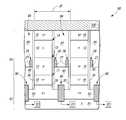
- a memory cell 5comprises a pair of base regions 10 and 12 between a pair of electrode regions 14 and 16 .
- the base regions 10 and 12may be referred to as first and second base regions, respectively; and similarly the electrode regions 14 and 16 may be referred to as first and second electrode regions, respectively.
- One of the electrode regions 14 and 16corresponds to an anode region and the other corresponds to a cathode region.
- the base regions 10 and 12correspond to a p-type base region and an n-type base region (with region 10 being the p-type base region in the shown embodiment, and with region 12 being the n-type base region).
- the regions 14 , 10 , 12 and 16are alternating n-type and p-type regions.
- the first base region 10interfaces with the first electrode region 14 at a junction 11 , and interfaces with the second base region 12 at a junction 13 .
- the second base regioninterfaces with the second electrode region 16 at a junction 15 .
- the junctions 11 , 13 and 15may be referred to as first, second and third junctions, respectively.
- the electrode regions 14 and 16are shown to be electrically coupled to electrical nodes 18 and 20 , respectively.
- One of the nodes 18 and 20may correspond to a bitline (i.e., a digit line or sense line).
- the other of the nodes 18 and 20may correspond to a wordline (i.e., an access line) in some embodiments, or to a ground or other electrically static structure in other embodiments.
- the illustrated memory cell 5shows one of many doping arrangements that may be utilized for the two bases and the two electrodes. Other doping arrangements may be utilized in other embodiments, with some examples of other doping arrangements being illustrated in FIGS. 2 and 13 .
- the various regions 10 , 12 , 14 and 16 of FIG. 1are doped to various levels, with the symbols “+” and “ ⁇ ” being utilized to indicate some of the dopant levels.
- some or all of the designations p+, p, p ⁇ , n ⁇ , n and n+may be used to indicate various levels and types of doping.
- the difference in dopant concentration between the regions identified as being p+, p, and p ⁇may vary depending on the particular material being doped.
- An example dopant concentration of a p+ regionis a dopant concentration of at least about 10 19 atoms/cm 3 (and in some example applications may be from about 10 19 atoms/cm 3 to about 10 20 atoms/cm 3 ), an example dopant concentration of a p region is from about 10 18 to about 10 19 atoms/cm 3 , and an example dopant concentration of a p ⁇ region is less than about 5 ⁇ 10 18 atoms/cm 3 (and in some embodiments may be less than about 5 ⁇ 10 17 atoms/cm 3 ).
- the regions identified as being n ⁇ , n and n+may have dopant concentrations similar to those described above relative to the p ⁇ , p and p+ regions, respectively.
- p and ncan be utilized herein to refer to both dopant type and relative dopant concentrations.
- the terms “p” and “n”are to be understood as referring only to dopant type, and not to a relative dopant concentration, except when it is explicitly stated that the terms refer to relative dopant concentrations. Accordingly, for purposes of interpreting this disclosure and the claims that follow, it is to be understood that the terms “p-type doped” and n-type doped” refer to dopant types of a region and not to relative dopant levels.
- a p-type doped regioncan be doped to any of the p+, p, and p ⁇ dopant levels discussed above, and similarly an n-type doped region can be doped to any of the n+, n, and n ⁇ dopant levels discussed above.
- the dopants utilized in memory cell 5may be any suitable dopants.
- at least part of the memory cellwill comprise wide-bandgap material.
- An example wide-bandgap materialis silicon carbide, and such may be n-type doped with, for example, one or more of N (such as from N 2 and/or NH 3 ), P (such as from PH 3 ) and As (such as from AsH 3 ); and p-type doped with, for example, one or more of B (such as from B 2 H 6 ), Al (such as from AlCl 3 , trimethylaluminum and triethylaluminum) and Ga (such as from trimethylgallium).
- Nsuch as from N 2 and/or NH 3
- Psuch as from PH 3
- Assuch as from AsH 3
- Bsuch as from B 2 H 6
- Alsuch as from AlCl 3 , trimethylaluminum and triethylaluminum
- Gasuch as from trimethylgallium
- depletion regions 22 , 24 and 26may be generated across the junctions 11 , 13 and 15 , respectively.
- the depletion regionsare diagrammatically illustrated with cross-hatching. Approximate boundaries of the depletion regions are illustrated with dashed lines.
- the memory cell 5has a gate 28 along the base region 10 .
- Such gateis electrically coupled with the base region 10 .
- the gateis a control terminal of the type described in the “Background” of this disclosure, and may be utilized for switching the thyristor of memory cell 5 between an “on” and “off” state.
- the illustrated thyristor of memory cell 5is configured as a vertical pillar having a pair of opposing sidewalls 29 and 31 , and the gate 28 is shown to be bifurcated into a pair of segments 33 and 35 , with each segment being along one of the opposing sidewalls.
- the illustrated memory cellmay be one of a plurality of memory cells of a memory array, and the illustrated segments 33 and 35 of the gate may correspond to a pair of lines that extend along multiple memory cells of a row or column of the array to interconnect multiple memory cells. Such lines would extend in and out of the page relative to the cross-sectional view of FIG. 1 .
- the gatemay extend entirely around the base region 10 (a so-called gate all around construction) so that the gate is along sides of the base region 10 that are in and out of the page relative to the view of FIG. 1 , and in some embodiments the gate may be only along the opposing sides of the base shown in FIG. 1 .
- the gate 28comprises a material 27 .
- Such materialmay comprise any suitable substance; and may, for example, comprise one or more of various metals (for instance, titanium, tungsten, etc.), metal-containing compositions (for instance, metal silicide, metal nitride, etc.), and conductively-doped semiconductor materials (for instance, conductively-doped silicon, conducted-doped geranium, etc.).
- the gate 28is spaced from the sidewalls 29 and 31 of the thyristor pillar by dielectric material 30 .
- the dielectric materialmay comprise any suitable composition or combination of compositions.
- at least a portion of the thyristor pillarcomprises one or more forms of silicon carbide, and at least a portion of the dielectric material 30 that is directly against the silicon carbide comprises a passivation composition containing silicon, oxygen and nitrogen.
- Such passivation compositionmay be formed by chemically reacting a surface of the silicon carbide with oxygen and nitrogen, and/or by depositing a composition containing silicon, oxygen and nitrogen along the surface of the silicon carbide.
- an entirety of dielectric material 30may comprise the passivation composition containing silicon, oxygen and nitrogen.
- the dielectric material 30may comprise two or more different compositions, with the composition directly against surfaces of the thyristor pillar being the passivation material, and with one or more other compositions being between the passivation material and the gate 28 .
- Such other compositionsmay comprise, for example, one or more of silicon dioxide and silicon nitride.
- the gate 28is along base region 10 of the thyristor, but does not overlap the junctions 11 and 13 . Further, the gate does not overlap the depletion regions 22 and 24 during operation of the thyristor. In the shown configuration in which the thyristor is a vertical pillar, the gate 28 may be considered to vertically overlap the base region 10 , and to not vertically overlap the depletion regions 22 and 24 .
- a thyristor-based memory cellmay have primary leakage mechanisms that include gate-induced leakage (which may be referred to as gate-induced-drain-leakage, i.e., GIDL), and leakage through the various junctions (i.e., junction leakage).
- gate-induced leakagewhich may be referred to as gate-induced-drain-leakage, i.e., GIDL
- junction leakageleakage through the various junctions
- the gatedoes not overlap the depletion regions, and thus only couples with the base region. Accordingly, the gate-induced leakage, if any, may be a small contribution to the overall leakage within the memory cell; and thus the overall leakage through the memory cell may be reduced. This can enable the memory cell of FIG. 1 to have much longer retention times than conventional T-RAM, and in some environments to have retention times suitable for utilization in nonvolatile memory.
- the thyristor pillar of memory cell 5may be considered to be subdivided into numerous regions, as explained with reference to the scales I and II shown in FIG. 1 .
- Scale Iillustrates that the thyristor pillar may be considered to be subdivided into the first electrode region 14 , the first base region 10 , the second base region 12 , and the second electrode region 16 .
- the regions 14 and 10interface at the junction 11
- the regions 10 and 12interface at the junction 13
- the regions 12 and 16interface at the junction 15 .
- Scale IIillustrates that the thyristor pillar may be considered to comprise a first outer region 40 corresponding to the portion of the electrode region 14 that is outward of the depletion region 22 , a second outer region 42 corresponding to the portion of the electrode region 16 that is outward of the depletion region 26 , a first inner region 44 between the depletion regions 22 and 24 , and a second inner region 46 between the depletion regions 24 and 26 .
- the thyristor pillarmay comprise one or more wide-bandgap materials.
- the wide-bandgap materialsmay advantageously improve retention time of the memory cell relative to narrower bandgap materials (such as silicon) by reducing leakage within the memory cell.
- wide-bandgap materialsare provided at least across the junctions 11 and 13 in wide enough expanses to fully encompass depletion regions 22 and 24 . Thus, the wide-bandgap materials are provided across the locations where the wide-bandgap materials may reduce junction leakage.
- the wide-bandgap materialsmay be provided as strips extending across depletion regions 22 and 24 , and thus the regions 40 , 44 and 46 of scale II may be narrow bandgap materials (such as silicon).
- the wide-bandgap strips across depletion regions 22 and 24may be the same composition as one another, and in other embodiments such wide-bandgap strips may be different compositions from one another.
- the wide-bandgap materialsmay be provided anywhere in the thyristor pillar where leakage may be problematic. For instance, it may be advantageous to provide wide-bandgap material to be across the region 40 of scale II when such region corresponds to part of a cathode region of the thyristor. In such embodiments, the wide-bandgap material across region 40 may be the same or different than the wide-bandgap material across one or both of the depletion regions 22 and 24 .
- wide-bandgap materialwithin the one or both of regions 44 and 46 of scale II to either alleviate leakage, or to simplify fabrication of memory cell 5 in embodiments in which wide-bandgap material as provided within depletion regions 22 and 24 .
- wide-bandgap materialis provided across all of the regions 40 , 22 , 44 , 24 , 46 , 26 and 42 of scale II.
- the same wide-bandgap materialmay be provided across all of the regions 40 , 22 , 44 , 24 , 46 , 26 and 42 so that the entirety of the vertical thyristor pillar comprises, consists essentially of, or consists of only one wide-bandgap material.
- one or more of the regions 40 , 22 , 44 , 24 , 46 , 26 and 42may comprise a different wide-bandgap material than another region to tailor the memory cell 5 for a particular application.
- the wide-bandgap materialmay comprise any suitable composition.
- the wide-bandgap materialmay comprise silicon and carbon, and may comprise one or more forms of silicon carbide.
- the wide-bandgap materialmay comprise, consist essentially of, or consist of the 3C form of silicon carbide in some embodiments, and thus may have a bandgap greater than 2.3 eV (specifically, such form of SiC has a band gap of 2.36 eV).
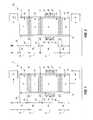
- FIG. 2shows an example embodiment memory cell 5 a analogous to the memory cell 5 of FIG. 1 , but comprising an npnp thyristor rather than a pnpn thyristor.
- the memory cell 5 a of FIG. 2is labeled with identical numbering to that used above to describe FIG. 1 , and comprises identical features as the memory cell of FIG. 1 , except for the different dopant type utilized in the electrode regions and base regions.
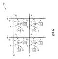
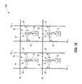
- FIG. 3diagrammatically illustrates a memory array 50 comprising a plurality of memory cells 5 of the type described above with reference to FIG. 1 .
- Each memory cellis schematically illustrated as a thyristor, with the electrode regions 14 and 16 being a cathode and an anode, respectively.
- the memory array 50comprises a series of bitlines (the series identified as BL), a first series of wordlines (the series identified as WL 1 ), and a second series of wordlines (the series identified as WL 2 ).
- the node 20 of FIG. 1may correspond to a bitline (BL)
- the node 18 of FIG. 1may correspond to a wordline of the first series (WL 1 )
- the gate 26 of FIG. 1may be along a wordline of the second series (WL 2 ).
- the electrode regions 14 of memory cells 5may be considered to be first electrode regions which are directly coupled with a first series of wordlines
- the electrode regions 16 of the memory cellsmay be considered to be second electrode regions which are electrically coupled with bitlines.
- Each memory cell of array 50may be uniquely addressed through combinations containing one of the bitlines together with one of the wordlines WL 2 and/or one of the wordlines WL 1 .
- the wordlinesmay be alternatively referred to as access lines in some embodiments, and the bitlines may be alternatively referred to as sense lines in some embodiments.
- FIG. 4diagrammatically illustrates various operations that may be utilized for programming individual memory cells of the array 50 into a “0” data state (i.e., “write 0” operations), programming the individual memory cells into a “1” data state (i.e., “write 1” operations), and for reading the memory cells to ascertain the data states of the individual memory cells.
- FIG. 4also diagrammatically illustrates charge stored on the P base (i.e., the base 10 of FIG. 1 ) during the various operations.
- Example voltage levels for the various states indicated in FIG. 4may include (assuming a bandgap of 2.3 eV):
- VBLID1.5 Volt (V)
- VBLW 01.5V
- VBLRD3V (D 0 , 3V; D 1 , 2.5V)
- VBLW 13V
- D 0 ” and D 1indicate voltages read for the “0” data state and the “1” data state, respectively, of a memory cell.
- Another set of example voltage levels for the various states indicated in FIG. 4may include (assuming a bandgap of 2.3 eV):
- VBLW 02V
- VBLRD3.2V (D 0 , 3.2V; D 1 , 2.5V)
- VBLW 13.2V
- the “write 0” operationhas a lower voltage differential between WL 1 and the bitline than does the “write 1” operation.
- the lower voltage differential between the bitline and WL 1allows charge to drain from the P base , while the higher voltage differential between the bitline and WL 1 results in charge being trapped on the P base .
- Various mechanismsmay account for such relationship. For instance, high-voltage differentials between the bitline and WL 1 during capacitive coupling of the base 10 with gate 28 can lead to latching and/or other mechanisms which limit charge transfer through the thyristor, and thus can lead to charge being trapped on the base 10 .
- low-voltage differentials between the bitline and WL 1 during the capacitive coupling of the gate with the basemay permit a steady flow of charge through the thyristor, and thus may permit charge to be drained from the base 10 .
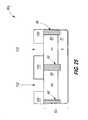
- FIG. 5diagrammatically illustrates another example embodiment memory array 50 a comprising a plurality of memory cells 5 of the type described above with reference to FIG. 1 .
- the memory array of FIG. 5is similar to that of FIG. 3 , except that the first series of wordlines (WL 1 of FIG. 3 ) has been replaced with nodes 51 .
- the nodes 51are at a common voltage as one another, and in some embodiments may be electrically coupled with one another and with a common terminal (for instance, they may all be connected to a grounded plate).
- the node 20 of FIG. 1may correspond to the bitline (BL) of FIG. 5
- the node 18 of FIG. 1may correspond to one of the nodes 51
- the gate 28 of FIG. 1may be along a wordline of the series (WL 2 ).
- the electrode regions 14 of memory cells 5may be considered to be first electrode regions which are electrically coupled with one another and with a common terminal; and the electrode regions 16 of the memory cells may be considered to be second electrode regions which are electrically coupled with bitlines.
- Each memory cell of array 50 amay be uniquely addressed through combinations containing one of the bitlines together with one of the wordlines WL 2 .
- FIG. 6diagrammatically illustrates various operations that may be utilized for programming individual memory cells of the array 50 a into a “0” data state (i.e., “write 0” operations), programming the individual memory cells into a “1” data state (i.e., “write 1” operations), and for reading the memory cells to ascertain the data states of the individual memory cells.
- FIG. 6also diagrammatically illustrates charge stored on the P base (i.e., the base 10 of FIG. 1 ) during the various operations.
- Example voltage levels for the various states indicated in FIG. 6may include (assuming a bandgap of 2.3 V):
- VBLW 00V
- VBLRD3.2V (D 0 , 3.2V; D 1 , 2.5V)
- VBLW 13V
- FIG. 7diagrammatically illustrates another example embodiment memory array 50 b .
- the memory array of FIG. 7comprises a plurality of memory cells 5 a of the type described above with reference to FIG. 2 .
- the memory array of FIG. 7like that of FIG. 3 , comprises a series of bitlines (the series identified as BL), a first series of wordlines (the series identified as WL 1 ), and a second series of wordlines (the series identified as WL 2 ).
- the electrode 14 of FIG. 2corresponds to an anode and the electrode 16 corresponds to a cathode.
- the cathodesare coupled to bitlines (BL); and thus the nodes 20 of FIG. 2 may correspond to bitlines.
- the anodesare coupled to wordlines of the first series (WL 1 ); and thus the nodes 18 of FIG. 2 may correspond to wordlines of the first series.
- Gates analogous to the gate 28 of FIG. 2are along wordlines of the second series (WL 2 ).
- Each memory cell of array 50 bmay be uniquely addressed through combinations containing one of the bitlines together with one of the wordlines WL 2 and/or one of the wordlines WL 1 .
- FIG. 8diagrammatically illustrates various operations that may be utilized for programming individual memory cells of the array 50 b into a “0” data state (i.e., “write 0” operations), programming the individual memory cells into a “1” data state (i.e., “write 1” operations), and for reading the memory cells to ascertain the data states of the individual memory cells.
- FIG. 8also diagrammatically illustrates charge stored on the N base (i.e., the base 10 of FIG. 2 ) during the various operations.
- Example voltage levels for the various states indicated in FIG. 8may include (assuming a bandgap of 2.3 eV):
- VBLW 02.2V
- VBLRD0V (D 0 , 0V; D 1 , 1V)
- VBLW 10.6V
- Another set of example voltage levels for the various states indicated in FIG. 8may include (assuming a bandgap of 2.3 eV):
- VBLW 01.6V
- VBLRD0V (D 0 , 0V; D 1 , 1V)
- VBLW 10V
- FIG. 9diagrammatically illustrates another example embodiment memory array 50 c comprising a plurality of memory cells 5 a of the type described above with reference to FIG. 2 .
- the memory array of FIG. 9is similar to that of FIG. 7 , except that the first series of wordlines (WL 1 of FIG. 7 ) have been replaced with nodes 53 .
- the nodes 53are at a common voltage as one another, and in some embodiments may be electrically coupled with one another and with a common terminal (for instance, they may all be connected to a plate having a voltage of 3V).
- FIG. 10diagrammatically illustrates various operations that may be utilized for programming individual memory cells of the array 50 c into a “0” data state (i.e., “write 0” operations), programming the individual memory cells into a “1” data state (i.e., “write 1” operations), and for reading the memory cells to ascertain the data states of the individual memory cells.
- FIG. 10also diagrammatically illustrates charge stored on the N base (i.e., the base 10 of FIG. 2 ) during the various operations.
- Example voltage levels for the various states indicated in FIG. 10may include (assuming a bandgap of 2.3 eV):
- VBLW 02.2V
- VBLRD0V (D 0 , 0V; D 1 , 1V)
- VBLW 10V
- FIGS. 1 and 2have a gate ( 28 ) along only one of the base regions of the thyristor (specifically, the base region 10 in the shown embodiments).
- FIGS. 11 and 12illustrate alternative embodiments in which paired gates are utilized so that each of the base regions of the thyristor is coupled with a gate.
- FIG. 11such illustrates a memory cell 5 b analogous to the memory cell 5 of FIG. 1 , but comprising a second gate 60 which is coupled with base region 12 .
- the second gate 60is shown to be bifurcated into a pair of segments 61 and 63 along the cross-sectional view of FIG. 11 , but such segments may join with one another at some location outside of the view of FIG. 11 so that the segments are actually two parts of the same gate.
- the second gate 60may extend entirely around the base region 12 (a so-called gate all around construction) so that the gate is along sides of the base region 12 that are in and out of the page relative to the view of FIG. 11 , and in some embodiments the gate may be only along the opposing sides of the base region 12 shown in FIG. 11 .
- the illustrated memory cell 5 bmay be considered to comprise a thyristor pillar, and to comprise a two-to-one relationship of gates with the pillar.
- the gatesare a pair of vertically-spaced gates 28 and 60 ; with one of the gates being coupled with the n-type base region 12 of the thyristor, and the other of the gates being coupled with the p-type base region 10 of the thyristor.
- the gate 60may comprise any suitable material, and may, for example, comprise one or more of the materials discussed above as being suitable for utilization in gate 28 .
- the gate 60does not overlap the junctions 13 and 15 on opposing sides of base region 12 , and in the shown embodiment the gate 60 also does not overlap the depletion regions 24 and 26 during operation of the thyristor. In the shown configuration, the gate 60 may be considered to vertically overlap the base region 12 , and to not vertically overlap the depletion regions 24 and 26 .
- gate 60can be advantageous for gate 60 to not overlap depletion regions 24 and 26 for reasons analogous to those discussed above as advantages for having the gate 28 not overlap depletion regions 22 and 24 . Specifically, if gate 60 does not overlap depletion regions 24 and 26 such can alleviate or eliminate gate-induced leakage from gate 60 .
- the utilization of two gated base regions within the memory cell 5 bmay provide additional operational parameters within the memory cell (as described below with reference to FIGS. 14-17 ) which may enable the memory cell to be more readily tailored for some applications than could a memory cell having only a single gated base region.
- FIG. 11shows the second gate utilized with a pnpn thyristor
- the second gatecould also be utilized with an npnp thyristor.
- FIG. 12shows a memory cell 5 c comprising an npnp thyristor having two gated base regions.
- the memory cells of FIGS. 1, 2, 11 and 12are shown to comprise doped base regions.
- a difficulty that may occur in utilizing wide-bandgap materialsis that it may be difficult to attain desired dopant levels in the base regions.
- the gate adjacent to a gated base regionmay be utilized to induce a desired conductivity type within the base region in some embodiments.
- the gates 28 of FIGS. 1 and 2may be utilized to induce a desired conductivity type within base region 10 ; or one or both of the gates 28 and 60 of FIGS. 11 and 12 may be utilized to induce desired conductivity types within one or both of the base regions 10 and 12 .
- FIG. 13shows a memory cell 5 d being shifted between two different modes by utilizing gates 28 and 60 to induce desired conductivity types within base regions 10 and 12 .
- the memory cell 5 d of FIG. 13has an initial mode 66 in which base regions 10 and 12 are of unspecified dopant type.
- the dopant type within the regionsmay be unknown, or may be different than a dopant type desired in a working thyristor.
- base region 10should be p-type in a working thyristor, but may be n-type in mode 66 , or may be of an undetermined type, depending on, among other things, the processing conditions utilized to form region 10 and the composition of region 10 .
- the initial mode 66is converted to a different mode 68 through application of electric fields onto base regions 10 and 12 utilizing gates 28 and 60 .
- the transition from mode 66 to mode 68may be considered to comprise electrical inducement of desired dopant types within the base regions 10 and 12 .
- the mode 68has regions 10 and 12 appropriately doped for the pnpn the thyristor, and specifically has region 12 doped to n-type and region 10 doped to p-type. In the shown embodiment, the mode 68 also has depletion regions 22 , 24 and 26 formed within the thyristor.
- the operation of the thyristormay further include inducement of a memory state within the thyristor through utilization of a voltage differential between the two electrode regions ( 14 and 16 ), together with capacitive coupling of one both of the base regions ( 10 and 12 ) to the gate adjacent the base region (gates 28 and 60 ).
- both of gates 28 and 60are utilized for electrical inducement of desired dopant types the base regions ( 10 and 12 ), and are utilized for operation of the thyristor.
- one of the gatesmay be utilized only for either electrical inducement or operation of the thyristor, rather than being utilized for both tasks.
- the vertical thyristor pillar 5 d at the initial mode 66may be considered to correspond to a structure having two electrodes (regions 14 and 16 ), and having a segment between the two electrodes (with the segment comprising the base regions 10 and 12 ).
- the segmenthas at least one gated portion (i.e., a portion proximate a gate), and in the shown embodiment of FIG. 13 has two gated portions.
- the thyristor pillarmay be considered to be transitioned from mode 66 to mode 68 by inducing a conductivity type within the gated portion utilizing an electrical field produced with the gate.
- the thyristor 5 d of FIG. 13will comprise wide-bandgap material at least within one or both of the base regions 10 and 12 .
- Such wide-bandgap materialmay extend entirely across depletion regions 22 , 24 and 26 to reduce junction leakage, and to thereby increase retention time of the thyristor relative to a thyristor lacking the wide-bandgap material.
- the inducement of conductivity type within the base regionsmay be particularly advantageous when utilizing wide-bandgap materials in the base regions, there may also be advantages to such inducement when the base regions comprise, consist essentially of, or consist of conventional semiconductor materials (like silicon). Accordingly, in some embodiments gates analogous to one or both of the gates 28 and 60 may be utilized to induce conductivity type in one or both base regions of a thyristor that has conventional semiconductor materials in one or both of such base regions.
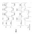
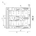
- FIG. 14diagrammatically illustrates an example embodiment memory array 50 d utilizing a plurality of memory cells 5 b of the type shown in FIG. 11 .
- the memory array 50 dcomprises a series of bitlines (BL) connected to the anodes 16 of the thyristors, a series of wordlines (identified as WL 2 ) connected to the gates 28 , a series of first nodes 70 connected to the cathode regions of the thyristors, and a second series of nodes 72 connected to the gates 60 .
- the nodes 70may be all at a common voltage as one another, and the nodes 72 may be all at a common voltage as one another.
- FIG. 15diagrammatically illustrates various operations that may be utilized for programming individual memory cells of the array 50 d into a “0” data state (i.e., “write 0” operations), programming the individual memory cells into a “1” data state (i.e., “write 1” operations), and for reading the memory cells to ascertain the data states of the individual memory cells.
- FIG. 15also diagrammatically illustrates charge stored on the P base (i.e., the base 10 of FIG. 11 ) during the various operations.
- Example voltage levels for the various states indicated in FIG. 15may include (assuming a bandgap of 2.3 eV, assuming nodes 70 are at about 0V, and assuming nodes 72 are at about 3V):
- VBLW 00.8V
- VBLRD3V (D 0 , 3V; D 1 , 2V)
- VBLW 12.9V
- Voltage levels analogous to those of FIG. 15may be utilized for the memory cell of FIG. 12 (which has an n-type base 10 ), if the nodes 72 ( FIG. 14 ) are at about ⁇ 3V.
- FIGS. 14 and 15has the gates 60 held at about a constant voltage across all of the memory cells during read and write operations. In other memory arrays, the voltages across the gates 60 may vary, together with the voltages across gates 28 , during the reading and writing operations.
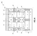
- FIG. 16illustrates a memory array 50 e in which the gates 28 and 60 are both configured to be varied during reading and writing operations.
- the memory array 50 e of FIG. 16is similar to the memory array 50 d of FIG. 14 , except that gates 60 are connected to a set of wordlines (WL 3 ) instead of being connected to static voltage nodes.
- FIG. 17diagrammatically illustrates various operations that may be utilized for programming individual memory cells of the array 50 e into a “0” data state (i.e., “write 0”operations), programming the individual memory cells into a “1” data state (i.e., “write 1” operations), and for reading the memory cells to ascertain the data states of the individual memory cells.
- FIG. 17also diagrammatically illustrates charges stored on the P base (i.e., the base 10 of FIG. 11 ) and the N base (i.e., the base 12 of FIG. 11 ) during the various operations.
- Example voltage levels for the various states indicated in FIG. 17may include (assuming a bandgap of 2.3 eV, and assuming nodes 70 are at about 0V):
- VBLW 00.8V
- VBLRD3V (D 0 , 3V; D 1 , 2V)
- VBLW 13V
- FIGS. 18 and 19illustrate an example process for fabricating a memory array 50 a of the type shown in FIG. 5 .
- a semiconductor construction 80comprises a substrate 82 comprising an n-type doped region 83 over a p-type doped region 81 .
- the substrate 82may comprise, consist essentially of, or consist of monocrystalline silicon in some embodiments.
- semiconductor substratemeans any construction comprising semiconductive material, including, but not limited to, bulk semiconductive materials such as a semiconductive wafer (either alone or in assemblies comprising other materials), and semiconductive material layers (either alone or in assemblies comprising other materials).
- substraterefers to any supporting structure, including, but not limited to, the semiconductive substrates described above.
- the substratemay comprise numerous materials in some embodiments.
- the substratemay correspond to a semiconductor substrate containing one or more materials associated with integrated circuit fabrication.
- such materialsmay correspond to one or more of refractory metal materials, barrier materials, diffusion materials, insulator materials, etc.
- the regions 81 and 83may be conductively-doped regions of a monocrystalline silicon wafer, and/or may be conductively-doped regions formed along a tier of a partially-fabricated integrated circuit.
- Conductively-doped regions 10 , 12 , 14 and 16 of a memory cell stack 84are formed over substrate 82 .
- the entire stack 84may comprise, consist essentially of, or consist of doped wide-bandgap material (such as, for example, 3C-SiC). If doped region 83 comprises monocrystalline silicon and the wide-bandgap material comprises silicon carbide, the wide-bandgap material may be epitaxially grown over the monocrystalline silicon.
- a difficulty encountered in incorporating wide-bandgap materials (such as, for example, silicon carbide) into integrated circuit fabrication sequencesis that dopant activation within the wide-bandgap materials may utilize a thermal budget which is too high for many of the components conventionally utilized in integrated circuitry.
- a method of reducing the thermal budget for dopant activationis to in situ dope the wide-bandgap material during epitaxial growth of such material.
- a patterned mask 97is formed over memory cell stack 84 , with such patterned mask defining a pattern corresponding to a plurality of openings 99 that extend through the mask.
- the patterned maskmay comprise any suitable composition and may be formed with any suitable processing.
- the maskmay comprise photolithographically-patterned photoresist.
- the maskmay comprise one or more structures formed utilizing pitch multiplication methodologies.
- a patternis transferred from mask 97 ( FIG. 18 ) into stack 84 with one or more suitable etches, and then the mask is removed.
- the memory cell stack 84is thus patterned into a plurality of substantially vertical thyristor pillars 88 that extend upwardly from the substrate 82 .
- dielectric material 30is formed along sidewalls of the pillars.
- the pillars 88are referred to as being “substantially vertical” pillars to indicate that they extend substantially orthogonally to a primary upper surface of the substrate.
- verticalis used herein to define a relative orientation of an element or structure with respect to a major plane or surface of a wafer or substrate.
- a structuremay be referred to as being “substantially vertical” to indicate that the structure is vertical to within reasonable tolerances of fabrication and measurement.
- Electrically-conductive interconnects 90are formed between the pillars and in electrical connection with doped region 83 .
- the interconnects 90may be electrically coupled with one another through doped region 83 and/or through other interconnections, and may be all electrically connected to a common terminal so that they are all tied to the common voltage 51 (as shown).
- the dielectric material 30may be formed by initially providing surface passivation along outer exposed surfaces of pillars 88 .
- Such surface passivationmay comprise providing a layer containing silicon, oxygen and nitrogen along the outer surfaces.
- Such layermay be formed by nitridation/oxidation of exposed outer surfaces of silicon carbide in some embodiments, and/or by deposition of passivation material along the exposed outer surfaces.
- the dielectric material 30may consist of the passivation layer in some embodiments. In other embodiments, additional dielectric materials may be formed over the passivation layer to form a dielectric material 30 comprising the passivation layer in combination with other dielectric materials.
- Such other dielectric materialsmay comprise, for example, one or both of silicon dioxide and silicon nitride.
- material 90may comprise metal or other thermally sensitive material, and an advantage of forming conductive material 90 after the doping of the wide-bandgap material is that such can avoid exposure of the thermally sensitive material to the thermal budget utilized for the doping of the wide-bandgap material.
- Electrically insulative material 92is formed over conductive material 90 and between the pillars 88 , and then the conductive material 27 is formed and patterned over insulative material 92 to form the gates 28 . Subsequently, another insulative material 94 is formed over gates 28 and insulative material 92 .
- the electrically insulative materials 92 and 94may comprise any suitable compositions or combinations of compositions, including for example, one or more of silicon dioxide, silicon nitride, and any of various doped oxide glasses (for instance, borophosphosilicate glass, phosphosilicate glass, fluorosilicate glass, etc.).
- the electrically insulative materials 92 and 94may be the same composition as one another in some embodiments, and may differ in composition from one another in other embodiments.
- bitline 100is formed across the pillars 88 , and in direct electrical contact with the upper doped regions 16 within such pillars.
- the bitline 100may be considered to be an example of a node 20 ( FIG. 1 ) that may be formed in direct electrical connection with the upper electrode regions 16 of the illustrated example embodiment memory cells.
- Bitline 100may comprise any suitable electrically conductive material; and may, for example, comprise, consist essentially of or consist of one or more of various metals, metal-containing compositions and conductively-doped semiconductor materials.
- the construction 80has a dimension from one side of a pillar to a same side of an adjacent pillar of 2F, and thus the individual memory cells may have footprints of about 4F 2 .
- the thyristor pillars 88have topmost junctions corresponding to the junctions 15 between regions 12 and 16 .
- Any suitable speciesmay be implanted for the top junction lifetime killer implant, and the species may vary depending on the materials present in regions 12 and 16 .
- a suitable species for the top junction lifetime killer implantmay be carbon.
- top junction killer implantis described specifically with reference to the embodiment of FIGS. 18 and 19 , it is to be understood that the top junction lifetime killer implant may be utilized in any of the various embodiments described in this disclosure.
- FIGS. 18 and 19pertain to formation of memory cells of the type shown as memory cells 5 in FIG. 1 , persons of ordinary skill will recognize that similar processing may be utilized to form any of the other memory cells described in this disclosure. For instance, in some embodiments, processing analogous to that of FIGS. 18 and 19 may be utilized to fabricate two-gate thyristors of the types described with reference to FIGS. 11-13 .
- FIGS. 18 and 19patterns the thyristor pillars 88 ( FIG. 19 ) by providing a patterned mask ( 97 of FIG. 18 ) over an expanse of memory cell material, and then transferring a pattern from the mask into the memory cell material with one or more suitable etches.
- Another example embodiment method for forming the pillarsmay comprise depositing the memory cell material within a plurality of openings, as described with reference to FIGS. 20-22 .
- a construction 80 acomprises the substrate 82 and a patterned dielectric material 110 formed over the substrate.
- the dielectric material 110may comprise any suitable composition or combination of compositions; and in some embodiments may comprise, consist essentially of, or consist of one or more of silicon dioxide, silicon nitride, and any of various doped silicon oxide glasses (for instance, borophosphosilicate glass, phosphosilicate glass, etc.).
- the patterned dielectric materialhas a plurality of vertical openings 112 extending therethrough, with such openings being arranged in a pattern across the substrate.
- the openingsmay be formed utilizing any suitable processing, such as, for example, formation of a patterned mask (not shown) over the dielectric material 110 to define locations for the openings, followed by one or more suitable etches through material 110 to create the openings.
- the patterned maskmay be any suitable mask, including, for example, a photolithographically-patterned photoresist mask, and/or a mask created utilizing various pitch multiplication methodologies.
- the substrate 80 of FIG. 20has the electrically-conductive interconnects 90 formed therein.
- wide-bandgap materialwill be formed within openings 112 and conductively doped.
- the conductive doping of wide-bandgap materialmay comprise a thermal budget which can problematically affect common conductive materials (for instance, metal) utilized for conductive interconnects.
- either conductive interconnects 90may be formed of material that tolerates the relatively high thermal budget utilized for fabricating doped wide-bandgap materials, or the wide-bandgap material may be of a composition that can be formed and conductively-doped within a thermal budget that does not adversely impact conductive interconnects formed of conventional materials. Accordingly, there can be embodiments in which the conductive interconnects 90 are formed prior to fabrication and doping of wide-bandgap materials.
- the conductive interconnectsmay be alternatively formed after fabrication and doping of the thyristor pillars with processing analogous to that discussed above with reference to FIG. 19 .
- thyristor pillar material 114is formed within openings 112 .
- the thyristor pillar materialmay comprise wide-bandgap material, such as, for example, one or more forms of silicon carbide (with an example form of silicon carbide being 3C-SiC).
- the thyristor pillar material 114is shown to be homogeneous, in other embodiments the thyristor pillar material may comprise multiple discrete compositions.
- the thyristor pillar materialmay be formed utilizing any suitable processing.
- material 114may be formed by epitaxial growth from exposed upper surfaces of the semiconductor material of substrate 82 (for instance, epitaxial growth of silicon carbide from an exposed upper surface of a monocrystalline silicon substrate).
- material 114may be formed by deposition of one or more appropriate compositions within openings 112 .
- the depositionmay comprise chemical vapor deposition (CVD), atomic layer deposition (ALD) and/or any other suitable deposition process.
- CVDchemical vapor deposition
- ALDatomic layer deposition
- Material 114may be in situ doped during the formation of the material within the openings, and/or may be doped with one or more suitable implants occurring after formation of the material within the openings.
- material 114is formed within the openings with a deposition process and is amorphous as-deposited, and it is desired for material 114 to be crystalline (such as, for example when material 114 comprises, consists essentially of, or consists of one or more forms of silicon carbide), the material may be recrystallized after the deposition of the material within the openings. In some embodiments, such recrystallization may be accomplished with suitable thermal processing.
- material 114 within the openings 112patterns material 114 into a plurality of pillars 88 .
- material 114may be deposited to overfill the openings, and to extend across an upper surface of dielectric material 110 .
- CMPchemical-mechanical polishing
- planarizationmay be utilized to remove material 114 from over the upper surface of dielectric 110 and to form the illustrated structure of FIG. 21 having a plurality of spaced-apart pillars 88 .
- the thyristor material 114is shown after appropriate doping to form the electrode regions 14 and 16 , and the base regions 10 and 12 ; and to thereby form appropriately-doped thyristor pillars from the thyristor material of the pillars 88 .
- Such thyristor pillarsmay be incorporated into any of the various memory cells discussed above with reference to FIGS. 1, 2 and 11-13 .
- the thyristor pillarsare incorporated into memory cells 5 b analogous to those discussed above with reference to FIG. 11 .
- dielectric material 30is formed along sidewalls of the pillars 88 , and gates 28 and 60 are formed along the base regions 10 and 12 .
- the illustrated embodimentmay be a memory array analogous to the array 50 d of FIG. 14 ; and thus may have the interconnect regions 90 connected to common voltage of the type shown in FIG. 14 as nodes 70 , and the gates 60 connected to common voltage of the type shown in FIG. 14 as nodes 72 .
- the dielectric material 30may be formed utilizing processing of the type discussed above with reference to FIG. 19 .
- the gate 28 and 60may be formed with any suitable processing.
- dielectric material 110FIG. 21
- dielectric material 120may be formed over substrate 82 and between the pillars 88 , and then gates 28 may be formed and patterned over such dielectric material.
- Another dielectric material 122may be formed over and between the gates 28 , and then gates 60 may be formed and patterned over the material 122 .
- a dielectric material 124may be formed over gates 60 , and then bitline 100 may be formed and patterned over the dielectric material 124 .
- the dielectric materials 120 , 122 and 124may comprise any suitable compositions or combinations of compositions, including for example, one or more of silicon dioxide, silicon nitride, and any of various doped oxide glasses (for instance, borophosphosilicate glass, phosphosilicate glass, fluorosilicate glass, etc.).
- the electrically insulative materials 120 , 122 and 124may be the same composition as one another in some embodiments. Alternatively, at least one of such electrically insulative materials may differ in composition from at least one of the other of such electrically insulative materials in other embodiments.
- the base regions 10 and 12may not be doped to the shown n and p types at the processing stage of FIG. 22 , but instead such dopant types within the base regions may be electrically induced during utilization of the thyristors as discussed above with reference to FIG. 13 .
- FIGS. 20-22pertain to formation of memory cells 5 b of the type shown in FIG. 11 , persons of ordinary skill will recognize that similar processing may be utilized to form any of the other memory cells described in this disclosure.
- FIGS. 20-22is a process in which gates 28 and 60 are formed after formation of thyristor material 114 ( FIG. 21 ) within substantially vertical openings in a dielectric material.
- the gatesmay first be formed within the dielectric material, and then the openings patterned through the material and filled with thyristor material 114 .
- An example embodiment in which the gates are formed prior to filling openings with thyristor materialis described with reference to FIGS. 23 and 24 .
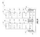
- a semiconductor construction 80 bis shown to comprise dielectric materials 120 , 122 and 124 , and the gates 28 and 60 supported over the dielectric materials 120 and 122 . Openings 112 are formed through the dielectric materials, and adjacent the gates 28 and 60 . The openings may be formed utilizing any appropriate mask (not shown) to define the locations of the openings, followed by one or more appropriate etches through the various materials to extend the openings to the upper surface of substrate 82 .
- the openings 112are lined with the dielectric material 30 .
- the dielectric material 30may be formed in the shown configuration by initially depositing the dielectric material 30 to extend along sidewalls of the openings, across the bottom surfaces of the openings, and across top surfaces of dielectric material 124 ; and then utilizing an anisotropic etch to remove material 30 from along the horizontal surfaces, while leaving material along the vertical sidewall surfaces.
- thyristor material 114is formed within openings 112 to form pillars 88 .
- the thyristor materialis appropriately doped to create electrode regions 14 and 16 , and to create base regions 10 and 12 .
- bitline 100may be formed across the pillars 88 .
- FIGS. 20-22formed all of the thyristor material 114 ( FIG. 21 ) of the vertical pillars 88 ( FIG. 22 ) within the openings 112 in the patterned material 110 ( FIG. 20 ). In other embodiments, only some of the thyristor material of such pillars may be formed within openings in a patterned material. An example embodiment in which only some of the thyristor material is formed within openings in a patterned material is described with reference to FIGS. 25-28 .
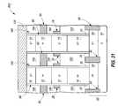
- a construction 80 ccomprises the substrate 82 and a patterned material 130 formed over the substrate.
- the material 130may comprise any suitable composition or combination of compositions, and in some embodiments may be electrically insulative and may comprise, consist essentially of, or consist of one or more of silicon dioxide, silicon nitride, and any of various doped silicon oxide glasses (for instance, borophosphosilicate glass, phosphosilicate glass, etc.).
- the patterned material 130has a plurality of openings 132 extending therethrough, with such openings being arranged in a pattern across the substrate.
- the openingsmay be formed utilizing any suitable processing, such as, for example, formation of a patterned mask (not shown) over the dielectric material 130 to define locations for the openings, followed by one or more suitable etches through material 130 to create the openings.
- the patterned maskmay be any suitable mask, including, for example, a photolithographically-patterned photoresist mask, and/or a mask created utilizing various pitch multiplication methodologies.
- a material 134is formed within openings 132 .
- the material 134overfills the openings, and thus forms an expanse extending across the upper surface of patterned material 130 .
- the material 134may comprise wide-bandgap material, such as, for example, one or more forms of silicon carbide (with an example form of silicon carbide being 3C-SiC), and may be epitaxially grown from exposed surfaces of substrate 82 within the openings (for instance, the material 134 may comprise one or more forms of silicon carbide epitaxially grown from exposed surfaces of monocrystalline silicon of substrate 82 ).
- the material 134is shown to be in situ doped to form alternating n-type and p-type regions 136 , 138 , 140 and 142 .
- Epitaxially-grown material formed within openingsmay have stacking faults therein. However, if the bulk of the epitaxially-grown material is outside of the openings, the epitaxially-grown material within the openings and directly above the openings may be relatively clean of stacking faults, and instead the stacking faults may be primarily within regions between the openings (which are regions which will ultimately be removed to form pillars 88 in processing described below with reference to FIG. 27 ).
- a patterned maskis formed over material 134 , with such mask comprising the shown features 146 .
- the patterned maskmay be any suitable mask, including, for example, a photolithographically-patterned photoresist mask, and/or a mask created utilizing various pitch multiplication methodologies.
- a patternis transferred from masking features 146 into material 134 with one or more suitable etches to pattern the material 134 into pillars 88 .
- the doped regions 136 , 138 , 140 and 142 of material 134become the various electrode and base regions 10 , 12 , 14 and 16 of the thyristor pillars.
- the illustrated thyristor pillarshave narrower segments 150 within the openings 132 in material 130 , and have wider segments 152 over the narrower segments (with the terms “narrower” and “wider” being relative to one another, and indicating the segments 150 are narrow relative to the segments 152 ).
- dielectric material 162is formed over the dielectric material 130 , and subsequently gates 28 are formed over the dielectric material 162 .
- a dielectric material 164is formed over and between the gates 28 , and then gates 60 are formed over the material 164 .
- Dielectric material 166is then formed over the gates 60 , and the bitline 100 is formed and patterned over the dielectric material 166 .
- FIGS. 29-31Another example embodiment in which only some of the thyristor material is formed within openings in a patterned material is described with reference to FIGS. 29-31 .
- a construction 80 dcomprises the substrate 82 , and comprises the conductive interconnects 90 formed to extend above an upper surface of the substrate.
- the shown interconnects 90may be considered to correspond to patterned features of a mask, and to define a pattern of openings 170 extending between the interconnects and to the upper surface of the substrate.
- the material 134is formed within openings 170 and across upper surfaces of interconnects 90 .
- the material 134may comprise the wide-bandgap material discussed above with reference to FIG. 26 , and may be epitaxially grown from exposed surfaces of substrate 82 .
- the material 134is in situ doped to form the alternating n-type and p-type regions 136 , 138 , 140 and 142 .
- a patterned maskis formed over material 134 , with such mask comprising the shown features 172 .
- the patterned maskmay be any suitable mask, including, for example, a photolithographically-patterned photoresist mask, and/or a mask created utilizing various pitch multiplication methodologies.
- a patternis transferred from masking features 172 into material 134 with one or more suitable etches to pattern the material 134 into pillars 88 .
- the doped regions 136 , 138 , 140 and 142 of material 134become the various electrode and base regions 10 , 12 , 14 and 16 of the thyristor pillars.
- the patterning of the thyristor pillarsforms gaps 174 which space the thyristor pillars from the upper portions of interconnects 90 .
- dielectric material 182is formed over the substrate 82 , and subsequently gates 28 are formed over the dielectric material 182 .
- a dielectric material 184is formed over and between the gates 28 , and then gates 60 are formed over the material 184 .
- Dielectric material 186is then formed over the gates 60 , and the bitline 100 is formed and patterned over the dielectric material 186 .
- the various memory cells and arrays discussed abovemay be incorporated into integrated circuit chips or packages, and such may utilized in electronic devices and/or electronic systems.
- the electronic systemsmay be used in, for example, memory modules, device drivers, power modules, communication modems, processor modules, and application-specific modules, and may include multilayer, multichip modules.
- the electronic systemsmay be any of a broad range of systems, such as, for example, clocks, televisions, cell phones, personal computers, automobiles, industrial control systems, aircraft, etc.
Landscapes
- Engineering & Computer Science (AREA)
- Computer Hardware Design (AREA)
- Physics & Mathematics (AREA)
- Condensed Matter Physics & Semiconductors (AREA)
- General Physics & Mathematics (AREA)
- Manufacturing & Machinery (AREA)
- Microelectronics & Electronic Packaging (AREA)
- Power Engineering (AREA)
- Semiconductor Memories (AREA)
- Thyristors (AREA)
Abstract
Description
Claims (8)
Priority Applications (2)
| Application Number | Priority Date | Filing Date | Title |
|---|---|---|---|
| US13/957,304US9361966B2 (en) | 2011-03-08 | 2013-08-01 | Thyristors |
| US14/948,097US9691465B2 (en) | 2011-03-08 | 2015-11-20 | Thyristors, methods of programming thyristors, and methods of forming thyristors |
Applications Claiming Priority (2)
| Application Number | Priority Date | Filing Date | Title |
|---|---|---|---|
| US13/043,295US8519431B2 (en) | 2011-03-08 | 2011-03-08 | Thyristors |
| US13/957,304US9361966B2 (en) | 2011-03-08 | 2013-08-01 | Thyristors |
Related Parent Applications (1)
| Application Number | Title | Priority Date | Filing Date |
|---|---|---|---|
| US13/043,295DivisionUS8519431B2 (en) | 2011-03-08 | 2011-03-08 | Thyristors |
Related Child Applications (1)
| Application Number | Title | Priority Date | Filing Date |
|---|---|---|---|
| US14/948,097ContinuationUS9691465B2 (en) | 2011-03-08 | 2015-11-20 | Thyristors, methods of programming thyristors, and methods of forming thyristors |
Publications (2)
| Publication Number | Publication Date |
|---|---|
| US20130314986A1 US20130314986A1 (en) | 2013-11-28 |
| US9361966B2true US9361966B2 (en) | 2016-06-07 |
Family
ID=46794723
Family Applications (3)
| Application Number | Title | Priority Date | Filing Date |
|---|---|---|---|
| US13/043,295Active2031-05-01US8519431B2 (en) | 2011-03-08 | 2011-03-08 | Thyristors |
| US13/957,304ActiveUS9361966B2 (en) | 2011-03-08 | 2013-08-01 | Thyristors |
| US14/948,097ActiveUS9691465B2 (en) | 2011-03-08 | 2015-11-20 | Thyristors, methods of programming thyristors, and methods of forming thyristors |
Family Applications Before (1)
| Application Number | Title | Priority Date | Filing Date |
|---|---|---|---|
| US13/043,295Active2031-05-01US8519431B2 (en) | 2011-03-08 | 2011-03-08 | Thyristors |
Family Applications After (1)
| Application Number | Title | Priority Date | Filing Date |
|---|---|---|---|
| US14/948,097ActiveUS9691465B2 (en) | 2011-03-08 | 2015-11-20 | Thyristors, methods of programming thyristors, and methods of forming thyristors |
Country Status (3)
| Country | Link |
|---|---|
| US (3) | US8519431B2 (en) |
| TW (1) | TWI471941B (en) |
| WO (1) | WO2012121845A2 (en) |
Cited By (4)
| Publication number | Priority date | Publication date | Assignee | Title |
|---|---|---|---|---|
| US20170229306A1 (en)* | 2016-02-08 | 2017-08-10 | Kilopass Technology, Inc. | Vertical Thyristor Memory with Minority Carrier Lifetime Reduction |
| US10998316B2 (en) | 2019-07-26 | 2021-05-04 | SK Hynix Inc. | Vertical memory device and method for fabricating vertical memory device |
| US11417659B2 (en) | 2019-10-08 | 2022-08-16 | Samsung Electronics Co., Ltd. | Semiconductor memory device and method of fabricating the same |
| US11621264B2 (en) | 2020-01-20 | 2023-04-04 | Samsung Electronics Co., Ltd. | Semiconductor memory device |
Families Citing this family (30)
| Publication number | Priority date | Publication date | Assignee | Title |
|---|---|---|---|---|
| US9608119B2 (en) | 2010-03-02 | 2017-03-28 | Micron Technology, Inc. | Semiconductor-metal-on-insulator structures, methods of forming such structures, and semiconductor devices including such structures |
| US8507966B2 (en) | 2010-03-02 | 2013-08-13 | Micron Technology, Inc. | Semiconductor cells, arrays, devices and systems having a buried conductive line and methods for forming the same |
| US9646869B2 (en) | 2010-03-02 | 2017-05-09 | Micron Technology, Inc. | Semiconductor devices including a diode structure over a conductive strap and methods of forming such semiconductor devices |
| US8598621B2 (en) | 2011-02-11 | 2013-12-03 | Micron Technology, Inc. | Memory cells, memory arrays, methods of forming memory cells, and methods of forming a shared doped semiconductor region of a vertically oriented thyristor and a vertically oriented access transistor |
| US8952418B2 (en) | 2011-03-01 | 2015-02-10 | Micron Technology, Inc. | Gated bipolar junction transistors |
| US8519431B2 (en) | 2011-03-08 | 2013-08-27 | Micron Technology, Inc. | Thyristors |
| US8772848B2 (en) | 2011-07-26 | 2014-07-08 | Micron Technology, Inc. | Circuit structures, memory circuitry, and methods |
| WO2013044612A1 (en)* | 2011-09-29 | 2013-04-04 | Tsinghua University | Vertical selection transistor, memory cell, and three-dimensional memory array structure and method for fabricating the same |
| US8962465B2 (en) | 2012-10-15 | 2015-02-24 | Micron Technology, Inc. | Methods of forming gated devices |
| US8901529B2 (en)* | 2013-03-15 | 2014-12-02 | International Business Machines Corporation | Memory array with self-aligned epitaxially grown memory elements and annular FET |
| KR102195694B1 (en)* | 2014-01-24 | 2020-12-28 | 인텔 코포레이션 | Fin-based semiconductor devices and methods |
| US20150333068A1 (en)* | 2014-05-14 | 2015-11-19 | Globalfoundries Singapore Pte. Ltd. | Thyristor random access memory |
| US9209187B1 (en) | 2014-08-18 | 2015-12-08 | Micron Technology, Inc. | Methods of forming an array of gated devices |
| US9673054B2 (en)* | 2014-08-18 | 2017-06-06 | Micron Technology, Inc. | Array of gated devices and methods of forming an array of gated devices |
| US9224738B1 (en) | 2014-08-18 | 2015-12-29 | Micron Technology, Inc. | Methods of forming an array of gated devices |
| US20160093624A1 (en)* | 2014-09-25 | 2016-03-31 | Kilopass Technology, Inc. | Thyristor Volatile Random Access Memory and Methods of Manufacture |
| EP3149740A4 (en)* | 2014-09-25 | 2017-11-01 | Kilopass Technology, Inc. | Thyristor volatile random access memory and methods of manufacture |
| US9484068B2 (en)* | 2015-02-17 | 2016-11-01 | Kilopass Technology, Inc. | MTP-thyristor memory cell circuits and methods of operation |
| US20160379984A1 (en)* | 2015-06-29 | 2016-12-29 | Kilopass Technology, Inc. | Thyristor Memory Cell with Gate in Trench Adjacent the Thyristor |
| EP3203517A1 (en)* | 2016-02-08 | 2017-08-09 | Kilopass Technology, Inc. | Methods and systems for reducing electrical disturb effects between thyristor memory cells using heterostructured cathodes |
| KR101804666B1 (en)* | 2016-04-06 | 2017-12-05 | 고려대학교 산학협력단 | Semiconductor memory device with vertical semiconductor column |
| KR101835231B1 (en)* | 2016-09-26 | 2018-03-08 | 고려대학교 산학협력단 | Semiconductor Devices |
| CN108630612B (en)* | 2017-03-24 | 2019-10-18 | 联华电子股份有限公司 | Semiconductor element and manufacturing method thereof |
| US10453515B2 (en)* | 2017-05-10 | 2019-10-22 | Tc Lab, Inc. | Methods of operation for cross-point thyristor memory cells with assist gates |
| US20190013317A1 (en)* | 2017-07-10 | 2019-01-10 | Tc Lab, Inc. | High-Density Volatile Random Access Memory Cell Array and Methods of Fabrication |
| KR101952510B1 (en)* | 2017-07-25 | 2019-02-26 | 포항공과대학교 산학협력단 | Thyristor-based Memory and Method of fabricating the same |
| KR102132196B1 (en)* | 2018-09-05 | 2020-07-09 | 고려대학교 산학협력단 | Feedback field-effect electronic device using feedback loop operation and array using the same |
| KR102202910B1 (en)* | 2019-08-27 | 2021-01-13 | 가천대학교 산학협력단 | Feedback 1t dram device having localized partial insulating layers |
| KR102833171B1 (en) | 2020-04-28 | 2025-07-10 | 삼성전자주식회사 | Semiconductor memory device and method for fabricating thereof |
| KR20250142636A (en)* | 2024-03-22 | 2025-09-30 | 고려대학교 산학협력단 | Binarized neural network circuitry using quasi-nonvolatile memory device |
Citations (244)
| Publication number | Priority date | Publication date | Assignee | Title |
|---|---|---|---|---|
| US3988771A (en) | 1974-05-28 | 1976-10-26 | General Electric Company | Spatial control of lifetime in semiconductor device |
| US4487639A (en) | 1980-09-26 | 1984-12-11 | Texas Instruments Incorporated | Localized epitaxy for VLSI devices |
| JPH02275663A (en) | 1989-01-24 | 1990-11-09 | Fujitsu Ltd | Semiconductor device and manufacture thereof |
| US5098861A (en) | 1991-01-08 | 1992-03-24 | Unitrode Corporation | Method of processing a semiconductor substrate including silicide bonding |
| US5102821A (en) | 1990-12-20 | 1992-04-07 | Texas Instruments Incorporated | SOI/semiconductor heterostructure fabrication by wafer bonding of polysilicon to titanium |
| US5106776A (en)* | 1988-06-01 | 1992-04-21 | Texas Instruments Incorporated | Method of making high performance composed pillar dRAM cell |
| JPH04186815A (en) | 1990-11-21 | 1992-07-03 | Fujitsu Ltd | Manufacture of silicon-on-insulator substrate |
| JPH04283914A (en) | 1991-03-12 | 1992-10-08 | Fujitsu Ltd | Cladded semiconductor substrate and production method thereof |
| JPH0464249B2 (en) | 1986-09-24 | 1992-10-14 | France Bed Co | |
| US5260233A (en) | 1992-11-06 | 1993-11-09 | International Business Machines Corporation | Semiconductor device and wafer structure having a planar buried interconnect by wafer bonding |
| JPH0610446B2 (en) | 1984-03-22 | 1994-02-09 | 三菱自動車工業株式会社 | Engine idle control device |
| US5378316A (en) | 1991-04-03 | 1995-01-03 | Eastman Kodak Company | High durability mask for dry etch processing of GaAs |
| US5412598A (en) | 1992-04-27 | 1995-05-02 | The University Of British Columbia | Bistable four layer device, memory cell, and method for storing and retrieving binary information |
| US5465249A (en) | 1991-11-26 | 1995-11-07 | Cree Research, Inc. | Nonvolatile random access memory device having transistor and capacitor made in silicon carbide substrate |
| US5471039A (en) | 1994-06-22 | 1995-11-28 | Panda Eng. Inc. | Electronic validation machine for documents |
| JPH0888153A (en) | 1994-09-19 | 1996-04-02 | Toshiba Corp | Laminated structure wafer and method for forming the same |
| US5510630A (en) | 1993-10-18 | 1996-04-23 | Westinghouse Electric Corporation | Non-volatile random access memory cell constructed of silicon carbide |
| US5563084A (en) | 1994-09-22 | 1996-10-08 | Fraunhofer-Gesellschaft zur F orderung der angewandten Forschung e.V. | Method of making a three-dimensional integrated circuit |
| US5600160A (en) | 1993-04-14 | 1997-02-04 | Hvistendahl; Douglas D. | Multichannel field effect device |
| JPH10150176A (en) | 1996-11-15 | 1998-06-02 | Tadahiro Omi | Semiconductor substrate and manufacturing method thereof |
| US5874760A (en) | 1997-01-22 | 1999-02-23 | International Business Machines Corporation | 4F-square memory cell having vertical floating-gate transistors with self-aligned shallow trench isolation |
| JPH11103035A (en) | 1997-07-30 | 1999-04-13 | Tadahiro Omi | Semiconductor substrate and manufacturing method thereof |
| US5904507A (en) | 1998-02-23 | 1999-05-18 | National Semiconductor Corporation | Programmable anti-fuses using laser writing |
| US5909618A (en) | 1997-07-08 | 1999-06-01 | Micron Technology, Inc. | Method of making memory cell with vertical transistor and buried word and body lines |
| US5920105A (en) | 1996-09-19 | 1999-07-06 | Fujitsu Limited | Compound semiconductor field effect transistor having an amorphous gas gate insulation layer |
| US5930640A (en) | 1995-06-07 | 1999-07-27 | International Business Machines Corporation | Mechanical supports for very thin stacked capacitor plates |
| US5936274A (en) | 1997-07-08 | 1999-08-10 | Micron Technology, Inc. | High density flash memory |
| US5963469A (en) | 1998-02-24 | 1999-10-05 | Micron Technology, Inc. | Vertical bipolar read access for low voltage memory cell |
| US6017778A (en) | 1994-12-30 | 2000-01-25 | Sgs-Thomson Microelectronics S.A. | Method for making power integrated circuit |
| JP2000150905A (en) | 1998-09-04 | 2000-05-30 | Semiconductor Energy Lab Co Ltd | Method for manufacturing semiconductor device |
| US6137128A (en) | 1998-06-09 | 2000-10-24 | International Business Machines Corporation | Self-isolated and self-aligned 4F-square vertical fet-trench dram cells |
| US6191476B1 (en) | 1992-10-21 | 2001-02-20 | Seiko Instruments Inc. | Semiconductor device |
| US6225165B1 (en) | 1998-05-13 | 2001-05-01 | Micron Technology, Inc. | High density SRAM cell with latched vertical transistors |
| US6225151B1 (en) | 1997-06-09 | 2001-05-01 | Advanced Micro Devices, Inc. | Nitrogen liner beneath transistor source/drain regions to retard dopant diffusion |
| US6229161B1 (en) | 1998-06-05 | 2001-05-08 | Stanford University | Semiconductor capacitively-coupled NDR device and its applications in high-density high-speed memories and in power switches |
| US6245663B1 (en) | 1998-09-30 | 2001-06-12 | Conexant Systems, Inc. | IC interconnect structures and methods for making same |
| US6255731B1 (en) | 1997-07-30 | 2001-07-03 | Canon Kabushiki Kaisha | SOI bonding structure |
| US6274888B1 (en) | 1999-01-11 | 2001-08-14 | Hitachi, Ltd | Semiconductor device including a TFT having large-grain polycrystalline active layer, LCD employing the same and method of fabricating them |
| US6294418B1 (en) | 1998-02-24 | 2001-09-25 | Micron Technology, Inc. | Circuits and methods using vertical complementary transistors |
| US20010024841A1 (en) | 1998-05-13 | 2001-09-27 | Noble Wendell P. | High density vertical sram cell using bipolar latchup induced by gated diode breakdown |
| US20010026477A1 (en) | 1999-01-19 | 2001-10-04 | Micron Technology, Inc. | Integrated circuit having an on-board reference generator |
| US6303468B1 (en) | 1997-08-12 | 2001-10-16 | Commissariat A L'energie Atomique | Method for making a thin film of solid material |
| US20010048119A1 (en) | 2000-03-17 | 2001-12-06 | Kabushiki Kaisha Toshiba | Semiconductor device and method of manufacturing the same |
| US6335258B1 (en) | 1996-11-05 | 2002-01-01 | Commissariat A L'energie Atomique | Method for making a thin film on a support and resulting structure including an additional thinning stage before heat treatment causes micro-cavities to separate substrate element |
| US20020024152A1 (en) | 2000-07-10 | 2002-02-28 | Kazutaka Momoi | Semiconductor member, semiconductor device and manufacturing methods thereof |
| US6352894B1 (en) | 1998-03-23 | 2002-03-05 | Siemens Aktiengesellschaft | Method of forming DRAM cell arrangement |
| US20020028541A1 (en) | 2000-08-14 | 2002-03-07 | Lee Thomas H. | Dense arrays and charge storage devices, and methods for making same |
| US6355501B1 (en) | 2000-09-21 | 2002-03-12 | International Business Machines Corporation | Three-dimensional chip stacking assembly |
| US6355520B1 (en) | 1999-08-16 | 2002-03-12 | Infineon Technologies Ag | Method for fabricating 4F2 memory cells with improved gate conductor structure |
| US6365488B1 (en) | 1998-03-05 | 2002-04-02 | Industrial Technology Research Institute | Method of manufacturing SOI wafer with buried layer |
| US20020070454A1 (en) | 2000-11-30 | 2002-06-13 | Seiko Epson Corporation | SOI substrate, element substrate, semiconductor device, electro-optical apparatus, electronic equipment, method of manufacturing the SOI substrate, method of manufacturing the element substrate, and method of manufacturing the electro-optical apparatus |
| US20020081753A1 (en) | 1999-10-26 | 2002-06-27 | International Business Machines Corporation | Formation of arrays of microelectronic elements |
| US20020079537A1 (en) | 2000-12-20 | 2002-06-27 | Houston Theodore W. | Semiconductor on insulator device architecture and method of construction |
| US20020094619A1 (en) | 2001-01-18 | 2002-07-18 | International Business Machines Corportion | 6F2 Trench edram cell with double-gated vertical MOSFET and self-aligned STI |
| US20020142562A1 (en) | 2000-05-08 | 2002-10-03 | Chan Kevin K. | Method for manufacturing device substrate with metal back-gate and structure formed thereby |
| US20020158254A1 (en) | 2001-04-30 | 2002-10-31 | International Business Machines Corporation | Memory system capable of operating at high temperatures and method for fabricating the same |
| US20020163019A1 (en) | 1990-10-15 | 2002-11-07 | Mohsen Amr M. | Interconnect substrate with circuits for field-programmability and testing of multichip modules and hybrid circuits |
| US6492662B2 (en) | 2001-04-16 | 2002-12-10 | Ibm Corporation | T-RAM structure having dual vertical devices and method for fabricating the same |
| US20020185684A1 (en) | 2001-06-12 | 2002-12-12 | International Business Machines Corporation | Method and structure for buried circuits and devices |
| US20020190265A1 (en) | 2001-06-13 | 2002-12-19 | International Business Machines Corporation | T-Ram cell having a buried vertical thyristor and a pseudo-TFT transfer gate and method for fabricating the same |
| US20020190298A1 (en) | 2001-06-13 | 2002-12-19 | Johann Alsmeier | Trench capacitor of a dram memory cell with a metallic collar region and a non-metallic buried strap to a selection transistor |
| US20030006461A1 (en) | 2001-07-06 | 2003-01-09 | Kabushiki Kaisha Toshiba | Integrated circuit device |
| JP2003030980A (en) | 2001-07-13 | 2003-01-31 | Toshiba Corp | Semiconductor storage device |
| US6559471B2 (en) | 2000-12-08 | 2003-05-06 | Motorola, Inc. | Quantum well infrared photodetector and method for fabricating same |
| US20030102469A1 (en) | 2001-11-30 | 2003-06-05 | Jones Robert E. | Semiconductor device and method therefor |
| US6576944B2 (en) | 2000-12-14 | 2003-06-10 | Infineon Technologies Ag | Self-aligned nitride pattern for improved process window |
| US6593624B2 (en) | 2001-09-25 | 2003-07-15 | Matrix Semiconductor, Inc. | Thin film transistors with vertically offset drain regions |
| US6600173B2 (en) | 2000-08-30 | 2003-07-29 | Cornell Research Foundation, Inc. | Low temperature semiconductor layering and three-dimensional electronic circuits using the layering |
| US20030211705A1 (en) | 2000-02-16 | 2003-11-13 | Ziptronix, Inc. | Method for low temperature bonding and bonded structure |
| US6649980B2 (en) | 2000-12-11 | 2003-11-18 | Sony Corporation | Semiconductor device with MOS transistors sharing electrode |
| US20030223292A1 (en) | 2002-05-16 | 2003-12-04 | Hasan Nejad | Stacked 1T-nmemory cell structure |
| US20030235710A1 (en) | 2002-06-19 | 2003-12-25 | International Business Machines Corporation | Structures with improved adhesion to Si and C containing dielectrics and method for preparing the same |
| JP2004003398A (en) | 2002-05-31 | 2004-01-08 | Shin Caterpillar Mitsubishi Ltd | Construction machine |
| US20040007717A1 (en) | 2002-07-10 | 2004-01-15 | Yoo In-Kyeong | Memory device having a transistor and one resistant element as a storing means and method for driving the memory device |
| US20040022105A1 (en) | 2000-08-17 | 2004-02-05 | Kabushiki Kaisha Toshiba | Semiconductor memory device and method of manufacturing the same |
| US6690039B1 (en) | 2002-10-01 | 2004-02-10 | T-Ram, Inc. | Thyristor-based device that inhibits undesirable conductive channel formation |
| US6713810B1 (en) | 2003-02-10 | 2004-03-30 | Micron Technology, Inc. | Non-volatile devices, and electronic systems comprising non-volatile devices |
| US6713791B2 (en) | 2001-01-26 | 2004-03-30 | Ibm Corporation | T-RAM array having a planar cell structure and method for fabricating the same |
| US20040097022A1 (en) | 2002-05-07 | 2004-05-20 | Werkhoven Christiaan J. | Silicon-on-insulator structures and methods |
| US20040094758A1 (en) | 2002-07-29 | 2004-05-20 | Koji Usuda | Semiconductor apparatus |
| US6744094B2 (en) | 2001-08-24 | 2004-06-01 | Micron Technology Inc. | Floating gate transistor with horizontal gate layers stacked next to vertical body |
| US6756286B1 (en) | 1997-12-30 | 2004-06-29 | Commissariat A L'energie Atomique | Method for transferring a thin film comprising a step of generating inclusions |
| US20040130015A1 (en) | 2002-12-25 | 2004-07-08 | Mitsuhiko Ogihara | Semiconductor apparatus having adhesion layer and semiconductor thin film |
| US6768156B1 (en) | 2003-02-10 | 2004-07-27 | Micron Technology, Inc. | Non-volatile random access memory cells associated with thin film constructions |
| US20040174734A1 (en) | 2003-03-04 | 2004-09-09 | Micron Technology, Inc. | Vertical gain cell |
| US6809044B1 (en) | 1999-06-30 | 2004-10-26 | Commissariat A L'energie Atomique | Method for making a thin film using pressurization |
| US6812504B2 (en) | 2003-02-10 | 2004-11-02 | Micron Technology, Inc. | TFT-based random access memory cells comprising thyristors |
| US6815781B2 (en) | 2001-09-25 | 2004-11-09 | Matrix Semiconductor, Inc. | Inverted staggered thin film transistor with salicided source/drain structures and method of making same |
| US20040233761A1 (en) | 1998-10-30 | 2004-11-25 | Schwabe Nikolai Franz Gregoe | Magnetic storage device |
| US20040262679A1 (en) | 2003-06-30 | 2004-12-30 | Kabushiki Kaisha Toshiba | Semiconductor storage device and semiconductor integrated circuit |
| US20040262635A1 (en) | 2003-06-24 | 2004-12-30 | Sang-Yun Lee | Three-dimensional integrated circuit structure and method of making same |
| US20050001232A1 (en) | 2003-07-02 | 2005-01-06 | Micron Technology, Inc. | High-performance one-transistor memory cell |
| US6841813B2 (en) | 2001-08-13 | 2005-01-11 | Matrix Semiconductor, Inc. | TFT mask ROM and method for making same |
| US6845034B2 (en) | 2003-03-11 | 2005-01-18 | Micron Technology, Inc. | Electronic systems, constructions for detecting properties of objects, and assemblies for identifying persons |
| US20050037582A1 (en) | 2003-08-13 | 2005-02-17 | International Business Machines Corporation | Device threshold control of front-gate silicon-on-insulator mosfet using a self-aligned back-gate |
| US20050059252A1 (en) | 2003-09-15 | 2005-03-17 | International Business Machines Corporation | Self-aligned planar double-gate process by self-aligned oxidation |
| US6870202B2 (en) | 2001-11-07 | 2005-03-22 | Shindengen Electric Manufacturing Co., Ltd. | Surge protection semiconductor device |
| US6882008B1 (en) | 2003-10-30 | 2005-04-19 | Kabushiki Kaisha Toshiba | Semiconductor integrated circuit device |
| US6888199B2 (en) | 2003-10-07 | 2005-05-03 | International Business Machines Corporation | High-density split-gate FinFET |
| US6891205B1 (en) | 2001-03-22 | 2005-05-10 | T-Ram, Inc. | Stability in thyristor-based memory device |
| US6914286B2 (en) | 2002-06-27 | 2005-07-05 | Samsung Electronics Co., Ltd. | Semiconductor memory devices using sidewall spacers |
| US20050146955A1 (en) | 2003-11-11 | 2005-07-07 | Takeshi Kajiyama | Resistance change memory having organic semiconductor layer |
| US6934209B2 (en) | 2002-06-06 | 2005-08-23 | Micron Technology, Inc. | Temperature compensated T-RAM memory device and method |
| US6940761B2 (en) | 2002-08-29 | 2005-09-06 | Micron Technology, Inc. | Merged MOS-bipolar capacitor memory cell |
| US6940748B2 (en) | 2002-05-16 | 2005-09-06 | Micron Technology, Inc. | Stacked 1T-nMTJ MRAM structure |
| US6946365B2 (en) | 2000-12-08 | 2005-09-20 | Commissariat A L'energie Atomique | Method for producing a thin film comprising introduction of gaseous species |
| US6953953B1 (en) | 2002-10-01 | 2005-10-11 | T-Ram, Inc. | Deep trench isolation for thyristor-based semiconductor device |
| US20050230356A1 (en) | 2002-04-02 | 2005-10-20 | Nanosys, Inc. | Methods of making, positioning and orienting nanostructures, nanostructure arrays and nanostructure devices |
| US6958513B2 (en) | 2003-06-06 | 2005-10-25 | Chih-Hsin Wang | Floating-gate memory cell having trench structure with ballistic-charge injector, and the array of memory cells |
| US6965129B1 (en) | 2002-11-06 | 2005-11-15 | T-Ram, Inc. | Thyristor-based device having dual control ports |
| JP2005327766A (en) | 2004-05-12 | 2005-11-24 | Fujitsu Ltd | System LSI using fin-type channel FET and manufacturing method thereof |
| US20050282356A1 (en) | 2004-06-21 | 2005-12-22 | Sang-Yun Lee | Semiconductor layer structure and method of making the same |
| US20050282318A1 (en) | 2004-06-18 | 2005-12-22 | Dao Thuy B | Method of forming a transistor with a bottom gate |
| US6995456B2 (en) | 2004-03-12 | 2006-02-07 | International Business Machines Corporation | High-performance CMOS SOI devices on hybrid crystal-oriented substrates |
| US20060034116A1 (en) | 2004-08-13 | 2006-02-16 | Lam Chung H | Cross point array cell with series connected semiconductor diode and phase change storage media |
| US7015092B2 (en) | 2003-12-18 | 2006-03-21 | Infineon Technologies North America Corp. | Methods for forming vertical gate transistors providing improved isolation and alignment of vertical gate contacts |
| US20060071074A1 (en) | 2004-09-29 | 2006-04-06 | Matrix Semiconductor, Inc. | Doped polysilicon via connecting polysilicon layers |
| US20060082004A1 (en) | 2003-07-07 | 2006-04-20 | Parekh Kunal R | Methods of forming memory circuitry |
| US20060099776A1 (en) | 2004-11-09 | 2006-05-11 | Frederic Dupont | Methods for fabricating compound material wafers |
| US20060125011A1 (en) | 2004-03-31 | 2006-06-15 | Chang Peter L | Memory with split gate devices and method of fabrication |
| US20060124974A1 (en) | 2004-12-15 | 2006-06-15 | International Business Machines Corporation | Structure and method to generate local mechanical gate stress for mosfet channel mobility modification |
| US7075146B2 (en) | 2004-02-24 | 2006-07-11 | Micron Technology, Inc. | 4F2 EEPROM NROM memory arrays with vertical devices |
| US7081663B2 (en) | 2002-01-18 | 2006-07-25 | National Semiconductor Corporation | Gate-enhanced junction varactor with gradual capacitance variation |
| US20060197115A1 (en) | 2003-04-03 | 2006-09-07 | Haruki Toda | Phase change memory device |
| US20060220085A1 (en) | 2005-03-31 | 2006-10-05 | Zong-Liang Huo | Single transistor floating body DRAM cell having recess channel transistor structure and method of fabricating the same |
| US7120046B1 (en) | 2005-05-13 | 2006-10-10 | Micron Technology, Inc. | Memory array with surrounding gate access transistors and capacitors with global and staggered local bit lines |
| US20060227601A1 (en) | 2004-08-24 | 2006-10-12 | Micron Technology, Inc. | Memory cell with trenched gated thyristor |
| US20060249770A1 (en) | 2005-05-03 | 2006-11-09 | Samsung Electronics Co., Ltd. | Single Transistor Floating-Body DRAM Devices Having Vertical Channel Transistor Structures and Methods of Fabricating the Same |
| US7151024B1 (en) | 2004-09-02 | 2006-12-19 | Micron Technology, Inc. | Long retention time single transistor vertical memory gain cell |
| US7157771B2 (en) | 2004-01-30 | 2007-01-02 | Micron Technology, Inc. | Vertical device 4F2 EEPROM memory |
| US20070012945A1 (en) | 2005-07-15 | 2007-01-18 | Sony Corporation | Semiconductor device and method for manufacturing semiconductor device |
| US20070018223A1 (en) | 2005-07-25 | 2007-01-25 | Micron Technology Inc. | Dram including a vertical surround gate transistor |
| US20070018166A1 (en) | 2005-07-22 | 2007-01-25 | Atanackovic Petar B | Stacked transistors and process |
| US20070023805A1 (en) | 2005-07-26 | 2007-02-01 | Wells David H | Reverse construction memory cell |
| USRE39484E1 (en) | 1991-09-18 | 2007-02-06 | Commissariat A L'energie Atomique | Process for the production of thin semiconductor material films |
| US7180135B1 (en) | 2003-10-06 | 2007-02-20 | George Mason Intellectual Properties, Inc. | Double gate (DG) SOI ratioed logic with intrinsically on symmetric DG-MOSFET load |
| US20070045709A1 (en) | 2005-08-29 | 2007-03-01 | Taiwan Semiconductor Manufacturing Co., Ltd. | Vertical flash memory |
| US20070047364A1 (en) | 2005-08-31 | 2007-03-01 | International Business Machines Corporation | Methods and apparatus for varying a supply voltage or reference voltage using independent control of diode voltage in asymmetrical double-gate devices |
| US20070057328A1 (en) | 1999-05-18 | 2007-03-15 | Fujitsu Limited | Semiconductor device and its manufacture |
| US20070064342A1 (en) | 2005-09-20 | 2007-03-22 | Kabushiki Kaisha Toshiba | Magnetic element |
| US7195959B1 (en) | 2004-10-04 | 2007-03-27 | T-Ram Semiconductor, Inc. | Thyristor-based semiconductor device and method of fabrication |
| US20070077694A1 (en) | 2003-06-24 | 2007-04-05 | Sang-Yun Lee | Three-dimensional integrated circuit structure |
| US20070080385A1 (en) | 2005-10-10 | 2007-04-12 | Samsung Electronics Co., Ltd. | Semiconductor device having vertical transistor and method of fabricating the same |
| US20070121696A1 (en) | 2003-11-14 | 2007-05-31 | Sharp Kabushiki Kaisha | Submount for light emitting/receiving device |
| US20070127289A1 (en) | 2005-12-07 | 2007-06-07 | Yeong-Taek Lee | Memory devices including floating body transistor capacitorless memory cells and related methods |
| US7268373B1 (en) | 2003-11-12 | 2007-09-11 | T-Ram Semiconductor, Inc. | Thyristor-based memory and its method of operation |
| US7271052B1 (en) | 2004-09-02 | 2007-09-18 | Micron Technology, Inc. | Long retention time single transistor vertical memory gain cell |
| US20070215954A1 (en) | 2006-03-16 | 2007-09-20 | Micron Technology, Inc. | Stacked non-volatile memory with silicon carbide-based amorphous silicon thin film transistors |
| US7279740B2 (en) | 2005-05-12 | 2007-10-09 | Micron Technology, Inc. | Band-engineered multi-gated non-volatile memory device with enhanced attributes |
| WO2007123609A1 (en) | 2006-03-29 | 2007-11-01 | Micron Technology, Inc. | Floating body transistor constructions, semiconductor constructions, and methods of forming semiconductor constructions |
| US20070264771A1 (en) | 2006-05-11 | 2007-11-15 | Venkatesan Ananthan | Dual work function recessed access device and methods of forming |
| US7304327B1 (en) | 2003-11-12 | 2007-12-04 | T-Ram Semiconductor, Inc. | Thyristor circuit and approach for temperature stability |
| US20080003778A1 (en) | 2006-06-13 | 2008-01-03 | Rensselaer Polytechnic Institute | Low-temperature welding with nano structures |
| US20080003774A1 (en) | 2006-06-30 | 2008-01-03 | Hynix Semiconductor Inc. | Semiconductor device manufactured with a double shallow trench isolation process |
| JP2008010503A (en) | 2006-06-27 | 2008-01-17 | Toshiba Corp | Semiconductor memory device and manufacturing method thereof |
| US7323380B2 (en) | 2002-08-29 | 2008-01-29 | Micron Technology, Inc. | Single transistor vertical memory gain cell |
| US7326969B1 (en) | 2004-12-02 | 2008-02-05 | T-Ram Semiconductor, Inc. | Semiconductor device incorporating thyristor-based memory and strained silicon |
| US7358120B2 (en) | 2005-09-12 | 2008-04-15 | International Business Machines Corporation | Silicon-on-insulator (SOI) read only memory (ROM) array and method of making a SOI ROM |
| US7359229B2 (en) | 2003-05-13 | 2008-04-15 | Innovative Silicon S.A. | Semiconductor memory device and method of operating same |
| US7362609B2 (en) | 2002-09-12 | 2008-04-22 | Griffith University | Memory cell |
| US7368352B2 (en) | 2005-10-12 | 2008-05-06 | Samsung Electronics Co., Ltd. | Semiconductor devices having transistors with vertical channels and method of fabricating the same |
| EP1918998A2 (en) | 2006-11-01 | 2008-05-07 | Samsung Electronics Co., Ltd. | Single transistor memory cell and device and fabricating methods |
| US7378325B2 (en) | 2003-02-14 | 2008-05-27 | Nissan Motor Co., Ltd. | Semiconductor device and manufacturing method thereof |
| US20080124867A1 (en) | 2006-09-14 | 2008-05-29 | Micron Technology, Inc. | Methods of forming vertical transistors |
| US20080149984A1 (en) | 2006-12-22 | 2008-06-26 | Chang Peter L D | Floating body memory cell having gates favoring different conductivity type regions |
| US20080164528A1 (en) | 2007-01-10 | 2008-07-10 | International Business Machines Corporation | Self-aligned metal-semiconductor alloy and metallization for sub-lithographic source and drain contacts |
| US7415690B2 (en) | 2004-05-19 | 2008-08-19 | Altera Corporation | Apparatus and methods for multi-gate silicon-on-insulator transistors |
| US20080211061A1 (en) | 2004-04-21 | 2008-09-04 | California Institute Of Technology | Method For the Fabrication of GaAs/Si and Related Wafer Bonded Virtual Substrates |
| US20080211023A1 (en) | 2007-01-17 | 2008-09-04 | Kabushiki Kaisha Toshiba | Semiconductor memory device and manufacturing method of semiconductor memory device |
| US20080233694A1 (en) | 2004-12-20 | 2008-09-25 | Hong-Jyh Li | Transistor Device and Method of Manufacture Thereof |
| US20080237776A1 (en) | 2004-08-30 | 2008-10-02 | Abbott Todd R | DRAM layout with vertical FETs and method of formation |
| US20080246023A1 (en) | 2004-09-24 | 2008-10-09 | Institute Of Physics, Chinese Academy Of Sciences | Transistor Based on Resonant Tunneling Effect of Double Barrier Tunneling Junctions |
| US7456439B1 (en) | 2001-03-22 | 2008-11-25 | T-Ram Semiconductor, Inc. | Vertical thyristor-based memory with trench isolation and its method of fabrication |
| US20080299753A1 (en) | 2005-09-01 | 2008-12-04 | Figura Thomas A | Peripheral Gate Stacks and Recessed Array Gates |
| US20090003025A1 (en) | 2007-06-26 | 2009-01-01 | Nima Mokhlesi | Dual bit line metal layers for non-volatile memory |
| US20090010056A1 (en) | 2002-11-20 | 2009-01-08 | The Regents Of The University Of California | Method and apparatus for capacitorless double-gate storage |
| US7476939B2 (en) | 2004-11-04 | 2009-01-13 | Innovative Silicon Isi Sa | Memory cell having an electrically floating body transistor and programming technique therefor |
| US20090014813A1 (en) | 2007-07-09 | 2009-01-15 | Chao Donald Y | Metal Gates of PMOS Devices Having High Work Functions |
| US20090022003A1 (en) | 2007-07-20 | 2009-01-22 | Song Ki-Whan | Memory cell structures, memory arrays, memory devices, memory controllers, and memory systems, and methods of manufacturing and operating the same |
| US20090026522A1 (en) | 2007-07-09 | 2009-01-29 | Venkatesan Ananthan | Semiconductor device comprising transistor structures and methods for forming same |
| US20090050948A1 (en) | 2007-08-24 | 2009-02-26 | Ishikawa Mizue | Spin mos field effect transistor and tunneling magnetoresistive effect element using stack having heusler alloy |
| US20090072341A1 (en) | 2007-09-19 | 2009-03-19 | Micron Technology, Inc. | Buried low-resistance metal word lines for cross-point variable-resistance material memories |
| US20090079030A1 (en) | 2007-09-26 | 2009-03-26 | International Business Machines Corporation | Forming SOI Trench Memory with Single-Sided Buried Strap |
| US7518182B2 (en) | 2004-07-20 | 2009-04-14 | Micron Technology, Inc. | DRAM layout with vertical FETs and method of formation |
| KR20090040460A (en) | 2006-09-07 | 2009-04-24 | 마이크론 테크놀로지, 인크. | 1-transistor DrAM floating body cell having a bias gate in a bulk substrate and a method of manufacturing and operating the same |
| US20090108351A1 (en) | 2007-10-26 | 2009-04-30 | International Business Machines Corporation | Finfet memory device with dual separate gates and method of operation |
| US20090129145A1 (en) | 2007-11-19 | 2009-05-21 | Qimonda Ag | Memory Cell Array Comprising Floating Body Memory Cells |
| US7538000B2 (en) | 2005-07-28 | 2009-05-26 | Freescale Semiconductor, Inc. | Method of forming double gate transistors having varying gate dielectric thicknesses |
| KR20090054245A (en) | 2007-11-26 | 2009-05-29 | 삼성전자주식회사 | Floating Body DRAM Device and Manufacturing Method Thereof |
| US20090140290A1 (en) | 2007-11-30 | 2009-06-04 | Infineon Technologies Ag | Semiconductor component including a short-circuit structure |
| US20090170261A1 (en) | 2007-12-28 | 2009-07-02 | Hynix Semiconductor Inc. | Method for manufacturing semiconductor device having 4f2 transistor |
| US20090173984A1 (en) | 2008-01-08 | 2009-07-09 | Qimonda Ag | Integrated circuit and method of manufacturing an integrated circuit |
| WO2009088889A1 (en) | 2007-12-31 | 2009-07-16 | Sandisk 3D, Llc | Memory cell that employs a selectively fabricated carbon nano-tube reversible resistance-switching element formed over a bottom conductor and methods of forming the same |
| US20090189228A1 (en) | 2008-01-25 | 2009-07-30 | Qingchun Zhang | Semiconductor transistor with p type re-grown channel layer |
| US20090200538A1 (en) | 2004-09-28 | 2009-08-13 | Sumitomo Chemical Company, Limited | Group lll-V compound semiconductor and a method for producing the same |
| US20090201723A1 (en) | 2008-02-06 | 2009-08-13 | Serguei Okhonin | Single Transistor Memory Cell |
| US20090207681A1 (en) | 2008-02-19 | 2009-08-20 | Micron Technology, Inc. | Systems and devices including local data lines and methods of using, making, and operating the same |
| US20090213648A1 (en) | 2007-12-21 | 2009-08-27 | Qimonda Ag | Integrated Circuit Comprising a Thyristor and Method of Controlling a Memory Cell Comprising a Thyristor |
| US20090218656A1 (en) | 1996-03-01 | 2009-09-03 | Micron Technology, Inc. | Methods of making semiconductor structures including vertical diode structures |
| US7592209B2 (en) | 2006-11-13 | 2009-09-22 | Intel Corporation | Integration of a floating body memory on SOI with logic transistors on bulk substrate |
| US20090246952A1 (en) | 2008-03-28 | 2009-10-01 | Tokyo Electron Limited | Method of forming a cobalt metal nitride barrier film |
| US20090242865A1 (en) | 2008-03-31 | 2009-10-01 | Macronix International Co., Ltd | Memory array with diode driver and method for fabricating the same |
| US20090250738A1 (en) | 2008-04-04 | 2009-10-08 | International Business Machines Corporation | Simultaneous buried strap and buried contact via formation for soi deep trench capacitor |
| US7615436B2 (en) | 2001-03-28 | 2009-11-10 | Sandisk 3D Llc | Two mask floating gate EEPROM and method of making |
| US7619917B2 (en) | 2006-11-28 | 2009-11-17 | Qimonda North America Corp. | Memory cell with trigger element |
| US20090315084A1 (en) | 2008-06-23 | 2009-12-24 | Cha Dae-Kil | Semiconductor device and semiconductor substrate |
| US20100001271A1 (en) | 2008-07-02 | 2010-01-07 | Semiconductor Manufacturing International (Shanghai) Corporation | Semiconductor device with amorphous silicon mas memory cell structure and manufacturing method thereof |
| US20100006938A1 (en) | 2008-07-14 | 2010-01-14 | Hynix Semiconductor Inc. | High Integrated Semiconductor Memory Device |
| US20100008139A1 (en) | 2008-07-08 | 2010-01-14 | Samsung Electronics Co., Ltd. | Memory devices having volatile and non-volatile memory characteristics and methods of operating the same |
| US7663188B2 (en) | 2007-07-27 | 2010-02-16 | Hynix Semiconductor Inc. | Vertical floating body cell of a semiconductor device and method for fabricating the same |
| US20100044670A1 (en) | 2008-08-19 | 2010-02-25 | Peiching Ling | Semiconductor device structures having single-crystalline switching device on conducting lines and methods thereof |
| US20100061145A1 (en) | 2008-09-09 | 2010-03-11 | Rolf Weis | Phase Change Memory Cell with MOSFET Driven Bipolar Access Device |
| KR20100070835A (en) | 2008-12-18 | 2010-06-28 | 삼성전자주식회사 | Memory cell having thyristor and memory device havign its |
| US20100197141A1 (en) | 2009-02-03 | 2010-08-05 | Taiwan Semiconductor Manufacturing Company, Ltd. | Novel self-aligned static random access memory (sram) on metal gate |
| US20100200916A1 (en)* | 2009-02-12 | 2010-08-12 | Infineon Technologies Ag | Semiconductor devices |
| US20100203695A1 (en) | 2009-02-12 | 2010-08-12 | Oh Yong-Chul | Method of manufacturing semiconductor devices |
| US20100207180A1 (en) | 2009-02-19 | 2010-08-19 | Kyungpook National University Industry-Academic Cooperation Foundation | High-performance one-transistor floating-body dram cell device |
| US7786505B1 (en) | 2005-12-16 | 2010-08-31 | T-Ram Semiconductor, Inc. | Reduction of charge leakage from a thyristor-based memory cell |
| US20100248153A1 (en) | 2009-03-31 | 2010-09-30 | Hynix Semiconductor Inc. | Method for forming pattern of semiconductor device |
| US7816728B2 (en) | 2005-04-12 | 2010-10-19 | International Business Machines Corporation | Structure and method of fabricating high-density trench-based non-volatile random access SONOS memory cells for SOC applications |
| US20100277982A1 (en) | 2009-04-30 | 2010-11-04 | Innovative Silicon Isi Sa | Semiconductor device with floating gate and electrically floating body |
| US20110006377A1 (en) | 2009-07-13 | 2011-01-13 | Seagate Technology Llc | Patterning Embedded Control Lines for Vertically Stacked Semiconductor Elements |
| US20110024791A1 (en) | 2009-07-30 | 2011-02-03 | Infineon Technologies Austria Ag | Bipolar semiconductor device and manufacturing method |
| US7883962B2 (en) | 1998-12-03 | 2011-02-08 | Micron Technology, Inc. | Trench DRAM cell with vertical device and buried word lines |
| US7929343B2 (en) | 2009-04-07 | 2011-04-19 | Micron Technology, Inc. | Methods, devices, and systems relating to memory cells having a floating body |
| US20110163357A1 (en) | 2010-01-05 | 2011-07-07 | Globalfoundries Singapore Pte. Ltd. | Method for fabricating semiconductor devices using stress engineering |
| US20110215396A1 (en) | 2010-03-02 | 2011-09-08 | Micron Technology, Inc. | Semiconductor cells, arrays, devices and systems having a buried conductive line and methods for forming the same |
| US20110215436A1 (en) | 2010-03-02 | 2011-09-08 | Micron Technology, Inc. | Semiconductor devices including a diode structure over a conductive strap and methods of forming such semiconductor devices |
| US20110215407A1 (en) | 2010-03-02 | 2011-09-08 | Micron Technology, Inc. | Semiconductor-metal-on-insulator structures, methods of forming such structures, and semiconductor devices including such structures |
| US20110215408A1 (en) | 2010-03-02 | 2011-09-08 | Micron Technology, Inc. | Floating body cell structures, devices including same, and methods for forming same |
| US20110215371A1 (en) | 2010-03-02 | 2011-09-08 | Micron Technology, Inc. | Thyristor based memory cells, devices and systems including the same and methods for forming the same |
| US8018058B2 (en)* | 2004-06-21 | 2011-09-13 | Besang Inc. | Semiconductor memory device |
| US20110223731A1 (en) | 2010-03-11 | 2011-09-15 | Samsung Electronics Co., Ltd. | Vertical Channel Transistors And Methods For Fabricating Vertical Channel Transistors |
| US20110223725A1 (en) | 2010-03-12 | 2011-09-15 | Samsung Electronics Co., Ltd. | Methods of manufacturing buried wiring type substrate and semiconductor device incorporating buried wiring type substrate |
| US8102025B2 (en) | 2006-02-24 | 2012-01-24 | Denso Corporation | Semiconductor device having IGBT and diode |
| US8148780B2 (en) | 2009-03-24 | 2012-04-03 | Micron Technology, Inc. | Devices and systems relating to a memory cell having a floating body |
| US20120205736A1 (en) | 2011-02-16 | 2012-08-16 | Micron Technology, Inc. | Memory Arrays and Methods of Forming Electrical Contacts |
| US20120223369A1 (en) | 2011-03-01 | 2012-09-06 | Micron Technology, Inc. | Gated Bipolar Junction Transistors, Memory Arrays, and Methods of Forming Gated Bipolar Junction Transistors |
| US8518812B2 (en) | 2011-05-23 | 2013-08-27 | Micron Technology, Inc. | Methods of forming electrical contacts |
| US8519431B2 (en) | 2011-03-08 | 2013-08-27 | Micron Technology, Inc. | Thyristors |
| US8598621B2 (en) | 2011-02-11 | 2013-12-03 | Micron Technology, Inc. | Memory cells, memory arrays, methods of forming memory cells, and methods of forming a shared doped semiconductor region of a vertically oriented thyristor and a vertically oriented access transistor |
| US20140008721A1 (en) | 2011-08-08 | 2014-01-09 | Micron Technology, Inc. | Vertical devices and methods of forming |
| US20140106554A1 (en) | 2012-10-15 | 2014-04-17 | Micron Technology, Inc. | Methods of Forming Gated Devices |
| US8772848B2 (en) | 2011-07-26 | 2014-07-08 | Micron Technology, Inc. | Circuit structures, memory circuitry, and methods |
Family Cites Families (9)
| Publication number | Priority date | Publication date | Assignee | Title |
|---|---|---|---|---|
| JPH0464249A (en) | 1990-07-04 | 1992-02-28 | Fujitsu Ltd | Manufacture of soi substrate |
| JP2616862B2 (en) | 1992-06-23 | 1997-06-04 | ジャパンライフ株式会社 | Manufacturing method of continuous spacer and molded product for continuous spacer |
| US6690038B1 (en) | 1999-06-05 | 2004-02-10 | T-Ram, Inc. | Thyristor-based device over substrate surface |
| US6525953B1 (en) | 2001-08-13 | 2003-02-25 | Matrix Semiconductor, Inc. | Vertically-stacked, field-programmable, nonvolatile memory and method of fabrication |
| US6890819B2 (en) | 2003-09-18 | 2005-05-10 | Macronix International Co., Ltd. | Methods for forming PN junction, one-time programmable read-only memory and fabricating processes thereof |
| TWI236120B (en) | 2003-10-16 | 2005-07-11 | Via Tech Inc | Chip package and electrical-connection structure between chip and substrate |
| KR20070028604A (en) | 2004-06-30 | 2007-03-12 | 코닌클리즈케 필립스 일렉트로닉스 엔.브이. | Electrical apparatus having a layer of conductive material contacted by nanowires and manufacturing method thereof |
| FR2872627B1 (en) | 2004-06-30 | 2006-08-18 | Commissariat Energie Atomique | MOLECULAR ADHESION ASSEMBLY OF TWO SUBSTRATES |
| US20090179262A1 (en) | 2008-01-16 | 2009-07-16 | Qimonda Ag | Floating Body Memory Cell with a Non-Overlapping Gate Electrode |
- 2011
- 2011-03-08USUS13/043,295patent/US8519431B2/enactiveActive
- 2012
- 2012-02-14WOPCT/US2012/025109patent/WO2012121845A2/enactiveApplication Filing
- 2012-03-07TWTW101107759Apatent/TWI471941B/enactive
- 2013
- 2013-08-01USUS13/957,304patent/US9361966B2/enactiveActive
- 2015
- 2015-11-20USUS14/948,097patent/US9691465B2/enactiveActive
Patent Citations (302)
| Publication number | Priority date | Publication date | Assignee | Title |
|---|---|---|---|---|
| US3988771A (en) | 1974-05-28 | 1976-10-26 | General Electric Company | Spatial control of lifetime in semiconductor device |
| US4487639A (en) | 1980-09-26 | 1984-12-11 | Texas Instruments Incorporated | Localized epitaxy for VLSI devices |
| JPH0610446B2 (en) | 1984-03-22 | 1994-02-09 | 三菱自動車工業株式会社 | Engine idle control device |
| JPH0464249B2 (en) | 1986-09-24 | 1992-10-14 | France Bed Co | |
| US5106776A (en)* | 1988-06-01 | 1992-04-21 | Texas Instruments Incorporated | Method of making high performance composed pillar dRAM cell |
| JPH02275663A (en) | 1989-01-24 | 1990-11-09 | Fujitsu Ltd | Semiconductor device and manufacture thereof |
| US20020163019A1 (en) | 1990-10-15 | 2002-11-07 | Mohsen Amr M. | Interconnect substrate with circuits for field-programmability and testing of multichip modules and hybrid circuits |
| JPH04186815A (en) | 1990-11-21 | 1992-07-03 | Fujitsu Ltd | Manufacture of silicon-on-insulator substrate |
| US5102821A (en) | 1990-12-20 | 1992-04-07 | Texas Instruments Incorporated | SOI/semiconductor heterostructure fabrication by wafer bonding of polysilicon to titanium |
| US5373184A (en) | 1990-12-20 | 1994-12-13 | Texas Instruments Incorporated | SOI/semiconductor heterostructure fabrication by wafer bonding |
| US5098861A (en) | 1991-01-08 | 1992-03-24 | Unitrode Corporation | Method of processing a semiconductor substrate including silicide bonding |
| JPH04283914A (en) | 1991-03-12 | 1992-10-08 | Fujitsu Ltd | Cladded semiconductor substrate and production method thereof |
| US5378316A (en) | 1991-04-03 | 1995-01-03 | Eastman Kodak Company | High durability mask for dry etch processing of GaAs |
| USRE39484E1 (en) | 1991-09-18 | 2007-02-06 | Commissariat A L'energie Atomique | Process for the production of thin semiconductor material films |
| US5465249A (en) | 1991-11-26 | 1995-11-07 | Cree Research, Inc. | Nonvolatile random access memory device having transistor and capacitor made in silicon carbide substrate |
| US5412598A (en) | 1992-04-27 | 1995-05-02 | The University Of British Columbia | Bistable four layer device, memory cell, and method for storing and retrieving binary information |
| US6191476B1 (en) | 1992-10-21 | 2001-02-20 | Seiko Instruments Inc. | Semiconductor device |
| US5260233A (en) | 1992-11-06 | 1993-11-09 | International Business Machines Corporation | Semiconductor device and wafer structure having a planar buried interconnect by wafer bonding |
| US5600160A (en) | 1993-04-14 | 1997-02-04 | Hvistendahl; Douglas D. | Multichannel field effect device |
| US5510630A (en) | 1993-10-18 | 1996-04-23 | Westinghouse Electric Corporation | Non-volatile random access memory cell constructed of silicon carbide |
| US5471039A (en) | 1994-06-22 | 1995-11-28 | Panda Eng. Inc. | Electronic validation machine for documents |
| JPH0888153A (en) | 1994-09-19 | 1996-04-02 | Toshiba Corp | Laminated structure wafer and method for forming the same |
| US5563084A (en) | 1994-09-22 | 1996-10-08 | Fraunhofer-Gesellschaft zur F orderung der angewandten Forschung e.V. | Method of making a three-dimensional integrated circuit |
| US6017778A (en) | 1994-12-30 | 2000-01-25 | Sgs-Thomson Microelectronics S.A. | Method for making power integrated circuit |
| US5930640A (en) | 1995-06-07 | 1999-07-27 | International Business Machines Corporation | Mechanical supports for very thin stacked capacitor plates |
| US20090218656A1 (en) | 1996-03-01 | 2009-09-03 | Micron Technology, Inc. | Methods of making semiconductor structures including vertical diode structures |
| US5920105A (en) | 1996-09-19 | 1999-07-06 | Fujitsu Limited | Compound semiconductor field effect transistor having an amorphous gas gate insulation layer |
| US6335258B1 (en) | 1996-11-05 | 2002-01-01 | Commissariat A L'energie Atomique | Method for making a thin film on a support and resulting structure including an additional thinning stage before heat treatment causes micro-cavities to separate substrate element |
| JPH10150176A (en) | 1996-11-15 | 1998-06-02 | Tadahiro Omi | Semiconductor substrate and manufacturing method thereof |
| US5874760A (en) | 1997-01-22 | 1999-02-23 | International Business Machines Corporation | 4F-square memory cell having vertical floating-gate transistors with self-aligned shallow trench isolation |
| US6033957A (en) | 1997-01-22 | 2000-03-07 | International Business Machines Corporation | 4F-square memory cell having vertical floating-gate transistors with self-aligned shallow trench isolation |
| US6225151B1 (en) | 1997-06-09 | 2001-05-01 | Advanced Micro Devices, Inc. | Nitrogen liner beneath transistor source/drain regions to retard dopant diffusion |
| US5936274A (en) | 1997-07-08 | 1999-08-10 | Micron Technology, Inc. | High density flash memory |
| US5909618A (en) | 1997-07-08 | 1999-06-01 | Micron Technology, Inc. | Method of making memory cell with vertical transistor and buried word and body lines |
| JPH11103035A (en) | 1997-07-30 | 1999-04-13 | Tadahiro Omi | Semiconductor substrate and manufacturing method thereof |
| US6255731B1 (en) | 1997-07-30 | 2001-07-03 | Canon Kabushiki Kaisha | SOI bonding structure |
| US6303468B1 (en) | 1997-08-12 | 2001-10-16 | Commissariat A L'energie Atomique | Method for making a thin film of solid material |
| US6756286B1 (en) | 1997-12-30 | 2004-06-29 | Commissariat A L'energie Atomique | Method for transferring a thin film comprising a step of generating inclusions |
| US5904507A (en) | 1998-02-23 | 1999-05-18 | National Semiconductor Corporation | Programmable anti-fuses using laser writing |
| US5963469A (en) | 1998-02-24 | 1999-10-05 | Micron Technology, Inc. | Vertical bipolar read access for low voltage memory cell |
| US6294418B1 (en) | 1998-02-24 | 2001-09-25 | Micron Technology, Inc. | Circuits and methods using vertical complementary transistors |
| US6365488B1 (en) | 1998-03-05 | 2002-04-02 | Industrial Technology Research Institute | Method of manufacturing SOI wafer with buried layer |
| US6352894B1 (en) | 1998-03-23 | 2002-03-05 | Siemens Aktiengesellschaft | Method of forming DRAM cell arrangement |
| US20010002062A1 (en) | 1998-05-13 | 2001-05-31 | Noble Wendell P. | High density SRAM cell with latched vertical transistors |
| US20010024841A1 (en) | 1998-05-13 | 2001-09-27 | Noble Wendell P. | High density vertical sram cell using bipolar latchup induced by gated diode breakdown |
| US6225165B1 (en) | 1998-05-13 | 2001-05-01 | Micron Technology, Inc. | High density SRAM cell with latched vertical transistors |
| US6653174B1 (en) | 1998-06-05 | 2003-11-25 | T-Ram, Inc. | Thyristor-based device over substrate surface |
| US20040159853A1 (en) | 1998-06-05 | 2004-08-19 | Farid Nemati | Thyristor-type memory device |
| US6727529B2 (en) | 1998-06-05 | 2004-04-27 | The Board Of Trustees Of The Leland Stanford Junior University | Semiconductor capacitively-coupled NDR device and related applications in high-density high-speed memories and in power switches |
| US6229161B1 (en) | 1998-06-05 | 2001-05-08 | Stanford University | Semiconductor capacitively-coupled NDR device and its applications in high-density high-speed memories and in power switches |
| US6137128A (en) | 1998-06-09 | 2000-10-24 | International Business Machines Corporation | Self-isolated and self-aligned 4F-square vertical fet-trench dram cells |
| JP2000150905A (en) | 1998-09-04 | 2000-05-30 | Semiconductor Energy Lab Co Ltd | Method for manufacturing semiconductor device |
| US6335231B1 (en) | 1998-09-04 | 2002-01-01 | Semiconductor Energy Laboratory Co., Ltd. | Method of fabricating a high reliable SOI substrate |
| US6245663B1 (en) | 1998-09-30 | 2001-06-12 | Conexant Systems, Inc. | IC interconnect structures and methods for making same |
| US20040233761A1 (en) | 1998-10-30 | 2004-11-25 | Schwabe Nikolai Franz Gregoe | Magnetic storage device |
| US7883962B2 (en) | 1998-12-03 | 2011-02-08 | Micron Technology, Inc. | Trench DRAM cell with vertical device and buried word lines |
| US20030164501A1 (en) | 1999-01-11 | 2003-09-04 | Kenkichi Suzuki | Semiconductor device including a TFT having large-grain polycrystalline active layer, LCD employing the same and method of fabricating them |
| US6274888B1 (en) | 1999-01-11 | 2001-08-14 | Hitachi, Ltd | Semiconductor device including a TFT having large-grain polycrystalline active layer, LCD employing the same and method of fabricating them |
| US20010026477A1 (en) | 1999-01-19 | 2001-10-04 | Micron Technology, Inc. | Integrated circuit having an on-board reference generator |
| US20070057328A1 (en) | 1999-05-18 | 2007-03-15 | Fujitsu Limited | Semiconductor device and its manufacture |
| US6809044B1 (en) | 1999-06-30 | 2004-10-26 | Commissariat A L'energie Atomique | Method for making a thin film using pressurization |
| US6355520B1 (en) | 1999-08-16 | 2002-03-12 | Infineon Technologies Ag | Method for fabricating 4F2 memory cells with improved gate conductor structure |
| US20020081753A1 (en) | 1999-10-26 | 2002-06-27 | International Business Machines Corporation | Formation of arrays of microelectronic elements |
| US20030211705A1 (en) | 2000-02-16 | 2003-11-13 | Ziptronix, Inc. | Method for low temperature bonding and bonded structure |
| US20010048119A1 (en) | 2000-03-17 | 2001-12-06 | Kabushiki Kaisha Toshiba | Semiconductor device and method of manufacturing the same |
| US20020142562A1 (en) | 2000-05-08 | 2002-10-03 | Chan Kevin K. | Method for manufacturing device substrate with metal back-gate and structure formed thereby |
| US20020024152A1 (en) | 2000-07-10 | 2002-02-28 | Kazutaka Momoi | Semiconductor member, semiconductor device and manufacturing methods thereof |
| US20040214379A1 (en) | 2000-08-14 | 2004-10-28 | Matrix Semiconductor, Inc. | Rail stack array of charge storage devices and method of making same |
| US20120223380A1 (en) | 2000-08-14 | 2012-09-06 | Sandisk 3D Llc | Dense arrays and charge storage devices |
| US20020028541A1 (en) | 2000-08-14 | 2002-03-07 | Lee Thomas H. | Dense arrays and charge storage devices, and methods for making same |
| US6992349B2 (en) | 2000-08-14 | 2006-01-31 | Matrix Semiconductor, Inc. | Rail stack array of charge storage devices and method of making same |
| US6881994B2 (en) | 2000-08-14 | 2005-04-19 | Matrix Semiconductor, Inc. | Monolithic three dimensional array of charge storage devices containing a planarized surface |
| US7129538B2 (en) | 2000-08-14 | 2006-10-31 | Sandisk 3D Llc | Dense arrays and charge storage devices |
| US7825455B2 (en) | 2000-08-14 | 2010-11-02 | Sandisk 3D Llc | Three terminal nonvolatile memory device with vertical gated diode |
| US20070029607A1 (en) | 2000-08-14 | 2007-02-08 | Sandisk 3D Llc | Dense arrays and charge storage devices |
| KR100821456B1 (en) | 2000-08-14 | 2008-04-11 | 샌디스크 쓰리디 엘엘씨 | Dense array and charge storage device and manufacturing method thereof |
| US20110156044A1 (en) | 2000-08-14 | 2011-06-30 | Sandisk 3D Llc | Dense arrays and charge storage devices |
| US20040022105A1 (en) | 2000-08-17 | 2004-02-05 | Kabushiki Kaisha Toshiba | Semiconductor memory device and method of manufacturing the same |
| US6600173B2 (en) | 2000-08-30 | 2003-07-29 | Cornell Research Foundation, Inc. | Low temperature semiconductor layering and three-dimensional electronic circuits using the layering |
| US6355501B1 (en) | 2000-09-21 | 2002-03-12 | International Business Machines Corporation | Three-dimensional chip stacking assembly |
| US20020070454A1 (en) | 2000-11-30 | 2002-06-13 | Seiko Epson Corporation | SOI substrate, element substrate, semiconductor device, electro-optical apparatus, electronic equipment, method of manufacturing the SOI substrate, method of manufacturing the element substrate, and method of manufacturing the electro-optical apparatus |
| US6946365B2 (en) | 2000-12-08 | 2005-09-20 | Commissariat A L'energie Atomique | Method for producing a thin film comprising introduction of gaseous species |
| US6559471B2 (en) | 2000-12-08 | 2003-05-06 | Motorola, Inc. | Quantum well infrared photodetector and method for fabricating same |
| US6649980B2 (en) | 2000-12-11 | 2003-11-18 | Sony Corporation | Semiconductor device with MOS transistors sharing electrode |
| US6576944B2 (en) | 2000-12-14 | 2003-06-10 | Infineon Technologies Ag | Self-aligned nitride pattern for improved process window |
| US20020079537A1 (en) | 2000-12-20 | 2002-06-27 | Houston Theodore W. | Semiconductor on insulator device architecture and method of construction |
| US20020094619A1 (en) | 2001-01-18 | 2002-07-18 | International Business Machines Corportion | 6F2 Trench edram cell with double-gated vertical MOSFET and self-aligned STI |
| US6713791B2 (en) | 2001-01-26 | 2004-03-30 | Ibm Corporation | T-RAM array having a planar cell structure and method for fabricating the same |
| US7897440B1 (en) | 2001-03-22 | 2011-03-01 | T-Ram Semiconductor, Inc. | Vertical thyristor-based memory with trench isolation and method of fabrication thereof |
| US7456439B1 (en) | 2001-03-22 | 2008-11-25 | T-Ram Semiconductor, Inc. | Vertical thyristor-based memory with trench isolation and its method of fabrication |
| US6891205B1 (en) | 2001-03-22 | 2005-05-10 | T-Ram, Inc. | Stability in thyristor-based memory device |
| US7615436B2 (en) | 2001-03-28 | 2009-11-10 | Sandisk 3D Llc | Two mask floating gate EEPROM and method of making |
| US6492662B2 (en) | 2001-04-16 | 2002-12-10 | Ibm Corporation | T-RAM structure having dual vertical devices and method for fabricating the same |
| US6627924B2 (en) | 2001-04-30 | 2003-09-30 | Ibm Corporation | Memory system capable of operating at high temperatures and method for fabricating the same |
| US20020158254A1 (en) | 2001-04-30 | 2002-10-31 | International Business Machines Corporation | Memory system capable of operating at high temperatures and method for fabricating the same |
| US7029956B2 (en) | 2001-04-30 | 2006-04-18 | International Business Machines Corp. | Memory system capable of operating at high temperatures and method for fabricating the same |
| US20020185684A1 (en) | 2001-06-12 | 2002-12-12 | International Business Machines Corporation | Method and structure for buried circuits and devices |
| US20020190298A1 (en) | 2001-06-13 | 2002-12-19 | Johann Alsmeier | Trench capacitor of a dram memory cell with a metallic collar region and a non-metallic buried strap to a selection transistor |
| US20020190265A1 (en) | 2001-06-13 | 2002-12-19 | International Business Machines Corporation | T-Ram cell having a buried vertical thyristor and a pseudo-TFT transfer gate and method for fabricating the same |
| US6906354B2 (en) | 2001-06-13 | 2005-06-14 | International Business Machines Corporation | T-RAM cell having a buried vertical thyristor and a pseudo-TFT transfer gate and method for fabricating the same |
| US20030006461A1 (en) | 2001-07-06 | 2003-01-09 | Kabushiki Kaisha Toshiba | Integrated circuit device |
| JP2003030980A (en) | 2001-07-13 | 2003-01-31 | Toshiba Corp | Semiconductor storage device |
| US7250646B2 (en) | 2001-08-13 | 2007-07-31 | Sandisk 3D, Llc. | TFT mask ROM and method for making same |
| US6841813B2 (en) | 2001-08-13 | 2005-01-11 | Matrix Semiconductor, Inc. | TFT mask ROM and method for making same |
| US7525137B2 (en) | 2001-08-13 | 2009-04-28 | Sandisk Corporation | TFT mask ROM and method for making same |
| US7579240B2 (en) | 2001-08-24 | 2009-08-25 | Micron Technology, Inc. | Method of making vertical transistor with horizontal gate layers |
| US6744094B2 (en) | 2001-08-24 | 2004-06-01 | Micron Technology Inc. | Floating gate transistor with horizontal gate layers stacked next to vertical body |
| US7115939B2 (en) | 2001-08-24 | 2006-10-03 | Micron Technology Inc. | Floating gate transistor with horizontal gate layers stacked next to vertical body |
| US7491608B2 (en) | 2001-08-24 | 2009-02-17 | Micron Technology, Inc. | Vertical transistor with horizontal gate layers |
| US7410867B2 (en) | 2001-08-24 | 2008-08-12 | Micron Technology, Inc. | Vertical transistor with horizontal gate layers |
| US6593624B2 (en) | 2001-09-25 | 2003-07-15 | Matrix Semiconductor, Inc. | Thin film transistors with vertically offset drain regions |
| US6815781B2 (en) | 2001-09-25 | 2004-11-09 | Matrix Semiconductor, Inc. | Inverted staggered thin film transistor with salicided source/drain structures and method of making same |
| US6870202B2 (en) | 2001-11-07 | 2005-03-22 | Shindengen Electric Manufacturing Co., Ltd. | Surge protection semiconductor device |
| US20030102469A1 (en) | 2001-11-30 | 2003-06-05 | Jones Robert E. | Semiconductor device and method therefor |
| US7081663B2 (en) | 2002-01-18 | 2006-07-25 | National Semiconductor Corporation | Gate-enhanced junction varactor with gradual capacitance variation |
| US20050230356A1 (en) | 2002-04-02 | 2005-10-20 | Nanosys, Inc. | Methods of making, positioning and orienting nanostructures, nanostructure arrays and nanostructure devices |
| US20040097022A1 (en) | 2002-05-07 | 2004-05-20 | Werkhoven Christiaan J. | Silicon-on-insulator structures and methods |
| US20030223292A1 (en) | 2002-05-16 | 2003-12-04 | Hasan Nejad | Stacked 1T-nmemory cell structure |
| US6940748B2 (en) | 2002-05-16 | 2005-09-06 | Micron Technology, Inc. | Stacked 1T-nMTJ MRAM structure |
| JP2004003398A (en) | 2002-05-31 | 2004-01-08 | Shin Caterpillar Mitsubishi Ltd | Construction machine |
| US6934209B2 (en) | 2002-06-06 | 2005-08-23 | Micron Technology, Inc. | Temperature compensated T-RAM memory device and method |
| US6764774B2 (en) | 2002-06-19 | 2004-07-20 | International Business Machines Corporation | Structures with improved adhesion to Si and C containing dielectrics and method for preparing the same |
| US20030235710A1 (en) | 2002-06-19 | 2003-12-25 | International Business Machines Corporation | Structures with improved adhesion to Si and C containing dielectrics and method for preparing the same |
| US6914286B2 (en) | 2002-06-27 | 2005-07-05 | Samsung Electronics Co., Ltd. | Semiconductor memory devices using sidewall spacers |
| US20040007717A1 (en) | 2002-07-10 | 2004-01-15 | Yoo In-Kyeong | Memory device having a transistor and one resistant element as a storing means and method for driving the memory device |
| US20040094758A1 (en) | 2002-07-29 | 2004-05-20 | Koji Usuda | Semiconductor apparatus |
| US6940761B2 (en) | 2002-08-29 | 2005-09-06 | Micron Technology, Inc. | Merged MOS-bipolar capacitor memory cell |
| US7323380B2 (en) | 2002-08-29 | 2008-01-29 | Micron Technology, Inc. | Single transistor vertical memory gain cell |
| US7362609B2 (en) | 2002-09-12 | 2008-04-22 | Griffith University | Memory cell |
| US6690039B1 (en) | 2002-10-01 | 2004-02-10 | T-Ram, Inc. | Thyristor-based device that inhibits undesirable conductive channel formation |
| US6953953B1 (en) | 2002-10-01 | 2005-10-11 | T-Ram, Inc. | Deep trench isolation for thyristor-based semiconductor device |
| US6965129B1 (en) | 2002-11-06 | 2005-11-15 | T-Ram, Inc. | Thyristor-based device having dual control ports |
| US20090010056A1 (en) | 2002-11-20 | 2009-01-08 | The Regents Of The University Of California | Method and apparatus for capacitorless double-gate storage |
| US20040130015A1 (en) | 2002-12-25 | 2004-07-08 | Mitsuhiko Ogihara | Semiconductor apparatus having adhesion layer and semiconductor thin film |
| US7250628B2 (en) | 2003-02-10 | 2007-07-31 | Micron Technology, Inc. | Memory devices and electronic systems comprising thyristors |
| US6958263B2 (en) | 2003-02-10 | 2005-10-25 | Micron Technology, Inc. | Methods of forming devices, constructions and systems comprising thyristors |
| US6713810B1 (en) | 2003-02-10 | 2004-03-30 | Micron Technology, Inc. | Non-volatile devices, and electronic systems comprising non-volatile devices |
| US6768156B1 (en) | 2003-02-10 | 2004-07-27 | Micron Technology, Inc. | Non-volatile random access memory cells associated with thin film constructions |
| US6812504B2 (en) | 2003-02-10 | 2004-11-02 | Micron Technology, Inc. | TFT-based random access memory cells comprising thyristors |
| US7378325B2 (en) | 2003-02-14 | 2008-05-27 | Nissan Motor Co., Ltd. | Semiconductor device and manufacturing method thereof |
| US20040174734A1 (en) | 2003-03-04 | 2004-09-09 | Micron Technology, Inc. | Vertical gain cell |
| US6845034B2 (en) | 2003-03-11 | 2005-01-18 | Micron Technology, Inc. | Electronic systems, constructions for detecting properties of objects, and assemblies for identifying persons |
| US7158401B2 (en) | 2003-03-11 | 2007-01-02 | Micron Technology, Inc. | Methods for machine detection of at least one aspect of an object, methods for machine identification of a person, and methods of forming electronic systems |
| US20060197115A1 (en) | 2003-04-03 | 2006-09-07 | Haruki Toda | Phase change memory device |
| US7359229B2 (en) | 2003-05-13 | 2008-04-15 | Innovative Silicon S.A. | Semiconductor memory device and method of operating same |
| JP2007511895A (en) | 2003-05-15 | 2007-05-10 | マイクロン・テクノロジー・インコーポレーテッド | 1Tn memory cell stack structure |
| US6958513B2 (en) | 2003-06-06 | 2005-10-25 | Chih-Hsin Wang | Floating-gate memory cell having trench structure with ballistic-charge injector, and the array of memory cells |
| US20040262635A1 (en) | 2003-06-24 | 2004-12-30 | Sang-Yun Lee | Three-dimensional integrated circuit structure and method of making same |
| US20070077694A1 (en) | 2003-06-24 | 2007-04-05 | Sang-Yun Lee | Three-dimensional integrated circuit structure |
| US7052941B2 (en) | 2003-06-24 | 2006-05-30 | Sang-Yun Lee | Method for making a three-dimensional integrated circuit structure |
| US20040262679A1 (en) | 2003-06-30 | 2004-12-30 | Kabushiki Kaisha Toshiba | Semiconductor storage device and semiconductor integrated circuit |
| US20050001232A1 (en) | 2003-07-02 | 2005-01-06 | Micron Technology, Inc. | High-performance one-transistor memory cell |
| US20060082004A1 (en) | 2003-07-07 | 2006-04-20 | Parekh Kunal R | Methods of forming memory circuitry |
| US20050037582A1 (en) | 2003-08-13 | 2005-02-17 | International Business Machines Corporation | Device threshold control of front-gate silicon-on-insulator mosfet using a self-aligned back-gate |
| US7205185B2 (en) | 2003-09-15 | 2007-04-17 | International Busniess Machines Corporation | Self-aligned planar double-gate process by self-aligned oxidation |
| US20050059252A1 (en) | 2003-09-15 | 2005-03-17 | International Business Machines Corporation | Self-aligned planar double-gate process by self-aligned oxidation |
| US7180135B1 (en) | 2003-10-06 | 2007-02-20 | George Mason Intellectual Properties, Inc. | Double gate (DG) SOI ratioed logic with intrinsically on symmetric DG-MOSFET load |
| US6888199B2 (en) | 2003-10-07 | 2005-05-03 | International Business Machines Corporation | High-density split-gate FinFET |
| US6882008B1 (en) | 2003-10-30 | 2005-04-19 | Kabushiki Kaisha Toshiba | Semiconductor integrated circuit device |
| JP2005136191A (en) | 2003-10-30 | 2005-05-26 | Toshiba Corp | Semiconductor integrated circuit device |
| US20050146955A1 (en) | 2003-11-11 | 2005-07-07 | Takeshi Kajiyama | Resistance change memory having organic semiconductor layer |
| US7304327B1 (en) | 2003-11-12 | 2007-12-04 | T-Ram Semiconductor, Inc. | Thyristor circuit and approach for temperature stability |
| US7268373B1 (en) | 2003-11-12 | 2007-09-11 | T-Ram Semiconductor, Inc. | Thyristor-based memory and its method of operation |
| US7488627B1 (en) | 2003-11-12 | 2009-02-10 | T-Ram Semiconductor, Inc. | Thyristor-based memory and its method of operation |
| US20070121696A1 (en) | 2003-11-14 | 2007-05-31 | Sharp Kabushiki Kaisha | Submount for light emitting/receiving device |
| US7015092B2 (en) | 2003-12-18 | 2006-03-21 | Infineon Technologies North America Corp. | Methods for forming vertical gate transistors providing improved isolation and alignment of vertical gate contacts |
| US7157771B2 (en) | 2004-01-30 | 2007-01-02 | Micron Technology, Inc. | Vertical device 4F2 EEPROM memory |
| US7075146B2 (en) | 2004-02-24 | 2006-07-11 | Micron Technology, Inc. | 4F2 EEPROM NROM memory arrays with vertical devices |
| US6995456B2 (en) | 2004-03-12 | 2006-02-07 | International Business Machines Corporation | High-performance CMOS SOI devices on hybrid crystal-oriented substrates |
| US20060125011A1 (en) | 2004-03-31 | 2006-06-15 | Chang Peter L | Memory with split gate devices and method of fabrication |
| US20080211061A1 (en) | 2004-04-21 | 2008-09-04 | California Institute Of Technology | Method For the Fabrication of GaAs/Si and Related Wafer Bonded Virtual Substrates |
| JP2005327766A (en) | 2004-05-12 | 2005-11-24 | Fujitsu Ltd | System LSI using fin-type channel FET and manufacturing method thereof |
| US7415690B2 (en) | 2004-05-19 | 2008-08-19 | Altera Corporation | Apparatus and methods for multi-gate silicon-on-insulator transistors |
| US20050282318A1 (en) | 2004-06-18 | 2005-12-22 | Dao Thuy B | Method of forming a transistor with a bottom gate |
| US8018058B2 (en)* | 2004-06-21 | 2011-09-13 | Besang Inc. | Semiconductor memory device |
| US20050282356A1 (en) | 2004-06-21 | 2005-12-22 | Sang-Yun Lee | Semiconductor layer structure and method of making the same |
| US7736969B2 (en) | 2004-07-20 | 2010-06-15 | Micron Technology, Inc. | DRAM layout with vertical FETS and method of formation |
| US7518182B2 (en) | 2004-07-20 | 2009-04-14 | Micron Technology, Inc. | DRAM layout with vertical FETs and method of formation |
| US20060034116A1 (en) | 2004-08-13 | 2006-02-16 | Lam Chung H | Cross point array cell with series connected semiconductor diode and phase change storage media |
| US7440310B2 (en) | 2004-08-24 | 2008-10-21 | Micron Technology, Inc. | Memory cell with trenched gated thyristor |
| US20060227601A1 (en) | 2004-08-24 | 2006-10-12 | Micron Technology, Inc. | Memory cell with trenched gated thyristor |
| US7560336B2 (en) | 2004-08-30 | 2009-07-14 | Micron Technology, Inc. | DRAM layout with vertical FETs and method of formation |
| US20080237776A1 (en) | 2004-08-30 | 2008-10-02 | Abbott Todd R | DRAM layout with vertical FETs and method of formation |
| US7151024B1 (en) | 2004-09-02 | 2006-12-19 | Micron Technology, Inc. | Long retention time single transistor vertical memory gain cell |
| US7271052B1 (en) | 2004-09-02 | 2007-09-18 | Micron Technology, Inc. | Long retention time single transistor vertical memory gain cell |
| US20080246023A1 (en) | 2004-09-24 | 2008-10-09 | Institute Of Physics, Chinese Academy Of Sciences | Transistor Based on Resonant Tunneling Effect of Double Barrier Tunneling Junctions |
| US20090200538A1 (en) | 2004-09-28 | 2009-08-13 | Sumitomo Chemical Company, Limited | Group lll-V compound semiconductor and a method for producing the same |
| US20060071074A1 (en) | 2004-09-29 | 2006-04-06 | Matrix Semiconductor, Inc. | Doped polysilicon via connecting polysilicon layers |
| US7195959B1 (en) | 2004-10-04 | 2007-03-27 | T-Ram Semiconductor, Inc. | Thyristor-based semiconductor device and method of fabrication |
| US7476939B2 (en) | 2004-11-04 | 2009-01-13 | Innovative Silicon Isi Sa | Memory cell having an electrically floating body transistor and programming technique therefor |
| US20060099776A1 (en) | 2004-11-09 | 2006-05-11 | Frederic Dupont | Methods for fabricating compound material wafers |
| US7326969B1 (en) | 2004-12-02 | 2008-02-05 | T-Ram Semiconductor, Inc. | Semiconductor device incorporating thyristor-based memory and strained silicon |
| US20060124974A1 (en) | 2004-12-15 | 2006-06-15 | International Business Machines Corporation | Structure and method to generate local mechanical gate stress for mosfet channel mobility modification |
| US20080233694A1 (en) | 2004-12-20 | 2008-09-25 | Hong-Jyh Li | Transistor Device and Method of Manufacture Thereof |
| KR100663359B1 (en) | 2005-03-31 | 2007-01-02 | 삼성전자주식회사 | Single transistor floating body DRAM cell having recess channel transistor structure and method of manufacturing same |
| US7338862B2 (en) | 2005-03-31 | 2008-03-04 | Samsung Electronics Co., Ltd. | Methods of fabricating a single transistor floating body DRAM cell having recess channel transistor structure |
| US20080128802A1 (en) | 2005-03-31 | 2008-06-05 | Zong-Liang Huo | Single transistor floating body dram cell having recess channel transistor structure |
| US20060220085A1 (en) | 2005-03-31 | 2006-10-05 | Zong-Liang Huo | Single transistor floating body DRAM cell having recess channel transistor structure and method of fabricating the same |
| US7816728B2 (en) | 2005-04-12 | 2010-10-19 | International Business Machines Corporation | Structure and method of fabricating high-density trench-based non-volatile random access SONOS memory cells for SOC applications |
| US20060249770A1 (en) | 2005-05-03 | 2006-11-09 | Samsung Electronics Co., Ltd. | Single Transistor Floating-Body DRAM Devices Having Vertical Channel Transistor Structures and Methods of Fabricating the Same |
| KR100702014B1 (en) | 2005-05-03 | 2007-03-30 | 삼성전자주식회사 | Single Transistor Floating Body DRAM Devices with Vertical Channel Transistor Structure and Manufacturing Methods Thereof |
| US8084316B2 (en) | 2005-05-03 | 2011-12-27 | Samsung Electronics Co., Ltd. | Method of fabricating single transistor floating-body DRAM devices having vertical channel transistor structures |
| US7279740B2 (en) | 2005-05-12 | 2007-10-09 | Micron Technology, Inc. | Band-engineered multi-gated non-volatile memory device with enhanced attributes |
| US7838360B2 (en) | 2005-05-13 | 2010-11-23 | Micron Technology, Inc. | Memory array with surrounding gate access transistors and capacitors with global and staggered local bit lines |
| US7120046B1 (en) | 2005-05-13 | 2006-10-10 | Micron Technology, Inc. | Memory array with surrounding gate access transistors and capacitors with global and staggered local bit lines |
| US20070012945A1 (en) | 2005-07-15 | 2007-01-18 | Sony Corporation | Semiconductor device and method for manufacturing semiconductor device |
| US20070018166A1 (en) | 2005-07-22 | 2007-01-25 | Atanackovic Petar B | Stacked transistors and process |
| US20070018223A1 (en) | 2005-07-25 | 2007-01-25 | Micron Technology Inc. | Dram including a vertical surround gate transistor |
| US20070023805A1 (en) | 2005-07-26 | 2007-02-01 | Wells David H | Reverse construction memory cell |
| US7538000B2 (en) | 2005-07-28 | 2009-05-26 | Freescale Semiconductor, Inc. | Method of forming double gate transistors having varying gate dielectric thicknesses |
| US20070045709A1 (en) | 2005-08-29 | 2007-03-01 | Taiwan Semiconductor Manufacturing Co., Ltd. | Vertical flash memory |
| US20070047364A1 (en) | 2005-08-31 | 2007-03-01 | International Business Machines Corporation | Methods and apparatus for varying a supply voltage or reference voltage using independent control of diode voltage in asymmetrical double-gate devices |
| US20080299753A1 (en) | 2005-09-01 | 2008-12-04 | Figura Thomas A | Peripheral Gate Stacks and Recessed Array Gates |
| US7358120B2 (en) | 2005-09-12 | 2008-04-15 | International Business Machines Corporation | Silicon-on-insulator (SOI) read only memory (ROM) array and method of making a SOI ROM |
| US20070064342A1 (en) | 2005-09-20 | 2007-03-22 | Kabushiki Kaisha Toshiba | Magnetic element |
| US20070080385A1 (en) | 2005-10-10 | 2007-04-12 | Samsung Electronics Co., Ltd. | Semiconductor device having vertical transistor and method of fabricating the same |
| US7368352B2 (en) | 2005-10-12 | 2008-05-06 | Samsung Electronics Co., Ltd. | Semiconductor devices having transistors with vertical channels and method of fabricating the same |
| US20070127289A1 (en) | 2005-12-07 | 2007-06-07 | Yeong-Taek Lee | Memory devices including floating body transistor capacitorless memory cells and related methods |
| US7786505B1 (en) | 2005-12-16 | 2010-08-31 | T-Ram Semiconductor, Inc. | Reduction of charge leakage from a thyristor-based memory cell |
| US8102025B2 (en) | 2006-02-24 | 2012-01-24 | Denso Corporation | Semiconductor device having IGBT and diode |
| US20070215954A1 (en) | 2006-03-16 | 2007-09-20 | Micron Technology, Inc. | Stacked non-volatile memory with silicon carbide-based amorphous silicon thin film transistors |
| JP2009531860A (en) | 2006-03-29 | 2009-09-03 | マイクロン テクノロジー, インク. | Floating body transistor structure, semiconductor structure, and method for forming semiconductor structure |
| WO2007123609A1 (en) | 2006-03-29 | 2007-11-01 | Micron Technology, Inc. | Floating body transistor constructions, semiconductor constructions, and methods of forming semiconductor constructions |
| US8501581B2 (en) | 2006-03-29 | 2013-08-06 | Micron Technology, Inc. | Methods of forming semiconductor constructions |
| US20070252175A1 (en) | 2006-03-29 | 2007-11-01 | Micron Technology, Inc. | Floating body transistor constructions, semiconductor constructions, and methods of forming semiconductor constructions |
| TW200802866A (en) | 2006-03-29 | 2008-01-01 | Micron Technology Inc | Floating body transistor constructions, semiconductor constructions, and methods of forming semiconductor constructions |
| US20070264771A1 (en) | 2006-05-11 | 2007-11-15 | Venkatesan Ananthan | Dual work function recessed access device and methods of forming |
| US20080003778A1 (en) | 2006-06-13 | 2008-01-03 | Rensselaer Polytechnic Institute | Low-temperature welding with nano structures |
| US7629651B2 (en) | 2006-06-27 | 2009-12-08 | Kabushiki Kaisha Toshiba | Semiconductor memory device and manufacturing method therefor |
| JP2008010503A (en) | 2006-06-27 | 2008-01-17 | Toshiba Corp | Semiconductor memory device and manufacturing method thereof |
| US20080003774A1 (en) | 2006-06-30 | 2008-01-03 | Hynix Semiconductor Inc. | Semiconductor device manufactured with a double shallow trench isolation process |
| US7589995B2 (en) | 2006-09-07 | 2009-09-15 | Micron Technology, Inc. | One-transistor memory cell with bias gate |
| KR20090040460A (en) | 2006-09-07 | 2009-04-24 | 마이크론 테크놀로지, 인크. | 1-transistor DrAM floating body cell having a bias gate in a bulk substrate and a method of manufacturing and operating the same |
| US20080124867A1 (en) | 2006-09-14 | 2008-05-29 | Micron Technology, Inc. | Methods of forming vertical transistors |
| US7851859B2 (en) | 2006-11-01 | 2010-12-14 | Samsung Electronics Co., Ltd. | Single transistor memory device having source and drain insulating regions and method of fabricating the same |
| EP1918998A2 (en) | 2006-11-01 | 2008-05-07 | Samsung Electronics Co., Ltd. | Single transistor memory cell and device and fabricating methods |
| US7592209B2 (en) | 2006-11-13 | 2009-09-22 | Intel Corporation | Integration of a floating body memory on SOI with logic transistors on bulk substrate |
| US7619917B2 (en) | 2006-11-28 | 2009-11-17 | Qimonda North America Corp. | Memory cell with trigger element |
| US20080149984A1 (en) | 2006-12-22 | 2008-06-26 | Chang Peter L D | Floating body memory cell having gates favoring different conductivity type regions |
| US20080164528A1 (en) | 2007-01-10 | 2008-07-10 | International Business Machines Corporation | Self-aligned metal-semiconductor alloy and metallization for sub-lithographic source and drain contacts |
| US20080211023A1 (en) | 2007-01-17 | 2008-09-04 | Kabushiki Kaisha Toshiba | Semiconductor memory device and manufacturing method of semiconductor memory device |
| US20090003025A1 (en) | 2007-06-26 | 2009-01-01 | Nima Mokhlesi | Dual bit line metal layers for non-volatile memory |
| US20090014813A1 (en) | 2007-07-09 | 2009-01-15 | Chao Donald Y | Metal Gates of PMOS Devices Having High Work Functions |
| US20090026522A1 (en) | 2007-07-09 | 2009-01-29 | Venkatesan Ananthan | Semiconductor device comprising transistor structures and methods for forming same |
| US20090022003A1 (en) | 2007-07-20 | 2009-01-22 | Song Ki-Whan | Memory cell structures, memory arrays, memory devices, memory controllers, and memory systems, and methods of manufacturing and operating the same |
| US7663188B2 (en) | 2007-07-27 | 2010-02-16 | Hynix Semiconductor Inc. | Vertical floating body cell of a semiconductor device and method for fabricating the same |
| US20090050948A1 (en) | 2007-08-24 | 2009-02-26 | Ishikawa Mizue | Spin mos field effect transistor and tunneling magnetoresistive effect element using stack having heusler alloy |
| US20090072341A1 (en) | 2007-09-19 | 2009-03-19 | Micron Technology, Inc. | Buried low-resistance metal word lines for cross-point variable-resistance material memories |
| US20090079030A1 (en) | 2007-09-26 | 2009-03-26 | International Business Machines Corporation | Forming SOI Trench Memory with Single-Sided Buried Strap |
| US20090108351A1 (en) | 2007-10-26 | 2009-04-30 | International Business Machines Corporation | Finfet memory device with dual separate gates and method of operation |
| US20090129145A1 (en) | 2007-11-19 | 2009-05-21 | Qimonda Ag | Memory Cell Array Comprising Floating Body Memory Cells |
| KR20090054245A (en) | 2007-11-26 | 2009-05-29 | 삼성전자주식회사 | Floating Body DRAM Device and Manufacturing Method Thereof |
| US20090140290A1 (en) | 2007-11-30 | 2009-06-04 | Infineon Technologies Ag | Semiconductor component including a short-circuit structure |
| US20090213648A1 (en) | 2007-12-21 | 2009-08-27 | Qimonda Ag | Integrated Circuit Comprising a Thyristor and Method of Controlling a Memory Cell Comprising a Thyristor |
| US20090170261A1 (en) | 2007-12-28 | 2009-07-02 | Hynix Semiconductor Inc. | Method for manufacturing semiconductor device having 4f2 transistor |
| JP2011508979A (en) | 2007-12-31 | 2011-03-17 | サンディスク スリーディー,エルエルシー | Memory cell using selectively manufactured carbon nanotube reversible resistance switching element formed on bottom conductor and method of manufacturing the same |
| WO2009088889A1 (en) | 2007-12-31 | 2009-07-16 | Sandisk 3D, Llc | Memory cell that employs a selectively fabricated carbon nano-tube reversible resistance-switching element formed over a bottom conductor and methods of forming the same |
| US8558220B2 (en) | 2007-12-31 | 2013-10-15 | Sandisk 3D Llc | Memory cell that employs a selectively fabricated carbon nano-tube reversible resistance-switching element formed over a bottom conductor and methods of forming the same |
| US20090173984A1 (en) | 2008-01-08 | 2009-07-09 | Qimonda Ag | Integrated circuit and method of manufacturing an integrated circuit |
| US20090189228A1 (en) | 2008-01-25 | 2009-07-30 | Qingchun Zhang | Semiconductor transistor with p type re-grown channel layer |
| US20090201723A1 (en) | 2008-02-06 | 2009-08-13 | Serguei Okhonin | Single Transistor Memory Cell |
| US20090207681A1 (en) | 2008-02-19 | 2009-08-20 | Micron Technology, Inc. | Systems and devices including local data lines and methods of using, making, and operating the same |
| US20090246952A1 (en) | 2008-03-28 | 2009-10-01 | Tokyo Electron Limited | Method of forming a cobalt metal nitride barrier film |
| US20090242865A1 (en) | 2008-03-31 | 2009-10-01 | Macronix International Co., Ltd | Memory array with diode driver and method for fabricating the same |
| US20090250738A1 (en) | 2008-04-04 | 2009-10-08 | International Business Machines Corporation | Simultaneous buried strap and buried contact via formation for soi deep trench capacitor |
| US20090315084A1 (en) | 2008-06-23 | 2009-12-24 | Cha Dae-Kil | Semiconductor device and semiconductor substrate |
| CN101621036B (en) | 2008-07-02 | 2011-08-17 | 中芯国际集成电路制造(上海)有限公司 | Semiconductor device with amorphous silicon MAS memory cell structure and method for manufacturing same |
| US20100001271A1 (en) | 2008-07-02 | 2010-01-07 | Semiconductor Manufacturing International (Shanghai) Corporation | Semiconductor device with amorphous silicon mas memory cell structure and manufacturing method thereof |
| US20100008139A1 (en) | 2008-07-08 | 2010-01-14 | Samsung Electronics Co., Ltd. | Memory devices having volatile and non-volatile memory characteristics and methods of operating the same |
| US20100006938A1 (en) | 2008-07-14 | 2010-01-14 | Hynix Semiconductor Inc. | High Integrated Semiconductor Memory Device |
| US20100044670A1 (en) | 2008-08-19 | 2010-02-25 | Peiching Ling | Semiconductor device structures having single-crystalline switching device on conducting lines and methods thereof |
| US20100061145A1 (en) | 2008-09-09 | 2010-03-11 | Rolf Weis | Phase Change Memory Cell with MOSFET Driven Bipolar Access Device |
| KR20100070835A (en) | 2008-12-18 | 2010-06-28 | 삼성전자주식회사 | Memory cell having thyristor and memory device havign its |
| US20100197141A1 (en) | 2009-02-03 | 2010-08-05 | Taiwan Semiconductor Manufacturing Company, Ltd. | Novel self-aligned static random access memory (sram) on metal gate |
| US20100200916A1 (en)* | 2009-02-12 | 2010-08-12 | Infineon Technologies Ag | Semiconductor devices |
| US20100203695A1 (en) | 2009-02-12 | 2010-08-12 | Oh Yong-Chul | Method of manufacturing semiconductor devices |
| US20100207180A1 (en) | 2009-02-19 | 2010-08-19 | Kyungpook National University Industry-Academic Cooperation Foundation | High-performance one-transistor floating-body dram cell device |
| US8148780B2 (en) | 2009-03-24 | 2012-04-03 | Micron Technology, Inc. | Devices and systems relating to a memory cell having a floating body |
| US20100248153A1 (en) | 2009-03-31 | 2010-09-30 | Hynix Semiconductor Inc. | Method for forming pattern of semiconductor device |
| US7929343B2 (en) | 2009-04-07 | 2011-04-19 | Micron Technology, Inc. | Methods, devices, and systems relating to memory cells having a floating body |
| US20100277982A1 (en) | 2009-04-30 | 2010-11-04 | Innovative Silicon Isi Sa | Semiconductor device with floating gate and electrically floating body |
| US20110006377A1 (en) | 2009-07-13 | 2011-01-13 | Seagate Technology Llc | Patterning Embedded Control Lines for Vertically Stacked Semiconductor Elements |
| US20110024791A1 (en) | 2009-07-30 | 2011-02-03 | Infineon Technologies Austria Ag | Bipolar semiconductor device and manufacturing method |
| US20110163357A1 (en) | 2010-01-05 | 2011-07-07 | Globalfoundries Singapore Pte. Ltd. | Method for fabricating semiconductor devices using stress engineering |
| US20110215396A1 (en) | 2010-03-02 | 2011-09-08 | Micron Technology, Inc. | Semiconductor cells, arrays, devices and systems having a buried conductive line and methods for forming the same |
| US8507966B2 (en) | 2010-03-02 | 2013-08-13 | Micron Technology, Inc. | Semiconductor cells, arrays, devices and systems having a buried conductive line and methods for forming the same |
| US20110215436A1 (en) | 2010-03-02 | 2011-09-08 | Micron Technology, Inc. | Semiconductor devices including a diode structure over a conductive strap and methods of forming such semiconductor devices |
| US20110215371A1 (en) | 2010-03-02 | 2011-09-08 | Micron Technology, Inc. | Thyristor based memory cells, devices and systems including the same and methods for forming the same |
| US8524543B2 (en) | 2010-03-02 | 2013-09-03 | Micron Technology, Inc. | Thyristor-based memory cells, devices and systems including the same and methods for forming the same |
| US20110215408A1 (en) | 2010-03-02 | 2011-09-08 | Micron Technology, Inc. | Floating body cell structures, devices including same, and methods for forming same |
| US20110215407A1 (en) | 2010-03-02 | 2011-09-08 | Micron Technology, Inc. | Semiconductor-metal-on-insulator structures, methods of forming such structures, and semiconductor devices including such structures |
| US8501559B2 (en) | 2010-03-02 | 2013-08-06 | Micron Technology, Inc. | Semiconductor cells, arrays, devices and systems having a buried conductive line and methods for forming the same |
| US20110223731A1 (en) | 2010-03-11 | 2011-09-15 | Samsung Electronics Co., Ltd. | Vertical Channel Transistors And Methods For Fabricating Vertical Channel Transistors |
| US20110223725A1 (en) | 2010-03-12 | 2011-09-15 | Samsung Electronics Co., Ltd. | Methods of manufacturing buried wiring type substrate and semiconductor device incorporating buried wiring type substrate |
| US8598621B2 (en) | 2011-02-11 | 2013-12-03 | Micron Technology, Inc. | Memory cells, memory arrays, methods of forming memory cells, and methods of forming a shared doped semiconductor region of a vertically oriented thyristor and a vertically oriented access transistor |
| US20120205736A1 (en) | 2011-02-16 | 2012-08-16 | Micron Technology, Inc. | Memory Arrays and Methods of Forming Electrical Contacts |
| US20120223369A1 (en) | 2011-03-01 | 2012-09-06 | Micron Technology, Inc. | Gated Bipolar Junction Transistors, Memory Arrays, and Methods of Forming Gated Bipolar Junction Transistors |
| US8519431B2 (en) | 2011-03-08 | 2013-08-27 | Micron Technology, Inc. | Thyristors |
| US8518812B2 (en) | 2011-05-23 | 2013-08-27 | Micron Technology, Inc. | Methods of forming electrical contacts |
| US8772848B2 (en) | 2011-07-26 | 2014-07-08 | Micron Technology, Inc. | Circuit structures, memory circuitry, and methods |
| US20140008721A1 (en) | 2011-08-08 | 2014-01-09 | Micron Technology, Inc. | Vertical devices and methods of forming |
| US20140106554A1 (en) | 2012-10-15 | 2014-04-17 | Micron Technology, Inc. | Methods of Forming Gated Devices |
Non-Patent Citations (78)
| Title |
|---|
| "IBM Builds World's Fastest Communications Microchip", Reuters U.S. Company News, Feb. 25, 2002, http://activequote300.fidelity.com/rtrnews/-individual-n . . . / . . . , 1 pg. |
| Bae, G.J. et al. "A Novel SiGe-Inserted SOI Structure for High Performance PDSOI CMOSFET", IEDM Tech. Digest, 2000, pp. 667-670. |
| Belford, et al., Performance-Augmented CMOS Using Back-End Uniaxial Strain, DRC Conf. Digest, 2002, pp. 41-42. |
| Bhattacharyya, A., "The Role of Microelectronics Integration in Environmental Control: A Perspective", Mat. Res. Soc. Symp. Proc. vol. 344, 1994, pp. 281-293. |
| Burke et al., "Silicon Carbide Thyristors for Power Applications", pp. 327-335. |
| Cheng, Z. et al., "SiGe-on-Insulator (SGOI): Substrate Preparation and MOSFET Fabrication for Electron Mobility Evaluation"and conference outline, MIT Microsystems, Tech. Labs, Cambridge, MA 2001 IEEE Internatl. SOI Conf., Oct. 2001, pp. 13-14, 3-pg. outline. |
| Cheong et al., "Investigation of Ultralow Leakage in MOS Capacitors on 4H SiC", IEEE Transactions on Electron Devices, vol. 51(9), Sep. 2004, pp. 1361-1365. |
| Cho et al., A Novel Capacitor-Less DRAM Cell Using Thin Capacitively-Coupled Thyristor (TCCT), IEEE, 2005, 4 pages. |
| CN 201180011589.X Search Rept., Aug. 21, 2014, Micron Technology, Inc. |
| CN 201180011628.6 Search Report, Feb. 27, 2015, Micron Technology, Inc. |
| CN 201180011628.6 Srch Rpt., Jun. 25, 2014, Micron Technology, Inc. |
| CN 2011800159.x Search Report, Apr. 10, 2015, Micron Technology, Inc. |
| Current, M.I. et al., "Atomic-Layer Cleaving with SixGey Strain Layers for Fabrication of Si and Ge-Rich SOI Device Layers", 2001 IEEE Internatl. SOI Conf. Oct. 2001, pp. 11-12. |
| Dimitraiadis et al., "New a-SiC, Optically Controlled, Thyristor-Like Switch", Electronics Letters, vol. 28(17), Aug. 13, 1992, pp. 1622-1624. |
| EP 11751050 Supp. Search Rept., Nov. 14, 2014, Micron Technology, Inc. |
| EP 11751053, Jun. 4, 2014, Supp. Search Report. |
| Ernst, T. et al., "Fabrication of a Novel Strained SiGe:C-channel Planar 55 nm nMOSFET for High-Performance CMOS", 2002 Sympos. on VLSI Tech. Digest of Technical Papers, pp. 92-93. |
| Feder, B.J., "I.B.M. Finds Way to Speed Up Chips", The New York Times, Jun. 8, 2001, reprinted from http://www.nytimes.com/2001/06/08. |
| Garone, P.M. et al., "Mobility Enhancement and Quantum Mechanical Modeling in GexSi1-x Channel MOSFETs from 90 to 300K", IEDM Tech. Digest, 1991, pp. 29-32. |
| Gu, J. et al., "High Performance Sub-100 nm Si Thin-Film Transistors by Pattern-Controlled Crystallization of Thin Channel Layer and High Temperature Annealing", DRC Conf. Digest 2002, pp. 49-50. |
| Hara, A. et al., "High Performance Poly-Si TFTs on a Glass by a Stable Scanning CW Laser Lateral Crystallization", IEDM Tech. Digest, 2001, pp. 747-750. |
| Hara, A. et al., "Selective Single-Crystalline-Silicon Growth at the Pre-Defined Active Regions of TFTs on a Glass by a Scanning CW Layer Irradiation", IEDM Tech. Digest, 2000, pp. 209-212. |
| Huang, L.J. et al., "Carrier Mobility Enchancement in Strained Si-on-Insulator Fabricated by Wafer Bonding,"2001 Sympos. on VLSI Tech. Digest of Technical Papers, pp. 57-58. |
| Jagar, S. et al., "Single Grain Thin-Film-Transistor (TFT) with SOI CMOS Performance Formed by Metal-Induced-Lateral-Crystallization", IEDM Tech. Digest, 1999, p. 293-6. |
| Jen et al., "Electrical and Luminescent Characteristics of a-SiC:H P-I-N Thin-Film LED's with Graded-Gap Junctions", IEEE Transactions on Electron Devices, vol. 44(4), Apr. 1997, pp. 565-571. |
| Jeon, J., et al., "A New Poly-Si TFT with Selectively Doped Channel Fabricated by Novel Excimer Laser Annealing", IEDM Tech. Digest, 2000, pp. 213-216. |
| Kesan, V. Et al., "High Performance 0.25 mum p-MOSFETs with Silicon-Germanium Channels for 300K and 77K Operation", IEDM Tech. Digest, 1991, pp. 25-28. |
| Kesan, V. Et al., "High Performance 0.25 μm p-MOSFETs with Silicon-Germanium Channels for 300K and 77K Operation", IEDM Tech. Digest, 1991, pp. 25-28. |
| Kim, C.H. et al., "A New High-Performance Poly-Si TFT by Simple Excimer Laser Annealing on Selectively Floating a-Si Layer", IEDM Tech. Digest, 2001, pp. 751-754. |
| King, T. et al, "A Low-Temperature (<550° C.) Silicon-Germanium MOS Thin-Film Transistor Technology for Large-Area Electronics", IEDM Tech. Digest, 1991, pp. 567-570. |
| Kuriyama, H. et al., "High Mobility Poly-Si TFT by a New Excimer Laser Annealing Method for Large Area Electronics", IEDM Tech. Digest, 1991, pp. 563-566. |
| Li, P. et al., "Design of High Speed Si/SiGe Heterojunction Complementary MOSFETs with Reduced Short-Channel Effects", Natl. Central University, ChungLi, Taiwan, ROC, Aug. 2001, Contract No. NSC 89-2215-E-008-049, Natl. Science Council of Taiwan., pp. 1, 9. |
| Lu, N.C.C. at al., "A Buried-Trench DRAM Cell Using a Self-Aligned Epitaxy Over Trench Technology", IEDM Tech. Digest, 1988, pp. 588-591. |
| Markoff, J., "I.B.M, Circuits are Now Faster and Reduce Use of Power", The New York Times, Feb. 25, 2002, reprinted Mar. 20, 2002, from http://story.news.yahoo.com/ news?tmpl=story&u=/nyt/20020225/ . . . , 1 pg. |
| Mizuno, T. et al., "High Performance CMOS Operation of Strained-SOI MOSFETs Using Thin Film SiGe-on-Insulator Substrate", 2002 Sympos. on VLSI Tech. Digest of Technical Papers, p. 106-107. |
| Myers, S.M. et at., "Deuterium Interactions in Oxygen-Implanted Copper", J. Appl. Phys., vol. 65(1),. Jan. 1, 1989, p. 311-321. |
| Nayfeh, H.M. et al., "Electron Inversion Layer Mobility in Strained-Si n-MOSFET's with High Channel Doping Concentration Achieved by Ion Implantation", DRC Conf. Digest, 2002, pp. 43-44. |
| Nemati et al., A Novel High Density, Low Voltage SRAM Cell with a Vertical NDR Device, IEEE, 1998, 2 pages. |
| Ono, K. et al., "Analysis of Current-Voltage Characteristics in Polysilicon TFTs for LCDs", IEDM Tech. Digest, 1988, pp. 256-259. |
| Park, at al., "Normal Incident SiGe/Si Multiple Quantum Well Infrared Detector", IEDM Tech. Digest, 1991, pp. 749-752. |
| Powell et al., "SiC Materials-Progress, Status, and Potential Roadblocks", Proceedings of the IEEE, vol. 90(6), Jun. 2002, pp. 942-955. |
| Rim, K. at al., "Strained Si NMOSFET's for High Performance CMOS Technology", 2001 Sympos. on VLSI Tech. Digest of Technical Papers, p. 59-60. |
| Rim, K. et al., "Characteristics and Device Design of Sub-100 nm Strained SiN- and PMOSFETS"2002 Sympos. on VLSI Tech. Digest of Technical Papers, pp. 98-99. |
| Saggio, M. et al., "Innovative Localized Lifetime Control in High-Speed IGBT's", IEEE Elec. Dev. Lett., V. 18, No. 7, Jul. 1997, pp. 333-335. |
| Sasago et al., "Cross-point phase change memory with 4F2 cell size driven by low-contact-resistivity 1 poly-Si diode", 2009 Symposium on VLSI Technology Digest of Technical Papers, pp. 24-25. |
| Shima, M. et al., " Channel Strained-SiGe p-MOSFET with Enhanced Hole Mobility and Lower Parasitic Resistance", 2002 Sympos. on-VLSI Tech. Digest of Technical Papers, pp. 94-95. |
| Shima, M. et al., "<100> Channel Strained-SiGe p-MOSFET with Enhanced Hole Mobility and Lower Parasitic Resistance", 2002 Sympos. on-VLSI Tech. Digest of Technical Papers, pp. 94-95. |
| Sugizaki et al., "35-nm Gate-Length and Ultra Low-voltage (0.45 V) Operation Bulk Thyristor-SRAMIDRAM (BT-RAM) Cell with Triple Selective Epitaxy Layers (TELs)", 2008 Symposium on VLSI Technology Digest of Technical Papers. |
| Suliman et al., Gate-Oxide Grown on the Sidewalls and Base of aU-Shaped Si Trench: Effects of the Oxide and Oxide/Si Interface Condition on the Properties of Vertical MOS Devices, Microelectronic Engineering, vol. 72, pp. 247-252; 2004. |
| Takagi, Strained-Si- and SiGe-on-Insulator (Strained SOI and SGOI) MOSFETs for High Performance/Low Power CMOS Application, DRC Conf. Digest, 2002, pp. 37-40. |
| Tezuka, T. et al., "High-Performance Strained Si-on-Insulator MOSFETs by Novel Fabrication Processes Utilizing Ge-Condensation Technique", 2002 VLSI Tech. Digest of Technical Papers, pp. 96-97. |
| TW 100106775 Srch Rpt., Jun. 19, 2014, Micron Technology, Inc. |
| TW 100106776 Search Rept., Nov. 25, 2014, Micron Technology, Inc. |
| TW 101107759 Srch Rpt., Jun. 10, 2014, Micron Technology, Inc. |
| Tzeng et al., "Dry Etching of Silicon Materials in SF6 Based Plasmas", J. Electrochem. Soc., 1987 vol. 134, issue 9, pp. 2304-2309. |
| U.S. Appl. No. 14/265,168, filed Apr. 29, 2014, Righetti et al. |
| U.S. Appl. No. 14/461,689, filed Aug. 18, 2014, Mariani et al. |
| U.S. Appl. No. 14/461,730, filed Aug. 18, 2014, Zanderigo et al. |
| U.S. Appl. No. 14/461,751, filed Aug. 18, 2014, Mariani et al. |
| van Meer, H. et al., "Ultra-Thin Film Fully-Depleted SOI CMOS with Raised G/S/D Device Architecture for sub-100 nm Applications", 2001 IEEE Internatl. SOI Conf. Oct. 2001, pp. 45-46. |
| WO PCT/US2011/024354, Sep. 29, 2011, Search Report. |
| WO PCT/US2011/024354, Sep. 29, 2011, Written Opinion. |
| WO PCT/US2011/024376, Sep. 28, 2011, Search Report. |
| WO PCT/US2011/024376, Sep. 28, 2011, Written Opinion. |
| WO PCT/US2011/024387, Sep. 21, 2011, Search Report. |
| WO PCT/US2011/024387, Sep. 21, 2011, Written Opinion. |
| WO PCT/US2012/021438, Aug. 28, 2012, Search Report. |
| WO PCT/US2012/021438, Aug. 28, 2012, Written Opinion. |
| WO PCT/US2012/025109 IPRP, Sep. 10, 2013, Micron Technology, Inc. |
| WO PCT/US2012/025109Search Report, Sep. 20, 2012, Micron Technology, Inc. |
| WO PCT/US2012/025109WrittenOpinio, Sep. 20, 2012, Micron Technology, Inc. |
| WO PCT/US2012/025115, Oct. 4, 2012, Search Report. |
| WO PCT/US2012/025115, Oct. 4, 2012, Written Opinion. |
| Xie et al., "A Veritically Integrated Bipolar Storage Cell in 6H Silicon Carbide for Nonvolatile Memory Applications", IEEE Electron Device Letters, vol. 15(6), Jun. 1994, pp. 212-214. |
| Yamada, T. et al., "Spread Source/Drain (SSD) MOSFET Using Selective Silicon Growth for 64Mbit DRAMs", IEDM Tech. Digest, 1989, pp. 35-38. |
| Yamauchi, N. et al., "Drastically Improved Performance in Poly-Si TFTs with Channel Dimensions Comparable to Grain Size", IEDM Tech. Digest, 1989, pp. 353-356. |
| Yang et al., High Performance CMOS Fabricated on Hybrid Substrate with Different Crystal Orientations, IEEE, 2003, 4 pages. |
| Yu et al., Low-Temperature Titanium-Based Wafer Bonding, Journal of the Electrocheical Society, vol.154, No. 1, 2007, pp. H20-H25. |
Cited By (6)
| Publication number | Priority date | Publication date | Assignee | Title |
|---|---|---|---|---|
| US20170229306A1 (en)* | 2016-02-08 | 2017-08-10 | Kilopass Technology, Inc. | Vertical Thyristor Memory with Minority Carrier Lifetime Reduction |
| US10256241B2 (en)* | 2016-02-08 | 2019-04-09 | Tc Lab, Inc. | Vertical thyristor memory with minority carrier lifetime reduction |
| US10998316B2 (en) | 2019-07-26 | 2021-05-04 | SK Hynix Inc. | Vertical memory device and method for fabricating vertical memory device |
| US11830879B2 (en) | 2019-07-26 | 2023-11-28 | SK Hynix Inc. | Vertical memory device and method for fabricating vertical memory device |
| US11417659B2 (en) | 2019-10-08 | 2022-08-16 | Samsung Electronics Co., Ltd. | Semiconductor memory device and method of fabricating the same |
| US11621264B2 (en) | 2020-01-20 | 2023-04-04 | Samsung Electronics Co., Ltd. | Semiconductor memory device |
Also Published As
| Publication number | Publication date |
|---|---|
| US20130314986A1 (en) | 2013-11-28 |
| WO2012121845A3 (en) | 2012-11-22 |
| WO2012121845A2 (en) | 2012-09-13 |
| US8519431B2 (en) | 2013-08-27 |
| TW201241928A (en) | 2012-10-16 |
| US9691465B2 (en) | 2017-06-27 |
| US20120228629A1 (en) | 2012-09-13 |
| US20160078917A1 (en) | 2016-03-17 |
| TWI471941B (en) | 2015-02-01 |
Similar Documents
| Publication | Publication Date | Title |
|---|---|---|
| US9691465B2 (en) | Thyristors, methods of programming thyristors, and methods of forming thyristors | |
| US10886273B2 (en) | Gated bipolar junction transistors, memory arrays, and methods of forming gated bipolar junction transistors | |
| US10784374B2 (en) | Recessed transistors containing ferroelectric material | |
| US9450024B2 (en) | Field effect transistor constructions and memory arrays | |
| US6211531B1 (en) | Controllable conduction device | |
| US7630235B2 (en) | Memory cells, memory devices and integrated circuits incorporating the same | |
| TW200308082A (en) | Thin film memory, array, and operation method and manufacture method therefor | |
| KR20080066742A (en) | Recessed Channel Negative Differential Resistance-Based Memory Cells | |
| US7504286B2 (en) | Semiconductor memory devices and methods for fabricating the same | |
| US10790288B2 (en) | Memory arrays comprising ferroelectric capacitors | |
| US7940560B2 (en) | Memory cells, memory devices and integrated circuits incorporating the same | |
| US7883941B2 (en) | Methods for fabricating memory cells and memory devices incorporating the same | |
| US8357967B2 (en) | Methods of forming memory cells | |
| US20210305256A1 (en) | Dram with selective epitaxial transistor and buried bitline | |
| US20250014627A1 (en) | Thyristor memory cell, thyristor memory array, and method for fabricating a thyristor memory array |
Legal Events
| Date | Code | Title | Description |
|---|---|---|---|
| FEPP | Fee payment procedure | Free format text:PAYOR NUMBER ASSIGNED (ORIGINAL EVENT CODE: ASPN); ENTITY STATUS OF PATENT OWNER: LARGE ENTITY | |
| AS | Assignment | Owner name:U.S. BANK NATIONAL ASSOCIATION, AS COLLATERAL AGENT, CALIFORNIA Free format text:SECURITY INTEREST;ASSIGNOR:MICRON TECHNOLOGY, INC.;REEL/FRAME:038669/0001 Effective date:20160426 Owner name:U.S. BANK NATIONAL ASSOCIATION, AS COLLATERAL AGEN Free format text:SECURITY INTEREST;ASSIGNOR:MICRON TECHNOLOGY, INC.;REEL/FRAME:038669/0001 Effective date:20160426 | |
| STCF | Information on status: patent grant | Free format text:PATENTED CASE | |
| AS | Assignment | Owner name:MORGAN STANLEY SENIOR FUNDING, INC., AS COLLATERAL AGENT, MARYLAND Free format text:PATENT SECURITY AGREEMENT;ASSIGNOR:MICRON TECHNOLOGY, INC.;REEL/FRAME:038954/0001 Effective date:20160426 Owner name:MORGAN STANLEY SENIOR FUNDING, INC., AS COLLATERAL Free format text:PATENT SECURITY AGREEMENT;ASSIGNOR:MICRON TECHNOLOGY, INC.;REEL/FRAME:038954/0001 Effective date:20160426 | |
| AS | Assignment | Owner name:U.S. BANK NATIONAL ASSOCIATION, AS COLLATERAL AGENT, CALIFORNIA Free format text:CORRECTIVE ASSIGNMENT TO CORRECT THE REPLACE ERRONEOUSLY FILED PATENT #7358718 WITH THE CORRECT PATENT #7358178 PREVIOUSLY RECORDED ON REEL 038669 FRAME 0001. ASSIGNOR(S) HEREBY CONFIRMS THE SECURITY INTEREST;ASSIGNOR:MICRON TECHNOLOGY, INC.;REEL/FRAME:043079/0001 Effective date:20160426 Owner name:U.S. BANK NATIONAL ASSOCIATION, AS COLLATERAL AGEN Free format text:CORRECTIVE ASSIGNMENT TO CORRECT THE REPLACE ERRONEOUSLY FILED PATENT #7358718 WITH THE CORRECT PATENT #7358178 PREVIOUSLY RECORDED ON REEL 038669 FRAME 0001. ASSIGNOR(S) HEREBY CONFIRMS THE SECURITY INTEREST;ASSIGNOR:MICRON TECHNOLOGY, INC.;REEL/FRAME:043079/0001 Effective date:20160426 | |
| AS | Assignment | Owner name:JPMORGAN CHASE BANK, N.A., AS COLLATERAL AGENT, ILLINOIS Free format text:SECURITY INTEREST;ASSIGNORS:MICRON TECHNOLOGY, INC.;MICRON SEMICONDUCTOR PRODUCTS, INC.;REEL/FRAME:047540/0001 Effective date:20180703 Owner name:JPMORGAN CHASE BANK, N.A., AS COLLATERAL AGENT, IL Free format text:SECURITY INTEREST;ASSIGNORS:MICRON TECHNOLOGY, INC.;MICRON SEMICONDUCTOR PRODUCTS, INC.;REEL/FRAME:047540/0001 Effective date:20180703 | |
| AS | Assignment | Owner name:MICRON TECHNOLOGY, INC., IDAHO Free format text:RELEASE BY SECURED PARTY;ASSIGNOR:U.S. BANK NATIONAL ASSOCIATION, AS COLLATERAL AGENT;REEL/FRAME:047243/0001 Effective date:20180629 | |
| AS | Assignment | Owner name:MICRON TECHNOLOGY, INC., IDAHO Free format text:RELEASE BY SECURED PARTY;ASSIGNOR:MORGAN STANLEY SENIOR FUNDING, INC., AS COLLATERAL AGENT;REEL/FRAME:050937/0001 Effective date:20190731 | |
| AS | Assignment | Owner name:MICRON SEMICONDUCTOR PRODUCTS, INC., IDAHO Free format text:RELEASE BY SECURED PARTY;ASSIGNOR:JPMORGAN CHASE BANK, N.A., AS COLLATERAL AGENT;REEL/FRAME:051028/0001 Effective date:20190731 Owner name:MICRON TECHNOLOGY, INC., IDAHO Free format text:RELEASE BY SECURED PARTY;ASSIGNOR:JPMORGAN CHASE BANK, N.A., AS COLLATERAL AGENT;REEL/FRAME:051028/0001 Effective date:20190731 | |
| MAFP | Maintenance fee payment | Free format text:PAYMENT OF MAINTENANCE FEE, 4TH YEAR, LARGE ENTITY (ORIGINAL EVENT CODE: M1551); ENTITY STATUS OF PATENT OWNER: LARGE ENTITY Year of fee payment:4 | |
| MAFP | Maintenance fee payment | Free format text:PAYMENT OF MAINTENANCE FEE, 8TH YEAR, LARGE ENTITY (ORIGINAL EVENT CODE: M1552); ENTITY STATUS OF PATENT OWNER: LARGE ENTITY Year of fee payment:8 |