US9361600B2 - Physical layer management (PLM) system for use with an optical distribution frame in which trays can be selectively removed and re-attached - Google Patents
Physical layer management (PLM) system for use with an optical distribution frame in which trays can be selectively removed and re-attachedDownload PDFInfo
- Publication number
- US9361600B2 US9361600B2US13/766,137US201313766137AUS9361600B2US 9361600 B2US9361600 B2US 9361600B2US 201313766137 AUS201313766137 AUS 201313766137AUS 9361600 B2US9361600 B2US 9361600B2
- Authority
- US
- United States
- Prior art keywords
- tray
- backplate
- connector
- subrack
- connections
- Prior art date
- Legal status (The legal status is an assumption and is not a legal conclusion. Google has not performed a legal analysis and makes no representation as to the accuracy of the status listed.)
- Expired - Fee Related, expires
Links
Images


Classifications
- G—PHYSICS
- G06—COMPUTING OR CALCULATING; COUNTING
- G06Q—INFORMATION AND COMMUNICATION TECHNOLOGY [ICT] SPECIALLY ADAPTED FOR ADMINISTRATIVE, COMMERCIAL, FINANCIAL, MANAGERIAL OR SUPERVISORY PURPOSES; SYSTEMS OR METHODS SPECIALLY ADAPTED FOR ADMINISTRATIVE, COMMERCIAL, FINANCIAL, MANAGERIAL OR SUPERVISORY PURPOSES, NOT OTHERWISE PROVIDED FOR
- G06Q10/00—Administration; Management
- G06Q10/08—Logistics, e.g. warehousing, loading or distribution; Inventory or stock management
- G06Q10/087—Inventory or stock management, e.g. order filling, procurement or balancing against orders
- G—PHYSICS
- G02—OPTICS
- G02B—OPTICAL ELEMENTS, SYSTEMS OR APPARATUS
- G02B6/00—Light guides; Structural details of arrangements comprising light guides and other optical elements, e.g. couplings
- G02B6/44—Mechanical structures for providing tensile strength and external protection for fibres, e.g. optical transmission cables
- G02B6/4439—Auxiliary devices
- G02B6/444—Systems or boxes with surplus lengths
- G02B6/4452—Distribution frames
- G02B6/44524—Distribution frames with frame parts or auxiliary devices mounted on the frame and collectively not covering a whole width of the frame or rack
- G—PHYSICS
- G02—OPTICS
- G02B—OPTICAL ELEMENTS, SYSTEMS OR APPARATUS
- G02B6/00—Light guides; Structural details of arrangements comprising light guides and other optical elements, e.g. couplings
- G02B6/44—Mechanical structures for providing tensile strength and external protection for fibres, e.g. optical transmission cables
- G02B6/4439—Auxiliary devices
- G02B6/444—Systems or boxes with surplus lengths
- G02B6/44528—Patch-cords; Connector arrangements in the system or in the box
- G—PHYSICS
- G02—OPTICS
- G02B—OPTICAL ELEMENTS, SYSTEMS OR APPARATUS
- G02B6/00—Light guides; Structural details of arrangements comprising light guides and other optical elements, e.g. couplings
- G02B6/44—Mechanical structures for providing tensile strength and external protection for fibres, e.g. optical transmission cables
- G02B6/4439—Auxiliary devices
- G02B6/444—Systems or boxes with surplus lengths
- G02B6/4453—Cassettes
- H—ELECTRICITY
- H04—ELECTRIC COMMUNICATION TECHNIQUE
- H04Q—SELECTING
- H04Q1/00—Details of selecting apparatus or arrangements
- H04Q1/02—Constructional details
- H04Q1/13—Patch panels for monitoring, interconnecting or testing circuits, e.g. patch bay, patch field or jack field; Patching modules
- H04Q1/135—Patch panels for monitoring, interconnecting or testing circuits, e.g. patch bay, patch field or jack field; Patching modules characterized by patch cord details
- H04Q1/136—Patch panels for monitoring, interconnecting or testing circuits, e.g. patch bay, patch field or jack field; Patching modules characterized by patch cord details having patch field management or physical layer management arrangements
- H04Q1/138—Patch panels for monitoring, interconnecting or testing circuits, e.g. patch bay, patch field or jack field; Patching modules characterized by patch cord details having patch field management or physical layer management arrangements using RFID
- H—ELECTRICITY
- H04—ELECTRIC COMMUNICATION TECHNIQUE
- H04Q—SELECTING
- H04Q1/00—Details of selecting apparatus or arrangements
- H04Q1/02—Constructional details
- H04Q1/15—Backplane arrangements
- H04Q1/155—Backplane arrangements characterised by connection features
- H—ELECTRICITY
- H05—ELECTRIC TECHNIQUES NOT OTHERWISE PROVIDED FOR
- H05K—PRINTED CIRCUITS; CASINGS OR CONSTRUCTIONAL DETAILS OF ELECTRIC APPARATUS; MANUFACTURE OF ASSEMBLAGES OF ELECTRICAL COMPONENTS
- H05K5/00—Casings, cabinets or drawers for electric apparatus
- H05K5/02—Details
- H05K5/0256—Details of interchangeable modules or receptacles therefor, e.g. cartridge mechanisms
- H05K5/0286—Receptacles therefor, e.g. card slots, module sockets, card groundings
- H—ELECTRICITY
- H05—ELECTRIC TECHNIQUES NOT OTHERWISE PROVIDED FOR
- H05K—PRINTED CIRCUITS; CASINGS OR CONSTRUCTIONAL DETAILS OF ELECTRIC APPARATUS; MANUFACTURE OF ASSEMBLAGES OF ELECTRICAL COMPONENTS
- H05K7/00—Constructional details common to different types of electric apparatus
- H05K7/14—Mounting supporting structure in casing or on frame or rack
- H05K7/1485—Servers; Data center rooms, e.g. 19-inch computer racks
- H05K7/1488—Cabinets therefor, e.g. chassis or racks or mechanical interfaces between blades and support structures
- H05K7/1491—Cabinets therefor, e.g. chassis or racks or mechanical interfaces between blades and support structures having cable management arrangements
- G—PHYSICS
- G02—OPTICS
- G02B—OPTICAL ELEMENTS, SYSTEMS OR APPARATUS
- G02B6/00—Light guides; Structural details of arrangements comprising light guides and other optical elements, e.g. couplings
- G02B6/44—Mechanical structures for providing tensile strength and external protection for fibres, e.g. optical transmission cables
- G02B6/4439—Auxiliary devices
- G02B6/444—Systems or boxes with surplus lengths
- G02B6/4453—Cassettes
- G02B6/4455—Cassettes characterised by the way of extraction or insertion of the cassette in the distribution frame, e.g. pivoting, sliding, rotating or gliding
- Y—GENERAL TAGGING OF NEW TECHNOLOGICAL DEVELOPMENTS; GENERAL TAGGING OF CROSS-SECTIONAL TECHNOLOGIES SPANNING OVER SEVERAL SECTIONS OF THE IPC; TECHNICAL SUBJECTS COVERED BY FORMER USPC CROSS-REFERENCE ART COLLECTIONS [XRACs] AND DIGESTS
- Y10—TECHNICAL SUBJECTS COVERED BY FORMER USPC
- Y10T—TECHNICAL SUBJECTS COVERED BY FORMER US CLASSIFICATION
- Y10T29/00—Metal working
- Y10T29/49—Method of mechanical manufacture
- Y10T29/49002—Electrical device making
- Y10T29/49004—Electrical device making including measuring or testing of device or component part
Definitions
- This applicationrelates to providing physical layer management in an optical distribution frame.
- One embodimentis directed to a subrack comprising a backplate and at least one tray configured so that a plurality of connections can be made at a plurality of positions on the tray.
- Each of the plurality of connectionsinvolves at least one connector having information stored in a device associated therewith that can be read.
- the backplate and the trayare configured so that the tray can be selectively attached and removed from the backplate.
- the backplate and the trayare configured so that the devices associated with the connectors involved in making the connections can be read via the tray.
- the devices associated with the connectionscan be implemented, for example, using RFID tags or connection point identifier (CPID) storage devices (such as EEPROMs).
- CPIDconnection point identifier
- Another embodimentis directed to a method of using a subrack that comprises a backplate and at least one tray configured so that a plurality of connections can be made at a plurality of positions on the tray.
- Each of the plurality of connectionsinvolves at least one connector having information stored in a device associated therewith.
- the methodcomprises attaching the tray to the backplate; reading, via the tray, the devices associated with the connectors involved in making the connections; and removing the tray from the backplate and thereafter re-attaching the tray to the backplate.
- the devices associated with the connectionscan be implemented, for example, using RFID tags or connection point identifier (CPID) storage devices (such as EEPROMs).
- CPIDconnection point identifier
- FIG. 1illustrates one exemplary embodiment of a subrack.
- FIG. 2illustrates one exemplary embodiment of a rack in which the exemplary subrack of FIG. 1 can be used.
- FIGS. 3A-3Billustrate the stacking of trays in the exemplary subrack of FIG. 1 .
- FIG. 4illustrates how a fiber adapter can be removably attached to a tray in the exemplary subrack of FIG. 1 as well as the structure of a printed circuit board used in the tray.
- FIGS. 5-6are block diagrams illustrating one example of how active components can be integrated into the exemplary subrack of FIG. 1 .
- FIGS. 7-11illustrate the use of plastic tethers and cut-outs in the exemplary subrack of FIG. 1 .
- FIGS. 12-13illustrate one way to attach a daughter board to a tray that is suitable for use with the exemplary subrack of FIG. 1 .
- FIG. 14illustrates another way in which radio frequency fields emitted by RFID antennas can be constrained that is suitable for use in the exemplary subrack of FIG. 1 .
- FIG. 1illustrates one exemplary embodiment of a subrack 100 (also referred to as a general patch splice patch tray or “GPST”).
- a subrack 100also referred to as a general patch splice patch tray or “GPST”.
- an optical distribution framecomprises one or more racks in which one or more subracks 100 are mounted.
- FIG. 2One example of a frame 102 in which multiple subracks are mounted is shown in FIG. 2 .
- Each subrack 100comprises an enclosure 104 and a shelf 106 .
- Each subrack 100is configured so that the shelf 106 can slide in and out of an opening formed in the front of the enclosure 104 .
- a front panel 108is attached to the front of the shelf 106 so that when the shelf 106 has been completely pushed into the enclosure 104 , the front panel 108 can be flipped up to close the front opening of the enclosure 104 . Also, the front panel 108 can be flipped down to allow the shelf 106 to slide out of the enclosure 104 .
- Each subrack 100includes a backplate 110 that extends generally vertically from the top of the shelf 106 .
- Each subrack 100includes multiple trays 112 that are vertically stacked.
- Each tray 112is rotatably mounted to the backplate 110 so that the tray 112 can flipped up in order to provide access to the tray 112 that is underneath it (if there is one).
- each tray 112is removably mounted to the backplate 110 so that the tray 112 can be easily removed from the subrack 100 in order to assist in providing access to that tray or to trays 112 that are underneath it.
- the tray 112can also be easily re-mounted to the backplate 110 .
- the backplate 110is vertically disposed at angle so that the trays 112 are arranged in a stair step configuration (though this need not be the case).
- each tray 112incorporates managed connectivity technology.
- a plurality of connectionscan be made at a plurality of positions on the tray 112 , where each of the plurality of connections involves at least one connector.
- the managed connectivity technologygenerally takes the form of a device (for example, an RFID tag or an EEPROM) that is attached to or integrated into at least one connector used to make each such connection. Information is stored in the managed connectivity connector device.
- the tray 112is configured so that either side of the tray can be used as the patch side of the tray 112 . Also, the tray 112 is configured to read the information stored in the managed connectivity devices.
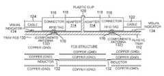
- each tray 112is configured to hold multiple fiber optic adapters 114 (where each adapter 114 is associated with one of the plurality of positions where a connection can be made).
- Each adapter 114is configured to optically couple each optical fiber in a set of one or more optical fibers to a respective optical fiber in another set of one or more optical fibers.
- each such set of one or more optical fibersis terminated with a connector 116 .
- each such adapter 114is used to couple a single fiber to another single fiber.
- Each adapter 114comprises two ports 118 to receive and hold the two connectors 116 in place while optically coupling the fibers.
- fiber optic adapters 114 and connectors 116examples include SC, LC, FC, LX.5, MTP, or MPO connectors. Other adapters and connectors can used.
- the fiber optic adapters 114are arranged and held on the tray 112 so that the ports 118 on each side of the adapters 114 all face the same direction and are aligned with one another.
- each tray 112 and the adapters 114 held by that tray 112are described as having a first or left side and a second or right side.
- each adapter 114is held on the tray 112 by a plastic clip 120 . This allows each fiber optic adapter 114 to be easily removed and attached to the tray 112 .
- each tray 112can be configured to have one side of the tray 112 and adapters 114 serve as the “patch field” or “patch side”.
- the patch sideis the side of the tray and adapters where the optical patching is performed.
- the other side of the tray 112 and adapters 114serve as the “fixed side”.
- connectors 116 attached to one end of optical patch cords 122are attached to the ports 118 on the patch side.
- Connectors attached to the other end of the patch cordsexit that tray and are typically connected to a port on the patch side of another adapter or another device in the network.
- the fixed optical cabling 124can be an optical pigtail, in which case the other end of the pigtail comprises a fiber that is spliced (for example, using a smooth) to another longer optical fiber that exits the tray 112 .
- the other end of the longer cableis connected as appropriate (for example, at another optical node located somewhere else in the network).
- the fixed optical cables 124 that are connected to the ports 118 on the fixed side of the tray 112can themselves exit the tray 112 (like the patch cords 122 attached to the ports 118 on the patch side of the tray 112 ) and can be connected as appropriate (for example, at another optical node located somewhere else in the network).
- each tray 112typically is configured to include two removable island assemblies 126 , where one island assembly 126 is attached to the patch side of the tray 112 and the other island assembly 126 is attached to the fixed side of the tray 112 .
- the island assemblies 126are configured to facilitate the routing and/or splicing of the fiber optic cabling that is attached to the ports 118 on that side.
- the island assemblies 126 in each traycan be reconfigured as needed by removing and inserting appropriate island assemblies 126 .
- the connectors 116 attached to the patch side of the adapters 114have RFID tags 128 (shown in FIG. 4 ) attached, or integrated into, them.
- the RFID tags 128store a unique identifier for the connector 116 and/or the patch cord 122 that can be used to identify which patch cord 122 is attached to each patch port 118 .
- the RFID tags 128can store other information, and can be written to as well as read from
- a printed circuit board 130(also referred to here as the “tray PCB” 130 ) is attached to the bottom of each tray 112 .
- the tray PCB 130includes a respective RFID antenna or coil 132 and respective LED (or other visual indicator) 134 positioned near each side of each fiber optic adapter 114 . That is, each fiber optic adapter 114 has a associated pair of RFID antennas 132 , a first one of which is located near a first one port 118 of the adapter 114 and second one of which is located near the other port 118 of the adapter 114 .
- Each RFID antenna or coil 132is used for reading an RFID tag 130 inserted into the respective port 118
- each LED or other visual indicator 134is used for visually identifying the respective port 118 (for example, in connection with guiding a technician in carrying out a work order).
- the ports 118 on only one side of the tray 112are used as the patch ports at any given time, there are RFID antennas or coils 132 and LEDs (or other visual indicators) 134 positioned on each side of the adapters 114 so that the same tray 112 and tray PCB 130 can be used to support patching on either side of the tray 112 .
- a PCB 136is mounted in the shelf 106 of each subrack 100 .
- This PCB 136is also referred to here as the “subrack PCB” 136 or the “subrack controller card” 136 .
- Components of the subrack PCB 136are coupled to components on each of the tray PCBs 130 using a backplane PCB 138 .
- the subrack PCB 136includes a flexible circuit or ribbon cable 140 to which a suitable backplane connector 142 is attached. This backplane connector 142 is attached to a connector on the backplane PCB 144 .
- each tray PCB 130includes a flexible circuit or ribbon cable 144 to which a suitable backplane connector 146 is attached.
- This backplane connector 146is attached to a connector 148 on the backplane PCB 138 .
- the backplane connector 148 of each tray 112is held in place by a pair of tethers 150 (for example, plastic tethers typically used for attaching price tags to items of clothing and the like) that are attached to both the tray 112 and the back-plane connector 146 . See FIGS. 7-11 .
- the tethers 150 and backplane connector 146are configured so that when the tray 112 is removed from the backplate 110 (backplane PCB 138 ), the tethers 150 will pull the backplane connector 146 out of the connector 148 on the backplane 138 before the flexible circuit or ribbon cable 144 is pulled on. This is done to protect the flexible circuit or ribbon cable 144 from being damaged by removing the tray 112 from the backplane 138 . Also, the tethers 150 help hold the backplane connector 146 in place to ease insertion of the backplane connector 146 onto the connector 148 on the backplane PCB 138 when the tray 112 is re-attached.
- the backplate 110 to which the trays 112 are attachedcomprises the backplane PCB 138 . That is, the functions of the backplate 110 are performed at least in part by the backplane PCB 138 .
- the backplane PCB 138includes cut outs 152 to which plastic strain relief cables 154 can be attached. Strain relief cables 154 are used to hold the fiber optic cabling attached to the ports 118 of that tray 112 in place so as to relieve the strain (for example, due to pulling on the cables) that otherwise might affect the cables or the connections provided at the ports 118 or splices housed in the tray 112 .
- the subrack PCB 136includes an RFID reader 156 .
- the RFID reader 156can be selectively coupled to the pair of RFID antennas or coils 132 positioned near each of the adapters 114 in each subrack 100 .
- the subrack PCB 136includes a first multiplexer 158 to couple the RF I/O port of the RFID reader 156 to another multiplexer 160 located on one of the tray PCBs 130 .
- a multiplexer 160 located on each tray PCB 130is used to selectively couple the RF I/O port of the RFID reader 156 to one of the RFID antenna pairs 132 included on that tray PCB 130 .
- a controller 162is located on the subrack PCB 136 , and a controller 164 is located on each of the tray PCBs 130 .
- Each controller 162 and 164can be implemented using a suitable programmable processor for executing software.
- the software executing on the programmable processorperforms at least some of the processing described here as being performed by each of the controllers 162 and 164 .
- the subrack controller 162is coupled to the RFID reader 156 , the subrack multiplexer 158 , and an LED 166 that is mounted to the subrack 100 (for example, to the front panel 108 of the subrack 100 ). Also, the subrack controller 162 is coupled to each of the tray controllers 164 via the backplane 138 .
- Each tray controller 164is coupled to the tray multiplexer 160 on that tray 112 and the LEDs (or other visual indicators) 134 on that tray 112 .
- the subrack controller 162is coupled to an overall rack controller 168 (also referred to here as the “analyzer”).
- the analyzer 168is configured to cause the subrack controller 162 and the tray controllers 164 to read the RFID tag 128 that is attached to any connector 116 inserted into each patch port 118 . This can be done in a polling manner, where periodically each such patch port 118 is read. This can be done in other ways as well. Reading of a particular RFID tag 128 is done by instructing the subrack controller 162 and tray controller 164 to configure the multiplexers 158 and 160 to couple the RFID reader 156 to the appropriate RFID antennas or coils 132 .
- the RFID antennas 132 and LEDs 134 on both sides of the adapter 114are coupled to the tray controller 164 and to power and ground using the same PCB traces.
- a first set of PCB traces for coupling the RFID antennas 132 and LEDs 134 on the left side of each adapter 114 and a second, separate set of PCB for coupling the RFID antennas 132 and LEDs 134 on the right side of that adapter 114need not be provided; instead, for each adapter 114 , only a single set of PCB traces need be provided for coupling the RFID antennas 132 and LEDs 134 on both sides of each adapter 114 to the tray controller 164 and power and ground.
- the analyzer 168is also configured to communicate the information read from the RFID tags 128 to middleware software 170 in the manner described in the following US patent applications (all of which are hereby incorporated herein by reference): U.S. Provisional Patent Application Ser. No. 61/152,624, filed on Feb. 13, 2009, titled “MANAGED CONNECTIVITY SYSTEMS AND METHODS” (also referred to here as the “'624 Application”); U.S. patent application Ser. No. 12/705,497, filed on Feb. 12, 2010, titled “AGGREGATION OF PHYSICAL LAYER INFORMATION RELATED TO A NETWORK” (is also referred to here as the '497 Application); U.S. patent application Ser. No.
- the middleware software 170includes, or is coupled to a database or other data store (not shown) for storing the information provided to it.
- the middleware software 170also includes functionality that provides an interface for external devices or entities to access the information maintained by the middleware software 170 . This access can include retrieving information from the middleware software 170 as well as supplying information to the middleware software 170 .
- the middleware software 170is implemented as “middleware” that is able to provide such external devices and entities with transparent and convenient access to the information maintained by the middleware software 170 .
- the middleware software 170aggregates information from the relevant devices in the network and provides external devices and entities with access to such information, the external devices and entities do not need to individually interact with all of the devices in the network that provide such information, nor do such devices need to have the capacity to respond to requests from such external devices and entities.
- the middleware software 170implements an application programming interface (API) by which application-layer functionality can gain access to the physical layer information maintained by the middleware software 170 using a software development kit (SDK) that describes and documents the API.
- APIapplication programming interface
- SDKsoftware development kit
- ICMInfrastructure Configuration Manager
- the analyzer 168is also configured to instruct the subrack controller 162 and/or the tray controllers 164 to turn on the LEDs (or other visual indicators) 134 as appropriate (for example, in connection with instructing a technician in carrying out a work order or to signal an error condition).
- the analyzer 168can be configured to guide a technician in carrying out a work order by visually signally which ports 118 are to be affected by a particular step in the work order using the LEDs 134 .
- the LEDs 134can be used to provide a visual indication as to whether each step was properly carried out. Data read from the RFID tags 18 is also used to determine if each step was properly carried out (for example, in similar manner as is described in the previously mentioned US patent applications).
- datacan be written to the RFID tags 128 in the same manner.
- poweris supplied to the components on the subrack and tray PCBs 136 and 130 from the analyzer 168 on this cable 172 .
- this connectionis implemented as a RS422 serial connection.
- the subrack PCB 136includes two connectors 174 that can be used for connecting the cable 172 from the analyzer 168 to the subrack PCB 136 .
- these two connectors 174can be oriented at an angle (for example, 30 degrees to 45 degrees) to facilitate routing this cable 172 in a manner that is compatible with the fiber optic cables in the rack 102 . Either of the two connectors 174 can be used depending on what is more convenient for connecting to the analyzer 168 . Also, the two connectors 174 can be used to connect multiple subracks 100 to the analyzer 168 using a daisy chain topology.
- the tray 112can include pockets 176 in the plastic of the tray 112 to accommodate components that are mounted to the underside of the tray PCB board 130 . This enables the tray PCB 130 to lay flat in the tray 112 .
- the ground planessurround the conductive plane in which the RFID inductors (coil or antenna) are formed. Openings are formed in the upper ground plane in order to enable RF signals to pass between the RFID antenna 134 and any RFID tag 128 positioned above it. The rest of the ground plane serves to constrain the RFID signals. Also, in this example, the openings formed in the bottom of the ground plane serve to let some of the RFID signals escape through the bottom to reduce the size of the field that is created above the tray PCB 130 .
- FIG. 14illustrates another way in which radio frequency fields emitted by RFID antennas can be constrained that is suitable for use in the exemplary subrack of FIG. 1 .
- the layers of the tray PCB 130are configured so that, for each RFID antenna 132 on each tray 113 , the tray PCB 130 includes a multi-layer coil assembly 1404 that implements that RFID antenna 132 .
- the layers of the tray PCB 130are also configured so that, for each RFID antenna 132 on each tray 113 , the tray PCB 130 includes a respective C-shaped open copper track feature 1402 and a respective O-shaped closed copper track feature 1404 that concentrically surround the coil assembly 1404 .
- the C-shaped open feature 1404is located inside of the O-shaped closed feature 1406 .
- Each respective coil assembly 1402 , C-shaped open feature 1404 , and O-shaped closed feature 1406are isolated from each another.
- Each C-shaped open feature 1402provides a dampening field for producing a rectangular region of interest (ROI) box for addressing misalignment problems that may otherwise occur in general usage.
- Each C-shaped open feature 1042also provides rear field dampening to the tray 112 below.
- Each O-shaped closed features 1406provides protection against cross-talk that may otherwise occur among adjacent RFID antennas 132 , where each such O-shaped closed feature 1406 is implemented as shorted turn that produces a corresponding nulling field.
- a daughter board 200it is necessary to position a daughter board 200 onto the tray PCBs 130 .
- a storage devicesuch as an EEPROM
- EEPROMelectrically erasable programmable read-only memory
- QUAREOQUAREO technology that is commercially available from TE Connectivity. This technology is also referred to here as “Connection Point Identifier” or “CPID” technology.
- the storage device interfacecomprises four leads—a power lead, a ground lead, a data lead, and an extra lead that is reserved for future use.
- a suitable protocolfor example, the UNI/O protocol
- each adapter 114that are configured to come into electrical contact with the four corresponding storage-device leads on a connector inserted in that adapter 114 .
- Appropriate tracesare provided on the tray PCB 130 in the tray 112 to couple these adapter contacts to the tray controller 164 via multiplexer 160 and to power and ground.
- the connectivity between the subrack controller 162 and the tray controllers 164is provided in the manner described above. In this way, the QUAREO (or similar CPID) technology can be integrated into what is otherwise an RFID subrack 100 to support the mixing and matching of CPID and RFID trays in the field.
- the contacts for reading the storage devicescan be attached to a daughter board 200 (shown in FIGS. 12 and 13 ). It is helpful to precisely align this daughter board 200 while attaching it to an appropriate daughter-board connector 202 on the tray PCB 136 . One way of doing this is shown in FIGS. 12 and 13 .
- One side of the daughter board 200has one or more metal pins 204 extending from it.
- the tray PCB 136includes a corresponding plastic post 206 .
- the pins 204 and posts 206are arranged so that each pin 204 can be inserted into the top of a corresponding one of the posts 206 on the tray PCB 136 .
- the connectors 210 and 208 on the daughterboard 200 and tray PCB 136can more easily be connected while providing more precise alignment of the items on the daughter board 200 (for example, the interfaces for reading the EEPROMS, which in this example are positioned above the fiber optic adapters 114 , which are preferably precisely aligned in order to read the EEPROMS).
- the CPID contacts 220can be placed on both sides of the adapters 114 so that either side of the adapters 114 can be used as the patch field in the manner described above connection with RFID versions of trays.
- CPID contacts 220 on both sides of the adapter 114are coupled to the tray controller 164 and to power and ground using the same PCB traces.
- a first set of PCB traces for coupling the CPID contacts 220 on the left side of each adapter 114 and a second, separate set of PCB for coupling the CPID contacts 22 —on the right side of that adapter 114need not be provided; instead, for each adapter 114 , only a single set of PCB traces need be provided for coupling the CPID contacts 220 on both sides of each adapter 114 to the tray controller 164 and power and ground.
- Example 1includes a subrack comprising: a backplate; at least one tray configured so that a plurality of connections can be made at a plurality of positions on the tray, each of the plurality of connections involving at least one connector having information stored in a device associated therewith that can be read; wherein the backplate and the tray are configured so that the tray can be selectively attached and removed from the backplate; and wherein the backplate and the tray are configured so that the devices associated with the connectors involved in making the connections can be read via the tray.
- Example 2includes the subrack of Example 1, wherein the devices associated with each connector comprises RFID tags, wherein the backplate and the tray are configured so that the RFID tags associated with the connectors involved in making the connections can be read via the tray.
- Example 3includes the subrack of Example 2, wherein each tray comprises a plurality of RFID antennas, each of the RFID antennas being associated with a respective one of the positions, wherein each of the plurality of RFID antennas can be selectively coupled to an RFID reader in order to read the RFID tags associated with the connectors involved in making the connections.
- Example 4includes the subrack of Example 1, wherein the devices associated each connector comprises connection point identifier (CPID) storage devices, wherein the backplate and the tray are configured so that the CPID storage devices associated with the connectors involved in making the connections can be read via the tray.
- CPIDconnection point identifier
- Example 5includes the subrack of any of the Examples 1-4, wherein the backplate is implemented as a backplane printed circuit board.
- Example 6includes the subrack of Example 5, wherein the backplane printed circuit board comprises a tray connector, wherein the tray has attached thereto a backplane connector that is configured to be connected to the tray connector of the backplane printed circuit board in connection with the tray being attached to the backplate; and wherein the tray further comprises at least one plastic tether attached to the backplane connector, wherein the plastic tether is configured to pull the backplane connector out of the tray connector on the backplane printed circuit board in connection with the tray being removed from the backplate.
- Example 7includes the subrack of any of the Examples 5-6, wherein the backplane printed circuit board comprises at least one cut out to which a strain relief cable can be attached.
- Example 8includes the subrack of any of the Examples 1-7, further comprising a plurality of trays.
- Example 9includes the subrack of any of the Examples 1-8 wherein each tray comprises a plurality of visual indicators, each of the visual indicators being associated with a respective one of the positions.
- Example 10includes the subrack of any of the Examples 1-9, wherein each tray is configured so that a plurality of fiber optic adapters can be attached to the printed circuit board, each of the plurality of fiber optic adapters associated with a respective one of the positions.
- Example 11includes the subrack of any of the Examples 1-10, further comprising a subrack controller; wherein each tray comprises: a tray controller; and at least two communication ports, each of which is coupled to the tray controller, wherein the subrack is configured so that the tray controller can be coupled to the subrack controller via one or more of the communication ports.
- Example 12includes the subrack of Example 11, wherein the communication ports are angled.
- Example 13includes the subrack of any of the Examples 1-12, wherein each tray includes pockets formed in the tray to accommodate electronics.
- Example 14includes the subrack of any of the Examples 1-13, wherein the each of the plurality of connections is made using at least one of optical cabling and metallic cabling.
- Example 15includes a method of using a subrack that comprises a backplate and at least one tray configured so that a plurality of connections can be made at a plurality of positions on the tray, each of the plurality of connections involving at least one connector having information stored in a device associated therewith, the method comprising: attaching the tray to the backplate; reading, via the tray, the devices associated with the connectors involved in making the connections; and removing the tray from the backplate and thereafter re-attaching the tray to the backplate.
- Example 16includes the method of Example 15, wherein the devices associated each connector comprises RFID tags; and wherein reading, via the tray, the devices associated with the connectors involved in making the connections comprises reading, via the tray, the RFID tags associated with the connectors involved in making the connections.
- Example 17includes the method of Example 16, wherein each tray comprises a plurality of RFID antennas, each of the RFID antennas being associated with a respective one of the positions; and wherein reading the RFID tags associated with the connectors involved in making the connections via the tray comprises selectively coupling each of the plurality of RFID antennas to an RFID reader in order to read the RFID tags associated with the connectors involved in making the connections.
- Example 18includes the method of Example 15, wherein the devices associated each connector comprises connection point identifier (CPID) storage devices; and wherein reading, via the tray, the devices associated with the connectors involved in making the connections comprises reading the CPID storage devices associated with the connectors involved in making the connections via the tray.
- CPIDconnection point identifier
- Example 19includes the method of any of the Examples 15-18, wherein the backplate is implemented as a backplane printed circuit board.
- Example 20includes the method of Example 19, wherein the backplane printed circuit board comprises a tray connector, wherein the tray has attached thereto a backplane connector that is configured to be connected to the tray connector of the backplane printed circuit board in connection with the tray being attached to the backplate; and wherein the tray further comprises at least one plastic tether attached to the backplane connector, wherein the plastic tether is configured to pull the backplane connector out of the tray connector on the backplane printed circuit board in connection with the tray being removed from the backplate.
- Example 21includes the method of any of the Examples 19-20, further comprising attaching a strain relief cable to the tray using a cut out formed in the backplane printed circuit board.
Landscapes
- Engineering & Computer Science (AREA)
- Physics & Mathematics (AREA)
- Business, Economics & Management (AREA)
- General Physics & Mathematics (AREA)
- Optics & Photonics (AREA)
- Economics (AREA)
- Computer Networks & Wireless Communication (AREA)
- Microelectronics & Electronic Packaging (AREA)
- Theoretical Computer Science (AREA)
- General Engineering & Computer Science (AREA)
- Operations Research (AREA)
- Computer Hardware Design (AREA)
- Finance (AREA)
- Entrepreneurship & Innovation (AREA)
- Human Resources & Organizations (AREA)
- Marketing (AREA)
- Accounting & Taxation (AREA)
- Quality & Reliability (AREA)
- Strategic Management (AREA)
- Tourism & Hospitality (AREA)
- General Business, Economics & Management (AREA)
- Development Economics (AREA)
- Light Guides In General And Applications Therefor (AREA)
- Electromagnetism (AREA)
- Health & Medical Sciences (AREA)
- Toxicology (AREA)
- Human Computer Interaction (AREA)
- General Health & Medical Sciences (AREA)
- Artificial Intelligence (AREA)
- Computer Vision & Pattern Recognition (AREA)
- Structure Of Telephone Exchanges (AREA)
- Coupling Device And Connection With Printed Circuit (AREA)
- Pallets (AREA)
Abstract
Description
Claims (21)
Priority Applications (3)
| Application Number | Priority Date | Filing Date | Title |
|---|---|---|---|
| US13/766,137US9361600B2 (en) | 2012-02-14 | 2013-02-13 | Physical layer management (PLM) system for use with an optical distribution frame in which trays can be selectively removed and re-attached |
| MX2014009775AMX336311B (en) | 2012-02-14 | 2013-02-14 | PHYSICAL LAYER MANAGEMENT (PLM) IN AN OPTICAL DISTRIBUTION FRAME. |
| CL2014002161ACL2014002161A1 (en) | 2012-02-14 | 2014-08-13 | Tray for use in a subframe of a frame, comprising a printed circuit board, in which each of a plurality of connections involves at least one connector positioned on a patch side of the plate, in which both sides of the positions may be used as the communication side, and where the devices associated with the connectors involved in making the connections on the patch side can be read through the tray; subbastidor; associated methods |
Applications Claiming Priority (2)
| Application Number | Priority Date | Filing Date | Title |
|---|---|---|---|
| US201261598713P | 2012-02-14 | 2012-02-14 | |
| US13/766,137US9361600B2 (en) | 2012-02-14 | 2013-02-13 | Physical layer management (PLM) system for use with an optical distribution frame in which trays can be selectively removed and re-attached |
Publications (2)
| Publication Number | Publication Date |
|---|---|
| US20130306723A1 US20130306723A1 (en) | 2013-11-21 |
| US9361600B2true US9361600B2 (en) | 2016-06-07 |
Family
ID=47843227
Family Applications (3)
| Application Number | Title | Priority Date | Filing Date |
|---|---|---|---|
| US13/766,137Expired - Fee RelatedUS9361600B2 (en) | 2012-02-14 | 2013-02-13 | Physical layer management (PLM) system for use with an optical distribution frame in which trays can be selectively removed and re-attached |
| US13/766,151Active2033-08-11US9111249B2 (en) | 2012-02-14 | 2013-02-13 | Physical layer management (PLM) system for use with an optical distribution frame using RFID antennas with localized fields |
| US13/766,120Active2034-12-30US9805332B2 (en) | 2012-02-14 | 2013-02-13 | Physical layer management (PLM) system for use with an optical distribution frame having trays with selectable patch side |
Family Applications After (2)
| Application Number | Title | Priority Date | Filing Date |
|---|---|---|---|
| US13/766,151Active2033-08-11US9111249B2 (en) | 2012-02-14 | 2013-02-13 | Physical layer management (PLM) system for use with an optical distribution frame using RFID antennas with localized fields |
| US13/766,120Active2034-12-30US9805332B2 (en) | 2012-02-14 | 2013-02-13 | Physical layer management (PLM) system for use with an optical distribution frame having trays with selectable patch side |
Country Status (9)
| Country | Link |
|---|---|
| US (3) | US9361600B2 (en) |
| EP (1) | EP2815587B1 (en) |
| CN (1) | CN104380759B (en) |
| AU (1) | AU2013220736B2 (en) |
| BR (1) | BR112014020121A2 (en) |
| CL (1) | CL2014002161A1 (en) |
| MX (1) | MX336311B (en) |
| NZ (1) | NZ628612A (en) |
| WO (1) | WO2013120616A2 (en) |
Families Citing this family (22)
| Publication number | Priority date | Publication date | Assignee | Title |
|---|---|---|---|---|
| US9361600B2 (en) | 2012-02-14 | 2016-06-07 | Tyco Electronics Uk Ltd | Physical layer management (PLM) system for use with an optical distribution frame in which trays can be selectively removed and re-attached |
| CN102752672B (en)* | 2012-06-06 | 2015-07-08 | 华为技术有限公司 | Method, device and system for optical fiber distribution |
| US11113642B2 (en) | 2012-09-27 | 2021-09-07 | Commscope Connectivity Uk Limited | Mobile application for assisting a technician in carrying out an electronic work order |
| US9130318B2 (en) | 2012-11-16 | 2015-09-08 | Tyco Electronics Uk Ltd. | Localized reading of RFID tags located on multiple sides of a port from a single side using RFID coupling circuit and portable RFID reader |
| CN203444504U (en)* | 2013-08-26 | 2014-02-19 | 鸿富锦精密工业(深圳)有限公司 | Reader |
| US9407510B2 (en) | 2013-09-04 | 2016-08-02 | Commscope Technologies Llc | Physical layer system with support for multiple active work orders and/or multiple active technicians |
| US9279945B2 (en) | 2014-02-10 | 2016-03-08 | Avago Technologies General Ip (Singapore) Pte. Ltd. | Methods, apparatuses and systems for blind mating arrays of multi-optical fiber connector modules |
| EP3105627B1 (en)* | 2014-02-14 | 2020-11-04 | CommScope Connectivity UK Limited | Managed connectivity in optical distribution frame |
| US9258916B2 (en)* | 2014-03-07 | 2016-02-09 | Go!Foton Holdings, Inc. | High density cassette storage system |
| CN204129294U (en) | 2014-09-17 | 2015-01-28 | 中兴通讯股份有限公司 | A kind of fiber optic network distributing equipment |
| US9451716B1 (en)* | 2015-06-27 | 2016-09-20 | Intel Corporation | Serviceable chassis for devices |
| WO2017062231A1 (en)* | 2015-10-08 | 2017-04-13 | Commscope Technologies Llc | Communication media and methods for providing indication of signal power to a network entity |
| KR102460453B1 (en)* | 2016-02-19 | 2022-10-28 | 삼성전자주식회사 | Electronic device attachable outside storage media |
| US10346654B2 (en) | 2016-10-05 | 2019-07-09 | Mox Networks, LLC | RFID-based rack inventory management systems |
| WO2018195588A1 (en)* | 2017-04-26 | 2018-11-01 | The Yield Technology Solutions Pty Ltd | An electronics holder |
| CN107529099A (en)* | 2017-08-31 | 2017-12-29 | 苏州惠华电子科技有限公司 | A kind of electrical harnesses frame control system based on RFID |
| CN107404673A (en)* | 2017-08-31 | 2017-11-28 | 苏州惠华电子科技有限公司 | A kind of electronic wiring frame of the RFID based on EMI |
| CN110049652B (en)* | 2018-01-16 | 2021-07-09 | 联想企业解决方案(新加坡)有限公司 | Server rack and cabinet comprising same |
| CN208705520U (en)* | 2018-09-25 | 2019-04-05 | 中兴通讯股份有限公司 | Optical fiber thermoconnecting tray |
| US11353662B2 (en)* | 2019-04-26 | 2022-06-07 | Hewlett Packard Enterprise Development Lp | Smart carriers and smart adapters for automatic discovery of fiber assemblies |
| US11464131B2 (en)* | 2020-02-07 | 2022-10-04 | Seagate Technology Llc | Cable management assembly |
| CN111511139B (en)* | 2020-04-30 | 2021-03-16 | 陇东学院 | A new type of multifunctional maintenance device for electrical automation |
Citations (43)
| Publication number | Priority date | Publication date | Assignee | Title |
|---|---|---|---|---|
| US5821510A (en) | 1994-12-22 | 1998-10-13 | Lucent Technologies Inc. | Labeling and tracing system for jumper used in an exchange |
| US5910776A (en) | 1994-10-24 | 1999-06-08 | Id Technologies, Inc. | Method and apparatus for identifying locating or monitoring equipment or other objects |
| US6002331A (en) | 1998-07-20 | 1999-12-14 | Laor; Herzel | Method and apparatus for identifying and tracking connections of communication lines |
| US20010024360A1 (en) | 2000-03-14 | 2001-09-27 | Fuji Xerox Co., Ltd. | Printed wiring board |
| US6378111B1 (en) | 1997-11-11 | 2002-04-23 | Wolfgang Brenner | Method for management and documentation of contact points of a wiring network |
| US6499861B1 (en) | 1999-09-23 | 2002-12-31 | Avaya Technology Corp. | Illuminated patch cord connector ports for use in a telecommunications patch closet having patch cord tracing capabilities |
| US6784802B1 (en) | 1999-11-04 | 2004-08-31 | Nordx/Cdt, Inc. | Real time monitoring of cable patch panel |
| US20040169996A1 (en)* | 2003-02-27 | 2004-09-02 | Paul Dieter G. | Universal receptacles for interchangeably receiving different removable computer drive carriers |
| US6808116B1 (en) | 2002-05-29 | 2004-10-26 | At&T Corp. | Fiber jumpers with data storage method and apparatus |
| US6847856B1 (en) | 2003-08-29 | 2005-01-25 | Lucent Technologies Inc. | Method for determining juxtaposition of physical components with use of RFID tags |
| US7046899B2 (en) | 2004-03-02 | 2006-05-16 | Furukawa Electric North America, Inc. | Universal apparatus for incorporating intelligence into an optical fiber distribution frame |
| US20060158833A1 (en)* | 2005-01-20 | 2006-07-20 | Belady Christian L | Communicating with an electronic module that is slidably mounted in a system |
| US7197214B2 (en) | 2004-05-24 | 2007-03-27 | Corning Cable Systems Llc | Methods and apparatus for facilitating cable locating |
| US7246746B2 (en) | 2004-08-03 | 2007-07-24 | Avaya Technology Corp. | Integrated real-time automated location positioning asset management system |
| US7406231B1 (en) | 2005-06-21 | 2008-07-29 | Avaya Technology Corp. | Electroluminescent patch cable |
| US7468669B1 (en) | 2005-06-21 | 2008-12-23 | Avaya Technology Corp. | RFID patch panels and cables |
| US7547150B2 (en) | 2007-03-09 | 2009-06-16 | Corning Cable Systems, Llc | Optically addressed RFID elements |
| US20090166404A1 (en) | 2008-01-02 | 2009-07-02 | Commscope, Inc. Of North Carolina | Intelligent MPO-to-MPO Patch Panels Having Connectivity Tracking Capabilities and Related Methods |
| US7605707B2 (en) | 2004-12-06 | 2009-10-20 | Commscope, Inc. Of North Carolina | Telecommunications patching system that utilizes RFID tags to detect and identify patch cord interconnections |
| US7667574B2 (en) | 2006-12-14 | 2010-02-23 | Corning Cable Systems, Llc | Signal-processing systems and methods for RFID-tag signals |
| US7729586B2 (en)* | 2008-10-07 | 2010-06-01 | Commscope Inc. Of North Carolina | Telecommunications patching systems with vertically-oriented patching modules |
| US7760094B1 (en) | 2006-12-14 | 2010-07-20 | Corning Cable Systems Llc | RFID systems and methods for optical fiber network deployment and maintenance |
| US7772975B2 (en) | 2006-10-31 | 2010-08-10 | Corning Cable Systems, Llc | System for mapping connections using RFID function |
| US20100210135A1 (en) | 2009-02-19 | 2010-08-19 | Michael German | Patch Panel Cable Information Detection Systems and Methods |
| US7782202B2 (en) | 2006-10-31 | 2010-08-24 | Corning Cable Systems, Llc | Radio frequency identification of component connections |
| US7855697B2 (en) | 2007-08-13 | 2010-12-21 | Corning Cable Systems, Llc | Antenna systems for passive RFID tags |
| US7856166B2 (en) | 2008-09-02 | 2010-12-21 | Corning Cable Systems Llc | High-density patch-panel assemblies for optical fiber telecommunications |
| US20110116755A1 (en) | 2009-11-13 | 2011-05-19 | Reflex Photonics Inc. | Optical backplane rack assembly with external optical connectors |
| US7965186B2 (en) | 2007-03-09 | 2011-06-21 | Corning Cable Systems, Llc | Passive RFID elements having visual indicators |
| US8050939B2 (en) | 2005-02-11 | 2011-11-01 | Avaya Inc. | Methods and systems for use in the provision of services in an institutional setting such as a healthcare facility |
| US20110273892A1 (en) | 2010-05-07 | 2011-11-10 | Tyco Electronics Corporation | Solid state lighting assembly |
| US8075348B2 (en) | 2009-04-23 | 2011-12-13 | Commscope Inc. Of North Carolina | Assembly and system of datacommunication cables and connectors |
| US20120007717A1 (en) | 2010-07-09 | 2012-01-12 | Michael De Jong | Cables and connector assemblies employing a furcation tube(s) for radio-frequency identification (rfid)-equipped connectors, and related systems and methods |
| US20120023232A1 (en) | 2009-04-09 | 2012-01-26 | Huawei Device Co., Ltd. | Method for configuring access rights, control point, device and communication system |
| US8116434B2 (en) | 2006-11-29 | 2012-02-14 | Commscope, Inc. Of North Carolina | Telecommunications patching system that facilitates detection and identification of patch cords |
| US8138925B2 (en) | 2008-01-15 | 2012-03-20 | Corning Cable Systems, Llc | RFID systems and methods for automatically detecting and/or directing the physical configuration of a complex system |
| US8172468B2 (en) | 2010-05-06 | 2012-05-08 | Corning Incorporated | Radio frequency identification (RFID) in communication connections, including fiber optic components |
| US8181229B2 (en) | 2008-03-25 | 2012-05-15 | Commscope, Inc. Of North Carolina | Methods, systems and computer program products for operating a communications network with enhanced security |
| US8248208B2 (en) | 2008-07-15 | 2012-08-21 | Corning Cable Systems, Llc. | RFID-based active labeling system for telecommunication systems |
| US8264366B2 (en) | 2009-03-31 | 2012-09-11 | Corning Incorporated | Components, systems, and methods for associating sensor data with component location |
| US8264355B2 (en) | 2006-12-14 | 2012-09-11 | Corning Cable Systems Llc | RFID systems and methods for optical fiber network deployment and maintenance |
| US20130120941A1 (en)* | 2011-11-15 | 2013-05-16 | Microsoft Corporation | Modular equipment rack system for data center |
| US20130207782A1 (en) | 2012-02-14 | 2013-08-15 | Tyco Electronics Raychem Bvba | Physical layer management (plm) system for use with an optical distribution frame using rfid antennas with localized fields |
- 2013
- 2013-02-13USUS13/766,137patent/US9361600B2/ennot_activeExpired - Fee Related
- 2013-02-13USUS13/766,151patent/US9111249B2/enactiveActive
- 2013-02-13USUS13/766,120patent/US9805332B2/enactiveActive
- 2013-02-14WOPCT/EP2013/000441patent/WO2013120616A2/enactiveApplication Filing
- 2013-02-14MXMX2014009775Apatent/MX336311B/enunknown
- 2013-02-14BRBR112014020121Apatent/BR112014020121A2/ennot_activeIP Right Cessation
- 2013-02-14CNCN201380019932.4Apatent/CN104380759B/ennot_activeExpired - Fee Related
- 2013-02-14NZNZ628612Apatent/NZ628612A/ennot_activeIP Right Cessation
- 2013-02-14EPEP13708082.6Apatent/EP2815587B1/enactiveActive
- 2013-02-14AUAU2013220736Apatent/AU2013220736B2/ennot_activeCeased
- 2014
- 2014-08-13CLCL2014002161Apatent/CL2014002161A1/enunknown
Patent Citations (48)
| Publication number | Priority date | Publication date | Assignee | Title |
|---|---|---|---|---|
| US5910776A (en) | 1994-10-24 | 1999-06-08 | Id Technologies, Inc. | Method and apparatus for identifying locating or monitoring equipment or other objects |
| US5821510A (en) | 1994-12-22 | 1998-10-13 | Lucent Technologies Inc. | Labeling and tracing system for jumper used in an exchange |
| US6378111B1 (en) | 1997-11-11 | 2002-04-23 | Wolfgang Brenner | Method for management and documentation of contact points of a wiring network |
| US6002331A (en) | 1998-07-20 | 1999-12-14 | Laor; Herzel | Method and apparatus for identifying and tracking connections of communication lines |
| US6499861B1 (en) | 1999-09-23 | 2002-12-31 | Avaya Technology Corp. | Illuminated patch cord connector ports for use in a telecommunications patch closet having patch cord tracing capabilities |
| US6784802B1 (en) | 1999-11-04 | 2004-08-31 | Nordx/Cdt, Inc. | Real time monitoring of cable patch panel |
| US20010024360A1 (en) | 2000-03-14 | 2001-09-27 | Fuji Xerox Co., Ltd. | Printed wiring board |
| US6808116B1 (en) | 2002-05-29 | 2004-10-26 | At&T Corp. | Fiber jumpers with data storage method and apparatus |
| US20040169996A1 (en)* | 2003-02-27 | 2004-09-02 | Paul Dieter G. | Universal receptacles for interchangeably receiving different removable computer drive carriers |
| US6847856B1 (en) | 2003-08-29 | 2005-01-25 | Lucent Technologies Inc. | Method for determining juxtaposition of physical components with use of RFID tags |
| US7046899B2 (en) | 2004-03-02 | 2006-05-16 | Furukawa Electric North America, Inc. | Universal apparatus for incorporating intelligence into an optical fiber distribution frame |
| US7197214B2 (en) | 2004-05-24 | 2007-03-27 | Corning Cable Systems Llc | Methods and apparatus for facilitating cable locating |
| US7246746B2 (en) | 2004-08-03 | 2007-07-24 | Avaya Technology Corp. | Integrated real-time automated location positioning asset management system |
| US7605707B2 (en) | 2004-12-06 | 2009-10-20 | Commscope, Inc. Of North Carolina | Telecommunications patching system that utilizes RFID tags to detect and identify patch cord interconnections |
| US20060158833A1 (en)* | 2005-01-20 | 2006-07-20 | Belady Christian L | Communicating with an electronic module that is slidably mounted in a system |
| US8050939B2 (en) | 2005-02-11 | 2011-11-01 | Avaya Inc. | Methods and systems for use in the provision of services in an institutional setting such as a healthcare facility |
| US7406231B1 (en) | 2005-06-21 | 2008-07-29 | Avaya Technology Corp. | Electroluminescent patch cable |
| US7468669B1 (en) | 2005-06-21 | 2008-12-23 | Avaya Technology Corp. | RFID patch panels and cables |
| US7782202B2 (en) | 2006-10-31 | 2010-08-24 | Corning Cable Systems, Llc | Radio frequency identification of component connections |
| US7772975B2 (en) | 2006-10-31 | 2010-08-10 | Corning Cable Systems, Llc | System for mapping connections using RFID function |
| US8116434B2 (en) | 2006-11-29 | 2012-02-14 | Commscope, Inc. Of North Carolina | Telecommunications patching system that facilitates detection and identification of patch cords |
| US7667574B2 (en) | 2006-12-14 | 2010-02-23 | Corning Cable Systems, Llc | Signal-processing systems and methods for RFID-tag signals |
| US8264355B2 (en) | 2006-12-14 | 2012-09-11 | Corning Cable Systems Llc | RFID systems and methods for optical fiber network deployment and maintenance |
| US7760094B1 (en) | 2006-12-14 | 2010-07-20 | Corning Cable Systems Llc | RFID systems and methods for optical fiber network deployment and maintenance |
| US7547150B2 (en) | 2007-03-09 | 2009-06-16 | Corning Cable Systems, Llc | Optically addressed RFID elements |
| US7965186B2 (en) | 2007-03-09 | 2011-06-21 | Corning Cable Systems, Llc | Passive RFID elements having visual indicators |
| US7855697B2 (en) | 2007-08-13 | 2010-12-21 | Corning Cable Systems, Llc | Antenna systems for passive RFID tags |
| US8203450B2 (en) | 2008-01-02 | 2012-06-19 | Commscope, Inc. | Intelligent MPO-to-MPO patch panels having connectivity tracking capabilities and related methods |
| US20090166404A1 (en) | 2008-01-02 | 2009-07-02 | Commscope, Inc. Of North Carolina | Intelligent MPO-to-MPO Patch Panels Having Connectivity Tracking Capabilities and Related Methods |
| US8138925B2 (en) | 2008-01-15 | 2012-03-20 | Corning Cable Systems, Llc | RFID systems and methods for automatically detecting and/or directing the physical configuration of a complex system |
| US8181229B2 (en) | 2008-03-25 | 2012-05-15 | Commscope, Inc. Of North Carolina | Methods, systems and computer program products for operating a communications network with enhanced security |
| US8248208B2 (en) | 2008-07-15 | 2012-08-21 | Corning Cable Systems, Llc. | RFID-based active labeling system for telecommunication systems |
| US7856166B2 (en) | 2008-09-02 | 2010-12-21 | Corning Cable Systems Llc | High-density patch-panel assemblies for optical fiber telecommunications |
| US7729586B2 (en)* | 2008-10-07 | 2010-06-01 | Commscope Inc. Of North Carolina | Telecommunications patching systems with vertically-oriented patching modules |
| US20100210135A1 (en) | 2009-02-19 | 2010-08-19 | Michael German | Patch Panel Cable Information Detection Systems and Methods |
| US8092249B2 (en) | 2009-02-19 | 2012-01-10 | Commscope Inc. Of North Carolina | Patch panel cable information detection systems and methods |
| US8264366B2 (en) | 2009-03-31 | 2012-09-11 | Corning Incorporated | Components, systems, and methods for associating sensor data with component location |
| US20120023232A1 (en) | 2009-04-09 | 2012-01-26 | Huawei Device Co., Ltd. | Method for configuring access rights, control point, device and communication system |
| US8075348B2 (en) | 2009-04-23 | 2011-12-13 | Commscope Inc. Of North Carolina | Assembly and system of datacommunication cables and connectors |
| WO2011057383A1 (en) | 2009-11-13 | 2011-05-19 | Reflex Photonics Inc . | Optical backplane rack assembly with external optical connectors |
| US20110116755A1 (en) | 2009-11-13 | 2011-05-19 | Reflex Photonics Inc. | Optical backplane rack assembly with external optical connectors |
| US8172468B2 (en) | 2010-05-06 | 2012-05-08 | Corning Incorporated | Radio frequency identification (RFID) in communication connections, including fiber optic components |
| US20110273892A1 (en) | 2010-05-07 | 2011-11-10 | Tyco Electronics Corporation | Solid state lighting assembly |
| US20120007717A1 (en) | 2010-07-09 | 2012-01-12 | Michael De Jong | Cables and connector assemblies employing a furcation tube(s) for radio-frequency identification (rfid)-equipped connectors, and related systems and methods |
| US20130120941A1 (en)* | 2011-11-15 | 2013-05-16 | Microsoft Corporation | Modular equipment rack system for data center |
| US20130207782A1 (en) | 2012-02-14 | 2013-08-15 | Tyco Electronics Raychem Bvba | Physical layer management (plm) system for use with an optical distribution frame using rfid antennas with localized fields |
| US20130205579A1 (en) | 2012-02-14 | 2013-08-15 | Tyco Electronics Raychem Bvba | Physical layer management (plm) system for use with an optical distribution frame having trays with selectable patch side |
| US20130306723A1 (en) | 2012-02-14 | 2013-11-21 | Tyco Electronics Raychem Bvba | Physical layer management (plm) system for use with an optical distribution frame in which trays can be selectively removed and re-attached |
Non-Patent Citations (10)
Also Published As
| Publication number | Publication date |
|---|---|
| MX2014009775A (en) | 2014-11-25 |
| MX336311B (en) | 2016-01-13 |
| US9111249B2 (en) | 2015-08-18 |
| AU2013220736B2 (en) | 2017-05-11 |
| AU2013220736A1 (en) | 2014-09-04 |
| CN104380759A (en) | 2015-02-25 |
| BR112014020121A2 (en) | 2019-09-24 |
| US20130207782A1 (en) | 2013-08-15 |
| CL2014002161A1 (en) | 2015-06-05 |
| US20130205579A1 (en) | 2013-08-15 |
| US9805332B2 (en) | 2017-10-31 |
| EP2815587B1 (en) | 2017-10-18 |
| WO2013120616A3 (en) | 2013-10-10 |
| NZ628612A (en) | 2016-06-24 |
| WO2013120616A2 (en) | 2013-08-22 |
| EP2815587A2 (en) | 2014-12-24 |
| US20130306723A1 (en) | 2013-11-21 |
| CN104380759B (en) | 2018-07-03 |
Similar Documents
| Publication | Publication Date | Title |
|---|---|---|
| US9361600B2 (en) | Physical layer management (PLM) system for use with an optical distribution frame in which trays can be selectively removed and re-attached | |
| US12235505B2 (en) | Fiber optic cassette arrangement | |
| EP2954358B1 (en) | Optical assemblies with managed connectivity | |
| US20100079248A1 (en) | Optical fiber connector assembly with wire-based RFID antenna | |
| US8781267B2 (en) | Optical physical interface module | |
| US20150060539A1 (en) | Telecommunications systems with managed connectivity | |
| CN110546539A (en) | connectivity device | |
| US10509177B2 (en) | Optical adapter module with managed connectivity | |
| US10101542B2 (en) | Managed connectivity systems | |
| US11353662B2 (en) | Smart carriers and smart adapters for automatic discovery of fiber assemblies | |
| US7636506B2 (en) | Optical fiber management in a chassis-based network system |
Legal Events
| Date | Code | Title | Description |
|---|---|---|---|
| AS | Assignment | Owner name:TYCO ELECTRONICS RAYCHEM BVBA, BELGIUM Free format text:ASSIGNMENT OF ASSIGNORS INTEREST;ASSIGNORS:MATHER, DAVID;STANDISH, IAN MILES;JEURIS, KRISTOF JOHAN;AND OTHERS;SIGNING DATES FROM 20141217 TO 20150121;REEL/FRAME:034844/0476 Owner name:TYCO ELECTRONICS UK LTD, UNITED KINGDOM Free format text:ASSIGNMENT OF ASSIGNORS INTEREST;ASSIGNORS:MATHER, DAVID;STANDISH, IAN MILES;JEURIS, KRISTOF JOHAN;AND OTHERS;SIGNING DATES FROM 20141217 TO 20150121;REEL/FRAME:034844/0476 | |
| AS | Assignment | Owner name:TYCO ELECTRONICS UK INFRASTRUCTURE LIMITED, UNITED Free format text:ASSIGNMENT OF ASSIGNORS INTEREST;ASSIGNOR:TYCO ELECTRONICS UK LTD.;REEL/FRAME:036074/0636 Effective date:20150530 | |
| ZAAA | Notice of allowance and fees due | Free format text:ORIGINAL CODE: NOA | |
| ZAAB | Notice of allowance mailed | Free format text:ORIGINAL CODE: MN/=. | |
| ZAAA | Notice of allowance and fees due | Free format text:ORIGINAL CODE: NOA | |
| STCF | Information on status: patent grant | Free format text:PATENTED CASE | |
| MAFP | Maintenance fee payment | Free format text:PAYMENT OF MAINTENANCE FEE, 4TH YEAR, LARGE ENTITY (ORIGINAL EVENT CODE: M1551); ENTITY STATUS OF PATENT OWNER: LARGE ENTITY Year of fee payment:4 | |
| AS | Assignment | Owner name:COMMSCOPE CONNECTIVITY UK LIMITED, UNITED KINGDOM Free format text:CHANGE OF NAME;ASSIGNOR:TYCO ELECTRONICS UK INFRASTRUCTURE LIMITED;REEL/FRAME:060163/0847 Effective date:20160104 | |
| AS | Assignment | Owner name:COMMSCOPE CONNECTIVITY BELGIUM, BELGIUM Free format text:CHANGE OF NAME;ASSIGNOR:TYCO ELECTRONICS RAYCHEM;REEL/FRAME:061447/0280 Effective date:20160101 | |
| FEPP | Fee payment procedure | Free format text:MAINTENANCE FEE REMINDER MAILED (ORIGINAL EVENT CODE: REM.); ENTITY STATUS OF PATENT OWNER: LARGE ENTITY | |
| LAPS | Lapse for failure to pay maintenance fees | Free format text:PATENT EXPIRED FOR FAILURE TO PAY MAINTENANCE FEES (ORIGINAL EVENT CODE: EXP.); ENTITY STATUS OF PATENT OWNER: LARGE ENTITY | |
| STCH | Information on status: patent discontinuation | Free format text:PATENT EXPIRED DUE TO NONPAYMENT OF MAINTENANCE FEES UNDER 37 CFR 1.362 | |
| FP | Lapsed due to failure to pay maintenance fee | Effective date:20240607 |