US9361577B2 - Processing device and computation device - Google Patents
Processing device and computation deviceDownload PDFInfo
- Publication number
- US9361577B2 US9361577B2US14/176,490US201414176490AUS9361577B2US 9361577 B2US9361577 B2US 9361577B2US 201414176490 AUS201414176490 AUS 201414176490AUS 9361577 B2US9361577 B2US 9361577B2
- Authority
- US
- United States
- Prior art keywords
- time
- digital
- signal
- delay
- computation
- Prior art date
- Legal status (The legal status is an assumption and is not a legal conclusion. Google has not performed a legal analysis and makes no representation as to the accuracy of the status listed.)
- Active, expires
Links
Images


Classifications
- G06N3/0635—
- G—PHYSICS
- G06—COMPUTING OR CALCULATING; COUNTING
- G06N—COMPUTING ARRANGEMENTS BASED ON SPECIFIC COMPUTATIONAL MODELS
- G06N3/00—Computing arrangements based on biological models
- G06N3/02—Neural networks
- G06N3/06—Physical realisation, i.e. hardware implementation of neural networks, neurons or parts of neurons
- G06N3/063—Physical realisation, i.e. hardware implementation of neural networks, neurons or parts of neurons using electronic means
- G06N3/065—Analogue means
- G—PHYSICS
- G06—COMPUTING OR CALCULATING; COUNTING
- G06N—COMPUTING ARRANGEMENTS BASED ON SPECIFIC COMPUTATIONAL MODELS
- G06N3/00—Computing arrangements based on biological models
- G06N3/02—Neural networks
- G06N3/04—Architecture, e.g. interconnection topology
- G06N3/048—Activation functions
- G06N3/0481—
Definitions
- Embodiments described hereinrelate generally to a processing device and a computation device.
- a neural networkis a model devised by imitating neurons and synapses in the brain, and is constituted by processing in two stages including learning and recognition.
- learning stagefeatures are learned from many inputs to establish a neural network for recognition processing.
- recognition stageit is recognized what the new input is using the neural network.
- a multi layer neural network having a high degree of expressing abilitycan be structured by deep learning.
- the processing in the recognition stagewhen the processing in the recognition stage is implemented with software, it could take a lot of time in the processing and lead to higher power consumption. Accordingly, the processing in the recognition stage may be performed with hardware.
- the hardware configurationmay become complicated.
- FIG. 1is a block diagram illustrating a schematic configuration of a recognition system.
- FIG. 2is a block diagram illustrating a schematic configuration of the recognition device 3 .
- FIG. 3is a figure for schematically illustrating the computation processing of the computation unit P.
- FIG. 4is a block diagram schematically illustrating hardware configuration of the computation unit P of FIG. 3 .
- FIG. 5is a figure for illustrating the time signal T[k].
- FIG. 6is a figure illustrating an example of a circuit configuration of the DTC circuit 21 k.
- FIGS. 7A and 7Bare time charts for illustrating operation of the DTC circuit 21 k of FIG. 6 .
- FIG. 8is a figure illustrating an example of a circuit configuration of the TDC circuit 22 .
- FIGS. 9A and 9Bare a time charts for illustrating operation of the TDC circuit 22 of FIG. 8 .
- FIG. 10is a figure illustrating another example of a circuit configuration of the DTC circuit 21 k.
- FIG. 11is a time chart for illustrating operation of the DTC circuit 21 k of FIG. 10 .
- FIG. 12is a figure illustrating another example of a circuit configuration of the TDC circuit 22 .
- FIG. 13is a time chart for illustrating operation of the TDC circuit 22 of FIG. 12 .
- FIG. 14is a diagram showing a sigmoid function.
- FIG. 15is a circuit diagram illustrating a first example of the delay circuit 32 .
- FIGS. 16A and 16Bare figures for illustrating a second example of a delay circuit 32 ′.
- FIGS. 17A to 17Care circuit diagrams illustrating a third example of a delay circuit 32 ′′.
- FIG. 18is a figure illustrating an example of the variable resistance device 321 of FIG. 17A in details.
- FIG. 19is a figure illustrating another example of the variable resistance device 321 of FIG. 17A in details.
- FIG. 20is a circuit diagram illustrating a fourth example of a delay circuit 32 ′′′.
- FIG. 21is a figure illustrating the variable capacitance 324 of FIG. 17 in details.
- a recognition deviceis configured to recognize input data formed of a plurality of input digital values.
- the recognition devicehas a plurality of computation layers connected in series. Each of the computation layers has a plurality of computation devices.
- Each of the plurality of computation devices in the computation layer of a first stageis configured to generate a digital value from the input digital values and weight coefficients defined in advance. The weight coefficients are applied to each of the input digital values.
- Each of the plurality of computation devices of the computation layer of a second or subsequent stageis configured to generate a new digital value from the digital values generated by the computation devices of the computation layer of the previous stage and weight coefficients defined in advance.
- the weight coefficientsare applied to each of the digital values.
- the digital values generated by the computation devices of the computation layer of a final stageindicate a recognition result.
- At least one of the computation deviceshas a plurality of digital-to-time conversion circuits connected in series, and a time-to-digital conversion circuit.
- Each of the plurality of digital-to-time conversion circuitsgenerates a second time signal by delaying a first time signal by a time corresponding to an inputted digital value and the weight coefficient corresponding to the digital value.
- the second time signalis inputted into the digital-to-time conversion circuit of a subsequent stage as the first time signal.
- the time-to-digital conversion circuitis configured to generate a digital signal by comparing the second time signal outputted from the digital-to-time conversion circuit of the final stage and a first time threshold signal.
- a recognition system using a neural networkis assumed.
- a neural network(described later) is firstly established in a learning stage. After the neural network is established, recognition can be made as to what a new input is using this neural network in the recognition stage.
- recognition systemwill be described, where an input is an image in which any one of one-digit numerals 0 to 9 is drawn, and the recognition system recognizes which one of the numerals is drawn.
- FIG. 1is a block diagram illustrating a schematic configuration of a recognition system.
- the recognition systemincludes a sensor 1 , a learning device 2 , a recognition device (processing device) 3 , and an application (app) 4 .
- the senor 1is an image sensor, and generates input data corresponding to the image from the image in which the numeral is drawn.
- the input datais constituted by n pixels, and the value Ak of each pixel is a digital value of one or multiple bits.
- the learning device 2learns features from many pieces of the input data generated by the sensor 1 , to establish a neural network. As described later in detail, the established neural network is represented as weight coefficients used by computation units in the recognition device 3 . When the learning device 2 receives input data corresponding to the image in which a numeral “x” is drawn, the learning device 2 finds weight coefficients for outputting that the input data is “x”.
- the learning device 2establishes the neural network using a known manner.
- the recognition device 3obtains the weight coefficients of the neural network from the learning device 2 .
- the recognition device 3obtains the weight coefficients of a new neural network, thus improving the accuracy of the recognition.
- the recognition device 3having obtained the weight coefficients receives input data which are the recognition target generated by the sensor 1 . Then, the recognition device 3 applies the neural network using the weight coefficient on the input data, and recognizes what the numeral drawn on the image is.
- the application 4performs various kinds of processing using the recognition result.
- the recognition device 3thereafter can recognize the input data without referring to the learning device 2 and.
- the result of the recognitionis used by the application 4 .
- this recognition systemcan operate with an extremely low consumption power.
- FIG. 2is a block diagram illustrating a schematic configuration of the recognition device 3 , and illustrates a neural network.
- the recognition device 3may be implemented with, for example, one or more integrated circuits.
- the recognition device 3includes an input layer 31 , one or more hidden layers 32 , and an output layer 33 .
- the hidden layer 32 and output layer 33are also collectively referred to as computation layers.
- the figureshows an example where the recognition device 3 includes two hidden layers 32 a , 32 b .
- the hidden layer 32 ais also referred to as the hidden layer of the first stage.
- the hidden layer 32 bmay also be referred to as a hidden layer subsequent to the hidden layer 32 a of the previous stage, or as the hidden layer of the final stage.
- the input layer 31includes n input units I1 to In.
- the number of input units I1 to Inis equal to the number of pixels of the input data generated by the sensor 1 .
- the k-th pixel value Ak of the input datais set in the input unit Ik.
- the hidden layer 32 aincludes p (p is any given integer) computation units P11 to P1p.
- the operation of the computation units P11 to P1pis all the same, and therefore, in the description below, they are described as the computation unit P1k representing them.
- the computation unit P1kreceives n pixel values A1 to An from input units I1 to In of the input layer 31 . Then, the computation unit P1k performs predetermined computation processing on the pixel values A1 to An and weight coefficients Fk1 to Fkn corresponding thereto respectively, thus generating a new digital value Bk.
- the digital value Bkmay be one bit or multiple bits.
- the weight coefficients Fk1 to Fknare obtained from the learning device 2 .
- the hidden layer 32 bhas q (q is any given integer) computation units P21 to P2q.
- the operation of the computation units P21 to P2pis all the same, and therefore, in the description below, they are described as the computation unit P2k representing them.
- the computation unit P2kreceives p digital values B1 to Bp from the computation units P11 to Pip of the hidden layer 32 a of the previous layer. Then, the computation unit P2k performs predetermined computation processing on the digital values B1 to Bp and weight coefficients Gk1 to Gkp corresponding thereto respectively, thus generating a new digital value Ck.
- the digital value Ckmay be one bit or multiple bits.
- the weight coefficients Gk1 to GKpare obtained from the learning device 2 .
- the output layer 33has ten computation units P30 to P39.
- the number of possible recognition resultsis 10 (more specifically, one-digit numerals 0 to 9), and therefore, the computation units P30 to P39 corresponding thereto are provided.
- the operation of the computation units P31 to P39is all the same, and therefore, in the description below, they are described as the computation unit P3k representing them.
- the computation unit P3kreceives q digital values C1 to Cq from the computation units P21 to P2q of the hidden layer 32 b . Then, the computation unit P3k performs predetermined computation processing on the digital values C1 to Cq and weight coefficients Hk1 to Hkq corresponding thereto respectively, thus generating a new digital value Dk.
- the weight coefficients Hk1 to Hkqare obtained from the learning device 2 .
- digital value Dkis one bit, and any one of digital values D0 to D9 is “1”. Then, for example, when the digital value D6 is “1”, the recognition result is that, in the image, a numeral “6” is drawn.
- the weight coefficients Fk1 to Fkn, Gk1 to Gkp and Hk1 to Hkqare important parameters in the neural network, and by appropriately defining them, the input data can be correctly recognized.
- FIG. 2shows an example where the neural network has two hidden layers, but one or more hidden layer 32 may be additionally provided between the hidden layers 32 a and 32 b .
- defining weight coefficients with regard to many hidden layersis referred to as “deep learning”.
- the computation units P11 to Pip of the hidden layer 32 athe computation units P21 to P2q of the hidden layer 32 b , and the computation units P30 to P39 of the output layer 33 perform substantially the same computation processing. Therefore, in the description below, they will be denoted as computation unit P.
- FIG. 3is a figure for schematically illustrating the computation processing of the computation unit P.
- the computation unit Pincludes a production summation computation unit 11 and a threshold value processing unit 12 .
- the computation unit Preceives multiple digital values x1 to xr from the input unit or the computation unit of the previous stage.
- weight coefficients w1 to wr corresponding to the digital values x1 to xr, respectively,are defined in advance.
- the weight coefficients w1 to wrare obtained from the learning device 2 .
- the production summation computation unit 11generates an intermediate signal M by performing the production summation computation processing as shown below in (1).
- M⁇ wi*xi (1)
- ⁇indicates a summation where i is 1 to r.
- the threshold value processing unit 12performs threshold value processing for comparing the intermediate signal M and a threshold value TH, thus generating a digital value xout.
- the threshold value THmay be a constant defined in advance, or may be obtained from the learning device 2 .
- the threshold value THmay be the same for all the computation units P, or may be different for each computation unit P.
- the digital values xoutare the digital values B1 to Bp for the computation units P11 to P1p, respectively, of the hidden layer 32 a of the first stage, are the digital values C1 to Cq for the computation units P21 to P2q, respectively, of the hidden layer 32 b of the second stage, and are the digital value D0 to D9 for the computation units P30 to P39, respectively, of the output layer 33 .
- the computation processing of FIG. 3is performed with hardware.
- the circuit configurationsince there are many weight coefficients (there may be several billion weight coefficients), the circuit configuration may become complicated and the power consumption may be increased if an ordinary digital circuit is used. Therefore, in the present embodiment, the circuit configuration is simplified by performing computation using a circuit suitable for the production summation computation processing and the threshold value processing described above, thus enhancing the speed of processing and reducing the power consumption. Hereinafter, this will be described in more details.
- FIG. 4is a block diagram schematically illustrating hardware configuration of the computation unit P of FIG. 3 .
- the computation unit Pincludes r digital-to-time conversion circuits (Digital to Time Converter, hereinafter referred to as DTC circuits) 211 to 21 r constituting the production summation computation unit 11 , and a time-to-digital conversion circuit (Time to Digital Converter, hereinafter referred to as a TDC circuit) 22 constituting the threshold value processing unit 12 .
- DTC circuitsDigital to Time Converter
- TDC circuitTime to Digital Converter
- the r DTC circuits 211 to 21 rare connected in series.
- a reference time signal T[0]is input into the DTC circuit 211 of the first stage.
- the reference time signal T[0]is a signal whose voltage value changes at a reference time.
- the time signal T[k]is input into the DTC circuit 21 ( k +1) of the subsequent stage.
- a time signal T[r] generated by the DTC circuit 21 r of the final stageis an intermediate signal M.
- the time signal T[k]will be described.
- FIG. 5is a figure for illustrating the time signal T[k].
- the horizontal directionrepresents elapse of time
- the vertical directionrepresents a voltage value.
- the time signal T[k]is a signal whose voltage value changes at a certain time.
- the difference between a predetermined reference time t0 and the time when the voltage value of the time signal T[k] changescorresponds to the value of the time signal T[k].
- the time signal T[k]can be said to be a signal obtained by delaying the reference time signal whose voltage value changes at the time t0 by the time corresponding to the value of the time signal T[k].
- the transition of the voltage valuemay be transition from “0” to “1” as shown in the figure or from “1” to “0”.
- a digital value xk and a weight coefficient wkare set on the DTC circuit 21 k .
- the DTC circuit 21 r of the final stagegenerates the intermediate signal M as shown in the expression (3) below.
- the intermediate signal Mis the time signal, so that the hardware configuration can be simplified.
- the circuit configuration of the DTC circuit 21 k and the threshold value circuit 22will be described.
- FIG. 6is a figure illustrating an example of a circuit configuration of the DTC circuit 21 k .
- the DTC circuit 21 kis an example where the digital value xk is one bit, and is constituted by a unit DTC circuit 210 .
- the unit DTC circuit 210includes an NOR circuit 31 , a delay circuit 32 , and NOR circuits 33 and 34 .
- the NOR circuit 31generates a signal A by NOR operation of the time signal T[k] and inversion of the digital value xk.
- the delay circuit 32generates a signal B by delaying the signal A by the time Dk corresponding to the weight coefficient wk.
- one of the inputsis fixed at “0”, and therefore, a signal C is generated by inversing the time signal T[k ⁇ 1].
- the NOR circuit 34generates the time signal T[k] by NOR operation of the signal B and the signal C.
- a specific configuration example of the delay circuit 32will be described in the second embodiment.
- FIGS. 7A and 7Bare time charts for illustrating operation of the DTC circuit 21 k of FIG. 6 , and show the waveforms of the digital value xk, the time signal T[k ⁇ 1], the signals A to C, and the time signal T[k].
- the time signal T[k ⁇ 1]is considered to change from “0” to “1” at the time t1.
- FIG. 7Ais a time chart in a case where the digital signal xk is “0”.
- FIG. 7Bis a time chart in a case where the digital signal xk is “1”.
- the delay time of the NOR circuits 31 , 33 , and 34is sufficiently smaller than the delay time of the delay circuit 32 , and is therefore, disregarded.
- the time signal T[k]is a signal that changes from “0” to “1” at the time t2 when the time Dk corresponding to the weight coefficient wk has elapsed since the time t1, i.e., a signal that is obtained by delaying the time signal T[k ⁇ 1] by Dk.
- the time signal T[k]is a signal that changes from “0” to “1” at the time t1, i.e., the time signal T[k ⁇ 1] itself.
- FIG. 8is a figure illustrating an example of a circuit configuration of the TDC circuit 22 .
- the TDC circuit 22is also a circuit example where the digital value xout is one bit. As shown in the figure, the TDC circuit 22 is constituted by one flip-flop 22 a .
- the TDC circuit 22compares the intermediate signal M and a time threshold value signal Th0, to generate a digital value xout of one bit.
- FIG. 9is a time chart for illustrating operation of the TDC circuit 22 of FIG. 8 .
- FIGS. 9A and 9Bshow an intermediate signal M0, the time threshold value signal Th0, and the digital signal xout, and also shows a reference time signal T0 for reference.
- the time threshold value signal Th0is a signal whose logic changes from “0” to “1” at the time t11 corresponding to the threshold value.
- the flip-flop 22 aretrieves the value of the intermediate signal M at the time when the time threshold value signal Th0 changes, and makes the retrieved value to be the digital signal xout.
- the intermediate signal Mhas a smaller delay time with respect to the reference signal T0, and changes from “1” to “0” before the time t11. Therefore, the flip-flop 22 a sets the digital value xout to “0”.
- the intermediate signal Mhas a larger delay time with respect to the reference signal T0, and changes from “1” to “0” after the time t11. Therefore, the flip-flop 22 a sets the digital value xout to “1”.
- FIG. 10is a figure illustrating another example of a circuit configuration of the DTC circuit 21 k .
- the DTC 21 kis a circuit example where the digital value xk is composed of three bits, and in which three unit DTC circuits 210 as shown in FIG. 6 are connected in series.
- the digital value xkis composed of n bits
- n unit DTC circuits 210need to be connected in series.
- the unit DTC circuit 210 of the first stagereceives the most significant bit xk[2] of the digital value xk and the time signal T[k ⁇ 1] from the DTC circuit 21 ( k ⁇ 1) of the previous stage.
- the delay time of the delay circuit 32 in the unit DTC circuit 210 of the first stageis four times the time Dk corresponding to the weight coefficient wk.
- the unit DTC circuit 210 of the second stagereceives the second bit xk[1] from the highest bit of the digital value xk and the time signal from the unit DTC circuit 210 of the first stage.
- the delay time of the delay circuit 32 in the unit DTC circuit 210 of the second stageis twice the time Dk corresponding to the weight coefficient wk.
- the unit DTC circuit 210 of the final stagereceives the least significant bit xk[0] of the digital value xk and the time signal from the unit DTC circuit 210 of the second stage.
- the delay time of the delay circuit 32 in the unit DTC circuit 210 of the final stageequals to the time Dk corresponding to the weight coefficient wk.
- FIG. 11is a time chart for illustrating operation of the DTC circuit 21 k of FIG. 10 .
- the DTC circuit 21 koutputs the time signal T[k] by delaying the received time signal T[k ⁇ 1] in accordance with the digital value xk.
- the delay timeincreases by the time Dk corresponding to the weight coefficient wk.
- FIG. 12is a figure illustrating another example of a circuit configuration of the TDC circuit 22 .
- the TDC circuit 22shows an example where a digital value xout composed of three bits is generated.
- the TDC circuit 22includes two delay devices 221 and 222 and three flip-flops 223 to 225 .
- the delay device 221generates a signal M1D by delaying the intermediate signal M by a predetermined time.
- the delay device 222generates a signal M2D by delaying the signal M1D by a predetermined time.
- the flip-flops 223 to 225receive the intermediate signal M, the signals M1D and M2D, respectively.
- the flip-flops 223compares the intermediate signal M with the time threshold value signal Th0 to generate a digital values xout[2].
- the flip-flops 224compares the signal M1D with the time threshold value signal Th0 to generate a digital values xout[1].
- the flip-flops 225compares the signal M2D with the time threshold value signal Th0 to generate a digital values xout[0].
- FIG. 13is a time chart for illustrating operation of the TDC circuit 22 of FIG. 12 .
- FIG. 13shows the intermediate signal M, the signals M1D and M2D, the time threshold value signal Th0, and the signals xout[2], xout[1], and xout[0].
- the time threshold value signal Th0is a signal whose logic changes from “0” to “1” at the time t11 corresponding to the threshold value.
- the flip-flops 223 to 225retrieve the values of the intermediate signal. M, the signals M1D and M2D at the time when the time threshold value signal Th0 changes, and makes the retrieved values to be the signals xout[2], xout[1], and xout[0], respectively.
- the intermediate signal M and the signal M1Dchange from “1” to “0” before the time t11.
- the signal M2D obtained by delaying the signal M1Dchanges from “1” to “0” after the time tn. Therefore, the flip-flops 223 to 225 sets the signals xout[2], xout[1], and xout[0] to “0”, “0”, and “1”, respectively. As a result, the digital signal xout becomes “001”.
- sigmoid function 1/(1+e x ) as shown in FIG. 14may be approximated by determining the delay time of the intermediate signal M, which is the time signal, in details.
- each computation unit Pcan perform the computation as shown in FIG. 3 .
- the hardware configurationcan be simplified.
- FIG. 15is a circuit diagram illustrating a first example of the delay circuit 32 .
- the delay circuit 32has multiple inverters (delay devices) that are connected in series. Each inverter delays a received signal by a predetermined time and provides it to the inverter of the subsequent stage. The more inverters are provided, the longer the delay time can be. Therefore, the delay circuit 32 can be structured in a simple manner.
- the delay timeis a fixed value that is determined according to the number of the inverters, and is difficult to be changed after a recognition device 3 is manufactured.
- FIGS. 16A and 16Bare figures for illustrating a second example of a delay circuit 32 ′.
- FIG. 16Ais a circuit diagram.
- FIG. 16Bis a time chart schematically illustrating operation thereof.
- the delay circuit 32 ′has a delay device 322 receiving a variable power supply voltage Vdd.
- the delay device 322may include multiple inverters, and at least one of them may receive the variable power supply voltage Vdd.
- the delay device 322generates a signal B by delaying a signal A in accordance with the received power supply voltage Vdd. For example, when the power supply voltage Vdd is high (Vdd: H), the delay time is reduced. On the other hand, when the power supply voltage Vdd is low (Vdd: L), the delay time becomes long.
- FIGS. 17A to 17Care circuit diagrams illustrating a third example of a delay circuit 32 ′′.
- the delay circuit 32 ′′includes a variable resistance device 321 , a pMOS transistor Qp, and an nMOS transistor Qn.
- the transistors Qp and Qnconstitute a delay device 322 .
- a variable resistance device 321may be inserted between a power supply terminal and a source terminal of the transistor Qp.
- the variable resistance device 321may be inserted between a ground terminal and a source terminal of the transistor Qn.
- the variable resistance devices 321may be inserted between the power supply terminal and the source terminal of the transistor Qp and between the ground terminal the source terminal of the transistor Qn.
- one or more invertersmay be provided before and after the delay circuit 32 ′′ of FIG. 17 .
- FIG. 18is a figure illustrating an example of the variable resistance device 321 of FIG. 17A in details.
- the variable resistance device 321includes a DA converter (DAC) and an MOS transistor Q.
- the DACreceives a weight coefficient from a memory chip 323 different from the recognition device 3 .
- This memory chip 323stores the weight coefficient obtained from a learning device 2 in advance.
- the DACconverts the weight coefficient into an analog voltage, and inputs it into the gate of the transistor Q.
- the resistance value of the transistor Qdepends on the analog voltage. More specifically, the larger the analog voltage is, the smaller the resistance value is.
- the resistance value of the variable resistance device 321can be changed by rewriting the weight coefficient of the memory chip 323 . Therefore, the neural network can be flexibly changed. For example, this can support update of the neural network and the change of the purpose of use (e.g., changing from the neural network for recognizing numerals to the neural network for recognizing hiraganas (Japanese characters)).
- FIG. 19is a figure illustrating another example of the variable resistance device 321 of FIG. 17A in details.
- the variable resistance device 321is constituted by a resistance-variable non-volatile storage device 321 a .
- the storage device 321 amay be a NAND-type flash memory, a ReRAM, and the like, but is not particularly limited.
- the storage device 321 astores a weight coefficient of the neural network.
- the storage device 321 ahas a threshold value voltage Vth according to the weight coefficient.
- the storage device 321 ahas not only a function serving as the variable resistance device but also a function serving as a memory for storing the weight coefficient.
- the resistance value of the variable resistance device 321can be changed by readjusting the threshold value voltage Vth of the storage device 321 a . Further, the storage device 321 a itself can store the weight coefficient. Therefore, as compared with FIG. 18 , it is not necessary to provide the memory chip 323 , and the time for loading the weight coefficient from the memory chip 323 can be saved.
- FIGS. 18 and 19may be applied to the variable resistance device 321 in FIGS. 17B and 17C .
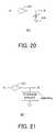
- FIG. 20is a circuit diagram illustrating a fourth example of a delay circuit 32 ′′′.
- the delay circuit 32 ′′′includes a variable capacitance 324 between the output terminal of the delay device 322 and the ground terminal. The larger the capacitance value of the variable capacitance 324 is, the longer the delay time is.
- FIG. 21is a figure illustrating the variable capacitance 324 of FIG. 17 in details.
- a capacitance-change-type non-volatile storage device 324 amay be used as the variable capacitance. Similar to FIG. 19 , the storage device 324 a has not only a function serving as the variable capacitance device but also a function serving as a memory for storing the weight coefficient.
- the delay circuit 32 as described aboveis an analog circuit, and therefore, an exactly desired delay time is not always attained.
- the neural network itselfis a fault tolerant system, and therefore this issue hardly causes any problem.
- each embodiment described abovean example for recognizing the numeral drawn in the image is shown.
- the purpose of each embodimentis not limited, and the image other than the numeral may be recognized.
- soundmay be recognized.
- the sensor 1may convert the sound into input data.
- the present inventionmay be applied to activity prediction of a chemical compound.
- the “recognition” in the description aboveis a concept including not only “recognition”, which is to find what the numeral is, but also “classification” and “prediction”. All the computation devices as shown in FIG. 2 are preferably of the configuration described in the embodiment, but may be of a configuration at least a portion of which is different.
Landscapes
- Engineering & Computer Science (AREA)
- Physics & Mathematics (AREA)
- Theoretical Computer Science (AREA)
- Health & Medical Sciences (AREA)
- Life Sciences & Earth Sciences (AREA)
- Biomedical Technology (AREA)
- Biophysics (AREA)
- Evolutionary Computation (AREA)
- Computational Linguistics (AREA)
- Data Mining & Analysis (AREA)
- Artificial Intelligence (AREA)
- General Health & Medical Sciences (AREA)
- Molecular Biology (AREA)
- Computing Systems (AREA)
- General Engineering & Computer Science (AREA)
- General Physics & Mathematics (AREA)
- Mathematical Physics (AREA)
- Software Systems (AREA)
- Neurology (AREA)
- Image Analysis (AREA)
Abstract
Description
M=Σwi*xi (1)
In this case, Σ indicates a summation where i is 1 to r.
T[k]=T[k−1]+wi*xi (2)
M=T[r]=T[0]+Σwi*xi (3)
Claims (20)
Applications Claiming Priority (2)
| Application Number | Priority Date | Filing Date | Title |
|---|---|---|---|
| JP2013-186626 | 2013-09-09 | ||
| JP2013186626AJP5885719B2 (en) | 2013-09-09 | 2013-09-09 | Identification device and arithmetic unit |
Publications (2)
| Publication Number | Publication Date |
|---|---|
| US20150074028A1 US20150074028A1 (en) | 2015-03-12 |
| US9361577B2true US9361577B2 (en) | 2016-06-07 |
Family
ID=52626536
Family Applications (1)
| Application Number | Title | Priority Date | Filing Date |
|---|---|---|---|
| US14/176,490Active2034-12-19US9361577B2 (en) | 2013-09-09 | 2014-02-10 | Processing device and computation device |
Country Status (2)
| Country | Link |
|---|---|
| US (1) | US9361577B2 (en) |
| JP (1) | JP5885719B2 (en) |
Cited By (16)
| Publication number | Priority date | Publication date | Assignee | Title |
|---|---|---|---|---|
| EP3306558A2 (en) | 2015-08-03 | 2018-04-11 | Angel Playing Cards Co., Ltd. | Substitute currency for gaming, inspection device, and manufacturing method of substitute currency for gaming, and management system for table games |
| US10032335B2 (en) | 2015-08-03 | 2018-07-24 | Angel Playing Cards Co., Ltd. | Fraud detection system in casino |
| US20180239984A1 (en)* | 2017-02-21 | 2018-08-23 | Angel Playing Cards Co., Ltd. | System for counting quantity of game tokens |
| EP3422307A1 (en) | 2017-06-28 | 2019-01-02 | Angel Playing Cards Co., Ltd. | Game management system |
| US10320372B2 (en) | 2017-05-23 | 2019-06-11 | Kabushiki Kaisha Toshiba | Information processing device, semiconductor device, and information processing method |
| EP3496058A1 (en) | 2017-12-05 | 2019-06-12 | Angel Playing Cards Co., Ltd. | Management system |
| US10727819B2 (en) | 2018-03-05 | 2020-07-28 | Kabushiki Kaisha Toshiba | Information processing device, semiconductor device, and information processing method |
| US10924090B2 (en) | 2018-07-20 | 2021-02-16 | Semiconductor Energy Laboratory Co., Ltd. | Semiconductor device comprising holding units |
| US10957156B2 (en) | 2016-09-12 | 2021-03-23 | Angel Playing Cards Co., Ltd. | Chip measurement system |
| US10970962B2 (en) | 2015-08-03 | 2021-04-06 | Angel Playing Cards Co., Ltd. | Management system of substitute currency for gaming |
| US11074780B2 (en) | 2015-08-03 | 2021-07-27 | Angel Playing Cards Co., Ltd. | Management system of substitute currency for gaming |
| US11424737B2 (en) | 2018-06-15 | 2022-08-23 | Semiconductor Energy Laboratory Co., Ltd. | Semiconductor device and electronic device |
| US11515873B2 (en) | 2018-06-29 | 2022-11-29 | Semiconductor Energy Laboratory Co., Ltd. | Semiconductor device and electronic device |
| EP4220590A1 (en) | 2022-02-01 | 2023-08-02 | Angel Group Co., Ltd. | Management system |
| US11798362B2 (en) | 2016-02-01 | 2023-10-24 | Angel Group Co., Ltd. | Chip measurement system |
| US11915116B2 (en) | 2016-06-20 | 2024-02-27 | Kioxia Corporation | Arithmetic apparatus for a neural network |
Families Citing this family (13)
| Publication number | Priority date | Publication date | Assignee | Title |
|---|---|---|---|---|
| CN114404925A (en)* | 2015-08-03 | 2022-04-29 | 天使集团股份有限公司 | Management system for table game, medal, inspection device, and management system for medal |
| MY189969A (en)* | 2015-11-19 | 2022-03-22 | Angel Playing Cards Co Ltd | Table game management system, game token, and inspection apparatus |
| JP6551715B2 (en) | 2016-03-14 | 2019-07-31 | オムロン株式会社 | Expandable device |
| JP6602279B2 (en)* | 2016-09-20 | 2019-11-06 | 株式会社東芝 | Mem capacitor, neuro element and neural network device |
| WO2018168537A1 (en) | 2017-03-14 | 2018-09-20 | Omron Corporation | Learning target apparatus and operating method |
| WO2018168536A1 (en) | 2017-03-14 | 2018-09-20 | Omron Corporation | Learning apparatus and learning method |
| JP6695595B2 (en)* | 2017-08-30 | 2020-05-20 | 株式会社アクセル | Inference device and inference method |
| US20190251430A1 (en)* | 2018-02-13 | 2019-08-15 | International Business Machines Corporation | Mixed signal cmos rpu with digital weight storage |
| JP6926037B2 (en) | 2018-07-26 | 2021-08-25 | 株式会社東芝 | Synaptic circuits, arithmetic units and neural network devices |
| US11573792B2 (en) | 2019-09-03 | 2023-02-07 | Samsung Electronics Co., Ltd. | Method and computing device with a multiplier-accumulator circuit |
| KR102861762B1 (en) | 2020-05-22 | 2025-09-17 | 삼성전자주식회사 | Apparatus for performing in memory processing and computing apparatus having the same |
| US11095427B1 (en)* | 2020-09-25 | 2021-08-17 | Intel Corporation | Transceiver with inseparable modulator demodulator circuits |
| GB2620785B (en)* | 2022-07-21 | 2024-08-07 | Advanced Risc Mach Ltd | Improved spiking neural network apparatus |
Citations (8)
| Publication number | Priority date | Publication date | Assignee | Title |
|---|---|---|---|---|
| JPH09212477A (en) | 1995-11-27 | 1997-08-15 | Canon Inc | Digital image processor |
| JP2004252943A (en) | 2002-12-26 | 2004-09-09 | Kazuhiro Matsue | Pattern teaching system, pattern identification device using the same, computer program, and digital logic circuit design method for pattern identification device |
| US20060294034A1 (en) | 2005-06-24 | 2006-12-28 | Elpida Memory, Inc. | Artificial neural network |
| US20110004579A1 (en) | 2008-03-14 | 2011-01-06 | Greg Snider | Neuromorphic Circuit |
| JP5155843B2 (en) | 2008-12-22 | 2013-03-06 | シャープ株式会社 | Information processing apparatus and neural network circuit using the same |
| JP2013160418A (en) | 2012-02-03 | 2013-08-19 | Hamamatsu Heat Tec Kk | Rapid heat treatment device |
| US20130254632A1 (en) | 2012-03-22 | 2013-09-26 | Kabushiki Kaisha Toshiba | Transmission system, decoding device, memory controller, and memory system |
| US20150035690A1 (en) | 2013-08-01 | 2015-02-05 | Kabushiki Kaisha Toshiba | Delay circuit and digital to time converter |
Family Cites Families (1)
| Publication number | Priority date | Publication date | Assignee | Title |
|---|---|---|---|---|
| JP4248187B2 (en)* | 2002-03-27 | 2009-04-02 | シャープ株式会社 | Integrated circuit device and neuro element |
- 2013
- 2013-09-09JPJP2013186626Apatent/JP5885719B2/enactiveActive
- 2014
- 2014-02-10USUS14/176,490patent/US9361577B2/enactiveActive
Patent Citations (15)
| Publication number | Priority date | Publication date | Assignee | Title |
|---|---|---|---|---|
| JPH09212477A (en) | 1995-11-27 | 1997-08-15 | Canon Inc | Digital image processor |
| US6148101A (en) | 1995-11-27 | 2000-11-14 | Canon Kabushiki Kaisha | Digital image processor |
| JP2004252943A (en) | 2002-12-26 | 2004-09-09 | Kazuhiro Matsue | Pattern teaching system, pattern identification device using the same, computer program, and digital logic circuit design method for pattern identification device |
| US20060294034A1 (en) | 2005-06-24 | 2006-12-28 | Elpida Memory, Inc. | Artificial neural network |
| JP2007004514A (en) | 2005-06-24 | 2007-01-11 | Elpida Memory Inc | Artificial neural circuit |
| US7548894B2 (en) | 2005-06-24 | 2009-06-16 | Elpida Memory, Inc. | Artificial neural network |
| US20110004579A1 (en) | 2008-03-14 | 2011-01-06 | Greg Snider | Neuromorphic Circuit |
| JP5154666B2 (en) | 2008-03-14 | 2013-02-27 | ヒューレット−パッカード デベロップメント カンパニー エル.ピー. | Neuromorphic circuit |
| JP5155843B2 (en) | 2008-12-22 | 2013-03-06 | シャープ株式会社 | Information processing apparatus and neural network circuit using the same |
| JP2013160418A (en) | 2012-02-03 | 2013-08-19 | Hamamatsu Heat Tec Kk | Rapid heat treatment device |
| US20130254632A1 (en) | 2012-03-22 | 2013-09-26 | Kabushiki Kaisha Toshiba | Transmission system, decoding device, memory controller, and memory system |
| JP2013198052A (en) | 2012-03-22 | 2013-09-30 | Toshiba Corp | Transmission system, decoding device, memory controller and memory system |
| US20150035690A1 (en) | 2013-08-01 | 2015-02-05 | Kabushiki Kaisha Toshiba | Delay circuit and digital to time converter |
| JP2015032950A (en) | 2013-08-01 | 2015-02-16 | 株式会社東芝 | Delay circuit and digital time converter |
| US8988262B2 (en) | 2013-08-01 | 2015-03-24 | Kabushiki Kaisha Toshiba | Delay circuit and digital to time converter |
Cited By (117)
| Publication number | Priority date | Publication date | Assignee | Title |
|---|---|---|---|---|
| US11527130B2 (en) | 2015-08-03 | 2022-12-13 | Angel Group Co., Ltd. | Fraud detection system in a casino |
| EP4123565A1 (en) | 2015-08-03 | 2023-01-25 | Angel Playing Cards Co., Ltd. | Fraud detection system at game parlor |
| EP3329975A1 (en) | 2015-08-03 | 2018-06-06 | Angel Playing Cards Co., Ltd. | Inspection device for inspecting substitute currency for gaming |
| US10032335B2 (en) | 2015-08-03 | 2018-07-24 | Angel Playing Cards Co., Ltd. | Fraud detection system in casino |
| US12412452B2 (en) | 2015-08-03 | 2025-09-09 | Angel Group Co., Ltd. | Fraud detection system in a casino |
| US12400517B2 (en) | 2015-08-03 | 2025-08-26 | Angel Group Co., Ltd. | Fraud detection system in a casino |
| US20180350193A1 (en) | 2015-08-03 | 2018-12-06 | Angel Playing Cards Co., Ltd. | Fraud detection system in a casino |
| US12394277B2 (en) | 2015-08-03 | 2025-08-19 | Angel Group Co., Ltd. | Fraud detection system in a casino |
| US12387564B2 (en) | 2015-08-03 | 2025-08-12 | Angel Group Co., Ltd. | Fraud detection system in a casino |
| US12387561B2 (en) | 2015-08-03 | 2025-08-12 | Angel Group Co., Ltd. | Fraud detection system in a casino |
| US12387563B2 (en) | 2015-08-03 | 2025-08-12 | Angel Group Co., Ltd. | Fraud detection system in a casino |
| US10529183B2 (en) | 2015-08-03 | 2020-01-07 | Angel Playing Cards Co., Ltd. | Fraud detection system in a casino |
| US10540846B2 (en) | 2015-08-03 | 2020-01-21 | Angel Playing Cards Co., Ltd. | Fraud detection system in a casino |
| US10593154B2 (en) | 2015-08-03 | 2020-03-17 | Angel Playing Cards Co., Ltd. | Fraud detection system in a casino |
| US10600282B2 (en) | 2015-08-03 | 2020-03-24 | Angel Playing Cards Co., Ltd. | Fraud detection system in a casino |
| EP4589522A2 (en) | 2015-08-03 | 2025-07-23 | Angel Playing Cards Co., Ltd. | Fraud detection system at game parlor |
| US10741019B2 (en) | 2015-08-03 | 2020-08-11 | Angel Playing Cards Co., Ltd. | Fraud detection system in a casino |
| EP3693919A1 (en) | 2015-08-03 | 2020-08-12 | Angel Playing Cards Co., Ltd. | Management system for substitute currency for gaming |
| US10748378B2 (en) | 2015-08-03 | 2020-08-18 | Angel Playing Cards Co., Ltd. | Fraud detection system in a casino |
| US10755524B2 (en) | 2015-08-03 | 2020-08-25 | Angel Playing Cards Co., Ltd. | Fraud detection system in a casino |
| EP4123566A1 (en) | 2015-08-03 | 2023-01-25 | Angel Playing Cards Co., Ltd. | Fraud detection system at game parlor |
| US10846986B2 (en) | 2015-08-03 | 2020-11-24 | Angel Playing Cards Co., Ltd. | Fraud detection system in a casino |
| US10846987B2 (en) | 2015-08-03 | 2020-11-24 | Angel Playing Cards Co., Ltd. | Fraud detection system in a casino |
| US10846985B2 (en) | 2015-08-03 | 2020-11-24 | Angel Playing Cards Co., Ltd. | Fraud detection system in a casino |
| US10896575B2 (en) | 2015-08-03 | 2021-01-19 | Angel Playing Cards Co., Ltd. | Fraud detection system in a casino |
| US12354438B2 (en) | 2015-08-03 | 2025-07-08 | Angel Group Co., Ltd. | Management system of substitute currency for gaming |
| US10930112B2 (en) | 2015-08-03 | 2021-02-23 | Angel Playing Cards Co., Ltd. | Fraud detection system in casino |
| US12198498B2 (en) | 2015-08-03 | 2025-01-14 | Angel Group Co., Ltd. | Fraud detection system in casino |
| US10970962B2 (en) | 2015-08-03 | 2021-04-06 | Angel Playing Cards Co., Ltd. | Management system of substitute currency for gaming |
| EP4563204A2 (en) | 2015-08-03 | 2025-06-04 | Angel Playing Cards Co., Ltd. | Substitute currency for gaming, inspection device, and manufacturing method of substitute currency for gaming, and management system for table games |
| US12322247B2 (en) | 2015-08-03 | 2025-06-03 | Angel Group Co., Ltd. | Management system of substitute currency for gaming |
| US11037401B2 (en) | 2015-08-03 | 2021-06-15 | Angel Playing Cards Co., Ltd. | Fraud detection system in a casino |
| US11074780B2 (en) | 2015-08-03 | 2021-07-27 | Angel Playing Cards Co., Ltd. | Management system of substitute currency for gaming |
| US11232674B2 (en) | 2015-08-03 | 2022-01-25 | Angel Group Co., Ltd. | Inspection device for detecting fraud |
| US12293632B2 (en) | 2015-08-03 | 2025-05-06 | Angel Group Co., Ltd. | Fraud detection system in a casino |
| US11270554B2 (en) | 2015-08-03 | 2022-03-08 | Angel Group Co., Ltd. | Substitute currency for gaming, inspection device, and manufacturing method of substitute currency for gaming, and management system for table games |
| US11380161B2 (en) | 2015-08-03 | 2022-07-05 | Angel Group Co., Ltd. | Fraud detection system in a casino |
| US11386749B2 (en) | 2015-08-03 | 2022-07-12 | Angel Group Co., Ltd. | Fraud detection system in a casino |
| US11386748B2 (en) | 2015-08-03 | 2022-07-12 | Angel Playing Cards Co., Ltd. | Fraud detection system in a casino |
| US11393286B2 (en) | 2015-08-03 | 2022-07-19 | Angel Group Co., Ltd. | Fraud detection system in a casino |
| US11393284B2 (en) | 2015-08-03 | 2022-07-19 | Angel Group Co., Ltd. | Fraud detection system in a casino |
| US11393285B2 (en) | 2015-08-03 | 2022-07-19 | Angel Group Co., Ltd. | Fraud detection system in a casino |
| US12293634B2 (en) | 2015-08-03 | 2025-05-06 | Angel Group Co., Ltd. | Fraud detection system in a casino |
| EP4465232A2 (en) | 2015-08-03 | 2024-11-20 | Angel Playing Cards Co., Ltd. | Fraud detection system at game parlor |
| EP4542482A2 (en) | 2015-08-03 | 2025-04-23 | Angel Playing Cards Co., Ltd. | Fraud detection system at game parlor |
| US11527131B2 (en) | 2015-08-03 | 2022-12-13 | Angel Group Co., Ltd. | Fraud detection system in a casino |
| EP3327657A1 (en) | 2015-08-03 | 2018-05-30 | Angel Playing Cards Co., Ltd. | Management system of substitute currency for gaming |
| US12198499B2 (en) | 2015-08-03 | 2025-01-14 | Angel Group Co., Ltd. | Fraud detection system in a casino |
| US10762745B2 (en) | 2015-08-03 | 2020-09-01 | Angel Playing Cards Co., Ltd. | Fraud detection system in a casino |
| EP4123564A1 (en) | 2015-08-03 | 2023-01-25 | Angel Playing Cards Co., Ltd. | Fraud detection system at game parlor |
| US11587398B2 (en) | 2015-08-03 | 2023-02-21 | Angel Group Co., Ltd. | Fraud detection system in a casino |
| US11620872B2 (en) | 2015-08-03 | 2023-04-04 | Angel Group Co., Ltd. | Fraud detection system in a casino |
| EP4167176A1 (en) | 2015-08-03 | 2023-04-19 | Angel Playing Cards Co., Ltd. | Fraud detection system at game parlor |
| EP4169592A1 (en) | 2015-08-03 | 2023-04-26 | Angel Playing Cards Co., Ltd. | Fraud detection system at game parlor |
| EP4181051A1 (en) | 2015-08-03 | 2023-05-17 | Angel Playing Cards Co., Ltd. | Fraud detection system at game parlor |
| US11657673B2 (en) | 2015-08-03 | 2023-05-23 | Angel Group Co., Ltd. | Fraud detection system in a casino |
| US11657674B2 (en) | 2015-08-03 | 2023-05-23 | Angel Group Go., Ltd. | Fraud detection system in casino |
| EP3306558A2 (en) | 2015-08-03 | 2018-04-11 | Angel Playing Cards Co., Ltd. | Substitute currency for gaming, inspection device, and manufacturing method of substitute currency for gaming, and management system for table games |
| US12283156B2 (en) | 2015-08-03 | 2025-04-22 | Angel Group Co., Ltd. | Management system of substitute currency for gaming |
| EP4220536A1 (en) | 2015-08-03 | 2023-08-02 | Angel Playing Cards Co., Ltd. | Fraud detection system at game parlor |
| EP4535276A2 (en) | 2015-08-03 | 2025-04-09 | Angel Playing Cards Co., Ltd. | Fraud detection system at game parlor |
| US11727750B2 (en) | 2015-08-03 | 2023-08-15 | Angel Group Co., Ltd. | Fraud detection system in a casino |
| US11741780B2 (en) | 2015-08-03 | 2023-08-29 | Angel Group Co., Ltd. | Fraud detection system in a casino |
| EP4235559A2 (en) | 2015-08-03 | 2023-08-30 | Angel Playing Cards Co., Ltd. | Fraud detection system at game parlor |
| EP4235558A2 (en) | 2015-08-03 | 2023-08-30 | Angel Playing Cards Co., Ltd. | Fraud detection system at game parlor |
| EP4234053A2 (en) | 2015-08-03 | 2023-08-30 | Angel Playing Cards Co., Ltd. | Management system of substitute currency for gaming |
| EP4465233A2 (en) | 2015-08-03 | 2024-11-20 | Angel Playing Cards Co., Ltd. | Fraud detection system at game parlor |
| US11810426B2 (en) | 2015-08-03 | 2023-11-07 | Angel Group Co., Ltd. | Management system of substitute currency for gaming |
| US11810422B2 (en) | 2015-08-03 | 2023-11-07 | Angel Group Co., Ltd. | Management system of substitute currency for gaming |
| US11816957B2 (en) | 2015-08-03 | 2023-11-14 | Angel Group Co., Ltd. | Management system of substitute currency for gaming |
| US12266237B2 (en) | 2015-08-03 | 2025-04-01 | Angel Group Co., Ltd. | Fraud detection system in a casino |
| EP4517641A2 (en) | 2015-08-03 | 2025-03-05 | Angel Playing Cards Co., Ltd. | Fraud detection system at game parlor |
| US12198497B2 (en) | 2015-08-03 | 2025-01-14 | Angel Group Co., Ltd. | Fraud detection system in casino |
| EP4428798A2 (en) | 2015-08-03 | 2024-09-11 | Angel Playing Cards Co., Ltd. | Fraud detection system at game parlor |
| EP4428800A2 (en) | 2015-08-03 | 2024-09-11 | Angel Playing Cards Co., Ltd. | Fraud detection system at game parlor |
| EP4428801A2 (en) | 2015-08-03 | 2024-09-11 | Angel Playing Cards Co., Ltd. | Fraud detection system at game parlor |
| EP4428799A2 (en) | 2015-08-03 | 2024-09-11 | Angel Playing Cards Co., Ltd. | Fraud detection system at game parlor |
| EP4428802A2 (en) | 2015-08-03 | 2024-09-11 | Angel Playing Cards Co., Ltd. | Fraud detection system at game parlor |
| US12094294B2 (en) | 2015-08-03 | 2024-09-17 | Angel Group Co., Ltd. | Fraud detection system in a casino |
| US12094292B2 (en) | 2015-08-03 | 2024-09-17 | Angel Group Co., Ltd. | Fraud detection system in a casino |
| US12094293B2 (en) | 2015-08-03 | 2024-09-17 | Angel Group Co., Ltd. | Fraud detection system in a casino |
| US12094297B2 (en) | 2015-08-03 | 2024-09-17 | Angel Group Co., Ltd. | Fraud detection system in a casino |
| US12094291B2 (en) | 2015-08-03 | 2024-09-17 | Angel Group Co., Ltd. | Fraud detection system in a casino |
| US12094296B2 (en) | 2015-08-03 | 2024-09-17 | Angel Group Co., Ltd. | Fraud detection system in a casino |
| US12094295B2 (en) | 2015-08-03 | 2024-09-17 | Angel Group Co., Ltd. | Fraud detection system in a casino |
| EP4432207A2 (en) | 2015-08-03 | 2024-09-18 | Angel Playing Cards Co., Ltd. | Fraud detection system at game parlor |
| EP4435708A2 (en) | 2015-08-03 | 2024-09-25 | Angel Playing Cards Co., Ltd. | Fraud detection system at game parlor |
| EP4435709A2 (en) | 2015-08-03 | 2024-09-25 | Angel Playing Cards Co., Ltd. | Fraud detection system at game parlor |
| EP4443375A2 (en) | 2015-08-03 | 2024-10-09 | Angel Playing Cards Co., Ltd. | Fraud detection system at game parlor |
| EP4451199A2 (en) | 2015-08-03 | 2024-10-23 | Angel Playing Cards Co., Ltd. | Fraud detection system at game parlor |
| US12142112B2 (en) | 2016-02-01 | 2024-11-12 | Angel Group Co., Ltd. | Chip measurement system |
| US11798362B2 (en) | 2016-02-01 | 2023-10-24 | Angel Group Co., Ltd. | Chip measurement system |
| US11915116B2 (en) | 2016-06-20 | 2024-02-27 | Kioxia Corporation | Arithmetic apparatus for a neural network |
| US11475733B2 (en) | 2016-09-12 | 2022-10-18 | Angel Group Co., Ltd. | Chip measurement system |
| US10957156B2 (en) | 2016-09-12 | 2021-03-23 | Angel Playing Cards Co., Ltd. | Chip measurement system |
| US11663803B2 (en) | 2017-02-21 | 2023-05-30 | Angel Group Co., Ltd. | System for counting quantity of game tokens |
| US20180239984A1 (en)* | 2017-02-21 | 2018-08-23 | Angel Playing Cards Co., Ltd. | System for counting quantity of game tokens |
| WO2018155497A1 (en)* | 2017-02-21 | 2018-08-30 | エンゼルプレイングカード株式会社 | System for counting number of game tokens |
| US12142107B2 (en) | 2017-02-21 | 2024-11-12 | Angel Group Co., Ltd. | System for counting quantity of game tokens |
| US10320372B2 (en) | 2017-05-23 | 2019-06-11 | Kabushiki Kaisha Toshiba | Information processing device, semiconductor device, and information processing method |
| EP3825969A1 (en) | 2017-06-28 | 2021-05-26 | Angel Playing Cards Co., Ltd. | Game management system |
| EP4629208A2 (en) | 2017-06-28 | 2025-10-08 | Angel Playing Cards Co., Ltd. | Game management system |
| EP4618055A2 (en) | 2017-06-28 | 2025-09-17 | Angel Playing Cards Co., Ltd. | Game management system |
| EP3422307A1 (en) | 2017-06-28 | 2019-01-02 | Angel Playing Cards Co., Ltd. | Game management system |
| US12327459B2 (en) | 2017-12-05 | 2025-06-10 | Angel Group Co., Ltd. | Management system |
| EP3806052A1 (en) | 2017-12-05 | 2021-04-14 | Angel Playing Cards Co., Ltd. | Management system |
| WO2019111593A1 (en) | 2017-12-05 | 2019-06-13 | エンゼルプレイングカード株式会社 | Management system |
| EP3496058A1 (en) | 2017-12-05 | 2019-06-12 | Angel Playing Cards Co., Ltd. | Management system |
| US10727819B2 (en) | 2018-03-05 | 2020-07-28 | Kabushiki Kaisha Toshiba | Information processing device, semiconductor device, and information processing method |
| US11424737B2 (en) | 2018-06-15 | 2022-08-23 | Semiconductor Energy Laboratory Co., Ltd. | Semiconductor device and electronic device |
| US11848664B2 (en) | 2018-06-15 | 2023-12-19 | Semiconductor Energy Laboratory Co., Ltd. | Semiconductor device and electronic device |
| US11515873B2 (en) | 2018-06-29 | 2022-11-29 | Semiconductor Energy Laboratory Co., Ltd. | Semiconductor device and electronic device |
| US11870436B2 (en) | 2018-06-29 | 2024-01-09 | Semiconductor Energy Laboratory Co., Ltd. | Semiconductor device and electronic device |
| US11264973B2 (en) | 2018-07-20 | 2022-03-01 | Semiconductor Energy Laboratory Co., Ltd. | Semiconductor device comprising a logic circuit and a holding unit |
| US10924090B2 (en) | 2018-07-20 | 2021-02-16 | Semiconductor Energy Laboratory Co., Ltd. | Semiconductor device comprising holding units |
| EP4220590A1 (en) | 2022-02-01 | 2023-08-02 | Angel Group Co., Ltd. | Management system |
| WO2023149437A1 (en) | 2022-02-01 | 2023-08-10 | エンゼルグループ株式会社 | Management system |
Also Published As
| Publication number | Publication date |
|---|---|
| JP2015053008A (en) | 2015-03-19 |
| US20150074028A1 (en) | 2015-03-12 |
| JP5885719B2 (en) | 2016-03-15 |
Similar Documents
| Publication | Publication Date | Title |
|---|---|---|
| US9361577B2 (en) | Processing device and computation device | |
| US11361216B2 (en) | Neural network circuits having non-volatile synapse arrays | |
| US11620505B2 (en) | Neuromorphic package devices and neuromorphic computing systems | |
| US9111222B2 (en) | Method and apparatus for switching the binary state of a location in memory in a probabilistic manner to store synaptic weights of a neural network | |
| US20190279079A1 (en) | Neuromorphic system with transposable memory and virtual look-up table | |
| CN111095300B (en) | Neural network operation circuit using semiconductor memory element | |
| US10783963B1 (en) | In-memory computation device with inter-page and intra-page data circuits | |
| US20220157384A1 (en) | Pulse-Width Modulated Multiplier | |
| WO2019147522A2 (en) | Neural network circuits having non-volatile synapse arrays | |
| US20230297839A1 (en) | Deep learning in bipartite memristive networks | |
| CN111919389B (en) | Electronic device for data compression and decompression and compression method thereof | |
| US11797833B2 (en) | Competitive machine learning accuracy on neuromorphic arrays with non-ideal non-volatile memory devices | |
| JPH03250244A (en) | information processing equipment | |
| US11494629B2 (en) | Charge-sharing compute-in-memory system | |
| US11455371B2 (en) | Computation circuit for performing vector-matrix multiplication and semiconductor device including the computation circuit | |
| US20190294957A1 (en) | Arithmetic device and arithmetic method | |
| CN113055546B (en) | System and method for processing images | |
| US11977982B2 (en) | Training of oscillatory neural networks | |
| CN111639757B (en) | Simulation convolution neural network based on flexible material | |
| US11120864B2 (en) | Capacitive processing unit | |
| US11093823B2 (en) | Neuromorphic device including a synapse array with inverting circuits | |
| US20200151569A1 (en) | Warping sequence data for learning in neural networks | |
| US20200019377A1 (en) | Arithmetic device | |
| Oshio et al. | Preliminary evaluation for multi-domain spike coding on memcapacitive neuromorphic circuit |
Legal Events
| Date | Code | Title | Description |
|---|---|---|---|
| AS | Assignment | Owner name:KABUSHIKI KAISHA TOSHIBA, JAPAN Free format text:ASSIGNMENT OF ASSIGNORS INTEREST;ASSIGNOR:MIYASHITA, DAISUKE;REEL/FRAME:032183/0495 Effective date:20140116 | |
| STCF | Information on status: patent grant | Free format text:PATENTED CASE | |
| AS | Assignment | Owner name:TOSHIBA MEMORY CORPORATION, JAPAN Free format text:ASSIGNMENT OF ASSIGNORS INTEREST;ASSIGNOR:KABUSHIKI KAISHA TOSHIBA;REEL/FRAME:043709/0035 Effective date:20170706 | |
| MAFP | Maintenance fee payment | Free format text:PAYMENT OF MAINTENANCE FEE, 4TH YEAR, LARGE ENTITY (ORIGINAL EVENT CODE: M1551); ENTITY STATUS OF PATENT OWNER: LARGE ENTITY Year of fee payment:4 | |
| AS | Assignment | Owner name:K.K. PANGEA, JAPAN Free format text:MERGER;ASSIGNOR:TOSHIBA MEMORY CORPORATION;REEL/FRAME:055659/0471 Effective date:20180801 Owner name:KIOXIA CORPORATION, JAPAN Free format text:CHANGE OF NAME AND ADDRESS;ASSIGNOR:TOSHIBA MEMORY CORPORATION;REEL/FRAME:055669/0001 Effective date:20191001 Owner name:TOSHIBA MEMORY CORPORATION, JAPAN Free format text:CHANGE OF NAME AND ADDRESS;ASSIGNOR:K.K. PANGEA;REEL/FRAME:055669/0401 Effective date:20180801 | |
| MAFP | Maintenance fee payment | Free format text:PAYMENT OF MAINTENANCE FEE, 8TH YEAR, LARGE ENTITY (ORIGINAL EVENT CODE: M1552); ENTITY STATUS OF PATENT OWNER: LARGE ENTITY Year of fee payment:8 |