US9360968B2 - Cursor control device and method of operation - Google Patents
Cursor control device and method of operationDownload PDFInfo
- Publication number
- US9360968B2 US9360968B2US12/036,090US3609008AUS9360968B2US 9360968 B2US9360968 B2US 9360968B2US 3609008 AUS3609008 AUS 3609008AUS 9360968 B2US9360968 B2US 9360968B2
- Authority
- US
- United States
- Prior art keywords
- sensing elements
- capacitance
- sensing
- actuator
- capacitors
- Prior art date
- Legal status (The legal status is an assumption and is not a legal conclusion. Google has not performed a legal analysis and makes no representation as to the accuracy of the status listed.)
- Active, expires
Links
Images


Classifications
- G—PHYSICS
- G06—COMPUTING OR CALCULATING; COUNTING
- G06F—ELECTRIC DIGITAL DATA PROCESSING
- G06F3/00—Input arrangements for transferring data to be processed into a form capable of being handled by the computer; Output arrangements for transferring data from processing unit to output unit, e.g. interface arrangements
- G06F3/01—Input arrangements or combined input and output arrangements for interaction between user and computer
- G06F3/03—Arrangements for converting the position or the displacement of a member into a coded form
- G06F3/041—Digitisers, e.g. for touch screens or touch pads, characterised by the transducing means
- G06F3/044—Digitisers, e.g. for touch screens or touch pads, characterised by the transducing means by capacitive means
- G—PHYSICS
- G06—COMPUTING OR CALCULATING; COUNTING
- G06F—ELECTRIC DIGITAL DATA PROCESSING
- G06F3/00—Input arrangements for transferring data to be processed into a form capable of being handled by the computer; Output arrangements for transferring data from processing unit to output unit, e.g. interface arrangements
- G06F3/01—Input arrangements or combined input and output arrangements for interaction between user and computer
- G06F3/02—Input arrangements using manually operated switches, e.g. using keyboards or dials
- G06F3/0202—Constructional details or processes of manufacture of the input device
- G—PHYSICS
- G06—COMPUTING OR CALCULATING; COUNTING
- G06F—ELECTRIC DIGITAL DATA PROCESSING
- G06F3/00—Input arrangements for transferring data to be processed into a form capable of being handled by the computer; Output arrangements for transferring data from processing unit to output unit, e.g. interface arrangements
- G06F3/01—Input arrangements or combined input and output arrangements for interaction between user and computer
- G06F3/03—Arrangements for converting the position or the displacement of a member into a coded form
- G06F3/041—Digitisers, e.g. for touch screens or touch pads, characterised by the transducing means
- G06F3/044—Digitisers, e.g. for touch screens or touch pads, characterised by the transducing means by capacitive means
- G06F3/0445—Digitisers, e.g. for touch screens or touch pads, characterised by the transducing means by capacitive means using two or more layers of sensing electrodes, e.g. using two layers of electrodes separated by a dielectric layer
- H—ELECTRICITY
- H03—ELECTRONIC CIRCUITRY
- H03K—PULSE TECHNIQUE
- H03K17/00—Electronic switching or gating, i.e. not by contact-making and –breaking
- H03K17/94—Electronic switching or gating, i.e. not by contact-making and –breaking characterised by the way in which the control signals are generated
- H03K17/96—Touch switches
- H03K17/962—Capacitive touch switches
- H03K17/9622—Capacitive touch switches using a plurality of detectors, e.g. keyboard
- H—ELECTRICITY
- H03—ELECTRONIC CIRCUITRY
- H03K—PULSE TECHNIQUE
- H03K17/00—Electronic switching or gating, i.e. not by contact-making and –breaking
- H03K17/94—Electronic switching or gating, i.e. not by contact-making and –breaking characterised by the way in which the control signals are generated
- H03K17/965—Switches controlled by moving an element forming part of the switch
- H03K17/975—Switches controlled by moving an element forming part of the switch using a capacitive movable element
- H03K17/98—Switches controlled by moving an element forming part of the switch using a capacitive movable element having a plurality of control members, e.g. keyboard
- H—ELECTRICITY
- H03—ELECTRONIC CIRCUITRY
- H03K—PULSE TECHNIQUE
- H03K2217/00—Indexing scheme related to electronic switching or gating, i.e. not by contact-making or -breaking covered by H03K17/00
- H03K2217/94—Indexing scheme related to electronic switching or gating, i.e. not by contact-making or -breaking covered by H03K17/00 characterised by the way in which the control signal is generated
- H03K2217/96—Touch switches
- H03K2217/9607—Capacitive touch switches
- H03K2217/960755—Constructional details of capacitive touch and proximity switches
Definitions
- This inventionrelates generally to a control device, and more specifically, to a cursor control device and method.
- a remote control or game controllercan include one or more control assemblies.
- the control assembliesinclude actuators and circuitry to convert a mechanical movement applied to the actuator by a user into an electrical signal.
- Directional padsare one example of control assemblies found on nearly all modern game controllers. D-pads typically comprise a substantially circular control surface, pivoted in the center and coupled to four buttons or switches associated with corresponding four primary directions.
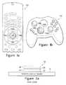
- FIGS. 1 a and 1 billustrate a D-pad 100 used in a remote control 102 and a game controller 104 , respectively.
- the D-pad 100includes four buttons 106 a - d and 108 a - d associated with corresponding Up, Down, Right, and Left primary directions.
- the compass pointsare merely used here as a convenience to define the directions and do not refer to actual compass points or cardinal directions.
- Depressing the button 106 a in the Up or N directioncloses the underlying switch generating a corresponding electronic signal provided to the D-pad's circuitry (not shown).
- depressing button 106 b in the Down or S directioncloses the underlying switch generating a corresponding electronic signal and providing it to the D-pad's circuitry (not shown).
- Simultaneously depressing both button 106 a in the Up and N direction and button 106 b in the Left or W directioncloses both underlying switches, generating a corresponding electronic signal.
- the D-padcan sense movement in four primary directions (Up or N, Down or S, Right or E, and Left or W) and in four secondary directions (NE, NW, SE, and SW).
- the D-padcan sense movement in the four secondary directions when a user depresses two buttons. For example, the D-pad would determine movement in the NW direction when a user depresses both the Up or N and Left or W buttons.
- D-pads 100are relatively inexpensive to manufacture but typically lack angular resolution better than 45 degrees. And D-pads 100 do not measure the depression force with which the user presses the buttons 106 a - d and 108 a - d . If the D-pad 100 could measure the depression force, this could be used to control the rate of a cursor's movement.
- FSRforce sensing resistor
- FIGS. 1 a and 1 billustrate a remote control and a game controller, respectively.
- FIG. 2 aillustrates a side view of an embodiment of a cursor control device.
- FIG. 2 billustrates a top view of sensing element traces for the cursor control device shown in FIG. 2 a.
- FIG. 3illustrates the directions used to identify the sensing elements of FIGS. 2 a and 2 b.
- FIG. 4illustrates an embodiment of a capacitance sensing circuit connected to the plurality of sensing elements shown in FIGS. 2 a and 2 b.
- FIG. 5illustrates an embodiment of a 3-plate capacitor for the cursor control device of FIG. 2 a.
- FIG. 6illustrates an embodiment of an actuator of FIG. 2 a , with a pivot attached.
- FIG. 7illustrates another embodiment of the actuator.
- FIG. 8illustrates a side view of an embodiment of a cursor control device.
- FIG. 2 aillustrates a side view of an embodiment of a cursor control device 20 .
- FIG. 2 billustrates a top view of sensing element traces for the cursor control device shown in FIG. 2 a.
- the cursor control device 20includes a printed circuit board (PCB) 21 with a plurality of sensing elements 22 .
- the plurality of sensing elements 22are arranged in a ring or circular manner as shown in FIG. 2 b .
- Each of the plurality of sensing elementscan be traces on the PCB 21 .
- a non-conductive compressive layer 24stacks or overlays on the plurality of sensing elements 22 . Any suitable non-conductive or dielectric compressive material can make up the compressive layer 24 , e.g., rubber or high-density foam.
- a conductive layer 28stacks over the compressive layer 24 . Any suitable conductive material can make up the conductive layer 28 including copper foil.
- An actuator 26stacks on the conductive layer 28 .
- a userapplies a force to the actuator 26 that, in turn, compresses the compressive layer 24 through the conductive layer 28 changing the distance and hence, the capacitance between the conductive layer 28 and one or more of the plurality of 20 sensing elements 22 .
- the conductive layer 28may be a PCB trace and the actuator 26 may be a PCB substrate.
- the device 20can include multiple actuators 26 stacked on top of each other.
- the conductive layer 28may be a printed conductive ink (such as silver or carbon-impregnated ink) applied to the underside of actuator 26 .
- the conductive layer 28may be a single 25 conductor covering all of the plurality of elements 22 ; in another implementation, the conductive layer 28 may be segmented similarly to the plurality of elements 22 , or in such a way that a single segment overlaps two or more of the elements 22 .
- the plurality of sensing elements 22could include any number of elements with three elements being a minimum for full 360 degrees sensing.
- the devicecan include less than three elements 22 if the angle to be sensed is less than a full 360 degrees.
- the plurality of sensing elements 22may include eight elements arranged in a circular or ring manner as shown in FIG. 2 b .
- FIG. 3illustrates the directions used to identify the sensing elements of FIGS. 2 a and 2 b .
- Each of the plurality of elements 22can associate with corresponding directions including North-North-East (NNE) 212 , North-North-West (NNW) 210 , East-North-East (ENE) 214 , West-North-West (WNW) 216 , East-South-East (ESE) 218 , West-South-West (WSW) 220 , South-South-East (SSE) 222 , and South-South-West (SSW) 224 , as shown in FIGS. 2 b and 3 .
- NNENorth-North-West
- NWNorth-North-West
- ENEEast-North-East
- WNWEast-North-West
- ESEEast-South-East
- WSWWest-South-West
- SSESouth-South-West
- SSWSouth-South-West
- the cursor control device 20calculates a measure of either direction or magnitude of a force applied by a user to the actuator 26 using a difference in capacitance.
- the difference in capacitanceis a reflection of a distance change between a first set of conductive plates or layers (e.g., conductive layer 28 ) and a second plate or set of plates (e.g., the plurality of segments 22 ).
- each sensing elementforms a capacitor with the conductive layer 28 , the compressive layer 24 serving as a dielectric.
- the conductive layer 28can connect to ground, or may be unconnected to any electrical voltage in the system.
- the capacitance between each of the sensing elements 22 and the conductive layer 28is relatively small but may be useful to calibrate the cursor control device 20 .
- the actuator 26When the user (not shown) applies a force to depress the actuator 26 , the actuator 26 is active. The force will compress the compressive layer 24 , changing the vertical distance between the conductive layer 24 and one or more of the sensing elements 22 located in the direction of the force. The change in vertical distance, in turn, increases the capacitance to ground for the capacitor formed between the conductive layer 28 and the one or more sensing elements 22 aligned along the direction of the force.
- the device 20therefore, can determine the direction of the force on the actuator 26 by measuring the capacitance change of the one or more capacitors formed by corresponding one or more of the plurality of segments 22 responsive to the user's application of force to the actuator 26 .
- the device 20can generate a signal indicating a desired movement direction for a cursor (not shown) on a display (not shown) by measuring or sensing a capacitance change that lies along the direction of the force applied by the user on the actuator 26 .
- This directionmay be calculated by interpolating between the detected capacitance of two or more of the segments 22 in the 210 - 224 directions and ground.
- the device 20can measure the increase in capacitance in the NNW and NNE sensing elements 22 . If the device 20 measures the change in capacitance as equal in both NNW and NNE directions, the device 20 will determine that the user applied the force in the N direction (between the NNW and NNE directions). Similarly, if the device 20 measures the change in capacitances as greater in the NNW sensing element, the device 20 will determine the user applied the force in a direction closer to NNW than NNE, the precise angle being calculated in a manner derived from the ratio of the two capacitances.
- the device 20can measure the magnitude of the force applied to the actuator 26 to generate a signal indicating a desired rate of movement for the cursor on the display.
- the device 20can measure the magnitude of the force by summing the capacitance change for at least two of the plurality of sensing elements 22 .
- the device 20can determine the magnitude of the force by calculating a difference between a sensing element 22 with a most capacitance change and a sensing element 22 with a least capacitance change.
- Another alternativeis for the device 20 to determine the magnitude of the force by determining a difference in capacitance for a sensing element having one of either a most capacitance change or a least capacitive change.
- the device 20determines the magnitude of the force by comparing the capacitance of the at least one capacitor to a capacitance of all other capacitors.
- a person of reasonable skill in the artcan envision other methods of calculating or otherwise determining the magnitude of the force on the actuator 26 .
- FIG. 4illustrates an embodiment of a capacitance sensing circuit connected to the plurality of sensing elements 22 shown in FIGS. 2 a and 2 b .
- a sensing circuit 62electrically couples to each of the plurality of sensing elements 22 .
- the sensing circuit 62can measure the capacitance change for each of the plurality of sensing elements 22 through terminals 60 a - h responsive to actuation (or activation) of the actuator 26 by application of a force.
- the sensing circuit 62can measure the capacitance between each of the sensing elements 22 and ground.
- sensing circuit 62may be implemented as a single sensing circuit coupled to an 8:1 multiplexor, or eight individual sensing circuits, or two sensing circuits each coupled to a 4:1 multiplexor, and the like.
- the sensing circuit 62can include an inexpensive microprocessor control unit (MCU) that is capable of accurately and reliably detecting very small changes in capacitance.
- the MCUcan be any one of the PSoC® mixed signal controllers manufactured by Cypress Semiconductor®.
- a processing element 64receives a numerical measure of the capacitance change associated with the sensing elements 22 from the sensing circuit 62 .
- the processing element 64calculates the direction of the force on the actuator 26 and generates a signal indicating a desired movement direction for the cursor on the display.
- the processing element 64calculates the magnitude of the force and generates a signal indicating a desired rate of movement for the cursor on the display.
- the processing element 64can transmit the signal indicating movement direction and transmit the signal indicating rate of movement of the cursor on the display to a computer via the interface 66 .
- the processing element 64continuously receives capacitance values from the sensing circuit 62 , and calculates the direction and magnitude of the force from these values.
- the processing element 64may periodically signal to the sensing circuit 62 to make a set of capacitance measurements. Between periodic measurements, the processing element 64 and the sensing circuit 62 may be in a low power mode to save power.
- the sensing circuit 62can make capacitance measurements continuously or at predetermined periods, e.g., every 8 ms.
- the processing element 64calculates a measure of the direction and magnitude of the force applied to the actuator 26 each time the sensing circuit 62 makes a capacitance measurement. In an embodiment, the processing element 64 provides the calculations to a downstream computer (not shown) via the interface 66 .
- the processing element 64can provide conventional cursor movement signals representing a pair of x and y direction values, to the downstream computer (not shown) via the interface 66 .
- a game software program(not shown) stored in the downstream computer uses the calculated direction and magnitude of the force applied to the actuator 26 or alternatively, the cursor signals, to move a cursor in a corresponding direction and at a corresponding rate or speed.
- FIG. 5illustrates an embodiment of a 3-plate capacitor for the cursor control device of FIG. 2 a .
- the 3-plate capacitorcan include a pair of adjacent sensing elements 22 and the conductive layer 28 shown in the cursor control device 20 of FIG. 2 a (plate 74 in FIG. 5 ).
- the pair of adjacent sensing elements 22are coupled to the sensing circuit 62 ( FIG. 4 ) via terminals 70 and 72 .
- the conductive layer 28floats, i.e., not electrically coupled to a potential, forming an array of 3-plate capacitors with the plurality of sensing elements 22 .
- the sensing circuit 62reads the capacitance of a selected sensing element 22 by applying a ground voltage to all of the elements 22 not user selected and measuring the capacitance to ground of the element that is user selected.
- FIG. 6illustrates an embodiment of an actuator of FIG. 2 a , with a pivot attached.
- the actuator 26can have a variety of shapes and sizes.
- the actuator 26includes a pivot 90 that allows the actuator 26 to rock in any number of directions.
- FIG. 7illustrates another embodiment of the actuator 26 .
- an enclosure 100encloses or surrounds portions of the device 20 .
- only a top portion of the actuator 26may be outside the enclosure 100 and accessible to the user.
- a compressive layer 24 aexists between the actuator 26 and the enclosure 100 .
- the compressive layer 24 aprovides resistance to movement of the actuator 26 and results in a larger force than an embodiment not including the compressive layer 24 a .
- a larger forcewill create a greater reduction in the distance between the conductive layer 28 and the plurality of segments 22 , resulting in a greater increase in capacitance.
- the compressive layer 24 or 24 aincludes springs. The springs, in turn, can be located between the actuator 26 and the enclosure 100 or, alternatively, between the actuator 26 and the conductive layer 28 .
- FIG. 8illustrates a side view of an embodiment of a cursor control device.
- an air gap 30replaces the compressive layer 24 shown in FIG. 2 a between the conductive layer 28 and the plurality of segments 22 .
- the air gap 30can be air as the name implies, or an appropriate fluid.
- the plurality of sensing elements 22may include more or fewer than the eight elements shown in the drawings depending on the application. Using more elements may result in a more accurate directional calculation, but at the cost of requiring more inputs to the capacitance sensing circuit 62 .
- cursor controlcan also be applied for other purposes, e.g., movement control or direction of view control in computer gaming, menu item selection in a display menu, camera field of view control, radio controlled model control, audio balance/fade control, and the like.
Landscapes
- Engineering & Computer Science (AREA)
- General Engineering & Computer Science (AREA)
- Theoretical Computer Science (AREA)
- Human Computer Interaction (AREA)
- Physics & Mathematics (AREA)
- General Physics & Mathematics (AREA)
- Position Input By Displaying (AREA)
Abstract
Description
Claims (18)
Priority Applications (1)
| Application Number | Priority Date | Filing Date | Title |
|---|---|---|---|
| US12/036,090US9360968B2 (en) | 2007-02-22 | 2008-02-22 | Cursor control device and method of operation |
Applications Claiming Priority (2)
| Application Number | Priority Date | Filing Date | Title |
|---|---|---|---|
| US89120707P | 2007-02-22 | 2007-02-22 | |
| US12/036,090US9360968B2 (en) | 2007-02-22 | 2008-02-22 | Cursor control device and method of operation |
Publications (2)
| Publication Number | Publication Date |
|---|---|
| US20080204409A1 US20080204409A1 (en) | 2008-08-28 |
| US9360968B2true US9360968B2 (en) | 2016-06-07 |
Family
ID=39710535
Family Applications (1)
| Application Number | Title | Priority Date | Filing Date |
|---|---|---|---|
| US12/036,090Active2032-10-31US9360968B2 (en) | 2007-02-22 | 2008-02-22 | Cursor control device and method of operation |
Country Status (2)
| Country | Link |
|---|---|
| US (1) | US9360968B2 (en) |
| WO (1) | WO2008103943A1 (en) |
Cited By (8)
| Publication number | Priority date | Publication date | Assignee | Title |
|---|---|---|---|---|
| US9886116B2 (en) | 2012-07-26 | 2018-02-06 | Apple Inc. | Gesture and touch input detection through force sensing |
| US9910494B2 (en) | 2012-05-09 | 2018-03-06 | Apple Inc. | Thresholds for determining feedback in computing devices |
| US9939901B2 (en) | 2014-09-30 | 2018-04-10 | Apple Inc. | Haptic feedback assembly |
| US10108265B2 (en) | 2012-05-09 | 2018-10-23 | Apple Inc. | Calibration of haptic feedback systems for input devices |
| US10162447B2 (en) | 2015-03-04 | 2018-12-25 | Apple Inc. | Detecting multiple simultaneous force inputs to an input device |
| US10297119B1 (en) | 2014-09-02 | 2019-05-21 | Apple Inc. | Feedback device in an electronic device |
| US10591368B2 (en) | 2014-01-13 | 2020-03-17 | Apple Inc. | Force sensor with strain relief |
| US10642361B2 (en) | 2012-06-12 | 2020-05-05 | Apple Inc. | Haptic electromagnetic actuator |
Families Citing this family (5)
| Publication number | Priority date | Publication date | Assignee | Title |
|---|---|---|---|---|
| EP2418777B1 (en)* | 2010-08-09 | 2013-12-25 | RAFI GmbH & Co. KG | Capacitative switch |
| DE102011089693A1 (en)* | 2011-12-22 | 2013-06-27 | Continental Automotive Gmbh | operating device |
| US9304587B2 (en)* | 2013-02-13 | 2016-04-05 | Apple Inc. | Force sensing mouse |
| CN106972780B (en)* | 2017-04-01 | 2021-02-09 | 广东易百珑智能科技有限公司 | Passive rebound switch capable of changing number of keys |
| US11295604B2 (en)* | 2019-09-26 | 2022-04-05 | Guangdong Ebelong Intelligent Technology Co., Ltd | Passive rebound switch having variable number of buttons |
Citations (15)
| Publication number | Priority date | Publication date | Assignee | Title |
|---|---|---|---|---|
| US2611051A (en) | 1951-10-04 | 1952-09-16 | Kolff Peter Van Santen | Rotary contactor device |
| US4347478A (en)* | 1979-07-17 | 1982-08-31 | Heerens Willem C | Capacitive gauge |
| US4584625A (en)* | 1984-09-11 | 1986-04-22 | Kellogg Nelson R | Capacitive tactile sensor |
| US4604584A (en) | 1985-06-10 | 1986-08-05 | Motorola, Inc. | Switched capacitor precision difference amplifier |
| US5949354A (en)* | 1997-05-10 | 1999-09-07 | Acer Peripherals, Inc. | Computer pointing device |
| US6067862A (en) | 1994-11-09 | 2000-05-30 | Amada Company, Ltd. | Fingerpad force sensing system |
| US6115030A (en)* | 1997-12-18 | 2000-09-05 | International Business Machines Corporation | Trackpoint device |
| US6442812B1 (en)* | 2000-03-02 | 2002-09-03 | Eaton Corporation | Method of manufacturing a piezoelectric torque sensor |
| US20020122025A1 (en)* | 1998-07-27 | 2002-09-05 | Katsutoshi Suzuki | Input device |
| US20040255697A1 (en)* | 1990-10-12 | 2004-12-23 | Kazuhiro Okada | Force detector and acceleration detector and method of manufacturing the same |
| US20050156881A1 (en)* | 2002-04-11 | 2005-07-21 | Synaptics, Inc. | Closed-loop sensor on a solid-state object position detector |
| US20050253643A1 (en) | 2002-10-30 | 2005-11-17 | Sony Corporation | Input device and process for manufacturing the same, portable electronic apparatus comprising input device |
| US20060169060A1 (en)* | 2003-04-28 | 2006-08-03 | Kazuhiro Okada | Force-detecting device |
| US20060267933A1 (en)* | 2005-05-25 | 2006-11-30 | Li Chong Tai | Eliminating mechanical spring with magnetic forces |
| US20070057167A1 (en)* | 2005-09-09 | 2007-03-15 | Mackey Bob L | Polar sensor patterns |
- 2008
- 2008-02-22USUS12/036,090patent/US9360968B2/enactiveActive
- 2008-02-22WOPCT/US2008/054781patent/WO2008103943A1/enactiveApplication Filing
Patent Citations (15)
| Publication number | Priority date | Publication date | Assignee | Title |
|---|---|---|---|---|
| US2611051A (en) | 1951-10-04 | 1952-09-16 | Kolff Peter Van Santen | Rotary contactor device |
| US4347478A (en)* | 1979-07-17 | 1982-08-31 | Heerens Willem C | Capacitive gauge |
| US4584625A (en)* | 1984-09-11 | 1986-04-22 | Kellogg Nelson R | Capacitive tactile sensor |
| US4604584A (en) | 1985-06-10 | 1986-08-05 | Motorola, Inc. | Switched capacitor precision difference amplifier |
| US20040255697A1 (en)* | 1990-10-12 | 2004-12-23 | Kazuhiro Okada | Force detector and acceleration detector and method of manufacturing the same |
| US6067862A (en) | 1994-11-09 | 2000-05-30 | Amada Company, Ltd. | Fingerpad force sensing system |
| US5949354A (en)* | 1997-05-10 | 1999-09-07 | Acer Peripherals, Inc. | Computer pointing device |
| US6115030A (en)* | 1997-12-18 | 2000-09-05 | International Business Machines Corporation | Trackpoint device |
| US20020122025A1 (en)* | 1998-07-27 | 2002-09-05 | Katsutoshi Suzuki | Input device |
| US6442812B1 (en)* | 2000-03-02 | 2002-09-03 | Eaton Corporation | Method of manufacturing a piezoelectric torque sensor |
| US20050156881A1 (en)* | 2002-04-11 | 2005-07-21 | Synaptics, Inc. | Closed-loop sensor on a solid-state object position detector |
| US20050253643A1 (en) | 2002-10-30 | 2005-11-17 | Sony Corporation | Input device and process for manufacturing the same, portable electronic apparatus comprising input device |
| US20060169060A1 (en)* | 2003-04-28 | 2006-08-03 | Kazuhiro Okada | Force-detecting device |
| US20060267933A1 (en)* | 2005-05-25 | 2006-11-30 | Li Chong Tai | Eliminating mechanical spring with magnetic forces |
| US20070057167A1 (en)* | 2005-09-09 | 2007-03-15 | Mackey Bob L | Polar sensor patterns |
Non-Patent Citations (2)
| Title |
|---|
| United States Patent and Trademark Office; PCT Search Report dated Jun. 27, 2008; 2 Pages. |
| Written Opinion of the International Searching Authority for International Application No. PCT/US2008/054781 mailed Jun. 27, 2008; 4 pages. |
Cited By (10)
| Publication number | Priority date | Publication date | Assignee | Title |
|---|---|---|---|---|
| US9910494B2 (en) | 2012-05-09 | 2018-03-06 | Apple Inc. | Thresholds for determining feedback in computing devices |
| US9977500B2 (en) | 2012-05-09 | 2018-05-22 | Apple Inc. | Thresholds for determining feedback in computing devices |
| US9977499B2 (en) | 2012-05-09 | 2018-05-22 | Apple Inc. | Thresholds for determining feedback in computing devices |
| US10108265B2 (en) | 2012-05-09 | 2018-10-23 | Apple Inc. | Calibration of haptic feedback systems for input devices |
| US10642361B2 (en) | 2012-06-12 | 2020-05-05 | Apple Inc. | Haptic electromagnetic actuator |
| US9886116B2 (en) | 2012-07-26 | 2018-02-06 | Apple Inc. | Gesture and touch input detection through force sensing |
| US10591368B2 (en) | 2014-01-13 | 2020-03-17 | Apple Inc. | Force sensor with strain relief |
| US10297119B1 (en) | 2014-09-02 | 2019-05-21 | Apple Inc. | Feedback device in an electronic device |
| US9939901B2 (en) | 2014-09-30 | 2018-04-10 | Apple Inc. | Haptic feedback assembly |
| US10162447B2 (en) | 2015-03-04 | 2018-12-25 | Apple Inc. | Detecting multiple simultaneous force inputs to an input device |
Also Published As
| Publication number | Publication date |
|---|---|
| WO2008103943A1 (en) | 2008-08-28 |
| US20080204409A1 (en) | 2008-08-28 |
Similar Documents
| Publication | Publication Date | Title |
|---|---|---|
| US9360968B2 (en) | Cursor control device and method of operation | |
| US11491392B2 (en) | Using finger presence to activate a motion control feature for a handheld controller | |
| US8884913B2 (en) | Systems and methods for determining the location and pressure of a touchload applied to a touchpad | |
| US6243077B1 (en) | Sensor and circuit architecture for three axis strain gauge pointing device and force transducer | |
| CN101226449B (en) | Capacitive sensing and absolute position mapping in displacement type pointing devices | |
| US9766742B2 (en) | Contact sensor | |
| US10395860B2 (en) | Strain gauge proportional push button | |
| US5541622A (en) | Miniature isometric joystick | |
| US5905485A (en) | Controller with tactile sensors and method of fabricating same | |
| US5510812A (en) | Piezoresistive input device | |
| US9182845B2 (en) | Sensor | |
| KR100979394B1 (en) | Touchpad for capacitive touch coordinate sensing | |
| EP0486617B1 (en) | Apparatus for data input | |
| US20070227256A1 (en) | Method and apparatus for sensing the force with which a button is pressed | |
| US7684953B2 (en) | Systems using variable resistance zones and stops for generating inputs to an electronic device | |
| WO1997040482A1 (en) | Touch and pressure sensing method and apparatus | |
| JP2018018159A (en) | Input device | |
| CN1985238A (en) | Control system and related control method | |
| WO2006002661A1 (en) | Keypad signal input apparatus | |
| US20170205914A1 (en) | Click-button-integrated contact position input apparatus | |
| US9235274B1 (en) | Low-profile or ultra-thin navigation pointing or haptic feedback device | |
| EP1487114B1 (en) | Keypad signal input apparatus |
Legal Events
| Date | Code | Title | Description |
|---|---|---|---|
| AS | Assignment | Owner name:CYPRESS SEMICONDUCTOR CORPORATION, CALIFORNIA Free format text:ASSIGNMENT OF ASSIGNORS INTEREST;ASSIGNOR:WRIGHT, DAVID;REEL/FRAME:020564/0130 Effective date:20080222 Owner name:CYPRESS SEMICONDUCTOR CORPORATION,CALIFORNIA Free format text:ASSIGNMENT OF ASSIGNORS INTEREST;ASSIGNOR:WRIGHT, DAVID;REEL/FRAME:020564/0130 Effective date:20080222 | |
| AS | Assignment | Owner name:MORGAN STANLEY SENIOR FUNDING, INC., NEW YORK Free format text:PATENT SECURITY AGREEMENT;ASSIGNOR:CYPRESS SEMICONDUCTOR CORPORATION;REEL/FRAME:028863/0870 Effective date:20120822 | |
| AS | Assignment | Owner name:MORGAN STANLEY SENIOR FUNDING, INC., NEW YORK Free format text:SECURITY INTEREST;ASSIGNORS:CYPRESS SEMICONDUCTOR CORPORATION;SPANSION LLC;REEL/FRAME:035240/0429 Effective date:20150312 | |
| STCF | Information on status: patent grant | Free format text:PATENTED CASE | |
| AS | Assignment | Owner name:MUFG UNION BANK, N.A., CALIFORNIA Free format text:ASSIGNMENT AND ASSUMPTION OF SECURITY INTEREST IN INTELLECTUAL PROPERTY;ASSIGNOR:MORGAN STANLEY SENIOR FUNDING, INC.;REEL/FRAME:050896/0366 Effective date:20190731 | |
| MAFP | Maintenance fee payment | Free format text:PAYMENT OF MAINTENANCE FEE, 4TH YEAR, LARGE ENTITY (ORIGINAL EVENT CODE: M1551); ENTITY STATUS OF PATENT OWNER: LARGE ENTITY Year of fee payment:4 | |
| AS | Assignment | Owner name:MORGAN STANLEY SENIOR FUNDING, INC., NEW YORK Free format text:CORRECTIVE ASSIGNMENT TO CORRECT THE 8647899 PREVIOUSLY RECORDED ON REEL 035240 FRAME 0429. ASSIGNOR(S) HEREBY CONFIRMS THE SECURITY INTERST;ASSIGNORS:CYPRESS SEMICONDUCTOR CORPORATION;SPANSION LLC;REEL/FRAME:058002/0470 Effective date:20150312 | |
| AS | Assignment | Owner name:SPANSION LLC, CALIFORNIA Free format text:RELEASE BY SECURED PARTY;ASSIGNOR:MUFG UNION BANK, N.A.;REEL/FRAME:059410/0438 Effective date:20200416 Owner name:CYPRESS SEMICONDUCTOR CORPORATION, CALIFORNIA Free format text:RELEASE BY SECURED PARTY;ASSIGNOR:MUFG UNION BANK, N.A.;REEL/FRAME:059410/0438 Effective date:20200416 | |
| MAFP | Maintenance fee payment | Free format text:PAYMENT OF MAINTENANCE FEE, 8TH YEAR, LARGE ENTITY (ORIGINAL EVENT CODE: M1552); ENTITY STATUS OF PATENT OWNER: LARGE ENTITY Year of fee payment:8 |