US9360564B2 - Imaging device - Google Patents
Imaging deviceDownload PDFInfo
- Publication number
- US9360564B2 US9360564B2US14/467,161US201414467161AUS9360564B2US 9360564 B2US9360564 B2US 9360564B2US 201414467161 AUS201414467161 AUS 201414467161AUS 9360564 B2US9360564 B2US 9360564B2
- Authority
- US
- United States
- Prior art keywords
- light
- imaging device
- transistor
- circuit
- wiring
- Prior art date
- Legal status (The legal status is an assumption and is not a legal conclusion. Google has not performed a legal analysis and makes no representation as to the accuracy of the status listed.)
- Expired - Fee Related
Links
Images


Classifications
- G—PHYSICS
- G01—MEASURING; TESTING
- G01T—MEASUREMENT OF NUCLEAR OR X-RADIATION
- G01T1/00—Measuring X-radiation, gamma radiation, corpuscular radiation, or cosmic radiation
- G01T1/16—Measuring radiation intensity
- G01T1/20—Measuring radiation intensity with scintillation detectors
- G01T1/2018—Scintillation-photodiode combinations
- G01T1/20184—Detector read-out circuitry, e.g. for clearing of traps, compensating for traps or compensating for direct hits
- G—PHYSICS
- G01—MEASURING; TESTING
- G01T—MEASUREMENT OF NUCLEAR OR X-RADIATION
- G01T1/00—Measuring X-radiation, gamma radiation, corpuscular radiation, or cosmic radiation
- G01T1/16—Measuring radiation intensity
- G01T1/20—Measuring radiation intensity with scintillation detectors
- G01T1/2018—Scintillation-photodiode combinations
- G01T1/20188—Auxiliary details, e.g. casings or cooling
- H01L27/14663—
- H—ELECTRICITY
- H10—SEMICONDUCTOR DEVICES; ELECTRIC SOLID-STATE DEVICES NOT OTHERWISE PROVIDED FOR
- H10F—INORGANIC SEMICONDUCTOR DEVICES SENSITIVE TO INFRARED RADIATION, LIGHT, ELECTROMAGNETIC RADIATION OF SHORTER WAVELENGTH OR CORPUSCULAR RADIATION
- H10F39/00—Integrated devices, or assemblies of multiple devices, comprising at least one element covered by group H10F30/00, e.g. radiation detectors comprising photodiode arrays
- H10F39/10—Integrated devices
- H10F39/12—Image sensors
- H10F39/18—Complementary metal-oxide-semiconductor [CMOS] image sensors; Photodiode array image sensors
- H10F39/189—X-ray, gamma-ray or corpuscular radiation imagers
- H10F39/1898—Indirect radiation image sensors, e.g. using luminescent members
- A—HUMAN NECESSITIES
- A61—MEDICAL OR VETERINARY SCIENCE; HYGIENE
- A61B—DIAGNOSIS; SURGERY; IDENTIFICATION
- A61B6/00—Apparatus or devices for radiation diagnosis; Apparatus or devices for radiation diagnosis combined with radiation therapy equipment
- A61B6/42—Arrangements for detecting radiation specially adapted for radiation diagnosis
- A61B6/4208—Arrangements for detecting radiation specially adapted for radiation diagnosis characterised by using a particular type of detector
Definitions
- the present inventionrelates to an object, a method, or a manufacturing method.
- the present inventionrelates to a process, a machine, manufacture, or a composition of matter.
- the present inventionrelates to, for example, a semiconductor device, a display device, a light-emitting device, a power storage device, a photoelectric conversion device, an imaging device, a driving method thereof, or a manufacturing method thereof. More particularly, the present invention relates to an imaging device including a scintillator.
- a known method for digitizing imagesuses an imaging plate.
- An imaging plateemits light when being irradiated with X-rays and the light is sensed with a scanner, so that digitized images can be obtained.
- the imaging plateis a plate coated with a material (a photostimulable phosphor) emitting light by X-ray irradiation (this property is referred to as photostimulability) and has higher detection sensitivity to X-ray absorption difference than an X-ray film does.
- the imaging platecan be re-used because data of X-ray irradiation on the plate can be erased.
- the data that the imaging plate acquiresis analog data, which needs to be digitized in a later process.
- Flat panel detectorscapable of acquiring digital data directly (e.g., Patent Documents 1 and 2).
- Flat panel detectorshave direct and indirect conversion systems.
- X-raysare directly converted into electrical charges with the use of an X-ray detecting element.
- X-raysare converted into visible light with a scintillator and the light is converted into electrical charges by a photodiode.
- a flat panel detectorincludes a plurality of pixel circuits arranged in a matrix.
- a transistor included in each pixel circuit of a flat panel detectorincludes a semiconductor material or an insulating material.
- the semiconductor material or the insulating materialis exposed to radiation such as X-rays having strong energy, defect states, fixed charges, and the like are generated in some cases, thereby varying the electrical characteristics of the transistor.
- Such a phenomenonmay occur with a slight amount of radiation that passes through a scintillator, leading to increased power consumption or reduced reliability of a flat panel detector.
- One embodiment of the present inventionrelates to an imaging device that includes a pixel circuit provided with a transistor using an oxide semiconductor, and that takes an image with radiation such as X-rays.
- One embodiment of the present inventionis an imaging device including a substrate, a pixel circuit, and a scintillator which are stacked in order.
- the pixel circuitincludes a light-receiving element and a circuit portion electrically connected to the light-receiving element.
- the substrateis provided with a heater.
- One embodiment of the present inventionis an imaging device including a light-emitting device, a substrate, a pixel circuit, and a scintillator which are stacked in order.
- the pixel circuitincludes a light-receiving element and a circuit portion electrically connected to the light-receiving element.
- the substrateis provided with a heater. Light is emitted from the light-emitting device to the pixel circuit.
- the light-emitting devicepreferably emits monochromatic light with a wavelength of 500 nm to 600 nm or a mixture of colors including light in this wavelength range.
- the pixel circuitpreferably includes a top-gate transistor using an oxide semiconductor for a channel formation region.
- One embodiment of the present inventionis an imaging device including a substrate, a pixel circuit, and a scintillator which are stacked in order.
- the pixel circuitincludes a light-receiving element and an imaging circuit portion electrically connected to the light-receiving element, and a light-emitting element and a light-emitting circuit portion electrically connected to the light-emitting element.
- the substrateis provided with a heater.
- the light-receiving elementcan be a photodiode or a variable resistor including a semiconductor layer between a pair of electrodes.
- the substrate and the heatermay have light-transmitting properties.
- the light-emitting elementpreferably emits monochromatic light with a wavelength of 500 nm to 600 nm or a mixture of colors including light in this wavelength range.
- the pixel circuitpreferably includes a bottom-gate transistor using an oxide semiconductor for a channel formation region.
- an imaging devicethat is highly stable when exposed to radiation such as X-rays can be provided.
- An imaging device with a high resolutioncan be provided.
- An imaging device capable of taking images with a low dose of radiationcan be provided.
- An imaging device with a low power consumptioncan be provided.
- a highly reliable imaging devicecan be provided.
- An imaging device having a display functioncan be provided.
- a novel imaging device or the likecan be provided. Note that one embodiment of the present invention is not limited to these effects. For example, depending on the circumstances or conditions, one embodiment of the present invention might produce another effect. Furthermore, depending on the circumstances or conditions, one embodiment of the present invention might not produce any of the above effects.
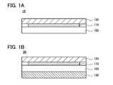
- FIGS. 1A and 1Bare cross-sectional views of imaging devices
- FIG. 2is a top view of an imaging device
- FIG. 3illustrates a heater
- FIG. 4shows Id ⁇ Vg characteristics of a transistor before and after X-ray irradiation
- FIG. 5shows the amount of returned shift value calculated from the Id ⁇ Vg characteristics after heat treatment
- FIG. 6shows the amount of returned shift value calculated from the Id ⁇ Vg characteristics after heat treatment and light irradiation
- FIGS. 7A and 7Beach illustrate a configuration of a pixel circuit
- FIGS. 8A to 8Care timing charts each showing the operation of a pixel circuit
- FIGS. 9A and 9Beach illustrate a configuration of a pixel circuit
- FIG. 10illustrates a configuration of a pixel circuit
- FIGS. 11A and 11Beach illustrate a configuration of a pixel circuit
- FIGS. 12A to 12Ceach illustrate an integrator circuit
- FIGS. 13A to 13Care a cross-sectional view and top views illustrating an imaging device
- FIG. 14illustrates a configuration of a pixel circuit
- FIG. 15illustrates an imaging device having a display function
- FIGS. 16A and 16Bare timing charts showing the operations in a global shutter system and a rolling shutter system, respectively;
- FIGS. 17A and 17Billustrate a structure of an imaging system
- FIGS. 18A and 18Beach illustrate a configuration of a pixel circuit.
- an explicit description “X and Y are connected”means that X and Y are electrically connected, X and Y are functionally connected, and X and Y are directly connected. Accordingly, without limiting to a predetermined connection relation, for example, a connection relation shown in drawings or texts, another connection relation is included in the drawings or the texts.
- X and Yeach denote an object (e.g., a device, an element, a circuit, a wiring, an electrode, a terminal, a conductive film, or a layer).
- X and Yare connected without an element that enables electrical connection between X and Y (e.g., a switch, a transistor, a capacitor, an inductor, a resistor, a diode, a display element, a light-emitting element, or a load) interposed between X and Y.
- an element that enables electrical connection between X and Ye.g., a switch, a transistor, a capacitor, an inductor, a resistor, a diode, a display element, a light-emitting element, or a load
- one or more elements that enable an electrical connection between X and Ycan be connected between X and Y.
- the switchis controlled to be turned on or off. That is, the switch is conducting or not conducting (is turned on or off) to determine whether current flows therethrough or not.
- the switchhas a function of selecting and changing a current path. Note that the case where X and Y are electrically connected includes the case where X and Y are directly connected.
- one or more circuits that enable functional connection between X and Ycan be connected between X and Y.
- a logic circuitsuch as an inverter, a NAND circuit, or a NOR circuit
- a signal converter circuitsuch as a D/A converter circuit, an A/D converter circuit, or a gamma correction circuit
- a potential level converter circuitsuch as a power supply circuit (e.g., a step-up circuit or a step-down circuit) or a level shifter circuit for changing the potential level of a signal
- a voltage sourcee.g., a step-up circuit or a step-down circuit
- a level shifter circuitfor changing the potential level of a signal
- a voltage sourcee.g., a step-up circuit or a step-down circuit
- an amplifier circuitsuch as a circuit that can increase signal amplitude, the amount of current, or the like, an operational amplifier, a differential amplifier circuit, a source follower circuit, and a buffer circuit
- X and Yare functionally connected if a signal output from X is transmitted to Y.
- X and Yare functionally connected includes the case where X and Y are directly connected and X and Y are electrically connected.
- an explicit description “X and Y are connected”means that X and Y are electrically connected (i.e., the case where X and Y are connected with another element or circuit provided therebetween), X and Y are functionally connected (i.e., the case where X and Y are functionally connected with another circuit provided therebetween), and X and Y are directly connected (i.e., the case where X and Y are connected without another element or circuit provided therebetween). That is, in this specification and the like, the explicit expression “X and Y are electrically connected” is the same as the explicit simple expression “X and Y are connected”.
- any of the following expressionscan be used for the case where a source (or a first terminal or the like) of a transistor is electrically connected to X through (or not through) Z 1 and a drain (or a second terminal or the like) of the transistor is electrically connected to Y through (or not through) Z 2 , or the case where a source (or a first terminal or the like) of a transistor is directly connected to one part of Z 1 and another part of Z 1 is directly connected to X while a drain (or a second terminal or the like) of the transistor is directly connected to one part of Z 2 and another part of Z 2 is directly connected to Y.
- Examples of the expressionsinclude, “X, Y, a source (or a first terminal or the like) of a transistor, and a drain (or a second terminal or the like) of the transistor are electrically connected to each other, and X, the source (or the first terminal or the like) of the transistor, the drain (or the second terminal or the like) of the transistor, and Y are electrically connected to each other in this order”, “a source (or a first terminal or the like) of a transistor is electrically connected to X, a drain (or a second terminal or the like) of the transistor is electrically connected to Y, and X, the source (or the first terminal or the like) of the transistor, the drain (or the second terminal or the like) of the transistor, and Y are electrically connected to each other in this order”, and “X is electrically connected to Y through a source (or a first terminal or the like) and a drain (or a second terminal or the like) of a transistor, and X, the source (or the first
- a source (or a first terminal or the like) of a transistoris electrically connected to X through at least a first connection path, the first connection path does not include a second connection path, the second connection path is a path between the source (or the first terminal or the like) of the transistor and a drain (or a second terminal or the like) of the transistor, Z 1 is on the first connection path, the drain (or the second terminal or the like) of the transistor is electrically connected to Y through at least a third connection path, the third connection path does not include the second connection path, and Z 2 is on the third connection path”.
- a source (or a first terminal or the like) of a transistoris electrically connected to X through at least Z 1 on a first connection path, the first connection path does not include a second connection path, the second connection path includes a connection path through the transistor, a drain (or a second terminal or the like) of the transistor is electrically connected to Y through at least Z 2 on a third connection path, and the third connection path does not include the second connection path”.
- Still another example of the expressionis “a source (or a first terminal or the like) of a transistor is electrically connected to X through at least Z 1 on a first electrical path, the first electrical path does not include a second electrical path, the second electrical path is an electrical path from the source (or the first terminal or the like) of the transistor to a drain (or a second terminal or the like) of the transistor, the drain (or the second terminal or the like) of the transistor is electrically connected to Y through at least Z 2 on a third electrical path, the third electrical path does not include a fourth electrical path, and the fourth electrical path is an electrical path from the drain (or the second terminal or the like) of the transistor to the source (or the first terminal or the like) of the transistor”.
- the connection path in a circuit structureis defined by an expression similar to the above examples, a source (or a first terminal or the like) and a drain (or a second terminal or the like) of a transistor can be distinguished from each other to specify the technical scope.
- each of X, Y, Z 1 , and Z 2denotes an object (e.g., a device, an element, a circuit, a wiring, an electrode, a terminal, a conductive film, a layer, or the like).
- one componenthas functions of a plurality of components in some cases.
- one conductive filmfunctions as the wiring and the electrode.
- electrical connectionin this specification includes in its category such a case where one conductive film has functions of a plurality of components.
- filmand “layer” can be interchanged with each other depending on the case or circumstances.
- conductive layercan be changed into the term “conductive film” in some cases.
- insulating filmcan be changed into the term “insulating layer” in some cases.
- FIGS. 1A and 1Bare cross-sectional views each illustrating a structure of the imaging device of one embodiment of the present invention.
- An imaging device 10 illustrated in FIG. 1Aincludes a pixel array 110 over a substrate 100 , and a scintillator 120 over the pixel array 110 .
- the scintillator 120is made of a substance that, when exposed to radiation such as X-rays or gamma-rays, absorbs the energy of the rays to emit visible light or ultraviolet light or a material containing the substance.
- the known materialsinclude Gd 2 O 2 S:Tb, Gd 2 O 2 S:Pr, Gd 2 O 2 S:Eu, BaFCl:Eu, NaI, CsI, CaF 2 , BaF 2 , CeF 3 , LiF, LiI, and ZnO, and a resin or ceramics in which any of the materials is dispersed.
- the pixel array 110 over the substrate 100can have a structure illustrated in the top view of FIG. 2 , for example. Note that in FIG. 2 , the scintillator 120 is omitted for clarity.
- the pixel array 110includes a plurality of pixel circuits 210 arranged in a matrix, and the pixel circuits 210 each include a light-receiving element 220 and a circuit portion 230 electrically connected to the light-receiving element 220 .
- a transistor including an oxide semiconductor in an active layercan be used for the circuit portion 230 .
- the transistor using an oxide semiconductorhas a higher mobility than a transistor using amorphous silicon, and is thus easily reduced in size, resulting in a reduction in the size of a pixel. In other words, the resolution of the imaging device can be increased.
- a first circuit 240 and a second circuit 250may be provided over the substrate 100 to drive the pixel array 110 .
- FIG. 2shows an example in which the circuits for driving the pixel array 110 are provided in the two regions
- the structures of the circuitsare not limited to this example.
- the circuits for driving the pixel array 110may be collectively provided in one region, or may be divided into three or more parts.
- the circuits for driving the pixel array 110may be formed directly on the substrate 100 like a transistor included in the pixel circuit 210 , or may be formed by mounting an IC chip on the substrate 100 by chip on glass (COG) or the like.
- COGchip on glass
- a tape carrier package (TCP), a chip on film (COF), or the likemay be connected to the pixel array 110 .
- TCPtape carrier package
- COFchip on film
- the substrate 100is provided with a heater 101 as illustrated in FIG. 3 , for example.
- the heater 101can be formed using a resistor such as a metal wire or a conductive film. The passage of a current through the heater 101 produces Joule heating.
- the heater 101may be formed on either surface of the substrate 100 or embedded in the substrate 100 . Note that the shape of the heater 101 is not limited to that illustrated in FIG. 3 which is just an example.
- the substrate 100 including the heater 101needs to have a high light-transmitting property in some cases. In that case, a light-transmitting resistor is preferably used as the heater 101 .
- a metal or a nitridesuch as tungsten, chromium, titanium, titanium nitride, or tantalum nitride, or an oxide such as zinc oxide, tin oxide, or indium oxide can be used for the heater 101 .
- the imaging device of one embodiment of the present inventionmay have a structure illustrated in FIG. 1B .
- An imaging device 20has a structure in which a light-emitting device 130 is provided in contact with the substrate 100 of the imaging device 10 illustrated in FIG. 1A .
- a light-emitting diode or the likecan be used as a light source of the light-emitting device 130 .
- Radiation such as X-rayspasses through a subject to enter the scintillator 120 , and then is converted into light (fluorescence) such as visible light or ultraviolet light owing to a phenomenon known as photoluminescence.
- the lightis sensed by the light-receiving element 220 provided in the pixel circuit 210 , whereby image data is obtained.
- part of the radiation emitted to the scintillator 120is not used for photoluminescence but passes through the scintillator 120 . If a semiconductor material or an insulating material of a transistor is exposed to the radiation such as X-rays, defect states and the like are generated in the irradiated portion, whereby the electrical characteristics of the transistor change. This might lead to increased power consumption or decreased reliability of the imaging device.
- the threshold voltage of the transistorshifts in the negative direction.
- the transistorhas a bottom-gate structure in which an oxide semiconductor is used for an active layer and a stack of a silicon nitride film and a silicon oxide film is used for a gate insulating film.
- the L/W of the transistoris 6/50 ⁇ m.
- the transistorIn the initial state, the transistor has a low off-state current and exhibits excellent normally-off characteristics.
- the gate voltage (Vg) at which a current starts flowinglargely shifts in the negative direction.
- the amount of shift in the threshold voltage of the transistor ( ⁇ Vth)is ⁇ 2.6 V
- the amount of shift in the shift value ( ⁇ Shift)is ⁇ 2.7 V.
- the followingis a degradation model in X-ray irradiation.
- an electron-holeis generated in an oxide semiconductor (an active layer of the transistor, e.g., an In—Ga—Zn oxide layer).
- the generated holeis trapped in a deep defect state in the oxide semiconductor which is derived from an oxygen vacancy.
- the trapped holeis injected into a defect state of a non-bridging oxygen hole center (NBOHC) in silicon oxide (the gate insulating film of the transistor).
- NOHCnon-bridging oxygen hole center
- the injected holeserves as a fixed charge having a positive charge in silicon oxide, thereby changing the threshold voltage of the transistor.
- FIG. 5shows the amount of returned shift value ( ⁇ Shift 2 ) calculated from the Id ⁇ Vg characteristics after the heat treatment.
- a point plotted at 25° C.shows the result of a sample that was not subjected to heat treatment, and points plotted at 60° C. and 125° C. show the results of samples that were heated at the respective temperatures for 30 minutes.
- FIG. 5shows that the shift value is returned more easily when the heat treatment is performed at higher temperatures.
- FIG. 6shows the amount of returned shift value ( ⁇ Shift 2 ) of a degraded transistor that was subjected to heat treatment and light irradiation, which was calculated from the Id—Vg characteristics.
- the heat treatmentwas performed at 60° C. and light irradiation with each wavelength was performed for 30 minutes.
- darkdenotes a sample that was subjected only to heat treatment without light irradiation.
- the longitudinal axisrepresents a normalized value with the value of dark taken as 1.
- FIG. 6indicates that degradation due to light irradiation can be recovered when the amount of returned shift value (AShift 2 ) is larger than that of dark.
- AShift 2amount of returned shift value
- light with a wavelength of 500 nm to 600 nm, more preferably, approximately 550 nmare preferably emitted.
- the heat treatment and light in the above wavelength rangesignificantly contribute to a reduction in fixed charges in the gate insulating film. That is, the heat and light do not produce another source of degradation and can supply the activation energy necessary for recovery of degradation.
- degradation due to X-ray irradiationcan be recovered by adjusting the temperature and time of heat treatment.
- degradation due to X-ray irradiationcan be recovered by irradiation with light with a wavelength of 500 nm to 600 nm.
- degradation due to X-ray irradiationcan be recovered by combining heat treatment and light irradiation.
- heat treatment at high temperaturesrequires cooling measures or countermeasures against heat to prevent damage on the components and circumference of the imaging device. It is therefore preferable that heat treatment at low temperatures be combined with light irradiation to recover degradation due to X-ray irradiation.
- heat treatmentis performed at temperatures of approximately 60° C. to 80° C. and light with a wavelength of approximately 550 nm is emitted. In such a case, degradation in X-ray irradiation can be recovered rapidly without a need of extensive cooling measures or countermeasures against heat.
- the inventorshave proposed the imaging devices illustrated in FIGS. 1A and 1B .
- heat treatmentis performed on the pixel array 110 with use of the heater on the substrate 100 , thereby recovering the electrical characteristics of the transistor degraded by X-ray irradiation. If cooling measures or countermeasures against heat are taken properly, the pixel array 110 may be heated at temperatures higher than or equal to 100° C.
- heat treatmentis performed on the pixel array 110 with use of the heater 101 on the substrate 100 , and light is emitted from the light-emitting device 130 to the pixel array 110 , thereby recovering the electrical characteristics of the transistor degraded by X-ray irradiation. If cooling measures or countermeasures against heat are taken properly, the pixel array 110 may be heated at temperatures higher than or equal to 100° C. Light emitted from the light-emitting device 130 may be monochromatic light with a wavelength of 500 nm to 600 nm or a mixture of colors including light in this wavelength range. Note that the transistor included in the pixel array 110 preferably has a top-gate structure so that light from the light-emitting device 130 is effectively emitted to an active layer of the transistor.
- the heat treatment on the pixel array 110 with use of the heater 101 and the light irradiation to the pixel array 110 with use of the light-emitting device 130are preferably performed at times other than imaging. If the heat treatment is performed on the pixel array 110 at the time of imaging, the off-state current of the transistor increases to decrease dynamic range. When light is emitted from the light-emitting device 130 , the light is sensed by the light-receiving element 220 and thus imaging is hindered. Thus, the heat treatment and light irradiation are preferably performed at waiting time, for example, between an interval of imaging.
- the heat treatment and light irradiationmay be performed at the time when an imaging system including the imaging device is turned on or off.
- the imaging systemmay have a means (such as an air blower) for cooling the imaging device so that images can be taken rightly after the heat treatment.
- FIG. 17Aillustrates an example of a detector unit including the imaging device 10 or 20 .
- a detector unit 991is provided with a handle 992 .
- the detector unit 991includes not only the imaging device of one embodiment of the present invention but also part or whole of the peripheral equipment of the imaging device.
- FIG. 17Billustrates an example of the entire structure of an imaging system 998 .
- the detector unit 991is placed on a stand 995 .
- the detector unit 991is connected to a computer 999 in some cases.
- An X-ray 997 emitted from an X-ray source 996passes through a subject 994 and is sensed by the detector unit 991 .
- This embodimentcan be implemented in an appropriate combination with any of the structures described in the other embodiments.
- Embodiment 1the pixel circuit 210 shown in Embodiment 1 will be described.
- FIG. 7Ashows an example of a circuit that can be used as the pixel circuit 210 illustrated in FIG. 2 .
- a circuit 211includes a photodiode 320 serving as the light-receiving element 220 , and a first transistor 301 , a second transistor 302 , and a third transistor 303 that are provided in the circuit portion 230 connected to the light-receiving element 220 .
- An anode of the photodiode 320is electrically connected to a first wiring 311 (RS); a cathode of the photodiode 320 is electrically connected to one of a source and a drain of the first transistor 301 ; the other of the source and the drain of the first transistor 301 is electrically connected to a wiring 305 (FD); a gate of the first transistor 301 is electrically connected to a second wiring 312 (TX); one of a source and a drain of the second transistor 302 is electrically connected to a fourth wiring 314 (GND); the other of the source and the drain of the second transistor 302 is electrically connected to one of a source and a drain of the third transistor 303 ; a gate of the second transistor 302 is electrically connected to the wiring 305 (FD); the other of the source and the drain of the third transistor 303 is electrically connected to a fifth wiring 315 (OUT); and a gate of the third transistor 303 is electrically connected to a third wiring 313 (SE).
- a potential such as GND, VSS, or VDDmay be supplied to the fourth wiring 314 .
- a potential or a voltagehas a relative value. Therefore, the potential GND is not necessarily 0 V.
- the photodiode 320is a light-receiving element and generates a current corresponding to the amount of light entering the pixel circuit.
- the first transistor 301controls accumulation in the wiring 305 (FD) of electrical charges generated by the photodiode 320 .
- a signal corresponding to a potential of the wiring 305 (FD)is output from the second transistor 302 .
- the third transistor 303controls the selection of the pixel circuit at the time of reading.
- the wiring 305 (FD)is a charge accumulation portion retaining electrical charges whose amount changes depending on the amount of light received by the photodiode 320 .
- the charge accumulation portionis depletion layer capacitance in the vicinity of a source region or a drain region of the first transistor 301 electrically connected to the wiring 305 (FD), wiring capacitance of the wiring 305 (FD), gate capacitance of the second transistor 302 electrically connected to the wiring 305 (FD), and the like.
- the second transistor 302 and the third transistor 303only need to be connected in series between the fifth wiring 315 and the fourth wiring 314 .
- the fourth wiring 314 , the second transistor 302 , the third transistor 303 , and the fifth wiring 315may be arranged in order, or the fourth wiring 314 , the third transistor 303 , the second transistor 302 , and the fifth wiring 315 may be arranged in order.
- the first wiring 311 (RS)is a signal line for resetting the wiring 305 (FD).
- the first wiring 311 (RS) in the circuit 211is also a signal line for performing charge accumulation in the wiring 305 (FD).
- the second wiring 312 (TX)is a signal line for controlling the first transistor 301 .
- the third wiring 313 (SE)is a signal line for controlling the third transistor 303 .
- the fourth wiring 314 (GND)is a signal line for setting a reference potential (e.g., GND).
- the fifth wiring 315 (OUT)is a signal line for reading data obtained in the circuit 211 .
- the pixel circuit 210may have a configuration illustrated in FIG. 7B .
- a circuit 212 illustrated in FIG. 7Bincludes the same components as those in the circuit 211 in FIG. 7A but is different from the circuit 211 in that an anode of a photodiode 321 is electrically connected to one of the source and the drain of the first transistor 301 and a cathode of the photodiode 321 is electrically connected to the first wiring 311 (RS).
- RSfirst wiring 311
- the photodiodes 320 and 321can be formed using a silicon semiconductor with a pn junction or a pin junction, for example.
- a pin photodiode including an i-type semiconductor layer formed of amorphous siliconis preferably used. Since amorphous silicon has a high sensitivity in a visible light wavelength region, weak visible light can be sensed easily.
- the i-type semiconductorrefers not only to what is called an intrinsic semiconductor in which the Fermi level lies in the middle of the band gap, but also to a semiconductor in which the concentration of an impurity imparting p-type conductivity and the concentration of an impurity imparting n-type conductivity are less than or equal to 1 ⁇ 10 20 atoms/cm 3 and in which the photoconductivity is higher than the dark conductivity.
- a silicon semiconductorsuch as amorphous silicon, microcrystalline silicon, polycrystalline silicon, or single crystal silicon can be used to form the first transistor 301 , the second transistor 302 , and the third transistor 303
- an oxide semiconductoris preferably used to form the transistors.
- a transistor including an oxide semiconductor in a channel formation regionhas an extremely low off-state current.
- each of these transistorsis also preferably a transistor including an oxide semiconductor in a channel formation region.
- the transistor using an oxide semiconductor with an extremely low off-state currentis used as the second transistor 302 , imaging can be performed with wider dynamic range.
- a gate potential of the second transistor 302is decreased with an increase in the intensity of light entering the photodiode 320 .
- the gate potential of the second transistor 302is decreased with a decrease in the intensity of light entering the photodiode 321 . Since the transistor using an oxide semiconductor has an extremely low off-state current, a current corresponding to the gate potential can be accurately output even when the gate potential is extremely low. Thus, it is possible to broaden the detection range of illuminance, i.e., the dynamic range.
- a sufficiently wide dynamic rangecan be obtained even when the gate potential of the second transistor 302 is relatively low, i.e., when the intensity of light emitted from the scintillator to the photodiode 321 is low.
- the scintillatordoes not need to emit high-intensity light, which makes it possible to reduce the intensity of X-rays emitted to a subject.
- a signal which varies between two levelsis applied to each wiring, for simplicity. Note that in practice, an analog signal is input; hence, the potential can have various levels depending on the circumstances without being limited to two levels.
- a signal 401corresponds to the potential of the first wiring 311 (RS); a signal 402 , the potential of the second wiring 312 (TX); a signal 403 , the potential of the third wiring 313 (SE); a signal 404 , the potential of the wiring 305 (FD); and a signal 405 , the potential of the fifth wiring 315 (OUT).
- the potential of the first wiring 311(signal 401 ) is set high and the potential of the second wiring 312 (signal 402 ) is set high, whereby a forward bias is applied to the photodiode 320 and the potential of the wiring 305 (signal 404 ) is set high.
- the potential of the charge accumulation portionis initialized to the potential of the first wiring 311 and brought into a reset state. The above is the start of a reset operation.
- the potential of the fifth wiring 315(signal 405 ) is precharged to high.
- the potential of the first wiring 311(signal 401 ) is set low and the potential of the second wiring 312 (signal 402 ) is set high, so that the reset operation is terminated and an accumulation operation starts.
- a reverse biasis applied to the photodiode 320 , whereby the potential of the wiring 305 (signal 404 ) starts to decrease due to a reverse current. Since irradiation of the photodiode 320 with light increases the reverse current, the rate of decrease in the potential of the wiring 305 (signal 404 ) changes depending on the amount of the light irradiation. In other words, channel resistance between the source and the drain of the second transistor 302 changes depending on the amount of light emitted to the photodiode 320 .
- the light emitted to the photodiode 320refers to the light which is converted from radiation such as X-rays by the scintillator.
- the potential of the second wiring 312(signal 402 ) is set low to terminate the accumulation operation, so that the potential of the wiring 305 (signal 404 ) becomes constant.
- the potentialis determined by the number of electrical charges generated by the photodiode 320 during the accumulation operation. That is, the potential changes depending on the amount of light emitted to the photodiode 320 .
- the first transistor 301includes a channel formation region in an oxide semiconductor layer and thus has an extremely low off-state current. Accordingly, the potential of the wiring 305 can be kept constant until a subsequent selection operation (read operation) is performed.
- the potential of the second wiring 312(signal 402 ) is set low, the potential of the wiring 305 changes due to parasitic capacitance between the second wiring 312 and the wiring 305 in some cases. In the case where this potential change is large, the number of electrical charges generated by the photodiode 320 during the accumulation operation cannot be obtained accurately. Examples of effective measures to decrease the potential change include reducing the capacitance between the gate and the source (or between the gate and the drain) of the first transistor 301 , increasing the gate capacitance of the second transistor 302 , and providing a storage capacitor connected to the wiring 305 . Note that in this embodiment, the potential change can become negligible by the adoption of these measures.
- the potential of the third wiring 313(signal 403 ) is set high to turn on the third transistor 303 , whereby the selection operation starts and the fourth wiring 314 and the fifth wiring 315 are electrically connected to each other through the second transistor 302 and the third transistor 303 .
- the potential of the fifth wiring 315(signal 405 ) starts to decrease. Note that precharge of the fifth wiring 315 is terminated before time D.
- the rate of decrease in the potential of the fifth wiring 315 (signal 405 )depends on the current between the source and the drain of the second transistor 302 . That is, the rate of decrease changes depending on the amount of light emitted to the photodiode 320 during the accumulation operation.
- the potential of the third wiring 313(signal 403 ) is set low to turn off the third transistor 303 , so that the selection operation is terminated and the potential of the fifth wiring 315 (signal 405 ) becomes a constant value.
- the constant valuedepends on the amount of light emitted to the photodiode 320 . Therefore, the amount of light emitted to the photodiode 320 during the accumulation operation can be found by obtaining the potential of the fifth wiring 315 .
- a relatively high potentialcan be read from the fifth wiring 315 .
- a relatively low potentialcan be read from the fifth wiring 315 .
- the potential of the first wiring 311(signal 401 ) is set low and the potential of the second wiring 312 (signal 402 ) is set high, whereby a forward bias is applied to the photodiode 321 and the potential of the wiring 305 (signal 404 ) is set low.
- the potential of the charge accumulation portionis brought into a reset state.
- the aboveis the start of a reset operation.
- the potential of the fifth wiring 315 (signal 405 )is precharged to high.
- the potential of the first wiring 311(signal 401 ) is set high and the potential of the second wiring 312 (signal 402 ) is set high, so that the reset operation is terminated and an accumulation operation starts.
- a reverse biasis applied to the photodiode 321 , whereby the potential of the wiring 305 (signal 404 ) starts to increase due to a reverse current. Since irradiation of the photodiode 321 with light increases the reverse current, the rate of increase in the potential of the wiring 305 (signal 404 ) changes depending on the amount of the light irradiation. In other words, channel resistance between the source and the drain of the second transistor 302 changes depending on the amount of light emitted to the photodiode 321 .
- the description of the timing chart in FIG. 8Acan be referred to for the operations at and after time C.
- the amount of light emitted to the photodiode 321 during the accumulation operationcan be found by obtaining the potential of the fifth wiring 315 at time E.
- the pixel circuit 210may have a configuration illustrated in FIG. 9A or 9B .
- a circuit 213 illustrated in FIG. 9Ahas a configuration in which a fourth transistor 304 is added to the circuit 211 in FIG. 7A .
- a gate of the transistor 304is electrically connected to the first wiring 311 ; one of a source and a drain of the transistor 304 is electrically connected to the wiring 305 (FD); the other of the source and the drain of the transistor 304 is electrically connected to a seventh wiring 317 ; and the anode of the photodiode 320 is electrically connected to a sixth wiring 316 .
- the sixth wiring 316is a signal line (low potential line) for applying a reverse bias to the photodiode 320 all the time.
- the seventh wiring 317is a signal line (high potential line) for resetting the wiring 305 to a high potential.
- the fourth transistor 304serves as a reset transistor for resetting the wiring 305 (FD).
- the wiring 305 (FD)can be reset by setting the potential of the first wiring 311 (RS) high. Operations of the circuit 213 are the same as those of the circuit 211 in FIG. 7A , which are illustrated in the timing chart in FIG. 8A .
- a circuit 214 illustrated in FIG. 9Bhas a configuration in which the fourth transistor 304 is added to the circuit 212 in FIG. 8B .
- the gate of the transistor 304is electrically connected to the first wiring 311 ; one of the source and the drain of the transistor 304 is electrically connected to the wiring 305 (FD); the other of the source and the drain of the transistor 304 is electrically connected to the seventh wiring 317 ; and the cathode of the photodiode 321 is electrically connected to the sixth wiring 316 .
- the sixth wiring 316is a signal line (high potential line) for applying a reverse bias to the photodiode 321 all the time.
- the seventh wiring 317is a signal line (low potential line) for resetting the wiring 305 to a low potential.
- the fourth transistor 304serves as a reset transistor for resetting the wiring 305 (FD).
- the wiring 305 (FD)can be reset by setting the potential of the first wiring 311 (RS) high.
- the circuit 214can operate in accordance with the timing chart in FIG. 8C .
- FIGS. 9A and 9Beach show, but are not limited to, an example including the first transistor 301 .
- Circuits 216 and 217 illustrated in FIGS. 18A and 18Bhave configurations in which the first transistor 301 is omitted from the circuits 213 and 214 in FIGS. 9A and 9B .
- the fourth transistor 304can be formed using a silicon semiconductor such as amorphous silicon, microcrystalline silicon, polycrystalline silicon, or single crystal silicon; however, when the fourth transistor 304 has a high leakage current, electrical charges cannot be retained in the charge accumulation portion for a sufficiently long time. For this reason, a transistor formed using an oxide semiconductor with an extremely low off-state current is preferably used as the fourth transistor 304 , as in the case of the first transistor 301 .
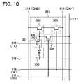
- the pixel circuit 210may have a configuration illustrated in FIG. 10 .
- a circuit 215 in FIG. 10has the same configuration as that in FIG. 7A or 7B except that instead of the photodiode, a variable resistor 330 is used as a light-receiving element.
- the variable resistorcan be constituted by a pair of electrodes and an i-type semiconductor layer provided therebetween.
- the resistancechanges due to visible light irradiation when an i-type amorphous silicon layer is used as the semiconductor layer; thus, the potential of the wiring 305 can be changed as in the case of using the photodiode, which makes it possible to find the amount of light emitted to the variable resistor 330 during the accumulation operation.
- the i-type semiconductor layeran oxide semiconductor layer having a band gap of 3 eV or more may be used. Since the resistance of the oxide semiconductor layer changes due to ultraviolet light irradiation, the potential of the wiring 305 can be changed, which makes it possible to find the amount of light emitted to the variable resistor 330 during the accumulation operation.
- the type of the scintillator 120may be changed to select the wavelength of the light emitted to the variable resistor 330 .
- the circuit 215 in FIG. 10can operate in accordance with the timing chart in FIG. 8A .
- the circuit 215can operate in accordance with the timing chart in FIG. 8C .
- the first transistor 301 , the second transistor 302 , and the third transistor 303 in the pixel circuit 210may have back gates as illustrated in FIGS. 11A and 11B .
- FIG. 11Billustrates a configuration in which the same potential is applied to the front gate and the back gate, which enables an increase in on-state current.
- FIG. 11Aillustrates a configuration in which a constant potential is applied to the back gates, which enables control of the threshold voltage.
- the back gatesare electrically connected to the fourth wiring 314 (GND) in the configuration of FIG. 11A , they may be electrically connected to another wiring to which a constant potential is supplied. Note that FIGS. 11A and 11B show an example in which back gates are provided in the transistors of the circuit 211 .
- the circuits 212 , 213 , 214 , 215 , 216 , and 217may have the same configuration. Moreover, the configuration of applying the same potential to a front gate and a back gate, the configuration of applying a constant potential to a back gate, and the configuration without a back gate may be used in combination for the transistors in one pixel circuit as necessary.
- an integrator circuit illustrated in FIG. 12A, 12B , or 12 Cmay be connected to the fifth wiring 315 (OUT).
- an S/N ratio of a reading signalcan be increased to sense weaker light, that is, the sensitivity of the imaging device can be increased.
- FIG. 12Aillustrates an integrator circuit using an operational amplifier circuit (also referred to as an op-amp).
- An inverting input terminal of the operational amplifier circuitis connected to the fifth wiring 315 (OUT) through a resistor R.
- a non-inverting input terminal of the operational amplifier circuitis grounded.
- An output terminal of the operational amplifier circuitis connected to the inverting input terminal of the operational amplifier circuit through a capacitor C.
- FIG. 12Billustrates an integrator circuit including an operational amplifier circuit having a structure different from that in FIG. 12A .
- An inverting input terminal of the operational amplifier circuitis connected to the fifth wiring 315 (OUT) through a resistor R and a capacitor Cl.
- a non-inverting input terminal of the operational amplifier circuitis grounded.
- An output terminal of the operational amplifier circuitis connected to the inverting input terminal of the operational amplifier circuit through a capacitor C 2 .
- FIG. 12Cillustrates an integrator circuit using an operational amplifier circuit having a structure different from those in FIGS. 12A and 12B .
- a non-inverting input terminal of the operational amplifier circuitis connected to the fifth wiring 315 (OUT) through a resistor R.
- a non-inverting input terminal of the operational amplifier circuitis connected to an output terminal of the operational amplifier circuit.
- the resistor R and the capacitor Cconstitute a CR integrator circuit.
- the operational amplifier circuitis a unity gain buffer.
- This embodimentcan be implemented in an appropriate combination with any of the structures described in the other embodiments.
- FIGS. 13A and 13Bare cross-sectional views each illustrating a structure of the imaging device of one embodiment of the present invention.
- An imaging device 30 illustrated in FIG. 13Aincludes a pixel array 111 over the substrate 100 , and the scintillator 120 over the pixel array 111 .
- the pixel array 111 over the substrate 100can have a structure illustrated in the top view of FIG. 13B , for example. Note that in FIG. 13B , the scintillator 120 is omitted for clarity.
- the pixel array 111includes a plurality of pixel circuits 710 arranged in a matrix, and the pixel circuits 710 each include a light-receiving element 720 and an imaging circuit portion 730 electrically connected to the light-receiving element 720 , and a light-emitting element 760 and a light-emitting circuit portion 770 electrically connected to the light-emitting element 760 (see FIG. 13C ).
- a transistor including an oxide semiconductor in an active layercan be used for the imaging circuit portion 730 and the light-emitting circuit portion 770 .
- the transistor using an oxide semiconductorhas a higher mobility than a transistor using amorphous silicon, and is thus easily reduced in size, resulting in a reduction in the size of a pixel. In other words, the resolution of the imaging device can be increased.
- the transistor including an oxide semiconductor in the active layeris damaged by part of X-rays passing through the scintillator 120 .
- the degradationis recovered by heat treatment using the heater 101 and light irradiation using the light-emitting device 130 in Embodiment 1.
- light irradiation using the light-emitting element 760is performed in addition to the heat treatment using the heater 101 .
- the light-emitting element 760for example, an organic EL element can be used.
- the light-emitting elementpreferably emits light with a wavelength of 500 nm to 600 nm, more preferably, approximately 550 nm as described in Embodiment 1.
- the light-emitting element 760is formed over the imaging circuit portion 730 and the light-emitting circuit portion 770 as illustrated in the drawing. Therefore, the light-emitting element 760 preferably has a bottom-emission structure (in which light is emitted to the substrate 100 side) so that both the circuit portions are irradiated with light.
- transistors included in the imaging circuit portion 730 and the light-emitting circuit portion 770preferably have a bottom-gate structure so that active layers of the transistors are irradiated with light effectively.
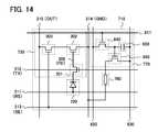
- FIG. 14is a circuit diagram of the pixel circuit 710 in which the circuit 211 illustrated in FIG. 7A is used as the imaging circuit portion 730 and the light-emitting element 760 and the light-emitting circuit portion 770 are connected with the fourth wiring 314 (GND), a reference potential line, used in common.
- VFDfourth wiring 314
- one of a source and a drain of a fifth transistor 840is connected to a signal line 820
- the other of the source and the drain of the fifth transistor 840is connected to a gate of a sixth transistor 890 and one electrode of a capacitor 850
- a gate of the fifth transistor 840is connected to a scanning line 811
- one of a source and a drain of the sixth transistor 890is connected to a power source line 830
- the other of the source and the drain of the sixth transistor 890is connected to one electrode of the light-emitting element 760
- the other electrode of the light-emitting element 760is connected to the fourth wiring 314 (GND).
- Light emissioncan be maintained in the light-emitting element 760 and the light-emitting circuit portion 770 in the following manner by utilizing the feature that the potential of at least the capacitor 850 can be retained.
- a potential that turns the fifth transistor 840 onis supplied to the scanning line 811 .
- the potential of the signal line 820is supplied to the one electrode of the capacitor 850 and the gate electrode of the sixth transistor 890 . That is, a predetermined charge is applied to a node including the capacitor 850 and the gate of the sixth transistor 890 .
- the sixth transistor 890makes a current corresponding to the potential of the node flow into the light-emitting element 760 , thereby controlling the emission intensity.
- the fifth transistor 840is turned off when a potential that turns the fifth transistor 840 off is supplied to the scanning line 811 .
- the potential of the node including the capacitor 850 and the gate of the sixth transistor 890is retained, so that emission from the light-emitting element 760 is maintained.
- the potential of the nodecan be retained for a long time if a transistor using an oxide semiconductor and having an extremely low off-state current is used as the fifth transistor 840 .
- the emission intensity of the light-emitting element 760can be maintained for a long period even when the interval between operations for supplying a potential to the node increases, leading to a reduced power consumption.
- Light from the light-emitting elementis emitted to the active layers of the transistors included in the imaging circuit portion 730 and the light-emitting circuit portion 770 ; thus, degradation of the electrical characteristics due to X-ray irradiation can be recovered.
- the imaging device 30can be used as a display device if openings are provided in the imaging circuit portion 730 and the light-emitting circuit portion 770 and the substrate 100 and the heater 101 are made of a material that transmits light emitted from the light-emitting element 760 .
- X-rays passing through a subject 920enters the input side (the scintillator 120 side) of an imaging system 900 including the imaging device 30 .
- an image signal output from the imaging circuit portion 730 in the imaging device 30is converted into a grayscale signal by a signal processing device 910 and input to the light-emitting circuit portion 770 in the imaging device 30 .
- an imagecan be displayed on the output side (the substrate 100 side) of the imaging system 900 .
- This embodimentcan be implemented in an appropriate combination with any of the structures described in the other embodiments.
- the operation of the pixel circuitis repetition of the reset operation, the accumulation operation, and the selection operation.
- radiation timeis preferably as short as possible in consideration of influence on the living body. To shorten the radiation time and perform imaging in a short time, the reset operation, the accumulation operation, and the selection operation need to be carried out at high speed in all the pixel circuits.
- FIG. 16Ashows operations of an imaging device in which a plurality of pixel circuits 211 illustrated in FIG. 7A are arranged in a matrix. Specifically, FIG. 16A show operations of the circuits 211 from the first row to the n-th row (n is a natural number of three or more). The operation described below can be applied to the circuit 213 in FIG. 9A , the circuit 215 in FIG. 10 , and the circuits in FIGS. 11A and 11B .
- a signal 501 , a signal 502 , and a signal 503are input to the first wirings 311 (RS) connected to the pixel circuits in the first row, the second row, and the n-th row, respectively.
- a signal 504 , a signal 505 , and a signal 506are input to the second wirings 312 (TX) connected to the pixel circuits in the first row, the second row, and the n-th row, respectively.
- a signal 507 , a signal 508 , and a signal 509are input to the third wirings 313 (SE) connected to the pixel circuits in the first row, the second row, and the n-th row, respectively.
- a period 510is the time taken for one imaging.
- the pixel circuits in each rowperform the reset operation at the same time.
- the pixel circuits in each rowperform the accumulation operation at the same time.
- the selection operation of the pixel circuitsis sequentially performed on the row basis. For example, the selection operation is performed in the pixel circuits in the first row in a period 531 . In this manner, in the global shutter system, the reset operation is performed in all the pixel circuits substantially at the same time, the accumulation operation is performed in all the pixel circuits substantially at the same time, and then the read operation is sequentially performed on the row basis.
- the accumulation operationis performed in all the pixel circuits substantially at the same time; accordingly, imaging is simultaneously performed in the pixel circuits in all the rows. Radiation is thus in synchronization with the accumulation operation, leading to a reduction in radiation time. That is, in the global shutter system, radiation needs to be performed only in the period 520 .
- FIG. 16Bis a timing chart of operation using a rolling shutter system.
- the description of FIG. 16Acan be referred to for the signals 501 to 509 .
- a period 610is the time taken for one imaging.
- a period 611 , a period 612 , and a period 613are reset periods in the first row, the second row, and the n-th row, respectively.
- a period 621 , a period 622 , and a period 623are accumulation operation periods in the first row, the second row, and the n-th row, respectively.
- the selection operationis performed in the pixel circuits in the first row.
- the accumulation operationis not performed at the same time in all the pixel circuits but is sequentially performed on the row basis; accordingly, imaging is not simultaneously performed in the pixel circuits in all the rows. For this reason, even when the radiation is synchronized with the accumulation operation, a radiation period 620 (the sum of the periods 621 to 623 ) is longer than the period 520 in the global shutter system.
- the radiation period 620can be shortened, for example, by reducing the accumulation operation period; thus, the rolling shutter system can also be used as a driving method of the imaging device of one embodiment of the present invention.
- the potential of the wiring 305 (FD) in each pixel circuitneeds to be kept for a long time until the read operation is performed.
- the potential of the wiring 305 (FD)can be kept for a long time.
- the potential of the wiring 305 (FD)cannot be kept for a long time because of a high off-state current, which makes it difficult to use the global shutter system.
- transistors including a channel formation region formed of an oxide semiconductor in the pixel circuitsmakes it easy to perform the global shutter system; accordingly, the imaging device that allows for a low dose of radiation emitted to a subject can be provided.
- This embodimentcan be implemented in an appropriate combination with any of the structures described in the other embodiments.
Landscapes
- Physics & Mathematics (AREA)
- Health & Medical Sciences (AREA)
- Life Sciences & Earth Sciences (AREA)
- General Physics & Mathematics (AREA)
- High Energy & Nuclear Physics (AREA)
- Molecular Biology (AREA)
- Spectroscopy & Molecular Physics (AREA)
- Solid State Image Pick-Up Elements (AREA)
- Measurement Of Radiation (AREA)
- Transforming Light Signals Into Electric Signals (AREA)
- Light Receiving Elements (AREA)
- Thin Film Transistor (AREA)
Abstract
Description
- [Patent Document 1] Japanese Published Patent Application No. H2-164067
- [Patent Document 2] Japanese Published Patent Application No. 2002-151669
Claims (25)
Applications Claiming Priority (2)
| Application Number | Priority Date | Filing Date | Title |
|---|---|---|---|
| JP2013-179560 | 2013-08-30 | ||
| JP2013179560 | 2013-08-30 |
Publications (2)
| Publication Number | Publication Date |
|---|---|
| US20150060675A1 US20150060675A1 (en) | 2015-03-05 |
| US9360564B2true US9360564B2 (en) | 2016-06-07 |
Family
ID=52581806
Family Applications (1)
| Application Number | Title | Priority Date | Filing Date |
|---|---|---|---|
| US14/467,161Expired - Fee RelatedUS9360564B2 (en) | 2013-08-30 | 2014-08-25 | Imaging device |
Country Status (2)
| Country | Link |
|---|---|
| US (1) | US9360564B2 (en) |
| JP (1) | JP6525530B2 (en) |
Families Citing this family (10)
| Publication number | Priority date | Publication date | Assignee | Title |
|---|---|---|---|---|
| US9674470B2 (en) | 2014-04-11 | 2017-06-06 | Semiconductor Energy Laboratory Co., Ltd. | Semiconductor device, method for driving semiconductor device, and method for driving electronic device |
| US11205669B2 (en) | 2014-06-09 | 2021-12-21 | Semiconductor Energy Laboratory Co., Ltd. | Semiconductor device including photoelectric conversion element |
| TWI757788B (en) | 2014-06-27 | 2022-03-11 | 日商半導體能源研究所股份有限公司 | Imaging device and electronic device |
| US9729809B2 (en) | 2014-07-11 | 2017-08-08 | Semiconductor Energy Laboratory Co., Ltd. | Semiconductor device and driving method of semiconductor device or electronic device |
| US9685476B2 (en)* | 2015-04-03 | 2017-06-20 | Semiconductor Energy Laboratory Co., Ltd. | Imaging device and electronic device |
| US10163948B2 (en)* | 2015-07-23 | 2018-12-25 | Semiconductor Energy Laboratory Co., Ltd. | Imaging device and electronic device |
| US10242617B2 (en)* | 2016-06-03 | 2019-03-26 | Semiconductor Energy Laboratory Co., Ltd. | Display device, display module, electronic device, and driving method |
| JP7139327B2 (en) | 2017-06-27 | 2022-09-20 | 株式会社半導体エネルギー研究所 | Semiconductor equipment and electronic components |
| JP2019220684A (en) | 2018-06-19 | 2019-12-26 | シャープ株式会社 | Radiation detector |
| CN109216391B (en)* | 2018-09-11 | 2021-02-19 | 京东方科技集团股份有限公司 | A detection panel, its manufacturing method and detection device |
Citations (111)
| Publication number | Priority date | Publication date | Assignee | Title |
|---|---|---|---|---|
| JPS60198861A (en) | 1984-03-23 | 1985-10-08 | Fujitsu Ltd | Thin film transistor |
| US4734588A (en)* | 1985-08-21 | 1988-03-29 | Kabushiki Kaisha Toshiba | X-ray computed tomograph detector |
| JPS63210023A (en) | 1987-02-24 | 1988-08-31 | Natl Inst For Res In Inorg Mater | Compound having a hexagonal layered structure represented by InGaZn↓4O↓7 and its manufacturing method |
| JPS63210024A (en) | 1987-02-24 | 1988-08-31 | Natl Inst For Res In Inorg Mater | Compound having a hexagonal layered structure represented by InGaZn↓5O↓8 and its manufacturing method |
| JPS63210022A (en) | 1987-02-24 | 1988-08-31 | Natl Inst For Res In Inorg Mater | Compound having hexagonal layered structure represented by InGaZn↓3O↓6 and method for producing the same |
| JPS63215519A (en) | 1987-02-27 | 1988-09-08 | Natl Inst For Res In Inorg Mater | Compound having hexagonal layered structure represented by InGaZn↓6O↓9 and method for producing the same |
| JPS63239117A (en) | 1987-01-28 | 1988-10-05 | Natl Inst For Res In Inorg Mater | Compound having hexagonal layered structure represented by InGaZn↓2O↓5 and method for producing the same |
| JPS63265818A (en) | 1987-04-22 | 1988-11-02 | Natl Inst For Res In Inorg Mater | Compound having a hexagonal layered structure represented by InGaZn↓7O↓1↓0 and its manufacturing method |
| JPH02164067A (en) | 1988-12-19 | 1990-06-25 | Fujitsu Ltd | X-ray image sensor |
| JPH05251705A (en) | 1992-03-04 | 1993-09-28 | Fuji Xerox Co Ltd | Thin-film transistor |
| US5248885A (en)* | 1990-08-30 | 1993-09-28 | Shimadzu Corporation | Radiation detector having means for exciting trapped carriers |
| JPH08264794A (en) | 1995-03-27 | 1996-10-11 | Res Dev Corp Of Japan | Metal oxide semiconductor device in which a pn junction is formed with a thin film transistor made of a metal oxide semiconductor such as cuprous oxide, and methods for manufacturing the same |
| US5731856A (en) | 1995-12-30 | 1998-03-24 | Samsung Electronics Co., Ltd. | Methods for forming liquid crystal displays including thin film transistors and gate pads having a particular structure |
| US5744864A (en) | 1995-08-03 | 1998-04-28 | U.S. Philips Corporation | Semiconductor device having a transparent switching element |
| JP2000044236A (en) | 1998-07-24 | 2000-02-15 | Hoya Corp | Article having transparent conductive oxide thin film and method for producing the same |
| JP2000150900A (en) | 1998-11-17 | 2000-05-30 | Japan Science & Technology Corp | Transistor and semiconductor device |
| US6294274B1 (en) | 1998-11-16 | 2001-09-25 | Tdk Corporation | Oxide thin film |
| US20010046027A1 (en) | 1999-09-03 | 2001-11-29 | Ya-Hsiang Tai | Liquid crystal display having stripe-shaped common electrodes formed above plate-shaped pixel electrodes |
| JP2002076356A (en) | 2000-09-01 | 2002-03-15 | Japan Science & Technology Corp | Semiconductor device |
| US20020056838A1 (en) | 2000-11-15 | 2002-05-16 | Matsushita Electric Industrial Co., Ltd. | Thin film transistor array, method of producing the same, and display panel using the same |
| JP2002151669A (en) | 2000-11-14 | 2002-05-24 | Toshiba Corp | X-ray imaging device |
| US20020132454A1 (en) | 2001-03-19 | 2002-09-19 | Fuji Xerox Co., Ltd. | Method of forming crystalline semiconductor thin film on base substrate, lamination formed with crystalline semiconductor thin film and color filter |
| JP2002289859A (en) | 2001-03-23 | 2002-10-04 | Minolta Co Ltd | Thin film transistor |
| US20020159563A1 (en)* | 2001-04-27 | 2002-10-31 | Canon Kabushiki Kaisha | Radiation imaging apparatus and radiation imaging system using the same |
| JP2003086000A (en) | 2001-09-10 | 2003-03-20 | Sharp Corp | Semiconductor memory device and test method therefor |
| JP2003086808A (en) | 2001-09-10 | 2003-03-20 | Masashi Kawasaki | Thin film transistor and matrix display device |
| US20030189401A1 (en) | 2002-03-26 | 2003-10-09 | International Manufacturing And Engineering Services Co., Ltd. | Organic electroluminescent device |
| US20030218222A1 (en) | 2002-05-21 | 2003-11-27 | The State Of Oregon Acting And Through The Oregon State Board Of Higher Education On Behalf Of | Transistor structures and methods for making the same |
| US20040038446A1 (en) | 2002-03-15 | 2004-02-26 | Sanyo Electric Co., Ltd.- | Method for forming ZnO film, method for forming ZnO semiconductor layer, method for fabricating semiconductor device, and semiconductor device |
| JP2004103957A (en) | 2002-09-11 | 2004-04-02 | Japan Science & Technology Corp | Transparent thin film field effect transistor using homologous thin film as active layer |
| US20040127038A1 (en) | 2002-10-11 | 2004-07-01 | Carcia Peter Francis | Transparent oxide semiconductor thin film transistors |
| JP2004273732A (en) | 2003-03-07 | 2004-09-30 | Sharp Corp | Active matrix substrate and manufacturing method thereof |
| JP2004273614A (en) | 2003-03-06 | 2004-09-30 | Sharp Corp | Semiconductor device and method of manufacturing the same |
| WO2004114391A1 (en) | 2003-06-20 | 2004-12-29 | Sharp Kabushiki Kaisha | Semiconductor device, its manufacturing method, and electronic device |
| US20050017302A1 (en) | 2003-07-25 | 2005-01-27 | Randy Hoffman | Transistor including a deposited channel region having a doped portion |
| US20050199959A1 (en) | 2004-03-12 | 2005-09-15 | Chiang Hai Q. | Semiconductor device |
| US6954514B2 (en)* | 2001-08-09 | 2005-10-11 | Koninklijke Philips Electronics N.V. | X-ray detector provided with a heating device |
| US20060043377A1 (en) | 2004-03-12 | 2006-03-02 | Hewlett-Packard Development Company, L.P. | Semiconductor device |
| US20060091793A1 (en) | 2004-11-02 | 2006-05-04 | 3M Innovative Properties Company | Methods and displays utilizing integrated zinc oxide row and column drivers in conjunction with organic light emitting diodes |
| US20060108529A1 (en) | 2004-11-10 | 2006-05-25 | Canon Kabushiki Kaisha | Sensor and image pickup device |
| US20060110867A1 (en) | 2004-11-10 | 2006-05-25 | Canon Kabushiki Kaisha | Field effect transistor manufacturing method |
| US20060108636A1 (en) | 2004-11-10 | 2006-05-25 | Canon Kabushiki Kaisha | Amorphous oxide and field effect transistor |
| US20060113549A1 (en) | 2004-11-10 | 2006-06-01 | Canon Kabushiki Kaisha | Light-emitting device |
| US20060113536A1 (en) | 2004-11-10 | 2006-06-01 | Canon Kabushiki Kaisha | Display |
| US20060113565A1 (en) | 2004-11-10 | 2006-06-01 | Canon Kabushiki Kaisha | Electric elements and circuits utilizing amorphous oxides |
| US20060113539A1 (en) | 2004-11-10 | 2006-06-01 | Canon Kabushiki Kaisha | Field effect transistor |
| US7061014B2 (en) | 2001-11-05 | 2006-06-13 | Japan Science And Technology Agency | Natural-superlattice homologous single crystal thin film, method for preparation thereof, and device using said single crystal thin film |
| US20060170111A1 (en) | 2005-01-28 | 2006-08-03 | Semiconductor Energy Laboratory Co., Ltd. | Semiconductor device, electronic device, and method of manufacturing semiconductor device |
| US20060169973A1 (en) | 2005-01-28 | 2006-08-03 | Semiconductor Energy Laboratory Co., Ltd. | Semiconductor device, electronic device, and method of manufacturing semiconductor device |
| US20060197092A1 (en) | 2005-03-03 | 2006-09-07 | Randy Hoffman | System and method for forming conductive material on a substrate |
| US7105868B2 (en) | 2002-06-24 | 2006-09-12 | Cermet, Inc. | High-electron mobility transistor with zinc oxide |
| US20060208977A1 (en) | 2005-03-18 | 2006-09-21 | Semiconductor Energy Laboratory Co., Ltd. | Semiconductor device, and display device, driving method and electronic apparatus thereof |
| US20060228974A1 (en) | 2005-03-31 | 2006-10-12 | Theiss Steven D | Methods of making displays |
| US20060231882A1 (en) | 2005-03-28 | 2006-10-19 | Il-Doo Kim | Low voltage flexible organic/transparent transistor for selective gas sensing, photodetecting and CMOS device applications |
| US20060238135A1 (en) | 2005-04-20 | 2006-10-26 | Semiconductor Energy Laboratory Co., Ltd. | Semiconductor device and display device |
| US20060284172A1 (en) | 2005-06-10 | 2006-12-21 | Casio Computer Co., Ltd. | Thin film transistor having oxide semiconductor layer and manufacturing method thereof |
| US20060284171A1 (en) | 2005-06-16 | 2006-12-21 | Levy David H | Methods of making thin film transistors comprising zinc-oxide-based semiconductor materials and transistors made thereby |
| US20060292777A1 (en) | 2005-06-27 | 2006-12-28 | 3M Innovative Properties Company | Method for making electronic devices using metal oxide nanoparticles |
| US20070024187A1 (en) | 2005-07-28 | 2007-02-01 | Shin Hyun S | Organic light emitting display (OLED) and its method of fabrication |
| US20070046191A1 (en) | 2005-08-23 | 2007-03-01 | Canon Kabushiki Kaisha | Organic electroluminescent display device and manufacturing method thereof |
| US20070052025A1 (en) | 2005-09-06 | 2007-03-08 | Canon Kabushiki Kaisha | Oxide semiconductor thin film transistor and method of manufacturing the same |
| US20070054507A1 (en) | 2005-09-06 | 2007-03-08 | Canon Kabushiki Kaisha | Method of fabricating oxide semiconductor device |
| US20070090365A1 (en) | 2005-10-20 | 2007-04-26 | Canon Kabushiki Kaisha | Field-effect transistor including transparent oxide and light-shielding member, and display utilizing the transistor |
| US7211825B2 (en) | 2004-06-14 | 2007-05-01 | Yi-Chi Shih | Indium oxide-based thin film transistors and circuits |
| US20070108446A1 (en) | 2005-11-15 | 2007-05-17 | Semiconductor Energy Laboratory Co., Ltd. | Semiconductor device and manufacturing method thereof |
| US20070152217A1 (en) | 2005-12-29 | 2007-07-05 | Chih-Ming Lai | Pixel structure of active matrix organic light-emitting diode and method for fabricating the same |
| US20070172591A1 (en) | 2006-01-21 | 2007-07-26 | Samsung Electronics Co., Ltd. | METHOD OF FABRICATING ZnO FILM AND THIN FILM TRANSISTOR ADOPTING THE ZnO FILM |
| US20070187760A1 (en) | 2006-02-02 | 2007-08-16 | Kochi Industrial Promotion Center | Thin film transistor including low resistance conductive thin films and manufacturing method thereof |
| US20070187678A1 (en) | 2006-02-15 | 2007-08-16 | Kochi Industrial Promotion Center | Semiconductor device including active layer made of zinc oxide with controlled orientations and manufacturing method thereof |
| US20070194379A1 (en) | 2004-03-12 | 2007-08-23 | Japan Science And Technology Agency | Amorphous Oxide And Thin Film Transistor |
| US20070252928A1 (en) | 2006-04-28 | 2007-11-01 | Toppan Printing Co., Ltd. | Structure, transmission type liquid crystal display, reflection type display and manufacturing method thereof |
| US7297977B2 (en) | 2004-03-12 | 2007-11-20 | Hewlett-Packard Development Company, L.P. | Semiconductor device |
| US20070272922A1 (en) | 2006-04-11 | 2007-11-29 | Samsung Electronics Co. Ltd. | ZnO thin film transistor and method of forming the same |
| US20070287296A1 (en) | 2006-06-13 | 2007-12-13 | Canon Kabushiki Kaisha | Dry etching method for oxide semiconductor film |
| US20080006877A1 (en) | 2004-09-17 | 2008-01-10 | Peter Mardilovich | Method of Forming a Solution Processed Device |
| US7323356B2 (en) | 2002-02-21 | 2008-01-29 | Japan Science And Technology Agency | LnCuO(S,Se,Te)monocrystalline thin film, its manufacturing method, and optical device or electronic device using the monocrystalline thin film |
| US20080038882A1 (en) | 2006-08-09 | 2008-02-14 | Kazushige Takechi | Thin-film device and method of fabricating the same |
| US20080038929A1 (en) | 2006-08-09 | 2008-02-14 | Canon Kabushiki Kaisha | Method of dry etching oxide semiconductor film |
| US20080050595A1 (en) | 2006-01-11 | 2008-02-28 | Murata Manufacturing Co., Ltd. | Transparent conductive film and method for manufacturing the same |
| US20080073653A1 (en) | 2006-09-27 | 2008-03-27 | Canon Kabushiki Kaisha | Semiconductor apparatus and method of manufacturing the same |
| US20080083950A1 (en) | 2006-10-10 | 2008-04-10 | Alfred I-Tsung Pan | Fused nanocrystal thin film semiconductor and method |
| US20080106191A1 (en) | 2006-09-27 | 2008-05-08 | Seiko Epson Corporation | Electronic device, organic electroluminescence device, and organic thin film semiconductor device |
| US20080129195A1 (en) | 2006-12-04 | 2008-06-05 | Toppan Printing Co., Ltd. | Color el display and method for producing the same |
| US20080128689A1 (en) | 2006-11-29 | 2008-06-05 | Je-Hun Lee | Flat panel displays comprising a thin-film transistor having a semiconductive oxide in its channel and methods of fabricating the same for use in flat panel displays |
| US7385224B2 (en) | 2004-09-02 | 2008-06-10 | Casio Computer Co., Ltd. | Thin film transistor having an etching protection film and manufacturing method thereof |
| US20080166834A1 (en) | 2007-01-05 | 2008-07-10 | Samsung Electronics Co., Ltd. | Thin film etching method |
| US7402506B2 (en) | 2005-06-16 | 2008-07-22 | Eastman Kodak Company | Methods of making thin film transistors comprising zinc-oxide-based semiconductor materials and transistors made thereby |
| US20080182358A1 (en) | 2007-01-26 | 2008-07-31 | Cowdery-Corvan Peter J | Process for atomic layer deposition |
| US7411209B2 (en) | 2006-09-15 | 2008-08-12 | Canon Kabushiki Kaisha | Field-effect transistor and method for manufacturing the same |
| US20080224133A1 (en) | 2007-03-14 | 2008-09-18 | Jin-Seong Park | Thin film transistor and organic light-emitting display device having the thin film transistor |
| US20080258141A1 (en) | 2007-04-19 | 2008-10-23 | Samsung Electronics Co., Ltd. | Thin film transistor, method of manufacturing the same, and flat panel display having the same |
| US20080258139A1 (en) | 2007-04-17 | 2008-10-23 | Toppan Printing Co., Ltd. | Structure with transistor |
| US20080258140A1 (en) | 2007-04-20 | 2008-10-23 | Samsung Electronics Co., Ltd. | Thin film transistor including selectively crystallized channel layer and method of manufacturing the thin film transistor |
| US20080258143A1 (en) | 2007-04-18 | 2008-10-23 | Samsung Electronics Co., Ltd. | Thin film transitor substrate and method of manufacturing the same |
| US7453087B2 (en) | 2005-09-06 | 2008-11-18 | Canon Kabushiki Kaisha | Thin-film transistor and thin-film diode having amorphous-oxide semiconductor layer |
| US20080296568A1 (en) | 2007-05-29 | 2008-12-04 | Samsung Electronics Co., Ltd | Thin film transistors and methods of manufacturing the same |
| US7501293B2 (en) | 2002-06-13 | 2009-03-10 | Murata Manufacturing Co., Ltd. | Semiconductor device in which zinc oxide is used as a semiconductor material and method for manufacturing the semiconductor device |
| US20090073325A1 (en) | 2005-01-21 | 2009-03-19 | Semiconductor Energy Laboratory Co., Ltd. | Semiconductor device and method for manufacturing the same, and electric device |
| US20090114910A1 (en) | 2005-09-06 | 2009-05-07 | Canon Kabushiki Kaisha | Semiconductor device |
| US20090134399A1 (en) | 2005-02-18 | 2009-05-28 | Semiconductor Energy Laboratory Co., Ltd. | Semiconductor Device and Method for Manufacturing the Same |
| US20090152506A1 (en) | 2007-12-17 | 2009-06-18 | Fujifilm Corporation | Process for producing oriented inorganic crystalline film, and semiconductor device using the oriented inorganic crystalline film |
| US20090152541A1 (en) | 2005-02-03 | 2009-06-18 | Semiconductor Energy Laboratory Co., Ltd. | Electronic device, semiconductor device and manufacturing method thereof |
| US7674650B2 (en) | 2005-09-29 | 2010-03-09 | Semiconductor Energy Laboratory Co., Ltd. | Semiconductor device and manufacturing method thereof |
| US20100065844A1 (en) | 2008-09-18 | 2010-03-18 | Sony Corporation | Thin film transistor and method of manufacturing thin film transistor |
| US20100092800A1 (en) | 2008-10-09 | 2010-04-15 | Canon Kabushiki Kaisha | Substrate for growing wurtzite type crystal and method for manufacturing the same and semiconductor device |
| US20100109002A1 (en) | 2007-04-25 | 2010-05-06 | Canon Kabushiki Kaisha | Oxynitride semiconductor |
| US20100182282A1 (en) | 2009-01-21 | 2010-07-22 | Semiconductor Energy Laboratory Co., Ltd. | Touch panel and electronic device |
| US20110176038A1 (en) | 2010-01-15 | 2011-07-21 | Semiconductor Energy Laboratory Co., Ltd. | Semiconductor device and method for driving the same |
| US8492728B2 (en) | 2009-06-17 | 2013-07-23 | Regents Of The University Of Michigan | Photodiode and other sensor structures in flat-panel X-ray imagers and method for improving topological uniformity of the photodiode and other sensor structures in flat-panel X-ray imagers based on thin-film electronics |
| US20140054466A1 (en) | 2012-08-23 | 2014-02-27 | Semiconductor Energy Laboratory Co., Ltd. | Imaging device and method for driving the same |
| US20140056405A1 (en) | 2012-08-24 | 2014-02-27 | Semiconductor Energy Laboratory Co., Ltd. | Radiation detection panel, radiation imaging device, and diagnostic imaging device |
Family Cites Families (30)
| Publication number | Priority date | Publication date | Assignee | Title |
|---|---|---|---|---|
| JPS6113652A (en)* | 1984-06-28 | 1986-01-21 | Nec Corp | Sensor for loading to which radiation deterioration reduction countermeasure is considered |
| JPS6175560A (en)* | 1984-09-21 | 1986-04-17 | Hitachi Ltd | image sensor |
| JPS61166162A (en)* | 1985-01-18 | 1986-07-26 | Ricoh Co Ltd | Image sensor |
| JPS6211268A (en)* | 1985-07-08 | 1987-01-20 | Sharp Corp | Image reading device |
| JPS62154780A (en)* | 1985-12-27 | 1987-07-09 | Toshiba Corp | image sensor |
| JPH0627852B2 (en)* | 1990-08-30 | 1994-04-13 | 株式会社島津製作所 | Radiation detector |
| JP2564979B2 (en)* | 1990-09-26 | 1996-12-18 | 株式会社島津製作所 | Radiation detector |
| JPH0530278A (en)* | 1991-07-22 | 1993-02-05 | Hitachi Ltd | Image reading device, line image sensor and shift register |
| JPH05145052A (en)* | 1991-11-19 | 1993-06-11 | Hamamatsu Photonics Kk | Solid state image sensor |
| JPH07169985A (en)* | 1994-10-27 | 1995-07-04 | Semiconductor Energy Lab Co Ltd | Semiconductor device |
| JP2000150895A (en)* | 1998-11-16 | 2000-05-30 | Alps Electric Co Ltd | Thin-film transistor and driving device of image display |
| JP4364553B2 (en)* | 2002-08-30 | 2009-11-18 | シャープ株式会社 | Photoelectric conversion device and manufacturing method thereof |
| JP5207583B2 (en)* | 2005-07-25 | 2013-06-12 | キヤノン株式会社 | Radiation detection apparatus and radiation detection system |
| JP4834518B2 (en)* | 2005-11-29 | 2011-12-14 | キヤノン株式会社 | Radiation imaging apparatus, control method therefor, and recording medium on which program for executing the same is recorded |
| JP2007248285A (en)* | 2006-03-16 | 2007-09-27 | Canon Inc | Radiation detector |
| JP5049739B2 (en)* | 2006-11-01 | 2012-10-17 | キヤノン株式会社 | Radiation imaging device |
| JP2008178522A (en)* | 2007-01-24 | 2008-08-07 | Canon Inc | Radiation imaging apparatus and driving method thereof |
| WO2008126012A2 (en)* | 2007-04-12 | 2008-10-23 | Philips Intellectual Property & Standards Gmbh | Determination of a spatial gain distribution of a scintillator |
| JP4834614B2 (en)* | 2007-06-12 | 2011-12-14 | キヤノン株式会社 | Radiation detection apparatus and radiation imaging system |
| JP5305731B2 (en)* | 2008-05-12 | 2013-10-02 | キヤノン株式会社 | Method for controlling threshold voltage of semiconductor device |
| JP5844030B2 (en)* | 2010-01-14 | 2016-01-13 | 富士フイルム株式会社 | Field effect transistor manufacturing method, display device manufacturing method, X-ray imaging device manufacturing method, and optical sensor manufacturing method |
| JP5482286B2 (en)* | 2010-02-25 | 2014-05-07 | ソニー株式会社 | Radiation imaging apparatus and driving method thereof |
| JP2011216606A (en)* | 2010-03-31 | 2011-10-27 | Fujifilm Corp | Method of manufacturing thin film transistor |
| JP2012049208A (en)* | 2010-08-25 | 2012-03-08 | Fujifilm Corp | Oxide semiconductor thin film, thin film transistor, and device having thin film transistor |
| JP5701539B2 (en)* | 2010-08-25 | 2015-04-15 | 富士フイルム株式会社 | Oxide semiconductor thin film and method for manufacturing the same, thin film transistor, and device including thin film transistor |
| JP6010291B2 (en)* | 2010-11-05 | 2016-10-19 | 株式会社半導体エネルギー研究所 | Driving method of display device |
| JP2012108052A (en)* | 2010-11-18 | 2012-06-07 | Fujifilm Corp | Radiation image photographing device |
| JP5653829B2 (en)* | 2011-04-25 | 2015-01-14 | 富士フイルム株式会社 | Radiographic apparatus, radiographic system, and radiographic method |
| CN103890947B (en)* | 2011-10-28 | 2017-04-12 | 株式会社半导体能源研究所 | Imaging device |
| JP2013096731A (en)* | 2011-10-28 | 2013-05-20 | Fujifilm Corp | Radiographic imaging device |
- 2014
- 2014-08-25USUS14/467,161patent/US9360564B2/ennot_activeExpired - Fee Related
- 2014-08-29JPJP2014174928Apatent/JP6525530B2/ennot_activeExpired - Fee Related
Patent Citations (129)
| Publication number | Priority date | Publication date | Assignee | Title |
|---|---|---|---|---|
| JPS60198861A (en) | 1984-03-23 | 1985-10-08 | Fujitsu Ltd | Thin film transistor |
| US4734588A (en)* | 1985-08-21 | 1988-03-29 | Kabushiki Kaisha Toshiba | X-ray computed tomograph detector |
| JPS63239117A (en) | 1987-01-28 | 1988-10-05 | Natl Inst For Res In Inorg Mater | Compound having hexagonal layered structure represented by InGaZn↓2O↓5 and method for producing the same |
| JPS63210024A (en) | 1987-02-24 | 1988-08-31 | Natl Inst For Res In Inorg Mater | Compound having a hexagonal layered structure represented by InGaZn↓5O↓8 and its manufacturing method |
| JPS63210022A (en) | 1987-02-24 | 1988-08-31 | Natl Inst For Res In Inorg Mater | Compound having hexagonal layered structure represented by InGaZn↓3O↓6 and method for producing the same |
| JPS63210023A (en) | 1987-02-24 | 1988-08-31 | Natl Inst For Res In Inorg Mater | Compound having a hexagonal layered structure represented by InGaZn↓4O↓7 and its manufacturing method |
| JPS63215519A (en) | 1987-02-27 | 1988-09-08 | Natl Inst For Res In Inorg Mater | Compound having hexagonal layered structure represented by InGaZn↓6O↓9 and method for producing the same |
| JPS63265818A (en) | 1987-04-22 | 1988-11-02 | Natl Inst For Res In Inorg Mater | Compound having a hexagonal layered structure represented by InGaZn↓7O↓1↓0 and its manufacturing method |
| JPH02164067A (en) | 1988-12-19 | 1990-06-25 | Fujitsu Ltd | X-ray image sensor |
| US5248885A (en)* | 1990-08-30 | 1993-09-28 | Shimadzu Corporation | Radiation detector having means for exciting trapped carriers |
| JPH05251705A (en) | 1992-03-04 | 1993-09-28 | Fuji Xerox Co Ltd | Thin-film transistor |
| JPH08264794A (en) | 1995-03-27 | 1996-10-11 | Res Dev Corp Of Japan | Metal oxide semiconductor device in which a pn junction is formed with a thin film transistor made of a metal oxide semiconductor such as cuprous oxide, and methods for manufacturing the same |
| JPH11505377A (en) | 1995-08-03 | 1999-05-18 | フィリップス エレクトロニクス ネムローゼ フェンノートシャップ | Semiconductor device |
| US5744864A (en) | 1995-08-03 | 1998-04-28 | U.S. Philips Corporation | Semiconductor device having a transparent switching element |
| US5731856A (en) | 1995-12-30 | 1998-03-24 | Samsung Electronics Co., Ltd. | Methods for forming liquid crystal displays including thin film transistors and gate pads having a particular structure |
| JP2000044236A (en) | 1998-07-24 | 2000-02-15 | Hoya Corp | Article having transparent conductive oxide thin film and method for producing the same |
| US6294274B1 (en) | 1998-11-16 | 2001-09-25 | Tdk Corporation | Oxide thin film |
| JP2000150900A (en) | 1998-11-17 | 2000-05-30 | Japan Science & Technology Corp | Transistor and semiconductor device |
| US7064346B2 (en) | 1998-11-17 | 2006-06-20 | Japan Science And Technology Agency | Transistor and semiconductor device |
| US6727522B1 (en) | 1998-11-17 | 2004-04-27 | Japan Science And Technology Corporation | Transistor and semiconductor device |
| US20010046027A1 (en) | 1999-09-03 | 2001-11-29 | Ya-Hsiang Tai | Liquid crystal display having stripe-shaped common electrodes formed above plate-shaped pixel electrodes |
| JP2002076356A (en) | 2000-09-01 | 2002-03-15 | Japan Science & Technology Corp | Semiconductor device |
| JP2002151669A (en) | 2000-11-14 | 2002-05-24 | Toshiba Corp | X-ray imaging device |
| US20020093581A1 (en) | 2000-11-14 | 2002-07-18 | Kabushiki Kaisha Toshiba | X-ray imaging device |
| US20060237647A1 (en) | 2000-11-14 | 2006-10-26 | Kabushiki Kaisha Toshiba | X-ray imaging device |
| US20020056838A1 (en) | 2000-11-15 | 2002-05-16 | Matsushita Electric Industrial Co., Ltd. | Thin film transistor array, method of producing the same, and display panel using the same |
| US20020132454A1 (en) | 2001-03-19 | 2002-09-19 | Fuji Xerox Co., Ltd. | Method of forming crystalline semiconductor thin film on base substrate, lamination formed with crystalline semiconductor thin film and color filter |
| JP2002289859A (en) | 2001-03-23 | 2002-10-04 | Minolta Co Ltd | Thin film transistor |
| US20020159563A1 (en)* | 2001-04-27 | 2002-10-31 | Canon Kabushiki Kaisha | Radiation imaging apparatus and radiation imaging system using the same |
| US6954514B2 (en)* | 2001-08-09 | 2005-10-11 | Koninklijke Philips Electronics N.V. | X-ray detector provided with a heating device |
| JP2003086808A (en) | 2001-09-10 | 2003-03-20 | Masashi Kawasaki | Thin film transistor and matrix display device |
| US6563174B2 (en) | 2001-09-10 | 2003-05-13 | Sharp Kabushiki Kaisha | Thin film transistor and matrix display device |
| JP2003086000A (en) | 2001-09-10 | 2003-03-20 | Sharp Corp | Semiconductor memory device and test method therefor |
| US7061014B2 (en) | 2001-11-05 | 2006-06-13 | Japan Science And Technology Agency | Natural-superlattice homologous single crystal thin film, method for preparation thereof, and device using said single crystal thin film |
| US7323356B2 (en) | 2002-02-21 | 2008-01-29 | Japan Science And Technology Agency | LnCuO(S,Se,Te)monocrystalline thin film, its manufacturing method, and optical device or electronic device using the monocrystalline thin film |
| US7049190B2 (en) | 2002-03-15 | 2006-05-23 | Sanyo Electric Co., Ltd. | Method for forming ZnO film, method for forming ZnO semiconductor layer, method for fabricating semiconductor device, and semiconductor device |
| US20040038446A1 (en) | 2002-03-15 | 2004-02-26 | Sanyo Electric Co., Ltd.- | Method for forming ZnO film, method for forming ZnO semiconductor layer, method for fabricating semiconductor device, and semiconductor device |
| US20030189401A1 (en) | 2002-03-26 | 2003-10-09 | International Manufacturing And Engineering Services Co., Ltd. | Organic electroluminescent device |
| US20030218222A1 (en) | 2002-05-21 | 2003-11-27 | The State Of Oregon Acting And Through The Oregon State Board Of Higher Education On Behalf Of | Transistor structures and methods for making the same |
| US7501293B2 (en) | 2002-06-13 | 2009-03-10 | Murata Manufacturing Co., Ltd. | Semiconductor device in which zinc oxide is used as a semiconductor material and method for manufacturing the semiconductor device |
| US7105868B2 (en) | 2002-06-24 | 2006-09-12 | Cermet, Inc. | High-electron mobility transistor with zinc oxide |
| JP2004103957A (en) | 2002-09-11 | 2004-04-02 | Japan Science & Technology Corp | Transparent thin film field effect transistor using homologous thin film as active layer |
| US20060035452A1 (en) | 2002-10-11 | 2006-02-16 | Carcia Peter F | Transparent oxide semiconductor thin film transistor |
| US20040127038A1 (en) | 2002-10-11 | 2004-07-01 | Carcia Peter Francis | Transparent oxide semiconductor thin film transistors |
| JP2004273614A (en) | 2003-03-06 | 2004-09-30 | Sharp Corp | Semiconductor device and method of manufacturing the same |
| JP2004273732A (en) | 2003-03-07 | 2004-09-30 | Sharp Corp | Active matrix substrate and manufacturing method thereof |
| WO2004114391A1 (en) | 2003-06-20 | 2004-12-29 | Sharp Kabushiki Kaisha | Semiconductor device, its manufacturing method, and electronic device |
| US20060244107A1 (en) | 2003-06-20 | 2006-11-02 | Toshinori Sugihara | Semiconductor device, manufacturing method, and electronic device |
| US20050017302A1 (en) | 2003-07-25 | 2005-01-27 | Randy Hoffman | Transistor including a deposited channel region having a doped portion |
| US7462862B2 (en) | 2004-03-12 | 2008-12-09 | Hewlett-Packard Development Company, L.P. | Transistor using an isovalent semiconductor oxide as the active channel layer |
| US20090278122A1 (en) | 2004-03-12 | 2009-11-12 | Japan Science And Technology Agency | Amorphous oxide and thin film transistor |
| US7282782B2 (en) | 2004-03-12 | 2007-10-16 | Hewlett-Packard Development Company, L.P. | Combined binary oxide semiconductor device |
| US7297977B2 (en) | 2004-03-12 | 2007-11-20 | Hewlett-Packard Development Company, L.P. | Semiconductor device |
| US20050199959A1 (en) | 2004-03-12 | 2005-09-15 | Chiang Hai Q. | Semiconductor device |
| US20070194379A1 (en) | 2004-03-12 | 2007-08-23 | Japan Science And Technology Agency | Amorphous Oxide And Thin Film Transistor |
| US20060043377A1 (en) | 2004-03-12 | 2006-03-02 | Hewlett-Packard Development Company, L.P. | Semiconductor device |
| US20080254569A1 (en) | 2004-03-12 | 2008-10-16 | Hoffman Randy L | Semiconductor Device |
| US20090280600A1 (en) | 2004-03-12 | 2009-11-12 | Japan Science And Technology Agency | Amorphous oxide and thin film transistor |
| US7211825B2 (en) | 2004-06-14 | 2007-05-01 | Yi-Chi Shih | Indium oxide-based thin film transistors and circuits |
| US7385224B2 (en) | 2004-09-02 | 2008-06-10 | Casio Computer Co., Ltd. | Thin film transistor having an etching protection film and manufacturing method thereof |
| US20080006877A1 (en) | 2004-09-17 | 2008-01-10 | Peter Mardilovich | Method of Forming a Solution Processed Device |
| US20060091793A1 (en) | 2004-11-02 | 2006-05-04 | 3M Innovative Properties Company | Methods and displays utilizing integrated zinc oxide row and column drivers in conjunction with organic light emitting diodes |
| US20060113536A1 (en) | 2004-11-10 | 2006-06-01 | Canon Kabushiki Kaisha | Display |
| US20060113549A1 (en) | 2004-11-10 | 2006-06-01 | Canon Kabushiki Kaisha | Light-emitting device |
| US20060108636A1 (en) | 2004-11-10 | 2006-05-25 | Canon Kabushiki Kaisha | Amorphous oxide and field effect transistor |
| US20060113539A1 (en) | 2004-11-10 | 2006-06-01 | Canon Kabushiki Kaisha | Field effect transistor |
| US20060113565A1 (en) | 2004-11-10 | 2006-06-01 | Canon Kabushiki Kaisha | Electric elements and circuits utilizing amorphous oxides |
| US20060108529A1 (en) | 2004-11-10 | 2006-05-25 | Canon Kabushiki Kaisha | Sensor and image pickup device |
| US7453065B2 (en) | 2004-11-10 | 2008-11-18 | Canon Kabushiki Kaisha | Sensor and image pickup device |
| US20060110867A1 (en) | 2004-11-10 | 2006-05-25 | Canon Kabushiki Kaisha | Field effect transistor manufacturing method |
| US20090073325A1 (en) | 2005-01-21 | 2009-03-19 | Semiconductor Energy Laboratory Co., Ltd. | Semiconductor device and method for manufacturing the same, and electric device |
| US20060170111A1 (en) | 2005-01-28 | 2006-08-03 | Semiconductor Energy Laboratory Co., Ltd. | Semiconductor device, electronic device, and method of manufacturing semiconductor device |
| US20060169973A1 (en) | 2005-01-28 | 2006-08-03 | Semiconductor Energy Laboratory Co., Ltd. | Semiconductor device, electronic device, and method of manufacturing semiconductor device |
| US20090152541A1 (en) | 2005-02-03 | 2009-06-18 | Semiconductor Energy Laboratory Co., Ltd. | Electronic device, semiconductor device and manufacturing method thereof |
| US20090134399A1 (en) | 2005-02-18 | 2009-05-28 | Semiconductor Energy Laboratory Co., Ltd. | Semiconductor Device and Method for Manufacturing the Same |
| US20060197092A1 (en) | 2005-03-03 | 2006-09-07 | Randy Hoffman | System and method for forming conductive material on a substrate |
| US20060208977A1 (en) | 2005-03-18 | 2006-09-21 | Semiconductor Energy Laboratory Co., Ltd. | Semiconductor device, and display device, driving method and electronic apparatus thereof |
| US20060231882A1 (en) | 2005-03-28 | 2006-10-19 | Il-Doo Kim | Low voltage flexible organic/transparent transistor for selective gas sensing, photodetecting and CMOS device applications |
| US20060228974A1 (en) | 2005-03-31 | 2006-10-12 | Theiss Steven D | Methods of making displays |
| US20060238135A1 (en) | 2005-04-20 | 2006-10-26 | Semiconductor Energy Laboratory Co., Ltd. | Semiconductor device and display device |
| US20060284172A1 (en) | 2005-06-10 | 2006-12-21 | Casio Computer Co., Ltd. | Thin film transistor having oxide semiconductor layer and manufacturing method thereof |
| US7402506B2 (en) | 2005-06-16 | 2008-07-22 | Eastman Kodak Company | Methods of making thin film transistors comprising zinc-oxide-based semiconductor materials and transistors made thereby |
| US20060284171A1 (en) | 2005-06-16 | 2006-12-21 | Levy David H | Methods of making thin film transistors comprising zinc-oxide-based semiconductor materials and transistors made thereby |
| US20060292777A1 (en) | 2005-06-27 | 2006-12-28 | 3M Innovative Properties Company | Method for making electronic devices using metal oxide nanoparticles |
| US20070024187A1 (en) | 2005-07-28 | 2007-02-01 | Shin Hyun S | Organic light emitting display (OLED) and its method of fabrication |
| US20070046191A1 (en) | 2005-08-23 | 2007-03-01 | Canon Kabushiki Kaisha | Organic electroluminescent display device and manufacturing method thereof |
| US7453087B2 (en) | 2005-09-06 | 2008-11-18 | Canon Kabushiki Kaisha | Thin-film transistor and thin-film diode having amorphous-oxide semiconductor layer |
| US20070054507A1 (en) | 2005-09-06 | 2007-03-08 | Canon Kabushiki Kaisha | Method of fabricating oxide semiconductor device |
| US7468304B2 (en) | 2005-09-06 | 2008-12-23 | Canon Kabushiki Kaisha | Method of fabricating oxide semiconductor device |
| US20090114910A1 (en) | 2005-09-06 | 2009-05-07 | Canon Kabushiki Kaisha | Semiconductor device |
| US20070052025A1 (en) | 2005-09-06 | 2007-03-08 | Canon Kabushiki Kaisha | Oxide semiconductor thin film transistor and method of manufacturing the same |
| US7732819B2 (en) | 2005-09-29 | 2010-06-08 | Semiconductor Energy Laboratory Co., Ltd. | Semiconductor device and manufacturing method thereof |
| US7674650B2 (en) | 2005-09-29 | 2010-03-09 | Semiconductor Energy Laboratory Co., Ltd. | Semiconductor device and manufacturing method thereof |
| US20070090365A1 (en) | 2005-10-20 | 2007-04-26 | Canon Kabushiki Kaisha | Field-effect transistor including transparent oxide and light-shielding member, and display utilizing the transistor |
| US20070108446A1 (en) | 2005-11-15 | 2007-05-17 | Semiconductor Energy Laboratory Co., Ltd. | Semiconductor device and manufacturing method thereof |
| US20070152217A1 (en) | 2005-12-29 | 2007-07-05 | Chih-Ming Lai | Pixel structure of active matrix organic light-emitting diode and method for fabricating the same |
| US20090068773A1 (en) | 2005-12-29 | 2009-03-12 | Industrial Technology Research Institute | Method for fabricating pixel structure of active matrix organic light-emitting diode |
| US20080050595A1 (en) | 2006-01-11 | 2008-02-28 | Murata Manufacturing Co., Ltd. | Transparent conductive film and method for manufacturing the same |
| US20070172591A1 (en) | 2006-01-21 | 2007-07-26 | Samsung Electronics Co., Ltd. | METHOD OF FABRICATING ZnO FILM AND THIN FILM TRANSISTOR ADOPTING THE ZnO FILM |
| US20070187760A1 (en) | 2006-02-02 | 2007-08-16 | Kochi Industrial Promotion Center | Thin film transistor including low resistance conductive thin films and manufacturing method thereof |
| US20070187678A1 (en) | 2006-02-15 | 2007-08-16 | Kochi Industrial Promotion Center | Semiconductor device including active layer made of zinc oxide with controlled orientations and manufacturing method thereof |
| US20070272922A1 (en) | 2006-04-11 | 2007-11-29 | Samsung Electronics Co. Ltd. | ZnO thin film transistor and method of forming the same |
| US20070252928A1 (en) | 2006-04-28 | 2007-11-01 | Toppan Printing Co., Ltd. | Structure, transmission type liquid crystal display, reflection type display and manufacturing method thereof |
| US20070287296A1 (en) | 2006-06-13 | 2007-12-13 | Canon Kabushiki Kaisha | Dry etching method for oxide semiconductor film |
| US20080038929A1 (en) | 2006-08-09 | 2008-02-14 | Canon Kabushiki Kaisha | Method of dry etching oxide semiconductor film |
| US20080038882A1 (en) | 2006-08-09 | 2008-02-14 | Kazushige Takechi | Thin-film device and method of fabricating the same |
| US7411209B2 (en) | 2006-09-15 | 2008-08-12 | Canon Kabushiki Kaisha | Field-effect transistor and method for manufacturing the same |
| US20080073653A1 (en) | 2006-09-27 | 2008-03-27 | Canon Kabushiki Kaisha | Semiconductor apparatus and method of manufacturing the same |
| US20080106191A1 (en) | 2006-09-27 | 2008-05-08 | Seiko Epson Corporation | Electronic device, organic electroluminescence device, and organic thin film semiconductor device |
| US20080083950A1 (en) | 2006-10-10 | 2008-04-10 | Alfred I-Tsung Pan | Fused nanocrystal thin film semiconductor and method |
| US20080128689A1 (en) | 2006-11-29 | 2008-06-05 | Je-Hun Lee | Flat panel displays comprising a thin-film transistor having a semiconductive oxide in its channel and methods of fabricating the same for use in flat panel displays |
| US20080129195A1 (en) | 2006-12-04 | 2008-06-05 | Toppan Printing Co., Ltd. | Color el display and method for producing the same |
| US20080166834A1 (en) | 2007-01-05 | 2008-07-10 | Samsung Electronics Co., Ltd. | Thin film etching method |
| US20080182358A1 (en) | 2007-01-26 | 2008-07-31 | Cowdery-Corvan Peter J | Process for atomic layer deposition |
| US20080224133A1 (en) | 2007-03-14 | 2008-09-18 | Jin-Seong Park | Thin film transistor and organic light-emitting display device having the thin film transistor |
| US20080258139A1 (en) | 2007-04-17 | 2008-10-23 | Toppan Printing Co., Ltd. | Structure with transistor |
| US20080258143A1 (en) | 2007-04-18 | 2008-10-23 | Samsung Electronics Co., Ltd. | Thin film transitor substrate and method of manufacturing the same |
| US20080258141A1 (en) | 2007-04-19 | 2008-10-23 | Samsung Electronics Co., Ltd. | Thin film transistor, method of manufacturing the same, and flat panel display having the same |
| US20080258140A1 (en) | 2007-04-20 | 2008-10-23 | Samsung Electronics Co., Ltd. | Thin film transistor including selectively crystallized channel layer and method of manufacturing the thin film transistor |
| US20100109002A1 (en) | 2007-04-25 | 2010-05-06 | Canon Kabushiki Kaisha | Oxynitride semiconductor |
| US20080296568A1 (en) | 2007-05-29 | 2008-12-04 | Samsung Electronics Co., Ltd | Thin film transistors and methods of manufacturing the same |
| US20090152506A1 (en) | 2007-12-17 | 2009-06-18 | Fujifilm Corporation | Process for producing oriented inorganic crystalline film, and semiconductor device using the oriented inorganic crystalline film |
| US20100065844A1 (en) | 2008-09-18 | 2010-03-18 | Sony Corporation | Thin film transistor and method of manufacturing thin film transistor |
| US20100092800A1 (en) | 2008-10-09 | 2010-04-15 | Canon Kabushiki Kaisha | Substrate for growing wurtzite type crystal and method for manufacturing the same and semiconductor device |
| US20100182282A1 (en) | 2009-01-21 | 2010-07-22 | Semiconductor Energy Laboratory Co., Ltd. | Touch panel and electronic device |
| US8492728B2 (en) | 2009-06-17 | 2013-07-23 | Regents Of The University Of Michigan | Photodiode and other sensor structures in flat-panel X-ray imagers and method for improving topological uniformity of the photodiode and other sensor structures in flat-panel X-ray imagers based on thin-film electronics |
| US20110176038A1 (en) | 2010-01-15 | 2011-07-21 | Semiconductor Energy Laboratory Co., Ltd. | Semiconductor device and method for driving the same |
| US20140054466A1 (en) | 2012-08-23 | 2014-02-27 | Semiconductor Energy Laboratory Co., Ltd. | Imaging device and method for driving the same |
| US20140056405A1 (en) | 2012-08-24 | 2014-02-27 | Semiconductor Energy Laboratory Co., Ltd. | Radiation detection panel, radiation imaging device, and diagnostic imaging device |
Non-Patent Citations (70)
| Title |
|---|
| Asakuma.N et al., "Crystallization and Reduction of Sol-Gel-Derived Zinc Oxide Films by Irradiation With Ultraviolet Lamp", Journal of Sol-Gel Science and Technology, 2003, vol. 26, pp. 181-184. |
| Asaoka.Y et al., "29.1:Polarizer-Free Reflective LCD Combined With Ultra Low-Power Driving Technology", SID Digest '09 : SID International Symposium Digest of Technical Papers, May 31, 2009, pp. 395-398. |
| Chern.H et al., "An Analytical Model for the Above-Threshold Characteristics of Characteristics of Polysilicon Thin-Film Transistors", IEEE Transactions on Electron Devices, Jul. 1, 1995, vol. 42, No. 7, pp. 1240-1246. |
| Cho.D et al., "21.2:Al and Sn-Doped Zinc Indium Oxide Thin Film Transistors for AMOLED Back-Plane", SID Digest '09 : SID International Symposium Digest of Technical Papers, May 31, 2009, pp. 280-283. |
| Clark.S et al., "First Principles Methods Using Castep", Zeitschrift fur Kristallographie, 2005, vol. 220, pp. 567-570. |
| Coates.D et al., "Optical Studies of the Amorphous Liquid-Cholesteric Liquid Crystal Transition: The "Blue Phase"", Physics Letters, Sep. 10, 1973, vol. 45A, No. 2, pp. 115-116. |
| Costello.M et al., "Electron Microscopy of a Cholesteric Liquid Crystal and Its Blue Phase", Phys. Rev. A (Physical Review. A), May 1, 1984, vol. 29, No. 5, pp. 2957-2959. |
| Dembo.H et al., "RFCPUS on Glass and Plastic Substrates Fabricated by TFT Transfer Technology", IEDM 05: Technical Digest of International Electron Devices Meeting, Dec. 5, 2005, pp. 1067-1069. |
| Fortunato.E et al., "Wide-Bandgap High-Mobility ZnO Thin-Film Transistors Produced at Room Temperature", Appl. Phys. Lett. (Applied Physics Letters) , Sep. 27, 2004, vol. 85, No. 13, pp. 2541-2543. |
| Fung.T et al., "2-D Numerical Simulation of High Performance Amorphous In-Ga-Zn-O TFTs for Flat Panel Displays", AM-FPD '08 Digest of Technical Papers, Jul. 2, 2008, pp. 251-252, The Japan Society of Applied Physics. |
| Godo.H et al., "P-9:Numerical Analysis on Temperature Dependence of Characteristics of Amorphous In-Ga-Zn-Oxide TFT", SID Digest '09 : SID International Symposium Digest of Technical Papers, May 31, 2009, pp. 1110-1112. |
| Godo.H et al., "Temperature Dependence of Characteristics and Electronic Structure for Amorphous In-Ga-Zn-Oxide TFT", AM-FPD '09 Digest of Technical Papers, Jul. 1, 2009, pp. 41-44. |
| Hayashi.R et al., "42.1: Invited Paper: Improved Amorphous In-Ga-Zn-O TFTs", SID Digest '08 : SID International Symposium Digest of Technical Papers, May 20, 2008, vol. 39, pp. 621-624. |
| Hirao.T et al., "Novel Top-Gate Zinc Oxide Thin-Film Transistors (ZnO TFTs) for AMLCDs", J. Soc. Inf. Display (Journal of the Society for Information Display), 2007, vol. 15, No. 1, pp. 17-22. |
| Hosono.H et al., "Working hypothesis to explore novel wide band gap electrically conducting amorphous oxides and examples", J. Non-Cryst. Solids (Journal of Non-Crystalline Solids), 1996, vol. 198-200, pp. 165-169. |
| Hosono.H, "68.3:Invited Paper:Transparent Amorphous Oxide Semiconductors for High Performance TFT", SID Digest '07 : SID International Symposium Digest of Technical Papers, 2007, vol. 38, pp. 1830-1833. |
| Hsieh.H et al., "P-29:Modeling of Amorphous Oxide Semiconductor Thin Film Transistors and Subgap Density of States", SID Digest '08 : SID International Symposium Digest of Technical Papers, May 20, 2008, vol. 39, pp. 1277-1280. |
| Ikeda.T et al., "Full-Functional System Liquid Crystal Display Using Cg-Silicon Technology", SID Digest '04 : SID International Symposium Digest of Technical Papers, 2004, vol. 35, pp. 860-863. |
| Janotti.A et al., "Native Point Defects in ZnO", Phys. Rev. B (Physical Review. B), Oct. 4, 2007, vol. 76, No. 16, pp. 165202-1-165202-22. |
| Janotti.A et al., "Oxygen Vacancies in ZnO", Appl. Phys. Lett. (Applied Physics Letters) , 2005, vol. 87, pp. 122102-1-122102-3. |
| Jeong.J et al., "3.1: Distinguished Paper: 12.1-Inch WXGA AMOLED Display Driven by Indium-Gallium-Zinc Oxide TFTs Array", SID Digest '08 : SID International Symposium Digest of Technical Papers, May 20, 2008, vol. 39, No. 1, pp. 1-4. |
| Jin.D et al., "65.2:Distinguished Paper:World-Largest (6.5'') Flexible Full Color Top Emission AMOLED Display on Plastic Film and Its Bending Properties", SID Digest '09 : SID International Symposium Digest of Technical Papers, May 31, 2009, pp. 983-985. |
| Jin.D et al., "65.2:Distinguished Paper:World-Largest (6.5″) Flexible Full Color Top Emission AMOLED Display on Plastic Film and Its Bending Properties", SID Digest '09 : SID International Symposium Digest of Technical Papers, May 31, 2009, pp. 983-985. |
| Kanno.H et al., "White Stacked Electrophosphorecent Organic Light-Emitting Devices Employing MOO3 as a Charge-Generation Layer", Adv. Mater. (Advanced Materials), 2006, vol. 18, No. 3, pp. 339-342. |
| Kikuchi.H et al., "39.1:Invited Paper:Optically Isotropic Nano-Structured Liquid Crystal Composites for Display Applications", SID Digest '09 : SID International Symposium Digest of Technical Papers, May 31, 2009, pp. 578-581. |
| Kikuchi.H et al., "62.2:Invited Paper:Fast Electro-Optical Switching in Polymer-Stabilized Liqiud Crystalline Blue Phases for Display Application", SID Digest '07 : SID International Symposium Digest of Technical Papers, 2007, vol. 38, pp. 1737-1740. |
| Kikuchi.H et al., "Polymer-Stabilized Liquid Crystal Blue Phases", Nature Materials, Sep. 2, 2002, vol. 1, pp. 64-68. |
| Kim.S et al., "High-Performance oxide thin film transistors passivated by various gas plasmas", 214th ECS Meeting, 2008, No. 2317, ECS. |
| Kimizuka.N et al., "Spinel, YbFe2O4, and Yb2Fe3O7 Types of Structures for Compounds in the In2O3 and Sc2O3-A2O3-BO Systems [A; Fe, Ga, or Al; B: Mg, Mn, Fe, Ni, Cu,or Zn] at Temperatures Over 1000°C", Journal of Solid State Chemistry, 1985, vol. 60, pp. 382-384. |
| Kimizuka.N et al., "Syntheses and Single-Crystal Data of Homologous Compounds, In2O3(ZnO)m (m=3, 4, and 5), InGaO3(ZnO03, and Ga2O3(ZnO)m (m=7, 8, 9, and 16) in the In2O3-ZnGa2O4-ZnO System", Journal of Solid State Chemistry, Apr. 1, 1995, vol. 116, No. 1, pp. 170-178. |
| Kitzerow.H et al., "Observation of Blue Phases in Chiral Networks", Liquid Crystals, 1993, vol. 14, No. 3, pp. 911-916. |
| Kurokawa.Y et al., "UHF RFCPUS on Flexible and Glass Substrates for Secure RFID Systems", Journal of Solid-State Circuits , 2008, vol. 43, No. 1, pp. 292-299. |
| Lany.S et al., "Dopability, Intrinsic Conductivity, and Nonstoichiometry of Transparent Conducting Oxides", Phys. Rev. Lett. (Physical Review Letters), Jan. 26, 2007, vol. 98, pp. 045501-1-045501-4. |
| Lee.H et al., "Current Status of, Challenges to, and Perspective View of AM-OLED", IDW '06 : Proceedings of the 13th International Display Workshops, Dec. 7, 2006, pp. 663-666. |
| Lee.J et al., "World's Largest (15-Inch) XGA AMLCD Panel Using IGZO Oxide TFT", SID Digest '08 : SID International Symposium Digest of Technical Papers, May 20, 2008, vol. 39, pp. 625-628. |
| Lee.M et al., "15.4:Excellent Performance of Indium-Oxide-Based Thin-Film Transistors by DC Sputtering", SID Digest '09 : SID International Symposium Digest of Technical Papers, May 31, 2009, pp. 191-193. |
| Li.C et al., "Modulated Structures of Homologous Compounds InMO3(ZnO)m (M=In,Ga; m=Integer) Described by Four-Dimensional Superspace Group", Journal of Solid State Chemistry, 1998, vol. 139, pp. 347-355. |
| Masuda.S et al., "Transparent thin film transistors using ZnO as an active channel layer and their electrical properties", J. Appl. Phys. (Journal of Applied Physics) , Feb. 1, 2003, vol. 93, No. 3, pp. 1624-1630. |
| Meiboom.S et al., "Theory of the Blue Phase of Cholesteric Liquid Crystals", Phys. Rev. Lett. (Physical Review Letters), May 4, 1981, vol. 46, No. 18, pp. 1216-1219. |
| Miyasaka.M, "SUFTLA Flexible Microelectronics on Their Way to Business", SID Digest '07 : SID International Symposium Digest of Technical Papers, 2007, vol. 38, pp. 1673-1676. |
| Mo.Y et al., "Amorphous Oxide TFT Backplanes for Large Size AMOLED Displays", IDW '08 : Proceedings of the 6th International Display Workshops, Dec. 3, 2008, pp. 581-584. |
| Nakamura.M et al., "The phase relations in the In2O3-Ga2ZnO4-ZnO system at 1350°C", Journal of Solid State Chemistry, Aug. 1, 1991, vol. 93, No. 2, pp. 298-315. |
| Nakamura.M, "Synthesis of Homologous Compound with New Long-Period Structure", Nirim Newsletter, Mar. 1, 1995, vol. 150, pp. 1-4. |
| Nomura.K et al., "Amorphous Oxide Semiconductors for High-Performance Flexible Thin-Film Transistors", Jpn. J. Appl. Phys. (Japanese Journal of Applied Physics) , 2006, vol. 45, No. 5B, pp. 4303-4308. |
| Nomura.K et al., "Carrier transport in transparent oxide semiconductor with intrinsic structural randomness probed using single-crystalline InGaO3(ZnO)5 films", Appl. Phys. Lett. (Applied Physics Letters) , Sep. 13, 2004, vol. 85, No. 11, pp. 1993-1995. |
| Nomura.K et al., "Room-Temperature Fabrication of Transparent Flexible Thin-Film Transistors Using Amorphous Oxide Semiconductors", Nature, Nov. 25, 2004, vol. 432, pp. 488-492. |
| Nomura.K et al., "Thin-Film Transistor Fabricated in Single-Crystalline Transparent Oxide Semiconductor", Science, May 23, 2003, vol. 300, No. 5623, pp. 1269-1272. |
| Nowatari.H et al., "60.2: Intermediate Connector With Suppressed Voltage Loss for White Tandem OLEDs", SID Digest '09 : SID International Symposium Digest of Technical Papers, May 31, 2009, vol. 40, pp. 899-902. |
| Oba.F et al "Defect energetics in ZnO: A hybrid Hartree-Fock density functional study", Phys. Rev. B (Physical Review. B), 2008, vol. 77, pp. 245202-1-245202-6. |
| Oh.M et al., "Improving the Gate Stability of ZnO Thin-Film Transistors With Aluminum Oxide Dielectric Layers", J. Electrochem. Soc. (Journal of the Electrochemical Society), 2008, vol. 155, No. 12, pp. H1009-H1014. |
| Ohara.H et al., "21.3:4.0 In. QVGA AMOLED Display Using In-Ga-Zn-Oxide TFTs With a Novel Passivation Layer", SID Digest '09 : SID International Symposium Digest of Technical Papers, May 31, 2009, pp. 284-287. |
| Ohara.H et al., "Amorphous In-Ga-Zn-Oxide TFTs with Suppressed Variation for 4.0 inch QVGA AMOLED Display", AM-FPD '09 Digest of Technical Papers, Jul. 1, 2009, pp. 227-230, The Japan Society of Applied Physics. |
| Orita.M et al., "Amorphous transparent conductive oxide InGaO3(ZnO)m (m<4):a Zn4s conductor", Philosophical Magazine, 2001, vol. 81, No. 5, pp. 501-515. |
| Orita.M et al., "Mechanism of Electrical Conductivity of Transparent InGaZnO4", Phys. Rev. B (Physical Review. B), Jan. 15, 2000, vol. 61, No. 3, pp. 1811-1816. |
| Osada.T et al., "15.2: Development of Driver-Integrated Panel using Amorphous In-Ga-Zn-Oxide TFT", SID Digest '09 : SID International Symposium Digest of Technical Papers, May 31, 2009, pp. 184-187. |
| Osada.T et al., "Development of Driver-Integrated Panel Using Amorphous In-Ga-Zn-Oxide TFT", AM-FPD '09 Digest of Technical Papers, Jul. 1, 2009, pp. 33-36. |
| Park.J et al., "Amorphous Indium-Gallium-Zinc Oxide TFTs and Their Application for Large Size AMOLED", AM-FPD '08 Digest of Technical Papers, Jul. 2, 2008, pp. 275-278. |
| Park.J et al., "Dry etching of ZnO films and plasma-induced damage to optical properties", J. Vac. Sci. Technol. B (Journal of Vacuum Science & Technolgy B), Mar. 1, 2003, vol. 21, No. 2, pp. 800-803. |
| Park.J et al., "Electronic Transport Properties of Amorphous Indium-Gallium-Zinc Oxide Semiconductor Upon Exposure to Water", Appl. Phys. Lett. (Applied Physics Letters) , 2008, vol. 92, pp. 072104-1-072104-3. |
| Park.J et al., "High performance amorphous oxide thin film transistors with self-aligned top-gate structure", IEDM 09: Technical Digest of International Electron Devices Meeting, Dec. 7, 2009, pp. 191-194. |
| Park.J et al., "Improvements in the Device Characteristics of Amorphous Indium Gallium Zinc Oxide Thin-Film Transistors by Ar Plasma Treatment", Appl. Phys. Lett. (Applied Physics Letters) , Jun. 26, 2007, vol. 90, No. 26, pp. 262106-1-262106-3. |
| Park.S et al., "Challenge to Future Displays: Transparent AM-OLED Driven by Peald Grown ZnO TFT", IMID '07 Digest, 2007, pp. 1249-1252. |
| Park.Sang-Hee et al., "42.3: Transparent ZnO Thin Film Transistor for the Application of High Aperture Ratio Bottom Emission AM-OLED Display", SID Digest '08 : SID International Symposium Digest of Technical Papers, May 20, 2008, vol. 39, pp. 629-632. |
| Prins.M et al., "A Ferroelectric Transparent Thin-Film Transistor", Appl. Phys. Lett. (Applied Physics Letters) , Jun. 17, 1996, vol. 68, No. 25, pp. 3650-3652. |
| Sakata.J et al., "Development of 4.0-In. AMOLED Display With Driver Circuit Using Amorphous In-Ga-Zn-Oxide TFTs", IDW '09 : Proceedings of the 16th International Display Workshops, 2009, pp. 689-692. |
| Son.K et al., "42.4L: Late-News Paper: 4 Inch QVGA AMOLED Driven by the Threshold Voltage Controlled Amorphous GIZO (Ga2O3-In2O3-ZnO) TFT", SID Digest '08 : SID International Symposium Digest of Technical Papers, May 20, 2008, vol. 39, pp. 633-636. |
| Takahashi.M et al., "Theoretical Analysis of IGZO Transparent Amorphous Oxide Semiconductor", IDW '08 : Proceedings of the 15th International Display Workshops, Dec. 3, 2008, pp. 1637-1640. |
| Tsuda.K et al., "Ultra Low Power Consumption Technologies for Mobile TFT-LCDs", IDW '02 : Proceedings of the 9th International Display Workshops, Dec. 4, 2002, pp. 295-298. |
| Ueno.K et al., "Field-Effect Transistor on SrTiO3 With Sputtered Al2O3 Gate Insulator", Appl. Phys. Lett. (Applied Physics Letters) , Sep. 1, 2003, vol. 83, No. 9, pp. 1755-1757. |
| Van de Walle.C, "Hydrogen as a Cause of Doping in Zinc Oxide", Phys. Rev. Lett. (Physical Review Letters), Jul. 31, 2000, vol. 85, No. 5, pp. 1012-1015. |
Also Published As
| Publication number | Publication date |
|---|---|
| US20150060675A1 (en) | 2015-03-05 |
| JP6525530B2 (en) | 2019-06-05 |
| JP2015065433A (en) | 2015-04-09 |
Similar Documents
| Publication | Publication Date | Title |
|---|---|---|
| US9360564B2 (en) | Imaging device | |
| US11856804B2 (en) | Imaging display device and electronic device | |
| JP6247863B2 (en) | Imaging device | |
| JP6663635B2 (en) | Imaging device | |
| US7491960B2 (en) | Radiographic apparatus and control method therefor | |
| US7012260B2 (en) | Radiation image pick-up device and radiation image pick-up method | |
| KR102032003B1 (en) | Radiographic detector with rapid power-up, imaging apparatus and methods using the same | |
| US9341722B2 (en) | Imaging device | |
| US20120175618A1 (en) | Radiation imaging device, radiation imaging display system, and transistor | |
| US9190448B2 (en) | Imaging device and operation method thereof | |
| KR20140034691A (en) | Photodetector circuit and semiconductor device | |
| US20130100327A1 (en) | Image pickup unit and image pickup display system | |
| JPWO2019008482A1 (en) | Display system and method of operating display system | |
| CN113421942A (en) | Photodetection transistor, method for manufacturing the same, and photodetection method using the same | |
| JP2012033835A (en) | Driving method of photoelectric element and photoelectric device driven by the driving method | |
| US11108983B2 (en) | Imaging device | |
| US9536921B2 (en) | Radiation image-pickup device and radiation image-pickup display system | |
| JP2019009640A (en) | Imaging apparatus and electronic apparatus | |
| Li et al. | Randomly-Accessible Active Pixel Sensor with Logarithmic-Exponential Response Enabling Low Dose and Wide Dynamic Range Indirect-Conversion X-ray Imaging |
Legal Events
| Date | Code | Title | Description |
|---|---|---|---|
| AS | Assignment | Owner name:SEMICONDUCTOR ENERGY LABORATORY CO., LTD., JAPAN Free format text:ASSIGNMENT OF ASSIGNORS INTEREST;ASSIGNORS:AKIMOTO, KENGO;KOEZUKA, JUNICHI;TAKAHASHI, HIRONOBU;REEL/FRAME:033709/0877 Effective date:20140901 | |
| FEPP | Fee payment procedure | Free format text:PAYOR NUMBER ASSIGNED (ORIGINAL EVENT CODE: ASPN); ENTITY STATUS OF PATENT OWNER: LARGE ENTITY | |
| ZAAA | Notice of allowance and fees due | Free format text:ORIGINAL CODE: NOA | |
| ZAAB | Notice of allowance mailed | Free format text:ORIGINAL CODE: MN/=. | |
| STCF | Information on status: patent grant | Free format text:PATENTED CASE | |
| MAFP | Maintenance fee payment | Free format text:PAYMENT OF MAINTENANCE FEE, 4TH YEAR, LARGE ENTITY (ORIGINAL EVENT CODE: M1551); ENTITY STATUS OF PATENT OWNER: LARGE ENTITY Year of fee payment:4 | |
| FEPP | Fee payment procedure | Free format text:MAINTENANCE FEE REMINDER MAILED (ORIGINAL EVENT CODE: REM.); ENTITY STATUS OF PATENT OWNER: LARGE ENTITY | |
| LAPS | Lapse for failure to pay maintenance fees | Free format text:PATENT EXPIRED FOR FAILURE TO PAY MAINTENANCE FEES (ORIGINAL EVENT CODE: EXP.); ENTITY STATUS OF PATENT OWNER: LARGE ENTITY | |
| STCH | Information on status: patent discontinuation | Free format text:PATENT EXPIRED DUE TO NONPAYMENT OF MAINTENANCE FEES UNDER 37 CFR 1.362 | |
| FP | Lapsed due to failure to pay maintenance fee | Effective date:20240607 |